GE-Transistor-Manual-1964.pdf - World Radio History
664
-
Upload
khangminh22 -
Category
Documents
-
view
0 -
download
0
Transcript of GE-Transistor-Manual-1964.pdf - World Radio History

111111M.
,10
M..
I 1
eel‘it ethe
qM ee
rt..
;,.'
,
• fols,
••••
•e-N
ieeeie 4
,10
/eh*
-
-lre
eeeletge:
%".-9e
rr.'0'
;ejleaq
ite-
41,14.
ihna.r -10
*mitt>
4e,e
reir
e.él
earA
ile
eerf
,r- -
eeep
_

The circuit diagrams included in this manual are for illus-tration of typical transistor applications and are not intended as constructional information. For this reason, wattage ratings of resistors and voltage ratings of capacitors are not necessarily given. Similarly, shielding techniques and alignment methods which may be necessary in some circuit layouts are not indicated. Although reasonable care has been taken in their preparation to insure their technical correctness, no responsibility is assumed by the General Electric Company for any consequences of their use.
The semiconductor devices and arrangements disclosed herein may be covered by patents of General Electric Company or others. Neither the disclosure of any information herein nor the sale of semiconductor devices by General Electric Company conveys any license under patent claims covering combinations of semiconductor devices with other devices or elements. In the absence of an express written agreement to the contrary General Electric Company as-sumes no liability for patent infringement arising out of any use of the semiconductor devices with other devices or elements by any purchaser of semiconductor devices or others.
Copyright 1964 by the
General Electric Company
li

framer manual
CONTRIBUTING AUTHORS
R. E. BeIke J. F. Cleary U. S. Davidsohn J. Giorgis E. Gottlieb E. L. Haas D. J. Hubbard I). V. Jones E. F. Kvamme J. H. Phelps W. A. Sauer K. Schjonneberg G. E. Snyder R. A. Stasior T. P. Sylvan
EDITOR
J. F. Cleary
2N2 14
TECHNICAL EDITOR
J. H. Phelps Manager Application Engineering
LAYOUT/DESIGN
L. L. King
PRODUCTION
F. W. Pulver, Jr.
EDITED AND PRODUCED BY
Semiconductor Products Department Advertising & Sales Promotion General Electric Company Electronics Park Syracuse, New York
-sere-
»New, teer.

Progress /s Our Most Important Product
GENERAL ELECTRIC

CONTENTS
Page
1. BASIC SEMICONDUCTOR THEORY 1 A Few Words of Introduction 1 Semiconductors 3 Atoms 4 Valency 6 Single Crystals 6 Crystal Flaws 8
Energy 8 Electronic 8 Atomic 8
Conductivity in Crystals 9 Thermal 9 Radiation 10 Impurities 10 N-Type Material 10 P-Type Material 11
Temperature 12 Conduction: Diffusion and Drift 13
Diffusion 13 Drift 13
PN Junctions (Diodes) 17 Junction Capacity 21 Current Flow 21 Diode "Concept" 21 Bias: Forward and Reverse 23
Transistor 25 Alpha 29 Beta 29 Base-Emitter Bias Adjustment 30 Transistor Switch 31 Transistor Amplifier 31 Symbols and Abbreviations 31 Leakage 32 Bias Stability 34
Thermal Spectrum 36 Transistor Abuses 36
Mechanical 38 Electrical 39
Some Things to Remember in the Application of Transistors 39 Aging 39 Current 39 Frequency 40 Leakage 40 Manufacturing Ratings 40 Mechanical 40 Power 40 Temperature 41 Voltage 41
References 41
III

Page
2. SMALL SIGNAL CHARACTERISTICS 43 Part /—Low Frequency Considerations 43 Introduction 43 Transistor Low Frequency Equivalent Circuits 45
Generic Equivalent Circuit 45 "Black-Box Analysis" of the Four Terminal Linear Network 49 Open Circuit Impedance Parameters (z-Parameters) 49 Short Circuit Admittance Parameters (y-Parameters) 50 h-Parameter Equivalent Circuit 51 T-Equivalent Circuit 51
Basic Amplifier Stage 57 Input Resistance 57 Output Resistance 57 Current Amplification 59 Voltage Amplification 59 Maximum Power Gain 59 Transducer Gain 60 Maximum Power Gain (MPG) 62
Part 2—High Frequency Considerations 65 Addition of Parasitic Elements to the Low-Frequency
Equivalent Circuits 65 Junction Capacitances 65 Parasitic Resistances 66 Consideration of the Equivalent Circuit 71
Consideration of the Transistor's Frequency Limitations 74 Gain-Bandwidth Product 74 Alpha and Beta Cutoff Frequencies 76
The Use of Black-Box Parameters (h or y) 77 Calculation of Input Admittance (Common-Emitter) 79 Calculation of Output Admittance (Common-Emitter) 79 Calculation of Gain 79 Measurement of y-Parameters 80
References 80
3. LARGE SIGNAL CHARACTERISTICS AND TRANSISTOR CHOPPERS 81
Parameters 81 Basic Equations 83 Active Operation 83 Saturated Operation 83 Cutoff Operation 86 Useful Large Signal Relationships 86
Collector Leakage Current (ICEO) 87 Collector Leakage Current (IcE8) 87 Collector Leakage Current (IcER) 87 Collector Leakage Current—Silicon Diode in Series With Emitter 87 Base Input Characteristics 88 Voltage Comparator Circuit 88
Junction Transistor Choppers 88 References 94
4. BIASING AND DC AMPLIFIERS 95 Biasing 95
Introduction 95 Single Stage Biasing 96 Biasing of Multistage Amplifiers 102 Nonlinear Compensation 106
Thermal Runaway 107 DC Amplifiers 111
Transistor Requirements 111 Single Stage Differential Amplifier 114 Two Stage Differential Amplifier 117
References 120
5. LOGIC 121 Switching Algebra 121 The Karnaugh Map 126
Number Systems 128 Arithmetic Operations 130
Memory Elements 131 Circuit Implications 134
IV

Page
6. SWITCHING CHARACTERISTICS 139 The Basic Switch 139 The Basic Diode Switch 139 The Basic Transistor Switch 139
Static Parameters 141 Power 141 Leakage Current 144 Current Gain 145 Collector Saturation Voltage 146 Base-Emitter Saturation Voltage 149
Transient Response Characteristics 149 Definition of Time Intervals and Currents 149 Turn-On Delay 149 Collector and Emitter Transition Capacitances 151 Forward Base Current 152 Gain Bandwidth Products 153
Charge Control Concepts 156 Application of Stored Charge Concepts 158
Rise Time 159 Complete Solutions 162 Limitations 166 r. Specification 166 Calculation of Fall-Time 168
Summary of Results 169 Anti-Saturation Techniques 169 References 173
7. DIGITAL CIRCUITS 175 Introduction 175 Basic Circuits 175 Common Logic Systems 182 Flip-Flop Design Procedures 186
Saturated Flip-Flops 186 Non-Saturated Flip-Flop Design 188
Triggering 196 Special Purpose Circuits 199
Schmitt Trigger 199 Astable Multivibrator 200 Monostable Multivibrator 200 Indicator Lamp Driver 202 Pulse Generator 203 Ring Counter 203
DCTL 203
8. OSCILLATORS 205 Oscillator Theory 205 Phase Shift Oscillators 206 Resonant Feedback Oscillators 207 Crystal Oscillator 210 References 211
9. FEEDBACK AND SERVO AMPLIFIERS 213 Use of Feedback in Transistor Amplifiers 213
Negative Feedback 213 Positive Feedback 215
Servo Amplifier for Two Phase Servo Motors 217 Preamplifiers 217 Driver Stage 220 Output Stage 220
References 226
10. REGULATED DC SUPPLIES 227 Regulated DC Supplies 227 Precision Power Supplies Using Reference Amplifier. 228
Precision Regulated Voltage Supply 232 Precision Constant Current Supply 233
Parallel Inverters 234 DC to DC Converters 237 References 239
V

Page 11. AUDIO AND HIGH FIDELITY AMPLIFIER
CIRCUITS 241 Part 1—Audio Amplifier Circuits 241 Basic Amplifiers 241
Single Stage Audio Amplifier 241 Two Stage RC Coupled Audio Amplifier 241 Class B Push-Pull Output Stages 242 Class A Output Stages 244 Class A Driver Stages 244 Design Charts 245
Part 2—High Fidelity Circuits 250 Introduction 250 Preamplifiers 251
Bass Boost or Loudness Control Circuit 254 NPN-Tape and Microphone Preamplifier 255 NPN-Phono Preamplifiers 258
Power Amplifiers 259 Silicon Power Amplifiers 261 8 Watt Transformerless Amplifier 262 21/2 Watt Transformerless Amplifier 265 12 Watt Transformerless Amplifier 266 15 Watt Transformerless Amplifier 268
Stereophonic Systems 270 20 Watt Stereo With 8 or 16 Ohm Speakers 270 Stereophonic Systems Using Silicon Transistors 270
Stereo Headphone Amplifier 271 Tape Recording Amplifier With Bias and Erase Oscillator 274
Recording Amplifier 274 Tape Erase and Bias Oscillator 278
References .. 279
12. RADIO RECEIVER CIRCUITS 281 Silicon Transistors 281 Advantages 281
Line Operated Receivers 282 Radio Frequency Circuits 282 Autodyne Converter Circuits 284 IF Amplifiers 285
Emitter Current Control 286 Auxiliary AVC Systems 288
Detector Stage 289 Reflex Circuits 289 Complete Radio Receiver Diagrams 291 Notes 299 Additional Component Information 299
13. UNIJUNCTION CIRCUITS 300 Theory of Operation 301 Parameter—Definition and Measurement 303 Construction 304 Important Unijunction Characteristics 307 Peak Point 307 Peak Point Temperature Stabilization 307 Valley Point 310 Power Dissipation Ratings 312
Relaxation Oscillator 312 Circuit Operation 312 Oscillation Requirements and Component Limits 314 Transient Waveform Characteristics 314 Pulse Generation 315 Frequency Stability 316 Synchronization 316
Sawtooth Wave Generators 317 General Considerations 317 Temperature Effects 318 Improving Linearity 318 Linear Sawtooth Wave Generators 319
Precision Timing Circuits 320 Time Delay Relay 320 Precision Solid State Time Delay Circuits 320 Delayed Dropout Relay Timer 323
VI

Page
Sensing Circuits 324 Voltage Sensing Circuit 324 Nanoampere Sensing Circuit With 100 Megohm Input Impedance 325
SCR Trigger Circuits 326 Simplified SCR Trigger Circuit Design Procedures 326 Triggering Parallel-Connected SCR's 328 Simplified SCR Trigger Circuits for AC Line Operation 329 Sensitive AC Power Switch 330 Sensitive DC Power Switch 331 High Gain Phase-Control Circuit 331 Triggering Circuits for DC Choppers and Inverters 332
Regulated AC Power Supply 333 Transistor Control of Unijunction 336
Shunt Transistor Control of Unijunction 336 Series Transistor Control of Unijunction 336
Hybrid Timing Circuits 337 Symmetrical Multivibrator (Square Wave Generator) 338 One-Shot Multivibrator 338 Non-Symmetrical Multivibrator 339 Non-Symmetrical Multivibrators (Constant Frequency) 339
Multivibrator 339 Frequency Divider 341 Miscellaneous Circuits 343
Regenerative Pulse Amplifier 343 Pulse Generator (Variable Frequency and Duty Cycle) 343 Staircase Wave Generator 345 One-Shot Multivibrator (Fast Recovery and Wide Frequency
Range) 345 Voltage-to-Frequency Converter 346
References 347
14. TUNNEL DIODE CIRCUITS 349 Tunnel Diode Oscillators 349 Tunnel Diode Micro-Power Transmitters 355 Tunnel Diode Converters 358 Various Industrial Special Uses of Tunnel Diodes 362 Tunnel Diode Amplifiers 363 Tunnel Diode Multivibrators 366 Hybrid (Transistor—Tunnel Diode) Multivibrators 367 Tunnel Diode Counters 368 Miscellaneous Tuned Diode Circuits 369 Tuned Diode Computer Circuits 370 References 373
15. EXPERIMENTER CIRCUITS 375 Simple Audio Amplifier "ru Low Impedance Microphone Preamplifier 175 Direct Coupled "Battery Saver" Amplifier 175 Six Volt Phono Amplifier 376 Nine Volt Phono Amplifier 377 Code Practice Oscillator 378 Unijunction Transistor Code Practice Oscillator 378 Unijunction Transistor Metronome 379 Metronome 379 Unijunction Home Signal System 379 Ultra-Linear High Precision Tachometer 380 Audible Auto Signal Minder 381 Unijunction CW Monitor 382 1KC Oscillator 182 100KC Crystal Standard 382 Unijunction 100KC Crystal Standard 383 One Transistor Receiver 383 Two Transistor Receiver 383 Three Transistor Receiver 384 AM Broadcast Band Tuner 384 Superregenerative 27MC Receiver 184 FM Broadcast Band Tuner 385 Low Power AM Broadcast Band Transmitter 386 Low Power VFO CW Transmitter 386 Transistor Test Set 387 Transistor Tester 188 Transistor Tester Showing Readout Chart 389 Internal View of Transistor Tester 189 Regulated Power Supply 390
VII

Page
16. SILICON CONTROLLED SWITCHES 391 Part 1—Understanding PNPN Devices 391 Introduction 391 The Equivalent Circuit 391 PNPN Geometry 392 Biasing Voltages 394 Basic Two Transistor Equivalent Circuit 395 Rate Effect 398 Forward Conducting Voltage 399 Holding Current and Valley Point 399 Transient Response Time 400 Recovery Time 400
Basic Circuit Configurations 401 Circuit Configurations Based on NPN Transistor 401 Circuit Configurations Using High Triggering Sensitivity 403 Threshold Circuits 404 Circuit Configurations for Turning Off the SCS 404 Circuit Configurations for Minimizing Rate Effect 407
Circuit Design "Rule of Thumb" 408 Measurement 410 DC Measurements 410 Transient Measurement 411
Part 2—SCS Characteristic Curves 413 Part 3—SCS Circuit Applications 425
17. SILICON SIGNAL DIODES & SNAP DIODES 437 Silicon Signal Diodes 437
Planar Epitaxial Passivated Silicon Diode 437 DC Characteristics 439 AC Characteristics 443 Diode Comparisons and Trade-Offs 448
Diode Assemblies 449 Stabistors 450 Snap Diodes 451 References 455
18. TRANSISTOR MEASUREMENTS 457 Introduction 457 Reverse Diode Characteristics 458
General 458 DC Tests 459 Current Measurements 463
Large-Signal (DC) Transistor Measurements 465 Large Signal Definitions and Basic Test Circuits 466 Some Test Circuits 467
Junction Temperature Measurements 470 Junction Temperature (TI) 470 Thermal Impedance 470 Test Circuit for Junction Temperature Measurements 471
Small Signal Measurements (Audio) of Transistor Parameters 474 Common Base Configuration 475 Common Emitter Configuration 477 Common Collector Configuration 479 General 480
High Frequency Small Signal Measurements of Transistor Parameters 482 General 482 Input Impedance 483 Output Admittance 485
Forward Current Ratio 487 Power Gain Measurement 493
General 493 Measuring Power Gain 494 Neutralization 497
Transistor Noise Measurements 499 General 499 Measurement of Noise Figure 499 Equivalent Noise Current and Noise Voltage 501 Measurement of (eN) % and (iN') % for Transistors 503 Measurement of Noise Factor Without Using Signal
Generator or Noise Diode 504 Transistor Noise Analyzer. 507
VIII

Page Charge Control Parameter Measurement 507
r., Effective Lifetime in the Active State 507 TB, Effective Lifetime in Saturated State 508 CBE, Average Emitter Junction Capacitance 509 Composite Circuit for r., rb, CBE 510 QB*, Total Charge to Bring Transistor to Edge of Saturation 510 Calibration of Capacitor, C, on QB* Test Set 512
19. THE TRANSISTOR SPECIFICATION SHEET AND SPECIFICATIONS 514
Part 1—The Transistor Specification Sheet 516 General Device Capabilities 516 Absolute Maximum Ratings 516
Voltage 516 Current 520 Transistor Dissipation 520 Temperature 521
Electrical Characteristics 521 DC Characteristics 522 Cutoff Characteristics 522 High Frequency Characteristics 522 Switching Characteristics 522 Generic Characteristics 523
Explanation of Parameter Symbols 524 Symbol Elements 524 Decimal Multipliers 525 Parameter Symbols 525 Abbreviated Definition of Terms 529
Part 2—Specifications 533 GE Specification Charts Index 533 GE Semiconductor Charts 534 GE Outline Drawings 575 Registered JEDEC Transistor Types with
Interchangeability Information 590
20. APPLICATION LITERATURE_ SALES OFFICES 643
GE Application Notes and Article Reprints 643 GE Semiconductor Sales Offices 644 GE Full-line Semiconductor Distributors 645 Other General Electric Product Departments 648 GE Semiconductor Type Index 649
NOTE: For information pertaining to General Electric Sales Offices, Dis-tributors, Related Departments, and GE Semiconductor Products — Turn to back of book.
IX

FOREWORD
The growth to maturity of the semiconductor industry is paralleled by the growth of this General Electric Transistor Manual. First published in 1957, the present Manual's more than 600 pages is roughly 10 times the size of the first edition. The contents, how-ever, retain the same basic orientation which is that of a highly prac-tical circuit book, one that can be used to advantage by electronic design engineers as well as students, teachers, and experimenters.
This seventh edition contains new and updated material which accounts for more than 80% of the contents. For instance: more high frequency material has been added; the chapter on switching has been completely rewritten; the number of circuits in the manual has been almost tripled; also, the chapter for experimenters has been greatly enlarged.
This is a book written not by theorists, but by experienced men who are devising the practical solutions to some of the most challenging, difficult problems encountered in electronic engineering.
As solid state devices contribute more and more to the won-derful age of automated industry and electronic living, we at General Electric sincerely hope that this Manual will provide insight and understanding on how semiconductors might do the job better and more economically.
L. G ager Se onductor Products Department Syra use, New York
X

BASIC SEMICONDUCTOR THEORY
A FEW WORDS OF INTRODUCTION
Pushing the frontiers of space outward along the "space spectrum" toward both i finities has caused to be born in this century whole new technologies. Those related t • outer space, and those related to "inner space." But not one stands alone, inde-p ndent of another. All are related. It is this relationship, accumulating as it has down t rough the ages that has brought with it the transistor.
Just as the vast reaches of outer space — that infinite "land" of the sun and moon, ti e star constellations and the "milky way," Mars, Venus, and all of the other mysteries that exist there — has caused man throughout his history to wonder and ask questions, so too has he wondered and asked about the vast reaches of "inner space" — the world of the atom. But it has only been recently, during the 19th and 20th centuries in fact, that some of his questions about inner space have been answered. Much to his credit, many questions man has answered by mere observation and mathematical calculation. Further to his credit he has devised "seeing eye" aids to help push the space boun-daries still farther out.
ffle
41 3 di
GENERAL ELECTRIC DEVICES
Problems of "seeing" exist at both ends of space, and it is just as difficult to look 'in" as it is to look "out." Just as the outer space astronomer depends on his powerful
1

1 BASIC SEMICONDUCTOR THEORY
magnifying aids to help him see, hear, and to measure, to gather information and data in order to comprehend; so too does the inner space "astronomer" depend on his mag-nifying aids. Microscopes, mass spectrometers, x-ray and radiography techniques, electric meters, oscilloscopes, and numerous other intricate equipment help him to measure the stuff, the matter, that makes up inner space. From his search has devel-oped many new technical terms. In fact, whole new technical languages have come into existence: electron, hole, neutron, neutrino, positron, photon, muon, kaon, the Bohr atom, quantum mechanics, Fermi-Dirac statistics. Strange terms to many, but terms of the world that exist at one end of the infinite space spectrum, the atomic world.
Atomic physics as we know it today started far back in 400 B.C." when the doctrine of atoms was in vogue in the Greek world of science. And no matter how unsophisti-cated the atomic theories at the time, it was a beginning. The idea of "spirit" particles too small for the unaided human eye to see was then postulated. It would take many centuries before the knowledge of the physicist, the statistician, the metallurgist, the chemist, the engineer — both mechanical and electronic — could and would combine to bring into being a minute, micro-sized crystal that would cause to evolve a completely new and unusually complicated industry, the semiconductor industry.
The history of the semiconductor is, in fact, a pyramid of learning, and if any one example were to be cited, of the practical fruits of scientific and technical cooperation over the ages, and especially over the past 100 or so years, near the head of the list would surely be the transistor.
In 1833, Michael Faraday,(2) the famed English scientist, made what is perhaps the first significant contribution to semiconductor research. During an experiment with silver sulphide Faraday observed that its resistance varied inversely with temperature. This was in sharp contrast with other conductors where an increase in temperature caused an increase in resistance and, conversely, a decrease in temperature caused a decrease in resistance. Faraday's observation of negative temperature coefficient of resistance, occurring as it did over 100 years before the birth of the practical transistor, may well have been the "gleam in the eye" of the future.
For since its invention in 1948" the transistor has played a steadily increasing part not only in the electronics industry, but in the lives of the people as well. First used in hearing aids and portable radios, it is now used in every existing branch of electronics. Transistors are used by the thousands in automatic telephone exchanges, computors, industrial and military control systems, and telemetering transmitters for satellites. A modern satellite may contain as many as 2500 transistors and 3500 diodes as part of a complex control and signal system. In contrast, but equally as impressive, is the two transistor "pacemaker," a tiny electronic pulser. When imbedded in the human chest and connected to the heart the pacemaker helps the ailing heart patient live a nearly normal life. What a wonderful device is the tiny transistor. In only a few short years it has proved its worth — from crystal set to regulator of the human heart.
But it is said that progress moves slowly. And this is perhaps true of the first hundred years of semiconductor research, where time intervals between pure research and practical application were curiously long. But certainly this cannot be said of the years that followed the invention of the transistor. For since 1948 the curve of semi-conductor progress has been moving swiftly and steadily upward. The years to come promise an even more spectacular rise. Not only will present frequency and power limitations be surpassed but, in time, new knowledge of existing semiconductor mate-rials . . . new knowledge of new materials . . . improved methods of device fabrication . . . the micro-miniaturization of semiconductor devices . . . complete micro-circuits . . . all, will spread forth from the research and engineering laboratories to further influence and improve our lives.
Already, such devices as the tunnel diode and the high-speed diode can perform
2

BASIC SEMICONDUCTOR THEORY 1
with ease well into the UHF range; transistors, that only a short time ago were limited to producing but a few milliwatts of power, can today produce thousands upon thousands of milliwatts of power; special transistors and diodes such as the u 'junction transistor, the high-speed diode, and the tunnel diode can simplify and make more economical normally complex and expensive timing and switching circuits. Intri-cate and sophisticated circuitry that normally would require excessive space, elaborate cooling equipment, and expensive power supply components can today be designed and built to operate inherently cooler within a substantially smaller space, and with less imposing power components. All this is possible by designing with semiconductors. In almost all areas of electronics the semiconductors have brought immense increases in efficiency, reliability, and economy.
Although a complete understanding of the physical concepts and operational theory o the transistor and diode are not necessary to design and construct transistor circuits, it goes without saying that the more device knowledge the designer possesses, whether h be a professional electronics engineer, a radio amateur, or a serious experimenter, e more successful will he be in his use of semiconductor devices in circuit design. S ch understanding will help him to solve special circuit problems, will help him to b tter understand and use the newer semiconductor devices as they become available, a d surely will help clarify much of the technical literature that more and more a ounds with semiconductor terminology.
The forepart of this chapter, then, is concerned with semiconductor terminology a d theory as both pertain to diodes and junction transistors. The variety of semi-c nductor devices available preclude a complete and exhaustive treatment of theory a d characteristics for all types. The silicon controlled rectifier (SCR) is well covered
other General Electric Manuals;" treatment of the unijunction transistor (UJT) ill be found in Chapter 13 of this manual, and tunnel diode circuits are shown in hapter 14.'"' Other pertinent literature will be found at the end of most chapters der references. Information pertaining to other devices and their application will be
f und by a search of text books and their accompanying bibliographies. The "year-end index" ( December issue) of popular semiconductor and electronic periodicals is another excellent source. Public libraries, book publishers, magazine publishers, and component and device manufacturers are all "information banks" and should be freely used in any srarch for information and knowledge.
.,EIVIICONDUCTORS
Semiconductor technology is usually referred to as solid-state. This suggests, of ourse, that the matter used in the fabrication of the various devices is a solid, as pposed to liquid or gaseous matter — or even the near perfect vacuum as found in the t ermionic tube — and that conduction of electricity occurs within solid material. "But ow," it might be asked, "can electrical charges move through solid material as they ust, if electrical conduction is to take place?" With some thought the answer becomes bvious: the so-called solid is not solid, but only partially so. In the microcosmos, the orld of the atom, there is mostly space.'> It is from close study of this intricate and • omplicated "little world," made up mostly of space, that scientists have uncovered the asic ingredients that make up solid state devices — the semiconductors.
Transistors and diodes, as we know them today, are made from semiconductors, o-called because they lie between the metals and the insulators in their ability to onduct electricity. A simple illustration of their general location is shown in Figure 1.1. haded areas are transition regions. Materials located in these areas may or may not • e semiconductors, depending on their chemical nature.
There are many semiconductors, but none quite as popular at the present time as ermanium and silicon, both of which are hard, brittle crystals by nature. In their
3

1 BASIC SEMICONDUCTOR THEORY
HIGH SEMI LOW CONDUCTIVITY CONDUCTIVITY CONDUCTIVITY REGION REGION REGION
CONDUCTORS SEMICONDUCTORS NON-CONDUCTORS (METALS) (CRYSTALS) (INSULATORS)
10-6 105
RESISTANCE IN OHMS/CM3 MATERIALS RESISTIVITY SPECTRUM
18 10
SEMICONDUCTORS ARE LOCATED IN REGION BETWEEN CONDUCTORS AND INSULATORS
Figure 1.1
natural state they are impure in contrast, for example, to the nearly pure crystalline structure of high quality diamond. In terms of electrical resistance the relationship of each to well known conductors and insulators is shown in Table 1.1.
MATERIAL RESISTANCE IN OHMS PER
CENTIMETER CUBE (R/CM3)
CATEGORY
Silver Aluminum Io
Conductor
Pure Germanium Pure Silicon 50,000-60,000
50-60 Semiconductor
Mica 10'2-10" Insulator Polyethlene 10"-10"
Table 1.1
Because of impurities, the R/CM' for each in its natural state is much less than an ohm, depending on the degree of impurity present. Material for use in most prac-tical transistors requires R/CMs values in the neighborhood of 2 ohms/CM'. The ohmic value of pure germanium and silicon, as can be seen from Table 1, is much higher. Electrical conduction, then, is quite dependent on the impurity content of the material, and precise control of impurities is the most important requirement in the production of transistors. Another important requirement for almost all semiconductor devices is that single crystal material be used in their fabrication.
ATOMS
To better appreciate the construction of single crystals made from germanium and silicon, some attention must be first given to the makeup of their individual atoms. Figure 1.2(A) and (C) show both as represented by Bohr models of atomic structure, so named after the Danish physicist Neils Bohr ( 1885-1962).
Germanium is shown to possess a positively charged nucleus of +32 while the silicon atom's nucleus possesses a positive charge of +14. In each case the total positive charge of the nucleus is equalized by the total effective negative charge of the elec-trons. This equalization of charges results in the atom possessing an effective charge that is neither positive nor negative, but neutral. The electrons, traveling within their respective orbits, possess energy since they are a definite mass in motion.* Each electron in its relationship with its parent nucleus thus exhibits an energy value and
*Rest mass of electron = 9.108 X 10⁻²⁸ gram.
4

BASIC SEMICONDUCTOR THEORY 1
GERMANIUM ATOM
(A)
SIMPLIFIED (B)
SILICON ATOM (C)
VALENCE BAND
NUCLEUS VALENCE BAND
SIMPLIFIED
(0)
CENTRAL CORE
OR KERNEL
BOHR MODELS OF GERMANIUM AND SILICON ATOMS
Figure 1.2
functions at a definite and distinct cue, gy level. This energy level is dictated by the electron's momentum and its physical proximity to the nucleus. The closer the electron to the nucleus, the greater the holding influence of the nucleus on the electron and the greater the energy required for the electron to break loose and become free. Likewise, the further away the electron from the nucleus the less its influence on the electron.
Outer orbit electrons can therefore be said to be stronger than inner orbit electrons because of their ability to break loose from the parent atom. For this reason they are called valence electrons, from the Latin valere, to be strong. The weaker inner orbital electrons and the nucleus combine to make a central core or kernel. The outer orbit in which valence electrons exist is called the valence band or valence shell. It is the elec-trons from this band that are dealt with in the practical discussion of transistor physics.
With this in mind the complex atoms of germanium and silicon as shown in (A) and ( C) of Figure 1.2 can be simplified to those models shown in ( B ) and ( C ) and used in further discussion. It should be mentioned that although it is rare for inner orbital electrons — those existing at energy levels below that of the valence band — to break loose and enter into transistor action, they can be made to do so if subjected to heavy x-rays, alpha particles, or nuclear bombardment and radiation.
When an electron is freed from the valence band and moves into "outer atomic space," it becomes a conduction electron, and exists in the conduction band. Electrons
5

ELECTRON
INDEPENDENT
ATOMS
COVALENT OR
ELECTRON-PAIR BOND
OF ATOMS
1 BASIC SEMICONDUCTOR THEORY
possess the ability to move back and forth between valence and conduction bands.
VALENCY
The most important characteristic of most atoms is their ability to unite with other atoms. Such an atom is said to possess valency, or be a valent atom. This ability is dependent on those electrons that exist in the parent atom's valence band, leaving the band to move into the valence band of a neighboring atom. Orbits are thus enlarged to encompass two parent atoms rather than only one; the action is reciprocated in that electrons from the neighboring atom also take part in this mutual combining process.
VALENCE CENTRAL CORE OR KERNEL
SHARED ORBIT
Figure 1.3
In short, through orbit sharing by interchange of orbital position, the electrons become mutually related to one another and to the parent cores, binding the two atoms together in a strong spaced locking action. A covalent bond (cooperative bond; working together) or electron-pair bond is said to exist. This simple concept when applied to germanium and silicon crystals will naturally result in a more involved action, one the reader may at first find difficult to visualize. This important and basic atomic action can be visualized as shown in Figure 1.3.
SINGLE CRYSTALS
In the structure of pure germanium and pure silicon single crystals the molecules are in an ordered array. This orderly arrangement is descriptively referred to as a diamond lattice, since the atoms are in a lattice-like structure as found in high quality diamond crystals."' A definite and regular pattern exists among the atoms due to space equality. For equal space to exist between all atoms in such a structure, however, the following has been shown to be true: the greatest number of atoms that can neighbor any single atom at equal distance and still be equidistant from one another is four.'0> Figure 1.4 is a two dimensional presentation of a germanium lattice structure showing covalent bonding of atoms. (Better understanding and more clear spatial visualization — that is, putting oneself in a frame of mind to "mentally see" three dimensional figures, fixed or moving with time — of Figure 1.4 may be had by construction of a three dimensional diamond lattice model using the technique shown in Figure 1.5.
6

BASIC SEMICONDUCTOR THEORY 1
CENTRAL CORE OR KERN L
ORBITING VALENCE
• ELECTRON,
••••
TWO DIMENSIONAL CRYSTAL LATTICE STRUCTURE
Figure 1.4
/ \
A / \
t.
TYPICAL MODEL OF ATOMIC CRYSTAL LATTICE STRUCTURE (TYPIFIES SPATIAL VISUALIZATION)
Figure 1.5
t.
7

1 BASIC SEMICONDUCTOR THEORY
Spatial visualization differs in individuals, and where some will have little trouble forming a clear mental picture of complex theoretical concepts, others will have diffi-culties. Whether electrons and holes and atoms in all their involved movements are mentally pictured in terms of more graphic objects such as marbles, moth balls, base-balls, automobiles, or whatever else that might come to mind, is of little consequence and may even be helpful.) Figure 1.4 could just as well represent a silicon lattice since the silicon atom also contains four electrons in its outer valence band. With all valence electrons in covalent bondage, no excess electrons are free to drift throughout the crystal as electrical charge carriers. In theory, this represents a perfect .and stable diamond lattice of single crystal structure and, ideally, would be a perfect insulator.
CRYSTAL FLAWS But such perfect single crystals are not possible in practice. Even in highly purified
crystals imperfections exist making the crystal a poor conductor rather than a non-conductor. At the start of the manufacturing process modern and reliable transistors require as near perfect single crystal material as possible. That is, crystal that exhibits an orderly arrangement of equally spaced atoms, free from structural irregularities. Crystal imperfections fall into three general classes, each acting in its own way to influence transistor action.
ENERGY Both light and heat cause imperfections in a semiconductor crystal. Disturbance by
light striking the crystal is dependent on the frequency and magnitude of light energy absorbed. This energy is delivered in discrete and definite amounts known as quanta composed of particles known as photons.
Heat, or thermal, disturbance is also absorbed by the crystal, in the form of vibrat-ing waves. Interference is such that when the waves are absorbed, electronic action is impaired through atomic vibration of the lattice structure; the effect is crystal heating and destruction of the "perfectness" of the crystal. Thermal waves interfere with charge movement, causing the charges to be scattered and diffused throughout the crystal. In effect, the electrons are buffeted and jostled in various and indiscriminate and indefinite directions as defined by the laws of quantum-mechanics."' Because of this severe thermal encounter, the electrons gain thermal kinetic energy which is of extreme importance in the practical operation of diodes and transistors.
ELECTRONIC Too many or too few electrons also cause crystal imperfections. In short, in perfect
single crystal all electrons are assumed to be locked in covalent bond. Those that are not are free and therefore constitute a form of imperfection. (Figures 1.6 and 1.7).
ATOMIC Any atomic disorder in the lattice structure causes the crystal to be less than
perfect. Crystals of this nature are said to be polycrystal. They are characterized by breaks in covalent bonds, extra atoms not locked in place by covalent bonds (inter-stitial atoms), and missing atoms that leave gaps in an otherwise orderly crystal structure (atomic vacancies). Such imperfections interfere with proper transistor action by not readily allowing charge carriers to move freely.
Interference to carrier movement also occurs when the perfect lattice structure appears as being interrupted. This can be viewed as crystal discontinuity, or as two separate crystals not properly "fit" so as to form a perfect single crystal; the two crystals appear at the point of joining as being improperly oriented to each other. This form of imperfection is referred to as a grain or grain boundary. Flaws of this nature cause impurities to be generated with consequent impairment of the perfect crystal.
8

BASIC SEMICONDUCTOR THEORY 1
Electrons set free from covalent bondage move at some given velocity and for some gi en time before arriving at a destination; the travel time involved is referred to as
¡me. While free and in motion the electron will experience numerous collisions thin the crystal, with the result that electrons will not experience equal lifetimes. ere an electron's lifetime is limited and cut short, the cause is theorized to be
a imperfection mechanism known as a recombination center (sometimes called a "o eathnium center"). A recombination center acts to capture and hold an electron u til an opposing carrier arrives to affect recombination and thus empty the center, ti capture and then immediately release an electron, or to release an electron that has e isted within the center thus producing a hole. The impurity causing the center • ermines at what energy level capture takes place. The electron involved may not
cessarily be a free charge, but one from a covalent bond. In any case, the center ts as an intermediate "holding" point of charge carriers. Another imperfection more common to silicon than to germanium is the trap.
variation of the recombination center, the trap as the name implies captures a carrier • nd holds it; emptying occurs only upon release of the first carrier, which may be eld in the trap up to several minutes. Trapping is unlikely in germanium at normal emperatures, but does appear around —80°C. In silicon, trapping is common at room emperatures ( 25°C ).'"'
The effects of the various imperfections in semiconductor crystals are many, and ot always easily explained. Although much is already known about semiconductor mperfections, it is generally recognized that other imperfection mechanisms, as yet ot known, may exist. Of importance, however, is that those working with diodes and ransistors recognize that imperfections are both good and bad. They both hinder and help, depending of course on the imperfections involved. Semiconductors would not be possible without imperfections, yet by their very nature they act in many devious and obscure ways.
CONDUCTIVITY IN CRYSTALS
As already mentioned, to be of practical use transistors require crystal material of greater conductivity (lower R /CM° ) than found in highly purified germanium and silicon. Conductivity can be increased by subjecting the crystal to heat, to radiation, or by adding impurities to the crystal when it is formed.
THERMAL Heating the crystal will cause the atoms which form the crystal to vibrate. Occa-
sionally one of the valence electrons will acquire enough energy (ionization energy) to break away from its parent atom and move through the crystal. Since the atom has lost an electron, it will thus assume a positive charge equal in magnitude to the charge of the electron. In turn, once an atom has lost an electron it can then acquire another electron from one of its neighboring atoms. This neighboring atom may, also in turn, acquire an electron from one of its neighbors. It is evident that each free electron which results from the breaking of a covalent bond will produce an electron deficiency which can move through the crystal as readily as the free electron itself. It is con-venient to consider these electron deficiencies as positively charged particles called holes. Each time a covalent bond is broken and a negative electron set free, a positive hole is simultaneously generated. This process is known as the thermal generation of hole-electron pairs. The average time either charged carrier, the hole or the electron, exists as a free or mobile carrier is known as lifetime. Should a free electron join with or collide with a hole, the electron will fill the existing electron deficiency which the hole represents and both the hole and the electron will cease to exist as free charge carriers. This joining or colliding process is known as recombination.
9

1 BASIC SEMICONDUCTOR THEORY
RADIATION Transistor crystal material is very sensitive to radiation. Neutron bombardment,
gamma rays, beta rays, both slow and high energy particles in various forms can effect semiconductor material. Their influence is to increase crystal lattice imperfec-tions. Atoms, normally in space locked position within the crystal, are knocked out of position and into interstitial positions where they come to rest. What was a perfect lattice structure at that particular location in the crystal becomes imperfect by the generation of atomic vacancies as well as extra atoms. The result is a drastic reduction of minority carrier lifetime, and a change in conductivity. Moreover, how conductivity changes depends on the nature of the semiconductor material; that is, whether n-type, p-type, silicon, germanium, and so on.
IMPURITIES Conductivity can also be increased by adding impurities to the semiconductor
crystal when it is formed. This is often referred to as doping. And doping level refers to the amount of impurities added. These impurities, added in the form of atoms, replace a few of the existing semiconductor atoms that make up the crystal lattice structure. An impurity atom, depending on its nature (see Table 2), may either donate a free electron to the crystal structure or it may accept a free electron from another atom in the structure.
N-Type Material As shown in Figure 1.6 should the replacement impurity atom contain 5 electrons
in its valence band, four will be used to form covalent bonds with neighboring semi-conductor atoms. The fifth electron is excess, or extra. It is therefore free to leave its parent atom. When it leaves it does not leave behind a space, or hole, since the four remaining electrons join covalently with electrons of the neighbor atoms and thus satisfy all localized valency requirements. The donor atom is therefore locked in posi-tion in the crystal. It cannot move. With the loss of the electron the donor's charge balance is upset causing it to ionize. The donor impurity atom, therefore, can be viewed as a fixed-in-position positive ion.
A /
7 N N 7 N.
.. , N .7,r 7 7 .7 N 7
\ / \ / V DONOR ATOM i / / \ / \
N 7 7 fT N 7 7\
7 N 7 7
\ e' \
\ ,i EXCESS \ ELECTRON
/ \ /
7
N 7 N 7 N 7 N .>`..,
7 N ,..
N-TYPE MATERIAL
Figure 1.6 / N
10

BASIC SEMICONDUCTOR THEORY 1
Since, in practice, imperfections exist in the crystal, to some extent holes also will ex st. But since the electrons greatly outnumber the holes, the crystal is negative in na ure and called n-type semiconductor. Inasmuch as electrons and holes are present in the crystal, both will contribute to the conduction process. Electrons, predominating, ar the majority carriers; holes the minority carriers.
P ype Material
Should, on the other hand, as shown in Figure 1.7, the replacement impurity atom contain only 3 electrons in its valence band, all three will be used up in covalent bonds with neighboring semiconductor atoms. Since a lack, or deficiency, of one electron p evails an empty space will exist causing one bond to be unsatisfied. This empty s ace in the impurity atom's valence band is called a hole and is positive in nature. s such, it is able to accept an electron from the crystal in order to satisfy the incom-ete bond. As in the case of the donor atom, this action contributes to locking the ceptor in its lattice position. It cannot move. The gaining of an electron upsets the
cceptor's charge balance causing it to ionize; thus, the acceptor impurity atom, like e donor, can also be viewed as a fixed-in-position ion, but one of negative charge. ice, in this case, a hole has been generated elsewhere in the crystal, positive holes redominate and the material is called p-type.
'I
..,- ...
..--- N. N N r / N V ..,
, N
K ....\
/N
P-TYPE MATERIAL
Figure 1.7
\ /
\ / ACCEPTOR ATOM
/ \ / \
\ A / \
•••
I HOLE \ / • //(ELECTRON \ / \/ DEFICIENCY)
/ / \
In p-type material, just as in n-type, both holes and electrons exist and contribute to the conduction process. Holes, predominating, are the majority carriers; electrons the minority carriers. With two oppositely charged carriers in existence in both n and p materials, two conduction (current) paths of opposite direction must exist. Both are of great importance to transistor action.
To summarize, solid-state conduction takes place in semiconductor crystals by the movement of charge carriers known as holes and free-electrons. These holes and elec-trons may originate either from donor or acceptor impurities in the crystal, or from the thermal generation of hole-electron pairs. During the manufacture of the crystal, it is possible to control conductivity and make the crystal either n-type or p-type by
11

1 BASIC SEMICONDUCTOR THEORY
adding controlled amounts of donor or acceptor impurities (Table 1.2). On the other hand, thermally generated hole-electron pairs cannot be controlled except by vary-ing the crystal temperature.
ELEMENT GROUP IN (SYMBOL) PERIODIC
TABLE
NUMBER VALENCE ELECTRONS
APPLICATIONS IN SEMICONDUCTOR DEVICES
Acceptors
boron (B) aluminum (Al) III gallium (Ga) indium (In)
3
C)
Trivalent (3), or acceptor, elements are used to form p-type semicon-ductors. A trivalent atom replaces a quadravalent atom in the lattice structure; lacking one electron in its valence band the trivalent atom is thus able to accept one electron from a neighboring quadravalent atom to produce a hole.
Semiconductors
germanium (Ge) IV
silicon (Si)
4
- e -
Quadravalent (4) elements are basic semiconductor materials. When combined with controlled amounts of trivalent or pentavalent mate-rial, p-type or n-type transistor crystal, respectively, is formed.
Donors
phosphorus (P) arsenic (As) V antimony (Sb)
5
,...., - - Q'V - -
Pentavalent (5), or donor, elements are used to form n-type semicon-ductors. A pentavalent atom re-places a quadravalent atom in the lattice structure; containing an excess electron in its valence band it is thus able to donate one free electron to the crystal lattice structure.
MATERIALS USED IN THE CONSTRUCTION OF TRANSISTORS AND OTHER SEMICONDUCTOR DEVICES
Table 1.2
TEMPERATURE
Carriers move through a semiconductor by two different mechanisms: diffusion or drift. In either case temperature plays a singularly important part. Atomic activity is said to cease at absolute zero, but this is only an assumption. At absolute zero tem-perature ( —273.185°C) a finite amount of kinetic energy is known to exist. This ever-so-small activity is known as zero-point energy and in modern physics can be located only by extremely involved methods. It is well known that charged carriers in semi-conductor material are strongly influenced by temperature and that as temperature increases so too does the atomic activity. Atomic movement and motion is ever present, and the extent to which such activity and agitation occurs is only a matter of degree. In any lattice structure where all atoms are strongly bound together by covalent bonds, the atoms are continually shaking and vibrating in their lattice positions due
12

M411•1111111111111 BASIC SEMICONDUCTOR THEORY 1
to thermal effects. It is important to keep in mind that the atoms, whether semicon-ductor or impurity, at all times remain locked in their lattice position due to the co aient bonds. Any motion of the atom, no matter how extreme, is a vibratory and ela tic motion. The atom's position does not change unless a flaw exisits in the crystal.
Electrons moving in their orbits also vibrate and become excited with temperature. W h continued temperature increase, their vibration becomes more violent to the ex nt that those possessing the most energy, break loose from parent atoms and fly ou into the spaces of the lattice structure. This is especially true of valence band el ctrons, since by nature they possess more energy and can operate at higher energy le els. When such an electron flies free, a hole is generated and any free electron may joi this hole.
Too, as mentioned under Crystal Flaws, thermal effects are characterized by the a sorption of the thermal waves which interfere with electron movement. If it were p ssible to look into the crystal, a constant movement and motion would be seen; a ion of a highly complex nature, not easy to visualize nor to depict. On a grand s le, therefore, at any given temperature there is always atomic activity occurring i semiconductor material; the lower the temperature the less the activity, the higher t e temperature the greater and more violent the activity.
CONDUCTION: DIFFUSION AND DRIFT
DIFFUSION Since many charge carriers are actively moving throughout the crystal, at any
ven location a concentration of carriers may occur. Whenever there is a difference i carrier concentration in adjacent regions of the crystal, carriers will move in a r ndom fashion from one region to another. Moreover, more carriers will move from
gions of higher concentration to regions of lower concentration than will move in the pposite direction. In the simplest illustration, this permeation, or spreading out of arriers, throughout the crystal is shown in Figure 1.8 and is known as diffusion. The rocess is not easily explained in terms of a single electron's movement. It can be ought of as a sporadic, or random, or unorganized electron movement when the
rystal is free from the influence of an electric field. The action of diffusion is an omnipresent process in a semiconductor, dependent
n the impurity content, and on temperature. The principles of diffusion, that is, the atomic penetration of one material by
nother, are used in semiconductor manufacture to advantage, being widely used to orm pn junctions in semiconductors. Briefly, the process consists of exposing ger-anium or silicon to impurity materials known as diffusants, generally in a furnace.
Both time and temperature are of extreme importance, as well as the type of impurity diffusant (indium, antimony, etc.) used. Since each diffusant exhibits an individual diffusion constant (D), the time and temperature required for a diffusant to reach a given depth of penetration into the semiconductor will vary. Indium, for example, is a slow diffusant while antimony is much faster.
DR IFT Even when subjected to an electric field the process of diffusion persists. The
action is somewhat more defined and orderly, however, in that the field's influence causes charge movement to occur parallel to the direction of the field. This is often referred to as drift mobility and implies both thermal and electric field influences acting on the charge carriers.
Drift is a process that accelerates charge movement within the crystal. Should a battery, for example, be connected across the crystal, a definite and deliberate move-ment of carriers will begin. Direction of movement will depend on the polarity of the
13

1 BASIC SEMICONDUCTOR THEORY
CONCENTRATION
SPREADING
b,b(cfcf —0 0 0-- e--,0‘P?qa,
DIFFUSED
O0000
ace co
O0000
ELECTRON DIFFUSION IN SEMICONDUCTOR
Figure 1.8
electric field generated by the battery. Where before the fields existence carrier move-ment was random and sporadic — and a more or less overall state of electrostatic equilibrium existed — with voltage applied, equilibrium is upset; charge carriers are influenced, and electrical conduction takes place. This is illustrated in Figure 1.9(B) where a single conduction path in n-type semiconductor material is shown. (Figures 1.9 and 1.10 are illustrative only. Since they are two-dimensional models, presented to help explain a highly involved, and in many cases difficult to explain theory, they should not be taken too literally. )
All atoms, semiconductor and donor impurity, are locked in their lattice positions by covalent bonds as shown in Figure 1.9(A). Atoms cannot and do not leave these
. fixed positions. Prior to closing the switch electrons are in a continuous state of thermal diffusion throughout the crystal. Closing the switch produces an electric field through-out the crystal which influences the diffusing electrons to drift around the circuit.
Referring to Figure 1.9(B), as electron 1 enters the semiconductor through the left negative ohmic contact, electron 4 simultaneously leaves at the positive end. A balance is thus maintained between the crystal and the external circuit by this equal exchange of electrons into and out of the crystal. Electron 1 jqins the hole left by the departure of electron 2 into conduction. Since the donor atoms contain extra electrons, these are also freed into the conduction process, or conduction band, to roam the crystal.
During this instant several things, all important to transistor action, happen: a hole-electron pair is generated, free charge carriers (electron and hole) exist for a lifetime to produce a portion of the overall conduction process, and, free charge carriers (electron and hole) unite together in recombination. Here, in essence, is the process of conduction in a semiconductor — generation, lifetime, and recombination. (It is important to keep in mind, that in this process, only the valence electrons possess the ability to leave the valence bands of their parent atoms and roam throughout the
14

(A)
(B)
OHMICJ CONTACT
SWITCH
o o
ELECTRON DRIFT BATTERY
H IM *
oror ELECTRON I
ENTERS
HOLE'S SEMICONDUCTOR ATOM OLE -ELECTRON LIFETIME H RECOMBINATION _...e - - .7 /,-
3 , / \ ,
N A j /ICI I + I
LIFETIME 3,e/ sI , / r.7,-. , ‘....,,..".
' ELECTRON'S
A'4 ,. -- '7.)-.- ----, HOLE-ELECTRON ,fi'' ;'« ' —...
'''• GENERATION / ''',4, ..... ,k,...r •eere \ \r;e1 \ EXTRA .. .,,--i. 2'lli
.- /......;:: ‘Nr ,i,,,AALNEDNcE ELECTR ?.K...1,/ LEELAEVCETSRON 4 ... 5 \
j + CP .'. .--- ELECTEXTRRAO N \& ELECTRON IN-1 ‘...._, /I CONDUCTION
BAND ?DONOR IMPURITY ATOM
MAJOR+0+ELECTRON MOVEMENT IS TOWARDS POSITIVE TERMINAL, ELECTRONS MOVE INTO AND OUT OF N-TYPE MATERIAL.
MINOR D HOLE MOVEMENT IS TOWARDS NEGATIVE TERMINAL. HOLE DOES NOT LEAVE VALENCE BAND,
DRIFT IN N-TYPE SEMICONDUCTOR
Figure 1.9
BASIC SEMICONDUCTOR THEORY 1

(A) OHMIC
CONTACT
(B)
SWITCH
o 0 ELECTRON DRIFT
BATTERY
- 111111 +
HOLE'S SEMICONDUCTOR ATOM LIFETIME HOLE-ELECTRON
RECOMBINATION ___,e3 • N i
I
ELECTRON'S LIFETIME
HOLE-ELECTRON ..,','3 ,"-r,p-' / , / i c I
L-As , l'Ail ::•-)HOLE \
'''•':: GENERATION /'' -
\ \ If r/ ' VALE CE 4 \ s ':-..: dr"' , /-
4,s...re - - ...... - •-•e, 2
r, \N.4 4,.../
I — le—HOLE \
\,,,,2 — El A NON 0 ‘,
ELECTRON IN-\
......-' \
... 2 //
/ ....._ .../ CONDUCTION
LACCEPTER IMPURITY ATOM
MAJOR D HOLE MOVEMENT IS TOWARDS NEGATIVE TERMINAL. HOLE DOES NOT LEAVE ATOM'S VALENCE BAND
MINOR .0., ELECTRON MOVEMENT IS TOWARDS POSITIVE TERMINAL. ELECTRONS MOVE INTO AND OUT OF P-TYPE MATERIAL
DRIFT IN P-TYPE SEMICONDUCTOR
Figure 1.10
1 BASIC SEMICONDUCTOR THEORY

BASIC SEMICONDUCTOR THEORY 1
cry I; holes, being what they are — electron deficiencies — remain at the level of the val nce band. Holes, therefore, cannot and do not exist outside of semiconductor material.) In Figure 1.9(B) hole activity can be better followed by starting with ele tron 4 leaving atom C.
lectron movement, then, is an actual movement from negative to positive around the total circuit while hole movement is from positive to negative, but only inside the crystal.
Figure 1.10 depicts conduction in p-material. As shown in Figure 1.10(A) all se iconductor and acceptor impurity atoms are locked in their lattice positions by co alent bonds. Since the impurity atoms are acceptors, holes predominate. Electrons, although in the minority within the crystal, are still basic to the conduction process. In Figure 1.10(B), starting at the positive terminal, hole movement can be followed through the crystal towards the negative terminal. Note that the impurity atoms accept el ctrons from some other bond in the crystal, thus causing the acceptors to ionize and b come negative. These electrons moving to the acceptors leave other holes behind. e process is not unlike that depicted for n-type material except that in p-material a eater number of holes exist in the semiconductor to contribute to current conduction. le migration, then, is from positive to negative in the crystal; while electron conduc-
ti n is from negative to positive. Just as in n-type material, conduction within the c stal is by generation, lifetime, and recombination of charge carriers.
For the single conduction paths illustrated in Figures 1.9(A) and 1.10(B) it is i teresting to note that if the electrons and holes are counted, keeping in mind that e ectrons 1 and 4 equal one charge,* the following results.
Electron Holes
n-type semiconductor Major conduction
1-2-3 Minor conduction
p-type semiconductor 1 1-2--3 Minor conduction
1-2-3— 0— 0 Major conduction
Circled numbers indicate extra electrons and holes.
PN JUNCTIONS (DIODES)
Connecting the p-type and n-type materials of Figure 1.9 and 1.10 in series with a single battery, as shown in Figure 1.11, is no different — from the viewpoint of the external circuit — than connecting two resistors in series, with one exception. The nature of conduction within each semiconductor material will be different, as already explained. In the case of Figure 1.11, as voltage is increased a linear relationship will prevail in accordance with Ohm's law.
Should the center ohmic contact be removed and an actual contact made between p and n materials, action both inside the crystal and as viewed by the external circuit will then differ radically from Figure 1.11. This change of character is brought about by the forming of p and n materials into a pn junction. (Note the word "forming" is used, not "connected." Reliable and efficient pn junctions cannot be made by placing pieces of p and n materials together. Tightly pressing, or even welding the materials allows only small area surface contact to be made. Too, the exposed surfaces can be contaminated by airborne impurities. For optimum control of conduction, pn junction structure must be single crystal in nature. This means that single crystal material must be continuous from n material through the junction and into the p material. This is
17

1 BASIC SEMICONDUCTOR THEORY
ELECTRON DRIFT
11111+ ELECTRON DRIFT
OHMIC CONTACT
MAJOR HOLE DRIFT
MINOR ELECTRON DRIFT
MINOR HOLE DRIFT
N MAJOR
ELECTRON
ELECTRON DRIFT
P-TYPE AND N-TYPE MATERIAL CONNECTED IN SERIES
Figure 1.11
accomplished by chemical means. Suffice to say that pn junction fabrication is highly complex and specialized, and beyond the scope of this Manual. Figure 1.12, therefore, is illustrative only.)
Prior to the p and n materials being joined, atomic activity within each is random. Figure 1.12(A) is representative of this state. Since holes predominate in the p mate-rial and electrons in the n, each material — although electrically neutral unto itself — will exist at a different charge level from the other because of differences in nature and impurity content. When the two dissimilar materials form, as shown in Figure 1.12( B), an energy exchange occurs as the materials try to equalize. This exchange is shown by electrons 1 and 2 moving across to fill the holes in the p-type material. At this instant of brief conduction the donor and acceptor atoms change their charge states and ionize. This is shown in Figure 1.12(C). (It should be kept in mind that this is a two-dimensional, highly simplified illustration, and all action is in reality three-dimensional with many more charged carriers involved.)
The electrical neutrality of both p and n materials (existing at different charge levels), upset by this brief but dynamic exchange of electrons, tend to align with each other (alignment of Fermi levels). During the forming, hole-electron recombina-tions readily occur, and as the action progresses a limited area empty of free charge carriers is produced. This "no free-charge land" is called by many names: barrier, depletion region, dipole layer, junction barrier, potential barrier and sometimes space charge region. But mostly it is referred to as a pn junction or junction diode.
It would seem that during this brief forming process that all existing free charge carriers should combine. If this did occur, assuming equal impurity content, a single piece of neutralized crystal would result; it would be neither p nor n in nature. After a few recombinations take place in the vicinity of the junction area, and a "no free-charge land" produced, conduction decreases as an electric field builds up, generated by — and located between — the newly created positive ions in the n-type material and negative ions in the p-type material. Figure 1.12(D) attempts to illustrate the pn junction after forming.
Total recombinations cannot occur, however, because of thermal generation of hole-electron pairs, hole-electron recombinations, and the effects of recombination centers and trap imperfections. All combine in a highly complex process to bring about a barrier balance. The eventual culmination of this forming process can be viewed as a balance of major and minor conduction currents as shown in Figure 1.13(A). Perfect barrier balance is never completely possible because of external influences. Much like the balancing of a set of delicate scales when a state of equilibrium exists,
18

BASIC SEMICONDUCTOR THEORY 1
P-TYPE N-TYPE
ACCEPTOR ATOMS PRE )0MINATE
ELECTRONS I a 2 JON HOLES IN VALENCE BAND CAUSING ACCEPTOR ATOMS TO BECOME NEGATIVE (—) IONS
(A) PN JUNCTION JUST BEFORE FORMING
NEGATIVE REGION
(B) PN JUNCTION AT INSTANT OF FORMING
HOLE-ELECTRON 2 2 RECOMBINATION ,_
EXTRA ELECTRONS LEAVE VALENCE BAAOS
(C) PN JUNCTION AFTER FORMING
ELECTRIC FIELD
— • ss ‘.•
JUNCTION CAPACITY
o+o,oeoeoo +0000000e (3"de e eeCe
1-9(*)ooGo"c5 pdisoo00_e-
(D) PN JUNCTION AT REST EQUIVALENT
BATTERY
1 DEPLETION REGION k— DEPLETION FREE CHARGES EXIST
DURING EQUILIBRIUM
PN JUNCTION FORMING
Figure 1.12
DONOR ATOMS PREDOMINATE
ELECTRONS 182 FLY FREE INTO CONDUCTION BAND CAUSING DONOR ATOMS TO BECOME POSITIVE (+) IONS
POSITIVE REGION
IMPERFECTIONS, .1 (RECOMBINATION
CENTERS, TRAPS, ETC.)
DONOR ATOMS
ACCEPTOR ATOMS
SEMICONDUCTOR ATOMS
+ HOLES
— ELECTRONS
19

REVERSE LEAKAGE Is
FORWARD CURRENT IF
MINOR , MINOR ELECTRON, HOLE
*
MAJOR I MAJOR HOLE ELECTRON
BARRIER BALANCED
- OHM C CONTACT
V
+IF
-Is (A) NO BIAS
GENERATION
RECOMBINATION
REVERSE CURRENT
Is
FORWARD CURRENT
I F
JUNCTION CAPACITY SMALLER
MINOR I MINOR ELECTRON I HOLE
•
414' MAJOR MAJOR HOLE ELECTRON
GENERATION
RECOMBINATION
BARRIER UNBALANCED
4— ELECTRON DRIFT
ELECTRIC FIELD BARRIER HIGHER
- "II +EQUIVALENT BATTED' LARcityt
• 4— ELECTRON
DRIFT
+ IF
IF
, HIGHLY EXAGGERATED
V +V av
Ge -I re HIGH s aIs (B) REVERSE BIAS
PN JUNCTION BIAS
Figure 1.13
REVERSE LEAKAGE
Is
FORWARD CURRENT
IF
JUNCTION CAPACITY LARGER
MINOR I MINOR ELECTRON I HOLE
4-1
GENER-ATION
RECOM-
MAJOR , MAJOR BINATION HOLE j ELECTRON
BARRIER UNBALANCED
EF EELCDT R I C
N
BARRIER LOWER
BARRIER,/ LL...EQUIVALENT E NARROWS - + BATTERY
SMALLER
111111 ELECTRON ELECTRON DRIFT DRIFT
rf LA VIF LOW
Ge -Is
(C) FORWARD BIAS
+V
MIOSHI 110IDIICINODINISS DISV£1 i

BASIC SEMICONDUCTOR THEORY 1
so it is with a pn junction. Although a depletion area exists, and in theory no charge mi vement across the barrier is taking place, in reality the barrier balance is such that oc asional charge carriers do diffuse to opposite regions to cause opposing currents to exist. At any instant currents may be equal or unequal in magnitude since tempera-tu e is always present.
J NCTION CAPACITY With each side of the barrier at an opposite charge with respect to the other, each
si e can be viewed as the plate of a capacitor. In short, the pn junction possesses c pacity. As illustrated in Figure 1.13 junction capacity changes with applied voltage. F gure 1.14 graphically shows junction capacity variation with reverse voltage for two d fferent device junctions.
Depending on the application, junction capacity can be an advantage, or a detri-ent. To illustrate the former, the FM Tuner in Chapter 15 uses a reverse biased 1N678
ti accomplish Automatic Frequency Control (AFC) of the oscillating converter. The d ode, in this case, is being used as a dc voltage controlled variable capacitor. As a
riment, in high frequency amplifier applications where small capacity effects are ore apparent, the same junction capacity would not be desirable since it limits the t ansistor's upper useful frequency of operation. Further, in intermediate and high f equency amplifier applications excessive collector-base capacity can cause positive f edback and undesirable oscillation. On the other hand, should the capacity be such t at it is within the limits of the associated tuning circuit's required LC ratio, it might e used to advantage as part of the capacitive component. Chapter 2 discusses in eater detail device capacities in general, and their effects on high frequency erformance.
The barrier's electric field is often referred to — and can be visualized — as a space harge equivalent battery. Since the field spans a specific distance it is said to have idth, and since the field possesses an intensity it is said to have height. These effects an be expressed in volts. A pn junction made from germanium, for example, can be hought of as having an equivalent battery field voltage of about 0.3 volt; a junction ade from silicon, about 0.6 volt. Both the width and height can be changed by pplying an external voltage to the crystal. Herein lies the real importance for the xistence of the pn junction in its relation to external circuitry. Depending on the • larity of the applied voltage, the crystal will either pass or block current. In short, t will rectify.
UR R ENT FLOW In the field of electronics one of the first great bewilderments of many students is
that of current flow. Not necessarily the physics of it, but its direction. One school of thought has current flowing in the direction of electron drift, negative to positive. Another has agreed that current flows positive to negative. This is known as conven-tional current flow. The fact that two different and opposing flow directions are recog-nized in electronics has always been confusing for students in general to cope with. The arrival of the transistor compounded the confusion since it brought with it current flow by hole movement, from positive to negative. Add to the foregoing such diverse terms as: forward current, reverse current, saturation current, leakage current, etc., and it is understandable why semiconductors on first encounter can be confusing.
The question itself of "which way does the current flow?" is academic. In practical circuit design it can even be a trivial consideration, except where accurate communica-tions is involved; of real importance is that one try to be consistent. Consistency is not always easy, however, when dealing with the semiconductor "world of opposites." DIODE "CONCEPT"
With the "opposite" natures of npn and pnp transistors, the opposite voltage polari-
21

1 BASIC SEMICONDUCTOR THEORY
1.0
o a. 4 o
0.90
o o a
(A)
(8)
0.80
18
16
6
-t-
IN3604
TYPI CAL
AND IN3607
(SILICON)
CAPACITANCE
VS VOLTAGE REVER SE
0.01 0.10 I 0
VR -VOLTS
ANODE NEGATIVE , CATHODE POSITIVE
10 100
Cob VS Nice
2N2711, 2N27I2 (SILICON EPDXY NPN)
•0 TA • 25•C
f • IMC
8 10 2 4 6
VcB IN VOLTS
COLLECTOR POSITIVE WITH RESPECT TO BASE
TRANSISTOR AND DIODE JUNCTION CAPACITY
Figure 1.14
20
22

BASIC SEMICONDUCTOR THEORY 1
tie each require, and the opposite natures of hole and electron movement taking place hin a transistor at the same instant, it is not surprising to find even seasoned circuit
d igners, especially in their first encounters with solid state devices, bewildered with tr nsistor action. One way to overcome this first confusion and induce some sense into p ctical circuit work is to apply the "diode concept" approach as an aid. This pre-cl des, however, thinking in terms of charge carrier movement, for the moment at le st, and requires visualizing by conventional current flow, positive (±) to negative ( ). The "diode concept" presents a pn junction as shown in Figure 1.15.
ANODE
N
CATHODE
PN JUNCTION BLOCK DIAGRAM
ANODE IS ALWAYS POSITIVE
P-MATERIAL
CATHODE IS ALWAYS NEGATIVE
N-MATERIAL
ANODE
CATHODE
'DIODE CONCEPT" DIODE SYMBOL
"DIODE CONCEPT" OF PN JUNCTION
Figure 1.15
It is only necessary to keep in mind 1. Anode is always positive p material. 2. Cathode is always negative n material. 3. Conduction (passing of current) occurs when positive potential is applied
to positive p anode and negative potential to negative n cathode (forward bias ).
4. Blocking occurs when negative potential is applied to positive p anode and positive potential to negative n material (reverse bias).
Figure 1.16 illustrates these simple points.
I. FLAWS I' BLOCKED
(A) FORWARD (8) REVERSE
BIAS OF PN JUNCTION
Figure 1.16
BIAS: FORWARD AND REVERSE
At this point it would be helpful to replace the junction diode, which, it should be remembered is a unilateral (one-way) device, with a resistor, which is a passive bilateral (two-way) component. The electrical difference between the two can be shown by graphically plotting voltage vs. current.
23

1 BASIC SEMICONDUCTOR THEORY
Connecting a 1000 ohm resistor in the simplest form of electric circuit, a series circuit, using a current meter (or a zero center galvanometer), and a 1 volt power supply, a current will flow causing the meter to deflect to I = E/R = 1/1000 = 1 ma; should the battery polarity be reversed and a second reading taken, the current flow would again cause the meter to deflect to 1 ma, but in the opposite direction. Record-ing a series of voltage vs. current readings from zero voltage, first with the battery connected in one direction, say the forward direction; then in the opposite direction, say the reverse direction, will show a linear relationship between voltage and current. This is illustrated in Figure 1.17. As shown, whether the resistor is forward or reverse biased, a linear plot results. The variable battery, in theory at least, sees an unchanging positive resistance of 1000 ohms. This is not true, as shown in Figures 1.13( B,C ) and 1.17, when a pn junction diode is subjected to forward and reverse voltages.
REVERSE BREAKDOWN
e
1.0V
REVERSE BIAS
100011 RESISTOR
IMA
+I,
Ge
FORWARD BIAS
IF
Si I
RESISTOR
0.3 V as v 1. lov
+V,
DC CHARACTERISTICS OF RESISTOR, GERMANIUM DIODE, AND SILICON DIODE UNDER INFLUENCE OF FORWARD
AND REVERSE BIAS VOLTAGE
Figure 1.17
Figures 1.13(B,C) and 1.17 represent the classical semiconductor diode curve. As with other phenomena of the physical sciences, the pn junction is also governed by natural laws of growth and decay. Charge diffusion across the barrier, charge lifetimes, charge concentration, and temperature, all influence the shape of the curve. As with many of the other phenomena in nature, the pn junction curve, under conditions of variable bias, is characterized by "natural" logarithms, and the following well known pn junction equation applies.
IF = Is (eel"— 1 ) where
IF = forward current = reverse, or saturation current
e = natural log 2.71828 q = electron charge 1.6 x 10-' coulomb
24

BASIC SEMICONDUCTOR THEORY 1
V = applied bias voltage K = Boltzmann's constant ( 1.38 X 10 watt sec/°K ) T = absolute temperature in degrees Kelvin ( at room temperature K = 300)
t room temperature the exponent KT/q = 0.026 volt, thus
IF = Is (e°•°"v— 1 )
orward bias corresponds to positive values of V while reverse bias conditions corre-s ond to negative values of V. In the case of reverse bias (negative V) the exponential t rm will diminish. Since the barrier is widened and charge movement at a minimum,
rrent flow will be small and relatively fixed by thermal energy absorbed by the stal; for this reason Is is often referred to as reverse saturation current since it is a
xed variable, controlled only by design of the junction and thermal influences. IF will t erefore diminish towards zero, and Is remain relatively constant. With IF zero, Is s all, and negative bias V large, the junction resistance will be very high.
With forward bias (positive V) the exponential term rapidly increases. This auses IF to take on the classical "natural" look. With IF large and V small, the junc-t on resistance will be correspondingly very small. In practice Is is considered a akage current tending to subtract from Ir. In germanium, reverse leakage is about 000 times greater than in silicon.
TRANSISTOR
If it were possible to simulate the circuit in Figure 1.18, useful work could be per-rmed. Connecting resistor RI in series with the 10 volt battery by placing the switch ' position A would cause an ampere of current to flow, resulting in a power dissipa-on in RI of 10 watts. If, when throwing the switch to position B, the same 1 ampere ould be made to flow through R2, a hundred-fold gain in power dissipation would esult. Forgetting the drop in R1 and concentrating on R2, if R2 were in a position
offer a large portion of the dissipated power to an external load where useful work ould be performed, Figure 1.18 could be considered an active circuit because of its bility to amplify power. This, in effect, is accomplished by the transistor.
RI =100 R2=10000
E =I0V
E 10 - - I AMP RI 10
Pk I2RI
= 12 X10.10 WATTS
P2 I2R2
= 12 X 1000.1000 WATTS
1000 4,A POWER GAIN P - 1P2 = .100
10 ' B
TRANSFER + RESISTOR = TRANSISTOR
Figure 1.18
By placing a second pn junction adjacent to the first, with the connecting semi-onductor material common to both junctions, as shown in Figure 1.19, and by orward biasing one junction and reverse biasing the other junction, the conditions power gain are possible. Depending on which side of the existing pn junction the
econd junction is formed, will determine the transistor's type, PNP or NPN. And as hown in Figure 1.20 the type will determine the polarity of the bias voltages. Figure .22 shows the generally accepted circuit symbols used for NPN and PNP transistors.
25

1 BASIC SEMICONDUCTOR THEORY
JUNCTION TRANSISTOR
Figure 1.19
OHMIC CONTACT
OHMIC CONTACT
MINOR I MINOR u MINOR ELECTRON1 HOLE ELECTRON
a a
MAJOR I MAJOR MAJOR HOLE I ELECTRONI HOLE
BARRIERS BALANCED
(A)
MINOR MINOR ! MINOR HOLE ELECTRON' HOLE
MAJOR I MAJOR I MAJOR ELECTRONI HOLE ELECTRON
BARRIERS BALANCED
GENERATION
RECOMBINATION
GENERATION
RECOMBINATION
(13)
Transistors operate by the mechanisms of injection, diffusion, and collection. It will be noted in Figure 1.20 that the three elements are labelled emitter, base, and collector, regardless of type. Should the emitter-base portion of the transistor be for-ward biased, a drift-movement of charges will begin. Majority carriers, holes or elec-trons, depending on the transistor type, will enter the base region to recombine with opposite carriers. In effect these majority carriers can be thought of as being emitted from the emitter and injected into the base region. Those charges escaping recombina-tion near the junction area will penetrate further into the base region. Once in the base, carriers spread out by the process of diffusion. Applying a reverse bias of sufficient magnitude from collector to base, as shown, will cause the carriers diffused throughout the base region to continue into the collector region. Majority carrier movement will therefore have taken place, originating within a low resistance region (emitter-base junction) and by diffusion and collection through a high resistance region ( base-collector junction). The transistor therefore meets the conditions of Figure 1.18.
26

BASIC SEMICONDUCTOR THEORY 1
REVERSE LEAKAGE
Is
FORWARD CURRENT
IF
ELECTRON
DRIFT
REVERSE LEAKAGE
FORWARD CURRENT
`,
PART OF MAJOR MAJORITY OF ELECTRONS INJECTED ELECTRONS COMBINE INTO BASE, DIFFUSE THROUGH AND
W ITH HOLES COMBINE WITH HOLES GENERATED
TO PRODUCE BY ELECTRONS LEAVING COLLECTOR. EMITTER-BASE HIGH POSITIVE POTENTIAL ATTRACTS
CURRENT DIFFUSED ELECTRONS.
EMITTER BASE COLLECTOR
N P 2
ROLES DIFFUSE THRU BASE TO COLLECTOR
•._
PART OF MAJOR HOLES COMBINE WITH ELECTRONS
TO PRODUCE EMITTER- BASE
CURRENT.
o 2
MAJORITY OF HOLES INJECTED INTO BASE, DIFFUSE THROUGH AND COMBINE WITH ELECTRONS FROM BATTERY. HIGH NEGATIVE
POTENTIAL ATTRACTS HOLES.
REVERSE BIAS
ELECTRON
DRIFT
I..'
EMITTER BASE COLLECTOR i' N P I N g.'
. L... I I I I
I. I I V)
ELECTRONS DIFFUSE THRU BASE 1D COLLECT. 2
ELECTRON
DRI r T
•
REVERSE BIAS
ELECTRON
DRIFT
BIASED JUNCTION TRANSISTOR (COMMON BASE CONNECTION)
Figure 1.20
27

COMMON BASE (CB) COMMON EMITTER (CE) COMMON COLLECTOR (CC)
TRANSISTOR
N P N L E' I IE.aIE
..--
a
FORWARD I ,
EMITTER
- - -
BASE
N
P 'B.-
COLLECTOR
-
BASE
N
REVERSE
P -4 +
1—.
- 1
EMITTER BASE COLLECTOR EMITTER BASE COLLECTOR i+
+T FORWARD j 18. REVERSE AS A DEVICE -
+1
- - - -
COLLECTOR
REVERSE _...-
N
+
1-0 FORWAR D
+
- ---'
EMITTER N
_
(ARROWS INDICATE ELECTRON CURRENT FLOW. LOADS NOT SHOWN )
-e
a . 78*o* (SEE TEXT)
hFB ' IC/ 'E
I, = IE - IB
1-
lIc - I E
h FC = 'E R B I, = IE - IB
-e
h FE 'Sr IC /I Et I, = IE - IB
BAS IC TRANSISTOR
V ,..- CE
., V CB V BE
'\ RL *\ R
- () V BE
+T -......-
, IR+L
" —
CIRCUITS 4.
a
VCE +
l V„
-
\
+
V, -
-
+ SHOWING SIGNAL
SOURCE AND LOAD (RL) ,
_ ,.
(n (-)
1
b a (X a x o
POWER GAIN *
VOLTAGE GAIN *
CURRENT GAIN *
INPUT IMPEDANCE *
OUTPUT IMPEDANCE *
PHASE INVERSION
YES YES (APPROX. SAME CE)
NO (LESS THAN UNITY)
LOWEST ( L. 500 ) HIGHEST (a 1.0 MEG.)
NO
YES (HIGHEST)
YES
YES
INTERMEDIATE ( .-: 1.0K )
INTERMEDIATE (e- 50K)
YES
YES
NO (LESS THAN UNITY)
YES HIGHEST (e 300K)
LOWEST (2 3000)
NO
SIMPLE T-EQUIVALENT re re r rc re e
INPUT OUTPUT r INPUT OUTPUT r
o
NETWORK OF TRANSISTOR PUT OUTPUT IN r
o (DC ONLY - SEE CHAPTER 2 FOR SMALL-SIGNAL 8 HIGH FREQ. EQUIV. CIRCUITS)
* DEPENDS ON TRANSISTOR, TERMINATIONS, ETC.
TRANSISTOR CIRCUITS AND CHARACTERISTICS
Figure 1.21
A.110aHl 110IDIKINODINUS DISVa L

BASIC SEMICONDUCTOR THEORY 1
Since the transistor is a three element, three lead device it is possible to use it in • y of three different, and useful, configurations. The identification of each of these i dividual circuits is derived from the element "common" to both input and output. • igure 1.21 illustrates this, showing the three configurations: common base, common
itter, and common collector; an often used variation is "grounded" emitter, grounded" base, etc., since the common element is usually returned to the signal ound point in a circuit.
LPHA
Since fewer carriers reach the collector than leave the emitter region, the collector • urrent IE will be less than the emitter current IE. The ratio Ie/IE defines the total orward current gain of the transistor as viewed from an external circuit, and is called pha (a). This parameter is seldom greater than 1, and in practice falls between 0.95 o better than 0.99.
Within the device several mechanisms contribute to the transistor's a. First, and of eat importance in controlling alpha, is the emitter efficiency -y, i.e., how efficiently the • mitter injects carriers into the base region. The greater the forward emitter current oving from emitter to base, in contrast to opposing "leakage" current, the higher y 11 be. This is brought about by a greater concentration of majority carriers existing n the emitter than are present in the base region. A second mechanism contributing to the transistor's overall a is called the base
ransport factor p*. As carriers diffuse through the base after being injected from the emitter, some will recombine in the base to form base current In. These carriers can be • nsidered lost since they will never reach the collector region. If few recombinations
are to occur in the base region, either the diffusion length of the injected carriers must be such that they penetrate across the base to the collector region, or the width of the base must be made narrower. Base width as it relates to carrier penetration is therefore critical if the greatest number of carriers injected into the base are to reach the col-ector region. Transport factor #* is also a controllable mechanism of importance in transistor action.
The mechanism of carrier collection by the collector region is known as collector multiplication factor a*. In general, it gives an indication of the level of current injec-tion from base to collector region and is a function of the relationship existing between majority carriers present in the collector to those being injected. Normally, a* is equal to unity.
By proper selection of each mechanism, through control of the nature and size of p and n materials that make up the transistor, the a is controllable.
Alpha (a) is sometimes called dc alpha, or ar, to indicate forward current transfer ratio, the de current gain of the device itself. Since this is a static de measurement, it tells little of the gain or impedance characteristics of the transistor when subjected to signal conditions in an actual circuit. It does, however, offer some indication as to the merit of the transistor as an active device; that is, whether it is capable of power gain.
Under dc conditions, de alpha (ar) is usually designated an; for the common-base configuration. The capital letters F and B point out that static dc conditions prevail, and that the forward current gain of a common-base circuit is being defined. By the matrix method of circuit analysis small-signal gain is abbreviated hfb, and sometimes as hfi. This is discussed in Chapter 2.
BETA
As shown in Figure 1.21 for the common-base circuit, if the emitter current 1E = 1 and IE = a the base current Ill = 1 — a. Connecting the transistor into a common-emitter configuration and feeding signal into the base, forward gain would
29

1 BASIC SEMICONDUCTOR THEORY
then be
lc = a As an example, if a = .99, 99 1 — a — .99 .01
thus the CE configuration is more useful in that it produces more gain than the common-base circuit. The a/1 — a ratio is referred to as beta, or p. The static de forward current gain of a transistor in the common-emitter configuration is designated as "de beta," Pp, 1121E , or hFE. The latter two terms come from the matrix method of circuit analysis.
It should be noted that if a is high, the base current term 1 — a is quite small. Therefore, the higher the transistor's alpha, the higher the impedance looking into the base of a common-emitter configuration. Hence, by virtue of its combination of high input impedance and high gain, the common-emitter configuration more readily meets general amplifier requirements. ( Chapter 6 discusses frequency limitations of CB and CE configurations under Gain Bandwidth Product.)
BASE-EMITTER BIAS ADJUSTMENT A useful rule-of-thumb common to both NPN and PNP transistors is presented in
Figure 1.22 for adjustment of base-emitter bias. Difficulty is often encountered in the first practical transistor circuit work in recognizing that
1. Moving the base towards the collector voltage supply turns the transistor on. 2. Moving the base away from the collector voltage supply turns the tran-
sistor off.
TURNS
TRANSISTOR ON
TURNS TRANSISTOR
OFF
RL
IN-COLLECTOR
:P- BASE
N- EMITTER
NPN DI ODE "CONCEPT "
TURNS TRANSISTOR
ON .11P- COLLECTOR
IN- BASE
JIP- EMITTER
TURNS TRANSISTOR
OFF
PNP DIODE "CONCEPT "
(A)
(B)
NPN SYMBOL
PNP SY MBOL
SIGNAL OUT
VŒ
BASE-EMITTER BIAS ADJUSTMENT TURNS TRANSISTOR "ON" OR "OFF"
Figure 1.22
As shown in Figure 1.22(A) by the "diode concept" method, when the base con-nected slider A is moved toward the positive voltage supply, the anode of the base-emitter diode goes positive with respect to the cathode. Since this forward biases the diode, it conducts (IB) and the transistor turns on allowing collector current (1c) to
30

BASIC SEMICONDUCTOR THEORY 1
ow. Moving slider A away from the positive supply voltage decreases forward bias cross the base-emitter diode causing the diode, hence the transistor, to turn off.
RANSISTOR SWITCH
When turned fully on, the transistor is said to be operating in the saturation region. hen turned fully off, it is said to be operating in the cut-off region. (The region be-epn is often referred to as the transition region.) The transistor can therefore be
sed as a switch by simply biasing the base-emitter diode junction off (cut-off) or on (saturation). Chapter 6 offers a detailed discussion of Switching Characteristics.
RANSISTOR AMPLIFIER
Adjusting base-emitter bias to some point approximately midway between cut-off and saturation will place the transistor in the active, or linear, region of operation. When operating within this region, the transistor is able to amplify. Figure 1.23 locates the cut-off, active, and saturation regions of transistor operation on a typical set of collector characteristic curves. For amplifier operation, base-emitter de bias will be approximately 0.3 volt for germanium and 0.6 volt for silicon, shown as point B in Figure 1.17.
.%50m0
ee4,411°0 .qz r
• Dc, e,
e
*re ' 4e 6i ipe
4,s, 4
,sks
a sék,
r.,
B . 040
04,
,s, eci'4>fre-18 .50iO3
I .25µ1:1 MUMIMI C ,
• 0 1 4 s s 10
COLLECTOR VOLTAGE v„ IN VOLTS
CUT-OFF REGION (TRANSISTOR TURNED OFF-I, LOW, I, LOW, Vc,
12 14
TYPICAL COMMON-EMITTER COLLECTOR CHARACTERISTICS
Figure 1.23
SYMBOLS AND ABBREVIATIONS
Chapter 2 discusses the transistor as a small-signal low and high frequency device. It should be noted that parameter symbols differ from those in Chapter 1 where only de conditions are considered. Inasmuch as the transistor encounters a variety of elec-trical conditions, a variety of symbols is necessary to describe these conditions. Direct
31

1 BASIC SEMICONDUCTOR THEORY
current, no signal conditions — as discussed in this chapter — are defined by all capitals; ac rms signal conditions by capital and lower case subscripts; instantaneous conditions use all lower case letters. Examples of this mixture follows.
DIRECT CURRENT (no signal)
ALTERNATING CURRENT (rms conditions)
ALTERNATING CURRENT (instantaneous conditions)
IB, VCR, L:, etc. Ib, V,b, I„ etc. lb, v.13, h, etc.
More complete information on Letter Symbols and Abbreviation for Semiconduc-tors is given in Electronic Industries Association (EIA) document RS-245. This is available from the Engineering Department of EIA, 11 West 42nd Street, New York 36, New York, at a nominal cost. Additional symbol information is presented in Chap-ter 19 of this Manual.
LEAKAGE As previously mentioned, the real importance of the pn junction is its ability to
pass or block current flow; that is, to function as a unilateral device. But this suggests a perfect junction. In practice this is not the case.
Generation of hole-electron pairs by thermal influences causes a reverse leakage to exist in any pn junction. Referred to as either Ico or IcBo in transistors (measured from collector-to-base with emitter open, hence subscript CBO), leakage is generated in four ways.
One component originates in the base region of the transistor. At any temperature, a number of interatomic energy bonds will spontaneously break into hole-electron pairs. When a voltage is applied, holes and electrons drift in opposite directions and can be seen as Ico current. When no voltage is present, the holes and electrons eventually recombine. The number of bonds that will break can be predicted theo-retically to double about every 10°C in germanium transistors and every 6°C in silicon. Theory also indicates that the number of bonds broken will not depend on voltage over a considerable voltage range. At low voltages, Ico appears to decrease because the drift field is too small to extract all hole-electron pairs before they recombine. At very high voltages, breakdown occurs. A second component of Ico is generated at the surface of the transistor by surface
energy states. The energy levels established at the center of a semiconductor junction cannot end abruptly at the surface. The laws of physics demand that the energy levels adjust to compensate for the presence of the surface. By storing charges on the surface, compensation is accomplished. These charges can generate an Ico component; in fact, in the processes designed to give the most stable Ico, the surface energy levels con-tribute much Ico current. This current behaves much like the base region component with respect to voltage and temperature changes. It is described as the surface thermal component in Figure 1.24. A third component of la) is generated at the surface of the transistor by leakage
across the junction. This component can be the result of impurities, moisture, or surface imperfections. It behaves like a resistor in that it is relatively independent of tempera-ture but varies markedly with voltage.
The fourth component of Ico is generated in the collector depletion region. This component is the result of hole-electron pair formation similar to that described as the first Ico component. As the voltage across the collector junction is increased, the deple-tion region will extend into the base and collector regions. The hole-electron pairs generated in the base portion of the depletion region are accounted for by the first Ico component discussed, but those generated in the collector portion of the depletion
32

BASIC SEMICONDUCTOR THEORY 1
BASE CONTACT S,ICON DIOXIDE
LAYER
SURFACE LEAKAGE CURRENT
COLLECTOR
• = HOLE O = ELECTRON ==INDICATES DIRECTION OF
CARRIER DRIFT
EMITTER CONTACT
SURFACE THERMAL Ico
DEPLETION REGION IN COLLECTOR
COLLECTOR DEPLETION LAYER COMPONENT OF 'co
CROSS SECTION OF NPN PLANAR PASSIVATED TRANSISTOR SHOWING REGIONS GENERATING 1(..
(A)
BREAKDOWN
LOW VOLTAGE VOLTAGE REGION REGION
COLLECTOR DEPLETION REGION Ica
SURFACE THERMAL
'co
/1 II
I /I / ....SURFACE I u/
LEAKAGE I / íI
REGION GON
COLLECTOR VOLTAGE
VARIATION OF h, COMPONENTS WITH COLLECTOR VOLTAGE
(e)
NOTE. CURVES A INDICATE THE BASE REGION Ico CURVES B INDICATE THE SUM OF BASE REGION
AND SURFACE THERMAL Ica CURVES C INCLUDE THE SURFACE LEAKAGE
COMPONENT CURVES D INCLUDE THE COLLECTOR
DEPLETION REGION Ico AND INDICATE THE MEASURED Ica
'coo 65°C
'co
COLLECTOR VOLTAGE
VARIATION OF I., COMPONENTS WITH TEMPERATURE
(C)
Figure 1.24
region are not included. The number of pairs generated in the collector portion of the depletion region and, thus, the from this region depend On the volume of the depletion region in the collector. Inasmuch as this volume is a function of collector and base resistivity, of junction area, and of junction voltage, the fourth component of In, is voltage dependent. In an alloy transistor, this component of leo is negligible
33

1 BASIC SEMICONDUCTOR THEORY
since the collector depletion layer extends only slightly into the collector region due to the high base resistivity and low collector resistivity. In a mesa or planar structure, where the collector region is not too heavily doped, the depletion region extends into the collector, and this fourth leo component may be appreciable. Since this mechanism of Ico generation is hole-electron pair formation, this component will be temperature sensitive as well as voltage dependent.
Figure 1.24(A) shows the regions which contribute to the four components. Figure 1.24(B) illustrates how the components vary with voltage. It is seen that while there is no way to measure the base region and surface energy state components separately, a low voltage ¡co consists almost entirely of these two components. Thus, the surface leakage contribution to a high voltage ¡co can be readily determined by subtracting out the low voltage value of Ico, if the collector depletion layer contribution is small.
Figure 1.24(C) shows the variation of ¡co with temperature. Note that while the surface thermal component, collector depletion region component and base component of ¡co have increased markedly, the surface leakage component is unchanged. For this reason, as temperature is changed the high voltage 'co will change by a smaller per-centage than the low voltage Ico.
Figure 1.25 shows typical variation of ko (Ingo) with temperature for germanium, voltage and temperature for silicon.
.0
lcDo VS TEMPERATURE
NORMALIZED DuRvE 40.•-3V TOP 1,0.4 25,A)
4,±Z525.reasr5Z1 UN6
(TYPICAL) •25µ4
T.,..(MAX) 10µ0
-40 -40 -40 o • o .40 •40 .44 One 1/1 •C
COLLECTOR CUTOFF CURRENT VS
TEMPERATURE NORMALIZED TO 25°C
44411 • 2.113
401/1
2413!1:4 03,3041
ic.. RS TEIPPERATWIE
(SILICON TYPES)
PO 11
P.P. 111 •C
REVERSE LEAKAGE VS. TEMPERATURE
Figure 1.25
eeo
BIAS STABILITY In actual transistor circuit design one of the more important aspects of the design
is dc biasing (see Chapter 4). Since stable circuit operation is highly dependent on temperature, thermal influences that may effect the transistor and therefore circuit performance must be considered in design of the dc bias circuit.
34

BASIC SEMICONDUCTOR THEORY 1
The three most important transistor parameters to be considered are de forward current gain hFE, reverse leakage ken, and base-emitter voltage VB.. All vary with temperature. All effect bias stability and must be accounted for if stable operation is to result.
Figure 1.26 shows typical variation of de current gain hr., and ac current gain hf. vs. temperature. Since de gain hrE is here defined as Ic/IB, and since Ic is approxi-mately equal to hp. (In ± Ico), it can be seen that FIFE is dependent on Ico. (IB repre-sents the current measured if an ammeter is inserted in the base.) If the base is open circuited (In = 0), collector current will continue to flow of magnitude Ic = hrB OPEN ICOt since Ico is diverted through the emitter. The hFre OPEN term is defined as aN/1 — aN where aN (alpha N) is the ratio of collector to emitter currents with zero collector to base voltage, at an emitter current approximately the value of hPE OPEN Ico. As defined here, hpE is infinite when III = O. Dc gain hFE will rapidly increase with temperature because of Ico.
In contrast, ac current gain hr. is relatively independent of Ire and generally in-creases about 2 to 1 from —55° to +85°C. Figure 1.26 illustrates the variation of both hi, and hr. with temperature.
MAGNITUDE OF hFE AND ht. COMPARED TO 25°C VALUE
2.6
24
2.2
2.0
1.8
1.6
1.4
1.2
1.0
.8
.6
.4
hFE
AC —DC
CURRENT GAIN
VERSUS TEMPERATURE
FOR 2N524, 2N525, 2N526, 2N527 GERMANIUM TYPES
• lyEl 16+1031
+60 +80
hFE
— 80 —60 — 40 —20 0 +20 +40
TEMPERATURE, TA ('C)
VARIATION OF h,, AND h,. VS. TEMPERATURE
Figure 1.26
Normal semiconductor properties tend to disappear at high temperatures with the result that transistor action ceases. This temperature usually exceeds 85°C and 150°C in germanium and silicon transistors, respectively.
When a transistor is used at high junction temperatures, it is possible for regenera-tive heating to occur which will result in thermal run-away and possible destruction of the transistor. For maximum overall reliability, circuits should be designed to preclude the possibility of thermal run-away under the worst operating conditions. Thermal run-away is discussed in detail in Chapter 4. A major problem encountered in the operation of transistors at low temperatures is
the reduction in both the ac and de current gain. Figure 1.26 shows the variation of hFB with temperature for the 2N525 and indicates that at —50°C the value of hrE
35

BASIC SEMICONDUCTOR THEORY
drops to about 65% of its value at 25°C. Most germanium and silicon transistors show approximately this variation of hEE and hn. with temperature. In the design of tran-sistor circuits, the decrease of hEE and he., and the increase of VBE (see Figure 4.2) at the lower temperatures must be accounted for to guarantee reliable circuit operation. This is discussed in Chapter 6.
Variation of reverse leakage Into with temperature has already been discussed under Leakage. Further and more specific information will be found in Chapters 4 and 6. Variation of base-emitter voltage Vi E with temperature is covered in Chapter 4 and illustrated in Figure 4.2.
THERMAL SPECTRUM
Figure 1.27 illustrates a portion of the thermal spectrum. Comparison temperature scales appear in degrees Centigrade and degrees Fahrenheit. The illustration is attempt-ing to show, in pictorial terms, the present semiconductor storage, operating, and circuit design limits, and compare these limits with other known points throughout the tem-perature spectrum.
Melting point temperatures of a variety of metals used in semiconductor manufac-ture are also included, as well as prime semiconductor materials, germanium and silicon. Many other materials important to semiconductor manufacture do not appear because of space limitations.
Shaded areas point up the three generally accepted semiconductor circuit applica-tion categories: entertainment, industrial, and military. All overlap to some degree depending on individual circuit design specifications; and in some instances circuit applications from an "outer" category will fall within a less severe "inner" category.
In any circuit application involving semiconductors, consideration of temperature is vital. As previously mentioned, reliable operation of a transistor over a wide tem-perature range requires that bias voltage and current remain reasonably stable. At the outset of any circuit design a temperature range should be chosen over which the circuit must reliably function. If the circuit is to be used in an electronic musical instru-ment for home entertainment, for example, temperature limits from 0°C to 55°C should more than suffice. This range allows some safety factor to insure against severe temperature ambients that might occur. It would be required, from the standpoint of reliability, that as temperature changed, circuit parameters such as frequency, gain, power, distortion, etc., would not shift from a specified design center by more than some allowed amount ( % tolerance). Knowing his design centers, and ambient tem-perature limits, the designer is then faced with selecting semiconductor devices, associated circuit components, and a circuit design to meet the requirements. Figure 1.27 shows, that should the application fall within an "inner" category either germanium or silicon transistors could be used. If temperature limits are increased, reliability would be more difficult to "design in" with germanium devices. In this case either more stringent circuit techniques must be called on, or lower leakage silicon devices used.
TRANSISTOR ABUSES
A manufacturer publishes a transistor specification sheet (Chapter 19) not only to describe his devices, but more importantly, to warn the user of its limitations. Naturally, in publishing his device specification the manufacturer assumes the user to be somewhat familiar with the type of device described as well as the area of its appli-cation. Where this knowledge is known to be lacking, additional information in the form of application notes, technical tips, article publication in technical periodicals, promotion material, manuals, and other sundry bits of educational material is usually prepared.
36

BASIC SEMICONDUCTOR THEORY 1
I J.
WELDING
HAND SOLDER AND HIGH TEMP.
BRAZING
SILICON MELTS 1420
COPPER MELTS
GOLD MELTS 1083 052
1000
GERMANIUM MELTS 958.5
820 SILVER SOLDERS MELT
ALUMINUM MELTS ANTIMONY MELTS
SILICON STORAGE
675 660
630 600
300
COMPLETE L1OUIFICATIONI— 213 200
SOLDER MELTS I 181 175
INDIUM MELTS I 156.4
SILICON OPERATING
GERMANIUM OPERATING
GERMANIUM STORAGE
125
^100
85 75
57.8 4
ENTERTAINMENT? 37 AND 25
INDUSTRIAL /
o NDUSTR1AL AND
1
MILITARY -17.8 25
MILITARY --40
C5/9 (°F-320)
DRY ICE TEMP (OR LOWER)
55
-55 65 -78.5_88.3
- -100
-200
ZERO-ENERGY POINT---273165
2588
1925 1981 1832 1754
1508
--I SILVER MELTS
1220 1247 1166
1112
572
358 347 314
257
USEFUL RANGE OF MERCURY
THERMOMETER
212 STEAM POINT
185 167 136 131 98.6 77
32
-130
40 -67 -85
126.9-109.3
-148
-328
HIGHEST RECORDED WORLD TEMP HUMAN BODY TEMPERATURE
ICE POINT
FREEZES
LOWEST RECORDED WORLD TEMP
.F.(9/5•C) +32*
-459.69 ABSOLUTE ZERO
I. CENTIGRADE FAHRENHEIT SCALE IN •C SCALE IN°F
THERMAL SPECTRUM
Figure 1.27
37

1 BASIC SEMICONDUCTOR THEORY
It scarcely needs mentioning, however, that the manufacturer, no matter how care-fully he prepares his specification sheet, cannot guarantee his device against handling abuses. Such abuses fall under two main headings: mechanical and electrical.
Over the years transistors have acquired the reputation for being highly reliable and rugged. Continuous reliability studies substantiate this built-in "toughness" — up to a point. It is these "points" or limitations that the designer must become familiar with if he is to design reliable semiconductor circuits.
Following are some of the more common handling abuses that transistors are subjected to.
MECHANICAL Dropping — Semiconductor material is hard and brittle and can be damaged by high impact shock. For example, dropping a transistor 41/2 " onto a hardwood bench subjects the device to around 500g; a drop of 30" onto concrete may increase the impact shock from 7000 to 20,000g; snapping a transistor into a clip causes a shock of 600g; and the simple act of clipping a transistor's lead may generate a shock wave of several thousand g. Any high impact shock, therefore, can cause fracture of the semiconductor material, or lead breakage, resulting in complete ruin of the transistor.
Lead Bending — Several sharp back and forth bends of a wire will usually cause it to break, or at least fracture. This is especially true of transistor leads at the point where they enter, or attach to, the header. Some leads when bent during testing and handling may easily break later since the "bending life" of the lead has already been spent. Plated leads when subjected to excessive bending and twisting can generate cracks at the header; such cracks offer openings for mois-ture to enter and contaminate the device thereby causing gradual degradation of gain and voltage characteristics. To insure against the foregoing it is always well to remember: allow at least %2" to 1/2 " clearance between the header and the start of a lead bend.
Overheating — If, during soldering, the maximum specified junction tempera-ture of a device is exceeded, the device can be destroyed. Heat transmitted over connecting leads and printed circuit board leads to the header can also be destructive. Junctions can be shorted. Lead connections may open. Unequal expansion between header and package may break the hermetic seal. Safety precautions include: removal of the transistor from the immediate socket to which heat is being applied, keeping in mind that the heat can quickly travel along connecting wires to neighboring sockets; use heat shunts (clips, pliers, etc.) connected between the heat source and the device; and, a soldering iron of adequate heat delivery for the job to be done. Most small-signal transistor circuit work can be accomplished by use of a 20 to 50 watt iron. Larger irons can be used, of course, with increased chance of device damage. At any rate, it is always best to "heat shunt" to insure against damage. And, solder cleanly and quickly.
Ultrasonic Cleaning — Depending on the frequency of the cleaning apparatus, sympathetic vibration can induce unusually high stresses into transistor leads. Lead breakage occurring at a particular frequency range can cause internal opens. Where ultrasonic cleaning of transistorized equipment is being consid-ered, the maximum average PSI (pounds per square inch) level in the tank when cleaning action is taking place should be determined.
In most cases, an average level of 3 PSI will adequately clean most equip-ment without damaging the semiconductors; energy levels exceeding this value
38

BASIC SEMICONDUCTOR THEORY 1
tend to induce damage, especially to semiconductors fabricated by germanium techniques (alloy, grown junction, mesa). PSI level can be somewhat increased for equipment using transistors fabricated by the latest silicon planar tech-niques. Close monitoring of PSI energy level is always good practice, in any case.
ELECTR I CAL Excessive Voltage — Absolutely do not exceed the absolute maximum voltages ( usually specified at 25°C) as given by the manufacturer. In signal amplifier cir-cuits this means peak-to-peak voltage swings should not exceed the transistor's inter-element absolute maximum voltages. A good rule is to use a supply voltage equal to half the maximum voltage rating. Maximum inter-element voltages can also be exceeded by voltage transients (inductive or capacitive kicks, etc. ) when connecting a transistor into a "hot" circuit; when removing or replacing a transistor in a circuit it is always safest to turn the power off first. Transistor testing by use of an ohmmeter can also cause damage by application of exces-sive voltage. Since the emitter-base reverse breakdown voltage for most tran-sistors is from 1 to 5 volts, the transistor can easily be damaged when subjected to the high voltage (many ohmmeters use 221/2 volt batteries) ranges of an ohmmeter. When measuring breakdown voltage, always use a current limiting resistor. Voltage spikes can cause a build-up of impurities concentrated at a point in the collector and emitter junctions and can result in punch-through (internal short from collector to emitter) across the base region.
Excessive Power —Exceeding the maximum junction temperature of a tran-sistor can permanently change the gain, the breakdown voltage, and can cause opens and shorts in the transistor. To guard against such damage, when testing for gain at excessive power dissipation levels, use a protective heat sink or test with a low duty cycle pulse.
Miscellaneous — When a transistor is used in the common emitter configuration, opening the base lead while voltages are still applied can result in junction heating, thermal-run-away, and eventual burn-up of the transistor. The right conditions of applied voltage, current gain and reverse leakage can be destruc-tive, particularly to germanium transistors where leakage currents may be a 1000 or more times greater than in silicon. With the base disconnected, collec-tor-to-emitter leakage (Ice°, base open) equals the collector-to-base leakage (IcBo, emitter open) magnified by the transistor's forward current gain (p). High values of IcE0 can flow when inductive collector loads, exhibiting low resistance paths, are part of the associated circuitry. Where current limiting is not a part of the external circuitry, supply power should be disconnected when-ever the base is opened circuited.
SOME THINGS TO REMEMBER IN THE APPLICATION OF TRANSISTORS
AGING Allow sufficient latitude in circuit design to accommodate some change in tran-sistor's parameters with time. This is particularly important in high reliability circuit design.
CURRENT Generally, above a few milliamperes current gain decreases as operating cur-rent increases (see Figure 6.7).
Limit collector current (Ic) so that maximum power dissipation will not be exceeded.
39

1 BASIC SEMICONDUCTOR THEORY
Limit collector current (Ic) in breadboards by using a resistor or a fuse.
FREQUENCY fmAx., the maximum frequency of oscillation, is the upper frequency limit of operation of a transistor.
Frequency cutoff for CE or CC circuits depends on forward current gain. (fide = fhfb/life)•
Collector capacitance (Cob, Co.) contributes to poor transistor high frequency response.
Collector capacitance varies inversely as 1/VC2 for alloy devices and as 1/VC° for diffused devices (mesa, planar, etc. ).
Transistor rise time (t,) and fall time (tr) are dependent on the base control charge required to cause the transistor to conduct, as well as upon the currents driving the transistor into or out of saturation.
Fall time ( tr) is also limited by barrier capacitance ( Cc ). To minimize storage and fall time, do not overdrive the transistor or let it saturate.
To eliminate oscillations in narrow band amplifiers, neutralize the transistors or load down the tank circuits sufficiently.
LEAKAGE Leakage currents increase exponentially with temperature (double every 8°C to 10°C of temperature increase).
In switching circuits, remember that both the collector and the emitter leakage currents flow in the base lead.
In common emitter circuits, Ice can vary from kilo to hFE X ICBO•
Beware of unstable leakage currents at fixed temperature and voltage, due most likely to contamination. Minimize circuit resistance between base and emitter consistent with stage gain.
MANUFACTURING RATINGS Compare ratings of different manufacturers of same transistor type number when considering second source or replacement.
Apply derating factors to the manufacturer's ratings to insure reliable circuit operation.
MECHANICAL Use heat shunts when soldering. Do not connect or disconnect transistors with power on.
Do not use an ohmmeter for checking transistors unless a "safe" voltage/current range is used.
Keep sharp lead bends at least %2" to le away from the transistor body ( header ).
POWER Do not store transistors at a temperature higher than the maximum rated junc-tion temperature as specified by the manufacturer.
Use a thermal derating factor for temperatures above 25°C.
Use the proper thermal derating factor for small signal transistors; this is about 1 — 10 mw/ °C. For power transistors .25 — 1.5 W/ °C.
40

BASIC SEMICONDUCTOR THEORY 1
Thermal resistance (RT, OE) given by the manufacturer does not include the heat sink thermal resistance.
In a switching circuit, the peak power during the transition should not be excessive.
Limit collector power dissipation to avoid thermal runaway (use of emitter resistance helps ).
Maximum power dissipation is not always dependent on the device; the circuit (or system ) may limit the maximum power at which a device may be operated.
TEMPERATURE Limit maximum junction temperature to prevent excessive leakage currents.
Limit minimum junction temperature to minimize effects due to VII,: variation ( negative temperature coefficient of 2 mv/°C for both germanium and silicon ).
Choose low values of stability factors. For example, use some emitter resistance to improve stability. Also, keep the base-emitter shunting resistance in common-emitter circuits as low as gain considerations will permit.
Choose large values of collector current ( lc) to minimize the effect of Mc due to temperature changes.
Use low values of source resistance driving the base circuit to keep the stability factor low.
Stabilize emitter current by using a large value of emitter resistance or by using a constant current supply source.
For large temperature changes, the use of a differential amplifier will reduce the effects of AVBE.
When using diodes and transistors in a temperature compensation circuit, use a common heat sink for all devices.
Design for minimum IIFE over the operating temperature range.
Low stability factor does not improve a de amplifier's performance.
VOLTAGE Do not exceed VcE maximum.
Do not exceed VEE maximum ( reverse breakdown voltage ).
Do not exceed VcE maximum.
Minimize circuit resistance between base and emitter.
In push-pull applications, keep Vcc < 1/2 Veil.
Minimize transient voltages in circuitry.
Reverse breakdown of silicon decreases with increasing temperatures.
REFERENCES
(-)"Encyclopaedia Britannica," Encyclopaedia Britannica, Inc., Chicago, Illinois ( 1962). 11 Pearson, G.L., and Brittain, W.H., "History of Semiconductor Research," Proceedings of the IRE,
Vol. 43, pp. 1794-1806 (December 1955). (3) Bardeen, J. and Brittain, W.H., "The Transistor, A Semiconductor Triode," Physics Review, Vol.
74, No. 2, page 230,(July 15, 1948). (,) "Silicon Controlled Rectifier Manual," General Electric Company, Rectifier Components Depart-
ment, Auburn, New York (1964). (5) "Silicon Controlled Rectifier Hobby Manual," General Electric Company, Rectifier Components Department, Auburn, New York (1963).
(6) "Tunnel Diode Manual," General Electric Company, Semiconductor Products Department, Liver-pool, New York (1961).
41

1 BASIC SEMICONDUCTOR THEORY
(7) Bush, G.L., and Silvidi, A.A., "The Atom — A Simplified Description," Barns & Noble, Inc., New York, New York.
(8) Bragg, Sir William, "Concerning the Nature of Things," Dover Publications, New York, New York.
0) Shockley, W., "Transistor Electronics: Imperfections, Unipolar and Analog Transistors," Proc. IRE, Vol. 40, pp. 1289-1313 (November 1952).
(10)Phillip's, A.B., "Transistor Engineering," McGraw-Hill Book Company, Inc., New York, New York (1962). Warschauer, D.M., "Semiconductors and Transistors," McGraw-Hill Book Company, Inc., New York, New York (1959). "Basic Theory and Applications of Transistors," Department of the Army Technical Manual TM11-690 (1959). Available from Superintendent of Documents, U. S. Government Printing Office, Washington 25, D. C.
NOTES
42

SMALL-SIGNAL CHARACTERISTICS
cc
x 2
Port 1 — Low Frequency Considerations
INTRODUCTION
The transistor, like the vacuum tube, is a non-linear device and since it is capable of gain, it can be defined as a non-linear active device.
Figure 2.1 illustrates that although slightly non-linear throughout its range, the transistor's non-linearities become very pronounced at the very low and very high current and voltage levels (below point A and above point B). Hence if, for example, an ac signal is applied to the base of a transistor in the absence of any dc bias, con-duction would take place only during one half cycle of the applied signal and the amplified signal would be highly distorted. To avoid this problem, a de bias operating point OP is chosen (see Figure 2.1 and Chapter 4 on Biasing). This bias moves the transistor's operation to the more linear portion of its characteristics. There the linearity, although not perfect, is acceptable, resulting in amplification with low signal distortion.
The application of a dc bias, in itself, is still not sufficient. A transistor could be biased right squarely in the middle of its linear range and be operated at such large signal swings (see Figure 2.1 ) that the signal encroaches upon the non-linear part of the characteristics, resulting in increased distortion once more. This is quite common, for example, in class A audio output (or driver) stages of radio or television receivers where normal signal levels make the transistor operate linearly, but higher volume music passages such as crescendos, fortissimos ... tv commercials ... may drive the transistor into cut-off and/or saturation. This would, of course, result in severe clipping distortion.
In a great number of transistor applications, normal operating signal levels are small. Examples of such applications are the RF and most IF amplifier stages of radar, radio, and television receivers. Even after detection, as in audio or servo preamplifiers, signal levels can be moderate.
In low-level stages, signal swings run from less than 1 1.4v to about 10 mv under normal operating conditions (for which these stages are generally designed). Therefore it is important to analyze the transistor under conditions when the bias is such that the largest ac signal to be amplified is small compared to the de bias current and voltage. The transistor is then said to be operating in the small-signal mode. Transistors used in this way are normally biased at currents between 0.1 and 10 ma and voltages between 2 and 10 volts. Insufficient biases can cause distortion while excessive biases exhibit unnecessarily increased power dissipation and higher noise figures (the latter is pri-marily important in input stages). If the bias is sufficiently increased to make the stage operate in the high voltage non-linear region, distortion will once again be increased. A simple analysis of transistors under large signal conditions requires a great deal
of approximations. More accurate analysis is mathematically complex as one deals with non-linear equations. The restriction to small signal levels, will lead to more accurate equivalent circuits composed of linear circuit elements and internal linear generators. This allows the analyst the use of conventional linear-circuit analysis.
43
2 SMALL SIGNAL CHARACTERISTICSI
TYPICAL VI CHARACTERISTICS
OF THE SILICON PLANAR 2N1613
Figure 2.1
100
90
SO
70
60
50
T1
40
30
20
10
o
la.0.7MA /
/
!
/ /
/ /
/ /
/ /
/ /
/
A/
0.6MA
/ / / / /
/ /
/
0.5MA /
04 MA 10P 1
,
0.3MA 1
, •
1 I
/ /
0.2MA
1 1 i /
1 1
1
11
1 1
/
C Ta • 25.•C
— 0.1MA
r 1 , , , 1 B
0 5 10 15 . 29 25 1 30 35 40 45 5
(A)
......
45
.
Ta•25.0
— *3
_ — — — — — — — — — —
35
I 1
30 OP.
25
VCE .5V
20 _
15
_ _ _ _ _ _ _ _ _
1
10 A
1
li
5
1
1
1
— 7 OP'
I 1
00 02 04
1
t , 1 oe to VOLTS
1
,
1
1
14 16 1.8 2
I i 1 I .
(B)
44

SMALL SIGNAL CHARACTERISTICS 2
TRANSISTOR LOW FREQUENCY EQUIVALENT CIRCUITS
There are three major approaches to the choice of equivalent circuits. First the device designer wants a circuit which he can simply relate to the device physics. Then there is the device manufacturer who wants to use an equivalent circuit whose parameters can be easily and inexpensively measured and controlled in the manu-facturing process. The third party to this plot is the circuits engineer who must handle this equivalent circuit continually and who wants to use parameters fitting conveniently into his circuit design. These parameters should be easy to measure and, if possible, readily obtainable from the commonly used graphical characteristics. He is also interested in controls and limits to those parameters relating directly to his circuit's performance.
As a result of these varying interests several equivalent circuits have been devel-oped over the years. Some of these have retained their importance in modern transistor circuits analysis, others have become less used and will only be mentioned for academic reasons. The important thing is that every one of the equivalent circuits must fully describe and accurately synthesize the device it represents.
Before getting into the discussion on the various equivalent circuits, it should be remembered that all equivalent circuits have three useful connections; i.e., common base, common emitter and common collector (see Chapter 1).
GENERIC EQUIVALENT CIRCUIT"' The device designer looks at the transistor from a physical mechanism viewpoint.
The circuit engineer also finds an understanding of these basic mechanisms of great help, at least in the early stages of his circuit design work. The generic equivalent circuit is a circuit composed of parameters identified with the basic transistor mecha-nism and have been expressed in terms of the physical attributes of the device at a given bias point and ambient temperature.
aoje
EMITTER
BASE b
GENERIC EQUIVALENT CIRCUIT
Figure 2.2
COLLECTOR
BASE
Emitter Diffusion Resistance, I-. To relate the current and voltage of the emitter junction one can define a small-
signal emitter resistance, r.. This relationship is nonlinear and is expressed as a partial derivative with the collector voltage held constant. Thus,
dV. 1 r. = [ di] V. conatant = ge
This small signal emitter resistance turns out to be proportional to the de value of the
45

2 SMALL SIGNAL CHARACTERISTICS
emitter current and is given by
KT r. = qIEm
where T is the absolute temperature in degrees Kelvin (T = °C + 273), hence T is about 300 at room temperature; K is Boltzmann's constant ( 1.38 X 10 watt-seer C and q is the charge of an electron (1.60 x 10⁻¹⁹ coulomb). m is a constant whose value is 1 for germanium and varies between 1 and 2 for silicon transistors."' Hence, r. 28/Is (IE expressed in milliamperes) for a germanium transistor; which makes r. = 26 ohms at 1.0 ma, for example. One can thus see that r. changes with the de bias operating point and the ambient temperature.
Base Resistance, rb The flow of current from the base terminal to the active region of the transistor
is by majority carriers (electrons). These electrons flow by the drift process, so that there is an ohmic drop associated with this current. The resulting resistance is defined as the base resistance, rb. The geometry of this base current path (base resistance), is very complex and can differ radically from one transistor structure to another.
Practically, this base resistance causes a power loss and a feedback path when the base is common to input and output. It will be seen later in the high frequency equivalent circuit analysis that since this resistance denies direct access to the intrinsic base point b' (in Figure 2.2), it also obstructs efforts to accomplish broad-band neu-tralization. The base resistance also varies somewhat with temperature and bias.
Collector Resistance, The small-signal collector resistance, r., can be defined as the ac slope of the
reverse biased collector junction at a particular voltage. This gives us
r. — Ie eonet•nt =
13 This collector resistance is generally very high, in excess of 1 megohm, and is primarily sensitive to bias.
Emitter Feedback Conductance, g.e This feedback conductance results from the fact, that an increase in collector volt-
age results in an increase in emitter current even though the emitter voltage is held constant. The physical cause of this is the base-widening effect's"' Schematically this is represented as a small-signal current generator across the emitter junction. The value of this current generator is proportional to the small-signal collector voltage, and since it relates current to voltage, it will have the dimension of transconductance, where
d g.. = [d I Ve conetant
Ve
Current Amplification Factor, a The cumulative effect of three basic mechanisms, emitter efficiency, transport
factor, and collector efficiency results in the current amplification factor, a (see Chapter 1 ). The relationship is
a = [dI.di'l V,,99.19,1
This a varies with de emitter current and collector voltage and generally has values slightly smaller than unity. It is another parameter sensitive to bias and temperature changes.
The first disadvantage of the generic equivalent circuit is that the use of the feed-
46

SMALL SIGNAL CHARACTERISTICS 2
back generator go ovo is a poor choice since vo is not obtainable at the external terminals of the transistor. Another disadvantage of this equivalent circuit is that it has two current generators which essentially present two extra circuit meshes to our analysis.
1-Equivalent Circuit (tee) This circuit has found widespread use in the literature due to its greater simplicity.
It still maintains close touch with the physical transistor mechanisms and is easily analyzed. One schematic representation of the T-equivalent circuit is shown in Figure 2.3.
ai.
T-EQUIVALENT CIRCUIT (COMMON-BASE) WITH CURRENT GENERATOR
Figure 2.3
This particular representation has a current generator (ai.) in the collector circuit. Although this current generator is in fact a third mesh, this circuit is relatively simple and has the advantage of great resemblance to the physical mechanism. The elements which comprise this circuit are identified with the branch of the circuit in which they are located. Thus here again we find a base resistance rb, an emitter resistance r. and a collector resistance ro. It would be very confusing to identify these terms by other than these characteristic symbols. It must be understood, however, that these T-equiva-lent terms and the symbols used for the generic or any other equivalent circuit are not at all the same resistances. This is a very important factor and must be thoroughly understood to avoid ghastly confusion. To understand these differences, let us rigor-ously analyze both the generic and the T-equivalent circuits by writing their mesh equations and equating corresponding coefficients.
For the generic circuit shown in Figure 2.2, vo = ( a. i, — io ) ro and hence we have
i. (r. rb go. ro ro a.) io ( — rb goo ro r.) =vi
1. (rb + a. ro) -I- io ( — rb — ro) =
For the T-equivalent circuit in Figure 2.3, we have
ie (re re) ic ( — 11) = vi
j. (re a,.) (— r. — rt.) = y2
Equating corresponding coefficients we obtain the following relationship between the T-equivalent parameters and their generic counterparts.
rb (tee) = ri, + g,. ro ro
r. (tee) = ro — g,. ro ro ( 1 — a.)
ro (tee) = ro (1 — go o ro)
a (tee) = a° — g" I.° 1 — go. r.
By carefully defined valid approximations, the following simplifications can be made: first, in a good transistor a, is close to unity. We can thus define a new param-
47

2 SMALL SIGNAL CHARACTERISTICS
eter, beta (p), such that
1 1 = = à 1 — a.
(The present standard terminology defines fi as hf. and a as hie).
If g., = = 1 2A 2àr,
then g.. re — — P_ _ hf.
rt and g.. r. — P--re 2r, 2r.
A typical value of the parameter fl is approximately 50, corresponding to an alpha (a.) of 0.98. The emitter resistance r. is rarely greater than 100 (r. 26/Is, hence above 0.25 ma r, will be less than 100 ohms). The collector resistance r, is usually very large, in the order of one or more megohms. Hence, we can further approximate
g.. r.<<1
Finally with these approximations, the simplified, yet sufficiently accurate tee-equiva-lent parameters can be expressed as follows in terms of their generic counterparts:
rb (tee) = rb 2
r. (tee) = re 2
r. (tee) = r.
a (tee) = a.
It is important to note that the base resistance rb in the tee-equivalent circuit is the sum of the extrinsic base resistance and Early's feedback term.'" <" Extrinsic base resistance is generally of the order of several hundred ohms. The feedback term for high alpha transistors may be several thousand ohms and dominates this expression. Thus the n, of the tee-equivalent circuit does not reliably reflect the physical base resistance value. Let us demonstrate this by a practical example of a typical PNP germanium alloy junction transistor operated at a collector voltage of 5 volts, a collector current of 1 ma, and at an ambient temperature of 25°C. The generic param-eters of this unit are
KT r. = — = 25 ohms ( r. here is the diffusion resistance)
qIE
rb = 250 ohms ( rb here is n,', the base spreading resistance)
r. = 2 megohms
hfb. = a. = 0.98 hence
hf. = 1 1 1 — hfb„ = 1 — 0.98 = 50
The equivalent tee-parameters of this same transistor are
25 r. — 12.5 ohms hfo 0.98 2
r. 2.0 megohms hf. 50
( r. here is the "tee-equivalent emitter resistance" )
rb 250 25 x 50 875 ohms ( rb here is the "tee-equivalent a_. 2 base resistance )
As one can plainly see there is very little resemblance between the generic rb of 250 ohms and the tee-equivalent value of 875 ohms.
The main shortcomings of both the generic and the tee equivalent circuits are
48

SMALL SIGNAL CHARACTERISTICS 2
that their elements are difficult, in some cases even impossible to measure directly. The electrical engineer then resorts to another analytical concept, consisting of meas-uring and analyzing the black-box parameters of the device, which avoids having to use any of the internal parameters.
"BLACK-BOX ANALYSIS" OF THE FOUR-TERMINAL LINEAR NETWORK
This concept consists of analyzing a device (or an entire circuit and/or a system) by writing two simultaneous equations expressing the input and output voltages in terms of the input and output currents. If the equations relating these currents and voltage are known, everything that is needed in a linear network calculation can be determined from them.
The transistor is a three-terminal device. One of these terminals will be used as common, the other two as input and output. In view of the wealth of information available on the analysis of four-terminal devices, however, (i.e., one pair of input and one pair of output terminals) it is more convenient to analyze the transistor as a four-terminal device. Figure 2.4 illustrates that the three-terminal network is just a special case of the four-terminal network, in which the common terminal serves in both the input and output portions of the circuit.
FOUR-TERMINAL LINEAR NETWORK REPRESENTATION OF THE TRANSISTOR (A THREE-TERMINAL DEVICE)
Figure 2.4
OPEN CIRCUIT IMPEDANCE PARAMETERS (z-PARAMETERS) The generalized equations for the input and output voltages of a black-box are
vi = i2 Z12
V2 = ii Z21 i2 Z22
The open circuit impedance parameters, by z., the output be open-circuited; while for be open-circuited. Hence one can see that ii =
zii = = input impedance it
and
(2a)
definition, require that to measure z11 and the measurement of zi2 and z22, the input for the open-circuited output case, where
zi, — -v -= forward transfer impedance Il
while for the open-circuited input case, where ii = 0,
zt, = -v-1= reverse transfer impedance
49

2 SMALL SIGNAL CHARACTERISTICS
and
z22 = ‘21.= output impedance 12
The input and output currents in this case are independent variables. All electrical properties, such as current gain, voltage gain, power gain, etc., can
be calculated from these impedance parameters. The current gain Ai, for example, is given by
A, — .
From equation ( 2a) it can be seen that v2 7.7_ i2 z22. Figure 2.4 shows that v2 also equals
hence = RL
—i2 RL = ii zn z22
A. = i2 = Z21
11 Z22 + RL
The z-parameters prove most useful to describe low impedance devices and/or circuits. This is mainly due to the fact that when measuring high impedances, one's test equipment must present ultra-high impedances to the device under test in order not to load it down. Hence for a low to medium impedance "to be measured" (up to several thousand ohms) a one megohm driving impedance can synthesize a virtual open-circuit. Another difficulty in the z-parameter measurement is that at higher frequencies a true open circuit becomes even more difficult to achieve due to device, as well as stray test circuit, capacitances.
SHORT CIRCUIT ADMITTANCE PARAMETERS (y-PARAMETERS) The generalized equations for the input and output currents of the black-box are
and
= y1 yn y2 Y12
i2 = vi y. + V2 Y22
(2b)
where vi and v. are independent variables. Since these equations describe the short-circuit admittance parameters it suffices to short-circuit the output (v. = 0) in order to measure yii and y. Thus
yii = = input admittance VI
and
y. = —i2 = forward transfer admittance. vi
To measure the output parameters, it suffices to short-circuit the input (vi = 0). Hence
and
yi. = = reverse transfer admittance y2
y. = — = output admittance. (2c) v.
Once again, knowing these parameters, all other electrical properties of the black-box can be derived. The y-parameters prove most useful to describe high impedance devices and/or circuits. This is due to the fact that it is easier to virtually short-circuit a high impedance circuit than a low impedance one. It must be realized that when one talks of open-circuit or short-circuit that this is only true with respect to ac signal frequencies, and that the necessity of applying dc biases prevents the application of
50

SMALL SIGNAL CHARACTERISTICS 2
actual physical short or open circuits. In general, since the transistor turns out to exhibit low input impedances and
high output impedances, the use of z and y parameters becomes awkward, especially at high frequencies. As a result the hybrid, or h, parameters have been found to pro-vide the most useful tool in modern transistor circuit analysis. This is primarily due to the fact that the h parameters are a combination of impedance and admittance parameters ideally fitting the low input and high output impedances of the modern transistor. As a result they are also the easiest parameters to measure at both low and high frequencies. Another advantage is that the h., h., and h22 terms approximate the actual typical operating conditions even though the latter do not occur with either input or output terminals shorted or open. (See Figures 2.8 and 2.9). For the h-parameters, the black-box equations read
= i, h. -I- v. hl.
= i, h., + v. Hence when the output is short-circuited, (v. = 0),
h. = YL= input impedance,
and h. = 4—= forward transfer current ratio;
II
and with an open-circuited input circuit, (1, = 0),
h. = -N7--= reverse transfer voltage ratio, y,
and
(2d)
(2e)
h. = output admittance. y,
When going from the general four-terminal analysis to the specific transistor param-eter work, it is usual to drop numeric subscripts such as h., h., h., and h,, in favor of more descriptive letter subscripts. Therefore it has become customary for the first subscript letter to indicate whether the particular parameter is an input, output, forward transfer, or reverse transfer parameter; while the second subscript describes the tran-sistor configuration. We will therefore refer to the common-emitter h-parameters as
hi. = common-emitter input impedance hr. = common-emitter forward current transfer ratio h,. = common-emitter reverse voltage transfer ratio h.. = common-emitter output admittance.
For the common-base parameters, these will be referred to as hu,, hrb, hrb, and h.b; while the common-collector parameters will be hi., hr., and h...
h-PARAMETER EQUIVALENT CIRCUIT From the h-parameter equations, one can derive three equivalent circuits. See
Figure 2.5 (A), (B) and (C).
1-EQUIVALENT CIRCUIT Another useful equivalent circuit capable of describing the h-parameters is the
tee-equivalent which enables one to get a physical picture of the inside of the black-box. In our previous discussion we saw that the tee-equivalent had certain shortcom-ings. The main one was described as caused by the feedback term which made the
and r. terms look considerably different than their physical values. This is due to space charge layer widening as explained by Early.(3>")
In the h-parameter analysis, however, the output circuit is short circuited (v. = 0, see equations (2d) and (2e) ). In this specific instance, then, the feedback term dis-
51

2 SMALL SIGNAL CHARACTERISTICS
EMITTER
e 1 b
ve,
COLLECTOR
c
+0 hre Yee 0 1.4 ie
• e BASE
(A)—COMMON—BASE
BASE
hie
t +
vce vee h,e vc. hfeib
O.
COLLECTOR
o. • •
EMITTER
(B) —COMMON—EMITTER
BASE
COLLECTOR (C)—COMMON—COLLECTOR
HYBRID-EQUIVALENT CIRCUITS
Figure 2.5
(A)—COMMON—BASE
E
(B)—COMMON--EMITTER
T-EQUIVALENT CIRCUITS
Figure 2.6
EMITTER
52

SMALL SIGNAL CHARACTERISTICS 2
(NUMERICAL VALUES ARE TYPICAL FOR THE 2N525 AT t MA, 5V)
SYMBOLS j COMMON
EMITTER
COMMON
BASE
COMMON
COLLECTOR
T EQUIVALENT CIRCUIT
(APPROXIMATE) IRE OTHER
hie I
hIle '1 1400 , OHMS
hib hic tb+ 1_,„ I+ bfb
hre hl2e' /"Lbc' /re
3 X 10⁻⁴ hi bhob _ h,.37
li- hie b I- hre
re
(I-a) rc
hfe h21e' 8 44 htb -(1+hrc) l+hfb 1-aa
,
hoe 1
h22e Z22e 27 X 10-6MHOS
hob hoc
1 1+hfb (1- o) rc
hib 1
h11 qii hie
31 OHMS h. _ ,c
htc re + i+hfe
h r" , hI2 ',Liec ,
/ -1-rb
hie hoe h 5 X 10 -4
hic hoc rb rc li- hte re h - I- rc htc
hfb h21 , _ __Le_h 1-tie - 0.978
l+hfc -
gric
hob I
h22 ' Z22
hoe 0.60 X10⁻⁶MHOS
h0C
— h ic
I
i-c-prhfe
hic I
hfic ,y, ic hie 1400 OHMS rb ' I-. l+hfb
hre h12e i.d. be,
P• rc I - hre I LOO 1- re
(1-a)rc
hic h2lc taeb --(14-h ie) _ I -45 _ 1 I-a 14-hfb
hoc h22c.Z I22c hoe hob 27 X10-6 MHOS I
i+hfb (1-a)rc
a hf e
--hfb Prhtc
0.978 ii-h fe ilk
fc ii-h fe 1-nrb _ lik
hoc I 67 MEG
hoe hob
re _i_gh hoe
, hrb „0-n ... % nib- —fbi hob
I-hrc 12 5 OHMS
hoc
rb hie - ---- (l+hfe) hoe hob
hic+ijc-(.-, .rc) 840 OHMS
APPROXIMATE CONVERSION FORMULAE h-PARAMETERS AND T-EQUIVALENT CIRCUIT
Figure 2.7
53

2 SMALL SIGNAL CHARACTERISTICS
COLLECTOR SWEEP
- V,
STEP GENERATOR
•
,C.Vb Ii
(A) INPUT IMPEDANCE, hi le , hie
COLLECTOR SWEEP
STEP GENERATOR
VERTICAL AMPLIFIER
HORIZONTAL AMPLIFIER
hi, eki (B) INPUT IMPEDANCE, hub, hi b
VERTICAL AMPLIFIER
HORIZONTAL AMPLIFIER
-0.5v BASE-EMITTER VOLTS 0
+2ma
0 EMITTER VOLTS +0 5v
COLLECTOR SWEEP
STEP GENERATOR
- le
HORIZONTAL AMPLIFIER
VERTICAL AMPLIFIER
(C) VOLTAGE FEEDBACK RATIO, hi2e , h„
-50v COLLECTOR-EMITTER VOLTS
6 ma 08 ma
.1 ma
COLLECTOR SWEEP
- V,
STEP
GENERATOR
+ Ie + V,
AVe h, b v-c
HORIZONTAL AMPLIFIER
VERTICAL
AMPLIFIER
(D) VOLTAGE FEEDBACK RATIO, hi2b, Fi re,
.04 mo—
.02 ma
h Z-'2 X10⁻⁴ p:- Olmo
,E=0 1•••••••• ••1i
-50v COLLEETOR-BASE %.70LTS • -O Iv
Figure 2.8 h-PARAMETERS
54

SMALL SIGNAL CHARACTERISTICS 2
COLLECTOR SWEEP
V, -IV
-1.
STEP GENERATOR +10
HORIZONTAL AMPLIFIER
VERTICAL AMPLIFIER
I, IC hl. hFe
(E) ALPHA ALPHA CURVE, a, hvb, hfb, hFB
COLLECTOR CURRENT
- 50ma
0 EMITTER CURRENT +50mo
a "'"• .98
COLLECTOR SWEEP
- V,
STEP GENERATOR
-
- Ib
VERTICAL AMPLIFIER
HORIZONTAL AMPLIFIER
NOTE BETA, hf. DECREASES AT HIGHER CURRENTS.
2ma BASE CURRENT O
42 V, Iv
(F) FORWARD CURRENT TRANSFER RATIO, BETA, 0, h2te, hie, hFE
COLLECTOR
SWEEP
- V,
STEP GENERATOR
HORIZONTAL
AMPLIFIER
VERTICAL AMPLIFIER
(G) OUTPUT ADMITTANCE, h22 ., hob
-50v COLLECTOR-BASE VOLTS 0 ,.0 e . t .02mo J
04 ma
.06mo . X 10-7 t-f-- [
.08mo'
.1 ma --- -4
COLLECTOR CURRENT
100/.‘a
COLLECTOR
SWEEP
- V,
STEP GENERATOR
-
Ale h...
HORI ZONTAL
AMPLIFIER
VERTICAL AMPLIFIER
(H) OUTPUT ADMITTANCE, h22e, hoe
-20v COLLECTOR-EMITTER VOLTS° II
Olmo 8..e 10'5
.02 ma
03 ma
.04 ma
(Courtesy of Tektronix, Inc.)
AS OBTAINED ON TEKTRONIX MODEL 575 CURVE TRACER
COLLECTOR CURRENT
2ma
55

2 SMALL SIGNAL CHARACTERISTICS
appears and the tee-equivalent parameters are equal to those of the physical circuit. Hence in the circuits of Figure 2.6( A ) and ( B )
Alpha (a) is the fraction of the emitter current that becomes the collector cur-rent and is typically 0.90-0.999.
r. is the incremental diffusion resistance of the forward biased emitter-to-base diode: r. KT/qIE 26/IE at room temperature.
rE, is the ohmic resistance of the base contact plus that of the active base region.
r„ is the incremental resistance of the reversed biased collector junction.
The common-base and common-emitter tee-equivalent circuits are shown in Figure 2.6(A) and (B).
The table in Figure 2.7 gives the equations as well as numerical values for the h-parameters of a typical transistor in the three configurations. This table also gives approximate conversion formulae between h-equivalent and T-equivalent parameters.
Figures 2.8(A) through 2.8(H) illustrate the graphical data of the h-parameters as obtained on the Tektronix 575 Transistor Curve Tracer.
Knowing any one set of established parameters, the others may be worked out, or more conveniently, obtained from Figure 2.9.
MATRIX INTERRELATIONS
Figure 2.9
FROM
TO
—" [I] [y] [h] [g] [a]
1
[z]
20
2 21
Z12
222
Y22
T Y21
tà2
-Y12 - AY
Yll
te
A h h12 I
911
921
911
-912 011
0 21
I
021
An
h22
Th 21
h22
I
h22
911
Ag
911
0 21
°22
h22 021
[y]
Z22 -Z 12
A Z A Z
-2 21 z II AZ AZ
Yil
v 21
Y12
y
22
1
hI1
h 21
h II
-11 12
hil
A h
h 1 i
Ag 912
Q22 I
022
4322
012 «I
0 12
-Ph
012 ° II
922
- 921
922 0 12
CÑ L
222
222
Z12
222
Z22
I
Yil
Y2I
- Y12
Yll
AY
Y II
h 11
h 21
h 12
, "22
922 A g
'gm
'912
A 9
911
0 12
022
— I
0 22
A°
022
312L
022 Yll .9 a &I
[g]
I z11
Z11
'Z12 211
z11
.6, Y22
Y22
yI2 Y22
Y22
h22 "h12 Ah Ah
Ah Ah
g II
,. Y21
,, v12
.. Y22 dii
021 Oil
'A°
(111
Oil
[a]
Zu
221
i 221
Pz
Z21
222
2 21
'Y22
Y21
-2 Y21
- I
Y21
-Yli Y2I
-tih
h21
-h22 h 21
'hIl
h21
-1 h21
I
921
911
922 921
A° 921
Oil
021
012
022 921
NOTE A REPRESENTS THE DETERMINANT (A z Z„ Z22 Z21 Z12 )
56

SMALL SIGNAL CHARACTERISTICS 2
BASIC AMPLIFIER STAGE
How do the actual dynamic transistor parameters such as rix, rOUT, Ai, A., PG, etc., relate to the h-parameter measurements? Well, of course, when the source and load terminations simulate those of the measurement conditions of the h-parameters then = h11, rOUT = 1/h22, etc. Figure 2.10 illustrates the black-box of a basic amplifier
stage.
BLACK-BOX REPRESENTATION OF BASIC AMPLIFIER CIRCUIT
Figure 2.10
To keep this analysis general, in order to be able to apply it to all three transistor configurations we return to the use of h-parameters with numeric subscripts.
It has already been established that when RL = O ( short circuited output) the input resistance rix = hn. For high values of load resistance, however, hn can be significantly different than rix as can be seen by Figure 2.11. This follows from a matrix analysis of the h-parametere" which result in the following equations:
(h. ± A° RL) rIx = (2f) (1 + h21 RL)
r (hn + R.) OUT -
( Ah Rg)
A. i2 — (1 ±
FG = \ / • /fl 112 RL
ku ) ( 1 ± h21 RL) (hn ± RL) where
A. is the determinant of h, Ah = 11.2 — hn 1112)
INPUT RESISTANCE (ris)
Figure 2.11 shows that for high values of load resistance (RL/re>1)
(11,211.1 rn.; = hn /
In terms of tee-parameters ris rb ± re rb. In the common-base and common-collector configurations, the input impedance in-creases for increasing RL due to negative values of hni, (ho,) and hn. (h..) as opposed to positive values for hne ( hr.).
OUTPUT RESISTANCE (rouT)
Similarly, for high values of source resistance it has previously been established that the output admittance is equal to the h-parameter value of hn, hence when
R. co,
1 rour =
57

2 SMALL SIGNAL CHARACTERISTICS
But for low values of source resistance, when
R. 0,
hll 1 rouT = =
Ah h_ (Ian ho) hn
Figure 2.12 illustrates the behavior of rouT as a function of R..
10 M
INPUT RESISTANCE (
riN) IN OHMS
OUTPUT RESISTANCE ( rouT) IN OHMS
I M
100 K
10K
1S+19re K
100
ra+r, /0 10
RiIrc
RL
rIN COMMON- COLLECTOR
COMMON-EMITTER
COWMON- BArS.F.,/e
I/0 .1/50
1 -2 10 0 10 10 10 1 ID' I 2 io3 104
1010 1K 10K 100K I'M 10M
rc'h re erc
rb É rb+ re
( %h2)22
5 NUMERICAL EXAMPLE FOR TYPICAL
TRANSISTOR
INPUT RESISTANCE AS A FUNCTION OF LOAD RESISTANCE
Figure 2.11
10M
IM
100K
rc(1/0+ re /rb )
10K
1K
100
re + rb/ø lo
R9 /r,
R9
rOUT COMMON-BASE
COMMON-EMITTER —
COMMON-COLLECTOR
io 4
rc
row.= re+ rc/0 'rc/a
h22
1.01 102 ib3 IO 4 io5
loon IK 10K1-1 IMO
OUTPUT RESISTANCE AS A FUNCTION OF SOURCE RESISTANCE
Figure 2.12
As the source resistance is increased the output resistance (rouT) goes towards its open-circuited-input value of 1/h.. For low source resistances, the common-base and common-emitter values of rouT are identical and equal to ro ( r./ro. It should be noted, once again, that when departing from the h-parameter test conditions which stipulate that the output be short-circuited with respect to signal (RL = 0), and the
58

SMALL SIGNAL CHARACTERISTICS 2
input be open-circuited with respect to signal (R. = ), the tee-equivalent values of rb, r., and ro (see limit conditions on Figures 2.11 and 2.12) are definitely affected by Early's feedback term and hence are not the generic values.
One other very important factor to note from these figures is that both the input and output resistances vary the least when the transistor is used in the common-emitter configuration.
CURRENT AMPLIFICATION 100
10
0.1
/3 e- COMMON- COU_ECTOR'
'......****N\ (- COMMON- EMITTER
COMMON-BASE .........
10
RL/r
10-5
100 IK 10K 100K 1 //3
IM
10-3 10-2 -1 10 1
CURRENT AMPLIFICATION VS. LOAD RESISTANCE
Figure 2.13
CURRENT AMPLIFICATION (A1)
The forward current transfer ratio with the output short-circuited ( RL = 0) is
A1 = h,, =
At the other extreme, when RL = cc, i2 = 0 and the current amplification factor or forward current transfer ratio, as it is more exactly defined, is equal to zero. Figure 2.13 shows the typical behavior of AI with variations of load resistance.
From Figure 2.13 it can be seen that the current amplification Ai is equal to beta (13) in both the common-emitter and common-collector configurations up to the point when FL becomes comparable to ro/fi. The only difference is that their sign is different, as the common-emitter configuration does not exhibit a phase reversal between the input and output currents, hence we have A, = -Ehro. In the common-collector con-figuration A1 = —he,, while in the common-base configuration A1 = —hrb.
VOLTAGE AMPLIFICATION (A.)
The voltage amplification factor for both the common-base and common-emitter configuration is about the same and is equal to ro/rb for high values of load resistance ( see Figure 2.14 ). In the common-collector configuration, Ay 1.
MAXIMUM POWER GAIN
It is obvious that no power gain can be obtained in either the open or short-circuited conditions, as either the input or output power would be zero. Hence there exists a maximum value of power gain, which is given by
PGbfAx = ( Vhn h22 Ver
at a value of RL given by
RL = hn a°
59

2 SMALL SIGNAL CHARACTERISTICS
VOLTAGE AMPLIFICATION (Av)
10,000
1000
100
10
0.1
0.01
COMMON- EMITTER
COMMON- BASE
COMMON - COLLECTOR
yr b
—2 -I 0 1 102 103 104 105 10 10 10 10 10 1 1
R Ir,
VOLTAGE AMPLIFICATION FACTOR (A,) AS A FUNCTION OF Rh
Figure 2.14
Figure 2.15 illustrates the behavior of a typical transistor. One can plainly see that the highest gain configuration is the common-emitter, with common-base second, and common-collector the lowest. It is also apparent that the power gain optimizes at different values of load resistance ( RL) for the three configurations.
POWER GAIN IN db
40
30
20
10
o
10
1 I COMMON EMIT TER
I. COAMMON - SE
COMMON - COLLECTOR
10 100 IK 10K 100K
R L OHMS
IM
POWER GAIN VS. LOAD RESISTANCE
Figure 2.15
TRANSDUCER GAIN
This gain is defined as the ratio of the output power to the maximum power avail-able from the source. Thus it is a very useful figure of merit for specific source and load resistance conditions. The transducer gain is
TG= R. = RL ][1,, 4A,' RL (2g) ee/4R,, (vi h Rg).2 = (riN 11.)2
60

ELECTRICAL PROPERTY
COMMON-EMITTER (CE) COMMON-BASE (CB) COMMON-COLLECTOR (CC)
R OPT L ih ie /h oe Aeh = 47 KI1 h
i hib/ hob Ab = 322 KII ih io /h oo Aho = 1075 Q.
A h hiehbe -h fehre = 23 X 10 - 3 hibh0b --(- hit)) hrb = 5 X 10 -4 h „h oe — (-h ic) hio =-45
r1N h re+ Ah R e L - a hib+ ,O, hb RL
- h io 4- Aho RL
- 48.5 K.0 1100 l+h oe RL
16011 1 +h ob RL I +h oo RL
rOUT
hie + Rg -
hib +R g
- hio+ Rg
- 0 47 KII h + hR A e eeg
322 KSI h + A h R ob g b
1050 A tic + h. Rg
Ai hie
- (-h fb) (-h fc)
- 43.8 19.5 I + h R oe L
= 0.82 I + hR ob L
I+ h R oc L
MPG
2 li fe RL
-
,2 (-h f b j RL
-
,2 P .11c) RL
- 16.3 db 42db ( I + h 08 R L) (h 8 +A he RL)
31.4 db 0 + hob RL)( hib +A RL) (1 4- hocRL )( h ,c + A hc RL)
PROPERTIES OF THE IMAGE-MATCHED CONDITION
Figure 2.16
SMALL SIGNAL CHARACTERISTICS 2

2 SMALL SIGNAL CHARACTERISTICS
MAXIMUM POWER GAIN (MPG) From equation (2g) it becomes apparent that there are optimum values of source
and load resistances for which maximum power gain is obtained. These optimum terminations are found to match the input and output resistances of the transistor. When terminated such that fig = ris and R1. = rorT, the transistor is said to be image-matched, which is the condition of maximum (low frequency) power gain.
The table in Figure 2.16 gives the equations and typical values to determine such electrical properties as input resistance, output resistance, current gain and maximum power gain in the image-matched condition for the three configurations.
In practical low-frequency applications, the image-matched condition is not used very often as it generally entails the use of input and output matching transformers. In most applications, DC or RC coupling is used because of the lower component cost. This presents the transistor with rather restrictive source and load terminations. Con-sider a chain of n-transistor stages. Since the input impedance of each stage is a func-tion of its load (see equation (2f) ), a computation of the input impedance of any one stage would require the computation of the input impedance of all the stages following it. It can be shown, that except for the last few stages, the input impedance of each stage becomes nearly equal to that of the stage preceding it. Such a stage is called an iterative stage.
The iterative input impedance may be computed by setting R. = rm. Note that this condition is virtually equal to the output-short-circuited condition of the h-parameter measurements since the ratio of Rill-, is smaller than 1 x 10-e (see Figure 2.11). Hence our calculations show that
common-emitter input resistance is rm, hi.
common-base input resistance is riNb es hib
common-collector input resistance is
In general, for an n-stage amplifier, all but the last stage may be considered itera-tive for the CE and CB connections, while all but the last two stages of a CC chain are iterative. Since R1. = rue, the iterative power gain is given by
11.1 PGI ter•tIve = ie = i2 ) 2
riN (I -I- 1122RL)2
Substituting the iterative input impedance for FIL,
PGcE ..... ti..) (h21.)' 32.8 db
PGcB (Iterative) (h2113) 2 0 db
PGee(it•..ti..)es 1 es 0 db
From the above, it can be concluded that only the common-emitter configuration offers any gain in the iterative amplifier case. The common-base configuration only offers a lower input impedance and higher output impedance, while the common-collector connection offers high input and low output impedances. Hence the latter two connections are rarely used and only in cases where special terminations are of paramount importance. An example design of an image-matched amplifier is illustrated in Figure 2.17.
Resistors RI and R2 form a bias voltage divider to provide the dc base bias voltage. R3 provides the emitter potential to fix a de operating point. Since the choice of bias components is the subject of the next chapter we will ignore the de design considerations here and concern ourselves only with the signal operation of this stage. Hence capacitors Cl and C2 will be considered ac short circuits at all signal frequen-cies of interest, and points A and B are ac grounds. Transformers Ti and T2 match 115 to ris and R1. to rOUT, giving us an "image-matched" amplifier. The only discrepan-cies between the calculated maximum available power gain and the gain obtained in
62

SMALL SIGNAL CHARACTERISTICS 2
Figure 2.17 EXAMPLE OF IMAGE-MATCHED AMPLIFIER STAGE
this circuit can be found in the transformer insertion losses (efficiencies). Figure 2.16 describes the calculations of the properties of such a stage.
R9 RL
Figure 2.18 EXAMPLE OF ITERATIVE AMPLIFIER STAGE
In the design of an iterative stage (see Figure 2.18), all capacitors are considered ac short circuits again, while resistors RI, R2, R3 and R4 are primarily there to provide a stable dc operating point. Here RL is equal to the input resistance of the next stage which is identical (by our definition of iterative) to that of our example amplifier. The source resistance R. is equal to the circuit output resistance of the previous stage which again means it is equal to the output resistance of our example. In our iterative stage, the r1. is equal to hi. which is typically 1400 ohms. Hence RL and R. are also 1400 ohms. Although rouT here can be calculated (as per Figure 2.16) to be about 45 K, the need to provide a de collector load resistance (R4) of small enough resistance to stay in the linear bias region makes the effective circuit rOUT equal to R4. Usually this resistance will not be too much larger than hi.. As a result the typical calculated iterative power gain of 32.8 db must be adjusted to account for the power losses in R4 (and, of course, the small losses in the de bias network components).
As might be expected from the earlier discussion, h-parameters vary with operating point. Specification sheets often carry curves showing variation of the small-signal parameters with bias current and voltage. Such curves are shown in Figure 2.19. These are specifically for the 2N525 and are plotted with respect to the values at an operating point defined by a collector potential of 5 volts and an emitter current of 1 ma.
Suppose, for example, the typical value of hob is required for the 2N525 at 1. = 0.5 ma and V. = 10 volts. From Figure 2.7 the typical value of hob at 1 ma and 5 volts is 0.6 X 10 mhos. From Figure 2.19 the correction factor at 0.5 ma is 0.6 and the correc-tion factor at 10 volts is 0.75. Therefore,
hob (0.5 ma, 10 volts) = 0.6 x 10' x 0.6 X 0.75
= 0.27 x 10' mhos.
63

2 SMALL SIGNAL CHARACTERISTICS
hob
10
0.1 -0.1 -03 -10 -30 -10
EMITTER CURRENT IElMA)
CHARACTERISTICS VS EMITTER CURRENT
14-htb
bib TA • 25•C
Vc • -5V
h,.
_ h,A 41, •
hf
hi. bib
o
— TA 25•C
___ IE mIMA
30
I-0
ri
0.3 I
01
hob
-
-30 -10.0 -30.0 COLLECTOR VOLTAGE, (Vc
CHARACTERISTICS VS COLLECTOR VOLTAGE
VARIATION OF h-PARAMETERS WITH BIAS CONDITIONS
Figure 2.19
64

SMALL SIGNAL CHARACTERISTICS 2
Once the h-parameters are known for the particular bias conditions and configura-tion being used, the performance of the transistor in an amplifier circuit can be found for any value of source or load impedance.
Figure 2.20 gives the equations for determining the input and output impedances, current, voltage, and power gains of any black-box, including the transistor, when any set of its four-pole parameters (z, y, a, h, or g) are known or have been calculated.
z y h g a
z, & +z„z1 y22 +yl An +6 11 yi 922 -1•21 au zi +0 12
122+ Z1 e Ilan h22+21 e +911z1 02121+022
zo e +.„;,, yip + y, 4+2, e +9,2y, 0..29+% lu +2. e +y,. YQ ie + h22z, gm + yg 02i 2, +011
AV 221 z1 - Y21 -62121 921 11 21
Az +1 11 21 y22 4-yi h11 +ert 922+21 an +011 11
Ai 221 - Y21Y1 -92121 921 1
222,21 eiliin h22+21 0 +0 zt 022+021z1
PROPERTIES OF THE TERMINATED FOUR-TERMINAL NETWORK
Figure 2.20
Part 2— High Frequency Considerations
ADDITION OF PARASITIC ELEMENTS TO THE LOW-FREQUENCY EQUIVALENT CIRCUITS
JUNCTION CAPACITANCES As soon as the transistor is operated outside its low-frequency range (generally
above audio frequencies), the presence of reactive components within the transistor becomes apparent. The barrier layers separating the emitter and collector from the base are regions containing strong electric fields. This implies that there are capaci-
a ie
e
TRANSISTOR T-EQUIVALENT CIRCUIT VALID FROM LOW-THROUGH-MEDIUM FREQUENCIES
Figure 2.21
65

2 SMALL SIGNAL CHARACTERISTICS
tances associated with these regions. These are identified as barrier capacitances, also sometimes referred to as junction, depletion layer, or transition capacitances (see Chapter 1).
Figure 2.21 illustrates the addition of these capacitances to the low-frequency T-equivalent circuit. The differences between this equivalent circuit and that in Figure 2.3 is that besides adding the junction capacitances C. and C., the base resistance ri,' ( from b-b' ) and the emitter resistance r., are the generic values, with Early's feedback term accounted for by the addition of the internal generator hm,' v.b. This manipula-tion allows us to work with the feedback term independently and know that the emitter diffusion resistance r. KT/q IE and rt, = rt,' (the physical value of the base spread-ing resistance ).
There are actually two types of capacitances associated with any semiconductor junction: transition capacitance (CT) and diffusion capacitance (CD).
Transition capacitance is due to the high electric field in the depletion region caused by the voltage across the barrier. Hence the transition capacitance is voltage dependant. The diffusion capacitance is due to the current flowing through the deple-tion region. Hence Co is current dependant. The total junction capacitances (C. and C.) are the sum of the transition (CT) and diffusion ( CD) capacitances.
The collector capacitance C. is primarily made up of the transition capacitance CTC as the diffusion capacitance is small in a reverse biased junction. The emitter junction, being forward biased, will, on the other hand, primarily consist of the diffusion component.
PARAS ITIC RESISTANCES
Base Spreading Resistance. r.' The active portion of the base region of a transistor is not equipotential, but
exhibits an ohmic resistance to the flow of base current. This parasitic resistance is called the base-spreading resistance, rt,'. (The term base-spreading resistance is due to the shape of the base of an alloy junction transistor which "spreads out" as one progresses from the center of the junction to the periphery of the transistor)."' The
NOTE: Although the sheet resistivity is uniform in the base, the width of the base is modulated (Early effect) causing resistance RI, R2, and R3 to become effectively non-equal. Resistors RI and R3 which are on the periphery will be smaller than R2. The sum of RI, R2, and R3 make up actual base spreading resistance re. Resistors R4 (material bulk or sheet resistance) and R5 (base contact resistance) are in series with ri,'. Even though these are extrinsic resistances and are not collector modulated, they are generally considered an integral part of re. It is then convenient to call this term rob' (total resistance from b to b'). The non-shaded portion of this figure is the active base region.
PHYSICAL DIAGRAM OF ALLOY-JUNCTION TRANSISTOR BASE RESISTANCE
Figure 2.22
66

SMALL SIGNAL CHARACTERISTICS 2
prime in the nomenclature is due to the fact that rb' is defined as the resistance between the external base contact and point b' (see Figure 2.21 ) which is a point in the active region of the transistor which cannot be reached. ( Sometimes this spreading resistance is also designated as rbb' — or resistance from point b to b'. )
EMITTER LEAD
(A) ALLOY JUNCTION (B) PLANAR PASSIVATED
CROSS SECTION VIEWS SHOWING DISTRIBUTED NATURE OF r, ' AND C,
BASE LEAD
EMITTER
BASE
COLLECTOR
Figure 2.23
This base resistance is not purely resistive but takes on a distributed form (trans-mission line) in many transistor structures. (See Figures 2.23 and 2.24.) In general, however, in order not to excessively complicate the analysis, it will be assumed that rbb' is resistive. As will be seen later, rbb' is a most objectionable parameter, since it contributes to the deterioration of transistor performance in many ways.
Leakage Conductance In all transistors, there exists a certain amount of leakage current from collector
to base. This effect can be represented by a corresponding leakage conductance go connected in parallel with the collector capacitance. However, this leakage conductance is extremely small for a reliable modern transistor and is therefore generally ignored. At one time this leakage component was actually thought to be the collector conduc-tance ge. Early (s) suggested, however, that another phenomenon, presently called the Early-effect, base-width-modulation, or space-charge-layer-widening was the cause of the predominant portion of this collector conductance.
The Early-effect takes place in all transistors because the collector depletion region extends into the bise. The depth of this penetration, and hence the base width, depends on the, collector voltage. As a matter of fact, if the collector voltage is increased sufficiently the depletion region can penetrate so deeply into the base region as to reach all the way to the emitter causing punch-through, a condition describing the
j fact that there is an effective emitter-collector short-circuit. For small-signal voltages, the effect will n t be as drastic, but does cause added complexity in the equivalent circuit. This added complexity was previously illustrated by the differences between the "generic" and "effective" terms of re and rb, or if one wants to avoid confusion, the use of the feedback generator term 11,2' veb.
There is also an effect on the collector resistance re since the magnitudes of a and p are functions of base width. This base width is effectively modulated by the signal at the collector causing a modulation in the current amplification. Hence the output port of the transistor feeds energy back to the input port and vice-versa, giving us both a capacitive term CTC as well as a resistive term re in the collector junction.
67

2 SMALL SIGNAL CHARACTERISTICS
e
ce
r '
+ R4 + R5 R4 + R5 e EXTRINSIC RESISTANCES
EQUIVALENT CIRCUIT WITH DISTRIBUTED rb' (ALLOY JUNCTION MODEL)
Figure 2.24
Extrinsic Resistances (re', rb' and ro') As can be seen in Figures 2.23 and 2.24 there is some series resistance associated
with bringing the active base region out to the transistor's external terminals (leads). In the case of the base resistance in Figure 2.22 it is the slim of R4 and R5; specifically, the sum of the resistances of the semiconductor base bulk-material, the contact resist-ance at point B, and finally the resistance of the lead itself. The lead resistance will generally be extremely small but both the bulk resistance and the contact resistance can be appreciable. In high frequency transistors, having extremely small junctions, such resistances can be as high as several hundred ohms. Generally such high values are only found in series with the collector junction (collector saturation resistance), since the collector region consists of high resistivity material in order to provide reduced capacitance and increased voltage breakdown ratings. In the base and emitter regions this extrinsic resistance is minimized by the use of relatively low-resistivity material; hence, here a fraction of one ohm up to a few ohms is more typical.
In general, then, one might be tempted to neglect the extrinsic base and emitter resistances. This can lead to serious errors in some transistor structures, however. In some diffused-base transistors the base region is so small that it becomes difficult to make a good, solid electrical contact to it, resulting in an increased rbb'.
In transistors with extremely small geometry, like some UHF transistors, the same problem exists in the emitter contact, hence an increased r.' occurs. When operated in the common-emitter connection this r.' acts like an unbypassed (internal) emitter resistance and results in decreased gain and increased noise figure. Figure 2.25 shows these extrinsic resistances in the total equivalent circuit of the transistor. This model consists of the intrinsic* transistor and all extrinsic* elements such as the depletion layer (or transition) capacitances CTE (Ce) and CTC (C0) as well as contact and bulk resistances such as r.', rb' and
*Intrinsic and extrinsic are used here in their general meanings as "belonging to" or "not belonging to" the essence of the device.
68

t..
Ce T CD.
roe
CINTRINSIC TRANSISTORi
L ACTUAL TRANSISTOR PELLET
TRANSISTOR CAS75
1•C
FOR TO-18 CASE ,
Cpec 5 0.75 pfd, TYPICALLY 0.5 pfd.
Coen ≤ 0.75 pfd, TYPICALLY 0.5 pfd.
Cpoo≤ 0.75 pfd, TYPICALLY 0.5 pfd.
1...1.bB le‘ DEPENDING ON LEAD
LENGTH COULD BE AS HIGH AS 40 nh.
it, el k .TYPICALLY 2 - 5 nh. TYPICALLY 2 OHMS, BUT COULD BE AS
HIGH AS 20 OHMS.
1100, TYPICALLY 30-60 OHMS.
r,',TYPICALLY 8-10 OHMS.
KT/cflEIS 25 OHMS AT Imo
(ROOM TEMPERATURE"..300 °K
r,•1-2 MEGOHMS. rb,'• 10-300 OHMS
MODEL OF REASONABLY COMPLETE HIGH FREQUENCY TRANSISTOR WITH TYPICAL VALUES (IN HF T-EQUIVALENT CIRCUIT)
Figure 2.25
SMALL SIGNAL CHARACTERISTICS 2

2 SMALL SIGNAL CHARACTERISTICS
Lead Inductances
Up to this point, one only has the model of the transistor proper before it is placed into a package. Leads must now be used to connect the transistor structure to the header, hence the inclusion of inductances 18., lib and L. The header itself is gener-ally made of metal with tiny glass-passages for the leads, giving us lead-to-case and lead-to-lead capacitances Cpeb, Cpbe and C00 0. Emerging from the transistor case are three leads, which can of course be cut very short to reduce the external lead in-ductances L, Lb and L.
As can be imagined, the lead inductances are very small, in the order of a few nanohenries and therefore they only become important for operation in and beyond the VHF band. At and above VHF these inductances act as rf chokes, having appreciable impedance in some cases. For instance, the inductive reactance of 20 nh at 500 mc is in excess of 62 ohms. If this inductance were situated in the emitter lead connection, the effective increase in input impedance, and hence drop in gain, could be appreciable. Let us assume that we operate below 50 mc, however, and that we minimize the external lead inductance of the transistor (while we hope the manu-facturer has reduced the internal lead inductances) then all transistor inductances can be neglected in the calculations. Before we attempt to eliminate all stray re-actances, however, let us say a word about the stray package capacitances.1"
Header Capacitances
The TO-18 transistor package, presently extensively used for high frequency transistors, typically exhibits about 0.5 pfd for Cpeb, Cpbc and Coo.. If one works with high capacitance transistors, having CTE and CTC in excess of 5 pfd, this does not represent an appreciable amount of added parasitic capacitance. For good high fre-quency units (VHF and UHF transistors) having only 0.5 — 2 pfd of CTE and CTC, these parasitic capacitances may become excessive. In a common-emitter VHF ampli-fier, for instance, the collector-to-base package capacitance can add directly to the transition capacitance. This adds feedback to the transistor since it returns a portion of the output (collector) signal to the input (base) connection thereby making the transistor more bilateral. External neutralization can generally eliminate this added package capacitance since one has reasonably close access to points e", b", c"' assuming the external leads are cut short. This is unfortunately not quite the case with the internal transition capacitances CTE and CTC. The latter are isolated from points e", b" and c" by ro', rb' and ro' making perfect unilateralization (signal flowing only in the forward direction) very difficult to achieve.
In general, one can summarize the case for (or maybe we should really say — against...) the parasitic reactances in the following manner: as the operating fre-quency increases, all parasitic elements must be minimized, be they resistive as ro', rb' and ro' or reactive as CTE and CTE; be they an integral part of the transistor or of the package as all Co's and l's shown in Figure 2.25.
Part of this reduction can only be accomplished by the device manufacturer, as only he can design both the device and its package for minimum parasitics. Part of this reduction must be assumed by the user by making an educated choice of the optimum device to be used for a given application at a given frequency, and how to best connect it into the circuit.
Therefore our first simplifying assumption is to neglect all device inductances, which should not create appreciable inaccuracies below 200 mc if we cut external lead lengths to a bare minimum. The second simplification is to lump the existing extrinsic resistances in with their intrinsic relatives, hence rbb', ro and ro are the lumped sum of the various resistances in each branch of the structure. The third simplification will be to lump the package and device capacitances. Such approximations will not
70

SMALL SIGNAL CHARACTERISTICS 2
give us the epitome of exactness but will allow us to predict the performance of our circuit in the mid-frequency range (from above audio to the low VHF frequencies) with reasonable accuracy.
CONSIDERATIONS OF THE EQUIVALENT CIRCUIT The variety of equivalent circuits used at medium and high frequencies, range
from the simple but not very accurate, to the accurate but very complex representation. Neither extreme is very useful and one should therefore use a reasonably accurate but analytically manageable equivalent circuit.
One of the most popular high-frequency equivalent circuits is the hybrid-ir common-emitter circuit of Giacollettow Figure 2.26 illustrates this circuit which has the advantage of closely tying the electrical parameters to the physical structure of the device. Figure 2.26(A) shows the general form of this equivalent circuit, Figure 2.26(B) shows the high-frequency simplification of this equivalent circuit. Since the bulk of small signal amplifier circuits use the transistor in the common-emitter con-figuration, this equivalent circuit sees frequent use.
rbb'
cr e I
gbe' re - h,e re
CDe 2, 1f, re
gce'
- gcb -e gc
C„ c
I
rbb' b.
Vbe
Cbb e
be (cDe)
(Crc)
NOTE: AT AND ABOVE VHF THE SERIES LEAD-INDUCTANCES MUST BE CONSIDERED ALSO.
Vbe
e
(A) MEDIUM FREQUENCIES
e
(B) SIMPLIFICATION AT HIGH FREQUENCIES
HYBRID-7 EQUIVALENT CIRCUIT
Figure 2.26
r +a r ' I
rbb+r, I — ae
INCREASING FREQUENCY
NOTE: WHEN APPROACHING f, , THE
REACTANCE OF Cb'e BECOMES A
SHORT ACROSS gb'e LEAVING ONLY
A Relh„I rb Ç.
(C) CHARACTERISTICS OF THE SHORT
CIRCUIT INPUT IMPEDANCE
VERSUS FREQUENCY.
The base spreading resistance rbb' in this hybrid-ir equivalent circuit, is the actual base resistance appearing between the active region (point b') and the external base
71

2 SMALL SIGNAL CHARACTERISTICS
contact (point b). The emitter conductance g.'. is not merely the reciprocal of the emitter diffusion resistance (r.) here, but since the base current appears amplified by hf. in the emitter ge'. becomes 1/hf. r.. The emitter capacitance, however, is not affected by this mechanism, thus C.', is approximately equal to the emitter diffusion capacitance
Ce = --274 tr.
The hybrid-,r collector conductance (gr.') and capacitance (Cr.') are the afore-mentioned Early-conductance (gr) and transition capacitance (Cm) of the collector junction. There remain two elements to consider in this equivalent circuit: collector to emitter conductance, g„.; and the current generator, g.
Collector to Emitter Conductance (go.) As previously explained, it is generally more convenient to deal with an equivalent
circuit composed of mostly generic parameters and then account for Early's base-width modulation by a feedback generator (L NO added in the emitter branch. In the hybrid-r, we can take account of this feedback term, by inserting a conductance (gr.) between the collector and emitter. This conductance will have a value of
g— = -e-r„.
since Vep..
r. for constant ve',..
Current Generator (go. ve'.) The value of this current generator depends on the internal base voltage ve'.. Thus,
gm is determined by a L, = g., ve', which yields the transconductance
g . = al:
V. e
since 1
V,,', r.
a 1 gm = r.
hr. rix — r..'
where gm is the intrinsic transconductance. Any internal series resistance or reactance such as the extrinsic emitter resistance r.' (or even an external unbypassed emitter resistor), or the series-lead inductance in the emitter(' will reduce the effective value of transconductance which we shall define as gm', where
gm' = (2h)
The intrinsic transconductance is constant over an appreciable frequency range. At high frequencies, the emitter-to-base capacitance C.'. effectively shunts ge'r, thus reducing gm and giving us a transconductance cut-off frequency (where gm is reduced to .707 of its low frequency value). This frequency is
'' re. ± ree fgm = (2i) 2r rb'. Cb'e rbb'
In this equation re'. = —17 = r1N — g.
and C, ' . 1 zw• re 'e fhi.
72

SMALL SIGNAL CHARACTERISTICS 2
At high frequencies, the emitter lead inductance also starts reducing gm' as the following example shows. If g. m 1/r.., g., .04 mhos at 1 ma. Assuming a series in-ductance of 10 nh and r„' of 5 ohms, g.,' = .04/ 1 .04 (5 j 6.28) .03 mho. The parasitic elements have reduced g,. by 25% at 100 mc. Furthermore, if the tran-sistor is operated at several milliamperes (Ir) the effect will be much more drastic since gm is higher as current is increased. To summarize what has been illustrated so far on the subject of transconductance
g„. is relatively constant from low through medium-frequencies.
gm has a cut-off frequency given by equation (2i) whose only reactive element is G,'„.
Total measured transconductance is the intrinsic transconductance ( gm 1/r„) modified by the extrinsic terms in series with the active device as illustrated by equation (2h). Therefore the extrinsic emitter resistance, and any external unbypassed emitter resistance as well as both internal and external emitter inductances must be minimized for good high-frequency operation.
Transconductance enters into both the voltage and power gain equations in the following manner:
Voltage Gain
A. gm' — 2
Power Gain p . g.' )2 rix R. — 4
Now let us reflect for a moment on the hybrid-ir equivalent circuit and decide what values its elements should have for good high-frequency operation.
Base spreading resistance rid,' forms a low-pass filter with Cje, hence both rim' and Cb'e must be reduced as much as possible.
Emitter capacitance also shunts g.'„ (see graph of hn versus frequency in Figure 2.26(B) ) thus reducing gm at high frequencies, hence once again Ci,'„ should be minimized.
Transconductance is essentially equal to hf./rix 1/re. The effective transcon-ductance is reduced by extrinsic device and unbypassed external emitter re-sistance and inductance. These latter must therefore be minimum, both in the device and the external circuit.
Collector capacitance, Orr, provides a feedback path between collector and base (b'). A large collector capacitance increases the feedback with resulting lack of stability (determined by the ratio of forward to reversed gain, the so called loop gain).
At low-to-medium frequencies it suffices to know gm, riz and rOUT to equate voltage gain and power gain. As the transconductance cut-off frequency can be determined from equation (2i), one can see when an appreciable error would result by using the low-frequency gm value. The input and output impedance at low-to-medium fre-quencies can be calculated (or measured) and from these one can calculate the power gain, voltage gain, and stability factor. The input and output impedances will soon start to be affected by their reactive components, however, and at medium frequencies (in relation to the capabilities of the transistor) they will become complex and difficult to determine analytically.
73

2 SMALL SIGNAL CHARACTERISTICS
As a matter of fact, the use of equivalent circuits is more useful to the device designer than to the circuit designer. The former must optimize the structure for its applications. The latter finds to his disappointment that the manufacturer does not specify all the elements of the equivalent circuit. The reason for this, as the circuit designer soon finds out, is that the elements of the various equivalent circuits are difficult to measure accurately. In desperation both device and circuit designer gen-erally turn to the black-box parameters (as these can be measured accurately). Plug-ging the measured values into well established two-part analysis gives all the necessary information for circuit design. Before we fully abandon the equivalent circuit tech-niques, however, it should be noted that a full grasp of the equivalent circuit is useful, if not necessary, to evaluate device limitations as well as to compare one device to another. For example, two devices with equal input impedance may have appreciably different values of hf., rbb' and re', thereby yielding radically different performances.
CONSIDERATIONS OF THE TRANSISTOR'S FREQUENCY LIMITATIONS
GAIN-BANDWITH PRODUCT
When operated at low frequencies in the common emitter configuration the tran-sistor exhibits a short-circuit current gain (R,.<<roirr) of h,,.. This value may vary in modern transistors from a low of 20 to a high of several hundred. As the signal frequency is increased, the magnitude of h,. decreases and its phase shift increases. This is due to the fact that when carriers are injected into the base-emitter junction
COLLECTOR
C.
rt; o
i\J INPUT SIGNAL
BASE
EMITTER
oc SHORT CIRCUIT
VARIOUS TIME-CONSTANTS LIMITING THE GAIN-BANDWITH PRODUCT OF THE TRANSISTOR
Figure 2.27
they will take a certain time to cross into the collector region. As a matter of fact, if we look at a physical picture we see (Figure 2.27) that there are three* time con-stants limiting the speed of the injected carrieren: emitter time-constant re Ce, collec-tor time-constant re CTC ( since the collector is shorted to the emitter), and base transit-time rB.
Lindmayer et al 10' defines the sum of these three constants as the gain-bandwidth product ft, since it is the frequency at which 'hr.' falls to unity, thus
1 f = 2ir [rB -I- re (Ce Ce)]
*If the collector bulk resistance is appreciable a fourth time constant X Ore must be added.
74

SMALL SIGNAL CHARACTERISTICS 2
It can be said that even if C. ( Cb'. ) and C. (CTc) were made very small, the base transit-time would still limit the frequency response of the transistor. Therefore one must design high gain-bandwidth (ft) transistors with extremely thin base regions and/or add an accelerating field into the base region. A good modern high-frequency transistor might have
r, Ci,'. of 25 x 1 x 10'2 = 0.025 nanoseconds
r. CTc of 25 x 0.4 x 10 = 0.010 nanoseconds
Tb of 125 X 10' = 0.125 nanoseconds
Total time for carriers to reach collector = 0.160 nanoseconds
1 1 Hence ft = 1.0 kmc TCtot.i 6.28 x 160 x 10'
A large collector bulk resistance will add a fourth time-constant of r.' CTc, which if r.' = 100 ohms and CTC = 0.5 pfd gives the carriers another delay of 100 X 0.5 X 10-" = 0.05 nanosecond, reducing ft to 760 mc. Thus a good high frequency transistor should also exhibit low extrinsic collector series resistance (r.'). In epitaxial transistors, r.' is small and this fourth time-constant can be made negligibly small.
Let us plot hf., hfb, and maximum available power gain (MAG) versus frequency for a typical 2N918 UHF transistor.
Ihf.41 feo MAG - 40db
1.0 -3db
0.7073 - - 30db
20db
10db
Odb
-3db
-10db
-20db
011mc
MAG
MAG
hf,o
te if
fh, e
Ih ie1 2.reep
1htbl
hfbo
1+ fhtb
ft • fh tex
— I I I I
fli fe 511:t fe
I I I I
I I I f f hfbf MAX
LOmc I0.0mc I00.0mc 1Kmc 1.6Kmc 10Kmc
MAG, I h,. I, I hn, VS. FREQUENCY OF TYPICAL UHF TRANSISTOR
Figure 2.28
The first deduction we can make is that there is an exact relationship between ft and hf.. (hf.. X flif. = fa, both values generally supplied by the transistor manu-
75

2 SMALL SIGNAL CHARACTERISTICS
facturer. Secondly at a frequency 5 times this beta cutoff frequency (flit.), a 6 db/octave slope has been reached. Along this 6 db/octave slope the product of Ihf.1 and its corresponding frequency is a constant, defined as the so-called gain-bandwidth product. The constant has the dimension of a frequency, is called ft, and is attained when Ihr.! = 1.
ALPHA AND BETA CUTOFF FREQUENCIES
We have seen in the gain-bandwidth discussion that the beta-cutoff frequency ( fhf.) can be used as an aid to locate the proximity of the 6 db/octave slope. Actually, modem transistor circuit analysis has done away with the formerly much used "alpha cutoff frequency" (fht,) and "beta cutoff frequency" (fht.)."" As Pritchard pointed out in an earlier editorial,'tm the modern transistor is primarily frequency-limited by its emitter, base, and collector time-constants, and may not be usable at fhf, (as a matter of fact, due to feedback, there may not even be an fht.). We shall therefore satisfy ourselves to only define these two frequencies, and use flit, only as an aid to locate the end of the 6 db/octave slope.
Alpha cutoff frequency is the frequency at which the common-base current gain a, falls to 0.707 of its low frequency value (hrbo). In modem transistors film is usually somewhat above ft.
Beta cutoff frequency is the frequency at which the common-emitter current gain p, more recently identified as ht., falls to 0.707 of its low frequency value (ht..).
Transconductance cutoff frequency f, is the frequency at which gm falls to 0.707 of its low-frequency value, as previously seen in our discussion of the hybrid-jr equiva-lent circuit.
Maximum frequency of oscillation f..«, is the frequency at which the maximum available unilateralized power gain (MAC) falls to unity. Looking at the equation for MAC in Figure 2.28, it can be seen that as 114.1 drops to unity there still is a power gain given by ro.,/4r,.. (impedance ratio of output to input impedance). Hence f... will be generally higher than f,. f..,, is sometimes also referred to as the (power gain)" (bandwidth) product"); stated as V PG X BW which gives us a 6 db PG/octave slope, but should not be confused with f,. As a matter of fact, we can draw some other interesting conclusions from the MAC equation. The series input-impedance ri.. is the real part of hi., which as we approach f, (on the 6 db/octave slope) is approximately equal to rb,', see Figure 2.26(B). The parallel output-impedance ro.,, is really the reciprocal of go.„ (the real part of the output admittance yo..) and is approximately equal to
1 ro., ft CTC
since 2-1 rm.'
and 114.1' = (11)2 ( along the 6 db/octave slope) fo
f, r 1
fo f 2 f C MAC = 1 •••-• (to determine f..., f., = f..) 4rbb'
(2k)
ft or MAC ( rbb' C IT) (21) tir
therefore
f... = ft (2m) 8 rbb' CTC
76

SMALL SIGNAL CHARACTERISTICS 2
Several conclusions can be drawn from the above equations. Providing one operates the transistor in the 6 db/octave slope, which extends from ft back to about 5fhf., a knowledge of
ft hr..
rbb' or at least the rbb' CTC product CTC
gives us a reasonable figure of merit of the transistor, as we can easily derive approxi-mations for
( see equation ( 2k ) )
r... ( see equation ( 2j ) ) MAG ( see equation ( 21) )
( see equation ( 2m ) )
The manufacturer of high-frequency transistors will usually give the four required parameters, as they can be measured (relatively) easily. It can be said that the high-frequency performance of a transistor is primarily determined by the four parameters: ff', rbb', CTC (Cb'r) and CTE (Ch'e). CTC imposes an upper limit on output impedance (r,), rbb' a low limit on input impedance (rt..), CTE limits ft while ft in turn limits ihf.1 at the operating frequency.
Figure 2.29 is a nomagram which relates the various parameters to make possible a rapid determination of the maximum available unilateralized power gain (MAC) at frequencies above 5fhf, (with reduced accuracy down to fhf.).
Step 1 consists of placing a straight edge to join the values (generally specified by the manufacturer) of f, and rm.' Ore and thereby locating In the example on the nomogram an ft of 1 kmc and an rid,' Ore time-constant of 15 psec gives an fmAx of approximately 1.6 kmc.
Step 2 then consists of placing the straight edge on the operating frequency ( 100 mc in the example) and joining f, with the determined in step 1 ( 1600 mc). The maximum available ( unilateralized) power gain is then read off the MAC scale. In our 100 mc example, the MAC is approximately 24.5 db.
THE USE OF BLACK-BOX PARAMETERS (h Or Y)
One other method of high frequency characterization is to use two-port parameters, considering the transistor simply as a black-box having one input and one output port. This analysis is much more exact, since it uses the terminal properties of the tran-sistor, rather than the internal parameters of an approximate equivalent circuit. This method applies to any linear two-port active device and is amenable to matrix analysis. The main disadvantage is the lack of direct relationship to the physical equivalent circuit, although this is generally of little concern to the circuit designer. He finds the use of black-box parameters attractive because the manufacturer gives them on his high-frequency transistor specification sheets. Furthermore, both the manufacturer and user can measure the black-box parameters more easily than the elements of the equivalent circuits. The two-port parameters of the linear active network completely describes its performance. It is thus possible to derive complete and accurate gain and stability expressions at any frequency, "plug-in" the measured values of the parameters and "crank-out" the results.
In general, any of the many sets of two-port parameters (z, g, h, y, a and b) could be used. Because at high frequencies it is more convenient to measure the y-parameters, the latter seem to be used predominately on manufacturer's specification sheets. Refer-
77

2 SMALL SIGNAL CHARACTERISTICS
NAG rbt; C TC
db PICOSECONDS
33 -
32 -_
31 1.2
30
29 -- 2
28% 2.5
27 3
26 %4 25 %
MAGa 24.5db-. " 24 6
23 - 8
22 21 -\..12
20 rie Cle l5Psee
19 `- 20 18% 25
17 ,-30
16% 40
15-- 50
14 60
I3-,70 - 80
12 -100
11 -120
10 --I50
9 200 8 250
7 - 300
6 400
5 -- 500
4 - 600 3,- 700 - 800
2 -1000
1 -
f MAX
MEGACYCLES
aI600mc
4000 -
3000 - 2500 -
1500 -
1200 - 1000
800
600 500
400
300 250
200
150
120 100
80
60 50
40
30 25
20
15
10
eeep
f f
STEP
00,4c
MEGACYCLES
2000 -
1500 -
1200
1000 - 900 - 800 -
700 -
600 -
500 - 450 - 400 - 350 -
" 0 3000 250 r 2500
- 2000
200-- 1500 -1200 1000 f .1Kmc
150 800
120 600 10 400
80-, 250 90 — 300
70 _, 200
- 150 60 %
120 so< 100
45 80 40 -- 60
35 5° - 40
30 30
25 _r 25 - 20
20 15 - 12 - 10
15 -
12 -
10 -
NOMOGRAM TO DETERMINE MAG AS A FUNCTION OF rbb', CTC AND ft
Figure 2.29
ring back to equations (2b) and ( 2c), the four y-parameters are short-circuit param-eters and are given as
yil = —= input admittance vi
y. = —is = forward transfer admittance vi
y,, = k= reverse transfer admittance V2
= -4-= output admittance V2
Any admittance y can be resolved into its components of conductance g, and sus-
78

SMALL SIGNAL CHARACTERISTICS 2
ceptance b, in the following format:
y = g + jb
hence the input admittance ( common-emitter) is
Ylle = yle = gle ible output ac short-circuited = y.. = g,. 031.
y12. = yr. = gre jbre Y'..
y.. = g.. iboe input ac short-circuited
The manufacturer's specification sheet will generally show both the real and imagi-nary components of the y-parameters at a given frequency and operating point (bias). Sometimes there may be graphs of these parameters covering the frequency range for which the transistor has been designed. The next step consists of determining from these measured values the actual dynamic parameters of the transistor.
CALCULATION OF INPUT ADMITTANCE (COMMON-EMITTER)
Yfe YINe y'.,= yi. Yoe
where n is the load admittance. Since the highest power gain is attained in the conjugate match* condition, we will make
hence
b.. = —13L
= Yle Yfe yr. YI,.. g.. + gt.
CALCULATION OF OUTPUT ADMITTANCE (COMMON-EMITTER)
where
then
yut., = - y'. ± Y.
y. = source admittance, if ( gi. + g. ) > > ( bi. -I- b. ),
YOUTe = Yoe
gi. + g. Yfe yr.
CALCULATION OF GAIN
Current gain = yr. yr. yi. (Y.. YL) — yr. Y..
Voltage gain = — Yr" y..
Power gain = Yf• 2 gL y.. -F
To determine stability, the loop gain is calculated. This loop gain is essentially the ratio of forward to reverse gain and hence should be as large as possible.
if
Loop gain = Yfe Yee (n+ Yoe) (n + y.)
(gi. + g.)>(bi. + b.) and (g.. + gL) >(b.. + bL);
*A linear four-terminal network is conjugate matched if the generator is the complex conjugate (equal magnitude — opposite sign or phase) of its input impedance and the load is the complex conjugate of its output impedance.
79

2 SMALL SIGNAL CHARACTERISTICS
then the
yfe Yre loop gain = (gi. + g.) (go. +
MAC = IY"I2 4gi. g..
Assume a 2N918 transistor has the following specified parameters at 200 mc:
lyre' = gf. bf. = Re lyi.1-1- 1m lyi.1 = (20 + j50) 10'
g,. = R. ly1.1 = 8 X 10 mho
g.. = Re 0.4 x 10" mho th its MAG 2900 X 10' 2900 227 23.6 db en
4 X 8 X 10' X 0.4 X 10' — 12.8
The loop gain would be very high, since ye. is minimized (perfect neutralization is not feasible) in this neutralized condition. Naturally losses in tuned circuits, poorly bypassed resistors, etc., would subtract from the MAG so that the actual circuit power gain will be somewhat smaller than this "maximum" amount of power gain.
MEASUREMENT OF y-PARAMETERS Short-circuit y-parameter measurements can be made by using simple bridge tech-
niques. Readily available commercial equipment such as the Boonton RX Meter* (range 1-250 mc ), the Wayne Kerr B801 VHF Admittance Bridge (range 1-100 mc ), and the General Radio Immittance Bridge B-1601 (range 30-1500 mc ) will do the job.
REFERENCES (»Dewitt D. and Rossoff, A.L., "Transistor Electronics," McGraw-Hill, New York 1957. (5) Pritchard, R.C., "Advances in the Understanding of the P-N Junction Triode," Proceedings of the
IRE., Vol. 46, June 1958. (8) Early, J.M., "Effect of Space Charge Layer Widening in Junction Transistors," Proceedings of
the IRE, Vol. 40, pp. 1401-1406, November 1952. to ((Design Theory of Junction Transistors," Bell Telephone System Technical Journal, Vol. 32,
pp. 1271-1312, November 1953. (5) Shea, R.F., "Transistor Circuit Engineering," John Wiley and Sons, Inc., New York, 1957, (page 74 and Appendix).
(3) Shea, ibid, page 31. (7) Gottlieb, Erich, Electronic Design, June 8, 1964. (*)Giacolletto, L.J., "Study of PNP Alloy Junction Transistors from DC Through Medium Frequen-
cies," RCA Review, Vol. 15, pp. 506-562. December 1954. (0)Rheinfelder, W.A., "Extending the High-Frequency Response of Transistor Amplifiers," Electronic
Design, December 6 and 20, 1961. 00) Lindmayer, J., Wrigley, C.Y., "Beta Cutoff Frequencies of Junction Transistors," Proceedings of
the IRE, February 1962, pp. 194-198. ("Pritchard. R.L., "Old Parameters Just Slowly Fade Away," Editorial, Solid State Design, October
1963, pp. 8-13. 02) Pritchard, R.L., "Transistor Alpha-Cutoff Frequency," Editorial, Solid State Design, September
1961, pp. 11-12. ('8)Early, J.M., "Structure-Determined Gain-Band Product of Junction Triode Transistors," Proceed-
ings of the IRE, December 1958, pp. 1924-1927.
NOTES
* For details see Boonton "The Note Book" No. 19, 1958.
80

cc LARGE SIGNAL CHARACTERISTICS AND TRANSISTOR CHOPPERS
C.3
The large signal or d-c characteristics of junction transistors can be described in many cases by the equations derived by Ebers and Moll.1" These equations are useful for predicting the behavior of transistors in bias circuits, switching circuits, choppers, d-c amplifiers, etc. Some of the more useful equations are listed below for reference. They apply with a high degree of accuracy to germanium and silicon junction tran-sistors operated at low current and voltage levels.
PARAMETERS
The parameters used in the following large signal equations are listed below and indicated in Figure 3.1.
'CO LBO
IlO IEBO
IE
PARAMETERS USED IN LARGE SIGNAL EQUATIONS
Figure 3.1
Collector leakage current with reverse voltage applied to the collector, and the emitter open circuited (leo has a positive sign for NPN tran-sistors and a negative sign for PNP transistors ).
Emitter leakage current with reverse voltage applied to the emitter, and the collector open circuited (IE0 has a positive sign for NPN transistors and a negative sign for PNP transistors).
as Normal alpha, the d-c common base forward current transfer ratio from emitter to collector with output short circuited (a has a positive sign for NPN transistors and PNP transistors). In practice, best results are obtained if the collector junction has a few tenths of a volt reverse bias. Since a is a function of emitter current, the value at that particular value of emitter or collector current should be used in the large signal equations.
ai Inverted alpha, same as as but with emitter and collector interchanged.
rE', rE', re' Ohmic resistance internal to the transistor and in series with the base, emitter, and collector leads respectively.
1E, 1E, lc D-C currents in the base, emitter, and collector leads respectively; positive sense of current corresponds to current flow into the terminals.
çbc Bias voltage across collector junction, i.e., collector to base voltage exclusive of ohmic drops (across rE', re' ); forward bias is considered a positive polarity.
81

3 LARGE SIGNAL CHARACTERISTICS AND TRANSISTOR CHOPPERS
rpE Bias voltage across emitter junction, i.e., emitter to base voltage exclu-sive of ohmic drops (across rE', rE' ); forward bias is considered a positive polarity.
VgB, Vc5, VEE Terminal voltages: emitter to base, collector to base, and collector to emitter respectively.
A — cr 1/A = 26 millivolts at 25°C for n = 1. — e
Electronic charge = 1.60 X 10 coulomb.
Boltzmann's constant = 1.38 x 10" watt sec/°K.
Absolute temperature, degrees Kelvin = °C + 273.
A constant of value between 1 and 2 (n tends to be nearly 1 for germanium transistors and varies between 1 and 2 for silicon tran-sistors ).<"
A can be determined from a semi-log plot of the junction forward characteristic (the semi-log scale is used for the current, while the linear scale is used for the volt-age). A portion of the plot will be linear, from which A can be determined
A = ln (3a) AV
where AV is the corresponding change in voltage for a AI change in current on the linear portion of the plot. This is shown in Figure 3.2 for the emitter-base junction of a germanium alloy and a silicon planar transistor. Curves are shown for the case of an open collector and for the case of a one volt reverse bias of the collector-base junction. Notice that the slope is different for these two cases. The best correlation between theory and practice results when the A obtained with the reverse bias is used.")
VEB,VOLTS (2N634)
0.160
0.140
0120
0.100
0.08
0.06
SW
VI
- — V
Vg
=--
/
/
/
e/
e
t. „ .•
.
.1,('
cb• (0
"'At *)
\e'
/
10
1E, p.
100 000
V, VS. I, FOR A GERMANIUM ALLOY AND A SILICON PLANAR TRANSISTOR AS A FUNCTION OF AN OPEN CIRCUITED OR
REVERSE BIASED COLLECTOR JUNCTION
Figure 3.2
060
058
-2 056
t-J o
054
;`'
032
030
82

MN LARGE SIGNAL CHARACTERISTICS AND TRANSISTOR CHOPPERS 3
BASIC EQUATIONS
The basic equations which govern the operation of transistors under all conditions of junction bias are
aNIEo = adco
I 1E = E0 (e Ao, 1) ± ai Ica (eAo, _ 1) 1 — aNal 1 — aNal
Ic = aN IN° (eMbE 1) 'CO (ell« —1) 1 — aNal 1 — aNai
IN ± Ia ± IC =
(3b)
(3c)
(3d)
(3e) The above equations are written for the direction of current flow shown in Figure 3.1 and the sign of IE0 and lao as given above under Parameters. The three possible areas of transistor operations are: 1) one junction forward biased and one junction reverse biased (active), 2) both junctions forward biased (saturated), 3) both junctions reverse biased ( cutoff ).
ACTIVE OPERATION
The transistor behaves as an active device if one junction is forward biased and the other is reverse biased. Under normal operation, the collector is reverse biased so tpa in equations (3c) and (3d) is negative. If this bias exceeds a few tenths of a volt, etc <<1, and it can be eliminated from the equations. The collector current can then be solved in terms of the leakage currents, current gains, and emitter-base potential, thus giving the large signal behavior of the device.
SATURATED OPERATION
The transistor can be operated in the normal (grounded emitter) or the inverted (grounded collector) connection as seen in Figure 3.3. The equations which are devel-oped for each respective configuration will be labeled "normal" and "inverted." The directions of base, collector, and emitter current respectively are taken as into the transistor. Where a current flows out of the transistor, it is to be given a minus sign. When a (±) sign proceeds the equation, the plus applies to a PNP transistor while the minus applies to an NPN transistor.
(a) Normal (b) Inverted
THE NORMAL AND INVERTED CONNECTIONS
Figure 3.3
The transistor in saturation can be represented by an equivalent circuit as shown in Figure 3.4. re' and rE' are the collector and emitter bulk or body resistances from
83

3 LARGE SIGNAL CHARACTERISTICS AND TRANSISTOR CHOPPERS IM
the junction to the terminals. The collector to emitter voltage due to transistor action, 0, is determined by the connection:
, 1 ( Normal ) VeS = \ J— ,A
El [1 TIC (1 aN /ix
[ 1 ( 1 — al)]
(3f)
aN [1 ( 1 —al al )]
( Inverted ) 4,EC = ( --A- In (3g) [1 +-- (1 — a N )
Notice that equation ( 3g) can be obtained from ( 3f ) by replacing Ic by Is, ax by ai in the numerator, and ai by ax in the denominator. If the ratio of load current to base drive,
IS IS or is very small or zero, equations ( 3f) and ( 3g) respectively reduce to
( Normal ) 4.CE In al
( Inverted ) aficc 1 ) In a, A
E
(a)
E
nI L UI L
.r•¿
°CE OEC
ibrc' Ibrc
OA NORMAL (c) INVERTED CONNECTION CONNECTION
EQUIVALENT COLLECTOR-EMITTER CIRCUIT OF A SATURATED TRANSISTOR
Figure 3.4
(3h)
(3i)
Thus the collector to emitter voltage or "offset voltage" becomes (for an npn transistor)
( Normal )
( Inverted )
y VcE = — -- -e a.n a/ b rE'
A
1 Vsc = — an ax -I- Is re'
A
(3j)
(3k)
Since ax and at are functions of base drive, the offset voltage will change as IB is varied. This is shown in Figure 3.5 which shows the inverted connection offset voltage of a planar epitaxial transistor as a function of base current. From zero, the offset voltage decreases with increasing base drive because ¡LE is increasing. At some base drive, the offset voltage becomes a minimum. Above this, the offset voltage becomes a linear function of I13 since the IB re' drop predominates. The slope of VEC VS. IB curve in this region (with IE = 0) gives re'. Likewise, by operating the transistor in the normal connection (with Ic = 0) the slope of Ves VS. IS curve at the higher values of base current ( IB > 1 ma) gives rE'.
84

IM LARGE SIGNAL CHARACTERISTICS AND TRANSISTOR CHOPPERS 3
o
08
06
04
02
SLOPE. r• . 0811
-
O I 0 20 30
IarO
V, VS. I FOR 2N2152
Figure 3.5
Since at < ax for most transistors, the offset voltage of the inverted connection will be less than that of the normal connection. Thus in low level chopper circuits, the inverted connection is always used. Examination of equations (3f) and (3g) shows that the sign of ("ice and cpEc can be made to reverse by forcing a load current from collector to emitter for a PNP transistor and from emitter to collector for a NPN tran-sistor. Thus, the emitter to collector terminal voltages VEc or VcE can be made zero.
The transistor in either mode of operation will remain saturated as long as the bracketed terms in the numerator or denominator of equations (3f) and (3g) remain larger than one. Thus, the transistor behaves as a "closed switch," and the load current can flow through the transistor from collector to emitter or emitter to collector, depend-ing upon the polarity of the load supply. If either the numerator or denominator term which is bracketed becomes zero, the log becomes infinite and the transistor comes out of saturation. Since al < ax, it can be seen from equations ( 3f ) and (3g), that both the normal and inverted configurations will become unsaturated respectively at lower
Ic IE ratios of —IB & if the load current passes from collector to emitter in a PNP tran-
sistor, and from emitter to collector in an NPN transistor. By differentiating equation (3f) and (3g) respectively with respect to Ic and 1E,
and adding the bulk resistances, the dynamic impedance of the saturated transistor can
be found. If ( 1 -- aN aN ) and Is ( 1 — al are much less than 1, then
( Normal) rdx \ at
1 ( 1 — at ax) rE' ro' A
( Inverted ) rdi A 1 \ 1 — at aN)
IB rE' rd
and rdt = ax — — raN ai
if rE' rc' <G ay A \ IB ax /
85

3 LARGE SIGNAL CHARACTERISTICS AND TRANSISTOR CHOPPERS
For base currents where the above inequality holds, the dynamic impedance is in-versely proportional to the base current as shown in Figure 3.6. Also, the dynamic impedance of the inverted connection is larger than that of the normal connection since ax < al. (This is in contrast to the offset voltage where it is smaller for the in-verted mode than for the normal connection.)
loo
eo
60
40
20
10
6
4
Figure 3.6
)
-- TRUE
MEASURED
HYPERBOLICIFUNCTION
CTUALNAcTEE,
DRIVE
—
OF BASE
Or
\\ DYNA—MICTRESIS
d . orl A
‘1 FUNCTION
\ \\
\ \
......„.............
.4 .6 .8 10 1.2 14 1.6 18 2.0
19 ma
CUTOFF OPERATION
By reverse biasing both emitter and collector, equations (3b), (c), and (d) can be solved for the emitter and collector currents
( Normal ) Iv = Io10 (1 — al) (30) — asai
IFO ( Inverted ) = (1 — ax) (3P) — axai
Equations (3o) and (3p) indicate that with both junctions reverse biased, the col-lector current will be less than Iv,, and the emitter current will be less than IE0. Also, the inverted connected will result in the lowest leakage current in the load. While this is true for germanium transistors, it is not true for most silicon transistors. The reason for this is that the alphas of the silicon transistor are almost zero at collector or emitter currents given by the leakage currents. Leakage currents for well made signal planar transistors at low voltages are below a nanoampere.
USEFUL LARGE SIGNAL RELATIONSHIPS
The relationships given with an asterisk * (opposite page) apply only to germanium transistors and not to signal silicon transistors because of the reasons given in the pre-ceding section of this chapter.
86

LARGE SIGNAL CHARACTERISTICS AND TRANSISTOR CHOPPERS 3
COLLECTOR LEAKAGE CURRENT (Ico)* For the direction of current flow shown
1, Tao
I VOLT
'CEO —
1 — (ix 'CO
(3q)
ICED is the collector leakage current with the base open-circuited and is generally much larger than lc°.
COLLECTOR LEAKAGE CURRENT (IcEs)* For the direction of current flow shown
las VOLT
¡CO ICES = 1 — axai (3r)
is the collector leakage current with the base shorted to the emitter and equals the leakage current the collector diode would have if the emitter junction was not present. Accurate values of ax and al for use in the equations in this section are best obtained by measurement of ¡co, ICE() and I,Es and calculation of ax and al from equa-tions (3q) and ( 3r). The value of IED may be calculated from equation ( 3b ).
COLLECTOR LEAKAGE CURRENT (I,ER)* For direction of current flow shown
vcE>-o 'VOLT icER (1 ± AIE0R) ¡co
ICES 1 — axai ARIE0 (1—ax) (3s)
IcE. is the collector leakage current measured with the emitter grounded and a resistor R between base and ground. The size of the resistor is generally about 10 K. From equation (3s), it is seen that as R becomes very large, Ira. approaches ICED—equation (3q). Similarly, as R approaches zero, Ie approaches icKe—equation (3r).
COLLECTOR LEAKAGE CURRENT —SILICON DIODE IN SERIES WITH EMITTER" For direction of current flow shown
IC = (1 ± AIE011 — a,AVD) IC. 1 — axai ARIE0 (1—ax) (3t
This circuit is useful in some switching applications where a low collector leakage current is required and a positive supply voltage is not available for reverse biasing the base of the transistor. The diode voltage VD used in the equation is measured at a forward current equal to the Ir. of the transistor. This equation holds for values of Ir larger than ku.
87

3 LARGE SIGNAL CHARACTERISTICS AND TRANSISTOR CHOPPERS MI
BASE INPUT CHARACTERISTICS
for I., =
VBE = ID (RE + RE) -I- ln (_-_+ 1 ) (3u)
for W E > —.1 volt
VBE = IB fin ± RE ) ± 1 in [ IB (1—axai) ± 1 ± ax (1—al (3v) 1 — ax A IE0 (1 — ax) a,(1—aN)
A comparison of equations (3u) and (3v) indicates that they are approximately equal if RE is small and ax is smaller than al. For this condition, the base input charac-teristic will be the same whether the collector is reverse biased or open-circuited.
VOLTAGE COMPARATOR CIRCUIT
VCC
for Vo = Nice ye, r RT. L ai
ax 1 — ai (3w)
If an emitter follower is overdriven such that the base current exceeds the emitter current, the emitter voltage can be made exactly equal to the collector voltage. For example, if a square wave with an amplitude greater than Vcc is applied to the base of the transistor, the output voltage V., will be a square wave exactly equal to Vcc. Equation ( 3w) gives the base current required for this condition and indicates that the transistor should be used in the inverted connection if the required base current is to be minimized. This circuit is useful in voltage comparators and similar circuits where a precise setting of voltage is necessary.
JUNCTION TRANSISTOR CHOPPERS
Transistor choppers are used in the amplification of low level d.c. signals, as well as in the conversion of d.c. signals to a synchronous a.c. voltage for driving the control phase of two phase servo motors. The chopper converts the d.c. signal to a synchronous a.c. voltage whose magnitude is proportional to that of the d.c. signal, and whose phase relationship to the reference a.c. voltage is either zero or 180°, depending upon the polarity of the d.c. voltage. This can best be seen by referring to Figure 3.7(A). The chopper contacts close during the positive half cycle of the a.c. reference and open during the negative half cycle. With the switch in position 1, the positive voltage Es is tied to the resistor R as shown in Figure 3.7(B) during the positive half cycle of the reference. During the negative half cycle of the reference, the chopper contacts are open and the voltage across R is zero. The capacitor removes the d.c. level such that e., is now an a.c. square wave which in phase with the reference a.c. If the switch is in position 2, the negative voltage E. is applied to R during the positive half cycle of the reference voltage, and as can be seen in Figure 3.7(C), the output is 180° out of phase with the reference a.c.
Figure 3.8 shows a single transistor replacing the mechanical chopper. When the base voltage is made positive with respect to the collector (NPN transistor), the tran-sistor behaves as a closed switch, and the d.c. input voltage is connected to R. During the half cycle of the reference voltage when the base is made negative with the supply,
88

LARGE SIGNAL CHARACTERISTICS AND TRANSISTOR CHOPPERS 3
O,. WITCH
2
CHOPPER ‘R CONTACTS
um o t me
,.....,-. I
A.C. SWITCHING + el.... R O VOLTAGE l
REFERENCE +
A. C
+ol
WAVE FORMS FOR SWITCH IN POSITION I
( B)
(A)
Es o
OR 0
et;e1TL=F:=Ed•
WAVE FORMS FOR SWITCH IN POSITION 2
(C
HALF-WAVE CHOPPER
Figure 3.7
the transistor behaves as an open switch, and the voltage across R is zero. However, the transistor is not a perfect switch, and an error voltage and current are respectively superimposed on the d.c. source. During the half cycle that the switch is closed, the error voltage introduced by the transistor is
VEc = .026 In ax -F Ii, rc' (3x)
where as is the normal alpha as defined at the beginning of this chapter and re' is the collector bulk or body resistance. The error current which is introduced when the transistor is an open switch is
= as (1 — as ai)
where ai is the inverse alpha and is the leakage current as defined earlier in this chapter.
Ice° ai (1 — as)
0
to INPUT
10K IBA I R
Ac. REFERENCE
2N2192 OR 2N2195
Eg . 5 VOLTS PEAK SINE OR SQUARE WAVE
SIMPLE SERIES TRANSISTOR CHOPPER
Figure 3.8
(3y)
89

3 LARGE SIGNAL CHARACTERISTICS AND TRANSISTOR CHOPPERS MI
The error voltage introduced by the transistor during the "on" half cycle can be minimized by using two transistors whose offset voltages cancel one another as shown in Figure 3.9. The transistors must not only be matched at room temperature but must track over the required ambient temperature extremes. This is no problem with transistors such as the 2N2356 and the 2N3082 where two transistor pellets are mounted in one header. The initial offset voltages are matched to 50 and 75 miciovolts respectively. Drifts of less than ±-100 microvolts over an ambient temperature of —55 to 125°C are easily obtainable. The low drift results primarily from the low initial offsets of each transistor (due to the very high aN and low re') and to the negligible temperature difference between the transistor pellets. Some of the important param-eters of Ihese chopper transistors is given in Table 3.1.
TYPE NUMBER
BVen,,
BVEEg.
BVER
Differential Offset Voltage, 25°C
Differential Offset Voltage change with temperature —55 to 25°C 25 to 50°C
Differential Offset Voltage, —55 to 125°C
Differential Offset Current, 25°C
G.E. 2N2356
G.E. 2N2356A
G.E. G.E. 2N3082 2N3083
25 25 25 25
UNITS
volts, min
7
50
100 100
"On" Dynamic Resistance, 151 = 152 = 1 ma
Collector Capacitance (VER = 0 V)
9
40
20 20 volts, min
7
50
2
40
10 10 volts, min
75 /.2 volts, max
100 100
75
5 2
40 40
ea volts, max µ volts, max
µ volts, max
n amp, max
ohm, max
Emitter Capacitance ( VER = 0 V)
8 8 pf, max
8 8 pf, max
PARAMETERS OF CHOPPER TRANSISTORS
Table 3.1
A chopper configuration' which can be used to advantage for a low source
impedance input is shown in Figure 3.10. During the half cycle when Q, is "on," Q2 is turned "off" because its collector-base junction is reverse biased, and R is tied to the d.c. input. On the next half cycle when Q, is turned "off," Q2 is turned "on," shorting R, The leakage current due to Q1 does not flow through R during this half cycle since Q. essentially short circuits R. During the alternate half cycle when Q2 is turned "off," its leakage current will flow primarily through Q, (its turned "on") and the input circuit
90

MI LARGE SIGNAL CHARACTERISTICS AND TRANSISTOR CHOPPERS 3
if R is made much larger than the source impedance. Thus, the drift due to leakage current is minimized. In addition, the offset voltages of the two transistors effectively cancel, even though they occur on separate half cycles. The reason for this is that they form a d.c. voltage which is not chopped and which is not passed by the capacitor, C. An advantage this circuit has over the chopper circuits discussed above is that it is less sensitive to noise pickup because the load always looks back into a low impedance.
NOTE: I. ()IA QIB -GE 2N2356,2N2356A,2N3082 OR 2N3083 (TWO MATCH-
ED TRANSISTORS IN ONE PACKAGE)
2. ELECTROSTATIC SHIELDING BETWEEN PRIMARY AND SECONDARY WINDINGS OF TRANSFORMER T MAY BE REQUIRED.
3. R8-10K, Eel() VOLT PEAK (SINE OR SQUARE WAVE ). 4. DI .1N3604
AN IMPROVED SERIES TRANSISTOR CHOPPER
Figure 3.9
DC INPUT
1ELECTRO - STATIC SHIELD
AC REFERENCE •
01= 02=GE 2N2I92, 2N2I95, OR 01,Q2• 2N2356, 2N2356A, 2N3082 OR 2N3083
NOTES: I. ROOK, EB = 7.5V SINE OR SQUARE WAVE
FOR 2N2I95, 2N2I92, 2N2356, 2N2356A
2. RB =50K, EB 5V SQUARE WAVE FOR
2N3082, 2N3083
SERIES-SHUNT CHOPPER
Figure 3.10
Figure 3.11 shows actual drift performance obtained with this circuit using the 2N2356A as the chopper transistor'". The chopper drift was less than -±60 /Iv from —55 to 150°C.
91

3 LARGE SIGNAL CHARACTERISTICS AND TRANSISTOR CHOPPERS
UNIT r I
UNIT* 2
UNIT* 3 /
o
0
20
o
-20
-40
-60
-80
-100
GE 2N2356A
Es = 12 Vp_ p, 400 SINE WAVE
100 150
••••• •••„„
•••••
UNIT* 2 134413
UNIT* I
•C
TYPICAL TEMPERATURE DRIFT OF SERIES— SHUNT CHOPPER USING GE 2N2356A
Figure 3.11
DC INPUT
IN 3604
AC INPUT
02 IN3604
RL .0 2K
NOTES:
I. Rs CAN BE SOURCE IMPEDANCE OF 50K
TO SEVERAL MEGOHMS
2.E. 10 VOLT PEAK SINE WAVE FOR GE 2N2195,RB .10 K.
3. RelOOK FOR 12X IIII,EB .10 VOLT
PEAK SQUARE WAVE.
SHUNT CHOPPER FOR HIGH IMPEDANCE SOURCES
Figure 3.12
F▪ e- IN OVEN
92

MI LARGE SIGNAL CHARACTERISTICS AND TRANSISTOR CHOPPERS 3
Figure 3.12 shows a transistor chopper used for high source impedance applica-tions or those where the d.c. input cannot be loaded. Although Rs is shown as part of the chopper circuit, it can be the d.c. source impedance.
Operation of this chopper is basically one of shorting node A to ground each half cycle when the base of the transistor is made positive with respect to ground (the collector). A zeroing adjustment for removing the transistor's offset voltage is pro-vided by D,, Rz, and R, which causes a current to flow during the half cycle from collector to emitter [see equation ( 3g)]. In some applications where the 12X1111 and 2N2192 are used, the offset voltage is small enough (less than a millivolt) so that the balance network can be eliminated.
On the half cycle of the supply which would normally reverse bias the collector-base junction of Q, the diode D, prevents this from occurring. The collector-base poten-tial is then zero; however, Chapin. and Owens'" have shown that the emitter-collector impedance is given by
0.026 rEe = , a5/al — 2 aN)
Ira° (3z)
Thus the dynamic impedance is approximately 26 mv. divided by the IcBo. For silicon transistors (even at high temperatures) this impedance can be made larger than the load impedance so that the current at node A due to the input d.c. voltage flows into the load during this half cycle. The maximum value of the load is then determined by the minimum value of rEr obtained from equation ( 3z ). Also, any drifts which normally
- -0.2
--04
- -06
- -08
-10
100 150 .-T, •C
r 100K
0 C INPUT
G.E. 2N2192
ISD160 OR2X1111
5K
2
20V2_, L =_ IN OVEN
400- SINE WAVE
CHOPPER DRIFT WITH 2N2192
Figure 3.13
93

3 LARGE SIGNAL CHARACTERISTICS AND TRANSISTOR CHOPPERS IIIIM
would have been caused by the transistor leakage currents have been eliminated. For the condition that rEc> >RI., the peak to peak load current is given by
2 ED.0 . II' = Rs + 2 RI,
(3aa)
The equivalent input current drift due to drift in transistor offset voltage (AV) is shown to be
Io = for R8» sAL (3bb)
A second component of the chopper drift is due to transient current spikes which occur when the transistor switches "on" and "off." The net area (charge) of the tran-sients develops a potential on the capacitor C which, to the circuit, appears as an input signal. In order to zero the output, a d.c. input current (integrated over one-half cycle) must be provided. The 12X1111 is ideal for this application because of its low junc-tion capacitances ( < 8 pf at 0 volts) and low initial offset ( < 250 AV at IB = .1 ma).
Temperature drift tests made using 2N2192's show that with the entire chopper of Figure 3.12 exposed to temperature, the required d.c. input necessary to zero the out-put is less than 10' amperes from —55 to 125°C. This is equivalent to 1 mv of drift referred to the input for R8 = 100 K.
REFERENCES: (1)Ebers, J. J., "Large — Signal Behavior of Junction Transistors," Proceedings of the IRE, Vol. 42, December 1954.
(5) Pritchard, R. C., "Advances in the Understanding of the P-N Junction Triode," Proceedings of the IRE, Vol. 46. June 1958.
(2) Giorgis, J., "Some Large Signal Properties of Planar and Planar Epitaxial Transistors," G. E. Appli-cation Note 90.13.
(4) Kruper, A., "Switching Transistors used as a Substitute for Mechanical Low Level Choppers," AIEE Transactions, Vol. 74, part I. March 1955.
(5) Giorgis, J., and Thompson, C. C., "Silicon Transistor Performance in a Chopper Application," Applications and Industry, #37, July 1958. Giorgis, J., "Silicon Transistor Choppers for Low Impedance Sources," Solid State Design, Vol. 4, No. 5, May 1963.
") Chaplin, G. B., and Owens, A. R., "Some Transistor Input Stages for High-Gain D.C. Amplifiers," The Proceedings of the IEE, Vol. 105, part B, No. 21, May 1958. Giorgis, J., "A Transistor Chopper for High Impedance Sources," Electronic Equipment Engineer-ing, Vol. 11, No. 1, January 1963.
NOTES
94

(a)
BIASING AND DC AMPLIFIERS
cc
a_
C.) 4
BIASING
INTRODUCTION One of the basic problems encountered in the design of transistor amplifiers is that
of establishing and maintaining the proper de emitter current and collector to emitter voltage (called the bias conditions of the circuit). The biasing problem is due pri-marily to the change of transistor parameters ( hrE, 6), VI1 ) with temperature and the variation of these parameters between transistors of the same type. This can readily be seen by referring to Figure 4.1(a) where the transistor is operated in the common emitter mode and is biased by a constant base current, IB. Figure 4.1( b ) shows the common emitter collector characteristics of two different transistors with the saine collector load line superimposed on them. For the transistor characteristic shown with solid lines and a base current lin, the operating point is at A. On the other hand, if a higher gain transistor is used, or the original transistor's gain and leakage current are increased due to an increase in temperature, the transistor characteristic shown with dashed lines could result. For the same base current, I'm, the bias point is at B and distortion would result since the transistor begins to saturate during the positive half cycle of the signal base current.
V CC
(b)
SIMPLE BIAS CIRCUIT
Figure 4.1
The factors which must be considered in the design of transistor bias circuits, whether operating class A or class B, and single or multi stage include
1. The specified maximum and minimum values of current gain (4E) at the oper-ating point for the type of transistor used.
95

4 BIASING AND D.C. AMPLIFIERS
2. The variation of hEE with temperature. This will determine the maximum and minimum values of hFE over the desired temperature range of operation. The variation of hFE with temperature is shown in Figure 1.26 for the 2N525 transistor.
3. The variation of collector leakage current (Ito) with temperature. For most transistors, ¡co increases at approximately 6.5-8%/°C and doubles with a tem-perature change of 9-11°C. In the design of bias circuits, the minimum value of ¡co is assumed to be zero and the maximum value of ¡co is obtained from the specifications and from a curve such as Figure 1.25. In low level stages and when silicon transistors are used, leo can usually be neglected if the junction temperature is below about 100°C. This is not true, however, if the emitter bias current is in the microampere region.
4. The variation of base to emitter voltage drop (V8E) with temperature. Under normal bias conditions, VBE is about 0.2 volts for germanium transistors and 0.7 volts for silicon transistors and has a temperature coefficient of about —2.5 milli-volts per °C. Figure 4.2 shows the variation of VBE with collector current at several different temperatures for the 2N525. Note that for some conditions of high temperature it is necessary to reverse bias the base to get a low value of collector current.
5. The tolerance of the resistors used in the bias networks; tolerance of the supply voltages.
EMITTER TO
.40 -65°C
0°C
25°C
°C
70°C
+10o -2 -3 -4 -5 -6
EMITTER CURRENT-IE -MILLIAMPERES
INPUT CHARACTERISTICS OF 2N525 (Vc. = 1V)
Figure 4.2
SINGLE STAGE BIASING Several bias circuits are shown in Figure 4.3(a) through 4.3(d) which have been
used to stabilize the emitter current and collector to emitter voltage. There are a number of methods by which each circuit can be analyzed and synthesized, and the methods chosen depend upon the requirements of the application and the aptitude and preference of the designer. For example, the circuit of Figure 4.3(c) roughly can
96

BIASING AND D.C. AMPLIFIERS 4
be biased for low level applications which operate near room temperature. The VCE, VCC and IC are selected by the designer — generally it is advisable to choose VCE and IE at the values given on the specification sheet for the measurement of the small signal parameters. IB is then IE/hEE Ice; and VA, the voltage at point A of Figure 4.3(c), is then IE VBE. (VBE is approximately .2 volts for germanium and 0.7 volts for silicon.) IE Rs is chosen to be at least five times larger than VBE, and the current through 112 is chosen to be at least five times IB. 112 is then VA /I2, and Rs is
VCC — VA 132 -I- LI
The load resistance is then
VCC VCE VCC VCE R3 or I IE ,
VCC
vcc
(d)
(b)
(e)
VARIOUS CLASS A BIAS CIRCUITS
Figure 4.3
Most applications require operation in an ambient other than room temperature so that a more thorough analysis must be done. Rather than analyzing each circuit individually, a general one battery circuit as shown in Figure 4.3(e) can be analyzed. Each of the other circuits in Figure 4.3 can be obtained by setting the appropriate resistor in 4.3(e) to zero or infinity. For example, the circuit of Figure 4.3( b ) is obtained by setting Flu and Rs equal to zero and 112 equal to infinity.
By means of Thévenin's theorem, any of the circuits in Figure 4.3 can be converted into another general circuit which consists of a three resistor and two battery circuit as shown in Figure 4.4."' This allows the designer to use the simple circuit of Figure 4.4 to analyze the bias circuit and determine the values of RE, Re, RB, VB and Vc.
97

4 BIASING AND D.C. AMPLIFIERS
Once these are obtained, then the resistance values and the supply voltage of any of the bias circuits of Figure 4.3 can be determined.
•ca + 1 C E CO
I,a hFEIB+ (hFE+1)Iii
h - IIL FE —.
Rs
GENERAL TRANSISTOR BIAS CIRCUIT
Figure 4.4
Thus, for the circuit of Figure 4.4, the following equatiGns apply
JE = (hFE + 1) ( + ICO) (4a)
= [(hEER8 1) Ry In + VBE ICO RB
VC = 1E ( RE + a Ro) -F Vop:
(4b)
(4c)
(The currents in the above equation and as shown in Figure 4.4 are those which would be measured if an ammeter were inserted in that circuit.)
Considering bias conditions at the temperature extremes: at the minimum tem-perature, IE will have its minimum value, and the worst conditions would occur for hEE = hFEmI, VBE = VBEm", ¡co = 0, or, at the lowest temperature
v. = r R. hFic"""1-1 + RE] 'En"» VBE""' L (4d)
At the highest temperature of operation II.: will have its maximum value and the worst conditions would occur for hEE = 1-1FE'", VBE = VBErn ICO = 100". At the highest temperature
RE VE = [ II m ± 1 + RE IE"'" + — ICOm" RB.
FE s (4e)
From these two equations the value of RE can be calculated by equating the two expressions, thus
RB = (IEn"' — le") RE + VBE' — VBErn" h max
00 1- hFe" ± 1 hFe'n +1
(4f)
98

BIASING AND D.C. AMPLIFIERS 4
From equation (4c) the minimum collector to emitter voltage with no signal is
( ( ± R) — max RR, e+rErF RI: e (4g) r wen .= veon „,.. C
where i. is the peak emitter current due to the signal, and rE and rE are the a.c. im-pedances respectively between the emitter and ground and the collector and ground.
The bias conditions (IE, WE) may be determined by the application. For example, the transistor may be biased to obtain the lowest noise figure, optimize the gain, or the lowest possible supply drain. Because of the variations of small signal parameters and noise with operating point, the range or tolerance of the bias conditions may be determined by the amount the noise performance or gain are allowed to degrade. If the application does not determine the bias conditions, and if wide ambient tempera-tures are encountered, it is desirable to bias the transistor near the operating conditions given for the measurement of the small signal parameters.
Regardless of how the bias current is determined, the extremes of operating point are ultimately limited by the requirement that the transistor does not cut-off ( IE = 0) or saturate (VEE = 0) under conditions of maximum input signal. The a.c. impedances seen by the collector and emitter are used in calculating the additional voltage drop due to the signal.
The procedure for determining the resistors and voltages of Figure 4.4 can best be described by a sample bias design.
1. Select the transistor type to be used ( 2N525 ).
2. Determine the required range of temperature.
0°C to + 55°C
3. Determine Ire'''. From the electrical specifications the upper limit of IE. is 10 eia at 25°C and
from Figure 1.25(A), 1E0 will increase by a factor of 10 at 55°C, thus Imm" = 10 x 10 = 100 ga.
4. Determine the values of hEEm'n and hrEm"
From the electrical specifications, the range of hEE at 25°C is 34 to 65. From Figure 1.26 hEE can change by a factor of 0.83 at 0°C and by a factor of 1.45 at +55°C.
Thus hEE'" = 0.83 X 34 = 28, and hEE"'" = 1.45 X 65 = 94.
5. Determination of IE and the range of Is.
The nominal bias condition is selected as 1 ma and 5 volts because the small signal parameters are specified here and the temperature range involved. The range of IE is selected to be 0.6 ma to 1.4 ma since the change in small signal parameters is small over this current range. If we assume that the maximum input signal is 8 microamperes peak to peak, the maximum emitter current swing due to the signal occurs at 55°C and is (hr.' + 1) Ib = 65 X 1.3 X 1.1 x 8 = .75 ma peak to peak or .375 ma peak. Thus the minimum value of bias current that has been selected is sufficient to keep the transistor from cutting off.
The allowable range of emitter current must be narrowed to take into account the tolerance of the bias resistors. If the bias network has three resistors with a 5% tolerance, then
Jmmn = ( 1 + 3 X .05) (.6) =.69 ma and
IEM" = ( 1 3 X .05 ) ( 1.4) 7-- 1.2 ma.
99

4 BIASING AND D.C. AMPLIFIERS
6. Since the VBE temperature coefficient is about 2.5 mv/°C, VBE Inn: — VBE rn 10 can be estimated to be 2.5 x 10 X 55 = .135 volt.
7. Calculate the value of RB from equation ( 4f),
RB = 4.6 RE — 1.2K.
8. Using the equation from step 7, choose a suitable value of RB and RE. This in-volves a compromise since low values of RE require a low value of RB which shunts the input of the stage and reduces the gain. A high value of RE reduces the collector to emitter bias voltage which limits the peak signal voltage across RL, or for the same collector-emitter voltage, requires a higher Ve.
Choose RE = 2.7K for which RB = 11.2K. 9. Calculate VB using equation (4d)
VB = 2.32 volts
10. Determine Ve and R. RL and Ve must be chosen so that with the maximum bias current and peak
signal the transistor does not saturate. However, an upper limit is set on Ve by the BVeme rating of the transistor and the allowable power dissipation at the highest operating temperatures. The load resistor, Re, is chosen to be as large as possible with the constraints given above.
In our example the emitter is assumed to be bypassed so that the emitter to ground a.c. impedance is negligible. In addition, the collector is assumed to be a.c. coupled to a 500 ohm load. To effect a maximum transfer of signal to the load, Re > > 500 ohms. Rc is thus selected to be 5K. Since the peak signal current is .375 ma and using equation ( 4g)
Vemin > (1.05) (5K ± 2.7K ) ( 1.4 ma ) ± .375 ma X 453 0 ( 1.05) or
Ve nun > 11.4 ± .18 11.6 volts
Vcc
Rs RI
L C
E
R3
(a)
RL
(c )
R 5
(b)
Rc
(d)
Vcc ' Vc
Vc
R2 -Vc -Vs (RB-Rs)
Vc RI = — (R -R )
Vs 8 S
R3= RE
RL . Rc
CONVERTING GENERAL BIAS CIRCUIT TO VOLTAGE DIVIDER TYPE
Figure 4.5
100

BIASING AND D.C. AMPLIFIERS 4
Vo is selected to be 15 volts. Once RB, RE, Re, Ve and VB of the general bias circuit are determined, the resistor and supply voltage of a particular bias circuit can be calculated. This is accomplished by equating between the bias circuits: 1) the transistor open circuit terminal voltages, and 2) the equivalent terminal resistances with the supply voltages shorted. For example, Figure 4.5 shows how the voltage divider bias network of Figure 4.3(c) is determined in terms of the general bias circuit. The open circuit collector-emitter voltages are Vcc and Vc, respectively, while the open circuit base-emitter voltages are (112/R1 -I- R2) Vcc and VB, respectively. The equivalent resistance network of the circuits with the power supplies shorted are shown in Figure 4.5(c) and (d). From inspection Re = RE., R3 = RE, and 118 + RI R2/111 + R2 = RB. Using these relationships and the voltage relationship given above, the values of the bias resistors and voltages are calculated as shown in Figure 4.5(d). The same relationship for other types of bias circuits are given in Figure 4.6.
,
(a)
R3
,
,
RL = RE
R I = Re
vcc • Ve• VC
RL+ R3= RE
RI = RB
VCC' Vs ' VC
,
(b)
— (d I
v CC
v„
RI = Re
R3 = RE
RL = RC
Vœ =V =V B C
RI V R CC B •
= V8
V R CC R2 - B VC-VB
R . I V CC \R L V CC -v8 l C
VA R3 R (-=—
E VB-V )RC C lit
V = V + ve c R 13 e
BIAS BIAS CIR CUIT VALU ES IN TERMS OF GENERAL BIAS PARAMETERS
Figure 4.6

4 BIASING AND D.C. AMPLIFIERS
DIRECT COUPLED AMPLIFIER
Figure 4.7
this is that the VBE characteristic of silicon transistors has a steeper slope than it does for germanium transistors. The disadvantage of this circuit, however, is that the stage gain and bias point are more susceptible to hEE variations. Another approach to biasing silicon transistors for this type of application is to use a separate battery for the bias supply. Since the drain is greatly reduced, the life of the bias battery will be several times larger than that of the collector supply battery.
BIASING OF MULTISTAGE AMPLIFIERS Frequently, in biasing an amplifier, it becomes necessary to use techniques by
which higher input impedance or better stability are obtained than afforded by the circuits already shown. Many different schemes have been used to accomplish these purposes and the degree of complexity of any one method depends largely upon the factors listed earlier in this chapter. In any design, however, considerations similar to those in the example shown above must govern the circuit values chosen. Some of the bias methods for two and three stage direct coupled amplifiers are shown in Figures 4.7, 4.8, and 4.9.
OUT
In Figures 4.7 and 4.8, biasing techniques are used which will improve the input impedance of the amplifier being designed. In Figure 4.7, the ac feedback through R1 is essentially eliminated by the existence of C2. R2 can therefore be quite small in order to obtain good temperature stability for the amplifier. In Figure 4.8 bootstrapping techniques are used. Here the ac and de feedback are quite large. Temperature stability and input impedance can be optimized but the gain of the circuit is sacrificed for increased input impedance.
102

BIASING AND D.C. AMPLIFIERS 4
IN
BOOTSTRAPPED AMPLIFIERS
Figure 4.8
RF
3-STAGE COMMON EMITTER DIRECT COUPLED AMPLIFIER
Figure 4.9
V„
OUTPUT
Two-stage Biasing Analysis
As an example of biasing considerations for a direct coupled amplifier, the circuit of Figure 4.7 is considered. As with single stage circuits, the bias can be established
103

4 BIASING AND D.C. AMPLIFIERS
using a "rule of thumb" procedure (as shown in Chapter 9) or it can be done ana-lytically. /n the analytical derivation for Figure 4.7 which follows, R. and R7 are com-bined and called R.' since only the dc conditions are of interest. Nodal equations can be written for this bias scheme:
(4h)
(4i)
(4j)
(4k)
Again, these currents are those which one would measure in the lines in which they flow. In addition to these equations, two more equations can be written which depend upon the transistor's action.
= hFci (hpci ± 1) 'col
Ic2 = 11E52 1112 -I- (11PE2 + 1) ICO2 The relationships between the voltages, resistors, and currents in the circuit are
Vo Vci 12 = —
IB1 =
R2
Vt — VBI
y VIII lEi = 1:76-
Vo VC, IC2 = Re
y VE2 — VI 1E2 = Re
y v, =
R« Substituting these voltage and resistor values into the node equations, and eliminating Ici and 182 by use of the transistor equations (41) and (4m), the following results
R2 = IIFE1 `) %HEM 1C01 — V — y
(41)
(4m)
(4n)
(40)
(4p)
(4g)
(4r)
(4s)
+ VO — VC2 (11FE2 ± 1) /c02 h0F2 R4 110E2
(1 -I- 11001) V, — VBI -I- IC01) = ----- _VE1 ( 112 112
(Ve — V02 R4 /cm) (i + hFE,,) = hh002 f V52 — VI \ ‘. Re )
VE, — VI — VIRI ± VI 112 Re'
To these equations, other transistor voltage relationships can be written VE, + VCE1 = VC1
VE, VCE2 = VC2 VE, VBE1 = VB1
VE2 VBE2 = VB2 = VC1
(4t)
(4u)
(4v)
(4w)
(4x)
(4y)
(4z)
(4aa)
There are now eight independent equations (4t) through (4aa) relating the voltage and resistance values of the circuit. The circuit requirements of the particular design now govern the remainder of the design procedure. All of the above equations are true at all temperature extremes. The stability problem arises since the values of Ico and 1103 change as a function of temperature. As these values change, the voltage and
104

BIASING AND D.C. AMPLIFIERS 4
current relationships within the circuit must also change so that equations (41) through (4aa) are satisfied. In practical design, for example, the specifications for the amplifier normally demand that the output be capable of a specific voltage excursion. This peak to peak allowable swing at the collector of the output transistor can theoretically equal the supply voltage, if the bias voltage, Vc2, is exactly V0/2. Maintaining Vc2 exactly over the range of hrE and Ico is essentially impossible, and thus the output voltage excursion must be somewhat less than the supply voltage so that limiting does not occur on the output waveform as the bias level changes. At the lowest temeperature of interest, the emitter currents will be a minimum and the worst conditions would occur for hrE = hFEmI0, VBE"'", and Ico = O. At high temperature, the emitter currents will have a maximum value, and the worst case is encountered for hrE = hFE"'”, VBE = VBE", and Ico =
The choosing of resistor values throughout the circuit is normally accomplished by considering circuit requirements in conjunction with transistor operating conditions. Equations (4h) through (4s) may also be of value in selecting resistors. A perfectly general biasing scheme is difficult to describe since individual circuit requirements play an important role in every amplifier. A general method of checking the values of resistance chosen could be worked out by solving equations (4t) through ( 4aa) for Vea by eliminating all voltages except VO, VBEI, and VEE2. The resulting equation will be of the form
= K, V0 + K2 VBE, K3 VBE2 + K4 IC01 + K5 ICO2 V C2
If no approximations are made, these constants can be quite lengthy. For the case of Figure 4.7 the constants are
K, = 1 + h' ) ReIR- (1 -1-b) + RA ± liFF:t R2] RA (hFE. (4CC) R4 " R.
K2 = — hrE2 ( hFEI R2 — ) (4dd)
where, RA = R, + (1 + hrE,) R, (4ii)
RE = R2 112 + R2 R0' + 113 Re' (41i)
Rc = RI Rs -I- RI R.' + R2 R0 (4kk)
By calculating the value of Vc2 using the worst case values for hFE, VBE, and Ico at the temperature extremes the variation in Vc2 with temperature can be checked. Though this procedure is tedious, one is able to determine the stability of any given amplifier using steps similar to those outlined for the circuit of Figure 4.7.
Because of the circuit configuration used in this example, other types of bias schemes can also be analyzed by setting some of the resistor values at zero. Two different bias schemes would call for the following resistor changes: R. = 0; or 110 = 0, and R. represents resistance seen at the base by the first transistor.
Three-stage Biasing Analysis A general purpose 3-stage direct coupled amplifier is shown in Figure 4.9. The pur-
pose of the zener diodes VE, and VZ2 is to provide sufficient collector to emitter voltage
(4bb)
K3 = liFE2 RA (4ee)
K. = hrE2 (1 + hrE1) (RB + RI R2) (4ff)
K2 = — (1 + hr00) [(1 + hrE:) (R3 113 RB) (RI R2 -I- Re)] (4gg)
= 1+hy02) RaI RA + FIE, Ra] R.
R2 (1 + RA )± ± (RA + R02) R2 (4hh)
105

4 BIASING AND D.C. AMPLIFIERS
for the preceding stage. In some cases they could be eliminated, or replaced by a for-ward biased diode. Using the method of analysis given for the two stage amplifier, the collector voltage of Q. is
Vc. =,-,1 [K. Yee + K2 VEB1 + K3 VI + 1C4 V2 K5 IC01 + Ke Icces 1C7 ( 411 )
where Vi = VEB2 VE. and V2 = VEB3 VZ2
The coefficients Ko K2 are given in Table 4.1. For the case where R1 >> hFE2 R4y Re > > hFE. R., and hF131 R2 > > ROy the expression becomes
VC3 = ( RF RO ) (V R, „E. + Ro RI V2 ) RF ( RO R2) ICOI CC Ro 114 R2 e hFE3 R2 R3 RO
+ R2 (R., Ro)( i 1CO3 CO2 hrE., ( 4mm)
Ro
The ac gain and frequency stability considerations are given in Chapter 9.
K. = 1 -I- ( f31 R2 ± RO) +ZFIL (#1 R2 + RO ) RF pt RO R2
[AI (Re — R4) — Pe lit IC4 = 1 + (RI + fie R4 ) (R. A- 13. R3)
K2 = RL (RO RF Z Ro Ro R2 -I- R() ) Re ± fil R. RO
K3 = (Ri i:2114/34xRLR.R4+ is. R5)
IC4 = R I• R3 +/33 R.
K5 = RI, RF ( RO R2) Z RO
Ke (R. + R4) (14, Rs 132(33) — (114 ±PeR4) (Re -1-P3R5)
= 03 R3 RL R. -I- P. R.
Ro R, R. fit 132P3 where Z = [R2 Ro RF ( R. -I- ROM& + /32 RI) (R3 ± 133113)
and PI = hFEI
03 = hFE2
Pa = hFE3 Table 4.1
NONLINEAR COMPENSATION In the previous section, the bias point was maintained by employing feedback. It is
possible to stabilize the bias point for temperature variations by using nonlinear com-ponents or another transistor ( as shown under DC AMPLIFIERS ). The nonlinear com-ponents to be discussed in this chapter compensate only for temperature changes and are not effective for the variation of transistor parameters between units or with life.
Figure 4.10(a) shows a circuit where a thermistor, R2, in parallel with a fixed resistor R. is used to compensate for the transistor leakage current, VBE, and gain variation with temperature. Since the thermistor has a negative temperature coefficient, it will reduce the base-emitter voltage with increasing temperature. The temperature coefficient and values of resistors are usually determined experimentally.
106

BIASING AND D.C. AMPLIFIERS 4
(a) (b) (c)
NONLINEAR TEMPERATURE COMPENSATION
Figure 4.10
A similar compensation technique which can be used with germanium transistors is shown in Figure 4.10( b ). Diode D, ( a silicon diode) is forward biased and compen-sates for the transistor VRE variations. D2 is a germanium diode (it could be the collector-base junction of a transistor of the same kind that is being used) which com-pensates for Ico variations. Because Ico is voltage sensitive, more perfect compensation is obtained if point B of D2 were returned to a minus voltage equal to the collector voltage of the transistor. If silicon transistors are used, diode D2 could be eliminated. Because of the low impedance presented by D1, the signal would have to be inserted in series with the base — this can be accomplished with transformer coupling.
Diodes can also be used to compensate for Vac variations of push-pull amplifiers as shown in Figure 4.10(d). The stages are generally biased Class AB in order to eliminate crossover distortion. If the stages were biased Class B ( no quiescent current ) the input signal would have to exceed the transistor VBE before any appreciable col-lector current would flow. The d.c. current through the diode must be larger than the maximum peak signal current if the diode is not to cut off during the negative half cycle of the signal. By placing another diode as shown by the dotted line, the diode bias current can be reduced since the second diode will conduct for the negative half cycle of the signal.
THERMAL RUNAWAY
When a transistor is used at high junction temperatures (high ambient temperatures and/or high power dissipation) it is possible for regenerative heating to occur which will result in thermal run-away and possible destruction of the transistor. In any circuit the junction temperature (ri) is determined by the total power dissipation in the transistor (P), the ambient temperature (TA), and the thermal resistance (K).
= TA ICP (4nn)
If the ambient temperature is increased, the junction temperature would increase an equal amount provided that the power dissipation was constant. However, since both hrE and Ico increase with temperature, the collector current can increase with increas-ing temperature which in turn can result in increased power dissipation. Thermal run-away will occur when the rate of increase of junction temperature with respect to the power dissipation is greater than the thermal resistance (PT3/PP > K).
Thermal run-away is generally to be avoided since it can result in failure of the circuit and possibly in destruction of the transistor. By suitable circuit design it is possible to ensure either that the transistor can not run away under any conditions or that the transistor can not run away below some specified ambient temperature. A dif-
107

4 BIASING AND D.C. AMPLIFIERS
ferent circuit analysis is required depending on whether the transistor is used in a linear amplifier or in a switching circuit.
In switching circuits such as those described in Chapter 6, it is common to operate the transistor either in saturation (low collector to emitter voltage) or in cutoff (base to emitter reverse biased). The dissipation of a transistor in saturation does not change appreciably with temperature and therefore run-away conditions are not possible. On the other hand, the dissipation of a transistor in cutoff depends on Ico and therefore can increase rapidly at higher temperatures. If the circuit is designed to ensure that the emitter to base junction is reverse biased at all temperatures (as for the circuit of Fig-ure 4.11 ) the following analysis can be used
'co Vcc —30V
+ IV
Figure 4.11
The transistor power dissipation will be
P = IcoVcm = Ico(Vcc — IcoRL) = Ico Vcc — 'CO2 RL (400)
The rate of change of power dissipation with temperature will be
dP dP „ dIco — (Vcc — 2IcoRL) 8Ico ( 4pp ) dT dIco dT
where o es 0.08 is the fractional increase in Ico with temperature. The condition for run-away occurs when dP/dT = 1/K or,
(Vcc — 2IcomRL) aIcœm = 1/K ( 4qg )
where 'cola is the value of 1(.0 at the run-away point. Solving for Icom gives
Vcc (Vcc)* — Icom = (8RL)/(8K) 4RL
(4rr)
In this equation the solution using the negative sign gives the value of Icom, while the solution using the positive sign gives the value of Ico after run-away has occurred. It is seen from the equation that the value of Ico after run-away can never be greater than Vcc/2RL so that the collector voltage after run-away can never be less than one half of the supply voltage Vcc. If the term under the square root sign in the above equation is zero or negative, thermal run-away cannot occur under any conditions. Also, if thermal run-away does occur it must occur when the collector voltage is greater than 0.75Vcc, since, when the term under the square root sign is zero, Icom RL equals 0.25 Veo. As RL goes to 0, the solution for 'cou using the negative sign is indeterminant, i.e., equal to 0/0. In this case Equation (7mm) is used and
1 lc" — o K Vcc
(4ss)
Since no RL exists, the current after thermal runaway is theoretically infinite, and the transistor will be destroyed unless some other current limiting is provided. Once the value of Icom is determined from Equation (4rr) or (4ss) the corresponding junction temperature can be determined from a graph such as Figure 1.25. The heating due to Icom is found by substituting Icom for Ico in equation (400). Finally, the ambient tem-
108

BIASING AND D.C. AMPLIFIERS 4
perature at which run-away occurs can be calculated from Equation (4nn). In circuits which have appreciable resistance in the base circuit such as the circuit
of Figure 4.12 the base to emitter junction will be reverse biased only over a limited temperature range. When the temperature is increased to the point where the base to emitter junction ceases to be reverse biased emitter current will flow and the dissipation will increase rapidly. The solution for this case is given by
VB . + I V
RB
I e
Figure 4.12
VCC' -30V
kw& — (Vcc — 2111.hreI.) ± V (Vec — 214.14.Ix)2 — (8RL)/(aK) 4Ri.lit.
where I„ = VB/RB. When RL approaches O.
1 kw: = heE 8 K Vec
(4tt)
(4uu)
In the analysis of run-away in linear amplifiers it is convenient to classify linear amplifiers into preamplifiers and power amplifiers. Preamplifiers are operated at low signal levels and consequently the bias voltage and current are very low particularly in stages where good noise performance is important. In capacitor coupled stages a large collector resistance is used to increase gain and a large emitter resistance is used to improve bias stability. Accordingly, thermal run-away conditions are seldom met in preamplifier circuits.
In contrast, power amplifiers invariably require transistors to operate at power levels which are near the run-away condition. The conditions are aggravated by the use of biasing networks of marginal stability which are required for power efficiency and by the use of transformer coupling to the load which reduces the effective collector series resistance. Since thermal run-away in power stages is likely to result in destruc-tion of the transistors, it is wise to use worst case design principles to ensure that thermal run-away cannot occur. The worst case conditions are with 111. —, 00, VBE = 0,
RE = 0, and le° = Ice'''. If these conditions are applied to a transistor in the general bias circuit shown in Figure 4.13 the total transistor dissipation is given by:
VB x 2V
Figure 4.13
P =VcEIc = (Vec — VB ICORB) (ICO ± VB + ICORB )
RE (4vv)
109

4 BIASING AND D.C. AMPLIFIERS
Equating dP/dT with 1/K and solving for Icox as before,
= (Vcc — RNLI) -± V (Vcc —Va)2 — (R2)/(8K) Irom 4RE
where RE R= + R-2RB 8Rella I RE ± RB 2 RE ±
As before, the solution of equation (4ww) using the negative sign gives the value of Icom, while the solution using the positive sign gives the final value of Ic after run-away has occurred. If the quantity under the square root sign is zero or negative, run-away cannot occur under any conditions.
In class B power amplifiers the maximum transistor power dissipation occurs when the power output is at 40% of its maximum value at which point the power dissipation in each transistor is 20% of the maximum power output. In class A power amplifiers on the other hand, the maximum transistor dissipation occurs when there is no applied signal. The maximum power dissipation is obtained by substituting 'cold in equation (4vv) and the maximum junction temperature is obtained from equation (4nn).
In the design of power amplifiers the usual procedure is to design the circuit to meet the requirements for gain, power output, distortion, and bias stability as described in the other sections of this manual. The circuit is then analyzed to determine the conditions under which run-away can occur to determine if these conditions meet the operating requirements. As a practical example, consider the analysis of the class-A output stage of the Three Transistor Reflex Receiver shown in Chapter 15. The tran-sistor is the 2N241A for which K = 250°C/watt and ire" = Meta at 25°C and 25 volts. Calculating the circuit values corresponding to Figure 4.13 and equation (4ww)
Vcc = 9 v, RE = 100 n
v.. 138 v RB = (1000) (9) (1000) (4700) _ 825 1000 ± 4700 1000 -I- 4700
(4ww)
RL= 100 -F 2(825) _ 1 89 100 -I- 825
Calculating 'col, from equation ( 7ss )
R. = 8(100) (825) _ 713 100 825
6 ± V 0.47 Icom = 3300 — 1.61 ma or 2.02 ma
Since the quantity under the square root is positive, thermal run-away can occur. The two solutions give the value of Ian, (1.61 ma) and the value of Ico after run-away has occurred (2.02 ma). The fact that these two currents are very nearly equal indicates that the change in power dissipation when run-away occurs will not be very large. Using the value Icom/Icom" = 100 the junction temperature at run-away from Figure 1.25 is about 92°C. The dissipation at run-away, calculated from equation ( 4vv ), is about 187 milliwatts. The rise in junction temperature due to this power dissipation is (0.25) (187) = 46.7°C. The ambient temperature at run-away is then calculated to be 92 — 46.7 = 45.3°C. The above value of maximum transistor power dissipation is calculated under the assumption that the series collector resistance is zero. In the cir-cuit under consideration the transformer primary will have a small de resistance (RT) which will reduce the transistor power dissipation by approximately (Ic)'lIT where Ic is given by the second term in equation ( 4vv ). Assuming that the de resistance of the transformer is 20 ohms the reduction in power dissipation for the case just considered will be 18.8 milliwatts and the ambient temperature at run-away will be increased to 50.0°C.
110

BIASING AND D.C. AMPLIFIERS 4
DC AMPLIFIERS
TRANSISTOR REQUIREMENTS
In the previous section of this chapter it was shown that the variation of transistor de parameters with temperature and life produced a corresponding change in the transistor bias conditions. Thus the transistor base current and/or voltage must be changed to return the collector voltage and current to their original value. It is this drift (the input necessary to return the output to its original value) that usually limits the minimum detectable dc signal. Feedback does not reduce the drift in a de ampli-fier since the gain is also reduced proportionally.
Drift is reduced by compensation; and the most effective method found to date is the use of a second transistor in the emitter coupled circuit of Figure 4.14. The circuit will amplify single ended inputs (by setting ea = 0) or it will amplify the difference of isolated inputs (ea — ea ). One feature of the circuit is that it tends to amplify only the difference of the two input signals and reject the signal common to both inputs. This property has been given the name of common mode rejection; it is defined as the amplifier gain with a differential input divided by the amplifier gain with both inputs tied together. It is usually given in db.
e,
E
EMITTER COUPLED DIFFERENTIAL AMPLIFIER
Figure 4.14
Inspection of Figure 4.14 shows that both single and differential outputs are avail-able. The single ended output presents more of a drift problem; however, the drift can be minimized by using multistage amplifiers with common mode feedback and a constant current emitter supply.
The transistor parameters which contribute to the drift are: 1. Leakage current. For silicon planar transistors, the leakage current can be as
low as 1 na at I00°C (Vel. = 10V). Leakage current becomes a secondary drift factor unless the source resistance is very large.
2. DC current gain. Since In = Ic/heE -I- 1, a change in current gain results in a change in base current, which, multiplied by the source impedance, produces an equivalent voltage drift. The drift contribution of the hFE variations can be reduced by the matching of the transistor current gains, by operating at low bias currents, and by using low source impedances. Planar transistors are available which have a current gain of 100 or more at collector currents of 10 and 100 A. The current gains of two transistors can be matched to better than 10%.
111

4 BIASING AND D.C. AMPLIFIERS
3. Base emitter voltage. The base emitter voltages tend to cancel one another in the differential amplifier. However, the difference of the base emitter voltages is in series with the signal and cannot be distinguished from it. It is important
not only to match the base emitter voltages, but to keep the transistors at the
same temperature since the VBE temperature coefficient is 2.5 mv/*C. A method of maintaining the transistors of the differential amplifier at the same tem-
perature is by mounting the transistor pellets on isolated islands of a header as shown in Figure 4.15. The degree of Vi E matching and the calculated temperature coefficient of one such transistor is shown in Figure 4.16. Notice that an initial VHS match of
2.5 mv and a temperature coefficient of 3 i.av/*C for the match are typical. Figure 4.17 shows how well the base emitter voltages and the current gains track with life. The percentile curves are shown for the severe life tests of 500 mw operating life and
300°C storage.
10
TO-5 PACKAGE (a)
FLAT PACKAGE (b)
DIFFERENTIAL AMPLIFIER PACKAGE
Figure 4.15
! I I 95th PERCENTILE
50th PERCENTILE
5th PERCENT ILE
—55 -25 0 +25
TA - °C
(o) vim MATCH VS. TEMPERATURE FOR 2N2480
DI FFERENTIAL AMPLIFIER
Figure 4.16 (a)
+50 +75 +100 +125
112

BIASING AND D.C. AMPLIFIERS 4
1.1
1.0
0.9
10
9
8
7
6
5
4
3
2
95th PERCENTILE
T1. — 55"C
72. +25 °C
73. +125•C
50th PERCENTILE
o
VBE VBE 2
171 —T2 I
5th PERCENTILE
— VBE 2
I 72 — T3 I
(b) VE,E TEMPERATURE COEFFICIENT
FOR 2N2480 DIFFERENTIAL
AMPLIFIER
Figure 4.16 (b)
- 600 MV OPERATING LIFE
- 300°C STORAGE LIFE
V1 -V 2 I
ITI-T31
90%
50%
4 6 8 10 12
TIME X100 HOURS
-600 MW OPERATING LIFE
- - -300°C STORAGE LIFE
••• 90%
50%
10%
4 6 8 10 12
TIME X100 HOURS
TYPICAL VB. AND h,. MATCH LIFE TEST DATA
Figure 4.17
113

4 BIASING AND D.C. AMPLIFIERS
Table 4.2 shows some of the important parameters and the degree of matching for three typical differential amplifier transistors which are commercially available.
Thus, with the excellent initial matching and tracking of silicon planar transistors with temperature and life, it is possible for most applications to design high perform-ance dc amplifiers without resorting to chopped stabilization techniques.
TYPE NUMBER G.E.
2N2480 G.E.
2N2652A G.E.
2N2920
VCEO m In( VOItS ) 40 60 60
ICB0 ma: (na) at 25°C (Vcc > 30V ) 50 2 2
hFE min at Ic = 10 ga at Ic = loo »a at Ic = 1 ma
— 20 30
— 35 50
150 225 300
hcc match, max at Ic = 10 µa at Ic = 100 µa at Ic = 1 ma
— 20% 20%
— 10% 10%
10% —
Vcc match, max at Ic = 10 ga at Ic = 100 pa at Ic = 1 ma
— 10 mv 10 mv
— 3 mv 3 mv
5 mv 3 mv 5 mv
'Wine Temp Coefficient, max 15 gv/°C 10 etv°/C 10 pv°/C
TYPICAL DIFFERENTIAL AMPLIFIER CHARACTERISTICS
Table 4.2
SINGLE STAGE DIFFERENTIAL AMPLIFIER
The circuit of Figure 4.14 has been analyzed in detail in the literature.<3." The single ended output voltage, E.,, for a differential input is given by's)
( ec2— eri ) -I- ( Vim — VBE2) + Rip Ico2 — Re Icoi— (,Lte- ± RBI) ,V" [ nFE1 nEE Io. Rt.,
R.1 -I- R.. g2 R R R. R. hrE2 hFEI hFEI hFE2 Rze
( 4xx)
The differential output voltage)
E. — EO, = K [( egi — ea) + (Vcc2 — Vcci) -F ( Re. IC01 — Rg2 — Io.)
(hFEI Re R e' ± — RR..\-]— ICO2 RL2 4yy
where
RLI RL2
= Re2 1*-1 Rut Rg2 hFE2 hrEl hFE1 hFE2 REE
114

BIASING AND D.C. AMPLIFIERS 4
If the transistors and external resistors are equal, the differential gain
A En. — 2R1. ddo = = eg, — egg R. ± R. 1 ( R. y (4zz)
111,1: REE "W E/
where RE = RE rE, and rE is the base-emitter junction dynamic impedance nKT/qIE. For the case where R./hEE << RE, the gain becomes for a differential output
A40 2 ft" Ad - RE
( 4aaa )
If BEE > > RE, the input resistance for a differential input is
• (hEE 1) RE 4bbb)
For a differential input and single ended output, or a single ended input and differential output, the gain is one half of that given by equations (4zz) and (4aaa). For a single ended input (e2 = 0) the input resistance
• = (hEEI + 1 ) 2 RE, -I- Re ( 4ccc ) (hEE2 + 1)
The common mode gain for a differential output is given by (egi = = eg)
E02 E01 - rRL1Rg2 RI.2 R., 1 ( 4ddd ) e. + RI.2) BEE L hevs J
In the derivation of equation (4aaa) it was not assumed that the R. << hrE RE. If the circuit is perfectly balanced and the transistors are exactly alike, then the
common mode gain is zero. If the source impedance and external resistances are equal, but the current gains are different, equation (4ddd) becomes
Aede = En, — Em K 1 1 e, = 2 REF: ‘11F1:2 hF1:1
and the common mode rejection then becomes
CMR = Differential Cain = 2 REE 1.1FEI hFE2 Common Mode Gain R. ( hEEI —
For a single ended output the common mode gain is
• = REI ± 2 BEE
if 2 BEE h,, > > R..
The common mode rejection becomes for BEE > > RF:1
2 RE. CMR = REI RE2
(4eee)
( 4fff )
(4hhh)
( 4iii
Thus to reduce the common mode gain and improve the common mode rejection, for both the single ended and differential output, BEE should be as large as possible. As REE is increased, the operating currents must be decreased or VEE must be in-creased. Another solution is to replace BEE and VEE by a constant current source as shown in Figure 4.18. For RI = R2, I.. = VEE/2 R., and the diodes Di and D. com-pensate for the VBE variation of the transistor with temperature.
Because the temperature coefficient of a forward biased junction is a strong func-tion of de current for silicon (see Chapter 17), it is important that some care be exerted in selecting the transistors, the diodes, and current levels if an optimum com-pensation is desired. If the transistor is diffused and non-gold doped, the diodes should be the same and the current through the diodes should be selected to be equal to IEE.
115

4 BIASING AND D.C. AMPLIFIERS
Ro".;
CONSTANT CURRENT SOURCE
Figure 4.18
The resistance shown in dashed lines is the output impedance of the circuit and is approximately the ho, of the transistor. At low collector currents it is at least several megohms.
The common mode rejection as given in equations (4fff) and (41ü) assumed that only the current gains were not equal. The mis-matching of resistors also contribute to the common mode rejection; however, such a discussion is beyond the scope of this manual. For such a discussion the reader is referred to reference 4.
Examination of equation (4aaa) shows that the differential gain is proportional to RL/RE if R5/h5 << RE. Thus an upper limit on gain and an upper limit on source impedance are set by the inequality. The gain or source impedance can be increased by increasing the current gain of the transistor. Figures 4.19 and 4.20 show circuits where the gain is increased by using additional npn and pnp transistors respectively. In the Darlington configuration of Figure 4.19, it is important that Q2' and Q2' have good current gain hold up at very low currents, have low collector capacitance, and low leakage. RE of equations ( 4yy) and ( 4zz) becomes 2 rE2 REI where rE, = n KT/q I El.
DARLINGTON SINGLE STAGE DIFFERENTIAL AMPLIFIER
Figure 4.19
116

BIASING AND D.C. AMPLIFIERS 4
Vol — Vo, — 2 h... RI.3
V EE
NPN-PNP SINGLE STAGE DIFFERENTIAL AMPLIFIER
Figure 4.20
The current gain becomes hFE, hria', where the current gains are measured at the respec-tive bias currents of the two transistors. Since the base currents In, and In have been reduced by the gain of Q,' and Q2' respectively, the drift due to current gain variation is considered reduced. A complimentary circuit arrangement is used in Figure 4.20 to increase the gain.'
The breakdown diodes D, and D2 are chosen to have a positive temperature coefficient which cancels the base-emitter coefficients of Q, and Q2'. The current gain of the transistor pair Q, and Q,' is
hpE = hPEI IIFE1 4iii) I‘
Thus to increase the gain, R, should be made large to reduce I,. In the limit, it becomes infinite so that the base current of the pnp transistor becomes the collector current of the npn transistor, and the need for high current gain at low collector cur-rents for the npn is also required. The input impedance of this circuit is also high since the collector current of the pnp transistors flows through the external emitter resistors.
TWO STAGE DIFFERENTIAL AMPLIFIER
A basic two stage npn differential amplifier is shown in Figure 4.21. The emitters of the first and second stages have been returned respectively to terminals A and B since there are quite a number of possible terminations as shown in Figure 4.22. Some of the possible terminations when no common mode feedback is desired are shown in Figure 4.22(a) while some of the common mode feedback circuits are shown in Figure 4.22( b ). Which of the terminations in Figure 4.22(a) are used depends upon the circuit applications, i.e., whether or not common mode signals exist, the magnitude of the input, etc.
The differential gain of the two stage amplifier is
Addo =
egt — eg2 RE,
where RE, = R.i r, and it is assumed that current gains and resistors on either side are equal, i.e., hr., = hf.,, R.1 = R,2 etc. Another assumption is that the input im-
(4kkk)
117

4 BIASING AND D.C. AMPLIFIERS
pedance seen at the base of Q, and Q., is larger than the source impedance, R. Voltage gains of several thousand are possible since transistors with current gains of 100-400 at currents of 10-100gA are commercially available.
For most applications which require a single ended output, the circuit provides sufficient gain — one half of that given by (41:1:k) — so that succeeding stages can be
RL3 .RL4 .5K
RLI =RL2.5IK
Rei rRe2'.0.5K
Vcc .I8V
1 E2
A (SEE FIGURE4 22 FOR CIRCUIT CONNECTIONS TO POINTS A AND BI
RL3
Re2
Vcc
Rg2
092
BASIC NPN TWO STAGE DIFFERENTIAL AMPLIFIER
Figure 4.21
(al)
"A" TERMINATIONS
REFERENCE AMPLIFIER
(bl
VEE
1.B
VEE
(02) (03) (a5) (o6) (07)
"B" TERMINATIONS
B VEE (OR GROUND)
(a) TERMINATIONS FOR NO FEEDBACK CASE
A
R6 Îl6
DI
VEE
(1,2) ( b3)
(b) TERMINATIONS FOR COMMON MODE FEEDBACK
VEE
D2
EMITTER TERMINATIONS FOR POINTS A AND B OF TWO STAGE DIFFERENTIAL AMPLIFIERS (FIG. 4.21)
Figure 4.22
R5
R6
VEE
118

BIASING AND D.C. AMPLIFIERS 4
single ended. For example, the emitter-base junction of a single ended third stage reflects back to the input a drift of only 1-2 et v/°C. With a single ended output, the causes of drift are the power supply variations (especially the minus supply) and the variation of the emitter bias currents with temperature. The temperature drift of the bias circuits can be reduced significantly by the common mode feedback circuit of Figure 4.22( bl ). This can best be explained by referring to the complete circuit dia-gram given by Figure 4.23.
R ,
e51
05
REFERENCE AMPLIFIER
VEE
Vcc
RL.2
Re2
Vcc .18v
VEE . -12V
Rei .R.2.510a
Ru sRL2.5IK
Rs RL4 .5.1K
R5 . 5.1K
R6 .3.5K
Q5 .RA2B
01-02 mG.E. 2N2652
Q3-04.G.E. 2N2652
TWO STAGE DIFFERENTIAL AMPLIFIER WITH COMMON MODE FEEDBACK
Figure 4.23
e62
The voltage drop across R. clue to the emitter currents of Q. and Q. is compared to the reference diode plus emitter-base voltage of the reference amplifier, Q.. This latter voltage, VR, is extremely stable with temperature and with life (a detailed explanation of the reference amplifier is given in Chapter 10). The error between VR and the voltage drop across R. is converted into a current IR by Q.. This current is essentially the collector currents of the first stage of the differential amplifier, which in turn determines the emitter current of Q, and Q.. If the RA2 series of reference amplifiers is used, the external zener current, Iz, is not required, and the bias currents of QL and Q. must be 250 ILA. If the RA3 series is used, then a 5 ma external zener current must be supplied and Qi and Q. must be biased at 50 ;LA for optimum performance.
If the temperature coefficient of the reference amplifier is r%/°C and the reference voltage is VR, then the single ended output voltage temperature gradient is
W O2 VRT RL1 (4111) AT — AT — 100 \2 R./
Thus for an RA2B and with the values of resistances given in Figure 4.23, the drift contribution due to the reference amplifier is only .25 m V/°C at the single ended
119

4 BIASING AND D.C. AMPLIFIERS
output or 0.25 1.2v/°C at the input if the amplifier gain is a thousand. Because the voltage at point B in Figure 4.21 or 4.23 is proportional only to a
common mode input voltage but does not change for a differential input, it can be amplified and fed back to the input so that the common mode gain is reduced but the differential gain is not affected. The feedback occurs via R., R«, the reference amplifier, Q2 and Q2, and the base-emitter circuit of Q. and Q.. The reference amplifier provides the circuit gain since Q2 and Q. operate in the grounded base mode in this loop. The common mode loop gain is calculated by opening the circuit at some point, such as X-Y in Figure 4.23, with point Y terminated in an impedance equal to the input im-pedance of the reference amplifier. The loop gain is then the ratio of the current which flows in this terminating impedance to a current injected into point X. The common mode loop gain is
or
GC--- heel Rn 1 Re 2 [115 Re + (R5 + Re)]
RIA Re Rin GC 2 [R5 Re ± Rin (Rs + R5)]
where gm, 14.., and R1. are respectively the transconductance, ac current gain, and input resistance of the reference amplifier.
Without the common mode feedback (point X in Figure 4.23 returned to a de voltage which biases the circuit properly) the common mode gain for a single ended output is approximately
A = R22 R2,2 h., ,.. 4 Ra'
where
( 4mmm )
( 4nnn )
Re Rin R.' = R. RO RI.
( 4000 )
and h., is the output admittance of the reference amplifier. With common mode feedback, the common mode gain for a single ended output
becomes
A...' = A... • I + Gc In practice, the common mode gain obtained may not be as low as that given by
equation (4ppp) because of a mis-match in hr. of Q2 and Q.. Even so, common mode gains as low as 3 x 10 and common mode rejections in excess of 100 db are easily obtained for the single ended output case.
4PPP
REFERENCES (1) Hellerman, H., "A Generalized Theory of Transistor Bias Circuits," Paper 57-1023, presented at
the AIEE Fall General Meeting, 1957. (2) Snyder, G. E., "A High Performance Silicon Transistor for the Entertainment Industry," IEE
Transactions on Broadcast and Television Receivers, Vol. BTR-9, No. 2, July 1963. (a) Okada, R. H., "Stable Transistor Wide-Band D-C Amplifier," Communications and Electronics, March 1960.
(0 Middlebrook, R. D., "Differential Amplifiers," John Wiley & Sons, New York, New York (1963). (5)Hilbiber, D. F., "A New DC Differential Amplifier," 1961 International Solid State Circuits
Conference, pp. 44-45.
NOTES
120

Lu
LOGIC
An understanding of the manner in which each circuit in a radio receiver operates is almost all that is required to achieve an understanding of how a receiver operates. The remaining residue of information needed to complete understanding is the order in which the circuits are connected. For the example chosen, the order is so obvious and simple that it could conceivably be deduced from an understanding of the circuits alone. Naturally other examples, such as radio transmitters, various test equipment, etc., could have been used.
More elaborate systems cannot be understood solely in terms of circuit operation. In general, as systems become more complex, understanding must be based more and more on the way in which circuits are interconnected and less attention need be given to the fine details of circuit operation. The particular circuit is only important to understanding as far as the function (amplify, oscillate, shape, etc.) it performs and not on how it performs that function.
The classical approach to electronic equipment has been to teach circuit theory and operation as fundamental and, if time permits, to use a simple block diagram to show how the circuits are interconnected. As a result, most of us are oriented in such a manner that we allot a disproportionate importance to circuitry and tend to consider organization as being of nominal importance.
Digital systems are representative of a class of systems where an understanding of the organization of circuitry is of far greater importance than an understanding of the circuit details. That is, a complete and thorough study of each individual circuit in a digital system will give virtually no clue to the operation of the system. A typical diagram of a portion of the system will contain "black" boxes labelled AND, OR, FLIP-FLOP, etc. It is totally immaterial to an understanding of the system whether the functions are synthesized with relays, vacuum tubes, magnetic cores, cryotrons, hydraulic valves, transistors, etc. Which of these devices will be used is determined by such things as size, cost, weight, power, and speed. Furthermore, quite different digital equipments can be built using identical circuits.
The purpose of this section is to discuss some of the concepts and techniques utilized in digital work in order to aid the circuit designer in visualizing some of the constraints and conditions placed upon switching circuits by the intended usage.
SWITCHING ALGEBRA
Consider the switch arrangement in Figure 5.1(a). If either switch A, or switch B, or both are operated, then the output will be the input voltage E. More than one switch may be operated to cause an output equal to the input as the only require-ment is that at least one of the switches be thrown to obtain an output at F. This type of switch arrangement is called an OR gate. Figure 5.1( b ) is one way of symbol-izing any circuit which performs an OR function. Such a box need not be made up of mechanical switches only, but may be synthesized in many ways.
If a table is made of the possible combinations of switches A and B and the value of the output F for each of these combinations it would appear as shown in Figure 5.2(a). Since a switch has only two possible conditions or states, either closed or open, and the network can either have a closed or open path between input and output, it is common to use the symbol "0" to represent an open condition and a "1" to repre-
121

5 LOGIC
SWITCH A
E VOLTS
F.
A OR EI
(OUTPUT)
2_ (o) MECHANICAL SWITCH
ARRANGEMENT FOR
OBTAINING THE OR
FUNCTION
(b) BLOCK DIAGRAM
REPRESENTATION FOR
THE OR FUNCTION USEFUL
FOR ELECTRONIC CIRCUITS
THE OR FUNCTION
Figure 5.1
sent the closed condition. This use of "0" and "1" is different from that normally encountered in that these symbols do not represent numbers. They are simply used as a short hand for indicating the presence or absence of a conducting path. In a similar manner, the symbol "+" is used to indicate OR rather than the usual "plus" of ordinary arithmetic. The table of Figure 5.2( b ), using these conventions, is some-times called a truth table as well as á table of combinations. This is borrowed from abstract logic where "0" and "1" represent "false" and "true" respectively and F = A ± B would be interpreted as "statement F is true if either statement A or statement B ( or both) is true."
A e F
OPEN OPEN 0 VOLTS
CLOSED OPEN E VOLTS
OPEN CLOSED E VOLTS
CLOSED CLOSED E VOLTS
A 13 F=A+13
0 0 0
I 0 I
0 I I
I I I
(a) (b)
TABLE OF COMBINATIONS FOR THE SIMPLE OR GATE
Figure 5.2
Consider now the case of series switches as shown in Figure 5.3(a). There will be a conducting path between input and output if, and only if, both A and B are closed. The symbol "." is used to indicate the AND and again care should be used to prevent confusing this symbol with ordinary algebraic multiplication.
With the above concepts in mind, it is quite possible to set up an "algebra" to describe various switching arrangements. Keeping in mind that "0" represents an open path and "1" represents a conducting path we may write the first six results of Table 5.1 from the truth tables of Figures 5.2( b ) and 5.3(c).
Notice, in Table 5.1, that 1 ± 1 = 1 does not appear at all like ordinary algebra. If we read "a conducting path or a conducting path is a conducting path," however, and visualize short circuits in place of the two switches in Figure 5.1( a), it is a mean-ingful and logical statement.
122

LOGIC 5
SWITCH SWITCH
A e F •
A AND B
E VOLTS (OUTPUT)
(a) MECHANICAL SWITCH
ARRANGEMENT FOR
OBTAINING THE AND
FUNCTION.
(b) BLOCK DIAGRAM
REPRESENTATION OF
THE AND FUNCTION USEFUL
FOR ELECTRONIC CIRCUITS.
A F•A•B
O
o
o o O
(al TABLE OF COMBINATIONS
FOR THE AND FUNCTION.
SIMPLE AND FUNCTION
Figure 5.3
SIMPLE RELATIONS
I. 0+0 .0
2. 0.0.0
3. 1+1=1
4. 1.1=1
5. 0.1=0 9. A + A • A
6. 0+1=1 10. A•A • A
7. o =) II. Tt•A =0
8. T.0 I2.À+A =I
13. 0+A=A
14. 0•A =0
15.1+4=1
16. I•A•A
LAWS
COMMUTATIVE ASSOCIATIVE DISTRIBUTIVE
17. A+B • B+A
18. A•13 • B•A
19.(A+8 )+C =A+(B+C)
20. (A•01•C •A•( B•C 1
21.A4B+C)=A•B+A•C
SIMPLIFICATION RULES
22. A+A•B =A
23. A +74.0 =A-+ B
24. A•( A+ B )= A
25. (A•B )= —A+Éi (NAND) De MORGAN'S
26. (A+B) =-Ii•ii ( NOR ) THEOREM
USEFUL RELATIONSHIPS Table 5.1
Since "0" and"1" are the only two possible values we may have, it follows that "not 0" (written Ô) must be "1" and "not 1" (written i) must be "O." Negation in this manner is sometimes called INVERT or simply NOT. TN. would be a switch which was closed whenever A was open and open whenever A was closed.
Table 5.1 tabulates some of the more useful rules for this form of algebra. Most of these can be demonstrated with simple switch arrangements or by use of a table of combination or both.
123

5 LOGIC
To illustrate the usefulness of the relations given in Table 5.1, refer to Figure 5.2( b ). F is "1" whenever we have the combination "A AND not B, OR not A AND B, OR A AND B." That is, F = A • 13- 4- À • B + A • B. To simplify we first use (21) from Table 5.1 to obtain F = A • Ij + B • (À + A). By using first ( 12) and then ( 16) from the table we arrive at F = A • 1-3 + B • 1 = A • 173 + B. Finally, from application of (23) we obtain F = A B. Figure 5.4 shows the black box arrangement for each of these steps.
F.A•ii+ À•B +A•B. A iii-( À+A) El= Al-B
(a) F =A+ B IN UNSIMPLIFIED FORM
FAB+B•(À+A)=A•b+B =A+B
(b) FIRST STEP IN SIMPLIFICATION
A —› •
AB
F= A ÉS+B=A+B
(c) SECOND REDUCTION DUE TO A + = I
F=A+B
(d) SIMPLEST FORM
DIFFERENT WAYS OF OBTAINING THE SAME FUNCTION
Figure 5.4
One of the basic problems in digital design is obtaining the minimum number of circuits to synthesize a given function and hence much of the work in this area is devoted to simplification techniques. It is beyond the scope of this book to describe the many simplification methods which have been developed and, therefore, only the Karnaugh Map will be discussed.
The following example is given to illustrate the ideas discussed above as applied to a real problem.
Consider a simplified hot air heating system using oil as a fuel. It is desirable to control the fan for circulating the air and the motor-ignition system for turning on the furnace automatically.
124

LOGIC 5
The first condition that must be met is that the furnace is to be turned on when the temperature in the building falls below a certain value. A thermostat remotely located with respect to the furnace can be used to provide a variable T which will have the value 0 when the temperature is too low and the value 1 when the tempera-ture is above that desired. A second condition is that the fan should not operate until the furnace is warm
enough to heat the air. This lower temperature limit can be obtained from a thermo-stat connected to the furnace itself. Let this variable be designated L and have the value 1 when the temperature of the furnace is sufficiently high, and 0 otherwise. A third variable might be introduced for preventing overheating of the furnace.
Let this variable, H, be 0 as long as the temperature of the furnace is not excessive, and 1 otherwise. Naturally if H is 1 then L must be 1 also.
There are three variables (T, L, and H) involved and two functions, the fan F and the motor-ignition M, which must be controlled. Table 5.2 is a listing of all possible combinations.
VARIABLES FUNCTIONS
TLHFM
00001
0 0 1
0 I 0 I 1
0 I I I 0
10000
I 0 1
1 I 0 1 0
I I I 1 0
NOT POSSIBLE
NOT POSSIBLE
TRUTH TABLE FOR SIMPLE FURNACE SYSTEM
Table 5.2
Ignoring those combinations which cannot happen (i.e. the furnace at an exces-sively high temperature, H = 1, but not hot enough to turn on the fan, L = 0) it can be seen that M = 1 when
From Table 5.1, relation 21, this expression may be factored to obtain
M ="i• rl • (L L). Since relation 12 gives L L = 1, M may be written as
= i. Ñ • 1 =-T• where the last step is obtained by applying relation 16 from Table 5.1. In a similar manner we may obtain
F=T•L•Ii ±T•L•H
L. ±H) +T. L. (Ï4+ H) =P. L. 1 -1-T•L• 1 =T•L+T•L = L • ("T T) = L • 1 = L
This arrangement of switches is shown in Figure 5.5. Although this example is very simple, it does illustrate the simplification which is possible by the application of a very few rules.
125

5 LOGIC
THERMOSTAT
ROOM FURNACE THERMOSTAT THERMOSTAT
DIRECTION OF INCREASING TEMPERATURE
FAN MOTOR
FINAL SIMPLIFIED CONTROL CIRCUITRY FOR BASIC FURNACE
Figure 5.5
THE KARNAUGH MAP It is sometimes convenient to arrange the truth table in a somewhat different way.
Consider the four-variable table of Figure 5.6(a). Glancing at this table it can be seen that there are four rows where CD =_ 00 (C = 0 and D = 0), four rows where CD =. 10, four rows where CD -= 01, and finally four rows where CD = 11. Not quite so obvious is the fact that the same statements could be made about any two variables such as AB, BC, AC, etc.
Now consider a change in switch values. Let us say that CD goes from CD =_ 00 to CD = 11. This implies that two variables, C and D, must change. A similar case
ABCD•0110 x.f. ---*
VARIABLES
A BCDF
0000f0
I 0 0 0 f 1
0 I 0 0 f,
I I 0 0 f,
0 0 I 0 f.
I 0 I Of.
0 I I Of.
I I I 0 fi
000 I f.
1 00 1 f.
0 1 0If,0
1101 f.
0011 f,.
1011 f,,
0111 f,.
1111 fu,
O OF 1 DEPENDING ON THE VALUE DESIRED FOR FAT THE th ROW
(0) A FOUR VARIABLE TABLE OF COMBINATIONS
00
( e 10 CD 01
(b) A CYCLIC SEQUENCE WHERE ONLY ONE VARIABLE AT A TIME
CHANGES AT EACH STEP
AB
CD 00 01 11 10
00
01
ID
ABCD.0110 f.
(C) A MAP OF ALL POSSIBLE COMBINATIONS OF ABCD ARRANGED IN CYCLIC ORDER
CONSTRUCTING A KARNAUGH MAP
Figure 5.6
126

LOGIC 5
occurs for CD = 10 to CD = 01 where C must go from C = 1 to C = 0 and D must change from D = 0 to D = 1. It is desirable to choose a sequence of combinations where only one variable at a time changes. Such a sequence is CD = 00, 01, 11, 10, 00, 01 etc. This is illustrated in Figure 5.6( b ). This same sequence is used for both AB and CD in the map shown in Figure 5.6(c). Consider the square marked with an X. This square is in the position AB = 01 and CD = 10 or it corresponds to the combination ABCD = 0110 in the truth table of Figure 5.5(a). Reference to the truth table reveals that F should have the value f6 for this combination of variables. Hence the value f6 should be placed in the box indicated by an X. The map, called a Karnaugh map, is thus a somewhat more compact way of writing a truth table.
The Kamaugh map is of great value in simplification of switching functions. This comes about because any two adjacent squares differ by only one variable. Consider the three variable map of Figure 5.7( a). Here the values for the f 1 have been filled in. F is true when
F=À•É•é+À•B•é-I-A•É•é+A•711•C
Consider the first two terms A. ft • é and A. B • These terms correspond to the case where AB = 00 and C = 0 for the first term and AB = 01 and C = 0 for the second. The only variable which is different for these two terms is B. AC = 00 for both terms. As a matter of fact, wherever A = 0 and C = 0 on the map, F is 1 and we may replace the first two terms of the expression for F with AC. Similarly the last two terms occur when A = 1 and B = 0 regardless of the value of C and hence they can be replaced with Abl. F becomes
F=À•é+A•i;
\AB
CD
00
à- 5 o I
10
01 10 1
1 / , . o o \ 1 _
0 IT — CI 0 l<
0 !I •._ 11 ._, 0
I \ 0 0, I 1
BD
(o) THREE VARIABLE MAP (b) FOUR VARIABLE MAP
SIMPLIFICATION ON KARNAUGH MAPS
Figure 5.7
Of course, the above expression could have been obtained by using the relations in Table 5.1 and juggling the expression for F until it had simplified. It is not always easy to see which of the expressions to use, however, and the map does give a convenient way of visualizing simplifications. It is also interesting to note that the square where AB = 00 and C = 0 and the square where AB = 10 and C = 0 are actually "adjacent" in that B is the only variable that is different in these two positions. Hence we could also write
F=X•é-FA•U-1-U•é-
The last term, • é, is however redundant and therefore not necessary since the l's covered by B *è are also covered by X • é ± A • B. The important point is that the map may be pictured as folded to form a cylinder with the first and last columns adjacent at the seam.
127

5 LOGIC
In a similar manner, a group of four l's which are adjacent can be combined. This is indicated in the four variable map shown in Figure 5.6(b). The center group of units are covered by B • D (B = 1, D = 1) and the corner units by ii • D (B z-- 0, D = 0) so that
F=B•D-Fili•15 On this four variable map the upper and lower rows are considered adjacent as
well as the left and right columns of the map.
NUMBER SYSTEMS The ordinary, every day number system has the base, or radix, 10. There are ten
digits, 0 through 9, which are used to express any quantity desired depending on the order in which they are placed. A decimal number N, such as 2904 is really a con-traction for
N = (2 X 10⁸) -I- (9 X 10²) ± (0 X 101) ± (4 x 10°)
Suppose, however, that instead of the ten digits, 0 through 9, with which we are familiar, only 8 digits, or 5 digits, or 3 digits, or even only 2 digits had been invented. How would counting be established? A possible way of counting is shown in Table 5.3 and in each case the method is identical in nature to that followed in the ordinary decimal system.
COMPARISON OF VARIOUS
COUNTING SYSTEMS
Table 5.3
BASE
NAME
10 8 5 3 2
DECIMAL OCTAL OUINARY TERT IARY BINARY
o o o o o 1 I I I I 2 2 2 2 10
3 3 3 10 II
4 4 4 II 100
5 5 10 12 101
6 6 II 20 110
7 7 12 21 III 6 10 13 22 1000
9 II 14 30 1001
10 12 20 31 1010
11 13 21 32 1011
12 14 22 100 1100
13 15 23 101 1101
14 16 24 102 1110
15 17 30 110 1111
16 20 31 1 1 I 10000
Notice that in the decimal system, the least significant digit goes from 0 through 9 and then begins the procedure all over again. A unit before the least significant digit indicates that one cycle of 0 through 9 has been completed. In a similar manner, the least significant digits in the octal system, cycle through digits 0 through 7 and then repeat. A digit before the least significant bit indicates how many cycles have already been used.
Using a subscript to indicate the particular number system being used, we may convert from any number system back to the decimal system. For example
(1111)2= [(I X 22)± (I X 22) -I- (1 X 21) ± (I X 2°)Lo = [8 ± 4 + 2 + 11,0 = (15)10
or (23)2= [(2 X 51) ± (3 X 5”122 = [10 -F 3]ao = (13)12
128

LOGIC 5
The ordinary procedures of everyday arithmetic, namely: addition, subtraction, multiplication, and division, can be carried out in the same manner as for the common decimal system. Naturally, a new multiplication and addition table must be used for each system. Fortunately, as the number of digits becomes smaller the tables become simpler. Table 5.4 and Table 5.5 contain the addition and multiplication tables, respectively, for the decimal, quinary and binary systems.
+ 0 1 2 3 4 5 6 7 8 9
0 0 1 2 3 4 5 6 7 8 9
1 1 2 3 4 5 6 7 8 9 10
2 2 3 4 5 6 7 8 9 10 II
3 3 4 5 6 7 8 9 10 II 12
4 4 5 6 7 8 9 10 II 12 13
5 5 6 7 8 9 10 II 12 13 14
6 6 7 8 9 10 1 I 12 13 14 15
7 7 8 9 10 II 12 13 14 15 16
8 8 9 10 II 12 13 14 15 16 17
9 9 10 II 12 13 14 15 16 17 18
(a) DECIMAL ADDITION
COMPARISON OF ADDITION TABLES FOR SEVERAL
NUMBER SYSTEMS
Table 5.4
COMPARISON OF MULTIPLICATION TABLES FOR
SEVERAL NUMBER SYSTEMS
Table 5.5
+ 0 1 2 3 4
0 0 1 2 3 4
1 1 2 3 4 10
2 2 3 4 10 II
3 3 4 10 II 12
4 4 10 II 12 13
(b) OUINARY ADDITION
O
O O
10
(c) BINARY ADDITION
X 0 1 2 3 4 5 6 7 8 9
0 0 0 0 0 0 0 0 0 0 0
I 0 1 2 3 4 5 6 7 8 9
2 0 2 4 6 8 10 12 14 16 18
3 0 3 6 9 12 15 18 21 24 27
4 0 4 8 12 16 20 24 28 32 36
5 0 5 10 15 20 25 30 35 40 45
6 0 6 12 18 24 30 36 42 48 54
7 0 7 14 21 28 35 42 49 56 63
8 0 8 16 24 32 40 48 56 64 72
9 0 9 18 27 36 45 54 63 72 81
(a) DECIMAL MULTIPLICATION
X 0 I 2 3 4
0 0 0 0 0 0
1 0 I 2 3 4
2 0 2 4 II 13
3 0 3 1 1 14 22
4 0 4 13 22 31
(b)OUINARY MULTIPLICATION
X o
o o
O
O
(0 BINARY
MULTIPLICATION
129

5 LOGIC
It is very obvious that, of all the systems here suggested, the binary system is the simplest. Because there are only two digits, 0 and 1, the multiplication and addition tables are much less complex than for the decimal system. Again, the fact that there are only two digits means that any device with only two distinct states can be used to represent binary numbers. The simplest such device is a mechanical switch which is either in a closed position or an open position. It follows that binary numbers can be represented by very simple devices. A four place binary number such as 1101 can be represented by four switches, three of which are closed and one is open.
ARITHMETIC OPERATIONS In general, arithmetic operations are carried out just as in ordinary decimal arith-
metic. These can best be described by comparative examples. The first two examples are written in considerable detail to clarify the carry and borrow operation while the last two examples assume the carry and borrow is understood.
Addition
Carry Note (1) Carry Note ( 1111 ) 46 101110
+28 + 10110
74 1000100 Subtraction
Borrow (1) Borrow (1) 42 101010
—18 — 10010 2A 011000
Multiplication
Division
42 21
42 84
882
101010 10101
101010 000000
101010 000000 101010
1101110010
3.75 11.11 16 V 60.00 10000 V 111100.00
48 10000 120 11100 112 10000 80 11000 80 10000
10000 10000
Division obviously can produce answers which are fractional. The binary point need cause no confusion, however, if it is kept in mind that a decimal number 3.75 means
( 3.75 )10 = (3 X 10°)10 + (7 X 10⁻¹ )10 ± (5 X
By direct analogy then, a binary number 11.11 means
(11.11)2= (1 x 21)10+ (1 X 2°)10+ (1 X 2') -I- (1 x 2').
130

LOGIC 5
MEMORY ELEMENTS
Just as there are many types of switching elements, so there are many types of memory elements which may be used. Briefly, a memory element is an element whose present state depends on what has happened in the past. A simple delay line can be used as a memory element for the output at any given moment depends on what the input was at some previous time. Magnetic materials are frequently used as memory elements as the direction of magnetization at the present moment is determined by the direction of current flow through a coil. This current flow may have occurred quite some time ago and thus the memory is not limited in time as a delay line is. In elec-tronic circuitry, a standard bistable flip-flop with some means of triggering to cause a change of state can be employed as a memory element. A relay is used as a memory element in Figure 5.8 as this is a very simple and
versatile element familiar to almost everyone associated with electronics. Switch S is used to turn on the lamp and switch R is used to turn the lamp off. Whenever S is closed, the lamp will light and relay A will be activated through either a normally closed relay contact (X) or the normally closed (F) switch. Of course, once the relay is operated, normally open contact A provides an alternative path for the current which flows through the relay and the lamp. Therefore, even if switch S is released, the lamp will stay lit.
A S R LAMP RELAY A
0 0 0 o 0
0 0 o 0
0 I 0 I 0 I I I
I 0 0 I I
I 0 I 0
I I 0 I I
I I I I 0
LAMP
E VOLTS
RELAY A= Ar2 + Sr? + AS
LAMP ,A+S
A SIMPLE MEMORY ELEMENT UTILIZING A RELAY
Figure 5.8
131

5 LOGIC
Once relay A is operated, the normally closed contact (X) is open and thus only the normally closed position of R (R) provides a return path for current. Closing R (or opening 'A) removes exitation from relay A, thereby turning off the lamp provided S is off. Thus the relay acts as a memory element for the lamp enabling the circuit to "remember" which switch, S or R, was last operated.
There are many variations of memory element of which the above was chosen because of its extreme simplicity. Practical circuits are discussed in the chapter on digital circuits. This section will discuss very briefly some common applications of memory elements.
Figure 5.9(a) is a symbol frequently used for memory elements. The output line is labelled Q and in some circuits, such as the Eccles-Jordan flip-flop, the complement,
CONTROL (SET)M OUTPUT OR
INPUT
1 2 3 4
(RESET)
f
(PULSE)
(a) A SIMPLE REPRESENTATION FOR MEMORY ELEMENTS
SIGNAL
PULSES
3
2 4
(b) A SIMPLE TECHNIQUE FOR GENERATING PULSES FROM RECTANGULAR WAVES
8
(c) MEMORY ELEMENTS INTERCONNECTED TO FORM A SIMPLE BINARY COUNTER
AFTER PULSE
BEFORE PULSE
MEMORY ELEMENTS DECIMAL EQUIVALENT c B A
0 — N rn e u-,
o
1.-
I 0 0 0 0
2 0 0 I I
3 0 I 0 2
4 0 I I 3
5 I 0 0 4
6 I 0 I 5
7 1 I 0 6
8 I I I 7
(d) COMPLETE SEQUENCE FOR THE COUNTER IN TRUTH TABLE FORM
COUNTING WITH BINARY ELEMENTS
Figure 5.9
or "not Q" (( ), is also available. The 1' signal is usually a "clock" or chain of uniformly separated pulses which enable the memory element to change state. In effect, the P pulses are ANDed with each of the input lines R and S so that the element can respond to the input lines only at discrete intervals of time coinciding with the presence of a clock pulse.
132

LOGIC 5
Sometimes a square wave is used as the clock in which case it is frequently con-venient to use an RC differentiating network to cause the flip-flop to respond to either the leading or trailing edge (never both) of the clock signal P. This is also indicated in Figure 5.9( b ).
The R line, commonly called a reset, is used to set the memory element to a zero (Q-+ 0 when R = 1). The S line is used to cause the memory element to assume a "one" state (Q—> 1 when S = 1 ). Due to the internal ANDing of the P line with both R and S, neither input can have an effect until a clock pulse appears. It is also true that it is quite meaningless to make R and S both unity and then apply a clock pulse as this is logically equivalent to asking the Q line to become 0 and 1 simultaneously.
Figure 5.9(c) shows a particular way of connecting three such memory elements. Assuming that the P inputs do use differentiating RC networks and that the elements are sensitive only to positive going pulses on the P lines, then quite obviously whenever À changes from 0 to 1, an active pulse will be applied to input Pa on element B and this pulse will cause flip-flop B to go to whatever state is being asked for by the con-trol lines RB and SB. The same remark applies to the connection from it" to Pc.
The outputs of each element are fed back to the inputs. Whenever, for example, the A line is a 1, then the reset line RA is also a one so that the next pulse at PA must set A = 0. When -À is a 1, A is 0 and hence the set line SA would not be energized under this condition. Since A can never be equal to À, there can never be a case where both RA and SA are one (or zero) simultaneously, thus avoiding an illogical possibility.
The manner of interconnection on each of the flip-flops is such that they will change state each time a positive going signal enters a P line. Assume that the elements are all in the zero state (A = B = C = 0). The first signal pulse into PA will cause A to change state so that A = 1. This means that À must change from À = 1 to À = O. Since this would cause a negative going pulse into PR, the B element will not be affected and the state of the flip-flops CBA is 001. By following this analysis for a number of pulses, the truth table of Figure 5.9( d) may be obtained. If these combina-tions are compared with the binary column of Table 5.3, it can be seen that each combination represents a binary number equivalent to the number of signal pulse which have entered PA. ( Recall that zero's to the left of a number are not meaningful). An arrangement such as that in Figure 5.9(c) is frequently referred to as a counter. With only three memory elements, such a counter can only count from 0 to 7 and then must repeat itself. By adding more stages, the counter can be used to count as high as desired.
A slightly different arrangement of elements is given in Figure 5.10(a). In addi-tion, to memory elements, small delay units, D, are also used. In many practical cases, there is an inherent delay from the instant a signal is applied to an R or S line to the moment this signal becomes effective (or recognized) inside the memory element. In these cases, the external delay elements may be eliminated. In any event, the total delay time must be less than the interval between clock pulses. The purpose of the delay elements is only to prevent the input lines, R and S, from changing while a clock pulse is actually present. It can be seen that all elements receive the same clock pulse and a possibility for confusion exists if the inputs to B are changing, for example, at the instant Pg is energized.
In order to understand the operation of this arrangement, consider the case where all elements are in the zero state (A = B = C = 0), and SA = RA = 0. Let SA become 1 just long enough for one clock pulse to enter element A and cause the flip-flop to go to the one state. Thereafter, let SA return to 0. When SA returns to zero, let RA become 1 long enough to catch a clock pulse and thereafter let RA go to 0 and remain there. This sequence of events is depicted graphically in Figure 5.10( b ).
133

5 LOGIC
Before the first clock pulse, the setting of the three elements were all zero (ABC = 000). After the first pulse, but before the second pulse, we have ABC = 100. Between the second and third pulse ABC = 010, between the third and fourth ABC = 001, and after the fourth pulse ABC = 000. The effect is that a 1 has been propagated from left-to-right in Figure 5.10(a), advancing one step with each clock pulse. Such an arrangement of memory elements is commonly termed a shift register. When the output (in this case C and E) is tied back to the input (in this example SA and Re), the arrangement is termed a circulating register or a ring counter.
CLOCK PULSES
sA
A t> A 4 D
PA
1-1 Pe
PC
D = DELAY
(a) SIMPLE SHIFT REGISTER INTERCONNECTION
CLOCK
54
. 0
FLIP-FLOP I A
1
SB
FLIP -FLOP.
8 o
sc 0
FLIP -FLOP .
O
O
O
0 0 0
0 I j 0 I 0
HI-HD
o I o o
TIME
(b)TIMING CHART FO R THE SH IFT REG ISTER
SHIFT REGISTER
Figure 5.10
CIRCUIT IMPLICATIONS
In order to discuss the areas which have a bearing on the design of circuitry, a problem common to many digital computers will be illustrated. Suppose that it is desirable to design a "black box" which will add two binary numbers together and have as an output the sum of the two numbers. A coarse diagram is given in Figure 5.11 which indicates one possible way in which this task might be performed.
134

Locic 5
CLOCK CLOCK PULSES PULSES
SHIFT REGISTER NUMBER A
A
SHIFT REGISTER NUMBER 0
MOST LEAST SIGNIFICANT SIGNIFICANT
BIT BIT
C,
PREVIOUS
ADDER
CARRY DELAY
NEW 4 CARRY
SHIFT REGISTER RESULT
R=A PLUS B
ONE METHOD OF PERFORMING BINARY ADDITION
Figure 5.11
The two numbers, A and B, are each stored in shift registers in the manner indi-cated so that the least significant bits of the numbers will be first into the box labelled Adder. The Adder must do two things. It must produce a bit for the result register and must also determine whether or not a carry would result that should be applied to the next set of bits from A and B. The result register is used to accept and store the sum as it is developed by the Adder. It should be kept firmly in mind that only one bit of each number is present at any one time at the input to the Adder.
O.
2.
3.
4.
5.
6.
7.
PRESENT BINARY VALUE A
PRESENT BINARY VALUE B
PREVIOUS CARRY C o
NEW CARRY CN
RESULT VALUE R
0 0 0 0 0
0 0 I 0 I
0 I 0 0 I
0 I I I 0
I 0 0 0 I
I 0 I I 0
I I 0 I 0
I I I I I
Table 5.6
Table 5.6 lists all possible combinations of carry and bit values for A and B which can occur at the input of the Adder. In line 3, for example, bit A is a 0, B is a 1, and the previous addition had produced a carry. Since
O + 1 + 1 = ( 10)2
the result R must be 0 and the new carry should be 1. In line 7, all three bits are 1 and since 1 + 1 + 1 = (11)2, the result should be R = 1 and CN = 1. From Table 5.6, it is seen that
R = À • É • C. + À • B • ± A • i3 • ± A • B • Cp CN=A•BA-A•Cp+B•C,
135

5 LOGIC
The complete logic arrangement of the Adder is shown in Figure 5.12. Instead of delaying the carry with a delay line, a memory element in the form of a flip-flop is used to store the new carry. This allows the carry to change with the same clock pulses used to shift the registers thus avoiding the need for a delay and clock with very tight tolerances.
The Cp line of the C flip-flop in Figure 5.12 is attached to four AND gates while the complement line C. is attached to two AND gates. To the circuit designer this means that the flip-flops must be designed so as to be capable of driving these gates without undue loading. If all flip-flops are to be identical (to save on engineering effort) rather than individually designed for each trivial variance in use, then one must also be able to make a shift register with them. In the counter shown in Figure 5.9(c), the flip-flops must be capable of driving the P line as well as an input S line. Although the AND circuits need drive only one input on an OR gate, the OR gate in Figure 5.12 must be capable of driving at least an S line on a flip-flop and an INVERT circuit. It follows that no circuit should be designed to operate only without a load. Every circuit has at least one load and frequently has more than one.
It is customary to consider the current required to drive one input on a logic gate (OR or AND) as a unit load. The maximum current available from any circuit for driving other circuits is divided by the current required by a unit load. The resulting number is the number of logic gates that the circuit can drive and is called the "fan-out" capability of the circuit. In general, the fan-out should be three or greater although special cases may not require this.
A study of Figure 5.12 reveals that the AND gates can be divided in two groups according to the number of inputs. Four of the gates have 3 inputs and three have 2 inputs. One of the OR gates has 4 inputs and the other has 3 inputs. The number of inputs is called the "fan-in" of a circuit. Frequently the circuits are built as 3 input, 5 input, and 9 input gates. If a 4 input AND is needed, for example, a 5 input AND is used with one of its inputs tied to a voltage which represents the 1 level as A•B•C•D•1=A•B•C• D. Thus the number of different types of circuits which must be manufactured for a given machine is minimized.
Beside fan-in and fan-out considerations, there is one rather subtle point that is not directly apparent from Figure 5.12. Current flow can be either into or out of a circuit. The output of the 3 input OR gate in Figure 5.12, for example, indicates an I, which flows into the circuit and an I. which flows out of the circuit. A current out of the output of a circuit, I., is considered as flowing in a positive direction whereas L is considered as flowing in a negative direction.
In a similar fashion an input may be driven either by "pulling" current out or ‘`pushing" current in as shown by I. and L respectively. A current entering the input is considered as a positive flowing current while a current leaving the input is con-sidered as a negative flowing current. Since it is desirable that circuits be capable of driving each other and in particular that any logic circuit be capable of driving another circuit like itself, it is necessary that all currents be positive or that all currents be negative. A set of circuits for which this is true is called a compatible set.
A compatible set is called complete if it is possible to generate any arbitrary switching function whatever and includes a general-purpose compatible memory element. The AND, OR, INVERT circuits with the R-S flip-flop of Figure 5.12 form a complete set. Actually, it is possible to eliminate either the AND or the OR gate (but not both) from this set without affecting its completeness. In general, the circuit designer must produce a complete set if his efforts are to be usable.
136

NP
CLOCK
SHIFT REGISTER A
AN - - -
N INTE_ReElp1TE
_ _ A,
Cp
PULSES'
INPUT I
SHIFT REGISTER B
SN _ INTERMEDIATE - c,BIL STAGES __ _
CLOCK' I's
PULSES
LOGIC DETAILS OF THE BINARY ADDER
Figure 5.12
•
•
•
•
•
A
Cp •
Cp •
Cp
Pl
IS —•
144—
S
I II+
CLOCK I. PULSES
N
12
NEW
RC éN
CLOCK PULSE
CN
CARRY
SHIFT REGISTER —I
- RN INTERMEDIATE
r t>_ _ STAGES _ >
T
__
X .7( INVERT OR I -
NOT CIRCUIT

5 Locic
NOTES
138

SWITCHING CHARACTERISTICS
cc IsJ
C.) 6
Semiconductor transistors and diodes have rapidly become the most useful, versa-tile, and widely used devices in switching applications. Among the many devices which are used and will continue to be used in this area, only semiconductors have so broad a combination of desirable features. Among these are low power consumption, high speed, small size, no filament power, low cost, good fan-out, and remarkably long life. Any number of devices may have superior qualities in any one area but not in all these areas. A relay, for example, has much greater fan-out capabilities (many relays may be operated by a single relay contact) but is poor in speed, power, and life com-pared to a transistor. Relays will be life tested many hours for several million opera-tions without failure to qualify as highly reliable while a good transistor switch can make a million or more operations in one second without impairing its useful life. Furthermore, problems of contact bounce and arcing are non-existent with either transistors or diodes.
THE BASIC SWITCH Any device which has, or can be made to have, two distinct states may be con-
sidered for possible application in digital equipment. This property need not always resemble a mechanical switch in being open or closed. For example, a device which can be made to oscillate on one of two distinct frequencies, or a device which operates as an oscillator on a single frequency but which can be made to have one of two distinct phases, or even a device that can be made to oscillate or not oscillate could be used. Frequently switches are made of two components such as a light-emitting diode and a photo-diode where the photo-diode is necessary to detect the presence of absence of a light from the light emitter. In short, there are many ways of producing an analog of the simple mechanical switch.
The most common usage for transistors and diodes is as a direct analog of the mechanical switch. That is, the diode and transistor are made to have a high resistance (open) state and a low resistance (closed) state.
THE BASIC DIODE SWITCH A diode can be changed from a low resistance state to a high resistance state by
the simple expedient of altering the bias conditions across the diode junction. Figure 8.1 gives the voltage-current characteristic for a PN junction and from this it can be seen that a very small voltage in the forward direction can cause an appreciable current flow (low resistance) while a voltage in the reverse direction (but to the right of the avalanche region) will produce only a small leakage current (high resistance).
This figure is somewhat misleading in that it is not drawn to scale. A typical value for leakage current for the 1N3805 at room temperature is 15 nano-amperes at a reverse voltage of 50 volts which corresponds to an "open" circuit resistance of more than 3000 megohms. On the other hand, a forward bias of 0.8 volts will typically produce a current of 80 milliamperes at room temperature which corresponds to 10 ohms for the "closed" circuit resistance. Thus a diode can be a very good switch.
THE BASIC TRANSISTOR SWITCH A generalized volt-current characteristic for an NPN transistor is shown in Figure
8.2. That portion of the load line between point A and point B lies in what is com-monly referred to as the active-region of the transistor. This region is bounded on the
139

6 SWITCHING CHARACTERISTICS
CURRENT
FORWARD BIAS
(ON)
LOW RESISTANCE
— BREAKDOWN
LEAKAGE CURRENT
e '\'• HIGH
RESISTANCE
AVALANCHE CURRENT (LOW DYNAMIC RESISTANCE)
REVERSE BIAS
(O FF)
VOLTAGE
GENERAL VOLT-CURRENT CHARACTERISTIC OF A DIODE
Figure 6.1
IC
/CS
SLOPE _
SAT
Io
MAXIMUM RATED
17 -DISSIPATION
Vs
Io • 6A Io.5à
4t,
Io. OA
Io. 2A
v LOAD LINE / LOPE -L IB.
VcE
+E
/c
IVCE
A, 'OFF . CONDITION
LB. 0
GENERALIZED VOLT-CURRENT CHARACTERISTICS FOR AN NPN TRANSISTOR
Figure 6.2
left by the line formed by the superposition of the base current lines with a slope of 1/1..1, and on the bottons by the In = O base current line. Thus point A is on one boundary of the active region and point B is on the other.
140

SWITCHING CHARACTERISTICS 6
Point A occurs at a low current, I0, and a relatively high voltage implying a high resistance or "open" condition. In a properly designed circuit, 10 will approach lc°. This current can be extremely small in a modern transistor of the silicon planar type. The 2N914, for example, has a guaranteed maximum of 25 nano-amperes at 20V at room temperature which implies a resistance of about 800 megohms. Typically the value is about four times this or 3200 megohms. Germanium devices, however, have appreciably higher leakage currents. The 2N404, for example, has a guaranteed maxi-mum leakage of 5 micro-amperes at 12 volts at room temperature implying a resistance of only 2.4 megohms. In this one respect silicon is a better choice for a switch. It will be seen, however, that other factors are important also.
Point B occurs at a relatively low voltage and high current point implying low resistance. The ratio of V. to Ics in Figure 6.2 is often called the saturation resistance. The 2N914, with 1c = 10 IB, has a typical value of V. = 0.35 volts at Ic = 200 ma which is equivalent to about 1.75 ohms for rsAt. Actually rBAT is a somewhat mislead-ing parameter as will be shown.
The high value of "off" resistance and low value of "on" resistance associated with a transistor make the device valuable for switching applications on a par with the diode. The transistor has one very important advantage over the diode in that its state is easily controllable from the base lead. This is because a relatively small cur-rent in the base can control a large current in the collector. The diode can only be switched by altering its bias. This switching "gain" makes the transistor a more versa-tile device. By analogy, a mechanical switch is to a diode what a relay is to a transistor.
STATIC PARAMETERS
The parameters of interest may be separated into static and transient groupings. This is, of course, somewhat arbitrary in that the same parameters may influence both aspects of device behavior, but it is convenient for purposes of discussion.
POWER Examination of the load line of Figure 6.2 reveals that a considerable portion of
the line is in an area where the power dissipation is excessive. This is a common characteristic of many switching circuits. Since the device is operated either "on" (point B) or "off" (point A), the device will not dwell for any appreciable time in the region of excessive power and therefore the average power will not be influenced appreciably at moderate switching rates by this transient excursion into normally forbidden regions. At high switching rates, however, the average power will definitely be influenced by this condition.
Consider Figure 6.3 where a typical waveform has been linearized. It is assumed periodic in form and the transitions are assumed to be ramp functions. The power dissipated in the collector circuit is
1 f oT el ut
Evaluating this integral we have as a result
P = Is Vs ( AV Is — Vs ) (2 toff 2Ttr tf) AI (3 toff + -Ejl) 3T
where
= E — Jo R — Vs
= Is — Io
T = tr tort tr -I- ton
If V8 = 0 and Io = 0 are assumed, then the power dissipated in one cycle is due
141

6 SWITCHING CHARACTERISTICS
only to the transient during switching and not to the power dissipated when fully on or fully off. Under these conditions the power becomes
= E Is pr + tfl P 6 L T
If the on-time and off-time are reduced to zero, then T = tr tr and this represents a limiting case for a given voltage and current swing. The transistor simply cannot operate at a higher repetition rate than this and still maintain a full swing. Fortunately, most transistors have sufficiently high power handling capabilities that this is not a serious problem for many applications. For example, if E = 6 volts and Is = 10 milli-amperes, only 10 milliwatts will be dissipated at this ultimate rate.
It is interesting to note that the limiting repetition rate is determined only by the rise-time, t, and fall-time tf, of the device and circuit itself.
+E
BO BASIC CIRCUIT
tOFF.tir +E
E-I,R _ TIME
-CURRENT FALL TIME
10,•CURRENT OFF TIME
'CURRENT RISE TIME
top, 'CURRENT ON TIME
T TIME OF ONE PERIOD
(b) COLLECTOR VOLTAGE AS A FUNCTION OF TIME
(c) COLLECTOR CURRENT AS A FUNCTION OF TIME
LINEARIZED SWITCH WAVEFORM FOR POWER CALCULATIONS
Figure 6.3
For cases where power is very critical, the dissipation in the base should be added to that of the collector. Normally this is quite small compared to the collector power but, especially in heavily saturating circuitry, this is not necessarily so. The base power is given by
Ps = Is v. — [Av. I. + Y. àib] [2tor, t, +1+ 2T AVs Mb[34" t' 3T where
VB = base voltage when transistor is on IB = base current when transistor is on
AVb = "on" base voltage minus "off" base voltage or the total change in base voltage from on to off
AL, = change in base current from on to off Ps = power dissipated in the base
and the switching times are the same as for the collector. If the device is actually reverse biased in the off condition, then AVs and AL, will be larger than Vs and Is. All equations are taken for the NPN configuration.
The limiting factor in transistor (or diode) power dissipation is the temperature of the junction. In a sense, the power dissipated is immaterial as long as the junction temperature does not exceed its maximum rated value. Figure 6.4 is a typical curve of the maximum permissible power as a function of ambient temperature. At room temperature (25°C) the maximum rated power is P. This implies that at a tempera-ture of 25°C and P watts, the junction temperature is at its maximum permissible value.
142

SWITCHING CHARACTERISTICS 6
25°C TA
At an ambient temperature TJ, the maximum power that may be dissipated is zero which also implies that the junction temperature is at its maximum permissible value. As a matter of fact, at each point along the sloping portion of the curve the junction temperature is at its maximum value.
POWER
•
EFFECT OF A NEAT SINK
• • • •
AMBIENT TEMPERATURE
Tj
TYPICAL POWER DERATING CURVE
Figure 6.4
Two problems arise in practice. In the first case, the power dissipated in the tran-sistor, PT, is known and it is desired to know the maximum ambient temperature, TA, which may be permitted. This may be determined graphically as indicated by the dotted lines starting at PT and TA in Figure 6.4 or the ratio
PT P T., — TA — T1 25
may be used. If the ratio is used, then obviously
TA = T, — —PT (Tl — 25)
The second case is the problem of determining the maximum permissible operating power if the maximum ambient temperature is known. Again this may be determined graphically, or using the ratio method we have
rT, — TA] PT = P — 25
The use of a heat sink can increase the power capability of a transistor considerably for ambient temperatures below T,. It cannot, however, enable operation above that im-posed by the junction. The dashed curve in Figure 6.4 shows the effect of a heat sink on the power capability.
It sometimes happens that the manufacturer will specify two power ratings at two different ambient temperatures. Since the shape of the derating curve is known, this is generally sufficient to reconstruct the curve. For example, suppose the two points given are (Pi, T, ) and (P., T.) with T. > T1, P1 > P.. The power along the sloping portion of the curve is given by
p = T2 •—• P2 T1 ) PI P2 ) T
T. — T2 — I 1
The maximum junction temperature occurs when P = 0 and hence
= P, T2 — P2 T1 — P.
while the maximum rated power occurs when T = 25°C. Hence
p m.. = (PI TT: T1 ) 25 — P2 \ T. — Ti
To reconstruct the graph, power remains at P.., for all temperatures below 25°C. From the 25°C point to T., a straight line is drawn which starts at (P..., 25) and ends at ( 0, TJ ).
143

6 SWITCHING CHARACTERISTICS
LEAKAGE CURRENT, lop This current, along with the current gain, determines to a large extent the minimum
off current, Io, as indicated in Figure 6.3(c). The physical nature of lc() is discussed elsewhere. In this section only the manner in which it influences the circuit designer will be discussed.
WM
600
MO
200
00
so 040 NJ
'A 20
CC
2 4
o 111 1.0
0.6
0.4
02
0.1 WO 0 +50 +100 +MO •200
TEMPERATURE - CENTIGRADE
BEHAVIOR OF WITH TEMPERATURE
AND VOLTAGE Figure 6.5
10
64
2
LO
o. ,jc. 0.0 N
0.2 —1 4 01 CC .06
.04
.oz
149 01
.006
0.04
.002
muummu
MMMOMMUMM ilemmummumm VOMMIIMMMEM MMMUMMUM '1111 mom mu
MMUMMMEMMM MI . 2
4 6 S 10 12 14
VcE
16 16 20 22
N VOLTS
Ico is defined as the dc collector current when the collector junction is reverse biased and the emitter is open-circuited. Its value is determined by the voltage applied and the temperature at which it is measured as is indicated in Figure 6.5. As the curves indicate, Ico essentially varies exponentially with temperature and above the "knee" of the voltage curve tends to follow an exponential variation with voltage.
The use of normalized values for Ico is simply a convenience. For example, at 25°C and 20V the normalized value of Ico is unity. If the specification sheet reads Ico = 5 ga at 25°C and 20 volts then all values along the ordinate should be multi-plied by 5 micro-amperes. Thus at 100°C where the normalized value reads 60, the actual value would be 60 x 5 microamperes or 300 microamperes.
In order to eliminate the need to take voltage variation into account each time a circuit is designed, Ico is almost always specified at a voltage near the maximum rating of the transistor. The circuit designer then assumes Ico constant for voltages less than this value (in some cases this is nearly true). This means that the designer is nearly always conservative; the actual Ico is always less than he has assumed and therefore the design is on the "safe" side. The temperature which determines Ico is the junction temperature of the device, not the ambient. If the basic measuring circuit is studied, however, it is seen that the power dissipated in the transistor is the product of Ico and E. Since Ico is very small the power is very small and the junction temperature is essentially that of the ambient temperature. Many manufacturers label the Ico versus temperature curve with ambient rather than junction temperature.
To the designer of switching circuits, Ico is important in that it determines how close he may approach to a true open circuit condition. As has been shown, this cur-rent can be very small indeed. Unfortunately, another phenomena enters into this consideration. Consider the circuit of Figure 6.6 in which the base lead is open rather
144

SWITCHING CHARACTERISTICS 6
than the emitter. Leakage current leo flows across the reverse biased collector-to-base diode junction as before. Now, however, this current cannot return to the battery source unless it flows across the base-to-emitter diode junction. Since polarities are such that this junction tends to be forward biased, this leakage current is essentially indistinguishable from a base current supplied externally. The transistor therefore amplifies this current to produce an additional current, 14. leo, in the collector. The net result is that a total collector current of ( 1 ± he.) leo appears.
COLLECTOR
I BASE
1--•
EMITTER
EB= ECO
t IC0 hfe
'CO hfeICO
(11-4,)Ico
EFFECT OF TRANSISTOR GAIN ON LEAKAGE CURRENT
Figure 6.6
If a finite resistance is placed between the base and the emitter, some of the leo current can be shunted through this resistor. This shunted portion of the leakage cur-rent would not be amplified and therefore a collector current, Io, will flow such that leo < Io < ( 1 ± he.) leo. This is the Io shown in Figure 6.3 and used in the power calculations.
By reverse-biasing the base to emitter by approximately 0.2 volts, L can be made to approach leo quite closely for germanium transistors. Because of the higher thresh-olding effect of silicon, L approaches Ieo quite closely at zero bias. It is not always desirable, however, to return the base to zero bias in some circuits and frequently Io is specified for some specific forward bias on silicon units. Thus the 2N914 is specified for a maximum current of 10 microamperes at a collector-to-emitter voltage of 20V, an ambient temperature of 25°C and a forward bias of 0.25 volts. Io under these condi-tions is only 25 nanoamperes maximum. Because germanium has such low base-emitter voltages and because leakage current is very much greater than in silicon, it is not very practical to apply this type of specification to germanium transistors.
If the base to emitter of a transistor is reverse biased, there will be a leakage cur-rent, him, similar in every way to 'co except that it flows from emitter to base. Thus to reverse bias a transistor, it is necessary to allow for leo and IEBO to flow out of the base lead. When I.Ro is not specified it is usually assumed to be equal to leo.
CURRENT GAIN, hrE The current gain of greatest interest to the designer of switching circuits is the
direct-current gain. This is defined as
= lc LiFE
where h and Ie is the absolute value of the base current and collector current respec-tively. The more commonly used parameter, he., is essentially the ratio of a change in collector current for a small change in base current.
The value of hre is usually measured at a voltage between collector and emitter which is rather close to the saturation voltage as this represents a minimum value. Speaking loosely, h5 is not a very strong function of collector-emitter voltage outside of saturation. It is, however, a rather strong function of junction temperature and of
145

6 SWITCHING CHARACTERISTICS
Ic-COLLECTOR CURRENT MA)
VARIATION OF h, WITH TEMPERATURE AND CURRENT
Figure 6.7
collector current. Figure 6.7 is a set of typical curves for hFE as a function of Ic for the 2N914. Each curve is associated with a different temperature.
The most important feature is that over most of the current range, the gain decreases with decreasing temperature. Obviously, this rule cannot be applied indis-criminately. The reverse begins to be true beyond 10 milliamperes and 100°C. A second feature of interest is that the gain has a definite maximum which may be quite broad (at room temperature for example) or rather sharp (at 125°C). The collector current at which this maximum occurs is a function of the junction tempera-ture. It follows that the selection of operating (on) current to be used should take into consideration the temperature range over which the circuit will be expected to operate.
It sometimes happens that a decreasing gain with increasing temperature is desira-ble. Magnetic cores, for example, often require less drive at high temperatures than at low. Generally, however, this characteristic cannot be controlled sufficiently well to be useful.
hFE should not be confused with forced current gain. Consider Figure 6.2. When Ic = E/R, VCE = 0 and therefore all collector bias is removed from the transistor. Actually this cannot quite happen. As shown by point B, further transistor action ceases at a voltage V. (which is quite small). Hence the collector current is actually limited to Ics = (E — V. ) /R. It is, however, quite possible to force more base current than necessary for Ic = Ics. This, of course, cannot change Ic appreciably. The ratio of Ics to Is when Is > ICS/hFE is called the forced current gain and it is always less than the natural gain hFE. The forced current gain is sometimes referred to simply as the circuit current ratio.
COLLECTOR SATURATION VOLTAGE, VCE (SAT) The collector saturation voltage, VCE (SAT), which has been abbreviated to V. in
Figure 6.2 and in the equations for power, is the parameter that effectively limits how closely the transistor may approximate a closed switch. Figure 6.8 contains two curves which show how this parameter varies with the circuit current ratio, collector current, and temperature.
146

SWITCHING CHARACTERISTICS 6
I./
I 100 MA
)6 BASE VERSUS
COLLECTOR SATURATION CIRCUIT
2N914 TA •
CURRENT RATIO
25*C
VOLTAGE
1.5
50 MA
k4
20 MA ,
10 MA
1.3
elMA
---"'"----e..-----........- 1.2
DI
n 10 20 30 40 50 1c/1,3-CIRCUIT CURRENT RATIO (A)
0.5
0.4
-o ° 0.3
1
60.2
0.1
VcEI (SAT
IC -I 2N9I
-55 -15
I 7
) VS TA
OIB 4
lc .100MA
..--
Ic.50MA
lc 10MA lc =20MA
Ic.1MA
+25 +65
TA -*C
+105 +145 +185
VARIATIONS IN V ' %T WITH TEMPERATURE, COLLECTOR CURRENT, AND FORCED GAIN
Figure 6.8
In the first set of curves the temperature is held constant while the circuit current ratio is increased (or In decreased ) and the saturation voltage changes linearly. The fact that the saturation voltage changes with the circuit current ratio makes the concept of r(SAT) as the reciprocal of the slope of the characteristic curve below V. in Figure 6.2
147

6 SWITCHING CHARACTERISTICS
rather awkward. This is probably the reason r(SAT) has never been widely accepted. The two curves of Figure 6.8 represent the best method yet devised to describe satura-tion voltage over a wide range of operating conditions.
The second of the two sets of curves indicate that temperature is not a particularly strong influence and that the saturation voltage increases with increasing temperature. This depends very much on the device being used. In some devices the saturation voltage is almost completely independent of temperature while in others the tempera-ture coefficient can be negative over all or part of the temperature range.
tî 0.90
UI (/) 4
s.
1'3) o
0
0
o
o
0.80
0.70
0.60 o
BASE EMITTER SATURATION VOLTAGE VERSUS CIRCUIT CURRENT RATIO
2N9I4 T.25.0
100 MA
50 MA
20MA
10MA
Ic.I MA
10 20 50 40 50 I,/ CIRCUIT CURRENT RATIO (A)
5
a
......,„_ VBE (SAT Ie cn, 2N9I4
VS TA .1 ...........................____
3 I,•100MA
h 7.c.50PAA
1
s i.c.20MA
PA A
7
6
5 I
I,- 1 MA 4
-55 -15 +25 + 65 + 105 +145 +185 (6)
VARIATIONS IN Vni.(1, WITH OPERATING CONDITIONS
Figure 6.9
148

SWITCHING CHARACTERISTICS 6
BASE-EMITTER SATURATION VOLTAGE, VRE (SAT) A set of curves similar to the curves for collector saturation are shown in Figure
6.9 for the 2N914. The most characteristic feature is that the slopes of these curves are opposite to those shown in Figure 6.8. The temperature coefficient is negative and varies little over the entire range. A common rule of thumb is to allow 2 millivolts change per degree centigrade in the base-emitter voltage. This rule is surprisingly good, even for germanium at moderate current levels. At higher current levels this value tends to be too large.
TRANSIENT RESPONSE CHARACTERISTICS
The factors which influence the transient response of the transistor are basically associated with the diffusion time of the carriers across the base region, the effect of capacitances due to the collector-base and base-emitter junctions, the associated para-sitic capacitances between leads and from case to leads and, just as important, the operating conditions of the circuit. In predicting transient response it is convenient to think of the turn-on delay time, td, the current rise time, t,, the storage or turn-off delay time, t., and the current fall time, t,, as dependent variables whose value depends upon the operating conditions of the device as well as the capacitances and diffusion parameters. These latter are also affected by the operating conditions of the circuit. It follows that the calculations of the time intervals (td, t t., and t, ) can be very complex.
DEFINITION OF TIME INTERVALS AND CURRENTS The time intervals are defined in Figure 6.10. This set of definitions has become
almost universally accepted for measurements and therefore requires no further expla-nation beyond pointing out that the 10% and 90% points of the collector waveform are taken as the points at which measurements are to be made. The collector wave-form is, of course, the voltage from collector to emitter. For most calculations we shall use collector current rather than collector voltage as the reference thereby avoiding some difficulty with what is meant by rise-time, t,. In Figure 6.10(c), the voltage is falling during t, but, of course, this is due to the fact that the current is increasing ( or rising ) during this interval.
TURN-ON DELAY, ta Consider the circuit of Figure 6.10(a) with the switch in its open position. Under
static conditions there exists only a —10V source connected to the base, B, through the 100 ohm resistor in series with RR. Thus the base must be reverse biased at —10V, plus a very slight voltage drop due to leakage currents, and the transistor is off. The collector, C, must, therefore, be at +10V minus a very small voltage due to collector leakage, Io, and the total voltage between collector and base is +20 volts. Any capaci-tance between base and collector is, therefore, charged to 20 volts, and any capacitance between base and emitter must be charged to 10 volts as shown in Figure 6.11(a). Since the transistor is off, it is effectively not in the circuit.
At the instant of switch closure, the voltage at the base cannot change immedi-ately because of the capacitances associated with the base. This means that effectively 20 volts has been placed across Rn thus making Is = 1 ma as indicated in Figure 6.11( b ). Until the base-emitter voltage vanishes, there is no way the transistor can turn-on. As current continues to flow, the transistor base-to-emitter becomes forward biased and the transistor begins to turn-on. This occurs when VBE approaches about +0.1 volt for germanium and +0.5 volts for silicon. Beyond this point the base-emitter diode acts as a clamp so that the voltage cannot continue to rise at the base. Since 0.5 volts is very small compared to 10 volts, the final base-current will be about 0.5
149

6 SWITCHING CHARACTERISTICS
+10V
i
E 1 +10V j o-
E2.-10V
+10V
—etch
— -10%
- -90% - —Wt. 44 1—•11/14-
--. TIME
(A) TYPICAL CIRCUIT I9 102 0.5 mo
Ic. 10 ma
Ici < h FE 491
(B) WAVEFORM GENERATED AT A BY SWITCH
(C) WAVEFORM AT B SHOWING FORWARD BIAS ON BASE DURING SATURATION
(D)COLLECTOR WAVEFORM SHOWING STANDARD DEFINITIONS OF RESPONSE TIMES
TRANSIENT RESPONSE
Figure 6.10
ma as indicated in Figure 6.11(c ). The time required to reach the threshold of transistor turn-on may be calculated,
assuming CE and Cc are simple capacitances whose value is known. This time interval is not td since the collector current has not reached its ten percent point at this time. Calling this time interval td' and realizing that td is the sum of td' plus a small portion of the rise time, At„ we have, for this particular circuit
td = td' + At,
Due to the fact that the circuit of Figure 6.11 gives rise to two time constants, it is not a simple matter to solve explicitly for td'. For this reason it is customary to make some reasonable approximation for ta'. The change in voltage at the base is AVb = 10V. Assuming that the collector voltage does not change, the change in charge, QcE, on Cc is QCE = CC àVb and the change in charge on QE is CE àVb. The total charge which has flowed into both capacitors is thus (Cc + CE) AVb. Since this occurred in a time td', then the average current must have been
Ig (.,.) = ( CC -I- CE) ta'
The average current is very nearly given by the arithmetic mean of the initial current and final current.
IB (avg ) [IE(o) ±19 (te')] 2
This gives 0.75 ma for 1E (,‘„, ) although in this example the true value would be closer to 0.7 ma. Using this value ( 0.75 ma) for we have
td' (Cc + CE)[. AVb = 13.3 (Cc + CE) X 103 1B (avg.)
150

SWITCHING CHARACTERISTICS 6
If 0.7 ma (obtained by assuming an exponential decay from 1 to 0.5 ma and aver-aging) had been used, td' would have been 14.3 ( Cc -I- CR ) x lie and the error would be about seven percent.
+10V
VOLTAGE TO GROUND
A: -10V
13: -10V
C: +10V
-I0V
(a) STEADY-STATE 'OFF' CONDITION WITH ALL CURRENTS DECAYED TO ZERO.
+IOV
A
+ Re2OK
2004, loon MA -
-10V
RL 1K
20V
+ 10V
VOLTAGE TO GROUND
A: +10V
B: -10V
C: +10V
• VA -Ve 10-(-10). IMA Re 20K
(b) CURRENT FLOW AT THE INSTANT OF SWITCH CLOSURE.
+10V
VOLTAGE TO GROUND
+ 10V
13: OV
C: +10V
ie - 181. Yê • A • 0.5 MA Re 20
( c) CURRENT FLOW AT THE THRESHOLD 'TURN-ON'
PHYSICAL REASONS FOR td
Figure 6.11
COLLECTOR AND EMITTER TRANSITION CAPACITANCES Although these calculations are quite simple and give reasonably good results,
there is a significant drawback inherent in this method. This has to do with the nature of the capacitances involved. Consider Figure 6.12 where the capacitances Cc and CE are depicted as functions of voltage. A swing of ten volts, for example, causes Cc to change from approximately 4 picofarads at 10 volts to 6 picofarads at 0.1 volts. It is thus rather difficult to state precisely what value of Cc to use in calculating td'.
It is frequently mentioned in the literature that Cc is a function of voltage. If this function is known, then the total change in charge on the capacitor for a change in voltage from V, to V2 is
QcD =f Cc (V) dV V,
151

6 SWITCHING CHARACTERISTICS
This value for the change in charge for a change in voltage V. — V, = AV may then be used to calculate an equivalent linear capacitance, Cc. Thus
Ec — = CCD eiV
and this value may then be used. Unfortunately, this evaluation requires a knowledge of the proper analytical expression for Ce as a function of Ve.
CAPACITANCE (PF)
6
5
4
3
2
O
Ce (lc 0)
Cc let:»
COLLECTOR — EMITTER TRANSITION
OUTPUT CAPACITANCE CAPACITANCE
2N914 TA
VS
.25°C
COLLECTOR VS EMITTER
—BASE —BASE
VOLTAGE VOLTAGE —
f.350kc
1
0.1 10
REVERSE BIAS VOLTAGE (VOLTS)
Figure 6.12
100
It is generally easier and simpler to use the graph of Figure 6.12 directly. Initially VCB was at 20V as indicated in Figure 6.11. Using the graph of Figure 6.12, it can be seen that Cc is about 3.6 picofarads at this voltage. This implies that the charge, Qr = C VCR is 72 picocoulombs. At the edge of turn-on, VeE is 10 volts (Figure 6.11(c) ) and Cc is 4 picofarads (Figure 6.12) giving Qr = 40 picocoulombs. Since -1Qc = QCD = 72 — 40 = 32 picocoulombs, we have
CCD = e = àQc 32 — = 3.2 picofarads 10
and the effective linear capacitance is actually less than the capacitance at each point. Using the minimum capacitance ( at 20V ) in this case would be somewhat conservative.
The same process may be used for CE except that in this case the voltage across CE is reduced to zero (or even slightly reversed) as indicated in Figure 6.11(c). Thus the total charge to be removed is determined only by the charge at the 10 volt point. The net result is that the time interval, td', is modified as
ta' = (Cc EE) W 1, = ( cep + "vb . . .v. 114 (,vg
Supposing that CE is 2 picofarads at 10 volts for some particular transistor (not a 2N914), then .1(2. will be 20 picocoulombs for a 10-volt change from 10 volts to zero volts. Hence the effective capacity, CE, is 2 pf. Using the previous estimate td' = 14.3 C-CC X me we have td' = 14.3 (5.2) x 10 = 74.4 nanoseconds. FORWARD BASE CURRENT, 1E1
When the circuit of Figure 6.10(a) reaches the edge of transistor turn-on, as indi-cated in Figure 6.11(c), the base-emitter diode acts as a clamp to hold the base volt-
152

SWITCHING CHARACTERISTICS 6
age near ground. Under these conditions the value of IR remains constant throughout the rise time and "on" time of the device. This constant current is denoted as IRI and in applications where In is not constant it is usually understood that IRl is some sort of average or effective value in the formulas. It is frequently referred to as the forward base current.
GAIN BANDWIDTH PRODUCT
The common base current gain, generally denoted as a, is a function of frequency. One of the better approximations, obtained by solving the diffusion equation (with some simplifying assumptions regarding boundary conditions) is
a = Sech [a V I -I- jeir]
where a = W/L << 1, W= base width, L = diffusion length of carriers in the base, and T is the carrier life time. Such a formula is rather awkward to use and an approxi-mation occasionally suggested is
a = 1 j
where a,, is the low frequency gain, co,, is the 'alpha cutoff' frequency in radians per second and determined as that frequency where the magnitude of a is —3 db, or 0.707, of its low frequency value, and k is an empirically determined constant (about 0.2 - 0.4) for a particular device. Even this formula, however, is somewhat awkward to use and thus the most common approximation is simply
a = a. 1 +
This final approximation has the same magnitude at all frequencies as the previous estimate but the predicted phase can be in considerable error.
As ca/co,, becomes large compared to 1, the magnitude of a becomes ( cualw ), or, rearranging, we have
culal a. co« = tor = 2w fT
a°
That is, the product of the frequency w and the magnitude of the gain at this fre-quency is approximately equal to the product of the low frequency gain and the alpha cutoff frequency, both of which are constants of the device. The product is termed the gain-bandwidth product and may be given in terms of radians/second (an) or cycles/second (fT) and is widely used as a figure-of-merit for transistors.
The small-signal common-emitter gain, /3, is defined as
= a P. (1 — a) 1 -I- LT )
where 130 = ao/( 1 — ). The frequency at which the magnitude of p is —3 db down (or 0.707 of) from go occurs when w = wT/{3, and is usually referred to as the "beta cutoff frequency." It can be seen that the beta cutoff frequency is considerably lower than the alpha cutoff frequency. As w becomes larger than cuT/13., the magnitude of {3 rapidly approaches
1131 P. (13%) — or
153

6 SWITCHING CHARACTERISTICS
Thus the gain-bandwidth product is the same in the common-emitter configuration as it is in the common-base configuration.
For switching applications it is usually assumed that 13 is approximately hFE. This is due to the fact that p (as a small-signal parameter) changes at different operating points and hFE is a sort of average value over the entire switching range. Thus the frequency dependent relation for IR and Ir becomes
hFE Is le = 1 j hFE
or, rewriting, WT T WIC -I- = 0,1* IR hFE
Examining this last statement, it can be seen that this corresponds to the sinusoidal solution of the differential equation
d • oil, • —dt (le) (lc) = coTie
hFE
I= iR+ lc )
= iRR
q CV
. V _ CV q R• = CR T
T. RC I = CONSTANT
V
ddvt _ c ddt (iRR) _ e ccIlt 0 (CV).C— ddqt
(a) BASIC CIRCUIT AND FUNDAMENTAL RELATIONS
CURRENT:
VOLTAG E:
CHARGE:
DIFFERENTIAL SOLUTION
r.r°18-+i dt R
dv v I = C +
dq q
= I (1 -E -1/7)
v.IR (I- ertil)
q
(b) TIME SOLUTION FOR BASIC CONCEPTS OF CHARGE , VOLTAGE , AND CURRENT
DEVELOPMENT OF EQUIVALENT CONCEPTS
Figure 6.13
154

SWITCHING CHARACTERISTICS 6
The solution for i„ if ih = IIII (a constant), is very simply
( — coTt ) i, = hEE hi 1 — E hFE
which is a well known form given by simple RC circuits. Indeed, if the very simple circuit of Figure 6.13 is considered, we have several possible forms for expressing the basic differential equation. Provided
= - COT hVE
•
= hFE 1111 = Ic
the circuit of Figure 6.13 exactly represents the equivalent circuit for the approximate transistor relation
hp': In Ic = co 1 ± j E
RC.fi
(a) SIMPLE EQUIVALENT CIRCUIT WITH CHARGE IN COLLECTOR
IB
(b) SIMPLE EQUIVALENT CIRCUIT WITH
CHARGE REFERRED TO BASE
SIMPLE EQUIVALENT CIRCUIT WITH CHARGE REFERRED TO BASE
Figure 6.14
If a circuit is desired which will distinguish I. and hrs this can be done by using a current generator as shown in Figure 6.14.
The current solution of Figure 6.13 indicates that in is directly equivalent to the collector current, Ic. The voltage and the charge are related to the collector current by constants. Thus
V — IR or Ic —
Q = Ic T or Ic =
It is immaterial at this point from what viewpoint (current, voltage, or charge) the device is viewed, as the viewpoints can be shown to be equivalent. Thus the transistor may be considered as: a current-controlled device, in which the current in
155

6 SWITCHING CHARACTERISTICS
the base controls the collector current; a voltage-controlled device in which the junc-tion voltages are considered the controlling factors; or a charge-controlled device in which the charge within the transistor controls the device ( and base current is needed only to replenish charge which has leaked' away) —just as one may consider the simple circuit of Figure 6.13 as having ix controlled by the input current I, or controlled by the voltage across the capacitor, or controlled by the charge in the capacitor. As devel-oped, however, the charge concept appears to offer some slight advantage in reducing the number of required parameters needed to describe switching behavior, as well as providing a mental concept of the device which can aid intuition.
CHARGE CONTROL CONCEPTS
The emitter and collector junctions of a transistor when in the cutoff condition are reversed biased; in this condition only leakage currents flow across the junctions, the base charge is negligible, and the junction depletion layers are wide because of the reverse bias applied as shown in Figure 6.15( a). In Figure 6.10 (a), this condition exists in the transistor when the switch is open; VBE is equal to —10 volts and VCB is equal to 20 volts. Immediately after the switch is closed, no collector current flows since the emitter junction is reverse biased, thus the initial base current which flows supplies charge to the emitter and collector junction depletion layers and soon causes the emitter junction to become forward biased and begin emitting as shown in Figure 6.15( b ). The quantity of charge which has been supplied to the emitter junction depletion region is called QE and is a function of the reverse bias voltage which was applied to the junction prior to the application of the turn-on signal. The charge supplied to the collector depletion region during this time is denoted QED and is a function of the reverse bias on the emitter, and the collector supply voltage being sweched. Looking again at Figure 6.10( a), the condition illustrated in Figure 6.15(b) exists when VBE equals about 0.3 volts and VCB equals about 10 volts.
With the emitter junction now forward biased, the transistor enters the active region. Collector current begins to flow and the voltage at the collector begins to drop because of the presence of the collector load resistor, RL, shown in Figure 6.10(a). During this time a gradient of charge is established in the base region of the tran-sistor. The slope of this charge gradient is proportional to the collector current which is flowing. If the base current supplied is greater than the rate of recombination of charge in the base region, the gradient will continue to rise until an equilibrium condition is reached. If equilibrium is reached before the collector junction is for-ward biased, the transistor will not saturate. Since the recombination rate of charge in the base is IE/hEE (or Is.), the collector current will rise to hFE In if the device does not saturate. If, on the other hand, the collector current causes the collector-base junction to become forward biased before equilibrium is reached, the device will saturate. The existing condition within the transistor at the edge of saturation is depicted in Figure 6.15(c). The time required to move from the edge of cutoff to the edge of saturation is the rise time. Charge quantities involved are the base gradient of charge Q.., which is a function of collector current flowing, and QE, which is a function of VCB. Qc is the charge required to cause the collector junction to narrow and becomes forward biased. Since measurement of QD and QE is frequently accomplished by measuring the two quantities together and then separating them as shown in Chapter 18, the sum of QD and Qc is frequently used and is called Qx*. At the edge of satura-tion the Vim.; is about 0.3 volt and VED is 0 volts if the bulk resistance of the collector body is neglected. Since equilibrium is not established with respect to the base current, charge in excess of that required to saturate the transistor is introduced into the base region. The base gradient of charge remains constant since the collector current is at a maximum for the circuit; the excess charge, Qxx, is a function of the current which is
156

SWITCHING CHARACTERISTICS 6
permitted to flow into the base in excess of that required to saturate the transistor. This current is called IBx. Distribution of QBx in the transistor is shown in Figure 6.15(d).
In the alloy type transistor, essentially all of the stored charge is in the base region. In devices where the collector bulk region has high minority carrier lifetime, excess carriers can also be stored in the collector. These carriers reach the collector from the base since the collector junction is now forward biased and base majority carriers are free to flow into the collector region during saturation. These stored carriers have no effect during turn-on time. Storage time, however, is the time required to remove these stored carriers as well as those stored in the base. Both the mesa and planar devices
EMITTER I JUNCTION
1.EMITTER BASE
COLLECTOR JUNCTION
.„,,COLLECTOR
DEPLETION REGIONS I
(A) TRANSISTOR CUTOFF-WIDE DEPLETION REGIONS
! OE SUPPLIED
SUPPL ED
, NARROW DEPLETION REGIONS I
(B) EDGE OF CUTOFF CONDITION
'NARROW DEPLETION REGIONS I
(C) EDGE OF SATURATION CONDITION
CI , SUPPLIED
(D) TRANSISTOR SATURATED
CHARGE DISTRIBUTION IN TRANSISTOR DURING SWITCHING
Figure 6.15
157

6 SWITCHING CHARACTERISTICS
exhibit collector minority carrier storage. The epitaxial process used in General Electric transistors 2N781, 2N914, 2N994 and the 2N2193 minimizes collector storage while not adversely effecting collector breakdown voltage or other desirable characteristics of the transistor. Incidentally, it may be possible to meet the electrical specification of a given registration without using epitaxial techniques. Component manufacturer's data should be consulted for process information.
From the various charge quantities introduced, a number of time constants can be described that relate the charge quantities to the currents flowing; these time constants are defined in the following equations
T 7913 — IRS
Te 911 — ICS
Db
IBX T. is called the active region lifetime, r, is called the collector time constant, and
Tb is the effective lifetime in the saturated region. In some literature Tb has been called r.. Where collector minority carrier storage exists the measurement method for Tb shown in Chapter 18 does not only measure QBx/IBx but includes much of the collec-tor stored charge; as such, this parameter is still a valuable tool in rating the storage characteristics of various transistors since a low Tb value indicates a low storage time. The time constants defined are constant over large regions of device usage and are normally specified as device constants.
To determine the transient response using the charge approach, the required charge for the time in question is divided by the current available to supply that charge; thus, the basic equations are
t, - QB Qc Te IC Qc IB,
t. = — Tb 11- 12`- and IR. — IR2 QB ± QC re Iv Qc
— ¡DI —
The simplicity of these equations is readily seen. Their accuracy is dependent upon the assumption made in the equations that hi and IB2 truly are constant. Refinements in these equations arise from the fact that some of the charge in the base recombines on its own and must he accounted for in determining transient speed.
APPLICATION OF STORED CHARGE CONCEPTS
In calculating that portion of the delay time before the current begins to rise td', it was found necessary to employ the approximation
ta = QE QC T D AB (avg. )
in order to obtain a reasonably simple solution. Qi.; is essentially the total charge which must be removed from the base emitter junction to turn on the device. QC», however, is but a portion of the total charge stored at the base collector junction. During actual rise time, the remaining portion of this charge must be removed. Letting QTC be the total charge due to this capacitive effect, it is wise to separate QTe into two components, Q8D and Qc. QC!) is then the charge removed during td' and Qc is
158

SWITCHING CHARACTERISTICS 6
the charge removed during the rise time. It is rather obvious that the calculation for ta' lends itself nicely to charge concepts.
RISE-TIME, t, Basically, only one mathematical relationship is involved in the remaining discus-
sion. This will be briefly examined before dealing with the full solutions. The equation,
fo dr) Jo in dt =ft dt + dt, dt o o Ts
which may also be written in differential form as
41:9L1 ± 91.3 dt T.'
is the fundamental governing equation in most practical approaches for determining the switching time intervals. This equation represents a first order approximation and should never be regarded as more than this.
The first term on the right hand side is simply the rate of change of OB with time (coulombs per second ) and essentially represents the capacitive element in the equiva-lent circuit. The second term (often called the recombination term) is associated with resistance in the equivalent circuit and accounts for loss (leakage) of charge with time through the shunt resistance. T. is the RC time constant of the equivalent circuit and is often referred to as the recombination time constant. Initially, QB and the collec-tor current are zero. At the end of the rise-time, QB and the collector current are at their final value. Two cases immediately present themselves. In the first case, the tran-sistor does not enter saturation and the collector current stabilizes at Ic = while in the second case the transistor enters saturation and the collector current is 'Cs <h5 IB1 where the s in the subscript merely indicates saturation. Ins, defined as Ics/hFE, is merely that base current which is just sufficient to bring the transistor to the edge of saturation. Thus IB, = In. + lux where lux is the excess base drive above that necessary to saturate the device.
As indicated in Figure 6.14 ( b ), QB is related to Ic by the constant (ÚT. Thus the final value of QB in the unsaturated case is QB = Ic/WT = Ic Te while in the saturating case the final value for OB is given by OR = ICS/COT = ICS re. Since lc = hFE In, and les = hFE IBA, then QB is related to In or Inn as well. Thus QB = hFle re = IBI T.,.
For In = where In is a constant, the solution to the basic equation is t
OB = As " B
where A and B are arbitrary constants determined by the boundary conditions. For example, at t = 0 we expect QB to be zero if the device is off and ready to be turned on. The above equations immediately reduce to A ± B = 0 at t = O. At t = oo, the exponentional term has vanished and hence QB must be at its final value, Qr. This makes B = QF and we have
— t —t \ QB = —QF€ QF = QF (1 — e
Naturally, if the device does not saturate, Qs. = TaIBI and we then have
OB = T. hi (i - This equation may be solved for t as follows,
T. IBI tr r. ln IB1 QB( t
To find the rise time it is necessary to determine t., the time at which OS reaches 0.1
159

6 SWITCHING CHARACTERISTICS
T. hi and th, the time at which QB reaches 0.9 T. Igt. The rise time from the 10 to 90 percent points is simply th — t, and we have
T. LI T. Ii t = r,, ln T. ln = In 9 = 2.2 ra r. In, — 0.9 T. T. Igl 0.1 T. hi
The rise time from zero to 90 percent is simply t, = r. In 10 2.3 r,.. Thus the turn-on time is
To.; = Qe° 2.3 T. ia
and the total turn on delay is given by
ta = Q: Qe" -I- 0.1 T. Ig (aVg
For the saturating case a more complicated situation arises. Qn is limited to QBB, the charge required to just reach the edge of saturation. QBB, of course, is simply equal to T. IBS and hence if the 10 to 90 percent points of r. Ins are taken, the solution becomes
t, = r. In — 0.1 IBS Igl — 0.9 I'm
Frequently approximations are made in solving for t in order to simplify the mathe-matics. For example, for t «r,, d QB/dt is the only factor of importance and we have
¡in d Q B AQB dt àt
or àt = — .1QB Ogg _ IRS
r 1r Igt BI — 1.* ¡Bi
where At is simply the time interval of interest and AQ the total change in charge. For At = t,, QB must go from zero to QBB and hence AQ0 = QBS and t, QBB/IBI. As can be seen from Figure 6.16, for t appreciably less than Tn, it is necessary that QBS be appreciably less than r. In,. This occurs, of course, in the saturating case.
OB. Ter„ T - /1
8S EXPONENTIAL CURVE FE
hFEI-"7" 15
OBe BS i 08 IB ( E.-" ,1 )
- - hFE IBS _ hFEIB
1,
r,„ TIME
APPROXIMATE SOLUTION FOR RISE-TIME
Figure 6.16
A second approximation, which attempts to correct somewhat for the recombina-tion term is sometimes used. Essentially, the original differential equation is written as
— — dt r.
The final value of QB is Qgg = IBS t,. Assuming that QB is roughly linear with
160

SWITCHING CHARACTERISTICS 6
time, we have Qs = IBS t for 0 < t < tr. It follows that
f t,
dt =f d QB = QBS = IBI tr hs = [ — 1:211s1 tr ORS
dt 2r. 2r, o
or OBS OHS T. IRS tr = ORS IBI 0.5 II»; IB 0.5 'FIR IBI 2r.
Although the logarithmetic solution is the exact solution for the basic equation while these last two are only approximate solutions, it should be kept in mind that the basic equation itself is only an approximation.
The three solutions obtained for t, should be compared.
t, ( 0 to 100% ) (6a)
tr r. (0 to 100% ) (6b) IB — 0.5 Is
T. ln [ Ins ( 10% to 90% ) (6c)
To alter (6a and 6b) to read from 10% to 90% we need only multiply by the factor 0.8. Thus
0.8 T. IIBB.S (6d)
tr 0.8 r,, (6e) Is — 0.5 IBS
Figure 6.17 gives a comparison of the predicted rise-time for each of the three approximations. The steepness of the curve below Is/Iss= 3 indicates that none of the equations will be in good agreement, whereas above Is/Is,; = 3 all the curves tend to converge.
26
2.4
COMPARISON OF CALCULATED SWITCHING TIME FOR SEVERAL
APPROXIMATIONS
Figure 6.17
RATIO tr /I
2.2
2.0
1 8
1.6
1.4
1.2
0.8 -
0 6-
a4
0 2 -
-o ,115 Ir I = n ,11131
1-0.9 ±13 - 1 131
= 0.8
181 0.8[
Ie;
0 1 2 3 4 5 6 7 5 9 10
RATIO IBI /IBs
161

6 SWITCHING CHARACTERISTICS
COMPLETE SOLUTIONS The simple solutions obtained for rise time in the previous section are not really
adequate in that two very important factors have been ignored. The most important of these two remaining factors is the effect of Ce on the rise and fall times. During either of these two intervals, the device is passing through the active region and Cc acts as a feedback capacitor from output to input. Hence the effects produced by this parameter are much greater than one would assume from its capacitive value alone.
To modify the basic charge equation, it is only necessary to realize that at satura-tion all charge is effectively removed from Cc due to the fact that the collector voltage approaches very closely that of the base. Thus a charge Qc = Cc dV must be removed during the rise-time. (Note that Ce is no longer the sanie as CeB, as the base voltage is not changing very much during this interval.) Thus the modified charge equation becomes
d Ql! QB d Q. dt + —dt
IB
(a) Qc 24 -CcVc
hFEQB dQc hFEQ5
b) To df =
„ te, dOc d E, - hFE QB _ "CRLhFE — dt dt — C RL 7a
EFFECT OF C ON SWITCHING WITH SIMPLIFYING ASSUMPTIONS
Figure 6.18
d08
dt
An equivalent circuit is given in Figure 6.18. A word of caution is in order here. The base voltage is not changing appreciably during the rise-time and this circuit indicates that it should. Any derivations, therefore, should assume that only Ve is effectively present across Cc while still permitting Ce to rob base current.
By using the relationships shown in Figure 6.18, the equation may be rearranged as follows:
_ d QB Qn
1 ± [h" R1,1 dt hFE R..Tat _1
The solution to this equation is, after applying the necessary boundary values,
— Ta 11FE Ec Rt.) QB IB1 Ta (1 — E
which indicates that the effective time constant has been increased from T. hFE c RL. The effect of c has been multiplied by hFE. Thus the simple formulas
Ta to
162

SWITCHING CHARACTERISTICS 6
previously given are still valid provided the time constant is replaced with the new value.
We now consider the last effect, namely the effect of a shunt capacitance across the load. Figure 6.19 is an equivalent circuit of this condition. The basic charge equation is simply enlarged to include the charge Qr., which must be removed from CI, during the switching interval.
çe e9-12 dt r, dt dt
By inspection, it is evident that Qr. will increase the effective time constant in a manner analogous to the increase in the effective time-constant with Qc. There will, however, be some interaction between -C. and CI, and it is obvious that an exact solution to this equation will involve several time constants and, indeed, be transcendental in nature. It is best, therefore, to make some approximations in order to achieve a solution which will be solvable for time.
The component of current flowing through c is very much less effective in the collector circuit than it is in the base circuit where it robs some of the driving current available for turning on the device. From the previous discussion where Cc alone was considered, it was found that the current taken by Ue was
d (h eR,.hrE d dt T. dt
18
RLhrE
hFE
• 11 — • Vc
dt d01 f tdQL
dt »co hFE.B =— C Yo =RC 9QB yo TCL
0 T CLRL
(a) EQUIVALENT CIRCUIT INCLUDING Cc AND CL
I B
dQ, dd OB1
dt
RC
(b) REDUCED EQUIVALENT CIRCUIT
GB
r
j.c) dt CQLLRL
hFEOB -I-CL
IB
OLRLdAi To dt 9
tIFE CG RI.d1 To dt e
•
dQB
dt * Q8
RL
hFE Q8 ro
(c) APPROXIMATION FOR OBTAINING A USEFUL SOLUTION
APPROXIMATE SOLUTION TO THE COMPLETE SWITCH PROBLEM
Figure 6.19
163

6 SWITCHING CHARACTERISTICS
Figure 6.19( b ) is a simplification of Figure 6.19(a) in that c has been removed and an equivalent capacitance placed in the base circuit to account for this effect.
The collector circuit contains two components of current which are related by
hrs.: QB _ d QL 4. Q1, T. dt CL
After steady state conditions are achieved, the capacitive current disappears and we obtain
hFF: 1Olt Of. T. — C1. Rr.
Or
hFF CI RI AOL = -1Q8
where AQL is the change in the charge on CL and 1OB is the change in the charge on C in the base circuit. Since these changes are essentially complete in a time interval At, an average or equivalent steady current, ici., must have been supplied which may be written
= 111,1, CI RI = AQL — r. At At
and must correspond to a component of the base current, im.. With in,. = iEL/hFE, we have
CI RI 10µ 1 1OI. At hrE At
This base current must act to rob some of the drive current available for driving the load during the switching interval only. If the approximations
AQR d OK 1t dt
AQL cl Oc Lt = dt
are used, then one may write
Cr FIL d QB iBL (ti r. dt
Thus the equivalent circuit of Figure 6.19( b ) may be further reduced to that of Figure 6.19(c). It is now possible to write the expanded charge equation as
= d Qi! Olt dt OFE T RL) d OR CL RI. ) 49,3 7" . dt r . dt
which has as the general solution
On = 'RI T.( 1 — ;+i RL + CL RL)
in which it is immediately seen that the time constant is r0 hFE è-E CL RL and the time solution from the 10 to 90 percent points would be
IRI — 1 Li tr = rR ln [— —
— 0.9 IDS where
TR = T. ± hFE .éC RL CL R.
= hFE [ 1 CL RL] II _ — FL THL IdT nFE
if T./hFE = 1/WT. The constant TRE insert is called the rise-time constant by J. A. Ekiss and C. D. Simmons."> The development here, while not quite identical to the
164

SWITCHING CHARACTERISTICS 6
work of Simmons and Ekiss, nevertheless has the same result. Although the time constant r, has been treated as a constant, in general T. does
vary somewhat with operating conditions. Since r, is taken as hrs/ter and both 1150 and ter are functions of operating point, this is only reasonable. The assumption of constancy is frequently justified in that the variation of r. is less than either hss or ter alone, the variation with operating point is frequently less than the variation from unit to unit in many types, and the variation is frequently masked to some extent by hsE Cc which can have an appreciable influence on rise-time.
Storage-Ti me, t. Of all the switching time intervals, storage-time has generally been the most
difficult to predict. No one has, as yet, determined a sufficiently general approach for calculating storage-time with reasonable accuracy, and with a reasonably (useful) simple solution that will apply to any junction transistor regardless of type or geometry. The stored charge approach has a simple solution but is reasonably accurate for a limited number of transistor processes.
Reverse Drive, IBS During the storage interval of the transistor, the base voltage remains virtually at
the same value as during the "on" interval. Examination of Figure 6.10( c), for exam-ple, indicates that immediately after the switch is opened, the base to emitter remains slightly forward biased. Since point A is no longer held at +10V, this implies a current flow from base, through RB and the 100n resistor, to the —10V supply. This current, whose magnitude is about 0.5 milliamperes, must flow from the base of the transistor and is usually referred to as Ins. It represents a reverse current from the base to shut the device off. The symbol In represents magnitude only and IB = —Ins during this interval.
Circuit Conditions and Initial Conditions During storage-time, the collector voltage and current and the base to emitter
voltage remain constant. Since this is so, the capacitances Cc and CB are not effective since no voltage change implies no capacitive current. Thus the only parameters of interest for the basic charge equation are the active region charge QB and the excess stored charge QBX. The basic equation becomes
d Q. , , d 00,1 ,-r Qnx = — dt r. dt Tb
Before turn-off, the base current was IB = IB1. At the point where Ic = the base current necessary to maintain Ics is Ins = Ics/hrs = QB/r.. The difference loi — IBS is IBX, an excess base drive which forces the device into saturation. At this time QB has reached its final value and hence d Q0/dt = 0. Thus initially we have
hi _ 1. d +--+L_t_ 9j_is dt Tb
IBI — IBS = d Q" = lox dt lb
which has the simple solution —t \
Qgx = IBX (1 — rb) (6f)
Obviously, the value of QBX is a function of the length of time the device is in saturation. Assuming the device has been in saturation for a time interval t., then the accumulated stored charge at the instant of turn-off will be some value QBX (t.).
For convenience, the storage-time is treated in two parts very similar to the treat-ment of the delay interval. That is, we have t. = t.' + Att in order to account for the
or
165

6 SWITCHING CHARACTERISTICS
fact that t. is actually measured to the point at which the collector current has fallen to its ten percent point. Thus t.' is simply that interval before the collector current has begun to fall. The point at which QSX has been reduced to zero is the end of t.'. It is furthermore assumed that QS does not change during t.' and therefore d QB/dt = 0.
During t.' the basic equation becomes
—IB. — IB. = (1--Q4-11 9L3x- - dt
which has the solution
QBX = [QBX (tx) + Tb (IB2 'Bs)] e —Tb (IB. IB.) (6g)
Since QBX = 0 when t = ts, equation (6g) may be set equal to zero and solved for t.' to give
t. ( t‘_)+_rb ( IS2 IRS)] = Tb ln [Q" (6h) Tb (IS2 IBS)
For t. > 3 re equation ( 6h) reduces to the more familiar form
t.' = rb ln [ + (6i) IR. -F Is.
since QBX approaches IBX Th as t. becomes large. As with the rise time solutions, various approximations are frequently used. The simplest being t.' = QBx/In.. Naturally if QM( = Tb IBx, this simply becomes t.' = Tb IBX/IB2.
LIMITATIONS The above approach has been most successful in describing the alloy type tran-
sistor, but far less successful in mesa and planar devices where minority charge can be stored not only in the base material but also in the bulk material of the rather high resistivity collector. Epitaxial construction essentially minimizes this by minimizing the amount of high resistivity material in the collector. It follows that some devices will follow very closely the solution for t.' as given above, while other devices will only approximate this solution and still others will be wildly different.
To some extent the validity of the solution can be extended by considering Tb as strictly a function of lc.. Thus at different current levels there will be different values for Tb, Figure 6.20 is an example of Tb as a function of collector current for a planar device. From the Tb curve, it is very obvious that Tb is reasonably constant only at very low or very high currents. In the middle range, where the device is used most widely, Tb is far from constant. If a curve of t, and a curve of hrs as functions of collector current are given, Tb may be calculated for any collector current. If Tb is given directly as a function of collector current, no calculations need be made and the proper value to use may be taken directly from the graph.
By using the corrected values of Tb for the proper collector current level, changes in the drive conditions ( IBi, Is.) act as small perturbations which alter the predicted result in roughly the proper direction to account for the observed change in storage time. The simple model, if used with care, can therefore be an effective tool in circuit analysis despite its weaknesses.
T. SPECIFICATION A time constant Tto is frequently used on specification sheets. This is a measurement
of storage time, t., under the condition that lc. = IB, = IB2. Assuming that IB. << IC.
166

SWITCHING CHARACTERISTICS 6
under these conditions (hrE > > 1), then
T. = Tb In 2 or
Tb = 1.44 T.
Tb is essentially the same as C. D. Simmons' Hole Storage Factor K's") used to describe the behavior of alloy devices.
100
80
60
40
20
10
8
6
4
2
rbIN n SEC 7—
ts IN n SEC
hFE
11111 BBC
2 4 6810 20 40 60 80 100 200
COLLECTOR CURRENT Ics IN MA
VARIATION OF Th, t,', AND WITH I,
Figure 6.20
400 1000
Method of Grinich and Noyce (")
Because of the generally unsatisfactory nature of the simple approximation used above for storage time, a second approach has been suggested for diffused base struc-tures in which minority carrier lifetime in the collector region is quite large.
In saturation, the collector-base diode becomes forward biased. Figure 6.21 is a simple sketch of an NPN transistor with a diode connected between base and collector to represent this forward biased collector-base diode. Thus the transistor is conceived as essentially unsaturated and the diode accounts for the saturation effect. In trying to turn off the device, it is necessary that the charge stored in the diode be removed before turn off can properly start. The recovery time of the diode is essentially the storage time interval of the transistor.
The standard diode reverse recovery formula as used in this analysie is
erf .' t = If -77' I f + I,
where t.' is the storage time or the time required by the diode to become reverse biased, It is the current ( ID ) in the diode just prior to turn-off, I, is the current ( —ID) in the diode during turn-off, and r is the minority carrier lifetime in the collector. Solving for t.' there is obtained
t,,' = r [erf-' (I, +I' 2 I)]
167

6 SWITCHING CHARACTERISTICS
Prior to turn-off If = +In and IB = Ian. It follows that
hss IR, — ICS If = In =
1 -I- hFE
After turn-off commences, In = I, and I. = Therefore
IB. ICS = —ID = 1 -I- }ICE
Making the proper substitutions the solution for t.' becomes
t., = [ed. CB' - IR.)] 2= [erf-i IBx )] + 1,32 IBI
While theoretically r should be the lifetime of minority carriers in the collector, the picture is somewhat confused by the available tables for the error function (erf). The error functions differ to the extent of a multiplying constant and thus it would appear that, in effect, r = k r' where k is determined by the particular table being used and r' is the lifetime of minority carriers in the collector.
Essentially this approach assumes that the major portion of the storage time lies in clearing minority carriers from the high resistivity collector material and the excess base charge is quite insignificant.
TRANSISTOR
Ics hFE (1 B - /D) hFE IB - 'Cs
I h FE
SIMPLE EQUIVALENT CIRCUIT FOR ESTIMATING STORAGE TIME WHEN APPRECIABLE CHARGE IS LOCATED IN COLLECTOR
Figure 6.21
CALCULATION OF FALL-TIME, t, For devices where collector body storage is not an important factor, the parameters
which affect fall-time are the same, or nearly the same, as those affecting the rise-time. The effect of Cc, CL, r., and RL are all present during the turn-off interval. The basic charge equation is
d QB QB d 42 d QT. IB = dt Ta — dt dt
which can be referred to QB only, as with rise-time, to obtain
or
= lcQm , hrE Cc RL , CLRL] 9j_3 dt r. T. Ta
+ = ,1 9- Ta T.
168

SWITCHING CHARACTERISTICS 6
where TF = Ta hFE CC RL CL RL
which has the simple solution
QB = T. (182 + 'B. ) e—t/TB — Ta 1132 At the point where QB = 0.9 T. ha the collector current has decreased 10 percent while at QB = 0.1 Ta IB$ the collector current has decreased 90 percent. The difference in time is tf and given by
ti = 7-F In r ± 0.9 Insi L IB. -I- 0.1 I» J
If there is any collector storage, or any other factor implied by saturation, the effec-tive fall time-constant will be greater than the TF calculated. It is frequently the practice, therefore, to make separate measurements of the effective rise and fall time-constants.
In cases where collector storage is a very important phenomenon, the fall time-constant must be measured in order to use the above results. For this reason Simmons"' uses hFE TEE as the rise time-constant and hFE TFE as the fall time-constant.
SUMMARY OF RESULTS Of great importance to a proper appreciation of the problem involved in the pre-
diction of transition times is an understanding that there is no exact solution which is applicable to every device. Furthermore, solutions obtained from a solution of the diffusion equation are usually based on an assumed geometry with simple boundary conditions which are not necessarily the same as the actual device. At any rate, the need to assume a geometry necessarily implies that the solution may not be valid for all geometries. A solution which cannot be solved explicitly for time is of limited use to most
design engineers and certainly even more limited in usefulness to hobbyists, experi-menters, etc., most of whom do not have large scale digital computers available to solve any problem numerically. It is necessary to have available techniques for approxi-mating the answers needed despite the fact that the approximations are limited in scope and do not always work very well.
Any transistor is a temperature dependent device. This means that any and all of the parameters involved are affected by temperature. In general, both the turn-on and turn-off intervals tend to increase with temperature. Turn-off, essentially that portion due to saturation, is generally affected more than the turn-on time.
Table 6.1 summarizes the most frequently encountered solutions. Obviously expressions other than those shown may be derived if one chooses a more elaborate model than the very simple RC circuit.
ANTI-SATURATION TECHNIQUES Saturation implies the presence of turn-off delay or storage-time, t.. The storage
time is every bit as important as the rise or fall times, which are influenced primarily by T. = hFE/COT and parasitic capacities. Unfortunately, storage-time is not directly related to r,. That is, a small value of r, does not necessarily imply a small value for Tb. The relationship of :I, to the time constant developed by Moll' 43 becomes quite remote when appreciable minority carrier storage begins to occur in the collector. Indeed, it is not incorrect to state that the gain-bandwidth product of a device is not a measure of its storage-time capabilities. Attempts are frequently made to operate the transistor in such a manner as to avoid saturation entirely. In pulsed systems,
169

.TIME INTERVAL FIRST APPROXIMATION SECOND APPROXIMATION THIRD APPROXIMATION FOURTH APPROXIMATION
td r TON
0%
0
, * OW +OE+0.1 mg OCD -1- OE OB* OCD +OE 'BI
43 1( AVG1 ., =+ B1 'BI (AVG1+0.1 /B1 -0.51 E15 'BI (AvG1+TR LN 'BI -0.1 Isis
OCD +OE , .B90* +1/9
OCD+OE 08*
IBHAVG1 /I31 +1/9
/B11AVG) 'BI - 0.518s
tr r TON
90%
0%
08 Q8 44 OB*
0.8 'BI 1
LN [/131 -01 'BS]
'BI 'BI -0 5I8s rR [ IF,' -18s TR LN
Is! - 0.918s
n * 0 0 B90 *
8/9 , 1.81
8/9 „. +131 -115 IBS
Is = TOFF
90%
00%
* IBX 08 *
Tb I BX QB -I- 0.1
/ BX
+ /131 b
T 1 B2 4- CH 1 132 182+0.5IB )( IB2+0.5IBS r LERF-1 (
412+ 'BI )12
+TR LN [IB2+IBS
[/132 Tb LN 1B2 +1 BS 1
/B2+ IBS ±FF LN [
] IBX , ,, ,, °B90* *I, IBx °B90*
r * - e Tb li 1 B2 1 B2 IB2+05-1-1/9 IBx 182 +0.51 8s 1B2 +0.91851 182 + 0 9I gs
tf = TOFF
0%
90%
OR* 0.8
OB * 0.8
LIB2 + 1.8s 1 1
182 432 +0.54s rF LN
182
TF LN [I B2 +0.9I BB
182 +0.1 Iss _1
Q B90 * 0 E190* 8/9 8/9
1 132 18 2 +0.51 8s
Qs* = QB+ Qc 0890* = THAT PORTION OF QB+Q c REQUIRED TO REACH
THE 90%'ON' LEVEL
T = TIME CONSTANT OR EFFECTIVE LIFETIME OF
MINORITY CARRIERS IN COLLECTOR - BASE DIODE
TR r Ta -1-1.1FEC + RL = RISE TIME CONSTANT
-1-bFEC RL +CL RL = FALL TIME CONSTANT
rF NORMALLY SOMEWHAT GREATER THAN
SUMMARY OF APPROXIMATE SOLUTIONS TO SWITCHING TIME INTERVALS
Table 6.1
rR
6 SWITCHING CIIARACTERISTICS

SWITCHING CHARACTERISTICS 6
where the pulse width is very short compared to ri,, the device may be permitted to reach saturation without incurring the penalty of long storage-time simply because the narrowness of the pulse does not permit sufficient time to build up appreciable storage charge. The forward recovery characteristics of the base to collector diode governs the rate at which charge is accumulated.
By and large, however, most approaches to the elimination of storage-time are simply techniques to eliminate the possibility of saturating the transistor. Some of the approaches will be discussed in the following paragraphs.
In general, the advantages of saturated switch design are: (a) simplicity of circuit design, (b) well defined voltage levels, ( c) fewer parts required than in non-saturating circuits, (d) low transistor dissipation when conducting, and (e) immunity to short stray voltage signals. Against this must be weighed the probable reduction in circuit speed since higher trigger power is required to turn off a saturated transistor than one unsaturated.
hF
D
ED ECC VCE
DIODE COLLECTOR COLLECTOR CHARACTERISTICS CLAMPING CIRCUIT TO SHOWING LOAD LINE AND OPERATING AVOID SATURATION POINTS
COLLECTOR VOLTAGE CLAMP
Figure 6.22
A number of techniques are used to avoid saturation. The simplest is shown in Figure 6.22. The diode clamps the collector voltage so that it cannot fall below the base voltage to forward bias the collector junction. Response time is not improved appreciably over the saturated case since Ic is not clamped but rises to hFEIB. Typical variations of IB and hrE with temperature and life, for a standard transistor, may vary Ic by as much as 10:1. Care should be taken to ensure that the diode prevents satura-tion with the highest Ic. When the transistor is turned off Ic must fall below the value given by (Ecc — ED)/RL before any change in collector voltage is observed. The time required can be determined from the fall-time equations in the section on transient response. The diode can also have a long recovery time from the high currents it has to handle. This can further increase the delay in turning off. Diodes such as the 1N3604 or 1N3606 have recovery times compatible with high speed planar epitaxial transistors.
It is not always obvious in design work that power will be an important considera-tion. During the on-time the power dissipated in the device is very close to being hFc Ia ED. Although IB and ED may be quite fixed in value, hFE is not. A much better way of avoiding saturation is to control ID in such a way that Ic is
just short of the saturation level. This can be achieved with the circuit of Figure 6.23(a). The diode is connected between a tap on the base drive resistor and the collector. When the collector falls below the voltage at the tap, the diode conducts diverting base current into the collector and preventing any further increase in Ic. The
171

6 SWITCHING CHARACTERISTICS
voltage drop across R2 is approximately IcR2/11212 since the current in R2 is IB. Since the voltage drop across the diode is approximately the same as the input voltage to the transistor, VcE is approximately IcR2/hrE. It is seen that if the load decreases (Ic is reduced) or hFE becomes very high, WE decreases towards saturation. Where the change in hFE is known and the load is relatively fixed, this circuit prevents saturation.
COLLECTOR CURRENT CLAMP
WITHOUT BIAS SUPPLY
Figure 6.23(a)
Ecc
COLLECTOR CURRENT USING BIAS SUPPLY
Figure 6.23(b)
R2 ECC
RL hFE +R2
ECC R2 IF VEE RL hFE <<ECC
VCE RL hFE + R 2
R2 (Ecc +13 Ri hFc )
E„
RL R2 2) IF Vcc <<E
hFE CC
To avoid the dependence of VCE on Ic and hFE, 118 may be added as in Figure 6.23( b ). By returning IL to a bias voltage, an additional current is drawn through R2. Now VCE is approximately (Ic/hrE L) R2. 13 can be chosen to give a suitable mini-mum VCE.
COLLECTOR CURRENT CLAMP
USING SILICON AND GERMANIUM DIODES
Figure 6.23(c)
VCE 0.7V at 25*C
172

SWITCHING CHARACTERISTICS 6
The power consumed by R. can be avoided by using the circuit of Figure 6.23( c), provided a short lifetime transistor is used. Otherwise fall-times may be excessively long. R. is chosen to reverse bias the emitter at the maximum Icc. The silicon diode replaces R2. Since the silicon diode has a forward voltage drop of approximately 0.7 volt over a considerable range of current, it acts as a constant voltage source making VcE approximately 0.7 volt. If considerable base drive is used, it may be necessary to use a high conductance germanium diode to avoid momentary saturation as the voltage drop across the diode increases to handle the large base drive current.
In applying the same technique to silicon transistors with low saturation resistance, it is possible to use a single germanium diode between the collector and base. While this permits VcE to fall below VBE, the collector diode remains essentially non-conducting since the 0.7 volt forward voltage necessary for conduction cannot be reached with the germanium diode in the circuit.
Diode requirements are not stringent. The silicon diode need never be back biased, consequently, any diode will be satisfactory. The germanium diode will have to with-stand the maximum circuit VcE, conduct the maximum base drive with a low forward voltage, and switch rapidly under the conditions imposed by the circuit, but these requirements are generally easily met.
Care should be taken to include the diode leakage currents in designing these circuits for high temperatures. All the circuits of Figure 6.23 permit large base drive currents to enhance switching speed, yet they limit both Is and Ic just before saturation is reached. In this way, the transistor dissipation is made low and uniform among transistors of differing characteristics.
It is quite possible to design flip-flops which will be non-saturating without the use of clamping diodes by proper choice of components. The resulting flip-flop is simpler than that using diodes but it does not permit as large a load variation before malfunction occurs. Design procedure for an undamped non-saturating flip-flop can be found in Transistor Circuit Engineering by R. F. Shea, et al (John Wiley & Sons, Inc).
STORED CHARGE NEUTRALIZATION BY CAPACITOR
Figure 6.24
Another circuit which is successful in minimizing storage-time is shown in Figure 6.24. If the input is driven from a voltage source, it is seen that if the input voltage and capacitor are appropriately chosen, the capacitor charge can be used to neutralize the stored charge, in this way avoiding the storage-time delay. In practical circuits, the RC time constant in the base necessary for this action limits the maximum pulse repetition rate.
REFERENCES (1) Ekiss, J. A., Simmons, C. D., "Junction Transistor Transient Response Characterization, Parts I
and II," The Solid State Journal, January and February, 1961. (2) Simmons, C. D., "Hole, Storage Delay Time and its Prediction," Semiconductor Products, May/
June 1958. (5) Grinich, V., and Noyce, R., "Switching Time Calculations for Diffused Base Transistors," pre-
sented at IRE — Wescon, August 22, 1958. (.0 Chen, C. H., "Predicting Reverse Recovery Time of High Speed Semiconductor Diodes," General
Electric Application Note 90.36.
173

6 SWITCHING CHARACTERISTICS
NOTES
174

DIGITAL CIRCUITRY
cc
o_
C-)
INTRODUCTION
In a digital computer the numerical values change in discrete steps. An example of a digital computer is the ordinary desk calculator or adding machine. In an electronic digital computer numerical values involved in the calculation are represented by the discrete states of flip-flops and other switching circuits in the computer. Numerical calculations are carried out in digital computers according to the standard rules of addition, subtraction, multiplication and division. Digital computers are used primarily in cases where high accuracy is required such as in standard accounting work. For example, most desk calculators are capable of giving answers correct to one part in one million, but a slide rule (analog computer) would have to be about Ya of a mile long to be read to the same accuracy.
The transistor's small size, low power requirements and inherent reliability have resulted in its extensive use in digital computers. Special characteristics of the transistor such as low saturation resistance, low input impedance, and complementary NPN and PNP types, have permitted new types of digital circuits which are simple, efficient and fast. Computers operating at speeds of 5 megacycles are a commercial reality, and digital circuits have been proved feasible at 160 megacycles.
This chapter offers the design engineer practical basic circuits and design proce-dures based on proven techniques and components. Flip-flops are discussed in detail because of their extensive use in digital circuits as memory elements.
BASIC CIRCUITS
Methods for using transistors in gate circuits are illustrated in Figure 7.1. The base of each transistor can be connected through a resistor either to ground or a positive voltage by operating a switch. In Figure 7.1(A) if both switches are open, both tran-sistors will be non-conducting except for a small leakage current. If either switch A or switch B is closed, current will flow through RL. If we define closing a switch as being synonymous with applying an input then we have an "OR" gate. When either switch is closed, the base of the transistor sees a positive voltage, therefore, in an "OR" gate the output should be a positive voltage also. In this circuit it is negative, or "NOT OR". The circuit is an "OR" gate with phase inversion. It has been named a "NOR" circuit. Note that if we define opening a switch as being synonymous with applying an input, then we have an "AND" circuit with phase inversion since both switch A and switch B must be open before the current through RL ceases. We see that the same circuit can be an "AND" or an "OR" gate depending on the polarity of the input.
The circuit in Figure 7.1(B) has identically the same input and output levels but uses PNP rather than NPN transistors. If we define closing a switch as being an input, we find that both switches must be closed before the current through RL ceases. There-fore, the inputs which made the NPN circuit an "OR" gate make the PNP circuit an "AND" gate. Because of this, the phase inversion inherent in transistor gates does not complicate the overall circuitry.
Figure 7.2(A) and ( B ) are very similar to Figure 7.1(A) and ( B) except that the transistors are in series rather than in parallel. This change converts "OR" gates into "AND" gates and vice versa.
Looking at the logic of Figure 7.2, let us define an input as a positive voltage; a lack of an input as zero voltage. By using the circuit of Figure 7.1(A) with three
175

7 DIGITAL CIRCUITRY
+10V
(A) GATE USING NPN TRANSISTORS IF CLOSING A SWITCH IS AN INPUT, THIS IS AN "OR" GATE
IF OPENING A SWITCH IS AN INPUT, THIS IS AN "AND GATE
NOTE: PHASE INVERSION OF INPUT
+10V
(B) GATE USING PNP TRANSISTORS IF CLOSING A SWITCH IS AN INPUT THIS IS AN"AND" GATE IF OPENING A SWITCH IS AN INPUT THIS IS AN "OR" GATE
NOTE: PHASE INVERSION OF INPUT
BASIC LOGIC CIRCUITS USING PARALLEL TRANSISTORS
Figure 7.1
+10V
(A) GATE USING NPN TRANSISTORS - IF CLOSING A SWITCH IS AN INPUT THIS IS AN "AND" GATE IF OPENING A SWITCH IS AN INPUT THIS IS AN "OR"GATE NOTE: PHASE INVERSION OF INPUT
+10V
(B) GATE USING PNP TRANSISTORS IF CLOSING A SWITCH IS AN INPUT THIS IS AN "OR" GATE IF OPENING A SWITCH IS AN INPUT THIS IS AN"AND"GATE NOTE PHASE INVERSION OF INPUT
BASIC LOGIC CIRCUITS USING SERIES TRANSISTORS
Figure 7.2
transistors in parallel, we can perform the "OR" operation but we also get phase inversion. We can apply the output to an inverter stage which is connected to an "AND" gate of three series transistors of the configuration shown in Figure 7.2(A).
176

DIGITAL CIRCUITRY 7
_1(OR) (I+M+L)
I(I+m+L) -4> (AND) (I+M +L).(I+M+LHI+M+L)
M + I C
TYPICAL LOGIC DIAGRAM
Figure 7.3
An output inverter stage would also be required. This is shown in Figure 7.4( A ). By recognizing that the circuit in Figure 7.1(A) becomes an "AND" gate if the
input signal is inverted, the inverters can be eliminated as shown in Figure 7.4( B ).
ALL TRANSISTORS - 2N2 95 „ 'NOR'GATE INVERTER NOT "AND GATE
(A) INVERTERS COMPENSATE FOR PHASE INVERSION OF GATES
10K
10K
'NOR' GATE TO OTHER NOT "AND" "NOR" GATES GATE
10K
(B) PHASE INVERSION UTILIZED TO ACHIEVE "AND" AND "OR" FUNCTIONS FROM THE SAME CIRCUIT
IN
+10V
+10V
OUTPUT
CIRCUITS REPRESENTING (I + M+ L) (I + M + I:) (Ï + M + L) =
Figure 7.4
177

7 DIGITAL CIRCUITRY
If the transistors are made by processes yielding low saturation voltages and high base resistance, the series base resistors may be eliminated. Without these resistors the logic would be called direct-coupled transistor logic DCTL. While DCTL offers ex-treme circuit simplicity, it places severe requirements on transistor parameters and does not offer the economy, speed or stability offered by other logical circuitry.
The base resistors of Figure 7.4 relax the saturation voltage and base input voltage requirements. Adding another resistor from each base to a negative bias potential would enhance temperature stability.
Note that the inputs include both "on" and "off" values of all variables e.g., both I and i appear. In order that the gates function properly, I and I cannot both be posi-tive simultaneously but they must be identical and oppositely phased, i.e. when I is positive I must be zero and vice versa. This can be accomplished by using a phase inverter to generate I from I. Another approach, more commonly used, is to take I and I from opposite sides of a symmetrical flip-flop.
IF A OR B OR C IS RAISED FROM ZERO TO 12 VOLTS THE TRANSISTOR WILL CONDUCT.
BASIC NOR CIRCUIT
Figure 7.5
"NOR" logic is a natural extension of the use of resistors in the base circuit. In the circuit of Figure 7.5, if any of the inputs is made positive, sufficient base current results to cause the transistor to conduct heavily. The "OR" gating is performed by the resistors; the transistor amplifying and inverting the signal. The logic of Figure 7.3 can now be accomplished by combining the "NOR" circuit of Figure 7.5 with the "AND" circuit of Figure 7.2(A). The result is shown in Figure 7.5. In comparing the circuits in Figures 7.4(A) and 7.6, we see that the "NOR" circuit uses one-fourth as many transistors and one-half as many resistors as the brute force approach. In fact if we recall that the equation we are dealing with gives R rather than R, we see that we can get R by removing the output phase inverter and making use of the inherent inversion in the "NOR" circuit. In the circuit of Figure 7.5 two supply voltages of +20 and —10 volts are used. The —10 volt supply is to insure that the transistor is held off when L. increases at elevated temperatures. If silicon transistors (such as the 2N708, 2N914, or 2N2193A) are used in NOR logic circuits the hold off supply may not be necessary. Since VBE is larger for silicon devices and L. is very low a resistor returned to the emitter reference may result in sufficient circuit stability.
Because of the fact that a generalized Boolean equation can be written as a series of "OR" gates followed by an "AND" gate as was shown, it follows that such equations can be written as a series of "NOR" gates followed by a "NOR" gate. The low cost of the resistors used to perform the logic and the few transistors required make "NOR" logic attractive.
178

DIGITAL CIRCUITRY 7
ALL TRANSISTORS 2N708
41K
47K
IN
- 10V
(A) NOR LOGIC USING SERIES TRANSISTORS FOR "AND" GATE
+20V
4.7K
(B) NOR LOGIC USING INVERSION FOR "AND" GATE
Figure 7.6
A detailed "NOR" building block is shown in Figure 7.7. The figure defines the basic quantities. The circuit can readily be designed with the aid of three basic equations. The first derives the current I. under the worst loading conditions at the collector of a stage.
Vcc — VHF ICOMRC • R. NRc (7a)
where Icom is the maximum ko that is expected at the maximum junction temperature. The second equation indicates the manner in which I. is split up at the base of the transistor.
M WCFM VCF,; VBE — VE11) (VHF; — VCRs) T IR 1 y B - ICOM (7b) RE
179

7 DIGITAL CIRCUITRY
DEFINITIONS
IK • MINIMUM CURRENT THROUGH RK FOR TURNING TRANSISTOR ON
IB 'MINIMUM BASE CURRENT FOR TURNING TRANSISTOR ON
IT 'BIAS CURRENT TO KEEP TRANSISTOR OFF AT HIGH TEMPERATURES
M • MAX. NUMBER OF INPUTS PERMITTED
N • MAX. NUMBER OF OUTPUTS PERMITTED
VBE• MA X. BASE TO EMITTER VOLTAGE WHEN THE TRANSISTOR IS ON.
VcE • MAX. COLLECTOR TO EMITTER VOLTAGE WHEN THE TRANSISTOR IS ON.
CIRCUIT USED FOR DESIGN OF NOR CIRCUITRY
Figure 7.7
where VEEN is the minimum expected saturation voltage, Vc.. is the maximum expected saturation voltage and VER is the reverse bias required to reduce the collector current to ICO. VER is a negative voltage. The third equation ensures that VER will be reached to turn off the transistor.
(VCRS! VEB)NI IT = ICOM (7c) RK
Knowing IT and choosing a convenient bias potential permits calculation of RT. In using these equations, first select a transistor type. Assume the maximum possible supply voltage and collector current consistent with the rating of the transistor and the maximum anticipated ambient temperature. This will ensure optimization of N and M. From the transistor specifications, values of 103., VB., VC.., and Ili (min) can be calculated. In (min) is the minimum base current required to cause saturation. Re is calculated from the assumed collector current. In equation (7a) solve for IK using the desired value of N and an arbitrary value for R.. Substitute the value for IK in equa-tion (7b) along with a chosen value for M and solve for IB. While superficially IB need only be large enough to bring the transistor into saturation, increasing I. will improve the rise time.
Circuit speed can be enhanced by using a diode as shown in Figure 7.8(A) to prevent severe saturation. Excess base current is diverted by the diode into the tran-sistor collector. By controlling the maximum base current the diode clamps the collector close to saturation. The voltage across RB raises the effective clamping voltage. Since RB carries IT plus the base current required to barely saturate the transistor, the voltage
180

DIGITAL CIRCUITRY 7
OUTPUT
CLAMPING DIODE REDUCES STORAGE
TIME TO INCREASE SPEED
(A)
INPUTS
CAPACITORS REDUCE STORAGE TIME TO INCREASE SPEED
(8)
METHODS TO INCREASE CIRCUIT SPEED
Figure 7.8
across RB will vary with transistor beta. Best results are obtained with narrow beta range transistors and IT large compared to the base current.
If a silicon transistor is used, a germanium diode will generally clamp well enough with R = O. Since the diode carries only excess base current its recovery time is gen-erally short compared to the transistor's storage time.
The speed-up capacitor in Figure 7.8(B) helps clean out stored base charge. The capacitors may cause malfunction unless the stored charge during saturation is care-fully controlled. The capacitors permit high frequency input transients to appear at the base of the transistor. If the transistor's stored charge is too small, the transients will generate a spurious output. If the stored charge is too large the capacitors cannot sweep it all out with resulting slower speed. In general, it is impractical to exceed two inputs to a common base. The capacitors also aggravate crosstalk between collectors. For this reason it is preferable to use higher frequency transistors without capacitors when additional speed is required.
Table 7.1 lists the characteristics of common logic systems employing transistors.
181

7 DIGITAL CIRCUITRY
NAME TYPICAL CIRCUIT
(Positive signals are defined as 1) DESCRIPTION
RTL
Resistor transistor
logic (NOR)
Logic is performed by re-sistors. Any positive input produces an inverted out-put irrespective of the other inputs. Resistor Rs gives temperature stability. ( See Fig. 7.7)
RCTL
Resistor capacitor transistor
logic
a +b
Same as RTL except that capacitors are used to en-hance switching speed. The capacitors increase the base current for fast col-lector current turn on and minimize storage time by supplying a charge equal to the stored base charge.
DCTL Direct coupled transistor
logic
ab a +b
Logic is performed by transistors. Ven and VBE, measured with the tran-sistor in saturation, define the two logic levels. Vex must be much less than VBE to ensure stability and circuit flexibility. (See Fig 7.4 )
DL
Diode logic
o+b+c
Logic is performed by diodes. The output is not inverted. Amplifiers are re-quired to maintain the cor-rect logic levels through several gates in series.
LLL
Low level logic
Logic is performed by diodes. The output is in-
a +b+c verted. The diode D iso-lates the transistor from the gate permitting R to turn on the collector cur-rent. By proper choice of voltage changes occur. This method is also called current switching diode logic.
COMMON LOGIC SYSTEMS
182

DIGITAL CIRCUITRY 7
FEATURES
SUITABLE TRANSISTORS SUITABLE DIODES
GERMANIUM SILICON SILICON Low Speed
(fa<15mcs.) High Speed (fa>15mcs.)
Low Speed (fa<15mcs.)
High Speed (fa>15mcs.) High Speed
The circuit design is straightforward. All logical operations can be per- formed with only this cir- cuit. Many transistors readily meet the steady state requirements.
2N78. 2N167* 2N169A 2N396A* 2N525 2N526* 2N1305* 2N1924
2N335* 2N656A*
2N706* 2N708 2N914 2N1613*
2N2.193
Faster than RTL at the ex- pense of additional compo- nents and stringent stored charge requirements.
2N396A* 2N404
2N1613• 2N2193
Very low supply voltages may be used to achieve high power efficiency and miniaturization. Relatively fast switching speeds are practical.
2N7O8 2N914
Several gates may be used between amplifiers. High speeds can be attained. Non - inversion simplifies circuit design problems. Relatively inexpensive components are used.
2N78* 2N167* 2N396A• 2N526 *
2N333* 2N337* 21•1658A*
2N706* 2N708 2N914 2N1613 * 2N2193
DHD 1N4150 1N4151
1N4152 1N4153
DO-7 1N3604 1N3605 1N3606
The number of inputs to the diode gate does not affect the transistor base current thus giving pre- dictable performance. The small voltage excursions minimize the effects of stray capacitance and en-hance switching speed.
2N396A• 2N525 2N526* 2N1305*
2N335* 2N338*
2N914 2N1711* 2N2192
Table 7.1
183

7 DIGITAL CIRCUITRY
NAME TYPICAL CIRCUIT
( Positive signals are defined as 1) DESCRIPTION
CML Current mode logic
Logic is performed by transistors which are biased from constant current SOuturb Lu keep them far out of saturation. Both in-verted and non-inverted outputs are available.
DTL
Diode transistor
logic
oab.c
Logic is performed by diodes. The output is in-verted. The transistor acts as an amplifier. This is essentially an extension of the diode logic discussed above.
CDL Core diode logic
Logic is performed by cores and transmitted by diodes. Transistors act as drivers to shift informa-tion. Each transistor can drive many cores but not successive cores in the logic line.
131.1,•e
4 Layer
Device logic
Logic is performed by silicon controlled switches which are triggered on at the gate lead. The gates can be actuated by pulse or DC levels. The gates have a built in memory and must be reset.
TDL
Tunnel diode logic
Logic is performed by tunnel diode switching from low voltage to high voltage state. Whether circuit represents AND or OR gate depends on bias current through resistor R. Tunnel diode biased near peak current for OR gate, and close to ground for AND.
COMMON LOGIC SYSTEMS
184

DIGITAL CIRCUITRY 7
FEATURES
SUITABLE TRANSISTORS SUITABLE DIODES
GERMANIUM SILICON SILICON Low Speed ( fa< 15 mcs. )
High Speed ( fa > 15 mcs. )
Low Speed ( fa < 15 mcs. ) High Speed ( fa > 15-mcs. ) High Speed
Very high switching speeds 2N337* 2N708 are possible because the transistors are operated at optimum operating condi-tions. Although the volt-age excursion is small the circuitry is relatively un-affected by noise.
2N338* 2N914
High speeds can be at- 2N78* 2N333* 2N706* DHD tamed. The impedance 2N167* 2N337* 2N708 1N4150 and voltage levels from 2N396A* 2N914 1N4151 stage to stage are well 2N526* . 2N1613* 1N4152 defined. 2N1305* 1N4153
These core modules can 2N697* DO-7 be made very small. Speed 2N1613* 1N3604* is limited by core switch- 2N1893 1N3605 ing speeds. 2N2193 1N3606
2N2243
SUITABLE DEVICES These gates are pulse or dc actuated and the input need not be maintained. High output power capa-bility is available. In gen- 3N58 eral, in the presence of 3N59 Silicon Controlled radiation, units will turn on permitting fail-safe de-sign in this atmosphere.
3N81 Switches 3N82
Current flowing through input resistors determines logic. Circuit is basically 1N3713 simple and very high 1N3715 Germanium
1N3717 Tunnel Diodes speed is obtainable. TD-401
NOTE: Other peak current diodes are listed in Chapter 19.
Table 7.1 (Continued) *Military types
185

7 DIGITAL CIRCUITRY
FLIP-FLOP DESIGN PROCEDURES
SAT U RATED F L I P-F LOPS For standard transistor types the flip-flop circuit in Figure 7.9(A) is preferable at
moderate temperatures. We shall refer to the conducting and non-conducting transistors as the on and off transistors respectively. For stability, the circuit depends on the low collector to emitter voltage of the saturated on transistor to reduce the base current of the off transistor to a point where the circuit gain is too low for regeneration. The 2209 emitter resistor can be removed if emitter triggering is not used. By adding
2 2K
2N525
(A)
(B)
SATURATED FLIP-FLOPS
Figure 7.9
25V VCc
2N525
VE
220 OHMS R4
25V
I.5K
• OUTPUT
2N3965
TRIGGER
750 OHMS
186

DIGITAL CIRCUITRY 7
resistors from base to ground as in Figure 7.9(B), the off transistor has both junctions reverse biased for greater stability. While the 33K resistors divert some of the formerly available base current, operation no longer depends on a very low saturation voltage consequently less base current may be used. Adding the two resistors permits stable operation beyond 50°C ambient temperature.
The circuit in Figure 7.9(C) is stabilized to I00°C. The price that is paid for the stability is: smaller voltage change at the collector, more battery power consumed, more trigger power required, and a low ¡co transistor must be used. The capacitor values depend on the trigger characteristics and the maximum trigger repetition rate as well as on the flip-flop design.
By far, the fastest way to design saturating flip-flops is to define the collector and emitter resistors by the current and voltage levels generally specified as load require-ments. Then assume a tentative cross-coupling network. With all components specified, it is easy to calculate the on base-current and the off base-voltage. For example, the circuit in Figure 7.9( B ) can be analyzed as follows. Assume VBE = 0.3 volt and W E = 0.2 volt when the transistor is on. Also assume that VER = 0.2 volts will maintain the off transistor reliably cut-off. Transistor specifications are used to validate the assumptions.
1. Check for the maximum temperature of stability.
R4 Vcc 220 VE = RI 4- R4 - 2200 -I- 220 (25) - 2.3 volts
Vc.. = VE + Vceon = 2.3 + 0.2 = 2.5 volts
Assuming no leo, the base of the off transistor can be considered connected to a potential,
R3 R2 R3 VB' = VC.. through a resistor RR' R2 4- R3 R2 ± R3
(2.5) (33K) VB' -- 1.1 volts (42K + 33K)
(33K) (42K) RB' = 75K = 18.5K
The ¡co of the off transistor will flow through RB' reducing the base to emitter potential. If the Ico is high enough, it can forward bias the emitter to base junction causing the off transistor to conduct. In our example, VE = 2.3 volts and VEB = 0.2 volts will maintain off conditions. Therefore, the base potential can rise from 1.1 volts to 2.1 volts (2.3 - 0.2) without circuit malfunction. This potential is developed across
RB' by ¡co 2.1 - 1.1= 54 ga. A germanium transistor with ¡co = 10 #4a at 25°C 18.5K
will not exceed 54 1.2a at 50°C. If a higher operating temperature is required, R2 and R3 may be decreased and/or R4 may be increased.
2. Check for sufficient base current to saturate the on transistor.
VB.. = VE VBE.. = 2.3 + 0.3 = 2.6 volts
2.6v The current through R3 = = 33K - - .079 ma
The current through RI and R2 in series is 12 = RI + R2
= 0.506 ma
The available base current is IB = 12 - Is = 0.43 ma
Vcc - Vo OD 25 - 2.5 The collector current is Ic = 10.25 ma RI 2.2K
VCC VB on 25 - 2.6 = 42K ± 2.2K
187

7 DIGITAL CIRCUITRY
The transistor will be in saturation if hcs at 10 ma is greater than
Ic 10.25 = 24 Is 0.43
If this circuit were required to operate to —55°C, allowance must be made for the reduction of liss at low temperatures. The minimum allowable room temperature hss should be 50% higher or hss mt = 36.
Generally it is not necessary to include the effect of Ico flowing through RI when calculating I. since at temperatures where Ico subtracts from the base drive it simulta-neously increases hcc. If more base drive is required, R2 and R3 may be decreased. If their ratio is kept constant, the off condition will not deteriorate, and so need not be rechecked.
3. Check transistor dissipation to determine the maximum junction temperature. The dissipation in the on transistor is
(0.3) (0.43) (0.2) (10.25) VBE on LI VCE = = 2.18 mw 1000 1000
Ti ,I.ssipation in the off transistor resulting from the maximum Ico is
" (25) (55) ‘itS ICO = 1.4 mw
— 10°
Generally the dissipation during the switching transient can be ignored at speeds justifying saturated circuitry. In both transistors the junction temperature is within 1°C of the ambient temperature if transistors in the 2N394-97 or 2N524-27 series are used.
NON-SATURATED FLIP-FLOP DESIGN The abundance of techniques to prevent saturation makes a general design pro-
cedure impractical if not impossible. While it is a simple matter to design a flip-flop as shown above, it becomes quite tedious to check all the worst possible combinations of component change to ensure manufacturability and long term reliability. Often the job is assigned to a computer which calculates the optimum component values and tolerances. While a number of flip-flop design procedures have been published, they generally make simplifying assumptions concerning leakage currents and the voltages developed across the conducting transistors.
CIRCUIT CONFIGURATION FOR NON-SATURATING FLIP-FLOP DESIGN PROCEDURE
Characteristics:
Trigger input at points E
Trigger steering by D2 and R5
Collector clamping by DI and R3 RS Connect points A, B, C, D, E as shown in
Figure 7.11 to get counter or shift regis-ter operation
Cl and C2 chosen on basis of speed re-quirements
Figure 7.10 (A)
188

DIGITAL CIRCUITRY 7
The design procedure described here is for the configuration in Figure 7.10( A ). No simplifying assumptions are made but all the leakage currents and all the potentials are considered. The design makes full allowance for component tolerances, voltage fluctuations, and collector output loading. The anti-saturation scheme using one resistor (R3) and one diode (D1) was chosen because of its effectiveness, low cost and simplicity. The trigger gating resistors (R5) may be returned to different collectors to get different circuit functions as shown in Figure 7.11. This method of triggering offers the trigger sensitivity of base triggering and the wide range of trigger amplitude permissible in collector triggering. The derivation of the design procedure would require much space, therefore for conciseness, the procedure is shown without any substantiation. The procedure involves defining the circuit requirements explicitly then determining the transistor and diode characteristics at the anticipated operating points. A few astute guesses of key parameters yield a fast solution. However, since the procedure deals with only one section of the circuit at a time, a solution is readily reached by cut and try methods without recourse to good fortune. A checking pro-cedure permits verification of the calculations. The symbols used refer to Figure 7.11(A) or in some cases are used only to simplify calculations. A bar over a symbol denotes its maximum value; a bar under it, its minimum. The example is based on polarities associated with NPN transistors for clarity. The result is that only E2 is negative. While the procedure is lengthly, its straightforward steps lend themselves to computation by technically unskilled personnel and the freedom from restricting assumptions guarantees a working circuit when a solution is reached. A circuit designed by this procedure is shown in Figure 7.11( B ).
ALL DIODES 1N4152
620n 620n
LOAD-3.16 VOLTS I2O,f LOAD-316 VOLTS
220,.f +16v 220,.f
NON-SATURATED FLIP-FLOP
Figure 7.10 (B)
The same procedure can be used to analyze existing flip-flops of this configuration by using the design check steps.
189

7 DIGITAL CIRCUITRY
2N396A 111j 2N396A
9.1 K
2.2 K 250 pf 250 pf 2.2K E
(A) FLIP—FLOP
u CE DI-
INPUT 0 (!)
(B) INTERCONNECTION AS COUNTER
u C B ED 1-
10V
B --0.,......,...„:: A B CE D -0- C E D
LA B C ED
(C) INTERCONNECTION AS SHIFT REGISTER
-0-TRIGGER
500 KC COUNTER-SHIFT REGISTER FLIP-FLOP
Figure 7.11
190

NON-SATURATING FLIP-FLOP DESIGN PROCEDURE
STEP I DEFINITION OF OPERATION SYMBOL I SAMPLE DESIGN FOR 2N396 TRANSISTOR
(A) Circuit Requirements and Device Characteristics
1 Assume maximum voltage design tolerance ae Let Ae = :17 5%
2 Assume maximum resistor design tolerance eir Let Air = ± 7% (assuming -±- 5% resistors)
3 Assume maximum ambient temperature TA Let TA = 40°C
4 Assume maximum load current out of the off side Io Let Io = 1 ma
5 Assume maximum load current into the on side I, Let Ii = 0.2 ma
6 Estimate the maximum required collector current in the on transistor
L Let L < 17.5 ma
7 Assume maximum design Ico at 25°C From spec sheet Ico < 6 pa
8 Estimate the maximum junction temperature Ta Let TA = 60°C
9 Calculate Ico at T.1 assuming Ico doubles every 10°C or IcoTi = ICO25 e"°"j -25)
L 12 = 6e.°71.3 = 71 pa; Let I2 = 100 /la
10 Assume the maximum base leakage current is equal to the maximum Ico
I, Let L = 100 pa
11 Calculate the allowable transistor dissipation 2N396 is derated at 3.3 mw/°C. The junction temperature rise is estimated at 20°C therefore 67 mw can be allowed. Let Pc = 67 mw
12 Estimate hrE minimum taking into account low temperature degradation and specific assumed operating point
pm in Let am,. = 0.94 or f3n, in = 15.67
_ 13 Estimate the maximum design base to emitter voltage of
the "on" transistor Vi Let V, = 0.35 volts
14 Assume voltage logic levels for the outputs Let the level separation be >. 7 volts,
Z MIIIIIDIED IVII9ICI

NON-SATURATING FLIP-FLOP DESIGN PROCEDURE (CONTINUED)
STEP DEFINITION OF OPERATION SYMBOL SAMPLE DESIGN FOR 2N396 TRAN SISTOR
15 Choose the maximum collector voltage permissible for the "on" transistor
V. Let V. < 2.0 volts
16 Choose suitable diode types Let all diodes be 1N4152
17 Estimate the maximum leakage current of any diode L Maximum leakage estimated as < 0.25 Aa. Let L = 40 eta at end of life
18 Cakulate I. = L + L LS 40 + 100 = 140 µa
19a Choose the minimum collector voltage for the "off" transistor keeping in mind 14 and 15 above
V8 Let V. > 9.0 volts
19b Choose the maximum collector voltage for the "off" tran- sistor
V. Let V. < 13.0 volts
20 Choose the minimum design base to emitter reverse bias to assure off conditions
V. Let V. = 0.5 volt
21a Estimate the maximum forward voltage across the diodes V. Let V. = 0.8 volt
21b Estimate the minimum forward voltage V7 Let V7 = 0.2 volt
22 Estimate the worst saturation conditions that can be tol-erated.
22a Estimate the minimum collector voltage that can be tolerated V. Let V. = 0.1 volt
22b Estimate the maximum base to collector forward bias volt- age that can be tolerated
V. Let V. = 0.1 volt
23a Calculate V. ± V7 V70 2 + 0.2 = 2.2 volts
23b Calculate V, + V. V77 2 + 0.8 = 2.8 volts
24a Calculate V8 + V7 V7g 0.1 + 0.2 = 0.3 volt
AILLII
1DII
ID

STEP
24b
DEFINITION OF OPERATION
Calculate V. ± V0
25 Calculate V. ±
(B) Cut and Try Circuit Design
SYMBOLI SAMPLE DESIGN FOR 2N396 TRANSISTOR
V18
V14
0.1 ± 0.8 = 0.9 volt
0.1 ± 0.1 = 0.2 volt
Assume E2 E2 Let E2 = -16 volts -±: 5%; E. = -15.2 v; E. = -16.8 v
2 (1 + AO
Calculate Ki 1.07
(1 - e.r) = 1.15 0.93
2b Calculate (1 ± AO K2 1.05
(1 - AO = 1.105 0.95
2c Calculate 21 17.5 pmln = 1.117 ma
15.67 2d Calculate 12 ± 10 + 21. 1C4 0.1 + 1.0 + 0.08 = 1.18 ma
2 Ve - V9
Calculate 0.8 - 0.1 V. + V9 --. E2 - 0.0454 volts
0.1 + 0.1 + 15.2
3 Calculate iT4 < 10 - V1 K1 (V1 - E2) j 1 2.2 - 0.35 r KiK. 1.117 L (1.15) (0.0454) - 1.15 (0.35 + 16.8) j = 14.03 K
4 Choose R4 R4 Let R4 = 13 K -±- 7%; iii = 13.91 K; R4 = 12.09 K
5 Calculate R3 > K5 Fa (0.0454) (13.91K) = 0.632 K
6 Choose R3 R3 Let R3 = 0.68 K ± 7%; FT3 = 0.7276 K; R3 = 0.6324 K
7 R4 (V10 - V1)
Check R3 by calculatingrt3 < (12.09 K) (2.2 - 0.35) Vi-- E2 ± K. R4 = 0.730 K; choice of 0.35 + 16.8 ± (1.117) (12.09)
R3 satisfactory
8 R4 Calculate K. 13.91 K -V. - E - L R4 -- 1.091 K/V
-0.5 -I- 15.2 - (0.14) (13.91)
Z AI
LLIflallID ri
vnoi
a

NON-SATURATING FLIP-FLOP DESIGN PROCEDURE (CONTINUED)
STEP DEFINITION OF OPERATION SYMBOL SAMPLE DESIGN FOR 2N396 TRANSISTOR
9 Ko (V. -I- V.) - R3 (1.091) (2.0 + 0.5) K - 0.632 K
= 2.19 K Calculate R2 > 1 - K.1. 1 - (1.091) (0.04)
10 Choose R2 - If there are difficulties at this point, assume a different Et.
iv, Let R2 = 2.7 K ÷ 7%; R2 = 2.889 K; R2 = 2.511 K
11 Ki2 [V3 - V12 ± K. R2]
Calculate K2 (1.15)2[9.0 - 0.3 -I- (1.18) (2.511)]
1.51 V. - V11
_ 10 - 8 1 2.
12 < KN. - VII (1.51) (13.0) - 9.0 17.63 Calculate E,
K. - 1/K2 =
1.51 - 1/1.105 - -
13 Choose E1 E1 Let E1 = 16 volts ± 5%; E = 16.8 volts; E, = 15.2 volts
14 (Ei - V,,) R2 (15.2 - 9.0) (2.511)
1.335 K Calculate Ki < V3 - V,2 -I- K., R2 _
- 9.0 - 0.3 + (1.18) (2.511)
15 (E - V.) (R2) (16.8 - 13.0) (2.889)
1.077 K Calculate RI > ‘, , -
- 13.0 - 2.8
16 Choose RI RI Let RI = 1.2 K -±- 7%; Ill = 1.284 K; RI = 1.116 K
(C) Design Checks
1 Check "off" stability. Reverse bias voltage is given by: R4 VER<E+ [v., É-4I,R2+I.(R2-1-R3)]VEB
R4-FR3A-R2
Circuit stable if VER <
VER 13.91
- 15.2 ± 17.05
[2 ± 15.2 + (0.04) (2.511) ± (0.14) (3.14)] =_- -0.7 volts The design value of V. was 0.5 volts. Therefore, the "off" condition is stable.
XIIIIf1DIED 'IVIMICI

STEP DEFINITION OF OPERATION SYMBOL SAMPLE DESIGN FOR 2N396 TRANSISTOR
2 Check for non-saturation under the worst conditions. R4 (VIA -r2)
Vim < E + vi ,. 13.91 (0.9 ± 15.2) IT4 ± R3
- 15.2 ± _ 0.19 volts 14.54
Circuit non-saturated if VBE < VI, The design maximum of V,. was 0.2 volts.
3 Check for stability. Calculate: 3a RA =T11 -I- TI2 RA 1.284 + 2.889 = 4.173 K
3b RB = TII ± TI2 + TI3 + R4 RB 1.284 ± 2.889 ± 0.728 -I- 12.09 = 16.99 K
3c Re = 171-5 + R4 Rc 0.728 -I- 12.09 = 12.82 K
3d E.' = E, - K. TII E.' 15.2 - (1.18) (1.284) = 13.68 volts
3e RD = RI ± R2 ± R3 + R4 RD 1.116 ± 2.889 -I- 0.728 + 13.91 = 18.643 K
RD (E., - V2) - RI [E - E2 - L El - L (R3 + R4)] IA 18.64 (16.8 - 2) - 1.116 [16.8 + 16.8 - (0.14) (13.91)
3f L, = RI (RD - RI) 1.116 (18.64 - 1.116)
- (.04) (0.728 ± 13.91)] 12.34 = ma
3g B IT = (E,' - V») - 1 (E,' E2) 17 16.99 (13.68 + 16.8)
- K.Anc Rc (13.68 - 2.2) = 1.266 ma (4.173) (12.82) 12.82
3h L ± L ± 17
L = L 0.2 ± 12.34 ± 1.266
ame ± R4/ Rc = 0.831 ma 15.67 ± 12.09/12.82
16.8 t 12.09 1 . 4.173 _ + 16.99 ‘ 1- 12.818 ) (13.683 + 16.8)
3i R4 / RA \ /
VBE' E2 1 + --) E1'- ) 12.09 2
= + R, R-c - - ' 683 2 2) 0 831 1209 -- -- 12.818 (13' - ' -16.99
M (El' - V10) - 1,, 111 ( RA R4 _ RA - TI3 VBE' (4.17132)8(1182.09)
4.173 0 7276) 0.55V _ Rc RB \ Re
__. . =
0.55V is greater than V, = 0.35V, therefore the design is satisfactory.
Z XIIIIf
IDIII3 IVIIDICI

7 DIGITAL CIRCUITRY
TRIGGERING
Flip-flops are the basic building blocks for many computer and switching circuit applications. In all cases it is necessary to be able to trigger one side or the other into conduction. For counter applications, it is necessary to have pulses at a single input make the two sides of the flip-flop conduct alternately. Outputs from the flip-flop must have characteristics suitable for triggering other similar flip-flops. When the counting period is finished, it is generally necessary to reset the counter by a trigger pulse to one side of all flip-flops simultaneously. Shift registers and ring counters have similar triggering requirements.
In applying a trigger to one side of a flip-flop, it is preferable to have the trigger turn a transistor off rather than on. The off transistor usually has a reverse-biased emitter junction. This bias potential must be overcome by the trigger before switching can start. Furthermore, some transistors have slow turn on characteristics resulting in a delay between the application of the trigger pulse and the actual switching. On the other hand, since no bias has to be overcome, there is less delay in turning off a transistor. As turn-off begins, the flip-flop itself turns the other side on. A lower limit on trigger power requirements can be determined by calculating
the base charge required to maintain the collector current in the on transistor. The trigger source must be capable of neutralizing this charge in order to turn off the transistor. It has been determined that the base charge for a non-saturated transistor is approximately QB = 1.22 Ir/274 using the equivalent circuit approach, or r. Ic using charge parameters. The turn-off time constant is approximately heid2rf or r«. This indicates that circuits utilizing high speed transistors at low collector currents will require the least trigger power. Consequently, it may be advantageous to use high speed transistors in slow circuitry if trigger power is critical. If the on transistor was in saturation, the trigger power must also include the stored charge. The stored charge is given approximately by Q. rb IBX, where the symbols are defined in the section on transient response time.
Generally, the trigger pulse is capacitively coupled. Small capacitors permit more frequent triggering but a lower limit of capacitance is imposed by base charge con-siderations. When a trigger voltage is applied, the resulting trigger current causes the charge on the capacitor to change. When the change is equal to the base charge just
+6V
2N708 2KI708
FO PULSE 2K CT INPUT
MAXIMUM TRIGGER RATE EXCEEDS 2MC WITH TRIGGER AMPLITUDE FROM 4V TO I2V.
EMITTER TRIGGERING
Figure 7.12
196

DIGITAL CIRCUITRY 7
calculated, the transistor is turned off. If the trigger voltage or the capacitor are too small, the capacitor charge may be less than the base charge resulting in incomplete turn-off. In the limiting case C= Q./VT. The speed with which the trigger turns off a transistor depends on the speed in which Q. is delivered to the base. This is determined by the trigger source impedance and 11'.
In designing counters, shift registers or ring counters, it is necessary to make alternate sides of a flip-flop conduct on alternate trigger pulses. There are so-called steering circuits which accomplish this. At low speeds, the trigger may be applied at the emitters as shown in Figure 7.12. It is important that the trigger pulse be shorter than the cross coupling time constant for reliable operation. The circuit features few parts and a low trigger voltage requirement. Its limitations lie in the high trigger current required.
At this point, the effect of trigger pulse repetition rate can be analyzed. In order that each trigger pulse produce reliable triggering, it must find the circuit in exactly the same state as the previous pulse found it. This means that all the capacitors in the circuit must stop charging before a trigger pulse is applied. If they do not, the result is equivalent to reducing the trigger pulse amplitude. The transistor being turned off presents a low impedance permitting the trigger capacitor to charge rapidly. The capacitor must then recover its initial charge through another impedance which is generally much higher. The recovery time constant can limit the maximum pulse rate.
CT
(-0 -trir 900 PULSE
I NPUT
MAXIMUM TRIGGER RATE EXCEEDS 5MC WITH TRIGGER AMPLITUDE FROM 9V TO I2V.
COLLECTOR TRIGGERING
Figure 7.13
MAXIMUM TRIGGER RATE EXCEEDS 5MC WITH TRIGGER AMPLITUDE FROM 4175 TO 2 VOLTS.
BASE TRIGGERING
Figure 7.14
Steering circuits using diodes are shown in Figures 7.13 and 7.14. The collectors are triggered in 7.13 by applying a negative pulse. As a diode conducts during trigger-ing, the trigger pulse is loaded by the collector load resistance. When triggering is accomplished, the capacitor recovers through the biasing resistor RT. To minimize trigger loading, RT should be large; to aid recovery, it should be small. To avoid the recovery problem mentioned above, RT can be replaced by a diode as shown in 7.15. The diode's low forward impedance ensures fast recovery while its high back im-pedance avoids shunting the trigger pulse during the triggering period.
Collector triggering requires a relatively large amplitude low impedance pulse but has the advantage that the trigger pulse adds to the switching collector waveform to
197

7 DIGITAL CIRCUITRY enhance the speed. Large variations in trigger pulse amplitude are also permitted.
In designing a counter, it may be advantageous to design all stages identically the same to permit the economies of automatic assembly. Should it prove necessary to increase the speed of the early stages, this can be done by adding a trigger amplifier as shown in Figure 7.16 without any change to the basic stage.
DIODE TO SUPPLY VOLTAGE REDUCES TRIGGER POWER AND EXTENDS MAXIMUM TRIGGER RATE.
COLLECTOR TRIGGERING
Figure 7.15
36pf
CT
PULSE INPUT
FOR I MC TRIGGER RATE LESS THAN I VOLT TR IGGER AMPLITUDE REQUIRED.
COLLECTOR TRIGGERING WITH TRIGGER AMPLIFIER
Figure 7.16
198

DIGITAL CIRCUITRY 7
Base triggering shown in Figure 7.14 produces steering in the same manner as collector triggering. The differences are quantitative with base triggering requiring less trigger energy but a more accurately controlled trigger amplitude. A diode can replace the bias resistor to shorten the recovery time.
10K 1N4152 OR 162K 1N3605
CT 220 pf ) 2u2T0 pf
BASE TRIGGERING WITH HYBRID GATE
Figure 7.17
Hybrid triggering illustrated in Figure 7.17 combines the sensitivity of base triggering and the trigger amplitude variation of collector triggering. In all the other steering circuits the bias potential was fixed, in this one the bias potential varies in order to more effectively direct the trigger pulse. By returning the bias resistor to the collector the bias voltage is VeB. For the conducting transistor, Vc5 is much less than for the off transistor, consequently, the trigger pulse is directed to the conducting transistor. This steering scheme is particularly attractive if VeB for the conducting transistor is very small as it is in certain non-saturating circuits such as shown in Figure 6.23.
Care should be taken that the time constant CTRT does not limit the maximum counting rate. Generally RT can be made approximately equal to RK, the cross-coupling resistor.
SPECIAL PURPOSE CIRCUITS
SCHMITT TRIGGER
A Schmitt trigger is a regenerative bistable circuit whose state depends on the amplitude of the input voltage. For this reason, it is useful for waveform restoration, signal level shifting, squaring sinusoidal or non-rectangular inputs, and for de level detection. Practical circuits are shown in Figure 7.18.
Circuit operation is readily described using Figure 7.18(B). Assuming Q 1 is non-conducting, the base of Q2 is biased at approximately +6.8 volts by the voltage divider consisting of resistors 3.3K, 1.8K and 6.8K. The emitters of both transistors are then at 6.6 volts due to the forward bias voltage required by Q2. If the input voltage
199

DIGITAL CIRCUITRY 7
1K
(3)
+12V
2.2 K
OUTPUT
SCHMITT TRIGGERS
Figure 7.18
FREQUENCY RANGE 0- 500KC
OUTPUT AT COLLECTOR HAS 8V MINIMUM LEVEL CHANGE
QI ALWAYS CONDUCTS IF INPUT IS MORE NEGATIVE THAN -5V
02 ALWAYS CONDUCTS IF INPUT IS MORE POSITIVE THAN -2V
AMBIENT TEMPERATURE -55•C TO 71°C
FREQUENCY RANGE 0 TO I MC
OUTPUT AT COLLECTOR HAS 2V MINIMUM LEVEL CHANGE
QI ALWAYS CONDUCTS IF INPUT EXCEEDS 6.8V
02 ALWAYS CONDUCTS IF INPUT IS BELOW 5.2V
AMBIENT TEMPERATURE 0•C TO 71.0
is less than 6.6 volts, QI is off as was assumed. As the input approaches 6.6 volts, a critical voltage is reached where QI begins to conduct and regeneratively turns off Q2. If the input voltage is now lowered below another critical value, Q2 will again conduct.
ASTABLE MU LT I V I BRATOR The term multivibrator refers to a two stage amplifier with positive feedback. Thus
a flip-flop is a bistable multivibrator; a "one-shot" switching circuit is a monostable multivibrator and a free-running oscillator is an astable multivibrator. The astable multivibrator is used for generating square waves and timing frequencies and for frequency division. A practical circuit is shown in Figure 7.19. The circuit is sym-metrical with the transistors dc biased so that both can conduct simultaneously. The cross-coupling capacitors prevent this, however, forcing the transistors to conduct alternately. The period is approximately T = CT 100/28.8 microseconds where CT is measured in pf WM. A synchronizing pulse may be used to lock the multivibrator to an external oscillator's frequency or subharmonic.
MONOSTAB LE MU LT I VI B RATOR On being triggered a monostable multivibrator switches to its unstable state where
it remains for a predetermined time before returning to its original stable state. This makes the monostable multivibrator useful in standardizing pulses of random widths or in generating time delayed pulses. The circuit is similar to that of a flip-flop except that one cross-coupling network permits ac coupling only. Therefore, the flip-flop can
200

DIGITAL CIRCUITRY 7
I2V
FREQUENCY RANGE I CPS TO 250KCPS BY CHANGING CT
OUTPUT AT COLLECTOR HAS 8 VOLT MINIMUM LEVEL CHANGE
AMBIENT TEMPERATURE -55.0 TO 71.0
SYNCHRONIZING PULSES PERMIT GENERATING SUBHARMONICS
SYNC PULSE AMPLITUDE MUST EXCEED I.5V POSITIVE; RISETIME MUST BE LESS THAN 1.0µ SEC.
ASTABLE MULTIVIBRATOR
Figure 7.19
only remain in its unstable state until the circuit reactive components discharge. Two circuits are shown in Figure 7.20 to illustrate timing with a capacitor and with an inductor. The inductor gives much better pulse width stability at high temperatures.
(A)
-I2V
I.8K
OUT PUT
2N396A
OUTPUT AT COLLECTORS HAS 8 VOLT LEVEL CHANGE
OUTPUT PULSE DURATION 2µSEC TO I SEC
MAXIMUM INPUT FREQUENCY 250KC
MAXIMUM REQUIRED INPUT PULSE IS 5 VOLTS
DUTY CYCLE EXCEEDS 60%
AMBIENT TEMPERATURE -55.0 TO 71.0
OUTPUT AT COLLECTOR HAS 5 VOLT LEVEL CHANGE
OUTPUT PULSE DURATION APPROX 600 MICROSECONDS
MAXIMUM INPUT PULSE REQUIRED 3 VOLTS
AMBIENT TEMPERATURE -55 .0 TO 71.0
MONOSTABLE MULTIVIBRATOR
Figure 7.20
201

7 DIGITAL CIRCUITRY
INDICATOR LAMP DRIVER The control panel of a computer frequently has indicator lamps to permit monitor-
ing the computer's operation. The circuit in Figure 7.21 shows a bistable circuit which permits controlling the lamp by short trigger pulses.
A negative pulse at point A turns on the lamp, which remains on due to regenera-tive feedback in the circuit. A positive pulse at A will turn off the lamp. The use of complementary type transistors minimizes the standby power while the lamp is off.
PULSE GENERATOR WITH 0.5 AMPS. IN 25 NSEC.
Figure 7.22
NOTE:
I. TRIGGER PULSE REQUIREMENT 2 VOLTS NEGATIVE
WITH RESPECT TO 24 V MAXIMUM. 2.AMBIENT TEMPERATURE -55°C TO 71 °C.
3. RESISTOR TOLERANCE ± 10% AT END OF LIFE.
24V+ 20%
BISTABLE INDICATOR LAMP DRIVER
Figure 7.21
PERFORMANCE
AMPLITUDE 25V RISE TIME 25 ns
IMPEDANCE 5on WIDTH 200 ns
REP RATE 100kc FALLTIME 30 ns
202

DIGITAL CIRCUITRY 7
PULSE GENERATOR Frequently, in computer circuits a clock pulse is required to set the timing in an
array of circuits. A pulse generator is shown in Figure 7.22 which delivers a very fast rise time (25 nsec. ) pulse of high power. The circuit is basically composed of two parts. A multivibrator is formed by Q1 and Q2 and their associated circuitry and triggers the pulse generator formed by Q3 and Q4.
RING COUNTER The circuit of Figure 7.23 forms a digital counter or shift register with visual
readout. The circuit operates from a 12 volt source and uses six components per stage. The counter and indicator functions are combined to insure low battery drain. The .22 ihfd capacitor ensures that the first stage turns on after the reset button is released. No current is drawn by the stages except when a lamp is on. As many stages as desired may be included in a ring.
RESET N.C.
+12V0-0 T
IN4009
1144009
IN4009 RECTIFIERS PROVIDE BIAS VOLTAGES FOR TEMPERATURE STABILITY.
INPUT
154009
IN4009
FIRST STAGE SECOND STAGE LAST STAGE OF RING COUNTER
RING COUNTER WITH VISUAL READOUT
Figure 7.23 DCTL
Some circuits have been designed making specific use of saturation. The direct coupled transistor logic (DCTL) flip-flop shown in Figure 7.24 utilizes saturation. In saturation VCE (SAT) can be so low that if this voltage is applied between the base and emitter of another transistor, as in this flip-flop, there is insufficient forward bias to cause this transistor to conduct appreciably. The extreme simplicity of the circuit is self evident and is responsible for its popularity. However, special requirements are placed on the transistors. The following are among the circuit characteristics:
First, the emitter junction is never reverse biased permitting excessive current to flow in the off transistor at temperatures above 40°C in germanium. In silicon, how-ever, operation to 150°C has proved feasible.
Second, saturation is responsible for a storage time delay slowing up circuit speed.
OUTPUT H o TO NEXT
COUNTER 0.1/ad RING
203

7 DIGITAL CIRCUITRY
0.2V
vcE (sat)
DIRECT COUPLED TRANSISTOR LOGIC (DCTL) FLIP-FLOP
Figure 7.24
In the section on transient response we see the importance of drawing current out of the base region to increase speed. In DCTL this current results from the difference between VCE (SAT) and VBE of a conducting transistor. To increase the current, VeE (SAT) should be small and n,' should be small. However, if one collector is to drive more than one base, n,' should be relatively large to permit uniform current sharing between bases since large base current unbalance will cause large variations in transient response resulting in circuit design complexity. High base recombination rates and epitaxial collectors to minimize collector storage result in short storage times in spite of ri,'.
Third, since VCE (SAT) and VBE differ by less than 0.3 volt in germanium, stray voltage signals of this amplitude can cause faulty performance. While stray signals can be minimized by careful circuit layout, this leads to equipment design complexity. Silicon transistors with a 0.6 volt difference between VeE (SAT) and VBE are less prone to being turned on by stray voltages but are still susceptible to turn-off signals. This is some-what compensated for in transistors with long storage time delay since they will remain on by virtue of the stored charge during short turn-off stray signals. This leads to conflicting transistor requirements — long storage time for freedom from noise, short storage time for circuit speed.
NOTES

OSCILLATORS
cc
o_
C-1
OSCILLATOR THEORY
The study of oscillators forms one of the most interesting fields available to the electronic circuits designer. The anonymous wag quoted as saying "an oscillator ampli-fies and an amplifier oscillates" underlines the capricious nature of the amplifier which furnishes its own input signal from its own output signal. Vital and fundamental to all oscillators is an amplifier. The process of oscillation simply involves a connection of output to input so that certain conditions are fulfilled. These conditions are called stability criteria; and different types of oscillators are classed primarily by the means employed to obey the basic stability criteria.
Although one hears about transistor oscillators, or vacuum tube oscillators, or tunnel diode oscillators, etc., these various classes are as many as the active devices furnishing the gain necessary for oscillation, but do not really reveal much about the nature of the oscillator. Figure 8.1 shows an amplifier having a voltage gain A, whose output is connected to a second amplifier having a voltage gain B. Further, the input of amplifier A is connected to the output of B.
e. = ei ± Be. (8a)
e. = Ae. ( 8b )
e. A ei 1 ± AB (8c)
INPUT es AMPLIFIER
GAINA
OUTPUT
Be ozer
OUTPUT
AMPLIFIER GAIN=B
INPUT
STABILITY CRITERIA
Figure 8.1
e.
Nothing is said about the amount of voltage, current or power gains of either amplifier (whether it is greater or lesser than unity), or how the outputs are added. Figure 8.1 writes three simple equations. Equation (8e) is called a transfer function and describes how the output voltage/input voltage ratio behaves in terms of the gains of the amplifiers. In an oscillator we might expect that a small input signal would be amplified regeneratively until infinite, or until some limit is imposed. This condition, from equation (8e) is possible if the product of AB = —1. This, in turn, would require us to choose the positive sign in equation (8a). Returning to the block diagram, this positive sign stipulates that ef = Be. "add" to el or be in phase with el. The ratio of eje, need not be infinite for oscillation to occur, nor must the product of A and B exactly = 1. Exact specification, in general terms, of the condi-tions for oscillation is most simply stated as AB > 1. In some cases the gain considered in writing the transfer function is most conveniently expressed as power or current
205

8 OSCILLATORS
gain. If power gain is considered, then the loop gain (net gain) must be greater than unity. This criteria is called the Barkhausen criteria.
Four other common approaches are used for analytical determination of the stability of the system. These approaches are, from direct examination of the system differen-tial equation solutions: Routh's criterion, Nyquist's criterion, Bode's attenuation and phase shift method, or combinations of all. In nearly all oscillators the amplifier we have labeled A has a voltage gain and current gain greater than unity (in addition to a power gain greater than unity), and the amplifier labeled B has gain less than unity. An active device, such as a transistor, furnishes the gain; resistors, capacitors, and inductors provide the loss and phase shift to insure the proper polarity of output to input feedback.
PHASE SHIFT OSCILLATORS
Figure 8.2(A) depicts a simple, versatile transistor amplifier. (Chapter 4, Figure 4.3 and accompanying text as well as Chapter 2 give detailed design of this type of amplifier.) Its current gain is stabilized against transistor variation. The means used to stabilize both operating point and small signal current gain also allow it to be used over a collector voltage range of 2 to 24 volts.
470K
e IN 'IN
(C)
(A)
+Vcc
33K
eOUT 'OUT
2N2924
047 047 047 47K
47K >47K
(B)
3.3K
470K .047 .047
II I 4.7K
5.0K
10 TO 20V
o OUTPUT
4.7K — .047
AMPLIFIER TO OSCILLATOR
Figure 8.2
o
When this simple amplifier is combined with the phase shift network in Figure 8.2(B) oscillation will occur at a frequency where there is a 360° total phase shift; 180° of this 360° total is furnished by the grounded emitter amplifier, and 180° is furnished by the high pass network. Figure 8.2(C) connects both together and pro-vides a 5K pot for frequency adjust. This pot adjusts frequency from about 200 to 400 cps. Both hi., and hob enter as terms in the expression for frequency, but the unusually low impedances chosen provide excellent temperature and voltage stability.
206

OSCILLATORS 8
Output is derived across the collector and is approximately equal to Vcc. Frequency of oscillation is
1
2w V 6 R2 Cz + 4 R RI, C2
(This equation assumes R > 10111. and 1/11.. > 10 RL)
The hi. for sustained oscillation is
30 R hr. 22 + + 4 RL (8e) RL R
Figure 8.3 details yet another RC phase shift oscillator using a bridged-T network. In this case the simple amplifier is supplemented by an emitter follower to eliminate 111. loading variations. Exceptional frequency stability (.2%) is possible over the temperature range of —55°C to +80°C. In both phase shift oscillators the affect of h.. variations is swamped by the low (3.3K) collector load.
HIGH STABILITY BRIDGED-T OSCILLATOR
Figure 8.3
(8d)
RESONANT FEEDBACK OSCILLATORS
Among the most prevalent, useful oscillators is a class termed resonant-feedback circuits. These use either inductance-capacitance combinations or their equivalent (electro-mechanical resonators). They are characterized by having circuit simplicity, good power efficiency, and good frequency stability. Figure 8.4(A) demonstrates how ac coupling between input and output of a transistor amplifier is accomplished. This circuit is classed as a tuned collector oscillator. L, and C in the collector of transistor Q, form a parallel resonant circuit. Further, the mutual coupling between L. and L2 (called a tickler winding) provides an input signal current whose direction and mag-nitude are set by the physical arrangement of L, relative to L., and by the direction and magnitude of the current through L.
The dots shown on the coils indicate winding start and infer phase coincidence, so that an increase in collector current causes an increase in base current which pro-vides the regenerative, or positive, feedback required to initiate oscillation. The core placed in the transformer is shown to indicate unity coupling between Li and L2 which simplifies the analytical design procedure, but is not necessary for oscillator operation. The collector current and base current waveforms of Figure 8.4(B) both show an offset which comes about from a bias current not shown in this simple ac circuit. This offset, or bias, current insures that the oscillator will start. Reversal of the increasing, or decreasing, base current is limit cycle in nature and comes about because the current gain of a transistor falls at both very high and very low currents. The exact points in Ic where reversal occurs are determined by loop gain and loss, and will
207

8 OSCILLATORS
BIAS CURRENT
TIME —6.
(A)
(C)
RESONANT FEEDBACK OSCILLATOR
Figure 8.4
always lie between transistor cutoff and saturation. The period of oscillation is very nearly set by the familiar relation between L. and C
1 f = • (8f)
2.3- V L. C
This presupposes that the core coupling Li and L. is operated over a reasonably linear portion of its B-H characteristic. A more nearly exact expression, including the mutual inductance M is
1 f r = (8g)
22r VC (L2 + 1,1 ± 2M) — (L2 1,1 — Mr hObillib
In Figure 8.4( C), the ac circuit, an auto transformer can be substituted for the two winding transformer, and the emitter rather than the base may be allowed to float. This preserves the proper feedback polarity, and is the basic circuit of the Hartley oscillator. Further, it is a grounded-base oscillator and stability criteria are appropri-ately expressed in terms of grounded base hybrid parameters. Analysis of this type of oscillator most frequently concerns itself with limit conditions. First, and fundamental, is the ability of the oscillator to start and continue oscillation. For this purpose small signal hybrid parameters may be used to establish the power gain of the circuit or the equivalent current or voltage gains. The Barkhausen criteria for loop unity gain forms the most convenient analytical approach. In terms of the mutual inductance M and the inductances L1 -I- L2 oscillation requires
L2+ M hn, — + M (8h)
In power applications, device ratings become important limit parameters to examine. The first point to consider is the power dissipation of the device compared to the power needed in an attached load. In most cases oscillator efficiency will be somewhat greater than the theoretical class "A" efficiency of 50%. This follows because of the bias needed to guarantee starting and proceeds from the stability criteria. A figure of 50% is pessimistic; it may later be refined by actual circuit
208

OSCILLATORS 8
performance measurement. Supposing we desire to furnish 1 watt of power into a stipulated load; and further, that we may, by an additional winding or other means, provide a correct reflected load to the collector of the transistor related to the desired power output as follows
RL — — 2 Po VC1.2
h Po Po 100 — PI — -F PE
( neglecting circuit loss )
(8i)
(80
RL = required load
Vcc = collector supply voltage
Po = output power
PI = input power
PE = power dissipated in the transistor
h = efficiency as a percent
In our example, at a worse case efficiency of 50%, .5 = 1/1 -I- PE where PD = 1 — .5 = .5 watts. A device must be chosen which has a half watt capability at the highest environ-
mental temperature to be encountered. The 2N2192 series of silicon devices, described in Chapter 19, will provide ample margin up to their f« at approximately 100 mega-cycles.
The next concern is that of collector voltage swing. Having selected a supply voltage, Vcc, the maximum swing will be determined by the value of the load resistor RL. If RL = co then the worst case occurs and the oscillator tank voltage swing is the largest. The peak voltage appearing across the tank circuit is
then
vis Vcc QwL RL
coL Q = RL ( assuming an unloaded Q > 10 )
VP RL2
Vcc co' L2
the peak stress across the transistor then becomes w 2
RL2 VCE VCC 1 ±
(8k)
(81)
(8m)
(8n)
The peak stress across the emitter base junction is related to VcE through the transformer turns ratio. So,
Vcc co' L2 N VEB = where N = turns ratio (8o) R L2
If the capacitor used to resonate the collector tuned circuit is split and used to form the feedback divider network a Colpitts oscillator results. A simplified ac circuit for this configuration is shown in Figure 8.5(A). Both Ci and C. together, set the effective capacity against which L resonates.
Figure 8.5(B) is identical to 8.5(A) except that the emitter rather than the base is shown at ground. At higher frequencies one may relate nearly any oscillator to the Hartley or Colpitts types even though part of the capacitive voltage divider is hidden as transistor capacity. In this figure, C,, connected between collector and emitter of the transistor, is termed the feedback capacity often seen in high frequency grounded base oscillators.
Figure 8.5(C) illustrates a practical 10 Kc Colpitts oscillator having a temperature
209

8 OSCILLATORS
(C)
COLPITTS OSCILLATOR
Figure 8.5
(A) (8)
+10v
SIGNAL OUTPUT
drift rate of .035% CC. This is the total drift rate and is determined by the tempera-ture rate of incremental permeability of the coil core material. For the purpose of stability analysis, the Thevanin equivalent of the emitter resistor and the bias divider, together with transistor hil, and the loaded voltage divider, are lumped to form the lossy feedback loop.
If very high frequency-stability is desired, the frequency determining network should be buffered from the amplifier, furnishing its losses, as well as possible. This provision cushions the frequency determining network from the inevitable changes induced from electrical environmental variation, but demands higher losses in coupling networks and a higher amplifier gain to satisfy stability criteria. The alternative to this is a lower loss frequency determining network. The lower loss network is an alternative way of saying that high Q is required; where Q is defined as the energy stored per radian of angular period divided by the energy lost per radian of angular period. This Q definition is the usual figure of merit associated with resonant circuits, but is equally applicable to many other networks having a transcendental solution.
CRYSTAL OSCILLATOR
The quartz crystal is an example of a very low loss resonator which will furnish exceptionally good frequency stability. In Figure 8.6( A,B) the equivalent circuit and impedance vs. frequency characteristic indicate that two modes of operation exist. The lower mode is called the series resonant mode, the upper mode the parallel resonant mode. The series resistance, Rs, of the crystal is a factor of prime importance since it sets, together with the equivalent inductance, the impedance at mode resonance. This impedance in turn sets the design of the feedback loop and the frequency stability of the oscillator. In general, the higher the value of Rs, the tighter the coupling to produce sustained oscillation and the poorer the frequency as set by changes in elec-trical environment. The analysis of oscillator starting criteria directly involves both Rs and L and these should be recognized in writing the expression for loop current gain.
In much of the citizen's band equipment, cost is a constant challenge and higher Rs units must be accommodated. Figure 8.6(C) typifies an oscillator designed to
210

OSCILLATORS 8
(A)
IZ1
1
(C)
f 1 f2 -.' (B)
+22V (OR 12V) 01 Ho OUTPUT
L1-16 TURNS #24 WOUND ON CTC SPI1C -4L FORM TAPPED AS SHOWN
CRYSTAL OSCILLATOR
Figure 8.6
accept higher Rs crystals ( to 300) ; and provide adequate output to satisfy most MOPA applications. The output tap is arranged to match directly a companion grounded base amplifier (2N2195 — see Experimenter's Chapter). The crystal used is the 3rd overtone type. Operation at lower power is possible, at 12 volts.
REFERENCES Glasgow, R. S., "Principles of Radio Engineering," McGraw-Hill Book Company, Inc., New York, New York (1936)• Ware, W. A., Reed, H. R., "Communication Circuits," John Wiley & Sons, Inc., New York, New York (1948). Shea, R. F., et al, "Transistor Circuit Engineering," John Wiley & Sons, Inc., New York, New York (1957).
211

8 OSCILLATORS
NOTES
212

FEEDBACK AND SERVO AMPLIFIERS
cc
o_
USE OF FEEDBACK IN TRANSISTOR AMPLIFIERS
NEGATIVE FEEDBACK
Negative feedback is used in transistor amplifiers to fix the amplifier gain, increase the bandwidth (if the number of transistors is less than three),") reduce distortion, and change the amplifier input and output impedances. Feedback is used in servo ampli-fiers to obtain one or more of these characteristics.
Gain is reduced at the midband frequencies as the feedback is increased, and the predictability of the midband gain increases with increasing feedback. Thus, the greater the feedback, the less sensitive will be the amplifier to the gain changes of its transistors with operating point and temperature, and to the replacement of transistors.
The output and input impedances of the amplifier are dependent upon the type of feedback. If the output voltage is fed back, the output impedance is lowered. In con-trast, feedback of the output current raises the output impedance. If the feedback remains a voltage, the input impedance is increased, while if it is a current, the input impedance is decreased.
C G IGH I+GH H I+GH)
_ _
E R-B
B HC
C GE
OUTPUT
SERVO-TYPE FEEDBACK SYSTEM
Figure 9.1
A convenient method for evaluating the external gain of an amplifier with feedback is the single loop servo-type system as shown in Figure 9.1. (The internal feedback of transistors can be neglected in most cases.) The forward loop gain of the amplifier without feedback is given by G and it includes the loading effects of the feedback network and the load. H is the feedback function, and is usually a passive network. In using this technique, it is assumed that the error current or voltage does not affect the magnitude of the feedback function. The closed loop gain is then
_lf CH R 1 + GH H \ 1 GH
where C is the output function and R is the input. If CH is made much larger than one, the closed loop response approaches 1/H and becomes independent of the ampli-fier gain. Thus, CH determines the sensitivity of the closed loop gain to changes in amplifier gain.
Since CH is a complex quantity whose magnitude and phase are a function of frequency, it also determines the stability of the amplifier. The phase shift of CH for
213

(A) BLOCK DIAGRAM
(B) SIMPLIFIED EQUIVALENT CIRCUIT
9 FEEDBACK AND SERVO AMPLIFIERS all frequencies must be less than 180° for a loop gain equal to or greater than one or the amplifier will become unstable and oscillate. Therefore, if the number of transistors in the amplifier is greater than two, the phase shift of CH can exceed 180° at some frequency, and stabilization networks must be added to bring the loop gain to one before the phase shift becomes 180°.
ZF
GAIN AND IMPEDANCE
RELATIONSHIPS
YA i Zr
1+AiTZ L ZL
Zr
eL ZL (I L ZF
eg Zg Ig Zg
Z1
Zinee 14-6H I + A, yZL
z o Z0»
I + A, Z.n
Z r
A, y ZL GH
Zt+ TZL
Z1+ y ZL
Y- I-I- ZL
Zon
CONDITIONS: Z1
Z1 << GH +I Zr
VOLTAGE FEEDBACK AMPLIFIER
Figure 9.2
Figure 9.2 shows a voltage feedback amplifier where both the input and output impedances are lowered. A simplified diagram of the amplifier is shown in Figure 9.2( B ), which is useful in calculating the various gains and impedances. Z. is the input impedance of the first stage without feedback, and Z,,,, is the output impedance of the last stage without feedback. Ai is the short circuit current gain of the amplifier without feedback (the current in the load branch with 111, = 0 for a unit current into the base of the first transistor). Any external resistors such as the collector resistor, which are not part of the load, can be combined with Z00. The gain and impedance equations shown are made assuming that the error voltage (617.) is zero which is nearly correct in most cases. If this assumption is not made, the loop gain of the amplifier can be derived by breaking the loop at y-y' and terminating the point y with Zi.'" The loop gain is then if/ib, with the generator voltage set equal to zero. Since the loop is a
214

FEEDBACK AND SERVO AMPLIFIERS 9
(A) BLOCK DIAGRAM
(B) SIMPLIFIED EQUIVALENT CIRCUIT
numeric, the voltage and current loop gains are identical. The loop gain is then
where
Ai(Zi? ( Z, Zr Z,') Z,
ZL Zon ZL = = ZL7, and Z..
(9a)
Z,' = Z Z ' Z, Z,
Notice that if Z, > > Z, and ZF > > Z,, then the loop gain is very nearly equal to CH as given in Figure 9.2.
The input impedance of the amplifier is reduced by 1 CH, while the output im-pedance is also decreased.
Figure 9.3 shows a current amplifier where both the output and input impedances are increased. The loop is obtained by breaking the circuit at y-y' and terminating points y-a with Z,. The loop gain is and is approximately equal to
yAi ZF (9b) Zg -F Z,
GAIN AND IMPEDANCE RELATIONSHIPS
A, yZ,
IL ZgT Zi
is - I+A iyZ F
Zi+2,3
et_ A i Z L
eg + Ai yZ F
Zi+Z 9
Z .2 1(4-A i YZ F
Zo =Z0«, (+A, ZF Zi+Zg
Ai YZE GH
2,1-Z9
- I + ZL
Zo„
I 9 Zg
CONDITIONS:
ZF«ZI;ZF<<Z I_
CURRENT FEEDBACK AMPLIFIER
Figure 9.3
POSITIVE FEEDBACK
Positive feedback can be used without stability considerations if the loop gain is less than unity. (It can also be used with a loop gain greater than unity if it is used in conjunction with negative feedback, and stability is properly considered. )"•5) If positive feedback is applied as a current to the transistor base, the input impedance is
215

9 FEEDBACK AND SERVO AMPLIFIERS
increased, while if it is applied as a voltage in series with the emitter, the input imped-ance is decreased. A common example of positive feedback with less than unity loop gain is the boot-
strapping of the biasing resistors in a transistor amplifier. This is done to minimize the shunting effect these resistors have on the input impedance of the circuit. Figure 9.4( A) shows a transistor amplifier biased in a conventional manner. The transistor's input impedance (Zint) seen at the base is
hf. RE re Ziflt ± r. h.. (RE -I- RL) ± re
where it is assumed RE > > r, and re > > RT.
INPUT
BASIC CIRCUIT
(A)
INPUT
ein
BOOTSTRAPPING THE
BIASING RESISTORS
BOOTSTRAPPING THE BIASING
RESISTORS AND COLLECTOR
(C)
BOOTSTRAPPING
Figure 9.4
(B)
(9e)
Thus, to increase the transistor's input impedance, it is necessary to increase RE; however, an upper limit of value re is reached when hr. RE >> re. While this may be in the order of several megohms, the impedance seen at the input terminals is Zint in parallel with the parallel combination of RI and R2. The value of these resistors are determined by the biasing requirements of the circuit, and consequently they reduce the input impedance of the circuit.
216

FEEDBACK AND SERVO AMPLIFIERS 9
Figure 9.4 shows how the bias resistors are bootstrapped in order to reduce their shunting effect on the transistor input impedance. The circuit input impedance (Zinc) becomee
R3' RE hr. Zinc = R3' + RE hr. (9d)
where R3' = R3/I — A; where it is assumed that the reactance of the capacitor is negligible at the frequencies of interest; and where hf. RI << re and Hr. << re/ht.. A is the voltage gain between the base and the emitter or e2/ein. It is given by
Rp A — (9e)
n, ( 1 — a) -I- r, -I- RP where
1_ 1 ± 1 ± 1 " and r M26
Rp — TIE R4 RI IE
Since the voltage gain can be made near unity, R4' can become very large. For exam-ple if Rp is selected to be 3.6K and the transistor is a 2N1711 (biased at 1 ma and 10 volts) with an hr. of 100 and a n, of 1000 ohms, then A 0.99. R3' becomes 100 R3.
+28V
2NI613 OR 2N2049
e2
SHIELD GUARD
BOOTSTRAPPED EMITTER FOLLOWER
Figure 9.5
In some applications the input bootstrapping becomes so effective (through a judicious choice of bias conditions and transistors) that the amplifier input impedance is again limited by re. This situation can be remedied by bootstrapping the collector as shown in Figure 9.4(C). Another stage of current gain is provided by Q2, and the voltage en2 is coupled back to the collector of QI by C2. Bootstrapping the collector also reduces the effect of the collector to base capacitance, C.1,, on the input imped-ance. Figure 9.5 shows a bootstrapped emitter follower with an input impedance of about 20 megohms and with a band width of 1 cps to 5 kc. The upper frequency is limited by the hf. cutoff frequencies of QI and Q2, since they are respectively biased at 10 and 100 pamperes.
SERVO AMPLIFIER FOR TWO-PHASE SERVO MOTORS
PREAMPLIFIERS
Figure 9.6 shows a two stage preamplifier which has a low input impedance, and which is quite stable in bias point and gain over wide temperature ranges. In addition, no selection of transistors is required.
217

9 FEEDBACK AND SERVO AMPLIFIERS
Because only two stages are involved, the amplifier is stable, and frequency stabili-zation networks are not required. The current gain io/iin is approximately RE/RF if the generator impedance and RE are much larger than the grounded emitter input imped-ance of Ql. RF should not exceed a few hundred ohms because it contributes to the loss of gain in the interstage coupling network. The loss of gain in the interstage coupling is
' K = - — Z1 — (9f) Z„,' ni.2 nfe2 nE
where Z.,1' is the parallel combination of R2 and the output impedance of Ql. The loop gain then is approximately
( R hr., hf.: heI+R5 K RF lR5 ) (9g)
22K
01 =Q2 rG E. 2N335,4C30, 4C3I, OR 2N336
'o RE RL , — — Fvrt ii n RF R4
400 CYCLE PREAMPLIFIER FOR OPERATION IN AMBIENTS OF —55°C TO 125°C
Figure 9.6
Because the feedback remains a current, the input impedance of this circuit is quite low; less than 100 ohms in most cases. This preamplifier will work well where current addition of signals is desired and "cross-talk" is to be kept to a minimum.
Bias Design Procedure for Stage Pair ( Reference Figure 9.7 )
1. The values of EBB, IEly 1E2, VCEI, and VcE2 are selected by the designer to be com-patible with the constraints imposed by the circuit and component specifications. Thus, IE2 and EBB must be large enough to prevent clipping at the output under conditions of maximum input. For designs which must operate in wide tempera-ture environment, the bias currents and voltages (IE and VcE) of QI and Q2 should be approximately equal to those used by the manufacturer for specifying the "h" parameters. (For the 2N335, IEi = 'El = 1 ma and VCE = 5 to 10 volts.)
218

FEEDBACK AND SERVO AMPLIFIERS 9
IN
Figure 9.7
2. For good bias stability, L; Rl should be five to ten times VEB,, i.e., 3 to 5 volts; thus, knowing LEI, RI can be found. L should also be five to ten times larger than
= Ebb — VEEI ¡El RI 3. R2 IFI ¡in
where
(9h)
y I Fl y /no — - , 1(1102, I It I ICROI (9i) n E2 W JSI
and where hrE, and hFE2 are the typical dc current gains at the particular bias conditions. Ic80 is the collector-base leakage current at the temperature and collector-base voltage being used.
4. R5 = IF, 111 VEgi (9i) I5
where L is selected to be 5 to 10 times larger than 1Ri.
5. RE = WEI VERI VER2 (9k)
15 181
6. R3 = IF, RI -I- WEI — \TER: (91) 1E2 — ( I5 IB1 )
7. R4 = EBB — IF:2 R3 2 IE2
8. RF RF =
(9m)
(9n)
where G, is the desired closed loop ac current gain. (The emitter by-pass capacitors are selected to present essentially a short circuit impedance at the lowest frequency of interest.)
Figure 9.8 shows a three-stage 400 cycle direct-coupled preamplifier with good bias stability from —55°C to 125°C. The de biasing of the circuit is discussed in Chap-ter 4, with the collector bias voltage of Q3 being given by equations ( 411) and ( 4mm).
219

9 FEEDBACK AND SERVO AMPLIFIERS
The various ac gains and impedances can be calculated from the equations of Figure 9.1 with the exception that the ac feedback is now approximately
RI? \ (R10\ ( 9o) R8 ) R9
where 1/Rn' = 1/R. 1/Ro. + 1/R7 and Ro3 is the output impedance of Q3. This assumes that the input impedance of QI is much less than RI and R9. The value of R10 determines the closed loop gain, while the values of C31, C.., R4, and R6 are used to bring the magnitude of the loop gain to unity before the phase shift reaches 180°. The values required for these capacitors and resistors are dependent upon the maxi-mum expected loop gain.
o
39K
01.02=03.GE 2N335,4C30
THREE-STAGE 400 CYCLE DIRECT-COUPLED PREAMPLIFIER
Figure 9.8
DRIVER STAGE •
Because the output stages of servo amplifiers are usually operated either Class B or a modified Class B, the driver must provide phase inversion of the signal. In most cases, this is accomplished by transformer coupling the driver to the output stage. The phase shift of the carrier signal in passing through the transformer must be kept small. However, since the output impedance of the transistor can be quite large, the phase shift can be large if the transformer shunt inductance is small, or if the load resistance is large as shown in Figure 9.9. The inductance of most small transformers decreases very rapidly if a dc current flows in the transformer. Therefore in transformer coupling, the phase shift of the carrier is reduced to a minimum if the de current through the coupling transformer is zero, or feedback is used to lower the output impedance of
the driver.
220

FEEDBACK AND SERVO AMPLIFIERS 9
I =L- II
I TRANSISTOR LOW FREQ. I I TRANSFORMER I EQUIV. CIRCUIT i i 8 REFLECTED
I I i LOAD
I.- — — — —' 1---- — — — — i
hfe
TS IL = I y1 0
yR,2
Ro Y -
Ro ÷ RI!
S = LAPLACE TRANSFORM.
Lp = PRIMARY SHUNT L
= LOAD REFLECTED - TO PRIMARY
CARRIER PHASE SHIFT DUE TO TRANSFORMER COUPLING
Figure 9.9
Figure 9.10 shows a modified "long tail pair" driver. In this case QI and Q2 oper-ate Class A, and the quiescent collector current of QI and Q2 cancel magnetically in the transformer. Transistor QI operates grounded emitter, while Q2 operates grounded base. Separate emitter resistors Ri and Ri are used rather than a common emitter re-sistor in order to improve the bias stability. The collector current of QI is approximately ha.' ibl, while the emitter current of Q2 is (hr. 1) iba. Since Q2 operates grounded base, the collector current of Q2 is —hfb2/(hiel + I) ibl or —hr. Iba if the current gain of QI and Q2 are equal. Thus push-pull operation is obtained.
In order to stabilize the driver gain for variations in temperature and interchange-ability of transistors, another transistor can be added to form a stage pair with QI as
EBB
TWO-STAGE CLASS "A" PUSH-PULL DRIVER
Figure 9.10
C3 = TRANSFORMER
TUNING CAPACITOR
01 = 02 = G. E 2N656A 2N2017 2 N2 108
221

9 FEEDBACK AND SERVO AMPLIFIERS 11111MIIIMIIIMMIIMIIIIIIIMMII
TO OUTPUT TRANSISTORS
30V
9.IK QI =02 G.E. 2N656A, 2N2017, OR 2N2I08 03 G.E. 2N335A, 2N760
15K = 1C2 clONA. C4 =ADJUST TO TUNE T
"STABLE" 400 CYCLE DRIVER
Figure 9.11
shown in Figure 9.11. The gain of the driver is then very stable and is given approxi-mately by
¡el — iC2
is — is
OUTPUT STAGE
(9p)
The output stages for servo amplifiers can be grounded emitter, grounded collector or grounded base. Output transformers are generally not required because most servo motors can be supplied with split control phase windings. Feedback of the motor con-trol phase voltage to the driver or preamplifier is difficult if transformer coupling is used between the driver and output stages. If a high loop gain is desired, the motor and transformer phase shifts make stabilization of the amplifier very difficult. One technique which can be used to stabilize the output stage gain is to use a grounded emitter configuration where small resistors are added in series with the emitter and the feedback is derived from these resistors. The motor time constants are thus eliminated and stabilization of the amplifier becomes more practical. A second technique which results in a stable output stage gain and does not require
matched transistor characteristics is the emitter follower (common collector) push-pull amplifier as shown in Figure 9.12. Also it offers the advantage of a low impedance drive to the motor. A forward bias voltage of about 1.4 volts is developed across DI and D2, and this bias on the output transistors gives approximately 20 ma of no signal current. At lower levels of current the cross-over distortion increases and the current gain of the 2N2202 decreases. D3 and D4 protect the 2N2202's from the inductive
222

FEEDBACK AND SERVO AMPLIFIERS 9
load generated voltages that exceed the emitter-base breakdown. The efficiency of this circuit exceeds 60% with a filtered de voltage supply and can be increased further
600 fl INPUT
TRANSFORMER-NI: N2: N3 .1 D I, D2, D3, 04 - IN1692S
0[
03
04
02
VOLTAGE SUPPLY
( TUNED CONTROL PHASE OF SERVO MOTOR)
Q I . 02 G.E. 2N2202 2N2203 2N2204 2N2I96 2N2197 7F2 OR 7F4
SERVO MOTOR DRIVE CIRCUIT (1 TO 4 WATTS)
Figure 9.12
by using an unfiltered rectified ac supply. This unfiltered supply results in lower operating junction temperatures for the 2N2202's, and in turn permits operation at a higher ambient temperature. The maximum ambient operating temperature varies with the power requirements of the servo motor and the type of heat radiator used with the 2N2202. It is practical to attain operation in ambients to 125°C.
Another technique which results in a stable output amplifier gain over wide am-bient temperature extremes and which is compatible with low gain transistors is shown in Figure 9.13. In this case, a grounded base configuration and a split control phase motor winding are used. The driver is coupled to the output stage by means of a step-down transformer, and the current gain occurs in the transformer since the current gain of the transistors is less than one. The current gain is 2aNpi/Nsi if the drivers are operated Class A such as shown in Figures 9.10 or 9.11. The negative unfiltered dc supply and diode DI are used to operate the transistor Class AB and eliminate cross-over distortion. As the signal increases, the diode DI becomes conductive and shunts the bias supply. The operation of the output stage thus goes from Class A to Class B.
An unfiltered de is used for the collector supply to reduce transistor dissipation. If saturation resistance and leakage currents are neglected, 100% efficiency is possible under full load conditions with an unfiltered supply. The transistor dissipation is given by
p EcNi2 [a az + Rs )] ±
4 RL RL (9q)
where PL is the dissipation due to leakage current during the half-cycle when the transistor is turned off, a is the fraction of maximum signal present and varies from 0 to 1, Rs is the saturation resistance, RL is the load resistance, and Ecm is the peak value of the unfiltered collector supply voltage. If PL is negligible and Rs/RL << 1,
223

9 FEEDBACK ANI) SERVO AMPLIFIERS
02
Np, TO
DRIV ER 4
TRANSISTORS Np2
4
TI
Cll. 02. GE 2 N2203 OR 7F3
DI . GE IN676
Np
Ns
C IS ADJUSTED FOR MAXIMUM STALLED TORQUE
CONTROL PHASE
MOTOR
TO •
LINE
QI
—' /\7—E-LF3A1
EB
GROUNDED BASE SERVO OUTPUT STAGE
Figure 9.13
then maximum dissipation occurs at a = 1/2 or when the signal is at 50% of its maxi-mum. Thus for amplifiers which are used for position servos, the signal under steady-state conditions is either zero or maximum which are the points of least dissipation.
The peak current which each transistor must supply in Figure 9.13 is given by 2W = (9r) nem
where W is the required control phase power. The transistor dissipation can then be written in terms of the control phase power
P = —W [ a — a2 ( 1 )] + PT 2
The driver must be capable of supplying a peak current of
a Nri
where a is the grounded base current gain of the output transistor.
Figure 9.14 shows a complete servo amplifier capable of driving a 3 watt servo motor in an ambient of —55°C to 125°C (if capacitors capable of operation to 125°C are used). The gain can be adjusted from 20,000 to 80,000 amperes/ampere by adjust-ing RF in the driver circuit. The variation of gain for typical servo amplifiers of this design is less than 10% from —55°C to 25°C, and the variation in gain from 25°C to 125°C is within measurement error. The variation in gain at low temperature can be reduced if solid tantalum capacitors are used instead of wet tantalum capacitors. The reason is that the effective series resistance of wet tantalum capacitors increases quite rapidly at low temperatures thus changing the amount of preamplifier and driver feed-back. The effective series resistance of solid tantalum capacitors is quite constant with temperature. Many 85°C solid tantalum capacitors can be operated at 125°C if they are derated in voltage.
(9s)
(9t)
224

+60V
INPUT OH
20p.f
24K
PREAMPLIFIER DRIVER
01,02,03, -GE 2N335 OR GE 2N336
04,05,-GE 2N656A OR 2N2017
06 ,07 ,-GE 2N2202, 2N2203, OR 7F3
OUTPUT
07
TO +50 V PEAK UNFILTERED FULL WAVE
RECTIFIED 400 CYCLES
TO -50V PEAK UNFILTERED FULL WAVE 400v
71, -12.5,1 STEP DOWN ( TURNS RATIO)
- GEIN676
NOTES, I. ADJUST RF FOR DESIRED GAIN. 2. C9 ADJUSTED TO TUNE MOTOR FOR
MAXIMUM STALLED TORQUE.
3. C6 ADJUSTED TO TUNE Ti
3 WATT 400 CYCLE SERVO AMPLIFIER FOR -55°C TO 125° OPERATION
Figure 9.14

9 FEEDBACK AND SERVO AMPLIFIERS
REFERENCES a> Hurley, Richard B., "Designing Transistor Circuits — Negative Feedback for Transistor Amplifiers,"
Electronic Equipment Engineering, February 1958. (2> Hellerman. H., "Some Stability Considerations in the Design of Large Feedback Junction Transistor
Amplifiers," Conference Paper #CP58-87, presented at the 1958 AIEE Winter General Meeting. (a) Blecher, F.H., "Transistor Circuits for Analog and Digital Systems," Bell System Technical
Journal, Vol. 35, March, 1956.
(4) Looney, James C., "How to Analyze Feedback in Transistor Amplifiers," Electronic Industries, September 1961. Middlebroud, R.D., and Mead, C.A., "Transistor AC and DC Amplifiers with High Input Imped-dance," Semiconductor Products, Vol. 2, No. 3, March 1959.
(6) Bernstein — Bervery, Sergio, "Designing High Input Impedance Amplifiers," Electronic Equipment Engineering, August-September, 1961.
NOTES
226

REGULATED DC SUPPLY AND INVERTER CIRCUITS
Le. 1 o
REGULATED DC SUPPLIES
The regulated supply of Figure 10.1 is a conventional circuit using a series regu-lating element. With QI mounted on a 21/2 " x Pk" x %2" aluminum fin the circuit can operate in an ambient temperature up to 55°C. The 2N2108 can be mounted with a washer as shown in Chapter 11.
IR AD F-92A
REGULATED DC VOLTAGE SUPPLY
Figure 10.1
01 2N2I97 OR
2N2106
Q1 requires a VeER capability equal to the unregulated output voltage of the bridge. The voltage rating for Q2 must be equal to the difference between the regu-lated output and the Zener voltage.
Figure 10.2 shows equal regulating ability for all load currents to 350 ma, and 2% voltage regulation at 400 ma. Peak-to-peak output ripple of this circuit is less than 0.3 volt at 400 ma load current, and 0.01 volt at no load; output impedance is less than 2 ohms from dc to 20 cycles and then decreases to less than 1 ohm at 200 ma load current. The output voltage has very little overshoot with step load functions.
50
a o> 47 46 o
49 I-
0 48 a. a -J
400 (00 200 300
LOAD CURRENT (MILLIAMPERES)
OUTPUT VOLTAGE VS. LOAD CURRENT
Figure 10.2
500
Improved regulation is obtained by using a Darlington connection for the series regulating element (Q1 and Q2) as in Figure 10.3. This regulated de supply also fea-
227

10 REGULATED DC SUPPLY AND INVERTER CIRCUITS
tures higher current capability. The supply is designed for output currents up to 2 amps average, or 3.5 amps peak. Output voltage can be adjusted from 45 to 65 volts with R7, but for operation below 60 volts output, the total resistance of R2 and R3 should be increased by a percentage equal to the decrease in output voltage. This will maintain the 22 volt Zener dissipation within its rating.
TRIAD N-471A 2:1
01
84V(NO LOAD) 2N I970 (DELCO)
72V RI
LOAD CURRENT (D.C.) REGULATION
1/2 AMP 0.50 %
1 AMP 0.72%
2 AMP 2.1%
REGULATED DC VOLTAGE SUPPLY
Figure 10.3
Transistors Q2 and Q3 should each be mounted on a heat dissipator capable of dissipating approximately 2 watts; such as an IERC #LP5A1B ( 135 West Magnolia Blvd., Burbank, California), or a Thermolloy Company #2210 (4417 North Central Expressway, Dallas, Texas). QI should be mounted on a heatsink that has a thermal resistance of less than 2.5°C per watt; such as the Delco Radio heatsink #7270725. The 1N3570's can be mounted with insulating hardware to a metal surface of 10 square inches or more.
Output ripple is less than 1 millivolt rms at no load and increases to 60 millivolts peak-to-peak at 2 amps dc load current; output impedance at 0.5 amp dc load current is less than 0.5 ohm clown to dc. There is negligible shift in output voltage with step load current from 0 to 1 amp. The output overshoots approximately 5% (decaying in 0.10 sec. ) with step load change from 1 amp to zero.
The 6.2 volt Zener diode together with RI limits the peak output current to approximately 5.5 amps. At higher currents the emitter-base of QI will have less than 0.66 volt drive, thus the output voltage will decrease. If 5.5 amps is sustained for about 100 milliseconds, the 3 amp fuse will open.
PRECISION POWER SUPPLIES USING REFERENCE AMPLIFIERm
The General Electric types RA-1, RA-2 and RA-3 are Reference Amplifiers (see C.E. Pub. 35.35) designed for applications in regulated voltage or current sup-plies where they can serve the dual function of a voltage reference element and an error voltage amplier. They are integrated devices comprised of a Zener diode and NPN transistor in a single pellet. Cancellation of temperature coefficients between the Zener diode and the transistor result in a transfer characteristic having a very low net
228

REGULATED DC SUPPLY AND INVERTER CIRCUITS 10
temperature coefficient. Temperature differentials between the Zener diode and the transistor are minimized owing to the integrated structure with a consequent reduction in the transient variation and long term drift of the reference voltage. Reference Ampli-fiers offer significant advantages in performance, circuit simplicity, and overall cost.
The temperature coefficient of the Reference Amplifier is determined by
% per .c Vref Ti — Vref e 25°C X 100% ( 10a ) (Vref 250c) (Ti — 25°C)
where V„f T , is the reference voltage at temperature Ti and V„fe 25°C is the ref-erence voltage at 25°C. The temperature coefficient of the Reference Amplifier as defined above shall not exceed the specified maximum value at any temperature over the entire operating temperature range. This definition is illustrated in Figure 10.4 together with a curve of versus temperature for a typical unit. Note that the curve must lie entirely within the triangular areas to satisfy the specifications for the type RA-2B.
In contrast, the common method of specifying the temperature coefficient of a com-pensated Zener diode is to determine the voltage variation at each temperature extreme equivalent to the specified temperature coefficient and to guarantee only that this volt-age variation will not be exceeded at temperateres between 25°C and the tempera-ture extreme. This definition is illustrated in Figure 10.4(B) together with a curve of W. versus temperature for a typical unit. Note that although the temperature range and maximum temperature coefficient is the same as for the Reference Amplifier, the voltage variation is considerably higher for the Zener, particularly for temperatures in the vicinity of 25°C.
The temperature coefficient specification applies only when the biasing conditions are identical to those given in the specification. Increasing the collector current or the bias current will tend to make the temperature coefficient more positive.
+II.2W
U ref
-55
-11.2W
150C
+I7.5W
-55C 150C
-11.2MV
".-17.5MV
(A) (13)
TEMPERATURE COEFFICIENT
Figure 10.4
i 17.5W
A base source resistance, RR, is included in the specification of the reference volt-age temperature coefficient to duplicate the effect of the resistance divider which is used in most power supplies to set the output voltage. It is desirable to choose the resistance of the divider as low as possible to maximize the gain of the Reference Ampli-fier and to reduce the effects of In, and 11FE on the reference voltage. However, consid-erations such as power dissipation in the divider and current drain will set a lower limit on the resistance which can be used. In consideration of these requirements a compromise value of 1000 ohms has been chosen for RB.
The transfer characteristic of the Reference Amplifier as shown in Figure 10.5 is of importance in the design of a regulated power supply since it determines the change in collector current resulting from a small change in the reference voltage at the base.
229

10 REGULATED DC SUPPLY AND INVERTER CIRCUITS
6.80
The circuit transconductance, defined as the ratio of collector current change to refer-ence voltage change, is equivalent to the slope of the curve in Figure 10.5.
gm =Vc, Iz constant ) ( 10b ) dV,of
7.10
Iz.5MA
0.03 0.05 0.07 0.1 02 03 05 0.7 I
COLLECTOR CURRENT-Ic-MILLIAMPERES
2 3
TRANSFER CHARACTERISTICS OF REFERENCE AMPLIFIER
Figure 10.5
The circuit transconductance includes the effects of the base source resistance and the dynamic Zener impedance and hence is lower than the transconductance of a transistor common emitter amplifier stage (1/111b). The circuit transconductance is approximately
(10e)
where rz is the dynamic resistance of the Zener diode and all parameters are measured at the specified bias conditions.
The dynamic resistance of the Zener diode in the Reference Amplifier is relatively low as indicated by Figure 10.6 from which it is seen that at low current levels rz is lower than the dynamic resistance of a forward biased silicon diode. The low value of rz permits the Reference Amplifier to be operated at values of collector current as low as 0.5 ma without additional biasing current for the Zener diode, thus permitting a simplification in the design of regulated power supplies without requiring a compro-mise in performance.
The simplest version of a regulated power supply using the Reference Amplifier is shown in Figure 10.7. This supply is designed for an output of 12 volts at currents up to 100 ma. The 180 ohm resistor provides short circuit protection, limiting the output current to less than 200 ma. The 100 gfd capacitor and the 4.7K resistors provide an effective filter for the base current to the 2N2108 transistor, reducing the
230

REGULATED DC SUPPLY AND INVERTER CIRCUITS 10
ZENER DYNAMIC RESISTANCE-rz-OHMS
‘.4.,
70
50
30
20
7
3
2
I
N N \ N ‘ TYPICAL FORWARD \ BIASED DIODE
\ \ \ \ \
10 ZENER
PERCENTILE
\ \ \
\ \ 90 ZENER PERCENTILE
\10
"...
\ ....,.
0.3 05 0.7 1 2 3 5 7 10
TOTAL ZENER CURRENT-MILLIAMPERES
20 30
REFERENCE AMPLIFIER ZENER DYNAMIC RESISTANCE
Figure 10.6
1800 IOW
L. 25V 1 A
•
4
•
500µf + 1000 50V 50V
4 4
G.E. 7A32 OR
2N2I08+ DELTA 207 HEAT SINK
+12
T 25µ1 25V
1- • • • • - O..-INI69; (4)
REGULATED DC VOLTAGE SUPPLY
Figure 10.7
output ripple to less than 80 microvolts under full load conditions. Output impedance of the supply is approximately 0.65 ohms. For line voltage variations of ±10% the output voltage regulation is better than ±-0.3%.
The variable 8 to 25 volts supply in Figure 10.8 limits the current to 100 ma for protection against output shorting. Limiting occurs when the voltage drop across R2 exceeds 6.8 volts and cuts off the current flow in the 2N1924, which is the bias current
231

10 REGULATED DC SUPPLY AND INVERTER CIRCUITS
25V IA
(GE.) 24 XL67.
azy
500 50V
RAI REFERENCE
4.7K -
.005 T "PLIFIER
RI 2.7
2N2I97 ON HEAT SINK
R2 • GEM 2W
84 IN4009
2NI9
IK
e2.5K VOLTAGE ADJUST
20 ±-13-25V
IK
51692
GENERAL PURPOSE POWER SUPPLY WITH CURRENT LIMITING
Figure 10.8
source for the 2N2197. In operation the 2N1924 functions as a constant current source and improves regulation with input voltage variations to the regulator circuit. The circuit of Figure 10.8 has 0.02% regulation for line voltages from 105 to 130 volts. The output impedance is 1.0 ohm and the ripple is 200 itv at 20 volts, 100 ma.
Output currents up to 300 ma can be obtained by reducing R1 and R2 and using a suitable heatsink for the 2N2197. The heatsink should be large enough to keep the case temperature below 100°C at minimum output voltage, maximum output current, and maximum line voltage.
PRECISION REGULATED VOLTAGE SUPPLY Use of the Reference Amplifier in a precision 12 volt, 200 ma regulated voltage
supply is shown in Figure 10.9. In this supply the 2N1131 PNP silicon transistor is used to regulate the collector current of the Reference Amplifier. The output current of the 2N1131 will vary with line voltage due to the finite output resistance of the transistor and the voltage divider action between R2 and the dynamic resistance of DI and D2. Resistor R3, added to compensate for these effects, makes the output current of the 2N1131 almost completely independent of changes in line voltage. For a -±-10% change in line voltage, the variation in output voltage is typically less than -±0.001% and by adjustment of R3 can be reduced to less than -1.-0.0001%. Diode D2 provides temperature compensation for the base-emitter diode of the 2N1131.
117 VAC
25V IA
• IN3639(4)
2211 2W
RI 220 2W
2NI131
2N2I97
- 005
4,7K R2 .23 14 T R2
• •
10V
(GE) RAS
2.2K
PRECISION REGULATED VOLTAGE SUPPLY
Figure 10.9
0+12V
25µf 25V
• • 0
232

REGULATED DC SUPPLY AND INVERTER CIRCUITS 10
This compensation is not critical since, owing to the gain of the Reference Amplifier, a 1% change in the collector current of the 2N1131 has only the effect of a 0.01% change in the reference voltage. A Darlington transistor connection is used for the series regulator. The current
gain of the Darlington is typically 10,000 at 100 ma so the normal variation of collec-tor current of the Reference Amplifier over the full range of output current will be 10 microamperes, or only 2% of the nominal collector current.
In a constant-voltage power supply, regulation of the collector current in the Reference Amplifier allows the collector-to-base voltage to be adjusted to the 3 volt nominal operating value by adding resistor R5 between the base of the series regu-lator and the collector of the Reference Amplifier. R4 limits any surge current via the base-collector path in the 2NI131.
Sharp current limiting is provided in this circuit at 300 ma by RI and D3. When the IR drop across RI exceeds 6 volts, diode D3 will conduct decreasing the emitter current to the 2N1131 and thus reducing the base current to the 2N1711. The output impedance of the power supply is approximately .012 ohm; output ripple and noise at full load is less than 300 microvolts peak-to-peak. Voltage regulation for 100 ma load change is 0.01%. Temperature stability of the supply is mainly dependent on the temperature coefficient of the reference amplifier. An overall temperature coeffi-cient of -±0.002%/°C can easily be achieved using the RA-2B.
PRECISION CONSTANT CURRENT SUPPLY In many applications requiring precise measurements of dc parameters, it is more
convenient to use a current reference rather than a voltage reference. However, there is a popular misconception that precision current sources are more difficult to achieve than precision voltage sources.
- 20V 03 RAIS
PRECISION CONSTANT CURRENT SUPPLY
Figure 10.10
It will be noted that the current reference supply is similar to the voltage reference supply shown in Figure 10.9, but is somewhat simpler. The Reference Amplifier in Figure 10.10 acts together with transistor Q2 to maintain the voltage constant across R4 at V,.r. The current through R4 equals the current through the load except for the relatively small base currents of Q2 and Q3.
V f ILOAD = — 1112 1113 (10d)
R4 where IB2 is the base current to Q2 and IB3 is the base current to Q3. Since these cur-rents have opposite signs in the above expression, they can be made to compensate for
233

10 REGULATED DC SUPPLY AND INVERTER CIRCUITS
each other for changes in ambient temperature by proper selection of transistors and bias points. However, since the base currents have only a second order effect on the tem-perature coefficient of the output current, it is generally more practical to include the base current changes in the overall temperature compensation.
Transistors with typical values of hr0 and h. were used to evaluate the circuit. The Reference Amplifier had a temperature coefficient of +0.002%1°C. Resistor R4 is a Precision Resistor Corporation wire wound type having specified temperature coefficient of ±-20 ppm per °C. All other resistors, being much less critical than R4, are standard composition types. During performance evaluation, output current was measured across a precision resistor, in place of load, using a Keithley 660 differential voltmeter; output impedance was measured by inserting a resistor in series with the load with a value chosen to give a 10 volt drop and noting the resultant change in voltage across the load. The entire circuit was inserted in a temperature chamber.
TEST CONDITION NO. 1: Io = 10 ma ( R4 = 700 ohms) Change in current for 10 volts change in V,
aIo < 100 na (0.001% or 1 ppm per volt)
Output impedance > 100 megohms
Change in current with temperature ( 25°C to 55°C ) iIo = +5.0 a ( +0.0013% per °C)
TEST CONDITION NO. 2: Io = 1.0 ma ( R4 = 7K) Output impedance
> 1300 megohms
Change in current with temperature ( 25°C to 55°C) àIo = —0.2 ita ( —0.0008% per °C)
Drift ( 15 hours) <0.01% ( limited by measuring resistor)
No attempt was made to minimize the temperature coefficient by trimming the circuit values. This could easily be done by adjusting the bias current to the collector of the Reference Amplifier by changing the value of RI. The specification sheet for RA-1 shows change in reference voltage vs. temperature for different collector currents.
PARALLEL INVERTERS
The parallel inverter configuration shown in Figure 10.11 provides an output that is essentially a square wave. An ac input can be rectified to provide the primary power for the inverter, in which case it will function as a frequency changer. A square wave drive to this inverter causes QI to conduct half the time while Q2 is blocking, and vice-versa. In this manner, the current from the supply will flow alternately through the two sides of the transformer primary and produce an ac voltage at the load.
It may be desirable to incorporate the feedback diodes DI and D2 if the circuit is to be lightly loaded or operated under open circuit conditions. For reactive loads these diodes can conduct to supply the out-of-phase portion of the load current. When the inverter switches from Q I to Q2 an inductive load prevents the main load current from reversing instantaneously, so transformed load current must flow through D2 and back into the de supply until the load current reverses. The feedback diodes prevent the voltage across either half of the primary winding from exceeding the supply volt. age. These diodes not only maintain a square wave output under all load conditions, but also decrease the voltage requirements for QI and Q2.
234

REGULATED DC SUPPLY AND INVERTER CIRCUITS 10
500,11 LOAD
DC TO AC (SQUARE WAVE)
INVERTER
Figure 10.11
T3
01 02 2N2I97 pI D2' 2N2 97
TI OF F10.10.12 TI OF FIG.10.12
The de source should have a low transient impedance, and a capacitor on the output of the de supply is usually required so it can accept power as well as supply power. It is often important to have this capacitor (Cl) right at the inverter itself as shown in Figure 10.11 since the inductance of the supply leads of a few feet in length represents an undesirable impedance during the gsec switching intervals.
For a driven transistor inverter, it is desirable to select a transformer and core with a volt-second saturation capability that is at least two times the actual circuit requirements. The leakage inductance should be held to a minimum since the trans-former will be subjected to rapidly changing currents during the switching interval. Bifilar transformer winding is usually used to obtain tight coupling between the two primary windings. Since the inverter output transformer (T3) cannot be allowed to saturate, its design must either incorporate an air gap, have a high ratio of saturation to residual flux density, or be used with predictable reset circuitry.
The inverter circuit of Figure 10.11 was operated using two stacked AJ-H12 ( Arnold) C-cores ( 4 mil), in transformer T3. The core gap spacing was .02 inch. This gives about a 2:1 volt-second capability at 400 cycles.
The square wave inverter drive is easily obtained with a transistor multivibrator that uses a unijunction transistor to stabilize and control the frequency as in Figure 10.12. This circuit provides a symmetrical square wave drive which avoids second harmonics in the output and also a de component in the inverter, tending to saturate the transformer. With this drive circuit, the inverter output voltage waveform across the load is shown in Figure 10.13. The efficiency of the square wave inverter ( Figure 10.11) is 80 to 85% in the 400 to 3200 cycle frequency range at 16 watts output. General Electric transistor type 11C10B1 can be used for Q1 and Q2 of Figure 10.11 with both improved efficiency and waveform at 3200 cycles. The efficiency is 92% at 20 watts output. Type IICIOB1 has lower saturation voltage because of epitaxial construction and also higher switching speeds. Q1 and Q2 should each be mounted on a heatsink capable of dissipating 1.75 watts.
The circuit of Figure 10.12 is a slightly modified "hybrid-multivibrator," described in more detail in Chapter 13. The unijunction transistor provides a source of short, precisely timed negative pulses with the period between pulses depending on the C1R2 time constant. These pulses are coupled to the common emitter resistor of a con-ventional transistor flip-flop (Q3 and Q4). Each pulse from the unijunction transistor will turn off the transistor which is on in the flip-flop and the resulting square wave of voltage at the collectors is coupled to the inverter by a small transformer. D3 and D4 are used to prevent the emitter-base voltage of Q3 and Q4 from exceeding ratings when a transistor is turned off.
The multivibrator free-runs at about 100 cps, but is synchronized and controlled
235

10 REGULATED DC SUPPLY AND INVERTER CIRCUITS
0I-GE 2N167IA OR USAF 2N490
03 04-GE 2N526 OR JAN 2N526
03 D4 -GE IN4009
71 -GE 9793YI338
SQUARE WAVE INVERTER DRIVE CIRCUIT
Figure 10.12
amimun
1.0.A
1357
5 7
400 cycles
3200 cycles
INVERTER OUTPUT VOLTAGE (VERTICAL SCALE 50 VOLTS/CM)
Figure 10.13
236

REGULATED DC SUPPLY AND INVERTER CIRCUITS 10
9T #20 9T #20
by the unijunction at the higher operating frequencies at which it is designed to operate. This circuit has good frequency stability with variations in supply voltage and ambient temperature, due to the inherent stability of the unijunction. The circuit has an operating frequency range of 400 to 3200 cps in an ambient temperature up to 70°C. The output impedance of this square wave generator is about 8 ohms and the open circuit voltage is about 4 volts peak.
DC TO DC CONVERTERS A simple and efficient saturating core inverter is shown in Figure 10.14. The load
can be shorted without any harm to the circuit and operation automatically resumes after removal of the short. The operating frequency is approximately 8.5 kc with an efficiency of 80% at 10 watts output. Each transistor should be mounted on a heatsink that can dissipate about 1.5 watts; such as IERC #LP5AIB (135 West Magnolia Blvd., Burbank, California), or Thermolloy Company, #2210 (4417 North Central Expressway, Dallas, Texas ).
+ I62V
LOAD 250041
,••••••,.... •
5T e56 32
it O
• 0+12V
200kat 02
01 12N2868 2N2868 I OR
OR 10536 OIICI 536 (GE) (GE.) • •
5T 56
32
i T1 —TWO #3C3 E CORE # 206F440 FERROXCUBE BOBBIN # 595F425 SAUGERTIES,N.Y.
FREQUENCY% 8.6 KC
DC TO DC CONVERTER (12 VOLT SUPPLY)
Figure 10.14
The 560 ohm resistor assures start-up with QI conduction initially. The 56 ohm resistor in series with the base, limits the drive and hence the transistor current during the switching interval at core saturation. The operating frequency is determined by
ti 2N ( 10e ) Vs
where ti = 1/2 the operating period N = 9 turns in Figure 10.14 = total flux = BA
B = flux density A = core cross sectional area Vs = about 11.5 volts in Figure 10.14
237

10 REGULATED DC SUPPLY AND INVERTER CIRCUITS
The higher power de to de converter in Figure 10.15 has the following characteristics: Output — 125 watts Input voltage — 28 volts Input current — 5.1 amps Operating frequency — 10 ke Output voltage — 420 volts Output current - 0.3 amps Output voltage ripple — 0.7 volts P-P Efficiency — 87% Ambient temperature range - —50°C to -1-12&C
1N646
5000 3W
N FERROXOUBE zw IN646 CORE
2NI618 3T,
22µF,I5V TANTALUM
100»F,50V TANTALUM
2NI618
al I7T, 28V 5A • + INPUT -
17T,
22µF,I5V TANTALUM
3T2 50,2W
IN646
470pF MYLAR,500V
500V OUTPUT
A 420V •I25W
NOTE : EACH TRANSISTOR IS MOUNTED ON A COPPER HEATSINK WITH DIMENSIONS - 5" X e X 3/ 32"
1/2 SECONDARY WINDING 136 TURNS CASING
NOMENCLATURE
TRANSFORMER T
A MAGNETIC CIRCUIT FERROXCUBE {U CORE PT * IF2
I (SAUGERTIES, NY) CORE PT* IF2B1
MAINTAIN 1/2 MM GAP
B WINDING DIMENSIONS (SEE FIGURE AT LEFT) ALL
WINDINGS WOUND IN SAME DIRECTION.
371-3 TURNS ENAMEL COPPER WIRE, *23
17Ti -17 TURNS ENAMEL COPPER WIRE, *18
17T, - 3T2 1772-17 TURNS ENAMEL COPPER WIRE, *18
3T, - 177, 3 T2- 3 TURNS ENAMEL COPPER WIRE, It 23 SECONDARY WINDING 136 + 136 TURNS ENAMEL COPPER WIRE, *26
C STACKING OF THE WINDINGS ON THE CORE THE WINDINGS ARE STACKED ON THE CORE AS SHOWN. THIS WILL MINIMIZE CORE LOSSES AND DECREASE THE HIGH VOLTAGES THAT WILL OCCUR AS A RESULT OF THE SWITCHING OF THE
2 SECONDARY TRANSISTORS WINDING 136 TURNS
CORE
D. INSULATION APPLY PAPER INSULATION BETWEEN LAYERS APPLY DOUBLE PAPER INSULATION BETWEEN WINDINGS.
125 WATT DC TO DC CONVERTER
Figure 10.15
Additional information on circuit performance is shown in Figures 10.16 and 10.17. The power transistors can be mounted on a common heatsink.
238

111.111M REGULATED DC SUPPLY AND INVERTER CIRCUITS 10
EFFICIENCY AT 25°C AMBIENT TEMPERATURE EFFICIENCY AT I25°C AMBIENT TEMPERATURE
100
90
BO
:1 70
60
e 50
400 10 20 30 40 50 60 70 BO 90 100 110 120 130 140
OUTPUT POWER (WATTS)
EFFICIENCY VS. OUTPUT POWER (VARIABLE LOAD BETWEEN A AND B)
Figure 10.16
(AMBIENT TEMPERATURE 25°C)
gbll
450
440
/
430 G , v
420 I
410
Ann 15 .2
lolil
25 3 35
OUTPUT VOLTAGE VS. OUTPUT CURRENT FOR CONSTANT INPUT VOLTAGE
Figure 10.17
REFERENCES III Sylvan, T. P., "An Integrated Reference Amplifier for Precision Power Supplies," General Electric
Application Note 90.15, Semiconductor Products Department, Syracuse, New York.
239

10 REGULATED DC SUPPLY AND INVERTER CIRCUITS
NOTES
210

AUDIO AND HIGH FIDELITY AMPLIFIER CIRCUITS
Part I — Audio Amplifier Circuits
BASIC AMPLIFIERS In this chapter on audio amplifiers a few basic circuit concepts are given in a sim-
plified approach. Approximate circuit design techniques are used, but in most cases the accuracy attained is practical because of the production variation in a given tran-sistor parameter for a particular transistor type. Chapter 2 discusses some of the more exact formulas.
SINGLE STAGE AUDIO AMPLIFIER
Figure 11.1 shows a typical single stage audio amplifier using a 2N1414 PNP transistor. With the resistance values shown, the bias conditions on the transistor are 1 ma of collector current and six volts from collector to emitter. At frequencies at which C2 provides good by-passing, the input resistance is given by the formula
Rin = (1 + hr.) hit,
For the 2N1414, at a design center of 1 ma, the input resistance would be 45 x 29, or about 1300 ohms.
Figure 11.1 SINGLE STAGE AUDIO AMPLIFIER
The ac voltage gain eo.lein is approximately equal to RL/hib. For the circuit shown, this would be 5000/29, or approximately 172 (44 db). The low frequency gain will drop 3 db when the reactance of Cl equals RI. -F rg. This assumes the bias network, R1 and R2, are high impedance compared to Ran. Also, the low frequency gain will drop 3 db when the reactance of C2 equals the parallel impedance of R3 and RE. Where
RE R. + hib hre 1
and RG is the parallel impedance of the bias network and generator, rg. Where the low frequency gain loss is mostly circuit dependant, the high frequency gain loss can be due to transistor characteristics (see Chapter 2).
TWO STAGE RC COUPLED AUDIO AMPLIFIER The circuit of a two stage RC coupled amplifier is shown by Figure 11.2. The
input impedance is the same as the single stage amplifier and would be approxi-mately 1300 ohms.
241

11 AUDIO AND HIGH FIDELITY AMPLIFIER CIRCUITS
TWO STAGE RC COUPLED AUDIO AMPLIFIER
Figure 11.2
The load resistance for the first stage is now the input impedance of the second stage. The voltage gain for the two stage circuit is given approximately by the formula
A. i h R .. — h b
CLASS B PUSH-PULL OUTPUT STAGES In the majority of applications the output power is specified so a design will usually
begin at this point. The circuit of a typical push-pull Class B output stage is shown in Figure 11.3.
FROM DRIVER STAGE
CLASS B PUSH-PULL OUTPUT STAGE
Figure 11.3
242

AUDIO AND HIGH FIDELITY AMPLIFIER CIRCUITS 11
The voltage divider consisting of RI and R2 gives a slight forward bias of about 0.14 volts on the transistors to prevent cross-over distortion. The 10 ohm resistors in the emitter leads stabilize the transistors so they will not go into thermal runaway when the ambient temperature is less than 55°C. Typical collector characteristics with a load line are shown below.
I MAX
COLLECTOR CURRENT
E CC COLLECTOR VOLTAGE
NO SIGNAL OPERATING
POINT
TYPICAL COLLECTOR CHARACTERISTICS AND LOAD LINE
Figure 11.4
It can be shown that the maximum oc output power without clipping using a push-pull stage is given by the formula
I max VCE Pont
— 2
where VcE = collector to emitter voltage at no signal. Since the load resistance is equal to
VCE RL =
and the collector-to-collector impedance is four times the load resistance per collector, the output power is given by the formula
2 Ves° = Re-e
(11a)
Thus, for a specified output power and collector voltage the collector to collector load resistance can be determined. For output powers in the order of 50 mw to 850 mw the load impedance is so low that it is essentially a short circuit compared to the out-put impedance of the transistors. Thus, unlike small signal amplifiers, no attempt is made to match the output impedance of transistors in power output stages. The power gain is given by the formula
Power Gain = P"ut =
Since I./Ii. is equal to the current gain, beta, for small load resistance, the power gain formula can be written as
P. G. = (32 R5-5
where is the collector-to-collector load resistance,
Rb-b is the base to base input resistance, and
p is the grounded emitter current gain. Since the load resistance is determined by the required maximum undistorted output power, the power gain can be written in terms of the maximum output power by com-
(11b)
243

11 AUDIO AND HIGH FIDELITY AMPLIFIER CIRCUITS
bining equations ( Ila ) and ( 1lb ) to give
2fe W E' P. G. = RO-b Pout
CLASS A OUTPUT STAGES The Class A output stage is biased as shown on the collector characteristics below
I MAX.
COLLECTOR CURRENT
IC
DC OPERATING POINT
VCE 2VCE COLLECTOR VOLTAGE
DC OPERATING POINT OF CLASS A AUDIO AMPLIFIER
Figure 11.5
The de operating point is chosen so that the output signal can swing equally in the positive and negative direction. The maximum output power without clipping is equal to
VCE Ir PoU t = —
2
The load resistance is then given by
RL =
Combining these two equations, the load resistance can be expressed in terms of the collector voltage and power output by
VCE2 RL =
2 P„
For output powers of 20 mw and above the load resistance is very small compared to the transistor output impedance and the current gain of the transistor is essentially the short circuit current gain beta. Thus for a Class A output stage the power gain is given by the formula
Vcé RI. 2 Ri. P„
(11d)
(11e)
CLASS A DRIVER STAGES For a required output power of 500 mw the typical gain for a 12 volt push-pull
output stage would be in the order of 27 db. Thus the input power to the output stage would be about 1 to 2 mw. The load resistance of a Class A driver stage is then deter-mined by the power that must be furnished to the output stage and this load resistance is given by equation ( 11d). For output powers in the order of a few milliwatts, the load resistance is not negligible in comparison to the output impedance of the tran-sistors, therefore, more exact equations must be used to determine the power gain of a Class A driver stage. From four-terminal network theory, after making appropriate approximations, it can be shown that the voltage gain is given by
A RL v = (11f) ha, -I- Z.
244

AUDIO AND HIGH FIDELITY AMPLIFIER CIRCUITS 11
where hib is the grounded base input impedance, and
Z. is the external circuit impedance in series with the emitter.
The current gain is given by
a At =
where h.b is the grounded base output conductance
The power gain is the product of the current gain and the voltage gain. Unlike the formula for high power output stages, there is no simple relationship between required output power and power gain for a Class A driver amplifier. Thus the following design charts simplify a circuit design.
1 — a+ Rt. ho. (11g)
DESIGN CHARTS
Figures 11.7 through 11.16 are design charts for determination of transformer impedances and typical power gains for Class A driver stages, Class A output stages, and Class B push-pull stages. The transformer power output charts take into account a transformer efficiency of 75% and therefore may be read directly in terms of power delivered to the loudspeaker. Power gain charts show the ratio of output power in the collector circuit to input power in the base circuit and therefore do not include trans-former losses. Since the output transformer loss is included in the one chart, and the design procedure that follows includes the driver transformer loss, it can be seen that the major losses are accounted for.
The charts can best be understood by working through a typical example. Assume a 500 mw output is desired from a 12 volt amplifier consisting of a driver and push-pull output pair. To obtain 500 mw in the loudspeaker, the output pair must develop 500 mw plus the transformer loss.
Pont 500 mw Prollector—to—rollertor = = 666 mw
transformer eff. .75
From Figure 11.11, a pair of 2N1415's in Class B push-pull produce a power gain of approximately 27 db at 666 mw. This is a numerical gain of 500, so the input power required by the output stage is
Pont 666 mw P,. = — = 1.33 mw Gain 500
If the driver transformer is 75% efficient, the driver must produce
Pdriver = P into output stage 1.33 mw 1.8mw 75% .75
From Figure 11.16 the 2N322 has a power gain of 42 db at a power output of 1.8 mw. The output transformer primary impedance is obtained from Figure 11.12 on the
12 volt supply line at 666 mw output, and is 340 ohms maximum collector to collector load resistance. Therefore, a more standard 300 ohm center tap (CT) output trans-former may be used with secondary impedance to match the load. From Figure 11.13 the driver transformer primary impedance is 20,000 ohms. The secondary must be center tapped with a total impedance of 800 to 5000 ohms. When this procedure is used for commercial designs, it must be remembered that it represents full battery voltage, typical power gain and input impedance, and therefore does not account for end-limit points. Figure 11.6 is a circuit that uses the above design calculations. The input sensitivity is between 10 and 20 millivolts for 1/2 watt output.
245

11 AUDIO AND IIIGH FIDELITY AMPLIFIER CIRCUITS
INPUT
GAI I2V
RI C
190K
PERFORMANCE RI-VOLUME CONTROL 1 MEG AUDIO TAPER
R2-TONE CONTROL 25K UNEAR TAPER
400
r. 300
7.e, 20 200 2- crx 0
100
2 5 80 - 60 o — 40
W 30
TI -DRIVER TRANSFORMER PRI. 20K/SEC 2K CT
T2-OUTPUT TRANSFORMER PRI. 3000 CT/SEC V.C.
500 I2V I2V
TO LOUDSPEAKER
MAX. POWER OUT @ 10% HARM DIST
500MW
12 VOLT AUDIO AMPLIFIER Figure 11.6
MAX PRACTICAL POWER
2NI413
2N1175
j.
o l0 12 14 16 18 20 22 24 26 28 30 32 34
POWER GAIN-DECIBELS
1000 850
600 cn
- 400
Z. 300 - o
g 200 0
I- I-
40 o a. 30
2NI414
2NI415
11/
TYPICAL POWER GAIN FOR CLASS B PUSH-PULL AMPLIFIERS, 3.0 VOLT SUPPLY
Figure 11.7
10 12 14 16 18 20 22 24 26
POWER GAIN-DECIBELS
28 30 32 34
MAX RATED POWER
2NI413
2NI414
2NI415
2NI175
TYPICAL POWER GAIN FOR CLASS B PUSH-PULL AMPLIFIERS, 4.5 VOLT SUPPLY
Figure 11.8
246

AUDIO AND HIGH FIDELITY AMPLIFIER CIRCUITS 11
1000 850
600
.1 400
300
40 30
o 12 14 16 18 20 22 24 26 28
POWER GAIN- DECIBELS
IQ8 .E„ 600
400 -1 Q É 300 I S
200 D (I)
d-
40
30
30 32 34
MAX RATED POWER
2NI413
2N1414
2NI415
36
TYPICAL POWER GAIN FOR CLASS B PUSH-PULL AMPLIFIERS, 6 VOLT SUPPLY
Figure 11.9
0 14
1000 850
600
400 3 2 3 o 300 F_
200
26 - 100 D (=> e 80 cr 60
40
16 18 20 22 24 26 28 30 32
POWER GAIN -DECIBELS
2NI175
MAX RATED POWER
1 2NI413
2NI414
2NI415
2NI175
34
TYPICAL POWER GAIN FOR CLASS 13 PUSH-PULL AMPLIFIERS, 9 VOLT SUPPLY
Figure 11.10
018 20 22 24 26 28 30
POWER GAIN-DECIBELS
32
MAX RATED POWER
1 2NI413
2NI414
2NI415
2NI175
34 36
TYPICAL POWER GAIN FOR CLASS B PUSH-PULL AMPLIFIERS, 12 VOLT SUPPLY
Figure 11.11
247

11 AUDIO AND HIGH FIDELITY AMPLIFIER CIRCUITS
MAXIMUM POWER OUTPUT- MILLIV/ATTS ( <10% DISTORTION )
100
80
60
40
1.0
0.8
I 000
BOO
600
400
200
loo
80
60
40
20
1 0
1 I III
DESIGN CHART FOR
OUTPUT TRANSFORMER IN CLASS B PUSH PULL AUDIO AMPLIFIERS
/
°4 4
6 0<
...
srs5. N
&
\\\.
( y
T
100 200 500 IK 2K
COLLECTOR TO COLLECTOR LOAD —OHMS
5K
DESIGN CHART FOR OUTPUT TRANSFORMER IN CLASS B PUSH-PULL AUDIO AMPLIFIERS
Figure 11.12
200 400 600 800 IK 2K 4K 6K BK 10K 20K
COLLECTOR LOAD RESISTANCE-OHMS
DESIGN CHART FOR OUTPUT TRANSFORMER IN CLASS A SINGLE-ENDED AMPLIFIER
Figure 11.13
10K
50K
248

AUDIO AND HIGH FIDELITY AMPLIFIER CIRCUITS 11
1.0 0.8
0.6
0.4_
MAX RATED POWER
I MAX RATED POWER
2N322
2NI175
2NI413
.....-2N323 I 1--- 2NI414
2N324 1 r 2N1415
2N508
II I
26 28 30 32 34 36 38 40
POWER GAIN-DECIBELS
42 44
TYPICAL POWER GAIN FOR CLASS A SINGLE-ENDED AMPLIFIERS, 6 VOLT SUPPLY
Figure 11.14
100
40
1.0 08
0.6
0.4
26 28 30 32 34 36 38 40 42 44 46
POWER GAIN-DECIBELS
MAX RATED POWER
_ MAX RATED POWER
2N1175
2N322
2NI413
2NI414
2N1415
2N323
2N324
2N508
TYPICAL POWER GAIN FOR CLASS A SINGLE-ENDED AMPLIFIERS, 9 VOLT SUPPLY
Figure 11.15
249

AUDIO AND HIGH FIDELITY AMPLIFIER CIRCUITS 11
100
cn 40
• 20 3 F.. àg 1,7,
e F- at 6 an cc — 4 ta
2 2
0.8 0.6 OA-o 28 30 32 34 36 38 40 42
POWER GAIN-DECIBELS 44 46 48
MAX RATED POWER MA X-RATED POWER _
2N322
2N323
2N324
2N508
2N1 175
2NI 413
2N1414
2NI415
TYPICAL POWER GAIN FOR CLASS A SINGLE-ENDED AMPLIFIERS, 12 VOLT SUPPLY
Figure 11.16
TRANSISTORS LISTED IN THE TOP ROW ARE PREFERRED TYPES. THEY CAN BE SUBSTITUTED FOR TYPES LISTED BELOW THEM IN THE SAME COLUMN. BRACKETED TYPES ARE NOT RECOMMENDED FOR NEW DESIGNS.
* 2N322
* 2N323
* 2N324
* 2N508 2NI413 2NI414 2N1415 2N1175
(2N190) (2NI91) (2N192) (2N265) (2N187A) (2N189) 2N319
(2N1888) (2N190) 2N320 2N322
(2N24IA) (2NI91) 2N321 2N323
(2N192) 2N324
*THESE TYPES CAN NOT BE SUBSTITUTED IF APPLICATION REQUIRES VcER >16 VOLTS
PREFERRED TYPES AND SUBSTITUTION CHART
Figure 11.17
Part 2 — High Fidelity Circuits
INTRODUCTION
Transistors are ideally suited for high fidelity amplifiers since there is no problem with microphonics or hum pick-up from filaments as there is with tubes. Transistors are inherently low impedance devices and thus offer better matching to magnetic pick-ups and loudspeakers for more efficient power transfer.
Transistor circuits with negative feedback can give the wide frequency response and low distortion required for high fidelity equipment. In general, the distortion reduction is about equal to the gain reduction for the circuit to which negative feedback is applied. The input and output impedances of amplifiers with feedback are either increased or decreased, depending on the form of feedback used. Voltage feedback
250

AUDIO AND HIGH FIDELITY AMPLIFIER CIRCUITS 11
from the collector, over one or several transistor stages, decreases the output imped-ance of that stage; whereas current feedback from the emitter increases the output impedance of the stage. If either of these networks are fed back to the base of a transistor the input impedance is decreased, but if the feedback is to the emitter then the impedance is increased. The feedback can be applied to the emitter for effective operation with a low generator impedance, whereas the feedback to the base is effective with a high impedance (constant current) source. If the source impedance is low in the latter case then most of the feedback current would flow into the source and not into the feedback amplifier. The feedback connections must be chosen to give a feedback signal that is out-of-phase with the input signal if applied to the base, or in-phase if it is applied to the emitter of a common-emitter stage.
Care must be used in applying feedback around more than two transistor stages to prevent high frequency instability. This instability results when the phase shift through the transistor amplifiers is sufficient to change the feedback from negative to positive. The frequency response of the feedback loop is sometimes limited to stabilize the cir-cuit. At the present time the amount of feedback that can be applied to some audio power transistors is limited because of the poor frequency response in the common-emitter and common-collector connections. The common-collector connection offers the advantage of local voltage feedback that is inherent with this connection. Local feedback (one stage only) can be used on high phase shift amplifiers to increase the frequency response and decrease distortion.
PREAMPLIFIERS
Preamplifiers have two major functions: increasing the signal level from a pickup device to about 1 volt rms; and providing compensation, if required, to equalize the input signal for a constant output with frequency.
The circuit of Figure 11.18 meets these requirements when the pickup device is a magnetic microphone, phono cartridge (monaural or stereo), or a tape head. The total harmonic or IM (intermodulation) distortion of the preamp is less than 0.3% at reference level output ( 1 volt).
This preamp will accommodate most magnetic pickup impedances. Input imped-ance to the preamp increases with frequency (except in switch pos. #4) because of the frequency selective negative feedback to the emitter of Ql. The impedance of the magnetic pickups will also increase with frequency but are below that of the preamp.
The first two stages of this circuit have a feedback bias arrangement with RI feeding bias current to the base of QI that is directly proportional to the emitter current of Q2. This stabilizes the voltage and current bias points in the circuit for variations in both hFE of the 2N508 and ambient temperatures up to 55°C ( I31°F). The output stage is well stabilized with a 5K emitter resistance.
The ac negative feedback from the collector of Q2 to the emitter of QI is fre-quency selective to compensate for the standard NAB recording characteristic for tape or the standard RIAA for phonograph records. The flat response from a standard NAB recorded tape occurs with the treble control ( R9) near mid-position (see Figure 11.19). There is about 5 db of treble boost with the control at 25K and approximately 12 db of treble cut with R9 = 0. Mid-position of the treble control also gives flat response from a 33/4 "/second tape. This treble equalization permits adjustment for variations in program material, tap heads, and loudspeakers.
The 0.36 henry tape head gives an equalized response within -±1 db variation from 50 cycles to 15 kc (see Figure 11.19). Noise level is 66 db below reference level output with a weighted measurement. The unweighted noise level is 57 db below reference. Measurement of unweighted noise even in the audio range ( 16 cps to 20 kc)
251

TUNER OR FM DECODER
î
C 4
R8 330K
220K
o
C5 I .0082 110% T C6
RIO .0047 18 K ±10%T
TREBLE EQUALI- C7 ZAT ION R9 .0068
25K 210%
C 3 R6 .1 56K
CI 20 I5V
HL
MAGNETIC TAPE HEAD OR PHONO MICROPHONE
CARTRIDGE
INPUT LEVEL
R5 20K
Q I 2N508A OR
2N508
R4 I.5K
C8 .027 I 10%
R11 IIK
•
SWITCH POSITIONS
I PHONO (R1A A EQUALIZATION)
2 TAPE - 7 1/2" / SEC. (NAB)
3 TAPE - 3 3/4"/ SEC
4 MICROPHONE(MAGNETIC) OR TUNER
NOTE. ALL RESISTORS 1/2 WATT, 25% TOLERANCE ALL CAPACITOR VALUES -µf
-22V 4.25 ma —*
RI3 10K
I0.7V
2N508
R16 5K
LEVEL
G.E. Z4XL228
03 2N508 OR 2N322
BASS BOOST
1- 1 - CIO 200 I5V
PHONO, TAPE, MICROPHONE PREAMPLIFIER
Figure 11.18
.7 HENRY 50n MAX. DC
4_±1
500 25V
-40 TO -46V
4•25". 2ND STEREO - CHANNEL
OUTPUT
o

AUDIO AND HIGH FIDELITY AMPLIFIER CIRCUITS 11
PNP TAPE PREAMPLIFIER OUTPUT
(db)
+10
0
-10
-20
30
40
50
-60
-70
1 I REFERENCE LEVEL (1 VOLT) -.0
250— R9.25K
1----R9 I IK
R9 -0
TAPE HEAD -NORTRONICS ASO7K (#1101) OR CSO7K (#1001)
VIKING TAPE DECK TAPE SPEED 7 I/2" /SEC
NOISE LEVEL (WEIGHTED) .'""• 66db BELOW REFERENCE (TAPE STOPPED)
r 50-- 100 500 1 C
FREQUENCY
- -.
5 10 I5KC
TAPE PREAMPLIFIER RESPONSE FROM NAB RECORDING
Figure 11.19
does not give results that correlate with the low level audible noise as heard from a speaker. For measurement of low level noise, a filter can be used with a response that follows the Fletcher-Munson curve of equal loudness at a level of 40 db above the threshold of hearing at 1 kc. This response falls within the ASA standard "A" weighting curve.") A good signal-to-noise ratio (S/N) can be realized with a tape head inductance
between 0.2 and 0.5 henry. One has to be careful of the physical position of the tape head or the noise output will increase considerably due to pick-up of stray fields. For good S/N it is important that the tape head have good shielding and hum bucking. The S/N and dynamic range is improved by R14 in the emitter of Q2 which reflects a higher input impedance for this stage and thus increases the gain of Ql. The preamp performance with a Nortronics B2Q7K, or F, head will be similar to Figure 11.19 with the preamp output level increased about 2 db.
The preamp in the #2 (Tape 7½ "/sec.) position requires about 1.5 mv input signal at 1 kc for 1 volt output. Therefore a tape head with a 1 kc reference level output of 1.2 to 2 mv is desirable. Maximum output of the preamp before clipping is over 14 db above the 1 volt reference output level.
In switch position #3 (Tape 33/4 "/sec.) with R9 ± R10 = 30K, the equalized response is within -±-1 db from 50 cycles to 71/2 kc with Ampex Standard Alignment Tape #6000-A4 and Nortronics ASQ7K tape head. The preamp reference level output is 0.55 volts and the noise (weighted) is 56 db below this level.
The voltage feedback from the collector of Q2 decreases at lower frequencies because of the increasing reactance of the feedback capacitor in series with the treble control. In switch position #4 the capacitor C4 is large enough with R8 to make the voltage feedback, and thus the gain, constant across the audio spectrum. This flat
253

11 AUDIO AND HIGH FIDELITY AMPLIFIER CIRCUITS
preamp response can be used with a tuner, FM decoder or microphone. The input impedance to the preamp in #4 switch position is about 4.5K ohms, and 350 micro-volts input level gives 1 volt output (69 db gain). This sensitivity and input im-pedance gives excellent performance with low and medium impedance magnetic microphones. The noise (weighted) is 64 db below the 1 volt output level. A magnetic pickup should be left connected at the preamp input while using the tuner or FM decoder. This tuner input has a sensitivity down to 250 millivolts.
The RIAA feedback network (switch position #1) has a capacitor C7 for decreasing the amplifier gain at the higher frequencies. This eliminates the need to load a magnetic cartridge with the proper resistance for high frequency compensa-tion. An input level of 8 millivolts gives 1 volt output, and the preamp output noise ( unweighted) is 78 db below this level. The equalized output is within ±1 db varia-tion from 40 cycles to 12 kc using the London PS-131 stereophonic frequency test record and a Shure M77 Stereo Dynetic pickup cartridge.
Generally, the manufacturer of a piezoelectric pickup often has a recommended network for converting his pickup to a velocity device, so that it may be fed into an input jack intended for a magnetic pickup.
The emitter-follower output stage of the preamp gives a low impedance output for a cable run to a power amplifier (transistor or tube), and acts as a buffer so that any loading on the preamp will not affect the equalization characteristic. The preamp output should not be loaded with less than 3K ohms and preferably about 10K or greater.
Since this is a high gain circuit care should be used in the physical layout to prevent regenerative feedback to the input. Also, a switching circuit at the input will increase the possibilities for hum pickup and thus decrease the S/N. All connections to the base of QI should be very short, or shielded. A 221/2 volt battery can be used to power this preamp circuit with good battery life since total load current is only 4.25 ma. The treble control should have a linear taper and the level control an audio taper.
BASS BOOST OR LOUDNESS CONTROL CIRCUIT The bass boost circuit of Figure 11.20 operates on the output of the preamp
(Figures 11.18, 11.22). With this addition, the operator has the necessary treble and bass control to compensate for listening levels, or deficiencies in program material, pickup, speakers, etc. This bass boost circuit gives the operator independent control of the level, or amount of bass boost desired, or the level control can be used as a loudness control.
TRANSISTOR
INPUT
20µI
BASS BOOST
0.7 HENRY
500 o c MAXIMUM
I5V OUTPUT
BASS BOOST OR LOUDNESS CONTROL CIRCUIT
Figure 11.20
It is usually desirable to have some method of boosting the level of the lower portion of the audio spectrum as the overall sound level is decreased. This is to com-pensate for the non-linear response of the human ear as shown in the Fletcher-Munson
254

AUDIO AND HIGH FIDELITY AMPLIFIER CIRCUITS 11
curves that are often referred to in the audio industry. The ear requires a higher level for the low frequency sound to be audible as the frequency is decreased and also as the overall spectrum level is decreased.
Figure 11.21 shows the frequency characteristics of this bass boost circuit. With the level control set for zero attenuation at the output there is no bass boost available, but as the output level is attenuated the available bass boost increases.
OUTPUT VOLTAGE
(db)
INPUT VOLTAGE
woo
-so
R17.0
60
RI7.50K
30",
R17.0
50 [00
R17 .50K
500 IKC 5 10 I5KC FREQUENCY
FREQUENCY RESPONSE OF BASS BOOST CIRCUIT
Figure 11.21
Figure 11.21 shows the frequency response ( lower dashed curve) when the output is attenuated 40 db and the bass boost control is set for minimum (50K ohms). The solid curve immediately above represents the frequency response when the bass boost control is set at maximum (zero ohms). Thus, a frequency of 30 cycles can have anything from zero to 27 db of boost with respect to 1 kc, depending on the adjust-ment of the bass boost control.
The Fletcher-Munson contours of equal loudness level show most of the contour changes involve a considerable boost of the bass frequencies at the lower levels of intensity. Therefore, this circuit combination fulfills the requirements of level control, bass boost, and loudness control.
When using R17 as a loudness control, set it at 50K and adjust the level control, R16, so that the program material sounds as loud as the original and adjust the treble equalization (Figure 11.18 and 11.22) for proper tone balance. Now the program level can be reduced to the desired listening level and R17 adjusted for the same acoustical bass response. With R17 set for maximum bass boost and the level control at —40 db output, the frequency response as shown in Figure 11.21 is within about 2 db of the 55 phon curve of equal loudness as given by Fletcher and Munson below 1 kc. Forty decibals higher intensity level at 1 kc would be at the 95 phon curve of equal loudness. This is near the maximum level of very loud music peaks while a 55 phon level is representative of background music level.
The bass boost control may be a standard 50K potentiometer with a linear taper. The desired inductance may be obtained by using the green and yellow leads on the secondary of an Argonne transistor transformer #AR-128 (Lafayette Radio Catalog).
NPN-TAPE AND MICROPHONE PREAMPLIFIER The basic preamplifier of Figure 11.22 is similar to that of Figure 11.18 except
silicon planar NPN transistors are used and thus the first stage does not require a temperature compensating resistor in the emitter circuit. Since Q1 is a planar passi-vated transistor which has very low leakage current (Icso), the bias current can be
255

11 AUDIO AND HIGH FIDELITY AMPLIFIER CIRCUITS
reduced. Approximately 0.35 ma of collector current for QI gives the best signal-to-noise ratio (S/N). R4 and C2 provide ripple reduction in the supply to the first stage. This preamp has higher open loop gain than the preamp in Figure 11.18 and thus R5 is required for NAB equalization at 50 cycles.
SWITCH POSITIONS
TAPE-7 I/2"/SEC (NAB) TAPE-3 3/4/SEC 2
3 MICROPHONE(MAGNETIC) OR TUNER
NOTE ALL RESISTORS 1/2 WATT, 35% TOL. ALL CAPACITOR VALUES -µf
TUNER OR FM DECODER
INPUT
100K
TAPE HEAD OR MICROPHONE
CI 30 6V
R2 47
C4 RS .1 330K
R5 TREBLE R7 3 560K EQUALIZATION I2K 2
C 3 R6
.0056 310%
e«— H I+ IV RIA 20
1001 3V T
LEVEL 5K
03 2N2925,2N2924
OR 2923
50K RI?
BASS BOOST
0.7 HENRY son
MAX. DC
e +22V @3.5mcs
RI I IK
I5V CIO
OUTPUT
TAPE-MICROPHONE PREAMPLIFIER
Figure 11.22
The 0.4 henry tape head gives an equalized response within --t1 db variation from 50 cycles to 15 kc (see Figure 11.23). Noise level is approximately 66 db below reference level output with a weighted measurement, and 57 db unweighted. The equalized response is equally good with a Nortronics B2Q7K or ASQ7K tape head.
The preamp in switch position #1 (Tape 71k"/sec.) requires 1.8 mv input signal at 1 kc for 1.1 volts output. This level is about 14 db below maximum output. The IM distortion is less than 0.25% at 1.1 volts output (reference level). The input impedance at 1 kc is over 100K and approximately 43K at 15 kc. This high input impedance along with the treble equalization adjustment accommodates tape head impedances to 0.8 henry. The optimum output level of the tape head for best dynamic range and S/N is a 1 kc reference level of 1.8 mv ±3 db.
In switch position #2 (Tape 33/4"/sec.) with R6 + R7 = 22K, the equalized response is within ±-1.25 db from 50 cycles to 71/2 kc with Ampex standard alignment tape #6000-A4 and Nortronics B2Q7F tape head. The preamp reference level output is 1.18 volts which is 57 db above the weighted noise level.
In switch position #3, the flat preamp response can be used with a tuner, FM decoder, or magnetic microphone. The microphone preamp input impedance is 43K, and a 400 microvolts input signal gives 1.2 volts output (70 db gain). This output level is 14 db below maximum, and is 62 db above the weighted noise level. The
256

AUDIO AND HIGH FIDELITY AMPLIFIER CIRCUITS 11
+10
O
-10
• 20
wce 30
3 rà. -40
(A.1
a.
w 50
o-z • 60
70
80
REFERENCE LEVEL (.1 VOLT)
R6.6 8K
R6 20K
R6.0
TAPE VIK TAPE
HEAD-NORTRONICS B2Q7F NG TAPE DECK
SPEED - 7 1/2" /SEC
NOISE LEVEL (WEIGHTED) '-e 66db BELOW REFERENCE s(ToppETAPE DI _
_I_
30-, 50 100 500 KC FREQUENCY
5 10 I5KC
TAPE PREAMPLIFIER RESPONSE FROM NAB RECORDING
Figure 11.23
frequency response is flat within 0.25 db from 30 cycles to 15 kc and the total harmonic distortion is 0.01% at 1.2 volts output. The tape head or a 200 ohm resistor should be connected at the preamp input while using the tuner or FM decoder. This tuner input has a sensitivity down to 260 millivolts. A large capacitor value for Cl is desirable to keep the impedance low at the base
of Q1 for best S/N performance. All connections to the base of QI should be very short, or shielded. Since this basic preamp is quite similar to the circuit in Figure 11.18, the previous detailed discussion applies also to this NPN preamp.
Q I 20 2N2925 I5V - 4-
MAGNETIC CARTRIDGE
PHONO (RIM) PREAMPLIFIER
Figure 11.24
03 2N3397,2N2924
OR 2N2925
257

11 AUDIO AND HIGH FIDELITY AMPLIFIER CIRCUITS
NPN-PHONO PREAMPLIFIERS The circuit of Figure 11.24 is designed for a magnetic phono cartridge and is
quite similar to the basic circuit of Figure 11.22. An input signal of 6 millivolts at 1 kc gives 1 volt output which is 15 db below the clipping level and 72 db above the unweighted noise level. The RIAA equalized output is within ±1 db variation from 40 cycles to 12 kc using the London PS 131 stereophonic frequency test record and a Shure M77 Stereo Dynetic cartridge. The input impedance at 1 kc is 43K. The total harmonic distortion at 1 kc is 0.15% at 1 volt output.
The circuit of Figure 11.25 gives an RIAA equalized output when used with ceramic cartridges that have 5,000 to 10,000 pf capacitance. The input impedance is approximately 620K at 50 cycles. With the Astatic Model 137 cartridge the output reference level of 1 volt is 13 db below maximum output and 69 db above the unweighted noise level. The total harmonic distortion is less than 0.6% at the 1 volt output level. R3 and R4 with the .01 capacitor give the 500 and 2,122 cycle turnover points for RIAA equalization.
The circuit of Figure 11.26 gives an RIAA equalized output when used with ceramic cartridges that have 1,000 to 10,000 pf capacitance. Here the feedback
CARTRIDGE CAPACITANCE le-5,000 TO
01 10,000 p f 1'10%
OUTPUT
PHONO PREAMPLIFIER FOR CERAMIC CARTRIDGE (AMPLITUDE RESPONSE — RIAA EQUALIZATION)
Figure 11.25
1200 pf 5'10%
CARTRIDGE CAPACITANCE
1,000 TO oe-10,000 pf
120K
PHONO PREAMPLIFIER FOR CERAMIC CARTRIDGE (VELOCITY RESPONSE — RIAA EQUALIZATION)
Figure 11.26
258

AUDIO AND HIGH FIDELITY AMPLIFIER CIRCUITS 11
equalization is from collector to base which lowers the input impedance. This has the advantage of accepting a wide range of cartridge capacitance. It is also less susceptible to cable capacitance and noise pickup. The input impedance, which is about 30K at 40 cycles, decreases with increasing frequency. This results in a velocity response from the cartridge and thus the preamp frequency response is like that required for a magnetic cartridge.
Using the Astatic 137 cartridge (7,800 pf) and the London PS 131 stereophonic frequency test record the output is equalized within ±-1.6 db from 40 cycles to 12 kc. The output reference level is 11/4 volts which is 14 db below clipping, and 70 db above the unweighted noise level. The 1 kc total harmonic distortion is less than 0.1% at 11/4 volts output.
Using the Astatic 17 cartridge ( 1,000 pf), the preamp output is equalized within ±-1.6 db also, but at about 10 db lower level.
POWER AMPLIFIERS It is difficult to attain faithful reproduction of a square wave signal with a trans-
former amplifier. A high quality transformer is required and it must be physically large to have a good response at the low frequencies. Thus, a great deal of effort has gone into developing transformerless push-pull amplifiers using vacuum tubes. Prac-tical circuits, however, use many power tubes in parallel to provide the high currents necessary for direct-coupling to a low impedance load such as loudspeakers.
The advent of power transistors has sparked new interest in the development of transformerless circuits since the transistors are basically low voltage, high current devices. The emitter-follower stage, in particular, offers the most interesting possibili-ties since it has low inherent distortion and low output impedance.
Figure 11.27 is a direct-coupled power amplifier with excellent low frequency response, and also has the advantage of de feedback for temperature stabilization of all stages. This feedback system stabilizes the voltage division across the power output transistors Q4 and Q5 which operate in a single-ended Class B push-pull arrange-ment. Q2 and Q3 also operate Class B in the Darlington connection to increase the current gain. Using an NPN for Q3 gives the required phase inversion for driving Q5 and also has the advaptage of push-pull emitter-follower operation from the out-put of Q 1 to the load. Emitter-follower operation has lower inherent distortion and low output impedance because of the 100% voltage feedback.
Q4 and Q5 have a small forward bias of 10 to 20 ma to minimize cross-over distortion and it also operates the output transistors in a more favorable beta range. This bias is set by the voltage drop across the 390 ohm resistors that shunt the input to Q4 and Q5. Q2 and Q3 -are biased at about 1 ma (to minimize cross-over distortion) with the voltage drop across the silicon diode ( DI ). Junction diodes have a tempera-ture characteristic similar to the emitter-base junction of a transistor. Therefore, this diode also gives compensation for the temperature variation of the emitter-base resistance of Q2, Q4 and Q3. These resistances decrease with increasing temperature, thus the decrease in forward voltage drop of approximately 2 millivolts/degree centigrade of the diode provides some temperature compensation.
QI is a Class A driver with an emitter current of about 3 ma. Negative feedback to tle base of Q 1 lowers the input impedance of this stage and thus requires a source impedance that is higher so the feedback current will flow into the amplifier rather than into the source. Resistor RI limits the minimum value of source impedance. The value of R3 permits about one-half the supply voltage across QS.
About 11 db of positive feedback is applied by way of C3 across RS. This boot-strapping action helps to compensate for the unsymmetrical output circuit and permits the positive peak signal swing to approach the amplitude of the negative peak. This
259

Il AUDIO AND HIGH FIDELITY AMPLIFIER CIRCUITS
C3 _ 20µI
25V
24i RI 25V 2700
INPUT
10 WATT AMPLIFIER
Figure 11.27
04 2N553 OR
2N297A (DELCO)
1/2 AlTYPE AGC OR 340)
1500F f 50V
05 2N553 OR
2N2976 (DELCO)
"I/2A (TYPE AGC OR 3AG)
2
22
0 46V
0 8 OR 1611 SPEAKER
OUTPUT
positive feedback is offset by about the same magnitude of negative feedback via R3 to the base of Ql. The net amount of negative feedback is approximately 14 db result-ing from R12 connecting the output to the input. In addition, there is the local feed-back inherent in the emitter-follower stages. The value for the C2 feedback capacitor was chosen for optimum square wave response ( i.e., maximum rise-time and minimum overshoot ). A 1/2 ampere fuse is used in the emitter of each output transistor for protective
fusing of Q4 and QS, and also to provide local feedback since the 1/2 ampere type AGC or 3AG fuse has about 1 ohm de resistance. This local feedback increases the bias stability of the circuit and also improves the declining frequency response of Q4 and Q5 at the upper end of the audio spectrum. Because of the lower transistor effi-ciency above 10 kc, care should be used when checking the amplifier for maximum continuous sinewave output at these frequencies. If continuous power is applied for more than a short duration, sufficient heating may result to raise the transistor current enough to blow the 1/2 ampere fuses. Since there is not sufficient sustained high frequency power in regular program material to raise the current to this level, actual performance of the amplifier does not suffer since the power level in music and speech declines as the frequency increases beyond about 1 to 2 kc. •
The speaker system is shunted by 22 ohms in series with 0.22 pfd to prevent the continued rise of the amplifier load impedance and its accompanying phase shift beyond the audio spectrum.
The overall result, from using direct-coupling, no transformers, and ample degen-eration, is an amplifier with output impedance of about 1 ohm for good speaker damping, low distortion, and good bandwidth. The power response at 1 watt is flat
260

AUDIO AND HIGH FIDELITY AMPLIFIER CIRCUITS Il
from 30 cycles to 15 kc and is down 3 db at 50 kc. At this level the total harmonic and 1M distortion are both less than 1%. At 7 watts the 1M distortion is less than 21/2 % and the total harmonic distortion is less than 1% measured at 50 cycles, 1 kc, and 10 kc. The performance of the amplifier of Figure 11.27 is about equal for both 8 and 16 ohm loads.
This amplifier is capable of about 8 watts of continuous output power with 1 volt rms input, or 10 watts of music power into 8 or 16 ohms when used with the power supply of Figure 11.28. This power supply has diode decoupling which provides excellent separation (80 db) between the two stereo amplifier channels.
IA
II 7 vAC
STANCOR RT- 201
CI , C2, a C3 -1500/1f, 50V.
POWER SUPPLY FOR STEREO SYSTEM
Figure 11.28
AMPLIFIER 2
The power transistors Q4 and Q5 should each be mounted on an adequate heat radiator such as used for transistor output in an automobile radio, or mounted on a 3" x 3" x 3/4 9" aluminum plate that is insulated from the chassis.
SILICON POWER AMPLIFIERS Some of the transistor power amplifiers to date have been lacking in their high
frequency performance and their temperature stability. The diffused silicon transistors permit good circuit performance at high frequency. Silicon transistors are desirable for power output stages because of their ability to perform at much higher junction temperatures than germanium. This means smaller heat radiating fins can be used for the same power dissipation. On the negative side, silicon often has higher satura-tion resistance which gives decreased operating efficiency that becomes appreciable when operating from low voltage supplies.
The power handling capability of a transistor is limited by both its electrical and thermal ratings. The electrical rating limit is a function of the transistor's voltage capability, and its maximum current at which the current gain is still usable. The thermal rating is limited by the transistor's maximum junction temperature. Therefore, it is desirable to provide the lowest thermal impedance path that is practical from junction to air. The thermal impedance from junction to case is fixed by the design
261

AUDIO AND HIGH FIDELITY AMPLIFIER CIRCUITS 11
of the transistor; thus it is advantageous to achieve a low thermal impedance from case to the ambient air.
The GE 7A31, 2N2I07, and 2N2I96 are NPN diffused silicon transistors. They will be limited in their maximum power handling ability by the thermal considerations for many applications unless an efficient thermal path is provided from case to air.
These transistors are constructed with the silicon pellet mounted directly on the metal header, and it is therefore more efficient to have an external heat radiator in direct contact with this header than to make contact with the cap of the transistor package.
WAS { APPROX. 3/4" 0.0 HER 1.11 • .3475+ .0125
2 1/2"
1/8"
•--21/2'=. MOUNTING HARDWARE
2N2I07 OR 7A3I
ALUMINUM FIN (OR I/16"COPPER)
:4
:1-13/ , 64
e
THREE 3/32"
DIA HOLES
- FIN ONLY
TRANSISTOR HEAT RADIATOR
Figure 11.29
Figure 11.29 shows a practical method for achieving a maximum area of direct con-tact between the metal header and an aluminum fin for efficient heat transfer to the surrounding air. A plain washer with two holes drilled for the mounting hardware is simple but quite adequate for securing the transistor header to the fin. Since air is a relatively poor thermal conductor, the thermal transfer can be improved by applying a thin layer of GE Silicone Dielectric Grease #SS-4005 or equivalent between the transistor and the radiating fin before assembly. The fin may be anodized or fiat paint may be used to cover all the surface except for the area of direct contact with the transistor header. An anodized finish would provide the insulation needed between the base and emitter leads and the sides of the feed-through holes in the aluminum fin. Figure 11.30 shows a thermal rating for the 2N2107 and 7A31 as assembled on the radiating fin. An efficient commercial version of the heat radiator shown in Figure 11.30 is available in the IERC #LP5C1B (IERC, 135 W. Magnolia Blvd., Burbank, California ).
8 Watt Transformerless Amplifier
The circuit of Figure 11.31 is very much like that described for Figure 11.27. Opposite polarity is used for transistors, capacitors, and supply voltage. The 1N91 in the emitter circuit of Q4 stabilizes the push-pull output stage for variations in transistor beta and temperature. The fuse, FI, in the emitter circuit of Q4 gives protective fusing for Q4 and Q5, and also its 1 ohm de resistance gives increased circuit stability. The voltage drop across forward biased diodes, DI and D2, sets the quiescent current level for the circuit and also adds to the temperature stability as mentioned for Figure 11.27.
262

AUDIO AND HIGH FIDELITY AMPLIFIER CIRCUITS 11
THERMAL RESISTANCE
RT 25* C / WATT
20 40 60 80 100 120
AMBIENT TE MPERATURE -
THERMAL CHARACTERISTIC
Figure 11.30
140 160
The silicon power amplifier of Figure 11.31 has an output impedance of 0.5 ohm for good speaker damping. There is about 20 db of overall negative feedback with R12 connecting the output to the input. The rise-time and fall-time for a square pulse is less than 2 microseconds. The square wave response shown in Figure 11.32 is indicative of an amplifier with good transient response as well as good bandwidth. The bandwidth is confirmed by the response curve of Figure 11.33 where it is —3 db at 86 kc. Power response at 6 watts output is fiat within 1/3 db from 30 cycles to 15 kc. The amplifier exhibits good recovery from overload, and the square wave peak power output without distorting the waveform is 12 watts.
C3 20µ f 50V -
FI -1/24 (TYPE 3AG) STANDARD FUSE
ALL RESISTORS 1/2 WATT
STEREO BALANCE RI
C I 2N2I96 10K 2.7K
R5 1500
04 2N2196, 2N2107 OR 7A3I (G.E.)
FI
IN91
2N2I07 OR 7431 20µf OR 2N3364
12V (GE) I5V
INPUT
122
OUTPUT
.22
+50V
I6R ° LOAD
8 WATT AMPLIFIER
Figure 11.31
263

11 AUDIO AND HIGH FIDELITY AMPLIFIER CIRCUITS
2 KC SQUARE WAVE RESPONSE
Figure 11.32
Odb • 1/2 WATT
20 100 1KC
FREQUENCY RESPONSE
Figure 11..33
IOKC 100KC
The output transistors, Q4 and Q5, were mounted on heat dissipating fins as shown in Figure 11.29 and the amplifier operated successfully delivering 1 watt rms 400 cycles continuous power to the load with no increase in total harmonic distortion from room ambient of 75°F to 175°F ( approx. 80°C). At 175°F the de voltage across Q5 had decreased less than 15% from its room ambient value. Operation at higher temperatures was not attempted because of Q3 being a germanium transistor which has a maximum operating junction temperature of 85°C.
When operated with the heat radiator assembly, this amplifier can safely deliver up to 10 watts rms of continuous power to the load at room temperature. When driving a loudspeaker with program material at a level where peak power may reach 10 watts, the rms power would generally be less than 1 watt. This amplifier, when operated with 2N2196's in the outputs, cart be mounted on a smaller 2" x 2" fin be-cause of its increased power capabilities. The 2N2196 has a case that simplifies mount-ing on a heat radiator and has electrical characteristics that equal or excel the 2N2107 or 7A31 for this application.
IM and total harmonic distortion is less than 1/2 % at power levels under 31/2 watts. The total harmonic distortion measured at 50 cycles, 400 cycles, and 10 kc is still
264

AUDIO AND HIGH FIDELITY AMPLIFIER CIRCUITS 11
under 1% at 6 watts output, and the IM distortion under 2%. An rms input signal of PA volts is required for 8 watts continuous output with a supply furnishing 350 ma at 48 volts. The amplifier operates with an efficiency of 47% to 60%, and has a signal-to-noise ratio of better than 98 db.
The performance tests were made with a 16 ohm resistive load. Performance near maximum power output will vary slightly with transistors of different beta values. Also, varying values of saturation resistance for the output transistors Q4 and Q5 affect the maximum power output.
2 8
Po VS RL
20
5 WATT DISTORTION VS R L
510 1 610 70 80 0 10 30 40
LOAD (R L IN OHMS)
AMPLIFIER PERFORMANCE VS. LOAD
Figure 11.34
8 'ins
3 6 z
4
2 0 cc
e 90 1CO
Figure 11.34 shows the load range for maximum performance. It indicates that for a varying load impedance, such as a loudspeaker, the most desirable range is 16 to 40 ohms. A 16 ohm speaker system is in this range. A 20 to 600 ohm auto-transformer should be used for driving a 600 ohm line.
This amplifier can be used with either the power supply shown in Figure 11.35 or Figure 10.1 of Chapter 10.
IA
117VAC
TRIAD F-92A
CI, C2, 8 C3 - 1500µI, 50v
POWER SUPPLY FOR STEREO SYSTEM
Figure 11.35
21/2 Watt Transformerless Amplifier
Figure 11.36 is a lower power version of the circuit shown in Figure 11.31. This 21/2 watt amplifier uses economical semiconductors, and the output transistors, Q4
265

11 AUDIO AND HIGH FIDELITY AMPLIFIER CIRCUITS
and Q5, can be fastened with their strap directly to the printed circuit board for adequate heat dissipation. This circuit requires about 330 millivolts input for 21/2 watts power output. At this power level the total harmonic distortion at 1 kc is less than 1% and the IM distortion less than 2%.
+24V
@150ma
1000 ALL RESISTORS I/2W
Q2
20» f -IL--
25V -7--
15V 2700 w. -
15µf
3900
SILICON DIODES
1N4154 OR S0974 (GE)
2N3414
04 C) 2N 3402
470
IN9 1 y 500f I2V + —
Q3 2N320
130K
5
INPUT I8K
390
01 2N3392
85V
470
I5V
05 2N3402
122
OUTPUT
.22
1612 ° LOAD
100K 'VVs.
21/2 WATT AMPLIFIER
Figure 11.36
12 Watt Transformerless Amplifier The amplifier shown in Figure 11.31 is limited in maximum power output by
supply voltage and the increasing saturation resistance of the output transistors, Q4 and Q5, as the current increases. The supply voltage can not be increased much beyond 50 volts at maximum amplifier signal swing without making the VCE rating for Q1 marginal. Under these conditions the saturation resistance becomes the limit-ing factor for obtaining increased power output.
The circuit of Figure 11.37 uses two transistors in parallel for each of the outputs. This enables the saturation resistance to be reduced in half and gives 12 watts output. The 0.47 ohm resistor used in the emitter of the paralleled transistors gives a more uniform input characteristic for sharing of the input currents. These emitter resistors, in addition, aid the bias stabilization. R9 in the emitter of Q3 improves the perform-ance of this germanium transistor stage through local feedback. The rest of the circuit is the same as in Figure 11.31.
Performance of the 12 watt circuit is like that given previously for the circuit of Figure 11.31 except for the distortion vs. power output. Figure 11.39 indicates the increased power output and also the lower distortion which is a second advantage of parallel operation of the outputs. Lower distortion results from parallel operation since the signal current swing in each transistor is approximately halved and thus confined to the more linear portion of the transfer characteristic.
266

AUDIO AND HIGH FIDELITY AMPLIFIER CIRCUITS 11
1/2 A (TYPE AGC OR 3AG)
eR5 1500 IALL RESISTORS 1/2 WATT
RI CI 2.79
9-111- WI..
20µf 15V
INPUT
C3 • 200 50v y DI
1N4154 OR IDS2D974
t R6 j6800
R2 C2 — 220
R4 y I5K
03 2NI924
R7 < 390.,
01 25336A OR 263416
I. C4 _.,150µf
3V
2N34I6 7432 (GE) OR 2N2108
R8 1K
R9 47
eR13 .47
25V
Ri.
04 9 06 25207'S OR 7A3I'S
Rt4 e5
-47 1500 f 50V
.11- •
05 a 07 2N2107S OR 7931S
R., e R16 .470 .470
RI2 33K
12 WATT AMPLIFIER
Figure 11.37
+50V a 360mo
160 ° LOAD
Rit 22
OUTPJT
_C6 I .22
12 WATT AMPLIFIER
Figure 11.38
267

11 AUDIO AND HIGH FIDELITY AMPLIFIER CIRCUITS
The 12 watt amplifier operates at maximum power output with an efficiency of 67%. This circuit can be packaged with minimum volume and weight without com-ponent crowding (see Figure 11.38). One of the paralleled output transistors uses the technique described in Figure 11.29 and the other makes for simplified mounting using the 2N2196 as previously discussed. All four of the output transistors could be 7A31's, 2N2107's, or all 2N2196's. Each mounting fin is %." x 11/2 " x 41/2 " aluminum. If the amplifier is powered by the supply of Figure 11.35. It will provide 10 watts of continuous power output or 12 watts at Music Power Rating.
ae 0.5
o
HARMONIC INTERMODULATION - - -
10 KC
{6KC AND 60.••_
.••••••
1 2 3 4 5 6 7 8 9 10 11 12
POWER OUTPUT (WATTS)
DISTORTION VS. POWER OUTPUT FOR 12 WATT AMPLIFIER
Figure 11.39
50^. 1KC -
15 Watt Transformerless Amplifier
The amplifier in Figure 11.40 has an input stage added to increase the input impedance from about 3K ohms, as in the previous power amplifiers, to over 200K ohms. This stage also increases the amplifier sensitivity so that slightly less than 1 volt rins signal is required for full output.
The power frequency response is flat within 1/2 db from 20 cycles to 20 kc. Output impedance is less than 0.3 ohm for good speaker damping. At 15 watts the total harmonic distortion is less than 1/4 % across the band, 20 cycles to 20 kc. IM distortion (60 and 6000 cps mixed 4:1) is about 1% at 15 watts.
The output transistors should be mounted on a heat dissipator such as IERC #LP 5C3B (IERC, 135 W. Magnolia Blvd., Burbank, California).
Diode D3 has a leakage current which increases with temperature in a manner similar to the ICO of Q3. D3 can thus shunt this temperature sensitive current to ground, whereas, if it were to flow into the base of Q5 and Q7, it would be amplified in the output stages. The standard 1/2 ampere fuse (Littlefuse type 3AG) has a de resistance of about 1 ohm and is used in the emitter circuit of each output transistor for bias stabilization, equalization of the input characteristic for parallel operation, and protective fusing of the transistors. Bias adjust, R2, is set for one-half the supply voltage across Q5 and Q7. The power supply in Figure 10.3 is more than adequate to power two of these 15 watt amplifiers for 30 watts of continuous stereo power. This will give superb performance in a stereo system when used to drive 16 ohm speakers that have at least moderate sensitivity.
268

22K
-± 50V
.220
INPUT
22K
•,¡ 4.7 MEG.
2V
1.8(<
FUSES - F4, F5, F6,F7 I/2A (TYPE 3AG) STANDARD
ALL RESISTORS 1/2 WATT
+60V
BIAS ADJ
C3 + 200 50V -
1500 R5
6800 02 R6
DI
IN 4154'S
D2
2N2I08
R8 IK
100K R9 R2 47
35V 39µ0 — C2
IIV
C 1 50/4f
20V
'11 QI 2N27I2 OR
2N3393
100K R3
01A 2N2I08
I8K 1.2000 R4 390
R7 3V I- C4
2N1614 03
RIO ingi 1K D3
F4 F6
30V
15 WATT AMPLIFIER
Figure 11.40
RI2 33K
i F5 F7
04 a 06 2N2107 .5
C5 1500» f 50V
+I h-
05 El 07 2N2107'S
o +60V
@400MA
o 160 LOAD
22 R11
OUTPUT
— .22 C6

11 AUDIO AND IIIGII FIDELITY AMPLIFIER CIRCUITS
STEREOPHONIC SYSTEMS
Complete semiconductor, stereophonic playback systems may be assembled by using combinations of previous circuits as indicated in the block diagrams that follow.
20 WATT STEREO WITH 8 OR 16 OHM SPEAKERS
CHANNEL
MICROPHONES, FM TUNER,
TAPE DECK, OR
PHONO PLAYER
CHANNEL
2
PREAMP
FIG. 11.18
PREAMP FIG. 11.18
POWER SUPPLY
FIG 1128
10 WATT POWER AMP
FIG. 11.27
10 WATT POWER AMP
FIG. 11.27
BLOCK DIAGRAM OF 20 WATT STEREOPHONIC SYSTEM
Figure 11.41
STEREOPHONIC SYSTEMS USING SILICON TRANSISTORS
CHANNEL
CHANNEL
2
CHANNEL
PREAMPLIFIER FIG I 1.22 ,FIG. 11.24
FIG 11.25 OR FIG. 11.26
PREAMPLIFIER FIG. 11.22,FIG. 11.24
FIG. 11.25 OR FIG 11.26
2 1/2 WATT POWER AMP
FIG. 11.36
2 1/2 WATT POWER AMP
FIG. 11.36
5 WATT STEREOPHONIC SYSTEM
Figure 11.42
* CHANNEL 2
PREAMPLIFIER FIG 1 1.22,FIG. 11.24
FIG 11.25 OR FIG. 11.26
8 WATT POWER AMP
FIG. 1.31
POWER SUPPLY
FIG. 11.35 OR
FIG. 10.1
PREAMPLIFIER FIG. 11.22,FIG. 11.24
FIG. 11.25 OR FIG. 11.26
8 WATT POWER AMP
FIG. 11.31
16 WATT STEREOPHONIC SYSTEM
Figure 11.43
-EC
160 SPEAKER
160 SPEAKER
E( 160 SPEAKER
rel 16D. 144 SPEAKER
8 OR 16.Q. SPEAKER
8 OR 16S2 SPEAKER
270

AUDIO AND HIGH FIDELITY AMPLIFIER CIRCUITS 11
CHANNEL
*CHANNEL
2
CHANNEL
PREAMPLIFIER FIG 11.22 ,FIG. 11.24
FIG 11.25 OR FIG. 11.26
12 WATT POWER AMP
FIG. 1.37
POWER SUPPLY
FIG II 35 OR
FIG 10 I
PREAMPLIFIER FIG. 11.22,FIG. 11.24
FIG. 11.25 OR FIG. 11.26
12 WATT POWER AMP
FIG 11 37
24 WATT STEREOPHONIC SYSTEM
Figure 11.44
CHANNEL
PREAMPLIFIER FIG 11.22,FIG. 11.24
FIG 11.25 OR FIG. 11.26
b.
2
PREAMPLIFIER FIG. 11.22,FIG. 11.24
FIG. 11.25 OR FIG. 11.26
POWER SUPPLY FIG. 10.3
15 WATT POWER AMP
FIG II 40
15 WATT POWER AMP
FIG. 11.40
30 WATT STEREOPHONIC SYSTEM
Figure 11.45
EC ISO SPEAKER
E( 1611 SPEAKER
1611 1-1„. SPEAKER
160 SPEAKER
STEREO HEADPHONE AMPLIFIER
The stereo headphone amplifier shown in Figure 11.46 will drive dynamic head-phones of 75 to 400 ohms impedance to a power level of 45 to 60 milliwatts. Program source may be from a tuner or from records using a ceramic cartridge. This amplifier may also be used as a low level 600 ohm line driver.
Typical performance of the amplifier with a 200 ohm load, such as the AKG Model K50 dynamic headphones, has less than 1% 1M distortion for 10 milliwatts output. At 1 milliwatt level or less (usual listening level with the K50) the distortion level is below the measuring capability of most test equipment. Frequency response is flat within -± 1/2 db from 20 cycles to 20 kc. The input impedance is 1 megohm from 30 cycles to 2.5 kc and gradually decreases to 400K ohms at 15 kc. An input signal level of 110 millivolts will give 10 milliwatts output, and 250 millivolts input gives the maximum output of 60 milliwatts into a 200 ohm load.
The high input impedance is attained by using a "bootstrapped" bias network for Q1 and also with the negative feedback via C4 and R6. This high impedance will not load the output of a tuner and can be readily adapted to many of the standard ceramic cartridges. Figure 11.47 shows a practical equalization and level control circuit for a cartridge capacitance of 1000 pf.
271

11 AUDIO AND HIGH FIDELITY AMPLIFIER CIRCUITS
+I8V
C2 05
INDHI
GNDe
84 220K
47K
C3 3V ,
e47K 5
ASTATIC 170 STEREO CARTRIDGE
1 10101 R I R2 I, R103 18K IK 2 OR03.1 5% ,25CI,2 100
CI 00
TIOV IW IW TIOV 02 0102
2NI415
01 2N3393
C4 86 10 4.7K 3V •%.•
65V 6.5V 2N 415
R1102 Rig
C5 • • C105 C10410 65V 100— — 100 -1 •
I5V I5V
89 RIO RII0 3V
GNDOUT OUT AND
0101 2N3393
8106 4.7K
NOTE. SELECT 84 AND 8104 TO GIVE 13 VOLTS AT EMITTER OF 02 AND 0102. 03 AND 0103-2N2868 OR I IC1536(G.E.) ALL RESISTORS 1/2 WATT, UNLESS NOTED. ALL CAPACITORS IN ,,fd
8104 220K
R1051 47K
C103 Lev 3V
5 8108 4.7K
Figure 11.46 STEREO HEADPHONE AMPLIFIER
240K I STEREO •HEADPHONE
3MEG I AMPLIFIER
1000pf si 1
1000pf FIG. 11.46
3 MEG 240K
DUAL 3MEG POTENTIOMETER
Figure 11.47 PHONO-HEADPHONE STEREO SYSTEM
C102 .05 1 i—o IN
8107 47K
'AND
AKG K50 DYNAMIC
HEADPHONES
A printed circuit board is shown in actual size in Figure 11.49. The component assembly of the Figure 11.46 circuit is shown in Figure 11.48.
\-PRINTED BOARD
Figure 11.48 STEREO AMPLIFIER COMPONENT ASSEMBLY
272

AUDIO AND HIGH FIDELITY AMPLIFIER CIRCUITS 11
- IN
(NJ
PRINTED CIRCUIT BOARD
CI
bl)
273

11 AUDIO AND HIGH FIDELITY AMPLIFIER CIRCUITS
TAPE RECORDING AMPLIFIER WITH BIAS AND ERASE OSCILLATOR
The design of a magnetic recording amplifier will be discussed with equalization to produce a flat final system response with a Nortronics low impedance recording head when the playback preamplifier is adjusted for NAB equalization at 71/2 "/second tape speed. This design has sufficient input impedance to permit the use of a medium high impedance magnetic microphone and the circuit is capable of providing audio current at least 15 db above reference recording level at 1 kc.
The recording amplifier must perform several functions to properly impress a magnetic recording on tape. The microphone, or high level, signal must be amplified, pre-equalized, and presented as a recording current signal to the head. At the same time an oscillator, operating in this case between 70 kc and 80 kc, provides a bias cur-rent which is electrically added to the audio current supplied to the head. Figure 11.50 illustrates a block diagram for one channel only of the amplifier that will be described.
HI— LEVEL INPUT
MIC. INPUT
I -2N508A
2 - 2N 508A'S
POWER SUPPLY
-I - 2N5o8A
'EQUAL- I I IZER 4 I
2 — 7A3IS (GE)
BIAS 84 ERASE OSCILLATOR
BIAS TRAP
ERASE rà HEAD
SEQ 4 (NORTRONICS)
DIAGRAM OF RECORDING SYSTEM (ONE CHANNEL)
Figure 11.50
BIAS ADJ.
_t
REC. HEAD B2Q4R
RECORDING AMPLIFIER*
Record equalization for 7.5 ips is arrived at by extrapolating back to the NAB playback curve, the basic Nortronics constant current head response curve, and assum-ing that flat system response from 50 to 20 kc is desired. The NAB playback curve is shown in Figure 11.51. It represents what the output voltage of the amplifier will look like when the input is energized with a constant voltage signal in series with the playback head impedance over the audible range.
*Courtesy of Nortronics Co., 8101 West 10th Avenue, N., Minneapolis 27, Minn. Customer Engi-neering Bulletin No. 8.
274

AUDIO AND HIGH FIDELITY AMPLIFIER CIRCUITS 11
20
° is 12-D 10 a.
D 5 o
cr 0
-5 10
50-- 100 500 IKC 5 10 20KC
FREQUENCY
PLAYBACK AMPLIFIER RESPONSE WITH CONSTANT VOLTAGE INPUT SIGNAL IN SERIES WITH HEAD IMPEDANCE
Figure 11.51
20
15
50", 100 500 IKC
FREQUENCY 5 10 20KC
TYPICAL PLAYBACK HEAD RESPONSE FROM A TAPE RECORDED WITH CONSTANT CURRENT AT PEAK BIAS AT 7.5 IPS •
Figure 11.52
Figure 11.52 is a plot of the constant current characteristic of a typical Nortronics head. This curve would result when taking the unequalized, open circuit voltage from the terminals of a playback head, where the recorded signal was with a constant recording current and bias current adjusted to peak at 1 kc response. When the curve in Figure 11.52 is subtracted from the curve in Figure 11.51 the resultant curve is shown by A in Figure 11.53. It is the inverse of this curve that is required during the recording process to give an overall flat system response. The inverted curve represents the desired audio current for the recording head.
15
10
5
o 0
5
10
15
••••• 100 500 IKC 5 10 20KC
FREQUENCY
RECORD EQUALIZATION CHARACTERISTICS AT 71/2"/SEC.
Figure 11.53
275

TI -BURNSTE1N APPLEBEE 18 B 506 R3-50K, AUDIO TAPER R8-10K,LINEAR RESISTORS 1/2 WATT UNLESS NOTED Q4
2N508A
HIGH LEVEL INPUT
R2 I K
MIC INPUT
R3 50K
LEVEL
00022
—C14
+ 1000 25V
220K
C2 1/25
C2I 330 Pf
RI2 Ç RIO 68K a2K
-I9VDC
I5K
-4VDC
01 2N508A
R29 150K +1%
C5 I/25V MONITOR
R4
30 VAC
INI69aS
RI4 2.2K
REC. I ADJ. C7 - Re 200 RIS
R7 10K 25v + 330K
120K RII 22K
02 6 2N508A
R28
Wv 100K ±1%
R5
1/25V
-I4V DC
117 VAC
ON
R22 100 IW
i\AA/
CI3
5001- -
50V
-27 VDC
Figure 11.54 RECORDING AMPLIFIER
1/25V CI
03 330 pf
2N508A
CII
H ee°07.5 0.0047
L2 11 IOMH
MILLER 7OF 102 AI
0 X
TO BIAS AND ERASE OSC
RECORD HEAD-8204R
R20 100

AUDIO AND HIGH FIDELITY AMPLIFIER CIRCUITS 11
The first two stages of the recording amplifier in Figure 11.54 have a small amount of negative feedback through R7 to stabilize gain, increase input impedance, and generally provide amplification with low distortion.
The equalizing components in the amplifier include R11, C6, R13, C9, C11, C12, and L2. With frequencies between 200 cycles and 1500 cycles, RI 1 and R13 act as a straight voltage divider between the output of the Record Current Adjust and the base input of the last stage. At frequencies below 200 cycles the capacitive reactance of C9 becomes increasingly higher as the frequency goes down. This produces the slightly rising characteristic which is called for in Figure 11.53 at the low end.
At frequencies above 1500 cycles capacitor C6 begins to shunt resistor R11 pro-ducing an increasing amplitude of signal at the base of the driver transistor as the frequency goes up. The series resonant action of C11 and L2 provides a further assist to the high end boost, up to a peak of approximately 20 kc. This LC peaking circuit offers a further advantage of suppressing noise above 20 kc. The resulting curve is shown in Figure 11.55. Note that this curve is nearly the same as is called for in Figure 11.53. 0 db is 0 VU at 1 kc with a head current of 0.05 ma ( 50 microamperes). Note that the amplifier overload point is above tape saturation at 1 kc. With a quality playback system such as Figure 11.18 or Figure 11.22 a flat system response between 50 cycles and 15 kc is easily attained at 7.5 ips. It must be remembered that full frequency response at 7.5 ips must be checked at least 15 db below reference record-ing level, and at least —20 db at 3 75 ips.
*-25
cr E Ir in 20 o • 0 o - ta 10 Cà
15
c.) z O
_ cr
3.75
AMPLIFIER OVERLOAD
SATURATION
a••••
7.5
50 - 100 500 IKC FREQUENCY
Figure 11.55 RECORD AMPLIFIER WITH B2Q4R
5 lO 20 30KC
Record equalization for 3.75 ips is shown also in Figure 11.55 and is obtained by simply switching the additional capacitor (C12) into the circuit. A bias trap consisting of Li and CI provides a high impedance to the bias fre-
quency and thus reduces bias intermodulation at the collector of the driver stage. Adjust Li for minimum bias signal at the collector of Q3. C21 is a bypass filter for the bias or higher rf frequencies.
The use of the gain control before the first stage will not be a source of noise if a good quality control is used. There are several good reasons for placing the control in this position, they include: the amplifier cannot be over-loaded under any condi-tions; and feedback can be applied between the first and second stage which will help to make the gain independent of transistor beta variations. The philosophy of design in this amplifier tends to promote operation at the highest signal-to-noise ratios under all conditions. The standard VU-meter which is driven by the emitter-follower is, in turn, directly connected to the output of the first two stages. Therefore, when a recording is being made sufficiently high in level to give proper reading on the VU-meter (peaks from 0 to +2) the operator is making full and proper use of signal level in the first two stages.
Construction of the amplifier should follow good standard practice and excessive heat should be avoided when soldering transistors and components. The power trans-
277

11 AUDIO AND HIGH FIDELITY AMPLIFIER CIRCUITS
former should be located away from the input transistor and, if possible, it should be shielded with an external steel case. For stereo recording all of the Figure 11.54 circuit would be duplicated for the second channel except for the power supply. R22 can be reduced to maintain a 27 volt supply for a stereo system.
TAPE ERASE AND BIAS OSCILLATOR As previously mentioned it is necessary to add a supersonic "bias current" to the
audio current during the recording process; the amplitude (or magnitude) of this current is approximately ten times the amplitude of the average audio current. If it is too high it will result in unwanted degeneration of the higher audio frequencies, and if it is too low, recording stability, distortion, and dynamic range will all be adversely affected. At the so called "peak bias" operating mode, the 1 kc signal recorded on the tape will be at its maximum value; in practice this is a good point to operate a recording system.
In this application diffused silicon transistors are used since they offer the advan-tage of efficient operation with no external heat sink required. This silicon transistor is the 2N2106 or 7A30, and it has the standard TO-5 package.
The circuit of Figure 11.56 provides ample power to give a minimum of 60 db erasure of saturated tape (at 400 cycles) with a stereo erase head. This is accom-plished with at least 10 ma of 70 to 80 kc signal in the Nortronics SEQ4 erase head. The total power output of this circuit is approximately 11/2 watts with an efficiency of 60%. This erase signal increases the noise level only about 1 db on bulk erased tape. The balanced push-pull oscillator circuit of Figure 11.56 has negligible dc or even harmonic distortion in the output waveform which is a requirement for minimum increase in tape noise during playback. Total harmonic distortion is less than 1/2 %.
SI
RECORDING BIAS ADJUST
R2I 470 500K Df LINEAR
TO RECORDING. I HEAD
3
pf 2ND CHANNEL
BROWN YELLOW WHITE 12mo
NORTRONICS 760-T2
BLUE
05 2N2I06 OR
7A30
5jaf 25V + IW PLAYBACK
ERASE HEAD NORTRONICS SEO 4
BLUE SWITCH SI
1 UPPER TRACK ONLY
2 STEREO 3 LOWER TRACK ONLY
06 2N2I06 OR
7A30 (G.E.)
27 RECORD
S2
NO. 47 30a LAMP
IW -27V
Figure 11.56 TAPE ERASE AND BIAS OSCILLATOR
278

AUDIO AND HIGH FIDELITY AMPLIFIER CIRCUITS 11
C16 in the resonant tank circuit determines the frequency of the oscillator. Since the efficiency of the erase head decreases above approximately 76 kc, this was chosen as the operating frequency for the oscillator. Also, higher frequencies will be more difficult to handle in equipment with cable capacitance losses, circuit switching, etc.
The 27 ohm resistors provide negative feedback which help to compensate for component variations in the circuit. The transistor interchangeability vs circuit per-formance is very good.
This circuit is a cross-coupled multivibrator with a tuned load. The erase head winding is coupled to the transformer tap with 560 pf which series resonates with the erase head winding. Thus, the load appears largely resistive on the transformer secondary winding. This permits switching a 2.7K resistor in place of the series tuned erase head load without changing the loading or the frequency of the oscillator. This permits erasing and recording on only one channel of the tape. The series resonant circuit of the erase head winding and the 560 pf capacitor has a low Q of about 11/2 ; variations in either the L or the C, therefore, will not alter appreciably the value of erase current in the head.
The 76 kc bias current for the recording head is adjusted with R21. Bias current can be measured by measuring the voltage across the 100 ohm resistor in series with the record head in Figure 11.54. A VTVM, such as a Ballantine 310A, is used for this measurement. The audio signal record current can also be measured at R20, but switch S2 in Figure 11.56 must be in the playback position to stop the oscillator bias current. The approximate reference level 1 kc record signal current for the Nortronics B2Q4R is 0.05 ma and the bias current is 0.70 ma. Accurate determination of bias and record currents can best be achieved by using a deck with an independent play-back head and amplifier. Under these conditions the bias current is adjusted until the 1 kc response is maximum and the record current is adjusted until "0—VU" on the meter is one-fourth ( —12 db ) of saturation level.
REFERENCES ("McKnight, J.C., "Signal-to-Noise Problems and a New Equalization For Magnetic Recording of
Music." Audio Engineering Society Preprint #58, presented October 1958. (2) Jones, D.V., "Class B Power Amplifier Performance with Silicon Transistors," Audio Engineering
Society Convention Paper, presented October 1960. (3>Geiser, D.T., "Using Diodes as Power Supply Filter Elements," Electronic Design, June 10, 1959. ("Jones, D.V., "All Transistor Stereo Tape System," Electronics World, July 1959.
NOTES
279

11 AUDIO AND HIGH FIDELITY AMPLIFIER CIRCUITS
NOTES
2S0

RADIO RECEIVER CIRCUITS 12 Transistorized radio receiver circuits are of two main categories; portable and line
operated. The transistors used may be germanium or silicon or a combination of the two. Practical working circuits representing some of the more popular radios are offered at the end of this Chapter.
SILICON TRANSISTORS
Silicon transistors in low cost epoxy housings have recently been introduced by General Electric for use in FM, AM, and TV receivers. Figure 12.1 shows the size and shape of the new transistor as compared to the conventional TO-18 and TO-5 pack-ages. Figure 12.2 presents an internal view of the construction.
SIZE COMPARISON OF LOW COST EPDXY HOUSING TO TO-18 AND TO-5
Figure 12.1
The transistors are manufactured by the planar passivated process, which is the very latest technique employed on high reliability military transistors. Low costs are achieved by an entirely new concept of highly mechanized manufacture, the use of the epoxy package, and high speed automatic testing.
When designing radio circuits with silicon transistors there is very little difference in technique as compared to germanium transistors, with the major exception of the dc biasing circuits. Silicon transistors will exhibit a larger change in quiescent collec-tor current when the supply voltage is varied than will germanium transistors if con-ventional biasing circuits are used. In portable radios, where operation is required at half the original battery voltage, a special biasing technique is required. This has been discussed on page 101 of Chapter 4. Other more obvious methods would be the use of a Zener diode to regulate the supply voltage at a value below the original battery voltage, or the use of a single, separate battery to supply only the base circuits. Since current drain would be very low, the life of the battery would be essentially its shelf life.
ADVANTAGES Some of the advantages to be gained by the use of silicon transistors are
1. Low leo permits simpler circuit design and improved high temperature operation.
2. Stable characteristics are guaranteed by the passivated surface.
3. Consistent characteristics are inherently produced by the planar process
281

12 RADIO RECEIVER CIRCUITS , ' - ------- "-- ' •
• ,i
I 14-- EPDXY 1
INTERNAL VIEW OF 2N2711 AND 2N2921 SERIES
Figure 12.2
E c B
KO VAR
PELLET
PHENOLIC HEADER
which simplifies bias circuits, makes possible fixed neutralization of col-lector feedback capacity, and assures constant power gain.
4. Small solid package is practically immune to shock and vibration. 5. High cut-off frequency in excess of 100 Mc assures a constant, high power
gain across the frequency band. 6. High betas of 500 and higher are perfectly practical and useable with
silicon transistors. This permits high gain AVC systems and high gain audio systems.
LINE OPERATED RECEIVERS
Subsequent sections are devoted to a stage by stage discussion of portable receivers and with few exceptions they are applicable to line operated receivers. The main differences to consider are the derivation of a suitable supply voltage from the line voltage, the higher audio output generally required, and the feasibility of using Class A output stages since power consumption is not very important.
The most economical design, the Four Transistor Line Set, is shown in Figure 12.21. Incorporation of a Class A output stage, with its constant current drain, permits the use of a simple half wave rectifier and dropping res:stance. The resistance may consist of a light bulb, a high resistance line cord, or an actual resistor. Even with an inefficient power supply of this nature, power consumption of the transistor set is only one third that of a tube set. Sensitivity, selectivity, and audio output of the transistor receiver are all equal or superior to an equivalent 5 tube AC-DC radio. A more deluxe radio for those who prefer push-pull output is the Six Transistor
Line Set shown in Figure 12.22. The varying load current drawn by the output necessitates a low impedance power supply in order to maintain the B+ voltage nearly constant as the load power is increased. A "filament" step down transformer and half-wave rectifier is sufficient to allow close to one watt audio output power.
RADIO FREQUENCY CIRCUITS
A tuned RF stage at the input of a radio receiver will greatly enhance perform-ance in several important respects. Improved signal to noise ratio, sensitivity, selec-tivity, and AVC are all benefits to be expected from the use of a tuned RF stage.
In establishing the maximum useable sensitivity of a receiver (or the minimum signal that can be satisfactorily received) the predominating factor is the noise con-
282

RADIO RECEIVER CIRCUITS 12
TO CONVERTER
0+ 9 VOLTS
AVC
TUNED RF STAGE
Figure 12.3
tribution of the first stage. If the first stage has a high equivalent noise input, then a large signal will be required to overcome the noise and produce an intelligible out-put. Once the signal and noise have been inter-mixed, it is practically impossible to separate them. The effect of noise added by succeeding stages is of secondary impor-tance because it is reduced by the gain of the first stage according to the relation
NF-NF = NFi - --C,
where NF is the overall receiver noise figure
NF, is the RF stage noise figure
NF2 is the converter stage noise figure, and
Gi is the RF stage gain.
A transistor used as a linear RF amplifier will inherently be several db quieter than the same transistor used as a converter because the mixing action of a converter produces additional noise components not present in the RF stage. For the ultimate in sensitivity therefore, an RF stage is required.
An alternative method to describe noise performance, which in practice is simpler to measure, is signal to noise ratio, S/N. The end result, however, is identical; a figure of merit which describes a receiver's ability to perform on weak signals. ENSI ratio or equivalent noise sideband input is still another method. For a complete description of these procedures see the Radiotron Designer's Handbook by Langford-Smith, or appro-priate IEEE standards.
Improved selectivity results directly from the extra tuned circuit in the collector of the RF stage. By narrowing the bandwidth, unwanted signals close to the desired signal will be rejected. Image frequencies (desired RF signal frequency plus twice the intermediate frequency, IF) will also be greatly attenuated.
Automatic volume control, AVC, is improved by an RF stage for several reasons. In the ordinary converter input radio, AVC power is taken from the detector and applied to the first IF stage. There is only one stage of gain between the controlled stage and the detector, which is the second IF. In a receiver with an RF stage there will be at least two stages of gain between the controlled stage and the detector, the converter and IF. There will therefore be more loop gain within the AVC closure, and better AVC action. A small amount of AVC may also be placed on the IF for addi-tional control. A converter is not usually AVC'd, as the bias change would cause an appreciable
283

12 RADIO RECEIVER CIRCUITS
shift in oscillator frequency. When the converter is the input stage it must be operated at maximum gain for best performance on weak signals. Under strong signal condi-tions, it still will be high gain and will deliver a large signal to the IF, tending to cause overload. With an RF stage, control is applied to the very first amplifier, which is the most effective place. Blocking of the converter on strong signals is greatly reduced by AVC on the RF stage, as the signal to the converter can be less than the incoming signal.
However, there are a few disadvantages in using an RF stage: a three-gang tuning condenser is required which occupies more space and is more expensive; and, due to the extra tuned circuit the receiver is more difficult to align and track.
AUTODYNE CONVERTER CIRCUITS
The converter stage of a transistor radio is a combination of a local oscillator, a mixer, and an IF amplifier. A typical circuit for this stage is shown in Figure 12.4.
AC 190.6 AAA&
AUTODYNE CONVERTER
Figure 12.4
FOR ADDITIONAL INFORMATION SEE PAGE 299
I5K:500C/ AUTOMATIC 725
TO FIRST IF STAGE
_J
Redrawing the circuit to illustrate the oscillator and mixer sections separately, we obtain Figures 12.5 and 12.6.
The operation of the oscillator section in Figure 12.5 is as follows: random noise produces a slight variation in base current which is subsequently amplified to a larger variation of collector current. This ac signal in the primary of L. induces an ac current into the secondary of L. tuned by CB to the desired oscillator frequency. C2 then couples the resonant frequency signal back into the emitter circuit. If the feedback (tickler) winding of L2 is properly phased the feedback will be positive (regenerative) and of proper magnitude to cause sustained oscillations. The secondary of L2 is an auto-transformer to achieve proper impedance match between the high impedance tank circuit of L2 and the relatively low impedance of the emitter circuit.
2NI087
OSCILLATOR SECTION
Figure 12.5
CB
+ 9V
284

RADIO RECEIVER CIRCUITS 12
LI
MIXER SECTION
Figure 12.6
TI
0I9V
C, effectively bypasses the biasing resistors R3 and R3 to ground, thus the base is ac grounded. In other words, the oscillator section operates essentially in the grounded base configuration.
The operation of the mixer section in Figure 12.6 is as follows: the ferrite rod an-tenna La exposed to the radiation field of the entire frequency spectrum is tuned by CA to the desired frequency (broadcast station).
The transistor is biased in a relatively low current region, thus exhibiting quite non-linear characteristics. This enables the incoming signal to mix with the oscillator signal present, creating signals of the following four frequencies
1. Local oscillator signal 2. Received incoming signal 3. Sum of the above two 4. Difference between the above two.
The IF load impedance Ti is tuned here to the difference between the oscillator and incoming signal frequencies. This frequency is called the intermediate frequency (IF) and is conventionally 455 KC. This frequency will be maintained fixed since CA and CB are mechanically geared (ganged) together. 11, and C3 make up a filter to pre-vent undesirable currents flowing through the collector circuit. C3 essentially bypasses the biasing and stabilizing resistor 11, to ground. Since the emitter is grounded and the incoming signal injected into the base, the mixer section operates in the grounded emitter configuration.
IF AMPLIFIERS AND AVC SYSTEMS
A typical circuit for a transistor IF amplifier is shown by Figure 12.7.
AUTOMATIC 725 AUTOMATIC 725 ( EXO -3926)
2N293
500.a I OUTPUT
Figure 12.7 IF AMPLIFIER
285

12 RADIO RECEIVER CIRCUITS
The collector current is determined by a voltage divider on the base and a large resistance in the emitter. The input and output are coupled by means of tuned IF transformers. The .05 capacitors are used to prevent degeneration by the resistance in the emitter. The collector of the transistor is connected to a tap on the output transformer to provide proper matching for the transistor and also to make the per-formance of the stage relatively independent of variations between transistors of the same type. With a rate-grown NPN transistor such as the 2N293, it is unnecessary to use neutralization to obtain a stable IF amplifier. With PNP alloy transistors, it is necessary to use neutralization to obtain a stable amplifier and the neutralization capacitor depends on the collector capacitance of the transistor. The gain of a tran-sistor IF amplifier will decrease if the emitter current is decreased. This property of the transistor can be used to control the gain of the IF amplifier so that weak stations and strong stations will produce the same audio output from a radio. Typical circuits for changing the gain of an IF amplifier in accordance with the strength of the received signal are explained in the AVC section of this chapter.
AVC is a system which automatically varies the total amplification of the signal in a radio receiver with changing strength of the received signal carrier wave. From the definition given, it would be correctly inferred that a more exact term to describe the system would be automatic gain control (ACC).
Since broadcast stations are at different distances from a receiver and there is a great deal of variation in transmitted power from station-to-station, the field strength around a receiver can vary by several orders of magnitude. Thus, without some sort of automatic control circuit, the output power of the receiver would vary considerably when tuning through the frequency band. It is the purpose of the AVC, or AGC, circuit to maintain the output power of the receiver constant for large variations of signal strengths.
Another important purpose of this circuit is its so-called "anti-fading" properties. The received signal strength from a distant station depends on the phase and amplitude relationship of the ground wave and the sky wave. With atmospheric changes this relationship can change, yielding a net variation in signal strength. Since these changes may be of periodic and/or temporary nature, the AVC system will maintain the average output power constant without constantly adjusting the volume control.
The AVC system consists of taking, at the detector, a voltage proportional to the incoming carrier amplitude and applying it as a negative bias to the controlled amplifier thereby reducing its gain.
In tube circuits the control voltage is a negative going dc grid voltage creating a loss in transconductance (Gm).
In transistor circuits various types of AVC schemes can be used.
EMITTER CURRENT CONTROL As the emitter current of a transistor is reduced (from 1.0 ma to .1 ma for instance) various parameters change considerably (see Figure 12.8).
The effect of these changes will be twofold
1. A change in maximum available gain, and 2. A change in impedance matching since it can be seen that both hob
and hib vary radically.
Therefore, a considerable change in power gain can be obtained as shown by Figure 12.9.
On the other hand, as a result of leo (collector leakage current) some current always flows, thus a transistor can be controlled only up to a point and cannot be "cut-off" completely. This system yields generally fair control and is, therefore, used more than others. For performance data see Figure 12.10.
286

RADIO RECEIVER CIRCUITS 12
10
db 34
32
30
28
26
24
22
20
rc 16
o
12
10
8
Vc 5v hob
hro
h f
• hf b
GND.
EMITTER —
hib
.2 .5 2
EMITTER BIAS,MA.
CHARACTERISTICS VS. EMITTER CURRENT
5
h PARAMETERS VS. EMITTER BIAS CURRENT
Figure 12.8
10
Vo. • 9v
VCE • 5i-7--- \
GE 2NI087 AGC CURVE
poviE8 GAIN VS EMITTER CURRENT INPUT MeCHED AT I. • Imo OUTPUT TUNED AT 455 KC 2 LOAD • 15Kn; Vo. • 5 VOLTS
2 .4 .6 B 2 4 6 8 EMITTER CURRENT -
POWER GAIN VS. EMITTER CURRENT
Figure 12.9
287

12 RADIO RECEIVER CIRCUITS POWER OUTPUT IN DB
+ 6
+4
+ 2
—9
—10
—12
—14
—16
—18
IDEAL CURVE
EMITTER CURRENT PLUS AUXILIARY A.V.0 DIODE
/* ./'
OBTAINABLE CURVE
/ l/
vEAK iSIGNAljoSD STRONG
SI GNALS
EMITTER CURRENT CONTROL ONLY
N (OVERLOAD \ ABOVE .1 V/ m \ YIELDS DISTORTION)
0.0001 0.001 0.01 01 1.0
SIGNAL STRENGTH IN VOLTS /METER
Figure 12.10 IDEAL VS. TYPICAL AVC PERFORMANCE
AUXILIARY AVC SYSTEMS
Since most AVC systems are somewhat limited in performance, to obtain im-proved control, auxiliary diode AVC is sometimes used. The technique used is to shunt some of the signal to ground when operating at high signal levels, as shown by Figure 12.11.
CONVERTER TRI
CR1
I C
bb
T2
R2
TO 2nd •
AVC FROM DETECTOR
Figure 12.11 AUXILIARY DIODE AVC SYSTEM
288

RADIO RECEIVER CIRCUITS 12
In the circuit of Figure 12.11, diode CR, is back-biased by the voltage drops across R4 and R2 and represents a high impedance across Ti at low signal levels. As the signal strength increases, the conventional emitter current control AVC system creates a bias change reducing the emitter current of the controlled stage. This current reduction coupled with the ensuing impedance mismatch creates a power gain loss in the stage. As the current is further reduced, the voltage drop across R2 becomes smaller thus changing the bias across CR,. At a predetermined level CR, becomes forward biased, constituting a low impedance shunt across Ti and creating a great deal of additional AVC action. This system will generally handle high signal strengths as can be seen from Figure 12.10. Hence, almost all radio circuit diagrams in the circuit section of this chapter use this system in addition to the conventional emitter current control.
DETECTOR STAGE
In this stage ( see Figure 12.12), use is made of a slightly forward biased diode in order to operate out of the square law detection portion of the I-V characteristics. This stage is also used as source of AGC potential derived from the filtered portion of the signal as seen across the volume control R.. This potential, proportional to the signal level, is then applied through the ACC filter network C4, Ri and C. to the base of the 1st IF transistor in a manner to decrease collector current at increasing signal levels. R. is a bias resistor used to fix the quiescent operating points of both the 1st IF and the detector stage, while Co couples the detected signal to the audio amplifier. (See Chapter 11 on Audio Amplifiers. )
IF OUTPUT TRANSFORMER r
FROM 2nd IF I COLLECTOR '
AVC TO COLD SIDE OF 1st IF TRANSFORMER
IN64G OR EQUIV.
TC5
DETECTOR STAGE
Figure 12.12
R9
B PLUS
C6 °
TO AUDIO AMPLIFIER
REFLEX CIRCUITS
"A reflex amplifier is one which is used to amplify at two frequencies — usually intermediate and audio frequencies."'
The system consists of using an IF amplifier stage and after detection to return.the audio portion to the same stage where it is then amplified again. Since in Figure 12.13, two signals of widely different frequencies are amplified, this does not constitute a "regenerative effect" and the input and output of these stages can have split audio/IF loads. In Figure 12.14, the IF signal (455 KC) is fed through T2 to the detector circuit CR1, C. and R.. The detected audio appears across the volume control R. and is re-turned through C4 to the cold side of the secondary of Ti. * F. Langford-Smith, Radiotron Designers Handbook, Australia, 1953, p. 1140
289

12 RADIO RECEIVER CIRCUITS
1 AUXILIARY
A.V.C.
AUTODYNE
CONVERTER
2NI097
IN1140
FIRST IF
AMPLIFIER
2N292
•.VC
AUDIO
2nd IF •
AUDIO DRIVER
2NI69
DIODE DETECTOR +
A.V.C.
AUD
Figure 12.13 REFLEX RECEIVER SYSTEM
AUDIO POWER OUTPUT
2NI414
B PLUS
REFLEX IF-DETECTOR CIRCUIT
Figure 12.14
AUDIO
OUTPUT
Since the secondary consists of only a few turns of wire, it is essentially a short circuit at audio frequencies. C, bypasses the IF signal otherwise appearing across the parallel combination of R, and 112. The emitter resistor Ra is bypassed for both audio and IF by the electrolytic condenser C2. After amplification, the audio signal appears across R. from where it is then fed to the audio output stage. C. bypasses R. for IF frequencies and the primary of T2 is essentially a short circuit for the audio signal.
The advantage of reflex circuits is that one stage produces gain otherwise requiring two stages with the resulting savings in cost, space, and battery drain. The disadvantages of such circuits are that the design is considerably more difficult, although once a satisfactory receiver has been designed, no outstanding production difficulties should be encountered. Other disadvantages are a somewhat higher amount of "playthrough" (i.e. signal output with volume control at zero setting), and a mini-mum volume effect. The latter is the occurrence of minimum volume at a volume control setting slightly higher than zero. At this point, the signal is distorted due to the balancing out of the fundamentals from the normal signal and the out-of-phase play-through component. Schematics of complete receivers will be found at the end of this chapter and in Chapter 15.
290

CI
I 142
1
L•
RADIO 1NCUSTR£S 4,B222 OR AUTOMATIC 85.7258
HL
IN648 C A
T
/CONVERTER
TRI
RI
t CRI
C3
T2 T 3 RADIO INDUSTRIES RADIO INDUSTRIES
re8222 OR W8223 OR
AUTOMATIC AUTOMATIC BS-729G BS-6140
I
R9
1ST I F
TR2
C6
4 R6
TR3
I DETECTOR 111164G lc A
4-. CR2 1
J
BECAUSE OF THE SPECIAL NATURE OF MANY OF THE COMPONENTS USED IN THIS CIRCUIT HOME CONSTRUC• ION IS NOT RECOMMENDED
R12
REEL X
RI C9
PIS
MM R 0 R14
- C5 147
RI, RI4, 1500 OHM CI, CI I, .02,AL Id
Fr2, 6800 OHM C2,C3,C7, 0414
R3, . 27,000 OHM C4,C6,C9,C13- 05pfd
R4, R11, — 470 OHM C5, 15pf d 12V
145, 82,000 OHM CB, 50pfd, 3V
R6, 330 OHM CO, 6pfd, I2V
R7,R8,— 3300 OHM C12, 50pf d, I2V
R9, 10,000 OHM CI4, 100pfd, 12V
RIO, 91,000 OHM TRI, GE 2N1086,2N10864
RIO, VOLUME CONTROL OR 291087 CONVERTOR 10.000 OHM AUDIO TAPER TR2, 29290 1ST I F
1413, 100 OHM TR3, GE 29169 OR 2N1121 REFLEX
185,— 120 OHM TR9, 291415 AUDIO
*FOR FURTHER COMPONENT INFORMATION SEE PAGE 299
LI, 435,01810%
L2, 250ph±10%
CRI C17', IN646 OR EQUIV.
ACI AC2 —89.5 P/C MODEL 242
14
950D,/ VC
C13;11---
9 VOLTS
PERFORMANCE
NOMINAL SENSITIVITY 200 MICROVOLTS/METER (MEASURED WITH 5 MILLIWATTS REFERENCE POWER OUTPUT )
MAXIMUM POWER OUTPUT ' 75 MILLIV/ATTS
SELECTIVITY AT -6db 8.0 KC/S
SELECTIVITY AT -60db 60.0 KC/S TOTAL BATTERY DRAIN 17.0 MILLIAMPS
FOUR TRANSISTOR - 9 VOLT REFLEX RECEIVER
Figure 12.15
COMPLETE RADIO RECEIVER CIRCUIT DIAGRAMS
RADIO RECEIVER CIRCUITS

RADIO INDUSTRIES * 8222 OR AUTOMATIC BS-725G
TI CRI
t 2 14
T3 F CONVERTER
TRI
R2
RI,R8, 10,000 OHM R2, 15.000 OHM 133, 1500 OHM R4 270 OHM
47,000 OHM 220 OHM 2200 OHM 1000 OHM
R5, R6, R7, R9, RIO, R II,R14, 4700 OHM
RI2, VOLUME CONTROL mow OHM I/2W AUDIO TAPER
RI3, 68,000 OHM RIS, 470 OHM
R16, 100 OHM R17,R18 8.2 OHM RIS, 330FIM
RADIO INDUSTRIES *8222 OR AUTOMATIC BS-725G
L3
CI4,
CRI ,CR2, TRI, TR2, TR3, TR4, IRS ,TR6,
T2
RADIO INDUSTRIES .8223 OR AUTOMATIC BS-614G
T 3
r---± ca2
54.5.1M • o
RII
*T4 = 3600 0/200011 CT *T5 .360D CT/VC
BECAUSE OF THE SPECIAL NATURE OF MANY OF THE COMPONENTS USED IN THIS CIRCUIT, HOME CONSTRUC. TION IS NOT RECOMMENDED.
.2mfd. IN64G OR EOU1V GE 2NI087 G 2N293 eE.2N169 OR 2NI121 G. E.2 N324 G. E. 2111415
* FOR FURTHUR INFORMATION SEE PAGE 299
AUDIO DRIVER
PUSH-PULL AUDIO OUTPUT
CI 02 mfd C2,C3,C5,C6,C7,C8, — Olmfd. C4,C10, 6mfd -6V C9,.ODpfd. CII.C12,C13, 50mfd -12V
13
EARPHONE JACK
‘_f c p
\
6V
11111: —
PERFORMANCE
NOMINAL SENSITIVITY: 200 MICRO VOLTS/METER (MEASURED WITH 50 MILLIVATTS REFERENCE POWER) MAXIMUM POWER OUTPUT: 200 MW SELECTIVITY AT -6 db 8.0 Kc /S SELECTIVITY AT-60 db : 60.0 Kc/S ZERO SIGNAL BATTERY DRAIN. 8 MILLIAMPS
SIX TRANSISTOR — 6 VOLT BROADCAST RECEIVER
Figure 12.16
12 RADIO RECEIVER CIRCUITS

AUTOMATIC EXO 5460
r
LI Ac,
L'_ _
CRI
RI, RII, 6800 OHM R2, 33,000 OHM 63, 1500 OHM R4, RIO,RI5,— 470 OHM R5, ece,000 OHM R6, 330 OHM R7, RI3,— 4700 OHM 1313, 2200 OHM R9, 2,700 OHM RI2, VOLUME CONTROL 10,000 OHM I/2W AUDIO TAPER
RI4, 15,000 OHM RIG, 220 OHM 617, 2700 OHM RI8, RI9,— 10 OHM R20, 33 OHM
AUTOMATIC EXO 5460
+Tc R9
RADIO INDUSTRIES *8223 OR AUTOMATIC
1X0-3015 OR BS614G
I CR2 t 14.
CI, .02pf d C2, C3, .0Ipfd
C5, 61d, I2V C9, .05p1d CIO, 6pfd, 6V CII, .003pld C12,C13,C14,-50pfd, I2V
CI5, 2pfd TRI, GE 2141087
CONVERTER TR2, — G.E 2N293 1ST I F
TR3, GE 2N169 OR 2NI121 2,01.F. TR4, GE 2N324 DRIVER
TR5,TR6,—G.E.2N1415 AUDIO WITH CLIP-ON HEAT SINK IBIRCHER 3AL635-2R OR EOU1V.)
*FOR FURTHER COMPONENT INFORMATION SEE PAGE 299
BECAUSE OF THE SPECIAL NATURE OF MANY OF THE COMPONENTS USED IN THIS CIRCUIT, HOME CONSTRUC T1ONIS HOT RECOMMENDED
* TI
AUDIO R 2 DRIVER
PuSH PULL AuDIO OUTPUT
1* TI, 2000/2600 CT * 72, 2000 CT/VC
LI, 435pbt IO% L2, 250ph±10% Ad I —190.6} LiC2,— 89.3 R/C MODEL 242
CRI,CR2,— IN64 OR IN295 OR EQUIV.
*T2
--'"M 12V
SW
PERFORMANCE
NOMINAL SENSITIVITY . 150 MICROVOLTS/METER (MEASURED WITH 50 MILLIWATTS REFERENCE POWER OUTPUT) MAXIMUM POWER OUTPUT : I WATT SELECTIVITY Al -6db 8.0 KC/S SELECTIVITY AT -60db . 38.0 KC/S ZERO SIGNAL BATTERY DRAIN • 10 M1LLIAMPS
SIX TRANSISTOR - 12 VOLT 1 WATT RECEIVER
Figure 12.17
RADIO RECEIVER CIRCUITS 12

330K.12 33012
•" I Ol 120011
• 14 TURNS
o 2r
56KS1 22011
D2
pf *
02
150012
GENERAL ELECTRIC CO.
01, 03 2N2926 (RED) OR 2N27I5 OR 2N3394 02, 04 2N2926 (ORANGE) OR 2N27I6 OR 2N3393 05, 06 2N32I DI IN4009 (SILICON) 02 1N60 (GERMANIUM)
120Kfl
-II II— .01 .05
330f/
15K12
—+ 100µfd
*USE 1.0 pf WITH 2N2926 AND 2N339I SERIES TRANSISTOR, 0.5 pf WITH 2N27I5 SERIES
240K11
5
6pfd
RADIO INDUSTRIES, INC.
TI 13964-RI
T2, T3 13964
LI 16413
L2 16411
MODEL 42-2A
SIX TRANSISTOR — 6 VOLT RECEIVER
Figure 12.18
100S/
100p,fd
180011
loO 180011
-= 3.0
_=3.0
PERFORMANCE
NOMINAL SENSITIVITY 75 p.v/m
RATED OUTPUT POWER 280 MW
BATTERY DRAIN 10.5 MA
OTHER COMPONENTS T4 7K13K C. T.
12 RADIO RECEIVER CIRCUITS

PERFORMANCE GENERAL ELECTRIC CO.
QI ,Q3 2N2926 (RED) OR 2N27I5 OR 2N3394
02,04 2N2926 (ORANGE) OR 2N27I6 OR 2N3393
Q5,Q6 2N27I4 (WITH HEAT SINK)
DI INGO (GERMANIUM )
D2 ,D3 IN4009 (SILICON)
RADIO INDUSTRIES, INC.
TI -13964-R 1
T2,T3-13964
LI 16413
L2 16411
AC MODEL 42-2A
NOMINAL SENSITIVITY 20µv/m
RATED OUTPUT POWER 500 MW
BATTERY DRAIN 10MA
OTHER COMPONENTS
T4-5K/2K CT
T5-2501.2 CT/VC
RUSE 1.0 pf WITH 2N2926 AND 2N339I SERIES TRANSISTORS, 0.5pf WITH 2N27I5 SERIES.
SIX TRANSISTOR - 9 VOLT RECEIVER
Figure 12.19
RADIO RECEIVER CIRCUITS 12

GENERAL ELECTRIC CO. RADIO INDUSTRIES, INC.
01
01
02, 03
04
05, 06
DI , D2
2N2715
2N27I6
2N2924 OR 2N3392
2N27 I 4 (WITH HEAT SINK)
IN4009
TI
T2
T3 LI
L2
4700
16412
16414
13964 16413
16411
RADIO CONDENSER CORP.
TUNING CONDENSER MODEL 42- 3A (CN 909991)
+ 1501
220 + \2.
100
- 9V
05
PERFORMANCE
NOMINAL SENSITIVITY 30µ v/m
RATED OUTPUT POWER 500 MW
BATTERY DRAIN 12.5 MA
OTHER COMPONENTS
T4 5K/2K CT
T5 250 CT/VC
SIX TRANSISTOR - 9 VOLT RECEIVER WITH TUNED RF STAGE
Figure 12.20
Sin-01HD llgAI3D3/1 OICIVII
zi,

03 BI
PERFORMANCE GENERAL ELECTRIC CO
01 2N2926 (RED) OR 2N27I5 OR 2N3394
02,03 2N2926 (ORANGE) OR 2N27I6 OR 2N3393
04 2N2I96 OR 2N2I07 (ATTACH TO HEAT SINK)
DI IN4009 (SILICON)
D2 IN60 (GERMANIUM)
03 INI692
* USE 1.0pf WITH 2N2926 AND 2N339I SERIES TR
2N27I5 SERIES.
RADIO INDUSTRIES, INC.
TI 16414
12 13964
LI 16413
L2 16411
C MODEL 42-2A
ANSISTORS, 0.5 pf WITH
FOUR TRANSISTOR LINE SET
Figure 12.21
NOMINAL SENSITIVITY 40p.v/m
RATED OUTPUT POWER 750 MW
TOTAL POWER DRAIN 10 W
OTHER COMPONENTS
T3 35K/10011
14 250/VC
BI 110V, 25W LIGHT BULB
zi.
SIIIIDIIID IlaA133311 OI
CIVI
I

5820K
.01
w.
QI
1500
_t
2700 pf
L2
10 I
180
_77105 .05 270
I5K
GENERAL ELECTRIC CO.
01, Q3 2N2926 (RED) OR 2N27I5 OR 2N3394 02, 04 2N2926 (ORANGE) OR 2N27I6 OR 2N3393 05, 06 2N2714 (WITH HEAT SINK) OR 4JX I1C1536
DI IN4009 (SILICON) D2 IN60 (GERMANIUM) 03 IN1692
*USE 1.0pf WITH 2N2926 AND 2N339I SERIES
TRANSISTOR, 0.5 pf WITH 2N27I5 SERIES
7.5V
25
RADIO INDUSTRIES, INC.
TI 13964—RI
T2, T3 13964
LI 16413
L2 16411
AC MODEL42-2A
SIX TRANSISTOR LINE SET
Figure 12.22
II7V AC
110ac 03
1500 I9.8V
06 SPK
T6
PERFORMANCE
NOMINAL SENSITIVITY 30/..v/m
RATED OUTPUT POWER 940 MW
TOTAL POWER DRAIN 4 W
OTHER COMPONENTS
T4 4K/2.5K CT
15 450 CT/VC
TE I2.6V FILAMENT TRANSFORMER
SIla:MID IlaAIUDUll ()KIVU zi
.

RADIO RECEIVER CIRCUITS 12
Heatsinks for the 2N2714 transistor may be constructed by epoxy glueing, or clamping the "flat side" of the transistor to a 2" x 2" piece of copper or aluminum. Both transistors may be mounted on the same heatsink, as the case is electrically insulated from the transistor.
The 2N2196 and 2N2107 may be bolted or clamped to a 2" x 2" copper or alumi-num heatsink. Observe proper isolation of the heatsink, as the collector of the tran-sistor is connected to the case. See Chapter 11 for further details.
ADDITIONAL COMPONENT INFORMATION
ANTENNA, IF TRANSFORMERS, OSCILLATOR COIL, TUNING CONDENSER Original equipment manufacture (OEM) should contact Radio Indus-tries Inc., 666 Garland Place, Des Plaines, Illinois for further information.
NOTES
299

SILICON UNIJUNCTION TRANSISTORS
Type TO-18
Type TO-5
Rau Interbose Resistance Van = 3V
Ig = 0 Kilohms
n Intrinsic Standoff Ratio
Viin = 10V -
I r ( Max) Peak Point Emitter Current
Vii = 25V
Po
11:o (Max) Emitter Reverse Current
'Li = 25°C
/to
Volt, (Min)
Base One Peak Pulse Voltage
volts
Comments
21N2417 2N489( 1) 4.7-6.8 .51-.62 12 2.0 -
2N2417A 2N489A 12 2.0 3
2N241711 2N48913 '1 " 6 0.2 3
2N2418
2N2418A
2N490( 0
2N490A
6.21 9.1 12
12
2.0
2.0
-
3 A versions are guaranteed in recom-
2N241813 2N490B 1' 6 0.2 3 mended circuit to trigger G.E. SCR's
2N2419 2N491( 1> 4.7 6.8 .56-.68 12 2.0 - over range TA = -55°C to 125°C.
2N2419A 2N491A
1 /
12 2.0 :I Industrial
2N241911 2N491E 6 0.2 3 and Military
2N2420 2N492(I) 6.2 9.1 .56 .68 12 2.0 - Types
2N2420A
2N242013
2N492A
2N49211 / "i"
12
6
2.0
0.2 3 3
2N2421 2N493(1) 4.7 6.8 .62 .75 12 2.0 -
2N2421A 2N493A
/
12 2.0 3 II versions in addition to SCR trig-
2N242113 2N49313 6 0.2 3 goring, guarantees lower Inn and Ir
2N2422 24N94(l) 6.2 9.1 12 2.0 - for long timing periods with a smaller
2N2422A 2N494A 12 2.0 3 capacitor.
2N2422I3 2N49411
/
6 0.2 11
- 2N494C 2 0.02 3
- 2N1671 4.7 9.1 .47-.62 25 2.0 -
- 2N1671A 25 2.0 3 Industrial
- 2N167113 `I" l' 6.0 0.2 3 Types
- 2N2160 4.0-12.0 .47-.80 25 2.0 3
2N2646 - 4.7-9.1 .56-.75 5 2.0 3 Low Cost UJT (SCR Trigger)
2N2647 - 4.7-9.1 .68-.82 2 0.2 6 For long timing periods & trigger high current SCR's
VP 2 \ 2810 - 4.7-9.1(2) 1.31.5(0 10(2) 1 - Low Voltage Applications
NOTES ( Available as USAF TYPES (MIL-T-19500/75) (2) Vaa = 1.5 volts

UNIJUNCTION TRANSISTOR CIRCUITS
The unijunction transistor (UJT) is a three-terminal semiconductor device which has electrical characteristics quite different from those of a conventional two-junction transistor. Its most important features are: ( 1) a stable triggering voltage ( V, ) which is a fixed fraction of the applied interbase voltage, (2) a very low value of firing current (I,), (3) a negative resistance characteristic which is uniform from unit to unit and stable with temperature and life, (4) a high pulse current capability, and (5) a low cost. These characteristics make the unijunction transistor advantageous in oscillators, timing circuits, voltage and current sensing circuits, SCR trigger circuits and bistable circuits.
The unijunction transistor is available in 47 distinct types to meet the needs of a wide range of applications. The chart on the opposite page shows 45 of these types as to package size, main parameter differences, and some general comments as to the circuit application for which they are characterized. Types 5E35 and 5E36 are not shown since they are characterized in a specific multivibrator circuit and are dis-cussed later.
THEORY OF OPERATION
The symbol of the unijunction, Figure 13.1, and a simplified equivalent circuit, Figure 13.2, show a resemblance. RBI plus RBI represents the interbase resistance, RBB,
1 82
v,
V55
SYMBOL FOR UNIJUNCTION TRAN-SISTOR WITH IDENTIFICATION OF PRINCIPLE VOLTAGES AND CUR-
RENTS
Figure 13.1
1„
SIMPLIFIED EQUIVALENT CIRCUIT OF THE UNIJUNCTION TRANSISTOR
Figure 13.2
and is between 5K and 10K ohms. This is the resistance of an n-type silicon bar with ohmic contacts, called base-one (B1) and base-two (B2), at opposite ends. A single rectifying contact, called the emitter (E), is made between base-one and base-two. The diode in the simplified equivalent circuit of Figure 13.2 represents the unijunc-tion's emitter diode. In normal circuit operation base-one is grounded and a positive
301

13 UNIJUNCTION TRANSISTOR CIRCUITS
bias voltage, VEE, is applied at base-two. With no emitter current flowing, the silicon bar acts like a simple voltage divider (Figure 13.2) and a certain fraction, n, of VEE will appear at the emitter. If the emitter voltage, VE, is less than n VEE, the emitter will be reverse biased and only a small emitter leakage current will flow. If VE becomes greater than n Vita, the emitter will be forward biased and emitter current will flow. This emitter current consists primarily of holes injected into the silicon bar. These holes move down the bar from the emitter to base-one and result in an equal increase in the number of electrons in the emitter base-one region. The net result is a decrease in the resistance between emitter and base-one so that as the emitter current increases the emitter voltage decreases, and a negative resistance characteristic is obtained ( Figure 13.3 ).
EMITTER VOLTAGE
VE
NEGATIVE - -CUTOFF RESISTANCE t.4-SATURATION---
REGION I REGION REGION Vp PEAK POINT
VE (SAT ) -
Ip
VBB.I0V
- -
EMITTER TO BASE-ONE DIODE CHARACTERISTIC
ALLEY POINT \,
Iv
IE0
1 EMITTER 1 CURRENT
50MA IE
STATIC EMITTER CHARACTERISTIC CURVE SHOWING IMPORTANT PARAMETERS
Figure 13.3
On the emitter characteristic shown in Figure 13.3 curve there are two points of interest, the peak point and the valley point. The region to the left of the peak point is called the cut-off region; here the emitter is reverse biased and only a small leakage current flows. The region between the peak point and the valley point is the negative resistance region. The region to the right of the valley point is the saturation region; here the dynamic resistance is positive.
V BB
.50MA
' B2
BASE-TWO CURRENT STATIC INTERBASE CHARACTERISTICS CURVES
Figure 13.4
302

UNIJUNCTION TRANSISTOR CIRCUITS 13
The electric field that exists between the base-two and base-one contacts is such that the majority of holes injected at the emitter will be swept toward the base-one contact. RB., is also modulated but to a lesser degree than RB, due to the direction of the electric field in the pellet. This characteristic is specified by measuring the current in base-two for a specified value of emitter current and interbase voltage. This param-eter is defined by the symbol Iru mom. The resultant static characteristic curve is shown in Figure 13.4. It is important to note that in many applications a large value of peak power is developed between base-two and emitter and it is wise to use a current limiting resistor in series with base-two.
The resistance RBI varies with the emitter current as indicated in Figure 13.5.
I E
(MA)
R B I
(OHMS)
O
2 5 10 20 50
4600 2000 900 240 150 90 40
VARIATION OF R,, WITH I, IN REPRESENTATIVE CIRCUIT (TYPICAL 2N492)
Figure 13.5
PARAMETERS—DEFINITION AND MEASUREMENT
1. Interbase Resistance ( RBB). The interbase resistance is the resistance measured between base-one and base-two with the emitter open circuited. It may be measured with any conventional ohmmeter or resistance bridge if the applied voltage is five volts or less. The interbase resistance increases with temperature at about 0.8% /`C. This temperature variation of R86 may be utilized for either temperature compensation or in the design of temperature sensitive circuits.
2. Intrinsic Stand-off Ratio (n). This parameter is defined in terms of the peak point voltage, V,,, by means of the equation: V„ = nVBB ± VD. A circuit which may be used to measure n is shown in Figure 13.6. In this circuit RI, Cl and the unijunc-tion transistor form a relaxation oscillator and the remainder of the circuit serves as a peak voltage detector with the diode automatically. subtracting the voltage VD. To use the circuit, the "cal" button is pushed and R3 adjusted to make the meter read full scale. The "cal" button is then released and the value of n is read directly from the meter ( 1.0 full scale). If the voltage V, is changed, the meter must be recalibrated. Current limiting should be provided in the• power supply to protect the unijunction transistor.
3. Peak Point Current (Ir). The peak point current corresponds to the emitter current at the peak point. It represents the minimum current which is required to trigger the unijunction transistor or required for oscillation in the relaxation oscillator circuit. II. is inversely proportional to the interbase voltage. I,. may be measured in the circuit of Figure 13.7. In this circuit the potentiometer setting is slowly increased until the unijunction transistor fires as evidenced by a sudden jump and oscillation of the meter needle. The current reading just prior to when the jump takes place is the peak point current.
4. Peak Point Emitter Voltage ( Va). This voltage depends on the interbase voltage as indicated in 2. V,. decreases with increasing temperature because of the change in VI, and may be stabilized by a small resistor in series with base-two.
303

13 UNIJUNCTION TRANSISTOR CIRCUITS
TEST CIRCUIT FOR INTRINSIC STANDOFF RATIO (,7)
Figure 13.6
5. Emitter Saturation Voltage (VE (sat). This parameter indicates the forward drop of the unijunction transistor from emitter to base-one in the saturation region. It is measured at an emitter current of 50 ma and an interbase voltage of 10 volts.
6. Interbase Modulated Current ( IB2 (mod). This parameter indicates the effective current gain between emitter and base-two. It is measured as the base-two current under the same condition used to measure VE (sat).
7. Emitter Reverse Current (IEE). The emitter reverse current is measured with an applied voltage between base-two and emitter with base-one open circuit. This .current varies with temperature in the same way as the ¡co of a conventional transistor.
8. Valley Voltage ( Vr ). The valley voltage is the emitter voltage at the valley point. The valley voltage increases as the interbase voltage increases, it decreases with resistance in series with base-two and increases with resistance in series with base-one.
9. Valley Current (Iv). The valley current is the emitter current at the valley point. The valley current increases as the interbase voltage increases and decreases with resistance in series with base-one or base-two.
+10V
TEST CIRCUIT FOR PEAK POINT EMITTER CURRENT (I,)
Figure 13.7
CONSTRUCTION
The unijunction types shown in the chart at the beginning of this chapter are from two basic unijunction structures which we shall identify as bar and cube structures. The 2N2646, 2N2647, and 2N2840 types are the cube structure (5E production line), and all the remaining types are bar structure. A cross-sectional view of the bar unijunction transistor structure is shown in
Figure 13.8(A). A ceramic disc having the same thermal expansion coefficient as silicon is used as a mounting platform. The pellet is a single crystal of n-type silicon with dimensions of 8 x 10 x 60 mils. The pn emitter junction is formed by alloying a 3 mil aluminum wire to the top of the pellet nearest the base-two ohmic contact. The resultant device is then surface passivated and hermetically sealed. This design per-mits TO-5 and TO-18 package sizes with all leads electrically isolated from the case. A cross-sectional diagram of the cube unijunction transistor structure is shown in
Figure 13.8(B). The pellet consists of single crystal of n-type silicon having dimen-sions of 13 x 17 x 17 mils. It is mounted directly to the top of a gold-plated kovar header. Thus base-two is common to the header and case. The base-one ohmic con-tact is formed by alloying a wire, 2 mils in diameter, into the top surface of the pellet. This alloy ohmic contact has a shape which is a section of a sphere giving rise to a non-linear voltage gradient between base-one and base-two. The pn emitter junction

UNIJUNCTION TRANSISTOR CIRCUITS 13
N-TYPE SILICON BAR EMITTER (E)
PN EMITTER JUNCTION
BASE-ONE (BI) BASE - TWO (82) OHMIC CONTACT OHMIC CONTACT
(A) BAR STRUCTURE
BASE- ONE (BI)
OHMIC CONTACT
N-TYPE SI LICON CUBE
(B) CUBE STRUCTURE
RN EMITTER JUNCTION
EMITTER (E)
BASE-TWO (82) OHMIC CONTACT
CROSS SECTIONAL VIEWS OF UNIJUNCTION STRUCTURES
Figure 13.8
is formed by alloying an aluminum wire, 3 mils in diameter, into the side of the pellet. The resultant unit is surface passivated and hermetically sealed in a TO-18 size pack-age. Because of the geometry of the small area ohmic contact used for base-one, the voltage gradient in the vicinity of base-one is higher than elsewhere in the silicon, so it is possible to achieve a high standoff ratio with a much smaller spacing between emitter and base-one. This then permits the cube structure to have lower peak point current, turn-on time, and lower emitter saturation voltage with a large base-one peak pulse for triggering silicon controlled rectifiers (SCR). This design also makes possible unijunction operation at low voltage. Cube structure unijunctions, in general, have a lower valley point and a larger value of negative resistance (see Figure 13.9). This results in excellent switching action for this device with its low saturation voltage and high negative resistance. Also, a larger voltage swing may be derived from the cube structure in such applications as oscillators and pulse generators than for the bar structure with a comparable intrinsic standoff ratio. At the same time one must consider the lower valley current of the 2N2646 (cube) with regard to lock-up of a circuit in the saturation region by allowing the emitter to supply a steady state current in excess of the valley current.
The electric field gradient between base-one and base-two of the bar structure is essentially linear in contrast to that of the cube. Even with this difference, however,
305

13 UNIJUNCTION TRANSISTOR CIRCUITS
18
16
14
STATIC EMITTER CHARACTERISTICS TA • +25•C
2
V„ • 30V
VA, 20V
V. .10V
VA, 5V
oo
I82 .0
20
18
16
14
là. 6 1-
Ii w
2 4 6 e io 12 14 16
EMITTER CURRENT-I, -MILLIAMPERES
(A) BAR STRUCTURE
18 20
VA,• 30V STATIC EM TIER CHARACTERISTICS TA . -4-25*C
„ =20V
„ .I0V
VAA• 5V
2 4 6 8 10 12 14 16 18 20 22 EMITTER CURRENT-I,- MILL 'AMPERES
(B) CUBE STRUCTURE
TYPICAL STATIC EMITTER CHARACTERISTIC CURVES AT 25°C FOR BAR AND CUBE STRUCTURES
Figure 13.9
22
306

UNIJUNCTION TRANSISTOR CIRCUITS 13
the interbase resistance characteristics (1100) of the two structures, for allowable values of voltage and temperature, are essentially identical. The positive temperature coefficient of RBB improves the thermal stability of the unijunction at junction tem-peratures below 150°C. Of the two structures, the bar structure unijunction types exhibit more stable characteristics at extreme junction temperatures (beyond —40°C and +100°C).
IMPORTANT UNIJUNCTION CHARACTERISTICS
PEAK POINT
The most important characteristic of the unijunction is the peak point character-istic since it determines the triggering voltage in bistable circuits, the threshold level in sensing circuits, and the frequency of relaxation oscillators. Peak point voltage (Ve) is proportional to the interbase bias voltage and is
Vi. =nV00+ Vn ( 13a) where VD is the voltage drop across the emitter diode with a forward current equal to the peak point current. Generally Vr is not measured directly but is obtained by measurement of n in test circuits such as Figure 13.6. At 25°C the diode voltage for the cube structure is typically 0.4 volt compared with 0.67 volt for the bar structure.
The peak point characteristic for a typical UJT (bar structure) is shown on an expanded scale in Figure 13.10. The solid line in this figure indicates the V-I char-acteristic calculated for a silicon diode in series with a fixed value of negative resist-ance. The value of the emitter current at the point where the peak point characteristic has a zero slope is defined as the peak point current ( Ir).
Ci)
o
a 0
1 0 I a. 3 5 -0.2
s-03
0 -04
-0.5
000 MEASURED ... CALCULATED --- Vc Vp0A+B LOG
VE 0-04--AAA—*
IE
VALUES VALUES
,... ....-e-"
It IE R Np
+nViN3 e- , e
.....f,
..-.'
........\\
V.I5V T . 25°C A
001 01 10
EMITTER CURRENT- IE-MICROAMPERES
UNIJUNCTION TRANSISTOR STATIC EMITTER CHARACTERISTICS AT PEAK POINT
Figure 13.10
100
PEAK POINT TEMPERATURE STABILIZATION The principal variation of Vr with temperature is due to the variation of VD for
the bar structure, since the n variation is negligible. This effect may be compensated
307

13 UNIJUNCTION TRANSISTOR CIRCUITS
+VI
PERCENT CHANGE IN FREOUENCY
yea
TYPICAL UJT BIAS CIRCUIT
RBI 4- R52 = RBB
RBI RBI+ R B2
UJT EQUIVALENT CIRCUIT FOR PEAK POINT
Figure 13.11
by means of a smaller resistor (R2) as shown in Figure 13.11. As the ambient tem-perature increases the interbase resistance (RDD) will increase and VDD will also increase due to the voltage divider action of R2, RDD and RI.
If R2 is chosen correctly the increase in interbase voltage will compensate for the decrease in VD. The approximate value of R2 is
R2 0'70 RBB nV,
( 13b )
If R2 satisfies this equation the peak point voltage will be given by
VD = ( 13c )
In a following discussion on valley point it will be shown in Figure 13.16 that it is generally desirable to keep the value of RI in Figure 13.11 less than 100 ohms. This is the condition under which equation ( 13b ) is valid. Figure 13.12 shows a typical variation of relaxation oscillator frequency with temperature where the UJT was the only component submitted to the varying ambient temperature. Frequency stability could be improved if the other components had compensating temperature coefficients. The value of the compensating resistor in series with base-two was selected using equation ( 13b ).
Iv
e
6
4
2
0
-2
_.1
I HL +20V
47011 B,
Bi 211
20K E
0.1
___......--""''......'........7
-60 -40 -20 20 40
TEMPERATURE "*C
60 80 00
UNIJUNCTION ONLY SUBMITTED TO TEMPERATURE
Figure 13.12
120 140
308

UNIJUNCTION TRANSISTOR CIRCUITS 13
When circuit operation over the extreme temperature range ( —60 to +140°C) is not required better compensation can be achieved. The reason being that the tem-perature coefficient of the UJT is not perfectly linear, and over a more limited range the actual slope of the temperature coefficient can be compensated more accurately with R2. For temperatures below 100°C more accurate compensation can be obtained by using a smaller value for R2; this is given by equation (13d).
2N489 series 2N1671 series 2N2417 series
1, R2 _ 0.4 RIM n vi
(13d)
-60 -40 - ? 00 20 40 60 80 100 120 140
TEMPERATURE °C
TYPICAL FREQUENCY VS TEMPERATURE CURVE
Figure 13.13
The solid curve in Figure 13.13 is the same as Figure 13.12. If the value of 112 is decreased it causes the curve to rotate counter-clockwise with 25°C as the pivot point (see dashed curve). Thus, if the temperature range of interest is from —45°C to 100°C, then the value of R2 can be decreased to compromise between the 1/2 % deviation at 100°C and the 31/2% at —45°C, to give approximately 2% at each temperature extreme as shown by the dashed curve of Figure 13.13.
Each individual unijunction has its own value of R2 that gives best compensation. Therefore using one fixed value of R2 for a group of unijunctions, one would expect the majority to follow a curve similar to that of Figure 13.13, with a scattering at the more extreme temperature on each side. The best average value of resistance can be determined for 112 by taking a random sample of unijunctions, and then determin-ing the average fixed resistance which compensates best over the desired temperature range. With this general compensation method, one should be able to attain a fre-quency stability of better than 2% for most all of the units over a temperature range of 0°C to 100°C. Typically the stability should be better than 1/2 %.
If the compensating resistor (R2) is adjusted or selected for each unit (by placing the circuit in an oven and adjusting 112 of each circuit) the frequency change from 0°C to 100°C will generally be less than Y4% (all units under 1% ). It is easier and often adequate to place a thermal probe on the UJT and adjust R2 for minimum frequency change from room ambient conditions. This method gives very good results when the values of the resistors and capacitors are quite stable with temperature.
If a stability of better than 0.05% is required over a wide ambient temperature range, then the complete relaxation circuit can be operated in a small components (crystal) oven.
309

13 UNIJUNCTION TRANSISTOR CIRCUITS
IG
10
8
6
4
2
0
2
-4
-a
20K
20V R2 270
•
0.01 CT
FIT B2 2N167IA
B1
27
4_
e-----------"--..-
-60 -40 -20 20 40 60
TEMPERATURE °C
100
TYPICAL FREQUENCY VS TEMPERATURE (Un- ONLY SUBMITTED TO TEMPERATURE)
Figure 13.14
120 140
Stability at temperatures below 25°C can be improved by returning RT to base-two of the UJT as shown in Figure 13.14. R2 may be tapped at an optimum point for best temperature compensation for the particular supply voltage and temperature range.
The circuit mode used in Figure 13.14 offers another advantage in that the tem-perature characteristic is more linear making compensation easier. In fact, the tempera-ture characteristic of a mylar capacitor compliments the curve in Figure 13.14, and is about the right compensation when used as CT for a temperature range of —25°C to +85°C.
In some applications a diode has been used in series with either base-two or the emitter of the unijunction to improve the temperature stabilization or to reduce the dependance on power supply variation.
The foregoing discussion on bar construction types applies in general to the cube structure also, except that the 2N2646 and 2N2647 (5E production line) types have a greater variation of II with temperature. Therefore, this has to be considered along with the variation of VD and requires a larger value for R2 to temperature compensate these types. R2 for the most usual ambient temperature requirements is given by
2N2646 2N2647
} R2 = 10'000 n V,
(13e)
Figure 13.15 shows a temperature characteristic that is typical for the 2N2647 with a value for R2 as given in equation ( 13e). It is expected that a few units may depart considerably from this curve. Such units would require a lower value resistor for R2 if they fall below the curve at 100°C and a larger value resistor for R2 if they fall above the curve.
In the preceding discussion of UJT oscillator frequency stability vs. temperature, although the primary consideration has been to stabilize the peak point, the valley point also is involved in the total compensation.
VALLEY POINT
Both the valley point and the shape of the negative resistance characteristics are circuit dependent and may be varied over a moderate range by choice of suitable
310

UNIJUNCTION TRANSISTOR CIRCUITS 13
5
r 4 E, z LU 3 D Cs w o 2 LL
z 1
w o z 0 a x o i I-z w - 2 E) o w a. 3
1
39K
0.1
' +26V
6800
2N2647 (5E LINE)
OUT
270
-40 -20 0 20 40 60
TEMPERATURE-°C
80
2N2647 TEMPERATURE CHARACTERISTIC
Figure 13.15
100
circuitry. For example, valley voltage may be increased by increasing the interbase voltage, by increasing the resistor in series with base-one, or by decreasing the resistor in series with base-two. Similarly, valley current may be increased by increasing the interbase voltage, by decreasing the resistance in series with base-one, or by decreas-ing the resistance in series with base-two. Th emitter characteristics for different values of base-one series resistance are shown in Figure 13.16. The emitter character-istics for different values of base-two series resistance are shown in Figure 13.17. In
14
Z
2
R1.3.3K
RI. LOA
RI. 4700
RI' 2200 _
RI.10011
RI. 0
0 2 4 6 8 10 12 14
EMITTER CURRENT — 1E — MILLIAMPERES
EMITTER CHARACTERISTIC CURVES FOR TYPE 2N492 UNIJUNCTION TRANSISTOR WITH BASE-ONE SERIES RESISTANCE
Figure 13.16
311

13 UNIJUNCTION TRANSISTOR CIRCUITS
14
12
R2 • 0 ( VIA • 20 V)
R2 5K
R2 •00 142 • 2.7 MA)
2 4 6 e lO ? EMITTER CURRENT -LE - MILLIAMPERES
EMITTER CHARACTERISTIC CURVES FOR TYPE 2N492 UNIJUNCTION TRANSISTOR WITH BASE-TWO SERIES RESISTANCE
Figure 13.17
taking the data for Figures 13.16 and 13.17, the bias voltage, VI, was adjusted to give the same peak point voltage. In regard to Figure 13.17, the curves for all possible values of base-two series resistor lie between the curve for constant interbase voltage and the curve for constant interbase current. The range of valley voltage and valley currents are determined by the valley points on these two curves.
POWER DISSIPATION RATINGS The power rating of the UJT is given in terms of the total dissipation which is the
sum of the emitter dissipation and the interbase dissipation. It is important or provide circuit stabilization in the interbase circuit when the
UJT is used in pulse type applications since the instantaneous temperature of the silicon could rise to a high enough value to permit runaway if the interbase current is not limited by R2.
Measurement of the thermal resistance of the UJT in a particular socket or heat sink is best accomplished by making use of RBB as the temperature sensitive parameter.
RELAXATION OSCILLATOR
CIRCUIT OPERATION The relaxation oscillator circuit shown in Figure 13.18 is a basic circuit for many
applications. It is useful as a timing circuit, a pulse generator, a trigger circuit, or a sawtooth wave generator.
At the beginning of an operating cycle the emitter is reverse-biased and hence non-conducting. As the capacitor CT is charged through the resistor RT the emitter voltage rises exponentially towards the supply voltage Vi. When the emitter voltage
312

UNIJUNCTION TRANSISTOR CIRCUITS 13 VE
+ V,
VE(MIN)-
BASIC RELAXATION OSCILLATOR WITH TYPICAL WAVEFORMS
Figure 13.18
reaches the peak point voltage Vp the emitter becomes forward biased and the dynamic resistance between the emitter and base-one drops to a low value. Capacitor CT then discharges through the emitter. When the emitter voltage reaches VB MIN), as shown in Figure 13.18, the emitter ceases to conduct and the cycle is repeated.
Vie (MIN) is the minimum emitter voltage and is relatively independent of bias volt-age, temperature, and capacitance if RI is zero. VIE (MIN) is approximately equal to 0.5 VE Esau. For small values of RI and R2 the frequency of oscillation is
1 f
RI C ln ( 1 —1 n
and may be obtained conveniently from the nomogram of Figure 13.19.
RESISTANCE - - N I LONAIS
e.
MAXIMUM FREQUENCY TYPES 2N491 , 2N492 NOM INAL FREQUENCY TYPES 2N 489 , 2N 490
e e e
FREQUENCY - I - CYCLES PER SECOND .0.58
MINIMUM FREQUENCY TYPES 2N491 , 2N492 NOMINAL FREQUENCY TYPES 2N 493 , 2N 494
1 1 1 1 1 1 I I
CAPAC1TANCE - C - M1CROFARADS
(13f)
NOMOGRAM FOR CALCULATING FREQUENCY OF RELAXATION OSCILLATION
Figure 13.19
313

13 UNIJUNCTION TRANSISTOR CIRCUITS
OSCILLATION REQUIREMENTS AND COMPONENT LIMITS The UJT relaxation oscillator is noteworthy for its ability to operate over a wide
range of circuit parameters and ambient temperature. There are, however, several important conditions which must be satisfied if this circuit is to operate satisfactorily:
1. The load line formed by the resistor RT and the supply voltage Vi must intersect the emitter characteristic curve to the right of the peak point. This condition ensures that the resistor RT can supply sufficient current to the emitter to trigger the UJT. This condition may be written
VI - Vp > IP ( 13g) RT
IP is generally specified at an interbase voltage of 25 volts and is inversely proportional to VBB. Equation (13g) sets a maximum limit on RT so that RT must be chosen to satisfy the inequality under the worst conditions for each of the other parameters. The worst conditions would include, (a) the maximum value of Vp, (b) the minimum value of Va, and (c) the maximum value of Ip at the minimum temperature of operation. The limit value of RT can be greatly increased by supplying an externally generated negative pulse at base-two. This will be discussed later under both time delay and sensing circuits.
2. The second condition which must be satisfied is that the load line formed by RT and the supply voltage Vi must intersect the emitter characteristic to the left of the valley point.
V, — Vv (where Vv is circuit dependent and should < Iv ( 13h) RT be measured in the actual circuit)
If this condition is not satisfied the load line will intersect the emitter charac-teristic curve in the saturation region and the UJT may not turn off after it triggers on the first cycle. Note that the valley current given in equation (13h) refers to the valley current of the UJT in the circuit together with the base-one and base-two series resistors. If these external resistors are large the value of Iv will be reduced as indicated in Figure 13.16 and 13.17. In general the limitations imposed by condition 1 and 2 are not severe. A maxi-mum value of Ip might be 2 microamperes and a minimum value of Iv might be 8 milliamperes so that the allowable range of RT should be 1000 to 1 (approxi-mately 3K to 3 Meg).
3. A final condition for the operation of the UJT relaxation oscillator concerns the allowable range of capacitance CT. As the size of CT is decreased below about 0.01 ¿if d (0.001 effd for 2N2646 and other 5E production line types) the amplitude of the emitter voltage waveform will decrease as indicated in Figure 13.20. This decreases the frequency stability of the circuit and also reduces the allowable range of RT.
The emitter peak current should not exceed two amperes for values of CT less than 10 pfd and peak point voltages less than 30 volts. For higher values of CT or VP, resistance should be used in series with the capacitor to protect the emitter circuit. This additional series resistance should be at least one ohm per microfarad of CT.
TRANSIENT WAVEFORM CHARACTERISTICS In a UJT relaxation oscillator circuit the most important transient characteristic
is the emitter voltage fall-time (tf), or turn-on time. This is shown on unijunction specification sheets as Emitter Voltage Fall-time (4) Microseconde vs. Capacitance (C1) Microtarads, Ci being the emitter capacitor and sometimes referred to as CT. The fall-time is found to be independent of the supply voltage and is determined
314

UNIJUNCTION TRANSISTOR CIRCUITS 13
PEAK EMITTER
10
8
6
4
2
°- 0 0.0003
/ ITS 8LC:E°/1°N— OP ITS
0001 0.01
VALUE OF CAPACITOR C, I cl
O
VARIATION OF PEAK TO PEAK EMITTER VOLTAGE WITH CAPACITANCE IN UNIJUNCTION RELAXATION OSCILLATOR
Figure 13.20
primarily by the value of the capacitor C., and the ambient temperature, TA. For values of RI other than zero the fall-time will be increased in proportion to the time constant RI CT.
PULSE GENERATION
Each time the UJT in the relaxation oscillator circuit conducts, a current pulse flows in the emitter, base-one, and base-two circuits. The relaxation oscillator can be used as an efficient pulse generator which may be used to generate either positive or negative pulses at various impedance levels. Various configurations of the pulse gen-erator are shown in Figure 13.21. The first three configurations (A, B, C) use the discharge current of the capacitor to generate the pulse and hence have a low output impedance. The configuration shown in 13.21 ( ) uses the base-two current to gen-erate the pulse and has a higher output impedance although this configuration is capable of generating higher voltages. In configuration 13.21(C) it is important to note that the capacitor discharge current flows through the external supply so that a low impedance power supply is required.
RI
(A) (B) (C) (DI
CONFIGURATIONS OF THE RELAXATION OSCILLATOR FOR USE AS PULSE GENERATORS
Figure 13.21
The emitter current pulse width, measured between the 10% points, is approxi-mately equal to 2 tr. For small values of RI the peak emitter current is given ap-
315
1

13 UNIJUNCTION TRANSISTOR CIRCUITS
proximately by
IE (PEAK) [V„ — 1/2 VE(sat)]CT
= tf
and the corresponding base-two current is given approximately by
IFI2 (MOD) T 1112 (PEAK) — V AE (PF:AK) 7
(13i) •
(13j)
where the units are ma, volts, Ind, and scc. The output pulse from a conventional UJT relaxation oscillator has a moderately
fast rise-time and a very slow fall-time. In applications where a well shaped pulse is required with controlled width and fast rise and fall times the use of an inductance as shown in the circuit of Figure 13.22 can yield a significant improvement over the con-ventional resistance coupled circuit. The inductance is given approximately by 0.4t2/C where t is the desired pulse width and C is the value of the emitter capacitor.
+10V
200S1
VouT
2N697
till PULSE SHAPING CIRCUIT
Figure 13.22
For the circuit shown the pulse width for various transistors fell between 11 and 12 microseconds and the rise and fall times were typically 0.3 microseconds. With a 47 ohm resistor substituted for the inductance the rise-time was typically 0.3 micro-seconds, but the fall-time was typically 3 microseconds.
FREQUENCY STABILITY Frequency variation of the relaxation oscillator with temperature is discussed in
a previous section on Peak Point Temperature Stabilization. The base-two circuit resistor, R2, which is normally selected to stabilize the oscillator frequency with temperature also is adequate for stabilizing the frequency for supply voltage variations. Frequency change is usually less than -±1% with supply variations up to ±25%.
SYNCHRONIZATION
The UJT relaxation oscillator can be synchronized by means of either positive pulses at the emitter or negative pulses at base-two. Amplitude of the synchronizing pulses must be large enough to reduce the peak point voltage below the instantaneous emitter voltage according to equation ( 13a ). The effect of pulse width on the required trigger amplitude is shown in Figure 13.23. For pulse widths greater than 1 micro-second the required trigger amplitude approaches the dc conditions, for pulse widths of less than 1 microsecond the required pulse amplitude is inversely proportional to the pulse width. The equivalent electric charge required for triggering is approxi-mately 10-" coulombs for the bar structure and 10-w coulombs for the cube structure.
316
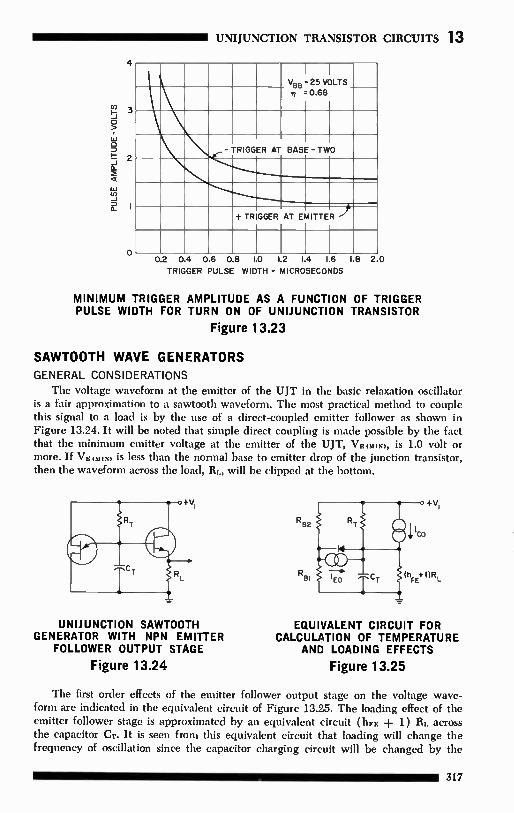
UNIJUNCTION TRANSISTOR CIRCUITS 13
4
PULSE AMPLITUDE -VOLTS
3
2
O
V65 .25 VOLTS n =0.68
- TRIGGER AT BASE-TWO
+ TRIGGER AT EMITTER
02 04 06 08 10 12 14 16 18 20
TRIGGER PULSE WIDTH - MICROSECONDS
MINIMUM TRIGGER AMPLITUDE AS A FUNCTION OF TRIGGER PULSE WIDTH FOR TURN ON OF UNIJUNCTION TRANSISTOR
Figure 13.23
SAWTOOTH WAVE GENERATORS
GENERAL CONSIDERATIONS
The voltage waveform at the emitter of the UJT in the basic relaxation oscillator is a fair approximation to a sawtooth waveform. The most practical method to couple this signal to a load is by the use of a direct-coupled emitter follower as shown in Figure 13.24. It will be noted that simple direct coupling is made possible by the fact that the minimum emitter voltage at the emitter of the UJT, VE (MIN), is 1.0 volt or more. If VE (MINI is less than the normal base to emitter drop of the junction transistor, then the waveform across the load, RI., will be clipped at the bottom.
UNIJUNCTION SAWTOOTH GENERATOR WITH NPN EMITTER
FOLLOWER OUTPUT STAGE
Figure 13.24
EQUIVALENT CIRCUIT FOR CALCULATION OF TEMPERATURE
AND LOADING EFFECTS
Figure 13.25
The first order effects of the emitter follower output stage on the voltage wave-form are indicated in the equivalent circuit of Figure 13.25. The loading effect of the emitter follower stage is approximated by an equivalent circuit (hrE -I- 1) RL across the capacitor Cr. It is seen from this equivalent circuit that loading will change the frequency of oscillation since the capacitor charging circuit will be changed by the
317

13 UNIJUNCTION TRANSISTOR CIRCUITS
presence of the resistor (hEE ± 1) RL. To minimize the effects of loading on the frequency, the value of RL and hEE should be as large as possible. If the values of hEE or RL are too small, the circuit will not oscillate. To ensure oscillation hEE and RI, must satisfy the condition,
(hEE -I- 1) RL > (MAX) 13k RT (hEE ± 1) RL ( )
TEMPERATURE EFFECTS Two important temperature effects are involved in the use of the emitter-follower
output stage. The variation in 11E'; with temperature will change the loading and effect the frequency of oscillation; to minimize this temperature effect, (hEE ± 1) RL should be much greater than the resistor RT. The second temperature effect results from the collector leakage current, )6, of the junction transistor as indicated in Figure 13.25. It will be noted that this current adds to the emitter leakage current, 1E0, of the UJT. Both of these leakage currents tend to increase the frequency as tempera-ture increases. The effect of the leakage currents on the frequency can be minimized by using a large capacitor CT. If the NPN transistor is silicon, the effects of the two leakage currents can generally be neglected at temperatures below 100°C.
Some improvement in circuit operation can be achieved by the use of an PNP emitter follower output stage. For this circuit configuration the effective load resist-ance, (hEE ± 1 ) RL, is in parallel with RT so that the possibility of nonoscillation due to low values of hEE or RL is eliminated. Another advantage is that the Ico of the transistor subtracts from 1E0 of the UJT so that some degree of temperature com-pensation is obtained. This is particularly true if a silicon transistor is used as the PNP output transistor.
IMPROVING LINEARITY For many applications the linearity obtained with the basic UJT relaxation oscil-
lator is inadequate. To achieve the best linearity with the basic circuit, it is necessary to use a UJT having the minimum value of n ( types 2N489, 2N490). The best linearity which can be obtained with these types is about 10%. A number of simple circuit techniques can be used to improve the linearity of the
sawtooth waveform. The direct approach of using a higher supply voltage for charg-ing the timing capacitor is illustrated in Figure 13.26(A). This is an inexpensive method of improving linearity if a high voltage supply is available in the system under design. It suffers from the disadvantage that the frequency would not be as stable as it would with a single power supply.
(A) USE OF H GH VOLTAGE SUPPLY FOR CHARGING OF TIMING CAPACITOR
VI
(3) USE OF COLLECTOR CHARACTERISTIC FOR CONSTANT CURRENT SOURCE
TWO CIRCUITS FOR IMPROVING LINEARITY OF SAWTOOTH GENERATORS
Figure 13.26
Figure 13.26(B) illustrates the use of the high output impedance of a common-base transistor to maintain a constant charging current for the capacitor.
318

UNIJUNCTION TRANSISTOR CIRCUITS 13
LINEAR SAWTOOTH WAVE GENERATORS Two variations of a bootstrap charging circuit are shown in Figures 13.27 and
13.28. In 13.27 a constant voltage is maintained across the charging resistor by the zener diode and the emitter follower transistor amplifier stage so that the capacitor charging current is constant over the complete cycle. This circuit is quite economical in that it makes double use of the transistor, both as the driver for the bootstrap circuit and as an output amplifier stage. Note that the 3.9K load resistor is returned to a negative voltage to prevent clipping at the bottom of the sawtooth waveform. Q3 maintains the zener current constant for improved linearity and also assists Q2 in supplying current to the load. The circuit will generate a linear sawtooth up to 50 kc.
+24V
1N4154
03
2N525
680
5.6V
01 2N2646 J F-0 OUTPUT
.001
3.9K
-10V
50 KC SAWTOOTH GENERATOR
Figure 13.27
The circuit shown in Figure 13.28 makes use of a capacitor in place of the zener diode. This variation permits the negative supply to be eliminated. The NPN tran-sistor serves as an output buffer amplifier with the capacitor C2 and resistor R2 serving in a bootstrap circuit to improve the linearity of the sawtooth. RI and Cl act as an integrating network to provide second order compensation for the non-linearity of the waveform. By varying the value of RI the output waveform can be made concave upward, concave downward, or linear.
+20V
N\P
OUTPUT
6V P- P
OUTPUT
10 V P-P I KC
SAWTOOTH GENERATOR WITH HIGH LINEARITY
Figure 13.28
319

13 UNIJUNCTION TRANSISTOR CIRCUITS
=
The feedback networks in Figure 13.28 are frequency sensitive. C2 will not be effective at low frequencies and the effective emitter capacity can not be much less than .01 gf without affecting the linearity and operation at the higher frequencies. Cl could be reduced to about .001 1.4f by using the higher frequency type 2N2647.
PRECISION TIMING CIRCUITS
TIME DELAY RELAY
Figure 13.29 shows how the unijunction transistor can be used to obtain a delay in the operation of a relay. When the switch SW1 is closed, capacitor CT is charged to the peak point voltage at which time the unijunction triggers and the capacitor discharges through the relay causing it to close. One set of relay contacts holds the relay closed and the second set of contacts can be used for control functions. To be used in this circuit, relays must have fast operating times, low coil resistance and low operating power.
RELAY CONTACTS
RT
I MEG
CT
I00µ fd 25V
2NI6716
RELAY 14613 DPDT
SW'
3300 2W
+ V1
( 24-32V )
GE MICRO— MINIATURE RELAY 3S2791G200A-6
IN536
TIME DELAY CIRCUIT WITH RELAY
Figure 13.29
The time delay of this circuit is determined by RT, about one second of delay for each 10K of resistance. The time delay is quite independent of temperature and supply voltage.
PRECISION SOLID STATE TIME DELAY CIRCUITS Figure 13.30 illustrates a typical time delay circuit ùsing the unijunction transistor
together with a low cost SCR. The timing interval is initiated by applying power to the circuit. At the end of the timing interval, which is determined by the value of RTCT, the unijunction triggers the SCR and the full supply voltage minus about one volt is applied to the load. By suitable choice of RT and CT this circuit will give time delays from 0.4 milliseconds to 1 minute. Load currents are limited only by the rating of the SCR; up to 6 amperes for the C2OF (stud mounted). Use of a precision cali-brated resistor such as helipot in place of RT permits the time delay to be set accurately over a wide range after one initial calibration.
The timing resistor in a conventional UJT time delay circuit must be small enough to supply the minimum trigger current (II.) of the UJT plus the leakage current of the timing capacitor when the UJT emitter is biased at its peak point voltage. The 2N494C has a maximum h. requirement of 2 ga. This places a limit of 3 megohms on RT and for CT = 4 gf permits time delays to 12 seconds with a conventional circuit.
The circuit shown in Figure 13.31 reduces the effective trigger current by a factor
320

UNIJUNCTION TRANSISTOR CIRCUITS 13
56on
SOLID STATE TIME DELAY CIRCUIT
Figure 13.30
10µf
25V
--0-
22K R,
47011 1000 M.S1
CT
4µf d YLHAR •A SSD708
2N494C
SSD708 1.5n
47(7)K TIME ADJUST
27011
1500
N4009
2711
ONE HOUR TIME DELAY CIRCUIT
Figure 13.31
+28V
EXTERNAL LOAD
+28V
C35F CIOF C9F
LOAD
G N
of more than 1000 and allows time delays of up to 1 hour to be achieved with a low leakage 4 1.4.fd mylar capacitor. This is achieved by periodically sampling the voltage on the timing capacitor. Between samples the timing capacitor is isolated from the emitter of the UJT by ultra-low leakage planar silicon diodes (the SSD-708 has a leakage current of less than 20 picoamperes at 25°C). The sampling pulse is gen-erated by a UJT relaxation oscillator operating at approximately 2 cps.
The 2N494C is biased continuously at the peak point by a 15 megohm resistor to reduce the triggering energy required. Adjustment of the time intérval is obtained by means of the 10K potentiometer which sets the initial voltage on the timing capaci-tor. Extreme care must be taken in the choice of components and the layout to minimize leakage. A high quality mylar capacitor must be used for CT. A glass sealed resistor must be used for RT. Point A should be supported by the leads only or by a single teflon standoff insulator.
The circuit in Figure 13.32 gives time delays from 0.3 milliseconds to 5 hours without using a tantalum or electrolytic capacitor. The timing interval is initiated by applying power to the circuit. At the end of the timing interval, which is determined
321

13 UNIJUNCTION TRANSISTOR CIRCUITS
RI 2.2K TO 10.000 MEG
CI 0.1 TO 2,‘ f
FIVE HOUR TIME DELAY CIRCUIT
Figure 13.32
C9F, CI 2F OR C4OF
by the value of RI Cl, the 2N494C triggers the controlled rectifier. Load currents are limited only by the rating of the controlled rectifier which is from 1 ampere up to 25 amperes for the types specified in the circuit.
Charging resistor RI must be small enough to supply the minimum trigger cur-rent (peak point current, Ip) of the 2N494C plus the leakage current of the capacitor when the emitter of the unijunction is biased at its peak point voltage. This would place a limit of 3 megohms for RI and permit time delays to 6 seconds (Cl = 2 gf) without using the additional 2N491 relaxation oscillator.
The circuit as shown effectively reduces the minimum It. requirement more than 1000 times by pulsing the upper base of the 2N494C with a 3/4 volt negative pulse. This negative pulse rate is not critical but it should have a period that is less than 0.02 (R1 Cl). The negative pulse causes the peak point voltage to drop slightly and if the voltage level at Cl is greater than this, the unijunction will trigger with the necessary Ir supplied from Cl. The low leakage requirement for Cl is easily obtained with a mylar capacitor. R2 can be adjusted or selected for best stabilization over the required temperature range. A pulse transformer can be used in place of the 27 ohm resistor if it is necessary to have the timing circuit isolated from the power switching (controlled rectifier) circuit which, for instance, might be connected to the ac line.
The input impedance of the 2N494C is greater than 1500 megohms before it is triggered. The maximum time delay that can be achieved by this circuit is mainly dependent upon the maximum values that can be obtained for RI and Cl consistent
I N1694
3.9K I W
START SWITCH
200 100V
120V 60 CPS
SPRAGUE 312286 CIO OR C35
SOLID STATE AC TIME DELAY (ONE SECOND)
Figure 13.33
322

UNIJUNCTION TRANSISTOR CIRCUITS 13
with the low leakage requirement. Without diode DI, R1 is limited to 15 megohms for an accuracy of 0.5% at 25°C and 5% at 55°C, but with DI, RI can be increased to 10,000 megohms.
An all solid state time delay circuit with ac output can be achieved with a single UJT as shown in Figure 13.33. The timing sequence is started by closing the START SWITCH and applying voltage to the UJT circuit. The time delay is determined by the time constant (R1 ± R2) (Cl -I- C2). When the voltage at the emitter of the UJT reaches the peak point voltage, capacitor Cl remains charged and the UJT oscillates at a high frequency determined by the time constant (R1 ± R2) C2. The pulses from the UJT are then coupled through the pulse transformer to the SCR's, turning them on and applying voltage to the load. Since the UJT oscillates at a frequency much higher than the line frequency the switching of the SCR's is prac-tically from full on to full off. The 2N2647 is needed to obtain the high output pulse required to fire two SCR's in parallel at a high repetition rate. When the start switch is opened diode DI provides a path to discharge Cl. Larger values of time delay can be obtained by increasing the value of Cl. The timing circuit and the load circuit can be operated from a common ac supply or a seperate ac supply as desired.
DELAYED DROPOUT RELAY TIMER The circuit of Figure 13.34 provides a simple means for accurately delaying the
dropout of a relay after it is energized. In the quiescent state no power is applied to the circuit. When SW1 is momentarily closed the transistor will turn on and the relay will pull in. Voltage to the circuit is then maintained through the relay contact so that the relay will remain energized when SW1 is opened. After a time interval determined by the values of RI and Cl the UJT will trigger, and the discharge of Cl will turn off the NPN transistor, allowing the relay to drop out. If SW1 is open the voltage to the circuit will be removed and the circuit will revert to its quiescent state.
R3
DELAYED DROPOUT RELAY TIMER
Figure 13.34
An output voltage can be obtained from the relay contacts shown or extra sets of contacts on the relay can be used as desired.
After deciding on the supply voltage and the relay to be used, R2 is then selected to provide sufficient base current to the NPN transistor with regard to the resistance of the relay coil and the minimum specified current gain of the transistor. The size of the capacitor is then selected to provide sufficient off time for the NPN transistor to allow the relay to drop out. Resistor RI is then chosen for the maximum time delay
323

13 UNIJUNCTION TRANSISTOR CIRCUITS
+30V O
IMOMENTARY CONTACT SWITCH
IN536
IK
Ion
SCS 3N61
4
35ma
I WATT RELAY ¡IN536
I 2µf 2p.f
2.5
10 SECOND TIMER
Figure 13.35
470
2N2647
required and the maximum peak point current of the UJT. Finally, resistor R3 is chosen for the required overall temperature compensation.
The circuit of Figure 13.35 provides for the relay to be energized for a preset period of time up to 10 seconds. Closing Si triggers the silicon controlled switch (SCS), and places most of the supply voltage across the relay which also starts the unijunction timing interval. After a preset interval the unijunction will be triggered and discharge the 4 eif capacitance through the 10 ohm resistor. This discharge pulse makes the anode negative with respect to the anode gate (connected to +30 volts) and turns off the SCS which drops out the relay.
SENSING CIRCUITS
VOLTAGE SENSING CIRCUIT
The high sensitivity of the unijunction transistor and the extreme stability of VP make it ideally suited for use in go no-go types of voltage sensing circuits such as shown in Figure 13.36. This circuit includes a simple floating power supply with zener diode regulation which operates from the 115 volt ac line. If the input signal is negative the unijunction will not trigger and there will be no output. If the input signal is slightly positive, the unijunction will trigger and pulses will occur at the output as long as the input signal remains positive. The output pulses are of sufficient magnitude to trigger a flip-flop, an SCR, or other pulse sensitive devices. Note that the transformer coupled supply and output of this circuit give complete freedom of choice in connecting the circuit to the signal source since there are no common grounds.
Most of the output pulse energy is supplied by capacitor C3. This capacitor is charged rapidly through RI after each pulse and hence does not limit the response time of the circuit. Diode D2 provides a discharge path for C3, and diodes DI and D2 clamp the input voltage to enable C3 to charge to its steady state voltage when very large voltages are present at the signal input. Capacitors Cl and C2 provide the initial trigger energy for the unijunction transistor and also serve as a filter for tran-sients appearing at the signal input and across the supply. In some cases a small capaci-tor will also be required across the primary of the pulse transformer to prevent false triggering due to transients.
The circuit is initially adjusted by shorting the signal input and setting RI so that the circuit is on the verge of triggering. If close temperature compensation is needed
324

UNIJUNCTION TRANSISTOR CIRCUITS 13
330 A
SIGNAL INPUT
3300 PUL SE OUTPUT
VOLTAGE SENSING AND TRIGGER CIRCUIT
Figure 13.36
R2 is adjusted so that the triggering voltage does not change appreciably when the unijunction is heated or cooled. It is normally possible to adjust the temperature com-pensation so that the drift in trigger voltage is within ±-2 millivolts from 0°C to 55°C. After the temperature compensation is completed it will normally be necessary to reset R 1. The long term stability of this circuit is normally better than ±-10 millivolts and the hysteresis is normally less than 1 millivolt. The change in triggering voltage with a change in the supply voltage ( aV, ) will be less than 0.7 AV1/V1. The voltage stability can be improved by adding two silicon diodes in series with R2.
NANOAMPERE SENSING CIRCUIT WITH 100 MEGOHM INPUT IMPEDANCE The circuit in Figure 13.37 may be used as a sensitive current detector or as a
voltage detector having high input impedance. R1 is set so that the voltage at point A is 1/2 to 3/4 volts below the level that triggers the 2N494C. A small input current (It.) of only 40 nanoamperes will charge C2 and raise the voltage at the emitter to the triggering level. When the 2N494C is triggered, both capacitors, Cl and C2 are dis-charged through the 27 ohm resistor, which generates a positive pulse with sufficient amplitude to trigger a silicon controlled rectifier (SCR), or other pulse sensitive cir-cuitry. C2 is kept small for faster triggering response time and Cl is used to provide the pulse output energy. Rapid recovery is obtained after the 2N494C triggers since both capacitors are charged through Rl. This configuration has the advantage that the leakage current of the silicon diode effectively subtracts from the leakage current of the unijunction and thus provides some temperature compensation.
The input current available MO through the 100 megohm resistor will be much lower than the minimum trigger requirement for the 2N494C (peak point current (L.) = 2.0 sa). Use of a sampling technique described for Figure 13.31, however, permits a reduction in the external triggering current ( II.) by as much as 1000 times below h. By pulsing the upper base of the 2N494C with a 0.75 volt amplitude nega-tive pulse the peak point voltage V, will drop slightly and if the voltage level at C2 is greater than this, the unijunction will trigger with the necessary Ir supplied from C2. By use of this technique, the 2N494C has been triggered with external input cur-rents MO as low as 1 nanoampere with a 2000 megohm resistor for R2.
The period of the 2N491 relaxation oscillation is not critical, but it should have a time constant of 0.02, or less, than that of the 2N494C.
For this sensing circuit a floating power supply using a zener diode will permit
325

13 UNIJUNCTION TRANSISTOR CIRCUITS •
NANOAMPERE SENSING CIRCUIT WITH 100 MEGOHM INPUT IMPEDANCE
Figure 13.37
SCR (C9F, Cl2F, OR C4OF
grounding one of the sensing input terminals if this is desirable. M. should be adjusted so the circuit will not trigger at the maximum ambient temperature in the absence of the current or voltage sensing signal. R3 can be adjusted or selected for best stabiliza-tion of Vp over the required temperature range.
SCR TRIGGER CIRCUITS
SIMPLIFIED SCR TRIGGER CIRCUIT DESIGN PROCEDURES SCR trigger circuits using the unijunction are simple and compact with low power
consumption yet the 2N2647 can easily trigger a 235 amp rms SCR. An added advan-tage is that triggering is assured over a wide ambient temperature range even with UJT and SCR limit units (due to production variations). This assurance is available by using the tailored trigger circuits as outlined in Figures 13.38 and 13.39. These circuits essentially marry the particular UJT and SCR in a configuration that takes into account the dynamic triggering requirement of the SCR. Whereas most SCR specification sheets give consideration only to the static requirements. These design curves give the condition for the required minimum trigger energy, and it is then simple to double the value of CT or increase Vi for a guaranteed 2 to 1 above this minimum which is often desirable to decrease the SCR turn-on time and switching losses.
The value of R1 in the trigger circuits is kept low enough to prevent the de voltage at the gate, due to interbase current, from exceeding the minimum gate triggering voltage for the SCR.
The design of a suitable SCR triggering circuit can be achieved rapidly and easily by using the design curves that are given. These curves give the minimum supply voltage required to guarantee triggering of the various types of SCR's over the specific temperature range as a function of the UJT emitter capacitor, CT. The value of the resistor RT is not important for the purposes of the design provided that it is within the limits required for the UJT to oscillate. If R2 is significantly greater than 100 ohms the minimum supply voltage which is assumed ( Vi' ) should be calculated from the minimum supply voltage (Vi) given in the design curves using the equation (131).
yi Vi' ( 2200 ± R2 2300
As an example of the practical design of an SCR triggering circuit, consider the following:
Problem: A circuit is required to trigger a high current type 2N1913 SCR and the trigger circuit supply is 22 volts. We choose the 2N2647 UJT because of its guar-
(131)
326

UNIJUNCTION TRANSISTOR CIRCUITS 13
36
34
!. 32
o > 30
28
t..) 26 0
1- 24
o > 22
2 16
14
12
10
8
6 001
UJT TYPE SCR TYPE CURVE RI V I(MAXI I..
2N489A Et B THROUGH 2N494A, B, AND C (ALSO USAF TYPES)
2N24I7A 8 B THROUGH 2N2422A, El, AND C
2N167IA 8 B
2N2646
2N2647
C60(2N202 3-30) C55 AND C56 C52(2N1792-98) C50(2N1909-16) C46 C45 C37 C 36(2NI842 -50)
A 270 -± e%
..,
35v
s 470 ± e% 26V
c PULSE TRANS. PE223I
35V
C40 C380 C35(2N681-92)
C30 AND C32 ** C20 AND C22 *. C15
D 270 ± 10% 35V
E 470 II0% 20V
G PULSE TRANS. SPRAGUE 31Z204
35V
C12 CI 1(2N1770 -78,
2N2619) C10(2N1770A-77A) C9 C8(2N1929-35) 2N1595-99
E 270 t 10% 32V
G 470 ± 10% 18 V
r PULSE TRANS. SPRAGUE 31Z204
35V
C7(2N2344-48) C6 C5
F ISO ± io% 35V
H 270 ± 10% 20V
J _ SPRAGUE 31Z204 35V
NOTES: *LIMITED TO 27 VOLTS MAX ON "D" CURVE AND 15 ***MINIMUM TRIGGER PULSE IS TWICE THE AMP-VOLTS ON "E" CURVE. L TUDE OF OTHER UJT'S, THIS ASSURES 2:1
**TRIGGER REQUIREMENTS LESS THAN OTHERS OVER MINIMUM SCR TRIGGER REQUIREMENTS. IN THIS GROUP.
0 te\o c ® v, OK - .„
é
LOAD
Coo T RI
0
0
0
-.
—55°C TO+ I25° C (NOTE: Temperature range may be restricted by the SCR specification.)
0.1
CAPAC1TANCE-C T- MICROFARADS
SCR TRIGGER CIRCUIT DESIGN CURVES (Assures minimum trigger requirement for IA rise <10A/gsec.)
Figure 13.38
10
anteed high trigger pulse, V.51. Assume that the value of capacitance, chosen on the basis of operating frequency, is 0.2 uf and that the value of the base-two resistor, calculated for temperature compensation, is 620 ohms. Solution: From Figure 13.39 it is seen that curve B meets the above requirements with a 27 ohm resistor for RI. On curve B it is seen that the minimum voltage for CT = 0.2 ,if is 11.7 volts. Correcting this value to take into account the value of R2, equation (131) gives Vi' = (1.22) (11.7) = 14.3 volts. Triggering is therefore assured for a supply voltage range of 14.3 to 35 volts. If the supply voltage is
327

13 UNIJUNCTION TRANSISTOR CIRCUITS MINIMUM SUPPLY VOLTAGE -V1 - VOLTS
34
32
30
28
26
24
22
20
16614
12
10
O 6 4
2
A 27Ot 10%
PULSE TRANS. PE223I
27000%
470110%
20V
D
SCR TYPE CURVE RI VIIMAX)
C80
C60(2N202330)
C55,C56
C52(2N1792-98) C50(2N1909-16) C45 AND C46 ZJ257 ZJ285
35V
35V
20V
PULSE TRANS. PE2231
35V
.01
2N2647 TA =-40•C TO 125•C
I I II .05 0 I 05
CAPACITANCE -CT - MICROFARADS
HIGH CURRENT SCR TRIGGER CIRCUIT DESIGN CURVES USING 2N2647
Figure 13.39
10
greater than 35 volts the SCR may be triggered by the de voltage across RI at an elevated SCR junction temperature. Thus, a suitable design using the 2N2647 in the triggering circuit would be CT = 0.2 pf, R2 = 620 ohms, RI = 27 ohms, and V, = 22 volts, +60% or —35%.
TRIGGERING PARALLEL-CONNECTED SCR'S If two or more SCR's in parallel are to be triggered by a single UJT the design
of the trigger circuit must take into consideration the possibility that an SCR with a low gate resistance may be paralleled with an SCR having a high gate resistance, thus loading down the output pulse sufficiently to prevent the second SCR from being triggered. To reduce this possibility it is recommended that the trigger pulse be coupled by means of a separate capacitor to each SCR gate. These capacitors act to equalize the charge coupled to each gate during the trigger pulse and thus tend to reduce the effects of unequal loading. The optimum value of capacitor for this purpose has been found to be 0.1 pf. In addition to this capacitor, a resistor having a value of 220 ohms to IK should be connected between gate and cathode of each 'SCR. Using this approach of equalizing capacitors, the design curves of Figures 13.38 and 13.39 can be used for parallel triggering of SCR's, provided that the minimum supply volt-age is multiplied by a factor of 1.5 if two SCR's are to be triggered in parallel and by a factor of 1.8 if three SCR's are to be triggered in parallel. Since the gates are not direct coupled, the maximum supply voltage allowed is limited only by the 35 volt rating of the UJT.
328

UNIJUNCTION TRANSISTOR CIRCUITS 13
Alternatively, a larger value of base-one resistance, R1, can be used to reduce the otherwise required increase in value of supply voltage for parallel triggering. For example, if RI . 100 ohms, and using equalizing capacitors, the curves for RI = 27 ohms apply for triggering two SCR's in parallel with no increase in supply voltage. For triggering three SCR's in parallel under this condition the supply voltages given by these curves should be increased by a factor of 1.25.
SIMPLIFIED SCR TRIGGER CIRCUITS FOR AC LINE OPERATION A trigger circuit that is synchronized from the ac line is shown in Figure 13.40.
fYY1 rrn
AC FULL WAVE RECT PIED
1 ZEN ER 1 DIODE
R2
01
RI
OUTPUT TO SCR GATE
LINE SYNCHRONIZED TRIGGER CIRCUIT
Figure 13.40
A full wave rectified signal obtained from a rectifier bridge or a similar source is used to supply both power and a synchronizing signal to the trigger circuit. The zener diode is used to clip and regulate the peaks of the ac as indicated in Figure 13.40. At the end of each half-cycle the voltage at base-two of the UJT will drop to zero, and any charge on the capacitor will forward bias the emitter diode of UJT into conduction. The capacitor is thus discharged at the beginning of each half cycle and the trigger circuit synchronized with the line. A pulse is produced at the output at the end of each half cycle which can cause the SCR to trigger and produce a small current in the load. A simplified type of trigger circuit results if base-two and the emitter timing
circuit of the UJT are supplied directly from the line by way of dropping resistor RD which keeps the peak voltage on the UJT within its specifications. (See Figure 13.41.) The voltage across capacitor C will increase at a rate determined by the time constant of the circuit. When it reaches the peak point voltage the UJT will trigger and turn on the SCR.
SIMPLIFIED UNIJUNCTION TRANSISTOR TRIGGER
CIRCUIT
Figure 13.41
329

13 UNIJUNCTION TRANSISTOR CIRCUITS
LOAD
120 VAC
o
SCR C11/20 47
33K RD
RI 100K
RmiN 01 2N2646 22K 500K Q. CONTROL
R51 0.1
WC — 0.1 7
02 2N2646 RI 100K
33K
SIMPLIFIED FULL-WAVE UJT TRIGGER CIRCUIT
Figure 13.42
SCR CH/20
The half-wave circuit of Figure 13.41 can be extended to full-wave operation. In Figure 13.42 two of the basic circuits of Figure 13.41 have been placed back-to-back. The emitters of the two UJT's have been cross-coupled with a network that exerts full cycle phase control over both SCR's.
The unijunction phase-control circuit in Figure 13.43 has a wide range of stable control without hysteresis or dependence upon supply voltage. Automatic feedback control systems can be designed with this UJT circuit since the UJT is essentially half of a balanced bridge with built-in un-balance detection of high sensitivity and stability. The dual diode is selenium and has a low peak reverse voltage requirement in this circuit.
LOAD
120 VAC 60e.
RI 33K
o TI - SPRAGUE
R3 3-125K R 2 O. leaf 33K
• DUAL DIODE —OE 6RS5GDIBADf (G.E.)
TI
TYPE 31Z204
• (T
WT/TRIAC PHASE CONTROL
Figure 13.43
G.E. TRI AC ZJ-257B
SENSITIVE AC POWER SWITCH The circuit Figure 13.44 switches load in response to a gradually changing signal
such as light on a cadmium sulfide photocell, temperature of a thermistor and so on. Switching is a positive snap action from full "off" to full "on" and vice versa. Differ-ential in input between switching conditions may be adjusted over a wide range by changing values of Cl and RI.
330

UNIJUNCTION TRANSISTOR CIRCUITS 13
SENSITIVE
AC POWER SWITCH
Figure 13.44
o—r LOAD 1-40
120V AC
GE -KGE A44B A44B
VOLTAGE ACROSS C2
6.8K 2W
2N2646 47 C2
OFF LON
4.7K Z4XLI6
GE 8425 PHOTO CELL
PEAK POINT — VOLTAGE OF UJT
•
The conventional unijunction transistor circuit has been modified so the voltage waveshape across capacitor C2 has a higher value at the beginning of each half-cycle than at the end. This wave is the result of Cl and RI producing a higher charging current to C2 at the beginning of the cycle. As the photocell resistance (in this case) increases, the voltage on C2 rises until it reaches the peak-point voltage of the UJT. Since this condition occurs first at the leading edge of the cycle, the UJT will only trigger at that point, turning the SCR on early in each half cycle. Triggering the SCR removes voltage from the UJT circuit, and capacitor Cl discharges. At the beginning of the next half cycle, the discharged condition of Cl produces a higher charging current for C2, assuring a snap action full "on" condition. Photocell resistance must then be reduced to a value lower than before in order to stop triggering the UJT and SCR, hence the differential between "on" and "off" conditions.
The photocell can be replaced with a grounded emitter NPN transistor to make the circuit sensitive to de input signals. This on/off ac switch can be used for photoelectric controllers, temperature regulators, overheat protection, latch-on functions, ac motors, driving compressors, conveyors, and fans.
SENSITIVE DC POWER SWITCH The circuit in Figure 13.45 features a latching action. That is, once triggered, it
stays on. In this circuit
Power input = 0.1 volt at 25 µamp = 2.5 µwatts
Power output = 400 volts at up to 110 amps de = 44k watts
Output 44 X 103 Power gain tt — 17.5 x Ice — 92db Input 2.5 X 10'
SENSITIVE DC POWER SWITCH
Figure 13.45
+20V
SENSITIVITY CONTROL 10K
LOAD OUTPUT
331

13 UNIJUNCTION TRANSISTOR CIRCUITS
HIGH GAIN PHASE-CONTROL CIRCUIT
The minimum size of the capacitor C2 in a conventional UJT/SCR phase-control circuit is dictated by the minimum acceptable pulse amplitude at the output. For reliable firing of high current SCR's a capacitor in the range of 0.20 µfd is necessary. Once the minimum size of the capacitor and the required range of phase control are determined the required current from the control element will be fixed. If the available current from the control element is insufficient, one or more stages of amplification must be added between the control element and the phase-control circuit.
HIGH GAIN PHASE-CONTROL CIRCUIT
Figure 13.46
22011
2N49113 OR
2N24198
C PULSE OUTPUT
The simple modification of the phase-control circuit shown in Figure 13.46 permits an increase in the effective gain by a factor of up to 10,000 times and in many applica-tions will duplicate the performance of two or three stages of transistor amplification. In this circuit the larger capacitor, C2, is rapidly charged through the 6.8K resistors at the beginning of the timing interval. The smaller capacitor, Cl, is charged through the control element and since this capacitor is in series with C2 it can be charged simultaneously with C2. The effective gain of the circuit is very large since a smaller voltage change is required across a smaller capacitor than with the conventional phase control circuit. Thus the current required from the control element is much less than if C2 were charged directly. At the same time the full pulse energy from C2 is avail-able at the output.
In designing this circuit, C2 is chosen large enough to provide the required output pulse amplitude. Capacitor Cl is chosen small enough to provide sufficient gain for the circuit and large enough to ensure regeneration at the peak point. Usually a value of 500 pf will be adequate to meet the latter requirement for the 2N489-2N494, 2N2417-2N2422 or 2N1671, and 100 pf will be adequate for the 2N2646 or 2N2647.
TRIGGERING CIRCUITS FOR DC CHOPPERS AND INVERTERS The impulse commutation often used in de choppers and inverters can cause
premature triggering of the unijunction. The positive commutating pulse applied to the cathode of the SCR, results in a negative pulse gate to cathode. If these negative pulses reach base-one of the unijunction it may be triggered prematurely. When transformer coupling is used, transients can be greatly attenuated by a diode bridge as shown in Figure 13.47. A negative gate to cathode pulse at the SCR may be further attenuated by the low impedance 1N91.
Supply voltage transients can be decoupled from the unijunction emitter by choosing the impedance of Cl and C2 so the transient has negligible effect on V. The sum of Cl and C2 constitute the total unijunction timing capacitance.
The triggering circuit of Figure 13.48 uses the UJT to drive the 2N526 from cut-off to saturation. Since we are not using the energy in Cl to trigger the SCR, the smaller .01 gf capacitor size can be used and thus achieve UJT operation to 20 kc. The 1N4154 keeps the emitter-base junction of the 2N526 reverse biased except for
332

UNIJUNCTION TRANSISTOR CIRCUITS 13
TRIGGER CIRCUIT FOR ELIMINATION OF TRANSIENT INTERFERENCE
Figure 13.47
1- 28V 3.3K
20 KC TRIGGER GENERATOR
Figure 13.48
COMMUTATING PULSE
the discharge interval of Cl. R5 limits the voltage amplitude of the trigger pulse to the SCR. The 2N526 also isolates the SCR turn-off pulse from the UJT timing circuit.
The square wave inverter drive circuit shown in Figure 10.12 (Chapter 10) has been used successfully as the control and trigger source for parallel inverters using General Electric type C40 SCR's.
REGULATED AC POWER SUPPLY
The unijunction triggering circuit in Figure 13.49(A) uses the voltage developed across the SCR's during blocking for the interbase supply as well as synchronization for the unijunction transistor. The firing circuit is connected to the output of a single phase bridge formed by the 1N1695's. Through the action of the bridge, the zener diode and the resistor R3, a clipped and rectified voltage with a waveform as shown in Figure 13.49(B) is applied to the UJT and its emitter circuit.
333

13 UNIJUNCTION TRANSISTOR CIRCUITS
60
- I LOAD •
It
SPRAGUE 3IZ 286
INI695
R3
3.3K 5W
BB
R4 IK
R2 390 22V I W
2N167IA
Vi
2.7K
4,.
i
50K
5V CPS
C356
• VE - CI
•
T0.21.0
1 INI695 i
SUPPLY 0 VOLTAGE
VOLTAGE ACROSS ZENER DIODE 0
VOLTAGE ACROSS
CI
GATE CURRENT
VOLTAGE ACROSS 0 LOAD
0
O
(A)
(B)
REGULATED AC POWER SUPPLY AND WAVESHAPES
Figure 13.49
INI695
INI695
The regulating ability of the supply in Figure 13.49(A) results from having R4 in the circuit. The charging voltage for the capacitor is equal to the zener voltage and is essentially constant over the half cycle prior to the instant when the SCR is triggered. This is shown in the waveforms of Figure 13.50. The interbase voltage, VBB, of the UJT is not constant during this interval, but is equal to the breakdown voltage of the zener diode plus a small fraction of the line voltage determined by the voltage dividing ratio of R3 and R4. Thus at any given phase angle the interbase
334

UNIJUNCTION TRANSISTOR CIRCUITS 13
voltage will increase if the line voltage increases as shown in Figure 13.50. The peak point voltage of the unijunction transistor is equal to the interbase voltage times the standoff ratio and is given in Figure 13.50 to correspond to the two interbase volt-age curves.
The emitter voltage follows the normal exponential charging characteristic since the charging voltage, Vi, is constant. The UJT and SCR's trigger when the emitter voltage equals the peak point voltage. It is readily apparent from Figure 13.50 that, as the line voltage increases, the delay before the UJT and SCR's are triggered in-creases and hence the conduction angle of the SCR's decreases. The decreased con-duction angle reduces the power to the load, thus offsetting the increase of power to the load otherwise due to the increase in line voltage. By proper choice of the voltage divider ratio of R3 and R4 it is possible to obtain perfect compensation of the circuit for small changes in line voltage.
INTERCASE VOLTAGE, VaB
CHARGING VOLTAGE, V1
PEAK POINT VOLTAGE
(Vp V8B)
EMITTER VOLTAGE, VE
HIGH LINE VOLTAGE
LOW LINE VOLTAGE
• •
ONE-HALF CYCLE OF AC LINE
CONDUCTION I._ ANGLE HIGH LINE —4 VOLT AGE
CONDUCTION I ANGLE LOW LINE VOLT
VOLTAGE WAVEFORMS OF SCR/WT REGULATED AC SUPPLY WITH HIGH AND LOW LINE VOLTAGE
Figure 13.50
The circuit shown was adjusted to give optimum regulation at 25 volts rms output and 115 volts input, and the component values listed were found to be suitable. For a change in line voltage from 115 volts to 100 volts the change in output voltage was less than 0.1 volt with any output voltage setting from 10 volts to 30 volts.
If regulation is desired over a wide range of output voltage, a ganged pot can be used with R1, and the value of R4 can be changed with the position of the potenti-ometer. The value of R2 is chosen to achieve the desired temperature compensation in the ordinary manner. There is some interaction between the adjustment of R4 for voltage compensation and the adjustment of R2 for temperature compensation, so several successive adjustments may be required.
335

13 UNIJUNCTION TRANSISTOR CIRCUITS
TRANSISTOR CONTROL OF UNIJUNCTION
SHUNT TRANSISTOR CONTROL OF UJT
In circuits using a shunt transistor to control the UJT similar to the arrangement in Figure 13.51, it is seen that Q1 can shunt some of the charging current supplied to Cl by resistor RI in an amount dependent of the base drive to Ql. The more Q1 is turned on, the greater the delay before the UJT is triggered. With R1 set for about 4.7K ohms, base current IB to Q1 will then control the diversion of charging current from Cl and retard or advance the triggering of the UJT. Q1 can prevent the trigger-ing of the UJT if
V, (1 — n) IB (13m)
hBE RI where
IB is in amperes V, = 20 volts, and hFE = current gain of Q1
RESET
RI .10K + 4.7K
4.7K
OI 2N2I9 2
SIGNAL 75K
INPUT
SIGNAL DROPOUT DETECTOR
Figure 13.51
The circuit of Figure 13.51 can be used to provide an indication of a momentary dropout of an input signal. The signal monitored could be a dc voltage, an ac voltage, or a pulse voltage. The time between the disappearance of the signal and the indica-tion of a fault can be adjusted as desired.
Capacitor Cl will be charged through RI continuously. In the presence of an input signal the NPN transistor will discharge CI in a periodic manner so that the voltage at the emitter of the UJT will not reach the peak point voltage and neither the UJT nor the SCS will be triggered. If the input signal disappears or the time between pulses exceeds the preset value, the UJT and the SCS will be triggered and provide a de output signal. The output signal will remain until the SCS is turned off by momentarily opening the reset switch. The 100K resistor in the anode gate of the SCS is used to prevent the rate effect from interfering with the reset action.
SERIES TRANSISTOR CONTROL OF UNIJUNCTION A transistor in series with Cl instead of in shunt with it can be used to regulate
the charging rate of the capacitor and thereby retard or advance the triggering of
336

UNIJUNCTION TRANSISTOR CIRCUITS 13
the UJT. Such a circuit is shown in Figure 13.52. An additional NPN transistor, Q3, is required if it is desired to keep one side of the input signal at the potential of the lower line. Series control often offers an advantage in noise immunity in a system.
INPUT SIGNAL V2
PULSE OUTPUT
TI-SPRAGUE TYPE 31 Z 204
SERIES TRANSISTOR CONTROL OF WT
Figure 13.52
HYBRID TIMING CIRCUITS
The unijunction transistor can he used in conjunction with conventional PNP or NPN transistors to obtain versatile timing circuits such as symmetrical and nonsym-metrical multivibrators, one-shot multivibrators, variable frequency oscillators, and time delay circuits. The advantages of these circuits include: (1) the output at the collector of each transistor is very nearly an ideal rectangular waveform, (2) the circuits will tolerate large variations in hFE or Ico of the transistors as compared to conventional circuits, (3) the circuits are not prone to "lock-up" or non-oscillation, (4) the timing stability is excellent, and (5) a single small timing capacitor CT can be used, avoiding the use of electrolytic capacitors in many applications.
The hybrid timing circuits can use either germanium or silicon transistors as desired. The basic circuits for PNP or NPN transistors are shown in Figures 13.53(A) and 13.53(B). In both of these circuits, the junction transistors form a conventional flip-flop with the unijunction transistor serving the timing and triggering functions. Each time the unijunction transistor conducts, the discharge current from the capacitor CT develops a pulse across RA which triggers the flip-flop from one state to the other.
The basic circuits as shown in Figures 13.53(A) and 13.53(B) will operate at frequencies from about 1 cycle to 500 cycles, and at temperatures above 75°C. Fre-quencies from 1 cycle per minute to 100 kc can be obtained by proper choice of Cr and RA and suitable flip-flop design. The operating temperature range may be extended to 150°C by the use of silicon transistors.
337

13 UNIJUNCTION TRANSISTOR CIRCUITS
The basic hybrid timing circuits in Figures 13.53(A) and 13.53( B ) can be adapted to perform desired functions by connecting resistors or potentiometers, as indicated below, between the circuit points Cl, C2, E, and G.
( A;
BASIC HYBRID TIMING CIRCUITS USING PNP AND NPN TRANSISTORS
Figure 1 3.53
SYMMETRICAL MULTIVIBRATOR (SQUARE WAVE GENERATOR)
E 0
RT
M.A., 0 G (FIXED)
Vo
E 0-/V\A"-y,\/-0 G (VARIABLE)
Ri>3K R2
Connecting the resistor between points E and G in the basic circuits gives a square wave generator which has perfect symmetry. By the use of a 2 megohm potentiometer the frequency may be varied continuously from 1 cps to 500 cps. The frequency is f = 1/2 RTCT.
ONE-SHOT MULTIVIBRATOR
RT
C(0- '/V", OE (FIXED)
OE (VARIABLE)
RI>3K R2
_11 -_ Vo 1...t ...i
tURTCT
In the quiescent state, Q2 is on in Figure 13.53(A), therefore a positive pulse at the base of Q2 will trigger the circuit. For Figure 13.53(B), QI is on in the quiescent state, therefore a negative pulse at the base of QI will trigger the one-shot. At the end of the timing interval, the unijunction will be triggered and cause the circuit to revert to its quiescent state. This circuit has the advantage of a fast recovery time so it may be operated at a high duty ratio without any loss of accuracy.
338

UNIJUNCTION TRANSISTOR CIRCUITS 13
NON-SYMMETRICAL MULTIVIBRATOR
R TI
Cl
02
RT2
RI >3K
'\AARI GO
E (VARIABLE)
OE (FIXED)
vo_l
tI (RTI + RI) CT
t2"=. ORT2 T RI) CT
Ii RI CT
RI R2CT
12- RI + R2
R2
The timing capacitor CT will be charged through the resistor RTI or RT., which is connected to the positive collector. The diodes will isolate the other resistor from the timing capacitor. The two parts of the period (ti, ti,) can thus be set independently by RTI and RT2 and may differ by as much as 1000 to 1.
NON-SYMMETRICAL MULTIVI BRATORS (Constant Frequency)
RI >3K
CI O-----W
0-111111-V\A" RI>3K
E (2 RIA-R21CT
This configuration gives a multivibrator which has a constant frequency but a variable duty cycle.
MULTIVIBRATOR
Figure 13.54 shows a unijunction transistor multivibrator circuit which operates at 400 cycles. The length of time during which the unijunction transistor is off (no emitter current flowing) is determined primarily by RI. The length of time during which the unijunction transistor is on is determined primarily by R2. Assume power is applied to the circut at time t = 0. Current will flow through R2 and the diode to ground. The capacitor will be charged through RI with the right hand side rising towards +20V. In Figure 13.54 the emitter voltage rises from point A as the capacitor voltage increases. When the emitter voltage reaches the peak point voltage (point B), the UJT is triggered on. The emitter voltage falls to the value determined by the inter-section of the load line formed by R1R2/R1+R2 and the emitter characteristic, point C. At the same time the voltage across the diode drops by an equal amount and the diode becomes reverse biased. The capacitor is then discharged through R2 with the left hand side rising towards +20V. During this interval the current through the emitter of the UJT is the sum of the current through RI and the discharging current from the capacitor.
The UJT remains stable in the negative resistance region as long as the emitter sees the high resistance of R2 in series with the capacitor. After the capacitor is discharged to a point where the diode again becomes forward biased, the current through R2 will be diverted into the diode and the emitter current will fall to a value determined by the load line formed by RI (point D). Now unstable, because of the low impedance of the forward biased diode, the UJT will turn off and its operating
339

13 UNIJUNCTION TRANSISTOR CIRCUITS
UNIJUNCTION MULTIVIBRATOR
Figure 13.54
VI
0 O
point will move to E. This cycle will repeat with the operating point of the UJT moving around the characteristic in an EBCD sequence, as shown in Figure 13.54.
During the on time of the UJT the capacitor is discharged through R2 and the emitter current decreases. This in turn increases the interbase resistance and produces a slight increase in the interbase voltage as indicated between points C and D on the waveform.
The frequency of the multivibrator is inversely proportional to the capacitor.
= A - C
where A = 40 for R1 = IIK and R2 = 27K. The UJT off time is determined primarily by RI and the on time by R2.
ti = RI C In [ Vi - VE MIN/ - Vp
t2 = R2 C in [Vi -I- VP VE (MIN)
where VE (MIE) is measured at
I = V, (R1 -I- R2) ( 13P E ) RI R2
which is point C on the waveform in Figure 13.54. In Figure 13.55, the diode is replaced by the emitter-base junction of the NPN
transistor. This turns the transistor on and off when this diode is forward and reverse biased, respectively. The collector load has a negligible effect on the timing of the
( 13n)
(13o)
340

UNIJUNCTION TRANSISTOR CIRCUITS 13
circuit. It should be noted, however, that the load must be large enough to permit the minimum base current of
Vi — VP R2 -I- (13q)
RI to drive the transistor into saturation. It is not necessary to supply the transistor from the same power supply as the multivibrator. Any NPN transistor can be used in this circuit if the emitter-base breakdown voltage is adequate (BVEB ≥ 15V). The 7A35, a low-cost silicon mesa with an emitter-base voltage rating of 15 volts and a minimum hrE of 50 at 50 ma, is recommended for use in this application.
20V
0.2V
TRANSISTOR-UJT MULTIVIBRATOR
Figure 13.55
The specification sheet for the unijunction types 5E35 and 5E36 give design curves and performance capability for the UJT multivibrator.
FREQUENCY DIVIDER
The simple unijunction relaxation oscillator circuit can easily be adapted for fre-quency division by cascading several of these basic circuits and synchronizing from a master oscillator. From each divider stage there is available a sawtooth waveform as well as pulse outputs of either polarity.
The divider circuit in Figure 13.57 consists of a class C Hartley oscillator followed by three basic unijunction relaxation oscillators each having its own "free-running" frequency when unsynchronized. Each unijunction stage functions as a relaxation oscillator synchronized to the preceding stage by pulses coupled through C4, C6, and C8. Frequency division by two (÷ 2) will result with maximum divider stability when the oscillator free-runs at about three times the period of its synchro-nizing pulse. About 5% increase in period will result in the first and second dividers because of the parallel value of the emitter timing capacitor plus the sync pulse coupling capacitor.
The ideal timing resistor (RI, R2, R3) for each stage can always be determined by checking the maximum and minimum resistance values before the stage drops out of synchronization; the divider stage that follows should be connected since it does load the previous stage.
The UJT relaxation oscillator can be synchronized by applying positive pulses at the emitter or negative pulses at base-two. At the emitter the pulse amplitude require-ment is approximately % of that required at base-two when using the 2N2646. Since base-two synchronization offers less loading on the pulse source and since a negative pulse of suitable amplitude is readily available, this method of synchronizing is used
341

13 UNIJUNCTION TRANSISTOR CIRCUITS
ii
250.f 15)/
'77777/
2.26
B2 SYNC PULSE
1ST
DIVIDER
EMITTER WAVEFORM
B2 SYNC PULSE
2ND DIVIDER
EMITTER WAVEFORM
B2 SYNC PULSE
3RD
DIVIDER
EMITTER WAVEFORM
UJT FREQUENCY CIVIDER WAVEFORMS
Figure 13.56
1390 CPS MASTER OSCILLATOR
695 CPS I sr DIVIDER
r, 21
347.5 CPS 2nd DIVIDER
1, 21
173.75 CPS 3 rd DIVIDER
(+2) •
III T5K
12K
C6
R2
100K
I.2K R3 1 2K
240K
25
G 20 1 , CI 2.2K
.068 120K C.
001 C8 I2V
1.5 MA C2 0.01 .0068 B2
N264 a,
C5 .047
292646
Cl .047
0.0?
292646
C9 .047
8
7451_129 (GE)
C.5
100K
2N27I2
LI - 450MHY SLUG TUNED COIL r 6 (Tyr WC
DC RES. 48011
NOTE, ALL CAPACITORS ±10% ALL RESISTORS 1/2 WATT
UNIJUNCTION FREQUENCY DIVIDER
Figure 13.57
V
A.
in Figure 13.57. Using a high amplitude sync pulse permits wide variations in corn-ponent tolerance. Total component variation for each divider including the unijunction, can approach ±25% when dividing by two. If the pulse amplitude is too high it will lock the divider stage on every sync pulse instead of counting down by two. For division by two with a 25 volt supply, synchronizing pulses from about 6 to 10 volts may be used, with about 8 volts ideal. When the countdown is increased, however,
342

UNIJUNCTION TRANSISTOR CIRCUITS 13
allowable component variation decreases. In addition, synchronizing pulse amplitude becomes more critical. To illustrate, dividing by six ( ÷ 6) in a single stage, synchro-nized by a 11/2 to 3 volt pulse, permitted a total component variation of only ±7%.
Two capacitors, Cl and C2, are used across Li rather than only a single capacitor for two reasons: a balanced tank to ground results in improved wave shape across the resonant tank, and, the prime reason, rapid turn-on of current conduction by the 2N2712 results in a sharp synchronizing pulse with more than twice the amplitude obtained when only a single capacitor is used. If Li is tapped at the optimum point, C3 can then be used for de blocking only. Any stable oscillator that will produce a negative 6 to 8 volt pulse with sharp wavefront and a few microseconds wide, will drive this unijunction divider system.
Capacitor C4 is selected to provide a 6 to 8 volt pulse at base-two of the first divider. This pulse amplitude allows good locking action between the oscillator and the first divider with minimum oscillator loading. In addition, feedback of the pulse generated at base-two by the unijunction when the 1st divider triggers is minimized. To completely alleviate the feedback pulse, a blocking diode can be used in series with, or in place of, C4.
By adding a 1K to 2K resistor in series with each emitter timing capacitor, as shown in Figure 13.58, an additional ±-5% circuit tolerance can be expected. An advantage in adding the base-one resistors is the availability of a positive going pulse at base-one. Duty cycle, up to about 5%, as well as the pulse amplitude are de-pendent on the resistor values used.
When subjected to temperatures of 0°C to 70°C the frequency dividers remain locked.
I K TO 2K
ADDING 1K TO 2K RESISTOR IMPROVES CIRCUIT TOLERANCE
Figure 13.58
MISCELLANEOUS CIRCUITS
REGENERATIVE PULSE AMPLIFIER The basic UJT relaxation oscillator may be adapted to form a regenerative pulse
amplifier by adding a resistor between emitter and ground. Resistors R3 and R4 should have a ratio such that the emitter voltage does not exceed the peak point voltage for the quiescent state, similar to the level sensing circuits. The values of the resistors should be large enough so that the UJT is not stable in the on state as dis-cussed under relaxation oscillators. Figure 13.59 shows a general pulse amplifier with three possible inputs and three outputs. Two trigger input pulses could be used for coincident pulse detection. Either pulse by itself should not have sufficient amplitude to trigger.
343

13 UNIJUNCTION TRANSISTOR CIRCUITS
REGENERATIVE PULSE
AMPLIFIER CIRCUIT
Figure 13.59
OR
OR
TRIGGERS
PULSE GENERATOR (VARIABLE FREQUENCY AND DUTY CYCLE) The frequency and duty ratio can be varied independently with the rectangular
wave generator shown in Figure 13.60. The UJT is used in a conventional sawtooth generator and the two transistors serve to provide a positive going output when the voltage at the emitter of the UJT exceeds the voltage at the emitter of the NPN transistor as determined by the setting of the RATIO potentiometer. The loading of the sawtooth by the transistors is compensated by feeding a current from the output to the emitter of the UJT which is equal to the current diverted into the base of the NPN transistor at the switching point. If this was not done the frequency would be dependent on the setting of the RATIO potentiometer.
The ratio of the circuit as shown can be varied from 0 to 100% and the frequency can be varied from approximately 60 cps to 1000 cps. Rise and fall times of the output waveform are approximately 1/500 of the period of oscillation.
1N4009
+I5V
OUTPUT
PULSE GENERATOR (VARIABLE FREQUENCY AND DUTY CYCLE)
Figure 13.60
344

UNIJUNCTION TRANSISTOR CIRCUITS 13
STAIRCASE WAVE GENERATOR
The circuit shown in Figure 13.61 can be used to generate a staircase waveform over a wide frequency range. An NPN-PNP emitter follower output circuit is used to achieve a high input impedance and a low output impedance to reduce the droop in the output voltage between pulses. The bias for the NPN transistor is obtained from the 1.8 megohm resistor across D3 and D4 and is effectively bootstrapped on the output to maintain the high input impedance. The staircase wave is generated by a diode-capacitor pump (D2 and C2) which is also bootstrapped on the output to maintain equal amplitude on each step. The number of steps per cycle depends on the ratio of Cl to C2 and the amplitude of the input pulse. For the circuit values shown a staircase of 10 steps is obtained with a 12 volt pulse input having a width = 4 ( Rg C2) microseconds, where Rg is the impedance of the pulse generator. The input impedance of the amplifier as determined by the droop on the output voltage is approximately 15 megohms, giving satisfactory waveforms at frequencies as low as 50 cycles.
+15V
C2
o
.01 PULSE INPUT
DI - D4 = 1N4009
STAIRCASE WAVE GENERATOR WITH LOW IMPEDANCE OUTPUT
Figure 13.61
ONE-SHOT MULTIVIBRATOR (Fast Recovery and Wide Frequency Range)
This hybrid one-shot multivibrator circuit, Figure 13.62, is an improved configura-tion which provides a wide timing range, good timing stability, fast clean waveforms, and operation over an extreme range of duty cycle. Even though silicon diodes and transistors are used exclusively the overall circuit cost is low owing to the low cost of the components.
In the quiescent state QI is off, Q2 is on and the emitter voltage of the UJT is clamped to a low voltage through D2 and the collector of Q2. A negative trigger at the input turns off Q2 and permits Cl to charge through Rl. When the UJT triggers, the negative pulse generated across the 10 ohm resistor is coupled through D3 to the base of Ql, turning off QI and setting the circuit back to its initial state. Capacitor Cl is rapidly discharged through D2 and the collector Q2 resulting in fast recovery. The circuit can thus be retriggered immediately after completion of a timing cycle without loss in overall timing accuracy. Resistor RI provides the main time delay adjustment. Resistor R2 provides a normalizing adjustment for RI to compensate for
345

13 UNIJUNCTION TRANSISTOR CIRCUITS
minor variations in the value of Cl, RI, D2, and the intrinsic standoff ratio (n) of the UJT. If this normalizing adjustment is not required R2 can be eliminated and a single IK resistor used in the collector of Q2.
+10v
o -LF TRIGGER INPUT
ONE-SHOT MULTIVIBRATOR WITH FAST RECOVERY AND WIDE FREQUENCY RANGE
Figure 13.62
VOLTAGE-TO-FREQUENCY CONVERTER This voltage-to-frequency converter shown in Figure 13.63 gives an output fre-
quency proportional to the input voltage with 1 volt producing a frequency of 1 kc. The input impedance is 100K. The linearity is better than 0.1% and the short term equivalent input voltage drift is less than 0.5 millivolts.
Overall negative feedback is used to achieve the high degree of linearity and stability. The transistors form an operational amplifier with an overall voltage gain of 5000 at the emitter of the UJT. Each time the UJT fires a fixed quantity of charge is fed back to the input of the operational amplifier through Cl, C2, and the diode.
100K
VOLTAGE-TO-FREQUENCY CONVERTER
Figure 13.63
346

UNIJUNCTION TRANSISTOR CIRCUITS 13
The average current fed back to the input is proportional to the frequency so that the frequency must be proportional to the input voltage to maintain the summing point of the operational amplifier at zero potential.
To adjust the circuit, close SW1 and set R2 to the point where oscillations just start. Open SW1, apply 1 millivolt at the input and set R3 to the point where the frequency is approximately 1 cps. Apply 1 volt at the input and set C2 to the point where the frequency is 1000 cps. If this setting is outside the range of C2 replace or trim Cl, using mica capacitors only. The voltage supplies used for this circuit should be at least as stable as the required measurement accuracy.
REFERENCES "Sylvan, T.P., "Notes on the Application of the Unijunction Transistor," Pub. No. 90.10, 1961,
General Electric Company, Electronics Park, Syracuse, New York. <2) "Silicon Controlled Rectifier Manual", 2nd. Edition, General Electric Company, Rectifier Com-
ponents Department, Auburn, New York, ( 1964)
NOTES
347

13 UNIJUNCTION TRANSISTOR CIRCUITS
NOTES
348

TUNNEL DIODE CIRCUITS 4 4
TUNNEL DIODE OSCILLATORS'-'8)
Tunnel Diode Oscillators are attractive because of their high-frequency capability, low power consumption, good frequency stability and extreme circuit simplicity. These advantages enable a designer to produce stable miniature oscillator circuits with a wide variety of uses. Figure 14.1 illustrates the basic "series-parallel" sinewave oscil-lator. Design equations are also given. Additional design information will be found by consulting the references at the end of this chapter.
R2
R1 < -R4 — 3
112 = Ebb — Vd V1 Id ± R1
Cl = „\I gai ( 1 — RT gal ) RT
CI
%UT
where Rd is TD's negative resistance.
where gal is TD's initial negative conductance
RT is circuit's total dc resistance and
is equal to —R1 —R2 RI ± R2 ± RS + RUC (roll)
Rs is TD's total series resistance. Ci 1 C = where gd is TD's negative conductance. — 11T ga w-
hence
L = 1 w 2(c + Cl
/ 1 — RT gd
BASIC TUNNEL DIODE SINEWAVE OSCILLATOR AND DESIGN EQUATIONS
Figure 14.1
The circuits that follow illustrate the many applications and variety of tasks tunnel diode oscillators are capable of performing. Brief descriptions accompany some circuits. For more complete information readers should consult the specific reference as indi-cated. An extensive reference list appears at the end of this chapter.
349

14 TUNNEL DIODE CIRCUITS
IN3714 +Ebb OUT
270
1N1692 2.5µH
This 1.1 mc oscillator senses temperature changes and translates them into frequency variations. The main temperature sensing element is a mylar capacitor whose charac-teristics yield a 0.5 ke/*C temperature coefficient."'
250
10
E bb I.5V
TEMPERATURE SENSING OSCILLATOR
Figure 14.2
0.022
1N2939 OR
1N3712
A voltage variable capacitor tunes this oscillator electronically over the 12-22 mc range."'
VOLTAGE CONTROLLED OSCILLATOR
Figure 14.3
350

TUNNEL DIODE CIRCUITS 14
P. TO 50.11
LOAD
+ 2.5K
TUNNEL DIODE BIAS
OSCILLATOR FREQUENCY (
MC)
10K
VARICAP BIAS VOLTAGE
460 440
420
400
380
360 340
320
300 280 260 240
220
P. -0.50 MW-•
•
10
VARICAP BIAS VOLTAGE (VOLTS)
100
This VHF oscillator can be electronically tuned over the 200-400 me range. Output
power is over 0.5 milliwatts.")
Vbb °
L=16µh nom
Rb,,,,,
VOLTAGE CONTROLLED VHF OSCILLATOR
Figure 14.4
Cb RA
1 100011 ( V f
VDc .110ms
loon 10011
o •
IN3712(TD-11
Cb = DC BLOCKING CAPACITOR
RA = ATTENUATING RESISTOR
ZIA --4. R (1 +
in
"\Mla
(EM,
RA =101.1
Z in .11001).
RA =11011 Zi n .19111
RA = 36011 Zi n =127.811
Resistor R., is an attenuating resistor which varies the magnitude of the oscillator swing. This enables the oscillator to operate over a limited, hence highly linear portion, of the diode's conductance curve. Note low distortion in the oscilloscope display at the bottom."
VARIABLE AMPLITUDE OSCILLATOR
Figure 14.5
351

14 TUNNEL DIODE CIRCUITS
MATERIAL
Ge Go As Ga As
Go As
(MA)
40 45 80
100
BIAS
(MW)
1 1.5 3
4
FREQ. (GC)
6 3 6
6
Two or more tunnel diodes placed in a half-wave cavity structure delivers 4 milliwatts at 6 kme.'
MICROWAVE OSCILLATOR
Figure 14.6
+I2V
IK
2012
Using a General Radio Delay-Line (Type 314-S86 ) this oscillator covers the 0.5-20 mc range. Output is in the square wave category.
DELAY-LINE OSCILLATOR
Figure 14.7
* SELECTED DEVICE
SINEWAVE OSCILLATOR WITH "PLUG-IN" COILS (Covers 3 to 260 mc range)
Figure 14.8
352

TUNNEL DIODE CIRCUITS 14
Vbb
R< IR d il
R =
Z in R (1+ ) -CR
WHERE Rc R IS THE SERIES
RESISTANCE OF THE CRYSTAL AT RESONANCE.
FOR OSCILLATIONS ,
BASIC TUNNEL DIODE CRYSTAL CONTROLLED OSCILLATOR")
Figure 14.9
Re I Yi n I<Ig di I
'Yi n =
Figures 14.10 and 14.11 show crystal controlled Citizens Band and Fire Depart-ment oscillators. Both are useable in low power (microwatt) transmitters for short range communications."'
+I.5V
Vbb
+I.5V Vbb
338 mp.h nom
750S1
1N3712
(TD-I)
THE OSCILLATOR FREQUENCY OPERATES WITHIN THE TOLERANCE OF THE QUARTZ CRYSTAL OVER A TEMPERATURE RANGE OF FROM -55°C TO +85°C AND A BIAS RANGE OF FROM 110 TO 150mv.
CITIZENS BAND 27.255 MC CRYSTAL CONTROLLED OSCILLATOR
Figure 14.10
ANDERSON 3d OVERTONE CRYSTAL, TOL 0.005% RcR 25fL min.
THE OSCILLATOR FREQUENCY OPERATES WITHIN THE QUARTZ CRYSTAL TOLERANCE OVER A TEMPERATURE RANGE OF FROM
IN3712 -55*C TO +85°C AND OVER A (TD-1) BIAS RANGE OF FROM 110 TO
150mv.
FIRE DEPARTMENT 47.100 MC CRYSTAL CONTROLLED OSCILLATOR
Figure 14.11
353

14 TUNNEL DIODE CIRCUITS
f0.5ma I 300-500p.h
I.34V
MERCURY CELL _ T
100-250 mh I 10
S i 0.25
•---1 MOTOR
01 WINDING
R*
IK
Si 2N336
10 2.5mh 1500 _
* ADJUST R FOR COLLECTOR CURRENT OF 0.5 ma WHILE MOTOR IS RUNNING
TUNNEL DIODES 0.5 ma UNITS
This circuit illustrates an application where the low power consumption, the low volt-age requirements, and the excellent frequency stability of crystal controlled tunnel diode oscillators provides the circuit designer with an ideal device for his job. The complete circuit incorporates trimmers that can adjust the timing of the clock by a few seconds per year. Three tunnel diodes give overall division ratio of 2,000 to 1. Figure 14.13 pictures the finished chronometer.
CRYSTAL CONTROLLED CHRONOMETER(s)
Figure 14.12
Figure 14.13 HIGH ACCURACY CHRONOMETER
354

TUNNEL DIODE CIRCUITS 14
TUNNEL DIODE MICRO-POWER TRANSMITTERS“ ,5)
Tunnel diode remote control transmitters have adequate range to remote control toys, garage doors, window displays, etc. Where voice modulated they can be used for short range communications, as in television studios, power plants, bowling alleys,
shopping centers, etc. Circuits in Figures 14.15 and 14.16 can be built into miniature hand-held box chassis as shown below.
Figure 14.14
WhiP
(SEE FIG 14.17)
ANTENNA
I0-22pf
SW'
PUSH TO SEND
MERCURY + CELL -
LI - 6 TURNS *16
(1/2" LONG, 3/8" I.D., TURNS SPACED 1/32")
TUNNEL DIODE OSCILLATOR
UNIJUNCTION TONE OSCILLATOR
IN3716 (4:1MA )
2N2840 UNIJUNCTION
E
.22
Unijunction tone oscillator modulates this miniature transmitter used to remotely control garage door.
TUNNEL DIODE-UNIJUNCTION REMOTE CONTROL TRANSMITTER
Figure 14.15
355

14 TUNNEL DIODE CIRCUITS
? !WHIP ANTENNA
(SEE Fig. 14.17)
PUSH 200nh TO
SEND 750.
MERCURY- I.34V CELL
LI - 6 TURNS *16
(1/2" LONG, 3/8" ID., TURNS SPACED I/32")
I0-22PF
TUNNEL D ODE OSC IN3716 (47MA)
Z.320./Z=5000CT
Hartley oscillator using silicon transistor modulates tunnel diode transmitter.
141/2"
TUNNEL DIODE-TRANSISTOR REMOTE CONTROL TRANSMITTER
Figure 14.16
A. SAFETY CAP SOLDERED TO ANTENNA TIP
B. 14 1/2 INCH .052" PIANO WIRE SOLDERED OR BRAZED TO C
C. BANANA PLUG (E.E. JOHNSON 108-771)
D. BANANA JACK FORCED-TAPPED INTO 7/32" DRILLED HOLE (E.F. JOHNSON 108-760)
E. 50 TURNS *24 FORMVAR OR ENAMEL COVERED WIRE ADJUSTED TO 27 mc WITH GRID DIP METER
F. 1/2" X 1 1/4" SOLID COIL FORM MADE FROM
TEFLON OR POLYSTYRENE
G. TIP PLUG FORCE TAPPED INTO 7/32" HOLE
(E.F• JOHNSON 105-301)
Details of antenna and loading cod construction for Figures 14.5 and 14.6.
ANTENNA
Figure 14.17
356

TUNNEL DIODE CIRCUITS 14
I.3mh
A /4@ 25 ..
'...1001‘AC/S
73.5 MC CRYSTAL CONTROLLED SELF-MODULATED TRANSMITTER
Figure 14.18
IL 4.5-25 pf
IN3716(TD-3)
FM TRANSMITTER 96 TO 110MC/S USING 4.7MA T. D.
L 2
e
E .125MV. TO GRN
IN3716
Ï 2
RI
ANTENNA LOADING
200pfd j COIL
R4
R5 C5
SPEAKER OR MICROPHONE
LI 2 TURNS * * COPPER 3/BID SPACED 1/8" FROM GROUND END OF L2 (ADJUST FOR BEST STABILITY) L2 6 TURNS*I6 COPPER 3/810 CLOSE-WOUND AND CONNECTED DIRECTLY TO C2. TAPPED I TURN
FROM GROUND. CI 45- 25/ap.fd CERAMIC TRIMMER C2 IS-Sk(4 VARIABLE
C3 800p.p.td (VOLTAGE NOT IMPORTANT-SELECT FOR SMALL SIZE )
C4 50p.fd 6VDC ELECTROLYTIC (VOLTAGE NOT IMPORTANT- SELECT FOR SMALL SIZE)
C5 I p. d 35 vDC (VOLTAGE NOT IMPORTANT-SELECT FOR SMALL SIZE)
RI IBA 1/2W 5%
R2 1500 1/2W 5%
R3 4700 1/4W R4 10K0 1/4W R5 10K0 1/4v4 Ebb MALLORY RM-12R MERCURY CELL 134VDC-3600 MAH Swl NORMALLY OPEN SPST "PUSH-TO- TALK "SWITCH SPKR 2"PM SPEAKER IN3716 (TD-3) 4.7MA AXIAL TUNNEL DIODE
This circuit has a 200 yard range when used in conjunction with sensitive commercial receiver.
FM WIRELESS MICROPHONE (96 to 110 mc)
Figure 14.19
357

TUNNEL DIODE CONVERTERS 11 • 2' 19-25)
The tunnel diode oscillator can be used in the design of "self-oscillating" converters.
IN3712 (TO-I)
I-2µh
270Pf
2211
200mA
„Ts 330pf 4700 t
INPUT FROM CAR ANTENNA
ANTENNA
0.57µP
56pf
— 1209
— 4110N
CAR RADIO
mi F : r—r .02_0 j OFF
1 470. SW— I.5V SW-3 POLE DOUBLE
THROW SWITCH
_t.
1000p!
e OUTPUT TO
CIVIL AIR PATROL CONVERTER
(A)
0.57µA U 56pf
+I.5V 4700
Vbb
4711 CITIZEN BAND CONVERTER
(C)
IN3712 (TD-I)
1000 pf
H@
50
40
» 30
Ic71
20
15
10
!DO
SYSTEM SENSITIVITY AT INC: 4µv (50mw REFERENCE)
II
III
I
1
I
I
I
.0=
g
I a
to
OSCILLATOR SWING I
N nw r
rns
I
1
REOUENCY
I SENSITI ITY
m--5.46MC
Odb CONVERSION GAIN
111 .-4 ill 95 105 115 125 135 145 155 165 175 185 195 205 215 225 235 245
(B) PERFORMANCE CURVES BIAS VOLTAGE IN mv
ANTENNA
560
0.5741
150pf 170,ah +1.5V 7500 CRYSTAL
ii Vbb
IN3712 (71)-1)
5.55
5.50
o
ce 5.45 e
o
10000
OUTPUT
CRYSTAL CONTROLLED CITIZEN BAND CONVERTER
(D)
S111
1311
13 ac
roia
"laNNfli td.

NPUT FROM TRANSMISSION LINE IN3712(TD-1)
COMMUNITY TV "UP CONVERTER"
(E)
ANTENNA
OUTPUT TO TV 300
OHMS
Sw I
47 OHMS
LOW INDUCTANCE FEEDTHROUGH
CAPACITIVELY TUNED TUNER
(G)
I.5V
I.F. OUTPUT
+I.5V
ANTENNA
UHF TUNER
(F
e 033pf
1-4-1I II 100f 0.68pf
.0
Figure 14.20 SELF-OSCILLATING TUNNEL DIODE CONVERTERS
IN3713 (TD-1A
LO-3.0pf
2-8pf
22
IF ) OUTPUT
300 430 pi 471
J DC
SUPPLY
vi SIIIIDIIID aCIOICI gaNNIIL

14 TUNNEL DIODE CIRCUITS
TO BIAS NETWORK
AMPLIFIER X/4
OPEN
SHORT
16
TUNNEL DIODE B
OSC STRIPLINE
INPUT
INPUT
SIGNAL STRIPLINE
— — — X/4 — — — —01
STRIPLINE LAYOUT
(A)
BIAS
LUMPED CONSTANT EQUIVALENT CIRCUIT
(B)
L-BAND SELF-OSCILLATING CONVERTER
Figure 14.21
AMPLIFIER (30mc)
A
3 KMC L-BAND CONVERTER PACKAGE
Figure 14.22
360

TUNNEL DIODE CIRCUITS 14
TD-9
10K
AFC VOLTAGE
300.0 FEED
LI 88-108MC INPUT
4-135MV
200 RI
LI - 4 TURNS *18-3/8" ID, APPROX. I/2"LONG
L2 - 4 TURNS *18 - 3/8" ID, APPROX. I/2 "LONG
L3 -81/2" TURNS *18-3/8" ID, APPROX. 3/4" LONG TAPPED AT 5 TURNS
LIL2 - COUPLED END TO END, SPACED... 1/8" APART
RI - DEPENDS ON SUPPLY VOLTAGE. SELECT FOR BIAS OF APPROX.
I35MV ACROSS 2000 RESISTOR.
IF OUTPUT (200KC)
This converter is AFC controlled by a variable capacitance diode. The 200 kc IF output is used here because of the type of receiver design (see Figure 15.21).
Figure 14.23 FM-AFC CONTROLLED CONVERTER
DIPOLE ANTENNA
7me (FM)
Lwi
81 2
39pf .50nh 114me
LeelOnh 7me
* GE BACK DIODE
1,000 cps
VV\
8D7*
R3.67
R2.330
RT (0.3-0.7)
STABILITY LESS de DRAIN
gd (I-RTgd) VbR T RI
Vb- E,
C - R,g, R2me-R, I
I.4V
Figure 14.24 TUNNEL DIODE TRANSCEIVER'm
This transceiver is tuned for a 114 me AM input signal and a 7 mc FM output signal. The 1N3714 (TD-2) tunnel diode acts as 7 mc RF oscillator and frequency modulator while the BD-7 back diode is the 114 mc detector.
361

14 TUNNEL DIODE CIRCUITS
VARIOUS INDUSTRIAL SPECIAL USES OF TUNNEL DIODES" ,"'
TONE-FREQUENCY SENSITIVITY CONTROL
SELECTIVE CIRCUIT
BROADBAND IN3712 PICK UP COIL (TD-1)
(2 TURNS NO.18-2" DIA )
X
.X'
I. WAVEMETER I. KEYING MONITOR 2.PARASITIC 2. CODE PRACTICE OSC. DETECTOR
X
100 MC
IN3712
CI
10K 33K I K
0.0Ie
CRYSTALcb SWITCH OR PHONES, KEY
10 MA. METER OR SPEAKER
=9v _
NOTE: AN SOR 16 OHM LOUDSPEAKER MAY BE USED. BUT FOR OPTIMUM SOUND OUTPUT A HIGHER SPEAKER IMPEDANCE IS NEEDED.
SENSITIVE BROADBAND CW KEYING MONITOR-CODE PRACTICE OSCILLATOR-SENSITIVE AURAL/VISUAL
PARASITIC DETECTOR OR WAVEMETER
270
.001 22
Figure 14.25
2N2840 7.7" C2
CI 1.5- 5.0pf VARIABLE
C2 .047 TO 0.2µfd
LI Z- 0.2µ.h (6 TURNS #16, 3/8" I.D.)
loo me wireless telemetry link transmitter. The microphone picks up signal which is amplified by 2N2712; second 2N2712 inhibiting CI turns off allowing Cl to charge up and fire 2N2840 unijunction oscillator. Unijunction pulse modulates a tunnel diode transmitter.
2N27I2
• I( 100kOd
2N2712
_ 1.5 VO6 M.A. _L
INPUT SENSITIVITY 500µV. o
MIC.
WIRELESS PULSE MONITOR
Figure 14.26
362

TUNNEL DIODE CIRCUITS 14
THRESHOLD ADJUST
1N3712 (TDI)
PICK-UP COIL
0.05µ f
3.3K
+9V
(1 SPEAKER DC RESISTANCE 4 TO 60.0
IK
2NI304
L IS 2 TURNS OF * 14 WIRE, SELF SUPPORTING, 1.25" DIAMETER, TURNS ARE SPACED 1/8"
This circuit illustrates a 200 mc, RF radiation detector giving audible (1800 cps) alarm oscillations. A small slot antenna or a pick-up coil can be used as sensors.
RF RADIATION DETECTOR(u)
Figure 14.27
+9V
SPEAKER DC RESISTANCE 4 TO 600
THRESHOLD ADJUST
G.E. PHOTO CONDUCTIVE CELL A35A
This is a variation of the circuit shown in Figure 14.27. Here the sensor is a photo-conductive cell giving alarm at below 0.1 foot candles of illumination near 5500 angstroms.
LIGHT DETECTOR
Figure 14.28
TUNNEL DIODE AMPLIFIERS'' , 2' 42' 15 '
The performance of tunnel diodes in low noise amplifiers is especially attractive at UHF and microwave frequencies where ferrite isolators, circulators, and/or hybrid-couplers can be used to unilateralize the signal flow. At frequencies where these devices are not available, stable gain is difficult to achieve. Tunnel diodes have been used at L, S, C, and X band with excellent stability and low noise performance.
363

14 TUNNEL DIODE CIRCUITS
TUNNEL DIODE UHF CIRCULATORS
Figure 14.29
3 2
THREE PORT CIRCULATOR (A)
4—TO CIRCULATOR
PARALLEL STUB
RF BYPASS
2
TERMINATION 50 OHM
FOUR-PORT CIRCULATOR (B)
RESISTIVE TERMINATION
TWO CASCADED THREE-PORT CIRCULATORS
(C)
SIMPLIFIED TD PREAMP CIRCUIT
(A)
UHF PREAMPLIFIERS
Figure 14.30
SERIES STUB
POWER-SUPPLY LOW-FREQUENCY TERMINATION , BYPASS
,--{- 1-1 1 V .4
e"-RF BY
,--DIELECTR1C.
t'BIAS INSERTION
PHYSI CAL ARRANGEMENT
(B)
THREE-PORT CIRCULATOR COUPLED
L- BAND AMPLIFIER
(C)
364

TUNNEL DIODE CIRCUITS 14
Figure 14.31 TUNNEL DIODE SIX-GIGACYCLE WAVEGUIDE AMPLIFIER
PORT I
e a
PORT 4
PORT 2
Lo. /2 PORT 3
AL-9o° e SIGNAL DISTRIBUTION IN
HYBRID—COUPLER
(A)
',TUNNEL DIODE
TUNNEL DIODE AMPLIFIER
(B)
yIN
y OUT
-3DB • 2
-3DB .3
-90"
3DB HYBRID
Zo IN3218A
z. IN3218A
AMPLIFIER MODULE NO. I
R AMPLIFIER MODULE
E NO.2 BB
L_
2 ZO 0 20/I-R d I Rs/ I Rd I 2
+ +
f. Id I -R d ft2 I-R d I 2/ I d I 2/I-Rd
[: f Zo Rs 2 f 2 2 Zoi I-R d I Rs/I-Rd 11 2 --I+ —+— + —0
fI2 H ed 1 I-Rd I 1 f 12 1-Rd 1 Zil -Rd 1 Zi I-Rd I
Z • CHARACTERISTIC IMPEDANCE 2TIVU
Figure Z I-Rdl• NEGATIVE RESISTANCE OF THE DIODE
14.32 HYBRI D-COUPLED TUNNEL DIODE AMPLIFIER AND GAIN EQUATION
(0)
365

14 TUNNEL DIODE CIRCUITS
The tunnel diode is a very useful device in switching circuits because of its 1. Very high switching speed capabilities 2. Low power consumption 3. Well defined thresholding properties 4. Stable characteristics 5. Radiation resistance
It is the fastest switching device known, with transistion times as low as 27 pico-seconds (27 X 10' second or the time it takes light to travel 0.3 inches). The speed of most high speed circuits is limited by the circuit and package inductance and capacitance and not by the tunnel diode.
Figures 14.33 through 14.35 show various types of low power consumption tunnel diode multivibrators. Figure 14.36 through 14.41 is representative of circuits where the tunnel diode is used with a transistor. The transistors are used to provide amplifica-tion with the exception of Figures 14.38 and 14.39 where they are used as a shorting — resetting element.
Figure 14.42 shows a selection of some high speed logic circuits developed to take advantage of the tunnel diodes ultra-high-speed switching capabilities.
TUNNEL DIODE MULTIVIBRATORS' 2'
SHORTED DELAY LINE
80mµsec WAVEFORM ACROSS TUNNEL DIODE FOR 15 FT OF RG62/ U CABLE AS SEEN ON TEKTRONIX 581 WITH PROBE. li s.33
Es =280mv 8m µ se c 10mµsec
Figure 14.33 RELAXATION OSCILLATOR USING A SHORTED DELAY LINE
Figure 14.34 TUNNEL DIODE MONOSTABLE OSCILLATOR
Abl)

TUNNEL DIODE CIRCUITS 14
I.5V
I.2K
INPUT 12pf
)
1 1 1 1 IN3712
OUTPUT
IN3712
TUNNEL DIODE FLIP-FLOP
Figure 14.35
HYBRID (TRANSISTOR-TUNNEL DIODE) MULTIVIBRATORS( 2'
3.3K 3.3K
ASTABLE HYBRID OSCILLATOR
FIGURE 14.36
BISTABLE CIRCUIT USING TUNNEL DIODE AND NPN
GERMANIUM ALLOY TRANSISTOR
Figure 14.37
TRIGGER
Ebb —I°
NOTE: Vv ≥. 35 VOLTS
367

14 TUNNEL DIODE CIRCUITS
TUNNEL DIODE COUNTERS" , 2)
E bb
t0.7MA
INPUT
TRIGGER INPUT
Jinn_
2N396
NOTE:ALL TUNNEL
DIODES ARE IN3712
SERIES CONNECTED TUNNEL DIODES USED FOR 5:1 PULSE FREQUENCY DIVIDER OR STAIRCASE
WAVE GENERATOR
Figure 14.38
-0.65V
+I.5V BINARY NO.1 BINARY NO. 2
LOW LEVEL TUNNEL DIODE COUNTER
Figure 14.39
OUTPUT
368

TUNNEL DIODE CIRCUITS 14
MISCELLANEOUS TUNNEL DIODE CIRCUITS ,2,
+10
ein
TUNNEL DIODE TIME DELAY CIRCUIT WITH TWO CASCADED COMPLIMENTARY STAGES
Figure 14.40
—10V
(A)
NOTE: VV ≥ .35 VOLTS
HYBRID LEVEL DETECTOR CIRCUITS
Figure 14.41
—5.5V
(B)
369

14 TUNNEL DIODE CIRCUITS
TUNNEL DIODE COMPUTER CIRCUITS'' ,
+6V +6V
+90mv 2660 1140
INPUTS
OUTPUTS
Ip=25mo 0-51mo
TWO CASCADED MONOSTABLES FORM AN "OR" GATE (A)
PULSE 22.70 INPUT
210 lOnh
LEVEL INPUT
+6V +6V +6V
10270 333 206
+90mv +90mv +90mv
I2nh
OUTPUTS
Ip.20ma Ip=20ma 10= 35ma
THREE CASCADED MONOSTABLES PROVIDE ADEQUATE GAIN IN "AND" GATE (B)
+6V
+3V
NIPO GATE
1/2 -3V
+814- PINO GATE
DELAY
200 MC PUMP
TO PINO 300 GATES
+3V
OUTPUTS TO NIPO
BASIC PUMPED TUNNEL DIODE TRANSISTOR LOGIC GATES SHOWN INTERCONNECTED
(C)
Figure 14.42
370

TUNNEL DIODE CIRCUITS 14
IK
INPUT
750
This circuit operates as a slideback sensing circuit' to give a dc output which is pro-portional to the positive peak of a repetitive input signal. With proper choice of the tunnel diode and the input circuit layout it is possible to measure the peak amplitude of pulses as narrow as one nanosecond. The circuit is similar to an operational ampli-fier with a voltage gain determined by the ratio R,B/RIN.
TUNNEL DIODE PEAK SENSING OPERATIONAL AMPLIFIER
Figure 14.43
RI
100K INPUT
IN3606 6.8K IN3604
20V
60 CPS
A simple peak reading voltmeter circuit using a tunnel diode together with a silicon controlled switch to give a dc output proportional to the positive peak of the input signal. Voltage gain is equal to ( R2 + R3 ) /R1.
AC OPERATED PEAK READING VOLTMETER
Figure 14.44
371

14 TUNNEL DIODE CIRCUITS
R2
OUTPUT
A tunnel diode pair used in conjunction with an operational amplifier which functions as a sampling circuit with the output proportional to the input signal at the instant corresponding to the leading edge of the sampling pulse. Effective rise-time can be in the nanosecond range depending on the tunnel diodes used, the rise-time of the sampling pulse and the construction of the input circuitry. Voltage gain is determined by the ratio R2/R1.
OPERATIONAL SAMPLING CIRCUIT USING TUNNEL DIODE PAIR
Figure 14.45
+I5V
OUTPUT
I5V
1 1 INPUT
AC OR PULSE
A practical version of an operational sampling circuit using the principles shown in Figure 14.45. Voltage gain of the circuit is 100. Pulse synchronizing and pulse gener-ating circuit details are not shown. This circuit can also be used to measure the differ-ential peak point current of tunnel diode pairs.
PRACTICAL EXAMPLE OF OPERATIONAL SAMPLING CIRCUIT USING TUNNEL DIODE PAIR
Figure 14.46
372

TUNNEL DIODE CIRCUITS 14
REFERENCES
(1) Gottlieb, E., Giorgis, J., "Tunnel Diodes — A Four Part Series," General Electric Application Note 90.48. (Reprinted from June 14, 21, 28 and July 5, 1963 issues of Electronics.)
(»"Tunnel Diode Manual." Chapter 4, General Electric Company, Semiconductor Products Depart-ment, Syracuse, NewYork 13201.
() Burrus, C.A., "Millimeter Wave Esaki Diode Oscillators," Proceedings of the IRE, p. 2024, December 1960.
(4) Gottlieb, E.. "Tunnel Diode Oscillators — Don't Sell Them Short," Electronic Design, March 1963. (8) Gottlieb, E., Cleary, J.F., "Tunnel Diode Remote Control Transmitters," Radio Electronics, June
1963. () Nagle, J.J., "Crystal-Stabilized Tunnel Diode Oscillators," Electronics, p. 40, September 1, 1961. (» Wafters, R.L., "A Quartz Crystal Controlled Tunnel Diode Oscillator," General Electric Research Lab Memo Report p. 203.
(8) Wailers, R.L., "A Quartz Crystal Chronometer," Electronics, p. 129, September 29, 1961. (9> Ishii, K., Hi:4%s, C.C., "Extending Tunnel Diode Operating Frequency," Electronics, p. 43, June
1, 1962. (10 Puffer, J.K., "Voltage Tuning in Tunnel Diode Oscillators," Proceedings of the IRE, p. 1155,
June 1960. au Haneman, F.G., Thomson, G.W., "Varactor-Tuned Tunnel Diode Oscillator Now Practical,"
Electronics, p. 50, September 21, 1962. ((,)Hauer, W.B., "A 4 Mw, 6 Erne Tunnel Diode Oscillator," Digest of Technical Papers — 1962
International Solid-State Circuits Conference, p. 68. "8) Ishii, K., Hoffins, C.C., "Microwave Tunnel Diode Operation Beyond Cutoff Frequency," Proceed-
ings of the IRE, (Correspondence), p. 370, February 1963. Bammel, S.E., "Tunnel Diode Radio Frequency Generator," Popular Electronics, p. 44, February 1963.
UM Kim, C.S., Hopkins, J.B., "High Frequency and High Power Operation of Tunnel Diodes," Digest of Technical Papers — 1961 International Solid State Circuits Conference, p. 22. Trambarulo, R., Burrus, C.A., "Esaki Diode Oscillators from 3-40 ICmc." Proceedings of the IRE (correspondence), p. 1776, October 1960.
(17) Sterzer, F., Nelson, D.E., "Tunnel Diode Microwave Oscillators, Proceedings of the IRE, p. 744, April 1961.
"8) Gottlieb, E., "Tunnel Diode Sinewave Oscillators," Electronic Design, August 2 and August 16, 1961.
"8) Iizuka, K., "Leadless Transceiver Probe Works Underwater," Electronics, pp. 56-59, July 19, 1963. (28) Kim, C.S., "Tunnel Diode Converter Analysis," IRE Transactions on Electron Devices, p. 394,
September 1961.
Christensen, B., "Measurement of Tunnel Diode Conductance Parameters," Proceedings of the IRE, (Correspondence) p. 1581, October 1961.
"2) Semiannual Report of Advanced Equipment Studies, WDL Technical Report TR 1481 Contract AF04 ( 647 )-532.
(23> Sterzer, F., Presser, A., "Stable Low Noise Tunnel Diode Frequency Converters" RCA Review, p. 3, March 1962.
(2» Pucel, R.A., "Measurement of the Conversion Conductances of Esaki Mixer Diodes," IRE Trans-actions on Microwave Theory and Techniques, MTT-9, 8, November 1961.
(88) Pucel, R.A., "Theory of the Esaki Diode Frequency Converter," Solid State Electronics, p. 167, Pergamon Press 1961, Printed in Great Britain.
(2» Gottlieb, E., "Practical Tunnel Diode Converter Circuit Considerations," Solid State Design, p. 31, September 1962.
(27) Hubbard, D., "Pulse Counter FM Discriminator Design," Electronic Equipment Engineering, p. 44, July 1962.
(28) Gottlieb, E., and Wolfram, A., "Design of Tunnel Diode UHF-TV Tuners," Semiconductor Products Magazine, p. 36A, March 1962.
(28) Reindel, J., "A Compact Tunable Tunnel Diode S-Band Receiver," The Microwave Journal, p. 92, December 1961.
(9" Chang, K.K.N., Heilmeier, G.H., Prager, H.J., "Low Noise Tunnel-Diode Down Converter Having Conversion Gain," Proceedings of the IRE, 48, p. 854, May 1960.
(u)Dickens, L.E., Gneiting, G.R., "A Tunnel Diode Amplifying Converter," IRE Transactions on Microwave Theory and Techniques, p. 99, January 1961.
(82) Eng, S.T., "Low Noise Properties of Microwave Backward Diodes," IRE Transactions on Micro-wave Theory and Techniques, p. 419, September 1961.
(38) Follmer, W.C., "Low Frequency Noise in Backward Diodes," Proceedings of the IRE, p. 1939, December 1961.
(84) " Tunnel Detector Models A and B," Reindel Microwave Engineering, San Diego, Calif. 0» Barnes, F.S., Morris, L., "A Tunnel Diode Frequency Multiplier with Gain," Proceedings of the
IRE, p. 1940, December 1961. (»6) Stockman, H.E., "Tunnel Diode Super Regenerative Parametric Motor," Proceedings of the IRE,
p. 1586, October 1961.
(an Sikorski, ME., "Sensitive Tunnel Diode Pressure Transducers," Digest of Technical Papers — 1962 International Solid State Circuits Conference, p. 74 and 106, February 15.
488) Mason, W.P., "Semiconductor Devices as Pressure Transducers," Electronics, p. 35, February 23, 1962.
373

14 TUNNEL DIODE CIRCUITS
"" Miller, S.L., Nathan, MI., and Smith, A.C., "Pressure Dependance of the Current-Voltage Char-acteristics of Esaki Diodes," Physical Review, Letters p. 60, 4 No. 2, January 15, 1960.
"" Rogers, E.X., "Experimental Tunnel Diode Electromechanical Transducer Elements and Their Use in Tunnel Diode Microphones," Journal Acoustical Society of America, p. 888, 34. No. 7, July 1962.
(41) Phelps, J.H., "A Tunnel Diode RF Radiation Detector," General Electric Application Note 90.43, April 1962.
"" MacGlashan, D.W., "New Tunnel Diode Preamplifier Improves Phased Array Radar," Electronics p. 57, September 28, 1962.
ow sic, J.J., "Absolutely Stable Hybrid-Coupled Tunnel Diode Amplifier," Proceedings of the IRE, p. 1321, July 1960. Fleri, D., Boyet, H., "Investigation of Traveling Wave Parametric and Hybrid Coupled Tunnel Diode Amplifier," Technical Note RADC-TR-61-231.
(") Yariv, A., Cook, J.S., "A Noise Investigation of Tunnel Diode Microwave Amplifiers," Proceed-ings of the IRE, pp. 739-743, April 1961. Goto, E., et al, "Esaki Diode High Speed Logical Circuits," IRE Transactions on Electronic Computers, EC-9, p. 25, 1, March 1960.
"" Herzog, G.B., "Tunnel-Diode Balanced-Pair Switching Analysis," RCA Review, p. 187, XXIII, No. 2, June 1962.
08) Gibson, J.J., "An Analysis of the Effects of Reactances on the Performance of the Tunnel-Diode Balanced-Pair Logic Circuit," RCA Review, p. 457, XXIII, No. 4, December 1962.
(1,) Miller. H.S., and Powlus, R.A., "An Evaluation of Tunnel Diode Balanced Pair Logic Systems," RCA Review, p. 489, XXIII, No. 4, December 1962.
(50) Axelrod, M.S., et al. "Some New High-Speed Tunnel-Diode Logic Circuits," IBM Journal, p. 158, 6, No. 2, April 1962.
(5" Bergman, R.H., et al, "High Speed Logic Circuits Using Tunnel Diodes," RCA Review, page 152, XXIII, No. 2, June 1962.
"" Hwang, Y.C., et al, "Analysis of a Pumped Tunnel Diode Logic Circuit," IRE Transactions on Circuit Theory, p. 233, Volume CT-9, No. 3, September 1962.
(53> Sear, B., et al, "The Enhanced Tunnel Diode Logic Circuit," Digest of Technical Papers — 1963 International Solid States Circuits Conference.
'> Berry, D.L., and Fisch, E.A., "High Speed Tunnel Diode Memory," Digest of Technical Papers — 1961 International Solid States Circuits Conference, p. 112.
(5" Chaplin, G.B., and Thompson, P.M., "A Fast-Word Organized Tunnel-Diode Memory Using Voltage-Mode Selection," Digest of Technical Papers — 1961 International Solid States Circuits Conference, p. 40.
(") Cole, A.J., et al, "The Engineering of a Fast Word Organized Tunnel Diode Store," Digest of Technical Papers — 1962 International Solid States Circuits Conference, p. 40.
"" Schindler, H.R., "UHF Analog Digital Converter," Digest of Technical Papers — 1963 Inter-national Solid States Circuits Conference.
(7" Bush, E.G., "A Tunnel Diode Counter for Satellite Applications," NASA Technical Note D-1337, June 1962.
00> Sylvan, T.P., "Tunnel Diode Slide-Back Sensing Circuits," Electronic Equipment Engineering, p. 60-64, September 1963.
NOTES
374

EXPERIMENTERS CIRCUITS
cc
e. 15
.05f
AUDIO INPUT
2N107 200011 HEAD PHONES
SIMPLE AUDIO AMPLIFIER
Figure 15.1
470K
20,.‘fd
MIC INPUT°—I 1500
3.3K
201.dd
2N27Il 2N27I2 2N2926
+ I.5V
OUTPUT
LOW IMPEDANCE MICROPHONE PREAMPLIFIER
Figure 15.2
Ip.fd (3V) O INPUT + -
2N107
2211
2000fi HEAD IPHONES
3.0V
NOTE: ADJUST R FOR OPTIMUM RESULTS
DIRECT COUPLED "BATTERY SAVER" AMPLIFIER
Figure 15.3
375

33K
47K
150K
10K
CRYSTAL CARTRIDGE
220K
RI - BASS CONTROL - 50K LINEAR TAPER
R2 - TREBLE CONTROL-50K LINEAR TAPER
R3 - VOLUME CONTROL-10K AUDIO TAPER
T 1 - DRIVER TRANSFORMER -PRI 2K/SEC 1.5K C.T. T2 - OUTPUT TRANSFORMER-PRI 10012/SEC V.C.(3.2,8,1611
NOTE: ALL RESISTORS 1/2 WATT
2NI415
72
SW
6V 6V
-r-+
• o
TO SPEAKER
_to
PERFORMANCE DATA
MAX POWER OUT
Q 10% DIST 300 MW
DISTORTION 60 CYCLES - 3.0%
0100 MW 1.0 KC - 1.5% 5.0 KC - 3.0 %
SIX VOLT PHONO AMPLIFIER
Figure 15.4
15 EXPERIMENTERS CIRCUITS

CRYSTAL CARTRIDGE INPUT
FREOUENCY RESPONSE
OF FOUR TRANSISTOR AMPLIFIER
MAXIMUM BASS POSITION MAXIMUM TREBLE POSITION ------
+ 5
O
db 5
10
-15 10 102 103 104
AMPLIFIER LOADED WITH 3.211 VOICE COIL- SPEAKER RESONANCE @ 130 CPS
------
RI - VOLUME CONTROL-5K AUDIO TAPER
R2 - TONE CONTROL-25K LINEAR TAPER
TI- DRIVER TRANSFORMER PRI. 5K/SEC. 3K, C.T.
T2 - OUTPUT TRANSFORMER PRI. 20012 C.T./SEC. (3.2,I3,16n)
NOTE ALL RESISTORS 1/2 WATT
PERFORMANCE
MAX POWER OUTIP 10% DIST 400 MW
DISTORTION 0100 MW
100 CYCLES - 5% 1 KC -2% 5 KC - 5%
Figure 15.5 NINE VOLT PHONO AMPLIFIER
EXPERIMENTERS CIRCUITS 15

15 EXPERIMENTERS CIRCUITS
CODE PRACTICE OSCILLATOR
Figure 15.6
SW1 8201-2. VOLUME
— 45V
TO SPKR
25K TONE
TO 01 p.f d
TO 100 ,a RESISTOR
SOK
loo
100
P -S
WIRING DETAILS OF SW2 (BACK VIEW)
(MALLORY TYPE 3I23J)
2N2I60 UNIJUNCTION
SW2
3 .01/..cfd
°
01SPKR 8-16S1
1.5 V
KEY
PHONES
POS. I PHONES POS.2 PHONES-SPEAKER POS.3 SPEAKER
UNIJUNCTION TRANSISTOR CODE PRACTICE OSCILLATOR
Figure 15.7
378

EXPERIMENTERS CIRCUITS 15
NOTES: RATE-ADJUSTABLE FROM 40(LOW LARGO) RI -ADJUSTS HIGH RATE LIMIT
R2-ADJUSTS LOW RATE LIMIT
R3-IRC TYPE 013-328 POTENTIOMETER (LOG TAPER)
SPKR-UTAH MODEL SP358 3.4 2 V.C. SIZE 31/2' MAGNET I OZ (HOWEVER, ANY SPEAKER CAN BE USED).
I2K r«,A.A.e-Cflp
SW 120V 4:1) 60rb
TO 220(HIGH PRESTO) BEATS PER MINUTE
20K
UNIJUNCTION TRANSISTOR METRONOME
Figure 15.8
22K
METRONOME
Figure 15.9
22 1/2V
25VDC NOMINAL
APPROX. 4MA
379

15 EXPERIMENTERS CIRCUITS
FRONT SIDE BACK
DOOR
3900
2N2926
1p,fd
25V
DOOR DOOR
METER 0-.5 MA CALIBRATED 0-6000 RPM
3300 1000
TO POINTS
UNIJUNCTION HOME SIGNAL SYSTEM
Figure 15.10
NOTE: WITH 6 VOLT NEGATIVE GROUND SYSTEMS USE SEPARATE 6 VOLT DRY CELL IN SERIES WITH AUTO BATTERY OR USE SEPARATE 12 VOLT DRY BATTERY
eoo 5E29,2N2647 OR 2N493
UNIJUNCTION 2500
E
REMOTE SPEAKERS
10-20V
330 IW
INI769 OR GE-4JZ9 X 82B
8V NO. OF CYLINDERS
4 6 8
CI IN » fd FOR 2
CYCLE ENGINE 33 22 .15
CI IN » fcl FOR 4
CYCLE ENGINE .68 47 .33
GENERAL AUTOMOTIVE IGNITION INFORMATION
SPARKS/REV,
SPARKS/SEC. AT 600 RPM
TIME/SPARK AT 600 RPM
SPARK/SEC AT 6000 RPM
TIME/SPARK AT 6000 RPM
CAMSHAFT SPEED TO CRANKSHAFT SPEED CAM DEGREES/SPARK CRANK DEGREES/SPARK
TWO CYCLE FOUR CYCLE
4 CYL. 6 CYL. 8 CYL. 4 CYL. 6 CYL. 8 CYL.
4 6 a 2 3 4
40 60 80 20 30 40
25 MS 16.7 12.5 50 33.3 25
400 600 800 200 300 400
2.5 MS 1.67 1.25 5.0 3.33 2.5
EQUAL EQUAL EQUAL HALF HALF HALF
90° 60° 45° 900 60° 45° 90° 60° 450 180° 120° 90°
ULTRA-LINEAR HIGH PRECISION TACHOMETER (For Automotive Type Ignition Systems with 12 Volt Negative Ground)
Figure 15.11
380

EXPERIMENTERS CIRCUITS 15
330
330
0.33 2N2I60 50V
50V
NOTE: "RIGHT" AND "LEFT"-I2V TAPPED OFF FROM RIGHT AND LEFT FLASHER LIGHTS ON AUTO DASH BOARD. DIODES PREVENT SHORT CIRCUIT.
330
330
5MFD 25V
4.7K
+ 5MFD
- 25V
+I2V
° (AUTO FRAME)
150 MFD T 25V AMPLIFIER 2N32I
6.2K SPKR
1N4009 IN4009
(A)
0 "RIGHT" -I2V
o 'LEFT" -I2V
0 "LEFT" +I2V
2N2 160 -1-5 0 V
-I2V
NOTE: "RIGHT" AND "LEFT"+12V TAPPED OFF FROM RIGHT AND LEFT FLASHER LIGHTS ON AUTO DASHBOARD. DIODES PREVENT SHORT CIRCUIT.
(B)
"RIGHT" ° +I2V
YIN4009
AMPLIFIER 2N32I 50MFD
= 25V
AUDIBLE AUTO SIGNAL MINDER (Not Adaptable to 6.0 Volt Operation)
Figure 15.12
e o -I2V
(AUTO FRAME)
381

15 EXPERIMENTERS CIRCUITS
R-F COUPLING COIL
2-3 1TURNS
TO TO
SPEAKER
.01 .01
LI
470K 'WS
2N27I2 OR 2N2926
TO 81
ONES
CLOSED CIRCUIT PHONE JACK
UNIJUNCTION CW MONITOR
Figure 15.13
1 KC OSCILLATOR
Figure 15.14
PUSH SWITCH
3.3K 0-31 . 9%,
1MA
100K
OUT
SHARP L.
W AVE FRONT OUTPUT
LI - 450 MHY SLUG TUNED COIL 0.6 AT IKC
OC RES 480II
500 pfd
- 100 KC 500pfd CRYSTAL
T
.01
/IN4009 10K
CRYSTAL JAMES KNIGHT CO TYPE H-93 OR EQUIVALENT
100 KC CRYSTAL STANDARD
Figure 15.15
OUTPUT
.01
PHONES
382

EXPERIMENTERS CIRCUITS 15
10 V(ó) 2.0 MA
TO
30 V a 5.0MA.
MILLER LOOP STICK *6300
OR EQUIV.
47K
CRYSTAL JAMES KNIGHT CO. TYPE H-93
UNIJUNCTION 100 KC CRYSTAL STANDARD
Figure 15.16
MILLER LOOP II STICK II #6300 OR EQUIV.
1N34A OR 1N64
ONE TRANSISTOR RECEIVER (AM Broadcast Band)
Figure 15.17
2N107
365 pf
T 1
5 kMEG
2000.D HEAD PHONES
2N107
111' 10µf -
100I< 3V
3V SW
TI -PRI 200K11 SEC IK ARGONNE AR100 OR EQUIVALENT
2 K PHONES o
TWO TRANSISTOR RECEIVER (AM Broadcast Band)
Figure 15.18
383

15 EXPERIMENTERS CIRCUITS
3650
FERRITE CORE ANTENNA 232 µ h
Figure 15.19 THREE TRANSISTOR RECEIVER (AM Broadcast Band)
EXTERNAL ANTENNA MAY BE CONNECTED IN MANNER SHOWN
,-, DOT TED
CI - 2 GANG CAPACITOR BOTH SECTIONS 100-3650 MILLER CAT. NO. 2112, OR EQUIVALENT
1470K
ANTENNA
2N2926
LI - LOOPSTICK MILLER CAT NO 2000, OR EQUIVALENT
L2 -ADJUSTABLE 220µ. H-275µ H MILLER PART NO.42A224 CBI, OR EQUIVALENT
Figure 15.20 AM BROADCAST BAND TUNER
4711
BUILD RECE VER TO THIS POINT IF I FOR RELAY OPERATION IN REMOTE CONTROL ONLY SPEECH RECEPTION IS DESIRED1 APPLICATIONS ADD THIS RELAY CIRCUIT
LI - 15 TURNS *24 AWG TAPPED AT 6 TURNS, PROPORTIONED AS SHOWN 6 TURNS/9 TURNS ON CTC *SPCI I-4L (CAMBRIDGE THERMIONICS CORPORATION I
L2- 180 TURNS AWG ON FERROXCUBE 1408 -FID BOBBIN, IN 1408- P100 - 385 CUPCORE, HELD BY 1408 BRACKET ASSEMBLY. (FERROXCUBE CORPORATION OF AMERICA, SAUGERTIES, NEW YORK 1
RELAY- OMEGA SALES HR300 REED RELAY
RFC - 22µHENRY DELAVAN TYPE *1537-44 (DELAVAN ELECTRIC CORPORATION, 270 QUAKER ROAD, EAST
AURORA, NEW YORK
SUPERREGENERATIVE 27 MC RECEIVER
Figure 15.21
384

1 0047#1
10-1 04
1N679 4 -
30011 FEED LINE
TD-9 1/2MA TD
33pf
L2
200
470p
10K
0(»(1620
AFC
CONVERTER OSCILLATES 1ST I.F AMPLIFIER
AT ONE-HALF SIGNAL 200KC/S FREQUENCY i CENTER FREQUENCY
y 1N34A
0047f 2NI121
N404
K .1,Lf
33« 2.4K
2ND IF AMPLIFIER
200KC/S
CENTER FREQUENCY
NOTEI DOTTED LINES INDICATE SUGGESTED MODULAR BREAKDOWN LI - 4 TURNS #I8 3/8" I.D., APPROX, 1/2" LONG L2 - 4 TURNS #18 3/8" ID., APPROX. V2" LONG
(LI A L2 COUPLED END TO END, SPACED APPROX. 1/13")
L3 - 8 1/2 TURNS 018 3/8" I.D. CENTER TAPPED, APPROX. 3/4" LONG
T .01µ1
2.7K
.22µf
Figure 15.22
LIMITER
II7V 60 C/S
DEMODULATOR
100pa I /I5V
10K AUDIO TAPER
AUDIO
1N1692 4 200µf /15V
1012
t 6.3V R M.S.
STANCOR P-6465
POWER - SUPPLY— 12 VOLTS
INI692
200,1.1/15V
FM BROADCAST BAND TUNER (88 to 108 MC)
si S1
1113
1113
Sl
laIN
I3IN
III3
dXa
IMMIIIIIIIIMIIIIMIMI

15 EXPERIMENTERS CIRCUITS
670 KC I
150K
CRYSTAL= 2Nl7O 3001 LI
Pf
LI,L3- 40-300µhy FERRITE CORE
ANTENNA (J.W. MILLER TYPE 2002)
L2 -8 TURNS *22 WIRE WRAPPED AROUND BOTTOM LI
.001 L3
ANTENNA
T .00: T ool
6V -I-. I I0»fd
iov
AUDIO INPUT IV RMS FOR 00% MOD.
CHASSIS O GROUND
Courtusy Electronics World
LOW POWER AM BROADCAST BAND TRANSMITTER (670 Kc Crystal Controlled-400 Microwatts)
Figure 15.23
CI 5-I5pf BANDSPREAD VARIABLE LI 57T B &W NO. 3016
C2 5-55pf BANDSET VARIABLE L2 35T MINI -DUCTOR COILS
C3 6-80pf FINAL TUNING VARIABLE I" DIA 32T/INCH
LOW POWER VFO CW TRANSMITTER (80 Meter Amateur Band—I00 Milliwatts)
Figure 15.24
386

EXPERIMENTERS CIRCUITS 15
EVEREADY e 724 OR EQUIVALENT 6V
(SEE FIG 15.29)
PNP TEST SOCKET
TERMINAL STRIP (MOUNT ON METER)
GAIN SWITCH CRAFT *1004 PUSH BUTTON SWITCH
oo
/ 21
200K I/2W 5%
2 3
ó kb
NPN TEST SOCKET
680 I/2W10%
•
200K I/2W 5%
LEAKAGE
METER SCALE
G.E. METER TYPE DC-9I 0-3 MA OR EQUIVALENT
INSTRUCTIONS FOR TRANSISTOR TEST SET
BATTERY CHECK: INSERT 560 OHM RESISTOR BETWEEN E AND C (EITHER SOCKET). IF METER DOES NOT READ FULL SCALE, REPLACE BATTERY ( EVEREADY TYPE 724 OR EQUIVALENT)
LEAKAGE TEST: INSERT TRANSISTOR IN APPROPRIATE SOCKET. METER READING INDICATES CONDITION WITH RESPECT TO LEAKAGE.
GAIN TEST. DEPRESS GAIN BUTTON AND NOTE INCREASE IN METER DEFLECTION. AN IN-CREASED DEFLECTION TO THE RIGHT EQUAL TO AT LEAST ONE DIVISION ON THE GAIN SCALE COMPARED TO THE DEFLECTION DURING LEAKAGE TEST INDICATES ACCEPTABLE CURRENT GAIN.
OPENS AND SHORTS TEST,. A SHORTED TRANSISTOR WILL BE INDICATED BY A FULL SCALE METER DEFLECTION IN LEAKAGE TEST. AN OPEN TRANSISTOR WILL BE INDI-CATED BY NO METER DEFLECTION IN BOTH LEAKAGE AND GAIN TESTS.
TRANSISTOR TEST SET
Figure 15.25
387

15 EXPERIMENTERS CIRCUITS
4.7 K
1.2 K
40
50 I
7. I
TEST SOCKET
L NPN
PARTS
SI -3 POLE 6 POSITION NON -SHORTING SELECTOR SWITCH
S2-4 POLE 2 POSITION SWITCH
PUSH TO READ =IL S3
I + 6V
J PNP
GE IN 169
R2 IK
S3- S4 NORMALLY OPEN PUSH SWITCHES
M -100, A FULL SCALE METER
METER S INTERNAL RESISTANCE
TO TEST
WHEN
ADJUST SELECTOR SWITCH SI
TO POSITION
RESULT
I co VcE, = 6V I READ METER DIRECT
I, 16 = 200A 2 READ METER DIRECT
IC IB =100µA 3 READ METER DIRECT
'CEO VcE= 6V 4 READ METER DIRECT
ICES VCE= 6V 5 READ METER DIRECT
/ES VES = 6V 6 READ METER DIRECT
h FE I, =20µ A 2
CALCULATE : I c
h FE - 1. - METER READING
20µ A
hFE IB =100µ A 3
CALCULATE:
IC hFE - - I,
METER READING
100µ A
11 1, I,=20 µ A 2
CALCULATE :
lc, 'CO
WHERE:
ic, = METER READING
Ic2=- METER READING WITH S4 CLOSED
hie 4X10⁶
hie 4.100µ A 3
CALCULATE
h - IC, -IC2 1.
20 X10 -6
6V.
BATTERY 4
WITH 150 0 RESISTOR CONNECTED TO C-E OF TEST SOCKET, FULL-SCALE METER DEFLECTION WILL RESULT WHEN S3
IS PRESSED.
TRANSISTOR TESTER
Figure 15.26
388

EXPERIMENTERS CIRCUITS 15
TRANSISTOR TESTER SHOWING READOUT CHART
Figure 15.27
INTERNAL VIEW OF TRANSISTOR TESTER
Figure 15.28
389

15 EXPERIMENTERS CIRCUITS
The 100 pa meter is in a network which results in a nearly linear scale to 20ga, a highly compressed scale from 20 pa to 1 ma and a nearly linear scale to full scale at 10 ma as shown in the photograph. The network permits reading leo, IEO, ICES, and IEE0 to within 10% on all transistors from mesas to power alloys without switching meter ranges or danger to the meter movement.
By making RE -I- R1 equal to 12K the scale will be compressed only 1 pa at 20 pa. Potentiometer R2 should be adjusted to give 10 ma full scale deflection. The scale can then be calibrated by comparison with a standard conventional meter. By placing selector switch in position 4 and connecting a second meter and a decade box in series with C-E of test socket both meters will track.
If the NPN-PNP switch is in the wrong position, the collector and emitter junctions will be forward biased during the IF.) and IRO tests respectively. The high resulting cur-rent can be used as a check for open or intermittent connections within the transistor.
The test set also measures hFE with 20 pa and 100 pa base current. Depressing the hr. button decreases the base drive 20% permitting hr, to be estimated from the cor-responding change in collector current. The tests are done with a 330 ohm resistor limiting the collector current to approximately 12 ma and maximum transistor dissipa-tion to approximately 20 mw. Therefore, this test set can not harm a transistor regard-less of how it is plugged in or how the switches are set.
"Battery test" has been designed to give full scale meter deflection of 10 ma when the battery voltage is 6 volts. This is achieved by connecting 150 ohms from C to E of the test socket. This test assumes precision resistors.
NOTES
I I7V NEON 60'. PANEL
LIGHT
120 A TI IN1692 2W
I5V
ZENER DIODE-GE 4J24 X 6.2B 71- STANCOR P-6465
(117V PRI - 6 3V, .64 SEC)
100µfd
isv
6.2V REG.
ZENER1 DIODE 4,
REGULATED POWER SUPPLY (For Use With Fig. 15.25 & Fig. 15.26 Testers)
Figure 15.29
390

SILICON CONTROLLED SWITCHES
16 Part 1 — Understanding PNPN Devices
INTRODUCTION
The silicon controlled switch, SCS, is a PNPN structure with all four semicon-ductor regions accessible, rather than only three as is customary with silicon controlled rectifiers( SCR ).• Accessibility of the fourth region greatly expands circuit possibilities beyond those of conventional transistors or SCR's.
In fact, the wide usage of the SCS since its introduction two years ago has war-ranted the development and introduction of new types based on planar technology. The reasons for its wide acceptance are varied.
To some, it is an integrated circuit consisting of a PNP and an NPN transistor in a positive feedback configuration. As such, it offers fewer connections, few parts, lower cost, and better characterization than is available from two separate transistors. To others it is an SCR with an "extra lead" by which they can completely eliminate rate effect problems. Some prefer to use it as a complementary SCR being triggered by negative going pulses. Many find the high triggering sensitivity ideal for timing and level sensing applications. By viewing the SCS as a transistor with an additional "latching" junction, some have developed very useful bistable circuits with high turn-on and turn-off gains.
Underlying these technical values are the inherent high temperature capabilities of silicon, the ruggedness and reliability of a design for military usage, and the low cost due to existing high volume transistor facilities which proved readily adaptable to SCS manufacture.
This chapter cannot cover fully the wealth of device and application data avail-able. Instead it endeavors to give the circuit designer a "feel" for the SCS so that he can quickly design and evaluate circuits. To this end the construction techniques and the characteristics resulting from them will be discussed. Qualitative equivalent circuits will be derived from several points of view. Circuits for measuring SCS char-acteristics will be suggested. "Rules of thumb" to speed circuit design are included, but detailed device characteristics are not included since these are found on the specification sheets. Finally, groups of circuit configurations are shown to illustrate how the SCS can be used.
For a device to be useful it must be understood. In turn, the more versatile a device is, the harder it is to thoroughly understand but the greater the rewards once the effort is made. As in the early days of transistors, PNPN devices are still primarily discussed in terms of mathematical models to advance device design. These, however, do not give a circuit designer an easy intuitive familiarity with the device that he needs. The following discussion derives PNPN characteristics from currently well-understood transistor behavior.
THE EQUIVALENT CIRCUIT Converting the PNPN into familiar equivalent circuits aids in understanding it. Figure 16.1 shows a variety of symbols and equivalent circuits appropriate to
PNPN's. The basic structure in Figure 16.1(A) can be considered an NPN transistor with a diode in series with the collector as shown in Figure 16.1(B). By grouping the
*See Reference 4 at end of Chapter 1.
391

16 SILICON CONTROLLED SWITCHES
2
(E)
(A) ( B )
3
(G)
( C ) (D)
(F)
(K) (H) (I) (J)
SYMBOLS AND EQUIVALENT CIRCUITS
Figure 16.1
top three regions together the device resembles a PNP transistor with a series diode as shown in Figure 16.1(C). Neither of the circuits suggests the regeneration inherent in a PNPN, and thus the two transistor circuit as shown in Figure 16.1(D) is a more accurate representation. To these transistors we can add the R., rb' and Cob para-sitics, Figure 16.1(E), which are inherent in all semiconductors. This circuit in turn leads to a distributed circuit of several transistor pairs joined by the sheet resistance of each semiconductor layer. While this final complex circuit is most versatile, it gen-erally can be avoided. The common SCR symbols in Figures 16.1(G) and 16.1(H) ignore the central N-region; the Shockley diode in Figure 16.1(1) has leads to the outside regions only; while the silicon controlled switch in Figures 16.1(J) and 16.1(K) has leads to all four regions. The best choice of equivalent circuit depends on the specific parameters of interest and the geometry of the device.
PNPN GEOMETRY
The details of the PNPN geometry determine which elements of an equivalent circuit are significant. The sectional view in Figure 16.2(A) leaves little area for
392

SILICON CONTROLLED SWITCHES 16
(A)
4 ANODE 4 ANODE
(I) 2 GATE
(C)
I RING CATHODE
ANODE 4 3 ANODE GATE
CATHODE 2 GATE
GATE 2 I CATHODE
(B)
GATE 2 I CATHODE
(D)
CATHODE GATE
ANODE 4 2 I CATHODE (4)
3 ANODE GATE
(F)
SECTIONAL VIEWS OF PNPN GEOMETRIES
Figure 16.2
connections to the central junctions, therefore is only suitable for a four layer diode. Its equivalent circuits can ignore re,' but must include Cob and the collector breakdown voltage since the latter two determine the maximum blocking voltage under transient and dc conditions, respectively. Figures 16.2(B) and 16.2(C) show common SCR structures which add an N-region to a PNP transistor. The gate lead can be attached at one side (Figure 16.2(B)) or in a hole at the center of the N-region (Figure 16.2(C)). A planar SCR version is shown in Figure 16.2(D). The anode region can be
brought out to the surface along with the other regions by a number of different processes. The silicon controlled switch series 3N58, 3N59, and 3N60 has the structure as shown in Figure 16.2(E). It is basically an NPN transistor to which has been added an additional P-junction so located that a PNP transistor is formed. A new planar SCS structure is shown in Figure 16.2(F). It is also basically an NPN transistor surrounded by a P diffused ring to form a PNP transistor across the surface. Since the P-base and P ring-anode can be diffused simultaneously this structure is no more difficult or costly to manufacture than a planar transistor. Yet it makes all four layers readily accessible to leads and concentrates the current near the surface where cooling by radiation is optimum, while enjoying the parameter stability inherent in oxide
393

16 SILICON CONTROLLED SWITCHES
passivated planar structures. As can be expected, such varied geometries yield equiva-lent circuits which quantitatively are quite different.
BIASING VOLTAGES The simplest equivalent circuit, shown in Figures 16.1(B) and 16.3(A) shows
how the biases on all regions are interrelated.
BLOCKING BIAS
(B)
REVERSE BIAS
(C) (A)
PNPN BIASING
Figure 16.3
VBE
VSAT VD > VBE > VSAT PNPN
CONDUCTING
(0)
To start with, NPN transistor action can only occur if the collector is positive with respect to the emitter. This is illustrated in Figure 16.3(B). Referring to Figure 16.3(A), if current is to flow through the anode (4), it in turn must be positive with respect to the collector. When the anode is returned to a positive voltage, col-lector current is controlled by the base (2). Reverse biasing the emitter junction keeps the transistor cut off. The voltage across the PNPN is sustained across the collector-to-base junction. This description shows that the center junction breakdown determines the maximum blocking voltage, which is defined as the maximum permis-sible positive anode voltage. Generally the emitter junction has a low voltage break-down to enhance emitter efficiency and therefore beta. If the anode is returned to a negative voltage the diode becomes reverse biased and the transistor's emitter and collector interchange roles (Figure 16.3(C)). The maximum reverse voltage, i.e. the maximum negative anode voltage that can be applied is limited to the diode break-down voltage plus the breakdown voltage of the inverted transistor. The latter is the transistor's emitter breakdown voltage. The common manufacturing processes result in the collector and diode breakdowns being equal and in the emitter breakdown being much lower. Therefore PNPN specifications show equal blocking and reverse ratings.
This equivalent circuit provides further insight. If the emitter junction is reverse biased the collector, or anode, cannot conduct as long as the collector junction break-down is not exceeded. In lieu of reverse biasing, the base can also be left disconnected or connected to the emitter through a resistor or a short. This leads to lower collector breakdown corresponding to BVeleo, BVcEit, and BVcEs, respectively.
To turn the PNPN on the base is forward biased, the base current increasing about ten fold for each 0.1 volt increase in base voltage. This is true until regeneration occurs as will be shown later. Once the PNPN is on, it is seen that the collector and anode differ in potential only by the diode forward voltage.
The above discussion, based on the equivalent circuit of Figure 16.1(B), applies equally well to the circuit of Figure 16.1(C) if polarities appropriate to the PNP
394

SILICON CONTROLLED SWITCHES 16
transistor are substituted. In this case, however, the PNP emitter breakdown is equal to the collector breakdown while the diode breakdown is less than 15 volts. This results in the blocking voltage being substantially higher than the reverse voltage.
BASIC TWO TRANSISTOR EQUIVALENT CIRCUIT PNPN devices designed for very high holding currents or for gate turn-off resemble
the transistor-diode circuit in Figure 16.3(B) at low currents. In general, however, the PNPN is important because it behaves like two complementary transistors in a regenerative feedback configuration.
(B) (C) (D) (A)
TWO TRANSISTOR EQUIVALENT CIRCUIT OF PNPN
Figure 16.4
aNpN(I8 -1- I(
Figure 16.4 shows how the two transistor circuit is derived. The diode in Figure 16.3 is now the emitter junction of the PNP transistor. Base current into the NPN is multiplied by the NPN beta and becomes base current for the PNP. After being multiplied by the PNP beta it reinforces the initial NPN base current. If the rein-forcing current exceeds the initial base current, i.e. if (13NrN) (13pNp) ≥ 1 the currents build up regeneratively driving both transistors into saturation. Therefore the product (13Np:4) (PrNr) is the critical factor which determines if the PNPN will switch on.
To keep the PNPN non-conducting the betas must be kept sufficiently low so that (PsrN) (fipsr) < 1. To do this it is necessary to realize that beta (ht.) is a function of VCE, IC, VBE, and temperature as shown in Figure 16.5. These parameters will be analyzed in detail in the next few paragraphs.
hf •
VCE
hfe
IC vB,
PARAMETERS CONTROLLING hre
Figure 16.5
hhe
TEMP.
Beta increases as the collector junction breakdown voltage is approached, in turn causing the collector current to increase. Therefore, raising the anode near the col-lector breakdown voltage can trigger the device. Figure 16.6 shows a suitable equiva-lent circuit.
395

16 SILICON CONTROLLED SWITCHES
EQUIVALENT CIRCUIT OF PNPN TRIGGERED BY COLLECTOR BREAKDOWN
Figure 16.6
Figure 16.7 plots le as a function of In, VBE, and Ic for a typical silicon transistor. When the base is reverse biased IB is very nearly loc.. When open circuited the base will float at a potential of about 0.5 volt and the collector current will rise as leo takes on the role of base current. The slope of the curve, by definition he., continues to increase until reduced emitter efficiency reverses it.
100 —
ID 10 — IN ma CHANGE
I — OF SCALE
1 —• + o I 10 100 MA 'CO 1 I I 1 1 1 1 1
I 1 I I VBECSILICONI-, 0.4V 05 06 0.7 0.8 V
AND UNDER
COLLECTOR CURRENT VS. le, VBE AND leo
Figure 16.7
Figure 16.7 shows that reverse biasing the base, or at least keeping it below 0.4 volt makes the base current very nearly la), and h.. very nearly zero ensuring that (PNPN) (fipt.p) < 1. With the base forward biased between 0.4 and 0.5 volts, beta may increase sufficiently to cause triggering. Since leakage current flows out of the base, this would be defined as triggering with a negative input current. If triggering occurred at 0.5 volts, this corresponds to zero input current. Generally, specifications will show the maximum forward current required to trigger.
The above discussion ignores the interaction between the two transistors, the presence of parasitic resistors, and the impedance of the measuring instruments. Figure 16.8 shows a typical curve tracer plot at the cathode gate of a PNPN as an ac voltage is applied to it. Starting at point A the device is blocking and Ice is being diverted by the base. As the base becomes forward biased, base current may increase as would be expected for a normal transistor. The device triggers on when point B is
396

SILICON CONTROLLED SWITCHES 16
GATE CURRENT
GATE VOLTAGE -4. 4- NEGATIVE ( E (POSITIVE)
_ — —
CATHODE GATE (NPN BASE) CHARACTERISTICS
Figure 16.8
reached. Immediately the base voltage jumps to point C and traces out curve C D E F G. From E to F current is being pulled out of the base tending to turn off the device. If the anode current is low enough, the device turns off at point G, rapidly returning to point A to complete the cycle.
If the curve tracer source impedance is low, it acts as a shunt for the feedback current from the PNP collector. This permits the loop gain to approach unity very closely yet not trigger the PNPN. This is illustrated by the negative current leading to B', where switching occurs. The point B' may lie above or below the axis for different devices.
If the anode current is too large to be turned off by the base (i.e. the gate) the base is driven negative to H where it is clamped by the emitter junction zener break-down. Curve HGED will continue to be retraced until the device is turned off when the cycle can begin at A again.
CATHODE GATE EQUIVALENT CIRCUIT
Figure 16.9
397

16 SILICON CONTROLLED SWITCHES
This locus can be interpreted using the equivalent circuit of Figure 16.9. The base resistance is shown in two portions to better represent its distributed nature. The zener represents the .emitter junction breakdown voltage. At point A of Figure 16.8, IR is only 'Co as the zener and NPN transistor are both cut off and PNP beta is gen-erally very low. At point B the product of betas results in triggering. The load current I. now divides into IA' and IAl. L., causes the base voltage to increase to C. The ampli-tude of the jump is proportional to IA. Vui continues to rise to D as the ac source supplies more current. Since the base resistance is modulated downward when the PNPN is on, ri, and ri,' decrease as current is increased.
As the ac source drops in voltage, L is partially diverted into the source via n, in the region E to F of Figure 16.8. In this case rb is modulated upward becoming a much higher impedance. At G enough of L has been diverted that the NPN transistor cannot stay in saturation and turn-off begins. It is obvious that if the device did not turn off the zener clamps the negative excursion of the base with rb determining the maximum base current.
Now if R source is zero and n, is also low it is seen that the shunting effect on the feedback current is much greater resulting in the locus to B.
Qualitatively the same curves are seen when the triggering input is to the base of the PNP. Since rb and ri,' are much lower the jump from B to C is smaller. Since the PNP emitter breakdown voltage is much higher than the NPN emitter breakdown, much higher anode currents can be turned off.
RATE EFFECT
(A)
CATHODE GATE
(B) (C)
RATE EFFECT EQUIVALENT CIRCUIT
Figure 16.10
PNPN devices may be triggered on if anode voltage is applied suddenly or if they are subjected to high frequency transients. This phenomenon, called rate effect, is readily explained by the equivalent circuit of Figure 16.10. Figure 16.6 shows how the zener breakdown of the center junction supplies the base currents necessary to trigger the PNPN. For high frequencies, the Cob capacitance of Figure 16.10(A) is a low impedance resulting in substantial base currents and triggering. The base currents are I» = C„b dV/dt where V is the increasing anode voltage. The equivalent circuit in Figure 16.10(B) suggest ways of suppressing rate effect. By shorting the cathode gate to cathode rb, diverts the Cob charging current, preventing its forward biasing the NPN transistor. Similarly the anode gate can be shorted to the anode to advantage. If it is desired to maintain de triggering sensitivity, the shorts may be capacitors. Reverse biasing a gate will only be effective if a low impedance bias source is used. Again, a capacitor can be used to generate the low impedance.
398

SILICON CONTROLLED SWITCHES 16
A far more elegant solution is shown in Figure 16.10(C). While the anode is reverse biased (the switch closed) Cob charges up via the collector resistor. The switch may now be opened as rapidly as desired.
It is obvious that if a highly rate sensitive device is required, for example, for detecting transients, the addition of an interbase capacitor creates one by effectively in-creasing C.b. Appropriate circuitry for minimizing rate effect is shown in Figure 16.20.
FORWARD CONDUCTING VOLTAGE The anode-to-cathode voltage during conduction, i.e. the forward voltage, can be
evaluated using the equivalent circuit of Figure 16.11. The resistors rb2 and rb3 can be considered as base or collector resistors, but since they carry minor carriers they are strongly modulated and are much lower in resistance than their doping level and geometry would predict. The currents IAi and IA2 are determined by the transistor betas as well as by rb2 and rbs.
i IA
t......\.!BE PNP VSAT PNP 1 \ rb3 rb4
42 1,11
rbl r b2 VIIE....s.' NPN
'Ai
) VSAT NPN
IIA
Iv / 0 -SAT PNP VBE PNP
'AI I '12 e r b3
VBE NPN T VSAT NPN
1
FORWARD CONDUCTING VOLTAGE EQUIVALENT CIRCUIT
Figure 16.11
Forward voltage does not change much with temperature. At high temperatures the resistors increase while W IT and VBE decrease. At low temperatures the resistors decrease while VSAT and VBE increase to compensate.
HOLDING CURRENT AND VALLEY POINT As IA is reduced the transistors are forced to operate in their low current, low beta
region. Eventually the betas become so low that (OBEs) (PENE) < 1 and the PNPN switches off.
IA
Ij
'HOLDING
iVALLEY I VALLEY --.> VF
HOLDING CURRENT AND VALLEY POINT
Figure 16.12
399

16 SILICON CONTROLLED SWITCHES
Figure 16.12 shows a typical forward characteristic. The devices start to turn off at the valley point i.e. where the forward voltage is lowest. But as the anode voltage rises, the transistors come out of saturation raising beta, and the PNPN remains con-ducting. At the holding current increasing voltage cannot raise beta enough and the device switches off. If the gates are left open in the equivalent circuit of Figure 16.11, loop gain is high; the valley current and holding current are very low and nearly equal. If, however, the cathode gate is shorted to the cathode, rbi will divert part of IA2 lowering loop gain, and raising both the valley current and holding current. These currents now are separated considerably since the valley point is reached while the transistor betas are high. As a result of the high betas a slight change in anode voltage can change the ratio of IA, to IA, to sustain conduction.
It is important to differentiate betvireen holding current and valley current. If the anode, while at the valley point, sees an ac short circuit load i.e., a capacitive load, the device will turn off. The reason for this is thoroughly developed for applications based on the unijunction" transistor and will not be discussed here. With a resistive load, however, the PNPN will conduct until the holding current is reached. Where the load characteristics are uncertain, the anode current should exceed the valley point current to assure conduction.
TRANSIENT RESPONSE TIME
Figure 16.4 indicates how an input base current is amplified by both transistors and fed back to the input. Each transistor introduces a delay which depends on its frequency response (f or fr) and the input current. Once regeneration starts, how-ever, the "input current" is only limited by the maximum anode current and the PNPN turns on rapidly.
Two limiting cases are of interest. If the input current is small, there is substantial delay followed by a rapid turn-on. With large inputs and low anode currents the NPN transistor can be driven into saturation before regeneration is fully established. The equivalent circuit resembles that in Figure 16.3(A).
RECOVERY TIME
The circuit in Figure 16.13(A) assumes the PNPN is turned off at the cathode
CATHODE GATE
(A) (B)
Figure 16.13 RECOVERY TIME EQUIVALENT CIRCUITS
gate. This is achieved by diverting all of IA, and pulling current out of the NPN transistor base. Following the NPN storage and fall time the PNP is deprived of base drive and in turn stops conducting. To shorten recovery time it is seen that the *See Chapter 13.
400

SILICON CONTROLLED SWITCHES 16
turn-off current should be as large as possible. By not overdriving the NPN prior to turn-off, storage-time can be shortened. In other words IA2 should be reduced or diverted. Returning rbi to ground prior to turn-off partially diverts IA.. An anode-to-anode gate short would also aid recovery by reducing IA..
The turn-off input should be maintained until the anode rises to its maximum voltage, least the PNPN retrigger due to rate effect or residual charge in the PNP during its fall-time.
Turning off the PNPN by reverse biasing the anode requires the equivalent circuit of Figure 16.13(B). Rapidly reverse biasing the anode causes the anode junction to recover isolating the anode from the rest of the device which now behaves as an NPN transistor. If its base is open, eventually the base charge will recombine and the transistor turns off. Connecting Ili to ground or a negative bias helps turn off the NPN more rapidly.
During recovery, there is a spike of anode reverse current while the anode junc-tion recovers, after which the device appears to have recovered. However, once the anode rises above ground it will conduct again unless the NPN transistor has recov-ered. Therefore proof of recovery is the anode's ability to withstand full voltage.
BASIC CIRCUIT CONFIGURATIONS CIRCUIT CONFIGURATIONS BASED ON NPN TRANSISTOR
Since the SCS is basically an NPN transistor with an anode junction added, circuit configurations based on its transistor characteristics can be developed. Figure 16.14 indicates that ignoring the anode makes the SCS a conventional NPN transistor. Current into the base (G) results in collector current through R. Connecting a large resistor from the supply to the anode allows regeneration which in effect raises the NPN beta.
OUTPUT
INPUT
--s. TIME
SCS AS A VARIABLE GAIN TRANSISTOR
Figure 16.14
As the waveforms show, when the base is forward biased (above Vim ) the output current is pNPN IB. As soon as the anode-gate voltage drops anode current starts to increase beta as indicated by the steeper turn-on towards saturation. As the transistor begins to cut-off, the collector is not driven as hard into saturation, hence rises slightly before turning off completely. The amount of regeneration can be varied by changing the anode resistor. Variability from unit to unit and with temperature makes the
401

16 SILICON CONTROLLED SWITCHES
circuit more suitable for feedback applications such as ACC rather than for fixed gain amplifiers.
SCHMITT TRIGGER
Figure 16.15
The circuit in Figure 16.15 can be considered a PNP transistor operated common base, driving a common collector NPN. With the variable resistor shorted out only linear amplification occurs. As the resistor is increased regeneration makes the circuit perform as a Schmitt trigger. The 3N58 series SCS has sufficient built-in NPN satura-tion resistance to ensure regeneration.
RA in Figure 16.14 can be decreased sufficiently that although base drive is removed, the feedback via RA is sufficient to keep the NPN transistor saturated. If the feedback is not excessive the PNPN can be turned off with a negative pulse at the base as shown in Figure 16.16(A). Alternately very little energy is required for turn-off from the anode. This is referred to as the latching mode of operation.
(B)
LATCHING MODE
Figure 16.16
Figure 16.16(B) shows a bistable circuit resulting from the Schmitt trigger of Figure 16.15 when regeneration is increased. The output is in phase with the input.
The cathode gate may be left open for maximum sensitivity or connected to the cathode for faster recovery.
Decreasing RA still further in Figure 16.14 prevents turn-off from the cathode gate. The PNPN can now be considered to have two parallel loads isolated by the anode junction diode. ( Thus, for example, they may be returned to different voltages.) The PNPN is switched on and off just as a conventional SCR but the load R. is not subjected to the switching transients.
402

SILICON CONTROLLED SWITCHES 16
Finally RA may be used alone, and the SCS considered an SCR. In circuits oper-ating from dc, however, rate effect is suppressed if the anode gate is returned to the supply voltage via a large resistor.
CIRCUIT CONFIGURATIONS USING HIGH TRIGGERING SENSITIVITY
One of the unique features of the SCS is its high triggering sensitivity. This sensi-tivity can be used in many ways as suggested in Figure 16.17. At moderate tempera-tures where leakage current is not excessive sensitivity permits using high triggering source impedances with minimal loading as in Figure 16.17(A).
®
Hi R
1
0 O
NOISE
O
,-
chadt I
R2 R RI.- .R2
0
DC
0 O
INPUT
T D
STROBE
,
o _A__A_ ..
SENSITIVITY
Figure 16.17
If anode transients as in mechanical resetting give rise to rate effect, an anode gate resistor suppresses it as shown in Figure 16.17(B) but decreases gate sensitivity somewhat. High sensitivity initially, allows suppressing rate effect with ample sensi-
tivity remaining. Noise on the triggering input can be attenuated by a resistor divider as in Figure
16.17( C). If the noise is frequency sensitive a capacitor across RI attenuates only low frequencies, while a capacitor across R2 attenuates high frequencies. High trig-gering sensitivity allows RI and R2 to be large permitting the use of small inexpensive capacitors to shape frequency response. Figure 16.17(D) shows an alternate circuit for suppressing high frequency noise.
As the triggering point is approached, the PNPN becomes more sensitive to noise, temperature, or voltage transients. The circuit in Figure 16.17(E) avoids these prob-lems if the sensed dc input is below ground. To the dc level a precise amplitude strobe pulse is added. The de level determines whether the strobe pulse reaches the triggering voltage. This circuit offers a high input impedance over a wide tempera-
ture range. Indicator lamps, solenoids, and relays represent a class of loads which will operate
from ac to dc. Ac cannot be used with transistors and neither transistors nor SCR's exhibit latching without significant circuit complexity. In Figure 16.17(F) a positive pulse triggers the SCS on. The emitter resistor raises both the cathode and cathode
403

16 SILICON CONTROLLED SWITCHES
gate potentials. This causes the capacitor to charge by current out of the cathode gate. As the full wave rectified ac anode supply drops to zero the SCS turns off and the capacitor discharges into the cathode gate. While the discharge current is still in excess of the triggering current the anode voltage rises retriggering the SCS for the next half cycle. Therefore, once the SCS is triggered on, it continues to retrigger itself. To turn off the SCS a negative input pulse is used to discharge the capacitor breaking the retriggering cycle. If desired the cathode resistor may be the load, elim-inating one component.
By adjusting the anode to anode-gate resistance as shown in Figure 16.17(G) it is possib?e to set the cathode gate triggering current to a precise value. Since triggering current is temperature sensitive this factor should be taken into consideration. Once the SCS triggers, its temperature rises due to increased dissipation. This in turn reduces the triggering current. In feedback control systems this phenomenon results in a built-in hysteresis that eliminates erratic triggering.
While the triggering voltage level can be used as a threshold detector better precision is possible with tunnel diodes. The SCS is useful in amplifying the low level output as shown in Figure 16.17( H). The anode waveform can be used to reset the tunnel diode if desired. If large anode currents are required ac coupling from the tunnel diode will prevent leakage current from changing the tunnel diode threshold.
THRESHOLD CIRCUITS
A variety of threshold circuits are feasible offering a wide range of characteristics. Positive or negative inputs can be sensed, with either polarity output. In Figure 16.18( A ) the SCS triggers on when the anode voltage rises above approximately VRI/R1 + R2. The threshold can be set by the resistors anywhere within the break-over voltage rating. Since this SCS circuit resembles the unijunction transistor a capacitor from anode to ground generates large positive pulses across the cathode resistor.
If the anode is ignored for a moment, the rather similar circuit in Figure 16.18(B) is really a bias stabilized NPN transistor. When the anode voltage exceeds the stabilized collector voltage the transistor saturates. The voltage divider of Figure 16.18(A) may be replaced by a single resistor as in Figure 16.18(C) if an appropriate supply voltage is available. The anode rising above +V triggers the SCS. Note that a resistor must be used in series with the anode gate.
In some applications it may be preferable to apply the input to the cathode gate as in Figure 16.18(D). The zener diode sets the threshold voltage, the diode pro-tecting the gate from excessive current while the input is near ground. The gate resistor is for diverting leakage.
To trigger on a negative waveform the circuit in Figure 16.18(E) can be used. Unless the maximum cathode waveform voltage does not exceed the cathode to gate breakdown the diode is necessary to avoid loading the input.
Where "two terminal" threshold devices are required the circuit in Figure 16.18(F) breaks over just above the zener voltage. The zener may also be connected from anode gate to cathode or cathode gate to anode, thus freeing one gate for control of sensi-tivity or recovery time if desired.
Figures 16.18(G) and 16.18(H) replace the zener with a resistance divider. In Figure 16.18(1) the SCS will allow any arbitrary de voltage across it but is made rate sensitive by the capacitor. It therefore triggers when a "rate threshold" is exceeded.
CIRCUIT CONFIGURATIONS FOR TURNING OFF THE SCS
PNPN devices readily turn on but are much more difficult to turn off. This had led to jokes such as: First engineer, curiously, "How long did it take that PNPN to

SILICON CONTROLLED SWITCHES 16
(A)
(D)
NEG BIAS
(G) (H)
(B)
+V
(E)
POS BIAS
(I)
THRESHOLD CIRCUITS
Figure 16.18
(C)
(F)
+V
turn off?" Second engineer, frustratedly, "I don't know; I've been trying to get it off since 9 this morning without success!" Thus it is important to consider carefully the available means for turning off the SCS when closing a circuit configuration.
The simplest turn off is achieved by operating from ac as in Figure 16.19(A), the SCS turning off when the anode becomes negative. Figure 16.19(B) shows full wave rectified ac can be used provided the anode voltage drops to zero each half cycle, i.e., provided no filtering capacitance or inductive load is used. When operating from a dc supply, the anode can be opened as in Figure 16.19(C). A resistor to the anode gate suppressed rate effect when the switch is reclosed. Figure 16.19(D) turns off the SCS by reverse biasing the anode when the switch is closed. The capacitor charg-ing current through RL minimizes rate effect. Re should be as large as possible to avoid rate effect when the switch is opened. Figure 16.19(E) uses a shunt transistor to divert the SCS current permitting recovery. By transformer coupling the turn-off pulse, the load may be in series with either the cathode or anode. Inductive loads can
405

16 SILICON CONTROLLED SWITCHES
FULL WAVE RECTIFIED AC
(B)
AC SOURCE
(A)
DC
SHUNT TRANSISTOR
(E)
ANODE GATE PULSE
(I)
'. R RE
ANODE OPENED
(C)
c
SERIES CAPACITOR SERIES CAPACITOR PARALLEL LOAD SERIES LOAD
(F) (G)
4C
CAPACITOR
COMMUTATION
(D)
ANODE PULSE
(J)
LOAD IN ANODE GATE
(M)
CATHODE PULSE (K)
AC LOAD WITH DC FOR LATCHING
TURN-OFF METHODS
Figure 16.19
(N)
CATHODE GATE PULSE (H)
MULTIPLE TURN OFF (L)
406

SILICON CONTROLLED SWITCHES 16
be made to ring to turn off the SCS, or inductance may be added to turn off resistive loads. Figures 16.19(F) and 16.19(G) illustrate this for high and low resistance loads, respectively. The equations shown indicate the practical limits for RL and C. Figures 16.19(H) and 16.19(1) indicate that the gates can be used to turn off the SCS. The range of anode current that can be turned off and the "turn-off gain" are quite different for the 3N58 series and the 3N80 series. Just as a positive pulse to the anode gate turns off the SCS, a negative pulse to the anode as in Figure 16.19(J) achieves the same result. The resistor RA is a function of RL. Moving the load into the anode results in Figure 16.19(K). Where a number of devices are to be turned off simultaneously a transistor can be used with the preceding circuit as shown in Figure 16.19( L ).
Often it is desirable to have the load connected to the anode gate. The anode current to hold the device on is substantially less than the load current permitting turn-off gain and rate effect suppression in Figure 16.19(M).
Substantial ac loads can be controlled by small turn-off inputs in the circuit of Figure 16.19(N). The dc current exceeds the holding current to keep the SCS on, once it is triggered. On negative half cycles the ac load disconnects preventing turn off. While the diode is reverse biased the SCS can readily be turned off by several of the methods above.
CIRCUIT CONFIGURATIONS FOR MINIMIZING RATE EFFECT When a PNPN device appears to take milliseconds to recover, it is found that
while recovery in fact occurs within a few microseconds, rate effect turns the device back on when voltage is reapplied. Figure 16.20 suggests several ways of suppressing
RESISTOR
RRE ADDED
(Al
LOAD IN ANODE GATE
(B)
MINIMIZING RATE EFFECT CATHODE GATE TRANSIENT
REVERSE BIASED REVERSE BIAS Figure 16.20 (D) (E)
BIAS
CATHODE GATE REVERSE BIASED
(C)
TRANSIENT GATE SHORT
(F)
407

16 SILICON CONTROLLED SWITCHES
rate effect. The simplest, in Figure 16.20(A), consists of adding an anode gate resistor which charges the center junction capacitance while the anode is open. Figure 16.20(B) transfers the load to the anode gate so that the switch carries less current and rate effect is eliminated. Figures 16.20(C) and 16.20(D) illustrate two methods of reverse biasing the cathode gate to decrease rate effect. In Figure 16.20(D) the diode in effect generates a bias voltage which may be shared by other devices, if desired.
Often a reverse bias can be generated during the voltage transient. In Figure 16.20(E), the anode rises more slowly than the anode gate.
Loop gain can be suppressed by using a capacitor as shown in Figure 20(F). The capacitor shorts out the anode junction on a transient basis; the shunting resistor allowing the capacitor to discharge when the switch is open. Shorting the anode gate to the anode can be considered a variation of this circuit.
CIRCUIT DESIGN "RULE OF THUMB"
It is often handy to be able to cheek the feasibility of a circuit at a glance. This can be done readily with the help of a few basic ideas.
1. When the PNPN is blocking make sure the voltage ratings are not exceeded. While blocking, there is no transistor action and the device can be considered to be three interconnected diodes as shown in Figure 16.21. Figure 16.21 also indicates which SCS rating determines each diode breakdown.
REVERSE VOLTAGE RATING
GA BLOCKING
4"--""-- VOLTAGE RATING
Gc GATE TO CATHODE RATING
VOLTAGE RATINGS
Figure 16.21
2. The SCS cannot be turned on unless both end junctions are forward biased. If a gate is open circuited it may be considered forward biased. Generally it is necessary to forward bias only one junction, the second becoming forward biased by the resulting transistor action.
3. Consider power supply and noise transients which may cause inadvertent triggering.
4. Check the circuit for rate effect. Be sure the gates are shunted or reverse biased while the anode voltage is rising. Generally, it is sufficient to control one gate only.
5. The effects of capacitors connected from anode to cathode must be carefully evaluated since extremely high peak currents and consequent high junction temperatures may result. The junction thermal mass and transient thermal resistance allow calculation of the maximum junction temperature.
6. A simple but useful equivalent circuit of the SCS while conducting is shown in Figure 16.22. Using the cathode as a reference, the anode appears as an approximate 1 volt battery with an ohmic series resistance. The anode gate
408

SILICON CONTROLLED SWITCHES 16 can be considered the collector of a saturated NPN transistor. The saturation offset voltage can generally be ignored and the saturation resistance is modu-lated over about a 2:1 range, inversely with anode current. The cathode gate or base of the NPN exhibits the conventional VBE (SAT) of a saturated transistor. The variable resistor represents re', which is modulated over a range of 10:1 by the magnitude and direction of gate current. The zener, i.e., emitter-base breakdown limits the maximum gate reverse voltage.
IGA VSAT NPN VOFFSET SIMPLIFIED EQUIVALENT CIRCUIT DURING
CONDUCTION
Figure 16.22
7. It is easy to overlook some of the more subtle aspects of turning off a PNPN by means of reverse biasing a gate. Figure 16.23(A) shows that a cathode gate input is effective in turning off the SCS. In effect the cathode is reverse biased preventing PNPN action. What remains is a saturated PNP transistor which turns off as carriers recombine. A positive input to the anode gate is much less effective since it cannot reverse bias the anode junction.
V GOOD TURNOFF (A) POOR POOR TURNOFF
(B)
11_ GOOD
(C)
GATE TURN-OFF POSSIBILITIES
Figure 16.23
IL FAIR FAIR
When the load is moved to the cathode as in Figure 16.23(B), the cathode junc-tion can no longer be reverse biased but the anode gate becomes more effective in turn-off.
Figure 16.23(C) modifies the above discussion if the anode is shunted by a capacitor. The cathode gate is as effective as before, possibly more so since rate effect is also suppressed. A positive input to the anode gate, however, tries to raise the forward voltage across the SCS. The capacitor holds it down forcing the anode current below the holding current and the SCS turns off. A negative input to the anode gate is coupled by the forward biased anode junction to the capacitor pulling the anode below ground. On releasing the anode gate the SCS can recover while the anode is reverse biased.
409

16 SILICON CONTROLLED SWITCHES
MEASUREMENT
The test conditions given in defining and specifying the electrical characteristics suggest appropriate test circuits. While many of the tests can be performed on a Tektronix 575 Curve Tracer care is required both in setting the CRO and in interpret-ing the waveforms. Furthermore, the settings and waveforms often change considerably with operating point making interpretation more difficult. Suitable settings for the Tektronix 575 Curve Tracer are beyond the scope of this chapter and are discussed in a separate General Electric Application Note.
DC MEASUREMENTS
The junction breakdown voltages are readily measured using techniques identical to those for diodes or transistors. Measurements with the SCS forward biased (either blocking or conducting) require special care. First, it is essential that the conditions existing at all four leads be specified. Second, the test circuitry must avoid voltage transients or rate effect. Since hum or noise pick up can trigger the SCS, circuit layout should take appropriate precautions. Anode to cathode capacitance must be avoided unless its effect on holding current, peak anode current, and temperature are considered.
Several methods of specifying triggering parameters are possible. In the interests of measurement precision, the triggering voltage range is measured using a low im-pedance voltage source at the gate. The triggering current, however, is derived from a current source.
Figure 16.24 shows a simple test set for measurement of 3N58 characteristics. Push buttons are used throughout. With no buttons depressed, the SCS has an 800 ohm anode load resistor and 10K from gate to ground. The voltmeter primarily moni-tors whether the SCS has triggered. Pressing the VG= MIN button should not trigger the SCS. Pressing the V6Tc MAX button should. On releasing the button, VP can be read. The RESET button allows the SCS to recover. Pressing the IGTc button should again trigger the SCS. Pressing the IH button should result in the anode voltage remain-ing at approximately one volt. The zener triggers the SCS in case it inadvertently turned off prior to this test. Figure 16.25 shows a comparable circuit for a 3N59.
65011
400S1
DC PARAMETER TEST SET FOR 3N58
Figure 16.24
410

SILICON CONTROLLED SWITCHES 16
V ATA MIN
VOTA MAX
DC PARAMETER TEST SET FOR 3N59
Figure 16.25
I, BUTTON
IS DP DT
TRANSIENT MEASUREMENT
Recovery Time
As with dc measurements it is essential that conditions at all four leads be specified for meaningful measurement. The definition of recovery time generally used for PNPN devices applies to the SCS also. The defining waveform is shown in. Figure 16.26. Initially the device is conducting. A capacitively coupled negative transient equal to the anode supply voltage reverse biases the anode. The device is said to have recov-ered if the anode voltage rises to the anode supply voltage without the unit retriggering. The recovery time is defined as the time from the initiation of the negative transient until the anode voltage crosses through zero.
VCC
VF 0-=--& —
v„ i
,
IL RECOVERED PNPN
or UNRECOVERED WAVE FORM
-a
—e. TIME
Figure 16.26 ANODE WAVEFORM DEFINING RECOVERY
MERCURY RELAY
Figure 16.27 RECOVERY TEST SET
411

16 SILICON CONTROLLED SWITCHES
A suitable circuit for measuring recovery time is shown in Figure 16.27. When-ever the mercury relay contacts open a positive pulse appears at the anode which results in the 2N1711 shorting the gates together. This is a most effective way of triggering the SCS. It also permits shorting the cathode gate to cathode as is required by the 3N59 specification. Once the SCS turns on, the triggering circuitry is com-pletely isolated. Closure of the mercury relay contacts supplies the prescribed negative transient to the anode. The capacitor is increased until the SCS just recovers and the recovery time is recorded. The capacitor value will, of course, depend on the load resistance RA.
Turn-On Time
By considering the SCS as an NPN transistor with an additional diode in series it is obvious that at least all the factors affecting transistor turn-on time are also applicable here. Gate biases prior to the turn-on transient, control delay-time. The magnitude of gate current also determines how rapidly regeneration will start. A suitable test circuit for the 3N58 is shown in Figure 16.28. A mercury relay of the make before break variety is used. The anode load resistor, the initial impedance from gate to cathode and the triggering current resistor are chosen. When the upper relay contact opens, trigger current is applied. Eventually the contact recloses and the bottom contact opens. This permits the capacitor to charge, shorting out the SCS with the 2N1711. As soon as the zener clamps the capacitor the anode is permitted to rise to the supply voltage. The bottom contact recloses discharging the capacitor. The cycle now repeats. The zener is primarily for limiting the 2N1711 emitter reverse voltage. A similar circuit for the 3N59 is shown in Figure 16.29.
CRO TRIGGER
I.5V
5µs 500pps
CONNECT POWER SUPPLY
BEFORE INPUT PUL SE
Figure 16.28 3N58 TURN-ON TIME TEST SET
DEVICE UNDER TEST
CRO TRIGGER
CONNECT POWER SUPPLY BEFORE INPUT PULSE
Figure 16.29 3N59 TURN-ON TIME TEST SET
lOOK
412

SILICON CONTROLLED SWITCHES 16
Rate Effect — Dynamic Breakover Voltage It is a simple matter to apply a fast anode voltage to the SCS. One precaution is
necessary, however. Using the circuit in Figure 16.30 it is important that the anode voltage be raised until the SCS triggers and then decreased until the SCS ceases to trigger. The latter is the dynamic breakover voltage. The reason for this is as follows: while VA is increasing the center junction capacitance charges slightly with each closure of the relay, then maintains the charge while the anode becomes reverse biased as the relay opens. Therefore to get the capacitance to charge fully due to a single closure it is necessary to discharge it first by causing the SCS to trigger.
MERCURY RELAY
RATE EFFECT TEST SET
Figure 16.30
A capacitor may be used to vary the rate to rise with RD discharging the capacitor between cycles. The CRO input capacitance must be isolated from the SCS to get the fastest waveforms. The gate impedance and bias voltage can be varied as desired.
Part 2 — SCS Characteristic Curves Two sets of characteristic curves are shown representing the two different SCS
structures. One set of curves pertains to types 3N58 through 3N60 which are grown diffused devices, fixed-bed mounted on a ceramic disc and housed in a TO-12 case. The other set of curves pertains to the more recent types 3N81 through 3N86 which are planar devices housed in a TO-18 size package.
The planar devices offer higher voltage and current ratings at lower cost and are therefore the preferred types for new designs. Care should be exercised in substituting PLANAR devices for the 3N58-3N60 series due to the different gate-to-cathode im-pedances required for the two products. Particular attention should be given to the differences shown by the curves for anode holding current ( ) and anode gate current to trigger ( IOTA) as a function of gate to cathode impedance.
These differences result from the lower internal resistances inherent with the planar product. The lower resistances give the 3N81-3N86 distinct advantages in gate turn-off and dissipation characteristics but cause a profound effect on Li and IOTA when the cathode gate is shorted to the cathode as is done in the 3N59 characterization.
Lower internal resistance in the planar product permits substantially higher current ratings for the anode gate. In many cases, this allows placing the load in the anode gate rather than the anode thus improving immunity to noise, eliminating rate effect problems ( dvidt) and presenting circuit possibilities with high turn-off gain.
SCS types 3N81 and 3N82 represent "the center of the line." They are thoroughly characterized and yet manufacturable at high yield to maintain uniformity and low cost. The 3N83, 3N84 and 3N85 are functionally-oriented less demanding types. The 3N86 is a premium high performance type for the most demanding applications.
413

16 SILICON CONTROLLED SWITCHES
.9
.8
.2
ee,
5o
VAc • 40V 171 • 8000 RAc •101(9
-75
.8
.7
.6
4
-50 -25 0 +25 +50 +75
AMBIENT TEMPERATURE - TA- •C
+100 +125 +150
RL. 8000
VAC • 4 OV
-75 -50 -25 0 +25 +50 +75 +100 +125
AMBIENT TEMPERATURE -TA- n
Figure 16.31
414

SILICON CONTROLLED SWITCHES 16
9
Roc .00
SPREE W C I FI WITH ON OC .10 LIMIT SK A
Roc • IK
Roc • 10KII
-75 -50 -25 0 +25 +50 +75 +100 +125
AMBIENT TEMPERATURE - •C
10
.2
.05
.02
+150
---SPECIF CATION ss LIMIT (Roc • 1010
R., • 00
Roc • 10KA
.0175
TRIGGERING (3N81, 3N82) -25 +25 +75 +125
AMBIENT TEMPERATURE - T.-•C
+175
415

10
5
2
1
.5
.2
.05
.02
SPECIFICATION LIMIT (Iwo)
Ioo • SOMA
• ICAA
Ioo • OUA
Roc 10KD
.0175 -25 +25 +75 +125
AMBIENT TEMPERATURE
ANODE MOLDING CURRENT-4 - MA
10
5.0
2.0
1.0
0.5
0.2
0.1
0.05
0.02
0.01 +175 -75 -25 +25 +75 +125
• SPECIFICATION LIMIT (Roc 10K)
Roc • 1K11
Roc • 10K/1
AMBIENT TEMPERATURE - TA- •C
+175
100
50
20
10
• 2
U
'5
o o
• 2
.1
.05
.02
Roc • OD
Roc • KO
Roc • 10Kil
.0175 -25 +25 +75 +125
AMBIENT TEMPERATURE - TA - •C
+175
SallaLIMS aaT1OUINOD NODIIIS cm

1.3
0.9
SPECIFICATION LIMIT -•*"... 2.04 Al la • 200MA WITH I•0
SOMA
20 40 60 so 100 120
ANODE CURRENT-I.-MA
140 160 180 200
AGO VOLTAGE DROP - V, - VOLTS
1.4
1.3
12
10
0.8
4•100MA
I. • SOMA
•10MA
-75 -50 -25 0 +25 +50 +75 +100 +125 +150
AMBIENT TEMPERATURE -T.- C
Figure 16.32 FORWARD (3N81, 3N82)
SILICON CONTROLLED SWITCHES 16

16 SILICON CONTROLLED SWITCHES
.9
.7
IA IONA
'6
e .5 .4
.2 o
IA • 00MA
lac INA
o -75 -50 -25 0 +25 +50 +75 +100 +125 +150
AMBIENT TEMPERATURE - TA- •1
IA •10MA Roc • 10KII
Roc IKII
Roc • 00
-75 -50 -25 0 +25 +50 +75 +100 +125 +150
AMBIENT TEMPERATURE - TA - •C
Figure 16.33
418

SILICON CONTROLLED SWITCHES 16
.40
IA •100MA
'c .30
IA •10MA
IGA • 3MA
Roc • 10K11
e w
î -25 0 +25 +50 +75 +100 +125 +150
AMBIENT TEMPERATURE - TA- C
16
, SPECIFICATION LIMIT
(Roc • 10K)
4
ROC • 10K13
12
10
IA •100MA
Roc • KO
6
4
2
GC • on
-75 -25 0 +25 +50 +75 +100 +125 +150
AMBIENT TEMPERATURE -T C
TRANSIENT (3N81, 3N82)
419

16 SILICON CONTROLLED SWITCHES
2.0
SPECIF CATION LIMIT
RPM COLLECTOR SATURATION VOLTAGE -VcE
NPN COLLECTOR SATURATION VOLTAGE - %mar VOLTS
.5
0.5
-50
.77 Ic.50MA IB.5MA
O -75
2.0
1.5
1.0
0.5
lc •10MA Ie•IMA
-25 0 +25 +50 +75 +100 +125 +150
AMBIENT TEMPERATURE - TA- •C
IA OMA
le SOMA
I 8.5MA
IA • 10MA
IA • 100MA
O -75 -50 -25 0 +25 +50 +75 +100 +125 +150
AMBIENT TEMPERATURE-TA- C
Figure 16.34 COLLECTOR SATURATION (3N81, 3N82)
420

SILICON CONTROLLED SWITCHES 16
0.8
PNP CURRENT GAIN -PNP hrE 0.6
0.4
0.2
VcE • -2V
- 0 I -02 -0.5 -10 -2.0
COLLECTOR CURRENT - Ic-MA
60
It
5
-50 -10
VcE -2V
SPECIFICATION, LIMIT
01
J
It
It o
o
o
o o
02
20
15
10
0.5 10 2.0 5.0 10 20 50 100
COLLECTOR CURRENT— lc— MA
Figure 16.35 CURRENT GAIN (3N81, 3N82)
E • 0

16 SILICON CONTROLLED SWITCHES
.001 10
1.5
3N58— — — 3N59-
-50 0 50 100 150
TEMPERATURE-SC
TRIGGERING VOLTAGE
1.0
o
-0.5 -50 0 50 100
TEMPERATUR E-*C
TRIGGERING CURRENT
UMMIMMUMMIMMIMMMUMM
MageUMMUMMUUMMIMIMM MMMUMMUM
mummumme-A59 limmumm mummummum._ mom IMMMIUMMMIUMIemAIIMMMR MMOIMMIIMMUMUMMICAIMM mmummum amen.
3N58 (i") MINIM WIMMUMMUMMUMMUMUMMU MUMMMMMUMUMMUMMMUM .............MMIMMUM IMMUMMMMUMMMIMBUBM MMIUMMUMUMMUMMUMMM
150
'LITA VS R GC
100 1K 10K 100K
RGc-a
NORMALIZED ANODE GATE TRIGGERING CURRENT VS. CATHODE GATE RESISTANCE
TRIGGERING (3N58 TO 3N60)
Figure 16.37
1.8
1.6 0
o 1.4
o
1.2
LO
1MEG
5 10 15 20 25
VAc (VOLTS)
30 35 40
NORMALIZED ANODE GATE TRIGGERING CURRENT
VS. ANODE TO CATHODE VOLTAGE

SILICON CONTROLLED SWITCHES 16
3.0
n 2.0
o
io
nannanannannnannanan nannnannnnnannnnanna nannannannananananan nanannunnannannanan nanannannannanannann Mann« Manna ummomm. 4.100mA mummm
U.....
Banana@ 4.50mA Banana nnannnnn nnannannann nannnnanannnanannnan nannanannanannannann nannanannannannannan nannannannananananan
-50 0 50 100 TEMPERATURE-°C
FORWARD VOLTAGE
1.5
1.0
0.5
nnnanannnaennannnann annannannannanannann nananananananannannn umnannuinnannunnnannm annannannannannannan nannannnnannannannna Sennannannnanannanna miemmommimmimmen mummanummilimiim m mmumaseumm mummenwenum m
mmerewaimmmusemmumm ammumwemmnemmilialem mmummummommumm amommumaummummom
150 -50 0 50 100 TEMPERATURE - °C
HOLDING CURRENT
Figure 16.38 FORWARD (3N58 TO 3N60)
Gc SHORTED GA SHORTED GATES OPEN BOTH GATES SHORTED
BREAKOvER VOLTAGE VER) VOLTS 0 TO 20 70 50 80
REVERSE VOLTAGE VR VOLTS
80 80 4 0.5
IH MA 0 0.5 TO 1 2 TO 3 2 TO 3
I9, MA (TO FIRE) 0 0.5 2 4
IGF, MA (TO FIRE) -TO IA 10 TO 60
µA
VG,c VOLTS (TO FIRE) 0.4 TO 0.6 0.5 TO 0.8
I GFA mA (TO FIRE) 0 TO 8µA 0.2 TO 1.0 MA
VGFA VOLTS (TO FIRE) 0.4 TO 0.6 0.6 TO 0.9
TYPICAL ANODE CHAR
Figure 16.39 3N58 TO 3N60 SERIES
5.0
4.0
z 3.0
2.0
1.0
SCS CENTER JUNCTION CAPACITANCE
\ 90 -TH MEDIAN
10 -TH
PERCENTILE
PERCENTILE
—
e
10V 20V 30V 40V
VOLTAGE VAc ( ve
CENTER JUNCTION CAPACITANCE
50V
Figure 16.40 3N58 TO 3N60 SERIES
150
423

16 SILICON CONTROLLED SWITCHES
30
+ I25°C
+ 25°C
-65°C
3N58 3N59
IGC= 20µA IGc =100µ A IGA >.3MA IGA = IMA (Ru r 10K)
IA(MA) I4(MA) IA(MA) IA(MA)
1 10 100 1 10 100 10 100 10 100
1.00 LOO .95 .65 .65 .70 .50 .50 .60 .65
1.10 1.15 1.05 .70 .70 .70 .45 .50 .60 .60
1.40 1.45 1.40 .75 .75 .75 .45 .50 .55 .55
TURN ON TIME
MINIMUM DYNAM IC BREAKOVER VOLTAGE IN
-3N58 CONFIGURATION 13 V
-3N59 CONFIGURATION 35V
-3N58 CONFIGURATION WITH
VGC ' - IV 50V
-3N59 CONFIGURATION WITH
VGA ' + 1V 80V
STATIC BREAKOVER VOLTAGE 80V
DYNAMIC BREAKOVER
MMBUMMUMMMUMMUMMMMM MURMUR« SCS 3N58
MMURG= Pu MIMMUMMUMM MMMIMMUMUMM
MMUMMUMMUMMIMMUMMIM MMUMMUMMIMMUM 100 MA MUMMUMMMIMMM il MUMMUMMMUMMMUCROM MUMMMMMIUMMLI 10MA 11 mummommommemm —gem MMUMMLIaOMMOIMMIMMIM
imMOMMMOMM:à111MMMEMOIM
maiiaMMIUMMII -50 0 50 100
TEMPERATURE -°C
RECOVERY TIME
MMUMMUMMUMMUMUMMIM MMUMMMUMMUMMMUMMMMIIM MMIIMMMMMIMIMMMMMIMM MMIIMMMUMMUMMMUMMMUMM MMIBBBMMIMMIMMUMMUMMM
MMMMUMMMUMUMMUM MUMMUMMUMMUMM MUMMMUMMUMMUMMMUMQ« UMMMUMMUMMOM20 MUMMIUMM 1= -MOMOMM!
»mmaellm
100MA
150 -50 0 50 100 TEMPERATURE -°C
RECOVERY TIME
TRANSIENT (3N58 TO 3N60)
Figure 16.41
150
424

SILICON CONTROLLED SWITCHES 16
Part 3 — SCS Circuit Applications The circuits chosen for this section are representative of the wide range of appli-
cations open to a four terminal SCS. They were selected to illustrate basic principles such as suppression of rate effect and methods of turn off. The SCS is applied as a high gain DC amplifier; an SCR; a complementary SCA; a latching NPN transistor and as a PNP-NPN integrated transistor pair. Additional circuit data is available from the editor on request.
ALTERNATE INPUT
z 100K y
POSITIVE PULSE TRIGGERS SCS
Y
SET IK TO IM
-I2V
+ I2V
100K MR RATE EFFECT I
3N81 WHEN Rs DECREASES SUFFICIENTLY
OR TO FORWARD BIAS THE SCS, THE 3N84 ALARM IS ACTIVATED.
INTERCHANGING Rs AND THE POTENTIOMETER TRIGGERS THE SCS WHEN Rs INCREASES.
TEMPERATURE, LIGHT, OR RADIATION SENSITIVE RESISTORS UP TO I MEGOHM READILY TRIGGER ALARM WHEN THEY DROP BELOW VALUE OF PRESET POTENTIOMETER. ALTERNATELY, 0.75V AT INPUT TO 100K TRIGGERS ALARM. CONNECTING SCS BETWEEN GROUND AND-I2V PERMITS TRIGGERING ON NEGATIVE INPUT TO GA.
(A) ALARM CIRCUIT
USE 3N8I FOR HIGHER CURRENT LAMPS
ANY OF SEVERAL INPUTS PULLS IN COMMON ALARM RELAY WITH LAMPS GIVING VISUAL INDICATION OF TRIGGERING INPUT. LOW RESISTANCE LAMPS DECREASE INPUT SENSITIVITY.
(B) MULTIPLE ALARM CIRCUIT
EFFECTIVE INPUT
SET
IK TO 250K
-12V
+I2V
100K
12 VOLT ZENER
INPUT TRIGGERS SCS UNLESS WITHIN ±IV OF GROUND
(C) ALARM TRIGGERED BY DEVIATION FROM GROUND
Figure 16.42 VOLTAGE SENSING
425

16 SILICON CONTROLLED SWITCHES
95 TO 105V DC FOR LATCHING AC FOR NON-LATCHING
+ V .ON 0.OFF
INITIALLY 10K
(A)
(b)
RESET METHODS
il-RESET -IV 3 MA FOR
5,,.S MAX LOAD
SCR REPLACEMENT
+12V FOR 95-120 DC OR LATCHING • RECTIFIED AC
AC FOR NON-LATCHING 150K
(c)
+2.6v.ON (»OFF
INITIALLY IOK
INPUT
3.9K
NEON DRIVER
+ 2.6V ON O OFF
INITIALLY
3N83
NE-8I
(d)
SEVERAL STAGES
BETTER CIRCUIT
(A) NEON
¡W
RESET METHODS
(AS ABOVE, PLUS')
,„ 3 MA FOR
RESET 3 µ S MAX LOAD
170 V
I5K
+ 12 V 00000
LIKE NEON DRIVER BUT WITH DIFFERENT
2.2K CURRENTS AND VOLTAGE
10K
3N83
X
(B) NIXIE TUBE
Figure 16.43
426

SILICON CONTROLLED SWITCHES 16
+6V
ALTERNATE INPUT
680K
220K
ON AT OV OFF AT -6V
+6V
V
220K
ON AT +6V OFF AT 0
INPUT
220K
3901(
-6V
LAMP
RAT
VOLTS
ING
AMPS SCS
SEC VOLTS
TI *
RMS
T2
24 24 035 3N8I 34 24
327 28 04 3N8I 40 28
330 14 08 3N8I 20 14
344 10 .015 3N8I 14 10
1829 28 07 3N8I 40 28
INCREASED VOLTAGE GIVES NORMA BRIGHTNESS IN HALF WAVE CIRCUIT
RECTIFIER PREVENTS ON AT +6V AC FEEDBACK INTO
INPUT INPUT OFF AT 0 O
220K
390K 1 ALTERNATE OFF AT OV -6V INPUT ON AT -6V
LAMP DRIVERS
+ 24V
(c)
o 110V AC
C22
INCANDESCENT LAMP DRIVERS
o BRIDGE RECTIFIERS HANDLE TOTAL LAMP LOAD
THE 2N2646 OSCILLATOR TURNS ON THE 2N527 FOR APPROX. 20i£SEC AT A IKC RATE IF THE INPUT IS AT 07 VOLTS THE SCS TURNS ON GENERATING A PULSE TO TRIGGER THE SCR DRIVING THE LAMP. BY USING A BRIDGE RECTIFIER AND A I KC PULSE RATE THE LAMPS GIVE NORMAL BRILLIANCE. A 0.2V INPUT DOES NOT TURN ON THE SCS AND THEREFORE THE LAMP
T2
ANOTHER STAGE
3N8I OR 3N84
39K
INPUT
0 2V OR 07V
ALTERNATE POWER SOURCE
TÉ ALTERNATE
POWER SOURCE
(D) DRIVING 110V INCANDESCENT LAMPS BY LOW LEVEL LOGIC
427

16 SILICON CONTROLLED SWITCHES
2.0V _FL
+I2V
OUTPUT
THE RESISTOR DIVIDER CONNECTED BETWEEN QI AND 02 SUPPLIES IH TO 01 AFTER INPUT A TRIGGERS IT. IT ALSO PREVENTS INPUT B FROM TRIGGERING 02 UNTIL DI CONDUCTS. CONSEQUENTLY THE FIRST B INPUT PULSE AFTER INPUT A IS APPLIED WILL SUPPLY CURRENT TO RL.
(A) PULSE SEQUENCE DETECTOR
2.0V INPUT B
_FL
2.0V INPUT A
3N8I OR
3N84
+ I2V
IK
(NC)
(NC )
OUTPUT
UNLESS INPUTS A AND B (2 TO 3V AMPLITUDE ) OCCUR SIMULTANEOUSLY NO VOLTAGE EXISTS ACROSS RL. LESS THAN I MICROSECOND OVERLAP IS SUFFICIENT TO TRIGGER
THE SCS. COINCIDENCE OF NEGATIVE INPUTS IS DETECTED WITH GATES GA INSTEAD OF Gc BY USING THE SCS IN A COMPLEMENTARY SCR CONFIGURATION .
(B) PULSE COINCIDENCE DETECTOR
LOGIC
Figure 16.44
428

SILICON CONTROLLED SWITCHES 16
INPUT SQUARE WAVE
o
VON VOFF R. RG R C
+ 1 -1 100 470 10K
+1 -1 100 100 3.3K
+I -1 100 0 IK
+I -3 100 0 330
INPUT
3N8I
OUTPUT
RG. RL
-24V
LOAD IN CATHODE - OUTPUT IN PHASE WITH INPUT
VON VOFF
10K 3.3K IK
INPUT
+24V
R = RL
OUTPUT
3N81
LOAD IN ANODE - OUTPUT OUT OF PHASE WITH INPUT
INPUT PULSES OF INDICATED AMPLITUDE WILL TRIGGER
BISTABLE CIRCUITS. OPPOSITE PHASE INPUT CAN BE APPLIED TO RG. FOR DIFFERENT SUPPLY VOLTAGES ADJUST
RL TO KEEP LOAD CURRENT CONSTANT.
BISTABLE MEMORY ELEMENTS
MEMORY ELEMENTS
Figure 16.45
+I2V
1N4009 T MAY BE I OMI TTED
ON LAST -J STAGE
INPUT 1 +2 i +4 STAGE 1 1
STAGES ARE TRIGGERED BY POSITIVE GOING EDGE . THE SCS IS TURNED ON AT THE CATHODE GATE ; TURNED OFF AT THE ANODE GATE. THE ANODE-TO-CATHODE IN4009 SUPPR ESSES POSITIVE TRANSIENTS WHIL E THE SCS IS RECOVERING. THE INPUT STAGE GENE RATES FAST POSITIVE EDGES TO TRIGGE R THE COUNTER.
BINARY COUNTER
COUNTERS
Figure 16.46
429

16 SILICON CONTROLLED SWITCHES
SHIFT PULSES ARE GENERATED BY THE UNIJUNCTION TRANSISTORS. THE INTERVALS BETWEEN PULSES ARE CONTROLLED BY Cr AND RT. A DIFFERENT RT CAN BE SELECTED FOR EACH STAGE OF THE COUNTER AS SHOWN.
(A) RING COUNTER WITH VARIABLE TIMING
9+170V
15K
+I2V t 20%
IK
L 6
100K
68K
10 TO 20» I Topf sv sC2fe,i
.002 5KC MAX
1-r ° - 6V 4.7K
68K
4.7K
'V'el(z -e 00 N83
47K 47K
(G) NIXIE TUBE RING COUNTER
o 6V ± 20%
Figure 16.47
430

SILICON CONTROLLED SWITCHES 16
SET PUSH -
BUTTON
TRIGGER LINE
IN4009
2N27I4 J1_ SHIFT PULSE 5-10µS
RESET PULSE>I00µS
-6V
+20V
IOK
4TK
.002
TO SUCCEEDING STAGES
THE SHIFT PULSE TURNS OFF THE CONDUCTING SCS BY REVERSE BIASING THE CATHODE GATE. THE CHARGE STORED ON THE COUPLING CAPACITOR THEN TRIGGERS THE NEXT STAGE. AN EXCESSIVELY LONG SHIFT PULSE CHARGES UP ALL THE CAPACITORS, TURNING OFF ALL STAGES. GROUNDING AN ANODE GATE
WILL "SET" THAT STAGE.
(C) 20 KC RING COUNTER
SHIFT PULSE
prf .10KC
pw.I0 TO 20µS
FIRST STAGE
l-FRESET PULSE 7V FOR > 100µ5
SECOND STAGE LAST STAGE
RING COUNTER OPERATES FROM 1.0 TO 6.0V REQUIRING ONLY 6 MILLIWATTS AT L5V. THE RESET PULSE TURNS ON THE FIRST STAGE WITH ITS TRAILING EDGE. MAXIMUM SHIFT PULSE WIDTH INCREASES WITH VOLTAGE AND APPROACHES 704 FOR A 6.0 SUPPLY. MINIMUM PULSE WIDTH IS 10µS.
(D) EXTREMELY LOW POWER RING COUNTER (LESS THAN 6MW)
RING COUNTERS
431

16 SILICON CONTROLLED SWITCHES
+I8V
INTERRUPTED +I5V TO REGISTER (1.0 AMP MAXI
SHIFT PULSE LINE TO REGISTER
Ji-
A 16 VOLT POWER SUPPLY CAN BE SYNTHESIZED AS SHOWN USING
IN1692 RECTIFIERS. A SHIFT PULSE INPUT SATURATES THE 2142714 DEPRIVING TIC DARLINGTON COMBINATION (2N2714 AND 2N2868) OF BASE DRIVE. THE NEGATIVE PULSE SO GENERATED ON THE I5V LINE IS DIFFERENTIATED TO PRODUCE A POSITIVE TRIGGER PULSE AT ITS TRAILING EDGE.
IL 2N27I4
SHIFT PULSE pr1,.51(C
pw•I5 TO 40µS
(A) SHIFT REGISTER DRIVER
100K
FROM PREVIOUS STAGE
---
SHIFT PULSE
IL
*330 LAMP 80MA 41, I4V
.02
10K
+I8V
INTERRUPTED +I5V
TO NEXT STAGE
IN4009 OR 1N4154
BASIC SHIFT REGISTER STAGE
THE SHIFT PULSE AMPLITUDE IS LESS THAN 15 VOLTS. IF A STAGE IS OFF, THE SHIFT PULSE WILL NOT BE
COUPLED TO THE NEXT STAGE. IF IT IS ON, THE DIODE WILL CONDUCT TRIGGERING THE NEXT STAGE. JUST
PRIOR TO TFIE SHIFT PULSE THE ANODE SUPPLY IS INTERRUPTED TO TURN OFF ALL STAGES. THE STORED CAPACITOR CHARGE DETERMINES WHICH STAGES WILL BE RETRIGGERED.
SHIFTING CIRCUITRY
(13) SHIFT REGISTER
RE T RIGGERING LINE
THE SHIFT PULSE TURNS OFF ALL SCSS. THE TRAILING EDGE OF THE TURN OFF PULSE IS DIFFERENTIATED AND TURNS ON THE APPROPRIATE STAGES. THE 2N27I4 WILL EASILY DRIVE TEN STAGES.
(C) SHIFT REGISTER
Figure 16.48 SHIFT REGISTERS
432

SILICON CONTROLLED SWITCHES 16
VA
lUTE 3N8I THRU 3N85
SWITCH NOT GROUNDED
SWITCH GROUNDED
+ I8V RESET
PULSE AMPLITUDE IS EITHER 3N84 I OR 3V
INPUT
*330 LAMP
3N84 2711
A ONE VOLT AMPLITUDE PULSE TRIGGERS SCS 1 BUT HAS
INSUFFICIENT AMPLITUDE TO TRIGGER SCS #2. A TLIREE VOLT INPUT PULSE IS DELAYED IN REACHING SCS ^1 BY THE 10K AND .004,f INTEGRATING NETWORK. INSTEAD, IT TRIGGERS SCS #2 THEN RAISES THE COMMON EMITTER VOLTAGE TO PREVENT SCS FROM TRIGGERING. THE 100K RESISTORS SUPPRESS RATE EFFECT.
PULSE AMPLITUDE DISCRIMINATOR
Figure 16.49
VAX eov
220K R LOAD
ANODE SUPPLY r.481
VOLTAGE OR HIGHER TO 3N82 MINIMIZE TRANSIENT 10K PROBLEMS
SWITCH GROUNDED
SWITCH CLOSED TO TRIGGER SCS
VA='100V
220K
3N8I THRU 3N85
100V
220 ANODE SUPPLY VOLTAGE OR HIGHER TO MINIMIZE TRANSIENTS
SWITCH AND LOAD GROUNDED
1.1‘,100V
3N8I THRU 3N85
SWITCH AND LOAD GROUNDED
SWITCH OPENED TO TRIGGER SCS
CONTACT ISOLATORS ELIMINATE CONTACT BOUNCE , ISOLATE NOISE ON THE CONTACT LINES AND REDUCE CONTACT CURRENT. THE LOAD CURRENT INCREASES RAPIDLY AND LATCHES ON. THE SCS CAN BE RESET TO THE OFF STATE BY AUXILIARY CIRCUITRY. THE CIRCUITS ARE READILY ADAPTED TO NEGATIVE SUPPLY VOLTAGES.
CONTACT ISOLATORS
Figure 16.50
433

16 SILICON CONTROLLED SWITCHES
OUTPUT
R,C DETERMINE HALF THE PERIOD; Re THE REMAINDER.
R, • R2 FOR SQUARE WAVE OUTPUT.
THE POTENTIOMETER VARIES PULSE WIDTH WITHOUT VARYING FREQUENCY. THE OUTPUTS ARE TRANSIENT FREE SQUARE OR RECTANGULAR PULSES, EQUAL AND OPPOSITELY PHASED. SYNCHRONIZATION IS OPTIONAL.
INPUT
UP TO 100V
IN4148 INPUT
OUTPUT
RL
IR
3N81 OR ON82 IMPENDING ON VOLTAGE)
220II
(A) SOUARE WAVE PULSE GENERATOR
PULSE GENERATORS
Figure 16.51
A POSITIVE TRANSIENT SUCH AS THE POWER SWITCH CLOSING CHARGES C THROUGH L TO A VOLTAGE ABOVE THE SUPPLY VOLTAGE
IF Q IS SUFFICIENT. WHEN CURRENT RE-VERSES, THE DIODE BLOCKS AND TRIGGERS THE SCS. AS THE CAPACITOR DISCHARGES, THE ANODE GATE APPROACHES GROUND POTENTIAL DEPRIVING THE ANODE OF HOLD-ING CURRENT. THIS TURNS OFF THE SCS AND C CHARGES TO REPEAT THE CYCLE.
(B) RLC OSCILLATOR
(C) TACHOMETER, SINGLE PULSE GENERATOR, POWER LOSS DETECTOR, PEAK DETECTOR
A POSITIVE GOING INPUT CHARGES C THROUGH THE IN4148 AND R. THE DIODE KEEPS THE SCS OFF. A NEG-ATIVE GOING INPUT SUPPLIES ANODE-GATE CURRENT TRIGGERING ON THE SCS DISCHARGING C THROUGH RL.
20M 20M
24V
'LOAD " e°14A prf • ICPS
DUTY FACTOR 50%
0.1µf 0.1µ1
ELECTROLYTIC CAPACITORS ARE UNNECESSARY TO GENERATE A I CPA FREQUENCY. AS AN SCS TRIGGERS ON, THE 0.2µf COMMUTATING CAPACITOR TURNS OFF THE OTHER ONE AND CHARGES ITS GATE CAPACITOR TO A NEGATIVE POTENTIAL. THE GATE CAPACITOR CHARGES TOWARDS 24 VOLTS THROUGH 20M RETRIGGERING ITS SCS, BATTERY POWER IS DELIVERED TO THE LOAD WITH 88% EFFICIENCY. THE 20M RESISTORS CAN BE VARIED TO CHANGE pi OR DUTY FACTOR.
(D) LOW FREQUENCY OSCILLATOR -FLASHER
434

SILICON CONTROLLED SWITCHES 16
RESET
IK °TIME
TO IOMEG 500a RL
TO 50K IN4148
13N82 00K OR 3N85
0 +100V DC
100K
100K
LOAD CURRENT STARTS APPROX. 0.5 RC AFTER
SWITCH IS THROWN
100K
50V RMS INPUT
10K 2W
A POSITIVE PULSE TO THE GATE OF THE SCS TRIGGERS IT ON, SUPPLYING POWER TO THE RELAY LOAD AND UNIJUNCTION TIMING CIRCUIT. AT THE COMPLETION OF
THE TIMING INTERVAL BASED ON RC A NEGATIVE PULSE TO THE ANODE TURNS OFF THE SCS.
(C) 10 SECOND TIMER
OK
3N82 OR 3N85
+100V
R 11TO 2,7,07
-6V -I2V
INPUT PULSE TURNS CFF SCS. SCS TRIGGERS AFTER DELAY
OF APPROX. RC
(A) TIMING CIRCUITS
THE SWITCH IS NORMALLY CLOSED CHARGING C AND CAUSING THE SCS TO BLOCK. THE DELAY IS INITIATED
3N52 BY OPENING THE SWITCH AND DISCHARGING C THROUGH R. SINCE R IS CONNECTED FOR ONLY HALF OF EACH CYCLE THE DELAY
IN4148 IS LENGTHENED BEYOND THE RC TIME CONSTANT. THE DELAY IS
RL VARIED BY R,C, AND THE SETTING 5000 OF THE POTENTIOMETER. FOLLOWING TO 50K THE DELAY THE SCS CONDUCTS
ALTERNATE HALF CYCLES.
(B) AC OPERATED TIME DELAY
TRIGGER INPUT
10K LOAD
+24V
270
SQUARE OUTPUT PULSE 22V FOR 20 TO DOMS
CAPACITOR 1501 AND 4.7K DETERMINE STRETCH IN'ERVAL. CAPACITOR (501 AND 100K DETERMINE CIRCUIT RECOVERY TIME. RESISTOR 4JK SUPPLIES 1,, DURING STRETCH
INTERVAL. RATIO OF 2700 TO 10K LOAD CONTROLS
OF SCS.
(D) PULSE STRETCHER
TIMING (MONOSTABLE)
Figure 16.52
435

16 SILICON CONTROLLED SWITCHES
NOTES
446

SILICON SIGNAL DIODES & SNAP DIODES
cc 17
SILICON SIGNAL DIODES
Semiconductor diodes are used extensively in all types of electronic circuitry. Many of the chapters in this manual illustrate applications in which diodes are used, from detectors in radio receivers to gating and logic elements in computer circuits. The first semiconductor diodes, made before the invention of the transistor, were silicon point contact diodes used as detectors in radar receivers. Later, germanium point contact diodes and gold bonded diodes were introduced which could be used in a variety of applications. The demand for high operating temperatures and low leakage currents led to the development of the silicon alloy junction diode and the silicon diffused mesa diode. Reliability and superior electrical characteristics of the silicon diode together with declining prices has caused it to be used in place of germanium diodes in an increasing number of applications.
In addition, by utilizing various properties of silicon diodes several special types of diodes have evolved, i.e., varactor diodes, stabistor diodes, snap diodes, etc. The snap diode is of particular interest because it makes possible highly efficient harmonic generators, and also pulse generators having high repetition rates with extremely short transition times ( as low as 0.1 nanoseconds ).
PLANAR EPITAXIAL PASSIVATED SILICON DIODE Silicon diodes can be made using any of the transistor fabrication techniques
including alloying, growing, meltback, or diffusion. But on the basis of inherent relia-bility and overall electrical parameters the planar epitaxial passivated (PEP) diode structure has proven superior to all others. Some of the significant advantages of the PEP silicon diode include
1. High forward conductance due to use of epitaxial material. 2. Low, uniform, leakage currents due to passivated surfaces. 3. Low capacitance due to small planar junction. 4. Low reverse recovery time due to accurate control of lifetime with gold doping. 5. High reliability due to passivation and rugged mechanical structure. Fabrication of the diode starts with a wafer of low resistivity single crystal silicon.
A thin epitaxial layer of high resistivity silicon is grown on the wafer. A layer of silicon oxide is formed over the entire wafer and the oxide is removed from small circular "windows" by means of photographic techniques. The planar junctions are then diffused through the windows in the oxide. Gold is plated on the back of the wafer and diffused into the wafer at a temperature determined by the required reverse recovery time. The wafer is cut into pellets each forming a complete diode, and contacts are made to the front and back of the pellets. Each pellet is then mounted in a glass package and the package is sealed.
Formation of the junction under a stable silicon oxide layer results in a passivated diode which is immune to contaminants which plague other types of silicon diodes. The effectiveness of the passivation is substantiated by a tight distribution of reverse leakage current, a parameter which is usually very sensitive to surface conditions, and by the close correlation between the measured values of the electrical parameters and the theoretical values. The use of an epitaxial structure reduces the bulk resistance of the diode and thus makes it possible to achieve simultaneously a high conductance together with a low capacitance and a low reverse recovery time.
437

17 SILICON SIGNAL DIODES & SNAP DIODES
CUT-AWAY VIEW OF PEP SILICON DIODES
Figure 17.1
Figure 17.1 shows the cross section and mechanical structure of the two popular diode glass packages. The double heat sink (DHD) diode is smaller than the conven-tional (D0-7) glass diode, yet it has a higher dissipation and greater reliability. These are due to the elimination of the "S" spring and fusion of the pellet directly to the Dumet leads. The heat generated in the pellet is dissipated via the leads. This is brought out by Table 17.1 which gives the thermal resistance and power dissipation as a function of the spacing between the heat sink and the end of the diode body.
438

SILICON SIGNAL DIODES & SNAP DIODES 17
HEATSINK SPACING FROM END OF DIODE BODY
STEADY STATE
THERMAL RESISTANCE
`C/MW
POWER DISSIPATION AT 25 C/MW
DO-7 DHD DO-7 DHD
.062" .389 .250 450 700
.250" .500 .319 350 550
.500" .700 .438 250 400
DIODE THERMAL RESISTANCE AND POWER DISSIPATION
Table 17.1
DC Characteristics The characterization of the PEP silicon diode is greatly simplified by the close
correlation between the theoretical and the actual parameters. The de characteristics are generally specified by means of the following parameters and characteristic curves.
1000
FORWARD CURRENT (I
F) MILLIAMPERES 100
10
0.1
0010
SHADED AREA INDICATES 25°C GUARANTEED LIMITS OF CONTROLLED CONDUCTANCE TYPES IN3605 IN4152
IN3606 IN4153 IN3608 IN3609
150°C 25°C
02 04 06 08 I 0
—55°C
FORWARD VOLTAGE (VF) VOLTS
TYPICAL FORWARD DC CHARACTERISTICS OF PEP SILICON DIODES
Figure 17.2
1.2
1. Forward Voltage. The maximum value of the forward voltage, VF, is generally specified at one or more values of forward current, IF. For controlled conductance diodes such as the 1N3605, 6, 8, 9, 1N4152, and 3 both the minimum and maximum
439

17 SILICON SIGNAL DIODES & SNAP DIODES
values of forward voltage are specified at six values of forward current. The relation-ship between the forward voltage and forward current for a typical PEP silicon diode is shown in Figure 17.2 at three values of ambient temperature. The shaded area indi-cates the guaranteed range of forward characteristics for the controlled conductance types at 25°C junction temperature. The tight control of forward conductance is very desirable in the design of diode logic circuits where it permits greater design margins or additional logic stages»
Forward de characteristics of the PEP silicon diodes closely follow the theoretical equation
IF = Is [ exp (VF — Rs) nKT
where
(17a)
Is = diode saturation current
Rs = diode series ohmic resistance
q electronic charge (1.60 x 10-" coulomb)
K = Boltzmanns constant (1.38 x 10 watt see/°K)
T = absolute temperature (°K)
NOTE: I = Is [exp (x)] = Is (e).
At low forward currents where Iv Rs << VF, and with the exponential term much larger than one, then 17( a ) becomes
IF = exp ci-Vr 17(b) nKT
or = ,IKT q n\ Is / 17(c)
Figure 17.3 shows"» the deviation of the forward characteristic of a silicon PEP diode from the true exponential equation as given by 17( c). The error is less than 1% from Zta to 2 ma. At low currents the error increases because the exponential term in 17( a) approaches one. At high currents the increase in error is due to the effect of the IF RS term in 17 ( a).
7
6
5
P- 4
A TYPICAL
A TRUE EXPONENTIAL
FOR
DEVIATION
IN3605 PEP
IN
RELATIONSHIP
DIODE
Vf FROM
05 1.0 5 10 50 100
IF •
500 1000 s000 e,000
A TYPICAL DEVIATION IN V, FROM A TRUE EXPONENTIAL RELATIONSHIP FOR 1N3605 PEP DIODE
Figure 17.3
440

SILICON SIGNAL DIODES & SNAP DIODES 17
Parameter n in the above equations is dependent upon the impurity gradient in the junction and the carrier lifetime in the semiconductor material. At low values of forward current, carrier recombination in the junction depletion layer is the pre-dominant factor in determining the relationship between forward voltage and current, and n 2. At high values of forward current the relationship between forward current and voltage is determined primarily by minority carrier diffusion, and n 1 for non-gold doped diodes. The characteristics of the normal gold doped PEP silicon diode can be approximated with reasonable accuracy by assuming that n = 2 over the entire current range. (At 25°C this gives nKT/q = .052 volt). n is shown in Figure 17.4 for both gold doped and non-gold doped diodes.
700
600
_> D. 500
uJ 400 o
o
o cc 300
e o Il-
200
SD300 NON-GOLD DOPED DIODES)
/7• I 25
71.2.00'
77• 2.00
IN3605 (GOLD DOPED DIODES)
10-10 10- 8 0-7 10-8 FORWARD CURRENT (IF) IN AMPERES
1) FOR TWO TYPES OF PEP DIODES
Figure 17.4
Dynamic resistance, ro, of the diode at a forward current, IF, is given by the equation
ro — nKT R8
q IF 17(d)
Since Rs is typically 1 to 2 ohms for a PEP diode, the dynamic impedance is inversely proportional to the current up to about 10 ma.
Forward voltage-temperature coefficient can be determined by taking the voltage differential of 17( a) with respect to temperature (remembering that Is is a function of temperature). Figure 17.5 shows that for a 1N3605, 1N4152, and SD300, (dVF/dT) is a strong function of forward current.
441

17 SILICON SIGNAL DIODES & SNAP DIODES 1.0
u
2 1.5
.01
(S0300) NON-GOLD DOPED DIODES
GOLD DOPED DIODES ( IN 3605, SDI00)
10 FORWARD CURRENT (IF) IN MILLIAMPERES
V, TEMPERATURE COEFFICIENT AS A FUNCTION OF FORWARD CURRENT
Figure 17.5
100
The empirical equations which describes these relations are: for the 1N4152 and 1N3605 series-gold doped diodes
dVr = —1.92 0.6 log'. IF
dT
and for SD300 non-gold doped diodes
dVr dT = —1.66 + 0.33 log'. IF (17f)
(17e)
where Ir is in milliamperes and dVr/dT is mv/°C. The constant terms in 17(e) and 17(f ) are functions of Is, 7), and T ( the absolute temperature), while the coefficients of the log,. IF terms are proportional to ,,IC/q. For germanium the constant term is larger than for silicon, while the coefficient of the log term is small. Thus, dVr/dT for ger-manium is not as strong a function of IF as it is with silicon.
2. Breakdown Voltage. The breakdown voltage, Bv, is normally specified at a reverse current of 5 p.a. The breakdown voltage increases with temperature up to the point where the reverse leakage current becomes comparable with the current at which the breakdown voltage is measured. The breakdown characteristic of a PEP diode may not be as sharp as that of a non-epitaxial diode. The shape of the breakdown characteristic can be explained theoretically, and life tests have shown that this is not as indicative of reliability as it is with other types of diodes.
3. Reverse Current. The reverse current, In, is specified at a voltage below the breakdown voltage. The magnitude of the reverse current is dependent on the area of the junction and upon whether the diode has been gold doped or not. Thus, for a given area the IR of a non-gold doped unit (SD300) will be two to three orders of magnitude less than the I. of a gold doped unit ( 1N3605). Typical leakage currents
442

SILICON SIGNAL DIODES & SNAP DIODES 17
of these two types of diodes at 30 volts and 25°C are 0.02 and 20 nanoamperes re-spectively. Reverse current increases exponentially with temperature as indicated by the equation
II: = IRO exp 8 (T — T.) ( 17g)
where IR is the reverse current at temperature T, 1E0 is the reverse current at tempera-ture T., and 8 is the fractional increase of IR with temperature. For the PEP silicon diodes (1N3605, 1N4152) 8 .1 0.0551°C. The reverse current will increase by a factor of ten when the temperature is increased by 2.30/8 = 42°C. At low values of reverse voltage the reverse current is proportional to the square root of the voltage owing to the spreading of the depletion layer. At values of reverse voltage comparable to the breakdown voltage, the reverse current increases rapidly due to avalanche multi-plication and localized breakdown effects.
AC Characteristics 1. Capacitance. The capacitance normally specified for a diode is the total capaci-
tance which is equal to the sum of the junction capacitance and the fixed capacitance of the leads and the package. The capacitance, C., is specified at a frequency of 1 mc with zero applied bias. Since the typical capacitance of some PEP silicon diodes is less than 1.0 pf it is necessary to use a three terminal bridge configuration to achieve an accurate measurement. The junction capacitance is inversely proportional to the square root of the reverse voltage and increases linearly with temperature.
2. Rectification Efficiency. The rectification efficiency, RE, is defined as the ratio of dc load voltage to peak rf input voltage to the detector circuit, measured with 2.0 volts rms, 100 mc input to the circuit. Load resistance is 5K and the load capacitance is 20 pf. The rectification efficiency is determined primarily by the conductance, reverse recovery time, and capacitance, and provides an indication of the capabilities of the diode as a high frequency detector.
3. Transient Thermal Resistance. The transient thermal resistance of a diode is presented by a curve such as Figure 17.6 showing the instantaneous junction tempera-ture as a function of time with constant applied power. This curve permits a determina-tion of the peak junction temperature under any type of pulsed operation. By means of a simple analytical procedure, described in Reference 2, this curve can be used to determine the peak junction temperature under any type of transient operation and hence provides a valuable method of insuring the reliable operation of diodes in pulse circuits.<2)
4. Forward Recovery Time. If a large forward current is suddenly applied to a diode, the voltage across the diode will rise above its steady state value and then drop rapidly, approaching the steady state value in approximately an exponential manner. This effect is caused by the finite time required to establish the minority carrier density on both sides of the junction. The forward recovery time is the time required for the diode voltage to drop to a specified value after the application of a step of forward current. The forward recovery time increases for a given area device as the breakdown voltage increases and the capacitance decreases (increasing resistivity), and as the reverse recovery time decreases (decreasing lifetime). Under some extremes of resis-tivity and lifetime, the forward recovery time can be longer than the reverse recovery time. For a given diode the forward recovery time also increases as the rate of rise of the forward current is increased, and decreases as the forward current flowing prior to the current step is increased. If the amplitude of the forward current step is suffi-ciently small the effect of the junction capacity will predominate and prevent the diode voltage from overshooting its steady state value.
443

17 SILICON SIGNAL DIODES & SNAP DIODES
1.2
e 2
1.0 o
C.--
o 0.8
(7)
cr 0.6
_1
2
0.4
t) 0.2
cc
o -3 10 10 -2 10-I 1 10
DURATION OF PEAK SQUARE WAVE FORWARD POWER PULSE-SECONDS
IN4043 _
FROM END (HEATS1NK
FROM END SPACING 0.250" OF DIODE BODY)
IN914,A,B _ IN916,A,13 IN4009
N4I48 N4I49 N4154 N4446 N4447 N4448 N4449 »
MAXIMUM TRANSIENT THERMAL RESISTANCE
Figure 17.6
V,
0 1 (o) APPLIED
VOLTAGE
(b) DIODE VOLTAGE
v, O
V2
V2 --
If (c) DIODE
CURRENT I,2
In
to —*I tb 4-
TYPICAL DIODE REVERSE TRANSIENT WAVEFORMS
Figure 17.7
100
5. Reverse Recovery Time. \\*ben a forward biased diode is subjected to a reverse voltage step, a large reverse current will flow for a short time as a result of the stored charge consisting of the minority carriers on both sides of the junction. The typical

SILICON SIGNAL DIODES & SNAP DIODES 17
voltage and current waveforms involved as shown in Figure 17.7. Initially, a current IF is flowing in the diode and a voltage VF appears across it. When the reverse voltage step occurs at t = 0 a reverse current In flows which is determined by the magnitude of the applied voltage and the loop impedance of the circuit. At the same time the forward voltage decreases by an amount approximately equal to Rs ( IF ± Li ) due to the reversal of the current through the diode. The reverse current remains constant at Li for a time t« (the constant current phase) and then rapidly decreases, approaching the dc reverse current value. At the same time the diode voltage goes negative and approaches the value of the applied reverse voltage.
The reverse recovery time of a diode, t,„ is specified as the time between the application of reverse voltage and the point where the reverse current has dropped to a specified value, Ir. The specification must also include the forward current, Ip, the initial reverse current, Ir., and the loop impedance of the test circuit. The specifi-cation of the reverse recovery time of diodes is difficult to use for circuit design pur-poses because the recovery time is given only for one arbitrary test circuit and bias condition. Due to the wide variety of possible circuit arrangements and bias conditions encountered in diode applications, it is impossible for the manufacturer to control and specify the reverse recovery time corresponding to each special condition encountered. However, for most design requirements an accurate estimation of the reverse recovery time can be obtained by use of a quantity called the effective lifetime, r, and the ratio of the forward and reverse currents. Figure 17.8 can be used for this purpose together with Figure 17.9 which gives the typical effective lifetime of the PEP silicon diode as a function of temperature for various values of forward current.
The use of Figure 17.8 and 17.9 in estimating the reverse recovery time of a PEP silicon diode can be best described by means of the following design example.
Problem: Estimate the typical recovery time to 5 ma reverse current (Im) when the forward current is 20 ma (IF) and the initial reverse current is 15 ma (Li) at a temperature of 75°C.
Solution: Enter the left side of Figure 17.8 at Li/I, = 15/20 = 0.75 and follow horizontally (dotted line) until the t, vs. 1,1/If line is reached. From the tir scale on the horizontal axis, it is seen that t. = 0. 31p. The ti, portion of the curve is estimated by moving downward parallel to the general contour lines until reaching the line corresponding to 1,2/If = 5/20 = 0.25. The total switching time is thus 0.44p. From Figure 17.9 the effec-tive lifetime at IF = 20 ma and T3 = 75°C is 6.0 nsec, hence the calcu-lated values are
constant current phase t. = (0.31) (6.0) = 1.86 nsec. reverse recovery time t,, = (0.44) (6.0) = 2.64 nsec.
For additional material on the reverse recovery time of diodes see References 3 and 4.
6. Stored Charge. Increasing use is being made ef stored charge, Qs, as a parameter for characterizing the reverse recovery time of diodes. For a given diode type and structure there is a direct correlation between the reverse recovery time in a given circuit to a given set of conditions and the stored charge so that the two measurements are equivalent. However, the use of stored charge as the specified parameters offers a number of significant advantages over the use of reverse recovery time.
1. Stored charge is a single unambiguous figure of merit for a diode which can be specified without an elaborate set of test conditions and test jig construction details. It is generally sufficient to specify only the forward current at which the stored charge is measured.
2. The test circuit for measurement of stored charge is simple and relatively inex-pensive. A direct meter readout is possible even with high speed diodes, and the use of an expensive sampling scope is avoided.
445

17 SILICON SIGNAL DIODES & SNAP DIODES
3. Reproducibility of stored charge measurements are better than the reproduci-bility of reverse recovery time measurements.
4. Comparative reading of stored charge can be made even on ultra-fast recovery diodes which can not be measured on the fastest sampling scopes.
10
5
2 to, VS Id /If
0.5
EFFECTIVE LIFETIME (
r) NANOSECONDS
12
10
8
6
4
2
0.2
010 02 04 06
1/7
08 I 0
CURVE FOR DETERMINING REVERSE RECOVERY TIME UNDER VARIOUS DRIVE CONDITIONS
Figure 17.8
2
IF 50 MA 40 MA 30 MA
20 MA
10 MA
o —50 -25 0 25 50 75 100 125 150
JUNCTION TEMPERATURE (Ta) DEGREES CENTIGRADE
EFFECTIVE LIFETIME OF PEP SILICON DIODES VS. TEMPERATURE AND FORWARD CURRENT
Figure 17.9
446

SILICON SIGNAL DIODES & SNAP DIODES 17
PULSE GENERATOR
-V, V2
BASIC DIODE STORED CHARGE TEST CIRCUIT
Figure 17.10
The basic circuit for measurement of stored charge is shown in Figure 17.10. In this circuit the diode under test (DUT) is biased by a forward current which flows through DI, the DUT, RI, and the bias current meter Ir. A short positive pulse at a known frequency, f, is coupled from the pulse generator through Cl to the DUT. This pulse reverse biases the DUT and forces the charge stored on the DUT through D2 into the output current meter L. The current through the meter L will be propor-tional to the charge stored on the DUT. If the forward voltage across the DUT is set to zero by adjusting Vi, an output current I, will flow which is proportional to the capacitance of the DUT.
L = f Vr f ts Ir ( 17h)
where f is the pulse frequency, Vs the amplitude of the pulse, C„,s the average capaci-tance of the diode over the range of reverse voltage from 0 to V„, ts the pulse width, and Ir the reverse leakage current of the DUT measured at a reverse voltage equal to V,,. The storage charge is defined by the equation
= I. — It Qs - - (17i)
where Is is the output current at the specified value of forward current, and L the output current with a zero bias voltage across the DUT. Inasmuch as the above defini-tion of Qs involves the difference between two bias conditions it reduces the depend-ance of the measurement on the pulse voltage and the reverse current of the DUT, and thus provides a more significant parameter for characterizing the diode. Effects of leakage current, junction capacitance, pulse amplitude and pulse width can be con-sidered separately by the designer when estimating the performance of a diode in a given circuit.
Certain precautions must be observed when building and using the test circuit of Figure 17.10 for measurements on high speed diodes. The pulse generator must have a fast rise-time. It is particularly important that the 0 to 10% rise-time of the pulse be short to prevent losing part of the stored charge before the voltage has reached the level required to forward bias D2. The pulse generator should have a high output voltage and a low output impedance so that a large reverse current can be forced through the DUT resulting in a minimum amount of stored charge being lost through recombination. Diode DI should be an ultra-fast recovery type since any charge store on DI will subtract from Qs of the DUT. However, the reading for Qs of the DUT can be corrected if Qs of DI is known. Diode D2 must be a diode with fast turn-on, low leakage, a moderately low Qs, and a high conductance and pulse current capability
447

17 SILICON SIGNAL DIODES & SNAP DIODES
to permit the flow of the large reverse current of the DUT. The voltage V, should be adjusted at the different measurement condition to maintain the voltage at point A constant. If this is not done a portion of Qs will be lost owing to the capacitance between point A and ground together with the difference in voltage required at point A to forward bias D2. Likewise the output current meter must have a sufficiently low resistance to avoid an appreciable change in voltage across C2 at the different measurement conditions. In the construction of the test circuit particular care should be taken in minimizing the inductance through Cl, the test clips, the DUT, D2, C2, DI, and C3. Typical test conditions for measurement of high speed diodes would be: f = 100 kc, V, = 10 volts, t,. = 100 nanoseconds, t, = 0.3 nanoseconds, and IF = 10 milliamperes.
The test circuit, the definition of stored charge, and the measurement precautions given above are essentially equivalent to those given in the JS-2 proposed standard on stored charge, and in method 4062 of MIL-STD-750.
For a given type of diode the stored charge is directly related to the effective life-time, r, and to the reverse recovery time in a given test circuit with a given set of test limits. The relationship between stored charge and effective lifetime for the IN3605, 1N4152 family of diodes is given by T 1.5 (Qs/IF), where IF is the current at which Qs is measured or specified. Using this relationship and the curves given in Figure 17.8 it is possible to predict the reverse recovery time from the stored charge value. For example, assume a 1N3605 diode has a stored charge of 35 picocoulombs measured at IF = 10 ma and it is desired to determine the reverse recovery time, t,,, for If = 10 ma, L., = 10 ma, and L., = 1 ma. The effective lifetime is
T = 1.5 ( 35/10 ) = 5.25 nanoseconds and from Figure 17.8
t,, = 0.57r = 3.0 nanoseconds
Diode Comparisons and Trade-Offs As in all designs, the design of a diode to perform a given function requires a
series of compromises. An improvement in one parameter is usually accompanied by the deterioration of another parameter. This can be seen in Table 17.2 where the important parameters are shown for a series of diodes with different areas, levels of gold doping, and resistivities. Junction areas of the SD100, SD300, and SD500 are the same, while the junction area of the SD600 and SD800 are twice and fourteen times the area of the SD100, respectively. Gold doping levels for the SD100, SD500, and SD600 are approximately the same, while the SD400 has less; the SD800 is only lightly doped and the SD300 has none. Resistivities of all the diodes are about the same with the exception of the SD500. It has a higher resistivity which increases the breakdown voltage and reduces the capacitance of the diode. This, however, is accom-plished at the expense of the reverse recovery time.
Notice that the SD300 which has no gold doping has a much lower leakage current than the SD100 and a higher conductance; however, it has a slightly larger capaci-tance and a much higher reverse recovery time.
The increasing conductance of the SD600, SD400, and SD800 is due to the in-creasing areas of these diodes. The price paid for this is an increase in capacitance and recovery time. Because of the successive lighter levels of gold doping used as the device area is increased, the leakage current of these devices does not increase in proportion to the increase in area. A parameter not shown in Table 17.2 is forward recovery time. However, as was
pointed out earlier in this chapter, the forward recovery time may increase as the level of gold doping is increased (reverse recovery lowered) and as the resistivity is in-creased (breakdown voltage increased ).
448

SILICON SIGNAL DIODES & SNAP DIODES 17
DEVICE SD100 SD500 SD300 S D600 S D400 SD800 UNITS
Junction Area A A A
No
2A 5.7A 14A
Gold Yes Yes Yes Yes Yes*
Resistivity Mod. High Mod. Mod. Mod. Mod.
Breakdown Voltage
60-90 90-160 60-90 60-90 60-90 60-90 volts
Max. Leakage Currents @ 30 volts, 25°C
30 30 0 1 •
at 10V 50 50 50
nano-amps
Capacitance at 0 volts
1-2 0.6-1.4 2-4 2-5 4-9 15-30 pico-farads
Reverse Recovery Time tn. (h = IF = 10 ma, recovery to 1 ma)
2-4 3-5 100 2-4 6-10 10-18 nano-seconds
Conductance IF at Vr = 1 volt @ 25°C
100 100 150 250 500 900 milli-amperes
JEDEC Registered Types
1N3604-68 1N4009 1N4154
1N914 1N914B 1N916
1N3600 1N4150
*Lightly doped
COMPARISON OF DIODE CHARACTERISTICS
Table 17.2
DIODE ASSEMBLIES
PEP silicon diodes are available in matched pairs and matched quads for use in applications where close matching in the forward characteristics is required. These units are sealed in small epoxy packages to preserve the identity of the diodes and minimize temperature differentials between diodes. The diodes used in these assem-blies have all of the high performance capabilities of the standard PEP silicon diodes, and in addition are matched within very tight limits for VF over a range of forward currents and over a wide temperature range. Vp's are matched to better than 10 mv (3 mv typical) from 100 /La to 10 ma and to better than 20 mv from 10 ma to 50 ma over the entire temperature range of —55°C to +125°C. Further, diode pellets can be assembled into any configuration in multi-leaded TO-5, TO-18, and flat packages. The degree of matching Vp for pairs or quads of pellets can be as good or better than obtained with the diode assemblies already discussed.
An example of the application of a diode matched quad in a sampling bridge circuit is shown in Figure 17.11. A negative pulse at the input will trigger the block-ing oscillator generating a pulse approximately 100 nanoseconds wide. The pulse at the output winding will forward bias the diodes in the bridge with a current of approxi-mately 20 milliamperes. This produces the effect of a closed contact between terminals 1 and 2 with a typical impedance of 5 ohms, and a typical offset voltage of less than 2 millivolts. Between pulses the bridge diodes are reverse biased by the charge on the 0.1 ilfd capacitor, and the equivalent impedance between terminals 1 and 2 is typically 1000 megohms.
449

17 SILICON SIGNAL DIODES & SNAP DIODES
330 pf
TRIGGER INPUT o
-u-44
TI
+I5V 0.1
22052 I—H14
6.2V IN709
330$1
>I IN3605
G.E. 2N9I4
7-70.22
IN3605 IN3605
*MATCHED QUAD SUCH AS GE IN4307 OR GE I2X235
.2
TI = FERROXCUBE 266TI88 TOROID WITH 5 TURNS ON EACH WINDING OR OTHER PULSE TRANSFORMER
DIODE SAMPLING BRIDGE WITH BLOCKING OSCILLATOR DRIVING CIRCUIT
Figure 17.11
STABISTORS
Stabistors are single or multi-pellet diodes which have tightly controlled forward voltage characteristics and which are always used in a forward biased condition. Two examples of the multi-pellet stabistor (or low voltage reference diode) are the 1N4156 and IN4157. The 1N4156 contains two diode pellets in a single glass package while the 1N4157 contains three diode-pellets in a single glass package. Both have a tightly controlled VP characteristic over an IF range of .01 to 100 ma. Stabistors are used as low voltage regulator diodes, as amplifier non-linear bias elements, and as a level shifting diode in diode-transistor logic circuits such as shown in Figure 17.12. When the multi-pellet stabistor is used as a low voltage regulator, the temperature coefficient of the stabistor will be larger than a breakdown diode of comparable voltage. How-ever, this is offset by the stabistor's tighter initial tolerance, lower dynamic impedance, and absence of noise at low currents.
DC LEVEL SHIFTING DIODE IN DIODE
TRANSISTOR LOGIC
Figure 17.12
+V +V
IN 3604
450

SILICON SIGNAL DIODES & SNAP DIODES 17
SNAP DIODES
The normally undesirable recovery characteristics of a conventional diode are improved and controlled in the snap diode. This results in a device ideally suited for highly efficient harmonic generators and pulse generators with extremely short tran-sition times.
Under conditions of forward bias the diode will store a finite amount of charge. The amount stored is primarily dependent upon the lifetime of the material and the magnitude of the forward current. If the diode is suddenly reverse biased, after having been forward biased, it will conduct in the reverse direction for a finite time until all carriers stored in the diode have been removed as shown in Figure 17.13. The length of time the reverse current flows (storage time) is a function of the initial charge stored, the diode lifetime, and the amount of reverse current. As soon as the stored charge at the junction goes to zero, the diode begins to turn off. A well designed snap diode will turn off linearly as shown in Figure 17.13. This is in contrast to the complex error function turn-off characteristic of a conventional high-speed planar epitaxial diode.
Rg
(A)
eg o
Id O
SNAP DIODE
(13)
CONVENTIONAL t' —1 DIODE
REVERSE RECOVERY OF A DIODE
Figure 17.13
Turn-off or snap-off time is a function of carrier gradient at the junction, diode capacitance, package inductance, initial charge stored, and loop impedance. It is therefore difficult for the circuit designer to calculate the turn-off time. Circuit and package inductances and capacitances should be minimized, however, and the loop impedance adjusted to minimize the turn-off time. (If the impedance is too low, the L/R time constant becomes too large, while if it too large, the RC time constant predominates. )
Turn-off time is generally given on the specification sheet for a particular set of forward and reverse currents. Thus, the SSA550 and SSA551 snap diodes have a maximum snap-off time of 0.5 nanoseconds for a forward current of 1 ma and a reverse current of 20 ma. Snap-off time may be limited by the package, circuit, or test
451

17 SILICON SIGNAL DIODES & SNAP DIODES
equipment. For example, the SSA552 and SSA553 have a typical snap-off time given as 0.2 nanoseconds. This figure is probably limited by the package inductance and test equipment available at the time of measurement. For extremely short snap-off times, the SSA556 and SSA557 should be used since these units have a "pill" package construc-tion with only 0.15 nanohenries of inductance. They have been tested in strip line circuits where the snap-off time has been measured as 0.1 nanoseconds using a sam-pling scope of 0.1 nanosecond rise-time.
While it is difficult to predict the snap-off time, the charge stored during forward bias and the storage-time under reverse bias conditions are easily calculated. The charge stored can be obtained by solving the charge continuity equation
(17i)
where id is the conduction current across the junction and r is the recombination lifetime.
For the case of a rectangular supply voltage with the shunt and series circuit of Figure 17.14, the stored charge becomes.
Qr = r(ir — v4 ) (1 — e— ti/T) ( 171)
where
and
and
and
Rg
R R = - —e- • — for the shunt circuit; (R„ RL)
Rg RL
R = Fig RL for the series circuit. If tr > > r the stored charge becomes
= — r (17k)
The storage-time, ts, is also obtained by solving equation (171) for the charge recovered under reverse bias conditions.* The charge thus recovered is
where
and
Qr = (14 vii) t/r
= e-L for the shunt circuit; fig
(171)
= e' — for the series circuit. ( Rg RL)
When Q, goes to zero the diode snaps off so that the storage-time t5 is obtained from equation ( 171) as
[ ls = rIn Or
The series circuit provides a convenient method of measuring the diodes lifetime. If the forward bias current is applied for a time much larger than the diodes lifetime, and the reverse current is of sufficient amplitude that the storage-time is much less
( 17m )
*Because of the method of manufacture, over 95% of the charge is recovered during the storage time. This is not true for a conventional diode.
452

SILICON SIGNAL DIODES & SNAP DIODES 17
than the lifetime, then the lifetime can be calculated to be
= iLf ts (17n) iLf /
Thus it is only necessary to measure the two currents and the storage-time to calculate
the lifetime.
SNAP DIODE
eg
e0
Cf
o
e,
o
tt 4
SHUNT
(A)
Cf
eg o
e,
o e. _
ttH
SERIES
(B)
SERIES AND SHUNT CIRCUIT WITH RECTANGULAR SUPPLY
Figure 17.14
If a sinusoidal supply is used with a rectangular and dc current, then the charge stored for the series and shunt circuit of Figure 17.15 is
WIMIt 1 — e— T/gor) 2 (1 ± e—tr/wr)
(7)+e where
R = Rg Rr' (Rs + RL)
and EMI
= Rg for the shunt circuit;
and R = Rs ± RL
and
ILI = for the series circuit. Rs ±
For the case where rr/T<<w, then the charge stored becomes
Qf = 2 Imf/w
(17o)
(17p)
453

17 SILICON SIGNAL DIODES & SNAP DIODES
SNAP R0 DIODE
E.Sinwt
89 o
SHUNT (A)
K1+101%0
E.
R9+R L
R.R9+R L
K Rg+R L
i• 0
•
SERIES
(B)
I R
RO
RL+ R9
SERIES AND SHUNT CIRCUITS WITH SINEWAVE SUPPLY
Figure 17.15
The charge recovered during the half cycle of reverse bias becomes
where K = 1 for the shunt circuit and
K = R8 for the series circuit. If 7,-/co << 7' then ( + R8)
QN = Qt — (1- cos wt ) (17r) Equations ( 17p) and ( 17r) can be combined to give the snap off angle
= cos' ( 1 — 2 Ix dim )
If the peak forward and reverse currents are equal, o = 180°. Some form of self bias or different values of current must be used if the diode is to snap off before reaching 180°. On the other hand if the above inequality does not hold, then the diode will snap off at some angle before 180° even if the forward and reverse peak currents are equal.
Because of a larger lifetime (20-100 nanoseconds) the SSA550, SSA551, SSA554, and SSA555 should be used when the frequency is roughly below 100 mc. The reason is that a larger charge can be stored during the half cycle of forward bias which in turn allows a larger reverse peak current. Above about 100 mc it is desirable to use the SSA552, SSA553, SSA556 and SSA557 with lifetimes of 1-5 nanoseconds, otherwise all the stored charge might not be removed during the time of reverse bias without an excessively high peak reverse current.
Figure 17.16 shows a simple pulse generator which utilizes a sinusoidal supply and a shunt-series circuit. The pulse width and its phase relationship with the 50 mc
Q. = TKir 7"Vd e—th. —
( VT)? + cc?
IN, sin cot COIL, COS CO
[(i)2• 4- (' )2• +
454

SILICON SIGNAL DIODES & SNAP DIODES 17
source are adjustable by means of the dc voltages. The rise and fall times are probably inductance limited. The construction details, together with other configurations are given in Reference 6.
TIME —.
50 .002 r -
510 510
irEpc
.002
E„
- SSA550
7Vp_,
SONIC SSA550
RL SO (SCOPE INPUT)
H = 2 nsec/CN1 V = 0.5 V/CNI
H = 2 nsec/CM V = 0.5 V/CM
SHUNT-SERIES PULSE CIRCUIT RESPONSE
Figure 17.16
REFERENCES (1) Kvamme, E.F., "Controlled Conductance Applications," General Electric Application Note 90.40. (2) Gutzwiller, F.W., Sylvan, T.P., "Power Semiconductor Ratings Under Transient and Intermittent
Loads," General Electric Application Note 200.9. (3) Chen, C.H., "Predicting Reverse Recovery Time of High Speed Semiconductor Diodes," General
Electric Application Non( 90.36. 01 Ko, W.H., "The Reverse Transient Behavior of Semiconductor Junction Diodes," IRE Transac-
tions, ED-8, March 1961, pp. 123-131. (5) Giorgis, j., "The Logarithmic and Temperature Coefficient Characteristics of the 1N3605 and
1N3606 Diode," General Electric Application Note 90.47. (5) Giorgis, J., "Understanding Snap Diodes," Electronic Equipment Engineering, November 1963.
455

17 SILICON SIGNAL DIODES & SNAP DIODES
NOTES
456

TRANSISTOR MEASUREMENTS
cc 18
INTRODUCTION
Accurate measurements demand a thorough knowledge of measurement principles and pitfalls. To simplify these measurements, such that they are non-discretionary go-no go types, requires in addition, prior information about the device characteristics and their probable distribution. Transistor measurements in particular, due to the extreme power sensitivity of signal transistors and the active amplifier nature of the device, impose great demands on the skill and ingenuity of the test-equipment
designer.
To obtain precision and accuracy in transistor measurements, not only must the definition, meaning, and limits of each test be considered ( as well as the actual meas-urement methods), but attention must also be given to the effect of the measurement upon the device. To illustrate: the transistor is a non-linear device and under normal dc bias conditions the emitter-base voltage drop in a germanium transistor is about 250 millivolts. If linear (small-signal) measurements are to be made, it becomes obvious that the rapid curvature of the forward-biased diode characteristic precludes the usual "one order of magnitude less" argument normally applied to signal/bias relationships for small-signal measurements and demands even smaller peak-to-peak signal excursions.
In addition, the transistor is a current amplifier and the effect of the input signal on the output current must be considered. Thus, prior knowledge of probable input impedance and device current gain becomes necessary. For example, assuming an ideal transistor at low frequency and neglecting parasitics, in measuring hi.
then,
hi. = I,,
and hr. =
e. = 0 e,. = 0
eb Ii,= and i, = hf. ib
r. from the theory (see any basic transistor text) hi, = hr. r. (1 — a.)
(since hf, = )) so that ie ;
KT also, r. = —q/E (see any basic transistor text) where K = Boltzmann's constant,
T= temperature in degrees Kelvin, and q is the charge of the electron. Now,
KT = 26 x 10' volts at room temperature; and, assuming
IC = IE (within 10% )
26 x 10" r. = IC
is very much less than IC, (say ie = 0.1 Ic) for small signal measurements.
457

18 TRANSISTOR MEASUREMENTS
Then,
• eh eh Ic = 0.1 I, = r,. 26 x 10-3
or,
IC 96 X 10-e 0.1 lc whence eh 5- 26 x 10-4
so that the maximum signal swing, eh, should be in the order of 2.5 millivolts and is largely independent of gain or collector current. However, when the transistor is driven from a current source it is seen that since
then
or,
whence,
eh max =lbn,ax 111..,
eh ib max =
95 x 10' ib
hre r,. , „ 25 x 10-e Of. max A IC
IC "" = 10 hr....
Here a knowledge of the probable range of hr.. expected is quite important. Thus, depending upon whether a current source or a voltage source is used in small signal measurements, rare must be exercised to insure that small signal conditions truly exist.
REVERSE DIODE CHARACTERISTICS
General
leo or 1E0 are the leakage currents within the safe operating region of reverse voltage and are intended to yield comparative, evaluative information as to permissible operation, surface condition and temperature effects on operation.
The breakdown voltage tests are indicative of the maximum voltage that can be applied to the device and serve to indicate the voltage at which "avalanche-breakdown" and "thermal-runaway" take place.
The curves of Figures 18.1 and 18.2 are arbitrary but representative ones for tran-sistors and are included to explain what some of the reverse diode characteristic tests mean, and the points at which they are taken. In Figure 18.1, the collector to base reverse voltage of a transistor versus the leakage current is displayed; the points of interest are point A, the leakage current ( Icno in this case) at a specified collector to base junction voltage, and point B, the breakdown voltage (BVE,B0 in this case) at a specified leakage current. Figure 18.2 illustrates some points which must be considered when accurate breakdown voltage measurements are desired. The two transistors shown have different reverse voltage characteristics. The load line of the measuring instrument which is to approximate a constant current source may give slightly or grossly erroneous readings if care is not exercised in measurement technique. The true values of breakdown voltage are shown at points A. The slightly erroneous readings are at points B on the two characteristic curves while the grossly erroneous data is at points C.
458

TRANSISTOR MEASUREMENTS 18
(EMITTER OPEN)
ICB
DESIRED LEAKAGE CURRENT INFORMATION
I am I SPECIFIED VCB
DESIRED BREAKDOWN VOLTAGE INFORMATION
vca B VcB0 SPECIFIED I ci3
REPRESENTATIVE COLLECTOR-BASE JUNCTION REVERSE CHARACTERISTICS
Figure 18.1
Cao
COMPARISON OF MEASUREMENTS ON TWO TRANSISTORS SHOWING ERRORS THAT MAY
ARISE DUE TO TECHNIQUE- i.e., LOAD LINE CONSTANT CURRENT APPROXIMATION IS POOR
AND DOES NOT MEASURE DEVICE AT SPECIFIED CURRENT
V„ REVERSE VOLTAGE
BV„o CHARACTERISTICS
BV I•1l
TRANSISTOR I — TRANSISTOR 2
MEASUREMENT TECHNIQUES
Figure 18.2
LOAD LINE CONSTANT CURRENT APPROXIMATIONS
DC TESTS The following abstracts include the definitions of particular tests and the associated
simplified circuits. The current measuring (ICBO, IERO, etc.) circuits are discussed in more detail in the next section.
1. IcB0, commonly called Ico, is the dc collector current which flows when a speci-fied voltage, VcBo, is applied from collector to base, the emitter being left open (unconnected). The polarity of the applied voltage is such that the collector-base junction is biased in a reverse direction. (Collector is negative with respect to the base for a PNP transistor.)
leo is greatly dependent on temperature and in some instances, transistors must be handled with gloves to prevent heating the transistor by contact with the operator's hand.
459

18 TRANSISTOR MEASUREMENTS
1, , MEASUREMENT
Figure 18.3
2. IEso, commonly called IE0, is the de current which flows when a specified voltage is applied from emitter to base, the collector being left open (uncon-nected). The polarity of the applied voltage is such that the emitter-base junction is biased in a reverse direction. (Emitter is negative with respect to the base for a PNP transistor). Io also is greatly dependent on the temperature and the same precautions apply as for leo determination.
'EEO MEASUREMENT
Figure 18.4
3. IcE0 is the dc collector current which flows when a specified voltage is applied from collector to emitter, the base being left open (unconnected). The polarity of the applied voltage is such that the collector-base junction is biased in a reverse direction. (Collector is negative with respect to the emitter for a PNP transistor.) IcEo is greatly dependent on temperature and the operator should use gloves when handling transistor before measuring.
v„ 1-T
, MEASUREMENT
Figure 18.5
4. ICES is the de collector current which flows when a specified voltage is applied from collector to emitter, the base being shorted to the emitter. The polarity of the applied voltage is such that the collector-base junction is biased in a reverse direction. (Collector is negative with respect to the emitter for a PNP transistor.)
I . MEASUREMENT
Figure 18.6
460

TRANSISTOR MEASUREMENTS 18
5. Ices is the dc emitter current which flows when a specified voltage is applied from emitter to collector, the base being shorted to the collector. The polarity of the applied voltage is such that the emitter-base junction is biased in a reverse direction. (Emitter is negative with respect to the collector for a PNP
transistor.)
MEASUREMENT
Figure 18.7
_VEE
6. BVcE Tests —BVcEo, BVcER, BVcER, BVcEv
A BVcE test is a measurement of the breakdown voltage of a transistor in the common emitter configuration. For the measurement to be meaningful, a collector current must be specified.
r;PE-CFIET-31 BVcEct
I CIRCUIT I es4
BVCEV_y_
v -TR •
( NOTE: BASE CONTACT IS S POSITION SWITCH)
VTVIA
I 1_ CONSTANT —CURRENT GENERATOR
LT
Figure 18.8
In measuring BVcE breakdown voltages, a constant value of collector current, Ic, is caused to flow in the reverse direction (collector is negative with respect to the emitter for a PN P transistor) and the collector to emitter voltage, VcE, is read on the meter. This voltage reading is the BVcE breakdown voltage required.
In addition to a collector current specification, the condition of the base lead must be specified.
a. BVczo is the common emitter breakdown voltage (for a specified collector current, Ic) when the base is left open (unconnected).
b. BVcER is the common emitter breakdown voltage (for a specified collector current, Ic) when a resistor of a specified value, R, is connected from the
base to the emitter.
c. BVcEs is the common emitter breakdown voltage (for a specified collector current, Ic) when the base is shorted to the emitter.
d. BVcEv is the common emitter breakdown voltage (for a specified collector current, Ic) when the base is biased with a voltage with respect to the
emitter.
461

18 TRANSISTOR MEASUREMENTS e. BVccx is the common emitter breakdown voltage (for a specified collector
current, Ic) when the base is terminated through a specified circuit to the emitter.
It should be strongly emphasized that BVcc, by itself, is meaningless unless: a collector current is specified, the condition of the base lead is specified (by the use of a third subscript), and, if the measurement is for BVcEE or BVcEv, a definite resistor, R, or a definite voltage, V, are specified, or for BVcEx a definite circuit is specified.
7. BVcEo is a measurement of the breakdown of the collector-base junction with the emitter open. A collector current, Ic, must be specified.
1
I CONSTANT-CURRENT I
GENERATOR
Mum MEASUREMENT
Figure 18.9
The emitter is left open (unconnected) as specified by the third subscript. A collector current, Ic, is caused to flow through the collector-base junction and the voltage drop VcE is the breakdown voltage, BVcao. Polarity is such that the collector-base junction is biased in a reverse direction (collector is negative with respect to the base for a PNP transistor).
8. VRT (reach through). Reach through voltage is that voltage which, when ap-plied from the collector to base, causes the collector space charge layer to expand into the emitter junction.
SIMPLE GO-NO GO V MEASUREMENT
Figure 18.10
In Figure 18.10, if, when switch "S" is closed, Ic does not increase, the punch through voltage is greater than Vcc. Punch through may also be meas-ured by the use of the circuit shown in Figure 18.11.
VTVM INPUT R >10 MEG
ALTERNATE GO-NO GO \flu MEASUREMENT
Figure 18.11
462

TRANSISTOR MEASUREMENTS 18
If VRR is less than 1 volt, then VRT > (VCC —1) volts.
The above Vim. tests are go-no go in character. By making Vcc variable actual values may be determined; for example, in the circuit shown in Figure 18.12 one can adjust Vcc until the VTVM reads 1.0 volt, then VRT equals VCB — 1 volts.
VTVM INPUT
R>I0 MEG
V,,, MEASUREMENT
Figure 18.12
CURRENT MEASUREMENTS
1. General
In this section the elaboration of the basic circuit into actual test equipment (both qualitative and quantitative) is delineated. The necessity of saving time in measurement is considered of importance; and means that constant voltage and constant current techniques will be used. (Constant within the accuracy requirements desired.)
Certain problems arise concommitant with constancy. A voltage source, by definition, makes it difficult to limit the current through the ammeter in the event of device failure; and current sources have large open-circuit voltages prior to test, which can be damaging to the operator; and, due to circuit capacity, if the device has an extremely short thermal time constant, the unit under test may be damaged from the large instantaneous currents that can flow.
For the above reasons voltage and current "clamps" are resorted to in order to have the required constancy and are discussed, with their limitations, in conjunction with each class of test.
2. Clamp Circuits
In the circuits shown in Figures 18.13 through 18.16, the measurement of IeBo is accomplished. In Figure 18.13, the basic form of the circuit is shown. There is some error in this simple arrangement in establishing the test voltage conditions since there is a small voltage drop across the meter. Also, if a unit is shorted or has an excessively high leakage current, the microammeter may be damaged. For meter protection the circuit of Figure 18.14 is used. The diode used here is a large area diode which has a reverse leakage current greater than that which is intended to be measured. If a 1N91 is used the maximum leakage current which could be measured would be approximately 10 »a since this is the maximum reverse current which the 1N91 will conduct when a small reverse voltage is impressed across it. To avoid this current limitation and still protect the microammeter the circuit shown in Figure 18.15 is used. This circuit is basically a form of bridge so that if the drop through the limiting resistor is not enough to bring the reference point (the collector) below the clamp voltage, current flows through the diode and the voltage at the reference is that of the clamp supply less the forward drop in the diode.
463

18 TRANSISTOR MEASUREMENTS
VOLTAGE
SUPPLY
BASIC Irno CIRCUIT
Figure 18.13
LARGE AREA DIODE
VOLTAGE
SUPPLY
I, CIRCUIT WITH METER PROTECTION
Figure 18.14
When the drop through the limiting resistor exceeds the allowed value, the current through the diode tries to reverse; thereupon, the diode becomes back biased and the reference point is driven by a current source, where Iiimit ( which is considered a fault condition, but meter protection is accomplished by this current limiting).
Since the current under fault conditions is greater than the desired limit ( and it is desired to keep the overload on the ammeter as small as possible ) it is desirable to make the protection voltage much larger than the clamp voltage; preferably 10 times larger. The reverse current of the clamp diode at the clamp voltage must be considered, for it adds to the meter overload, and must have a breakdown voltage much greater than the clamp supply. When the currents that are being measured are appreciable (in the order of milliamps) the addi-tional currents flowing through the reference (clamp) supply must be considered. Thus if 1 MA is the limiting current allowed, the clamp bleeder should carry much greater currents ( >10 MA) so that the clamp voltage does not change. Where the test voltage is fairly low the drop through the ammeter or reading resistor must be considered for this subtracts from the supply to the tested device.
The go-no go test equipment of Figure 18.16 is designed to indicate only that the device possesses specified, or better, characteristics. Generally this type of equipment is designed individually for each requirement and has only limited flexibility.
CURRENT LIMITING RESISTOR
R REF • VOLTAGE v PROTECTION SOURCE
VTEST-
OR
CLAMP
SUPPLY
COMPLETE I, TEST CIRCUIT
Figure 18.15
GO - NO GO POINT AT
V TEST
LOW CURRENT
DIODE
CLAMP
- VOLTAGE
I TEST VSOUR CE + V TFST
GO-NO GO I, TEST CIRCUIT
Figure 18.16
464

TRANSISTOR MEASUREMENTS 18
From the Figure 18.16 circuit go-no go BVeno tests can be made by using a current source whose value is that at which BVeno is defined. In this case the Ven voltmeter will indicate that the voltage is less than (km, is excessive), equal to, or greater than the required test BVeno voltage (Ien° is less than the allowed current limit). The current for the voltmeter must be considered, and its accuracy at the limit point (VT) must be checked to put the reject-line on the meter at the correct point. Once this has been done the readings are as accurate as the initial calibration and the stability of the power supply. To prevent overloading the voltmeter and to avoid the large open-circuit voltages at the test point, the current source is often voltage-clamped where the desired test voltage is less than that of the clamp. When this is done the circuit bears a close resemblance to the kilo test circuit of Figure 18.16.
LARGE-SIGNAL (DC) TRANSISTOR CHARACTERISTICS
The large-signal transistor characteristics may be divided into two categories with the line of demarcation being the difference between high-frequency pulse response and the dc parameters useful in control-circuit and some computer applications. The pulse response characteristics are discussed in a later section.
In the following curves Figures 18.17 and 18.18, the significant points of interest are described on the transistor family of curves where le vs. W E is plotted for various
In values. RANGE
EXPANDED TO ILLUSTRATE POINTS
VARIOUS VALUES OF
VCE (SAT) R (SAT) — SPEC Ic
RANGE OF
VCE (SAT) VCE
KNEES IN 1B FAMILY WILL APPROXIMATELY DESCRIBE A
FORWARD DIODE CURVE.
VCE (SAT) AND R(SAT) FUNCTIONS OF I, AND 1-
IC (MAX)
\ I \ I
Figure 18.17
STEADY STATE IS AT
POINT OF INTERCEPT OF
Vms „KNEES AND ALLOWED
DISSIPATION CURVE.
MAX POWER DISSIPATION CURVE
I. STEADY STATE
Figure 18.18
465

18 TRANSISTOR MEASUREMENTS
LARGE SIGNAL DEFINITIONS AND BASIC TEST CIRCUITS
1. hrE is the static value of the forward transfer current gain in the common emitter configuration and is measured as shown in Figure 18.19. It is the de
collector current, Ic, divided by the de base current, Is; hFE = —Ic
PROTECTION RESISTOR
(OPT I ONAL)
h, , MEASUREMENT
Figure 18.19
The collector voltage, WE, and the collector current, le, must be specified. A go-no go test for lice may be used, as shown in Figure 18.20.
I CONSTANT CURRENT GENERATOR
L J
GO-NO GO h, CIRCUIT
Figure 18.20
'7=
CONSTANT CURRENT GENER ATOR
In the method shown in Figure 18.20, In is adjusted to give the base current required for an hrE of the required value, Ic is adjusted to the specified value
, IC " =nra•
If VcE as read on the meter is less than that given in the test specifications, then the hrE for the transistor is greater than that required. If VcE is greater than the value specified, then hrE is less than the required value.
2. VCE (NAT) is the voltage from collector to the emitter, VCE, for a given Ic and IE while biased in the collector saturation region. The test is very similar to that for hrE in Figure 18.20. Ic and Is are adjusted to their specified values and VCE as read on the meter connected from collector to emitter is VCE (SAT).
466

TRANSISTOR MEASUREMENTS 18
3. VBE is a measurement of the base to emitter voltage, Vs, when in the common emitter configuration and biased according to instructions given in the test specifications. A circuit similar to Figure 18.20 for hrE may be used with the addition of a voltmeter (VTVM) between base and emitter.
4. h 1E is the equivalent (slope intercept) resistance equal to VBE/IB. This test is generally made at a specific Is which is sufficient to saturate the device when it is driven by a specified Ir. This information finds maximum applica-bility in switching and computer applications.
5. hut is equivalent to hiE except with the transistor operated in a grounded-base configuration. This resistance is an indication of the forward drop in the emitter, and finds application in some power transistor considerations, in bias requirements for some small-signal transistors, and in some regulated power supply applications.
6. Ic MAX must be considered for two different applications,
a. Steady state—Ic max. is determined by the intercept of the curve of the "knees" of the collector saturation points with the maximum allowable power dissipation curve.
b. The second consideration of Ir max. involves the duty-cycle of the on times for switching applications and is dependent on the duty cycle of the circuit being used.
IC ▪ (S) MW
VAR IOUS POWER
I, MAX AT DIFFERENT DUTY CYCLES
▪ (A) MW
I, MAX "STEADY STATE"
VC E
NOTE: DRIVING POWER IN THE BASE MAY NEED TO BE SUBTRACTED FROM MAXIMUM ALLOWED POWER (DEPENDING
ON PERCENTAGE OF TOTAL) IN ORDER TO PLOT POWER CURVES AT LEFT.
I CHARACTERISTICS
Figure 18.21
SOME TEST CIRCUITS
Methods of test and equipment for almost all parameters may be divided into two basic categories: (a) quantitative and evaluative equipment for engineering, and (b) go-no go equipment for use when the limits of allowed variance of a particular parameter have been determined and specified. The equipment required for the engineering measurements of dc parameters consist primarily of precise power (current and voltage) supplies, and reliable and precise (as well as often very sensitive) voltmeters and ammeters. The following section will be devoted to both quantitative and go-no go equipments and circuits in use.
467

18 TRANSISTOR MEASUREMENTS
1. hEs measurement is accomplished in the circuit of Figure 18.22. The potenti-ometers are adjusted in the base and collector circuits to establish the proper measurement conditions; namely, since hEE is a function of both VrE and Ir, these two quantities must be specified. When the desired le and Ves conditions are established the hEs can be determined. As has been stated hEE = 'ens; thus two current reading resistors, RI and R2, are inserted into the base and collector circuitry respectively. RI is made very much smaller than RB, and R2 is made very much smaller than R. Using a Helipot, R3, whose resistance is much larger than R2, the voltage drops across RI and R2 can be compared. When RI is equal to R2, for example, and a null is established on the VTVM when the Helipot reads twenty thousandths (20/1000) of full scale then the hEE = 1000/20 or 50. If RI = 10 R2, a greater range of the Helipot can be used and, in the example above, a null would be established at two hundred thousandths (200/1000) on the Helipot indicating hEs = 1000/200 x 10 = 50. On the physical test equipment the Helipot could be calibrated in hEE for direct reading.
NOTE: IN ALL OF THE hFE AND VcE (SAT) TEST CIRCUITS, IT MAY BE
NECESSARY TO "CLAMP" THE BASE AND COLLECTOR SUPPLIES
TO PREVENT DAMAGE TO EXTREMELY SENSITIVE AND LOW— POWER UNITS.
RI«RB
DIFFERENTIAL MILLIVOLTMETER LOW
CURRENT AND SENSITIVE
CALIBRATED IN hr E (HELIPOT)
R3>>R2
RI MAY BE SOME MULTIPLE OF R2 AND ACT AS
MULTIPLIER OF hFE
READ ON R3
QUANTITATIVE h, MEASUREMENT
Figure 18.22
2. hrs go-no go equipment is normally built using a constant collector current and classifying hr. according to required base current as shown in Figure 18.23. When the desired Ves and Ie measurement conditions are known, a circuit can be built as shown to classify the devices. If VrE reads below the specified measurement condition, the hEE is greater than that established by the fixed resistors and supplies; if the Vv5 reads higher than that established as a measurement condition, the hrs is lower than that established by the circuit.
3. The WE (sAT) measurement, Figure 18.24, is often made by applying a speci-fied Ir to the transistor and increasing IB until an abrupt change in Ves indi-cates that the collector voltage has dropped below the knee of the collector curve; however, in specifications both le and IB are specified. IB is usually
468

TRANSISTOR MEASUREMENTS 18
—AAA 0002Ic
CLASSIFIES h„ BY
VcE INDICATION
hi., CLASSIFIER
Figure 18.23
Icr SPECIFIED
CONSTANT
AMMETER
TVcc
sufficient to saturate the device; and, in go-no go testing, noting that Vci.; is below some specified voltage, or that it is within certain specified limits is normal procedure. The latter being of particular importance in computer applications where maximum and minimum Vck; (SAT) values are relied upon. Two circuits in which measurements can be performed are shown in Figure 18.24.
ONE OR MORE Ic'S MAY BE
SPECIFIED
IN PLACE OF THE VTVM MILLIVOLTMETER SHOWN ABOVE A REFERENCE (NULL)
COMPARATOR MAY BE USED FOR GO-NO GO TESTS
IN9IS FOR METER PROTECTION I%
VI•E (SAT) MEASUREMENT
Figure 18.24
I% REF DIVIDER
MERCURY CELL
REFERENCE VOLTAGE
469

18 TRANSISTOR MEASUREMENTS
JUNCTION TEMPERATURE MEASUREMENTS
JUNCTION TEMPERATURE (T3)
The measurement of junction temperature, depends on one of two temperature-sensitive mechanisms inherent in the junction device. These are the exponential rise of the reverse diode saturation current, and forward diode voltage decrease with tem-perature. In most instances experience has shown that calculated theoretical changes of leo and VF are too gross (due to rather large "second-order" effects) to be sufficiently accurate indices of junction temperature; and the test device must, in fact, be calibrated. This requires that the unit be temperature cycled in an oven (allowing sufficient time for the device to stabilize at each temperature or using a large, high thermal-conductivity heat sink) and a plot of the desired index vs. temperature be made. Power is applied to the device in the forward direction, or through the application of bias current. This power is then momentarily switched off and the built-in thermometer checked by a suitably gated meter. The off time is either kept negligibly small when possible, or else considered in determining the average input power.
Both the leo and VF methods are alike in having a large possible error due to the thermal response-time of the device. If the temperature at the junction declines rapidly, the resultant apparent value of T., will be lower and fall somewhere between the true T1 and that of the thermal mass.
The reverse-current method suffers the additional handicap of charge-storage in the junction when the forward current is reversed. This charge must be swept out by the reverse voltage before a true indication of Icno can be obtained, a race between charge and thermal decays results. In the large area device of relatively small effective lifetime, the error will probably not be large, but the current metering system must be gated to prevent the charge-decay currents from registering. No peak-reading detectors can be used; although if the charge decays rapidly enough compared to the measuring time, and TT is reasonably constant during this interval; an average reading metering system is sufficiently accurate, if suitably calibrated.
In the case of the small-area, long lifetime device the problem is more difficult. The masking effect here precludes reverse measurements and only forward measure-ments are feasible; there are still storage problems, but switching presents the major difficulty. Fast-acting mercury relays are generally used to prevent contact bounce and carry the required currents without large contact drops.
There are decided advantages to using forward voltage drop as the T., index from the point of view of the circuit requirements. Since the detector (meter) circuit is driven by a voltage source the system is less liable to pick up extraneous hum that can plague the reverse-current measurements. (Particularly when Ica° is low, as in silicon devices, where the current reading resistor is necessarily large.) Unfortunately, however, the change of VP is comparatively small and the "thermometer" is therefore relatively insensitive. This may require differential amplifier techniques in the detector circuit for precise measurements of TT.
THERMAL IMPEDANCE
Once a means of measuring T, has been developed, the measurement of thermal impedance is readily accomplished. The simplest means of measuring the case tem-perature — such as a thermocouple or large heat sink — may be used, and different powers are fed into the transistor while measuring Tr. By defining thermal resistance as the input power required to raise T., to some arbitrary temperature, (say 70°C) and measuring this power at different ambients, sink or case temperatures, we may write the following definition:
470

TRANSISTOR MEASUREMENTS 18
if x watts = 70°C T3 from 25°C Link and y watts = 70°C T3 from 45°C Link
Then, 45° - 25° 20
= — per watt x-y watts x-y
we can draw a derating curve through these intercepts as shown in Figure 15.25
POWER / TEMPERATURE DERAT1N6 CURVE
(SLOPE
20 25 4045 60 70 80 TEMPERATURE - C
:00
POWER VS. TEMPERATURE DERATING CURVE
Figure 18.25
TEST CIRCUIT FOR JUNCTION TEMPERATURE MEASUREMENTS
1. Description of Operation
Under certain conditions, the forward drop of a semiconductor junction varies linearly with temperature. By setting up these conditions and using a test circuit similar to that of Figure 18.26, it is possible to determine the temperature of a transistor collector junction for various power dissipations in the transistor.
PS E≥: 100V
RI
SCOPE
R4 11 12 10K 3 N.O.
IN495 I R6 114 CR3
_10K,1/2W
71
•
Vc SUPPLY
4 N.C. •
3
W.E. 2751311 K2
ezt
110 V 60".•
R2 K 1
I —_,;
I IE SUPPLY i '2
1
17
11 W.E.27513 IRI 3K,5W,W.W. 8
IN93
CRI IS USED TO R5 j SUPPRESS OSCILLATIONS
I5K,5W,W.W.' , CR2 IN93
R3 2K,5W,W.W.
NOTE: POLARITIES SHOWN FOR NPN. TO USE FOR PNP, REVERSE POLARITY OF POWER SUPPLIES AND DIODE CR3.
Figure 18.26 THERMAL MEASUREMENTS TEST CIRCUIT
471

18 TRANSISTOR MEASUREMENTS
The circuit shown is one of several variations which can be used. IC1 is a mercury relay (W. E. 275 B type) which interrupts the circuit in which the transistor is heated. K2 is another relay of the same type that puts the transistor in a temperature measuring circuit when it is not in the heating circuit. The relays operate at 60 cps. The transistor under test is heated for about 80% of the time and its forward drop (temperature) measured during the other 20%. If the scope were put directly on contact No. 3 of K2, the presentation would be similar to that shown in Figure 18.27.
HEATING MEASURING HEATING TIME TIME TIME
11 - K2 CLOSES 12 - K I OPENS 13 - K I CLOSES 14 - K2 OPENS
1B 13- t2< 4 MSEC 12-11} AS SMALL AS ht- t 3 POSSIBLE
Vf
1 tr4-r-
2 13 TIME -•
OSCILLOSCOPE PATTERN
Figure 18.27
In this presentation, V, is the forward drop of the collector junction while it is in the measuring circuit, and VCB is the collector to base voltage while in the heating circuit. The scope vertical amplifier is normally set to the range that will best show the variations in V. Under this condition, Ws is of such magnitude that it would overdrive the scope and cause distortion of the V, presentation. To prevent this situation, a clamp consisting of R4 and CR3, is inserted between the scope and contact No. 3 of IC2. This minimizes the possibility of overdriving, but still allows the monitoring of V f. Since V f varies linearly with temperature, the changes in junction temperature can be deter-mined by measuring the changes in V.
Now, back to the conditions mentioned earlier. The first of these is that the measuring current (I,) through the junction during the measurement must be held constant. This requirement is met by using a power supply (PS) with V .= 100 volts and a high resistance (111).
Another condition is that If be set to such a value that dV,/dT will be a constant over a wide range of temperature T. Based primarily on calibration tests of several types of transistors, If should be adjusted to give a Vf 500 mv at 27°C for silicon junctions and a Vf 200 mv at 27°C for germanium junc-tions. This is accomplished by adjusting the value of RI. Once the conditions are met, the final requirement is that the value of dV,/dT be known.
dVddT for different transistors can be determined by placing the units in an oven, adjusting If to the value specified in above paragraph and then measuring V f at different oven temperatures. Sufficient time must be allowed
472

TRANSISTOR MEASUREMENTS 18
for the junction temperature to reach that of the oven as mentioned earlier. This would be the most accurate value of dVf/dT to use since it is deter-mined for each transistor on an individual basis. A more convenient, but less accurate method, would be to take the average value of several transistors of the same type. Here the accuracy of the value of dVf/dT would be dependent on the spread, but in general would be within the accuracy of the temperature measuring circuit described.
2. Procedure for Determining Junction Temperature
a. Determine dVf/dT for the transistor collector junction.
b. With Ve = 0, and IE = 0 connect transistor to terminals CBE of test circuit. Handle transistor in such a manner that its temperature is not raised above ambient (use gloves, etc.). Adjust R5 for time relationships shown in Figure 18.27.
c. Adjust RI for a reading of Vf on the scope equal to 500 mv ± (27° — T
amb.) X dVf/dT.
d. Set Vc and JE to desired bias conditions. Vf)
e. Note change in V. TJuno = Tomb + dVf/dT
3. Procedure for Determining Thermal Resistance from Junction to Ambient
a. Determine junction temperature as above.
b. Measure power input to the transistor to give this temperature rise. = VcE max. X Ii max. X duty cycle).
c. Thermal resistance from junction to ambient ( Om) is then computed,
Ta.mblent eiA =
Pin
EXAMPLE:
A 2N657 transistor (a silicon NPN mesa with pellet mounted directly on flat metal header) is calibrated in an oven with It adjusted to give a Vf (V08) of 500 mv at 27°C. The slope dVf/dT was found to be 2.5 mv/ °C. It was desired to find what power was required to raise the junction 125°C above ambient and to determine the thermal resistance from junction to ambient at 149°C; room temperature = 24°C.
1. The transistor was connected to the terminals provided on test set up. Ve = 0 and II: = O.
2. RI was adjusted to give a Vf of 500 ± 3° (2.5 mv/°C) or 507 mv. (This took a resistance of nearly 20 megohms.)
3. For the junction temperature to rise 125°C, the voltage Vf in step 2 would have to drop by 313 mv (125 x 2.5). VeE supply was set at 25v. IE was then increased slowly until Vf dropped to (507 - 313) or 194 mv.
4. The voltage from C to E read with a Weston analyzer was found to be 20.0 volts. (This is an average voltage). The current in the emitter, read with a Weston analyzer in the emitter current lead, was found to be 33.3 ma. (Average value.) Thus the power dissipated in the tran-sistor was approximately equal to
20.0 X 33 or 834 mw. 0.8
I.v X E.v Pin =
duty cycle
473

18 TRANSISTOR MEASUREMENTS T1 T4
5. Since 01A = D 1 in
then eJA _ 24 0.149° C/mw 834
4. Procedure for Determining Thermal Resistance from Junction to Sink
The thermal resistance from junction to sink is a useful parameter for com-puting operating junction temperature of a sink mounted transistor from the input power and sink temperature. Junction to sink thermal resistance can be calculated using the same procedure as used for 0,A with the exception that sink temperature is now used instead of ambient temperature. The heat sink will be more efficient if it is placed in contact with the surface on which the pellet is mounted. For instance, units which have the pellet mounted on the header should have the heat sink placed in contact with the header, giving an excellent thermal path. The contact between the sink and the transistor header could be achieved by holding the unit tightly against a 2" x 2" x %" piece of copper by a steel washer clamped down on the transistor flange. Holes are only large enough so that the insulated transistor leads can pass through. Silicone grease is spread over all contact surfaces to provide a better thermal path between the transistor header and the copper. The sink temperature can now be measured by placing the thermocouple between the bottom of the copper fin and the nut as indicated in Figure 18.28.
TRANSISTOR
HEAT SINK NUT
THERMOCOUPLE LEADS
THERMOCOUPLE PLACEMENT
Figure 18.28
Once case temperature is established, e's can readily be obtained by using the same procedure as used to find 0 3%.
SMALL SIGNAL MEASUREMENTS (AUDIO) OF TRANSISTOR PARAMETERS
The two most familiar matrices (the z and y) proved to be difficult to apply to transistors in practice, for driving the collector of a transistor with a current, in measuring z.B, required large source impedances; and driving the input to the transistor with a voltage source, as in measuring yu., could produce large errors due to the current sensitivity of the device. (Base currents when multiplied by ht, could cause current clipping in the collector.)
To overcome these disadvantages the h or hybrid matrix was proposed and became commonly used. The device characteristics that make the h matrix most useful at audio and low rf frequencies change appreciably as the frequency is increased. Above 30 mc the terminal requirements become increasingly difficult to obtain; measure-ments at these higher frequencies will be discussed in next section, (High Frequency Small Signal Measurements of Transistor Parameters).
474

TRANSISTOR MEASUREMENTS 18
Consider the terminal requirements of the h matrix, and how they may be obtained in practice. The matrix is described as follows:
he = edi, when e2 = 0 (Input impedance, short circuit output)
h. = el /e2 when i, = 0 (Reverse voltage ratio, open circuit input)
112, = 12/i, when e2 = 0 (Forward current gain, short circuit output)
11,2 = i2/e2 when i, = 0 (Output admittance, open circuit input)
These matrix quantities are defined for either common base, common emitter or common collector configuration. Originally 270 cps was the audio frequency used in parameter determination, but today 1 kc is used more frequently although both are still common.
In establishing the correct a.c. conditions several considerations are of importance. In establishing these conditions, the desired percentage of accuracy will be used as the factor which will determine how well the ideal measurement conditions are realized. 1/(Desired Percentage of Accuracy) will be called (DPA)-1; thus, if the desired accuracy is 5% then 1/.05 = 20 or (DPA -= 20. The following notes on each measurement show where errors may be introduced and indicate what conditions must be established for measurements to be of desired accuracy.
COMMON BASE CONFIGURATION
1. bib (hub) eg h lb =
eg enolse
VTVM
z,
v„ SIGNAL
GENERATOR
IE
CURRENT SOURCE
h MEASUREMENT
Figure 18.29
For desired accuracy,
Zv Zg Zg'
zg zg' zg zg, (DPAY' 11113 (MAX)
≥ (DPA)-' hob MAX (for all tests)
en.,.. <<eg hib MIN
2. he, (hub) he, =
475

18 TRANSISTOR MEASUREMENTS
Z, SHIELD
e, 1- efl.se
1E
CURRENT SOURCE
r
h„ MEASUREMENT
Figure 18.30
z. = effective leakage impedance
For desired accuracy,
e„ <<V,b
Ic R2 <<Vb
z,' z. > > , ≥ (DPAP hib MAX
enoi «10'4 eg
—1 ≥ (DPA)' hob MAX
3. hrb (h21b) hfb JUMPER FOR CALIBRATION OF Ilfb 1.0
SIGNAL -Ay-GENERATOR / =
• z 9,
/ I 2 = eziRL
SIGNAL GENERATOR
SHIELD
RL
VC C
cIt VTVM e2-t-enoise
E
CURRENT SOURCE
Figure 18.31 hi,, MEASUREMENT
V2 =
For the desired accuracy use the same considerations as for hie and, 1
Hob MAX RL
(RI, is normally less than or equal to 100 ohms average)
z„ z„' ' (DPA)' zg z„ i„ <<Ic
4. he,. (h22b) h0,. = in ;ig ey since L. is small. e„
476

TRANSISTOR MEASUREMENTS 18
SHIELD
RI
je 41—
o ea 9
(!)
RL VTVM
e noise
Vec
Figure 18.32 h „ MEASUREMENT
For the desired accuracy use the same considerations as for hrt, and, ej: hob MIN RL >>enol
1 z.>> ≥ (DPA)' Rh
t. Mob MIN — [ICBM ± (1 ± hFII) IE] RL <<VCC QWL (DPAY' Rh at measuring frequency
To satisfy some of the above Rh requirements and yet have xi. large enough to have sufficient sensitivity; a parallel resonant circuit of low series R is bridged across Rh to reduce the dc drop.
COMMON EMITTER CONFIGURATION When considering practical measurements of grounded emitter parameters it is
also necessary to consider the dc bias requirements. It immediately becomes apparent that each transistor will require base bias adjustments to obtain specified base condi-tions. Since it would be preferable to avoid this time consuming operation and particu-larly so when many units must be measured, a quasi grounded emitter circuit is used. Through the use of high Q, parallel resonant circuits, the device sees a grounded base bias supply and an ac grounded-emitter configuration. Of course this technique is applicable to fixed-frequency measurements only. It is also necessary to consider the current multiplication of input measuring currents appearing in the collector circuit. To maintain small signal requirements steps are taken to insure that these collector signal currents will be much less than the de bias currents. (See Introduction, to this chapter.)
1.
SIGNAL GENERATOR
hi. (1111.) hi. =
4—
VTVM
Zv
CI
zQ. L
1E
VE
02
VCC
NORMALLY CLOSED PRESS-TO- READ
SWITCH
Figure 18.33 h,. MEASUREMENT
477

18 TRANSISTOR MEASUREMENTS
Coils used are high Q toroids in which de saturation must be considered when certain bias conditions are used.
For the desired accuracy,
ig << life MAX
IE RI <<Vc, Zr Zp
(DPA)-1 hi,» MAX Z, Zg —E Z, Zg —E Zp Zg
1 <<re at specified IE wC kT
where r, 26 Çl at IF: = 1 ma (see Introduction this chapter) qIE coC2>> h..
blIN
The press-to-read switch is incorporated to prevent charging Cl to VE when no transistor is in the socket. Otherwise, the discharge of the capacitor may destroy a unit as it is inserted into the socket for test.
9. hr. (hi.2.) h,, ei ec
e, +en.00
zv
VTVM
1
CI
tI,
eg
PRESS -TO-READ
Vec
h, MEASUREMENT
Figure 18.34
Cl, C2, and RI are the saine as for For desired accuracy,
I. R2 <<V.. e. <<V..
z. > > —°zzy ≥ (DPA)' hi. MAX Zp Z,
e..i.. «h.. MIN eg 1
(DPA) ' hoe MAX Zg
. e2 3. hi. (112,..)
1g RL
I SIGNAL R2 'GENERATOR
_
C2
478

TRANSISTOR MEASUREMENTS 18
JUMPER TO CALIBRATE hie .1
SIGNAL
GENERATOR
Figure 18.35 h,, MEASUREMENT
For the desired accuracy, use the same considerations as for hi0 and, enolee «is RL
1 RL << is generally about 50 ohms.
4. h.. (11) h, = ; e" e. Ri,
SHIELD
L
I
RI
L. RL
st. e
VTVM
PRESS TO READ
e, 9
L _
Figure 18.36 h MEASUREMENT
z., RI, R2, Cl, and C2 same as for h,. For the desired accuracy,
zi,>> hi.21.2x (R. -I- RL) el.!" «hoe MIN RL eg e. <<Vo.
CD R2
SIGNAL GENERATOR
COMMON COLLECTOR CONFIGURATION
Common collector parameters may be calculated from measurements of common base and common emitter. Notice that the two parameters not identical to those in common emitter configuration are in one case almost equal to hi. and in the other almost equal to 1.
1. hi. = hi.
2. hr. (hi2.) h.. = e.
479

18 TRANSISTOR MEASUREMENTS
Figure 18.37 h, MEASUREMENT
SIGNAL GENERATOR
PRESS-TO-READ
Driving. conditions are the same as for h,.; however, es <<VER, also h,. 1.0 and deviations from unity are difficult to measure.
. es 3. h,. (112,.) ht. = ; 12
SIGNAL GENERATOR
Figure 18.38 h,, MEASUREMENT
Driving considerations are the same as for 14, if R1, is kept small; otherwise, zo ≥ (DPA) -1 (R. +
hf. hf. 1
h" = 1 + hrb
4. hor = ho.
GENERAL
Some of the parameters mentioned are particularly difficult to measure, the terminal requirements difficult to obtain, or particularly sensitive to temperature. When measuring 11,b it is found that as this parameter approaches unity, the difference is increasingly hard to detect. Instead, hr. could be measured and h,b calculated; or an attempt to measure 1 -I- hrb could be made instead. A circuit for measuring 1 ± ha, is shown in Figure 18.39.
1 + = , = e! is RL
480

TRANSISTOR MEASUREMENTS 18
SIGNAL GENERATOR
CALIBRATE I.h b 1.0 WITH JUMPER
L _
IE
zp.C)L RL VTVM
e2+ eno, VCC
1 h, MEASUREMENT
Figure 18.39
Considerations for obtaining accuracy are,
z„ Z.' zg' (DPA) -1 (hib -I- Rt.)
z. (DPA)'
enolee << (1 hfb MAX) RI. in
wC2> > hoe MAX However, since RL appears in the collector loop, the collector is not really short
circuited, and RL must therefore be kept quite small. On the other hand, it must be insured that ig <<IE (in the order of 0.1 ma RMS for 1.0 ma 1E). Now the maximum current that will flow through RL will be 4, when hu, = 0, therefore in practice RL = 10' X 102 or about 10 mv at most. Since, too, it is preferable to measure up
to hib = 0.999, the ability to measure 1 -I- hn, max. X j5 RI, = about 10 microvolts is necessary. Some available VTVM's do not have sufficient sensitivity for this measure-ment and either selective VTVM's or pre-amplifiers must be used; at this point, noise and "pick-up" become important considerations.
Similar important considerations also arise in measuring h... In order to maintain the collector signal current within the required small signal level, one must start with 10 amps and a reading resistor of 50 ohms max, assuming 1.0 ma de collector current. This output signal of 5 mv is the maximum signal level in the collector. To measure h,. up to 1000, one would have to insert a base signal current of 10-7 amps; and calibrating by inserting this signal into the 50 ohm resistor, it develops that only 51.Lv of signal are available and the permissible noise background is less than 0.5 eiv.
To illustrate a method whereby most of these difficulties may be eliminated by a different technique of measuring, the circuit of Figure 18.40 is considered.
In this instance a constant signal voltage (say 10V) and a unit of resistance are used that will limit the signal current to that permissible in the collector circuit. At 50 ohm and 0.1 ma a reference signal of 5 mv exists, which is readily measurable. The unit of resistance is 100 K. Now units of resistance are inserted in the base circuit ( ac) until the collector current returns to the reference level. The number and fractions thereof of units of resistance will read hr, directly; and the result is that a calibrated decade resistance box is used to read 111.. At 1 kc accuracy is not limited by the resistors, but rather by the 1/2 to 1% resetability of the VTVM pointer. By using a
481

18 TRANSISTOR MEASUREMENTS
DECADE OF 1 Kft EACH STEP
01 % DEPOSITED CARBON RESISTORS
HUNDREDTHS
• DECADE OF IOKS1 EACH STEP
Vm
TENTHS
DECADE OF 100Krt EACH STEP
hf. =NUMBER OF UNITS UNITS INDICATED BY DECADE BOXES + I UNIT
NOTE. BY INSERTING A 20db ATTENUATOR BETWEEN THE SIGNAL GENERATOR AND THE DECADES, THE READINGS OF hte ARE MULTIPLIED BY 10.
DECADE OF 10 MEG EACH STEP
TENS
1 UNIT OF RESISTANCE 100 KB
R,
500
NORMALLY CLOSED PRESS
TO READ
ALTERNATE h, MEASUREMENT
Figure 18.40
VTVM
selective VTVM with an expanded scale, such as the Hewlett-Packard 415B, (VSWR indicator) resetability and accuracy can be improved to better than 0.2%. The limitation now is the accuracy with which the temperature of the unit under test can be maintained since hr1 is temperature sensitive.
HIGH FREQUENCY SMALL SIGNAL MEASUREMENTS OF TRANSISTOR PARAMETERS
GENERAL
The subject of high frequency h parameter measurements is considered in this section. Measurements from 100 kc to above 300 mc are considered.
1. Common Base - Common Emitter Several considerations must enter into making a small signal measurement
other than the high frequency techniques. Of importance is the time required and, in common emitter measurements, the effect of the de shunt paths. For both of these reasons, all of the common emitter measurements are made in the pseudo grounded emitter configuration where, to dc, the circuit appears common-
482

TRANSISTOR MEASUREMENTS 18
base. This was described in the last section. All of the considerations described there are equally applicable at high frequencies.
2. Broad-Band Measurements
Common base broad-band measurements are feasible up to 100 mcs with care in circuit layout and due attention to socket capacity, etc. Common emitter measurements are broad-band in a very limited sense. By picking a sufficient number of spot frequencies data are obtained to draw a curve of parameter vs. frequency. The spot-frequency approach results directly from the circuits which will be described.
INPUT IMPEDANCE: (111b, lb.)
I. 200 kc to 5 mcs
For this measurement the British Wayne-Kerr Model B601 Itridge was found to be the most suitable. By using suitable multiplier taps it will measure from a few ohms to more than one megohm of R parallel and reactances of ± several hundred ¡if with reasonable accuracy. However, some reactance errors arise in measuring low parallel R values, due to inductance inside the bridge.
A receiver is used as the bridge detector. A unit with a few av sensitivity and a frequency range of 200 kc to 5 mcs. This detector sensitivity is manda-tory, since the maximum signal voltage the bridge applies to the input of the transistor must be less than 5 mv, if overdriving the unit and distortion are to be avoided. Since small-signal conditions are to be maintained, the ac cur-rents permissible should be at most 10% of the de bias currents. Assuming 1.0 ma IE and 50 ohms of hie then the maximum input signal voltage is 10 x 50 = 5 mv. Now for common-emitter operation, (assuming 1 + hfb of .01), the base current is 10' amps. For 500 ohm of hi, the maximum signal swing is 10' x 5 x 102 = 5 mv. These figures are arbitrary, but realizable, and show the need for care. A suitable substitute is to incorporate means of reading the ac current in the collector; and, abiding by the 10% rule, the input signal is adjusted to the maximum permissible. The signal generator used is a Tektronix 190 with the attenuator fixed to limit the input signal to the bridge. Since the Tektronix 190 starts at 375 kc this is the lowest frequency measured. Another generator, such as the Hewlett-Packard 650-A will extend the low frequency range. Test circuits are in plug-in boxes, for connecting to the bridge and are shown in Figure 18.41( A ).
2. 1 to 100 mcs
At higher frequency the small signal terminal requirements of h param-eters (viz, open and short circuits) are progressively more difficult to obtain. In general, the input impedances are lower due to decreasing current gain and shunt reactance effects. The requirements of low driving signal voltage and the detector sensitivity demanded are even more stringent.
The Wayne-Kerr Model 701B Admittance Meter is used with a Halli-crafter SX-82A receiver as the null detector. Mathematical conversion from the parallel admittances to the required series R. -±- jX, will be necessary. The generator used here is a Measurements Corp. Model 80 with a 2 mc to 420 mc frequency range. Since the Wayne-Kerr Model 701-B bridge has a 3:1 step-down transformer built in, the signal input to the bridge is limited to 10 mv maximum. The circuits used in measurements are shown in Figure 18.41(B).
483

18 TRANSISTOR MEASUREMENTS
SIGNAL GEN TEKTRONIX
190 411,--111
hib
r 1. BRIDGE L
IE SUPPLY
hit)
SIG. GEN.
(MODEL *80)
IE SUPPLY
hie
SIG. GEN. TEKTRONIX
•190
Vc SUPPLY
R fC P- P
WAYNE-KERR 13601 BRIDGE
'«Î—II TTTT
RECE IVER
(DETECTOR)
TEST CONNECTORS
TEST BOX
0,1 hie 3x,.0>fd
VCC
BRIDGE DIAL RANGES:
C TO 240 pl R TO 100 KG
(A) UP TO 5 MC
BRIDGE DE TECTOR 0.001 ADMITTANCE
KERR) SX-62-A BRTIDOGVIC
(wAyNE- 9-411HALLICRAFTER
TERMINAL 0.02
• H.1? 4000 NULL
VOLTMETER
Vc SUPPLY
0,1
M MY
VC
4.7K 04. ...r.02_1_ 9.001
5.IK
LAYOUT IS EMPHASIZED
E
WAYNE-KERR 13701
ADMITTANCE BRIDGE
DETECTOR G. R. CQ 30 /AC "UNIT" I. F AlAPL
4111216-A
E TO VE
SIP PLY
( B ) UP TO 100 MC
Figure 18.41 h., AND h,,. MEASUREMENT
IMM
VE
750
TO BRIDGE
484

TRANSISTOR MEASUREMENTS 18
3. 30 Mes and Higher
Two different Rohde and Schwartz Diagraphs are being used above 30 mc. One, Model ZDV, BN3561 operates from 30 to 300 mc; another, Model ZDD, BN3562 operates from 300 to 2400 mc. These diagraphs measure the imped-ance or admittance of an unknown by measuring the reflection coefficient between a reference and an unknown transmission line. All shorts and opens at advanced frequencies can be established by using transmission lines of the appropriate length; that is, an open quarter-wave line is an ac short and an open half-wave line is an ac open. The system used is basically a 50 ohm system and measurement of 111b or hi, may be read directly from the Smith chart display of the diagraph.
OUTPUT ADMITTANCE (hob, h..)
1. 200 Ice to 5 mcs
The same equipment is used here as for the h,t, measurements. However, as much as 1.0 volts rms (although less is preferable) can be applied at the
collector. The slope of the characteristic is reasonably constant over a large range of V«.
A conversion from 11,, ± jX, to G ± jB is necessary. Circuits are in plug-in boxes.
190 GIG GEN
hob
2K
B601 BRIDGE
-I mmm TEST BOX
- -
BRIDGE
1 _j
V SUPPLY
350 KC - IMC
RECEIVER (DETECTOR)
CIRCUITS ARE IN PLUG-IN BOXES
NOTE: CIRCUIT USES 5 MHY
RFC IN BASE FOR I- 5MC RANGE
liRIDGE
11,, AND ho,. MEASUREMENT UP TO 5 MC
Figure 18.42
_J
2. 500 kc to 200 mcs
The Boonton Radio Corp. Model 250 RX meter is used to make these measurements. The bridge measures Ili. ± C, and has a built-in signal gen-erator and heterodyne detector. The "RX" meter measures 11, from 15 ohms to over 100 k ohms and —80 pf to +20 pf (with means of extending this range by adding external reactance).
Since de currents of up to 50 ma may flow through the bridge, the
485

18 TRANSISTOR MEASUREMENTS
shunt-feed problems are alleviated somewhat, and the entire bias supply is "floated" with respect to the bridge as follows:
hib
47 K 5 I K
YOD SWITCH
THE hob/Yob SWITCH IS A SELECTED
LOW LOSS,LOW C,LOW L TOGGLE TYPE
HI LO
'1,De METER
c-HI • I o o+ e
005µ fd 005µfd
h,, AND h„, MEASUREMENT UP TO 200 MCS
Figure 18.43
The built-in positive feed-back in the common base configuration, due to " overlap" capacity, etc., will often make the resistance term appear negative. The bridge, of course, is not designed to measure —R. Yet by balancing the bridge at R = 10k, for example, and rebalancing with the unit inserted one can calculate the effective —R term. The built-in capacity is sufficient to warrant great care to prevent any more from being added by the external circuit, and a shield between emitter and collector should be included in the physical circuit. A comparison of the measuring circuit of Figure 18.44, and that of an oscillator clarifies the above requirement for minimum capacitance. Also note that hob may not be measurable at some frequencies, and an ac by-pass may be switched in, in order to measure the parallel equivalent of yob, which is also useful in determining h,1 at high frequencies.
hob TEST CIRCUIT OSCILLATOR CIRCUIT
COMPARISON OF h , TEST CIRCUIT WITH THAT OF AN OSCILLATOR
Figure 18.44
3. 30 Mcs and Up
The Rohde and Schwartz Diagraph is also used on output measurements at higher frequencies. However, since the diagraph is a 50 ohm system, the' reso-lution above 2.5 k ohm is difficult; thus, on some devices the real part of hob and h., may be difficult to determine except to say that it is less than 1/2.5 k or 0.4 millimhos.
486

TRANSISTOR MEASUREMENTS 18
FORWARD CURRENT RATIO (rim, hf, AND flab)
Maintaining a high impedance, broad band current source in the presence of capacity is difficult. The problem arises in determining what signal current is being injected into the transistor, i.e., in calibrating the unity input current. It is convenient to assume that when the current is jumpered into the collector reading resistor to calibrate the set, this current will then flow into the transistor too. However, even 5 agf of capacity of the emitter socket has a capacitive reactance of only 1.5 k ohms at 20 mcs, which is not a good current source if R. = 25 ohms and h lb = 200 ohms. This can cause a 10% current change, and much larger errors in frequency when meas-
uring fhfb, (the slope of hfb with frequency is relatively small) since a a. . f • 1 -I- I —fh.
Another factor rises which must be considered. The input impedance of the tran-sistor looks inductive below fhfb, and at some point becomes resonant with the terminal capacity. If the real part of h lb is larger than the reactive part, then the Q of the circuit exceeds unity and more current flows in the emitter. At this juncture, the current gain appears to exceed unity. It is the nature of hfb to return to unity at high enough frequency, as an examination of the equivalent circuit will show. Of course, hfb could be measured at many frequencies while resonating out the terminal capacity for each step. This is done for hf. and fhfb, but is time-consuming. Time consuming, too, is the recalibration operation in fbfb measurements, but this time has been reduced as much as possible in the circuit shown in Figure 18.46. The switch-ing is made automatic, and the gain is changed to correct for the difference between hfb-. (low frequency) and unity. This too is automatically switched between calibrate and measure positions. With a flat 3 db pad (General Radio type), the detector becomes a reference indicator. Now the frequency is found where both readings
are equal. The phase of hfb at any frequency may be found by using a parallel (and as
nearly identical as possible — but without the transistor) channel as a reference. The two channels are amplitude and phase balanced without the transistor. The transistor is then inserted, amplitudes rebalanced, and the peak vector voltage between the
190 SIGNAL
GENERATOR •
INPUT
ATTENUATOR
• PENTODE
AC CURRENT SOURCE
SHIELD
It
REFERENCE METER
DETECTOR
----r -
WIDESAND AMPLIFIERS
2000
h,. AND f„ MEASUREMENT UP TO 10 MCS
Figure 18.45
487

18 TRANSISTOR MEASUREMENTS
channels measured. An Advance Electronics Corporation "Vectrolizer" is used. This consists of a peak reading diode differential detector and de amplifier/voltmeter.
The usual considerations of signal currents in the collector still apply. Lead-length is critical in this equipment and disc type by-pass capacitors are preferable.
1. hr and f.. to 10 mcs is measured in the arrangement shown in Figure 18.45.
2. ht,, fbn, and phase of a to 100 mcs is measured as shown in Figure 18.46.
Two basic methods of calibrating unity current are shown in Figure 18.47.
METHODS OF CALIBRATING UNITY CURRENT
Figure 18.47
CURRENT SOURCE
SIGNAL
SPLITTER --• •
CURRENT SOURCE
ATTENUATOR
GAIN CONTROL
PHASE
50i/ COAX.
CHANNEL I
"DISTRIBUTED"
COAXIAL WIDE-BAND RELAYS 50 < AMPLIFIERS
c'•*,^^^/J«_I -
5011 COAX.
50
Vc
NULL
METER
AMPLIFIER TRAIN
o AS ABOVE
5011
CHANNEL 2 NOTE CALIBRATE OUTPUT NULL WITH COAXIAL RELAYS IN POSITION ® .MEASURE IN POSITION it
AND PHASE OF MEASUREMENT UP TO 100 MCS
Figure 18.46
SHUNT DC FEED
488

TRANSISTOR MEASUREMENTS 18
Signal generators used are either the Tektronix Model 190, up to 50 mes, or the Measurement Corporation Model 80 up to 100 mcs, and beyond. The distributed amplifiers used are the Hewlett-Packard Model 460A or the Spencer-Kennedy Model 201, the latter having a 200 mcs cut-off frequency. Detectors are the Hewlett-Packard Model 401-B or the Boonton Electronics Company Model 91-B. The "Vectrolizer" has already been described.
Finite termination transfer constants can be measured on the diagraph which when coupled with a knowledge of the other h parameters measured will yield the hrt,, hrb, hr or hr.. The computation involved is somewhat long and tedious and with any large number of measurements would almost require a computer. In the measurement of hf. at high frequencies another test facility has been developed which will perform this measurement at certain fixed frequehcies. 20, 40, 100, and 200 mcs are currently used. This measurement is essentially used to determine the ft of a device where f. is equal to ht. times the frequency of measurement if the hr. vs. frequency characteristic is de-creasing at 6 db/octave at the frequency of measurement. ft is defined as the frequency at which ht. = 1.
e,
ib e,
zL
hie
'cal
1-F ZL zgl +1zo zg
ib
'col izgl + ihiel hie —zg
( +
1+ Zg I ) Ihie
zt_
IZg IF h =
fe ib
ic (ib) (h fe)' ¡cal )
1 +
e
e,
z
ZL
Zg
+ hie
1+ hie
Zg
Figure 18.48 BASE ERROR TERMS
hfe
489

18 TRANSISTOR MEASUREMENTS
(i o) (Fi fe )
1 +
hfe (MEAS)
zz 9
he
zg
hfe (MEAS) SHOULD = hfe (ACT)
h (MEAS.). loco fe
lit L.
hie!1 + —
1 + hoe
Figure 18.49 COLLECTOR ERROR TERMS
hfe (ACT.)
hfe (ACT.)
a. fi Measurement
In a high frequency mesa transistor, the ft point or the frequency where hr. = 1, usually occurs at a frequency in the order of several hundred megacycles which makes measurement of this quantity quite difficult. This is in addition to the device parasitics interfering with the measurement. To avoid such difficulties, hr., (the short circuit current gain of a transistor), is measured at a fixed frequency somewhat below the ht. = 1 value. The ft point can then be very closely approximated by applying the relationship of ft = (hr.) as mentioned. In the particular test set described provisions were made to check 11, at two fixed frequencies an octave apart. This, in effect, tells:
1. If the particular transistor under test has any useful gain at these frequencies.
2. If the transistor is following the theoretical 6 db/octave slope. 3. If the second condition holds, what the value of ft is.
For example, two sets of similar design will be described for two dif-ferent types of mesa transistors. The fixed frequencies of one are 100 and 200 mcs, and the other, 20 and 40 mcs.
Problems which must be avoided in the measurement of ft are:
1. The signal level applied to the base must not be too high for a small signal measurement.
9. The signal fed into the base must be a suitable current source. 3. The output reading load must be well defined.
490

TRANSISTOR MEASUREMENTS 18
To illustrate where these problems arise, consider the errors in calibration in the input circuit of Figure 18.48, and in the output circuit of Figure 18.49 when the transistor is inserted. Combining these two terms results in Figure 18.50 where the total relationship of measured hr, as compared to actual hr0 is shown.
The object of this measurement is to get the measured value of hr. to equal or to approximately equal the actual hr. value. Therefore, both the input and output error terms must be minimized; i.e., the variation of the input loop impedance when changing from the calibrating load to the input impedance
(MEAS).
z,
h,,
z,
ho,
1 + !-7_
) ht. (ACT.)
ERROR TERMS IN h, MEASUREMENT
Figure 18.50
of the transistor under test must be minimized and the magnitude of the output admittance, h.., as compared to the load must be minimized. In other words,
ht. h.. -- and — must be < 1. z,, YL
The signal current generator uses a 10 k ohm series resistor to the base of the transistor and is placed through a double sided copper clad shield which tends to reduce the shunt capacitance across the resistor since at high fre-quencies shunt or stray capacities lower the impedance of a current source. To compensate for the residual capacitance in the test set described and therefore raise the current source's effective impedance at the base of the transistor socket, a high Q parallel resonant circuit is placed to ground. (One of the methods which can be used to tune the resonant circuit is to install it physically in the test circuit and then connect an RX Bridge as closely as possible to the base terminal of the transistor socket. Set the C dial on the RX meter to 0 pf. Tune the capacitor in the test set and the II, dial on the RX meter until the meter on the RX bridge nulls. Then read the 11,, dial. This is the effective impedance which normally is from 4 to 8 k ohms depending upon the fre-quency of the test set.)
Some mesa transistors tend to exhibit an output impedance, 1/h.., in the order of from 50 to 100 ohms at high frequency. Therefore, in order to measure this type of transistor with accuracy the magnitude of the load admittance terms, yL, must be greater than 100 millimho (or RL < 100). In order to realize this condition, transmission line techniques are applied. Not only does the transmission line transform the 3 k ohms resistance of the if millivoltmeter used as a detector to approximately 1 ohm, but the standing wave voltage transformation permits operation at lower signal levels. Effectively a quarter
wave transmission line is placed from the collector of the transistor socket to the rf millivoltmeter. In practice, it is found much easier to cut a piece of cable shorter than the actual quarter wave length and use a variable ceramic capacitor at the if voltmeter end of the cable to ground. When adjusted, this capacitor electrically extends the line to exactly a quarter wave length.
With mesa transistors in a psuedo-grounded emitter configuration which is used in this circuit, a mesa transistor may break into oscillation. Therefore,
491

18 TRANSISTOR MEASUREMENTS
a series RC circuit, using a 10 ohm resistor, is placed from collector to ground. This effectively lowers the collector impedance at frequencies other than the frequency of interest and discourages unwanted oscillations.
Figure 18.51 is the diagram of the test set. High frequency construction techniques are used. Shielding is of utmost importance, and the input circuit must be isolated from the output circuit to avoid leakage of signal which could cause a calibration error. (In this case, the hase from the collector.) In
20 MC 40 MC 100 MC 200 MC
CI 3-12 pf 3-12 pf I 5-7 p f I.5-7pf
C2 0.1µf 0.1µf 0 Olp.f 0.01µf
C3 0.1µf 0.1µ f 0 010 0.01µ f
C4 3-12pf 3-12pf I .5-7pf 1 .5-7pf
LI 10µ h 2.2µ h 0 60µ h 0.15µ11
L2 82µ h 47p.h 4 7,, h 4.7p. h
Á I 2-500n 2- 500e 2.2K 2.2 K IN SERIES IN SERIES
* CRI SHOWN FOR PNP OPERATION OF CIRCUIT (3-IN540'S IN SERIES)
DIAGRAM OF hr,. TEST SET
Figure 18.51
constructing this test circuit, double sided copper-clad board is used. Com-ponents are physically placed such that lead length, is kept to a minimum. To eliminate lead inductance of the transistor under test, a socket is used which allows close connection of the circuit to the transistor header. A rectifier, CR-1, is connected from emitter to ground to insure that C2 does not charge-up when the test socket is empty. This prevents destroying the next transistor to be tested. In Figure 18.51 the circuit is connected for PNP opera-tion of the test set. A switchable attenuator box is used instead of the range switch of the rf millivoltmeter. The rf millivoltmeter used in this test set has about a 1 db non-linearity from scale to scale and within a scale. To avoid this error and still use the instrument, an alternate method is required using a single point on the voltmeter (say full scale on the 3 mv scale) and working around that level with a switchable attenuator.
492

TRANSISTOR MEASUREMENTS 18
Figure 18.52 ATTENUATOR BOX
Figure 18.52 shows the attenuator box. Three switchable pads are incor-porated enabling any combination of the three pads to be used. This in effect keeps the rf millivoltmeter on the same scale (3 mv scale) and within that scale, the pointer is always no less than 2/3 of full scale. The design formulas for these pads were taken from Reference Data for Radio Engineers* using unbalanced ir networks keeping the input and output impedances equal to 50 ohms.
POWER GAIN MEASUREMENT
GENERAL In a practical and useful amplifying device there is one question of paramount
importance, how much will it amplify at the frequency (or band of frequencies) of interest? In short, what is the power gain? Obviously where the amplifier has insuffi-cient gain to fulfill the minimum requirements, the device is of only passing interest. Other important considerations may include flat frequency response, amplifier stability with temperature variation and other environmental changes, effective operating life of the device and total power consumption. Power gain, however, is still of primary interest and will be discussed in this section.
From the standpoint of the circuit designer the power amplifier should, among other things, he a unilateral device with no internal feedback of any sort, and have equal input and output driving point impedances. It should contribute no noise of its own to the signal being amplified, have a perfectly fiat gain/frequency response, and a large gain-bandwidth product. Transistors, however, are not unilateral devices. Depending upon the circuit configuration being used (common base or common emitter) and the particular frequency, the internal feedback may be either negative or positive, and may even shift phase from one to the other. This effect is not unique to transistors, of course, but these internal aspects do necessitate some thought in defining Power Gain. Consider the case of an amplifier with positive feedback. When the feedback power is great enough to overcome the associated circuit losses, the device will oscillate. Describing the power gain of an oscillator is, of course, mean-ingless. With no signal applied and any signal at all out of the device, its apparent gain, according to the usual definitions, is infinite! This suggests the need for addi-tional constraints in the definition of gain. Gain may be described under neutralized or unilateralized conditions, with attendant problems of defining measurement of the
*Published by International Telephone and Telegraph C pany.
493

18 TRANSISTOR MEASUREMENTS
degree of undaterality. Cain may also be defined with certain boundary conditions, or stability criteria, for example, when gain is measured with only that feedback required to make the output driving-point impedance appear infinite. This will be discussed later.
Problems of gain measurement break down into three specific phases:
a. Means of measuring input and output powers of the transistor.
b. Determining the effects of the circuit on the device.
c. Determining the effects of the device upon the circuit.
To be still more specific: in (a.) the generator and load impedances are adjusted to match (either resistively or complex conjugate) the transistor for maximum power gain. It must also be insured that the device is not over-driven either current or voltage-wise. In other words, assurance must be maintained that small signal condi-tions apply. Due to the extreme signal sensitivity of the usual low-power transistor, the measuring of ac powers in the order of 1 to 10 microwatts (ac currents in the order of microamperes and ac voltages of a few millivolts) is of concern. As a result the measurement problem is more complex than may be immediately apparent.
In (b.) spurious paths or parasitic strays can introduce unwanted feedback, and the particular terminations used must not permit the transistor to operate in a region where internal feedback can cause potential unstability. This is the "gain" of an oscillator paradox. The ideal way to guarantee that the above conditions do not exist is to measure the two port impedances when terminated at the other end by the apparent required match, to see that no signs of negative-resistance exist. This latter condition leads to (c.).
In any circuit with R, L, and C components, a basic loaded Q is present. Assume that this circuit is the complex conjugate match for a transistor. When this transistor is inserted, its output conductance appears across the circuit and the circuit Q should decrease to half the original value. Now consider what would happen were the device to have positive feedback. With enough feedback the output of the transistor has a negative resistance component which absorbs some of the circuit losses and the Active Q now increases. Even if this feedback is internal, rather than caused by unknown and uncontrolled strays, it is difficult to state with confidence the true gain of the transistor. However, a means of using the bandwidth of the circuit as a criterion of stability is available. Thus, the Active Q may be made less than that of the circuit Q alone. This approach will not suffice for negative feedback where the solution relies on the neutralizing techniques which are to be discussed shortly.
MEASURING POWER GAIN
Power gain depends on the particular definitions used and the frequency or band of frequencies being considered. These definitions are as follows:
1. C = or G — P.,.. ' 7! • where = current amplification gain it r it
This is the low frequency case and is the actual gain between Rg ,, and
Rim., and is maximum when 111,... = R and Rt. = P,0, iii..
where E., = open circuit generator voltage.
2. ( circuit gain or available power) CTranstlurer is the output to available power ratio. The closeness of matching
conditions to the two-port impedances of the amplifier will determine how closely CT approaches G.,.. avallable•
494

TRANSISTOR MEASUREMENTS 18
3. G4,1110314
This is the gain of the transistor with only the real part of its input and output impedances matched to the load and generator.
Gmaxlmum available
The real parts are matched and the reactances are tuned out, that is, the saine impedance but of opposite phase. This is the complex-conjugate match and is the most true gain obtainable. Close attention is required to distinguish between this and pseudo gains which may appear larger due to positive feedback.
4.
SIGNAL GENERATOR
L_ J MATCHING NETWORK
WITH AVAIL " K 'RESISTIVE GENERATOR"
WITH RI »R2, 2 ( Ft2+ R3) » R2
R2+ R3
GENERATOR
3K 3K
¡ DEVICE \ , UNDER, 13 TEST 5"
OUTPUT MATCHING NETWORK,
COMPLEX MATCH
— 1 WITH Eovr. f (POWER IN LOAD)
K WHEN PL. K
R4
R5
L._
, / 390
, .r.__M is, ,// TEST SOCKET
/..._
i
RF CHOKE
V TVM e OUT
Z1 »RL MAX.
AND IF EouT el( RLOAD). R4+ R5. RL
THEN le It
FfUlTASILE 9Y -PASS 1/(,< III)
• I 1K
0.1
HEWLETT-PACKARD111-11 4000 VTVIA 100
.02
e l -3130
225 V Va
5.411
330K
POWER GAIN MEASUREMENT CIRCUITS
Figure 18.53
HI CREO
COWPER
495

18 TRANSISTOR MEASUREMENTS
All of the foregoing definitions, with the possible exception of (1) may be considered as classes and are often divided into sub-classes as determined by the considerations mentioned earlier when discussing the phases of the measurement problem. As to the particulars of each measurement set: while it may be possible to measure the current amplification gain in (1) and (3), it is usually easier to have switchable Rn and RL so arranged that the available generator power is kept constant and an output volt-age is obtained proportional to the power in the load. It should be noted that this circuit is also applicable to (2) as long as a resistive generator is desired or necessary. The device, potentially unstable if complex-conjugate matched, may be usably stable if only one terminal is complex matched and the other resistively terminated. For prac-tical reasons the generator is usually the resistive match as shown in Figure 18.53.
Measurement of (2) often takes the form of the circuit shown in Figure 18.54. This is a functional IF test.
455KC SIG GEN
I TI
12.5Kû
___ 500
I .
L-- — F TRANSFORMER (BI-FILAR WOUND)
BIAS RESISTORS CHOSEN FOR
IE .1.0MA FOR AVERAGE UNIT.
TEST SOCKET
f B C \ 10 Ok "
BK
100 y fd
VTVM TO SET LEVEL (CALIBR)
SAME TYPE OF TRANSFORMER AS TI
0 I
FUNCTIONAL IF POWER TEST
Figure 18.54
VTVM
To reproduce the measurements from set to set, the transformer loaded imped-ances, losses, and bandwidth must be specified. The layout is standardized and pre-cision resistors and meters are used to establish the de bias conditions. Since gain varies with temperature, means of controlling or at least monitoring temperature should be included. The use of attenuators to set relative levels on the VTVM is encouraged, rather than relying on the linearity and accuracy of the VTVM.
For complex-conjugate matching, and also for a simple method of measuring high-frequency gain, the ir network has proven very useful as an impedance transformer. With care, the losses in the network can be kept low (in the order of 1 db). It should be remembered that this network acts as a filter, and bandwidth measurements should not be made. Where bandwidth is important the use of variable link coupling networks will prove more satisfactory.
In the following circuit, Figure 18.55, the detector is coupled into the generator at the calibrate jack. The network is then adjusted for a maximum reading. Assuming
496

TRANSISTOR MEASUREMENTS 18
the losses of the input network are constant with small variations of match, and the input impedance of the transistor is close to the 50 ohms of the detector, the output will be the zero db reference setting, and only the losses in the output network are important. By keeping these losses small with proper network design, the losses can then be considered as part of the transistor's gain.
NEUTRALIZATION
The need for neutralization arises when internal feedback exists. The device is not unilateral and variations of load affect the input impedance. This fact enables one to devise methods of determining when neutralization has been accomplished. There are two accurate measuring techniques. One uses a resonant load and sweeps the input
HIGH FREQUENCY MATCHING NETWORKS ,
CALIBRATE
SIG GEN
GEN 4-
5K
TEST SOCKET DETECTO'i
Bi ‘C
DETECTOR USED BOONTON ELECTRONICS CORP MODEL 9I-B (0.003V FULL SCALE
SENSITIVITY )
• TO \/, SUPPLY
DETECTO
HIGH FREQUENCY POWER GAIN
Figure 18.55
DC CHOPPER
AMPLIFIER
with a variable frequency signal current source. As the signal goes above and below the resonant frequency, the load becomes first capacitive and then inductive. If a high impedance sensitive detector is used to look at the input voltage, the changing impedance is seen at the input due to reflected load changes. At frequencies up to 5 or 10 mes such detectors are available, but in the VHF range a different approach is used. The second approach, applicable at most frequencies, is to measure the feed-back voltage appearing at the input when a signal is applied at the output. This is precisely what is done in measuring ha,.
In both methods some out of phase feedback is applied in parallel with the device, so as to cancel either impedance changes or feedback voltage. Means of amplitude and phase control will need to be incorporated in the neutralizing network to avoid over-compensation. Simplified circuit diagrams are illustrated in Figure 18.56 to show some of the various feedback schemes used. The feedback networks are lumped-constant types at lower frequencies and transmission line types at VHF.
497

18 TRANSISTOR MEASUREMENTS
COMMON BASE
OUTPUT
INPUT
INPUT
INPUT
WHICH WHEN
REDRAWN IS:
R/C FEEDBACK, SOMETIMES R/L USED INSTEAD
OUTPUT
e
TRANSISTOR
Cc
L _ _ _R* _J
NEUTRALIZING NETWORK
COMMON EMITTER
NOTE:
FEEDBACK MAY OFTEN BE TAKEN FROM A "TERTIARY" WINDING OR LINK COIL
NEUTRALIZATION MEASUREMENTS
Figure 18.56
LINE STRETCHER TO ADJUST PHASE
OUTPUT
SCHEMATIC OF TRUE GAIN MEASUREMENT
Figure 18.57
OUTPUT
To check the true gain of a transistor, unilateral amplifiers are used in the feedback path to supply the power consumed in the feedback (neutralizing) network, thereby not loading the transistor's output, as shown in Figure 18.57.
498

TRANSISTOR MEASUREMENTS 18
TRANSISTOR NOISE MEASUREMENTS
GENERAL The noise output from an amplifier consists of two parts:
1. Output due to noise generated at the input-terminals.
2. Output due to noise generated inside the amplifier itself.
Part 1 of the noise power output is predictable since the available noise-power in any resistor is
P. = kT1-3- (18a) where,
k = Boltzman's constant
T = Absolute temperature (°K)
B = Effective bandwidth
and this effective bandwidth is
ee'i3 — fG(f) df ( 18b ) — G
0
By measuring the gain with frequency, integrating and dividing by the maximum gain, the equivalent rectangular power pass-band is found. Since noise-power at the output consists of two parts, and one of these may be predicted, this may be used to specify the noisiness of an amplifier. The index used for this purpose is called the noise factor and is defined
Or,
F Total noise power out Power gain x Noise power due to source resistor
Ps F
G • P.
(Ps)..t But since G _ ' where Ps is signal power (P8)1.
(Ps)in (Signal \ F = Ps P. Noise I.
(Ps).. t • (Ps).., Signal\ • p" Ps V Noise )..t
(18e)
(18d)
Noise Figure ( NF ) = 10 log F. Expressed in terms of voltage and resistance, the avail-able noise-power can be written
p. = - = KTri ( 18e ) 4 R.
Or,
= NI 4 KT-1-3 R.
At room temperature, 4 KT = 1.6 x 10' joules.
(18f)
MEASUREMENT OF NOISE FIGURE In equation ( 18f ) E. is the noise voltage at the input. Now a signal is added at the
input (1, times E.) such that the output level with signal is much greater than the noise
499

18 TRANSISTOR MEASUREMENTS
output. This value y is the signal-to-noise ratio and "calibrates" the output level of the entire measuring system. When the signal is removed, the output level should drop to 1/7 of this calibrated level provided the amplifier is perfect. Since the amplifier contributes some noise, the level will not drop that far. The ratio between the actual level of noise background and the ideal case is the noise factor and the noise figure may be read on the db scales of the VTVM used. Since the noise voltage fluctuates, sufficient capacitance must be added across the meter movement of the VTVM to integrate the noise voltage with time. If an average-reading meter (calibrated in RN1S of a sine wave) is used, then the meter will read 11% lower on noise than on sinusoidal signals, and the "calibration" signal must be reduced accordingly for correct measure-ments. If a true RMS meter or bolometer is used, this correction is unnecessary.
Since the unknown signal is present during the calibration process, the measured Noise Figure is not the true Noise Figure.
According to equation ( 18d ) Signal \ Noise
F Signal \ ( 18g) Noise Jo...
The input during calibration is S',. = ( Ps )1. + P.. The noise input is N'1. = P.. and,
S'in = , (P,.), .. —
N' P. (18h) The apparent output signal S'.., = G [ ( Ps ) ± P.] ± PE. The apparent output noise
= GP. ± PE, where PE is the noise generated in the transistor. Therefore,
S'„„, G [(Ps),. ± PE N'00. — GP. ± PE (18i)
The measured noise factor
S ' I n (Ps),« SI. 1 ± 1 -1- N',„ P. N,,.
FM — = (18j) S'.., G [(Ps),. + Pn] + PE — 1 ± Sont
N'„„, GP. ± PE No„,
since G ( Ps ) 1. is the true output signal = Sm.', and GP. + PE is the true output noise = No.,.
By re-arranging equation ( 18j )
S,„ No., NI. 1 + e 1 +
N,„ S = = F (18k)
S.., N 1 ±
N.., S,,.. +
or the true noise factor N,„
1 SI.
F = (181) 1 ±
From equation (181) it is seen that if So., is much greater than the noise back-ground level F approaches Fb, since this also implies Sin> >N,..
One other complication is that the noise output of the transistor under test is far below the level of sensitivity of most commercially available meters, so that an amplifier must be used to raise the noise level to a readable level. Unfortunately, this amplifier can contribute noise of its own and degrade the readings.
500

MIIIIMIMIMMIIMB TRANSISTOR MEASUREMENTS 18
It is easily shown that the total noise factor of a cascade system is Fg —1 F. —1
FT = F, -I- -I- (18m) Ga GI G2
So that G should be made as high and Fg as low as possible to avoid these errors. (Removing the device under test while observing the noise background will supply a quick check on post-amplifier degradation. The output level should drop 20 db or more.)
A much more convenient way to make noise factor measurement is to use a noise diode. It is known that the output noise current from such a noise diode is
IN2 = 2q Inc B Inc = plate current in diode
q = electron charge = effective bandwidth If the source resistance is Rg, the available noise power is
IN' R„ 2q Inc B Rg ( 18o)
4 4
This is the noise power generated by the diode alone. The noise power due to Rg is
(18n)
N, = KTri ( 18P)
and this is in addition to Si.
The excess noise generated in the amplifier is NE and the power gain is G and if M is defined as the ratio of noise power output with diode turned on to noise power out-put with diode turned off, then
Or,
(KTB ±2q B Rg G + NE) M =
KTI3- G NE
2q I pc G 4 S M —1 =
KT G NE N).. and since,
2q Inc T3 Ft, 4
KTÉ.
we have, S 2qIncRg l3
F = N /In 4 S M-1
2q But at T = 290°K (17°C), 4 KT = 20 (volts)-1
So equation ( 18t ) can be written as
F 20 Lai, Rg M-1
Usually M is chosen to be equal to 2 therefore the noise factor is,
F = 20 Inc Rg
(18q)
(18r)
(18s)
( 18t )
(18u)
(18v)
EQUIVALENT NOISE CURRENT AND NOISE VOLTAGE
Because of the internally generated noise, the output noise current is not zero when the input is open, and for the same reason the output noise voltage is not zero when the
501

18 TRANSISTOR MEASUREMENTS
input is short-circuited. Since the noise current and noise voltage output are solely dependent on the transistor it seems that a noise specification based on those two quantities would be more generally useable. In the following derivation the relation-ship between open circuit noise current, short-circuit noise voltage and noise factor will be shown. A noisy amplifier may be substituted by a noise-less amplifier with equivalent noise-current and noise-voltage sources connected to the input, as shown in Figure 18.58.
• î,
Figure 18.58 THEVENIN'S EQUIVALENT OF NOISY AMPLIFIER
The total noise-power at point A is proportional to 4 Kit
=iT R 11,2 is , The first term is the noise-current generated in Fig and since the noise factor,
F all noise
noise due to R. then,
ex' iRg F = 1
4 KTS -ti-, + 4 Kit
= effective bandwidth — ,1 fe G(f)df UMAX
where, G(f) = gain as function of frequency GMAX = maximum gain.
Defining,
. = 4 KTB
iN2
2 q13-equation ( 18x) will be,
Reqv 2q leqv F = 1 + R. ± 4 KT and since,
—2q- = 20 (volts)' at T = 290°K, 4 KT
(18w)
(18x)
F = 1 + R, + 20 1.„. Fig ( 18aa )
In Figure 18.58 the noise-voltage source may be thought of as a lossless resistor and the current source as a parallel shot noise generator due to an equivalent dc current
To find the optimum value on the noise factor the derivative of F equation ( 18x) is taken with respect to R,, and this optimum noise factor is found to be
F„, = 1 + — 1 + 2 Ni 20 Reg', Lc, 2 KTB ( 18bb )
502

TRANSISTOR MEASUREMENTS 18
for,
jR. = R.., = = iN. 1120 I.,
( 18cc )
From equation (18bb) it is seen that the optimum noise factor can be found analytically if el.2 and ite are known. This is also the noise factor which will be measured if a meas-urement is made with a source resistance 110.2. Combining equations ( 18x ) and ( 18bb ).
F = 1 + Fopt Ra Ropt
2 Llopt Rg ( 18dd )
Therefore, if Ropt and R,t are given, the noise factor can be found for any source resistance R..
Defining a factor k, as
k1 [ Rg Ro =. pt
2 Rort
equation ( 18dd) becomes F = 1 ± (F.pt —1) k
FACTOR k VS. -L Ropt
Figure 18.59 25 5 I 2 3 4 5678
R9
RT,rà
( 18ee )
For example, the optimum noise figure (NF)0 .t is given as 1.5 db or Fopt = 1.4. The optimum source-resistance is 1000 ohms. What is the noise factor in a circuit where
R. = 8 k ohms. The ratio R./11..t = 8, and from the Figure 18.59, k is found to be 4.
Therefore, the noise factor will be F = 1 ± (F0pt k = 1 + (1.4 —1) <4 = 2.6 NF = 4.1 db
MEASUREMENT OF (P)1/2 AND (rD,2)% FOR TRANSISTORS
The schematic in Figure 18.60 is used to measure (eN2)%.
GENERATOR
ATTENUATOR TRANSISTOR
LINDER TEST
Rg
//
SET UP TO MEASURE (et)'
Figure 18.60
0-0
NARROW BANDPASS FILTER
METER
503

18 TRANSISTOR MEASUREMENTS
R. must be chosen so as to be much smaller than the input resistance of the transistor. It is known from transistor-analysis that
r. ef,V rb'
2
To make in equation ( 18aa ) the dominant term, R.
R...> >R. or R.<<
The measurement-procedure is as follows:
a. The back-ground noise-level is noted.
b. The signal generator is connected through a suitable attenuator, and the level of the generator is adjusted until the device output level is 20 db above back-ground level.
c. The required input level is measured from which e,, can be determined.
To measure the equivalent noise-current, an almost identical circuit is used. The only difference being R. replaced by a high resistor inserted in series as shown in Figure 18.81.
METER
T E NU ATOR•-ii-W /-• UNDER •--*EIANDPASS TRANSISTOR NARROW
V R'9 TEST FILTER
GENERATOR
-..-
Figure 18.61 SET UP TO MEASURE (Gi)1/2
A condition which must be satisfied is
4 KTB << i N2 R.'
If the background noise level is V. and the input voltage V gives E volts out, then equivalent noise-current is
V VN — • — R. E
It should be strongly emphasized that eN and iN must be measured under the same operating conditions to have any practical significance, and also the necessary correc-tion must be made for the lower meter reading on noise.
MEASUREMENT OF NOISE FACTOR WITHOUT USING SIGNAL GENERATOR OR NOISE DIODE
The concept of equivalent noise current and equivalent noise voltage can be used to measure noise factor without a signal generator or noise diode. Since the noise factor depends on the source resistance, and every resistor is a thermal noise source by nature, the source resistance can be utilized as a noise generator. The method is based on three measurements, from which the noise factor can be computed
1. The noise voltage at the output, input open-circuited.
2. The noise voltage at the output, input short-circuited.
3. The noise voltage at the output, the desired source resistance connected to the input.
One necessary condition in this method is that the input resistance to the device be known, or be measurable.
504

TRANSISTOR MEASUREMENTS 18
EQUIVALENT NOISE CIRCUIT
Figure 18.62
ej is the noise voltage generated in the source resistance R„
e.' is the equivalent noise voltage, input shorted
cio,p is the true equivalent noise current, input open is the noise voltage generated in the input resistance
The above circuit, Figure 18.62, is re-drawn as a current equivalent in Figure 18.63.
9
NOISE CURRENT EQUIVALENT CIRCUIT
Figure 18.63
The relationships between currents and voltages are
„, 2 e" • e cg
1g = Is = R: • = s
The total current flowing into the parallel combination of R„ and RI.
e -I- es' 2 IT = g 11,2 (02 ' '"' (18ff )
RI.
The measured open circuited equivalent noise voltage is due to
( 18gg)
Combining (18ff) and ( 18gg ) gives
s' e = e +e R: o (18hh) The noise factor
± es' ± e.2 2
2 R.' es2 , R, F =iT = — 1 -F -t- =-— — ( 18ii ) ig2 Ri.
505

18 TRANSISTOR MEASUREMENTS
From this last equation it is seen that F can be expressed in tfrms of voltage ratios; and, therefore, only output voltages have to be measured. Equation ( 18ii ) is not too useful since we can not measure ea separately.
The noise factor may also be expressed as,
F — [total voltage across parallel R,, and Ri.]' [voltage across parallel R. and Ri,, due to ia]'
er' F = 2 = 2
[Rg Rift Rin
R, + Rs. e2 LRa +
Multiplying both sides of ( 18jj) by es' and solving for —es'
= F RI.' es' ea' (Ri. + Ra)' eT2
Substituting the identity,
• e.' es' = • = • es' ea'
and equation ( 18kk ) into equation ( 18ii ), and solving for F,
F 1
1 + --1 — e.' RI.
eT2 ( R„ Ri.
According to equation ( 18cc ),
• = e"
and since,
ex' e
and,
I• N , e.
• ix'
• = .1 es R e.'
and equation ( 1811) becomes,
1 F — 1 + ( Fla
\ Rol», / 1 — 2 2
es' Ri.
N er' output voltage when Fla is connected to input N es' output voltage, input terminals shorted Ne.' output voltage, input terminals open
• Ri. I e.'
Rh, = input resistance of transistor.
(1811)
( 18kk )
(1811)
( 18mm)
( 18nn )
506

TRANSISTOR MEASUREMENTS 18
GENERATOR, MODEL B-7
VIN
and
Thus, the measurement of noise factor is accomplished without the use of a noise generator or diode.
TRANSISTOR NOISE ANALYZER A more convenient way to measure equivalent noise voltage and current is to use
the Quan Tech Transistor Noise Analyzer Model 310. This is an instrument where equivalent noise voltage and current can be read directly at three different center frequencies, namely at 100 cps, 1 kc, and 10 kc. The noise voltages and currents are read in volts per square root cycle (V/ V cycle) and Amperes per square root cycle (A/ V cycle).
Example: Transistor 2N123 VcE = —5 V IE = 1 mA
Equivalent short-circuited noise voltage —es = 1.8 x 10⁻⁹ V/ V cycle
Equivalent open-circuited noise current ix = 2.5 x 10-" A/ V cycre (measured at 1 kc)
This gives 1.8 x 10'
Ropt — 2.5 x 10-12 = 720 ohms
F." = 1 ex ix 1 + 1.8 x 2.5 1.564 2 KT 8
Optimum noise figure = 1.94 db.
CHARGE CONTROL PARAMETER MEASUREMENT
The measurement of the charge parameters (described in Chapter 6) are discussed in this section. The four parameters which are currently specified on G.E. specification sheets are measured in the manner shown in the following paragraphs. NPN configura-tion is used for circuit layouts, but PNP measurements can be accomplished by revers-ing the polarity of V1., and Vcc. One consideration which should be mentioned before the actual circuits are introduced is that of measurement accuracy. In any measure-ment of switching speed, determination of the pulse voltage magnitudes and the bias voltages is extremely critical. In these parameter measurements, an attempt was made to minimize the number of critical pulse and bias voltage measurements necessary.
r„, EFFECTIVE LIFETIME IN THE ACTIVE STATE The circuit used to measure r a is shown in Figure 18.64. Inasmuch as the circuit
PULSE WIDTH SC:.µ SEC REP. RATE 2.KC
I/2W, 1% CARBON FILM
Ycc
TEK TYPE 545 SCOPE
RUTHERFORD PULSE TEKTRONIX CURRENT PROBE P6016
T. TEST CIRCUIT
Figure 18.64
507

18 TRANSISTOR MEASUREMENTS
contains no dissipation limiting resistor, extreme caution should be used to assure that Vcc • Ic does not exceed the dissipation limits of the device.
To perform the actual measurement, the following steps are taken:
1. Before the device is inserted into the test socket, VI. amplitude is set to below + 0.3 volts.
2. Vcc is set to +4 volts. (This voltage may be lowered when dissipation is an important factor, but should not be made lower than +2 volts.)
3. A Tektronix Type 131 Amplifier and Tektronix Type 545 Oscilloscope (or equivalent) are set up so that the collector current at which measurement is desired produce a scope deflection equal to 3 cm. The current at which the measurements should be made is that Ic for which the device dissipation rating is approached by the Vcc • Ic product. This point is used for the measurement so that the T. obtained will be the true minimum and be accurate for "worst-case" design techniques.
4. The device is now inserted into the test socket. CAUTION: If the base lead accidently touches the collector lead during insertion, the device may be destroyed, unless an electrically current-limited power supply is used.
5. The input voltage is now increased until the Ic deflection is 3 cm (or the desired Ic value).
6. T. is the time constant of the resulting pulse waveform as shown in Figure 18.65. It is not necessary to record the input pulse amplitude.
T MEASUREMENT WAVEFORM
Figure 18.65
Tb, EFFECTIVE LIFETIME IN SATURATED STATE
The test circuit for measuring Tb is shown in Figure 18.66
PULSE WIDTH .10 US •VCC REP RATE à 2 KC
1% CARBON FILM ** BL
VIN2 r--; VIN
RUTHERFORD PULSE GENERATOR, MODEL B-7
Tb TEST CIRCUIT
Figure 18.66
TO TEKTRONIX 545
The following steps are taken to perform the Tb measurement:
1. Vcc is chosen to be approximately one-half the transistor's breakdown voltage
508

TRANSISTOR MEASUREMENTS 18
(about 10 volts for most alloy switching transistors).
2. RL is chosen so the current flowing when the transistor is saturated is equal to a median current. (For alloy types where 100 ma is the maximum current permissible, RL could be from 200 ohms to 1K for Vec = 10 volts. In switch-ing transistors of the mesa type, \Tee = 10 volts and RL = 1K are common conditions.)
3. R1 is normally from 2 to 5 times larger than RL.
4. Vi., is the quantity varied in order to make the Tb measurement. The transistor is saturated at two different values of V1,,, and the change in storage time is measured. Ease and accuracy of the measurement may be enhanced with the use of a Rutherford Model B7 pulse generator since V,,. may be varied by the built-in decade attenuator.
5. The unit is inserted into the test circuit.
6. Two values of VI,, are chosen which fulfill the conditions that the circuit # (forced 13, forced lire, or Vcc R1/Vis RL) is not more than M of the device 14.5.
7. The storage time portion of the trace is observed as shown in Figure 18.67. Only àts and Viss/V is, need be recorded. àts is observed as the V.., value is switched between VI», and \The by manually switching the generator's pulse amplitude.
8. Tb is obtained by using the relationship that Tb = In tvts,....
\Vim/ (If Viss 1= 2.72 Visi, then n, = -ts.)
TURN OFF POINT
ts
In (VIN 2
7Vj7)
; VIN2
Figure 18.67 MEASUREMENT WAVEFORM
CBE, AVERAGE EMITTER JUNCTION CAPACITANCE
Figure 18.68 is circuit used to measure CBE. It should be noted that the input pulse used is to reverse bias the base emitter diode and is not of the polarity which would turn the base-emitter diode on. To obtain the actual value of c, the following steps are taken
PULSE WIDTH USEC REP RATE A 2 KC
0, v,, 7 RUTHERFORD
MODEL B-7
I% CARBON FILM
LOW CAPACITANCE PROBE TO TEKTRONIX
545 OPEN
Figure 18.68 o„,, TEST CIRCUIT
509

18 TRANSISTOR MEASUREMENTS
1. Normally, V1,, is from 10 to 20 volts and depends somewhat on junction break-down voltage, i.e., 10 volts may be too high for a low breakdown unit.
2. Insert the transistor into the test socket.
3. VBE transient is observed on the oscilloscope as shown in Figure 18.69. The
value of CBE is obtained from the relationship shown below the curve.
4. One measurement of capacitance is made to determine measurement gear capacity by performing the same steps with the test socket empty. Measurement gear capacitance is subtracted from the measured CBE to determine the actual CBE.
TIME (µS)
MN At "ar' 10K Ztv
vBE
v BE
v IN > > v BE I
I CeE dV
VIBE (OFF)
C. MEASUREMENT WAVEFORM
Figure 18.69
COMPOSITE CIRCUIT FOR Ta, re, Glib
The similarity of the T., Tb, and CBE test circuits allow that they may be combined in one flexible test circuit as shown in Figure 18.70. The appropriate RI and RL condi-tions allow for the various parameter measurements.
RI = IK, 2K, 5K, (0K
vcc
RL. 0, 10011 , 200 51, SOUL,
IK, OR OPEN. MUST BE CAPABLE OF ATTACHING CURRENT PROBE FOR RL O.
SOCKET MUST HAVE LOW CAPACITANCE i. e. <I pf
COMPOSITE CIRCUIT FOR ro, rb, AND CBE
COMPOSITE CIRCUIT
Figure 18.70
QB*, TOTAL CHARGE TO BRING TRANSISTOR TO EDGE OF SATURATION
The circuit used to measure Qs* is shown in Figure 18.71. Capacitor, C, is chosen to supply adequate charge to the device being tested without requiring an excessive VI,, pulse. For alloy transistors a 5 to 100 pf variable capacitor with the capability of switching in additional capacitance, in steps of 100 pf, is used. Mesa transistors require a 3 to 50 pf range. It is important that low inductance capacitors be used. General
510

TRANSISTOR MEASUREMENTS 18
(1,* TEST CIRCUIT
Figure 18.71
Vcc
TO TEKTRONIX 545
(OR EQUIVALENT)
Radio precision capacitors, Hammarlund type air dielectric capacitors, or their equiva-lents are satisfactory. In any case, excessive capacity between the base lead and circuit ground must be avoided.
QB* is a function of collector voltage variation and collector current. Thus, meas-ments are made for various Vec and RI, combinations. The following steps are taken to obtain QB* data.
1. Vcc is determined first. Several values of Vcc will be necessary to determine the full QB* picture; however, data is taken for one Vcc value and various RL values. We values of interest range from BWE0 value to a value of 1 or 2 volts.
2. The unit is now inserted into the test socket.
3. The product C(V — VRE) is the charge which is placed into the transistor to bring it to the edge of saturation. A value of Vi., is chosen which is sufficient to permit enough charge to pass into the base of the transistor to bring it to the edge of saturation. This, of course, will also depend upon the range of capaci-tance available. Vt, is normally between 5 and 20 volts, so that V1,.> >VBE. The capacitor used should be carefully chosen for large variation so as to render the test set more valuable.
4. With Vcc and V1,, adjusted, data can be taken. Record the values of Vcc and Vt.,. A typical oscilloscope pattern is shown in Figure 18.72.
vcc
_ _ _É -90% FROM Vcc —
VCE (SAT.) 100%
Q.* COLLECTOR WAVEFORM
Figure 18.72
TO VCE SAT.
As C is increased, the peak of the waveform will approach VCE(BAT). Co is the value of capacitance necessary for the peak to reach 90% of the waveform from Vcc to VCE(SAT), while Cioo is the value of capacitance necessary for the peak of the waveform to reach VCE(SAT).
511

18 TRANSISTOR MEASUREMENTS
5. QB*00 and QB*100 are the products of Cao (VI. — VBE) and Goo (V1. — VBB) re-spectively. QB* values are then plotted against 'cg (i.e., Vcc — VCEB1AT) ) as shown in Figure 18.73. Rf.
vCC2 .)C100 QC9
.( QC100 VCCI
0C90
Q moo B90
Oc. f (VOLTAGE)
vcci
vcc2
Q its o
OB.f (COLLECTOR CURRENT )
ICS (MA)
OB* .( VIN-VBE )C
Cl.* PLOT VS.
Figure 18.73
These plots are generally linear over a wide collector current and voltage range for alloy and diffused transistors. The intercept on the QB* axis is called Qc and is the part of QB* which varies with collector voltage. The part of QB* which varies with leg is called Qs. Thus, QB* = QB Qc. If desired, QB and Qc can also be plotted separately.
CALIBRATION OF CAPACITOR, C, ON Cla* TEST SET
A simple method of calibrating the capacitor on the QB* test set is available if the circuit in Figure 18.74 is used. The fact that the reactance of the capacitor at 1.59 mc (frequency chosen for convenience) is large compared to 10 ohms, permits the 10 ohm resistor to be used as a current measuring device. Looking at the equations
Xc = (2r f C)' Vs. = I Xc
Or,
C = f Xc)'
27r f VI.
If VI. = 1 volt RMS and f = 1.59 mc, then,
C = (I) 10'
Using the 10 ohms to measure current,
I = VE/10 ohms therefore,
C = VB (10). Thus, the VTVM reading, VB, is used to calibrate C, and 0.1 mv RMS indicates 1 pf, etc.
CALIBRATION OF CAPACITOR ON 0B*TEST SET
CAPACITOR CALIBRATION
Figure 18.74 I VOLT RMS 159 MC
H.P. MOD 400C VTVPA
B OSOCKET
E
512

TRANSISTOR MEASUREMENTS 18
ADD SHORT
NEW REFERENCE
o 4- INPUT 1 VOLT RMS
1.59 MC E
VR OUTPUT TO
H.P. MODEL
400 C VTVM
STRAY CAPACITANCE MEASUREMENT
Figure 18.75
If it is desirable to know the stray capacitance from the base to emitter in the test circuit, a similar measurement can be made as shown in Figure 18.75. The variable capacitor is set at a known value, say Ch so Garay = VR (10-8) — CI. Note that in this determination of stray capacitance the normal circuit reference has been changed. Care must be taken to insure that the old reference is not shorted to the new test reference.
NOTES
513

This family of General Electric devices are PLANAR EPI-TAXIAL transistors designed for high speed switching and high frequency amplifier circuits.
FEATURES: • Low Leakage Current 11. LOW Let 111331/ le' Guaranteed current gain from
0.1 to 1000 ma. lt> High Breakdown Voltage
absolute maximum ratings (25°C unie.therwise ,pecitied) 2N2193 2N2194 2N2195
Vohoge 2N2193A 2N2194A 2N2195A Collector to Base Ve110 80 60 45 volts Collector to Emitter Wm) 50 40 Emitter to Base V8150 8 5 2g volts
Collector 1, 1.0 1.0 1.0 amp Transistor Diuipation
(Free Air 25°C)* PT 0.8 0.8 watts (Free Air 25°C)** PT 0.6 watts (Case Temperature 25°C)*** PT 2.8 2.8 N watts (Case Temperature 100°C)*•• PT 1.6 1.6
Temperature Storage Tn. *If— —65 to +300 —)** °C Operating Junction T., «c(-- —60 to +200 —le. °C
*Derate 4.6 mw/°C increase in ambient temperature above 25°C **Derate 3.4 mw/°C increase in ambient temperature above 26°C
***Derate 16.0 mw/°C increase in case temperature above 25°C
Current
_2W2193 " 2N2193A 2N2194 2N2194A 2N2195 2N2195A
DIMENSIONS WITHIN
((DEC OUTLINE
TO-5
N . pee ms me... we adt MN. TM .01. um mcluel dlumel• Mee Inms sm.. emceed 00 w« Ihnured tmorn elm dmamele el
added demece
OSTI Jr 5pecmled lead.melem ep p. ecne beteeen 050 and ISO lee, the bee me, Pee. 150 antl I 5 magraum el Oil dmerneler 0 held ol these tones 15e NM [Wen a K. meelled lees may asette1...d 'veep. mn OE noles whde Imes. entn, Mk muenl.... ed.
.02111NOTEI) —
ir24
.310H.
MI Nos 325 mg
re7,
g g 07:2\__151 " 1«zootem-1
437 MOTE 31
CONNECTED INTERNAL, TO CASE

electrical characteristics: (25C'uni.., therv.i ,, •pocifled) 2N2193 2N2194 2N2195 2N2193A 2N2194A 2N2195A
\Turin Dr Cl-loRoc-rFniSTICS Min. Max.
;:;',Z, 8 Min. Max. ilff> Collector to Base Voltage fin = 100 ea) 80 60 Min. Max. 45
IIle Collector to Emitter Voltage (in = 25 ma) t 60 40 26 Emitter to Rasa Voltage Os = 100 sa) 5 5 volts volts
Forward Current Transfer Ratio ( IC = 150 ma, Vcs = 10 V) t he. 40 120 20 60 20 (Ic = 10 ma, Vco = 10 V) hr. 30 15 (Ic = 1000MS, Vco = 10 V)t has 16 (10 = 0.1 ma, Vce = 10 V) hr. 15 (I° = 500 ma, Vcs = 10 V) t h.,s 20 12 (Ic = 10 ma, Vc.. = 10 V, Ts = —55°C) hao 20
Base Saturation Voltage fin = 150 ma, ID = 15 Ma) VBEISAT, 1.3 1.3 1.3 Volts Collector Saturation Voltage go = 150111£1, In = 15 ma) VCIE,SAT, (0.36 volts max., 2N2193, 94,96 only)
VCECSAT, (0.25 volts max., 2N2193A, 94A, 95A only) VCIUBAT, (0.16 volts typ., 2N2193A, 94A, 95A only)
r-, er:TERISTICS Icen 100 mua Leakage Current (Vas = 30 V) 10
(VC. = 30 V, Ta = 150°C) IIcc eo on 10 25 50 ca. (V..= 60 V) inga (Vcs = 60 V, Ta = 150°C) I:: 26 As.
Emitter Base Cutoff Current (V.. = 5 V) I 50 mica Emitter Base Leakage Current (Vs. = 3 V) Itte 50 100 mi.ta
,JGY c.HARACTERISTICS Current Transfer Ratio (Ic = 50 ma, Vox, = 10 V, f = 20 Me) ht. 2.6 2.5 2.5 Collector Capacitance Om = 0, VCIS = 10 V, f = 1 Ma) Cob 20 20 20 pf
CHARACTERISTICS (See Figure 1)
l\. \: 15V) Rise Time Storage Time Fall Time tPulse width -300 µSee, duty cycle
t. t. ti
70 150 50
70 150 50
nsec nsec nsec
GENERAL ce--4) ELECTRIC CHAPTER
111111

19 THE TRANSISTOR SPECIFICATION SHEET
Part 1—The Transistor Specification Sheet The published transistor specification sheet is fully as important as the device it
describes since it provides the description necessary for sensible use of the subject transistor.
Four general categories of information are presented. These are
1. a statement of broad device capabilities and intended service
2. absolute maximum ratings
3. electrical characteristics
4. generic or family electrical characteristics
Let's study each of these categories in some detail and use the specification sheet for 2N2193 through 2N2195 as a guide.
1. GENERAL DEVICE CAPABILITIES
The lead paragraph found at the top of the sheet furnishes the user with a concise statement of the most likely applications and salient electrical characteristics of the device. It is useful in first comparison of devices as one selects the proper device for a particular application.
2. ABSOLUTE MAXIMUM RATINGS
Absolute maximum ratings specify those electrical, mechanical, and thermal ratings of a semiconductor device which, as limiting values, define the maximum stresses beyond which either initial performance or service life is impaired.
VOLTAGE
The voltages specified in the Absolute Maximum Ratings portion of the sheet are breakdown voltages with reverse voltage applied to one selected junction, or across two junctions with one junction reverse biased and the second junction in some speci-fied state of bias. Single junction breakdown either between collector and base or between emitter and base has the form shown in Figure 19.1.
CURRENT
1:DRWARD CURRENT
P N JUNCTION FORWARD BIASED
BREAKDOWN VOLTAGE
VOLTAGE
?LEAKAGE CURRENT
14-- AVALANCHE CURRENT
P N JUNCTION [ REVERSE BIASED
TYPICAL VOLTAGE CURRENT CHARACTERISTICS OF A PN JUNCTION
Figure 19.1
516

THE TRANSISTOR SPECIFICATION SHEET 19
The solid portion of the curve is the active, normally used portion of a diode or any compound junction device. The dotted portion exhibits large dramatic changes in reverse current for small changes in applied voltage. This region of abrupt change is called the breakdown region. If breakdown occurs at relatively low voltage, the mecha-nism is through tunneling or "zener" breakdown. The means of conduction is through electrons which have "tunneled" from valence to conduction energy levels. A more complete explanation of tunneling is contained in the Tunnel Diode Manual.*
At higher voltage levels conduction is initiated and supported by solid ionization. When the junction is reverse biased, minority current flow (leakage current) is made up of holes from the n-type material and electrons from the p-type material. The high field gradient supplies carriers with sufficient energy to dislodge other valence electrons, raising their energy level to the conduction band resulting in a chain genera-tion of hole-electron pairs. This process is called avalanche. While theory predicts an abrupt, sharp (sometimes called hard) characteristic in the breakdown region, a soft or gradual breakdown often occurs. Another possibility is the existence of a negative resistance "hook." The hook usually occurs when zener breakdown is the predominant mechanism. Figure 19.2 graphically illustrates these possibilities. In practice, silicon, because of lower leakage current, exhibits a sharper knee than does germanium.
VOLTAGE
NEGATIVE RESISTANCE
*I-- RESISTIVE COMPONENT
SOFT KNEE
LEAKAGE CURRENT
P N JUNCTION REVERSE BIASED
AVALANCHE 4-
CURRENT
TYPICAL VARIATIONS IN BREAKDOWN CHARACTERISTIC OF A PN JUNCTION
Figure 19.2
CURRENT
The family of the 2N2193 to 2N2195 silicon devices are measured for individual junction breakdown voltages at a current of 100 microamperes. V0E0, the collector-base diode breakdown voltage— with emitter open circuited or floating — is shown to be a minimum of 80 volts for the 2N2193 and 2N2193A.
VE110, the emitter-base breakdown voltage — with collector open circuited or floating — is specified at 8 volts minimum for the 2N2193 and 2N2193A.
The breakdown voltage between collector and emitter is a more complex process. The collector-base junction in any configuration involving breakdown is always reverse biased. On the other hand, the condition applied to the emitter-base diode depends upon the nature of base lead connection. The most stringent requirement is realized by allowing the base to float. The next most stringent requirement is connecting the *See references at end of Chapter 1.
517

19 THE TRANSISTOR SPECIFICATION SHEET
base to the emitter through a resistor. A more lenient measurement is with base and emitter shorted. Finally, the condition yielding the highest breakdown voltage is that which applies reverse bias to the emitter-base junction. The symbols for the breakdown voltage, collector to emitter, under the foregoing base connection conditions are VCEO, VEER, VCER, and VcEx respectively. On some specification sheets the letter B, signifying breakdown, precedes the voltage designation, i.e., BVcEo.
The generic shape of breakdown characteristics differs among transistors fabricated by different processes. Figure 19.3 is typical of the planar epitaxial 2N2193. Note that the BVcEo curve exhibits little current flow (IcEo) until breakdown is initiated. At break-down a region of negative resistance appears and disappears at increased collector voltage. The region of negative resistance is not suitable for measurement and specifi-cation because of instability. The low current positive resistance region below (in volt-age) the breakdown region is so low as to cause instrumentation difficulties. It is desirable, therefore, to measure breakdown voltage at a current, in the breakdown region, where the slope is positive. This current for the 2N2193 family is 25 ma.
Since BVcint and BVcEx as well as BVeno exhibit a negative resistance region, they must also be measured in a region of positive resistance. The voltage thus measured is always less than voltage needed to establish breakdown. For this reason it has been suggested that these voltages be named differently than breakdown voltages. One proposal is to designate them as "sustaining" voltages with the prefix letter L substi-tuted for B, i.e., LVcER. The nomenclature VOER (BUST.) has also been used.
1000
100
25 MILLIAMPERE SENSING LEVEL BV,Ex BV,,s
(THESE LEAKAGE CURRENTS ARE — EXAGGERATED) I Ice° IICES ICE%
BVc,e(SUSTA COLLECTOR VOLTAGE V,
TYPICAL PLANAR EPITAXIAL COLLECTOR BREAKDOWN CHARACTERISTICS
Figure 19.3
The behavior of alloy devices is sufficiently different to warrant separate considera-tion. Figure 19.4 illustrates a typical family of breakdown characteristics. Since leakage currents are appreciable in this class of devices they form an important part of break-down consideration. In the specification of BVcEo, consideration must be given to Ico multiplication. In this connection IcEo is approximately hFE X loo. This product may exceed 100 µa (the usual BVcEo sensing current) at voltages well below breakdown. For this reason it is common to specify breakdown at a collector current of 600 µa. Figure 19.4 shows the realistic increase in voltage resulting from the use of a 600 µa sensing current. The earlier statement that BVcro is a very conservative rating is par-ticularly true of germanium alloy devices. It is primarily applicable to circuits with little or no stabilization.
518

THE TRANSISTOR SPECIFICATION SHEET 19
10K —
0 I
2100A A SENSING CURRENT
9%0 COLLECTOR VOLTAGE
'CEO
TYPICAL FAMILY OF ALLOY TRANSISTOR BREAKDOWN CHARACTERISTICS
Figure 19.4
90.0 I BVCBO 110/c,x
BVcEs is measured with the base shorted to the emitter. It is an attempt to indicate more accurately the voltage range in which the transistor is useful. In practice, using a properly stabilized circuit, such as those described in Chapter 4, the emitter junction is normally forward biased to give the required base current. As temperature is in-creased, the resulting increase in ¡co and hsE requires that the base current decrease if a constant, i.e., stabilized, emitter current is to be maintained. In order that base current decrease, the forward bias voltage must decrease. A properly designed biasing circuit performs this function. If temperature continues to increase the biasing circuit will have to reverse bias the emitter junction to control the emitter current. This is illustrated by Figure 4.1 which shows that VEE = 0 when Ic = 0.5 ma at 70°C for the 2N525. VEE = 0 is identically the same condition as a base to emitter short as far as analysis is concerned. Therefore, the BVcEs rating indicates what voltage can be applied to the transistor when the base and emitter voltages are equal, regardless of the circuit or environmental conditions responsible for making them equal. Figure 3.4 indicates a negative resistance region associated with ICES. At sufficiently high currents the negative resistance disappears. The 600 µa sensing current intersects ICES in the negative resistance region in this example. Oscillations may occur depending on the circuit stray capacitance and the circuit load line. In fact, "avalanche" transistor oscillators are operated in just this mode.
Conventional circuit designs must avoid these oscillations. If the collector voltage does not exceed VA (Figure 19.4) there is no danger of oscillation. VA is the voltage at which the negative resistance disappears at high current.
To avoid the problems of negative resistance associated with BVcEs, BVcEE was introduced. The base is connected to the emitter through a specified resistor. This condition falls between BVcE0 and BVcEs and for most germanium alloy transistors avoids creating a negative resistance region. For most low power transistors the resistor is 10,000 ohms. The significance of BVcEE requires careful interpretation. At low volt-ages the resistor tends to minimize the collector current as shown by equation (3s), in Chapter 3. Near breakdown the resistor becomes less effective permitting the collector current to increase rapidly.
Both the value of the base resistor and the voltage to which it is returned are important. If the resistor is connected to a forward biasing voltage the resulting base drive may saturate the transistor giving the illusion of a collector to emitter short. Returning the base resistor to the emitter voltage is the standard BVcEE test condition. If the resistor is returned to a voltage which reverse biases the emitter junction, the
519

19 THE TRANSISTOR SPECIFICATION SHEET
collector current will approach leo. For example, many computer circuits use an emitter reverse bias of about 0.5 volts to keep the collector current at cut-off. The available power supplies and desired circuit functions determine the value of base resistance. It may range from 100 to 100,000 ohms with equally satisfactory performance pro-vided the reverse bias voltage is maintained.
In discussing the collector to emitter breakdown so far, in each case the collector current is Ico multiplied by a circuit dependent term. In other words all these collector to emitter breakdowns are related to the collector junction breakdown. They all depend on avalanche current multiplication.
Another phenomenon associated with collector to emitter breakdown is that of reach-through or punch-through. Silicon devices as typified by grown diffused, double diffused, planar, mesa, and planar epitaxial structures do not exhibit this characteristic. The phenomenon of reach-through is most prevalent in alloy devices having thin base regions, and lighter base region doping than collector region doping. As reverse volt-age is increased the depletion layer spreads more in the base than in the collector and eventually "reaches" into the emitter. An abrupt increase in current results.
The dotted lines in Figure 19.4 indicate the breakdown characteristics of a reach through limited transistor. Several methods are used to detect reach through. BVcEx (breakdown voltage collector to emitter with base reverse biased) is one practical method. The base is reverse biased by 1 volt. The collector current IcEx is monitored. If the transistor is avalanche limited BVezx will approach BVcao. If it is reach-through limited it will approach BVcEs.
Note that IcEx before breakdown is less than kn. Therefore, if leo is measured at a specified test voltage and then the emitter is connected with a reverse bias of 1 volt, the 'co reading will decrease if reach-through is above the test voltage and will increase if it is below.
"Emitter floating potential" is another test for reach-through. If the voltage on an open-circuited emitter is monitored while the collector to base voltage is increased, it will remain within 500 mv of the base voltage until the reach-through voltage is reached. The emitter voltage then increases at the same rate as the collector voltage. VET is defined as (W E — 1) where VCB is the voltage at which VEB = 1V.
CURRENT
The absolute maximum collector current, shown as 1 ampere for the 2N2193, is a pulse current rating. In this case it is the maximum collector current for which hEE is specified. In some cases the current level at which hEE drops from its maximum value by 50% is specified. In all cases judgement concerning adverse life affects is a major consideration. Also in all cases no other absolute maximum rating can be exceeded in using this rating. In cases of very short, high current pulses, the power dissipated in transition from cutoff to saturation must be considered so that thermal ratings are not exceeded.
TRANSISTOR DISSIPATION
Transistor dissipation ratings are thermal ratings, verified by life test, intended to limit junction temperature to a safe value. Device dissipation is shown for three cases. The first indicates the transistor in free air at an ambient temperature of 25°C. The 2N2193 under these conditions is capable of dissipating 0.8 watt. Further, we must derate at a rate of 4.6 mw/ °C for an ambient temperature above 25°C. This thermal derating factor can be interpreted as the absolute maximum thermal conductance
520

THE TRANSISTOR SPECIFICATION SHEET 19
junction to air, under the specified conditions. If dissipation and thermal conductance are specified at 25°C case temperature an infinite heat sink is implied and both dissipa-tion and thermal conductance reach their largest allowable values. For the 2N2193 these are 2.8 watts and 16 mw/ °C respectively.
Both free air and infinite heat sink ratings are valuable since they give limit appli-cation conditions from which intermediate (in thermal conductance) methods of heat sinking may be estimated.
TEMPERATURE The 2N2193 family carries a storage temperature rating extending from —85°C
to +300°C. High temperature storage life tests substantiate continued compliance with the upper temperature extreme. Further, the mechanical design is such that thermal/mechanical stresses generated by rated temperature extremes cause no elec-
trical characteristic degradation. Operating junction temperature although stated implicitly by thermal ratings is
also stated explicitly as an absolute maximum junction temperature.
3. ELECTRICAL CHARACTERISTICS
Electrical characteristics are the important properties of a transistor which are controlled to insure circuit interchangeability and describe electrical parameters.
DC CHARACTERISTICS
The first characteristics shown are the voltage ratings, repeated in the order of the absolute maximum ratings, but this time showing the conditions of test. Note that these and subsequent electrical parameters are measured at 25°C ambient temperature unless otherwise noted. The 2N2193 has the highest rated breakdown voltages of the series at Vcgo = 80V, VcEo = 50V, and VEE0 = 8V.
Forward current transfer ratio, hFE, is specified over four decades of collector current from 100 microamperes to 1 ampere. Such wide range in collector current is feasible only in transistors having very small leakage currents. Note that hrE measure-ments at 150, 500 and 1000 ma. are made at a 2% duty cycle and pulse widths less than or equal to 300 microseconds. This precaution is necessary to avoid exceeding thermal ratings. Both the 2N2193 and 2N2193A have a specified minimum current gain at —55°C. A collector current of 10 ma. was chosen as being most useful to the circuit designer who wishes to predict low temperature circuit performance.
Base saturation, VBE (SAT), specifies the base input voltage characteristic under the condition of both junctions being foreward biased. The conditions of measurement specify a base current of 15 ma. and a collector current of 150 ma. Base-emitter drop is then 1.3 volts. This parameter is of particular interest in switch designs and is covered in further detail in Chapter 3 (Equations 3u & 3v).
Collector saturation voltage, VCE (SAT), is the electrical characteristic describing the voltage drop from collector to emitter with both base-emitter and collector-base junc-tions foreward biased. Base and collector currents are stipulated. For the 2N2193 through 2N2195 these are 15 ma. and 150 ma. respectively. The quotient of collector and base currents is termed "forced beta."
The principal difference between "A" and "non-A" versions of the 2N2193 family lie in their maximum collector saturation voltages. "A" versions exhibit 0.16 volts typically and are specified at 0.25 volts maximum. The "non-A" versions are specified at 0.35 volts maximum. It is interesting to note that the 1.05 volt ( minimum ) difference
521

19 THE TRANSISTOR SPECIFICATION SHEET
between VBE (SAT) and VCE (SAT) is the level of false trigger (noise immunity level) for DCTL switches. In germanium alloy devices this level is generally less than 0.3 volt and is seldom greater than 0.7 volt in other silicon devices (see Chapter 6). The wide difference in VB.; (SAT) and VCE (SAT) is undesirable if Darlington connection of devices is desired for saturated switching. The collector saturation characteristic of the com-pound device demonstrates that the lead section is incapable of saturating the output section. Modification of the circuit to provide separate connection of the input section collector directly to the joint collector supply will provide the needed VEE (SAT) to allow output section saturation.
CUTOFF CHARACTERISTICS
Chapter 1 contains a detailed study of transistor leakage currents. This examination deals with phenomena which predominate in alloy structures. The principal differences in planar epitaxial devices lie in the relative magnitudes of the leakage current compo-nents. The complete protection afforded by the passivation layer reduces surface leakage to a very small value. Further, it reduces the surface thermal component by decreasing recombination velocity. Figure 1.25(B) shows the variation with tempera-ture of kilo for units of the 2N2193 family. It is interesting to note that the theoretical semi-log plot of IcB0 vs. temperature is a straight line. At high temperatures planar devices follow predicted behavior quite well. At lower temperatures, the temperature rate is considerably less than that which would be predicted by the theoretical model.
The 25°C Imo and Imso maximum limits are both 100 nanoamperes. ICRO rises to 25 microamperes at 150°C, typically, and carries a 150°C upper limit of 50 pa.
HIGH FREQUENCY CHARACTERISTICS
The small-signal foreward current transfer ratio, lb., is shown as a minimum of 2.5 at 20 mc. This parameter is specified for those amplifier applications requiring control of high frequency lb.. Chapter 18 treats the measurement of high frequency hr., in detail. See also Chapter 2.
SWITCHING CHARACTERISTICS
Chapters 6 and 18 on switching and measurements, respectively, discuss and define transient response times td, t,, t., and tr. The circuit used to measure t,, t., and tr is shown in Figure 19.5. The specified maximum rise, storage, and fall times are measured in this circuit. The base of the transistor under test is clamped at approximately —1.5 volts by the diode returned to a —1 volt bus. As the point VI., is raised in potential the base is unclamped and the transistor moved through the active region to saturation. As noted in the referenced chapters, the switching times measured are highly circuit
—IV
S266G
V in If DIODE 0-1-5-11 100 0 40 OHMS OHMS OHMS
sr
1 K
Vb SWITCHING 7V
( 2 N2I 93, 2N2193A, 2N2 19 4 AND 2 N2 19 4A ONLY)
Figure 19.5
Vour
522

THE TRANSISTOR SPECIFICATION SHEET 19
dependent. By the time this description is published more thorough switching char-acterization will be made available, which specify td, t,, t., and tr as a function of the ratio of collector current to foreward base current (forced beta).
GENERIC CHARACTERISTICS Much information about the behavior of semiconductor devices is conveyed by
showing typical behavior. This information is presented graphically and differs from other electrical specifications by not bearing the high statistical assurance associated with maximum and minimum limits. Statistical confidence is assigned the generic characteristics of some devices by showing 5th, 50th, and 95th percentile points of a given characteristic. This sort of specification is found as part of very thoroughly characterized devices such as the 2N335 and 2N396.
1000
900
800
700
6
! 5 .2
40
30
20
10
1
%
2 8WC)25°C CASE CONSTANT
4, DISSIPATION ea,
N \ %
I 8 • 5 MA/STEP \ \
• /"......--......"----.1 • • • ...„.
I
I
s
-
-.__ -- ....... \
10 VcE (VOLTS)
2N2I93,A
1000
900
800
700
600
500
400
30
20
10
1000
900
800
700
600
40
30
20
10
I I
1 2 13WQ) 25°C CASE CONSTANT
in DISSIPATION
2, \
1E05 MA/STEP '0
0ill \
Ci .. ...
10 20
VaE (VOLTS)
2N2194, A
I
2.8W 0 25"C CASE CONSTANT
DISSIPATION %
o 41;‹, '0 0,
1e0 e . ...
'e .°
s- te 2
0 5 10 15
VcE (VOLTS)
2N2I95, A
Figure 19.6
523

19 THE TRANSISTOR SPECIFICATION SHEET
The specification sheet for the 2N2193 family includes collector family data for the 2N2193, 2N2194 and 2N2195 and associated "A" versions. The hyperbola of con-stant 2.8 watt 25°C dissipation is shown in Figure 3.6 to demark the area of permissible static operation as defined by previously discussed thermal limitations. In addition, a triangular area bounded by the collector current and collector voltage axes and a line noted as "region defined by specification" is specified. This area is one that defines the safe boundary for transient operation and should at no time be exceeded.
Semiconductor manufacturers go to great lengths in constructing their product specification sheets because they realize the value of offering the designer adequate information. If the device described therein is to be of use to the design engineer, is to be used properly for optimum performance and reliability by the designer within the limits specified by the manufacturer, the specification sheet must be accurate, com-plete, and reliable. This requires precise and time consuming measurements, coupled with costly hours of anlysis and preparation of the final specification sheet. The tran-sistor specification sheet is, without doubt, the most important work tool the electronics circuit designer has at his disposal. When understood by the designer and used intelli-gently, many labor hours can he saved.
EXPLANATION OF PARAMETER SYMBOLS
SYMBOL ELEMENTS
A Ampere (a.c., r.m.s or d.c.), ambient, anode electrode
a Ampere (peak or instantaneous)
B, b Base electrode, breakdown
C, c Capacitance, collector electrode, cathode electrode
( Delta) A small change in the value of the indicated variable
E, e Emitter electrode
F, f Frequency, forward transfer ratio
G, g Gain, acceleration of gravity, gate electrode
h General symbol for hybrid parameter
I, i Current, input, intrinsic region of device
J, i Reference electrode
K, k Unspecified (general) measurement electrode. Also degrees Kelvin
L, I Inductance
N, n n-region of semiconductor device
0, o Output, open circuit
P, P Power, p-region of semiconductor device
O Charge
R, r Resistance, reverse transfer ratio
Temperature
Time
524

THE TRANSISTOR SPECIFICATION SHEET 19
V Voltage (max., avg. or rms)
Volt (peak or instantaneous)
Watt ( max., avg. or rms )
Watt (peak or instantaneous)
X Unspecified (general) parameter
Y General symbol for an admittance parameter
O (Theta) Thermal resistance
Z, z General symbol for impedance, impedance parameter
DECIMAL MULTIPLIERS
Prefix Symbols Multiplier
tera T 1012 giga G 109 mega M or Meg 106 kilo K or k 103 hecto h 102 deka da 10 deci d 10 -1
PARAMETER SYMBOLS
Prefix Symbols Multiplier
centi c 10-2 milli m 10-3 micro P 10 -6 nano n 10-9 pico 10 -12 femto F 10-15 atto a 10-13
BVcso *Dc breakdown voltage collector to base junction reverse biased, emitter open-circuited (value of Ic should be specified).
BVcso *Dc breakdown voltage, collector to emitter, with base open-circuited. This may be a function of both "m" (the charge carrier multiplication factor) and the hn, of the transistor. Specify Ic.
BVCER *Dc breakdown voltage, similar to BVcE0 except a resistor value "R" between base and emitter.
BVCES *Dc breakdown voltage, similar to BVcE0 but base shorted to emitter.
BVCEV ''Dc breakdown voltage, similar to BVcE0 but emitter to base junc-tion reverse biased.
BVccx *Dc breakdown voltage, similar to BVcE0 but emitter to base junc-tion reverse biased through a specified circuit.
BVEE0 *Dc breakdown voltage, emitter to base junction reverse biased, collector open-circuited. Specify I.
BVR Dc breakdown voltage, reverse biased diode.
Barrier capacitance.
Ceb *(Common base) capacitance emitter to base, collector open.
Input capacitance.
Cob
Co.
*(Common base) collector to base Output capacitance measured *(Common emitter) collector to emitter.) across the output terminals.
+Test conditions must be specified.
525

19 THE TRANSISTOR SPECIFICATION SHEET
f
fhfb (Lb)
Frequency at which measurement is performed.
(Common base) small-signal short-circuit forward current transfer ratio cut-off frequency.
fht. (f..) (Common emitter) small-signal short-circuit forward current trans-fer ratio cut-off frequency.
f.... (f...) Maximum frequency of oscillation.
ft Gain bandwidth product frequency at which the small signal, com-mon emitter, short-circuit, forward current, transfer ratio (hr.) is unity or zero db.
—g Negative conductance.
Gpb *(Common base) small-signal power gain.
GPE *(Common emitter) large-signal power gain.
G.. *(Common emitter) small-signal power gain.
Gee (CONY.) *(Common emitter) conversion gain.
hfb (Common base)
hr. (Common collector)
11.. (Common emitter)
hfJ (General) 1
Small-signal short-circuit forward current transfer ratio, output ac short-circuited.
hPE *(Common emitter) static value of forward current transfer ratio, IF
liFE = — Ill
hFE (inv.) Inverted hFE (emitter and collector leads switched)
hlb, hie, hs., hit
(Common base, common emitter, common collector, general) small-signal input impedance, output ac short-circuited.
h IE (Common emitter) static value of the input resistance.
hi. (real) (Common emitter) real part of the small-signal value of the short-circuit input impedance at high frequency.
hob, h.., h.„ ho
(Common base, common emitter, common collector, general) small-signal, output admittance, input ac open-circuited.
h,b, h.., h.., ho
(Common base, common emitter, common collector, general) small-signal, reverse voltage transfer ratio, input ac open-circuited.
I, i Region of a device which is intrinsic and in which neither holes nor electrons predominate.
*Test conditions must be specified.
526

THE TRANSISTOR SPECIFICATION SHEET 19
IE, IC, Ill Dc currents into base, collector, or emitter terminal.
I. Base current (rms)
ib Base current ( instantaneous)
IBX Dc base current with both the emitter and collector junctions reverse biased.
I. Collector current (rms)
L, Collector current (instantaneous)
',Bo ( Ico) *Dc collector current when collector junction is reverse biased and emitter is open-circuited.
*Dc collector current with collector junction reverse biased and base open-circuited.
'CEE *Dc collector current with collector junction reverse biased and a resistor of value "R" between base and emitter.
ICES *De collector current with collector junction reverse biased and base shorted to emitter.
ICEV *Dc collector current with collector junction reverse biased and with a specified base-emitter voltage.
ICEX *Dc collector current with collector junction reverse biased and with a specified base-emitter circuit connection.
L Emitter current (rms)
i. Emitter current (instantaneous)
IEBO (IE0) *Dc emitter current when emitter junction is reverse biased and collector is open-circuited.
IECS *Dc emitter current with emitter junction reverse biased and base shorted to collector.
IF *Dc forward current.
IF Forward current (instantaneous).
Ir Peak point current.
hull, Peak to valley current ration.
Ix Reverse current ( dc ).
IR Reverse current ( instantaneous ).
527

19 THE TRANSISTOR SPECIFICATION SHEET
Iv Valley point current.
Lc Conversion loss — ratio of available signal power to the available intermediate frequency power.
L. Total series inductance.
N, n Region of a device where electrons are the majority carriers.
n Intrinsic stand-off ratio (unijunction).
NF Noise figure.
P, P Region of a device where holes are the majority carriers.
Pt (peak) Peak collector power dissipation for a specified time duration, duty cycle and wave shape.
Pc Average continuous collector power dissipation.
P. Power output.
pt (peak) Peak total power dissipation for a specified time, duration, duty cycle and wave shape.
PT Average continuous total power dissipation.
QSB Stored base charge.
rb' Base spreading resistance equals hi. (real) when hi. (imagi-nary) = O.
Isms (rBB0) Device resistance between base 1 and base 2, emitter open-circuited (interbase resistance — unijunction).
rCE(SAT) Device resistance, collector to emitter, under saturation conditions (saturation resistance, steady state).
RE Rectification efficiency ( voltage ).
RIU Circuit resistance between terminals K and J.
RL Load resistance.
r. Small signal series resistance.
TA Operating temperature ( ambient )
Ti Junction temperature
528

THE TRANSISTOR SPECIFICATION SHEET 19
TSTE Storage temperature
VE, Circuit voltage between terminals K and J.
VP Peak point voltage.
Va De reverse voltage.
Var Dc voltage reach-through (formerly called punch-through CrT). At collector voltages above reach-through VRT = VCR —VER. (VER normally defined as 1 volt).
VV Valley point voltage.
Yfl Small signal short circuit forward transfer admittance.
Zjj Input impedance.
z01 Output impedance.
NOTE: DC voltage and current terminologies (as listed herein) are valid only when measurements are made under non-oscillating conditions. Care must be exercised with avalanche transistors as they may oscillate when making these measurements and give erroneous readings.
ABBREVIATED DEFINITIONS OF TERMS
1. Absolute Maximum Ratings — the value when so specified is an "absolute limit" and the device is not guaranteed if it is exceeded.
2. Applied Voltage — voltage applied between a terminal and the reference point.
*3. Constant Current — one that does not produce a parameter value change greater than the required precision of the measurement when the generator impedance is halved.
*4. Constant Voltage — one that does not produce a parameter value change greater than the required precision of the measurement when the genrator impedance is doubled.
*5. Breakdown Voltage (BV) — that value of applied reverse voltage which remains essentially constant over a considerable range of current values, or where the incre-mental resistance = 0 at the lowest current in avalanche devices.
6. Limits — the minimum and maximum values specified.
7. Noise Figure (NF) — at a selected input frequency, the noise figure (usually 10 log of base 10 of ratio) is the ratio of the total noise power per unit bandwidth at a corresponding output frequency delivered to the output termination, to the portion thereof engendered at the input frequency by the input termination, (whose noise temperature is standard 290°K).
*Test conditions must be specified.
529

19 THE TRANSISTOR SPECIFICATION SHEET
8. Open Circuit — a condition such that halving the magnitude of the terminating impedance does not produce a change in the parameter measured greater than the required precision of the measurement.
9. Pulse — a flow of energy of short duration which conveys intelligence.
10. Pulse Average Time (tw) — the time duration from a point on the leading edge which is 50% of the maximum amplitude to a point on the trailing edge which is 50% of the maximum amplitude.
11. Pulse Delay Time (td) — the time interval from a point on the leading edge of the input pulse which is 10% of its maximum amplitude to a point on the leading edge of the output pulse which is 10% of its maximum amplitude.
12. Pulse Fall Time (te) — the time duration during which the amplitude of its trailing edge decreases from 90 to 10% of the maximum amplitude.
13. Pulse Rise Time (t,.) — the time duration during which the amplitude of its lead-ing edge increases from 10 to 90% of the maximum amplitude.
14. Pulse Storage Time (t.) — the time interval from a point 10% down from the maximum amplitude on the trailing edge of the input pulse to a point 10% down from the maximum amplitude on the trailing edge of the output pulse.
15. Pulse Time (t.) — the time interval from a point on the leading edge which is 90% of the maximum amplitude to a point on the trailing edge which is 90% of the maximum amplitude.
16. Short Circuit — a condition where doubling the magnitude of the terminating impedance does not produce a change in the parameter being measured that is greater than the required precision of the measurement.
17. Small Signal — a signal is considered small when halving its magnitude does not produce a change in the parameter being measured that is greater than the required precision of the measurement.
18. Spike — an unintended flow of electrical energy of short duration.
19. Supply Voltage (VBB, Vcc, VEE) — the potential of the circuit power source.
20. Thermal Equilibrium — a condition where doubling the test time does not produce a change in the parameter that is greater than the required precision of the measurement.
21. Thermal Resistance (0) — the temperature rise per unit power dissipation of the junction above the device case or ambient temperature under conditions of steady-state operation (where applicable, "case" means device mounting surface).
22. Thermal Response Time (y,.) — the time required for the junction temperature to reach 90% of the final value of junction temperature change caused by a step func-tion in power dissipation when the device case or ambient temperature is held constant.
23. Thermal Time Constant (7,) — the time required for the junction temperature to reach 63.2% of the final value of junction temperature change caused by step func-tion in power dissipation when the device case or ambient temperature is held constant.
24. Base Voltage (VBJ) — the voltage between the base terminal and the reference point (J).
25. Collector Voltage (V03) — the voltage between the collector terminal and the reference point (J).
530

THE TRANSISTOR SPECIFICATION SHEET 91
26. Cut-off Current (Luc, IKJR, IMS, IILTX) — the measured value of (K) elec-trode de current when it is reverse-biased by a voltage less than the breakdown voltage and the other electrode(s) is (are) de open-circuited (Luc.) or
1. returned to the reference electrode (J) through a given resistance (Ilux)
2. de short circuited to the reference electrode (J) (Lus)
3. reverse-biased by a specified voltage (Luv)
4. under a specified set of conditions different from the above
27. Depletion Layer Capacitance (C dep) — the transition capacitance of a reverse-biased pn junction. (Small signal as well as de conditions to be stated).
28. Diffusion Capacitance (C dif) — the transition capacitance of a forward biased (with an appreciable current flow) pn junction.
29. Emitter Voltage (V53) — the voltage between the emitter terminal and the reference point (J).
30. Floating Potential ( ) — the de voltage between the open circuit terminal (K) and the reference point (J) when a de voltage is applied to the third terminal and the reference terminal.
31. Input Capacitance (Cis) — the shunt capacitance at the input terminals.
32. Input Terminals — the terminals to which input voltage and current are applied.
33. Inverse Electrical Characteristics [Xx.1 — those characteristics obtained when the collector and emitter terminals are interchanged.
34. Large-signal Short Circuit Forward-current Transfer Ratio (hp3) — ratio of the change in output current (AL) to the corresponding change in input current (AL).
35. Large-signal Transconductance (Gnu) — the ration of the change in output current (AL) to the corresponding change in input voltage (AV1).
36. Large-signal Power Gain (Ge) — the ratio of the ac output power to the ac input power under the large signal conditions. Usually expressed in decibels (db). (ac conditions must be specified).
37. Maximum Frequency of Oscillation (fi.,, or L..) — the highest frequency at which a device will oscillate in a particular circuit.
38. Output Capacitance (Co) — the shunt capacitance at the output terminals.
39. Output Terminals — the terminals at which the output voltage and current may be measured.
40. Power Gain Cut-off Frequency (Li) — that frequency at which the power out-put has dropped 3 db from its value at a reference test frequency (Gp(f) = constant) with constant input power.
41. Reach Through Voltage (VRO (formerly referred to as "punch through volt-age") — that value of reverse voltage at which the reverse-biased pn junction spreads sufficiently to electrically contact any other junction or contact, and thus act as a short circuit.
42. Real Part of Small-signal Short-circuit Input Impedance [1111( real )] — the real part of the ratio of ac input voltage to the ac input current with zero ac output voltage.
531

19 THE TRANSISTOR SPECIFICATION SHEET
43. Reference Point (electrical) — the terminal that is common to both the input and output circuits.
44. Saturation Resistance [rK, (FAT)] — the ratio of saturation voltage to the meas-urement (K) electrode de current.
45. Saturation Voltage [Vic/ fsem] — the de voltage between the measurement electrode (K) and the reference electrode (J) for the saturation conditions specified.
46. Small-signal Open-circuit Forward Transfer Impedance (zfj) — the ratio of the ac output voltage to the ac input current with zero ac output current.
47. Small-signal Open-circuit Input Impedance (zu) — the ratio of the ac input voltage to the ac input current with zero ac output current.
48. Small-signal Open-circuit Output Admittance (h.j) — the ratio of the ac output current to the ac voltage applied to the output terminals with zero ac input current.
49. Small-signal Open-circuit Output Impedance (z.j) — the ratio of the ac voltage applied to the output terminals to the ac output current with zero ac input current.
50. Small-signal Open-circuit Reverse Transfer Impedance (z, j) — the ratio of the ac input voltage to the ac output current with zero ac input current.
51. Small-signal Open-circuit Reverse Voltage Transfer Ratio (h,j) — the ratio of the ac input voltage to the ac output voltage with zero ac input current.
52. Small-signal Power Gain (G5) — the ratio of the ac output power to the ac input power. Usually expressed in db.
53. Small-signal Short-circuit Forward Current Transfer Ratio (h i) — the ratio of the ac output current to the ac input current with zero ac output voltage.
54. Small-signal Short-circuit Forward Current Transfer Ratio Cut-off Frequency (fi.) — the frequency in cycles per second (cps) at which the absolute value of this ratio is 0.707 times its value at the test frequency specified (Gp(f) = constant).
55. Small-signal Short-circuit Forward Transfer Admittance (yfj) — the ratio of the ac output current to the ac input voltage with zero ac output voltage.
56. Small-signal Short-circuit Input Impedance (hbi) — the ratio of the ac input voltage to the ac input current with zero ac output voltage.
57. Forward Voltage (V55) — highest value of positive voltage at which the forward current equals the maximum specified peak point current (IF = Ir).
58. Peak Point Current (IF) — value of the static current flowing at the lowest posi-tive voltage at which giddy = 0.
59. Peak Point Voltage (VF) —the lowest positive voltage at which d1/d5 = O.
60. Peak to Valley Ratio IF/Iv — the ratio of peak point current to valley point current.
61. Valley Point Current (Iv) — the value of the static current flowing at the second lowest positive voltage at which df/dv = 0.
62. Valley Point Voltage ( V5 ) — the second lowest positive voltage at which df/dv = 0.
532

SPECIFICATIONS 19
Part 2—Specifications This portion of Chapter 19 consists of three parts:
1. C.E. SEMICONDUCTOR PRODUCTS SELECTION CHARTS ( Transistors, Special Silicon Products, Functional Devices, and Diodes )* beginning on page 534.
2. G.E. SEMICONDUCTOR OUTLINE DRAWINGS.. . beginning on page 575.
3. REGISTERED JEDEC TRANSISTOR TYPES CHART (With Closest GE Type Interchangeability Information ) beginning on page 590.
Since a semiconductor device, such as a transistor, can be specified and char-acterized in any number of ways and under a variety of test conditions it is at best difficult to offer detailed data on all types in a book of this nature. The presentation of detailed information describing an individual device is more the purpose of the specification sheet (see Part 1 of this chapter). Seasoned circuit designers will always refer to the semiconductor device manufacturer's specification sheet as a prime source of electrical and physical data when designing. But this usually comes after device "selection."
If the circuit designer is to approach his design intelligently, he must first know what devices are available to do the circuit job he has in mind; it is at this point that the following selection charts will be valuable since they allow him to take a broad look over the manufacturer's line of products (in this case G. E. Semi-conductors) with the hope of filling his device requirements thus leading to circuit design success.
To find General Electric Turn to page NUMERICAL TYPE INDEX (See back of book)
TRANSISTORS 534 Silicon
Economy 534 NPN Grown Diffused 536 Power 539 Amplifiers 543 Switches and Amplifiers 546 High Speed Switches 549
Germanium NPN Rate Grown 551 PNP Alloy 552 PNP High Frequency (PEB—Prolongated Exterior Base) 554
SPECIAL SILICON PRODUCTS 555 Reference Amplifiers 555 Silicon Controlled Switches 556 Unijunctions 558
FUNCTIONAL DEVICES (ACTIVE DISCRETE) 560 Choppers 560 Darlingtons 560 Differential Amplifiers 561
DIODES 562 Silicon
Signal (Mili Heatsink, DHD, DO-7, Diffused Junction, Kovar Tab, Point Contact) 562 Matched Pairs and Quads 566 Snap-off 567 NPN Microphoto 567
Germanium Point Contact 568 Bonded Junction 569 Video Detectors 570 Tunnel Diodes 571 Back Diodes . 573
Gallium Arsenide Tunnel Diodes 574
OUTLINE DRAWINGS 575
REGISTERED JEDEC TRANSISTOR TYPES WITH INTERCHANGEABILITY INFORMATION 590
*For other General Electric Product information see Chapter 20.
533

e SILICON TRANSISTORS
ECONOMY NPN Planar (See Outline Drawing No. 1)
Small Signal Amplifiers — Audio to 30mc (16A Product Line)
Type
h FE
Vr•F:=4.5v Ir=2 MO
hr..
Ves.10v Ir=2 ma F.1 kc
W E.,
lc.-.1 ma Volts
P r
milliwatts
Cr,s
Vcg.10v
pfd
f t
Typical
mc Comments
2N2711 30-90 — 18 200 7 120 RI, Converter, IF, Audio Driver & Output for
AM & CB Radio. 2N2712 75-225 —
2N2715(16D) 30-90 — 18 200 t 120 RF Converter, IF for AM & CI) Radio
2N2716(16D) 75-225 —
2N2921 — 35-70
25 200 7 120 Higher Collector Voltage and 2 to 1 AC Beta (hte) Spread for Consumer and Industrial Applications.
2N2922 — 55-110 2N2923 — 90-180
2N2924 — 150-300 2N2925 — 235-470
2N2926 — 35-470 18 200 - . 120 Low Cost Spread Type.
2N3390 400-800 — _
200 _ 120
Optimized Types for Ultra Ifigh Beta, Low Noise, 2 to 1 DC Beta (hgE) Spreads, High Collector Voltage For Consumer & Industrial Applications.
2N3391 250-500 2N3391 A 250-500 2N3392 150-300 2N3393 90-180 2N3394 55-110 2N3395 150-500 Combines 2N3391 and 2N3392
2N3396 90-500 Combines 2N3392 and 2N3393.
2N3397 2N3308
55-500 Combines 2N3391. 2, 3, 4.
55-800 Combines 2N3390, 1, 2, 3, 4.
High Frequency Amplifiers and Oscillators — 10 mc to 950 mc Epitaxial (16G Product Line)
16G2 20 Nlin
cno = 18 Vcaow 30
200 1.3 1000 '1' \ & FM Tuner, IF and 111IF Oscillators.
MIMMIMIMMmmilimilimmilm SNOIIVDIAIDadS 61.

High Frequency Amplifier — 10 mc-250 mc, for Forward AGC (16K Product Line)
16K le=4 ma. :10 200 1.1 1000 Forward AGC, VHF BF and IF Amplifiers (TV
Zit FM).
High Frequency Amplifiers and Oscillators —262.5 kc to 100 mc Epitaxial (16L Product Line)
I6L2 20-40 30 200
250 Very Low 2 mc Noise for AM RI' Stages. I6L3 35-70 300
16L4 60-120 350
16L22 20-40 — 30 200 2.5
250 Low 2 me Noise for AM Converter %Rea.. I6L23 35-70 — 300
I6L24 60-120 — 350
I6L25 100-320 — 30 200 2 2 400 high he>: for IF Stages.
16IA2 20-40 — 18 200 2 2
250 General Purpose Types for FM and TV. I6L43 35-70 — 300
16IA4 60-120 — 350
I6L62 20-40 1 200
250 High Frequency Applications in FM and TV. I6L63 35-70
— 300
I6L64 60-120 350
Large Signal Amplifiers and Medium Speed Switch — Epitaxial (16N Product Line)
2N2713(165) 30-90 18 200 7.0 120 Medium Power & Voltage. Low Vanr, lwe Hold-
up to 200 ma. 2N2714(1611) 75-225
2N3402 75-225 25
900 (A tlachexi Ileataink
8.0 120 high Power. Medium, Voltage Lew VNAT, bra hold-up to 500 ma. 2N3403 180-540
2N3404 75-225 50 'S ee Dwg.
No. 2) 80 . 120 High Power. High Voltage, Low VNAT, !we
Hold-up to 500 ma. 2N3405 180-5-40
2N3414 75-225 — 25 360 8.0 120
Medium Power. Medium Voltage, Lo'w VNAT, Ore Hold-up to 500 ma. 2N3415 180-540 —
2N34I6 75-225 — 50 360 8.0 120 Medium Power, High Voltage, Low VSAT, bee
Hold-up to 500 ma. 2N34I7 180-540
High Speed Switch — Low Storage Time, Typical 3O nsec. Epitaxial, Gold Doped (16J Product Line)
,J1 11,1
10,12 c.n
30 Min ig Ic=10 ma.
14 200 I 4.0 350 Similar to 2N9I4. Similar to 2N708.

to GROWN DIFFUSED — NPN Passivated
(See Outline Drawing No. 3)
TYPe
ht.
VcE=5 V lE=1 ma f=1 kc
heE
TYPICAL
VcE=5 y Ic=1 ma
I3Vcso
MINIMUM
Icso= 50 jo I E=0
volts
!coo
MAXIMUM
VcE=30 V lE=0
Te=25°C
go
Call
TYPICAL
VCII=20V lE= —1 ma f=1 mc.
0
PT
MAXIMUM
Power Diss
MW Comments
2N332 9-22 14 15 1.0 4 150
Audio Amplifiers Astable Oscillators Chopper Circuits Flip-flop Circuits Logic Circuits RF Amplifiers
2N332A 9-22 14 15 .s 4 500
2N333( 13) 18-44 27 45 1.0 4 150
2N333A 18-44 27 45 .5 4 500
2N334 18-90 36 45 1.0 4 150
2N334A 18-90 36 45 .5 4 500
2N335031 37-90 as 45 1.0 4 150
2N335A 37-90 45 45 .5 4 500
2N335B 37-90 45( 12) 60 .5 4 500
2N336( 13) 76-333 75 45 1.0 4 150
2N336A 76-333 75 45 .5 4 500
2N3370,1 55(0 20-55(") 45 1.0() 2 125
2N337A 55(1) 20-55( 11) 45 .5 2 500
2N338( 13) 9901 45-1500 0 45 1.0(,) 2 125
2N338A WO 45-1500 11 45 .s 2 500
MINIIMIIIIIIIMIIIIIMIIIIMIMIIIIIIIMMI SNOLLVDMID3dS 61

2N470 10-25 — 15 .5 2 200
Audio Amplifiers Astable Oscillators Chopper Circuits Flip-flop Circuits Logic Circuits }IF Amplifiers
2N471 10-25 — 30 .5 2 200
2N471A 10-25 — 30 .5 2 200
2N472 10-25 — 45 .5 2 200
2N472A 10-25 — 45 .5 2 200
2N473 20-50 — 15 .5 2 200
2N474 20-50 — 30 .5 2 200
2N474A 20-50 — 30 .5 2 200
2N475 20-50 — 45 .5 2 200
2N475A 20-50 — 45 .5 2 200
2N478 40-100 — 15 .5 2 200
2N479 40-100 — 30 .5 2 200
2N479A 40-100 — 30 .5 2 200
2N480 40-100 — 45 .5 2 200
2N480A 40-100 — 45 .s 2 200
2N541 80-200 — 15 .5 2 200
2N542 80.-200 — 30 .5 2 200
2N542A 80-200 — 30 .5 2 200
2N543 80-200 — 45 .5 2 200
2N543A 80-200 — 45 .5 2 200
2N1248 — 15 min( 1+) 6 0.01(s) 2 30
2N1276 9-22 10( 11) 40 1.0 2 150
2N1277 18-44 20(n) ao 1.0 2 150
continued next page

Type
ht.
Ven=5v I g=1 ma f=lkc
hi i:
TYPICAL
Vcs=5v Ic=1 010
BV, so
MINIMUM
I cso= 50 ita 1E=.0
volts
li so
MAXIMUM
Vcs=30v lE=0
Ts=25°C
4.3
Ciiii
TYPICAL
Vcs=20v 1E= —1 TO f=1 mc.
pf
P i
Comments
MAXIMUM
Power Diss.
my/
2N1278 37-90 33( 11) 40 1.0 2 150 Audio Amplifiers Astable Oscillators Chopper Circuits Flip-flop Circuits Logic Circuits It F Amplifiers
2N1279 76-333 800 il 40 1.0 2 150
2N1417 30-200 — 15 1.004> 2 150
2N1418 30-200 — 30 10 2 150
4C28 9-19 15 40(4) 2.0 4 150
Audio amplifiers Low cost industrial switches
4C29 18-40 30 40(4) 2.0 4 150
4C30 37-80 55 40M 2.0 4 150
4C31 76-300 115 40(4) 2.0 4 150
4D20 See leis 15-50( 10) 40(4) 1.0(0) 2 150
4D21 See hss 40-135( 10) 40(4) 1.0(8) 2 150
4D22 See he 120-250( 10) 40(4) Lee 150
4D24 See hem 15-50( 10) 15(0 1.0) 125
4D25 See hsg 40-135( 10) 15(0 1.0(7) 125
4D26 See beg 120-250( 10) i -i'') 1
(See Outline Drawing No. 4)
2N2673 9-22 8-22 60 0.1 1 250 Audio Amplifiers Astable Oscillators
2N2674 18-44 12-40 60 0.1 3 250 Chopper Circuits, Logic Circuits
2N2675 37-90 22-76 60 0.1 3 250 . Flip-flop Circuits, 11F Amplifiers
MIIIIIIMIMMIIIIIMIM SNOUVDIAID3dS 61

2N2676 76-333 45-290 60 0.1 3 250 Audio Amplifiers
2N2677 19-120(9) 20-55( 22) 45 0.1 2 250 Astable Oscillators
Chopper Circuits, Logic Circuits
2N2678 39-250(0 45-150(n) 45 0.1 2 250 Flip-flop Circuits, RF Amplifiers
NOTES: (I) Typical hr. (4) VCB= 20 V, IE = 1 ma. (4) 'alto= 100 µa, IE = 0. (2) "Waco IcEo = 100 pa.
e
(2) We =20 V, TE= 0 (7) VCB = 15 V, 1E= 0 (2) VCB= 12 V, IE = (9) Vcc =20 V, le= 1 ma.
(to) Pulsed measurement. (11) VCE =5V, lc =10 ma. (12) VCE =10 V, IC=5 ma. (IS) Also available in military types.
POWER — NPN Passivated Mesa(5)
(14) VCE= 3V, 1c= .02 ma.
(is) Ven =3V, In = 0, Tx =25°C.
Type Dveg. No.
hrE (9) VcE.10v I c=2OO ma
MINIMUM
VCE0
I c=250µa
Volts
VESO
I E=250µa
Volts
MAXIMUM
Comments
ICB0
Veit =30v Ti=150°C
ea
Power PT
Free Air (t1225°C
Watts
Dissipation PT
Case Temp @25°C
Watts
VCE (SAT) (2) I c=2OO ma la=40 ma
Volts
2N497(°) 5 12-36 60 8 250 0.8 4 5
Audio Amplifiers Blocking Oscillators DC to AC Inverters Linear Amplifiers Magnetic Tape Bias and Erase Oscillators Power Oscillators Power Switching Pulse Amplifiers Regulated Power Supplies Servo Amplifiers Servo Drivers Solenoid Drivers
High Voltage Series Regulator
2N497A 5 12-36 60 8 250 1.0 5 2
2N498(°) 5 12-36 100 8 250 0.8 4 5
2N498A 5 12-36 100 8 250 1.0 5 2
2N656(s) 5 30-90 60 8 250 0.8 4 5
2N656A 5 30-90 60 8 250 1.0 5 2
2N657(21 5 30-90 100 8 250 0.8 4 5
2N657A 5 30-90 100 8 250 1.0 5 2
2N2017 5 50-200 60 8 250 1.0 5 2
2N2106 5 12-36 60(') 8 200(2) 1.0 5 5
2N2107 5 30-90 60(') 8 200(2) 1.0 5 2
2N2108 5 75-200 60(0 8 200(2) 1.0 5 2(2)
2N2726 5 30-90 200 (22) 10 100 1.0 5 2
2N2727 5 75-150 200( 12) 10 100 1.0 5 2 continued nerd page

Type Dwg. No.
hge(e) VCE=10v I c=200 ma
MINIMUM MAXIMUM
VC»
I c=250ga
Volts
VEBO
I g=250ga
Volts
ICHO
Vca=30v Ti=150°C
go
Power PT
Free Air @25°C
Watts
Dissipation PT
Case Temp ( 25C
Watts
VCB ( SAT) (9) I c=200 mo 111=40 mo
Volts Comments
7A30 5 12-36 40 8 10(7) 1.0 5 1.0 Typ.
7A31 5 30-90 30 8 io(7) 1.0 s 1.0 Typ. (Same applications as on previous page) 7A32 5 75-200 30 8 10(7) 1.0 5 1.0 Typ.
7A35 5 50-200 40( 1) 160°1 10(7) 1.0 5 2(3)
2N1047 6 12-36 80 6 15() 1.0 40 7.5 (8)
(Same applications as above but at higher power con-ditions)
2NI047A 6 12-36 80 6 350 1.0 40 7.5(8)
2N1047B 6 12-36 80 6 200 1.0 40 2.0(8)
2N1048 6 12-36 120 6 15() 1.0 40 7.5(8)
2N1048A 6 12-36 120 6 350 1.0 40 7.5(8)
2N1048B 6 12-36 120 6 200 1.0 40 2.0(8)
2N1049 6 30-90 80 6 15(7) 1.0 40 7,5(8)
2N1049A 6 30-90 80 6 350 1.0 40 7.5(8)
2N1049B 6 30-90 80 6 200 1.0 40 2.0(8)
2N1050 6 30-90 120 6 ism 1.0 40 7.5(8)
2N1050A 6 30-90 120 6 350 1.0 40 7.5(8)
2N105013 6 30-90 120 6 200 1.0 40 2.0(8)
2N1067 7 15-75 60 12('°> 1000(11) - 5.0 -
2N1068 7 , 15-75(10 60 12( '°) 1000( 1) - 10 -
VC« I c=250 ma VBE= -1.5v Te=150°C
Case Temp.") @ 100°C
2N2196 8 30-90 60(0 80 250 2.0 10 2
2N2197 8 75-200 60(1) 80 250 2.0 10 2(8)
2N2201 8 30-90 100 120 200 2.0 10 1.7
2N2202 12 30-90 100 120 200 1.0 10 1.7
2N2203 13 30-90 100 120 200 1.0 10 1.7
2N2204 14 30-90 100 120 200 1.0 10 1.7
SNOIIVOLIIDadS

2N2239 8 30-200 50( so) 8(17) 250 1.0 10 3
(Same applications as above but at higher power con-ditions)
2N2995 13 30-90 100 120 200 1.5 10 1.7
7B1 a 12-36 60 80 200 2.0 10 1.7
7B2 8 30-90 60 80 200 2.0 10 1.7
2N2611 8 12-36 100 120 200 2.0 10 1.7
7B13 8 75-200 60 250 2.0 10 2
7B33 8 30-90 200(1s) 100( 14) 200 2.0 10 2
7B34 8 75-150 200( sr) 10004) 200 2.0 10 2
7C1 9 12-36 60 so 200 1.0 10 1.7
7C2 9 30-90 60 80 200 1.0 10 1.7
7C3 9 12-36 100 120 200 1.0 10 1.7
7CI3 9 75-200 60 250 1.0 10 2
7D1 10 12-36 60 80 200 1.0 10 1.7
7D2 10 30-90 60 80 200 1.0 10 1.7
7D3 10 12-36 100 120 200 1.0 10 1.7
7DI3 10 75-200 60 250 1.0 10 2
7D33 10 30-90 200(12) 100(44) 200 1.0 10 2
7D34 10 75-150 200(12) 100('4) 200 1.0 10 2
7E1 11 12-36 60 80 200 1.0 10 1.7
7E2 11 30-90 60 80 200 1.0 10 1.7
7E3 11 12-36 100 120 200 1.0 10 1.7
7E13 II 75-200 60 250 1.0 10 2
7F1 12 12-36 60 80 200 1.0 4.0 1.7
7F2 12 30-90 60 80 200 1.0 4.0 1.7
7F3 12 12-36 100 120 200 1.0 4.0 1.7
7F4 12 30-90 100 120 200 1.0 4.0 1.7
7F13 12 75-200 60 - 250 1.0 4.0 2
7G1 13 12-36 60 80 200 1.5 10 1.7
7G2 13 30-90 60 80 200 1.5 10 1.7
7G3 13 12-36 100 120 200 1.5 10 1.7
7G13 13 75-200 60 - 250 1.5 10 2
7G33 13 30-90 200(12) 1004) 200 1.5 10 2
continued nee pape

Type Dwg No.
hrE(0) VCE=10v I c=200 ma
MINIMUM MAXIMUM
Comments
Wm
Ic=250ga
Volts
VESO
Ig=250ga
Volts
I CBI)
Vcn=30v T.i= 1 50°C
go
Power PT
Free Air @25°C
Watts
Dissipation P r
Case Temp «,. 25°C
Watts
VCE (SAT) (9) I c=200 ma 111=40 ma
Volts
71, I 13 75-150 200( 12) 1000-0 200 1.5 10 2
NOTES: (I) VCER (IC = 16 ma. R = 1KD) (2) Ti = 125°C (3) I = 10 ma (4) See outline drawing for attachment to heatsink. ( ) Typ. It for all types,.- 15 MC 0,) Available as JAN types (MIL-S-19500/74A) (7) Ti 1.5°C (5) 111 = 500 ma. 1B = 100 ma (9) Pulsed Measurement: 300 gsec. pulse width, 2% duty cycle.
Yap.= 1V, lc = 750 ma (10 TJ = 175°C (12) VCER (lc= 50 run. R = 5K1D (13) 1E = 1 ga (14) IC 100 ma (15) IE = 100 eat
\ CHB (Ic =250ga, It =5K11) (17) V EBO (I E = 250µa )
Triple-Diffused NPN Passivated
Type Dwg. No.
Iwo
VCE=1 5v I c=2 amp.
hr z
VCE=5V I c=500 ma
MINIMUM
I.
Amps
MAXIMUM
VCEO
Volts
ICES @ 1 50°C
ma
Power Pr
Free Air @25°C Watts
Dissipation Pr
Case Temp @:00°C Watts
VCE ( SAT ) Ic=2 amps 1,3=250 ma
Volts
VCE I SAT/ I c=1 amp 18=100 ma
Volts
2N1616 14 15 min. — 60 10(4160(0 5
5
s
s
3 60 — —
2N1617 14 15-75 — 80 10@tt0(') 3 60 — —
2N1618 14 15-75 — 100 10@80( 0 3 60 ^ —
2N1724 14 20-90 — 80 2 (D60V 3 50 1 —
2N1724A 14 50-150 — 120 [email protected] 3 50 6 —
2N1725 14 30-90 — 80 2@60V 5 3 50 1 —
2N2150 15 — 20-60 80 .1 @120V 2 2 30 — 1.25
2N2151 15 — 40-120 80 .1 ig120V 2 2 30 — 1.25
2N3220 15 — 20-60 80 .1 @100 2 2 30 — 1.25
2N3221 15 — 40-120 80 .1@100 2 2 30 — 1.25
2N3222 15 — 20-60 60 .1 @BO 2 2 30 — 1.25
2N3223 15 — 40-120 60 .1 (gi80 2 2 30 — 1.25
NOTES: co tcBo.

AMPLIFIERS NPN Planar, Typical f, 130 mc (See Outline Drawing No. 5)
Typem
hrE
Ic=150 MO
VCE=10V
Min.
e.
e
• f=1 kc
1c=1
ma
✓ VcE=5v
ist
MAXIMUM
o
8 0- 5111 >'-'2
Volts
POWER MSS.
°< E< 0- II
li 11 .?>
MINIMUM hFE
Comments
o
o .;,-,e_ t 'oez >e-
Volts <
VCE ( SAT)
2. le=150 ma
• 18=15 ma
<
VISE ( SAT)
2.Ic=150 ma
e 18=15 ma
VCR Volts
C. L,, 27 -1-
go
«.'0 z, t ni
ctit@ Watts
Q.
1,(-) 1-- .8 .^-
ede) Watts
°)' Eórn 0-L^
II I 7 til .'>iz
Eci -- d II Il p
.' .5'
,`-,ó 6 - Lil II II .?"'
o
Ró 6-
II 7 .
2N1889 40-120 80 5.0 1.3 30-100 75 15 7 0.8 1.7 35 20 20 - - High Voltage 2N1613.
2N1890 100-300 80 5.0 1.3 50-200 - - 7 0.8 1.7 - - - - - Higher voltage 2N1711.
2N1972 - 30 2(7) 1.1(7) 40 30 100 5 0.6 1.0 70 40 - - • -
2N1973 75 Min.(6) 80 1.2(7) 0.9(7) 76-200 75 15 7 0.8 1.7 - - - - -
2N1974 35 Min.(5) 80 1.2(7) 0.9(7) 36_90 75 15 7 0.8 1.7 - - - - -
2N1975 15 Min.() 80 1.2(7) 0.9(7) 18-50 75 15 7 0.8 1.7 - - - - -
2N1983 - 30 0.25(0 - 70-210 30 200 5 0.6 1.0 - - - - - High beta for high gain, low noise amplifiers. .,11 .
2N1984 - 30 0.25(5) - 35-100 30 200 5 0.6 1.0 - - - - - *a
Amplifier Circuits. 3 ». *el-
2N1985 - 30 0.25151 - 15-45 30 200 5 0.6 1.0 - - - - - e
Amplifier Circuits. -
2N2049 - 50 0.4(4) 0.8(a) 75 60 10 7 0.8 1.7 - - 60 - - High beta for high gain, low noise amplifiers NF = 3db.
(See Outline Drawing No. 16)
2N870 40-120 80 5.0 1.3 30-100 75 15 7 .5 1.0 35 20 20 - - TO-18 Version of 2N1889.
2N871 100-300 80 5.0 1.3 50-200 - - 7 .4 .75 - - - - - TO-18 Version of 2N1890.
2N910 75 Min.(5) 80 1.2(7) 0.9(7) 76-200 75 15 7 .4 .75 - - - - - TO-18 Version of 2N1973.
2N911 35 Min.(6) 80 1.2(7) (OM 36-90 75 15 7 .4 .75 - - - - - TO-18 Version of 2N1974.
2N912 15 Min.(5) 80 1.2(7) 0.9(7) 18-50 75 15 7 .4 .75 - - - - - TO-18 Version of 2N1975.
continued next page

Typical f, 130 mc (See Outline Drawing No. 16)
Type
hen Min. Max. @le @Vee
ma Volts
MINIMUM MAXIMUM
ht. VCE=1 OV Ic=4 ma f=100 mc
VCEO Volts
@lc
ma
Veso Volts
@ IE
go
VBE (SAT) 1C=10 ma 111=1 Ina
Volts
V• i: (SAT ) le=1 0 ma 113=1 ma
Volts
leso
Tr=150°C (,, VCB
Volts no
Var Vea (SAT) (SAT) Cob @ Ws
pf Volts Comments
I e=3 ma le=1.5
2N929 .01 5.0
40-120 — 10
45 100
5 0.6-1(2) 1.0(2) 45
10 — — 5(rve)
These devices are intended for applies-Lions requiring high gain at low current.
2N930 .01 5.0 100-300 —
10 . 45
100 s 0.6-1(2) 1.0(2)
45 10 — —
5(TYP)
2N2483 .« 5.0
40-120 — 10
60 10
6 — ,35(3) 1,5
10 — — 5(Tre)
2N2484 .01 5.0 100-500 —
10 60
10 6 .35(3)
45 10 — — 5(rep)
Typical f, 130 mc (See Outline Drawing No. 16)
Type
hre Min. Max. @ IE @ VCE
ma Volts
MINIMUM MAXIMUM
kft VIIE= 1 OV I e=4 ma f=)00mc
VCEO Volts
@ le
ma
VEBo Volts
@le
Ka
Vse (SAT) IC=10 Ma Is=1 ma
Volts
Vea ( SAT ) Il`=10 MO 111=1 ma
Volts
117110
T I — 150°C
'V s
Volts no
Va VCE (SAT) (SAT Cob @ VeE
pf Volts
•
Comments
I c=3 ma Is=1.5
2N759 10 5.0 36-90
1.0 45
100 8 — 1.0
30 200 _ _ 8 5 These devices are well suited for applica-
tions where the 2N335 and 2N336 have been used and higher frequency devices or smaller packages are required.
2N760 1.0 5.0 76-333-
1.0 45
100 8 — 1.0
30 200 — — 8 5
2N915 10 5.0 40-160 —
10 50
100 5 0.9 1.0
60 30 — — 3.5 10 These devices are intended for non-sat-
urating switching circuits, amplifier and oscillator circuits.
2N916 10 1.0 50-200 —
30 25
10 5 0.9 0.5
15 10 — — 6 5
SNOILVDMIDUdS

NPN Planar Epitaxial Typical ft 900 mc (See Outline Drawing No. 17)
Type
ISPE Min. Max. @le @ VCE
ma Volts
MINIMUM
Vt E I SAT) IC=I 0 MO I s=1 ma
Volts
MAXIMUM
Comments
ht. VcE=10v IC=4 TO f=100 mc
VCEO Volts
@ IC
ma
VEBO Volts
@ IE
iza
VBE (MT) IC=I0 MO I a=1 ma
Volts
ICBO
Ti=150°C @Veil
Volts na
VBE Vez (SAT) (SAT) Cob @ VCB
pf Volts
Ic=3 ma 16=1.5
2N917 3 1
20 5 3
15 10
1
Io 1
15 1 .87 .5
1.7 10 These devices are intended for use in
ultra-high frequency amplifiers and os-cillators, and in non-saturated switching.
2N918 3 1
20 6 3
15 15
10 1.0 .4 1.7
10
Kovar Tab (See Outline Drawing No. 18)
100571
100571
— — 1.0
45 100
6 — — 30
15 — —
g
8
10 Kovar tab version of 2N759.
— — 1.0
45 100
6 — 30
10 Kovar tab version of 2N760.
NOTES (1) hfo (2) 111=0.5 ma. (3) 18=0.1 ma. (4) IC= IO ma. and Ie = 1 ma. (4) 1c= 5 ma and 183=0.5 ma. (6) hFE = 1c = 10 ma, VCE=
(7) IC= 50 ma, la =5 ma.

e SWITCHES AND AMPLIFIERS ,'•",- NPN Planar Epitaxial Available in Seven Different Package Configurations: Three Power Packages, TO-5, TO-46, TO-50, and Kovar Tab
Type Dwg. No.
Iwo
Ic=150 ma
Vcc=10v
< VCER
I
2. RBE:=100
a
Ic=100 ma
< VCE ( SAT)
e
2-
113=15 ma
••••
i.
Ic=150 ma
X
i
< VBE (SAT)
c
2.
Im=150 ma
e
2.
Ilt—
IS mn
i
Max. _
0 b u, - g II • • .-1- -
vcit Volts ma
0
8 0- . ii >2
Volts e PT
1:0
I 0
e.
Free Air @25
°C
e PT
C;
Case Temp @ 25°C
Fri
!"
Eo - 0 it
i n _>
MINIMUM lira
Comments
Eou% o
ii i . liait 2>1::
o Eó
0 ii ii 2 .!:2>
a E > o
u, u ii 2 _>>.
a E ,oci a -
ii 7 r. 1,>.'
2N2192 5 0.8 2.8 2N2350 t 100-300 10 1,1 0.35 1.3 30 15 5 0.4 5.0 75 35 15 35 15 Similar to 2N1711, but 11C702 19 lower Vaz(sAr.
0.3 1.0
2N2I92A 5 0.8 2.8 0.4 5.0 2N2350A 4
11CIBI 8 100-300 40(2) 0.25 1.3 30 15 5 1.5 5.0 75 35 15 35 15 Similar to 2NI711, but
IICIF1 12 lower VcE(svr). 1.15 3.1
11C201520 20 1.0 50
2N2193 5 0.8 2.8 2N2351 4 40-120 50(2) 0.35 1.3 60 25 8 0.4 5.0 30 20 15 20 15 Similar to 2N1613, but
11C704 19 lower Vca(mAr. 0.3 1.0
2N2193A 5 0.8 2.8 0.4 5.0 2N235I A 4
11C3131 8 40-120 50(2) 0.25 1.3 60 25 8 1.5 5.0 30 20 15 20 15 Similar to 2N1613, but
11C3FI 12 lower VCE(SAT). 1.15 3.1
11C203B20 20 1.0 5.0
2N2194 2N2352
5 4 20-60 4012) 0.35 1.3 30 25 5
0.8 2.8 15 - - 12 - Similar to 2N696, but
lower Ven(sAr. 0.4 5.0
2N2194A 5 0.8 2.8 0.4 5.0 2N2352A 4
1105111 8 20-60 40(2) 0.25 1.3 30 25 5 1.5 5.0 15 - - 12 - Similar to 2N696, but
1105F1 12 lower Vca(ser). 1.15 3.1
11C205B20 20 1.0 5.0
2N2195 5 0.6 2.8 2N2353 4 20 min. 25(2) 0.35 1.3 30 50 5 - - - - Industrial Types.
.35 3.0
SNOUNDIAIDadS 6L

2N2195A 2N2353A 11C7B1 11C7F1 11C2071120
5 4 8 12 20
20 min. 25(2) 0.25 1 S
1 S
SO
60
50
15
0.6 2.8
- - - - - Industrial Types. .35 3.0
1.5 5.0 1.15 3.1
2N2243 2N2364
5 4 40-120 80 .35 7
.8 2.8 30 20 15 20 -
Similar to 2N1893 but lower Vca(ser). .4 5.0
.8 2.8 2N2243A 5 .4 5.0 2N2364A 4
.3 1.0 11C710 IICIOB1
19 8
40-120 80 .25 1.3 60 15 7 30 20 15 20 - Similar to 2N1893 but lower Vcatsan. 1.5 5.0
11C10F1 12 1.15 3.1 11C210B20 20
1.0 5.0 .8 2.8
2N2868 2N2909
5 4
.4 5.0 1.5 5.0 IICI1B1 8 40-120 40 .25 1.3 30 15 5 30 20 - 20 - -
IICI1F1 12 1.15 3.1 11C211B20 20 1.0 5.0
11C1536 3 40-120 30(2) .3 1.3 30 25 6 0.8 2.8 - - - 15 - -
4JD12X043 21 Two 2N2193 transistors in a six lead TO-5 package 4JD12X047 21 Two 2N2195 transistors in a six lead TO-5 package
Kovar Tab (See Outline Drawing No. 18)
110551 (6) 100-300M - 0.25(5) 0.9(5) 30 15 5 100mw - 100-300 - 75 - - Kovar Tab of 2N2192, A
1105534) 40-120(6) - 0.25(5) 0.9(5) 30 15 7 100mw - 40-120 - 30 - - Kovar Tab of 2N2193, A
110557(6) 30-150(6) - 0.25(5) 0.9(5) 30 50 5 100mw - 30-150 - - - - Kovar Tab of 2N2195, A
NOTES: Test Conditions in Italics (I) Typical ft for all types,6= 130 Mc. (2) \Tom (2) For switching and amplifier applications. (4) him =Ic =10 ma, Vca =10V.
(5) le= 50 ma, Is = 5 ma. (6) Storage Temperature on all types is - 65°C to +300°C. Operating Temperature on all types is -65°C to -1-200°C.
continued on next page 6L SNOILVDIAIDadS

NPN Planar Passivated (1,3) (See Outline Drawing No. 5)
Typ e ,)
him
le=150 ma
VcE=10v
Min.
0> uEtn
e Min. Max.
MAXIMUM
0 e. o 0 - ii
Volt
POWER DISS. MINIMUM hen
Comments < VCER
o RBE≤10f6
1c100 m0
< Yee (SAT)
2. le=150 ma
e 4=15 mo
< Van (SAT)
• le=150 ma
e 4=15 mo
P o
ail , .. ', CB Volts go •
PT
O Free Air
@25°C
• PT
o Case Temp.
e @,
00.0
?.ri
97 ii .
o 0 En
27 I? 11.11
o Er!,
0:7 II -
g e ci
th ii -
o E ó
..ii ii rd -›
2N696(4) 20-60 40 1.5 1.3 30 100 5 0.6 1.0 - - - -
2N697(4) 40-120 40 1.5 1.3 - 30 100 5 0.6 1.0 - - - - -
2N698 20-60 80 5.0 1.3 15 75 15 7 0.8 1.7 - - - - - High Voltage 2N696.
2N699 40-120 80 5.0 1.3 35-100 60 200 5 0.6 1.0 - - - - - High Voltage 2N697.
2N1613 40-120 50 1.5 1.3 30-100 60 10 7 0.8 1.7 35 20 20 20 - Lower leakage 2N697.
2N1711 100-300 50 1.5 1.3 50-200 60 10 7 0.8 1.7 75 35 35 40 - High beta 2N1613.
2N1837 40-120 50 .8 1.3 - 30 50 8 0.6 1.0 - - - - -
2N1893 40-120 100 5.0 1.3 30-100 _.. 90 15 7 0.8 1.7 35 20 20 - - lligh voltage 2N1613.
(See Outline Drawing No. 16)
2N717 20-60 40 1.5 1.3 - 30 100 5 .4 .75 - - - - - TO-18 Version of 2N696.
2N718 40-120 40 1.5 1.3 - 30 100 5 .4 .75 - - - - - TO-18 Version of 2N697.
2N718A 40-120 50 1.5 1.3 30-100 _ 60 10 7 0.8 1.7 - - - - - TO-18 Version of 2N1613.
2N719 40-120 80 5.0 1.3 35-100 60 200 5 .5 1.0 - - - - - TO-18 Version of 2N698.
2N719A 20-60 80 5.0 1.3 15 75 15 7 .4 .75 - - - - - TO-18 Version of 2N698.
2N720 40-120 80 5.0 1.3 35-100 60 200 5 .5 1.0 - - - - - TO-18 Version of 2N699.
2N720A 40-120 100 5.0 1.3 30-100 90 15 7 .4 .75 35 20 20 - - TO-18 Version of 2N1893.
2N956 100-300 50 1.5 1.3 50-200 60 10 7 .5 1.0 75 35 35 40 - TO-18 Version of 2N1711.
SNOLLVDIIDadS 6L

Kovar Tab (See Outline Drawing No. 18)
11B551 20-60(5) 0.7(6) 0.9(6) 30 25 5 100mw
116552 40-120(5) 0.7(6) 0.9(6) 30 25 5 100mw -
1113554 40-120(5) 0.7(6) 0.9(6) /10 15 7 100mw -
Kovar tab of 2N696.
Kovar tab of 2N697.
Kovar tab of 2N1613.
11B555 100-300(5) 0.7(6) 0.9(6) /10 15 7 100mw Kovar tab of 2N1711.
11B556 40-120(5) 1.3(6) 0.9(6) 40 15 7 100mw Kovar tag of 2N1893.
11B560 40-120(5) 1.3(6) 0.9(6) 30 25 5 100mw Kovar tab of 2N699.
NOTES: Test Conditions in Italics. 01 Typical ft for all types 130 Mc. (2) Storage temperature on all types s -65° to +300°C. Operating junction temperature on all types is -65° to +200°C. (3) For switching and amplifier applications. (4) Also available in military types. (5) tiFE= lc =10 ma. VrE= 10V. (6) lc =50 ma, la =5 ma.
HIGH SPEED SWITCHES". 3'- NPN Planar Epitaxial (See Outline Drawing No. 16)
Type
h re Min. Max. (1-Ï lc ',. Ves
ma Volts
M INIMUM
VEBO Volts
@ lE
i.to
VBE (SAT ) le=10 ma 18.1 ma
Volts
V e SAT) I, -10 ma lit=1 ma
Volts
MAXIMUM
I CB0
Ti=150°C @Vcis
Volts no Comments
VCER Volts
@le @Rom
ma ohms
VCE0 Volts
@to
ma
too
nsec
toff
nsec
Cob @ Vel,
pf Volts
2N706 10 1.0 20 Min.
30 10 20 -
100 3 0.9 0.6
15 30 -
75
6 10 Economy I rots. _
2N706A 10 1.0 20-60
10 10 20
10 15
10 5 0.9 0.6
15 30 40 5 5 Economy units. high speed.
2N708 10 1.0 30-120
30 10 20
30 15
10 5 0.8 0.4
20 15 40 70 6 10 Low leakage current. high speed.
2N709 10 0.5
20-120 - - -
10 6
10 4 0.85(6) 0.3(6)
5 5(2) 15 15 3 5 Very high speed switch.
2N753 10 1.0 40-120
10 10 20
10 15
10 5 0.9 0.6
15 30 40 75 5 5 High beta. High speed.
continue on ne%1 page 6L SNIOLINDI3IDadS

Type
h In: Min. Max. @le @WE ma Volts
MINIMUM MAXIMUM
go
t.,
nsec
t fr
nsec
C,,i, (,, V, 1,
pf Volts Comments
VCER Volts
talc @Rim
ma ohms
V, BO Volts
@lc
ma
VEBO Volts
@ I E
ea
VBE (SAT) le=10 ma 4=1 ma
Volts
V, E (SAT ) I, =10 ma 18=1 ma
Volts
I (Bo
1-J=150°C 0 Vete
Volts
10 1.0 10ga 0 _ 100 20 2N834 25 Min. 3001 - 5 0.9 0.25 30 35 75 4 10 Low saturation voltage.
10 1.0 30 10 30 10 20 2N914 30-120 20 15 5 r
0.8 0.25 15 40 40 6 10 High speed. Low saturation voltage. 10 1.0 - - 10 10 20 2N2369 40-120 - 15 4.5 0.85 0.25 30 12 18 4 5 High speed switching. 10 .1.0 1µa 0 30 100 20 2N2481 40-120 30(2) 15 5 0.82 0.25 15 40 45 5 5 U.S. Navy Specification.
Kovar Tab See Outline Drawing No. 18)
10B551 10 1.0 10 10 10 100 15 30-120 20 15 5 0.85 0.25 25 45 50 6 10 Kovar tab version of 2N914.
10B553 10 1.0 10 10 10 100 15 30-120 20 15 5 0.85 0.4 25 40 70 - - Kovar tab version of 2N706.
10 1.0 10 10 10 100 15 10B555 20 Min. 20 15 3 0.9 0.6 30 - - - - Kovar tab version of 2N706A. 10 1.0 10 10 10 100 15 1011556 20-60 20 15 3 0.9 0.6 30 40 75 - - Kovar tab version of 2N708.
NOTES: Test Conditions in Italics. (1) Typical ft for all ypes 130 Mc.
(2) Storage temperature on all types is -65° to +300°C. Operating junction temperature on all types is - 65° to +200°C.
(3) For switching and amplifier applications. (4) Storage temperature -55° C to +200° C. Operating temperature - 55° C to + 125°C. (5) TJ= 125°C. (6) Ic 3 ma, Is...15 ma.
SNOLLVDMIDadS 61

GERMANIUM TRANSISTORS
NPN RATE GROWN (See Outline Drawing No. 22)
Type
BEE Vco=1 v I C=1 MO
MINIMUM MAXIMUM
Power
Gain
@ 455 kc
db
MAXIMUM TYPICAL
Comments
BVCEO
I c=300 fin
volts
lam) lE=0
Ven=15 v
AO
PT
Power Dissipation
mw
fhtb
me
2N78 45-135 15 3 26.0-31.0 65 9 Preamplifier switch. Lamp driver. Schmitt trigger. Waveform restoration. DC level de-tection.
2N78A(7) 45-135 20 3 26.0-31.0 65 9 Applications same as 2N78.
2N167A(7) 17-90(') 30 1.5 — 75 9 Trigger circuits. Gate circuits. Logic circuits.
2N169 34-200 15(s) 5 23.5 65 9 Reflex circuits. IF amplifiers. DC coupled audio amplifiers.
2N169A 34-200 25(3) 5 23.5 65 9 General purpose low level switch ).
2N292 8-51 15(3) 5 21.0-26.0 65 5 IF amplifiers.
2N293 8-51 15(3) 5 23.5-28.0 65 8 IF amplifiers.
2N1086 17-200 9(3) 3(0 23.0-29.0(6) 65 9 Autodyne Converter. Mixer-oscillator.
2N1086A 17-200 9(3) 3(0 23.0-27.0(6) 65 9 Autodyne Converter. Mixer-oscillator.
2N1087 17-200 9(3) 3(0 25.0-29.0(°) 65 9 Autodyne Converter. Mixer-oscillator.
2N1694 15-45(2) 20 1.5 — 75 9 Decade counter. Low level switch. Amplifiers.
NOTES: 0) lc w 8 ma., Vcs =1 V (3) BVcsa, R— 10K. (6) Vctsw 5 V. (2) lc w 2 ma., Vcs w 1 V. (4) M AX Vcs(say) =0.4 V. (6) Conversion Gain ® 1600 kc.
(7) Also available in military types.
continued on next page 6L SNOLLVDMIDadS

PNP ALLOY
Types Dwg. No.
hag
VCE=I V 1=20 ma
TYPICAL MINIMUM MAXIMUM
Comments
fete
me
BVcga
@ I c=600 ga Raz=10K
Volts
ICB0
@ Vag
no Volts
PT
Power Dissipation
mw
2N43A( 12) 23 34-65 1.3 30 16 45 240 See 2N525.
Not recommended for new designs.
2N44A(10 23 18-43 1.0 30 16 45 240 See 2N524. 2N186A 23 19-31 0.8 25 16 25 200
See 2N508, 2N1175 and 2N1413 series.
2N187A 23 25-42 1.0 25 16 25 200 2N188A 23 34-65 1.2 25 16 25 200 2N189 23 25-42 0.8 25 16 25 200 2N190 23 34-65 1.0 25 16 25 200 2N191 23 53-121 1.2 25 16 25 200 2N192 23 72-176 1.5 25 16 25 200 2N241A 23 50-125 1.3 25 16 25 200 2N319 24 25-42 2.0 20 16 25 225
Audio driver and audio output.
2N320 24 34-65 2.5 20 16 25 225 2N321 24 53-121 3.0 20 16 25 225 2N322 24 34-65 3.0 16 16 16 200 2N323 24 53-121 3.5 16 16 16 200 2N324 24 72-198 4.0 16 16 16 200 2N394 24 20-150(2) 7.0 15 6 10 150 Medium speed switch. 2N395 24 20-150(2) 6.0 15 6 15 200 Medium speed switch. 2N396 24 30.150(2) 8.0 20 6 20 200 Industrial/Military-medium beta, medium speed switch. 2N396A( 12) 24 30-150(2) 8.0 20(2) 6 20 200 Same as 2N396. Mil-S-19500/6411 2N397 24 40.150(2) 12.0 15 6 15 200 Industrial/Military-medium speed switch. 2N404( 12) 24 — 8.0 24(0 5 12 150 Medium speed switch—wide beta spread. MIL-T-19500/20. 2N404A 24 — 8.0 3500 5 20 150 Same as 2N404.
SNOILVDIAIDUdS 6L

2N413 24 20-100(2) 6.0 18(0 5 12 150 General purpose medium speed switch.
2N414 24 30-12012) 7.0 150) 5 /2 150 Same as 2N413.
2N461 24 32-199(e) 4.0 35(0 15 45 200 General purpose.
2N508 24 100-200 4.5 16 7 16 200 High gain, low noise preamplifiers.
2N508A 24 100-200 4.5 25 7 25 200
2N524 24 25-42 2.5 30 10 30 225 Military/industrial.-Audio amplifier and medium speed switch. Spec-ified lice hold-up, high temperature lc°, and low temperature lice. Guaranteed reliability index. MIL-T-19500/60B.
2N525 24 34-65 3.0 30 10 30 225
2N526( 10) 24 53-90 3.5 30 10 30 225
2N527 24 72-121 4.0 30 10 30 225
2N1057 23 34-90 1.3 30(r) 16 45 240 See 2N1924 series. Not recommended for new designs.
2N1097 24 34-90 3.0 16 16 /6 200 Audio driver and audio output.
2N1098 24 25-90 3.0 16 16 16 200
2N1144 23 34-90 1.3 16 16 /6 175 See 2N1097. 2N1098, or 2N1413 series. Not recommended for new designs.
2N1145 23 25-90 1.3 16 16 16 175
2N1175 24 70-140 4.0 25 12 30 200 General purpose industrial and consumer preamplifier.
2N1175A 24 70-140 4.0 25 12 30 200 General purpose industrial and consumer, high gain, low noise pre-amplifiers. Guaranteed noise figure.
2N1303( 10) 24 20 Min.(2) 7.0 25(e) 6 25 150 Medium speed switch. MIL-S-19500/126A.
2N1305( 10) 24 40-200(2) 8.0 20(e) 6 25 150
2N1307(i0) 24 60-300 (2) 12.0 15(0 6 25 150
2N1413 24 25-42 3.2 25 12 30 200 General purpose industrial and consumer audio amplifier and medium speed switch. 2N1414 24 34-65 3.6 25 12 30 200
2N1415 24 53-90 4.0 25 12 30 200
2N1614 23 18-43 1.3 40(8) 25 65 240 See 2N1924 series. Not recommended for new designs.
2N1924 24 34-65 3.0 40 10 45 225 Military/industrial audio amplifier and medium speed switch. High
2N1925 24 53-90 3.5 40 10 45 225 voltage, specified lice hold-up, low temperature hce, and high tern-index.
2N1926 24 72-121 4.0 40 10 45 225 perature !co. Guaranteed reliability
NOTES: Test conditions in Italics. (e) Vce..5V, le-1 ma, f Kc,
(I) All specs. at 25eC unless noted otherwise (5) BVceo. (2) Vce IV, ¡c-10 Ma. (e) Var.
(2) Vce.25V, Is Ma. 0/ Var.= 45V.
(8) Var =60 V.
(e) K.
( ‘0) Also available as military types.
continued on next page 6L SNOLLVDMIDadS

HIGH FREQUENCY*— PNP Prolongated Exterior Base (PEB) (See Outline Drawing No. 25)
Typesu,$)
MAXIMUM MAXIMUM
Ves
Volts
MIN.
hys(')
TYPICAL 0,
Comments
VcEso)
Volts
Vcno
Volts
VI. Iic,
Volts
Pc
mw
1, so AT
go
fr
mc
fa,..
mc
Ge at f
db me
NF at f Ragg=50 ohm
db me
154T1 —12 —12 —1 80 10 —10 30 140 45 455kc Mixer-oscillator, IF amplifier in AM receivers.
155T1 —12 —12 —1 80 10 —10 30 150 35 10.7 Mixer-oscillator, IF amplifier (455KC and 10.7 mc).
156T1 —12 —12 —1 80 10 —10 15 150 13 100 Mixer-oscillator (100 mc) IF amplifier.
157T1 —12 —12 —1 80 10 —10 15 160 14 100 RF amplifier (100 me).
159T1 —14 —14 —0.7 80 10 —12 15 350 800 34 44 IF amplifier (35-50 mc).
160T1 —14 —14 —0.7 80 10 —12 15 345 1000 25 100 RF amplifier, Mixer-oscillator
161T1 —14 —14 —0.7 80 10 —12 15 345 1000 19 150 6 200 RF amplifier, Mixer-oscillator.
162T1 —14 —14 —0.7 80 10 —12 15 360 1400 18 200 5 200 Low noise RF amplifier.
501T1 —20 —20 —1 80 10 —20 30 345 1000 27 100 4 100 GP= 16 db at f = 200 mc.
503T1 —20 —20 —1 80 10 —20 15 545 1000 16 200 5 200
504T1 —20 —20 —I 80 10 —20 100 300 Video frequency amplifier.
505T1 —20 —20 —1 80 10 —20 30 330 800 34 36 large output impedance.
508T1 —20 —20 —1 80 10 —20 15 330 800 28 60
°Made in France for General Electric by the Societe Europeenne des Semiconducteurs (SESGO). (I) All specs at 25°C unless noted otherwise.
(2) Storage temperature on all types is —65 to +100°C. Operating junction temperature on all types is —65 to +85°C. (3) RD < 100 RE for types 154T1 through 157T1. Rs ≤50 RE for all other types.
(4) VCE = —6 volts, le = —1 ma for 15IT1 through 157T1. For all other types VCE = —9 volts, lc = —2 ma.
SNOLLVDIAID3dS 61

SPECIAL SILICON PRODUCTS
REFERENCE AMPLIFIERS (See Outline Drawing No. 26)
CIRCUIT CHARACTERISTICS Zener
TRANSISTOR CHARACTERISTICS Characteristics
Type
KT Max.
Temperature Coefficient
Temperature Range
',ref
I Reference I Voltage
GMC Min. Trans-
Conductance
lye Ice° Max.
µa
BVcEo Min.
Volts
Itt Max.
Ohms
TEST CONDITIONS TEST CONDITIONS
Vea=3v @ le=.5 ma aï Re-=1 K @ le=0 Vce=3v I e=5 ma VcB=30v Ic=1 ma I z=.5 ma
RAI RA1A RAM RAIC
.02% /°C .0054_/°C .0027 /°C .001•90/°C
0°C to
+70°C
7.0V ± 10%
3000 µmho
10 Minimum 120 Maximum
1.0 45 200
RA2 RA2A RA213
.02% /°C .005e/°C .002%/°C
—55°C to
+150°C
7.0V ± 5%
6000 ambo
40 Minimum 120 Maximum
0.1 45 200
TEST CONDITIONS TEST CONDITIONS
VcB=3v @ Ic=.1 TO @ Ra=1 K @ lz=5 ma Vce=3v le=.1 ma Ven=4Sv Ic=1 ma I z=5 ma
RA3 RA3A RA3li
.02%/°C .005%/°C . 002%/°C
—55°C to
+150°C
7.0V ±5 %
I 2000 ambo
30 Minimum 90 Maximum
_.....
0.1 60 65
conlinued on neil page
61 SNOIIVDIAIDMIS

SILICON CONTROLLED SWITCHES (SCS)(4) Grown Diffused (See Outline Drawing No. 27)
Type
Anode
o
Blocking
Voltage
Continuous DC
3
a
Forward Current
100°C Ambient
o
Peak Recurrent
3
Forward Current
‘3
100 µse
c 100°C
3
Peak Gate
°
Current
g C e o o. 7,
à
MW
_MAX. GATE RATINGS GATE INPUT TO FIRE
Vec=d-40v
▪
Roc=1 OK, 1 50°C r
• VAC=-40v
O
Roc.] OK, 1 50°C
a • I A=50 ma
3
Vec=40v,
o Roc=10K
Z
Ice las Max. lose Vora
Max. lore VOFC
> in r-i I
ij o >
ACI
ó T;
e ,iat 3
Vec=40v, Rac=0,
o Rt=800 ohms
o •
Vec=40v, Roc=0,
RL=800 ohms
g _e - 0 e 8 II -o II ..1 a > et
go <
AC=
v
an
.
1:21
,=80
0 ohms
3N58(') 40 100 0.5 50 150 20 20 1.5 1.5 20 1.0 0.4 to 0.65
3N59(2) 40 100 0.5 50 150 20 1.5 1.5 20 (150°C) 1.5 —0.6 to —1.2
3N60(3) 40 100 0.5 50 150 20 20 1.5 1.5 20 0.2 (25°C) 1.5 —0.6 to —1.2 1.0 0.4 to 0.65
NOTES: (i) For this characterization GA is electrically open. This corresponds to the conventional SCR configuration. (2) For this characterization, Ge is connected to C. This corresponds to the complementary SCR configuration.
(3) This characterization is for SCR, complementary SCR (6), and Binistor circuit configurations. The 31A160 meets all specifications for the 3N58 and 3N59.
4) See Chapter 16, G-E 7th Edition Transistor Manual,
( ) Derate at 2.4 mw per °C.
/ See General Electric Silicon Controlled Rec-tifier Manual.
SNOILVDIAIDadS 6L

Planar (See Outline Drawing No. 28)
Type
g. ai - 0 -01- '3 2 ei <Fs>
Volts
tot,
3? . c.- c ;:° 2 e0 .5 QC“..)
ma
4.. . c c 0 e '
7 '5 .%..,' mo .* .1, ..,c I?) e au--
amp
1 2 .c 2 135 (..4.)
C"-a) o at,
ma 3
Diss
ipat
ion
. . _
e
CUTOFF C HARACTERISTICS
CONDUCTING CHARACTERISTICS
MAXIMUM GATE
RATINGS
GATE TRIGGERING CHARACTERISTICS
IB Ve 111 V1.1• VGA 11,TC VI.Tt• II,TA VI.TC
o
b tr, -
,è- o
-1-1 .1
> '
Volts µa 3
«,
o
o
Maximum .
o
il .:.
ma
a o
ril
Volts
o s_
TI <
Volts
Vsc=40v Ri.=800O Ros=ro
go Volts
Vec=409 12c=800(1 Rcc=10K
ma Volts
3N81 65 200 1.0 500 400 65 20 200 2.0 1.5 5 65 1.0 .4 to .65 1.5
400 100 20 200 2.0 1.5 5 100 1.0 .4 to .65 1.5 -.4 to -.8
3N82 100 200 1.0 500
50 200 70 20* 50 1.4 4.0t 5 70 150t .4 to .80 - -
3N83 70 50 0.1
100 320 40 20* 175 1.9 2.0 5 40 10 .4 to .65 - -
3N84 40 175 0.5
100 320 100 20* 175 1.9 2.0 5 100 10 .4 to .65 - -
3N85 100 175 0.5
3N£16 65 200 1.0 500 400 65 20 200 2.0 0.2 5 65 1.0 .4 to .65 0.1 -.4 to -.8
NOTES: *Measured @125°C. tMeasured in special test circuit (See specification sheet)
continued on next page
o

UNIJUNCTIONS
TYPES Rim n I% I p IL., Vos,
Cube Structure
Bar Structure
Bar Structure
Interbase Resistance
Intrinsic Standoff
M in. Volley
Max. Peak Point
M ax Emitter Reverse Current
M in. Base One
Vss=3v Ratio Current Emitter Peak Pulse Dwg. No. 29
Dwg. No.
Dwg. 11:=0 Current T3=-25 °C
Voltage 30 No. 31 Kohms Vs6=10v ma ma tio @:: Vase Volts Comments
2N2417 2N489( ,) 12 2 60
cawI
Ind
Types
— 2N24I7A 2N489A 4.7-6.8 .51- 62 8 12 2 60 2N241711 2N489B 6 0.2 30
2N24I8 2N490(i) 12 2 60 — 2N2418A 2N490A 6.2-9.1 .51-.62 8 12 2 60
2N2418I1 2N490B 6 0.2 30
4.7-6.8 .56-.68 8
"A" versions are guaranteed in rec-ommended circuit to trigger G.E. SCB's over range TA ss —55°C to 125°C
— 2N2419 2N2419A
2N491( ,) 2N491A
12
12
2
2
60
60 2N2419B 2N491B 6 0.2 :SO
2N2420 2N492(0 12 2 60 — 2N2420A 2N492A 6.2-9.1 .56-.68 8 12 2 60
2N2420I3 2N492B 6 0.2 30
2N2421 2N493(I) 12 2 60 2N2421 A 2N493A 4.7-6.8 .62-.75 8 12 2 60 2N2421B 2N493B 6 0.2 30
"B" versions in addition to SCR 2N2422
2N2422A
2N494
2N494A 6.2-9.1 .62-.75 8
12
12
2
2
60
60
triggering guarantees lower Inc. and IP for long timing periods with a smaller capacitor.
2N242213 2N49413 6 0.2 30 — 2N494C 2 .02 :10
5G514 2N1671 25 12 30 — 5G515 2N1671A 4.7-9.1 .47-.62 8 25 12 30
5G516 2N1671B 6 0.2 30
SNOUNDLIIDHJS 61

— — 2N2160 4.0-12.0 .47-.80 8 25 12 30 3 Low cost UJT.
2N2646 — — 4.7-9.1 .56-.75 4 5 12 30 3 Low cost UJT.
2N2647 — — 4.7-9.1 .68-.82 8 2 0.2 30 6 For long timing periods and trigger high current SCR'S.
5E35 — — 4.7-9.1 .62,82 Frequency 360-440 12 30
Duty Cycle 45-55
Multivibrators-guaranteed performance at 25° C.
5E36 — — 4.7-9.1 .62-.82 380 420 1.0 30 47-53 See specification sheet for details
RBB Vita=1.5V I c=0
Kohms
V 1 Viiii 1.5V
Volts
I \
Van=1.5V
mo
I r Max. Van=1.5V
xa
1E0 Max. Va2E=30V
Ini=0
ea
2N2840 — — 4.7-9.1 1.3-1.5 .2- 7 10 1 1 — Low voltage applications.
NOTES: (I) Avai able as USAF TYPES M1L-T-19500/75.
6L SNOLINDLEDMS

FUNCTIONAL DEVICES (ACTIVE DISCRETE)
CHOPPERS — NPN Five-terminal Packages Containing Two Matched Pellets
Type Dwg. No.
MAXIMUM
Vo (Offset Voltage) 1131=1 B2=1 TO 1E1=1E2=0 IL volts
MINIMUM
VEEO
1E1E2=1 ma 181=1E2
volts
rs 181=1 ma
Ice=0.1 ma ohms
MAXIMUM
Icoo or ICB02 Veal or VCB2=25V
no 2N2356
2N2356A
2N3082
32 (i) 300 ® —55°C to +125°C
2N3083
32 0 50 ® —55°C to +125°C
33 (2) 350 ® —55°C to +125°C
33 (2) 75 ® —55°C to +125°C
20 40
20
20
4JD12X013 Special
20
Dual (Four transistor) version of 2N2356
4JDI2X070 Special Dual (Four transistor) version of 2N2356A
NOTES: (I) .BI = 1232 = Ima (2) 1BI = 182 = 0.25ma
40
40
40
10
10
10
10
DARLINGTONS — NPN Four-terminal Package Containing Two Pellets Connected in Darlington Configuration (See Outline Drawing No. 5)
Types
VC EO MINIMUM MIN.
12212
MAX. heE
MIN. MAX.
ma
heE MINIMUM
Ic=1 ma
Icao@PVca MAXIMUM
Ic=30 ma volts
Ic=100 ma I(=10
na volts
2N997 ao 7000 70,000 4000 — _ 10 el
2N998 60( 1) 2000 — 1600 8000 800 10 90
2N999 60 7000 70,000 4000 — — 10 60
2N2785
..----40( 1) 2000 20,000 1200 — 600 50 30
. CEO at 20 ma.
SNOILVDIIIDgdS 6L

DIFFERENTIAL AMPLIFIERS — NPN Six-terminal Packages Containing Two Isolated Pellets
TYPE W EB Min.
volts lirc@ 100 µa
Min. Max. hrrn/hrer
@lc.100 µa hrgeil ma
Min. Max. hrei/hrEs I c=1 ma
à VIM MAXIMUM
Icao@Yen 110 volts Dwg.
No. 21 Dwg. No. 34
Dwg. No. 35
Dwg. No. 36
10 isa 1 MO
2N2060 — — — 60(0 30 — 0.9-1.0 30 — — — 5 2 80
2N2223 — — 60 25 — 0.8-1.0 — — — — 15(31 10 80
2N2480 — — — 40 20 — 0.8-1.0 30 250 0.8-1.0 — 10 50 60
2N2480A 2N3513 2N3514 2N3515 40 35 — 0.8-1.0 50 200 0.8-1.0 — 5 20 60
2N2652 — — — 60 35 — .85-1.0 50 200 0.85-1.0 — 3 10 60
2N2652A 2N3516 2N3517 2N3518 60 35 — 0.9-1.0 50 200 0.9-1.0 — 3 2 60
12A8 — — — 30 30 — 0.6-1.0 — — — — 15( 11) 25 30
2N2453 — 2N3519 2N3520 30 8001 — — 150 600 0.9-1.0 3 5 5 30
2N2910 — — — 25 70 — 0.8-1.0 80 — 0.8-1.0 10 10 — —
2N2913 — — — 45 100 — — 150 — — — — 10 45
2N2914 — — — 45 225 — — 300 — — — — 10 45
2N2915
,
— — — 45 100 — 0.9-1.0 150 — — 5 5 10 45
2N2916 — — — 45 225 — 0.9-1.0 300 — — 5 5 10 45
2N2917 — — — 45 100 — 0.8-1.0 150 — — 10 10 10 45
2N2918 — — — 45 225 — 0.8-1.0 300 — — 10 10 10 45
2N29I9 — — — 60 100 — 0.9-1.0 150 — — 5 5 2 45
2N2920 — — — 60 225 — 0.9-1.0 300 — — 5 5 2 45
2N3521 2N3522 2N3523 2N3524 45 155( 11 500 0.8-1.0( 11 200 600(2) 0.8-1.0 5 10 10 45
4.11112X084A See outline
,
drawing No. 36 Network package (Matched 2N914 pellets ® Ic w 1 ma. & 10 ma. hre ± 20%. Vac ± 5Inv.)
NOTES: () At Ic= 10 ma (2) At lc = 10 ma. (3) At 0.1 ma.
6L SNOIIVDMIDadS

SILICON DIODES
SIGNAL DIODES— Planar Epitaxial
Type Dwg. No.
MAXIMUM
<
is3AreUenage o
r o Min
.E Vo
ltage V 0 Indicated
Reverse Current
v Tota
l Capacitance @
Indi
cate
d Voltage
a Rev
erse Recovery Time trr
g Noted Condition
MAXIMUM
Comments
Forward Voltage Vr(o
Indicated Fwd, Current
Volts
Reverse Current 04' Indicated Voltage lit
3 Power
E Di
ssip
atio
n @,
25°C.
3 Forward Current
D Steady Sta
te DC
25°C
Fie
100 C
ALO
125 C
Pa
150°C µes
1N251 37 1.0, 5 ma 0.2,-10V `'OV 10.0,- in\ 30 — 150(6) 150
1N252 37 1.0, 10 ma 0.1-5V 2 ::2V — 10.0,-5V — 30 — 150(6) 150 -
1N625 37 1.0, 4 ma 1,-20V 30.0,-20V — — 30 — 1000( 1) 200 20 1N626 37 1.0, 4 ma 1,-35V 30.0,-35V — — 50 — 1000( 1) 200 20 1N659 37 1.0, 6 ma 5,-50V 25.0,-50V — — 50 2.7,-10V 300(6) 250 100 1 N659A 37 1.0, 10 ma 0.025,-50V — — 5.0,-50V 75 2.7,-10V 300() 250 100 1N789 37 1.0, 10 ma 1,-20V 30,-20V — — 30 — 500(2) 500 180 1N790 37 1.0, 10 ma 5,-20V 30,-20V — — 30 — 250(2) 500 180 1N791 37 1.0, 50 ma 5,-20V 30,-20V — — 30 — 500(2) 500 250 1N793 37 1.0, 10 ma 1.-50V 30,-50V — — 60 — 500(2) 500 180 1N794 :37 1.0, 10 ma 5,-50V 30,-50V — — 60 — 250(2) 500 180 1N795 37 1.0, 50 ma 5,-50 V 30,-50V — — 60 — 500(2) 500 250
1N811 37 1.0, 1 ma 1.0,-10V 20.0.45v — 10.0,-10V — 30 — 250(6) 150 40
1N812 37 " 1 2 ma
0.1-10V 2 ::20V — 10.0,-10V — 40 — 250(2) 150 60
1N813 37 1.0, 5 ma 0.5 2 :: 'V
— 10.0,-5V — 20 — 250(e) 150 75
lN814 37 1.0, 2 ma 0.1-20V 2 ::3v — 10.0,-20V — 50 — 250(0 150 60
SNIOLLVDIII3adS 6L

1N815 37 1.5, 100 ma 2(:)::':gv — 10.0,-5V — 20 — 250(3) 150 120
37 1.0, 50 ma 0.1,-50V 25.0,-50V — — 60 — 300(3) 200
—1N903 1N891
37 1.0, 10 ma 0.1,-40V 10.0,-40V — - - 40 1.0,-6V 4.0(8) 250 110
1N903A 37 1.0. 20 ma 0.1,-40V 10.0,-40V — — 40 1.0,-6V 4.0(10 250 75
1N904 37 1.0, 10 ma 0.1,-30V 10.0,-30V — — 30 1.0,-6V 4.0(8) 250 110
1 N904A 37 1.0, 20 ma 0.1,-30V 10.0.-30V -- — 30 1.0,-6V 4.0(8) 250 110
1N905 37 1.1, 10 ma 0.1.-20V 10.0.-20V — — 20 1.0,-6V 4.0M 250 110
1N905A 37 1.0, 20 ma 0.1.-20V 10.0,-20V — — 20 1.0,-6V 4.0( 11) 250 110
1N906 37
• 1.0, 10 ma 0.1,-20V 10.0,-20V — — 20 2.5,-6V 4.0(8) 250 110
1 N906A 37 1.0. 20 ma 0.1,-20V 10.0,-20V — — 20 2.5,-6V 4.0(8) 250 110
1N907 37 1.0, 10 ma 0.1,-30V 10.0,-30V — — 30 2.5,-6V 4.0(8) 250 110
1N907A 37 1.0. 20 ma 0.1,-30V 10.0,-30V — — 30 2.5,-6V 4.0(8) 250 110
1N908 37 1.0, 10 ma 0.1.-40V 10.0,-40V — — 40 2.5,-6V 4.0(8) 250 110
1N908A 37 1.0. 20 ma 0.1.-40V 10.0,-40V — — 40 2.5,-6V 4.0(3) 250 110
1N914 1N4148 1N4531 .
37 38 39
1.0. 10 ma 0.025,-20V — — 50.0,-20V 100 4.0,-OV 4.0(3) 250 500 500
110
1N914A 37 1.0. 20 ma 0.025,-20V 5.0,-20V — 50.0,-20V 100 4.0,-OV 4.0(9) 250 110
1N914B 37 1.0, 100 ma 0.025,-20V — — 50.0.-20V 100 4.0.-OV 4.0(3) 250 110
1N915 37 1.0. 50 ma 0.025,-10V — — — 75 4.0,-OV 10.0( 11) 250
—1N916
1N4149 37 38
1.0, 10 ma 0.025.-20V — — 50.0,-20V 100 2.0,-OV 4.0(3) r o) 110
1N916A 37 1.0, 20 ma 0.025,-20V — — 50.0,-20V 100 2.0,-OV 4.0(9) 250 110
1N916B 37 1.0, 20 ma 0.025.-20V — — 50.0,-20V 100 2.0,-OV 4.0(3) 250 110
1N917 37 1.0, 10 ma 0.05,-10V 25.0,-20V — — 50 2.5.-0V 3.0( 11) 250 —
1N925 37 1.0, 5 ma 1.0.-10V 20.0,-10V — — 40 4.0,-OV 150(3) 500 180
1N926 37 1.0. 5 ma 0.1,-10V 10.0,-10V — — 40 4.0,-OV 150(s) 500 180
1N927 37 1.0' 10 ma
0.1,-10V 5.0,-50V
10.0,-10V 25.0,-50V
— — 65 4.0,-OV 150(0 500 180
1N997 37 1.0, 10 ma 0.025,-12V — — — 40 — 150(e) 150 —
1N3062 37 1.0, 20 ma 0.1,-50V — — — 75. Spa 1.0,-OV 2.00) 250 —
1N3063 37 0.85,10ina (cc) 0.1,-50V — — 100,-50V 75, Spa 2.0,-OV 2.0(3) gg _ 1 N 4305 41
1N3064 1N4454 1N4532
37 38 39
1.0,10ma (cc) 0.1,-50V — — 100,-50V 75, Spa 2.0,-OV 4.0(111
250 500 500 —
1N3065 37 1.0.20ma (cc) 0.1,-50V — — 100,-50V 75, Spa 1.5,-OV 2.0(19 250 —
1N3066 37 1.0, 10 ma 0.1,-50V — — 100,-50V 75, Spa 1.0,-OV 2.0(3) 250 —
1N3067 37 1.0, 5 ma 0.1.-20V — — 100,-20V 30, Sida 4.0,-OV 2.0(3) 250 — continued on next page
m111

,
Type Dwg. No.
MAXIMUM
Min. SAT. Voltage o
r <
v Min. Breakdown
Voltage V e Indicated
Reverse Current
v To
tal Capacitance @
Indicated Voltage
e Reverse Recovery Time t-r
Noted Condition
Forward Voltage Vs, e
Indicated Fwd, Current
Volts
Reverse Current @ Indicated Voltage IR
3 Power
E Di
ssip
atio
n 25 C.
3 Forward Current
0 Steady State DC
Comments
25 °C
Ain
100°C
AO
125°C
pa
150°C
pa
1 N3060 37 1.0, 5 ma 0.1,-20V — — 100,-20V 30, Spa 6.0,-OV 50.0( 10) 250 — 1N3124 37 1.0, 20 ma 0.1,-40V 10.0,-40V — — 40 2.0,-6V 4.0(9) 125 50 1N3206 37 1.0, 10 ma 0.025,-20V 5.0.-80v — — 50,-20V 100 4.0,-OV 4.0( 11) 150
—1N3600 1N4150
37 38 1.0,200ma(cc) 0.1,-50V — — 100,-50V 50 2.5,-OV 6.0(12) 500 —
1N3604 1N4151
37 38 1.0, 50 ma 0.05,-50V — — 50,-50V 75, 5eat 2.0,-OV 2.0(9) ggg 115
Very high speed, high con-ductance, computer diode. Subminiature
1N3605 1N4152 1N4533
37 38 39
See Table 1 0.05,-30V — — 50,-30V 40, Sim 2.0,-OV 2.0(0 250 500 500
115
package.
Controlled conductance , very high speed diode. Sub-Submima Lure
1N3606 1N4153 1N4534
37 38 39
See Table 1 0.05,-50V — — 50,-50V 75, Spa 0.0,-OV ,
2.04, 250 500 500
115
package.
1N3607 40 1.0, 50 ma 0.05,-50V — — 50,-50V 75, 5aa 2.0,-OV 2.0(9) 150 115 Very high speed, high con-ductance diode in micro-miniature package. 1N3608 40 See Table 1 0.05,-30V — — 50,-30V 40, 5sta 2.0,-OV 2.0(9) 150 115
1N3609 40 See Table 1 0.05,-50V — — 50,-50V 75, 5µa 2.0,-OV 2.0(9) 150 115 Controlled conductance, very very high speed diode in mi-crominiature package.
1N3873 1N3873/HR
37 37 0.85,20ma (cc) 0.1,-50V — — 40,-50V 50 4.0,-OV 4.0( 11) 250 200
Very high speed, electrically identical to the Polaris G-321 high reliability diode.
1N4009 1N4154 1N4536
37 38 39
1.0, 30 ma 0.1,-25V — — 100,-25V 35, 5µa 4.0,-OV 2.04) 250 500 500
115 Economy type.
_

1N4043 1N4306 1N4307
40 43 43
1.0, 30 ma I 0.1,-25V I - - 100,-25V 135, Sua These types appear under section "Matched Pairs and Quads.
4.0,-OV 2.04) 150 115
Kovar Tab
KSD101 44 1 1 @ 30 ma! 0.1,-25V 1 50-25\ 35 I 210
Stabistors (1, 2, or 3 diode pellets in a series)
1N4156 42 See Table 2 0.05,-20V - - 50,-20V 30, 5vat 25.0,-OV - 400 - DHD Stabistor with con-trolled conductance and stored charge of 50 pc Min.@I r=1 ma.
1N4157 41 See Table 3 0.05.-20V - - 50.-20V 30, 5pa 20.0,-OV - 400 -
1N4453 38 See Table 4 0.05,-20V - - 50,-20V 30, Spa 30.0,-OV - 400 -
TABLE 1 TABLE 2 TABLE 3 TABLE 4
IF VF 1 F VF V F VF
MO
Min. MY
Max. MY MO
Min. MY
Max. MY
Min. MY
Max. MY
Min. MY
Max. MY
0.1 0.490 0.550 0.01 0.74 1.09 1.19 1.54 .430 .550
0.25 0.530 0.590 0.1 0.97 1.22 1.52 1.77 .510 .630
1.0 0.590 0.670 1.0 1.21 1.41 1.85 2.05 .600 .710
2.0 0.620 0.700 10.0 1.38 1.58 2.12 2.32 .690 .800
10.0 0.700 0.810 100.0 1.54 1.84 2.36 2.66 .800 .920
20.0 0.740 0.880 - - - - - - -
NOTES: () Recovery to 400K, switching from 30 ma forward to -35 volts. IBM Y circuit. (2) Recovery to 200K, switching from 5 ma forward to -40 volts. JAN 256 circut. (3) Recovery to 80K, switching from 5 ma forward to -40 volts. JAN 256 circuit. (4) Recovery to 400K, switching from 30 ma forward to -35 volts. JAN 256 circuit. (8) Recovery to 20K, switching from 5 ma forward to -10 volts. JAN 256 circuit. (0) Recovery to 40K, switching from 5 ma forward to -10 volts. JAN 256 circuit. O) Recovery to 40K, switching from 10 ma forward to -10 volts. JAN 256 circuit. (8) Recovery to 1.0 ma reverse, switching from 10 ma forward to -5.0 volts FIL= 100 ohms. (8) Recovery to 1.0 ma reverse, switching from 10 ma forward to -6.0 volts. RL= 100 ohms. (10) Recovery to 1.0 ma reverse, switching from 30 ma forward to 30 ma reverse. RL= 150 ohms.
(11) 1,1p =10 ma, recovery to 1 ma. (12) IF= 10 ma, In =1 ma, recovery to 0.1 ma.
Diffused Junction Diodes* (See Outline Drawing No. 37)
Types
(2S.C. unless otherwise specified)
Continuous Peak Transient Peak Inverse Voltage pnverse Voltage
Volts I Volts
MAXIMUM
Forward Current ma
25°C 100°C Surge Current (1 Second ) Amps
Reverse Current At P.I.V.
25 °C 100°C uo ea
Forward Voltage V
Volts
Total Capacitance V=-l2 volts
pf
62J2 through 66J2 200-600 I 270-720 400 150 2.5 1-0.5 65-50 1.25 at 400 ma 9
* Made in France for General Electric by the Societe Europeenne Des Semiconducteurs (SESCO). continued on next page 45L
SNOILVDMIDadS

Subminiature Point Contact Diodes* (See Outline Drawing 37)
Types
MAXIMUM
MAXIMUM Reverse Current
lit TOTAL
CAPACITANCE _
Peak Inverse Voltage Volts
Average Forward Current")
ma
Surge Currentm
ma 25°C go
150°C sza
Va= —2 volts Pf
Vg = —40 volts Pf
121'2 through 19P2 200-10 40 120 0.5 100 0.1 0.3
23J2 through 28J2 200-10 60 120 0.2(s) 100 0.1 0.3
NOTES: *Made in France for General Electric by the Societe Europeenne Des Semiconducteurs (SESCO).
(I) For types 12P2 and 19P2 this parameter is 60 ma
(2) For types 12P2 and 19P2 this parameter is 180 ma (3) For 90% of the production, the inverse current is less than 0.1 eta.
Matched Pairs and Quads (See Outline Drawing No. 43)
Type
MAXIMUM
Forward Voltage
Volts
Reverse Current
In
25"C an
150`C ua
75
IV—Max. Forward Voltage
difference between diodes in pairs or quads
(Te=-55°C to -,125°C)
It=0.1 Ir=10 to 10 mo to 50 ma
mv mv
MAX.
E,. 0.2
04 ta 82
MO
Typo IF ma
Forward Voltage VF Min. Max.
.100 .440 .550 MP-1 and
1 .560 .670
MQ-1 10 .670 .810
100 .750 1.000
Comments
MP-1 (1N4306) See above* .05 (4) 50V
.10 30V
50 @ 50V 10 20
MP-2 1.0 ® 10 ma 100 (4) 30V 40 10 50
(MP-1 was formerly 1N1306) Matched pairs in molded package. (Silicon Signal Diodes)
MQ-1 (1N4307)
MQ-2
See above* .05 (41 50V 50 @ 50V 75 10 20
1.0 (4) 10 ma .10 (gt 30V 100 ® 30V 40 10 so (MQ-1 was formerly 1N4307) Matched quads in molded package. (Silicon Signal Diodes)
SNOLINDIAIDadS 61

Snap-off Diodes (See Outline Drawing No. 37)
Type
Power Dissipation
25°C mw
Peak Surge
Current 1 us
amperes
MINIMUM
Breakdown Voltage IR=54amps
Bi Volts
MAXIMUM
Capacitance VR=OV, f= I mc
c. Pf
MINIMUM
Stored Charge
Qf pc/ma
TYP. MAX. TYP. MAX.
Snap-off time
T8=2 nsec. I r=20 mo t p
nsec.
Snap-off time
Ts=2 nsec. Ir=100mo
tsp PIS«.
SSA-550(2)/55e) 250 2 12 1.5 20 0.3 0.5
SSA-551(2)/555(3) 250 2 8 4.0 20 0.3 0.5
SSA-552(2)/556(3) 250 2 12 1.5 1.0 0.2(') 0.4
SSA-553(2)/557(3) 250 2 8 4.0 1.0 0.2( 1) 0.4
NOTES: 0) Limited by resolution time of test equipment. (2) DO-7 package. (3) Micro Silicon Diode-see Specifications 75. 28 for outline dimensions.
Mic ophoto Diodes") - NPN (See Outline Drawing No. 45)
Type
MAL (2) MAX.
DARK CURRENT TYPICAL
DARK CURRENT TYPICAL SENSITIVITY (3• 4) TYPICAL PHOTOCURRENT DECAY TIMER
,sec. Bias Volts
Pc mw
at 24 vdc go
at 24 vde go
at 250 ft. -e. µo/ft. --e.
at 1000 ft. --e. go/ft. -e.
31F2 40 50 0.1 0.02 0.2 0.8 I
32F2 40 50 0.1 0.02 0.5 1.5 I
33F2 40 50 0.1 0.02 0.9 2.2 1
34F2 40 50 0.1 0.02 1.6 5.0 1
NOTES: *Made in France for General Electric by the Societe Europeenne Des Semiconducteurs (SESCO). (I) All specs at 25°C unless noted otherwise. (2) Storage temperature on all types is -65 to +125°C. Operating temperature on all types is -65 to +100°C. (3) Light source-Tungsten Filament Lamp Operated at a Color Temperature of 2870°K. (4) Maximum Sensitivity wave length 0.9 to 1.0 microns. 6L
sNouvamaaas

GERMANIUM DIODES
SIGNAL DIODES — Point-Contactil"n (See Outline Drawing No. 37)
Type No. PRV
Max. Cont.
Reverse Voltage
Forward - -
Average
Maximum Current — ma
Min. For- ward Current @ ± IV ma Volts
Maximum Reverse -
40
Current
Volts Comments Recurrent Peak
1 sec. Surge ma
1N34 75 60 50 150 500 5.0 -10 50 - 50 800 General purpose
1N34A 75 60 50 150 500 5.0 -10 30 —50 500
1N35(2) 75 60 50 150 500 7.5 -10 10 Matched pair of 1N34A
1N38 120 100 50 150 500 3.0 -3 6 -100 500
High reverse voltage 1N38A 120 100 50 150 500 4.0 -3 6 -100 500
1N38B 100 50 150 500 4.0 -3 6 -100 500
1N48 85 70 ao 150 400 4.0 -50 833
General purpose detector
1N51 50 40 20 100 300 2.5 -50 1660
1N52 85 70 40 150 400 4.0 -50 150
1N52A 50 40 150 400 5.0 -50 100
1N54 50 35 ao 150 500 5.0 -10 10
1N54A 75 50 40 150 500 5.0 -10 7 -50 60
1N58 120 100 40 150 500 5.0 -100 600
High reverse voltage 1N58A 120 100 40 150 500 5.0 -100 600
1N63 125 100 ao 150 400 4.0 -50 50
1N65
1N67
85 70 40 150 400 2.5 -50 200
General purpose
.
100 ao 35 100 500 4.0 -5 5 -50 50
1N67A 100 80 30 100 300 4.0 -5 s — 50 50
1N68A 130 100 30 100 500 3.0 -100 625 High reverse voltage
1N69 75 60 ao 125 400 5.0 -10 50 -50 850
General purpose
1N69A 75 60 40 125 400 5.0 -10 30 -50 500
1N70 125 100 30 90 350 3.0 -10 25 -50 300
1N70A 125 100 30 90 350 3.0 -10 25 -50 300
1N75 125 100 40 150 400 2.5 -50 50
SNOILVDIIIDadS 61

1N8I 50 40 40 90 350 3.0 —10 10
General purpose 1N81A 50 40 30 90 350 3.0 —10 10
IN90 75 60 30 150 500 5.0 —50 500
1N116 75 60 30 250 5.0 —50 100 Low leakage
1N126 75 60 30 90 350 5.0 —50 850 General purpose
1N126A 75 60 30 90 350 5.0 —10 50 —50 300
1N127 125 100 30 90 300 3.0 —50 300
General purpose 1N127A 125 100 30 90 300 3.0 —10 25 —50 200
1N128 50 40 30 90 300 3.0 —10 10
1N19I 90 70 30 90 300 5.0 —10 25 —50 125 Computer diode
1N192 80 55 30 90 300 5.0 —10 20 —WO 100()
1N198 100 80 30 90 300 4.0 —10 10 —50 250(6) High temp. "JAN" diode
1N198A 100 80 30 90 300 4.0 —10 10 —se) 250(0 High temp. low leakage
1N636 60 45 30 2.5 —10 10 Low leakage
IP541(3) 45 30 10 100 200 1.5 mA @ IV .1 mA @ .3V —1.5 2.8 —10 18 A.M. detector
IP542(3) The 1P542 is a matched pair of 1P541 F.M. ratio detector
NOTES: In Made in Canada by Canadian General Electric. (2) Each diode current at +1V matched to within 10%• (3) The 1P541 and IP542 are very similar to the 1N541 and 1N542 electrically but are in a smaller case. (4) All measurements at 25°C unless otherwise specified. (5) Measured at 55°C. (5) Measured at 65°C.
Bonded-Junction Diodes (See Outline Drawing No. 37)
Type No. P RV
Max. Cont.
Reverse Voltage
Forward
Average
Maximum Current — ma
Min. For- word Current @ ± IV ma
Maximum Reverse Current
Comments Recurrent
Peak 1 sec. Surge Volts go Volts go
1N56A 50 10 60 200 1.000 15 —30 300 General purpose
1N96A 75 60 70 250 400 40 —50 500
High conductance
1N97A 100 80 30 250 20 —5 8 —50 100
1N98A 100 80 70 250 400 40 —5 8 —50 100
IN99A 100 80 30 300 20 —5 5 —50 50
1 N100A 100 80 70 250 400 40 —5 5 —50 50
1N117A 75 60 40 300 20 —50 100 General purpose continued on next page
6L SNOLINDIAIDMS

Cif
Type No. PR V
Ma x. Cont.
Reverse Voltage
Maximum Forward Current — ma
Min. For- ward Current @ ± IV ma
Maximum Reverse Current
Comments Average Recurrent
Peak 1 see. Surge Volts go Volts AO
IN118A 77 60 70 250 400 40 —50 100
High conductance
1N273 35 30 80 450 100 —20 20
1N279 39 30 80 450 100 —20 200
1N281 75 60 75 400 100 —10 30 —50 500
1N292 75 60 70 150 100 —50 200
1N298A 85 70 30 300 3.5 —5 10 —40(2) 250(2) Computer diode
1N309 40 30 100 100 —20 100 High conductance
1N313 100 40 500 20 —20 10 —100 50 Low leakage diode
1N449 40 30 60 50 —10 10 —30 30 High conductance
1N497 30 20 60 100 —20 20 Low leakage
1N774 70 60 50 450 100 —10 15 —50 150 High conductance
IN776 30 20 45 400 50 —10 200 —30 500
1N777 70 60 50 450 100 —10 25(3) —50(s) 1250> Switching diode
NOTES: (,)Measured at 75°C unless otherwise specified. (2)Measured at 50°C. M Measured at 55°C.
Video Detector Diodes** (See Outline Drawing No. 37)
Type No. PRV
Maximum Reverse Current
Max. Average Rectified Forward Current , ma ) Volts go
1N60 30 —10 67 50
1N60A 40 —10 60 50
1N60C 50 —10 67 50
1N64 25 —10 100 50
1N87A 30 —1.5 30 50
I N295A in —10 200 35
1 \ 616 SO — I 0 100 50
** Made in Canada by Canadian General Electric.
SNOIIVDMIDatIS 61

TUNNEL DIODES - General Purpose
Type Dwg. No.
Peak Point Current II ma
MAXIMUM
Peak Voltage VI. m y
Max. Series Resist. R,..
Oh ms
Negative Conductance
G m hos • 10 1
Typical Resistive Cutoff
Frequency fro KMC Comments
Valley Point Current I, ma
Capaci- tance C pf
1N2939 46 1.0 ± 10% 0.14 15 65 Typ. 1.0 6.6 Typ. 2.2
General purpose switching, oscillator, amplifier and con-verter circuits. Nominal series inductance, Ls, is 4 nh. TO-18 package.
1N2939A 46 1.0 ± 2.5% 0.14 10 60 ± 10 1.0 6.6 Typ. 2.6 1N2940 46 1.0 ± 10% 0.22 10 65 Typ. 4.0 6.6 Typ. 2.2 1N2940A 46 1.0 + 2.5% 0.22 7 65 ± 10 4.0 6.6 Typ. 2.6 IN2941 46 4.7 ± 10% 1.04 50 65 Typ. 2.0 30 Typ. 2.6 IN2941A 46 4.7 ± 2.5% 1.04 30 65 ± 10 2.0 30 Typ. 3.9 1N2969 46 2.2 ± 10% 0.48 25 65 Typ. 3.0 16 Typ. 2.5 IN2969A 46 2.2 ± 2.5% 0.48 15 65 ± 10 3.0 16 Typ. 3.3 1N3149 46 10.0 ± 10% 2.2 90 65 Typ. 1.5 60 Typ. 2.6 1N3149A 46 10.0 + 2.5% 2.2 50 65 ± 10 1.5 60 Typ. 3.1 IN3150 46 22.0 ± 10% 4.8 150 65 Typ. 1.0 100 Typ. 2.2
IN3712 (TD-1) 47 1.0 ± 10% 0.18 10 65 Typ. 4.0 8 Typ. 2.3
General purpose switching, oscillator, amplifier and con-verter circuits. Miniature axial package with series in-ductance, Ls. of 0.5 nh. MIL qualified units available for -A" versions.
1N3713 (TD-IA) 47 1.0 ± 2.5% 0.14 5 65 ± 7 4.0 8.5 ± 1 3.2 IN3714 (TD-2) 47 2.2 ± 10% 0.48 25 65 Typ. 3.0 18 Typ. 2.2 IN3715 (TD-2A) 47 2.2 ± 2.5% 0.31 10 65 ± 7 3.0 19 ± 3 3.0 IN3716 (TD-3) 47 4.7 ± 10% 1.04 50 65 Typ. 2.0 40 Typ. 1.8 IN3717 (TD-3A) 47 4.7 ± 2.5% 0.60 25 65 ± 7 2.0 41 + 5 3.4 IN3718 (TD-4) 47 10.0 ± 10% 2.20 90 65 Typ. 1.5 80 Typ. 1.6 1N3719 (TD-4A) 47 10.0 + 2.5% 1.40 50 65 + 7 1.5 85 + 10 2.8 IN3720 (TD-5) 47 22.0 ± 10% 4.80 150 65 Typ. 1.0 180 Typ. 1.6 IN3721 (TD-5A) 47 22.0 ± 2.5% 3.10 100 65 ± 7 1.0 190 ± 30 2.6
TD-9 47 0.5 ± 10% 0.10 5 60 Typ. 6.0 4.0 Typ. 1.3

Ultra-High Speed Switching (See Outline Drawing No. 48)
Type
Peak Point Current I, ma
MAXIMUM VOLTAGE Typical Series Resis- tance Rs
ohms
Typical Rise Time tr
psec. Comments
Valley Point
Current I, TO
Coped- tance C Pf
Peak Point VP MY
Forward le=0.25 II VFS IVIV
Forward I F=Ir Ver TV
TD-251 2.2 ± 10% o ;I 3.0 70 Typ. 420 Min. 500-650 5.0 430
Extremely high speed memory circuits, logic circuits, pulse gen-erators and threshold detectors. Housed in a subminiature epoxy package with series conductance. Ls, of 1.5 oh.
TD-251A 2.2 ± 10% 0.31 1.0 110 Max. 420 Min. 500-650 7.0 160
TD-252 4.7 ± 10% 0.60 4.0 80 Typ. 435 Min. 500-650 3.5 320
TD-252A 4.7 ± 10% 0.60 1.0 120 Max. 435 Min. 500-650 4.0 74
TD-253 10.0 ± 10% 1.40 9.0 75 Typ. 450 Min. 500-650 1.7 350
TD-253A 10.0 ± 10% 1.40 5.0 80 Typ. 450 Min. 520-650 2.0 190
TD-253B 10.0 ± 10% 1.40 2.0 120 Max. 450 Min. 550-650 2.5 68
TD-254 22.0 ± 10% 3.80 18.0 90 Typ. 520 Typ. 600 Typ. 1.8 185
TD-254A 22.0 ± 10% 3.80 4.0 120 Max. 460 Min. 550-650 2.0 64
TD-255 50.0 ± 10% 8.50 25.0 110 Typ. 530 Typ. 625 Typ. 1.4 100
TD-255A 50.0 ± 10% 8.50 5.0 130 Typ. 480 Min. 640 Typ. 1.5 35
TD-256 100 ± 10% 17.50 35.0 150 Typ. 530 Typ. 650 Typ. 1.1 57
TD-256A 100 ± 10% 17.50 6.0 180 Typ. 500 Min. 660 Typ. 1.2 22
Microwave (See Outline Drawing No. 49)
Type
Typical Peak Point Current II ma
Negative Resistance
-R ohms
Maximum Junction
Capacitance Ci pf
Maximum Series
Resistance Rs
ohms
Minimum Resistive Cutoff
Frequency fro GC Comments
TD-401 .2.0 65-75 2.60 5 5
High performance microwave pill pack-age with series inductance. Ls, of 0.1 oh and package capacitance, di., of 0.1 Pf. Units can be stud mounted on request.
TD-402 2.0 65-75 1.30 5 10
TD 403 2.0 65-75 0.89 5 15
TD-404 2.0 65-75 0.67 5 20
TD-405 2.0 65-75 0.54 6 25
TD-406 2.0 65-75 0.45 6 30
TD-407 2.0 65-75 0.40 6 35
TD-408 2.0 65-75 0.35 6 40

Back Diodes
Type Dwg. No.
MAXIMUM -
Total Capacitance
C p8
MINIMUM Reverse Voltage
Forward Current
Irt I Vel=90 -±10 my)
ma
Typical Forward Voltage
V1,2 14'2=3 lei/
my Comments
Peak Point Current
ii' ma
Vi (In=li. max)
my
Vas (I=I ma)
my
BD-1 50 1.0 20 440 440 10.0 120
BD-1 through -7 are general pur-pose types for use in mixer, detectors and switching circuits housed in miniature axial package. BD-400 series are microwave ver-sions featuring low capacitance and a pill package with a series inductance Ls, of 0.1 nh.
BD-2 50 0.5 10 420 465 5.0 130
BD-402 49 0.5 3 420 465 5.0 130
BD-3 50 0.2 10 400 465 2.0 170
BD-403 49 0.2 1 400 465 2.0 170
BD-4 50 0.1 10 380 465 1.0 170
BD-404 49 0.1 1 380 465 1.0 170
BD-5 50 0.05 10 350 465 0.5 160
BD-405 49 0.05 1 350 465 0.5 160
BD-6 50 0.02 10 330 465 0.2 160
BD-406 49 0.02 2 330 465 0.2 160
BD-7 50 0.01 10 300 465 0.1 160
1N4090 48 0.2 1.5 430 500 2.0
(Vini.100 ± 20 111V)
170 Low noise mixer.
GALLIUM ARSENIDE TUNNEL DIODES (See Outline Drawing No. 50)
Type
Peak Point Current
I.• ma
MAXIMUM
Peak Voltage V. M V
Forward Voltage (lr=lp) VFP MY
Negative Conductance
—G mhos .. 10'
Max. Series Resist. Rs
ohms Comments
Valley Point Current
Iv ma
Capacitance C Pt
1N3118 10 ± 10% I 10 20 Irm t >1, /WI IIIIII 10 5
Oscillator circuits where wide volt-age swing is required. Series in-ductance, Ls, is 4 oh. TO-18 package.
ed SNOILVDIAIDacIS

19 SPECIFICATIONS
NOTES:
574

TRANSISTOR OUTLINE DRAWINGS
NOTE I: Lead diameter is controlled in the zone between 070 and 750 from the seat-ing plane. Between 250 and end of lead a max of 321 !s held
ALL OIMEN. IN INCHES AND ARE REFERENCE UNLESS TOLERANCED
3 LEADS
.017 =
(NOTE II
21 Jr e .500 SEATING
O OT MIN PLANE --à—
H 050 ± .005
100±.005 .-11a
.090
.140 Tris
.263 MAX.
1 .I56R MAX.
.407 MAX.
_L
.128
.116 DIA.
3 LEADS
.500 MIN. M i.0I7
.050t.005
.520 MAX.
127 MAX.
.156
ALL »EN. IN baCHES AND ARE REFERENCE uNLESS TOLERANCED
DIMENSIONS WITHIN
JEDEC OUTLINE TO-5
NOTE 1: Lead diameter is controlled m the lone between 050 and 250 from the seat. mg plane. Between 250 and end of lead a max of 021 is held.
NOTE 2: Leads having maximum dlagnete 019' measured ni gagmg bIane 054 301
000 below the seahng plane of the device shall be within .007 ol tgue position tela-tige to a maximum width tab.
NOTE 3: Measured from max Marneter of he actual device.
NOTE 4: This tone is controlled for auto matis handling The variation in actual tham. elm within this zone shall not exceed 010
.045
ALL OMEN. IN INCHES AND ARE .029 REFERENCE UNLESS TOLERANCE° (NOTE 3)
, 45.
.150 MIN (NOTE 41
.260
"035 e0 N
SEATING PLANE
3 LEADS h.002
•"ll"
(NOTE I)
.034
.028
6L SNOILVDMIDAdS

DIMENSIONS WITHIN JEDEC OUTLINE TO-46
NOTE I: Lead diameter is controlled in Me Tone between 050 and 250 from the sea, mg plane Belween .250 and end ol lead a max of 021 is held.
NOTE 2: Leads having maximum diameter 1.0191 measured in gaging plane .054 . 001
.000 below the seating plane ol the device shall be within 007 of true position rela. toe to a maximum vadth tab.
NOTE 3: Measured rom max diameter of the actual device.
.048
ALL OMEN. IN INCHES AND ARE .026 REFERENCE UNLESS TOLF_RANCED (NOTE 3)
.230
.209
e o
SEATING PLANE
3 LEADS
.017 I'M
(NOTE II
.096
\e .036
DIMENSIONS WITHIN
JEDEC OUTLINE TO-5
NOTE 1: Lead diamete, is controlled in the now between 0)0 and 250 from the seat-ing Paw Between 2)0 and end ol leaf a max of 021 is held NOTE 2: LEMS having maximum diameter 10191measured in gaging Oane 054 • WI
000 below the seating plane of the device shall be within 007 of true position rele live to a maximum width tab.
NOTE 3: Measured from max. diameter al the actual device
NOTE 4: This LC.% is controlled for auto mall, handling The valiation in actual diales eter within this gone shall not exceed .010
:3375: .322
.045
ALL DIMEN. IN INCHES AND ARE .029 REFERENCE UNLESS TOLERANCED (NOTE 3)
5'
.215 MAO 030 MAO J95 MIN o .cee max 1.515MAX .063 MIN
1485 MIN T
w6-32
t
.407MAX NC DA
.3801816 N.0 11" MAO
ITORQUE 4 IN /LOS
-11-5-Or,-.1-114 I (NOTE 41
j. 240 .260
.035
MIN
SEATING PL ANE
3 LEADS
(NOTE 11
CONNECTED INTERNALLY TO HEADER
.034
1- le et:
2 MICA MUMERS 0.3 X .005 T141,
FLAT WASHER .31703 X.032 THK
INT. LOCK WASHER -/
.460 MAX
.940M114
.100 ± .010
.078 TOOS
ALL DIMEN, IN INCHES AND ARE REFERENCE UNLESS TOLERANCED
MHOS: Lead diameter n controlled In the zone between 050 and 250 horn the base seat. Between 250 and end 01 Mad a max. of .021 is held.
NOTE 4: 1^,e.44 mcanl,nr; narinare shoe,' hell* is supplied. For hds serese a IV clearance hole Is recommended
-11\ 3 LEADS
E. .017 f 2Sf (NOTE 1)
PANEL MAX. .093 THIC
TEFLON SPACER .182 0.0. X .090 TM(
06 32 NUT
CONNECTED TO CASE

o MOUNTING
PLATE
•4-400 5/16 SCREW
PANEL: •31 DRILL 1.120 DIM
LOCKWASHER.4.40 00..270 MAX NUT
3 LEADS
.610
.590
.••17955
1.189 MAX
INSULATED MOUNTING
MOUNTING PLATE
PANEL-.
DIMENSIONS WITHIN JEDEC OUTLINE TO-8
.330
.300
.000
.360
.128 DIA. 12 HOLES)
GROUNDED TO CASE
•2-56 X 3/8 SCREW
SHOULDER WASHER INSULATOR
.42 DRILL I 09351
LOCXWASHER • 2-56NUT
NOTE I LEADS ARE GOLD PLATED uNLESS TINNING IS REQUESTED.
NOTE 2: INSULATED HARDWARE IS PROVIDED.
ALL DRAM. IN INCHES AND ARE REFERENCE UNLESS TOLERANCES
•4-40 NUT
SA INT LW
MAX TORQUE 5 5 IN Lin *4-40 X 586 SLOTTED PAN H SCR FOR UP TO .125 Tme PANEL
MAO TORQUE 3.2 IN LBS *2-560 3/8 SLOTTED PAN H. SCR. FOR UP TO .160 TOS, PANEL
.375 MAX.
Pili la Lead ender Is controlled n the zone between 050 and 250 Irom the base seat Between .250 and end al Had a max. of .021 rs held.
iMh Sa All noloey metal hardwa e es slernless steel. All hardware drown wIll be snoped enth dence .ncludIng elecirr:al rsolaton hardware shown below
MAX .99r MIN
.6882.002
.2002.010
INSULATED SMOULDER WASHER
ALL DIMENSIONS IN INCHES ANO ARE
0 REFERENCE UNLESS TOLERANCED
,—.030 WIN
INSULATED
MOUNTING
1 1 262 MAR .330
MAL
065
MIN
3 LEADS .017. .002
(NOTE II
.128 12 HOLES)
• 2-56 NUT
.070
MICA WASHER .003 iHn. (SAME
CONTOUR AS
HEATSINK
o .335 MAS .325 MIN.
Pen Is Lead dmmete is controlled In the zone between .050 and .250 now the cap or base seat Between .250 and end of Had a max of.021 rs
inn t Clearance Is Wooded to bend all leads for overhead country «hoot Inter. f enng path heat sank mounlIng on chews
.035 MAX INSULATING TUBING
ALL DIMENSIONS IN INCHES AND ARE REFERENCE UNLESS TOL ERANCE0
(NOTE I)
A%
75 ur
3 LEADS
.017 +1% 2
(NOTE 0'
.029 MIN
L.031±.003
o
6L smonvaidiaaas

NOTE I .1Ê diameter is controlled ro the n .050 and 250 horn the cap
it Between 250 and end or lead 21 is held.
ROTE 2 le attempt to insert a .2 56 .-,ss of 045 Man torque for s 3.2 in lbs.
MOTE 3: 22131. IS provided lo bend ,neter leads los overhead cir ut interfering with heat sink n chassis
INSULATED MOUNTING
(HARDWARE IS PROVIDED>
aS wAs.
ALL DIMEN, IN INCHES AND ARE REFERENCE UNLESS TOLERANCED
.335 MAO.
.325 MIN.
1.1 [I .065
.375 MAO.
200 122-56612
i.010 (NOTE 2)
o .530
MAO.
tar
3 LEADS
.017 (NOTE II
.029 MIN.
.0310.003
*— 325 mAx. •
.3332Vee.'
•6.32 INC 2A
Al. NAMPA 4/2 IN LOS
". 2130 7.010
I ALL DIMENSIONS IN
INCHES AND ARE REFERENCE UNLESS TOLERANCED
o e MOTO I: All leads are Protected from grounding on mounting panel
up to .. thick. Between .250 and end of lead a max. of 021 is held.
11011 2: Clearance is provided to bend all leads for overhead circuitry
wrthout Interfering with heat sink mounting on Chassis.
NOTE 3: All auxiliary metal hare ware is stemless steel.
.050 MAX INSuLAIING TUBING
LEADS
017
INOTE 1/
•6 1NT
*6-32 Nui
TOO
* 10-32 NUT —•
• e0-32 NF 2A
PO...1697MAX
'— TORQUE
12 IN 1.85
•52 1:IAX.
4 .72+
.510 7 —
! 3 LeS
- 00, INOTE 11
IV
437 Mao 4241.1,N
2
0
" to WASHER .4750 0.2.04021411
TEFLON SPACER .272 00 0.050 T.
PANEL AUX.
7/32 TNIC
(NOTE 21
2 MICA WASHERS .630 .40 O. X.006 TIIN.
MOTO Il lead diameter is controlled in the cone between .050 and 150 trom the cap or base seat. Between .250 and end of lead
a max. of 021 is held.
1101I 2v 81.151011 rs made tor the device to be electrically insulated from mounting surface as shown above For this service
a clearance hole of .281 is recommended.
MOM 3: All exposed metal pads are nickel plated.
ALL DIMENSIONS ARE REFERENCE UNLESS TOLERENCED
clo Leaps eir •PARTI
SNOLLVDMIDadS 61

•• •
PIO•32 NUT —177) *10-32
29 n.• m6371.x
.en 3 LEADS
.017 •.002
(NOTE II
1439
437 M•X. •24 MIN
1;e5 50.4 TEFLON SPACER 272 0 D X 050 T.(
PANEL M. 7/32 TN« (NOTE 21
o
2 MICA wASHEPS 630 MAX 00 Id now TN«
MOTS k lead diameter is controlled in the zone between .050 and .250 from the base seat. Between 250 and end of lead a ni as of .021 is held.
MOT! 2: Provision is made for the device to be electrically insulated from mounting surface as shown above For this service a clearance hole of 281 n recommended.
NOT! 3: All exposed metal parts are nickel plated
ALL DIMENSIONS ARE \ REFERENCE UNLESS
4,.(\ TOLERANCED 13 LEADS Se
.612e. 0626.005
2E2 LHA. .70. .106! 010 SO MAX
.044 MIN 1.0
SEATING PLANE
.455 .05
1.25 MICA WASHERS -.860 0.0 MAX X .005 TN«.
9 TEFLON SPACER - .31S 0.0. X zoo 11019
5 • E • 4. I' I I MAX. (NOTE 21
F.',L.,,V7 WASHER - .750 00. X 063 THIC h._
2 1..O.CuNrSHER
o
i....ConIFI- II 1P. 0 .2269 MAXI
NOTES:
I MAX. TORQUE TO BE APPLIED TO STUD IS 20 INCH POUNDS. 2 INSULATED MOUNTING HARDWARE IS SUPPLIED.
FOR THIS SERVICE A .321 DIA. MAX. PANEL HOLE IS RECOMMENDED.
rOS 430 iDO
9
NOTES:
01A PIN CIRCLE
(GROUNDED TO HOUSING I
.041 MIN 1.0.
.135 MAX
SEATING PLANE
10•32 NF• OA (P.O. 1597 MAX / (NOTE II
MICA WASNERS- 030 I) D. MAX X 004 TAW
TEFLON SPACER -.272 0.0 X .050 MI
I— 4 '":ern— EL ,
I 10 FLAT WASHER- 475 0.0 X .090 TSR
HIT LOCKWASHER
/10 -32 NUT
MAX. TORQUE TO BE APPLIED TO STUD IS 12 INCH POUNDS
2 INSULATED MOUNTING HARDWARE IS SUPPLIED FOR THIS SERVICE A .281 DIA. MAX PANEL HOLE IS RECOMMENDED
61 SNOLLVDIAIDScIS

DIMENSIONS WITHIN
JEOEC OUTLINE TO-113
NOTE lead diameter is controlled in the zone between 050 and .250 Iran the seat. mg plane Between 250 and end of lead a max of 021 is hetd.
NOTE 2: Leads having mammum diameter 1.0191 measured in gaging plane 054 • 001
.000 below the seating plane of the device shall be within .007 of true position rela-twe to a maximum width tat
NOTE 3: Measured fiat, max diameter of the actual device.
ALL DIMEN. IN INCHES AND ARE REFERENCE UNLESS TOLERANCES
.048
.028 (NOTE 3)
.230
.209
.r93
.178
o .210 DIMENSIONS WITHIN
.170 JEDEC OUTLINE TO-18
.030 EXCEPT FOR MAX
LEAD CONFIGURATION
SEATING PLANE
3 LEADS
.017 I'M
(NOTE Il
CONNECTED INTERNALLY TO HEADER
.046
.036
NOTE I: Lead diameter is controlled in the lone between .000 and 250 from the seat red plane. Between .29) and end of Had a max. of 021 is held.
NOTE 2: Leads haring maximum diameter tole measured in gam plane .0S4 .0)1
000 below the seating plane el he dense shall be within .007 of true position MN tive to a maximun width tab.
NOTE 3: Measured from max. diameter of the actual device.
046 .028
ALL DIMEN. IN INCHES AND ARE (NOTE 31 REFERENCE UNLESS TOLERANCES
e.195 .178
0 0 r-Fdi'TV
co .210 .170
.030 Max
1.500 RIN
SEATING PLANE
4 LEADS .017
(NOTE il
COMMON BASE EMITTER GROUNDED TO BASE
.046
.036
080MA% F-t 005-.1
250 MIN
250 MIN
I ;914.•1 if E
.030 .006 MAX /VP
EPDXY
*COMMON WITH TAB
H .100 MAX
1.005.1 e .250 MIN
250 MIN
I eel
030 .006 MAX TYP
o .060 MAX
GOLD FLASH NOVAR
II
MA
C.
.350fillea
O COMMON WITH TAB
NOTE: BOTH 2-LEAD AND 3-LEAD VERSIONS ARE AVAILABLE. SUFFIX DESIGNATION DETERMINES NUMBER OF LEADS. i.e 116554-2 (2-LEAD)
SINIOLLVDIAIDadS 61

11/
o .060 MAX .215 MAX H TO-50 .040MIN .205 MIN OUTLINE
.01 b-.0250.003 TOP 22 MAX
.3513 MIN
.358 MIN -±--.358 MIN
BOTTOM VIEW
ALL DIMENSIONS IN INCHES
4.71 00
.035 MAX
.015 MIN
o 110 MAX.
I 475 MIN
#4..40 X PAN HO. SCR. MAX. TORQUE - 3.2 IN.LBS
PANEL .140 MAX
.---404 INT. LW. VA 4-40 NUT
3 LEADS ON .100 DIA PIN CIRCLE
NOTE I. The specified lead diameter applies to the zone between .050 and .250 from the base of the seat. Be tween 250 and end of lead
.440- a maximum of .021 dram. 635 MAO. elm is held. .
All auxilia y metal hardware is stainless steel. All hardware shown will be shipped with device
DIMENSIONS WITHIN
JEDEC OUTLINE TO-5 EXCEPT FOR
LEAD CONFIGURATION
NOTE I: Lead diameter is controlled in the zone between 050 and 250 Imo the seat. ing plane. Between 250 and end of lead a max. of .021 is held. NOTE 2: Leads having maximum diameter 0191 measured in gaging plane 054 • 001 .000 below the seating plane of the device
shall be within 007 of tow melon (Fla. h. In a mum. 4,r1th tab.
NOTE 3: Measured frorn max diameter of the actual device.
NOTE 4: This awe is controlled for auhe matic handling. The variation in actual dram-eter within this zone shall not exceed 010.
[JO 0 [1
ALL D1MEN. IN INCHES AND ARE .029 REFERENCE UNLESS TOLERANCES (NOTE 31
.035 1.500 MIN
SEATING PLANE
6 LEADS
.017 (NOTES I) ANO 2
.034
61 SNOLINDLEDMS

ALL DIMEN. IN INCHES AND ARE REFERENCE UNLESS TOLERANCES
ALL LEADS ARE ISOLATED FROM CASE
-e
A36 5322 MAS. .300
t - LUSE LS SEAT MIN o 3 LEADS .0I7 I:gg= (NOTE 1)
NOTE I: Lead diameter IS controlled in the zone between 050 and 250 0onf the base seat Between 050 and end of lead a mar of .021 s held.
.2126
o
.1000 .0197
o NOTE Ir Lead diameter is controlled m lIre zone between 050 and 250 horn the seat. leg plane Between 250 and end ol lead a max. of 021 IS held
ALL DIMEN. IN INCHES AND ARE REFERENCE UNLESS TOLERANCES
.0394
1.1023
.3150-41
*THIS LEAD GROUNDED TO HOUSING
:ge INS
L SEATING is MIN PLANE
3 LEADS .017 (NOTE I)
BASE CONNECTED TO CASE
DIMENSIONS WITHIN
JEDEC OUTLINE TO-5
NOTE I: Lead thameter ru controlled re the zone between 050 and 250 Urn the seat• ing plane. Between 250 and end of lead a max of 02k Is held.
NOTE 2: Leads having mammon, chameter 10191 measured Is gagIng plane .054 • .001
000 below the seating plane of the device shall be wrthin 007 of true positron ;ale live to a maximum width lab.
NOTE 3 Measured from max diameter of the actual device. NOTE Or This zone is controlled for anta matit handling The variation in actual dram. etervorthra Mrs zone shall not exceed .010
.045 ALL OMEN. IN INCHES AND ARE .029 REFERENCE UNLESS TOLERANCES (NOTE 3)
-75-01-M-IN I (NOTE 41 . I .240
.260
1035 1.500 MIN
SEATING PLANE 3 LEADS .017 (NOTE il CONNECTED INTERNALLY TO HEADER .039
x y —
> •
SNOLLVDMIDHJS 61.

SPECIAL SILICON PRODUCT OUTLINE DRAWINGS
DIMENSIONS WITHIN
JEOEC OUTLINE TO-12
NOTE Lead Dueler is controlled in the zone between 050 and 250 front the seat-ing plane Between 250 and end of cad a max of 021 is held.
NOTE 2: lead having MaxiMorn diameter 10191 measure in gaging plane 054 001
.000 below he seating plane of the device shall be with, 007 of true Pee,on tel. bye to a Minimum Aldtb tab
NOTE 3: Measured from max diameter of the actual des ce.
NOTE 4: This zone w controlled for auto. matie hand'', The var ilion in actual diam-eter within h s zone s all not exceed 010
3
4 Z .045
ALL OMEN. IN INCHES AND ARE .029 REFERENCE UNLESS TOLERANCED (NOTE 31
o .150 MIN (NOTE 41
==li240
1
.035
.260
MIN
SEATING PLANE
4 LEADS
Oil
(NOTE 11
.034
DIMENSIONS WITHIN
JEDEC OUTLINE TO-12
NOTE I: Lead diameter is controlled loi the tone behreen .050 and .250 from the seat-ing plane. Between .250 and end of cad a man of .021 a held.
NOTE 2: Leads having maximum diameter (0191 measured in gaging plane .054 • .001
.000 below the seating elane of the device shall be within .007 ol true position tela. five to a maximum width tab.
NOTE 3: Measured from max. Demeter of the actual device.
NOTE 4: This zone is centrolled loe auto-matie handling The va ilion in actual chain eter within this zone shall not exceed 010.
CATHOOE (GC) GATE 2
saIn 4
IClôl .028 CATHODE .045
ALL OMEN. IN INCHES AND ARE .029 REFERENCE UNLESS TOLERANCES (NOTE 3)
45.
ANOOE 3 GATE
.375: 3.335 e
.150 MIN (NOTE 4/
.260
.240
039 :IV
SEATING PLANE
4 LEADS .017 s.oca
(NOTE Il
.034
DIMENSIONS WITHIN
JEDEC OUTLINE 10-113 EXCEPT FOR
LEAD CONFIGURATION
11011 1: Lead diameter A controlled tn the zone between 050 and 250 from the seat-ing plane Between 150 and end ot lead a max of 011 n held
NOTE 2: Leads na in‘ ma lacte (.0191measured in gaging plane 054 , 1st
.000 below the seating plane of the device shall be within 007 01 Poe posilmn rele tive to a Mannar web tab
NOTE 3: Measured from maa diameter of the actual device
EntitTEn
COLLECT. Nana BASE
man BaSE
n'L“LECTOft
fa. Eat' OTTER
110 â
CATIICOE GATE .048
CATHODE .028 ALL OHACN. IN INCHES AND ARE INOTE SI REFERENCE UNLESS TOLERANCES,
MIN
0 0 pieo
o
.030 MAX
I
SEAT NG PLANE
4 LEADS
(01' I'M (NOTE 0
CONNECTED INTERNALLY TO CASE
.006
757.
61 SNOLLVDIEDadS

DIMENSIONS WITHIN
JEDEC OUTLINE TO-18 EXCEPT FOR
LEAD CONFIGURATION
NOTE I: Lead diameter is controlled in the zone between .050 and .250 Iran the seat-ing plane. Between .250 and end of lead a max of 021 is held NOTE 2: Leads having maximum diameter ( 0191 measured in gaging plane 054 • 001
.000 below the seating plane of the device shall be within .007 of nue position rela-tive to a maximum width tab
NOTE 3: Measured from max diameter of the actual device.
LEAD I EMITTER.... E BASE ONE .81 BASE TWO. 82
F32 LEAD 4
81 .048 LEA02 .028
ALL DIMEN. IN INCHES AND ARE (NOTE 3/ REFERENCE UNLESS TOLERANCES
o 1
.210
.170
.030 MAX
.500 MIN
SEATING PLANE
3 LEADS OIT
*-lóg (NOTE 11
CONNECTED INTERNALLY TO HEADER .046 .036
DIMENSIONS WITHIN
JEDEC OUTLINE TO-18 EXCEPT FOR
LEAD CONFIGURATION
NOTE I: Lead diameter is controiled in the zone between 050 and 250 from the seat ing plane Between 250 and end of lead a max cl 021 is held
NOTE 2: Leads having maximum diameter ( 0191 measured in gaging plane 054 001
000 below the sealing plane of the device shall be within .007 of true position fete five to a maximum width tab
NOTE 3: Measured from max diameter of the actual deny
LEAD I EMITTER__ E BASE ONE. BI BASE TWO...82
B2 LEAD 4
Bi .048 LEADS .028
ALL OMEN. IN INCHES AND ARE MOTE 3) REFERENCE UNLESS TOLERANCE°
.230
.209
.195
.178
0 0 rTie
o .210 .170
.030 MAX
.500 MIN
SEATING PLANE
DIMENSIONS WITHIN
JEDEC OUTLINE TO-5 EXCEPT FOR
LEAD CONFIGURATION
NOTE Lead diameter is controlled in the zone between 050 and 250 from the seat. mg plane Between .250 and end of teed a max. of 021 is held. NOTE 2: Leads having maximum diameter 019 measured in gaging plane 054 • WI .000 below the seating plane of the device
shall be within .007 of true position rel. tile to a maximum width tab. NOTE 3. Measured frcm max diameter of the actual device.
NOTE 4: This zone is controlled for auto matic handling The variation in actual diam-eter within this zone shall not exceed 010.
3 LEADS B2
.017 ,ciox (NOTEIr LEAD I LEA° 4
E EMITTER E BASE ONE __Br BASE TWO.-82
.046
.036
BI LEAD 2
ALL DIMEN. IN INCHES AND ARE REFERENCE UNLESS TOLERANCES
.045
.029 (NOTE 3)
.;;: :
o
.150 MIN (NOTE WI
.260
r '035 let
SEATING PLANE
3 LEADS
.017
(NOTE 0
.034
.028
SNOLLVDMIDadS 61.

FUNCTIONAL DEVICE OUTLINE DRAWINGS
DIMENSIONS WITHIN
JEDEC OUTLINE TO -5
EXCEPT FOR
LEAD CONFIGURATION
NOTE I: Lead diameter is controlled in the zone between 050 and 250 frcen the seat Ina plane. Between 250 and end of !ead a max of .021 is held.
NOTE 2: Leads having maximum diameter ( 019I measured wi gaging plane 054 • WI
000 below Me seating plane of the device shall be withal 007 of true posdlon rela five to a mammum width tab.
NOTE 3: Measured from max diameter of the actual device
NOTE This 4one is controlled for auto matm handling the variation in actual diam-eter within this zone shall not exceed OIL
e
E g .ICLL15
ALL OMEN. IN INCHES AND ARE .029 REFERENCE UNLESS TOLERANCE() (NOTE 31
o - r .150 MIN (NOTE 4/ _I .260
.240
-035 1.500 MIN
SEATING PLANE
5 LEADS
'017 (NOTE 11
C„ Cg GROUNDED
TO HOUSING
:0032:
DIMENSIONS WITHIN
JEDEC OUTLINE TO-18
EXCEPT FOR LEAD CONFIGURATION
NOTE lead diameter is controlled in the lone between OSO and 250 tan the seat-ing plane Between 250 and end of lead a max of 021 is held
NOTE 2: Leads havIng musc mum Gamete, 10191 measured in gaging plane 054 • 601
000 below the seating plane of the device shall be within 007 of true poem' rela-bye to a maximum width tab.
NOTE 3: Measured from mas diameter el the actual device
4
.230
.209
.195
.176
00 0
.040
.026 ALL DIMEN. IN INCHES AND ARE (NOTE 3/ REFERENCE UNLESS TOLERANCE('
.030 MAX
o
.172100
1.500 MIN
SEAT NG PLANE
5 LEADS
.017 I:gg
Cris2
.046
.036
DIMENSIONS WITHIN
JEDEC OUTLINE TO-18
EXCEPT FOR LEAD CONFIGURATION
NOTE I: Lead diameter is controlled in the zone between 050 and 250 from the seat-ing plant Between 250 and end of lead a max of .021 Is held.
NOTE 2, Leads having magnum Mameter 1.0191 in gaging plane 054 - 001
000 beloo the seating plane of the device shall be "Ohm 007 of true P.M. rela hve to a maximum width tab
NOTE 3: Measured from max diameter of the actual de«
35
Oc
I. r9
I._ .195 .178
.048
.028 ALL DIMEN• IN INCHES AND ARE (NOTE 31 REFERENCE UNLESS TOLERANCED
.210
.170
.030 MAX
1500 MN
SEAT NG PLANE
6 LEADS .01T I:tce
(N°2,.Dsz I)
.046
.036
6L SNOLLVDIAIDMS

C,
B,
.375 MIN
6 - LEAD FLAT PACK
.375 MIN
c, .050 TYP (NOTE 27o:in,
(NOTE 2)
1.028 MAX .022 MIN
.007 MAX
.003 MIN
NOTE 1: ALL DIMENSIONS IN INCHES AND ARE REFERENCE UNLESS TOLERANCED
NOTE 2. TOLERANCE IS ± .015 AT ENDS OF LEADS AND 0.005 ADJ. TO PKG.
.015 MAX NETWORK PACKAGE
-r- .2.0 .100. .240
=AM 050 0
.010 INDEX
e .0013 .050 r.,..„«41
MAX
t 1.— 200 MIN ZOO MIN —.1—n .506
* LEAD SPACING TOLERANCE IS ze5 AT THE END AND 3.005 ADJACENT TO THE BODY
SNOILV313IDadS 61
.

DIODE OUTLINE DRAWINGS
CATHODE END NOTE: ALL DIMENSIONS IN INCHES
4-1.250
:190021
.032 2.002 DIA. CATHODE END NOTE:
2.630 2.570
.155
.140 180 MAX
ALL DIMENSIONS IN INCHES
1.305 1.2651
176t=1 320 ,- 3.001 DIA-I .105 OA MAX
o 1.250
019 i=f=ti CATHODE DANO
o
o .075
.060
1.5001.000
.7501.025
.018
Ho ±
.0035 j CATHODE _.I.DIA.C6011: 4- .035 .0025
.033 MAX I. ALL DIMENSIONS ARE IN INCHES AND REFERENCE UNLESS TOLER ANCE°.
4 1.250
21 .019 .032 REF COAT CATHODE END
.021
.019
.169
.154
.192 MAO
NOTE . ALL DIMENSIONS IN INCHES
.162
.147 387 MAO
.032 REF. DIA. -1 CATHODE END ---2 NOTE. ALLEIMENSeNS IN INCHES
o 1.250
075
060
o ;L: 251 f-
6L SNOIIVDMIDadS

HOBO Tr] —Loo
I T V I>
c•
1=.1
caTifooc END
ALL »EN ed INCHES AND ARE REFERENCE UNLESS TOLERANCED
•LL LEADS
o
.050 006 MAX TYP
.100 MAX --1
.350mIN
/-EPDXY
MAX
.'-i21g. I KOVAR
NOTE: BOTH I-LEAD AND 2-LEAD VERSIONS ARE AVAILABLE. SUFFIX DESIGNATION DETERMINES NUMBER OF LEADS. le KSDIOI-I (I LEAD) CCNINON WITH TAB
4.• LEAD DIAMETER -002
o ICROPHOTO DIODE .470 :3217551:AU
1.-047
F.1 81 , .3574
.55
.074
ALL DIMENSIONS IN INCHES AND ARE REFERENCE UNLESS TOLERANCED
DIMENSIONS WITHIN
JEDEC OUTLINE TO-IN
NOTE I: Lead diameter H controlled in the zone between 050 and 250 from the see leg plane. Between .250 and end of lead a max. of 021 is held
NOTE 2: Leads having rnallmum diameter 10191 measured in gagrng plane 054 • .001
.000 below the seating plane of the device shall be within .007 of true posillon rela-tive Va maximum width tab.
NOD 3: Measured from mas diameter of the actual device.
PINS I AND 2 ARE POSITIVE ELECTRODES CONNECTED IN-TERNALLY TO REDUCE LEAD INDUCTANCE. PIN 3 IS NEGATIVE ELECTRODE CONVECTED TO THE HEADER
ALL OMEN. IN INCHES AND ARE REFERENCE UNLESS TOLERANCED
.230
.209
e o 1
.210
.170
.030 MAX
SEATING PLANE
3 LEADS
.017 le (NOTE Il CONNECTED IN TO HEADER
.046
.036
IHOTE 31
.048
.028
45T
SNOLLVDIAIDadS 6L

o
.110 MAX.
-{
.020 5.00
.090 MAX.
040 MAX 11-- 1
.020 5.001
l'000 1.000 X.030 MAX.- T• -.000 -.000
ALL OMEN. IN INCHES AND ARE REFERENCE UNLESS TOLERANCED.
o 3 _ W]- .500 MIN —
70357.e- ----'
0035CATHODE 0035
INDICATOR
I. ALL DIMENSIONS ARE IN INCHES AND REFERENCE UNLESS TOLER ARCED.
2. UNIT WILL BE SUPPLIED WITH LEADS WHEN SPECIFIED. WHEN LEADS ARE SUPPLIED, THE DIMENSIONS ARE WITHIN JEDEC D0.20 OUTLINE.
032 MAX
DIMENSIONS WITHIN JEDEC OUTLINE DO-18
WHITE DOT INDICATES CATHODE-1 .060 MAX .on MAX .018 M1N_I_
_.0 EPDXY-A'
0035 mAx ALL DIMENSIONS IN INCHES AND ARE MAX MIN REFERENCE UNLESS TOLERANCED
I S .500 MIN .100MAx
11
.500 MIN
-
o I .110
.020 5.001
+.030 ,095
-.000
1 ___E] .090 MAX.
.040 MAX IT
..-.005 1 .020
.—+1«.%3Ó 5.001
-.000
ALL EHNEN IN INCHES AND ARE REFERENCE UNLESS TOLERANCED.

REGISTERED JEDEC TRANSISTOR TYPES For Explanation of Abbreviations, See Page 642.
JEDEC No. Type Use
MAXIMUM RATINGS ELECTRICAL PARAMETERS
Dwg. No.
Pc mw @ 25°C
BVce BVco* lc ma T., °C
MIN. hfe-hce @ k ma
MIN. Ilifb me
MIN. Ge db
MAX. lc° (pa) @ Vca
Closest GE
2N22 2N23 2N24
Pt Pt Pt
120 80
120
—100 —50 —30
—20 —40 —25
55 55 50
1.9a 1.9a 2.2e
2N25 2N26 2N27
Pt Pt NPN
200 90 50
—50 —30 35*
—30 —40 100
60 55 85
2.5a
100 1 2N28 2N29 2N30
NPN NPN Pt Obsolete
50 50
100
30* 35* 30
100 30 7
85 85 ao
100 100 2.2e
.5 I 2T 17T
15 30
2N31 2N32 2N32A
Pt Pt Pt
Obsolete Obsolete Obsolete
100 50 50
30 —40 —40
7 —8 —8
40 ao 40
2.2e 2.2e 2.2e
2T 2.7 2.7
21T 21T
150 25
2N33 2N34 2N34A
Pt PNP l'NP
Obsolete Obsolete Obsolete
30 50 50
—8.5 —25 —25
—7 —8 —8
40 50 50
40 40
.6
.6 40T 40T
2N190 2N190
23 23 2N35
2N36 2N37
NPN PNP PNP
50 50 50
25 —20 —20
8 —8 —8
50 50 50
40 45T 30T
.8 40T 40T 36T
2N169 2N191 2NI90
22 23 23 2N38
2N38A 2N41
PNP ¡'NP PNP
50 50 50
—20 —20 —25
—8 —8 —15
50 50 50
15T 18T 40T
32T 34 40T
—12 —10
—3 —12
2N189 2N189 2N190
23 23 23 2N43
2N43A 2N44
PNP PNP PNP
AF AF AF
240 240 240
—30 —30 —30
—300 —300 —300
100 100 100
30 30 25T
1 1 1
.5
.15
.5
—16 —16 —16
— 45 —45 — 45
2N43. 2N525 2N43A. 2N525 2N44, 2N524
23,24 23,24 23.24 2N45
2N46 2N47
PNP PNP PNP
Obsolete 155 50 50
—25 —25 —35*
—10 —15 —20
100 50 65
25T 40T
.975a
.5 34 4T
—16 —10 —5
—45 —12 —12
2N44 2N1414 2NI414
23 24 24 2N48
2N49 2N50
PNP PNP l't
50 50 50
—35* —35* —15
—20 —20 —1
65 65 50
.970a
.975 20, 3T
—5 —5
—12 —12
2NI414 2N1414
24 21
2N51 2N52 2N53
Pt l't Pt
100 120
—50 —50 —50
—8 —8 —8
50 50
2.2e —350 —7
2N54 2N55 2N56
PNP PNP PNP
200 200 200
—45 —45 — 45
—10 —10 —10
60 60 60
.95a
.92a
.90a
40T 39T 38T
2N1098 16V 2N1097 16V 2N320
24 24 3 2N59
2N59A 2N59B
PNP PNP PNP
180 180 180
—25* —40* —50*
—200 —200 —200
85 85 85
90T* 90T* 90T*
—100 —100 —100
35T 35T 35T
—15 —15 —15
—20 —20 —20
2NI415 2N1415
24 24
q, rd)
9 >
o e

MAXIMUM RATINGS ELECTRICAL PARAMETERS
JEDEC Pc mw BVcE MIN. MIN. MIN MAX. Closest Dwg.
No. Type Use @ 25°C BVca* lc ma TJ°C fife- hFr.* ® lc ma fhfb mc G d b Ico (ma) ® Ws GE No.
2N 59C PNP 180 — 60* — 200 85 90T* —100 35T —15 — 20
2N60 l'N1' 180 —25* — 200 85 65T* — 100 35T —15 —20 2N1415 24
2N60A PNP 180 — 40* —200 85 65T* — 100 35T —15 — 20 2N1415 24
2N6OB PNP 180 — 50* — 200 85 65T* — 100 35T — IS —20 2N1925 24
2N60C PNP 180 — 60* — 200 85 65T* 100 35T —15 —20 2N1926 24
2N61 PNP 180 —25' — 200 85 45T* 100 35T —15 —20 2N1415 24
2N61A PNP 180 — 40* —200 85 45T* 100 35T —15 —20 2N1415 24
2N61B PNP 180 — 50* —200 85 45T* 100 35T —15 —20 2N1924 24
2N61C PNP 180 — 60* — 200 85 45T* 100 35T —is —20 2N1924 24
2N62 PNP 50 _35* —20 .975aT 2N63 PN1' 100 — 22 —10 85 22T 1 39T — 6 — 6 2N 1924 24
2N64 PN1' 100 —15 —10 85 45T 1 41T — 6 — 6 2N1415 24
2N65 PNP 100 —12 —10 85 90T 1 92T — 6 — 6 2N324 3
2N66 PNP 1W — 40 .8A BO .2 — 300 — 40
2N67 PNP 2W —25* —1.5A 70 23T
2N68 PNP 2W —25' —1.5A 23 —150 ma
2N71 PNP 1W — 50 —250 60 .25 20 2N72 Pt 50 — 40 — 20 55 2.5
2N73 PN1' 200 — 50 2N1614 23
2N74 PN1' 200 — 50 2N1614 23
2N75 PN1' 200 —20 2N1614 23
2N76 PNP Obsolete 50 —20* —10 60 .90a 1.0 34 —10 —20 2 N 322 3
2N77 PNP —25' —15 85 55 .70 44T —10 —12 2N324 3
2N78 NPN R F/IF 65 15 20 85 45* 1 5 27 3 15 2N78 22
2N78A NPN RF/IF 65 20 20 85 45* 1 5 29 3 15 2N78A 22
2N79 PNP 35 — 30 — 50 46 .7 44 2N321, 2N323 3, 3
2N80 PNP 50 —25 — 8 100 BOT — 30 —10 214508. 2N1175 24.24
2N81 PNP Obsolete 50 — 20 —15 100 20 1 —16 — 30 2N1098 24
2N82 PNP 35 at 71* C — 20 —15 100 20 1 —16 — 30 2N1098 24
2N94 NPN 30 20 5 75 40T 5 3T 25T 3 10 2N169A 22
2N94A NPN 30 20 5 75 40T .5 6T 25T 3 10 2N169A 22
2N95 NPN 2.5W 25* 1.5 70 40 .4T 23T
2N96 PNP 50 — 30 —20 55 35 .5 2N1414 24
2N97 NPN so 30 10 75 .85a .5 38T 10 4.5 2N169 15V 22
2N97A NPN 50 ao 10 85 .85a .5 3BT 5 30 2N169A 25V 22
2N98 NPN 50 40 10 75 .95a .8 47T 10 4.5 2N169A 25V 22
2N98A NPN 50 40 10 85 .96a .a 47T 10 4.5 2N169A 25V 22
2N99 NPN 50 40 10 75 .95a 2.0 47T 10 4.5 2N169A 25V 22
2N100 NPN 25 25 5 50 .99a 2.5 53T 10 4.5 2N170 6V 22
2N101 PNP 1W —25' —1.5 70 23T 2N102 NPN 1W 25* 1.5 70 23T 2N103 NPN 50 35 10 75 .75T 33T 50 35 6L SNOIINDIAIDadS

JEDEC No. Type Use
MAXIMUM RATINGS
TJ °C
ELECTRICAL PARAMETERS
Dwg, No.
Pc mw @ 25°C
BVce IIVce* lc ma
MIN. hre-hee* @ le ma
MIN. fhfb me
MIN. Ge db
MAX. leo Wed @ Vce
Closest GE
2N104 2N105 2N106
PN I' PNP l'NP
150 35
100
—30 —25 —6
—50 —15 —10
85 85 85
44 55 25
.7 .7 .75 .8
33T 42 28
—10 —5 —12
—12 —12 —6
2N1415, 2N1414 2N14I5 2NI097, 2N1098
21,24 24
24,24 2N107 2N108 2N109
PNP PNP PNP
AF 50 50
150
—6 —20 —25
—10 —15 —70
60
85
20
75*
.6
30T
—10 —12 2N107, 2NI098 2N322 2NI175
23,24 3
24 2N1I0 2NlIl 2NIIIA
Pt PNP PNP
200 150 150
—50 —15 —15
—50 200
—200
85 85 85
32 15 15
1.5 3T 3T
33T 33T
—5 —5
—12 —12
2N394 2N394
24 24 2N1I2
2N112A 2NI13
I'NP PNP PNP
150 150 100
—15 —15 —6
—200 —200 — 5
85 85 85
15 15 45T
5T ST 10T
35T 35T 33T
—5 —5
—12 —12
2N394 2N394 2N394
24 24 24 2N114
2N117 2N118
PNP NPN NPN
100 150 150
—6 30* 30*
—5 25 25
85 150 150
65T .90a .950
1 1
20T 1 2
10 10
30 30
2N394 2N332. 2N334 2N333, 2N335
24 3, 3 3, 3 2N1I8A
2N119 2N120
NPN-G NPN NPN
150 150 150
45 30* 45*
25 25 25
150J 150 175
54T .974« .987a
1 1
7.50 2 7T
10 10 2
30 30
2N335 2N335, 2N336
3 3, 3
2NI22 2NI23 2NI24
NPN PNP NPN
Sw 8.75W 150 50
—15 10*
140A —125
8
150 85 75
3 30* 12*
100 —10 5
5 3
10 me —6 2
50 —20 5
2N123 2N293
23 22 2NI25
2NI26 2N127
NPN N1'N NPN
50 50 50
10* 10* 10*
a a 8
75 75 75
24* 48* 100*
5 5 5
5 5 5
2 2 2
5 5 5
2NI67 2NI67, 2NI69 2NI67, 2NI69
22 22,22 22. 22 2NI28
2N129 2N130
l'NP PNP PNP
30 30 85
—4.5 —4.5 —22
—5 —5 —10
85 85 85
.95
.92 22T
.5
.5 45 fns 30 rwss
39T
—3 —3
— 5 — 5
2NI413. 2N1921 24.24 24,24 24,24 24.24
2NI30A 2NI31 2N131A
PNP PNP PNP
100 85
100
—40 —15 —30
—100 —10 —100
85 85 85
14 45T 27
1
1
.7T
.8T
40T 41T 42T
—15
—15
—20
—20
2NI413, 2N1924 2NI413, 2N1415 2N1413, 2N1924
2NI32 2NI32A 2NI33
PNP PNP PNP
85 100 85
—12 —20 —15
—10 —100 —10
85 85 85
90T 56 25
1 IT 42'1' 44T 36T
—15 —12
—20 —15
2N1175 2NI415 2N1414
24 24 22 2N133A
2NI35 2N136
PNP PNP PNP
Obsolete Obsolete
100 100 100
—20 —12 —12
—100 —50 —50
85 85 85
SOT 20T 40T
1 .8T 4.5T 6.5T
38T 29T 31T
—15 —20 2NI414, 2N1175 2N394 2N394 24
22,24 24
24 2N137 2NI38 2NI38A
PNP PNP PNP
Obsolete 100 50 150
—6 —12 —30
—50 —20 —100
85 50 85
60T 140T
IOT 33T 30T 29T
2N394 2N508 2NI098 24
24 24
24 2NI38B 2NI39 2NI40
PNP PNP PNP
100 80 35
—30 —16 —16
—100 —15 —15
85 85 85
48 45
1 .4
6.8 7
29T 30 27
—6 —6
—12 —12
2NI098 2N394 2N394, 2N395
24 24
24,24
SNOLLVDMIDadS 61

JEDEC No. Type Use
MAXIMUM RATINGS
lc ma
ELECTRICAL PARAMETERS
Closest GE
DWg.
No. Pc mw @ 25°C
BVce BVcs* TJ °C
MIN. hfe-hFs* (4) lc mta
MIN. fhb mc
MIN. Ge db
MAX. Ice (pa) @ Ves
2N111 2NI42 2N143
PNP NPN PNP
4W 4W 4W
-30 30
-30
-.8A .8A
-.8A
65 65 65
.975aT
.975aT
.975aT
50 -50 50
.4T
.4T
.4T
18T 26T 26T
-100 -100 -100
-20 20
-20
2N144 2NI45 2NI46
NPN NPN NPN
4W 65 65
30 20 20
.8A 5 5
65 75 75
.975,«T 30 33
50 .4T 26T 30 33
100 3 3
20 9 9
2N293, 2NI121 2NI121
22,22 22
2NI47 2NI48 2N 148A
NPN NPN NPN
65 65 65
20 16 32
5 5 5
75 75 75
36 36 32 32
3 3 3
9 12 12
2NI121 2N169 2NI69
22 22 22
2NI49 2NI49A 2NI50
NPN NPN NPN
65 65 65
16 32 16
5 5 5
75 75 75 75 85 85 85 85 85
35 35 38
3 3 3
12 12 12
2NI69 2N169 2NI69
22 22 22
2NI50A 2NI55 2N156
NPN PNP PNP
65 8.5W 8.5W
32 -30* -30*
5 -SA -3A 24* .5A
.1ST
.1ST
38 30 33
3 1 ma 1 ma
12 -30 -30
2NI69 22
2NI57 2NI57A 2N158
PNP PNP PNP
8.5W 8.5W 8.5W
-60* -90* -60*
-SA -3A -3A
20* 20* 21*
.5A
.5A
.5A
.1
.1
.15T 37
1 ma 1 ma 1 ma
-60 -90 -60
2N158A 2NI60 2NI60A
PNP NPN NPN
8.5W 150 150
-80* 40* 40*
-3A 25 25
85 150 150
21* .9« .9a
.5A
-1
.15 4T 4T
34T 34T
1 ma 5 5
-BO 40 40
2N332, 2N1276 2N332
3, 3 3
2NI61 2N161A 2N162
NPN NPN NPN
150 150 150
40* 40* 40*
25 25 25
150 150 150
.95a
.95a
.95a
-1 -1 -1
5T 5T 8
37T 37T 38T
5 5 5
40 40 40
2N333, 2N1277 2N333 2N335, 2N1278
3, 3 3
3, 3
2NI62A 2NI63 2N163A
NPN NPN NPN
150 150 150
40* 40* 40*
25 25 25
150 150 150
.95a .975a .975a
-1 - 1 -1
8 6T 6T
38T 40T 40T
5 5 5
40 40 40
2N335 2N335, 2NI278 2N335
3 3, 3 3
2N164A 2N165 2NI66
NPN PNP-M NPN Obsolete
65 55 25
1.0* 1.0* 6
20 20 20
853 75J 50
40T 72T 32T 1
8.00 5.00 5T
30 26 24T 5 5
2NI121 2N169 2NI70
22 22 22
2NI67 2N167A 2N168
NPN NPN NPN
Sw Sw IF
65 65 55
30 30 15
75 75 20
85 85 75
17* 17* 20T
8 8 t
5 5 6T 28
1.5 1.5 5
15 15 15
2N167 2N 167A 2N293
22 22 22
2NI68A 2N169 2N169A
NPN NPN NPN
Obsolete IF AF
65 65 65
15 15 15
20 20 20
BS 85 85
23* 34* 34*
1 1 1
5 8T 8T
28 27 27
5 5 5
15 15 15
2N1086, 2N1121 2N169 2N169A
22,22 22 22
2NI70 2N172 2N173
NPN NPN PNP
IF 25 65 40W
6 16
-60
20 5
- I3A
50 75 95
.95aT
85T*
1
IA
4T
.6T
22T 22 40T
5 3
-.5 ma
5 9
-40
2N170 2N293
22 22
2N174 2N174A 2N175
PNP PNP PNP
40W 85W 20
-80 -80 -10
-13A -15A -2
95 95 85
40T* 40* 65
IA 1.2A .s
,2T .1 2
39T
4.3T
-10 ma -8 ma
-12
-60 -BO -25 2NI175A 24 6L
SNOUNDIAIDadS

: MAXIMUM RATINGS ELECTRICAL PARAMETERS
JEDEC No. Type Use
Pc mw @ 25°C
BV I
8V. 1, * I ma TJ°C MIN.
hfe-hpes @ lc ma MIN.
fhfb mc MIN. G.• db
MAX.
Imp caza) (41 VCB Closest GE
Dwg. No. 2N176
2N178 2N179
PNP PNP PNP
3W 3W
—12 —12 —20
—600 —600 —60
80 80 88
251' 29T
2N180 2N181 2N182 2N183
PNP PNP NPN NPN
150 250 100
—30 —30 25*
—25 —38 10
75 75 85
60T 60T 25T*
.7
.7 2.5
32'1 371' 34T
3T
2N1415 2N526
24 24
2N184 2N185 2N186
NPN PNP PNP Obsolete
100 100 150
25* 25*
—20
10 10
—150
85 85 75
50T* 100T* 35 —100
5 10
26
3T 3T
15
10 10 10
2N186A 2N187 2N187A
PNP PNP PNP
AF Out Obsolete AF Out
100 200
100
—25 —25
—25
200 200
200
85 85
85
24T* 24T*
36T*
—100 —100
—100
.8T .8T
IT
28 28
30
—16 —16
—16
—20 —25 —25
2N323
2N186A, 2N1413 2N186A 3, 3
23, 24 23
2N188 2N188A 2N189
PNP PNP PNP
Obsolete AF Out
AF
200 100 200
—25 —25 —25
200 —200 —200
85 85 85
36T* 54T* 54T*
—100 100 100
1T 1.2T 1.2T
30 32 32
—16 —16 —16
—25 —25 —25
2N187A. 2N1413 2N187A 2N188A, 2N1413
23.24 23
23,24 2N190 2N191 2N192
PNP l'NP PNP
AF AF AF
75 75 75
—25 —25 —25
—50 —50 —50
85 85 85
24T* 36T* 54T*
1 - 1 1
.8T 1.0T 1.2T
37 39 41
—16 —16 —16
—25
—25 —25
2N188A
2N189, 2N1413 2N190, 2N1114
23 23,24 23,24
2N193 2NI94 2N194A
NPN NPN NPN
75 50 50
—25 15 15
—50 85 75 75
75T* 3.8 4.8
I 1 1
I.5T 2 2
43
15T
—16 40 40
—25 —25 15
2N191, 2N1415 2N192, 2N1175 2N1086
23,24 23,24
22 2N206 2N207 2N207A
PNP PNP PNP
50 75 50
20 —30 —12
100 —50 —20
75 85 65
5 47T 35
1
1
2 .8 2T
20 50
—15
15 18
2N1086 2N1087 2N1414
22 22 24
2N207B 2N211 2N212
PNP NPN NPN
50 50 50
—12 —12
10
—20 —20 50
65 65 75
35 35 3.8
1 1 1
2T 2T 2
—15 —15 20
—12 —12 —12
2N1415, 2N323 24,3
2N1415, 2N1175A 24,24 2N1415, 2N1175A 24,24
2N213 2N213A 2N214
NPN NPN NPN
50 50
150
10 25
25
50 100
100
75 75
85
7 70
100
1 1
1
4
10 Kc
22T 39
38
20 200
50
10 10 40
2N293, 2N1086
2N293, 2N1086 2N169A 22, 22
22,22 22
2N215 2N216 2N217
PNP NPN PNP
125 150 50
25 —30
15
75 —50 50
75 85 75
50 44 3.5
35
1
.6
.7 2
26 33T 26T
200 —10 40
20 40
—12 2N1415 24 2N2I8 2N219 2N220
PNP PNP PNP
150 80 80
—25 —16 —16
—70 —15 —15
85 85 85
75* 48 75
1 .4
6.8 10
30T 30 32
—6 —6
15
—12
2N292, 2N1086
2N321, 2N396 2N394
22,22 3.24 24
2N223 2N224 2N225
PNP PNP PNP
50 100 250
—10 —18
—25*
—2 —150
150
85 65
75
65 39
60*
—2
—100
.8 .6T
.5T
43 —20
—25
—12 —9
2N394 2N323, 2N1175A 2N323 24
3, 24 3
2N226 2N227
PNP PNP
250 250 250
—25* —30* —30*
150 150 150
75 75 75
60* 35* 35*
—100 —100 —100
.5T
.4T
.4T
—25 —25 —25
—12 —12 —30
2N321, 2N1175 2N321, 2N1175 2N321, 2N1415
3,24 3,24 3,24
—30 2N321. 2N1415 3.24
wouvaimaaas 6
1

JEDEC No. Type Use
MAXIMUM _
Pc mw BVes: ë 25°C EVce*
RATINGS
lc ma Ti °C
ELECTRICAL PARAMETERS
Closest
GE
Dwg. No.
MIN. hfe-hvc* @ k ma
MIN. fhfb mc
MIN. Ge db
MAX. leo (pa) @ Vce
2M:28 2N229
NPN NPN
50 SO
25 12
50 40
75 75
50 .9a
:15 I
.6
.55 23 200
200 40 5
2N169 2N169
22 22
2N231 PNP 9 -4.5 -3 55 19 20 fos -3 -5
2N232 2N233 2N233A
PNP NPN NPN
9 50 50
-4.5 10 10
-3 50 50
55 75 75
9 3.0 3.5
1 1
30 1.0. - 6 100 150
-5 10 15
2N292 2N292
22 22
2N234 PNP 25W -30 -3A 90 8 Kc 25 -1 ma T -25
2N234A PNP 25W -30 -3A 90 8 Kc 25 - I ma T -25
2N235 PNP 25W -40 -3A 90 7 Kc 30
2N235A PNP 25W -40 -3A 90 7 Kc 30
2N235B PNP 40 3.0A 85 300 3
2N236 PNP 25W -40 -3A 95 6 Kc 30 -1 ma -25
2N236A PN1' 25W -40 -3A 95 6 Kc 30 -1 ma -25
2N2368 2N237
PNP PNP 150
40 45
3.0A 20
95 85 SOT .50
300 10
2 2N525 24
2N238 PNP 50 -20 75 37 -20 -20 2N323 3
2N240 2N241
PN1' PNP Obsolete
10 100
-6 -25
-15 200 85
16 73T* 100
30 fos 1.3T 35T
-3 -16
-5 -25 2N241A 23
2N241A PNP Ate Out 200 -25 200 85 73T* 100 1.3T 35T -16 -25 2N241A, 2N1415 23,24
2N242 PNP 20W -45 -2A 85 5 Kc 30 -5 ma -45
2N243 NPN 750 60* 60 . 150 .9 -5 30 1 30
2N244 NPN 750 60* 60 150 .961 -5 30 1. 30
2N247 PNP 80 -12 -10 85 60 30 37 -20 -12
2N248 PNP 30 -25 -5 85 20T* .5 50T -10 -12
2N249 PNP 350 -25 -200 85 30 -100 -25 -25
2N250 PNP 12W -30 -2A 80 30* -.SA -1 ma -30
2N251 PNP I2W -60 -2A 80 30* -.5A 30 -2 ma -60
2N252 2N253 2N254
PNP NPN NPN
30 65 65
-16 12 20
-5 5 5
55 75 75
28 32
-10 3 3
-12 9 9
2N293, 2NI121 2N293, 2N1121
22,22 22,22
2N255 PN1' I.5W -15* -3 85 .2'1' 19
2N255A PNP 20W 15 4A 85 25* 450 5 ma 15
2N256 PNP 1.5W -30* -3 85 .2T 22
2N256A l'NP 20W 25 4A 85 25* 450 5 ma -25
2N257 2N260
PNP PNP
2W 200
-40* -10* -50
85 150
55T 16T
.5A 1
7 Kc 1.8T
30 38T
-2 ma .001T
-40 -6 2N332. 2N1276 3,3
2N260A PNP 200 -30* -SO 150 16T 1 1.8T 38T .001T -6 2N332 3 3 2N261 PNP 200 -75* -50 150 10T 1 1.8T 36T .001T -6 2N332
2N262 PNP 200 -10* -50 150 20T 1 6T 40T .001T -6 2N333 3
2N262A 2N265
PN1' PNP
200 75
-30* -25
-50 -50
150 85
20T 110T*
1 1
6T 1.5T
40T 45
.001T -16
-6 -25
2N333 2N265, 2N508
3 23,24
2N267 l'NP 80 -12 -10 85 60 30 37 -20 -12

JEDEC No. TYP. Use
MAXIMUM RATINGS
lc ma
ELECTRICAL PARAMETERS
Closest OE
Dwg. No.
Pc mw @ 25°C
BVce BVca* IVC
MIN. hfe-het:* Q,I. I, ma
MIN. fhfl, mc
MIN. Ge db
MAX. leo (pa) ® Vea
2N268 2N268A 2N269
PNP PNP PNP
2W 2W
120
—80* —60 —24 —100
85 90 85
20* 35
21
I; ti I 1
6 Kc
t
28 —2 ma —2 ma
—5
—80 —80 —12 2N404 24 2N270
2N27I 2N271A
PNP PNP PNP
150 150 150
—25 —10 —10
—75 —200 —200
85 85 85
70 45T 45T
in IOT
35 29T 39T
—10
—5 —5
—25
—12 —12
2N32I, 2NI415
2N394 2N394
3,24
24 24 2N272
2N273 2N274
PNP PNP PNP
150 150 80
—24 —30 —12
—100 —100 —10
85 85 85
60 10 60T
50 1
IT
30T
I2T 29 45T
—6T —6T —20
—20 —20 —12
2N324 2N1098
3 24
2N277 2N278 2N28I
PNP PNP PNP
55W 55W
165
—40 —50 32
12A 12A
250
95 95
75J
85T 85T 70T*
1.2A 1.2A
.5T
.5T
.90
34T 34T
—.5 ma T —.5 ma T
10
—30 —20
2N1415 24 2N285 2N285A 2N290
PNP PNP PNP
25W 25W 55W
—40 —40 —70
3A 3A
—12A
95 95 95 72T* 1.2A
6 Kc 6 Kc .4T
38 38 37T
—1 ma —1 ma —1 ma T
—25 —25 —60 2N291
2N292 2N293
PN1' NPN NPN
IF IF
180 65 65
—25 15 15
—200 . —20 —20
85 85 85
30* 8 8
100 1 1
5T 8T
31 25.5 28
—25 5 5
—25 15 15
2N320, 2N1414
2N292 2N293
3,24
22 22 2N297
2N297A 2N299
PNP PNP PNP
35W 35W 20
—50 —50 —4.5
—5A —5A —5
95 95 85
40* 40*
.5
.5 5 Kc 5 Kc
90 f. 20
3 ma 3 ma —3
—60 —60 —5
2N300 2N301 2N30IA
PNP PNP PNP
20 11W 11W
—4.5 —20 —30
—5 —1.5A —1.5A
85 91 91
11 70T* 70T*
.5 lA IA
85 fo. 33T 33T
—3 —3 ma —3 ma
—5 —30 —30
2N302 2N303 2N306
PNP PNP NPN
150 150 50
—10 —10
15
—200 —200
85 85 75
45T 75T 25 1
7 14 .6 34
—1T —1T 50
—.12 —.12
20
2N186A 2NI86A 2N292
23 23 22 2N307
2N307A 2N308
PNP PNP PNP
10W 17W 30
—35 —35 —20
—IA —2A —5
75 75 55
20 20
200 200
3 Kc 3.5 Kc 22
39
15 ma 7 ma —10
—35 —35 —9
2N309 2N3I0 2N311
PNP PNP PNP
30 30 75
—20 —30 —15
—5 —5
55 55 85
28T 25
41 37T
—10 —10 —60
—9 —9 —15 2N123 23 2N3I2
2N3I3 2N314
NPN NPN NPN
Obsolete Obsolete
75 65 65
15 15 15
20 20
85 85 85
25 25 25
5 8
36 max 39 max
60 15 2N167 Use 2N292 Use 2N293
22 22 22 2N3I5
2N315A 2N316
PNP PNP-A PNP
100 150 100
—15 30
—10
—200
—200
85 1008
85
15 35T5 20
100
200
5T 5.00 12T
—2 25 —2
—5
—5
2N396 2N396 2N397
24 24 24 2N316A
2N317 2N3I8
PNP-A PNP PNP Photo
150 100 50
30 —6 —12
—200 —20
100S 85
35T* 20 400
12.0 20T .75T
25 —2 —5
2N397 24

MAXIMUM RATINGS ELECTRICAL PARAMETERS
JEDEC Pc mw BVcE MIN. MIN. MIN. MAX. Closest Dwg. No. Type Use @ 25°C Mice* lc ma TJ °C hfe- h FE* @ lc ma f hfb mc Go db Ica (po) @ Ven GE No.
2N3I9 ¡'NP A F 225 -20 - 200 85 34T* -20 2T -16 -25 2N319, 2N14I3 3,24 2N320 2N32I
PNP ¡'NP
AF A F
225 225
-20 - 20
-200 - 200
85 85
50T* 80T*
- 20 - 20
2.5T 3.0T
-16 -16
- 25 -25
2N320, 2NI414 2N32I, 2N14I5
3,24 3,24
2N322 l'NP AF 140 -16 - 100 60 45T -20 2T -16 -16 2N322 3 2N323 PNP A F 140 -16 - 100 60 68T -20 2.5E -16 -16 2N323 3 2N324 ¡'NP A F 140 -16 - 100 60 85T - 20 3.0T -16 -16 2N324 3 2N325 ¡'NP 12W -35 -2A 85 30* - 500 .15 - 500 - 30 2N326 NPN 7W 35 2A 85 30* 500 .15 500 30 2N327 l'N P 335 - 50* - 100 160 9 .1 .3T 30 - 30 2N327A PNP 350 - 50* - 100 160 9* 1 .2T -30 2 N 328 ¡'NP 335 -35' - 100 160 18 1 .35T 32 - 30 2N328A l'NP 350 - 50* - 100 160 18* 1 .3T - 30 2N329 ¡'NP 335 -30' - 100 160 36 1 .6T 34 - 30 2N329A ¡'NP 350 - 50* - 100 160 36* 1 .5T - 30 2N330 ¡'NP 335 - 45* - 50 160 9 1 .5 30 -30 2N330A PNP 350 - 50* - 100 160 25T 1 .5 34T - 30 2N331 2N332
PNP NPN Si A F
200 150
-30' 45*
- 200 25
85 200
50T 9 1 10T
44T 14T
-16 2
- 30 30
2N1415 2 N 332
24 3
2N332A NPN Si AF 500 45 25 175 9 2.5 11 .500 30 2N 332A 3 2N333 NPN Si A N'. 150 45* 25 200 18 1 12* 14T 2 30 2N333 3 2N333A NPN Si A F 500 45 25 175 18 2.5 11 .500 30 2N333A 3 2N334 NPN Si A F 150 45* 25 200 18 1 8 13T 2 30 2N334 3 2N 334A NPN Si A F 500 45 25 175 18 8.0 12 .500 30 2N334A 3 2N335 NPN Si A F" 150 45* 25 200 37 1 14' 13T 2 30 2N335 3 2N335A NPN Si AF 500 45 25 175 37 2.5 12 .500 30 2N335 3 2N335I3 NPN Si A F 500 60 25 175 37 2.5 12T .500 30 2N335B 3 2N336 NPN Si A N' 150 45* 25 200 76 1 15* 12T 2 30 2N336 3 2N336A NPN Si A le 500 45 25 175 76 2.5 12 .500 30 2N336A 3 2N337 N PN Si A N' 125 45* 20 200 19 1 10 I 20 2N337 3 2N337A N PN-G 500 45 20 200S 35T 30.0 .10 2N337A 3 2N338 N PN Si At 125 45* 20 200 39 1 20 I 20 2N338 3 2N338A N PN-G 500 45 20 2008 75T 45.0 .10 2N 338A 3 2N339 NPN 1W 55* 60 150 .9« - 5 30 1 30 2N656A 24 2N339A 2N340
NPN NPN
1000 1W
60 85* 60
2008 150
53T .9« - 5 30
1.0 1 30
2N656A 2N 657 A
24 34 2N 340A NPN 1000 85 150J 50T 30 1.0 2N657A 24
2N341 NPN IW 125* 60 150 .9« - 5 30 1 30 2N657A 24 2N341A NPN 1000 125 2008 53T 30 1.0 2N657 A 24 2N342 NPN 1W 60* 60 150 .9« - 5 30 I 30 2N656A 24 2N342A 2N342B 2N343
NPN-G GD NPN
1000 1000
I W
85 85 60*
60 60 60
150J 150J 150
20T 2IT
.966« - 5 6.00
30
30
1.0 50 1 30
2N657A 2N33515, 2N657A 2N656A
24 3,24 24

J1
JEDEC No. Type Use
MAXIMUM RATINGS
Pc mw Vic>: @ 25°C BVes °
ELECTRICAL PARAMETERS
MIN. MIN.
® le me fh11, mc G. db
Closest GE
Dwg. No. le ma TJ°C
MIN. lee-IIFE°
MAX. 'co (µa) @ VCB
2N3131i GD 1000 65 60 150J 59T t, (ml 100 2N33511, 2N 656A 3,24
2N344 PNP 40 — 5 — 5 85 11 30 1.. — 3 — 5
2N345 PNP 40 — 5 — 5 85 25 30 L. — 3 — 5
2N346 l'NP 40 — 5 85 10 60 l'.. — 3 — 5
2N348 N PN-G 750 90 50 150.1 241' 3.00 35 6.0 2N292 22
2N349 N PN-G 750 125 40 150J 19T 3.00 34 8.0 2N293 22
2N350 l'NP IOW — 40* —SA 90 20* — 700 5 Kc 30 — 3 ma — 30
2N351 PN P IOW _40* —3A 90 25* —700 5 Kc 32 — 3 ma —30
2N352 PN P 25W —40_ —2A 100 30 —IA 10 Kc 30-5 ma — 1 @ 85°C
2N353 PN1' 30W — 40 —2A 100 40 —IA 7 Kc 30 — 5 ma — 1 @ 85°C
2N354 PN1' 150 —25° — 50 140 9 I 8 ro. —10 2N355 PNP 150 — 10° — 50 140 9 I 8 fo. — 10
2N356 N l'N 120 18 100 85 20 100 31' 5 5
2N356A N PN-A 150 30 100S 35T* 3.00 25 2N357 N PN 120 15 100 85 20 200 6T 5 5
2N357A N PN-A 150 30 100S 40-r* 6.00 25
2N358 N PN 120 12 100 85 20 300 9T 5 5
2N358A N PN-A 150 30 100S 40T* 9.00 25
2N359 PNP-A 150 20 400 85 3001' 1.50 40 10 2N508 24
2N360 PN P-A 150 400 85 150T 1.20 37 10 2N1415 24
2N36I PNP-A 150 20 400 85 75T 1.00 34 10 2N I 413 24
2N362 PN P-A 150 18 100 85 90T 2.00 42 15 2N324 3
2N363 PN P-A 150 32 100 85 50T 1.50 39 15 2N1414 24
2N364 N PN 150 30* 50 85 9 — I I 10 30 2N1694 24
2N365 N PN 150 30* 50 85 19 — 1 1 10 30 2NI694 2 I
2N366 NPN 150 30* 50 85 49 — 1 1 10 30
2N367 N l'N 100 — 30* — 50 75 9 1 .3 — 30 —30 2N1413 24
2N368 PNP 150 — 30* — 50 75 19 1 .4 — 20 — 30 2N1413 24
2N369 PN P 150 —30° — 50 75 49 1 .5 — 20 — 30 2N14I5 24
2N370 l'NP 80 —24* —20 85 60T 1 30T 31M —10 —12
2N371 PNP 80 _24* — 20 85 .984T 1 30T I7.6M —10 —12
2N372 PNP 80 —24° —20 85 60T I 30T 12.5M —10 —12
2N373 PNP 80 —24° —10 85 60T 1 30T 40T —16 —12
2N374 PN P 80 —24* —10 85 60T 1 30T 40T —16 —12
2N375 PNP 45W — 60 —3A 95 35 I A 7 Kc — 3 ma — 60
2N376 PNP IOW —40° —3k 90 60T 1 A 5 Kc 35T
2N377 N PN Sw 150 20 200 100 20* 30 6T 5 1
2N377A NPN 150 40 200 100 20* 200 6T 40 40
2N378 PNP 50W — 40 —5k 100 15* 2A 5 Kc — 500 —25
2N379 PNP 50W — 80 —SA 100 20* 2A 5 Kc — 500 —25
2N380 PNP 50W — 60 —SA 100 30* 2A 7 Kc — 500 —25
2N381 PNP 200 —25 — 200 85 50T 20 1.2T 3IT — IOT —25 2N320. 2NI924 3.24 3.24
co,
o

MAXIMUM RATINGS ELE CTRICAL PA RAMETERS
JEDEC Pc mw BV( f• MIN. M IN. M IN. MAX. Closest Dwg.
No. Type Use © 25°C BVce * I, ma T.I°C hfe-hrE * (L+ h ma fut. mc G• db lc() (.ca) ê VCB GE No.
2N382 PNP 200 —25 —200 85 75T 20 I.51' 11 I — IOT —25 2N321 3 2N383 l'NP 200 —25 —200 85 100T 20 1.8T F. I —10T —25 2N321. 2N1175 3,24 2N384 PNP 120 —30 —10 85 601' 1.5 100T 13 —16 —12
2N385 NPN 150 25 200 100 30* 30 4 35 25 2N385A NPN-A 150 40 200 100J 70T 8.00 40 2N386 PNP 12.5W —60 —3A 100 20 —2.5A 7 Kc —5 ma —60
2N387 PNP 12.5W —80 —3A 100 20 —2.5A 6 Kc —5 ma — 80 2N388 NPN Sw 150 20 200 100 60* 30 5 10 25 2N388A NPN 150 ao 200 100 30* 200 5 40 40
2N389 NPN 85W 60 200 12 IA 10 ma 60 @ 100°C 2N392 PNP 70W —60* —5A 95 60 3A 6 Kc — 8 ma —60 2N393 PNP 50 —6 — 50 85 20* — 50 40 fo. —5 —5
2N394 PNP Sw 150 —10 —200 85 20* —10 4 — 6 —10 2N394 24 2N394A PNP-A 150 30 200 1008 70T* 7.00 6.0 2N394A 24 2N395 PNP Sw 200 —15 —200 100 20* —10 3 —6 —15 2N395 24 2N396 l'NP Sw 200 —20 —200 100 30* —10 5 —6 —20 2N396 24 2N396A PNP Sw 200 20 200 100 30* 10 5 —6 —20 2N396A 24 2N397 PNP Sw 200 —15 —200 100 40* —10 10 — 6 —15 2N397 24
2N398 PNP 50 —105 —110 85 20* —5 ma —14 —2.5 2N1614 23 2N398A PNP 150 105 100J 20T 1.00 2N1924 24 2N399 PNP 25W —40 —3A 90 8 Kc 33T —1 ma —25
2N400 PNP 25W —40 3.0A 95 1 40 - 2 ma —25 2N401 PNP 25W —40 —3A 90 8 Kc 30T —1 ma —25 2N402 l'NP 180 —20 —150 85 .96aT 1 .6T 37T —15 —20 2N320, 2N1413 3, 24
2N403 PNP 180 —20 —200 85 .97aT 1 .85T 32 —15 —20 2N319, 2N 1413 3,24 2N404 PNP Sw 120 —24 —100 85 4 — 5 —12 2N404 24 2N404A PNP-A F1CPS 150 40 150 100 8.00 20 2N404A 24
2N405 PNP 150 —18 —35 85 35T* 1 .65T 431' —14 —12 2N322 3 2N406 PNP 150 —18 —35 85 35T* 1 .65T 43T —14 —12 2N322 3 2N407 l'NP 150 —18 —70 85 65T* —50 33T —14 —12 2N323 3
2N408 PNP 150 —18 —70 85 65T* — 50 331' —14 —12 2N323 3 2N409 PNP 80 —13 —15 85 .98ceT 1 6.7T 38T —10 —13 2N394 24 2N410 PNP 80 —13 —15 85 .98aT 1 6.7T 38T —10 —13 2N394 24
2N411 l'NP 80 —13 —15 85 75T .6 32T —10 —13 2N397 24 2N412 PNP 80 —13 —15 85 75T .6 32T —10 —13 2N397 24 2N413 PNP IF Sw 150 —18 —200 30 6T —5 —12 2N413 21
2N413A l'NP 150 —15 —200 85 30T 1 2.5T 33T —5 —12 2N394 24 2N414 l'NP IF Sw 150 —15 —200 60 7T —5 —12 2N414 24 2N414A PNP 150 —15 —200 85 60T 1 7T 35T —5 —12 2N394, 2N414 24
2N415 PNP 150 —10 —200 85 80T 1 10T 30T —5 —12 2N394 24 2N415A PNP 150 —10 —200 85 80T 1 10T 39T —5 —12 2N394 24 2N416 PNP 150 —12 —200 85 80T 1 10T 20T —5 —12 2N394 24 6L SNOIIVDIAIDUS
MMIIIMIIMIMINNIM

MAXIMUM RATINGS ELECTRICAL PARAMETERS
JEDEC Pc mw BVcE MIN. MIN. MIN. MAX. Closest Dwg. No. Type Use @ 25°C BVco° le ma TJ°C hfe-hFE * €7.* 1c ma Dill mc Ge db leo (fia) @ Veo GE No.
2N4I7 2N4I8
PNP l'NP
150 2SW
—10 80
—200 SA
85 100
140T 40*
1 4A
20T 400 Kc
27T — 5 15 ma
—12 —60
2N394 24
2N420 PNP 25W 45 5A 100 40* 4A 400 Kc 10 m 10 ma —25 2N420A PNP 25W 70 SA 100 40* 4A 400 Kc 15 ma — 60 2N422 PNP 150 —20 —100 85 SOT I .8T 38T —15 —20 2N320, 2N1175A 3,24 2N425 PNP 150 —20 — 400 85 20* I 2.5 —25 —30 2N394 24 2N426 PNP 150 —18 — 400 85 30* 1 3 —25 —30 2N395 24 2N427 l'NP 150 —15 — 400 85 40* 1 5 —25 —30 2N396 24 2N428 PN I' 150 —12 —400 85 60* 1 10 —25 — 30 2N397 21 2N438 NPN 100 25 85 20* 50 2.5 10 25 2N438A NPN 150 25 85 20* 50 2.5 10 25 2N439 NPN 100 20 85 30 50 5 10 25 2N439A NPN 150 20 85 30* 50 5 10 25 2N440 NPN 100 15 85 40* 50 10 10 25 2N440A NPN 150 15 85 40* 50 10 10 25 2N444 NPN 120 15 85 1ST .5T 2T 10 2N444A NPN-A 150 40 100S 30T .50 25 2N445 NPN 100 12 85 35T 2T 2T 10 2N445A NPN-A 150 30 100S 90T* 2.00 25 2N446 NPN 100 10 85 60T ST 2T 10 2N446A NPN-A 150 30 100S 150T* 5.00 25 2N447 NPN 100 6 85 125T 9T 2T 10 2N447A NPN-A 150 30 100S 200T* 9.00 25 2N448 NPN IF 65 15 20 85 8* 1 ST 23 5 15 2N292 22 2N449 NPN IF 65 15 20 85 34* 1 8T 24.5 5 15 2N293 22 2N450 2N456
PNP PNP
Sw 150 50
—12 — 40
—125 SA
85 95
30* 130T*
—10 IA
5 — 6 —2 ma
—12 — 40
2N450, 2N394A 23,24
2N457 l'NP 50 — 60 SA 95 130T* lA —2 ma — 60 2N458 PNP 50 —80 SA 95 I30T* lA —2 ma — 80 2N459 PNP 50 — 60 5A 100 20* 2A 5 Kc 100 ma — 60 2N460 PNP 200 —45° —400 100 .94a 1 1.2T 34T —15 — 45 2N524 24 2N461 PNP 200 — 45* — 400 100 .97a 1 1.2T 37T —15 — 45 2N461 24 2N462 PNP 150 — 40* —200 75 20* —200 .5 —35 —35 2N1614. 2N527 23,24 2N463 PNP 37.5W — 60 SA 100 20* —2A 4 mc —300 — 40 2N464 PNP 150 — 40 —100 85 14 1 .7T 40T —15 —20 2N1614. 2N527 23.24 2N465 PNP 150 —30 —100 85 27 1 .8T 42T —15 —20 2N1414, 2NI924 24,24 2N466 PNP 150 —20 —100 85 56 1 IT 44T —15 —20 2N32I, 2N1175 3,24 2N467 2N469
PNP PNP
150 50
—15 —100 85 75
112 10
1 1
1.2T IT
45T —15 — 50
—20 — 6
2N508 24
2N470 NPN-GD 200 15 175A 16T 2N335 3 2N471 NPN-GD 200 30 175A 16T 2N335 3 2N47IA NPN-GD 200 30 175A 25T 2N335 3
SNOUNDLIIDUcIS 61

MAXIMUM RATINGS ELECTRICAL PARAMETERS
JEDEC Pc mw BVcE MIN. MIN. MIN. MAX. Closest Dwg. No. Type Use @ 23°C SVcis* Ic ma T.1°C hfe-heF:* ® Ic ma fhfb me Ge db leo (ma) @ Vre GE No.
2N472 NPN-GD 200 45 I75A 16T 2N335 3 2N472A PNP-A 200 45 100S 18T 8.00 50 2N335 3 2N473 NPN-GD 200 15 175A 30T 11.0 2N333 3 2N474 NPN-GD 200 30 I75A 30T 11.0 2N333 3 2N474A NPN-GD 200 30 175A SOT 11.0 2N333 3 2N475 NPN-GD 200 45 175A 30T 11.0 2N333 3 2N475A NPN 200 45 200S 35T 8.00 50 2N533 3 2N478 NPN-GD 200 15 175A 60T 11.0 4C30 3 2N479 NPN-GD 200 30 175A 60T 11.0 4C30 3 2N479A NPN-GD 200 30 175A 80T 2N335 3 2N480 NPN-GD 200 45 175A 60T 11.0 .50 2N335 3 2N480A NPN-GD 200 45 I75A 60T 11.0 2N335 3 2N481 PNP 150 —12 —20 85 50T 1 3T —10 —12 2N395 21 2N482 PNP 150 —12 —20 85 50T 1 3.5T —10 —12 2N395 24 2N483 PN I' 150 —12 —20 85 60T 1 5.5T —10 —12 2N394 24 2N484 PNP 150 —12 —20 85 90T 1 IOT —10 —12 2N394 24 2N485 PNP 150 —12 —10 85 50T 1 7.5T —10 —12 2N394 24 2N486 PNP 150 —12 —10 85 100T 1 12T —10 —12 2N394 24 2N489 Si Uni SEE G-E SPECIFICATIONS SECTION 2N489 31 2N489A Si Uni SEE G-E SPECIFICATIONS SECTION 2N489A 31 2N489B Si Uni SEE G-E SPECIFICATIONS SECTION 2N489B 31 2N490 Si Uni SEE G-E SPECIFICATIONS SECTION 2/%4,490 31 2N490A Si Uni SEE G-E SPECIFICATIONS SECTION 2N490A 31 2N49013 Si Uni SEE G-E SPECIFICATIONS SECTION 2N490B 31 2N491 Si Uni SEE G-E SPECIFICATIONS SECTION 2N491 31 2N491A Si Uni SEE G-E SPECIFICATIONS SECTION 2N491A 31 2N491I1 Si Uni SEE G-E SPECIFICATIONS SECTION 2N491B 31 2N492 Si Uni SEE G-E SPECIFICATIONS SECTION 2N492 31 2N492A Si Uni SEE G-E SPECIFICATIONS SECTION 2N492A 31 2N49211 Si Uni SEE G-E SPECIFICATIONS SECTION 2N492B 31 2N493 Si Uni SEE G-E SPECIFICATIONS SECTION 2N493 31 2N493A Si Uni SEE G-E SPECIFICATIONS SECTION 2N493A 31 2N4935 Si Uni SEE G-E SPECIFICATIONS SECTION 2N4935 31 2N494 Si Uni SEE G-E Sl'ECIFICATIONS SECTION 2N494 31 2N494A Si Uni SEE G-E SPECIFICATIONS SECTION 2N494A 31 2N494B Si Uni SEE G-E SPECIFICATIONS SECTION 2N4945 31 2N495 PNP 150 —25 —50 140 9 I 8 fo• —.1 —10 2N496 PNP 150 —10 —50 140 9 1 8 f.. —.1 —10 2N497 NPN Si AF 4W 60 500 200 12* 200 10 30 2N497 24 2N497A NPN Si AF 5W 60 500 200 12* 200 10 30 2N497A 24 2N498 NPN Si AF 4W 100 500 200 12* 200 10 30 2N498 24 2N498A NPN Si AF 5W 100 500 200 12* 200 10 30 2N498A 24 6L
SNOIINDIAIDMIS

E JEDEC No. TYlle Use
MAXIMUM RATINGS ELECTRICAL PARAMETERS
Closest Dwg. GE No.
Pc mw I& 25°C
BVce BVce* lc ma T.1 °C
MIN. hfe-hFe* @ lc me
MIN. fhfb mc
MIN. G, db
MAX. Ico (ma) @ Vce
2 N499 PNP 30 @ 45°C —18 — 50 85 6 2 10 100 — 30 25500 PN I' 50 @ 45°C —15 85 100 — 20 25501 PNP 25 @ 45°C _15* — 50 85 20 —10 ' 100 —15
25501A PN1' 25 @ 45°C _15* — 50 100 20° —10 8 25 —15 25502 PNI' 25 @ 4I°C —20 85 9 2 200 a —100 —20 25502A MP 25 @ 45*c —30* 100 9 2 100 — 30
25503 l'51' 25 @ 11°C —20 — 50 85 9 2 100 11 —100 —20 25505 P51' 125 40 250 853 hOT 8.00 25396 24 25506 P51' 50 — 40* —100 85 25 — 10 .6 —15 —30 25320. 25413 3.24
25507 NPN 50 40 100 85 25 10 .6 15 30 25508 PNI' AF Out 140 —16 — 100 85 125T* —20 3.5T —16 —16 25508 24 25509 PN I' 225 —30° — 40 100 .960, 10 750T — 5 — 20
25514 PN1' 110W — 10 —25A 95 12° —25 —2.0 —20 25514A PNP 80W — 60 —25A 95 12* —25 2.0 — 30 2551411 P51' 80W —80 —25A 95 12* —25 7.0T —2.0 —40
25515 NPN 50 18 10 75 4 1 2 23 50 18 25293 22 25516 NPN 50 18 10 75 4 1 2 25 50 18 25293 22 25517 NPN 50 18 10 75 4 1 2 27 50 18 251121 22
25519 l'51' 100 —15 85 15 1 .5 — 2 — 5 2N394 24 25519A NPN-A 150 25 100S 35T* .50 25 25394 24 25520 PNP 100 —12 85 20 1 3 — 2 — 5 25394 24
25520A PN P-A 150 25 100S LOOT* 3.00 25 25394 24 25521 PNP 100 — 10 85 35 1 a — 2 — 5 25397 24 25521A PN P-A 150 25 100S 150T* 8.00 25 25397
25522 P51' 100 — 8 85 60 1 15 — 2 — 5 25523 PNP 100 — 6 85 80 1 21 — 2 — 5 25524 PNP AF 225 —30 — 500 100 16 — 1 .8 —10 — 30 25524 24
25525 PN1' AF 225 — 30 — 500 100 30 — 1 1 —10 — 30 25525 24 25526 PN P AF 225 —30 — 500 100 44 —1 1.3 —10 — 30 25526 24 25527 P51' AF 225 —30 — 500 100 60 —1 1.5 —10 —30 25527 24
25528 PN I' 2.5W — 40 100 20* —0.5 —15 —30 25529 PNP-NPN 100 15 85 15 1 2.5T 5 5 25530 PNP-NPN 100 15 85 20 1 3T 5 5 25394 24
25531 PNP-NPN 100 15 85 25 1 3.5T 5 5 25395 24 25532 PNP-NPN 100 15 85 30 1 4T 5 5 25395 24 25533 PNP-NPN 100 15 85 35 1 4.5T 5 5
25534 PNP 25 @ 50°C — 50 —25 65 35 — 1 —15 — SO 251057, 251924 23,24 25535 PN P 50 —20 —20 85 35 —1 2T —10 —12 251415, 25 I175A 24, 24 25535A PN P 50 —20 —20 85 35 — I 2T —10 —12 251415, 251175A 24, 24
25535B PNP 50 — 20 — 20 85 35 — 1 2T —10 —12 25508, 251175A 24,24 25536 PNP 50 — 20 — 30 85 100* — 30 1 —10 —12 25508 24 25538 PNP IOW @ 70°C _80* 95 40 2A 8T Ke — 20 ma — 80
SNOLLVDIMMS 61

E
JEDEC No. Type Use
MAXIMUM RATINGS ELECTRICAL PARAMETERS
Closest GE
Dwg. No.
Pc mw @ 25°C
BV.-E BV...* I. ma T.I°C
MIN. hfe-hre* @ k ma
MIN. fl.fh me
PAIN. Ge db
MAX. lc° (ma) @ Vea
2N538A PNP 10W r 70°C —80* 95 40 2A IT Kc —20 ma —80 2N539 PNP 10W @ 70°C —80* 95 27 2A 7T Kc —20 ma —80 2N539A PNP 10W Olt 70°C —80 95 27 2A 7T Kc —20 ma —80 2N540 PNP 10W @ 70°C —80 95 18 2A 6T Kc —20 —80 2N540A PNP 10W @ 70°C —80 95 18 • 2A 6T Kc —20 —80 2N544 PNP 80 —24* —10 85 60T 1 30T 30.4 —16 —12 2N545 NPN-GD 5000 60 175A 25T* 4.00 2N497A 24 2N546 NPN-GD 5000 30 175A 25T* 4.00 2N497A 24 2N547 NPN-GD 5000 60 175A 35T* 4.00 2N656A 24 2N548 NPN-GD 5000 30 175A 35T* 4.00 2N656A 24 2N549 NPN-GD 5000 60 175A 35T* 4.00 2N656A 24 2N550 NPN-GD 5000 30 175A 35T* 4.00 2N656A 24 2N551 NPN-GD 5000 60 175A 30T* 4.00 2N656A 24 2N552 NPN-GD 5000 30 175A 30T* 4.00 2N656A 24 2N553 PNP 12W 71°C —80* —4A 95 40 —.5A 20 Kc —2 ma —60 2N554 PNP 10W @ 80°C —40* —3A 90 30T* —.5A 8T Kc 20 —50T —2 2N555 2N556
PNP NPN
10W @ 80°C 100
—30 25*
—3A 200
90 85
20 35*
—.5A 1
5 Kc 34T —7 ma —30
2N557 NPN 100 20* 200 85 20* 1 2N558 NPN 100 15* 200 75 60* 1 2N559 PNP 150 —15 —50 100 25* 10 —50 —5 @ 65°C 2N560 NPN .50 20* —100 .10 —20 2N1613 3 2N561 1'NP 50W —50 —5A 100 65T —1A .5 24.6 —500 —30 2N563 PNP 150 —25 —300 85 10* 1 .8T —5 —10 2N44 23 2N564 PNP 120 —25 —300 85 10* 1 .8T —5 —10 2N524 24 2N565 l'NP 150 —25 —300 85 30* I IT —5 —10 2N43 23 2N566 PNP 120 —25 —300 85 30* 1 1T —5 —10 2N525 24 2N567 PNP 150 —25 —300 85 50* 1 1.5T —5 —10 2N43. 2N526 23,24 2N568 PNP 120 —25 —300 85 50* 1 1.5T —5 —10 2N526 24 2N569 l'NP 150 —20 —300 85 70* 1 2T —5 —10 2N241A, 2N1175 23.24 2N570 PNP 120 —20 —300 85 70* 1 2T —5 —10 2N527, 2N1415 23,24 2N571 PNP 150 —10 —300 85 100* 1 3T —5 —10 2N508 24 2N572 PNP 120 —10 —300 85 100* 1 3T —5 —10 2N508 24 2N574 PNP 25W @ 75°C —60* —15A 95 10* —10A 6T Kc —7 ma —60 2N574A PNP 25W @ 75°C —80* —15A 95 10* —10A 6T Kc —20 ma —80 2N575 PNP 25W @ 75°C —60* —15A 95 19* —10A 5T Kc —7 ma —60 2N575A PNP 25W @ 75°C —80* —15A 95 19* —10A 5T Kc —20 ma —80 2N576 NPN 200 20 400 100 80T* 30 5T 20 20 2N576A NPN 200 20 400 100 20* 400 5T 40 40 2N578 PNP 120 —14 —400 85 10* 1 3 —5 —12 2N394 24 2N579 PNP 120 —14 —400 85 20* 1 5 —5 —12 2N396 24 2N580 l'NP 120 —14 —400 85 30* 1 10 —5 —12 2N397 24

JEDEC No. Type Use
MAXIMUM
BV. i BV. a*
RATINGS
lc ma T.3 °C
ELECTRICAL PARAMETERS
MIN. MIN. MAX. %II mc Ge db 'co (no)
Closest GE
Dwg. No.
Pc mw ® 25°C
MIN. hfe-hrE° ® lc ma @ VCB
2N581 PNP 80 -15 -100 85 20* -20 4 -6 -6 2N394 24
2N582 PNP 120 -14 -100 85 40* -20 11 -5 -12 2N397 24
2N583 PNP 150 -15 -200 85 20* -20 t -6 -6 2N394 24
2N584 l'NP 120 -14 -100 85 40* -20 14 -5 -12 2N397 24
2N585 NPN 120 24 200 85 20* 20 3 8 12 2N586 PNP 250 -45* -250 85 35T* -250 -16 -45 2N525, 2NI925 24.24
2N587 NPN 150 20 200 20* 200 50 40 2N588 PNP 30 ® 45°C -15 -50 85 15 -15 2N591 PNP 50 -32 -20 100 70T 2 .7T 4IT -6.5 -10 2N324. 2N526 3,24
2N592 PNP 125 -20 85 20* 1 .4T -5 -5 2N1414 24 2N593 PNP 125 -30 85 30* .5 .6T -5 -5 2NI414 24 2N594 NPN 100 20 85 20* 1 1.5 5 5
2N595 NPN 100 15 85 35* 1 3 5 5 2N596 NPN 100 10 85 50* I 5 5 5 2N597 PNP 250 -40 -400 100 40* -100 3 -25 -45 2N526, 2N 527 24, 24
2N598 PNP 250 -20 -400 100 50* -100 5 -25 -30 2N599 PNP 250 -20 - 400 100 100* -100 12 25 -30 2N508 24 2N600 PNP 750 -20 - 400 100 50* -100 5 -25 -30
2N601 PNP 0.75 -20 -400 100 2.5 3 12 25 -30 2N602 PNP 120 -20 85 20* .5 -8 -10 2N395 24
2N603 PNP 120 -20 85 30* .5 - 8 -10 2N396 24
2N604 PNP 120 -20 85 40* .5 - 8 -10 2N397 24
2N605 PNP 120 -15 85 40T -1 20 -10 -12 2N394 24
2N606 PNP 120 -15 85 60T - I 25 -10 -12 2N395 24
2N607 PNP 120 -15 85 80T -1 30 -10 -12 2N396 24
2N608 PNP 120 -15 85 120T -1 35 -10 -12 2N396 24
2N609 PNP 180 -20 -200 85 90T* 100 30T -25 -20 2N32I, 2N324 3, 3
2N610 PNP 180 -20 -200 85 65T* 100 28T -25 -20 2N320, 2N323 3, 3
2N611 PNP 180 -20 -200 85 45T* 100 26T -25 -20 2N320, 2N322 3, 3
2N612 PNP 180 -20 -150 85 .96aT 1 .6T 37 -25 -20 2N319, 2N1098 3.24
2N613 PNP 180 -20 -200 85 .97aT 1 .85T 32 -25 -20 2N320, 2NI097 3,24
2N6I4 PNP 125 -15 -150 85 4.5T .5 3T 26T -6 -20 2N395 24
2N615 PNP 125 -15 -150 85 7.5T .5 5T 34T -6 -20 2N395 24
2N616 PNP 125 -12 -150 85 25T .5 9T 20T -6 -15 2N394 24
2N617 PNP 125 -12 -150 85 15T .5 7.5T 30T 6 -15 2N394 24
2N6I8 PNP 45W -80* -3A 90 60* -1A 5 Ke -3 ma -60
2N622 NPN 400 50* 50 160 25T* .5 .3 34T .1 30 2N624 PNP 100 -20 -10 100 20 2 12.5 20T -30 -30 2N625 NPN 2.5W 30 100 30* 50 100 -40
2N631 PNP 170 -20 -50 85 150T 10 1.2'1' 35T -25 -20 2N508 24
2N632 PNP 150 -24 -50 85 100T 10 IT 25T -25 -20 2N324. 2N1175 3,24
2N633 PNP 150 -30 -50 85 60T 10 .8T 25T -25 -20 2N323. 2NI415 3,24
SNOIIVDIAIDadS 61

JEDEC No. Type
MAXIMUM RATINGS ELECTRICAL PARAMETERS
MIN. Ge db
Closest GE
Dwg. No.
Use
Pc mw @ 25°C
BVce 131/ce* lc ma TeC
MIN. hfe-hFe* @ I, ma
MIN. fhfb one
MAX. Ico (on) Li/ Vca
2N634 2N634A 2N635
NPN NPN NPN
Sw Sw Sw
150 150 150
20 20 20
300 300 300
85 85 85
15* 40* 25*
200 10
200 ,
10
5 6 5
5 25 5
2N635A 2N636 2N636A
NPN NPN NPN
Sw Sw Sw
150 150 150
20 20 15
300 300 300
85 85 85
80* 35* 100*
10 200 10
10 15 15
6 5 6
25 5
25
2N637 2N637A 2N637B
PNP PNP PNP
25W 25W 25W
—40 —70 —80
—5A —5A —5A
100 100 100
30* 30* 30*
—3A —3A —3A
1 ma 5 ma 5 ma
—25 —60 —60
2N638 2N638A 2N638B
PNP PNP PNP
25W 25W 25W
—40 —70 —80
—5A —5A —5A
100 100 100
20* 20* 20*
—3A —3A —3A
1 ma 5 ma 5 ma
—25 —60 —60
2N639 2N639A 2N639B
PNP PNP PNP
25W 25W 25W
—40 —70 —80
—5A —5A —5A
100 100 100
15* 15* 15*
—3A —3A — 3A
1 ma 5 ma 5 ma
—25 —60 —60
2N640 2N641 2N642
PNP PNP PNP
80 80 80
—34* —34* —34*
—10 —10 —10
85 85 85
.984aT
.984aT
.984aT
—1 —1 —1
42T 42T 42T
28T 28T 28T
—5 —7 —7
—12 —12 —12
2N643 2N644 2N645
PNP PNP PNP
120 120 120
—29 —29 —29
—100 —100 —100
85 85 85
20* 20* 20*
—5 —5 — 5
20 40 60
—10 —10 —10
—7 —7 —7
2N647 2N649 2N650
NPN NPN PNP-A
100 100 200
25 18 45
50 50
250
85 85 100J
70T* 65T* 40T
—50 —50
2.00
54T 54T 42
14 14 15
25 12
2N1924 24
2N650A 2N651 2N652
PNP-A. PNP-A PNP-A
200 200 200
45 45 45
500 250 250
100C 100J 100J
75T 160T
.75 2.50 3.00
44 46
50 15 15
2N1924 2N1925 2NI925
24 24 24
2N652A 2N653 2N654
PNP-A PNP-A PNP-A
200 200 200
45 30 30
500 250 250
100C 100J 100J
160T 40T 75T
1.25 2.00 2.50
42 44
50 15 15
2NI926 2N1926 2N1414
24 24 24
2N655 2N656 2N656A
PNP-A NPN NPN
Si AF Si AF
200 4W 5W
30 60 60
250 500 500
100J 200 200
160T 30* 30*
200 200
3.50 46 15 10 10
30 30
2N1175 2N656, 2N508 2N656A
24 24,24
24
2N657 2N657A 2N658
NPN NPN PNP
Si AF Si AF
4W 5W
175
100 100 —16
500 500 —1A
200 200 85
30* 30* 25*
200 200 —1 2.5
10 10 —6
30 30
—12
2N657 2N657A 2N394
24 24 24
2N659 2N660 2N661
PNP PNP PNP
175 175 175
—14 —11 —9
—1A —1A —1A
—1A 5A (ta)
85 85 85
40* 60* 80*
—1 —1 —1
5.0 10 15
—25 —25 —25
—25 —25 —25
2N396 2N397
24 24
2N662 2N665 2N679
PNP PNP NPN
175 35W 150
—11 —80* 20
85 95 85
30* 40* 20*
—1 —.5A 30
4 20 Ke 2
—25 —2 ma —30
25
—25 (471°C
25
2N396 24

MAXIMUM RATINGS ELECTRICAL PARAMETERS •
JEDEC Pc mw BVce MIN. MIN. MIN. MAX. Closest Dwg. No. Type Use @ 25°C BVce* lc ma T.teC lite-lwe* @ lc ma filth mc Ge db Ice (µa) @ Vce GE No.
2 N680 NPN 150 20 50 85J 35T 14 2N1113 24 2N695 PNP-M 75 15 50 100.1 40T 350 2 N696 NPN-PL Sw 600 60* 175J 20* 1.0 30 2N696 3 2N696A NPN-PL Sw 800 60* 200J 45T 150 .10 2 N2194A 3 2N697 NPN-PL Sw 600 60* 175J 40* 1.0 30 2N697 3 2N697A NPN-M 800 60* 200 70T 150 .10 2N2193A 3 2N698 NPN-I'L Sw 800 120* 200J 40T* 70.0 .005 75 2N698 3 2N699 NPN-PL Sw 600 120* 1751 40* 2.0 60 2N699 3 2N699A NPN-M 800 120* 200 70T 180 .10 2N1893 3 2N699B NPN-PL 870 120* 2001 80T 120 .01 2N1893 3 2N700 PNP-M 75 25 50 100J IOT 500 23 - 2N702 NPN 600 25 50 175 20* 10 0.5 10 2N706 16 2N703 NPN 600 25 50 175 10* 10 0.5 10 2N753 16 2N705 1°N I' Sw 300 15* 50 100 25*
.
2N705A PN P-A 175 40 200 85J 75T 2.00 44 2N706 NPN-PEP Sw 300 25* 200 175.I 20 e 0.5 2N706 16 2N 706A NPN-PEP Sw 300 25* 1751 40T 750 0.5 2N 706A 16 2N706B NPN-M Sw 300 25* 1751 40T* 400 10 2N914 16 2N707 NPN 1W 28 9* 10 3.5 15 2N915 16 2N707A NPN-M 300 70 200 175 30T* 500 5.0 2N915 16 2N708 NPN-PEP Sw 360 40 2001 50T* 500 .025 2N708 16 2N710 PNP-M Sw 300 15 50 100 25* 2N711 PNP-M Sw 150 12 50 100J 30T* 360 22 3.0 2N711A PNP-M Sw 150 15* 100 100S 25* 1.5 5 . 2N711B PNP-M Sw 150 18* 100 100S 30* 1.5 10 2N715 NPN-M 500 50 175J 30T* 150 .01 2N915 16 2N716 NPN-M 500 70 175J 30T* 150 10 2N915 16 2N717 NPN-PL Sw 400 60 175J 40T* 150 1.0 2N717 16 2N718 NPN-PL Sw 400 60 175J 75T* 150 1.0 2N718 16 - 2N718A NPN-PL Sw 500 75 200J 70T* 160 .01 2N718A 16 2N719 NPN-I'L Sw 400 120 1751 30T* 180 2.0 2N719 16 2N719A NPN-PL Sw 300 120 200J 30T* 100 .01 2N719A 16 2N720 NPN-PL Sw 400 120 175J 65T* 180 2.0 2N720 16 2N721A NPN-PL Sw 500 120 200J 65T* 110 .01 2N 720A 16 2N725 NPN-M 150 15 50 20T* 2N728 NPN-D 500 30 175 40T* 150 5.0 2N706 16 2N729 NPN-D 500 15 3.0 175 40T* 150 5.0 2N717 16 2N735 NPN-D 1000 80 50 175 40T 40.0 1.0 2N736 NPN-D 1000 80 50 175 50.0 1.0 2N741 PNP-M 150 15 100 100J 25T* 360 22 2N741A PNP-M 150 20 100 100 25T* 360 22 3.0 2N743 NPN-EM 300 25 200 300S 40T* 2N914 16
SNOLLVDI3ID3dS 61

MAXIMUM RATINGS ELECTRICAL PARAMETERS
JEDEC Pr mw BVcE MIN. MIN. MIN. MAX. Closest Dwg.
No. Type Use (i, 25C Mice lo ma TJ °C hfe-hees @ It ma flab mc Ge db lea (pa) tg VC B GE No.
2N744 M'?-EM 300 25 200 300S 80T* 2N911. 16 2N753 NPN-PEP Sw 300 25 1753 80T 750 2N753 lb 2N754 N PN-M 300 60 50 1753 50T 45.0 1.0 2N915 16
2N758 NPN-M 500 45 100 200A 50T 50.0 2N759 16 2N759 NPN-PL AF 500 45 100 200A 65T 50.0 2N759 16 2N760 NPN-PL AF 500 45 100 200A 150T 50.0 2N760 16
2N761 NPN-M 500 45 100 200A 35T* 50.0 2N759 16 2N762 N PN-M 500 45 100 200A 70T5 50.0 2N759 16 2N768 PN P-M 13 35 12 100 100 40T* 175 25
2N769 l'N P-M 35 12 100 1003 55T* 900 3.0 2N779 l'NP-MD 60 15 50 100 90T* 480 25 2N964 16 2N779A PNP-MD 60 15 100 100 60T* 450 3.0 2N994 16
2N780 NPN-M 300 45 1753 20T 30.0 2N760 16 2N78I PNP-EM 150 15 200 100 25T 3.0 2N781 16 2N782 PN P-EM 150 12 200 100 20T 3.0 2N782 16
2N783 NPN-EM 300 40 200 175 40T .25 2N914 16 2N784 NPN-EM 300 30 200 175 25T .25 2N914 16 2N796 PNP-M 150 13 100 85A 75T* 80.0 3.0
2N815 NPN-FA 75 25 200 80T* 8.00 14 10 2N816 NPN-FA 75 25 200 100J 80T* 8.00 14 10 2N818 NPN-FA 75 30 400 85J 25T 2.50 10
2N819 NPN-FA 75 30 400 853 30T 5.00 10 2N820 NPN-FA 75 30 400 85J 30T 5.00 10 2N821 NPN-FA 75 30 400 85J 70T5 10.0 10
2N822 NPN 75 30 400 85J 70T* 10.0 10 2N823 NPN 75 25 400 85J 40T 12.0 5.0 2N824 NPN 75 25 400 853 40T 12.0 5.0
2N828 PNP-D 150 15 200 150S 40T* 400 3.0 2N834 NPN-PEP Sw 300 40 200 1753 40T* 500 .50 2N834 16 2N835 NPN-M 300 25 200 175 40T* 450 .50 2N834 16
2N839 NPN-M :100 45 50 1753 35T 30.0 1.0 2N759 16 2N840 NPN-M 300 45 50 175 70T 30.0 1.0 2N759 16 2N841 NPN-M 300 45 50 175 140T 40.0 1.0 2N760 16
2N844 NPN-M 300 60 50 175 80T* 50.0 14 1.0 2N718A 16 2N845 NPN-M 300 100 50 175 80T* 50.0 14 1.0 2N720A 16 2N846 PNP-MD 60 15 50 100$ 35T* 450 25
2N849 NPN-M 450 25 175J 40T* 10 2N706 16 2N850 NPN-M 450 25 1753 80T* 10 2N753 16 -2N870 NPN-PL 500 100 2003 70T* 110 .01
2N871 NPN 500 100 2003 120T* 130 .01 2N871 16 2N909 NPN-D 400 60 I75J 55T 160 1.0 2N956 16 2N910 NPN-PL 500 100 2003 100T 60.0 .025 6L
SNOLLVDIAIDadS

JEDEC No. Type Use
MAXIMUM RATINGS ELECTRICAL PARAMETERS
Closest GE
Dwg. No.
Pc mw @ 25°C
BVce Mice lc ma T.1 °C
MIN. hfe-hrE" @ k ma
MIN. fhfb mc
MIN. Ge db
MAX. !co (sa) @ Ven
-2N911 2N9I2 2N9I4
NPN-PL NPN-PL NPN-PEP Sw
500 500 360
100 100 40
200J 200J 200J
50T 30T 30T
50.0 40.0 400
.025
.025
.025 2N9I4 16 2N9I5 2N9I6 2N929
NPN-PL NPN-PL NPN-PL
AF AF
360 360 300
70 45 45
200J 200J 175J
40T 50T 40
400 500 30.0
.01
.01
.01
2N9I5 2N9I6 2N9I5
16 16 16
2N930 • 2N956 2N960
NPN-PL NPN-1'L PNP Sw
300 500 150
45 75 15
175J 200J 100
100 100T 20T
30.0 200 460
.01
.01 2N9I5 2N956
16 16
2N96I 2N962 2N964
PNP-EM PNP-EM PNP-EM
Sw Sw Sw
150 150 150
12 12 15
100 100 100
20T 20T 40T*
460 460 460
2N965 2N966 2N968
¡'NP-EM ¡'NP-EM PNP
Sw Sw
150 150 150
12 12 15
100 100 1002
40T* 40T* 20T*
460 460 320 3.0
2N969 2N970 2N97I
PNP PNP PNP
150 150 150
12 12 7.0
100 100 100
20T* 20T* 20T*
320 320 320
3.0 10
2N972 2N973 2N974
PNP ¡'NP l'NP
150 150 150
15 12 12
100 100 100
40T* 40T* 40T*
320 320 320
3.0 3.0 3.0
2N975 2N994 2NI000
PNP l'N P NPN-A
Sw 150 200 150
7.0 15 40
150 100 150S 100S
40T* 75* 35T*
320
7.00
10 3.0 15
2N1008 2N 1008A 2N1008B
l'NP-A PNP ¡'NP
167 167 167
20 40 60
300 300 300
752 852 852
90T 90T 90T
1.00 1.00 1.00
2N1415 2N526 2NI925
24 24 24
2N1009 2N1010 2N1012
¡'NP-A NPN NPN-A
150 20 150
25 10 40
20 2
85A 85 100S
40T 35T 50T
.50 2T
3.00
800 10 25
10 2N395 2NI694
24 24
2N1015 2NI015A 2N 1015B
NPN NPN NPN
150 @ 45°C 150 @ 45°C 150 e 45°C
30 60 100
75A 75A 7.5A
150 150 150
10* 10* 10*
2A 2A 2A
20T Kc 201' Kc 20T Kc
20 ma 20 ma 20 ma
30 60 100
2NI015C 2N1015D 2N10I5E
NPN NPN NPN
150 @ 45°C 150 @ 45°C 150 (445°C
150 200 250
7.5A 7.5A 7.5A
150 150 150
10* 10* 10*
2A 2A 2A
20T Kc 20T Kc 20T Kc
20 ma 20 ma 20 ma
150 200 250
2NI015F 2N1016 2N1016A
NPN NPN NPN
150 @ 45°C 150 @ 45°C 150 @ 45°C
300 30 60
7.5A 7.5A 7.5A
150 150 150
10* 10* 10*
2A 5A 5A
20T Kc 20T Kc 20T Kc
20 ma 20 ma 20 ma
300 30 60
2N10168 2N 1016C 2N 1016D
NPN NPN NPN
150 @ 45°C 150 (445°C 150 62/ 45°C
100 150 200
7.5A 7.5A 7.5A
150 150 150
10* 10* 10*
5A 5A 5A
20T Kc 20T Kc 20T Kc
20 ma 20 ma 20 ma
100 150 200
SNOLINDMIDadS 61
.

JEDEC No. Type
MAXIMUM RATINGS ELECTRICAL PARAMETERS
Closest GE
Dwg. No.
Use
Pc mw @ 25°C
BVca BVce* tc ma T.r°C
MIN. hfe- hrE 'I (4) lc ma
MIN. fhfh mc
MIN. Ge db
MAX. lc° (µa) @ Vea
2N 1016E 2N 1016F 2N1017
NPI\ NPN PN 1'
150 @ 45°C 150 @ 45°C
150
250 300 —10
7.5A 7.5A
— 400
150 150 85
10* 10° 70*
SA SA 1
20T Kc 20T Kc 15
20 ma 20 ma — 25
250 300 — 30
2N1021 2N1022 2N1038
PNP PN I' PNP
50W 50W 20W
—l00 —120 — 40
— 5 — 5 —SA
95 95 95
70T* 70T° 35°
—IA —IA — I A
— 2 ma — 2 ma —125
—100 — 120
.5
2N1039 2NI040 2N1041
PNI' PNP PNP
20W 20W 20W
— 60 — 80 —100
—3k —3A —3A
95 95 95
35* 35* 35°
— IA —1A —IA __ -125
—125 —125
— 1 ma IS IS 15 15
—25
.5
.5
.5
2N1046 2NI047 2N1048
PNI' NPN NPN
1SW 40W @ 25°C 40W @ 25°C
— a 80° 120*
— 3A 500 SOO 500 500
— 300
65 200 200 200 200 100
70° 12* 12*
—0.5A 500 500
.5
— 40 30 30
7E1 7E3 '
11 11
2NI049 2N1050 2N1056
NPN NPN l'N1' Obsolete
40W @ 25°C 40W @ 25°C
240
80* 120° — 50
30* 30* 18°
500 500 —20
30 30
—70
7E2 2N2204 2N1614, 2N1924
11 11
23.24 23, 24
22 2NI057 2N1058 2N1059
PNP NPN NPN
Sw 240 50
180
—45 20 IS
— 300 50 100
100 75 75
34* 10 50°
— 20 I
35
.5 4
10 Kc .75 .75 .5
22.5 25
—16 50 50
— 45 18 40
2 N 1057, 2 N 1924 2N292
2N1067 2N1068 2N1069
NPN NPN NPN
5W IOW 50W
:10 30 45
.5A 1.5A 4A
175 175 175
15* 15° 10°
200 750 1.5A
500 500 1 ma
60 60 60
2N1070 2N1086 2N 1086A
NPN NPN NPN
Ose Ose
50W 65 65
45 9 9
4A 20 20
175 85 85
10° 17* 17*
1.5A 1 1
.5 8T ST
24T 24T
I ma 3 3
60 5 5
2N1086 2N1086A
22 22
2N1087 2N1090 2N1091
NPN NPN NPN
Ose 65 120 120
9 15 12
20 400 400
85 85 85
17° 50° 40*
1 20 20
ST 5
10
26T 3 8 a
5 12 12
2NI087 22
2N1092 2NI093 2N1097
NPN l'N P-A PNI' AF Out
2W 150 140
30 30
—16
500 250
— 100
175 85J 85
15° 125T 55T
200
1
.75 8.00
500 6.0 —16
60
—16 2NI307 2N1097
24 24
2N1098 2N1099 2N1100
PNP PNP PNP
A F Out 140 30W 30W
—16 80° 100*
— 100 85 95 95
451' 35* 25*
I SA SA
10 Kc 10 Kc
—16 8 ma 8 ma
—16 — 80 — 100
2N1098 24
2NI101 2N1102 2N1107
NPN NPN PN 1'
180 180 30
15 25 16*
100 100 5
75 75 85
25° 25* 33
35 35
—0.5
10 Kc 10 Kc 40
50 50
— 10
20 40
—12
2N1108 2NI109 2N1I10
PN1' PNP PN I'
30 30 30
16* 16* 16*
5 5 5
85 85 85
30 15 26
—0.5 —0.5 —0.5
35 35 35
—10 —10 —10
—12 —12 —12
2N1111 2N1114 2N1115
PNP NPN-A PNP Sw
30 150 150
20* 25
— 20
5 200
—125
85 100J 85
22 110T* 35
—0.5
— 60
35 10.0 5
—10 30 — 6
—12
— 20 2N1115, 2N396A 23.24

JEDEC
No. Type Use
MAXIMUM RATINGS ELECTRICAL PARAMETERS
Closest
GE
Dwg,
No.
Pc mw @ 25°C
IMIce
BVca * le ma re °C MIN.
hfe-hEE* @ lc ma
MIN.
fhfb me MIN.
Ge db MAX. lco (µa) @ VCB
2N1115 ,\ 2N1116
l'NP s, 150 —35 —125 85 35 —60 5 —6 —20 2N1115A, 2N65OA2.1, 21
2N1117 NPN-GO 5000 60 175A 70T* 4.00 2N656A 24 NPN-GI) 5000 60 175A 70T* 4.00 2N656A 24
2N1118 PNP 150 —25 —50 140 9 1.0 —25 2N1118A PNP 150 —25 —50 140 15 I 0.1 —10 2NI119 PNP 150 —10 —50 140 6* —15 0.1 —10 2N1121 2N1122
NPN PNP
IN' 65 —25 (§ 45°C
15 —10
20 —50
85 85
34* 35
1 1.0
8 Kc 5 5
15 —5
2N1121 22 2N1122A PNP —25 (§ 45°C —50 85 35 1.0 5 —5 2N1123 PNP 750 —40 —400 100 40* —100 3 —25 —45 2NI128 PNP-A 150 25 250 85J 120T 1.25 20 2N324 3 2N1I29 PNP-A 150 25 250 851 165T* .75 25 2N508 24 2N1130
—2N1I41 PNP-A PNP
150 750
30 250 100
851 100
110T* 12 —10
.75 750T
25 —5 —15
2N1926 24 2N1142 l'NP 750 100 100 10 —10 600T —5 —15 2N1I43 l'NP 750 100 100 3 —10 480T —5 —15 2N1144 2N1I45
PNP l'NP
AF Out AF Out
140 140
—16 —16
—100 —100
85 85
55T 45T
I 1
—16 —16
—16 —16
2N1144, 2N1097 2N1145, 2NI098
24,24 24,24
2NI149 NPN 150 45* 25 175 —0.9 —1 4T 35T 2 30 2N1276 3 2N1150 NPN 150 45* 25 175 —0.948 — I ST 39T 2 30 2N1277 3 2N1151 NPN 150 45* 25 175 —0.948 —1 8T 39T 2 30 2N1278 3 2N1152 NPN 150 45* 25 175 —0.9735 —1 6T 42T 2 30 2N1278 3 2N1153 NPN 150 45* 25 175 —0.987 — I 7T 42.5T 2 30 2N1279 3 2N1154 NPN 750 50* 60 150 —0.9 —5 30 5 50 2N333 3 2N1155 NPN 750 80* 50 150 —0.9 —5 30 6 80 2N333 3 2N1156 NPN 750 120* 40 150 —0.9 —5 30 8 120 2N1157 l'NP —60* 95 38* —10A —7.0 ma —60 2NI157A l'NP —80* 95 38* —10A —20 ma —80 2NI159 l'NP 20W (4 71°C 80* —65 —65 30* 3A IOT Kc 8 ma —80 2N1160 l'NP 20W @71°C 80* —65 20* SA IOT Kc 8 ma —80 2N1168 l'NP 45W —50* SA (1E) 95 110T IA IOT Kc 37T —8 rna —50 2N1171 2N1172
PNP l'NP
—12 40*
400 85 —65
30* 30
1 100
10 34T
5 0.2 ma
—12 —40
2N397 24
2N1175 2N1175A
PNP-A 200 35 200 85J 90T* 4.20 12 2N1175 24 2N1177
PNP-A PNP
200 80
35 —30*
200 —10
851 71
90T* 100
4.20 110
12 —12 —12
2N11.75A 24
2N1178 PNP 80 —30* —10 71 40 140 —12 —12 2N1179 PNP 80 —30* —10 71 80 140 —12 —12 2N1180 l'NP 80 —30* —10 71 80 100 —12 —12 2NI183 PNP 1W —20 —3.0 100 20* —400 500 Kc —250 —250 —45 2N1183A PNP 1W —30 —3.0 100 20* —400 500 Kc —250 —80 2N118311 PNP 1W —40 —3.0 100 20* —400 500 Kc —250 —80
SNOLLVDIAIDadS 61

JEDEC No. Type Use
MAXIMUM RATINGS
Pc mw BVce @ 25 °C BVce* lc ma T.I °C
ELECTRICAL PARAMETERS
MIN. MIN. MIN. MAX. hfe-her.* 1, ma fhfb mc db Ico (go) (q. VCR'
Closest Dwg. GE No.
2N1Ill4 PNP 2N1184A PNP 2N118411 PNP 2NI186 2NI187 2NI188 2NI191 2N 1192 2N1193 2N1198 2N1199 2N1202 2N1203 2N1213 2N12I4 2N1215 2N1216 2N1217 2N1224 2N1225 2N1226 2NI228 PNP 2N1229 ¡'NP 2NI230 PNP 2NI231 2NI232 2N1233 2N1234 2NI238 2NI239 2NI240 2NI241 2NI242 2NI243 2NI244 2NI247 2NI248 NPN 2NI251 NPN 2NI252 NPN
¡'NP PNP PNP l'NP-A PNP-A l'NP-A NPN NPN l'N1' PN1' PNP l'N I' PN PNP NPN PNP ¡'NI' PNI"
1W -20 -3.0 100 IW -30 -3.0 100 1W -40 -3.0 100
200 200 200 175 40 200 85J 175 40 200 85.1 175 40 200 85J 65 25 75 85 100 20 100 150
-60 95
60 60 60
100.1 100.1 100.1
40* -400 500 Kc -250 -45 40* -400 $OO Kc -250 -BO 40* -400 500 Kc -250 -BO SOT 1.50 85T 2.00 155T 2.50 40T 75T 160T
Sw
-70 95 75 -25 -100 71 75 -25 -100 71 75 -25 -100 75 -25 -100 75 20 25
1.50 12 2.00 .11 2.50 16
17* 8 5 12* 20 40* -0.5A 25* -2A -2.0 ma -120
-5 -12 -5 -12 --S -12 -5 -12
40* .5 6.0 29 15
217 2rl. 2 t 21,.192f, 21 2N1414 24 2N1175 24 2N508 24 2NI198, 2NI67 22,22 1.5 15
0.7 -10 -2.0 ma -80
l'NP PNP l'NP l'N1' PN1' l'N I' PN l'N I' PNP PNP PNP NPN
71 71
2N1217 22
120 -40 -10 100 20 -1.5 30 15 -12 -12 120 -40 -10 100 20 -1.5 100 15 -12 -12 120 -60 -10 100 20 -1.5 30 15 -12 -12
400 -15 160 14 I.2T -0.1 -12 400 -15 160 28 I.2T -0.1 -12 400 -35 160 14 1.21' -0.1 -30
400 400 400
-35 -6o -6o
160 160 160
400 -110 160 1W free air -15 160 1W free air -15 160 IW free air -35 160 1W free air -35 160 1W free air -60 160 1W free air -60 160 1W free air -110 160
200 6.0 175A
28 I.2T -0.1 -30 I t 1.0T -0.1 -50 28 1.0T -0.1 -50 14 8T -0.1 -90 14 1.2'1' -0.1 -12 28 1.2T -0.1 -12 14 1.2T -0.1 -30 28 1.21' -0.1 -30 I t 1.0T -0.1 -50 28 1.0T -0.1 -50 14 .8T -0.1 -90 25T 5.00 20T 5.00 70 7.5 50 20 15* 150 10 20
40* 150 10 20 20* 30* -2.0 -60
200 6.0 175A 150 15 100 85 2W 20 175
2NI253 NPN 0, 2NI261 PNP
2NI262 PNP
2W 20 175 -45 95 -45 95 6L
smouvaialaaas

JEDEC
No. Type Use
MAXIMUM RATINGS ELECTRICAL PARAMETERS
Closest
GE
Dwg.
No.
Pc mw
@ 25°C BVcs
BVcs* lc ma TJ °C MIN.
hre-hes* @ lc ma
MIN.
ihrb me MIN. G, d b
MAX.
leo ('m) ® Ws
2N1263 PM' —45 95 45* - 20 — 60 2N1264 PN I' 50 — 20* 50 75 15 1.5 50 — 20 2N1265 ¡'NP 50 —l0* 100 85 25 1 600 100 2N1097 24 2N1266 l'N1' 80 — 10* 85 10 1 100 — 10 2N1098 24 2N1273 PNP-A 150 15 150 85J 50T 2.00 2N1097 24 2N1274 ¡'NP-A 150 25 150 85J 50T 2.00 2N1414 24 2NI276 NPN Si AF 150 30 25 150 10T 10 15 37E 1 30 2N1276 3 2N1277 NPN Si AF 150 30 25 150 20T 10 15 391' 1 30 2N1277 3 2N1278 N PN Si AF 150 30 25 150 33T 10 15 UT 1 30 2NI278 3 2N 1279 N l'N Si AF 150 30 25 150 80T 10 15 i -, I I 30 2N1279 3 2N1280 PNP 200 16 400 85 40 — 20 5 —10 — 10 2N396 24 2N1281 PNP 200 12 400 85 60 — 20 7 —10 —10 2N396 24 2N1282 PN I' 200 6 400 85 70 — 20 10 —10 —10 2N397 24 2N1284 PNI1 150 15 400 85 30 —10 5 — 6 —20 2 N 396 24 2N1287 PNP 165 20* 300 85 40 1.00 10 2N526 24 2N 1287A l'Nl' 165 20* 300 85 40 1.00 10 2N527 24 2N1288 NPN Obsolete 75 5 50 85 50* 10 40 5 5 2N1289 NPN Obsolete 75 .15 50 85 50* 10 40 5 15 2N1291 ¡'NI' 20W 30 3 85 40* 0.5 5 — 2 2N1293 ¡'NP 20W 60 3 85 40* 0.5 5 — 2 2N1295 N l'N 20W 80 3 85 40* 0.5 5 — 2 2N1297 PNP 20W 100 3 85 40* 0.5 5 — 2 2N1299 N PN 150 20 200 100 35* 50 4.0 100 40 2N 1300 ¡'NI' 150 — 12 —100 85 50 — 10 —3 2N1301 ¡'NP 150 —12 —100 85 50 —10 — 3 2N1302 NPN 150 25* 300 100 50 3.00 6.0 2N1303 l'NP 150 30* 300 100 50 3.00 6.0 2N1303 24 2N1304 NPN Sw 300 20 300 100 40* 10 5 6 25 2N1305 ¡'NI' 150 30* 300 100 70 5.00 6.0 2N1305 24 2N1306 NPN Sw 300 15 300 100 60* 10 10 6 25 2N1307 l'N 1' 150 30* 300 100 100 10.0 6.0 2N1307 24 2N1308 NPN Sw 300 15 300 100 80* 10 15 6 25 2N1309 ¡'NP 150 30* 300 100 150 15.0 6.0 2NI309 24 2N1310 NPN 120 90 20* 5 1.5r 7 5 2N1510 22 2NI313 ¡'NI' 180 —15 400 100 40* 6 2.5 —0.5 2N396 24 2N1316 l'NP 200 15 400 85 50* 10 — 5 —12 2N397 24 2N1317 l'NP 200 12 400 85 45* 10 — 6 —12 2N397 24 2N1318 PNP 200 6 400 85 40* 10 — 7 —10 2N397 24 2N1343 l'N P 150 16 400 85 15* — 50 4 — 6 —15 2N395 24 2N1344 ¡'NP 150 10 400 85 60* —20 7 10 —15 2N397, 2N396 24,24 2N1345 l'N I' 150 8 400 85 30* — 400 10 — 6 —12 2N397 24 2N1346 ¡'NP 150 10 400 85 40* —14 10 — 5 — 5 2N397 24

JEDEC No. Type Use
MAXIMUM RATINGS ELECTRICAL PARAMETERS
Closest GE
Dwg. No.
Pc mw ® 25°C
BVci": BVca* lc met TeC
MIN. hfe-hFes @ lc ma
MIN. fhfb mc
MIN. Ge db
MAX. lc° (Ata) @ Vcs
2N1347 PNP 150 12 200 85 30* 10 5 - 6 -12 2N396 24 2N1348 l'NP 200 40* 400 85 95* 5.0 10 2N1305 24 2N1352 PNP 150 20 200 85 40* 2.5T - 5 - 30 2N526, 2NI925 24,24
2NI353 PNP 200 10 200 85 25* 10 1.5 6 10 2N394, 2N397 24,24 2N1354 l'NP 200 15 200 85 25* 10 3 6 15 2N395 24 2N1355 l'NP 200 20 200 85 30* 10 5 6 20 2N396 24
2N1356 l'NP 200 30* 200 85 80* 8.0 6.0 2N397 24 2N1357 PNP 200 15 200 85 40* 10 10 6 15 2N397 24 2N1358 PNP 80* 95 40* 1.2 100
2N1366 PNP Sw 150 20* 70* 10.0 2N397 24 2N1367 NPN Sw 150 20* 70* 10.0 2N1370 PNP 150 25* 150 100 80* 2.0 2NI415 24
2N1371 l'NP 150 45* 150 100 80 2.0 2N1415 24 2N1372 PNP 210 25* 200 100 45 2.0 2N1415 24 2N1373 PNP 250 45* 200 100 45 2.0 2N1924 24
2N1374 PNP 250 25* 200 100 70 2.0 2N1415 24 2N1375 PNP 250 45* 200 100 70 2.0 2NI925 24 2N1376 l'NP 250 25° 200 100 95 2.0 2NI175 24
2N1377 l'NP 250 45* 200 100 95 2.0 2N1926 24 2N1378 l'NP 250 12* 200 100 200 2.0 2N508 24 2NI379 PNP 250 25* 200 100 200 2.0 2N1175 24
2N1380 PNP 250 12* 200 100 100 2.0 2N1097 24 2N1381 PNP 250 25* 200 100 100 2.0 2N1414 24 2N1382 PNP 200 25* 200 85 80 2.0 2N1415 24
2N1383 l'NP 200 25° 200 85 50 2.0 2NI414 24 2N1389 NPN 250 50* 50 175 25 15 2N696 3 2N1404 PNP 150 25* 300 85 100* 4.00 5.0 2N404 24
2N1408 PNP 150 50* 100 25 2N1924 24 2N1411 PNP 25 @ 45°C - 5 -50 85 20* - 50 5 - 5 2N14I3 PNP AF Sw 200 -25 -200 85 25* -20 0.8 -12 -30 2N1413 24
2N1414 PNP AF Sw 200 -25 -200 85 34* -20 1.0 -12 -30 2NI414 24 2N1415 PNP AF Sw 200 -25 -200 85 53* -20 1.3 -12 -30 2NI415 24 ' 2N1420 NPN-M 600 60* 175 140* 250 2N1711 3
2N1420A NPN-PL 800 60* 200 120* 200 2N1711 3 2N1427 PNP 25 @ 45°C -6 -50 85 20* - 50 5 -6 2N1428 PNP 100 - 6 -50 140 12* -5 0.1 -6
2N1429 PNP 100 - 6 -50 140 12* -5 0.1 - 6 2NI431 NPN 180 15 100 75 75* 35 50 20 2N1432 l'NP 100 - 45 10 100 30 2 15 - 45
2N1433 PNP -50 3.5 95 20* 2 5 0.1 -2 2N1434 PNP -50 3.5 95 45* 2 5 0.1 -2 2N1435 PNP -50 3.5 95 30* 2 5 0.1 -2 6L SNOLLVDIanacIS allialfflIIMIIIII1111.1.

JEDEC No. Type Use
MAXIMUM RATINGS
Wee
BVcie Ic ma T.e °C
ELECTRICAL
MIN.
0 Ii: ma f1.11, m c
PARAMETERS
MIN.
G, db Closest
GE
Dwg,
No.
Pc mw
@ 25°C
MIN.
hfe-hss *
MAX.
¡co (i.ns) @ VCB
2N I vsr, ¡'NP 50 - 15* - 50 100 20* - 10 27\ I 1 ln PNP 200 25 400 85 16* 20 .8 10 30 2N 524 2 t 2IN I t 1.7 PNP 200 25 400 85 35* 20 1.5 10 30 2N 525 24 2N1448 PNP 200 25 400 85 50* 20 2 10 30 2N 526 24 2N1449 PNP 200 25 400 85 70* 20 2.5 10 30 2N 527 24 2NI450 PNP 120 30* 100 85 20* 10 10 7 2N1451 PNP 200 45* 400 85 45* 1.50 15 2N1413 24 2N1452 PNP 200 45* 400 85 60* 2.20 15 2N1414 24 2N1471 PNP 200 12* 200 85 160* 5.0 5.0 2N508 24 2N1472 NPN 100 25 100 150 20 10 0.5 10 2N1473 NPN 20 400 75 25* 400 4 100 40 2N1478 PNP 250 - 30* - 400 100 40* -100 3 5 1.5 2N396, 2N1415 24, 24 2N1479 NI'N 4W 60* 1.5 175 15* 200 1.5 60 10 30 2N497A 16 2N1480 NPN 4W 100* 1.5 175 15* 200 1.5 100 10 30 2N497A 16 2NI481 NPN 4W 60* 1.5 175 35* 200 1.5 60 10 30 2N656A 16 2N1482 NPN 4W 100* 1.5 175 35* 200 1.5 100 10 30 2N656A 16 2N1483 NPN 15W 60* 3 175 15* 750 1.25 15 30 2N1484 NPN 15W 100* 3 175 15* 750 1.25 15 30 2NI485 NPN 15W 60* 3 175 35* 750 1.25 15 30 2N1486 NPN 15W 100* 3 175 35* 750 1.25 15 30 2N1487 NPN 60W 60* 6 175 10* 1.5 I 25 30 2N1488 NPN 60W 100* 6 175 10* 1.5 1 25 30 2N1489 NPN 60W 60* 6 175 25* 1.5 I 25 30 2N1490 NPN 60W 100* 6 175 25* 1.5 1 25 30 2N1499 PNP 25 -25* - 50 85 20* -10 5 -5 2N1499A PNP 60 20* 50 100 50* 110 3.0 2N1500 PNP 50 -15* -50 100 20* -50 5 -5 2N1501 PNP -60* 95 25* -2A -2 -60 2N1502 PNP -40* 95 25* -2A - 9 - •40 2N1507 NPN 0.6W 60* 500 175 100* 150 I 30 2N1510 NPN Neon Indicator 75 70 20 85 8* 1 5 75 2N1510 22 2N1514 NPN 2.5 100V 8.0 Amps 175 75* 1000 Kc 25 30 2N1924 24 2N1524 PNP 80 24* 10 85 60* 33.0 16 2N1924 24 2N1525 PNP 80 24* 10 85 60* 33.0 16 2N1925 24 .2N1564 NPN 1200 80* 50 175 70 40 1.0 2N698 3 2N1565 NPN 1200 80'" 50 175 120 50 1.0 2N699 3 2N1566 NPN 1200 80* 50 175 120 50 1.0 2N699 3 2N1566A NPN 600 80 100 200 125 200 .50 2N699 3 21%11572 PNP 600 125 35 2N698 3 2N1573 PNP 600 125 70* 2N699 3 2N1574 PNP 600 125 140* 2N699 3 2N1586 NPN 150 15 25 18 4.0 2N1276 3
SNOLLVDIAIDScIS 61

JEDEC No. Type Use
MAXIMUM RATINGS ELECTRICAL PARAMETERS
Closest GE
Dwg. No.
Pc mw @ 25°C
BVce BVce* lc ma te °C
MIN. MIN. MIN. hfe-hees Co I, ma fi•fl• mc Ge db
MAX. 'co Wed © Vea
2N1587 NPN 150 30 25 18 1.0 2N1276 3 2N1588 NPN 150 60 25 18 to 2N332 3 2N1589 NPN 150 15 25 50 6.0 2N1277 3
2N1590 NPN 150 30 25 50 6.0 2N1277 3 2N1591 NPN 150 60 25 50 6.0 2N334 3 2N1592 NPN 150 15 25 140 7.0 2N1279 3
2N1593 NPN 150 30 25 140 7.0 2N1279 3 2N1594 NPN 150 60 25 140 7.0 2N337 3 2N1605 NPN 150 24 100 100 40* 20 4 5 12
2N1605A NPN 200 40 100 100 60* 6.0 10 2N1613 NPN-PL Sw 800 75 200 80* 160 .01 2N1613 3 2N1614 PNP Sw 240 -65* -300 85 18* -20 0.5 -25 -65 251614 23
2N1624 NPN 150 25 100 120* 8.0 10 2N1644 NPN 600 60 175 75* 150 1.0 25697 3 2N1644A NPN 600 60* 175 75* 150 1.0 2N697 3
2N1646 PNP 150 15 100S 20* 3.0 2N1671 l'N Si Uni SEE G-E SPECIFICATIONS SECTION 2N1671 31 2N1671A PN Si Uni SEE G-E SPECIFICATIONS SECTION 2N1671A 31
2N1671B PN Si Uni SEE G-E SPECIFICATIONS SECTION 2N16718 31 251672 NPN 120 40* 50 2.0 25 2N 1672A NPN 120 40* 85 20* 2.0
2N1684 PNP 100 25* 100 100 8.0 20 2N397 21 2N1694 NPN 75 20* 25 85S 30* 9.0 1.5 2N1694 24 2N1700 NPN 5000 60* 1.0 Amp 200 20 1.20 75 2N656A 24
2N1705 PNP 200 18* 400 100 110 4.0 10 2N527 24 251706 PN1' 200 25* 400 100 90 3.0 10 2N527 24 2N1707 PNP 200 30* 400 100 95 3.0 15 25527 24
• 2N1711 NPN 800 30* 500 175 35 230 2N1711 3 2N1714 NPN 7.5 90 1.0 Amp 175 16 7D2 10 251715 NPN 7.5 150 1.0 Amp 175 16 7D4 10
2N1716 NPN 7.5 90 1.0 Amp 175 16 71413 10 2N1717 NPN 7.5 150 1.0 Amp 175 16 7144 10 251718 NoN 7.5 90 1.0 Amp 175 16 7G2
2N1719 NPN 7.5 150 1.0 Amp 175 16 7G4 2N1720 NPN 7.5 90 1.0 Amp 175 16 7G13 2N1721 NPN 7.5 150 1.0 Amp 175 16 7G4
2N1726 PNP 60 20 50 100 120* 150 2N1727 PN1' 60 20 50 100 150* 150 251728 PSI' 60 20 50 100 100* 150 2N1754 PNP 50 13* 100 85 50* 75 251779 NPN 100 25* 100 100 40* 5.0 10 2N1780 NPN 100 25* 100 100 40* 8.0 10 6L
SNOLINDIAID3dS

JEDEC No. Type Use
MAXIMUM RATINGS ELECTRICAL PARAMETERS
Closest GE
Dwg. No.
Pc mw @ 25°C
BVcE BVcs* lc mo TJ°C
MIN. hfe-hre* @ k ma
MIN. MIN. fhfb mc Ge db
MAX. leo (pa) @ VCB
2N1781 NPN 100 25* 100 100 60* 6.0 20 2N1785 1'N I' 45 10* 50 85 60* 125 10 2N1786 PNP 45 10* 50 85 60* 125 10 2N1787 PN I' 45 15* 50 85 60* 125 10 2N1808 NPN 150 25* 300 100S 60* 4.0 5.0 '-'2N1889 NPN-PL 800 100* 2001 70* 110 .01 2N1890 NPN-PL 800 100* 2001 120* 130 .01 2N1893 NPN-PI, Sw 800 120* 2001 85* 110 .01 2N1893 .1 2N1924 PN I' A F 225 - 60* - 500 85 30* - 100 1.0 -10 45 2N1924 21 2N1925 PNI' AF 225 _60* -500 85 47* - 100 1.3 -10 45 2N1925 24 2N1926 PN I' ‘1,' 225 -60' -500 85 65* - 100 1.5 -10 45 2N1926 24 2N1954 PN P 200 60* 1.0 Amp 100J 120 20 2N1926 24 2N1955 PN P 200 60* 1.0 Amp 100J 200 20 2N1926 24 2N1956 PN P 200 60* 1.0 Amp 100J 120 20 2N1926 24 2N1958 NPN 600 60* 500 175 45 .50 2N2194A 3 2N1959 NPN 600 60* 500 175 80 .50 2N2193A 3 2N1960 PNP 150 15* 200 100 25 3.0 2N1961 PN I' 150 12* 200 100 20 3.0 2N1969 PN P 150 30* 400 100 125 10 5.0 2N1307 24 2N1973 NPN 800 100* 200J 100 60 .025 2N1974 NPN 800 100* 200J 50 50 .025 2N1975 NPN 800 100* 2001 30 40 .025 • 2N1986 NPN 600 50* 1501 150* 50.0 5.0 2N697 3 2N1987 NPN 600 50* 1501 50* 50.0 5.0 2N696 3 2N1997 1'N l' 250 45* 500 100S 75* 3.0 6.0 2N527 24 2N1998 PN I' 250 35* 500 100S 100* 6.50 6.0 2N527 24 2N2000 PN I' Sw 300 15 1.0A 100S 50* 100 ., 10 30 2 N 2001 1N1' Sw 300 15 1.0A 100S 100* 100 6 6 15 2 N2002 ¡'NI' Ch 250 5 100 200S .01 4.5 2 N 2003 I'N P Ch 250 5 100 200S .03 4.5 2 N2004 l'NP Ch 250 15 100 175S 12 1 .0015 10 2N2005 PNP Ch 250 15 100 200S 1 .05 10 2N2006 PN I' Ch 250 35 100 200S I .02 30 2N2007 PN I' Ch 250 35 100 200S 1 .05 30 2N2008 NPN Pwr 3W 110 500 200J 30* 10 .05 100 2N2009 PNPN Sw 1.0A 150S 3 N84 28 2N2010 PN l'N Sw 1.0A 150S 3 N 85 28 2N2011 PNPN Sw 1.0A 150S 3N85 28 2N2012 PNPN Sw 1.0A 150S 2N2013 PNPN Sw 1.0A 150S 2N2014 PNPN Sw 1.0A 150S 2N2015 NPN Pwr I 150W 50 10A 200 15* 5A 200 40
SNOIIVDIJIDadS 6E

MAXIMUM RATINGS ELECTRICAL PARAMETERS
JEDEC
No. Type Use
Pc mw BVcE
2.5°C BVcs* lc me 'WC MIN. MIN. MIN. MAX.
hfe.hFE @ Ic me fhb mc Ge db lc° (µa) VCB
Closest GE
Dwg. No.
2N2016 NPN Pwr 2N2017 NPN AF 2N2020 NPN Pwr 2N2021 NPN l'wr 2N2022 PNP 2N2032 NPN Pwr 2N2033 N PN l'wr 2N2034 NPN Pwr 2 N 2035 N PN Pwr 2 N 2036 NPN Pwr 2N2038 NPN AF 2 N2039 NPN AF 2N2040 N l'N AF 2N2041 NPN AF 2N2042 l'N I' 2N2042A 1'N I' 2N2043 1'N I' 2N2043A PN I' 2 N2048 I'NP Sw 2N2048A PNP Sw
---2N2049 NPN-PL 2N2059 PNP Sw 2N2060 NPN-PL DIST 2 N2061 PN I' Sw 2 N2062 MI' Sw 2N2063 PNP Sw 2 N2064 PNP Sw
2N2065 MP Sw 2 N2066 PN I' Sw 2N2067 l'NP AF 2N2068 PN I' AF 2 N2069 ¡'NI' AF 2N2070 PNP AF 2N2071 ¡'NI' AF 2N2072 PNP AF 2N2074 l'N PN Sw 2N2083 PN I' MF 2N2084 PN 1IF 2N2085 NPN 2N2086 NPN
CP. 2N2087 NPN 2N2101 NPN Pwr
150W 65 10A 200 15* 5A 200 40 SW 60 IA 200 35/20* 10/1A 10 30 40W 150* 2A 175S 25* 100 100 100 2N21511 I -, 40W 200* 2A 175S 25* 100 100 100 2N2150 15 150 15* 50 100J 35 3.0 85W 45 SA 200S 20* 2A 20ma 45
60 3A 200 20* 500 150 80 60 3A 200 20* 1 A 150 80 60 3A 200 20* 1.5A 150 80
60 3A 200 20* 2A 150 80 45 500 200S 12* 200 15 30 75 500 200S 12* 200 15 30 45 500 200S 75 500 200S
200 105* 200 105* 200 100 200 105* 200 105* 200 100 150 15 100 1008 150 20 100 100S 800 75* 200J 60 10* 50 100S 500 100* 200J
10 3A 85S 10 3A 85S 15 3A 955
15 3A 95S 25 25 25 55 IA 95S 40* 12A 95S 80* 12A 95S
A 958 A 95S A 955
40* 12A 95S 80* 12A 95S
200 50 1.0A 150S 100 30* 10 85S 125 20 10 100S 150 33* SOO 100 600 120* 500 300S 600 120* SOO 3008
40 :SA 2008
30* 200 30* 200 50 .50
15 30 15 30
2N497 2N498 2N656 2N657 2N1925
5 5 5 5
24
50 .50 25 2N1925 24 113 .75 2N1926 24 113 .75 25 2N1926 21
50* 10 5 5 50* 10 3 15 60* 50 .01 20* 10 5 5 35* .01 .002 80 2N2060 16 10* 500 2kc 2ma 20 20* 2A 2kc 2ma 20 10* 2A 21te 400 2 20* 2A 2kc 400 2 10* 2A 2kc 400 a 20* 2A 2kc 400 2 20* 500 28 3ma 40 20* 500 28 3ma 80 30* SA 1.5kc 15ma 40 30* SA 1.5kc 15ma 80 30* SA 1.5kc 15ma 40 30* SA 1.5kc 15ma 80
25 40 100 70* 65* 15*
3N85 28
8.0
12 12 8 6
5.0
225 2.0 225 2.0
1 A 25kc 30 30
2N2194 2N2193 2N1724
3 3
11 6L SNOLINDIAIDadS

MAXIMUM RATINGS ELECTRICAL PARAMETERS
JEDEC Pc mw BVcE MIN. MIN. MIN. MAX. Closest Dwg. No. Type Use 4® 25°C BVco* lc ma WC hte-hEE° @ lc ma flarb mc G. d b leo (iJa) ® We GE No.
2N2102 2N2104
NPN PNP
Sw Sw
5W 65 35
lA 200J 600 200J
40* 150 25* 150
.002
.010 60 30
2N2193A 5 2N2105 PNP Sw 35 600 200J 15* 150 .010 30 2N2106 NI'N-M AF 125 60* 150.1 15MC .20 30 2N2I06 24 2N2107 NPN-M AF 125 60* 150J I5MC .20 30 2N2107 24 2N2108 NPN-M AF 125 60* 150J I5MC .20 30 2N2108 24 2N2I50 NPN l'wr 80 2A 2005 20* IA 10 120 2N2150 15 2N215I NPN Pwr 80 2A 200S 40* IA 10 120 2N2151 15 2N2160 Si Uni SEE G-E SPECIFICATIONS SECTION 2N2I60 31 2N216I NPN Sw 200 35 50 175S 70* 10 .01 45 2NI711 5 2N2162 PNP Ch 150 30 50 140S 3.5 1 .01 10 2N2I63 PNP Ch 150 15 50 140S 3.5 1 .01 4.5 2N2164 PNP Ch 150 8 50 140S 6 1 .02 4.5 2N2165 PNP Ch 150 30 50 140S 2.5 1 .02 10 2N2I66 PNP Ch 150 15 50 140S 2.5 1 .02 4.5 2N2167 PNP Ch 150 8 50 140S 4 1 .02 4.5 2N2168 PNP Sw 60 15 100 100S 50* 10 3 5 2N2I69 PNP 60 15* 100S 85* 3.0 2N2I70 l'NP Sw 60 10 100 100S 20* 10 5 5 2N2I71 PNP AF 500 50* 400 100S 110* 20 10 25 2N508A 24 2N2172 PNP AF 200 15 400 85S 30* 10 6 20 2N524 24 2N2I73 2N2I75
PN I' PNP
Sw AF
240 100
15 6
750 100S 50 175S
30* 200 30* .02
10 • .001
10 4.5
2N527 24
2N2I76 PNP AF 100 6 50 175S 30* .02 .001 4.5 2N2177 PNP AF 100 6 50 160S 35* .05 .005 4.5 2N2I78 PNP AF 100 6 50 160S 35* .05 .005 4.5 2N2180 PNP Sw 50 6 50 1005 70* 50 1 5 2N2I81 PNP Ch 150 25 50 140S 10* 5 .01 10 2N2I82 PNP Ch 150 25 50 140S 10* 5 .01 10 2N2183 l'N1' Ch 150 15 50 140S 10* 5 .01 10 2N2I84 l'NP Ch 150 15 50 140S 10* .01 10 2N2185 IN I' Ch 150 30 50 140S 1 I .001 10 2N2186 PNP Ch 150 30 59 I49S .001 10 2N2I87 l'N1' Ch 150 30 50 140S .001 10 2N2192 NPN-PEP Sw BOO 60 1.0 Amp 300S 100* 150 10 'Tina 30 2N2I92 3 2N2I92A NPN-PEP Sw 800 60 1.0 Amp 300S 100* 150 10 irlpa 30 2N2I92A 3 2N2193 NPN-PEP Sw 800 80 1.0 Amp 300S 40* 150 10 mpa 30 2N2I93 3 2N2I93A NPN-PEP Sw 800 80 1.0 Amp 300S 40* 150 10 Tuna 30 2N2I93A 3 2N219311 NPN Sw 800 80* IA 200J 40* 150 .01 60 2N219311 5 2N2194 NPN-PEP Sw 800 60 1.0 Amp 300S 20* 150 10 Mel 30 2N2I94 3 2N2I94A NPN-PEP Sw 800 60 1.0 Amp 300S 20* 150 10 nima 30 2N2I94A 3 2N219411 NPN Sw 800 60* IA 200J 20* 150 .01 30 2N2I9411 5
SNOLINDIAIDadS 6L

MAXIMUM RATINGS ELECTRICAL PARAMETERS
JEDEC Pc mw BVce MIN. MIN. MIN. MAX. Closest Dwg.
No. Type Use (41250C [Wen* ic ma TJ °C hfe-her:* 0 I, ma f1,11. mc Ge db Ico (ma) ® We GE No.
2N2195 NPN-PEP Sw 600 45 1.0 Amp 300S 20* 17.11 100 matt 60 2N2195 3 3
2N2195A NPN-PEP Sw 600 45 1.0 Amp 300S 20* 17,11 100 mart 60 2N2I95A
2N2I9511 NPN Sw 800 45* IA 200J 20* 1511 .1 30 2N21958 5
2N2I96 NPN Power 2W 80* 175 10* 15T 75 80 2N2I96 8
2N2I97 NPN Power 2W 80* 175 20* 15T 75 80 2N2I97 8
2N2I98 NPN Pwr 80 200 200S 35 100 15 80 2N657A 5
-2N2201 NPN Power I5W 120* 1753 30* I5MC 50 120 2N220I 8
2N2202 2N2203
NPN NPN
Power Power
15W I5W
120* 1753 120* 1753
30* 15MC 50 30* I5MC 50
120 120
2N2202 2N2203
9 10
2N2204 NPN Power I5W 120* 1753 30* I5MC 50 120 2N2204 11
2N2303 l'NP IF 0.6W 35 500 1753 75 1 —1 —30
2N2304 NPN Pwr 25WC 40 3A 200S 20* 300 100 30
2N2305 NPN Pwr 75WC 40 6A 200S 15* 800 200 30
2N2306 2N2307
NPN Sw Si Uni
I3WC 250
50 2A 175S SFE
12* 350 1 ma G-E SPECIFICATION SECTION
75 2NI671 31
2N2308 2N2309 2N2310
NPN NPN NPN
Pwr AF Out AF
25WC 600 350
80 3A 200S 30 500 1753 60 500 1753
20* IA 250 40 0.2 .005 12* 200 .025
100 4 60
2N2I92 2N2353
5 4
2N2311 2N2312 2N23I3
NPN NPN NPN
AF AF AI,
350 350 350
100 500 175.1 60 500 1753 100 500 175J
12* 200 .025 30* 200 .025 30* 200 .025
100 60 100
2N2364 2N2351 2N2364
4 4 4
2N23I4 NPN AF 350 60* 500 1753 20* 150 .025 30 2N2352 4 4
2N2315 NPN AF 350 60* 500 1753 40* 150 .025 30 2N235I
2N23I6 NPN AF 350 120* 500 175.1 40* 150 .025 60
2N2317 NPN AF 350 75* 500 1753 40* 150 .010 60 2N235I 4
2N2318 NPN Sw 360 30* 200S 40* 20 .050 20
2N2319 NPN Sw 300 30* 200S 40* 20 .050 20
2N2320 2N2322 2N2323
NPN PNPN PNPN
Sw Sw Sw
600 30* 200S REFER TO G. E. SILICON REFER TO G. E. SILICON
40* 20 .050 CONTROLLED RECTIFIER MANUAL CONTROLLED RECTIFIER MANUAL
20 2N2322 2N2323
2N2324 PNPN Sw REFER TO G. E. SILICON CONTROLLED RECTIFIER MANUAL 2N2324
2N2325 l'NI'N Sw REFER TO G. E. SILICON CONTROLLED RECTIFIER MANUAL 2N2325
2N2326 PNPN Sw REFER TO G. E. SILICON CONTROLLED RECTIFIER MANUAL 2N2326
2N2327 PNPN Sw REFER TO G. E. SILICON CONTROLLED RECTIFIER MANUAL 2N2327
2N2328 2N2329
PNPN PNI'N
Sw Sw
REFER TO G. E. SILICON CONTROLLED RECTIFIER MANUAL REFER TO G. E. SILICON CONTROLLED RECTIFIER MANUAL
2N2328 2N2329
2N2330 2N233I
NPN NPN
Ch Ch
800 500
20 500 I75S 20 500 175S
50* 10 .001 50* 10 .001
4.5 4.5 2N929 16
2N2332 PNI' Ch 150 15* 100 200S —.010 —4.5
2N2333 PNI' Ch 150 15* 100 2005 —.030 —4.5
2N2334 PNP Ch 150 30* 100 2005 .010 4.5
2N2335 PNI' Ch 150 30* 100 2005 .050 4.5 6L SNOUNDIAIDadS

JEDEC
No. Type Use
2N2336 UNI' Ch 2N2337 ¡'NI' Ch 2N2338 NUN Pwr
MAXIMUM RATINGS ELECTRICAL PARAMETERS
Pc mw BVcE MIN. MIN. MIN. MAX.
@25°C BVca* lc ma Ti °C hfe-hEE* @ lc ma fldb mc G,‘ db 'co (jia) Vca
7 6A 2N2339 NI'N 2N2340 NI'Nl'wr 40WC 40 2.5A 200S 6* 1.5A 2N234I NUN l'wr 40 LOA 175S 10* 750
l'wr 40 1.0A 175S 40* 750 2N2342 NUN Pwr 60 1.0A 175S 10* 750 2N2343 NI'N
l'wr 40 1.0A 175S 40* 750 2N2344 PN1IN Sw 2N2345 PNPN Sw REFER TO G. E. SILICON CONTROLLED RECTIFIER MANUAL
2N2346 PNPN Sw REFER TO G. K SILICON CONTROLLED RECTIFIER MANUAL 2N2347 PNPN Sw REFER TO G. E. SILICON CONTROLLED RECTIFIER MANUAL
REFER TO G. E. SILICON CONTROLLED RECTIFIER MANUAL 2N2348 PNPN Sw 2N2349 NI'N AF 150 REFER TO G. E. SILICON CONTROLLED RECTIFIER MANUAL 2N2350 NUN Sw 400 24 25 200S 120* 10 1
40 lA 200J 75* 10 2N235I NI'N Sw 400 50 IA 200J 2N2352 NUN Sw 400 40 lA 200J 2N2353 NUN Sw 350 25 lA 200J 2N2354 NI'N AF 180 20* 150 85S 2N2356 NI'N(2) Ch-Inv 600 25* 500 200J 2N2357 PNP Sw 170WC 30 50A 110S 2N2358 PNP Sw 170WC 60 50A 110S 2N2359 MP Sw 170WC 80 50A 110S 2N2360 UNI' VHF 60 20* 50 125J 2N2361 l'N1' VHF 60 20* 50 125J 2N2362 l'NP VHF 60 20* 50 100J 2N2363 MP VIF/UHF 75 20 50 100S 10* 2 2N2364 NUN Sw 400 80 IA 200J 2N2365 NUN Sw 800 60 175J 2N2368 NI'N Sw 360 15 500 200J 2N2369 NI'N 360 15 500 200J 2N2370 PNP A; 200 15 100 200S 2N237I PNP AF 200 15 100 200S 2N2372 UNI' AF 2N2373 MP AF 2N2374 MP AF 2N2375 PNP AF 2N2376 ¡'NU AF 2N2377 ¡'NP IF 2N2378 PNP Sw 2N2379 Pwr 2N2380 NUN Sw
150 50* 100 2008 150 50* 100 200S 150WC 40 7.5A 200S
150 15 100 200S 150 15 100 200S 250 35* 500 100S 250 35* 500 »OS 250 35* 500 1008 150 25 50 1408 150 10 50 140S 150 WC 100* 15A 100S 600 40 500 175J
.020 30
.050 30
Closest Dwg.
GE No. Cr1
2N104911 6 7111 8
8 0 771111113
8 crl 71113 8 2N2344 2N2345 2N2346 2N2347 2N2348
12 .010 30 2N2350 4
30* 15* 10 .010 60 2N235I 4
1 20* 10 .010 30 2N2352 4 50 100 30 2N2353 4
50* 35 25 10 10 2.5 30* 50 .010 20 2N2356 32
20A 50 ma 60 30* 20A 50 ma 100 30* 20A 50 ma 120 10* 2 14 10 10 10* 2
40* 150 100* 150 20* 10
14 10 10 10 10 5 12
.010 60 2N2364
.010 60 .4 20
40 10 .4 20 15* .025 .005 4 20* .025 .005 4 15* .025 15* .025
100* 100 35* 100 35* 100 10* 5
.005 4
.005 4 5 2 2N508A 5 2 2N526 5 2 2N526 I 25
15* 15 .1 10 25* 5A 8 ma 100 20* 150 4 40
4
24 24 24

JEDEC No. Type Use
MAXIMUM
Pc mw BV(.1.: é 25°C BVces
RATINGS -
lc ma TJ °C
ELECTRICAL PARAMETERS
Closest GE
Dwg. No.
MIN. MIN.
hfe-hre* (9 I, ma f I d I, m c
MIN. Ge db
MAX. lc() (ma) (41 VCB
2N2381 2N2382
PN l' PNP
Sw Sw
300 300 85WC
15 20 60
500 100S 500 100S 5A 200S
40* 200 40* 200 20* 1.5A
7 7 I ma
5 5
80 2N2383 2N2384 2N2387 2N2388
NPN NPN NPN NPN
AF AF
aswc 300 300
60 45 45
5A 200S 30 1753 30 1753
20* 1.5A 60 1 150 1
1 ma .010 .010
80 45 45
2N9I5 2N929
16 16
2N2389 2N2390
NPN NPN PNP
AF AF AF
450 450 300
75* 75* 20
500 2003 500 2003 50 1753
30 1 50 1 15 10
.010
.010 10
60 60 25
2N911 2N910
16 16
2N2391 2N2392 2N2393 2N2394
PNP ¡'NI' PNP
AF AF AF
300 450 450
20 35 35
50 1753 300 1753 300 1753
30 10 15 1 25 1
10 1 1
25 30 30
2N2395 2N2396 2N2397
NPN NPN NPN
AF AF Sw
450 450 300
40 40 15
300 2003 300 200J 200 2003
20* 150 40* 150 25* 10
.010
.010 .1
30 30 15
2N2398 2N2399 2N2400
PN1' PNP ¡'NI'
VHF VHF MXR Sw
60 60
150
20* 20* 7
50 1003 50 100J
100 100S
10* 2 10* 2 30* 10
16 16
10 10 3
10 10 5
2N2401 2N2402 2N2403
PNP PNP NPN
Sw Sw Sw
150 150 1W
10 12 60
100 100S 100 1005 IA 200S
50* 10 60* 10 20* 600
1.5 1.5 1
5 5 30 2N2I95 5
1W 1W
800
60 90 30
IA 200S lA 200S
800 2003
40* 600 60* 150 30* 150
1 .010
.3
30 100 30
2N2I92 2N657
5 5 2N2404
2N2405 2N2410
NPN NPN NPN
Sw
Sw
2N24Il 2N24I2 2N2413
PNP PNP NPN
Sw Sw IF
300 300 300
20 20 18
100 2003 100 2003 200 300S
20* 10 40* 10 30* 10
.010
.010 .1
25 25 20
2N24I4 2N24I5 2N24I6
NPN l'NP PNP
Diff. IF IF
600 75 75
28 10 10
500 2003 20 1003 20 1003
50 5 15 2 10 2
.025 5 5
60 10 10
12A8 21
2N24I7 2N24I8
Si Uni Si Uni Si Uni
SEE G. F. SPECIFICATION SECTION SEE G. F. SPECIFICATION SECTION SEE G. E. SPECIFICATION SECTION
2N2117 2N2118 2N2119
30 30 30
2N2419 2N2420 2N2423 2N2424
PNP PNP
Si Uni l'wr Sw Sw
90WC 375
100* 40*
SEE G. 5A 100S
50 160S
E. SPECIFICATION SECTION 20* 2A 30* 5
5 ma 0.1
100 30
2N2420 30
2N2425 2N2426 2N2427
PNP NPN NPN
Sw Lo PA IF/RF
375 150 500C
30* 40* 40
50 160S 200 100S 50 200S
25* 5 35 1 20* .010
35 0.1 20 0.5
30 40 40 2N760 16
2N2428 2N2429 2N2430
PNP PNP PNP
Lo l'wr Lo Pwr Lo l'wr
500 500 280
32* 32* 32*
100 75S 100 75S 300 75S
50* 2 65* 2 60* 100
10 10 10
10 10 10 2N527 24

JEDEC No. Type Use
MAXIMUM RATINGS ELECTRICAL PARAMETERS
Dwg. No
Pc mw @ 25°C
1111cie BVce* lc ma T.T°C
MIN. hfe-hre*
MIN. ® le ma fhfb mc
MIN. MAX.
Ge db leo (pci) ® Vea Closest GE
2N2431 2N2432 2N2433
l'N1' NPN NPN
Lo PO Ch Sw
550 300 800
10* 30 45
IA 100 IA
90S 175 200
60* 50* 30
300 1 1
10 0.01 .001
10 25 60 2N2352 2N2434
2N2435 2N2436
NPN NPN NPN
Sw Sw Sw
800 800 800
45 80 80
IA 500 500 500 500 500
200 200 200 200 200 200
50 30 50
1 1 1
.001
.001
.001
60 90 90
2N2350 2N2364 2N2350
4 4 2N2437
2N2438 2N2439
NPN NPN NPN
Ampl Ampl Ampl
800 800 BOO
75 75 75
18 36 76
1 1 1
.001
.001
.001
75 75 75
2N2353 2N2364 2N2350
4 4 4 4
2N2440 2N2443 2N2444
NPN NPN PNP
Sw A Pwr Arte
800 4W 85WC
80 100 80
500
10A
200 2008 1108
50 30 50
1 1
0.5A
.001 .0015
20 ma
90 90 80
2N2353 2N2243
2N2445 2N2446 2N2447
1'N1' PNP PN1'
Ampl Sw AF
90WC 90WC 75
50 60 24
15A 7A
100
100S 125S 8ss
30 15* 25
0.5A 5A 1
20 ma 0.5 ma 10
100 30 20 2N1415 24
24 24 24
2N2448 2N2449 2N2450
PN1' PNI' PNP
AF AF AF
75 75 75
24 20 20
100 100 100
Bss 85S 85S
25 50 50
1 1 I
10 10 10
20 20 20
2NI415 2N527 2N527 2N2451
2N2453 2N2453 A 2N2454
PNP N PN (2) NPN (2)
Sw Diff Diff
200 200
5 30 50
50 50 50
858 200 200
25* 150* 150*
10 I 1
5 .005 .005
6 50 60
2N2453 2N2453A
21 21
2N2455 2N2456
l'NPN PNP PNP
SCR, Sw Sw Sw
150 150
8 8
200 200
100S 100S
40* 40*
30 30
2 2
6 6 2N2459
2N2460 2N2461
NPN Si NPN Si NPN Si
Lo PA Lo PA
' Lo l'A
400 400 400
60 60 60
50 50 50
275S 275S 2758
20* 35* 70*
1 1 1
.002
.002
.002
80 80 80
2N2353 2N2353 2N2350
4 4 4 2N2462
2N2463 2N2464
NPN Si NPN Si NPN Si
Lo PA Lo PA Lo l'A
400 500 500
60 60 60
50 50 50
275S 275S 2758
100* 20* 35*
I 1 1
.002
.002
.002
80 80 80
2N2350 2N720 2N720
4 16 16 2N2465
2N2466 2N2467
NPN Si NPN Si PNP
Lo PA Lo PA A Pwr
500 500 5W
60 60 30
50 50 3A
275S 275S 110S
70* 100* 20*
1 1 IA
.002
.002 10 ma
80 80 60
2N956 2N956
16 16
2N2468 2N2469 2N2472 2N2473
PNP PNP NPN
A Pwr A Pwr Ampl
SW 5W 1W
60 100 100
3A 3A IA
110S 110S 175S
20* 20* 30*
IA IA
200
10 ma 10 ma 50
100 200 120
2N2474 2N2476
NPN PNP NPN
Ampl Lo PA Sw
IW 250 600
100 15 20
IA 50
175S 160 300S
30* 8*
20*
200 0.1 150 150 150 150
50 .001 0.2
120 30 30 2N2195 5 2N2477
2N2478 2N2479
NPN NPN NPN
Sw Sw Sw
600 600 600
20 40 40
500 500
300S 175 175
40* 30* 30*
0.2 2 4
30 60 40
2N2195 2N2193 2N2193
5 5 5
ce el
o

JEDEC No. Type Use
MAXIMUM RATINGS ELECTRICAL PARAMETERS
@ Vce
Closest GE
Dwg. No.
Pc mw @ 25°C
BVce BVces lc ma TJ°C
MIN. hfe-hFF:*
MIN. MIN.
@ It ma flirt) me Ge db
MAX. lc° (pa)
2N2480 NPN (2) Diff 300 40 500 200 30* 1 .05 60 2N2480 21
2N2480A NPN (2) Diff 300 40 500 200 50* 1 .02 60 2N2480A 21
2N2481 NPN Sw 360 15 500 300S 40* 10 .05 20
2N2482 NPN IF/RF 150 12 100 100S 25* 2 5 6 16L3 1
2N2483 NPN AS 360 60 50 200 175* 1 .001 45
2N2484 NPN AS 360 60 50 200 250* 1 .001 45
' 2N2485 NPN VHF/UHF 8.8WC 120 lA 200S 10* 500 500 120
2N2486 NPN VHF/UHF 8.8WC 140 IA 200S 10* 500 500 140
2N2487 PNP Sw 60 10 100 100S 20* 10 3 5
2N2488 PNI1 Sw 60 10 100 100S 20* 50 3 5
2N2489 PNP Sw 60 15 100 100S 20* 10 2.5 15
2N2490 PNP Pwr Sw 170WC 70* 12A 110S 20* 5A .2 ma 2
2N2491 PNP Pwr Sw 170WC 60* 12A 110S 35* 5A .2 ma 2
2N2492 PNP Pwr Sw 170WC 80* 12A 110S 25* 5A .2 ma 2
2N2493 PNP Pwr Sw 170WC 100* 12A 110S 25* 5A .2 ma 2
2N2494 l'NP IF/SF 83 20* 10 758 25* 1 6 6
2N2495 PNP IF/RF 83 20* 10 75S 25* 1 6 6
2N2496 PNP 1F/RF 83 20* 10 75S 25* 1 6 6
2N2501 NI'N Sw 360 20 200 10* 10 .025 20 2N708 16
2N2509 NPN Sw 360 80 200 3005 40* 10 .005 100 2N720A 16
2N2510 NPN Sw 360 65 200 3008 150* 10 .005 80
2N2511 NPN Sw 360 50 200 300S 240* 10 .005 60
2N2512 PNP Vi Amp! 150 70* 30 75S 20 1 5 6
2N2514 NPN A 400 60 100 200S 15* 5 .005 50
2N25I5 NPN A 400 60 100 200S 30* 5 .005 50 2N2352 4
2N2516 NPN A 400 60 100 200S 60* 5 .005 50 2N2352 a
2N2517 NPN Lo PA 400 80 50 200S 15* 5 .005 80 2N2364
2N2518 NPN Lo PA 400 80 50 200S 30* 5 .005 80 2N2364
2N2519 2N2520
NPN NPN
Lo PA Lo PA
400 400
80 60
50 100
200S 2005
60* 12.5*
5 1
.005
.005 80 45
2N2364 2N2353
4 _ 4
2N2521 NPN Lo PA 400 60 100 200S 25* 1 .005 45 2N2353 4
2N2522 NPN Lo PA 400 60 100 200S 50* 1 .005 45 2N2353 4
2N2523 NPN Lo PA 400 45 300S 40* .010 .002 45
2N2524 NPN Lo PA 400 45 300S 100* .010 .002 45
—2N2525 NPN VHF 80 IA 200 10* 350 5 28
2N2526 PNP Pwr Sw 85WC 80 10A 110S 20* 3A 150 2
2N2527 PNP Pwr Sw 85WC 120 10A I I OS 20* 3A 150 2
2N2528 PNP Pwr Sw 85WC 160 10A 110S 20* 3A 150 2
2N2529 NPN Lo PA 150 40 25 175S 10 1 .050 30 2N759 16
2N2530 NPN Lo PA 150 ao 25 1758 12 1 .050 30 2N759 16
2N2531 2N2532
NPN NPN
Lo PA Lo PA
150 150
40 40
25 25
175S 1758
20 45
1 1
.050 30 2N760
2N759 2N760
16 16 61
SNOLLVDMIDUS

JEDEC No. Type Use
2N2533 NPN Lo PA 2 N2534 NPN Lo PA 2 N2535 PNP Sw
2N2536 PNP Sw 2N2537 NPN Sw 2N2538 NPN Sw
2N2539 NPN Sw 2N2540 NPN Sw
2N254I PNP 2N2542 PNPN 2N2543 PNPN
2N2544 PNPN 2N2545 PNPN 2N2546 PNPN 2N2547 PNPN 2N2548 PNPN 2N2549 PNPN
2N2550 PNPN 2N2551 PNP AF 2N2552 PNP Pwr
2N2553 PNP Pwr 2N2554 PNP Pwr 2N2555 PNP Pwr
2N2556 PNP Pwr 2N2557 PNP Pwr 2N2558 PNP Pwr
2N2559 PNP Pwr 2N2560 PNP Pwr 2N256I PNP Pwr 2N2562 PNP Pwr 2N2563 PN1' Pwr 2N2564 PNP Pwr 2N2565 PNP Pwr 2N2566 PNP Pwr 2N2567 PNP Pwr 2N2568 NPN Pwr 2N2569 NPN Ch 2N2570 NPN Ch
2N257I NPN Ch 2N2572 NPN Ch 2N2580 NPN Pwr
Sw
20WC 80 3A 100 20* lA 20WC 100 125 40 3A 100 20* lA 125 50 20WC 20WC 60
ao 3A 100 20* IA 125 20 3A 100 20* IA
125 30 20WC 80 3A 100 20* lA 125 ao
800 30 800 200 100* 150 0.25 40
SEE G. E SILICON CONTROLLED RECTIFIER MANUAL SEE G. E. SILICON CONTROLLED RECTIFIER MANUAL
SEE G. E. SILICON CONTROLLED RECTIFIER MANUAL SEE G. E. SILICON CONTROLLED RECTIFIER MANUAL SEE G. E. SILICON CONTROLLED RECTIFIER MANUAL
SEE G. E. SILICON CONTROLLED RECTIFIER MANUAL SEE G. E. SILICON CONTROLLED RECTIFIER MANUAL SEE G. E. SILICON CONTROLLED RECTIFIER MANUAL
400 SEE G. E. SILICON CONTROLLED RECTIFIER MANUAL 150 IA 200 15* 100
20WC ao .1 100 3A 100 20* IA 125 20
800 30 800 200 50* 150 0.25 40
MAXIMUM RATINGS
Pc row 25°C
BVce
BVcs* lc ma T.I °C
150 150 lOWC
ELECTRICAL PARAMETERS
MIN. MIN. MIN.
hfe-hm* le ma mc db lc° (µa) 4 Ws
40 25 1758 20* 10 40 .050 30 25 175S 45* 10 30 .050 30
3A 100S 40 400 0.25 ma 60 lOWC 40 3A 100S 40 400 0.25 ma 80
500 30 BOO 200 50* 150 500 60 0.25 40
800 200 100* 150 0.25 40 215 30 IA 100 60* 50 5 12
20WC 60 3A 100 20* IA 125 30
20WC 100 3A 100 20* IA 20WC ao 125 50 3.5A 100 20* 3A 20WC 60 125 20
3.5A 100 20* 3A 125 30 20WC 20WC 100
80 3.5A 100 20* 3A 125 40 3.5A 100 20* 3A
20WC 40 3.5A 100 20* 3A 125 50 125 20 20WC 60 3.5A 100 20* 3A 125 30 20WC 80 3.5A 100 20* 3A 125 40 20WC 100 3.5A 100 20* 3A
1WC 35 100 1 125 50 00 15* 40 10 2 15 300 20 500 200 50* 100
.010 15 300 20 500 200 50* 100 300 .010 15 20 500 200 50* 100 .010 15 300 20
400 500 200 50* 100 .010 15 5A 200 10* 5A 30ke 5ma 400
MAX. Closest Dwg.
2N759 2N759
2N2I93 2N2I92
2N956
2N2542 2N2543
2N2544 2N2545 2N2546
GE No.
16 16
5 5
16

JEDEC No. Type Use
MAXIMUM -
Pc mw B V, I
CO 25°C BV, ."`
RATINGS
b ma Ti °C
MIN.
hire-hre
ELECTRICAL PARAMETERS
MIN.
® I( ma fidl, mc
Closest GE
Dwg. No.
MIN. Ge db
MAX. Ico (µa) ® Vee
21N2581 2N2582 2N2583
NPN NPN NPN
Pwr Pwr Pwr
teo 500 500
10A 5A 10A
200 200 200
25* 10* 25*
5A 5A 5A
tOkt• SOkc 10kc
5ma 5ma 5ma
400 500 500
2N2584 2N2585 2N2586
NPN NPN NPN
Pwr Pwr AF 300
600 600 60
5A 10A 30
200 200 200
10* 25* 120*
5A 5A 10pa
30kc 30kc
5ma 5ma
.002
600 600 45 2N930 16
2N2587 2N2588
PNP PNP NPN
IF IF Pwr
150 150
30 40 150
100 30 7A
100 100 200
15* 50* 17*
8 1.5 7A
13 5 3 2ma
15 12 150
2N2589 2N2590 2N2591 2N2592
PNP PNP PNP
Vid Vid Vid
400 400 400
100 100 100
50 50 50
200 200 200
ao 70 115
5 5 5
.025
.025
.025
80 80 80
2N2593 ..2N2594 2N2595
PNP NPN PNP
Vid Pwr Vid
400 1W
400
100 80 80
50 IA
50
200 200 200
160 50* 15*
5 100 5
40 .025
.1 .025
80 60 50
2N699 5
2N2596 2N2597 2N2598
PNP PNP PNP
Vid Vid Vid
400 400 400
80 80 80
50 50 50
200 200 200
30* 60* 15*
5 5 5
.025
.025
.025
50 50 80
2N2599 2N2600 2N2601
PNP PNP PNP
Vid Vid Vid
400 400 400
BO BO 60
50 50 50
200 200 200
30* 60*
12.5*
5 5 1
.025
.025
.025
80 80 45
2N2602 2N2603
PNP PNP PNP
Vid Vid Vid
400 400 400
60 60 60
50 50 30
200 200 200
25* 50* 40*
1 1
100a
.025
.025
.010
45 45 45
2N2604 2N2605 2N2610 2N2611
PNP NPN NPN
Vid AF Pwr
400 150 2W
60 45 120
30 25 IA
200 150 175
100* 9
12*
10pa 1
200
.010 2
50
45 30
120 2N332 2N2611
3 8
2N2612 2N2613 2N2614
PNP PNP PNP
Pwr AF AF
75WC 120 120
65 30 40
15A 50 50
100 100 100
85* 120 100
10A .5 1
10ma 5 5
30 12 20
2N2615 2N2616 2N2617
NPN NPN PNP
Ow Ow AF
300 300 250
30 30 25
50 100
200 200 150
20* 20* 25
3 3 1
9 15
.001
.010 .1
15 15 6
2N917 2N918
17 17
2N2618 2N2621 2N2622
NPN PNP PNP
Vid 600 150 150
60 15 24
750 100 100
200 110 110
25* 15* 15*
10 1 1
.1 16 12
25 12 12
2N696
2N2623 2N2624 2N2625
PNP PNP PNP
150 150 150
32 15 24
100 100 100
110 110 110
20* 15* 15*
1 1 1
8 16 12
12 12 12
2N2626 2N2627 2N2628
PNP PNP PNP
150 150 150
32 15 24
100 100 100
110 110 110
20* 15* 15*
1 1 1
8 12 14
12 20 12 6L
SNOUNDIAIDMS

JEDEC No. Type Use
MAXIMUM RATINGS ELECTRICAL PARAMETERS
Dwg. No.
Pc mw @ 25°C
8VcE inrce* lc ma T.I°C
MIN. MIN. fife- her:* ® lc me. fhfb mc
MIN. Ge db
MAX. lc° (Ea) @ Ws
Closest GE
2N2629 2N2630 2N263I
PNP l'NP NPN
Sw RF
150 300
32 18 80
100 110 100 100 1.5A 200
10* 1 25* 100 8* 200 8.7
10 5 .1 .1 .1 .1
12 15 30 2N2632
2N2633 2N2634
NPN NPN NPN
Pwr Pwr Pwr
90 120 150
5A 175 5A 175 5A 175
40* IA 10* IA 10* IA
60 60 60 2N2635
2N2636 2N2637
PNP PNP PNP
Sw Pwr l'wr
150 100W 100W
30 100 100
100 100 25A 110 25A 110
45* 50 20* 25A 20* 25A
5 10ma 10ma
25 100 100 2N2638
2N2639 2N2640
PNP NPN NPN
l'wr Dill Dill
100W 600 600
100 45 45
25A 110 30 200 30 200
20* 25A 50* 10pa 50* 10ust
10ma .010 .010
100 45 15 2N2642
2N2643 2 N2644
NPN NPN
Dill Dill
600 600
45 45
30 200 30 200
100* 10ma 100* lOga
.010
.010 45 45
2N2645 2N2646 2N2647
NPN PN l'N
AF Si Uni Si Uni
500 75 200 SEE G. E. SEE G. E.
100* 150 SPECIFICATION SECTION SPECIFICATION SECTION
.010 60 2N956 2N2646 2N2647
16 29 29 2N2648
2N2649 2N2650
PNP NPN NPN
Pwr 5WC 8.7WC 8.7WC
35 65 140
IA 100 1 A 200 1 A 200
80* IA 10* 500 10* 500
100 500 500
35 65 140
21
2N265I 2N2652 2N2654 2N2655
NPN NPN PNP
Sw Dill
I.2WC 600 100
40 100 25
500 200 500 200 10 75
25* 10 35* 100µa 25* 1.0 20
.030
.010 8.0
20 50 10
2N2652
2N2656 2N2657
NPN NPN NPN
Pwr RF Pwr
15WC 360 I.25W
100V 25 80
500 200 200 200 5A 200
30* 200 4 40* .1 40* IA
10 10 .5
100 15 60
2N9I8 2N657
17 5 5-
2N2658 2N2659
.-2N2660
NPN
PNP
Pwr Pwr Pwr
I.25W
I5W
100 50* 70*
5A 200 100
3A 100
40* 1 A 30-90* 500 30 30-90* 500 30
.1
.1 20 ma 20 ma
60 20 20
2N657
2N266I 2N2662 2N2663
PNP PNP PNP
Pwr Pwr Pwr
15W 15W 15W
90* 50* 70*
3A 100 3A 100 3A 100
30-90* 500 30 30-90* 500 30 30-90* 500 30
20 ma 20 ma 20 ma
25 25 25 2N2664
2N2665 2N2666
PNP PNP PNP
Pwr Pwr Pwr
I5W 15W 15W
90* 50* 70*
3A 100 3A 100 3A 100
30-90* 500 30 50-150* 500 30 50-150* 500 30
20 ma 20 ma 20 ma
25 25 25 2N2667
2N2668 2N2669
PNP PNP PNP
Pwr Pwr Pwr
I5W 15W 15W
90* 50* 70*
3A 100 3A 100 3A 100
50-150* 500 30 50-150* 500 30 50-150* 500 30
20 ma 20 ma 20 ma
25 25 25 2N2670
2N267I 2N2672
PNP PNP PNP
Pwr AF AF
I5W 100 100
90* 25* 25*
3A 100 10 75 10 75
50-150* 500 30 40 1 40 1
12 40
20 ma 8 8
25 6 6
SNOIIVDMIDadS 61

MAXIMUM RATINGS ELECTRICAL PARAMETERS
JEDEC
No. Type Use
Pc mw BVce @ 25°C Wks* le ma Ti°C
MIN. MIN. MIN. MAX. hfe-hrE* @ lc ma fhfl, mc G, db lea (pa) @ Vea
Closest Dwg. GE No.
2N2672A PNP AF 2N2673 NPN AF
100 25* 10 75 250 60* 25 200
60* 25 200
10 1 00 8 6 8-22* 1 2.5 .100 30 12-40* 1 5.0 .100 30
2N2673 4 2N2674 4
2N2674 NPN AF 250 30 2N2575 4
2N2675 NPN AF 2N2676 NPN AF
AF
250 60* 25 200 250 60* 25 200 250 45* 25 200
22-76* 1 10 .100 45-290* 1 10 .100 30 20-5P 1 10 .100 30
2N2676 4 2N2677 4
2N2677 NPN 2N2678 NPN AF 2N2679 PNPN Sw
250 4P 25 200 SEE G. SEE G.
45-150* 1 20 .100 30 F. SPECIFICATION SECTION E. SPECIFICATION SECTION
2N2678 4 3N84 28 3N81 28
2N2680 PNPN Sw 3N82 28 2N2681 PNPN Sw 2N2682 PNPN Sw 2N2683 PNPN Sw
SEE G. E. SPECIFICATION SECTION
SEE G. E. SPECIFICATION SECTION 3N83 28
2N2684 PNPN Sw 2N2685 PNPN Sw 2N2686 PNPN Sw
SEE G. E. SPECIFICATION SECTION
SEE G. E. SPECIFICATION SECTION 3N84 28
3N81 28
3N84 28
2N2687 PNPN Sw 2N2688 PNPN Sw 2N2689 PNPN Sw
SEE G. E. SPECIFICATION SECTION SEE G. E. SPECIFICATION SECTION SEE G. E. SPECIFICATION SECTION
3N84 28 3N81, 3 28 3N82, 4 28
2N2690 PNPN Sw 2N2691 PNP Pwr 2N2692 NPN Amp/Sw
100W 100* 20A 110C 300 45* 50 200
30-100* 20A 6 5 ma 100 90-360* 100pa 45 10 Na 25 2N929 16
2N2693 NPN Sw 2N2694 NPN Sw 2N2695 PNP Sw
1000 30 50 200 1000 20 50 200 2W 25 500 200
60 100pa 10 Na 25 30 100pa 10 Na 25
30-130* 50 25 Na 10
2N929 16 2N929 16
2N2696 PNP Sw 2N2697 NPN Pwr Sw
l'wr Sw
1.2W 25 500 200 IOW 60 5A 200 10W 80 5A 200
30-130* 50 25pa 10 40-120* IA .1 60 40-120* I A .1 60
2N2698 NPN 2N2699 PNP Sw 2N2706 PNP A 2N2708 NPN HF
150 15* 100 100 500 32* 200 75 200 20 200
40-200 10 3 6 80-290* 2 1.3 10 .5 30-180* 2 700 15 .01 15 2N918 17
2N2709 PNP A 2N2710 NPN Sw 2N2711 NPN A
240 35 50 200 360 20 500 200 200 18 100 125
10-22 .2 .2 1.0 30 40* 10 .03 20
30-120 2 .5 18 2N2711 1
2N2712 NPN A 2N2713 NPN A 2N2714 NPN A
200 18 100 125 200 18 200 125 200 18 200 125
80-300 2 .5 18 30-120 2 .5 18 80-300 2 .5 18
2N27I2 1 2N27I3 1 2N2714 1
2N2715 NPN A 2N2716 NPN A
200 18 50 125 200 18 50 125
30 75
30-120 2 .5 18 80-300 2 .5 18 50* 30 1.4 .5
2N2715 1 2N2716 1
2N2717 PNP Sw 100 15
2N2718 PNP Sw 2N2719 NPN Sw 2N2720 NPN Duff
240 12 400 100 300 8 200 175 600 60 40 200
25* 170 150 7 5 30* 60 200 100 25
30-120* .100 .010 60 2N914 16 2N2919 21

JEDEC
No. Type Use
MAXIMUM RATINGS ELECTRICAL PARAMETE'S
MIN. MIN.
f Id I, mc G db Closest
GE Dwg.
No.
Pc mw
g 25°C EWE
B\fcea k ma W C MIN.
hre-hpi.: * (a I, ma MAX.
ko (pa) Cu \Ica
2N272I 2N2722 2N2726
NPN NPN NPN
Diff Diff l'wr
600 600 IW
60 45
200*
40 40
500
200 200 200
30-120* 50-250* 30-90*
.100
.00 l' 200 5
.010
.001 1
60 30 100
2N2919 2N29I6 2N2726
21 21 5 ^2N2727
2N2728 NPN PNP
Pwr l'wr
IW 170W
200* 5
500 50A
200 110
75-150* 40-130*
200 20A
10 1 100 2N2727 5 2N2729 NPN IIF 300 15 50 200 20-200 3 600 .01 15 2N2730 l'NP l'wr Sw 80W 60 65A 110 30-120* 25A 5 na 80 2N273I PNP l'wr Sw 80W 45 65A 110 30-120* 25A 5 na 60 2N2732 PN P Pwr Sw 80W 30 65A 110 30-120* 25A 5 na 40 2N2733 PNP Pwr Sw 66 60 65A 110 30-120* 25A 5 na 80 2N2734 PNP Pwr Sw 66 45 65A 110 30-120* 25A 5 na 60 2N2735 PNP l'wr Sw 66 30 65A 110 30-120* 25A 5 na 40 2N2736 PNP l'wr Sw 66 60 65A 110 30-120* 25A 5 na 80 2N2737 PNP l'wr Sw 66 45 65A 110 30-120* 25A 5 na 60 2N2738 PN l' Pwr Sw 66 30 65A 110 30-120* 25A 5 na 40 2N2739 NPN Pwr 200W 50 20A 175 10* 10A 2N2740 NPN l'wr 200W 100 20A 175 10A 2N2741 NI'N Pwr 200W 150 20A 175 10A 2N2742 NPN Pwr 200W 200 20A 175 10A 2N2743 NPN Pwr 200W 250 20A 175 10A 2N2744 NI'N Pwr 200W :100 20A 175 10A 2N2745 NPN Pwr 200W 50 20A 175 I5A 2N2746 NPN l'wr 200W 100 20A 175 I5A 2N2747 NPN l'wr 200W 150 20A 175 15A 2N2748 NPN Pwr 200W 200 20A 175 I5A 2N2749 NPN l'wr 200W 250 20A 175 15A 2N2750 NPN Pwr 200W 300 20A 175 I5A 2N275I NPN Pwr 200W 50 20A 175 20A 2N2752 NPN Pwr 200W 100 20A 175 20A 2N2753 NPN l'wr 200W 150 20A 175 20A 2N2754 NPN Pwr 200W 200 20A 175 20A 2N2755 NI'N l'wr 200W 250 20A 175 20A 2N2756 NPN l'wr 200W 300 20A 175 20A 2N2757 NPN Pwr 200W 20A 175 10* 2N2758 NPN Pwr 200W 20A 175 10* 2N2759 NI'N Pwr 200W 20A 175 10* 2N2760 NPN Pwr 200W 20A 175 10* 2N276I NPN l'wr 200W 20A 175 10* 2N2762 NPN l'wr 200W 20A 175 10* 2N2763 NPN l'wr 200W 20A 175 10* 2N2764 NPN Pwr 200W 20A 175 10* 2N2765 NPN Pwr 200W 20A 175 10*

JEDEC No. Type Use
MAXIMUM RATINGS
le 11113
ELECTRICAL PARAMETERS
MIN. MIN. MAX. flab mc Ge db Ico (go) @ We
Closest GE
Dwg. No.
Pc mw @ 25°C
BVcE BVce * T.1 °C
MIN. hfe-FirE* @ IC 11113
2N2766 NPN Pwr 200W 20A 175 10* 2N2767 NPN Pwr 200W 20A 175 10* 2N2768 NPN Pwr 200W 20A 175 10*
2N2769 NPN Pwr 200W 20A 175 10* 2N2770 NPN l'wr 200W 20A 175 10* 2N2771 NPN Pwr 200W 20A 175 10*
2N2772 NPN l'wr 200W 20A 175 10* 2N2773 NPN l'wr 200W 20A 175 10* 2N2774 NPN l'wr 200W 20A 175 10*
2N2775 NPN l'wr 200W 20A 175 10* 2N2776 NPN l'wr 200W 20A 175 10* 2N2777 NPN l'wr 200W 20A 175 10*
2N2778 NPN l'wr 200W 20A 175 10* 2N2779 NPN Pwr 200W 20A 175 10* 2N2780 NPN Pwr 200W 20A 175 10*
2N2780 NPN Pwr Sw 200W 300* 30A 200S 10* 25A 2N2781 NPN VIIF/U1IF 2.0W 75* 2.0A 1758 7.5* 350 12.5 500 28 2N2782 NPN VIIFAIIIF 2.0W 100* 2.0A 175S 7.5* 350 12.5 500 28
2N2783 NPN VHF/UHF 2.0W 100* 2.0A 1755 7.5* 350 10 28 2N2784 NPN I,o Pwr 300 15* 200 40* 10 .005 5 2N918 17 2N2785 NPN DA 500 60* 175 2000* 100 .005 30 2N2785 5
2N2786 1'N1' I1F 260 35* 150 90S 33* 100 10 10 10 2N2786A PNP 11F 260 35* 150 90S 33* 100 10 10 10 2N2787 NPN Sw 800 75* 800 175 12* 1.0 .01 50 2N2195 5
2N2788 NPN Sw 800 75* 800 175 20* 0.1 .01 50 2N2195 5 2N2789 NPN Sw 800 75* 800 175 35* 0.1 .01 50 2N2192 5 2N2790 NPN Sw 500 75* 800 175 12* 1.0 .01 50 2N760 16
2N2791 NPN Sw 500 75* 800 175 20* 0.1 .01 50 2N760 16 2N2792 N l'N Sw 500 75* 800 175 35* 0.1 .01 50 2N760 16 2N2793 PN I' l'wr Ami 170W 75* 60A 110 I'.»* 50A 2ke
2N2794 P-FIT A 300 200S 2N2795 PN I' Sw 75 25* 100 100S 50* 10 25 25 2N2796 PNP Sw 75 20* 100 100S 30* 10 25 20
2N2797 PNP Sw 75 40* 100 100S 50* 10 25 40 2N2798 PNP Sw 75 60* 100 100S 30* 10 25 60 2N2799 PNP Sw 75 30* 100 100S 30* 10 25 30
2N2800 PNP Sw 800 50* 800 300S 20* 0.1 10 50 2N2801 PNP Sw 800 50* 800 300S 30* 0.1 10 50 2N2802 PNP Diff 250 25* 30 200S 15* .01 .01 25
2N2803 PNP Dill* 250 25* 30 200S 15* .01 .01 25 2N2804 PNP Diff 250 25* 30 200S 15* .01 .01 25 2N2805 PNP Diff 250 25* 30 200S 30* .01 .01 25 en S
NOLINDMID3dS

JEDEC
No. Type Use
MAXIMUM RATINGS ELECTRICAL PARAMETERS
Pc mw BVcE MIN. MIN. MIN. MAX. Closest Dwg.
@ 25°C BVe.69 le ma TJ °C hfe-hr h ma flab mc Ge db lee (µa) Ven GE No.
2N2806 UNI' Diff 250 25* 30 200S 30* .01 .01 25 2N2807 UNI' Diff 250 25* 30 200S 30* .01 .01 25 2N2808 NUN ‘111.7111F 200 30* 25 200 20* 2.0 20 .01 15
2N2808A NUN VIIF/111 F 200 30* 25 200 20* 2.0 22 .01 15 2N2809 N PN V I IF/411 F 200 30* 25 200 20* 2.0 17 .01 15 2N2809A N PN \ 11F/111 F 200 30* 95 900 20* 2.0 no .01 15 _ 2N2810 N I' N ‘11F/III F 200 30* 25 200 20* 2.0 17 .01 15 2N2810A NPN VIIF/1.11 F 200 30* 25 200 20* 2.0 20 .01 15 2N2811 N I' N. I'wr 40W 80* 10A 200 10* 10 0.1 60 _2N172t 14
2N2812 N I' N l'wr 40W 80* 10A 200 10* 10 0.1 60 2NI724 14 2N2813 N PN l'wr 40W 120* 10A 200 10* 10 0.1 60 2N 1724 14 2N28I4 N PN l'wr tOW 120* 10A 900 10* 10 0.1 60 2NI724 14 2N2815 NPN Sw 200W 80* 20A 200S 10* 10A 2N2816 NUN Sw 200W 100* 20A 200S 10* 10A 2N2817 NUN Sw 200W 150* 20A 200S 10* 10A
2N2818 NUN Sw 200W 200* 20A 200S 10* 10A 2N2819 NPN Sw 200W 80* 25A 200S 10* 15A 2N2820 NUN Sw 200W 100* 25A 2008 10* 15A 2N2821 NUN Sw 200W 150* 25A 200S 10* 15A 2N2822 NUN Sw 200W 200* 25A 200ti 10* 15A 2N2823 NUN Sw 200W 80* 30A 2008 10* 20A
2N2824 NUN Sw 2N2825 NUN Sw 2N2826 MP A
2N2827 2N2828 2N2829
¡'NP NPN NUN
A Sw Sw
200W 100* 30A 200S 10* 20A 200W 150* 30A 200S 10* 20A 7.5W 15 1.0A 110S 75* 100 4
7.5W 30 1.0A 110S 75* 100 4 40W 80* 3.0A 2005 20* 500 40W 80* 3.0A 2005 20* 1.0
2N2831 NUN Vid 2N2832 UNI' Sw
2N2833 PN I' Sw 2N2834 MP Sw 2N2835 Pwr
2N2836 I'N Pwr 2 N 2837 PNP Sw 2 N 2838 l'N I' Sw
2N1721 It 2N1721 1 t _ _ _
360 40* 200 200 25* 10 .03 15 2N760 80* 20A 110S 25* 10A 10 ma 80 120* 20A 110S 25* 10A 10 ma 120 140* 20A 110S 95* 10A 10 nia 140
16W 32* 1.0A 90S 30* 1.0A 0.3 25 0.5
37.5W 55* 3.5A 100S 30* 1.0A 0.250 50 0.5 500 50* 800 300S 20* 0.1 500 50* 800 3005 30* 0.1 10 50
2N2840 Si Uni 2N2845 NUN Sw
2N2846 NUN Sw 2N2847 N l'N Sw 2N2848 NUN Sw
16
SEE G. E. SPECIFICATION SECTION 2N2840 29 360 60* 200 10* 500 30 2 N 956 16
800 60* 200 10* 500 30 2N1711 1 360 60* 200 40* 150 30 2N718 16 800 60* 200 40* 150 :10 2 N 697 5 M
MIIMIIIMMIMIMIMMIMM SNOIIVDI3IDacIS 6L

JEDEC
No. Type Use
MAXIMUM RATINGS
Pc mw BVcE
g 25°C BVcri* Ic ma T.1 °C
ELECTRIC AL PARA METERS
MIN. MIN. MIN. MAX. Closest 'Dmg.
hfe-hel.* (g. I( ma flbfh mc G db Ico (µa) @ W I; GE No.
252849 NI'N Sw 252850 N l'N Sw 252851 NI'N Sw 252852 N l'N Sw 252853 N PN Sw 252854 NPN Sw 252855 NPN Sw 252856 NPN Sw 252857 NI'N 11F 252858 NI'N Sw 252859 NPN Sw 252860 ('N1' Sw 252861 PN I' 252862 1'51' 252863 N l'N 252864 N PN 252865 NPN 252866 NPN l'wr
252867 NPN l'wr 252868 NPN Sw 252869 ('NI' l'wr 252870 ('N l' I'wr 252871 PNP Ch 252872 PN I' Ch 252873 1'51' 252874 NPN I III: N2875 l'N1'
252876 51'N \ II I, 252877 IN N I r 252878 51'N I r
252879 N 1' \ l'wr 252880 N I' N l'wr 252881 I' N I' Pwr 252882 1' N. I' l'wr 252883 N l'N 111111, 252884 N l'N 1111IF
252885 51'5 Sw 252886 N PN A 252887 N l'N VIIF 252888 1'51'5 Sw 252889 1'5 l'N Sw 252890 N l'N l'wr
850 100* IA 200S 850 100* IA ZOOS 850 100* IA 200S 850 100* IA 200S 850 60* SA 200S 850 60* IA ZOOS 850 60* IA 2005 850 60 IA 200S 200 30* 20 200S
8.75W 1110* 3A 200S 8.75W 120* SA 200S 150 18* 150 100
300 25* I 00 200 50 1.0 .01 :100 25* 100 200 25 .01 800 60* I A 200 30* 2110 11.5 252193 5
800 60* 1 A 200 20* 200 0.5 252193 5 200 25* 50 200 20 4.0 .01 2N918 17 20W 120* 3A 200S 15* 2.11A 25:1220 15
20W 120* SA ZOOS 10* 2.0A 253221 I 5 800 60* IA 200 40* 150 .01 30 30W - 60* 10A 100S 30* 5A _ 4....... SOW - 80* 10A 1110S 30* 5A ......,
.100 60* 200S 15* 1.0 0.5 0. I - 50 1.00 110* 200S 15* 1.0 0 5 0. I - 90
115 35* 10 I 00S 40* 1.0 3.7 - I 2 - 12 2W 75* 2A 1 75S 7.5* 350 10 I 0 28 25656 5 20W 60* 2A 2005 15* 50 25 - 40 - 30
17.5W 80* 2.5A 21/0S 5* 2.5A 7 O. I 30 30W 80* 5A 200 15* 10 11.1 60 25:1221 15 30W 80* 5A 200 30* 10 0.1 60 _ 25:1221 Is
30W 100* 5A 200 15* 10 0.1 60 25:1221 15 - 30W 100* SA 200 30* 10 0.1 60 25:1221 15
8.75W 60* 1.5 A ZOOS 20* 500 25k,' 100 30
8.75W 100* 1.5 A 2005 20* 500 251tc 100 50 800 -10* 300 200 20* 100 0.5 20 25697 5 800 10* 300 200 20* 100 0.5 20 25697 5
150 40* 50 I 75 30* III 0.025 20 800 50* 500 200 22* 5.0 0.1 30 25699 5 25W 100* 1.2A 200S 6 :150
SEE G. E. SilIMN CONTROLLED li ECTI FIER NIA NU A I. 252888 SEE G. E. SILICON CONTROLLED R ECTI FIER NI A NU A L
800 100* 200 L so* LOA
100* IA 40* IA 252192A 5 40* IA 2 52192 A 5
20* IA 252213A 411* 1 A 252193A 5 100* 1 A 252192A 5 _ _ 40* IA 252192A 5 20* IA 252193A 5 20 2 12 .01 15_ '5918 17 _ - 20 IA 20 IA
40 6.0 12
N 2889
6L S
NOLINDIIIDUS

MAXIMUM RATINGS ELECTRICAL PARAMETERS
JEDEC Pcmw BVce MIN. MIN. MIN. MAX. Closest Dwg. No. Type Use @ 25°C BVca* h ma TJ °C hfe-hvr:* 1 I. ma tulip mc G db I (.a) V u GE No.
252891 NI'N Pwr 800 100* 200 :10* 1.11A 252892 N l'N l'wr 30W 100* 5.0A 200 50* 1.0A 252893 N l'N l'wr 30W 100* 5.0A 200 :10* 1.0A
252894 P51' Sw 360 - 19* 200 900 40* 30 252895 N l'N 500 120* 1.0A 200S 10* .01 252896 51'N 500 140* 1.0A 200S 35* 1.0
252897 5 PN 500 60* 1.0A 200S 35* 1.0 252898 5 PN 500 120* 1.0A 200S 10* .01 252899 51'N 500 140* 1.0A 200S 35* 1.0
252900 5 PN Amid 1.8W C 60* 1000 200 50 252901 _ NPN Ch .36W C 20* 20 200 12 I ir
252902 NI'N Amid 240W C 120* 750 200 30 50 120 25290:1 NPN Dill 1.2W C 60* 50 200 60 10pa 10 na 50 252904 PN I' Sw 3W 60 600 200 40 150 20 na 50
252905 ['NI' Sw 3W 60* 600 200 75 150 20 na 50 252906 ['NI' Sw 600 60* 600 200 40 150 20 na 50 252907 ['N I' Sw 600 60* 600 200 75 150 20 na 50
252908 N l'N Amid 18W 80* 2000 200 12 1000 45 252909 5 PN Amid 100 60* 1000 200 30 150 10 na 30 252910 5 PN Diff 2W 45* 200 711 .1 10 na 20 252911 N1'5 Sw 5W 150* 3000 200 20 I 000 150 252912 1'51' Pwr 75W 15* 25A 110 100 5A 15 252913 NPN Dili 1.5W 15* 10 200 60 1 giat 10 na 45
252914 NPN Dill 1.5W 15* Nl 200 150 I Oaa 10 na 15 252915 NPN Dili I.5W 15* 10 200 60 II/ma 10 na 15 252916 NPN Dill I.5W 15* 10 2011 150 I Oma 10 tut 15 252917 NI'N Dill I.5W 45* 10 200 60 I Oita 10 na 15 252918 N l'N Dili 1.5W 60* 10 200 150 10aa 10 na 15 252919 NPN Dili 1.5W 60* 30 200 60 I 0µa 2 na 15 252920 51'N Dill 1.5W 60* 10 200 150 I oaa 2 na 15 252921 N1'5 A 200 25* 100 125 :15 2 .5 25 2N2922 5 PN A 200 25* 100 125 55 2 .5 • 25 252923 N l'N A 900 ,r5i, 100 125 90 2 .5 25 252924 51'N A 200 25* 100 125 150 2 .5 25 252925 NPN A 200 25* 100 125 235 2 .5 25 252926 N l'N A 200 25* 100 125 35 2 .5 25 252927 PN I' Sw 3W 25* 500 200 30 50 25 na I 0 252928 1'51' 111IF 150 15* 100 100 10 2 5 10
252929 l'151' IF/F11, 750 25* 100 100 10 10 5 10 252930 l'N I' Sw 250 :10* 500 100 60 I 0 7 15 252931 NPN A 37.5 5* 50 125 30 .2 15 na 2
.01)2
.125
6 60 60
60 60 60
60 15
253221 25:1221
15 15
252364 4 252:164 4
252:153 252:156 32
7F1 12
252910 21
252913 21
252914 252915 252916
252917 21 252918 21 252919 o
2 N 2920 21 252921 252922 1
252923 252924 1 252925
252926 1
21 21 21
1111552 18

MAXIMUM RATINGS ELECTRICAL PARAMETERS
JEDEC
No. Type Use
Pc mw BVen MIN. MIN. MIN. MAX. Closest Dwg.
@ 25°C BVcn* h. ma 7.1 °C hfe-hrEs 4 k ma (MI mc G. db lc° (pa) @ VCB GE No.
21\12932 NPN A 2N2933 N PN A 2N2934 \I'N A
2N2935 ;N. I A 2N2936 'N, Dill 2N2937 :\
2N2938 1%. PN Sw 2N2939 NPN Ampl 2N2940 NPN Amyl
2N2941 NPN Amyl 2N2942 PNI' Sw 2N2943 PNI' Sw
2N2944 PN1' Ch 2N2945 PN I' Ch 2N2946 PN I' Ch
2N2947 NPN Ampl 2N2948 NPN Ampl 2N2949 NPN Ampl
2N2950 NPN Ampl 2N2951 N l'N Ampl 2N2952 NPN Ampl
2N2953 l'N I' A 2N2954 NPN Ampl 2N2955 l'N I' Sw 2N2956 l'NP Sw 2N2957 l'NP Sw 2N2958 N l'N Sw
2N2959 NPN Sw 2N2960 N l'N Sw 2N2961 NPN Sw
2N2962 PN I' Ampl 2N2963 l'NP Ampl 2N2964 l'NP Ampl
2N2965 l'N I' Ampl 2N2966 PNP Ampl 2N2967 NPN Sw
2N2968 PNP Ch 2N2968 PN I' Ch 2N2970 l'NP Ch
2N2971 1'N I' Ch er. 2N2972 N l'N Dill C.° 2N2973 NPN Dill Cm
7.5 5* 50 125 70 .2 15 na 2 1111555 18 17.5 5* 50 125 45 .2 15 na 2 1111555 18 17.5 45* 50 12$ :10 .2 15 na 30 1111552 18 7.5 45* 50 125 70 .2 15 na 30 1111555 18 600 60* 175 100 10µa 10 na 60 2N2916 21 600 60* 175 100 10ma 10 na 60 2N291t 21
300 25* 500 200 10 1 25 na 20 800 75* 1000 200 60 150 10 25 na 60 2N2193 5 800 120* 1000 200 60 150 10 25 na 90
800 150* 1000 200 60 150 10 25 na 100 150 50* 100 100 50 10 2 25 150 30* 100 100 :10 10 3 15
400 15* 100 200 80 I .1 na 15 400 25* 100 200 40 1 ma .2 na 25 400 40* 100 200 30 1 ma .5 na 10
25W 60 I.5A 175 2.5 1000 I 50 25W 40 I.5A 175 2.5 1000 1 30 6W 60 700 175 5 400 .1 50 6W 60 700 175 5 400 .1 50 3W 60 250 175 20 150 .1 50 2N2I93
I.8W 60 250 17$ 20 150 .1 50
100 30 150 100 100 50 5 20 200 30* 500 200 25 2 15 50 pa 10 2N9I8 17 150 40 100 1011 20 10 10 25
150 40 100 100 30 10 10 25 150 40 100 100 60 10 10 95 :SW 60* 600 200 40 150 25 na 50 2N2I93 5
3W 60* 600 200 100 150 25 na 50 2N2I92 5 3W 60* 600 200 75 10 25 na 50 2N2192 5 cé)
3W 60* 600 200 30 500 25 na 50 2N2192 $ 01:1
:SW ,141* 300 100 6 5 10 M 3W 40* :100 100 5 5 10 r) 3W 30* 300 100 6 5 10
3W 30* 300 100 5 5 10 9 r) 60 20* 100 100 8 3 5 10 300 12* 200 20 10 50 na 5 >0.
150 30* 50 140 15 .1 10 na 15 • 11:1 150 30* 50 140 15 .1 10 na 15 0 150 30* 50 140 10 .1 10 na 15 Z
cd, 150 :10* 50 140 10 .1 10 na 15 750 45* 30 200 60 lOna 10 na 45 750 45* 30 200 150 10pa 10 na 45

JEDEC
No. Type Use
MAXIMUM RATINGS ELECTRICAL PARAMETERS
Pc mw BVee MIN. MIN. MIN. MAX.
(0) 25°C BVc:e* le ma T.1 °C hfe-FIFF:* @ le ma fleb mc Ge db lee (pa) @ Vea Closest Dwg. GE No.
2N2974 N PN 2N2975 NPN 2N2976 NPN 2N2977 NPN 2N2978 NPN 2N2979 2N2980 NPN Diff 750 100* 500 2N2981 NPN Diff 750 100* 500 2N2982 N l'N Diff 750 100* 500 2N2983 NPN Ampl I W 155* 000 2N2984 NPN Ampl I W 185* 3000 2N2985 NPN Ampl I W 155* 000 2N2986 NPN Ampl I W 185* 3000 2N2987 NPN Ampl 15W 95* 1000 200 2N2988 NPN Ampl I.5W 155* 1000 200 2N2989 N l'N Ampl 2N2990 NPN Ampl
2N2991 NPN Ampl
2N2992 NPN Ampl
Diff Diff Diff Diff Diff Diff
750 45* 30 200 60 750 45* 30 200 150 750 45* 30 200 60 750 45* 10 200 150 750 60* 10 200 60 750 60* 10 200 150
lama 10pa 10pa lopa 10pa 10µa
200 50 10 ma 200 50 10 ma 200 50 10 ma 200 20 1000 200 20 1000 200 40 1000 200 40 1000
25 200 25 200
200 200
I.5W 95* 1000 200 60 I.5W 155* 1000 200 60
10 na 45 10 na 45 10 na_ 45
na 45 2 na 45 2 na 45 2 na 80 10 na 80 10 na 80
150 180 150 180 90 90 150 150
2N2203 2N2203
IcHo 15000 95* 1000 200 20 500 .10pa 50 7FI
lcmo 15000 155* 1000 200 20 500 .1 0 pa 90 7F3
Ictio 2N2993 NPN Ampl 15000 95* 1000 200 40 500 .10pa 50 71,2
Iceo 2N2994 NPN Ampl 15000 155* 1000 200 40 500 .10pa 90 71,1 2N2995 NPN Ampl 15000 120* 1000 175 10 1000 50i.da 120 2N2995 2N2996 PNP Ampl 751,A 15* 50 100 25 4 Spa 10 2N2997 1'N l' Ampl 75F'A 30* 50 100 40 4 5/aa 12 2N2998 l'N P Ampl 751,A 15* 20 100 15 3 Spa 10 2N2999 l'NP Ampl 75F'A 15* 20 100 10 1 Spa 10 2N3001 PNPN Sw SEE G. I. SPECIFICATION SECTION 1N84 28 2N3002 PNPN Sw SEE G. F. SPECIFICATION SECTION 1N/13 28 2N3003 l'NPN Sw SEE G. F. SPECIFICATION SECTION 0182 28 2N3004 PNPN Sw SEE G. F. SPECIFICATION SECTION 2N3005 PNPN Sw SEE G. F. SPECIFICATION SECTION 3N84 28 2N3006 PN PN Sw SEE G. F. SPECIFICATION SECTION 3 N83 28 2N3007 PN PN Sw SEE G. I... SPECIFICATION SECTION 3N 82 28 2N3008 PNPN Sw SEE G. F. SPECIFICATION SECTION 2N3009 NPN Sw 1200 40* 200 200 30 30 20 2N3010 NPN Sw 300 15* 50 200 15 30 II 2N3011 NPN Sw 1200 30* 200 200 30 10 20 2N2369 2N3012 PNP Sw 1200 12* 200 200 30 30 6
SKOLLVDIAID3dS 61

JEDEC No. Type Use
MAXIMUM RATINGS
Pc mw BVeF: 25°C BVee* le ma T.1 °C
2N3013 NPN Sw 1200 2N3014 NPN Sw 1200 2N3015 N PN Sw 3000 2N3016 NPN Ampl 5000 100* 500 150 60 1000 2N3017 NPN A rnpl 10000 100* 1000 ISO 60 1000 2N3018 NPN Ampl 5000 100* 2000 150 60 1000 2N3019 N PN Ampl 5000 140* 1000 200 100 150 2N3020 NPN IF/RF 5w 80 IA 200 30 1 2N3021 NPN Sw 25W 30 3A 175 20 IA 2N3022 NPN Sw 25W 45 3A 175 20 1 A 2N3023 N PN Sw 25W 60 3A 175 20 IA 2N3024 N PN Sw 25W 30 3A 175 50 IA 2N3025 NPN Sw 25W 45 3A 175 50 IA 2N3026 NPN Sw 25W 60 3A 175 50 1 A 2N3033 N l'N Sw 300 160* 200 200 2N3034 NPN Sw 300 120* 200 200
40* 40* 60*
200 200 200 200
200
ELECTRICAL PARAMETERS
MIN. MIN. MIN. MAX. Closest Dwg. hfe-lwEs eq, le ma mc Ge db leo (µa) Vce GE No.
30 30 20 30 30 20 30 150 30 2N2193 5
2N3035 NPN .Sw 300 90 200 200 2N3036 NPN AF 2N3037 NPN AF 2N3038 NPN AF 2N3039 I'NP AF 2N3040 l'NP AF 2N3043 NPN 2N3044 NPN Di IT 2N3045 NPN AF 2N3046 NPN Dill 2N3047 N l'N 2N3048 N l'N AF 2N3049 PN Di IT 2N3050 PN I' Di IT 150 20 100 200 30* 1 10 na 25 2N3051. PN l' AF 150 20 100 200 :so* t 10 na 25 2N3052 NPN Sw 150 15 200 200 25* 10 25 na 20 2N3053 N PN AV 5W 40 700 200 50* 150 .25 60 2N3054 ' 90* 4A 200 25* 500 2N3055 N PN AF 115W 100* 15 A 200 20* 4A .IIINIM.
2N3056 N l'N II le 5W 60 1 A 200 40* 150 10 na 60 2 N 2364 2N3057 N PN I1F 5W 60 I A 200 100* 150 10 na 60 2N3058 PN1' AF 400 6 100 200 40* .1rat .1 na 6
.1 60
.1 60
.1 60 10 na 90 2N21.92 10 na 90
5
11vcaa 5 less I5V
5W 80 1200 200 50* ISO 10 na 60 360 70 500 200 40* 150 10 na 60 360 60 500 200 80* 150 10 na 60 360 35 500 200 20* 150 25 na 30 60 30 500 200 40* 150 25 na 30 50 45 30 200 130* 1 10 na 45
350 45 30 200 130* 350 45 30 200 130* 350 45 30 200 65* 50 45 30 200 65* 1 50 45 30 200 65* 50 20 100 200 30* 1
10 na 45 10 na 45 10 na 45 10 na 45 10 na 45 10 na 25
2N3059 l'N I' AF 400 10 100 200 100* 10aa .1 na 6
rçr 2N3060 PNP AF 400 60 100 200 30* L 5 na 60 2N3061 l'N I" AF 400 60 100 200 60* 1 5 na 60 6L SNOLLVDMIDadS IMMIIMMIIIMMIIIII

MAXIMUM RATINGS ELECTRICAL PARA METERS
JEDEC No.
2N:1062 2N3063 2N3064 2N3065 2N3072 PNV 2N3073 2N3076 2N3077 2N3078 2N3079 2N3080 2N3081 2N3082 2N3083 2N3108 2N3110 2N3114 2N3I17 2N3118 2N3119 2N3120 2N3121 2N3122 2N3123 2N3124 2N3125 2N3126 2N3127 2N3128 2N3I29 2N3130 2N3I31 2N3133 2N3134 2N3135
2N3136 Type
PNP PNP PNII> PNP
PNP NPN NPN NPN NPN NPN PNP NPN NPN NPN NPN NPN NPN NPN NPN PNP PNP NPN NPN PNP PNP PNP PNP NPN NPN NPN NPN PNP PNP PNP PNP 10
2N3137 NPN 2N3138 NPN 2N3139 NPN 2N3140 NPN 2N3141 NPN
2N3142 NPN AFUse
AF AF AF Sw Sw Sw AF AF Sw Sw Sw Ch Ch Sw Sw IF A F RF IF IF IF AF Sw A F A F AF
IF IF IF Sw Sw Sw Sw Sw RF R F RF AF AF
AF Pc mw BV I
@ 25°C BVcii* ma T.P °C
400 400 400 400 3W
1.2W 125W 360 :160 150W 150W 2W
1.8W I.8W 5W 5W 5W
1.2W 1W IW 3W
1.2W 3W 3W 90W 90W 90W 100 150 150 150 150 3W 3W
1.8W 1.8W 1W 20W 20W 20W 20W
25W 80
80 100 100 60 60
50 60
60 200 300 50 7 7
60 .10 150 60 60 80 45 45 30
40* 80*
120(0)* 20 45 6o 15 35 35 35 35 20 65
140 65*
140*
65* 100 200
100 200 100 200 100 200 500 200 500 200 10A 200 50 200 50 200 5A 200 5A 200
600 300 100 200 100 200
IA 200 lA 200
200 200 50 20 500 200 500 200 500 200 500 200 500 200
30 800 175 15A 100
3.3A. 100 15A 100 50 100 100 150 100 150 100 150 100 150 600 300 600 300
600 300 MIN.
40* 600 300 100* 150 200 2A 200 2A 200 2A 2A
20* 10* 10*
1 50 50 7A 1 1
5A 1505A
22550%01 500 500 30 1
25 100
50
:10500 150 3A :IA
1013111A 150
1155(01 150 50
IA MIN. MIN. MAX.
100 17 10 na
10 na 100 na 100 na
10 na 10 na
10 na 10 na 10 na 10 na
5.0 na 10 na 10 na 2
100 na 20 ma 15 ma 3 ma 5 10 na 10 na 10 na 5205 aa
50 na 50 na 50 na 50 na
lA 500
500 80
80 100 100
15 45
60 60 100 45 30 60 30 30 30 50 40 80 65 10 16 36
18 20
0 0 10
20 60
Ico
110
hr111111121e, 20‘:572340):60233:255:2:3:2305til 131:1) -0000005000 000000050005770:50:50:*:::******.******************:* @ I' ma fie!' mc db WI) 4
10* 10* 10* IA IA IA 500 500 500 65 140
65
Closest GE
SNOLLVDIA

JE DEC
No. Type Use
MAXIMUM RATINGS ELECTRICAL PARAMETERS
Pc mw BVcE
@ 25°C BVes* le ma T.I °C
MIN. MIN. MIN. MAX.
hfe-hFc * I ma fh11, roc Ge db Ica (µa) @ Vt.»
Closest
GE
Dwg.
No.
2N3143 NPN A le 2N3144 NPN A Fe 2N3145 NPN AF
2N3146 ¡'NP Pwr 2N3147 ¡'NI' l'wr 2N3148 ¡'NI' Sw 2N2149 NPN Sw 2N3150 NPN Sw 2N3151 NPN Sw
2N3152 NPN Sw 2N3153 N PN Sw
2N3154 l'N1' Sw 2N3155 l'NP Sw 2N3I56 ¡'NI' Sw
2N3 I 57 PN I' Sw 2N3158 l'N I' Sw 2N3159 PN I' Sw
2N3160 2N3161 2N3162
2N3163 2N3164 2N3I65
2N3I66 2N3 I 67 2N3 168
¡'NI' ¡'NI' NPN
¡'NI' ¡'NP ¡'NI'
l'NP ¡'NI' PNI1
Sw Sw Dill
Pwr Pwr l'wr
l'wr l'wr l'wr
2N3I69 ¡'NI' Pwr 2N3170 ¡'NI' AF ,2_N3171 ¡'NI' Ale 2N3172 ¡'NI' A I, 2N3173 ¡'NI' AF 2N3174 ¡'NI' AF
2N3175 ¡'NI' 2N3176 PNP AF 2N3177 ¡'NP A F 2N3178 ¡'NI' A I, 2N3I79 ¡'NI' A le 2N3180 ¡'NI' A F
2N3181 ¡'NI' Ale 2N3182 ¡'NP AF
Ce) "N:1183 ¡'NI' AI" •••1
25W 140* 2A 25W 65* 2A 25W 140° 2A
150W 150* 15A 150W 180* ISA 11* 50
70A 70A 70A
120° 100 15 100 200
17.5W IA 17.5W IA 17.5W IA
17.5W IA 17.5W IA 17.5W SA
17.5W IA 17.5W SA 1.5W 15* 200
85W — IA 85W — SA 85W — IA
85W — IA 86W — IA 85W — IA
85W — IA 85W — 75W — IA
75W — IA 75W —1A 75W —1A
85W —5A 115W —5A 85W —SA
85W —SA 85W —SA 85W —SA
85W —SA 85W —SA 75W —SA
10* I A 10* 1A 10* 1 A
25* — 10A 25° — 10A 60* — 50
10° 50A 10* 50A 10° SO A
40* :10
60* 0.5A 60° 0.5A 60° 0.5A
60° 0.5A 100 2 :10* 0.5A 100 2 :10* 0.5A 100 ''' :SO° 0.5A 100 2 10* 0.5A 100 2 15* I 00pa 10 na 30
12° —IA 12* —IA 12* —IA
12* —IA 12° —IA 12* —IA
12° —IA 12* —IA 12° —IA
12* —1A 12* — IA 12* —IA
10* 10* —2A 10° —2A
10* —2k 10* —2A 10* —2A
10* —2k 10* —2A 10* —2k
500 110 500 65 500 140
— 10 - 150 — 10 ma — 180 5 — 5
SO 100°C 20 10 nn 15 25760 16
100 2 100 2 100 2
2 N2015 21
I I
61,
SNOLLVDIAIDadS

JEDEC No. Type Use
MAXIMUM RATINGS
I. ma TJ °C MIN.
hte-hrE*
ELECTRICAL
MIN. to fi ma fhfl, mc
PARAMETERS
Closest GE
Dwg. No.
Pc WSW 4 25°C
BVCE
BVce• MIN. MAX. G. db Ica (pa) @Vas
2N3I81 ¡'NI' \ le 75W —3k 10* —2A 2N3185 ¡'NI' \ le 75W —5A 10* —2A 2N3186 PNP A N' 75W —5A 10* —2A
2N3187 l'N1' AF 85W —5A 10* —3A 2N3188 ¡'NI' AI? 85W —5A 10* —3A 2N3189 ¡'NI' A F 85W —SA 10* —3k
2N3190 ¡'NI' AF 85W —5A 10* —3A 2N3191 ¡'NI' AF 85W —5A 10* —3A 2N3192 ¡'NP AN' 85W —5A 10* —3A
2N3193 l'N1' A' 85W —5A 10* — IA 2N3194 ¡'NI' A le 85W —5A 10* — IA 2N3195 ¡'NP AF 75W —5A 10* — iA
2N3I96 ¡'NP A F 75W —5k 10* —3A 2N3I97 ¡'NP AF 75W —5A 10* —3A 2N3198 ¡'NP AF 75W —5A 10* —3A
2N3199 ¡'NP AF 40W —3A 20* —1A 2N3200 ¡'NI' AF 40W —5k 20* —1A 2N3201 ¡'NP AF 40W —3A 20* —IA
2N3202 ¡'NI' AF 8.75W —3A 20* — IA 2N3203 ¡'NI' AF 8.75W —3A 20* —IA 2N3204 ¡'NP AF 8.75W —3A 20* —1A
2N3205 ¡'NP AF 40W —2A 20* — 500 2N3206 ¡'NP AF 40W —2A 20* —500 2N3207 ¡'NP AF 40W —2A 20* —500
2N3208 ¡'NP AF 8.75W —2A 20* —500 2N3209 ¡'NP Sw I.2W —20* 200 200 15* 100 2N3210 NPN Sw 1.2W 40* 500 200 30* 10 10 na 20 2N708 16
2N3211 NPN Sw 1.2W 40* 500 200 10* 500 —5A
2N3212 ¡'NP Sw 12.1W 5A 30* 3A —SA
2N3213 ¡'NP Sw 12.IW SA 30* 3A —5A
2N3214 ¡'NP Sw 12.1W 5A 30* 3A —SA
2N3215 ¡'NP Sw 12.IW 5A 25* :SA
2N3217 ¡'NP Sw 100 .001 15 2N3218 ¡'NP Sw 100 .001 25 2N3219 ¡'NI' Sw 100 .001 ao 2N3220 NPN AF 2A 20* IA 2N3220 15 2N3221 NPN A F 2A 40* IA 2N322I 15 2N3222 NPN AF 2A 20* IA 2N3222 15
10

MAXIMUM RATINGS
JEDEC Pc mw Vicp:
No. Type Use @ 25°C BVc a* k ma T.1 °C
ELECTRICAL PARAMETERS
MIN. MIN. MIN. MAX. hfe- @I: ma fhf b mc G d b lc° (pa) @ We
Closest Dwg. GE No.
2N3223 NPN AF 2A 40* 1 A 2N3224 PNP Vid 20* — 50 —0.1 —80 2N3225 l'NP Vid — 100* 40* —50 —91 —80
2 N 3223 15
2N3227 NPN Sw 1.2W 40* 200 200 100* 10 0.1 20 2N3228 PNPN Sw 3.2A 2N3229 NPN AF 17.5W 105* 2.5A 5* 2.5A 8.75 0.1 30
2N3230 NPN Sw 25W 80* 7A 200 1000 50 2 50 2N3231 NPN Sw 25W 100* 7A 200 1000 50 2 60
2N3244 l'NP Sw 5W 40* 1 A 200 25* 750 50 na 30 2N3245 l'N P Sw 5W 50* IA 200 20* 1.A 50 na 50 2N3246 NPN A F .35W 60* 50 300* 100pii .001 40
2N3247 NPN A F .1 5W 60* 50 150* I.0/..a .001 40 2N3254 PNPN Sw SKI. G. E. SPECIFICATION SECTION 2 N3255 PNPN Sw SKI' G. E. SPECIFICATI N SECTION
2N3256 l'N l'N Sw SKI' G. E. SPECI FICATION SECTION 2 N 3257 l'N l'N Sw SKI' G. E. SPECIFICATION SECTION 2 N3258 PNPN Sw SKI' G. E. SPECIFICATION SECTION
2N3259 l'N PN Sw SEI G. E. SPECIFICATION SECTION 2N3262 NPN Pwr 8.75W 80 1.5A 200S 40* 50 2N3263 N l'N Pwr 60 25A 200 20* I 5A
2N3264 NPN Pwr 90 25A 200 20* I 5A 2N3265 NPN Pwr 60 25A 200 20* I5A 2N3266 N l'N Pwr 90 25A .00 20* I 5A
2 N3267 l'NP 2N3268 NPN 2N3273 PNI'N
HF/IF 75 — a 20 1005 15 — A F 150 45 25 200S 12 10 2.5 Sw SEE G. E. SPECI FICATION 514 11015
2N3305 PN I' AV 600 — 40 200S 40* —.1 — .05 — 30 2N3306 l'N I' AV 600 — 40 200S 100* — .1 — .115 — 10 2N3307 NPN HF/IF 300 35 50 200 20* 2.0 17 .111 IS
2N3308 NPN RF/IF 300 25 50 200 10* 2.0 17 .01 15 2N3309 NPN Pwr 5W 50* 500 175 5* 30 0.5 25 2N3311 PNP Pwr 170W 20 500 110 60* 3A 5na 30
2N3312 l'NP l'wr 170W 30 500 110 60* IA 5ma 15 2N3313 PNP l'wr 170W 40 500 110 60* (A 5ma 60 2N3314 PNP Pwr 170W 20 500 110 100* IA 5ma 30
2N3315 PNP Pwr 170W 30 500 110 100* 3A 5ma 45 2N3316 PNP Pwr 170W 40 500 110 10 2N3323 PN I' l'wr 150 0* 3A 5ma 60 35* 100 100 30 3 10 10
2 N9311A 16
3N84 28 3N84 28
(N81. 31583 28 (Nat 28 INII 28
3N81. 31583 28 2 N 1068
31582. 3N85 28
2N918 17
215917 17 7A30 5
61. SNOILVDMIDga
IMMIMMIIMMMIIIM

JEDEC
No. Type Use
MAXIMU M RATINGS
Pe env BVce
@ 25°C BVce* lc ma T.1 °C
ELECTRICAL PARAMETERS
MIN. MIN. MIN. MAX. hfe-hrii* I( ma fil I mc G• db 'co (Ise) @ Yee
Closest Dwg. GE No.
2N3324 ¡'NI' Pwr 2N3325 PNP Pwr 2N3347 ¡'NP Diff
2N3348 ¡'NP Diff 2N3349 ¡'NI' Diff 2N3350 ¡'NP Duff
2N3351 PNI' Diff 2N3352 PNP Diff 2N337I MVP RF/F 2N3372 NPN Obsolete 2N3373 NPN Obsolete 2N3390 NPN AF 2N3391 NPN 2N339IA NPN 2N3392 NPN 2N3393 NPN 2N3394 NPN 2N3395 NI'N 2N3396 NPN AF 2N3397 N1'N AF 2N3398 NPN AF 2N3399 ¡'NP IIF 2N340I ¡'NI' Ch 2N3402 NPN AF 2N3403 NPN AF 2N3404 NPN AF 2N3405 NPN AF
150 35* 100 100 150 35* 100 100 600 —45 200 600 —45 200 600 —45 200 600 —45 200 600 —45 200 600 —45 200 150 —10 100 125S 200 18 100 100 200 18 100 100 200 25 100 100 200 25 100 100 200 25 100 100 200 25 100 100 200 25 100 100 200 25 100 100 200 25 100 100 200 25 100 100 200 25 100 100 200 25 100 100
AF AF AF AF AF AF
:10 3 10 10 30* 3 10 10 40* —.010 —.010 —45 40* —.010 —.010 —45 40* —.010 —.010 —45 100* —.010 —.010 —45 100* —.010 —.010 —45 100* —.010 —.010 —45 25 —12 —7 —6
100
100
100
100
20*
75
75
20*
40* 15* 40*
75
10*
15*
10*
10*
100
100
100
10
50
2 2
SA
5A
5A
2 2
2 2
5A
2
8
0.1 0.1
0.1
0.1 0.1 0.1
0.1 0.1
3 120
100
120
25 2N3415 25 2N34I6
25 2N34I7 20* 100
80
25 2N341t
80
25 2N3403 25 2N3404 25 2N3405
5 2
2 14* 10
2
1 1 1 1
250* 2 .1 18 2N3391 1 250* 2 .1 18 2N339IA I 400* 2 0.1 18 2N3390 1
250* 2 0.1 25 2N3391 1 250* 2 0.1 25 2N3391A 1 150* 2 0.1 25 2N3392 1 90* 2 0.1 25 2N3393 1 55* 2 0.1 25 2N3394 1 150* 2 0.1 18 2N3395 1 90* 2 0.1 18 2N3396 1 55* 2 0.1 18 2N3397 1 55* 2 0.1 18 2N3398 1
8.2 4 0.1 20
75 2 0.1 25 2N3402 2
2N3413 l'NP AF 2N3414 NPN AF 2N3415 NPN AF 2N34I6 NPN AF 2N3417 NPN AF
2N34I8 NPN
2N3419 NPN
2N3420 NPN
2N3421 NPN 2N3449 ¡'N1'
l'wr Sw
Pwr Sw
Pwr Sw
l'wr Sw Sw
250 25 100 150 560 25 500 150 560 25 500 150 560 25 500 150 560 25 500 150
400 150 200 200 360 25 500 150 360 25 500 150 360 25 500 150 360 25 500 150
800 60 3A 175
800 80 3A 175
800 60 3A 175
800 80 3A 175 150 6 100 100
SNOIIVDIAIDadS 6

JEDEC No. Type Use
MAXIMUM RATINGS ELECTRICAL PARAMETERS _
MAX. leo WO @ Wes
Closest GE
Dwg. No.
Pc mw @ 25°C
BVce BVce" lc ma T.I°C
MIN. We- hrE*
MIN. @ le ma fldb mc
MIN. Ge db
4D20 NPN Sw 150 40* 25 1503 33* 1.0 41420 3
41421 NPN Sw 150 40* 25 1503 88* 1.0 11421 3
4D22 NPN Sw 150 40* 25 1503 185* 1.0 41422 3
41324 N l'N Sw 125 15* 25 I 25J 33* 1.0 41421 3
41325 NPN Sw 125 15* 25 1253 88* 1.0 4D25 3
41426 NPN Sw 125 15* 25 1253 133* 1.0 41326 3
4C28 N l'N Sw 150 40* 25 1253 15 12.0 2.0 4C28 3
4C29 NPN Sw 150 40* 25 1253 30 12.0 2.0 4C29 3
4C30 NPN Sw 150 40* 25 I 25J 55 12.0 2.0 4C30 3
4C31 NI'N Sw 150 40* 25 1253 115 12.0 2.0 4C31 3
7131 N l'N Power 15W 80* 175 12* 15T 50 80 7131 8
7C1 NPN Power 15W 80* 175 12* 15T 50 80 7C1 9
7141 NPN Power 15W 80* 175 12* 15T 50 80 7141 10
7E1 N PN Power 15W 80* 175 12* 15T 50 BO 7E1 11
7 Fl N l'N Power 7W 80* 175 12* 151' 50 80 7F1 12
7132 N I' N Power 15W BO* 175 30* 15T 50 80 7132 a
7C2 NPN Power 15W 80* 175 30* 15T 50 BO 7C2 9
7142 N l'N Power 15W 80* 175 30* 15T 50 80 7142 10 — — -
7E2 NPN Power 15W 80* 175 30* 15T 50 80 7E2 I I
7F2 NPN Power 7W 80* 175 30* I 5T 50 80 7F2 12
7133 NPN Power 15W 120* 175 12* 15T 50 120 7133 a
7C3 NPN Power 15W 120* 175 12* 15T 50 120 7C:3 9
7143 NPN Power 15W 120* 175 12* 15T 50 120 7D3 10
7E3 N l'N Power 15W 120* I7S 12* 15T 50 120 7E3 11
71,3 NPN Power 7W 120* 175 12* 15T 50 120 7F3 12
61 SNOIIVDMIDadS

ABBREVIATIONS
A—Audio
AF—Audio Frequency Amplifier and General Purpose
AF Out—High Current AF Output
AF Sw—Low Frequency Switch
Ampl—Amplifier
AS—Audio Signal
C—Case Temperature .≤25°C
Ch—Chopper
DA—Darlington Amplifier
Diff—Differential Amplifier
GD—Grown Diffused
HF—High Frequency Amplifier
IF—Intermediate Frequency Amplifier
Inv—Inverter
J—Operating Junction Temperature
LoIF—Low IF ( 262 Kc) Amplifier
LoPA—Low Power Audio
LoPO—Low Power Output
MF--Medium Frequency Amplifier
Mxr—Mixer
NPN-A—NPN Alloyed
NPN-D—NPN Diffused
NPN-EM—NPN Epitaxial Mesa
NPN-FA—NPN Fused Alloy
NPN-G—NPN Grown
NOTE: Closest GE types are given only as a general guide and are
based on available published electrical specifications. However, General Electric Company makes no representation as to the
accuracy and completeness of such information. Since manu-
NPN-GD—NPN Grown Diffused
NPN-M—NPN Mesa
NPN-PL—NPN Planar
NPN-PEP—NPN Planar Epitaxial Passivated
NPN-PM—NPN Planar Epitaxial Mesa
Osc—High Gain High Frequency 11F Oscillator
PNP-A—PNP Alloyed
PNP-D—PNP Diffused
PNP-EM—PNP Epitaxial Mesa
PNP-M—PNP Mesa
PNP-MD—PNP Micro-Alloyed Diffused
Pt—Point Contact Types
Pwr—Power Output 1 Watt or More
Pwr Sw—Power Switch
HF—Radio Frequency Amplifier
S—Storage Temperature
Si—Silicon High Temp. Transistors ( all others germanium )
Sw—High Current, High Frequency Switch
T—Typical Values
UHF—Ultra High Frequency Amplifier
UNI —Unijunction Transistor
VHF—Very High Frequency Amplifier
Vid—Video Amplifier
W—Watts
facturing techniques are not identical, the General Electric Company makes no claim, nor does it warrant, that its tran-
sistors are exact equivalents or replacements for the types
referred to.
SNOLLVDIIIDMS 61

CC
APPLICATION LITERATURE -
11 20 SALES OFFICES
APPLICATION NOTES AND ARTICLE REPRINTS
(Atailable Upon Request From Semiconductor Products Department, Aduertis-
ing & Sales Promotion, Building 7, Electronics Park, Syracuse, New York)
PUBLICATION NO. TITLE
90.2 Transistorized Flashers
90.3 Efficient High Quality Program Amplifier Circuits Using The Industrial Silicon Series 2N2107, 2N2108, and 2N2196
90.5 Silicon Transistor Chopper For High Impedance Sources
90.6 Use of Complementary Transistors in Switching Circuits
90.7 Silicon Transistor Chopper for Low Impedance Sources
90.8 A High Performance Portable Broadcast Receiver Using Silicon Planar Passivated Transistors
90.9 The Use of Charge Control Parameters
90.10 Notes on the Application of the Silicon Unijunction Transistor
90.12 Unijunction Temperature Compensation
90.13 Some Large Signal Properties of Planar and Planar Epitaxial Transistors
90.14 Tape Erase and Bias Oscillator
90.15 An Integrated Reference Amplifier For Precision Power Supplies
90.16 Silicon Controlled Switches
90.17 Understanding Snap Diodes
90.20 A Precision Current Supply Using the Reference Amplifier
90.21 How to Suppress Rate Effect in PNPN Devices
General Consideration of Tunnel Diode Amplifiers
Tunnel Diodes as Amplifiers and Switches
90.33 Tunnel Diode Sinewave Oscillators
90.34 A Survey of UHF and Microwave Tunnel Diode Applications
90.36 Predicting Reverse Recovery Time of High Speed Semiconductor Junction Diodes
90.41 Article: Designing with Tunnel Diodes
90.42 Tunnel Diode UHF-TV Tuner
90.43 A Tunnel Diode R.F. Radiation Detector
90.44 Practical Tunnel Diode Converter Circuit Considerations
90.45 On the Subject of Tunnel Diode Sinewave Oscillators
90.46 Tunnel Diode Remote Control Transmitter
90.47 The Logarithmic and Temperature Coefficient Characteristics of the 1N3605-1N3606 Diodes
90.48 Tunnel Diodes — A Four Part Series
90.80 Microelectronics Using General Electric Emitter-coupled Logic Operators
643

20 APPLICATION LITERATURE — SALES OFFICES
GENERAL ELECTRIC SALES OFFICES
Semiconductor Products (transistors, diodes, rectifiers)
CALIFORNIA Los Angeles 90064 11840 W. Olympic Blvd. Area Code: 213 GRanite 9-7763 BRadshaw 2-8566 San Diego 92101 Room 253,121 Broadway St. Area Code: 714 234-0329
San Francisco 94304 (Palo Alto) 701 Welch Road Area Code: 415 DAvenport 1-6771
COLORADO Denver 80201 201 University Blvd. P.O. Box 2331 Area Code: 303 DUdley 8-5771
CONNECTICUT Bridgeport 06602 1285 Boston Ave. Bldg. 21—ES Area Code: 203 EDison 4-1012
DISTRICT OF COLUMBIA Washington 20005 777-14th St., N.W. Area Code: 202 EXecutive 3-3600
FLORIDA Orlando 32806 14 W. Gore St. Area Code: 305 425-8634
ILLINOIS Chicago 60641 3800 N. Milwaukee Ave. Area Code :312 SPring 7-1600
INDIANA Indianapolis 46200 3750 N. Meridian St. Area Code: 317 WAInut 3-7221
KENTUCKY Owensboro 42301 316 E. 9th St. Area Code: 502 683-2401
MASSACHUSETTS Boston (Newtonville) 02160 701 Washington St. Area Code: 617 DEcatur 2-7120
MICHIGAN Detroit (Southfield) 48076 17220 W. Eight Mile Rd. Area Code: 313 ELgin 6-1075
MINNESOTA Minneapolis 7710 Computer Ave., Rm. 104 Area Code: 612 927-5456
NEW JERSEY Clifton (New York City) 07014 200 Main Ave. Area Code: 201 GRegory 2-8100 (Dial direct from New York City Wisconsin 7-4065)
NEW YORK Buffalo 14211 1495 Fillmore Ave. Area Code: 716 TX 2-8000 Ext. 205
Syosset, L. I., N. Y. 11791 175 Jericho Turnpike Area Code: 516 WAInut 1-8840
New York City (Clifton, N. J. 07014)
200 Main Ave. Area Code: 201 GRegory 2-8100 (Dial direct from New York City Wisconsin 7-4065)
Schenectady 12305 Building 267 Area Code: 518 FRanklin 4-2211 Ext. 52339
Syracuse 13201 Bldg. 7, Electronics Park Area Code: 315 456-2062
OHIO Cleveland 44121 211 S. Green Road Area Code: 216 382-5650 Dayton 45402 118 W. First St. Area Code: 513 223-7151
PENNSYLVANIA Philadelphia (Bala Cynwyd) 19004 1 Belmont Ave., Room 1103 Area Code: 215 TEnnyson 9-6075
TEXAS Dallas 75205 4447 N. Central Expressway Area Code: 214 LA 6-0426
VIRGINIA Lynchburg P.O. Box 4217 (Carroll Ave. Plant) Area Code: 703 VI 6-7311
WASHINGTON Seattle 98108 220 S. Dawson St. Area Code: 206 PArkway 5-6800
DIRECT GOVERNMENT SALES OFFICES ALABAMA
Huntsville 35801 3322 Memorial Parkway
South, Suite 13 Area Code: 205 881-1640
CALIFORNIA Los Angeles 90064 11840 W. Olympic Blvd. Area Code: 213 GRanite 9-7763 BRadshaw 2-8566
DISTRICT OF COLUMBIA Washington 20005 777-14th St., N.W. Area Code: 202 EXecutive 3-3600
NEW JERSEY Red Bank 07701 43 W. Front St. Area Code: 201 741-8484
NEW YORK Syracuse, N. Y. 13201 Bldg. 7, Electronics Park Area Code: 315 456-3063
OHIO Dayton 45402 118 W. First St. Area Code: 513 223-7151
OUTSIDE THE CONTINENTAL UNITED STATES (EXCLUDING HAWAII and ALASKA)
Electronic Component Sales IGE Export Div. 159 Madison Ave. New York, N. Y. 10016 Area Code: 212 PLaza 1-1311
IN CANADA Canadian General Electric Co. 189 Dufferin St. Toronto, Ontario, Canada Area Code: 416 534-6311
644

APPLICATION LITERATURE - SALES OFFICES 20
AUTHORIZED FULL-LINE GENERAL ELECTRIC SEMICONDUCTOR DISTRIBUTORS
ALABAMA DELAWARE Electronic Wholesalers, Inc. 2310 Bob Wallace Ave., S.W. Huntsville, 534-2461
ARKANSAS Carlton-Bates Co. 1210 E. 6th st. -ittle Rock
ARIZONA Kierulff Electronics, Inc. 917 North Seventh Street Phoenix, AL 8-6121
CALIFORNIA Brill Electronics 610 East Tenth Street Oakland, TE 4-5888 Elmar Electronics 140 Eleventh Street Oakland, TE 4-3311 Fortune Electronics 2280 Palou Avenue San Francisco 24, VA 6-8811 Hollywood Radio & Electronics, Inc. 5250 Hollywood Boulevard Hollywood 27, 466-3181 Kierulff Electronics, Inc. 2585 Commerceway Los Angeles 22, (213) OV 5-5511 Kierulff Electronics, Inc. 2484 Middlefield Road Mountain View, 968-6292 Radio Products Sales 1501 South Hill Street Los Angeles 15, RI 8-1271 Santa Monica-Bell Electronic Corp. 306 E. Alondra Blvd. Gardena, FA 1-5802 Western Radio & TV Supply 1415 India Street San Diego, BE 9-0361 R. V. Weatherford Co. 6921 San Fernando Road Glendale 1, VI 9-3451
COLORADO L. B. Walker Radio Co. 300 Bryant Street Denver 19, WEst 5-2401 Newark-Denver Electronic Supply Corp. 2170 South Grape Street Denver, SK 7-3351
CONNECTICUT Arrow Electronics 225 Main Street Norwalk, VI 7-2423 Cramer Electronics, Inc. 60 Connolly Parkway Hamden 14, 288-3581 Hatry of Hartford 100 High Street Hartford 3, 527-1881
Almo Industrial Electronics 112 French Street Wilmington, OL 6-9467
DISTRICT OF COLUMBIA Silberne Industrial Sales Corp. 3400 Georgia Avenue, N.W. TU 2-5000
FLORIDA Electronic Wholesalers 1301 Hibiscus Boulevard Melbourne, PA 3-1441 Hammond Electronics 911 West Central Blvd. Orlando, 241-6601
GEORGIA Jackson Electronic Supply Co., Inc. 1135 Chattahoochee Ave., N.W. Atlanta, 355-2223
ILLINOIS Allied Electronics 100 North Western Avenue Chicago, TA 9-9100 Electronic Distributors, Inc. 4900 North Elston Avenue Chicago, AV 3-4800 Melvin Electronics, Inc. 541 Madison Street Oak Park, ES 8-7741 Newark Electronics Corp. 223 West Madison Street Chicago 6, ST 2-2944
INDIANA Brown Electronics, Inc. 1032 Broadway Fort Wayne, 742-7331 Graham Electronics, Inc. 122 South Senate Avenue Indianapolis, ME 4-8486
IOWA Deeco, Inc. 618 First Street, N.W. Cedar Rapids, EM 5-7551
KANSAS Interstate Electronics Supply Corp. 230 Ida Street Wichita, AM 4-6318
KENTUCKY P. I. Burks Co. 659 South Ninth Street Louisville, 583-2871
LOUISIANA Crescent Electronic Supply 537 South Clairborne Avenue New Orleans, JA 2-8726
645

20 APPLICATION LITERATURE - SALES OFFICES
Radio Parts Company 1112 Magazine St. New Orleans, 522-0217
MARYLAND Almo Industrial Electronics 317 Park Heights Avenue Salisbury, PI 2-1393 Kann-Ellert Electronics, Inc. 2050 Rockrose Avenue Baltimore, TU 9-4242 Wholesale Radio Parts 308 W. Redwood Street Baltimore, MU 5-2134
MASSACHUSETTS Cramer Electronics, Inc. 320 Needham Street Newton Upper Falls, WO 9-7700 T. F. Cushing, Inc. 1026 Bay Street P. 0. Box 2049 Springfield 1, 788-7341 Durrell Electronics, Inc. 922 Main Street Waltham, 893-7020 Gerber Radio Supply Co., Inc. 1900 Columbus Avenue Boston, GA 7-0411 Lafayette Industrial Electronics Corp. 1400 Worcester Street Natick, 969-6100
MICHIGAN Electronic Supply Corp. P.O. Box 430 Battle Creek, Michigan Enterprise 6379 (For Most Michigan Areas) Radio Specialties Co. 12775 Lyndon Avenue Detroit 27, BR 2-4212
MINNESOTA Admiral Distributors, Inc. 5333 Cedar Lake Road Minneapolis, LI 5-8811 Gopher Electronics Co. 2520 W. Larpenteur Ave. St. Paul 13, 645-0241 Lew Bonn Company 1211 LaSalle Avenue Minneapolis, 339-9461
MISSISSIPPI Ellington Radio, Inc. 824 S. Gallatin Street Jackson, FL 3-7877
MISSOURI Electronic Components for Industry 2605 South Hanley Road St. Louis, MI 7-5505 ECI Semiconductors, Inc. 3265 Gillham Road Kansas City, WE 1-0829 Radio Lab, Inc. 1612 Grand Avenue Kansas City, HA 1-0171
NEBRASKA
Radio Equipment Co. 625 North 18th Street Omaha, 341-7700
Scott Electronics, Inc. 2201 "0" Street Lincoln, 432-6558
NEW JERSEY Almo Industrial Electronics 1133 Haddon Avenue Camden, EM 5-4524
Atlas Electronics, Inc. 774 Pfeiffer Boulevard Perth Amboy, HI 2-8000
Eastern Radio Corp. 312 Clifton Avenue Clifton, GR 1-6600
Federated Purchaser, Inc. 155 U.S. Highway 22 Springfield, DR 6-8900
General Radio Supply Co., Inc. 600 Penn Street Camden 2, WO 4-8560
NEW MEXICO Kierulff Electronics, Inc. 6323 Acoma Road, S.E. Albuquerque, AM 8-3901
Midland Specialty Co. 1712 Lomas Blvd., N.E. Albuquerque, (505) 247-2486
NEW YORK Arrow Electronics, Inc. 900 Broadhollow Road., Route 110 Farmingdale, L. I., MY 4-6800
Atlas-New York, Inc. 1460 Old Country Road Plainview, MY 4-6969
Eastern Semiconductor Sales, Inc. Pickard Building East Molloy Road Syracuse, (315) 454-9247 Harvey Radio Co., Inc. 103 West 43rd Street New York 36, (212) JU 2-1500
Milo Electronics Corp. 530 Canal Street New York, BE 3-2980
Peerless Radio Distributors, Inc. 19 Wilbur Street Lynbrook, L. I., LY 3-2121
Rochester Radio Supply Company 140 West Main Street Rochester, LO 2-9900 Stack Electronics, Inc. 45 Washington Street Binghamton, RA 3-6326 Standard Electronics, Inc. 1501 Main Street Buffalo, TT 3-5000
Terminal Hudson Electronics, Inc. 236 West 17th Street New York, CH 3-5200
Valley Industrial Electronics, Inc. Truck Route 5A Yorkville, RE 6-3393
646

APPLICATION LITERATURE - SALES OFFICES 20
NORTH CAROLINA Electronic Wholesalers, Inc. 938 Burke Street Winston-Salem, 725-8711 Southeastern Radio Supply Co., Inc. 414 Hillsboro Street Raleigh, 828-2311
OHIO Buckeye Electronic Distributors, Inc. 242 East Long Street Columbus, CA 8-3265 Hughes-Peters, Inc. 1128 Sycamore Street Cincinnati, (513) 381-7625 Hughes-Peters, Inc. 481 East 11th Avenue Columbus, AX 4-5351 Newark-Herrlinger Electronics Co. 112 East Liberty Street Cincinnati, GA 1-5282 Pioneer-Standard Electronics, Inc. 5403 Prospect Avenue Cleveland, 432-0010 Srepco Electronics, Inc. 314 Leo Street Dayton, BA 4-3871 Warren Radio Co. 1002 Adams Street Toledo, CH 8-3364
OKLAHOMA Oil Capitol Electronics Corp. 708 South Sheridan Street Tulsa, TE 6-2511 Radio, Inc. 1000 South Main Street Tulsa, LU 7-9124 Trice Wholesale Electronics 800 North Hudson Street Oklahoma City, JA 4-4411
PENNSYLVANIA
Almo Industrial Electronics, Inc. 412 North 6th Street Philadelphia, WA 2-5918 Atlas Electronics, Inc. 125 Titus Avenue Warrington, DI 3-1860 Radio Parts Co. 6401 Penn Avenue Pittsburgh 6, 361-4600 Wholesale Radio Parts 1650 Whiteford Road York, 755-2891
RHODE ISLAND
W. H. Edwards Co. 116 Hartford Avenue Providence, 421-6158
SOUTH CAROLINA
Dixie Radio Supply Co., Inc. 1900 Barnwell Street Columbia, 253-5333 Wholesale Radio Supply Co., Inc. 515 Bay Street Charleston, 723-3626
TENNESSEE
Bondurant Brothers Co. 906 Sevier Avenue Knoxville, 523-9144 Curie Radio Supply Co. 439 Broad Street Chattanooga, 266-4729 Electra Distributing Co. 1914 West End Avenue Nashville, AL 5-8444 Radio Electric Supply Co. 961 East Sullivan Street Kingsport, CI 5-6106
TEXAS Lenert Co. 1420 Hutchinson Houston, CA 4-2663 McNicol, Inc. 811 North Estrella Street El Paso, LO 6-2936 Sterling Electronics 1616 McKinney Street Houston, CA 5-1321 Wholesale Electronic Supply 2809 Ross Avenue Dallas, TA 4-3001
UTAH
S. R. Ross, Inc. 1212 South State Street Salt Lake City, DA 8-0591
VIRGINIA
Meridian Electronics, Inc. 1001 West Broad Street Richmond, 353-6648 Peoples Radio & TV Supply Co. 1015 Moorman Road Roanoke, 342-8933 Virginia Radio Supply Co. 715 Henry Avenue Charlottesville, 296-4184
WASHINGTON
C&G Electronics Co. 2600 2nd Avenue Seattle, MA 4-4354
WEST VIRGINIA Mountain Electronics 708 Bigley Avenue Charleston, (304) 344-3411
WISCONSIN
Electronic Expeditors, Inc. 3501 Burleigh Milwaukee, UP 1-3000 Marsh Radio Supply Co. 6047 West Beloit Road West Allis, EV 3-2590 Radio Parts Co. 1314 North 7th Street Milwaukee, BR 6-4160
647

20 APPLICATION LITERATURE — SALES OFFICES
OTHER GENERAL ELECTRIC PRODUCT DEPARTMENTS
Cadmium Sulfide Cells
Control Elements Magnetic Reed Switches Tubes
G. E. Receiving Tube Department Owensboro, Kentucky
Capacitors G. E. Capacitor Department
Hudson Falls, New York
Silicon Controlled Rectifiers
Rectifiers Zener Diodes
G. E. Rectifier Components Department Auburn, New York
Lamps G. E. Lamp Department Nela Park, Cleveland, Ohio
Meters C. E. Meter Department
Somersworth, New Hampshire
Motors G. E. Specialty Motor Department
Fort Wayne, Indiana
Relays G. E. Specialty Control Department Waynesboro, Virginia
Silicone Potting Compounds G. E. Silicone Products Department Silicone Grease Waterford, New York
Thermistors C. E. Metallurgical Products Department Edmore, Michigan
Transformers G. E. Specialty Transformer Department Fort Wayne, Indiana
Wire & Cable G. E. M'ire and Cable Department
Bridgeport, Connecticut
648

APPLICATION LITERATURE - SALES OFFICES 20
General Electric Semiconductor TYPE INDEX
TYPE PAGE TYPE PAGE TYPE PAGE TYPE PAGE
Diodes IN774 570 IN3873 564 2N293 551 IN34 568 IN776 570 1N3873/HR 564 2N319 552 1N34A 568 IN777 570 IN4009 564 2N320 552 IN35 568 1N789 562 1N4043 565 2N321 552 IN38 568 IN790 562 1N4090 573 2N322 552 1N38A 568 1N791 562 1N4148 563 2N323 552 1N38B 568 IN793 562 1N4149 563 2N324 552 IN48 568 IN794 562 IN4150 564 2N332 536 IN51 568 IN795 562 IN4151 564 2N332A 536 IN52 568 IN811 562 1N4152 564 2N333 536 1N52A 568 IN812 562 IN4153 564 oN333A 536 1N54 568 IN813 562 1N4154 564 2N334 536 1N54A 568 IN814 562 1N4156 565 2N334A 536 1N56A 569 IN815 563 1N4157 565 2N335 536 IN58 568 1N891 563 1N4305 563 2N335A 536 IN58A 568 1N903 563 IN4306 565 2N335B 536 1N60 .... 570 1N903A 563 IN4307 565 2N336 536 1N60A 570 1N904 563 1N4453 565 2N336A 536 1N60C 570 1N904A 563 IN4454 563 2N337 536 1N63 568 1N905 563 IN4531 563 2N337A 536 1N64 570 1N905A 563 1N4532 563 2N338 536 IN65 568 1N906 563 1N4533 564 2N338A .. . 536 IN67 568 1N906A 563 1N4534 564 2N394 552 1N67A 568 1N907 563 IN4536 564 2N395 552 1N68A 568 1N907A 563 IP541 569 2N396 552 IN69 568 1N908 563 1P542 569 2N396A 552 1N69A 568 1N908A 563 BD-1-7 573 2N397 552 1N70 568 IN914 563 BD-402-406 573 2N404 552 1N70A 568 1N914A 563 KSD101 565 2N404A 552 IN75 568 1N914B 563 MP-1 566 2N413 553 IN81 569 1N915 563 MP-2 566 2N414 553 1N81A 569 IN916 563 MO-! 566 2N461 553 1N90 569 IN916A 563 MQ-2 566 2N470 537 1N96A 569 1N916B 563 SSA-550-557 567 2N47I 537 1N97A 569 IN917 563 TD-1-5 571 2N471A 537 IN98A 569 IN925 563 TD-1A-5A 571 2N472 537 1N99A 569 IN926 563 TD-9 571 2N472A 537 1N100A 569 1N927 563 TD-251-256 . 572 2N473 537 1N1I6 569 IN997 563 TD-251A-256A. 572 2N474 537 1N117A 569 IN2939 571 TD-401-408 572 2N474A 537 IN118A 570 1N2939A 571 RAI 555 2N475 537 IN126 569 IN2940 571 RALA 555 2N475A 537 1N126A 569 1N2940A 571 RA1B 555 2N478 537 1N127 569 IN2941 571 RA1C 555 2N479 537 IN127A 569 1N2941A 571 RA2 555 2N479A 537 IN128 569 IN2969 571 RA2A 555 2N480 537 IN191 569 1N2969A 571 RA2B 555 2N480A 537 1N192 569 1N3062 563 RA3 555 2N489 558 IN198 569 IN3063 563 RA3A 555 2N489A 558 1N198A 569 1N3064 563 RA3B 555 2N489B 558 IN251 562 IN3065 563 2N490 558 IN252 562 1N3066 563 Transistors 2N490A 558 IN273 570 IN3067 563 2N43A 552 2N490B 558 IN279 570 IN3068 564 2N44A 552 2N49I 558 1N281 570 IN3118 573 2N78 551 2N491A 558 IN292 570 IN3124 564 2N78A 551 2N49IB 558 1N295A 570 IN3149 571 2NI67A 551 2N492 558 1N298A 570 1N3149A 571 2N169 551 2N492A 558 1N309 570 1N3150 571 2N169A 551 2N492B 558 IN313 570 IN3206 564 2N186A 552 2N493 558 1N449 570 IN3600 564 2N187A 552 2N493A 558 1N497 570 IN3604 564 2N188A 552 2N493B 558 1N616 570 IN3605 564 2N189 552 2N494 558 IN625 .. . 562 IN3606 564 2N190 552 2N494A 558 1N626 . . 562 IN3607 564 2NI91 552 2N494B 558 1N636 . . 569 1N3608 564 2N192 552 2N494C 558 IN659 . . . 562 1N3609 564 2N241A 552 2N497 539 1N659A 562 IN3712-3721 571 2N292 551 2N497A 539
649

20 APPLICATION LITERATURE - SALES OFFICES
I
TYPE PAGE TYPE PAGE TYPE PAGE TYPE PAGE
2N498 539 2111145 553 2N2351A 546 2N3082 560 2N498A 539 2N1175 553 2N2352 546 2N3083 560 2N508 553 2N1175A ......553 2N2352A 546 2N3220 542 2N508A 553 2N1248 537 2N2353 546 2N3221 542 2N524 553 2111276 537 2N2353A 547 2N3222 542 2N525 553 2111277 537 2N2356 560 2N3232 542 2N526 553 2N1278 538 2N2356A 560 2N3390 534 2N527 553 2/11279 538 2N2364 547 2N3391 534 2N541 537 2/11303 553 2N2364A 547 2N3391A 534 211542 537 2111305 553 2N2369 550 2N3392 534 2N542A 537 2111307 553 2N2417 558 2N3393 534 2N543 537 2N1413 553 2N2417A 558 2N3394 534 2N543A 537 2N1414 553 2N2417B 558 2N3395 534 2/1656 539 2N1415 553 2112418 558 2N3396 534 2N656A 539 2N1417 538 2N2418A 534 5555r3 22NNgZ 2N657 539 2N1418 538 2N2418B 534 2N657A 539 2N1613 548 2N2419 558 2N3402 535 2N696 548 2/11614 553 2N2419A 558 2N3403 535 211697 548 2N1616 542 2N2419B 558 2N3404 535 2/1698 548 2N1617 542 2N2420 558 2N3405 535 2N699 548 2111618 542 2N2420A 558 2N3414 535 2N706 549 2N1671 558 2N2420B 558 2N3415 535 2N706A 549 2N1671A 558 2N2421 558 2113416 535 2N708 549 2N1671B 558 2N2421A 558 2N3417 535 2N709 549 2N1694 551 2N2421B 558 2N3513 561 2N717 548 2N1711 548 2N2422 558 2N3514 561 2N718 548 *N11724 542 2N2422A 558 2N3515 561 2N718A 548 2N1724A 542 2N2422B 558 2N3516 561 2N719 548 2N1725 542 2N2453 561 2N3517 561 2N719A 548 2N1837 548 2N2480 561 2N3518 561 2N720 548 2N1889 543 2N2480A 561 2N3519 561 2N720A 548 2N1890 543 2N2481 550 2N3520 561 2N753 549 2211893 548 2N2483 544 2213521 561 2N759 544 2N1724 542 2N2484 544 2N3522 561 211760 544 2N1925 553 2N2611 541 2N3523 561 2N834 550 2N1926 553 2N2646 559 2N3524 561 2N870 543 2N1972 543 2/12647 559 3N58 556 2N871 543 2N1973 543 2112652 561 3N59 556 2N910 543 *N1974 543 2N2652A 561 3N60 556 2N911 543 2N1975 543 2N2673 538 3N81 557 2N912 543 2N1983 543 2N2674 538 3N82 557 2N914 550 2N1984 543 2N2675 538 3N83 557 2N915 544 2N1985 543 2112676 539 3N84 557 2N916 544 2112017 539 2112677 539 3N85 557 2N917 545 2N2049 543 2112678 539 31186 . . ... 557 2N918 545 2N2060 561 2N2711 534 4C28-4C31 .. . 538 2N929 544 2N2106 539 2N2712 534 4D20-4D26 ... 538 2N930 544 2N2107 539 2N2713 535 4JD12X013 . .. 560 2N956 548 2N2108 539 2N2714 535 4JD12X043 . . .. 547 211997 560 2N2150 542 2/12715 534 4JD12X047 . . . . 547 2N998 560 2N2151 542 2N2716 534 4JD12X070 . .. . 560 2N999 560 2N2160 559 2N2726 539 4JD12X084A ... 561 2N1047 540 2112192 546 2N2727 539 5E35 559 2N1047A 540 2N2192A 546 2N2785 560 5E36 559 2N1047B 540 2N2193 546 2N2840 559 5G514 558 2N1048 540 2N2193A 546 2N2868 547 5G515 558 2N1048A 540 2N2194 546 2N2909 547 5G516 558 2N1048B 540 2N2194A 546 2N2910 561 7A30 540 2N1049 540 2112195 546 2N2913 561 7A31 540 2N1049A 540 2N2195A 547 2N2914 561 7A32 540 2N1049B 540 2N2196 540 2N2915 561 7A35 540 2N1050 540 2N2197 540 2112916 561 7B1 541 2N1050A 540 2N2201 540 2N2917 561 7B2 541 2N1050B 540 2N2202 540 2N2918 561 7B13 541 2N1057 553 2N2203 540 2N2919 561 7B33 541 2N1067 540 2N2204 540 2N2920 561 7B34 541 2N1068 540 2N2223 561 2N2921 534 7C1 541 2N1086 551 2N2239 541 2N2922 534 7C2 541 2N1086A 551 2112243 547 2N2923 534 7C3 541 2N1087 551 2N2243A 547 2N2924 534 7C13 541 2N1097 553 2N2350 546 2112925 534 7D1 541 2111098 553 2N2350A 546 2112926 534 7D2 541 2N1144 553 2N2351 546 2N2995 541 7D3 541
650

APPLICATION LITERATURE - SALES OFFICES 20
TYPE PAGE TYPE PAGE TYPE PAGE TYPE PAGE
7DI3 541 11C5BI 546 I2P2 566 24J2 566 7D33 541 I1C5F1 546 13P2 566 25J2 566 7D34 541 I1C7B1 547 14P2 566 26J2 566 7E1 541 I1C7F1 547 15P2 566 27J2 566 7E2 541 IICIOB1 547 16GI 534 28J2 566 7E3 541 11C10F1 547 16G2 534 31F2 567 7E13 541 IICIIBI 547 16J1 535 32F2 567 7F1 541 IICIIFI 547 16J2 535 33F2 567 7F2 541 11C201B20 546 16K 535 34F2 567 7F3 541 11C203B20 546 16L2 535 62J2 565 7F4 541 11C205B20 546 16L3 535 63J2 565 7FI3 541 11C207B20 547 1 6L4 535 64J2 565 7G1 541 11C2I0B20 547 16L22 535 65J2 565 7G2 541 11C2I1B20 547 I6L23 535 66J2 565 7G3 541 I1B551 549 I6L24 535 154T1 554 7GI3 541 I10551 547 I6L25 535 155TI 554 7G33 541 I1B552 549 16L42 535 156T1 554 7G34 542 110553 547 I6L43 535 157TI 554 10B551 550 1 1 B554 549 I6L44 535 159TI 554 10B553 550 11B555 549 161,62 535 160T1 554 10B555 550 1113556 549 16L63 535 16ITI 554 10B556 550 110557 547 100573 545 11B580 549 16L64 535 162TI 554 100574 545 11C702 546 16P2 566 50ITI 554 IICIBI 546 11C704 546 I7P2 566 503TI 554 IICIFI 546 I1C710 r477 1189% 566 504TI 554 1 IC3B1 546 11C1536 566 505TI 554 1 1 C3FI 546 I2A8 561 2312 566 508TI 554
651

20 APPLICATION LITERATURE - SALES OFFICES
NOTES
652