Atomic Layer Deposition of Undoped TiO 2 Exhibiting p -Type Conductivity
7
Atomic Layer Deposition of Undoped TiO 2 Exhibiting p‑Type Conductivity Andrei T. Iancu,* ,† Manca Logar, † Joonsuk Park, ‡ and Fritz B. Prinz †,‡ † Department of Mechanical Engineering, Stanford University, Stanford, California 94305, United States ‡ Department of Materials Science and Engineering, Stanford University, Stanford, California 94305, United States * S Supporting Information ABSTRACT: With prominent photocatalytic applications and widespread use in semiconductor devices, TiO 2 is one of the most popular metal oxides. However, despite its popularity, it has yet to achieve its full potential due to a lack of effective methods for achieving p-type conductivity. Here, we show that undoped p-type TiO 2 films can be fabricated by atomic layer deposition (ALD) and that their electrical properties can be controlled across a wide range using proper postprocessing anneals in various ambient environments. Hole mobilities larger than 400 cm 2 /(V·s) are accessible superseding the use of extrinsic doping, which generally produces orders of magnitude smaller values. Through a combination of analyses and experiments, we provide evidence that this behavior is primarily due to an excess of oxygen in the films. This discovery enables entirely new categories of TiO 2 devices and applications, and unlocks the potential to improve existing ones. TiO 2 homojunction diodes fabricated completely by ALD are developed as a demonstration of the utility of these techniques and shown to exhibit useful rectifying characteristics even with minimal processing refinement. KEYWORDS: atomic layer deposition, titanium dioxide, p-type conductivity, p−n homojunction diode, Hall effect, X-ray diffraction, X-ray photoelectron spectroscopy, transmission electron microscopy ■ INTRODUCTION Titanium dioxide (TiO 2 ) is a versatile material with a diverse set of existing applications. Traditionally, it has been used as an industrial pigment as well as an efficient ultraviolet absorber in sunscreen. 1 More recently, it has been employed as a photocatalyst for sterilizing, deodorizing, antifouling and other similar processes. 2−4 TiO 2 thin films have been researched as potential high dielectric constant layers in dynamic random-access memory 5,6 and metal-oxide-semi- conductor field effect transistor devices 7 as well as resistive switching layers in resistive random-access memory. 8−10 Promising applications in solar water splitting devices as a photoanode coating 11−13 and numerous uses in photovoltaic architectures 14−16 have also been investigated by a number of groups. These examples are just a few of the current, prominent uses of the material. Although TiO 2 is a relevant material with a significant amount of research that has been done toward its fundamental characterization and its implementation in devices, there are few studies on its potential for native p-type conductivity. This has limited its application to heterojunction architectures and oxidation-based chemical processes. Though many have attempted to p-type dope the material system with elements such as Cr, Mn, Zn, Al, Ni and so on with some success, such doping negatively affects the electrical properties of the film, especially the carrier mobility, resulting in poor device performance. 17−20 Some simulations and a scant few experi- ments have suggested the possibility of fabricating undoped p- type TiO 2 but high temperatures in excess of 800 °C were necessary for the synthesis, and this limits the potential applications. 21−23 In this work, we establish a technique for directly fabricating p-type TiO 2 films on silicon by atomic layer deposition (ALD) at temperatures as low as 200 °C. The films are additionally annealed in a wide range of temperatures and environments then characterized in order to explore the array of material properties that are achievable and the underlying physical factors that produce them. We show that one can precisely tailor p-type TiO 2 electrical characteristics across many orders of magnitude enabling a variety of novel devices and applications. Transparent TiO 2 junctions for use in low cost light-emitting diodes and photovoltaics become feasible due to hole mobilities in excess of 400 cm 2 /(V·s) and hole concentrations greater than 10 19 cm −3 . Enhancement of photocatalytic activity, through mechanisms such as surface carrier depletion and extreme work function tuning, is now viable. New pathways for resistive switching in the material are also possible. These are just a subset of the new, enabled opportunities. As a demonstration, TiO 2 homojunction diodes were fabricated using the developed processes and shown to Received: October 18, 2014 Accepted: January 8, 2015 Research Article www.acsami.org © XXXX American Chemical Society A DOI: 10.1021/am5072223 ACS Appl. Mater. Interfaces XXXX, XXX, XXX−XXX This is an open access article published under an ACS AuthorChoice License, which permits copying and redistribution of the article or any adaptations for non-commercial purposes.
-
Upload
independent -
Category
Documents
-
view
0 -
download
0
Transcript of Atomic Layer Deposition of Undoped TiO 2 Exhibiting p -Type Conductivity

Atomic Layer Deposition of Undoped TiO2 Exhibiting p‑TypeConductivityAndrei T. Iancu,*,† Manca Logar,† Joonsuk Park,‡ and Fritz B. Prinz†,‡
†Department of Mechanical Engineering, Stanford University, Stanford, California 94305, United States‡Department of Materials Science and Engineering, Stanford University, Stanford, California 94305, United States
*S Supporting Information
ABSTRACT: With prominent photocatalytic applications and widespread use insemiconductor devices, TiO2 is one of the most popular metal oxides. However,despite its popularity, it has yet to achieve its full potential due to a lack of effectivemethods for achieving p-type conductivity. Here, we show that undoped p-typeTiO2 films can be fabricated by atomic layer deposition (ALD) and that theirelectrical properties can be controlled across a wide range using properpostprocessing anneals in various ambient environments. Hole mobilities largerthan 400 cm2/(V·s) are accessible superseding the use of extrinsic doping, whichgenerally produces orders of magnitude smaller values. Through a combination ofanalyses and experiments, we provide evidence that this behavior is primarily dueto an excess of oxygen in the films. This discovery enables entirely new categoriesof TiO2 devices and applications, and unlocks the potential to improve existingones. TiO2 homojunction diodes fabricated completely by ALD are developed as ademonstration of the utility of these techniques and shown to exhibit useful rectifying characteristics even with minimalprocessing refinement.
KEYWORDS: atomic layer deposition, titanium dioxide, p-type conductivity, p−n homojunction diode, Hall effect, X-ray diffraction,X-ray photoelectron spectroscopy, transmission electron microscopy
■ INTRODUCTION
Titanium dioxide (TiO2) is a versatile material with a diverseset of existing applications. Traditionally, it has been used as anindustrial pigment as well as an efficient ultraviolet absorber insunscreen.1 More recently, it has been employed as aphotocatalyst for sterilizing, deodorizing, antifouling andother similar processes.2−4 TiO2 thin films have beenresearched as potential high dielectric constant layers indynamic random-access memory5,6 and metal-oxide-semi-conductor field effect transistor devices7 as well as resistiveswitching layers in resistive random-access memory.8−10
Promising applications in solar water splitting devices as aphotoanode coating11−13 and numerous uses in photovoltaicarchitectures14−16 have also been investigated by a number ofgroups. These examples are just a few of the current, prominentuses of the material.Although TiO2 is a relevant material with a significant
amount of research that has been done toward its fundamentalcharacterization and its implementation in devices, there arefew studies on its potential for native p-type conductivity. Thishas limited its application to heterojunction architectures andoxidation-based chemical processes. Though many haveattempted to p-type dope the material system with elementssuch as Cr, Mn, Zn, Al, Ni and so on with some success, suchdoping negatively affects the electrical properties of the film,especially the carrier mobility, resulting in poor deviceperformance.17−20 Some simulations and a scant few experi-
ments have suggested the possibility of fabricating undoped p-type TiO2 but high temperatures in excess of 800 °C werenecessary for the synthesis, and this limits the potentialapplications.21−23
In this work, we establish a technique for directly fabricatingp-type TiO2 films on silicon by atomic layer deposition (ALD)at temperatures as low as 200 °C. The films are additionallyannealed in a wide range of temperatures and environmentsthen characterized in order to explore the array of materialproperties that are achievable and the underlying physicalfactors that produce them. We show that one can preciselytailor p-type TiO2 electrical characteristics across many ordersof magnitude enabling a variety of novel devices andapplications. Transparent TiO2 junctions for use in low costlight-emitting diodes and photovoltaics become feasible due tohole mobilities in excess of 400 cm2/(V·s) and holeconcentrations greater than 1019 cm−3. Enhancement ofphotocatalytic activity, through mechanisms such as surfacecarrier depletion and extreme work function tuning, is nowviable. New pathways for resistive switching in the material arealso possible. These are just a subset of the new, enabledopportunities. As a demonstration, TiO2 homojunction diodeswere fabricated using the developed processes and shown to
Received: October 18, 2014Accepted: January 8, 2015
Research Article
www.acsami.org
© XXXX American Chemical Society A DOI: 10.1021/am5072223ACS Appl. Mater. Interfaces XXXX, XXX, XXX−XXX
This is an open access article published under an ACS AuthorChoice License, which permitscopying and redistribution of the article or any adaptations for non-commercial purposes.
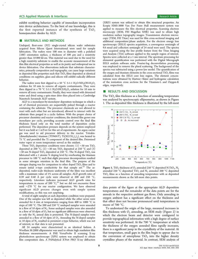
exhibit rectifying behavior capable of immediate incorporationinto device architectures. To the best of our knowledge, this isthe first reported instance of the synthesis of TiO2homojunction diodes by ALD.
■ MATERIALS AND METHODSUndoped, float-zone (FZ) single-crystal silicon wafer substratesacquired from Silicon Quest International were used for samplefabrication. The wafers were 100 mm in diameter with a polished(100) orientation surface, a thickness of 500 μm and a resistivitygreater than 10 000 Ω·cm. This material was used due to the need fora high resistivity substrate to enable the accurate measurement of thethin film electrical properties as well as its purity and widespread use indevice fabrication. Our observations indicate that substrate character-istics, primarily composition and topography, can cause large variationsin deposited film properties such that TiO2 films deposited at identicalconditions on sapphire, glass and silicon will exhibit radically differentbehavior.The wafers were first dipped in a 50 °C 5:1:1 H2O:NH4OH:H2O2
solution for 10 min to remove all organic contaminants. They werethen dipped in a 70 °C 5:1:1 H2O:HCl:H2O2 solution for 10 min toremove all ionic contaminants. Finally, they were rinsed with deionizedwater and dried using a spin-rinse drier then placed into a CambridgeNanotech Savannah ALD system.ALD is a monolayer-by-monolayer deposition technique in which a
set of chemical precursors are sequentially pulsed through a reactorcontaining the substrate. The precursor chemicals are not allowed toreact with each other but are introduced, allowed to interact with thesubstrate then purged in a cyclic fashion. With the proper choice ofprecursor chemistry and reactor conditions, the desired film grows onemonolayer per cycle, providing accurate control over the final filmthickness based only on the total number of deposition cyclesperformed. The deposition pressure depends on the system employedbut it was held at 1 mTorr for this set of experiments. An argon carriergas was used to aid precursor delivery to the reactor. Tetrakis-(dimethylamido) titanium (TDMAT), Ti(N(CH3)2)4), was heated to75 °C and provided the Ti component of the desired film. Deionizedwater vapor at room temperature served as the oxidant.Three TiO2 deposition conditions were chosen: (1) ∼30 nm TiO2
deposited at 200 °C, (2) ∼30 nm TiO2 deposited at 250 °C and (3)∼30 nm N-doped TiO2 deposited at 250 °C. The N-doped TiO2 wasfabricated with a 1 atomic % doping level by overheating the titaniumprecursor to 100 °C such that slight precursor decomposition resultedin some nitrogen retention in the final film. The purpose of thenitrogen doping was for comparison to other doped TiO2 films and toensure initial n-type conductivity for that sample set.24 The as-deposited, wafer-scale thickness uniformity of the films was excellentwith a maximum value of 1% across all samples. ALD growth rates of0.39 and 0.40 Å per cycle were observed at 200 and 250 °C,respectively. Literature indicates increased ALD growth rates fortemperatures in excess of 200 °C,25 but we did not encounter theseuntil ∼270 °C for our reactor configuration. We have observedsignificant ALD process changes even with simple systemmodifications, so this was not surprising.A total of eight samples at each deposition condition were prepared.
One of the samples was left as deposited while the other seven wereannealed for 6 min at temperatures ranging from 400 to 1000 °C insteps of 100 °C. The 200 and 250 °C undoped samples were annealedin a flow of 10 slpm of N2. Some undoped samples were also annealedin a flow of 10 slpm of O2 but no significant differences were observed,so only the N2 anneal data is presented. The N-doped samples wereannealed in a flow of 10 slpm of O2. Annealing the N-doped samplesin 10 slpm of N2 resulted in persistent n-type behavior, which was notof interest, so that data is not presented.All 24 samples were characterized in an identical fashion. A
Woollam M-2000 ellipsometer was used to obtain high resolution filmthickness measurements. A PHI VersaProbe II scanning X-rayphotoelectron spectroscopy (XPS) system was employed to obtainfilm composition data. A PANalytical X’Pert PRO X-ray diffraction
(XRD) system was utilized to obtain film structural properties. AnEcopia HMS-3000 Van Der Pauw Hall measurement system wasapplied to measure the film electrical properties. Scanning electronmicroscopy (SEM, FEI Magellan XHR) was used to obtain highresolution surface topography images. Transmission electron micros-copy (TEM, FEI Titan) was used for film cross-sectional imaging andadditional composition/phase analysis. For the electron energy lossspectroscopy (EELS) spectra acquisition, a convergence semiangle of9.6 mrad and collection semiangle of 24 mrad were used. The spectrawere acquired using the line profile feature from the Titan Imagingand Analysis (TIA) software applied to the sample region of interest.Spectra were collected at a 1 nm interval. The spectrum processing forelemental quantification was performed with the Digital MicrographEELS analysis software suite. Fourier-log deconvolution processingwas employed to remove the plural scattering. The background of thespectra was subtracted using a power-law model. The quantification ofthe oxygen and titanium elements in the cross-sectional TiO2 films wascalculated from the EELS core loss region. The element concen-trations were obtained by Hartree−Slater and hydrogenic calculationof the ionization cross sections for the Titanium-L and Oxygen-Kedges, respectively.
■ RESULTS AND DISCUSSIONThe TiO2 film thickness as a function of annealing temperaturewas analyzed by spectroscopic ellipsometry, as shown in Figure1. The as-deposited film thickness is illustrated by the left-most
data points of the figure at the appropriate ALD depositiontemperatures and the remainder of the data points are for theanneals in the respective ambient gas flows. Only annealing inoxygen ambient has a significant effect on the thickness andthat effect does not become pronounced until temperatures inexcess of 700 °C.To understand the origin of the large, measured increases in
film thickness with O2 annealing, an SEM study (Figure 2) inwhich the electron beam and detector were configured toprovide topographical information with a high degree of surfacesensitivity was performed. At the 700 °C temperature at whichthe thickness of the oxygen annealed films rapidly increases,there is a significant jump in the crystallinity of the material. Atthat temperature, small gaps in the film begin to appear due tothe conversion of amorphous TiO2 into the higher densitycrystalline phases of the material. In contrast, SEM analysis of
Figure 1. TiO2 thickness of O2 annealed 250 °C deposited N:TiO2, N2annealed 250 °C deposited TiO2 and N2 annealed 200 °C depositedTiO2 films as a function of annealing temperature with as depositedmeasurements shown as the left-most data points.
ACS Applied Materials & Interfaces Research Article
DOI: 10.1021/am5072223ACS Appl. Mater. Interfaces XXXX, XXX, XXX−XXX
B

the N2 annealed samples (Figure S1, Supporting Information)shows smoother surfaces and only moderate crystallinityincreases even at higher temperature conditions. Additionaldata provided by a cross-sectional TEM analysis (Figure S2,Supporting Information) corroborates the SEM results but alsoindicates that an interfacial silicon oxide layer that thickens athigher O2 annealing temperatures forms as well. Thus, some ofthe thickness increases seen in the ellipsometry results are dueto the increased surface roughness of the film and thecontributions of the SiOx at O2 annealing temperatures of700 °C and above. However, a large, but difficult to accuratelyquantify, fraction of the thickness increase is due to theaforementioned increase in grain size and overall crystallinity ofthe material with higher O2 annealing temperatures. As will belater demonstrated, the p-type behavior of the material persistseven through these significant morphological changes.Examining XRD data from the ALD films deposited at 250
°C in Figure 3a,b, it can be inferred that the as-deposited filmsare primarily amorphous with small rutile crystallite inclusionsdispersed throughout. Moreover, there is no significant effecton the film morphology from the 1% nitrogen doping. As theannealing temperature is increased, measurable crystallizationbegins to occur around 600 °C and accelerates with the risingtemperature. From the transient brookite phase peaksmeasured at temperatures around this 600 °C transition region,it is reasonable to deduce that the amorphous component ofthe TiO2 film crystallizes through either direct transformationinto the rutile phase or an indirect transformation into the rutilephase with brookite as an intermediate state. Additional dataprovided by a cross-sectional TEM analysis of grain crystallinity(Figure S3, Supporting Information) reinforces the XRDfindings and provides evidence that some small brookitecrystallites below the XRD system resolution are present evenat the 400 °C annealing temperatures. It is notable thatregardless of the ambient process gas, the effects of theannealing on film morphology are similar for the two samples.The brookite XRD peaks do appear at lower temperatures forthe undoped TiO2 annealed in nitrogen. The underlyingmechanism behind this result could be attributed to either thenitrogen doping of the oxygen annealed sample or an effect ofthe annealing process gas itself.XRD analysis results from the ALD films deposited at 200 °C
and annealed in a nitrogen ambient, shown in Figure 3c, areconsiderably different than those from the 250 °C samples.This indicates that the ALD deposition temperature has apowerful effect on the physical structure of the deposited films.
Most noticeable is the fact that, as deposited, the 200 °C filmhas both brookite and rutile components dispersed throughoutan amorphous matrix. Moreover, the brookite phase persistsuntil higher annealing temperatures but does eventually fullytransform to rutile around the expected transition temperatureof 800 °C.26 In the nanoscale size regime, the size of the TiO2crystallites has been shown to determine the thermodynamicphase stability.27 For nanocrystalline TiO2, anatase andbrookite are the most stable phases at temperatures below580 °C. However, for a TiO2 crystallite size above 11 nm, thebrookite phase has been shown to be the most thermodynami-cally stable. Low anatase−brookite transformation energy (11.9kJ·mol−1) can be sufficient for complete transformation of theanatase to its polytypic brookite structure as crystallite size inthe films increases above 11 nm.27 However, despite theseinitial differences, the final morphology of the film after the veryhigh temperature anneals at 900 and 1000 °C is similar to thoseof the samples deposited at 250 °C. The strong dependence ofTiO2 annealing crystallization on the initial structure of thefilms that is seen in these results has also been observed andcharacterized in more detail in a number of other publicationsproviding additional evidence for the versatility of this materialsystem.28,29
Analyzing the electronic properties of the TiO2 films as afunction of annealing temperature using a Hall effectmeasurement system (Figure 4), the most prominent featureof the data is the predominance of p-type conductivity in thesamples. With the exception of the as-deposited N-dopedsample and the two highest temperature anneals of the 200 °Cdeposited sample, all samples consistently exhibited p-typesemiconductor behavior across all measurements. No signifi-cant evidence for this effect has been found in publishedliterature for either ALD TiO2 films or TiO2 films deposited byany other method. However, single-crystal rutile phase TiO2has been shown to exhibit p-type conductivity upon certainhigh temperature anneals designed to produce titaniumvacancies in the lattice.21
At the 700 °C annealing temperature that was previouslyshown to represent the onset of rapid film crystallization, themeasurement of the electrical properties of the films becamesignificantly more difficult and the error bars in the resultshighlight this. Since the data were acquired using a Hall Effectsystem and grain boundary effects are known to causesignificant variability in such planar measurements, it isreasonable to assume that this was the case in this set ofexperiments as well. More focus will be placed on the electrical
Figure 2. Surface topography SEM analysis of N:TiO2 films as a function of oxygen annealing temperature.
ACS Applied Materials & Interfaces Research Article
DOI: 10.1021/am5072223ACS Appl. Mater. Interfaces XXXX, XXX, XXX−XXX
C

characteristics at annealing temperatures up to 600 °C becausethose represent a useful range of achievable properties forsubsequent incorporation into various semiconductor devices.
Regarding the as-deposited properties, the nitrogen-dopedfilm is heavily n-type, as expected from previous doping studies.It starts off with a very high majority electron concentrationcoupled with very low carrier mobility and resistivity. The
Figure 3. XRD analysis of ALD films of (a) O2 annealed 250 °Cdeposited N:TiO2, (b) N2 annealed 250 °C deposited TiO2 and (c) N2annealed 200 °C deposited TiO2 films as a function of annealingtemperature.
Figure 4. Electrical properties of O2 annealed 250 °C depositedN:TiO2, N2 annealed 250 °C deposited TiO2 and N2 annealed 200 °Cdeposited TiO2 films as a function of annealing temperature: (a)majority carrier concentration, (b) majority carrier mobility and (c)resistivity.
ACS Applied Materials & Interfaces Research Article
DOI: 10.1021/am5072223ACS Appl. Mater. Interfaces XXXX, XXX, XXX−XXX
D

undoped films are p-type as deposited with moderate majorityhole concentrations and higher carrier mobilities. It is notablethat the film deposited at 200 °C has a higher holeconcentration and subsequently lower mobility and resistivitythan the 250 °C film. This result is unexpected but may beattributed to the previous data indicating that it is a morediverse mixture of both brookite and rutile phases within anamorphous matrix.Upon annealing, the electrical properties of all three sample
sets converge at a temperature of 500 °C. At this condition, thevalues of the carrier concentration, mobility and resistivity forall three sets are virtually identical. This persists for theundoped films at 600 °C but the nitrogen-doped film mobilitydecreases drastically at this temperature. It is hypothesized thatthis difference is primarily due to enhanced crystallization of thedoped sample at a lower temperature in the oxygen annealingenvironment because we see similar sharp decreases in mobilityat 700 °C temperatures for the undoped samples. The sharptransition from n-type to p-type behavior in the N-dopedsamples is due to the rapid loss of nitrogen dopant from thefilms in the O2 annealing conditions. The same effect is notobserved for N2 annealing conditions of these N-doped films,which supports the measurements showing the undoped TiO2films to be natively p-type.The most important feature of these results is that a large
parameter space is accessible for the fabrication of p-type TiO2with device-tailored properties. The hole concentration can bevaried from below 1016 cm−3 to over 1019 cm−3. The mobilitycan be increased to over 400 cm2/(V·s) and the resistivity canrange from 0.01 to 100 Ω·cm. This provides the device designera certain amount of flexibility in the incorporation of thismaterial system into a given architecture.A scanning transmission electron microscopy electron energy
loss spectroscopy (STEM-EELS) analysis was performed on allcross-sectional samples (Figure 5) with the hypothesis that atitanium deficiency due to either titanium vacancies or oxygeninterstitials was the primary cause of the p-type behavior. Theresults indicate that the O:Ti ratio is consistently larger than 2for all of the as-deposited conditions. For the O2 annealing
conditions, the ratio does not begin to measurably decreaseuntil 1000 °C and there it does so uniformly. However, for theN2 annealing ambient, the top 4 nm of the film undergoessignificant oxygen loss starting at 600 °C.An XPS study was performed for additional verification of
the STEM-EELS results. To minimize damage to the films, noargon sputtering or pretreatment of the samples was performedprior to the analysis. It is well-known that these processes cansignificantly alter the measured ratio of oxygen to titanium.30
Instead, high resolution measurements were performed onunaltered surfaces and the amount of oxygen bonded to Ti4+
was measured by fitting the oxygen signal to the distinct,chemically shifted peak of this particular bond. Even ifadditional oxygen was bonded to titanium that was notaccounted for, we would still obtain a lower bound on theoxygen to titanium ratio of the film, which allows for anaccurate characterization of titanium deficiency if that measuredratio was consistently greater than 2. The results from the XPSanalysis (Figure S4, Supporting Information) indicate that theO:Ti ratio for the majority of the films is indeed greater than 2.The two notable exceptions are the 900 and 1000 °C annealingconditions for the 200 °C deposited sample set which alsoshowed a carrier type inversion in the Hall effect measurementsand significant surface oxygen loss from the EELS analysis. Theas-deposited, nitrogen-doped sample also shows an O:Ti ratiogreater than 2 but that can be attributed to the heavy dopingcompensating for the native p-type conductivity.If the as-deposited ALD TiO2 samples are titanium deficient,
then there must also be a process by which that deficiency iscorrected through the annealing because the hole concentrationdecreases with increasing annealing temperatures regardless ofthe annealing process gas. Because titanium vacancies in rutilecrystals have been shown to be difficult to produce even with900 °C annealing temperatures,21 it is more likely that our lowtemperature ALD process results in a high concentration ofoxygen interstitials that cause the p-type behavior. To addressthe question of what happens to the hypothesized excessoxygen, cross section TEM measurements were analyzed with afocus on the Si−TiO2 interface (Figure 6). From Figure 6a, the
Figure 5. STEM-EELS cross-sectional analysis of (a−c) O2 annealed N:TiO2 deposited at 250 °C and (d−f) N2 annealed TiO2 deposited at 200 °C:(a) dark field STEM image of as deposited N:TiO2 film, (b) cross-sectional O/Ti concentration profile versus annealing temperature, (c) top surfaceEELS spectrum versus annealing temperature, (d) dark field STEM image of as-deposited TiO2 film, (e) cross-sectional O/Ti concentration profileversus annealing temperature and (f) top surface EELS spectrum versus annealing temperature.
ACS Applied Materials & Interfaces Research Article
DOI: 10.1021/am5072223ACS Appl. Mater. Interfaces XXXX, XXX, XXX−XXX
E
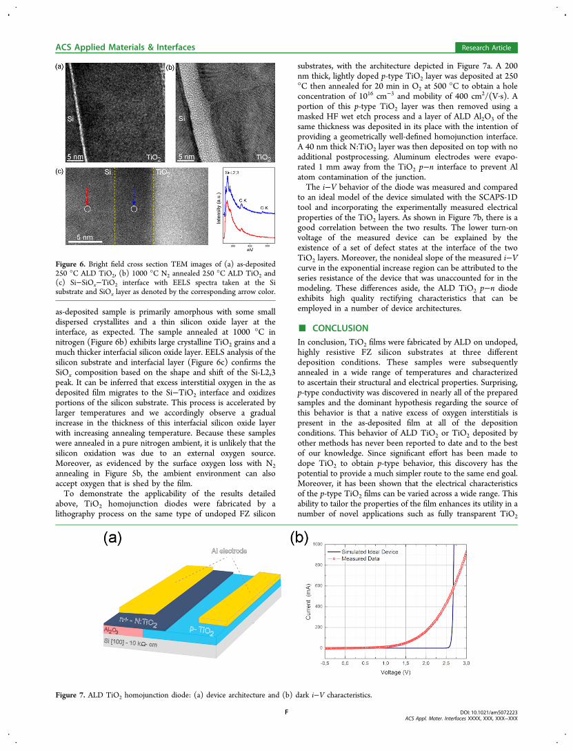
as-deposited sample is primarily amorphous with some smalldispersed crystallites and a thin silicon oxide layer at theinterface, as expected. The sample annealed at 1000 °C innitrogen (Figure 6b) exhibits large crystalline TiO2 grains and amuch thicker interfacial silicon oxide layer. EELS analysis of thesilicon substrate and interfacial layer (Figure 6c) confirms theSiOx composition based on the shape and shift of the Si-L2,3peak. It can be inferred that excess interstitial oxygen in the asdeposited film migrates to the Si−TiO2 interface and oxidizesportions of the silicon substrate. This process is accelerated bylarger temperatures and we accordingly observe a gradualincrease in the thickness of this interfacial silicon oxide layerwith increasing annealing temperature. Because these sampleswere annealed in a pure nitrogen ambient, it is unlikely that thesilicon oxidation was due to an external oxygen source.Moreover, as evidenced by the surface oxygen loss with N2annealing in Figure 5b, the ambient environment can alsoaccept oxygen that is shed by the film.To demonstrate the applicability of the results detailed
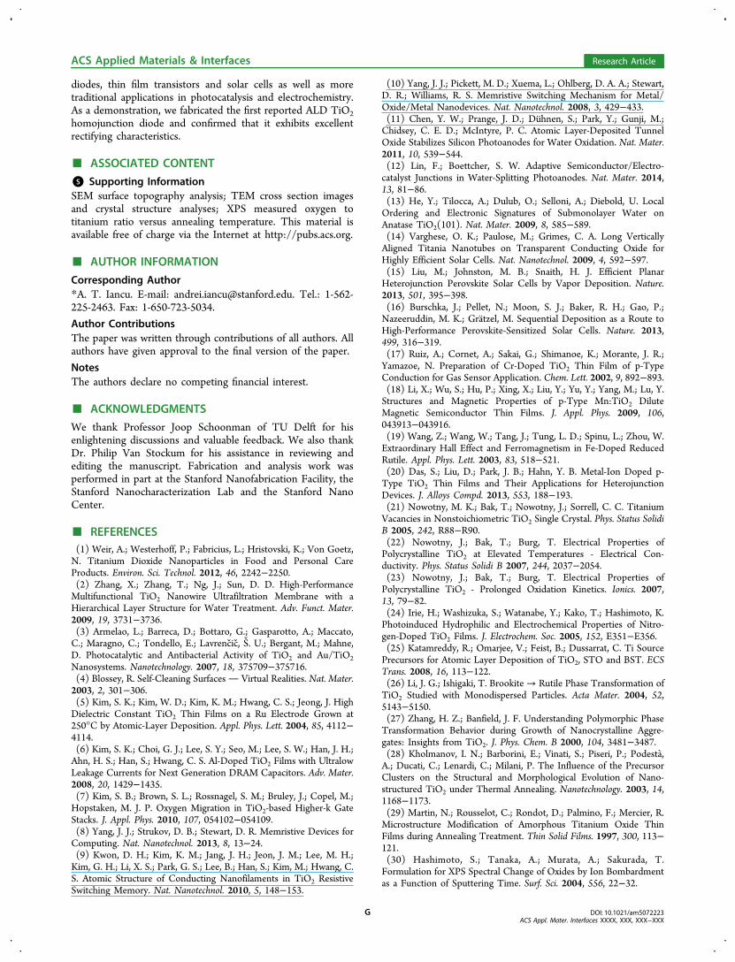
above, TiO2 homojunction diodes were fabricated by alithography process on the same type of undoped FZ silicon
substrates, with the architecture depicted in Figure 7a. A 200nm thick, lightly doped p-type TiO2 layer was deposited at 250°C then annealed for 20 min in O2 at 500 °C to obtain a holeconcentration of 1016 cm−3 and mobility of 400 cm2/(V·s). Aportion of this p-type TiO2 layer was then removed using amasked HF wet etch process and a layer of ALD Al2O3 of thesame thickness was deposited in its place with the intention ofproviding a geometrically well-defined homojunction interface.A 40 nm thick N:TiO2 layer was then deposited on top with noadditional postprocessing. Aluminum electrodes were evapo-rated 1 mm away from the TiO2 p−n interface to prevent Alatom contamination of the junction.The i−V behavior of the diode was measured and compared
to an ideal model of the device simulated with the SCAPS-1Dtool and incorporating the experimentally measured electricalproperties of the TiO2 layers. As shown in Figure 7b, there is agood correlation between the two results. The lower turn-onvoltage of the measured device can be explained by theexistence of a set of defect states at the interface of the twoTiO2 layers. Moreover, the nonideal slope of the measured i−Vcurve in the exponential increase region can be attributed to theseries resistance of the device that was unaccounted for in themodeling. These differences aside, the ALD TiO2 p−n diodeexhibits high quality rectifying characteristics that can beemployed in a number of device architectures.
■ CONCLUSIONIn conclusion, TiO2 films were fabricated by ALD on undoped,highly resistive FZ silicon substrates at three differentdeposition conditions. These samples were subsequentlyannealed in a wide range of temperatures and characterizedto ascertain their structural and electrical properties. Surprising,p-type conductivity was discovered in nearly all of the preparedsamples and the dominant hypothesis regarding the source ofthis behavior is that a native excess of oxygen interstitials ispresent in the as-deposited film at all of the depositionconditions. This behavior of ALD TiO2 or TiO2 deposited byother methods has never been reported to date and to the bestof our knowledge. Since significant effort has been made todope TiO2 to obtain p-type behavior, this discovery has thepotential to provide a much simpler route to the same end goal.Moreover, it has been shown that the electrical characteristicsof the p-type TiO2 films can be varied across a wide range. Thisability to tailor the properties of the film enhances its utility in anumber of novel applications such as fully transparent TiO2
Figure 6. Bright field cross section TEM images of (a) as-deposited250 °C ALD TiO2, (b) 1000 °C N2 annealed 250 °C ALD TiO2 and(c) Si−SiOx−TiO2 interface with EELS spectra taken at the Sisubstrate and SiOx layer as denoted by the corresponding arrow color.
Figure 7. ALD TiO2 homojunction diode: (a) device architecture and (b) dark i−V characteristics.
ACS Applied Materials & Interfaces Research Article
DOI: 10.1021/am5072223ACS Appl. Mater. Interfaces XXXX, XXX, XXX−XXX
F
diodes, thin film transistors and solar cells as well as moretraditional applications in photocatalysis and electrochemistry.As a demonstration, we fabricated the first reported ALD TiO2homojunction diode and confirmed that it exhibits excellentrectifying characteristics.
■ ASSOCIATED CONTENT
*S Supporting InformationSEM surface topography analysis; TEM cross section imagesand crystal structure analyses; XPS measured oxygen totitanium ratio versus annealing temperature. This material isavailable free of charge via the Internet at http://pubs.acs.org.
■ AUTHOR INFORMATION
Corresponding Author*A. T. Iancu. E-mail: [email protected]. Tel.: 1-562-225-2463. Fax: 1-650-723-5034.
Author ContributionsThe paper was written through contributions of all authors. Allauthors have given approval to the final version of the paper.
NotesThe authors declare no competing financial interest.
■ ACKNOWLEDGMENTS
We thank Professor Joop Schoonman of TU Delft for hisenlightening discussions and valuable feedback. We also thankDr. Philip Van Stockum for his assistance in reviewing andediting the manuscript. Fabrication and analysis work wasperformed in part at the Stanford Nanofabrication Facility, theStanford Nanocharacterization Lab and the Stanford NanoCenter.
■ REFERENCES(1) Weir, A.; Westerhoff, P.; Fabricius, L.; Hristovski, K.; Von Goetz,N. Titanium Dioxide Nanoparticles in Food and Personal CareProducts. Environ. Sci. Technol. 2012, 46, 2242−2250.(2) Zhang, X.; Zhang, T.; Ng, J.; Sun, D. D. High-PerformanceMultifunctional TiO2 Nanowire Ultrafiltration Membrane with aHierarchical Layer Structure for Water Treatment. Adv. Funct. Mater.2009, 19, 3731−3736.(3) Armelao, L.; Barreca, D.; Bottaro, G.; Gasparotto, A.; Maccato,C.; Maragno, C.; Tondello, E.; Lavrencic, S. U.; Bergant, M.; Mahne,D. Photocatalytic and Antibacterial Activity of TiO2 and Au/TiO2Nanosystems. Nanotechnology. 2007, 18, 375709−375716.(4) Blossey, R. Self-Cleaning Surfaces Virtual Realities. Nat. Mater.2003, 2, 301−306.(5) Kim, S. K.; Kim, W. D.; Kim, K. M.; Hwang, C. S.; Jeong, J. HighDielectric Constant TiO2 Thin Films on a Ru Electrode Grown at250°C by Atomic-Layer Deposition. Appl. Phys. Lett. 2004, 85, 4112−4114.(6) Kim, S. K.; Choi, G. J.; Lee, S. Y.; Seo, M.; Lee, S. W.; Han, J. H.;Ahn, H. S.; Han, S.; Hwang, C. S. Al-Doped TiO2 Films with UltralowLeakage Currents for Next Generation DRAM Capacitors. Adv. Mater.2008, 20, 1429−1435.(7) Kim, S. B.; Brown, S. L.; Rossnagel, S. M.; Bruley, J.; Copel, M.;Hopstaken, M. J. P. Oxygen Migration in TiO2-based Higher-k GateStacks. J. Appl. Phys. 2010, 107, 054102−054109.(8) Yang, J. J.; Strukov, D. B.; Stewart, D. R. Memristive Devices forComputing. Nat. Nanotechnol. 2013, 8, 13−24.(9) Kwon, D. H.; Kim, K. M.; Jang, J. H.; Jeon, J. M.; Lee, M. H.;Kim, G. H.; Li, X. S.; Park, G. S.; Lee, B.; Han, S.; Kim, M.; Hwang, C.S. Atomic Structure of Conducting Nanofilaments in TiO2 ResistiveSwitching Memory. Nat. Nanotechnol. 2010, 5, 148−153.
(10) Yang, J. J.; Pickett, M. D.; Xuema, L.; Ohlberg, D. A. A.; Stewart,D. R.; Williams, R. S. Memristive Switching Mechanism for Metal/Oxide/Metal Nanodevices. Nat. Nanotechnol. 2008, 3, 429−433.(11) Chen, Y. W.; Prange, J. D.; Duhnen, S.; Park, Y.; Gunji, M.;Chidsey, C. E. D.; McIntyre, P. C. Atomic Layer-Deposited TunnelOxide Stabilizes Silicon Photoanodes for Water Oxidation. Nat. Mater.2011, 10, 539−544.(12) Lin, F.; Boettcher, S. W. Adaptive Semiconductor/Electro-catalyst Junctions in Water-Splitting Photoanodes. Nat. Mater. 2014,13, 81−86.(13) He, Y.; Tilocca, A.; Dulub, O.; Selloni, A.; Diebold, U. LocalOrdering and Electronic Signatures of Submonolayer Water onAnatase TiO2(101). Nat. Mater. 2009, 8, 585−589.(14) Varghese, O. K.; Paulose, M.; Grimes, C. A. Long VerticallyAligned Titania Nanotubes on Transparent Conducting Oxide forHighly Efficient Solar Cells. Nat. Nanotechnol. 2009, 4, 592−597.(15) Liu, M.; Johnston, M. B.; Snaith, H. J. Efficient PlanarHeterojunction Perovskite Solar Cells by Vapor Deposition. Nature.2013, 501, 395−398.(16) Burschka, J.; Pellet, N.; Moon, S. J.; Baker, R. H.; Gao, P.;Nazeeruddin, M. K.; Gratzel, M. Sequential Deposition as a Route toHigh-Performance Perovskite-Sensitized Solar Cells. Nature. 2013,499, 316−319.(17) Ruiz, A.; Cornet, A.; Sakai, G.; Shimanoe, K.; Morante, J. R.;Yamazoe, N. Preparation of Cr-Doped TiO2 Thin Film of p-TypeConduction for Gas Sensor Application. Chem. Lett. 2002, 9, 892−893.(18) Li, X.; Wu, S.; Hu, P.; Xing, X.; Liu, Y.; Yu, Y.; Yang, M.; Lu, Y.Structures and Magnetic Properties of p-Type Mn:TiO2 DiluteMagnetic Semiconductor Thin Films. J. Appl. Phys. 2009, 106,043913−043916.(19) Wang, Z.; Wang, W.; Tang, J.; Tung, L. D.; Spinu, L.; Zhou, W.Extraordinary Hall Effect and Ferromagnetism in Fe-Doped ReducedRutile. Appl. Phys. Lett. 2003, 83, 518−521.(20) Das, S.; Liu, D.; Park, J. B.; Hahn, Y. B. Metal-Ion Doped p-Type TiO2 Thin Films and Their Applications for HeterojunctionDevices. J. Alloys Compd. 2013, 553, 188−193.(21) Nowotny, M. K.; Bak, T.; Nowotny, J.; Sorrell, C. C. TitaniumVacancies in Nonstoichiometric TiO2 Single Crystal. Phys. Status SolidiB 2005, 242, R88−R90.(22) Nowotny, J.; Bak, T.; Burg, T. Electrical Properties ofPolycrystalline TiO2 at Elevated Temperatures - Electrical Con-ductivity. Phys. Status Solidi B 2007, 244, 2037−2054.(23) Nowotny, J.; Bak, T.; Burg, T. Electrical Properties ofPolycrystalline TiO2 - Prolonged Oxidation Kinetics. Ionics. 2007,13, 79−82.(24) Irie, H.; Washizuka, S.; Watanabe, Y.; Kako, T.; Hashimoto, K.Photoinduced Hydrophilic and Electrochemical Properties of Nitro-gen-Doped TiO2 Films. J. Electrochem. Soc. 2005, 152, E351−E356.(25) Katamreddy, R.; Omarjee, V.; Feist, B.; Dussarrat, C. Ti SourcePrecursors for Atomic Layer Deposition of TiO2, STO and BST. ECSTrans. 2008, 16, 113−122.(26) Li, J. G.; Ishigaki, T. Brookite→ Rutile Phase Transformation ofTiO2 Studied with Monodispersed Particles. Acta Mater. 2004, 52,5143−5150.(27) Zhang, H. Z.; Banfield, J. F. Understanding Polymorphic PhaseTransformation Behavior during Growth of Nanocrystalline Aggre-gates: Insights from TiO2. J. Phys. Chem. B 2000, 104, 3481−3487.(28) Kholmanov, I. N.; Barborini, E.; Vinati, S.; Piseri, P.; Podesta,A.; Ducati, C.; Lenardi, C.; Milani, P. The Influence of the PrecursorClusters on the Structural and Morphological Evolution of Nano-structured TiO2 under Thermal Annealing. Nanotechnology. 2003, 14,1168−1173.(29) Martin, N.; Rousselot, C.; Rondot, D.; Palmino, F.; Mercier, R.Microstructure Modification of Amorphous Titanium Oxide ThinFilms during Annealing Treatment. Thin Solid Films. 1997, 300, 113−121.(30) Hashimoto, S.; Tanaka, A.; Murata, A.; Sakurada, T.Formulation for XPS Spectral Change of Oxides by Ion Bombardmentas a Function of Sputtering Time. Surf. Sci. 2004, 556, 22−32.
ACS Applied Materials & Interfaces Research Article
DOI: 10.1021/am5072223ACS Appl. Mater. Interfaces XXXX, XXX, XXX−XXX
G