Arrays of Ni nanowires in alumina membranes: magnetic properties and spatial ordering
9
Eur. Phys. J. B 40, 489–497 (2004) DOI: 10.1140/epjb/e2004-00163-4 T HE EUROPEAN P HYSICAL JOURNAL B Arrays of Ni nanowires in alumina membranes: magnetic properties and spatial ordering M. V´ azquez 1, a , M. Hern´ andez-V´ elez 1 , K. Pirota 1 , A. Asenjo 1 , D. Navas 1 , J. Vel´ azquez 2 , P. Vargas 3 , and C. Ramos 4 1 Instituto de Ciencia de Materiales, CSIC, 28049 Madrid, Spain 2 CAI XRD, Fac. Qu´ ımicas-UCM, 28040 Madrid, Spain 3 Dept. F´ ısica, Univ. T´ ecnica F. Sta. M a , Valparaiso, Chile 4 Instituto Balseiro, Centro At´omico, 8400 Bariloche, Argentina Received 24 November 2003 Published online 15 June 2004 – c EDP Sciences, Societ`a Italiana di Fisica, Springer-Verlag 2004 Abstract. Magnetic characteristics of arrays of Ni nanowires embedded in porous alumina are reviewed as a function of their spatial ordering. The different steps for the controlled production of highly-ordered nanowires is firstly described. Nanopores are formed into an hexagonal symmetry arrangement by self- organized process during anodization of pure Al. Parameters of the anodization allow us to control their diameter, hexagonal lattice parameter and size of crystalline domains. Subsequently, Ni nanowires are grown inside the pores by electrodeposition. Control of the pores filling and of geometrical ordering char- acteristics has been performed by SEM, HRSEM, RBS and AFM techniques. The magnetic characterisation of the arrays has been achieved by SQUID and VSM magnetometers, while information on the magnetic state of individual nanowires is obtained by MFM. Experimental studies are presented, particularly coer- civity and remanence, for arrays with different degree of ordering (crystalline domains up to around 1 µm), and for ratio diameter to lattice parameter (diameter ranging between 20 and 180 nm, and distance be- tween 35 and 500 nm). FMR studies have allows us to obtain complementary information of the anisotropy and magnetic characteristics. A modelling of multipolar interacting nanowires is introduced to account for the influence of short and long range ordering degree of the arrays. PACS. 75.60.Jk Magnetization reversal mechanisms – 81.15.Pq Electrodeposition, electroplating 1 Introduction Studies on various kinds of highly-ordered arrays of nanowires is nowadays attracting growing interest [1]. This is firstly a consequence of the development of experimen- tal techniques to fabricate such arrays in a controllable way [2,3]. The high ordering, together with the intrinsic nature of nanowires may give rise to outstanding coop- erative properties of fundamental and technological in- terest in a broad range of topical areas as semiconduc- tors, magneto-optics, biomedicals, miniaturized sensors or magnetic storing [4–6]. The understanding of the behav- ior of such arrays, different from bulk and even from film systems, is thus of importance from both theoretical and practical points of view. Patterning nanomagnetic elements 10 to 100 nm in size is being currently achieved by different methods: electron-beam, X-ray or imprint lithography techniques [2,7,8]. This offers in principle the potential interest of increasing the areal density in magnetic recording me- dia up to around 300 Gbit/in 2 in arrays of magnetic a e-mail: [email protected] nanoelements with about 50 nm periode distance, as- suming each nanomagnet or a very reduced number of them represents one single bit of information. Alterna- tive techniques include the use of nanoporous membranes fabricated by irradiation with heavy ions and by chemi- cal etching of polymers [9,10] or mica [11], and by self- assembling methods [12,13] which are employed as tem- plates for nanowire elements. In all cases, combined elec- trodeposition techniques are subsequently used to fill the membranes nanopores. Nanowires arrays in polymer mem- branes are spatially randomly distributed, while a higher geometrical symmetry ordering can be achieved in alu- mina membranes. Here, the self-organization process of the nanopores during their formation induces a dense packing of nanowires. Thickness of membranes and ac- cordingly length of nanowires vary within the range of few µm. The size of these templates, with typical cross- section in the range of a few cm 2 , make them nearly ideal systems to study fundamental problems in micro- magnetism because of the high degree of nanowires spa- tial ordering (with hexagonal symmetry) that can extend along several microns without perturbance. The diameter of nanowires can be controlled and the whole array can
-
Upload
independent -
Category
Documents
-
view
1 -
download
0
Transcript of Arrays of Ni nanowires in alumina membranes: magnetic properties and spatial ordering
Eur. Phys. J. B 40, 489–497 (2004)DOI: 10.1140/epjb/e2004-00163-4 THE EUROPEAN
PHYSICAL JOURNAL B
Arrays of Ni nanowires in alumina membranes: magneticproperties and spatial ordering
M. Vazquez1,a, M. Hernandez-Velez1, K. Pirota1, A. Asenjo1, D. Navas1, J. Velazquez2, P. Vargas3, and C. Ramos4
1 Instituto de Ciencia de Materiales, CSIC, 28049 Madrid, Spain2 CAI XRD, Fac. Quımicas-UCM, 28040 Madrid, Spain3 Dept. Fısica, Univ. Tecnica F. Sta. Ma, Valparaiso, Chile4 Instituto Balseiro, Centro Atomico, 8400 Bariloche, Argentina
Received 24 November 2003Published online 15 June 2004 – c© EDP Sciences, Societa Italiana di Fisica, Springer-Verlag 2004
Abstract. Magnetic characteristics of arrays of Ni nanowires embedded in porous alumina are reviewedas a function of their spatial ordering. The different steps for the controlled production of highly-orderednanowires is firstly described. Nanopores are formed into an hexagonal symmetry arrangement by self-organized process during anodization of pure Al. Parameters of the anodization allow us to control theirdiameter, hexagonal lattice parameter and size of crystalline domains. Subsequently, Ni nanowires aregrown inside the pores by electrodeposition. Control of the pores filling and of geometrical ordering char-acteristics has been performed by SEM, HRSEM, RBS and AFM techniques. The magnetic characterisationof the arrays has been achieved by SQUID and VSM magnetometers, while information on the magneticstate of individual nanowires is obtained by MFM. Experimental studies are presented, particularly coer-civity and remanence, for arrays with different degree of ordering (crystalline domains up to around 1 µm),and for ratio diameter to lattice parameter (diameter ranging between 20 and 180 nm, and distance be-tween 35 and 500 nm). FMR studies have allows us to obtain complementary information of the anisotropyand magnetic characteristics. A modelling of multipolar interacting nanowires is introduced to account forthe influence of short and long range ordering degree of the arrays.
PACS. 75.60.Jk Magnetization reversal mechanisms – 81.15.Pq Electrodeposition, electroplating
1 Introduction
Studies on various kinds of highly-ordered arrays ofnanowires is nowadays attracting growing interest [1]. Thisis firstly a consequence of the development of experimen-tal techniques to fabricate such arrays in a controllableway [2,3]. The high ordering, together with the intrinsicnature of nanowires may give rise to outstanding coop-erative properties of fundamental and technological in-terest in a broad range of topical areas as semiconduc-tors, magneto-optics, biomedicals, miniaturized sensors ormagnetic storing [4–6]. The understanding of the behav-ior of such arrays, different from bulk and even from filmsystems, is thus of importance from both theoretical andpractical points of view.
Patterning nanomagnetic elements 10 to 100 nm insize is being currently achieved by different methods:electron-beam, X-ray or imprint lithography techniques[2,7,8]. This offers in principle the potential interest ofincreasing the areal density in magnetic recording me-dia up to around 300 Gbit/in2 in arrays of magnetic
a e-mail: [email protected]
nanoelements with about 50 nm periode distance, as-suming each nanomagnet or a very reduced number ofthem represents one single bit of information. Alterna-tive techniques include the use of nanoporous membranesfabricated by irradiation with heavy ions and by chemi-cal etching of polymers [9,10] or mica [11], and by self-assembling methods [12,13] which are employed as tem-plates for nanowire elements. In all cases, combined elec-trodeposition techniques are subsequently used to fill themembranes nanopores. Nanowires arrays in polymer mem-branes are spatially randomly distributed, while a highergeometrical symmetry ordering can be achieved in alu-mina membranes. Here, the self-organization process ofthe nanopores during their formation induces a densepacking of nanowires. Thickness of membranes and ac-cordingly length of nanowires vary within the range offew µm. The size of these templates, with typical cross-section in the range of a few cm2, make them nearlyideal systems to study fundamental problems in micro-magnetism because of the high degree of nanowires spa-tial ordering (with hexagonal symmetry) that can extendalong several microns without perturbance. The diameterof nanowires can be controlled and the whole array can
490 The European Physical Journal B
be approached to a regular lattice of parallel nanowires.These nanowires provide certainly a less-expensive, versa-tile and reproducible systems to investigate magnetizationprocesses and transport phenomena.
From a geometrical point of view, an importantachievement is the controlled production of the densely-packed highly-ordered nanowires arrays. Magnetically, ad-ditional requirements are that each nanowire exhibit a lon-gitudinal magnetization easy axis and that its anisotropybe strong enough to reduce the effect of stray fields per-turbance of neighboring nanowires. That is important notonly because of the possibilities to employ the arrays instorage or sensor devices but also for micromagnetics andother fundamental studies.
Research on magnetic behavior has been reported pre-viously on arrays of nanowires prepared by electrodeposi-tion techniques on polycarbonate [14] and alumina tem-plates [15–17]. These studies are dealing on arrays of mostcharacteristic magnetic elements as Fe, Ni and Co, butalso on alloyed [18,19] or layered nanowires [20], and con-cern the magnetization reversal process of nanowires andtheir magnetic interactions. Other aspects of interest in-clude magnetotransport phenomena [21,22] that will notbe considered here. While shape mostly determines themagnetization easy axis in Fe and Ni [21,23], in the case ofCo nanowires magnetocrystalline anisotropy with nearlytransverse easy axis balances the shape anisotropy [24] sothat, Co is not a suitable element. Attempts have beenalso done to increase magnetic hardness using CoPt orFePt alloys and various thermal processing [25].
Investigations on the magnetization reversal ofnanowires have been performed by experimental tech-niques [26,27] and micromagnetics modelling [28]. Indi-vidual nanowires are taken as a first approximation to besingle-domain with axial magnetization. Magnetization re-versal of wires with diameter in the range of few microme-ters takes place by nucleation of domain walls at the endswhere magnetization reversal starts and by subsequent de-pinning and propagation along the entire wire [29]. Eachwire contributes with a small square hysteresis loop dis-placed accordingly to the stray field of the neighbouringwires. For nanowires with diameter in the range of around50 to 400 nm, a curling rotational model has been pro-posed combined with a nucleation-propagation process.The wire diameter, φ, is larger than the wall thickness(or actually the exchange correlation length), φw , whichin the case of Fe, Co and Ni lies within the range of 10to 50 nm. For the so-called 1-D magnetic wire systems,φ < λw = 2 (A/K)1/2 (A being the exchange constantand K the longitudinal anisotropy constant) magnetiza-tion should reverse at unison by coherent rotation. Nev-ertheless, although nearly non-dependent on wire diam-eter, switching field takes values smaller than expectedwhen measuring at the very low temperature range thatsuggests the existence of some alternative mechanism in-volving the formation of a kind of small domain wall atthe end or at local non-homogeneities, and its subsequentpropagation [30–33]. The determination of actual closure
structures at the ends seems then to be rather importantto deepen into the knowledge of the reversal process.
Ferromagnetic resonance studies on arrays of magneticnanowires has been proved to supply additional informa-tion other than magnetometry techniques. Only a fewworks have been published about the topic mainly in poly-carbonate membranes [34,35], considering for example theinfluence of the array porosity, the distributed effectiveanisotropy field and the angular spread or misorientaionof nanowires.
The objective of the present work has been to sum-marize the results of our investigations on arrays of Ninanowires. The steps for the production of nanoporousmembranes as templates for the nanowires are describedin the next section together with the techniques employedto determine their spatial arrangement. Then, magneticproperties are collected for arrays with different geomet-rical characteristics as nanowire diameter, interwire dis-tance or lattice parameter of the hexagonal symmetryarray, and degree of the ordering in the array. Generalinformation is gained by magnetometer techniques whilemore local details are obtained by MFM. FMR measure-ments are also shown to give noticeable information. Fi-nally, the magnetostatic interactions among nanowires aremodelled. It is shown that multipolar rather than dipolarinteractions must be considered to account for the exper-imental results.
2 Structural characterization of unfilledand Ni filled nanoporous alumina membranes
To fabricate the nanoporous alumina membrane withhighest quality and controlled geometrical characteristicsone has to take careful procedures. Nanoporous aluminamembranes with hexagonal ordering have been preparedby a two-step anodization process [12]. Aluminum foilswith high purity (99.999%) have been used as startingmaterial. Before being placed inside an anodization cell,foils are firstly degreased and electropolished. Anodizationprocesses at controlled temperature are done inside theanodization cell using oxalic, sulfuric or phosphoric acidsolutions. Nanopores form by self-assembling process, andparameters of first anodization determine important char-acteristics of final arrays as ordering degree of final poresarrays (e.g., size of crystalline domains with hexagonalsymmetry) and interpore distance (60 nm to 500 nm).The porous alumina is then removed, and a second an-odization is performed. Afterwards, the thickness of thealumina barrier layer is reduced while the diameter of thenanopores are finer controlled. Nanowires diameter hasbeen controlled between 18 and 35 nm for interwire dis-tance of 65 nm employing sulphuric acid as electrolthicalbath, and between 30 and 85 nm diameter for interwiredistance of 105 nm with oxalic acid as bath. Employingphosphoric acid allows one to obtain 180 nm diameternanowires separated 500 nm. The length of the nanopores,and consequently of the nanowires, is typically in the rangefrom 500 to 5000 nm. Results presented here correspondto nanopores 4000 nm long.
M. Vazquez et al.: Arrays of Ni nanowires in alumina membranes 491
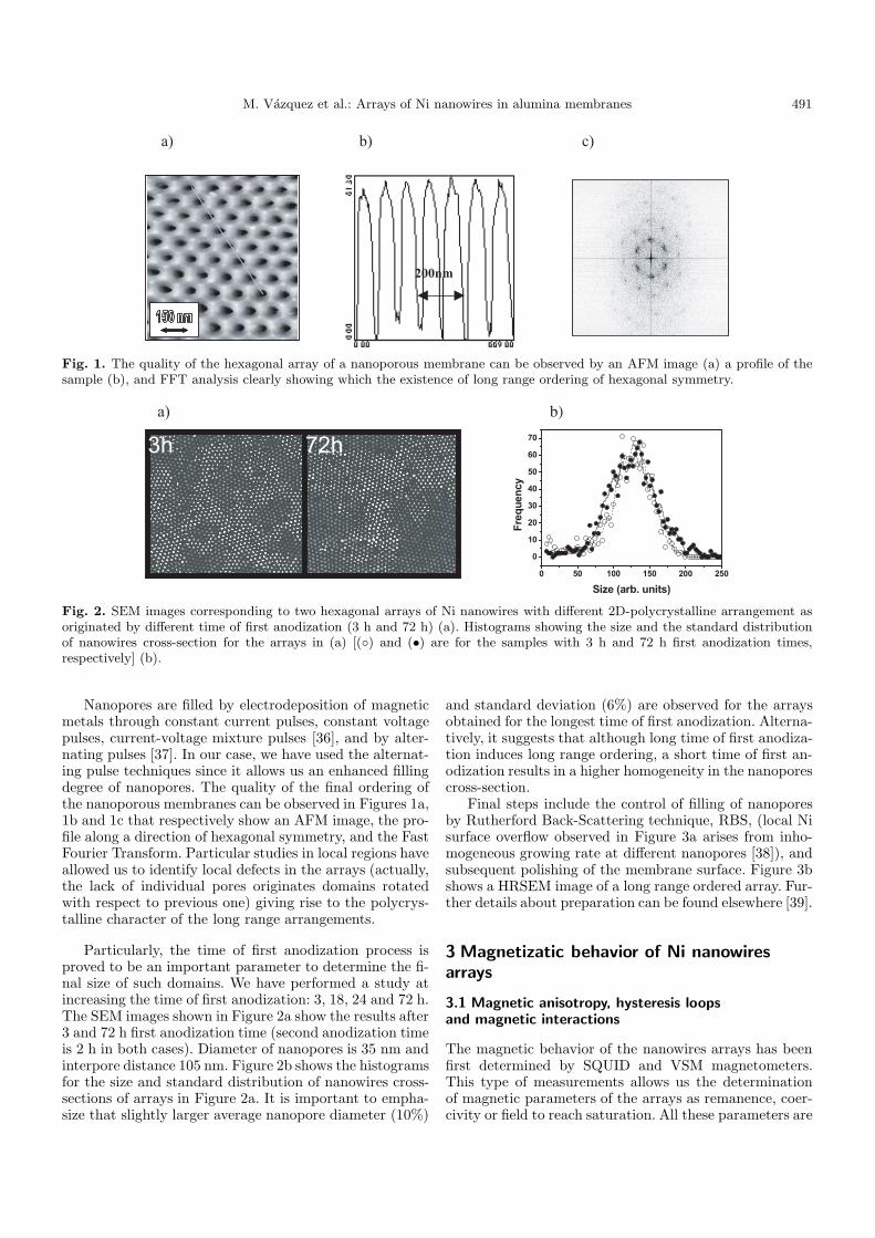
Fig. 1. The quality of the hexagonal array of a nanoporous membrane can be observed by an AFM image (a) a profile of thesample (b), and FFT analysis clearly showing which the existence of long range ordering of hexagonal symmetry.
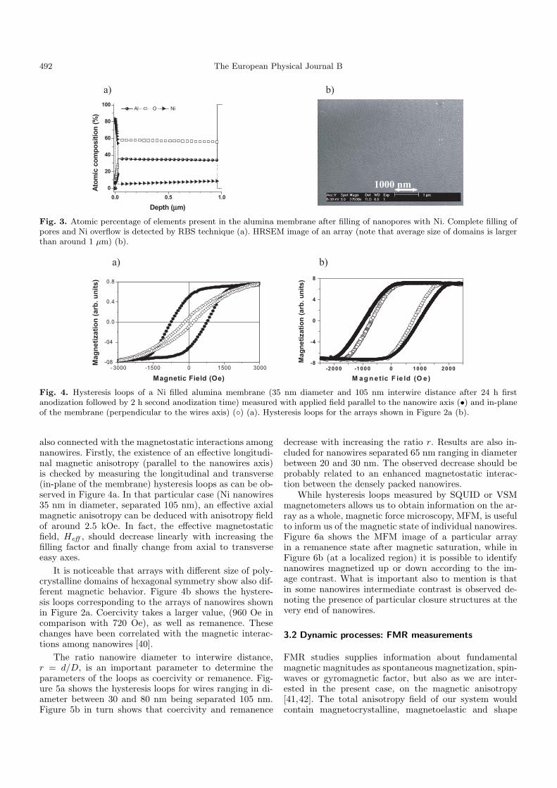
Fig. 2. SEM images corresponding to two hexagonal arrays of Ni nanowires with different 2D-polycrystalline arrangement asoriginated by different time of first anodization (3 h and 72 h) (a). Histograms showing the size and the standard distributionof nanowires cross-section for the arrays in (a) [(◦) and (•) are for the samples with 3 h and 72 h first anodization times,respectively] (b).
Nanopores are filled by electrodeposition of magneticmetals through constant current pulses, constant voltagepulses, current-voltage mixture pulses [36], and by alter-nating pulses [37]. In our case, we have used the alternat-ing pulse techniques since it allows us an enhanced fillingdegree of nanopores. The quality of the final ordering ofthe nanoporous membranes can be observed in Figures 1a,1b and 1c that respectively show an AFM image, the pro-file along a direction of hexagonal symmetry, and the FastFourier Transform. Particular studies in local regions haveallowed us to identify local defects in the arrays (actually,the lack of individual pores originates domains rotatedwith respect to previous one) giving rise to the polycrys-talline character of the long range arrangements.
Particularly, the time of first anodization process isproved to be an important parameter to determine the fi-nal size of such domains. We have performed a study atincreasing the time of first anodization: 3, 18, 24 and 72 h.The SEM images shown in Figure 2a show the results after3 and 72 h first anodization time (second anodization timeis 2 h in both cases). Diameter of nanopores is 35 nm andinterpore distance 105 nm. Figure 2b shows the histogramsfor the size and standard distribution of nanowires cross-sections of arrays in Figure 2a. It is important to empha-size that slightly larger average nanopore diameter (10%)
and standard deviation (6%) are observed for the arraysobtained for the longest time of first anodization. Alterna-tively, it suggests that although long time of first anodiza-tion induces long range ordering, a short time of first an-odization results in a higher homogeneity in the nanoporescross-section.
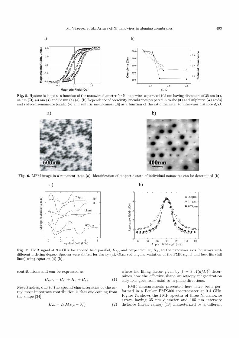
Final steps include the control of filling of nanoporesby Rutherford Back-Scattering technique, RBS, (local Nisurface overflow observed in Figure 3a arises from inho-mogeneous growing rate at different nanopores [38]), andsubsequent polishing of the membrane surface. Figure 3bshows a HRSEM image of a long range ordered array. Fur-ther details about preparation can be found elsewhere [39].
3 Magnetizatic behavior of Ni nanowiresarrays
3.1 Magnetic anisotropy, hysteresis loopsand magnetic interactions
The magnetic behavior of the nanowires arrays has beenfirst determined by SQUID and VSM magnetometers.This type of measurements allows us the determinationof magnetic parameters of the arrays as remanence, coer-civity or field to reach saturation. All these parameters are
492 The European Physical Journal B
Fig. 3. Atomic percentage of elements present in the alumina membrane after filling of nanopores with Ni. Complete filling ofpores and Ni overflow is detected by RBS technique (a). HRSEM image of an array (note that average size of domains is largerthan around 1 µm) (b).
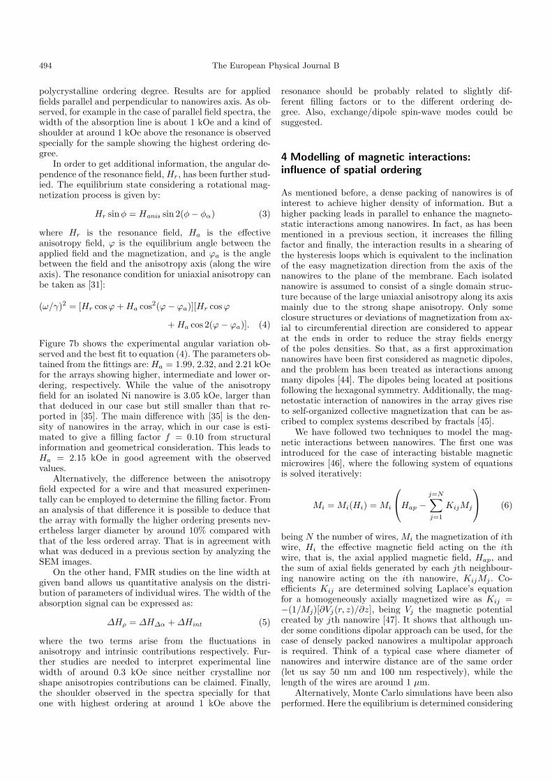
Fig. 4. Hysteresis loops of a Ni filled alumina membrane (35 nm diameter and 105 nm interwire distance after 24 h firstanodization followed by 2 h second anodization time) measured with applied field parallel to the nanowire axis (•) and in-planeof the membrane (perpendicular to the wires axis) (◦) (a). Hysteresis loops for the arrays shown in Figure 2a (b).
also connected with the magnetostatic interactions amongnanowires. Firstly, the existence of an effective longitudi-nal magnetic anisotropy (parallel to the nanowires axis)is checked by measuring the longitudinal and transverse(in-plane of the membrane) hysteresis loops as can be ob-served in Figure 4a. In that particular case (Ni nanowires35 nm in diameter, separated 105 nm), an effective axialmagnetic anisotropy can be deduced with anisotropy fieldof around 2.5 kOe. In fact, the effective magnetostaticfield, Heff , should decrease linearly with increasing thefilling factor and finally change from axial to transverseeasy axes.
It is noticeable that arrays with different size of poly-crystalline domains of hexagonal symmetry show also dif-ferent magnetic behavior. Figure 4b shows the hystere-sis loops corresponding to the arrays of nanowires shownin Figure 2a. Coercivity takes a larger value, (960 Oe incomparison with 720 Oe), as well as remanence. Thesechanges have been correlated with the magnetic interac-tions among nanowires [40].
The ratio nanowire diameter to interwire distance,r = d/D, is an important parameter to determine theparameters of the loops as coercivity or remanence. Fig-ure 5a shows the hysteresis loops for wires ranging in di-ameter between 30 and 80 nm being separated 105 nm.Figure 5b in turn shows that coercivity and remanence
decrease with increasing the ratio r. Results are also in-cluded for nanowires separated 65 nm ranging in diameterbetween 20 and 30 nm. The observed decrease should beprobably related to an enhanced magnetostatic interac-tion between the densely packed nanowires.
While hysteresis loops measured by SQUID or VSMmagnetometers allows us to obtain information on the ar-ray as a whole, magnetic force microscopy, MFM, is usefulto inform us of the magnetic state of individual nanowires.Figure 6a shows the MFM image of a particular arrayin a remanence state after magnetic saturation, while inFigure 6b (at a localized region) it is possible to identifynanowires magnetized up or down according to the im-age contrast. What is important also to mention is thatin some nanowires intermediate contrast is observed de-noting the presence of particular closure structures at thevery end of nanowires.
3.2 Dynamic processes: FMR measurements
FMR studies supplies information about fundamentalmagnetic magnitudes as spontaneous magnetization, spin-waves or gyromagnetic factor, but also as we are inter-ested in the present case, on the magnetic anisotropy[41,42]. The total anisotropy field of our system wouldcontain magnetocrystalline, magnetoelastic and shape
M. Vazquez et al.: Arrays of Ni nanowires in alumina membranes 493
Fig. 5. Hysteresis loops as a function of the nanowire diameter for Ni nanowires separated 105 nm having diameters of 35 nm (�),44 nm (❏), 53 nm (•) and 83 nm (◦) (a). (b) Dependence of coercivity [membranes prepared in oxalic (�) and sulphuric (�) acids]and reduced remanence [oxalic (◦) and sulfuric membranes (❏)] as a function of the ratio diameter to interwires distance d/D.
Fig. 6. MFM image in a remanent state (a). Identification of magnetic state of individual nanowires can be determined (b).
Fig. 7. FMR signal at 9.4 GHz for applied field parallel, H//, and perpendicular, H⊥, to the nanowires axis for arrays withdifferent ordering degree. Spectra were shifted for clarity (a). Observed angular variation of the FMR signal and best fits (fulllines) using equation (4) (b).
contributions and can be expressed as:
Hanis = Hcr + Hσ + Hsh . (1)
Nevertheless, due to the special characteristics of the ar-ray, most important contribution is that one coming fromthe shape [34]:
Hsh = 2πMs(1 − 6f) (2)
where the filling factor given by f = 3.67(d/D)2 deter-mines how the effective shape anisotropy magnetizationeasy axis goes from axial to in-plane directions.
FMR measurements presented here have been per-formed in a Bruker EMX300 spectrometer at 9.4 GHz.Figure 7a shows the FMR spectra of three Ni nanowirearrays having 35 nm diameter and 105 nm interwiredistance (mean values) [43] characterized by a different
494 The European Physical Journal B
polycrystalline ordering degree. Results are for appliedfields parallel and perpendicular to nanowires axis. As ob-served, for example in the case of parallel field spectra, thewidth of the absorption line is about 1 kOe and a kind ofshoulder at around 1 kOe above the resonance is observedspecially for the sample showing the highest ordering de-gree.
In order to get additional information, the angular de-pendence of the resonance field, Hr, has been further stud-ied. The equilibrium state considering a rotational mag-netization process is given by:
Hr sinφ = Hanis sin 2(φ − φα) (3)
where Hr is the resonance field, Ha is the effectiveanisotropy field, ϕ is the equilibrium angle between theapplied field and the magnetization, and ϕa is the anglebetween the field and the anisotropy axis (along the wireaxis). The resonance condition for uniaxial anisotropy canbe taken as [31]:
(ω/γ)2 = [Hr cosϕ + Ha cos2(ϕ − ϕa)][Hr cosϕ
+ Ha cos 2(ϕ − ϕa)]. (4)
Figure 7b shows the experimental angular variation ob-served and the best fit to equation (4). The parameters ob-tained from the fittings are: Ha = 1.99, 2.32, and 2.21 kOefor the arrays showing higher, intermediate and lower or-dering, respectively. While the value of the anisotropyfield for an isolated Ni nanowire is 3.05 kOe, larger thanthat deduced in our case but still smaller than that re-ported in [35]. The main difference with [35] is the den-sity of nanowires in the array, which in our case is esti-mated to give a filling factor f = 0.10 from structuralinformation and geometrical consideration. This leads toHa = 2.15 kOe in good agreement with the observedvalues.
Alternatively, the difference between the anisotropyfield expected for a wire and that measured experimen-tally can be employed to determine the filling factor. Froman analysis of that difference it is possible to deduce thatthe array with formally the higher ordering presents nev-ertheless larger diameter by around 10% compared withthat of the less ordered array. That is in agreement withwhat was deduced in a previous section by analyzing theSEM images.
On the other hand, FMR studies on the line width atgiven band allows us quantitative analysis on the distri-bution of parameters of individual wires. The width of theabsorption signal can be expressed as:
∆Hρ = ∆H∆α + ∆Hint (5)
where the two terms arise from the fluctuations inanisotropy and intrinsic contributions respectively. Fur-ther studies are needed to interpret experimental linewidth of around 0.3 kOe since neither crystalline norshape anisotropies contributions can be claimed. Finally,the shoulder observed in the spectra specially for thatone with highest ordering at around 1 kOe above the
resonance should be probably related to slightly dif-ferent filling factors or to the different ordering de-gree. Also, exchange/dipole spin-wave modes could besuggested.
4 Modelling of magnetic interactions:influence of spatial ordering
As mentioned before, a dense packing of nanowires is ofinterest to achieve higher density of information. But ahigher packing leads in parallel to enhance the magneto-static interactions among nanowires. In fact, as has beenmentioned in a previous section, it increases the fillingfactor and finally, the interaction results in a shearing ofthe hysteresis loops which is equivalent to the inclinationof the easy magnetization direction from the axis of thenanowires to the plane of the membrane. Each isolatednanowire is assumed to consist of a single domain struc-ture because of the large uniaxial anisotropy along its axismainly due to the strong shape anisotropy. Only someclosure structures or deviations of magnetization from ax-ial to circumferential direction are considered to appearat the ends in order to reduce the stray fields energyof the poles densities. So that, as a first approximationnanowires have been first considered as magnetic dipoles,and the problem has been treated as interactions amongmany dipoles [44]. The dipoles being located at positionsfollowing the hexagonal symmetry. Additionally, the mag-netostatic interaction of nanowires in the array gives riseto self-organized collective magnetization that can be as-cribed to complex systems described by fractals [45].
We have followed two techniques to model the mag-netic interactions between nanowires. The first one wasintroduced for the case of interacting bistable magneticmicrowires [46], where the following system of equationsis solved iteratively:
Mi = Mi(Hi) = Mi
Hap −
j=N∑j=1
KijMj
(6)
being N the number of wires, Mi the magnetization of ithwire, Hi the effective magnetic field acting on the ithwire, that is, the axial applied magnetic field, Hap, andthe sum of axial fields generated by each jth neighbour-ing nanowire acting on the ith nanowire, KijMj . Co-efficients Kij are determined solving Laplace’s equationfor a homogeneously axially magnetized wire as Kij =−(1/Mj)[∂Vj(r, z)/∂z], being Vj the magnetic potentialcreated by jth nanowire [47]. It shows that although un-der some conditions dipolar approach can be used, for thecase of densely packed nanowires a multipolar approachis required. Think of a typical case where diameter ofnanowires and interwire distance are of the same order(let us say 50 nm and 100 nm respectively), while thelength of the wires are around 1 µm.
Alternatively, Monte Carlo simulations have been alsoperformed. Here the equilibrium is determined considering
M. Vazquez et al.: Arrays of Ni nanowires in alumina membranes 495
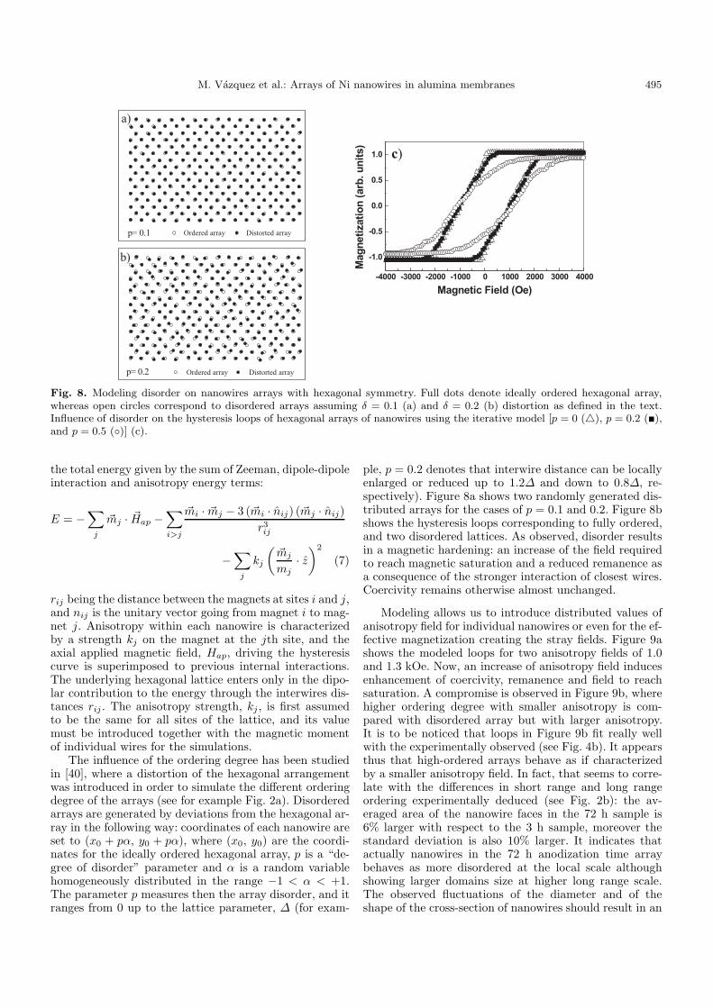
Fig. 8. Modeling disorder on nanowires arrays with hexagonal symmetry. Full dots denote ideally ordered hexagonal array,whereas open circles correspond to disordered arrays assuming δ = 0.1 (a) and δ = 0.2 (b) distortion as defined in the text.Influence of disorder on the hysteresis loops of hexagonal arrays of nanowires using the iterative model [p = 0 (�), p = 0.2 (�),and p = 0.5 (◦)] (c).
the total energy given by the sum of Zeeman, dipole-dipoleinteraction and anisotropy energy terms:
E = −∑
j
mj · Hap −∑i>j
mi · mj − 3 (mi · nij) (mj · nij)r3ij
−∑
j
kj
(mj
mj· z
)2
(7)
rij being the distance between the magnets at sites i and j,and nij is the unitary vector going from magnet i to mag-net j. Anisotropy within each nanowire is characterizedby a strength kj on the magnet at the jth site, and theaxial applied magnetic field, Hap, driving the hysteresiscurve is superimposed to previous internal interactions.The underlying hexagonal lattice enters only in the dipo-lar contribution to the energy through the interwires dis-tances rij . The anisotropy strength, kj , is first assumedto be the same for all sites of the lattice, and its valuemust be introduced together with the magnetic momentof individual wires for the simulations.
The influence of the ordering degree has been studiedin [40], where a distortion of the hexagonal arrangementwas introduced in order to simulate the different orderingdegree of the arrays (see for example Fig. 2a). Disorderedarrays are generated by deviations from the hexagonal ar-ray in the following way: coordinates of each nanowire areset to (x0 + pα, y0 + pα), where (x0, y0) are the coordi-nates for the ideally ordered hexagonal array, p is a “de-gree of disorder” parameter and α is a random variablehomogeneously distributed in the range −1 < α < +1.The parameter p measures then the array disorder, and itranges from 0 up to the lattice parameter, ∆ (for exam-
ple, p = 0.2 denotes that interwire distance can be locallyenlarged or reduced up to 1.2∆ and down to 0.8∆, re-spectively). Figure 8a shows two randomly generated dis-tributed arrays for the cases of p = 0.1 and 0.2. Figure 8bshows the hysteresis loops corresponding to fully ordered,and two disordered lattices. As observed, disorder resultsin a magnetic hardening: an increase of the field requiredto reach magnetic saturation and a reduced remanence asa consequence of the stronger interaction of closest wires.Coercivity remains otherwise almost unchanged.
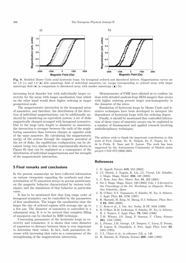
Modeling allows us to introduce distributed values ofanisotropy field for individual nanowires or even for the ef-fective magnetization creating the stray fields. Figure 9ashows the modeled loops for two anisotropy fields of 1.0and 1.3 kOe. Now, an increase of anisotropy field inducesenhancement of coercivity, remanence and field to reachsaturation. A compromise is observed in Figure 9b, wherehigher ordering degree with smaller anisotropy is com-pared with disordered array but with larger anisotropy.It is to be noticed that loops in Figure 9b fit really wellwith the experimentally observed (see Fig. 4b). It appearsthus that high-ordered arrays behave as if characterizedby a smaller anisotropy field. In fact, that seems to corre-late with the differences in short range and long rangeordering experimentally deduced (see Fig. 2b): the av-eraged area of the nanowire faces in the 72 h sample is6% larger with respect to the 3 h sample, moreover thestandard deviation is also 10% larger. It indicates thatactually nanowires in the 72 h anodization time arraybehaves as more disordered at the local scale althoughshowing larger domains size at higher long range scale.The observed fluctuations of the diameter and of theshape of the cross-section of nanowires should result in an
496 The European Physical Journal B
Fig. 9. Modeled Monte Carlo axial hysteresis loops. On hexagonal ordered and disordered lattices. Magnetization curves arefor 1.0 (◦) and 1.3 (•) kOe anisotropy field of individual nanowires (a). Loops corresponding to ordered array with largeranisotropy field (•) in comparison to disordered array with smaller anisotropy (�) (b).
increasing local disorder but with individually larger co-ercivity for the array with longer anodization time whichon the other hand would show higher ordering at largergeometrical scale.
The magnetostatic interaction in the hexagonal arrayof nanowires, and therefore, the distribution of the direc-tion of individual magnetizations, can be additionally an-alyzed by considering an equivalent system: a set of disksmagnetically charged arranged with hexagonal symmetry.Due to the large ratio length to diameter in nanowires,the interaction is stronger between the ends of the neigh-boring nanowires than between charges at opposite endsof the same nanowire. By calculating the magnetostaticenergy of the system through the magnetic potential ofthe set of disks, the equilibrium configuration can be ob-tained, being very similar to that experimentally shown inFigure 6b that can be explained as a consequence of thedistribution of individual magnetizations and the strengthof the magnetostatic interaction.
5 Final remarks and conclusions
In the present manuscript we have collected informationon various viewpoints regarding the synthesis and char-acterization of Ni nanowires arrays in porous membranes,on the magnetic behavior characterized by various tech-niques, and the simulation of that behavior in particularcases.
It has to be mentioned first that long range order ofhexagonal symmetry can be controlled by the parametersof first anodization. The longer the anodization time thelarger the size of ordered regions with average size up toa few µm. The diameter of nanowires is controlled in asubsequent step. It is to be noticed that complete fillingof nanopores can be checked by RBS technique.
Concerning parameters of the hysteresis loops as co-ercivity and remanence, it is shown that ratio diameterof nanowires to distance between them is very importantto determine their values. In fact, both parameters de-crease with increasing that ratio as a consequence of thestrengthening of the magnetostatic interaction.
Measurements of FMR have allowed us to confirm (asdone with detailed analysis from SEM images) that arrayswith higher ordering present larger non-homogeneity inthe diameter of the wires.
Simulation of hysteresis loops by Monte Carlo and it-erative techniques have been developed to interpret thedependence of hysteresis loops with the ordering degree.
Finally, it should be mentioned that controlled fabrica-tion of these types of nanowire arrays can be exploited ina number of fundamental and applied research involvingmultidisciplinary techniques.
The authors wish to thank the important contribution to thiswork of Prof. Gosele, Dr. K. Nielsch, Dr. F. Paszti, Dr. V.de la Prida, R. Sanz and D. Laroze. The work has beensupported by the Autonomous Community of Madrid underproject CAM 07N/0086/2002.
References
1. D. Appell, Nature 419, 553 (2002)2. J.I. Martın, J. Nogues, K. Liu, J.L. Vicent, I.K. Schuller,
J. Magn. Magn. Mater. 256, 449 (2003)3. C. Ross, Ann. Rev. Mater. Res. 31, 203 (2001)4. See J. Magn. Magn. Mater. 249 (2002) Vols. 1–2 devoted to
the Proceedings of the Int. Workshop on Magnetic Wires,San Sebastian, Spain
5. R. O’Barr, S.Y. Yamamoto, S. Schultz, W. Xu, A. Scherer,J. Appl. Phys. 81, 4730 (1997)
6. R. Skomski, H. Zeng, M. Zheng, D.J. Sellmyer, Phys. Rev.B 62, 3900 (2000)
7. C. Ross et al., J. Vac. Sci. Techn. B 17, 3168 (1999)8. R. O’Barr, R.M. Lederman, S. Schultz, W. Xu, A. Scherer,
R. J. Tonicci, J. Appl. Phys. 79, 5303 (1996)9. T.M. Witney, J.S. Jiang, P. Searson, C. Chien, Science
261, 1316 (1993)10. L. Piraux, J.M. George, J.F. Despres, C. Leroy, E. Ferain,
R. Legras, K. Ounadjela, A. Fert, Appl. Phys. Lett. 65,2484 (1994)
11. C.L. Chien et al., in reference [12], p. 14612. H. Masuda, K. Fukuda, Science 268, 1466 (1995)
M. Vazquez et al.: Arrays of Ni nanowires in alumina membranes 497
13. K. Nielsch, R. Wehrspohn, J. Barthel, J. Kirschner, U.Gosele, S. Fischer, H. Kronmuller, Appl. Phys. Lett. 79,1360 (2001)
14. A. Fert, L. Piraux, J. Magn. Magn. Mater. 200, 338(1999)
15. D.J. Sellmyer, M. Zheng, R. Skomski, J. Phys.: Condens.Matter 13, R433 (2001)
16. P.M. Paulus, F. Luis, M. Kroll, G. Schmid, L.J. de Jongh,J. Magn. Magn. Mater. 224, 180 (2001)
17. K. Nielsch et al., J. Magn. Magn. Mater. 249, 234(2002)
18. W. Schwarzacher, K. Attenborough, A. Michel, G.Nabiyouni, J.P. Meier, J. Magn. Magn. Mater. 165, 23(1997)
19. J. Lee et al., J. Appl. Phys. 91, 8513 (2002)20. A. Blondel, J.P. Meier, B. Doudin, J.Ph. Ansermet, Appl.
Phys. Lett. 65, 3019 (1994)21. A. Radulescu, U. Ebels, Y. Henry, K. Ounadjela, J.L.
Duvail, L. Piraux, IEEE Trans Magn. 36, 3062 (2000)22. T. Ohgai, X. Hoffer, L. Gravier, J.E. Wegrowe, J.P.
Ansermet, Nanotechnology 14, 978 (2003)23. S. Dubois, J. Colin, J.L. Duvail, L. Piraux, Phys. Rev. B
61, 14315 (2000)24. J.M. Garcıa, A. Asenjo, M. Vazquez, P. Aranda, E.
Ruiz-Hiztky, IEEE Trans. Magn. 36, 2981 (2000)25. G. Hadjipanayis et al., J. Appl. Phys. 91, 6869 (2002)26. T.G. Sorop, C. Untiedt, F. Luis, M. Kroll, M. Rasa, J.
de Jongh, Phys. Rev. B 67, 14402 (2003)27. K. Nielsch, R. Hertel, R.B. Wehrspohn, J. Barthel, J.
Kirschner, U. Gosele, S.F. Fischer, H. Kronmuller, IEEETrans. Magn. 38, 2571 (2002)
28. R. Hertel, in reference [13] p. 251; H. Forster et al., inreference [13] p. 181
29. M. Vazquez, D.-X. Chen, IEEE Trans. Magn. 31, 1229(1995)
30. M. Kroll et al., in reference [13] p. 241; J. Stankiewicz,F. Luis, A. Camon, M. Kroll, J. Bartolome, W. Blau, J.Magn. Magn. Mater. (in press)
31. R. Skomski, H. Zeng, D.J. Sellmyer, in reference [13] p. 17532. U. Ebels, A. Radulescu, Y. Henry, L. Piraux, K.
Ounadjela, Phys. Rev. Lett. 84, 983 (2000)33. Y. Henry, A. Iovan, J.M. George, L. Piraux, Phys. Rev. B
66, 184430 (2002)34. A. Encinas-Oropesa, M. Demand, L. Piraux, I. Huynen, U.
Ebels, Phys. Rev. B 63, 104415 (2001); M. Demand et al.,in reference [13] p. 228
35. U. Ebels, J.L. Duvail, P.E. Wigen, L. Piraux, L.D. Buda,K. Ounadjela, Phys. Rev. B 64, 14421 (2001)
36. K. Nielsch, F. Muller, A.P. Li, U. Gosele, Adv. Mater. 12,342 (2000)
37. R.M. Metzger, V.V. Konovalov, M. Sum, T. Xu, G.Zangari, B. Xu, M. Benakli, W.D. Doyle, IEEE Trans.Magn. 36, 1 (2000)
38. M. Hernandez-Velez, K. Pirota, F. Paszti, D. Navas, A.Climent, I. Schmytko, M. Vazquez (submitted)
39. K. Pirota, D. Navas, M. Hernandez-Velez, K. Nielsch, M.Vazquez, J. Alloys Comp. 369, 18 (2004)
40. M. Vazquez, K. Nielsch, P. Vargas, J. Velazquez, D. Navas,K. Pirota, M. Hernandez-Velez, E. Vogel, J. Cartes, R.B.Wehrspohn, U. Gosele, Physica B 343, 395 (2004)
41. R. Arias, D.L. Mills, Phys. Rev. B 67, 94423 (2003)42. Z.W. Wang et al., Phys. Rev. Lett. 89, 27201 (2002)43. C. Ramos, M. Vazquez, K. Nielsch, K. Pirota, J. Rivas,
R.B. Wehrspohn, M. Tovar, R.D. Sanchez, U. Gosele, Proc.ICM’2003 (J. Magn. Magn. Mater. in press)
44. E.O. Samwel, P.R. Bissell, J.C. Lodder, J. Magn. Magn.Mater. 115, 327 (1992)
45. J. Velazquez, M. Vazquez, IEEE Trans. Magn. 38, 2477(2002)
46. J. Velazquez, C. Garcıa, M. Vazquez, A. Hernando, Phys.Rev. B 54, 9903 (1995)
47. J. Velazquez K. Pirota, M. Vazquez, IEEE Trans. Magn.39, 249 (2003)