Applications of Porous Silicon Thin Films in Solar Cells and Biosensors
10
Applications of Porous Silicon Cells and B Priyanka Singh, Shailesh N. Sharma, and NoM.. Ravindra An QVeTlliew of the applications of porous silicon (PS) thin films, as QII- tireflection coatings (ARC) in silicon solar cells and transducers in biosen- sors, is presented. The rejlectlJnce gpec- tra of PS films have been compared with other conventional ARCs (such as nO,jMgF 2 and ZnS), and optimal PS ARC with minimum rejlectlJnce has been obtained. The implementation of PS into an industritJIly compatible screen-printed (SP) solar cell by both the electrochemical etching (ECE) and chemical etching (CE) methotb are reviewed. Porous silicon films, formed via ECE for short anodization times, on textured n+ emitter of c-Si solar cell having SP front and back contacts, lead to improvements in the performance of solar cells and demonstrate their vi- ability in industrial applications. INTRODUCTION Porous silicon (PS) is a sponge-like structure, composed of silicon skeleton penneated by a network: of pores. Po- rous silicon can be obtained by anod- ization or etching of silicon in aqueous hydrotluoric (HF) solutions and was first discovered in 1956 by Uhlir at the Bell Laboratories. 1 Etching of sili- con substrate generates a thin layer of porous silicon on the silicon substrate withpores as large as -200 DID in diam- eter (as shown in Figure 1A), providing a large surface area for light trapping (in solar cell applications) and molecu- lar interaction (in sensor applications) inside the porous layer. A scanning electron micrograph of such a PS film which has been formed on crystalline silicon (c-Si) substrate is shown in Fig- ure 1A. The right side images illustrate the magnified top and cross-sectional view of the PS layer and clearly indicate the formed pores of diameter -200 DID in the PS :film.'1 The poten1i.al. of porous silicon for various technological appli- cations such as optoelectronic devices, 3 displays,4 photodetectors,s and bi08en- sors 6 has been extensively investigated. Such devices can be fabricated by ei- ther varying the porosity of the PS :film itself or by depositing other :6.Ims on the PS :film such as metals, semiconducting How would you••. ... describe tile Im!nIllllignlflr.n.... of this peper? An cwerview of tIte applic:atioM of poroll.'1 silicon (PS) thinfilms fU antirejkction coating. (ARC) in silicon lOW cells atId tnIIuducer.s in bioaen.ron is preleNetL 'I'M implementDtion of PS into QIl intlII.Jt1ially compiJlible SCND!- printd .olar ceU by both tIte .lsctroclwnicul etching llIld cIrnnical etching met1wds are nNiewed. •••daaibe tIdI work to a IIIlIterial& IclIIlre II1II1 mgiDeerIDg profesI1IoDIIl with DO aperieDl:e In JUIIl' tech·.) spedaIly? TIte use of porrnu silicon ill IOUJr celLs llIld bio.retlSOP'& is described. /n partlclllm; the mdy focuu!J on tile utility of poroll.'1 silicon tu anti- COQIRsgI in solar cells. •••daaibe tIdI work to a 1aypenoD? /n recePlt yeaT', tltere 1ws hem II growing Were.rt ill rmtrWQ/Jle energy IOrlT'CU. Solar energy R!p1f!!Je1II& a non-pollMting, rtatwally avtJilDble lOW'Ce of eMrgy. Silicon is abundmltly avtJilDble in I/Qtu12 ill the form of.lUca. SlUcoll IOUJ' celLJ R!prele1lt tile largut compmumt t1uJt facjlikJte, die com>eniolt of nutlight to electricity. However. ailicoll reftect.s II ftuctioll of the iIlcident light (-33%) which theft gm WQ8tm Anti-rejl«tion coating. help to minimize refkction kmu. In the mIJ1IlUCript, we describe tile uu of t.:: poroll.'1 silicon tu "" anti-reft«tiOIl CODMg. oxides, or polymer films depending on the applications.' The large surface-to- volume ratio of porous silicon gives it the ability to react with biochemical species and sense them readily. Recent- ly, PS has attracted more attention due to its sensing properties and has been utilized in chemical, biological2,6,l-IO and gasu-17 sensing applications. The advantages of PS sensors are their low cost, ability to operate at room tempera- ture, and compatibility with traditional silicon device fabrication technology. Furthennore, interest in porous silicon in the solar cell industry has grown over the last decade. 1 &4.'l See the sidebar for a discussion of the formation and morphology of p<>- rous silicon. APPLICATION OF POROUS SILICON AS ARC IN SILICON SOLAR CELLS AB shown in Figure 2A, bare sili- con surface reflects more than 30% of the incident sunlight. These reflection losses can be reduced by texturization (it is an important step during solar cell fabrication. which makes silicon surface textured) and by depositing a suitable ARC on the top surface of the solar cell, reflection losses are reduced. This is shown in Figure 2A. The ARC effect relies on destructive interference of waves reflected at the top and bottom of the ARC, as shown in Figure 2B. It can be seen from Figure 2B that PSI and PS 1 are two ARCs formed on c-Si solar cell via ECE formation results in a very low refI.ectance in a certain wavelength range, which for photovoltaic applica- tions must lie between 650 and 700 DID. lI For example, in Figure 2A. PS 1 shows -5% reflectance in the wave- length range of 650 and 700 DID. For an
Transcript of Applications of Porous Silicon Thin Films in Solar Cells and Biosensors
Applications of Porous Silicon Cells and Biosensors
Priyanka Singh, Shailesh N. Sharma, and NoM.. Ravindra
An QVeTlliew of the applications ofporous silicon (PS) thin films, as QII
tireflection coatings (ARC) in siliconsolar cells and transducers in biosensors, is presented. The rejlectlJnce gpectra of PS films have been comparedwith other conventional ARCs (such asSiN~ nO,jMgF2 and ZnS), and optimalPS ARC with minimum rejlectlJnce hasbeen obtained. The implementationof PS into an industritJIly compatiblescreen-printed (SP) solar cell by boththe electrochemical etching (ECE) andchemical etching (CE) methotb arereviewed. Porous silicon films, formedvia ECE for short anodization times,on textured n+ emitter ofc-Si solar cellhaving SPfront and back contacts, leadto improvements in the performance ofsolar cells and demonstrate their viability in industrial applications.
INTRODUCTION
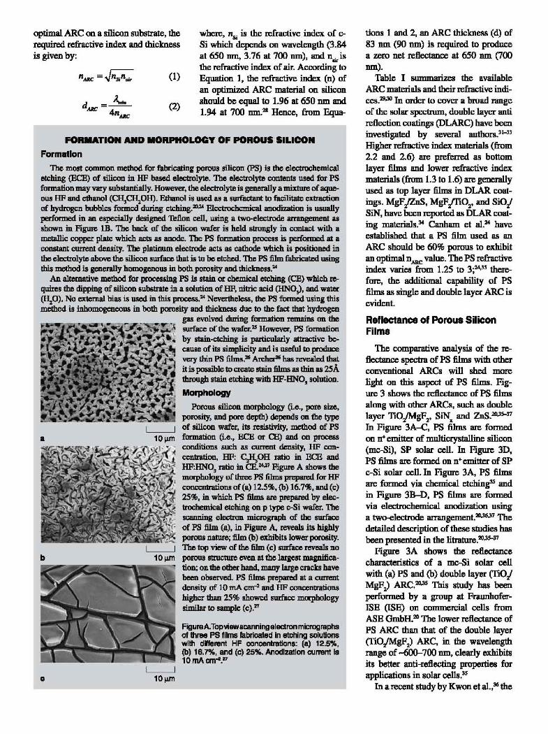
Porous silicon (PS) is a sponge-likestructure, composed of silicon skeletonpenneated by a network: of pores. Porous silicon can be obtained by anodization or etching of silicon in aqueoushydrotluoric (HF) solutions and wasfirst discovered in 1956 by Uhlir atthe Bell Laboratories.1 Etching of silicon substrate generates a thin layer ofporous silicon on the silicon substratewithpores as large as -200 DID in diameter (as shown in Figure 1A), providinga large surface area for light trapping(in solar cell applications) and molecular interaction (in sensor applications)inside the porous layer. A scanningelectron micrograph of such a PS filmwhich has been formed on crystallinesilicon (c-Si) substrate is shown in Figure 1A. The right side images illustratethe magnified top and cross-sectionalview ofthe PS layerand clearly indicatethe formed pores of diameter -200 DID
in the PS :film.'1 The poten1i.al. of poroussilicon for various technological applications such as optoelectronic devices,3
displays,4 photodetectors,s and bi08ensors6 has been extensively investigated.Such devices can be fabricated by either varying the porosity of the PS :filmitselfor by depositing other :6.Ims on thePS :film such as metals, semiconducting
How would you••....describe tile Im!nIllllignlflr.n....of this peper?
An cwerview oftIte applic:atioM ofporoll.'1 silicon (PS) thinfilms fU
antirejkction coating. (ARC) insilicon lOW cells atId tnIIuducer.sin bioaen.ron ispreleNetL 'I'MimplementDtion ofPS into QIl
intlII.Jt1ially compiJlible SCND!
printd .olarceU by both tIte.lsctroclwnicul etching llIldcIrnnical etching met1wds arenNiewed.
•••daaibe tIdI work to aIIIlIterial& IclIIlre II1II1 mgiDeerIDgprofesI1IoDIIl with DO aperieDl:e InJUIIl' tech·.) spedaIly?
TIte use ofporrnu silicon ill IOUJrcelLs llIld bio.retlSOP'& is described./n partlclllm; the mdy focuu!J ontile utility ofporoll.'1 silicon tu anti~ COQIRsgI in solar cells.
•••daaibe tIdI work to a1aypenoD?
/n recePlt yeaT', tltere 1ws hemII growing Were.rt ill rmtrWQ/Jleenergy IOrlT'CU. Solar energyR!p1f!!Je1II& a non-pollMting, rtatwallyavtJilDble lOW'Ce ofeMrgy. Siliconis abundmltly avtJilDble in I/Qtu12 illthe form of.lUca. SlUcoll IOUJ' celLJR!prele1lt tile largut compmumt t1uJtfacjlikJte, die com>eniolt ofnutlightto electricity. However. ailicollreftect.s IIftuctioll of the iIlcidentlight (-33%) which theft gmWQ8tm Anti-rejl«tion coating. helpto minimize refkction kmu. In themIJ1IlUCript, we describe tile uu of
t.:: poroll.'1 silicon tu "" anti-reft«tiOIlCODMg.
oxides, or polymer films depending onthe applications.' The large surface-tovolume ratio of porous silicon gives itthe ability to react with biochemicalspecies and sense them readily. Recently, PS has attracted more attention dueto its sensing properties and has beenutilized in chemical, biological2,6,l-IOand gasu-17 sensing applications. Theadvantages of PS sensors are their lowcost, ability to operate at room temperature, and compatibility with traditionalsilicon device fabrication technology.Furthennore, interest in porous siliconin the solarcell industry has grown overthe last decade.1&4.'l
See the sidebar for a discussion ofthe formation and morphology of p<>rous silicon.
APPLICATION OF POROUSSILICON AS ARC IN SILICON
SOLAR CELLS
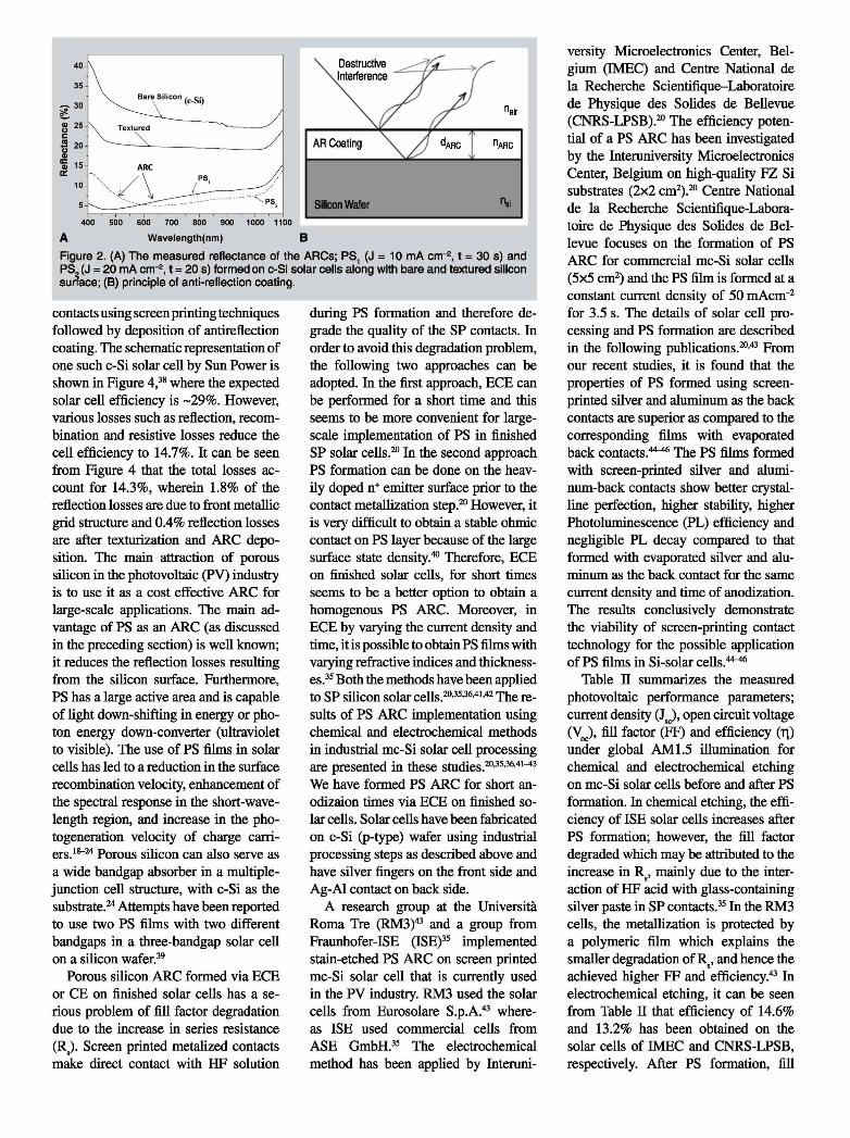
AB shown in Figure 2A, bare silicon surface reflects more than 30% ofthe incident sunlight. These reflectionlosses can be reduced by texturization(it is an important step during solarcell fabrication. which makes siliconsurface textured) and by depositing asuitable ARC on the top surface of thesolar cell, reflection losses are reduced.This is shown in Figure 2A. The ARCeffect relies on destructive interferenceofwaves reflected at the top and bottomof the ARC, as shown in Figure 2B. Itcan be seen from Figure 2B that PSIandPS1 are two ARCs formed on c-Si solarcell via ECE formation results in a verylow refI.ectance in a certain wavelengthrange, which for photovoltaic applications must lie between 650 and 700DID.lI
For example, in Figure 2A. PS1
shows -5% reflectance in the wavelength range of 650 and 700 DID. For an
Reflectance of Porous SiliconFilms
tions I and 2, an ARC thickness (d) of83 om (90 om) is required to producea zero net reflectance at 650 om (700om).
Table I summarizes the availableARC materials and their refractive indices.29,30 In order to cover a broad rangeof the solar spectrum, double layer antireflection coatings (DLARC) have beeninvestigated by several authors.31-33
Higher refractive index materials (from2.2 and 2.6) are preferred as bottomlayer films and lower refractive indexmaterials (from. 1.3 to 1.6) are generallyused as top layer films in DLAR coatings. MgFfZnS, MgFfIi02' and SiOISiN, have been reported as DLAR coating materials.:M Canham et aI.24 haveestablished that a PS film used as anARC should be 60% porous to exhibitan optimal nARC value. The PS refractiveindex varies from 1.25 to 3;24.35 therefore, the additional capability of PSfilms as single and double layer ARC isevident.
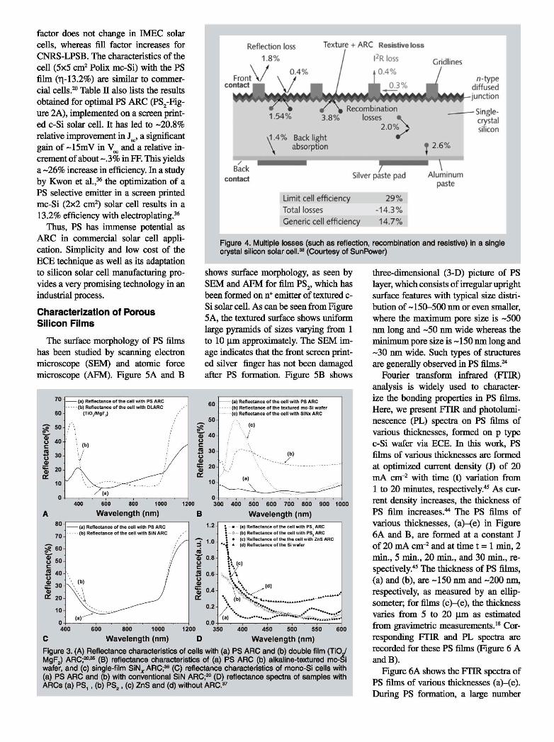
The comparative analysis of the reflectance spectra of PS films with otherconventional ARCs will shed morelight on this aspect of PS films. Figure 3 shows the re:8ectance of PS filmsalong with other ARCs. such as doublelayer TIO.jMgF2' SiN
land ZnS.20,3S-37
In Figure 3A--e. PS films are formedon nolo emitter of multicrysta1line silicon(mc-Si), SP solar cell. In Figure 3D,PS films are formed on n+emitter of SPc-Si solar cell. In Figure 3A, PS filmsare formed via chemical etching3S andin Figure 3B--D, PS films are formedvia electrochemical anodization usinga two-e1ectrode arrangement.2ll,36,37 Thedetailed description of these studies hasbeen presented in the litrature.2O,3S-a7
Figure 3A shows the reflectancecharacteristics of a me-Si solar cellwith (a) PS and (b) double layer (riOIMgF2) ARC.X\,3S This study has beenperformed by a group at FraunhoferISE (ISB) on commercial. cells fromASE GmbH.20 The lower reflectance ofPS ARC than that of the double layer(riO.jMgF2) ARC, in the wavelengthrange of -600-700 DIn, clearly exhibitsits better anti-reflecting properties forapplications in solar cells.3S
In a recent study by Kwon et aI.,~ the
where, ns; is the refractive index of cSi which depends on wavelength (3.84at 650 om, 3.76 at 700 om), and noiristhe refractive index ofair. According toEquation I, the refractive index (n) ofan optimized ARC material on siliconshould be equal to 1.96 at 650 DIn and1.94 at 700 om.2.1 Hence, from Equa-
FigureA Topviewscanningeleclronmicrographsof three PS fillTl$ fabricated in etching solutionswith different HF concentrations: <8> 12.5%,(b) 16.7%, and (e) 25%. Anodlzatlon current II10 rnA crrr'!'
FORMATION AND MORPHOLOGY OF POROUS SILICON
Formation
The most common method for fabricating porous silicon (PS) is the electrochemi.caetching (ECE) of silicon in HF based electrolyte. The electrolyte contents used for PSformalion may vary substantially. However, the electrolyte is geDe1'8lly a mixtureofaqueOWl HF and eIbanol (cu,~OH). Ethanol is used u a surfactant to facilitate extnu:tionof hydrogen bubbles formed dwing etching.2O,2A Electrochemical anodization is usuallyperformed in an especially designed Teflon cell, using a two-electrode arraDgetDeDt asshown in Figure lB. The back of the silicon wafer is held strongly in ccmtact with amdallic copper plate which acts u anode. The PS formation process is performed at aconstant current density. The platinum electrode acts as cathode which is positioned inthe electrolyte above the silicon surface that is to be etched. The PS film fabricated usingthis method is generally homogenous in both porosity and thickness.:14
An alternative method for processing PS is stain or chemical etching (CE) which requires the dipping of silicon substrate in a solution ofBP, nitric acid (RNO,), and water~O). No external bias is used in this proalSS.:14 Nevertheless, the PS formed using thismethod is inhomogeneous in both porosity and thiclmcss due to the fact that hydrogen
gas evolved during formation remains on thesurface of the wafer.2S Howevel'. PS formationby stain-etcl1ing is particularly attractive because of its simplicity and is useful to producevery thin PS films.- .An:hcr' has revealed thatit is possible to create stain films u thin 18 2SAthrough stain etching with HF-HN0
3solution.
MOl1)hology
Porous silicon morphology (i.e.• pore size,porosity, and pore depth) depends on the type
'----_--J1 of silicon wafer, its resistivity, method of PS• 10 IJ.m formation (i.e.• ECE or CE) and on process
conditions such IlII current density, HF ccmcenIration, HF: CAOH ratio in ECE andHF:HNO, ratio in CE.2UI F'lgUle A shows themorphology of three PS films pn::pIIRld for HFc~of(a)12.5%,{b)16.7%,and(c)25%, in which PS films are prepared by electrochemical etching on P type ~Si wafer. Thescanning electron miaograph of the surfila:of PS film (a), in Figure A, reveals ita highlyporous nature; film (b) exhibits lower porosity.
L--_---'I The top view of the film (c) surface reveals DO
b 10 11m porous structure even at the largest magnifica-tion; on the other band. many large cracks havebeen observed. PS films prepared at a cmTemtdensity of 10 rnA cm~ and HF oonc.entratiOlUlhigbcr than 25% showed surfila: morphologysimilar to sample (C).27
c
RAlIC =..Jns;R... (1)
op1imal. ARC on a silicon substrate, therequired refractive index aDd thicknessis given by:
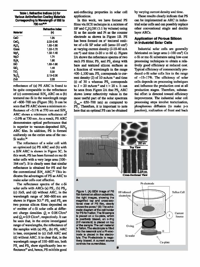
Table I. RefractIve Indices (n) forvarious Antireflection CoIling MatertalsColT88POl1dlng toWavelength of 650 to
7OOnm....
re:8ectance of (a) PS ARC is found tobe quite comparable to the reflectanceof (e) conventional SiNx ARC on a (b)textured mc-Si in the wavelength rangeof -600-700 DID (Figure 3B). It can beseen that PS ARC shows a minimum reflectance of -3.1% at 570 DID and SiNzARC shows a minimum reflectance of-2.0% at 730 nm. As a result, PS ARCdemonstrates optical performance thatis superior to vacuum-deposited SiNxARC film. In addition, PS is formeduniformly on the entire area of the mcSi wafer.36
The reflectance of a solar cell withan optimized (a) PS ARC and (b) witha SiN ARC is shown in Figure 3C. Inthis work. PS has beenfmmed on mc-Sisolar cells with a very large area (IOD164 cm2). It is clearly seen that similarrefl.ectance is obtained for PS and forthe conventional SiN" ARC.20 This indicates the advantages ofPS as ARC tomake solar cells cost effective.
The reflectance spectra of the c-Sisolar cells with ARCs (a) PSI' (b) PS2,
(c) Zns, and (d) without ARC, in thewavelength range of 360-600 nm areshown in Figure 3D.37 PSI and PS2 aretwo porous silicon films deposited onn+ emitter of c-Si solar cells at different charge densities QI = 0.06 C1cm2
and az= 0.9 C1cm2, respectively. It can
be seen that, in the entire investigatedrange of wavelengths, the re:flectance ofthe samples with (a) PSI' (b) PS2 ARCis less, compared to (c) Zns ARC and(d) without ARC. It is clear that, in thewavelength range of 550-600 DID, bothPSI and PS2 show significantly less Ie
flectance3'l and, hence. PS exhibits good
CurrentSource
by varying current density and time.These results clearly indicate that PS
can be implemented as ARC in induslrial solar cells and can possibly replaceother conventional single and doublelayer ARCs.
Application of Porous Siliconin Industrial Solar cells
Pt-electrode
Industrial solar cells are generallyfabricated on large area (-100 cm2) Czc-Si or mc-Si substrates using low~ost
processing techniques to obtain a relatively good efficiency at reduced cost.'JYpical efficiency ofcommercially pr0
duced c-Si solar cells lies in the rangeof -13-17%. The efficiency of solarcells depends on processing techniquesand influence the production cost at allproduction stages. Therefore, substantial effort is directed toward efficiencyimprovement. The induslrial solar cellprocessing steps involve texturizaDon,phosphorous diffusion (to make p-njIDlCtion), realization of front and back
Cu-plate
FIgure 1. (A) SEM Image of PS111m formed on silicon substrBIe,1he right imeg., showing 1hemagnified top and cross--sec·110n81 vtew of PS 111m, dear1yshows lt1e pores.· (8) The act1emlllic diagram of the cell holderfor PS formation. The Si sampleIs placed on a Cu-p1lrt8. whichIs positively biased, an o-ring(HF·resistant) is placed on 1Dpof the sample. The 0811 materialIs Tellon. The elec1rolyte Is1111edInto 1he reeervolr and a Pt-elec1rode is placed in the electro·Iyte. The PI·e1ectrode is nega·11\/8ly biased. A amant sourcecontrol81he a.lrren1lblas.
A
B
anti-reflecting properties in solar cellapplications.
In this work, we have formed PSfilms via ECE technique in a mixture ofHF and CAOH (1:1 by volume) usingSi as the anode and Pt as the counterelectrode as shown in Figure lB. PShas been formed on n+ textured emitter of c-Si SP solar cell (area-10 cm2)at varying cunent density (1-10-40 mAcm~ and time (t-20 s to 60 s). Figure2A shows the reflectance spectra of twosuch PS films; PSI and PS2 along withbare and textured silicon surfaces asa function of wavelength in the range400-1,100 DID. PSI conesponds to ClU'
rent density (1) of 10 mAcm-2 and time(t) of 30 s whereas PS
2corresponds
to J =20 mAcm-.2 and t =20 s. It canbe seen from Figure 2A that PS2 ARCshows lower reflectivity values in themost useful part of the solar spectrum(AmID= 650-700 DID) as compared to
PSI' Therefore, it is important to notehere that an optimal PS can be obtained
1.952.30-2.401.80-1.901.5(H.701.30-1.40
1.741.90
1.80-1.901.482.30
2.10-2.302.33
RtIrIcIIn IndII:(n)
ceoceozfld.0•GlassMgF.MgO
~4SiCSiC2
TiO!TSzO.znS
400 500 600 700 800 900 1000 1100
A Wavelength(nm) B
Figure 2. (A) The measured reflectance of the ARCs; PS1 (J = 10 mA cm-2, t = 30 s) andPS2 (J = 20 rnA crTr", t = 20 s) formed on c-Si solar cells along with bare and textured siliconsurface; (B) principle of anti-reflection coating_
versity Microelectronics Center, Belgium (IMEC) and Centre National dela Recherche Scientifique--Laboratoirede Physique des Solides de Bellevue(CNRS-LPSB).20 The efficiency potential of a PS ARC has been investigatedby the Interuniversity MicroelectronicsCenter, Belgium on high-quality FZ Sisubstrates (2x2 cm2).20 Centre Nationalde la Recherche Scientifique-Laboratoire de Physique des Solides de Bellevue focuses on the formation of PSARC for commercial mc-Si solar cells(5x5 cm2) and the PS film is formed at aconstant current density of 50 mAcm-2
for 3.5 s. The details of solar cell processing and PS formation are describedin the following publications.20,43 Fromour recent studies, it is found that theproperties of PS formed using screenprinted silver and aluminum as the backcontacts are superior as compared to thecorresponding films with evaporatedback contacts.- The PS films formedwith screen-printed silver and aluminum-back contacts show better crystalline perfection, higher stability, higherPhotoluminescence (PL) efficiency andnegligible PL decay compared to thatformed with evaporated silver and aluminum as the back contact for the samecurrent density and time of anodization.The results conclusively demonstratethe viability of screen-printing contacttechnology for the possible applicationofPS films in Si-solar cells.-
Table IT summarizes the measuredphotovoltaic performance parameters;current density (Jsc)' open circuit voltage(Voc)' fill factor (FF) and efficiency (T\)under global AM1.5 illumination forchemical and electrochemical etchingon mc-Si solar cells before and after PSformation. In chemical etching, the efficiency of ISE solar cells increases afterPS formation; however, the fill factordegraded which may be attributed to theincrease in R., mainly due to the interaction of HF acid with glass-containingsilver paste in SP contacts.35 In the RM3cells, the metallization is protected bya polymeric film which explains thesmaller degradation of R., and hence theachieved higher FF and efficiency.43 Inelectrochemical etching, it can be seenfrom Table IT that efficiency of 14.6%and 13.2% has been obtained on thesolar cells of IMEC and CNRS-LPSB,respectively. After PS formation, fill
nair
SIconWafer
during PS formation and therefore degrade the quality of the SP contacts. Inorder to avoid this degradation problem,the following two approaches can beadopted. In the first approach, ECE canbe performed for a short time and thisseems to be more convenient for largescale implementation of PS in finishedSP solar cells.20 In the second approachPS formation can be done on the heavily doped n+ emitter surface prior to thecontact metallization step.20 However, itis very difficult to obtain a stable ohmiccontact on PS layer because of the largesurface state density.40 Therefore, ECEon finished solar cells, for short timesseems to be a better option to obtain ahomogenous PS ARC. Moreover, inECE by varying the current density andtime, it is possible to obtain PS films withvarying refractive indices and thicknesses.35 Both the methods have been appliedto SP silicon solar cellS.20,35,36,41,42 The re-
sults of PS ARC implementation usingchemical and electrochemical methodsin industrial mc-Si solar cell processingare presented in these studies.20,35,36,41-43We have formed PS ARC for short anodizaion times via ECE on finished solar cells. Solar cells have been fabricatedon c-Si (p-type) wafer using industrialprocessing steps as described above andhave silver fingers on the front side andAg-Al contact on back side.
A research group at the UniversitARoma Tre (RM3)43 and a group fromFraunhofer-ISE (ISE)35 implementedstain-etched PS ARC on screen printedmc-Si solar cell that is currently usedin the PV industry. RM3 used the solarcells from Eurosolare S.p.A.43 whereas ISE used commercial cells fromASE GmbH.35 The electrochemicalmethod has been applied by Interuni-
Bare Silicon (c-Si)35
B 25 TexturedC
~ 20
~ :: -""",/\ /5, ___5 -••. -- -------------- "- P5,
- 30~!1....
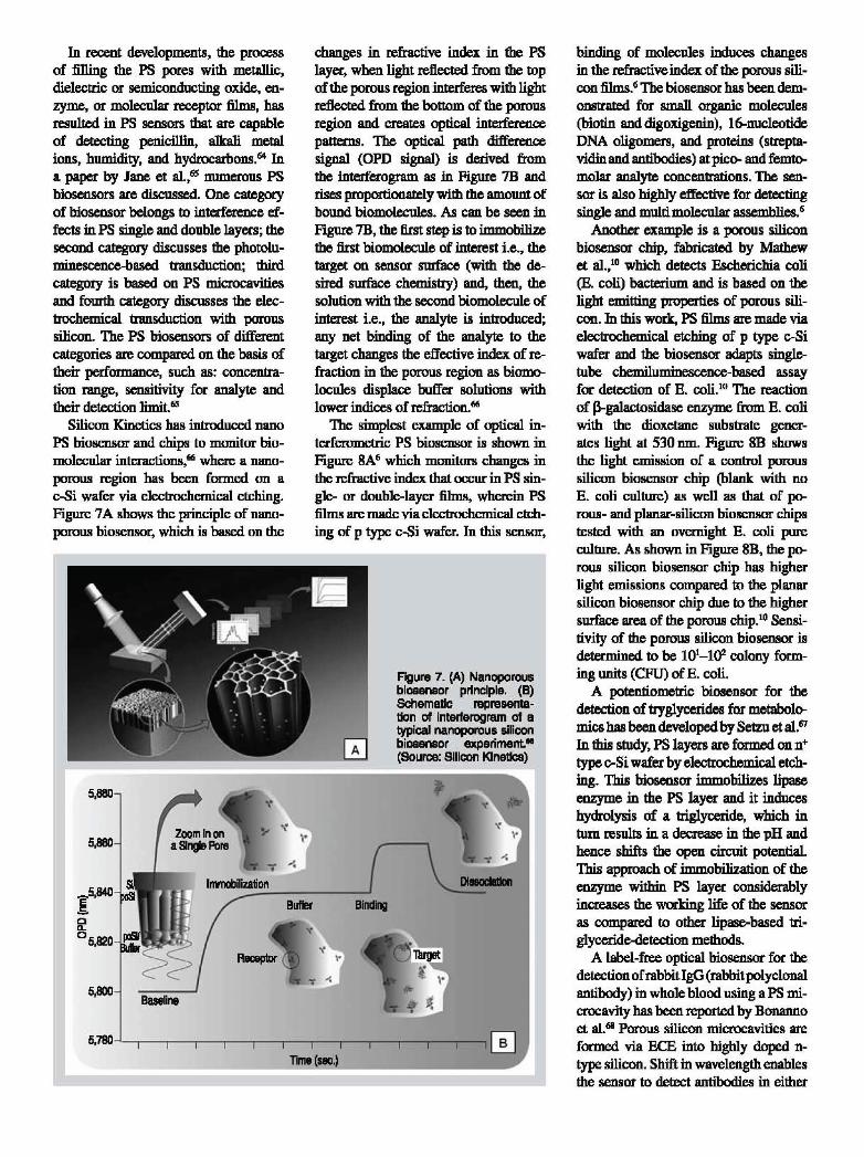
contacts using screenprinting techniquesfollowed by deposition of antireflectioncoating. The schematic representation ofone such c-Si solar cell by Sun Power isshown in Figure 4,38 where the expectedsolar cell efficiency is -29%. However,various losses such as reflection, recombination and resistive losses reduce thecell efficiency to 14.7%. It can be seenfrom Figure 4 that the total losses account for 14.3%, wherein 1.8% of thereflection losses are due to front metallicgrid structure and 0.4% reflection lossesare after texturization and ARC deposition. The main attraction of poroussilicon in the photovoltaic (PV) industryis to use it as a cost effective ARC forlarge-scale applications. The main advantage of PS as an ARC (as discussedin the preceding section) is well known;it reduces the reflection losses resultingfrom the silicon surface. Furthermore,PS has a large active area and is capableof light down-shifting in energy or photon energy down-converter (ultravioletto visible). The use of PS films in solarcells has led to a reduction in the surfacerecombination velocity, enhancement ofthe spectral response in the short-wavelength region, and increase in the photogeneration velocity of charge carriers.1S-
24 Porous silicon can also serve asa wide bandgap absorber in a multiplejunction cell structure, with c-Si as thesubstrate.24 Attempts have been reportedto use two PS films with two differentbandgaps in a three-bandgap solar cellon a silicon wafer.39
Porous silicon ARC formed via ECEor CE on finished solar cells has a serious problem of fill factor degradationdue to the increase in series resistance(R.). Screen printed metalized contactsmake direct contact with HF solution
40
2.6%
\Aluminum
paste
29%-14.3%
14.7%
three-dimensional (3-D) picture of PSlayer, which consists of irregular uprightsurface features with typical size distribution of -150--500 nm or even smaller,where the maximum pore size is -500nm long and -50 nm wide whereas theminimum pore size is -150 nm long and-30 nm wide. Such types of structuresare generally observed in PS films.24
Fourier transform infrared (FTIR)analysis is widely used to characterize the bonding properties in PS films.Here, we present FTIR and photoluminescence (PL) spectra on PS films ofvarious thicknesses, formed on p typec-Si wafer via ECE. In this work, PSfilms of various thicknesses are formedat optimized current density (1) of 20rnA cm-2 with time (t) variation from1 to 20 minutes, respectively.45 As current density increases, the thickness ofPS film increases.44 The PS films ofvarious thicknesses, (a)-{e) in Figure6A and B, are formed at a constant Jof 20 rnA cm-2 and at time t = 1 min, 2min., 5 min., 20 min., and 30 min., respectively.45 The thickness of PS films,(a) and (b), are -150 nm and -200 nm,respectively, as measured by an ellipsometer; for films (c)-(e), the thicknessvaries from 5 to 20 f.1IIl as estimatedfrom gravimetric measurements. IS Corresponding FTIR and PL spectra arerecorded for these PS films (Figure 6 Aand B).
Figure 6A shows the FfIR spectra ofPS films of various thicknesses (a)-{e).During PS formation, a large number
Silver paste pad
Recombinationlosses "
2.0CY~
1000
Texture + ARC Resistive loss
12R loss
3.8%
Limit cell effiCiency
Total losses
Generic cell efficiency
(b)
,! _ .
~.4% Back light\ absorption
/Back
contact
Reflection loss
1.8%
Fron~/contact
Figure 4. Multiple losses (such as reflection, recombination and resistive) in a singlecrystal silicon solar cell.38 (Courtesy of SunPower)
60 - (a) Reflectance of the cell with PS ARC- - - - - (b) Reflectance of the textured mc..si wafer
. (c) Reflectance of the cell with SINx ARC
(a)
10 I.......... "o+-~,___._____,_~-,-~_,_-.--,___,r__r-_I300 400 500 600 700 800 900
Wavelength (nm)
shows surface morphology, as seen bySEM and AFM for film PS2, which hasbeen formed on n+ emitter of textured cSi solar cell. As can be seen from FigureSA, the textured surface shows uniformlarge pyramids of sizes varying from 1to 10 J..lID. approximately. The SEM image indicates that the front screen printed silver finger has not been damagedafter PS formation. Figure 5B shows
5D
~41 40UcJ!I 30UCIl ,.,.~ 20:;./
B1200400
/(a)0-1--,--_,.-_-,.-_-,--_ _�
600 800 1000
Wavelength (nm)
80 _ (a) Reflectance of the cell with PS ARC70 . -_.. (b) Reflectance of the cell with SiN ARC
70 _ (a) Reflectance of the cell with PS ARC- - - - - (b) Reflectance of the cell with OLARe
60 (T10,lMgF)
10
A
1.2 ; -.- (a) Reflectance of the cell with PS, ARC
:-0- (b) Reflectance of the cell with PS~ ARC
- 1 0 i- e - (e) Reflectance of the the cell with ZoS ARC- :i . .....t ...- (d) Reflectance of the Siwafer~ 60 ni!if 50 41 0.8 \i: g ht)-e 40 J!lCIlU 0.6 't\\CIl (b) •
~:: \'.\. ~ 0.4 110.:......< (d) ~••••••••\ (b) "' A -
10 0.2 /\.. ~ #
/(a) _~~~ .:.:-.o 0.0+-----,----.--~---,----.--~_I400 600 800 1000 1200 350 400 450 500 550 600
C Wavelength (nm) D Wavelength (nm)
Figure 3. (A) Reflectance characteristics of cells with (a) PS ARC and (b) double film (TiOjMgF2) ARC;20·36 (B) reflectance characteristics of (a) PS ARC (b) alkaline-textured mc-Siwafer, and (c) single-film SiNx ARC;36 (C) reflectance characteristics of mono-Si cells with(a) PS ARC and (b) with conventional SiN ARC;20 (0) reflectance spectra of samples withARCs (a) PS1 ' (b) PS2 ' (c) ZnS and (d) without ARC.37
factor does not change in IMEC solarcells, whereas fill factor increases forCNRS-LPSB. The characteristics of thecell (5x5 cm2 Polix mc-Si) with the PSfilm (11-13.2%) are similar to commercial cells.20 Table IT also lists the resultsobtained for optimal PS ARC (PS
2-Fig
ure 2A), implemented on a screen printed c-Si solar cell. It has led to -20.8%relative improvement in Jsc' a significantgain of -15mV in Vee and a relative increment of about -.3% in FF. This yieldsa -26% increase in efficiency. In a studyby Kwon et al.,36 the optimization of aPS selective emitter in a screen printedmc-Si (2x2 cm2) solar cell results in a13.2% efficiency with electroplating.36
Thus, PS has immense potential asARC in commercial solar cell application. Simplicity and low cost of theECE technique as well as its adaptationto silicon solar cell manufacturing provides a very promising technology in anindustrial process.
Characterization of PorousSilicon Films
The surface morphology of PS filmshas been studied by scanning electronmicroscope (SEM) and atomic forcemicroscope (AFM). Figure SA and B
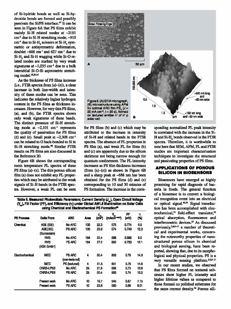
Table II. Ml8lul'8d PhOlOWlltaic Pllramll8l11j Current Density (J.), Open CircuitYabge(YJ, Fill FacIOr (FF),ud Efficiency (1'\l under Global AM1.5llluminatian on Solar cells
using Chlmicalud EI8cIroc:hImicll PS FormItionl'
(~v. FF "PS PI'DC8M Cella From ARC Ar8I (mAcnr-t') (mY) (%)
-
Chemical ASE(lSE) No ARC 100 22.3 575 0.774 9.9ASE(ISE) PSARC 100 28.9 574 0.740 12.3
(Eurosolare)RM3 No ARC 164 22.4 588 0.685 9.0RM3 PSARC 164 27.2 592 0.753 12.1
(ASEGmbH)
Electrochemical IMEC PSARC 4 31M 603 0.78 14.3(ncn-1exIured)
IMEC PS (taxtured) 4 31.3 801 0.78 14.6CNRStPSB No ARC 25 31.8 595 0.73 13.6CNRS-lPSB PSARC 25 3004 583 0.74 132
Present 'Mlrk No ARC 10 19.7 545 0.87 7.15Present 'Mlrk PSARC 10 23.8 580 0.88 9.01
of Si-hydride bonds as well all Si-hydroxide bonds are formed and pOllsiblypassivate the SilPS interface.47 It can beseen in Figure 6A that PS films exhibitmainly Si-H related modes at -2101em-I due to Si-H stretching mode, -910em-I due to Si-~ scissors or Si-~ symmetric or antisymmetric deformation.doublet -666 em-I and 627 em-I due to
Si-~ and Si-H wagging while Si-Q related modes are marked by very weaksignatures at -1,035 em-I due to a bulk:interstitial Si-D-Si allymmetric stretching model.1l,2O,4S
AB the thickness of PS films increase(i.e., FTIR spectra from (a)-{e», a clearincrease in both line-width and intensity of these modes can be seen. Thisindicates the relatively higher hydrogencontent in the PS films as tbi.ckness increases. However, for very thin PS:films,(a), and (b), the FI1R. spectra showsonly weak signatures of these bands.The distinct presence of Si-H stretching mode at -2,101 em-I representsthe quality of passivation for PS films(d) and (e). Small peak: at -2,308 em-Ican be related to 0 back-bonded to Si inSi-H stretching mode.4I Similar FTm.results on PS films are also discussed inthe Reference 20.
FIgUre 6B shows the correspondingroom temperature PL spectra of thesePS films (a)-{e). The thin porous siliconfilm (a) does not exhibit any PL properties which may be attributed to the weaksignals of Si-H bands in the FI'IR spectra. However, a weak PL can be seen
Figure5.(A)SEM micrograph,(8) mlcrostn.Jcture using AFMfor optimal ARC 111m PSI (J '"20 mA c:rrrI, t =20 s), formedon textunKl emitter n+ of n+ P B801arcell.
for PS films (b) and (c) which may beattributed to the increase in intensityof Si-H and related bands in the FTm.spectra. The absence ofPL properties inPS film (a), and weak PL for films (b)and (c) are apparently due to the siliconskeletons not being narrow enough forquantum confinement. The PL intensityincreases as PS film thickness increases(from (a}-(e» as shown in Figure 6Band a sharp peak at -688 nm. has beenobtained for the PS films (d) and (e)corresponding to 10 and 30 minutes ofPS formation. The increase in the corre-
sponding normalized PL peak intensityis correlated with the increase in the SiH and Si-Hzbonds observed in the FI1R.spectra. Therefore, it is worthwhile tonotehere that SEM, AFM, PL and FTlRstudies are important characterizationtechniques to investigate the structuraland passivating properties ofPS films.
APPLICATIONS OF POROUSSILICON IN BIOSENSORS
BiOllen80I'S have emerged as highlyprmnising for rapid diagnosis of bacteria in foods. The general functionof a biosensor is to convert a biological recognition event into an electricalor optical signal.49,sll Signal tramIduction has been accomplished with electroohemica1,51 field-effect transistor,52
optical absorption. fluorescence andinterferometric devices.53 As discussedpreviously,2,6,lI-I7 a number of theoreti-cal and experimental works, concerning the noteworthy properties of nanD
structured porous silicon in chemicaland biological sensing, have been reported, showing that. due to its morpoological and physical properties, PS is avery versatile sensing platform..:w.-17
In our recent studies, we observedthat PS :films formed on textured substrates show higher PL intensity andhigher lifetime values as compared tothose forIDed on polished substrates forthe same current density.S4 Porous sill-

800750600 650 700
Wavelength (nm)
surface stability of PS, there is a needto functionalize the surface of PS by asuitable precursor. In one of our recentworks, nanostructured PS surface wasbiofunctionalized by thermally depositing thin biocompatible films with alarge density of amine groups, using 3arninopropyltriethoxysilane (APTS) onto its surface.63 The aim of the study wasto demonstrate the covalent bonding between organic molecules (immunoglobulin) and modified inorganic surface(nanostructure PS) which can be usedfor the detection of protein signals. Inthis study, PS films prepared at an optimized J-50 rnA cm-\ having high PLintensity, stable surface bond configurations, mechanically strong structureand hydrogen-passivated surfaces wereused for APTS treatment.63 The presence of reactive amino groups on the PSsurface along with glutaraldehyde as alinker aids in the covalent binding of theantibody (Human IgG) onto the PS surface.63 Different antigen concentrationscan be detected with a good reproducibility with this technique which opensa possibility of using this biofunctionalized material for future biosensors.
550
J=20 mAcm-21.6
1.4
5 min (elOA ,
0.2t§§~~;~~1~m;:in3(a~I::;~~~500
B
-; 1.2
~ 1.0~'iii 0.8c::.! 0.6c::
- 30 min".. (e)
~ / /C'a- 2351 2101
~ 20 min ".. (d)II)c: 5min (e)Sc:
2min ".. (b)
1min ".. (a)
4000 3500 3000 2500 2000 1500 1000 500A Wavenumber (1Iem)
1.8,----------------,30 min (el
\
Figure 6. (A) FTIR spectraand (8) PL spectra of freshPS formed at current density(J) of 20 rnA cm-2 for timevariation from 1 min to 30min., curves (a-e).
J=20 mAcm·2
structures due to over-oxidation of thesilicon columns. It can be inferred thatthe surface passivation either by hydrogen or oxygen is one of the requisiteconditions for obtaining strong PL efficiency in PS.61 It seems that more thanone emission mechanisms are responsible to explain the luminescence properties of PS.60
Furthermore, PS biosensor technology has shown great capability in detecting biological molecules with high selectivity, using specific linker agents andprobe molecules.61 For the biomedicalapplications of PS, biomolecules haveto be first immobilized on its surfacethrough functional groups deposited onit. The common approach is to create acovalent bond between the PS surfaceand the biomolecules which specificallyrecognize the target analytes.61 The reliability of a biosensor strongly dependson the functionalization process as wellas its rapidity, simplicity, homogeneity, and repeatability.62 It is well knownthat, after anodization, the fresh siliconsurface is predominately hydride-terminated which is quite reactive and sensitive to oxidation.62 Thus, to increase the
con layers and their interfaces have beencharacterized by recording diffractioncurves and measuring lattice mismatch!strain and the radius of curvature due toinduced biaxial stress caused by the lattice expansion of PS film due to pores.55
The higher range of strain values exhibited by PS films on textured specimenscorresponding to a wide range of bandgaps compared to that formed on polished specimens indicates that stable andhigher porosity PS films can be formedon textured substrates at higher currentdensities. The larger surface area available for PS films formed on texturedsubstrates enables the even distributionof strain, thus, leading to enhanced stability as compared to the correspondingfilms formed on polished specimens.55
This factor is responsible for PS filmsformed on textured substrates to withstand higher strain without any elasticrelaxation at high current densities andcan be used for gas-sensing measurements.56 In the case of PS films on polished specimens, the relaxation of theinduced strain starts at relatively lowercurrent densities as compared with PSfilms on textured substrates and thusis not suitable for gas-sensing applications.
The surface of porous silicon needsto be stabilized for biosensing applications and is achieved by means of oxidation, silanization, or hydrosilylation.57
•58
Even without resorting to the abovetechniques, PS surface can be stabilizedusing an appropriate post-anodizationtreatment. At an optimum current density, passivation of defects by a novel nascent-H treatment resulted in the significant enhancement in the PL efficiency.59
The degraded PL intensity in the treatedsamples upon prolonged oxidation forseveral months was higher as comparedto that for the as anodized samples. Infrared vibrational studies indicated thatthe enhancement in PL was due to theH-passivation of defects in the Si-poreinterface as also elucidated from capacitance-voltage studies.59 Furthermore, ithas been found that HF-treated PS surfaces are relatively stable against oxidation as compared to untreated PS films.60
Upon oxidation of the HF treated PSfilms, the PL intensity initially increasesas a result of reduction in crystallite sizeto exhibit quantum size effects and thendecreases owing to loss of luminescing
Tml(IIC.)
5.780....-....,....---,--....,....---,---.----,--,----,--,--.-----r--.---....... 1 B
binding of molecules induces changesin the refracti'Yeindex of the porous silicon films.Ci1be biosensor has been demonstrated for small organic molecules(biotin and digoxi.genin), 16-nucleotideDNA oligomers, and proteins (streptavidinandantibodies) atpico- and femto.molar analyte concentrations. The sensor is also highly effective for detectingsingle and multi molecular assemblies.6
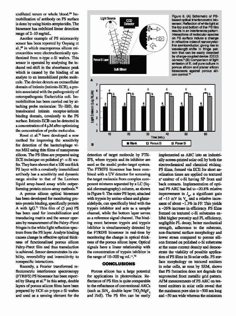
Another example is a porous siliconbiosensor chip, fabricated by Mathewet al.,ID which detects Escherichia coli(E. coli) bacterium and is based on thelight emitting properties of porous silicon. In this work, PS films are made viaelectrochemical etching of P type c-Siwafer and the biosensor adapts singletube chemiluminescence-based assayfor detection of E. coli.ID The reactionof P-galaetosidase enzyme from E. coliwith the dioxetane substrate generates light at 530 nm. Figure 8B showsthe light emission of a control poroussilicon biosensor chip (blank with noE. coli culture) as well as that of p0
rous- and planar-silicon biosensor chipstested with an overnight E. coli pureculture. As shown in Figure 8B. the p0
rous silicon biosensor chip has higherlight emissions compared to the planarsilicon biosensor chip due to the highersurface area of the porous chip.1.O Sensitivity of 1be porous silicon biosensor isdetermined to be 101-111 colony forming units (CPU) of E. coli.
A potentiometric biosensor for thedetection of tryglycerides for metabolomicshasbeen developedby Setzu et a1..f;]
In this study, PS layers are formed on n+type c-Si wafer by electrochemical etching. ThiB biosensor immobilizes lipaseenzyme in the PS layer and it induceshydrolysis of a triglyceride, which intum results in a decrease in the pH andhence shifts the open circuit potentiaL1bis approach of immobilization of theenzyme within PS layer considerablyincreases the working life of the sensoras compared to other lipase-based 1riglyceride-detection methods.
A label-free optical biosensor for thedetectionofrabbitIgG(rabbitpolyclonalantibody) in whole blood using a PS microcavity has been reported by Bonannoet al.61 Porous silicon microcavities areformed via ECE into highly doped ntype silicon. Shift in wavelengthenablesthe sensor to detect antibodies in either
Figure 7. (A) Nanoporousbiosensor principle. (B)5chemallc representation of interferogram 01 atypical nanoporous siliconbiosensor experiment"(Source: Silicon KInetics)
changes in refracti.'Ye index in the PSlayer, when light reflected from the topofthe porous region interferes with lightreflected from. the bottom of the porousregion and creates optical interferencepatterns. The optical path differencesignal (OPD signal) is derived fromthe interferogram as in Figure 7B andrises proportionately with the amount ofbound biomolecules. AB can be seen inFigure 7B, the first step is to immobilizethe first biomolecule of interest i.e., thetarget on sensor surface (with the desired surface chemistry) and, then, thesolution with the second biomolecule ofinterest i.e., the analyte is introduced;any net binding of the analyte to thetarget changes the effective index of refraction in the porous region as biomolocules displace buffer solutions withlower indices of refraction.6l'i
The simplest example of optical interfermnetric PS biosensor is shown inFigure SA6 which monitors changes inthe refractive index that occur in PS single- or double-layer :films, wherein PS:films are made via electrochemical etching of P type c-5i wafer. In this sensor,
,.
_5,840E..s~°5,820
5,800
5,860
5,880
In recent developments, the processof filling the PS pores with metallic,dielectric or semi.coIlducting oxide, enzyme. or molecular receptor films, hasresulted in PS sensors that are capableof detecting penicillin, alkali metalions, humidity, and hydrocarbons.64 Ina paper by Jane et al.,fi5 numerous PSbiosenso:rs are discussed. One categoryof biosensor belongs to interfeIeDCe effects in PS single and double layers; thesecond category discusses the photoluminescence-based transduction; thirdcategory is based on PS microcavitiesand fourth category discusses the electrochemical transduction with poroussilicon. The PS biosenso:rs of differentcategories are compared on the basis oftheir performance, such as: concentration range, sensitivity for analyte andtheir detection limit.(is
Silicon Kinetics has introduced nanoPS biosensor and chips to monitor biomolecular interactions,6l'i where a nanoporous region has been formed on ac-Si wafer via eleclrochemical etching.Figure 7A shows the principle of nanoporous biosensor, which is based on the
implemented as ARC into an industrially screen-printed solar cell by both theelectrochemical and chemical etching.PS films, formed. via ECE for short anodization times are applied on textmedn+ emitter of c-Si having SP from andback. contacts. Implementation of optimal PS ARC has led to -20.8% relativeimprovement in J"", a significant gainof -15 mV in V0; and a :relative increment of about -1.3% in FF. This yieldsa -26% increase in efficiency. PS filmsformed on textured c-Si substrates exhibit higher porosity and PI.. efficiency,negligible PL decay, better mechanicalstrength, adherence to the substrate,non-fractured surface morphology andlower stress compared to porous silicon formed on polished c-Si substratesat the same current density and demonstrate the viability of possible application ofPS films in Si-solar cells. PS smface morphology on textured emittersin solar cells, as seen by SEM, showsthat PS formation does not degrade theunprotected from metallic grid pattern.AFM measurements ofPS ARC on textured emitters in solar cells :reveal thatthe mayjrnnm pore size is -500 nm.longand -50 om wide whereas the minimum
Ugh! Souree .. Figure B. (A) SChematic of PS-bued optIcaIlnterleromstrlc blo-I18n80r. Reftection ofwhile lightatthe top and bottom of the PS filmresut18 in an interference pallern.Interactions of molecular speclll8on PS surface induce a changein 1'8fractiV8 indexof nanocryslal-line semiconductor, giving rise toWIMllengttl shifts In fr1nge pal-
...... 1em thai can be easily detectedby charge-coupleddevice (CCD)camera.' (B) Comparison of lightsmlselon of E. coil pure cufture Inporous 8IlIcon and planar siliconbiosensors agailllll porous sili-con control.1o
A7
~ : c c c c c c
.3 4cD
:1 3w:E! 2...::::J
010 20 30 40 50 60
TIIIIII (min.)
B • Blank D PorcusSi P1anerSi
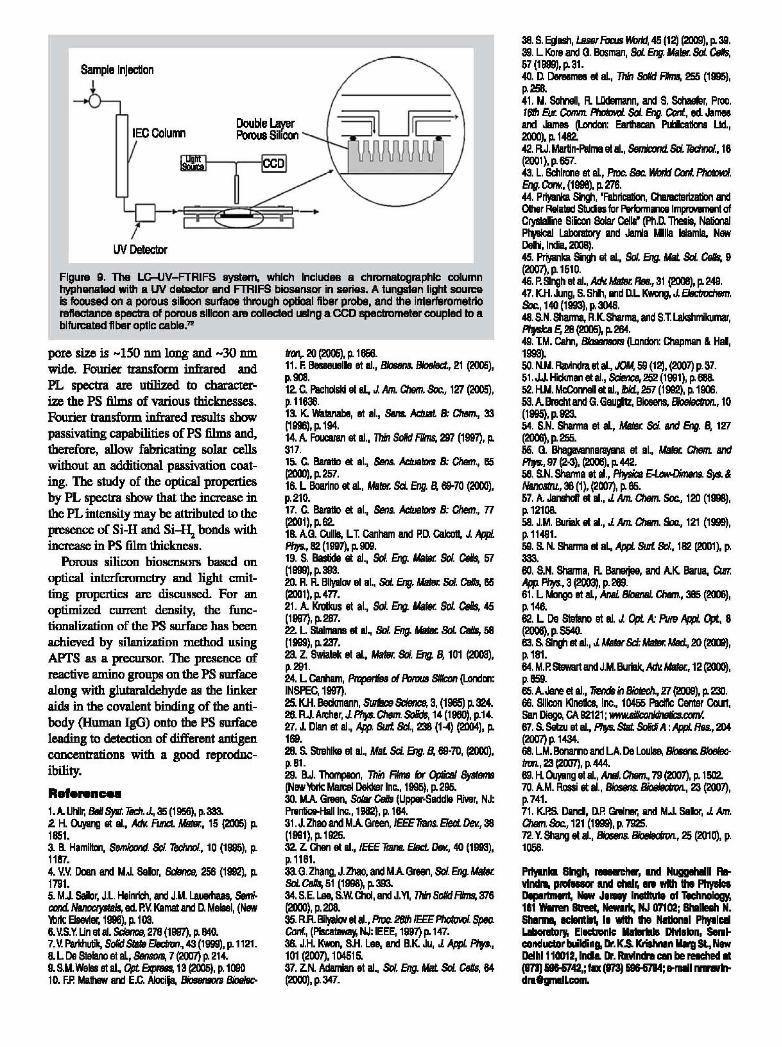
detection of target molecule by FfRIPS, where trypsin and its inhibitor areused as the model probe-target system..The FfRIFS biosensor has been combined with a UV detector for screeningthe target molecule from. complex component mixtures separated by a LC (liquid chromatography) column, as shownin Figure 9. The outerPS layer, attachedwith trypsin by amino-silane and glutaraldehyde, can specifically bind with thetrypsin inhibitor and acts as a samplechannel. while the bottom layer servesas a reference signal channel. The binding event between trypsin and trypsininhibitor is simultaneously detected bythe FI'RIFS biosensor in real-time bymonitoring the change in optical thickness of the porous silicon layer. Opticalsignals have a linear relationship withthe concentration of trypsin inhibitor inthe range of 10-200 ng mL-1,71
CONCLUSIONS
Porous silicon has a large potentialfor applications in photovol.taics. Reflectance ofPS film is quite comparableto the :reflectance ofconventional ARCs(such as SiN", double layer TIO/MgF2and ZnS). The PS film can be easily
undiluted serum or whole blood.68 Immobilization of antibody on PS surfaceis done by using biotin-streptavidin. Thebiosensor has exhibited linear detectionrange of2--10mgImL.
Another example of PS microcavitysensor has been reported by Ouyang etaI.,li9 in which macroporous silicon microcavities were electrochemically synthesized from n-type c-Si wafers. Thissensor is operated by analyzing the induced red-shift in the absorbance peakwhich is caused by the binding of ananalyte to an immobilized probe molecule. The device detects an extracellulardomain of intimin (intimin-ECB), a protein associated with the pathogenicity ofenteropathogenic Escherichia coli. Immobilizition has been carried out by attaching probe molecules: Th-ffin, theb'anslocated intim:in receptor-intiminbinding domain, covalently to the PSsurface. Intimin-ECB canbe detected ina concentrationof4 j.LMafteroptimizingthe concentration ofprobe molecules.
Rossi et aI.70 have developed a newmethod for improving the sensitivityfor detection of the bacteriophage virus MS2 using thin films of nanoporoussilicon. The PS films are prepared usingECE technique on polished p+- c-Si wafer. They have shown that a 100 omthickPS layer with a covalently immobilizedantibody has a sensitivity and dynamicrange similar to that of the Lum:inexliquid array-based assay while outperforming protein micro-array methods.70
A porous silicon optical biosensorhas been developed for monitoring protein-protein binding, specificallyproteinA with IgG.71 Thin film. of (5 J1Dl) PShas been used for immobilization andtransducing matrix and the sensor operates by measurement ofthe Fabry-Perot:fringes in the white light reflection spectrum from the PS layer. Analyte bindingcauses change in effective optical thickness of functionalized porous siliconFabry-Perot film and thus transductionis achieved. Sensor demonstrates its stability, reversibility and insensitivity toI1OII8pCCific inte:ractions.
Recently, a Fourier transformed reftectometri.c interference spectroscopy(FfRIFS) PS biosensor has beenreported by Shang et aL71 In this setup, doublelayers of porous silicon films have beenprepared by ECE on p-type c-Si wafersand used. as a sensing element for the
uv Detec1Dr
Figure 9. The Le-lJV-FTRIFS system, which Includee a chromatographic columnhyphenated with a UV detector and FTRIFS biosensor in series. A tungsten light sourceis focused on a porous silicon surface through optical fiber probe, and the interl8rometricre'IIectance spectra of ponlus silicon are collected UBlng a CCO spectlometer coupled 10 ablfun:ated fiber optic cable.71
Sample Injection
pore size is -150 nmlong and -30 nmwide. Fourier transform infrared andPL spectra are utilized to characterize the PS films of various thicknesses.Fourier ttansfonn infrared results showpassivating capabilities ofPS films and.therefore, allow fabricating solar cellswithout an additional passivation coating. The study of the optical propertiesby PL spectra show that the increase inthe PL intensity may be attributed to thepresence of Si-H and Si-~ bonds withincrease in PS film thickness.
PoroUll silicon biosensors based onoptical interferomelry and light emitting properties are discussed. For anoptimized ClD'J.'eIl1: density, the functionalization of the PS surface has beenachieved by silanization method usingAPTS as a precursor. The presence ofreactive amino groups on the PS smfacealong with glutaraldehyde as the linkeraids in the covalent binding of the antibody (Human IgG) onto the PS smfaceleading to detection of different antigenconcentrations with a good reproducibility.
R......nces1.A. Uhlir; Bell S)tIt. T6dr. J., 35 (1956), P. 333.2. H. 0uyBng et Ill., ArJv. Funct. MflIw.. 15 (2OD5) P.185t3. B. Hamilton, Semicond. SCi. TOOhnoI., 10 (11185), P.1187.4. V.V. Doan and M.J. 5alor, 5t:Ient:e. 256 (1992), P.179t5. M.J. sailor, J.L. Heinrich, and J.M. L.auerhaas, Sfmi.oond. NanocIyII8Is, ed. P.v. Kamal: and O. Meisel, (New'JtIrk: EJsevfBl', 1996), P. 1ca.B. V.S.Y. Un 81 aI. ScienofI, 278 (1997), P. B4O.7. V. Parkhutik, Solid StaffElecb'otl., 43 (1999), p. 1121.a. L. De St88no 81 aL, Sensm, 7 (2007) Po 214.9. S.M.we. 81 aI., Opt. &pI8IlI, 13 (2005), p. 109010. F.P. Ma1hew and E.C. AIociIa. EJicJsen.xI Bio8Isc-
tron,. 20 (2005), P. 1666.11. F. Bes8eulIIIs 81 aI., BIorl&n& BIo8Ied., 21 (2005),p.908.12. C. Pachclsld eI aL, J. Am. Cham. Soc., 127 (2005),p.11636.13. K. WBIBnabe, 81 al., &Ina. At:tuat. 8; Chem., 33(1996), p. 194.14. A Foucaran et aI., Th6I Solid Films, 'ISI1 (1997), Po317.15. C. 8aIBtID eI: al., Sen&. AduafM 8; Chem., 65(2000), P. m.18. L BoBrino et aI., MIter. Sci. Eng. B, 69-70 (2000),p.210.17. C. 8aIBtID eI: al., sens. AduafM 8; Chem., 77(2001), Po 62-1B. AB. QlIIIB, LT. canham and P.D. CaIcllIf, J. AppLPfr/S., 82 (1997), Po 909.19. S. Bastide et aI., Sol. Eng. Mater. Sol. ce¥s, fiT(1999), Po 393.20. R. R. B1lyB1llV 81 al., sa. Eng. Mater. Sol. C6IIB, 65(2001), P. 477.21. A. Ktolkus et al., Sol. Eng. Mater. Sol. ceas. 45(1997), P. 287.22. L. SIaIITIlIlIll 1II aI., Sol. Eng. Mater. Sol. C8I1s, 58(1999), p.237.23. Z. Swialllk et al., Maler. Sci. Eng. 8, 101 (2003),p.291.24. L CaMam, PmpertIes of Pomus SIItcon (Lond1l1:INSPEG. 1997).25. ItH. Beckmann, Sulks SciBncs. 3, (1965) p. 32428. FW. Aroher, J. Phys. Chfm. Solids, 14 (1960), p.14.'0. J. Dian 81 aI., App. SUd. Sd., 238 (1-4) (2004), p..169.28. a Strehlks 81 aI., Mat Sci. Eng. B, 69-70, (2000),P. B1.29. B.J.~, Thin Films for 0p/icIJI Systems(New'tbl1c Man:eI Deldcer Inc., 1995), p. 295.30. MA Green, Solar Cells (Upper-Saddle Aivllr, NJ:Prenlio&-HaIllnc., 19B2), p.l64.31. J. Zhao and MA Green, IEEETmns. Elect. DeK, 3B(1991), p.. 1925.32. Z. Chen et aI., IEEE Tl8II& Elect. Ow., 40 (1993),p. 11Bt33. G. Zhang, J.Zhao, and MA Green, Sol. Eng. Mater.SoL CellI, 51 (1998), P. 393-34. S.E.l.a8, S.W. ChoI, and J.Y1, ThIn SolidFI1mII, m(2000), p. 2ll8.35. R.R. BiIyekN et aI., Ptoc.26th IEEE PI'lotow1I. Spec.Conf., (Pisca~ NJ: IEEE, 1997) P. 147.36. J.H. KwllII, S.H. Lee, and B.1t Ju, J. AppI. PIIys.,101 (2007), 104515.37. l.N. AdanilIn et aI., Sol. Eng. Mat. Sol. Cells, 64(2000), p. 347.
38. S. EgIlSh, LsserFcJcus KtriI, 45 (12) (2009), p. 39.39. L Kere and G. Bollman, Sol. Eng. Mater. Sol. CB/Is,57 (1999), p.31.40. D. Denl8mes 1II aI., ThIn SolId FIlms, 255 (1995),p.25&.41. M. Sctr1eII, R. L.iidemann. and S. Schasfllr, Proc.16111 Eut. Comm. i'hokMJ/. sa. Eng. Coni, eel Jamesand Jamee (lllndcn: EarII1Ican Nicallons Ltd.,2000), p. 1482.42. R.J. MBrtin·PaIITB eI aI., Semicond. Sci. Tflchnol., 16(2001), P. 657.43. L. SChlral8 81 aL, Pmc. 8IJc. KM1 ConI. 1'haID1.fJI.Eng. caw., (1lll18), P. 276.44. PriyIMa Si9!, 'F1IbriC8lion, Chnct9rila1:iDn andOlher RBlallld Stucles for Perbmll1lllllmpnMmBnl ofCrystalli1e Sim Solar cell8" (Ph.D. 1heIie, NationalPI'rfsIcaI l..abcnIIXJry and Jamla Milia lsIamla, NewDelhi, India, 2008).45. Priyanka SfrIlil et aI., Sol. Eng. Mat Sol. Cells, 9(2007), P. 1510.46. P. SI~h 81 aI., AI:N. Mt1l8r. ReB., 31 (2008), p.. 249.47. ItH. J.mg, S. Shih, lind D.L~ J. Ei8c1mchem.Soc., 140 (1993), P. 3046.48. aN. Sharma, R.1t Sharma, and S.T. Lakstlmikumar,Physka E,28 (2006), P. 264.49. T.M. CBhn, 8IosstIIonI (London: Chapman & Hal,1993).50. N.M. Ravindra et aI., .JOM. 59 (12), (2007) p. 37.51 ..w. Hickman et aI., SCierIce,.252 (1991), Po eea.52. H.M. McComelI et aI~ lbld., 257 (1992), P. 1906.53. A. Brecht and G.Gau~, Bioeens, B«xllscf1oo., 10(1995), p. 923-54. S.N. Shatma et lll, Maler. SCi. and Eng. B, 127(2006), P. 2S5.56. B. BhagBvannarayana 81 al., Mafflt. Chen!. SlIdPhys., 'if1 (2-3}, (2006), p. 442.56. S.N. Sharma et aI.,~~ S)<s. &NanoIIru, 38 (1), (2007), Po 85.57. A JI1nIIhoI! 1II1l1., J. Am. Chsm. Soc., 120 (1998),p. 12108.58. J.M. Burilk: 1II aI., J. Am. Chsm. Soc., 121 (1999),Po 11491.59. S. N. Sharma 81 al., Apfi. SUrf. SCI., 182 (2001), p.333.eo. aN. Sharma, R. BanBrjee, and A.K Barua, CutT.App. Phjs., 3 (2003), p. 269.61. L Mongo 81 aL, AnaL B10BtIaL ChBm., 385 (2006),p.146.62. L De Sl9fBno et aI. J. Opt A: Pure AppI. qt, 8(2006), p. S540.63. S. S1fV181 aI., J. MB!srSCI: Mt1l8r. Med., 20 (201)>),P. 1Bt64. M.P. SIsMIrt and J.M. Burilk, Adv. Matsr., 12 (2000},p.1l59.65. A.Jane et aI., TIMdt in 8ioIech., 27 (2009). p. 230.66. Silicon K1ns11cs, Inc., 10455 PacIfIc Genter Court,san Diego, CA 92121;~ccm:ffl. S. Setzu et aI., Phys. sat. SoIifjA:AppL Res., 204(2007) P. 1434.68. LM. Bonamo and LA. De louise, BIoI8ns. BIoeIec11m, 23 (2007), P. 444.69. H. ()Jyang et aI., Arat. a.n., 79 (2007). p. 1502.70. A.M. Rt*i et aI., Biosens.~, 23 (2007),Po 74t71. K.P.s. DandI, D.P. Gnllner; and M.J. 5a1or, J. Am.ChBm. Soc., 121 (1999), P. 7925.72. Y. Shang It aI., lberI& BioellJc6'gn, 25 (2010), p.1058.
p...,... Sqh, fI••_, InII NugglIhIIII R.v1ndl'l, pRlfestor InII chIIr, I" with the PhpicsDeparIInent, *" J•.., IIl8IIMe of Tecllnology,1111 WIrren 8IreeI, NNark, NJ 071112; BlwlIeIIh N.Shlmlll, ICIlntIlt, II wtlh the Ndonll PhplCIIIIL.IbclrBIory, EllICtIanlc II8IIrtIIs DIvIsion, SemIconductorbUlding, Dr. K.S. KrishnIn IIIrgSt., NllWDeIhl l1ClO12,IncIa. Dr. Ravlnlh C8'I be relChed II(173) -.5742,: Iu (173) 5llH7II4: .rnIIIlllImIVhdflO!JTIIILcom.