Optical Properties of Non-Periodic Dielectric Systems Made of Nanostructured Porous Silicon
11
Optical Properties of Non-periodic Dielectric Systems Made of Nanostructured Porous Silicon B. Alvarado Tenorio 1 , J. Escorcia-Garcia 1 , Miguel Eduardo Mora-Ramos 2 , and V. Agarwal 1,a 1 Centro de Investigacion en Ingenieria y Ciencias Aplicadas Universidad Autonoma del Estado de Morelos Av. Universidad 1001, Col. Chamilpa, CP 62209, Cuernavaca, Morelos, Mexico 2 Facultad de Ciencias, Universidad Autonoma del Estado de Morelos Av. Universidad 1001, Col. Chamilpa, CP 62209, Cuernavaca, Morelos, Mexico a [email protected] (corresponding author) Submitted: July 11 th , 2007, revised: December 20 th , 2007, accepted: January 12 th , 2008) Keywords: porous silicon, Multilayers, Optical properties, non-periodic nanostructures, heterostructures Abstract. To investigate the optical properties in non-periodic dielectric systems, we study here the reflection of light from nanostructured porous-silicon-based period doubling heterostructures. The multilayered systems are fabricated in such a way that the optical thickness of each layer is one quarter of 650nm. The results for the optical reflectance are presented and compared with that of Fibonacci, Thue-Morse, and random structures fabricated under the same conditions. Numerical simulation for the reflectance along the lines of the transfer matrix approach is performed. In addition, optical reflection from Gaussian porous silicon multilayers is also briefly discussed. We find that porous silicon Period Doubling dielectric multilayers could demonstrate the optical properties similar to the classical periodic Febry-Perot interference filters with one or multiple resonant peaks, but with an advantage of having total optical thickness much lesser than that of the periodic structures. Introduction Formation of a periodic dielectric structure is done by repeating a finite arrangement several times which leads to the formation of a photonic crystal. On the other hand, a random structure follows no particular rule and cannot be reduced to a single cell that is repeated several times. Another category of quasiperiodic or quasiregular (non-periodic) structures are made up of two or more incomplete periods joined together to form an overall system that is neither fully periodic nor random but somewhere in between [1]. Such complex dielectrics are often considered as quasicrystals, and can be more easily obtained in a one-dimensional multilayered configuration. Several resonant peaks appear on breaking the periodicity of the structure, thus creating propagation modes within the structure. This property opens the doors for many useful applications. Typical binary systems of this nature are the Fibonacci (FN), Thue-Morse (TM), and Period Doubling (PD). All of them exhibit a singular continuous spectrum of the elementary excitations, which is the consequence of a multi-fractal character. A simple way of visualizing the generation of these quasiregular sequences in one dimension is through the definition of the so-called substitutional rules [2-5]. In particular, the Period Doubling sequence is a quasiperiodic system generated by iterated applications of the substitutional rule of the type (A → AB, B → AA). On the other hand, Fibonacci (FN) structure is also a quasiperiodic system whose j-th generation, F j , can be constructed by defining F 1 = A, F 2 = BA, together with the addition rule, F j = F j−2 + F j−1 . The Thue-Morse (TM) Journal of Nano Research Vol. 5 (2009) pp 69-78 online at http://www.scientific.net © (2009) Trans Tech Publications, Switzerland Online available since 2009/Feb/06 All rights reserved. No part of contents of this paper may be reproduced or transmitted in any form or by any means without the written permission of the publisher: Trans Tech Publications Ltd, Switzerland, www.ttp.net. (ID: 148.218.200.5-06/02/09,16:19:35)
Transcript of Optical Properties of Non-Periodic Dielectric Systems Made of Nanostructured Porous Silicon

Optical Properties of Non-periodic Dielectric Systems Made of Nanostructured Porous Silicon
B. Alvarado Tenorio1, J. Escorcia-Garcia1, Miguel Eduardo Mora-Ramos2,
and V. Agarwal1,a
1Centro de Investigacion en Ingenieria y Ciencias Aplicadas Universidad Autonoma del Estado de Morelos
Av. Universidad 1001, Col. Chamilpa, CP 62209, Cuernavaca, Morelos, Mexico 2Facultad de Ciencias, Universidad Autonoma del Estado de Morelos
Av. Universidad 1001, Col. Chamilpa, CP 62209, Cuernavaca, Morelos, Mexico [email protected] (corresponding author)
Submitted: July 11
th, 2007, revised: December 20
th, 2007, accepted: January 12
th, 2008)
Keywords: porous silicon, Multilayers, Optical properties, non-periodic nanostructures, heterostructures
Abstract. To investigate the optical properties in non-periodic dielectric systems, we study here the
reflection of light from nanostructured porous-silicon-based period doubling heterostructures. The
multilayered systems are fabricated in such a way that the optical thickness of each layer is one
quarter of 650nm. The results for the optical reflectance are presented and compared with that of
Fibonacci, Thue-Morse, and random structures fabricated under the same conditions. Numerical
simulation for the reflectance along the lines of the transfer matrix approach is performed. In
addition, optical reflection from Gaussian porous silicon multilayers is also briefly discussed. We
find that porous silicon Period Doubling dielectric multilayers could demonstrate the optical
properties similar to the classical periodic Febry-Perot interference filters with one or multiple
resonant peaks, but with an advantage of having total optical thickness much lesser than that of the
periodic structures.
Introduction
Formation of a periodic dielectric structure is done by repeating a finite arrangement several times
which leads to the formation of a photonic crystal. On the other hand, a random structure follows no
particular rule and cannot be reduced to a single cell that is repeated several times. Another
category of quasiperiodic or quasiregular (non-periodic) structures are made up of two or more
incomplete periods joined together to form an overall system that is neither fully periodic nor
random but somewhere in between [1]. Such complex dielectrics are often considered as
quasicrystals, and can be more easily obtained in a one-dimensional multilayered configuration.
Several resonant peaks appear on breaking the periodicity of the structure, thus creating propagation
modes within the structure. This property opens the doors for many useful applications. Typical
binary systems of this nature are the Fibonacci (FN), Thue-Morse (TM), and Period Doubling (PD).
All of them exhibit a singular continuous spectrum of the elementary excitations, which is the
consequence of a multi-fractal character. A simple way of visualizing the generation of these
quasiregular sequences in one dimension is through the definition of the so-called substitutional
rules [2-5]. In particular, the Period Doubling sequence is a quasiperiodic system generated by
iterated applications of the substitutional rule of the type (A → AB, B → AA). On the other hand,
Fibonacci (FN) structure is also a quasiperiodic system whose j-th generation, Fj, can be constructed
by defining F1 = A, F2 = BA, together with the addition rule, Fj = Fj−2 + Fj−1. The Thue-Morse (TM)
Journal of Nano Research Vol. 5 (2009) pp 69-78online at http://www.scientific.net© (2009) Trans Tech Publications, SwitzerlandOnline available since 2009/Feb/06
All rights reserved. No part of contents of this paper may be reproduced or transmitted in any form or by any means without the written permission of thepublisher: Trans Tech Publications Ltd, Switzerland, www.ttp.net. (ID: 148.218.200.5-06/02/09,16:19:35)
sequence is generated by iterated applications of the substitutional rule of the type (A →AB, B →
BA). The TM structure has a singular continuous Fourier spectrum without the presence of Bragg
peaks. It is not quasiperiodic, and can be considered as a critical aperiodic system [6].
On the other hand nanostructured PS has been a subject of extensive study for the last 17
years [7-12]. There has been a lot of interest in the photonic applications of porous silicon (PS).
The high optical sensitivity of PS is due to the possibility of producing the layers with the large
refractive index contrast which is made possible by producing a variation in the porosity of the
structure. This quality of porous silicon makes it a promising material for photonic devices like
Bragg filters and optical microcavities. Multilayered structures with high reflectivity [8], efficient
visible photoluminescence [7], compatibility with standard silicon processes for integrated
optoelectronics [9] and photonic applications [8,10,12], have been major attractions of this field.
The porous silicon can be fabricated, with an easy and cheap process i.e. using electrochemical
etching of crystalline silicon (c-Si) with HF. Moreover, this method gives us the ability of having a
wide refractive index contrast within the same material without having any the problem of inter-
diffusion between the dielectric layers. The advantage of making 1D structures with porous silicon
is that the optical properties can be measured accurately and the samples can be designed and
realized in any desired configuration. Since we can control both, the layer thickness and refractive
index, in principle, from completely ordered to completely disordered structure can be studied
experimentally.
Some previous works on FN and TM dielectric heterostructures based on porous silicon
have been put forward [13-18]. In the case of the PD sequence, only very scarce reports are found
regarding the analysis of the optical transmission of dielectric multilayers [16,19]. Within a
different framework, it is possible to mention the study, regarding the energy spectrum of Period
Doubling quasiperiodic structures, made by Luck [20] and A. Chakrabarti et al. [21], while their
dynamic structure factor has been calculated by A. Ghosh et al [22]. In addition, the propagation
and localization of electromagnetic waves in Period Doubling serial loop structures was recently
presented [23].
Apart from that the idea of Gaussian layered structures has several antecedents in the field of
electronics [24,25]. In the case of dielectric multilayer systems it introduces a novel approach in the
search for application in optics, and optoelectronics. For example, the work proposed by Arriaga et
al. [26] demonstrates the possibility of the formation of omnidirectional photonic band gap with the
PS-based one-dimensional photonic crystals with Gaussian refractive index profile.
In general, the non-regularity associated to the structure of these systems provides a special
kind of dielectric contrast that throughout reflects in the propagation of the light. Therefore, the
random character of the multilayers distribution should also lead to interesting features in its optical
properties. In this subject, disordered dielectric layered systems have been studied in the past by
randomly choosing the thickness of the layers and keeping the optical length of each ingredient
layer approximately equal to one quarter of a given wavelength [27,28]. Random Bragg reflectors
have been studied by Pavesi group [29] by keeping the thickness and the porosity of the low/high
porosity layer constant. The thicknesses of the high porosity layers were generated randomly in
such a way that their histograms form a Gaussian distribution.
So far there have been no previous reports on PS-based PD dielectric structures. Therefore,
the main motivation behind the present research is to present experimental measurements of the
properties of light propagation in this kind of structures and to compare their output with those
arising from some other non-regular systems fabricated from PS multilayers that follow the building
patterns of FN, TM, and Random Binary (RM) systems. They are all fabricated under the same
conditions. This means that the optical thickness of each ingredient layer is one quarter of 610 nm.
The comparison with the periodic structures is presented as well. In addition, some results regarding
light propagation in PS multilayers with Gaussian thickness profiles are also presented.
70 Journal of Nano Research Vol. 5
Experimental Details
For fabricating nanostructured PS-based multilayers, we have used boron doped, p++
type
crystalline silicon with resistivity 0.001−0.005 ohm-cm, (100) oriented substrates. For
electrochemical anodization process at room temperature, the electrolyte with volumetric ratio of
3:7 of HF (48 wt%) and ethanol (98 wt%) respectively was taken. The current density was
controlled by a computer interfaced electronic circuit. The 1D - PD quasiperiodic photonic
structures can be generated by stacking together the layers of different dielectric materials namely A
and B. The refractive index corresponding to each porosity was calculated by interferometric
method for a monolayer of approximately two microns at 1500nm of wavlength. The two current
densities used for making all the quasiregular heterostructures considered were (a) 5 mA/cm2,
refractive index nA = 2.0 (anodization time: 22 sec), and (b) 80 mA/cm2 (nB = 1.2, anodization
time: 4.6 sec). The thicknesses of the layers (as measured using Scanning Electron Microscope
(SEM)) were 80 nm for the layer A (5 mA/cm2) and 140 nm for B (80 mA/cm
2). The thicknesses of
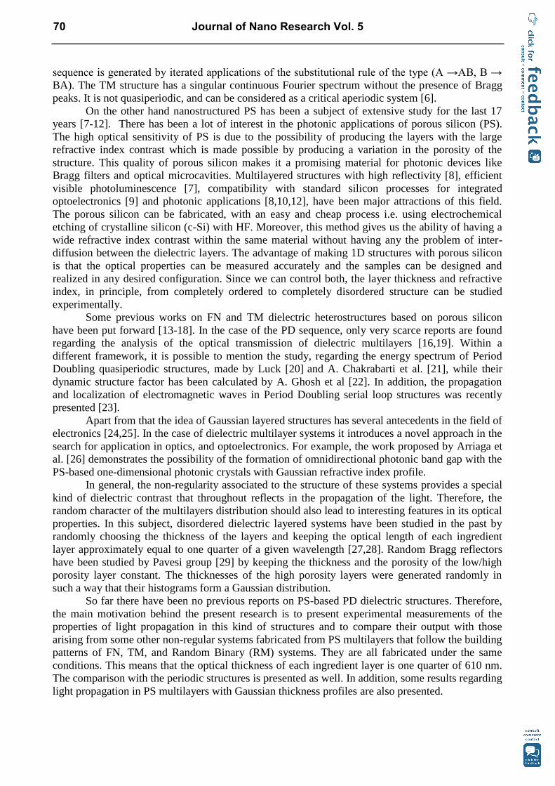
Figure 1. Cross-sectional SEM image of a typical
(a) Fifth generation period doubling structure (abaaabababaaabaaabaaabababaaabab).
(b) Sixth generation Fibonacci structure (abaababaabaababaababa).
(c) Fifth generation Thue-Morse structure (abbabaabbaababbabaababbaabbabaab).
(d) periodic structure (abababababababababab).
(a)
(a) (b)
(d) (c)
Journal of Nano Research Vol. 5 71

the layers are chosen in such a way that the optical thickness of each layer is approximately one
quarter of 610 nm. For the characterization and analysis of the optical properties of period doubling
dielectric heterostructures, absolute reflectance spectra was measured using specular reflectance
accessory (URA) of a Perkin Elmer UV-Vis-NIR spectrophotometer (Lambda 950) at 80 angle of
incidence.
Results and Discussion
Here we present some SEM images and the results of the optical measurements of the
different non-periodic PS-based multilayer structures considered in this work. Some numerical
simulations are included in order to compare with the experimental output. The calculation of
reflectance properties in these systems is based on the transfer matrix model [5,30,31].
Fig. 1 shows a typical scanning electron micrograph of fifth generation of PD sequence
(Figure 1a), sixth generation of FN (Figure 1b), fifth generation of TM series (Figure 1c) and a
periodic structure (Figure 1d). White and black layers represent the low and high porosity layers
respectively.
Fig. 2 shows the calculated and experimentally measured reflectance of PSPD
heterostructures fabricated in such a way that the optical thickness of each layer is one quarter of
610 nm. The orders of the PD generations in the multilayered structures are 5 (32 blocks), 6 (64
blocks) and 7 (128 blocks), respectively.
Figure 2. Theoretical and experimental reflectivity spectra of 5th, 6
th and 7
th generation of Period Doubling.
72 Journal of Nano Research Vol. 5
Taking into account the strong light absorption of the PS in the short wavelength regions, we
were only interested in the reflectance signal above 500 nm. It can be seen that the fabricated
samples show rather wide regions of high reflectivity, exhibiting a good accordance with the
theoretically predicted signal. As expected, higher generations lead more directly to the appearance
of pseudo-photonic band gap (PBG) regions because of the increasing dielectric contrast in the
system.
It can be observed in the fifth generation of PD structures (PD-32) that the main pseudo
PBG in the visible region appears in the wavelength range of 570 nm to 700 nm, with a fairly strong
photon confinement at 650 nm. The strongest confinement (resonant peak) is observed in the near
infra-red region at 854 nm, which leads to the observation of microcavity configuration (from 760
to 930 nm). In the sixth generation of period doubling structure (PD-64), the position of the main
pseudo PBG remains almost unchanged, but an additional photonic confinement can be observed at
620nm. The PBGs appearing in the NIR range are found to move slightly towards the visible
region, with an additional confinement at approximately 864nm.
Observing the wavelength range from 754nm to 960nm of the PD-32 and 720 to 940nm of
the PD-64, one can deduce that the structures are capable of producing resonant peaks in a
microcavity configuration. Analyzing in terms of optical thickness, PD-32 sequence has an
advantage, over the classical periodic Febry-Perot interferometric structure, fabricated for 848 nm
as a resonant frequency, of having lesser optical thickness of the structure (4880 nm) than the
periodic structure (5088 nm for a complete wavelength cavity structure at 848nm, added to another
few thousand nanometers more for creating any confinement mode in the visible region).
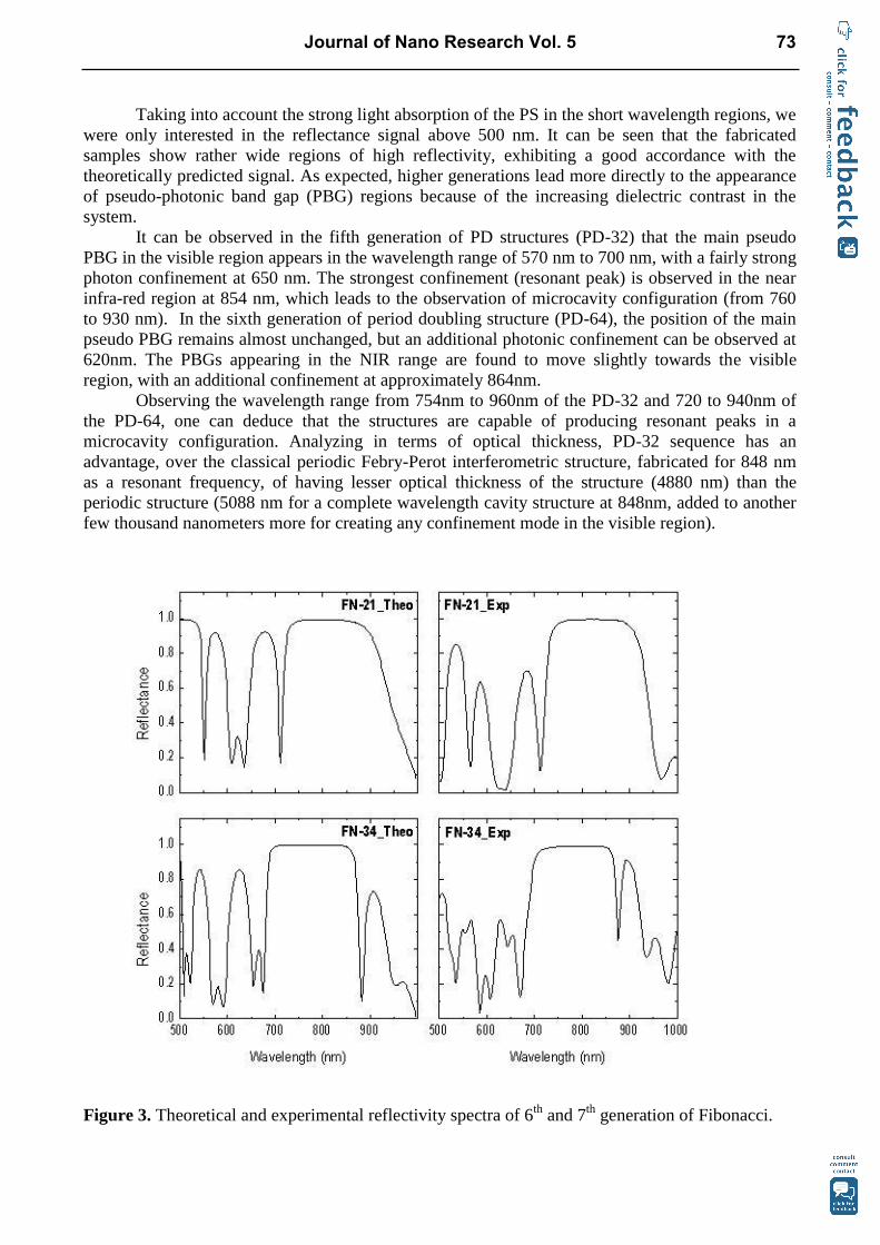
Figure 3. Theoretical and experimental reflectivity spectra of 6th
and 7th
generation of Fibonacci.
Journal of Nano Research Vol. 5 73
The seventh generation of the period doubling structure (PD-128) also shows a highly
fragmented spectrum. The main pseudo band gap appears in the visible range from 552 nm to 634
nm. Apart from that strong light confinement is observed at 640, 670 and 698 nm. The percentage
reflection of peaks appearing in the visible region (apart from the main PBG) is observed to be in
the range of 70-85%. Another band gap appears in the visible region extending up to the NIR region
(750-974 nm). Within this band gap few resonant modes appear at 814, 842, 876 and 890 nm of
wavelength.
In these PD heterostructures one observes that the experimental reflectance signals in the
PBG regions fall short to achieve the unity. This can be explained by assuming the presence of
optical losses in the system. In general, the losses detected can be attributed to different effects. In
our case, knowing that light absorption will occur for high frequencies, we are inclined to consider
the leading scattering mechanism as to be due to interface roughness. However, there is always
some kind light of light scattering due to the microscopic structure disorder.
For the sake of comparison, Fig.3 presents the reflectance of PS-based FN multilayer
heterostructures of 6th and 7th generation, respectively. Contrary to the PD structures, sixth
generation of Fibonacci structure (FN-21), having in total 21 layers, presents only one pseudo band
gap from 724 to 940 nm, with no resonant peaks. Similarly the seventh 5 generation of FN (FN-34)
shows a pseudo band gap from 688-910 nm with a resonant peak at 876 nm.
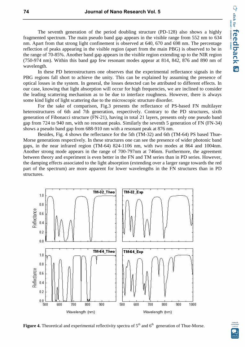
Besides, Fig. 4 shows the reflectance for the 5th (TM-32) and 6th (TM-64) PS based Thue-
Morse generations respectively. In these structures one can see the presence of wider photonic band
gaps, in the near infrared region (TM-64) 824-1106 nm, with two modes at 864 and 1004nm.
Another strong mode appears in the range of 700-797nm at 746nm. Furthermore, the agreement
between theory and experiment is even better in the FN and TM series than in PD series. However,
the damping effects associated to the light absorption (extending over a larger range towards the red
part of the spectrum) are more apparent for lower wavelengths in the FN structures than in PD
structures.
Figure 4. Theoretical and experimental reflectivity spectra of 5th and 6
th generation of Thue-Morse.
74 Journal of Nano Research Vol. 5
From the analysis of SEM micrographs of Fig 1, it is seen that interface quality is better for
the TM sample as compared to the interfaces present in PD sample. This helps to support the
interface scattering argument given above, regarding to the losses detected in the PD signals of
Fig.2.
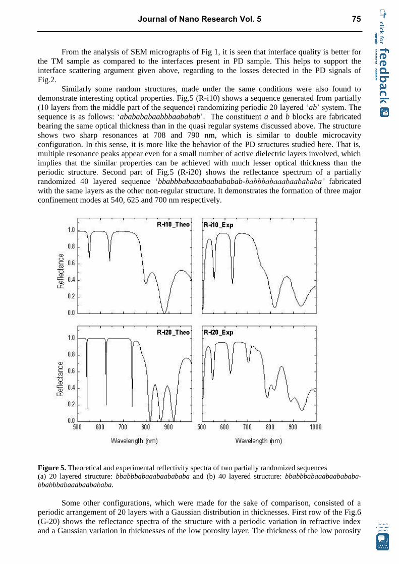
Similarly some random structures, made under the same conditions were also found to
demonstrate interesting optical properties. Fig.5 (R-i10) shows a sequence generated from partially
(10 layers from the middle part of the sequence) randomizing periodic 20 layered ‘ab’ system. The
sequence is as follows: ‘ababababaabbbaababab’. The constituent a and b blocks are fabricated
bearing the same optical thickness than in the quasi regular systems discussed above. The structure
shows two sharp resonances at 708 and 790 nm, which is similar to double microcavity
configuration. In this sense, it is more like the behavior of the PD structures studied here. That is,
multiple resonance peaks appear even for a small number of active dielectric layers involved, which
implies that the similar properties can be achieved with much lesser optical thickness than the
periodic structure. Second part of Fig.5 (R-i20) shows the reflectance spectrum of a partially
randomized 40 layered sequence ‘bbabbbabaaabaabababab-babbbabaaabaabababa’ fabricated
with the same layers as the other non-regular structure. It demonstrates the formation of three major
confinement modes at 540, 625 and 700 nm respectively.
Figure 5. Theoretical and experimental reflectivity spectra of two partially randomized sequences
(a) 20 layered structure: bbabbbabaaabaabababa and (b) 40 layered structure: bbabbbabaaabaabababa-
bbabbbabaaabaabababa.
Some other configurations, which were made for the sake of comparison, consisted of a
periodic arrangement of 20 layers with a Gaussian distribution in thicknesses. First row of the Fig.6
(G-20) shows the reflectance spectra of the structure with a periodic variation in refractive index
and a Gaussian variation in thicknesses of the low porosity layer. The thickness of the low porosity
Journal of Nano Research Vol. 5 75

layer was varied from 175 nm to 290 nm and the thickness of the high porosity layer was kept
constant at 110 nm. One can observe (G-20) that there are no confinement modes in visible region.
Finally, Fig.6 (G-40) presents the experimental and theoretical results of light transport in a
structure with a Gaussian profile in the thickness of the low porosity layer (similar to the one
presented in G-20), but the sequence is repeated twice i.e. now the structure has total 40 layers. The
values of the refraction indices na and nb are kept equal to the corresponding ones in the other non-
regular heterostructures investigated here. One can observe the appearance of three resonance
peaks, at 904, 1042 and 1132 nm within the photonic bandgap of 424 nm in the infrared region.
Figure 6. Theoretical and experimental reflectivity spectra of (a) G-20, 20 layered periodic sequence having
a Gaussian distribution in the thickness of the low porosity layer (b) G-40, 40 layers in a periodic sequence
having a Gaussian distribution in the thickness of the low porosity layer for each 20 layers i.e. G-20 made
twice.
Conclusions
In an attempt to create resonant peaks, period doubling structures seem to be appropriate in the
visible wavelength range of 600-700nm and in the NIR range of 800-900nm. On the contrary FN
structures did not present any sharp resonant peaks. TM structures also present resonant peaks in the
visible (only for the higher generations) and near infrared region. These proposed structures can be
76 Journal of Nano Research Vol. 5
useful for the applications in optical modulation and biosensors. Period doubling sequences (in
particular PD-5 sequence) can be used as a reflector in a microcavity configuration, with an
advantage of having the total optical thickness of the structure much lesser than the classical
periodic Fabry-Perot interferometric structure and can be more sensitive than the periodic structures
for biosensing due to the lower number of interfaces.
The above discussed results allow us to conclude that PD PS-based dielectric aperiodic
structures depart more from ”periodicity” than FN and TM structures do. Then it appears that with
an easily controllable structure like PD, one can get results analogous to the random systems,
viewing the occurrence of multiple and sharp resonant peaks. In general, non-periodic multilayers
reveal to be a promising ingredient to fabricate porous silicon microcavities with multiple
resonances.
Acknowledgements
We acknowledge the SEM facility provided by Dr. M Terrones (IPICyT, SLP) and the technical
help provided by Daniel Ramirez Gonzalez (IPICyT, SLP). VA and M.E.M.R acknowledge the
financial support from CONACyT, 57631 and 52304 respectively.
References
[1] M. Kohmoto, B. Sutherland and K. Iguchi, Phys. Rev. Lett. Vol. 58 (1987), p. 2436
[2] (a) R. Perez-Alvarez and F. Garcia-Moliner, Some Contemporary Problems in Condensed
Matter Physics, Eds. (b) S.J. Vlaev and L.M. Gaggero-Sager, Nova Science, New York
(2001), p. 1-37.
[3] R. Perez-Alvarez, F. Garcia-Moliner and V.R. Velasco, J. Phys.: Condens. Matter Vol. 13
(2001), p. 3689
[4] V.R. Velasco, R. Perez-Alvarez, and F. Garcia-Moliner, J. Phys.: Condens. Matter Vol. 14
(2002), p. 5933
[5] E. Macia and F. Domınguez-Adame, Electrons, Phonons and Excitons in Low Dimensional
Aperiodic Systems, Editorial Complutense, Madrid (2000).
[6] W. Steurer and D. Sutter-Widmer, J. Phys. D: Appl. Phys. Vol. 40 (2007), p. R229
[7] L.T. Canham, Appl. Phys. Lett. Vol. 57 (1990), p. 1046
[8] V. Agarwal and J. A. del Río, Appl. Phys. Lett. Vol. 82 (2003), p. 1512
[9] H.A. Lopez and P.M. Fauchet, Mater. Sci. Eng. B Vol. 81 (2001), p. 91
[10] M. Ghullinyan, C.J. Oton, Z. Gaburro, P. Bettotti and L.Pavesi, Appl. Phys. Lett. Vol. 82
(2003), p. 1550
[11] V. Agarwal, J.A del Río, G. M. Zamfirescu, A. Kavokin, D. Coquillat, D. Scalbert, M.
Vladimirova and B. Gil, Phys. Rev. Lett. Vol. 92 (2004), p. 097401
[12] L. Moetti, I. Rea, L. De Stefano and I. Rendina, Appl. Phys. Lett. Vol. 90 (2007), p. 191112
[13] L. Dal Negro, J.H. Yi, V. Nguyen, Y. Yi, J. Michel, and L.C. Kimerling, Appl. Phys. Lett.
Vol. 86 (2005), p. 261905
[14] C.J. Oton, L. Dal Negro, Z. Gaburro, L. Pavesi, P.J. Johnson, A. Lagendijk and D.S. Wiersma,
Phys. Status Solidi A Vol. 197 (2003), p. 298
[15] L. Moretti, I. Rea, L. Rotiroti, I. Rendina, G. Abbate, A. Marino and L. De Stefano, Opt.
Express, Vol. 14 (2006), p. 6264
[16] M.E. Mora-Ramos, V. Agarwal and J.A. Soto-Urueta, Microelectron. J. Vol. 36 (2005), p. 413
[17] V. Agarwal, J.A. Soto-Urueta, D. Becerra and M.E. Mora-Ramos, Photonics Nanostruct. Vol.
3 (2005), p. 155
[18] V. Agarwal and M.E. Mora-Ramos, J. Phys. D: Appl. Phys. Vol. 40 (2007), p. 3203
[19] M.S. Vasconcelos and E. L. Albuquerque, Phys. Rev. B Vol. 59 (1999), p. 11128
Journal of Nano Research Vol. 5 77
[20] J.M. Luck, Phys. Rev. B Vol. 39 (1989), p. 5834
[21] A. Chakrabarti, S.N. Karmakar and R.K. Moitra, Phys. Rev. B Vol. 50 (1994), p. 13276
[22] A. Ghosh and S.N. Karmakar, Phys. Rev. B Vol. 57 (1998), p. 2834
[23] H. Aynaou, E.H. El Boudouti, Y. El Hassouani, A. Akjouj, B. Djafari-Rouhani, J. Vasseur, A.
Benomar and V.R. Velasco, Phys. Rev. E Vol. 72 82005), p. 056601
[24] H.-H. Tung, and Ch.-P. Lee, IEEE J. Quantum Elect. Vol. 32 (1996), p. 507
[25] I. Gomez, F. Dominguez-Adame, E. Diez and V. Bellami, J. Appl. Phys. Vol. 85 (1999), p.
3916
[26] J. Arriaga and X. I. Saldana, J. Appl. Phys. Vol. 100 (2006), p. 044911
[27] D. Zhang, Z. Li, W. Hu and B. Cheng, Appl. Phys. Lett. Vol. 67 (1995) ,p. 2431
[28] H. Li, G. Gu, H. Chen and S. Zhu, Appl. Phys. Lett. Vol. 74 (1999), p. 3260
[29] L. Pavesi and P. Dubos, Semicon. Sci. Technol. Vol. 12 (1997), p. 570
[30] M.E. Mora, R. Perez and Ch. Sommers, J. Physique Vol. 46 (1985), p. 1021
[31] R. Perez-Alvarez and F. Garcia-Moliner, Transfer Matrix, Green Function and Related
Techniques, Castello de la Plana, Universitat Jaume I., Spain (2004).
78 Journal of Nano Research Vol. 5
Journal of Nano Research Vol. 5 doi:10.4028/0-00000-029-9Optical Properties of Non-Periodic Dielectric Systems Made of NanostructuredPorous Silicon doi:10.4028/0-00000-029-9.69
Journal of Nano Research Vol. 5 79