3 Periodic Progress Report - CORDIS
84
ROOTHz 3 rd Periodic Progress Report p 1 of 84 3 rd Periodic Progress Report This report corresponds to deliverable D5.3 (3 rd Period Scientific Report). Grant Agreement number: FP7-243845 Project acronym: ROOTHz Project title: Semiconductor Nanodevices for Room Temperature THz Emission and Detection Funding Scheme: Collaborative Project (STREP) Date of latest version of Annex I against which the assessment will be made: 25-05-2012 Periodic report: 1st 2nd 3rd Period covered: from 1 January 2012 to 30 June 2013 Date: 23 August 2013 Name, title and organisation of the scientific representative of the project's coordinator: Javier MATEOS, Universidad de Salamanca, Spain Tel: +34 923 2934436 Fax: +34 923 294584 E-mail: [email protected] Project website address: www.roothz.eu
-
Upload
khangminh22 -
Category
Documents
-
view
1 -
download
0
Transcript of 3 Periodic Progress Report - CORDIS

ROOTHz 3rd Periodic Progress Report p 1 of 84
3rd Periodic Progress Report This report corresponds to deliverable D5.3 (3rd Period Scientific Report).
Grant Agreement number: FP7-243845
Project acronym: ROOTHz
Project title: Semiconductor Nanodevices for Room Temperature THz Emission and
Detection
Funding Scheme: Collaborative Project (STREP)
Date of latest version of Annex I against which the assessment will be made: 25-05-2012
Periodic report: 1st 2nd 3rd
Period covered: from 1 January 2012 to 30 June 2013
Date: 23 August 2013
Name, title and organisation of the scientific representative of the project's coordinator:
Javier MATEOS, Universidad de Salamanca, Spain
Tel: +34 923 2934436
Fax: +34 923 294584
E-mail: [email protected]
Project website address: www.roothz.eu
ROOTHz 3rd Periodic Progress Report p 2 of 84
TABLE OF CONTENTS
1. Project Objectives for the 3rd period ............................................................................................................. 4
2. Work progress and achievements during the 3rd Period .............................................................................. 5
2.1 WP1: Device Modelling and design (USAL) .......................................................................................... 10
2.1.1 Calculation of responsivity and NEP (USAL)................................................................................. 10
2.1.1.1 Responsivity ............................................................................................................................. 10
2.1.1.2 Noise Equivalent Power (NEP)................................................................................................. 11
2.1.2 InAs SSDs for detection (USAL) .................................................................................................... 12
2.1.3 Simulations of GaN-SSDs for emission (USAL) ............................................................................ 15
2.1.3.1 Heating effects .......................................................................................................................... 16
2.1.3.2 Synchronization issues ............................................................................................................. 17
2.1.3.3 Optimization of the efficiency of Gunn oscillations in GaN SSDs ............................................ 19
2.1.4 NEP in GaN-based SSDs for detection (USAL) ............................................................................ 22
2.1.4.1 Noise at equilibrium .................................................................................................................. 22
2.1.4.2 Noise study for biased SSDs .................................................................................................... 24
2.1.5 WP1 Summary ............................................................................................................................... 25
2.2 WP2: fabrication of discrete devices ..................................................................................................... 26
2.2.1 Task 2.1.2: Narrow bandgap SSD fabrication (CHAL+UNIMAN) .................................................. 26
2.2.1.1 InAs SSDs (CHAL) ................................................................................................................... 26
2.2.1.2 InGaAs SSDs (CHAL+UNIMAN) .............................................................................................. 29
2.2.1.2.1 High-k coating of InGaAs SSDs (UNIMAN) ...................................................................... 29
2.2.1.2.2 Comparison between wet and dry etching in InGaAs SSDs (UNIMAN+CHAL) ............... 29
2.2.2 Task 2.2: Wide bandgap SSD fabrication (IEMN) ......................................................................... 31
2.2.2.1 Fabrication of Run 3 of GaN SSDs .......................................................................................... 31
2.2.2.2 Gated GaN SSDs ..................................................................................................................... 34
2.2.2.3 Self-Switching Diodes with Ion-implanted trenches (ISSD) ..................................................... 36
2.2.3 WP2: Summary .............................................................................................................................. 37
2.3 WP3: Characterization .......................................................................................................................... 38
2.3.1 Task 3.1: Physical characterization (CHAL+UNIMAN+IEMN) ...................................................... 38
2.3.2 Task 3.2: electrical (DC and RF) characterization ......................................................................... 38
2.3.2.1 DC and RF characterization of high-k coated InGaAs SSDs (UNIMAN) ................................. 38
2.3.2.2 DC and RF characterization of InAs and InGaAs SSDs (CHAL) ............................................. 40
2.3.2.2.1 Room temperature DC measurements ............................................................................. 40
2.3.2.2.2 DC cryogenic measurements of InAs SSDs ..................................................................... 42
2.3.2.2.3 On-wafer RF measurements ............................................................................................ 43
Dependence on W ......................................................................................................................... 44
Dependence on N and L (InAs SSDs) ........................................................................................... 46
2.3.2.3 DC and RF characterization of WBG SSDs (IEMN) ................................................................. 47
2.3.2.3.1 DC and RF characterization SSDs with Ion-implanted trenches (IEMN) ......................... 50

ROOTHz 3rd Periodic Progress Report p 3 of 84
2.3.3 Task 3.3: THz characterization (UNIMAN+CHAL+IEMN) ............................................................. 52
2.3.3.1 THz characterization of Slot diodes (CHAL+IEMN+UNIMAN)) ................................................ 52
2.3.3.2 THz characterization of InAs and InGaAs SSDs (CHAL+IEMN) .............................................. 54
Sub-THz imaging with InAs SSDs (IEMN) .................................................................................... 55
THz wireless communications with InAs-based SSDs (IEMN) ..................................................... 57
2.3.3.3 THz characterization of GaN SSDs (IEMN) ............................................................................. 58
2.3.3.4 THz characterization at external laboratories ........................................................................... 60
2.3.3.4.1 Characterization at USAL (Y. M. Meziani) ........................................................................ 60
2.3.3.4.2 Characterization at the Univ. of Rochester, EE. UU. (UROCH, R. Sobolewsky) ............. 62
2.3.3.4.3 Characterization at the Univ. of Montpellier (UMONT, J. Torres, L. Varani, P. Nouvel) .. 63
Laser beating characterization of InGaAs SSDs (USAL+UMONT) ............................................... 63
THz heterodyne detection with GaN SSDs (UMONT)................................................................... 64
Direct detection with GaN SSDs (UMONT) ................................................................................... 67
2.3.4 WP3 Summary ............................................................................................................................... 68
2.4 WP4: THz Subsystem Integration ......................................................................................................... 70
2.4.1.1 Task 4.1 Antenna design (IEMN+CHAL+UNIMAN) ................................................................. 70
2.4.1.2 Task 4.2 Subsystem design (IEMN+USAL+UNIMAN) ............................................................. 70
2.4.1.2.1 Operation of GaN SSDs in a resonant circuit (USAL) ...................................................... 70
Synchronization of the oscillations in SSDs arrays (USAL) .......................................................... 71
MC calculation of the impedance of the SSDs (USAL) ................................................................. 71
ADS simulations (IEMN) ................................................................................................................ 73
MC calculation of the efficiency of SSDs oscillators with RLC circuits (USAL) ............................. 74
2.4.1.3 Task 4.3 THz Subsystem integration ....................................................................................... 78
2.4.1.4 Task 4.4 Prototype subsystem benchmarking (USAL+IEMN) ................................................. 78
2.5 WP5: Dissemination and IP protection .................................................................................................. 80
2.6 WP6: Project management ................................................................................................................... 84
ROOTHz 3rd Periodic Progress Report p 4 of 84
1. PROJECT OBJECTIVES FOR THE 3RD PERIOD
As stated in the project proposal and considering the output of the first 24 months of progress and the last
review, the scientific objectives for the 3rd reporting period of ROOTHz (that was extended from one year to 18
months after the second year review) were:
WP1 Modelling: Exploitation of Monte Carlo simulations for device performance optimization, mainly
oriented to the reduction of thermal effects and the explanation of the absence of evidence of THz
emission.
WP2 Fabrication of discrete devices: The distribution of technological work between the partners
during this last part of the project remains as in the second year. Only CHAL has added some effort
to the fabrication of InGaAs SSDs. The objectives for each technology were the following:
o InGaAs slot-diodes (CHAL): The last batch of fabrication was considered to be optimum, so
that no new fabrication processes were scheduled.
o InAs and InGaAs SSDs (CHAL): The solution of the technological problems that produced
excessive oxidation and the fabrication of the first THz detectors with InAs SSDs were the
objectives of the technological efforts at CHAL. In parallel, also InGaAs SSDs were fabricated
taking advantage of the experience in the fabrication of InGaAs-based slot diodes and HEMTs.
o GaN SSDs (IEMN): After the excessive heating of the SSDs of Run 2, we aimed to finish the
fabrication of a 3rd Run with optimized designs (that was almost finished at the 2nd year review).
The possibility of a new fabrication Run integrating resonators with the discrete devices was
also considered, but the ROOTHz funding was not enough to cover its cost.
o InGaAs SSDs (UNIMAN): Fabrication of THz emitters and improved detectors checking new
technological possibilities such as the deposition of high-k dielectrics in the trenches.
WP3 Characterization: The objectives for this last period were focused on the THz characterization of
the emitters, developing a pulsed characterization setup that allows to bias the devices above the
threshold for the appearance of Gunn oscillations avoiding an excessive heating. Also, more sensitive
and broadband experiments, both for characterizing emission (using bolometers) and detection (with
UTC photodiodes, laser beating and fs lasers) were planned at the partners’ laboratories and at
collaborating sites, trying to evidence detection with SSDs at frequencies above 1 THz and emitters
at >200 GHz (based on slot-diodes or SSDs). Taking into account those results, the choice of the
optimum technology for continuing with the subsystem fabrication was expected for M30.
WP4 THz subsystem integration: The initial proposal included the fabrication of the emitter/detector
subsystem during this period, but that would be possible only if we could demonstrate that some of
the devices is able to generate THz oscillations (at the end of the second year we were still confident
that those objectives were reachable). The tasks related with the design of antennas and subsystem
modelling were also scheduled in this WP.

ROOTHz 3rd Periodic Progress Report p 5 of 84
2. WORK PROGRESS AND ACHIEVEMENTS DURING THE 3RD PERIOD
Table 2-1 summarizes the progress on the technological processes and characterization of every device
for the applications targeted in ROOTHz. The color of the cells indicates the status of the development of the
corresponding task (green: adequate progress, yellow: good progress but with need of some improvement,
red: problems for reaching the goals, grey: not addressed). In parentheses it is indicated the partner who
performed the task and the priority that was given to its development.
Table 2-1: Overview of the main achievements of the ROOTHz project.
Device Channel material
Modelling (Partner)
Fabrication (Partner)
Detection (Partner/Priority)
Emission (Partner/Priority)
Slot-Diodes
InGaAs
Design rules obtained
Good agreement MC/experiments
(USAL)
Last batch OK (CHAL)
No THz emission
(IEMN/Very High)
SSDs
InAs Good agreement MC/experiments
(USAL)
Last batch OK (CHAL)
RT detection at 600 GHz High bit-rate transmission demonstrated @200 GHz
(IEMN)
GaAs Simulated before
ROOTHz (USAL)
Fabricated before ROOTHz (UNIMAN)
RT detection at 1.5 THz THz imaging (UNIMAN)
No THz emission (UNIMAN/Low)
InGaAs Design rules obtained
Good agreement MC/experiments
(USAL)
Array of 2000 SSDs fabricated
High-k filled trenches
(UNIMAN/CHAL)
Good properties at RF (UNIMAN/IEMN)
Some hints of oscillations in planar diodes
(UNIMAN/High)
GaN
3rd Run OK Ion implantation
process OK (IEMN)
Broadband heterodyne detection @300 GHz. Detection @670 GHz (IEMN/U. Montpellier)
No THz emission (IEMN/Very
High)
We can observe that the detection side of the project has been quite successful, and most of the objectives
of the project have been achieved, mainly when the problems for developing the InAs technology have been
finally solved. We have been able to confirm the detection capabilities of SSDs at sub-THz frequencies on
InAs and InGaAs. The operation above 1 THz has only been demonstrated for previously fabricated GaAs
SSDs using a free electron laser, but just due to the lack of sufficiently powerful samples, since the devices
fabricated within ROOTHz have much better performances at the frequencies for which the characterization
has been possible. Indeed, we have got very good noise characteristics by increasing the number of SSDs in
parallel, obtaining values for the NEP similar to those achieved with Schottky diodes. We have also
demonstrated the possibility of using SSDs as i) heterodyne mixers for heterodyne detection up to the THz
frequency range, which allows broadband operation, high sensitivity, and operation at room temperature (GaN
SSDs have provided a 40 GHz bandwidth @300 GHz, even if mounted on a low frequency PCB), and ii) direct
demodulators of very high data rate signals on THz frequency carriers (500 Mbit/s @200 GHz is our first result
obtained with non-optimized InAs SSDs), both with interesting application to broadband telecommunication
systems, and which have led to the filing of two patents regarding the use of SSDs for both purposes.
On the other side, in spite of the effort dedicated by all the partners in all the aspects of the development
process (modeling, fabrication and characterization) we have not succeeded in showing an evidence of THz
emission from any of the fabricated devices.
ROOTHz 3rd Periodic Progress Report p 6 of 84
This is so because we had to modify the initial technological process of design of the targeted
technologies, SSDs on both GaN and InGaAs and slot diodes on InGaAs:
The initial design of GaN SSDs was not correct due to an unexpectedly low current associated with
the increase of the surface charges at high bias (this was the first time that these devices were
fabricated and MC simulations had not been calibrated before). The second run of devices with wide
square and V-shape channels (optimized design for the generation of Gunn oscillations) suffered
from an excessive heating due to the high dissipated power (too many devices were put in parallel).
The third run was then fabricated and all the initial problems were solved by a correct design, but no
Gunn oscillation was observed. A new iteration of fabrication of devices including resonant cavities
(element that could synchronize the oscillations of the individual channel and avoid the effect of the
high parasitic crosstalk capacitance that we consider to be the cause of the absence of evidence of
oscillations) would have been necessary for the complete success of the project, but the ROOTHz
funding was not enough to cover a new technological process.
InGaAs SSDs have had similar design problems than GaN SSDs. We were aiming at too narrow
channel widths that were not adequate for emission. In parallel to the optimization of the design of
GaN devices, and following the reviewers' recommendation of looking for a backup solution, InGaAs
planar Gunn diodes were successfully fabricated confirming the quality of the epilayer design and
the technology used, but later discarded as an option for THz emission due to their low oscillation
frequencies. Again, no oscillation was observed on InGaAs SSDs, allegedly for the same reason
than for GaN SSDs (non-synchronized oscillations and high parasitic capacitances).
InGaAs slot diodes have been fabricated on three different epilayers, only the last one providing an
adequate level of current (problems with the recess technology and the ohmic contacts appeared).
Being the ultra-fast Gunn oscillations a mechanism very sensitive to surface charges and epilayer
design, the optimization of the cap layer thickness is considered to be the key for obtaining
oscillations. The last fabrication process was successful, but the THz characterization was not
showing any emitted signal. In this case the synchronization cannot be the origin of the problem
(even if a resonator would be of help too), but the high sensitivity of the physical mechanism to
defects or technological variations on the epilayer growth or recess lithography. Even if the focus of
ROOTHz is on room temperature operation, THz characterization of the fabricated devices will be
performed at low temperature, since ultra-fast Gunn oscillations are theoretically reinforced.
Not only the fabrication of novel THz detectors/emitters is challenging, but also the way to
characterize them is problematic. The characterization of GaN SSDs with RF probes has revealed
as a difficult point due to the high bias needed and the narrowband of the VNA, while free space
measurements are limited by the effectiveness of the antennas. A pulsed setup for THz
characterization was implemented by IEMN, thus avoiding the undesirable heating of the samples
and allowing to increase the bias above the threshold for the onset of the Gunn oscillations without
burning the devices. Apart from the effort of the consortium, colleagues of external laboratories (Univ.
of Montpellier, Univ. of Rochester and other groups from CHAL and USAL not directly involved in
ROOTHz have performed THz measurements on our samples) have helped us on those tasks.
During this third review period of ROOTHz (lasting 18 months, due to the 6 month project extension
agreed in the 2nd year review), we have tried to follow the recommendations given by the reviewers during the
last evaluation. In the following we recall the “Recommendations concerning future work” provided in the
technical review report and how we have dealt with them point by point:
1. The initial gap between simulation and device development has been filled and now there is a very constructive feedback between model and technology. Nevertheless, USAL should use measured quantities for their models when describing the effects of the external environment on the devices. The resonant circuit, which has already been added to the model, should be designed taking into consideration all the parasitic parameters measured by IEMN, as these will affect the final behaviour of the system in terms of frequency of operation and amplitude of oscillations.

ROOTHz 3rd Periodic Progress Report p 7 of 84
The simulations performed by USAL have been finely tuned with the many experimental results available
for the different technologies, including all the important parasitic parameters and real effects (device heating,
contact resistances and capacitances, impedance mismatch, etc.). As a result, not only the DC results have
been correctly reproduced (qualitatively and also quantitatively), but also the RF and THz behavior, and the
simulations have been very useful in providing the design rules that were followed in the last fabrication runs.
2. Moreover greater importance should be given to thermal effects within the devices. It has become very clear from the experimental results, that this is a lethal issue for the diodes developed during the project, and needs to be understood and addressed. Another aspect of the device behaviour that should be added to the model regards coupling between devices, as this could become destructive when many devices are put in parallel in close proximity and would result in no measurable output.
Both the effect of the heating and the coupling between devices have been carefully analyzed. While the
first does not seem to be blocking the appearance of the oscillations (and has been strongly reduced by an
adequate device design and a pulsed measurement setup), the second seems to be at the origin of the
absence of evidence of oscillations in our devices (together with the influence of the crosstalk capacitances).
3. During the 2nd year review it also become apparent that the experimental setup for THz characterization needs to be improved. At this point in time it is unclear whether no measurement has been successful due to the set-up (given the low sensitivity of the detection instrumentation) or the devices. As this is a very complex type of measurement and there are no calibrated detectors for THz devices, the reviewers recommend a double strategy: i) it is imperative to use the consortiums most sensitive detection instrumentation (cryogenic bolometer) located at UNIMAN to corroborate the absence of emission on existing devices also for measurements performed at IEMN, and ii) that the consortium should seek help from other institutions in order to perform such measurements. Initial contact was made by the ROOTHz partners with the University of Montpellier and it must be pursued. UNIMAN and IEMN should nevertheless continue optimizing their setups and improve their expertise in the field.
Both paths recommended by the reviewers for improving the THz characterization have been followed by
the consortium. We have used more sensitive setups, including the He cooled bolometer at UNIMAN, and
collaborated with external laboratories (Univ. of Leeds, Univ. of Montpellier, Univ. of Rochester, and colleagues
from USAL and CHAL of groups not initially included in ROOTHz).
4. Thermal management must also be addressed. During the review no clear plan was put forward by the consortium to overcome this issue. USAL must simulate thermal effects and the consortium has to evaluate if such effects can be reduced significantly by pulsed analysis (possibly using the models to predict the effect of pulsing the devices). If this approach were not sufficient to reduce the heat generated by the devices, some other way of physically removing the heat from the devices would have to be investigated. In the worst case, if a solution couldn’t be found in house, the reviewers recommend that the consortium seek help externally for resolving this problem, as it is not going to be overcome by design modification.
USAL has developed a self-consistent MC thermal model able to reproduce the experimental effects of
the heating (by comparing DC and pulsed measurements of the I-V curves). The pulsed analysis, together
with an improved design used in the last fabricated run has allowed us to solve the heating problems that did
not allow to bias the devices above the threshold for the onset of the Gunn oscillations. As such, we have not
had the necessity of using any heat sink, mainly when MC simulations show that the onset of the oscillations
is not blocked by the increase of the device temperature (the danger is that they may burn while oscillating).
Regarding the comments made on the progress of the individual WPs:
WP1 – Device modelling and design
This work package is progressing according to plan. Models have been used to optimise devices geometry and material design. In the future, the simulation needs to take into account all parasitic components, implement a thermal 3D model and study coupling between devices in order to simulate a more realistic device behaviour and try to understand the cause of lack of THz emission/detection in the measured devices and how to resolve the thermal management issue.
ROOTHz 3rd Periodic Progress Report p 8 of 84
In order to correctly reproduce the heating of the devices, USAL has implemented a simple self-consistent
thermal model based on the thermal resistance of the devices and assuming a uniform temperature in the
whole device. Developing a full 3D electro-thermal MC model is an enormous task, which could not be
developed in such a short period. In any case, some advances have been done to implement a 2D electro-
thermal model, which could be used for slot diodes (or transistors, when a 2D representation is possible) but
it is not very useful for SSDs. Also, USAL has included in the MC simulations all the parasitic and real effects
that maybe important for the correct simulation of the devices (contact resistances and capacitances,
impedance mismatch, frequency dispersion of the surface states, etc.)
WP2 – Fabrication of discrete devices
This work package is progressing well from a technological prospective.
InGaAs slot diodes – the fabrication of these devices has reached possible best quality, no optimization can be made at this stage
InGaAs SSDs – devices have been fabricated according to design and no further optimization of process is planned
GaN SSDs – 3 iterations of device fabrication have been carried out (2 more than planned for this period) and the process is quite stable. One more iteration is planned to optimise the device geometry.
InAs SSDs – Despite having already solved some issues with oxidation during fabrication, no working devices has been made to date. Yet, this material is very promising in terms of THz emission, hence there is a real push to achieve operational devices.
Regarding GaN SSDs, the 4th iteration has not been possible due to the exhaustion of the financial
resources provided by the ROOTHz project. We have looked for a simple solution to implement a resonator
contacting external elements to the devices fabricated in Run 3, that avoided a new technological process.
The fabrication of InAs SSDs has been finally successful and THz detectors with excellent performances
have been demonstrated.
WP3 – Characterization
Although progress has been shown in this work package in terms of measurements setup and results, the work package is not progressing according to plan, as there has been no result of THz detection or emission obtained with devices developed within ROOTHz. Having added figures of merit that include the noise performance of the devices makes the characterization more complete and aids the comparison to other existing devices.
At this point in the project it is compulsory for the consortium to rely on external contacts to perform characterization of the devices developed within the project. Moreover it is mandatory that some solution is found for improving thermal dissipation in the characterization setup. The consortium might seek external advice on how to proceed, as this is a complex issue. Measurements of the THz emission should also be performed in pulsed mode to reduce excessive heating and degradation of the structures at high operating currents.
As no THz characterization to the specified requirements has been achieved at this moment, it is accepted that the project is extended for 6 months, as this will increase the possibility of success.
Moreover a more detailed description of the experimental setup is recommended to increase report readability.
The efforts dedicated to the THz characterization within the ROOTHz consortium have been widened with
the cooperation with external laboratories, mainly with the University of Montpellier (but also University of
Rochester and University of Leeds), using different techniques.
As explained before the heating issue was solved by putting together an adequate design and the pulsed-
mode characterization setup.
The experimental setups used have been completely described in this scientific report or in the
corresponding deliverable (D3.3).

ROOTHz 3rd Periodic Progress Report p 9 of 84
WP4 – THz subsystem integration
This work package is progressing according to plan. Antennas designs have been implemented in the devices, as it is integral part of it in order to be able to perform any THz characterization. So far any reference to antenna design in the report has been quite vague, as no details of expected bandwidth and directionality has been explicitly reported. It is recommended that in all future reports, such figures were stated.
A more detailed specification of the antennas has been provided in the report corresponding to Milestone
8 (MS.8: Antenna design defined).
WP5 – Dissemination and IP protection
This work package is progressing according to plan. Good dissemination effort is being made by all participants in the consortium, who participated to relevant international conferences. Some publications in prestigious journals have also arisen from work carried out in ROOTHz. D5.2 needs modified according to guidelines in section 1.b.
In addition to many presentations in conferences and papers in prestigious journals, 2 patents have been
filed regarding the operation of SSDs as broadband heterodyne detectors at THz frequencies.
WP6 – Management
This work package is progressing according to plan. The website should be updated to represent publications to date with the possibility of adding a copy of each paper, after having checked with relevant publishers for copyright implications. D6.3 needs modified according to guidelines in section 1.b
The website www.roothz.eu has been continuously updated with information about the conferences where
any of the partners of the consortium was presenting the outcome of ROOTHz, and the publications list has
been completed with a link to the journal paper. Also, the yearly scientific reports of ROOTHz have been
uploaded to the public section of the website in order to make public the achievements of the consortium. The
main publications produced within ROOTHz have also been uploaded to the USAL repository gredos.usal.es
in order to increase the visibility of the results obtained.
Regarding the final recommendations:
The objectives for the coming periods are still relevant but an extension of 6 months, as requested by the ROOTHz management, seems to be necessary in order to achieve the final goals of the project. Such extension will not impact the resources available to the project, as any fabrication effort will be terminated at the end of Year 3, and only characterization resources will be dedicated to the remainder of the project.
All material under investigation should still be pursued until the end of the project, except for the slot diode approach. Any work on the latter will be terminated if no THz emission is detected from existing devices.
Even if the final THz subsystem was not fabricated, the whole financial contribution provided was used
for the different runs of fabrication of the discrete devices, whose investigation was pursued until the end of
the project as suggested by the reviewers. Only the technology of slot-diodes, whose maturity was reached
during the second year and optimum devices were fabricated at about M22, was stopped in advance.
In summary, it can be said that during this last period the consortium has tried to accomplish the workplan
and followed almost at 100% the reviewers’ recommendations, successfully realizing the modelling, fabrication
and THz characterization of the devices, with the only failure to take one last “step to glory”, the demonstration
of THz emission (we knew that it was the most risky), which we believe is near. Even if unsuccessfully, we
consider that all possible (and reasonable) efforts were made to this end.

ROOTHz 3rd Periodic Progress Report p 10 of 84
2.1 WP1: DEVICE MODELLING AND DESIGN (USAL)
The objective of this Work Package is the exploitation of physics-based Monte Carlo (MC) simulations for
the optimization of device performance. The work is divided into three tasks (associated to the different types
of devices to be studied) running in parallel during the whole duration of the project:
o Task 1.1: Gunn SSDs as THz sources
o Task 1.2: Slot diodes as THz sources
o Task 1.3: SSDs as THz detectors
During this third period of the project, the activity on slot-diodes has decreased and USAL has focused
on adjusting the models trying to reproduce the experimental results of the newly fabricated InAs SSDs and
analyzing the effect of the heating and synchronization on the Gunn oscillations in GaN SSDs. Also the
influence of the bias in the responsivity and NEP of GaN SSDs has been analyzed in devices with different
geometries.
Before presenting the main results obtained, the first section describes the analytical calculations to
extract the responsivity and NEP from the MC simulations, including contact resistances (which are of key
importance when trying to reproduce the experimental results of InAs SSDs).
2.1.1 CALCULATION OF RESPONSIVITY AND NEP (USAL)
The first step in the calculation of the responsivity and NEP up to THz frequencies by means of Monte
Carlo simulations is the evaluation of the device response to a sinusoidal signal of varying frequency
superimposed to the VDC bias: V=VDC+V0cos(2πfACt). From the instantaneous values of the current response
I(t), the rectified current, Irect(fAC), is obtained as the time-average value. The intrinsic responsivity, Sint, is
determined by converting Irect into voltage, Vrect, by means of the resistance of the diode R (Vrect=Irect×R). In
order to avoid the low frequency noise contributions (1/f and g-r noise), the AC signal is usually modulated
(chopped) at a certain frequency. Figure 2.1-1 shows our approach and the correlation between the
magnitudes in the simulations and in the measurement set-up.
Figure 2.1-1: Scheme of (a) the simulations and (b) experiments for detection of THz signals.
2.1.1.1 Responsivity
If fchop is the chopping frequency of the detection system, it is the value of the diode resistance at such
frequency which must be used for the calculation of Vrect.
Vrect(fAC, fchop)=Irect(fAC)×R(fchop) (1)

ROOTHz 3rd Periodic Progress Report p 11 of 84
Evaluating the active power dissipated at the intrinsic SSD as Pint(fAC)=Re[V02/2Z(fAC)], one can obtain Sint as
AC ACint AC 2
int
rect chop rect chop
0 AC
chop
( , ) ( ) ( )( , )
Re 2
V f I ff
f f RS f
P V Z f
(2)
with Z(f ) the frequency dependent complex impedance of the intrinsic SSD, which is extracted from the MC
simulation taking as a base the values of I(t) (and following Ref. 1). The value of R(f ) used in (1) corresponds
to the real part of Z(f ) (with R(0)=RDC).
The extrinsic responsivity, Sext, is simply obtained by exchanging Pint in the denominator by the extrinsic
power (Sext=Vrect/Pext, with Pext=Pint/[1-|Γ(f)|2]), obtained by using the reflection coefficient of the device, Γ, when
inserted into the coplanar access line with characteristic impedance Z0(f ), Γ(f )=[Z(f )-Z0(f )]/[Z(f )+Z0(f )].
If a contact resistance is included in the simulation, the denominator of equation (2) must be slightly
modified. Basically, according to Figure 2.1-2, V0 and Z should be replaced by: V0=V0MC(1+N×RC/Z1) and
Z=RC+Z1/N, being N the number of diodes in parallel and RC the contact resistance. It is to be noted that we
have used the sub-index 1 to refer to a single SSD (Z1 is the impedance of a single SSD) and V0MC for the
applied AC excitation in the MC context.
Figure 2.1-2: Scheme of the influence of a contact resistance
2.1.1.2 Noise Equivalent Power (NEP)
From the previous calculations the intrinsic NEP (which represents the input power for which the output
voltage equals the noise floor) is then obtained as the ratio between the voltage noise of the device at fchop,
SV(fchop), and Sint (fAC, fchop)
chop
chop
V
int ACint A c opC h
( )( , )
( , )
ff
f
SNEP f
S f (3)
The extrinsic NEP, NEPext, is calculated by exchanging Sint in the denominator by the extrinsic
responsivity Sext defined before, using the reflection coefficient of the device, following the expression:
V int ACext AC 2
ext AC
chop chopchop
chop AC
( ) ( , )( , )
( , ) 1 ( )
S Nf ff
f
EP fNEP f
S f f
(4)
Now, to calculate the numerator of eq. (4) we differentiate two cases that will be studied later:
1 G. M. Dunn and M. J. Kearney, “A theoretical study of differing active region doping profiles for W-band (75–110 GHz) InP Gunn diodes,” Semicond. Sci. Technol. 18, 794, 2003.
ROOTHz 3rd Periodic Progress Report p 12 of 84
• At equilibrium (VDC=0), the value of SV can be obtained from the Nyquist theorem, SV(f )=4kBTR(f ),
being kB the Boltzmann constant and T the temperature. Moreover, as we will explain in next
sections, R does not depend on fchop, R(fchop)=RDC0=RDC (VDC=0), and from (3) NEPint is
rect
B DC0int AC
A inC DC0 t AC
4( )
( ) ( )
k TRNEP f
f R fI P
(5)
• Under far from equilibrium conditions (VDC≠0 V) the voltage noise must be computed from the MC
calculation of the spectral density of current fluctuations SI(f ), just multiplying by the resistance of
the diode, giving
I I
int ACAC ACin
chop chop chop
choprect int A hopC tc
( ) ( ) ( ),
,
f f ff
I Pf
S R SNEP f
f fS f
(6)
In both cases, at zero bias and far from equilibrium, NEPext can be computed following (4).
2.1.2 InAs SSDs FOR DETECTION (USAL)
The first step to study the performance of the InAs SSDs and predict their responsivity is the fitting of
their DC response. For this purpose we have defined the geometry of the simulated devices as similar as
possible to that the fabricated ones. In our case, the devices fabricated at CHAL were defined with a channel
length of L=1.1 m and widths of W=45, 70 and 120 nm. However, SEM pictures show the presence of an
under-etch of around 10 nm in the trenches. Therefore, the dimensions of the channel used for the MC
simulations were increased by 20 nm with respect to the nominal values.
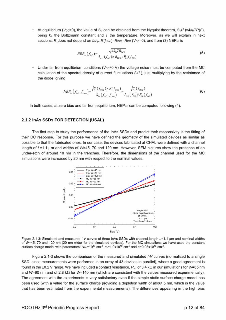
Figure 2.1-3: Simulated and measured I-V curves of three InAs-SSDs with channel length L=1.1 m and nominal widths of W=45, 70 and 120 nm (20 nm wider for the simulated devices). For the MC simulations we have used the constant surface charge model with parameters: NDb=1017 cm-3 ns=1.0x1012 cm-2 and =0.05x1012 cm-2.
Figure 2.1-3 shows the comparison of the measured and simulated I-V curves (normalized to a single
SSD, since measurements were performed in an array of 43 devices in parallel), where a good agreement is
found in the ±0.2 V range. We have included a contact resistance, RC, of 3.4 kΩ in our simulations for W=65 nm
and W=90 nm and of 2.8 kΩ for W=140 nm (which are consistent with the values measured experimentally).
The agreement with the experiments is very satisfactory even if the simple static surface charge model has
been used (with a value for the surface charge providing a depletion width of about 5 nm, which is the value
that has been estimated from the experimental measurements). The differences appearing in the high bias
Bias (V)
-0.2 -0.1 0.0 0.1 0.2
Cur
rent
(m
A)
-0.04
-0.02
0.00
0.02
0.04Exp. W=45 nmExp. W=70 nmExp. W=120 nmMC W=65 nmMC W=90 nmMC W=140 nm
single SSDLateral depletion 5 nm
@ 300 KL=1.1 m
Trenches=110 nm
ROOTHz 3rd Periodic Progress Report p 13 of 84
region may come from impact ionization mechanisms in the real devices, which, for the moment, have not
been taken into account in the MC simulations.
Once the DC response is replicated satisfactorily, the modelling of an RF excitation to the SSDs has
been performed and the extrinsic responsivity, Sext(V/W), obtained (accounting for the effect of the contact
resistance, as explained previously).
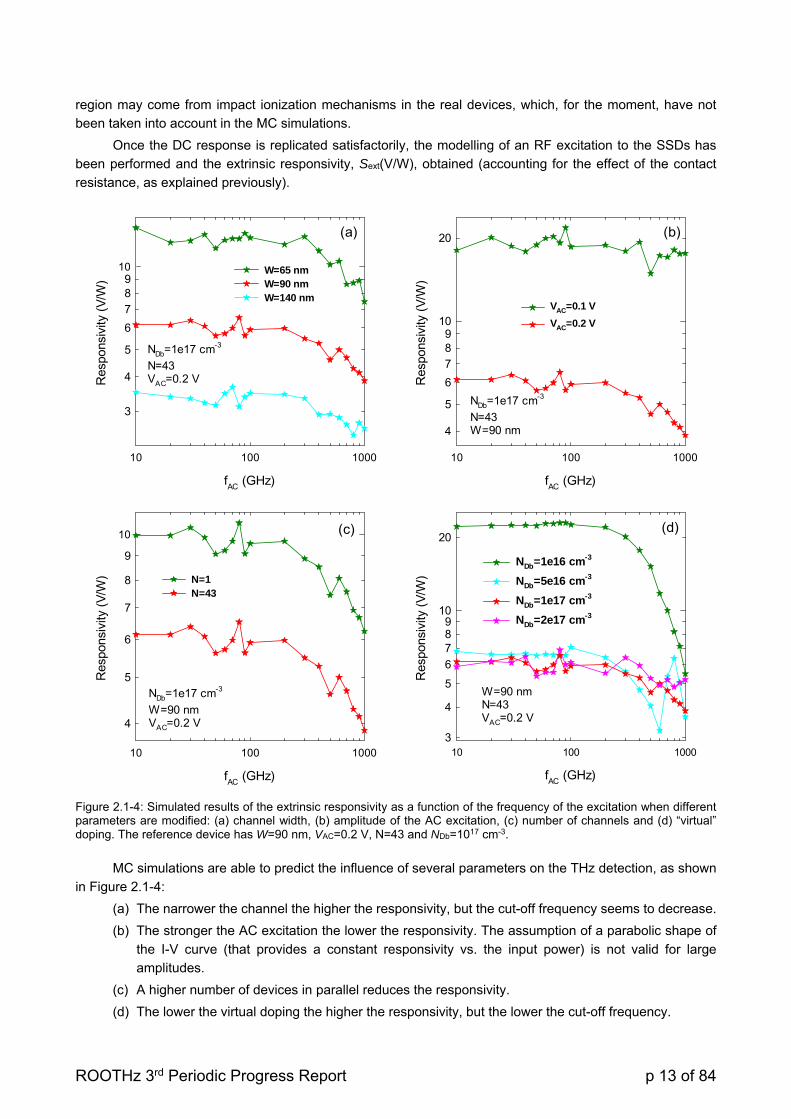
Figure 2.1-4: Simulated results of the extrinsic responsivity as a function of the frequency of the excitation when different parameters are modified: (a) channel width, (b) amplitude of the AC excitation, (c) number of channels and (d) “virtual” doping. The reference device has W=90 nm, VAC=0.2 V, N=43 and NDb=1017 cm-3.
MC simulations are able to predict the influence of several parameters on the THz detection, as shown
in Figure 2.1-4:
(a) The narrower the channel the higher the responsivity, but the cut-off frequency seems to decrease.
(b) The stronger the AC excitation the lower the responsivity. The assumption of a parabolic shape of
the I-V curve (that provides a constant responsivity vs. the input power) is not valid for large
amplitudes.
(c) A higher number of devices in parallel reduces the responsivity.
(d) The lower the virtual doping the higher the responsivity, but the lower the cut-off frequency.
fAC
(GHz)
10 100 1000
Res
pons
ivity
(V
/W)
3
4
5
6
789
10 W=65 nmW=90 nmW=140 nm
fAC
(GHz)
10 100 1000
Res
pons
ivity
(V
/W)
4
5
6
789
20
10VAC=0.1 V
VAC=0.2 V
fAC
(GHz)
10 100 1000
Res
pons
ivity
(V
/W)
3
4
5
6
789
20
10
NDb=1e16 cm-3
NDb=5e16 cm-3
NDb=1e17 cm-3
NDb=2e17 cm-3
NDb=1e17 cm-3
N=43VAC=0.2 V
W=90 nmN=43VAC=0.2 V
NDb=1e17 cm-3
N=43W=90 nm
fAC
(GHz)
10 100 1000
Res
pons
ivity
(V
/W)
4
5
6
7
8
9
10
N=1N=43
NDb=1e17 cm-3
W=90 nmVAC=0.2 V
(b)(a)
(c) (d)
ROOTHz 3rd Periodic Progress Report p 14 of 84
Most of these results were already known for InGaAs and GaN technologies, but now we are able to
quantitatively predict the real THz performance of the InAs SSDs, once the MC simulations have been adjusted
to correctly reproduce the experimental results.
Even if the intrinsic responsivity Sint is inversely proportional to N (N times higher input power is needed
to generate the same Vrect), Sext remains almost constant as long as the term 1-|Γ(f)|2 is sufficiently small (for
few channels, when there is a strong mismatch) and starts to decrease when the impedance of the array
approaches that of the access line. The advantage obtained by increasing N is that the NEPext is proportional
to 1/N, as we will show in the last section devoted to GaN SSDs, thus improving their sensitivity to small input
signals (even if the responsivity is degraded) .
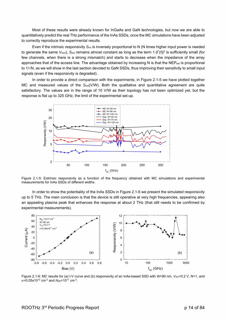
In order to provide a direct comparison with the experiments, in Figure 2.1-5 we have plotted together
MC and measured values of the Sext(V/W). Both the qualitative and quantitative agreement are quite
satisfactory. The values are in the range of 10 V/W as their topology has not been optimized yet, but the
response is flat up to 325 GHz, the limit of the experimental set-up.
Figure 2.1-5: Extrinsic responsivity as a function of the frequency obtained with MC simulations and experimental measurements for InAs SSDs of different widths.
In order to show the potentiality of the InAs SSDs in Figure 2.1-6 we present the simulated responsivity
up to 5 THz. The main conclusion is that the device is still operative at very high frequencies, appearing also
an appealing plasma peak that enhances the response at about 2 THz (that still needs to be confirmed by
experimental measurements).
Figure 2.1-6: MC results for (a) I-V curve and (b) responsivity of an InAs-based SSD with W=90 nm, VAC=0.2 V, N=1, and =0.05x1012 cm-2 and NDb=1017 cm-3.
fAC (GHz)
50 100 150 200 250 300
Re
spo
nsiv
ity (
V/W
)
2
5
20
30
10
MC W=65 nmMC W=90 nmMC W=140 nmExp. W=45 nmExp. W=70 nmExp. W=120 nm
fAC (GHz)
500010 100 1000
Res
pon
sivi
ty (
V/W
)
0
2
4
6
8
10
12
Bias (V)
-0.8 -0.6 -0.4 -0.2 0.0 0.2 0.4 0.6 0.8
Cur
rent
(A
)
-80
-60
-40
-20
0
20
40
60
80NDb=1e17 cm-3
W=90 nmVAC=0.2 V
=0.05x1012 cm-2
(b) (a)
ROOTHz 3rd Periodic Progress Report p 15 of 84
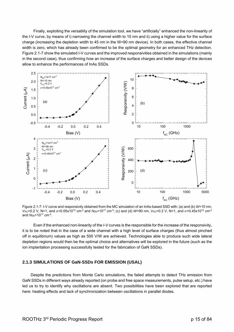
Finally, exploiting the versatility of the simulation tool, we have “artificially” enhanced the non-linearity of
the I-V curve, by means of i) narrowing the channel width to 10 nm and ii) using a higher value for the surface
charge (increasing the depletion width to 45 nm in the W=90 nm device). In both cases, the effective channel
width is zero, which has already been confirmed to be the optimal geometry for an enhanced THz detection.
Figure 2.1-7 show the simulated I-V curves and the improved responsivities obtained in the simulations (mainly
in the second case), thus confirming how an increase of the surface charges and better design of the devices
allow to enhance the performances of InAs SSDs.
Figure 2.1-7: I-V curve and responsivity obtained from the MC simulation of an InAs-based SSD with: (a) and (b) W=10 nm, VAC=0.2 V, N=1, and =0.05x1012 cm-2 and NDb=1017 cm-3; (c) and (d) W=90 nm, VAC=0.2 V, N=1, and =0.45x1012 cm-2 and NDb=1017 cm-3.
Even if the enhanced non-linearity of the I-V curves is the responsible for the increase of the responsivity,
it is to be noted that in the case of a wide channel with a high level of surface charges (thus almost pinched
off in equilibrium) values as high as 500 V/W are achieved. Technologies able to produce such wide lateral
depletion regions would then be the optimal choice and alternatives will be explored in the future (such as the
ion implantation processing successfully tested for the fabrication of GaN SSDs).
2.1.3 SIMULATIONS OF GaN-SSDs FOR EMISSION (USAL)
Despite the predictions from Monte Carlo simulations, the failed attempts to detect THz emission from
GaN SSDs in different ways already reported (on probe and free space measurements, pulse setup, etc.) have
led us to try to identify why oscillations are absent. Two possibilities have been explored that are reported
here: heating effects and lack of synchronization between oscillations in parallel diodes.
fAC (GHz)
10 100 1000R
esp
onsi
vity
(V
/W)
0
2
4
6
8
10
Bias (V)
-0.4 -0.2 0.0 0.2 0.4
Cur
rent
(A
)
-0.5
0.0
0.5
1.0
1.5
2.0
2.5NDb=1e17 cm-3
W=10 nmVAC=0.2 V
=0.05x1012 cm-2
fAC (GHz)
500010 100 1000
Res
pon
sivi
ty (
V/W
)
0
200
400
600
Bias (V)
-0.4 -0.2 0.0 0.2 0.4
Cur
rent
(A
)
-1
0
1
2
3
4NDb=1e17 cm-3
W=90 nmVAC=0.2 V
=0.45x1012 cm-2
(b) (a)
(d) (c)
ROOTHz 3rd Periodic Progress Report p 16 of 84
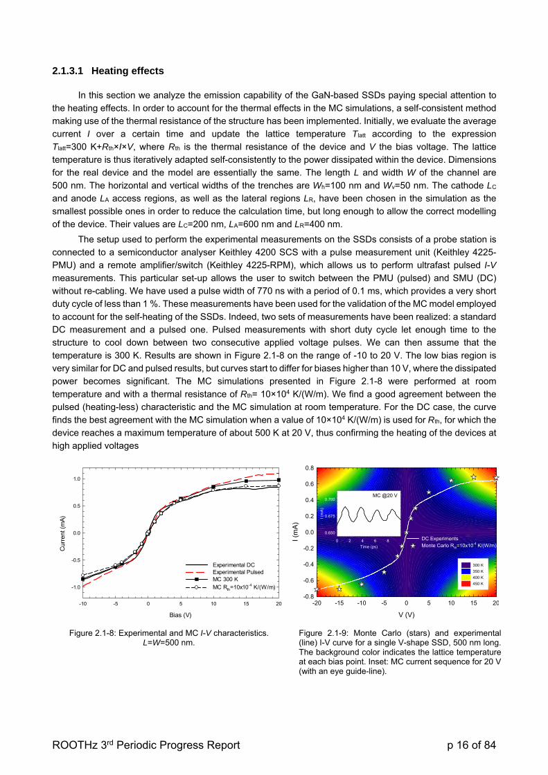
2.1.3.1 Heating effects
In this section we analyze the emission capability of the GaN-based SSDs paying special attention to
the heating effects. In order to account for the thermal effects in the MC simulations, a self-consistent method
making use of the thermal resistance of the structure has been implemented. Initially, we evaluate the average
current I over a certain time and update the lattice temperature Tlatt according to the expression
Tlatt=300 K+Rth×I×V, where Rth is the thermal resistance of the device and V the bias voltage. The lattice
temperature is thus iteratively adapted self-consistently to the power dissipated within the device. Dimensions
for the real device and the model are essentially the same. The length L and width W of the channel are
500 nm. The horizontal and vertical widths of the trenches are Wh=100 nm and Wv=50 nm. The cathode LC
and anode LA access regions, as well as the lateral regions LR, have been chosen in the simulation as the
smallest possible ones in order to reduce the calculation time, but long enough to allow the correct modelling
of the device. Their values are LC=200 nm, LA=600 nm and LR=400 nm.
The setup used to perform the experimental measurements on the SSDs consists of a probe station is
connected to a semiconductor analyser Keithley 4200 SCS with a pulse measurement unit (Keithley 4225-
PMU) and a remote amplifier/switch (Keithley 4225-RPM), which allows us to perform ultrafast pulsed I-V
measurements. This particular set-up allows the user to switch between the PMU (pulsed) and SMU (DC)
without re-cabling. We have used a pulse width of 770 ns with a period of 0.1 ms, which provides a very short
duty cycle of less than 1 %. These measurements have been used for the validation of the MC model employed
to account for the self-heating of the SSDs. Indeed, two sets of measurements have been realized: a standard
DC measurement and a pulsed one. Pulsed measurements with short duty cycle let enough time to the
structure to cool down between two consecutive applied voltage pulses. We can then assume that the
temperature is 300 K. Results are shown in Figure 2.1-8 on the range of -10 to 20 V. The low bias region is
very similar for DC and pulsed results, but curves start to differ for biases higher than 10 V, where the dissipated
power becomes significant. The MC simulations presented in Figure 2.1-8 were performed at room
temperature and with a thermal resistance of Rth= 10×104 K/(W/m). We find a good agreement between the
pulsed (heating-less) characteristic and the MC simulation at room temperature. For the DC case, the curve
finds the best agreement with the MC simulation when a value of 10×104 K/(W/m) is used for Rth, for which the
device reaches a maximum temperature of about 500 K at 20 V, thus confirming the heating of the devices at
high applied voltages
Figure 2.1-8: Experimental and MC I-V characteristics. L=W=500 nm.
Figure 2.1-9: Monte Carlo (stars) and experimental (line) I-V curve for a single V-shape SSD, 500 nm long. The background color indicates the lattice temperature at each bias point. Inset: MC current sequence for 20 V (with an eye guide-line).
Bias (V)
-10 -5 0 5 10 15 20
Cur
rent
(m
A)
-1.0
-0.5
0.0
0.5
1.0
Experimental DCExperimental Pulsed MC 300 KMC Rth=10x10-4 K/(W/m)
300 K
350 K
400 K
450 K
V (V)
-20 -15 -10 -5 0 5 10 15 20
I (m
A)
-0.8
-0.6
-0.4
-0.2
0.0
0.2
0.4
0.6
0.8
DC ExperimentsMonte Carlo Rth=10x10-4 K/(W/m)Time (ps)
0 2 4 6 8
I (m
A)
0.650
0.675
0.700MC @20 V
ROOTHz 3rd Periodic Progress Report p 17 of 84
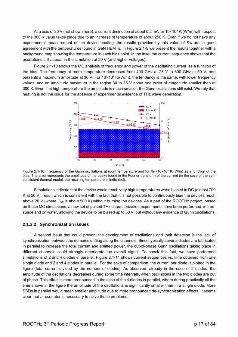
At a bias of 30 V (not shown here), a current diminution of about 0.2 mA for 10×104 K/(W/m) with respect
to the 300 K value takes place due to an increase of temperature of about 250 K. Even if we do not have any
experimental measurement of the device heating, the results provided by this value of Rth are in good
agreement with the temperatures found in GaN HEMTs. In Figure 2.1-9 we present the results together with a
background map showing the temperature in each bias point. In the inset the current sequence shows that the
oscillations still appear in the simulation at 20 V (and higher voltages).
Figure 2.1-10 shows the MC analysis of frequency and power of the oscillating current as a function of
the bias. The frequency at room temperature decreases from 400 GHz at 25 V to 300 GHz at 50 V, and
presents a maximum amplitude at 30 V. For 10×104 K/(W/m), the tendency is the same, with lower frequency
values, and an amplitude maximum in the region 30 to 35 V about one order of magnitude smaller than at
300 K. Even if at high temperature the amplitude is much smaller, the Gunn oscillations still exist. We rely that
heating is not the issue for the absence of experimental evidence of THz wave generation.
Bias (V)
25 30 35 40 45 50
Am
plitu
de (
10-6
A2/m
2s)
0.1
1
10
100
Fre
quen
cy (
GH
z)
0
100
200
300
400
500
300 K
Rth=10x10-4
300 K
Rth=10x10-4
Figure 2.1-10: Frequency of the Gunn oscillations at room temperature and for Rth=10×104 K/(W/m) as a function of the bias. The area represents the amplitude of the peaks found in the Fourier transform of the current (in the case of the self-consistent thermal model, the resulting temperature is indicated).
Simulations indicate that the device would reach very high temperatures when biased in DC (almost 700
K at 50 V), result which is consistent with the fact that it is not possible to continuously bias the devices much
above 20 V (where Tlatt is about 500 K) without burning the devices. As a part of the ROOTHz project, based
on those MC simulations, a new set of pulsed THz characterization experiments have been performed, in free-
space and on wafer, allowing the device to be biased up to 50 V, but without any evidence of Gunn oscillations.
2.1.3.2 Synchronization issues
A second issue that could prevent the development of oscillations and their detection is the lack of
synchronization between the domains drifting along the channels. Since typically several diodes are fabricated
in parallel to increase the total current and emitted power, the out-of-phase Gunn oscillations taking place in
different channels could strongly deteriorate the overall signal. To check this fact, we have performed
simulations of 2 and 4 diodes in parallel. Figure 2.1-11 shows current sequences vs. time obtained from one
single diode and 2 and 4 diodes in parallel. For the sake of comparison, the current per diode is plotted in the
figure (total current divided by the number of diodes). As observed, already in the case of 2 diodes, the
amplitude of the oscillations decreases during some time intervals, when oscillations in the two diodes are out
of phase. This effect is more pronounced in the case of the 4 diodes in parallel, where during practically all the
time shown in the figure the amplitude of the oscillations is significantly smaller than in a single diode. More
SSDs in parallel would mean smaller amplitude due to more pronounced de-synchronization effects. It seems
clear that a resonator is necessary to solve these problems.
510K 547K 581K
615K 646K
678K

ROOTHz 3rd Periodic Progress Report p 18 of 84
Figure 2.1-11: Current sequences of a (a) single SSD, (b) two SSDs and (c) four SSDs in parallel.
To illustrate in more deep this point, we have obtained snapshots of the carrier concentration and U-
valley occupation from the MC simulation of 4 diodes in parallel, as shown in Figure 2.1-12. Here, a clear
diphase between domains in the different channels is observed. By adding a parallel RCL resonant circuit in
series with the SSDs, with R=125 k, L=2.75 nH and C=0.04 fF, the synchronization of the oscillations is
achieved, like observed in Figure 2.1-13, in which the domain is in the same evolution stage in the 4 diodes.
Figure 2.1-12: Carrier concentration and U-valley occupation in 4 SSDs in parallel.
Figure 2.1-13: Carrier concentration and U-valley occupation in 4 SSDs in parallel with a RLC resonant
circuit.
In order to quantitatively show the reduction of the power of the oscillations when increasing the number
of SSDs in parallel considered, the value of the amplitude of the peak in the spectrum of the current is plotted
in Figure 2.1-14(a). The proximity between adjacent diodes in parallel could also be an important factor to be
considered to achieve in-phase oscillations in the different channels (note that heating effects should also be
considered to determine the separation between diodes). One could expect that close-enough diodes, due to
the electrostatic interaction between them, would naturally synchronize their respective oscillations. To check
this extent we have performed simulations of diodes separated a decreasing distance from each other. The
results are shown in Figure 2.1-14(b). One can observe, first, and contrary to expectations, that if the SSDs
(b)
(a)
(c)
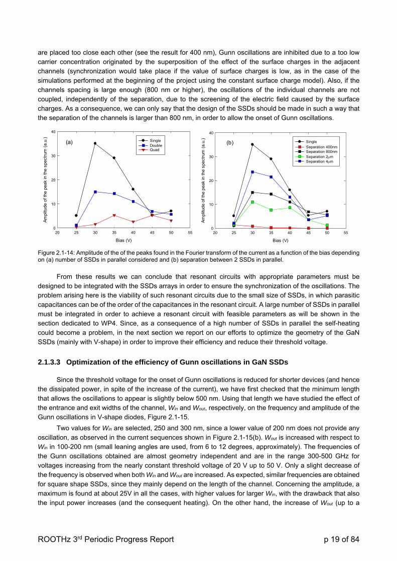
ROOTHz 3rd Periodic Progress Report p 19 of 84
are placed too close each other (see the result for 400 nm), Gunn oscillations are inhibited due to a too low
carrier concentration originated by the superposition of the effect of the surface charges in the adjacent
channels (synchronization would take place if the value of surface charges is low, as in the case of the
simulations performed at the beginning of the project using the constant surface charge model). Also, if the
channels spacing is large enough (800 nm or higher), the oscillations of the individual channels are not
coupled, independently of the separation, due to the screening of the electric field caused by the surface
charges. As a consequence, we can only say that the design of the SSDs should be made in such a way that
the separation of the channels is larger than 800 nm, in order to allow the onset of Gunn oscillations.
Bias (V)
20 25 30 35 40 45 50 55
Am
plitu
de o
f the
pea
k in
the
spec
trum
(a.
u.)
0
10
20
30
40
SingleDoubleQuad
(a)
Bias (V)
20 25 30 35 40 45 50 55
Am
plitu
de o
f the
pea
k in
the
spec
trum
(a.
u.)
0
10
20
30
40
SingleSeparation 400nmSeparation 800nmSeparation 2mSeparation 4m
(b)
Figure 2.1-14: Amplitude of the of the peaks found in the Fourier transform of the current as a function of the bias depending on (a) number of SSDs in parallel considered and (b) separation between 2 SSDs in parallel.
From these results we can conclude that resonant circuits with appropriate parameters must be
designed to be integrated with the SSDs arrays in order to ensure the synchronization of the oscillations. The
problem arising here is the viability of such resonant circuits due to the small size of SSDs, in which parasitic
capacitances can be of the order of the capacitances in the resonant circuit. A large number of SSDs in parallel
must be integrated in order to achieve a resonant circuit with feasible parameters as will be shown in the
section dedicated to WP4. Since, as a consequence of a high number of SSDs in parallel the self-heating
could become a problem, in the next section we report on our efforts to optimize the geometry of the GaN
SSDs (mainly with V-shape) in order to improve their efficiency and reduce their threshold voltage.
2.1.3.3 Optimization of the efficiency of Gunn oscillations in GaN SSDs
Since the threshold voltage for the onset of Gunn oscillations is reduced for shorter devices (and hence
the dissipated power, in spite of the increase of the current), we have first checked that the minimum length
that allows the oscillations to appear is slightly below 500 nm. Using that length we have studied the effect of
the entrance and exit widths of the channel, Win and Wout, respectively, on the frequency and amplitude of the
Gunn oscillations in V-shape diodes, Figure 2.1-15.
Two values for Win are selected, 250 and 300 nm, since a lower value of 200 nm does not provide any
oscillation, as observed in the current sequences shown in Figure 2.1-15(b). Wout is increased with respect to
Win in 100-200 nm (small leaning angles are used, from 6 to 12 degrees, approximately). The frequencies of
the Gunn oscillations obtained are almost geometry independent and are in the range 300-500 GHz for
voltages increasing from the nearly constant threshold voltage of 20 V up to 50 V. Only a slight decrease of
the frequency is observed when both Win and Wout are increased. As expected, similar frequencies are obtained
for square shape SSDs, since they mainly depend on the length of the channel. Concerning the amplitude, a
maximum is found at about 25V in all the cases, with higher values for larger Win, with the drawback that also
the input power increases (and the consequent heating). On the other hand, the increase of Wout (up to a

ROOTHz 3rd Periodic Progress Report p 20 of 84
certain value) also enhances the amplitude of the Gunn oscillations, also slightly increasing the DC current.
Therefore, a trade-off choice must be done between a large amplitude of the Gunn oscillations and the
avoidance of a strong heating (mainly if many SSDs are to be placed in parallel). Two possible adequate
choices could be Win=250 nm and Wout=450 nm or Win=300 nm and Wout=400 nm, both providing similar
amplitude of the oscillations with DC current of about 0.5 mA/SSD (the dissipated power is around 12.5 mW
per SSD when biasing continuously at 25 V).
Bias (V)
-60 -40 -20 0 20 40 60
Cur
rent
(m
A)
-0.8
-0.6
-0.4
-0.2
0.0
0.2
0.4
0.6
0.8
Wout=350 nmWout=400 nmWout=450 nm
Wout=400 nmWout=450 nmWout=500 nm
Win=250 nm
Win=300 nm
Bias (V)
20 25 30 35 40 45 50
Fre
quen
cy (
GH
z)
0
100
200
300
400
500
Am
plitu
de (
10-6
A2 /m
2 /s)
0
5
10
15
20
25Wout=400 nmWout=450 nmWout=500 nmWout=600 nm
Fre
quen
cy (
GH
z)
0
100
200
300
400
500
Am
plitu
de (
10-6
A2 /m
2 /s)
0
5
10
15
20
25
Wout=350 nmWout=400 nmWout=450 nm
Win=250 nm
Win=300 nm
(d)
(e)
Figure 2.1-15: (a) Geometry of the of the simulated V-shape GaN SSDs with L=500 nm (b) current sequences when the bias is increased in steps of 5 V and (c) I-V curves of diodes with different Win and Wout. (d) and (e) show the frequency (lines with symbols) and amplitude (shaded areas) of the Gunn oscillations found for (d) Win=250 nm and (e) Win=300 nm, both for variable Wout.
A further modification of the geometry of the SSD has been analyzed, considering only a tapered
channel, Figure 2.1-16. It is to note that when suppressing the lateral regions, the lateral field effect
characteristic of SSDs is also cancelled. In any case, this effect is not significant when one looks for Gunn
oscillations and wide channels have to be used. The idea of testing this modification originated from the result
Win Wout
Win=200 nm, Wout=300 nm Win=250 nm, Wout=350 nm Win=300 nm, Wout=400 nm
(b)
(a)
(c)
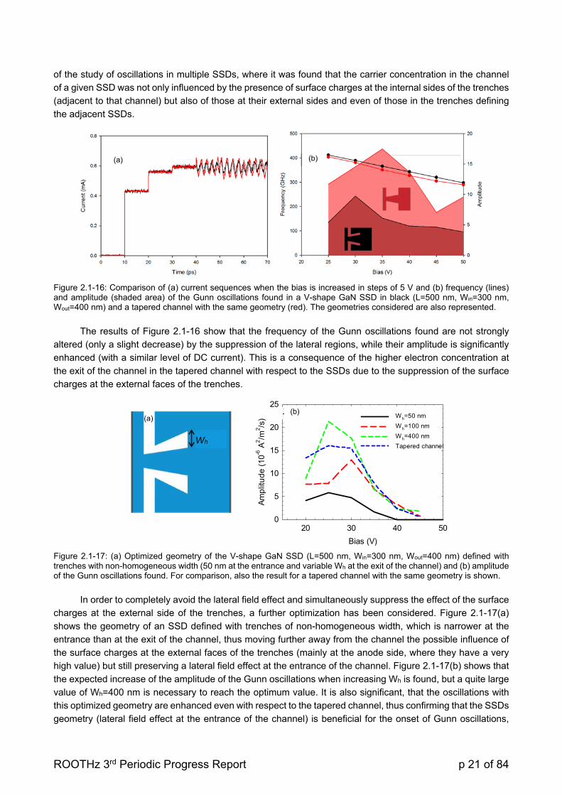
ROOTHz 3rd Periodic Progress Report p 21 of 84
of the study of oscillations in multiple SSDs, where it was found that the carrier concentration in the channel
of a given SSD was not only influenced by the presence of surface charges at the internal sides of the trenches
(adjacent to that channel) but also of those at their external sides and even of those in the trenches defining
the adjacent SSDs.
Figure 2.1-16: Comparison of (a) current sequences when the bias is increased in steps of 5 V and (b) frequency (lines) and amplitude (shaded area) of the Gunn oscillations found in a V-shape GaN SSD in black (L=500 nm, Win=300 nm, Wout=400 nm) and a tapered channel with the same geometry (red). The geometries considered are also represented.
The results of Figure 2.1-16 show that the frequency of the Gunn oscillations found are not strongly
altered (only a slight decrease) by the suppression of the lateral regions, while their amplitude is significantly
enhanced (with a similar level of DC current). This is a consequence of the higher electron concentration at
the exit of the channel in the tapered channel with respect to the SSDs due to the suppression of the surface
charges at the external faces of the trenches.
Bias (V)
20 30 40 50
Am
plit
ud
e (1
0-6 A
2/m
2/s
)
0
5
10
15
20
25Wh=50 nm
Wh=100 nm
Wh=400 nm
Tapered channel
Figure 2.1-17: (a) Optimized geometry of the V-shape GaN SSD (L=500 nm, Win=300 nm, Wout=400 nm) defined with trenches with non-homogeneous width (50 nm at the entrance and variable Wh at the exit of the channel) and (b) amplitude of the Gunn oscillations found. For comparison, also the result for a tapered channel with the same geometry is shown.
In order to completely avoid the lateral field effect and simultaneously suppress the effect of the surface
charges at the external side of the trenches, a further optimization has been considered. Figure 2.1-17(a)
shows the geometry of an SSD defined with trenches of non-homogeneous width, which is narrower at the
entrance than at the exit of the channel, thus moving further away from the channel the possible influence of
the surface charges at the external faces of the trenches (mainly at the anode side, where they have a very
high value) but still preserving a lateral field effect at the entrance of the channel. Figure 2.1-17(b) shows that
the expected increase of the amplitude of the Gunn oscillations when increasing Wh is found, but a quite large
value of Wh=400 nm is necessary to reach the optimum value. It is also significant, that the oscillations with
this optimized geometry are enhanced even with respect to the tapered channel, thus confirming that the SSDs
geometry (lateral field effect at the entrance of the channel) is beneficial for the onset of Gunn oscillations,
(b) (a)
Wh
(b) (a)
ROOTHz 3rd Periodic Progress Report p 22 of 84
even if an important part of its influence is counteracted by the increase of the surface charges (mainly at the
anode side of the channel).
2.1.4 NEP IN GaN-BASED SSDs FOR DETECTION (USAL)
In this section, by means of Monte Carlo simulations we calculate (and compare with experimental
results) the Noise Equivalent Power (NEP) in AlGaN/GaN-based submicron SSDs at zero bias and provide
guides for detection optimization in terms of number of devices and geometry (width and length of the channel).
We also calculate the responsivity and NEP under biased conditions.
2.1.4.1 Noise at equilibrium
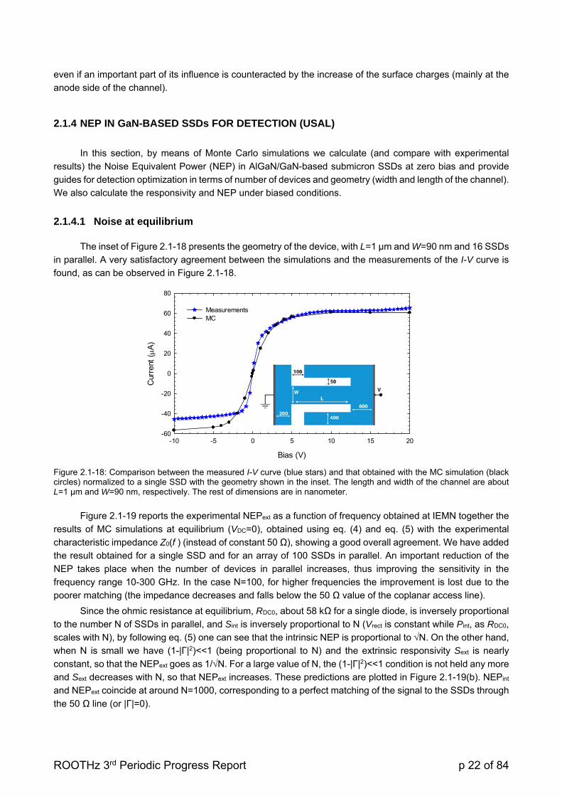
The inset of Figure 2.1-18 presents the geometry of the device, with L=1 µm and W=90 nm and 16 SSDs
in parallel. A very satisfactory agreement between the simulations and the measurements of the I-V curve is
found, as can be observed in Figure 2.1-18.
Figure 2.1-18: Comparison between the measured I-V curve (blue stars) and that obtained with the MC simulation (black circles) normalized to a single SSD with the geometry shown in the inset. The length and width of the channel are about L=1 µm and W=90 nm, respectively. The rest of dimensions are in nanometer.
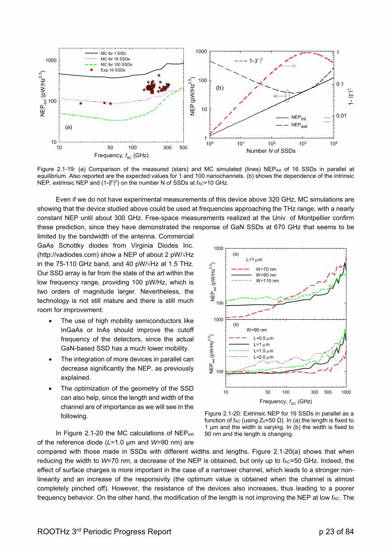
Figure 2.1-19 reports the experimental NEPext as a function of frequency obtained at IEMN together the
results of MC simulations at equilibrium (VDC=0), obtained using eq. (4) and eq. (5) with the experimental
characteristic impedance Z0(f ) (instead of constant 50 Ω), showing a good overall agreement. We have added
the result obtained for a single SSD and for an array of 100 SSDs in parallel. An important reduction of the
NEP takes place when the number of devices in parallel increases, thus improving the sensitivity in the
frequency range 10-300 GHz. In the case N=100, for higher frequencies the improvement is lost due to the
poorer matching (the impedance decreases and falls below the 50 Ω value of the coplanar access line).
Since the ohmic resistance at equilibrium, RDC0, about 58 kΩ for a single diode, is inversely proportional
to the number N of SSDs in parallel, and Sint is inversely proportional to N (Vrect is constant while Pint, as RDC0,
scales with N), by following eq. (5) one can see that the intrinsic NEP is proportional to N. On the other hand,
when N is small we have (1-|Γ|2)<<1 (being proportional to N) and the extrinsic responsivity Sext is nearly
constant, so that the NEPext goes as 1/N. For a large value of N, the (1-|Γ|2)<<1 condition is not held any more
and Sext decreases with N, so that NEPext increases. These predictions are plotted in Figure 2.1-19(b). NEPint
and NEPext coincide at around N=1000, corresponding to a perfect matching of the signal to the SSDs through
the 50 Ω line (or |Γ|=0).
Bias (V)
-10 -5 0 5 10 15 20
Cur
rent
(A
)
-60
-40
-20
0
20
40
60
80
MeasurementsMC
ROOTHz 3rd Periodic Progress Report p 23 of 84
Frequency, fAC (GHz)50 300 50010 100
NE
Pex
t (p
W/H
z0.5 )
10
100
1000
MC for 1 SSDMC for 16 SSDsMC for 100 SSDsExp.16 SSDs
(a)
Number N of SSDs100 101 102 103 104
NE
P (p
W/H
z0.5)
1
10
100
1000
1- ||
0.01
0.1
1
NEPintNEPext
1-
(b)
Figure 2.1-19: (a) Comparison of the measured (stars) and MC simulated (lines) NEPext of 16 SSDs in parallel at equilibrium. Also reported are the expected values for 1 and 100 nanochannels. (b) shows the dependence of the intrinsic NEP, extrinsic NEP and (1-|Γ|2) on the number N of SSDs at fAC=10 GHz.
Even if we do not have experimental measurements of this device above 320 GHz, MC simulations are
showing that the device studied above could be used at frequencies approaching the THz range, with a nearly
constant NEP until about 300 GHz. Free-space measurements realized at the Univ. of Montpellier confirm
these prediction, since they have demonstrated the response of GaN SSDs at 670 GHz that seems to be
limited by the bandwidth of the antenna. Commercial
GaAs Schottky diodes from Virginia Diodes Inc.
(http://vadiodes.com) show a NEP of about 2 pW/Hz
in the 75-110 GHz band, and 40 pW/Hz at 1.5 THz.
Our SSD array is far from the state of the art within the
low frequency range, providing 100 pW/Hz, which is
two orders of magnitude larger. Nevertheless, the
technology is not still mature and there is still much
room for improvement:
The use of high mobility semiconductors like
InGaAs or InAs should improve the cutoff
frequency of the detectors, since the actual
GaN-based SSD has a much lower mobility.
The integration of more devices in parallel can
decrease significantly the NEP, as previously
explained.
The optimization of the geometry of the SSD
can also help, since the length and width of the
channel are of importance as we will see in the
following.
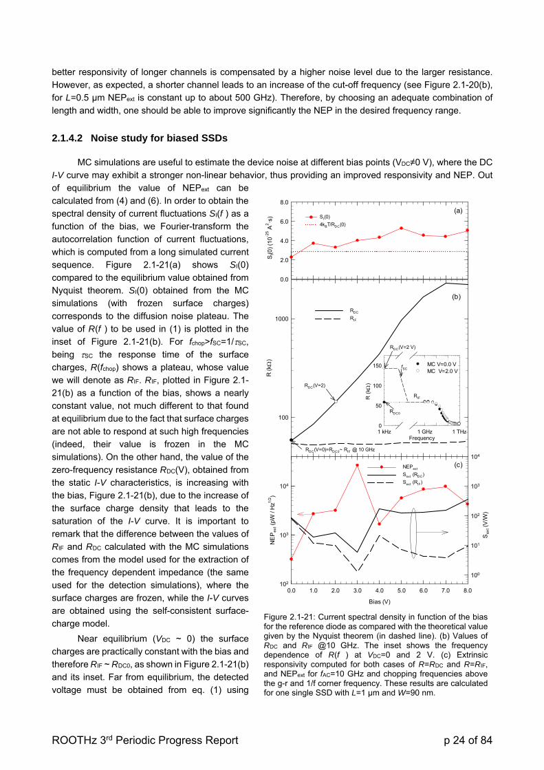
In Figure 2.1-20 the MC calculations of NEPext
of the reference diode (L=1.0 µm and W=90 nm) are
compared with those made in SSDs with different widths and lengths. Figure 2.1-20(a) shows that when
reducing the width to W=70 nm, a decrease of the NEP is obtained, but only up to fAC=50 GHz. Indeed, the
effect of surface charges is more important in the case of a narrower channel, which leads to a stronger non-
linearity and an increase of the responsivity (the optimum value is obtained when the channel is almost
completely pinched off). However, the resistance of the devices also increases, thus leading to a poorer
frequency behavior. On the other hand, the modification of the length is not improving the NEP at low fAC. The
Figure 2.1-20: Extrinsic NEP for 16 SSDs in parallel as a function of fAC (using Z0=50 Ω). In (a) the length is fixed to 1 µm and the width is varying. In (b) the width is fixed to 90 nm and the length is changing.
NE
Pex
t (p
W/H
z0.5 )
100
1000
W=70 nmW=90 nmW=110 nm
Frequency, fAC (GHz)
50 300 50010 100 1000
NE
Pex
t (p
W/H
z0.5 )
100
1000
L=0.5 mL=1 mL=1.5 mL=2.0 m
(a) L=1 m
(b) W=90 nm
ROOTHz 3rd Periodic Progress Report p 24 of 84
better responsivity of longer channels is compensated by a higher noise level due to the larger resistance.
However, as expected, a shorter channel leads to an increase of the cut-off frequency (see Figure 2.1-20(b),
for L=0.5 µm NEPext is constant up to about 500 GHz). Therefore, by choosing an adequate combination of
length and width, one should be able to improve significantly the NEP in the desired frequency range.
2.1.4.2 Noise study for biased SSDs
MC simulations are useful to estimate the device noise at different bias points (VDC≠0 V), where the DC
I-V curve may exhibit a stronger non-linear behavior, thus providing an improved responsivity and NEP. Out
of equilibrium the value of NEPext can be
calculated from (4) and (6). In order to obtain the
spectral density of current fluctuations SI(f ) as a
function of the bias, we Fourier-transform the
autocorrelation function of current fluctuations,
which is computed from a long simulated current
sequence. Figure 2.1-21(a) shows SI(0)
compared to the equilibrium value obtained from
Nyquist theorem. SI(0) obtained from the MC
simulations (with frozen surface charges)
corresponds to the diffusion noise plateau. The
value of R(f ) to be used in (1) is plotted in the
inset of Figure 2.1-21(b). For fchop>fSC=1/SC,
being SC the response time of the surface
charges, R(fchop) shows a plateau, whose value
we will denote as RIF. RIF, plotted in Figure 2.1-
21(b) as a function of the bias, shows a nearly
constant value, not much different to that found
at equilibrium due to the fact that surface charges
are not able to respond at such high frequencies
(indeed, their value is frozen in the MC
simulations). On the other hand, the value of the
zero-frequency resistance RDC(V), obtained from
the static I-V characteristics, is increasing with
the bias, Figure 2.1-21(b), due to the increase of
the surface charge density that leads to the
saturation of the I-V curve. It is important to
remark that the difference between the values of
RIF and RDC calculated with the MC simulations
comes from the model used for the extraction of
the frequency dependent impedance (the same
used for the detection simulations), where the
surface charges are frozen, while the I-V curves
are obtained using the self-consistent surface-
charge model.
Near equilibrium (VDC ~ 0) the surface
charges are practically constant with the bias and
therefore RIF ~ RDC0, as shown in Figure 2.1-21(b)
and its inset. Far from equilibrium, the detected
voltage must be obtained from eq. (1) using
R (
k )
100
1000
RDC RIF
Bias (V)
0.0 1.0 2.0 3.0 4.0 5.0 6.0 7.0 8.0
NE
Pex
t (pW
/ H
z1/2
)
102
103
104S
ext (
V/W
)
100
101
102
103
104
NEPext
Sext (RDC)
Sext (RIF)
(b)
(c)
SI(0
) (1
0-2
5 A
2 ·s)
0.0
2.0
4.0
6.0
8.0
SI(0)
4kBT/RDC(0)
(a)
Frequency1 kHz 1 GHz 1 THz
R (
k )
0
50
100
150 MC V=0.0 VMC V=2.0 V
fSC
RDC0
RDC(V=2 V)
RIF
RDC(V=2)
RDC(V=0)=RDC0~ RIF @ 10 GHz
Figure 2.1-21: Current spectral density in function of the bias for the reference diode as compared with the theoretical value given by the Nyquist theorem (in dashed line). (b) Values of RDC and RIF @10 GHz. The inset shows the frequency dependence of R(f ) at VDC=0 and 2 V. (c) Extrinsic responsivity computed for both cases of R=RDC and R=RIF, and NEPext for fAC=10 GHz and chopping frequencies above the g-r and 1/f corner frequency. These results are calculated for one single SSD with L=1 µm and W=90 nm.
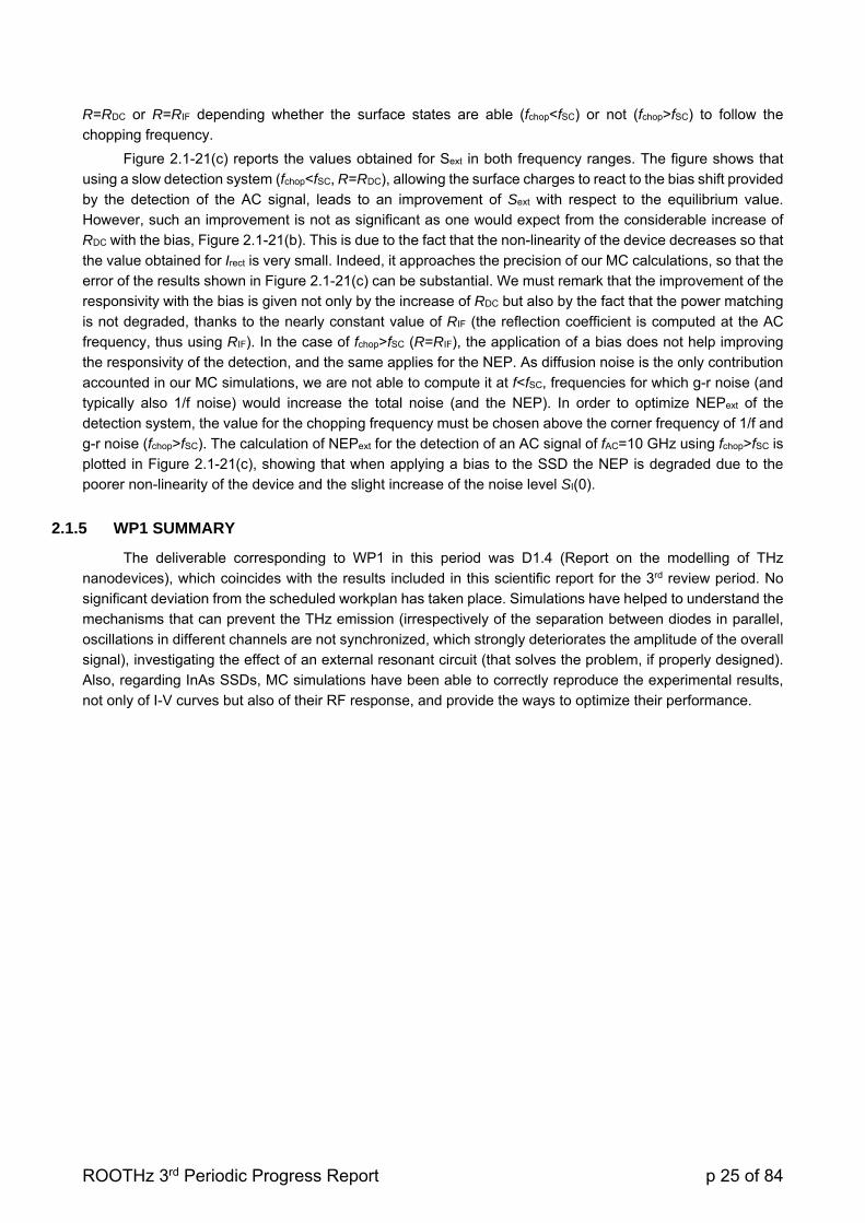
ROOTHz 3rd Periodic Progress Report p 25 of 84
R=RDC or R=RIF depending whether the surface states are able (fchop<fSC) or not (fchop>fSC) to follow the
chopping frequency.
Figure 2.1-21(c) reports the values obtained for Sext in both frequency ranges. The figure shows that
using a slow detection system (fchop<fSC, R=RDC), allowing the surface charges to react to the bias shift provided
by the detection of the AC signal, leads to an improvement of Sext with respect to the equilibrium value.
However, such an improvement is not as significant as one would expect from the considerable increase of
RDC with the bias, Figure 2.1-21(b). This is due to the fact that the non-linearity of the device decreases so that
the value obtained for Irect is very small. Indeed, it approaches the precision of our MC calculations, so that the
error of the results shown in Figure 2.1-21(c) can be substantial. We must remark that the improvement of the
responsivity with the bias is given not only by the increase of RDC but also by the fact that the power matching
is not degraded, thanks to the nearly constant value of RIF (the reflection coefficient is computed at the AC
frequency, thus using RIF). In the case of fchop>fSC (R=RIF), the application of a bias does not help improving
the responsivity of the detection, and the same applies for the NEP. As diffusion noise is the only contribution
accounted in our MC simulations, we are not able to compute it at f<fSC, frequencies for which g-r noise (and
typically also 1/f noise) would increase the total noise (and the NEP). In order to optimize NEPext of the
detection system, the value for the chopping frequency must be chosen above the corner frequency of 1/f and
g-r noise (fchop>fSC). The calculation of NEPext for the detection of an AC signal of fAC=10 GHz using fchop>fSC is
plotted in Figure 2.1-21(c), showing that when applying a bias to the SSD the NEP is degraded due to the
poorer non-linearity of the device and the slight increase of the noise level SI(0).
2.1.5 WP1 SUMMARY
The deliverable corresponding to WP1 in this period was D1.4 (Report on the modelling of THz
nanodevices), which coincides with the results included in this scientific report for the 3rd review period. No
significant deviation from the scheduled workplan has taken place. Simulations have helped to understand the
mechanisms that can prevent the THz emission (irrespectively of the separation between diodes in parallel,
oscillations in different channels are not synchronized, which strongly deteriorates the amplitude of the overall
signal), investigating the effect of an external resonant circuit (that solves the problem, if properly designed).
Also, regarding InAs SSDs, MC simulations have been able to correctly reproduce the experimental results,
not only of I-V curves but also of their RF response, and provide the ways to optimize their performance.

ROOTHz 3rd Periodic Progress Report p 26 of 84
2.2 WP2: FABRICATION OF DISCRETE DEVICES
Since the fabrication of optimum slot-diodes was already completed, the objectives of WP2 for the third
review period of ROOTHz are:
Fabrication of Run 2 of THz detectors based on InAs and InGaAs SSDs arrays (and benchmarking
against Schottky barrier detectors). Solving the problems found in the first two years (initially at UNIMAN
and later on at CHAL) for the development of the InAs SSDs technology was the priority in this case.
During the development of the fabrication process of slot diodes and narrow band gap (NBG) SSDs,
many different paths have been explored and many runs of fabrication have been made. In the ROOTHz
proposal we called “Run 2” to the devices fabricated with optimum dimensions and technological
processes, what we actually present here is the last run of each device fabrication.
Fabrication of Run 2 of room temperature CW THz emitters based on SSDs arrays, with priority for GaN
but also on InGaAs. Also in this case, instead of Run 2 we will present the results of the optimized Run
3 of GaN SSDs and the last batch of devices fabricated on InGaAs.
2.2.1 TASK 2.1.2: NARROW BANDGAP SSD FABRICATION (CHAL+UNIMAN)
Dry etched and in-situ passivated InAs-based SSDs were developed. Producing stable devices from
the chemically unstable InAs/AlSb structure proved challenging, requiring 40-50 attempts and epilayers
purchased from different vendors. A trade-off between electrical leakage and conductivity was made. Finally,
InAs SSDs could be processed successfully.
InGaAs-based SSDs were also fabricated both at CHAL and UNIMAN. The InGaAs/AlInAs is known to
be much more chemically stable as compared to InAs/AlSb and the technological development was much
easier. The process used at UNIMAN is the same used from the beginning of ROOTHz (already presented in
the first year report), so that we will only present here the technology of fabrication used at CHAL.
2.2.1.1 InAs SSDs (CHAL)
The design of the epitaxial structure, particularly the buffer, was crucial for successful fabrication of InAs
SSDs. Examples of investigated designs are given in Figure 2.2-1, together with SEM cross-sections of etched
and passivated SSD trenches. The cross-section was made by fabricating long trenches and then breaking
the substrate perpendicularly to the trenches.
Essentially, the buffer design is a trade-off between chemical stability and isolation. AlSb is known to be
prone to oxidation but offers good isolation, whereas Al0.80Ga0.20Sb is more stable but also more conductive.
In a pre-study of InAs SSD fabrication, the buffer design illustrated in Figure 2.2-1(a) was used. The same
buffer design has been successfully implemented in InAs/AlSb HEMT fabrication. In this design, a 250 nm
Al0.80Ga0.20Sb layer was sandwiched between AlSb layers. In the pre-study, InAs SSDs were successfully
fabricated by etching through the entire Al0.80Ga0.20Sb layer. As shown in Figure 2.2-1(a), there was a
considerable growth of oxide in the AlSb. For this reason, the etch is stopped inside the Al0.80Ga0.20Sb layer in
HEMT fabrication. However, tests showed that if the etch was stopped in the Al0.80Ga0.20Sb layer, the leakage
through the residual Al0.80Ga0.20Sb would make the resistivity of etched trenches 120 k/sq. Meanwhile, R0 for
the fabricated SSD was 1.6 M. To maintain a buffer resistance higher than R0, a sheet resistance of trenches
>120 Msq was needed. The Al0.80Ga0.20Sb would short-circuit an SSD. Therefore, the Al0.80Ga0.20Sb layer
was abandoned and the pure AlSb buffer design in Figure 2.2-1(b) investigated.
With a pure AlSb buffer, as in Figure 2.2-1(b), tests showed that the sheet resistance of trenches would
be 75 M/sq, and still cause a significant leakage in comparison to R0 of the SSD. By designing the SSD with
many channels and thus decreasing R0, the leakage current could be made less significant. However, the
oxidation could not be overcome. The cross section SEM shown in Figure 2.2-1(b) was made only minutes
after the trench etch. Despite the sample being passivated with SiNx, the oxidation was clearly visible. To avoid

ROOTHz 3rd Periodic Progress Report p 27 of 84
oxidation, an Al0.80Ga0.20Sb layer was necessary in the SSD buffer design. In the final buffer design, shown in
Figure 2.2-1(c), a 100 nm Al0.80Ga0.20Sb layer was reintroduced in the top part of the buffer. The trenches were
etched just through the InAs channel and stopped in the Al0.80Ga0.20Sb layer. As seen in Figure 2.2-1(c), the
stability was largely improved. The sheet resistance of trenches was >700 M/sq. Hence, the isolation was
more than enough for not degrading the device performance. Since the heterostructure in Figure 2.2-1(c) was
grown by a different vendor, the reason why the isolation was better than in the pure AlSb buffer was likely
different growth conditions.
Figure 2.2-1: Three buffer designs explored in the development of the InAs SSD process: (a) AlSb/AlGaSb/AlSb buffer, (b) pure AlSb and, (c) AlGaSb/AlSb buffer which was used in the final fabrication. The material was grown by CHAL, Intelliepi (commercial vendor) and IEMN, respectively.
The epitaxial structure is shown in detail in Figure 2.2-2. Hall data for this structure is shown in Table
2.2-1. Analogous carrier concentration and mobility have previously been observed in similar non-intentionally
doped InAs quantum wells.
Figure 2.2-2: The developed epitaxial structure used for fabrication of the InAs SSDs. In the top part of the buffer as well as for the barrier, AlSb is exchanged for Al0.80Ga0.20Sb.
Table 2.2-1: Hall data of InAs and InGaAs SSD wafers measured in passivated regions where the cap layer had been etched away, similar to the active regions of the SSDs.
Sample Rsh (/sq) ns (1012 cm-2) (cm2/Vs)
InAs 167 1.5 26000
InGaAs 480 0.9 15000
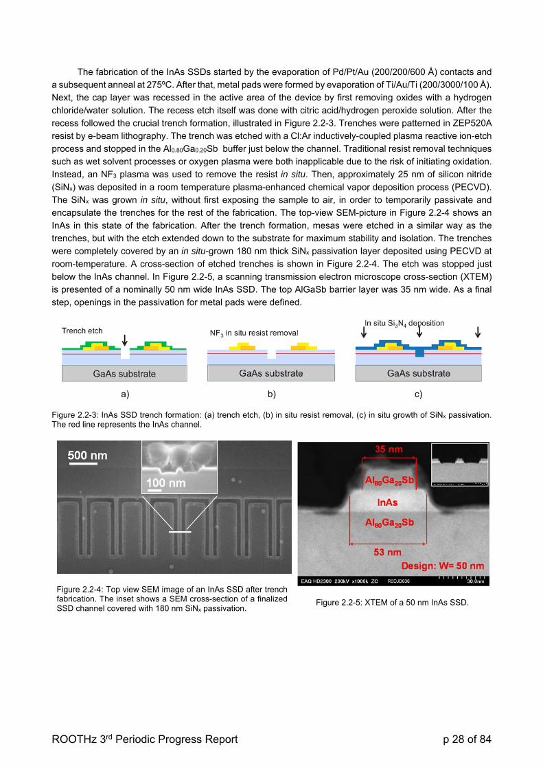
ROOTHz 3rd Periodic Progress Report p 28 of 84
The fabrication of the InAs SSDs started by the evaporation of Pd/Pt/Au (200/200/600 Å) contacts and
a subsequent anneal at 275ºC. After that, metal pads were formed by evaporation of Ti/Au/Ti (200/3000/100 Å).
Next, the cap layer was recessed in the active area of the device by first removing oxides with a hydrogen
chloride/water solution. The recess etch itself was done with citric acid/hydrogen peroxide solution. After the
recess followed the crucial trench formation, illustrated in Figure 2.2-3. Trenches were patterned in ZEP520A
resist by e-beam lithography. The trench was etched with a Cl:Ar inductively-coupled plasma reactive ion-etch
process and stopped in the Al0.80Ga0.20Sb buffer just below the channel. Traditional resist removal techniques
such as wet solvent processes or oxygen plasma were both inapplicable due to the risk of initiating oxidation.
Instead, an NF3 plasma was used to remove the resist in situ. Then, approximately 25 nm of silicon nitride
(SiNx) was deposited in a room temperature plasma-enhanced chemical vapor deposition process (PECVD).
The SiNx was grown in situ, without first exposing the sample to air, in order to temporarily passivate and
encapsulate the trenches for the rest of the fabrication. The top-view SEM-picture in Figure 2.2-4 shows an
InAs in this state of the fabrication. After the trench formation, mesas were etched in a similar way as the
trenches, but with the etch extended down to the substrate for maximum stability and isolation. The trenches
were completely covered by an in situ-grown 180 nm thick SiNx passivation layer deposited using PECVD at
room-temperature. A cross-section of etched trenches is shown in Figure 2.2-4. The etch was stopped just
below the InAs channel. In Figure 2.2-5, a scanning transmission electron microscope cross-section (XTEM)
is presented of a nominally 50 nm wide InAs SSD. The top AlGaSb barrier layer was 35 nm wide. As a final
step, openings in the passivation for metal pads were defined.
a)
b)
c)
Figure 2.2-3: InAs SSD trench formation: (a) trench etch, (b) in situ resist removal, (c) in situ growth of SiNx passivation. The red line represents the InAs channel.
Figure 2.2-4: Top view SEM image of an InAs SSD after trench fabrication. The inset shows a SEM cross-section of a finalized SSD channel covered with 180 nm SiNx passivation.
Figure 2.2-5: XTEM of a 50 nm InAs SSD.
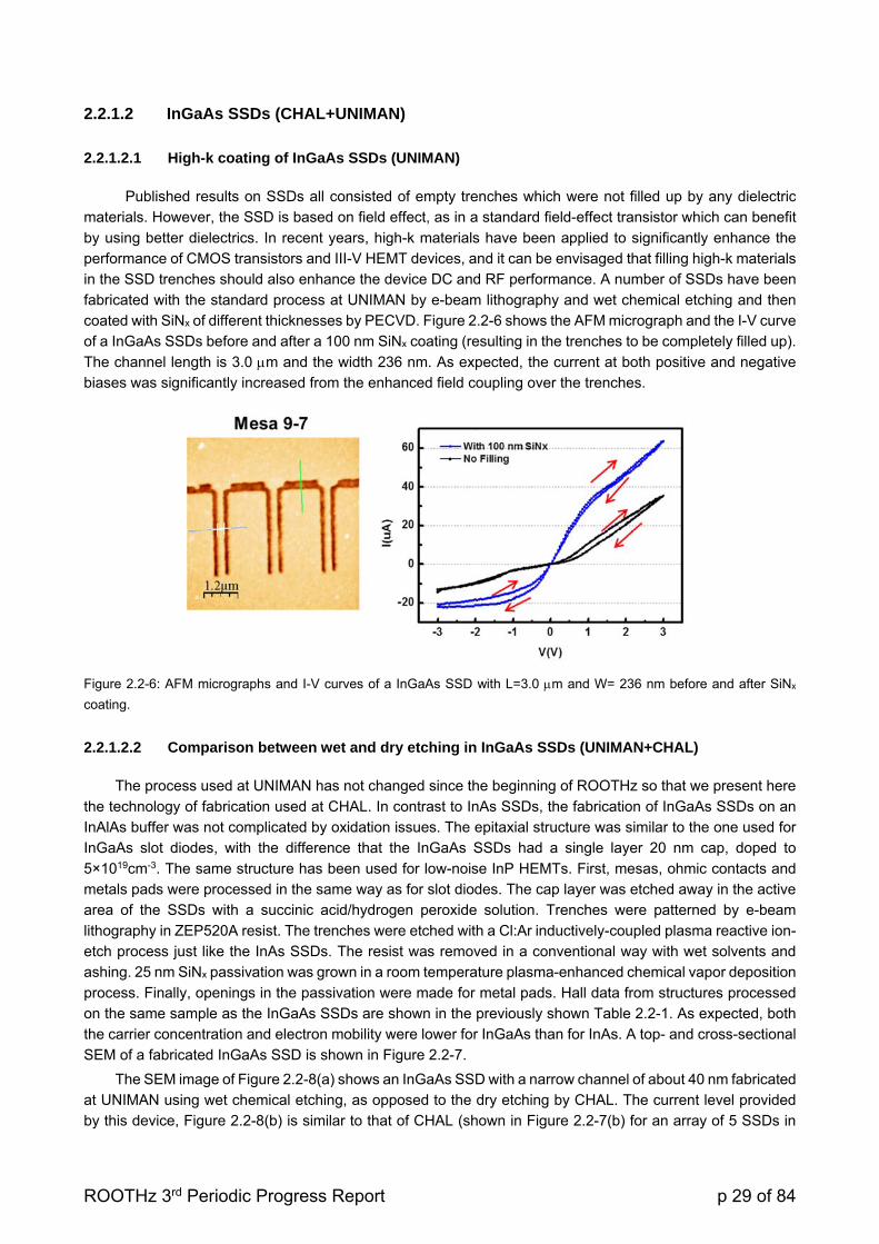
ROOTHz 3rd Periodic Progress Report p 29 of 84
2.2.1.2 InGaAs SSDs (CHAL+UNIMAN)
2.2.1.2.1 High-k coating of InGaAs SSDs (UNIMAN)
Published results on SSDs all consisted of empty trenches which were not filled up by any dielectric
materials. However, the SSD is based on field effect, as in a standard field-effect transistor which can benefit
by using better dielectrics. In recent years, high-k materials have been applied to significantly enhance the
performance of CMOS transistors and III-V HEMT devices, and it can be envisaged that filling high-k materials
in the SSD trenches should also enhance the device DC and RF performance. A number of SSDs have been
fabricated with the standard process at UNIMAN by e-beam lithography and wet chemical etching and then
coated with SiNx of different thicknesses by PECVD. Figure 2.2-6 shows the AFM micrograph and the I-V curve
of a InGaAs SSDs before and after a 100 nm SiNx coating (resulting in the trenches to be completely filled up).
The channel length is 3.0 m and the width 236 nm. As expected, the current at both positive and negative
biases was significantly increased from the enhanced field coupling over the trenches.
Figure 2.2-6: AFM micrographs and I-V curves of a InGaAs SSD with L=3.0 m and W= 236 nm before and after SiNx
coating.
2.2.1.2.2 Comparison between wet and dry etching in InGaAs SSDs (UNIMAN+CHAL)
The process used at UNIMAN has not changed since the beginning of ROOTHz so that we present here
the technology of fabrication used at CHAL. In contrast to InAs SSDs, the fabrication of InGaAs SSDs on an
InAlAs buffer was not complicated by oxidation issues. The epitaxial structure was similar to the one used for
InGaAs slot diodes, with the difference that the InGaAs SSDs had a single layer 20 nm cap, doped to
5×1019cm-3. The same structure has been used for low-noise InP HEMTs. First, mesas, ohmic contacts and
metals pads were processed in the same way as for slot diodes. The cap layer was etched away in the active
area of the SSDs with a succinic acid/hydrogen peroxide solution. Trenches were patterned by e-beam
lithography in ZEP520A resist. The trenches were etched with a Cl:Ar inductively-coupled plasma reactive ion-
etch process just like the InAs SSDs. The resist was removed in a conventional way with wet solvents and
ashing. 25 nm SiNx passivation was grown in a room temperature plasma-enhanced chemical vapor deposition
process. Finally, openings in the passivation were made for metal pads. Hall data from structures processed
on the same sample as the InGaAs SSDs are shown in the previously shown Table 2.2-1. As expected, both
the carrier concentration and electron mobility were lower for InGaAs than for InAs. A top- and cross-sectional
SEM of a fabricated InGaAs SSD is shown in Figure 2.2-7.
The SEM image of Figure 2.2-8(a) shows an InGaAs SSD with a narrow channel of about 40 nm fabricated
at UNIMAN using wet chemical etching, as opposed to the dry etching by CHAL. The current level provided
by this device, Figure 2.2-8(b) is similar to that of CHAL (shown in Figure 2.2-7(b) for an array of 5 SSDs in
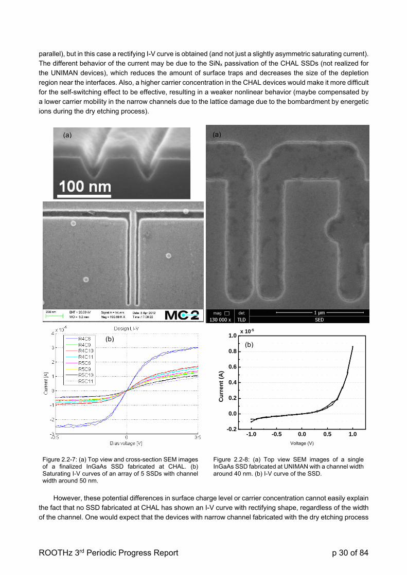
ROOTHz 3rd Periodic Progress Report p 30 of 84
parallel), but in this case a rectifying I-V curve is obtained (and not just a slightly asymmetric saturating current).
The different behavior of the current may be due to the SiNx passivation of the CHAL SSDs (not realized for
the UNIMAN devices), which reduces the amount of surface traps and decreases the size of the depletion
region near the interfaces. Also, a higher carrier concentration in the CHAL devices would make it more difficult
for the self-switching effect to be effective, resulting in a weaker nonlinear behavior (maybe compensated by
a lower carrier mobility in the narrow channels due to the lattice damage due to the bombardment by energetic
ions during the dry etching process).
Figure 2.2-7: (a) Top view and cross-section SEM images of a finalized InGaAs SSD fabricated at CHAL. (b) Saturating I-V curves of an array of 5 SSDs with channel width around 50 nm.
Figure 2.2-8: (a) Top view SEM images of a single InGaAs SSD fabricated at UNIMAN with a channel width around 40 nm. (b) I-V curve of the SSD.
However, these potential differences in surface charge level or carrier concentration cannot easily explain
the fact that no SSD fabricated at CHAL has shown an I-V curve with rectifying shape, regardless of the width
of the channel. One would expect that the devices with narrow channel fabricated with the dry etching process
-1.0 -0.5 0.0 0.5 1.0-0.2
0.0
0.2
0.4
0.6
0.8
1.0
Cu
rren
t (A
)
Voltage (V)
(a) (a)
(b)
x 10-5
(b)

ROOTHz 3rd Periodic Progress Report p 31 of 84
of CHAL (providing sharper edges in the trenches, as compared with the wriggly edges of the SSDs fabricated
at UNIMAN) will produce a better rectification, but the result is the opposite. The CHAL devices always show
a saturating behavior [as shown in Figure 2.2-7(b)], more asymmetric as the width of the channel decreases,
but they never present a strong rectifying shape as the UNIMAN devices [shown in Figure 2.2-8(b)]. A possible
explanation for the differences in the I-V curves could then be associated to the different morphology of the
channel walls obtained with the wet/dry etching processes. MC simulations will be used to try to explain this
fact, but it is not easy to perfectly reproduce such complex geometry.
2.2.2 TASK 2.2: WIDE BANDGAP SSD FABRICATION (IEMN)
After an important work for the development of all the process steps, during the first year of the project
the first GaN wafer was processed based on the dimensions obtained thanks to the MC simulations (with small
channel widths, around 75 nm). Unfortunately, the surface charges were underestimated and the electrical
results of the Run 1 were not in accordance with the simulation results (too low current density), so that the
fabricated SSDs could not produce Gunn oscillations. This behavior has been explained after an important
work done by USAL including a self-consistent surface charge model into the MC simulations. Based on this
new physical model a second mask was designed including wider SSD channels in order to counteract the
increase of the surface charges at high bias. Besides, a high number of SSDs were put in parallel (more than
600 SSDs) in the Run 2 in order to obtain an emission power level higher than the noise floor of our setup (if
oscillation conditions were reached). The high number of parallel SSDs (with no interconnection) helps to
overcome the well-known problems related to the high value of impedance of nanodevices (a single SSD has
a typical impedance of around R0=15 kΩ at zero bias). In this case the SSD electrical results were in good
agreement with MC but we were not able to bias the devices above the threshold voltage for the onset of Gunn
oscillations due to thermal limitations (the high number of SSD in parallel provides a huge current density).
This second Run proved the high uniformity of the process developed (finished September 2012, on M21, in
advance with respect of the ROOTHz schedule, since Run 1 was expected for M18 and Run 2 for M30) in view
that all the devices were operational.
After this experience, we have designed a third mask and process (not planned in the proposal) with the
optimal SSD dimensions on a full AlGaN/GaN on silicon wafer. This third mask includes square and V-shape
SSDs for emission and detection (with coplanar wave accesses for RF measurements under probes and with
bow-tie and spiral broadband integrated antennas for free space characterization) with only 16 and 32 SSDs
in parallel. The results obtained with this last process are described in this report.
2.2.2.1 Fabrication of Run 3 of GaN SSDs
This design of devices for Run 3 of GaN SSDs was mainly focused on THz emission, which, being the
priority of ROOTHz, was not obtained so far. So, all the topologies which MC simulations indicated to be
suitable to produce Gunn oscillations have been included in this last design. All these devices have been
integrated with two different type of broadband antennas, bow-tie and equiangular spiral (see the report of
MS.8 for its detailed description) to enhance the signal coupling between the SSD and the silicon lens for the
free space measurements. Figure 2.2-9 presents this layout which includes the optimal SSD dimensions, and
devices with coplanar wave accesses for RF on-wafer measurements. 12 V-shape and 8 square channel SSDs
have been included, the most suitable to produce Gunn oscillations (following the indications of MC
simulations) with lower threshold voltages (35V to 40V) and higher efficiency. The improved design was mainly
focused in avoiding an excessive heating and being able to bias the SSDs at high voltages in order to initiate
the Gunn oscillations. It was therefore decided to reduce the number of SSDs in parallel with respect to Run 2
(arrays of only 16 and 32 channels in parallel were fabricated), and to increase the separation each other to
minimize the self-heating.
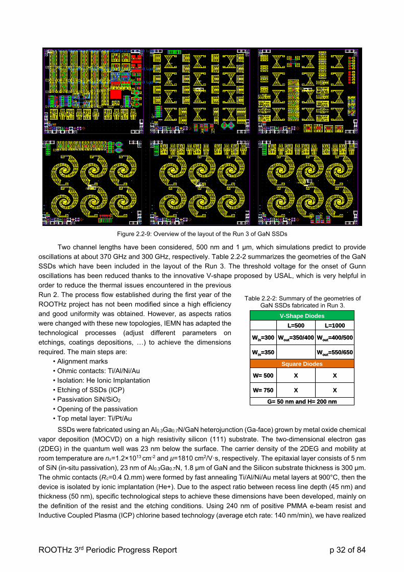
ROOTHz 3rd Periodic Progress Report p 32 of 84
Figure 2.2-9: Overview of the layout of the Run 3 of GaN SSDs
Two channel lengths have been considered, 500 nm and 1 µm, which simulations predict to provide
oscillations at about 370 GHz and 300 GHz, respectively. Table 2.2-2 summarizes the geometries of the GaN
SSDs which have been included in the layout of the Run 3. The threshold voltage for the onset of Gunn
oscillations has been reduced thanks to the innovative V-shape proposed by USAL, which is very helpful in
order to reduce the thermal issues encountered in the previous
Run 2. The process flow established during the first year of the
ROOTHz project has not been modified since a high efficiency
and good uniformity was obtained. However, as aspects ratios
were changed with these new topologies, IEMN has adapted the
technological processes (adjust different parameters on
etchings, coatings depositions, …) to achieve the dimensions
required. The main steps are:
• Alignment marks
• Ohmic contacts: Ti/Al/Ni/Au
• Isolation: He Ionic Implantation
• Etching of SSDs (ICP)
• Passivation SiN/SiO2
• Opening of the passivation
• Top metal layer: Ti/Pt/Au
SSDs were fabricated using an Al0.3Ga0.7N/GaN heterojunction (Ga-face) grown by metal oxide chemical
vapor deposition (MOCVD) on a high resistivity silicon (111) substrate. The two-dimensional electron gas
(2DEG) in the quantum well was 23 nm below the surface. The carrier density of the 2DEG and mobility at
room temperature are ns=1.2×1013 cm-2 and µ=1810 cm2/V·s, respectively. The epitaxial layer consists of 5 nm
of SiN (in-situ passivation), 23 nm of Al0.3Ga0.7N, 1.8 µm of GaN and the Silicon substrate thickness is 300 µm.
The ohmic contacts (Rc=0.4 Ω.mm) were formed by fast annealing Ti/Al/Ni/Au metal layers at 900°C, then the
device is isolated by ionic implantation (He+). Due to the aspect ratio between recess line depth (45 nm) and
thickness (50 nm), specific technological steps to achieve these dimensions have been developed, mainly on
the definition of the resist and the etching conditions. Using 240 nm of positive PMMA e-beam resist and
Inductive Coupled Plasma (ICP) chlorine based technology (average etch rate: 140 nm/min), we have realized
Table 2.2-2: Summary of the geometries of GaN SSDs fabricated in Run 3.
V-Shape Diodes
L=500 L=1000
Win=300 Wout=350/400 Wout=400/500
Win=350 Wout=550/650
Square Diodes
W= 500 X X
W= 750 X X
G= 50 nm and H= 200 nm
V-Shape Diodes
L=500 L=1000
Win=300 Wout=350/400 Wout=400/500
Win=350 Wout=550/650
Square Diodes
W= 500 X X
W= 750 X X
G= 50 nm and H= 200 nm
ROOTHz 3rd Periodic Progress Report p 33 of 84
nanodevices with channel and trench widths down to 50 nm and 90 nm, respectively. The channel width is
defined by the two etched horizontal trenches and the device symmetry is broken by the vertical trenches. To
ensure that the current only flows through the channel, the depth of the etched trenches is enough for making
them insulating. Finally the top metal layer (Ti/Pt/Au) is deposited to form a coplanar wave guide access line.
Figure 2.2-10: SEM images of Run 3 SSDs
The effect of the surface states along the sidewalls of the trenches in the AlGaN/GaN SSDs, even for
very narrow channels, is not enough to provide the theoretically expected rectifying I-V curve. Anyway, the
fabricated SSDs exhibit a slightly asymmetrical current-voltage characteristic. Indeed, in the fabrication of
SSDs aimed for THz emission the channel width is much wider, so the technological process is less critical
(Figure 2.2-10 shows SEM images of some fabricated devices).
Figure 2.2-11 presents the typical I-V characteristics of 16 SSD in parallel on wafer and after dicing and
mounting onto a PCB for free space measurements. Figure 2.2-11(a) and (b) shows that the post-processing
of the devices does not produce any damage. Figure 2.2-11(c), (d) and (e) show a good agreement between
measurements and MC simulation both for square and V-shape SSDs. Also, a good uniformity of the current
( 10%) is obtained around the whole wafer, whatever the SSD considered for a defined shape. With the
optimized designs fabricated in this Run 3 the devices can be biased up to 40 V without being destroyed (more
results will be presented in the section dedicated to characterization workpackage, WP3).

ROOTHz 3rd Periodic Progress Report p 34 of 84
Bias (V)
-10 -5 0 5 10 15 20
Cu
rren
t (m
A)
-1.5
-1.0
-0.5
0.0
0.5
1.0
1.5
ExperimentalMC
L= 500 nmW=500 nm
Bias (V)
-10 -5 0 5 10 15 20
L= 500 nmW=750 nm
Bias (V)
-10 -5 0 5 10 15 20
Cu
rren
t (m
A)
-1.5
-1.0
-0.5
0.0
0.5
1.0
1.5L= 500 nmWin=350 nm
Wout=450 nm
(c)
ExperimentalMC
(d)
ExperimentalMC
(e)
Figure 2.2-11: I-V characteristics of 16 SSDs in parallel with a) square shape (L=500 nm W=750 nm) and b) V-shape (L=500 nm, Win=350 nm, Wout=450 nm) before and after mounting and c), d) and e) comparison with Monte Carlo simulations of SSDs with different geometries.
2.2.2.2 Gated GaN SSDs
With the aim of controlling the total current and enhancing the electric field at the entrance of the channel,
SSDs with a top gate were fabricated. Figure 2.2-12 shows how the current is decreased when a negative
voltage is applied to the gate.
Figure 2.2-12: (a) SEM picture and (b) I-V curves of an array of 16 SSDs with a gate.
In order to understand the effect of the gate on a GaN SSD USAL has performed MC simulations using
a simple approach, since 3D simulations would strictly be needed. 1D n+nn+ structures can nicely account for
the electron transport for wide channels (the geometry used when Gunn oscillations are aimed), and the effect
of the reduction of the electron concentration (and the increase of the electric field) at the entrance of the
channel, can be reproduced by the presence of a notch (n+n-nn+ diode). The simulated topology of both types
of diodes and their I-V curves as a function of the channel length are represented in Figure 2.2-13, showing
that the effect of the notch is similar to the effect of a negative gate potential; a decrease of the current.
-10 -5 0 5 10 15 20
-20
-10
0
10
20
30
Cur
rent
(m
A)
Voltage (V)
Before Bonding After Bonding
-10 -5 0 5 10 15 20
-20
-10
0
10
20
30
Cur
rent
(m
A)
Voltage (V)
Before Bonding After Bonding
-10 -5 0 5 10 15 20-10
-5
0
5
10
15
Cur
rent
(m
A)
Voltage (V)
Before Bonding After Bonding
-10 -5 0 5 10 15 20-10
-5
0
5
10
15
Cur
rent
(m
A)
Voltage (V)
Before Bonding After Bonding
0
5
10
15
20
25
0 5 10 15 20
Current (m
A)
Voltage (V)
Vg= 0V
Vg= ‐4V
(a) (b)
(a) (b)

ROOTHz 3rd Periodic Progress Report p 35 of 84
Figure 2.2-13: Topology and I-V curves of the simulated diodes w/o and with notch.
Figure 2.2-14: Frequency of the peaks in the spectral densities vs. applied voltage for structures (a) without and (b) with a notch and different lengths. The size of the bubbles is proportional to the amplitude of these peaks [in (b) it is magnified x10].
The influence of the notch on the frequency and amplitude of the Gunn oscillations can be observed in
Figure 2.2-14, none of them beneficial: decrease of the frequency and amplitude, and increase of the threshold
voltage with respect to the case without a notch. However, as the gate potential is able to switch between the
two conditions, it could be used for tuning the frequency of the possible emission (and tune the oscillations of
the SSDs with the characteristic frequency of an external resonator, that seems to be needed to obtain a
coherent emission), and also opens the possibility of generating high order harmonics (with frequency up to
675 GHz, for the sixth generation band of a diode with notch and L=900 nm).
MC simulations of gated SSDs (with an approximate geometry, since 3D simulations would be needed)
confirm that the presence of the gate contact also allows reducing the threshold voltage needed for the onset
of Gunn oscillations, that helps to avoid the power dissipation issues found in these devices.
Bias (V)
0 20 40 60 80 100 120
Cu
rren
t (A
/m)
0
50
100
150
200
L=1.5 m w/o notchL=1.2 m w/o notchL=900 nm w/o notchL=750 nm w/o notch
Bias (V)
0 20 40 60 80 100 120
Cu
rren
t (A
/m)
0
50
100
150
200
L=1.5 m with notchL=1.2 m with notchL=900 nm with notchL=750 nm with notch
L L
n+ =2x1018cm
‐3
n=5x1017 cm‐3 n=5x1017 cm‐3
n+ =2x1018cm
‐3
n+ =2x1018cm
‐3
n+ =2x1018cm
‐3
n‐ =1017cm
‐3
Bias (V)
0 20 40 60 80 100 120 140
Osc
illa
tion
fre
que
ncy
(GH
z)
0
100
200
300
400
L=750 nm w/o notch L=900 nm w/o notchL=2mm w/o notchL=4mm w/o notch
Bias (V)
0 20 40 60 80 100 120 140
Osc
illa
tion
fre
que
ncy
(GH
z)
0
100
200
300
400
L=750 nm with notch
L=900 nm with notch
L=2m with notch
L=4m with notch
Size x 10Size x 10Amplitude = Size of the Bubble
ROOTHz 3rd Periodic Progress Report p 36 of 84
2.2.2.3 Self-Switching Diodes with Ion-implanted trenches (ISSD)
The measurements done in narrow SSDs fabricated in the initial runs have confirmed the MC predictions
that for wider channels the strength of the lateral field effect induced by the trenches is smaller, thus producing
a weaker current asymmetry. In order to improve the current rectification and therefore the responsivity of
SSDs used as THz detectors, the channel width has to be reduced to the limit that the channel is practically
totally depleted; this is not easily achieved with the previously reported dry etching recess processing. To
overcome this challenge and to obtain effective channel widths lower than W=90 nm, we have replaced the
etching technology by an ion implantation step. Other advantage of the implanted trenches is that the dielectric
constant of the implanted GaN is higher than that of air, thus improving the lateral field effect and enhancing
the non-linear behavior of the SSDs, and therefore the responsivity of the detectors fabricated with them. This
technology could also be interesting for improving the onset of Gunn oscillations if the amount of surface states
(which is known to be strongly technology dependent) were lower than those produced at the sidewalls of the
etched trenches. However, in this case we cannot have any indication before the devices have been fabricated.
Figure 2.2-15: Implantation profile with Stopping and Range of Ion in Matter Software
Figure 2.2-16: Dependence of the zero-bias conductance as a function of the projected width, W, of the ion implanted SSDs
Figure 2.2-17: Comparison of the I-V curves of arrays of 16 ion implanted (W=200 nm) and etched (W=90 nm) SSDs for approximately the same Weff of about 30 nm
Using Ar+ with an energy of 150 keV, on the one hand, the penetration depth of the ion implantation is
able to reach the GaN layer, and, on the other, the geometry of the insulating trenches is correctly defined.
The implantation energy was determined using the software Stopping and Range of Ion in Matter 2008 (Figure
2.2-15). However, the Ar+ implantation process induces large ion diffusion, resulting in an effective
nanochannel narrower than the one defined in the layout. In order to evaluate the effective width of the SSDs
75 100 125 150 175 200 2250,00
0,05
0,10
0,15
0,20
0,25
Zer
o-bi
as c
ondu
ctan
ce (
k
)
Projected Width (nm)
172 nm
-10 -5 0 5 10 15 20-1,0
-0,5
0,0
0,5
1,0
1,5
Implanted 16 SSD_200 nm width Recess 16 SSD_75 nm width
Cu
rren
t (m
A)
Voltage (V)
90
ROOTHz 3rd Periodic Progress Report p 37 of 84
channel, Weff, we have fabricated ion implanted SSDs with different projected channel widths W, from 75 to
200 nm. By analyzing the dependence of the conductance (1/R) as a function of the projected width of the
channel (Figure 2.2-16), we observe that the minimum width for having a conducting channel is about 172 nm.
Therefore, the implanted trenches width enlarged by the possible depletion associated to the defects and
surface charges created at the limits of the implanted region result in a non-conducting zone of about 86 nm
at each side of the channel (in excess of the projected width). To verify this assumption and compare the two
technological processes, we have performed DC measurements on arrays of 16 etched and implanted SSDs
with similar values of Weff: an implanted nanodiode with a projected width of W=200 nm (Weff≈28 nm) and a
recessed nanodiode with a 90 nm wide channel (Weff≈30 nm, since the depletion region in this type of devices
is about 30 nm wide). Figure 2.2-17 shows that the zero bias resistance is similar and also the current
saturation level. Surprisingly the implanted devices present a much stronger saturation, that can be due to the
presence of a large amount of surface states that are charged as the bias is increased, thus progressively
closing the channel and counteracting the increase of the current. This fact hinders the application of this
technology in the fabrication of SSDs for the generation of Gunn oscillations, where the lowest possible amount
of surface charges is desirable.
2.2.3 WP2: SUMMARY
As a summary we can say that the WP2 of ROOTHz has been absolutely successful in developing new
technological process and fabricating slot diodes and NBG and WBG SSDs. It is important to remark that the
fabrication of both GaN and InAs SSDs had never been previously demonstrated, and the consortium has
overcome all the difficulties found during the development and optimization of those challenging technologies.
As such, the deliverables corresponding to this period within WP2: D2.3, “Fabrication of Run 2 of NBG SSDs
and Slot-diodes” (M36) and D2.4 “Fabrication of Run 2 of WBG SSDs” (M36) have been provided on due time.
ROOTHz 3rd Periodic Progress Report p 38 of 84
2.3 WP3: CHARACTERIZATION
The tasks for the third year of the project in WP3 are similar to those developed in the previous review
period, with the only difference is that optimized devices will be characterized:
Task 3.1: Physical characterization (SEM, XTEM, AFM, etc.) of the fabricated devices.
Task 3.2: Electrical (DC and RF) characterization. This is the first step to confirm the correct operation
of the devices and to determine their dynamic response up to 325 GHz (the limit of the available RF
equipment) using integrated coplanar waveguides.
Task 3.3 THz characterization: Characterization of the fabricated emitters and detectors with a variety
of complementary techniques (in free space beyond 325 GHz). Cooled bolometers and pulsed
measurements will be used in order to improve the sensitivity and avoid heating problems.
The main goals for this period were to demonstrate the operation of emitters at frequencies above
200 GHz and detectors at >1 THz.
2.3.1 TASK 3.1: PHYSICAL CHARACTERIZATION (CHAL+UNIMAN+IEMN)
The results of the physical characterization of the technological process of InAs-based SSDs developed
at CHAL (which has been the most problematic fabrication issue during this period), have been presented in
the Section 2.2.1.1, devoted to this kind of devices. Different techniques (top view and cross section SEM
pictures were taken, together with inspection with scanning transmission electron microscope, XTEM, and
AFM) were used at different stages of the process in order to monitor and solve the causes of the failures.
We have also tried to explain, by means of the physical characterization of the devices, the differences
between the I-V curves of the InGaAs-based SSDs fabricated at CHAL and UNIMAN since only the wet
etching process of UNIMAN is able to provide a rectifying characteristic (which is the best suited for an
improved THz detection). As presented in Section 2.2.1.2.2, the important morphological differences in the
trench edges (together with an influence of the plasma etching on the electron concentration and mobility in
the narrowest channels) maybe at the origin of such variations.
Regarding GaN-based SSDs, the technological process at IEMN was already stable for Run 2 and not
much efforts have been done on the physical characterization of Run 3, see Section 2.2.2.
2.3.2 TASK 3.2: ELECTRICAL (DC AND RF) CHARACTERIZATION
2.3.2.1 DC and RF characterization of high-k coated InGaAs SSDs (UNIMAN)
Figure 2.3-1(a) shows the I-V characteristics of an InGaAs SSD (Device 8-7) with L=3.0 m and
W=215 nm before and after coating with a 20 nm film of SiNx, which is much less than the trench etching depth
(around 60 nm). Even though, the current is significantly enhanced. Device 9-7 (L=3.0 m and W=236 nm)
was coated with a much thicker film of 100 nm SiNx, resulting in the trenches to be completely filled up, and
thus providing a larger increase of the current, Figure 2.3-2(a).
In order to determine whether the net nonlinear characteristics of the device have also been enhanced,
the nonlinear components of the I-V curves, namely [I(V)+I(-V)]/2, have been extracted for both devices and
plotted in Figure 2.3-1(b) and Figure 2.3-2(b). Clearly the device nonlinearity has also been significantly
enhanced, particularly at low biases. At 0.5 V, for example, the nonlinear component of the I-V is boosted by
a factor of about 10, indicating that the threshold voltage of the device has been reduced. In comparison, the
relative enhancement of nonlinearity is much lower at 3 V. It is also observed that the increase of the
nonlinearity is enhanced by a thicker SiNx coating.
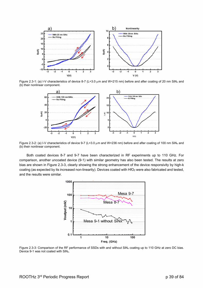
ROOTHz 3rd Periodic Progress Report p 39 of 84
Figure 2.3-1: (a) I-V characteristics of device 8-7 (L=3.0 m and W=215 nm) before and after coating of 20 nm SiNx and (b) their nonlinear component.
Figure 2.3-2: (a) I-V characteristics of device 9-7 (L=3.0 m and W=236 nm) before and after coating of 100 nm SiNx and (b) their nonlinear component.
Both coated devices 8-7 and 9-7 have been characterized in RF experiments up to 110 GHz. For
comparison, another uncoated device (9-1) with similar geometry has also been tested. The results at zero
bias are shown in Figure 2.3-3, clearly showing the strong enhancement of the device responsivity by high-k
coating (as expected by its increased non-linearity). Devices coated with HfO2 were also fabricated and tested,
and the results were similar.
Figure 2.3-3: Comparison of the RF performance of SSDs with and without SiNx coating up to 110 GHz at zero DC bias. Device 9-1 was not coated with SiNx.
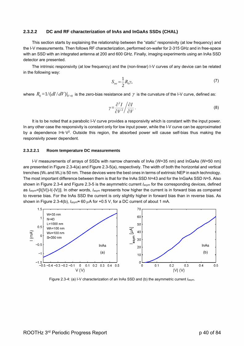
ROOTHz 3rd Periodic Progress Report p 40 of 84
2.3.2.2 DC and RF characterization of InAs and InGaAs SSDs (CHAL)
This section starts by explaining the relationship between the “static” responsivity (at low frequency) and
the I-V measurements. Then follows RF characterization, performed on-wafer for 2-315 GHz and in free-space
with an SSD with an integrated antenna at 200 and 600 GHz. Finally, imaging experiments using an InAs SSD
detector are presented.
The intrinsic responsivity (at low frequency) and the (non-linear) I-V curves of any device can be related
in the following way:
0
1,
2intS R γ (7)
where 0 =0=1/ ( / )|VR dI dV is the zero-bias resistance and is the curvature of the I-V curve, defined as:
2
2=
I Iγ
V V
. (8)
It is to be noted that a parabolic I-V curve provides a responsivity which is constant with the input power.
In any other case the responsivity is constant only for low input power, while the I-V curve can be approximated
by a dependence I=k·V2. Outside this region, the absorbed power will cause self-bias thus making the
responsivity power dependent.
2.3.2.2.1 Room temperature DC measurements
I-V measurements of arrays of SSDs with narrow channels of InAs (W=35 nm) and InGaAs (W=50 nm)
are presented in Figure 2.3-4(a) and Figure 2.3-5(a), respectively. The width of both the horizontal and vertical
trenches (Wh and Wv) is 50 nm. These devices were the best ones in terms of extrinsic NEP in each technology.
The most important difference between them is that for the InAs SSD N=43 and for the InGaAs SSD N=5. Also
shown in Figure 2.3-4 and Figure 2.3-5 is the asymmetric current Iasym for the corresponding devices, defined
as Iasym=[I(|V|)-I(-|V|)]. In other words, Iasym represents how higher the current is in forward bias as compared
to reverse bias. For the InAs SSD the current is only slightly higher in forward bias than in reverse bias. As
shown in Figure 2.3-4(b), Iasym≈ 60 A for +0.5 V, for a DC current of about 1 mA.
Figure 2.3-4: (a) I-V characterization of an InAs SSD and (b) the asymmetric current Iasym.
InAs
(a)
InAs
(b)

ROOTHz 3rd Periodic Progress Report p 41 of 84
Figure 2.3-5: (a) I-V characterization of an InGaAs SSD and (b) the asymmetric current Iasym.
While Iasym of this device is of the same order of magnitude as for other non-linear detectors such as Sb-
based backward diodes2, it constitutes only ≈ 6% of the total current provided by the InAs SSD. This large
contribution of the symmetric current comes from the fact that the channel is not completely closed in reverse
bias. However, it is this small asymmetry that allows the InAs SSD to operate as a detector.
The I-V for InGaAs SSD is in many aspects different from the InAs I-V. First, the current in the InGaAs
SSD starts to saturate at about 0.1 V. This saturation is similar to that observed in ID-VDS measurements for
VGS=0 V of InGaAs HEMTs fabricated in the same heterostructure. Second, the current per SSD is more than
a factor 15 lower than in the InAs SSDs. However, the asymmetry is stronger, below saturation, Iasym in the
InGaAs SSD is about 15% of the total forward current.
The values of responsivity can be derived from the measured I-V curves according to (7) and those of the
intrinsic/extrinsic NEP are simply given by NEPint/ext= B 04k TR /Sint/ext. The values in Table 2.3-1 have been
derived from the I-V measurements presented in Figure 2.3-4 and Figure 2.3-5. In comparison to the InGaAs
SSD, the InAs SSD has much lower Sint and higher NEPint. However, the significantly lower R0 makes the
power transfer from a 50 system easier with the InAs SSD than for the InGaAs SSD.
Table 2.3-1: Detector characteristics of InAs and InGaAs SSDs derived from I-V measurements.
N W R0 () Sint (V/W) NEPint (pW/Hz) Sext (V/W) NEPext (pW/Hz)
InAs SSD 43 35 350 18 200 11 210
InGaAs SSD 5 50 1800 14000 1.2 150 115
DC-measurements of R0 and curvature at zero bias as a function of the width of the channel W are
shown in Figure 2.3-6. As expected from its lower current level, the resistance of the InGaAs SSDs is many
kfor small W, making matching difficult. Smaller W leads to higher in both InAs SSDs and InGaAs SSDs,
reaching maximum values of 0.2 V-1 and 2.5 V-1, respectively. For comparison, zero-bias Schottky diodes and
Sb-heterostructure diodes have of 26 and 47 V-1, respectively, leading to the high responsivities observed
with those diodes.
2 N. Su, “Sb-heterostructure millimeter-wave detectors with reduced capacitance and Noise Equivalent Power,” IEEE Electr. Dev. Lett. 29, p. 536-539 (2008)
InGaAs
(a)
InGaAs
(b)
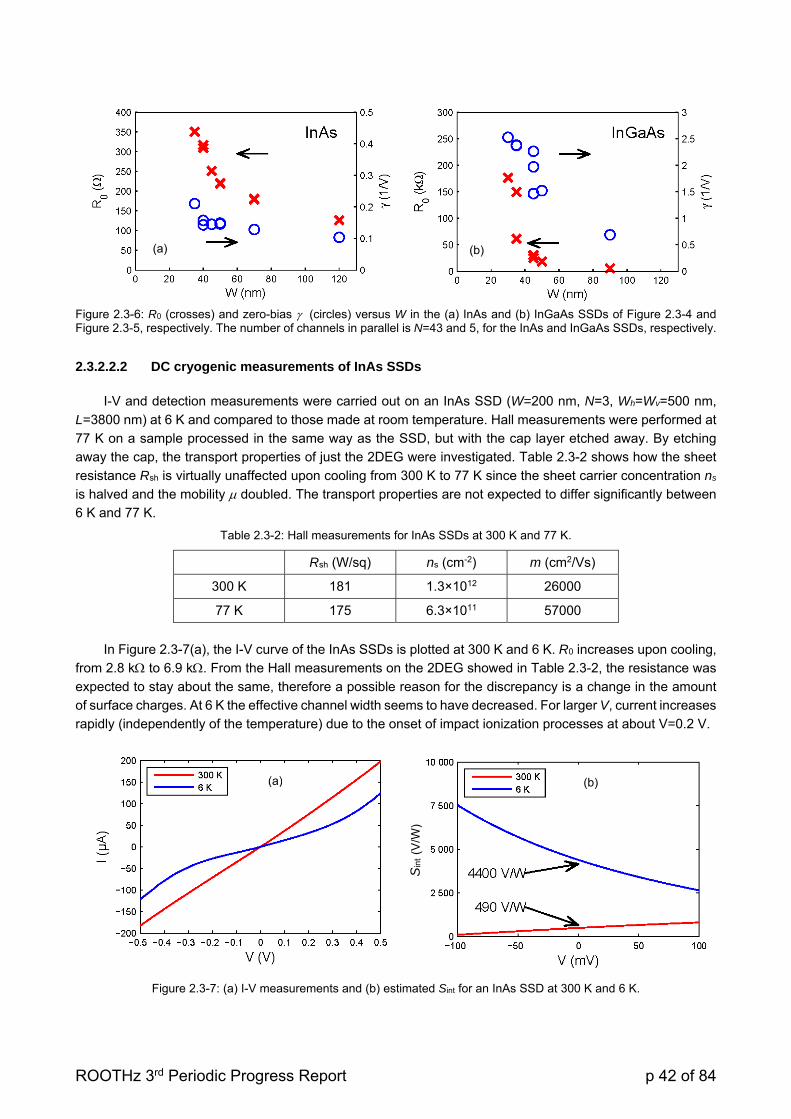
ROOTHz 3rd Periodic Progress Report p 42 of 84
Figure 2.3-6: R0 (crosses) and zero-bias (circles) versus W in the (a) InAs and (b) InGaAs SSDs of Figure 2.3-4 and Figure 2.3-5, respectively. The number of channels in parallel is N=43 and 5, for the InAs and InGaAs SSDs, respectively.
2.3.2.2.2 DC cryogenic measurements of InAs SSDs
I-V and detection measurements were carried out on an InAs SSD (W=200 nm, N=3, Wh=Wv=500 nm,
L=3800 nm) at 6 K and compared to those made at room temperature. Hall measurements were performed at
77 K on a sample processed in the same way as the SSD, but with the cap layer etched away. By etching
away the cap, the transport properties of just the 2DEG were investigated. Table 2.3-2 shows how the sheet
resistance Rsh is virtually unaffected upon cooling from 300 K to 77 K since the sheet carrier concentration ns
is halved and the mobility doubled. The transport properties are not expected to differ significantly between
6 K and 77 K.
Table 2.3-2: Hall measurements for InAs SSDs at 300 K and 77 K.
Rsh (W/sq) ns (cm-2) m (cm2/Vs)
300 K 181 1.3×10¹² 26000
77 K 175 6.3×10¹¹ 57000
In Figure 2.3-7(a), the I-V curve of the InAs SSDs is plotted at 300 K and 6 K. R0 increases upon cooling,
from 2.8 k to 6.9 k. From the Hall measurements on the 2DEG showed in Table 2.3-2, the resistance was
expected to stay about the same, therefore a possible reason for the discrepancy is a change in the amount
of surface charges. At 6 K the effective channel width seems to have decreased. For larger V, current increases
rapidly (independently of the temperature) due to the onset of impact ionization processes at about V=0.2 V.
Figure 2.3-7: (a) I-V measurements and (b) estimated Sint for an InAs SSD at 300 K and 6 K.
(a) (b)
Sin
t (V
/W)
(a) (b)

ROOTHz 3rd Periodic Progress Report p 43 of 84
Figure 2.3-7(b) shows the intrinsic responsivity, Sint, estimated near equilibrium according to (7) and (8)
at 300 K and 6 K. At V=0 its values are 490 and 4400 V/W, respectively. The corresponding NEPint values
were 14 and 0.34 pW/Hz. Thus, the performance of the InAs SSD as THz detectors is expected to be
significantly improved upon cooling. This has been verified with RF measurements in InGaAs SSDs, but not
so far in InAs SSDs.
2.3.2.2.3 On-wafer RF measurements
On-wafer measurements were performed using a vector network analyzer as the signal source. The setup
is shown in Figure 2.3-8. Different equipment was used for each of the three different bands (2-50, 140-220
and 240-315 GHz), all following the same principle: the power from the source was measured with a
calorimetric power meter for each frequency setting. By subtracting the loss of the RF probes, the available
power at the probe tip, Pi, was found. The power incident to the device was 1.7-8.5 W, delivered by a 50
source. The DC detected voltage, Vdet was measured through a bias-tee with a high-resistance load. The
unmatched responsivity Sext was calculated as the ratio Vdet/Pi.
Figure 2.3-8: Schematic view of the setup for on-wafer characterization of InAs and InGaAs SSDs.
The influence of design parameters on the responsivity and NEP was studied at 50 GHz. Typical designs
for InAs and InGaAs SSDs are shown in Table 2.3-3. Based on these designs, the dependence on W was
tested. For InAs SSDs, also the dependence on N and L was investigated.
Table 2.3-3: Typical SSD designs fabricated in InAs SSDs and InGaAs.
Material W (nm) N L (nm) Wh (nm) Wv (nm)
InAs 45 43 1100 100 100
InGaAs 45 5 1100 100 100
Figure 2.3-9(a) shows Sext as a function of frequency for InAs SSDs with three different W. The ripple in
the data is attributed to the fact that when Po was measured with the power meter, the source saw a different
load than when the SSDs were measured. Notably, no strong roll-off is observed in the measured band up to
315 GHz. The highest Sext is achieved for W=35 nm, for which Sext>10 V/W in the measured band. Figure 2.3-
9(b) shows the corresponding data for InGaAs SSDs. The values found for Sext in the InGaAs SSDs are higher
than in the InAs SSDs.
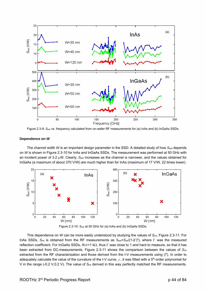
ROOTHz 3rd Periodic Progress Report p 44 of 84
Figure 2.3-9: Sext vs. frequency calculated from on-wafer RF measurements for (a) InAs and (b) InGaAs SSDs.
Dependence on W
The channel width W is an important design parameter in the SSD. A detailed study of how Sext depends
on W is shown in Figure 2.3-10 for InAs and InGaAs SSDs. The measurement was performed at 50 GHz with
an incident power of 3.2 W. Clearly, Sext increases as the channel is narrower, and the values obtained for
InGaAs (a maximum of about 370 V/W) are much higher than for InAs (maximum of 17 V/W, 22 times lower).
Figure 2.3-10: Sext at 50 GHz for (a) InAs and (b) InGaAs SSDs.
This dependence on W can be more easily understood by studying the values of Sint, Figure 2.3-11. For
InAs SSDs, Sint is obtained from the RF measurements as Sext=Sint/(1-||2), where was the measured
reflection coefficient. For InGaAs SSDs, R0>>1 k, thus was close to 1 and hard to measure, so that it has
been extracted from DC-measurements. Figure 2.3-11 shows the comparison between the values of Sint
extracted from the RF characterization and those derived from the I-V measurements using (7). In order to
adequately calculate the value of the curvature of the I-V curve, , it was fitted with a 5th-order polynomial for
V in the range (-0.2 V,0.2 V). The value of Sint derived in this way perfectly matched the RF measurements.
(a)
(b)
Se
xt (
V/W
) S
ext (
V/W
)
(a) (b)
Se
xt (
V/W
)
Se
xt (
V/W
)
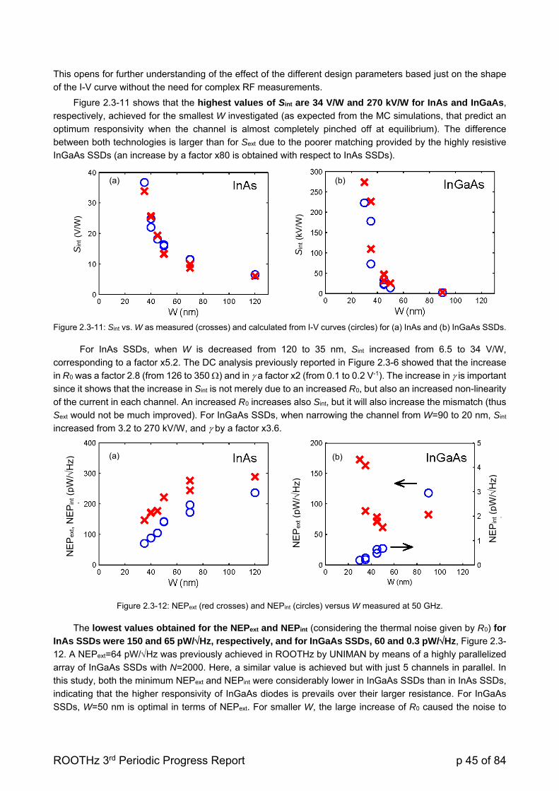
ROOTHz 3rd Periodic Progress Report p 45 of 84
This opens for further understanding of the effect of the different design parameters based just on the shape
of the I-V curve without the need for complex RF measurements.
Figure 2.3-11 shows that the highest values of Sint are 34 V/W and 270 kV/W for InAs and InGaAs,
respectively, achieved for the smallest W investigated (as expected from the MC simulations, that predict an
optimum responsivity when the channel is almost completely pinched off at equilibrium). The difference
between both technologies is larger than for Sext due to the poorer matching provided by the highly resistive
InGaAs SSDs (an increase by a factor x80 is obtained with respect to InAs SSDs).
Figure 2.3-11: Sint vs. W as measured (crosses) and calculated from I-V curves (circles) for (a) InAs and (b) InGaAs SSDs.
For InAs SSDs, when W is decreased from 120 to 35 nm, Sint increased from 6.5 to 34 V/W,
corresponding to a factor x5.2. The DC analysis previously reported in Figure 2.3-6 showed that the increase
in R0 was a factor 2.8 (from 126 to 350 ) and in a factor x2 (from 0.1 to 0.2 V-1). The increase in is important
since it shows that the increase in Sint is not merely due to an increased R0, but also an increased non-linearity
of the current in each channel. An increased R0 increases also Sint, but it will also increase the mismatch (thus
Sext would not be much improved). For InGaAs SSDs, when narrowing the channel from W=90 to 20 nm, Sint
increased from 3.2 to 270 kV/W, and by a factor x3.6.
Figure 2.3-12: NEPext (red crosses) and NEPint (circles) versus W measured at 50 GHz.
The lowest values obtained for the NEPext and NEPint (considering the thermal noise given by R0) for
InAs SSDs were 150 and 65 pW/Hz, respectively, and for InGaAs SSDs, 60 and 0.3 pW/Hz, Figure 2.3-
12. A NEPext=64 pW/Hz was previously achieved in ROOTHz by UNIMAN by means of a highly parallelized
array of InGaAs SSDs with N=2000. Here, a similar value is achieved but with just 5 channels in parallel. In
this study, both the minimum NEPext and NEPint were considerably lower in InGaAs SSDs than in InAs SSDs,
indicating that the higher responsivity of InGaAs diodes is prevails over their larger resistance. For InGaAs
SSDs, W=50 nm is optimal in terms of NEPext. For smaller W, the large increase of R0 caused the noise to
(a) (b)
Sin
t (kV
/W)
Sin
t (V
/W)
(a)
NE
Pex
t (pW
/H
z)
(b)
NE
Pex
t, N
EP
int (
pW/
Hz)
NE
Pin
t (pW
/H
z)

ROOTHz 3rd Periodic Progress Report p 46 of 84
increase. In InAs SSDs, the lowest NEPext and NEPint are achieved for the lowest W. A further reduction of W
may thus further improve the device performances. All these results confirm the predictions made by MC
simulations in the deliverable D1.2 (Design rules for the optimization of Run 2 devices) on M18. Only a slight
shift on the values of W that provide the optimum performances is observed due to a larger depletion width
considered there for InGaAs SSDs (75 nm, that resulted on an optimum value of W of about W=150 nm). Using
the experimental I-V curves, the depletion width for InAs SSDs was estimated to be about 5 nm, so that the
optimum value of W should be around 10 nm, again in good agreement with the experimental results.
Dependence on N and L (InAs SSDs)
In InAs SSDs, also the dependence on N was studied, with results shown in Figure 2.3-13. From the N=43
device, the dependence on N of the resistance, Sint, Sext, NEPext and NEPint of arrays of N parallel SSDs was
determined (taking into account that Sint,N=1=N×Sint,N, R0,N=1=N×R0,N and the consequent dependence of on
N). Figure 2.3-13 shows the comparison of the theoretical extrapolation of the results obtained with N=43 with
the measurements realized in arrays of SSD with different N. The agreement is good, with some discrepancy
for small N. NEPint increases for higher N but NEPext decreases as expected by the lower resistance that results
in a reduced mismatch. Figure 2.3-13(b) further suggests that increasing N beyond 40 has little effect on NEPext
even if the expected minimum occurs for N=70.
Figure 2.3-13: Sint and NEPint (circles), and Sext and NEPext (crosses) versus N, measured at 50 GHz. The theoretical relation (black lines) was derived from the value of Sint and R0 for the SSD with N=43.
The last design parameter investigated was the length of the channels L, shown in Figure 2.3-15. Longer
SSDs provide higher Sint and lower NEPint. Also Sext and NEPext are improved, but to a lesser extent due to
increased R0 and the consequent increased mismatch.
Figure 2.3-15: Sint and NEPint (circles), and Sext and NEPext (crosses) versus L, measured at 50 GHz.
(a) (b)
NE
Pex
t, N
EP
int (
pW/
Hz)
Se
xt (
V/W
)
Sin
t (V
/W)
(a) (b)
Sex
t, S
int (
V/W
)
NE
Pe
xt, N
EP
int (
pW/
Hz)
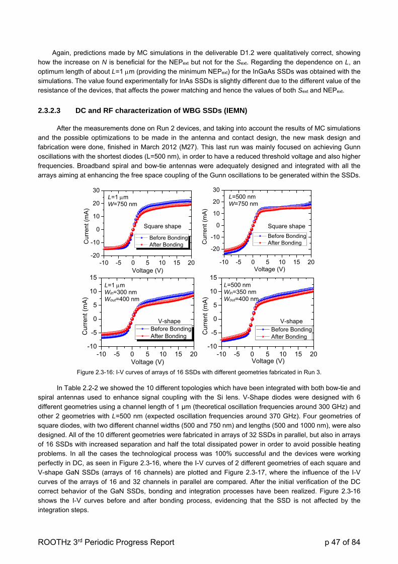
ROOTHz 3rd Periodic Progress Report p 47 of 84
Again, predictions made by MC simulations in the deliverable D1.2 were qualitatively correct, showing
how the increase on N is beneficial for the NEPext but not for the Sext. Regarding the dependence on L, an
optimum length of about L=1 m (providing the minimum NEPext) for the InGaAs SSDs was obtained with the
simulations. The value found experimentally for InAs SSDs is slightly different due to the different value of the
resistance of the devices, that affects the power matching and hence the values of both Sext and NEPext.
2.3.2.3 DC and RF characterization of WBG SSDs (IEMN)
After the measurements done on Run 2 devices, and taking into account the results of MC simulations
and the possible optimizations to be made in the antenna and contact design, the new mask design and
fabrication were done, finished in March 2012 (M27). This last run was mainly focused on achieving Gunn
oscillations with the shortest diodes (L=500 nm), in order to have a reduced threshold voltage and also higher
frequencies. Broadband spiral and bow-tie antennas were adequately designed and integrated with all the
arrays aiming at enhancing the free space coupling of the Gunn oscillations to be generated within the SSDs.
Figure 2.3-16: I-V curves of arrays of 16 SSDs with different geometries fabricated in Run 3.
In Table 2.2-2 we showed the 10 different topologies which have been integrated with both bow-tie and
spiral antennas used to enhance signal coupling with the Si lens. V-Shape diodes were designed with 6
different geometries using a channel length of 1 µm (theoretical oscillation frequencies around 300 GHz) and
other 2 geometries with L=500 nm (expected oscillation frequencies around 370 GHz). Four geometries of
square diodes, with two different channel widths (500 and 750 nm) and lengths (500 and 1000 nm), were also
designed. All of the 10 different geometries were fabricated in arrays of 32 SSDs in parallel, but also in arrays
of 16 SSDs with increased separation and half the total dissipated power in order to avoid possible heating
problems. In all the cases the technological process was 100% successful and the devices were working
perfectly in DC, as seen in Figure 2.3-16, where the I-V curves of 2 different geometries of each square and
V-shape GaN SSDs (arrays of 16 channels) are plotted and Figure 2.3-17, where the influence of the I-V
curves of the arrays of 16 and 32 channels in parallel are compared. After the initial verification of the DC
correct behavior of the GaN SSDs, bonding and integration processes have been realized. Figure 2.3-16
shows the I-V curves before and after bonding process, evidencing that the SSD is not affected by the
integration steps.
-10 -5 0 5 10 15 20-20
-10
0
10
20
30
Cur
rent
(m
A)
Voltage (V)
Before Bonding After Bonding
-10 -5 0 5 10 15 20
-20
-10
0
10
20
30
Cur
rent
(m
A)
Voltage (V)
Before Bonding After Bonding
-10 -5 0 5 10 15 20-10
-5
0
5
10
15
Cur
rent
(m
A)
Voltage (V)
Before Bonding After Bonding
-10 -5 0 5 10 15 20-10
-5
0
5
10
15
Cur
rent
(m
A)
Voltage (V)
Before Bonding After Bonding
L=1 m W=750 nm
L=500 nm W=750 nm
Square shape Square shape
L=1 m Win=300 nm Wout=400 nm
V-shape
L=500 nm Win=350 nm Wout=400 nm
V-shape
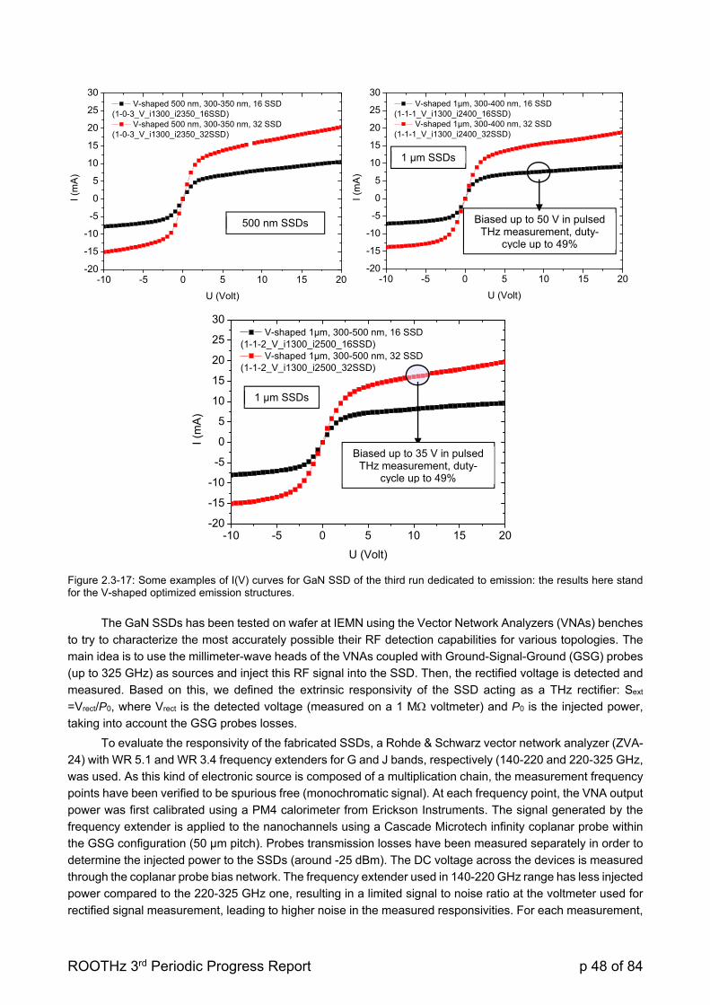
ROOTHz 3rd Periodic Progress Report p 48 of 84
Figure 2.3-17: Some examples of I(V) curves for GaN SSD of the third run dedicated to emission: the results here stand for the V-shaped optimized emission structures.
The GaN SSDs has been tested on wafer at IEMN using the Vector Network Analyzers (VNAs) benches
to try to characterize the most accurately possible their RF detection capabilities for various topologies. The
main idea is to use the millimeter-wave heads of the VNAs coupled with Ground-Signal-Ground (GSG) probes
(up to 325 GHz) as sources and inject this RF signal into the SSD. Then, the rectified voltage is detected and
measured. Based on this, we defined the extrinsic responsivity of the SSD acting as a THz rectifier: Sext
=Vrect/P0, where Vrect is the detected voltage (measured on a 1 M voltmeter) and P0 is the injected power,
taking into account the GSG probes losses.
To evaluate the responsivity of the fabricated SSDs, a Rohde & Schwarz vector network analyzer (ZVA-
24) with WR 5.1 and WR 3.4 frequency extenders for G and J bands, respectively (140-220 and 220-325 GHz,
was used. As this kind of electronic source is composed of a multiplication chain, the measurement frequency
points have been verified to be spurious free (monochromatic signal). At each frequency point, the VNA output
power was first calibrated using a PM4 calorimeter from Erickson Instruments. The signal generated by the
frequency extender is applied to the nanochannels using a Cascade Microtech infinity coplanar probe within
the GSG configuration (50 µm pitch). Probes transmission losses have been measured separately in order to
determine the injected power to the SSDs (around -25 dBm). The DC voltage across the devices is measured
through the coplanar probe bias network. The frequency extender used in 140-220 GHz range has less injected
power compared to the 220-325 GHz one, resulting in a limited signal to noise ratio at the voltmeter used for
rectified signal measurement, leading to higher noise in the measured responsivities. For each measurement,
-10 -5 0 5 10 15 20-20
-15
-10
-5
0
5
10
15
20
25
30 V-shaped 500 nm, 300-350 nm, 16 SSD
(1-0-3_V_i1300_i2350_16SSD) V-shaped 500 nm, 300-350 nm, 32 SSD
(1-0-3_V_i1300_i2350_32SSD)
I
(mA
)
U (Volt)
-10 -5 0 5 10 15 20-20
-15
-10
-5
0
5
10
15
20
25
30 V-shaped 1µm, 300-400 nm, 16 SSD
(1-1-1_V_i1300_i2400_16SSD) V-shaped 1µm, 300-400 nm, 32 SSD
(1-1-1_V_i1300_i2400_32SSD)
I (m
A)
U (Volt)
Biased up to 50 V in pulsed THz measurement, duty-
cycle up to 49%
500 nm SSDs
1 µm SSDs
1 µm SSDs
-10 -5 0 5 10 15 20-20
-15
-10
-5
0
5
10
15
20
25
30 V-shaped 1µm, 300-500 nm, 16 SSD
(1-1-2_V_i1300_i2500_16SSD) V-shaped 1µm, 300-500 nm, 32 SSD
(1-1-2_V_i1300_i2500_32SSD)
I (m
A)
U (Volt)
Biased up to 35 V in pulsed THz measurement, duty-
cycle up to 49%

ROOTHz 3rd Periodic Progress Report p 49 of 84
the DC signal is averaged to limit the noise effects. Figure 2.3-18 shows the scheme of the experimental setup
and the result of the measurement of P0. It should be highlighted the points where the signal generated from
the VNA is not monochromatic have been removed since they cannot be used for an accurate determination
of the responsivity of the SSDs.
Figure 2.3-18: Experimental setup for measuring P0 (injected power) and the values obtained vs. frequency.
MC simulations of RF detection were also performed to explain the experimental results following the
methodology explained in Section 2.1.1. The measured values of Z0 (shown in the inset of Figure 2.3-19) have
been used for the calculation of the value of for the lower frequencies. Above 320 GHz, a constant value of
Z0=(40+6j) has been considered. As we can see in Figure 2.3-19, there is a good overall agreement in the
I-V curve and extrinsic responsivity between simulations and measurements. Also plotted in Figure 2.3-19(b)
are the MC results obtained by considering a constant value of Z0=50 , showing the influence of the non-
ideality of the coplanar line, which reduces the responsivity at intermediate frequencies. It is also remarkable
that if the value of Z0 used in the calculations is increased to 75 , the value of the responsivity is significantly
increased, thus showing that the responsivity of the devices can be improved by a modified design of the
coplanar accesses (high impedance lines) allowing for a better power matching.
In these results, a strong cut off frequency is not identified, so that 320 GHz should not be the upper
operational limit of our devices. In fact, the simulations show that the devices could still be used at frequencies
approaching the THz range. For example, based on the measurements, a responsivity of at least 10 V/W is
still expectable beyond 600 GHz, which lets envisage that a signal with tens of µW power level should be
detectable with this GaN SSD. In fact, the last measurements performed at the University of Montpellier on
GaN SSDs shown the evidence of detection at 670 GHz.
140 160 180 200 220 240 260 280 300 320
2
4
6
8
10
inje
cte
d P
ow
er
[µW
]
Frequency [GHz]
Injected Power
Bias Tee
Bias Tee
Vector NetworkAnalyzer
10MHz‐24GHz
220 – 325 GHzExtenxion
PM4 Sensor
Thru 0.5ps
PM4 Readout
Scope
Reference plane
Millimeter-wave Head
(140-220 or 220-325 GHz)
Vrect (Voltmeter)
Missing points: the source contains spurious frequencies

ROOTHz 3rd Periodic Progress Report p 50 of 84
Frequency (GHz)
10 100 1000
Re
spo
nsiv
ity (
V/W
)
10
100
Frequency (GHz)10 100 1000
Exp
. Z 0
(
)
0
10
20
30
40
50
60
Real(Z0)
Imag(Z0)
Measurements MC with experimental Z0
MC with Z0=50MC with Z0=75
Figure 2.3-19: a) Comparison of simulated and measured (blue stars) I-V curves of the SSD in the SEM picture of the inset and b) its extrinsic responsivity. The MC results calculated by using the experimental value of the characteristic impedance of the coplanar line accesses (plotted in the inset), shown in black symbols, are compared with those obtained by using real values for Z0 corresponding to ideal lines of Z0=50 Ω (white circles) and Z0=75 Ω (white triangles). The measured responsivity in the 160-220 GHz range are affected by noise due to a power-limitation associated to the WR 5.1 extender used as a source.
2.3.2.3.1 DC and RF characterization SSDs with Ion-implanted trenches (IEMN)
Figure 2.3-20 shows the intrinsic responsivity of arrays of 16 ion implanted SSDs whose technological
process and I-V curves were presented in Section 2.2.2.3 (the result for the etched SSD with W=90 nm is also
shown for comparison). As expected, the maximum responsivity is obtained for a projected channel width of
W=175 nm (corresponding to a quasi-pinched-off channel, Weff≈3 nm). For channel widths lower than 175 nm,
there is a very low carrier density in the channel and its resistance is very high (~MΩ), so that the responsivity
decreases sharply for the SSDs with W=150 nm. Figure 2.3-20 also shows that, as expected from their
analogous I-V curves (Figure 2.2-17) and Weff, the responsivity of the etched SSD with W=90 nm (75 nm
defined on mask layout) and the implanted one with W=200 nm, are very similar. The array of 16 ion implanted
SSDs with W=175 nm is able to detect at room temperature with zero-bias a sub-millimeter wave signal of -
25 dBm power at 0.3 THz with a responsivity of 100 V/W. This value does not seem to decrease for higher
frequencies, which confirms its possible operation up to THz frequencies. As our detectors operate at zero
bias, the noise generated by the SSD is essentially due to thermal fluctuations (Johnson-Nyquist noise), since
Bias (V)
-10 -5 0 5 10 15 20
Cur
rent
(A
)
-80
-60
-40
-20
0
20
40
60
80
MeasurementsMC
100 nm
91.7 nm
32.2 nm
31.4 nm (a)
(b)
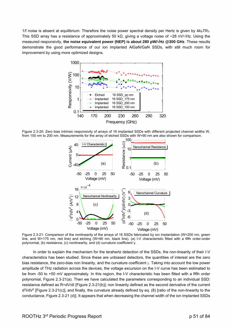
ROOTHz 3rd Periodic Progress Report p 51 of 84
1/f noise is absent at equilibrium. Therefore the noise power spectral density per Hertz is given by 4kBTR0.
This SSD array has a resistance of approximately 50 kΩ, giving a voltage noise of ~28 nV/Hz. Using the
measured responsivity, the noise equivalent power (NEP) is about 280 pW/Hz @300 GHz. These results
demonstrate the good performance of our ion implanted AlGaN/GaN SSDs, with still much room for
improvement by using more optimized designs.
Figure 2.3-20: Zero bias intrinsic responsivity of arrays of 16 implanted SSDs with different projected channel widths W, from 150 nm to 200 nm. Measurements for the array of etched SSDs with W=90 nm are also shown for comparison.
Figure 2.3-21: Comparison of the nonlinearity of the arrays of 16 SSDs fabricated by ion implantation (W=200 nm, green line, and W=175 nm, red line) and etching (W=90 nm, black line). (a) I-V characteristic fitted with a fifth order-order polynomial, (b) resistance, (c) nonlinearity, and (d) curvature coefficient γ.
In order to explain the mechanism for the terahertz detection of the SSDs, the non-linearity of their I-V
characteristics has been studied. Since these are unbiased detectors, the quantities of interest are the zero
bias resistance, the zero-bias non linearity, and the curvature coefficient . Taking into account the low power
amplitude of THz radiation across the devices, the voltage excursion on the I-V curve has been estimated to
be from -50 to +50 mV approximately. In this region, the I-V characteristic has been fitted with a fifth order
polynomial, Figure 2.3-21(a). Then we have calculated the parameters corresponding to an individual SSD:
resistance defined as R=dV/dI [Figure 2.3-21(b)]; non linearity defined as the second derivative of the current
d2I/dV2 [Figure 2.3-21(c)], and finally, the curvature already defined by eq. (8) [ratio of the non-linearity to the
conductance, Figure 2.3-21 (d)]. It appears that when decreasing the channel width of the ion implanted SSDs
140 170 200 230 260 290 3200.1
1
10
100
1000
Etched 16 SSD_75 nm Implanted 16 SSD_175 nm Implanted 16 SSD_200 nm Implanted 16 SSD_150 nm
Re
spon
sivi
ty (
V/W
)
Frequency (GHz)
-50 -25 0 25 50
-40
0
40 I-V Characteristic
Cu
rre
nt (
µA
)
Voltage (mV)-50 -25 0 25 50
0.1
1
10
100
Nanochannel Resistance
Re
sist
ance
(
)
Voltage (mV)
-50 -25 0 25 500
4
8
12
16 ×
Nanochannel Nonlinearity
d2I/d
V2 (
A/V
2)
Voltage (mV)-50 -25 0 25 50
-6
-3
0
3
6
Nanochannel Curvature
(d2I/d
V2)/
(dI/d
V)
(V-1)
Voltage (mV)
(a) (b)
(c)
(d)
90
ROOTHz 3rd Periodic Progress Report p 52 of 84
from W=200 nm to 175 nm, the resistance increases by several orders of magnitude leading to higher values
of the curvature coefficient and therefore to a higher voltage responsivity as observed in Figure 2.3-20. The
parameters for the ion implanted SSD with W=150 nm are not represented as the current level was too small
to fit correctly its I-V curve.
The values given for the responsivity and NEP correspond to the extrinsic ones. In order to have an idea
of the intrinsic ones an electrical model has been developed accounting for the losses of the access line (see
Figure 2.3-22).
Figure 2.3-22: Electrical equivalent circuit of the SSD Figure 2.3-23: Intrinsic responsivity versus frequency of the ISSD with W=175 nm and the etched SSDs with W=75 nm (arrays of 16 channels).
With this model, the intrinsic performances for the arrays of 16 SSDs obtained at 300 GHz (that could
be similar still at higher frequencies due to the flat response shown in Figure 2.3-23) are:
ISSD (W=175 nm, R0~50 k): intrinsic responsivity of 3100 V/W and NEP~9 pW/Hz
Etched SSD (W=75 nm, R0~1.4 k): intrinsic responsivity of 140 V/W and NEP~34 pW/Hz
2.3.3 TASK 3.3: THz CHARACTERIZATION (UNIMAN+CHAL+IEMN)
2.3.3.1 THz characterization of Slot diodes (CHAL+IEMN+UNIMAN))
The initial emission tests using Schottky detectors were performed at IEMN. The scheme of the setup
is shown in Figure 2.3-24(a). The samples were glued to a PCB and a Si lens was placed firmly against the
backside of the substrate. The test procedure starts with the alignment of the sample, the Si lens, the optics
and the detector. Figure 2.3-24(b) shows the alignment of the emission test setup using a Schottky barrier
diode integrated in a waveguide, with an optical chopper that modulates the beam.
Figure 2.3-24: (a) Scheme and (b) picture of the set-up for slot diode emission experiments with a Schottky detector at IEMN. The sample under test was positioned with a Si lens at the backside.
10
100
1000
10000
140 200 260 320
Re
sp
on
siv
ity
(V/W
)
Frequency (GHz)
(a) (b)

ROOTHz 3rd Periodic Progress Report p 53 of 84
Problems could arise if the oscillation frequencies of the slot-diodes tested were above the cutoff of the
Schottky detector (around 900 GHz). For that sake, devices with larger sizes and lower theoretical oscillation
frequencies (both LR=160 nm and 400 nm were tested at different bias in the range 1-1.5 V) have also been
fabricated and characterized. However, no evidence of THz emission from the slot diodes was obtained. The
power detection floor of our setup has been estimated knowing that the noise at the output of the Schottky
detector is around 0.5 µV and its responsivity at 900 GHz is 10 V/W. Therefore, the noise floor of the setup
is about 50 nW. As a consequence, if an oscillation occurs in the slot diode, the power emitted is less than that
value (which does not seem to be the case).
It has been realised that the impedance mismatch between the SSDs and RF test equipment such as
VNA and Spectrum Analyser might have prevented successful observation of emission from the fabricated
devices. In order to improve the sentitivity and increase the cutoff frequency of the setup, new experiments
wer performed by UNIMAN (performed in laboratories of the University of Manchester and also in the University
of Leeds for confirmation). The setup is shown in Figure 2.3-25. In this case the detector was a liquid-helium
cooled composite silicon bolometer made by QMC. The bolometer is behind a 600 cm-1 low-pass blocking
filter, corresponding to a cut off frequency of about 3 THz. The optimum responsivity of the bolometer from the
specifications is 10,000 mV/mW. With a black-body radiation source, the estimated responsivity in the lab
environment was measured to be about 800 mV/mW. The experiments were carried out using two different
biases and chopping schemes. In one setup, the devices were biased by a pulse generator and the pulse
signal was also sent to the lock-in as the reference. In the other setup, the DC and AC signal were combined
using an op-amp before being applied to the devices. The AC signal was used as the lock-in reference. The
lock-in showed the output of the bolometer having a fluctuation from 1V to 15 V, which corresponded to a
noise floor as referenced to emitted power of about 1.3 to 18 nW. Unfortunately, in spite of a better sensitivity
and broadband of the setup, no indication of THz emission from SSDs and slot diodes was observed above
the noise floor.
Figure 2.3-25: Bolometer-based measurement system used for detecting emission from slot diodes.
ROOTHz 3rd Periodic Progress Report p 54 of 84
Even if ROOTHz is specifically focused on room temperature THz emission and detection, Monte Carlo
simulations show that the operation of slot diodes as THz emitters benefits from cooling the devices as shown
in Figure 2.3-26 (a 10x factor is obtained when cooling from 300 to 77K). Our colleagues from the U. of
Montpellier have the possibility of performing THz emission experiments at low temperature, but the setup has
to be adjusted to fit our sample holder. Also, we are in contact with another group in Chalmers University that
will try to perform such experiments depending on the availability of their setup. The few devices that are still
alive will be then characterized at low temperature where the possibilities of finding Gunn-like oscillations are
enhanced.
Figure 2.3-26: Oscillation frequencies of a slot-diode with LS=200 nm, LR=160 nm and LD=550 nm obtained with Monte Carlo simulations at different temperatures. The size of the bubble is proportional to the amplitude of the oscillations.
2.3.3.2 THz characterization of InAs and InGaAs SSDs (CHAL+IEMN)
To investigate if the SSDs could function as a detector at 600 GHz, a free-space setup was used, shown
in Figure 2.3-27. A measurement at 200 GHz was conducted in a similar way, in order to compare the results
with the on-wafer measurements shown before. The detector consisted of an array of 11 InAs SSDs with
W=65 nm integrated with a circularly polarized spiral substrate antenna, whose characteristics are detailed on
the Milestone 8 report corresponding to the antenna design. A silicon lens was placed firmly against the
backside of the substrate with the SSDs. The output voltage was measured with a lock-in amplifier, thus
presenting a high DC-load.
Figure 2.3-27: The setup used for free-space measurements at 200 and 600 GHz.
On the emitter side, the vertically polarized beam was radiated through a conical horn antenna. By
replacing our detector with an Erickson PM4 power meter with a horn antenna, the incident power was
measured. At 200 GHz and 600 GHz the average power was 1.15 mW and 7 W, respectively. From the
Applied voltage (V)
0.6 0.8 1.0 1.2 1.4 1.6
f osc
(T
Hz)
0.6
0.8
1.0
1.2
1.4
1.6
1.8
2.077K
150K
300K
500K
ROOTHz 3rd Periodic Progress Report p 55 of 84
curvature of the I-V curve a value of Sint=53 V/W was expected. The extrinsic responsivity of the detector at
200 GHz and 600 GHz was found to be 2.1 V/W and 0.70 V/W, respectively. Compensating for polarization
mismatch (≈50%) and the mismatch between R0 (about 700 ) and the antenna radiation resistance (≈50 %),
Sint is calculated to 8.4 V/W and 2.8 V/W at 200 and 600 GHz, respectively.
In the on-wafer RF measurements, measured Sint matches the one calculated from I-V measurements,
see Figure 2.3-11. The discrepancy between the Sint measured in the free-space setup at 200 GHz and the
Sint calculated from I-V measurements may be due to other losses that were not accounted for, mainly the fact
that not all incident THz power is coupled into the antenna. We can globally account for all that losses by
means of an additional extrinsic parameter, which is the efficiency of the antenna (together with the Si lens)
which in our case would be of about 16% @200 GHz.
In any case, these measurements confirmed that InAs SSDs can function as detectors up to 600 GHz,
with a responsivity of the same order of magnitude as for 200 GHz (since the efficiency of the antenna could
be even lower). This find motivates further investigation of detection with InAs SSDs at 600 GHz and higher
frequencies. These free space measurements both @200 GHz and @600 GHz were repeated using an InGaAs SSD
array with N=3 and W=80 nm. The extrinsic responsivity obtained was as low as 3.0 V/W @200 GHz (even if
the intrinsic value is much higher) due the strong mismatch between antenna and SSD. This fact, together
with a low efficiency of the antenna and the lower power of the source @600GHz did not allow to obtain any
result at that frequency. These free-space measurements were performed at IEMN with the help of A. Westlund
(CHAL) that realized 2 campaigns of intensive measurements (one week each) at IEMN.
Sub-THz imaging with InAs SSDs (IEMN)
With the same InAs SSD used for free-space detection (N=11, W=65 nm), the imaging setup in Figure
2.3-28 was used to demonstrate the capability of our SSDs to be used for THz imaging. The beam was focused
on the RFID card shown in Figure 2.3-26(a), having a polymer part, and a metallic printed antenna/chip inside.
The card was moved in a grid pattern and the output voltage Vdet in the SSD was recorded for every point.
Figure 2.3-28: Setup used for imaging at 200 GHz with an InAs SSD. Spherical mirrors were used to focus the beam.
In these setup, the injected power is around 2 mW at 200 GHz and 20 µW at 600 GHz. At 200 GHz, the
signal to noise ratio at the lock-in amplifier was sufficient (> 1000) to produce an usable image, but at 600 GHz
the devices were not sufficiently sensitive. Thus, the THz acquired images were limited at 200 GHz. Plotting
the signal strength versus position resulted in the image shown in Figure 2.3-26. The plastics of the card is
transparent to the radiation and thus imaged bright, while the metal antenna and microchip are reflective and
imaged dark.
ROOTHz 3rd Periodic Progress Report p 56 of 84
Figure 2.3-26: Views of the imaging setup developed at IEMN to test the ROOTHz detectors. Left: emission side; and right: reception side. Below: RFID card and its image when irradiated by 200 GHz waves and detected by the InAs SSD.
THz
D.U.T.
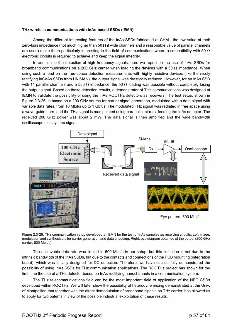
ROOTHz 3rd Periodic Progress Report p 57 of 84
THz wireless communications with InAs-based SSDs (IEMN)
Among the different interesting features of the InAs SSDs fabricated at CHAL, the low value of their
zero-bias impedance (not much higher than 50 if wide channels and a reasonable value of parallel channels
are used) make them particularly interesting in the field of communications where a compatibility with 50
electronic circuits is required to achieve and keep the signal integrity.
In addition to the detection of high frequency signals, here we report on the use of InAs SSDs for
broadband communications on a 200 GHz carrier when loading the devices with a 50 impedance. When
using such a load on the free-space detection measurements with highly resistive devices (like the nicely
rectifying InGaAs SSDs from UNIMAN), the output signal was drastically reduced. However, for an InAs SSD
with 11 parallel channels and a 580 impedance, the 50 loading was possible without completely losing
the output signal. Based on these detection results, a demonstrator of THz communications was designed at
IEMN to validate the possibility of using the InAs ROOTHz detectors as receivers. The test setup, shown in
Figure 2.3-26, is based on a 200 GHz source for carrier signal generation, modulated with a data signal with
variable data rates, from 10 Mbit/s up to 1 Gbit/s. The modulated THz signal was radiated in free space using
a wave-guide horn, and the THz signal is manipulated using parabolic mirrors, feeding the InAs detector. The
received 200 GHz power was about 2 mW. The data signal is then amplified and the wide bandwidth
oscilloscope displays the signal.
Figure 2.3-26: THz communication setup developed at IEMN for the test of InAs samples as receiving circuits. Left image: modulation and synthesizers for carrier generation and data encoding. Right: eye diagram obtained at the output (200 GHz carrier, 500 Mbit/s).
The achievable data rate was limited to 500 Mbit/s in our setup, but this limitation is not due to the
intrinsic bandwidth of the InAs SSDs, but due to the contacts and connections of the PCB mounting (integration
board), which was initially designed for DC detection. Therefore, we have successfully demonstrated the
possibility of using InAs SSDs for THz communication applications. The ROOTHz project has shown for the
first time the use of a THz detector based on InAs rectifying nanochannels in a communication system.
The THz telecommunications field can be the most important field of application of the NBG SSDs
developed within ROOTHz. We will later show the possibility of heterodyne mixing demonstrated at the Univ.
of Montpellier, that together with the direct demodulation of broadband signals on THz carrier, has allowed us
to apply for two patents in view of the possible industrial exploitation of these results.
Si-lens
Dx
Data signal
Oscilloscope
Eye pattern, 500 Mbit/s
Received data signal
50 dB
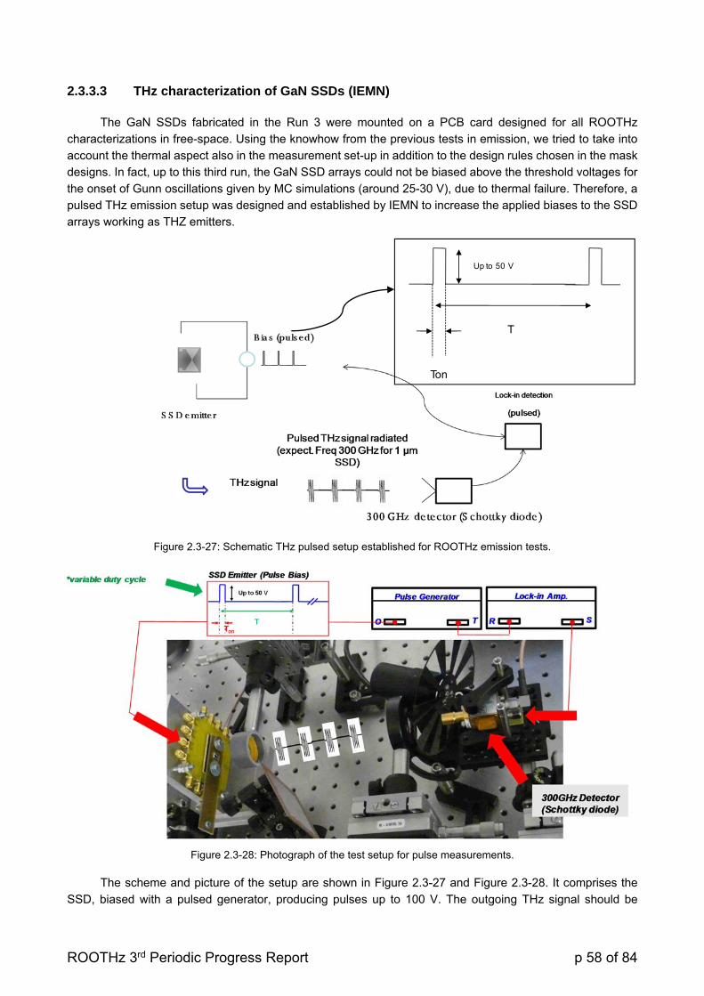
ROOTHz 3rd Periodic Progress Report p 58 of 84
2.3.3.3 THz characterization of GaN SSDs (IEMN)
The GaN SSDs fabricated in the Run 3 were mounted on a PCB card designed for all ROOTHz
characterizations in free-space. Using the knowhow from the previous tests in emission, we tried to take into
account the thermal aspect also in the measurement set-up in addition to the design rules chosen in the mask
designs. In fact, up to this third run, the GaN SSD arrays could not be biased above the threshold voltages for
the onset of Gunn oscillations given by MC simulations (around 25-30 V), due to thermal failure. Therefore, a
pulsed THz emission setup was designed and established by IEMN to increase the applied biases to the SSD
arrays working as THZ emitters.
Figure 2.3-27: Schematic THz pulsed setup established for ROOTHz emission tests.
Figure 2.3-28: Photograph of the test setup for pulse measurements.
The scheme and picture of the setup are shown in Figure 2.3-27 and Figure 2.3-28. It comprises the
SSD, biased with a pulsed generator, producing pulses up to 100 V. The outgoing THz signal should be
T
Ton
Up to 50 V
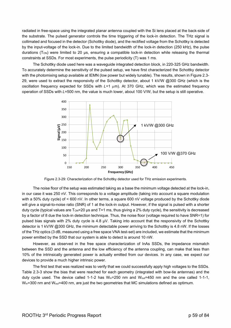
ROOTHz 3rd Periodic Progress Report p 59 of 84
radiated in free-space using the integrated planar antenna coupled with the Si lens placed at the back-side of
the substrate. The pulsed generator controls the time triggering of the lock-in detection. The THz signal is
collimated and focused in the detector (Schottky diode), and the rectified voltage from the Schottky is detected
by the input-voltage of the lock-in. Due to the limited bandwidth of the lock-in detection (250 kHz), the pulse
durations (TON) were limited to 20 µs, ensuring a compatible lock-in detection while releasing the thermal
constraints at SSDs. For most experiments, the pulse periodicity (T) was 1 ms.
The Schottky diode used here was a waveguide integrated detection block, in 220-325 GHz bandwidth.
To accurately determine the sensitivity of the pulsed setup, we have first characterized the Schottky detector
with the photomixing setup available at IEMN (low power but widely tunable). The results, shown in Figure 2.3-
29, were used to extract the responsivity of the Schottky detector, about 1 kV/W @300 GHz (which is the
oscillation frequency expected for SSDs with L=1 m). At 370 GHz, which was the estimated frequency
operation of SSDs with L=500 nm, the value is much lower, about 100 V/W, but the setup is still operative.
Figure 2.3-29: Characterization of the Schottky detector used for THz emission experiments.
The noise floor of the setup was estimated taking as a base the minimum voltage detected at the lock-in,
in our case it was 250 nV. This corresponds to a voltage amplitude (taking into account a square modulation
with a 50% duty cycle) of < 600 nV. In other terms, a square 600 nV voltage produced by the Schottky diode
will give a signal-to-noise ratio (SNR) of 1 at the lock-in output. However, if the signal is pulsed with a shorter
duty cycle (typical values are TON=20 µs and T=1 ms, thus giving a 2% duty cycle), the sensitivity is decreased
by a factor of 8 due the lock-in detection technique. Thus, the noise floor (voltage required to have SNR=1) for
pulsed bias signals with 2% duty cycle is 4.8 µV. Taking into account that the responsivity of the Schottky
detector is 1 kV/W @300 GHz, the minimum detectable power arriving to the Schottky is 4.8 nW. If the losses
of the THz optics (3 dB, measured using a free space VNA test-set) are included, we estimate that the minimum
power emitted by the SSD that our system is able to detect is around 10 nW.
However, as observed in the free space characterization of InAs SSDs, the impedance mismatch
between the SSD and the antenna and the low efficiency of the antenna coupling, can make that less than
10% of the intrinsically generated power is actually emitted from our devices. In any case, we expect our
devices to provide a much higher intrinsic power.
The first test that was realized was to verify that we could successfully apply high voltages to the SSDs.
Table 2.3-3 show the bias that were reached for each geometry (integrated with bow-tie antennas) and the
duty cycle used. The device called 1-1-2 has Win=250 nm and Wout=450 nm and the one called 1-1-1,
Win=300 nm and Wout=400 nm, are just the two geometries that MC simulations defined as optimum.
0
50
100
150
200
250
300
350
400
150 200 250 300 350 400 450
Sign
al (µV)
Frequency (GHz)
1 kV/W @300 GHz
100 V/W @370 GHz
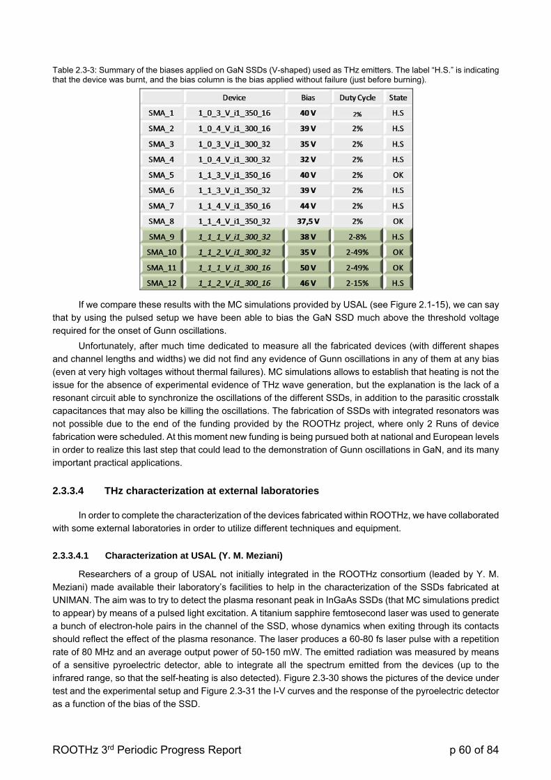
ROOTHz 3rd Periodic Progress Report p 60 of 84
Table 2.3-3: Summary of the biases applied on GaN SSDs (V-shaped) used as THz emitters. The label “H.S.” is indicating that the device was burnt, and the bias column is the bias applied without failure (just before burning).
If we compare these results with the MC simulations provided by USAL (see Figure 2.1-15), we can say
that by using the pulsed setup we have been able to bias the GaN SSD much above the threshold voltage
required for the onset of Gunn oscillations.
Unfortunately, after much time dedicated to measure all the fabricated devices (with different shapes
and channel lengths and widths) we did not find any evidence of Gunn oscillations in any of them at any bias
(even at very high voltages without thermal failures). MC simulations allows to establish that heating is not the
issue for the absence of experimental evidence of THz wave generation, but the explanation is the lack of a
resonant circuit able to synchronize the oscillations of the different SSDs, in addition to the parasitic crosstalk
capacitances that may also be killing the oscillations. The fabrication of SSDs with integrated resonators was
not possible due to the end of the funding provided by the ROOTHz project, where only 2 Runs of device
fabrication were scheduled. At this moment new funding is being pursued both at national and European levels
in order to realize this last step that could lead to the demonstration of Gunn oscillations in GaN, and its many
important practical applications.
2.3.3.4 THz characterization at external laboratories
In order to complete the characterization of the devices fabricated within ROOTHz, we have collaborated
with some external laboratories in order to utilize different techniques and equipment.
2.3.3.4.1 Characterization at USAL (Y. M. Meziani)
Researchers of a group of USAL not initially integrated in the ROOTHz consortium (leaded by Y. M.
Meziani) made available their laboratory’s facilities to help in the characterization of the SSDs fabricated at
UNIMAN. The aim was to try to detect the plasma resonant peak in InGaAs SSDs (that MC simulations predict
to appear) by means of a pulsed light excitation. A titanium sapphire femtosecond laser was used to generate
a bunch of electron-hole pairs in the channel of the SSD, whose dynamics when exiting through its contacts
should reflect the effect of the plasma resonance. The laser produces a 60-80 fs laser pulse with a repetition
rate of 80 MHz and an average output power of 50-150 mW. The emitted radiation was measured by means
of a sensitive pyroelectric detector, able to integrate all the spectrum emitted from the devices (up to the
infrared range, so that the self-heating is also detected). Figure 2.3-30 shows the pictures of the device under
test and the experimental setup and Figure 2.3-31 the I-V curves and the response of the pyroelectric detector
as a function of the bias of the SSD.

ROOTHz 3rd Periodic Progress Report p 61 of 84
Figure 2.3-30: (a) AFM image of the InGaAs SSD fabricated at UNIMAN and (b) picture of the PCB mounting of the device with its integrated bow-tie antenna. Experimental setup of photoresponse measurements at USAL.
Bias (mV)-40 -20 0 20 40
Lock
in (V
)
-10
-5
0
5
10
15
20
25
32mW
15mW
Figure 2.3-31: (a) I-V curves and (b), (c) response of the pyroelectric detector as a function of the bias applied to the SSD for different values of the power of the fs-laser excitation.
The first interesting result is that the SSD shows a notable level of photoresponse; the I-V curves strongly
depend on the illumination level. On the other hand, even if the initial measurements, Figure 2.3-31(c), showed
a repeatable peak around a bias of about 5 mV (that could be related to some excitonic response), the
pyroelectric detector did not show that interesting feature when the laser emission was better stabilized.
Nevertheless, even if the plasma emission could not be demonstrated, the possible application of the SSDs
as fast photodetectors motivated the measurements realized later on at the Univ. of Rochester.
(a) (b) (c)
(a) (b)
(c)
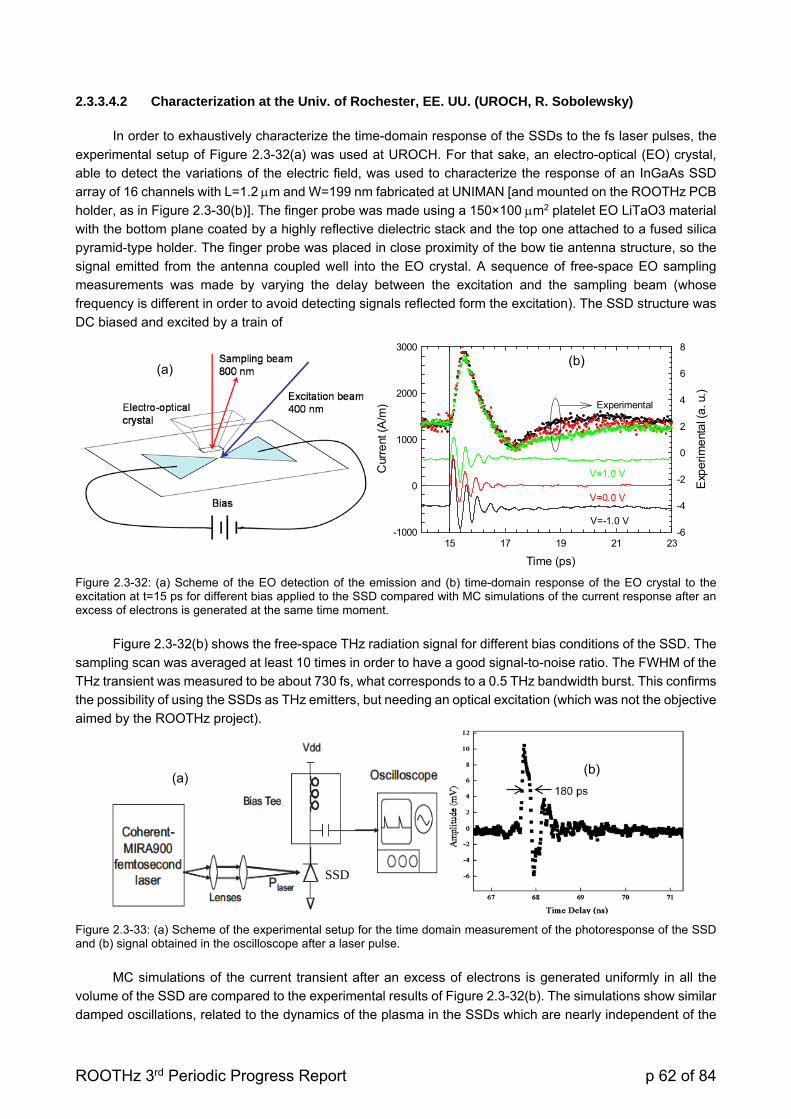
ROOTHz 3rd Periodic Progress Report p 62 of 84
2.3.3.4.2 Characterization at the Univ. of Rochester, EE. UU. (UROCH, R. Sobolewsky)
In order to exhaustively characterize the time-domain response of the SSDs to the fs laser pulses, the
experimental setup of Figure 2.3-32(a) was used at UROCH. For that sake, an electro-optical (EO) crystal,
able to detect the variations of the electric field, was used to characterize the response of an InGaAs SSD
array of 16 channels with L=1.2 m and W=199 nm fabricated at UNIMAN [and mounted on the ROOTHz PCB
holder, as in Figure 2.3-30(b)]. The finger probe was made using a 150×100 m2 platelet EO LiTaO3 material
with the bottom plane coated by a highly reflective dielectric stack and the top one attached to a fused silica
pyramid-type holder. The finger probe was placed in close proximity of the bow tie antenna structure, so the
signal emitted from the antenna coupled well into the EO crystal. A sequence of free-space EO sampling
measurements was made by varying the delay between the excitation and the sampling beam (whose
frequency is different in order to avoid detecting signals reflected form the excitation). The SSD structure was
DC biased and excited by a train of ~150-fs-wide, 400-nm-wavelength pulses.
Time (ps)
15 17 19 21 23
Cur
rent
(A
/m)
-1000
0
1000
2000
3000
Exp
eri
me
nta
l (a.
u.)
-6
-4
-2
0
2
4
6
8
Experimental
V=1.0 V
V=-1.0 V
V=0.0 V
Figure 2.3-32: (a) Scheme of the EO detection of the emission and (b) time-domain response of the EO crystal to the excitation at t=15 ps for different bias applied to the SSD compared with MC simulations of the current response after an excess of electrons is generated at the same time moment.
Figure 2.3-32(b) shows the free-space THz radiation signal for different bias conditions of the SSD. The
sampling scan was averaged at least 10 times in order to have a good signal-to-noise ratio. The FWHM of the
THz transient was measured to be about 730 fs, what corresponds to a 0.5 THz bandwidth burst. This confirms
the possibility of using the SSDs as THz emitters, but needing an optical excitation (which was not the objective
aimed by the ROOTHz project).
Figure 2.3-33: (a) Scheme of the experimental setup for the time domain measurement of the photoresponse of the SSD and (b) signal obtained in the oscilloscope after a laser pulse.
MC simulations of the current transient after an excess of electrons is generated uniformly in all the
volume of the SSD are compared to the experimental results of Figure 2.3-32(b). The simulations show similar
damped oscillations, related to the dynamics of the plasma in the SSDs which are nearly independent of the
SSD
(a) (b)
(a) (b)
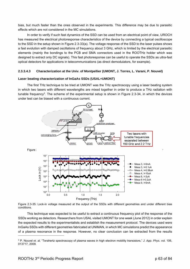
ROOTHz 3rd Periodic Progress Report p 63 of 84
bias, but much faster than the ones observed in the experiments. This difference may be due to parasitic
effects which are not considered in the MC simulations.
In order to verify if such fast dynamics of the SSD can be used from an electrical point of view, UROCH
has measured the electrical photoresponse characteristics of the device by connecting a typical oscilloscope
to the SSD in the setup shown in Figure 2.3-33(a). The voltage response of the SSD to the laser pulses shows
a fast evolution with damped oscillations of frequency about 3 GHz, which is limited by the electrical parasitic
elements (mainly the bondings to the PCB and SMA connectors used in the ROOTHz holder which was
designed to extract only DC signals). This fast photoresponse can be useful to operate the SSDs as ultra-fast
optical detectors for applications in telecommunications (as direct demodulators, for example).
2.3.3.4.3 Characterization at the Univ. of Montpellier (UMONT, J. Torres, L. Varani, P. Nouvel)
Laser beating characterization of InGaAs SSDs (USAL+UMONT)
The first THz technique to be tried at UMONT was the THz spectroscopy using a laser beating system
in which two lasers with different wavelengths are mixed together in order to produce a THz radiation with
tunable frequency3. The scheme of the experimental setup is shown in Figure 2.3-34, in which the devices
under test can be biased with a continuous current.
Figure 2.3-34: Experimental configuration for the THz spectroscopy of InGaAs SSDs at Univ. of Montpellier
Frequency (THz)0.0 0.5 1.0 1.5 2.0
Lo
ck in
(V
)
10-8
10-7
10-6
10-5
10-4
10-3
10-2
10-1
Mesa 3, I=0mA Mesa 3, I=0.1uA Mesa 4, I=0.58uA Mesa 4, I=10uA Mesa 8, I=2uA Mesa 6 I=0.2uA Mesa 9, I=0mA
Figure 2.3-35: Lock-in voltage measured at the output of the SSDs with different geometries and under different bias conditions.
This technique was expected to be useful to extract a continuous frequency plot of the response of the
SSDs working as detectors. Researchers from USAL visited UMONT for one week (June 2012) in order explain
the expected results to the experimentalists and establish the measurement protocol. The devices used were
InGaAs SSDs with different geometries fabricated at UNIMAN, in which MC simulations predict the appearance
of a plasma resonance in the response. However, no clear conclusion can be extracted from the results 3 P. Nouvel et. al, “Terahertz spectroscopy of plasma waves in high electron mobility transistors,” J. App. Phys. vol. 106, 013717, 2009.
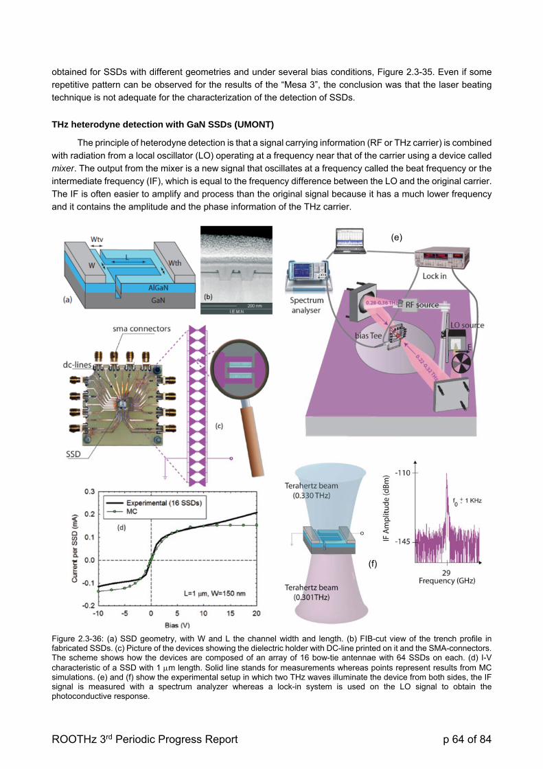
ROOTHz 3rd Periodic Progress Report p 64 of 84
obtained for SSDs with different geometries and under several bias conditions, Figure 2.3-35. Even if some
repetitive pattern can be observed for the results of the “Mesa 3”, the conclusion was that the laser beating
technique is not adequate for the characterization of the detection of SSDs.
THz heterodyne detection with GaN SSDs (UMONT)
The principle of heterodyne detection is that a signal carrying information (RF or THz carrier) is combined
with radiation from a local oscillator (LO) operating at a frequency near that of the carrier using a device called
mixer. The output from the mixer is a new signal that oscillates at a frequency called the beat frequency or the
intermediate frequency (IF), which is equal to the frequency difference between the LO and the original carrier.
The IF is often easier to amplify and process than the original signal because it has a much lower frequency
and it contains the amplitude and the phase information of the THz carrier.
Figure 2.3-36: (a) SSD geometry, with W and L the channel width and length. (b) FIB-cut view of the trench profile in fabricated SSDs. (c) Picture of the devices showing the dielectric holder with DC-line printed on it and the SMA-connectors. The scheme shows how the devices are composed of an array of 16 bow-tie antennae with 64 SSDs on each. (d) I-V characteristic of a SSD with 1 m length. Solid line stands for measurements whereas points represent results from MC simulations. (e) and (f) show the experimental setup in which two THz waves illuminate the device from both sides, the IF signal is measured with a spectrum analyzer whereas a lock-in system is used on the LO signal to obtain the photoconductive response.
(e)
(f)
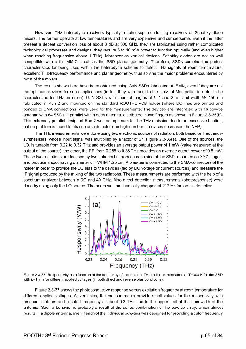
ROOTHz 3rd Periodic Progress Report p 65 of 84
However, THz heterodyne receivers typically require superconducting receivers or Schottky diode
mixers. The former operate at low temperatures and are very expensive and cumbersome. Even if the latter
present a decent conversion loss of about 8 dB at 300 GHz, they are fabricated using rather complicated
technological processes and designs, they require 5 to 10 mW power to function optimally (and even higher
when reaching frequencies above 1 THz). Moreover as vertical devices, Schottky diodes are not as well
compatible with a full MMIC circuit as the SSD planar geometry. Therefore, SSDs combine the perfect
characteristics for being used within the heterodyne scheme to detect THz signals at room temperature:
excellent THz-frequency performance and planar geometry, thus solving the major problems encountered by
most of the mixers.
The results shown here have been obtained using GaN SSDs fabricated at IEMN, even if they are not
the optimum devices for such applications (in fact they were sent to the Univ. of Montpellier in order to be
characterized for THz emission). GaN SSDs with channel lengths of L=1 and 2 m and width W=150 nm
fabricated in Run 2 and mounted on the standard ROOTHz PCB holder (where DC-lines are printed and
bonded to SMA connections) were used for the measurements. The devices are integrated with 16 bow-tie
antenna with 64 SSDs in parallel within each antenna, distributed in two fingers as shown in Figure 2.3-36(b).
This extremely parallel design of Run 2 was not optimum for the THz emission due to an excessive heating,
but no problem is found for its use as a detector (the high number of devices decreased the NEP).
The THz measurements were done using two electronic sources of radiation, both based on frequency-
synthesizers, whose input signal was multiplied by a factor of 27, Figure 2.3-36(e). One of the sources, the
LO, is tunable from 0.22 to 0.32 THz and provides an average output power of 1 mW (value measured at the
output of the source), the other, the RF, from 0.285 to 0.36 THz provides an average output power of 0.8 mW.
These two radiations are focused by two spherical mirrors on each side of the SSD, mounted on XYZ-stages,
and produce a spot having diameter of FWHM 1.25 cm. A bias-tee is connected to the SMA-connectors of the
holder in order to provide the DC bias to the devices (fed by DC voltage or current sources) and measure the
IF signal produced by the mixing of the two radiations. These measurements are performed with the help of a
spectrum analyzer between ≈ DC and 40 GHz. Also direct detection measurements (photoresponse) were
done by using only the LO source. The beam was mechanically chopped at 217 Hz for lock-in detection.
Figure 2.3-37: Responsivity as a function of the frequency of the incident THz radiation measured at T=300 K for the SSD with L=1 m for different applied voltages (in both direct and reverse bias conditions).
Figure 2.3-37 shows the photoconductive response versus excitation frequency at room temperature for
different applied voltages. At zero bias, the measurements provide small values for the responsivity with
resonant features and a cutoff frequency at about 0.3 THz due to the upper-limit of the bandwidth of the
antenna. Such a behavior is probably a result of the series combination of the bow-tie array, which almost
results in a dipole antenna, even if each of the individual bow-ties was designed for providing a cutoff frequency
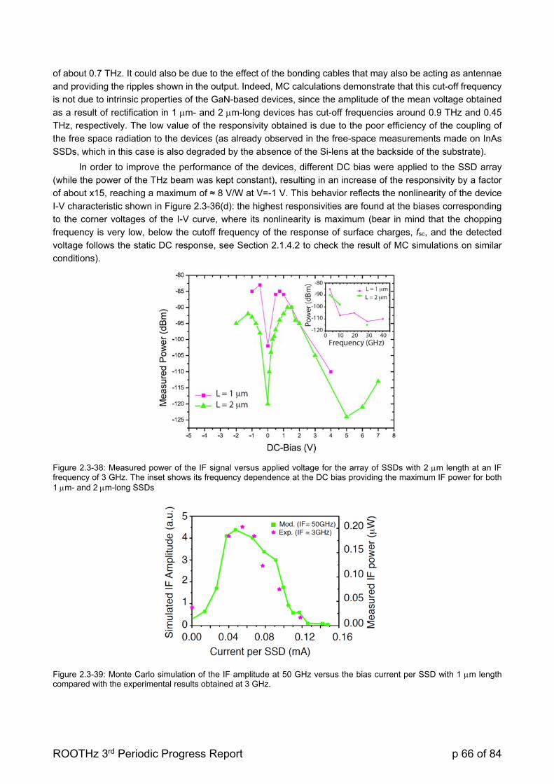
ROOTHz 3rd Periodic Progress Report p 66 of 84
of about 0.7 THz. It could also be due to the effect of the bonding cables that may also be acting as antennae
and providing the ripples shown in the output. Indeed, MC calculations demonstrate that this cut-off frequency
is not due to intrinsic properties of the GaN-based devices, since the amplitude of the mean voltage obtained
as a result of rectification in 1 m- and 2 m-long devices has cut-off frequencies around 0.9 THz and 0.45
THz, respectively. The low value of the responsivity obtained is due to the poor efficiency of the coupling of
the free space radiation to the devices (as already observed in the free-space measurements made on InAs
SSDs, which in this case is also degraded by the absence of the Si-lens at the backside of the substrate).
In order to improve the performance of the devices, different DC bias were applied to the SSD array
(while the power of the THz beam was kept constant), resulting in an increase of the responsivity by a factor
of about x15, reaching a maximum of ≈ 8 V/W at V=-1 V. This behavior reflects the nonlinearity of the device
I-V characteristic shown in Figure 2.3-36(d): the highest responsivities are found at the biases corresponding
to the corner voltages of the I-V curve, where its nonlinearity is maximum (bear in mind that the chopping
frequency is very low, below the cutoff frequency of the response of surface charges, fsc, and the detected
voltage follows the static DC response, see Section 2.1.4.2 to check the result of MC simulations on similar
conditions).
Figure 2.3-38: Measured power of the IF signal versus applied voltage for the array of SSDs with 2 m length at an IF frequency of 3 GHz. The inset shows its frequency dependence at the DC bias providing the maximum IF power for both 1 m- and 2 m-long SSDs
Figure 2.3-39: Monte Carlo simulation of the IF amplitude at 50 GHz versus the bias current per SSD with 1 m length compared with the experimental results obtained at 3 GHz.
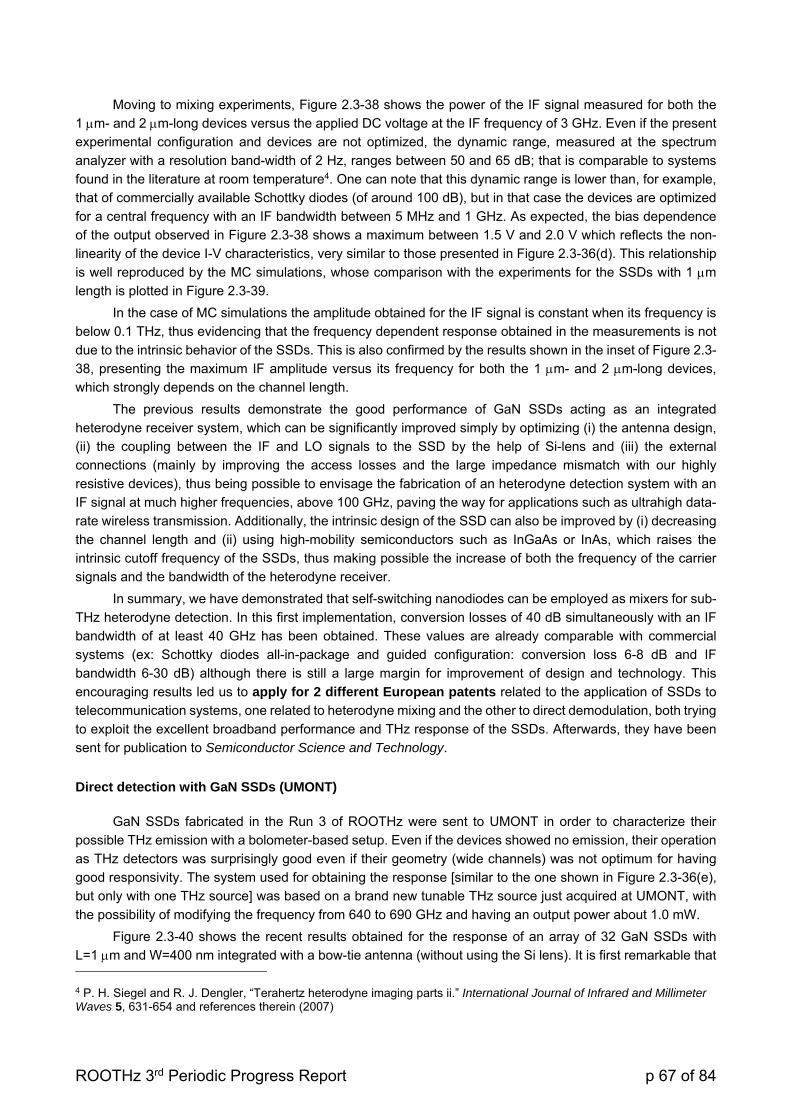
ROOTHz 3rd Periodic Progress Report p 67 of 84
Moving to mixing experiments, Figure 2.3-38 shows the power of the IF signal measured for both the
1 m- and 2 m-long devices versus the applied DC voltage at the IF frequency of 3 GHz. Even if the present
experimental configuration and devices are not optimized, the dynamic range, measured at the spectrum
analyzer with a resolution band-width of 2 Hz, ranges between 50 and 65 dB; that is comparable to systems
found in the literature at room temperature4. One can note that this dynamic range is lower than, for example,
that of commercially available Schottky diodes (of around 100 dB), but in that case the devices are optimized
for a central frequency with an IF bandwidth between 5 MHz and 1 GHz. As expected, the bias dependence
of the output observed in Figure 2.3-38 shows a maximum between 1.5 V and 2.0 V which reflects the non-
linearity of the device I-V characteristics, very similar to those presented in Figure 2.3-36(d). This relationship
is well reproduced by the MC simulations, whose comparison with the experiments for the SSDs with 1 m
length is plotted in Figure 2.3-39.
In the case of MC simulations the amplitude obtained for the IF signal is constant when its frequency is
below 0.1 THz, thus evidencing that the frequency dependent response obtained in the measurements is not
due to the intrinsic behavior of the SSDs. This is also confirmed by the results shown in the inset of Figure 2.3-
38, presenting the maximum IF amplitude versus its frequency for both the 1 m- and 2 m-long devices,
which strongly depends on the channel length.
The previous results demonstrate the good performance of GaN SSDs acting as an integrated
heterodyne receiver system, which can be significantly improved simply by optimizing (i) the antenna design,
(ii) the coupling between the IF and LO signals to the SSD by the help of Si-lens and (iii) the external
connections (mainly by improving the access losses and the large impedance mismatch with our highly
resistive devices), thus being possible to envisage the fabrication of an heterodyne detection system with an
IF signal at much higher frequencies, above 100 GHz, paving the way for applications such as ultrahigh data-
rate wireless transmission. Additionally, the intrinsic design of the SSD can also be improved by (i) decreasing
the channel length and (ii) using high-mobility semiconductors such as InGaAs or InAs, which raises the
intrinsic cutoff frequency of the SSDs, thus making possible the increase of both the frequency of the carrier
signals and the bandwidth of the heterodyne receiver.
In summary, we have demonstrated that self-switching nanodiodes can be employed as mixers for sub-
THz heterodyne detection. In this first implementation, conversion losses of 40 dB simultaneously with an IF
bandwidth of at least 40 GHz has been obtained. These values are already comparable with commercial
systems (ex: Schottky diodes all-in-package and guided configuration: conversion loss 6-8 dB and IF
bandwidth 6-30 dB) although there is still a large margin for improvement of design and technology. This
encouraging results led us to apply for 2 different European patents related to the application of SSDs to
telecommunication systems, one related to heterodyne mixing and the other to direct demodulation, both trying
to exploit the excellent broadband performance and THz response of the SSDs. Afterwards, they have been
sent for publication to Semiconductor Science and Technology.
Direct detection with GaN SSDs (UMONT)
GaN SSDs fabricated in the Run 3 of ROOTHz were sent to UMONT in order to characterize their
possible THz emission with a bolometer-based setup. Even if the devices showed no emission, their operation
as THz detectors was surprisingly good even if their geometry (wide channels) was not optimum for having
good responsivity. The system used for obtaining the response [similar to the one shown in Figure 2.3-36(e),
but only with one THz source] was based on a brand new tunable THz source just acquired at UMONT, with
the possibility of modifying the frequency from 640 to 690 GHz and having an output power about 1.0 mW.
Figure 2.3-40 shows the recent results obtained for the response of an array of 32 GaN SSDs with
L=1 m and W=400 nm integrated with a bow-tie antenna (without using the Si lens). It is first remarkable that 4 P. H. Siegel and R. J. Dengler, “Terahertz heterodyne imaging parts ii.” International Journal of Infrared and Millimeter Waves 5, 631-654 and references therein (2007)

ROOTHz 3rd Periodic Progress Report p 68 of 84
GaN SSDs with a non-optimized geometry are able to detect signals of 670 GHz with a responsivity strongly
increased when biasing the devices (a huge factor of almost x50 with respect to the unbiased device, reaching
about 1.5 V/W). Another interesting aspect of the results is that, instead of a more or less severe frequency
roll down (as expected from MC simulations, see for example the results of Figure 2.3-19, in a similar GaN
SSD with narrower channel), a resonant peak around 670 GHz is observed. This peak can be an extension of
the ripples already observed in Figure 2.3-37 that we attribute to the influence of the bonding cables since the
bow-tie antenna should have a flat response. These resonances may explain the absence of response in the
measurements made at IEMN at a fixed frequency of 600 GHz.
Figure 2.3-40: DC response vs. frequency measured from an array of 32 SSDs with L=1 m and W=400 nm for different bias voltages. The inset shows the result for the unbiased device.
Measurements of implanted GaN, InGaAs and InAs SSDs, more adequate to the operation as THz
detectors, will be performed and compared to these initial results.
2.3.4 WP3 SUMMARY
The deliverable corresponding to WP3 in this period was D3.3 (Report on characterization of Run 2
nanodevices and emitter/detector system), which coincides with the results included in this scientific report for
the 3rd review period. Regarding the characterization of discrete devices, no significant deviation from the
scheduled workplan has appeared, however, the emitter/detector system has not been produced (and hence
its characterization is absent). In spite of the lack of evidence of THz emission from the fabricated devices, an
extensive characterization work has been performed within this 3rd review period, in the partners’ laboratories
and also in collaborating Universities, using different techniques and conditions:
NBG SSDs
DC-characterization if InAs SSDs was performed in which a relatively small nonlinearity was observed.
Upon cooling to 6 K, this nonlinearity increased compared to at 300 K, increasing Sint tenfold.
InAs and InGaAs SSDs were characterized as room-temperature detectors on-wafer in the range 2-315
GHz, in which no strong roll-off of responsivity was observed. A comparison of different designs were made at
50 GHz. It was shown that for the range of designs tested, NEPext benefits from larger L and smaller W. For

ROOTHz 3rd Periodic Progress Report p 69 of 84
InAs SSDs, larger N will not reduce NEPext significantly. For InGaAs, larger N may lower NEPext since in this
case the resistance of the individual SSDs is much larger.
For InAs SSDs, measured at 50 GHz, the highest Sext and lowest NEPext observed were 17 V/W and
150 pW/Hz, respectively. For the same device, R0 was 350 , making the mismatch fairly low. With a
conjugate match, 34 V/W and 70 pW/Hz is expected. As compared to InAs SSDs, InGaAs SSDs are more
resistive and suffer from a larger mismatch, but also have a larger and thus Sint. The lowest NEPext observed
at 50 GHz when measured with a 50 source was 60 pW/Hz for a device with N=5 (and Sext=280 V/W).
Similar NEPext was observed in the InGaAs SSD array previously fabricated in ROOTHz but with N=2000.
Free-space detection with the InAs SSDs was also tested and the Sext was 2.1 V/W and 0.70 V/W at
200 GHz and 600 GHz, respectively. Several losses not compensated for may explain why the responsivity
from free-space characterization was lower than in corresponding DC and on-wafer RF measurements.
Furthermore, the free-space experiment showed that the InAs SSD operated up to 600 GHz. Finally, by
exploiting the good responsivity at high frequencies together with a low impedance, THz imaging and THz
telecommunications were also successfully demonstrated.
WBG SSDs
The results demonstrate the good performance of our ion implanted AlGaN/GaN SSDs, with still much
room for improvement by using more optimized designs (more channels in parallel, high impedance access
lines, etc.). And, more importantly, as highlighted by the Industrial Advisory Board, these GaN based SSDs
could handle very high input RF power, so that their practical application as power detectors in recently
developed vacuum tube ultra-high-power Continuous Wave (CW) mm and sub-mm wave sources seems feasible. Devices like gyrotrons, typically targeted at material processing, medical applications (nuclear
magnetic resonance appliances) or electronic countermeasure, can produce an output power in excess of 1
MW at frequencies above 100 GHz and there are not many detectors suitable for such operating conditions
(thermal detection is typically used). See for example at http://www.cpii.com/product.cfm/1/18/30 the
commercial products by CPI, formerly Varian, and the review in 5.
Thank to this project a reproducible process of wide band gap devices AlGaN/GaN on Silicon substrate
has been developed. A good uniformity and reproducibility has been obtained. Controls of the different
parameters on the different process have been checked, like the channel width, recess depth, recess width,
channel length, ohmic contact value, isolation, etc. Two types of recess have been developed by implantation
and by dry etching. For very narrow channels (below 100 nm) the implantation is the optimum process and the
results are very promising for fabricating THz detectors. For wider channels (aimed to produce Gunn
oscillations) a dry etching is preferable, seeing the quality of the isolation and the amount of surface charges.
5 S-T Han et al., “Continuous-wave Submillimeter-wave Gyrotrons,” Proc. Soc. Photo Opt. Instrum. Eng. 2006; 6373: 63730C. DOI: 10.1117/12.686436

ROOTHz 3rd Periodic Progress Report p 70 of 84
2.4 WP4: THz SUBSYSTEM INTEGRATION
Since the discrete devices fabricated within ROOTHz were not providing any emission, the final step of
the project, which was the integration of emitters and detectors into an integrated THz subsystem was not
possible. In any case, some of the tasks related to this WP4 were performed, mainly those related to the
antenna design and the simulations of resonant circuits, together with the benchmarking of the detectors.
2.4.1.1 Task 4.1 Antenna design (IEMN+CHAL+UNIMAN)
The antenna designs that have been used are both narrowband (double slot and dipole) and wideband
(spiral and bow-tie) and have been used in both emission and detection experiments. The aim was to use such
designs for the fabrication of the THz emitter/detector subsystem (WP4), but that was not possible due to the
absence of THz emission from our devices. In any case, the experience on the characterization of the antennas
on discrete devices will be useful when it will be hopefully achieved. In order to maintain this scientific report
to a reasonable length, the designs of the different types of antenna used on the devices fabricated at CHAL,
UNIMAN and IEMN and their main characteristics have been detailed in the report corresponding to Milestone
8 (MS.8: Antenna design defined).
2.4.1.2 Task 4.2 Subsystem design (IEMN+USAL+UNIMAN)
2.4.1.2.1 Operation of GaN SSDs in a resonant circuit (USAL)
In order to represent the influence of a resonant cavity on the oscillation capability of the diodes, USAL
has coupled to the MC simulation of the diodes the resolution of a parallel RLC resonant circuit connected in
series with the diode. The circuit configuration is sketched in Figure 2.4-1(a). This allows the MC study of the
capability of SSDs as emitters, taking as a base the conversion efficiency , calculated as the rate between
the time-average AC power PAC and the dissipated DC power PDC (–PAC/PDC). Thus, positive values of
indicate AC generation from DC. The theoretical model was already presented in the 2nd year report of
ROOTHz.
However, MC simulations is not at all the optimum approach for optimizing the parameters to be used
on the RLC resonator since they are time consuming and a systematic parametric analysis is out of reach.
Therefore, we have extracted the values of the complex impedance of the intrinsic SSDs by using MC
simulations and inserted them into an ADS circuit, Figure 2.4-1(b), for its transient simulations. This approach
would speed up the optimization process of the oscillator circuit, mainly because different configurations of the
resonant elements can be easily checked.
Figure 2.4-1: Circuit configuration of the series connection of the parallel resonant circuit with the SSD (a) within MC simulations and (b) for ADS transient simulations.
R
SSD C
L
V
VD(t)
VC(t)
ID(t)
USAL data files
In
Out Interm
SSD
S2P7
ImpMaxFreq=475 GHziVal1=1iVar1="Vac"InterpMode=Cubic SplineBlock=Type=S2PMDIFFile="Z_SSD_all.mdf"
V_DCSRC3Vdc=VDC V
PRLCPRLC1
C=C_var fFL=L_var nHR=R_var
I_ProbeIout
Current (time domain)
b) a)
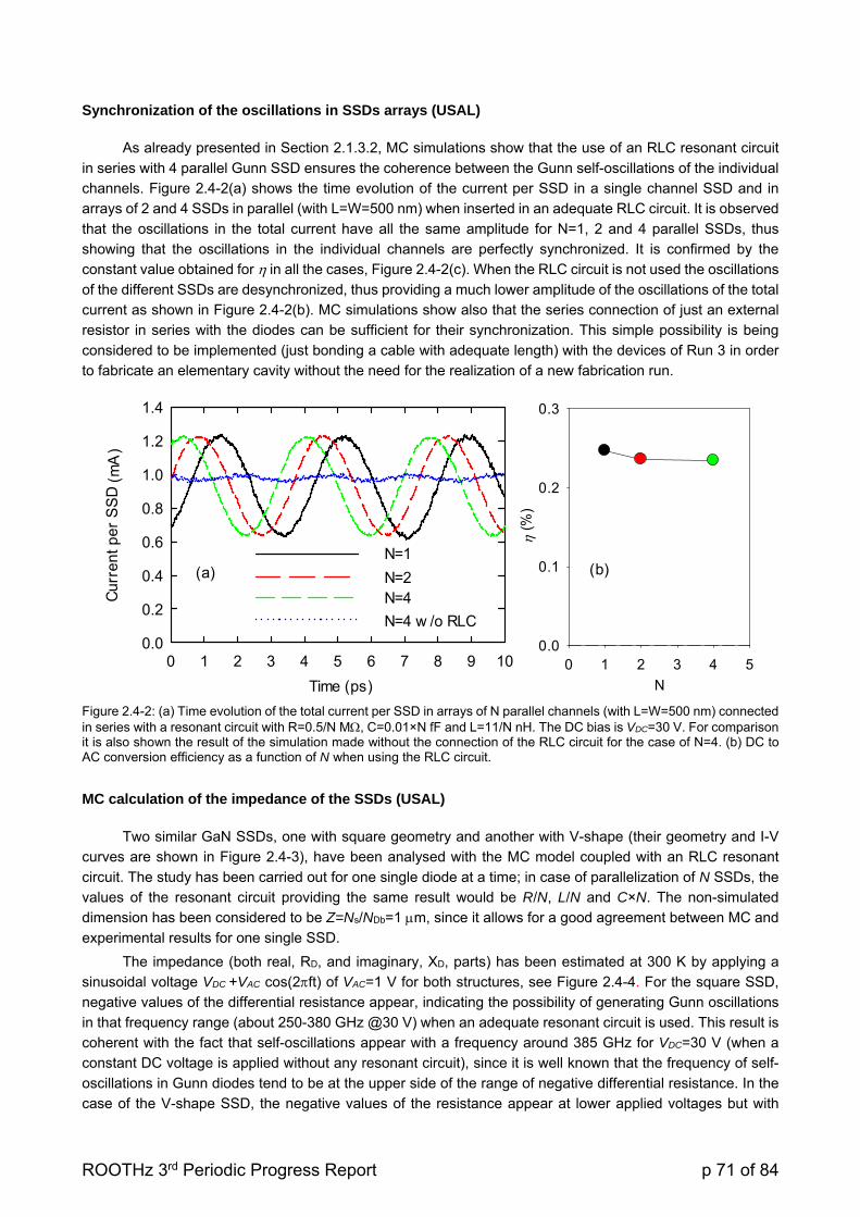
ROOTHz 3rd Periodic Progress Report p 71 of 84
Synchronization of the oscillations in SSDs arrays (USAL)
As already presented in Section 2.1.3.2, MC simulations show that the use of an RLC resonant circuit
in series with 4 parallel Gunn SSD ensures the coherence between the Gunn self-oscillations of the individual
channels. Figure 2.4-2(a) shows the time evolution of the current per SSD in a single channel SSD and in
arrays of 2 and 4 SSDs in parallel (with L=W=500 nm) when inserted in an adequate RLC circuit. It is observed
that the oscillations in the total current have all the same amplitude for N=1, 2 and 4 parallel SSDs, thus
showing that the oscillations in the individual channels are perfectly synchronized. It is confirmed by the
constant value obtained for in all the cases, Figure 2.4-2(c). When the RLC circuit is not used the oscillations
of the different SSDs are desynchronized, thus providing a much lower amplitude of the oscillations of the total
current as shown in Figure 2.4-2(b). MC simulations show also that the series connection of just an external
resistor in series with the diodes can be sufficient for their synchronization. This simple possibility is being
considered to be implemented (just bonding a cable with adequate length) with the devices of Run 3 in order
to fabricate an elementary cavity without the need for the realization of a new fabrication run.
N
0 1 2 3 4 5
(%
)
0.0
0.1
0.2
0.3
Time (ps)
0 1 2 3 4 5 6 7 8 9 10
Cu
rre
nt
pe
r S
SD
(m
A)
0.0
0.2
0.4
0.6
0.8
1.0
1.2
1.4
N=1
N=2N=4
N=4 w /o RLC
(a) (b)
Figure 2.4-2: (a) Time evolution of the total current per SSD in arrays of N parallel channels (with L=W=500 nm) connected in series with a resonant circuit with R=0.5/N M, C=0.01×N fF and L=11/N nH. The DC bias is VDC=30 V. For comparison it is also shown the result of the simulation made without the connection of the RLC circuit for the case of N=4. (b) DC to AC conversion efficiency as a function of N when using the RLC circuit.
MC calculation of the impedance of the SSDs (USAL)
Two similar GaN SSDs, one with square geometry and another with V-shape (their geometry and I-V
curves are shown in Figure 2.4-3), have been analysed with the MC model coupled with an RLC resonant
circuit. The study has been carried out for one single diode at a time; in case of parallelization of N SSDs, the
values of the resonant circuit providing the same result would be R/N, L/N and C×N. The non-simulated
dimension has been considered to be Z=Ns/NDb=1 m, since it allows for a good agreement between MC and
experimental results for one single SSD.
The impedance (both real, RD, and imaginary, XD, parts) has been estimated at 300 K by applying a
sinusoidal voltage VDC +VAC cos(2ft) of VAC=1 V for both structures, see Figure 2.4-4. For the square SSD,
negative values of the differential resistance appear, indicating the possibility of generating Gunn oscillations
in that frequency range (about 250-380 GHz @30 V) when an adequate resonant circuit is used. This result is
coherent with the fact that self-oscillations appear with a frequency around 385 GHz for VDC=30 V (when a
constant DC voltage is applied without any resonant circuit), since it is well known that the frequency of self-
oscillations in Gunn diodes tend to be at the upper side of the range of negative differential resistance. In the
case of the V-shape SSD, the negative values of the resistance appear at lower applied voltages but with
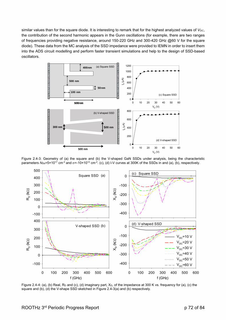
ROOTHz 3rd Periodic Progress Report p 72 of 84
similar values than for the square diode. It is interesting to remark that for the highest analyzed values of VDC,
the contribution of the second harmonic appears in the Gunn oscillations (for example, there are two ranges
of frequencies providing negative resistance, around 150-220 GHz and 300-420 GHz @60 V for the square
diode). These data from the MC analysis of the SSD impedance were provided to IEMN in order to insert them
into the ADS circuit modelling and perform faster transient simulations and help to the design of SSD-based
oscillators.
VD (V)
0 10 20 30 40 50 60
I D (A
)
0
200
400
600
800
1000
1200
VD (V)
0 10 20 30 40 50 60
I D (A
)
0
200
400
600
800
(c) Square SSD
(d) V-shaped SSD
Figure 2.4-3: Geometry of (a) the square and (b) the V-shaped GaN SSDs under analysis, being the characteristic parameters NDb=5×1017 cm-3 and =-10×1012 cm-2. (c), (d) I-V curves at 300K of the SSDs in and (a), (b), respectively.
f (GHz)
0 100 200 300 400 500 600
XD (
k )
-400
-300
-200
-100
0
f (GHz)
0 100 200 300 400 500 600
RD (
k )
-100
0
100
200
300
400
VDC=10 V
VDC=20 V
VDC=30 V
VDC=40 V
VDC=50 V
VDC=60 V
(b) (d)V-shaped SSD
V-shaped SSD
RD (
k )
-100
0
100
200
300
400
500
XD (
k )
-400
-300
-200
-100
0(a) (c)Square SSD
Square SSD
Figure 2.4-4: (a), (b) Real, RD and (c), (d) imaginary part, XD, of the impedance at 300 K vs. frequency for (a), (c) the square and (b), (d) the V-shape SSD sketched in Figure 2.4-3(a) and (b) respectively.
(a) Square SSD
(b) V-shaped SSD
500 nm
500 nm
300 nm
400 nm
500 nm
50 nm
100 nm
500 nm
400 nm
500 nm
50 nm
100 nm
500 nm
(a) Square SSD
(b) V-shaped SSD

ROOTHz 3rd Periodic Progress Report p 73 of 84
ADS simulations (IEMN)
By using the USAL data, ADS simulations have been used at IEMN in order to try to optimize the design
of the resonant circuit to be used for the fabrication of Gunn oscillators. Within ADS the modification of the
configuration of the resonant circuit (including the possibility of adding parasitic elements, additional filters,
etc.) can be easily made and the results are obtained much faster that with MC simulations. However, ADS
will not take into account any of the physical effects that MC is considering, only the values of the frequency
and bias dependent impedance will be included into the ADS electrical models. Also, convergence problems
can arise if the input data is not well discretized or the simulation parameters are not well chosen. Therefore
the first task to perform with ADS is to try to reproduce the results of MC simulations of the simple parallel RLC
resonator shown before in Figure 2.4-1 with one single square SSD. MC simulations performed by USAL
showed to provide Gunn oscillations at a frequency around 225 GHz when connected to an RLC circuit with
R=1 M, L=95.66 pF and C=5.2 fF. The current spectrum obtained with ADS, Figure 2.4-5(a), shows also
oscillations at the frequency predicted by the MC.
Figure 2.4-5: Current oscillations as a function of frequency obtained with ADS simulations for R=1 M, L=95.6 pH and C=5.2 fF (a) without any extrinsic element, and (b) with RSERIES=2×1.95.7 and Crosstalk=4.64 fF, for one single SSD.
Figure 2.4-6: Schematic input for ADS.
Then, the extrinsic elements extracted from the measured coplanar accesses of the fabricated devices
have been included in the input schematic file of ADS shown in Figure 2.4-6 (including the contact resistances,
and which is more important a crosstalk capacitance of 4.64 fF). In this case, similar current oscillations were
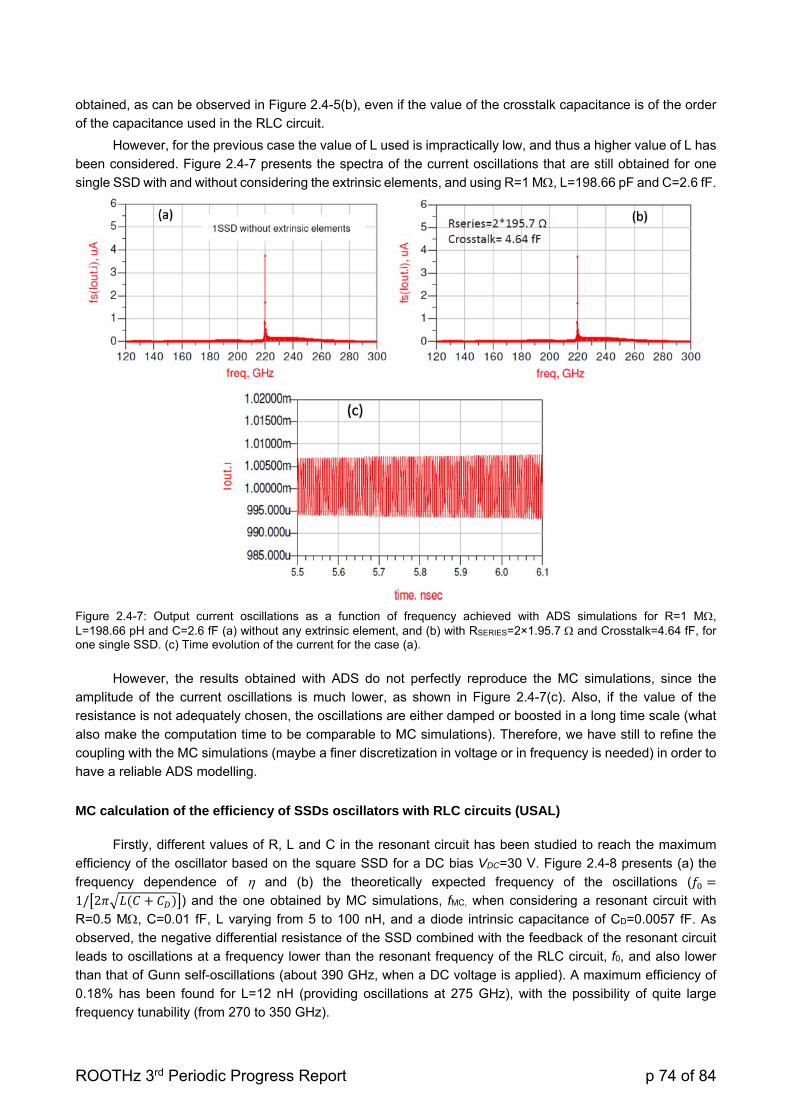
ROOTHz 3rd Periodic Progress Report p 74 of 84
obtained, as can be observed in Figure 2.4-5(b), even if the value of the crosstalk capacitance is of the order
of the capacitance used in the RLC circuit.
However, for the previous case the value of L used is impractically low, and thus a higher value of L has
been considered. Figure 2.4-7 presents the spectra of the current oscillations that are still obtained for one
single SSD with and without considering the extrinsic elements, and using R=1 M, L=198.66 pF and C=2.6 fF.
Figure 2.4-7: Output current oscillations as a function of frequency achieved with ADS simulations for R=1 M, L=198.66 pH and C=2.6 fF (a) without any extrinsic element, and (b) with RSERIES=2×1.95.7 and Crosstalk=4.64 fF, for one single SSD. (c) Time evolution of the current for the case (a).
However, the results obtained with ADS do not perfectly reproduce the MC simulations, since the
amplitude of the current oscillations is much lower, as shown in Figure 2.4-7(c). Also, if the value of the
resistance is not adequately chosen, the oscillations are either damped or boosted in a long time scale (what
also make the computation time to be comparable to MC simulations). Therefore, we have still to refine the
coupling with the MC simulations (maybe a finer discretization in voltage or in frequency is needed) in order to
have a reliable ADS modelling.
MC calculation of the efficiency of SSDs oscillators with RLC circuits (USAL)
Firstly, different values of R, L and C in the resonant circuit has been studied to reach the maximum
efficiency of the oscillator based on the square SSD for a DC bias VDC=30 V. Figure 2.4-8 presents (a) the
frequency dependence of and (b) the theoretically expected frequency of the oscillations (
1/ 2 ) and the one obtained by MC simulations, fMC, when considering a resonant circuit with
R=0.5 M, C=0.01 fF, L varying from 5 to 100 nH, and a diode intrinsic capacitance of CD=0.0057 fF. As
observed, the negative differential resistance of the SSD combined with the feedback of the resonant circuit
leads to oscillations at a frequency lower than the resonant frequency of the RLC circuit, f0, and also lower
than that of Gunn self-oscillations (about 390 GHz, when a DC voltage is applied). A maximum efficiency of
0.18% has been found for L=12 nH (providing oscillations at 275 GHz), with the possibility of quite large
frequency tunability (from 270 to 350 GHz).

ROOTHz 3rd Periodic Progress Report p 75 of 84
L (nH)10 100
Fre
que
ncy
(GH
z)
100
200
300
400
500
600f 0f MC
Self-oscillations
L (nH)10 100
(%
)
0.00
0.05
0.10
0.15
0.20
(a) (b)
Figure 2.4-8: (a) DC to AC conversion efficiency and (b) resonant frequency of the circuit, f0, and that of the oscillations obtained with the MC simulations, fMC, of the square SSD sketched in Figure 2.4-3(a) connected in series with a resonant circuit with R=0.5 M, C=0.01 fF and L varying from 5 to 100 nH. The DC bias is VDC=30 V.
VDC (V)
0 10 20 30 40 50 60
f MC (
GH
z)
0
100
200
300
(%
)
0.0
0.1
0.2
0.3
0.4
Square SSDV-shape SSD
(b)
(a)
Figure 2.4-9: (a) DC to AC efficiency , and (b) frequency of the oscillations obtained as a function of the applied DC voltage for the square and V-shape SSDs sketched in Figure 2.4-3 connected in series with a resonant circuit with R=0.5 M, C=0.01 fF and L=12 nH.
The low values obtained for the DC to AC conversion efficiency could be already experimentally useful,
but there is still much room for improvement, not only by optimizing the circuit design (looking for the best
combination of values of R, L and C, and in different configurations) but also the intrinsic characteristics of the
SSD. In order to establish a comparison between the square and the V-shape SSDs, the efficiency of both
types of SSDs coupled with a resonant circuit with the same set of elements R=0.5 M, C=0.01 fF and L=12 nH
has been calculated. Figure 2.4-9 shows the values of and the frequency of the current oscillations found as
a function of VDC. The V shape SSDs starts providing decent efficiencies for VDC >20 V (a threshold voltage
lower than for the square SSD, which needs VDC >25 V) with oscillation frequencies around 265-275 GHz, only
slightly dependent on VDC (and with lower values than for the square SSD, which gives 275-290 GHz). For
both types of diodes the efficiency presents a maximum value for VDC =30 V, which is much improved for the
V-shape SSD, around 0.35%. For VDC >55 V, when the second harmonic appears in the square SSD (see

ROOTHz 3rd Periodic Progress Report p 76 of 84
Figure 2.4-4) the efficiency takes higher values and the frequency of the oscillations increases, with the
drawback that the spectral purity of the oscillations is degraded and the dissipated DC power is increased
(60 mW per SSD @60 V). The time dependent values of the current and voltage in the circuits with square
and V-shape SSDs with VDC =30 V are shown in in Figure 2.4-10, both showing quite a well-defined sinusoidal
shape (with a phase shift between voltage and current slightly higher than a quarter of a period, thus indicating
a positive efficiency) at frequencies of about 275 GHz and 260 GHz, respectively.
It is necessary to remark that the values of the efficiency obtained for the different geometries are not
very significant, since the values used for R, L and C are not optimized and there may exist other sets values
providing better performances. The numbers of efficiency given by our MC simulations have to be taken only
as a reference for the possible operation of SSDs, since they will provide at least those figures.
I D (A
)
600
800
1000
1200
1400
VD (
V)
20
30
40(a) Square SSD
Time (ps)
0 1 2 3 4 5 6 7 8 9 10
I D (A
)
200400600800
1000
VD (
V)
20
30
40(b) V-shaped SSD
Figure 2.4-10: Time sequence of current and voltage in (a) the squared and (b) the V-shaped SSDs sketched in Figure 2.4-3 connected in series with a resonant circuit with R=0.5 M, C=0.01 fF and L=12 nH. The DC bias is VDC=30 V.
One can notice that some of the values provided for the elements of the RLC can be unfeasibly low, but
these values can be modified if considering instead of a single SSD an array of channels in parallel. If we want
to provide the results corresponding the N parallel SSDs it is not necessary to repeat the MC simulation, since
the current obtained is simply multiplied by a factor N. Therefore, if R/N, L/N and C×N are taken as the values
of the resonant circuit of the array of N channels, they provide the same efficiency of 0.18% that was obtained
for N=1 with R=0.5 M, C=0.01 fF and L=12 nH, see Table 2.4-1.
Table 2.4-1: Absolute values of the elements of the resonant circuit for achieving the maximum of efficiency for an optimized square and a V-shaped SSD using N parallel diodes.
R=0.5
M/N
L=12
nH/N
C=0.01
fFxN
PDC Square
@25V
PDC V-shape
@20V
N=1 0.5 M 12 nH 0.01 fF 25 mW 14 mW
N=10 50 k 1.2 nH 0.1 fF 0.25 W 0.14 W
N=100 5 k 120 pH 1.0 fF 2.5 W 1.5 W
N=500 25 k 0.6 nH 5.0 fF 12.5 W 7.5 W
In order to obtain Gunn oscillations with few parallel SSDs, it is necessary to use very small
capacitances. This may be a problem because they can be of the order of the crosstalk capacitances.
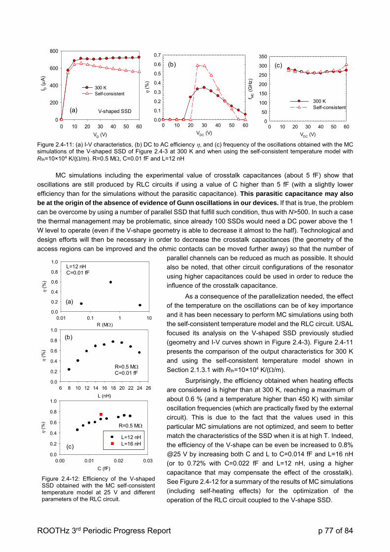
ROOTHz 3rd Periodic Progress Report p 77 of 84
VD (V)
0 10 20 30 40 50 60
I D (A
)
0
200
400
600
800
300 KSelf-consistent
V-shaped SSD(a)
VDC (V)
0 10 20 30 40 50 60
f MC (
GH
z)
0
50
100
150
200
250
300
350
VDC (V)
0 10 20 30 40 50 60
(%
)
0.0
0.1
0.2
0.3
0.4
0.5
0.6
0.7
300 KSelf-consistent
(c)(b)
Figure 2.4-11: (a) I-V characteristics, (b) DC to AC efficiency , and (c) frequency of the oscillations obtained with the MC simulations of the V-shaped SSD of Figure 2.4-3 at 300 K and when using the self-consistent temperature model with Rth=10×104 K/(/m). R=0.5 M, C=0.01 fF and L=12 nH
MC simulations including the experimental value of crosstalk capacitances (about 5 fF) show that
oscillations are still produced by RLC circuits if using a value of C higher than 5 fF (with a slightly lower
efficiency than for the simulations without the parasitic capacitance). This parasitic capacitance may also
be at the origin of the absence of evidence of Gunn oscillations in our devices. If that is true, the problem
can be overcome by using a number of parallel SSD that fulfill such condition, thus with N>500. In such a case
the thermal management may be problematic, since already 100 SSDs would need a DC power above the 1
W level to operate (even if the V-shape geometry is able to decrease it almost to the half). Technological and
design efforts will then be necessary in order to decrease the crosstalk capacitances (the geometry of the
access regions can be improved and the ohmic contacts can be moved further away) so that the number of
parallel channels can be reduced as much as possible. It should
also be noted, that other circuit configurations of the resonator
using higher capacitances could be used in order to reduce the
influence of the crosstalk capacitance.
As a consequence of the parallelization needed, the effect
of the temperature on the oscillations can be of key importance
and it has been necessary to perform MC simulations using both
the self-consistent temperature model and the RLC circuit. USAL
focused its analysis on the V-shaped SSD previously studied
(geometry and I-V curves shown in Figure 2.4-3). Figure 2.4-11
presents the comparison of the output characteristics for 300 K
and using the self-consistent temperature model shown in
Section 2.1.3.1 with Rth=10×104 K/(/m).
Surprisingly, the efficiency obtained when heating effects
are considered is higher than at 300 K, reaching a maximum of
about 0.6 % (and a temperature higher than 450 K) with similar
oscillation frequencies (which are practically fixed by the external
circuit). This is due to the fact that the values used in this
particular MC simulations are not optimized, and seem to better
match the characteristics of the SSD when it is at high T. Indeed,
the efficiency of the V-shape can be even be increased to 0.8%
@25 V by increasing both C and L to C=0.014 fF and L=16 nH
(or to 0.72% with C=0.022 fF and L=12 nH, using a higher
capacitance that may compensate the effect of the crosstalk).
See Figure 2.4-12 for a summary of the results of MC simulations
(including self-heating effects) for the optimization of the
operation of the RLC circuit coupled to the V-shape SSD.
C (fF)
0.00 0.01 0.02 0.03
(%
)
0.0
0.2
0.4
0.6
0.8
1.0
L=12 nHL=16 nH(c)
R=0.5 M
L (nH)
6 8 10 12 14 16 18 20 22 24 26
(%
)
0.0
0.2
0.4
0.6
0.8
1.0
(b)
R=0.5 MC=0.01 fF
R (M)0.01 0.1 1 10
(%
)
0.0
0.2
0.4
0.6
0.8
1.0
(a)
L=12 nHC=0.01 fF
Figure 2.4-12: Efficiency of the V-shaped SSD obtained with the MC self-consistent temperature model at 25 V and different parameters of the RLC circuit.

ROOTHz 3rd Periodic Progress Report p 78 of 84
2.4.1.3 Task 4.3 THz Subsystem integration
Due to the unsuccessful demonstration of THz emission this task has not been developed. All the effort
initially assigned to this objective has been dedicated to the design and fabrication of the discrete devices.
2.4.1.4 Task 4.4 Prototype subsystem benchmarking (USAL+IEMN)
Even if the benchmarking of the complete THz subsystem cannot be realized, we have analyzed the
performances of the THz detectors fabricated within ROOTHz as compared to the main types of technologies
presently used (Schottky barrier diodes and bolometers) and promising recent developments (Si MOSFETs
and Sb-based backward diodes, Sb-HBDs).
Table 2.4-2: Comparison of the figures of merit of different technologies of THz detectors.
ROOTHz devices Schottky
diodes (VDI)
Schottky
diodes
(ErAs
based)6,7
Bolomet
ers
Si
MOSFET8
Sb-
HBDs9 GaN
SSD
InAs
SSD
InGaAs
SSD
Intrinsic
Responsivity
(V/W)
3100 34 25000
Intrinsic NEP
(pW/Hz) 9 70 0.3
Extrinsic
Responsivity
(V/W)
100 16 300 1500 200 22000 107 80000 600
Extrinsic
NEP
(pW/Hz)
280 150 60 10 100 0.4 4 0.01 300 850
Frequency
(GHz) 315 315 315 330 1100 110 639 30 THz 645 700
Comments
High
power
operation
Expected
to work
>1 THz
Expected
to work
>1 THz
Already
optimized
design
Cooling
needed
Integration
with Si
technology
As compared with the standard Schottky barrier technology (such as those fabricated by VDI) the
performance of the InAs and InGaAs SSDs fabricated within ROOTHz is similar at frequencies around
300 GHz, mainly when our devices have not been designed for an optimum input matching, and values of
responsivity and NEP near the intrinsic limit could possibly be achieved (specially for the InAs SSDs 6 H. Kazemil, G. Nagy, L Tran, E Grossman, E. R. Brown, A. C. Gossard, G. D. Boreman, B Lail, A. C. Young, J. D. Zimmerman, “Ultra sensitive ErAs/InAlGaAs direct detectors for millimeter wave and THz imaging applications,” International Microwave Symposium, 2007 (IEEE/MTT-S), pp. 1367-1370, (2007).
7 E. R. Brown, A. C. Young, J. E. Bjarnason, H. Kazemi, J. Zimmerman and A. C. Gossard, “Millimeter and sub-millimeter wave performance of an ErAs:InAlGaAs Schottky diode coupled to a single-turn square spiral,” Int. J. High Speed Electron. Syst. 17, p. 383 (2007)
8 D. Glaab, S. Boppel, A. Lisauskas, U. Pfeiffer, E. Öjefors, H. G. Roskos. “Terahertz heterodyne detection with silicon field-effect transistors,” Applied Physics Letters 96, 042106 (2010)
9 G.C. Trichopoulos, L. Mosbacker, D. Burdette, and K. Sertel, “A Broadband Focal Plane Array Camera for Real-time THz Imaging Applications,” IEEE Transactions on Antennas and Propagation 61 ,pp. 1733-1740 (2013)

ROOTHz 3rd Periodic Progress Report p 79 of 84
technology, whose impedance is not far from the 50 reference). Also, InAs and InGaAs SSDs are expected
to have a constant value of responsivity and NEP in a broad range of frequency (up to 1-2 THz), where SSDs
should beat the performances of Schottky diodes. Another advantage of the SSD technology is the low value
of the 1/f corner frequency, easily achievable with beam chopping and other modulation techniques. Newly
developed ErAs/InAlGaAs based Schottky diodes have much improved performances, that could compete with
the SSD technology up to higher frequencies, but still with the drawback of being a vertical technology.
The comparison with other recent technologies for THz detection like Si MOSFETs and Sb-based
backward wave diodes is not easy to perform since the reference conditions are not the same. However, it
seems that the NEP of THz detectors based on Si MOSFETs and Sb-HBDs can be outperformed by our InAs
and InGaAs SSDs, (but with a lower responsivity in the case of Si-MOSFETs, that also benefits for the direct
integration with Si technology).
On the other hand, the strong capability of GaN SSDs for high power handling (and responding up to at
least 670 GHz) is unparalleled by any of the listed technologies, and only thermal detectors could be
competitors for this technology.

ROOTHz 3rd Periodic Progress Report p 80 of 84
2.5 WP5: DISSEMINATION AND IP PROTECTION
Even if the working principles of slot diodes and SSDs for THz detection and emission are already public,
we have found interesting to apply for IP protection (European Patents) of two of the applications of the SSDs
that we have demonstrated:
Device and method for mixing electromagnetic waves with frequencies up to the THz range
(EP12306383.6, 8 November 2012): In this configuration, the SSD are used as a mixer for heterodyne
detection of two TeraHertz incoming radiations. The resulting signal is transposed into the gigahertz-
band and can be tuned be between few GHz and several THz paving the way for THz heterodyne
detection (for spectroscopy, telecommunications, radar and astronomy applications). Consequently
we would like to propose to develop a SSD-based heterodyne mixer able to work in both up and down
conversion.
Device and method for direct demodulation of signals with carrier frequencies up to the THz
range (EP12306382.8, 8 November 2012): In this configuration, the SSD are used as a direct
demodulator of an incoming TeraHertz radiation modulated by a signal carrying the information
between few GHz and several THz. The resulting information is directly analyzed and usable into a
telecommunication system. This innovation paves the way for THz transmission and ultra-high band-
with telecommunication (for UHD-TV, security, telecommunication…). Consequently we would like to
propose to develop a SSD-based direct demodulator able to demodulate a THz carrier signal.
Regarding the dissemination, during this last period of the project development some of the work of the
partners related with the ROOTHz project has been presented in a good number of journal papers and
conference presentations (with a notable number of invited talks given by the ROOTHz partners in significant
international conferences):
Type Authors Title Details
Journal
paper
S. García, I Iñiguez-de-la-
Torre, S. Pérez, J. Mateos,
and T. González
Numerical study of sub-
millimeter Gunn oscillations in
InP and GaN vertical diodes:
Dependence on bias, doping,
and length
Journal of Applied Physics 114,
074503 (2013)
Journal
paper
P. Sangaré, G. Ducournau, B.
Grimbert, V. Brandli, M.
Faucher, C. Gaquière, A.
Iñiguez-de-la-Torre, I. Iñiguez-
de-la-Torre, J. F. Millithaler, J.
Mateos and T. González
Experimental demonstration of
direct terahertz detection at
room-temperature in
AlGaN/GaN asymmetric
nanochannels
Journal of Applied Physics 113,
034305 (2013)
Journal
paper
A. Iñiguez-de-la-Torre, I.
Iñiguez-de-la-Torre, J. Mateos,
T. González, P. Sangaré, M.
Faucher, B. Grimbert, V.
Brandli, G. Ducournau and C.
Gaquière
Searching for THz Gunn
oscillations in GaN planar
nanodiodes
Journal of Applied Physics 111,
113705, (2012)
Journal
paper
I. Iñiguez-de-la-Torre, H.
Rodilla, J. Mateos, T.
González, H. Irie and R.
Sobolewski
Monte Carlo studies of the
intrinsic time-domain response
of nanoscale three-branch
junctions
Journal of Applied Physics 111,
084511, (2012).

ROOTHz 3rd Periodic Progress Report p 81 of 84
Journal
paper
J. Mateos and T. González Plasma enhanced terahertz
rectification and noise in
InGaAs HEMTs
IEEE Transactions on Terahertz
Science and Technology 2, 562-
569 (2012)
Journal
paper
D. Pardo, J. Grajal, S. Pérez,
T. González and J. Mateos
Analysis of nonharmonic
oscillations in Schottky diodes
Journal of Applied Physics 112,
Art. No. 053703 [1-9] (2012)
Journal
paper
V. Kaushal, I. Iñiguez-de-la-
Torre, T. González, J. Mateos,
B. Lee, V. Misra and M.
Margala
Effects of a high-k dielectric on
the performance of III-V
Ballistic Deflection Transistors
IEEE Electron Device Letters 33,
1120 (2012)
Journal
paper
B. G. Vasallo, H. Rodilla, T.
González, G. Moschetti, J.
Grahn, and J. Mateos
Kink effect and noise
performance in isolated-gate
InAs/AlSb High Electron
Mobility Transistors
Semiconductor Science and
Technology 27, 065018 [1-5]
(2012)
Journal
paper
H. Rodilla, T. González, G.
Moschetti, J. Grahn and J.
Mateos
Monte Carlo study of the noise
performance of isolated-gate
InAs/AlSb HEMTs
Semiconductor Science and
Technology 27, 015008 [1-6]
(2012)
Journal
paper
H. Rodilla, T. González, G.
Moschetti, J. Grahn and J.
Mateos
Monte Carlo study of the noise
performance of isolated-gate
InAs/AlSb HEMTs
Semiconductor Science and
Technology 27, 015008 [1-6]
(2012)
Invited
Talk
J. Mateos Room temperature THz
Generation
Workshop “Terahertz
technologies - from devices to
diverse systems and
applications” in the European
Microwave Week 2012,
Amsterdam, Netherlands,
October 2012
Invited
Talk
J. Mateos, J. F. Millithaler, I.
Íñiguez-de-la-Torre, A.
Íñiguez-de-la-Torre, B. G.
Vasallo, S. Pérez, P. Sangare,
G. Ducournau, C. Gaquiére, Y.
Alimi, L. Zhang, A. Rezazadeh,
A. M. Song, A. Westlund, J.
Grahn and T. González
Semiconductor Nanodevices
for Room Temperature THz
Detection and Emission
International Workshop on
Optical Terahertz Science and
Technology (OTST 2013),
Kyoto, Japan, April 2013
Invited
Talk
T. González, J. F. Millithaler, I.
Íñiguez-de-la-Torre, A.
Íñiguez-de-la-Torre, B. G.
Vasallo, S. Pérez, P. Sangare,
G. Ducournau, C. Gaquiére, Y.
Alimi, L. Zhang, A. Rezazadeh,
A. M. Song, A. Westlund, J.
Grahn and J. Mateos
Room-temperature
semiconductor nanodiodes for
THz detection and emission
European Materials Research
Society (E-MRS), Strasbourg,
France, May 2013
Invited
Talk
J. Torres, P. Nouvel, A. Penot,
L. Varani, P. Sangare, B.
Grimbert, M. Faucher, G.
A room temperature THz
heterodyne detector based on
self-switching nanodiodes
18th International Conference on
Electron Dynamics in
Semiconductors,

ROOTHz 3rd Periodic Progress Report p 82 of 84
Ducournau, C. Gaquiere, I.
Iniguez-de-la-Torre, J. Mateos,
T. Gonzalez
Optoelectronics and
Nanostructures (EDISON 18),
Matsue, Japan, July 2013
Invited
Talk
I. Íñiguez-de-la-Torre Semiconductor nanodevices
for room temperature THz
detection and emission
15th International Symposium
on “Ultrafast Phenomena in
Semiconductors” (15-UFPS),
Vilnius, Lithuania, August 2013
Invited
Talk
J. Torres, P. Nouvel, A.
Penot, L. Varani, P. Sangaré,
B. Grimbert, M. Faucher, G.
Ducournau, C. Gaquière, I.
Iñiguez-de-la-Torre, J.
Mateos, T. González
Room temperature terahertz
detection using self-switching
nanodiodes
15th International Symposium
on “Ultrafast Phenomena in
Semiconductors” (15-UFPS),
Vilnius, Lithuania, August 2013
Invited
Talk
J. Mateos Plasma Wave Assisted THz
Detection
Workshop “Terahertz
technologies - From materials to
devices and their applications” in
the European Microwave Week
2013, Nuremberg, Germany,
October 2013
Oral
Presen-
tation
A. Westlund, G. Moschetti, H.
Zhao, P. A. Nilsson and J.
Grahn
InAs Self-Switching Diodes for
THz detection
GigaHertz Conference,
Stockholm, Sweden, March
2012
Oral
Presen-
tation
C. Gaquiere, G. Ducournau, P.
Sangaré, M. Faucher ,B.
Grimbert, I. Iñiguez-de-la-
Torre, T. González, A. Iñiguez-
de-la-Torre and J. Mateos
THz Applications at Room
Temperature Based on Self
Switch Diodes Using wide
Bandgap Material
IEEE International Microwave
Symposium (IMS 2012).
Montréal, Québec, Canada,
June 2012
Oral
Presen-
tation
J. F. Millithaler, I. Iñiguez-de-
la-Torre, T. González, P.
Sangaré, G. Ducournau, C.
Gaquière and J. Mateos
Monte Carlo analysis of
thermal effects in Self-
Switching Diodes
9th Spanish Conference on
Electron Devices (CDE 2013),
Valladolid, Spain, February 2013
Oral
Presen-
tation
J. F. Millithaler, I. Iñiguez-de-
la-Torre, T. González, P.
Sangaré, G. Ducournau, C.
Gaquière and J. Mateos
Noise in Terahertz detectors
based on semiconductor
nanochannels
22th International Conference on
Noise and Fluctuations (ICNF
2013), Montpellier, France, June
2013
Oral
Presen-
tation
I. Íñiguez-de-la-Torre, J. F.
Millithaler, A. Íñiguez-de-la-
Torre, J. Mateos, P. Sangaré,
G. Ducournau, C. Gaquière
and T. González
Geometry optimization for sub-
THz Gunn emission: a V-shape
GaN nanodevice
18th International Conference on
Electron Dynamics in
Semiconductors,
Optoelectronics and
Nanostructures (EDISON 18),
Matsue, Japan, July 2013
Oral
Presen-
tation
J. Torres, P. Nouvel, A.
Penot, L. Varani, P. Sangaré,
B. Grimbert, M. Faucher, G.
Ducournau, C. Gaquière, I.
Room temperature terahertz
detection using Self-switching
nanodiodes
15th International Symposium
on “Ultrafast Phenomena in
Semiconductors” (15-UFPS),
Vilnius, Lithuania, August 2013

ROOTHz 3rd Periodic Progress Report p 83 of 84
Iniguez-de-la-Torre, J. Mateos
and T. González
Oral
Presen-
tation
G. Ducournau, A. Westlund, P.
Sangaré, C. Gaquière, P. A.
Nilsson, I. Iñiguez-de-la-Torre,
J-F Millithaler, T. González, J.
Mateos and J. Grahn
200 GHz communication
system using unipolar InAs
THz rectifiers
38th International Conference on
Infrared, Millimeter, and
Terahertz Waves (IRMMW-THz
2013), Mainz, Germany,
September 2013
Poster J. Mateos and T. González Monte Carlo analysis of
plasma enhanced terahertz
detection in InGaAs HEMTs
15th International Workshop on
Computational Electronics
(IWCE 2012), Madison, USA,
May 2012
Poster A. Westlund, P.Å. Nilsson and
J. Grahn
Fabrication and DC
characterization of InAs/AlSb
Self Switching Diodes
IEEE International Conference
on Indium Phosphide and
Related Materials Conference
Proceedings (IPRM 2012),
Santa Barbara, USA, August
2012
Poster P. Sangaré, G. Ducournau, B.
Grimbert, V. Brandli, M.
Faucher and C. Gaquiere
GaN-based nano rectifiers for
THz detection
37th International Conference on
Infrared, Millimeter, and
Terahertz Waves (IRMMW-THz
2012), Wollongong, Australia,
September 2012
Poster J. Mateos, J. F. Millithaler, I.
Íñiguez-de-la-Torre, A.
Íñiguez-de-la-Torre, B. G.
Vasallo, S. Pérez, T.
González, Y. Alimi, L. Zhang,
A. Rezazadeh, A. M. Song, P.
Sangaré, G. Ducournau, C.
Gaquière, A. Westlund and J.
Grahn
Room Temperature THz
Detection and Emission with
Semiconductor Nanodevices
9th Spanish Conference on
Electron Devices (CDE 2013),
Valladolid, Spain, February 2013
Poster S. García Sánchez; B. G.
Vasallo; T. González and J.
Mateos
Time-domain Monte Carlo
simulations of resonant-circuit
operation of GaN Gunn diodes
9th Spanish Conference on
Electron Devices (CDE 2013),
Valladolid, Spain, February 2013
Poster I. Íñiguez-de-la-Torre, V.
Kaushal, M. Margala J. Mateos
and T. González
Ballistic Deflection Transistor:
Geometry Dependence and
Boolean Operations
9th Spanish Conference on
Electron Devices (CDE 2013),
Valladolid, Spain, February 2013
Poster A. Westlund, G. Moschetti, P.
A. Nilsson, J. Grahn, L.
Desplanque, and X. Wallart
Cryogenic DC
Characterization of
InAs/Al80Ga20Sb Self-
Switching Diodes
IEEE International Conference
on Indium Phosphide and
Related Materials Conference
Proceedings (IPRM 2013),
Kobe, Japan, May 2013.
Poster J. Mateos, I. Iñiguez-de-la-
Torre, Y. Meziani, E. García, L.
Q. Zhang, Y. Alimi, A. M.
Ultrafast Photoresponse of
Self-Switching Nano-Diodes
18th International Conference on
Electron Dynamics in
Semiconductors,

ROOTHz 3rd Periodic Progress Report p 84 of 84
Song, C. Chakraborty, J.
Serafini, R. Sobolewski, and T.
González
Optoelectronics and
Nanostructures (EDISON),
Matsue, Japan, July 2013
Poster C. Chakraborty, J. Serafini, J.
Zhang, L. Q. Zhang, Y. Alimi, I.
Iñiguez-de-la-Torre, J. Mateos,
T. González, A. M. Song, and
R. Sobolewski
Self-switching nano-devices as
optical photodetectors
15th Photonics North
Conference, Ottawa, Canada,
June 2013
PhD
Thesis
A. Iñiguez-de-la-Torre Nanodispositivos de GaN para
generación de señales de
THz. Simulación Monte Carlo
y análisis experimental
Presented on 20th December
2012 at the University of
Salamanca
PhD
Thesis
P. Sangaré Analyses des potentialités des
diodes de type SSD à base de
nitrure de Gallium pour les
applications d’émission et de
détection en gamme de
fréquence millimétrique et
submillimétrique
Presented on 3rd June 2013 at
the University of Sciences and
Technologies of Lille
Licentiate
thesis
A. Westlund Novel Terahertz Emitters and
Detectors: InGaAs Slot Diodes
and InAs Self-Switching
Diodes
Presented on 11th June 2013 at
the Chalmers University of
Technology
As in the previous reports, some of the works of USAL deal with simulations of HEMTs and Schottky
barrier diodes, which are closely related to the development of the MC models, that later on have been used
in ROOTHz.
The coordinator of ROOTHz, J. Mateos repeated in the organization (together with D. Pavilidis,
Technische Universität Darmstadt, Germany and I. Mehdi, Jet Propulsion Laboratory, USA) of the workshop
entitled “Terahertz Technologies -from Devices to Diverse Systems” within the European Microwave Week
2012, in Amsterdam, and that will be again held within the forthcoming EuMW’2013 in Nuremberg (Germany),
where the results of the ROOTHz project are presented in an invited talk by J. Mateos.
2.6 WP6: PROJECT MANAGEMENT
The report on project management is provided in a separate document (“Project management and use
of resources”) provided online through the NEF webpage.