Analytical modeling of single electron transistor for hybrid CMOS-SET analog IC design
11
1772 IEEE TRANSACTIONS ON ELECTRON DEVICES, VOL. 51, NO. 11, NOVEMBER 2004 Analytical Modeling of Single Electron Transistor for Hybrid CMOS-SET Analog IC Design Santanu Mahapatra, Student Member, IEEE, Vaibhav Vaish, Christoph Wasshuber, Kaustav Banerjee, Senior Member, IEEE, and Adrian Mihai Ionescu, Member, IEEE Abstract—A physically based compact analytical single electron transistor (SET) model is proposed for hybrid CMOS-SET analog circuit simulation. The modeling approach is based on the “or- thodox theory” of single electron tunneling, and valid for single or multi gate, symmetric or asymmetric devices and can also explain the background charge effect. The model parameters are physical device parameters and an associated parameter extraction proce- dure is reported. The device characteristics produced by the pro- posed model are verified with Monte Carlo simulation for large range of drain to source voltages and temper- atures and good agreements are observed. The proposed model is implemented in a commercial circuit simu- lator in order to develop a computer-aided design framework for CMOS-SET hybrid IC designs. A series of SPICE simulations are successfully carried out for different CMOS-SET hybrid circuits in order to reproduce their experimental/Monte Carlo simulated characteristics. Index Terms—Analog hardware description language (AHDL), CMOS-nano codesign, computer-aided design (CAD), Coulomb blockade, hybrid circuits, master equation circuit simulation, Monte Carlo simulation, semiconductor device modeling, single electron transistor (SET). I. INTRODUCTION T REMENDOUS PROGRESS in microelectronics has pushed the MOSFET dimension toward the 10-nm limits and motivated the interest for new devices that could perform at nanoscale according to International Technology Roadmap for Semiconductors figures of merit [1]. In the near future it is then probable that CMOS will need to share its domination with fundamentally new devices, such as single electron transistors (SETs). SETs have recently attracted much attention because of their nano feature size [2], [3], ultralow power dissipation (four–five decades lower than advanced digital CMOS) [3]–[5], new functionalities [6]–[8], and CMOS compatible fabrication process [3], [9]. It also appears that CMOS and SETs are rather complementary. For example, SET shows unique advantages Manuscript received December 10, 2003; revised August 12, 2004. The re- view of this paper was arranged by Editor S. Datta. S. Mahapatra and A. M. Ionescu are with the Electronics Laboratory, Insti- tute of Microelectronics and Microsystems (IMM), Swiss Federal Institute of Technology Lausanne, Lausanne CH 1015, Switzerland (e-mail: Santanu.Ma- hapatra@epfl.ch; Adrian.Ionescu@epfl.ch). V. Vaish is with the Department of Electrical Engineering, Indian Institute of Technology (IIT) Kanpur, UP 208016, India (e-mail: [email protected]). C. Wasshuber is with the Texas Instruments Incorporated, Dallas, TX 75243 USA (e-mail: [email protected]). K. Banerjee is with the Department of Electrical and Computer Engi- neering, University of California, Santa Barbara, CA 93106 USA (e-mail: [email protected]). Digital Object Identifier 10.1109/TED.2004.837369 in terms of low-power consumption and of new characteristics related to its unique Coulomb Blockade oscillations, while CMOS is still unrivaled in high-speed driving and voltage gain. Therefore, although a complete replacement of CMOS by SET is quite unlikely in the near future, it is also true that combining SET and CMOS, one can bring out novel functionalities [6]–[8], which are difficult to achieve in pure CMOS technology. How- ever, designing circuits with SETs is a difficult task, because of the electrical characteristics of SETs that are governed by phe- nomena such as Coulomb oscillations and Coulomb blockade characteristics are quite different compared to that of MOS transistors. The aim of this paper is to contribute to the design and analysis of hybrid CMOS-SET circuits by formulating an accurate analytical model that incorporates various physical effects including the background charge and temperature ef- fects, along with necessary parameter extraction procedure. The analytical model allows faster circuit analysis as compared to the Monte Carlo simulations (e.g., SIMON [10], MOSES [11] and KOSEC [12]) and master equation methods [13], [14] that are quite accurate but also very time consuming, making them ineffective even for the most basic circuits involving a few devices. On the other hand, the macro-modeling [15] approach provides little physical insight into the operation of the devices and may not be easily scalable. The proposed analytical model is incorporated in a commercial circuit simulator using an analog hardware description language (AHDL) that essentially embeds the SET model as a separate module in the circuit simulator without actually having to rigorously solve the SET characteristic equations along with other nonlinear elements in the hybrid circuit. This hybrid simulator is then used to cosim- ulate some CMOS-SET circuit styles and benchmarked against Monte Carlo simulations to simply provide a proof-of-concept. The results reported in this paper are promising enough to justify further investigations in large-scale hybrid CMOS-SET circuit design and analysis. The basic schematic of a SET device, where a conductive island is sandwiched between two tunnel junctions, is depicted in Fig. 1(a). A proper operation of a SET device requires: 1) the tunnel junction resistances to be greater than the quantum resistance to confine the electrons in the island, and 2) the charging energy of the island capacitance to be larger than the available thermal energy to avoid electron tunneling due to the thermionic emission. Fig. 1(b) demon- strates the typical Coulomb blockade oscillation behavior in SET – characteristics. It also reveals the fact that when (where is the elementary charge, is the 0018-9383/04$20.00 © 2004 IEEE
-
Upload
independent -
Category
Documents
-
view
0 -
download
0
Transcript of Analytical modeling of single electron transistor for hybrid CMOS-SET analog IC design
1772 IEEE TRANSACTIONS ON ELECTRON DEVICES, VOL. 51, NO. 11, NOVEMBER 2004
Analytical Modeling of Single Electron Transistor forHybrid CMOS-SET Analog IC DesignSantanu Mahapatra, Student Member, IEEE, Vaibhav Vaish, Christoph Wasshuber,Kaustav Banerjee, Senior Member, IEEE, and Adrian Mihai Ionescu, Member, IEEE
Abstract—A physically based compact analytical single electrontransistor (SET) model is proposed for hybrid CMOS-SET analogcircuit simulation. The modeling approach is based on the “or-thodox theory” of single electron tunneling, and valid for single ormulti gate, symmetric or asymmetric devices and can also explainthe background charge effect. The model parameters are physicaldevice parameters and an associated parameter extraction proce-dure is reported. The device characteristics produced by the pro-posed model are verified with Monte Carlo simulation for largerange of drain to source voltages ( DS 3 �) and temper-atures [ 2 (10 �)] and good agreements are observed.The proposed model is implemented in a commercial circuit simu-lator in order to develop a computer-aided design framework forCMOS-SET hybrid IC designs. A series of SPICE simulations aresuccessfully carried out for different CMOS-SET hybrid circuitsin order to reproduce their experimental/Monte Carlo simulatedcharacteristics.
Index Terms—Analog hardware description language (AHDL),CMOS-nano codesign, computer-aided design (CAD), Coulombblockade, hybrid circuits, master equation circuit simulation,Monte Carlo simulation, semiconductor device modeling, singleelectron transistor (SET).
I. INTRODUCTION
TREMENDOUS PROGRESS in microelectronics haspushed the MOSFET dimension toward the 10-nm limits
and motivated the interest for new devices that could perform atnanoscale according to International Technology Roadmap forSemiconductors figures of merit [1]. In the near future it is thenprobable that CMOS will need to share its domination withfundamentally new devices, such as single electron transistors(SETs). SETs have recently attracted much attention becauseof their nano feature size [2], [3], ultralow power dissipation(four–five decades lower than advanced digital CMOS) [3]–[5],new functionalities [6]–[8], and CMOS compatible fabricationprocess [3], [9]. It also appears that CMOS and SETs are rathercomplementary. For example, SET shows unique advantages
Manuscript received December 10, 2003; revised August 12, 2004. The re-view of this paper was arranged by Editor S. Datta.
S. Mahapatra and A. M. Ionescu are with the Electronics Laboratory, Insti-tute of Microelectronics and Microsystems (IMM), Swiss Federal Institute ofTechnology Lausanne, Lausanne CH 1015, Switzerland (e-mail: [email protected]; [email protected]).
V. Vaish is with the Department of Electrical Engineering, Indian Institute ofTechnology (IIT) Kanpur, UP 208016, India (e-mail: [email protected]).
C. Wasshuber is with the Texas Instruments Incorporated, Dallas, TX 75243USA (e-mail: [email protected]).
K. Banerjee is with the Department of Electrical and Computer Engi-neering, University of California, Santa Barbara, CA 93106 USA (e-mail:[email protected]).
Digital Object Identifier 10.1109/TED.2004.837369
in terms of low-power consumption and of new characteristicsrelated to its unique Coulomb Blockade oscillations, whileCMOS is still unrivaled in high-speed driving and voltage gain.Therefore, although a complete replacement of CMOS by SETis quite unlikely in the near future, it is also true that combiningSET and CMOS, one can bring out novel functionalities [6]–[8],which are difficult to achieve in pure CMOS technology. How-ever, designing circuits with SETs is a difficult task, because ofthe electrical characteristics of SETs that are governed by phe-nomena such as Coulomb oscillations and Coulomb blockadecharacteristics are quite different compared to that of MOStransistors. The aim of this paper is to contribute to the designand analysis of hybrid CMOS-SET circuits by formulating anaccurate analytical model that incorporates various physicaleffects including the background charge and temperature ef-fects, along with necessary parameter extraction procedure.The analytical model allows faster circuit analysis as comparedto the Monte Carlo simulations (e.g., SIMON [10], MOSES[11] and KOSEC [12]) and master equation methods [13], [14]that are quite accurate but also very time consuming, makingthem ineffective even for the most basic circuits involving a fewdevices. On the other hand, the macro-modeling [15] approachprovides little physical insight into the operation of the devicesand may not be easily scalable. The proposed analytical modelis incorporated in a commercial circuit simulator using ananalog hardware description language (AHDL) that essentiallyembeds the SET model as a separate module in the circuitsimulator without actually having to rigorously solve the SETcharacteristic equations along with other nonlinear elements inthe hybrid circuit. This hybrid simulator is then used to cosim-ulate some CMOS-SET circuit styles and benchmarked againstMonte Carlo simulations to simply provide a proof-of-concept.The results reported in this paper are promising enough tojustify further investigations in large-scale hybrid CMOS-SETcircuit design and analysis.
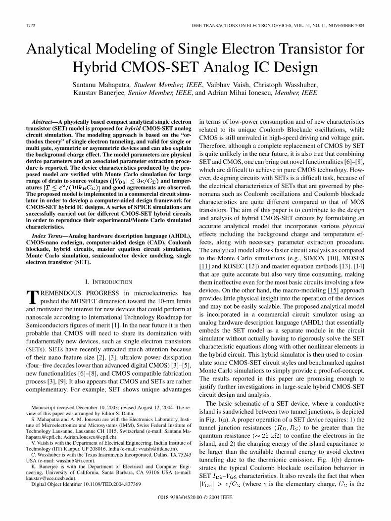
The basic schematic of a SET device, where a conductiveisland is sandwiched between two tunnel junctions, is depictedin Fig. 1(a). A proper operation of a SET device requires: 1) thetunnel junction resistances to be greater than thequantum resistance to confine the electrons in theisland, and 2) the charging energy of the island capacitance tobe larger than the available thermal energy to avoid electrontunneling due to the thermionic emission. Fig. 1(b) demon-strates the typical Coulomb blockade oscillation behavior inSET – characteristics. It also reveals the fact that when
(where is the elementary charge, is the
0018-9383/04$20.00 © 2004 IEEE
MAHAPATRA et al.: ANALYTICAL MODELING OF SET FOR HYBRID CMOS-SET ANALOG IC DESIGN 1773
Fig. 1. (a) Schematic of a basic single electron transistor and its different device parameters. Typical I –V characteristics (simulated by using SIMON [10])for (b) different values of V and, (c) different values of the temperatures (where the numbers within bracket denotes the ratio between the charging energy ofthe island capacitance and the available thermal energy). The solid circles represent the operating points of a constant current biased (I ) SET. The SET deviceparameters are C = 2 aF, C = C = 1 aF and R = R = 1 M .
total island capacitance with respect to the ground), it is nomore possible to obtain the Coulomb blockade (when the draincurrent is almost zero for certain values of ) in the devicecharacteristics. Therefore, for any switching application ofSET, should be less than . However, if a SET isbiased by a constant current source , which is a basicbuilding block for almost all analog SET/hybrid CMOS-SETarchitectures [6]–[8], [16], then as demonstrated in Fig. 1(b),for certain values of (unshaded region), the could behigher than . Moreover, in a mixed CMOS-SET architec-ture, it is very difficult to maintain the of the SET lowerthan , as the MOS devices are biased at higher voltagesand carry much higher currents than SET [7]. Therefore, unlikedigital SET circuits, the region is equally impor-tant for analog SET IC design. The effect of temperatureon the device characteristics is demonstrated in Fig. 1(c), andit shows that the Coulomb Blockade region becomes thinner athigher temperatures. Therefore, an accurate compact analyticalmodel for analog SET/hybrid CMOS-SET circuit simulationmust be able to capture both the effect of temperature and theeffect of high on the device characteristics.
Until now, to the best of our knowledge, only two compactanalytical models (Uchida et al. [17] and Mahapatra et al.[5], [18]) for SET devices have been reported, which appearto be attractive for practical IC design. The model reportedby Uchida et al. is more accurate at higher temperature butit is only applicable to the single gate resistively symmetric
device and does not account for the background charge ef-fect, which is significant for SET operations. A very recentarticle [19] has proposed a scheme to extend this model tothe asymmetric devices. On the other hand MIB (named afterMahapatra–Ionescu–Banerjee) [5], [18], is more flexible andcan be adapted for single or multiple-gate and symmetricor asymmetric device geometries and it can also explain thebackground charge effect. However, as MIB considers onlyunidirectional electron flow, it contains fewer exponential terms(which enhances the simulation speed for large circuits), andthus is less accurate at higher temperatures at low . It isimportant to note that both these models were developed underthe basic assumption of , which is quite practicalfor digital circuits. However, as explained earlier, for analogapplications of SET, one needs models valid for higher valuesof as well.
In this paper, we propose an improved version of the MIBmodel in order to extend its validity for andmake it suitable for analog SET/hybrid CMOS-SET circuit sim-ulations. The proposed model differs from another very recentmodel [20] at least in some key aspects. In our model, only onedirectional electron flow has been considered in order to mini-mize the number of exponential terms, yet keeping the accuracyat acceptable level and all analytical calculations correspondsto this assumption. Speed of the simulation and the accuracy ofthe proposed approach have also been compared by consideringthe bi-directional electron flow. In addition, a simple yet effi-
1774 IEEE TRANSACTIONS ON ELECTRON DEVICES, VOL. 51, NO. 11, NOVEMBER 2004
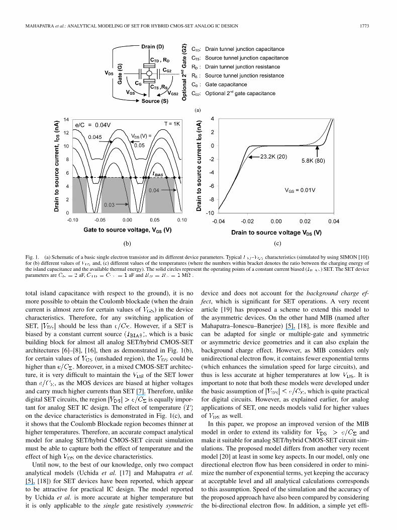
Fig. 2. (a) Schematic of SET drain current (I ) characteristics as a function of the island potential V [(2)] for any positive V (� e=C ) at T = 0 K.(b) Transition between different states in SET, where each state is represented by the number of electrons (n) in the island (i.e., the number inside each circle).
Here, � (or � ) represents the electron tunneling rate from source to island (or island to source) and � (or � ) represents the electron tunneling rate fromisland to drain (or drain to island).
cient method for extracting the model parameters is presentedfor a generalized asymmetric device, which is essential for SETbased circuit design as there is no fixed, unified technology forSET fabrication.
II. DEVELOPMENT AND VERIFICATION OF NEW MIB MODEL
A. Assumption
Proposed model MIB is based on the “orthodox theory ofsingle electron tunneling” [10], where we assume the following:
• The charge is discrete but the energy is continuous.• Tunnel junction resistance is larger than the quantum
resistance K to ensure the confinement of theelectrons on the island during SET operation.
• There is no co-tunneling.Our model also employs another practical assumption that theinterconnect capacitance associated with the gate, source, anddrain terminals are much larger than the device capacitances,which ensures the total capacitance of the island with respect toground to be equal to the summation of all device capaci-tances, i.e.
(1)
This assures that the SET characteristics are independent of thecapacitances of neighboring devices but only depend upon thenodal voltages of source, gate, and drain terminals.
B. Modeling of the Drain Current
The MIB model has been developed in three major steps:1) calculation of the island potential, 2) shifting the drain cur-
rent window and 3) calculation of the drain current, as discussedbelow.
1) Calculation of Island Potential : With a certainexternal bias (i.e., and ), before any electron tun-neling takes place, the tunnel junctions act as capacitance, andtherefore
(2)
where is a real number representing the background charge.Now, from the orthodox theory of single electron tunneling,we know that, at K, the electron tunneling throughany tunnel junction is only possible when the potential dropacross it becomes higher than . Therefore, con-sidering positive and grounded source, we can say thatwhen , one electron tunnels in from the source tothe island, and as a result decreases by of . Now, ifthe potential difference between drain-to-island is higher than
, one electron tunnels out from island to the drain (otherwise,the device enters into Coulomb Blockade region) and in-creases by (back to its original value). One can continue withthis basic idea of electron tunneling in order to achieve the pe-riodic drain current oscillation of a SET device as a function ofthe [(2)] as demonstrated in Fig. 2(a).
2) Shifting of the Drain Current Window: As seen inFig. 2(a), the drain current is a periodic function of with aperiodicity of . In this paper, the drain current model has beendeveloped only for the period: ,[which is shown by the dotted window in Fig. 2(a)] and for anyother value of one can shift by an integral multiple of
into this window and can apply the same model to calculate
MAHAPATRA et al.: ANALYTICAL MODELING OF SET FOR HYBRID CMOS-SET ANALOG IC DESIGN 1775
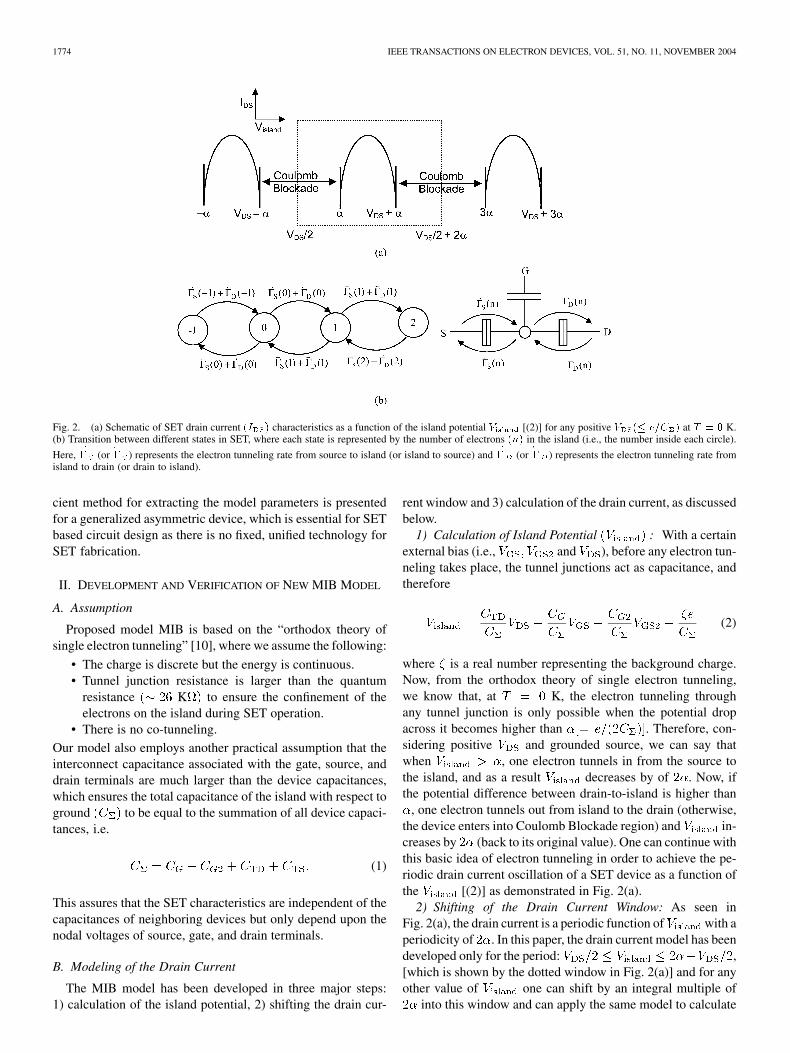
Fig. 3. Verification of MIB model for the I –V characteristics for (a) symmetric SET (R = R = 1 M) and (b) asymmetric SET(R = 0:382 M R = 1:91 M) with the same device capacitances as Fig. 1 at different values of V at T = 15 K. Here the numbers within bracketsrepresent the V =(e=C ) factor. (c) Verification of MIB model for the I –V characteristics of the symmetric device at different V at T = 15 K, wherethe numbers within brackets represent the V =(e=C ) factor. (d) Validation of MIB model at different temperature levels for symmetric device, where thenumbers within brackets represent the (e =C ) =k T factor. (d) also shows the effect of background charge on device characteristics. In these figures symbolsdenote the Monte Carlo simulation (SIMON) and solid line represents the proposed MIB model and dotted line represents the older version of the MIB model[i.e., without jV j > e=C extension as expressed by (9)].
the drain current. This shifting of this drain current window canbe done in the following way:
if
(3a)if
(3b)
Here holds the sign of and the box function, , returnsthe greatest integer less than or equals to .
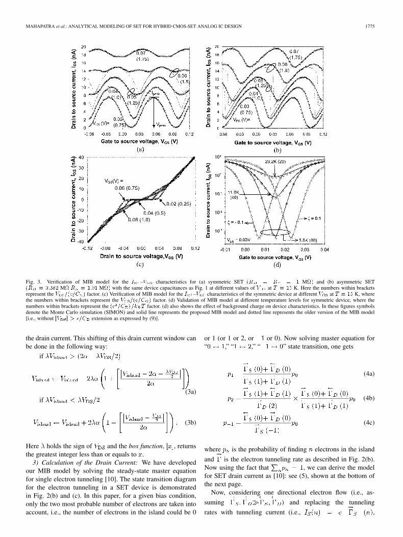
3) Calculation of the Drain Current: We have developedour MIB model by solving the steady-state master equationfor single electron tunneling [10]. The state transition diagramfor the electron tunneling in a SET device is demonstratedin Fig. 2(b) and (c). In this paper, for a given bias condition,only the two most probable number of electrons are taken intoaccount, i.e., the number of electrons in the island could be 0
or 1 (or 1 or 2, or or 0). Now solving master equation for“ ,” “ ,” “ ” state transition, one gets
(4a)
(4b)
(4c)
where is the probability of finding electrons in the island
and is the electron tunneling rate as described in Fig. 2(b).Now using the fact that , we can derive the modelfor SET drain current as [10]: see (5), shown at the bottom ofthe next page.
Now, considering one directional electron flow (i.e., as-
suming ) and replacing the tunneling
rates with tunneling current (i.e., ,
1776 IEEE TRANSACTIONS ON ELECTRON DEVICES, VOL. 51, NO. 11, NOVEMBER 2004
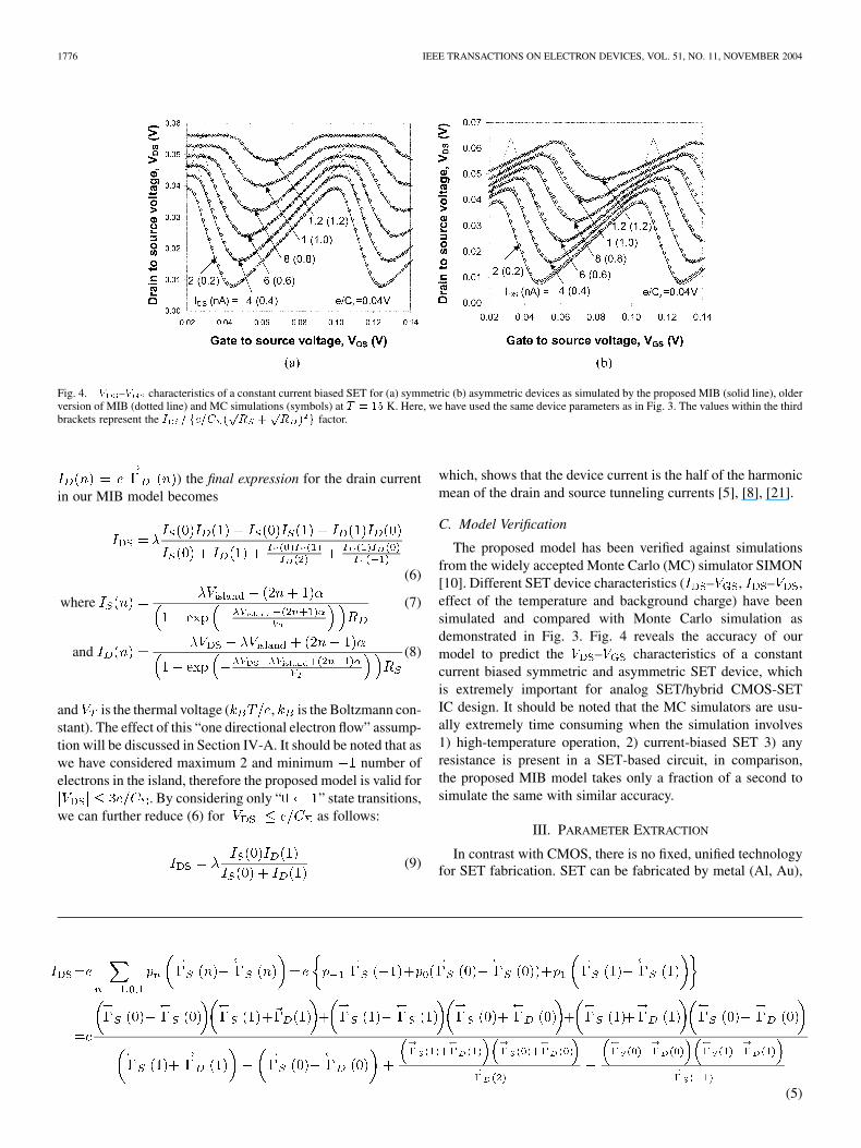
Fig. 4. V –V characteristics of a constant current biased SET for (a) symmetric (b) asymmetric devices as simulated by the proposed MIB (solid line), olderversion of MIB (dotted line) and MC simulations (symbols) at T = 15 K. Here, we have used the same device parameters as in Fig. 3. The values within the thirdbrackets represent the I = fe=C (
pR +
pR ) g factor.
) the final expression for the drain currentin our MIB model becomes
(6)
where (7)
and (8)
and is the thermal voltage ( , is the Boltzmann con-stant). The effect of this “one directional electron flow” assump-tion will be discussed in Section IV-A. It should be noted that aswe have considered maximum 2 and minimum number ofelectrons in the island, therefore the proposed model is valid for
. By considering only “ ” state transitions,we can further reduce (6) for as follows:
(9)
which, shows that the device current is the half of the harmonicmean of the drain and source tunneling currents [5], [8], [21].
C. Model Verification
The proposed model has been verified against simulationsfrom the widely accepted Monte Carlo (MC) simulator SIMON[10]. Different SET device characteristics ( – , – ,effect of the temperature and background charge) have beensimulated and compared with Monte Carlo simulation asdemonstrated in Fig. 3. Fig. 4 reveals the accuracy of ourmodel to predict the – characteristics of a constantcurrent biased symmetric and asymmetric SET device, whichis extremely important for analog SET/hybrid CMOS-SETIC design. It should be noted that the MC simulators are usu-ally extremely time consuming when the simulation involves1) high-temperature operation, 2) current-biased SET 3) anyresistance is present in a SET-based circuit, in comparison,the proposed MIB model takes only a fraction of a second tosimulate the same with similar accuracy.
III. PARAMETER EXTRACTION
In contrast with CMOS, there is no fixed, unified technologyfor SET fabrication. SET can be fabricated by metal (Al, Au),
(5)
MAHAPATRA et al.: ANALYTICAL MODELING OF SET FOR HYBRID CMOS-SET ANALOG IC DESIGN 1777
TABLE IDIFFERENT MIB MODEL PARAMETER EXTRACTED BY THE PROPOSED PARAMETER EXTRACTION PROCEDURE AT T = 10 K AND AT T = 20 K
Silicon (or silicon on insulator), III–V material, and even bycarbon nanotubes [10]. However, if the values of the devicecapacitances and resistances are known, MIB model can predictthe device behavior of a SET irrespective of its technology(geometry of islands and tunneling junctions), as it is physicallyfounded in terms of effective electrical parameters (devicecapacitances and resistances). Therefore, the proposed modelis technology independent and hence it requires an accurateparameter extraction procedure. The extraction procedure ofMIB model parameters ( , , , , , , and
), which is based on the assumption that the second gate isgrounded, is described below:
Step 1: Record a set of versus characteristics fordifferent values of positive . The period of oscillations
in the measured – characteristics gives us thevalue of the gate capacitance . Now, the maximum valueof at any particular and the correspondingvalue of [Fig. 3(a)] can be expressed as [5]
(10)
(11)
where is the effective (signed fractional part of ) fixedbackground charge of the device and is an integer number.
Equation (11) suggests that the plot of versus isa set of parallel straight lines (for different ) and the interceptwith the vertical axis can be used to extract . Please note that,if the slope of (11) is found to be too small to measure then onecan switch the drain and source terminal and perform the sameprocedure again.
Step 2: Bias the SET with a constant current source, and record a set of
quasi-triangular – characteristics. The slopes of thesecharacteristics could be formulated as
1 Slope rise (12)
2 Slope fall (13)
If similar characteristics are then recorded by exchanging thedrain and source terminals of the SET, one can have another setof equations for the slopes of – characteristics
1 Slope rise (14)
2 Slope fall (15)
Fig. 5. Effect of the “unidirectional electron flow” approximation on the MIBmodel. Here the symbols represents Monte Carlo simulation, dotted and solidline represents MIB model with “unidirectional electron flow” approximation(6) and without approximation (16), respectively.
Fig. 6. Effect of the bias current on the constant current based SET analogarchitectures (here R = R = R and p = (e =C )=k T ), where thesymbols denotes the MC simulation and solid line represents the proposed MIBmodel.
Using (12)–(15) one can extract all the device capacitances byusing the already extracted value of and the value of thetunnel junction resistances ( and ) can be easily extractedby using those device capacitances values in (10) and (11).
Proposed model and extraction procedure have been validatedusing a self-consistent approach: a set of realistic model param-eters are used as inputs to the MC simulator (SIMON) and theSET is simulated, following which, the parameters can be es-timated by applying the proposed extraction procedure to the
1778 IEEE TRANSACTIONS ON ELECTRON DEVICES, VOL. 51, NO. 11, NOVEMBER 2004
Fig. 7. (a) Schematic and (b) characteristics of a basic CMOS-SET hybrid neuron cell (with C = C = 0:04 aF, C = C = 0:02 aF, R = R =
1 M) as predicted by SIMON (symbol) and SMARTSPICE (solid and dotted line). It should be noted that I is taken to be 50 nA for SIMON simulationand for SMARTSPICE simulation the MOS current source is designed in such a way that it can drive the same bias current through the SET. Here the pMOSFETparameters are L = 0:5 �m, W = 0:8 �m, T = 9:74 nm, V = �0:55 and EKV [24] MOSFET model is used. The dotted line represents MIB modelwithout the jV j > e=C extension.
simulated characteristics. It should also be noted that the pro-posed parameter extraction procedure is temperature dependentas given in Table I and hence it is recommended to perform allthe measurement at low temperatures .
Please note that, the reported extraction procedure is based onelementary SET characteristics and independent of MIB modelcomplexities [5], [18] and also valid for any other SET models[17], [19], [20], which use only device capacitances, resistancesand background charge as model parameters.
IV. DISCUSSION
A. Effect of the “Unidirectional Electron Tunneling”Approximation
The MIB model proposed in this work [expressed by (6)],is based on the approximation that the electron tunneling ratetoward the positive potential (i.e., from source-to-island-to-drainfor positive and drain-to-island-to-source for negative )is much higher than the electron tunneling rate in the oppositedirection. By considering the bi-directional electron flows, from(5), the MIB model for SET drain current can be formulatedas (16)–(18), shown at the bottom of the next page. It shouldbe noted that (6) and (16) contains six and ten differentexponential terms respectively. The differences between thetwo approaches [(6) and (16)] are demonstrated in Fig. 5. The“bi-directional electron tunneling” approach only improves themodel accuracy at low drain voltage at high temperatures, and at
the same time introduces many exponential terms, which makesthe simulations time consuming (the “unidirectional tunnelingapproach” overestimates the drain current by 9.24% at =0.01V for the SET parameters 2aF, 1aF,
1M ). We have found that in a Pentium III1200MHz CPU, (16) consumes 22% more processing timethan (6) to simulate the characteristics of a current biasedSET.
B. Effect of the Bias Current on CMOS-SET Hybrid CircuitDesign
Fig. 6 demonstrates the relation between the bias currentand the output voltage of a constant current biased SET.As the bias current increases: 1) increases, 2) thedynamic range of the variation decreases, and 3) influenceof the temperature on the output voltage decreases. Therefore,for SET/ hybrid CMOS-SET analog IC design, in order tooptimize the tradeoff between the and the dynamicrange of the variation, the bias current should be less than
.
V. CMOS-SET HYBRID CIRCUIT SIMULATION
In this work, circuit level CMOS-SET cosimulations havebeen successfully performed by implementing the proposedMIB model in commercial circuit simulator SMARTSPICE byits Verilog-A interface [22], [23]. Verilog-A [23] is an Analog
(16)
where (17)
and (18)
MAHAPATRA et al.: ANALYTICAL MODELING OF SET FOR HYBRID CMOS-SET ANALOG IC DESIGN 1779
Fig. 8. (a) Schematic and (b) characteristics of NDR device for different bias current (I ) as simulated by SIMON (symbol) and MIB (solid and dotted line)with the device parameters are: C = 0:2 aF, C = 0:15 aF, R = R = 1 M for S1 and C = C = 0:15 aF, R = R = 1 M for S2. The dottedline represents MIB simulation without jV j > e=C extension.
High Level Hardware Description Language (AHDL) foranalog systems in which one can mix SMARTSPICE devicemodels (such as EKV [24], BSIM [25], etc.) and Verilog-Amodules in the same netlist. Analog SET and CMOS-SETco-simulations have been successfully carried out for differentbenchmarked circuit as discussed in Sections V-A–D.
A. Neural Network Circuit
Since a powerful signal processor demands a large neuralnetwork, therefore, due to the power dissipation and size ofthe neural chip, it is difficult to design efficient neural networkby CMOS technology. However, one can exploit the ultra lowpower dissipation of SET devices and its nano feature size inorder to realize compact neural device. A SET-based neural net-work scheme (composed of two-cascaded current biased SET),as proposed by Goossen’s [8] is depicted in Fig. 7(a). For theproper operation of the circuit, the drain and source tunnel ca-pacitances of the SET have to be equal and gatecapacitances have to be twice of that [8].One point should be noted that in order to drive currents of theorder of through the SET one has to bias the MOS transistorsin subthreshold (weak inversion) region. Using SMARTSPICE,the static characteristics of the neuron cell, has been simulatedaccurately and good agreement with MC simulation Fig. 7(b)demonstrates the accuracy of the proposed model.
B. NDR Circuit
A negative differential resistance (NDR) is a useful elementwith a wide variety of circuit applications such as in oscillators,amplifiers, logic cell, and memory. Fig. 8 depicts an alternativearchitecture of SET-based NDR cell [16], which is composed oftwo cross-connected SET (S1 and S2) and a current source. Thecurrent–voltage – characteristics of this NDR cell and theeffect of the bias current on the circuit behavior are shown inFig. 8. The input voltage and the constant current biasedfirst SET (S1) creates a feedback loop that helps to decrease thegate-to-source voltage of second SET (S2) for a certain range ofincreasing , and which follows a decrease in the drain current(or the input current, ) of S2 (NDR effect). It is found that
Fig. 9. Schematic of the universal literal gate comprising a SET anda MOSFET and comparison between measured and simulated V –Vcharacteristics of the universal literal gate at T = 27 K. The SET deviceparameters are C = 0:27 aF, C = C = 2:7 aF, R = R = 200 kand MOS device parameters are W = 12 �m, L = 14 �m, T = 90 nm,V = 0:64 V. V is set to 1.08 V, and V is hard-limited at 5 V [6].EKV [24] model is used to simulate the MOS device. Experimental data arereproduced after [6] at the end.
this NDR architecture appears more versatile than previously re-ported structure [26] in terms of dynamic range of NDR region,current controllability and drivability, and offers a very effectivesolution for real implementation of the NDR functionality.
C. Multiple-Valued Logic (MVL) Circuit
Multiple-valued logics (MVL) have potential advantagesover binary logics with respect to the number of elementsper function and operating speed. Most MVL circuits, beenfabricated with MOS and bipolar devices, have limited successpartially because the devices are inherently single-threshold orsingle-peak, and are not fully suited for MVL. Inokawa et al.[6] have recently proposed a hybrid CMOS-SET MVL circuit
1780 IEEE TRANSACTIONS ON ELECTRON DEVICES, VOL. 51, NO. 11, NOVEMBER 2004
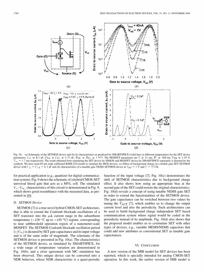
Fig. 10. (a) Schematic of the SETMOS device and (b) its characteristics as predicted by SMARTSPICE (solid line) at different temperatures for the SET deviceparameters: C = 0:2 aF, C = C = 0:15 aF, R = R = 1 M. The MOSFET parameters are L = 65 nm, W = 100 nm, V = 0:32 V,T = 1:7 nm respectively. The result obtained from simulating the SET device by SIMON and MOSFET device by SMARTSPICE separately is denoted by thesymbols. We have used 65-nm node calibrated BSIM [25] model to simulate the MOS devices. (c) Effect of background charge on a double gate SET SETMOSdevice with C = C = 0:1 aF and (d) characteristics of a tunable gate NEMS-SETMOS device at V = 1 V and T = 173 K.
for practical application (e.g., quantizer for digital communica-tion system). Fig. 9 shows the schematic of a hybrid CMOS-SETuniversal literal gate that acts as a MVL cell. The simulated
– characteristics of this circuit is demonstrated in Fig. 9,which shows good resemblance with the measured data, as pre-sented in [6].
D. SETMOS Device
SETMOS [7] is a true novel hybrid CMOS-SET architecture,that is able to extend the Coulomb blockade oscillations of aSET transistor into the current range in the subambienttemperature ( C up to C) regime, correspondingto near subthreshold operation region of a nanometer-scaleMOSFET. The SETMOS Coulomb blockade oscillation period
is dictated by SET gate capacitance and its input voltageand is of the same order of magnitude. The schematic of theSETMOS device is presented in Fig. 10(a). The characteristicsof the SETMOS device, as simulated by SMARTSPICE, fora wide range of temperature variation are demonstrated inFig. 10(b), and a close agreement with MC simulation hasbeen observed. This unique device can be converted into aNDR behavior, whose NDR characteristic is a quasi-periodic
function of the input voltage [7]. Fig. 10(c) demonstrates theshift of SETMOS characteristics due to background chargeeffect. It also shows how using an appropriate bias at thesecond gate of the SET could restore the original characteristics.Fig. 10(d) reveals a concept of using tunable NEMS gate SETin order to extend the functionalities of the SETMOS device.The gate capacitance can be switched between two values bytuning the [7], which enables us to change the outputcurrent level and also the periodicity. Such architectures canbe used to build background charge independent SET basedcommunication system where signal would be coded in theperiodicity instead of its amplitude. Fig. 10(d) also shows thatthe proposed model enables us to cosimulate SET with othertypes of devices, e.g., variable MEMS/NEMS capacitors thatcould add new attributes to conventional SET as tunable gatecapacitances.
VI. CONCLUSION
A new version of the MIB model for SET devices has beenreported, which is specially intended for analog CMOS-SEToperation. In this work, the earlier version of MIB model is
MAHAPATRA et al.: ANALYTICAL MODELING OF SET FOR HYBRID CMOS-SET ANALOG IC DESIGN 1781
extended to (up to ), which is essentialfor analog SET operation. The proposed model has beenverified at the device level for both symmetric and asymmetricdevices and a good agreement with Monte Carlo simulationis found. MIB is then implemented in the professional circuitsimulator SMARTSPICE using its AHDL interface in orderto co-simulate the SET devices along with CMOS devices.A series of simulations is then successfully performed fordifferent benchmarked CMOS-SET hybrid architecture. MIBhas some clear advantages: 1) it is physically based, and ableto accurately describe the drain current for symmetric andasymmetric, single/double gate device up to2) it is simple (carries less exponential terms than other models)yet able to predict device behavior accurately up to
. Finally, the model is shown to be very accurate forthe simulation, design, and verification of both digital andanalog hybrid CMOS-SET circuit architectures.
REFERENCES
[1] J. A. Hutchby, G. I. Bourianoff, V. V. Zhirnov, and J. E. Brewer, “Ex-tending the road beyond CMOS,” IEEE Circuits Devices Mag., vol. 18,pp. 28–41, Feb. 2002.
[2] Y. Ono et al., “Si complementary single-electron inverter,” in IEDMTech. Dig., 1999, pp. 367–370.
[3] K. Uchida, J. Koga, R. Ohba, and A. Toriumi, “Programmablesingle-electron transistor logic for low-power intelligent Si LSI,” inProc. ISSCC, vol. 2, 2002, pp. 162–453.
[4] A. M. Ionescu, M. Declercq, S. Mahapatra, K. Banerjee, and J. Gautier,“Few electron devices: Toward hybrid CMOS-SET integrated circuits,”in Proc. DAC, 2002, pp. 88–93.
[5] S. Mahapatra, A. M. Ionescu, K. Banerjee, and M. J. Declerq, “Mod-eling and analysis of power dissipation in single electron logic,” in IEDMTech. Dig., 2002, pp. 323–326.
[6] H. Inokawa, A. Fujiwara, and Y. Takahashi, “A multiple-valued logicwith merged single-electron and MOS transistors,” in IEDM Tech. Dig.,2001, pp. 147–150.
[7] S. Mahapatra et al., “SETMOS: A novel true hybrid SET- CMOS highcurrent Coulomb blockade oscillation cell for future nano-scale analogICs,” in IEDM Tech. Dig., 2003, pp. 703–706.
[8] M. Goossens, Analog Neural Networks in Single-Electron TunnelingTechnology. Delft, The Netherlands: Delft Univ. Press, 1998.
[9] Z. A. K. Durrani, A. C. Irvine, and H. Ahmed, “Coulomb blockadememory using integrated single-electron transistor/metal-oxide semi-conductor transistor grain cells,” IEEE Trans. Electron Devices, vol. 47,pp. 2334–2339, Dec. 2000.
[10] C. Wasshuber, Computational Electronics. New York: Springer-Verlag, 2002.
[11] R. H. Chen, A. N. Korotkov, and K. K. Likharev, “A new logic familybased on single-electron transistors,” in Proc. Device Res. Conf., 1995,pp. 44–45.
[12] Y. S. Yu et al., “Implementation of single electron circuit simulation bySPICE: KOSECSPICE,” in Proc. Asia Pasific Workshop FundamentalApplication Advanced Semiconductor Device, 2000, pp. 85–90.
[13] K. Likharev. SETTRANS- a simulator for single electron transistor. [On-line]. Available: http://hana.physics.sunysb.edu/set/software
[14] C. Le Royer, G. Le Carval, D. Fraboulet, and M. Sanquer, “Accuratemodeling of quantum-dot based multi-tunnel junction memory,” in Proc.ESSDERC, 2002, pp. 403–406.
[15] Y. S. Yu, S. W. Hwang, and D. Ahn, “Macromodeling of single elec-tron transistors for efficient circuit simulation,” IEEE Trans. ElectronDevices, vol. 46, pp. 1667–1671, Aug. 1999.
[16] S. Mahapatra and A. M. Ionescu, “A novel elementary SET negativedifferential resistance device,” Jpn. J. Appl. Phys., pt. 1, vol. 43, no. 2,pp. 538–539, 2004.
[17] K. Uchida, K. Matsuzawa, J. Koga, R. Ohba, S. Takagi, and A. Toriumi,“Analytical single-electron transistor (SET) model for design and anal-ysis of realistic SET circuits,” Jpn. J. Appl. Phys., pt. 1, vol. 39, no. 4B,pp. 2321–2324, 2000.
[18] S. Mahapatra, A. M. Ionescu, and K. Banerjee, “A quasianalytical SETmodel for few electron circuit simulation,” IEEE Electron Device Lett.,vol. 23, pp. 366–368, June 2002.
[19] H. Inokawa and Y. Takahashi, “A compact analytical model for asym-metric single-electron transistors,” IEEE Trans. Electron Devices, vol.50, pp. 455–461, Feb. 2003.
[20] G. Lientschnig, I. Weymann, and P. Hadley, “Simulating hybrid circuitsof single-electron transistors and field-effect transistors,” Jpn. J. Appl.Phys., pt. 1, vol. 42, no. 10, pp. 6467–6472, 2003.
[21] X. Wang and W. Porod, “Analytical I–V model for single-electron tran-sistors,” in Proc. Int. Workshop Computational Electronics, 2000, pp.71–72.
[22] S. Mahapatra et al., “A CAD framework for co-design and analysisof CMOS-SET hybrid integrated circuits,” in Proc. ICCAD, 2003, pp.497–502.
[23] SMARTSPICE User Manual. SILVACO Inc.. [Online]. Available:www.silvaco.com
[24] J. Sallese, M. Bucher, F. Krummenacher, and P. Fazan, “Inversion chargeliberalization in MOSFET modeling and rigorous derivation of the EKVcompact model,” Solid State Electron., vol. 47, pp. 677–683, 2003.
[25] Y. Cao et al.. New paradigm of predictive MOSFET and interconnectmodeling for early circuit design. presented at Proc. CICC. [Online].Available: www-device.eecs.berkeley.edu/~ptm
[26] C. P. Heij, D. C. Dixon, P. Hadley, and J. E. Mooij, “Negative differentialresistance due to single-electron switching,” Appl. Phys. Lett., vol. 74,no. 7, pp. 1042–1044, 1999.
Santanu Mahapatra (S’03) was born in Kolkata,West Bengal, India. He received the B.E. degree inelectronics and telecommunication from JadavpurUniversity, Kolkata, in 1999 and the M.Tech. degreein electrical engineering (specializing in microelec-tronics) from the Indian Institute of Technology(IIT), Kanpur, India, in March 2001. He is cur-rently pursuing the Ph.D. degree at the ElectronicsLaboratory, Swiss Federal Institute of TechnologyLausanne, Switzerland.
In 2001, he was with Atrenta Incorpora-tion, Kolkata, as an EDA tool developer. His research interests focus onemerging nanoscaled device modeling and co-simulation with CMOS, hybridCMOS-nano circuit design, and development of novel memory architectures.He has published several research papers in international journals and refereedconference
Mr. Mahapatra is an Associate Member of The Institution of Electronics andTelecommunication Engineers, India.
Vaibhav Vaish received the B.Tech. degree from theIndian Institute of Technology (IIT), Kanpur, India,in 2004.
His field of interests include digital electronics andmicroprocessors technology and theory of communi-cation systems.
Christoph Wasshuber was born 1968 in Vienna,Austria. He received the M.S. degree in telecom-munications and the Ph.D. degree in semiconductorand microelectronics from the Vienna University ofTechnology and Tokyo University, Tokyo, Japan,respectively. He is currently pursuing the M.B.Adegree at the Massachusetts Institute of Technology,Cambridge.
He holds several patents and is frequently aninvited speaker to cover topics in single-electronics,TCAD and simulation in general. He wrote the
widely used SIMON single-electron software package. He is currently withTexas Instruments, Incorporated, Dallas, TX. He is the author of two booksin the field of single-electronics and has published numerous articles inpeer-reviewed journals.
Dr. Wasshuber received the 1997 Dr. Ernst Fehrer Award.
1782 IEEE TRANSACTIONS ON ELECTRON DEVICES, VOL. 51, NO. 11, NOVEMBER 2004
Kaustav Banerjee (S’92–M’99–SM’03) receivedthe Ph.D. degree in electrical engineering andcomputer sciences from the University of California,Berkeley, in 1999.
He was with Stanford University, Stanford, CA,from 1999 to 2002 as a Research Associate at theCenter for Integrated Systems. In July 2002, hejoined the Faculty of the Department of Electricaland Computer Engineering, University of California,Santa Barbara (UCSB), as an Assistant Professor.From February 2002 to August 2002 he was a
Visiting Professor at the Circuit Research Labs of Intel, Hillsboro, OR. Inthe past, he has also held summer/visiting positions at Texas InstrumentsInc., Dallas, TX, Fujitsu Laboratories, and the Swiss Federal Institute ofTechnology (EPFL), Lausanne, Switzerland. His present research interestsfocus on nanometer scale issues in high-performance VLSI and mixed-signaldesigns, as well as on circuits and systems issues in emerging nanoelectronics.He is also conducting research on some exploratory interconnect and circuitarchitectures including 3-D ICs and carbon nanotube interconnects. At UCSB,he mentors several doctoral and masters students. He also co-advises graduatestudents at Stanford University, University of Illinois at Urbana-Champaign,and EPFL-Switzerland. He has co-directed two doctoral dissertations atStanford University and the University of Southern California, Los Angeles.He has published over 100 journal and refereed international conference papersand a book chapter.
Dr. Banerjee served as Technical Program Chair of the 2002 IEEE Interna-tional Symposium on Quality Electronic Design (ISQED‘02), and is the Gen-eral Chair of ISQED ’05. He also serves or has served on the technical programcommittees of the IEEE International Electron Devices Meeting, the IEEE In-ternational Reliability Physics Symposium, the EOS/ESD Symposium, and theACM International Symposium on Physical Design. He has been recognizedthrough the ACM SIGDA Outstanding New Faculty Award (2004) as well as aBest Paper Award at the Design Automation Conference (2001). He is listed inWho’s Who in America and Who’s Who in Science and Engineering.
Adrian Mihai Ionescu (M’94) was born in Ro-mania in 1965. He received the Ph.D. degree inmicroelectronics from the University “Politehnica”Bucharest, Romania, in 1994 and in physics of semi-conductors from the Institut National Polytechniquede Grenoble, France, in 1997.
He has held positions at LETI-CEA, Grenoble, andCNRS, France, and he was a visiting researcher atthe Center of Integrated Systems, Stanford Univer-sity, Stanford, CA. He has authored more than 70 re-search papers. He is a Tenure-Track Assistant Pro-
fessor at the Swiss Federal Institute of Technology (EPFL), Lausanne, Switzer-land. His present research interests include design, modeling, and characteriza-tion of submicrometer MOS devices, single-electron devices and few electroncircuit architectures, SOI novel applications, and RF MEMS. He is the head ofthe Institute of Microelectronics and Microsystems, EPFL.
Dr. Ionescu was part of the technical program committee of IEEE Interna-tional Electron Device Meeting (IEDM) and IEEE International Symposium onQuality Electronic Design (ISQED).