Pacemaker and network mechanisms of neural rhythm generation
Upload
independentCategory
view
11download
0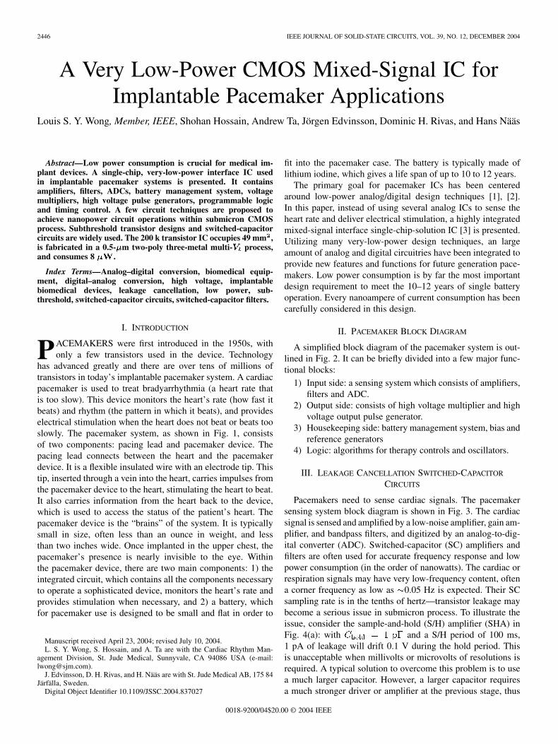
2446 IEEE JOURNAL OF SOLID-STATE CIRCUITS, VOL. 39, NO. 12, DECEMBER 2004
A Very Low-Power CMOS Mixed-Signal IC forImplantable Pacemaker Applications
Louis S. Y. Wong, Member, IEEE, Shohan Hossain, Andrew Ta, Jörgen Edvinsson, Dominic H. Rivas, and Hans Nääs
Abstract—Low power consumption is crucial for medical im-plant devices. A single-chip, very-low-power interface IC usedin implantable pacemaker systems is presented. It containsamplifiers, filters, ADCs, battery management system, voltagemultipliers, high voltage pulse generators, programmable logicand timing control. A few circuit techniques are proposed toachieve nanopower circuit operations within submicron CMOSprocess. Subthreshold transistor designs and switched-capacitorcircuits are widely used. The 200 k transistor IC occupies 49 mm2,is fabricated in a 0.5- m two-poly three-metal multi- process,and consumes 8 W.
Index Terms—Analog–digital conversion, biomedical equip-ment, digital–analog conversion, high voltage, implantablebiomedical devices, leakage cancellation, low power, sub-threshold, switched-capacitor circuits, switched-capacitor filters.
I. INTRODUCTION
PACEMAKERS were first introduced in the 1950s, withonly a few transistors used in the device. Technology
has advanced greatly and there are over tens of millions oftransistors in today’s implantable pacemaker system. A cardiacpacemaker is used to treat bradyarrhythmia (a heart rate thatis too slow). This device monitors the heart’s rate (how fast itbeats) and rhythm (the pattern in which it beats), and provideselectrical stimulation when the heart does not beat or beats tooslowly. The pacemaker system, as shown in Fig. 1, consistsof two components: pacing lead and pacemaker device. Thepacing lead connects between the heart and the pacemakerdevice. It is a flexible insulated wire with an electrode tip. Thistip, inserted through a vein into the heart, carries impulses fromthe pacemaker device to the heart, stimulating the heart to beat.It also carries information from the heart back to the device,which is used to access the status of the patient’s heart. Thepacemaker device is the “brains” of the system. It is typicallysmall in size, often less than an ounce in weight, and lessthan two inches wide. Once implanted in the upper chest, thepacemaker’s presence is nearly invisible to the eye. Withinthe pacemaker device, there are two main components: 1) theintegrated circuit, which contains all the components necessaryto operate a sophisticated device, monitors the heart’s rate andprovides stimulation when necessary, and 2) a battery, whichfor pacemaker use is designed to be small and flat in order to
Manuscript received April 23, 2004; revised July 10, 2004.L. S. Y. Wong, S. Hossain, and A. Ta are with the Cardiac Rhythm Man-
agement Division, St. Jude Medical, Sunnyvale, CA 94086 USA (e-mail:[email protected]).
J. Edvinsson, D. H. Rivas, and H. Nääs are with St. Jude Medical AB, 175 84Järfälla, Sweden.
Digital Object Identifier 10.1109/JSSC.2004.837027
fit into the pacemaker case. The battery is typically made oflithium iodine, which gives a life span of up to 10 to 12 years.
The primary goal for pacemaker ICs has been centeredaround low-power analog/digital design techniques [1], [2].In this paper, instead of using several analog ICs to sense theheart rate and deliver electrical stimulation, a highly integratedmixed-signal interface single-chip-solution IC [3] is presented.Utilizing many very-low-power design techniques, an largeamount of analog and digital circuitries have been integrated toprovide new features and functions for future generation pace-makers. Low power consumption is by far the most importantdesign requirement to meet the 10–12 years of single batteryoperation. Every nanoampere of current consumption has beencarefully considered in this design.
II. PACEMAKER BLOCK DIAGRAM
A simplified block diagram of the pacemaker system is out-lined in Fig. 2. It can be briefly divided into a few major func-tional blocks:
1) Input side: a sensing system which consists of amplifiers,filters and ADC.
2) Output side: consists of high voltage multiplier and highvoltage output pulse generator.
3) Housekeeping side: battery management system, bias andreference generators
4) Logic: algorithms for therapy controls and oscillators.
III. LEAKAGE CANCELLATION SWITCHED-CAPACITOR
CIRCUITS
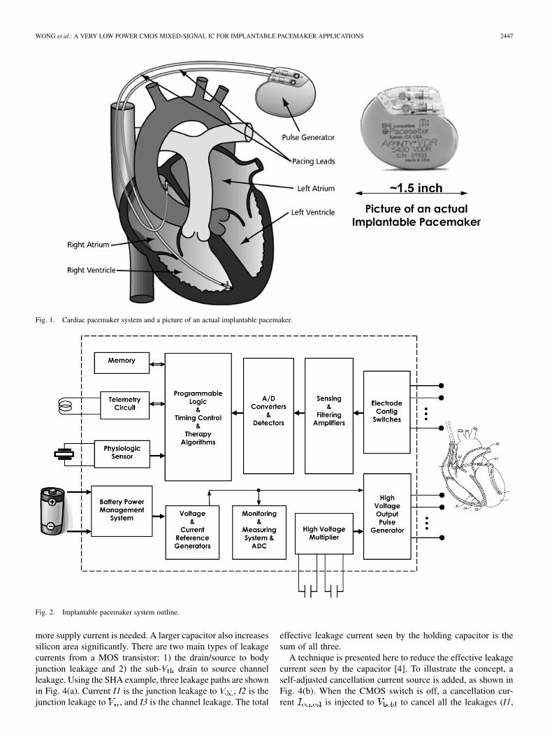
Pacemakers need to sense cardiac signals. The pacemakersensing system block diagram is shown in Fig. 3. The cardiacsignal is sensed and amplified by a low-noise amplifier, gain am-plifier, and bandpass filters, and digitized by an analog-to-dig-ital converter (ADC). Switched-capacitor (SC) amplifiers andfilters are often used for accurate frequency response and lowpower consumption (in the order of nanowatts). The cardiac orrespiration signals may have very low-frequency content, oftena corner frequency as low as 0.05 Hz is expected. Their SCsampling rate is in the tenths of hertz—transistor leakage maybecome a serious issue in submicron process. To illustrate theissue, consider the sample-and-hold (S/H) amplifier (SHA) inFig. 4(a): with and a S/H period of 100 ms,1 pA of leakage will drift 0.1 V during the hold period. Thisis unacceptable when millivolts or microvolts of resolutions isrequired. A typical solution to overcome this problem is to usea much larger capacitor. However, a larger capacitor requiresa much stronger driver or amplifier at the previous stage, thus
0018-9200/04$20.00 © 2004 IEEE
WONG et al.: A VERY LOW POWER CMOS MIXED-SIGNAL IC FOR IMPLANTABLE PACEMAKER APPLICATIONS 2447
Fig. 1. Cardiac pacemaker system and a picture of an actual implantable pacemaker.
Fig. 2. Implantable pacemaker system outline.
more supply current is needed. A larger capacitor also increasessilicon area significantly. There are two main types of leakagecurrents from a MOS transistor: 1) the drain/source to bodyjunction leakage and 2) the sub- drain to source channelleakage. Using the SHA example, three leakage paths are shownin Fig. 4(a). Current I1 is the junction leakage to , I2 is thejunction leakage to , and I3 is the channel leakage. The total
effective leakage current seen by the holding capacitor is thesum of all three.
A technique is presented here to reduce the effective leakagecurrent seen by the capacitor [4]. To illustrate the concept, aself-adjusted cancellation current source is added, as shown inFig. 4(b). When the CMOS switch is off, a cancellation cur-rent is injected to to cancel all the leakages (I1,
2448 IEEE JOURNAL OF SOLID-STATE CIRCUITS, VOL. 39, NO. 12, DECEMBER 2004
Fig. 3. Sensing system block diagram.
Fig. 4. (a) Switched-capacitor sample-hold amplifier. (b) Concept of the leakage cancellation technique.
I2, and I3). This current is automatically adjusted such that itis equal to the sum of I1, I2, and I3, but in the opposite direc-tion. The effective leakage seen by is virtually zero. Thus,
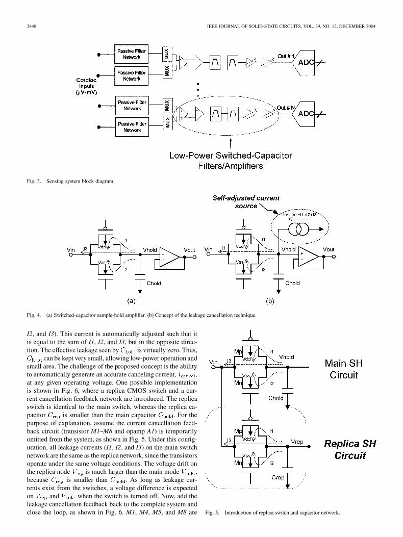
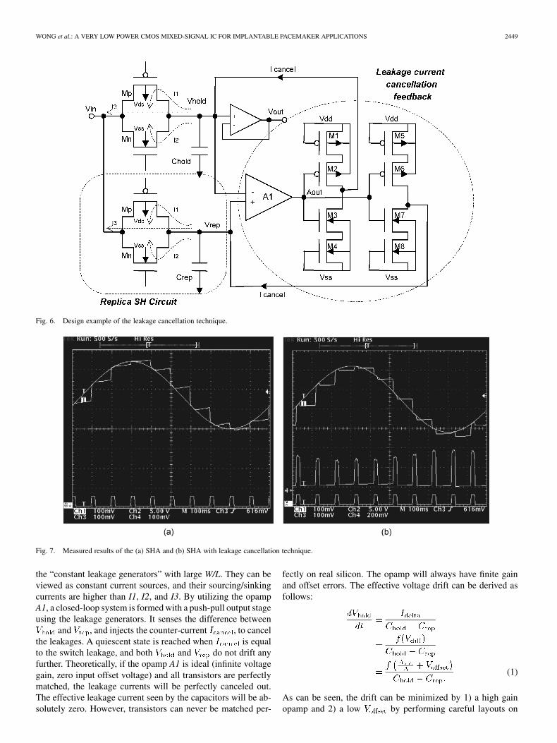
can be kept very small, allowing low-power operation andsmall area. The challenge of the proposed concept is the abilityto automatically generate an accurate canceling current, ,at any given operating voltage. One possible implementationis shown in Fig. 6, where a replica CMOS switch and a cur-rent cancellation feedback network are introduced. The replicaswitch is identical to the main switch, whereas the replica ca-pacitor is smaller than the main capacitor . For thepurpose of explanation, assume the current cancellation feed-back circuit (transistor M1–M8 and opamp A1) is temporarilyomitted from the system, as shown in Fig. 5. Under this config-uration, all leakage currents (I1, I2, and I3) on the main switchnetwork are the same as the replica network, since the transistorsoperate under the same voltage conditions. The voltage drift onthe replica node is much larger than the main mode ,because is smaller than . As long as leakage cur-rents exist from the switches, a voltage difference is expectedon and when the switch is turned off. Now, add theleakage cancellation feedback back to the complete system andclose the loop, as shown in Fig. 6. M1, M4, M5, and M8 are Fig. 5. Introduction of replica switch and capacitor network.
WONG et al.: A VERY LOW POWER CMOS MIXED-SIGNAL IC FOR IMPLANTABLE PACEMAKER APPLICATIONS 2449
Fig. 6. Design example of the leakage cancellation technique.
Fig. 7. Measured results of the (a) SHA and (b) SHA with leakage cancellation technique.
the “constant leakage generators” with large W/L. They can beviewed as constant current sources, and their sourcing/sinkingcurrents are higher than I1, I2, and I3. By utilizing the opampA1, a closed-loop system is formed with a push-pull output stageusing the leakage generators. It senses the difference between
and , and injects the counter-current , to cancelthe leakages. A quiescent state is reached when is equalto the switch leakage, and both and do not drift anyfurther. Theoretically, if the opamp A1 is ideal (infinite voltagegain, zero input offset voltage) and all transistors are perfectlymatched, the leakage currents will be perfectly canceled out.The effective leakage current seen by the capacitors will be ab-solutely zero. However, transistors can never be matched per-
fectly on real silicon. The opamp will always have finite gainand offset errors. The effective voltage drift can be derived asfollows:
(1)
As can be seen, the drift can be minimized by 1) a high gainopamp and 2) a low by performing careful layouts on
2450 IEEE JOURNAL OF SOLID-STATE CIRCUITS, VOL. 39, NO. 12, DECEMBER 2004
Fig. 8. Block diagram of the 8-bit ADC.
the matched devices. Fig. 7 shows the measured results for theSHA with and without the cancellation technique applied. Ithas a 1-Hz sinewave input, sampled at 10 Hz with hold a pe-riod of 100 ms; the natural leakage of the CMOS switch isapproximately 0.1 pA, whereas the effective leakage with theleakage cancellation technique has been reduced to approxi-mately 0.01 pA.
IV. A/D CONVERTERS
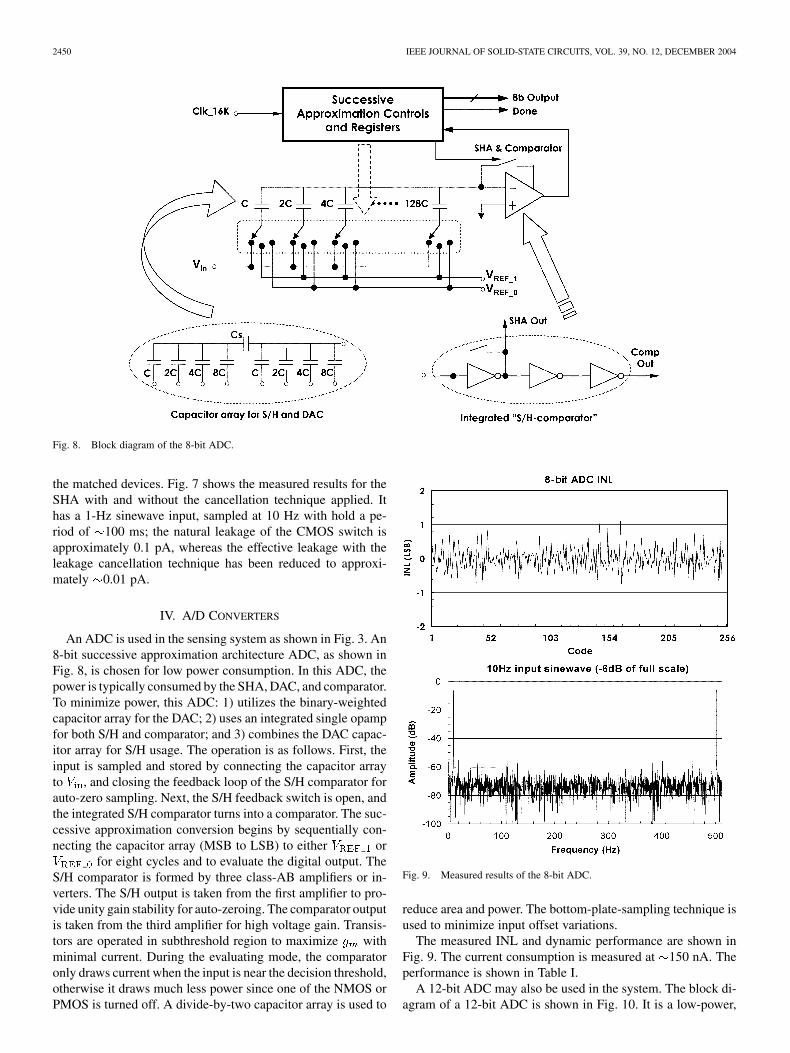
An ADC is used in the sensing system as shown in Fig. 3. An8-bit successive approximation architecture ADC, as shown inFig. 8, is chosen for low power consumption. In this ADC, thepower is typically consumed by the SHA, DAC, and comparator.To minimize power, this ADC: 1) utilizes the binary-weightedcapacitor array for the DAC; 2) uses an integrated single opampfor both S/H and comparator; and 3) combines the DAC capac-itor array for S/H usage. The operation is as follows. First, theinput is sampled and stored by connecting the capacitor arrayto , and closing the feedback loop of the S/H comparator forauto-zero sampling. Next, the S/H feedback switch is open, andthe integrated S/H comparator turns into a comparator. The suc-cessive approximation conversion begins by sequentially con-necting the capacitor array (MSB to LSB) to either or
for eight cycles and to evaluate the digital output. TheS/H comparator is formed by three class-AB amplifiers or in-verters. The S/H output is taken from the first amplifier to pro-vide unity gain stability for auto-zeroing. The comparator outputis taken from the third amplifier for high voltage gain. Transis-tors are operated in subthreshold region to maximize withminimal current. During the evaluating mode, the comparatoronly draws current when the input is near the decision threshold,otherwise it draws much less power since one of the NMOS orPMOS is turned off. A divide-by-two capacitor array is used to
Fig. 9. Measured results of the 8-bit ADC.
reduce area and power. The bottom-plate-sampling technique isused to minimize input offset variations.
The measured INL and dynamic performance are shown inFig. 9. The current consumption is measured at 150 nA. Theperformance is shown in Table I.
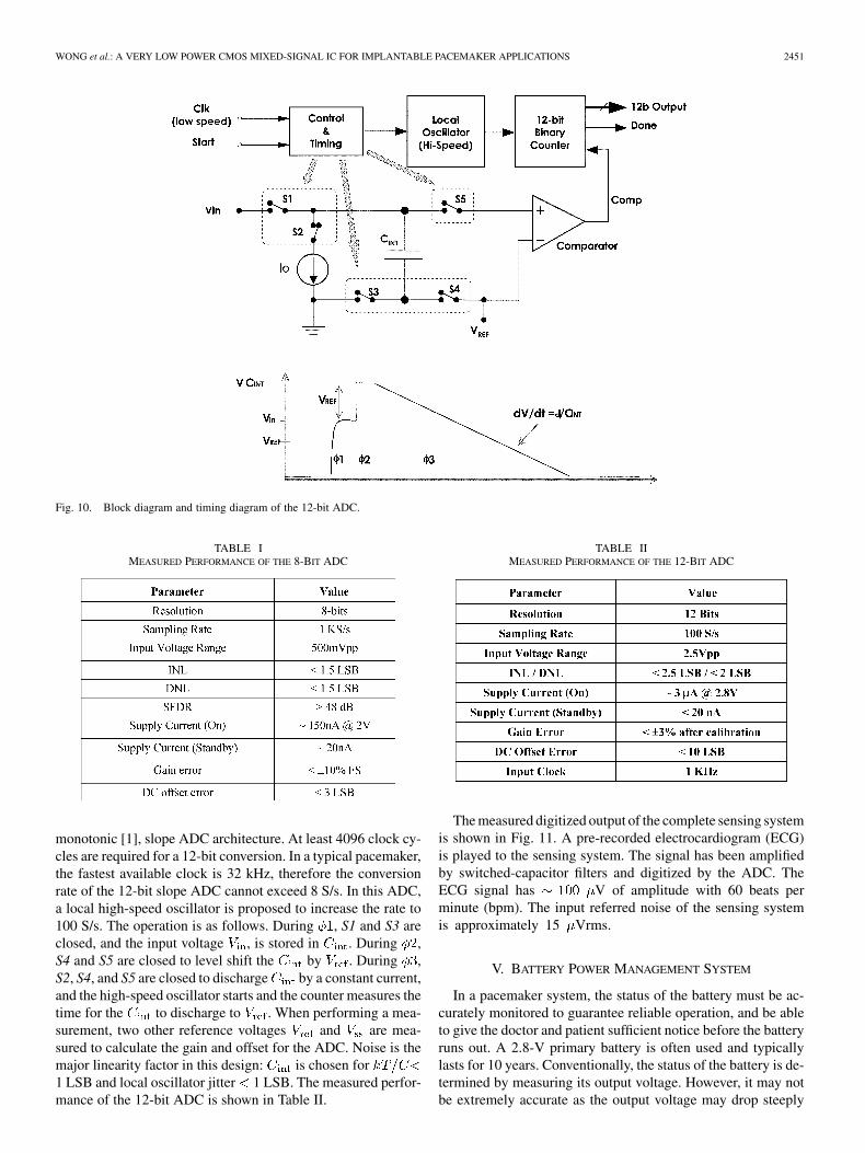
A 12-bit ADC may also be used in the system. The block di-agram of a 12-bit ADC is shown in Fig. 10. It is a low-power,
WONG et al.: A VERY LOW POWER CMOS MIXED-SIGNAL IC FOR IMPLANTABLE PACEMAKER APPLICATIONS 2451
Fig. 10. Block diagram and timing diagram of the 12-bit ADC.
TABLE IMEASURED PERFORMANCE OF THE 8-BIT ADC
monotonic [1], slope ADC architecture. At least 4096 clock cy-cles are required for a 12-bit conversion. In a typical pacemaker,the fastest available clock is 32 kHz, therefore the conversionrate of the 12-bit slope ADC cannot exceed 8 S/s. In this ADC,a local high-speed oscillator is proposed to increase the rate to100 S/s. The operation is as follows. During , S1 and S3 areclosed, and the input voltage , is stored in . During ,S4 and S5 are closed to level shift the by . During ,S2, S4, and S5 are closed to discharge by a constant current,and the high-speed oscillator starts and the counter measures thetime for the to discharge to . When performing a mea-surement, two other reference voltages and are mea-sured to calculate the gain and offset for the ADC. Noise is themajor linearity factor in this design: is chosen for1 LSB and local oscillator jitter 1 LSB. The measured perfor-mance of the 12-bit ADC is shown in Table II.
TABLE IIMEASURED PERFORMANCE OF THE 12-BIT ADC
The measured digitized output of the complete sensing systemis shown in Fig. 11. A pre-recorded electrocardiogram (ECG)is played to the sensing system. The signal has been amplifiedby switched-capacitor filters and digitized by the ADC. TheECG signal has V of amplitude with 60 beats perminute (bpm). The input referred noise of the sensing systemis approximately 15 Vrms.
V. BATTERY POWER MANAGEMENT SYSTEM
In a pacemaker system, the status of the battery must be ac-curately monitored to guarantee reliable operation, and be ableto give the doctor and patient sufficient notice before the batteryruns out. A 2.8-V primary battery is often used and typicallylasts for 10 years. Conventionally, the status of the battery is de-termined by measuring its output voltage. However, it may notbe extremely accurate as the output voltage may drop steeply

2452 IEEE JOURNAL OF SOLID-STATE CIRCUITS, VOL. 39, NO. 12, DECEMBER 2004
Fig. 11. Measured results for the complete sensing system, using a pre-recorded electrocardiogram (ECG).
Fig. 12. Battery management system.
when it approaches end-of-life. The block diagram of the bat-tery power management system is shown in Fig. 12. It consistsof a few reference voltage generators and voltage comparatorsto determine the battery status. To enhance the battery measure-ment accuracy, a new battery charge meter is proposed [5]. Thecharge meter consists of a voltage-controlled oscillator (VCO)and a binary counter. As shown in Fig. 12, all the battery cur-rent flows through a resistor and generates a voltage across it.The VCO senses the voltage across the resistor and integrates itcontinuously. The frequency of the VCO output is
(2)
where is the VCO gain. The output of the binary counteris
(3)
Rearranging (3) gives
(4)
The total amount of depleted charge from the battery can becalculated by (4). The battery charge meter provides better than0.5 A of resolution, so the VCO must have a low input offsetvoltage. The VCO also requires a very high linearity for accuratemeasurements over a wide input range. A switched-capacitorauto-zero VCO is used in this design, as shown in Fig. 13. Itconsists of an integrator and a comparator. Its operation can beexplained as follows. and are non-overlapping clocks.During : one end of the input voltage is sampled with auto-zero opamp configuration, the input voltage is stored on .During , the other end of the input voltage is sampled andintegrates the voltage difference. Depending on the state , theintegrator output either ramp up or down. The output stepsize at the end of each is
(5)
The output of the integrator will continue to ramp up or down,until it reaches the threshold voltage or . Once thethreshold is reached, the comparator will trip and the integratorgain will switch between positive and negative. This way,the integrator output will cycle between and with
WONG et al.: A VERY LOW POWER CMOS MIXED-SIGNAL IC FOR IMPLANTABLE PACEMAKER APPLICATIONS 2453
Fig. 13. Battery charge meter: switched-capacitor VCO implementation.
TABLE IIIMEASURED PERFORMANCE OF THE BATTERY CHARGE METER
a triangular waveform. The output of the comparator can be usedas the VCO output, and its frequency can be expressed as
(6)
The current consumption of the battery charge meter is mea-sured at 110 nA. Its performance is shown in Table III.
VI. HIGH-VOLTAGE GENERATOR
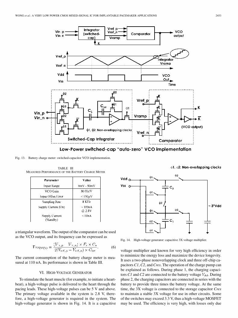
To stimulate the heart muscle (for example, to initiate a heart-beat), a high-voltage pulse is delivered to the heart through thepacing leads. These high-voltage pulses can be 5 V and above.The primary voltage available in the system is 2.8 V, there-fore, a high-voltage generator is required in the system. Thehigh-voltage generator is shown in Fig. 14. It is a capacitive
Fig. 14. High-voltage generator: capacitive 3X voltage multiplier.
voltage multiplier and known for very high efficiency in orderto minimize the energy loss and maximize the device longevity.It uses a two-phase nonoverlapping clock and three off-chip ca-pacitors C1, C2, and Cres. The operation of the charge pump canbe explained as follows. During phase 1, the charging capaci-tors C1 and C2 are connected to the battery voltage . Duringphase 2, the charging capacitors are connected in series with thebattery to provide three times the battery voltage. At the sametime, the 3X voltage is connected to the storage capacitor Cresto maintain a stable 3X voltage for use in other circuits. Someof the switches may exceed 3.3 V, thus a high-voltage MOSFETmay be used. The efficiency is very high, with losses only due
2454 IEEE JOURNAL OF SOLID-STATE CIRCUITS, VOL. 39, NO. 12, DECEMBER 2004
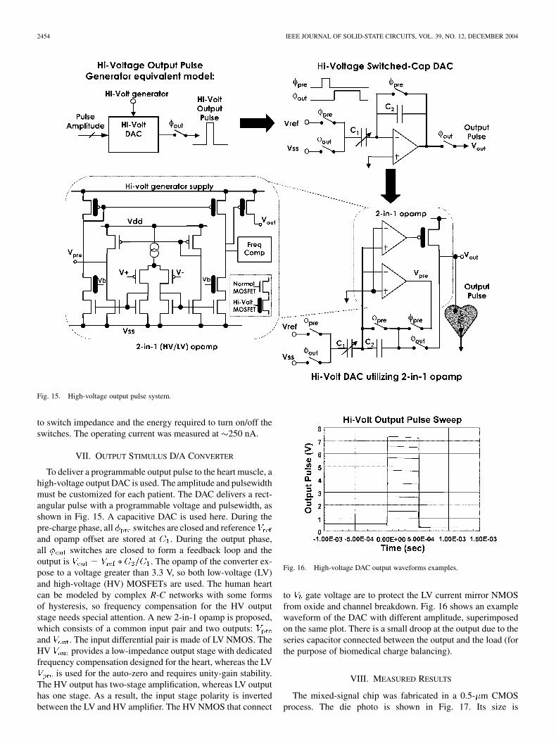
Fig. 15. High-voltage output pulse system.
to switch impedance and the energy required to turn on/off theswitches. The operating current was measured at 250 nA.
VII. OUTPUT STIMULUS D/A CONVERTER
To deliver a programmable output pulse to the heart muscle, ahigh-voltage output DAC is used. The amplitude and pulsewidthmust be customized for each patient. The DAC delivers a rect-angular pulse with a programmable voltage and pulsewidth, asshown in Fig. 15. A capacitive DAC is used here. During thepre-charge phase, all switches are closed and referenceand opamp offset are stored at . During the output phase,all switches are closed to form a feedback loop and theoutput is . The opamp of the converter ex-pose to a voltage greater than 3.3 V, so both low-voltage (LV)and high-voltage (HV) MOSFETs are used. The human heartcan be modeled by complex R-C networks with some formsof hysteresis, so frequency compensation for the HV outputstage needs special attention. A new 2-in-1 opamp is proposed,which consists of a common input pair and two outputs:and . The input differential pair is made of LV NMOS. TheHV provides a low-impedance output stage with dedicatedfrequency compensation designed for the heart, whereas the LV
is used for the auto-zero and requires unity-gain stability.The HV output has two-stage amplification, whereas LV outputhas one stage. As a result, the input stage polarity is invertedbetween the LV and HV amplifier. The HV NMOS that connect
Fig. 16. High-voltage DAC output waveforms examples.
to gate voltage are to protect the LV current mirror NMOSfrom oxide and channel breakdown. Fig. 16 shows an examplewaveform of the DAC with different amplitude, superimposedon the same plot. There is a small droop at the output due to theseries capacitor connected between the output and the load (forthe purpose of biomedical charge balancing).
VIII. MEASURED RESULTS
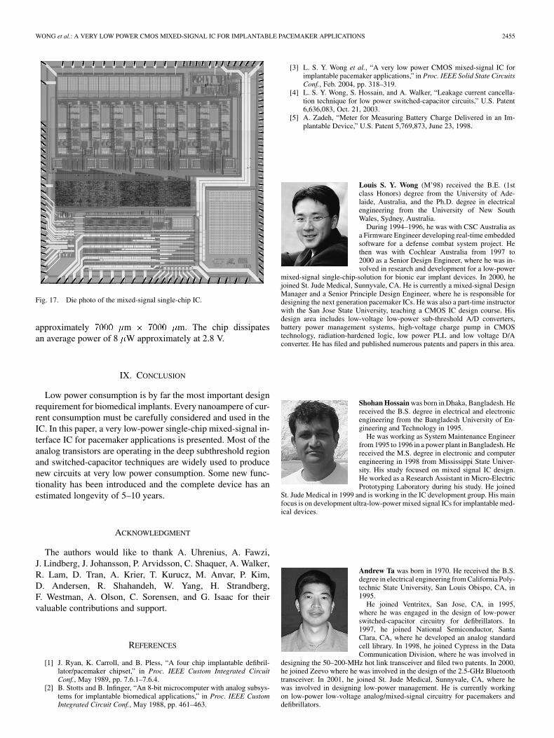
The mixed-signal chip was fabricated in a 0.5- m CMOSprocess. The die photo is shown in Fig. 17. Its size is
WONG et al.: A VERY LOW POWER CMOS MIXED-SIGNAL IC FOR IMPLANTABLE PACEMAKER APPLICATIONS 2455
Fig. 17. Die photo of the mixed-signal single-chip IC.
approximately m m. The chip dissipatesan average power of 8 W approximately at 2.8 V.
IX. CONCLUSION
Low power consumption is by far the most important designrequirement for biomedical implants. Every nanoampere of cur-rent consumption must be carefully considered and used in theIC. In this paper, a very low-power single-chip mixed-signal in-terface IC for pacemaker applications is presented. Most of theanalog transistors are operating in the deep subthreshold regionand switched-capacitor techniques are widely used to producenew circuits at very low power consumption. Some new func-tionality has been introduced and the complete device has anestimated longevity of 5–10 years.
ACKNOWLEDGMENT
The authors would like to thank A. Uhrenius, A. Fawzi,J. Lindberg, J. Johansson, P. Arvidsson, C. Shaquer, A. Walker,R. Lam, D. Tran, A. Krier, T. Kurucz, M. Anvar, P. Kim,D. Andersen, R. Shahandeh, W. Yang, H. Strandberg,F. Westman, A. Olson, C. Sorensen, and G. Isaac for theirvaluable contributions and support.
REFERENCES
[1] J. Ryan, K. Carroll, and B. Pless, “A four chip implantable defibril-lator/pacemaker chipset,” in Proc. IEEE Custom Integrated CircuitConf., May 1989, pp. 7.6.1–7.6.4.
[2] B. Stotts and B. Infinger, “An 8-bit microcomputer with analog subsys-tems for implantable biomedical applications,” in Proc. IEEE CustomIntegrated Circuit Conf., May 1988, pp. 461–463.
[3] L. S. Y. Wong et al., “A very low power CMOS mixed-signal IC forimplantable pacemaker applications,” in Proc. IEEE Solid State CircuitsConf., Feb. 2004, pp. 318–319.
[4] L. S. Y. Wong, S. Hossain, and A. Walker, “Leakage current cancella-tion technique for low power switched-capacitor circuits,” U.S. Patent6,636,083, Oct. 21, 2003.
[5] A. Zadeh, “Meter for Measuring Battery Charge Delivered in an Im-plantable Device,” U.S. Patent 5,769,873, June 23, 1998.
Louis S. Y. Wong (M’98) received the B.E. (1stclass Honors) degree from the University of Ade-laide, Australia, and the Ph.D. degree in electricalengineering from the University of New SouthWales, Sydney, Australia.
During 1994–1996, he was with CSC Australia asa Firmware Engineer developing real-time embeddedsoftware for a defense combat system project. Hethen was with Cochlear Australia from 1997 to2000 as a Senior Design Engineer, where he was in-volved in research and development for a low-power
mixed-signal single-chip-solution for bionic ear implant devices. In 2000, hejoined St. Jude Medical, Sunnyvale, CA. He is currently a mixed-signal DesignManager and a Senior Principle Design Engineer, where he is responsible fordesigning the next generation pacemaker ICs. He was also a part-time instructorwith the San Jose State University, teaching a CMOS IC design course. Hisdesign area includes low-voltage low-power sub-threshold A/D converters,battery power management systems, high-voltage charge pump in CMOStechnology, radiation-hardened logic, low power PLL and low voltage D/Aconverter. He has filed and published numerous patents and papers in this area.
Shohan Hossain was born in Dhaka, Bangladesh. Hereceived the B.S. degree in electrical and electronicengineering from the Bangladesh University of En-gineering and Technology in 1995.
He was working as System Maintenance Engineerfrom 1995 to 1996 in a power plant in Bangladesh. Hereceived the M.S. degree in electronic and computerengineering in 1998 from Mississippi State Univer-sity. His study focused on mixed signal IC design.He worked as a Research Assistant in Micro-ElectricPrototyping Laboratory during his study. He joined
St. Jude Medical in 1999 and is working in the IC development group. His mainfocus is on development ultra-low-power mixed signal ICs for implantable med-ical devices.
Andrew Ta was born in 1970. He received the B.S.degree in electrical engineering from California Poly-technic State University, San Louis Obispo, CA, in1995.
He joined Ventritex, San Jose, CA, in 1995,where he was engaged in the design of low-powerswitched-capacitor circuitry for defibrillators. In1997, he joined National Semiconductor, SantaClara, CA, where he developed an analog standardcell library. In 1998, he joined Cypress in the DataCommunication Division, where he was involved in
designing the 50–200-MHz hot link transceiver and filed two patents. In 2000,he joined Zeevo where he was involved in the design of the 2.5-GHz Bluetoothtransceiver. In 2001, he joined St. Jude Medical, Sunnyvale, CA, where hewas involved in designing low-power management. He is currently workingon low-power low-voltage analog/mixed-signal circuitry for pacemakers anddefibrillators.
2456 IEEE JOURNAL OF SOLID-STATE CIRCUITS, VOL. 39, NO. 12, DECEMBER 2004
Jörgen Edvinsson received the M.Sc. degree in elec-trical engineering in 1998 from the Royal Institute ofTechnology, Sweden.
He joined St. Jude Medical in 1990 and has beenworking with analog and mixed-signal IC design forpacemakers.
Dominic H. Rivas was born in 1970. He received theB.S. degree in electrical engineering from LinköpingInstitute of Technology, Sweden, in 1996.
He is a Senior Design Engineer with St. Jude Med-ical AB, Sweden. Prior to joining St. Jude Medical,he worked for Ericsson Components AB and NokiaTelecommunications AB on analog integrated circuitdesign.
Hans Nääs received the M.Sc. degree in appliedphysics and electrical engineering from the Univer-sity of Linköping, Sweden.
He joined St. Jude Medical in 2000, where he hasbeen engaged in the development of next-generationpacemakers.
Copyright © 2022 FDOKUMEN