iC-NV, iC-NVH 6-Bit Sin/D Flash Converter
22
iC-NV, iC-NVH 6-Bit Sin/D Flash Converter Rev E1, Page 1/22 FEATURES Fast flash converter Integrated glitch filter; minimum transition distance can be set using the optional resistor Selectable resolution of up to 64 steps per cycle and up to 16-fold interpolation Integrated instrumentation amplifiers with adjustable gain Direct connection of sensor bridges, no external components required 200 kHz input frequency with the highest resolution Incremental A QUAD B output of up to 3.2 MHz Reversed A/B phase selectable Index signal processing with 1/4 T gating (iC-NV), or with 1/2 T gating (iC-NVH) Sensor bridge calibration supportable by analog/digital test signals Low power consumption from single 5V supply TTL- /CMOS-compatible outputs Inputs and outputs protected against destruction by ESD APPLICATIONS Angle interpolation from orthogonal sinusoidal input signals Linear and rotary encoders MR sensor systems PACKAGES TSSOP20 RoHS compliant BLOCK DIAGRAM Z VCC STEP/CYCLE SELECT COS + - - + INPUT SIN VCC TRANSITION - INPUT ZERO - + VREF + INPUT COS DISTANCE PRESET - + GAIN SELECT SIN VCC VREF Z SF0 SF1 SG0 SG1 VCC VDD NSIN NZERO PCOS PSIN PZERO RCLK ROT A B GND GNDA NCOS COSINE SINE +5V 0V A B +5V iC-NV iC-NVH CONVERSION CORE DIGITAL TRANSITION DISTANCE CONTROL PROCESSING Copyright © 2001, 2019 iC-Haus http://www.ichaus.com
-
Upload
khangminh22 -
Category
Documents
-
view
1 -
download
0
Transcript of iC-NV, iC-NVH 6-Bit Sin/D Flash Converter

iC-NV, iC-NVH6-Bit Sin/D Flash Converter
Rev E1, Page 1/22
FEATURES
Fast flash converter Integrated glitch filter; minimum transition distance can be set
using the optional resistor Selectable resolution of up to 64 steps per cycle and up to
16-fold interpolation Integrated instrumentation amplifiers with adjustable gain Direct connection of sensor bridges, no external components
required 200 kHz input frequency with the highest resolution Incremental A QUAD B output of up to 3.2 MHz Reversed A/B phase selectable Index signal processing with 1/4 T gating (iC-NV),
or with 1/2 T gating (iC-NVH) Sensor bridge calibration supportable by analog/digital test
signals Low power consumption from single 5V supply TTL- /CMOS-compatible outputs Inputs and outputs protected against destruction by ESD
APPLICATIONS
Angle interpolation fromorthogonal sinusoidal inputsignals
Linear and rotary encoders MR sensor systems
PACKAGES
TSSOP20RoHS compliant
BLOCK DIAGRAM
Z
VCC
STEP/CYCLESELECT
COS+
-
-
+
INPUT SIN
VCC
TRANSITION
-
INPUT ZERO-
+
VREF
+
INPUT COS
DISTANCE PRESET
-
+
GAIN SELECT
SIN
VCC
VREF
Z
SF0SF1SG0SG1
VCC VDD
NSIN
NZERO
PCOS
PSIN
PZERO
RCLK
ROT
A
B
GNDGNDA
NCOS
COSINE
SINE
+5V
0V
A
B
+5V
iC-NViC-NVH
CONVERSION COREDIGITALTRANSITION
DISTANCE CONTROL PROCESSING
Copyright © 2001, 2019 iC-Haus http://www.ichaus.com

iC-NV, iC-NVH6-Bit Sin/D Flash Converter
Rev E1, Page 2/22
DESCRIPTION
iC-NV is a monolithic A/D converter which producestwo digital A/B incremental signals phase-shiftedat 90° from two sinusoidal input signals, alsophase-shifted at 90°.
The converter operates on the flash principle with fastsingle comparators. The back-end signal processingcircuit includes a no-delay glitch filter which can beset so that only clearly countable incremental signalsare generated. The minimum transition distance foroutputs A and B can be set via an external resistorand adapted to suit the application on hand. For staticinput signals hysteresis prevents the switching of theoutputs.
By programming the pins the interpolator can be setto nine different resolutions between 4 and 64 anglesteps per cycle; multiplication values of between 1and 16 are possible for the frequency. The phaserelation between the sine/cosine input signals and the
A/B incremental signals generated can be selectedhere.
The device also incorporates an index signal process-ing circuit which generates a digital zero pulse at Zdependent on the analog sine/cosine input signalsand the enable input ZERO. Alternatively, the con-verter MSB can also be output at Z for synchronizationpurposes in an absolute measuring system.
The input amplifiers are configured as instrumenta-tion amplifiers and permit sensor bridges to be directlyconnected without the need for external resistors. Theinput amplification has nine selectable settings whichhave been graded to suit standard sensor signals ofbetween approx. 10 mVpk and 1 Vpk. If external cal-ibration of the sensor bridge is required, e.g. withregard to offset, various test functions can be acti-vated. By this the amplified analog input signals comeavailable at the outputs, for instance.
iC-NV, iC-NVH6-Bit Sin/D Flash Converter
Rev E1, Page 3/22
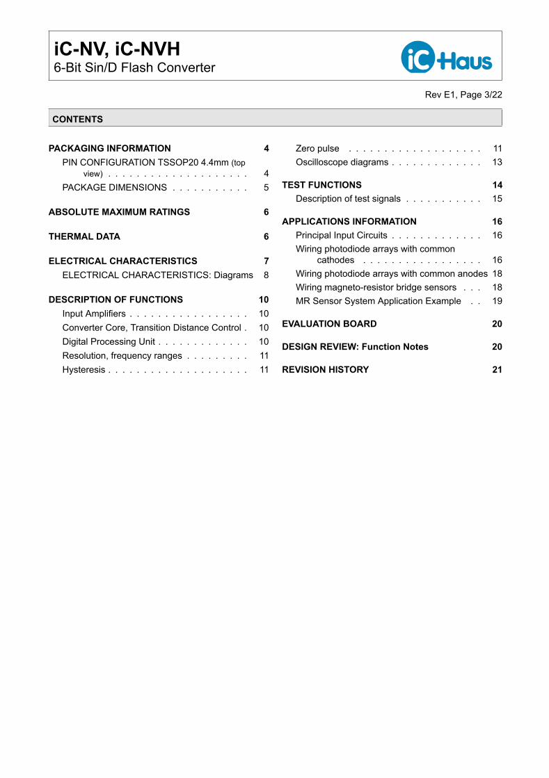
CONTENTS
PACKAGING INFORMATION 4PIN CONFIGURATION TSSOP20 4.4mm (top
view) . . . . . . . . . . . . . . . . . . . . 4PACKAGE DIMENSIONS . . . . . . . . . . . 5
ABSOLUTE MAXIMUM RATINGS 6
THERMAL DATA 6
ELECTRICAL CHARACTERISTICS 7ELECTRICAL CHARACTERISTICS: Diagrams 8
DESCRIPTION OF FUNCTIONS 10Input Amplifiers . . . . . . . . . . . . . . . . . 10Converter Core, Transition Distance Control . 10Digital Processing Unit . . . . . . . . . . . . . 10Resolution, frequency ranges . . . . . . . . . 11Hysteresis . . . . . . . . . . . . . . . . . . . . 11
Zero pulse . . . . . . . . . . . . . . . . . . . 11Oscilloscope diagrams . . . . . . . . . . . . . 13
TEST FUNCTIONS 14Description of test signals . . . . . . . . . . . 15
APPLICATIONS INFORMATION 16Principal Input Circuits . . . . . . . . . . . . . 16Wiring photodiode arrays with common
cathodes . . . . . . . . . . . . . . . . . 16Wiring photodiode arrays with common anodes 18Wiring magneto-resistor bridge sensors . . . 18MR Sensor System Application Example . . 19
EVALUATION BOARD 20
DESIGN REVIEW: Function Notes 20
REVISION HISTORY 21

iC-NV, iC-NVH6-Bit Sin/D Flash Converter
Rev E1, Page 4/22
PACKAGING INFORMATION
PIN CONFIGURATION TSSOP20 4.4mm (top view)
1
2
3
4
5
6
7
8
9
10 11
12
13
14
15
16
17
18
19
20
<P-CODE>
<A-CODE>
<D-CODE>
PCOS
ZGNDSF0SF1ROTVREFSG0SG1NCOS PSIN
NZEROPZEROGNDAVCCRCLKVDDAB
NSIN
PIN FUNCTIONSNo. Name Function
1 PCOS Input Cosine +2 NCOS Input Cosine -3 SG1 Gain Select Input4 SG0 Gain Select Input5 VREF Reference Voltage Output6 ROT A/B Phase Selection,
Test Signal S6 Input/Output7 SF1 Resolution Selection,
Test Signal S5 Input/Output8 SF0 Resolution Selection,
Test Signal S4 Input/Output9 GND Ground (digital)
10 Z (MSB) Index Signal Output Z(MSB Output when ROT= open),Test Signal S3 Input/Output
11 B Incremental Output B,Test Signal S2 Input/Output
12 A Incremental Output A,Test Signal S1 Input/Output
13 VDD +5 V Supply Voltage (digital)14 RCLK Min. Transition Distance Preset Input
(use is optional; can be wired to VCC)15 VCC 1 +5 V Supply Voltage (analog)16 GNDA 1 Ground (analog)17 PZERO Index Signal Enable Input +18 NZERO Index Signal Enable Input -19 PSIN Input Sine +20 NSIN Input Sine -
IC top marking: <P-CODE> = product code, <A-CODE> = assembly code (subject to changes), <D-CODE> = date code (subject to changes);1 External connections linking VCC to VDD and GND to GNDA are required.

iC-NV, iC-NVH6-Bit Sin/D Flash Converter
Rev E1, Page 5/22
PACKAGE DIMENSIONS
6.50
4.40
6.40
0.65 0.25
TOP
0.90
0.10
SIDE
0.15
0.60
4°
FRONT
0.65 1.60
5.40 0.40
RECOMMENDED PCB-FOOTPRINT
drb_tssop20-1_pack_1, 8:1
All dimensions given in mm. Tolerances of form and position according to JEDEC MO-153

iC-NV, iC-NVH6-Bit Sin/D Flash Converter
Rev E1, Page 6/22
ABSOLUTE MAXIMUM RATINGS
Beyond these values damage may occur; device operation is not guaranteed.Item Symbol Parameter Conditions UnitNo. Min. Max.G001 VCC Voltage at VCC -0.3 6 VG002 VDD Voltage at VDD -0.3 6 VG003 V() Voltage at
NSIN, PSIN, NCOS, PCOS, NZERO,PZERO, SG1, SG0, RCLK SF1, SF0,ROT, A, B, Z
V() < VCC + 0.3 V -0.3 6 VV() < VDD + 0.3 V
G004 Imx(VCC) Current in VCC -50 50 mAG005 Imx(GNDA) Current in GNDA -50 50 mAG006 Imx(VDD) Current in VDD -50 50 mAG007 Imx(GND) Current in GND -50 50 mAG008 Imx() Current in
NSIN, PSIN, NCOS, PCOS,NZERO, PZERO, SG1, SG0, VREF,RCLK, SF1, SF0, ROT, A, B, Z
-10 10 mA
G009 Ilu() Pulse Current in all pins(Latch-up strength)
pulse duration < 10µs -100 100 mA
G010 Vd() ESD Susceptibility at all pins 100 pF discharged through 1.5 kΩ 2 kVG011 Tj Junction Temperature -40 150 °C
THERMAL DATA
Operating Conditions: VCC = VDD = 5 V ±10 %Item Symbol Parameter Conditions UnitNo. Min. Typ. Max.
T01 Ta Operating Ambient Temperature Range -25 85 °CTSSOP20 ET -40/125 -40 125 °C
T02 Ts Storage Temperature Range -40 165 °C
All voltages are referenced to ground unless otherwise stated.All currents flowing into the device pins are positive; all currents flowing out of the device pins are negative.

iC-NV, iC-NVH6-Bit Sin/D Flash Converter
Rev E1, Page 7/22
ELECTRICAL CHARACTERISTICS
Operating Conditions: VCC = VDD = 5 V ±10 %, Tj = -40...125 °C, unless otherwise noted.Item Symbol Parameter Conditions UnitNo. Min. Typ. Max.Total Device001 VCC, VDD Permissible Supply Voltage 4.5 5.5 V002 I(VCC) Supply Current in VCC fin() = 200 kHz; A, B, Z open 15 mA003 I(VDD) Supply Current in VDD fin() = 200 kHz; A, B, Z open 5 mA004 Von Power-On Reset Threshold 2 3.8 V005 Voff Power-Down Reset Threshold 1 2.2 V006 Vhys Power-On Reset Hysteresis 0.4 1.8 V007 Vc()hi Clamp Voltage hi at
NSIN, PSIN, NCOS, PCOS,NZERO, PZERO, SG1, SG0,ROT, SF1, SF0, VREF, RCLK
Vc()hi = V()- VCC; 0.3 1.6 VI() = 1 mA, other pins open
008 Vc()lo Clamp Voltage lo atNSIN, PSIN, NCOS, PCOS,NZERO, PZERO, SG1, SG0,ROT, SF1, SF0, VREF, RCLK, A,B, Z
I() = -1 mA, other pins open -1.5 -0.3 V
009 Vc()hi Clamp Voltage hi atA, B, Z
Vc()hi = V() - VDD; 0.3 1.6 VI() = 1 mA, other pins open
Input Amplifiers NSIN, PSIN, NCOS, PCOS101 Vos() Input Offset Voltage Vin() see table gain select
GAIN = 10...66 -7 7 mVGAIN = 3...7.1 -10 10 mV
102 Iin() Input Current V() = 0 V...VCC -50 50 nA103 G() Gain GAIN following table gain select 95 101 %104 Grel Gain Ratio SIN/COS GAIN following table gain select 98 102 %105 fhc Cut-off Frequency GAIN = 66.667 0.5 MHz
GAIN = 3.03 2.3 MHz106 SR Slew Rate GAIN = 66.667 10 V/µs
GAIN = 3.03 15 V/µsSignal Processing: Converter Accuracy201 AAabs Absolute Angle Accuracy referred to 360° input signal,
GAIN =3.03;VPin = 2...2.6 Vpp, VNin = 2.5 Vdc -1 1 DEGVPin = 1...1.3 Vpp, VNin = 2.5 Vdc -2 2 DEG
202 AArel Relative Angle Accuracy referred to period of A, B (see figure 7)GAIN = 3.03 -10 10 %
VREF401 V(VREF) Reference Voltage at VREF I(VREF) = -1 mA...+1 mA 48 52 %VCC
Signal Processing: Transition Distance Control501 RCLK Permissible Resistor at
RCLK vs. GNDADIV = 1 (IPF = 10, 12, 16) 47 500 kΩDIV = 2 (IPF = 5, 8) 23 500 kΩDIV = 4 (IPF = 3, 4) 12 500 kΩDIV = 8 (IPF = 2) 6 500 kΩDIV = 16 (IPF = 1) 3 500 kΩ
502 DT() Minimum Transition Distance R(RCLK, GNDA) = 47 kΩ 1%;DIV = 1 (see figure 4) 45 78 nsDIV = 16 (see figure 2) 490 1000 ns
503 DT() Minimum Transition Distance V(RCLK) = VCC;DIV = 1 30 78 nsDIV = 16 420 1000 ns
Zero Comparator701 Vos() Input Offset Voltage V() = Vcm() -20 20 mV702 Iin() Input Current V() = 0 V ... VCC -50 50 nA703 Vcm() Common-Mode Input Volt. Range 1.4 VCC
-1.5V
704 Vdm() Differential Input Voltage Range 0 VCC V

iC-NV, iC-NVH6-Bit Sin/D Flash Converter
Rev E1, Page 8/22
ELECTRICAL CHARACTERISTICS
Operating Conditions: VCC = VDD = 5 V ±10 %, Tj = -40...125 °C, unless otherwise noted.Item Symbol Parameter Conditions UnitNo. Min. Typ. Max.Signal Processing: Inputs SG1, SG0, ROT, SF1, SF0801 Vt()hi Input Threshold Voltage hi 60 78 %VCC802 Vt()lo Input Threshold Voltage lo 25 40 %VCC803 V0() Mid Level Voltage 43 57 %VCC804 Ri() Input Resistance 45 150 220 kΩ
Signal Processing: Outputs A, B, ZD01 Vs()hi Saturation Voltage hi Vs()hi = VDD - V(); I() = -4 mA 0.4 VD02 Vs()lo Saturation Voltage lo I() = 4 mA 0.4 VD03 tr() Rise Time CL() = 50 pF 60 nsD04 tf() Fall Time CL() = 50 pF 60 ns
ELECTRICAL CHARACTERISTICS: Diagrams
min.
1μs
RCLK= 300kΩ200kΩ
2μs
400kΩ 500kΩ
IPF= 2
3μs
4μs
5μs
6μs
DT() IPF= 1
max.
100kΩ
7μs
Figure 1: Adjusting the minimum transition distance viaresistor RCLK (given typical at 5V, 27°C; for IPF=1 within 5V ±10% and -40..+125°C ranges).
min.
20kΩ15kΩ 100kΩ
IPF= 20.2μs
0.4μs
IPF= 1
max.
10kΩRCLK= 40kΩ 50kΩ30kΩ
1.4μs
DT()
1.0μs
1.2μs
0.6μs
0.8μs
5kΩ
1.6μs
Figure 2: Similar to Figure 1; the minimum transitiondistance can be reduced by smaller resistorsRCLK.
0.2μs
RCLK= 300kΩ200kΩ
0.8μs
400kΩ 500kΩ
IPF= 16
IPF= 81μs
1.2μs
1.4μs
1.6μsIPF= 4
0.6μs
0.4μs
DT()
100kΩ
1.8μs
Figure 3: Adjusting the minimum transition distance viaresistor RCLK.
20kΩ15kΩ 100kΩ
IPF= 1650ns
100ns
IPF= 8
10kΩRCLK= 40kΩ 50kΩ30kΩ
350ns
DT()
250ns
300ns
150ns
200ns
IPF= 4
5kΩ
400ns
Figure 4: Similar to Figure 3; minimum transition distancefor smaller RCLK resistor values.

iC-NV, iC-NVH6-Bit Sin/D Flash Converter
Rev E1, Page 9/22
RCLK= 300kΩ200kΩ
-1%
400kΩ 500kΩ
+125°C vs. 27°C
0%
+1%
∆DT()
-3%
+2%
-2%
-40°C vs. 27°C
100kΩ
+3%
Figure 5: Temperature drift of the minimum transitiondistance versus 27°C (VDD= 5V).
10kΩ 40kΩ20kΩ
-2%
100kΩ
+125°C vs. 27°C
0%
+2%
+6%
-6%
+4%
-4%
-40°C vs. 27°C
RCLK=
∆DT()
Figure 6: Temperature drift of the reduced minimumtransition distance versus 27°C (VDD= 5V).
twhi()/T
AArel ±10%
60%50%
40%0%
110%
AArel ±10%
90%
100%
0%
Figure 7: Definition of the relative angle accuracy.

iC-NV, iC-NVH6-Bit Sin/D Flash Converter
Rev E1, Page 10/22
DESCRIPTION OF FUNCTIONS
Input AmplifiersInput stages SIN and COS are configured as instru-mentation amplifiers. The gain is dependent on theamplitude of the input signal and set via pins SG0 and
SG1 according to the following table. So that the DClevel to be adjusted half of the supply voltage is avail-able at VREF.
GAIN SELECT
SG1 SG0 GainSine/Cosine Input Signal Levels Vin()
Amplitude Average value (DC)differential single ended differential single ended
hi hi 66.667 up to 60 mVpp up to 120 mVpp 0.7 V ... VCC – 1.2 V 0.7 V ... VCC – 1.2 V
hi open 50.000 up to 80 mVpp up to 160 mVpp 0.7 V ... VCC – 1.2 V 0.7 V ... VCC – 1.2 V
hi lo 33.333 up to 120 mVpp up to 240 mVpp 1.2 V ... VCC – 1.2 V 1.2 V ... VCC – 1.3 V
open hi 20.000 up to 0.2 Vpp up to 0.4 Vpp 1.2 V ... VCC – 1.2 V 1.2 V ... VCC – 1.3 V
open open 14.300 up to 0.28 Vpp up to 0.56 Vpp 0.7 V ... VCC – 1.3 V 0.8 V ... VCC – 1.4 V
open lo 10.000 up to 0.4 Vpp up to 0.8 Vpp 1.2 V ... VCC – 1.3 V 1.3 V ... VCC – 1.5 V
lo hi 7.125 up to 0.56 Vpp up to 1.1 Vpp 1.2 V ... VCC – 1.4 V 1.4 V ... VCC – 1.7 V
lo open 4.000 up to 1 Vpp up to 2 Vpp 1.2 V ... VCC – 1.6 V 1.6 V ... VCC – 2.1 V
lo lo 3.030 up to 1.3 Vpp up to 2.6 Vpp 1.2 V ... VCC – 1.7 V 1.8 V ... VCC – 2.4 V
Table 4: Input gainConverter Core, Transition Distance ControlFor each of the 64 comparator levels the sine/cosineinput signals are calculated according to the theorem ofaddition and are fed into single comparators. This pro-cedure guarantees a very high converter frequency yetalso means that consecutive comparators can switchin a very short space of time in the event of input signaldisturbances.
The comparator outputs are thus fed into a transitiondistance control unit. This monitors the temporal se-quence of the switching operations in such a way thateach event is delayed by the length of the settable min-imum gap to the previous event. If no errors arise thetransitions pass the control unit without a time delay.Synchronization with a fixed clock pulse does not occur.
The minimum transition distance is set via an externalresistor positioned between RCLK and GNDA. Alterna-
tively, pin RCLK can be shorted to VCC. Depending onthe resolution maximum input frequencies of at least200kHz are then guaranteed (see table of resolution).
Digital Processing UnitThe transition distance control unit is followed by the dig-ital processing unit. This is where the transition eventsare converted into a pulse sequence for the incrementaloutputs A and B. The square-wave signals generatedhave a phase shift of +90° or -90°, depending on thedirection of rotation. The phase relation between thesine/cosine input signals and the A/B output signals canbe set using programming pin ROT.
Alternatively, the MSB of the converter can be output toZ when ROT is high. With the zero signal this changesto high and has the pulse length of half a cycle. Thissignal can be used to synchronize the high-order tracksof an absolute-value encoder device.
A/B OUTPUT PHASE SELECTIONROT Input signals Output signals A, B; Z
lo positive; COS leading SIN B leading A; Z
lo negative; SIN leading COS A leading B; Z
open positive; COS leading SIN B leading A; MSB
open negative; SIN leading COS A leading B; MSB
hi positive; COS leading SIN A leading B; Z
hi negative; SIN leading COS B leading A; Z
Table 5: Output phase

iC-NV, iC-NVH6-Bit Sin/D Flash Converter
Rev E1, Page 11/22
Resolution, frequency rangesNine different resolutions or interpolation factors (IPF)can be programmed via inputs SF0 and SF1. Res-olutions 16, 12 and 10 are generated at the core ofthe converter itself. Resolutions of less than 10 areproduced by division DIV in the digital processing unit.The minimum transition distance at outputs A and Bcorresponds to that of the transition distance controlmultiplied by the divisor of the digital processing unit.
The minimum output transition distance (maximum out-put frequency) should be adjusted to tarry with the over-all system (bandwidth of the transfer medium, samplingrate of the counter). The maximum input frequency isdetermined by the transition distance control and theresolution of the converter core (16, 12 or 10). This fre-quency can be increased for resolutions of less than 10with an external resistor at RCLK. The following tablegives possible settings.
RESOLUTION
SF1 SF0 IPFDIVinternaldivision
finMAX
finMAXfor RCLK = VCCor RCLK = 47 kΩ
hi hi 16 1 200 kHz, RCLK = 47 kΩ 200 kHz
hi open 12 1 260 kHz, RCLK = 47 kΩ 260 kHz
hi lo 10 1 320 kHz, RCLK = 47 kΩ 320 kHz
open hi 8 2 400 kHz, RCLK = 23 kΩ 200 kHz
open open 5 2 640 kHz, RCLK = 23 kΩ 320 kHz
open lo 4 4 800 kHz, RCLK = 12 kΩ 200 kHz
lo hi 3 4 1.04 MHz, RCLK = 12 kΩ 260 kHz
lo open 2 8 1.6 MHz, RCLK = 6 kΩ 200 kHz
lo lo 1 16 (3.2 MHz), RCLK = 3 kΩ 200 kHz
Table 6: ResolutionHysteresisiC-NV has an angular hysteresis which is independentof the input amplitude and phase. It prevents the out-puts from switching when the inputs are static.
When the direction of rotation is reversed the integratedhysteresis circuit prompts the change in direction to be
signaled at the outputs; the hysteresis causes a delayhere. Figure 8 shows this effect for an interpolationfactor of 8.
According to the resolution the hysteresis is set to afixed value as listed in Table 7.
45°39.375°33.75°28.125° 50.625° 45° 39.375° 33.75° 28.125° 22.5° 16.875°
B8
A8
positive direction of rotation negative direction of rotation
50.625°
HYS
φ
Figure 8: Effect of angle hysteresis
ANGLE HYSTERESISInterpolation factor IPF 1 2 3 4 5 8 10 12 16
Hysteresis [deg] 5.625 ° 5.625 ° 7.5 ° 5.625 ° 9 ° 5.625 ° 9 ° 7.5° 5.625 °
Referred to A/B period 1/64 1/32 1/16 1/16 1/8 1/8 1/4 1/4 1/4
Table 7: Hysteresis

iC-NV, iC-NVH6-Bit Sin/D Flash Converter
Rev E1, Page 12/22
Zero pulseOne zero pulse (index) is generated per cycle from thesine/cosine inputs. To be output to Z it must be enabledby the comparator at differential inputs PZERO andNZERO.
For iC-NV: The width of the zero pulse is a quarter ofthe length of the A and/or B signal output cycle. WhenZ is high, simultaneously AB are high.
For iC-NVH: The width of the zero pulse is half thelength of the A and/or B signal output cycle. When Z ishigh, simultaneously A is high.
The position of the zero pulse dependent on the inter-polation factor and the direction of rotation is given inthe following tables.
INDEX WIDTH and POSITION of iC-NVZ Position Z Position
IPF Z Width with positive direction of rotation with negative direction of rotation16 5.625 ° 45 ° ... 50.625 ° 39.375 ° ... 45 °
12 7.5 ° 45 ° ... 52.5 ° 37.5 ° ... 45 °
10 9 ° 45 ° ... 54 ° 36 ° ... 45 °
8 11.25 ° 39.375 ° ... 50.625 ° 33.75 ° ... 45 °
5 18 ° 36 ° ... 54 ° 27 ° ... 45 °
4 22.5 ° 33.75 ° ... 56.25 ° 28.125 ° ... 50.625 °
3 30 ° 30 ° ... 60 ° 22.5 ° ... 52.5 °
2 45 ° 22.5 .. 67.5 ° 16.875 ° ... 61.875 °
1 90 ° 0 ° ... 90 ° 354.375 ° ... 84.625 °
Table 8: Index width and position (iC-NV)
INDEX WIDTH and POSITION of iC-NVHZ Position Z Position
IPF Z Width with positive direction of rotation with negative direction of rotation16 11.25 ° 45 ° ... 56.25 ° 39.375 ° ... 50.625 °
12 15 ° 45 ° ... 60 ° 37.5 ° ... 52.5 °
10 18 ° 45 ° ... 63 ° 36 ° ... 54 °
8 22.5 ° 39.375 ° ... 61.875 ° 33.75 ° ... 56.25 °
5 36 ° 36 ° ... 72 ° 27 ° ... 63 °
4 45 ° 33.75 ° ... 78.75 ° 28.125 ° ... 73.125 °
3 60 ° 30 ° ... 90 ° 22.5 ° ... 82.5 °
2 90 ° 22.5 .. 112.5 ° 16.875,° ... 106.875 °
1 180 ° 0 ° ... 180 ° 354.375 ° ... 174.625 °
Table 9: Index width and position (iC-NVH)

iC-NV, iC-NVH6-Bit Sin/D Flash Converter
Rev E1, Page 13/22
Oscilloscope diagramsThe following diagrams give the input and output signals for various directions of rotation and ROT settings forinterpolation factors 1 and 16.
Figure 9: iC-NV: ROT= lo/open, COS leading SIN
180 90 45 0 -90 -180 Angle
SIN
A1
COS
B1Z1(ROT= lo)
Z1(ROT= open)
A16B16
Z16(ROT= lo)Z16(ROT= open)
Figure 10: iC-NV: ROT= lo/open, SIN leading COS
Figure 11: iC-NV: ROT= hi, COS leading SIN Figure 12: iC-NV: ROT= hi, SIN leading COS
Figure 13: iC-NVH: ROT= lo/open, COS leading SIN Figure 14: iC-NVH: ROT= lo/open, SIN leading COS
Figure 15: iC-NVH: ROT= hi, COS leading SIN Figure 16: iC-NVH: ROT= hi, SIN leading COS

iC-NV, iC-NVH6-Bit Sin/D Flash Converter
Rev E1, Page 14/22
TEST FUNCTIONS
Device iC-NV features internal test functions which canbe used to ease sensor bridge calibration procedures ifsuch are required. To enable test operation, a thresholdcurrent of approx. 1 mA present at pin RCLK must be
exceeded during power up. Subsequently, four differ-ent test modes are selectable starting with mode 3 setinitially.
0V
+5V
+12V
C64.7μF
500kΩR4
R1100Ω
S1C71μF
5kΩR2R3
5kΩ
VCC
STEP/CYCLE SELECT
COS
CONVERSION CORE+
-
-
VCC
DIGITAL PROCESSING
-
INPUT ZERO
-
+
REF
+
+
INPUT COS
INPUT SIN
-
+
GAIN SELECT
SIN
VCC
SG0SG1
VCC VDD
VREF
Z
PSIN
PZERO
RCLK
ROT SF0SF1
B
GNDGNDA
NCOS
NSIN
NZERO
PCOS
AS1
S2
S3
+5V
iC-NV
C4100nF
C11μF
C2
C3
C5100nF
03 1 2 3
S4
S5
S6
trigger current
Figure 17: Activating test functions via pin RCLK.

iC-NV, iC-NVH6-Bit Sin/D Flash Converter
Rev E1, Page 15/22
Description of test signals
Test Signal DescriptionMode 3
ZK Un-gated index/zero comparator output
EXKA All comparators EXOR-gated
SIN, NSIN, COS, NCOS Amplifier outputs (signal valid with no load only)
Mode 0KA(0) Comparator 0 °– 180 °→ Duty cycle indicates offset of sine signal.
KA(16) Comparator 90 °– 270 °→ Duty cycle indicates offset of cosine signal.
KA(X) = KA(8) EXOR KA(24) Comparator 45 °– 225 °→ Duty cycle indicates amplitude ratio ofsine/cosine signal. Offset calibration must be performed first.
Mode 1CLK, UP, DN Control signals for external counters.
Mode 2NENOS, CLK, DALL Test signals for iC-Haus device test.
Table 10: Test modes
Test Mode S1 (A) S2 (B) S3 (Z) S4 (SF0) S5 (SF1) S6 (ROT)Mode 3 ZK EXKA SIN NSIN COS NCOS
Mode 0 KA(0) KA(16) KA(X)
Mode 1 CLK UP DN
Mode 2 NENOS CLK DALL
Table 11: Illustration of output signals during test modes

iC-NV, iC-NVH6-Bit Sin/D Flash Converter
Rev E1, Page 16/22
APPLICATIONS INFORMATION
Principal Input Circuits
Figure 18: Input circuit for voltage signals of 1Vpp withno ground reference. When grounds are notseparated the connection NSIN to VREF mustbe omitted.
Figure 19: Input circuit for current signals of 11µA. In thiscircuit offset adjustment is not possible.
Figure 20: Input circuit for single-side voltage or currentsource signals with ground reference (adapta-tion via resistors R3, R4).
Figure 21: Simplified input wiring for single-side voltagesignals with ground reference.
Figure 22: Input circuit for differential current sink sen-sor outputs, e.g. using Opto EncoderiC-WG.
GAIN = 8
+
-
+
-
P-IN
N-IN
GNDA
iC-NV / iC-NVH
case
-SINE
R3
1 kÙ
5 kÙ
R1
R2
470 pFC2
ENCODER
+SINE
120 Ù
470 pFC3
47 pFC1
GND
VREF
R5
1 kÙ
47 nFC4
5 kÙR4
Figure 23: Input circuit for sine encoders (0.8 Vpp to1.2 Vpp) with 120Ω termination and low-pass filtering. R2/R3 serve as protectionagainst ESD and transients, R4/R5 reducethe input signal to suit an input gain of 8.

iC-NV, iC-NVH6-Bit Sin/D Flash Converter
Rev E1, Page 17/22
Wiring photodiode arrays with common cathodes
iC-NVINPUT ZERO
-
+
INPUT COS
-
+
INPUT SIN
+
-
VREF
Z
SF0SF1SG0SG1
VCC VDD
NS
NZ
PC
PS
PZ
RC
ROT
A
B
GNDGNDA
NC
25kΩ
R220kΩ
20kΩR1
P1
Z
B
A
+5V
0V
+5V
D4
D1
D3
D2
C2100nF100nF
C14.7μFC3
R5
25kΩ
R420kΩ
20kΩR3
P2
Figure 24: Wiring scheme with offset adjustment possibil-ity; the resistor values must be selected with re-spect to the photo currents available (e.g. 65 kΩfor max. 16µApk at GAIN = 3, or 1µA at GAIN =50 respectively).
iC-NVINPUT ZERO
-
+
INPUT COS
-
+
INPUT SIN
+
-
VREF
Z
SF0SF1SG0SG1
VCC VDD
NS
NZ
PC
PS
PZ
RC
ROT
A
B
GNDGNDA
NC
25kΩ
R220kΩ
20kΩR1
P1
Z
B
A
+5V
0V
+5V
D4
D1
D3
D2
C2100nF100nF
C14.7μFC3
R5
25kΩP340kΩ
20kΩR3
P2
Figure 25: Additional adjustment possibility for amplitudedifferences; settings at P3 must be done first.
iC-NVINPUT ZERO
-
+
INPUT COS
-
+
INPUT SIN
+
-
REF
ET2010
REF
REF
REF
200Ω
VDD
VREF
Z
ROT SF0SF1SG0SG1
VCC
NSIN
NZ
PCOS
PSIN
PZ
RC
A
B
GNDGNDA
NCOS
REFVCC
Z-_BAL
Z-_PD
Z_BAL
Z_PD
Z_SIG
0_BAL
0_PD 0_SIG
180_BAL
180_PD 180_SIG
270_BAL
270_PD
90_BAL
90_PD
90_SIG
GAIN
GND
K
200Ω 200Ω
Z
B
A
0V
+5V
5kΩ
D4
100nFC2 C3
100nF
P1
P4
P2 P3
D5
D6
4.7μFC4
RCLK
100nFC1
D1
D3
D2
Figure 26: Photodiode scanning circuit using ET2010 pre-amp and adjustment device.

iC-NV, iC-NVH6-Bit Sin/D Flash Converter
Rev E1, Page 18/22
Wiring photodiode arrays with common anodes
iC-NVINPUT ZERO
-
+
INPUT COS
-
+
INPUT SIN
+
-
VREF
Z
SF0SF1SG0SG1
VCC VDD
NS
NZ
PC
PS
PZ
RC
ROT
A
B
GNDGNDA
NC
25kΩ
R220kΩ
20kΩR1
P1
Z
B
A
+5V
0V
+5V
C2100nF100nF
C14.7μFC3
R5
25kΩ
R420kΩ
20kΩR3
P2
D4
D3
D1
D2
Figure 27: Wiring scheme with offset adjustment possibil-ity; the resistor values must be selected with re-spect to the photo currents available (e.g. 65 kΩfor max. 16µA pk at GAIN = 3, or 1µA at GAIN =50 respectively).
iC-NVINPUT ZERO
-
+
INPUT COS
-
+
INPUT SIN
+
-
VREF
Z
SF0SF1SG0SG1
VCC VDD
NS
NZ
PC
PS
PZ
RC
ROT
A
B
GNDGNDA
NC
25kΩ
R220kΩ
20kΩR1
P1
Z
B
A
+5V
0V
+5V
C2100nF100nF
C14.7μFC3
R5
25kΩP340kΩ
20kΩR3
P2
D4
D3
D1
D2
Figure 28: Additional adjustment possibility for amplitudedifferences; settings at P3 must be done first.
Wiring magneto-resistor bridge sensors
iC-NVINPUT ZERO
-
+
INPUT COS
-
+
INPUT SIN
+
-
VREF
Z
SF0SF1SG0SG1
VCC VDD
NS
NZ
PC
PS
PZ
RC
ROT
A
B
GNDGNDA
NC
25kΩ
R220kΩ
20kΩ
MR2
P1
Z
B
A
+5V
0V
+5V
C2100nF100nF
C14.7μFC3
R5
25kΩ
R420kΩ
20kΩR3
P2
R1
MR1
Figure 29: Wiring MR sensor bridges with offset adjust-ment possibility; setup pins remaining open canbe linked to VREF to enhance interference im-munity.
iC-NVINPUT ZERO
-
+
INPUT COS
-
+
INPUT SIN
+
-
VREF
Z
SF0SF1SG0SG1
VCC VDD
NS
NZ
PC
PS
PZ
RC
ROT
A
B
GNDGNDA
NC
5kΩ
MR2
2kΩ
2kΩ
MR1
P1
Z
B
A
+5V
0V
+5V
C2100nF100nF
C14.7μFC3
R5
5kΩ
R42kΩ
2kΩR3
P2
R2
R1
Figure 30: Wiring MR half-bridge sensors with offset ad-justment possibility.

iC-NV, iC-NVH6-Bit Sin/D Flash Converter
Rev E1, Page 19/22
MR Sensor System Application Example
iC-NVINPUT ZERO
-
+
INPUT COS
-
+
INPUT SIN
+
-
Z
SF1SG0SG1
VCC VDD
VREF
NZER
PCOS
PSIN
PZER
RCLK
ROT SF0
A
B
GNDGNDA
NCOS
NSIN
AX
BX
VB VBR
VCC
VCCA
VHVHL
GND
NER
NERTNER
TRI
VBVCC
A1
A2
A3
E1
E2
E3
GND
INV
SIN+
COS-
GND
OUT_AX
OUT_BX
ERRORNER
+10..30V
COS+
+5V
NER
SIN-
MR2
100nF
C14μ7
500kΩR1
C5
C7220pF
C4
C8220pF
C21μF
4.7μFC3
iC-WE SO20W
ERROR
LOW VOLTAGE
MODE
CHAN1
CHAN2
CHAN3
T.SHUTDOWN
4.7μFCVH
LVH
220μH
RVB
1Ω
REG VCCA
REG VCC
REFERENCE
LOW VOLTAGE
SHUTDOWNTHERMAL
OSCILLATOR
SWITCHING REGULATOR VH
VREFiC-WD
ERROR DETECTION
D1
100nF1μFC6
MR1
Figure 31: Complete MR sensor system for 24 V environment featuring low-noise switch-mode power supply linearregulator combo iC-WD and line driver iC-WE, enabling data transmission via 100 m cable length. Themaximum output frequency is limited to approx. 280 kHz by R1 = 500 kΩ to comply with speed-limitedexternal counters (pins SF1 and SF0 are open and select IPF = 5). C7/C8 can help to improve noiseimmunity additionally, for instance with motor applications.

iC-NV, iC-NVH6-Bit Sin/D Flash Converter
Rev E1, Page 20/22
EVALUATION BOARD
An evaluation board for iC-NV is available for test purposes. Figures 32, 33 and 34 show the wiring as well as thetop and bottom layout of the test PCB.
VCC
STEP/CYCLE SELECT
COS
CONVERSION CORE+
-
-
VCC
DIGITAL PROCESSING
-
INPUT ZERO
-
+
VREF
+
+
INPUT COS
INPUT SIN
-
+
GAIN SELECT
SIN
VCC
SG1
VCC VDD
VREF
Z
PZERO
RCLK
ROT SF0SF1SG0GNDGNDA
NCOS
NSIN
NZERO
PCOS
PSIN
A
B
PSIN
PCOS
PZERO
NSIN
NCOS
NZERO
VREF
VREF
A
Z
GND
VCC,VDD
VDD
SG0SG1 SF0SF1ROT
VDD
VDD
100nFC7 C8
100nF
R3
C2
R4
C3
C6
R6
R5
C5 C4
iC-NV
P1
C1
R2
R1RCLK
B
Figure 32: Circuit diagram of the evaluation board (pot P1 is not populated).
Figure 33: Evaluation board (component side) Figure 34: Evaluation board (bottom side
iC-NV, iC-NVH6-Bit Sin/D Flash Converter
Rev E1, Page 21/22
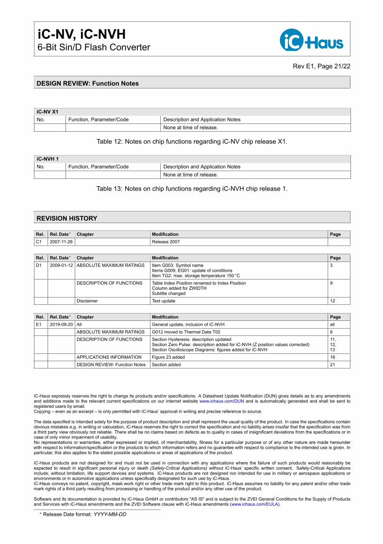
DESIGN REVIEW: Function Notes
iC-NV X1No. Function, Parameter/Code Description and Application Notes
None at time of release.
Table 12: Notes on chip functions regarding iC-NV chip release X1.
iC-NVH 1No. Function, Parameter/Code Description and Application Notes
None at time of release.
Table 13: Notes on chip functions regarding iC-NVH chip release 1.
REVISION HISTORY
Rel. Rel. Date∗ Chapter Modification PageC1 2007-11-26 Release 2007
Rel. Rel. Date∗ Chapter Modification PageD1 2009-01-12 ABSOLUTE MAXIMUM RATINGS Item G003: Symbol name
Items G009, EG01: update of conditionsItem TG2: max. storage temperature 150 °C
3
DESCRIPTION OF FUNCTIONS Table Index Position renamed to Index PositionColumn added for ZWIDTHSubtitle changed
9
Disclaimer Text update 12
Rel. Rel. Date∗ Chapter Modification PageE1 2019-09-20 All General update, inclusion of iC-NVH all
ABSOLUTE MAXIMUM RATINGS G012 moved to Thermal Data T02 6DESCRIPTION OF FUNCTIONS Section Hysteresis: description updated
Section Zero Pulse: description added for iC-NVH (Z position values corrected)Section Oscilloscope Diagrams: figures added for iC-NVH
11,12,13
APPLICATIONS INFORMATION Figure 23 added 16DESIGN REVIEW: Function Notes Section added 21
iC-Haus expressly reserves the right to change its products and/or specifications. A Datasheet Update Notification (DUN) gives details as to any amendmentsand additions made to the relevant current specifications on our internet website www.ichaus.com/DUN and is automatically generated and shall be sent toregistered users by email.Copying – even as an excerpt – is only permitted with iC-Haus’ approval in writing and precise reference to source.
The data specified is intended solely for the purpose of product description and shall represent the usual quality of the product. In case the specifications containobvious mistakes e.g. in writing or calculation, iC-Haus reserves the right to correct the specification and no liability arises insofar that the specification was froma third party view obviously not reliable. There shall be no claims based on defects as to quality in cases of insignificant deviations from the specifications or incase of only minor impairment of usability.No representations or warranties, either expressed or implied, of merchantability, fitness for a particular purpose or of any other nature are made hereunderwith respect to information/specification or the products to which information refers and no guarantee with respect to compliance to the intended use is given. Inparticular, this also applies to the stated possible applications or areas of applications of the product.
iC-Haus products are not designed for and must not be used in connection with any applications where the failure of such products would reasonably beexpected to result in significant personal injury or death (Safety-Critical Applications) without iC-Haus’ specific written consent. Safety-Critical Applicationsinclude, without limitation, life support devices and systems. iC-Haus products are not designed nor intended for use in military or aerospace applications orenvironments or in automotive applications unless specifically designated for such use by iC-Haus.iC-Haus conveys no patent, copyright, mask work right or other trade mark right to this product. iC-Haus assumes no liability for any patent and/or other trademark rights of a third party resulting from processing or handling of the product and/or any other use of the product.
Software and its documentation is provided by iC-Haus GmbH or contributors "AS IS" and is subject to the ZVEI General Conditions for the Supply of Productsand Services with iC-Haus amendments and the ZVEI Software clause with iC-Haus amendments (www.ichaus.com/EULA).
∗ Release Date format: YYYY-MM-DD
iC-NV, iC-NVH6-Bit Sin/D Flash Converter
Rev E1, Page 22/22
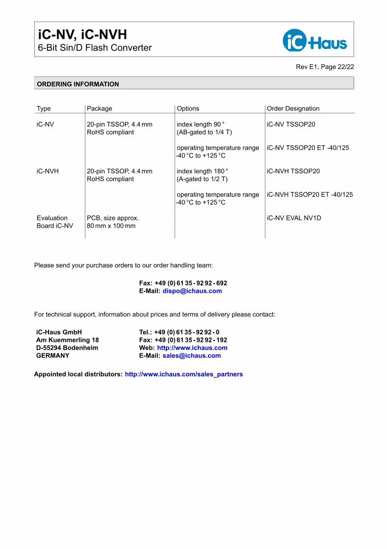
ORDERING INFORMATION
Type Package Options Order Designation
iC-NV 20-pin TSSOP, 4.4 mmRoHS compliant
index length 90 °(AB-gated to 1/4 T)
iC-NV TSSOP20
operating temperature range-40 °C to +125 °C
iC-NV TSSOP20 ET -40/125
iC-NVH 20-pin TSSOP, 4.4 mmRoHS compliant
index length 180 °(A-gated to 1/2 T)
iC-NVH TSSOP20
operating temperature range-40 °C to +125 °C
iC-NVH TSSOP20 ET -40/125
EvaluationBoard iC-NV
PCB, size approx.80 mm x 100 mm
iC-NV EVAL NV1D
Please send your purchase orders to our order handling team:
Fax: +49 (0) 61 35 - 92 92 - 692E-Mail: [email protected]
For technical support, information about prices and terms of delivery please contact:
iC-Haus GmbH Tel.: +49 (0) 61 35 - 92 92 - 0Am Kuemmerling 18 Fax: +49 (0) 61 35 - 92 92 - 192D-55294 Bodenheim Web: http://www.ichaus.comGERMANY E-Mail: [email protected]
Appointed local distributors: http://www.ichaus.com/sales_partners