FTIR 2-16 micron spectroscopy of micron-sized olivines from primitive meteorites
Upload
khangminh22Category
view
2download
0
ROBUST DESIGN WITH INCREASING DEVICE VARIABILITY IN SUB-
MICRON CMOS AND BEYOND: A BOTTOM-UP FRAMEWORK
A Dissertation
Presented to the Faculty of the Graduate School
of Cornell University
In Partial Fulfillment of the Requirements for the Degree of
Doctor of Philosophy
by
Xuan Zhang
January 2012

© 2012 Xuan Zhang
ALL RIGHT RESERVED

ROBUST DESIGN WITH INCREASING DEVICE VARIABILITY IN SUB-
MICRON CMOS AND BEYOND: A BOTTOM-UP FRAMEWORK
Xuan Zhang, Ph. D.
Cornell University 2012
My Ph.D. research develops a tiered systematic framework for designing
process-independent and variability-tolerant integrated circuits. This bottom-up
approach starts from designing self-compensated circuits as accurate building blocks,
and moves up to sub-systems with negative feedback loop and full system-level
calibration.
a. Design methodology for self-compensated circuits
My collaborators and I proposed a novel design methodology that offers
designers intuitive insights to create new topologies that are self-compensated and
intrinsically process-independent without external reference. It is the first systematic
approaches to create “correct-by-design” low variation circuits, and can scale beyond
sub-micron CMOS nodes and extend to emerging non-silicon nano-devices.
We demonstrated this methodology with an addition-based current source in
both 180nm and 90nm CMOS that has 2.5x improved process variation and 6.7x
improved temperature sensitivity, and a GHz ring oscillator (RO) in 90nm CMOS with
65% reduction in frequency variation and 85ppm/oC temperature sensitivity.
Compared to previous designs, our RO exhibits the lowest temperature sensitivity and
process variation, while consuming the least amount of power in the GHz range.
Another self-compensated low noise amplifiers (LNA) we designed also exhibits 3.5x
improvement in both process and temperature variation and enhanced supply voltage

regulation.
As part of the efforts to improve the accuracy of the building blocks, I also
demonstrated experimentally that due to “diversification effect”, the upper bound of
circuit accuracy can be better than the minimum tolerance of on-chip devices
(MOSFET, R, C, and L), which allows circuit designers to achieve better accuracy
with less chip area and power consumption.
b. Negative feedback loop based sub-system
I explored the feasibility of using high-accuracy DC blocks as low-variation
“rulers-on-chip” to regulate high-speed high-variation blocks (e.g. GHz oscillators). In
this way, the trade-off between speed (which can be translated to power) and variation
can be effectively de-coupled. I demonstrated this proposed structure in an integrated
GHz ring oscillators that achieve 2.6% frequency accuracy and 5x improved
temperature sensitivity in 90nm CMOS.
c. Power-efficient system-level calibration
To enable full system-level calibration and further reduce power consumption
in active feedback loops, I implemented a successive-approximation-based calibration
scheme in a tunable GHz VCO for low power impulse radio in 65nm CMOS. Events
such as power-up and temperature drifts are monitored by the circuits and used to
trigger the need-based frequency calibration. With my proposed scheme and circuitry,
the calibration can be performed under 135pJ and the oscillator can operate between
0.8 and 2GHz at merely 40µW, which is ideal for extremely power-and-cost constraint
applications such as implantable biomedical device and wireless sensor networks.
iii
BIOGRAPHICAL SKETCH
Xuan Zhang was born in Xi’an, China. She graduated from Tsinghua
University, in Beijing with a Bachelor of Engineering degree in 2006, before joining
the School of Electrical and Computer Engineering in Cornell University to pursue a
doctoral degree. From 2006 to 2011, she worked in Dr. Alyssa Apsel’s research lab on
process-voltage-temperature independent circuit design and variability-tolerant system
analysis and optimization.
She is the recipient of Intel PhD Fellowship in 2008. In the summers of 2008
and 2009, she interned at Broadcom Central Engineering Center and Schlumberger
Research Center respectively, where she worked on reference buffer design and
wireline communication system prototyping.

iv
To my loving parents,
Xilin Zhang and Jing Li

v
ACKNOWLEDGMENTS
I would like to express my most sincere gratitude to my advisor, Prof. Alyssa
Apsel, for her valuable guidance and constant support throughout my graduate study,
without which I could not accomplish anything. I am forever indebted for the advice
and encouragement she gave me when I had my doubt and hesitation. Her positive
can-do attitude towards research and her passion and commitment to work impress me
deeply and stimulate me over these years. I greatly appreciate Dr. Apsel for allowing
the uttermost freedom to conduct my research and manage my time. I will miss her
humor and laugh that always keep the conversations between a group of engineers
lively and fun.
I am deeply grateful for having Prof. Ehsan Afshari and Prof. Gennady
Samorodnitsky on my PhD committees to impart their critical and constructive
feedback on my doctoral research. In the pursuit of an academic career, I benefitted
tremendously from the support and advice from Prof. Alyosha Molnar, Prof. Rajit
Monahar, Prof. Edwin Kan, and Prof. Sunil Bhave, and would like to thank them all.
Many people have contributed to this work and I would like to acknowledge
my colleagues. Dr. Rajeev Dokania and Dr. Xiao Y. Wang have always been not only
my first resort for technical discussion and troubleshooting, but also precious asset for
the whole group. I enjoyed my close collaborations with Mustansir Mukadam and
Ishita Mukhopadhyay and would like to thank them for their dedicated work. I learned
a lot from Zhongtao Fu, Bo Xiang, Anthony Kopa, and other members of the Apsel
group, and appreciate their help and friendship. In the past years, I had many
constructive discussions with Dr. Guangyu Xu at UCLA and Dr. Nan Sun at UT-

vi
Austin, which helps to broaden my research perspective. All in all, I feel extremely
lucky to be surrounded by this group of brilliant people.
Finally, I would like to express my great appreciation to my parents, Jing Li
and Xilin Zhang, for their unconditional love. They have been and will always be the
source of my strength and motivation to stay strong and forge forward.
vii
TABLE OF CONTENTS
1 Variability in Submicron CMOS Technology 1
1.1 Introduction on Variability ........................................................................... 1
1.2 Impact of Variability on VLSI Systems ....................................................... 2
1.3 Categorization of Variability ........................................................................ 7
1.3.1 By source ....................................................................................... 7
1.3.2 By spatial scale .............................................................................. 8
1.3.3 Clarifications ................................................................................. 9
1.3.4 Scaling trends .............................................................................. 11
1.4 Existing Solutions ....................................................................................... 12
1.5 The Missing Piece—Dissertation Organization ......................................... 16
2 Improving Frequency Accuracy of Integrated Oscillators: A Case Study 20
2.1 Introduction ................................................................................................ 20
2.2 Types of Oscillators and Their Accuracy ................................................... 21
2.2.1 Crystal oscillators ........................................................................ 21
2.2.2 Silicon resonators ........................................................................ 22
2.2.3 LC oscillators ............................................................................... 23
2.2.4 Relaxation oscillators .................................................................. 25
2.2.5 Ring oscillators ............................................................................ 25
2.3 Applications of Oscillators in VLSI Systems ............................................. 27
2.4 Techniques to Enhance Accuracy of Ring Oscillators ............................... 30
2.4.1 Self-compensation ....................................................................... 31
2.4.2 Feedback loop .............................................................................. 32
2.4.3 Calibration ................................................................................... 33
2.4.4 A unified bottom-up approach ..................................................... 34

viii
2.5 Chapter Summary ....................................................................................... 34
3 Design Methodology for Self-Compensated Circuits 36
3.1 Introduction ................................................................................................ 36
3.2 Design Concept .......................................................................................... 37
3.3 Circuit Implementation ............................................................................... 43
3.3.1 Current source topology .............................................................. 43
3.3.2 Current source scalability ............................................................ 47
3.3.3 Current source temperature dependence ..................................... 50
3.3.4 Current-starved ring oscillator ..................................................... 51
3.4 Measurement Results .................................................................................. 54
3.4.1 Current source comparison .......................................................... 54
3.4.2 Ring oscillator comparison .......................................................... 56
3.5 Derivation of Temperature Dependence .................................................... 61
3.6 Supply Variation ......................................................................................... 64
3.7 Chapter Summary ....................................................................................... 66
4 Closed Loop Compensation with Feedback 67
4.1 Introduction ................................................................................................ 67
4.2 Design Concept .......................................................................................... 69
4.3 Comparator- Based Loop ........................................................................... 70
4.3.1 Accuracy analysis ........................................................................ 71
4.3.2 Circuit implementation ................................................................ 73
4.3.3 Loop dynamics ............................................................................ 79
4.4 Switched Capacitor-Based Loop ................................................................ 83
4.4.1 Improved frequency correction block ......................................... 84
4.4.2 Loop dynamics ............................................................................ 87
4.4.3 Accuracy analysis ........................................................................ 89

ix
4.5 Measurement Results .................................................................................. 90
4.6 Chapter Summary ....................................................................................... 98
5 System Self-Calibration 102
5.1 Introduction .............................................................................................. 102
5.2 PVT Compensation for VCO ................................................................... 102
5.2.1 System architecture ................................................................... 104
5.2.2 Calibration scheme .................................................................... 105
5.2.3 Frequency accuracy ................................................................... 108
5.3 Circuit Implementation ............................................................................. 109
5.3.1 Time-to-voltage converter (TVC) ............................................. 109
5.3.2 Comparator ................................................................................ 111
5.3.3 Voltage-controlled oscillator (VCO) ......................................... 111
5.3.4 SAR and DAC ........................................................................... 112
5.4 Measurement Results ................................................................................ 113
5.5 Chapter Summary ..................................................................................... 120
6 Improve Circuit Accuracy Using Diversification 122
6.1 Introduction .............................................................................................. 122
6.2 Accuracy of the Current Reference .......................................................... 123
6.3 Diversification in Modern Portfolio Theory ............................................. 128
6.4 Proof-of-Concept Resistor Optimization .................................................. 131
6.5 Simulation Results .................................................................................... 134
6.6 Measurement Results ................................................................................ 135
6.7 Chapter Summary ..................................................................................... 137
7 The Future Beyond CMOS 138

x
LIST OF FIGURES
1.1 Effect of variation on an oscillator in series with a frequency divider, causing
the oscillator output to vary in amplitude and the divider to fail or produce
ambiguous results ............................................................................................... 3
1.2 Spreads in normalized frequency and leakage in processor design. Courtesy of
[19] ..................................................................................................................... 5
1.3 Diagram of the proposed tiered systematic framework .................................... 17
2.1 Power and accuracy specification in various applications. Courtesy of [72] ... 31
3.1 Conceptual schematic of the current-starved ring oscillator ............................ 38
3.2 Start-up time of a ring oscillator changes with the effective load capacitance
from the bias current source ............................................................................. 42
3.3 Schematic of the addition-based current source ............................................... 43
3.4 Percentage variation of the current source changes with the percentage
variation of a single transistor and α ................................................................ 48
3.5 Schematic of the addition-based ring oscillator ............................................... 51
3.6 Phase noise comparison between the baseline ring oscillator and the addition-
based ring oscillator .......................................................................................... 52
3.7 Histograms of the output current spread in (a) a single transistor and (b) the
addition-based current source ........................................................................... 55
3.8 Percentage variation of the output currents over temperature .......................... 56
3.9 Histograms of the output frequency spread in (a) the baseline current-starved
ring oscillator and (b) the addition-based ring oscillator .................................. 57
3.10 Percentage variation of the output frequencies over temperature .................... 58
3.11 Die photo of the ring oscillator chip ................................................................. 59
3.12 The bias current (Ibias) from the addition-based current source and the output

xi
frequency (fosc) of the addition-based ring oscillator change with the supply
voltage (VDD) ................................................................................................... 65
4.1 System diagram of the general compensation loop .......................................... 69
4.2 System diagram of the comparator compensation loop ................................... 70
4.3 (a) Frequency sensor schematic, (b) timing waveform controlling the switches
in the frequency sensor ..................................................................................... 74
4.4 Charge pump schematic ................................................................................... 76
4.5 VCO schematic ................................................................................................. 77
4.6 Convergence simulation of the bang-bang dynamics in Matlab with random
initial condition and noise disturbance in each step ......................................... 80
4.7 Linear continuous-time model diagram ............................................................ 81
4.8 (a) Root locus and (b) step response with different loop gains, derived from the
transfer function of the compensation loop ...................................................... 83
4.9 System diagram of the switched capacitor-based compensation loop ............. 84
4.10 (a) Switched capacitor implementation of the frequency correction block, (b)
timing waveform controlling the switches in the block ................................... 85
4.11 Equivalent circuits in (a) the initialization phase; (b) the comparison phase; (c)
the correction phase .......................................................................................... 86
4.12 External current reference input testing set-up for (a) the baseline ring
oscillator; (b) the ring oscillator in the process compensation loop ................. 91
4.13 Histograms of the oscillator frequency from (a) the baseline oscillator; (b) the
comparator based compensation loop with constant external IEXT bias; (c) the
comparator based compensation loop with calibrated constant IREF bias ......... 92
4.14 (a) The process compensation loop with the addition-based current source; (b)
the scatter plot showing the correlation between the oscillation frequency (Fosc)
and the current provided by the addition-based current source (IADD) ............ 93
xii
4.15 Histograms of the oscillation frequency from the fully integrated (a) baseline
oscillator; (b) the compensation loop with the addition-based current bias ..... 94
4.16 Histograms of the oscillation frequency from the fully integrated (a) baseline
oscillator; (b) the switched capacitor compensation loop with the addition
based current bias ............................................................................................. 96
4.17 Percentage variation of the output frequencies over temperature .................... 98
4.18 Die photo of (a) the comparator-based compensation ring oscillator; (b) the
switched capacitor-based compensated ring oscillator ..................................... 99
5.1 Block diagram of the proposed VCO system with built-in self-calibrated PVT
compensation .................................................................................................. 106
5.2 State machine showing the transitions between different states .................... 107
5.3 Timing diagrams of the VCO frequency (fVCO) as it successively converges
towards NIref/CVIN during the successive approximation self-calibration.
Zoomed-in diagrams of Dctrl, VFS, and VCP, as the first 2 bits in Dctrl resolve ......
........................................................................................................................ 108
5.4 Schematics of (a) the TVC block and (b) the addition-based current source
with trimming capability ................................................................................ 109
5.5 Comparator schematic and the corresponding signal timing ......................... 110
5.6 SAR algorithmic block ................................................................................... 112
5.7 R-2R ladder DAC ........................................................................................... 113
5.8 Comparison of the frequency histograms without (free-running) and with the
proposed self-calibration at different frequencies: (a) and (b) 0.84GHz; (c) and
(d) 1.38GHz; (e) and (f) 1.96 GHz ................................................................. 114
5.9 Measured percentage deviation from the nominal frequency at different supply
voltage (VDD) in (a) the free-running and (b) the self-calibrated oscillators .. 116
5.10 Measured frequency deviation at different temperature before and after the

xiii
calibration ....................................................................................................... 117
5.11 Output oscillation waveforms (divided down by 32) of two consecutive self-
calibrations at (a) 0.84GHz and (b) 1.38GHz ................................................. 118
5.12 (a) Die photo of the chip; (b) zoom-in layout of the core area ....................... 119
6.1 Current reference schematic of Widlar bandgap topology based on native BJTs
........................................................................................................................ 125
6.2 Current variation in different reference topologies as a function of resistor
tolerance ......................................................................................................... 126
6.3 Construction of a portfolio resistor (RP) with device diversification ............. 127
6.4 Two asset portfolio with different correlation coefficient ρAB ....................... 129
6.5 Efficient frontier and optimal allocation in multi-asset portfolio ................... 131
6.6 Efficient frontier and optimal resistor weights allocation in IBM 90nm CMOS
........................................................................................................................ 132
6.7 Efficient frontier and optimal resistor weights allocation in TSMC 65nm
CMOS process from measurement results ..................................................... 136

xiv
LIST OF TABLES
3.1 Noise contribution in a current-starved ring oscillator ..................................... 41
3.2 Current source (CS) simulated specifications comparison ............................... 46
3.3 Ring oscillator (RO) simulated specifications comparison .............................. 53
3.4 Measured ring oscillator (RO) specifications comparison with reference ....... 60
4.1 Frequency spreads in two wafer runs over multiple chips ............................... 97
4.2 Measured ring oscillator (RO) specifications comparison with reference ..... 100
5.1 Chip summary ................................................................................................ 120
5.2 PVT compensated oscillator comparison ....................................................... 121
6.1 Variation in different types of resistor implementations ................................ 133
6.2 Normalized resistor variation in different process ......................................... 135

1
CHAPTER 1
VARIABILITY IN SUBMICRON CMOS TECHNOLOGY
As IC technologies scale, variability in the fabrication process and in operating
conditions (e.g. supply voltage, environment temperature) induces more pronounced
effects on circuit/system quality and threatens the future of the semiconductor
industry. Traditional techniques applied at different stages of the design-flow to deal
with variability are becoming less effective and more cumbersome for deep submicron
nodes, and outright insufficient for applications with tight constraints of power,
performance, and cost. It is of paramount importance to envision a new framework
that systematically addresses the problem of designing robust circuits in the presence
of increasing variability with minimum overhead. The focus of this dissertation is to
present such a design framework based on a bottom-up approach and to discuss its
merits and limitations in real applications using fully-integrated oscillators as an
example case study.
1.1 Introduction on Variability
Since the invention of transistors 40 years ago, we have witnessed unprecedented
technological advancement in integrated circuit design. The power of technology
scaling has transformed the bulky assembly of discrete components in the early days
to the sophisticated mobile electronics we have today. While embracing Moore’s
predictions of exponential improvements in computation speed and cost, IC designers
are acutely aware of the imminent challenges that may defy the continuation of this
powerful force, one of which is the problem of variability.
The existence of variability and its increasing magnitude in submicron CMOS
presents many negative impacts on VLSI systems. It can cause serious functional

2
failure, significant yield loss, and wide performance spread, even in well-designed and
optimized commercial micro processors. Often, design specifications of speed and
performance have to be sacrificed when variability is taken into account.
Variability originates from many distinct sources, which makes a general solution
difficult to obtain. There are a few ways to categorize different types of variations in
the circuit system and we will touch upon the definition of these categorizations and
their usage in the following section. The characteristics of different types of variations
are quite useful and will guide our way towards effective solutions later.
Dealing with device variability is not entirely a new problem. In fact, it has been
on the minds of engineers for a long time, and its history is almost as old as transistor
itself [1, 2]. A brief overview of the existing techniques will be provided, and their
effectiveness and deficiencies will be discussed under the design context we face
today in submicron CMOS. Our proposed design work is motivated by the gaping
gaps left behind by existing solutions, and will be the main focus of this dissertation.
1.2 Impact of Variability on VLSI Systems
As the functionality and performance of VLSI systems depends on their
underlying building blocks, there should be no surprise that variability in the device
electrical characteristics will ultimately emerge in the global system metrics. The
impacts of variability on VLSI systems can manifest itself in different ways:
Function failure:
CMOS Transistors are normally optimized with a large noise margin to avoid
direct function failures in fully digital systems, but even so critical blocks are not
immune from variability, especially when the functionality depends on some hard
voltage threshold. For example, consider the circuit shown in Fig. 1.1. Stage I is an

3
oscillator with a buffered and stepped down output leading into stage II, a frequency
divider. Such circuits are commonly used in frequency synthesizers and other
communications circuits. Even if we expect that the oscillator can be tuned somewhat
to reduce the impact of variation in the LC tank, normal process variability in the
transistors themselves can cause the circuit to fail. The desired response from the
circuit, labeled “without variation”, is a divided down version of the oscillator output,
with a clear threshold between levels useful in digital applications. The response
labeled “with variation” shows the range of likely responses including the effect of
normal process variation. The range of possible circuit behaviors across the process
includes failure of the divider to latch on some input signals (flat output) and a wide
variety of outputs with varied signal amplitudes and offsets. The extent of the output
signal variation makes thresholding very difficult and leads to high rates of signal
Fig. 1.1 Effect of variation on an oscillator in series with a frequency divider, causing the oscillator output to vary in amplitude and the divider to fail or produce ambiguousresults.

4
errors among other problems [3].
Yield loss:
For commercial integrated circuits products, we care about not only that each chip
executes functions correctly, but also what percentage of these chips fall within a
certain performance specification. This percentage is defined as yield, and it
determines the economic viability of any IC products. Unfortunately, variability is
increasingly becoming a huge yield limiting factor in today’s CMOS process [4].
Most digital VLSI systems, such as the micro-processor, are synchronous designs,
and have a maximum operating frequency that is determined by the aggregated delay
from its critical paths and is often used as one critical metric to gauge the system
performance. In this case, device variability leads to delay variations from the critical
paths and hence considerable variations of the maximum operating frequency, which
causes significant reduction in system performance for most fabricated chips. To make
the matter worse, sophisticated VLSI systems nowadays have many other performance
requirements to fulfill in addition to the operating frequency. Variations of the
threshold voltage can cause huge leakage power variations among different
components or different chips due to an approximate exponential relationship between
the two. Since sub-threshold leakage power is a major portion (30% to 50%) of total
power consumption [5], a 5 to 10 times variation in the leakage power alone
contributes to almost a 50% variation in total power. This in turn brings uncertainty to
the power consumption and the hotspot of microprocessors. In fact, the problem of
meeting several performance requirements simultaneously has important effect on the
overall yield of the system, and it is often described by the term parametric yield in the
literature [6].
In order to demonstrate the parametric yield, let us look at a simple case in the

5
micro-processor design where only operating frequency and leakage power
requirements are considered. Even in a mature process like the 65nm CMOS, we have
already seen a 30% variation in operating frequency and 5 to 10 times variation in
leakage power (Fig. 1.2).
Since a chip that passes the quality test must meet the requirements on both its
normalized frequency and leakage, the parametric yield is obtained by integrating the
joint probability distribution between the two performance ranges (i.e. normalized
frequency>1.2 and normalized leakage<2.5). You can clearly see from the scatter plot
in Fig. 1.2 that a lot more high-speed chips have to be thrown out because they exceed
the leakage limit.
Performance spread:
Unlike digital circuits that encode signals as discrete voltage levels, analog circuits
utilize the information in continuous value and thus are particularly susceptible to
process variations. Analog circuit metrics, such as gain, bandwidth, and input
Fig. 1.2 Spreads in normalized frequency and leakage in processor design. Courtesyof [19]

6
impedance, are often functions that directly relate to the electrical properties of
devices, and will vary greatly from process to process.
In order to overcome this performance spread caused by variability, traditional
design principles demand margins large enough to tolerate the worst case combination
of process variation, supply fluctuation, and temperature change.
Design tradeoff:
As we discussed earlier, variability can lead to a number of negative effects on
VLSI systems, and the techniques to mitigate these effects can be quite expensive in
terms of design trade-offs. Correcting function failure may require sensing the signal
amplitude from each stage of the circuit via an envelope detection and feedback in the
form of gain control, consuming considerable power in the control circuits and loading
the high frequency output nodes of each circuit. Improving the parametric yield and
leaving large design margins can also lead to significant power-speed-yield/margin
tradeoffs. For example, in inverter chains in 90nm CMOS technology, threshold
voltage variations result in 100% increase in energy consumption for the same
performance or a 25% reduction in performance for the same energy consumption [7].
As technology continues to scale beyond 22nm, process variations will increase in
magnitude, resulting in wider distribution of transistor threshold voltages and feature
sizes [8]. Since the behavior of the fabricated design in terms of power and
performance differs from what designers intended, the effect of variations looks like
inherent uncertainty in the design. All the above-mentioned impacts of variability are
expected to become even worse as technology scales. Future chip designers need to be
prepared for this increasing level of uncertainty and respond proactively to this
challenge with flexible and adaptive designs that can tolerate or/and compensate for a
broad range of variability.

7
1.3 Categorizations of Variability
The term variability encompasses many different types of variations in VLSI
systems. To avoid any confusion, this section is devoted to clarify their definitions by
categorizing them in two useful ways.
1.3.1 By source
The most straightforward way to separate different types of variability is probably
through its physical origins. Broadly speaking, variability can be divided into two
parts: physical variability and environmental variability.
Physical variability:
Physical variability has been well investigated in the past [9]. A number of studies
have been done to measure and characterize process variability and to extract the
major cause of variability in different technology nodes [10, 11]. A common way to
partition the semiconductor fabrication flow is front end and back end process, which
can also be used to further divide the physical variability. The former refers to the
variability associated with creating active components: implantation, oxidation,
polysilicon line definition, etc; the latter involves the processing steps that define the
wiring and the passive components of the integrated circuits: deposition, etching,
chemical mechanical polishing (CMP), etc.
Since lithography and etch are common processing steps shared by both front end
and back end, they affect the active and passive components in similar ways by
defining the outline and roughness of their geometry. On the other hand, implantation
is unique in the front end and determines the dopant distribution and concentration,
while electroplating and CMP are used more heavily in the back end and generate

8
additional types and sources of variations in the metal material property, thickness,
and planarity.
The variability caused by the front end processing steps appears to be more
dominant in determining timing variability of VLSI systems, and can manifest itself
through variations in the following parameters: gate length/ width, threshold voltage,
dielectric thickness, energy level quantization, and lattice stress [12, 13].
Environmental variability:
The physical variability is predominantly a function of the fabrication process, but
an IC system often shares a common operating environment with other components in
the package during its operation and changes in this environment could also affect the
system performance and generate variability. Supply voltage fluctuation, thermal
gradients, mechanical stress, and signal coupling and interference are just a few
sources of variability in this family. Process variation, together with the first two
major environmental factors (voltage and temperature) are often referred to as the
PVT variations in the literature and considered to be the focus of most variability-
tolerant designs.
1.3.2 By spatial scale
While understanding the physical origins of variations in the fabrication process is
important, it does not provide much guidance or insights for circuit designers. That is
why there exists another popular categorization of variability by its spatial scale, in
which process variation is broken down into lot-to-lot (L2L), wafer-to-wafer (W2W),
across-wafer, across-reticle, and within-die (WID) variation [14] according to the
device statistics obtained at different scales. This classification is particularly useful in
analyzing variability’s impact on system performance, and will be referenced quite
9
often in this dissertation.
As far as the circuit designer is concerned, the primary distinction is between die-
to-die (D2D or interchip) and within-die (intrachip) variability. Consider again micro-
processor design as the digital example. The aggregated delay on its critical path is the
summation of the delays from each digital block. In this case, the interchip variability
of the delay is the same for all the blocks (assuming each stage uses similar digital
design), while the intrachip variability gets averaged by the summation. This is also
the reason why interchip variability tends to shift the operating frequency of micro-
processor chips and intrachip variability has more pronounced effects in determining
the variance of the operating frequency. In analog designs where matching has been a
major concern, intrachip variability causes mismatch between transistors of the same
size, and interchip variability shows up as offsets that plague the absolute accuracy of
the design.
This spatial scale classification of variability is not only helpful for circuit
designers, but also provides important insights to device modeling. In fact, the most
common and comprehensive device model of variability is based on decomposing it
into different spatial scales.
1.3.3 Clarifications
Due to its complicated classification, variability are often described and
distinguished quite loosely, and sometimes even incorrectly, by a few different
dichotomies. Here, we would like to provide some clarifications on how these
dichotomies can relate to the categorizations introduced above.
Systematic versus random:
Systematic (or deterministic) and random (or stochastic, statistical) variations are

10
probably the most confusing concepts that cry for clarification. The confusion stems
from not distinguishing the actual mechanisms that generate variation from one’s
ability to predict the value of a variable deterministically. For example, a well-
specified non-uniform temperature profile of the wafer is observable and thus
systematic to the process engineer, but since it cannot be corrected in the fabrication
process, this source of variation appears to be statistical to the circuit designer.
Similarly, lithography aberrations are usually caused by the relative spatial positions
of adjacent shapes, and hence are deterministic once the physical layout of the system
is complete. However, from the circuit designer’s point of view, being further along
the design flow, the actual layout is unknown to the designer and can only be modeled
as a stochastic factor.
At the same time, there are some physical mechanisms that are inherently random,
such as dopant implantation and etching roughness, and can be modeled as random
variables at any stage.
Intrinsic versus extrinsic:
Extrinsic causes of variation refer to those related to the issues of manufacturing
control and engineering that generate unintentional shifts in the processing conditions
of the semiconductor fabrication, such as temperature, pressure, optical depth, and
other controllable factors. Intrinsic causes of variation come from the fundamental
atomic-scale randomness of the devices and materials. It is another useful way to
distinguish the sources of variability.
Static versus dynamic:
It is often tempting to equate static variability to process variations and dynamic
variability to voltage and temperature variations; because the former is predetermined

11
once the fabrication process is complete, while the latter depend on changing
operating conditions. This simplification is, however, not strictly correct. These days,
more and more attention is directed to the study of reliability issues in IC systems that
originate from device aging and its reversible and irreversible effects on system
performance.
Mismatch versus offset:
These terminologies are more popular among the analog community, especially
where differential signal path is employed. In this dissertation, they are used
interchangeably with die-to-die (offset) and within-die (mismatch) variations.
1.3.4 Scaling trends
As alluded to earlier, the exponential pace of scaling has a profound impact on
device variability, particularly in the deep submicron regime. Although it is quite
difficult to predict the magnitude of variability in future technology nodes, several
trends appear to be inevitable.
Precise control of the fabrication process is getting harder, as the nominal target
values of the transistor geometric features are decreasing. Further scaling has made
key process parameters, such as the minimum transistor channel length and the
interconnect pitch, approach nanometer scale, and in effect put a burden on our ability
to improve manufacturing tolerances. The cost of building a state-of-the-art fabrication
facility has already skyrocketed to billions of dollars, but unless we can find effective
solutions to improve the resolution/precision of the fabrication equipment at the same
rate of scaling, the dielectric thickness and line edge roughness are bound to be more
substantial contributors to the variability budget.
In addition to the pressures from extrinsic causes of variation, the fundamental

12
limitation imposed by the intrinsic device and material property on the atomic scale is
probably more daunting than ever. In the proposed 16nm process, the number of
dopant atoms and ions in the channel falls within two digits [15], and not to mention
the dielectric film is less than 3 atom layer thick. This means that even if we can
control the fabrication process perfectly, the fundamental randomness in the behavior
of silicon structure will unavoidably surface and diligent treatment of quantum physics
has to be applied. For example, as the threshold voltage of the transistor is determined
by the number and the placement of the dopant atoms, which are randomly scattered in
the channel area, huge increase in the magnitude of variance is expected in threshold
voltage, as well as discernable energy quantization effects.
1.4 Existing Solutions
Due to its numerous and heterogeneous causes, general solutions to reduce
variability on a global scale are very rare. Instead, a divide-and-conquer strategy is
employed and process engineers, computer architects, circuit designers, CAD
developers, and test engineers each focus on their areas of expertise.
Improving the fabrication:
Since lithography accounts for a significant portion of the extrinsic manufacturing
variations, a number of techniques have been invented to enhance the resolution and
fidelity of the lithography process.
Conventional lithography is limited by Rayleigh criterion to have a minimum
resolution of Rmin=0.5λ/NA. To overcome this constraint, artificial patterns of
destructive interference have to be created by manipulating the phase of the light. Off-
axis illumination (OAI) and phase-shift mask (PSM) are two methods developed
following this line of thought, as both create additional 180o phase shift through the

13
path difference and are able to improve the resolution by 2, i.e. Rmin=0.25λ/NA.
Optical proximity correction (OPC) is another measure that proves to be very
successful in improving the accuracy of the photolithography image. By pre-distorting
the mask patterns to compensate for the predictable lens aberration and light
scattering, OPC could prevent functional failures due to poorly printed features,
particularly at the edge of the layout shapes and reduce the intrachip linewidth
variation. To further improve the image robustness, subresolution assist features
(SRAF) are often inserted in conjunction with OPC.
The back end variability discussed earlier is related to pattern dependencies.
Usually, regular reoccurring patterns are favored in the layout for having lower
variance in the printed shapes after lithography. This is achieved by post-processing
the layout with the insertion of dummy fill to improve the layout regularity. In the
back end metal layers, dummy fill has the additional benefit of ensuring interconnect
planarity, because filling the empty space with dummy metal patterns improves the
uniformity of oxide CMP process. Automatic algorithms to generate dummy fill
patterns based on existing layout have been widely adopted in today’s advance CMOS
process.
Improving the device:
Device engineers have also been busy with designing novel processing methods
and device structures that exhibit reduced variation. For example, the implantation
depth and profile in the diffusion region of CMOS transistors have been rigorously
studied to determine the optimal parameters for lower current variations [16]. It has
also been demonstrated that some of the recently proposed technologies, such as the
fully-depleted silicon on insulator (FD-SOI) and double gate transistors (i.e. FinFET),
have lower standard deviations in their threshold voltage and on-current

14
characteristics, which adds to their more obvious advantages of reduced parasitic
capacitance and alleviated short-channel effect over bulk CMOS [17].
Improving the circuit:
Traditionally, circuit designers have very limited ability to deal with variability.
Rather than proactively attacking this problem, defensive measures are most often
taken based on rule-of-thumb design principles. Kinget has summarized some of the
most quintessential techniques used in analog circuit design to mitigate the impact of
device mismatch in his paper [18]. Generally speaking, high overdrive voltages are
preferred in fixed current biasing applications, while low overdrive should be used in
fixed voltage biasing case.
Since transistor mismatch is such a critical issue in analog and mixed-signal
circuits, designers often avoid automatic layout and routing tools and resort to
deliberate common centroid layout, which utilizes the symmetry of the pattern
location and orientation to reduce geometric mismatch in devices caused by gradients.
Improving the architecture:
Most computer architecture level solutions attempt to deal with the process-related
timing failure and variability through post-silicon compensation and adaptation. One
branch of techniques called adaptive body biasing (ABB) utilize the body potential to
tune the threshold voltage of transistors, so that frequency and leakage spread can be
optimized simultaneously [19]. Although first proposed for global tuning of the chip,
ABB can be applied locally, as well as with multiple supply voltage levels for further
yield enhancement.
Robust logic design approaches have also been investigated at the
microarchitecture level. The technique demonstrated in RAZOR [20] uses a shadow

15
latch to detect circuit timing errors and correct them by boosting the supply voltage
until error rate drops below certain acceptable number. In pipelined designs, timing
slack can be generated by either process induced frequency variation or supply voltage
disturbance. In order to achieve optimal power and performance under variability, the
authors described ReVIVaL [21], a novel architecture that combines variable latency
with post-fabrication voltage interpolation for each pipelined stage in the processor
core.
Improving the optimization:
The difficulty of designing VLSI systems in the presence of variability partly
stems from the primitive capability of our CAD tools that lack the proper and efficient
treatment of randomness. To address this deficiency, more powerful analysis and
simulation programs have been developed that are equipped with algorithms for
parametric yield optimization [22] and statistical timing optimization [23]. These tools
can perform multi-objective optimizations to improve system timing, power
dissipation, routability and yield simultaneously and substantially speed up the
iterations of logic and layout synthesis to reduce product cycle.
Variation-aware design procedures have been gaining a lot of tractions lately in the
design of SRAM [24] and algorithmic blocks. In these proposed procedures,
comprehensive variability-enabled transistor models are included very early on in the
design flow to fully account for the effect of variability on the circuit block.
Improving the testing:
Post-fabrication chip testing is probably the last line of defense against variability,
where the trade-off between cost and performance is most acute.
One of the innovations that enjoys great commercial success is product binning, a

16
process of sorting manufactured chips based on tested level of performance. In this
way, large variance in chip performance is transformed into several specification
ranges to satisfy different market segments. Product binning allows the manufactures
to recoup the revenue by selling the lower performance parts at a lower price, instead
of simply discarding the functional outliners. However, die-to-die variations (D2D),
within-die (WID) variations cannot easily be solved by speed-binning techniques,
because a handful of slow transistors can potentially lead to slow paths that affect
overall processor clock frequency.
When the accuracy requirement is particularly high (within 1%), post-fabrication
adjustments, such as laser trimming [25], polysilicon fuses [26], and multi-point
calibration, are routinely employed. These solutions consume precious test time and
require expensive automatic testing equipment (ATE) or considerable built-in self
testing (BIST) overhead on chip, therefore are more commonly reserved for sensitive
parts in high-end IC products.
1.5 The Missing Circuit Solution—Dissertation Organization
A survey of the variability landscape in VLSI systems thus far indicates that while
the looming problem of variability has attracted the attentions of researchers from
many diverse fields, a systematic design approach is still missing at the circuit level.
As proposals of adaptive resilient architecture are exhausting their potential and
innovations in process and device are hitting the wall of fundamental physical limits,
more and more power now resides in the creativity of circuit designers to close the
widening gap between variability and performance.
In the chapters to follow, I will present a tiered systematic framework (Fig. 1.3)
developed for designing process-independent and variability-tolerant integrated
circuits. This bottom-up approach starts from designing self-compensated circuits as
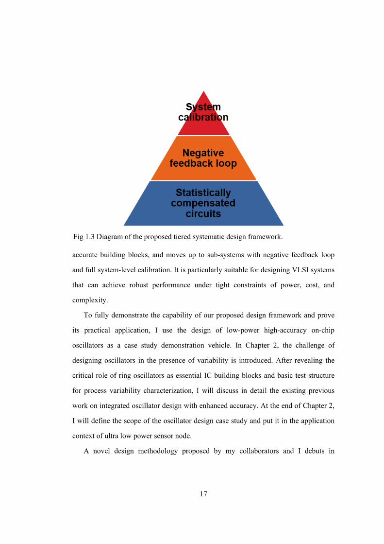
17
accurate building blocks, and moves up to sub-systems with negative feedback loop
and full system-level calibration. It is particularly suitable for designing VLSI systems
that can achieve robust performance under tight constraints of power, cost, and
complexity.
To fully demonstrate the capability of our proposed design framework and prove
its practical application, I use the design of low-power high-accuracy on-chip
oscillators as a case study demonstration vehicle. In Chapter 2, the challenge of
designing oscillators in the presence of variability is introduced. After revealing the
critical role of ring oscillators as essential IC building blocks and basic test structure
for process variability characterization, I will discuss in detail the existing previous
work on integrated oscillator design with enhanced accuracy. At the end of Chapter 2,
I will define the scope of the oscillator design case study and put it in the application
context of ultra low power sensor node.
A novel design methodology proposed by my collaborators and I debuts in
Fig 1.3 Diagram of the proposed tiered systematic design framework.

18
Chapter 3. It offers designers intuitive insights to create new topologies that are self-
compensated and intrinsically process-independent without external reference, and is
the first systematic approaches to create “correct-by-design” low variation circuits.
Based on this methodology, we demonstrate the design of a GHz ring oscillator (RO)
in 90nm CMOS with 65% reduction in frequency variation and 85ppm/oC temperature
sensitivity. Compared to previous designs, our RO exhibits the lowest temperature
sensitivity and process variation, while consuming the least amount of power in the
GHz range. The same methodology is also applied to design an addition-based current
source having 2.5x improved process variation and 6.7x improved temperature
sensitivity and a self-compensated low noise amplifiers (LNA) exhibiting 3.5x
improvement in both process and temperature variation and enhanced supply voltage
regulation.
Chapter 4 presents the negative feedback loop based sub-system built upon the
accurate blocks we developed in Chapter 3. The feasibility of using high-accuracy DC
blocks as low-variation “rulers-on-chip” to regulate high-speed high-variation blocks
(e.g. GHz oscillators) is explored. In this way, the trade-off between speed (which can
be translated to power) and variation can be effectively de-coupled. We demonstrated
this proposed structure in an integrated GHz ring oscillators that achieve 2.6%
frequency accuracy and 5x improved temperature sensitivity in 90nm CMOS.
To enable full system-level calibration and further reduce power consumption
during active feedback, the implementation of a successive-approximation-based
calibration scheme for tunable GHz VCOs is described in Chapter 5. Events such as
power-up and temperature drifts are monitored by the circuits and used to trigger the
need-based frequency calibration. With the proposed scheme and circuitry, the
calibration can be performed under 135pJ and the oscillator can operate between 0.8
and 2GHz at merely 40µW, which is ideal for extremely power-and-cost constraint

19
applications such as implantable biomedical device and wireless sensor networks.
In Chapter 6, after showcasing a number of oscillator designs in the previous
chapters, we dwell upon the fundamental question on the upper bound of circuit
accuracy and how it relates to the minimum tolerance of on-chip devices (MOSFET,
R, C, and L). It can be proven that achieving accuracy better than the tolerance of any
devices without external reference is possible, thanks to the “diversification effect”, a
concept commonly known in the theory of portfolio management.
Finally, Chapter 7 concludes the dissertation by discussing the potential of our
proposed design framework to scale beyond sub-micron CMOS nodes and extend to
emerging non-silicon nano-devices.
The power of Moore’s law has fueled the rapid advancement of information
technology, but recently, its pace has been stalled by increasing uncertainty of the
nano-scale devices and the constraint of power consumption. By addressing the
fundamental challenges of variability and adaptive performance in VLSI system
design, the proposed technology-independent design framework will extend the life of
Moore’s law and unleash the full potential of deep sub-micron CMOS process with
scaling and the emerging technology beyond CMOS.

20
CHAPTER 2
IMPROVING FREQUENCY ACCURACY OF INTEGRATED
OSCILLATORS: A CASE STUDY
2.1 Introduction
The oscillator is widely used in the VLSI systems for a range of applications.
When integrated on chip, it is influenced by the same variability discussed in Chapter
1. However, to achieve the design requirements and improve the performance metrics
of the system, many applications demand a stable center frequency despite the
variations induced by fabrication and environment. Due to the ubiquitous and essential
role the oscillator plays in the VLSI systems, it is chosen as the circuit example to
demonstrate the proposed bottom-up design framework for robust circuits.
This chapter intends to clarify the design specifications for the integrated oscillator
circuit used in the case study. Section 2.2 provides a survey of available oscillator
solutions distinguished by their resonating elements, with comments on the frequency
accuracy of each solution. The functions commonly performed by the oscillator in
integrated circuits are summarized in Section 2.3. Over the discussion of different
system requirements imposed by the diverse application contexts, some desirable yet
unfulfilled attributes emerge that motivate the quest of an integrated oscillator with
high accuracy and low power consumption. A more detailed discussion on the ring
oscillator is included in Section 2.4, focusing on the challenges of designing low
frequency variation oscillators in sub-micron technologies. Although a number of
accuracy-enhancing techniques for the ring oscillator have proposed in the literature,
there still exists a crucial design space that is unfilled by existing technology and calls
for a fully-integrated low power oscillator with improved frequency accuracy at GHz.

21
2.2 Types of Oscillators and Their Accuracy
The frequency and its accuracy of an oscillator are largely determined by the
physical property of the resonating element. By identifying the underlying oscillation
mechanism, we can classify the oscillators commonly used in integrated circuits and
analyze their performance and cost characteristics.
2.2.1 Crystal Oscillators
Quartz crystals have very stable frequency, thanks to the stable mechanical
resonance of the vibrating crystal in the piezoelectric material. By cutting a quartz
crystal at a specific angle, very selective resonance frequencies can be obtained. Each
one of these cuts has specific properties and reacts differently to changes in the
environment and aging. For example, the most common low-frequency quartz crystals
are Y-cut crystals and can operate up to about 100 kHz. They have a quadratic
frequency error curve reaction to changes in temperature. These crystals are
commonly used in real time clocks to keep wall time during system sleep, because
they consume very little power (< 15uW). For higher frequencies, AT-cut crystals are
employed. Their frequencies cover the range from 1MHz up to several hundreds of
MHz. Unlike the Y-cut, the AT-cut crystal exhibits a cubic frequency error curve
reaction to changes in temperature.
Temperature contributes most significantly to the frequency uncertainties of
crystal oscillators, compared to other factors such as material impurity, aging,
mechanical stress/shock/vibration, and gravity. Uncompensated crystals might exhibit
20ppm to more than 100ppm frequency error depending on the quartz quality. Various
compensation techniques have been proposed to improve the frequency accuracy
below 1ppm with higher manufacturing cost and system complexity [27]. Despite

22
having superior frequency accuracy, crystal oscillators cannot be integrated on chip
and are not available for GHz operation without additional power-hungry frequency
multiplier circuits.
2.2.2 Silicon Resonators
The most obvious advantage of silicon resonators over crystals is the possibility to
directly integrate them into the CMOS process. Microelectromechanical System
(MEMS) resonators, such as those based on thin film acoustic-wave resonator (FBAR)
technology, are among the latest developments in silicon resonator.
In addition to being compatible with the CMOS process for low cost fabrication,
FBAR-based oscillators can operate at GHz range with very low phase noise [28],
thanks to their high-Q resonance tank. The temperature coefficient of an
uncompensated FBAR is about -25ppm/oC, and it can be improved with physical
compensation to achieve zero-drift resonator that has average temperature dependence
of 1ppm/oC. At much lower frequency, Ruffieux et. al [29] also demonstrated a 1MHz
aluminum nitride (AIN) thin film driven silicon resonator that can achieve
approximately 0.4ppm/oC over the temperature range of 0 to 50oC with batch
calibration.
Silicon resonators usually consist of large MEMS structures on the order of mm2
and require additional steps in the fabrication process. Their operating frequencies are
higher than crystals and span MHz to GHz depending on the thin film material of the
resonator. However, the tuning range of the silicon resonator is very limited (<1%)
[30] due to the sturdiness of its underlying mechanical resonating elements, and hence
is often used as reference frequency generator instead of tuning oscillators.

23
2.2.3 LC Oscillators
Moving away from the specialized MEMS structures on silicon, one of the
simplest resonating elements available in most CMOS processes is an LC tank. An
electric current can resonate between the two elements at the circuit's resonant
frequency, forming the core of an LC oscillator.
The quality (Q) factor of the LC tank plays very a critical role in many key aspects
of the LC oscillator’s performance, such as phase noise, power consumption, and
tuning range. Since Q=ωo/Δω, where ωo is the oscillation frequency and Δω stands for
the bandwidth of the LC filter, a higher Q-factor means a sharper transfer function
with narrower bandwidth to filter out the off-center noise. On-chip inductors usually
have quality factors between 10 and 25, which is lower than some silicon resonators,
but high enough to meet the phase noise requirements of most narrow-band
communication circuits.
To sustain the resonance of an LC tank, sufficient negative resistance must be
generated to compensate for the energy loss caused by the parasitic resistance in the
tank, which can be modeled by a parallel tank resistance RP. The negative resistance is
usually generated by a cross-coupled transistor pair and has the magnitude of 1/gm,
where gm represents the transconductance of the transistor and can be expressed as a
function of the bias current IB:
ODox
Bm VLWC
Ig
2
(2.1)
At the same time, the following relationship exists between the Q factor and RP:
L
CRQ p (2.2)
24
Since the power consumption of the cross-couple pair equals IBVDD and the
oscillation condition demands RP>1/gm, the minimum power of an LC oscillator can
be derived as
LCQ
VLWCP ODox
2min
(2.3)
in which µ is the mobility, Cox is the unit oxide capacitance, and VOD is the over drive
voltage. For a given fabrication process and operating frequency, the right hand
expression in (2.3) often cannot be minimized beyond an optimal value, resulting in a
lower bound for the power consumption of LC oscillators. At the GHz range, the LC
oscillator usually consumes at least a few hundred µW for continuous operation.
The resonance frequency can be adjusted by tuning the capacitance in the LC tank.
To achieve a wider tuning range, switched capacitor arrays are often employed in LC
oscillators in addition to the standalone varactors with a maximum tunability of 20%.
The trade-offs between the on-resistance and the parasitic capacitance in MOS
switches prevent the tuning range to be more than 100% in LC oscillators, because
wide tuning demands smaller switch transistors with minimum parasitic capacitance,
while high Q factor demands larger switches with low on-resistance.
Compared to silicon resonators, LC oscillators offer lower production cost and
easier integration with existing CMOS technology, but the precision of on-chip
inductor and capacitor and their temperature dependence make the frequency of this
resonating element less stable. A statistical analysis of passive delay line based on
discrete components [31] suggests that frequency errors in the order of a few percent
can be easily observed in LC oscillators that occupy ~0.5mm2 chip area.

25
2.2.4 RC Oscillators
On-chip oscillation can also be produced using resistor and capacitor by relaxation
oscillators that deliver more compact integration than LC oscillators, because the size
of an inductor is large compared to a resistor. Many modern microprocessors integrate
such RC-type oscillators as a cheap alternative to external resonators, as they are
easily realizable in standard CMOS process.
Ultra low power frequency generators based on relaxation oscillators have been
proposed that typically operate at kHz to low MHz range. Denier [32] has
demonstrated a 3.3 kHz low-power relaxation oscillator in 0.35µm CMOS technology
without external components that has 6.9% relative accuracy as measured by the
standard deviation (σ) of the oscillation frequency.
The operating range and the accuracy of the output frequency in RC oscillators are
closely coupled. The former is determined by the RC time constant in the circuit and
higher output frequency means smaller R and C values. On the other hand, like the LC
circuit, the RC circuit uses passive components that are subject to similar degrees of
inaccuracies and resistors and capacitors of large size have better fabrication tolerance.
Therefore, it becomes harder to design accurate RC oscillators at higher frequency.
2.2.5 Ring Oscillators
A ring oscillator is a circuit consisting of an uneven number of inverters that have
specific transition time. Connecting them into a loop generates an oscillating signal
with a frequency of 1/nTINV, where TINV is the transition time of one inverter.
The advantages of ring oscillators are their extremely low cost, compact size, wide
tuning range, and low power consumption. An all-digital ring oscillator can be
synthesized to allow seamless integration with the automated digital design flow and
26
optimize for size and power. The frequency of a ring oscillator can be changed by both
revising the number of inverters in the circuit and adjusting the transition time of each
stage to cover a very wide range of frequency. The delay stages used in the ring
oscillator are often minimum-sized digital gates, which makes it possible to exploit the
power saving in the scaling technology to the uttermost extent.
However, in spite of all the advantages mentioned above, uncompensated ring
oscillators suffer from poor frequency accuracy, because the transition time of each
stage varies significantly from process variation. This characteristic of ring oscillators
is sometimes utilized to measure and characterize the fabrication process [33, 34]. It is
not uncommon for today’s sub-100nm process to have more than 35% 3σ variation in
both its drive-current and propagation delay within a single chip. In 90nm and 65nm
CMOS, variability of more than 26% can be observed in the gate delay from chip to
chip [35]. In addition to process, the oscillation frequency also depends heavily on the
applied voltage and temperature of the circuit, enabling designs of supply noise
monitors [36] and temperature sensors [37] based on ring oscillator structure.
Usually, hybrid designs of ring oscillators and some sort of RC-oscillator can be
found in some applications where the actual frequency isn't critical and where a cheap
oscillator is necessary or desired. Given its power, size, and cost, the ring oscillator is
very attractive for applications with stringent power and cost budget, if its frequency
accuracy can be improved to meet the requirements of those systems.
Research in resonators is still very active, and there are a multitude of resonating
elements that we have not yet discussed, such as ceramic resonators, bulk acoustic
wave (BAW) resonators, rubidium oscillator, atomic clocks [38], or optoelectronic
oscillators. These resonating elements all bear interesting potentials, but are still too
rudimentary to be viable solutions for VLSI systems in their current state.

27
2.3 Applications of Oscillators in VLSI Systems
Oscillators can be found in a variety of circuit applications such as data processing
units, high speed I/O interfaces, and wireless communication systems. Depending on
the diverse functions desirable in the system, different types of oscillators are selected
to meet the performance requirements of specific applications.
The most common uses of oscillators can be roughly categorized into three basic
functions, and the frequency accuracy considerations for each function are discussed
in this section.
Phase domain processing:
Signals can be embedded in the phase of an oscillating waveform and processed in
the phase domain. The most well-known phase domain processing circuit is perhaps
the phase locked loop (PLL). To lower the phase noise and maintain a high signal to
noise ratio, a narrow loop bandwidth is preferred in a PLL, because the noise spectrum
outside the band can be filtered out by the closed loop. For the noise consideration, the
voltage-controlled oscillator (VCO) in the PLL should have a small gain (KVCO), so
that its output frequency responds less sensitively to the disturbance on its control
voltage. On the other hand, process and temperature variation causes the center
frequency of the VCO to shift from chip to chip, and a wide tuning range is needed to
cover the whole range of the shift, which places a contradictory requirement on KVCO
[39].
Hurdles from frequency variation also exist in high-speed clock data recovery
(CDR) circuits. The decomposed two-loop architecture proposed for ripple reduction
[40] in the CDR systems faces the issue of mismatch between the VCOs used in
coarse and fine control loops, and could benefit from well-matched on-chip oscillators

28
as well.
There are apparent tradeoffs between noise performance and frequency variation
in the oscillators used in phase domain signal processing applications, but the external
reference (i.e. crystal) that is often employed in these systems can establish a robust
frequency in the feedback loop and thus mitigate the negative impact of frequency
variation. A two step method consisting of discrete coarse calibration and continuous
fine tuning proves to be very effective in dealing with process and temperature
induced frequency variability in PLLs [41].
Local oscillator:
For wireless communication, signals are modulated on a much higher carrier
frequency, so that they can be transmitted and received wirelessly. Local oscillators
can be found in both the transmitter and receiver modules, and the selection of these
oscillators depends heavily on the transceiver architecture employed in the wireless
communication system.
The narrowband continuous wave radio requires purity in its transmitted spectrum
to avoid channel interference. Similarly, the coherent detection scheme at the receiver
uses the knowledge of the phase of the carrier wave to demodulate the signal, and the
need to recover carrier phase at the receiver also puts stringent constraint on the phase
noise of its local oscillator. Therefore, LC oscillators are the most obvious candidates
in these architectures for its low phase noise.
While narrow-band architectures are not robust to frequency variation, low power
radio architectures, particularly the non-coherent energy detection based architectures
can sustain larger variation owing to large receiver bandwidth. Therefore, unlike the
traditional narrow band operation, ultra wide band (UWB) radios have presented
different design specifications for local oscillators. For example, the novel uncertain-

29
IF architecture [42] allows relaxed phase noise specifications and can tolerate up to
5% frequency inaccuracy in its local oscillator at the receiver. At the same time, the
frequency allocation for UWB has much broader signal bandwidth, making it less
likely for the transmission to fall outside the assigned mask due to frequency offset of
the local oscillator.
System clock:
Oscillators can also function as the system clock to keep track of absolute or
relative time between synchronizations or resets. Examples can be found in super-
regenerative receivers, where the time between the signal arrival and the oscillation
regeneration is measured to determine the amplitude of the signal; and in wake-up
receivers, where the operation of the main radio is duty-cycled to save power. Since
the system clock has to be on all the time, it must consume very low power at modest
oscillation frequency (kHz to MHz). Accuracy of the system clock often trades off
with other performance such as detection resolution, receiver sensitivity, duty cycle,
and beacon rate, and hence improvement in the frequency accuracy can result in better
overall system performance.
In recent years, low power radio systems have attracted attention for applications
in wireless sensor networks (WSN) and body area networks (BAN). These upcoming
systems involved with control, measurement, and automation will require a range of
low power and low cost timing solutions in signal processing, local oscillator and
system clock that are not currently supported. Fully integrated oscillators that are
immune to variations of process, supply voltage, and temperature (PVT) and able to
operate under a stringent power budget (<100µW) are therefore highly desirable.

30
2.4 Techniques to Enhance Accuracy of Ring Oscillators
As discussed earlier in Section 2.2, the ring oscillator based voltage-controlled
oscillator (VCO) exhibits wide-tuning range, low power consumption, small die area,
and ease of integration. Compared to the more power hungry LC oscillator and the
FBAR-based resonator with limited tuning range, it is particularly suitable for low
power radios whose inherent architecture is more tolerant to phase noise but require
flexible low power operation.
Unfortunately, the ring oscillator suffers from severe impacts of increasing
variability, especially as CMOS technology scales down to the nanometer regime.
Moreover, the relative variation of the circuits is even more pronounced in low-
voltage applications [34], and the transition delay of the inverter is the most
susceptible to variation due to random dopant fluctuations among the timing
parameters [43].
For example, this discrepancy between required and achievable accuracy can be
seen in the frequency reference of the wake-up radio in wireless sensor networks
(WSN). As illustrated in Fig. 2.1, this application requires frequency accuracy on the
order of 1%, which is beyond what can be easily achieved with conventional ring
oscillators.

31
In order to fill the void in this low power high accuracy design space, process
compensated ring oscillators with moderate frequency accuracy (between 1% and
10%) have been explored in the past.
2.4.1 Self-Compensation
Self-compensation refers to the efforts to improve the inherent accuracy of free-
running oscillators without resorting to any external reference or calibration. It can be
achieved in a number of ways, such as symmetric loads, process corner estimation,
stable current bias, and threshold and temperature sensing.
To avoid external references or post-fabrication testing, some oscillator designs
detect the direction of the variation (slow/fast) with novel circuits, so that counter-
directional correction can be applied through tuning the control current/voltage [44-
46] or switching the number of delay stages [47].
Another approach is to identify the most critical determinant of the oscillation
Fig. 2.1 Power and accuracy specifications in various applications. Courtesy ofreference [72]

32
frequency and design it to be constant against changes in process and temperature.
Examples of this approach can be found in [48] (constant current reference) and [49]
(constant gm bias). The latter presents a compact design of a process compensated two-
stage ring oscillator that has 5% variation based on measurement from 15 devices.
However, in order to generate the high gm necessary to sustain the oscillation, the core
oscillator and the biasing network have to draw 6mA of current.
More elaborate self-compensated oscillators have been demonstrated with
threshold and temperature sensing, where a process and temperature dependent control
voltage is generated to bias the oscillator at a constant frequency. This is accomplished
by approximating the control voltage as a function of the threshold voltage and the
temperature, so that specific biasing circuits can be designed to match the
approximation. With this approach, less than 3% worst-case variation is achieved by
Sundaresan et.al in 0.25µm CMOS. However, in order to arrive at a simplified control
voltage expression as a function of temperature and to fit the curve for all process
conditions by adjusting device parameters, the operating frequency of this
compensated oscillator cannot exceed several MHz.
2.4.2 Closed Feedback Loop
To achieve finer frequency accuracy below 3%, self compensation in free-running
oscillators may not be sufficient due to the limit of fabrication tolerance in sub-micron
CMOS and a closed loop compensation with negative feedback is often employed.
The idea of a closed feedback loop is to utilize another more accuracy frequency
source to establish a reference for the ring oscillator to compare to. Although off-chip
crystal may be the most straightforward choice of frequency reference [50], fully
integrated designs exploit other novel on-chip structures that exhibit less process-
induced variation. Examples can be found in a thermal-diffusivity-based 1.6MHz

33
frequency reference design [51] that includes an electrothermal filter (ETF) composed
of a thermopile structure in a 0.7µm CMOS process. When the entire system
configuration is considered, existing components in the system can perform dual
function as frequency reference in the feedback loop as well. For example, the self
resonance frequency of the patch antenna serves as the reference for frequency
generation in a 60GHz frequency-locked loop [52].
While showing potentials to significantly enhance the frequency accuracy of the
oscillator in the feedback loop, these specialized structures occupy large chip area and
require additional fabrication handling. Their operating frequency strongly depends on
the underlying physical mechanism and is not very flexible.
2.4.3 Calibration
In the commercial production of oscillator circuits, post-fabrication calibration is
routinely performed with laser trimming, electrical switches, or capacitor arrays [53].
In order to compensate for both process and temperature, the calibration is often
conducted for each chip at multiple temperature point, making it a very costly and
time-consuming step. Techniques have recently been proposed that estimate the delay
of each stage in the ring oscillators [54] with fitting parameters obtained from batch
testing data to alleviate the burden of post-fabrication calibration. Also, built-in self-
calibration circuitry can be embedded with the system to automate the calibration
process and minimize the need for manual handling.
In addition to the one-time post-fabrication calibration, local oscillators in low
power radios can be re-calibrated by taking advantage of the wireless communication
capability of the system. Timing information can be extracted from the transmitted
data from the central station or the master node, and used by the local node to calibrate
its oscillator [55].

34
2.4.4 A unified approach
The comprehensive survey of existing techniques above suggests that there is no
single silver-bullet solution to compensate the frequency variation in ring oscillators.
Each technique involves different system-level trade-offs and design considerations.
In order to take the unique advantage of each technique, I have explored all three
directions in the designs of process compensated ring oscillators and unified them into
a bottom-up approach. It starts with building self-compensated basic blocks for the
oscillator circuit, and then uses them in the construction of the closed feedback loop.
Finally, a need-based system-level self-calibration is performed with the feedback
loop. Using this proposed unified approach, I have demonstrated several ring oscillator
designs with enhanced frequency accuracy at low power and small area.
2.5 Chapter Summary
The oscillator is an indispensable block that has broad application in the VLSI
systems. It can be implemented in many distinct forms based on different resonating
elements. Frequency accuracy is a very critical performance metric for oscillators and
can determine the choice of various types of oscillators in a specific application.
In this case study, the application of interest is wideband radios for wireless
sensing and body network, where extreme low power and low cost is desired. The ring
oscillator appears to be a hopeful candidate for these radio systems due to its low
power, compact size, and easy integration, if efficient compensation techniques can be
applied to improve its poor frequency accuracy against variation in process, voltage,
and temperature (PVT).
After reviewing the existing compensation techniques for ring oscillators, I
propose to unify different schemes into a bottom-up approach toward accurate low

35
power oscillator design, and will walk you through the technique employed at each
level step-by-step in the following chapters.

36
CHAPTER 3
DESIGN METHODOLOGY FOR SELF-COMPENSATED CIRCUITS
3.1 Introduction
The design of a 1.8GHz 3-stage current-starved ring oscillator with a process-and
temperature-compensated current source is presented. Without post-fabrication
calibration or off-chip components, the proposed low variation circuit is able to
achieve a 65.1% reduction in the normalized standard deviation of its center frequency
at room temperature and 85ppm/oC temperature stability with no penalty in the
oscillation frequency, the phase noise or the start-up time. Analysis on the impact of
transistor scaling indicates that the same circuit topology can be applied to improve
variability as feature size scales beyond the current deep sub-micron technology.
Measurements taken on 167 test chips from 2 different lots fabricated in a standard
90nm CMOS process show a 3x improvement in frequency variation compared to the
baseline case of a conventional current-starved ring oscillator. The power and area for
the proposed circuitry is 87μW and 0.013mm2 compared to 54 μW and 0.01mm2 in the
baseline case.
In this chapter, we demonstrate a scalable, process-and- temperature compensated
GHz ring oscillator implemented with a low variation addition-based current source
that shows more than 3x improvement in its frequency process variation and
temperature stability, as compared to the baseline case of a conventional current-
starved ring oscillator.
The design concept is presented in Section 3.2, followed by details of the circuit
implementation with a focus on the addition-based current source in Section 3.3.
Finally, measurement results are provided in Section 3.4 to verify the oscillator's

37
superior frequency stability against process and temperature variations over that of a
baseline current-starved ring oscillator. With modest cost in power and area, such an
oscillator would be a good candidate for applications in wake-up radios and other RF
receiver systems.
The solution we propose in this chapter falls into the category of the last approach
and is based on the design methodology introduced in [3]. Since this general
methodology utilizes the local correlation between closely-spaced devices without
relying on any specific electrical behavior of the underlying devices or variation
characteristic of the fabrication process, it can be applied to a broad design space
beyond the current technology node. Our design also does not require external
reference components or post-fabrication processing, and is therefore inexpensive and
easy to integrate. It poses no restriction on the oscillation frequency and only requires
minimal power and area overhead compared to the previous solutions.
3.2 Design Concept
Variation in a ring oscillator can be isolated to a few primary sources. By
identifying its major contributors, we gain valuable insight into low variation
oscillator design. An inverter based ring oscillator is comprised of an odd number of
stages connected in a circular manner to provide an unstable state that leads to
oscillation. In a current-starved ring oscillator (Fig. 3.1), the low-to-high (Tplh) and
high-to-low propagation (Tphl) delays of a single inverter stage are controlled by the
current source (sink) and can be expressed as:
bntrpDDeffphl
bptrpeffplh
IVVCT
IVCT
)(
(3.1)

38
in which Ibp is the source current, Ibn is the sink current, Ceff is the effective load
capacitance of each inverter stage, and Vtrp is the inverter trip voltage. The source
current and the sink current are usually matched, so we let Ibn=Ibp=Ibias. Summing up
the propagation delays across each stage we have the oscillation period Tosc of an N-
stage current-starved ring oscillator:
biasDDeffosc IVNCT (3.2)
Note that matching Ibn and Ibp cancels Vtrp term in the final expression of Tosc.
In the presence of process variation, both Ibias and Ceff will vary from chip to chip,
resulting in additional offset terms Ibias=Ibias0±ΔIbias and Ceff=Ceff0±ΔCeff,i, in which
Ibias0 and Ceff0 are the nominal values, and ΔCeff,i (i=1,2,…N) and ΔIbias are the offset
deviations. In order to calculate the oscillation offset ΔTosc in an N-stage ring
oscillator, we have to consider the different Ceff values at each delay stage. After re-
Fig. 3.1 Conceptual schematic of the current-starved ring oscillator.

39
arranging the terms, we obtain the ΔTosc expression that looks like:
)( 00
0
0
1,
biasbiasbias
biaseffDD
biasbias
N
iieffDD
osc III
ICNV
II
CV
T
(3.3)
We define the relative percentage variation ρT by dividing ΔTosc with its nominal
mean Tosc0=NCeff0VDD/Ibias0, and transform (3.3) into a normalized expression:
I
I
I
N
iiC
osc
oscT NT
T
1)1(1
,
0
(3.4)
In which ρI=ΔIbias/Ibias0 and ρC,i=ΔCeff,i/Ceff0 (i=1,2,…N), are the respective percentage
variation of the current source and the effective loading capacitance. Being the
percentage offsets, ρC,i (i=1,2,…N) and ρI are usually much smaller than one, hence
we can approximate (4) by its first order Taylor expansion:
I
N
iiCT N
1,
1 (3.5)
Due to the complexity of the sources of variation, there is no comprehensive
probability distribution function to fully describe ρC,i (i=1,2,…N) and ρI, but we can
make a few simple assumptions. Since all the inverters are of the same size, the
loading effect is the same at all stages, making ΔCeff,i (i=1,2,…N) identically
distributed random variables. According to their definitions, ρI and ρC,i (i=1,2,…N) are
unit-less random variables with zero means. Let their standard deviations be σI and σC,i
(i=1,2,…N) respectively. σC,i (i=1,2,…N) can be further separated into two parts

40
according to previously mentioned classification of process variation: the perfectly
correlated part which is the die-to-die (D2D) variation σC-D2D shared by all the stages,
and the independent part σC-WID which is the within-die (WID) mismatch between
devices. γ is the correlation between ρC,i (i=1,2,…N) and ρI. We can now calculate σT,
the standard deviation of ρT, as:
NN
N
iiCI
WIDCDDCIT
1,2
22
22
2
(3.6)
This expression of σT provides us with several insights. For a large enough N, the
variation caused by the within-die mismatch (σC-WID) between stages decreases, while
the current source variation (σI) and the effective capacitance die-to-die variation (σC-
D2D) add directly to the frequency variation (σT). Furthermore, a positive correlation
(γ) between the load capacitance and the bias current will reduce the overall frequency
variation.
From (3.6), we know that the current source plays a critical role in determining the
overall frequency variation of the ring oscillator. To reduce it, we can replace the bias
current source in a current-starved ring oscillator, which is usually a single transistor,
with a lower variation alternative [56]. Doing so has the obvious benefit of avoiding a
complicated overhaul of the oscillator design, but a thorough investigation on the
oscillator’s phase noise and start-up time is still needed to better understand the
potential impact of the replacement.
Let us first look at the phase noise. The ring oscillator is known to have inferior
frequency stability compared to the LC oscillator [57]. It is important that any
proposed modification should not deteriorate its phase noise performance. To
determine the noise distribution in a current starved ring oscillator, we used PNOISE

41
in SpectreRF to simulate the noise in the circuit in Fig. 3.1. Ibn and Ibp are both biased
with single transistors. The total noise at the output node A attributed to different parts
in the oscillator is presented in Table 3.1. Not surprisingly, most of the noise comes
from the inverter stages, and Ibn and Ibp contribute less than 5% to the total noise. From
the percentage distribution of noise in Table 3.1, we determine that even though noise
from the bias current sources will add to the phase noise of the oscillator, its effect is
secondary relative to the inverter stages. Therefore, as long as the current source used
to replace the single transistor in the baseline design has comparable current noise, the
phase noise performance will stay be maintained.
Another performance metric of interest in low power applications is the start-up
time, ie. the time required for the oscillation to reach a stable state. To save power, the
oscillator is often duty-cycled in many low power systems and a shorter start-up time
would mean a narrower wake-up window and less power consumption [58]. In an N-
stage ring oscillator with a single current source, the bias current is shared by all the
stages and at least one stage will be sourcing (sinking) current at any point in time
during an oscillation period, therefore node N and P will stay at a relatively constant
DC level in order to sustain the current needed for a stable oscillation. Intuitively
speaking, the start-up time will depend on how much time it takes to charge up the
capacitance of that node to the constant DC level. We employ an empirical method to
verify the effect of the load capacitance on the start-up time, since analytical studies of
TABLE 3.1 NOISE CONTRIBUTION IN A CURRENT-STARVED RING OSCILLATOR
Inv1 Inv2 Inv3 Ibn Ibp Noise @A* (V/√Hz)
8.64e-6 8.64e-6 8.64e-6 7.91e-7 6.52e-7
31.5% 31.5% 31.5% 2.88% 2.38% * Spot noise measured at 100KHz offset frequency is reported.

42
the start-up time in a current-starved ring oscillator are absent in the literature. We ran
parametric analysis in Cadence by sweeping the load capacitance value at node N and
P, and obtained the start-up time by measuring the time between turning on the current
bias voltages and the time when the oscillation reaches 90% of its stabilized
magnitude. Fig. 3.2 illustrates how the start-up time changes proportionally with the
effective load capacitance at node N and node P. Ideally, we would like to achieve a
competitive start-up time with our revamped ring oscillator design by limiting the
effective load capacitance at node N and node P.
To summarize, we propose designing a low variation ring oscillator by replacing
the current source. Through our analysis in this section, we find that to avoid
degrading the oscillator’s original phase noise and start-up time performance, the
replacement current source should have the following characteristics: 1) low output
Fig. 3.2 Start-up time of a ring oscillator changes with the effective load capacitancefrom the bias current source.

43
current variation; 2) equivalent output referred current noise; 3) equivalent load
capacitance.
3.3 Circuit Implementation
In this section, we present a low variation addition-based current source as the
bias current source in the oscillator. After elaborating on the operation of the current
source, its scalability and temperature dependence are investigated. Finally, the
performance of the ring oscillator biased with the addition-based current source is
summarized and compared.
3.3.1 Current Source Topology
We choose the process-invariant addition-based current source proposed in [3] as
the bias current source, because it has the same loading effect as a single transistor
driving the same amount of current. The circuit schematic of the addition based
Fig. 3.3 Schematic of the addition-based current source.
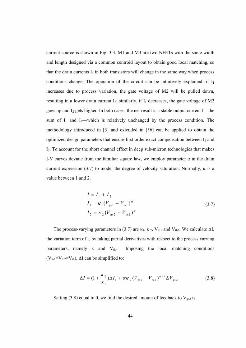
44
current source is shown in Fig. 3.3. M1 and M3 are two NFETs with the same width
and length designed via a common centroid layout to obtain good local matching, so
that the drain currents I1 in both transistors will change in the same way when process
conditions change. The operation of the circuit can be intuitively explained: if I1
increases due to process variation, the gate voltage of M2 will be pulled down,
resulting in a lower drain current I2; similarly, if I1 decreases, the gate voltage of M2
goes up and I2 gets higher. In both cases, the net result is a stable output current I—the
sum of I1 and I2—which is relatively unchanged by the process condition. The
methodology introduced in [3] and extended in [56] can be applied to obtain the
optimized design parameters that ensure first order exact compensation between I1 and
I2. To account for the short channel effect in deep sub-micron technologies that makes
I-V curves deviate from the familiar square law, we employ parameter α in the drain
current expression (3.7) to model the degree of velocity saturation. Normally, α is a
value between 1 and 2.
)(
)(
2222
1111
21
thgs
thgs
VVI
VVI
III
(3.7)
The process-varying parameters in (3.7) are κ1, κ 2, Vth1 and Vth2. We calculate ΔI,
the variation term of I, by taking partial derivatives with respect to the process varying
parameters, namely κ and Vth. Imposing the local matching conditions
(Vth1=Vth2=Vth), ΔI can be simplified to:
21
22211
2 )()1( gsthgs VVVII
(3.8)
Setting (3.8) equal to 0, we find the desired amount of feedback to Vgs2 is:

45
RIVV
IVthgs
gs 11222
1212
)(
1
(3.9)
This feedback can be realized with a resistor, R, as indicated in (3.9), and the
resistor’s nominal (ie. mean or average) value, R0, which meets the process
compensation condition, is in turn given by:
02
01
02
102
02
02
01
020 /1
)(
/1
mthgs gVVR
(3.10)
To obtain κ01, κ
02, we look at the DC bias condition of Vgs2. According to KVL, it
must satisfy:
001
02 RIVV DDgs (3.11)
Parameters tagged with a superscript “0” represent nominal values of that variable
that are undisturbed by the process variation. During the design process, we can only
choose these nominal values while realizing that final fabricated circuits will include
the randomness of those parameters. In the nominal case, V0gs2=Vgs1 in (3.11), because
we want to bias M2 at the same gate voltage as M1. Therefore by equating V0gs2 to
Vgs1 and plugging in I1 and R0 with their expressions in (3.7) and (3.11), we solve to
get:
)()( 0
11
01
01
02
thgsgsDD
thgs
VVVV
VV
(3.12)
The design equations given by (3.10) and (3.12) minimize the variation term ΔI

46
and greatly reduce the standard deviation of the summation current compared to a
single transistor current source with the same input gate voltage and nominal output
current. The single transistor used in the comparison has a fixed size, and the addition-
based current source is sized to have the same loading capacitance at node X in Fig.
3.3 through S-parameter analysis, making sure that the improved process variation
does not come at the cost of introducing additional loading effects.
In the above derivation, the effect of channel modulation is not accounted for in
the transistor model. This is justified because process compensation is achieved by the
matching of changes in I1 and I3, ie. ΔI1=ΔI3, rather than the matching of absolute
value of I1 and I3. Difference in the drain-source voltage will not disturb this desired
matching in our circuit. Another non-ideality is the resistor variation. In reality, the
resistor varies with the process and will deviate from its optimized nominal value R0
calculated in (3.10). Therefore when the actual resistance R=R0±ΔR, ΔVgs2 also
diverges from the condition that guarantees complete compensation derived by (3.9),
which results in degraded compensation performance. A detailed investigation on the
impact of resistor variation is included in the appendix of [3], which concludes that the
improvement in current variation exists irrespective of the precision of the resistor.
More specifically, the resistor we use in the circuit has a 3σ tolerance of 11% [59],
which, according to the analysis in [3], can achieve better than 2x improvement factor.
TABLE 3.2 CURRENT SOURCE (CS) SIMULATED SPECIFICATIONS COMPARISON
Type Current Mean (µA)
Current Std. (µA)
Norm. Std. (%)
Noise (A/√Hz)
Load Cap. (fF)
Power (µW)
Single Trans. CS
122.3 16.02 13.1 8.53e-20 142.9 122.3
Addition-based CS
121.2 5.21 4.3 1.32e-19 155.6 194.7

47
Table 3.2 summarizes the simulated specifications of the current sources. The
simulation uses IBM’s 90nm process model. It suggests that the addition-based current
source delivers a 67% reduction in the normalized standard deviation of its output
current compared to the baseline single transistor, with a similar amount of effective
load capacitance. The additional current noise does not present significant disturbance
to the phase noise of the oscillator. We will show the supporting simulation results in
part D of this section.
3.3.2 Current Source Scalability
Scalability is a desirable attribute for the current source when used as the bias
current reference in ring oscillators, for it allows full integration with the digital
processing circuits, which results in improved performance, reduced power and area,
and higher oscillation frequency in newer processes.
To analyze how the addition-based current source scales as transistor size shrinks,
we use the same transistor I-V model in (3.7). Without loss of generality, κ, Vth and R
can be modeled as Gaussian random variables. As the technology scales, the standard
deviation of κ and Vth are expected to increase relative to their mean values, while the
relative variation of the resistor value R remains the same [10]. This enables us to
numerically calculate the output current variation of the addition-based circuit and
compare it to that of a single transistor.

48
The result of the numerical simulation is presented in Fig. 3.4: the x-axis is the
normalized percentage variation of the output current from a single transistor as
modeled by (3.7), when variations from both ΔVth and Δκ are accounted for. The y-
axis is the normalized percentage variation of the output current in the current source.
If a single transistor is directly used as a current source, it will have a 45 degree angle,
as represented by the dashed line. Each solid line in the plot represents how the
variation of the addition-based current source changes with the variation of the single
transistor for a specific α value. For α between 1.4 and 2, all the solid lines have flatter
Fig. 3.4 Percentage variation of the current source changes with the percentagevariation of a single transistor and α.

49
slopes than 45 degrees. This means that, given a fixed α, the addition based current
source can achieve less percentage process variation in its output current than the
single transistor—an indication of the effectiveness of the process compensation in the
design.
The diamond symbols in Fig. 3.4 mark Cadence simulation results in 180nm,
90nm and 65nm technology using BSIM model characterized by real process data in
IBM’s CMOS7rf, CMOS9sf and TSMC’s N65 respectively. The plot indicates two
scaling trends: 1) increasing device-level variability in terms of normalized standard
deviation, which coincides with the process variability measurements in [10, 11]; 2)
more pronounced short-channel effect captured in the model by a decreasing α.
Referring to Fig. 3.4, these two trends have opposite effects on the variation of the
addition-based current source. Naturally, the first trend will increase variation because
as the building blocks become less reliable, so does the circuit built upon it, which is
captured by the positive slope of the solid lines. However, smaller α will significantly
decrease the variation of the addition-based current source, because our compensation
is based on a linearized gm of the transistor. Hence, as α approaches 1, the transistor
appears more linear with an almost constant gm, which makes the process
compensation applied through the resistor more accurate. The reason current variation
is reduced as we move from 180nm to 90nm to 65nm is due to the fact that the effect
from the second trend dominates over the first one. Further scaling in the direction of
stronger short- channel effect will eventually lead the variation of our addition- based
current source to fall on a solid line with a very flat slope (smaller α), which means a
constant current variation in future technology nodes. Better performance is available
through size optimization as discussed in [56], for only minimum-sized transistors are
used in the numerical analysis shown in Fig. 3.4.

50
3.3.3 Current Source Temperature Dependence
The general methodology in [3] does not distinguish the sources of variation when
calculating the variation term. In fact, variation caused by changes in the temperature
is also compensated by the same topology, because the critical parameters that vary
with temperature—the mobility of the charge carriers (µn), the threshold voltages
(Vth), and the resistance (R) are the same variables in our assumptions when dealing
with process variation. The relationship between these parameters and the temperature
(T) can be approximated by:
Tn
))(1)(()( 00 TTTVTV Vththth (3.13)
))(1)(()( 00 TTTRTR R
Similar to what we have done for process variation, we can calculate the variation
term of I induced by a ΔT change in temperature in the addition-based current source
ΔIADD and in the single transistor ΔITRAN:
2
00
03
00
0
00
02
0
00
0
0
)(
)(
)()(
)(
TVV
VT
TTVV
V
TVV
VT
TI
TI
TVV
VT
TI
TI
thgs
thVthR
Rthgs
thVth
thgs
thVth
ADD
ADD
thgs
thVth
TRAN
TRAN
(3.14)
In (3.14), the first order ΔT term in ΔIADD has been completely cancelled, leaving
only the higher order terms, while ΔITRAN has a ΔT term that can cause bigger

51
temperature shift. This indicates that the addition-based current source compensates
for temperature variation, as well as process variation. Please note that the temperature
expression in (3.14) is obtained assuming nominal process conditions and does not
account for the design parameters’ deviation caused by process variation. Detailed
derivation of (3.14) can be found in Appendix A.
3.3.4 Current-Starved Ring Oscillator
The overall circuit schematic of the oscillator after replacing the single transistor is
shown in Fig. 3.5. The nominal current provided by the top PFET current source is
designed to match that of the bottom NFET current source. The effective load
Fig. 3.5 Schematic of the addition-based ring oscillator

52
capacitance looking into the current source is on the order of hundreds of fF, setting
the start-up time around 100ps.
There is only minimal additional phase noise contribution from the addition-based
current source. This is proven by the simulated phase noise spectrum of both
oscillators. Over a relative frequency from 40kHz to 600MHz, the spectrum plot in
Fig. 3.6 shows negligible phase noise difference between the baseline ring oscillator
and the addition-based ring oscillator. At 10MHz offset frequency, the spot phase
noise is -103.97 dBc/Hz for the baseline oscillator and -103.87 dBc/Hz for the
addition-based one.
Of course, the replica branch in the addition-based current source consumes extra
power and chip area. It is well known that to some extent, power and area can be
traded for lower variation by using a bigger device with reduced mismatch [18]. In
order to show that our improvement comes from more than simply utilizing the power-
area-variation trade-off, we compare the addition-based ring oscillator with several
different current-starved ring oscillator designs that either consume the same amount
of power or occupy the same amount of layout area. All the designs under comparison
Fig. 3.6 Phase noise comparison between the baseline ring oscillator and the addition-based ring oscillator.
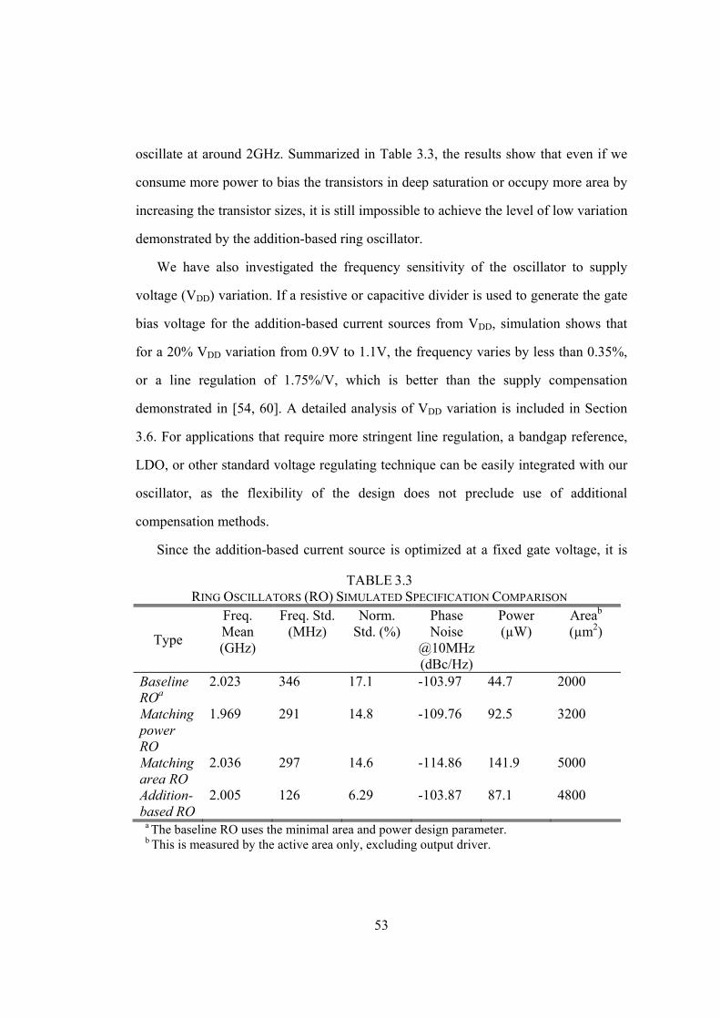
53
oscillate at around 2GHz. Summarized in Table 3.3, the results show that even if we
consume more power to bias the transistors in deep saturation or occupy more area by
increasing the transistor sizes, it is still impossible to achieve the level of low variation
demonstrated by the addition-based ring oscillator.
We have also investigated the frequency sensitivity of the oscillator to supply
voltage (VDD) variation. If a resistive or capacitive divider is used to generate the gate
bias voltage for the addition-based current sources from VDD, simulation shows that
for a 20% VDD variation from 0.9V to 1.1V, the frequency varies by less than 0.35%,
or a line regulation of 1.75%/V, which is better than the supply compensation
demonstrated in [54, 60]. A detailed analysis of VDD variation is included in Section
3.6. For applications that require more stringent line regulation, a bandgap reference,
LDO, or other standard voltage regulating technique can be easily integrated with our
oscillator, as the flexibility of the design does not preclude use of additional
compensation methods.
Since the addition-based current source is optimized at a fixed gate voltage, it is
TABLE 3.3 RING OSCILLATORS (RO) SIMULATED SPECIFICATION COMPARISON
Type
Freq. Mean (GHz)
Freq. Std. (MHz)
Norm. Std. (%)
Phase Noise
@10MHz (dBc/Hz)
Power (µW)
Areab (µm2)
Baseline ROa
2.023 346 17.1 -103.97 44.7 2000
Matching power RO
1.969 291 14.8 -109.76 92.5 3200
Matching area RO
2.036 297 14.6 -114.86 141.9 5000
Addition-based RO
2.005 126 6.29 -103.87 87.1 4800
a The baseline RO uses the minimal area and power design parameter. b This is measured by the active area only, excluding output driver.
54
not recommended to tune the oscillation frequency by directly controlling the gate
bias. However, in applications where frequency tuning is desired, such as in a PLL,
our addition-based current source can be used as the offset current bias to establish a
stable offset frequency. Additional voltage-controlled or digitally-controlled current
arrays can then be connected in parallel with the offset current bias to achieve
frequency tunability.
3.4 Measurement Results
The addition-based current source and the addition-based ring oscillator, as well as
their comparable baseline designs, have been fabricated in IBM’s 90nm CMOS9sf
process and measured on multiple chips in 2 different lots over a wide temperature
range. The supply voltage used in all the testing is 1V. The measurement set-up and
the circuit performances are covered in this section.
3.4.1 Current Source Comparison
We measured addition-based current sources from 2 wafer runs in different lots.
We also fabricated the baseline single transistor in the same 90nm process with the
same output current, load capacitance, and gate voltage. The measurement is taken
from 96 chips in total, out of which, 39 are from the first wafer run, and the remaining
57 belongs to the second wafer run. Each batch represents a full set of chips from the
multi-project wafer run. The histograms in Fig. 3.7 compare the measured results by
showing the mean (µ), the standard deviation (σ), and the normalized standard
deviation (σ/µ). It can be observed from the histograms that µ shifts less from wafer to
wafer in our addition based current source than in the single transistor, indicating
lower wafer-to-wafer variation. Within the same wafer run, the spread of current is
less in the addition-based current source, indicating lower die-to-die variation. The

55
combination of these two effects reduces the total process variation by 53.2%.
For characterization over temperature, we randomly select one chip and measure
its current using a probe station equipped with a vacuum chamber. We are able to
(a)
(b)
Fig. 3.7 Histograms of the output current spread in (a) a single transistor and (b) theaddition-based current source.

56
cover a temperature range from 200K to 400K using liquid hydrogen and an electrical
heater. The temperature variation of the output current is defined as ΔI(T)/I(T0), in
which I(T0) is the current value at room temperature (300K), and ΔI(T) is the
difference between I(T), the current value at temperature T, and I(T0). In Fig. 3.8, with
no compensation, the single transistor drain current varies as much as 12%, while the
addition-based current source experiences only minor variation of 1.8%, or 90
ppm/oC. This puts our addition-based current source among the best-in-class
temperature compensated current references [61] without post-fabrication calibration.
3.4.2 Ring Oscillator Comparison
We also fabricated the ring oscillators in 2 separate 90nm wafer runs from
different lots. We compare the performance of the ring oscillator biased with addition-
based current sources to that of a baseline current-starved ring oscillator biased with
single transistor current sources. The histograms of their output frequencies are plotted
Fig. 3.8 Percentage variation of the output currents over temperature.

57
in Fig. 3.9. The measurements are taken from 167 test chips, 112 of which are from
the first wafer run and 55 of which are from the second wafer run. The difference of
(a)
(b)
Fig. 3.9 Histograms of the output frequency spread in (a) the baseline current-starvedring oscillator and (b) the addition-based ring oscillator.

58
histogram magnitudes between the wafer runs is due to the different number of chips
in each run. Similar wafer-to-wafer and die-to-die process variation improvement can
be seen from the histograms, and an overall reduction of 65.1% in the normalized
standard deviation, defined as the standard deviation of output frequency over its
mean, is achieved.
An insulated, but not vacuumed, chamber is used to measure the temperature
dependence of the oscillators, which has a narrower range from 280K to 335K. The
temperature variation of the output frequency is defined as Δf(T)/f(T0), in which f(T0)
is the frequency value at room temperature (306K), and Δf(T) is the difference
between f(T), the frequency value at temperature T, and f(T0). The temperatures
reported in Fig. 3.10 are the ambient temperatures measured in the proximity of the
chip under test. Over the temperature range of 55 degrees, the frequency of the
baseline ring oscillator varies by 1.5%, or 312 ppm/oC, while the addition-based ring
Fig. 3.10 Percentage variation of the output frequencies over temperature.

59
oscillator experiences a 0.47% variation, or 85 ppm/oC.
The 1.8GHz addition-based ring oscillator dissipates 87μW power on average and
occupies 0.0128 mm2, while the baseline ring oscillator consumes 54μW and occupies
0.010 mm2, both including the output driver and the ESD diodes to protect the gates.
A die photo of the addition based ring oscillator, as well as the baseline current-
starved ring oscillator, is shown in Fig. 3.11.
Table 3.4 summarizes and compares several specifications of the baseline and the
addition-based ring oscillators described in this work, as well as the oscillators
reported in the literature. Compared to other works, our proposed addition-based ring
oscillator exhibits the lowest temperature sensitivity and comparable low process
variation, which is supported by larger number of chip measurements from different
lots. Operated at 1.8GHz with a 1V voltage supply, it consumes the least amount of
power, except for [48] which oscillates around 80 KHz, and occupies small chip area,
even after including ESD and output drivers.
Fig. 3.11 Die photo of the ring oscillator chip.
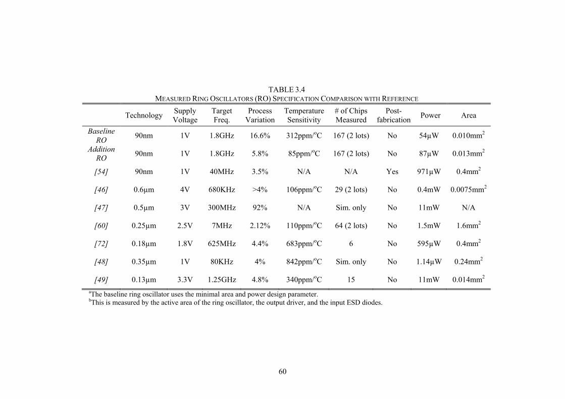
60
TABLE 3.4 MEASURED RING OSCILLATORS (RO) SPECIFICATION COMPARISON WITH REFERENCE
Technology Supply Voltage
Target Freq.
Process Variation
Temperature Sensitivity
# of Chips Measured
Post- fabrication
Power Area
Baseline RO
90nm 1V 1.8GHz 16.6% 312ppm/oC 167 (2 lots) No 54µW 0.010mm2
Addition RO
90nm 1V 1.8GHz 5.8% 85ppm/oC 167 (2 lots) No 87µW 0.013mm2
[54] 90nm 1V 40MHz 3.5% N/A N/A Yes 971µW 0.4mm2
[46] 0.6µm 4V 680KHz >4% 106ppm/oC 29 (2 lots) No 0.4mW 0.0075mm2
[47] 0.5µm 3V 300MHz 92% N/A Sim. only No 11mW N/A
[60] 0.25µm 2.5V 7MHz 2.12% 110ppm/oC 64 (2 lots) No 1.5mW 1.6mm2
[72] 0.18µm 1.8V 625MHz 4.4% 683ppm/oC 6 No 595µW 0.4mm2
[48] 0.35µm 1V 80KHz 4% 842ppm/oC Sim. only No 1.14µW 0.24mm2
[49] 0.13µm 3.3V 1.25GHz 4.8% 340ppm/oC 15 No 11mW 0.014mm2
aThe baseline ring oscillator uses the minimal area and power design parameter. bThis is measured by the active area of the ring oscillator, the output driver, and the input ESD diodes.

61
3.5 Derivation of Temperature Dependence
In this section, we perform the step-by-step calculation of the percentage change of
the output current with temperature in both the single transistor and the addition-based
current source.
For single transistor, let ΔITRAN (p, T) be the variation term when the transistor
experiences disturbance in process (Δp) and in temperature (ΔT) away from their
nominal value p0 and T0. Taking into account the change in mobility and threshold
voltage described by (3.13), we simplify the first-order partial derivative term relative
to the nominal current value I(p0, T0) as follows:
TTVV
V
VV
V
VV
TVV
T
T
VV
TVVVV
VV
VVT
T
TpI
TpI
thgs
thVth
thgs
th
thgs
thVthth
thgs
thVthththgs
thgs
thgsTRAN
00
0
000
00
0
0
2000
0000
2000
2000
00
)(
))((2
)(
)(
),(
),(
(3.15)
The first two terms in (3.15) are the result of process variation, while the last term
is caused by the temperature fluctuation. The discussion here only deals with
temperature variation, so we assume the process condition stays at the nominal corner,
ie p=p0, meaning Δκ=0, and ΔVth=0.
Similarly, we define ΔIADD(p, T) as the variation term of the addition-based current
source. Since the derivation of the ideal ΔVgs2(p, T) fully cancels the variation
regardless of the cause of ΔI1, ΔIADD(p, T) can be calculated by the product of the
transconductance of the M2 and the difference between the ideal ΔVgs2(p, T) and

62
ΔVgs2(p0, T), which is the actual compensation bias voltage generated giving by (3.9).
),TI(p
,T)(pΔV(p,T)ΔV(p,T)g
),TI(p
(p,T)ΔI gsgsmADD
00
0222
00
][ (3.16)
Notice that at the nominal process corner, the resistor value equals:
)1(),(
),(
),(1
),(002
001
002
0 TTpg
Tp
Tp
TpR Rm
(3.17)
With both (3.16) and (3.17), we now can calculate the complete expression of
ΔIADD(p0, T).
2000201
02
01
02
002
001
002
01200
0
)(),(),(
),(
),(
),(1
)1(),(
),(
),(1
),(),(),(
),(
thgs
mR
m
mADD
VVTpTp
Tpg
Tp
Tp
TTpg
Tp
Tp
TpITpgTpI
TpI
(3.18)
The reason we assume M1 and M2 have the same gate voltage here is because under
the nominal process condition, the design parameters κ and R are selected to guarantee
Vgs1 (p0, T0) = Vgs2 (p0, T0) =Vgs0.
We need a few short-hands to carry out further calculation. Recognize that:
01
02
01
02
001
002
),(
),(
),(
),(
Tp
Tp
Tp
Tp (3.19)

63
Plug (3.19) into (3.18), we have:
),(
),()1)(,(
))((
)1)(,(
))((
1)1(1),(
),(
),(
))((
),(
1)1(
),(
1
),(),(
),(
),(
002
00202
200
02
01
01
0201
200
02
01
01
02
01
02
002
02
01
200
02
01
02
01
02
002
01
02
0201
00
0
Tpg
TpgTTpg
VV
TpI
VV
TTpg
Tpg
TpI
VV
TpgT
Tpg
TpgTpI
TpI
TpI
m
mRm
thgs
thgs
Rm
m
thgs
mR
m
m
ADD
(3.20)
The term in the first bracket of (3.19) has been calculated in (3.15), as the case
when p=p0. Plugging (3.15) with p=p0 and rearranging the terms in the second bracket
give us:
),(
),(
),(
),(),(
),(
),(
002
02
002
00202
00
0
00
0
Tpg
TpgT
Tpg
TpgTpg
TVV
VT
TpI
TpI
m
mR
m
mm
thgs
thVth
ADD
(3.21)
Here, to facilitate our calculation, we first work out a few useful terms regarding
gm2(p0, T) and gm2(p0, T0).
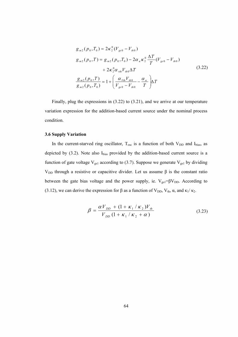
64
TTVV
V
Tpg
Tpg
TV
VVT
TTpgTpg
VVTpg
thgs
thVth
m
m
thvth
thgsmm
thgsm
00
0
002
02
002
000200202
0002002
1),(
),(
2
)(2),(),(
)(2),(
(3.22)
Finally, plug the expressions in (3.22) to (3.21), and we arrive at our temperature
variation expression for the addition-based current source under the nominal process
condition.
3.6 Supply Variation
In the current-starved ring oscillator, Tosc is a function of both VDD and Ibias, as
depicted by (3.2). Note also Ibias provided by the addition-based current source is a
function of gate voltage Vgs1 according to (3.7). Suppose we generate Vgs1 by dividing
VDD through a resistive or capacitive divider. Let us assume β is the constant ratio
between the gate bias voltage and the power supply, ie. Vgs1=βVDD. According to
(3.12), we can derive the expression for β as a function of VDD, Vth, α, and κ1/ κ2.
)/1(
)/1(
21
21
DD
thDD
V
VV (3.23)

65
For a specific CMOS technology, VDD, Vth, and α are fixed, so β is determined
entirely by κ1/ κ2. By setting Vgs1=βVDD, in which β is chosen to satisfy (3.23), we
simulate the output current of the addition-based current source (Ibias) by sweeping the
supply voltage from 0.9V to 1.1V. From the plot of Ibias in Fig. 3.12, we can see there
is a linear relation between Ibias and VDD. Now that VDD and Ibias change in the same
direction proportionally, Tosc (or its inverse fosc) is relatively unaffected by the change
in supply voltage. It is clearly shown in the output frequency (fosc) plot in Fig. 3.12
that the first order dependence between fosc and VDD has been cancelled. Over a supply
range from 0.9V to 1.1V, fosc varies by 6.5MHz, or less than 0.34% of its nominal
value at VDD=1V.
Fig. 3.12 The bias current (Ibias) from the addition-based current source and the output frequency (fosc) of the addition-based ring oscillator change with the supply voltage(VDD).
66
3.7 Chapter Summary
We have demonstrated a fully integrated, scalable, low power, process-and-
temperature-compensated ring oscillator, which does not require any post-fabrication
trimming or calibration. The improved frequency accuracy of the ring oscillator is
achieved through replacing the single transistor in a conventional current-starved ring
oscillator with a process and temperature invariant addition-based current source that
is able to scale beyond the current sub-micron technology node. Measurement results
from 167 chips show a 65.1% reduction of the frequency process variation and
85ppm/oC temperature stability in the proposed ring oscillators. The calibration-free,
low-power, CMOS-compatible, compact, and high-frequency design of our ring
oscillator makes it a potential candidate in a number of low-cost, low-power RF
applications.
67
CHAPTER 4
CLOSED LOOP COMPENSATION WITH FEEDBACK
4.1 Introduction
In this chapter, we present two implementations of a closed-loop process
compensation scheme for high speed ring oscillators—the comparator based and the
switched capacitor based loops. We provide detailed discussion of the frequency
accuracy, loop stability, and implementation cost for each design. More than 150 test
chips from multiple wafer-runs in a 90nm CMOS process verify that frequency
accuracy of better than 2.6% can be achieved with the application of the proposed
compensation loop. Moreover, by leveraging a low variation addition-based current
source, we have demonstrated a fully-integrated 2.15GHz ring oscillator with less than
4.6% frequency variation without external references or post fabrication calibration,
which is 3.8x improvement in frequency accuracy over the baseline case. The same
compensation scheme can also alleviate frequency drift caused by temperature.
Ring oscillators are commonly used to generate clock signals or as tunable local
oscillators in radio systems and I/O interfaces because of their compact size, wide
tuning range and low power consumption. For example, ring oscillators serve as LO’s
in super-regenerative receiver applications [62]. Other application examples can be
found in high-speed clock and data recovery (CDR) circuits, wake-up receivers [42],
and phase-locked loop (PLL) systems [39]. In many of these applications, it is critical
that the ring oscillator maintains a stable center frequency across process and
temperature variations, since frequency stability results in improved selectivity [62],
wider intermediate frequency (IF) bandwidth [42], and less noise coupling [39].
Unfortunately, as CMOS technology scales into deep sub-micron feature sizes, the
68
frequency stability of the ring oscillator deteriorates considerably due to increasing
process variation in the MOS drain current and the circuit propagation delay. Even
after optimizing the fabrication process, it is not uncommon for today’s sub-100nm
process to have more than 35% 3σ variation in both its drive-current and propagation
delay within a single chip [35, 63], and the relative variation of the circuits is more
pronounced in low-voltage applications [34]. Moreover, the high-to-low delay time
and low-to-high delay time, which directly determine the oscillation frequency of
inverter-based ring oscillators, are the most susceptible to variation due to random
dopant fluctuations among the timing parameters [43].
In this chapter, we present a closed-loop process compensation scheme that is able
to reduce the frequency variation in GHz ring oscillators to 2.6%. To achieve this
without resorting to external frequency references (i.e. crystal oscillators in a PLL), we
take advantage of the high precision current source and low tolerance vertical parallel
plate capacitors that are available in sub-micron CMOS process. Two different
compact on-chip implementations of the compensation loop have been designed, and
the measurement results from more than 150 chips in multiple wafer-runs demonstrate
a 3.8x improvement in the normalized standard deviation of the oscillation frequency,
as compared to a baseline current-starved ring oscillator design, with no external
component or post-fabrication calibration. The same control loop idea is also
demonstrated to limit the frequency drift resulting from fluctuations in temperature.
Previous work on low-variation oscillator design is covered in Section 4.2. The
comparator-based and the switched capacitor-based implementations of our proposed
process compensation loop are presented in Section 4.3 and Section 4.4 respectively.
In Section 4.5, measurement results of the compensation loop from multiple wafer-
runs and with different current biasing configurations are analyzed and discussed to
demonstrate the variation reduction performance of the compensation scheme. Finally,

69
conclusions regarding the potential of this technique are reached in Section 4.6.
4.2 Design Concept
To address this design challenge, we employ a feedback approach to correct the
frequency error caused by process variations [64]. In a feedback loop, it is possible to
de-sensitize the variation of the circuit in the forward path by regulating it with higher-
accuracy components in the feedback path that operate at much lower frequency, thus
de-coupling the trade-off between frequency and accuracy in high-speed oscillators.
The basic concept of the system is illustrated in Fig. 4.1. The loop converts the
frequency of the voltage-controlled oscillator (VCO) to a DC voltage VFS through a
frequency sensor and compares it to a constant voltage reference VREF. The difference
between the two represents the frequency error and is fed to the frequency correction
block to generate the bias or control voltage Vctrl that tunes the VCO to run at the
desired frequency despite process induced variation. Since the error comparison can
now be performed in the voltage domain at much lower frequency, we can eliminate
expensive external frequency references and power-hungry high speed circuit blocks,
Fig. 4.1 System diagram of the general compensation loop.

70
and substitute with high-precision on-chip DC components.
In this chapter, we present two possible variants of this loop architecture—the
comparator-based and the switched capacitor-based compensation loops. The circuit
implementation and performance analysis of both are covered in the following
sections.
4.3 Comparator-Based Loop
A voltage comparator followed by an integrator can be used to measure voltage
difference representing the error in the frequency output of the VCO. Following this
idea, a control loop can be designed that comprises of a comparator, a charge pump
(CP) acting as a low pass integrator, a frequency sensor, a VCO, and a timing
generator. The simplified system block diagram is shown in Fig. 4.2. The comparator
detects the difference between VFS and VREF, and its decision is fed to the charge
pump to generate the control voltage Vctrl that speeds up or slows down the VCO
accordingly. Ideally, this feedback regulation will force VFS to converge to VREF, and
thus unambiguously set the VCO’s output frequency.
Fig. 4.2 System diagram of the comparator-based compensation loop.

71
4.3.1 Accuracy Analysis
The actual frequency accuracy of the compensation loop is limited by non-
idealities of the circuits. We can derive the accuracy of the settling frequency of the
control loop, fosc, by obtaining an analytical expression as a function of the circuit
parameters and identifying the critical parameter terms that contribute to frequency
offsets.
A non-ideal comparator with finite transition gain ACP and an input offset VCP,off
can be described as
CP
DD
CP
DD
CP
DD
CP
DD
DDoffCPcp
DD
outCP
A
VVV
A
VVV
A
VA
VVV
VVVVA
V
V
2
22
2
02
)( ,,
(4.1)
in which V+ and V- are the positive and negative input of the comparator. VCP,off is
defined as the voltage difference between the positive and negative comparator inputs
that is required for the comparator output to be at VDD/2, the half point of the output
swing.
Assume that the charge pump current, ICP swings between IDN and –IUP as
controlled by the negative/positive comparator output (VCP,out). This combination can
be adequately modeled as a voltage- controlled current source that saturates at IDN
and-IUP. The sign of ICP indicates the charge/discharge direction of the current. The
functional behavior of ICP can be written in the following expression:

72
m
UPDNDDoutCP
m
UPDNDDoutCP
m
UPDNDD
m
UPDNDDoutCP
UP
UPDNDDoutCPCP
DN
CP
G
IIVV
G
IIVV
G
IIVG
IIVV
I
IIVVG
I
I
22
2222
22
2)
2(
,
,
,
,
(4.2)
The frequency sensor is realized by measuring the voltage across a capacitor (CFS),
which is being charged with a constant current source (IREF) during the duration of
NTosc, as Tosc is the oscillation period and N is the divider ratio. Its output (VFS) can be
depicted as:
FS
oscREFFS C
NTIV (4.3)
In the feedback loop, VREF and VFS are the positive and the negative input of the
comparator, so we replace V+ and V- with VREF and VFS in (4.1) to obtain the
expression of VCP,out. According to the loop operation described above, the stable state
value of Tosc can only be reached when the charge pump current ICP stays zero, so that
the VCO control voltage, Vctrl, is held at a constant value. Solving for VFS that satisfies
the condition of ICP=0, we can determine the analytical form for Tosc:
CPCP
DNUPoffCPREF
REF
FSosc GA
IIVV
NI
CT
2, (4.4)
As indicated by (4.4), mismatches in the comparator and the charge pump,
depicted by VCP,off and |IUP-IDN|, will affect Tosc and contribute to the overall variation
of the oscillation frequency. To alleviate this undesirable effect, we pay special
attention to ensure the matching of comparator input transistors and charge pump
currents and choose a relatively high VREF value compared to the last two mismatch
73
terms in (4.4). The relative accuracy of fosc=1/Tosc can be derived from (4.4) as a
function of the tolerance of the design parameters:
20
22
22
,2
2
0
2
0
2
0
2
0
REF
CPCP
DNUPoffCPREF
FS
C
REF
I
osc
T
osc
f
V
GA
CITf
(4.5)
in which, σf, σT, σI, σC, σREF, σCP,off, σUP-DN, represent the standard deviation of fosc,
Tosc, IREF, CFS, VREF, VCP,off, and (IUP-IDN)/2 respectively, and the superscript “0” in the
symbols indicates the mean value of that variable. Since the comparator input and the
charge pump current have minimal systematic offsets by design, VCP,off, and (IUP-
IDN)/2 should both be random variables with zero means, which justifies the
approximation of the last term in (4.5). In reality, σCP,off and σUP-DN are small relative
to VREF, and the reference voltage, VREF, can be generated on chip with a bandgap
reference, which usually has much better tolerance than the first two terms in (4.5). It
is fair to say that the frequency variation in our process compensation loop is
determined mainly by the variation of the current reference and the capacitor.
4.3.2 Circuit Implementation
In this sub-section, we elaborate on the operation of the circuit blocks employed in
the comparator-based compensation loop.
Frequency Sensor (FS)
The schematic of the FS is shown in Fig. 4.3(a), and the timing diagrams of the
control signals for the switches are illustrated in Fig. 4.3(b). CLK, SP and RST are the
control signals derived from the VCO output by the timing generator. As indicated in
Fig. 4.3(b), the pulse width of CLK which controls the charging up of capacitor CFS is

74
N times the oscillation period Tosc after the divider. In every cycle, CLK turns on the
switch to let IREF linearly charge up the capacitor in a period of NTosc so that at the end
of the charging phase, the voltage at node P equals:
1C
NTIV oscREF
P (4.6)
SP then closes the bridge switch and starts charge sharing between the capacitors.
The charge sharing splits charge proportionally between the two capacitors and such
that each has and equal voltage drop. Finally, SP goes low and disconnects the
capacitor bridge so charge stored on the first capacitor is completely discharged by the
RST switch. The output of the frequency sensor after n cycles can be derived using
charge conservation principle:
1
21
21
C
NTICC
C
V
oscREF
n
FS
(4.7)
Fig. 4.3 (a) Frequency sensor schematic, (b) timing waveform controlling the switches in the frequency sensor.

75
This shows that after running for n cycles, VFS converges to a faithful
representation of Tosc, and can be used to measure the oscillation frequency. For
example, if C1 and C2 are of the same size, after 8 cycles (n=8), VFS will settle to
within 0.4% of its final value. In our design, C1=C2=CFS=1.2pF vertical parallel plate
capacitors are used in the frequency sensor to achieve lower capacitance variations, as
the oxide thickness fluctuation and the line roughness of the process are averaged over
a larger area [65]. For IREF, it is possible to take advantage of recently developed
integrated PVT invariant current sources [3] and the calibration method [66] to
achieve better than 1% precision current references.
Voltage Comparator
A basic differential amplifier with active current mirror load serves as the
comparator. According to our accuracy analysis in the previous sub-section, it is
beneficial to have a small VCP,off. To minimize the input offset through better
matching, large and square transistors are used at the input and careful common-
centroid layout are employed. Estimated to be below 2mV [59], VCP,off contributes to
less than 0.3% to the overall absolute frequency variation. This non-ideality can be
further reduced with chopping or auto-zeroing at the comparator input, which can be
integrated in our system. We chose a modest comparator gain of 28 dB in the design.
Charge Pump
The schematic of the charge pump with low pass filter (CP/LPF) is presented in
Fig. 4.4. Positioned at the top and the bottom, the transmission gate pairs of M1-M2
and M3-M4 switch on/off the source and sink current of the charge pump, IDN and IUP,
both of which are mirrored from self-biased diode-connected transistors. The nominal

76
values of both currents are designed to be the same, i.e., IUP=IDN=150µA=ICP. The
capacitor used here is CCP=1.2pF.
The charge pump block here is different from that in a charge pump PLL, because
its inputs are not strictly digital levels. Instead, when the feedback loop approaches the
frequency locking range, the comparator falls into the transition region with its output
sitting between rails. Therefore, in addition to IUP=IDN, the values of the charge pump
currents should also match when the comparator output is at VDD/2.
Voltage Controlled Oscillator (VCO)
Fig. 4.4 Charge pump schematic.

77
The VCO block is a three-stage current-starved inverter chain ring oscillator with a
tuning range from 780MHz to 5.6GHz. A simple bias network for the VCO consists of
a diode-connected pFET and an nFET, whose gate is connected to the control voltage,
as shown in the circuit schematic in Fig. 4.5. Frequency tuning is achieved through
changing the bias current with the gate voltage. An offset current bias IB is included to
adjust the oscillation period’s sensitivity to the control voltage, K’VCO=dTosc/dVctrl, as
well as to provide the default oscillation current during start-up.
We need a wide tuning range to handle the worse case conditions, but no special
requirement is imposed on the linearity of the control voltage. Other topologies to
implement the VCO can easily be accommodated in our process compensation loop.
The same current-starved topology is used in the baseline ring oscillator design to
ensure fair comparison of frequency variation performance.
Fig. 4.5 VCO schematic.

78
Timing Generator
The frequency sensor block requires a series of well defined timing signals to
control its operation. These control signals (SP, /SP, RST, etc.), as well as the
oscillation signal (CLK) measured by the frequency sensor are generated by the timing
generator.
As indicated in Fig. 4.3(b), CLK is a divided down signal from the output of VCO
(Vout). It is important for CLK to have a nearly 50-50 duty cycle, because the
frequency sensor only measures half of the period when CLK is high. Adding the
frequency dividers after the oscillation signal is a simple way to ensure a 50-50 duty
cycle for CLK. We choose the divider ratio N=4 in our design and both divide-by-2
frequency dividers are implemented with static D-flipflops.
Other control signals necessary for the operation of the frequency sensor are
generated by standard static CMOS logics:
CLKCLKxRST
CLKCLKxSP
CLKCLKxSP
2
2
2
(4.8)
in which CLKx2 is the signal after the first divider and has twice the frequency of
CLK. The timing generator block is also used to offset the delays from different signal
paths to make sure that the difference in signal arrival time will not cause failure at
process corners.
4.3.3 Loop Dynamics
The comparator-based compensation loop experiences two different dynamic

79
regimes as it operates through frequency acquisition and locking. When the operating
frequency is far away from its static value, the feedback loop may exhibit a bang-bang
loop dynamic, due to the binary output at the comparator [67]. After the operating
frequency has been pulled closer to its static value by the bang-bang regulation, the
loop dynamic can be approximated by a 3rd order transfer function, now that the
behavior of the functional blocks in the system can be adequately captured with
continuous-time linear models.
First, let us investigate the bang-bang region of the loop dynamics in discrete time.
Assume that there exists a large initial frequency offset. The comparator will behave
non- linearly and give binary output ε(n), and the error signal in the nth step is:
offCPFSREF VnVVn ,sgn (4.9)
This error signal controls the charge pump to deposit or release charge stored on
CCP, the amount of which is determined by the charge pump current ICP and the
charging duration Tosc(n+1). This changes Vctrl and sets the new oscillation period
Tosc(n+1). The update process of Tosc(n) in discrete time is therefore captured by the
following difference equation:
CP
oscCP
VCO
cosc
C
nTIn
K
nTnT )1()(
)(1'
cos
(4.10)
To study the convergence behavior of the bang-bang model, we turn to
parameterized numerical simulations in Matlab, because the hard nonlinearity inherent
in the comparator prevents direct application of the Z-transform. The simulation
results in Fig. 4.6 show that given random initial conditions, the feedback loop always
successfully acquires the frequency even in the presence of noise, typically in fewer
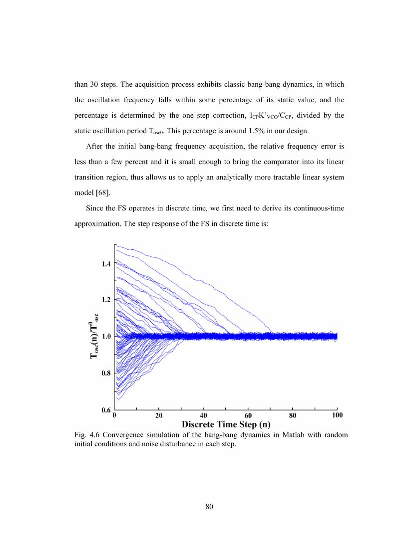
80
than 30 steps. The acquisition process exhibits classic bang-bang dynamics, in which
the oscillation frequency falls within some percentage of its static value, and the
percentage is determined by the one step correction, ICPK’VCO/CCP, divided by the
static oscillation period Tosc0. This percentage is around 1.5% in our design.
After the initial bang-bang frequency acquisition, the relative frequency error is
less than a few percent and it is small enough to bring the comparator into its linear
transition region, thus allows us to apply an analytically more tractable linear system
model [68].
Since the FS operates in discrete time, we first need to derive its continuous-time
approximation. The step response of the FS in discrete time is:
Fig. 4.6 Convergence simulation of the bang-bang dynamics in Matlab with randominitial conditions and noise disturbance in each step.
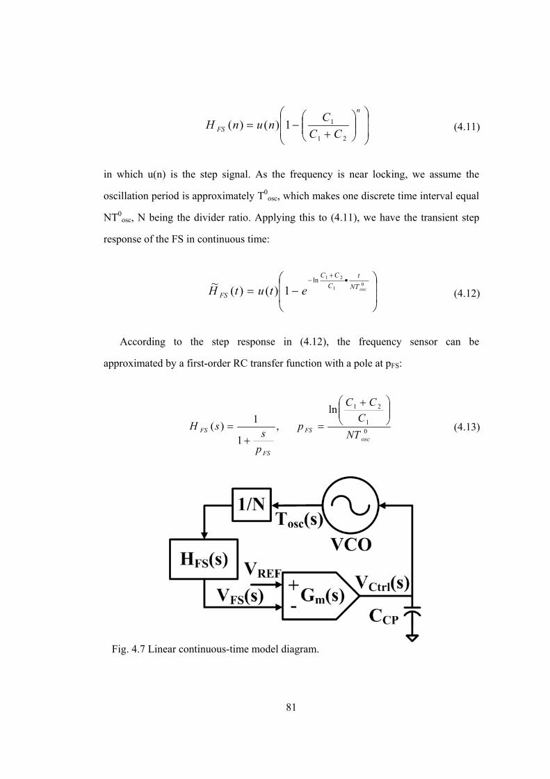
81
n
FS CC
CnunH
21
11)()( (4.11)
in which u(n) is the step signal. As the frequency is near locking, we assume the
oscillation period is approximately T0osc, which makes one discrete time interval equal
NT0osc, N being the divider ratio. Applying this to (4.11), we have the transient step
response of the FS in continuous time:
0
1
21ln
1)()(~
oscNT
t
C
CC
FS etutH (4.12)
According to the step response in (4.12), the frequency sensor can be
approximated by a first-order RC transfer function with a pole at pFS:
0
1
21ln
,1
1)(
oscFS
FS
FS NT
C
CC
p
p
ssH
(4.13)
Fig. 4.7 Linear continuous-time model diagram.

82
When the frequency error is small, the combination of the comparator and the
charge pump behaves similar to a trans- conductance amplifier, which can be modeled
by
CP
mm
p
sG
sG
1
)( 0 (4.14)
with its dominant pole, pcp, at around 420MHz. Plugging in the block models in (4.13)
and (4.14), the loop dynamic of the system can be described by its closed loop transfer
function:
FSCPout
FS
REF
FSREFosc
p
s
p
s
Kp
s
p
s
NI
CVsT
111
1
)( (4.15)

83
in which pout=Gm0/CCP is the pole at the charge pump capacitor CCP and
K=NK’VCOIREF/CFS is the loop gain. The root locus given by this transfer function is
illustrated in Fig. 4.8(a) and the step responses with different loop gains are in Fig.
4.8(b), both of which suggest that there is a desirable range for the loop gain K. If K is
too small (<<0.2), the loop converges very slowly; if K is too large (>>5), the loop can
become unstable. We take into account of the variation of K in our design and ensure
it to be between 0.4 and 1.6.
4.4 Switched Capacitor-Based Loop
The above loop dynamic analysis points out the existing limitations of the
comparator-based compensation loop. One potential shortcoming of this architecture
stems from the third order behavior of the loop and potential for instability. To
(a)
(b) Fig. 4.8 (a) Root locus and (b) step response with different loop gains, derived from the transfer function of the compensation loop.

84
improve the loop stability of the system, we explore a switched capacitor-based
implementation of the frequency compensation loop, depicted in Fig. 4.9.
4.4.1 Improved Frequency Correction Block
The architecture of the frequency correction block used in the compensation loop
is based on a discrete time switched capacitor integrator and is shown in Fig. 4.10(a).
It consists of a current source IREF, capacitors C1 and C2, a high gain operational
amplifier, transmission gate switches, and external inputs VREF and RST.
An external RST is applied at the beginning of operation to clear all digital
counters and establish a DC operating point for the output of the operational amplifier.
Once the RST signal is deasserted, the VCO oscillates with its free running frequency.
The output of the VCO is passed through a series of dividers to shape it into a square
wave with a 50-50 duty cycle. The timing signal generator produces signals φAB, φA,
φB, and φC based on digital logic as follows:
Fig. 4.9 System diagram of the switched capacitor-based compensation loop.

85
1684
1684
1684
16
CLKxCLKxCLKx
CLKxCLKxCLKx
CLKxCLKxCLKx
CLKx
C
B
A
AB
(4.16)
where CLKx4 is the waveform generated by dividing the output of the VCO by 4, as
shown in Fig. 4.10(b).
(a)
(b)
Fig. 4.10 (a) Switched capacitor implementation of the frequency correction block, (b) timing waveform controlling the switches in the block.

86
Based on when the signals are asserted, the operation of the frequency correction
unit can be divided into three phases: Initialization phase, Comparison phase, and
Correction phase, as depicted in Fig. 4.11.
Initialization Phase
When φAB and φA are asserted, one plate of capacitor C1 is charged to VREF and the
other plate is held at ground, as shown in Fig. 4.11(a). This state is used to set an
initial condition on C1 and allows for a comparison to be made between VREF and the
voltage proportional to the VCO’s oscillation period. The charge contained in C1 at the
end of the initialization phase is VREFC1.
Comparison Phase
In Fig. 4.11(b), when φAB and φB are asserted, one plate of the capacitor C1 is
charged up by current source IREF for a period NTosc, N being the divider ratio. The
charge contained in C1 at the end of the comparison phase is VREFC1-NIREFTosc. The
comparison establishes a charge difference at C1 which is proportional to the
difference between the system’s current oscillation period and its nominal oscillation
(a) (b) (c) Fig. 4.11 Equivalent circuits in (a) the initialization phase; (b) the comparison phase;(c) the correction phase.

87
period.
Correction Phase
Once φAB is deasserted, capacitor C1 is floating and the charge on it is held. When
φC is asserted, capacitor C1 is discharged by connecting one plate to ground and the
other to the negative input of the operational amplifier. The high gain of the
operational amplifier requires that its negative input also be a virtual ground as it
tracks the positive input, which is set to ground. Since charge must be conserved,
charge on the plate of C1 connected to the negative input of the operational amplifier is
transferred to capacitor C2.
The operational amplifier is designed as a conventional folded cascode to provide
high gain so that both input nodes are able to track each other effectively. PFET
transistors are used as input since the inputs to the operational amplifier are close to
ground. Fig. 4.11(c) illustrates this phase.
The PFET input transistors are made large and square in layout to improve
matching characteristics. Care is taken to ensure that the parasitic capacitance of the
input transistors is much smaller than those used in the switched capacitor circuit. The
op-amp is designed with a nominal gain of 35 dB. In the next section we will see that,
even with a finite gain, the switched capacitor based compensation system eliminates
the problem of loop stability.
4.4.2 Loop Dynamics
The voltage at the output of the operational amplifier, VCtrl, increases proportional
to the amount of charge transferred. This voltage does not change until the next
occurrence of φc and sets the frequency of the VCO. After n cycles, the voltage at the
output of the operational amplifier is updated according to the difference equation:
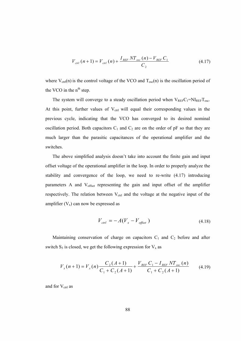
88
2
1)()()1(
C
CVnNTInVnV REFoscREF
ctrlctrl
(4.17)
where Vctrl(n) is the control voltage of the VCO and Tosc(n) is the oscillation period of
the VCO in the nth step.
The system will converge to a steady oscillation period when VREFC1=NIREFTosc.
At this point, further values of Vctrl will equal their corresponding values in the
previous cycle, indicating that the VCO has converged to its desired nominal
oscillation period. Both capacitors C1 and C2 are on the order of pF so that they are
much larger than the parasitic capacitances of the operational amplifier and the
switches.
The above simplified analysis doesn’t take into account the finite gain and input
offset voltage of the operational amplifier in the loop. In order to properly analyze the
stability and convergence of the loop, we need to re-write (4.17) introducing
parameters A and Voffset representing the gain and input offset of the amplifier
respectively. The relation between Vctrl and the voltage at the negative input of the
amplifier (Vx) can now be expressed as
)( offsetxctrl VVAV (4.18)
Maintaining conservation of charge on capacitors C1 and C2 before and after
switch S3 is closed, we get the following expression for Vx as
)1(
)(
)1(
)1()()1(
21
1
21
2
ACC
nNTICV
ACC
ACnVnV oscREFREF
xx (4.19)
and for Vctrl as

89
)1(
)(
)1()1(
)1()()1(
21
1
21
1
21
2
ACC
CVnNTIA
ACC
ACV
ACC
ACnVnV
REFoscREF
offsetctrlctrl
(4.20)
where Vctrl(n) is the control voltage applied to the VCO in the previous correction
cycle and Vctrl(n+1) is the control signal that will be applied at the end of the current
correction cycle. From (4.20), it is evident that, even in the presence of a finite gain,
the compensation loop is stable and will still converge based on a first-order negative
feedback exhibited by the third term, regardless of the starting condition. The static
error Voffset will cause some amount of ripple on Vctrl when VREFC1 = IREFNTosc but this
can be minimized by increasing the ratio of C1 and C2 and ensuring the input
transistors in the amplifier are well matched and large. Care must be taken not to make
C2 too large as this would make the incremental voltage buildup on Vctrl smaller, and
hence, the compensation time larger. Making C2 small would lead to a loss of
precision on Vctrl, forcing it to periodically overshoot and undershoot the correct value.
In our design a C1:C2 ratio of 1:3 was chosen.
4.4.3 Accuracy Analysis
When the loop converges, Vctrl(n+1)=Vctrl(n) =Vctrl∞ and the oscillation period Tosc
is represented as Tosc∞, where Tosc
∞ = K’VCO.Vctrl
∞. We can now determine how close
Tosc∞ is to the ideal value of Tosc=VREFC1/NIREF by solving (4.20):
'1
1
.
)(
VCOREF
offsetREFosc
KA
CIN
CVVT (4.21)

90
The above expression shows that there is still some accuracy error present due to
non-idealities in the compensation loop, similar to the error in the comparator based
compensation loop. For most operational amplifiers, input offset error is in the range
of less than 5mV [69] and can be further minimized by a number of proposed
techniques [70]. This reduces the error in the numerator of (4.21) to less than 1.5% for
VREF = 0.7. For an IREF = 300 µA, C1 = 1 pF, and K’VCO = 1.3 ns/V, the error in the
denominator of (4.21) is less than 5%.
Given the fact that Voffset<<VREF and C1/AK’VCO<<IREF, we can approximate the
relative accuracy of fosc=1/Tosc as a function of the tolerance of the design parameters:
20
222
01
20
01
'
2'
2'2
212
2
0
2
0
REF
offVC
REF
C
VCO
K
VCOI
osc
T
osc
f
VCI
CKKA
C
Tf
(4.22)
The definition of the symbols used in (4.22) is the same as those in (4.5). Based on
the frequency accuracy analysis, the switched capacitor-based compensation loop will
achieve similar process variation in its settling oscillation frequency as the
comparator-based compensation loop, since VREF, IREF and vertical parallel plate
capacitors, which are the dominant contributors to the frequency variation, are the
same in both designs.
4.5 Measurement Results
We have fabricated the proposed comparator-based and switch capacitor-based
process compensation systems in IBM’s 90nm CMOS9sf process over multiple
separate wafer-runs. Uncompensated three-stage current-starved ring oscillators are
also fabricated in the same runs to serve as a baseline. The measurement results of
more than 150 test chips obtained from the wafer-runs are presented in this section.

91
To demonstrate the effectiveness of the process compensation loops and make fair
comparison of the frequency variation, we first conduct the experiments by supplying
the baseline ring oscillator and the compensated oscillator in the comparator-based
loop with the same constant external current (IREF) using the testing set-up in Fig. 4.12.
In this way, both oscillators take the same mirrored version of IREF to generate the
oscillation. The histograms of the oscillation frequency based on the testing set-up
illustrated in Fig. 4.12 are presented in Fig. 4.13. When biased with the same external
current reference, the baseline oscillator has a higher frequency variation of 8.7% due
to both wider spread in each wafer run and more frequency shift between wafer runs.
On the other hand, the compensated oscillator enjoys narrower spread and less wafer-
to-wafer shift, resulting in 4.5% standard deviation over mean. Despite the obvious
improvement, the variation is a little higher than what has been predicted by (5) given
the accuracy of the external current source (IEXT) and voltage bias (VREF). This is due
to the fact that IEXT is not directly applied to the frequency sensor, but is instead
(a) (b)
Fig. 4.12 External current reference input testing set-up for (a) the baseline ring oscillator, (b) the ring oscillator in the process compensation loop.
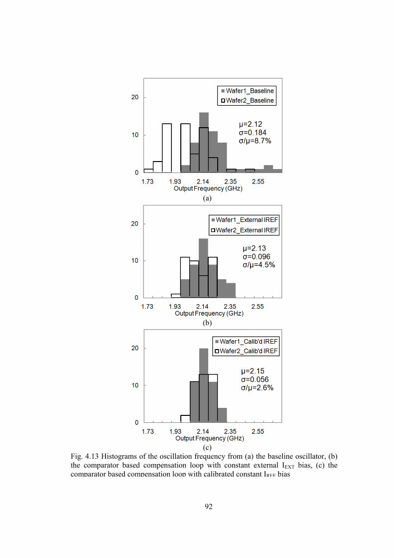
92
(a)
(b)
(c)
Fig. 4.13 Histograms of the oscillation frequency from (a) the baseline oscillator, (b)the comparator based compensation loop with constant external IEXT bias, (c) thecomparator based compensation loop with calibrated constant IREF bias

93
current mirrored to generate IREF in our set-up, which is subject to device mismatch.
This extra variation caused by the current mirror mismatch is on the order of a few
percent in sub-micron processes. To verify our hypothesis, we measure the actual
current in the FS branch and set it to a constant value by tweaking the value of IEXT
externally. With the calibrated current input that ensures the constant value of IREF in
the FS, we are able to obtain a reduced frequency variation of 2.6% from the
compensated oscillator in the comparator-based loop, the histograms of which is
shown in Fig.4.13(c). This demonstrates that our proposed closed-loop compensation
scheme can lock the frequency accuracy close to the current accuracy within 2.6%,
making it possible to replace expensive external frequency reference with cheaper
accurate current solutions (eg. high precision resistor, current calibration, etc.) in
applications that demand modest frequency accuracy and lower integration cost.
Although not implemented in our system, techniques such as chopping and dynamic
element matching can be employed to improve matching in the current mirror to
(a) (b)
Fig. 4.14 (a) The process compensation loop with the addition-based current source, (b) the scatter plot showing the correlation between the oscillation frequency (Fosc) and the current provided by the addition-based current source (IADD).

94
achieve the demonstrated minimum variation of 2.6%.
The next step is to integrate the whole system on chip by substituting the external
current reference with an on-chip addition-based current source that has been
(a)
(b)
Fig. 4.15 Histograms of the oscillation frequency from the fully integrated (a) baseline oscillator, (b) the comparator compensation loop with the addition-based current source bias.
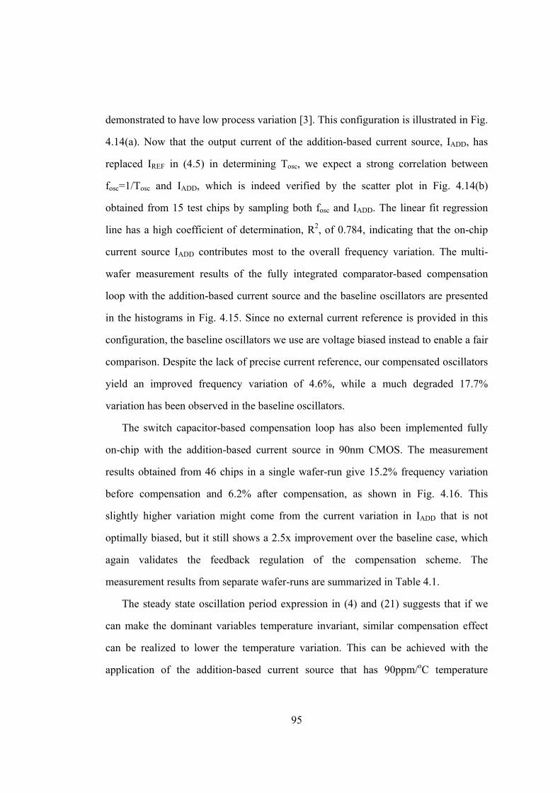
95
demonstrated to have low process variation [3]. This configuration is illustrated in Fig.
4.14(a). Now that the output current of the addition-based current source, IADD, has
replaced IREF in (4.5) in determining Tosc, we expect a strong correlation between
fosc=1/Tosc and IADD, which is indeed verified by the scatter plot in Fig. 4.14(b)
obtained from 15 test chips by sampling both fosc and IADD. The linear fit regression
line has a high coefficient of determination, R2, of 0.784, indicating that the on-chip
current source IADD contributes most to the overall frequency variation. The multi-
wafer measurement results of the fully integrated comparator-based compensation
loop with the addition-based current source and the baseline oscillators are presented
in the histograms in Fig. 4.15. Since no external current reference is provided in this
configuration, the baseline oscillators we use are voltage biased instead to enable a fair
comparison. Despite the lack of precise current reference, our compensated oscillators
yield an improved frequency variation of 4.6%, while a much degraded 17.7%
variation has been observed in the baseline oscillators.
The switch capacitor-based compensation loop has also been implemented fully
on-chip with the addition-based current source in 90nm CMOS. The measurement
results obtained from 46 chips in a single wafer-run give 15.2% frequency variation
before compensation and 6.2% after compensation, as shown in Fig. 4.16. This
slightly higher variation might come from the current variation in IADD that is not
optimally biased, but it still shows a 2.5x improvement over the baseline case, which
again validates the feedback regulation of the compensation scheme. The
measurement results from separate wafer-runs are summarized in Table 4.1.
The steady state oscillation period expression in (4) and (21) suggests that if we
can make the dominant variables temperature invariant, similar compensation effect
can be realized to lower the temperature variation. This can be achieved with the
application of the addition-based current source that has 90ppm/oC temperature
96
sensitivity between 200K and 400K [71], because the other variables, VREF and CFS,
are relatively constant over temperature. We measured the changes of oscillation
frequency in the comparator-based and the switched capacitor-based loop over a
temperature range from 280K to 350K, and the results are plotted in Fig. 4.17. The
(a)
(b)
Fig. 4.16 Histograms of the oscillation frequency from the fully integrated (a)baseline oscillator, (b) the switched capacitor compensation loop with the addition-based current source bias.

97
compensated loop architectures exhibit improved 168ppm/oC and 290ppm/oC
sensitivity, compared to 965 ppm/oC in the baseline case.
The additional circuitry needed to implement the closed feedback loop, occupies
0.046mm2 and consumes 0.9mW in the comparator-based architecture, and 0.033mm2
and 3.3mW in the switched capacitor-based one, compared to 1.05mW and 0.05mm2
for the baseline uncompensated ring oscillator, including decoupling capacitor and
output driver. Our measured results indicate that although stability may be improved
with the switched capacitor design proposed, the cost of this is in the required design
of a larger, higher power, and more complex op-amp in the feedback loop. This fact
may favor the comparator based design.
Although this trade-off between power-area and accuracy is somewhat inevitable
among all of these designs, it is possible to reduce the power consumption in our
scheme further in the future, because the loop only needs to be activated periodically
TABLE 4.1 FREQUENCY SPREADS IN TWO WAFER RUNS OVER MULTIPLE CHIPS
Oscillator Type Wafer-
run
No. of Chips
Meas’d
Freq. Mean (GHz)
Freq. Std. (MHz)
Norm. Std. (%)
Baseline (External IREF)
1st 52 2.22 157 7.10 2nd 53 2.02 155 7.68
Comp. Based (External IREF)
1st 48 2.15 94.6 4.39 2nd 39 2.09 84.1 4.02
Comp. Based (Calibrated IREF)
1st 46 2.15 56.2 2.61 2nd 39 2.14 55.1 2.57
Baseline (On-Chip)
1st 52 1.96 203 10.3 2nd 53 2.56 314 12.3
Comp. Based (On-Chip)
1st 46 2.14 104 4.86 2nd 43 2.17 92.5 4.25
Baseline (On-Chip)
N/A 46 2.85 424 15.2
Sw. Cap-Based (On-Chip)
N/A 46 2.91 178 6.23
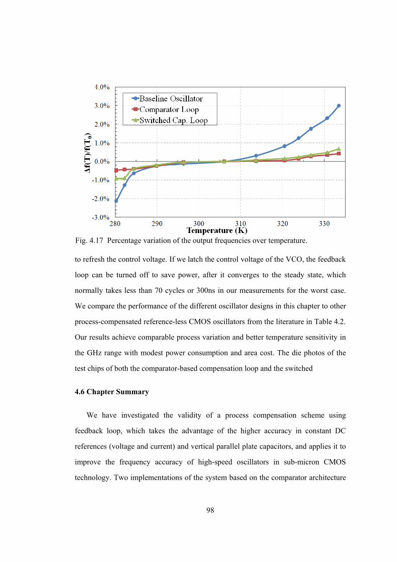
98
to refresh the control voltage. If we latch the control voltage of the VCO, the feedback
loop can be turned off to save power, after it converges to the steady state, which
normally takes less than 70 cycles or 300ns in our measurements for the worst case.
We compare the performance of the different oscillator designs in this chapter to other
process-compensated reference-less CMOS oscillators from the literature in Table 4.2.
Our results achieve comparable process variation and better temperature sensitivity in
the GHz range with modest power consumption and area cost. The die photos of the
test chips of both the comparator-based compensation loop and the switched
4.6 Chapter Summary
We have investigated the validity of a process compensation scheme using
feedback loop, which takes the advantage of the higher accuracy in constant DC
references (voltage and current) and vertical parallel plate capacitors, and applies it to
improve the frequency accuracy of high-speed oscillators in sub-micron CMOS
technology. Two implementations of the system based on the comparator architecture
Fig. 4.17 Percentage variation of the output frequencies over temperature.

99
and the switched-capacitor architecture have been demonstrated using IBM’s 90nm
CMOS9sf process, and measurement results from more than 150 chips in multiple
wafer-runs have been obtained. At 2GHz oscillation frequency, our proposed
compensation scheme not only delivers 3.8x improvement in its frequency accuracy
over the baseline case measured by normalized standard deviation of the center
frequency, but also achieves absolute frequency variation of 4.6% without external
reference and calibration at a modest cost of power an chip area.
(a) (b)
Fig. 4.18. Die photos of (a) the comparator-based compensated ring oscillator; (b) theswitch capacitor-based compensated ring oscillator.
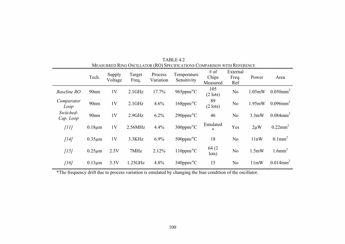
100
TABLE 4.2 MEASURRED RING OSCILLATOR (RO) SPECIFICATIONS COMPARISON WITH REFERENCE
Tech. Supply Voltage
Target Freq.
Process Variation
Temperature Sensitivity
# of Chips
Measured
External Freq. Ref
Power Area
Baseline RO 90nm 1V 2.1GHz 17.7% 965ppm/oC 105
(2 lots) No 1.05mW 0.050mm2
Comparator Loop
90nm 1V 2.1GHz 4.6% 168ppm/oC 89
(2 lots) No 1.95mW 0.096mm2
Switched-Cap. Loop
90nm 1V 2.9GHz 6.2% 290ppm/oC 46 No 3.3mW 0.084mm2
[11] 0.18µm 1V 2.56MHz 4.4% 300ppm/oC Emulated
* Yes 2µW 0.22mm2
[14] 0.35µm 1V 3.3KHz 6.9% 500ppm/oC 18 No 11nW 0.1mm2
[15] 0.25µm 2.5V 7MHz 2.12% 110ppm/oC 64 (2 lots)
No 1.5mW 1.6mm2
[16] 0.13µm 3.3V 1.25GHz 4.8% 340ppm/oC 15 No 11mW 0.014mm2
*The frequency drift due to process variation is emulated by changing the bias condition of the oscillator.

101

102
CHAPTER 5
SYSTEM SELF-CALIBRATION
5.1 Introduction
In this chapter, a 46µW 0.8-2GHz tunable oscillator with built-in self-calibrated
PVT compensation is presented for applications in low power radios. With single-
point current calibration at room temperature, the proposed VCO achieves 2.24%
frequency accuracy against process variation, 1.6% frequency shift over 0.85-1.15V
supply voltage, and 167ppm/oC temperature sensitivity between -7oC and 76oC. The
sub-135pJ on-chip self-calibration is based on a successive approximation scheme.
Our design shows 3.4x improved process variation tolerance, 45x improved supply
sensitivity, and 5.2x improved temperature sensitivity, as compared to the free-running
VCO without self-calibration. Measurements are taken from 94 chips fabricated in two
different lots in TSMC 65nm CMOS process.
Low power radio systems, such as UWB impulse radios and wake up receivers,
have attracted attention for applications in wireless sensor networks (WSN) and body
area networks (BAN), where low power operation at low cost is required. Generating
an accurate local frequency reference is critical in these systems, as it often sets the
limit of achievable power savings [72, 73], determines the optimal frequency plan
[42], and affects the network dynamics [74]. Hence, a PVT-invariant oscillator
immune to the variations of process, supply voltage, and temperature (PVT) is
extremely desirable. In addition to the accuracy requirement, the oscillator must
operate under a stringent power budget (<100µW) and be inexpensive to integrate
within a state-of-the-art CMOS process.
The ring oscillator based voltage-controlled oscillator (VCO) exhibits wide-tuning

103
range, low power consumption, small die area, and ease of integration. Compared to
the more power hungry LC oscillator [53] and the FBAR-based resonator with limited
tuning range [30], it is particularly suitable for low power radios whose inherent
architecture is more tolerant to phase noise but require flexible low power operation.
Unfortunately, the ring oscillator suffers from severe impacts of increasing variability,
especially as CMOS technology scales down to the nanometer regime. Despite efforts
to improve the inherent accuracy of free-running oscillators through symmetric loads
[75], stable current bias [71], and threshold and temperature sensing [60], built-in self-
calibration circuitry and compensation schemes are needed to achieve enhanced
performance against PVT variations as demanded in practical low power radios.
In this chapter, we demonstrate a 46µW VCO with built-in self-calibrated PVT
compensation that can function both as a local oscillator (LO) [42] and as a wake-up
clock [72]. The proposed oscillator has a tuning range of 0.8-2GHz that allows flexible
channel selection and frequency hopping. Based on the successive approximation
method [76], the self-calibration incorporated in our VCO design improves the
frequency sensitivity of the free-running oscillator to process by 3.1x, to supply
voltage by 45x, and to temperature by 5.2x, while consuming less than 135pJ to
perform the calibration procedure. These results are verified by more than 94 test
chips from two different lots fabricated in TSMC 65nm CMOS process.
5.2 PVT Compensation for VCO
Three types of built-in calibration techniques have been proposed for PVT
compensation in VCO’s: closed-loop control voltage monitoring [77], digital counter
over fixed time [78, 79], and analog time-to-voltage conversion (TVC) [80].
Monitoring the control voltage in closed-loop configuration requires long settling
time and continuous loop operation. At the same time, counting over a fixed time

104
window takes more calibration time to arrive at the same frequency resolution than the
analog TVC technique. Hence the most energy-efficient calibration is realized with
analog TVC that is able to track the frequency within several cycles of oscillation.
For low power radio applications in WSN and implantable electronics, integration
cost, power consumption, and form factor make an external reference, such as a
crystal oscillator, undesirable. Without an accurate frequency reference, we use
absolute comparison with low-tolerance on-chip components for calibration, instead of
relative frequency comparison [80].
Given the design considerations mentioned above, we use the analog TVC
technique based on absolute comparison in our self-calibration circuitry with post-
process trimming. To further minimize test time and cost, single-point DC current
trimming at room temperature is applied, instead of costly and complex frequency
calibration at multiple temperature points.
5.2.1 System Architecture
Successive approximation is a method that is often used in analog-to-digital
converters (ADC) to refine the accuracy of data conversion. In a successive
approximation ADC, VIN, the input voltage, is compared to VDAC, the output of the
digital-to-analog converter (DAC) which is also an estimate of the input value. The
error between the estimate and the input value is fed to a successive approximation
register (SAR) to increment or decrement a digital code representing a revised digital
estimate of VIN based on a binary search algorithm. This becomes the input to the
DAC and in turn provides a revised version of VDAC for comparison to Vin.
The same idea can be applied in designing a compensation scheme for a ring
oscillator. In this case, we break the connection between the DAC and the comparator
in the ADC, and add a voltage-controlled oscillator (VCO) and a frequency sensor,

105
which perform the transformation of voltage to frequency and back to the voltage
domain.
Our proposed self-calibration system (Fig. 5.1) that consists of a VCO, a time-to-
voltage converter (TVC), a comparator, a successive approximation register (SAR), a
digital-to-analog converter (DAC), and a state machine. At the TVC, oscillation is
measured so that VTVC is proportional to the VCO period. VIN and VTVC are then
compared to update the digital code (Dctrl) stored in the SAR to generate Vctrl. With
each comparison and update, Vctrl tunes the VCO frequency, until VTVC equals VIN.
When the calibration is completed, the final Dctrl is stored in the SAR to generate the
optimal Vctrl.
The external test controller also shown in Fig. 5.1 provides current calibration by
measuring Iref and adjusting the trimming bits for bias resistors in the TVC. VIN is
supplied externally with variable resistive divider from VDD in our measurement, but
could be fully-integrated into the system as well. The frequency sensor is designed
with low variation components, and therefore does not contribute significant process
variation. The digital blocks used in the SAR and the DAC have sufficient margins
that ensures correct operation at the process corners. If the comparator can distinguish
infinitesimal voltage differences and an infinite number of bits are used to represent
the control voltage, the output frequency of the VCO will be completely determined
by the reference voltage VIN.
5.2.2 Calibration Scheme
A state machine (Fig. 5.2) running on a derived clock from the VCO controls the
timing of events in the system, starting from Sleep/RST, moving onto Auto zero and
Conversion, when a request is initiated, and then iterating between update, sample and
compare until the final approximation is completed. The state machine also does the

106
clock gating to different blocks to save power. As the VCO clock can vary during the
control process, additional provision is made for synchronization using hand-shake
signals at crucial stages, such as update, sample and comparison for robustness.
Illustrated in Fig. 5.3 in the top row, VIN is the control voltage that determines the
final frequency in our system, as the VCO frequency (fVCO) successively approximates
NIref/CVIN (N is the divider ratio). The system starts in the Sleep/RST state (RST),
until Conv_Request triggers the self-calibration. As each bit in Dctrl resolves from
MSB to LSB, fVCO approaches its final value at increasingly finer steps. The decision
of LSB in Dctrl indicates the completion of the calibration and returns the system back
to RST state with fvco locked to its calibrated value.
We zoom into the dashed box in the fVCO timing diagram to show the state
transitions and the progression of Dctrl, VTVC, and the comparator output VCP, as the
T-to-V Converter Comparator
C
Iref
SAR
VCO
VIN
Vctrl
VTVC
State Machine
Vout
Dctrl
VCP
DAC
On-Chip System
Test Controller
VDD
Output Frequency
Iref
MeasureRD
BitsRG
BitsControl Voltage
Fig. 5.1 Block diagram of the proposed VCO system with built-in self-calibrated PVTcompensation.
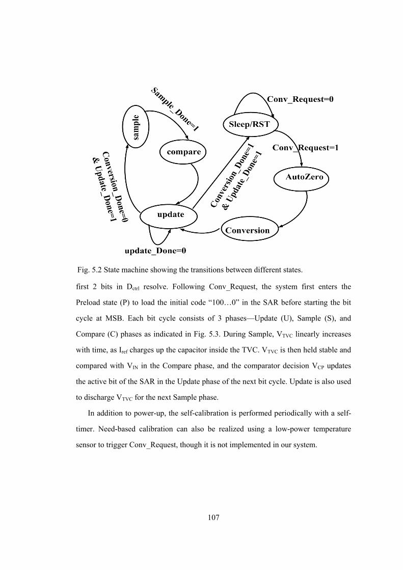
107
first 2 bits in Dctrl resolve. Following Conv_Request, the system first enters the
Preload state (P) to load the initial code “100…0” in the SAR before starting the bit
cycle at MSB. Each bit cycle consists of 3 phases—Update (U), Sample (S), and
Compare (C) phases as indicated in Fig. 5.3. During Sample, VTVC linearly increases
with time, as Iref charges up the capacitor inside the TVC. VTVC is then held stable and
compared with VIN in the Compare phase, and the comparator decision VCP updates
the active bit of the SAR in the Update phase of the next bit cycle. Update is also used
to discharge VTVC for the next Sample phase.
In addition to power-up, the self-calibration is performed periodically with a self-
timer. Need-based calibration can also be realized using a low-power temperature
sensor to trigger Conv_Request, though it is not implemented in our system.
Fig. 5.2 State machine showing the transitions between different states.

108
5.2.3 Frequency Accuracy
The input offset of the comparator (VCP,off), the finite resolution of the SAR and
the DAC (VLSB), and the capacitor variation in the TVC determine the final calibrated
frequency accuracy:
2'2
,22
,maxosc
VCOLSB
IN
offCPC
osc
f
f
KV
VCf
(5.1)
in which, σf, σC, and σCP,off, represent the standard deviation of the nominal
operating frequency fosc, C, and VCP,off. K’VCO is the VCO gain.
Fig. 5.3 Timing diagrams of the VCO frequency (fvco) as it successively converges towards NIref/CVIN during the successive approximation self-calibration. Zoomed-in diagrams of Dctrl, VFS, and VCP, as the first 2 bits in Dctrl resolve.

109
5.3 Circuit Implementation
According to (5.1), the frequency accuracy is determined by the capacitor
tolerance, the comparator offset, the number of bits in Dctrl, and the VCO gain. As the
capacitor tolerance is the dominant variation in the system, it is important to choose
the optimal block implementation in the self-calibration system so that the
contributions from other variation terms are minimized.
5.3.1 Time-to-Voltage Converter (TVC)
The TVC measures the oscillation period, and its absolute accuracy is especially
critical. It is realized with a current source (Iref) charging up a pF capacitor, as
illustrated in Fig. 5.4(a). CLK is generated by a divided-down VCO output, and it has
a 50-50 duty cycle and a period of 2NTosc. Therefore the output voltage of the TVC at
the end of charging period is VTVC=NIrefTosc/C=NIref/foscC.
(a)
(b) Fig. 5.4 Schematics of (a) the TVC block and (b) the addition-based current source with trimming capability.
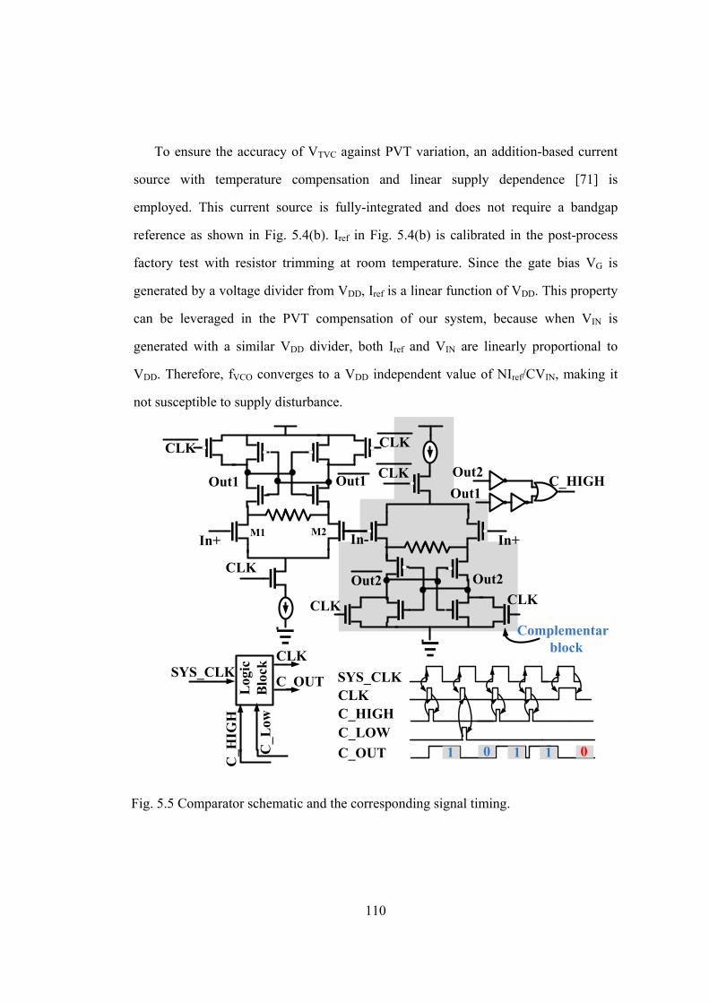
110
To ensure the accuracy of VTVC against PVT variation, an addition-based current
source with temperature compensation and linear supply dependence [71] is
employed. This current source is fully-integrated and does not require a bandgap
reference as shown in Fig. 5.4(b). Iref in Fig. 5.4(b) is calibrated in the post-process
factory test with resistor trimming at room temperature. Since the gate bias VG is
generated by a voltage divider from VDD, Iref is a linear function of VDD. This property
can be leveraged in the PVT compensation of our system, because when VIN is
generated with a similar VDD divider, both Iref and VIN are linearly proportional to
VDD. Therefore, fVCO converges to a VDD independent value of NIref/CVIN, making it
not susceptible to supply disturbance.
In+
CLK
CLK CLK
Out1 Out1CLK
In+
CLK
In-
Out2Out2CLK
C_HIGHOut1
Out2
C_H
IGH
Log
ic
Blo
ckSYS_CLK
C_L
ow
CLK
C_OUT SYS_CLKCLKC_HIGHC_LOW
C_OUT
Complementaryblock
1 0 1 1 0
M1 M2
Fig. 5.5 Comparator schematic and the corresponding signal timing.

111
5.3.2 Comparator
A differential regenerative latch based comparator with complementary stages
shown in Fig. 5.5 is designed for rail-rail input common-mode range. When the clock
is low (inactive phase), the outputs (C_LOW and C_HIGH) sit at “0”. When the clock
goes high, regenerative amplification forces one of the outputs to go high, which
indicates the relative difference of the signals In+ and In-, as well as the completion of
comparison, that asynchronously shuts the clock to the comparator “off” to save
power. The output decision is latched on to C_OUT and is held before the active edge
of the next comparison cycle sets it to zero.
The comparator can make decisions to high accuracy in less than 2ns. As a fail-
safe option around meta-stability, provision is taken to force a bit-decision when the
voltage difference at the input is extremely small. To minimize input offset, the input
transistors were sized to be big, and the offset variation is simulated to be <1mV. An
auto-zeroing preamp can further reduce it for higher accuracy applications.
5.3.3 Voltage-Controlled Oscillator (VCO)
The VCO is implemented with a three-stage current starved inverter chain ring
oscillator. A wide tuning range is achieved through two identical bias current sources:
one controlled by the MSB of Dctrl, and the other controlled by Vctrl generated by DAC
with the rest of the bits in Dctrl. Corner simulation indicates that there exists an overlap
of tuning ranges between 750MHz and 2.2GHz despite the center frequency shifts due
to process variation.

112
Phase noise of the system is determined by the DAC and the VCO, as the rest of
the circuitry is powered down and the feedback is cut off after self-calibration is
completed. It meets the relaxed phase noise specifications for the low power radio
applications we proposed.
5.3.4 SAR and DAC
The SAR (Fig. 5.6) algorithm uses 11-Flops and 11-Muxs and starts with loading
0’s in all but the MSB flop where a 1 is loaded. In every successive update cycle, the 1
is shifted to the next flop while the bit comparison decisions from the comparator are
stored, starting from MSB. It is auto-timed, and the conversion completion is indicated
by the LSB flop (Q0) flips from 0 to 1.
Fig. 5.6 SAR algorithmic block.

113
Since linearity and monotonicity only affect the last term in (5.1), which is often
much lower than the capacitor tolerance, we use a 10-bit R-2R ladder DAC (Fig. 5.7)
for its simplicity. The reference voltages of the DAC are generated from VDD by a
voltage divider. This topology has fewer components and also inherently ensures a
binary search. The low voltage reference of the DAC is set at 350mV to avoid
applying below-threshold control voltage at the VCO.
5.4 Measurement Results
We fabricated the proposed oscillator in two different lots 6-month apart using
TSMC’s 65nm CMOS process. A full set of 94 test chips are measured in both multi-
project runs. The histograms of the measurements are presented in Fig. 5.8, which
compare the normalized standard deviation (σ/µ) of the oscillator frequency without
(free-running) and with self-calibration. At 3 different VIN, we are able to obtain the
histograms exhibiting 3 different mean frequencies (0.85GHz, 1.36GHz, and
1.95GHz). The accuracy improvements shown in both narrower die-to-die frequency
spread and smaller lot-to-lot shift in the mean frequency can be observed in all 3
R R R R
2R2R 2R 2R2R2R
VREFL
VREFH
VDAC
Q0 Q1 Q7 Q8 Q9
Fig. 5.7 R-2R ladder DAC.
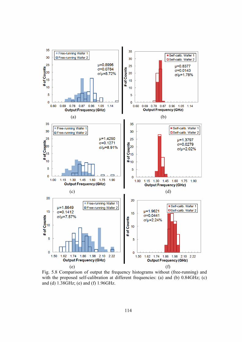
114
(a) (b)
(c) (d)
(e) (f)
Fig. 5.8 Comparison of output the frequency histograms without (free-running) andwith the proposed self-calibration at different frequencies: (a) and (b) 0.84GHz; (c)and (d) 1.38GHz; (e) and (f) 1.96GHz.

115
cases. The improvement factors defined by the ratio of σ/µ of the self-calibrated VCO
over that of the free-running VCO are 4.9x(at 0.84GHz), 4.41x(at 1.38GHz) and
3.38x(at 1.96GHz). Notice that accuracy decreases at higher frequency (i.e. lower
VIN), as predicted by (5.1) in Section 5.2.
To test the sensitivity of the self-calibrated VCO against the supply voltage, we
sweep VDD from 0.85V to 1.15V. Here, we set the operating frequency at 0.84GHz,
and define f0 as the average frequency measured at nominal VDD=1V for both the free-
running and the self-calibrated VCO. Against this 30% supply variation, the free-
running VCO on a typical chip varies by 72% around its center frequency, while the
self-calibrated one experiences only 1.6% frequency deviation, yielding a 45x
improvement as shown in Fig. 5.9. To gauge the combined effect of both process and
VDD variation, we perform the same VDD sweep on the slowest and the fastest dies
among all 94 test chips. Since process variation shifts the Δf/f0 versus VDD curves

116
(a)
(b)
Fig. 5.9 Measured percentage deviation from the nominal frequency at different supply voltages (VDD) in (a) the free-running and (b) the self-calibrated oscillators.

117
upwards for the fast chip and downwards for the slow chip approximately by the
amount of the worst frequency spread in the histograms, we have a worst case ±4%
frequency deviation after the application of self-calibration in Fig. 5.9(b), compared to
-49% and +72% frequency deviation in the free-running ones in Fig. 5.9(a).
In Fig. 5.10, we measure the frequency response of the free-running and self-
calibrated oscillators on a randomly-selected die over a temperature range from -7oC
to 76oC and observe 5.2x improvement after self-calibration (1.32%) over the free-
running one (6.88%).
The waveforms in Fig. 5.11 show the transitions between the Sleep/RST and the
self-calibration at two different frequencies (0.84GHz and 1.38GHz). The duration of
the self-calibration depends on the operating frequency. As indicated in Fig. 5.11, a
single calibration requires between 250ns and 600ns and consumes between 60pJ and
135pJ. The difference of phase noise between the free-running and self-calibrated
Fig. 5.10 Measured frequency deviation at different temperature before and after thecalibration.

118
oscillators is negligible. At 1.38GHz with 10MHz offset frequency, both oscillators
exhibit -98dBc/Hz spot phase noise. A summary of the self-calibrated VCO design
(a)
(b)
Fig. 5.11 Output oscillation waveforms (divided down by 32) of two consecutive self-calibrations at (a) 0.84GHz and (b) 1.38GHz.

119
specs and PVT accuracy is included in Table 5.1. The die photo and zoomed-in layout
are shown in Fig. 5.12. The core area of the VCO and the self-calibration circuitry
occupy 0.06mm2.
Table 5.2 compares our work with other oscillator designs in the literature. The
tunable GHz operating frequency of our design makes it possible to perform dual
functions as both local oscillator [42] and system clock [72]. Compared to [42] at GHz
range, our design shows much improved PVT-invariance with small power overhead.
The oscillator presented in [72] operates at kHz range while consuming similar
amount of power. It requires frequency trimming and additional high-precision
temperature sensors to achieve the temperature sensitivity of 103ppm/oC, which is
(a)
(b)
Fig. 5.12 (a) Die photo of the chip; (b) Zoom-in layout of the core area.

120
quoted as performance estimation with post-processed data, not from any direct
measurement results. Compared to [72], our self-calibrated VCO only needs easy-to-
perform current trimming at a single room temperature, and its performance has been
verified by direct chip measurements. Our calibration scheme can also be used to
replace the coarse-tuning PVT-calibrator in [81], because better PVT frequency
accuracy can be achieved after the self-calibration without performing post-fabrication
PVT characterization at multiple temperatures. It is also worth noting that our results
are verified by statistically significant number of chip measurements from different
fabrication lots.
5.5 Chapter Summary
The stringent power and cost budget of low power radio system calls for fully-
integrated VCO design with enhanced frequency accuracy against PVT variations that
can only be achieved with built-in self-calibration circuitry. We have designed and
implemented a 46µW VCO in the GHz range that can perform effective self-
calibration under 135pJ to significantly reduce its PVT-induced frequency deviation.
We have also performed comprehensive measurements on 94 test chips in order to
TABLE 5.1: Chip Summary Process TSMC 65nm CMOS
Core Area 0.06mm2 Supply Voltage
1V
Frequency 0.8~2GHz Power Self-calib.: 226µW Sleep/RST: 46µW
Time/Calib.* 250~600ns Energy/Calib.* 60~135pJ
Accuracy Process Supply Temperature 2.24%
94 chips 1.8%
0.85~1.15V 1.32%
-5~75oC: *Dependent on the operating frequency.

121
obtain statistically significant results.
TABLE 5.2 PVT Compensated Oscillator Comparison
This Work [3] [1] [13]** Technology 65nm CMOS 90nm CMOS 65nm CMOS 90nm CMOS Frequency 0.8~2GHz 2GHz 100kHz 5MHz Calibration Needed
Single-point current calib.
N/A Single-point freq. calib.
Multi-point calib.
Process Variation
2.1% <10% 0 (freq. calibrated)
N/A***
Temperature -5oC~75oC 0oC~90oC -22oC~85oC 0oC~75oC Temperature Sensitivity
167 ppm/oC
~700 ppm/oC
103 ppm/oC*
>500 ppm/oC
VDD Range 0.85V~1.15V 0.5V 1.05V~1.4V 0.9V~1.1V VDD Vari. 1.6% N/A 0.5% 2.1% Power 46µW 20µW 40.8µW 7.6µW Area 0.06mm2 N/A 0.11mm2 0.27mm2 Chips tested 94 4 11 1 * Not measurement data. **Compared to the PVT calibrator in [13] ***Only 1 chip is measured.

122
CHAPTER 6
IMPROVE CIRCUIT ACCURACY USING DIVERSIFICATION
6.1 Introduction
Reference voltage and current sources play an indispensable role in a wide variety
of integrated circuit applications including data converters, communication systems,
and memory peripheral circuits. In these systems, critical performance metrics, such as
resolution, linearity, sensitivity, and stability, inevitably depend on the accuracy of the
reference voltage/current, making reference design a perennial topic of intense
interest.
Over the years, different topologies have been proposed to accommodate lower
supply voltage [82, 83], ultra low power operation [84-86], and commercial processes
that are tilted toward digital application [87]. However, the fact remains that the
absolute accuracy of current references is ultimately determined by the fabrication
tolerance available in the process and is subject to increasing device variations as the
technology scales. It is of both fundamental interest and practical importance to
investigate the upper bound of absolute accuracy in reference circuits and the method
to achieve this limit in any given technology and process.
On the other hand, investors in the turbulent financial market face another form of
variability, namely the uncertainty in their investment returns. However, unlike the
common practice in circuit design that chooses only the least varying components,
shrewd investors diversify their portfolios among a number of investments to mitigate
the risk, instead of putting all capitals into the least risky financial asset.
Inspired by portfolio diversification, we extend this idea to circuit design in this
chapter through an unorthodox approach to improve the absolute accuracy of current

123
references. Our analysis in Section 6.2 suggests that the fabrication tolerance of
integrated resistors determines the absolute accuracy of untrimmed current references.
Therefore, we can effectively improve current accuracy by minimizing the normalized
standard deviation of resistors. Section 6.3 briefly introduces the concepts and
methods in modern portfolio theory and reveals the similarity in mathematical
formulation between optimizing a diversified portfolio of investments and minimizing
resistor variation. Based on this analogy, we are able to apply diversification to
resistor implementations in current reference circuits and achieve 40% lower current
variation than the smallest fabrication tolerance of on-chip devices, according to
simulation results from 180nm, 130nm, and 90nm CMOS technology in Section 6.4.
Finally, measurements are taken from more than 80 test chips fabricated in 65nm
CMOS technology, and 2.4x improvement in normalized accuracy of an untrimmed
current reference has been achieved.
6.2 Accuracy of the Current Reference
When accuracy is considered, current references present quite different challenges
compared to voltage references. The latter often rely on the bandgap of silicon
(1.22eV) at 0K as an on-chip ruler to set an absolute voltage independent of process
variation. As a result, accuracy of the output voltage in a bandgap reference depends
only on the matching precision between ratiometric components and experiences less
variation from the fabrication process. Unfortunately, physical constants with the
proper unit of a current are not readily available on chip, and circuit designers have to
go considerable length to generate accurate currents.
A survey of existing literature reveals several topologies that are commonly used
in CMOS-compatible integrated current references: Widlar bandgap topology based
on native bipolar transistor [61, 88, 89], Widlar and inverse Widlar mirror with

124
MOSFET [61, 88, 89], addition-based saturation currents [3], and MOS resistor
operating in sub-threshold [90] or strong-inversion and deep triode region (VGS-
VTH>>VDS) [85, 91]. We focus our investigation on the above-mentioned topologies
with explicit resistance components for current conversion, because they can achieve
better accuracy than references that generate currents nonlinearly from the input
voltage and do not exhibit equivalent resistance. Non resistance-based current
conversion often utilizes the I-V relationship in saturated transistors in strong
inversion [86] and weak inversion (subthreshold) [83, 92, 93] and is under the
influence of more severe process variation from mobility, oxide thickness, threshold,
and effective gain factor in subthreshold operation.
We can study how current accuracy relates to resistor tolerance by analyzing the
output current expression as a function of the design parameters. For example, the
Widlar bandgap circuit in Fig. 6.1 combines the proportional to absolute temperature
(PTAT) current from the vertical PNP transistor and the complementary to absolute
temperature (CTAT) current generated by the translinear loop (Q0-R0-M0-M1-Q1) to
form a temperature-independent current IREF. Assuming Q0 and Q1 have an area ratio
of A0/A1 (>1), IREF can be expressed as:
10
0
1
10
0
1lnlnRI
V
IA
IA
qR
TI
Q
BE
REFREF
(6.1)

125
where, κT/q=VT is the thermal voltage. Since A0I1/A1IREF=C is a unit-less ratio, the
major variation of IREF comes from the resistor variations of R0 and R1, which are
determined by the fabrication tolerance of their actual physical implementation.
Similarly, the analytical relationships between the output reference current and the
device parameters can be derived for other topologies, and we employ these models to
generate the plots in Fig. 6.2 to illustrate the impact of resistance tolerance on current
accuracy.
The x-axis in Fig. 6.2 displays the fabrication tolerance of some on-chip resistance
that is either generated by real resistors (i.e. polysilicon resistor, diffusion resistor) or
the equivalent resistance from MOSFET in triode or sub-threshold. The y-axis
Fig. 6.1 Current reference schematic of Widlar bandgap topology based on nativeBJTs.

126
displays the normalized variation of the resulting untrimmed output currents for a
variety of current reference circuits. Despite the differences in topology and operating
principle, all current reference designs exhibit positive slopes in their current variation
versus resistance tolerance curves. This indicates the importance of using a constant
and predictable resistance in these references, since the overall current accuracy
suffers consistently as the resistance tolerance degrades. All the curves in Fig. 6.2 fall
above the grey dashed line that marks the 45 degree angle slope from the origin, which
means the output current always has higher variation than the fabrication tolerance.
The analytical results presented Fig. 6.2 suggest that variation of output current is
lower bounded by the fabrication tolerance of the underlying devices, and current
references with better-than-tolerance accuracy cannot be realized on chip without
Fig. 6.2 Current variation in different reference topologies as a function of resistor tolerance.

127
applying post-fabrication trimming.
Since current variation is directly related to resistance variation as shown in Fig.
6.2, the problem of improving accuracy in current references can be effectively
addressed by lowering resistor variation beyond its fabrication tolerance. Thus, an
interesting question arises—is it ever possible to design integrated current references
that exceed the accuracy bound set by fabrication tolerance? Portfolio diversification
theory would indicate that the answer to this question is “yes”. Unlike the
conventional practice of simply choosing the resistor with the lowest fabrication
tolerance to implement in the reference circuits, we propose to employ a weighted
combination of series-connected on-chip resistors of different physical
implementations as illustrated in Fig. 6.3.
To set up the analytical framework more formally, assume there exist N types of
resistor implementations in a CMOS fabrication process. Due to process variation, the
values of different resistor types are modeled as random variables Ri (i=1,2,…, N)
with known mean value µi, standard deviations σi, and correlation matrix P=ρij.
Using these resistor parameters, we can construct a “portfolio resistor” RP that consists
of a linear combination of Ri with weight factor wi (i=1, 2, …, N). The goal is to find
the minimal standard deviation normalized over mean (σi/µi) for RP and to solve for
Fig. 6.3 Construction of a portfolio resistor (RP) with device diversification.

128
the optimal weight factors. Although this formulation might appear unfamiliar to
circuit designers, similar optimization problems have been investigated by economists
and mathematicians, leading to interesting results that suggest a diversified
implementation can reduce the resistor variation beyond fabrication tolerance.
6.3 Diversification in Modern Portfolio Theory
Counter-intuitive as it seems, diversification is an important finding of modern
portfolio theory (MPT), and has been widely accepted by the investment community.
In this section, we introduce briefly the mathematical formulations used in MPT to
derive analytically the benefit of diversification and demonstrate how the same results
can apply to the design problem mentioned earlier.
MPT models the return on a risky asset i as a random variable Ri and uses its
standard deviation σi, as the proxy for risk. The return of a portfolio, RP, is a weighted
combination of the constituent assets’ return, and its expected value and variance are
described as:
i jijjijiP
iii
iiiP
ww
wREwRE
2
)()(
(6.2)
where wi is the weight factor of component asset i, and should sum up to be 1, and ρij
is the correlation coefficient between the returns on asset i and j.
Since rational investors demand more return for taking any additional risk, their
goal is to maximize portfolio expected return for a given amount of portfolio risk, or
equivalently, to minimize risk for a given level of expected return. This preference is
captured by the reward-to-variability ratio, also known as the Sharpe ratio:

129
p
fp rRES
(6.3)
in which rf is the risk free rate of return. For the purpose of our discussion, we can
assume rf = 0 in our investment universe, which means the Sharpe ratio
S=E(RP)/σP=µP/σP. Higher Sharpe ratio means better return per unit risk, and
portfolios with higher Sharpe ratio are more desirable to investors.
We can now clearly observe the mathematical formulations and optimization goals
are identical in the construction of a low variation resistor and that of a diversified
portfolio with high Sharpe ratio, as both strive to minimize the standard deviation σ of
a linear combination of random variables over its mean µ, (i.e. to maximize µ/σ). This
similarity allows us to apply one of the most important conclusions derived by MPT to
resistor variation reduction—a linear combination of random variables can result in
lower normalized σ/µ than can be achieved with any individual variable of its
constituents.
This amazing benefit of diversification can be illustrated with a two-asset portfolio
by the charts in Fig. 6.4, whose x-axis and y-axis represent the standard deviation and
Fig. 6.4 Two asset portfolio with different correlation coefficient ρAB.

130
the expected return of the portfolio. The constituent assets A and B are marked based
on their individual return characteristics. The expected portfolio return
E(RP)=wAE(RA)+wBE(RB), and its standard deviation (σP) can be calculated according
to (6.2). By changing the weight factor wA and wB, we can draw a curve that
represents all the possible combination of the two assets on the graph. When the two
assets are perfectly positively correlated (ρAB=1), the portfolio curve become a straight
line connecting the two asset marks in Fig. 6.4(a), as E(RP) and σP are linearly
proportional. The portfolio combination that yields the highest Sharpe ratio is
represented by the point on the curve that has the steepest slope (µ/σ, indicated by the
dashed red line) connected from the origin. In the case of perfect positive correlation,
the optimal portfolio is to invest fully in the less risky asset of the two. However, the
benefit of diversification emerges as the correlation between A and B decreases
(ρAB<1). In this case, the portfolio curve bends towards the y-axis and the concave
curvature leads to steeper slope than the original assets. One example is shown in Fig.
6.4(b) with A and B being perfectly uncorrelated (ρAB=0). The tangent line of the
curve that starts at the origin (red dashed line) has a steeper slope than either
constituent asset, suggesting higher Sharpe ratio (or lower normalized standard
deviation) can be achieved. In the extreme case in Fig. 6.4(c) when the two assets are
negatively correlated (ρAB=-1), the risk (standard deviation) can be cancelled out
completely at certain weight combination, resulting in infinite Sharpe ratio (or zero
variation).
It has been proven that the diversification benefit can extend to multi-asset
portfolios. When the constituent assets are more than 2, the possible portfolio
combinations form regions under a concave curve on the risk-return graph. Illustrated
by the green curve in Fig. 6.5, the concave boundary represents the highest portfolio
return at fixed risk (standard deviation), and therefore is referred to as “efficient

131
frontier”. Similarly, a tangent line (red dashed) can be drawn from the origin to
identify the highest Sharpe ratio and the optimal portfolio combination. Since the
efficient frontier encloses all the constituent assets (Asset A to E), we can ensure its
tangent line yields steeper slope than any of the individual asset.
This conclusion has a very significant implication for the previously stated
accuracy problem. It suggests that using a “portfolio of resistors” instead of a single
implementation could achieve finer accuracy beyond the limit posed by fabrication
tolerance of on-chip devices.
6.4 Proof-of-Concept Resistor Optimization
To validate the working concept of device diversification inspired by MPT, we test
it analytically using the electrical parameters and models of resistors in a commercial
process.
The process under test is IBM CMOS9sf (90nm), which has 3 types of regular
resistors—N+ diffusion, P+ polysilicon, and N-well resistor. The fabrication tolerance
of each is calculated according to the formula provided in the design manual [59] that
accounts for variations in sheet resistance, width bias, length bias, and end resistance.
Fig. 6.5 Efficient frontier and optimal allocation in multi-asset portfolio.
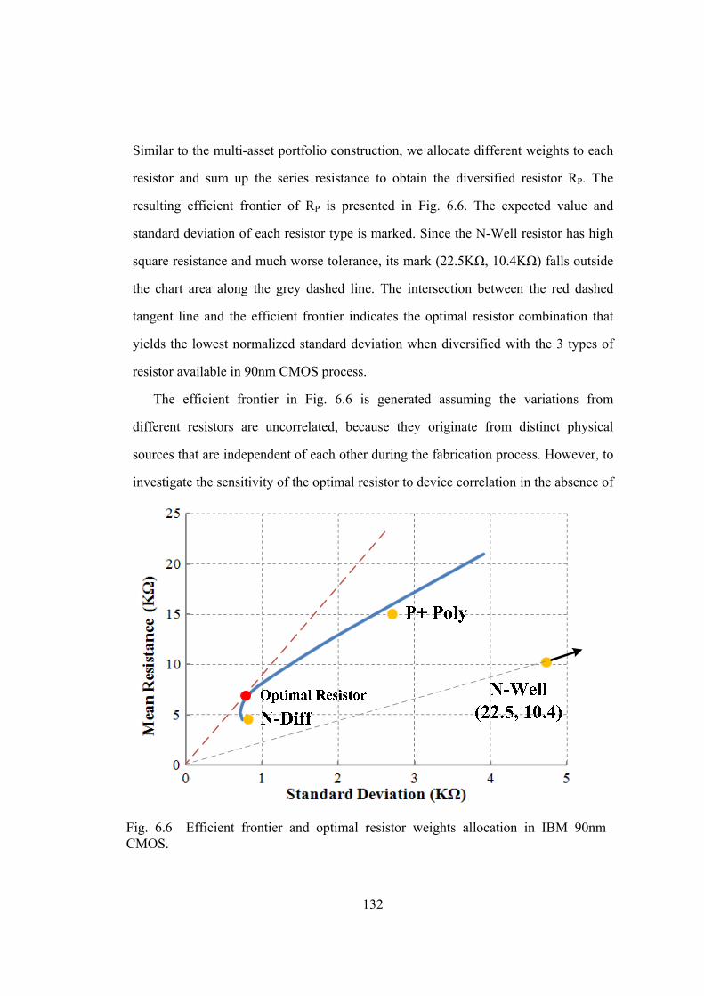
132
Similar to the multi-asset portfolio construction, we allocate different weights to each
resistor and sum up the series resistance to obtain the diversified resistor RP. The
resulting efficient frontier of RP is presented in Fig. 6.6. The expected value and
standard deviation of each resistor type is marked. Since the N-Well resistor has high
square resistance and much worse tolerance, its mark (22.5KΩ, 10.4KΩ) falls outside
the chart area along the grey dashed line. The intersection between the red dashed
tangent line and the efficient frontier indicates the optimal resistor combination that
yields the lowest normalized standard deviation when diversified with the 3 types of
resistor available in 90nm CMOS process.
The efficient frontier in Fig. 6.6 is generated assuming the variations from
different resistors are uncorrelated, because they originate from distinct physical
sources that are independent of each other during the fabrication process. However, to
investigate the sensitivity of the optimal resistor to device correlation in the absence of
Fig. 6.6 Efficient frontier and optimal resistor weights allocation in IBM 90nmCMOS.

133
any design manual data, we simulate different scenarios representing negative
correlation (ρ = -0.2), random correlation (ρ = 0), and positive correlation (ρ = 0.2),
where ρ is the pairwise correlation coefficient between the resistors. We summarize
the resistor specifications in Table 6.1. To make a fair comparison of resistor
variation, all resistors are implemented with approximately the same mean resistance
of 7000Ω and area of 50µm2. The results in Table 6.1 show that the proposed
diversification reduces the resistor variation in RP by more than 30% compared to P+
polysilicon resistor that has the lowest tolerance in this process, in spite of the
degradation due to positive correlation. At ρ=0, the optimized RP of 50µm2 exhibits
3.9% normalized standard deviation, and this level of accuracy can only be achieved
by N+ diffusion resistor occupying 9.8 times more area (490 µm2), and is completely
unobtainable by P+ poly or N-well resistor, no matter how large their size. In our
numerical simulation, we also consider the feasibility of employing the optimal
weights in actual design, and use only rounded integer weights instead of the
analytically derived exact values. For example, the optimized RP at ρ=0 consists of
TABLE 6.1 VARIATION IN DIFFERENT TYPES OF RESISTOR IMPLEMENTATIONS
Resistor Type Resistance
Mean (Ω)
Standard Deviation
(Ω)
Normalized Standard Deviation
Chip Area (µm2)
N+ Diffusion 7052 437.3 6.2% 49.6
P+ Polysilicon 6800 392.7 5.8% 51.0
N-Well 7000 968.1 13.8% 50.4
Optimized RP (ρ=-0.2)
6867 289.8 4.2% 50.6
Optimized RP (ρ=0)
6926 270.3 3.9% 50.0
Optimized RP (ρ=0.2)
7135 225.9 3.2% 49.8

134
80% N+ diffusion resistor and 20% P+ polysilicon resistor.
6.5 Simulation Results
Monte-Carlo simulations are performed using process model libraries from AMS
BiCOMS6hp (250nm), IBM CMRF7sf (180nm), CMRF8sf (130nm), CMOS9sf
(90nm), and TSMC N65 (65nm) processes in Cadence environment. Both process
variations and mismatch are modeled in these simulations. In additional to N+
diffusion, P+ polysilicon, and N-well resistors that are shared by all the processes
(i.e.), we also include diode-connected NFET and PFET and gate-biased NFET and
PFET to the constituent mix, a total of 7 different resistor implementations for the
resistor portfolio RP to choose from.
The calculation of optimal weights requires prior knowledge of device tolerance
and correlation. To avoid statistical artifact, we separate the simulation data into
training set and test set. The former is generated by the first 100 Monte-Carlo runs and
is used to extract the mean, standard deviation, and correlation matrix of the resistors.
The optimal weights that minimize the normalized standard deviation of RP are solved
numerically with the constraints that they have to be positive and sum up to 1. Once
the weights are determined, we choose the design parameters (W and L) for the
constituent resistors and/or transistors and connect them in series to obtain the
equivalent resistor RP as the sum of the weighted resistors. Finally, the test set is
generated by the second batch of 100 Monte-Carlo runs that are independent of the
training set to obtain the mean and standard deviation of the optimized resistor RP
through Cadence simulation.
The simulation results of the normalized resistor variations are all summarized in
Table 6.2. In all 5 CMOS processes from 250nm to 65nm, the optimized resistor
combination RP yield more than 40% lower variation, compared to any standalone

135
resistor implementation. This tightening of resistance tolerance can be directly
translated into improvement in current accuracy as depicted by the trends in Fig. 6.2.
6.6 Measurement Results
We fabricated the proposed resistor structure in TSMC 65nm CMOS process. The
standalone N+ diffusion, P+ polysilicon and N-well resistors, diode-connected NFET
and PFET, and gate-biased NFET and PFET are implemented as baseline cases to
compare with the diversified resistor RP, as well as for statistical parameter extraction.
We measured resistors over two separate tapeouts. The first one consisting of 44 test
chips is the training set, and its measurement results are used to extract the mean,
standard deviation, and the correlation matrix of the 7 basic resistor types. The
correlation coefficients between N+ diffusion, P+ polysilicon, N Well resistors, and
MOS resistors are close to 0, which confirms our assumption in Section 6.4. The
correlations between the diode-connected and gate-biased NFET (or PFET) are
positive, because the same fabrication process affects transistors in different operating
regions.
TABLE 6.2 NORMALIZED RESISTOR VARIATION IN DIFFERENT PROCESSES
Resistor Type 250nm 180nm 130nm 90nm 65nm
N+ Diffusion 5.76% 5.05% 7.75% 6.26% 6.60%
P+ Polysilicon 8.50% 5.12% 8.00% 6.57% 5.58%
N-Well 6.30% 6.43% 25.1% 13.0% 7.12%
NFET Diode 5.72% 11.48% 6.56% 6.71% 8.38%
PFET Diode 8.24% 11.23% 8.62% 7.50% 7.71%
NFET Biased 7.39% 10.0% 11.0% 10.1% 21.1%
PFET Biased 11.0% 12.1% 12.8% 10.2% 21.9%
Optimized RP 3.56% 2.76% 3.77% 3.39% 3.15%
Improvement Factor
1.62 1.83 1.75 1.84 1.77
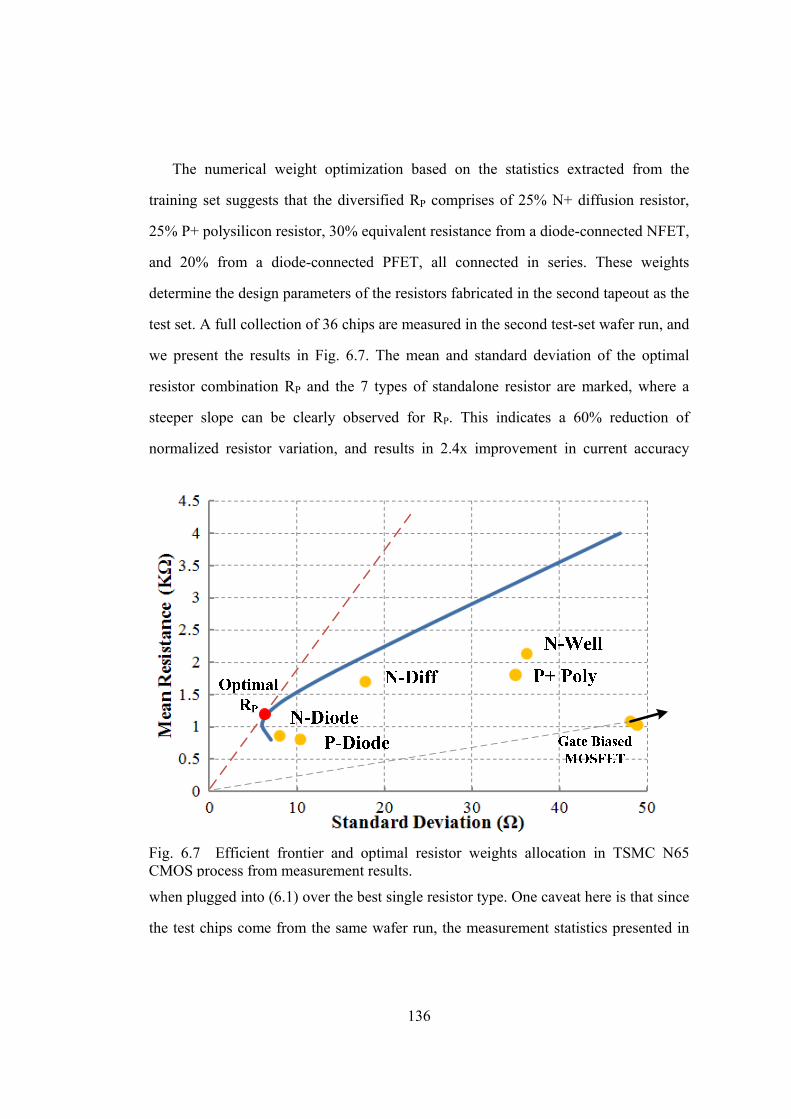
136
The numerical weight optimization based on the statistics extracted from the
training set suggests that the diversified RP comprises of 25% N+ diffusion resistor,
25% P+ polysilicon resistor, 30% equivalent resistance from a diode-connected NFET,
and 20% from a diode-connected PFET, all connected in series. These weights
determine the design parameters of the resistors fabricated in the second tapeout as the
test set. A full collection of 36 chips are measured in the second test-set wafer run, and
we present the results in Fig. 6.7. The mean and standard deviation of the optimal
resistor combination RP and the 7 types of standalone resistor are marked, where a
steeper slope can be clearly observed for RP. This indicates a 60% reduction of
normalized resistor variation, and results in 2.4x improvement in current accuracy
when plugged into (6.1) over the best single resistor type. One caveat here is that since
the test chips come from the same wafer run, the measurement statistics presented in
Fig. 6.7 Efficient frontier and optimal resistor weights allocation in TSMC N65 CMOS process from measurement results.

137
Fig. 6.7 do not include wafer-to-wafer variation and therefore is much lower than the
fabrication tolerance quoted in the design manual [59].
6.10 Chapter Summary
Counter-intuitive as it may appear, the idea of diversification has been proposed in
this chapter to improve accuracy in current references. Inspired by the mathematical
formulations and techniques in modern portfolio theory, we demonstrate that
combining different types of on-chip resistors in series with optimal weights can
reduce the normalized standard deviation of the resistance by 60% and thus achieve
2.4x better current accuracy when applied in popular current reference topologies.

138
CHAPTER 7
THE FUTURE BEYOND CMOS
Two imminent challenges are standing in the way of future VLSI system
designs—1) the end of CMOS scaling and the emergence of nano-devices; 2) the
increasing demand of performance, reliability, and flexibility in novel IC applications
(e.g. wireless sensor network, implantable biomedical devices). Having the expertise
that intersects devices and systems, the circuit designer plays the critical role to bridge
the two and generate innovative solutions to address both challenges.
As part of this endeavor, I developed a tiered systematic framework for designing
process-independent and variability-tolerant integrated circuits in my dissertation. This
bottom-up approach starts from designing self-compensated circuits as accurate
building blocks, and moves up to sub-systems with negative feedback loop and full
system-level calibration. The framework is independent of the technology and can be
extended beyond CMOS. The generality of the underlying statistical and mathematical
methods makes it especially suitable for future non-silicon nano-circuits (e.g. carbon
nanotube , nanowire [94], graphene [95, 96], molecule [97]), where the variability is
severe due to quantum effects on the nanoscale and yet the same laws of statistics still
apply [98, 99].
The main tenets I employed in my doctoral research can be summarized in three
folds:
I. Take advantage of the idiosyncrasy of the technology and process.
All kinds of variability experienced by the VLSI system originate from its
underlying building devices. To capture the device-level variability effects, in-depth
understanding of the physical mechanism inside the device is required and better

139
analytical models have to be developed and characterized. On the other hand, subtle
idiosyncrasies of nano-scale devices due to different fabrication process (e.g. silicon
energy bandgap, quantum resistance [100], spatially correlation in carbon nanotubes
[101, 102]) can be utilized to build special function blocks or guide physical layout
rules [103].
II. Use general higher-level abstraction for portable and scalable solutions.
Device behaviors can be encapsulated by parameterized models. When these
analytical models are applied, design in the circuit layer turns into multi-objective
stochastic optimization. In this dissertation, I have proposed a method [3] to generate
self-compensated circuits based on the general statistical concept of antithetic
sampling. It does not rely on any specific device behavior that is unique to certain
CMOS process, but instead, exploits the analogy between variance reduction methods
and variability tolerant circuits by mapping the variance reduction estimator to its
circuit equivalent. The generality of the high-level abstraction used in my proposed
design framework ensures its portability and scalability to deeper sub-micron CMOS,
as well as future non-silicon technology.
III. Improving performance and efficiency calls for adaptive and application-
specific design tradeoffs.
Like everything else, there is no free lunch in circuit design, but some performance
metrics might be cheaper to obtain yet more crucial for certain VLSI systems with
specific application. Resources such as memory, digital computing circuits, and
timing/clock references that are not easily accessible to each circuit block are often
available at the system level, making it easier to address some circuit variability
problems through system-level calibration and architecture innovations. Based on this

140
understanding, I would like to further investigate the design methodology for system
layer variability tolerance and develop a truly vertical framework that allows co-
optimization across multiple layers. One tangible application of this proposed design
framework is ultra-low-power-low-cost VLSI systems for ubiquitous computing
platform and wireless sensor networks, because robust design is now available with
minimum overhead in power and area, and its performance can be adaptively
monitored and configured in real-time [104], which could be accomplished by
embedding additional programmability and reconfigurability in VLSI systems without
incurring significant overhead in power and area.
Looking into the future of VLSI systems beyond CMOS, the ultimate goal is to
arrive at a general design solution that can integrate emerging nano-scale memory and
switch structures (i.e. spin-transfer torque RAM [105], phase change memory ,
memristor [106], nanoelectromechanical switch [107]) seamlessly with existing
CMOS based VLSI systems, and thus allows us to investigate and optimize the
functionality and performance of a hybrid integrated system. To achieve this goal, we
need a vertically integrated design framework with device-level granularity, circuit-
level optimization, and system-level adaptivity, the first step of which has been
demonstrated in this dissertation.

141
REFERENCES
[1] B. Shenoi, "Optimum variability design and comparative evaluation of thin-film RC active filters," Circuits and Systems, IEEE Transactions on, vol. 21, pp. 263-267, 1974.
[2] V. F. Flack, "Estimating variation in IC yield estimates," Solid-State Circuits, IEEE Journal of, vol. 21, pp. 362-365, 1986.
[3] A. M. Pappu, Xuan Zhang, A. V. Harrison and A. B. Apsel, "Process-Invariant Current Source Design: Methodology and Examples," Solid-State Circuits, IEEE Journal of, vol. 42, pp. 2293-2302, 2007.
[4] S. Saxena, C. Hess, H. Karbasi, A. Rossoni, S. Tonello, P. McNamara, S. Lucherini, S. Minehane, C. Dolainsky and M. Quarantelli, "Variation in Transistor Performance and Leakage in Nanometer-Scale Technologies," Electron Devices, IEEE Transactions on, vol. 55, pp. 131-144, 2008.
[5] D. M. Brooks, P. Bose, S. E. Schuster, H. Jacobson, P. N. Kudva, A. Buyuktosunoglu, J. Wellman, V. Zyuban, M. Gupta and P. W. Cook, "Power-aware microarchitecture: design and modeling challenges for next-generation microprocessors," Micro, IEEE, vol. 20, pp. 26-44, 2000.
[6] K. J. Antreich, H. E. Graeb and C. U. Wieser, "Circuit analysis and optimization driven by worst-case distances," Computer-Aided Design of Integrated Circuits and Systems, IEEE Transactions on, vol. 13, pp. 57-71, 1994.
[7] Tze-Chiang Chen, "Where CMOS is going: Trendy hype vs. real technology," in Solid-State Circuits Conference, 2006. ISSCC 2006. Digest of Technical Papers. IEEE International, 2006, pp. 1-18.
[8] ITRS. International technology roadmap for semiconductors, 2009. 2009Available: http://www.itrs.net/links/2009ITRS/Home2009.htm.
[9] M. Nekili, Y. Savaria and G. Bois, "Spatial characterization of process variations via MOS transistor time constants in VLSI and WSI," Solid-State Circuits, IEEE Journal of, vol. 34, pp. 80-84, 1999.
[10] Liang-Teck Pang and B. Nikolic, "Measurements and Analysis of Process Variability in 90 nm CMOS," Solid-State Circuits, IEEE Journal of, vol. 44, pp. 1655-1663, 2009.

142
[11] Liang-Teck Pang, Kun Qian, C. J. Spanos and B. Nikolic, "Measurement and Analysis of Variability in 45 nm Strained-Si CMOS Technology," Solid-State Circuits, IEEE Journal of, vol. 44, pp. 2233-2243, 2009.
[12] R. C. Jaeger, R. Ramani and J. C. Suling, "Effects of stress-induced mismatches on CMOS analog circuits," in VLSI Technology, Systems, and Applications, 1995. Proceedings of Technical Papers. 1995 International Symposium on, 1995, pp. 354-360.
[13] C. Gallon, G. Reimbold, G. Ghibaudo, R. A. Bianchi, R. Gwoziecki, S. Orain, E. Robilliart, C. Raynaud and H. Dansas, "Electrical analysis of mechanical stress induced by STI in short MOSFETs using externally applied stress," Electron Devices, IEEE Transactions on, vol. 51, pp. 1254-1261, 2004.
[14] K. A. Bowman, A. R. Alameldeen, S. T. Srinivasan and C. B. Wilkerson, "Impact of Die-to-Die and Within-Die Parameter Variations on the Clock Frequency and Throughput of Multi-Core Processors," Very Large Scale Integration (VLSI) Systems, IEEE Transactions on, vol. 17, pp. 1679-1690, 2009.
[15] T. Skotnicki, J. A. Hutchby, Tsu-Jae King, H. -. P. Wong and F. Boeuf, "The end of CMOS scaling: toward the introduction of new materials and structural changes to improve MOSFET performance," Circuits and Devices Magazine, IEEE, vol. 21, pp. 16-26, 2005.
[16] C. Bulucea, S. R. Bahl, W. D. French, Jeng-Jiun Yang, P. Francis, T. Harjono, V. Krishnamurthy, J. Tao and C. Parker, "Physics, Technology, and Modeling of Complementary Asymmetric MOSFETs," Electron Devices, IEEE Transactions on, vol. 57, pp. 2363-2380, 2010.
[17] Changhwan Shin, Min Hee Cho, Y. Tsukamoto, Bich-Yen Nguyen, C. Mazuré, B. Nikolić and Tsu-Jae King Liu, "Performance and Area Scaling Benefits of FD-SOI Technology for 6-T SRAM Cells at the 22-nm Node," Electron Devices, IEEE Transactions on, vol. 57, pp. 1301-1309, 2010.
[18] P. R. Kinget, "Device mismatch and tradeoffs in the design of analog circuits," Solid-State Circuits, IEEE Journal of, vol. 40, pp. 1212-1224, 2005.
[19] J. Tschanz, Nam Sung Kim, S. Dighe, J. Howard, G. Ruhl, S. Vanga, S. Narendra, Y. Hoskote, H. Wilson, C. Lam, M. Shuman, C. Tokunaga, D. Somasekhar, S. Tang, D. Finan, T. Karnik, N. Borkar, N. Kurd and V. De, "Adaptive frequency and biasing techniques for tolerance to dynamic temperature-voltage variations and aging," in Solid-State Circuits Conference, 2007. ISSCC 2007. Digest of Technical Papers. IEEE International, 2007, pp. 292-604.

143
[20] D. Bull, S. Das, K. Shivashankar, G. S. Dasika, K. Flautner and D. Blaauw, "A Power-Efficient 32 bit ARM Processor Using Timing-Error Detection and Correction for Transient-Error Tolerance and Adaptation to PVT Variation," Solid-State Circuits, IEEE Journal of, vol. 46, pp. 18-31, 2011.
[21] Xiaoyao Liang, Gu-Yeon Wei and D. Brooks, "Revival: A Variation-Tolerant Architecture Using Voltage Interpolation and Variable Latency," Micro, IEEE, vol. 29, pp. 127-138, 2009.
[22] M. Mani, A. Devgan and M. Orshansky, "An efficient algorithm for statistical minimization of total power under timing yield constraints," in Design Automation Conference, 2005. Proceedings. 42nd, 2005, pp. 309-314.
[23] Hongliang Chang and S. S. Sapatnekar, "Statistical timing analysis under spatial correlations," Computer-Aided Design of Integrated Circuits and Systems, IEEE Transactions on, vol. 24, pp. 1467-1482, 2005.
[24] A. Agarwal, B. C. Paul, S. Mukhopadhyay and K. Roy, "Process variation in embedded memories: failure analysis and variation aware architecture," Solid-State Circuits, IEEE Journal of, vol. 40, pp. 1804-1814, 2005.
[25] D. Marche, Y. Savaria and Y. Gagnon, "Laser Fine-Tuneable Deep-Submicrometer CMOS 14-bit DAC," Circuits and Systems I: Regular Papers, IEEE Transactions on, vol. 55, pp. 2157-2165, 2008.
[26] T. S. Doorn, "A Detailed Qualitative Model for the Programming Physics of Silicided Polysilicon Fuses," Electron Devices, IEEE Transactions on, vol. 54, pp. 3285-3291, 2007.
[27] T. Schmid, Z. Charbiwala, J. Friedman, Y. H. Cho and M. B. Srivastava, "Exploiting Manufacturing Variations for Compensating Environment-induced Clock Drift in Time Synchronization," Performance Evaluation Review : A Quarterly Publication of the Special Interest Committee on Measurement and Evaluation., vol. 36, pp. 97, 2008.
[28] Hao Zhang, Jongjin Kim, Wei Pang, Hongyu Yu and Eun Sok Kim, "5GHz low-phase-noise oscillator based on FBAR with low TCF," in Solid-State Sensors, Actuators and Microsystems, 2005. Digest of Technical Papers. TRANSDUCERS '05. the 13th International Conference on, 2005, pp. 1100-1101 Vol. 1.
[29] D. Ruffieux, F. Krummenacher, A. Pezous and G. Spinola-Durante, "Silicon Resonator Based 3.2 $mu$W Real Time Clock With $pm$10 ppm Frequency Accuracy," Solid-State Circuits, IEEE Journal of, vol. 45, pp. 224-234, 2010.

144
[30] J. Hu, R. Parkery, R. Ruby and B. Otis, "A wide-tuning digitally controlled FBAR-based oscillator for frequency synthesis," in Frequency Control Symposium (FCS), 2010 IEEE International, 2010, pp. 608-612.
[31] B. Analui and A. Hajimiri, "Statistical analysis of integrated passive delay lines," in Custom Integrated Circuits Conference, 2003. Proceedings of the IEEE 2003, 2003, pp. 107-110.
[32] U. Denier, "Analysis and Design of an Ultralow-Power CMOS Relaxation Oscillator," Circuits and Systems I: Regular Papers, IEEE Transactions on, vol. 57, pp. 1973-1982, 2010.
[33] B. P. Das, B. Amrutur, H. S. Jamadagni, N. V. Arvind and V. Visvanathan, "Within-Die Gate Delay Variability Measurement Using Reconfigurable Ring Oscillator," Semiconductor Manufacturing, IEEE Transactions on, vol. 22, pp. 256-267, 2009.
[34] N. Drego, A. Chandrakasan and D. Boning, "All-Digital Circuits for Measurement of Spatial Variation in Digital Circuits," Solid-State Circuits, IEEE Journal of, vol. 45, pp. 640-651, 2010.
[35] H. Masuda, S. Ohkawa, A. Kurokawa and M. Aoki, "Challenge: Variability characterization and modeling for 65- to 90-nm processes," in Custom Integrated Circuits Conference, 2005. Proceedings of the IEEE 2005, 2005, pp. 593-599.
[36] E. Alon, V. Stojanovic and M. A. Horowitz, "Circuits and techniques for high-resolution measurement of on-chip power supply noise," Solid-State Circuits, IEEE Journal of, vol. 40, pp. 820-828, 2005.
[37] Poki Chen, Shou-Chih Chen, You-Sheng Shen and You-Jyun Peng, "All-Digital Time-Domain Smart Temperature Sensor With an Inter-Batch Inaccuracy of After One-Point Calibration," Circuits and Systems I: Regular Papers, IEEE Transactions on, vol. 58, pp. 913-920, 2011.
[38] J. Kitching, S. Knappe, L. Liew, P. Schwindt, K. Shah, J. Moreland and L. Hollberg, "Microfabricated atomic clocks," in Micro Electro Mechanical Systems, 2005. MEMS 2005. 18th IEEE International Conference on, 2005, pp. 1-7.
[39] K. R. Lakshmikumar, "Analog PLL Design With Ring Oscillators at Low-Gigahertz Frequencies in Nanometer CMOS: Challenges and Solutions," Circuits and Systems II: Express Briefs, IEEE Transactions on, vol. 56, pp. 389-393, 2009.
[40] B. Razavi, "Challenges in the design high-speed clock and data recovery circuits," Communications Magazine, IEEE, vol. 40, pp. 94-101, 2002.
145
[41] B. Saeidi, Joshua Cho, G. Taskov and A. Paff, "A wide-range VCO with optimum temperature adaptive tuning," in Radio Frequency Integrated Circuits Symposium (RFIC), 2010 IEEE, 2010, pp. 337-340.
[42] N. M. Pletcher, S. Gambini and J. Rabaey, "A 52 W Wake-Up Receiver With 72 dBm Sensitivity Using an Uncertain-IF Architecture," Solid-State Circuits, IEEE Journal of, vol. 44, pp. 269-280, 2009.
[43] Yiming Li, Chih-Hong Hwang and Tien-Yeh Li, "Discrete-Dopant-Induced Timing Fluctuation and Suppression in Nanoscale CMOS Circuit," Circuits and Systems II: Express Briefs, IEEE Transactions on, vol. 56, pp. 379-383, 2009.
[44] Voltage Controlled Oscillator with Efficient Process Compensation, J. J. Jelinek and J. Deng. July 19). 5331295 , 1994.
[45] Process Compensation Method for CMOS Current Controlled Ring Oscillators, R. R. Rasmussen. May 18). 5905412 , 1999.
[46] Yang-Shyung Shyu and Jiin-Chuan Wu, "A process and temperature compensated ring oscillator," in ASICs, 1999. AP-ASIC '99. the First IEEE Asia Pacific Conference on, 1999, pp. 283-286.
[47] J. Routama, K. Koli and K. Halonen, "A novel ring-oscillator with a very small process and temperature variation," in Circuits and Systems, 1998. ISCAS '98. Proceedings of the 1998 IEEE International Symposium on, 1998, pp. 181-184 vol.1.
[48] G. De Vita, F. Marraccini and G. Iannaccone, "Low-voltage low-power CMOS oscillator with low temperature and process sensitivity," in Circuits and Systems, 2007. ISCAS 2007. IEEE International Symposium on, 2007, pp. 2152-2155.
[49] K. R. Lakshmikumar, V. Mukundagiri and S. L. J. Gierkink, "A process and temperature compensated two-stage ring oscillator," in Custom Integrated Circuits Conference, 2007. CICC '07. IEEE, 2007, pp. 691-694.
[50] H. Chen, E. Lee and R. Geiger, "A 2 GHz VCO with process and temperature compensation," in Circuits and Systems, 1999. ISCAS '99. Proceedings of the 1999 IEEE International Symposium on, 1999, pp. 569-572 vol.2.
[51] S. M. Kashmiri, M. A. P. Pertijs and K. A. A. Makinwa, "A Thermal-Diffusivity-Based Frequency Reference in Standard CMOS With an Absolute Inaccuracy of $pm $0.1% From $-$55 $^circ$C to 125 $^circ$C," Solid-State Circuits, IEEE Journal of, vol. 45, pp. 2510-2520, 2010.
[52] Kuo-Ken Huang and D. D. Wentzloff, "A 60GHz antenna-referenced frequency-locked loop in 0.13μm CMOS for wireless sensor networks," in Solid-State

146
Circuits Conference Digest of Technical Papers (ISSCC), 2011 IEEE International, 2011, pp. 284-286.
[53] M. S. McCorquodale, G. A. Carichner, J. D. O'Day, S. M. Pernia, S. Kubba, E. D. Marsman, J. J. Kuhn and R. B. Brown, "A 25-MHz Self-Referenced Solid-State Frequency Source Suitable for XO-Replacement," Circuits and Systems I: Regular Papers, IEEE Transactions on, vol. 56, pp. 943-956, 2009.
[54] Chien-Ying Yu, Jui-Yuan Yu and Chen-Yi Lee, "An eCrystal oscillator with self-calibration capability," in Circuits and Systems, 2009. ISCAS 2009. IEEE International Symposium on, 2009, pp. 237-240.
[55] Chi-Fat Chan, Kong-Pang Pun, Ka-Nang Leung, Jianping Guo, L. -. L. Leung and Chiu-Sing Choy, "A Low-Power Continuously-Calibrated Clock Recovery Circuit for UHF RFID EPC Class-1 Generation-2 Transponders," Solid-State Circuits, IEEE Journal of, vol. 45, pp. 587-599, 2010.
[56] Xuan Zhang, A. M. Pappu and A. B. Apsel, "Low variation current source for 90nm CMOS," in Circuits and Systems, 2008. ISCAS 2008. IEEE International Symposium on, 2008, pp. 388-391.
[57] A. Hajimiri, S. Limotyrakis and T. H. Lee, "Jitter and phase noise in ring oscillators," Solid-State Circuits, IEEE Journal of, vol. 34, pp. 790-804, 1999.
[58] B. P. Otis, Y. H. Chee, R. Lu, N. M. Pletcher and J. M. Rabaey, "An ultra-low power MEMS-based two-channel transceiver for wireless sensor networks," in VLSI Circuits, 2004. Digest of Technical Papers. 2004 Symposium on, 2004, pp. 20-23.
[59] IBM confidential, CMOS 9SF (CMOS9SF) Technology Design Manual. June 19, 2008.
[60] K. Sundaresan, P. E. Allen and F. Ayazi, "Process and temperature compensation in a 7-MHz CMOS clock oscillator," Solid-State Circuits, IEEE Journal of, vol. 41, pp. 433-442, 2006.
[61] F. Fiori and P. S. Crovetti, "A new compact temperature-compensated CMOS current reference," Circuits and Systems II: Express Briefs, IEEE Transactions on, vol. 52, pp. 724-728, 2005.
[62] J. L. Bohorquez, A. P. Chandrakasan and J. L. Dawson, "A 350 W CMOS MSK Transmitter and 400 W OOK Super-Regenerative Receiver for Medical Implant Communications," Solid-State Circuits, IEEE Journal of, vol. 44, pp. 1248-1259, 2009.

147
[63] M. Meterelliyoz, P. Song, F. Stellari, J. P. Kulkarni and K. Roy, "Characterization of Random Process Variations Using Ultralow-Power, High-Sensitivity, Bias-Free Sub-Threshold Process Sensor," Circuits and Systems I: Regular Papers, IEEE Transactions on, vol. 57, pp. 1838-1847, 2010.
[64] Xuan Zhang and A. B. Apsel, "A process compensated 3-GHz ring oscillator," in Circuits and Systems, 2009. ISCAS 2009. IEEE International Symposium on, 2009, pp. 581-584.
[65] Q. S. I. Lim, A. V. Kordesch and R. A. Keating, "Performance comparison of MIM capacitors and metal finger capacitors for analog and RF applications," in RF and Microwave Conference, 2004. RFM 2004. Proceedings, 2004, pp. 85-89.
[66] Guangbin Zhang, Sooping Saw, Jin Liu, S. Sterrantino, D. K. Johnson and Sungyong Jung, "An accurate current source with on-chip self-calibration circuits for low-voltage current-mode differential drivers," Circuits and Systems I: Regular Papers, IEEE Transactions on, vol. 53, pp. 40-47, 2006.
[67] B. Razavi, "From Devices to Architectures," Phase-Locking in High-Performance Systems, 2003.
[68] P. K. Hanumolu, M. Brownlee, K. Mayaram and Un-Ku Moon, "Analysis of charge-pump phase-locked loops," Circuits and Systems I: Regular Papers, IEEE Transactions on, vol. 51, pp. 1665-1674, 2004.
[69] Chong-Gun Yu and R. L. Geiger, "An automatic offset compensation scheme with ping-pong control for CMOS operational amplifiers," Solid-State Circuits, IEEE Journal of, vol. 29, pp. 601-610, 1994.
[70] C. C. Enz and G. C. Temes, "Circuit techniques for reducing the effects of op-amp imperfections: autozeroing, correlated double sampling, and chopper stabilization," Proceedings of the IEEE, vol. 84, pp. 1584-1614, 1996.
[71] Xuan Zhang and A. B. Apsel, "A Low-Power, Process-and- Temperature- Compensated Ring Oscillator With Addition-Based Current Source," Circuits and Systems I: Regular Papers, IEEE Transactions on, vol. 58, pp. 868-878, 2011.
[72] F. Sebastiano, L. J. Breems, K. Makinwa, S. Drago, D. Leenaerts and B. Nauta, "A Low-Voltage Mobility-Based Frequency Reference for Crystal-Less ULP Radios," Solid-State Circuits, IEEE Journal of, vol. 44, pp. 2002-2009, 2009.
[73] R. Dokania, X. Wang, S. Tallur, C. Dorta-Quinones and A. Apsel, "An Ultralow-Power Dual-Band UWB Impulse Radio," Circuits and Systems II: Express Briefs, IEEE Transactions on, vol. 57, pp. 541-545, 2010.

148
[74] R. Dokania, Xiao Wang, W. Godycki, C. Dorta-Quinones and A. Apsel, "PCO based event propagation scheme for globally synchronized sensor networks," in GLOBECOM 2010, 2010 IEEE Global Telecommunications Conference, 2010, pp. 1-5.
[75] J. G. Maneatis, "Low-jitter process-independent DLL and PLL based on self-biased techniques," Solid-State Circuits, IEEE Journal of, vol. 31, pp. 1723-1732, 1996.
[76] Xuan Zhang, R. Dokania, M. Mukadam and A. Apsel, "A successive approximation based process-invariant ring oscillator," in Circuits and Systems (ISCAS), Proceedings of 2010 IEEE International Symposium on, 2010, pp. 1057-1060.
[77] Tsung-Hsien Lin and W. J. Kaiser, "A 900-MHz 2.5-mA CMOS frequency synthesizer with an automatic SC tuning loop," Solid-State Circuits, IEEE Journal of, vol. 36, pp. 424-431, 2001.
[78] W. B. Wilson, Un-Ku Moon, K. R. Lakshmikumar and Liang Dai, "A CMOS self-calibrating frequency synthesizer," Solid-State Circuits, IEEE Journal of, vol. 35, pp. 1437-1444, 2000.
[79] Ivan Siu-Chuang Lu, N. Weste and S. Parameswaran, "A Power-Efficient 5.6-GHz Process-Compensated CMOS Frequency Divider," Circuits and Systems II: Express Briefs, IEEE Transactions on, vol. 54, pp. 323-327, 2007.
[80] T. -. Lin and Y. -. Lai, "An Agile VCO Frequency Calibration Technique for a 10-GHz CMOS PLL," Solid-State Circuits, IEEE Journal of, vol. 42, pp. 340-349, 2007.
[81] Wei-Hao Sung, Shu-Yu Hsu, Jui-Yuan Yu, Chien-Ying Yu and Chen-Yi Lee, "A frequency accuracy enhanced sub-10µW on-chip clock generator for energy efficient crystal-less wireless biotelemetry applications," in VLSI Circuits (VLSIC), 2010 IEEE Symposium on, 2010, pp. 115-116.
[82] A. Becker-Gomez, T. Lakshmi Viswanathan and T. R. Viswanathan, "A Low-Supply-Voltage CMOS Sub-Bandgap Reference," Circuits and Systems II: Express Briefs, IEEE Transactions on, vol. 55, pp. 609-613, 2008.
[83] F. Serra-Graells and J. L. Huertas, "Sub-1-V CMOS proportional-to-absolute temperature references," Solid-State Circuits, IEEE Journal of, vol. 38, pp. 84-88, 2003.

149
[84] G. De Vita and G. Iannaccone, "A Sub-1-V, 10 ppm/ °C, Nanopower Voltage Reference Generator," Solid-State Circuits, IEEE Journal of, vol. 42, pp. 1536-1542, 2007.
[85] T. Hirose, Y. Osaki, N. Kuroki and M. Numa, "A nano-ampere current reference circuit and its temperature dependence control by using temperature characteristics of carrier mobilities," in ESSCIRC, 2010 Proceedings of the, 2010, pp. 114-117.
[86] Wei Liu, W. Khalil, M. Ismail and E. Kussener, "A resistor-free temperature-compensated CMOS current reference," in Circuits and Systems (ISCAS), Proceedings of 2010 IEEE International Symposium on, 2010, pp. 845-848.
[87] A. E. Buck, C. L. McDonald, S. H. Lewis and T. R. Viswanathan, "A CMOS bandgap reference without resistors," Solid-State Circuits, IEEE Journal of, vol. 37, pp. 81-83, 2002.
[88] A. Kumar, "Trimless second order curvature compensated bandgap reference using diffusion resistor," in Custom Integrated Circuits Conference, 2009. CICC '09. IEEE, 2009, pp. 161-164.
[89] Jiwei Chen and Bingxue Shi, "1 V CMOS current reference with 50 ppm/°C temperature coefficient," Electronics Letters, vol. 39, pp. 209-210, 2003.
[90] Y. Osaki, T. Hirose, N. Kuroki and M. Numa, "A 95-nA, 523ppm/°C, 0.6-μW CMOS current reference circuit with subthreshold MOS resistor ladder," in Design Automation Conference (ASP-DAC), 2011 16th Asia and South Pacific, 2011, pp. 113-114.
[91] K. Ueno, T. Hirose, T. Asai and Y. Amemiya, "A 1-$muhboxW$ 600- $hboxppm/^circhboxC$ Current Reference Circuit Consisting of Subthreshold CMOS Circuits," Circuits and Systems II: Express Briefs, IEEE Transactions on, vol. 57, pp. 681-685, 2010.
[92] Zhangcai Huang, Qin Luo and Y. Inoue, "A CMOS sub-l-V nanopower current and voltage reference with leakage compensation," in Circuits and Systems (ISCAS), Proceedings of 2010 IEEE International Symposium on, 2010, pp. 4069-4072.
[93] E. M. Camacho-Galeano, C. Galup-Montoro and M. C. Schneider, "A 2-nW 1.1-V self-biased current reference in CMOS technology," Circuits and Systems II: Express Briefs, IEEE Transactions on, vol. 52, pp. 61-65, 2005.
[94] S. Bangsaruntip, A. Majumdar, G. M. Cohen, S. U. Engelmann, Y. Zhang, M. Guillorn, L. M. Gignac, S. Mittal, W. S. Graham, E. A. Joseph, D. P. Klaus, J. Chang, E. A. Cartier and J. W. Sleight, "Gate-all-around silicon nanowire 25-stage CMOS

150
ring oscillators with diameter down to 3 nm," in VLSI Technology (VLSIT), 2010 Symposium on, 2010, pp. 21-22.
[95] G. Xu, J. Bai, C. M. Torres, E. B. Song, J. Tang, Y. Zhou, X. Duan, Y. Zhang and K. L. Wang, "Low-noise submicron channel graphene nanoribbons," Applied Physics Letters, vol. 97, pp. 073107-073107-3, 2010.
[96] G. Xu, C. M. Torres, Y. Zhang, F. Liu, E. B. Song, M. Wang, Y. Zhou, C. Zeng and K. L. Wang, "Effect of Spatial Charge Inhomogeneity on 1/fNoise Behavior in Graphene," Nano Lett.Nano Letters, vol. 10, pp. 3312-3317, 2010.
[97] Wei Xiong, Yang Guo, U. Zschieschang, H. Klauk and B. Murmann, "A 3-V, 6-Bit C-2C Digital-to-Analog Converter Using Complementary Organic Thin-Film Transistors on Glass," Solid-State Circuits, IEEE Journal of, vol. 45, pp. 1380-1388, 2010.
[98] Xu G, Torres CM, Tang J, Bai J, Song EB, Huang Y, Duan X, Zhang Y and Wang KL, "Edge effect on resistance scaling rules in graphene nanostructures." Nano Letters, vol. 11, pp. 1082-6, 2011.
[99] G. Xu, C. M. Torres, J. Bai, J. Tang, T. Yu, Y. Huang, X. Duan, Y. Zhang and K. L. Wang, "Linewidth roughness in nanowire-mask-based graphene nanoribbons," Applied Physics Letters, vol. 98, pp. 243118-243118-3, 2011.
[100] Tzalenchuk A., Kazakova O., Janssen T.J.B.M., Lara-Avila S., Kalaboukhov A., Kubatkin S., Paolillo S., Syvajarvi M., Yakimova R. and Fal'Ko V., "Towards a quantum resistance standard based on epitaxial graphene," Nat.Nanotechnol.Nature Nanotechnology, vol. 5, pp. 186-189, 2010.
[101] A. Lin, N. Patil, Hai Wei, S. Mitra and H. -. P. Wong, "ACCNT—A Metallic-CNT-Tolerant Design Methodology for Carbon-Nanotube VLSI: Concepts and Experimental Demonstration," Electron Devices, IEEE Transactions on, vol. 56, pp. 2969-2978, 2009.
[102] A. Lin, Jie Zhang, N. Patil, Hai Wei, S. Mitra and H. -. P. Wong, "ACCNT: A Metallic-CNT-Tolerant Design Methodology for Carbon Nanotube VLSI: Analyses and Design Guidelines," Electron Devices, IEEE Transactions on, vol. 57, pp. 2284-2295, 2010.
[103] N. Patil, A. Lin, J. Zhang, Hai Wei, K. Anderson, H. -. P. Wong and S. Mitra, "Scalable Carbon Nanotube Computational and Storage Circuits Immune to Metallic and Mispositioned Carbon Nanotubes," Nanotechnology, IEEE Transactions on, vol. 10, pp. 744-750, 2011.

151
[104] Xin Li, B. Taylor, YuTsun Chien and L. T. Pileggi, "Adaptive post-silicon tuning for analog circuits: Concept, analysis and optimization," in Computer-Aided Design, 2007. ICCAD 2007. IEEE/ACM International Conference on, 2007, pp. 450-457.
[105] T. Kawahara, R. Takemura, K. Miura, J. Hayakawa, S. Ikeda, Young Min Lee, R. Sasaki, Y. Goto, K. Ito, T. Meguro, F. Matsukura, H. Takahashi, H. Matsuoka and H. Ohno, "2 Mb SPRAM (SPin-Transfer Torque RAM) With Bit-by-Bit Bi-Directional Current Write and Parallelizing-Direction Current Read," Solid-State Circuits, IEEE Journal of, vol. 43, pp. 109-120, 2008.
[106] Dmitri B. Strukov, Gregory S. Snider, Duncan R. Stewart and R. Stanley Williams, "The missing memristor found," 2008.
[107] Hei Kam, Tsu-Jae King Liu, V. Stojanović, D. Marković and E. Alon, "Design, Optimization, and Scaling of MEM Relays for Ultra-Low-Power Digital Logic," Electron Devices, IEEE Transactions on, vol. 58, pp. 236-250, 2011.
Copyright © 2022 FDOKUMEN