to-digital converter design in deep sub-micron cmos technology
165
A POWER OPTIMIZED PIPELINED ANALOG- TO-DIGITAL CONVERTER DESIGN IN DEEP SUB-MICRON CMOS TECHNOLOGY A Thesis Presented to The Academic Faculty by Chang-Hyuk Cho In Partial Fulfillment of the Requirements for the Degree Doctor of Philosophy in the School of Electrical and Computer Engineering Georgia Institute of Technology December 2005 Copyright 2005 by Chang-Hyuk Cho
-
Upload
khangminh22 -
Category
Documents
-
view
6 -
download
0
Transcript of to-digital converter design in deep sub-micron cmos technology

A P O W E R O P T I M I Z E D P I P E L I N E D A N A L O G -T O - D I G I T A L C O N V E R T E R D E S I G N I N D E E P
S U B - M I C R O N C M O S T E C H N O L O G Y
A Thesis Presented to
The Academic Faculty
by
Chang-Hyuk Cho
In Partial Fulfillment of the Requirements for the Degree
Doctor of Philosophy in the School of Electrical and Computer Engineering
Georgia Institute of Technology December 2005
Copyright 2005 by Chang-Hyuk Cho

UMI Number: 3198520
31985202006
UMI MicroformCopyright
All rights reserved. This microform edition is protected against unauthorized copying under Title 17, United States Code.
ProQuest Information and Learning Company 300 North Zeeb Road
P.O. Box 1346 Ann Arbor, MI 48106-1346
by ProQuest Information and Learning Company.

A P O W E R O P T I M I Z E D P I P E L I N E D A N A L O G -T O - D I G I T A L C O N V E R T E R D E S I G N I N D E E P S U B - M I C R O N C M O S T E C H N O L O G Y
Approved by: Dr. Phillip E. Allen, Advisor School of Electrical and Computer Engineering Georgia Institute of Technology Dr. W. Marshall Leach, Jr School of Electrical and Computer Engineering Georgia Institute of Technology Dr. James Stevenson Kenney School of Electrical and Computer Engineering Georgia Institute of Technology
Dr. W. Russell Callen, Jr School of Electrical and Computer Engineering Georgia Institute of Technology Dr. Thomas D. Morley School of Mathematics Georgia Institute of Technology Date Approved : November 10 2005
ii

Acknowledgments
First and foremost, I would like to express my deep appreciation to my academic advisor,
Professor Phillip E. Allen, for his invaluable guidance, his kindness, and support
throughout my graduate study at the Georgia Institute of Technology. Without his
encouragement and patient support, this work would not have been possible.
I would like to thank my dissertation committee members, Dr. W. Marshall Leach,
Jr., Dr. James Stevenson Kenney, Dr. W. Russell Callen, and Dr. Thomas D. Morley for
their time, effort and valuable suggestion. I would like to thank Professor Kwang-sup
Yoon for his help and kindness. My special appreciation also goes to Marge Boehme for
her kindness, smiles, and help. My thanks are also extended to the National
Semiconductor Corp. for support, fabrication, and packaging. I am especially grateful for
the assistance and support of Patrick O’Farrell and Arlo Aude at National Semiconductor
Norcross site.
I am indebted to my colleagues in the Analog Circuit Design Laboratory for their
assistance and friendship − Han-woong Son, Lee-Kyung Kwon, Kyung-Pil Jung, Hoon
Lee, Simon Singh, Ganesh Balachadran, Mustafa Koroglu, Tien Pham, Shakeel Qureshi,
Zhijei Xiong, Zhiwei Dong, and Fang Lin. Of the many good friends I have made in the
course of my graduate studies at Georgia Tech, I especially wish to recognize the
following for the many ways they have enriched my life: Wei-Chung Wu, Franklin Bien,
Hyungsoo Kim, Jinsung Park, Yunseo Park, Youngsik Hur, Moonkyun Maeng, Ockoo
Lee, Dr. Changho Lee, Dr. Kyutae Lim, Dr. Seoung-Yeop Yoo, Dr. Sang-Woo Han,
iii

Sang-Bin Lee, Sang-Bum Kang, Kyung-Girl Yoo, Jong-Seong Moon, and Sang-Woong
Yoon.
I am deeply grateful to my father and mother, Chung-Hun Cho and Kwang-Ja
Ahn. Without their endless support, love, prayer, and encouragement, this work could not
been completed. I also thank my brother, Chang-Ho Cho, his wife, Hee-Seong Yoo, his
beautiful daughter, Seo-Yeon Cho, and my little sister, Ji-Young Cho, for their love and
encouragement. Finally, I am thankful to my fiancée, Hyo-Suk Lim, for her love and
support.
iv

Table of Contents
Acknowledgments ························································································
································································································
································································································
······································································································
iii
List of Tables ix
List of Figures x
Summary xv
CHAPTER 1 :Introduction ..................................................................................................1
1.1 Motivation................................................................................................................1
1.2 Thesis Organization .................................................................................................4
CHAPTER 2 : Overview of A/D conversion.......................................................................5
2.1 A/D Converter Performance Parameters .................................................................5
2.1.1 Differential Non-linearity and Integral Non-linearity.....................................5
2.1.2 Signal-to-Noise Ratio......................................................................................7
2.1.3 Total Harmonic Distortion..............................................................................7
2.1.4 Signal-to-Noise and Distortion Ratio..............................................................8
2.1.5 Spurious Free Dynamic Range .......................................................................8
2.1.6 Effective Number of Bits ................................................................................8
2.2 Review of Analog to Digital Converter Architectures ............................................9
2.2.1 Flash ADC ......................................................................................................9
2.2.2 Two Step Flash ADC....................................................................................10
v

2.2.3 Folding ADC.................................................................................................11
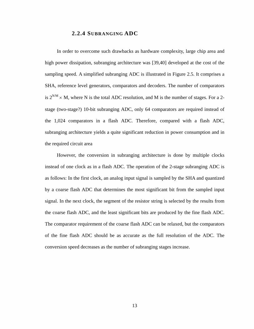
2.2.4 Subranging ADC...........................................................................................13
2.2.5 Successive Approximation ADC ..................................................................14
2.2.6 Pipeline ADC................................................................................................15
2.2.7 Oversampled ADC........................................................................................17
2.3 Summary ................................................................................................................18
CHAPTER 3 : Overview of A Pipeline ADC...................................................................19
3.1 Digital Error Correction.........................................................................................19
3.2 Basic Building Blocks............................................................................................25
3.2.1 Multiplying Digital-to-Analog Converter.....................................................25
3.2.2 Sub-Analog-to-Digital Converter .................................................................33
3.2.3 Operational Amplifiers .................................................................................35
3.2.4 Comparators..................................................................................................43
3.3 Non-ideal Error sources in Pipeline Stages ...........................................................55
3.3.1 Error in Sub-ADC.........................................................................................55
3.3.2 Thermal Noise...............................................................................................56
3.3.3 Switches ........................................................................................................58
3.3.4 Finite DC gain of Operational Amplifiers ....................................................64
3.3.5 Finite Bandwidth of Operational Amplifiers ................................................67
3.3.6 Capacitor Mismatch ......................................................................................69
3.4 Summary ................................................................................................................72
CHAPTER 4 : A Systematic Design Approach for a Power Optimized Pipeline ADC....73
4.1 Design Requirements .............................................................................................73
vi

4.1.1 DC gain of Operational Amplifiers...............................................................74
4.1.2 Bandwidth of Operational Amplifiers ..........................................................75
4.1.3 Capacitor Mismatch ......................................................................................76
4.1.4 Noise .............................................................................................................77
4.1.5 Stage Accuracy .............................................................................................77
4.2 Recent Pipeline Architecture .................................................................................79
4.3 Power Optimization ...............................................................................................80
4.3.1 Per Stage Resolution .....................................................................................81
4.3.2 Numerical Optimization Algorithm..............................................................84
4.3.3 Analysis Results............................................................................................87
4.4 Summary ................................................................................................................91
CHAPTER 5 : Design of a Prototype ADC ......................................................................93
5.1 SHA........................................................................................................................93
5.2 MDAC....................................................................................................................96
5.3 Operational Amplifier..........................................................................................102
5.4 Sub-ADC and Comparator...................................................................................113
5.5 Bias Circuit ..........................................................................................................117
5.6 Clock Generator ...................................................................................................118
5.7 Simulation Results ...............................................................................................120
5.8 Layout Design......................................................................................................121
5.9 summary...............................................................................................................124
CHAPTER 6 : Experimental Results...............................................................................125
6.1 Evaluation Board and Test Setup.........................................................................125
vii

6.2 Test Results..........................................................................................................128
6.3 Summary ..............................................................................................................137
CHAPTER 7 : Conclusion...............................................................................................138
viii

List of Tables
Table 4.1: Different pipeline architectures ........................................................................79
Table 4.2: List of different pipelined architectures............................................................84
Table 6.1: Summary of measurement results...................................................................129
Table 7.1: Comparison of the large and small number of bits per-stage .........................138
ix

List of Figures
Figure 1.1: Power versus sampling rate for 10-bit ADCs....................................................2
Figure 2.1: INL and DNL errors in a 3-bit ADC .................................................................6
Figure 2.2: Flash ADC.......................................................................................................10
Figure 2.3: Two step flash ADC........................................................................................11
Figure 2.4: Folding ADC ...................................................................................................12
Figure 2.5: Subranging ADC .............................................................................................14
Figure 2.6: Successive approximation ADC......................................................................15
Figure 2.7: A pipeline ADC block diagram.......................................................................16
Figure 2.8: block diagram of an oversampling ADC.........................................................18
Figure 3.1: The input/output characteristic of a 2-bit stage in a pipeline ADC.................20
Figure 3.2: The input/output characteristic of 2-bit stage in the pipeline ADC with the
offsets..............................................................................................................21
Figure 3.3: The input output characteristic of a 2-bit stage in the pipeline ADC with
conventional digital error correction when there are the offsets ....................22
Figure 3.4: The input/output characteristic of a 2-bit stage in a pipeline ADC with a
modified digital error correction.....................................................................23
Figure 3.5: The input /output characteristic of one stage in a pipeline ADC with a
modified digital error correction when offset is present.................................24
Figure 3.6: Basic building blocks of a pipeline ADC........................................................25
x

Figure 3.7: Typical S/H circuits (a) one-capacitor S/H (b) two-capacitors S/H................27
(c) combination of (a) and (b)............................................................................................27
Figure 3.8. SC MDAC in (a) sampling phase (b) amplifying phase..................................29
Figure 3.10. SC realization of a 1.5 bit/stage MDAC with equal-valued capacitor array .32
Figure 3.11: The 2.5-bit sub-ADC.....................................................................................34
Figure 3.12: Current mirror amplifier................................................................................37
Figure 3.13: Two stage Miller amplifier...........................................................................39
Figure 3.14: Telescopic amplifier ......................................................................................41
Figure 3.15: Folded-cascode amplifier ..............................................................................43
Figure 3.16: Input/output characteristic of an ideal comparator with infinite gain and
finite gain ........................................................................................................44
Figure 3.17: A CMOS regenerative latch .........................................................................45
Figure 3.18: A simple latch circuit comprising back-to-back inverters.............................46
Figure 3.19: The simplified small signal circuit of the latch .............................................46
Figure 3.20: The time domain response behavior of a CMOS latch ................................48
Figure 3.21: A comparator comprising of a preamplifier and a latch................................49
Figure 3.22: A comparator with input offset storage technique ........................................51
Figure 3.23: IOS comparator in Φ1 clock phase ................................................................51
Figure 3.24: IOS comparator in Φ2 clock phase ................................................................52
Figure 3.25: A comparator with output offset storage technique ......................................53
Figure 3.26: OOS comparator in Φ1 clock phase...............................................................54
Figure 3.27: OOS comparator in Φ2 clock phase...............................................................54
Figure 3.28: Effect of a comparator offset voltage on a 1.5-bit stage transfer function....56
xi

Figure 3.29 (a) simple MOS sampling circuit (b) its equivalent circuit with on-resistance
and thermal noise............................................................................................57
Figure 3.30: MOS sampling circuit ...................................................................................59
Figure 3.31: MOS sampling circuit with a dummy switch................................................60
Figure 3.32: The sampling circuit with bottom plate sampling technique and its operating
clock phases ....................................................................................................62
Figure 3.33: Principle of a bootstrapped switch ................................................................63
Figure 3.34: Switched-capacitor implementation of the bootstrapped switch : (a) Off state
(b) On state .....................................................................................................64
Figure 3.35: Finite DC gain effect on a 1.5-bit stage transfer function .............................67
Figure 3.36: Finite gain bandwidth effect on a 1.5-bit stage transfer function..................69
Figure 3.37: Capacitor mismatch effect on a 1.5-bit stage transfer function.....................71
Figure 4.1: SC MDAC in the amplifying phase ................................................................74
Figure 4.2: SC MDAC in the amplifying phase ................................................................82
Figure 4.3: Flow chart of the power optimization algorithm.............................................85
Figure 4.4: Simulation results of option I analysis ............................................................87
Figure 4.5: Simulation results of option II analysis...........................................................89
Figure 4.6: Simulation results of option III analysis..........................................................90
Figure 5.1: Fully differential flip around SHA and its clock phases .................................95
Figure 5.2: Switched-capacitor circuit implementation of the 2.5-bit MDAC..................97
Figure 5.3: Switched-capacitor implementation of the 1.5-bit MDAC .............................97
Figure 5.4: Non-overlapping clock phases ........................................................................98
Figure 5.5: Input/output transfer function of the 2.5-bit stage...........................................99
xii

Figure 5.6: Gain boosting cascode amplifier ...................................................................105
Figure 5.7: Bode plot of gain boosted, auxiliary boosting and original main amplifiers108
Figure 5.8: Gain boosted folded-cascode amplifier.........................................................110
Figure 5.9: N-type gain boosting auxiliary amplifier ( A2 ) ............................................111
Figure 5.10: P-type gain boosting auxiliary amplifier ( A1 ) ...........................................111
Figure 5.11: Switched-capacitor common-mode feedback circuit ..................................112
Figure 5.12: Simulated frequency response of the gain boosted folded-cascode amplifier112
Figure 5.13: The single ended version of the 2.5-bit sub-ADC.......................................114
Figure 5.14: Pre-amplifier used in 2.5-bit sub-ADC .......................................................114
Figure 5.15: Preamplifier used in 1.5-bit sub-ADC.........................................................116
Figure 5.16: CMOS latch and SR latch ...........................................................................116
Figure 5.17: Schematic of the bias circuit .......................................................................118
Figure 5.18: Non-overlapping clock generator................................................................119
Figure 5.19: Timing diagram of the clock generator .......................................................120
Figure 5.20: FFT spectrum of the full chip simulation....................................................121
Figure 5.21: Layout of the prototype ADC......................................................................123
Figure 6.1: Diagram of the measurement setup ...............................................................127
Figure 6.2: Photograph of the evaluation board...............................................................128
Figure 6.3: SNR and SNDR versus input frequency .......................................................130
Figure 6.4: Measured DNL.............................................................................................130
Figure 6.5: Measured INL................................................................................................131
Figure 6.6: FFT spectrum for Fin = 2.1 MHz ...................................................................131
Figure 6.7: FFT spectrum for Fin = 33.3 MHz.................................................................132
xiii

Figure 6.8: Simulated FFT spectrum with error sources .................................................137
xiv
Summary
High-speed, medium-resolution, analog-to-digital converters (ADCs) are
important building blocks in many electronic applications. Various architectures —
folding, subranging and pipeline — have been used to deliver these high-speed, medium-
resolution ADCs. Of these, pipeline architecture has proven to be the most efficient for
applications such as digital communication systems, data acquisition systems and video
systems. Especially, power dissipation is a primary concern in applications requiring
portability. Thus, the objective of this work is to design and build a low-voltage low-
power medium-resolution (8-10bits) high-speed pipeline ADC in deep submicron CMOS
technology.
The non-idealities of the circuit realization are carefully investigated in order to
identify the circuit requirements for a low power circuit design of a pipeline ADC. The
resolution per stage plays an important role in determining overall power dissipation of a
pipeline ADC. The pros and cons of both large and small number of bits per-stage are
examined. A power optimization algorithm was developed to assist in determining
whether a large or a small number of bits per stage performs best. Approaches using both
an identical and non-identical numbers of bit per-stage were considered and their
differences analyzed.
A low-power, low-voltage 10-bit 100Msamples/s pipeline ADC was designed and
implemented in a 0.18µm CMOS process. Its power consumption was minimized through
proper selection of the per-stage resolutions based on the result of the power optimization
algorithm and by scaling down the sampling capacitor size in subsequent stages.
xv

C H A P T E R 1 : I N T R O D U C T I O N
1.1 MOTIVATION
Over the past two decades, silicon integrated circuit (IC) technology has evolved
so much and so quickly that the number of transistors per square millimeter has almost
doubled in every eighteen months. Since the minimum channel length of transistors has
been shrunk, transistors have also become faster. The evolution of IC technology has
been driven mostly by the industry in digital circuits such as microprocessors and
memories. As IC fabrication technology has advanced, more analog signal processing
functions have been replaced by digital blocks. Despite this trend, analog-to-digital
converters (ADCs) retain an important role in most modern electronic systems because
most signals of interest are analog in nature and must to be converted to digital signals for
further signal processing in the digital domain.
In telecommunication systems, the goal of this trend toward digitalization is to
move ADCs close to the antennas so that all the analog functions such as mixing, filtering
and demodulating, can be implemented in the digital domain. Thus, one radio system can
handle multiple standards by simply changing the programs in the digital signal
processing block. This concept is known as software-defined radio. Recently, a cognitive
radio, based on a concept similar to software-defined radio, is getting attention due to the
its ability to adapt to the environment. Because of these trends and rapidly growing
1
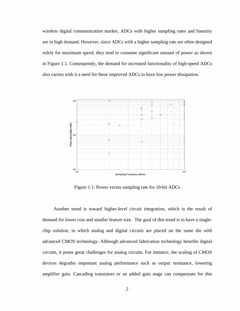
wireless digital communication market, ADCs with higher sampling rates and linearity
are in high demand. However, since ADCs with a higher sampling rate are often designed
solely for maximum speed, they tend to consume significant amount of power as shown
in Figure 1.1. Consequently, the demand for increased functionality of high-speed ADCs
also carries with it a need for these improved ADCs to have low power dissipation.
Figure 1.1: Power versus sampling rate for 10-bit ADCs
Another trend is toward higher-level circuit integration, which is the result of
demand for lower cost and smaller feature size. The goal of this trend is to have a single-
chip solution, in which analog and digital circuits are placed on the same die with
advanced CMOS technology. Although advanced fabrication technology benefits digital
circuits, it poses great challenges for analog circuits. For instance, the scaling of CMOS
devices degrades important analog performance such as output resistance, lowering
amplifier gain. Cascading transistors or an added gain stage can compensate for this
2

lowered gain. However, the use of cascading transistors runs into a limitation on the
number of transistors that can be stacked, a limitation that is imposed by the low power
supply voltage of scaled CMOS technology. And turning to the solution of additional
stages has the disadvantages of increased power dissipation and more complicated
circuitry. The low power supply voltage of scaled CMOS technology also limits the
performance of analog circuits. Assuming the system is limited by the CKT noise, the
Signal-to-Noise Ratio (SNR) of the system is reduced because the output voltage swing
of an op-amp is decreased while the CKT noise remains constant. To maintain the same
SNR, the capacitor size has to be increased to reduce the CKT noise. This means, the
size of devices and the current of the op-amp should also be increased to drive the large
capacitor. Therefore, just as is the case with digital circuits, simply lowering the power
supply voltage in analog circuits does not necessarily result in lower power dissipation.
The many design constraints common to the design of analog circuits makes it difficult to
curb their power consumption. This is especially true for already complicated analog
systems like ADCs; reducing their appetite for power requires careful analysis of system
requirements and special strategies.
The various ADC architectures available include flash, two-step, folding, pipeline,
successive approximation, and over-sampling. Each variation has unique features and
which of them is deployed in specific applications is typically determined by the speed
and resolution requirements involved. Of the d ADC architectures available, the pipeline
approach is most suitable for low-power, medium resolution and high-speed applications,
especially with CMOS technology. Pipeline architecture is widely used in digital
3
communication systems, data acquisition systems and video systems, all applications in
which both accuracy and speed are required. Nevertheless, as observed earlier, power
dissipation is a primary concern in those applications requiring portability. Thus, the
objective of this work is to design and build a low-voltage low-power medium-resolution
(8-10bits) high-speed pipeline ADC in deep submicron CMOS technology.
The main focus of this work is as following. First, study and understand the
principles and operation of a pipeline ADC. Second, identify the locations of the power
hungry blocks when a pipeline ADC is implemented with switched capacitor (SC)
circuits. Third, determine the relationship between power consumption and the number of
bits per stage. Fourth, develop an optimization algorithm in order to decide which version
of pipeline architecture consumes the least power for a given speed, resolution and
technology. Last, implement the pipeline ADC based on the results of a power
optimization algorithm.
1.2 THESIS ORGANIZATION
This thesis is organized as follows. Chapter 2 describes important ADC
performance parameters and various ADC architectures. Chapter 3 gives an overview of
a pipeline ADC. Chapter 4 presents a systematic design approach for low power pipeline
ADCs. Chapter 5 details the system blocks, circuit design and layout of a prototype ADC.
Chapter 6 assesses and discusses the performance of the prototype ADC. Chapter 7 is
devoted to conclusions drawn from the research.
4

C H A P T E R 2 : O V E R V I E W O F A / D
C O N V E R S I O N
Various parameters describe the performance of an ADC, and all of them must be
understood in undertaking to design an ADC. The first section of this chapter presents the
most important performance parameters. These parameters describe the static and
dynamic behavior of the ADC. The next section briefly reviews different ADC
architectures.
2.1 A/D CONVERTER PERFORMANCE PARAMETERS
2.1.1 DIFFERENTIAL NON-LINEARITY AND INTEGRAL
NON-LINEARITY
Differential non-linearity (DNL) is defined as the difference between the size of
an actual and an ideal step size. The ideal step size is equal to 1LSB and VLSB = VFS/2N,
where VFS is the full-scale input range and N is the full resolution of the ADC. DNL can
be expressed as follows:
DNL(k) = [ step size of code (k) – VLSB ] / VLSB ( eq.2.1.1 )
The input-output conversion characteristic of the 3-bit ADC is shown in Figure
2.1. DNL cannot be smaller than –1. If a DNL for code k is –1, then the converter cannot
5
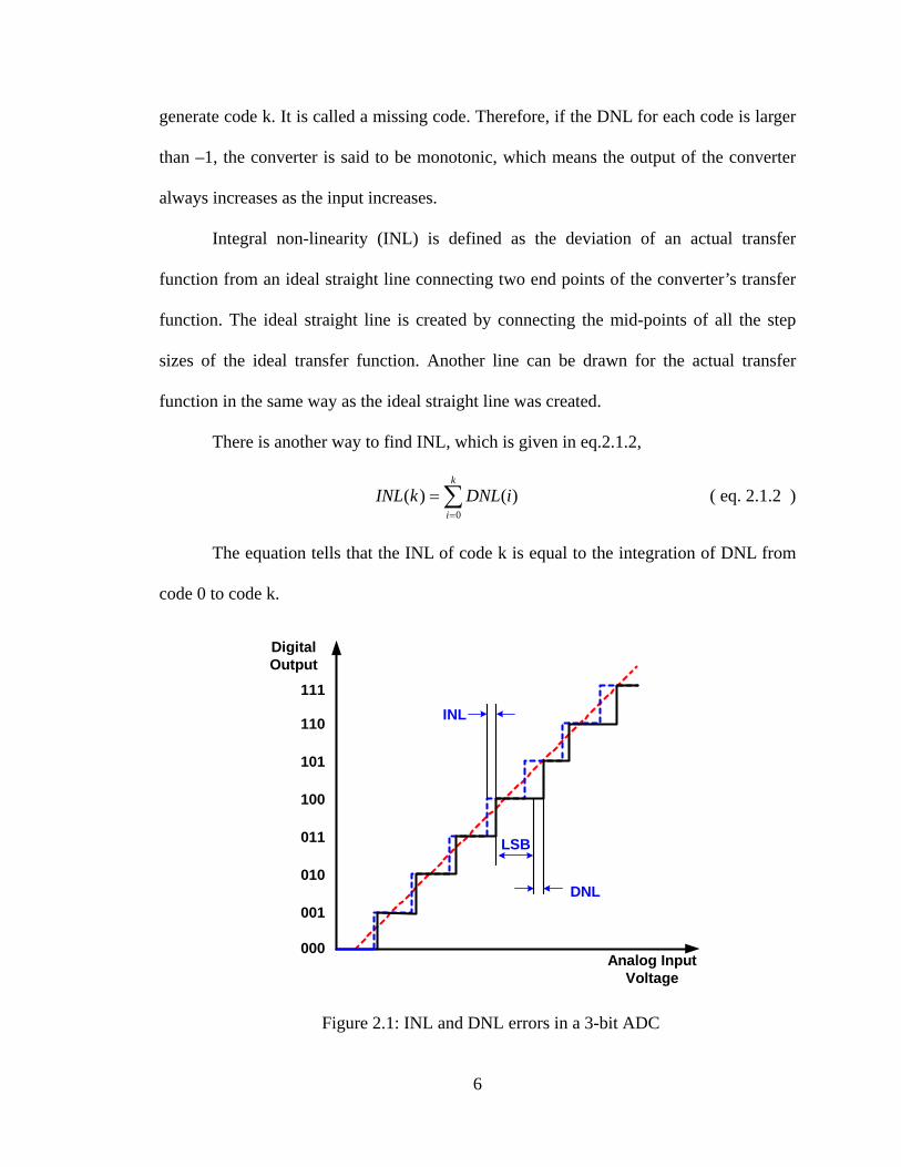
generate code k. It is called a missing code. Therefore, if the DNL for each code is larger
than –1, the converter is said to be monotonic, which means the output of the converter
always increases as the input increases.
Integral non-linearity (INL) is defined as the deviation of an actual transfer
function from an ideal straight line connecting two end points of the converter’s transfer
function. The ideal straight line is created by connecting the mid-points of all the step
sizes of the ideal transfer function. Another line can be drawn for the actual transfer
function in the same way as the ideal straight line was created.
There is another way to find INL, which is given in eq.2.1.2,
∑=
=k
iiDNLkINL
0)()( ( eq. 2.1.2 )
The equation tells that the INL of code k is equal to the integration of DNL from
code 0 to code k.
Analog InputVoltage
DigitalOutput
000
INL
DNL
LSB
001
010
011
100
101
110
111
Figure 2.1: INL and DNL errors in a 3-bit ADC
6

2.1.2 SIGNAL-TO-NOISE RATIO
Signal-to-Noise Ratio (SNR) is the ratio of the power of a full-scale input signal
to total noise power present at the output of a converter. The quantization noise and the
circuit noise are included in the SNR, but harmonics of the signal are excluded. The SNR
can be measured by applying a sinusoidal signal to the converter and performing a fast
Fourier transform (FFT) of the digital output of the converter. The SNR can then be:
(dB) Power Noise Total
Power Signal log10 SNR ⎟⎠⎞
⎜⎝⎛⋅= ( eq.2.1.3 )
The maximum achievable theoretical SNR is given by
)(76.102.6 dBNSNR +⋅= ( eq.2.1.4 )
where N is the resolution of the ADC and only the quantization noise is considered.
2.1.3 TOTAL HARMONIC DISTORTION
Total harmonic distortion (THD) is defined as the ratio between the root-mean-
square (RMS) sum of the harmonic components and the amplitude of the input signal.
THD is given by
( )
( )in
j
iin
fA
fiATHD
∑=
⋅= 2
2
( eq. 2.1.5 )
where is the amplitude of the fundamental input signal, is the
amplitude of the i
)( infA )( infiA ⋅
th harmonic and j is the number of harmonics considered.
7
2.1.4 SIGNAL-TO-NOISE AND DISTORTION RATIO
The Signal-to-Noise and Distortion Ratio (SNDR) is the ratio between the power
of the full scale input signal and total noise including harmonics and can be written as
(dB) Power Distotrion Harmonic and Noise
Power Signal log10 SNDR ⎟⎠⎞
⎜⎝⎛⋅= ( eq.2.1.6 )
2.1.5 SPURIOUS FREE DYNAMIC RANGE
The Spurious Free Dynamic Range (SFDR) is defined as the ratio between the
maximum amplitude of the input signal and the amplitude of the next largest spectral
component. SFDR is an important specification in telecommunication applications in
which ADC spectral purity is crucial of an ADC.
2.1.6 EFFECTIVE NUMBER OF BITS
The Effective Number of Bits (ENOB) can be obtained from the SNDR. The
ENOB can be given as
)(02.6
76.1 bitsSNDRENOB −= ( eq. 2.1.7 )
8

2.2 REVIEW OF ANALOG-TO-DIGITAL CONVERTER
ARCHITECTURES
2.2.1 FLASH ADC
As the nomenclature implies, Flash ADC conversion is the fastest possible way to
quantize an analog signal. The concept of this architecture is relatively simple to
understand. In order to achieve N-bit from a flash ADC, it requires 2N-1 comparators, 2N-
1 reference levels and digital encoding circuits. The reference levels of comparators are
usually generated by a resistor string.
One example of simple flash ADC is shown in Figure 2.2. First, the analog input
signal is sampled by comparators and is compared with one of the reference levels. Then,
each comparator produces an output based on whether the sampled input signal is larger
or smaller than the reference level. The comparators generate the digital output as a
thermometer code. This thermometer code output is usually converted to a binary or a
gray digital code by encoding logic circuits at the end. Since this operation is done in
only one clock cycle, a flash ADC can attain the highest conversion rate.
The high sensitivity of the comparator offset and a large circuit area are the main
drawbacks of a flash ADC. For instance, to build a 10-bit ADC based on flash
architecture requires more than 1,023 comparators. Therefore, it will occupy a very large
chip area and dissipate high power. Moreover, each comparator must have an offset
voltage smaller than 1/210, which is quite difficult to build. That is why we seldom see
flash architecture with ADCs of more than 8-bits.
9

Encodin
g L
ogic
Dig
ital outp
ut
V inVref+
Vref-
Figure 2.2: Flash ADC
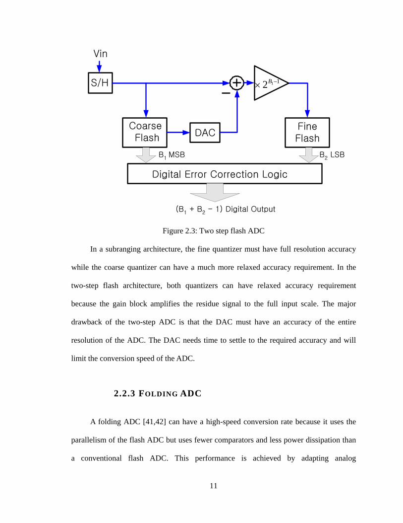
2.2.2 TWO STEP FLASH ADC
The block diagram of a two-step flash ADC [64] is shown in Figure 2.3. It consists
of a Sample and Hold Amplifier ( SHA ), two low-resolution flash ADCs, a digital-to-
analog (DAC), a subtracter and a gain block. The conversion is executed in two-steps as
the name implies. The sampled analog signal is digitized by the first coarse quantizer
producing the B1 Most Significant Bits (MSBs). This digital code is changed back to an
analog signal by the DAC and subtracted from the sampled input signal producing the
residue signal. The residue signal is amplified by the gain block and digitized by the
second quantizer producing the B2 LSBs. Because 1-bit out of the output digital codes is
often used for error correction, the overall resolution is (B1+B2-1) bit.
10
S/H
Coarse Flash DAC
112 −× B
FineFlash
Digital Error Correction Logic
B1 MSB B2 LSB
(B1 + B2 - 1) Digital Output
Vin
Figure 2.3: Two step flash ADC
In a subranging architecture, the fine quantizer must have full resolution accuracy
while the coarse quantizer can have a much more relaxed accuracy requirement. In the
two-step flash architecture, both quantizers can have relaxed accuracy requirement
because the gain block amplifies the residue signal to the full input scale. The major
drawback of the two-step ADC is that the DAC must have an accuracy of the entire
resolution of the ADC. The DAC needs time to settle to the required accuracy and will
limit the conversion speed of the ADC.
2.2.3 FOLDING ADC
A folding ADC [41,42] can have a high-speed conversion rate because it uses the
parallelism of the flash ADC but uses fewer comparators and less power dissipation than
a conventional flash ADC. This performance is achieved by adapting analog
11
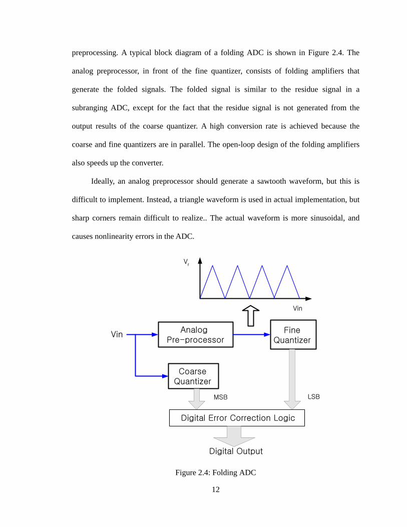
preprocessing. A typical block diagram of a folding ADC is shown in Figure 2.4. The
analog preprocessor, in front of the fine quantizer, consists of folding amplifiers that
generate the folded signals. The folded signal is similar to the residue signal in a
subranging ADC, except for the fact that the residue signal is not generated from the
output results of the coarse quantizer. A high conversion rate is achieved because the
coarse and fine quantizers are in parallel. The open-loop design of the folding amplifiers
also speeds up the converter.
Ideally, an analog preprocessor should generate a sawtooth waveform, but this is
difficult to implement. Instead, a triangle waveform is used in actual implementation, but
sharp corners remain difficult to realize.. The actual waveform is more sinusoidal, and
causes nonlinearity errors in the ADC.
Analog Pre-processor
CoarseQuantizer
FineQuantizer
Vin
Vr
Vin
Digital Error Correction Logic
MSB LSB
Digital Output
Figure 2.4: Folding ADC
12
2.2.4 SUBRANGING ADC
In order to overcome such drawbacks as hardware complexity, large chip area and
high power dissipation, subranging architecture was [39,40] developed at the cost of the
sampling speed. A simplified subranging ADC is illustrated in Figure 2.5. It comprises a
SHA, reference level generators, comparators and decoders. The number of comparators
is 2N/M × M, where N is the total ADC resolution, and M is the number of stages. For a 2-
stage (two-stage?) 10-bit subranging ADC, only 64 comparators are required instead of
the 1,024 comparators in a flash ADC. Therefore, compared with a flash ADC,
subranging architecture yields a quite significant reduction in power consumption and in
the required circuit area
However, the conversion in subranging architecture is done by multiple clocks
instead of one clock as in a flash ADC. The operation of the 2-stage subranging ADC is
as follows: In the first clock, an analog input signal is sampled by the SHA and quantized
by a coarse flash ADC that determines the most significant bit from the sampled input
signal. In the next clock, the segment of the resistor string is selected by the results from
the coarse flash ADC, and the least significant bits are produced by the fine flash ADC.
The comparator requirement of the coarse flash ADC can be relaxed, but the comparators
of the fine flash ADC should be as accurate as the full resolution of the ADC. The
conversion speed decreases as the number of subranging stages increase.
13

SHAVin
Vref
Decoder
Decoder
LSB
MSB
Figure 2.5: Subranging ADC
2.2.5 SUCCESSIVE APPROXIMATION ADC
The block diagram of a successive approximation ADC [66] is shown in Figure
2.6. It consists of a comparator, a DAC and a successive approximation register (SAR).
The successive approximation ADC uses a binary search algorithm to find the closest
digital code for an input signal. When an input signal is applied to the converter, the
comparator simply determines whether the input signal is larger or smaller than the DAC
output and produces one digital bit at a time starting from the MSB. The SAR stores the
produced digital bit and uses the information to change the DAC output for the next
comparison. This operation is repeated until all the bits in the DAC are decided. In order
14
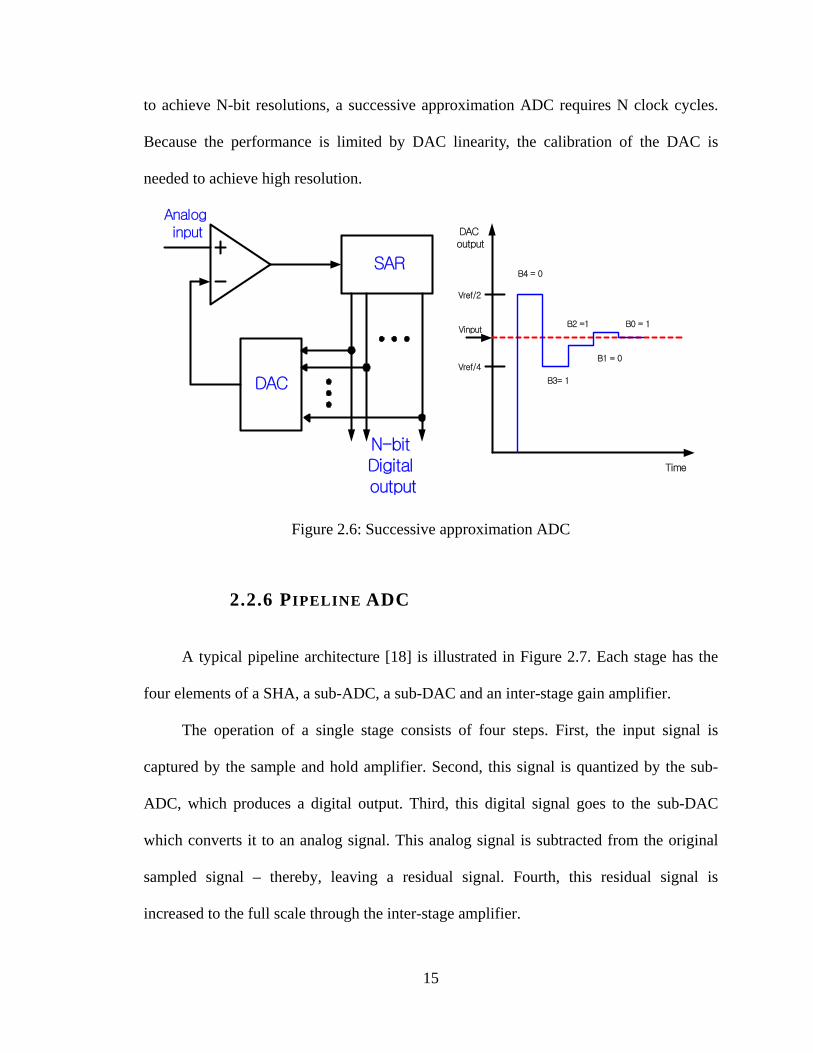
to achieve N-bit resolutions, a successive approximation ADC requires N clock cycles.
Because the performance is limited by DAC linearity, the calibration of the DAC is
needed to achieve high resolution.
DAC output
Time
Vref/2
Vref/4
B4 = 0
B3= 1
B2 =1
B1 = 0
B0 = 1Vinput
Analog input
SAR
DAC
N-bit Digital output
Figure 2.6: Successive approximation ADC
2.2.6 PIPELINE ADC
A typical pipeline architecture [18] is illustrated in Figure 2.7. Each stage has the
four elements of a SHA, a sub-ADC, a sub-DAC and an inter-stage gain amplifier.
The operation of a single stage consists of four steps. First, the input signal is
captured by the sample and hold amplifier. Second, this signal is quantized by the sub-
ADC, which produces a digital output. Third, this digital signal goes to the sub-DAC
which converts it to an analog signal. This analog signal is subtracted from the original
sampled signal – thereby, leaving a residual signal. Fourth, this residual signal is
increased to the full scale through the inter-stage amplifier.
15

Vinput Stage 1 Stage iStage i-j
D-ff and digital error correction
SHA
sub-ADC
sub-DAC
N-bits digital output
2^(n-1)
n-bits
n-bits
Figure 2.7: A pipeline ADC block diagram
The residual signal is passed to the next stage and the procedure mentioned above
is repeated. Since every stage has the element of sample and hold, the above procedure
occurs concurrently in every stage. The most interesting feature of a pipeline ADC is the
throughput behavior. For a pipeline with i-stages, the very first signal will take i-clock
cycles to go through the entire i-stages. Obviously, it will have the latency of i-clock
cycles. The next signal – given the nature of the sample and hold element – will have the
latency of (i-1) clock cycles. After i-clock cycles, we will have a complete digital output
in every clock cycle. At this moment, each sampled signal will have the latency of a
singular clock cycle. The advantage of a pipeline ADC is that the conversion rate does
16

not depend on the number of stages. The overall speed is determined by the speed of the
single stage.
2.2.7 OVERSAMPLED ADC
A sigma-delta ADC is also known as an oversampling data converter [61,62]. The
ADCs seen so far in this chapter are often called as Nyquist rate ADCs because the
conversion rate of those ADCs is equal to the Nyquist rate. In sigma-delta ADCs,
however, the sampling is performed at a much higher rate than the Nyquist rate. The ratio
of the sampling rate to the Nyquist rate is called the oversampling ratio (OSR). Each
doubling OSR allows to reduce the quantization noise power resulting in 3dB SNR
improvement.
A sigma-delta ADC also uses noise-shaping techniques to increase resolution. The
quantization noise power is moved to higher frequencies by negative feedback. Then, the
out-of-band noise is removed by a digital low pass filter, leaving only a small amount of
the quantization noise. The conceptual block diagram is shown in Figure 2.8. It consists
of a S/H, a sigma delta modulator, a digital filter and a down sampler. The down sampler
converts the oversampled digital signal into the lower sample rate digital signal.
The resolution of the sigma delta ADC can be enhanced by increasing either the
order of the modulator or the resolution of the quantizer. An L-th-order sigma delta
modulator improves SNR by 6L + 3dB/octave. However, increasing the order of the
modulator more than 2nd can cause instability problems. To avoid instability problem with
a high order modulator, a special architecture like multi-stage noise shaping (MASH) can
be employed. Increasing the resolution of the quantizer also cause a problem because of
17

the nonlinearity of the DAC. Dynamic element matching is one of the methods available
to reduce the distortion from the multi-bit DAC.
Figure 2.8: Block diagram of an oversampling ADC
2.3 SUMMARY
Performance metrics have been reviewed in this chapter and used to precisely
describe and characterize ADC performance. A brief description of various ADC
architectures has been presented, including flash, two-step flash, folding, successive
approximation, pipeline, and an oversampling ADC.
18

C H A P T E R 3 : O V E R V I E W O F A
P I P E L I N E A D C
This chapter presents a detailed description of pipeline architecture. In the first
section, a digital error correction technique is discussed. In the next section, the basic
building blocks of a pipeline architecture such as MDACs, sub-ADCs, op-amps and
comparators are described. The last section presents the nonidealities associated with
these pipeline ADC building blocks
3.1 DIGITAL ERROR CORRECTION
Digital error correction is a method to fix incorrect codes caused mainly by the
offsets of comparators in a sub-ADC. To better illustrate digital error correction, a 4-bit
ADC case is used as an example. Digital error correction [53] has evolved over the past
two decades. The conventional method uses two stages. For a 4-bit ADC, the first stage
would need to be 2-bits with three comparators. The second stage would need to be 3-bits
with seven comparators. This conventional method uses addition and subtraction to
correct the error. The newer modified digital error correction method [2] uses only
addition. In this new method, three stages, each with two bits, are used. The advantage of
the newer method lies in the ease with which addition is implemented in digital circuits,
whereas subtraction is cumbersome and takes substantial logic to implement.
19

00 01
Correct co
- Vref
1LSB
Inputrangeof thenext
stage
-1/2Vref
Figure 3.1: The input/output cha
In Figure 3.1, the input/output c
ADC is shown. The binary digits loca
from the sub-ADC of the current stag
are the ones from the next stage
residual/residue signal to full scale fo
Figure 2.7.
In Figure 3.1, 4-bits output cod
0111 for the inputs of Vin(1) and Vin(
offset error. Hence, no digital error cor
In Figure 3.2, the same input/o
offsets in the threshold level located
threshold level, the input/output chara
It is shown with dotted line in Figure 3
Vout
10 1100
01
10
11
Vin(1)Vin(2)Correct code : 1000
de : 0111
+ Vref
+1/2Vrefn
racteristic of a 2-bit stage in a pipeline ADC
haracteristic of an ideal 2-bit stage in the pipelin
ted on the top of the graph are the digital output
e. The binary digits on the right side of the grap
. The inter-stage gain amplifier converts th
r the next stage immediately after summation i
es from the two-stage pipeline ADC are 1000 an
2), respectively. This is a case in which there is n
rection is required.
utput characteristic of Figure 3.1 is shown wit
in the center. Notice that with an offset in th
cteristic is out of the input range of the next stage
.2. As a result, with the same inputs of Vin(1) an
20
Vi
e
s
h
e
n
d
o
h
e
.
d
Vin(2) in Figure 3.1, incorrect codes are produced. The output digital codes are now 0111
and 1000 instead of 1000 and 0111.
00 01 10 11
00
01
10
11
Vin(1)Vin(2)
Incorrect code : 0111Incorrect code : 1000
- Vref
+ Vref
1LSB
Inputrangeof thenext
stage
- 1/2Vref - 1/2Vref
(1)
(2)
Vout
n
Figure 3.2: The input/output characteristic of 2-bit stage in the pipeline ADC with offsets
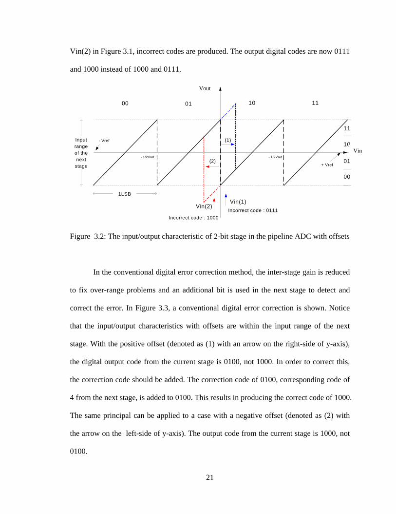
In the conventional digital error correction method, the inter-stage gain is reduced
to fix over-range problems and an additional bit is used in the next stage to detect and
correct the error. In Figure 3.3, a conventional digital error correction is shown. Notice
that the input/output characteristics with offsets are within the input range of the next
stage. With the positive offset (denoted as (1) with an arrow on the right-side of y-axis),
the digital output code from the current stage is 0100, not 1000. In order to correct this,
the correction code should be added. The correction code of 0100, corresponding code of
4 from the next stage, is added to 0100. This results in producing the correct code of 1000
The same principal can be applied to a case with a negative offset (denoted as (2) with
the arrow on the left-side of y-axis). The output code from the current stage is 1000, not
0100.
21
Vi
.

00 01 10 11
0
1
2
3
Vin(1)Vin(2)
- Vref
+ Vref
1LSB
Inputrangeof thenext
stage
- 1/2Vref + 1/2Vref
-1
-2
4
5
01000100+1000
10001111+0111
(1)
(2)
Vout
n
Figure 3.3: The input output characteristic of a 2-bit stage in the pipeline ADC with
conventional digital error correction when there are the offsets
To correct this, the correction code should be subtracted. The correction code o
1111 is added to 1000 and the correct code of 0111 is produced. The correction code o
1111 is the 2’s complement number of the corresponding code of –1.
However, this approach requires one more bit to the next stage, plus the
complication of the subtraction circuit. In the modified digital error correction method
[2][6], these two problems can be avoided by adding systematic offsets intentionally to
the threshold levels. In Figure 3.4, the modified digital error correction is shown. Notice
that all the threshold levels are moved to the right compared with the ones in Figure 3.3
Here redundancy is used to correct the errors. So, one bit from the each stage will be
22
Vi
f
f
.
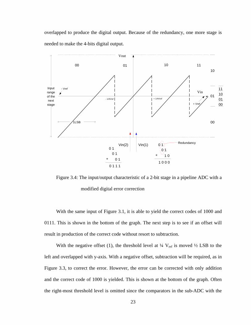
overlapped to produce the digital output. Because of the redundancy, one more stage is
needed to make the 4-bits digital output.
00 01 10 1110
Vin(1)
- Vref
+
1LSB
Inputrangeof thenext
stage
- 1/4Vref + 1/4Vref
Redundancy0 1 0 1
+
1 0 0 0
1 0
0 1 0 1
+
0 1 1 1
0 1
Vin(2)
11
Vout
n
Figure 3.4: The input/output characteristic of a 2-bit stage in a pipeline
modified digital error correction
With the same input of Figure 3.1, it is able to yield the correct codes
0111. This is shown in the bottom of the graph. The next step is to see if
result in production of the correct code without resort to subtraction.
With the negative offset (1), the threshold level at ¼ Vref is moved ½
left and overlapped with y-axis. With a negative offset, subtraction will be r
Figure 3.3, to correct the error. However, the error can be corrected with
and the correct code of 1000 is yielded. This is shown at the bottom of the
the right-most threshold level is omitted since the comparators in the sub-A
23
Vi
01Vref
00
000110
ADC with a
of 1000 and
an offset will
LSB to the
equired, as in
only addition
graph. Often
DC with the
modified digital error correction have the correction range of ½ LSB. The correction
range is the amount of allowable shift in threshold level that does not cause any error [6].
Therefore, two comparators will be needed and only three digital outputs (00,01,10) will
be produced. That is why the stage with modified digital error correction is often called
1.5-bits per stage instead of 2-bits per stage.
00 01 10 11
01
10
Vin(1)
- Vref
+ Vref
1LSB
Inputrangeof thenextstage
- 1/4Vref + 1/4Vref
00
00
11
01
10
1 0 0 0
+
1 0 0 0
0 0
Redundancy
(1)
Vout
Vin
Figure 3.5: The input /output characteristic of one stage in a pipeline ADC with a
modified digital error correction when an offset is present
24
3.2 BASIC BUILDING BLOCKS
3.2.1 MULTIPLYING DIGITAL-TO-ANALOG CONVERTER
SHA
sub-ADC
sub-DAC
2^(n-1)
n-bits
MDAC
Vinput Voutput
Figure 3.6: Basic building blocks of a pipeline ADC.
A basic block diagram of a pipelined ADC is illustrated in Figure 3.6. When this
block is designed, a switched-capacitor (SC) circuit is typically used. A sample and hold
amplifier, a sub-DAC, a subtractor and an inter-stage amplifier can be implemented with
one SC circuit called a Multiplying Digital to Analog Converter (MDAC). Therefore,
when one stage of a pipeline ADC is realized, actually only two blocks are needed: a
MDAC and a sub-ADC. Those blocks can be implemented simply with a low-resolution
flash ADC.
There are three typical SC configurations [18] that can be used for implementing a
SC MDAC. These are shown in Figure 3.7(a), (b) and (c). For simple illustration, all of
them are single-ended SC configurations but in circuit implementation all would be fully
differential. All of the three configurations share the same basic operation. The operation
needs two non-overlapping clock phases – sampling and amplifying or transferring
25

The first SC configuration is shown in Figure 3.7(a). This one is popularly
employed for an Sample and Hold (S/H) circuit. It requires only one capacitor that is used
for both sampling and feedback. Therefore, it does not have the capacitor mismatch
problem of the other two SC configurations.
Cs1Φ
1Φ1Φ
2Φ
Vinput Voutput
(a)
Cs1Φ
1Φ1Φ2Φ
Cf
Vinput Voutput
(b)
Figure 3.7: Typical S/H circuits (a) one-capacitor S/H (b) two-capacitors S/H
26

Cs1Φ
1Φ1Φ2Φ
Cf
VinputVoutput
1Φ
2Φ
(c)
Figure 3.7: Typical S/H circuits (a) one-capacitor S/H (b) two-capacitors S/H
(c) combination of (a) and (b)
The –3-dB frequency of the closed-loop amplifier is given by [20]
L
muadB C
g⋅=⋅==− βωβ
τω 1
3 (eq. 3.2.1)
where uaω is the unity-gain frequency of an op-amp, is the output load capacitance of
an op amp and
LC
β is the feedback factor. The feedback factor is defined as the ratio
between the feedback capacitor and the sum of all the capacitors connected to the
summing node of the op amp. If we ignore the input parasitic capacitance of an op amp,
the feedback factor of the SC circuit in Figure 3.7(a) is almost unity, which is larger than
in other configurations. Therefore, as we can observe from eq. 3.2.1, the SC circuit in
Figure 3.7(a) can be operated at higher speed than others. Nonetheless, the SC circuit
cannot be used for a MDAC due to transfer function is always unity and it cannot have
any other gain.
The next S/H circuit is shown in Figure 3.7(b). This configuration is often used for
an integrator. The input signal is sampled first in the sampling capacitor and in the next
27

clock phase the sampled charge is moved to the feedback capacitor. The transfer function
of this SC circuit is
f
s
in
out
CC
VV
= (eq.3.2.2)
And, the feedback factor is
psf
f
CCCC
++=β (eq.3.2.3)
The last SC configuration is illustrated in Figure 3.7(c). This one can be
understood as a combination of the other two SC circuits. In the sampling clock phase,
the input signal is sampled both in the sampling and feedback capacitor. In the next phase,
the sampled charge in the sampling capacitor is transferred to the feedback capacitor. As
a result, the feedback capacitor has the transferred charge from the sampling capacitor as
well as the input signal charge sampled by itself. The transfer function of this SC circuit
is given by
f
fs
in
out
CCC
VV +
= (eq.3.2.4)
The feedback factor is the same as in the second SC circuit. In comparing the
second and third configurations, the third has a wider bandwidth that makes it widely
used for an MDAC because it can have wider bandwidth. When both of these SC circuits
are designed to have the same gain, the configuration in Figure 3.7(c) can have a larger
feedback factor than the other. This results in its having wider bandwidth according to eq.
3.2.1.
A MDAC can be implemented by using either binary-weighted capacitors [47] or
equal-valued capacitors with SC implementation.
28

The SC MDAC with binary-weighted capacitor array [66] is shown in Figure 3.8.
For simplicity, the circuit shown in Figure3.8 is single-ended, but it would be constructed
with a fully differential configuration. This MDAC has two inputs b1, b0 where b1 is the
Most Significant Bit (MSB) and b0 is the least significant bit (LSB). Here, we assume the
op-amp has infinite gain and the parasitic capacitor at the inverting node of the op-amp is
negligible.
C4 = 2C
C2 = C
Voutput
C1 = C
C3 = C
(b)
refVb ⋅0
refVb ⋅1
C4 = 2C
C2 = C
Voutput
C1 = C
C3 = C
(a)
refV−
Vinput
Figure 3.8. SC MDAC in (a) sampling phase (b) amplifying phase
29

During the first sampling clock phase, the input signal is connected capacitors C2,
C3 and C4 and the capacitor C1 is connected to – Vref. The total charge stored during the
sampling clock phase is
( ) refinrefins VCVCCVCVq ⋅−⋅=⋅−+⋅= 44 (eq.3.2.5)
On the next amplification clock phase, the capacitors C1 and C2 are connected to the
output of the op-amp, building the feedback capacitors. The rest of the capacitors are
connected to either Vref or -Vref, depending on the output results from the sub-ADC in the
same stage. The total charge on the capacitors during the amplification phase is
refrefouta VbCVbCVCq ⋅⋅+⋅⋅+⋅= 10 22 (eq.3.2.6)
( )10 22 bbVCVC refout ⋅+⋅⋅+⋅= (eq.3.2.7)
where b1, b0 = ± 1 are the digital output bits from the sub-ADC. According to the charge
conservation theory, should be equal to . If we equate Eq.3.2.5 and Eq.3.2.7, we
have
aq sq
( )10 224 bbVCVCVCVC refoutrefin ⋅+⋅⋅+⋅=⋅−⋅ (eq.3.2.8)
Thus, the output of the MDAC in the 1.5-bits per stage is
( ) refrefinout VbbVVV ⋅−⋅+⋅⋅−⋅=212
212 10 (eq.3.2.9)
⎪⎩
⎪⎨
⎧
−<+⋅≤≤−⋅
>−⋅=
4/24/4/2
4/2
refinrefin
refinrefin
refinrefin
VVifVVVVVifV
VVifVV (eq.3.2.10)
The input output characteristic of the 1.5-bits per stage MDAC is shown in Figure 3.9.
30

Vin
Vout
4refV
− 4refV
00 1001
01bb 01bb
Figure 3.9. Transfer function of 1.5 bit/stage MDAC
The same MDAC transfer function of 1.5-bits per stage [18] in Figure 3.9 can also
be realized by the equal valued capacitor approach. The single-ended SC implementation
of the MDAC with the equal-valued capacitor array is shown in Figure 3.10. We can
observe the differences between the approaches in Figure 3.8 and Figure 3.10. In Figure
3.10, there are only two equal-sized capacitors, less the number of switches and a MUX.
The MUX chooses the DAC output from +Vref, 0, -Vref depending on the digital output of
the sub-ADC.
31

Cs1Φ
1Φ1Φ2Φ
Cf
Vinput
1Φ
2Φ
MUX
Sub-ADC
+Vref
-Vref
0
Figure 3.10. SC realization of a 1.5 bit/stage MDAC with equal-valued capacitor
array
The operation of the MDAC is as follows. First, the input signal is sampled to the
Cs and Cf capacitors. It is also applied to the sub-ADC that has decision levels at ±Vref/4.
On the next clock phase, the Cf capacitor is disconnected from the input signal and
switched to the op-amp output making a negative feedback loop. The Cs capacitor is
connected to the MDAC output which is decided by the sub-ADC output. The output of
this MDAC is given by
reff
sin
f
sfout V
CC
sVC
CCV ⋅⋅−⋅⎟
⎟⎠
⎞⎜⎜⎝
⎛ += 0 (eq.3.2.11)
Where Cs = Cf = C and can be one of the three values, +1, 0, -1, depending on the size
of the input signal.
0s
refinout VsVV ⋅−⋅= 02 (eq.3.2.12)
⎪⎩
⎪⎨
⎧
−<+⋅≤≤−⋅
>−⋅=
4/24/4/2
4/2
refinrefin
refinrefin
refinrefin
VVifVVVVVifV
VVifVV (eq.3.2.13)
32

3.2.2 SUB-ANALOG-TO-DIGITAL CONVERTER
A sub-Analog-to-Digital converter (sub-ADC) is one of the building blocks in one
stage of a pipeline ADC as illustrated in Figure 2.7. There are two roles for a sub-ADC.
The first one is to perform coarse quantization for an output voltage from the previous
stage or an SHA. The second one is to produce a decoded control signal for an MDAC in
the same stage so that the MDAC can perform the subtraction and amplification of the
sampled input signal. The control signal is generated by a few logic gates for a low
resolution per stage or by a read only memory (ROM) for a high resolution per stage.
Most pipeline ADCs are implemented with switched-capacitor (SC) circuits. Two
non-overlapping clocks are required to operate SC circuits, which are in a sampling
phase and in a hold or amplifying phase. Of course, there are delayed clock phases to
reduce charge injection errors from the switches, but they are merely variations from
these two clock phases and
sΦ
hΦ
sΦ hΦ . In a hold mode, the sub-ADC generates coarse
quantized digital outputs and passes a decoded control signal to the MDAC for
subtraction and amplification. The time to pass control signals to the MDAC from the
sub-ADC should be minimized to maximize the settling time of the MDAC, which is
important in high-speed applications. Because of their simple structure and high-speed
capability, flash architectures are natural choices for sub-ADCs. The 2-, 3- and 4-bit [14]
are the most commonly used resolution of sub-ADCs. 5-bit sub-ADC is also reported in
[21].
The block diagram of a 2.5-bit sub-ADC with flash architecture is illustrated in
Figure 3.11. It consists of six comparators, six reference voltage levels generated by a
33

resistor string, an encoding logic to convert a thermometer output code to a binary code
and a decoding logic to generate a control signal for the MDAC. When the input signal
arrives at the sub-ADC, all of the comparators determein whether the input signal is
larger than their reference voltages or not. If the input signal is larger than the reference
voltage, the corresponding comparator produces an output logic “1”. The output logic “0”
is produced from comparators whose reference voltages are smaller than the input signal.
The type of comparators in the sub-ADC is determined by the resolution of the
stage. For a 2-bit per stage, a dynamic comparator such as in [18] is the most popular
because it does not dissipate static power and occupies smaller area. For a stage with
more than a 2-bit, a dynamic comparator cannot be used because of its large offset
voltage. Instead, a comparator with a preamplifier and a regenerative latch is used for a
higher resolution than the 2-bit. The offset voltage is reduced by preamplification and
also can be reduced further by auto-zeroing technique.
Vin2Φ
2Φ
1ΦC
2Φ
2Φ
1ΦC
2Φ
2Φ
1ΦC
Dig
ital E
ncord
er
Vref1
Vref2
Vref6
B2
B1
B0
Sub-DAC
Figure 3.11: The 2.5-bit sub-ADC
34
3.2.3 OPERATIONAL AMPLIFIERS
An op-amp is not only a widely used component in most of analog circuits but a
very important building block of a SC pipeline ADC since it often limits performance
such as speed and accuracy, and consumes most of the power in the SC circuits. In this
section, the important parameters of the different op-amp topologies are reviewed and
their pros and cons are discussed.
3.2.3.1 CURRENT MIRROR AMPLIFIER
The circuit schematic of the current-mirror amplifier [56] is shown in Figure3.12.
The differential input stage is formed by input transistors M0, M1 and diode-connected
transistors M2, M3. The current-mirrors are formed by diode-connected transistor M2, M3
with transistor M6, M7 and M is the current multiplication factor of the current mirrors. A
typical value for M is between 1 and 3.
The voltage gain of the current-mirror amplifier is given by
)||( 640 oomv rrgMA ⋅⋅≈ ( eq.3.2.14 )
where are the resistance of transistor M64 , oo rr 4, M6, respectively.
The value of unity gain bandwidth is given by
L
mu C
gM 0⋅=ω ( eq. 3.2.15 )
where is the transconductance of input transistor M0mg 0, CL is the load capacitance and
M is the current mirror ratio.
The non-dominant pole is located at the drain of transistor M2 (M3) and given by
35

00660622
0
)1()1( GDoAmGDoutmDBGSDBGS
mn CrgCrgCCCC
g+++++++
≈ω ( eq. 3.2.16)
where are the transconductance of transistors M6,0 mm gg 0, M6 and CGS2, CGS6 are the gate-
source parasitic capacitance of transistor M2, M6. CDB0, CDB2 are the drain-bulk parasitic
capacitances of transistor M0, M2 and CGD0, CGD6 are the gate-drain parasitic capacitances
of transistor M0, M6. is the output resistance of the amplifier, which is the parallel
combination of the output resistance of transistors M
outr
4 and M5. is the resistance at
node A, which is approximately
oAr
21 mg . The last two terms of the denominator are
because of the miller effect of CGD0 and CGD6. In order to have enough phase margin of
the amplifier for stability, the non-dominant pole should be located at higher frequency
than the unity-gain frequency. The non-dominant pole of the current mirror amplifier is
much lower than that of the folded cascode amplifier and telescopic amplifiers because of
the larger parasitic capacitance at node A. Therefore, the current mirror amplifier is not
suitable for high-speed applications.
The output voltage swing of the amplifier is 2[VDD-2VDS,sat] where VDD is the power
supply voltage and VDS,sat is the saturation voltage of a transistor. The factor of 2 is
because of the fully differential architecture of the amplifier. The voltage swing of this
amplifier is larger than that of most of the amplifiers.
The slew rate of the amplifier is given by
L
b
CIM
SR 8⋅= ( eq. 3.2.17)
where M is the current mirror ratio, is the bias current of transistor M8bI 8 and CL is the
output load capacitance.
36

The input-referred noise voltage is
⎟⎟⎠
⎞⎜⎜⎝
⎛⋅+
++⋅⋅⋅≅0
254
0
2
0
2 113
16
m
mm
m
m
mn gM
gggg
gkTv ( eq. 3.2.18)
where M is the current mirror ratio, k is Boltzman constant, and and
are the transconductance of transistor M
420 ,, mmm ggg 6mg
0,M2,M4 and M6, respectively. We can decrease
the input-referred noise either by increasing the transconductance of input devices or by
increasing the current mirror ratio. A large current mirror ratio improves the unity-gain
frequency and slew rate, but degrades the phase margin because of increasing parasitic
capacitance at node A.
Vin+
Vb1Vbcm Vbcm
Vin- Vout+Vout-
M8
M0 M1
M2 M3M5
M4
M6
M7
M:1 1:M
CL
CL
A
Figure 3.12: Current mirror amplifier
3.2.3.2 TWO-STAGE MILLER AMPLIFIER
A Miller compensated two-stage amplifier [56,65] is shown in Figure3.13. The
gain of the two-stage miller amplifier can is approximately,
)||()||( 455200 oomoomv rrgrrgA ⋅⋅⋅≅ ( eq. 3.2.19 )
37
The unity gain bandwidth of the two-stage miller amplifier is given by
C
mu C
g 0=ω ( eq. 3.2.20 )
where is the transconductance of the input M0 and M1, and C0mg C is the miller
compensation capacitor. Often, a resistor is inserted in series with the compensation
capacitor to deal with the right half plane zero. The non-dominant pole of the amplifier is
located at the output of the amplifier and is approximately given by
5
52
GSL
m
CCg+
≈ω ( eq. 3.2.21 )
where gm5 is the transconductance of transistor M5, CGS5 is the gate-source parasitic
capacitance of transistor M5 and CL is the load capacitance. Usually, the location of this
non-dominant pole of the two-stage amplifier is lower than that of either a folded-cascode
or a telescopic amplifier. Thus, in order to push this pole to higher frequencies, the
second stage of the amplifier must have higher currents.
One of the main merits of the two-stage amplifier is its large output voltage swing.
The output swing is almost rail-to-rail and is given by 2[VDD-2VDS,sat], where VDS,sat is the
saturation voltage of transistor.
The slew rate is given by
⎟⎟⎠
⎞⎜⎜⎝
⎛+⋅
=LC
b
C
b
CCI
CI
SR 48 2,min ( eq. 3.2.22 )
where Ib8, Ib4 are the bias currents of transistors M8 and M4, respectively. The slew rate is
determined by the smaller of the two values in the bracket.
The input-referred noise voltage is
38

⎟⎟⎠
⎞⎜⎜⎝
⎛+⋅⋅⋅≅
0
2
0
2 113
16
m
m
mn g
gg
kTv ( eq. 3.2.23 )
where k is Boltzmann constant, T is the Kevin temperature, gm0, gm2 are the
transconductance of transistors M0, M2, respectively. A two-stage amplifier has a poor
power supply rejection ratio ( PSRR ) at high frequency due to the connection from Vdd
through the compensation capacitor and the gate-source parasitic capacitance of M5 (M6).
Vin+
Vb1Vbcm Vbcm
Vin-Vout+
Vout-
M8
M0 M1
M2 M3M5
M4
M6
M7
CL
CL
CC CC
Vb2 Vb2
Figure 3.13: Two stage Miller amplifier
3.2.3.3 TELESCOPIC AMPLIFIER
The simplest way to design a high-gain amplifier is to use a telescopic cascode
structure [31,57] as shown in Figure 3.11. The gain of the telescopic amplifier is given by
)}(||){( 6440220 oomoommv rrgrrggA ≅ ( eq. 3.2.24 )
Because it is a single-stage structure and there are only two current branches, the
telescopic amplifier is a good candidate for high-speed low-power applications. The unity
-gain frequency of the amplifier is given by
39

L
mu C
g 0=ω ( eq.3.2.25 )
where is the transconductance of the input M0, M1 and C0mg L is the load capacitance.
The second pole of the amplifier is located at the source of the n-channel cascode
transistor and is given by
0022
22
DBGDSBGS
m
CCCCg
+++≈ω ( eq. 3.2.26 )
where gm2 is the transconductance of transistor M2, CGS2 is the gate-source parasitic
capacitance of transistor M2, CSB2 is the source-bulk parasitic capacitance of transistor M2,
CGD0 is the gate-drain parasitic capacitance of transistor M0 and CDB0 is the drain-bulk
parasitic capacitance of transistor M0. The high-speed capability of the amplifier is the
result of the presence of only N-channel transistors in the signal path and of relatively
small capacitance at the source of the cascode transistors.
The main drawback of the telescopic amplifier is its small output voltage swing.
The output swing is given by 2[VDD-5VDS,sat], where VDS,sat is the saturation voltage of
transistor.
The slew rate is given by
L
b
CI
SR 8= ( eq. 3.2.27 )
where Ib8 is the bias current of transistor M8. The input-referred noise voltage is
⎟⎟⎠
⎞⎜⎜⎝
⎛+⋅⋅⋅≅
0
6
0
2 113
16
m
m
mn g
gg
kTv ( eq. 3.2.28 )
where k is Boltzmann constant, T is the Kevin temperature, gm0, gm6 are the
transconductance of transistors M0, M6, respectively, and 1/f noise of transistor is ignored.
40

The input referred noise voltage can be reduced by increasing the transconductance of the
input transistors. The major drawback of a telescopic amplifier is its small headroom due
to a stack of transistors.
Vin+Vin-
Vout+Vout-
M8
M0 M1
M2 M3
M5M4
M6 M7
Vbcmfb
Vb2
Vb2
Vb3
Vb2
Vb2
Vb3
CL CL
Figure 3.14: Telescopic amplifier
3.2.3.4 FOLDED -CASCODE AMPLIFIER
The folded cascode amplifier structure [32] is shown in Figure 3.15. The gain of the
folded cascode amplifier is given by
)}(||)]||({[ 24408660 oomooommv rrgrrrggA ≈ ( eq. 3.2.29 )
where are the transconductance of transistors M640 ,, mmm ggg 0,M4,M6 and are
the output resistance of transistors M
640 ,, ooo rrr
0,M4,M6, respectively. Compared with the gain of
the telescopic amplifier, a folded cascode amplifier has somewhat smaller gain because of
the parallel combination of the output resistance of transistors M8 and M0.
41

The output voltage swing of the amplifier is 2[VDD-4VDS,sat], which is better
than that of the telescopic amplifier. The unity-gain frequency of the amplifier is given by
L
mu C
g 0=ω ( eq. 3.2.30)
where is the transconductance of the input M0 and M1, and C0mg L is the load
capacitance. The second pole of the amplifier is located at the drain of the input transistor
and is given by
008866
62
DBGDDBGDSBGS
m
CCCCCCg
+++++≈ω ( eq.3.2.31 )
where is the transconductance of transistor M6mg 6 or M7 and CGS6 is the gate-source
parasitic capacitance of transistor M6, CSB6 is the source-bulk parasitic capacitance of
transistor M6, CGD8 is the gate-drain parasitic capacitance of transistor M8, CDB8 is the
drain-bulk parasitic capacitance of transistor M8, CGD0 is the gate-drain parasitic
capacitance of transistor M0 and CDB is the drain-bulk parasitic capacitance of transistor
M0. The non-dominant pole of the folded cascode amplifier is lower than that of the
telescopic amplifier because of more parasitic capacitance and the lower
transconductance of P-channel transistor.
The output voltage swing of the amplifier is given by 2[VDD-4VDS,sat], which is
larger than that of the telescopic amplifier. The slew rate is given by
L
bias
CI
SR 10= ( eq.3.2.32 )
where is the bias current of transistor M10biasI 10 and CL is the load capacitance
at the output. The frequency compensation of the folded cascode amplifier is simply
42

performed by changing the value of CL. The input-referred noise voltage is
⎟⎟⎠
⎞⎜⎜⎝
⎛ ++⋅⋅⋅≅
0
28
0
2 113
16
m
mm
mn g
ggg
kTv ( eq.3.2.33 )
where k is Boltzmann constant, T is the Kevin temperature, and gm0, gm2 and gm8 are the
transconductance of transistors M0, M2 and M8 respectively. The input-referred noise
voltage of the folded-cascode amplifier is larger than that of the telescopic amplifier
because of the noise contribution of transistors M2 and M8.
Vb1
Vb1
Vb2
Vb3
Vbcmfb
Vin+ Vin-
Vout+Vout-
M8
M0 M1
M2 M3
M5M4
M6 M7
M9
M10
CL
CL
Figure 3.15: Folded-cascode amplifier
3.2.4 COMPARATORS
Comparators are one of the most frequently used functional blocks in analog
circuits. A comparator is a circuit component that compares an applied input signal with a
reference voltage and then generates an output voltage based on whether the input
voltage is higher or lower than the reference voltage. Comparators can be found in many
43
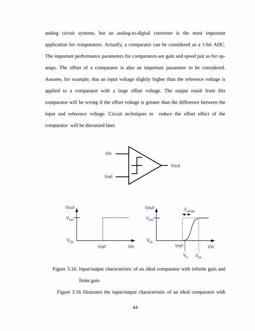
analog circuit systems, but an analog-to-digital converter is the most important
application for comparators. Actually, a comparator can be considered as a 1-bit ADC.
The important performance parameters for comparators are gain and speed just as for op-
amps. The offset of a comparator is also an important parameter to be considered.
Assume, for example, that an input voltage slightly higher than the reference voltage is
applied to a comparator with a large offset voltage. The output result from this
comparator will be wrong if the offset voltage is greater than the difference between the
input and reference voltage. Circuit techniques to reduce the offset effect of the
comparator will be discussed later.
Vin
Vref
Vout
Vin
Vout
VOH
VOL
Vref
Voffset
VIL VHL
Vin
Vout
VOH
VOL
Vref
Figure 3.16: Input/output characteristic of an ideal comparator with infinite gain and
finite gain
Figure 3.16 illustrates the input/output characteristic of an ideal comparator with
44

infinite gain, and showing a steep transition at Vref. A high gain op-amp in open-loop
configuration can be used to mimic an ideal comparator, but its performance will be
limited by non-idealities such as finite gain and offset voltage. The input/output
characteristics of a comparator implemented with a high-gain op-amp is shown in Figure
3.16. Comparator speed is another important non-ideality to consider. Because of its slow
response, an op-amp type comparator is seldom used in high-speed applications.
Regenerative latches can be used as comparators for high-speed applications. One of the
CMOS regenerative latches [37] is depicted in Figure 3.17.
M2
M4 M5
M3
M1φ
BASA SB
φ φVinA VinB
VoutA VoutB
Figure 3.17: A CMOS regenerative latch
When the clock Φ is low, two switches SA and SB are closed, and transistor M1 is
turned off. The two nodes A and B are connected to the inputs and charged to different
input voltages, VinA and VinB, respectively. When the clock Φ is high, two switches SA
and SB are opened, disconnecting nodes A and B from inputs VinA and VinB. The transistor
45

M1 is turned on and starts regeneration. The small voltage difference between nodes A
and B is then amplified because of a positive feedback to the digital logic levels. The time
domain behavior and time constant of the latch in its regeneration phase can be studied
with a simple latch circuit comprising two back-to-back amplifiers with a single-pole
response. It is shown in Figure 3.18. The simplified small-signal circuit of the latch [66]
is shown in Figure 3.19.
CL CL
VA VB
Figure 3.18: A simple latch circuit comprising back-to-back inverters
roCL
gmVB
VA
roCL
gmVA
VB
Figure 3.19: A simplified small-signal circuit of a latch
From the small-signal equivalent circuit, we can write
0=⋅++⋅dt
dVCrVVg B
Lo
BAm ( eq.3.2.34 )
46

0=⋅++⋅dt
dVCrVVg A
Lo
ABm ( eq.3.2.35 )
Dividing the above equation by and rearranging them, we have or
dtdVrCVVrg B
oLBAom ⋅⋅−=+⋅⋅ ( eq.3.2.36 )
dtdVrCVVrg A
oLABom ⋅⋅−=+⋅⋅ ( eq.3.2.37)
We can rewrite equations eq.3.2.36 and eq.3.2.37.
dtdVVVA B
BA ⋅−=+⋅ τ ( eq.3.2.38)
dtdVVVA A
AB ⋅−=+⋅ τ ( eq.3.2.39)
where A is the gain and τ is the time constant of the amplifier.
Subtracting eq.3.2.38 from eq.3.2.39, we can have
( ) ( )( )
dtVVd
AVV BA
BA−
⋅−
=−1
τ ( eq.3.2.40)
Solving eq.3.2.40 with the initial voltage VAB0, we have
( )⎥⎦⎤
⎢⎣⎡ −⋅
⋅=− τ1
0
At
ABBA eVVV ( eq.3.2.41)
Assuming A>>1, the settling time constant of the latch can be given by
m
LL g
CA=≅
ττ ( eq.3.2.42)
From the eq.3.2.41, we can find the fact that the exponential function has the positive
argument, therefore the latch output reaches its digital logic level very quickly as time
increases. The speed of the latch can be increased by increasing transconductance and
reducing the load capacitance of the amplifier. The time domain response behavior of the
47
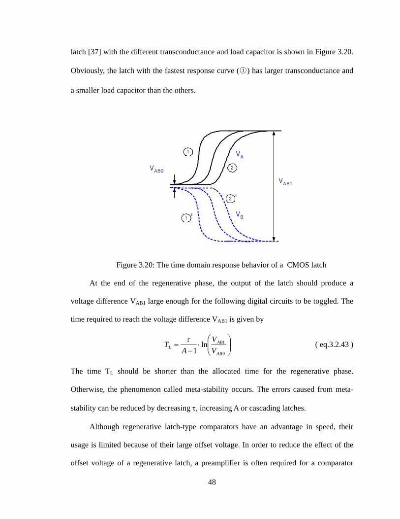
latch [37] with the different transconductance and load capacitor is shown in Figure 3.20.
Obviously, the latch with the fastest response curve (○1 ) has larger transconductance and
a smaller load capacitor than the others.
VAB0
VAB1
VA
VB
1
2
1 '
2 '
Figure 3.20: The time domain response behavior of a CMOS latch
At the end of the regenerative phase, the output of the latch should produce a
voltage difference VAB1 large enough for the following digital circuits to be toggled. The
time required to reach the voltage difference VAB1 is given by
⎟⎟⎠
⎞⎜⎜⎝
⎛⋅
−=
0
1ln1 AB
ABL V
VA
T τ ( eq.3.2.43 )
The time TL should be shorter than the allocated time for the regenerative phase.
Otherwise, the phenomenon called meta-stability occurs. The errors caused from meta-
stability can be reduced by decreasing τ, increasing A or cascading latches.
Although regenerative latch-type comparators have an advantage in speed, their
usage is limited because of their large offset voltage. In order to reduce the effect of the
offset voltage of a regenerative latch, a preamplifier is often required for a comparator
48

that is used in ADC. The preamplifier is placed in front of the latch as shown in Figure
3.21. The preamplifier enlarges the difference between the input and reference voltage so
that the comparator can perform a more precise comparison than a latch-type comparator
alone. Another disadvantage of using the latch-type comparator is its large kickback noise
from the latch circuit. The kickback noise is generated during regeneration and corrupts
the input signal and reference voltage. The preamplifier can reduce the effect of the
kickback noise from the latch.
Latch
CLK
Vout
Vin
Vref
A
Figure 3.21: A comparator comprising of a preamplifier and a latch
For higher accuracy comparison, the preamplifier needs to have high gain. When a
single stage amplifier is used as the preamplifier, increasing the gain usually means
decreasing bandwidth because of the increasing time constant because of the large value
of the output resistance. Thus, a high gain single-stage preamplifier is not suitable for
high-speed applications. For high-speed, high-resolution comparison, low-gain multistage
preamplifiers can be used instead of a high-gain single-stage preamplifier.
The penalty for using preamplifiers is higher power dissipation. Not like the
regenerative latch that consumes only dynamic power, the preamplifier consumes static
power that requires dc bias current. The dynamic power dissipation of the latch is
relatively small compared with static power dissipation of the preamplifier because the
49

transistors in the latch of Figure 3.17 are on for only a short time only during the
regenerative phase. Thus, the power dissipation of a comparator is usually determined by
the number of preamplifiers used in the comparators.
3.2.4.1 COMPARATOR OFFSET CANCELLATION TECHNIQUE
One of the main factors that limit the resolution of the comparator is the offset
voltage caused by mismatches of the MOS devices. Simple methods such as fuse and
laser trimming can be utilized to reduce errors caused by these mismatches. However
these approaches require high cost, extra time and take up large area. Besides, these
cancellation methods eliminate the offset voltage variation over time and temperature.
A better way to cancel an offset voltage is called the auto-zeroing technique [66,37].
The principle of this technique is as follows. First, the offset voltage is measured and
stored in a capacitor. Then, this stored offset voltage is added to the input voltage and
eventually the offset voltage is cancelled by itself. Since this process is repeated by
clocks, the offset voltage variation is reduced.
There are two different auto-zeroing techniques. One is called the Input Offset
Storage ( IOS ) technique [60] and the other is called the Output Offset Storage ( OOS )
technique [60]. A simplified single-ended comparator with the IOS technique is shown in
Figure 3.22.
50

2Φ
1Φ
Cs
1Φ
S1
S2
S3
Voff
Latch
CLK
Vout
Vin
Figure 3.22: A comparator with input offset storage technique
It consists of a preamplifier, a latch, and a capacitor for offset storage, switches, and
two nonoverlapping clock phases. The operation is as follows. During the offset
cancellation mode or Φ1 clock phase, switches S1, and S2 are turned on while switch S3 is
turned off. This will create a unity-gain feedback loop around the preamplifier, and the
sampling capacitor Cs will be charged with the offset voltage of the preamplifier, which is
shown in Figure 3.23
Cs
S1
S2
S3
Voff
Latch
CLK
Vout
Vin
Figure 3.23: IOS comparator in Φ1 clock phase
During the tracking mode or Φ2 clock phase, switches S1, and S2 are turned off,
which opens the feedback loop. The switch S3 is on, and the sampling capacitor is
51

connected to the input signal. This is shown in Figure 3.24.
Vx
S1
S2
S3
Voff
Latch
CLK
Vout
Vin
Voff
Figure 3.24: IOS comparator in Φ2 clock phase.
The voltage at the negative input of the preamplifier is equal to . Since the
node voltage at the positive input is , the difference between the two inputs of the
preamplifier is only , resulting in
offin VV +
offV
inV inVA ⋅ at the output of the preamplifier. Then, the
latch is strobed so that A> digital logic level is produced at its output.
In addition to the offset voltage of a preamplifier, other non-idealities can
contribute to total comparator offset. These are charge injection from switch S1 and
another offset voltage from a latch. Offset voltage caused by switch S1 can be minimized
by using a small transistor for S1 or by increasing the value of the sampling capacitor Cs.
An alternative method to reduce offset voltage from charge injection is to place a much
smaller size transistor, S1a, parallel with S1. The additional switch, S1a, is operated by the
delayed version of clock phase Φ1. Hence, S1 is turned off slightly earlier than S1a. In this
way, when S1 is off, the charge from S1 is absorbed by S1a reducing some of the charge
that otherwise would go to sampling capacitor Cs. The effect from S1a is minimized
because S1a is a much smaller device than S1
52

The other comparator offset cancellation technique, OOS, is shown in Figure 3.25.
This output offset storage technique measures the output offset of a preamplifier by
connecting preamplifier inputs to ground and stores offset voltage on a coupling capacitor
at the output of a preamplifier.
2Φ
1Φ
Cs
S2
S3
Voff
Latch
CLK
Vout
Vin
S1 1Φ
Figure 3.25: A comparator with output offset storage technique
The components of an OOS comparator are basically the same as an IOS
comparator. However, some of their positioning differs from IOS topology. Especially
noteworth positioning is the placement of the capacitor between a preamplifier and a
latch to store an offset voltage of a pre-amplifier. The operation is as follows. During the
offset cancellation mode or Φ1 clock phase, switches S1 and S2 are turned on while switch
S3 is turned off as shown in Figure 3.26. The inputs of both the preamplifier and the latch
are connected to ground. The preamplifier only amplifies the offset voltage producing
at the output, where A and are the gain and the offset of the preamplifier,
respectively. The amplified offset voltage
offVA ⋅ offV
offVA ⋅ is then stored on Cs.
53
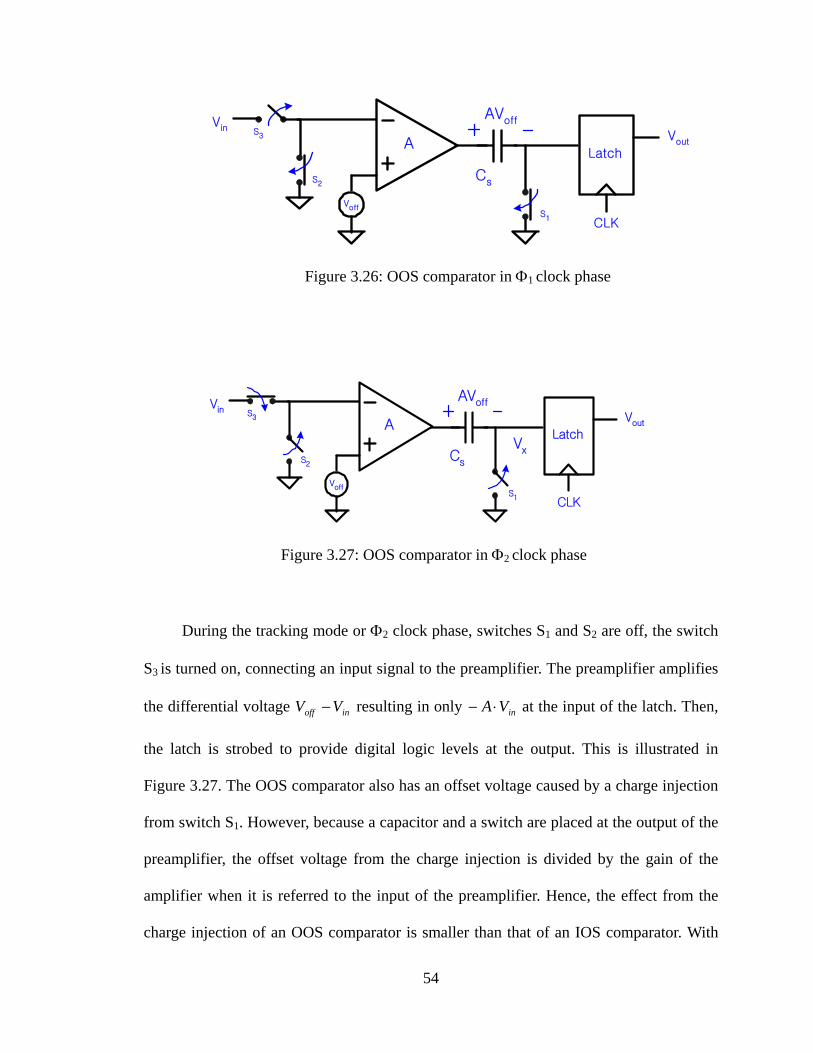
CsS2
S3
Voff
Latch
CLK
Vout
Vin
S1
AVoff
A
Figure 3.26: OOS comparator in Φ1 clock phase
CsS2
S3
Voff
Latch
CLK
Vout
Vin
S1
AVoff
AVx
Figure 3.27: OOS comparator in Φ2 clock phase
During the tracking mode or Φ2 clock phase, switches S1 and S2 are off, the switch
S3 is turned on, connecting an input signal to the preamplifier. The preamplifier amplifies
the differential voltage resulting in only inoff VV − inVA ⋅− at the input of the latch. Then,
the latch is strobed to provide digital logic levels at the output. This is illustrated in
Figure 3.27. The OOS comparator also has an offset voltage caused by a charge injection
from switch S1. However, because a capacitor and a switch are placed at the output of the
preamplifier, the offset voltage from the charge injection is divided by the gain of the
amplifier when it is referred to the input of the preamplifier. Hence, the effect from the
charge injection of an OOS comparator is smaller than that of an IOS comparator. With
54

OOS topology, the gain of a preamplifier should be low because a preamplifier is used in
an open-loop configuration. If the gain of a preamplifier is too high, the output of a
preamplifier maybe saturated by its own offset voltage. The input common-mode range
of an OOS comparator is limited because the input of a comparator is DC coupled with
an input source. In order to achieve higher accuracy comparison, a combination of these
two offset cancellation techniques, or a multistage OOS topology, can be used
3.3 NON-IDEAL ERROR SOURCES IN PIPELINE STAGES
3.3.1 ERROR IN SUB-ADC
The offset voltage of comparators is a main source of errors in the sub-ADC of a
pipeline ADC. A comparator produces an output signal indicating whether or not an input
signal is larger than a reference level. When an offset voltage exists in a comparator, the
offset voltage acts as an additional reference level and results in increasing or decreasing
the overall reference level of a comparator. Therefore, when an input signal is close to an
original reference level, a comparator may make a wrong decision. Several sources cause
the offset voltage in a comparator, but device mismatch is a main source of errors that
occur. The effect of an offset error in a comparator on a 1.5-bit stage transfer function is
shown in Figure 3.28. The dotted line represents an ideal transfer function, and the solid
line shows a transfer function with an offset voltage in a comparator.
55

Vin
Vout
4refV
− 4refV
Figure 3.28: Effect of a comparator offset voltage on a 1.5-bit stage transfer
function
3.3.2 THERMAL NOISE
Unpredictable errors occur in pipeline ADCs and they cannot be fixed because of
their randomness. One dominant source of these errors is thermal noise generated by
random movement of electrons in resistors. The thermal noise [36] of a resistor appears
as white noise and its power spectral density is given by
fKTReR ∆⋅= 42 ( eq.3.3.1 )
where K is Boltsmann’s constant (1.38×10⁻²³ JK-1), T is the temperature in Kelvin’s and R
is the resistor value.
56

CLK
Vin
C
VoutVin
C
Vout
R2Re
Figure 3.29 (a) Simple MOS sampling circuit (b) its equivalent circuit with on-resistance
and thermal noise
In the sampling circuit, thermal noise is produced due to finite resistance of a MOS
transistor switch and is stored in a sampling capacitor. A simple sampling circuit is
illustrated in Figure 3.29 (a) and in Figure 3.29 (b). A MOS switch is replaced with a
turn-on resistance and its thermal noise voltage source. The thermal noise of a switch is
filtered by a single pole response low-pass filter created by the resistance of a switch and
a sampling capacitor. The transfer function of the low-pass filter is
( )RCj
jAω
ω+
=1
1 ( eq.3.3.2)
The total noise power can be obtained by integrating noise power spectral density over
frequency and is given by
( )∫∞
⋅⋅=0
222, 2
1 ωωπ
djAee Routn ( eq.3.3.3 )
( )∫∞
⋅+
=0
214
21 ω
ωπd
RCKTR
( eq.3.3.4 )
57

( ) ∞⋅⋅
⋅= 0|arctan421 RC
CRKTR ω
π ( eq.3.3.5)
CKT
= ( eq.3.3.6)
From the above expression, it is obvious why noise in a sampling circuit is called
noise. It is also interesting to know that there is no resistance value at the expression,
which indicates that total noise power is independent of the resistance value of a switch.
This is because the increase of thermal noise power caused by increasing the resistance
value is cancelled in turn by the decreasing bandwidth of a low-pass filter. Therefore, the
only way to reduce thermal noise of a sampling network is to increase sampling capacitor
size.
CKT /
3.3.3 SWITCHES
Most pipelined ADCs are implemented with SC circuits, and MOS transistors are
used as switches. These MOS switches cause non-idealities and errors, and require
attention before any effort is undertaken to design SC pipelined ADCs. The main errors
of MOS switches are clock feedthrough, charge injection [25, 26, 27] and the nonlinear
turn-on resistance of a MOS transistor.
58
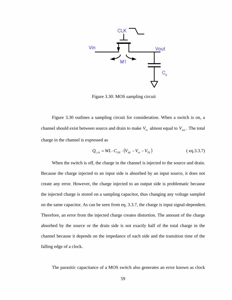
CLK
Vin
Cs
Vout
M1
Figure 3.30: MOS sampling circuit
Figure 3.30 outlines a sampling circuit for consideration. When a switch is on, a
channel should exist between source and drain to make almost equal to . The total
charge in the channel is expressed as
inV outV
( )ThinddOXcht VVVCWLQ −−⋅⋅=, ( eq.3.3.7)
When the switch is off, the charge in the channel is injected to the source and drain.
Because the charge injected to an input side is absorbed by an input source, it does not
create any error. However, the charge injected to an output side is problematic because
the injected charge is stored on a sampling capacitor, thus changing any voltage sampled
on the same capacitor. As can be seen from eq. 3.3.7, the charge is input signal-dependent.
Therefore, an error from the injected charge creates distortion. The amount of the charge
absorbed by the source or the drain side is not exactly half of the total charge in the
channel because it depends on the impedance of each side and the transition time of the
falling edge of a clock.
The parasitic capacitance of a MOS switch also generates an error known as clock
59

feedthrough. A clock signal is coupled to a sampling capacitor through a gate-source or a
gate-drain parasitic capacitor, creating an error in a sampled voltage on the same
capacitor. The size of a clock feedthrough error depends on the size of the parasitic
capacitor and the transition time of the rising/falling edge of a clock signal. Both clock
injection and clock feedthrough can be minimized by the same circuit techniques.
One approach to minimize these errors is to use a dummy switch as shown in
Figure 3.31.
CLK
Vin
Cs
Vout
M1
CLK
M2
Figure 3.31: MOS sampling circuit with a dummy switch
The switch M2 is used as a dummy and its source and drain are short-circuited. The
size of the dummy switch M2 is half of the real switch M1 and the dummy switch is
driven by an inverse clock waveform of the real switch. When M1 is off, M2 is on. The
channel charge from M1 is not injected to a sampling capacitor but absorbed by the
dummy switch M2 effectively canceling a charge injection error. With this method, the
effect of clock feedthrough is also minimized because error voltages from both switches
are equal and have opposite polarity. Similar charge injection cancellation can be
achieved by using the same size NMOS and PMOS transistors forming a CMOS
60

transmission gate. When a transmission gate is turned off, an opposite charge error
injected by both NMOS and PMOS switches reduces the effect of charge injection. The
most popular way to reduce a charge injection error use a bottom plate sampling
technique. A signal-dependent charge injection error introduces non-linear distortion. If a
switch is operated with a fixed voltage, an error generated from an injected charge will be
a constant error. A constant error can be minimized with a differential circuit
configuration.
A sampling circuit with a bottom plate sampling technique [28] and its operating
clock phases are shown in Figure 3.32. The operation of the sampling circuit is as follows.
In sampling clock phase (○1 ), switches S1 and S3 are turned on, and an input signal is
stored to a sampling capacitor. At the instant of ○2 , switch S3 is turned off, and the input
signal is sampled to capacitor Cs, which leaves node ○B floating. The charge injected from
switch S3 is not harmful because it is always connected to ground, resulting in a constant
error at the output. A moment later at ○3 , switch S1 is turned off, but the channel charge
from switch S1 is not injected to the sampling capacitor because there is no DC path from
node ○B . In the holding clock phase, switches S2 and S4 are closed, transferring the
charge to another capacitor. The charge injected from these switches is also not harmful
because switch S2 is connected to ground. Switch S4 is usually connected to virtual
ground at the input of the amplifier.
61

Vin Vout
S1
S2 S3
S4
1φ
2φ p1φ
p2φA B
1φ
p1φ
2φ
p2φ
1 2 3
Figure 3.32: A sampling circuit with a bottom plate sampling technique and its operating
clock phases
The turn-on resistance of a MOS switch is given by
( )ThgsOXn
ON
VVL
WCR
−⎟⎠⎞
⎜⎝⎛
=µ
1 ( eq.3.3.8)
( )ThinDDOXn VVVL
WC −−⎟⎠⎞
⎜⎝⎛
=µ
1 ( eq.3.3.9)
where nµ is the mobility of electrons, COX is the gate oxide capacitance, VTh is a
threshold voltage, and W and L are the width and the length of a MOS transistor. From
62

eq.3.3.9, the turn-on resistance of a MOS switch is input signal-dependent and creates
non-linear distortion. The non-linearity of a switch can be improved by using a CMOS
transmission gate instead of using a single transistor (NMOS or PMOS). For high
resolution ADCs, high linearity may not be achieved by a CMOS transmission gate. For
high linearity, there is a special technique called bootstrapping. The basic idea of
bootstrapping [29] comes from eq.3.3.8. From eq.3.3.8, the linearity of a MOS switch
can be improved significantly if Vgs is kept constant no matter how Vin changes. This idea
is illustrated in Figure3.33.
Vin Vout
Vbat
Figure 3.33: Principle of a bootstrapped switch
A battery voltage, Vbat, can be added between the gate and the source of a switch.
When the switch is turned on, the gate voltage Vg will always be (Vbat+Vin ), which
makes the gate-source voltage Vgs constant. The question now is how a battery is
implemented by circuits. It can be implemented by a switched capacitor circuit and is
illustrated in Figure 3.34 (a) and (b).
63

Vin Vout
Cbat
Vdd
(a)
Vin Vout
Cbat
Vdd
(b)
Figure 3.34: Switched-capacitor implementation of the bootstrapped switch : (a)
Off state (b) On state
The bootstrapped switch in Figure 3.34 (a) shows when a switch is turned off. A
NMOS switch is connected to ground while capacitor Cbat is charged to a supply voltage.
In the next clock phase, capacitor Cbat, now charged to Vdd, is connected between the gate
and the source of the switch and acts like a constant DC voltage. It is shown in Figure
3.34 (b).
3.3.4 FINITE DC GAIN OF OPERATIONAL AMPLIFIERS
An op-amp is one of the most important building blocks in switched capacitor
implementation of pipelined ADCs. Therefore, it is necessary to study the impact of the
64

non-idealities of op-amps on pipelined ADCs. First, we will analyze the effect of a finite
op-amp open loop gain in MDACs. The circuit configuration of a 1.5-bit MDAC is
illustrated in Figure 3.9. Capacitance Cp is the input parasitic capacitance of an op-amp.
The finite DC gain of the op-amp is A0.
During the sampling phase, a sampling capacitor Cs and a feedback capacitor Cf are
connected to an input, sampling an input signal on the capacitors. The total charge stored
on capacitors Cs and Cf on the sampling phase is expressed as
( ) ( )fsins CCVq +⋅−= 0 ( eq.3.3.10)
During the amplifying phase, feedback capacitor Cf is connected to the output of the op-
amp and sampling capacitor Cs is connected to ±Vref or to ground depending on the
output of a sub-ADC. The total charge stored during this clock phase is given by
( ) ( ) pfoutsrefa CVCVVCVsVq ⋅+⋅−+⋅⋅−= −−− ( eq.3.3.11)
where V- is the negative input of the op-amp, and S is the selection signal from the sub-
ADC and its value can be ±1 or 0.
The total charge is conserved. Therefore,
as qq = ( eq.3.3.12)
From the above equation, we can find
f
sref
f
pfs
f
fsinout C
CVs
CCCC
VC
CCVV ⋅⋅−⎟
⎟⎠
⎞⎜⎜⎝
⎛ ++⋅+⎟
⎟⎠
⎞⎜⎜⎝
⎛ +⋅= − ( eq.3.3.13)
The feedback factor β tells how much of the output voltage of an op-amp is fed back to
an op-amp input and is given by
pfs
s
CCCC
++=β ( eq.3.3.14)
65
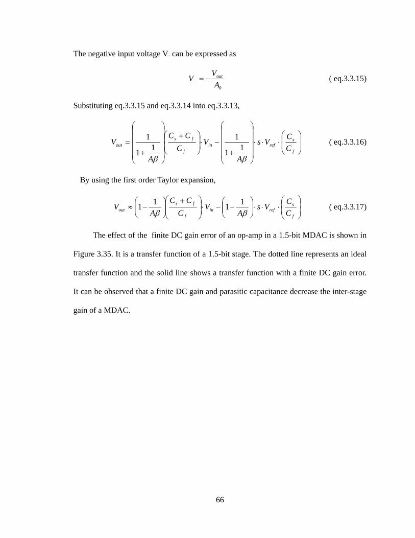
The negative input voltage V- can be expressed as
0AV
V out−=− ( eq.3.3.15)
Substituting eq.3.3.15 and eq.3.3.14 into eq.3.3.13,
⎟⎟⎠
⎞⎜⎜⎝
⎛⋅⋅⋅
⎟⎟⎟⎟
⎠
⎞
⎜⎜⎜⎜
⎝
⎛
+−⋅⎟
⎟⎠
⎞⎜⎜⎝
⎛ +
⎟⎟⎟⎟
⎠
⎞
⎜⎜⎜⎜
⎝
⎛
+=
f
srefin
f
fsout C
CVs
A
VC
CC
A
V
ββ11
111
1 ( eq.3.3.16)
By using the first order Taylor expansion,
⎟⎟⎠
⎞⎜⎜⎝
⎛⋅⋅⋅⎟⎟
⎠
⎞⎜⎜⎝
⎛−−⋅⎟
⎟⎠
⎞⎜⎜⎝
⎛ +⎟⎟⎠
⎞⎜⎜⎝
⎛−≈
f
srefin
f
fsout C
CVs
AV
CCC
AV
ββ1111 ( eq.3.3.17)
The effect of the finite DC gain error of an op-amp in a 1.5-bit MDAC is shown in
Figure 3.35. It is a transfer function of a 1.5-bit stage. The dotted line represents an ideal
transfer function and the solid line shows a transfer function with a finite DC gain error.
It can be observed that a finite DC gain and parasitic capacitance decrease the inter-stage
gain of a MDAC.
66
Vout
4refV
− 4refV
Figure 3.35: Finite DC gain effect on a 1.5-bit stage transfer function
3.3.5 FINITE BANDWIDTH OF OPERATIONAL
AMPLIFIERS
The finite gain bandwidth of an op-amp is another important non-ideality to study
in designing pipelined ADCs. Assuming a linear settling single-pole response and an
infinite DC gain of an op-amp, an output voltage of a MDAC can be written as
( )⎪⎭
⎪⎬⎫
⎪⎩
⎪⎨⎧
⎟⎟⎠
⎞⎜⎜⎝
⎛⋅−⋅⎟
⎟⎠
⎞⎜⎜⎝
⎛ +−≅ −
f
srefin
f
fstout C
CVsV
CCC
eV s τ/1 ( eq.3.3.18 )
where ts is a settling time and τ is a time constant of a MDAC in a closed-loop form. The
time constant τ is given by
67

βωωτ
⋅==
− udB
11
3
( eq.3.3.19 )
where ω-3dB is –3dB frequency of a MDAC, β is a feedback factor and ωu is the unity-
gain bandwidth of an op-amp. The unity-gain bandwidth of a single stage op-amp is
given by
L
mu C
g=ω ( eq.3.3.20)
where CL is total output load capacitance and gm is transconductance of an op-amp. The
total output load capacitance CL in the amplifying clock phase is
( )nectcomp
fps
psfL CC
CCCCCC
C ++++
+= ( eq.3.3.21 )
where Ccomp is the total capacitance of a next stage sub-ADC and Cnext is the total
capacitance of a next stage MDAC in a sampling mode.
The settling error of an op-amp in a MDAC is
τε /stes−= ( eq.3.3.22 )
⎪⎪
⎭
⎪⎪
⎬
⎫
⎪⎪
⎩
⎪⎪
⎨
⎧⎟⎠⎞
⎜⎝⎛
++++
+⋅⋅−
=
nextCcompCfCpCsC
pCsCfCmgst
e
/β
( eq.3.3.23 )
The result of a settling error due to the finite gain bandwidth of an op-amp in a 1.5-
bit MDAC is shown in Figure 3.36. The dotted line represents an ideal transfer function
and the solid line shows a transfer function with a finite gain bandwidth.
The settling behavior of an op-amp in actual switched capacitor circuits is not
entirely linear. Therefore, a settling error is largest when an input voltage is at ±Vref
because an output voltage should change to a full scale. The settling error produces
68

harmonic distortion at the output. Therefore, the gain bandwidth of an op-amp in a
MDAC should be large enough to avoid harmonic distortion due to the settling error.
Vin
Vout
4refV
−4refV
Figure 3.36: Finite gain bandwidth effect on a 1.5-bit stage transfer function
3.3.6 CAPACITOR MISMATCH
The gain of a SC MDAC is decided by a capacitor ratio. Thus, accurate capacitor
matching is required to design a high resolution pipelined ADC. The integrated circuit
capacitor value is given by
oxOX
OX CAt
AC ⋅== 111ε
( eq.3.3.24 )
where A1 is the area of a capacitor, εOX is the dielectric constant of silicon dioxide, tOX is
the thickness of oxide, and Cox is capacitance per unit area. Capacitance value depends on
the area and oxide thickness of a capacitor. The main causes of capacitor mismatch are
69
due to over-etching and the oxide-thickness gradient.
The relative capacitance error can be expressed by
11 AA
CC
CC
OX
OX ∆+
∆=
∆ ( eq.3.3.25 )
where is an error in COXC∆ ox due to oxide-thickness gradient and is an error in area
A
A∆
1 due to over-etching.
Since Cox is fixed by a process technology, the accuracy of capacitance can be
improved by simply increasing the area. However, in SC circuits the accuracy of a
capacitor ratio is more of concern more than the accuracy of capacitance because the gain
of a MDAC is decided by the capacitor ratio.
The integrated circuit capacitor can be defined as
CCC ∆+= 1'1 ( eq.3.3.26 )
where is the mismatch error of capacitor CC∆ 1.
Then, the ratio of to can be written as '2C '
1C
11
22'1
'2
CCCC
CC
∆+∆+
= ( eq.3.3.27 )
And can be approximated as
⎥⎦
⎤⎢⎣
⎡ ∆+
∆−⋅≅
2
2
1
1
1
2 1CC
CC
CC
( eq.3.3.28 )
The relative error of a capacitor ratio is
2
2
1
1
12
12
CC
CC
CCCC ∆
+∆
−≅∆ ( eq.3.3.29 )
Therefore, the accuracy of a capacitor ratio can be improved if the difference of the
mismatch errors of both capacitors is as small as possible. A mismatch error in the
70

accuracy of a capacitor ratio due to over-etching can be minimized by implementing
capacitors with an array of small equal sized unit capacitors [23]. A mismatch error in the
ratio accuracy of capacitors due to the variation of oxide thickness can be minimized by
laying out capacitors in common centroid geometry.
The output voltage of a MDAC with capacitor mismatch can be written as
⎟⎟⎠
⎞⎜⎜⎝
⎛∆+
∆+⋅⋅−⋅⎟
⎟⎠
⎞⎜⎜⎝
⎛
∆+
∆++∆+≅
ss
ffrefin
ff
ffssout CC
CCVSV
CCCCCC
V ( eq.3.3.30 )
If we let Cs = Cf = C and ε=∆ CC , then
( ) ( )2121 12 εεεε +−⋅⋅−⋅+−≅ refinout VSVV ( eq.3.3.31 )
The influence of capacitor mismatch on the transfer function of a 1.5-bit MDAC is
illustrated in Figure 3.37. The dotted line represents an ideal transfer function and the
solid line shows a transfer function with capacitor mismatch.
Vout
4refV
− 4refV
Figure 3.37: Capacitor mismatch effect on a 1.5-bit stage transfer function
71
An interesting fact from the above figure is that when an input voltage is equal to
±Vref, no error occurs even with capacitor mismatch. This can be checked with eq. 3.3.30.
Substituting Vref into Vin in eq. 3.3.30 and letting S = 1,
⎟⎟⎠
⎞⎜⎜⎝
⎛∆+
∆+⋅−⋅⎟
⎟⎠
⎞⎜⎜⎝
⎛
∆+
∆++∆+≅
ss
ffrefin
ff
ffssout CC
CCVV
CCCCCC
V ( eq.3.3.32)
refrefss
ss VVCCCC
=⋅∆+∆+
= ( eq.3.3.33 )
Capacitor mismatch is one of the limiting factors in designing high resolution
pipeline ADCs. Special techniques such as capacitor error averaging, capacitor trimming
and digital calibration are required to overcome this problem.
3.4 SUMMARY
This chapter has presented an overview of a pipelined ADC. A technique to correct
digital errors, with examples, has been described, and the basic building blocks of a
switched-capacitor pipelined ADC have been surveyed. An overview of various non-ideal
error sources in a pipeline ADC has also been presented, and the sources of these areas
have been reviewed. These error sources comparator offset, thermal noise, charge
injection, finite op-amp gain, finite settling time and capacitor mismatch.
72

C H A P T E R 4 : A S Y S T E M A T I C D E S I G N
A P P R O A C H F O R A P O W E R O P T I M I Z E D
P I P E L I N E A D C
A pipeline ADC consists of several stages. Stage resolution can be decided
arbitrarily. It could be 2-bit, 3-bit, 4-bit or even 5-bits. Then the question becomes, what
is the optimum resolution per stage in terms of low power dissipation? This question can
not be easily answered. In order to find a solution, a power optimization algorithm will be
developed.
In the next section, the design requirements of a MDAC are discussed to find
stage accuracy. After that, recent pipeline architectures are reviewed. Lastly, a power
optimization algorithm and its numerical results are explained.
4.1 DESIGN REQUIREMENTS
There are several non-ideal effects that limit the performance of a pipeline ADC,
when that is implemented with SC circuits. Among non-ideal effects, finite op-amp gain,
incomplete settling, mismatches, and thermal noise are of important to the overall
performance [20].
73
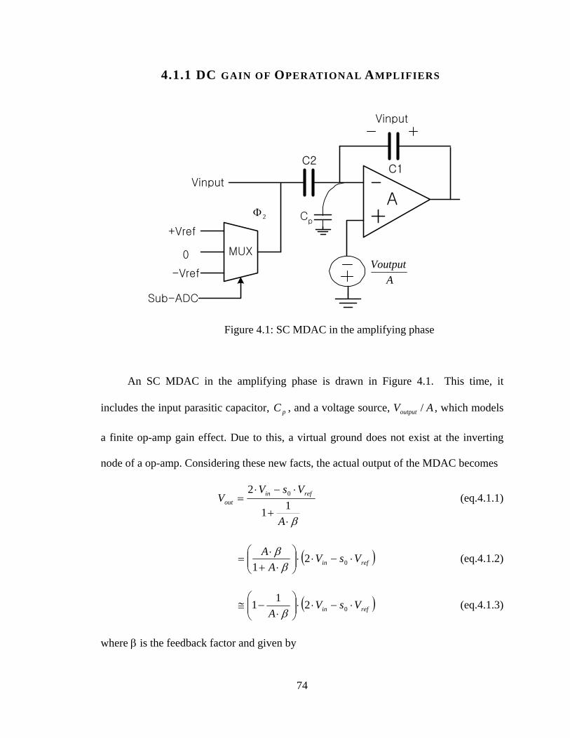
4.1.1 DC GAIN OF OPERATIONAL AMPLIFIERS
C2
2Φ
C1Vinput
MUX
Sub-ADC
+Vref
-Vref
0
Vinput
AVoutput
ACp
Figure 4.1: SC MDAC in the amplifying phase
An SC MDAC in the amplifying phase is drawn in Figure 4.1. This time, it
includes the input parasitic capacitor, , and a voltage source, , which models
a finite op-amp gain effect. Due to this, a virtual ground does not exist at the inverting
node of a op-amp. Considering these new facts, the actual output of the MDAC becomes
pC AVoutput /
β⋅+
⋅−⋅=
A
VsVV refin
out 11
2 0 (eq.4.1.1)
( refin VsVA
A⋅−⋅⋅⎟⎟
⎠
⎞⎜⎜⎝
⎛⋅+
⋅= 02
1 ββ ) (eq.4.1.2)
( refin VsVA
⋅−⋅⋅⎟⎟⎠
⎞⎜⎜⎝
⎛⋅
−≅ 0211β
) (eq.4.1.3)
where β is the feedback factor and given by
74

pCCCC
++=
21
1β (eq.4.1.4)
4.1.2 BANDWIDTH OF OPERATIONAL AMPLIFIERS
This discussion of the bandwidth of operational amplifiers will ignore momentarily
the finite op-amp gain effect and assume an op-amp has a single-pole. Due to the finite
bandwidth of an op-amp, an output needs time to reach its final value. Including this
effect, the actual output of a MDAC in Figure 4.1 is [19]
( refin
t
out VsVeV ⋅−⋅⋅⎟⎟⎠
⎞⎜⎜⎝
⎛−=
−
021 τ ) (eq.4.1.5)
where t is the available settling time, which is usually a little bit less than half of the one
clock cycle, and τ is the time constant of a MDAC in a closed-loop configuration. The
time constant, τ, is
uadB ωβωτ
⋅==
−
11
3
(eq.4.1.6)
where dB3−ω is the frequency of a MDAC in a closed-loop configuration and uaω is the
unity-gain frequency of an op-amp. The settling time due to the finite bandwidth limits
the speed of a SC pipeline ADC. When an op-amp is designed for a MDAC, the op-amp
should be designed to have wide enough bandwidth so that the output of the MDAC
settles to its final value with allowable accuracy. Otherwise, an incomplete settling error
appears as an gain error and degrades ADC performance, a situation discussed in a
previous section.
75

4.1.3 CAPACITOR MISMATCH
Capacitor mismatch is another error source that significantly degrades ADC
performance. It is mostly caused by over-etching [15] and the variation of oxide-
thickness [23]. Although a capacitor mismatch error can be minimized by using larger
capacitors realized with the parallel combination of a unit capacitor and common-
centroid layout technique [14], it still exists in circuits and affects the output result of a
MDAC. Eq. 4.1.12 can be re-written as
( ) ( )( )
( )( ) refinout V
CCsV
CCCV ⋅⎟⎟
⎠
⎞⎜⎜⎝
⎛++
⋅−⋅⎟⎟⎠
⎞⎜⎜⎝
⎛+
+++=
1
20
1
21
11
111
εε
εεε (eq.4.1.7)
where ε is the relative mismatch error of a capacitor C. If we assume and ignore high
order terms, then
( ) ( ) refinout VsVV ⋅+−⋅−⋅+−≅ 21021 12 εεεε (eq.4.1.8)
Assume C2 is larger than C by ∆C/2 and C1 is smaller than C by ∆C/2 where C is desired
capacitor value without a mismatch. We can say
CC
22∆
=ε (eq.4.1.9)
CC
22∆
−=ε (eq.4.1.10)
Therefore, the actual output of a MDAC becomes
refinout VCCsV
CCV ⋅⎟
⎠⎞
⎜⎝⎛ ∆+⋅−⋅⎟
⎠⎞
⎜⎝⎛ ∆
+≅ 12 0 (eq.4.1.11)
76
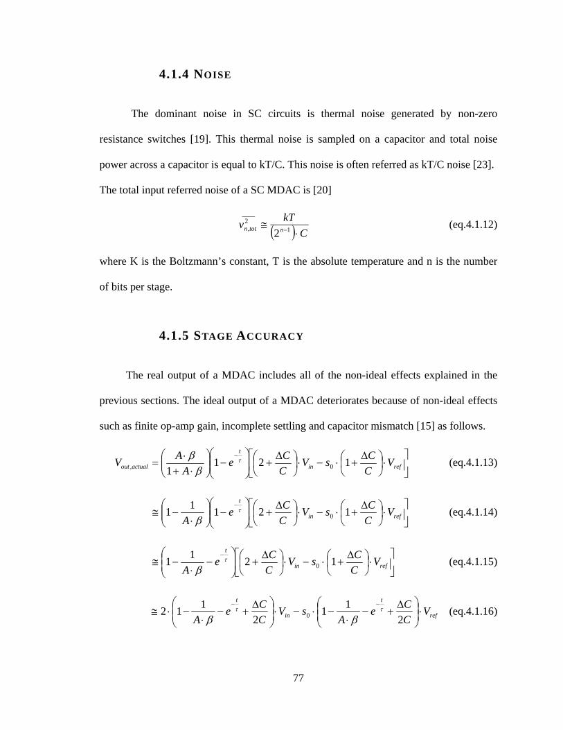
4.1.4 NOISE
The dominant noise in SC circuits is thermal noise generated by non-zero
resistance switches [19]. This thermal noise is sampled on a capacitor and total noise
power across a capacitor is equal to kT/C. This noise is often referred as kT/C noise [23].
The total input referred noise of a SC MDAC is [20]
( ) CkTv ntotn ⋅
≅ −1
____2, 2
(eq.4.1.12)
where K is the Boltzmann’s constant, T is the absolute temperature and n is the number
of bits per stage.
4.1.5 STAGE ACCURACY
The real output of a MDAC includes all of the non-ideal effects explained in the
previous sections. The ideal output of a MDAC deteriorates because of non-ideal effects
such as finite op-amp gain, incomplete settling and capacitor mismatch [15] as follows.
⎥⎦
⎤⎢⎣
⎡⋅⎟⎠⎞
⎜⎝⎛ ∆+⋅−⋅⎟
⎠⎞
⎜⎝⎛ ∆
+⎟⎟⎠
⎞⎜⎜⎝
⎛−⎟⎟
⎠
⎞⎜⎜⎝
⎛⋅+
⋅=
−
refin
t
actualout VCCsV
CCe
AAV 121
1 0,τ
ββ (eq.4.1.13)
⎥⎦
⎤⎢⎣
⎡⋅⎟⎠⎞
⎜⎝⎛ ∆+⋅−⋅⎟
⎠⎞
⎜⎝⎛ ∆
+⎟⎟⎠
⎞⎜⎜⎝
⎛−⎟⎟
⎠
⎞⎜⎜⎝
⎛⋅
−≅−
refin
t
VCCsV
CCe
A12111 0
τ
β (eq.4.1.14)
⎥⎦
⎤⎢⎣
⎡⋅⎟⎠⎞
⎜⎝⎛ ∆+⋅−⋅⎟
⎠⎞
⎜⎝⎛ ∆
+⎟⎟⎠
⎞⎜⎜⎝
⎛−
⋅−≅
−
refin
t
VCCsV
CCe
A1211 0
τ
β (eq.4.1.15)
ref
t
in
t
VCCe
AsV
CCe
A⋅⎟⎟⎠
⎞⎜⎜⎝
⎛ ∆+−
⋅−⋅−⋅⎟⎟
⎠
⎞⎜⎜⎝
⎛ ∆+−
⋅−⋅≅
−−
211
2112 0
ττ
ββ (eq.4.1.16)
77

refin VGG
CCsV
GG
CC
⋅⎟⎠⎞
⎜⎝⎛ ∆
−∆
+⋅−⋅⎟⎠⎞
⎜⎝⎛ ∆
−∆
+⋅≅2
12
12 0 (eq.4.1.17)
Since incomplete settling and finite gain error are caused by an inter-stage gain
amplifier, we can combine these two errors and denote as an inter-stage gain error, ∆G/G
defined as
βτ
⋅+=
∆ −
Ae
GG t 1 (eq.4.1.18)
The largest residue voltage error will occur if an input voltage is greater than 4refV
and is
given by [19]
referror VCC
GGV ⋅⎟⎟
⎠
⎞⎜⎜⎝
⎛ ∆⋅+
∆⋅=
43
21 (eq.4.1.19)
This residue voltage error should not be greater than 1/2LSB of the remaining stages.
Thus, we can get the stage accuracy requirement of i-th stage as follows:
iriC
CGG
21
43
21
<⎟⎟⎠
⎞⎜⎜⎝
⎛ ∆⋅+
∆⋅ (eq.4.1.20)
where is the remaining number of bits to be resolved from the following stages. So, the
first stage always has to be designed with the highest accuracy, and the later stages can be
designed with less accuracy as a stage moves down along pipeline stages [1].
ir
78

4.2 RECENT PIPELINE ARCHITECTURE
Table 4.1 shows the recently published pipeline ADCs. As we can observe from
Table 4.1, the minimum number of bits per stage is the most popular architecture. This
has two key advantages. First, an inter-stage amplifier has a wide bandwidth due to its
large feedback factor [18]. This higher feedback factor gives a shorter time constant,
which means faster speed per stage. Moreover, this bandwidth of the inter-stage gain
amplifier translates into the conversion rate of an entire pipeline ADC. Second,
preamplifiers are not required for comparators. This is because using a digital error
correction scheme relaxes the offset requirement of a comparator [2]. It consumes low
power mainly due to its large feedback factor.
Table 4.1: Different pipeline architectures
Reference Pipeline Architecture
[2] 3—3—3—3
[3] 2 – 2 – 2 – 2 – 2 – 2 – 2 – 2 – 2
[4] 2 – 2 – 2 – 2 – 2 – 2 – 2 – 2 – 2
[8] 2 – 2 – 2 – 2 – 2 – 2 – 2 – 2 – 2
[6] 2 – 2 – 2 – 2 – 2 – 2 – 2 – 2 – 2
[9] 3 – 3 – 3 – 4
[10] 4 – 4 – 4 – 4
[67] 4 – 3 – 3 – 3
[15] 4 – 4 – 4
[68] 4 – 4 – 4
[21] 5 – 5 – 5 – 6
79

An obvious disadvantage of this approach is that with a given resolution it needs a
large number of stages. It is more sensitive to component mismatch [21]. Thus, it often
requires additional calibration circuitry and thereby occupies more die area.
The large number of bits per-stage approach has five advantages. First, this has
relaxed gain and settling requirement [1]. This means less power dissipation. Second, this
approach allows more aggressive scaling down of capacitor size, which also means less
power dissipation [10]. Third, the total input referred noise can be reduced because noise
from later stages is divided by the large gain. Fourth, the capacitor mismatch requirement
is relaxed [10]. Finally, with increased number of bits per stage, the impact of parasitic
capacitance in the feedback factor will be reduced [21].
There are three disadvantages in this approach. First, with the increased number of
bits per stage, an inter-stage amplifier has a longer time constant because of its small
feedback factor [18]. Second, preamplifiers are needed for comparators when more than
4-bits per stage are involved. A preamplifier increases the power consumption of a
system. Third, we will have an increased number of comparators. These in turn, will
increase the parasitic capacitance that an amplifier has to drive – resulting once again in
increased power dissipation.
4.3 POWER OPTIMIZATION
In this section, we will discuss how to minimize power dissipation in a pipeline
ADC implemented with SC circuits.
80

4.3.1 PER STAGE RESOLUTION
As we have already seen in the previous section, there are advantages and
disadvantages of using either a minimum number of bits per stage ( n = 2 ) or a large
number of bits per stage ( n > 2 ). Then, which is the better choice to achieve low power
dissipation? The answer is not easy. To this point, only an approximate analysis has been
performed. In [7], the author has concluded that the optimum number of bits per stage is
three or four. This fact contradicts the result from [18] in which the minimum number of
bits per-stage (2-bits) is the optimum choice.
The reason for this contradiction is that there are too many parameters to consider
and most of the parameters are closely related to one another. There are two important
parameters – the time constant and total input referred noise. The time constant is given
by
βτ 1
⋅=m
L
gC (eq.4.3.1)
where is the load capacitance at the i-th stage in Figure 4.2 and is LC
( )[ ]comp
pin
pin
ii
nL C
CCCCC
CCi
i
i ++⋅
+⋅−⋅+⋅= +
+
212
2 11 (eq.4.3.2)
81

Ccomp
Cp
( ) in Ci ⋅−12
iC
in Ci ⋅+12
Figure 4.2: SC MDAC in the amplifying phase
where is the input capacitor of the comparators in a sub-ADC and is the
effective number of bits per stage at the i-th stage. The is the input parasitic
capacitance of an amplifier and is denoted by
compC in
pC
WLWCC OXp ⋅=⋅⋅⋅= ξ32 (eq.4.3.3)
β is the feedback factor of a closed-loop amplifier and is
pin
i
CCC
i +⋅=
2β (eq.4.3.4)
If we put everything together
( )[ ]
i
in
DS
pin
pin
ii
n
CWC
IL
WK
CCCCC
Cii
i
i
⋅+⋅⋅
⋅⋅⋅
+⋅
+⋅−⋅+⋅
=+
+
ξτ 2
2
212
2
'
11
(eq.4.3.5)
Thus, in order to decide a exact time constant at the i-th stage, we need to know the
number of bits per stage, capacitor size at i, i+1 stage and the parasitic capacitance of a
82

amplifier. Again, the capacitor size at each stage is related to the total input referred noise
through the next equation.
⋅⋅⋅⋅⋅+⋅⋅
+⋅
++= 23
22
21
____2
4,22
21
____2
3,2
1
____2
2,____
21,
____2, GGG
vGG
vGv
vv nnnntotn (eq.4.3.6)
where is the total input referred noise of a pipeline ADC and is the gain of a
MDAC at the i-th stage. The is the noise at the i-th stage. If we assume KT/C noise is
the dominant noise at each stage, it is given by
____2,totnv iG
____2,inv
inin CKTvi ⋅
=2
____2, (eq.4.3.7)
Since , we can rewrite the input referred noise such as iniG 2=
⋅⋅⋅⋅⋅+⎟⎟⎠
⎞⎜⎜⎝
⎛⋅
⋅+⎟⎟⎠
⎞⎜⎜⎝
⎛⋅
⋅+⋅
=3
22
2
____2, 3121 22
122
12 C
KTC
KTC
KTv nnnni
ntotn i (eq.4.3.8)
In order to find power consumption in one stage, we need to know all the
parameters – current stage resolution, next stage resolution, current stage capacitor size,
next stage capacitor size, and parasitic capacitor size. In addition, speed, accuracy and
noise requirements should be met with these parameters. This is not a simple task that can
be done by hand calculation. That is why a contradiction exists about the optimum
number of bits per stage.
Until recently, only an identical number of bits per stage has been used to build a
pipeline ADC. For instance, the nine cascaded 2-bits/stage [3] or three cascaded 4-
bits/stage [15] have been employed to achieve 10-bit resolution with digital error
correction. The reason behind this to save design time [19]. When power dissipation is
83

not a concern, design can be done quickly by copying the design of the first stage for all
subsequent stages.
An effort to take a different approach to design raises the question of how, with all
of the requirements that must be considered, to compare the different approaches and
choose the one that best delivers low power dissipation. Obviously, the number of factors
to consider overwhelms simplified analysis or qualitative comparison. A numerical
algorithm, however, would take the analysis to a higher level. It is the subject of the
following section.
4.3.2 NUMERICAL OPTIMIZATION ALGORITHM
Table 4.2: List of different pipelined architectures
Number Pipeline architecture
1 2 – 2 – 2 – 2 – 2 – 2 – 2 – 2 – 2
2 3 – 3 – 3 – 3 – 2
3 4 – 4 – 4
4 2 – 3 – 3 – 3 – 3
5 3 – 2 – 2 – 2 – 2 – 2 – 2 – 2
6 4 – 2 – 2 – 2 – 2 – 2 – 2
7 4 –3 – 2 – 2 – 2 – 2
8 4 – 3 – 3 – 3
9 5 – 2 – 2 – 2 – 2 – 2
84
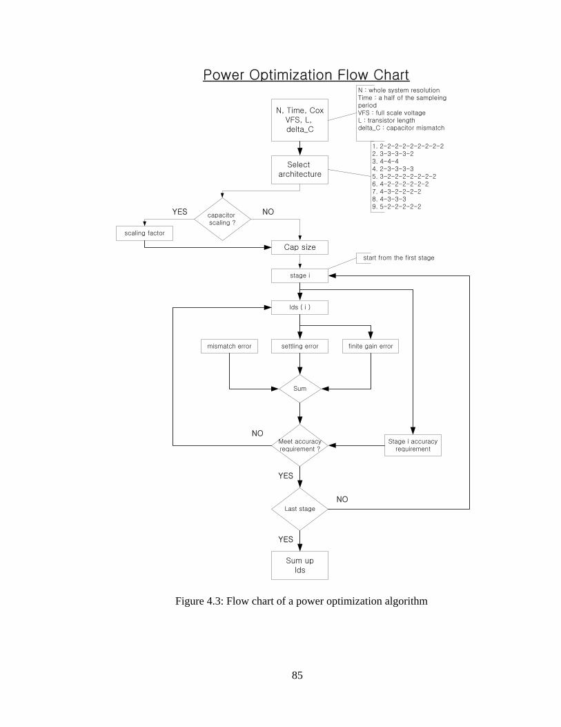
Power Optimization Flow Chart
N, Time, CoxVFS, L, delta_C
Select architecture
Cap size
start from the first stage
N : whole system resolutionTime : a half of the sampleing periodVFS : full scale voltageL : transistor lengthdelta_C : capacitor mismatch
capacitor scaling ?
stage i
Ids ( i )
scaling factor
1. 2-2-2-2-2-2-2-2-22. 3-3-3-3-23. 4-4-44. 2-3-3-3-35. 3-2-2-2-2-2-2-26. 4-2-2-2-2-2-27. 4-3-2-2-2-28. 4-3-3-39. 5-2-2-2-2-2
YES NO
settling error finite gain errormismatch error
Sum
Meet accuracyrequirement ?
Last stage
Sum upIds
Stage i accuracyrequirement
NO
NO
YES
YES
Figure 4.3: Flow chart of a power optimization algorithm
85

In this section, we perform a numerical analysis for power dissipation in a SC
pipeline ADC to decide which architecture consumes less power than others. In Table 4.2,
we have a list of architectures to be tested. As the table shows, there are architectures
composed of identical and non-identical per stage resolution. Hence, we can see a
difference between two approaches after analysis. All of the architectures are selected to
yield 10-bit resolution, and the sampling frequency is set to 100M samples/sec. Simple
single-stage amplifiers are used in this analysis. The peak-to-peak input voltage is
assumed to be 1V.
The flow chart of a power optimization algorithm is shown in Figure 4.3. First, we
need to have all the essential information such as the desired total ADC resolution, the
sampling rate, capacitor mismatch and technology-related parameters. Then, an
architecture is selected from the list in Table 4.2. Next, capacitor scaling may or may not
be applied. Capacitor size is decided based on the allowable total input referred noise.
Beginning with the first stage, we find the optimum bias currents so that the sum of finite
gain, incomplete settling and mismatch error is within the stage accuracy requirement.
This routine is repeated until the last stage.
This program offers three options. In Option I, capacitor size is decided so that
each stage will have the same KT/C noise. The first stage accuracy requirement, which is
the most stringent, is used for all stages. In Option II, the same capacitor size is used as in
Option I. A different stage accuracy requirement is applied to each stage. In a pipeline
ADC, the later stages have a more relaxed accuracy requirement than in the front stage.
In Option III, with the same stage accuracy requirement as in Option II, only the
capacitor size is scaled down along pipeline stages by a scaling factor.
86

4.3.3 ANALYSIS RESULTS
Figure 4.4: Simulation results of Option I analysis. ( In (a) and (b) the individual
(smaller) bars within a group represent a stage of the ADC )
In Option I, the size of the capacitors was chosen so as to have the same kT/C noise
at each stage. All architectures have the same total input referred noise. Total input
referred noise is set to a small enough value so that all architectures can yield 10-bit
resolution. The total capacitor size in each pipeline architecture is shown in Figure 4.4(b).
The x-axis represents the number of different pipeline architectures listed in Table 4.2.
87

Each bar consists of several thin bars that represent different stages in one architecture.
The same principle of graphical representation is also applied to other graphs.
Total capacitor size of each stage is shown in Figure 4.4(b). Total capacitor size of
each stage is the same in order to have the same kT/C noise. Notice that capacitor size in
architectures (1) and (4) is larger than others. The noise contribution of the later stages to
the total input referred noise is large when a small number of bits per-stage is used for the
first stage. Hence, capacitor size has to be larger than the capacitor size in other
architectures AND? with a large number of bits per stage in the first stage. Otherwise,
the total input referred noise of the architecture containing a small number bits per stage
in the first stage is greater than in the others.
The current consumption of a MDAC is shown in Figure 4.4(a). We can observe
that a large number bits per-stage consumes more current than a small number bits per
stage. This is because large transconductance is required to keep a small settling time
constant that meets speed requirement. Otherwise, the settling time constant is increased
by the small feedback factor of a large number of bits per stage and eventually becomes
unable to meet the speed requirement.
The total current consumption of each architecture is shown in Figure 4.4(c). In
this time, the current consumption of comparators is included. A power ratio of 10 is
assumed to estimate the current consumption of comparators [7]. The power ratio is
defined as the ratio between current consumed by a MDAC and current consumed by
each comparator in the same stage. As a result, we can see that architecture (5) dissipates
less power than the others in the Option I analysis.
88

Figure 4.5: Simulation results of Option II analysis
In Option II, the capacitor size is unchanged from Option I. However, a different
stage accuracy requirement is applied to each stage instead of the first-stage accuracy
requirement being used for all of stages as in Option I. Since the stage accuracy
constraint is getting relaxed as a stage moves down to the last stage, power consumption
is reduced by this fact. We can observe this effect from the current consumption of the
architecture (1) in Figure 4.5(a). Current consumption gets lower in the later stages due to
the relaxed stage accuracy requirement. As a result, the total current of all architectures is
reduced and, again, architecture (5) dissipates less power than the others.
89
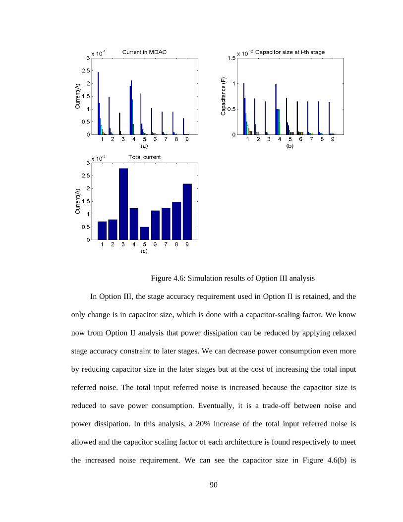
Figure 4.6: Simulation results of Option III analysis
In Option III, the stage accuracy requirement used in Option II is retained, and the
only change is in capacitor size, which is done with a capacitor-scaling factor. We know
now from Option II analysis that power dissipation can be reduced by applying relaxed
stage accuracy constraint to later stages. We can decrease power consumption even more
by reducing capacitor size in the later stages but at the cost of increasing the total input
referred noise. The total input referred noise is increased because the capacitor size is
reduced to save power consumption. Eventually, it is a trade-off between noise and
power dissipation. In this analysis, a 20% increase of the total input referred noise is
allowed and the capacitor scaling factor of each architecture is found respectively to meet
the increased noise requirement. We can see the capacitor size in Figure 4.6(b) is
90

different from that of Figure 4.4(b) and of Figure 4.5(b). Note that capacitor size in the
later stages of those architectures with a large number of bits per stage in the first stage is
much smaller than others; this is because much aggressive capacitor scaling down is
possible in those architectures. Likewise, current consumption in those architectures is
small since amplifiers do not need to drive large capacitors. The final total current result
is different from those of the previous analyses. Architectures with large resolution in the
first stage dissipate less power than ones with small resolution in the first stage. From
analysis results in Figure 4.6, architecture (5) dissipates less power than others. Although
more aggressive capacitor scaling is done in architectures (6) and (9); those architectures
consume more power than architecture (5). That is because of the power consumption of
comparators in 4-bits and 5-bits per-stage. First of all, the number of comparators in 4-bit
and 5-bit per-stage is larger than 3-bit per-stage. Since the accuracy requirement for
comparators in 4-bits and 5-bits per-stage is more stringent, they need more than one
preamplifier in a comparator. Thus, comparators in 4-bits and 5-bits per-stage consume
much more power than those in 3-bits per-stage. We can also observe that architectures
with a large number of bits per-stage in the first stage and 2-bits per-stage for the rest of
stages tend to consume less power. This is because not only the power dissipation of
comparators in 2-bits per-stage is small but also the capacitive loading of comparators to
a previous stage is also small.
4.4 SUMMARY
This chapter has presented a systematic approach to the design of a low-power
pipelined ADC. Important design requirements of a MDAC in a pipelined ADC have
91

been carefully investigated. These requirements include finite op-amp gain, finite setting
time, and noise. These are important parameters that determine overall power dissipation
of a pipeline ADC. A power optimization algorithm was developed to find an appropriate
resolution per stage in terms of low power dissipation. The numerical results are analyzed
and the 3-2-2-2-2-2-2-2 architecture was chosen for a 10-bit low-power pipelined ADC.
A detailed description of the design of the ADC will be presented in the next chapter
92
C H A P T E R 5 : D E S I G N O F A
P R O T O T Y P E A D C
In the previous chapter, the 3-2-2-2-2-2-2-2 architecture was selected for a low-
power 10-bit pipeline ADC. This chapter describes the design of a 10-bit, 100-
Msamples/s pipeline ADC with the architecture chosen in the previous chapter. The
proposed ADC is designed in a 0.18 µm CMOS technology with five metal layers, two
poly-silicon layers and is operated with a 1.8-V supply voltage.
5.1 SHA
Most pipelined ADCs need an SHA to acquire a high-frequency input signal.
Without it, a pipeline ADC will have an error caused by clock skew between a sampling
network of a first-stage MDAC and comparators in a first-stage sub-ADC. This error will
have the same effect on a pipeline ADC as if it were a comparator offset voltage, and the
error becomes larger as the input frequency gets higher. If a SHA exists in a pipelined
ADC, an input signal is sampled and is kept constant during a holding clock phase. Since
the sampled input remains constant, a small timing difference between an MDAC and a
sub-ADC is no longer a problem.
Because a SHA is placed at the front in a pipeline ADC, its design is crucial to the
overall performance of an ADC. Hence, the design requirement of an SHA must be at
least equal or be even more stringent than the overall design requirement of an ADC. Two
93
SHA topologies are widely used in pipelined ADCs. One is known as a charge-
transferring SHA, the other is known as a flip-around [17]. The latter was chosen for this
prototype design because of its advantages over the charge-sharing topology. The fully
differential circuit implementation of a flip-around SHA is shown in Figure 5.1.
When parasitic capacitance is ignored, the feedback factor β of a flip-around SHA
is 1, whereas the feedback factor of a charge-transferring SHA is 0.5. Because the
feedback factor of a flip-around SHA is twice as large, it only requires a half of op-amp
gain bandwidth to produce the same closed-loop bandwidth. Thus, the same performance
can be achieved with much less power by using a flip-around topology. A flip-around
topology also has lower noise than a charge-transferring topology. The total input-
referred noise power of a flip-around SHA can be written as
LStn C
KTCKTv
⋅⋅
+=3
82,
π ( eq.5.1.1 )
where CL is the output load capacitance of an op-amp. The first-term of total noise power
is wideband C
KT noise from the channel resistance of the sampling switches and the
second-term is thermal noise from an op-amp. The total input referred noise power of a
charge-transferring SHA is twice as large as that of a flip-around SHA. Since a flip-
around SHA has lower noise, it needs smaller capacitor size to achieve the same input
referred noise power. This results in power saving for a flip-around SHA.
94

1φ
p1φ
2φ1Φ
Cs
Cs
1Φ p1Φ
p1Φ
Vin 1Φ Vout
2Φ
2Φ
Figure 5.1: Fully differential flip-around SHA and its clock phases
During Φ1 clock phase, an input signal is applied to a sampling capacitor Cs. At the
falling edge of Φ1p clock phase, the applied input signal is captured on the sampling
capacitor Cs. During Φ2 clock phase, the bottom plate of the sampling capacitor is
connected to the output of an amplifier holding the sampled input voltage. An amplifier
for a flip-around SHA should have a large input common-mode range when the input
common-mode level is different from the output common-mode range. Since in this
design both the input and the output common-mode level is set to the middle of a supply
voltage, there is no concern about the input common-mode range of an amplifier.
Transmission gates composed of n- and p-MOS transistors in parallel are used for
switches to ensure that the switches are conducting throughout the node voltage swing.
The size of transistors for the transmission gates is carefully chosen to satisfy the
following equation to guarantee accurate settling.
95

sonclk CR
f⋅
<14
1 ( eq.5.1.2 )
where fclk is the sampling frequency, Ron is the turn-on resistance of CMOS transmission
gate and Cs is the sampling capacitor.
The open-loop gain of an op-amp for a SHA needs to be larger than 72dB to avoid
any error from finite amp gain. Assuming first-order linear settling for an op-amp, it takes
about 8.3 time constants for the output of an op-amp to settle down within 0.25LSB in a
10-bit ADC. For a 100MHz sampling frequency, the allocated time for settling is around
5n seconds. Therefore, the closed-loop unity gain bandwidth of an op-amp is 264.2MHz.
Considering process variations, parasitic effects from the layout, and a non-ideal clock
period, an op-amp should be designed to have higher unity gain bandwidth than the
calculated value. The op-amp used in the SHA is a gain-enhanced folded-cascode op-amp.
Detailed discussion about this op-amp can be found in a later chapter. Simulation results
show that the op-amp for the SHA has an open-loop gain of 95dB and a closed-loop unity
gain bandwidth of 450MHz while dissipating about 4mA.
5.2 MDAC
Two different MDACs are used in this prototype ADC One is a 2.5-bit MDAC and
the other is a 1.5-bit. The 2.5-bit MDAC is used only for the first stage of the pipeline
and the 1.5-bit MDAC is used for the rest of pipeline stages that are from the 2nd stage to
the 7th stage. The circuit implementations of the 2.5-bit and the 1.5-bit MDAC are
illustrated in Figure 5.2 and Figure 5.3, respectively. Basically, both MDACs consist of
an op-amp, capacitors and switches. The two non-overlapping clocks, Φ1 and Φ2 are
96

required to drive the switches. The two extra clocks, Φ1p and Φ2p are used to reduce
charge injection errors from switches.
Vin
Vout
1Φ
Vin
Vin
Vin
2Φ
C1
C2
C3
C4
Vrefn
Vcm
Vrefp
Vrefn
Vcm
Vrefp
Vrefn
Vcm
Vrefp
p1Φ2Φ
2Φ
2Φ
S1
S2
S6
S3
S7
S4
S8
S5
S9
1Φ
1Φ
1Φ
Figure 5.2: Switched-capacitor circuit implementation of the 2.5-bit MDAC
Vin
Vout
Vin
2Φ
C1
C2
Vrefn
Vcm
Vrefp
1Φ
2Φ p1Φ
S2
S1
S3
S4
1Φ
Figure 5.3: Switched-capacitor implementation of the 1.5-bit MDAC
97

1φ
p1φ
2φ
p2φ
Figure 5.4: Non-overlapping clock phases
The operation of the 2.5-bit MDAC is as follows. During a sampling phase, Φ1 and
Φ1p clocks are high turning on switches S1 ~ S4. All of capacitors are connected to an
input signal and the inputs of the op-amp are connected to a common-mode voltage. The
sampling process is completed at the falling edge of clock Φ1p. The input signal is
sampled on all capacitors. Then, Φ1 goes low, and switches S1 ~ S4 are off. The charge
injection from these switches does not change the charge on the capacitor since there is
no DC path. During a holding phase, Φ2 clock is high. The capacitor C1 is now connected
to the output of the op-amp and the rest of the capacitors are connected to Vrefp or Vrefn or
Vcm depending on the output of the sub-ADC.
The output of the 2.5-bit MDAC can be expressed as
refinout VbCCb
CC
bCCV
CCCCC
V ⋅⎟⎟⎠
⎞⎜⎜⎝
⎛⋅+⋅+⋅+⋅⎟⎟
⎠
⎞⎜⎜⎝
⎛ +++= 3
1
42
1
31
1
2
1
4321 ( eq.5.2.1 )
Since C1 = C2 = C3 = C4 = C and b1, b2, b3 = ±1 or 0, the output can be written as
refinout VSVV ⋅+⋅= 4 ( eq.5.2.2 )
where S = ±3, ±2, ±1, and 0 are decided by the digital output from the sub-ADC.
98

The output can also be expressed as
⎪⎪⎪⎪⎪⎪⎪⎪
⎩
⎪⎪⎪⎪⎪⎪⎪⎪
⎨
⎧
>⋅−⋅+⋅
⋅−>>⋅−⋅+⋅
⋅−>>⋅−⋅+⋅
⋅−>>⋅⋅
⋅>>⋅⋅−⋅
⋅>>⋅⋅−⋅
⋅>⋅−⋅
=
inrefrefin
refinrefrefin
refinrefrefin
refinrefin
refinrefrefin
refinrefrefin
refinrefin
out
VVifVV
VVVifVV
VVVifVV
VVVifV
VVVifVV
VVVifVV
VVifVV
V
8534
85
8324
83
8114
81
814
81
8314
83
8524
8534
( eq.5.2.3)
This input/output transfer function of the 2.5-bit stage is shown in Figure5.5.
Vin
Vout
-5/8 Vref
-3/8 Vref
-1/8 Vref
1/8 Vref
3/8 Vref
5/8Vref
000 001 010 011 100 101 110
Figure 5.5: Input/output transfer function of the 2.5-bit stage
99

Because noise is a very important factor in the design of MDACs, noise in a SC
MDAC will be discussed here. There are three different noise sources; 1/f noise, C
KT
noise and thermal noise from an op-amp. Since 1/f noise is quite small at high frequency,
CKT noise from sampling switches and thermal noise from an op-amp will be the main
concerns here. During clock phase Φ1, only thermal noise from switches exists. The noise
voltage sampled on the capacitors is given by
totn C
KTCCCC
KTv =+++
=4321
21 ( eq.5.2.4 )
where Ctot is the total sum of the sampling capacitors.
The total noise charge is
( ) totnn CKTCCCCvq ⋅=+++⋅= 24321
21
21 ( eq.5.2.5)
During clock phase Φ2, this noise charge is transferred to the feedback capacitor
generating an output voltage. The output voltage of the MDAC due to thermal noise from
sampling switches is given by
( )β1
12
1
43212
1
212
1, ⋅=+++⋅
==CKT
CCCCCKT
Cq
v nnout ( eq.5.2.6)
where β is the feedback factor of the MDAC.
During the clock phase Φ2, thermal noise from the op-amp dominates. The noise
power at the output of the MDAC [17] can be found from
nnopnnout BWGvv ⋅⋅= 22,
22, ( eq.5.2.7)
where 2,opnv is the noise power density of the amplifier, Gn is the noise gain and BW is the
100

noise bandwidth. Assuming a single-stage amplifier, the noise power density of the
amplifier is
mopn g
KTv3
442, ⋅= ( eq.5.2.8 )
where gm is the transconductance of an input transistor of the amplifier.
The noise gain can be
β11
1
432 =++
+=C
CCCGn ( eq.5.2.9)
and noise bandwidth is
L
m
L
mn C
gCg
BW ⋅⋅=⋅⋅⋅= βππ
β41
221
( eq.5.2.10)
where β is the feedback factor and CL is the total output capacitance at the op-amp output.
Hence, noise power at the output of the MDAC during clock phase Φ2 can be written as
Lnout C
KTv 11342
2, ⋅⋅⋅=β
( eq.5.2.11)
Total noise power at the output of the MDAC is the sum of noise power from both
clock phases, Φ1 and Φ2 as shown in eq. 5.2.12.
22,
21,
2, noutnouttotout vvv += ( eq.5.2.12)
LCKT
CKT 11
341
1
⋅⋅⋅+⋅=ββ
( eq.5.2.13)
The total input referred noise power of the MDAC is given by
2
2,2
,sig
totouttotin G
vv = ( eq.5.2.14)
LCKT
CKT ββ ⋅⋅+⋅=
34
1
( eq.5.2.15)
101

Ltot CKT
CKT β
⋅⋅+=34
( eq.5.2.16)
Eq.5.2.16 indicates that the total input referred noise mainly depends on capacitors in
MDACs. Although eq.5.2.16 is derived from the 2.5-bit MDAC, it can be applied to any
number of bit MDAC. Since the parasitic capacitance of an op-amp is not considered
when eq.5.2.16 is derived, the actual amount of total noise will be slightly larger than
represented in eq. 5.2.16. Thus, a little larger size of capacitor should be used to provide a
margin of safety.
Speed, accuracy and noise requirements for the first stage in a pipelined ADC are
most stringent. These requirements become relaxed as a signal goes down a pipeline. This
less stringent stage requirement for the later stages in a pipeline ADC is used to decrease
power consumption by scaling down the size of the capacitors. The scaling down of
capacitor sizes results in reductions in the power dissipation of an op-amp in a MDAC
because the op-amp has less capacitance load to drive. A 2.5-bit MDAC in a first stage
allows more aggressive scaling than a 1.5-bit MDAC in a first stage, which leads more
power saving.
Since reducing the size of capacitors increases thermal noise, capacitor sizes at
each stage should be chosen carefully. The input referred noise of total and each stage
should be smaller than the quantization noise of overall and each stage resolution,
respectively.
5.3 OPERATIONAL AMPLIFIER
Op-amps in MDACs are core circuit components in a SC pipelined ADC. In order
102

to avoid limiting linearity performance from the non-idealities of op-amps, op-amps must
have a sufficient DC gain and wide bandwidth so that output settles within 1/2 LSB to
desired value in half a clock cycle.
The DC gain requirement of an op-amp can be obtained from eq. 4.1.3. Error
portion due to finite op-amp gain should be smaller than 1/4 LSB of remaining resolution.
The gain can be found from
LSBA
⋅<⋅ 4
11β
( eq.5.3.1)
The open-loop DC gain requirement of an op-amp in a first-stage is with dBA 720 >
41
=β . The actual op-amp gain should be at least 12 dB larger than this calculated value
considering any process variation.
Similarly, an error due to finite gain bandwidth of an op-amp should be smaller
than 1/4 LSB. Assuming a single pole system, an error is
221+
−
<r
s
N
te τ ( eq.5.3.2)
where ts is allocated settling time, τ is a time constant, Nr is remaining resolution after a
current stage in a pipeline.
A time constant is given by
2ln)2( ⋅+<
r
s
Nt
τ ( eq.5.3.3)
A time constant can be also written as
OPuOPuCLdB f ,,,3 2111⋅⋅
=⋅
==− βπωβω
τ ( eq.5.3.4)
where ω-3dB,CL is the –3dB frequency of a close-loop amplifier, ωu,OP is the unity gain
103

bandwidth of an open-loop amplifier.
Substituting eq.5.3.4 into eq.5.3.3, the unity gain bandwidth can be found from
( )s
ru t
Nf⋅⋅⋅+
>βπ2
2ln2 ( eq.5.3.5)
For a 100 MHz clock operation, the time allowed for settling is around 5ns. The
required unity gain bandwidth of an op-amp in a first-stage is 967.6 MHz.
A single-stage op-amp like a telescopic or folded-cascode op-amp would be a first
choice here because it has wide gain bandwidth. However, the dc gain of a single-stage
op-amp in a 0.18 µm CMOS technology can hardly be larger than 60 dB. Thus, a special
technique known as a gain-boosting or a gain enhancement method [33,34] is utilized to
increase the DC gain of a single-stage op-amp. A gain-boosting op-amp is basically based
on a cascode amplifier with an auxiliary boosting amplifier connected to a cascode
transistor in order to increase the DC gain of the cascode amplifier. It is shown in Figure
5.6.
The output impedance of the gain-boosting cascode amplifier in Figure5.6 is given
by
21212 )1( dsdsdsdsboostmout rrrrAgR ++⋅⋅+= ( eq.5.3.6)
212 )1( dsdsboostm rrAg ⋅⋅+≅ ( eq.5.3.7)
where Aboost is the DC gain of an auxiliary boosting amplifier and rds1,rds2 is the output
resistance of transistors M1, and M2, respectively. Without (Aboost+1), it is the output
impedance of a cascode amplifier. Thus, the output impedance of a gain-boosting
amplifier is increased by the gain of an added boosting amplifier, Aboost. As a result, the
DC gain of a gain-boosted amplifier is increased by the same amount and is given by
104

( )12211 +⋅⋅⋅⋅≅ boostdsmdsmtot ArgrgA ( eq.5.3.8)
A
~
X
Y
Vb1
Vin
Vout
CL
M1
M2A
Figure 5.6: Gain boosting cascode amplifier
The gain is increased by an additional gain stage without comprising output swing
and the gain bandwidth of an original cascode amplifier. It is very crucial to pick up the
right bandwidth of an auxiliary boosting amplifier because bandwidth has a great impact
on the stability and settling behavior of the overall gain-boosting amplifier.
The transfer function of a cascode amplifier without an auxiliary boosting amplifier
can approximately be written as
⎟⎟⎠
⎞⎜⎜⎝
⎛+⎟⎟
⎠
⎞⎜⎜⎝
⎛+
=
21
0
11)(
ωωss
As
VV
in
out ( eq.5.3.9)
where A0 is the DC gain of a cascode amplifier, ω1 is a dominant pole at the output node
and ω2 is a first non-dominant pole at the source of transistor M2. With an auxiliary
boosting amplifier, the transfer function is given by
105

( )
( )⎭⎬⎫
⎩⎨⎧+
⎪⎪⎭
⎪⎪⎬
⎫
⎪⎪⎩
⎪⎪⎨
⎧
+
+
+=
21
0
1
1
1
1
ωωs
A
s
AAVV
b
boost
in
out ( eq.5.3.10)
Assuming an auxiliary boosting amplifier has a single-pole response, Aboost can be
written as
)1()(
3ωs
AsA boost
boost
+= ( eq.5.3.11)
where ω3 is the dominant pole of an boosting amplifier.
Substituting eq.5.3.11 into 5.3.10, then
( ) ( ) ⎭⎬⎫
⎩⎨⎧+
⎪⎭
⎪⎬⎫
⎪⎩
⎪⎨⎧
+⎟⎟⎠
⎞⎜⎜⎝
⎛+
+⋅+⋅+
⎭⎬⎫
⎩⎨⎧
++⋅+⋅
=
231
2
13
30
111
111
)1(1)1(
ωωωωω
ω
ssA
As
AsAA
VV
boostboost
boostboost
in
out ( eq.5.3.12)
Assuming ( )131 +⋅<< boostAωω ,
⎭⎬⎫
⎩⎨⎧+
⎪⎪⎭
⎪⎪⎬
⎫
⎪⎪⎩
⎪⎪⎨
⎧
+
+⎭⎬⎫
⎩⎨⎧
++
⎭⎬⎫
⎩⎨⎧
++⋅+⋅
=
213
30
1
1
1)1(
1
)1(1)1(
ωωω
ω
s
A
sA
s
AsAA
VV
boost
boost
boostboost
in
out ( eq.5.3.13)
The pole and zero at ( 13 )+⋅ boostAω cancel each other. As a result,
⎭⎬⎫
⎩⎨⎧+
⎪⎪⎭
⎪⎪⎬
⎫
⎪⎪⎩
⎪⎪⎨
⎧
+
+
+⋅=
21
0
1
1
1
)1(
ωωs
A
s
AAVV
boost
boost
in
out ( eq.5.3.14)
The pole of the auxiliary boosting amplifier creates the pole and zero in the transfer
106

function of the cascode gain-boosting amplifier. However, since they are located at the
same frequency, they cancel each other. Thus, the effect of the pole of the auxiliary
amplifier cannot be seen in the transfer function in eq.5.3.14. The transfer function in
eq.5.3.14 merely looks like a transfer function of a cascode amplifier with higher gain
and higher output impedance. The gain Bode plot of gain boosted, auxiliary boosting and
original main amplifiers is shown in Figure5.7.
A0 is the gain of the original cascode amplifier without gain, Aboost is the gain of the
auxiliary boosting amplifier and Atot is the gain of the gain-enhanced cascode amplifier in
Figure5.7. Atot shows a single-pole response until ω < ω2 as we can expect from
eq.5.3.14. In order to get eq.5.3.13, ( )131 +⋅<< boostAωω is assumed. This is equivalent
to the condition in which the unity-gain frequency boostu ,ω of the auxiliary boosting
amplifier should be larger than the –3 dB frequency 1ω of the original cascode amplifier.
The auxiliary boosting amplifier creates a closed-loop with transistor M2. A
stability problem might occur because there are two poles in the loop. One is located at
the output of the auxiliary boosting amplifier and the other is at the source of transistor
M2. Because the latter is equal to the non-dominant pole 2ω of the original amplifier, the
unity gain bandwidth of the auxiliary amplifier should be set lower than the first non-
dominant pole 2ω of the original amplifier. Although it has been previously shown that
the pole and zero cancel each other under the assumption ( 131 +⋅ )<< boostAωω , in a real
situation a pole – zero doublet exists near the unity-gain frequency of the auxiliary
boosting amplifier.
107

ω2ω
totu ,ω
boostu ,ω
boostu,ωβ ⋅
1ω3ω
)1(1
+boostAω
Atot
Aboost
A0
β1
booste
d g
ain
gain
Figure 5.7: Bode plot of gain boosted, auxiliary boosting and original main amplifiers
The pole – zero doublet can degrade the settling performance of the amplifier
because it increases a settling time. A slow settling problem due to the pole – zero
doublet can be avoided if the time constant of the pole – zero doublet is smaller than the
time constant of the gain-boosting cascode amplifier in a closed-loop form with feedback
factor β . Therefore, a safe frequency range [33] for the unity-gain frequency of the
auxiliary amplifier that will avoids instability and the slow settling problem is
2,, ωωωβ <<⋅ boostutotu ( eq.5.3.15)
where totu ,ω is the unity-gain frequency of the gain-boosting amplifier, boostu ,ω is the
unity-gain frequency of the auxiliary boosting amplifier and 2ω is the first non-dominant
108

pole of the gain-boosted main amplifier. The upper limit guarantees stability and the
lower limit prevents a slow settling due to the pole - zero doublet.
With this condition for the unity-gain frequency, the gain-enhancement technique is
applied to implement op-amps for the SHA and MDACs. There are two choices for a
main amplifier: One is telescopic, and the other is a folded-cascode amplifier. Although a
telescopic op-amp has an advantage in terms of power dissipation because of fewer
current branches, a folded-cascode op-amp is selected since its output swing is larger than
that of a telescopic op-amp. A fully differential gain-enhanced folded-cascode amplifier is
shown in Figure 5.8. This op-amp is used for all the MDACs and for the SHA in the
prototype ADC. Since capacitor size is scaled down along a pipeline, op-amps are also
scaled down in width and in current, which saves power and chip area.
There are two auxiliary boosting amplifiers, A1 and A2. These boosting amplifiers
are also fully differential folded- cascode configuration. The difference of these two
amplifiers is the transistor type of a differential input pair. A1 has N-type and A2 has P-
type input stage as shown in Figure 5.9 and Figure 5.10. An additional transistor M3 is
used to set the common mode voltages for the boosting amplifiers A1 and A2.
A common mode feedback (CMFB) circuit is required for a fully differential
folded-cascode main op-amp to set up common mode output voltage. A switched
capacitor CMFB is not only a popular choice with switched-capacitor applications, but
also it allows a larger output swing than a continuous time CMFB circuit. The SC CMFB
circuit is illustrated in Figure 5.11. It consists of four capacitors and eight switches
operated by two non-overlapping clocks. The common mode control voltage Vcmfb is
produced by capacitor C1, which is the average of the output voltages, Vout+ and Vout-.
109

When the common mode output voltage of Vout+ and Vout- is too high, the control voltage
Vcmfb goes up. Then, it brings up the gate voltage of M3 ( M7 ) decreasing the common
mode output voltage back to the required VCM. VCM is set to be 0.9 V in this design. Vb4 is
a bias voltage for transistors M3, and M7. The simulation results show that the gain-
enhanced folded-cascode op-amp achieves a DC gain of 95 dB, a phase margin of 58.9°,
a unity-gain bandwidth of 1.2 GHz and consumes around 6mA. Simulation results are
shown in Figure 5.12.
M0
M3
Vin+ Vin-Vout+Vout-
Vb1
Vb1
A1
Vcmfb
M1 M2
M4
M5
M6
M7
M8
M9
M10
A2
VbAN
VbAP
Figure 5.8: Gain boosted folded-cascode amplifier
110

Vin+ Vin-Vcm
Vout+ Vout-
Vb1 M0 Vb1
Vb2
Vb3
Vb4
M1M2
M3
M4
M5
M6
M7
M8
M9
M10
M11
Figure 5.9: N-type gain-boosting auxiliary amplifier ( A2 )
Vin+Vin-Vcm Vout+ Vout-
Vb4 M0
Vb1
Vb2
Vb3
Vb4
M1 M2
M4
M5
M6
M7
M8
M9
M10
M11
M3
Figure 5.10: P-type gain-boosting auxiliary amplifier ( A1 )
111

Vb4Vb4
Vcmfb
Vout+ Vout-Vcmo Vcmo
C1C1C2 C2
1Φ 1Φ
1Φ 1Φ
2Φ
2Φ
2Φ
2Φ
Figure 5.11: Switched-capacitor common-mode feedback circuit
Figure 5.12: Simulated frequency response of the gain-boosted folded-cascode
amplifier
112
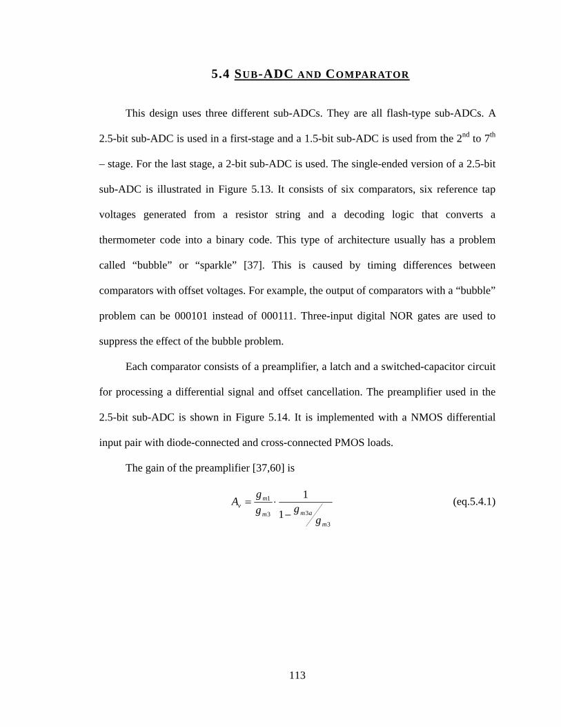
5.4 SUB-ADC AND COMPARATOR
This design uses three different sub-ADCs. They are all flash-type sub-ADCs. A
2.5-bit sub-ADC is used in a first-stage and a 1.5-bit sub-ADC is used from the 2nd to 7th
– stage. For the last stage, a 2-bit sub-ADC is used. The single-ended version of a 2.5-bit
sub-ADC is illustrated in Figure 5.13. It consists of six comparators, six reference tap
voltages generated from a resistor string and a decoding logic that converts a
thermometer code into a binary code. This type of architecture usually has a problem
called “bubble” or “sparkle” [37]. This is caused by timing differences between
comparators with offset voltages. For example, the output of comparators with a “bubble”
problem can be 000101 instead of 000111. Three-input digital NOR gates are used to
suppress the effect of the bubble problem.
Each comparator consists of a preamplifier, a latch and a switched-capacitor circuit
for processing a differential signal and offset cancellation. The preamplifier used in the
2.5-bit sub-ADC is shown in Figure 5.14. It is implemented with a NMOS differential
input pair with diode-connected and cross-connected PMOS loads.
The gain of the preamplifier [37,60] is
3
33
1
1
1
m
amm
mv
ggg
gA
−⋅= (eq.5.4.1)
113

Vin2Φ
2Φ
1ΦC
2Φ
2Φ
1ΦC
2Φ
2Φ
1ΦC
Dig
ital E
ncord
er
Vref1
Vref2
Vref6
B2
B1
B0
Sub-DAC
Figure 5.13: A single-ended version of the 2.5-bit sub-ADC
Vin+ Vin+
Vb1
Vout1- Vout1+
M0
M1 M2
M3M3a M4a
M4
Figure 5.14: Preamplifier used in 2.5-bit sub-ADC
The cross-connected transistors M3a and M4a are used to increase the gain of the
preamplifier. The second fraction of eq. 5.4.1 is a result from a positive feedback formed
114

by transistors M3a and M4a. The gain of the preamplifier is around 10 large enough to
suppress an offset voltage in a latch. For a 1.5-bit pipeline stage, a dynamic comparator
[43,48] without a preamplifier is widely used because a 1.5-bit stage with a digital
correction logic allows a comparator offset as large as 4/refV± . However, the offset
voltage of a dynamic comparator can be larger than 4/refV due to low power supply
voltage in this design. Thus, a preamplifier is also used in a 1.5-bit sub-ADC with a latch.
The preamplifier is shown in Figure 5.15. It is identical with the one in Figure5.14 except
for cross-connected transistors M3a and M4a. The gain of the preamplifier [37,60,66] is
given by
3
1
m
mv g
gA = (eq.5.4.2)
It is only decided by the ratio of NMOS and PMOS device dimensions. The gain is
around four, enough to reduce the effect from the offset voltage of a latch.
A CMOS latch and an SR latch [59] are followed by a preamplifier. They are
shown in Figure 5.16. The SR latch is used to hold previous CMOS outputs of the latch
during the whole clock cycle and to prevent them from being reset in every clock cycle.
The CMOS latch works in two modes: reset and regeneration. During its reset mode, a
latch signal is high. The transistor M3 is turned-on forcing both outputs to be set to
around Vgs. During this time, the current proportional to the voltage difference from the
preamplifier is injected to the output nodes through transistors M6 and M9. This will be
used as the initial difference for the next regeneration mode. A regeneration mode is
started immediately after the Latch signal goes low. Transistor M3 is opened, and M7 and
M8 are pulled up to Vdd. A latch looks just like back-to-back inverters. The positive
115
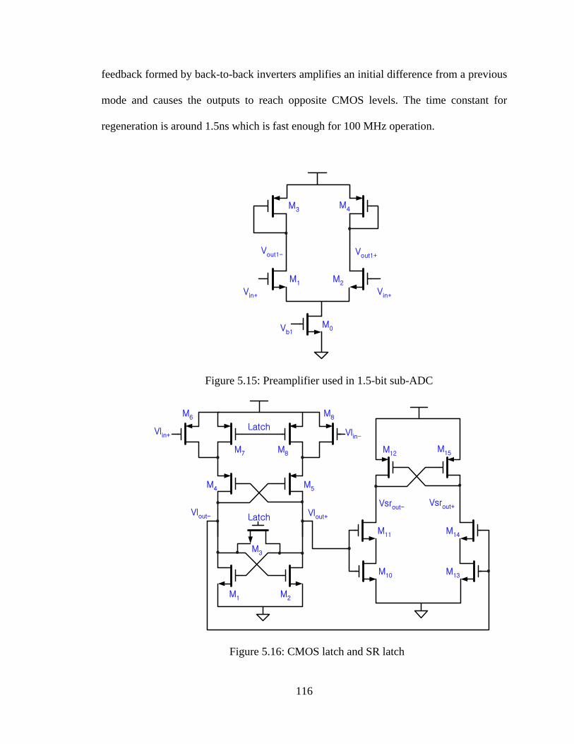
feedback formed by back-to-back inverters amplifies an initial difference from a previous
mode and causes the outputs to reach opposite CMOS levels. The time constant for
regeneration is around 1.5ns which is fast enough for 100 MHz operation.
Vin+ Vin+
Vb1
Vout1- Vout1+
M0
M1 M2
M3M4
Figure 5.15: Preamplifier used in 1.5-bit sub-ADC
Latch
Latch
Vlin+ Vlin-
Vsrout+Vlout-
Vsrout-Vlout+
M1 M2
M3
M4 M5
M6
M7 M8
M8
M10
M11
M13
M14
M12M15
Figure 5.16: CMOS latch and SR latch
116

5.5 BIAS CIRCUIT
The schematic of the bias circuits for op-amps is shown in Figure 5.17. Bias
circuits establish quiescent voltages for transistors in op-amps so that their drain-source
voltage is larger than their gate-source overdrive voltage. This ensure that all transistors
remain in the saturation region and maintain high output resistance. Bias circuits also
provide quiescent conditions for op-amps to have a wide output swing. A wide swing can
be accomplished by making the drain-source voltages of transistors M11, M15 and M19
near the minimum but not so low as to go into the triode region. In order to set the drain-
source voltages of M11 and M15 to the minimum, the gates of the NMOS cascode
transistors, M12 and M16, are biased to ovth VV ⋅+ 2 , which is generated from transistors M9
and M10. M9 operates in a saturation region since it is diode-connected. M9 forces M10
into operate in a triode region. The W/L ratio of M10 is chosen such that its drain-source
voltage is equal to . The same principle is also applied to the PMOS side. The
and are used as the bias voltages for the auxiliary boosting amplifiers, and in
Figure5.8. Then, the auxiliary amplifier drives the gates of M
ovV bANV
bAPV 2A 1A
2A 4 and M8 to make the
drain-source voltages of M3 and M7 equal to , which maximizes the output swing of
the bottom side. The upper side’s output swing is maximized in the same way by the
auxiliary amplifier . is used as the bias voltage for the switched-capacitor CMFB
circuit in Figure5.11. The master current is generated externally and is distributed to all
stages by current mirrors to reduce the effect of a supply line’s voltage drop.
ovV
1A 4bV
117

VbAp
M1
M2
M3
M4
M5
M6
M7 M8
M9
M10
M12
M13
M11M
14
M15
M16
I ref
M17
M18
M19
M20
M21
M22
VbAN
Vb1
Vb2V
b3
Vb4
Figure 5.17: Schematic of the bias circuit
5.6 CLOCK GENERATOR
A schematic of the clock generator circuit is shown in Figure 5.18. It is driven by a
reference clock provided from an external source. Two non-overlapping clocks are
118

generated from it to operate switched-capacitor circuits. The non-overlapping interval is
created by a propagation delay in inverter chains. An additional pair of delayed clock
phases is also generated for a bottom-plate sampling technique to reduce charge injection
errors. Clock phases are distributed by four local clock generators instead of one global
clock generator. This is done to reduce the effect of clock skew due to interconnections in
the layout. Each local clock generator is driven by a single master clock to synchronize
between stages. To minimize clock skew, the length of the clock lines are matched as
much as possible and the tree structure of the inverter chain is used to distribute the clock
from the master clock to improve speed and accuracy. The timing diagram of the clock
generator is shown in Figure 5.19.
Ph_2
Ph_2d
Ph_1d
Ph_1
CLK
Ph_2
Ph_2d
Ph_1d
Ph_1
CLK
Figure 5.18: Non-overlapping clock generator
119

Figure 5.19: Timing diagram of the clock generator
5.7 SIMULATION RESULTS
After integrating all the building blocks, simulations for the designed pipeline
ADC are conducted at the transistor level. A 2-MHz input signal is sampled at 100-MHz.
Simulation results show that the designed pipeline ADC achieves the SNR of 59.2 dB
and the SNDR of 58.6dB, which demonstrate successful design of each individual
building block.
120
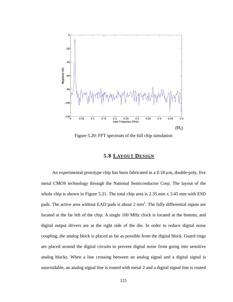
Figure 5.20: FFT spectrum of the full chip simulation
5.8 LAYOUT DESIGN
An experimental prototype chip has been fabricated in a 0.18 µm
metal CMOS technology through the National Semiconductor Corp.
whole chip is shown in Figure 5.21. The total chip area is 2.35 mm x 3
pads. The active area without EAD pads is about 2 mm2. The fully diff
located at the far left of the chip. A single 100 MHz clock is located
digital output drivers are at the right side of the die. In order to re
coupling, the analog block is placed as far as possible from the digital b
are placed around the digital circuits to prevent digital noise from go
analog blocks. When a line crossing between an analog signal and
unavoidable, an analog signal line is routed with metal 2 and a digital s
121
(f/fs)
, double-poly, five
The layout of the
.45 mm with ESD
erential inputs are
at the bottom, and
duce digital noise
lock. Guard rings
ing into sensitive
a digital signal is
ignal line is routed

with poly. Metal 1 is inserted between two layers as a shielding ground plane. Noise
coupling through the power supply line is decreased by using separate supplies for analog
and digital circuits. An analog supply is used for providing power to the op-amps and to
the preamplifiers in comparators. Latches, clock generators, and digital logic circuits are
powered by an digital supply. There is another digital supply used to power ESD circuits
and digital output drivers.
Reference voltages and common mode voltage are provided externally and
distributed through the chip. Wide metal lines are used for the supplies, voltage
references and the common mode voltage to reduce IR drop which is an unwanted
voltage drop caused by the parasitic resistance of a metal line. If possible, to lower metal
resistance, the double metal layers are used for power and ground supplies. A common-
centroid technique is used for the layout of the input devices of the op-amps to minimize
offsets. A common centroid layout technique decreases the gradient effect by averaging
out gradient factors out.
Capacitor-arrays are laid out using a common centroid layout technique to
minimize the mismatch caused by the processing gradient. Dummy capacitors are
placed along the outsides of the capacitor-arrays to ensure uniform etching of the four
sides of the capacitors and the equal fringing field for all capacitors. An N-well is
placed under the capacitor-arrays to reduce noise from the substrate.
122

Layo
ut o
f Pip
elin
e AD
C
SHA
Stage1 (2.5b)
Stage2 (1.5b)
Stage3 (1.5b)
Stage4 (1.5b)
Stage5 (1.5b)
Stage6 (1.5b)
Stage7 (1.5b)
Stage8 (2b)
Vref
Buf
fer
Del
ay c
kts,
clk
gen
, dig
ital c
orre
ctio
n ci
rcui
ts
Layo
ut o
f Pip
elin
e AD
C
SHA
Stage1 (2.5b)
Stage2 (1.5b)
Stage3 (1.5b)
Stage4 (1.5b)
Stage5 (1.5b)
Stage6 (1.5b)
Stage7 (1.5b)
Stage8 (2b)
Vref
Buf
fer
Del
ay c
kts,
clk
gen
, dig
ital c
orre
ctio
n ci
rcui
ts
Figure 5.21: Layout of the prototype ADC
123

5.9 SUMMARY
This chapter has presented the design of a low-power 10-bit, 100-Msamples/s
pipelined ADC with 3-2-2-2-2-2-2-2 architecture. A detailed description of the circuit
components of the proposed ADC is given. The circuit components include SHAs,
MDACs, op-amps, sub-ADCs, comparators, bias circuits, and clock generators. Lastly,
simulation results are presented, followed by a description of the layout of the proposed
ADC.
124

C H A P T E R 6 : E X P E R I M E N T A L
R E S U LT S
The proposed pipeline ADC described in the previous chapter was fabricated in a
0.18-µm CMOS process. In the first section of this chapter, the evaluation board and
measurement setup for the proposed chip are described. Then the experimental test
results obtained from the proposed chip are presented.
6.1 EVALUATION BOARD AND TEST SETUP
A diagram of the measurement setup to evaluate the proposed chip is shown in
Figure 6.1. The proposed chip is packaged in a 48-pin Quad Flat Package (QFP) for its
higher speed characteristics. The packaged chip is mounted on a Printed Circuit Board
(PCB) and soldered directly onto the board for better electrical contact. A four-layer PCB
is designed to provide a platform that offers multiple testing points for evaluation of the
proposed chip. The top and bottom layers are used for signal paths and for soldering
components. The two middle layers are used for ground and power supply. Any unused
area in the two outside layers is also used for ground. All power supplies and biasing
lines are decoupled with 0.1 µF ceramic capacitors and 10 µF tantalum capacitors. They
are placed as closed to the pins of the QFP as possible. The chip has three independent
power supplies and grounds: two for analog and digital blocks and one for the output
drivers. The digital output drivers are powered by a 3.0 V supply to make the output
125
signal of the ADC high enough so that the output buffer can process it properly. A
differential input signal is generated by a transformer. A single-ended signal from a signal
source is applied to the primary winding of the transformer and a differential input signal
is obtained from the secondary side by connecting the center tap to a common mode
voltage. Reference voltages are generated on the board. A low-noise voltage regulator is
used to generate a reference voltage that is buffered by low-noise amplifiers to produce
the reference voltages as well as the common mode voltage. The low-noise amplifier is
powered by a ±5 V supply. Potentiometers are used to adjust the reference voltages and
the common mode voltage. The clock signal is provided by an external signal generator.
Both square wave and sine wave signals can be applied to the board. A sine wave signal
is converted to a square wave by digital logic circuits on the board.
The digital output of the proposed ADC is buffered with an output buffer to the
drive large parasitic capacitance of the lines on the board and probes from the logic
analyzer. The digital outputs of the proposed ADC are captured by the logic analyzer. A
clock signal is also provided to the logic analyzer to synchronize with the ADC. A
photograph of the PCB used in the experimental evaluation is shown in Figure 6.2.
126
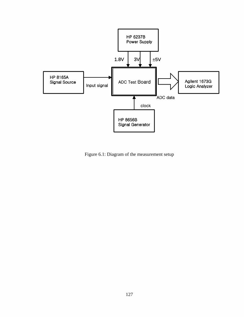
HP 8165ASignal Source
HP 6237BPower Supply
HP 8656BSignal Generator
ADC Test Board Agilent 1673GLogic Analyzer
clock
Input signal
ADC data
1.8V 3V ±5V
HP 8165ASignal SourceHP 8165ASignal Source
HP 6237BPower SupplyHP 6237BPower Supply
HP 8656BSignal GeneratorHP 8656BSignal Generator
ADC Test Board Agilent 1673GLogic AnalyzerAgilent 1673GLogic Analyzer
clock
Input signal
ADC data
1.8V 3V ±5V
Figure 6.1: Diagram of the measurement setup
127

Figure 6.2: Photograph of the evaluation board
6.2 TEST RESULTS
A code density test [35] was conducted to obtain static linearity of the proposed
ADC. The measured DNL and INL are shown in Figure 6.4 and 6.5. From the figures, the
maximum value of DNL and INL are 0.5 LSB and 0.75 LSB at 8 bit level, respectively.
The dynamic performance of the proposed ADC is measured by analyzing a Fast Fourier
Transform (FFT) of the digital output codes for a single input signal. Figure 6.6 illustrates
the spectrum of the output codes of the ADC with an input frequency at 2.1 MHz
sampled at 80 MHz with power supply of 1.8V. The sampling frequency of 80 MHz is
used because it is the highest frequency than can be generated from the HP 8656B signal
128

generator. The SNR is approximately 47 dB and the SNDR is around 44.4 dB. The THD
is –51.1 dB and the SFDR is 54 dB. The largest spike, other than the fundamental input
signal, is the third harmonic of the input signal and is about 54 dB below the fundamental
signal. Figure 6.7 illustrates the spectrum with 33.3MHz input frequency sampled at 80
MHz. The SNR is 45.6 dB and the SNDR is 41.5dB. The THD is - 42 dB and the SFDR
is 47 dB. Figure 6.7 illustrates that dynamic performance is more degraded with a higher
input signal. This degradation is mainly due to the nonlinear resistance of the sampling
switches. At lower input frequency, this degradation can be neglected since the bandwidth
of the sampling circuits is much higher than the input signal. However, with a higher
frequency input signal, distortion caused by the nonlinear resistance of the sampling
circuit is increased and decreases dynamic performance. The problem can be reduced by
using bootstrapped switches [55]. The SNR and SNDR as a function of input frequency
are shown in Figure 6.3. The measured results are summarized in Table 6.1
.
Table 6.1: Summary of measurement results
SNR 47 dB
Power dissipation ( analog ) 45mW
Input voltage 1 Vpp
max INL/DNL 0.75 / 0.5 LSB
Die Area 2 mm2 ( without ESD pads )
Technology 0.18 µm, 2-poly, 5-metal
Power Supply 1.8 V
129

Figure 6.3: SNR and SNDR versus input frequency
Figure
Output code
6.4: Measured DNL
130
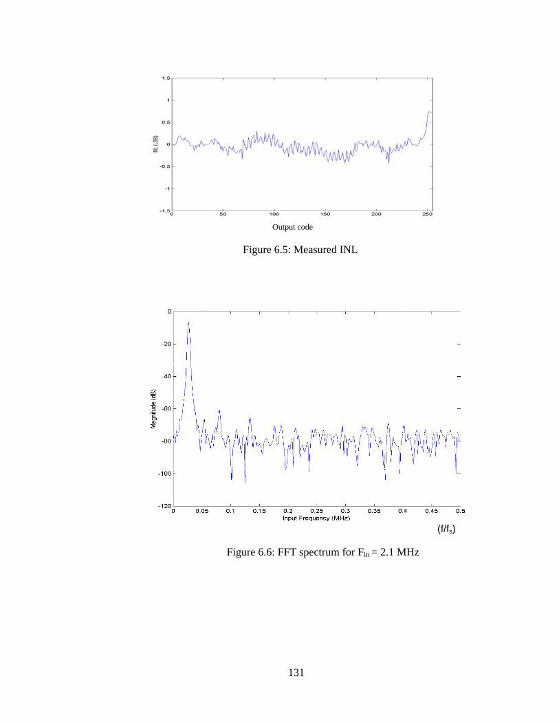
Figure 6.5: Measured INL
Figure 6.6: FFT spectrum for Fin = 2.1 MHz
131
(f/fs)
Output code
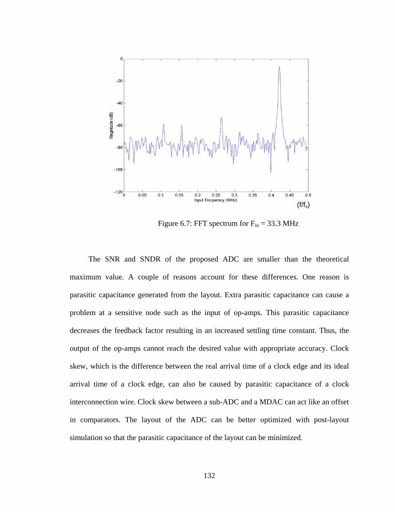
(f/fs)
Figure 6.7: FFT spectrum for Fin = 33.3 MHz
The SNR and SNDR of the proposed ADC are smaller than the theoretical
maximum value. A couple of reasons account for these differences. One reason is
parasitic capacitance generated from the layout. Extra parasitic capacitance can cause a
problem at a sensitive node such as the input of op-amps. This parasitic capacitance
decreases the feedback factor resulting in an increased settling time constant. Thus, the
output of the op-amps cannot reach the desired value with appropriate accuracy. Clock
skew, which is the difference between the real arrival time of a clock edge and its ideal
arrival time of a clock edge, can also be caused by parasitic capacitance of a clock
interconnection wire. Clock skew between a sub-ADC and a MDAC can act like an offset
in comparators. The layout of the ADC can be better optimized with post-layout
simulation so that the parasitic capacitance of the layout can be minimized.
132

The non-idealities of clock are another reason for the limited performance of the
proposed ADC. The non-idealities of the clock include clock jitter, non-overlapping
period time, finite rising and fall time, and unsymmetrical duty cycle. The three latter
errors reduce the time allocated for the setting time of an op-amp’s output. These errors
either increase the noise floor or cause distortion in the digital output spectrum resulting
in decreased SNR and SNDR. Clock jitter [38] is a random variation in time that decides
when to sample the input signal in a SHA. A condition for clock jitter in a ADC is given
by
Nft
21⋅⋅
<∆π
( eq.6.3.1)
where is clock jitter, is an input frequency and N is the resolution of an ADC. As
an input frequency and resolution increase, the requirement for clock jitter is getting more
stringent. In other words, a clock jitter error will degrade the SNR even more as an input
frequency approaches Nyquist input frequency.
t∆ f
As for other reasons for the ADCs limited performance, digital switching noise
ranks first. During the switching of digital circuits, the current is drawn from power
supply lines. Ideally, neither the supply or ground lines has any impedance. However,
because integrated circuits needs to be packaged, parasitic impedance such as resistance
and inductance occurs from the leadframe and bondwires. Thus when circuits inside a
package draw current, this current has to go through this parasitic impedance from the
outside of the package. A voltage drop will occur because of impedance and is given by
dtdiLVL ⋅= ( eq.6.3.2)
133

where is the current drawn from the circuits and L is the parasitic inductance of the
package. This voltage drop causes a difference between on-chip and off-chip supply
voltages. The parasitic inductance of a package interacts with an on-chip parasitic
capacitance creating ringing on the supply lines. Therefore, a disturbance exists on the
power supply and ground lines because of the parasitic impedance of a package. This
disturbance is referred to as switching noise. Switching noise produced in digital circuits
can couple into sensitive analog circuits through the substrate. It affects transistor
currents by changes in the threshold voltage due to body effect and by capacitive
coupling into the gate, source and drain of transistors. This limits the analog precision
that is required to design an ADCs with a desired resolution. The SNR can be
significantly degraded by substrate switching noise and the SNR can be reduced as much
as 20% as reported from [54].
di
One of the ways to suppress switching noise is to reduce the parasitic inductance of
a package by using multiple pins for power supply and ground lines. Since parasitic
inductance per pin is strongly dependent on the type of a package, using a special
package with low parasitic inductance such as Leadless Ceramic Chip Carriers (LCCC)
also can help to reduce switching noise. Common ways to reduce switching noise in
terms of layout are using physical separation between analog and digital circuits and
placing guard rings around each section. These methods work effectively on a lightly
doped substrate. However, in this proposed design, CMOS processing with an eptaxial
layer [50] on a heavily doped bulk substrate is used due to its excellent ability to suppress
latch-up. Because of its low-resistivity in the substrate, most of the switching noise
injected from digital circuits travels through the substrate and goes directly into the
134

analog circuits. Thus, on a heavily doped substrate, physical separation of analog and
digital circuits and installing guard rings around them are not as effective as when these
same solutions are employed on lightly doped substrate [50].
On-chip decoupling capacitors can be used to reduce switching noise on power
supply lines. Decoupling capacitors act like local power supplies during the switching
instant. Thus, most of the current can be drawn from decoupling capacitors instead of
directly from the power supplies. That means a reduction in the current from an off-chip
supply flowing through the parasitic impedance of a package. Therefore, switching noise
associated with the current is also reduced. However, the value of on-chip decoupling
capacitor should be chosen carefully because of the potential resonance caused by a LC
tank composed of parasitic inductance and a decoupling capacitor. A resonance
frequency should be located far away from the system clock frequency. Another method
is to put a series resistor with a decoupling capacitor. This will reduce the peak of the
resonance and damps the oscillation [63].
All digital circuits in this design have a single-ended structure because of its
simplicity and wide output voltage swing. Switching noise from this conventional CMOS
static logic circuit can be reduced by using a fully differential source-coupled structure.
Power supply current remains constant due to differential circuit structure. Among digital
circuits in the design, digital output buffers create more switching noise since they have
larger size in transistors to drive large output loads and wider swing because they have
high supply voltage. Hence, the significant potion of switching noise can be reduced if
switching noise from the output buffers is reduced. Output buffers with reduced input
swing and a fully differential structure [63] can minimize switching noise by canceling
135

noise coupled into the substrate through outputs due to its balanced structure. However,
twice as many pins are required compared with single-ended output buffers.
A full chip simulation with these error sources was conducted. The input frequency
of 2-MHz is sampled at 80-MHz. Parasitic inductance is placed on the power supply,
ground and reference voltage lines. The estimated parasitic capacitance is added to the
input of the op-amps and to the clock interconnection wire. A longer rising/fall time and
non 50% duty cycle is applied to the clock signal. Substrate switching noise is modeled
as the sum of sinusoidal signals at different frequencies with different amplitude over a
large frequency range [69]. This noise source is applied to a bulk node of transistors in
the op-amps and comparators. The simulated output spectrum is shown in Figure 6.8. The
SNR is 48dB and the SNDR is 45.2 dB. The distortion in the spectrum is caused by the
parasitic capacitance of the layout and the non-idealities of the clock. The noise floor of
the spectrum is increased by switching noise. As was expected, most of the SNR
degradation is due to switching noise from the digital circuits.
136

Figure 6.8: Simulated FFT spectrum with error sourc
6.3 SUMMARY
This chapter presented a design of the evaluation board and
measurement setup for the proposed ADC. The measurement resul
chip were presented, followed by a discussion of improvements th
the fabricated chip.
137
(f/fs)
es
a description of the
ts for the fabricated
at could be made to

C H A P T E R 7 : C O N C L U S I O N
The explosive growth of portable multimedia devices has generated great demand
for low power ADCs. With an increasing trend to a system-on-chip, an ADC has to be
implemented in a low-voltage submicron CMOS technology in order to achieve low
manufacturing cost while being able to integrate with other digital circuits. In this work,
the design and implementation of a low-voltage low-power 10-bit 100-MHz pipelined
ADC in a 0.18µm CMOS process with a 1.8-V supply voltage was presented.
Table 7.1: Comparison of the large and small number of bits per-stage
Dynamic comparator
– large offset– less power dissipation
Pre-amp + dynamic comparator
– small offset– increasing power
dissipation
Comparator
SensitiveLess sensitive Component mismatch
ModestAggressively Capacitor scaling
Small LargePower dissipation per stage
Fast SlowSpeed
LargeSmall # of stage
SmallLargeResolution
138

The number of resolutions per-stage plays an important role in determining the
overall power dissipation of a pipeline ADC. The pros and cons for both a large and a
small number of bits per-stage are summarized in Table 7.1. When a small number of bits
per-stage is used for a single stage, power dissipation per stage is small because of a large
feedback factor. The power dissipation of the comparators in a small number of bits per-
stage is also small since simple dynamic comparators can be used due to relaxed
comparator requirement. The power dissipation per stage of large number of bits per-
stage is large due to a small feedback factor of a MDAC. The power dissipation of
comparators with a large number of bits per-stage is also large since more than one stage
of a preamplifier is often needed for higher accuracy. However, the overall power
consumption of a pipeline ADC can be smaller because aggressive capacitor scaling is
possible with a large number of bits per-stage. Thus, it is not easy with mere qualitative
comparisons to decide which one is the better choice for low-power pipeline ADCs. It is
an even more complicated and difficult decision when important design parameters like
DC gain, bandwidth of the op-amps, and total thermal noise are considered. Therefore, a
numerical power optimization algorithm was developed using all important design
parameters considered as a way to decide which approach performs better for lower
power dissipation. So far, most discussions in the literature about pipeline architecture
applications with low power dissipation have focused on architectures with an identical
number of bits per-stage. In this work, we considered both identical and non-identical
number of bits per-stage. The numerical algorithm developed for this work was applied to
a 10-bit 100-MHz pipeline ADC and used to compare the nine most likely pipeline
architectures. The result of this analysis was that the 3-2-2-2-2-2-2-2 architecture yielded
139
the lowest power dissipation. 3-bits resolution in the first stage allows capacitors to be
scaled down more aggressively than an architecture with all identical 2-bits per-stage.
Power consumption is decreased because the load capacitance of the op-amps is reduced.
The main reason for selecting the 3-2-2-2-2-2-2-2 architecture is the power saving thanks
to aggressive capacitor scaling of 3-bit per-stage was more than increased power
dissipation by a lower feedback factor of a 3-bit per-stage. Although more capacitor
scaling is possible with architectures having 4-bits and 5-bits in the first stage, the power
dissipation of comparators in those architectures increases significantly because of the
larger number of comparators. Also each comparator in those architectures dissipates
more power because a multi-stage preamplifier is usually used due to higher accuracy
requirement. Architectures with a non-identical number of bits per-stage (high resolution
in a first stage and low resolution in subsequent stages) tend to dissipate less power. The
capacitive loading effect of a small number of bits per-stage to an op-amp in a previous
stage is much less than a large number of bits per-stage. The numerical power
optimization algorithm developed in this work is able to provide more accurate
comparison of different pipeline architectures than any comparative study reported so far.
With the program developed here, a low-power pipeline architecture can be found with
any desired speed, resolution and technology.
A low-power low-voltage pipeline ADC with 3-2-2-2-2-2-2-2 architecture was
designed and implemented in 0.18µm CMOS process. First, all non-idealities caused by
building blocks and their effect on an ADC were carefully investigated. Important design
parameters were calculated for circuit design of the building blocks. Advanced submicron
CMOS technology poses a huge challenge to analog circuits such as op-amps due to low
140
power supply and low intrinsic gain. A folded-cascode configuration was selected for the
op-amps because of its high-speed capability and medium output swing. A gain-
enhancement technique was applied to a folded-cascode amplifier and its frequency
response was analyzed in detail to design fast, stable op-amps for a SHA and MDACs.
The analysis, design and simulation of the proposed pipeline ADC have been
carried out at both system and circuit levels. The performance of the proposed ADC was
evaluated after fabrication and packaging. The proposed ADC chip was housed with the
48-pin QFP packaging and was mounted on a 4-layer evaluation board designed to
facilitate measurements. The chip area for the ADC is 2.35 mm X 3.45 mm including
ESD pads. Most of the area is occupied with ESD pads because the core area without
pads is only 2 mm2. The analog core of the chip consumes 25mA with a 1.8 V supply
voltage. Power was minimized with the right selection of the per-stage resolution based
on the results of the power optimization algorithm and by scaling down the sampling
capacitor size in subsequent stages.
Figure 7.1 illustrates the Figure of Merit (FOM) of reported ADCs versus their
sampling rate. The commonly used FOM for data converters is given by
)(2
pJF
PFOMs
ENOB ×= ( eq.7.1 )
where P is power consumption, ENOB is the effective number of bits and Fs is a
sampling rate of ADCs. The unit is in pico-Joule. It represents the energy used to achieve
a given performance. The smaller FOM number means more power efficient ADCs. (A)
and (B) in Figure 7.1 represent the simulated and measured results of the proposed ADC,
respectively. The FOM of the proposed ADC is lower than most of the reported ADCs at
high speed sampling frequenies.
141

Figure 7.1: FOM versus sampling rate
The contribution of this work is to develop a low-power 10-bit 100-Msamples/s
pipelined ADC with 3-2-2-2-2-2-2-2 architecture in a 0.18µm CMOS process. High-
speed, gain-enhanced, folded-cascode op-amps are used to achieve a 10-bit 100-
Msamples/s pipeline ADC with a 1.8V supply voltage. Low-power dissipation is
achieved by the right selection of the per-stage resolution based on the result of the
developed power optimization algorithm and by the scaling down of the size of the
sampling capacitor in subsequent stages. The power optimization algorithm was
developed for a switched capacitor pipeline ADC to decide more accurately what
resolution per stage is a better choice for lower power dissipation. Lastly, the reasons
why the experimental data did not agree with the simulated data were identified and
future improvements are suggested.
For more power saving, a dynamic biasing circuit technique [70] can be applied for
a future design. The basic idea of this technique originates from the fact that a MDAC is
142

in an idle state when it is in sampling phase. Thus, theoretically amplifiers can be turned
off during half of the clock cycle. However, since there is a turn-on recovery time of op-
amps, they are turned off only during the small portion of half of clock cycle. Also partial
biasing circuits for op-amps are always on to minimized the turn-on recovery time.
This work can easily be extended to higher resolution in the future. For higher
resolution, only the front stages such as a SHA and a first-stage need to be designed with
higher accuracy. The rest of the stages can be re-used from this work, thus saving design
and layout time. However, in order to design pipeline ADCs with more than 10-bit
resolution, usually some sort of special schemes such as capacitor error-averaging [51,52],
digital calibration [46] and oversampling techniques [71] are required to compensate for
the process mismatch.
.
143

References
[1] S. H. Lewis, “Optimizing the Stage Resolution in Pipelined, Multistage, Analog-to-Digital Converters for Video-rate Applications,” IEEE Trans. Circuits and Systems-II, vol. 39, pp. 516-523, Aug. 1992.
[2] S. H. Lewis, and P. Gray, “A pipeline 5-Msample/s 9-bit analog-to-digital converter,”
IEEE J. Solid-State Circuits, vol. SC-22, NO. 6, pp. 954-961, Dec. 1987. [3] W. Song, H. Choi, S. Kwak, and B. Song, “A 10-b 20-Msample/s low-power CMOS
ADC,” [4] L. Sumanen, M. Waltari, and K. Halonen, “A 10-bit 200-MS/s CMOS Parallal
Pipeline A/D Converter,” IEEE J. Solid-State Circuits, vol. 30, NO. 7, pp. 1048-1055, July 2001.
[5] Iuri Mehr and Larry Singer, ”A 55-mW, 10-bits, 40-Msample/s Nyquist-Rate CMOS
ADC,” IEEE J. Solid-State Circuits, vol. 35, NO. 3, pp. 318-325, Mar. 2000. [6] S. Lewis, H. Fetterman, G. Gross, R. Ramachandran, and T. Viswanathan, “A 10-b
20-Msample/s Analog-to-Digital Converter,” IEEE J. Solid-State Circuits, vol. 27, NO. 3, pp. 351-358, Mar 1992.
[7] Paulux T. F. Kwok and Howard C. Luong, ”Power Optimization for Pipeline Analog-
to-Digital Converters,” IEEE Trans. Circuits and Systems-II, vol. 46, pp. 549-553, May 1999.
[8] T. Shu, K. Bacrania, and R. Gokhale, ”A 10-b 40-Msample/s BiCMOS A/D
Converter,” IEEE J. Solid-State Circuits, vol. 31, NO. 10, pp. 1507-1510, Oct. 1996. [9] C. Conroy, D. Cline, and P. Gray, “An 8-b 85-MS/s Parallel Pipeline A/D Converter
in 1-µ m CMOS,” IEEE J. Solid-State Circuits, vol. 28, NO. 4, pp. 447-454, Apr. 1993.
[10] David W. Cline, and Paul R. Gray, “A Power Optimized 13-b Msamples/s Pipelined
Analog-to-Digital Converter in 1.2µ m CMOS,” IEEE J. Solid-State Circuits, vol. 31, NO. 3, pp. 294-303, Mar. 1996.
[11] David G. Nairn, “A 10-bit, 3V, 100MS/s Pipelined ADC,” IEEE Custom Integrated
Circuits Conference, pp. 257-260, 2000 [12] Jun Ming and Stephen H. Lewis, “An 8-bit 80-Msample/s Pipelined Analog-to-
144
Digital Converter with Background Calibration,” IEEE J. Solid-State Circuits, vol. 36, NO. 10, pp. 1489-1497, Oct. 2001.
[13] H. Chen, B. Song and K. Bacrania, “A 14-b 20-Msamples/s CMOS Pipelined ADC,
“IEEE J. Solid-State Circuits, vol. 36, NO. 6, pp. 997-1001, June 2001. [14] Roubik Gregorian, Introduction to CMOS OP-AMPS AND COMPARATORS, New
York, Wiley, 1999. [15] K. Kim, N. Kusayanagi, and A. Abidi, “A 10-b, 100-MS/s CMOS A/D Converter,”
IEEE J. Solid-State Circuits, vol. 32, NO. 3, pp. 447-454, Mar. 1997. [16] P. Yu, S. Shehata, A. Joharapurkar, P. Chugh, A. Bugeeja, X. Du, S. Kwak, Y.
Papantonopoulous, T. Kuyel, “A 14b 40Msample/s Pipelined ADC with DFCA,” ISSCC Digest of Technical Papers, pp. 136-137, Feb. 2001.
[17] D. Kelly, W. Yang, I. Mehr, M. Sayuk and L. Singer, “A 3V 340mW 14b 75MSPS
CMOS ADC with 85dB SFDR at Nyquist,” ISSCC Digest of Technical Papers, pp. 134-135, Feb. 2001.
[16] Larry A. Singer and Todd L. Brooks, “A 14-Bit 10-MHz Calibration-Free CMOS
Pipelined A/D Converter,” Symposium on VLSI Circuits Digest of Technical Papers, pp. 94-95, 1996
[17] L. Singer, S. Ho, Mike Timko, and D. Kelly, “A 12b 65Msamples/s CMOS ADC
with 82dB SFDR at 120MHz,” ISSCC Digest of Technical Papers, pp. 38-39, Feb. 2000.
[18] T. Cho, Low-power Low-voltage Analog-to-Digital Conversion Technique using
Pipelined Architectures, Ph.D thesis, University of California, Berkeley, 1995. [19] A. Abo, Design for Reliability of Low-voltage Switched-capacitor Circuits, Ph.D
thesis, University of California, Berkeley, 1999. [20] M. Gustavsson, J. Wikner and N. Tan, CMOS DATA CONVERTERS FOR
COMMUNICATIONS, Kluwer Academic Publishers, Boston, 2000. [21] S. Kwak, B. Song, and K. Bacrania, “A 15-b, 5-Msample/s Low-spurious CMOS
ADC,” IEEE J. Solid-State Circuits, vol. 32, NO. 12, pp. 1866-1875, Dec. 1997. [22] G. Ahn, H. Choi, S. Lim, S. Lee, and Chul-Dong Lee, “A 12-b, !0-MHz, 250-mW
CMOS A/D Converter,” IEEE J. Solid-State Circuits, vol. 31, NO. 12, pp. 2030-2035, Dec. 1996.
[23] David Johns and Ken Martin, ANALOG INTEGRATED CIRCUIT DESIGN, Wiley,
New York, 1997.
145

[24] W. Yang, D. Kelly, I. Mehr, M. T. Sayuk, L. Singer, “A 3-V 340-mW 14-b 75-
Msample/s CMOS ADC With 85-dB SFDR at Nyquist Input,” IEEE J. Solid-State Circuits, vol. 36, pp. 1931–1936, Dec. 2001.
[25] B. J. Sheu, C. Hu, “Switch-Induced Error Voltage on a Switched Capacitor,”IEEE J.
Solid-State Circuits, vol. sc-19, pp. 519–525, Aug. 1984. [26] W. B. Wilson, H. Z. Massoud, E. J. Swanson, R. T. George, Jr., R. B.
Fair,“Measurement and Modelling of Charge Feedthrough in n-Channel MOS Analog Switches,” IEEE J. Solid-State Circuits, vol. sc-20, pp. 1206–1213, Dec.1985.
[27] B. J. Sheu, J-H. Shieh, M. Patil, “Modeling Charge Injection in MOS
AnalogSwitches,” IEEE Trans. Circuits and Systems, vol. cas-34, pp. 214–216, Feb.1987.
[28] D. G. Haigh, B. Singh, “A switching scheme for switched capacitor filters which
reduces the effect of parasitic capacitances associated with switch control terminals,” in Proc. IEEE International Symposium on Circuits and Systems, pp. 586–589, 1983.
[29] A. M. Abo, P. R. Gray, “A 1.5V, 10-bit, 14MS/s CMOS Pipeline Analog-to-Digital
Converter,” 1998 Symposium on VLSI Circuits Digest of Technical Papers, pp. 166–169.
[30] J. Steensgaard “Bootstrapped Low-Voltage Analog Switches,” in Proc. IEEE
International Symposium on Circuits and Systems, vol. II, pp. 29–32, 1999. [31] G. Nicollini, P. Confalonieri, D. Senderowicz, “A Fully Differential Sampleand-
Hold Circuit for High-Speed Applications,” IEEE J. Solid-State Circuits, vol. 24, pp. 1461–1465, Oct. 1989.
[32] T. C. Choi, R. T. Kaneshiro, W. Brodersen, P. R. Gray, W. B. Jett, M. Wilcox,
“High-Frequency CMOS Switched-Capacitor Filters for Communications Application,” IEEE J. Solid-State Circuits, vol. SC-18, pp. 652–664, Dec. 1983.
[33] K. Bult, G. J. G. M. Geelen, “A Fast-Settling CMOS Op Amp for SC Circuits with
90-dB DC Gain,” IEEE J. Solid-State Circuits, vol. 25, pp. 1379–1384, Dec. 1990. [34] P. C. Yu, H-S. Lee, “A High-Swing 2-V CMOS Operational Amplifier with Replica-
Amp Gain Enhancement,” IEEE J. Solid-State Circuits, vol. 28, pp. 1265–1272, Dec. 1993.
[35] J. Doernberg, H.-S. Lee, D. A. Hodges, “Full-Speed Testing of A/D Converters,”
IEEE J. Solid-State Circuits, vol. SC-19, pp. 820–827, Dec. 1984.
146

[36] E. A. Vittoz, “Low-Power Design: Ways to Approach the Limits,” in Dig. Tech. Papers International Solid-State Circuits Conference, pp. 14–18, Feb. 1994.
[37] B. Razavi, Principles of Data Conversion System Design, IEEE Press, 1995. [38] M. Shinagawa, Y. Akazawa, T.Wakimoto, “Jitter Analysis of High-Speed Sampling
Systems,” IEEE J. Solid-State Circuits, vol. 25, pp. 220–224, Feb. 1990. [39] A. G. Dingwall, V. Zazzu, “An 8-MHz CMOS subranging 8-Bit A/D converter,”
IEEE J. Solid-State Circuits, vol. SC-20, pp. 1138–1143, Dec. 1985 [40] R. C. Taft, M. R. Tursi, “A 100-MS/s 8-b CMOS Subranging ADC with Sustained
Parametric Performance from 3.8 V Down to 2.2 V,” IEEE J. Solid-State Circuits, vol. 36, pp. 331–338, Mar. 2001.
[41] A. G. W. Venes, R. J. van de Plassche, “An 80-MHz, 80-mW 8-b CMOS Folding
A/D Converter with Distributed Track-and-Hold Preprocessing,” IEEE J. Solid-State Circuits, vol. 31, pp. 1846–1853, Dec. 1996.
[42] B. Nauta, A. G. W. Venes, “A 70-MS/s 110-mW 8-b CMOS Folding and
Interpolating A/D Converter,” IEEE J. Solid-State Circuits, vol. 30, pp. 1302–1308, Dec. 1995.
[43] T. B. Cho, P.R. Gray, “A 10 b, 20 Msample/s, 35 mW Pipeline A/D Converter,”
IEEE J. Solid-State Circuits, vol. 30, pp. 166–172, Mar. 1995. [44] D. W. Cline, P. R. Gray, “A Power Optimized 13-b 5 Msamples/s Pipelined Analog-
to-Digital Converter in 1.2 µm CMOS,” IEEE J. Solid-State Circuits, vol. 31, pp. 294–303, Mar. 1996.
[45] B. Ginetti, P. Jespers, “A 1.5 Ms/s 8-bit Pipelined RSD A/D Converter,” in
European Solid-State Circuits Conference Digest of Technical Papers, pp. 137–140, Sep. 1990.
[46] S.-H. Lee, B.-S. Song, “Digital-Domain Calibration for Multistep Analog-to-Digital
Converters,” IEEE J. Solid-State Circuits, vol. 27, no. 12, pp. 1679–1688,Dec. 1992. [47] J. Goes, J. C. Vital, J. E. Franca, “A CMOS 4-bit MDAC with Self-Calibrated14-bit
Linearity for High-Resolution Pipelined A/D Converters,” in Proceedings of the IEEE Custom Integrated Circuits Conference (CICC’96), May 1996, pp.105–108
[48] L. Sumanen, M. Waltari, K. Halonen, “A Mismatch Insensitive CMOS Dynamic
Comparator for Pipeline A/D Converters,” in Proceedings of the IEEE International Conference on Circuits and Systems (ICECS’00), Dec. 2000, pp. I-32–35.
[49] K. R. Laker, W. M. C. Sansen, Design of Analog Integrated Circuits and Systems,
147

McGraw-Hill International Editions, Singapore, 1996. [50] D. K. Su, M. J. Loinaz, S. Masui, B. A. Wooley, “Experimental Results and
Modeling Techniques for Substrate Noise in Mixed-Signal Integrated Circuits,” IEEE J. Solid-State Circuits, vol. 28, no. 4, pp. 420–430, Apr. 1993.
[51] B.-S. Song, M. F. Tompsett, K. R. Lakshmikumar, “A 12-b 1-Msamples/s Capacitor
Error Averaging Pipelined A/D Converter,” IEEE J. Solid-State Circuits, vol. 23, no. 6, pp. 1324–1333, Dec. 1988.
[52] P. Rombouts, L.Weyten, “A Digital Error-Averaging Technique for Pipelined A/D
Conversion,” IEEE Trans. on Circuits and Systems–II, vol. 45, no. 9, pp. 1321– 1323, Sep. 1998.
[53] S. H. Lewis, H. S. Fetterman, G. F. Gross, Jr., R. Ramachandran, T. R. Viswanathan,
“A 10-b 20-Msample/s Analog-to-Digital Converter,” IEEE J. Solid- State Circuits, vol. 27, no. 3, pp. 351–358, Mar. 1992.
[54] T. Blalack, Bruce A. Wooley, “The effect of Switching Noise on an Oversampling
A/D Converter,” in IEEE International Solid-State Circuits Conferences, Feb.1995. [55] A. M. Abo, P. R. Gray, “A 1.5V, 10-bit, 14MS/s CMOS Pipeline Analog-to- Digital
Converter,” 1998 Symposium on VLSI Circuits Digest of Technical Papers, pp. 166–169.
[56] P. E. Allen, D. R. Holberg, CMOS Analog Circuit Design, Holt, Rinehart and
Winston, 1987. [57] K. Gulati, H.-S. Lee, “A High-Swing Telescopic Operational Amplifier,” IEEE J.
Solid-State Circuits, vol. 33, pp. 2010–2019, Dec. 1998. [58] Y. Gendai, Y. Komatsu, S. Hirase, and M. Kawata, “An 8b 500MHz ADC,” in IEEE
International Solid-State Circuits Conferences, Feb.1991. [59] Iuri Mehr, D. Dalton, “A 500-Msample/s, 6-Bit Nyquist-Rate ADC for Disk-Drive
Read Channel Applications,” IEEE J. Solid-State Circuits, vol. 34, July 1999. [60] Roubik Gregorian, Introduction to CMOS OP-AMPS and Comparators, Wiley-
Interscience, 1999. [61] L. Williams and B. A. Wooley, “A third-order sigma-delta modulation with
extended dynamic range,” IEEE J. Solid-State Circuits, vol. SC-29, pp.193-202, March 1994.
[62] B. P. Brandt, D. Wingard, and B. A. Wooley, “Second-order sigma-delta modulation
for digital-audio signal acauisition,” IEEE J. Solid-State Circuits, vol. SC-26,
148

pp.618-627, April 1991 [63] Jing Cao, A Clock Generator and Output Buffer for 12-bit, 75-MS/s, 3.3-V CMOS
ADC with SFDR 85dB, M.A. Thesis, University of California, Los Angeles, 1999. [64] B. Razavi and B. A. Wooley, “A 12-b, 5-Msample/s two-step CMOS A/D
converter,” ” IEEE J. Solid-State Circuits, vol. 27, pp.1667-1678, Dec 1992. [65] B. Razavi, Design of Analog CMOS Integrated Circuits, McGraw Hill, 2000. [66] M. Gustavsson, J. Jacob Wikner, and N. Nick Tan, CMOS Data Converters for
Communacations, Kluwer Academic Publisher, 2000. [67 ] K. Moon, M. K. Song, J. W. Kim, and K. H. Kim, “A 10 bit 30 MSPS CMOS A/D
converter for a high performance video application system,” IEEE Transactions on Consumer Electronics, vol. 43, No.4, Nov 1997.
[68] S. M. Yoo, J. B. Park, S. H. Lee, and U. K. Moon, “A 2.5-V 10-b 120-MSamples
CMOS pipelined ADC based on merged-capacitor switching,” IEEE Transactions on Circuits and Systems II, vol.51, No.5, May 2004
[69] Y. Zinzius, G. Gielen and W. Sansen, “Analyzing the Impact of Substrate Noise on
Embeded Analog-to-Digital Converters,” IEEE International conference on Circuits and Systems for Communications, June 2002, pp. 82 ~ 85.
[70] Chunlei Shi, Design and Power Optimization Techniques of CMOS baseband
circuits Wideband Wireless Applications, Ph.D thesis, The Ohio State University, 2001.
[71] T. Shu, B. Song, and K. Bacrania, “A 13-b 10-Msample/s ADC Digitally Calibrated
with Oversampling Delta-Sigma Converter,” IEEE J. Solid-State Circuits, vol. 30, No. 4, April 1995
149