Analytical model and optimal design of a d 33 -mode active layer for the lightweight unimorph...
10
Analytical model and optimal design of a d 33 -mode active layer for the lightweight unimorph piezo-composite actuator Ngoc-Trung Nguyen & Bum-Soo Yoon & Ki-Hoon Park & Kwang-Joon Yoon Received: 9 December 2009 / Accepted: 29 May 2011 / Published online: 6 May 2011 # Springer Science+Business Media, LLC 2011 Abstract This paper presents an analytical model, simula- tion and optimal design of a d 33 -mode lightweight piezo- composite unimorph actuator (d 33 -mode LIPCA). The actuator consists of a PZT layer bonded to several other composite prepreg layers. In which, the interdigitated electrodes (IDE) are deposited on the surfaces of the PZT material. The PZT layer is poled in-plane and operated in the semi d 33 -mode. Since the d 33 coefficient is normally twice of d 31 value, the actuation performance of d 33 -mode LIPCA is expected to be improved significantly. Perfor- mance predictions of the d 33 -mode LIPCA are done by using the finite element method with a coupled-field model. Design of the IDE system patterned on the PZT surfaces is optimized in a poling process analysis to achieve the highest portion of PZT material poled in the longitudinal direction. Effect of the design variables such as electrode width, gap between electrodes and applied voltage for poling process is also performed numerically. Keyword LIPCA . d 33 -mode . Piezo-composite actuator . Interdigitated electrodes 1 Introduction During the past decade, many investigations have been conducted on application of smart materials to build effective and compact actuators. Several small, powerful, and reliable actuators using piezoelectric ceramic materials have been invented, e.g. AFC™ (MIT), THUNDER™ and LaRC-MFC™ (NASA Langley Research Center) [1, 2]. Among them, LIPCA (LIghtweight Piezo-Composite Actuator) was introduced as one of the excellent unimorph actuator suitable for wide range of applications [3–5]. LIPCA is designed to operate with d 31 actuation mecha- nism by utilizing the excitation in transverse direction. To fabricate LIPCA, a glass/epoxy fabric prepreg is placed as the bottom layer on a flat base plate and a PZT ceramic wafer with silver pasted copper strip wires are placed on the glass/epoxy prepreg. A carbon/epoxy unidirectional prepreg and glass/epoxy fabric prepreg is stacked over the ceramic wafer in accordance with the lay-up design. The stacked layers are then vacuum bagged and cured at an elevated temperature (177°C) following an autoclave bagging process. LIPCA has lighter weight than any other piezo- actuator thus it is most suitable as artificial muscle for biomimetic robots [6–8]. Although LIPCA shows its advantages in application to bio-robot field, the actuation it generates is still small. Demand on improving the performance of actuators is thus obvious. Recently, in experimental studies [9–11], the authors showed that with a preferable arrangement and loading, LIPCA could give higher actuation displacement values. In an application of the flapping device [7], the compressive LIPCA has also been proven to improve 22% in flapping angle and lifting force compared to that of the original LIPCA without compression at 300 V pp (applied peak-to-peak voltage). Another approach to improve the performance of LIPCA is applying the direct piezoelectric effect along the poling N.-T. Nguyen : B.-S. Yoon : K.-H. Park : K.-J. Yoon (*) Department of Aerospace Information System Engineering, Konkuk University, Seoul 143-701, South Korea e-mail: [email protected] J Electroceram (2011) 26:175–184 DOI 10.1007/s10832-011-9642-y
Transcript of Analytical model and optimal design of a d 33 -mode active layer for the lightweight unimorph...
Analytical model and optimal design of a d33-mode activelayer for the lightweight unimorph piezo-composite actuator
Ngoc-Trung Nguyen & Bum-Soo Yoon & Ki-Hoon Park &
Kwang-Joon Yoon
Received: 9 December 2009 /Accepted: 29 May 2011 /Published online: 6 May 2011# Springer Science+Business Media, LLC 2011
Abstract This paper presents an analytical model, simula-tion and optimal design of a d33-mode lightweight piezo-composite unimorph actuator (d33-mode LIPCA). Theactuator consists of a PZT layer bonded to several othercomposite prepreg layers. In which, the interdigitatedelectrodes (IDE) are deposited on the surfaces of the PZTmaterial. The PZT layer is poled in-plane and operated inthe semi d33-mode. Since the d33 coefficient is normallytwice of d31 value, the actuation performance of d33-modeLIPCA is expected to be improved significantly. Perfor-mance predictions of the d33-mode LIPCA are done byusing the finite element method with a coupled-field model.Design of the IDE system patterned on the PZT surfaces isoptimized in a poling process analysis to achieve thehighest portion of PZT material poled in the longitudinaldirection. Effect of the design variables such as electrodewidth, gap between electrodes and applied voltage forpoling process is also performed numerically.
Keyword LIPCA . d33-mode . Piezo-composite actuator .
Interdigitated electrodes
1 Introduction
During the past decade, many investigations have beenconducted on application of smart materials to build
effective and compact actuators. Several small, powerful,and reliable actuators using piezoelectric ceramic materialshave been invented, e.g. AFC™ (MIT), THUNDER™ andLaRC-MFC™ (NASA Langley Research Center) [1, 2].Among them, LIPCA (LIghtweight Piezo-CompositeActuator) was introduced as one of the excellent unimorphactuator suitable for wide range of applications [3–5].LIPCA is designed to operate with d31 actuation mecha-nism by utilizing the excitation in transverse direction. Tofabricate LIPCA, a glass/epoxy fabric prepreg is placed asthe bottom layer on a flat base plate and a PZT ceramicwafer with silver pasted copper strip wires are placed on theglass/epoxy prepreg. A carbon/epoxy unidirectional prepregand glass/epoxy fabric prepreg is stacked over the ceramicwafer in accordance with the lay-up design. The stackedlayers are then vacuum bagged and cured at an elevatedtemperature (177°C) following an autoclave baggingprocess. LIPCA has lighter weight than any other piezo-actuator thus it is most suitable as artificial muscle forbiomimetic robots [6–8]. Although LIPCA shows itsadvantages in application to bio-robot field, the actuationit generates is still small. Demand on improving theperformance of actuators is thus obvious. Recently, inexperimental studies [9–11], the authors showed that with apreferable arrangement and loading, LIPCA could givehigher actuation displacement values. In an application ofthe flapping device [7], the compressive LIPCA has alsobeen proven to improve 22% in flapping angle and liftingforce compared to that of the original LIPCA withoutcompression at 300 Vpp (applied peak-to-peak voltage).Another approach to improve the performance of LIPCA isapplying the direct piezoelectric effect along the poling
N.-T. Nguyen :B.-S. Yoon :K.-H. Park :K.-J. Yoon (*)Department of Aerospace Information System Engineering,Konkuk University,Seoul 143-701, South Koreae-mail: [email protected]
J Electroceram (2011) 26:175–184DOI 10.1007/s10832-011-9642-y

direction (using d33-mode actuation) instead of usingtransverse direction (d31-mode actuation) where the piezo-electric coefficient d33 is almost twice larger than the d31value [6, 12]. The induced strain of PZT layer with d33actuation mechanism is thus higher than that with d31actuation mechanism. Some research papers can be listedhere as attempts to use d33 actuation mechanism in actuator.Yoon et al. [13] have proposed an idea of the stackedceramic thin embedded InterDigitated Electrode ActuationLayer (IDEAL). The AFC™ (MIT) and LaRC-MFC™(NASA Langley Research Center) also used d33 actuationfor piezoceramic fiber with surface interdigitated electrodes(IDEs) to improve the actuation performance [1, 14].However, fabrication of these d33-mode actuators issomehow complicated and costly. Moreover, the attenuationof the driving electric fields phenomenon occurring in theAFC™/MFC™ actuators due to the unwanted accumulationsof epoxy between the electrodes and the ceramics is still anunsolved issue [2, 15].
This research aims to achieve an improvement ofactuation performance for LIPCA by introducing theconcept of a d33-mode active layer as well as making useof the enhancement of PZT performance under residualcompressive stress due to curing process. This d33-modeLIPCA has an interdigitated electrode (IDE) systempatterned on surfaces of a bulk PZT wafer to make a d33-mode actuation layer. The ceramic layer is stacked withother constituent material layers in accordance with anappropriate lay-up design to form a unimorph actuatorsimilar as in the case of LIPCA shown in Fig. 1. Thed33-mode LIPCA requires a poling process by applyinghigh voltage through IDEs to achieve the desired in-planepoling status. A comparison with the regular LIPCA byusing an analytical model shows that the performance of
the new design can be improved considerably. Numericalsimulation also shows that the optimal active layer withd33-mode operation can generate much higher straincompared to that in d31-mode.
Previously, only a few studies on optimization of theIDE system design have been published [16, 17]. However,most of the authors focused on the excitation condition.They somehow assumed that the material was uniformlypoled in the longitudinal direction and then tried tomaximize the strain. Yet the design of a IDE systempatterned on the PZT surfaces strongly affects the overallperformance of the d33-mode LIPCA. The electrode spacingand electrode width determine the distribution, directionand concentration of the electric field in PZT in both cases:poling process and operating condition. Electric fielddistribution and intensity are extremely important in polingprocess which establishes the behavior of the active layerlater on. Those two design parameters together with theapplied poling voltage determine how many percentage ofthe ceramic material will contribute to the actuation in d33mode and also limit the highly concentrated electric fieldzone to avoid potential failure. The design of the surfaceIDE system should be optimized.
2 Design of the piezo-composite actuator LIPCA
LIPCA is designed to have large actuating moment byincreasing the distance from the flexural neutral surface ofthe actuator to the center of the actuating layer. A glass/epoxy layer with the full length of the actuator is imbeddedbetween the ceramic wafer and the carbon/epoxy layer toincrease the moment arm distance and to prevent a crackinitiation problem at the edges of ceramic wafer. Anotherlayer of glass/epoxy was placed on the top surface of thecarbon/epoxy layer to protect the PZT ceramic wafer fromexternal impact and for the electrical insulation of thecarbon/epoxy top layer. The material and physical proper-ties of each layer are given in Table 1. The stacked layersare then vacuum bagged and cured at an elevatedtemperature (177°C) following an autoclave baggingprocess. Mismatching in coefficient of thermal expansion(CTE) of constituent materials leads to the curved shape ofmanufactured actuators and induced stress in each layer. Tocompare the actuating performance between the originalLIPCA (d31-mode) and the improved one (d33-mode), thelay-up design, materials, and all dimensions are keptunchanged in this study. The PZT wafer is of 72.42 mmlength, 23 mm width and 0.25 mm thickness. Thedifference between two actuators is thus only the actuationmechanism of the electro active layer.
The actuation displacement of a unimorph actuator isproduced by the curvature change of the laminated structure
Glass/Epoxy(14x24x0.18mm)
Glass/Epoxy (100x24x0.09mm)
d33-mode IDE actuation layer (72.42x23x0.25mm)
Carbon/Epoxy (71x22x0.1mm)
+
-
Interdigitated electrodes (IDE)
d33 actuation direction
Fig. 1 Layup structure of the d33-mode LIPCA
176 J Electroceram (2011) 26:175–184

when an electric field is applied on an electro active layer[5]. The actuating mechanism of a multi-layered beamstructure can be described as in Fig. 2.
In Fig. 2, a is the moment arm, ΔPa represents thechange in the actuating force of the electro active layergenerated due to the change in the electric field, and ΔMa
represents the change in the bending moment. For anactuator beam with unit width, the change in the curvaturecan be expressed as follows:
Δk ¼ 1
Δr¼ ΔMa
Dð1Þ
where D ¼ PEiIi is the total bending stiffness which is the
sum of the bending stiffness of each layer with respect tothe neutral axis, Ei and Ii are the modulus and the areamoment of inertia of each layer. The change in the actuationmoment ΔMa is the vector product of the actuation forcechange ΔPa and the moment arm a. The change in theactuation force ΔPa can be obtained from the multiplicationof the area of actuation layer cross section Aa ¼ 1� tað Þ perunit width, the elastic modulus of PZT layer Ea, and thestrain dij × ΔE induced from the change in the electric field
where dij is the electro-active strain coefficient, ΔE is theelectric field change. Therefore, ΔMa can be expressed as:
ΔMa ¼ a� ta � Ea � dij � ΔE ð2ÞThen, the change in the curvature is:
Δk ¼ a
D� ta � Ea � dij � ΔE ¼ ccua � ΔE ð3Þ
where, the curvature coefficient of a unimorph actuator isdefined by ccua ¼ a
D taEadijIt is clear that the moment arm length a from the flexural
neutral surface of the actuator beam to the center of theactuating layer must be as large as possible to have a largeractuating moment, which means that the actuating layershould be placed on one of the outer surfaces. In addition,the total bending stiffness of an actuator section should besmall to have a large curvature change for a given actuationmoment. Thus, the larger value ccua is, the higher actuationdisplacement can be achieved. With the given geometry(Fig. 1) and properties of constituent materials (Table 1) ofLIPCA we have a comparison for LIPCA operated withd31-mode and with d33-mode as shown in Table 2. It shouldbe noted here that the geometry and lay-up structure in twocases are identical. The only difference is the actuationmechanism of the active layer.
For the same given values of the PZT thickness ta andthe applied electric field change ΔE, LIPCA operating withd33-mode can theoretically generate a curvature changealmost twice of that in d31-mode LIPCA case. However, tofabricate a fully d33-mode actuator is not trivial. Thed33-mode LIPCA using surface interdigitated electrodes(IDEs) piezoelectric ceramic wafer as the actuation layer inthis work is not a perfect d33-mode actuation mechanism.The d33-mode LIPCA requires a poling process which isrealized by applying high voltage through IDEs to achievethe desired poling status. When an electrical input isapplied using the IDE system, the in-plane electric fields
Actuation Layer
Neutral surface (axis)
Pa
Ma
w =1.0
Ei, Ai, Ii
a
x
y
z
Fig. 2 Curvature change of a laminated beamwith electro active layer [5]
Properties PZT Carbon/Epoxy Glass/Epoxy
Modulus E1 (GPa) 62 231.2 21.7
E2 (GPa) 62 7.2 21.7
E3 (GPa) 49 7.2 0.217
G12 (GPa) 23.66 4.3 3.99
ν12 0.31 0.29 0.13
Piezoelectric strain coefficient d31 (×10−12m/V) −320 − –
d33(×10−12m/V) 650 – –
CTE α1 (10−6K−1) 3.5 −1.58 14.2
α2 (10−6K−1) 3.5 32.2 14.2
Product/Manufacturer 3203HD,CTS
UPN-116B, SKChemicals
GEP-108, SKChemicals
Table 1 Properties of constitu-ent materials of LIPCA (after[5])
J Electroceram (2011) 26:175–184 177

in ceramic are inhomogeneous. There exists ‘dead zones’where electric fields are low or in out-of-plane directions.Thus, the piezoelectric material is not actuated in a fullyd33-mode. An appropriate design of the surface IDE systemthat could improve much the performance of the piezoelec-tric material by approaching the perfect d33-mode is thegoal of this study.
3 Optimal design of the d33-mode active layer
The piezoelectric effect, i.e., the electro-mechanicalcoupling, is not present in a virgin material but appearsduring the poling procedure when a certain electric fieldacts onto the material. In practice, the required field canonly be applied after the manufacturing process throughthe surface IDEs configuration. Thus, the material has alocally inhomogeneous poling field distribution therebyinducing an inhomogeneous distribution of piezoelectricproperties. However, research on poling and its contri-bution to the overall performance of actuators withsurface IDEs system is limited [16, 17]. Works on theoptimization problem of surface IDE d33-mode actuatorssuch as MFC and AFC design mostly focused on theactuating phase and assumed that the piezoelectricmaterial is uniformly poled in the actuating direction[17, 18]. This assumption is not adequate since the polingof these actuators through surface IDEs system makes theelectric field inhomogeneous and thus the polarizationstate in the material is strongly non-uniform, especially forthe case of small gaps between two electrode lines [16].Experimental study also showed that the performance ofMFC is largely dependent on the configurations of theIDE system in poling tests [19]. The numerical analysis ofthe poling process for devices with surface IDEs systemhas been studied by the authors [20]. In which, poling isan incremental process where an electrical (voltage)loading is applied step by step. During the process,material properties of the actuator change with the polingstate it obtains. The simulation in this case is thus anincremental loading and the material properties areupdated after each loading step. From the poling analysisresults, one will have a better understanding on the
poling process for actuators with surface IDE systems,e.g. AFC and MFC, to build a guideline to obtain theoptimum design for a IDE system in the sense of thelevel of poling state. To achieve the optimum design ofthe IDE actuation layer, an optimization analysis isperformed using ANSYS® Multiphysics finite elementpackage through an electromechanical coupled-field andlinear analysis.
3.1 Finite element modeling of the poling process
The numerical analysis of the poling process for deviceswith surface IDEs system has been studied by theauthors [20]. In this section we briefly outline some keypoints of the method. By ignoring the influence of edgeeffects at the physical ends, the actuation layer can bedecomposed into repeating unit cells of identical behavior.A finite element model of the representative volumeelement (RVE) is built for the IDE actuation layer asshown in Fig. 3. Although the device is three-dimensional,the problem solving the electrical field can be simplifiedas a two-dimensional model because the electric fielddistribution does not vary along the width (z-direction).The 2D model can take the advantage of symmetry to
Interdigitated electrodes (IDEs)
w/2 w/2g
- +
- +
+ -
+ -
PZT wafer
y
xz
y-symmetry condition
RVE
Fig. 3 Representative volume element of the surface IDE actuationlayer (not to scale)
Quantity Symbol Unit d31-mode d33-mode
Bending stiffness D (×10−3 N·m2) 24.1 22
Moment arm a (mm) 0.151 0.163
ccua ccua ¼ aD taEadij (V−1·m−1) 0.123ta 0.236ta
Actuation moment ΔMa (×10−3N·m) 3.0 taΔE 5.2taΔE
Curvature change Δk ¼ ΔMaD (m−1) 0.124taΔE 0.236taΔE
Table 2 Comparison ofactuator performances andcharacteristics
178 J Electroceram (2011) 26:175–184

scale down the problem size and to lower the requiredcomputing resources and time as well. Computationalbenchmarks and tests have been conducted to claim thatthe field solution in 2D model is almost identical to that ofthe 3D model [20]. Since the repeating RVE has anidentical electric field based on the geometry of the IDEs,the piezoelectricity of the whole active layer can bedefined by determining the electromechanical propertiesof the unit cell.
The unpoled PZT ceramic wafer is assumed to beisotropic and to have the dielectric constant 60% that ofthe poled value [21]. The poled properties are given at CTSCorporation website (www.ctscorp.com). It is assumed thatthe electrodes do not contribute to the electrical andmechanical response of the active layer much and are notmodeled explicitly in the model. The electrical signal(voltage) is thus applied directly on nodes located on thesurface where electrodes are patterned. The y-symmetryboundary conditions are imposed on the two vertical sidesof the RVE.
An evolutionary, incremental solution was employed tomonitor the growth of poled region and the development ofpotential breakdown areas. The piezoelectricity coefficientsare functions of the direction of polarization. The givenvalues from the ceramics manufacturer can only be used fora fully poled material. In general case the coefficients areproportional to the remanent polarization. In FEM simula-tion, the updated piezoelectricity in each element isimplemented by rotating the element coordinate systemaccording to the direction of polarization within thatelement. By imposing the voltage incrementally throughthe IDEs, the local electric field value in material increases.To determine the poling state in an element, the polingstrength at the integration point is defined on the basis ofelectric field distribution [16]:
X ¼ 0 if Ej j < EC;
X ¼ E � EC
ES � ECif EC <jEj < ES;
and X ¼ 0 if jEj � EC
ð4Þ
where EC and ES are the coercive field and saturation fieldvalues respectively. As a rule of thumb, the saturationfield value is approximately double the coercive field value[21]. Table 3 gives typical property values of CTS3203HD PZT.
When the local electric field E approaches the coercivevalue EC, domain switching occurs and the polarizationaligns to the electric field vector direction. The materialbecomes partially poled. The local properties of partially
poled regions can be simply determined as a function of thepoling strength by [16]:
cEij ¼ cE;fpij � cE;upij
� �X þ cE;upij ;
"Tl ¼ "T ;fpl � "T ;upl
� �X þ "T ;upl ;
and dli ¼ dfpli X
ð5Þ
where cE;upij ; "T ;upl are the unpoled stiffness and dielectric
constants; cE;fpij ; "T ;fpl ; dfpli are the fully poled stiffness,dielectric and piezoelectric constants, respectively. Theactuator was assumed to be poled gradually with theincreasing electric field after exceeding the coercive fieldvalue. When the local electric field reaches the saturationfield value, the material becomes fully poled. The piezo-electric coefficients given by the manufacturer can beapplied with the polarization direction coincides that of thelocal electric field. During the poling process, only thematerial portions with the value of the electric field lagerthan the saturation value will be fully poled.
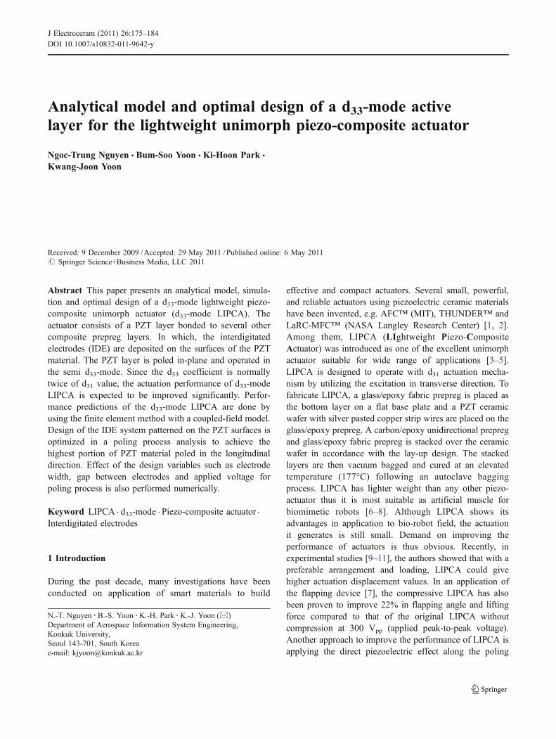
In each incremental step, a loop is triggered to update ofthe material properties according to the poling strength, tore-calculate the electric field solution and to compare thatwith the former solution of each element. The iterationstops when a predefined criterion on the difference inorientation and magnitude of the electric field is reached.The poling process simulation was implemented in theANSYS Parametric Design Language (APDL) using theadvanced techniques to access the electric field solutions ofthe integration point in every element at the end of eachiteration to check the poling status and update the materialproperties. The procedure can be summarized in Chart 1.
Simulation of the poling process for IDE ceramic waferis shown in Fig. 4. A typical result reveals that the electricfield distribution in RVE is strongly inhomogeneous andanisotropic. There are different regions:
& Effective region (A): the electric field is homogeneous;material is polarized along the longitudinal axis.
Table 3 Typical property values of PZT material (source: CTS Corp.)
Properties CTS 3203HD
Dielectric constant KT3 3800
Coercive field EC (kV/mm) 0.8
Remanent polarization PR (μC/cm2) 39
Elastic constants (short circuit) SE11 (×10−12 m2/N) 16.6
SE33 (×10−12m2/N) 21
ν12 0.31
Piezoelectric strain coefficient d31 (×10−12m/V) −320
d33 (×10−12m/V) 650
J Electroceram (2011) 26:175–184 179
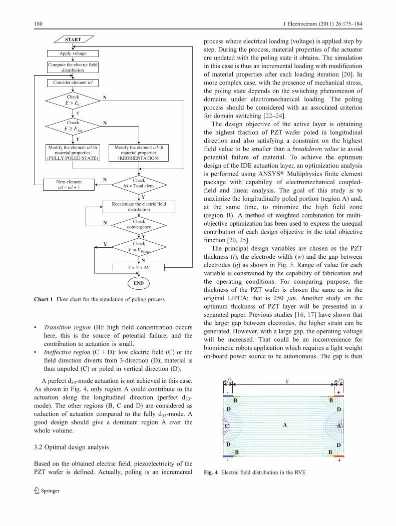
& Transition region (B): high field concentration occurshere, this is the source of potential failure, and thecontribution to actuation is small.
& Ineffective region (C + D): low electric field (C) or thefield direction diverts from 3-direction (D); material isthus unpoled (C) or poled in vertical direction (D).
A perfect d33-mode actuation is not achieved in this case.As shown in Fig. 4, only region A could contribute to theactuation along the longitudinal direction (perfect d33-mode). The other regions (B, C and D) are considered asreduction of actuation compared to the fully d33-mode. Agood design should give a dominant region A over thewhole volume.
3.2 Optimal design analysis
Based on the obtained electric field, piezoelectricity of thePZT wafer is defined. Actually, poling is an incremental
process where electrical loading (voltage) is applied step bystep. During the process, material properties of the actuatorare updated with the poling state it obtains. The simulationin this case is thus an incremental loading with modificationof material properties after each loading iteration [20]. Inmore complex case, with the presence of mechanical stress,the poling state depends on the switching phenomenon ofdomains under electromechanical loading. The polingprocess should be considered with an associated criterionfor domain switching [22–24].
The design objective of the active layer is obtainingthe highest fraction of PZT wafer poled in longitudinaldirection and also satisfying a constraint on the highestfield value to be smaller than a breakdown value to avoidpotential failure of material. To achieve the optimumdesign of the IDE actuation layer, an optimization analysisis performed using ANSYS® Multiphysics finite elementpackage with capability of electromechanical coupled-field and linear analysis. The goal of this study is tomaximize the longitudinally poled portion (region A) and,at the same time, to minimize the high field zone(region B). A method of weighted combination for multi-objective optimization has been used to express the unequalcontribution of each design objective in the total objectivefunction [20, 25].
The principal design variables are chosen as the PZTthickness (t), the electrode width (w) and the gap betweenelectrodes (g) as shown in Fig. 5. Range of value for eachvariable is constrained by the capability of fabrication andthe operating conditions. For comparing purpose, thethickness of the PZT wafer is chosen the same as in theoriginal LIPCA; that is 250 μm. Another study on theoptimum thickness of PZT layer will be presented in aseparated paper. Previous studies [16, 17] have shown thatthe larger gap between electrodes, the higher strain can begenerated. However, with a large gap, the operating voltagewill be increased. That could be an inconvenience forbiomimetic robots application which requires a light weighton-board power source to be autonomous. The gap is then
Compute the electric field distribution
Check
CEE >
Check
SatEE ≥
Modify the element iel-th material properties
(FULLY POLED STATE)
Modify the element iel-th material properties
(REORIENTATION)
Recalculate the electric field distribution
Check convergence
Check
PolingVV =
Apply voltage
Y
Next element iel = iel + 1
Consider element iel
Check iel = Total elem.
START
V = V + V
END
N
N
Y
Y
Y
N
N
Y
N
Δ
Chart 1 Flow chart for the simulation of poling process
+-
B
C A
B
BB
C
g w/2w/2
+-
D
D
D
D
Fig. 4 Electric field distribution in the RVE
180 J Electroceram (2011) 26:175–184

constrained to a maximum value, says 400 μm, accordingto the working range of the on-board power supplier. Withlimitations in current fabrication process, the width ofpatterned electrodes (w) and the gaps (g) between themcould not be smaller than 5 μm.
The design variables including electrode width (w), gapbetween electrodes (g) and the applied voltage (V) in polingprocess are varied and are automatically updated for eachiteration following the subspace approximation and firstorder algorithm in ANSYS® software [26]. By tracking thevariation of design variables and objective function we canmonitor how the poling process is affected by electrodewidth, gap between electrodes and applied voltage. Theanalysis is terminated when the difference in objectivefunction of two successive iterations is smaller than somegiven tolerance.
4 Results and discussions
4.1 Effects of the electrode gap and width
It has already been shown that “dead zones” exist belowthe electrode fingers, with the field magnitude being low,and out of plane [16, 17]. With larger electrode separationthe proportion of dead zones is lower. Meanwhile, thevoltage required to operate the device is higher. Incontrast, small electrode separations lower the operationalvoltage, but increase the proportion of “dead zones”.There should be a compromise between the achievableactuation strain and operational voltage. Figure 6 shows atypical tendency of the ineffective area in RVE of anelectrode design with electrode gap variations and otherfixed parameters. Moreover, for thinner substrates theelectrode separation can be reduced significantly whilestill maintaining a high proportion of the optimumd33-mode response.
It was found that by increasing the electrode width theelectric field strength in the x-direction between electrodesis increased and the “dead zone” under the electrodes,where the field in the x-direction is relatively low, alsobecomes larger [16]. The electric field in the “dead zones”is perpendicular to the actuation direction (x). For thinner
electrodes, a relatively weak field is observed between theelectrode fingers. It was reported that there exists an optimumwidth of electrode for which the strain per unit applied voltageis at a maximum, and this optimum width is independent ofelectrode separation and wafer thickness [17]. The polingstudy has showed that a field concentration exists at theelectrode edges [20]. The magnitude of the field strength inthis location increases as the electrode width is reduced,whilst the direction remains largely unaffected. The non-uniform fields present at electrode edges can cause cracking ofthe piezoelectric substrate resulting in device deterioration.This is a consequence of the large and non-uniformmechanical stresses induced via the piezoelectric effect.Although induced stresses are not quantified in this study,they can be an important effect that leads to device failure.
4.2 Optimization of the active layer with surface IDEs
For comparing purpose, the thickness of the PZT wafer ischosen the same as in the original LIPCA. Moreover, fromprevious argument, one can see that with the larger gapbetween electrodes, the higher strain can be generated.However, with a large gap, the operating voltage will beincreased. As explained above, the chosen gap is a compromisebetween achievable actuation strain and operational voltage. Itis then constrained to a maximum value of 400 μm in the d33-mode LIPCA hereinafter. The optimum poling process isachieved with the optimum set of design variables given inTable 4. The electrode width w=133μm, gap betweenelectrodes g=400 μm and the applied voltage V=1358 Vpp.
d
g
Fig. 5 PZT with electrodes patterned on surfaces
Table 4 Optimal design for a typical active layer with surface IDEs
Electrode width w (μm) 133
Electrode spacingg (μm) 400
Applied poling voltage (V) 1358 Vpp
Portion of breakdown volume 0.998%
Portion of unpoled volume 19.27%
Total ineffective volume portion 20.27%
0
5
10
15
20
25
30
200 300 400 500 600 700 800 900 1000Electrode gap (μm )
Tot
al in
effe
ctiv
e ar
ea (%
)
Fig. 6 Tendency of the ineffective area with electrode gap variations
J Electroceram (2011) 26:175–184 181
The reduction of actuation is defined as the ratio of the sum ofunpoled and high field volume to the total volume.
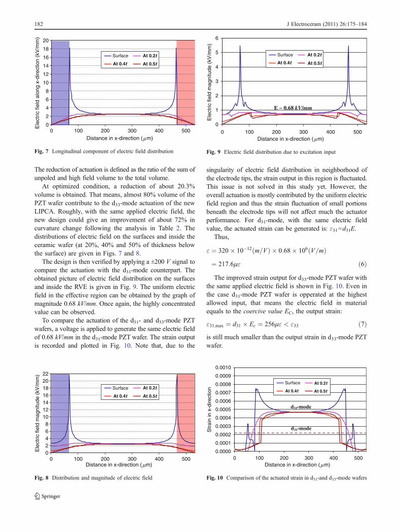
At optimized condition, a reduction of about 20.3%volume is obtained. That means, almost 80% volume of thePZT wafer contribute to the d33-mode actuation of the newLIPCA. Roughly, with the same applied electric field, thenew design could give an improvement of about 72% incurvature change following the analysis in Table 2. Thedistributions of electric field on the surfaces and inside theceramic wafer (at 20%, 40% and 50% of thickness belowthe surface) are given in Figs. 7 and 8.
The design is then verified by applying a ±200 V signal tocompare the actuation with the d31-mode counterpart. Theobtained picture of electric field distribution on the surfacesand inside the RVE is given in Fig. 9. The uniform electricfield in the effective region can be obtained by the graph ofmagnitude 0.68 kV/mm. Once again, the highly concentratedvalue can be observed.
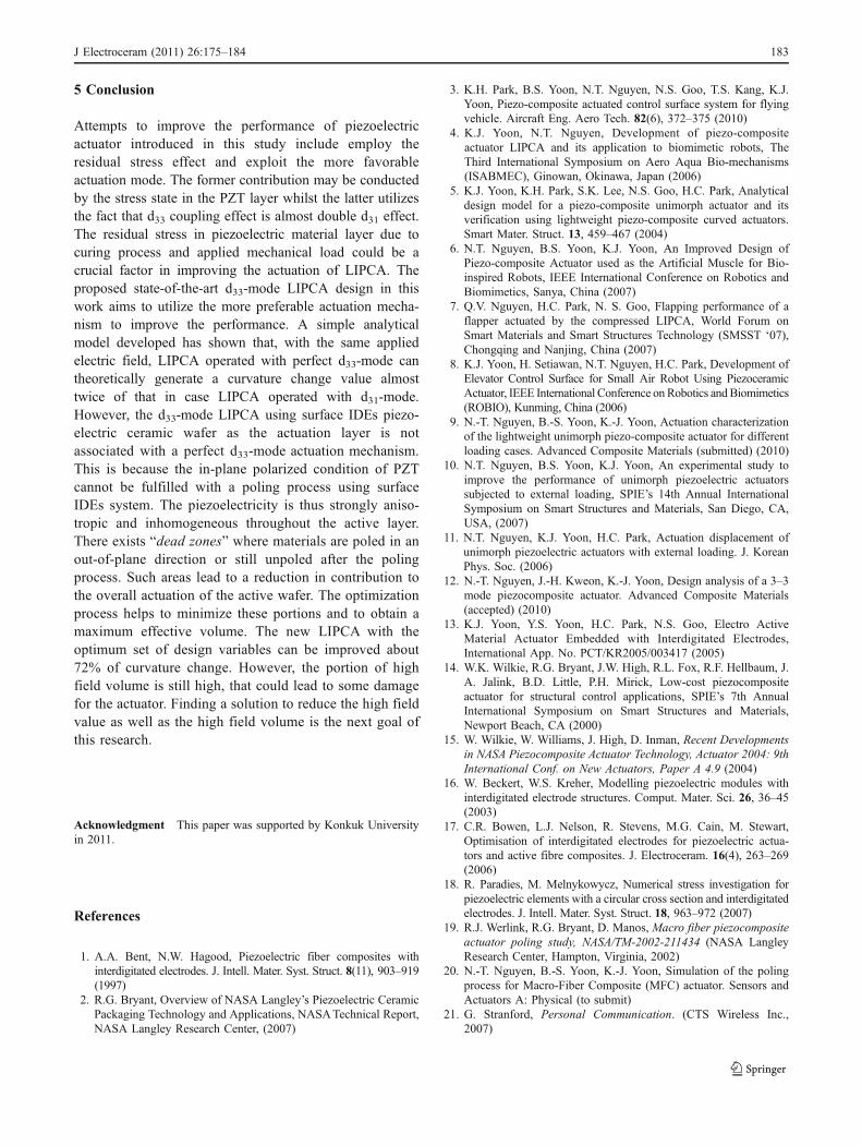
To compare the actuation of the d31- and d33-mode PZTwafers, a voltage is applied to generate the same electric fieldof 0.68 kV/mm in the d31-mode PZT wafer. The strain outputis recorded and plotted in Fig. 10. Note that, due to the
singularity of electric field distribution in neighborhood ofthe electrode tips, the strain output in this region is fluctuated.This issue is not solved in this study yet. However, theoverall actuation is mostly contributed by the uniform electricfield region and thus the strain fluctuation of small portionsbeneath the electrode tips will not affect much the actuatorperformance. For d31-mode, with the same electric fieldvalue, the actuated strain can be generated is: ε31=d31E.
Thus,
" ¼ 320� 10�12 m=Vð Þ � 0:68� 106 V=mð Þ¼ 217:6m" ð6ÞThe improved strain output for d33-mode PZTwafer with
the same applied electric field is shown in Fig. 10. Even inthe case d31-mode PZT wafer is opperated at the highestallowed input, that means the electric field in materialequals to the coercive value EC, the output strain:
"31;max ¼ d31 � Ec ¼ 256m" < "33 ð7Þis still much smaller than the output strain in d33-mode PZTwafer.
0
2
4
6
8
10
12
14
16
18
20
0 100 200 300 400 500
Distance in x-direction (μm)
Ele
ctric
fiel
d al
ong
x-di
rect
ion
(kV
/mm
)
Surface
At 0.5t
At 0.2t
At 0.4t
Fig. 7 Longitudinal component of electric field distribution
02468
10121416182022
0 100 200 300 400 500Distance in x-direction (μm)
Ele
ctric
fiel
d m
agni
tude
(kV
/mm
)
Surface
y = 150 At 0.5t
At 0.2t
At 0.4t
Fig. 8 Distribution and magnitude of electric field
0
1
2
3
4
5
6
0 100 200 300 400 500Distance in x-direction (μm)
Ele
ctric
fiel
d m
agni
tude
(kV
/mm
)
Surface y = 200
E ~ 0.68 kV/mm
At 0.5t
At 0.2t
At 0.4t
Fig. 9 Electric field distribution due to excitation input
0.0000
0.0001
0.0002
0.0003
0.0004
0.0005
0.0006
0.0007
0.0008
0.0009
0.0010
0 100 200 300 400 500Distance in x-direction (μm)
Str
ain
in x
-dire
ctio
n
Surface
d31-mode
d33-mode
At 0.2t
At 0.5tAt 0.4t
Fig. 10 Comparison of the actuated strain in d31-and d33-mode wafers
182 J Electroceram (2011) 26:175–184
5 Conclusion
Attempts to improve the performance of piezoelectricactuator introduced in this study include employ theresidual stress effect and exploit the more favorableactuation mode. The former contribution may be conductedby the stress state in the PZT layer whilst the latter utilizesthe fact that d33 coupling effect is almost double d31 effect.The residual stress in piezoelectric material layer due tocuring process and applied mechanical load could be acrucial factor in improving the actuation of LIPCA. Theproposed state-of-the-art d33-mode LIPCA design in thiswork aims to utilize the more preferable actuation mecha-nism to improve the performance. A simple analyticalmodel developed has shown that, with the same appliedelectric field, LIPCA operated with perfect d33-mode cantheoretically generate a curvature change value almosttwice of that in case LIPCA operated with d31-mode.However, the d33-mode LIPCA using surface IDEs piezo-electric ceramic wafer as the actuation layer is notassociated with a perfect d33-mode actuation mechanism.This is because the in-plane polarized condition of PZTcannot be fulfilled with a poling process using surfaceIDEs system. The piezoelectricity is thus strongly aniso-tropic and inhomogeneous throughout the active layer.There exists “dead zones” where materials are poled in anout-of-plane direction or still unpoled after the polingprocess. Such areas lead to a reduction in contribution tothe overall actuation of the active wafer. The optimizationprocess helps to minimize these portions and to obtain amaximum effective volume. The new LIPCA with theoptimum set of design variables can be improved about72% of curvature change. However, the portion of highfield volume is still high, that could lead to some damagefor the actuator. Finding a solution to reduce the high fieldvalue as well as the high field volume is the next goal ofthis research.
Acknowledgment This paper was supported by Konkuk Universityin 2011.
References
1. A.A. Bent, N.W. Hagood, Piezoelectric fiber composites withinterdigitated electrodes. J. Intell. Mater. Syst. Struct. 8(11), 903–919(1997)
2. R.G. Bryant, Overview of NASA Langley’s Piezoelectric CeramicPackaging Technology and Applications, NASATechnical Report,NASA Langley Research Center, (2007)
3. K.H. Park, B.S. Yoon, N.T. Nguyen, N.S. Goo, T.S. Kang, K.J.Yoon, Piezo-composite actuated control surface system for flyingvehicle. Aircraft Eng. Aero Tech. 82(6), 372–375 (2010)
4. K.J. Yoon, N.T. Nguyen, Development of piezo-compositeactuator LIPCA and its application to biomimetic robots, TheThird International Symposium on Aero Aqua Bio-mechanisms(ISABMEC), Ginowan, Okinawa, Japan (2006)
5. K.J. Yoon, K.H. Park, S.K. Lee, N.S. Goo, H.C. Park, Analyticaldesign model for a piezo-composite unimorph actuator and itsverification using lightweight piezo-composite curved actuators.Smart Mater. Struct. 13, 459–467 (2004)
6. N.T. Nguyen, B.S. Yoon, K.J. Yoon, An Improved Design ofPiezo-composite Actuator used as the Artificial Muscle for Bio-inspired Robots, IEEE International Conference on Robotics andBiomimetics, Sanya, China (2007)
7. Q.V. Nguyen, H.C. Park, N. S. Goo, Flapping performance of aflapper actuated by the compressed LIPCA, World Forum onSmart Materials and Smart Structures Technology (SMSST ‘07),Chongqing and Nanjing, China (2007)
8. K.J. Yoon, H. Setiawan, N.T. Nguyen, H.C. Park, Development ofElevator Control Surface for Small Air Robot Using PiezoceramicActuator, IEEE International Conference onRobotics andBiomimetics(ROBIO), Kunming, China (2006)
9. N.-T. Nguyen, B.-S. Yoon, K.-J. Yoon, Actuation characterizationof the lightweight unimorph piezo-composite actuator for differentloading cases. Advanced Composite Materials (submitted) (2010)
10. N.T. Nguyen, B.S. Yoon, K.J. Yoon, An experimental study toimprove the performance of unimorph piezoelectric actuatorssubjected to external loading, SPIE’s 14th Annual InternationalSymposium on Smart Structures and Materials, San Diego, CA,USA, (2007)
11. N.T. Nguyen, K.J. Yoon, H.C. Park, Actuation displacement ofunimorph piezoelectric actuators with external loading. J. KoreanPhys. Soc. (2006)
12. N.-T. Nguyen, J.-H. Kweon, K.-J. Yoon, Design analysis of a 3–3mode piezocomposite actuator. Advanced Composite Materials(accepted) (2010)
13. K.J. Yoon, Y.S. Yoon, H.C. Park, N.S. Goo, Electro ActiveMaterial Actuator Embedded with Interdigitated Electrodes,International App. No. PCT/KR2005/003417 (2005)
14. W.K. Wilkie, R.G. Bryant, J.W. High, R.L. Fox, R.F. Hellbaum, J.A. Jalink, B.D. Little, P.H. Mirick, Low-cost piezocompositeactuator for structural control applications, SPIE’s 7th AnnualInternational Symposium on Smart Structures and Materials,Newport Beach, CA (2000)
15. W. Wilkie, W. Williams, J. High, D. Inman, Recent Developmentsin NASA Piezocomposite Actuator Technology, Actuator 2004: 9thInternational Conf. on New Actuators, Paper A 4.9 (2004)
16. W. Beckert, W.S. Kreher, Modelling piezoelectric modules withinterdigitated electrode structures. Comput. Mater. Sci. 26, 36–45(2003)
17. C.R. Bowen, L.J. Nelson, R. Stevens, M.G. Cain, M. Stewart,Optimisation of interdigitated electrodes for piezoelectric actua-tors and active fibre composites. J. Electroceram. 16(4), 263–269(2006)
18. R. Paradies, M. Melnykowycz, Numerical stress investigation forpiezoelectric elements with a circular cross section and interdigitatedelectrodes. J. Intell. Mater. Syst. Struct. 18, 963–972 (2007)
19. R.J. Werlink, R.G. Bryant, D. Manos, Macro fiber piezocompositeactuator poling study, NASA/TM-2002-211434 (NASA LangleyResearch Center, Hampton, Virginia, 2002)
20. N.-T. Nguyen, B.-S. Yoon, K.-J. Yoon, Simulation of the polingprocess for Macro-Fiber Composite (MFC) actuator. Sensors andActuators A: Physical (to submit)
21. G. Stranford, Personal Communication. (CTS Wireless Inc.,2007)
J Electroceram (2011) 26:175–184 183

22. S.C. Hwang, J.E. Huber, R.M. McMeeking, N.A. Fleck, Thesimulation of switching in polycrystalline ferroelectric ceramics. J.Appl. Phys. 84(3), 1530–1540 (1998)
23. S.C.Hwang, C.S. Lynch, R.M.McMeeking, Ferroelectric/ferroelasticinteractions and a polarization switching model. Acta Metall. Mater.43(5), 2073–2084 (1995)
24. S.C. Hwang, R.M.McMeeking, A finite elementmodel of ferroelasticpolycrystals. Int. J. Solids Struct. 36(10), 1541–1556 (1999)
25. A. Messac, A.A. Mullur, Multiobjective optimization: Conceptsand methods, in Optimization of structural and mechanicalsystems, ed. by J.S. Arora (World Scientific, Singapore, 2007)
26. http://www.ansys.com/, ANSYS Documentation Manuals
184 J Electroceram (2011) 26:175–184