An FPGA Scalable Software-Defined Radio Platform for UAS ...
10
An FPGA Scalable Software-Defined Radio Platform for UAS Communications Research Angelo Manco and Vittorio U. Castrillo CIRA Italian Aerospace Research Centre, Italy Email: {a.manco, v.castrillo}@cira.it Abstract —In the framework of modern Unmanned Aerial System (UAS) ground-board communications, a data-link system should provide with the following features [1]: multiband and adaptive modulations for responding to channel conditions changes and multi-standard interoperability, interferences resilience with a secure physical layer, incorporation of an air-to-air link complementary to the classical air-to-ground links. Varying the available communication functions to provide the above features without the need to substitute on-board components is a desired target. For this purpose, a Field Programmable Gate Aray (FPGA) scalable Software Defined Radio hardware Platform (SDRP) and its control and baseband signal processing architecture have been developed. The platform is composed by means of three boards which provide respectively the power supply, an FPGA based processing core and the radio frequency front-end. The control and baseband signal processing architecture, implemented on the FPGA, is designed with an application- independent section, working as a base reference design, and a reconfigurable section that implements communication functions and algorithms. The overall platform, at the board and FPGA architecture level, has been designed considering scalability and modularity as key features. Thanks to this platform a data-link which responds to the above target can be easily implemented. As a case study a reconfigurable data-link between a UAS and a Ground Control Station (GCS), designed to establish reliable communication in all the phases of a flight (parking, taxiing, taking off, cruising and landing), is presented. Index Terms—Field-Programmable Gate Array (FPGA), Unmanned Aerial System (UAS), Software Defined Radio (SDR) I. INTRODUCTION The Software-Defined Radio Platform design project has the goal to provide the Italian Aerospace Research Center (CIRA) with a flexible radio platform to research in the field of communications for Unmanned Aerial Systems. During the last decade, Software-Defined Radios have become the state-of-the-art for the prototyping and implementation of communication systems in the field of terrestrial communications. Their popularity and utilization are increasing also in the aeronautical [2]-[4] and space applications [5]-[7]. A classical radio system is designed for a particular operative context with features (coding schemes, Manuscript received July 20, 2020; revised January 15, 2021. Corresponding author email: [email protected]. doi:10.12720/jcm.16.2.42-51 waveforms, bandwidths, etc.) tailored for the specific application. A modify of these features could require changing part of the system devices. On the other hand, a Software-Defined Radio can mutate his characteristics without changing the physical layer [8]. The SDR paradigm flexibility relies on the digital implementation of communications algorithms and on the availability of programmable wideband RF transceivers that integrate all the necessary functions in one chip. For high- performance SDR systems, Field-Programmable Gate Arrays (FPGA) could be used to develop custom hardware architectures for digital baseband processing at high data rates in real-time [9]. The development of High-Level Synthesis (HLS) and code generation tools have helped the effort reduction for FPGA design [10], [11]. The chance to modify the FPGA configuration and, hence, the internal architecture of the elaboration paths of the baseband signals, is the key feature for the implementation of a versatile SDR based UAS communications system [12]-[16]. Thus, the SDR can modify his characteristics during the flight or among different flights (when, for example, the communication channel changes or when it is necessary to guarantee multi-standard interoperability). As a result, using only one hardware system for different radio personalities reduces on-board size, weight, and power. The UAS handling costs are also minimized because there is no need to substitute on-board components when there are different radio implementations to test. This paper presents the design of an SDR platform suitable for on-board applications, that is, a platform optimized at higher Technology Readiness Level (TRL), and ready to be integrated into the CIRA UAS aircraft. It is characterized by compact size, modularity, consumption optimization, compatibility with typical on- board data interfaces and available power supply. An internal FPGA architecture for digital signal processing has been developed with the focus on design re-use. Finally, a case study scenario is shown. II. SDR PLATFORM DESCRIPTION The designed SDR platform is made up of three separate electronic boards, integrated, electrically and mechanically, in a vertical way according to a "turret" scheme, as shown in Fig. 1, to reduce and optimize the overall dimensions. Journal of Communications Vol. 16, No. 2, February 2021 42 ©2021 Journal of Communications
-
Upload
khangminh22 -
Category
Documents
-
view
0 -
download
0
Transcript of An FPGA Scalable Software-Defined Radio Platform for UAS ...

An FPGA Scalable Software-Defined Radio Platform for
UAS Communications Research
Angelo Manco and Vittorio U. Castrillo CIRA Italian Aerospace Research Centre, Italy
Email: {a.manco, v.castrillo}@cira.it
Abstract—In the framework of modern Unmanned Aerial
System (UAS) ground-board communications, a data-link
system should provide with the following features [1]:
multiband and adaptive modulations for responding to channel
conditions changes and multi-standard interoperability,
interferences resilience with a secure physical layer,
incorporation of an air-to-air link complementary to the
classical air-to-ground links. Varying the available
communication functions to provide the above features without
the need to substitute on-board components is a desired target.
For this purpose, a Field Programmable Gate Aray (FPGA)
scalable Software Defined Radio hardware Platform (SDRP)
and its control and baseband signal processing architecture have
been developed. The platform is composed by means of three
boards which provide respectively the power supply, an FPGA
based processing core and the radio frequency front-end. The
control and baseband signal processing architecture,
implemented on the FPGA, is designed with an application-
independent section, working as a base reference design, and a
reconfigurable section that implements communication
functions and algorithms. The overall platform, at the board and
FPGA architecture level, has been designed considering
scalability and modularity as key features. Thanks to this
platform a data-link which responds to the above target can be
easily implemented. As a case study a reconfigurable data-link
between a UAS and a Ground Control Station (GCS), designed
to establish reliable communication in all the phases of a flight
(parking, taxiing, taking off, cruising and landing), is presented. Index Terms—Field-Programmable Gate Array (FPGA),
Unmanned Aerial System (UAS), Software Defined Radio
(SDR)
I. INTRODUCTION
The Software-Defined Radio Platform design project
has the goal to provide the Italian Aerospace Research
Center (CIRA) with a flexible radio platform to research
in the field of communications for Unmanned Aerial
Systems. During the last decade, Software-Defined
Radios have become the state-of-the-art for the
prototyping and implementation of communication
systems in the field of terrestrial communications. Their
popularity and utilization are increasing also in the
aeronautical [2]-[4] and space applications [5]-[7]. A
classical radio system is designed for a particular
operative context with features (coding schemes,
Manuscript received July 20, 2020; revised January 15, 2021.
Corresponding author email: [email protected].
doi:10.12720/jcm.16.2.42-51
waveforms, bandwidths, etc.) tailored for the specific
application. A modify of these features could require
changing part of the system devices. On the other hand, a
Software-Defined Radio can mutate his characteristics
without changing the physical layer [8]. The SDR
paradigm flexibility relies on the digital implementation
of communications algorithms and on the availability of
programmable wideband RF transceivers that integrate all
the necessary functions in one chip. For high-
performance SDR systems, Field-Programmable Gate
Arrays (FPGA) could be used to develop custom
hardware architectures for digital baseband processing at
high data rates in real-time [9]. The development of
High-Level Synthesis (HLS) and code generation tools
have helped the effort reduction for FPGA design [10],
[11]. The chance to modify the FPGA configuration and,
hence, the internal architecture of the elaboration paths of
the baseband signals, is the key feature for the
implementation of a versatile SDR based UAS
communications system [12]-[16]. Thus, the SDR can
modify his characteristics during the flight or among
different flights (when, for example, the communication
channel changes or when it is necessary to guarantee
multi-standard interoperability). As a result, using only
one hardware system for different radio personalities
reduces on-board size, weight, and power. The UAS
handling costs are also minimized because there is no
need to substitute on-board components when there are
different radio implementations to test.
This paper presents the design of an SDR platform
suitable for on-board applications, that is, a platform
optimized at higher Technology Readiness Level (TRL),
and ready to be integrated into the CIRA UAS aircraft. It
is characterized by compact size, modularity,
consumption optimization, compatibility with typical on-
board data interfaces and available power supply. An
internal FPGA architecture for digital signal processing
has been developed with the focus on design re-use.
Finally, a case study scenario is shown.
II. SDR PLATFORM DESCRIPTION
The designed SDR platform is made up of three
separate electronic boards, integrated, electrically and
mechanically, in a vertical way according to a "turret"
scheme, as shown in Fig. 1, to reduce and optimize the
overall dimensions.
Journal of Communications Vol. 16, No. 2, February 2021
42©2021 Journal of Communications

Genius Board
PGen Board
RF Board
Fig. 1. SDR platform vertical layout scheme.
The first board, named PGen, provides power to the
entire platform, using as input an available on-board
power supply. An input voltage level equal to 28VDC
(with a wide tolerance range) is supported since it is
typically provided by the aircrafts power supply systems
and, in particular, is supported by CIRA UAS. The
second board, named Genius, is the core of the platform
and is used to process the baseband signals and to provide
an embedded microprocessor which controls the signal
processing architectures developed for the
communications and the peripherals available on the
platform. The board is based on a Xilinx Artix-7 FPGA
and is similar to an evaluation board but with smaller size,
dedicated interfaces suitable to communicate with the on-
board devices connected to the data-link system, fewer
integrated components and, accordingly, lower power
consumption. Finally, the third board of the platform,
named RF Board, provides a wideband radio-frequency
front-end transceiver
Genius and PGen are connected using terminal blocks
integrated on the boards which could be substituted with
vertical board-to-board connectors to further optimize the
overall platform size. Radio Frequency Board is
connected to Genius by means of an FPGA Mezzanine
Cards (FMC) connector. In fact, Genius is Vita 57.1
compliant, a feature that could allow to add other
daughter cards (for example Digital Signal Processor
units or Analog-to-Digital Converter boards) suitable for
different applications instead of the RF Board. The
portion of Genius and PGen boards located under the RF
Board is partially hollow so that a power amplifier and/or
an heatsink can be easily integrated if necessary.
In the next sections the characteristics of the individual
boards of the platform are described.
A. Genius Board
As previously stated, Genius is an FPGA board
optimized and customized for the on-board integration on
CIRA UAS. For its design we started from technical
solutions already adopted by evaluation boards that use
the same FPGA chip (the same family and the same
device, the XC7A200T device in this case, but not
necessarily the same package and the same number of
I/Os). For Genius development reference board designs
were “NEXYS Video Board” provided by Digilent [17]
and “AC701 Evaluation Board for the Artix-7 FPGA”
provided by Xilinx [18].
Genius board block diagram is shown in Fig. 2. Each
block is described below:
#4 user LED#4 user LED#4 user LEDSwitchesSwitchesSwitches
PulsantiPulsanti
VITA 57.1 FMC LPC Standard Connector
LEDsSwitchesPulsanti
FPGA Programming Mode Selector
USB-UART InterfaceMicro-USBConnector
JTAG Header
Connettori Alimentazione
JTAGBuffer
JTAG ChainSelector
JTAG-SMT Programming
Driver 422
Connettore
Quad Receiver 422
Flash Memory
DD3 Memory
100MHz Clock
General PurposeConnector
ConnettoreConnettoreConnectorsfor RS422
Connettori AlimentazioneConnettori AlimentazionePower Supply Terminal Blocks Buttons
Receiver 422Receiver 422#4 RS422 Receivers
Driver 422Driver 422#4 RS422 Drivers
FPGA
Logic AND for PGood Signals
Pgood SignalsTerminal Block
FAN Connector
FAN on/off Switch
Buffer forPGood Signals
Fig. 2. Genius board block diagram.
JTAG Buffer and Buffer for PGood Signals – The first
block is used to buffer JTAG (Joint Test Action Group)
signals for the FPGA programming. The second one
allows to buffer the Power-Good signals indicating that
voltage values made available by the power supply board
(PGen) are operating normally (the output voltage of the
related regulator is approximately above 90% of its
nominal output). These buffers are provided by a single
chip.
VITA 57.1 FMC Low Pin Count Standard Connector –
This is the standard high-speed array connector [19] used
to interface FMC. In SDR platform it is used to interface
the RF Board which provides the radio-frequency
transceiver.
Power Supply and PGood Signals Terminal Blocks –
They are used to receive power supply and power-good
signals from PGen Board. They could be replaced by
vertical board-to-board connectors to further compact the
SDR platform size.
General Purpose Connector, Micro-USB Connector
and Connectors for RS422 buses – The first connector
can be used to interface Genius with other expansion
boards, in particular the Com-Block modules [20], which
could be used, for example, to add to the platform another
Journal of Communications Vol. 16, No. 2, February 2021
43©2021 Journal of Communications

RF front-end. The second one can be used to connecting
the board to an external device provided with an
Universal Serial Bus interface. The last connectors can be
used to transmit/receive serial synchronous RS422
signals or for RS422 UART signals.
RS422 Drivers and Receivers – They allow to interface
the FPGA with external units to transmit and receive
synchronous bit streams with RS422 signal levels. They
can also be used to provide four RS422 asynchronous
full-duplex serial ports. RS422 signals are typically
provided by the on-board devices connected to the data-
link systems and, in particular, they are the interface
signals provided by the telemetry sources and
telecommands sinks of CIRA UAS avionics by means of
an on-board multiplexer/demultiplexer subsystem.
FPGA – This is the main component of the board and
is used to implement SDR algorithms, soft-core
microcontrollers and, more generally, all the functions
need for SDR applications. The device has been selected
on the basis of a trade-off between performance (in terms
of available logic resources), cost and design complexity
of the related print circuit board. The selected FPGA is
the chip XILINX XC7A200T-2FBG484I of Artix-7
series [21]. The related package is a Ball Grid Array
(BGA) with a size of 23 x 23 mm and 285 I/Os.
JTAG Header – This connector is used for FPGA
programming in JTAG mode.
USB-UART Interface – It allows the FPGA to
communicate with external devices with USB interface,
by means of a conversion of the USB signals in UART
(universal asynchronous receiver-transmitter) signals
suitable for FPGA I/O.
Fan Switches – They allow to switch on/off an external
fan (or other external components) by means of
commands generated by FPGA.
JTAG-SMT Programming – It is a compact electronic
board integrated on the Genius board to simplify the
FPGA programming. With this board it is possible to
program the FPGA directly using the Xilinx tools and a
mini-USB cable.
DDR3 Memory – This is 2Gbit DRAM (Dynamic
Random Access) memory (chip Micron mt41j128m16jt-
k125 [22]) integrated on the Genius Board. The
interconnections between the FPGA and the DDR3
(Double Data Rate) memory for
control/command/address bus have been implemented
using a fly-by architecture with termination resistors
connected to the bus signals on one side and to a
termination voltage (provided by a dedicated chip,
integrated on the Genius board, working as voltage
regulator) on the other side [23]. For data buses point-to
point connections have implemented exploiting the On-
Die Termination (ODT) available into the memory chip.
Flash Memory – This a non-volatile SPI (Serial
Peripheral Interface) flash memory used to store the
FPGA configurations (i.e. the bitstream program file).
The selected FPGA does not require all the memory for
the configuration file and about 70% of the memory can
be used to store user data.
100MHz Clock – This is the input source clock for
FPGA. It is provided by an external oscillator (Microchip
DSC1101 chip [24]) which utilizes a proven silicon
MEMS (Micro-ElectroMechanical Systems) technology
to provide excellent jitter and stability over a wide range
of supply voltages and temperatures.
Logic AND for PGood Signals – This component is
used to obtain a single power-good signal from those
ones coming from PGen board. The obtained signal is
provided as the power good signal for the pinout
compatibility with the standard interface of the Vita 57.1
FMC LPC connector.
JTAG Chain Selector – It allows to exclude (or not) the
mezzanine card integrated on the Genius card from the
JTAG programming chain. The block can detect the
presence of the mezzanine card by means of the presence
or absence of a short circuit between two pins of the
VITA 57.1 FMC LPC standard connector.
FPGA Programming Mode Selector – It allows to
select the FPGA programming mode. Two modes are
available: FPGA can be programmed using JTAG or its
configuration can be loaded from the Flash Memory at
the power up.
Buttons, Switches and LEDs – These components are
used to facilitate troubleshooting, monitoring and
management of the Genius board. In particular there are
present on the board: 1) four general purpose buttons
directly connected to the FPGA (one of them is intended
to reset the soft-core implemented on the FPGA, but can
also be used for other purposes) and one button used to
reset the FPGA configuration; 2) four general purpose
toggle switches integrated in a single component (in order
to save space on the board) whose status can be read
directly from the FPGA; 3) four general purpose LEDs
controlled directly by the FPGA, one LED used to verify
the completion of the FPGA configuration sequence and
two LEDs used to monitor the exchange of data with
external devices through the USB-UART interface.
The PCB is designed according to the rules reported in
[25]. Its stack-up is made up of 12 layers and six of which
are dedicate to power and ground planes and six used to
route signals. Top and bottom are routing layer. The
internal routing layers are always enclosed between 2
planes. The full stack-up is shown in Fig. 3.
Top LayerGND
Power
GNDPower
GND
Power
Routing Layer
Routing Layer
Routing Layer
Routing Layer
Bottom Layer Fig. 3. Genius board stack-up.
The traces connecting FPGA to DDR3 memory, FMC
connector and General-Purpose Connector have been
Journal of Communications Vol. 16, No. 2, February 2021
44©2021 Journal of Communications
designed using microstrips, striplines, differential
microstrips and differential striplines with a suitable
characteristic impedance. Furthermore, the design of the
digital interfaces between the FPGA and the DDR3
memory (data buses and control/command/address bus)
has been implemented equalizing the traces length to
obtain the same length in order to minimize any delay
[26]. Traces length equalization has also been used for
the traces connecting FPGA to FMC connector and to
General Purpose Connector with the aim of supporting
high-speed digital buses provided by other external FMC
boards.
B. RF Board
The selected RF Board is the part number AD-
FMComms3-EBZ developed by Analog Devices [27].
The board is an FMC provided with a highly integrated
2x2 RF transceiver (Analog Devices chip AD9361 [28]).
Thanks to this device, the board can operate in the 70
MHz to 6 GHz range. Supported channel bandwidths
vary from less than 200kHz to 56MHz, by both changing
sample rate and by changing digital filters and decimation
inside the AD9361.
The data path is fully integrated into AD9361. The
receive path consists of two independent direct
conversion receivers, each one with independent
automatic gain control (AGC), dc offset correction,
quadrature correction and digital filtering. A flexible
manual gain mode is also available and can be externally
controlled. Two high dynamic range analog-to-digital
converters (ADCs) per channel digitize the received I and
Q signals and pass them through configurable decimation
filters and 128-tap finite impulse response (FIR) filters to
produce a 12-bit output signal. The transmit path provides
two transmitters with a direct conversion architecture that
achieves high modulation accuracy with ultralow noise.
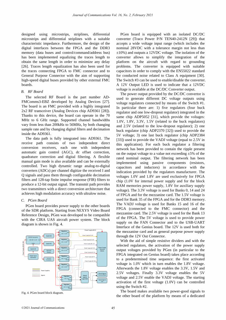
C. PGen Board
PGen board provides power supply to the other boards
of the SDR platform. Starting from NEXYS Video Board
Reference Design, PGen was developed to be compatible
with the CIRA UAS aircraft power system. The block
diagram is shown in Fig. 4.
DC/DC Converter
18V-36V → 12VIn Out
Enable
Switch #3
Power Input Connector
Switch #2
Switch #1
LED 12V Output
12V O UT Connector
In
En
OutRegulator
12V → 1.0V
In
En
OutRegulator
12V → 1.8V
In
En
OutRegulator
12V → 1.5V
In
En
Out
PGood
Regulator
12V → 3.3V
In
En
OutRegulator
12V → 2.5V
In
En
Out
PGood
Regulator
12V → 5V
In
En
Out
PGood
Regulator
12V → VADJ
PGood Signals
Logic AND
Power Supply Terminal
Blocks
Power Supply @ 1.0V
Power Supply @ 1.8V
Power Supply @ 1.5V
Power Supply @ 3.3V
Power Supply @ 2.5V
Power Supply @ 5V
Power Supply @ VADJ
PGood SignalsTerminal Block
Pgood SignalsLED
Power Supply @12V
Pow
er S
upp
ly @
18V
-36
V
Power Supplies
Signals
Fig. 4. PGen board block diagram.
PGen board is equipped with an isolated DC/DC
converter (Traco Power P/N TEN40-2412N [29]) that
accepts a wide voltage input range (which includes the
nominal 28VDC with a tolerance margin not less than
±10%) and outputs a 12VDC voltage. The isolation of the
converter allows to simplify the integration of the
platform on the aircraft with regard to grounding
problems. The converter is equipped with suitable
capacitors in order to comply with the EN55022 standard
for conducted noise related to Class A equipment [30].
The Switch #3 can be used to enable/disable the converter.
A 12V Output LED is used to indicate that a 12VDC
voltage is available at the DC/DC Converter output.
The power output provided by the DC/DC convertor is
used to generate different DC voltage outputs using
voltage regulators connected by means of the Switch #1.
In particular there are: 1) five regulators (four buck
regulator and one low-dropout regulator) integrated in the
same chip ADP5052 [31], which provide the voltages:
1.0V, 1.8V, 3.3V, 1.5V (related to the buck regulators)
and 2.5V (related to the low-dropout regulator); 2) one
buck regulator (chip ADP2370 [32]) used to provide the
5V voltage; 3) one last buck regulator (chip ADP2384
[33]) used to provide the VADJ voltage (equal to 2.5V in
this application). For each buck regulator a filtering
network has been provided to contain the ripple present
on the output voltage to a value not exceeding ±5% of the
rated nominal output. The filtering network has been
implemented using passive components (resistors,
capacitors and inductors) in accordance with the
indication provided by the regulators manufacturer. The
voltages 1.0V and 1.8V are used exclusively for FPGA
chip (1.0V for internal power supply and for the block
RAM memories power supply, 1.8V for auxiliary supply
voltage). The 3.3V voltage is used for Banks 0, 14 and 24
of FPGA and for the mezzanine card. The 1.5V voltage is
used for Bank 35 of the FPGA and for the DDR3 memory.
The VADJ voltage is used for Banks 15 and 16 of the
FPGA (connected to the FMC connector) and the
mezzanine card. The 2.5V voltage is used for the Bank 13
of the FPGA. The 5V voltage is used to provide power
supply on the FAN Connector and to the USB-UART
Interface of the Genius board. The 12V is used both for
the mezzanine card and as general purpose power supply
through the 12V Out Connector.
With the aid of simple resistive dividers and with the
selected regulators, the activation of the power supply
output voltages provided by PGen (in particular to the
FPGA integrated on Genius board) takes place according
to a predetermined time sequence: the first activated
voltage is 1.0V which in turn enables the 1.8V voltage.
Afterwards the 1.8V voltage enables the 3.3V, 1.5V and
2.5V voltages. Finally 3.3V voltage enables the 5V
voltage and 2.5V enable the VADJ voltage. The starting
activation of the first voltage (1.0V) can be controlled
using the Switch #2.
The board makes available two power-good signals to
the other board of the platform by means of a dedicated
Journal of Communications Vol. 16, No. 2, February 2021
45©2021 Journal of Communications

terminal block. The first power-good signal is the logic
AND between the output power-good signal of the chip
ADP5052 (related to the 3.3V output voltage) and the
output power-good signal of the chip ADP2370. A
dedicated LED is used to show that this power-good
signal is OK. The second power-good signal exiting
PGen board is the one related to the VADJ voltage
provided by the chip ADP2384. With these two power-
good signals is possible to verify, directly or indirectly,
that all the power supplies powered by PGen are working
properly except the 1.5V voltage output. However, this
last voltage can be indirectly checked using a dedicated
LED integrated on the Genius board. This LED is
controlled by a power-good signal generated by a
regulator integrated into the Genius board and used to
obtain a VTT voltage (the tracking termination voltage
used for the DDR3 integration) from the 1.5V provided
by PGen Board.
The PCB stack-up of PGen board is made up of four
layers. The internal layers are exclusively used as power
and ground planes. The external layers are used both for
signals routing and to provide copper pour area for power
and ground.
The realized Software-Defined Radio Platform is
shown in Fig. 5.
Fig. 5. Realized SDR platform.
III. FPGA BASEBAND ARCHITECTURE
An FPGA baseband architecture for the presented SDR
Platform has been developed. This architecture, shown in
Fig. 6, consists of two main sections: a permanent part,
that is application-independent, and a reconfigurable part
that implements the baseband elaboration of the
waveform used for the data-link (application dependant).
The logic related to the permanent part acts as a
reference design that can be used as a starting point for
the development of the SDRP-based data-link for
different operative scenarios. Depending on these ones,
the baseband processing is realized using IP (Intellectual
Property) Cores that belong to a custom component
library, previously developed, and takes place into the
reconfigurable part of the FPGA. The functions and the
waveforms of the radio can be changed in an off-line or
an on-line mode. In the first case, the FPGA on SDRP is
reconfigured with the desired elaboration chain before
every flight as needed. In the on-line mode, the partial
dynamic reconfiguration features of the Xilinx FPGAs
can be used to change radio personality during flight
operations [34]. In both cases, the FPGA reconfiguration
and so the possibility to time multiplex different
waveforms, allows saving power, cost, size, and weight
with respect to current radio systems implemented as
standalone equipment, especially for the UAS
communications context. In the following, the proposed
architecture is described in detail.
Fig. 6. Baseband architecture block diagram.
A. Permanent Section
The permanent section is the part of the FPGA logic
that implements:
The digital interface for the AD9361 RF Transceiver
The digital interface for I/O data stream
A soft-core microprocessor and its peripherals
The digital interface for the AD9361 chip is provided
by the Analog Devices as IP Core available for the use in
Vivado environment [35]. The block diagram is
represented in Fig. 7.
Fig. 7. Block diagram of the AD9361 digital interface IP core.
The IP Core architecture contains the following main
modules:
Interface module with programmable CMOS
(Complementary Metal–Oxide–Semiconductor) or
Journal of Communications Vol. 16, No. 2, February 2021
46©2021 Journal of Communications

LVDS (Low-Voltage Differential Signaling) electric
interface
Rx Core, that is the interface for the ADC path (for
each channel). It contains a data processing chain, an
ADC PN Monitor for interface validation and an ADC
Channel register map
Tx Core, that is the interface for the DAC (Digital-to-
Analog Converter) path (for each channel). It contains
a data processing chain with I/Q correction block and
a DAC Channel register map
Time Division Duplex Control module for the TDD
operative mode
AXI (Advanced eXtensible Interface) control and
status interface
The internal interface (i.e. to the custom processing
paths of the reconfigurable section) receives/transmits the
I/Q samples for each channel of the AD9361 chip.
The digital interface for the I/O data stream contains
two custom IP Cores:
Data-in, that is the interface to the input bitstream.
The incoming data is transferred to the FPGA chip
with a Source-Synchronous scheme, so the IP Core
realizes the sampling of the incoming data with the
external clock, a programmable delay of the incoming
data, a clock-domain crossing operation, and a
programmable randomization of the bitstream
following the IRIG-106 standard [36]. The core has
an AXI-4 Lite interface for control and configuration.
Data-out, that is the interface to the output bitstream.
It accepts two different bitstream and bitclock pairs
and contains a programmable delay block. It provides
a source-synchronous data transfer to a sink device
external to the SDR Platform. Furthermore, de-
randomization (IRIG-106 standard) can be performed
on the bitstream. The core has an AXI-4 Lite interface
for control and configuration.
The Microblaze processor soft-core from Xilinx [37] is
present in the permanent section of the architecture. The
available RAM processor for data and instruction is
composed by an internal 128 KB Block RAM and the
external 2 Gb DDR3 RAM. So, a DDR3 RAM controller
allows the data transfer to/from the external memory chip,
thanks to an AMBA (Advanced Microcontroller Bus
Architecture) AXI4 interconnection [38] with the
processor. A SPI controller is used for the transfer of
configuration, application and data stored in the external
flash memory chip. The processor architecture part is
completed with several peripherals of the Xilinx IP Cores
library available in Vivado, such as timers, UART
interfaces, GPIOs and SPIs.
The Microblaze processor acts as a controller of the
radio: it configures and controls the elaboration data path
on the reconfigurable part and the external AD9361 RF
chip.
B. Reconfigurable Section
The reconfigurable section refers to the part of the
architecture that implements the baseband digital signal
processing of the waveform. The baseband processing
typically consists of two independent chains, one for the
Tx path and another for the Rx path. On the Tx path, the
incoming data from the I/O interface is used for the
generation of the I/Q waveform samples relative to the
DAC path of the AD9361 digital interface. On the Rx
path, the I/Q samples coming from the ADC path of the
AD9361 digital interface are processed to obtain the
output bitstream. Hence, all the processing operations like
pulse shaping, filtering, frequency/phase estimation and
correction, timing recovery, mapping/de-mapping are
performed on the programmable logic of the FPGA. In
any case the presented base band processing scheme can
be scaled to be suitable for different applications (for
example if a different number of TX/RX paths is
necessary) thanks to the use of the programmable device.
Since the development of the processing algorithms on
FPGA hardware is very time consuming, to reduce the
design effort a model-based design approach is used as
described in the following section.
C. Design Flow
The model-based design is an effective way to develop,
simulate, and tune communication algorithms before their
hardware implementation as IP Cores on an SDR
platform. Environments like Simulink from Mathworks
allow us to minimize the time and cost burden related to
the development and verification phase of the algorithms
that are behind the modem IP Cores. Moreover, it is
possible to automatically generate HDL (Hardware
Description Language) code for implementation on
FPGA logic. The design flow adopted is represented in
the Fig. 8.
Fig. 8. Block diagram of the AD9361 digital interface IP Core.
The design flow is an iterative process that starts with
the implementation of the communication algorithms as
Simulink models, with floating-point arithmetic and a
high level of abstraction. The models are simulated to
validate the functionality and to tune the algorithm's
parameters. Then, the high-level model is converted to a
Journal of Communications Vol. 16, No. 2, February 2021
47©2021 Journal of Communications
low-level, hardware-aware model using structures and
elements that can be efficiently implemented on hardware
and using fixed-point arithmetic. At this point, we have a
model suitable for the HDL code automatic generation.
After validation of the hardware model, the HDL code
can be generated automatically and validated with a
FPGA-in-the-Loop test. A library of IP Cores can be
created in Vivado with all the HDL codes generated by
Simulink, for example, different types of demodulators,
modulators, filters. Hence, IP Cores can be used on the
Tx/Rx paths of the reconfigurable section of the
architecture.
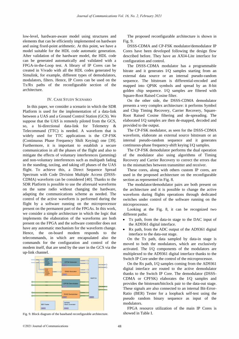
IV. CASE STUDY SCENARIO
In this paper, we consider a scenario in which the SDR
Platform is used for the implementation of a data-link
between a UAS and a Ground Control Station (GCS). We
suppose that the UAS is remotely piloted from the GCS,
so, a bi-directional data-link for Telemetry &
Telecommand (TTC) is needed. A waveform that is
widely used for TTC applications is the CP-FSK
(Continuous Phase Frequency Shift Keying) one [39].
Furthermore, it is important to establish a secure
communication in all the phases of the flight and also to
mitigate the effects of voluntary interferences (jamming)
and non-voluntary interferences such as multipath fading
in the standing, taxiing, and taking off phases of the UAS
flight. To achieve this, a Direct Sequence Spread
Spectrum with Code Division Multiple Access (DSSS-
CDMA) waveform can be considered [40]. Thanks to the
SDR Platform is possible to use the aforesaid waveforms
on the same radio without changing the hardware,
adapting the communications scheme as needed. The
control of the active waveform is performed during the
flight by a software running on the microprocessor
present on the permanent part of the FPGAs. In this work,
we consider a simple architecture in which the logic that
implements the elaboration of the waveforms are both
present on the FPGA and the software controller does not
have any automatic mechanism for the waveform change.
Hence, the on-board modem responds to the
telecommands, in which are encapsulated also the
commands for the configuration and control of the
modem itself, that are send by the user in the GCS via the
up-link channel.
Fig. 9. Block diagram of the baseband reconfigurable architecture.
The proposed reconfigurable architecture is shown in
Fig. 9.
DSSS-CDMA and CP-FSK modulator/demodulator IP
Cores have been developed following the design flow
described before. They have an AXI4-Lite interface for
configuration and control.
The DSSS-CDMA modulator has a programmable
bitrate and it generates I/Q samples starting from an
external data source or an internal pseudo-random
sequence. The bitstream is differential-encoded and
mapped into QPSK symbols and spread by an 8-bit
golden chip sequence. I/Q samples are filtered with
Square-Root Raised Cosine filter.
On the other side, the DSSS-CDMA demodulator
presents a very complex architecture: it performs Symbol
and Chip Timing Recovery, Carrier Recovery, Square-
Root Raised Cosine filtering and de-spreading. The
elaborated I/Q samples are then de-mapped, decoded and
provided to the output.
The CP-FSK modulator, as seen for the DSSS-CDMA
waveform, elaborate an external source bitstream or an
internal pseudo-random sequence and it generates
continuous-phase frequency-shift keying I/Q samples.
The CP-FSK demodulator performs the dual operation
of the modulator also using algorithms of Timing
Recovery and Carrier Recovery to correct the errors due
to the mismatches between transmitter and receiver.
These cores, along with others custom IP cores, are
used in the proposed architecture on the reconfigurable
section as represented in Fig. 8.
The modulator/demodulator pairs are both present on
the architecture and it is possible to change the active
waveform during flights operations through dedicated
switches under control of the software running on the
microprocessor.
Looking at the Fig. 8, it can be recognized two
different paths:
Tx path, from the data-in stage to the DAC input of
the AD9361 digital interface.
Rx path, from the ADC output of the AD9361 digital
interface to the data-out stage.
On the Tx path, data sampled by data-in stage is
moved to both the modulators, which are exclusively
activated. The I/Q components of the modulators are
multiplexed to the AD9361 digital interface thanks to the
Switch IP Core under the control of the microprocessor.
On the Rx path, I/Q samples coming from the AD9361
digital interface are routed to the active demodulator
thanks to the Switch IP Core. The demodulator (DSSS-
CDMA or CPFSK) elaborates the I/Q samples and
provides the bitstream/bitclock pair to the data-out stage.
These signals are also connected to an internal Bit-Error-
Ratio (BER) Tester for a loopback self-test using the
pseudo random binary sequence as input of the
modulators.
FPGA resource utilization of the main IP Cores is
showed in Table I.
Journal of Communications Vol. 16, No. 2, February 2021
48©2021 Journal of Communications

TABLE I: ARTIX XC7A200T RESOURCES UTILIZATION
Name Slice
LUTs
Slice
Registers Slice DSPs
System top 62.29% 30.19% 88.65% 23.92%
CDMA
Demodulator 37.62% 13.85% 51.13% 13.11%
AD9361 Interface 4.46% 4.71% 9.24% 8.11%
Microblaze 2.46% 1.18% 3.40% 0.54%
CPFSK
Demodulator 1.04% 0.66% 1.53% 1.22%
CDMA Modulator 0.53% 0.82% 1.42% 0.68%
CPFSK Modulator 0.75% 0.23% 0.91% 0.27%
BER Tester 0.30% 0.27% 0.73% 0.00%
Switch 0.09% 0.13% 0.28% 0.00%
Clk Generator 0.07% 0.10% 0.19% 0.00%
Data-out stage 0.05% 0.07% 0.14% 0.00%
Data-in stage 0.04% 0.07% 0.12% 0.00%
For this architecture, the total amount of used slices is
about 89% on the Artix XC7A200T FPGA. The
reconfigurable part uses approximately the 60% of the
FPGA logic, while the permanent part only about the
59%. The DSSS-CDMA demodulator occupies slightly
more than the 51% of the slices, while the other custom
IP Cores are under the 2% of the slices each. As a result,
we can observe that, in this case study application, the
ratio of the CP-FSK IP Cores area occupancy over the
DSSS one is very small and an alternative architecture
that exploits a dynamic reconfiguration of the active
waveform doesn’t result in any advantage by the resource
utilization point of view, but comes with the drawback of
slower waveform switching times.
With the considered case study scenario we can
implement also a data-link useful for multi-standard
interoperability (the system can uses two different
waveforms) besides to mitigate interferences and
multipath. In any case both the features shall be tested
and validated by means of a test campaign which will be
carried out as a future work. Other features, as adaptive
modulations for responding to channel conditions
changes for example, are not dependent by the platform
but require the design of a specific base band processing,
i.e. a dedicated application.
V. CONCLUSION
The proposed Software-Defined Radio Platform meets
the needs for the research and development activities in
the field of the communications systems for UAS at the
Italian Aerospace Research Center. The requirements for
the design of the SDRP have been identified considering
the available power sources and the data interfaces
needed by avionics equipment installed on-board of the
CIRA UAS. The result is a compact but flexible platform,
that is made up of three separate boards, integrated,
electrically and mechanically, in a vertical way according
to a turret scheme: the first one, named PGen, provides
power supply to the entire platform; the second one,
named Genius, is FPGA based and it is used to process
the baseband signals; the third one provides a wideband
RF Front-End transceiver. To improve FPGA design
reusability, a two-section architecture has been developed:
a permanent one, application-independent, and a
reconfigurable one that depends on the application (i.e. a
particular flying scenario). The first section remains
constant along different radio implementations and it
represents the backbone of the design with high-speed
digital interface to the wideband RF transceiver, data I/O
interfaces and an embedded microprocessor used for the
control and configuration of the entire radio, in particular
of the reconfigurable part. The reconfigurable part is the
portion of the FPGA area which is demanded the
baseband elaboration of the waveforms. Reconfiguration
can be on-line, also exploiting the partial dynamic
reconfiguration features of the Xilinx FPGA or can be
off-line, when the configuration bitstream is loaded
before the flight because of change in the experimental
scenario or when a new algorithm must be validated. A
library of modems IP Core was developed using a model-
based approach to reduce the FPGA design effort. Some
of these IP Cores were used in the reconfigurable section
of the FPGA to show a possible complete architecture in
a case study scenario: a reconfigurable data-link between
a UAS and a Ground Control Station (GCS), designed to
establish a reliable communication in all the phases of a
flight (parking, taxiing, taking off, cruising and landing).
The proposed SDR Platform contributed to improve
the CIRA capabilities to research and develop in the field
of the UAS communications, thanks to its flexibility and
modularity features. The possibility to change the
communications schemes without change the hardware,
as per SDR paradigm, will reduce also the UAS handling
effort.
CONFLICT OF INTEREST
The authors declare no conflict of interest.
AUTHOR CONTRIBUTIONS
All authors contributed to research and to model the
communications algorithms tested on the SDRP; V. U.
Castrillo designed all the boards of SDRP; A. Manco
developed and tested the IP Cores of the waveforms and
the baseband architecture on the FPGA; all authors had
approved the final version.
REFERENCES
[1] D. W. Matolak, “Unmanned aerial vehicles:
Communications challenges and future aerial networking,”
in Proc. International Conference on Computing,
Networking and Communications, Anaheim, California,
USA, February 16-19, 2015, pp. 567-572.
[2] Y. Cheng and K. Xu, “Technology demonstrator of a novel
software defined radio-based aeronautical communications
Journal of Communications Vol. 16, No. 2, February 2021
49©2021 Journal of Communications

system,” IET Science, Measurement & Technology, 2014,
8, pp. 370-379.
[3] B. Chamaillard, M. Lastera, and D. Roque, “A flexible
VHF-band aeronautical datalink receiver based on software
defined radio,” IEEE Aerospace and Electronic Systems
Magazine, vol. 33, pp. 58-61, 2018.
[4] R. C. Reinhart, T. J. Kacpura, S. K. Johnson, and J. P. Lux,
“NASA's space communications and navigation test bed
aboard the international space station,” IEEE Aerospace
and Electronic Systems Magazine, vol. 28, pp. 4-15, 2013.
[5] M. R. Maheshwarappa and C. P. Bridges, “Software
defined radios for small satellites,” in Proc. NASA/ESA
Conference on Adaptive Hardware and Systems (AHS),
Leicester, United Kingdom, July 14-18, 2014, pp. 172-179
[6] J. Budroweit, “Design of a highly integrated and reliable
SDR platform for multiple RF applications on
Spacecrafts,” in Proc. IEEE Global Communications
Conference, Singapore, 2017, pp. 1-6.
[7] J. Budroweit, “Design of a fully-integrated telemetry and
telecommand unit for CCSDS spacecraft communication
on a generic software-defined radio platform,” in Proc.
IEEE Space Hardware and Radio Conference, San
Antonio, Texas, USA, January 26-29, 2020, pp. 13-15.
[8] J. Mitola, “The software radio architecture,” IEEE
Communications Magazine, vol. 33, pp. 26-38, 1995.
[9] M. Cummings and S. Haruyama, “FPGA in the software
radio,” IEEE Communi. Magazine, vol. 37, pp. 108-112,
1999.
[10] M. Ahmadian, Z. J. Nazari, N. Nakhaee, and Z. Kostic,
“Model based design and SDR,” in Proc. 2nd
IEE/EURASIP Conference of DSP enabled Radio,
Southhampton, UK, September 18-20, 2005, pp. 1-8.
[11] A. G. Gener, J. Valverde, J. Otero, and P. J. Harris, “A fast
prototyping workflow for reconfigurable SDR
applications,” in Proc. International Symposium on
Reconfigurable Communication-centric Systems-on-Chip,
York, United Kingdom, July 1-3, 2019, pp. 66-73.
[12] C. Blümm, C. Heller, and R. Weigel, “SDR OFDM
waveform design for a UGV/UAV communication
scenario,” J Sign Process Syst., vol. 69, pp. 11–21, 2012.
[13] K. Powell, A. Sabri, D. Brennan, V. Marojevic, R. M.
Barts, A. Panicker, O. Ozdemir, and I. Guvenc, “Software
radios for unmanned aerial systems,” in Proc. 1st
International Workshop on Open Software Defined
Wireless Networks, Toronto, Canada, June 2020, pp. 14-20.
[14] V. Marojevic, I. Guvenc, M. Sichitiu, and R. Dutta, “An
experimental research platform architecture for UAS
communications and networking,” in Proc. IEEE 90th
Vehicular Technololgy Conference, Honolulu, USA,
September 22-25, 2019, pp. 1-5.
[15] N. Hosseini and D. W. Matolak, “Wide band channel
characterization for low altitude unmanned aerial system
communication using software defined radios,” in Proc.
Integrated Communications, Navigation, Surveillance
Conference, Herndon, USA, April 10-12, 2018, pp. 2C2-1-
2C2-9.
[16] Department of Defense USA, “Unmanned systems
integrated roadmap, FY2011-2036,” Reference Number:
11-S-3613, pp. 1-108, 2011.
[17] Nexys Video Reference Manual, Digilent, Rev. 1, 2020.
[18] AC701 Evaluation Board for the Artix-7 FPGA User Guide,
UG952, Xilinx, v. 1.4, August 6, 2019.
[19] FPGA Mezzanine Card, ANSI/VITA (VMEbus
International Trade Association), 57.1standard, 2008.
[20] COM BLOCK Modules. [Online]. Available:
https://comblock.com/product_list_hw.html#rfmodules
[21] 7 Series FPGAs Data Sheet: Overview, Xilinx, DS180, v.
2.6, February 27, 2018.
[22] 2Gb: x4, x8, x16 DDR3 SDRAM Features, Micron,
Datasheet, Rev. O, 2018.
[23] TN-41-13: DDR3 Point-to-Point Design Support
Introduction, Micron, Technical Note, Rev. B, 2013.
[24] DSC1101/21 Low-Jitter Precision CMOS Oscillator,
Microchip, DS20005613B, pp. 1-30, October 25, 2017.
[25] 7 Series FPGAs PCB Design Guide, Xilinx, UG483, v1.14,
May 21, 2019.
[26] DDR2/DDR3 Low-Cost PCB Design Guidelines for Artix-7
and Spartan-7 FPGAs, Xilinx, WP484, v1.0, September 27,
2016.
[27] AD-FMCOMMS3-EBZ User Guide. [Online]. Available:
https://wiki.analog.com/resources/eval/user-guides/ad-
fmcomms3-ebz
[28] RF Agile Transceiver AD9361, Analog Devices, Datasheet,
Rev. F, 2016.
[29] DC/DC Converters, TEN 40N Series, 40 Watt, Traco
Power, Datasheet, Rev. August 6, 2018.
[30] TEN 40N Series Application Note: DC/DC Converter 9 to
18Vdc, 18 to 36Vdc or 36 to 75Vdc Input 3.3 to 15Vdc
Single Outputs and ±12 & ±15Vdc Dual Outputs, 40W,
Traco Power, Application Note, Rev. 2.1, June 4, 2018.
[31] ADP5052: 5-Channel Integrated Power Solution with
Quad Buck Regulators and 200mA LDO Regulator,
Analog Devices, Datasheet, Rev. D, 2017.
[32] ADP2370/ADP2371: High Voltage, 1.2 MHz/600 kHz, 800
mA, Low Quiescent Current Buck Regulator, Analog
Devices, Datasheet, Rev. E, 2019.
[33] ADP2384: 20 V, 4 A, Synchronous, Step-Down DC-to-DC
Regulator, Analog Devices, Datasheet, Rev. A, 2014.
[34] Partial Reconfiguration User Guide, UG909, Xilinx, v.
2019.1, June 5, 2019.
[35] AXI_AD9361 Wiki page, Analog Devices.
[36] IRIG Standard 106-17, Telemetry Group, Secretariat
Range Commanders Council, July 2017.
[37] Microblaze Reference Guide, UG984, Xilinx, v. 2019.2,
October 30, 2019
[38] AXI Reference Guide, UG1037, Xilinx, UG1037, v. 4.0,
July 15, 2017
[39] IRIG Standard 106-04 Part I, Telemetry Group, Secretariat
Range Commanders Council, May 2004.
[40] A. J. Viterbi, “CDMA – Principles of Spread Spectrum
Communications,” Reading, MA, Addison-Wesley, 1995.
Copyright © 2021 by the authors. This is an open access article
distributed under the Creative Commons Attribution License
(CC BY-NC-ND 4.0), which permits use, distribution and
reproduction in any medium, provided that the article is
properly cited, the use is non-commercial and no modifications
or adaptations are made.
Journal of Communications Vol. 16, No. 2, February 2021
50©2021 Journal of Communications
Angelo Manco was born in Naples, Italy,
in 1983. He received the M.S. degree
with honors in Electronic Engineering
from the University of Naples “Federico
II”, Italy, in 2011. He joined the
Electronics and Communications group
of the Italian Aerospace Research Centre
(CIRA) in 2011. He has more than 8
years of experience in hardware design of digital electronics
circuits on FPGA platform for DSP, communications and image
processing applications.
He was invited to teach a 16 hours short course “Developing on
FPGA” in 2014 at STOA Learning Centre in Naples.
Vittorio U. Castrillo was born in 1979
and received the M.S. degree with
honors in Electronic Engineering from
the University of Naples “Federico II”
(Italy) in 2003. He joined the Electronics
and Communications unit at CIRA, in
2004. At the beginning he was involved
in the design and integration of data
acquisition systems and in the design and development of
software for microcontroller-based applications. Afterwards he
worked on the design and integration of communication systems
for telemetry and control data-link for unmanned aerial and
space vehicles. Since 2011 his activities have been focused also
on the design of algorithms for base-band digital signal
processing for communication systems with implementation on
FPGA-based hardware platforms. Recently, he has worked on
the full design of complex electronic systems based on FPGA,
DDR3 memory and microcontroller. He has been project
manager for the design of an innovative architecture for the
implementation of a beam steering controller of a phased array.
Journal of Communications Vol. 16, No. 2, February 2021
51©2021 Journal of Communications