Millimeter-Wave Beam Search with Iterative Deactivation and ...

332 IEEE TRANSACTIONS ON ADVANCED PACKAGING, VOL. 27, NO. 2, MAY 2004
3-D-Integrated RF and Millimeter-Wave Functionsand Modules Using Liquid Crystal Polymer (LCP)
System-on-Package TechnologyManos M. Tentzeris, Senior Member, IEEE, Joy Laskar, Senior Member, IEEE,
John Papapolymerou, Senior Member, IEEE, Stéphane Pinel, V. Palazzari, R. Li, Senior Member, IEEE, G. DeJean,N. Papageorgiou, D. Thompson, R. Bairavasubramanian, S. Sarkar, and J.-H. Lee
Abstract—Electronics packaging evolution involves system,technology, and material considerations. In this paper, wepresent a novel three-dimensional (3-D) integration approachfor system-on-package (SOP)-based solutions for wireless com-munication applications. This concept is proposed for the 3-Dintegration of RF and millimeter (mm) wave embedded functionsin front-end modules by means of stacking substrates usingliquid crystal polymer (LCP) multilayer and BGA technologies.Characterization and modeling of high-Q RF inductors using LCPis described. A single-input-single-output (SISO) dual-band filteroperating at ISM 2.4–2.5 GHz and UNII 5.15–5.85 GHz frequencybands, two dual-polarization 2x1 antenna arrays operating at14 and 35 GHz, and a WLAN IEEE 802.11a-compliant compactmodule (volume of 75 35 0.2 mm3) have been fabricated onLCP substrate, showing the great potential of the SOP approachfor 3-D-integrated RF and mm wave functions and modules.
Index Terms—Dual-band antenna, dual-band filter, embeddedfunctions, high-Q passives, inductors, liquid crystal polymer(LCP), BGA, multilayer modules, RF and mm-waves front-endmodule, system-on-package (SOP), three-dimensional (3-D)integration.
I. INTRODUCTION
EMERGING wireless communication and sensor applica-tions in the RF/microwave/millimeter (mm) wave regimes
require miniaturization, portability, cost, and performance askey driving forces in the electronics packaging evolution. Thesystem-on-package (SOP) approach [versus the system-on-chip(SOC) ] for module development [1] has become a primaryfocus of research due to the real estate efficiency, cost-saving,size reduction, and performance improvement contributed byits inherent capability for the easy integration of embeddedfunctions, thus, simultaneously satisfying the specifications ofthe next generation wireless communication systems. Also, thethree-dimensional (3-D) integration approach is an emergingand very attractive option for these systems. However, current3-D RF module integration is still based on low-density hybridassembly technologies [2], [3].
Manuscript received December 7, 2003; revised February 16, 2004. Thiswork was supported in part by the NSF CAREER, ECS-9984761, the NSFECS-0313951, and the Packaging Research Center, and NASA under ContractNCC3-1015.
The authors are with the Georgia Electronic Design Center, School of Elec-trical and Computer Engineering, Georgia Institute of Technology, Atlanta, GA30332 USA (e-mail: [email protected]).
Digital Object Identifier 10.1109/TADVP.2004.828814
Fig. 1. 3-D-integrated module concept view.
In this paper, we present novel liquid crystal polymer (LCP)multilayer technologies, and stacking board technique using
BGA as the candidates of choice for the 3-D integrationof RF front-end modules up to 35 GHz. Various figures ofmerit of the performance of high-Q RF inductor such asquality factor values up to 90 in C and X bands, using LCPare reported. A single-input-single-output (SISO) dual-bandfilter using the “dual-behavior resonators” technique is pre-sented for WLAN operating frequency bands ISM 2.4–2.5and UNII 5.15–5.85 GHz. The insertion loss and return lossat the central frequency are 2.4 and 15 dB for the 2.4-GHzband, respectively, and 1.8 and 8 dB for the 5-GHz band,respectively. Two dual-polarization 2 1 antenna arrays onLCP are also reported. The frequencies of operation are 14and 35 GHz and and both integrated structures exhibit a highefficiency and a low cross-polarization level. Finally, oneWLAN IEEE 802.11a-compliant compact module (volumeof 75 35 0.2 mm ) has been fabricated on LCP substrate,showing the great potential of the SOP approach for 3-D-inte-grated RF and mm waves functions and modules.
II. 3-D-INTEGRATED MODULE CONCEPT
Fig. 1 illustrates the proposed multilayer module con-cept. Two stacked SOP multilayer substrates are used andboard-to-board vertical transition is ensured by BGA balls.Standard alignment equipment is used to stack the board and,thus, provide a compact, high-performance, and low-costassembly process. Multistepped cavities into the SOP boardsprovide spacing for embedded RF active devices (RF switch,RF receiver, and RF transmitter) chipset and, thus, lead tosignificant volume reduction by minimizing the gap between
1521-3323/04$20.00 © 2004 IEEE

TENTZERIS et al.: 3-D-INTEGRATED RF AND MILLIMETER-WAVES FUNCTIONS 333
Fig. 2. Rx and Tx board block diagram.
TABLE ICOMPARAISON OF SUBSTRATE PROPERTIES
the boards. Active devices can be flip-chiped, as well aswire-bonded. Cavities also provide an excellent opportunityfor the easy integration of RF MEMS devices, such as MEMSswitches or tuners. Passive components, off-chip matchingnetworks, embedded filter, and antennas are implementeddirectly into the SOP boards by using multilayer technologies[4]–[6]. Standard BGA balls ensure the effective broadbandinterconnection of this high density module with motherboardssuch as the FR4 board. The top and the bottom substrates arededicated respectively to the receiver and transmitter buildingblocks of the RF front-end module.
Fig. 2 shows the RF block diagram of each board. The re-ceiver board includes antenna, bandpass filter, active switch, andRF receiver chipset (LNA, VCO, and downconversion mixer).The transmitter board includes RF transmitter chipset (upcon-verter mixer and power amplifier) and off-chip matching net-works. Ground planes and vertical via walls are used to addressisolation issues between the transmitter and the receiver func-tional blocks. Arrays of vertical vias are added into the trans-mitter board to achieve better thermal management.
III. LCP MULTILAYER SUBSTRATE AND BGA STACKING
APPROACH FOR 3-D INTEGRATION
A. LCP Multilayer Substrate Properties
Multilayer substrates have been, and still are, of great in-terest for research in the area of the 3-D integration of RF andmm wave functions and modules using the SOP approach. Ourpresented results have been focused mainly on advanced multi-layer organic substrates using FR4 material and advanced mate-rial such as LCP, in comparison with the more mature, but alsomore expensive ceramic-based platforms such as low-tempera-ture cofired ceramic (LTCC). The choice of the most suitable
technology depends on the application specifications such en-vironment, frequency of operation, performance, volume, andcost.
LCP is a fairly new and promising thermoplastic material [7].It can be used as a low-cost dielectric material for high-volumelarge-area processing methods that provide very reliable high-performance circuits at low cost. LCP has a unique combinationof properties as follows [11].
— Excellent electrical properties up to mm waves, such aslow dielectric constant of 3.0 @ 20 GHz and low-losstangent of 0.002 @ 20 GHz comparable with ceramics(cf. Table I).
— Very good barrier properties, permeability (moistureabsorption %) comparable to that of glass andvery close to that of ceramic.
— Low coefficient of thermal expansion (CTE) as low as/K, adjustable through thermal treatments
process coefficient of thermal expansion, and close tothat of ceramic ( /K) (cf. Table I).
Material, electrical, and cost considerations make LCPa serious candidate for all multichip-module (MCM), SOP,and advanced packaging technologies led by a tremendouslygrowing market of RF, sensor, digital,optical and mixed-signalapplications.
B. Stacking Board Technique Using BGA
To achieve significant volume reduction, 3-D integration ap-proaches are a very attractive option for RF front-end moduleintegration. The board-stacking technique has emerged as themost promising approach to simultaneously achieve size reduc-tion, performance improvement, reliability, and cost-saving. Inthis paper, we presented a Georgia Tech developed process dedi-
334 IEEE TRANSACTIONS ON ADVANCED PACKAGING, VOL. 27, NO. 2, MAY 2004
Fig. 3. 4 mils solder ball transition. (a) Side view of fabricated test structures showing stacked LCP substrates; (b) �BGA transitions.
Fig. 4. Extracted �BGA hybrid model.
cated to board-to-board stacking and interconnection using pre-formed solder balls (Sn63Pb37–183 C) and conventional re-flow process. Fig. 3(a) shows a cross section of one 4-mils solderball transition, and Fig. 3(b) shows a side view of a fabricatedtest structure with stacked LCP substrates and BGA (4 mils indiameter) transitions.
A combination of an RLC -network and a transmission-linemodel, shown in Fig. 4, is applied to model the BGA ver-tical RF transition. The two transmission line sections are addedto model accurately the phase responses of S11 and S21. Bothmeasured and simulated results exhibit insertion loss less than0.1 dB and return loss about dB up to 10 GHz.
IV. CHARACTERIZATION AND MODELING OF HIGH-QRF-INDUCTOR IMPLEMENTED USING LCP TECHNOLOGY
A. Inductor Physical Model
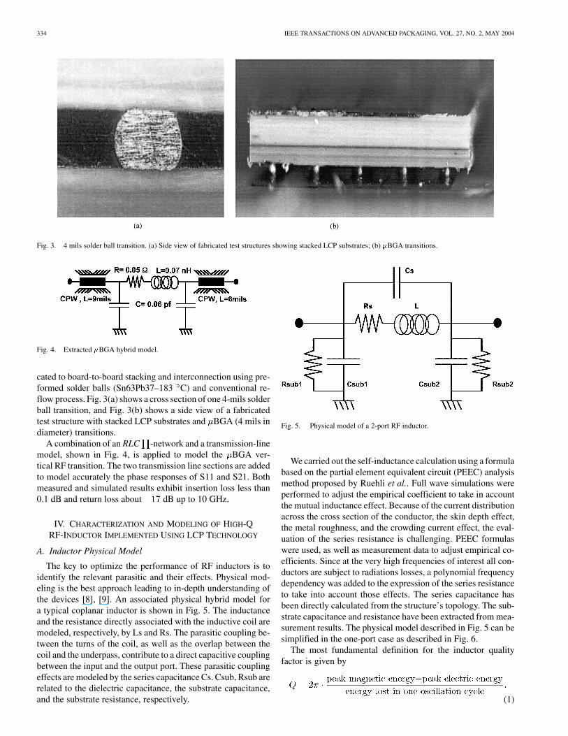
The key to optimize the performance of RF inductors is toidentify the relevant parasitic and their effects. Physical mod-eling is the best approach leading to in-depth understanding ofthe devices [8], [9]. An associated physical hybrid model fora typical coplanar inductor is shown in Fig. 5. The inductanceand the resistance directly associated with the inductive coil aremodeled, respectively, by Ls and Rs. The parasitic coupling be-tween the turns of the coil, as well as the overlap between thecoil and the underpass, contribute to a direct capacitive couplingbetween the input and the output port. These parasitic couplingeffects are modeled by the series capacitance Cs. Csub, Rsub arerelated to the dielectric capacitance, the substrate capacitance,and the substrate resistance, respectively.
Fig. 5. Physical model of a 2-port RF inductor.
We carried out the self-inductance calculation using a formulabased on the partial element equivalent circuit (PEEC) analysismethod proposed by Ruehli et al.. Full wave simulations wereperformed to adjust the empirical coefficient to take in accountthe mutual inductance effect. Because of the current distributionacross the cross section of the conductor, the skin depth effect,the metal roughness, and the crowding current effect, the eval-uation of the series resistance is challenging. PEEC formulaswere used, as well as measurement data to adjust empirical co-efficients. Since at the very high frequencies of interest all con-ductors are subject to radiations losses, a polynomial frequencydependency was added to the expression of the series resistanceto take into account those effects. The series capacitance hasbeen directly calculated from the structure’s topology. The sub-strate capacitance and resistance have been extracted from mea-surement results. The physical model described in Fig. 5 can besimplified in the one-port case as described in Fig. 6.
The most fundamental definition for the inductor qualityfactor is given by
(1)
TENTZERIS et al.: 3-D-INTEGRATED RF AND MILLIMETER-WAVES FUNCTIONS 335
Fig. 6. Physical model of a 1 port RF inductor.
In the one port case, this can be expressed as follows:
(2)
With
(3)
and
(4)
B. Measurement Results
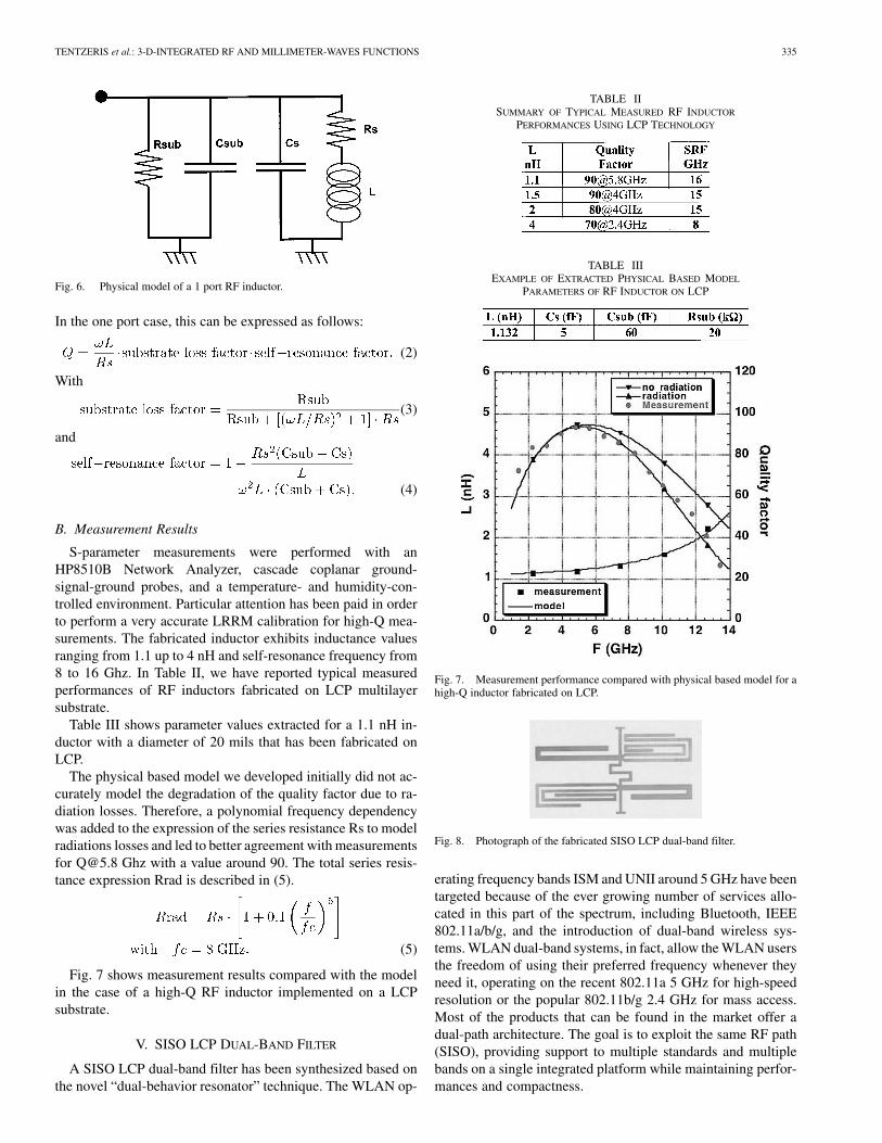
S-parameter measurements were performed with anHP8510B Network Analyzer, cascade coplanar ground-signal-ground probes, and a temperature- and humidity-con-trolled environment. Particular attention has been paid in orderto perform a very accurate LRRM calibration for high-Q mea-surements. The fabricated inductor exhibits inductance valuesranging from 1.1 up to 4 nH and self-resonance frequency from8 to 16 Ghz. In Table II, we have reported typical measuredperformances of RF inductors fabricated on LCP multilayersubstrate.
Table III shows parameter values extracted for a 1.1 nH in-ductor with a diameter of 20 mils that has been fabricated onLCP.
The physical based model we developed initially did not ac-curately model the degradation of the quality factor due to ra-diation losses. Therefore, a polynomial frequency dependencywas added to the expression of the series resistance Rs to modelradiations losses and led to better agreement with measurementsfor [email protected] Ghz with a value around 90. The total series resis-tance expression Rrad is described in (5).
(5)
Fig. 7 shows measurement results compared with the modelin the case of a high-Q RF inductor implemented on a LCPsubstrate.
V. SISO LCP DUAL-BAND FILTER
A SISO LCP dual-band filter has been synthesized based onthe novel “dual-behavior resonator” technique. The WLAN op-
TABLE IISUMMARY OF TYPICAL MEASURED RF INDUCTOR
PERFORMANCES USING LCP TECHNOLOGY
TABLE IIIEXAMPLE OF EXTRACTED PHYSICAL BASED MODEL
PARAMETERS OF RF INDUCTOR ON LCP
Fig. 7. Measurement performance compared with physical based model for ahigh-Q inductor fabricated on LCP.
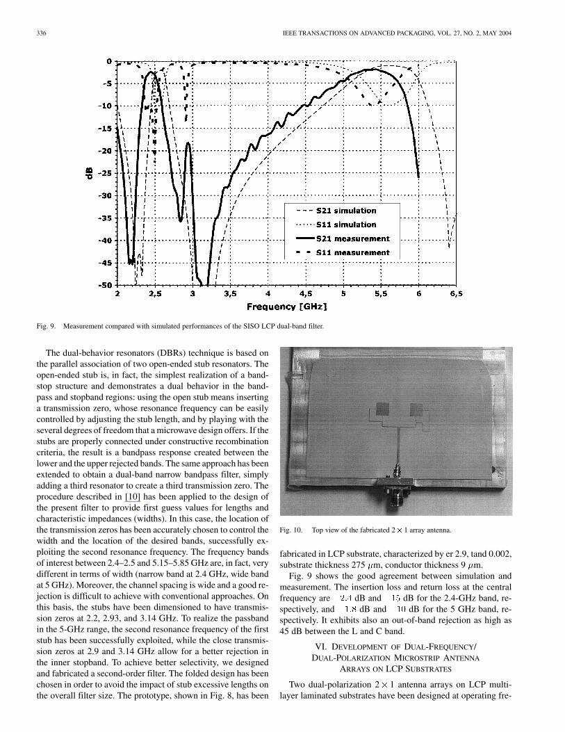
Fig. 8. Photograph of the fabricated SISO LCP dual-band filter.
erating frequency bands ISM and UNII around 5 GHz have beentargeted because of the ever growing number of services allo-cated in this part of the spectrum, including Bluetooth, IEEE802.11a/b/g, and the introduction of dual-band wireless sys-tems. WLAN dual-band systems, in fact, allow the WLAN usersthe freedom of using their preferred frequency whenever theyneed it, operating on the recent 802.11a 5 GHz for high-speedresolution or the popular 802.11b/g 2.4 GHz for mass access.Most of the products that can be found in the market offer adual-path architecture. The goal is to exploit the same RF path(SISO), providing support to multiple standards and multiplebands on a single integrated platform while maintaining perfor-mances and compactness.
336 IEEE TRANSACTIONS ON ADVANCED PACKAGING, VOL. 27, NO. 2, MAY 2004
Fig. 9. Measurement compared with simulated performances of the SISO LCP dual-band filter.
The dual-behavior resonators (DBRs) technique is based onthe parallel association of two open-ended stub resonators. Theopen-ended stub is, in fact, the simplest realization of a band-stop structure and demonstrates a dual behavior in the band-pass and stopband regions: using the open stub means insertinga transmission zero, whose resonance frequency can be easilycontrolled by adjusting the stub length, and by playing with theseveral degrees of freedom that a microwave design offers. If thestubs are properly connected under constructive recombinationcriteria, the result is a bandpass response created between thelower and the upper rejected bands. The same approach has beenextended to obtain a dual-band narrow bandpass filter, simplyadding a third resonator to create a third transmission zero. Theprocedure described in [10] has been applied to the design ofthe present filter to provide first guess values for lengths andcharacteristic impedances (widths). In this case, the location ofthe transmission zeros has been accurately chosen to control thewidth and the location of the desired bands, successfully ex-ploiting the second resonance frequency. The frequency bandsof interest between 2.4–2.5 and 5.15–5.85 GHz are, in fact, verydifferent in terms of width (narrow band at 2.4 GHz, wide bandat 5 GHz). Moreover, the channel spacing is wide and a good re-jection is difficult to achieve with conventional approaches. Onthis basis, the stubs have been dimensioned to have transmis-sion zeros at 2.2, 2.93, and 3.14 GHz. To realize the passbandin the 5-GHz range, the second resonance frequency of the firststub has been successfully exploited, while the close transmis-sion zeros at 2.9 and 3.14 GHz allow for a better rejection inthe inner stopband. To achieve better selectivity, we designedand fabricated a second-order filter. The folded design has beenchosen in order to avoid the impact of stub excessive lengths onthe overall filter size. The prototype, shown in Fig. 8, has been
Fig. 10. Top view of the fabricated 2� 1 array antenna.
fabricated in LCP substrate, characterized by er 2.9, tand 0.002,substrate thickness 275 m, conductor thickness 9 m.
Fig. 9 shows the good agreement between simulation andmeasurement. The insertion loss and return loss at the centralfrequency are dB and dB for the 2.4-GHz band, re-spectively, and dB and dB for the 5 GHz band, re-spectively. It exhibits also an out-of-band rejection as high as45 dB between the L and C band.
VI. DEVELOPMENT OF DUAL-FREQUENCY/DUAL-POLARIZATION MICROSTRIP ANTENNA
ARRAYS ON LCP SUBSTRATES
Two dual-polarization 2 1 antenna arrays on LCP multi-layer laminated substrates have been designed at operating fre-

TENTZERIS et al.: 3-D-INTEGRATED RF AND MILLIMETER-WAVES FUNCTIONS 337
Fig. 11. Plot of the simulated and measured results for the return loss versus frequency of the 2� 1 array for: (a) 14-GHz array, pol.X; (b) 14-GHz array, pol.Y;(c) 35-GHz array, pol.X; (d) 35-GHz array, pol.Y.
quencies of 14 and 35 GHz (mm-wave range) for precipita-tion remote sensing applications. The top view of the fabricated2 1 antenna arrays is shown in Fig. 10. The metal was copper(Cu) and had a thickness of 18 m. The total substrate thicknessfor the design was 425 m, consisting of two LCP layers (each200 m thick) and a 25 m bonding layer. The substrate thick-ness was chosen to achieve at least a 1.5% impedance bandwidthat dB, while maintaining a compact structure. The 14-GHzantenna array was placed on the top layer of the LCP substrate(at the interface of LCP and air), while the 35-GHz antenna arraywas “sandwiched” between two embedded layers for compact-ness and crosstalk minimization reasons. The LCP layer underthe 35 GHz antenna array had a thickness of 200 m. Both ar-rays were fed by microstrip lines printed on the same layer as thecorresponding array. To further prevent parasitic coupling be-tween the two antenna arrays, the antennas in the 35-GHz arrayhave a linear (“diamond”) topology and the 14 GHz array main-tains the “square” configuration. The control of the two orthog-onal linear polarizations is achieved through the use of two smallgaps in the feedlines for two perpendicular directions, which in-
troduced a small capacitance in each gap. The small capacitanceon the order of fFs in the gap represents high impedance valuesor an “almost ideal” electrical open circuit which prevents themode excitation of the corresponding polarization. RF MEMSswitches or pin diodes can be utilized to achieve this effect byturning on to excite a specific polarization and turning off toswitch to the alternative polarization.
Simulations of both arrays were performed, separately,using the 3-D full-wave simulation programs EmPicasso andMicro-Stripes. Plots of the simulated and measured results forthe return loss versus frequency of both polarizations at eachfrequency are shown in Fig. 11. The simulated results show areturn loss of approximately dB at a center frequencyof 13.99 GHz for polarizations X (“horizontal” x-axis feed)and dB at GHz for polarization Y (“vertical”y-axis feed) for the 14-GHz structure. Additionally, the 35-GHzstructure exhibits at return loss of approximately dB at
GHz for polarization X and dB at GHzfor polarization Y. The measured results for the return loss areas follows: the 14-GHz array has a return loss of approximately
338 IEEE TRANSACTIONS ON ADVANCED PACKAGING, VOL. 27, NO. 2, MAY 2004
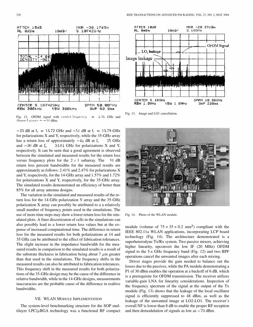
Fig. 12. OFDM signal with carrier frequency = 5:18 GHz andchannel power = �14 dBm.
dB at GHz and dB at GHzfor polarizations X and Y, respectively, while the 35-GHz arrayhas a return loss of approximately dB at GHzand dB at GHz for polarizations X and Y,respectively. It can be seen that a good agreement is observedbetween the simulated and measured results for the return lossversus frequency plots for the 2 1 subarray. The dBreturn loss percent bandwidths for the measured results areapproximately as follows: 2.41% and 2.47% for polarizations Xand Y, respectively, for the 14-GHz array and 1.57% and 1.72%for polarizations X and Y, respectively, for the 35-GHz array.The simulated results demonstrated an efficiency of better than85% for all array antenna designs.
The variation in the simulated and measured results of the re-turn loss for the 14-GHz polarization Y array and the 35-GHzpolarization X array can possibly be attributed to a a relativelysmall number of frequency points used in the simulations. Theuse of more time steps may show a lower return loss for the sim-ulated plots. A finer discretizaton of cells in the simulations canalso possibly lead to a lower return loss values but at the ex-pense of increased computational time. The difference in returnloss for the measured results for both polarizations at 14 and35 GHz can be attributed to the effect of fabrication tolerances.The slight increase in the impedance bandwidth for the mea-sured results in comparison to the simulated results is a result ofthe substrate thickness in fabrication being about 7 m greaterthan that used in the simulations. The frequency shifts in themeasured results can also be attributed to fabrication tolerances.This frequency shift in the measured results for both polariza-tions of the 35-GHz design may be the cause of the difference inrelative bandwidth, while in the 14-GHz designs, measurementsinaccuracies are the probable cause of the difference in realtivebandwidths.
VII. WLAN MODULE IMPLEMENTATION
The system-level benchmarking structure for the SOP mul-tilayer LPC/ BGA technology was a functional RF compact
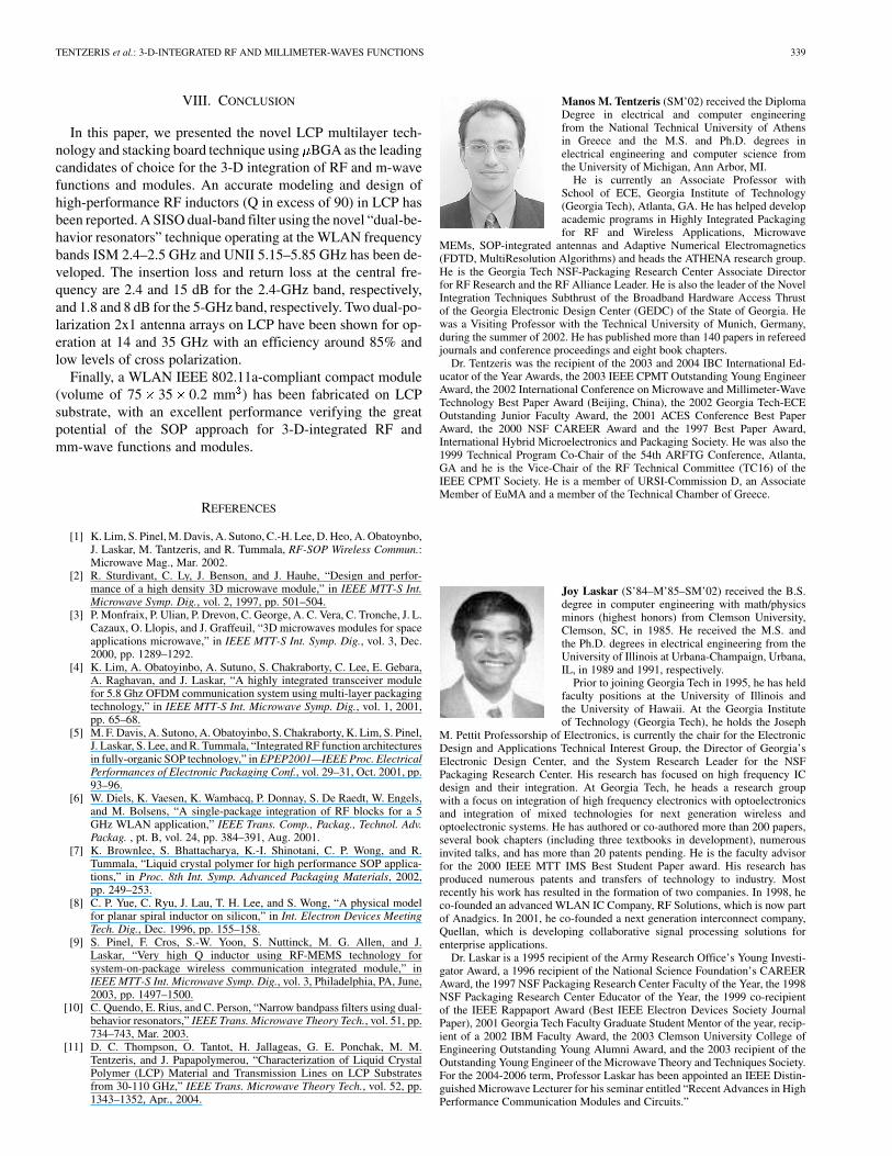
Fig. 13. Image and LO1 cancellation.
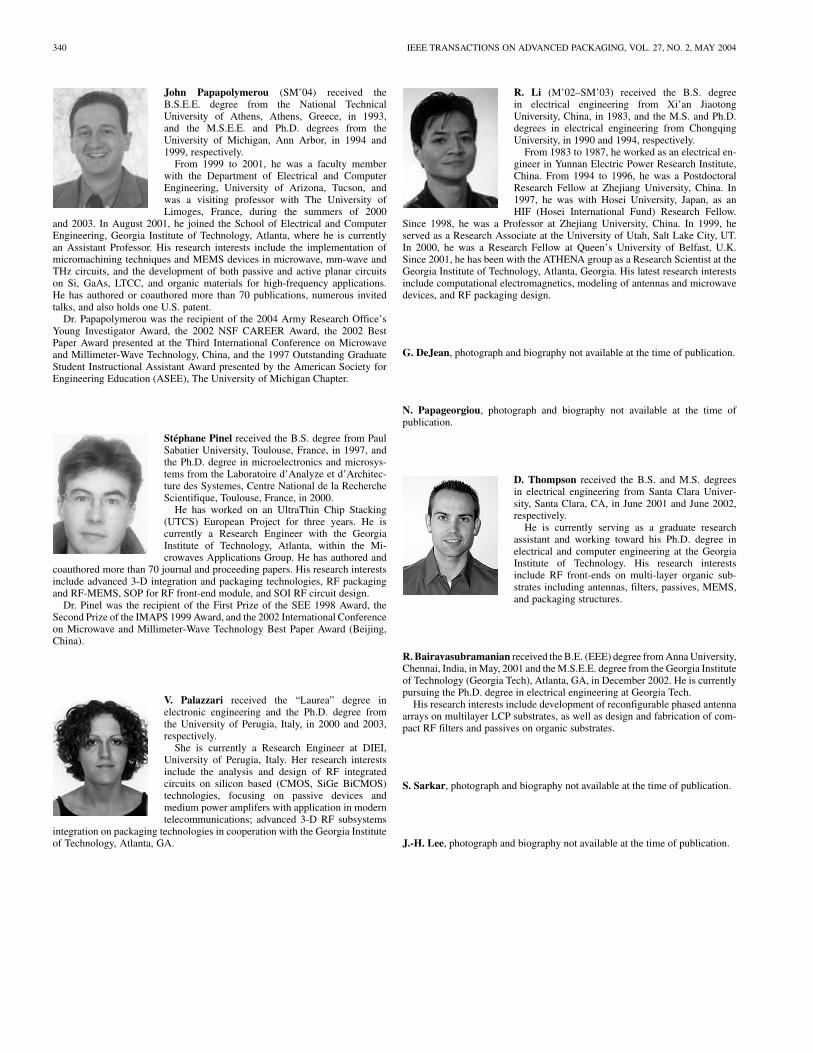
Fig. 14. Photo of the WLAN module.
module (volume of 75 35 0.2 mm ) compliant with theIEEE 802.11a WLAN applications, incorporating LCP boardtechnology (Fig. 14). The architecture demonstrated is asuperheterodyne Tx/Rx system. Two passive mixers, achievinghigher linearity, upconvert the low IF (20 MHz) OFDMsignal to the 5.x GHz frequency band (Fig. 12) and two BPFoperations cancel the unwanted images after each mixing.
Driver stages provide the gain needed to balance out thelosses due to the passives, while the PA module demonstrating aP1 of 30 dBm enables the operation at a backoff of 6 dB, whichis a prerequisite for OFDM transmission. The receiver utilizesvariable-gain LNA for linearity considerations. Inspection ofthe frequency spectrum of the signal at the output of the Txmodule (Fig. 13) shows that the leakage of the local oscillatorsignal is efficiently suppressed to 48 dBm, as well as theleakage of the unwanted image at LO2-LO1. The receiver’soverall NF is lower than 8 dB to enable the proper RF receptionand then demodulation of signals as low as dBm.
TENTZERIS et al.: 3-D-INTEGRATED RF AND MILLIMETER-WAVES FUNCTIONS 339
VIII. CONCLUSION
In this paper, we presented the novel LCP multilayer tech-nology and stacking board technique using BGA as the leadingcandidates of choice for the 3-D integration of RF and m-wavefunctions and modules. An accurate modeling and design ofhigh-performance RF inductors (Q in excess of 90) in LCP hasbeen reported. A SISO dual-band filter using the novel “dual-be-havior resonators” technique operating at the WLAN frequencybands ISM 2.4–2.5 GHz and UNII 5.15–5.85 GHz has been de-veloped. The insertion loss and return loss at the central fre-quency are 2.4 and 15 dB for the 2.4-GHz band, respectively,and 1.8 and 8 dB for the 5-GHz band, respectively. Two dual-po-larization 2x1 antenna arrays on LCP have been shown for op-eration at 14 and 35 GHz with an efficiency around 85% andlow levels of cross polarization.
Finally, a WLAN IEEE 802.11a-compliant compact module(volume of 75 35 0.2 mm ) has been fabricated on LCPsubstrate, with an excellent performance verifying the greatpotential of the SOP approach for 3-D-integrated RF andmm-wave functions and modules.
REFERENCES
[1] K. Lim, S. Pinel, M. Davis, A. Sutono, C.-H. Lee, D. Heo, A. Obatoynbo,J. Laskar, M. Tantzeris, and R. Tummala, RF-SOP Wireless Commun.:Microwave Mag., Mar. 2002.
[2] R. Sturdivant, C. Ly, J. Benson, and J. Hauhe, “Design and perfor-mance of a high density 3D microwave module,” in IEEE MTT-S Int.Microwave Symp. Dig., vol. 2, 1997, pp. 501–504.
[3] P. Monfraix, P. Ulian, P. Drevon, C. George, A. C. Vera, C. Tronche, J. L.Cazaux, O. Llopis, and J. Graffeuil, “3D microwaves modules for spaceapplications microwave,” in IEEE MTT-S Int. Symp. Dig., vol. 3, Dec.2000, pp. 1289–1292.
[4] K. Lim, A. Obatoyinbo, A. Sutuno, S. Chakraborty, C. Lee, E. Gebara,A. Raghavan, and J. Laskar, “A highly integrated transceiver modulefor 5.8 Ghz OFDM communication system using multi-layer packagingtechnology,” in IEEE MTT-S Int. Microwave Symp. Dig., vol. 1, 2001,pp. 65–68.
[5] M. F. Davis, A. Sutono, A. Obatoyinbo, S. Chakraborty, K. Lim, S. Pinel,J. Laskar, S. Lee, and R. Tummala, “Integrated RF function architecturesin fully-organic SOP technology,” in EPEP2001—IEEE Proc. ElectricalPerformances of Electronic Packaging Conf., vol. 29–31, Oct. 2001, pp.93–96.
[6] W. Diels, K. Vaesen, K. Wambacq, P. Donnay, S. De Raedt, W. Engels,and M. Bolsens, “A single-package integration of RF blocks for a 5GHz WLAN application,” IEEE Trans. Comp., Packag., Technol. Adv.Packag. , pt. B, vol. 24, pp. 384–391, Aug. 2001.
[7] K. Brownlee, S. Bhattacharya, K.-I. Shinotani, C. P. Wong, and R.Tummala, “Liquid crystal polymer for high performance SOP applica-tions,” in Proc. 8th Int. Symp. Advanced Packaging Materials, 2002,pp. 249–253.
[8] C. P. Yue, C. Ryu, J. Lau, T. H. Lee, and S. Wong, “A physical modelfor planar spiral inductor on silicon,” in Int. Electron Devices MeetingTech. Dig., Dec. 1996, pp. 155–158.
[9] S. Pinel, F. Cros, S.-W. Yoon, S. Nuttinck, M. G. Allen, and J.Laskar, “Very high Q inductor using RF-MEMS technology forsystem-on-package wireless communication integrated module,” inIEEE MTT-S Int. Microwave Symp. Dig., vol. 3, Philadelphia, PA, June,2003, pp. 1497–1500.
[10] C. Quendo, E. Rius, and C. Person, “Narrow bandpass filters using dual-behavior resonators,” IEEE Trans. Microwave Theory Tech., vol. 51, pp.734–743, Mar. 2003.
[11] D. C. Thompson, O. Tantot, H. Jallageas, G. E. Ponchak, M. M.Tentzeris, and J. Papapolymerou, “Characterization of Liquid CrystalPolymer (LCP) Material and Transmission Lines on LCP Substratesfrom 30-110 GHz,” IEEE Trans. Microwave Theory Tech., vol. 52, pp.1343–1352, Apr., 2004.
Manos M. Tentzeris (SM’02) received the DiplomaDegree in electrical and computer engineeringfrom the National Technical University of Athensin Greece and the M.S. and Ph.D. degrees inelectrical engineering and computer science fromthe University of Michigan, Ann Arbor, MI.
He is currently an Associate Professor withSchool of ECE, Georgia Institute of Technology(Georgia Tech), Atlanta, GA. He has helped developacademic programs in Highly Integrated Packagingfor RF and Wireless Applications, Microwave
MEMs, SOP-integrated antennas and Adaptive Numerical Electromagnetics(FDTD, MultiResolution Algorithms) and heads the ATHENA research group.He is the Georgia Tech NSF-Packaging Research Center Associate Directorfor RF Research and the RF Alliance Leader. He is also the leader of the NovelIntegration Techniques Subthrust of the Broadband Hardware Access Thrustof the Georgia Electronic Design Center (GEDC) of the State of Georgia. Hewas a Visiting Professor with the Technical University of Munich, Germany,during the summer of 2002. He has published more than 140 papers in refereedjournals and conference proceedings and eight book chapters.
Dr. Tentzeris was the recipient of the 2003 and 2004 IBC International Ed-ucator of the Year Awards, the 2003 IEEE CPMT Outstanding Young EngineerAward, the 2002 International Conference on Microwave and Millimeter-WaveTechnology Best Paper Award (Beijing, China), the 2002 Georgia Tech-ECEOutstanding Junior Faculty Award, the 2001 ACES Conference Best PaperAward, the 2000 NSF CAREER Award and the 1997 Best Paper Award,International Hybrid Microelectronics and Packaging Society. He was also the1999 Technical Program Co-Chair of the 54th ARFTG Conference, Atlanta,GA and he is the Vice-Chair of the RF Technical Committee (TC16) of theIEEE CPMT Society. He is a member of URSI-Commission D, an AssociateMember of EuMA and a member of the Technical Chamber of Greece.
Joy Laskar (S’84–M’85–SM’02) received the B.S.degree in computer engineering with math/physicsminors (highest honors) from Clemson University,Clemson, SC, in 1985. He received the M.S. andthe Ph.D. degrees in electrical engineering from theUniversity of Illinois at Urbana-Champaign, Urbana,IL, in 1989 and 1991, respectively.
Prior to joining Georgia Tech in 1995, he has heldfaculty positions at the University of Illinois andthe University of Hawaii. At the Georgia Instituteof Technology (Georgia Tech), he holds the Joseph
M. Pettit Professorship of Electronics, is currently the chair for the ElectronicDesign and Applications Technical Interest Group, the Director of Georgia’sElectronic Design Center, and the System Research Leader for the NSFPackaging Research Center. His research has focused on high frequency ICdesign and their integration. At Georgia Tech, he heads a research groupwith a focus on integration of high frequency electronics with optoelectronicsand integration of mixed technologies for next generation wireless andoptoelectronic systems. He has authored or co-authored more than 200 papers,several book chapters (including three textbooks in development), numerousinvited talks, and has more than 20 patents pending. He is the faculty advisorfor the 2000 IEEE MTT IMS Best Student Paper award. His research hasproduced numerous patents and transfers of technology to industry. Mostrecently his work has resulted in the formation of two companies. In 1998, heco-founded an advanced WLAN IC Company, RF Solutions, which is now partof Anadgics. In 2001, he co-founded a next generation interconnect company,Quellan, which is developing collaborative signal processing solutions forenterprise applications.
Dr. Laskar is a 1995 recipient of the Army Research Office’s Young Investi-gator Award, a 1996 recipient of the National Science Foundation’s CAREERAward, the 1997 NSF Packaging Research Center Faculty of the Year, the 1998NSF Packaging Research Center Educator of the Year, the 1999 co-recipientof the IEEE Rappaport Award (Best IEEE Electron Devices Society JournalPaper), 2001 Georgia Tech Faculty Graduate Student Mentor of the year, recip-ient of a 2002 IBM Faculty Award, the 2003 Clemson University College ofEngineering Outstanding Young Alumni Award, and the 2003 recipient of theOutstanding Young Engineer of the Microwave Theory and Techniques Society.For the 2004-2006 term, Professor Laskar has been appointed an IEEE Distin-guished Microwave Lecturer for his seminar entitled “Recent Advances in HighPerformance Communication Modules and Circuits.”
340 IEEE TRANSACTIONS ON ADVANCED PACKAGING, VOL. 27, NO. 2, MAY 2004
John Papapolymerou (SM’04) received theB.S.E.E. degree from the National TechnicalUniversity of Athens, Athens, Greece, in 1993,and the M.S.E.E. and Ph.D. degrees from theUniversity of Michigan, Ann Arbor, in 1994 and1999, respectively.
From 1999 to 2001, he was a faculty memberwith the Department of Electrical and ComputerEngineering, University of Arizona, Tucson, andwas a visiting professor with The University ofLimoges, France, during the summers of 2000
and 2003. In August 2001, he joined the School of Electrical and ComputerEngineering, Georgia Institute of Technology, Atlanta, where he is currentlyan Assistant Professor. His research interests include the implementation ofmicromachining techniques and MEMS devices in microwave, mm-wave andTHz circuits, and the development of both passive and active planar circuitson Si, GaAs, LTCC, and organic materials for high-frequency applications.He has authored or coauthored more than 70 publications, numerous invitedtalks, and also holds one U.S. patent.
Dr. Papapolymerou was the recipient of the 2004 Army Research Office’sYoung Investigator Award, the 2002 NSF CAREER Award, the 2002 BestPaper Award presented at the Third International Conference on Microwaveand Millimeter-Wave Technology, China, and the 1997 Outstanding GraduateStudent Instructional Assistant Award presented by the American Society forEngineering Education (ASEE), The University of Michigan Chapter.
Stéphane Pinel received the B.S. degree from PaulSabatier University, Toulouse, France, in 1997, andthe Ph.D. degree in microelectronics and microsys-tems from the Laboratoire d’Analyze et d’Architec-ture des Systemes, Centre National de la RechercheScientifique, Toulouse, France, in 2000.
He has worked on an UltraThin Chip Stacking(UTCS) European Project for three years. He iscurrently a Research Engineer with the GeorgiaInstitute of Technology, Atlanta, within the Mi-crowaves Applications Group. He has authored and
coauthored more than 70 journal and proceeding papers. His research interestsinclude advanced 3-D integration and packaging technologies, RF packagingand RF-MEMS, SOP for RF front-end module, and SOI RF circuit design.
Dr. Pinel was the recipient of the First Prize of the SEE 1998 Award, theSecond Prize of the IMAPS 1999 Award, and the 2002 International Conferenceon Microwave and Millimeter-Wave Technology Best Paper Award (Beijing,China).
V. Palazzari received the “Laurea” degree inelectronic engineering and the Ph.D. degree fromthe University of Perugia, Italy, in 2000 and 2003,respectively.
She is currently a Research Engineer at DIEI,University of Perugia, Italy. Her research interestsinclude the analysis and design of RF integratedcircuits on silicon based (CMOS, SiGe BiCMOS)technologies, focusing on passive devices andmedium power amplifers with application in moderntelecommunications; advanced 3-D RF subsystems
integration on packaging technologies in cooperation with the Georgia Instituteof Technology, Atlanta, GA.
R. Li (M’02–SM’03) received the B.S. degreein electrical engineering from Xi’an JiaotongUniversity, China, in 1983, and the M.S. and Ph.D.degrees in electrical engineering from ChongqingUniversity, in 1990 and 1994, respectively.
From 1983 to 1987, he worked as an electrical en-gineer in Yunnan Electric Power Research Institute,China. From 1994 to 1996, he was a PostdoctoralResearch Fellow at Zhejiang University, China. In1997, he was with Hosei University, Japan, as anHIF (Hosei International Fund) Research Fellow.
Since 1998, he was a Professor at Zhejiang University, China. In 1999, heserved as a Research Associate at the University of Utah, Salt Lake City, UT.In 2000, he was a Research Fellow at Queen’s University of Belfast, U.K.Since 2001, he has been with the ATHENA group as a Research Scientist at theGeorgia Institute of Technology, Atlanta, Georgia. His latest research interestsinclude computational electromagnetics, modeling of antennas and microwavedevices, and RF packaging design.
G. DeJean, photograph and biography not available at the time of publication.
N. Papageorgiou, photograph and biography not available at the time ofpublication.
D. Thompson received the B.S. and M.S. degreesin electrical engineering from Santa Clara Univer-sity, Santa Clara, CA, in June 2001 and June 2002,respectively.
He is currently serving as a graduate researchassistant and working toward his Ph.D. degree inelectrical and computer engineering at the GeorgiaInstitute of Technology. His research interestsinclude RF front-ends on multi-layer organic sub-strates including antennas, filters, passives, MEMS,and packaging structures.
R. Bairavasubramanian received the B.E. (EEE) degree from Anna University,Chennai, India, in May, 2001 and the M.S.E.E. degree from the Georgia Instituteof Technology (Georgia Tech), Atlanta, GA, in December 2002. He is currentlypursuing the Ph.D. degree in electrical engineering at Georgia Tech.
His research interests include development of reconfigurable phased antennaarrays on multilayer LCP substrates, as well as design and fabrication of com-pact RF filters and passives on organic substrates.
S. Sarkar, photograph and biography not available at the time of publication.
J.-H. Lee, photograph and biography not available at the time of publication.
Copyright © 2022 FDOKUMEN