Permeability coefficients and vapour pressure determination ...
Upload
unt-argentinaCategory
view
2download
0
ZnO nanowire co-growth on SiO2 and C by carbothermal reduction and vapour advection
This article has been downloaded from IOPscience. Please scroll down to see the full text article.
2012 Nanotechnology 23 275602
(http://iopscience.iop.org/0957-4484/23/27/275602)
Download details:
IP Address: 190.226.136.40
The article was downloaded on 18/06/2012 at 18:42
Please note that terms and conditions apply.
View the table of contents for this issue, or go to the journal homepage for more
Home Search Collections Journals About Contact us My IOPscience
IOP PUBLISHING NANOTECHNOLOGY
Nanotechnology 23 (2012) 275602 (11pp) doi:10.1088/0957-4484/23/27/275602
ZnO nanowire co-growth on SiO2 and Cby carbothermal reduction and vapouradvectionN C Vega1,3, R Wallar2, J Caram1, G Grinblat1,3, M Tirado4,R R LaPierre2 and D Comedi1,3
1 Laboratorio de Fısica del Solido, Departamento de Fısica, FACET, Universidad Nacional de Tucuman,Avenida Independencia 1800, 4000 Tucuman, Argentina2 Department of Engineering Physics, Centre for Emerging Device Technologies, McMaster University,Hamilton, ON L8S 4L7, Canada3 Consejo Nacional de Investigaciones Cientıficas y Tecnicas (CONICET), Argentina4 Laboratorio de Propiedades Dielectricas de la Materia, Departamento de Fısica, FACET, UniversidadNacional de Tucuman, Avenida Independencia 1800, 4000 Tucuman, Argentina
E-mail: [email protected]
Received 27 March 2012, in final form 10 May 2012Published 18 June 2012Online at stacks.iop.org/Nano/23/275602
AbstractVertically aligned ZnO nanowires (NWs) were grown on Au-nanocluster-seeded amorphousSiO2 films by the advective transport and deposition of Zn vapours obtained from thecarbothermal reaction of graphite and ZnO powders. Both the NW volume and visible-to-UVphotoluminescence ratio were found to be strong functions of, and hence could be tailored by,the (ZnO+ C) source–SiO2 substrate distance. We observe C flakes on the ZnO NWs/SiO2substrates which exhibit short NWs that developed on both sides. The SiO2 and Csubstrates/NW interfaces were studied in detail to determine growth mechanisms. NWs onAu-seeded SiO2 were promoted by a rough ZnO seed layer whose formation was catalysed bythe Au clusters. In contrast, NWs grew without any seed on C. A correlation comprising threeorders of magnitude between the visible-to-UV photoluminescence intensity ratio and the NWvolume is found, which results from a characteristic Zn partial pressure profile that fixes bothO deficiency defect concentration and growth rate.
(Some figures may appear in colour only in the online journal)
1. Introduction
ZnO nanowires (NWs) have been the subject of increasinginterest due to their wide band gap (3.37 eV), high breakdownstrength, large piezoelectricity and high excitonic bindingenergy (60 meV), for use in novel electronic, photonicand sensing devices [1]. While several NW fabricationtechniques have been explored, the most popular one by faris the vapour transport and deposition (VTD) on Au-seededsubstrates [2–5]. Despite the amount of work reported, theconditions and mechanisms leading to high-quality NWgrowth are not fully clear from the literature. In particular,different reports have attributed different roles to the metalcatalyst that is often used to promote consistent NW growth.
The most commonly proposed mechanism is perhaps thevapour–liquid–solid (VLS) process [2–4]; however, othermechanisms have been proposed as well, such as thevapour–solid (VS) [6, 7] and vapour–solid–solid (VSS)mechanisms [8]. An important point that has been overlookedin many reports is the vapour transport regime that isreally in effect during VTD (for instance, diffusion versusadvection). Different vapour transport regimes will result invery different distributions of species along the reaction tubeand therefore may promote distinct mechanisms of growth.However, while a better understanding of the growth processis needed, there are important practical aspects concerningthe various potential applications of ZnO NWs. One ofthem is the achievement of NW growth on inexpensive
10957-4484/12/275602+11$33.00 c© 2012 IOP Publishing Ltd Printed in the UK & the USA
Nanotechnology 23 (2012) 275602 N C Vega et al
substrates and at low temperatures. A common technique forreduction of the process temperature for ZnO NWs grownvia VTD is the utilization of ZnO and graphite powders ina reduction reaction (i.e. the carbothermal reaction [5]). Thisis very useful, as the Zn vapour pressure and thus growthconditions can be controlled with reaction temperatures thatare much lower than otherwise required. However, althoughthe carbothermal reduction has been used very often, notall implications from the involvement of C in ZnO NWfabrication have been thoroughly studied [5].
In this report, the growth of ZnO NWs via carbothermalreduction and VTD in the advection regime on a Au-seededamorphous SiO2 layer is reported and discussed. SiO2 is themost commonly used dielectric material in the semiconductorindustry (such as in MIS or sensor structures) and thereforethere is interest in mastering growth processes on top ofit. We show that, by increasing the VTD source–substratedistance, it is possible to reduce the NW mean diametersand lengths by an order of magnitude. Hence a smoothtransition from a complex, porous network on interconnectedNWs with interesting sensor applications to well separatedNWs is demonstrated. Concomitantly, the defect related NWphotoluminescence (PL) is reduced and the excitonic UVemission is dramatically improved. The ability of tailoringNW size and emission characteristics is very relevant formany photonic applications. In addition, an interestingresult is explored in depth, wherein regions, or patches, ofdifferent NW density, morphology and surface orientation areobserved. These regions, which turn out to be C flakes thatoriginate from the graphite source, have not been reportedfor growths under similar conditions. A detailed analysis ofthe composition, interface, crystalline structure and growthpatterns on both the Au-seeded SiO2 substrates and C flakesis presented. While these results should be relevant for ZnONW growth on C electrodes for field emission applications,the possible source of the C patches is identified so that theirincidence can be conveniently controlled or avoided.
2. Experimental details
Au catalysed ZnO NWs were grown on an amorphous SiO2film produced via thermal oxidation of Si substrates. NWgrowth was promoted through carbothermal reaction andVTD in a tubular furnace vapour transport system describedelsewhere [3]. 99.99% pure ZnO and graphite powders weremixed in a 1:1 volume ratio and placed in an alumina crucibleat the furnace centre. First, the system was evacuated to10 mTorr with a rotation pump. Then a steady flow of99.999% O2 gas was introduced to yield a dynamic partialpressure of 400 mTorr, followed by the injection of 99.999%Ar through a ‘tee’ connection to the same inlet until thesystem reached the total working pressure of ∼1 Torr. Thefurnace centre temperature was then ramped to 1100 ◦C ata 25 ◦C min−1 rate, leading to the production of Zn-richvapours that were transported by the Ar + O2 flow from theZnO + graphite source towards the substrate downstream inthe quartz tube. Four distinct ZnO+ graphite source/substratedistances (Z) were explored, which resulted in different
Table 1. Mean distances from the Zn+ C source to Au/SiO2/Sisubstrates (Z) and approximate substrate temperatures (Ts) duringgrowth of samples A, B, C and D.
Sample A B C D
Source–substrate distanceZ (cm)
20.0 17.9 15.7 12.0
Substrate temperature Ts (◦C) ∼450 ∼600 ∼730 ∼900
substrate temperatures (Ts) due to the natural gradient alongthe furnace axis (samples A, B, C and D; see table 1). Thetemperatures at each substrate position were estimated fromthermocouple measurements prior to the deposition runs. Thedepositions were performed sequentially; i.e., samples A,B, C and D were prepared in different runs while keepingall fabrication parameters identical except for the substrateposition.
The morphology of the samples was studied with a ZeissSupra 55 VP and a JEOL JSM 7000F field emission scanningelectron microscope (SEM) to obtain information regardingthe density, height and distribution of ZnO NWs. Secondly, asample was milled from sample B using Ga ions in a focusedion beam (FIB) system. This sample included a cross-sectionof several regions of interest and was secured on a grid forfurther imaging by transmission electron microscopy (TEM).The sample was studied with a Philips CM12 TEM and JEOL2010 TEM for high-resolution imaging. Energy dispersivex-ray analysis (EDX) spectra were obtained for compositionanalysis across regions of interest. Selective area diffraction(SAD) was performed on NWs from several regions of interestand crystalline information subsequently inferred.
PL spectra were recorded at 4 K by using an HR4000Ocean Optics spectrometer as a detection system and the325 nm line of a He–Cd laser (∼1.5 W cm−2) as theexcitation source. X-ray diffraction (XRD) measurementswere performed using a Cu rotating anode generator (Rigaku,wavelength 1.541 84 A) with a parallel focused beam,three-circle diffractometer (Bruker D8), and 2D detector(Bruker Smart 6000 CCD). Powder patterns were obtainedfrom the 2D ring patterns, integrating the ring data along theazimuth angle.
3. Results
3.1. NW growth on Au/SiO2/Si substrates
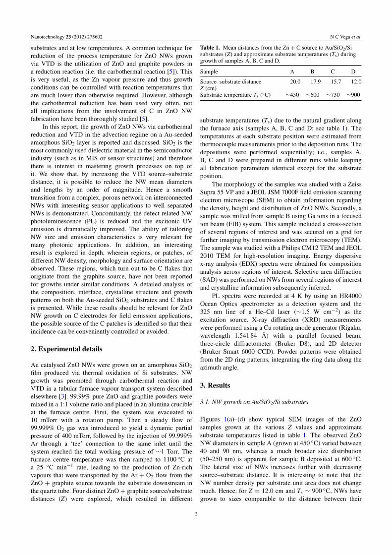
Figures 1(a)–(d) show typical SEM images of the ZnOsamples grown at the various Z values and approximatesubstrate temperatures listed in table 1. The observed ZnONW diameters in sample A (grown at 450 ◦C) varied between40 and 90 nm, whereas a much broader size distribution(50–250 nm) is apparent for sample B deposited at 600 ◦C.The lateral size of NWs increases further with decreasingsource–substrate distance. It is interesting to note that theNW number density per substrate unit area does not changemuch. Hence, for Z = 12.0 cm and Ts ∼ 900 ◦C, NWs havegrown to sizes comparable to the distance between their
2
Nanotechnology 23 (2012) 275602 N C Vega et al
Figure 1. (a)–(d) Top view SEM images of ZnO NWs grown on Au-seeded SiO2/Si substrates at different (ZnO+ C) source–substratedistances leading to different substrate temperatures and NW morphologies due to the natural temperature gradient along the tubular furnaceaxis. The insets of (b) and (d) show SEM images from samples B and D respectively taken at 45◦ showing the partial vertical orientation ofthe ZnO NWs.
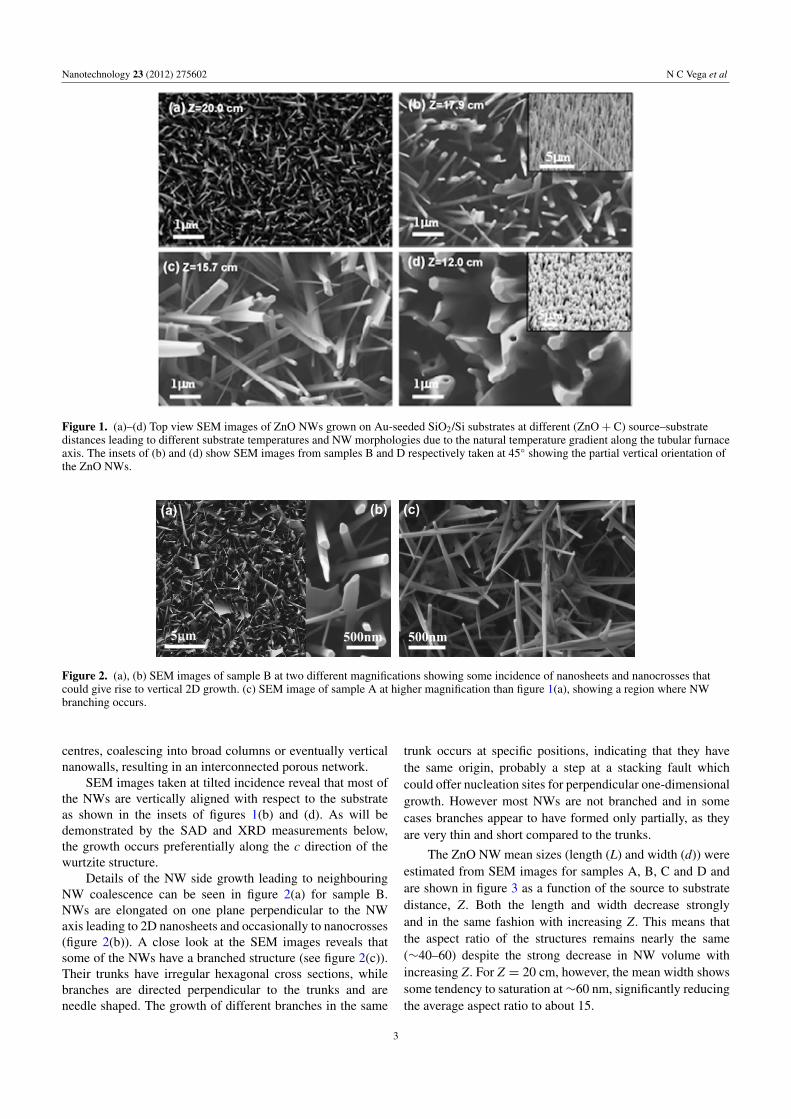
Figure 2. (a), (b) SEM images of sample B at two different magnifications showing some incidence of nanosheets and nanocrosses thatcould give rise to vertical 2D growth. (c) SEM image of sample A at higher magnification than figure 1(a), showing a region where NWbranching occurs.
centres, coalescing into broad columns or eventually verticalnanowalls, resulting in an interconnected porous network.
SEM images taken at tilted incidence reveal that most ofthe NWs are vertically aligned with respect to the substrateas shown in the insets of figures 1(b) and (d). As will bedemonstrated by the SAD and XRD measurements below,the growth occurs preferentially along the c direction of thewurtzite structure.
Details of the NW side growth leading to neighbouringNW coalescence can be seen in figure 2(a) for sample B.NWs are elongated on one plane perpendicular to the NWaxis leading to 2D nanosheets and occasionally to nanocrosses(figure 2(b)). A close look at the SEM images reveals thatsome of the NWs have a branched structure (see figure 2(c)).Their trunks have irregular hexagonal cross sections, whilebranches are directed perpendicular to the trunks and areneedle shaped. The growth of different branches in the same
trunk occurs at specific positions, indicating that they havethe same origin, probably a step at a stacking fault whichcould offer nucleation sites for perpendicular one-dimensionalgrowth. However most NWs are not branched and in somecases branches appear to have formed only partially, as theyare very thin and short compared to the trunks.
The ZnO NW mean sizes (length (L) and width (d)) wereestimated from SEM images for samples A, B, C and D andare shown in figure 3 as a function of the source to substratedistance, Z. Both the length and width decrease stronglyand in the same fashion with increasing Z. This means thatthe aspect ratio of the structures remains nearly the same(∼40–60) despite the strong decrease in NW volume withincreasing Z. For Z = 20 cm, however, the mean width showssome tendency to saturation at∼60 nm, significantly reducingthe average aspect ratio to about 15.
3
Nanotechnology 23 (2012) 275602 N C Vega et al
Figure 3. Mean length (red triangles) and width (black squares) ofZnO NWs in samples A, B, C and D as a function of the source tosubstrate distance during growth. Lines through data are a guide tothe eye.
3.2. Carbon patches
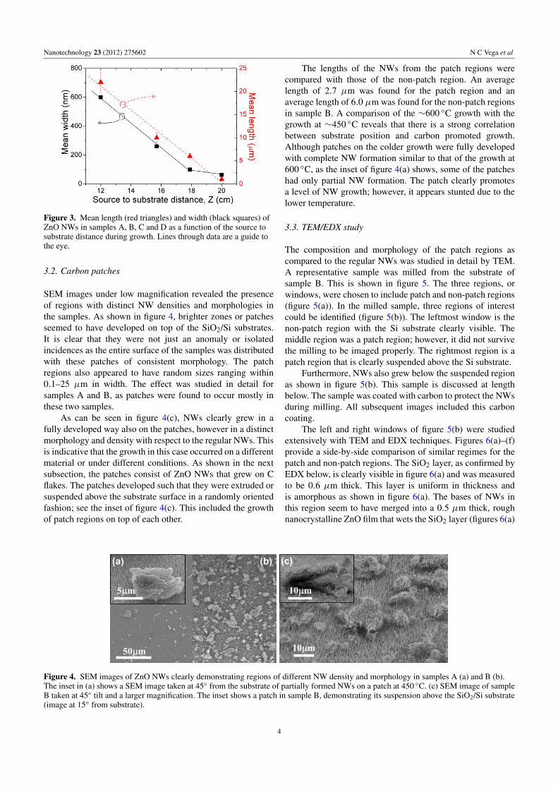
SEM images under low magnification revealed the presenceof regions with distinct NW densities and morphologies inthe samples. As shown in figure 4, brighter zones or patchesseemed to have developed on top of the SiO2/Si substrates.It is clear that they were not just an anomaly or isolatedincidences as the entire surface of the samples was distributedwith these patches of consistent morphology. The patchregions also appeared to have random sizes ranging within0.1–25 µm in width. The effect was studied in detail forsamples A and B, as patches were found to occur mostly inthese two samples.
As can be seen in figure 4(c), NWs clearly grew in afully developed way also on the patches, however in a distinctmorphology and density with respect to the regular NWs. Thisis indicative that the growth in this case occurred on a differentmaterial or under different conditions. As shown in the nextsubsection, the patches consist of ZnO NWs that grew on Cflakes. The patches developed such that they were extruded orsuspended above the substrate surface in a randomly orientedfashion; see the inset of figure 4(c). This included the growthof patch regions on top of each other.
The lengths of the NWs from the patch regions werecompared with those of the non-patch region. An averagelength of 2.7 µm was found for the patch region and anaverage length of 6.0 µm was found for the non-patch regionsin sample B. A comparison of the ∼600 ◦C growth with thegrowth at ∼450 ◦C reveals that there is a strong correlationbetween substrate position and carbon promoted growth.Although patches on the colder growth were fully developedwith complete NW formation similar to that of the growth at600 ◦C, as the inset of figure 4(a) shows, some of the patcheshad only partial NW formation. The patch clearly promotesa level of NW growth; however, it appears stunted due to thelower temperature.
3.3. TEM/EDX study
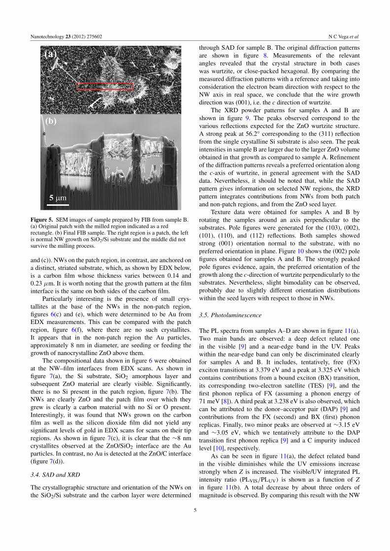
The composition and morphology of the patch regions ascompared to the regular NWs was studied in detail by TEM.A representative sample was milled from the substrate ofsample B. This is shown in figure 5. The three regions, orwindows, were chosen to include patch and non-patch regions(figure 5(a)). In the milled sample, three regions of interestcould be identified (figure 5(b)). The leftmost window is thenon-patch region with the Si substrate clearly visible. Themiddle region was a patch region; however, it did not survivethe milling to be imaged properly. The rightmost region is apatch region that is clearly suspended above the Si substrate.
Furthermore, NWs also grew below the suspended regionas shown in figure 5(b). This sample is discussed at lengthbelow. The sample was coated with carbon to protect the NWsduring milling. All subsequent images included this carboncoating.
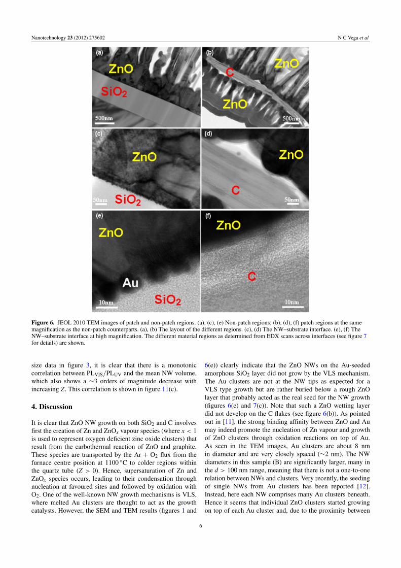
The left and right windows of figure 5(b) were studiedextensively with TEM and EDX techniques. Figures 6(a)–(f)provide a side-by-side comparison of similar regimes for thepatch and non-patch regions. The SiO2 layer, as confirmed byEDX below, is clearly visible in figure 6(a) and was measuredto be 0.6 µm thick. This layer is uniform in thickness andis amorphous as shown in figure 6(a). The bases of NWs inthis region seem to have merged into a 0.5 µm thick, roughnanocrystalline ZnO film that wets the SiO2 layer (figures 6(a)
Figure 4. SEM images of ZnO NWs clearly demonstrating regions of different NW density and morphology in samples A (a) and B (b).The inset in (a) shows a SEM image taken at 45◦ from the substrate of partially formed NWs on a patch at 450 ◦C. (c) SEM image of sampleB taken at 45◦ tilt and a larger magnification. The inset shows a patch in sample B, demonstrating its suspension above the SiO2/Si substrate(image at 15◦ from substrate).
4
Nanotechnology 23 (2012) 275602 N C Vega et al
Figure 5. SEM images of sample prepared by FIB from sample B.(a) Original patch with the milled region indicated as a redrectangle. (b) Final FIB sample. The right region is a patch, the leftis normal NW growth on SiO2/Si substrate and the middle did notsurvive the milling process.
and (c)). NWs on the patch region, in contrast, are anchored ona distinct, striated substrate, which, as shown by EDX below,is a carbon film whose thickness varies between 0.14 and0.23 µm. It is worth noting that the growth pattern at the filminterface is the same on both sides of the carbon film.
Particularly interesting is the presence of small crys-tallites at the base of the NWs in the non-patch region,figures 6(c) and (e), which were determined to be Au fromEDX measurements. This can be compared with the patchregion, figure 6(f), where there are no such crystallites.It appears that in the non-patch region the Au particles,approximately 8 nm in diameter, are seeding or feeding thegrowth of nanocrystalline ZnO above them.
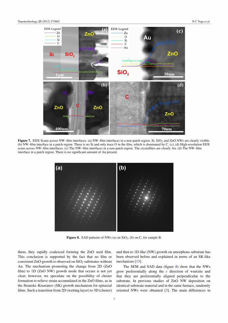
The compositional data shown in figure 6 were obtainedat the NW–film interfaces from EDX scans. As shown infigure 7(a), the Si substrate, SiO2 amorphous layer andsubsequent ZnO material are clearly visible. Significantly,there is no Si present in the patch region, figure 7(b). TheNWs are clearly ZnO and the patch film over which theygrew is clearly a carbon material with no Si or O present.Interestingly, it was found that NWs grown on the carbonfilm as well as the silicon dioxide film did not yield anysignificant levels of gold in EDX scans for scans on their tipregions. As shown in figure 7(c), it is clear that the ∼8 nmcrystallites observed at the ZnO/SiO2 interface are the Auparticles. In contrast, no Au is detected at the ZnO/C interface(figure 7(d)).
3.4. SAD and XRD
The crystallographic structure and orientation of the NWs onthe SiO2/Si substrate and the carbon layer were determined
through SAD for sample B. The original diffraction patternsare shown in figure 8. Measurements of the relevantangles revealed that the crystal structure in both caseswas wurtzite, or close-packed hexagonal. By comparing themeasured diffraction patterns with a reference and taking intoconsideration the electron beam direction with respect to theNW axis in real space, we conclude that the wire growthdirection was (001), i.e. the c direction of wurtzite.
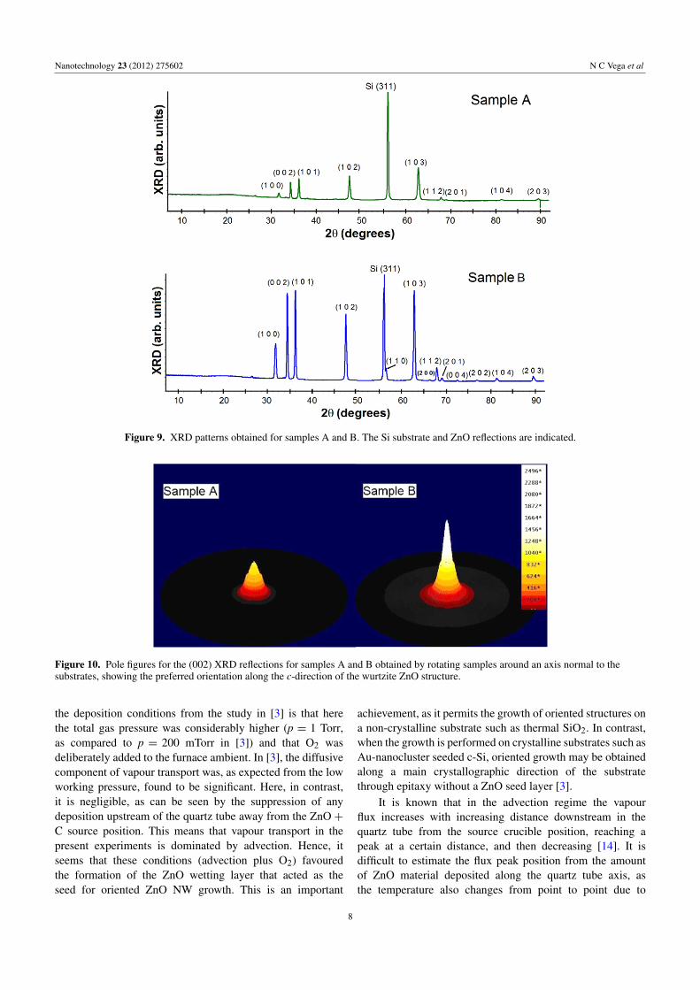
The XRD powder patterns for samples A and B areshown in figure 9. The peaks observed correspond to thevarious reflections expected for the ZnO wurtzite structure.A strong peak at 56.2◦ corresponding to the (311) reflectionfrom the single crystalline Si substrate is also seen. The peakintensities in sample B are larger due to the larger ZnO volumeobtained in that growth as compared to sample A. Refinementof the diffraction patterns reveals a preferred orientation alongthe c-axis of wurtzite, in general agreement with the SADdata. Nevertheless, it should be noted that, while the SADpattern gives information on selected NW regions, the XRDpattern integrates contributions from NWs from both patchand non-patch regions, and from the ZnO seed layer.
Texture data were obtained for samples A and B byrotating the samples around an axis perpendicular to thesubstrates. Pole figures were generated for the (103), (002),(101), (110), and (112) reflections. Both samples showedstrong (001) orientation normal to the substrate, with nopreferred orientation in plane. Figure 10 shows the (002) polefigures obtained for samples A and B. The strongly peakedpole figures evidence, again, the preferred orientation of thegrowth along the c-direction of wurtzite perpendicularly to thesubstrates. Nevertheless, slight bimodality can be observed,probably due to slightly different orientation distributionswithin the seed layers with respect to those in NWs.
3.5. Photoluminescence
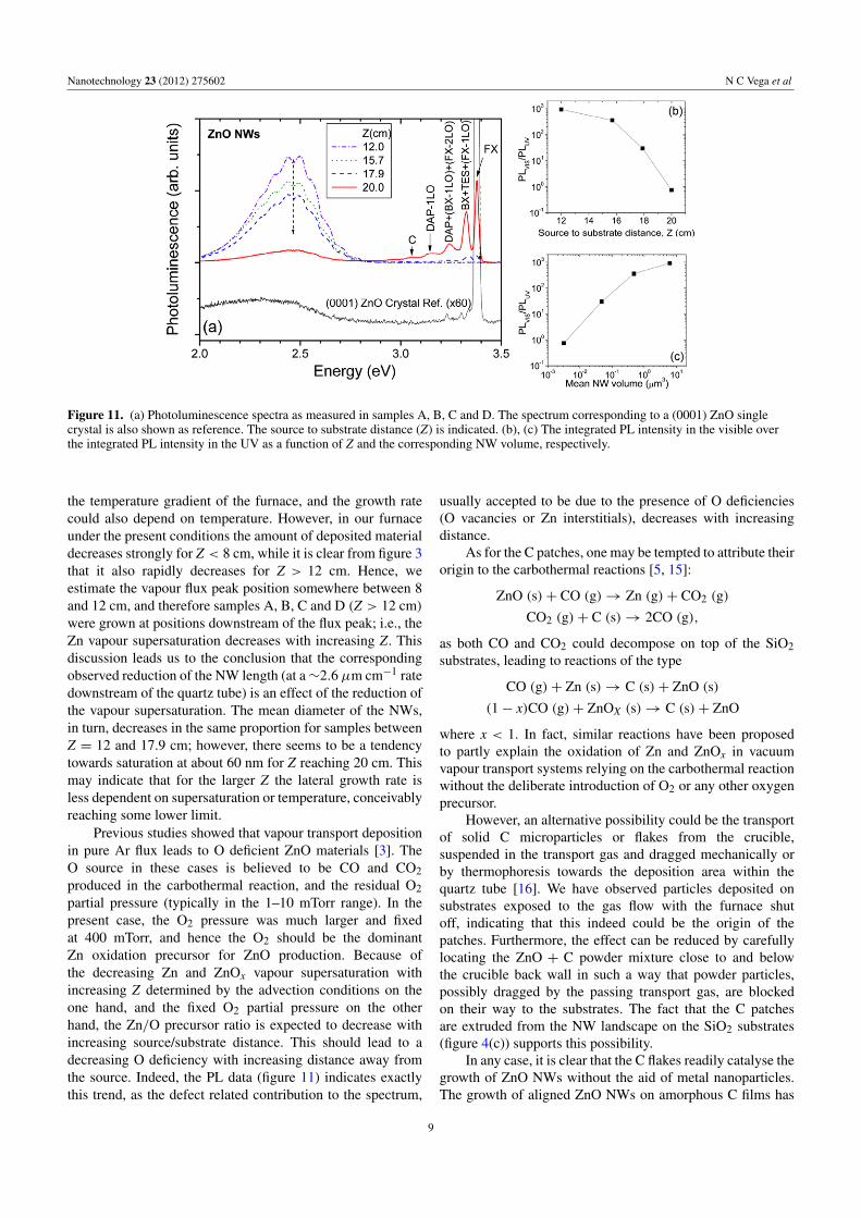
The PL spectra from samples A–D are shown in figure 11(a).Two main bands are observed: a deep defect related onein the visible [9] and a near-edge band in the UV. Peakswithin the near-edge band can only be discriminated clearlyfor samples A and B. It includes, tentatively, free (FX)exciton transitions at 3.379 eV and a peak at 3.325 eV whichcontains contributions from a bound exciton (BX) transition,its corresponding two-electron satellite (TES) [9], and thefirst phonon replica of FX (assuming a phonon energy of71 meV [8]). A third peak at 3.238 eV is also observed, whichcan be attributed to the donor–acceptor pair (DAP) [9] andcontributions from the FX (second) and BX (first) phononreplicas. Finally, two minor peaks are observed at ∼3.15 eVand ∼3.05 eV, which we tentatively attribute to the DAPtransition first phonon replica [9] and a C impurity inducedlevel [10], respectively.
As can be seen in figure 11(a), the defect related bandin the visible diminishes while the UV emissions increasestrongly when Z is increased. The visible/UV integrated PLintensity ratio (PLVIS/PLUV) is shown as a function of Zin figure 11(b). A total decrease by about three orders ofmagnitude is observed. By comparing this result with the NW
5
Nanotechnology 23 (2012) 275602 N C Vega et al
Figure 6. JEOL 2010 TEM images of patch and non-patch regions. (a), (c), (e) Non-patch regions; (b), (d), (f) patch regions at the samemagnification as the non-patch counterparts. (a), (b) The layout of the different regions. (c), (d) The NW–substrate interface. (e), (f) TheNW–substrate interface at high magnification. The different material regions as determined from EDX scans across interfaces (see figure 7for details) are shown.
size data in figure 3, it is clear that there is a monotoniccorrelation between PLVIS/PLUV and the mean NW volume,which also shows a ∼3 orders of magnitude decrease withincreasing Z. This correlation is shown in figure 11(c).
4. Discussion
It is clear that ZnO NW growth on both SiO2 and C involvesfirst the creation of Zn and ZnOx vapour species (where x < 1is used to represent oxygen deficient zinc oxide clusters) thatresult from the carbothermal reaction of ZnO and graphite.These species are transported by the Ar + O2 flux from thefurnace centre position at 1100 ◦C to colder regions withinthe quartz tube (Z > 0). Hence, supersaturation of Zn andZnOx species occurs, leading to their condensation throughnucleation at favoured sites and followed by oxidation withO2. One of the well-known NW growth mechanisms is VLS,where melted Au clusters are thought to act as the growthcatalysts. However, the SEM and TEM results (figures 1 and
6(e)) clearly indicate that the ZnO NWs on the Au-seededamorphous SiO2 layer did not grow by the VLS mechanism.The Au clusters are not at the NW tips as expected for aVLS type growth but are rather buried below a rough ZnOlayer that probably acted as the real seed for the NW growth(figures 6(e) and 7(c)). Note that such a ZnO wetting layerdid not develop on the C flakes (see figure 6(b)). As pointedout in [11], the strong binding affinity between ZnO and Aumay indeed promote the nucleation of Zn vapour and growthof ZnO clusters through oxidation reactions on top of Au.As seen in the TEM images, Au clusters are about 8 nmin diameter and are very closely spaced (∼2 nm). The NWdiameters in this sample (B) are significantly larger, many inthe d > 100 nm range, meaning that there is not a one-to-onerelation between NWs and clusters. Very recently, the seedingof single NWs from Au clusters has been reported [12].Instead, here each NW comprises many Au clusters beneath.Hence it seems that individual ZnO clusters started growingon top of each Au cluster and, due to the proximity between
6
Nanotechnology 23 (2012) 275602 N C Vega et al
Figure 7. EDX Scans across NW–film interfaces. (a) NW–film interfaces in a non-patch region. Si, SiO2 and ZnO NWs are clearly visible.(b) NW–film interface in a patch region. There is no Si and only trace O in the film, which is dominated by C. (c), (d) High-resolution EDXscans across NW–film interfaces. (c) The NW–film interfaces in a non-patch region. The crystallites are clearly Au. (d) The NW–filminterface in a patch region. There is no significant amount of Au present.
Figure 8. SAD patterns of NWs (a) on SiO2, (b) on C, for sample B.
them, they rapidly coalesced forming the ZnO seed film.This conclusion is supported by the fact that no film orconsistent ZnO growth is observed on SiO2 substrates withoutAu. The mechanism promoting the change from 2D (ZnOfilm) to 1D (ZnO NW) growth mode that occurs is not yetclear; however, we speculate on the possibility of clusterformation to relieve strain accumulated in the ZnO films, as inthe Stranski–Krastanov (SK) growth mechanism for epitaxialfilms. Such a transition from 2D (wetting layer) to 3D (cluster)
and then to 1D-like (NW) growth on amorphous substrate hasbeen observed before and explained in terms of an SK-likemechanism [13].
The SEM and SAD data (figure 8) show that the NWsgrew preferentially along the c direction of wurtzite andthat they are preferentially aligned perpendicular to thesubstrate. In previous studies of ZnO NW deposition onidentical substrate material and in the same furnace, randomlyoriented NWs were obtained [3]. The main differences in
7
Nanotechnology 23 (2012) 275602 N C Vega et al
Figure 9. XRD patterns obtained for samples A and B. The Si substrate and ZnO reflections are indicated.
Figure 10. Pole figures for the (002) XRD reflections for samples A and B obtained by rotating samples around an axis normal to thesubstrates, showing the preferred orientation along the c-direction of the wurtzite ZnO structure.
the deposition conditions from the study in [3] is that herethe total gas pressure was considerably higher (p = 1 Torr,as compared to p = 200 mTorr in [3]) and that O2 wasdeliberately added to the furnace ambient. In [3], the diffusivecomponent of vapour transport was, as expected from the lowworking pressure, found to be significant. Here, in contrast,it is negligible, as can be seen by the suppression of anydeposition upstream of the quartz tube away from the ZnO +C source position. This means that vapour transport in thepresent experiments is dominated by advection. Hence, itseems that these conditions (advection plus O2) favouredthe formation of the ZnO wetting layer that acted as theseed for oriented ZnO NW growth. This is an important
achievement, as it permits the growth of oriented structures ona non-crystalline substrate such as thermal SiO2. In contrast,when the growth is performed on crystalline substrates such asAu-nanocluster seeded c-Si, oriented growth may be obtainedalong a main crystallographic direction of the substratethrough epitaxy without a ZnO seed layer [3].
It is known that in the advection regime the vapourflux increases with increasing distance downstream in thequartz tube from the source crucible position, reaching apeak at a certain distance, and then decreasing [14]. It isdifficult to estimate the flux peak position from the amountof ZnO material deposited along the quartz tube axis, asthe temperature also changes from point to point due to
8
Nanotechnology 23 (2012) 275602 N C Vega et al
Figure 11. (a) Photoluminescence spectra as measured in samples A, B, C and D. The spectrum corresponding to a (0001) ZnO singlecrystal is also shown as reference. The source to substrate distance (Z) is indicated. (b), (c) The integrated PL intensity in the visible overthe integrated PL intensity in the UV as a function of Z and the corresponding NW volume, respectively.
the temperature gradient of the furnace, and the growth ratecould also depend on temperature. However, in our furnaceunder the present conditions the amount of deposited materialdecreases strongly for Z < 8 cm, while it is clear from figure 3that it also rapidly decreases for Z > 12 cm. Hence, weestimate the vapour flux peak position somewhere between 8and 12 cm, and therefore samples A, B, C and D (Z > 12 cm)were grown at positions downstream of the flux peak; i.e., theZn vapour supersaturation decreases with increasing Z. Thisdiscussion leads us to the conclusion that the correspondingobserved reduction of the NW length (at a∼2.6µm cm−1 ratedownstream of the quartz tube) is an effect of the reduction ofthe vapour supersaturation. The mean diameter of the NWs,in turn, decreases in the same proportion for samples betweenZ = 12 and 17.9 cm; however, there seems to be a tendencytowards saturation at about 60 nm for Z reaching 20 cm. Thismay indicate that for the larger Z the lateral growth rate isless dependent on supersaturation or temperature, conceivablyreaching some lower limit.
Previous studies showed that vapour transport depositionin pure Ar flux leads to O deficient ZnO materials [3]. TheO source in these cases is believed to be CO and CO2produced in the carbothermal reaction, and the residual O2partial pressure (typically in the 1–10 mTorr range). In thepresent case, the O2 pressure was much larger and fixedat 400 mTorr, and hence the O2 should be the dominantZn oxidation precursor for ZnO production. Because ofthe decreasing Zn and ZnOx vapour supersaturation withincreasing Z determined by the advection conditions on theone hand, and the fixed O2 partial pressure on the otherhand, the Zn/O precursor ratio is expected to decrease withincreasing source/substrate distance. This should lead to adecreasing O deficiency with increasing distance away fromthe source. Indeed, the PL data (figure 11) indicates exactlythis trend, as the defect related contribution to the spectrum,
usually accepted to be due to the presence of O deficiencies(O vacancies or Zn interstitials), decreases with increasingdistance.
As for the C patches, one may be tempted to attribute theirorigin to the carbothermal reactions [5, 15]:
ZnO (s)+ CO (g)→ Zn (g)+ CO2 (g)
CO2 (g)+ C (s)→ 2CO (g),
as both CO and CO2 could decompose on top of the SiO2substrates, leading to reactions of the type
CO (g)+ Zn (s)→ C (s)+ ZnO (s)
(1− x)CO (g)+ ZnOX (s)→ C (s)+ ZnO
where x < 1. In fact, similar reactions have been proposedto partly explain the oxidation of Zn and ZnOx in vacuumvapour transport systems relying on the carbothermal reactionwithout the deliberate introduction of O2 or any other oxygenprecursor.
However, an alternative possibility could be the transportof solid C microparticles or flakes from the crucible,suspended in the transport gas and dragged mechanically orby thermophoresis towards the deposition area within thequartz tube [16]. We have observed particles deposited onsubstrates exposed to the gas flow with the furnace shutoff, indicating that this indeed could be the origin of thepatches. Furthermore, the effect can be reduced by carefullylocating the ZnO + C powder mixture close to and belowthe crucible back wall in such a way that powder particles,possibly dragged by the passing transport gas, are blockedon their way to the substrates. The fact that the C patchesare extruded from the NW landscape on the SiO2 substrates(figure 4(c)) supports this possibility.
In any case, it is clear that the C flakes readily catalyse thegrowth of ZnO NWs without the aid of metal nanoparticles.The growth of aligned ZnO NWs on amorphous C films has
9
Nanotechnology 23 (2012) 275602 N C Vega et al
been observed and studied recently [17] due to the importanceof the C/ZnO NW system as efficient field emitters.In recent years, the growth of various one-dimensionalnanostructures has been explained by a vapour–solid (VS)process without introducing any heterometal catalysts [7]. Forthese cases, the growth directions are generally perpendicularto high-surface-energy planes, and their side surfaces areenclosed by low-index crystallographic planes to minimizethe surface energy. The results here emphasize the roleof different substrate materials on the growth mechanismunder identical atmosphere and thermal conditions. The NWlength is about three times larger on SiO2 seeded with Aunanoparticles than on the C patches. Since the impingingrate of vapour precursors must be roughly equal for bothsubstrates, the difference must stem from differences in thesurface diffusion contribution to the growth. It is conceivablethat vapour species that do not land on favoured nucleationsites diffuse on the substrate until reaching one of them. Asdiscussed above, a thin ZnO wetting layer is formed on theAu/SiO2/Si substrate but absent from C or bare SiO2, as maybe explained from the strong binding affinity between ZnOand Au. The surface diffusion component leading to a largergrowth in the non-patch regions, therefore, could be relatedto self-diffusivity of Zn material on top of ZnO, which seemsto be significantly larger than the Zn diffusivity on C. Theimportance of surface diffusion for the growth of ZnO hasbeen emphasized in the literature [18]. Another possibilityfor the larger growth in the non-patch regions could be theformation of 3D ZnO clusters or islands on the ZnO film,which could promote more efficient 1D growth as expectedby more efficient atom sticking at the cluster hills than at theshadowed valleys.
Finally, we would like to consider the relation betweenthe PL spectra and the changing growth conditions with thesubstrate position for samples A, B, C and D within thefurnace and the correlation between PLVIS/PLUV and the NWmean volume (refer to figure 11). We have seen that the Znand ZnOx partial pressures (pZn) decrease with increasingZ > 12 cm. As discussed above, since the O2 partial pressureis kept fixed, the amount of material collected (i.e. ZnO NWvolume) in each sample is determined by the supersaturationof Zn vapours, which depends primarily on pZn. On theother hand, the concentration of O deficiency defects (i.e. Ovacancies or Zn interstitials), which are believed to be at theorigin of the PLVIS, should be determined to a great extentby the partial pressure ratio, pZn/pO2 . In this case, a greaternumber of O deficiency defects would be formed for a higherpZn/pO2 , and PLVIS/PLUV should increase with pZn/pO2 .Since pO2 is fixed and pZn determines the NW volume, themonotonically increasing correlation between PLVIS/PLUVand the NW volume (figure 11(c)) can be predicted.
However, it is interesting to note that other authors [19]and some of us [20] have found a decreasing correlationbetween the PLVIS/PLUV ratio and the ZnO NW diameter.Indeed, such a negative correlation is observed fornanostructures grown with our fabrication system at nearlyconstant Z where the O2 partial pressure was changed tochange the nanostructure morphology [20]. This correlation
has led authors to propose that the luminescence in thevisible from NWs is due to recombination processes throughO deficiency defects that occur preferentially at the NWsurfaces [19, 20]. Here, in contrast, we observe an oppositebehaviour (figure 11(c)); that is, PLVIS/PLUV increases withincreasing NW diameter and volume. We believe this isbecause, with increasing Z, the corresponding decreases ofpZn/pO2 and Ts lead to such a drastic decrease of oxygendeficiency defect concentration that overweighs the observed∼10 times surface area increase. Indeed, the decreasingcorrelation has been observed only for cases in whichdeposition conditions are such that the surface defect densityper unit surface area remains approximately constant for thedifferently sized ZnO nanostructures studied [19, 20].
5. Conclusion
We have studied ZnO NWs on amorphous SiO2 films seededwith Au nanoparticles grown by VTD and carbothermalreduction. NWs are vertically oriented with respect tosubstrates and their mean size decreases strongly withincreasing ZnO+C source–SiO2/Si substrate distance, henceoffering an interesting method to produce ZnO NWs withvarious diameters and lengths in the 40–800 nm and 1–22 µmranges, respectively. In particular, for small source–substratedistances, interconnected porous NW networks on insulatingsubstrate with attractive sensor applications have beenobtained. The growth mechanism is governed by nucleation ofZn at the Au nanoclusters, the formation of a ZnO seed layerby oxidation reactions and coalescence of individual ZnOclusters, and the roughening of the ZnO seed layer, followedby VS growth of NWs on favourable sites on top of ZnO hillson the ZnO seed layer.
We observe C patches on the ZnO NW/SiO2 substrates,which probably result from C particles that are draggedmechanically or by thermophoresis from the ZnO + graphitesource towards the substrates. NWs readily grow on the Cparticles by a distinct VS, Au catalyst-free mechanism, whichdoes not involve any ZnO seed layer. ZnO NWs on C areabout three times shorter than those grown on the Au-seededSiO2. The simple growth of ZnO NWs on C material is ofimportance for the production of electrodes for field emissionapplications, but can be minimized for other applications.
The NWs show PL in the visible and the UV.The integrated PLVIS/PLUV decreases by various ordersof magnitude with increasing ZnO + C source–SiO2/Sisubstrate distance, in correlation with a strong NW volumedecrease. This behaviour can be explained by an expectedstrong reduction of the O deficiency defect concentrationwith decreasing pZn/pO2 in the advection conditions used.This result offers an interesting potential for tailoring andoptimizing the NW optical emission for various photonicapplications.
Acknowledgments
We are grateful to Dr L J Borrero-Gonzalez and ProfessorF E G Guimaraes from the IFSC, Sao Paulo University, Brazil,
10
Nanotechnology 23 (2012) 275602 N C Vega et al
for valuable help with the PL measurements, and to JimBritten and Vicky Jarvis from McMaster University, Canada,for the XRD work. This work was made possible by the CIAM(Inter-American Collaboration in Materials—NanoProject)initiative and has been partially funded by the Argentineanagencies CONICET, CIUNT 26/E419 and 26/E439 andFONCyT (PICT 2010 No. 400). In Canada, financial supportfrom NSERC is gratefully acknowledged.
References
[1] Singh D P 2010 Sci. Adv. Mater. 2 245[2] Huang M H, Wu Y, Feick H, Tran N, Weber E and
Yang P 2001 Adv. Mater. 13 113[3] Comedi D, Tirado M, Zapata C, Heluani S P, Villafuerte M,
Mohseni P and LaPierre R R 2010 J. Alloys Compounds495 439
[4] Wang Z L 2004 J. Phys.: Condens. Matter 16 R829[5] Biswas M, McGlynn E, Henry M O, McCann M and
Rafferty A 2009 J. Appl. Phys. 105 094306[6] Li J, Zhang Q, Peng H, Everitt H O, Qin L and Liu J 2009
J. Phys. Chem. C 113 3950[7] Campos L C, Tonezzer M, Ferlauto A S, Grillo V,
Magalhaes-Paniago R, Oliveira S, Ladeira L O andLacerda R G 2008 Adv. Mater. 20 1499
[8] Cha S N, Song B G, Jang J W, Jung J E, Han I T, Ha J H,Hong J P, Kang D J and Kim J M 2008 Nanotechnology19 235601
[9] Teke A, Ozgur U, Dogan S, Gu X, Morkoc H, Nemeth B,Nause J and Everitt H O 2004 Phys. Rev. B 70 195207
[10] Matsumoto K, Kuriyama K and Kushida K 2009 Nucl.Instrum. Methods B 267 1568
[11] Kim D S, Scholz R, Gosele U and Zacharias M 2008 Small4 1615
[12] Zhu G, Zhou Y, Wang S, Yang R, Ding Y, Wang X,Bando Y and Wang Z L 2012 Nanotechnology 23 055604
[13] Zhang H Z, Sun X C, Wang R M and Yu D P 2004 J. Cryst.Growth 269 464
[14] Ye C, Fang X, Hao Y, Teng X and Zhang L 2005 J. Phys.Chem. B 109 19758
[15] Osinga T, Olalde G and Steinfeld A 2004 Indust. Eng. Chem.Res. 43 7981
[16] Setyawan H, Shimada M, Ohtsuka K and Okuyama K 2002Chem. Eng. Sci. 57 497
[17] Yang Y H and Yang G W 2010 Chem. Phys. Lett. 494 64[18] Kim D S, Gosele U and Zacharias M 2009 J. Cryst. Growth
311 3216[19] Shalish I, Temkin H and Narayanamurti V 2004 Phys. Rev. B
69 245401[20] Grinblat G, Capeluto M G, Tirado M, Bragas A V and
Comedi D 2012 Appl. Phys. Lett. 100 233116
11
Copyright © 2022 FDOKUMEN