Wetting Angles on Illuminated Ta 2 O 5 Thin Films with Controlled Nanostructure
11
Subscriber access provided by CTRO INVES CIENT The Journal of Physical Chemistry C is published by the American Chemical Society. 1155 Sixteenth Street N.W., Washington, DC 20036 Article Wetting Angles on Illuminated Ta O Thin Films with Controlled Nanostructure Victor Rico, Ana Borra#s, Francisco Yubero, Juan P. Espino#s, Fabia#n Frutos, and Agusti#n R. Gonza#lez-Elipe J. Phys. Chem. C, 2009, 113 (9), 3775-3784• DOI: 10.1021/jp805708w • Publication Date (Web): 06 February 2009 Downloaded from http://pubs.acs.org on March 16, 2009 More About This Article Additional resources and features associated with this article are available within the HTML version: • Supporting Information • Access to high resolution figures • Links to articles and content related to this article • Copyright permission to reproduce figures and/or text from this article
-
Upload
independent -
Category
Documents
-
view
1 -
download
0
Transcript of Wetting Angles on Illuminated Ta 2 O 5 Thin Films with Controlled Nanostructure
Subscriber access provided by CTRO INVES CIENT
The Journal of Physical Chemistry C is published by the American ChemicalSociety. 1155 Sixteenth Street N.W., Washington, DC 20036
Article
Wetting Angles on Illuminated Ta2
O5
ThinFilms with Controlled Nanostructure
Victor Rico, Ana Borra#s, Francisco Yubero, Juan P.Espino#s, Fabia#n Frutos, and Agusti#n R. Gonza#lez-Elipe
J. Phys. Chem. C, 2009, 113 (9), 3775-3784• DOI: 10.1021/jp805708w • Publication Date (Web): 06 February 2009
Downloaded from http://pubs.acs.org on March 16, 2009
More About This Article
Additional resources and features associated with this article are available within the HTML version:
• Supporting Information• Access to high resolution figures• Links to articles and content related to this article• Copyright permission to reproduce figures and/or text from this article
Wetting Angles on Illuminated Ta2O5 Thin Films with Controlled Nanostructure
Victor Rico,† Ana Borras,†,‡ Francisco Yubero,† Juan P. Espinos,‡ Fabian Frutos,§ andAgustın R. Gonzalez-Elipe*,†
Laboratorio de Superficies y laminas delgadas, Instituto de Ciencia de Materiales de SeVilla(CSIC-UniVersidad de SeVilla), AVenida Americo Vespucio 49, 41092 SeVilla, Spain, EMPA, Swiss FederalLaboratories for Materials Testing and Research, Feuerwerkerstrasse 39, 3604, Thun, Switzerland, andDepartamento de Fısica Aplicada I, UniVersidad de SeVilla, AVenida Reina Mercedes s/n, 41012 SeVilla, Spain
ReceiVed: June 29, 2008; ReVised Manuscript ReceiVed: NoVember 27, 2008
Ta2O5 thin films with different nanostructure and surface roughness have been prepared by electron evaporationat different angles between the evaporation source and the substrates. Large variation of refraction indexes(n) from 1.40 to 1.80 were obtained by changing the geometry of evaporation and/or by annealing the evaporatedfilms at increasing temperatures up to 1000 °C to make them crystalline. Very flat and compact thin films (n) 2.02) were also obtained by assisting the growth by bombardment with O2
+ ions of 800 eV kinetic energy.A similar correlation has been found between the wetting contact angle of water and the roughness of thefilms for the evaporated and evaporated + annealed samples, irrespective of their procedure of preparationand other microstructural characteristics. When the films were illuminated with UV light of h > Eg ) 4.2 eV(Eg, band gap energy of Ta2O5), their surface became superhydrophilic (contact angle < 10°) in a way quitesimilar to those reported for illuminated TiO2 thin films. The rate of transformation into the superhydrophilicstate was smaller for the crystalline than for the amorphous films, suggesting that in Ta2O5 the size of crystaldomains at the surface is an important parameter for the control of this kinetics. Changes in the water contactangle on films illuminated with visible light were also found when they were subjected to implantation withN2
+ ions of 800 eV kinetic energy. The origin of this photoactivity is discussed in terms of the electronicband gap states associated with the nitrogen-implanted atoms. The possibility of preparing antireflective andself-cleaning coatings of Ta2O5 is discussed.
Introduction
The control of the wetting properties of materials (i.e., thecontact angle of liquids on their surfaces) is a subject of muchscientific interest with many practical and industrial implica-tions.1 Within this context, the discovery by Wang et al.2 thatthe surface of TiO2 may be transformed upon UV lightirradiation from partially hydrophobic (i.e., water contact anglesaround 80°) into fully hydrophilic (i.e., the water drops spreadon the surface), fostered the research on this material and thisparticular property.3-6 At present, the use of TiO2 as self-cleaning and an antifogging material is a reality that has beenincorporated into some types of commercial glasses. Otherapplications such as automobile side view mirrors, windowfilms, exterior tiles, and highway road wall panels, etc., havebeen also proposed.7
Despite the photoactive character of many other oxidesemiconductors, the change in water contact angle upon lightirradiation has only been extensively studied for TiO2. Thus,although a similar behavior has been described for epitaxiallayers of ZnO8 or for thin films of semiconductor oxides suchas ZnO, SnO2, WO3, and V2O5,9 a systematic study of the UV-induced wetting angle changes on oxide semiconductors otherthan TiO2 is still missing.
Another open issue for the practical implementation of thesephotoactive surfaces is to make them sensitive to photons in
the visible region of the spectrum. Visible light activity for TiO2
has been claimed by Asahi et al.,10 when these films were dopedwith nitrogen. Recently, we have studied the wetting behaviorupon UV and visible light irradiation of a series of oxidesemiconductors in the form of thin films including ZnO, ITOcommercial glass, Ta2O5, and InTaO4.11 In another recent work,we have also found that the modification of the outmost surfacelayers of TiO2 by implantation of N2
+ ions of 50 keV energyproduces a change in the illumination response of the titaniumoxide that becomes partially hydrophilic upon visible lightirradiation.12
In the present work we want to go a step forward in the studyof the wetting behavior of Ta2O5 thin films, trying to correlatetheir wetting response upon light irradiation with their opticalproperties and structural and microstructural characteristics.Parameters which have been considered for this investigationare the roughness of the films, their amorphous or crystallinecharacter, or their surface modification by a beam of low-energyN2
+ ions. Ta2O5 is a stable oxide with a band gap slightly largerand a refraction index smaller than those of TiO2.13,14 In additionto photocatalytic activity of this oxide in the form of powderswhen irradiated with UV15 or visible16,17 photons, this latter,when doped with nitrogen, has been also reported. Thesecharacteristics suggest that, under certain conditions, oxide layersof Ta2O5 might be an alternative to TiO2 in the quest forphotoactive thin films with self-cleaning properties. Indeed, thismaterial, with a refraction index (n) smaller than that of TiO2
would be a clear option when a coating with low n is a requisite(e.g., when looking for antireflective and self-cleaning coat-ings).18
* To whom correspondence should be addressed. E-mail: [email protected].
† CSIC-Universidad de Sevilla.‡ EMPA.§ Departamento de Fısica Aplicada I, Universidad de Sevilla.
J. Phys. Chem. C 2009, 113, 3775–3784 3775
10.1021/jp805708w CCC: $40.75 2009 American Chemical SocietyPublished on Web 02/06/2009

In the present work, amorphous Ta2O5 thin films withdifferent nanostructures and porosities have been prepared bye-beam evaporation either at normal or glancing angleincidences.19,20 In some cases annealing of the films at hightemperature has been done to get the crystalline thin films. Thecomparative analysis of the optical properties and contact anglevariation on the different thin films has provided some clues toassess the processes controlling the light-induced wettingtransformation of this oxide in the form of thin film. Anadditional investigation with Ta2O5 thin films subjected to N2
+
ion implantation has evidenced that this technique can be usedto render their surface sensitive to visible light.
Experimental Section
T2O5 thin films were prepared by physical vapor evaporation(PVD) in an electron evaporation system. T2O5 pellets were usedas material for evaporation. To get fully stoichiometric thinfilms, a constant oxygen partial pressure (P ∼ 10-4 torr) wasmaintained in the chamber during evaporation. The substrates,consisting of pieces of a silicon wafer or transparent silica plates,were kept at room temperature during the preparation of thefilms. To control the porosity and the surface roughness of thefilms, evaporation was carried out at different glancing angleswith respect to the evaporation source. This geometry leads tocolumnar microstructures with much porosity and high surfaceroughness.19,20 All the samples considered here were preparedby evaporation for the same period of time under equivalentrate conditions with an approximate growing rate at normalincidence of 6 nm min-1. This means that the thickness of thesamples prepared at glancing angles was smaller than that ofthose prepared with the sample placed normal with respect tothe electron gun.
Another set of films were prepared by e-beam evaporationwhile their growth was assisted by low-energy (800 eV) O2
+
ion bombardment (ion beam assisted deposition, IBAD21) anda beam current of 10 µA cm-2 (approximately an ion/atom ratioof 0.1). Some experiments were also carried out with thin filmsprepared at normal geometry that were subsequently subjectedto 800 eV N2
+ ion bombardment up to a dose of approximately1017 ions cm-2. The ion gun utilized in these experiments wasa broad beam ion source (HFQ 1303-3 from Plasma Consult)supplied with N2 and excited by a radio frequency (RF)discharge.
The as-prepared films were amorphous, but they could bemade crystalline by postannealing in air at t > 700 °C for 3 h.Therefore, another set of samples used in this study consistedof thin films evaporated at normal geometry that were annealedin a furnace at increasing higher temperatures up to 1000 °C.
The crystalline structure of the annealed films was assessedby X-ray diffraction in a Siemens D5000 diffractometer workingin the Bragg-Brentano configuration.
Illumination of the samples was carried out with a Xe lampwith a photon intensity at the position of the samples of 2 Wcm-2 for the complete spectrum of the lamp. For simplicity wewill refer to this situation in the text and figures as UVillumination. Other experiments consisted of the illuminationwith the same lamp by placing an UV filter between the lampand the sample. The light intensity was then 1.6 W cm-2 at thesample position. In all cases an infrared filter (i.e., a water bath)was kept between the lamp and the samples to prevent anypossible heating by the infrared radiation. From experimentswith TiO2 it is known that the wetting angle variation upon UVillumination is much affected by the temperature of the filmand the external humidity.22 In our case, we controlled the
temperature of the holder during a complete illuminationexperiment and found that it did not change by more than 10°C. All the experiments were carried out under similar conditionsof the laboratory, and no significant variations in ambienthumidity should be expected.
Measurement of contact angle was carried out by the Youngmethod by dosing small droplets of deionized and bidistilledwater on the surface of the illuminated samples. In theexperiments where the contact angle variation was determinedas a function of the illumination time, a metal foil acting as ashutter was used to close and open the lamp output. All wettingangle measurements within a given experiment were taken afterillumination for successive periods of time. Therefore, the timescale in the plots refers to the accumulative illumination of thesamples. The maximum uncertainty in the determination ofthe water contact angle is about 10°, depending on the sampleposition. In the course of this investigation it was noticed thatthe “as-prepared” thin films were more hydrophilic than thesame samples a given time after their preparation. Therefore,storage conditions were carefully controlled by putting thesamples in a desiccator until their use. The reported experimentswere carried out with samples that have been stored for asufficiently long period of time, so that they had stabilized theirsurface properties (the minimum time elapsed was 2 monthssince their preparation). The evolution of the wetting angles onthe samples prepared at different glancing angles stored forincreasing periods of time is presented in Supporting InformationS1.
Chemical analysis of the original samples and the filmssubjected to N2
+ ion bombardment has been carried out bymeans of X-ray photoemission spectroscopy (XPS) in a ES-CALAB 210 spectrometer supplied by VG. The Mg KR (i.e.,1253.6 eV) line was used as excitation source, and the spectrawere collected in the pass energy constant mode at a value of50 eV. Calibration of the binding energy (BE) scale was doneby referencing the energy scale to the C1s peak at 284.6 eV forthe adventitious carbon present on the surface of samples. Someof the samples containing nitrogen were also analyzed aftersputtering with Ar+ ions of 1000 eV kinetic energy. An erosionrate of approximately 1 nm min-1 was achieved under ourexperimental conditions. A treatment of ca. 5 min was consid-ered sufficient to remove the most external surface layers ofthe films.
The optical properties of the samples were determined byUV-vis absorption spectroscopy on a Perkin-Elmer Lambda12 spectrometer for samples prepared on fused silica and byspectroscopic ellipsometry for samples prepared on a siliconwafer. Typical thickness of the samples used for opticalcharacterization was around 350 nm. By the UV-vis absorptionexperiments, the refraction index of the films was determinedby simulating the oscillations appearing in the spectra of Ta2O5
thin films deposited on a substrate with a smaller refractionindex. The spectroscopic ellipsometry experiments were per-formed using a Sopra commercially available system.
The measurements of ellipsometric parameters were madeat wavelengths from 0.21 to 1.0 µm at 65, 70, and 75° anglesof incidence. The analysis procedure consists of a regressionusing a Cauchy law to simulate the refraction index
n(λ))�1+(n∞
2 - 1)λ2
λ2 - λ∞2
where λ is the wavelength, n the refractive index, n∞is therefractive index when λ f ∞, and λ∞ is the wavelength for
3776 J. Phys. Chem. C, Vol. 113, No. 9, 2009 Rico et al.
n f ∞. To extract the extinction coefficient of the layer, weused the followoing expression:
K)K0 + (K1
λ )3
The shape of the k vs λ curves was very similar in all cases.They were characterized by practically zero absorption in thevisible region of the spectra and an absorption onset at about4.1-4.2 eV typical of the bandgap of Ta5O5.
The reported values of refraction index measured by UV-visor ellipsometry were determined at 550 nm. These twotechniques yielded similar values of the refraction index, exceptfor differences of the order of 0.01 in some determinations.These differences will not be considered for the discussion ofthe results. This good agreement supports that the microstructureof the films is similar on the two substrates, fused silica andsilicon wafers, used to grow the films. Optical properties werenot analyzed for the films annealed at T > 700 °C because thescattering of light distorted the UV-vis and ellipsometry spectra.
Normal and cross-section scanning electron micrographs weretaken in a Hitachi S5200 field emission microscope working at5.0 keV. For this analysis the samples were prepared on a siliconwafer substrate that was cleaved for observation of the layercross-sections.
Atomic force microscopy (AFM) images of the surface ofsamples were taken with a Dulcinea microscope from Nanotec(Madrid, Spain) working in tapping mode and using high-frequency levers. AFM images were processed with the WSxMfree available software from Nanotec. For each thin film, morethan five good quality images were taken at different regionsof the sample. The derived root mean square (rms) values weredetermined for a representative image of the surface and agreewell with the average values of all images.
Results
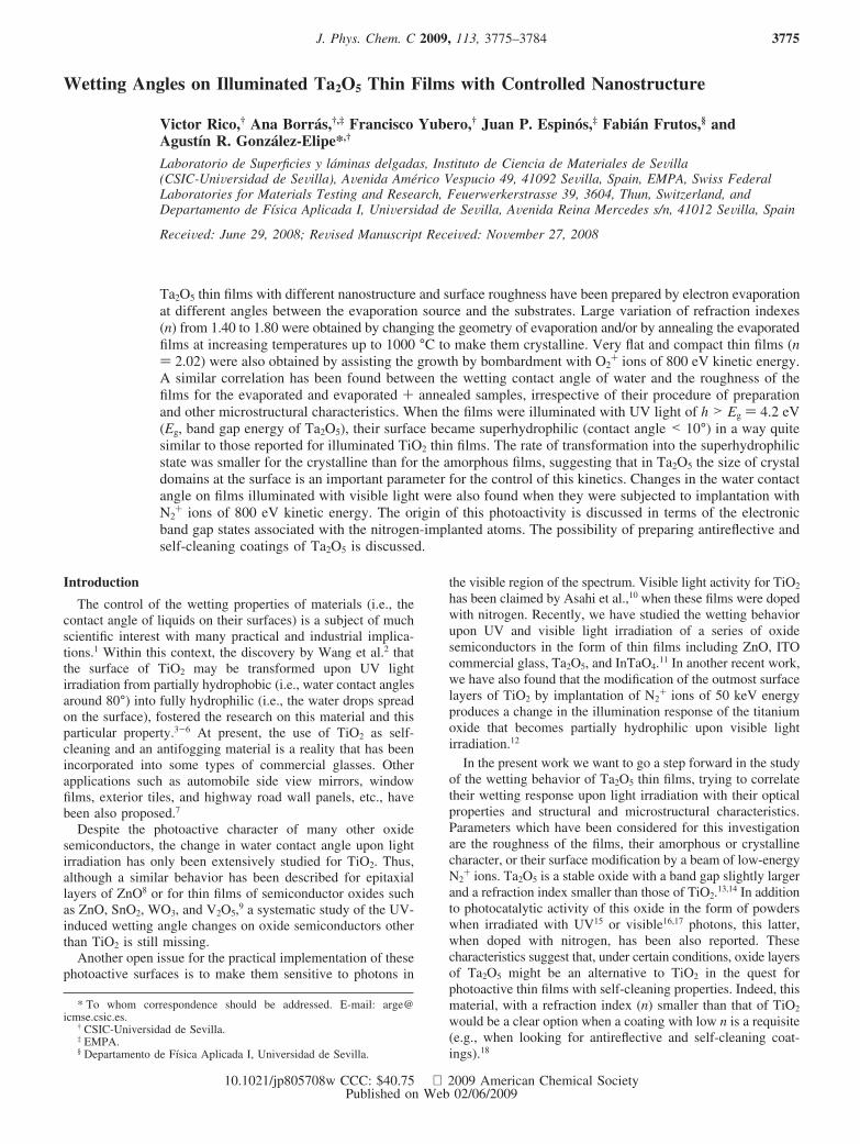
Structure of Thin Films. Just after preparation by electronevaporation the thin films were amorphous, but they becamecrystalline after an annealing treatment in a furnace at t>700°C, as indicated in the Experimental Section. Figure 1 shows aseries of X-ray diffraction (XRD) diagrams corresponding tothin films that were grown by evaporation at normal geometryand then annealed at the indicated temperatures. These diagramsconfirm that the thin films have become crystalline by annealing,depicting the hexagonal (at 700 °C) and orthorhombic (at 1000°C) structure of Ta2O5.23 The films present a preferentialtexturing according to the (003) and the (001) planes forrespectively the hexagonal and orthorhombic structures. Fromthe width of these peaks, the size of the crystal domains has
been determined by the method of Sherrer. The obtained valuesare reported in Table 1, showing that the size of the crystaldomains increases for the films annealed at 1000 °C.
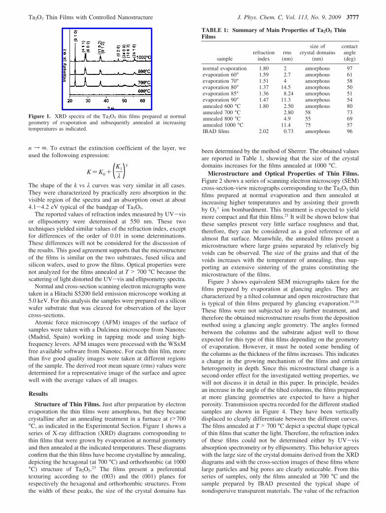
Microstructure and Optical Properties of Thin Films.Figure 2 shows a series of scanning electron microscopy (SEM)cross-section-view micrographs corresponding to the Ta2O5 thinfilms prepared at normal evaporation and then annealed atincreasing higher temperatures and by assisting their growthby O2
+ ion bombardment. This treatment is expected to yieldmore compact and flat thin films.21 It will be shown below thatthese samples present very little surface roughness and that,therefore, they can be considered as a good reference of analmost flat surface. Meanwhile, the annealed films present amicrostructure where large grains separated by relatively bigvoids can be observed. The size of the grains and that of thevoids increases with the temperature of annealing, thus sup-porting an extensive sintering of the grains constituting themicrostructure of the films.
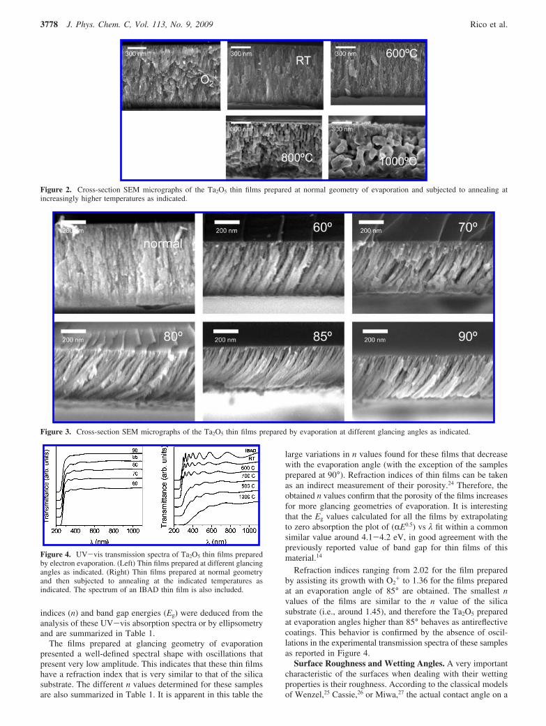
Figure 3 shows equivalent SEM micrographs taken for thefilms prepared by evaporation at glancing angles. They arecharacterized by a tilted columnar and open microstructure thatis typical of thin films prepared by glancing evaporation.19,20
These films were not subjected to any further treatment, andtherefore the obtained microstructure results from the depositionmethod using a glancing angle geometry. The angles formedbetween the columns and the substrate adjust well to thoseexpected for this type of thin films depending on the geometryof evaporation. However, it must be noted some bending ofthe columns as the thickness of the films increases. This indicatesa change in the growing mechanism of the films and certainheterogeneity in depth. Since this microstructural change is asecond-order effect for the investigated wetting properties, wewill not discuss it in detail in this paper. In principle, besidesan increase in the angle of the tilted columns, the films preparedat more glancing geometries are expected to have a higherporosity. Transmission spectra recorded for the different studiedsamples are shown in Figure 4. They have been verticallydisplaced to clearly differentiate between the different curves.The films annealed at T > 700 °C depict a spectral shape typicalof thin films that scatter the light. Therefore, the refraction indexof these films could not be determined either by UV-visabsorption spectrometry or by ellipsometry. This behavior agreeswith the large size of the crystal domains derived from the XRDdiagrams and with the cross-section images of these films wherelarge particles and big pores are clearly noticeable. From thisseries of samples, only the films annealed at 700 °C and thesample prepared by IBAD presented the typical shape ofnondispersive transparent materials. The value of the refraction
Figure 1. XRD spectra of the Ta2O5 thin films prepared at normalgeometry of evaporation and subsequently annealed at increasingtemperatures as indicated.
TABLE 1: Summary of Main Properties of Ta2O5 ThinFilms
samplerefraction
indexrms(nm)
size ofcrystal domains
(nm)
contactangle(deg)
normal evaporation 1.80 2 amorphous 97evaporation 60° 1.59 2.7 amorphous 61evaporation 70° 1.51 4 amorphous 58evaporation 80° 1.37 14.5 amorphous 50evaporation 85° 1.36 8.24 amorphous 51evaporation 90° 1.47 11.3 amorphous 54annealed 600 °C 1.80 2.50 amorphous 80annealed 700 °C 2.80 58 73annealed 800 °C 4.9 55 69annealed 1000 °C 11.4 75 57IBAD films 2.02 0.73 amorphous 96
Ta2O3 Thin Films with Controlled Nanostructure J. Phys. Chem. C, Vol. 113, No. 9, 2009 3777
indices (n) and band gap energies (Eg) were deduced from theanalysis of these UV-vis absorption spectra or by ellipsometryand are summarized in Table 1.
The films prepared at glancing geometry of evaporationpresented a well-defined spectral shape with oscillations thatpresent very low amplitude. This indicates that these thin filmshave a refraction index that is very similar to that of the silicasubstrate. The different n values determined for these samplesare also summarized in Table 1. It is apparent in this table the
large variations in n values found for these films that decreasewith the evaporation angle (with the exception of the samplesprepared at 90°). Refraction indices of thin films can be takenas an indirect measurement of their porosity.24 Therefore, theobtained n values confirm that the porosity of the films increasesfor more glancing geometries of evaporation. It is interestingthat the Eg values calculated for all the films by extrapolatingto zero absorption the plot of (RE0.5) vs λ fit within a commonsimilar value around 4.1-4.2 eV, in good agreement with thepreviously reported value of band gap for thin films of thismaterial.14
Refraction indices ranging from 2.02 for the film preparedby assisting its growth with O2
+ to 1.36 for the films preparedat an evaporation angle of 85° are obtained. The smallest nvalues of the films are similar to the n value of the silicasubstrate (i.e., around 1.45), and therefore the Ta2O5 preparedat evaporation angles higher than 85° behaves as antireflectivecoatings. This behavior is confirmed by the absence of oscil-lations in the experimental transmission spectra of these samplesas reported in Figure 4.
Surface Roughness and Wetting Angles. A very importantcharacteristic of the surfaces when dealing with their wettingproperties is their roughness. According to the classical modelsof Wenzel,25 Cassie,26 or Miwa,27 the actual contact angle on a
Figure 2. Cross-section SEM micrographs of the Ta2O5 thin films prepared at normal geometry of evaporation and subjected to annealing atincreasingly higher temperatures as indicated.
Figure 3. Cross-section SEM micrographs of the Ta2O5 thin films prepared by evaporation at different glancing angles as indicated.
Figure 4. UV-vis transmission spectra of Ta2O5 thin films preparedby electron evaporation. (Left) Thin films prepared at different glancingangles as indicated. (Right) Thin films prepared at normal geometryand then subjected to annealing at the indicated temperatures asindicated. The spectrum of an IBAD thin film is also included.
3778 J. Phys. Chem. C, Vol. 113, No. 9, 2009 Rico et al.
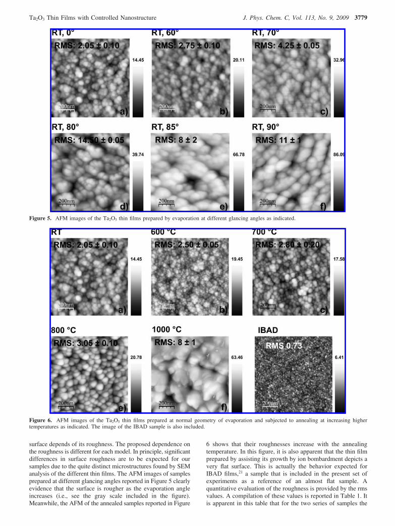
surface depends of its roughness. The proposed dependence onthe roughness is different for each model. In principle, significantdifferences in surface roughness are to be expected for oursamples due to the quite distinct microstructures found by SEManalysis of the different thin films. The AFM images of samplesprepared at different glancing angles reported in Figure 5 clearlyevidence that the surface is rougher as the evaporation angleincreases (i.e., see the gray scale included in the figure).Meanwhile, the AFM of the annealed samples reported in Figure
6 shows that their roughnesses increase with the annealingtemperature. In this figure, it is also apparent that the thin filmprepared by assisting its growth by ion bombardment depicts avery flat surface. This is actually the behavior expected forIBAD films,21 a sample that is included in the present set ofexperiments as a reference of an almost flat sample. Aquantitative evaluation of the roughness is provided by the rmsvalues. A compilation of these values is reported in Table 1. Itis apparent in this table that for the two series of samples the
Figure 5. AFM images of the Ta2O5 thin films prepared by evaporation at different glancing angles as indicated.
Figure 6. AFM images of the Ta2O5 thin films prepared at normal geometry of evaporation and subjected to annealing at increasing highertemperatures as indicated. The image of the IBAD sample is also included.
Ta2O3 Thin Films with Controlled Nanostructure J. Phys. Chem. C, Vol. 113, No. 9, 2009 3779
obtained rms values are within the same order of magnitude,varying from 0.73 for the IBAD thin film to 14.5 for the sampleprepared at a glancing angle of 80°. At this point it is importantto remark that, according to Tables 1, samples prepared at 85or 90° glancing angles are neither the more porous nor therougher from this series of samples prepared at glancingevaporation. The fact that the tilted columns forming themicrostructure of these samples bend at a given thickness forsamples prepared at glancing angles higher than 80° indicatesthat the growing mechanism is changing and deviating fromthe general predictions of the models developed to account forthe growth of this type of films.19,20 However, for the purposesof the present work, the most important point is that we haveprepared two series of samples that, except for the IBAD film,display rms values within the same range.
For the two sets of samples we have checked the dependenceof the wetting angle on this thin film characteristic. The contactangle measured on the thin films prepared by electron evapora-tion depended on both the roughness of the films and on thetime elapsed since their preparation. This latter dependence isillustrated in Supporting Information S1. The annealed filmsdid not show any aging process leading to a change in thewetting angle. However, the wetting angle for the two series offilms did show a strong dependence on the roughness of thefilms. Figure 7 represents the values of wetting contact anglesagainst the rms values for the series of annealed and IBAD filmsand for the set of evaporated samples in their steady state. It isworth noting that the two curves depict a similar profile.
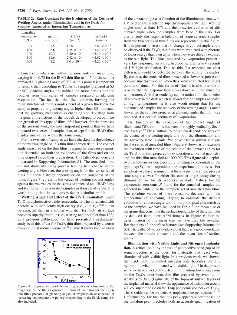
Wetting Angle and Effect of the UV Illumination. SinceTa2O5 is a photoactive oxide semiconductor when irradiated withphotons with sufficiently high energy (i.e., E > Eg),16,28 it canbe expected that, in a similar way than for TiO2, its surfacebecomes superhydrophilic (i.e., wetting angle smaller than 10°).In a previous publication we have presented a preliminaryanalysis of this effect for Ta2O5 thin films prepared by electronevaporation at normal geometry.11 Figure 8 shows the evolution
of the contact angle as a function of the illumination time withUV photons to reach the superhydrophilic state (i.e., wettingangles smaller than 10°) and the posterior evolution of thiscontact angle when the samples were kept in the dark. Forclarity, only the response behavior of some selected samplesfrom the two series of thin films are represented in this figure.It is important to stress that no change in contact angle couldbe observed if the Ta2O5 thin films were irradiated with photonsof lower energy than their Eg or when they were directly exposedto the sun light. The films prepared by evaporation present avery fast response, becoming hydrophilic after a few secondsof UV light irradiation. Due to this fast response no cleardifferences could be detected between the different samples.By contrast, the annealed films presented a slower response andbecame superhydrophilic when they were irradiated for longerperiods of times. For this series of films it is also possible toobserve that the response time slows down with the annealingtemperature. A similar tendency can be noticed for the kineticsof recovery in the dark which is slower for the samples annealedat high temperatures. It is also worth noting that for thenonannealed samples the recovery of the wetting angle is muchslower for the samples prepared at glancing angles than for thoseprepared at a normal geometry of evaporation.
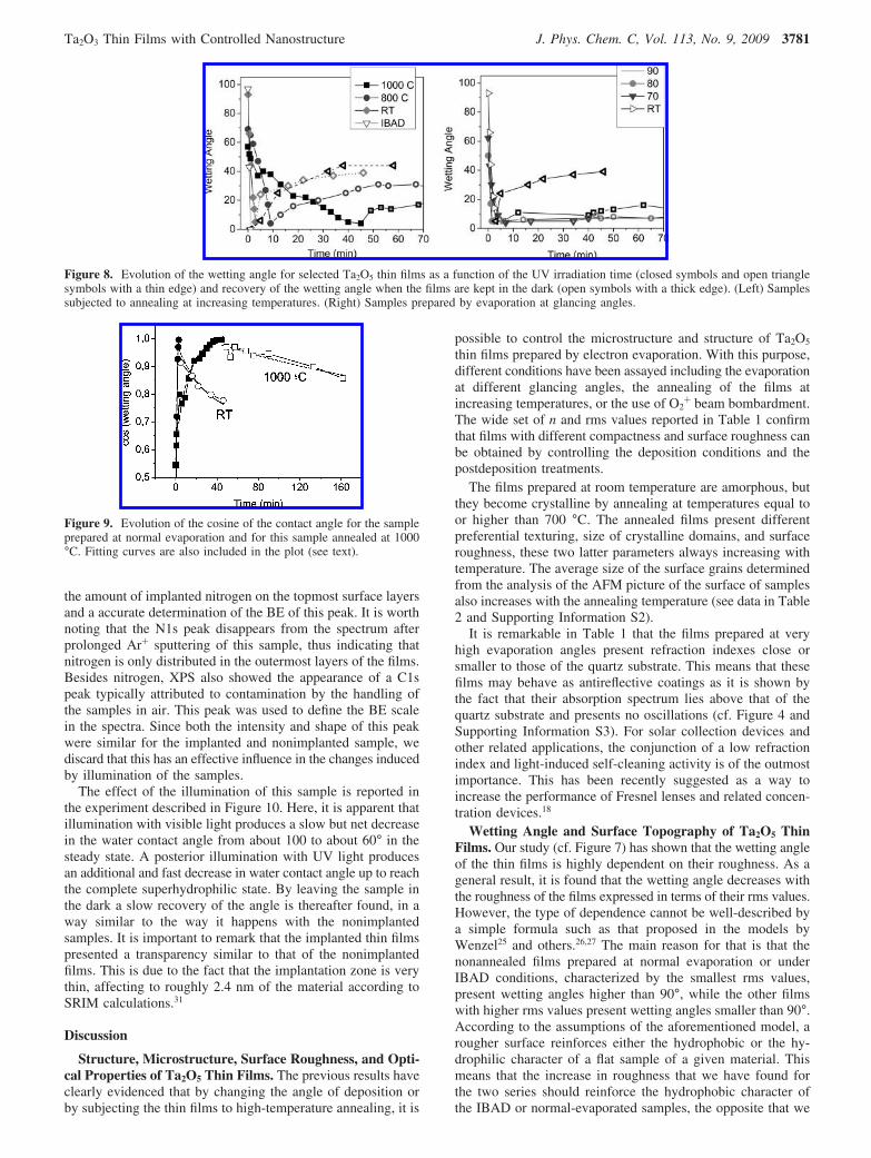
The kinetics of the evolution of the contact angle ofilluminated TiO2 thin films has been thoroughly studied by Sechiand Tachiya.29 These authors found a clear dependence betweenthe cosine of the wetting angle and both the illumination andthe recovery time in dark. We have tried a similar analysisfor the series of annealed films. Figure 9 shows as an examplethe evolution with time of the cosine of the contact angles forthe Ta2O5 thin film prepared by evaporation at normal geometryand for this film annealed at 1000 °C. This figure also depictstwo dashed curves corresponding to fitting exponentials of thetype exp(Kt) that reproduce the experimental curves. Forsimplicity we have assumed that there is just one single process(one single curve) for either the contact angle decay duringillumination or for its recovery in dark. Values for theexponential constants K found for the annealed samples aregathered in Table 2 for the complete set of annealed thin films.The absolute values of these constants decrease with thetemperature of annealing. Trying to correlate the distinctevolution of contact angle with a morphological characteristicof the samples, we have included in Table 2 the mean size ofthe grains that constitute the surface topography of these samplesas deduced from their AFM images in Figure 6. For thedetermination of this mean size we have used the so-calledBearing plots of the surface features (see Supporting InformationS2). The gathered values evidence that there is a good correlationbetween the kinetic constants and the mean size of surfacegrains.
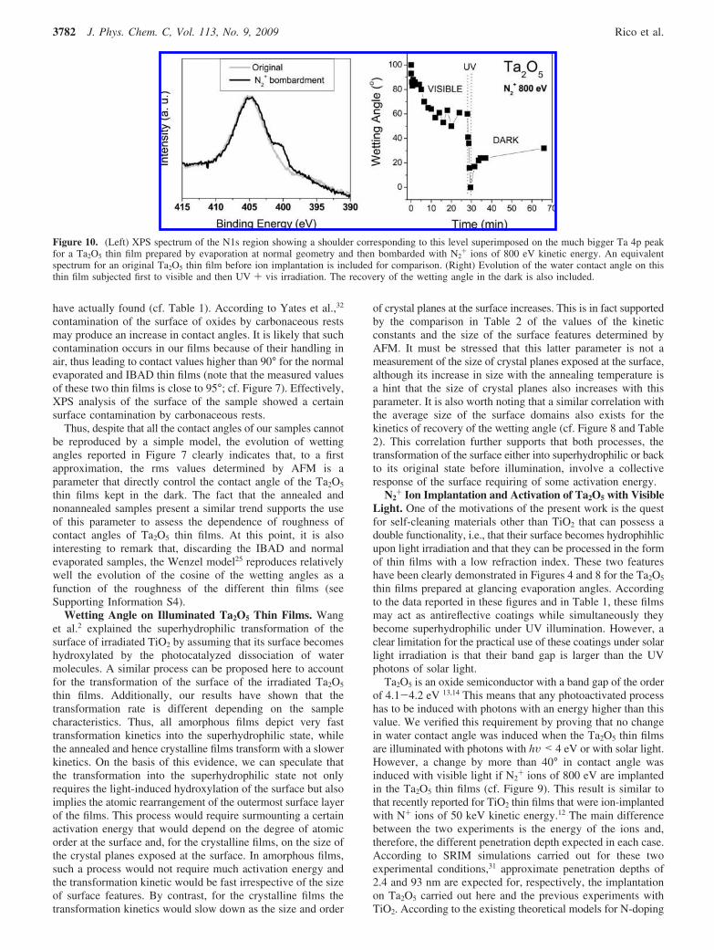
Illumination with Visible Light and Nitrogen Implanta-tion. A critical point by the use of photoactive band gap oxidesemiconductors is the quest for materials that react whenilluminated with visible light. In a previous work, we showedthat TiO2 with implanted nitrogen ions becomes partiallyhydrophilic when illuminated with visible light.12 In the presentwork we have checked the effect of implanting low-energy ionson the Ta2O5 amorphous thin film prepared by evaporation.Analysis by XPS (Figure 10) of the topmost surface layers ofthe implanted material show the appearance of a shoulder around400 eV superimposed on the Ta4p photoemission peak of Ta2O5.This shoulder can be attributed to implanted nitrogen species.10,12,30
Unfortunately, the fact that this peak appears superimposed onthe tantalum peak precludes both an accurate quantification of
Figure 7. Representation of the wetting angles as a function of theroughness of the films expressed in terms of their rms for the Ta2O5
thin films prepared at glancing angles of evaporation or annealed atincreasing temperatures. A point corresponding to the IBAD sample isalso included.
TABLE 2: Rate Constant for the Evolution of the Cosine ofWetting Angles under Illumination and in the Dark forSamples Annealed at Increasing Temperatures
annealingtemperature
(°C)grain
size (nm)K(UV)(min-1)
K(dark)(min-1)
25 7.5 1.18 -3.89 × 10⁻¹
600 8.6 4.35 × 10⁻¹ -1.49 × 10⁻¹
700 10.7 3.40 × 10⁻¹ -5.40 × 10⁻²
800 11.6 2.42 × 10⁻¹ -2.62 × 10⁻²
1000 41.2 9.0 × 10⁻² -4.26 × 10⁻³
3780 J. Phys. Chem. C, Vol. 113, No. 9, 2009 Rico et al.
the amount of implanted nitrogen on the topmost surface layersand a accurate determination of the BE of this peak. It is worthnoting that the N1s peak disappears from the spectrum afterprolonged Ar+ sputtering of this sample, thus indicating thatnitrogen is only distributed in the outermost layers of the films.Besides nitrogen, XPS also showed the appearance of a C1speak typically attributed to contamination by the handling ofthe samples in air. This peak was used to define the BE scalein the spectra. Since both the intensity and shape of this peakwere similar for the implanted and nonimplanted sample, wediscard that this has an effective influence in the changes inducedby illumination of the samples.
The effect of the illumination of this sample is reported inthe experiment described in Figure 10. Here, it is apparent thatillumination with visible light produces a slow but net decreasein the water contact angle from about 100 to about 60° in thesteady state. A posterior illumination with UV light producesan additional and fast decrease in water contact angle up to reachthe complete superhydrophilic state. By leaving the sample inthe dark a slow recovery of the angle is thereafter found, in away similar to the way it happens with the nonimplantedsamples. It is important to remark that the implanted thin filmspresented a transparency similar to that of the nonimplantedfilms. This is due to the fact that the implantation zone is verythin, affecting to roughly 2.4 nm of the material according toSRIM calculations.31
Discussion
Structure, Microstructure, Surface Roughness, and Opti-cal Properties of Ta2O5 Thin Films. The previous results haveclearly evidenced that by changing the angle of deposition orby subjecting the thin films to high-temperature annealing, it is
possible to control the microstructure and structure of Ta2O5
thin films prepared by electron evaporation. With this purpose,different conditions have been assayed including the evaporationat different glancing angles, the annealing of the films atincreasing temperatures, or the use of O2
+ beam bombardment.The wide set of n and rms values reported in Table 1 confirmthat films with different compactness and surface roughness canbe obtained by controlling the deposition conditions and thepostdeposition treatments.
The films prepared at room temperature are amorphous, butthey become crystalline by annealing at temperatures equal toor higher than 700 °C. The annealed films present differentpreferential texturing, size of crystalline domains, and surfaceroughness, these two latter parameters always increasing withtemperature. The average size of the surface grains determinedfrom the analysis of the AFM picture of the surface of samplesalso increases with the annealing temperature (see data in Table2 and Supporting Information S2).
It is remarkable in Table 1 that the films prepared at veryhigh evaporation angles present refraction indexes close orsmaller to those of the quartz substrate. This means that thesefilms may behave as antireflective coatings as it is shown bythe fact that their absorption spectrum lies above that of thequartz substrate and presents no oscillations (cf. Figure 4 andSupporting Information S3). For solar collection devices andother related applications, the conjunction of a low refractionindex and light-induced self-cleaning activity is of the outmostimportance. This has been recently suggested as a way toincrease the performance of Fresnel lenses and related concen-tration devices.18
Wetting Angle and Surface Topography of Ta2O5 ThinFilms. Our study (cf. Figure 7) has shown that the wetting angleof the thin films is highly dependent on their roughness. As ageneral result, it is found that the wetting angle decreases withthe roughness of the films expressed in terms of their rms values.However, the type of dependence cannot be well-described bya simple formula such as that proposed in the models byWenzel25 and others.26,27 The main reason for that is that thenonannealed films prepared at normal evaporation or underIBAD conditions, characterized by the smallest rms values,present wetting angles higher than 90°, while the other filmswith higher rms values present wetting angles smaller than 90°.According to the assumptions of the aforementioned model, arougher surface reinforces either the hydrophobic or the hy-drophilic character of a flat sample of a given material. Thismeans that the increase in roughness that we have found forthe two series should reinforce the hydrophobic character ofthe IBAD or normal-evaporated samples, the opposite that we
Figure 8. Evolution of the wetting angle for selected Ta2O5 thin films as a function of the UV irradiation time (closed symbols and open trianglesymbols with a thin edge) and recovery of the wetting angle when the films are kept in the dark (open symbols with a thick edge). (Left) Samplessubjected to annealing at increasing temperatures. (Right) Samples prepared by evaporation at glancing angles.
Figure 9. Evolution of the cosine of the contact angle for the sampleprepared at normal evaporation and for this sample annealed at 1000°C. Fitting curves are also included in the plot (see text).
Ta2O3 Thin Films with Controlled Nanostructure J. Phys. Chem. C, Vol. 113, No. 9, 2009 3781
have actually found (cf. Table 1). According to Yates et al.,32
contamination of the surface of oxides by carbonaceous restsmay produce an increase in contact angles. It is likely that suchcontamination occurs in our films because of their handling inair, thus leading to contact values higher than 90° for the normalevaporated and IBAD thin films (note that the measured valuesof these two thin films is close to 95°; cf. Figure 7). Effectively,XPS analysis of the surface of the sample showed a certainsurface contamination by carbonaceous rests.
Thus, despite that all the contact angles of our samples cannotbe reproduced by a simple model, the evolution of wettingangles reported in Figure 7 clearly indicates that, to a firstapproximation, the rms values determined by AFM is aparameter that directly control the contact angle of the Ta2O5
thin films kept in the dark. The fact that the annealed andnonannealed samples present a similar trend supports the useof this parameter to assess the dependence of roughness ofcontact angles of Ta2O5 thin films. At this point, it is alsointeresting to remark that, discarding the IBAD and normalevaporated samples, the Wenzel model25 reproduces relativelywell the evolution of the cosine of the wetting angles as afunction of the roughness of the different thin films (seeSupporting Information S4).
Wetting Angle on Illuminated Ta2O5 Thin Films. Wanget al.2 explained the superhydrophilic transformation of thesurface of irradiated TiO2 by assuming that its surface becomeshydroxylated by the photocatalyzed dissociation of watermolecules. A similar process can be proposed here to accountfor the transformation of the surface of the irradiated Ta2O5
thin films. Additionally, our results have shown that thetransformation rate is different depending on the samplecharacteristics. Thus, all amorphous films depict very fasttransformation kinetics into the superhydrophilic state, whilethe annealed and hence crystalline films transform with a slowerkinetics. On the basis of this evidence, we can speculate thatthe transformation into the superhydrophilic state not onlyrequires the light-induced hydroxylation of the surface but alsoimplies the atomic rearrangement of the outermost surface layerof the films. This process would require surmounting a certainactivation energy that would depend on the degree of atomicorder at the surface and, for the crystalline films, on the size ofthe crystal planes exposed at the surface. In amorphous films,such a process would not require much activation energy andthe transformation kinetic would be fast irrespective of the sizeof surface features. By contrast, for the crystalline films thetransformation kinetics would slow down as the size and order
of crystal planes at the surface increases. This is in fact supportedby the comparison in Table 2 of the values of the kineticconstants and the size of the surface features determined byAFM. It must be stressed that this latter parameter is not ameasurement of the size of crystal planes exposed at the surface,although its increase in size with the annealing temperature isa hint that the size of crystal planes also increases with thisparameter. It is also worth noting that a similar correlation withthe average size of the surface domains also exists for thekinetics of recovery of the wetting angle (cf. Figure 8 and Table2). This correlation further supports that both processes, thetransformation of the surface either into superhydrophilic or backto its original state before illumination, involve a collectiveresponse of the surface requiring of some activation energy.
N2+ Ion Implantation and Activation of Ta2O5 with Visible
Light. One of the motivations of the present work is the questfor self-cleaning materials other than TiO2 that can possess adouble functionality, i.e., that their surface becomes hydrophihlicupon light irradiation and that they can be processed in the formof thin films with a low refraction index. These two featureshave been clearly demonstrated in Figures 4 and 8 for the Ta2O5
thin films prepared at glancing evaporation angles. Accordingto the data reported in these figures and in Table 1, these filmsmay act as antireflective coatings while simultaneously theybecome superhydrophilic under UV illumination. However, aclear limitation for the practical use of these coatings under solarlight irradiation is that their band gap is larger than the UVphotons of solar light.
Ta2O5 is an oxide semiconductor with a band gap of the orderof 4.1-4.2 eV 13,14 This means that any photoactivated processhas to be induced with photons with an energy higher than thisvalue. We verified this requirement by proving that no changein water contact angle was induced when the Ta2O5 thin filmsare illuminated with photons with hυ < 4 eV or with solar light.However, a change by more than 40° in contact angle wasinduced with visible light if N2
+ ions of 800 eV are implantedin the Ta2O5 thin films (cf. Figure 9). This result is similar tothat recently reported for TiO2 thin films that were ion-implantedwith N+ ions of 50 keV kinetic energy.12 The main differencebetween the two experiments is the energy of the ions and,therefore, the different penetration depth expected in each case.According to SRIM simulations carried out for these twoexperimental conditions,31 approximate penetration depths of2.4 and 93 nm are expected for, respectively, the implantationon Ta2O5 carried out here and the previous experiments withTiO2. According to the existing theoretical models for N-doping
Figure 10. (Left) XPS spectrum of the N1s region showing a shoulder corresponding to this level superimposed on the much bigger Ta 4p peakfor a Ta2O5 thin film prepared by evaporation at normal geometry and then bombarded with N2
+ ions of 800 eV kinetic energy. An equivalentspectrum for an original Ta2O5 thin film before ion implantation is included for comparison. (Right) Evolution of the water contact angle on thisthin film subjected first to visible and then UV + vis irradiation. The recovery of the wetting angle in the dark is also included.
3782 J. Phys. Chem. C, Vol. 113, No. 9, 2009 Rico et al.
of TiO2,33,34 it must be expected that electronic levels in theband gap region are produced as a result of the ion implantationexperiments. According to the classical theories of photocatalysiswith wide oxide semiconductors,35,36 electronic excitations fromthese states into the conduction band of Ta2O5 would beresponsible for the observed photoactivity with visible photons.The fact that the illumination does not produce a completesuperhydrophilic state (i.e., contact angle < 10°) as it happenswith UV photons has been previously discussed by us for theimplanted TiO2 thin films.12 In that case, we assumed that onlya given type of surface species are energetically able to reactwith the photoholes created by excitation of the gap states. Sincethe superhydrophilic transformation would also require thereaction of other types surface species which are more energy-demanding, only photoholes created in the valence band (i.e.,requiring UV light of sufficiently high energy) would be ableto induce the complete transformation. Within this scheme, thefact that a similar situation is found here with doped Ta2O5 witha very shallow depth distribution of nitrogen species points tothat the partial decrease in wetting angle under visible lightirradiation is a superficial process that not necessarily involvesthe migration of photoholes from the bulk to the surface.Evidence supporting that the conventional UV-induced super-hydrophilicity and the visible-induced hydrophilicity reportedin Figure 10 are not equivalent processes is the fact that therate of transformation with visible photons is much slower thanwith UV photons. The migration of photoholes through theSchottky barrier formed in the depletion layer of charge of oxidesemiconductors is a requirement for the separation of photo-generated electrons and holes and, therefore, a requisite for theclassical photoactivity of oxide semiconductors.35,36 Apparently,this barrier is not a requisite for the contact angle changesinduced with visible light in the implanted Ta2O5 thin films asthe thickness of the implanted layer (i.e., 2.4 nm) is much thinnerthan the usual thickness of the depletion layer in oxidesemiconductors (i.e., of the order of a few hundreds of nano-meters).
Conclusions
The previous results and conclusions have shown that it ispossible to prepare Ta2O5 thin films with quite differentmicrostructures, textures, and optical properties. Preparationstrategies based on the evaporation at glancing angles, ionbombardment and annealing at increasing higher temperatureshave been essayed for this purpose. In this way, antireflectivefilms with refraction indices equal to or even slightly smallerthan that of quartz or glass have been prepared. The contactangles measured on the different thin films show a directdependence on the surface roughness of the films, decreasingas the roughness, expressed in terms of rms values, increases.
When the Ta2O5 thin films are illuminated with photons witha h . 4 eV, the surface of the films become superhydrophilic(i.e., contact angle smaller than 10°). We claim that thecombination of a low refraction index for the films (i.e.,antireflective coatings) together with the self-cleaning activityderived from their superhydrophilicity might be a very positivecombination of properties for certain applications in the fieldof solar collection.18 A drawback for this application is the factthat very energetic photons are required to induce the transfor-mation into the superhydrophilic state and that, therefore, solarlight would be unable to induce such a change. However,changes in the wetting angles on Ta2O5 can be activated if thinfilms of this material are implanted with N2
+ ions of low energy.Since this implantation, affecting just the few external layers
of the films, does not significantly affect their transparency (i.e.,from an optical point of view these films behave as pure Ta2O5
thin films and therefore do not appreciably filter the UV andnear UV photons), we believe that this result is a first step inthe development of antireflective coatings of this material thatpresent self-cleaning activity when irradiated with visible light.
Acknowledgment. We acknowledge the financial contribu-tion of the Spanish Ministry of Science and Technology(Projects MAT-2007-65764 and NAN2004-09317-C04-01 andCONSOLIDER-INGENIO 2010-CSD2008-00023), the Junta deAndalucıa (Project TEP2275), and the European Union throughits 6th framework program (Project NATAMA Project NMP3-CT-2006-032583). The support of the “Fundacion DomingoMartınez” made possible the updating of the electron evapora-tion apparatus used for the preparation of the films.
Supporting Information Available: (S1) Plot of wettingangles as a function of surface roughness, (S2) Bearing plotsfrom AFM images of the annealed Ta2O5 thin films, (S3) UV-vis transmission spectra of quartz plate and studied substrate,and (S4) text describing model for calculating rW, applicablereferences, and figure showing the measured wetting anglecompared to the rW values. This information is available freeof charge via the Internet at http://pubs.acs.org.
References and Notes
(1) Blossey, R. Nat. Mater. 2003, 2, 301.(2) Wang, R.; Hashimoto, K.; Fujishima, A.; Chikuni, M.; Kojima,
E.; Kitamura, A.; Shimohigoshi, M.; Watanabe, T. Nature 1997, 388, 431–431.
(3) Nakajima, A.; Hashimoto, K.; Watanabe, T. Montash. Chem. 2001,132, 31–31.
(4) Stevens, N.; Priest, C. I.; Sedev, R.; Ralston, J. Langmuir 2003,19, 3272–3272.
(5) Sakai, N.; Fujishima, A.; Watanabe, T.; Hashimoto, K. J. Phys.Chem. B 2001, 105, 3023.
(6) Miyauchi, M.; Kieda, N.; Hishita, Sh.; Mitsuhashi, T.; Nakajima,A.; Watanabe, T.; Hashimoto, K. Surf. Sci. 2002, 511, 401.
(7) Fujishima, A.; Hashimoto, K.; Watanabe, T. TiO2 Photocatalyst,Fundamentals and Applications; BKC: Tokyo, 1999.
(8) Miyauchi, M.; Shimai, A.; Tsuru, Y. J. Phys. Chem. B 2005, 27,13307.
(9) Miyauchi, M.; Nakajima, A.; Watanabe, T.; Hashimoto, K. Chem.Mater. 2002, 14, 2812.
(10) Asahi, R.; Morikawa, T.; Ohwaki, T.; Aoki, K.; Taga, Y. Science2001, 293 (5528), 269.
(11) Rico, V.; Lopez, C.; Borras, A.; Espinos, J. P.; Gonzalez-Elipe,A. R. Solar Energy Mater. Solar Cells 2006, 90, 2944.
(12) Borras, A.; Lopez, C.; Rico, V.; Gracia, F.; Gonzalez-Elipe, A. R.;Richter, E.; Battiston, G.; Gerbasi, R.; McSporran, N.; Suthier, G.; Gyorgy,E.; Figueras, A. J. Phys. Chem. C 2007, 111, 1801.
(13) Albella, J. M.; Martinez-Duart, J. M.; Rueda, F. Opt. Acta 1975,22, 973.
(14) Babeva, T.; Atanassova, E.; Koprinarova, J. Phys. Status Solidi A2005, 202, 330.
(15) Sayama, K.; Arawaka, H. J. Photochem. Photobiol., A 1994, 77,243.
(16) Murase, T.; Irie, H.; Hashimoto, K. J. Phys. Chem. B 2004, 108,15803.
(17) Hitoki, G.; Takata, T.; Hondo, J. N.; Hara, M.; Kobayashi, H.;Domen, K. Chem. Commun. (Cambridge). 2002, 16, 1698.
(18) Xi, Q.; Schubert, M. F.; Kim, J. K.; Schubert, E. F.; Chen, M.;Lin, S.-Y.; Liu, W.; Smart, J. A. Nat. Photonics 2007, 1, 176.
(19) van Popta, A. C.; Cheng, J.; Sit, J. C.; Brett, M. J. J. Appl. Phys.2007, 102, 013517.
(20) Hawkeye, M. M.; Brett, M. J. J. Vac. Sci. Technol., A 2007, 25,1317.
(21) Gonzalez-Elipe, A. R. Yubero, F. Sanz, J. M. Low Energy IonAssisted Film Growth; Imperial Collage Press: London, 2003.
(22) Takeuchi, M.; Sakamoto, K.; Martra, G.; Coluccia, S.; Anpo, M.J. Phys. Chem. B 2005, 109, 15422.
(23) Hummel, H. U.; Fackler, R.; Remmert, P. Chem. Ber. 1992, 125,551.
Ta2O3 Thin Films with Controlled Nanostructure J. Phys. Chem. C, Vol. 113, No. 9, 2009 3783

(24) Mergel, D.; Buschendorf, D.; Eggert, S.; Grammes, R.; Samset, B.Thin Solid Films 2000, 371, 218.
(25) Wenzel, R. N. Ind. Eng. Chem. 1936, 28, 988.(26) Cassie, A. B. D.; Baxter, S. Trans. Faraday Soc. 1944, 40
0546.(27) Miwa, M.; Nakajima, A.; Fujishima, A. Langmuir 2000, 16
5754.(28) Takahara, Y.; Kondo, J. N.; Takata, T.; Domen, K. Chem. Mater.
2001, 13, 1194.(29) Seki, K.; Tachiya, M. J. Phys. Chem. B 2004, 108, 4806.(30) Chen, X.; Burda, C. J. Phys. Chem. B 2004, 108, 15446.(31) http://www.srim.org/.
(32) Zubkov, T.; Stahl, D.; Thompson, T. L.; Pananyotov, D.; Diwald,O.; Yates, J. T. J. Phys. Chem. B 2005, 109, 15454.
(33) Nakamura, R.; Tanaka, T.; Nakato, Y. J. Phys. Chem. B 2004, 108,10617.
(34) Irie, H.; Washizuka, S.; Watanabe, Y.; Kako, T.; Hashimoto, K. J.Electrochem. Soc. 2005, 152, E351.
(35) Carp, O.; Huisman, C. L.; Reller, A. Prog. Solid State Chem. 2004,32, 33.
(36) Bak, T.; Nowotny, J.; Rekas, M.; Sorrell, C. C. Int. J. HydrogenEnergy 2002, 27, 991.
JP805708W
3784 J. Phys. Chem. C, Vol. 113, No. 9, 2009 Rico et al.