Understanding doping at the nanoscale: the case of codoped Si and Ge nanowires
11
This content has been downloaded from IOPscience. Please scroll down to see the full text. Download details: IP Address: 155.185.13.40 This content was downloaded on 12/09/2014 at 09:23 Please note that terms and conditions apply. Understanding doping at the nanoscale: the case of codoped Si and Ge nanowires View the table of contents for this issue, or go to the journal homepage for more 2014 J. Phys. D: Appl. Phys. 47 394013 (http://iopscience.iop.org/0022-3727/47/39/394013) Home Search Collections Journals About Contact us My IOPscience
-
Upload
mondodomani -
Category
Documents
-
view
0 -
download
0
Transcript of Understanding doping at the nanoscale: the case of codoped Si and Ge nanowires

This content has been downloaded from IOPscience. Please scroll down to see the full text.
Download details:
IP Address: 155.185.13.40
This content was downloaded on 12/09/2014 at 09:23
Please note that terms and conditions apply.
Understanding doping at the nanoscale: the case of codoped Si and Ge nanowires
View the table of contents for this issue, or go to the journal homepage for more
2014 J. Phys. D: Appl. Phys. 47 394013
(http://iopscience.iop.org/0022-3727/47/39/394013)
Home Search Collections Journals About Contact us My IOPscience
Journal of Physics D: Applied Physics
J. Phys. D: Appl. Phys. 47 (2014) 394013 (10pp) doi:10.1088/0022-3727/47/39/394013
Understanding doping at the nanoscale:the case of codoped Si and Ge nanowires
Michele Amato1, Riccardo Rurali2, Maurizia Palummo3 andStefano Ossicini4,5
1 Institut d’Electronique Fondamentale, UMR8622, CNRS, Universite Paris Sud, 91405 Orsay, France2 Institut de Ciencia de Materials de Barcelona (ICMAB-CSIC), Campus de Bellaterra, 08193 Bellaterra,Barcelona, Spain3 Dipartimento di Fisica, CNISM, ETSF Universita di Roma ‘Tor Vergata’, Via della RicercaScientifica 1, 00133 Roma, Italy4 ‘Centro S3’, CNR-Istituto di Nanoscienze, Via Campi 213/A, 41125 Modena, Italy and Dipartimento diScienze e Metodi dell’Ingegneria, Universita di Modena e Reggio Emilia, Via Amendola 2 Pad. Morselli,I-42100 Reggio Emilia, Italy5 Centro Interdepartmental En&Tech, Universita di Modena e Reggio Emilia, Via Amendola 2 Pad.Morselli, I-42100 Reggio Emilia, Italy
E-mail: [email protected]
Received 17 March 2014, revised 4 June 2014Accepted for publication 9 June 2014Published 11 September 2014
AbstractResults of first-principles DFT calculations of the structural and electronic properties of B–Pcodoped Si and Ge NWs are presented and discussed. We find that, according to experiments,for both Si and Ge NWs, impurities tend to get closer together and to occupy edge positions, asa result of minor structural relaxation and hence lower formation energy. The study of theelectronic structure shows that the simultaneous addition of B and P only slightly modifies theenergy band gap value with respect to the pure wire, and is strongly dependent on theparticular codoping configuration considered.
Keywords: nanowires, doping, DFT, co-doping
(Some figures may appear in colour only in the online journal)
1. Introduction
Understanding of the doping mechanism at the nanoscalerepresents one of the main topics for the design anddevelopment of nanowire-based devices. Recent experimentaland theoretical studies [1–9] on Si and Ge nanowires (NWs)have made concrete and real the possibility of using theseone-dimensional nanostructures as corner-stones for the nextgeneration electronics. Many applications using them asfield-effect transistor (FET) [10, 11], p–n diode [12, 13],photovoltaic [14] and thermoelectric [15] devices have beendemonstrated, and the scientific interest in this topic hasbeen rapidly increasing in the last decade [16]. As formicroelectronic technology, in all the above mentioned NWapplications the possibility of modifying electronic propertiesof the material by introducing impurities is of paramountimportance and its full understanding requires a microscopicpicture of basic mechanisms. Many experimental and
theoretical studies have addressed this topic [17–21], focusingmainly on B and P single doping of Si and Ge NWs.Experimentally, it has been clearly demonstrated that, with thecurrent growth methods (such as vapour–liquid–solid growth[5]), it is possible to incorporate III and IV group impuritiesinto the wire and to obtain both n-type and p-type wires [22–24]. On the other hand, theoretical investigations have shownthat B and P impurities give rise to energetic levels deep inthe band gap, and that they prefer to segregate towards thesurface of the wire in order to minimize mechanical stress anddistortions [17, 18, 25].
Very recently, the simultaneous addition of B and Pimpurities, i.e. codoping, has also been demonstrated to be afundamental tool for modifying electronic and optical featuresof NWs [20]. As already shown for Si nanocrystals (NCs)[26–30], being able to control the band gap through doubleaddition of impurities allows us to tune properties such as
0022-3727/14/394013+10$33.00 1 © 2014 IOP Publishing Ltd Printed in the UK
J. Phys. D: Appl. Phys. 47 (2014) 394013 Michele Amato et al
CORE EDGEy
z
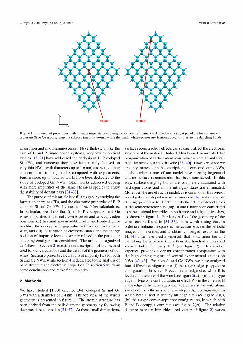
Figure 1. Top view of pure wires with a single impurity occupying a core site (left panel) and an edge site (right panel). Blue spheres canrepresent Si or Ge atoms, magenta spheres impurity atoms, while the small white spheres are H atoms used to saturate the dangling bonds.
absorption and photoluminescence. Nevertheless, unlike thecase of B and P single doped systems, very few theoreticalstudies [18, 21] have addressed the analysis of B–P codopedSi NWs, and moreover they have been mainly focused onvery thin NWs (with diameters up to 1.6 nm) and with dopingconcentrations too high to be compared with experiments.Furthermore, up to now, no works have been dedicated to thestudy of codoped Ge NWs. Other works addressed dopingwith more impurities of the same chemical species to studythe stability of dopant pairs [31–33].
The purpose of this article is to fill this gap, by studying theformation energies (FEs) and the electronic properties of B–Pcodoped Si and Ge NWs by means of ab initio calculations.In particular, we show that (i) in B–P codoped Si and Gewires, impurities tend to get closer together and to occupy edgepositions, (ii) the simultaneous addition of B and P only slightlymodifies the energy band gap value with respect to the purewire, and (iii) localization of electronic states and the energyposition of impurity levels is strictly related to the particularcodoping configuration considered. The article is organizedas follows. Section 2 contains the description of the methodused for our calculations and the details of the geometry of ourwires. Section 3 presents calculations of impurity FEs for bothSi and Ge NWs, while section 4 is dedicated to the analysis ofband structure and electronic properties. In section 5 we drawsome conclusions and make final remarks.
2. Methods
We have studied [1 1 0] oriented B–P codoped Si and GeNWs with a diameter of 2.4 nm. The top view of the wire’sgeometry is presented in figure 1. The atomic structure hasbeen derived from the bulk diamond geometry by followingthe procedure adopted in [34–37]. At these small dimensions,
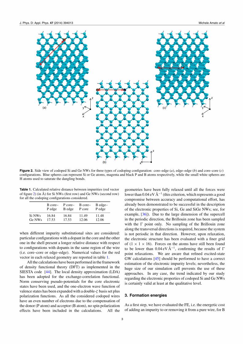
surface reconstruction effects can strongly affect the electronicstructure of the material. Indeed it has been demonstrated thatreorganization of surface atoms can induce a metallic and semi-metallic behaviour into the wire [38–40]. However, since weare only interested in the description of semiconducting NWs,all the surface atoms of our model have been hydrogenatedand no surface reconstruction has been considered. In thisway, surface dangling bonds are completely saturated withhydrogen atoms and all the intra-gap states are eliminated.Moreover, the use of such a model, as is common in this type ofinvestigation on doped nanostructures (see [16] and referencestherein), permits us to clearly identify the nature of defect statesin the semiconductor band gap. B and P have been consideredas substitutional impurities in both core and edge lattice sites,as shown in figure 1. Further details of the geometry of thewires can be found in [34–37]. It is worth noting that, inorder to eliminate the spurious interaction between the periodicimages of impurities and to obtain converged results for theFE [41], we have used a supercell that is six times the unitcell along the wire axis (more than 700 hundred atoms) andvacuum buffer of nearly 10 Å (see figure 2). This kind ofsupercell provides a dopant concentration comparable withthe high doping regime of several experimental studies onNWs [42, 43]. For both Si and Ge NWs, we have analyzedfour different configurations: (i) the n-type edge–p-type coreconfiguration, in which P occupies an edge site, while B islocated in the core of the wire (see figure 2(a)), (ii) the p-typeedge–n-type core configuration, in which P is in the core and Bat the edge of the wire (equivalent to figure 2(a) but with atomsswitched), (iii) the n-type edge–p-type edge configuration, inwhich both P and B occupy an edge site (see figure 2(b)),(iv) the n-type core–p-type core configuration, in which bothP and B occupy a core site (see figure 2(c)). The relativedistance between impurities (red vector of figure 2) varies
2
J. Phys. D: Appl. Phys. 47 (2014) 394013 Michele Amato et al
y
z
x
(a)
(b)
(c) y
z
x
z
x
Figure 2. Side view of codoped Si and Ge NWs for three types of codoping configuration: core–edge (a), edge–edge (b) and core–core (c)configurations. Blue spheres can represent Si or Ge atoms, magenta and black P and B atoms respectively, while the small white spheres areH atoms used to saturate the dangling bonds.
Table 1. Calculated relative distance between impurities (red vectorof figure 2) (in Å) for Si NWs (first row) and Ge NWs (second row)for all the codoping configurations considered.
B core– P core– B core– B edge–P edge B edge P core P edge
Si NWs 16.84 16.84 11.49 11.48Ge NWs 17.53 17.53 12.06 12.06
when different impurity substitutional sites are considered:particular configurations with a dopant in the core and the otherone in the shell present a longer relative distance with respectto configurations with dopants in the same region of the wire(i.e. core–core or edge–edge). Numerical values for the redvector in each relaxed geometry are reported in table 1.
All the calculations have been performed in the frameworkof density functional theory (DFT) as implemented in theSIESTA code [44]. The local density approximation (LDA)has been adopted for the exchange-correlation functional.Norm conserving pseudo-potentials for the core electronicstates have been used, and the one-electron wave function ofvalence states has been expanded with a double-ζ basis set pluspolarization functions. As all the considered codoped wireshave an even number of electrons due to the compensation ofthe donor (P atom) and acceptor (B atom), no spin polarizationeffects have been included in the calculations. All the
geometries have been fully relaxed until all the forces werelower than 0.04 eV Å−1 (this criterion, which represents a goodcompromise between accuracy and computational effort, hasalready been demonstrated to be successful in the descriptionof the electronic properties of Si, Ge and SiGe NWs; see, forexample, [36]). Due to the large dimension of the supercellin the periodic direction, the Brillouin zone has been sampledwith the � point only. No sampling of the Brillouin zonealong the transversal directions is required, because the systemis not periodic in that direction. However, upon relaxation,the electronic structure has been evaluated with a finer gridof (1 × 1 × 16). Forces on the atoms have still been foundto be lower than 0.04 eV Å−1, confirming the results of �
point relaxations. We are aware that refined excited-stateGW calculations [45] should be performed to have a correctestimation of the electronic impurity levels; nevertheless, thehuge size of our simulation cell prevents the use of theseapproaches. In any case, the trend indicated by our studyregarding the electronic properties of codoped Si and Ge NWsis certainly valid at least at the qualitative level.
3. Formation energies
As a first step, we have evaluated the FE, i.e. the energetic costof adding an impurity to or removing it from a pure wire, for B
3
J. Phys. D: Appl. Phys. 47 (2014) 394013 Michele Amato et al
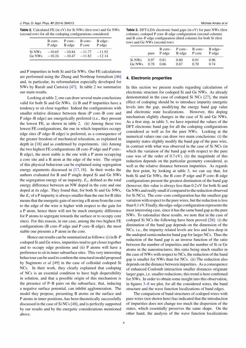
Table 2. Calculated FE (in eV) for Si NWs (first row) and Ge NWs(second row) for all the codoping configurations considered.
B core– P core– B core– B edge–P edge B edge P core P edge
Si NWs −10.65 −10.84 −11.77 −11.92Ge NWs −10.24 −10.47 −11.82 −12.14
and P impurities in both Si and Ge NWs. Our FE calculationsare performed using the Zhang and Northrup formalism [46]and, in particular, its reformulation especially developed forNWs by Rurali and Cartoixa [47]. In table 2 we summarizeour main results.
Looking at table 2, one can draw several main conclusionsvalid for both Si and Ge NWs. (i) B and P impurities have atendency to sit close together. Indeed the configurations withsmaller relative distance between them (P core–B core andP edge–B edge) are energetically preferred (i.e., they presentthe lowest FE, as shown in table 2. (ii) Among these twolowest FE configurations, the one in which impurities occupyedge sites (P edge–B edge) is preferred, as a consequence ofthe greater freedom of mechanical relaxation, as explained indepth in [18] and as confirmed by experiments. (iii) Amongthe two highest FE configurations (B core–P edge and P core–B edge), the most stable is the one with a P atom occupyinga core site and a B atom at the edge of the wire. The originof this physical behaviour can be explained using segregationenergy arguments discussed in [17, 18]. In their works theauthors evaluated for B and P single doped Si and Ge NWsthe segregation energy of an impurity, Es, defined as the totalenergy difference between an NW doped in the core and onedoped at its edge. They found that, for both Si and Ge NWs,the Es of a P impurity is always smaller than the one for B (thismeans that the energetic gain of moving a B atom from the coreto the edge of the wire is higher with respect to the gain fora P atom, hence there will not be much energetic differencefor P atoms to segregate towards the surface or to occupy coresites). For this reason, in our case, among the two highest FEconfigurations (B core–P edge and P core–B edge), the moststable one presents a P atom in the core.
Hence our results can be summarized as follows: (i) in B–Pcodoped Si and Ge wires, impurities tend to get closer togetherand to occupy edge positions and (ii) P atoms will have apreference to sit in inner subsurface sites. This very interestingbehaviour can be used to confirm the structural model proposedby Sugimoto et al [49] in the case of colloidal codoped SiNCs. In their work, they clearly explained that codopingof NCs is an essential condition to have high dispersibilityin solution, and that a possible origin of this mechanism isthe presence of P–B pairs on the subsurface, that, inducinga negative surface potential, can inhibit agglomeration. Themodel they propose, presenting B atoms on the surface andP atoms in inner positions, has been theoretically successfullydiscussed in the case of Si NCs [48], and is perfectly supportedby our results and by the energetic considerations mentionedabove.
Table 3. DFT-LDA electronic band gaps (in eV) for pure NWs (firstcolumn), codoped P core–B edge configuration (second column)and B core–P edge configuration (third column) for both Si (firstrow) and Ge NWs (second row).
B core– P core– B core– B edge–pure P edge B edge P core P edge
Si NWs 0.97 0.81 0.80 0.91 0.96Ge NWs 0.78 0.66 0.67 0.70 0.74
4. Electronic properties
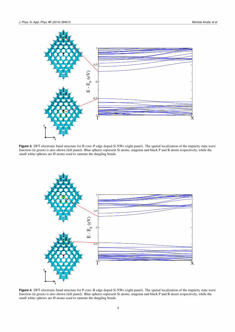
In this section we present results regarding calculations ofelectronic structure for codoped Si and Ge NWs. As alreadydemonstrated in the case of codoped Si NCs [27], the maineffect of codoping should be to introduce impurity energeticlevels into the gap, modifying the energy band gap valueand electronic state localizations. However, this dopingmechanism slightly changes in the case of Si and Ge NWs.As a first step, in table 3, we have reported the values of theDFT electronic band gap for all the codoping configurationsconsidered as well as for the pure NWs. Looking at thenumerical values one can draw two main conclusions: (i) theimpurity states slightly modify the band gap of the pure wire,in contrast with what was observed in the case of Si NCs (inwhich the variation of the band gap with respect to the purecase was of the order of 0.7 eV), (ii) the magnitude of thisreduction depends on the particular geometry considered, aswell as the relative distance between impurities. As regardsthe first point, by looking at table 3, we can say that, forboth Si and Ge NWs, the B core–P edge and P core–B edgeconfigurations present the greatest diminution of the band gap(however, this value is always less than 0.2 eV for both Si andGe NWs and really small if compared to the reduction observedfor Si NCs). The core–core configuration has the smallest gapvariation with respect to the pure wires, but the reduction is lessthan 0.1 eV. Finally, the edge–edge configuration represents themost interesting case, since it has the same band gap as the pureNWs. To rationalize these results, we note that in the case ofcodoped Si NCs the following have been proved [28]: (i) thediminution of the band gap depends on the dimension of theNCs; i.e., the impurity related levels are less and less deep inthe undoped semiconductor band gap for larger NCs. Thus thereduction of the band gap is an inverse function of the ratiobetween the number of impurities and the number of Si or Geatoms in the nanostructures; this ratio being much smaller inthe case of NWs with respect to NCs, the reduction of the bandgap is smaller for NWs than for NCs. (ii) The reduction alsodepends on the distance between impurities. As a consequenceof enhanced Coulomb interaction smaller distances originatelarger gaps, i.e. smaller reductions; this trend is here confirmedfor NWs. In order to obtain some insight into this observation,in figures 3–8 we plot, for all the considered wires, the bandstructure and the wave function localizations of band edges.
The comparison of band structures of codoped wires withpure wires (not shown here) has indicated that the introductionof impurities does not change too much the dispersion of thestates, which essentially preserves the same shape. On theother hand, the analysis of the wave function localizations
4
J. Phys. D: Appl. Phys. 47 (2014) 394013 Michele Amato et al
y
z
Figure 3. DFT electronic band structure for B core–P edge doped Si NWs (right panel). The spatial localization of the impurity state wavefunction (in green) is also shown (left panel). Blue spheres represent Si atoms, magenta and black P and B atoms respectively, while thesmall white spheres are H atoms used to saturate the dangling bonds.
y
z
Figure 4. DFT electronic band structure for P core–B edge doped Si NWs (right panel). The spatial localization of the impurity state wavefunction (in green) is also shown (left panel). Blue spheres represent Si atoms, magenta and black P and B atoms respectively, while thesmall white spheres are H atoms used to saturate the dangling bonds.
5
J. Phys. D: Appl. Phys. 47 (2014) 394013 Michele Amato et al
z
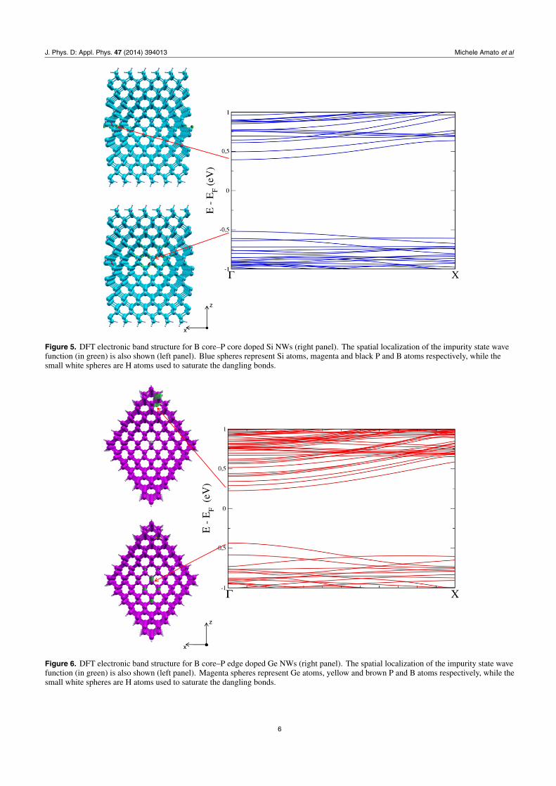
x
Figure 5. DFT electronic band structure for B core–P core doped Si NWs (right panel). The spatial localization of the impurity state wavefunction (in green) is also shown (left panel). Blue spheres represent Si atoms, magenta and black P and B atoms respectively, while thesmall white spheres are H atoms used to saturate the dangling bonds.
z
x
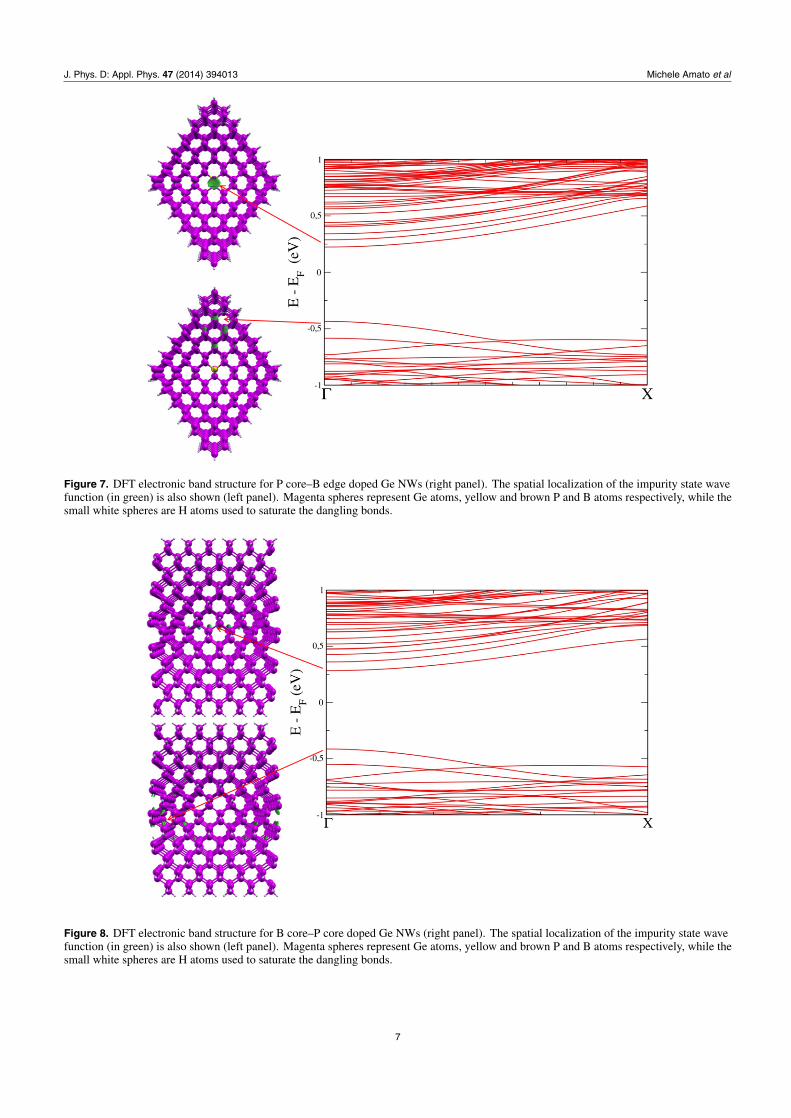
Figure 6. DFT electronic band structure for B core–P edge doped Ge NWs (right panel). The spatial localization of the impurity state wavefunction (in green) is also shown (left panel). Magenta spheres represent Ge atoms, yellow and brown P and B atoms respectively, while thesmall white spheres are H atoms used to saturate the dangling bonds.
6
J. Phys. D: Appl. Phys. 47 (2014) 394013 Michele Amato et al
Figure 7. DFT electronic band structure for P core–B edge doped Ge NWs (right panel). The spatial localization of the impurity state wavefunction (in green) is also shown (left panel). Magenta spheres represent Ge atoms, yellow and brown P and B atoms respectively, while thesmall white spheres are H atoms used to saturate the dangling bonds.
Figure 8. DFT electronic band structure for B core–P core doped Ge NWs (right panel). The spatial localization of the impurity state wavefunction (in green) is also shown (left panel). Magenta spheres represent Ge atoms, yellow and brown P and B atoms respectively, while thesmall white spheres are H atoms used to saturate the dangling bonds.
7
J. Phys. D: Appl. Phys. 47 (2014) 394013 Michele Amato et al
z
x
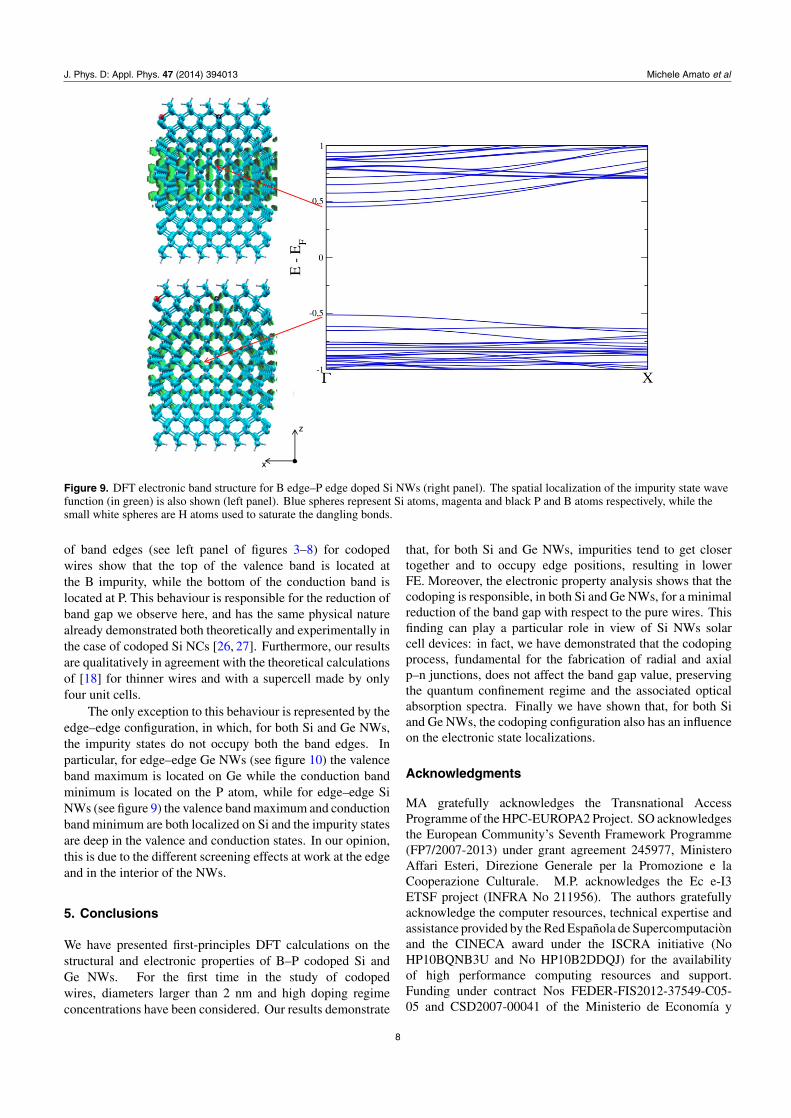
Figure 9. DFT electronic band structure for B edge–P edge doped Si NWs (right panel). The spatial localization of the impurity state wavefunction (in green) is also shown (left panel). Blue spheres represent Si atoms, magenta and black P and B atoms respectively, while thesmall white spheres are H atoms used to saturate the dangling bonds.
of band edges (see left panel of figures 3–8) for codopedwires show that the top of the valence band is located atthe B impurity, while the bottom of the conduction band islocated at P. This behaviour is responsible for the reduction ofband gap we observe here, and has the same physical naturealready demonstrated both theoretically and experimentally inthe case of codoped Si NCs [26, 27]. Furthermore, our resultsare qualitatively in agreement with the theoretical calculationsof [18] for thinner wires and with a supercell made by onlyfour unit cells.
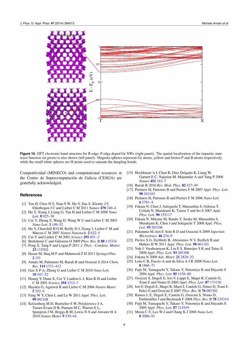
The only exception to this behaviour is represented by theedge–edge configuration, in which, for both Si and Ge NWs,the impurity states do not occupy both the band edges. Inparticular, for edge–edge Ge NWs (see figure 10) the valenceband maximum is located on Ge while the conduction bandminimum is located on the P atom, while for edge–edge SiNWs (see figure 9) the valence band maximum and conductionband minimum are both localized on Si and the impurity statesare deep in the valence and conduction states. In our opinion,this is due to the different screening effects at work at the edgeand in the interior of the NWs.
5. Conclusions
We have presented first-principles DFT calculations on thestructural and electronic properties of B–P codoped Si andGe NWs. For the first time in the study of codopedwires, diameters larger than 2 nm and high doping regimeconcentrations have been considered. Our results demonstrate
that, for both Si and Ge NWs, impurities tend to get closertogether and to occupy edge positions, resulting in lowerFE. Moreover, the electronic property analysis shows that thecodoping is responsible, in both Si and Ge NWs, for a minimalreduction of the band gap with respect to the pure wires. Thisfinding can play a particular role in view of Si NWs solarcell devices: in fact, we have demonstrated that the codopingprocess, fundamental for the fabrication of radial and axialp–n junctions, does not affect the band gap value, preservingthe quantum confinement regime and the associated opticalabsorption spectra. Finally we have shown that, for both Siand Ge NWs, the codoping configuration also has an influenceon the electronic state localizations.
Acknowledgments
MA gratefully acknowledges the Transnational AccessProgramme of the HPC-EUROPA2 Project. SO acknowledgesthe European Community’s Seventh Framework Programme(FP7/2007-2013) under grant agreement 245977, MinisteroAffari Esteri, Direzione Generale per la Promozione e laCooperazione Culturale. M.P. acknowledges the Ec e-I3ETSF project (INFRA No 211956). The authors gratefullyacknowledge the computer resources, technical expertise andassistance provided by the Red Espanola de Supercomputacionand the CINECA award under the ISCRA initiative (NoHP10BQNB3U and No HP10B2DDQJ) for the availabilityof high performance computing resources and support.Funding under contract Nos FEDER-FIS2012-37549-C05-05 and CSD2007-00041 of the Ministerio de Economıa y
8
J. Phys. D: Appl. Phys. 47 (2014) 394013 Michele Amato et al
Figure 10. DFT electronic band structure for B edge–P edge doped Ge NWs (right panel). The spatial localization of the impurity statewave function (in green) is also shown (left panel). Magenta spheres represent Ge atoms, yellow and brown P and B atoms respectively,while the small white spheres are H atoms used to saturate the dangling bonds.
Competitividad (MINECO) and computational resources atthe Centro de Supercomputacion de Galicia (CESGA) aregratefully acknowledged.
References
[1] Yan H, Choe H S, Nam S W, Hu Y, Das S, Klemic J F,Ellenbogen J C and Lieber C M 2011 Nature 470 240–4
[2] Hu Y, Xiang J, Liang G, Yan H and Lieber C M 2008 NanoLett. 8 925–30
[3] Cui Y, Zhong Z, Wang D, Wang W U and Lieber C M 2003Nano Lett. 3 149–52
[4] Hu Y, Churchill H O H, Reilly D J, Xiang J, Lieber C M andMarcus C M 2007 Nature Nanotech. 2 622–5
[5] Cui Y and Lieber C M 2001 Science 291 851–3[6] Berkdemir C and Gulseren O 2009 Phys. Rev. B 80 115334[7] Peng X, Tang F and Logan P 2011 J. Phys.: Condens. Matter
23 115502[8] Hasan M, Huq M F and Mahmood Z H 2013 SpringerPlus
2 151[9] Amato M, Palummo M, Rurali R and Ossicini S 2014 Chem.
Rev. 114 1371–412[10] Gao X P A, Zheng G and Lieber C M 2010 Nano Lett.
10 547–52[11] Huang Y, Duan X, Cui Y, Lauhon L J, Kim K H and Lieber
C M 2001 Science 294 1313–7[12] Hayden O, Agarwal R and Lieber C M 2006 Nature Mater.
5 352–6[13] Fung W Y, Chen L and Lu W 2011 Appl. Phys. Lett.
99 092108[14] Kelzenberg M D, Boettcher S W, Petykiewicz J A,
Turner-Evans D B, Putnam M C, Warren E L,Spurgeon J M, Briggs R M, Lewis N S and Atwater H A2010 Nature Mater. 9 239–44
[15] Hochbaum A I, Chen R, Diaz Delgado R, Liang W,Garnett E C, Najarian M, Majumdar A and Yang P 2008Nature 451 163–7
[16] Rurali R 2010 Rev. Mod. Phys. 82 427–49[17] Peelaers H, Partoens B and Peeters F M 2007 Appl. Phys. Lett.
90 263103[18] Peelaers H, Partoens B and Peeters F M 2006 Nano Lett.
6 2781–4[19] Fukata N, Chen J, Sekiguchi T, Matsushita S, Oshima T,
Uchida N, Murakami K, Tsurui T and Ito S 2007 Appl.Phys. Lett. 90 153117
[20] Fukata N, Mitome M, Bando Y, Seoka M, Matsushita S,Murakami K, Chen J and Sekiguchi T 2008 Appl. Phys.Lett. 93 203106
[21] Palummo M, Iori F, Sole R D and Ossicini S 2009 Superlatt.Microstruct. 46 234–9
[22] Pavlov S G, Eichholz R, Abrosimov N V, Redlich B andHubers H W 2011 Appl. Phys. Lett. 98 061102
[23] Nah J, Varahramyan K, Liu E S, Banerjee S K and Tutuc E2008 Appl. Phys. Lett. 93 203108
[24] Fukata N 2009 Adv. Mater. 21 2829–32[25] Leao C R, Fazzio A and da Silva A J R 2008 Nano Lett.
8 1866–71[26] Fujii M, Yamaguchi Y, Takase Y, Ninomiya K and Hayashi S
2004 Appl. Phys. Lett. 85 1158–60[27] Ossicini S, Degoli E, Iori F, Luppi E, Magri R, Cantele G,
Trani F and Ninno D 2005 Appl. Phys. Lett. 87 173120[28] Iori F, Degoli E, Magri R, Marri I, Cantele G, Ninno D, Trani F,
Pulci O and Ossicini S 2007 Phys. Rev. B 76 085302[29] Ramos L E, Degoli E, Cantele G, Ossicini S, Ninno D,
Furthmuller J and Bechstedt F 2008 Phys. Rev. B 78 235310[30] Fujii M, Yamaguchi Y, Takase Y, Ninomiya K and Hayashi S
2005 Appl. Phys. Lett. 87 211919[31] Moon C-Y, Lee W-J and Chang K J 2008 Nano Lett.
8 3086–91
9
J. Phys. D: Appl. Phys. 47 (2014) 394013 Michele Amato et al
[32] Park J-S, Ryu B and Change K J 2011 J. Phys. Chem. C115 10345–50
[33] Kim S, Park J-S and Chang K J 2012 Nano Lett. 12 5068–73[34] Amato M, Palummo M and Ossicini S 2009 Phys. Rev. B
80 235333[35] Amato M, Palummo M and Ossicini S 2009 Phys. Rev. B
79 201302(R)[36] Amato M, Ossicini S and Rurali R 2011 Nano Lett. 11 594–8[37] Amato M, Palummo M and Ossicini S 2010 Phys. Status
Solidi b 247 2096[38] Rurali R and Lorente N 2005 Phys. Rev. Lett. 94 026805[39] Rurali R and Lorente N 2005 Nanotechnology 16 S250[40] Rurali R, Poissier A and Lorente N 2006 Phys. Rev. B
74 165324[41] Rurali R, Palummo M and Cartoixa X 2010 Phys. Rev. B
81 235304
[42] Nah J, Liu E S, Shahrjerdi D, Varahramyan K M, Banerjee S Kand Tutuc E 2009 Appl. Phys. Lett. 94 063117
[43] Wang Y, Lew K K, Ho T T, Pan L, Novak S W, Dickey E C,Redwing J M and Mayer T S 2005 Nano Lett.5 2139–43
[44] Soler J M, Artacho E, Gale J D, Garcıa A, Junquera J,Ordejon P and Sanchez-Portal D 2002 J. Phys.: Condens.Matter 14 2745–79
[45] Niquet Y M, Genovese L, Delerue C and Deutsch T 2010Phys. Rev. B 81 161301
[46] Zhang S B and Northrup J E 1991 Phys. Rev. Lett.67 2339–42
[47] Rurali R and Cartoixa X 2009 Nano Lett. 9 975–9[48] Guerra R and Ossicini S 2014 J. Am. Chem. Soc. 136 4404–9[49] Sugimoto H, Fujii M, Imakita K, Hayashi S and Akamatsu K
2012 J. Phys. Chem. C 116 17969–74
10