Tunneling through a semiconducting spacer: complex band predictions vs. thin film calculations
16
June 9, 2004 Tunnelling through a semiconducting spacer: complex band predictions vs. thin film calculations Jer´ onimo Peralta Ramos a,* , Juli´an Milano b and Ana Mar´ ıa Llois a a Departamento de F´ ısica, Centro At´omico Constituyentes, Comisi´on Nacional de Energ´ ıa At´omica b Centro At´omico Bariloche, Comisi´on Nacional de Energ´ ıaAt´omica Using a simple tight-binding model, we compare the limitations of the tunnelling predictions coming out of the complex band structure of a semiconductor with the output of thin film calculations done for the same semiconducting spacer but considering it to be of finite width, and sandwiched by metallic electrodes. The comparison is made as a function of spacer width and interfacial roughness. KEY WORDS: tunnelling, complex bands, hybrid structures. * Corresponding author Centro At´ omico Constituyentes, Av. Gral. Paz 1650, San Mart´ ın, Bs. As., Argentina TEL: (54-11) 6772-7007 FAX: (54-11) 6772-7121 [email protected] 1 arXiv:0810.0453v1 [cond-mat.mes-hall] 2 Oct 2008
-
Upload
independent -
Category
Documents
-
view
2 -
download
0
Transcript of Tunneling through a semiconducting spacer: complex band predictions vs. thin film calculations
June 9, 2004
Tunnelling through a semiconducting spacer: complex band
predictions vs. thin film calculations
Jeronimo Peralta Ramos a,∗, Julian Milano b and Ana Marıa Llois a
a Departamento de Fısica, Centro Atomico Constituyentes, Comision Nacional de Energıa
Atomica
b Centro Atomico Bariloche, Comision Nacional de Energıa Atomica
Using a simple tight-binding model, we compare the limitations of the tunnelling
predictions coming out of the complex band structure of a semiconductor with the
output of thin film calculations done for the same semiconducting spacer but considering
it to be of finite width, and sandwiched by metallic electrodes. The comparison is made
as a function of spacer width and interfacial roughness.
KEY WORDS: tunnelling, complex bands, hybrid structures.
∗ Corresponding author
Centro Atomico Constituyentes, Av. Gral. Paz 1650, San Martın, Bs. As., Argentina
TEL: (54-11) 6772-7007 FAX: (54-11) 6772-7121
1
arX
iv:0
810.
0453
v1 [
cond
-mat
.mes
-hal
l] 2
Oct
200
8
A magnetic tunnel junction (MTJ) consists of a thin non-conducting spacer sand-
wiched by ferromagnetic electrodes. It is experimentally observed that the current
through it depends on the relative alignment of the spins of the electrodes. This phe-
nomenon is called tunnelling magnetoresistance (TMR) [1]. In the past few years MTJs
have aroused considerable interest due to their potential applications in spin-electronic
devices such as magnetic sensors and magnetic random-access memories. The diversity
of the physical phenomena which govern the functioning of these devices makes MTJs
also very attractive from a fundamental physical point of view [1,2].
The purpose of this work is to compare the information obtained from complex
band calculations with what is obtained from thin film calculations, both for perfect
and for roughed metal/spacer interfaces.
Mavropoulous et al showed that tunnelling through insulators and semiconduc-
tors can be understood qualitatively in terms of metal-induced gap states and that the
framework to investigate them is the complex band structure of the insulator or semi-
conductor in the gap region, which is obtained from a bulk calculation independent of
the characteristics of the electrodes [3].
For an infinite solid, boundary conditions impose a constraint on the wave vectors:
they must be real in order to satisfy Schrodinger’s equation (with real energies). If the
solid is periodic in one dimension but finite in the second one (for simplicity we assume
a 2D solid, but the arguments hold for the 3D case as well), the wave vector parallel to
the interface (let’s say ky) must still be real, but the component normal to the interface
may be complex and still correspond to real energies (kx = q + iκ, with q and κ real).
2
The real energies corresponding to complex wave vectors are called complex bands,
and their eigenstates ψ~k ∝ e−κx decay exponentially into the solid, κ > 0 being the
decay parameter. The solutions with κ < 0 represent eigenstates with ever growing
amplitudes (∝ e|κ|x), and must be discarded as solutions.
Even though evanescent states can exist only near a surface or interface, their
general properties can be derived from the bulk if one formally allows kx to become
complex. The reason is that the interface-induced changes in the charge density and
potential are confined to the first few monolayers, but the evanescent wave functions
themselves extend over many layers into the crystal, thus representing solutions to the
bulk Schrodinger’s equation [3].
Insulators or semiconductors can host evanescent states with their energy in the
band gaps. It is known that if a metal and an insulator or semiconductor are put
into contact the Fermi energy EF lies in the gap of the non-metal [4]. If we now have a
trilayer of the type metal/insulator or semiconductor/metal, and the spacer thickness is
small enough, electrons from one electrode are able to tunnel though the insulator, since
metal eigenstates with energy close to EF can match evanescent states in the barrier
which themselves match states on the other lead. In this context TMR is explained
in terms of the different matching that occurs between metal and spacer states for the
majority and minority spin channels [2,3,5,6].
Since the complex band structure of a spacer is independent of the leads attached
to it, a series of questions arise: Are the tunnelling predictions extracted from complex
band calculations reliable as compared to thin film calculations, which take into account
3
the interfaces and the finite size of the spacer? If this is so, does this correspondance
break down, for example, for sufficiently thin spacers?
To answer these questions, we consider a 2D semi-infinite model semiconductor
whose structure is given by a square Bravais lattice of constant a = 3.2 A with two
atoms per unit cell, as shown in Fig. 1. Each semiconductor layer consists of an infinite
array of atoms A and B in the y direction. The spacer is modelled by a tight-binding
paramagnetic Hamiltonian with one s orbital per site and hopping parameter tAB = 0.2
eV between first and second nearest-neighbours. The on site energy of atoms A is
EA = 1 eV, and that corresponding to atoms B is EB = 1.5 eV. With these parameters,
a band gap of 0.5 eV is obtained. In what follows, we call ‘layer’ to two successive
monolayers, one with atoms of type A and the other with atoms of type B.
For each real value of ky and complex values of kx we diagonalize the bulk Hamil-
tonian that describes the spacer and find those kx values which yield real energies very
close to a fixed energy in the middle of the gap of the semiconductor. This fixed energy
is the Fermi energy of the metal leads, to be used later.
Fig. 2 shows the complex bands of our spacer for q = π/a and ky = 0. In Fig. 2
we show only that complex band corresponding to the smallest κ > 0, which gives the
maximum penetration into the spacer.
Fig. 3 shows the value of the decay parameter κ vs. ky, for q = π/a. The decay
parameter is equal to (π/Na), where N is the number of layers the evanescent state
penetrates into the spacer. According to the complex band structure of the spacer, the
maximum penetration is slightly larger than 5.5 layers and occurs for normal incidence
4
(ky = 0). The penetration of the states into the barrier decreases with increasing ky,
and tends to zero for ky = π/a.
In order to check the validity of this maximum penetration length, we consider
the same semiconducting spacer, but now of finite width, sandwiched between metallic
layers of the same structure. For simplicity we consider them to be paramagnetic, but
the results are valid for magnetic ones as well. Epitaxial growth of the spacer on the
metallic leads is assumed. The on site energy of the metallic atoms of type C and
D is EC = 2.8 eV and ED = 2.9 eV respectively, while the corresponding hopping
parameters between first and second nearest-neighbours is equal to 1 eV (see Fig. 4).
The Fermi energy EF is chosen to be 1.3 eV and falls in the middle of the spacer’s band
gap.
To simulate interfacial roughness, the semiconducting atoms on the interfaces are
replaced by atoms whose on site energy Ei (left) and Ei (right) is variable (Fig. 4).
Taking Ei (left) = EA and Ei (right) = EB corresponds to perfect interfaces.
For a fixed number of metal layers we vary the number of spacer layers and for
each value of ky we diagonalize the Hamiltonian obtaining the corresponding eigenstates
and eigenenergies. Of these energies, we retain only those which are very close to the
Fermi energy of the leads, and plot the amplitude of these states on the atomic sites
along the x direction. This allows us to investigate the penetration of these states into
the spacer. The results are practically independent of the number of metal layers put
at each side of the spacer, if the number of metal layers is larger than 10, so we fix it
equal to 30, which is large enough for the leads to be considered semi-infinite.
5
Fig. 5 shows an example of a state decaying into the barrier in the case of a
spacer of 10 layers. The main result of this study is that for a number of spacer layers
larger than the maximum penetration infered from the complex bands (∼ 5.5), the
dependence on ky of the number of spacer layers penetrated by the decaying states is
in perfect agreement with the predictions of the complex band structure.
The situation is different when the number of spacer layers is smaller than 5.5.
In this case the dependence on ky of the number of penetrated spacer layers is not the
one given by the complex bands. The penetration is complete for values of ky in the
range [0, 0.9] π/a, in contradiction with the complex bands predictions. Fig. 6 shows an
example of a state with ky = 0.86 π/a penetrating completely through 3 spacer layers.
According to the complex band structure, this state should penetrate only 1.5 layers
(see Fig. 3).
Varying the on site energies of the impurities on the left and right interfaces, we
find that the penetration of states into the spacer is maximum for perfect interfaces
(Ei (left) = EA and Ei (right) = EB). Fig. 7 shows the result of leaving Ei (right)
constant and equal to EB and taking Ei (left) = EA+η with η in the range [−5, 5] eV.
Fig. 7 corresponds to 10 spacer layers. The penetration obtained when the interfaces
are not perfect is smaller than the one predicted by the complex bands of the spacer.
This result indicates that the complex band structure of the spacer cannot account for
interface roughness effects, not even in the case of thick spacers.
In summary, by studying a simple system we have found that the knowledge of
the complex band structure of the spacer is not enough to fully understand and predict
6
the tunnelling properties of MTJs, especially for thin spacers. The limit between thin
and thick spacers is set by the maximum penetration given by the complex bands of
the spacer. The agreement between the predictions stemming out of the complex bands
and those coming from thin film calculations is remarkably good for thick spacers and
very poor for thin ones, in the case of perfect interfaces.
In the case of rough interfaces, the penetration is always smaller than the one
predicted by the complex bands.
In agreement with the results of recent theoretical studies [7,8], we conclude that
it is critical to consider the metal/spacer interfaces, not only for thin but also for thick
spacers, and that the tunnelling predictions coming from the complex band structure
of the spacer are reliable only for the case of perfect metal/spacer interfaces. Therefore,
TMR values obtained from complex band calculations are to be considered with care.
This work was partially funded by UBACyT-X115, Fundacion Antorchas and
PICT 03-10698. Ana Marıa Llois belongs to CONICET (Argentina).
7
References
[1] X-G Zhang and W. H. Butler, J. Phys.: Condens. Matter 15 (2003) R1603-R1639
[2] Evgeny Y. Tsymbal, Oleg N. Mryasov and Patrick R. LeClair, J. Phys.: Condens.
Matter 15 (2003) R109-R142
[3] Ph. Mavropoulos, N. Papanikolaou and P. H. Dederichs, Phys. Rev. Lett. 5 (2000)
1088
[4] V. Heine, Phys. Rev. 138 (1965) A1689
[5] W. H. Butler, X-G. Zhang, T. C. Schulthess and J. M. MacLaren, Phys. Rev. B 63
(2001) 054416
[6] J. M. MacLaren, X.-G. Zhang, W. H. Butler and Xindong Wang, Phys. Rev. B 59
(1999) 5470
[7] O. Wunnicke, N. Papanikolaou, R. Zeller, P. H. Dederichs, V. Drchal and J. Ku-
drnovsky, Phys. Rev. B 65 (2002) 064425
[8] K. D. Belashchenko, E. Y. Tsymbal, M. van Schilfgaarde, D. A. Stewart, I. I. Oleynik
and S. S. Jaswal, Phys. Rev. B 69 (2004) 174408
8
Figure 1
Semi-infinite spacer with a square Bravais lattice and two atoms per unit cell, A and
B. The system is periodic in the y direction.
Figure 2
Complex band structure of the semi-infinite spacer, for q = π/a and ky = 0.
Figure 3
Imaginary part of kx = q + iκ as a function of ky, for q = π/a. The decay parameter
κ is equal to (π/Na), where N is the number of layers the evanescent state penetrates
into the spacer. The maximum penetration, 5.5 layers, occurs for ky = 0, and the
penetration decreses with increasing ky, going to zero as ky approaches π/a.
Figure 4
Semiconducting spacer of finite width sandwiched between metallic layers. The figure
corresponds to 3 spacer layers and 2 metal layers. The on site energies Ei (left) and
Ei (right) are variable. Taking Ei (left) = EA and Ei (right) = EB corresponds to
perfect interfaces.
Figure 5
Decaying state amplitude as a function of position for 10 spacer layers, with ky =
0.4 π/a. The penetration is ∼ 5 layers, in agreement with the predictions of the com-
9
plex band structure of the semiconductor.
Figure 6
Decaying state amplitude as a function of position for three spacer layers, with ky =
0.86 π/a. The penetration is complete, in disagreement with the predictions of the
complex band structure of the semiconductor.
Figure 7
Ei (right) is constant and equal to EB and Ei (left) = EA + η, with η in the range
[−5, 5] eV. The penetration obtained when the interfaces are not perfect is smaller than
the one predicted by the complex bands of the spacer.
10
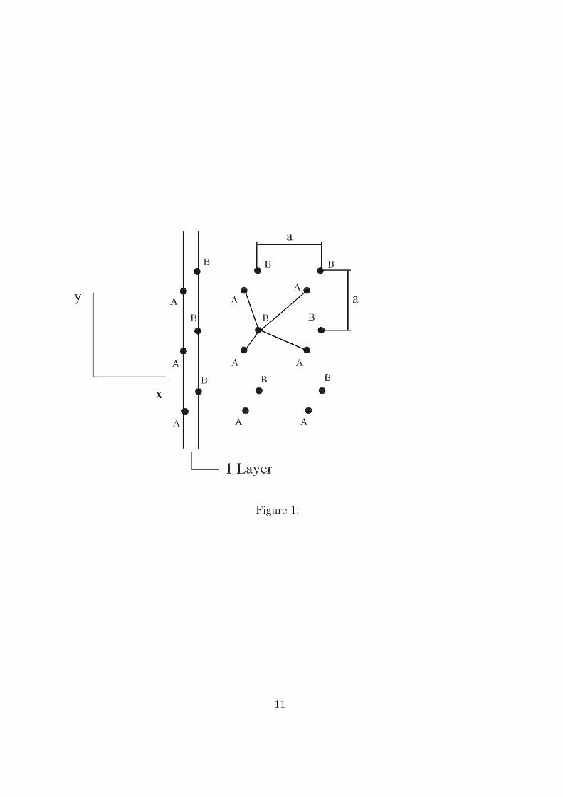
Figure 1:
11
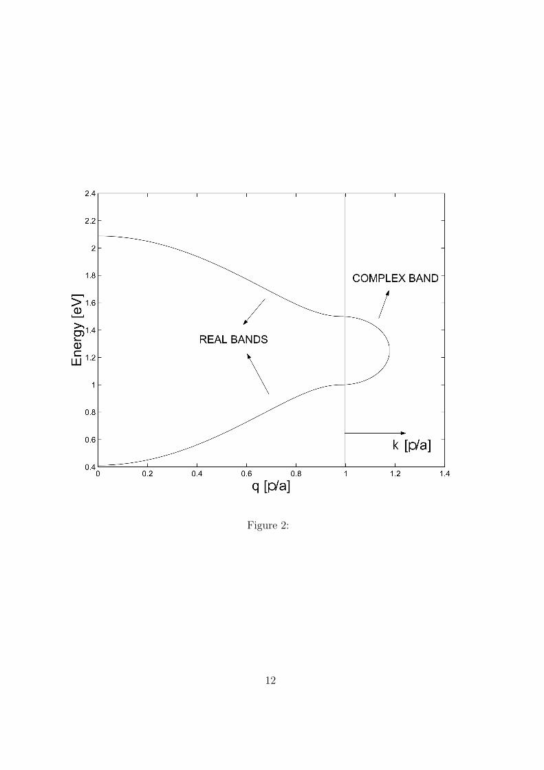
Figure 2:
12
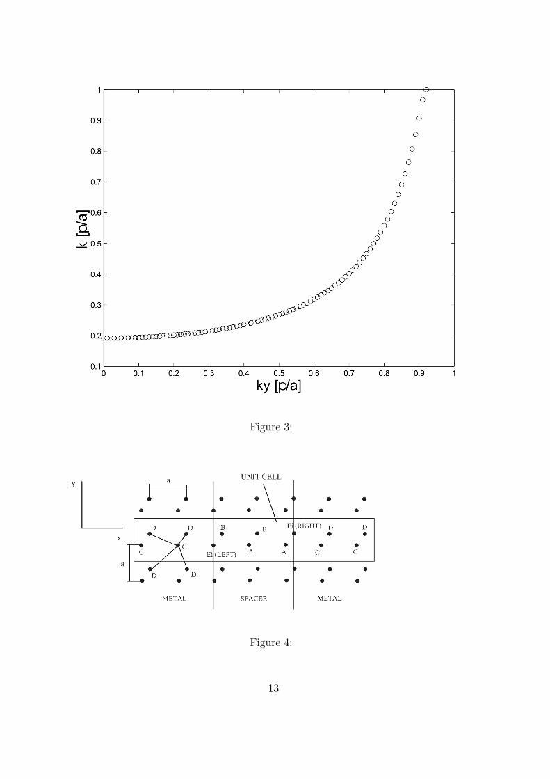
Figure 3:
Figure 4:
13
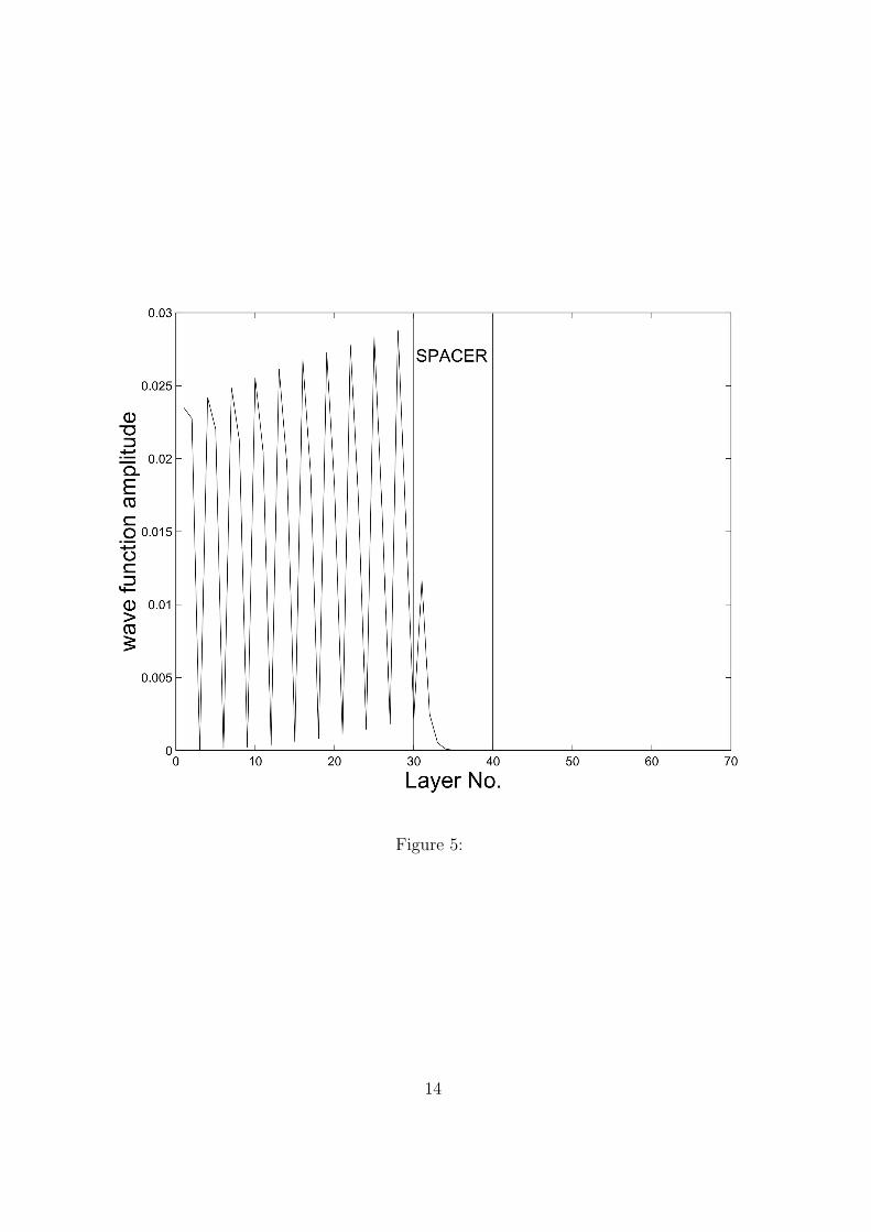
Figure 5:
14
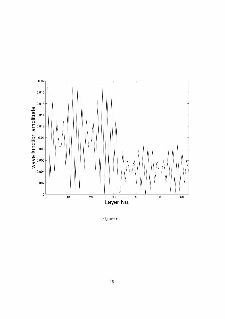
Figure 6:
15
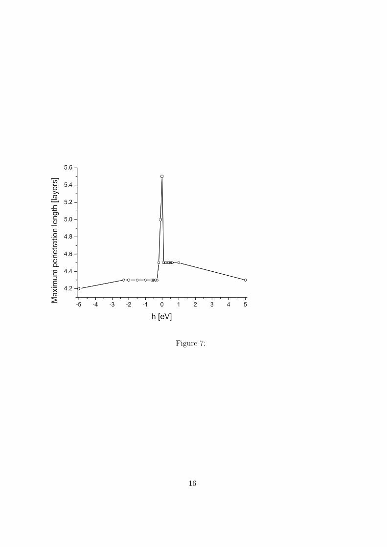
Figure 7:
16