Holographic patterning of acrylamide-based photopolymer surface
Upload
independentCategory
view
0download
0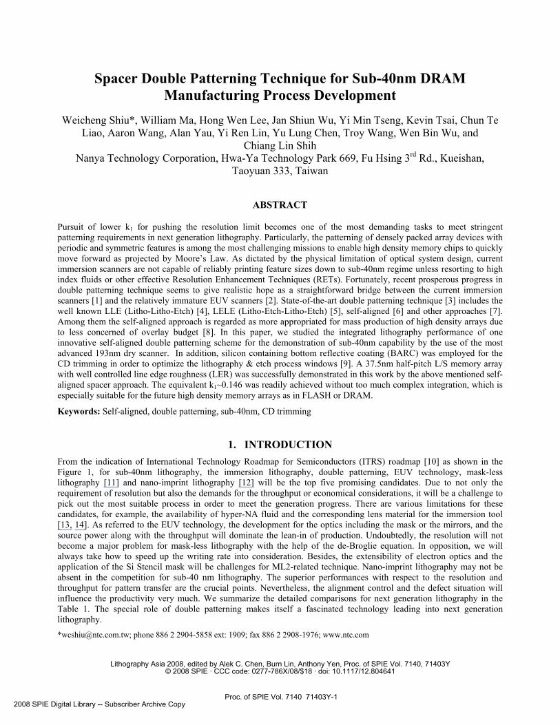
Spacer Double Patterning Technique for Sub-40nm DRAM Manufacturing Process Development
Weicheng Shiu*, William Ma, Hong Wen Lee, Jan Shiun Wu, Yi Min Tseng, Kevin Tsai, Chun Te
Liao, Aaron Wang, Alan Yau, Yi Ren Lin, Yu Lung Chen, Troy Wang, Wen Bin Wu, and Chiang Lin Shih
Nanya Technology Corporation, Hwa-Ya Technology Park 669, Fu Hsing 3rd Rd., Kueishan, Taoyuan 333, Taiwan
ABSTRACT
Pursuit of lower k1 for pushing the resolution limit becomes one of the most demanding tasks to meet stringent patterning requirements in next generation lithography. Particularly, the patterning of densely packed array devices with periodic and symmetric features is among the most challenging missions to enable high density memory chips to quickly move forward as projected by Moore’s Law. As dictated by the physical limitation of optical system design, current immersion scanners are not capable of reliably printing feature sizes down to sub-40nm regime unless resorting to high index fluids or other effective Resolution Enhancement Techniques (RETs). Fortunately, recent prosperous progress in double patterning technique seems to give realistic hope as a straightforward bridge between the current immersion scanners [1] and the relatively immature EUV scanners [2]. State-of-the-art double patterning technique [3] includes the well known LLE (Litho-Litho-Etch) [4], LELE (Litho-Etch-Litho-Etch) [5], self-aligned [6] and other approaches [7]. Among them the self-aligned approach is regarded as more appropriated for mass production of high density arrays due to less concerned of overlay budget [8]. In this paper, we studied the integrated lithography performance of one innovative self-aligned double patterning scheme for the demonstration of sub-40nm capability by the use of the most advanced 193nm dry scanner. In addition, silicon containing bottom reflective coating (BARC) was employed for the CD trimming in order to optimize the lithography & etch process windows [9]. A 37.5nm half-pitch L/S memory array with well controlled line edge roughness (LER) was successfully demonstrated in this work by the above mentioned self-aligned spacer approach. The equivalent k1~0.146 was readily achieved without too much complex integration, which is especially suitable for the future high density memory arrays as in FLASH or DRAM.
Keywords: Self-aligned, double patterning, sub-40nm, CD trimming
1. INTRODUCTION From the indication of International Technology Roadmap for Semiconductors (ITRS) roadmap [10] as shown in the Figure 1, for sub-40nm lithography, the immersion lithography, double patterning, EUV technology, mask-less lithography [11] and nano-imprint lithography [12] will be the top five promising candidates. Due to not only the requirement of resolution but also the demands for the throughput or economical considerations, it will be a challenge to pick out the most suitable process in order to meet the generation progress. There are various limitations for these candidates, for example, the availability of hyper-NA fluid and the corresponding lens material for the immersion tool [13, 14]. As referred to the EUV technology, the development for the optics including the mask or the mirrors, and the source power along with the throughput will dominate the lean-in of production. Undoubtedly, the resolution will not become a major problem for mask-less lithography with the help of the de-Broglie equation. In opposition, we will always take how to speed up the writing rate into consideration. Besides, the extensibility of electron optics and the application of the Si Stencil mask will be challenges for ML2-related technique. Nano-imprint lithography may not be absent in the competition for sub-40 nm lithography. The superior performances with respect to the resolution and throughput for pattern transfer are the crucial points. Nevertheless, the alignment control and the defect situation will influence the productivity very much. We summarize the detailed comparisons for next generation lithography in the Table 1. The special role of double patterning makes itself a fascinated technology leading into next generation lithography.
*[email protected]; phone 886 2 2904-5858 ext: 1909; fax 886 2 2908-1976; www.ntc.com
Lithography Asia 2008, edited by Alek C. Chen, Burn Lin, Anthony Yen, Proc. of SPIE Vol. 7140, 71403Y© 2008 SPIE · CCC code: 0277-786X/08/$18 · doi: 10.1117/12.804641
Proc. of SPIE Vol. 7140 71403Y-12008 SPIE Digital Library -- Subscriber Archive Copy

•flUid
•• Additth.il gfft
flUid
High liqid
Ph[hith i[igyCplhg f th thgL i[hil
h i.p[\d,
A[F / F h pplkdLhtk £hg h ih pikil
• Ch.kdihy • Ct• Cythth• C.pkhy f
•CD
CD hth• Shhk pii[. plh
• Pihk th h[hth £hipie• Sh.t i3.5.••
L NA th[gg• High[gyl• Uli. high
• Dfd-fr.k hh.th
•dhh[g• RhH d
• Th[.lhdh.gdpl.-fi.g Mi[hth• Cd[ pik[lhhiliiy
• Di[i[iiithh A f• Nk
• S[hil[ii• si• s.giihg•
pik••
• N digf[gwNpii/Cpi
• N MEEF• Mhhk f
p[ddh
• RhD h h.hdhy H.pHH
• DgHiy• H .i y• LifMh fih H.pHH• RSthl Hy thkk.
(RLT)
Double Exposure Litho-Etch-Litho-Etch Spacer Double Patternino
•
— — —
_l_t_ I I I I__________ Ifl- S L b &
•.ifl...1jM M
M
•Image intensitydiminished bynonlinear absorber
•Scanner thronghpnt
•Tight overlay budget•Mask-mask overlay,CD and linearity
ingle array exposnre •Process integration•Self-aligned array •Not for randam orprocess special layonts
•Additional trim mask•Cycle time
•Satssrable absorberdevelopment likenanoparticles or organs•cmolecules to
•Enhance the contrast
•Conpling of overlayerrors into CD errors
•Conpling of CD errorsinto overlay errors
It is a bridge between immersion lithography and EUV technology and might be likely to adopt in the generations from 40 nm to 22 nm. With the assistance of double patterning approach, the k1 limit restricted by the current imaging system designs will be broken. Double patterning technique is definitely important for the memory and logic IC for sub-40 nm patterning production regardless of the patterning types.
Fig. 1. 2007 ITRS: Lithography Table 1. Comparisons for the next generation lithography
The possible double patterning technique would be one of the following options as shown in the Figure 2:
1. Double exposure (DE): In which the wafer remains in the scanner during all the exposure time and the first and second exposures are inter-digitated in the photoresist.
2. Double patterning (DP): Expose the wafer with the first mask, development, etch, then exposed with a second mask, developed and etched.
3. Spacer double patterning (SDP): Or the self-aligned double patterning, SADP. In the second pattern, use the spacer to shrink the pitch. Additional trim mask is necessary to remove the undesired spacer or generated pattern.
In Table 2, we give the double patterning schemes comparison among the three approaches described above. Development for the required materials is necessary in order to run the double exposure scheme more smoothly. As referred to the double patterning scheme, we need to expose the wafer on separate times. The overlay between the double patterning may be severe during the process. On the other hand, due to the self-aligned character for spacer double patterning, we can control the overlay performance within the array region more easily. It is important for the patterning moving toward the resolution below hp 40nm and especially applicable for the symmetric and periodical structures.
Fig. 2. Double patterning schemes process flows Table 2. Double patterning schemes comparison
Proc. of SPIE Vol. 7140 71403Y-2

Exposure ML open UL open Filmi Etch" LIII— _lll_ — — I I IFilm2
ion Spaceretch Filmi Fill CMP
LJ i.i Film2 Film2
Spacerremoval
Film2 EtchI....Flm2 — 11111
Sil
Exposure ML open UL open Filmi Etch
:ion Spacer etch NonseIectixe
Filmi etchFiIm2 etch
FiIm2 FiIm2 I
Items Tools used Pattern Mask Purpose Mask Type IIIumination NA Outer]Inner Sigma PR BARC Substrate
However, the spacer double patterning is the most complicated from the process integration point of view. How to overcome the problems like the CD or film thickness uniformity induced in each process should be careful to deal with. In this work, we apply the spacer double patterning for sub-40nm symmetric line/space structure to examine the ability of production with ArF dry scanner on the 8” wafer firstly. A detailed description through all the processes is included to provide a reference of related topics for future study.
2. EXPERIMENTAL 2.1 Process flow description
In order to demonstrate the spacer double patterning, we have investigated two types of formation methods. The first type is the so-called line by spacer fill (LBSF) double patterning as shown in the Figure 3(a). The second type is the line by spacer (LBS) double patterning as shown in the Figure 3(b). Adoption of the multilayer BARC, say, trilayer, a silicon containing material from ShinEtsu chemical for both the types are putting into practice. There are some reasons for us to pick out trilayer:
1. Reduce the final CD to an acceptable degree.
2. As feature width decreasing, we can enlarge the photo and etch process window as we thin out the thickness of the photoresist.
3. Good reflectivity control behavior during the exposure.
Unquestionably, the steps of process flow for the LBSF scheme can exceed the LBS scheme, even so, there is a disadvantage for the LBS scheme due to the asymmetric etch process as the pattern transfer. Such phenomenon may result in CD uniformity error.
(a) (b)
Fig. 3. (a) Line by Spacer Fill Double Patterning, (b) Line by Spacer Double Patterning 2.2 Process setup
We list the process parameters for photolithography in Table 3. First, we deposit the film1 and film2 on the bare silicon wafer. Second, coat the under-layer (UL) 160nm and middle-layer (ML) 82 nm upon the deposited films by spinning. The track tool is TEL Lithius Track. The thickness of ArF photoresist is 170 nm prior to exposure. The exposure tool is Nikon ArF scanner and the illumination conditions are NA 0.75, outer/inner sigma 0.92/0.72, dipole-x. We use production mask 6% trans. HTPSM to verify the SDP schemes.
To apply the spacer double patterning will require all the help of the unit process like photolithography, etch, diffusion, and CMP. It is cooperative as we perform such an integration type of patterning method during the process transfer. For both the LBSF and LBS schemes, we think over a detailed test through our design for each process. In addition, we have considered the feasibility for the process flow. “Try and error” still works as we make the trouble shooting. For example, how to determine the suitable spacer thickness or the critical dimension in order to obtain the target pattern will be the representative question among all the problems.
Table 3. Photo exposure process conditions
Proc. of SPIE Vol. 7140 71403Y-3

• Focus Iatitude F0.3 F0.25u,cFO.2u,o F0.15 FO.1 F0.05u,o F0u,o F-O.05u,o
E31,cJIc,c !!1 !!1 111110 !11lTliii 1111111 111110 1111i0 011111D0F 0 O.25u,c 57.8no 60.4no 59.4no 62.5no 59.3no 57.7no
_______ 1111111 !1I!i I1!11!l 111110 1111111 1B1 _______
fl111 ill 11111110110111110 ITh54.7no 55.gno 53.4no 57.8no 56.8no 54.lno
E35,cJ/c,c ____________ ____________
;47 EL7 _______
47.6no 47.lno 50.2no
E32.5mJ!cmFocus O.l5um
E33.5mJ!cmFocus O.l5um
TCD 33.BnmBCD 44.7nm
PR/ML I 26.SnmULFT I53.Bnm
PR Remaining 44.3nmCD Bias -7.Snm
3. RESULTS AND DISCUSSIONS 3.1 Lithographic results
We have shown the over-exposure results in the Figure 4(a). For 37.5 nm (75 nm mask) exposure, based on the film thickness of photoresist 170 nm, the resist profile under over-exposure can extend line CD to about 50 nm (Original Pitch=150 nm) with DoF 0.25 um.
(a) (b)
Fig. 4. (a) Over-exposure FEM check for pattern collapse region, (b) Over-exposure top view and X-section profile
Line edge roughness (LER) is about 3.4 nm under over-exposure. As we see the cross-section (X-section) profile, the sidewall seems straight with top rounding. The CD bias is about -14 nm between X-section and top view. Thickness loss of the photoresist during exposure is about 23.7 nm. Figure 4(b) shows the pictures.
3.2 Trilayer (ML + UL) etch results
We use the fluorocarbon based reactive ion etching (RIE) to open the silicon containing BARC (ML). You can refer to Figure 5(a). From the top view profile, it seems line edge is a little rough post ML open. In order to check if we open ML clearly and acceptably, we have split several experimental etching times: 35s, 45s, and 50s. The best open time will be 50s from the X-section profile. The remaining of the photoresist is 44.3 nm. Sidewall angle is about 92.5o and CD Bias is about -7.8 nm between X-section and top view.
Fig. 5. (a) ML open top view and X-section profile, (b) UL open top view and X-section profile
We apply the oxygen-based RIE for the UL open. It seems line edge is a little rough with the value of LER= 4.0 nm from the measurements of the top view as shown in the Figure 5(b). The etching time is 26s. From the X-section profile, the side-etching striation appears in the sidewall along with sharp head. CD bias between X-section and top view is about -9.1 nm. The remaining of ML is about 28.2 nm while the aspect ratio (AR) is about 5.69 post UL open.
3.3 Film1 open results
We use the Hydrobromic acid (HBr) based etching gas to open the film1 hard mask (HM). In order to trim the desired CD and profile, we have tested several experimental conditions. We also add the Sulfur hexafluoride (SF6), Helium (He) and Oxygen (O2) to improve the etching performance. The Ozone (O3) based plasma ashing process follows up post the etching process. The etch conditions determined from the wafer test are (a) Etching time 60s, (b) Pressure 10 milli-torr (mT), (c) Source power 300 Watt (W), (d) Bias Power 75W, (e) HBr 180 standard cubic centimeters per minute (sccm), (f) SF6 3 sccm and (g) He-O2 13 sccm. In the Figure 6, we have shown the split conditions for film1 open test
Proc. of SPIE Vol. 7140 71403Y-4

SEM52005.OkV 2J22JO l5O,
Fig. 6. Split conditions for film1 open process
The final X-section CD is about 37 nm. The result film1 open is quite important since it defines the first pattern of the double patterns. If there is any existed CD variation or unacceptable profile for the film1 pattern, the error will propagate through all the process stations like the spacer formation. Hence, the critical dimension uniformity (CDU) at any levels like field or shot will suffer.
3.4 Spacer formation and spacer etch
The spacer formation as shown in the Figure 7 is a critical process step. It will influence the second pattern very much. The thickness (or CD) control for the spacer must be good enough, in other word, to deposit the spacer conformal. We can construct the space for the second pattern post the operation of spacer process. The deposition temperature is 715 oC and the operation pressure is 0.17 Torr. The deposition time for 375 Ǻ spacer is 51 min and 61 min for 455 Ǻ. It is necessary to examine the spacer etch process carefully. If we apply different thickness of the spacer, the etching result will be very distinct. In the Figure 8(a), we have deposited the thinner spacer than the right side. You can discover that the shapes of the space post spacer etch are dissimilar. For the thinner spacer, we can obtain a straighter sidewall relative to the thicker spacer. Of course, the shape of the sidewall will influence the pattern transfer very much.
(a) (b) Fig. 7. Spacer formation post film1 open Fig. 8. (a) Spacer etch effect for thinner spacer thickness, (b) thicker spacer
3.5 The remaining steps post spacer etch for the LBS scheme: Film1 recess and film2 etch
The results for film1 recess will influence the line pattern CD and profile very much. Double pattern will form post this process step. We may observe the different film1 CD during the first run and the second run since we want to make minimal CD difference between the line and space during the double patterning process. Consequently, we decide to enlarge the film1 CD about 20 nm for the second run. In the Figure 9, we have shown the X-section profile for the double run. In the first run, the time of break through (BT) is 5s and the main etching (ME) time is 20s. In the second run, we increase the bias power (BP) up to 5W and the ME time becomes 25s.
(a) (b) Fig. 9. (a) Film1 recess for the first run, (b) the second run
Proc. of SPIE Vol. 7140 71403Y-5

SEM52c 1OOkVO4,,QOOkSE 2127108 150785
07060830CB (AB60021)#3
JRiI1flEL
As referred to the X-section profiles of film2 etch images as shown in the Figure 10(a)-(b), the CD of the first pattern seems too small to open the film2 channel. Due to the poor selectivity between the spacer and film2, we have triangular shape for the final pattern. If we want to perform the LBS scheme more smoothly, we may reconsider the better film stacks combination, including the material type and the thickness. In the Figure 10(c), we have exhibited the situation post LBS scheme near the line end and landing pad regions. It will need an additional mask to trim the pattern for asymmetric patterns described above. Therefore, it will be a task to learn how to construct the additional layout.
(a) (b) (c) Fig. 10. (a) Film2 etch for the first run, (b) the second run, (c) Top views near the line end and landing pad post LBS scheme
3.6 The remaining steps post spacer etch for the LBSF scheme: Film1 fill, CMP, removal of the spacer and film2 etch
The thickness is 2000Ǻ for film1 fill process as shown in the Figure 11(a). The purpose of fill process is generating the second pattern in order to form the double pattern. The process temperature is 550 oC and the pressure is 0.45 Torr. Deposition time is 80 min. The source gas is Silane (SiH4).
(a) (b) (c) Fig. 11. (a) X-section picture post film1 fill process, (b) X-section picture post film1 CMP, (c) spacer strip process
CMP process like Figure 11(b) will follow the fill process. To judge the end point of the polishing will take some effort. One possible way is to inspect the top view CD and profiles. It is a key step since the result will affect the within wafer CDU very much. Good thickness uniformity control in the entire region of the wafer will lead to the success of the double pattern formation. We can find the dishing phenomena at the film1 sites. The polishing time is about 60s. The slurry is Fujimi PL4218 for polishing. The remainder of film1 is about 50 nm. Post the removal of the spacer as you can see in the Figure 11(c), we can generate the double pattern in the hard mask layer firstly. We use the Phosphoric acid (H3PO4) to etch the spacer. The total processing time is 832s. Use the film1 as the hard mask (HM) to open the bottom film2 layer. The final result has been shown in the Figure 12, i.e., the 37.5 nm half pitch line/space pattern through the LBSF scheme. The main etching time is 22s.
Fig. 12. X-section picture post film2 etch
3.7 Summary for LBSF double patterning
In the Figure 13(a), you can realize the situation for within wafer CD variation from photo to film1 open stations. Further, in order to examine the CDU variation during the line trimming process, we have analyzed the within wafer CDU at the stations just mentioned. We summarize the detailed results in the Figure 13(b). It is very clear that, as the CD trends down, the CDU trends up oppositely. You may pay this effort when you want to enlarge the process window for
Proc. of SPIE Vol. 7140 71403Y-6
photo process. However, you can still keep on improving the process parameters to obtain a better performance for the double patterning procedures.
(a)
010203040506070
PHOTO ML+UL Open Film1 Open
CD
(b)
0
2
4
6
8
10
PHOTO ML+ULOpen
Film1 Open
CDU
Fig. 13. LBSF scheme: (a) The measurement of within wafer CD, (b) CDU from photo until film1 open stations
You may notice the great CD bias post the CMP process as shown in the Figure 14(a). It indicates the importance to control the zone pressure very well during the CMP process. The CD bias will transfer when we process the latter process like spacer removal etc.
(a)
CD Bias (X-Section - Top View)
-40.0 -30.0 -20.0 -10.0 0.0 10.0 20.0
PHTriL Open
Film1 OpenSpacer
Spacer EtchFilm1 Fill
Film1 CMPSpacer
Film2 Etch
Spacer2nd1st
(b)
Cross Bank CDU / LER
0.01.02.03.04.05.06.07.0
1st 2nd 1st 2nd
PHOTO ML+ULOpen
Film1Open
Spacer Strip Film2 Etch
CDULER
Fig. 14. LBSF scheme: (a) CD bias between X-section, (b) Cross bank CDU and LER top view from photo until film2 etch
We measure the multiple point cross-bank CDU and LER data. In the Figure 14(b), we may observe the value of the CDU falls on the range below 6nm and above 2.5nm. Besides, for the LER measurement, the value ranges between 3.4nm and 4.1nm.
4. CONCLUSION An intention of this work is likely to demonstrate a possible way for sub-40nm line/space manufacturing with the current dry lithography process and tools. We go through the detailed investigations for the spacer double patterning LBS and LBSF schemes.
Conclusions are as bellow:
1. Initially, we demonstrate the line by spacer fill scheme (LBSF) for 37.5 nm HP L/S structure in the array region.
2. With the assistance of the LBSF schemes for the generation of 37.5nm HP L/S structure, k1 is reduced to 0.146 (highly below 0.25) under our NA 0.75 dipole illumination.
3. It is feasible to bring LBSF scheme into practice for resolving the limited half pitch below 40 nm from current data in general, but to take more work is necessary in order to settle the questions derived outside the array region, e.g., the pattern split or the trim process.
4. How to control all the LBSF unit process smoothly will be definitely a challenging task from the integration point of view.
Proc. of SPIE Vol. 7140 71403Y-7
Before the maturity of the EUV and high-index immersion fluid development, double patterning is very likely to be the candidate when we move toward the generation even to 22nm [15]. In addition to face the complexity of the process for the double patterning, we need to figure out the better approach of pattern split outside the array region in the future. Nevertheless, it points out an optimistic way for keeping shrinking the feature size through the experience of double patterning development for 37.5nm half pitch line/space.
ACKNOWLEDGMENT
The authors would like to acknowledge experimental support by ATD Dept. II, ATD Dept. IV, ATD Dept V and FAB-2 Diff Eng. Dept.
REFERENCES
[1] Burn J. Lin, "Immersion lithography and its impact on semiconductor manufacturing," Proc. SPIE 5377, 46-67 (2004).
[2] Hans Meiling, Vadim Banine, Noreen Hamed, Brian Blum, Peter Kürz, and Henk Meijer, "Development of the ASML EUV alpha demo tool," Proc. SPIE 5751, 90-101 (2005).
[3] William H Arnolda, Mircea Dusa, Jo Finders, "Metrology challenges for double exposure and double patterning," Proc. SPIE 6518, 651802 (2007).
[4] Alex K. Raub, S. R. J. Brueck, "Extending 193nm Lithography to the 22-nm HP Node Using Non-Linear Optical Films," SEMATECH Litho Forum (2006).
[5] M. Maenhoudt, J. Versluijs, H. Struyf, J. Van Olmen, M. Van Hove, "Double Patterning scheme for sub-0.25 k1 single damascene structures at NA=0.75, λ=193nm," Proc. SPIE 5754, 1508-1518 (2005).
[6] Woo-Yung Jung, Choi-Dong Kim, Jae-Doo Eom, Sung-Yoon.Cho, Sung-Min Jeon, Jong-Hoon Kim, Jae-In Moon, Byung-Seok Lee, and Sung-Ki Park, "Patterning with spacer for expanding the resolution limit of current lithography tool," Proc. SPIE 6156, 61561J (2006).
[7] M. Maenhoudt, R. Gronheid, N. Stepanenko, T. Matsuda, and D. Vangoidsenhoven, "Alternative process schemes for double patterning that eliminate the intermediate etch step," Proc. SPIE 6924, 69240P (2008).
[8] Gianfranco Capetti, Pietro Cantù, Elisa Galassini, Alessandro Vaglio Pret, Catia Turco, Alessandro Vaccaro, Pierluigi Rigolli, Fabrizio D’Angelo, Gina Cotti. Sub k1 = 0.25 Lithography with Double Patterning Technique for 45nm Technology Node Flash Memory Devices at λ = 193nm, Proc. SPIE 6520, 65202K (2007).
[9] Hung Jen Liu, Wei Hsien Hsieh, Chang Ho Yeh, Jan Shiun Wu, Hung Wei Chan, Wen Bin Wu, Feng Yi Chen, Tse Yao Huang, Chiang Lin Shih, Jeng Ping Lin, "Double patterning with multilayer hard mask shrinkage for sub-0.25 k1 lithography," Proc. SPIE 6520, 65202J (2007).
[10] INTERNATIONAL TECHNOLOGY ROADMAP FOR SEMICONDUCTORS 2007 EDITION LITHOGRAPHY, http://www.itrs.net/Links/2007ITRS/2007_Chapters/2007_Lithography.pdf.
[11] Burn J. Lin, "Marching of the microlithography horses: Electron, ion, and photon: Past, present, and future," Proc. SPIE 6520, 652002 (2007).
[12] William M. Tong, Scott D. Hector, Gun-Young Jung, Wei Wu, James Ellenson, Kenneth Kramer, Timothy Hostetler, Susan K. Richards, R. Stanley Williams, "Nanoimprint lithography: the path toward high tech, low cost devices," Proc. SPIE 5751, 46-55 (2005).
[13] Yasuhiro Ohmura, Hiroyuki Nagasaka, Tomoyuki Matsuyama, Toshiharu Nakashima, Teruki Kobayashi, Motoi Ueda, and Soichi Owa, "Studies of High Index Immersion Lithography," Proc. SPIE 6924, 692413 (2008).
[14] Harry Sewell, Jan Mulkens, Paul Graeupner, Diane McCafferty, Louis Markoya, Sjoerd Donders, Nandasiri Samarakone, and Rudiger Duesing, "Extending immersion lithography with high index materials results of a feasibility study," Proc. SPIE 6520, 65201M (2007).
[15] Byungjoon Hwang, Namsu Lim, Jang-Ho Park, Sowi Jin, Minjeong Kim, Jaesuk Jung, Byungho Kwon, Jongwon Hong, Jeehoon Han, Donghwa Kwak, Jaekwan Park, Jung-Dal Choi and Won-Seong Lee, "Development of 38nm Bit-Lines using Copper Damascene Process for 64-Giga bits NAND Flash," IEEE/SEMI Advanced Semiconductor Manufacturing Conference, 49-51 (2008).
Proc. of SPIE Vol. 7140 71403Y-8
Copyright © 2022 FDOKUMEN