Thermal modeling and management of DRAM memory systems
93
Thermal modeling and management of DRAM memory systems by Jiang Lin A dissertation submitted to the graduate faculty in partial fulfillment of the requirements for the degree of DOCTOR OF PHILOSOPHY Major: Computer Engineering Program of Study Committee: Zhao Zhang, Major Professor Arun K. Somani Akhilesh Tyagi J. Morris Chang Masha Sosonkina Iowa State University Ames, Iowa 2008 Copyright c Jiang Lin, 2008. All rights reserved.
-
Upload
khangminh22 -
Category
Documents
-
view
0 -
download
0
Transcript of Thermal modeling and management of DRAM memory systems
Thermal modeling and management of DRAM memory systems
by
Jiang Lin
A dissertation submitted to the graduate faculty
in partial fulfillment of the requirements for the degree of
DOCTOR OF PHILOSOPHY
Major: Computer Engineering
Program of Study Committee:Zhao Zhang, Major Professor
Arun K. SomaniAkhilesh TyagiJ. Morris ChangMasha Sosonkina
Iowa State University
Ames, Iowa
2008
Copyright c© Jiang Lin, 2008. All rights reserved.

ii
Dedicated to my brother Hui ...

iii
TABLE OF CONTENTS
LIST OF TABLES . . . . . . . . . . . . . . . . . . . . . . . . . . . . . . . . . . . vi
LIST OF FIGURES . . . . . . . . . . . . . . . . . . . . . . . . . . . . . . . . . . vii
CHAPTER 1. Introduction . . . . . . . . . . . . . . . . . . . . . . . . . . . . . 1
CHAPTER 2. Background . . . . . . . . . . . . . . . . . . . . . . . . . . . . . . 4
2.1 Thermal Management in Computer Systems . . . . . . . . . . . . . . . . . . . . 4
2.2 Thermal Issue of DDR2 and Fully Buffered DIMM (FBDIMM) Memories . . . 5
2.3 Dynamic Thermal Management Schemes for Memories . . . . . . . . . . . . . . 6
2.4 DRAM Power Saving Techniques . . . . . . . . . . . . . . . . . . . . . . . . . . 7
2.5 Other Related Work on Power Savings . . . . . . . . . . . . . . . . . . . . . . . 7
CHAPTER 3. Power and Thermal Model of DRAM Memory . . . . . . . . 8
3.1 Introduction . . . . . . . . . . . . . . . . . . . . . . . . . . . . . . . . . . . . . . 8
3.2 Structure of FBDIMM . . . . . . . . . . . . . . . . . . . . . . . . . . . . . . . . 9
3.3 Power Model of FBDIMM . . . . . . . . . . . . . . . . . . . . . . . . . . . . . . 11
3.4 Isolated Thermal Model of FBDIMM . . . . . . . . . . . . . . . . . . . . . . . . 14
3.5 Integrated Thermal Model of FBDIMM . . . . . . . . . . . . . . . . . . . . . . 17
CHAPTER 4. Proposed DTM Schemes and Their Simulation Result . . . . 19
4.1 Introduction . . . . . . . . . . . . . . . . . . . . . . . . . . . . . . . . . . . . . . 19
4.2 Dynamic Thermal Management for FBDIMM Memory . . . . . . . . . . . . . . 21
4.2.1 Existing Memory DTM Schemes . . . . . . . . . . . . . . . . . . . . . . 21
4.2.2 Proposed DTM Schemes . . . . . . . . . . . . . . . . . . . . . . . . . . . 21
4.2.3 DTM-ACG and DTM-CDVFS Integrated with Formal Control Method 22
iv
4.3 Experimental Methodology . . . . . . . . . . . . . . . . . . . . . . . . . . . . . 23
4.3.1 Two-Level Thermal Simulator . . . . . . . . . . . . . . . . . . . . . . . . 23
4.3.2 Workloads . . . . . . . . . . . . . . . . . . . . . . . . . . . . . . . . . . . 26
4.3.3 DTM Parameters . . . . . . . . . . . . . . . . . . . . . . . . . . . . . . . 27
4.3.4 Parameters in PID Formal Controller . . . . . . . . . . . . . . . . . . . 28
4.4 Effectiveness of Memory DTM Schemes . . . . . . . . . . . . . . . . . . . . . . 28
4.4.1 Performance Impact of Thermal Release Point . . . . . . . . . . . . . . 28
4.4.2 Performance Comparison of DTM Schemes . . . . . . . . . . . . . . . . 30
4.4.3 Impact on Energy Consumption . . . . . . . . . . . . . . . . . . . . . . 36
4.4.4 DTM Interval . . . . . . . . . . . . . . . . . . . . . . . . . . . . . . . . . 42
4.5 Impact of Thermal Interaction between Processors and DRAM Memory . . . . 42
4.5.1 Performance Comparison . . . . . . . . . . . . . . . . . . . . . . . . . . 45
4.5.2 Sensitivity Analysis of Thermal Interaction Parameter . . . . . . . . . . 45
CHAPTER 5. A Case Study of Memory Thermal Management for Multi-
core Systems . . . . . . . . . . . . . . . . . . . . . . . . . . . . . . . . . . . . 48
5.1 Introduction . . . . . . . . . . . . . . . . . . . . . . . . . . . . . . . . . . . . . . 48
5.2 Design and Implementation Issues . . . . . . . . . . . . . . . . . . . . . . . . . 50
5.2.1 Memory DTM Mechanisms . . . . . . . . . . . . . . . . . . . . . . . . . 50
5.2.2 Memory DTM Polices . . . . . . . . . . . . . . . . . . . . . . . . . . . . 52
5.3 Experimental Methodology . . . . . . . . . . . . . . . . . . . . . . . . . . . . . 56
5.3.1 Hardware and Software Platforms . . . . . . . . . . . . . . . . . . . . . 56
5.3.2 Workloads . . . . . . . . . . . . . . . . . . . . . . . . . . . . . . . . . . . 59
5.4 Results and Analysis . . . . . . . . . . . . . . . . . . . . . . . . . . . . . . . . . 60
5.4.1 Experimental Observation of DRAM Thermal Emergency . . . . . . . . 60
5.4.2 Performance Comparison of DTM Polices . . . . . . . . . . . . . . . . . 63
5.4.3 Analysis of Performance Improvements by Different DTM Policies . . . 68
5.4.4 Comparison of Power and Energy Consumption . . . . . . . . . . . . . . 70
5.4.5 Sensitivity Analysis of DTM Parameters . . . . . . . . . . . . . . . . . . 73

v
5.5 Conclusion . . . . . . . . . . . . . . . . . . . . . . . . . . . . . . . . . . . . . . 77
CHAPTER 6. Conclusion and Future Work . . . . . . . . . . . . . . . . . . . 78
BIBLIOGRAPHY . . . . . . . . . . . . . . . . . . . . . . . . . . . . . . . . . . . 79
ACKNOWLEDGMENTS . . . . . . . . . . . . . . . . . . . . . . . . . . . . . . . 83

vi
LIST OF TABLES
Table 3.1 The values of parameters in Equation 3.2 for FBDIMM with 1GB
DDR2-667x8 DRAM chips made by 110nm process technology. . . . . 14
Table 3.2 The value of parameters in the thermal model for the AMB and DRAM
chips in the given type of FBDIMM used in our simulation. The
columns in bold type are used in our experiments. . . . . . . . . . . . . 16
Table 3.3 The values of parameters in the thermal model for DRAM ambient
temperature. . . . . . . . . . . . . . . . . . . . . . . . . . . . . . . . . . 18
Table 4.1 Simulator parameters. . . . . . . . . . . . . . . . . . . . . . . . . . . . 25
Table 4.2 Workload mixes. . . . . . . . . . . . . . . . . . . . . . . . . . . . . . . 26
Table 4.3 Thermal emergency levels and their default settings used for the chosen
FBDIMM. . . . . . . . . . . . . . . . . . . . . . . . . . . . . . . . . . . 27
Table 4.4 Processor power consumption of DTM schemes. . . . . . . . . . . . . . 41
Table 5.1 Thermal emergency levels and thermal running states. . . . . . . . . . 53
Table 5.2 Workload mixes. . . . . . . . . . . . . . . . . . . . . . . . . . . . . . . 59
vii
LIST OF FIGURES
Figure 3.1 The structure of Fully-Buffered DIMM with one channel, n DIMMs
and eight DRAM chips per DIMM. The memory controller is able to
connect up to six channels, and each channel may connect up to eight
DIMMs. . . . . . . . . . . . . . . . . . . . . . . . . . . . . . . . . . . . 9
Figure 3.2 Four categories of data traffic that flows through AMB. . . . . . . . . . 13
Figure 3.3 Heat dissipation of FBDIMM. The arrows represent heat dissipation paths. . 15
Figure 4.1 Two-level thermal simulator. . . . . . . . . . . . . . . . . . . . . . . . . 24
Figure 4.2 Performance of DTM-TS with varied TRP. The DRAM TDP is 85.0◦C
and the AMB TDP is 110.0◦C. . . . . . . . . . . . . . . . . . . . . . . 29
Figure 4.3 Normalized running time for DTM schemes. . . . . . . . . . . . . . . . 31
Figure 4.4 Normalized total memory traffic for DTM schemes. . . . . . . . . . . . 33
Figure 4.5 AMB temperature changes of DTM-TS for W1 with AOHS 1.5. . . . . 35
Figure 4.6 AMB temperature changes of DTM-BW for W1 with AOHS 1.5. . . . 36
Figure 4.7 AMB temperature changes of DTM-ACG for W1 with AOHS 1.5. . . . 37
Figure 4.8 AMB temperature changes of DTM-CDVFS for W1 with AOHS 1.5. . 38
Figure 4.9 Normalized energy consumption of FBDIMM for DTM schemes. . . . . 39
Figure 4.10 Normalized energy consumption of processors for DTM schemes. . . . 40
Figure 4.11 Normalized average running time for different DTM intervals. . . . . . 43
Figure 4.12 Normalized running time for DTM schemes. . . . . . . . . . . . . . . . 44
Figure 4.13 Average normalized running time with different degrees of thermal in-
teraction. . . . . . . . . . . . . . . . . . . . . . . . . . . . . . . . . . . 46
viii
Figure 4.14 Average normalized performance improvement of DTM-ACG and DTM-
CDVFS with different degrees of thermal interaction, compared with
DTM-BW. . . . . . . . . . . . . . . . . . . . . . . . . . . . . . . . . . . 47
Figure 5.1 Thermal Zone. . . . . . . . . . . . . . . . . . . . . . . . . . . . . . . . . 50
Figure 5.2 Intel SR1500AL system with thermal sensors (“T”). . . . . . . . . . . 57
Figure 5.3 The daughter card. . . . . . . . . . . . . . . . . . . . . . . . . . . . . . 58
Figure 5.4 AMB temperature curve for first 500 seconds of execution. . . . . . . . 61
Figure 5.5 AMB temperature when memory is driven by homogeneous workloads
on the PE1950 without DTM control. . . . . . . . . . . . . . . . . . . . 62
Figure 5.6 Normalized running time of SPEC CPU2000 workloads. . . . . . . . . 64
Figure 5.7 Normalized running time of SPEC CPU2006 workloads on PE1950. . . 66
Figure 5.8 Normalized numbers of L2 cache misses. . . . . . . . . . . . . . . . . . 67
Figure 5.9 Measured memory inlet temperature. . . . . . . . . . . . . . . . . . . . 70
Figure 5.10 CPU power consumption. . . . . . . . . . . . . . . . . . . . . . . . . . 71
Figure 5.11 Normalized energy consumption of DTM policies. . . . . . . . . . . . . 72
Figure 5.12 Normalized running time on Intel SR1500AL at a room system ambient
temperature (26◦C). . . . . . . . . . . . . . . . . . . . . . . . . . . . . 73
Figure 5.13 Comparison of performance between DTM-ACG and DTM-BW under
two different processor frequencies on Intel SR1500AL. . . . . . . . . . 75
Figure 5.14 Normalized running time averaged for all workloads on PE1950 with
different AMB TDPs. . . . . . . . . . . . . . . . . . . . . . . . . . . . . 76
Figure 5.15 Normalized running time and number of L2 cache misses averaged for
all workloads on PE1950 with different switching frequencies. . . . . . 77

1
CHAPTER 1. Introduction
Thermal issues have been first-order considerations in designing processors and hard disk
for a long time [3, 52, 54, 12, 27]; and now they are becoming critically important for DRAM
memory subsystems as well [26, 33, 31, 32]. This trend is driven by the wide adoption of
multi-core processors and their ever increasing demands for high capacity and bandwidth from
DRAM memory subsystems.
Current thermal solutions and cooling capabilities of DRAM memories allow full system
performance under normal operating conditions. Thermal management is used as a protection
mechanism that ensures safe operation and prevents thermal emergencies under abnormal
scenarios. These scenarios, while not common, do occur in practice. They can be due to a
poorly designed thermal solution, system fan failure, obstructions to airflow within a system,
thermally challenging workload mix or other reasons that cause a system to operate outside of
its thermal design boundaries. Thermal management is also necessary when users or system
operators make a decision to operate in more thermally constrained environments, including
reduction of fan speed for acoustic reasons, and operating under high ambient temperatures to
reduce cooling costs in data centers. In practice, the use of DRAM thermal management has
appeared both in servers [33] and on mobile platforms [26]. In the future, as DRAM power
density continues to increase, even advanced cooling features such as fans over DRAM devices,
which increases system cooling budget and overall cost, may not allow full system performance
under normal operating conditions.
Regardless of the exact reason, a robust thermal management scheme is needed to ensure
safe system operation while maximizing its performance under thermal constraints. Instead
of fully shutting down the system upon reaching a thermal threshold, a carefully designed

2
DTM (dynamic thermal management) scheme may improve system performance and/or system
power efficiency under the same thermal constraints. Therefore, research on sophisticated
DRAM DTM schemes is highly desired.
To address this emerging issue, we have proposed and evaluated two new DTM schemes
which take a novel approach different from existing DTM schemes. Instead of throttling mem-
ory accesses directly at the memory side upon reaching a thermal threshold, the new approach
coordinates DRAM thermal states and processors’ running states: when DRAM is in thermal
emergency, it slows down the memory access intensity by either gating some processor cores
or applying DVFS (dynamic voltage and frequency scaling) on the processor cores. These two
new schemes have first been evaluated using simulation and then implemented and evaluated
on real systems. Furthermore, to support memory thermal studies, a simple and accurate
thermal model is proposed to estimate the dynamic temperature changes of DRAM memory
subsystems. A two-level simulator has been developed to emulate the thermal behavior of
memory subsystems. The simulation results show that the proposed schemes provide better
performance and energy efficiency than existing simple DTM schemes. To confirm the con-
clusions make by simulation, we have further performed a case study of the proposed DTM
schemes through measurement on real systems by implementing the proposed DTM schemes
in software and conducted experiments on two server platforms. The measurement-based ex-
periments first confirm that the two proposed schemes significantly improve performance and
energy efficiency in real server systems. In addition, we have surprising findings that are hard
to get from the simulation approach. In short, we have made a case that, with careful ther-
mal management designs, DRAM thermal issues can be handled at the cost of very small
performance penalty.
The rest of this thesis is organized as follows. After discussing the background and related
work in Chapter 2, we present our integrated power and thermal model by using existing
industrial power and temperature estimation methods in Chapter 3. Chapter 4 demonstrates
how we use the simulation approach to study the DRAM thermal issues. Chapter 5 describes
the case study of the proposed DTM schemes through measurement on real systems. Finally,
3
Chapter 6 concludes this thesis and discusses future directions.
4
CHAPTER 2. Background
2.1 Thermal Management in Computer Systems
Thermal management has become a research focus in recent years. Most studies so far
have focused on processors, disks, server systems and data centers. Brooks and Martonosi
study processor dynamic thermal management (DTM) mechanism, such as scaling the clock
frequency or voltage [3]. Skadron et al. develop a thermal model for individual functional blocks
using thermal resistances and capacitances derived from the layout of the micro-architecture
structures [52]. They further extend the model to HotSpot, which models thermal behavior
at the microarchitecture level using a network of thermal resistances and capacitances, and
can identify the hottest unit on a chip [54]. They also propose several DTM techniques, such
as migrating computation to spare hardware units from overheated ones. Li et al. study the
thermal constraints in the design space of CMPs [29]. Donald and Martonosi explore the
design space of thermal management techniques for multicore processors [9]. Regarding the
DTM for the hard disk drives, Gurumurthi et al. develop models to capture the capacity,
performance and thermal behavior of disk drives. They also present two DTM techniques for
hard disks, exploiting the thermal slack or throttling disk activities [12]. Kim et al. further
develop a performance-temperature simulator of disk drives and study the thermal behaviors
and management of storage systems using server workloads [27]. There are also a set of works
which study the DTM for server systems and data centers. Moore et al. use a temperature-
aware workload placement algorithm to reduce the cooling cost of data centers [43]. Heath et
al. propose Mercury, a temperature emulation suite for servers; they also develop and evaluate
Freon, a system for managing thermal emergency in server cluster [15]. Choi et al. propose
ThermoStat, a CFD-based tool, to study thermal optimization at run time on server systems
5
as well as the layout optimization in the design phase [6].
2.2 Thermal Issue of DDR2 and Fully Buffered DIMM (FBDIMM)
Memories
Processor speeds double approximately every eighteen months, while main memory speeds
double only about every ten years. These diverging rates resulted in a “memory wall”, in which
memory accesses dominate program performance. Recently, improvement of single processor
performance has slowed down in terms of single thread execution because of increasing power
consumption, increasing difficulty in finding enough instruction level parallelism, and increas-
ing relative wire delay and main memory access latency. Instead of building highly complex
single-threaded processors, processor designers put multiple processor cores on a single chip
to improve the overall throughput. With multicore processors, the high memory access la-
tency is likely to persist. Furthermore, as the number of processor cores increases, multicore
processors not only demand fast main memory speed as did single-thread processors, but also
require large memory capacity and high aggregate memory bandwidth to support simultaneous
multiple executions.
There have been many technology advances to improve DRAM bandwidth and capacity
and to address the latency issue. DRAM performance has been improved both in technology
and in architecture. In technology, DRAM latency is improved by 7% every year, which is much
slower than that of processor. In computer architecture, many architecture-level mechanisms
have been employed or studied at the DRAM level to improve performance, such as latency
reduction and data transfer rate improving techniques [50, 20, 21, 40, 41, 39, 45, 46], and
memory access scheduling [44, 36, 35, 37, 38, 17, 49, 48, 5, 59, 34, 58, 7, 60, 19, 47, 53].
Responding to the demand of improving main memory capabilities from multicore processors,
new memory technologies have been introduced by industry to support both large memory
capacity and high memory bandwidth, such as fully buffered DIMM (FBDIMM) proposed by
Intel [13] and the Socket G3 Memory Extender (G3MX) to be supported by AMD [1]. Both
technologies use narrow and high frequency buses to connect DRAM memory with s chipset

6
or processors. Therefore, the number of pins of each memory channel is reduced and more
memory channels can be supported in a system.
However, with those technological advances, DRAM memory subsystem now consumes
a significant portion of total system power. At this point, in server systems, DRAM power
consumption is comparable to that of processors. Moreover, with increased power consumption,
more heat is generated. Consequently, the DRAM thermal problem has become a real issue
recently for both DDR2 DRAM and FBDIMM. A recent study has reported that on a mobile
system, the temperature of DDR2 DRAM devices may exceed their thermal design point of
85◦C when running real workloads at an ambient temperature of 35◦C [26]. On sever platforms,
the recently deployed FBDIMM has become a focus for DRAM thermal studies [31, 33]. For
example, a current small-scale, two-way SMP server [22] provides peak memory bandwidth of
21 GB/s and maximum memory capacity of 32 GB to support up to eight cores. Its maximum
DRAM power consumption can reach 100 watts, which can be in the same range of power
consumed by the processors. Consequently, DRAM power and thermal management is an
urgent and critical issue.
2.3 Dynamic Thermal Management Schemes for Memories
In practice, two DTM schemes have been used to prevent AMB or DRAM device overheat-
ing. In thermal shutdown, the memory controller (or the operating system) periodically reads
the temperature of DIMMs from thermal sensors embedded into DIMMs. If the reading exceeds
a preset thermal threshold, the memory controller stops all accesses to the DRAMs until the
temperature drops below the threshold by a preset margin. In bandwidth throttling [22, 33], the
memory controller throttles memory throughput when overheating is to happen. The throt-
tling is done by counting and limiting the number of row activations in a given window of
time.
7
2.4 DRAM Power Saving Techniques
Several studies have focused on reducing the power consumption of main memory systems.
Although those proposed techniques may also help in lowering the memory temperature, they
do not directly target the alleviation of the memory thermal emergency. Lebeck et al. propose
a power-aware page allocation scheme that utilizes the long-latency but low-power DRAM
modes. It minimizes the number of memory chips used by an application to increase the
possibility that a DRAM chip can be put into low-power modes without affecting overall
performance [28]. Delaluz et al. further propose using compiler techniques to map memory
pages with similar active periods to the same chips in order to allow DRAM chips to stay in
low-power modes longer [8]. Fan et al. study memory controller policies considering DRAM
power states for power saving [10]. Huang et al. design and implement power-aware virtual
memory management to save power consumption of main memory systems [18].
2.5 Other Related Work on Power Savings
Isci et al. [25] has proposed a runtime phase prediction method and use it to predict memory
intensive phases of a program. They further propose the use of DVFS on the processor during
those phases to save the power and energy consumption of a single-threaded mobile processor.
In DTM-CDVFS, DVFS is triggered by thermal emergency and the objective is to improve
performance and power efficiency for multicore server systems. Since memory temperature
change is much slower than program phase change, thermal emergency is likely a more reliable
trigger for DVFS with a performance target, though phase prediction can work when thermal
emergency does not appear. Another study by Isci et al. [24] proposes methods to use per-core
DVFS in managing the power budget of a multicore processor. Besides the difference that
this study is focused on memory thermal management, per-core DVFS is not yet available on
mainstream processors except Intel Itanium (to the best of our knowledge).

8
CHAPTER 3. Power and Thermal Model of DRAM Memory
3.1 Introduction
Our DRAM power and thermal model is presented in this chapter. We focus on systems
with fully buffered DIMM (FBDIMM) as the main memory. FBDIMM is designed for multi-
core processors to meet their demand of high bandwidth and large capacity. However, it has
thermal issues when running at the peak performance for a while (usually less than a hundred
seconds). It uses narrow and high-speed memory channels, and includes Advanced Memory
Buffer (AMB) to buffer and transfer data between memory channels and DDR2 DRAM chips.
In FBDIMM, both the AMBs and DRAM chips may be overheated. The power density of
an AMB can be as high as 18.5Watt/cm2 [30]. To model the power consumption and ther-
mal behavior of FBDIMM, our model uses two sets of formulas: one by Micron Technology,
Inc. for DRAM power consumption [42] and the other by Intel Corp. for AMB and DRAM
temperature estimation in a stable state [23]. The heat generated by the AMBs and DRAM
chips is determined by the memory throughput. The model estimates the dynamic change of
temperatures of the AMBs and DRAM chips using the current memory throughput, which can
be collected by simulation or by measurement.
To be discussed in Chapter 5, there are strong thermal interactions between processors
and DRAM memory in some server platforms. In these platforms, the cooling air flow is pre-
heated by processors, and then passes through FBDIMM memories. Therefore, the memory
inlet (ambient) temperature is affected by heat generated by processor. Our isolated DRAM
thermal model does not consider this thermal interaction, while our integrated DRAM thermal
model does. The integrated DRAM thermal model estimates DRAM ambient temperature by
taking IPCs, voltage supply levels and frequencies of processor cores into consideration.

9
The rest of this chapter is organized as follows. We first discuss the basic structure of
FBDIMM in Section 3.2. We then present our power model of FBDIMM in Section 3.3.
Finally, we present the isolated thermal model of FBDIMM in Section 3.4, and the integrated
thermal of FBDIMM in Section 3.5.
3.2 Structure of FBDIMM
Figure 3.1 The structure of Fully-Buffered DIMM with one channel, n
DIMMs and eight DRAM chips per DIMM. The memory con-troller is able to connect up to six channels, and each channelmay connect up to eight DIMMs.
FBDIMM is designed to scale with multi-core processors in both memory bandwidth and
capacity. Today, a DDR2 memory channel using DDR2-800 chips can provide 6.4GB/s band-
width. However, because of the stub bus structure of DDR2 and DDR3 channels, they can
hardly maintain the signal integrity without reducing the number of memory devices (DRAM
chips) and the wire length [13]. In other words, the maximum memory capacity per channel
may have to drop with the increase of bandwidth. Furthermore, DDR2 or DDR3 channels use

10
a large number of pins (240 pins for DDR2 DIMM used in desktop computers), which limits
the number of channels that can be put on a motherboard.
Figure 3.1 shows the structure of FBDIMM with one channel connecting n DIMMs. It has
a two-level interconnect structure, the FBDIMM channel and the DDR2 buses on the DIMMs1.
The AMB (Advanced Memory Buffer) is a key component in this interconnect structure. The
memory controller links to these AMBs through a narrow but high frequency point-to-point
bus, forming a daisy chain. Figure 3.1 shows only one channel connected to the memory
controller; in real systems, multiple channels can be connected to a single controller. The
DRAM chips on a DIMM are connected to the DIMM’s AMB; they are not directly connected
to the channel bus. The narrow bus runs at a much higher frequency than the DDR2/DDR3
bus, significantly reducing the number of pins needed per memory channel. The number of
pins per channel is 69 with a default configuration. In addition, the point-to-point, daisy-chain
connection allows a FBDIMM channel to support more DIMMs at the cost of increased latency.
More channels and more DIMMs per channel mean the FBDIMM technology can support
higher memory capacity. Meanwhile, the use of AMB leaves the DRAM chips unchanged.
The FBDIMM channel interconnect has two unidirectional links, a southbound link and
a northbound link, which operate independently. The southbound link has ten logical signals
and may carry memory commands and data to be written; and the northbound link typically
has fourteen logical signals and carries the read data returned from the DIMMs. Each logical
signal is carried by a pair of wires using differential signaling. The memory controller schedules
the commands and data transfers on both links. During each memory cycle, the southbound
link can transfer three commands or one command and 16-byte write data; and the northbound
link can transfer 32-byte read data. The maximum bandwidth of the northbound link matches
that of one DDR2 channel. In the future, the FBDIMM will support DIMMs using DDR3
DRAM. A point worth noting is that the overall bandwidth of a FBDIMM channel is higher
than that of a DDR2 channel because the write bandwidth is extra.
The AMB is a small logic component attached to each DIMM and sits between the memory1Unlike in conventional DDR2 memory, here one bus only connects DRAM chips of only one DIMM.

11
controller and DRAM chips. It receives commands and data from the FBDIMM channel; and
then determines whether the commands and data are for its memory devices or not. If yes, the
AMB translates the commands and data from the FBDIMM channel format to the internal
DDR2/DDR3 format; otherwise, it forwards the commands and data to the next AMB or the
memory controller along the FBDIMM channel. An important feature of the FBDIMM is that
it has variable read latency (VRL). The minimum latency of accessing a given DIMM depends
on its logic distance from the memory controller. In other words, a DIMM close to the memory
controller may provide return data in a shorter latency than a remote DIMM. The FBDIMM
can also be configured to not supporting the VRL feature. In that case, every DIMM has a
fixed minimum read latency, which is the latency of the farthest DIMM.
3.3 Power Model of FBDIMM
We first develop a power model of FBDIMM, including its DRAM chips and AMBs (with
DDR2 bus interconnect). Based on the power model, we will develop a thermal model in
Section 3.4. We assume that the FBDIMM uses the close page mode with auto precharge. This
configuration achieves better overall performance in multicore program execution than the open
page mode or the close page mode without auto precharge. We also assume that the FBDIMM
uses 1GB DDR2-667x8 DRAM chips made by 110nm process technology. Additionally, the
memory access burst length is fixed at four to transfer a single L2 cache block of 64 bytes over
two FBDIMM channels.
A Simple DRAM Power Model We derive a simple power model from a DRAM power
calculator [42] provided by Micron Technology, Inc. The DRAM power at a given moment is
estimated as follows:
PDRAM = PDRAM static + α1 × Throughputread + α2 × Throughputwrite(3.1)
We assume that the DRAM does not enter low power modes and on average during 20%
of time the DRAM banks of a DIMM are all precharged. This is a representative setting and

12
is used as the default setting by the power calculator. With these assumptions, the DRAM
static power can be estimated as a constant for a relatively long time interval, e.g. a few
milliseconds2. The value is 0.98 Watt for a single FBDIMM, derived by the DRAM power
calculator. In the calculator, this value includes the power for DRAM refreshing, although
that part is actually dynamic power consumption.
The second and third components belong to the dynamic DRAM power consumption, and
are determined by the read throughput, write throughput and row buffer hit rate. With the
close page mode and auto-precharge, each DRAM read or write causes three DRAM opera-
tions: row activation (RAS), column access (CAS) and precharge (PRE). Each row activation
consumes the same amount of energy, and so does each precharge. A column access of a read,
however, consumes slightly less power than that of a write. The row buffer hit rate is zero with
the close page mode and auto-precharge, therefore it does not appear in Equation 3.1. The
value of α1 is 1.12 Watt/(GB/s) and that of α2 is 1.16 Watt/(GB/s) for a single FBDIMM,
derived from the DRAM power calculator. Finally, the read and write throughput are collected
in the simulation.
AMB Power Modeling To calculate the AMB power consumption, we first discuss
how AMB works. The FBDIMM channel interconnect has two unidirectional links located
in the AMBs, a southbound link and a northbound link, which operate independently. The
southbound link carries commands and data to be written; and the northbound link carries
the read data returned from the DIMMs. As shown in Figure 3.2, the AMB is a small logic
component attached to each DIMM and sits between the memory controller and DRAM chips.
It receives commands and data from the FBDIMM bus; and then determines whether the
commands and data are for its memory devices or not. If the answer is yes, the AMB translates
the commands and data to the internal DDR2/DDR3 format; otherwise, it will forward the
commands and data to the next AMB or the memory controller through the FBDIMM channel.
An AMB consumes energy in each local request (directed to the local DRAMs), and in
each bypassed request (to other DIMMs). For each local read request, the AMB consumes2If all DRAM banks of a DIMM are precharged, the static power is lower than otherwise by a small margin.

13
Figure 3.2 Four categories of data traffic that flows through AMB.
energy in decoding and forwarding the commands to the local DDR2 bus, and then receiving
the read data and sending them back through the FBDIMM channel. For each local write,
the AMB decodes the commands from FBDIMM channel, and then sends them with data
through the local DDR2 bus. For each bypassed read request, the AMB passes the commands
through the southbound link and later passes the data through the northbound link. For each
bypassed write request, the AMB passes the command and data through the southbound link.
The number of commands and the amount of data transferred are the same for a read or a
write request. Therefore, we assume that each local read or write request consumes the same
amount of energy, and so does each bypassed read or write request. A local request consumes
more energy than a bypassed request.
Based on the above analysis, we model the AMB power consumption as a linear function
of memory throughput of bypass traffic and local traffic:
PAMB = PAMB idle + β × ThroughputBypass + γ × ThroughputLocal(3.2)
PAMB idle represents the power consumption when there is no memory traffic presented to
14
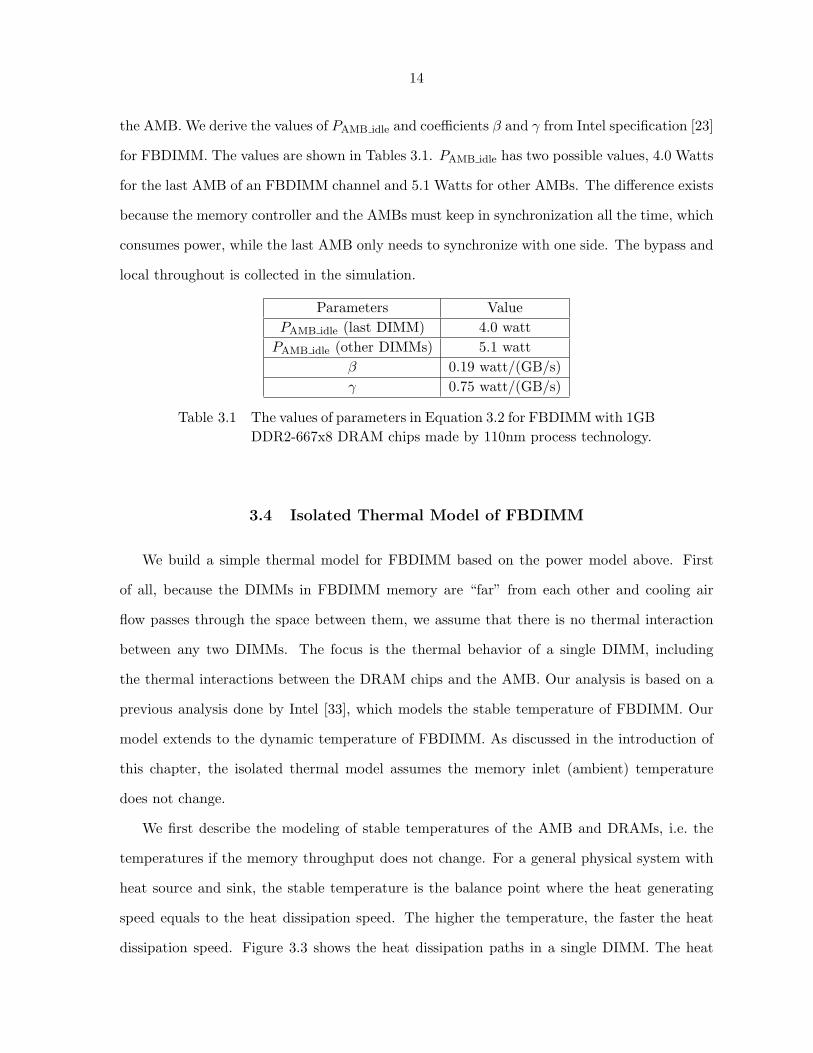
the AMB. We derive the values of PAMB idle and coefficients β and γ from Intel specification [23]
for FBDIMM. The values are shown in Tables 3.1. PAMB idle has two possible values, 4.0 Watts
for the last AMB of an FBDIMM channel and 5.1 Watts for other AMBs. The difference exists
because the memory controller and the AMBs must keep in synchronization all the time, which
consumes power, while the last AMB only needs to synchronize with one side. The bypass and
local throughout is collected in the simulation.
Parameters ValuePAMB idle (last DIMM) 4.0 watt
PAMB idle (other DIMMs) 5.1 wattβ 0.19 watt/(GB/s)γ 0.75 watt/(GB/s)
Table 3.1 The values of parameters in Equation 3.2 for FBDIMM with 1GBDDR2-667x8 DRAM chips made by 110nm process technology.
3.4 Isolated Thermal Model of FBDIMM
We build a simple thermal model for FBDIMM based on the power model above. First
of all, because the DIMMs in FBDIMM memory are “far” from each other and cooling air
flow passes through the space between them, we assume that there is no thermal interaction
between any two DIMMs. The focus is the thermal behavior of a single DIMM, including
the thermal interactions between the DRAM chips and the AMB. Our analysis is based on a
previous analysis done by Intel [33], which models the stable temperature of FBDIMM. Our
model extends to the dynamic temperature of FBDIMM. As discussed in the introduction of
this chapter, the isolated thermal model assumes the memory inlet (ambient) temperature
does not change.
We first describe the modeling of stable temperatures of the AMB and DRAMs, i.e. the
temperatures if the memory throughput does not change. For a general physical system with
heat source and sink, the stable temperature is the balance point where the heat generating
speed equals to the heat dissipation speed. The higher the temperature, the faster the heat
dissipation speed. Figure 3.3 shows the heat dissipation paths in a single DIMM. The heat

15
Figure 3.3 Heat dissipation of FBDIMM. The arrows represent heat dissipationpaths.
generated by AMB is dissipated along two paths: one to the heat spreader and then to ambient,
and another down to the raw card (DIMM board). Similarly, the heat from each DRAM chip
has these two dissipation paths, but may or may not have the heat spreader in the first path.
Thermal interactions exist among the AMB and DRAMs through the raw card.
The AMB and DRAMs have different stable temperatures3 that are affected by several
factors. First, the heat generation of the AMB and DRAM is determined by the memory
throughput. Second, the higher the velocity of the cooling air flow, the quicker the heat
dissipation from the AMB and DRAMs to the ambient. Third, the type of heat spreader can
change the distribution of heat dissipation between the two paths. There are two types of heat
spreader for FBDIMM: AMB Only Heat Spreader (AOHS) and Full DIMM Heat Spreader
(FDHS) [30]. The AOHS only contacts and covers the AMB. The FDHS covers the full length
of the DIMM including the AMB and DRAMs, providing another channel for the thermal
interactions between AMB and DRAMs. One can expect that the difference between stable
AMB temperature and the DRAM temperature of DIMMs with FDHS is smaller than that
with AOHS. Finally, the ambient temperature affects the stable temperatures: The higher the3The AMB has a higher thermal limit than the DRAMs.
16
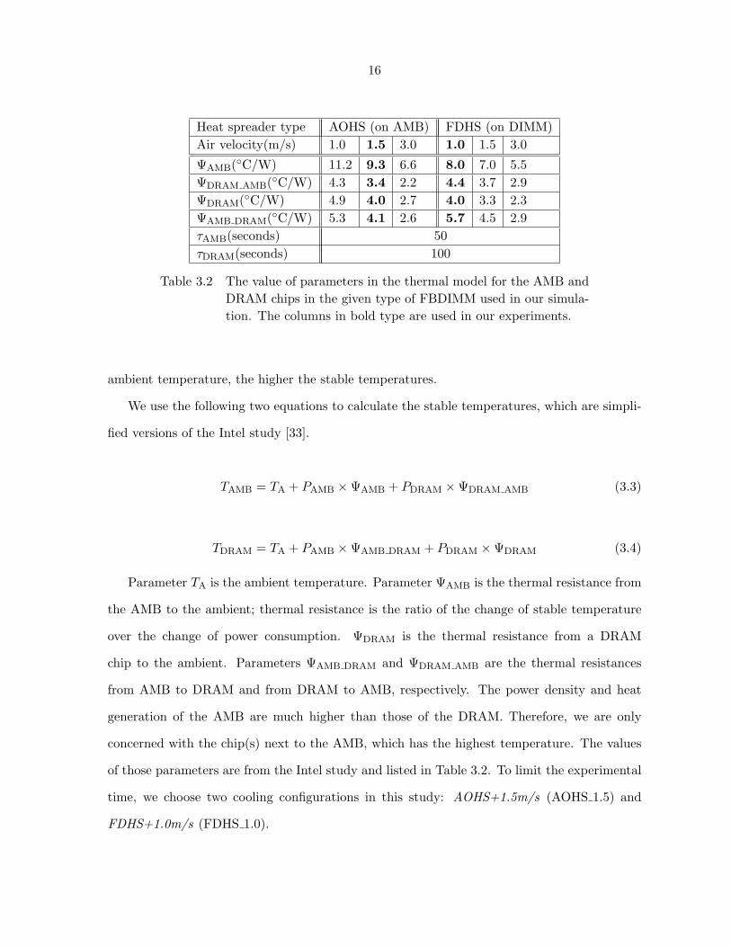
Heat spreader type AOHS (on AMB) FDHS (on DIMM)Air velocity(m/s) 1.0 1.5 3.0 1.0 1.5 3.0
ΨAMB(◦C/W) 11.2 9.3 6.6 8.0 7.0 5.5ΨDRAM AMB(◦C/W) 4.3 3.4 2.2 4.4 3.7 2.9ΨDRAM(◦C/W) 4.9 4.0 2.7 4.0 3.3 2.3ΨAMB DRAM(◦C/W) 5.3 4.1 2.6 5.7 4.5 2.9τAMB(seconds) 50τDRAM(seconds) 100
Table 3.2 The value of parameters in the thermal model for the AMB andDRAM chips in the given type of FBDIMM used in our simula-tion. The columns in bold type are used in our experiments.
ambient temperature, the higher the stable temperatures.
We use the following two equations to calculate the stable temperatures, which are simpli-
fied versions of the Intel study [33].
TAMB = TA + PAMB ×ΨAMB + PDRAM ×ΨDRAM AMB (3.3)
TDRAM = TA + PAMB ×ΨAMB DRAM + PDRAM ×ΨDRAM (3.4)
Parameter TA is the ambient temperature. Parameter ΨAMB is the thermal resistance from
the AMB to the ambient; thermal resistance is the ratio of the change of stable temperature
over the change of power consumption. ΨDRAM is the thermal resistance from a DRAM
chip to the ambient. Parameters ΨAMB DRAM and ΨDRAM AMB are the thermal resistances
from AMB to DRAM and from DRAM to AMB, respectively. The power density and heat
generation of the AMB are much higher than those of the DRAM. Therefore, we are only
concerned with the chip(s) next to the AMB, which has the highest temperature. The values
of those parameters are from the Intel study and listed in Table 3.2. To limit the experimental
time, we choose two cooling configurations in this study: AOHS+1.5m/s (AOHS 1.5) and
FDHS+1.0m/s (FDHS 1.0).

17
We now model the dynamic temperature changes with varying memory throughput in
program execution. We use the following equation to describe the dynamic temperature:
T (t +4t) = T (t) + (Tstable − T (t))(1− e−4tτ ) (3.5)
Basically, the equation treats the temperature in a thermal system like the voltage in an
electrical RC circuit. This idea has been used in previous studies [52, 54] and the formula above
is based on a classic equation for the electrical RC circuit [14]. In this equation, τ is the time for
the temperature difference to be reduced by 1/e, i.e. T (t+τ)−T (t) = (1−1/e)(Tstable−T (t)),
if the heat generation rate is a constant. We obtain the value of τ for the AMB and DRAMs
by observing their temperature changes in a physical testing environment using the same type
of FBDIMM as in our simulation environment. It is rounded to an integer number of seconds.
Because the leakage power is negligible for DRAM devices and AMBs, we do not include
the thermal-leakage feedback loop in the equation. In other words, we assume their leakage
power rate does not increase with the temperature. In an experimental testbed of FBDIMM
memory subsystem, we observed only a 2% increase of power rate as the DRAM subsystem
heated up. Additionally, the model can be adapted to other DRAMs because the power profiles
of various DRAMs are fairly consistent, across both manufacturers and generations.
3.5 Integrated Thermal Model of FBDIMM
The thermal model discussed in Section 3.4 assumes a constant memory ambient tempera-
ture. In practice, as will be discussed in Chapter 5, this assumption is not true in the systems
with strong interactions between DRAM memory and other components. In some systems,
the cooling air flow is pre-heated by processors before it passes DRAM memory. This thermal
interaction between processors and memory is a significant factor that could not be ignored.
We take a similar approach to model memory ambient temperature as we model DRAM
temperature. We use equation 3.6 to model the stable DRAM ambient temperature:
TA-stable = TInlet + ΨCPU MEM ×N−1∑i=0
(ξ × Vcore i × IPCcore i) (3.6)

18
System inlet temperature ΨCPU MEM × ξ
Isolated DRAM thermal model FDHS 1.0:45◦C; AOHS 1.5:50◦C 0.0Integrated DRAM thermal model FDHS 1.0:40◦C; AOHS 1.5:45◦C 1.5
Table 3.3 The values of parameters in the thermal model for DRAM am-bient temperature.
The equation models how processors’ heat generation affects memory ambient temperature
if the heat generation rate stays constant. Parameter TInlet is the inlet temperature of the whole
system. Vcore i is voltage supply level of the processor core i and IPCcore i is IPC (Instructions
Per Cycle) of processor i. We use (ξ × Vcore i × IPCcore i) to model the power consumption of
processor core i. The (ξ×IPC) estimates the electrical current level of the processor core. Here
the IPC is defined as number of committed instructions divided by number of reference cycles.
Although the frequencies of the processor cores are not constant with some DTM schemes, the
reference cycle time is a constant value which is the cycle time with highest possible frequency of
the processor core. ΨCPU MEM is the thermal resistance from the processors to DRAM memory.
Table 3.3 lists values of parameters in estimating DRAM memory ambient temperature. In the
isolated DRAM thermal model, the heat generated by processors does not affect the DRAM
ambient temperature. Therefore, we set ΨCPU MEM to 0.0. We set the value of ΨCPU MEM× ξ
to 1.5 based on our measurement data from real systems. To model a thermal constraint
environment, we set system inlet temperature to 45◦C for the isolated DRAM thermal model
and to 40◦C for the integrated DRAM thermal model under configuration FDHS 1.0. We set
them to 50◦C and 45◦C under configuration AOHS 1.5.
After getting the TA-stable, we use equation 3.5 to model the dynamic temperature behavior
of DRAM memory ambient temperature. The thermal RC delay τCPU DRAM(seconds) is 20
seconds in our model. The 20 seconds is an estimated value based on our experiment data on
real systems.

19
CHAPTER 4. Proposed DTM Schemes and Their Simulation Result
4.1 Introduction
Recently, simple DTM techniques have been applied in notebook computers with DDR2
memories. Two simple DTM schemes have been used so far for DRAM memories: thermal
shutdown and memory bandwidth throttling. Upon detected overheating of DRAM chips, with
thermal shutdown, the memory controller stops all memory transactions and shuts down the
DRAM chips until they are cooled down. With memory bandwidth throttling, the memory
controller lowers bandwidth to reduce DRAM activities. However, abrupt thermal shutdown
or bandwidth throttling will make the program execution fluctuate. Intuitively, the program
execution is far from optimal for a given thermal envelope: Thermal shutdown frequently stops
the memory subsystem and consequently forces the processor to stall; and simple memory
bandwidth throttling reduces the memory throughput while the processor runs at high speed.
Furthermore, the power efficiency of the whole system including the processor, power supply
and other components will not be optimal.
In this chapter, we take a new approach that controls the memory throughput by directly
controlling the source that generates memory activities – the processor, when the memory ther-
mal envelope is approached. We propose two new schemes and evaluate their effectiveness on
systems with multicore processors and Fully Buffered DIMM (FBDIMM) memories [11]. The
first scheme, Adaptive Core Gating, applies clock gating on selected processor cores according
to the DRAM thermal state. The second scheme, Coordinated DVFS (dynamic voltage and
frequency scaling), scales down the frequency and voltage levels of all processor cores, when
the memory is about to be overheated. Using the isolated DRAM thermal model discussed in
Section 3.4, our simulation results show that both schemes maintain the memory throughput

20
as high as allowed by the current thermal limit; and therefore improve the average memory
performance. Adaptive core gating further reduces L2 cache conflicts, which leads to lower
memory traffic and fewer DRAM bank conflicts. It improves the performance of multipro-
gramming workloads of SPEC2000 programs by up to 29.6% (18.5% on average) on a four-core
processor when compared with the simple thermal shutdown for a configuration used in our
study. Coordinated DVFS also reduces memory traffic slightly because the processor generates
fewer speculative memory accesses when running at a lower frequency. In addition, the proces-
sor power efficiency is improved with voltage scaling. The scheme improves performance 3.6%
on average, and may save the processor energy consumption by 36.0% on average, compared
with the simple thermal shutdown.
We further use a PID (Proportional-Integral-Differential) method based on formal control
theory to improve the efficiency of the proposed DTM schemes. It can make the system tem-
perature to converge quickly to the target temperature, and further improve the performance
of adaptive core gating by up to 33.5% (21.4% on average) and coordinated DVFS by 8.3% on
average when compared with the simple thermal shutdown.
For the systems with strong thermal interaction between processors and DRAM memory,
we use the integrated DRAM thermal model discussed in Section 3.5 to model the dynamic
temperature changes of FBDIMM. The simulation results indicate that, beside adaptive core
gating, coordinated DVFS also improves system performance significantly in these systems.
The adaptive core gating scheme improves the performance of the multiprogramming work-
loads by 9.1% on average when compared with the simple bandwidth throttling scheme for a
configuration used in our study on these systems. The coordinated DVFS has better perfor-
mance under same configurations. It improves performance by 14.6% on average. The root
cause of significant performance improvement of the coordinated DVFS scheme is that it can
reduce heat generated by processors largely. Therefore, In a system with the strong thermal
interaction, the DRAM ambient temperature is much lower when coordinated DVFS scheme
is deployed.
The rest of this chapter is organized as follows. Section 4.2 describes the existing and

21
proposed DTM schemes for DRAM main memory. Section 4.3 describes the experimental
environment. Section 4.4 and Section 4.5 present the results of our experiments.
4.2 Dynamic Thermal Management for FBDIMM Memory
In this section, we first discuss existing DTM schemes for main memory, and then describe
our DTM schemes and the use of a formal control method. All DTM schemes assume that
thermal sensors are used to monitor the DRAM temperature; and for FBDIMM, the AMBs
have already integrated thermal sensors.
4.2.1 Existing Memory DTM Schemes
In thermal shutdown, the memory controller (or the operating system) periodically reads the
temperature of DRAMs from the thermal sensors. The period may be a fraction of second. If
the temperature exceeds a preset thermal threshold, the memory controller stops all accesses to
the DRAMs. The controller keeps checking the temperature periodically and resumes DRAM
accesses when the temperature drops below the threshold by a preset margin. In bandwidth
throttling [33], multiple thermal emergency levels are used to indicate how close the DRAM
temperature is to the preset threshold. The BIOS (or the memory controller or OS) periodically
reads the temperature, evaluates the thermal emergency level, and decides a memory traffic
limit for the current period. Then, the memory controller will enforce this traffic limit. In the
rest of this paper, we refer these two schemes as DTM-TS and DTM-BW, respectively.
4.2.2 Proposed DTM Schemes
We propose adaptive core gating (DTM-ACG) and coordinated dynamic voltage and fre-
quency scaling (DTM-CDVFS) schemes. The two schemes are designed for multicore proces-
sors. Unlike DTM-TS and DTM-BW that control memory throughput locally at the memory
side, the two schemes directly control the multicore processor to affect the memory throughput.
For a processor of N cores, DTM-ACG may shut down 1 to N cores adaptively according to
the current thermal emergency level. The core shutdown is to apply clock gating, i.e. stop the
22
clock signal to the specific core. To ensure fairness among benchmarks running on different
cores, the cores can be shut down in a round-robin manner. By shutting down some cores,
memory throughput is expected to decrease and so is the DRAM and AMB heat generation
rate. DTM-CDVFS may lower the frequency and voltage levels of all cores according to the
DRAM/AMB thermal emergency level. In other words, it directly links the DRAM/AMB
thermal level to the processor frequency and voltage level. In the highest thermal emergency
level, for both DTM-ACG and DTM-CDVFS, the memory will be fully shut down. The two
schemes may be implemented in OS or memory controller.
Both schemes may make the program execution running more smoothly than DTM-TS
and DTM-BW, which shut down the memory system or reduce the bandwidth without con-
sidering the processor execution. DTM-ACG has another advantage for multicore processors
with shared L2/L3 caches: By reducing the number of active cores, it reduces L2/L3 cache
contention and therefore the total number of cache misses. Consequently, the total amount of
memory traffic will be reduced and less heat will be generated. DTM-CDVFS has another ad-
vantage of its own: It may improve the processor energy efficiency significantly by proactively
putting the processor in a power mode in coordination with the current DRAM thermal limit.
With DTM-BW, a passive DVFS policy at the processor side will not respond in a timely
manner because of the relatively long delay in power mode switch with DVFS. With DTM-
CDVFS, however, the processor power mode will be switched proactively when the change of
memory throughput limit is foreseen.
4.2.3 DTM-ACG and DTM-CDVFS Integrated with Formal Control Method
We further apply a formal control theory method called PID (Proportional-Integral-Differential)
into DTM-ACG and DTM-CDVFS schemes. The PID method has recently been used in the
processor thermal control [52, 54, 56, 57, 9]. A PID controller uses the following equation:
m(t) = Kc
(e(t) + KI
∫ t
0e(t)dt + KD
de
dt
)(4.1)
The equation has three components on the right-hand side: the proportional factor, the

23
integral factor and the differential factor. At any time t, e(t) is the difference between the
target temperature and the measured temperature; Kc, KI and KD are proportional, integral
and differential constants that are tuned for the specific system; and proper control actions will
be taken according to the controller output m(t). The control action is application-dependent;
for example, to set the processor frequency according to the range of m(t). The setting of the
ranges and the mapping of each range to a control decision are also application-dependent.
For DTM-ACG, the control action is to set the number of active processor cores. For DTM-
CDVFS, the control action is to set the processor frequency and voltage levels. We use two
PID controllers, one for the AMB thermal control and another for the DRAM thermal control.
For any given configuration that we have studied, either DRAM or AMB is always the thermal
limit during program execution. The action by the corresponding PID controller will be taken.
The advantages of using the PID formal controller in thermal control is two-fold: First, the
robust PID controller may make the temperature to converge to the target temperature within
a guaranteed time limit; and the target temperature can be set close to the thermal limit to
minimize the performance loss. Second, by taking into account of the history information in
the integral factor and the future prediction in the differential factor, the PID controller can
smooth the application running by proper control decisions from quantifying the temperature
feedback [52, 9].
4.3 Experimental Methodology
4.3.1 Two-Level Thermal Simulator
It takes a relatively long time for the AMB and DRAM to overheat, usually tens of seconds
to more than one hundred seconds1. Therefore, we need to evaluate the DRAM DTM schemes
for at least thousands of seconds. Direct cycle-accurate simulation for studying DRAM thermal
management is almost infeasible at this time length. To address this issue, we propose and
implement a two-level simulation infrastructure as shown in Figure 4.1. The first-level is
a cycle-accurate architectural simulator, which is used to build traces with performance and1By comparison, a processor may overheat in tens of milliseconds.

24
Figure 4.1 Two-level thermal simulator.
memory throughput information for all possible running combinations of workloads under each
DTM design choice. The second level simulator emulates the power and thermal behavior of
memory systems using those traces. The traces use a 10ms time window, which is sufficient
time to capture the fluctuation of temperature. DRAM temperature fluctuates slowly, up to
two degrees Celsius per second as we observed on real machines.
As for the first-level simulation, we use M5 [2] as the base architectural simulator and extend
its memory part to include a memory simulator for multi-channel FBDIMM with DDR2 DRAM
devices. The details of FBDIMM northbound and southbound links and isolated command and
data buses inside FBDIMM are simulated, and so are DRAM access scheduling and operations
at all DRAM chips and banks. Table 4.1 shows the major parameters of the pipeline, the
memory system, the DTM techniques and the DRAM operations. The outputs of the simulator
are the traces of the processor performance and memory throughput of each workload Wi under
the entire explored design space D, including varied memory bandwidth, processor running
speed and voltage level, and the number of active processor cores. The set of all traces Wi×D
is then fed into the second-level simulator for power and thermal simulation.

25
Parameters Values
Processor 4-core, 4-issue per core, 21-stage pipelineClock frequency scaling 3.2GHz at 1.55V, 2.8GHz at 1.35V,
1.6GHz at 1.15V, 0.8GHz at 0.95VFunctional units 4 IntALU, 2 IntMult, 2 FPALU, 1 FPMultROB and LSQ size ROB 196, LQ 32, SQ 32Branch predictor Hybrid, 8k global + 2K local, 16-entry RAS
4K-entry and 4-way BTB
L1 caches (per core) 64KB Inst/64KB Data, 2-way, 64B linehit latency: 1 cycle Inst/3-cycle Data
L2 cache (shared) 4MB, 8-way, 64B line, 15-cycle hit latencyMSHR entries Inst:8, Data:32, L2:64
Memory 2 logic (4 physical) channels, 4 DIMMs/physical channel8 banks/DIMM
Channel bandwidth 667MT/s (Mega Transfers/second), FBDIMM-DDR2Memory controller 64-entry buffer, 12ns overheadCooling configuration AOHS with 1.5m/s cooling air velocity
and FDHS with 1.0m/s cooling air velocityDTM parameters DTM interval 10ms, DTM control overhead 25µs
DTM control scale 25%
Major DRAM parameters (5-5-5) : active to read tRCD 15ns,read to data valid tCL 15ns, precharge to active tRP 15ns
Other DRAM parameters tRAS=39ns, tRC=54ns, tWTR=9ns, tWL=12nstWPD=36ns, tRPD=9ns, tRRD=9ns
Table 4.1 Simulator parameters.
The second-level simulator, MEMSpot, uses the power and thermal models described in
Chapter 3 to emulate the power and thermal behavior of the DRAM chips and AMBs in the
FBDIMM memory system. The memory throughput values used in the models are provided
by the first-level simulator. The values of other parameters are given in Chapter 3. The
MEMSpot simulates the change of DRAM/AMB temperatures using those parameters for the
current processor running mode, e.g. the frequency and voltage level. The temperature data
are used by the DTM component, which makes control decisions and informs the MEMSpot
any changes of processor running mode.
26
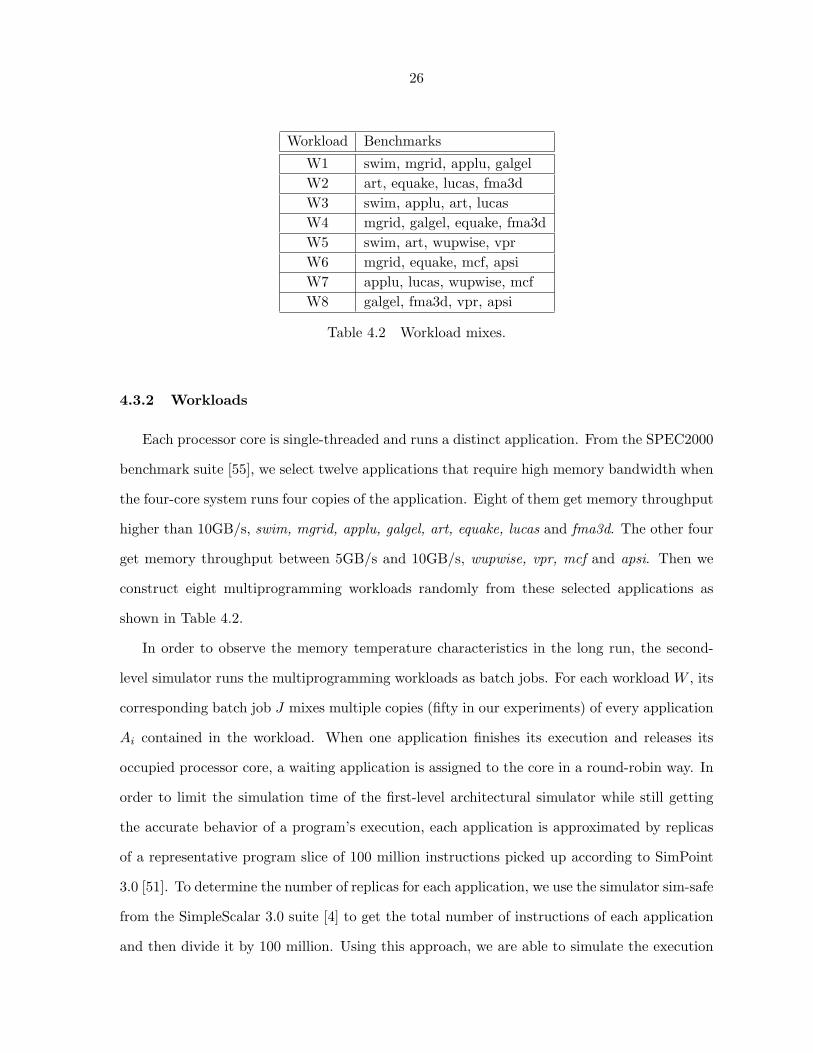
Workload Benchmarks
W1 swim, mgrid, applu, galgelW2 art, equake, lucas, fma3dW3 swim, applu, art, lucasW4 mgrid, galgel, equake, fma3dW5 swim, art, wupwise, vprW6 mgrid, equake, mcf, apsiW7 applu, lucas, wupwise, mcfW8 galgel, fma3d, vpr, apsi
Table 4.2 Workload mixes.
4.3.2 Workloads
Each processor core is single-threaded and runs a distinct application. From the SPEC2000
benchmark suite [55], we select twelve applications that require high memory bandwidth when
the four-core system runs four copies of the application. Eight of them get memory throughput
higher than 10GB/s, swim, mgrid, applu, galgel, art, equake, lucas and fma3d. The other four
get memory throughput between 5GB/s and 10GB/s, wupwise, vpr, mcf and apsi. Then we
construct eight multiprogramming workloads randomly from these selected applications as
shown in Table 4.2.
In order to observe the memory temperature characteristics in the long run, the second-
level simulator runs the multiprogramming workloads as batch jobs. For each workload W , its
corresponding batch job J mixes multiple copies (fifty in our experiments) of every application
Ai contained in the workload. When one application finishes its execution and releases its
occupied processor core, a waiting application is assigned to the core in a round-robin way. In
order to limit the simulation time of the first-level architectural simulator while still getting
the accurate behavior of a program’s execution, each application is approximated by replicas
of a representative program slice of 100 million instructions picked up according to SimPoint
3.0 [51]. To determine the number of replicas for each application, we use the simulator sim-safe
from the SimpleScalar 3.0 suite [4] to get the total number of instructions of each application
and then divide it by 100 million. Using this approach, we are able to simulate the execution

27
of a batch job with actual running time of thousands of seconds within a few days. This allows
us to balance between the simulation accuracy and time, and to explore a wide design space
of DTM schemes.
4.3.3 DTM Parameters
The thermal limits for the AMB and DRAM chips are 110◦C and 85◦C, respectively, for the
FBDIMM with 1GB DDR2-667x8 DRAM we chose in this study [23]. We define five thermal
emergency levels, L1 to L5 for the DTM schemes as shown in Table 4.3. DTM-TS keeps the
memory system turned on in states L1/L2 and keeps it shut down in state L5. As for states
L3/L4, DTM-TS shuts down the memory system when the AMB temperature ever reaches
110.0◦C and keeps it off until the temperature drops to 109.0◦C; and similarly for the DRAM
temperature. The control decisions by the DTM-BW, DTM-ACG and DTM-CDVFS schemes
are self explained in the table. The DTM scale indicates the difference between any two control
decisions next to each other.
Thermal Emergency Level L1 L2AMB Temp. Range (◦C) (-, 108.0) [108.0, 109.0) DTMDRAM Temp. Range (◦C) (-, 83.0) [83.0, 84.0) scale
DTM-TS: On/Off On 100%DTM-BW: Bandwidth No limit 19.2GB/s 25%DTM-ACG: # of Active Cores 4 3 25%DTM-CDVFS: Freq./Vol. [email protected] [email protected] 25%
Thermal Emergency Level L3 L4 L5AMB Temp. Range (◦C) [109.0, 109.5) [109.5, 110.0) [110.0,-)DRAM Temp. Range (◦C) [84.0, 84.5) [84.5, 85.0) [85.0, -)
DTM-TS: On/Off On/Off OffDTM-BW: Bandwidth 12.8GB/s 6.4GB/s OffDTM-ACG: # of Active Cores 2 1 0DTM-CDVFS: Freq./Vol. [email protected] [email protected] Stopped
Table 4.3 Thermal emergency levels and their default settings used for thechosen FBDIMM.

28
4.3.4 Parameters in PID Formal Controller
In the PID formal controller, parameters Kc, KI and KD are generally obtained by heuris-
tics and/or performance tuning. We use performance tuning and choose the following values:
Kc = 10.4, KI = 180.24, and KD = 0.001 for AMB, and Kc = 12.4, KI = 155.12 and
KD = 0.001 for DRAM. This approach is used in a previous study [52]. The PID controller’s
target temperatures of the AMB and DRAMs are 109.8 and 84.8◦C, respectively. In our FB-
DIMM configuration, the setting leads to quick settling time and guarantees that the thermal
limits will not be exceeded. To avoid the saturation effect [52, 9] created by the integral factor,
we only turn on the integral factor when the temperature exceeds a certain threshold, 109.0◦C
for the AMB and 84.0◦C for the DRAM by default; the integral factor is frozen when the con-
trol output saturates the actuator, which can effectively make the PID controller to respond
quickly to temperature changes.
4.4 Effectiveness of Memory DTM Schemes
We use the isolated DRAM thermal model described in Section 3.4 for performance, power
and energy evaluation of DTM schemes in this section.
4.4.1 Performance Impact of Thermal Release Point
With DTM-TS, when the temperature exceeds the TDP (thermal design point), thermal
management mechanisms are triggered; after the temperature drops below the TRP (thermal
release point), the mechanisms are disabled. For a given system, the choice of TRPs affects
the degree of performance loss due to thermal management. According to the FBDIMM
specification [23], the TDPs of AMB and DRAM chips are 110.0◦C and 85.0◦C, respectively,
for the FBDIMM that we choose. In this section, we will first study the performance impact
of TRPs in DTM-TS. The other schemes use more levels of thermal thresholds, and adjusting
the thresholds shows similar impact.
Figure 4.2 shows the running time of workloads using DTM-TS with different TRP values
under FDHS 1.0 (Full DIMM Heat Spreader with air velocity 1.0m/s) and AOHS 1.5 (AMB

29
(a) Performance of DTM-TS with varied DRAM TRP in the FDHS 1.0 cooling configuration
(b) Performance of DTM-TS with varied AMB TRP in the AOHS 1.5 cooling configuration
Figure 4.2 Performance of DTM-TS with varied TRP. The DRAM TDPis 85.0◦C and the AMB TDP is 110.0◦C.

30
Only Heat Spreader with air velocity 1.5m/s) configurations. For comparison, the performance
of an ideal system without any thermal limit (No-limit) is also presented. In the FDHS 1.0
configuration, the DRAMs usually enter thermal emergency before the AMBs, therefore we
only vary the DRAM TRP. In the AOHS 1.5 configuration, the AMBs usually enter thermal
emergency first, therefore we only vary the AMB TRP.
As shown in the figure, the performance loss due to thermal emergency is large. The
running time of DTM-TS is up to three times of that without thermal limit. As expected, a
higher TRP value causes smaller performance loss. For instance, compared with no thermal
limit, the execution time of workload W2 is increased by 152% when the DRAM TRP is
81.0◦C under FDHS 1.0, and the increase drops to 84% when the DRAM TRP is 84.5◦C. A
higher TRP value allows the system to stay at normal execution mode longer. In addition, the
falling speed of temperature decreases as the temperature drops since the difference between
the device and ambient temperatures is narrowing. As a result, high TRP values are desirable
for performance purpose. However, we cannot set the TRP value of a component too close
to its TDP value due to imperfect thermal sensors and delay on sensor reading. Thus, in the
rest of experiments, we set the TRP values to 109.0◦C for AMB and 84.0 for DRAM chips,
respectively (1.0◦C from their corresponding TDP values).
4.4.2 Performance Comparison of DTM Schemes
Running Time Figure 4.3 presents the running time of the DTM schemes normalized
to that of the ideal system without thermal limit. We do not present the data of DTM-TS
with PID (the formal control method) because DTM-TS has only two control decisions and
we find it does not benefit from the PID approach. The figure shows that the choice of DTM
schemes affects the performance significantly: The normalized running time ranges from 0.97
to 2.41. Notice that all DTM schemes avoid thermal risk; and shorter running time means
better performance.
The proposed DTM-ACG scheme has much better performance than DTM-TS and DTM-
BW techniques; and the proposed DTM-CDVFS scheme is moderately better than those two.
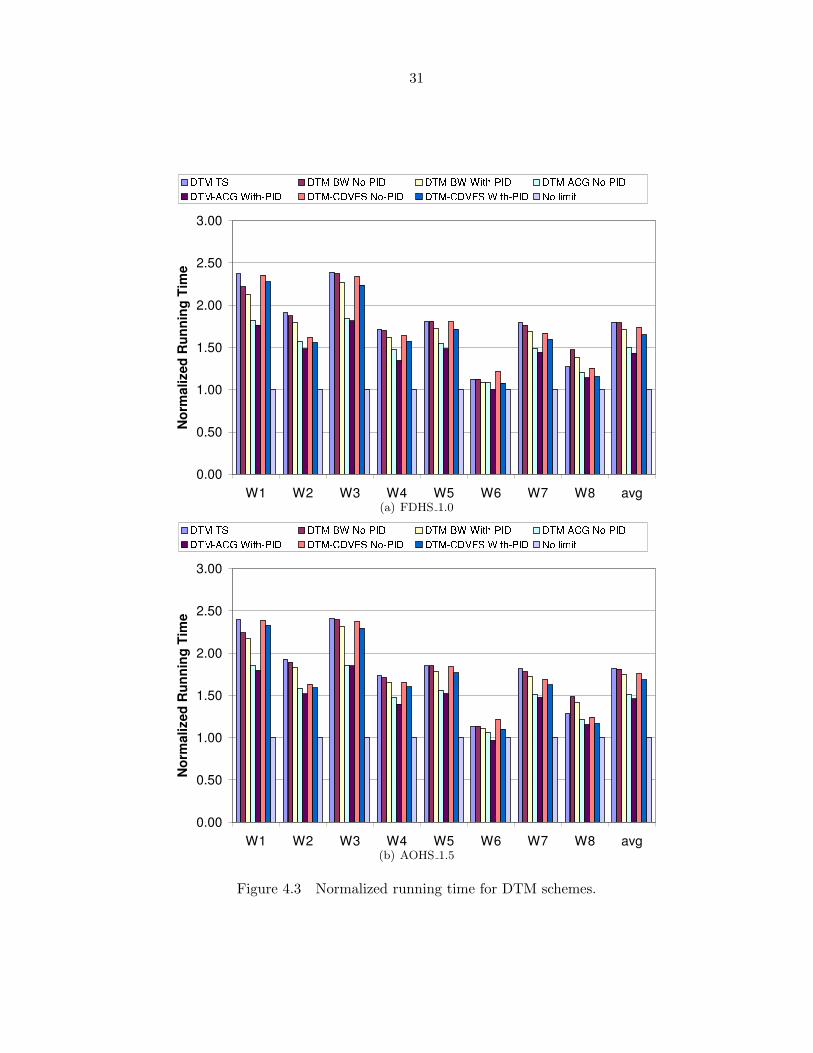
31
(a) FDHS 1.0
(b) AOHS 1.5
Figure 4.3 Normalized running time for DTM schemes.

32
The use of PID further improves the performance of DTM-ACG, DTM-CDVFS and DTM-
BW. With the AOHS 1.5 configuration, the average normalized running time of DTM-TS
and DTM-BW is 1.82 and 1.81. DTM-ACG and DTM-CDVFS improve it to 1.52 and 1.75,
respectively. The use of PID further improves it to 1.75, 1.46 and 1.68 for DTM-BW, DTM-
ACG and DTM-CDVFS schemes, respectively. The performance with the FDHS 1.0 cooling
package has a similar trend.
Under AHOS 1.5, the DTM-BW scheme has almost the same performance as DTM-TS.
Compared with DTM-TS, DTM-ACG without PID can improve performance by up to 29.6%
(for workload W1) and 18.5% on average; and DTM-CDVFS without PID can improve per-
formance by up to 18.1% (for W2) and 3.6% on average. Combined with the PID method, the
maximum performance improvement of DTM-ACG and DTM-CDVFS is 33.5% and 21.4%,
respectively; and their average performance improvement is 23.4% and 8.3%, respectively. We
will analyze the sources of performance gains in following discussion. It is worth noting that
the performance of W6 when using DTM-ACG, combined with PID, is even better than that
without thermal limit. A major reason is that the L2 cache conflicts drops when ACG is
applied (miss rate dropping from 69.0% to 64.7% under AHOS 1.5).
Sources of Improvement Next, we will analyze the sources of performance gains. We
first look into the impact of DTM techniques on the total amount of memory traffic. Figure 5.5
shows the total memory traffic of those DTM schemes normalized to that of systems without
memory thermal limit. As expected, the DTM-TS scheme does not affect the total memory
traffic. The DTM-BW scheme throttles the memory bandwidth. It decreases the total memory
traffic for workload W1; but increases the traffic for workload W8. For other workloads, its
impact on memory traffic is not significant. We find that the L2 cache miss rate of W1 drops
from 45.5% in DTM-TS to 40.6% in DTM-BW; and that of W8 increases from 25.3% in DTM-
TS to 28.8% in DTM-BW. For other workloads, the differences of L2 cache miss rates are
very small between DTM-TS and DTM-BW. We further find that the reason for the changes
of L2 cache miss rates for those two particular workloads is the change of running time for
different benchmark combinations. We leave this job scheduling issue to future work. The

33
(a) FDHS 1.0
(b) AOHS 1.5
Figure 4.4 Normalized total memory traffic for DTM schemes.

34
other workloads do not show this effect.
When the processor runs at a slower speed, it will generate fewer speculative memory
accesses. Thus, the DTM-CDVFS scheme has the potential to reduce the memory traffic. On
average, it reduces the traffic by 4.5% for both FDHS 1.5 and AOHS 1.0 configurations. The
DTM-ACG scheme is the most effective in reducing the memory traffic, since it can reduce the
amount of L2 cache conflicts when some of the processor cores are clock gated. It reduces the
traffic for every workload; and the average traffic reduction is 16.7% for FDHS 1.5 and 17.0%
for AOHS 1.0. When the control-theoretic method, PID, is applied, the total memory traffic is
slightly increased. The reason is that it attempts to let the processor run at higher frequencies
and with more active cores as long as the thermal limit is satisfied. Thus, the reduction on
memory traffic is smaller.
The traffic reduction cannot fully explain the performance gain of PID control. The use of
PID improves the overall performance with a slight increase of the memory traffic. In order to
show other sources of performance improvement, in Figures 4.5 to 4.8, we present temperature
curves of those DTM schemes for workload W0 under configuration AOHS 1.5 as predicted by
the thermal model. Because the AMB, instead of DRAM chips, is expected to have thermal
emergency under this configuration, only the AMB temperature is presented. The workload
W1 contains four benchmarks demanding high memory bandwidth. The data show the AMB
temperature changes during the first 1000 seconds of execution in one-second interval.
As expected, as shown in the Figures 4.5, the AMB temperature swings between 109.0
and 110.0◦C with DTM-TS, which is exactly defined by the scheme and thermal triggers.
For DTM-BW without PID, the temperature swings around 109.5◦C. This means that the
memory bandwidth is throttled between 6.4GB/s and 12.8GB/s. We can see from Figure 4.6
that one advantage of DTM-BW is that the AMB temperature is very stable and predictable.
Thus, using this scheme, the temperature thresholds can be set very close to the thermal
limit. When combined with the PID controller, the DTM-BW scheme makes the temperature
to stick around 109.8◦C. A higher stable temperature without violating thermal limit means
that the system can stay at the normal execution mode longer, and thus can achieve better

35
Figure 4.5 AMB temperature changes of DTM-TS for W1 with AOHS 1.5.
performance. For the three schemes, DTM-BW, DTM-ACG and DTM-CDVFS, combining
with the PID method allows the AMB temperature to stay at a higher level than without PID.
This is one of the reasons that the PID method can further improve performance for those
DTM schemes.
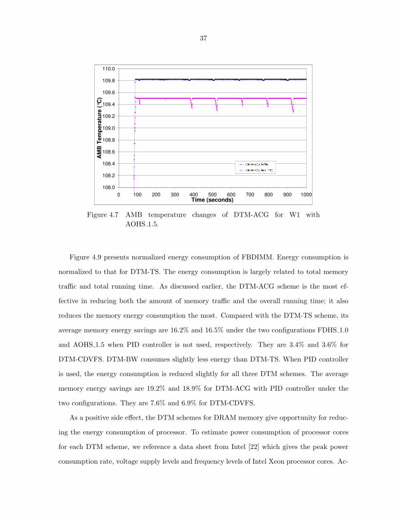
Figure 4.7 shows temperature temperature curves of DTM-ACG. For DTM-ACG without
PID, most of time, the AMB temperature stays around 109.5◦C and only one or two cores are
active. The spikes of the curve indicate that during those periods, even with two active cores,
the stable temperature is lower than 109.5◦C. Thus, more cores could have been enabled. As
shown in the figure, the use of PID eliminates almost all spikes. Additionally, we find from
the simulation data (not shown here) that three or four cores are active during those periods.
This is one of the reasons that the PID controller can improve performance.
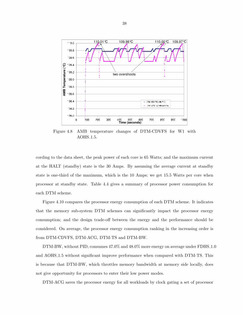
Figure 4.8 shows temperature curves of DTM-CDVFS. For DTM-CDVFS without PID,
most of time, the temperature swings between 109.5 and 110.0◦C. Thus, its average tempera-
ture is higher than others. This is another source of performance gain for DTM-CDVFS. From
the figure, we can see that the temperature reaches 110.0◦C twice during the 1000 seconds pe-

36
Figure 4.6 AMB temperature changes of DTM-BW for W1 withAOHS 1.5.
riod. Under such emergent cases, the memory is shut down until the AMB temperature drops
below 109.0◦C. The reach of the highest thermal emergency level (overshoot in the figure) is
a potential thermal risk, which are eliminated by employing the PID controller. When DTM-
CDVFS is combined with PID, the temperature sticks around 109.8◦C and never overshoots.
This allows us to set the target temperature of PID controller as high as 109.8◦C. Without the
PID controller, we must set the threshold lower to avoid overshooting. As mentioned earlier,
the ability to stay at higher average temperature is another source of performance gains for
the PID method.
4.4.3 Impact on Energy Consumption
As expected, DTM schemes for memory systems also affect their energy consumption.
The energy consumption is related to the total memory traffic and running time. Other
DTM schemes only change the memory energy consumption slightly. Our experiments do not
consider the use of DRAM low power mode because of the memory access intensity of the
selected workloads.
37
Figure 4.7 AMB temperature changes of DTM-ACG for W1 withAOHS 1.5.
Figure 4.9 presents normalized energy consumption of FBDIMM. Energy consumption is
normalized to that for DTM-TS. The energy consumption is largely related to total memory
traffic and total running time. As discussed earlier, the DTM-ACG scheme is the most ef-
fective in reducing both the amount of memory traffic and the overall running time; it also
reduces the memory energy consumption the most. Compared with the DTM-TS scheme, its
average memory energy savings are 16.2% and 16.5% under the two configurations FDHS 1.0
and AOHS 1.5 when PID controller is not used, respectively. They are 3.4% and 3.6% for
DTM-CDVFS. DTM-BW consumes slightly less energy than DTM-TS. When PID controller
is used, the energy consumption is reduced slightly for all three DTM schemes. The average
memory energy savings are 19.2% and 18.9% for DTM-ACG with PID controller under the
two configurations. They are 7.6% and 6.9% for DTM-CDVFS.
As a positive side effect, the DTM schemes for DRAM memory give opportunity for reduc-
ing the energy consumption of processor. To estimate power consumption of processor cores
for each DTM scheme, we reference a data sheet from Intel [22] which gives the peak power
consumption rate, voltage supply levels and frequency levels of Intel Xeon processor cores. Ac-
38
Figure 4.8 AMB temperature changes of DTM-CDVFS for W1 withAOHS 1.5.
cording to the data sheet, the peak power of each core is 65 Watts; and the maximum current
at the HALT (standby) state is the 30 Amps. By assuming the average current at standby
state is one-third of the maximum, which is the 10 Amps; we get 15.5 Watts per core when
processor at standby state. Table 4.4 gives a summary of processor power consumption for
each DTM scheme.
Figure 4.10 compares the processor energy consumption of each DTM scheme. It indicates
that the memory sub-system DTM schemes can significantly impact the processor energy
consumption; and the design trade-off between the energy and the performance should be
considered. On average, the processor energy consumption ranking in the increasing order is
from DTM-CDVFS, DTM-ACG, DTM-TS and DTM-BW.
DTM-BW, without PID, consumes 47.0% and 48.0% more energy on average under FDHS 1.0
and AOHS 1.5 without significant improve performance when compared with DTM-TS. This
is because that DTM-BW, which throttles memory bandwidth at memory side locally, does
not give opportunity for processors to enter their low power modes.
DTM-ACG saves the processor energy for all workloads by clock gating a set of processor

39
(a) FDHS 1.0
(b) AOHS 1.5
Figure 4.9 Normalized energy consumption of FBDIMM for DTM schemes.

40
(a) FDHS 1.0
(b) AOHS 1.5
Figure 4.10 Normalized energy consumption of processors for DTMschemes.

41
DTM-TS DTM-BW# active core Power (Watt) bandwidth(GB/s) Power (Watt)0 62 0 62- - 6.4 260- - 12.8 260- - 19.6 2604 260 25.6 260
DTM-ACG DTM-CDVFS# active core Power (Watt) DVFS setting(V,GHz) Power (Watt)0 62 (-,0) 621 111.5 (0.95,0.8) 80.62 161 (1.15,1.6) 116.53 210.5 (1.35,2.8) 193.44 260 (1.55,3.2) 260
Table 4.4 Processor power consumption of DTM schemes.
cores to handle DRAM thermal emergency. The average energy savings are 22.4% and 22.9%
for FDHS 1.0 and AOHS 1.5 without PID; Although the PID helps DTM-ACG improve the
performance by 4.2% and 4.5% for configuration FDHS 1.0 and AOHS 1.5, it increases energy
consumption under both configurations and for all workloads.
DTM-CDVFS achieves the highest energy savings, which are 36.0% and 42.0%, without PID
under the two configurations FDHS 1.0 and AOHS 1.5, respectively, compared with DTM-TS.
All workloads have energy savings without performance degradation. The maximum energy
saving of DTM-CDVFS without PID for AOHS 1.0 is 60.0% by W8, which improves per-
formance by 3.3% when compared with DTM-TS without PID. Although PID can further
improve the performance, it consumes more energy in general; for example, it needs 2.0%
and 7.0% more energy compared with DTM-TS without PID on average for FDHS 1.0 and
AOHS 1.5 respectively. This is because the scheme with PID makes the processor run with
high voltage and frequency level most of the time to achieve high performance. As the power
is proportional to the multiple of the square of the voltage supply level and the frequency
level, and the performance is nearly linear with the frequency, one can significantly reduce the

42
energy consumption by setting the processor cores at lower frequency and voltage supply level.
For example by W8 under AOHS 1.5, DTM-CDVFS without PID has 95.2% of its running
time at (1.6GHz,1.15V). In comparison, DTM-CDVFS with PID only has 31.7% of its running
time at (1.6GHz,1.15V); and has 21.1%, 47.1% of its running time at (2.8GHz,1.35V) and
(3.2GHz,1.55V), respectively. Because the total running time is only decreased by 6.7% with
the help of PID, processor energy consumption by DTM-CDVFS with PID is about the two
times of that without PID.
4.4.4 DTM Interval
In a previous analysis, we use 10ms as the DTM interval. Figure 4.11 shows normalized
average running time for different DTM intervals: 1ms, 10ms, 20ms and 100ms. The running
time is normalized to that when the DTM interval is 10ms.
In general, a shorter DTM interval allows the thermal emergency to be handled in a more
timely manner, especially when there is a danger of overshoot; while a longer interval has a
lower DTM overhead. We have done experiments on four DTM intervals: 1ms, 10ms, 20ms and
100ms. For all DTM schemes, the running time variance of these four different DTM intervals
is within 4.0%. Since we assume that each DTM period has 25µs overhead, which accounts
for 2.5% of the overhead for the DTM interval of 1ms, using this short interval causes longer
running time than others. The variance of running time of the other three DTM intervals is
within 2.0%. Based on these results, we believe 10ms is a good design choice for the DTM
interval for our system setup.
4.5 Impact of Thermal Interaction between Processors and DRAM
Memory
We use the integrated DRAM thermal model described in Section 3.5 to study the perfor-
mance impact of thermal interaction between processors and DRAM memory.

43
(a) FDHS 1.0
(b) AOHS 1.5
Figure 4.11 Normalized average running time for different DTM intervals.

44
(a) FDHS 1.0
(b) AOHS 1.5
Figure 4.12 Normalized running time for DTM schemes.

45
4.5.1 Performance Comparison
Figure 4.12 presents the normalized running time of the DTM schemes with the integrated
DRAM thermal model. The running time is normalized to that of the ideal system without
thermal limit.
The performance results from the integrated thermal model share many perspectives with
those from the isolated thermal mode. First, as shown in the figure, the performance loss due
to thermal emergency is large. The running time of DTM-TS is increased by up to 152% of
that without thermal limit. Second, the DTM-BW scheme has almost the same performance
as DTM-TS under two configurations FDHS 1.0 and AOHS 1.5. Third, DTM-ACG has much
better performance than DTM-TS and DTM-BW. With the AOHS 1.5 configuration, the
average normalized running time of DTM-TS and DTM-BW is 1.79 and 1.78. DTM-ACG
improves it to 1.64. The average normalized running time of DTM-TS, DTM-BW, and DTM-
ACG is 1.80, 1.80 and 1.62 with FDHS 1.0 configurations, respectively.
We have a surprise finding with the performance of DTM-CDVFS from the integrated
thermal model: It has better performance than DTM-ACG. DTM-CDVFS further improves
the average normalized running time to 1.56 and 1.59 under two configurations FDHS 1.0 and
AOHS 1.5, respectively. In Section 4.4, we show that DTM-CDVFS only has a small per-
formance improvement when compared with DTM-BW and DTM-TS. The large performance
improvement of DTM-CDVFS is related to thermal interaction between processors and DRAM
memory. We do not see a large performance gain for DTM-CDVFS in Section 4.4 because the
isolated DRAM thermal model does not take this interaction into consideration. As the in-
tegrated DRAM thermal model is inspired by our case study on real systems which will be
discussed in Chapter 5, we defer the detailed discussion of this interaction to that Chapter.
4.5.2 Sensitivity Analysis of Thermal Interaction Parameter
The performance shown in Section 4.5.1 uses the default thermal interaction parameters dis-
cussed in Section 3.5. The default value of thermal interaction degree parameter ΨCPU MEM×ξ
is set to 1.5 to model moderate thermal interaction between the processors and the DRAM
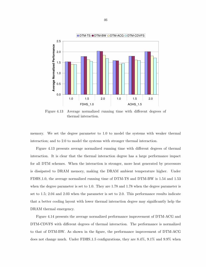
46
Figure 4.13 Average normalized running time with different degrees ofthermal interaction.
memory. We set the degree parameter to 1.0 to model the systems with weaker thermal
interaction; and to 2.0 to model the systems with stronger thermal interaction.
Figure 4.13 presents average normalized running time with different degrees of thermal
interaction. It is clear that the thermal interaction degree has a large performance impact
for all DTM schemes. When the interaction is stronger, more heat generated by processors
is dissipated to DRAM memory, making the DRAM ambient temperature higher. Under
FDHS 1.0, the average normalized running time of DTM-TS and DTM-BW is 1.54 and 1.53
when the degree parameter is set to 1.0. They are 1.78 and 1.78 when the degree parameter is
set to 1.5; 2.04 and 2.03 when the parameter is set to 2.0. This performance results indicate
that a better cooling layout with lower thermal interaction degree may significantly help the
DRAM thermal emergency.
Figure 4.14 presents the average normalized performance improvement of DTM-ACG and
DTM-CDVFS with different degrees of thermal interaction. The performance is normalized
to that of DTM-BW. As shown in the figure, the performance improvement of DTM-ACG
does not change much. Under FDHS 1.5 configurations, they are 8.4%, 9.1% and 9.9% when

47
Figure 4.14 Average normalized performance improvement of DTM-ACGand DTM-CDVFS with different degrees of thermal interac-tion, compared with DTM-BW.
the degree parameter is set to 1.0, 1.5 and 2.0, respectively. The performance improvement
of DTM-CDVFS is increased when the interaction is stronger. The performance improvement
is 8.8%, 14.6% and 19.6%, respectively. This is expected because DTM-CDVFS schemes can
significantly reduce processor energy consumption. Therefore, compared with other DTM
schemes, DTM-CDVFS is more effective when the thermal interaction is stronger.

48
CHAPTER 5. A Case Study of Memory Thermal Management for
Multicore Systems
5.1 Introduction
The simulation approach described in Chapter 4 has several limitations. First, the DRAM
thermal model used for the evaluation of different thermal management mechanisms has not
been validated on real systems. Given the dependency between the accuracy of the thermal
model and power/performance benefits, we think it is necessary to confirm results presented in
Chapter 4 by implementing and evaluating the proposed DTM schemes on real server systems.
Second, due to inherent limitations of running long workload traces in a simulator, the design
space and parameters of the proposed thermal models were not full explored and adequately
analyzed.
To address these issues, we evaluate the existing memory DTM schemes on real systems and
further explore their design space in this study. Unlike the previous work which used a hybrid of
execution- and trace-driven simulation, our study uses measurements on real systems running
multiprogramming workloads. We implement these schemes in a Linux OS and evaluate their
performance and power benefits on two production servers configured with latest generation
hardware. To obtain an accurate picture of the power and performance benefits of mechanisms
evaluated in this paper, we instrumented the SR1500AL with power and thermal sensors to
get fine-grain measurements at a component level.
To the best of our knowledge, this is the first study of software thermal management for
memory subsystem on real machines. We have done comprehensive experiments and detailed
analyses. Our experiments first confirm that the two recently proposed schemes significantly
improve performance in real server systems. In addition, we have encouraging findings that

49
address the limitations of the previous work discussed above:
• Compared with the simple DTM-BW (DTM through memory Bandwidth Throttling)
method, the DTM-ACG (DTM through Adaptive Core Gating) scheme [31] improves
performance by up to 19.5% and 17.9% on an PowerEdge 1950 server and an Intel
SR1500AL server testbed, respectively; and 11.7% and 6.7% on average, respectively.
We call the two machines PE1950 and SR1500AL thereafter. The improvements of
DTM-CDVFS (DTM through Coordinated Dynamic Voltage and Frequency Scaling) are
up to 15.3% and 19.3%, and 9.7% and 13.2% on average on the two servers, respectively.
• The performance gain of the DTM-CDVFS scheme measured on real systems is much
better than the previously reported simulation result, which is only 3.4% on average.
Besides the expected performance difference due to different configurations of the real
systems and the simulated one, our analysis indicates that the CPU heat dissipation and
its influence on DRAM, which were ignored in the previous study, is a significant factor
in DRAM thermal modeling.
• We have also found that the DTM-CDVFS scheme improves the system power efficiency
in addition to the performance gains. It reduces the processor power rate by 15.5% on
the SR1500AL. The energy consumed by the processor and DRAM to complete each
workload is reduced by 22.7% on average.
• We further propose a new scheme, called DTM-COMB, that combines DTM-ACG and
DTM-CDVFS. It may stop a subset of cores and apply DVFS to the others. Our exper-
imental results show that the new scheme may further improve the performance by up
to 5.4%.
The rest of this chapter is organized as follows. Section 5.2 discusses our design and
implementation of the DRAM DTM schemes on real systems. Section 5.3 describes the exper-
imental methodology and workloads. Section 5.4 analyzes the experimental results and finally
Section 5.5 summarizes this chapter.

50
Figure 5.1 Thermal Zone.
5.2 Design and Implementation Issues
In general, a DTM scheme can be divided two interdependent parts, mechanism and policy:
The mechanism enforces the DTM decisions made by the policy and also provides inputs to
it; the policy decides when and what thermal actions to trigger.
5.2.1 Memory DTM Mechanisms
A memory DTM mechanism should generally consist of three components: a memory
temperature monitor or estimator, a DTM policy trigger, and an approach to controlling
memory temperature. We have designed and implemented mechanisms to support four policies:
DTM-BW, DTM-ACG, DTM-CDVFS, and DTM-COMB on two Linux servers with Intel Xeon
5160 processors. The DTM mechanism is an integration of hardware/software components that
provide required functions to support the DTM policy.
Temperature Monitoring Normally, a memory DTM scheme makes thermal manage-
ment decisions based on the current (and sometimes also past or predicted future) memory
temperature. The temperature can be either measured if thermal sensors are available or
modeled otherwise. On both servers that we have used in experiments, a thermal sensor is

51
embedded into the AMB of each FBDIMM. Thus, the memory temperature can be directly
measured and used for DTM decisions. The temperature sensor reading of AMB temperature
is reported to the memory controller every 1344 bus cycles [22]. The result can be obtained
by reading a set of registers of a PCI device (Intel Corporation 5000 Series Chipset Error
Reporting Registers). Every register of the PCI device stores the most recent temperature
sensor reading of its corresponding DIMM. On the SR1500AL, there are multiple temperature
sensors which can measure the front panel temperature (system ambient), CPU inlet temper-
ature, CPU exhaust temperature (memory inlet temperature), memory exhaust temperature
and system exhaust temperature. All data from these sensors can be collected by a daughter
card on the mother board, and further be read by the system driver.
Policy Trigger A DTM policy needs to periodically check whether a memory emergency
occurs and invoke thermal control approaches if necessary. We implement the DTM policy as a
monitoring program, which is periodically awakened by the OS scheduler. The default interval
is one second in our experiments. Since the DRAM subsystem may approach the TDP in
a relatively long time, roughly a few hundred seconds from idle temperature, a one-second
interval is short enough for the thermal management. It is also long enough to avoid any
visible overhead. We have found that the overhead is virtually non-existent. An alternative
design is to implement the policy in a kernel module invoked by a periodical time interrupt,
but it does not really make a difference in system efficiency.
Memory Thermal Control Approaches Upon a detected memory emergency, some
approaches need to be invoked to lower the memory temperature. Since the temperature is
closely related to memory activities, normally this is achieved by lowering the memory access
frequency. We have used three approaches that either control memory activities from the
memory side or the processor side. First, Bandwidth Throttling is done by setting a traffic
cap for any given time window. Both servers use the Intel 5000X chipset. It provides an
“open loop” mechanism for memory access throttling, which allows a programmer to limit
the memory throughput by capping the number of memory row activations in a given time
52
window [22]. The default window size is 21504K bus cycles, which is 66ms with 333MHz bus
frequency (667MT for DDR2 DRAM). The DTM-BW policy uses this function to throttle
memory throughput, and the other three policies use it to avoid overheating in the worst case.
Second, Core Gating is done by employing an efficient cpu hot plug/remove module of Linux
kernel (version 2.6.20). If a CPU is disabled, it is logically removed from the OS. The overhead
is virtually non-existent with one-second interval. When a DTM policy decides to shut down
a core, the core can be disabled (unplugged from the OS) by writing a “0” to a system file
(e.g. /sys/devices/system/cpu/cpu1/online for the second core on the first processor). The
core can be re-enabled later by writing a “1” to the same file. At the architectural level, a
“halt” instruction is executed to stop a core. It is worth noting that the first core of the first
processor cannot be disabled. Finally, Voltage and Frequency Scaling to scale the frequency
and voltage supply of processor cores. is done by enabling the CPUfreq module of the Linux
kernel. The frequency of a processor core can be set by writing to the frequency in KHz
to a system file. For example, writing “2667000” to /sys/devices/system/cpu/cpu2/cpufreq-
/scaling setspeed will set the frequency of the first core of the second processor to 2.667 GHz.
The Xeon 5160 processors can run at four frequencies: 3.000, 2.667, 2.333, and 2.000 GHz.
The voltage supply of the processor core is automatically scaled with the frequencies to 1.2125,
1.1625, 1.1000 and 1.0375 V, respectively.
5.2.2 Memory DTM Polices
Thermal Emergency Level and Running Level The general approach in our DTM
policy design is to quantize memory temperature into thermal emergency levels, and then
determine the system thermal running level accordingly. This approach has been used in
Intel chipset 5000X [22]. In fact, our DTM-BW implementation is similar to the closed-loop
bandwidth throttling of the chipset. In general, a thermal running level with better system
performance also generates more heat. Every time a policy module is executed, it reads the
temperature sensors, determines the thermal emergency level, and then decides the thermal
running level for the next time interval. If the new running level is different from the current

53
PE1950
Thermal Emergency Level L1 L2 L3 L4AMB Temp. Range (◦C) (-, 76.0) [76.0, 80.0) [80.0, 84.0) [84.0 88.0)
Thermal Running Level L1 L2 L3 L4DTM-BW: Bandwidth No limit 4.0GB/s 3.0GB/s 2.0GB/sDTM-ACG: # of Active Cores 4 3 2 2DTM-CDVFS: Frequency 3.00GHz 2.67GHz 2.33GHz 2.00GHzDTM-COMB:: # of Cores@Freq. [email protected] [email protected] [email protected] [email protected]
SR1500AL
Thermal Emergency Level L1 L2 L3 L4AMB Temp. Range (◦C) (-, 86.0) [86.0, 90.0) [90.0, 94.0) [94.0 98.0)
Thermal Running Level L1 L2 L3 L4DTM-BW: Bandwidth No limit 5.0GB/s 4.0GB/s 3.0GB/sDTM-ACG: # of Active Cores 4 3 2 2DTM-CDVFS: Frequency 3.00GHz 2.67GHz 2.33GHz 2.00GHzDTM-COMB:: # of Cores@Freq. [email protected] [email protected] [email protected] [email protected]
Table 5.1 Thermal emergency levels and thermal running states.
one, a thermal action will be taken to change the system running state.
Table 5.1 describes the settings of the thermal emergency levels and the thermal running
levels for the two servers. It is worth noting that the number of the emergency levels and
that of the running levels do not have to equal. For example, there could be more than four
running levels if the two processors are quad-core. Also, it is only a coincidence that DTM-
ACG and DTM-CDVFS have the same number of running levels. The Intel SR1500AL is
put into a hot box and the system ambient temperature is set to 36◦C, which emulates a
typical server environment. For safety concern, we use a more conservative thermal design
point (TDP) of 100◦C for AMB on the Intel SR1500AL. We set the highest thermal emergency
level to [94, 98) with a margin of two degrees to the TDP. Other emergency levels are set by
stepping down four degrees every level. The PE1950 is located as a stand alone box in an air-
conditioned room with a system ambient temperature of 26◦C. The memory temperature has
reached 96◦C when running memory-intensive workloads. To emulate its thermal behaviors

54
in a server environment, we use an artificial AMB thermal design point of 90◦C, and then set
the thermal emergency levels similar to the SR1500AL. Also for safety concern, the chipset’s
open-loop bandwidth throttling is enabled for all policies at the highest thermal emergency
level to ensure that overheating will not happen.
DTM-BW Policy This policy only performs bandwidth throttling. It resembles the
bandwidth throttling in Intel chipset 5000X [22]; and we use it as a reference to evaluate
other DTM policies. It uses the bandwidth limiting function to cap the bandwidth usage
according to the current thermal emergency level. Setting the limit to 2GB/s on the PE1950
will guarantee that the memory will not overheat; and so does using the 3GB/s limit on
the SR1500AL. As Table 5.1 describes, four thermal running states are used. The limits are
enforced in the chipset by limiting the number of memory row activations in a time window.
Because the close page mode is used, bandwidth usage is mostly proportional to the number of
memory row activations. The default window of 66ms is used, which is suggested by the chipset
designers. Every time the policy module is executed, it reads the current AMB temperatures
and determines the thermal emergency level as discussed before.
DTM-ACG Policy This policy mainly uses core gating to indirectly throttle memory
traffic. Its rationale is that when a subset of cores is disabled, the cache contention from
simultaneous program execution will be reduced. Consequently, the memory traffic will be
reduced and the performance may be improved. As Table 5.1 shows, four running levels are
used. The servers has two dual-core processors. We retain at least one core active for each
processor to utilize its L2 cache. Therefore, both level three and level four have two running
cores. The difference is that at level four, memory throttling is also enabled, whose limit is
2GB/s on the PE1950 and 3GB/s on the SR1500AL. When one core of a processor is disabled,
the two programs will use the other core and the L2 cache alternatively. We found that the
default execution switch interval of 100ms is large enough to avoid cache thrashing, and small
enough to ensure fairness and smoothness.

55
DTM-CDVFS Policy This policy uses processor DVFS to indirectly throttle memory
traffic. The main reason for performance improvement, as will be shown in Section 5.4, is
the reduced processor heat generation and the heat dissipation to the memory. Consequently,
the memory subsystem may run at high speed for a longer time than normally allowed. Four
running levels are used in our experiments, because the processors support four frequency and
voltage levels. The current DTM-CDVFS does not differentiate the processor cores. All four
cores are scaled to the same level simultaneously. A differentiating policy is worth further
investigation and we leave it as our future work.
DTM-COMB Policy This policy combines the strength of DTM-ACG and DTM-
CDVFS. Our design uses four thermal running levels by changing the number of running
cores as well as scaling the processor frequency. By doing so, this policy may reduce memory
traffic as well as reduce processor heat dissipation to memory. As in DTM-ACG, at least one
core per processor is used to utilize the L2 caches.
Other Design Choices and Discussions Our implementations of DTM-ACG and
DTM-CDVFS are based on those in a previous study [31]. We have refined the thermal
running levels of DTM-ACG, which was designed for a single multicore processor. We have
also combined the use of chipset bandwidth throttling into DTM-ACG and DTM-CDVFS to
avoid worst-case overheating. Furthermore, we have proposed a new policy, DTM-COMB, to
combine the strength of DTM-ACG and DTM-CDVFS.
We did not fully explore the design space of DTM-ACG, DTM-CDVFS and DTM-COMB.
In fact, they can be extended in many ways; for example, by using temperature change history
as input, using more complex state machine, or considering program behaviors in memory
accesses. Our focus in this paper is to evaluate sophisticated memory DTM policies like
DTM-ACG and DTM-CDVFS and compare them with simple designs like DTM-BW on real
systems.

56
5.3 Experimental Methodology
5.3.1 Hardware and Software Platforms
We conducted our experiments on two machines. Both machines use FBDIMM and the
memory hot spots are AMBs, therefore we are only concerned with AMB temperatures there-
after. (The hot spots can be DRAM devices.) The first one, PE1950, is a Dell PowerEdge
1950 1U server put into an air-conditioned room as a stand alone system. It has an Intel
5000X chipset and two dual-core, 3.0GHz Intel Xeon 5160 processors. Each has a shared,
4MB, 16-way set associative L2 cache; and each core of the processor has a private 32KB
instruction cache and a private 32KB data cache. The machine has two 2GB 667MT Fully
Buffered DIMM (FBDIMM) as the main memory. The second machine is an Intel SR1500AL
machine which is instrumented for thermal and power study. It has almost the same configu-
ration as the PE1950 except that it has four 2GB 667MT FBDIMM. On the SR1500AL, we
are able to measure the power consumption of FBDIMM and processors and processor exhaust
temperature, which is also the memory ambient temperature on this system. It also has a hot
box as its enclosure, which allows us to control the system ambient temperature. We use the
two different machines to crosscheck our experiment results, and the SR1500AL allows us to
evaluate power and energy savings.
Figure 5.2 shows a system diagram of the SR1500AL server. We instrumented the Intel
SR1500AL with sensors that measure the voltage, current and temperature of different system
components. The analog signals from the power and thermal sensors are routed to a custom
designed daughter card that hosts an array of A/D converters and associated low pass filters.
The daughter card is shown in figure 5.3. The data from the A/D converters is sampled by a
micro-controller that stores all the digital sensor data in a local buffer. The daughter card is
connected to the host system through a LPC (low pin count) bus. We have implemented a user
space application that accesses the daughter card using Linux LPC driver. The application
reads sensor data periodically and stores it to a log file. In all experiments in this paper we used
a sampling rate of 10 milliseconds. This sampling is sufficient given AMB thermal constants
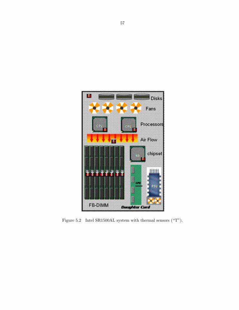
57
Figure 5.2 Intel SR1500AL system with thermal sensors (“T”).

58
Figure 5.3 The daughter card.
and time scales of thermal management mechanisms evaluated in our studies. We have done
an extensive evaluation to calibrate the sensors and ensure that the sampling application does
not introduce any overhead or artifacts into our measurements. We have run benchmarks and
synthetic workloads with and without our sampling application and have never observed any
measurable impact on their performance or system power consumption.
The two machines use the Red Hat Enterprise Linux 4.0 with kernel 2.6.20.3. Performance
data are collected by pfmon using perfmon kernel interface and libpfm library [16]. We enable
the CPU hot plug/remove functionality of the kernel to support the active core gating. Three
types of performance statistics are collected using hardware counters: numbers of retired uops,
L2 cache accesses, and L2 cache misses. The statistics are collected by three architecture
performance counters: INSTRUCTIONS RETIRES, LAST LEVEL CACHE REFERENCES
and LAST LEVEL CACHE MISSES. We use the per-thread mode of pfmon to collect statistics
for each benchmark. As discussed in Section 5.2, for DTM-ACG, when one core on a dual-core
processor is shut down, two programs will share the remaining core in a round-robin fashion.
The time slice for the sharing is 100ms by default Linux kernel. We also perform a sensitivity
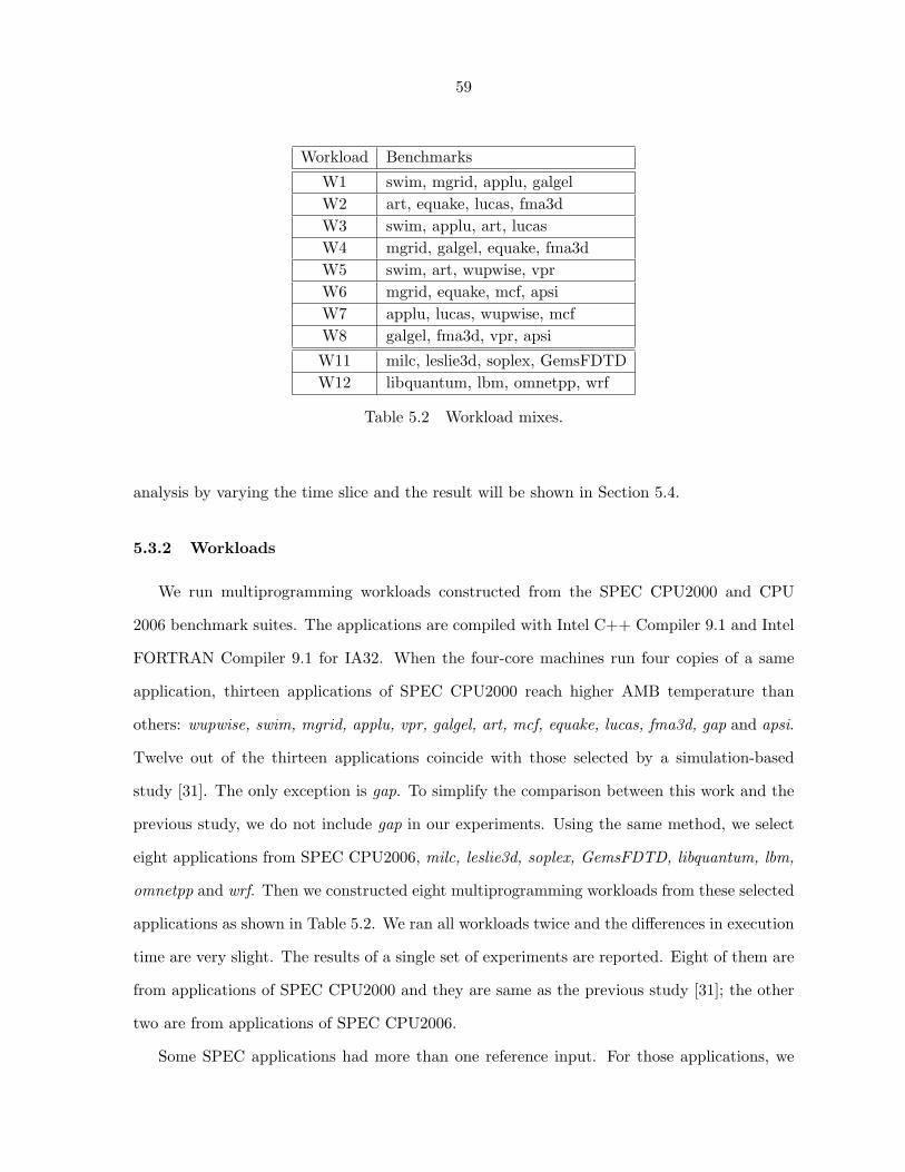
59
Workload Benchmarks
W1 swim, mgrid, applu, galgelW2 art, equake, lucas, fma3dW3 swim, applu, art, lucasW4 mgrid, galgel, equake, fma3dW5 swim, art, wupwise, vprW6 mgrid, equake, mcf, apsiW7 applu, lucas, wupwise, mcfW8 galgel, fma3d, vpr, apsi
W11 milc, leslie3d, soplex, GemsFDTDW12 libquantum, lbm, omnetpp, wrf
Table 5.2 Workload mixes.
analysis by varying the time slice and the result will be shown in Section 5.4.
5.3.2 Workloads
We run multiprogramming workloads constructed from the SPEC CPU2000 and CPU
2006 benchmark suites. The applications are compiled with Intel C++ Compiler 9.1 and Intel
FORTRAN Compiler 9.1 for IA32. When the four-core machines run four copies of a same
application, thirteen applications of SPEC CPU2000 reach higher AMB temperature than
others: wupwise, swim, mgrid, applu, vpr, galgel, art, mcf, equake, lucas, fma3d, gap and apsi.
Twelve out of the thirteen applications coincide with those selected by a simulation-based
study [31]. The only exception is gap. To simplify the comparison between this work and the
previous study, we do not include gap in our experiments. Using the same method, we select
eight applications from SPEC CPU2006, milc, leslie3d, soplex, GemsFDTD, libquantum, lbm,
omnetpp and wrf. Then we constructed eight multiprogramming workloads from these selected
applications as shown in Table 5.2. We ran all workloads twice and the differences in execution
time are very slight. The results of a single set of experiments are reported. Eight of them are
from applications of SPEC CPU2000 and they are same as the previous study [31]; the other
two are from applications of SPEC CPU2006.
Some SPEC applications had more than one reference input. For those applications, we

60
run all inputs and count them as a single run. In order to observe the long-term memory
temperature characteristics, We run the multiprogramming workloads as batch jobs. For each
workload, its corresponding batch job mixes ten runs (ten for workloads from SPEC CPU2000
and five for workloads from CPU2006) of every application contained in the workload. When
one program finishes its execution and releases its occupied processor, a waiting program is
assigned to the processor in a round-robin way. It is worth noting that, at the end of the batch
job, there is small fraction of time when less than four applications are running simultaneously.
We observed that the fraction was less than 5% of the total execution time on average.
We do not study DTM-TS (Thermal Shutdown) in this work for the following reasons. First,
DTM-TS is a special case of DTM-BW. Second, it abruptly shuts down the whole system and
makes system not run smoothly. Finally, from the previous simulation-based study, it has
similar performance as DTM-BW. Regarding DTM period, it was set to one second by default
in this study.
5.4 Results and Analysis
In this section, we first briefly describe the DRAM thermal emergency observed on the
servers. We then present the performance results of the four DTM policies, analyze the sources
of performance gain, discuss the results of power saving and finally study the sensitivity of
parameter selections. It is worth noting that the SR1500AL is an experimental platform in a
controlled environment. The reported high temperatures will not appear in a product machine
with normal operating conditions.
5.4.1 Experimental Observation of DRAM Thermal Emergency
First of all, we present our observation of AMB temperature changes on the two server
systems. Figure 5.4 shows the AMB temperature changing curves on the the SR1500AL when
it runs homogeneous workloads described as follows. The machine has open-loop bandwidth
throttling enabled by default in the chipset. We disable this function for AMB temperature
below 100◦. During the close-to-overheating periods (>100◦C), the function is enabled to limit

61
Figure 5.4 AMB temperature curve for first 500 seconds of execution.
the memory bandwidth under 3GB/s for safety concerns. We run four copies of each program
on the four cores (on two processors) simultaneously. For each program, we run a job batch
with twenty copies in total to observe the AMB temperature changes and report the results of
the first five hundred seconds. The data are collected every one second. The server has four
DIMMs and the highest AMB temperature among the four DIMMs is shown (most of the time
the third DIMM has the highest AMB temperature).
Temperature changes of five selected programs are reported in the figure. Among them,
swim and mgrid are memory intensive, and the other three are moderately memory inten-
sive. Initially the machine is idle for a sufficiently long time for the AMB temperature to
stabilize (at about 81◦C). As it shows, with swim and mgrid the temperature will reach 100◦
in about 150 seconds. Then it fluctuates around 100◦C because of the bandwidth throttling
for machine safety. We have similar observations for other memory intensive programs (not
shown). The other three programs, namely galgel, apsi and vpr, are less memory intensive.
Their temperatures rises in similar curves and then the temperature change patterns stabilize
under 100◦C.
Figure 5.5 shows the average AMB temperatures of the PE1950 when it runs the same

62
homogeneous workloads. Unlike Figure 5.4, Figure 5.5 does not show memory overheating;
instead, it shows how overheating would have happened for those workloads if the ambient
temperature is high enough and no DTM is used. The PE1950 is put in a room with good air
conditioning. It also comes with a much stronger fan than that on the SR1500AL. Therefore, we
are able to run memory-intensive workloads without having the system overheating the AMB
(or the DRAM). It is worth noting that we use this server as a stand alone system. If many
of such servers are packed into a rack, the ambient temperature of each server will be much
higher, and therefore the TDP may be reached. Additionally, the server currently includes
only two DIMMs. If eight DIMMs were used, as we observed on the SR1500AL, the AMB
temperature would be significantly higher than reported. As for experimental details, only
the AMB temperature of the first DIMM is shown because it always has a higher temperature
than others. The temperature sensors have noises which appear as high spikes in temperature
readings (which is visible in Figure 5.4), therefore we exclude 0.5% sampling points with the
highest temperatures to remove those spikes.
Figure 5.5 AMB temperature when memory is driven by homogeneousworkloads on the PE1950 without DTM control.
We have the following observations. First, average AMB temperature varies significantly
across those homogeneous workloads. Ten programs have average an AMB temperature higher
than 80◦C: wupwise, swim, mgrid, applu, art, mcf, equake, facerec, lucas and fma3d. As shown
in the previous study [31] and confirmed in our experiments using performance counters, these
ten programs have high L2 miss rates. Consequently, they have higher memory bandwidth uti-

63
lization, higher memory power consumption and therefore higher AMB temperatures than the
other workloads. Four programs, namely galgel, gap, bzip2 and apsi, have moderate memory
bandwidth utilization and their average AMB temperatures range between 70◦C and 80◦C.
The other twelve programs have small memory bandwidth utilization and their AMB temper-
atures are below 70◦C. Second, there are big gaps between the average and the highest AMB
temperatures. We have found the main reason is that it takes a relatively long initial time,
around two hundred seconds, for AMB to reach a stable temperature. Additionally, for some
workloads, the AMB temperatures keep changing due to the program phase changes in their
lifespan.
5.4.2 Performance Comparison of DTM Polices
Figure 5.6 compares the performance of the four DTM policies and a baseline execution
with no memory thermal limit on the two servers. As discussed in Section 5.3, on the PE1950,
we use an artificial TDP of 90◦C to reveal the impact of memory thermal limit. The no-
limit experiments are done without enforcing that artificial TDP. On the SR1500AL, we are
able to control the ambient temperature, so we run the no-limit experiments with an ambient
temperature of 26◦C and run the other experiments with an ambient temperature of 36◦C. We
disable the built-in bandwidth throttling feature of the chipset in the no-limit experiments.
We have the following observations for workloads from SPEC CPU2000. First of all, the re-
sults confirm that the use of simple bandwidth throttling (DTM-BW) may severely downgrade
the system performance. On average, the performance degradation is 18.5% on the PE1950
and 59.3% on the SR1500AL. Our detailed statistics show that there is a strong correlation
between the memory bandwidth utilization and the performance degradation. For example,
all workloads except W5 and W8 have a larger than 50% slowdown with DTM-BW, while
the slowdowns for W5 and W8 are 42.3% and 11.3%, respectively, on the SR1500AL. The
performance counter data show that W8 has 17.3 L2 cache misses per microsecond, which is
the lowest among the eight workloads. This means it is less memory-intensive than others.
Second, the results also confirm that DTM-ACG may significantly improve performance

64
(a) Dell PE1950
(b) Intel SR1500AL
Figure 5.6 Normalized running time of SPEC CPU2000 workloads.
65
over DTM-BW. On average, DTM-ACG improves the performance of CPU2000 workloads
by 11.7% on the PE1950 and 6.7% on the SR1500AL. The maximum improvement is 19.5%
and 17.9%, respectively. In comparison, the previous simulation-based study [31] reports an
average improvement of 16.3% using the same workloads. The main source of improvement
comes from the reduction on L2 cache misses, which will be detailed in Section 5.4.3. As for
the difference in the results from the two servers, several factors may contribute to it, including
the differences in cooling package, memory bandwidth, ambient temperature, and the layout
of the processors and DIMMs on motherboard. We also observe performance degradation of
DTM-ACG over DTM-BW on workload W8, which is 7.4% on the PE1950 and 23.2% on the
SR1500AL, respectively. This scenario was not reported in the previous study. As to be shown
in Figure 5.8, DTM-ACG actually reduces the L2 cache misses of W8 by 6.4% on the PE1950
and 7.4% on the SR1500AL. We believe that for this workload the DTM-ACG policy may stop
processor cores too proactively. This is not a fundamental problem of the policy, but indicates
that the policy may be further refined for certain types of workloads.
Regarding DTM-CDVFS, we have surprising findings that are very different from the
simulation-based study (with isolated DRAM thermal model). On average, DTM-CDVFS may
improve performance over DTM-BW by 9.7% on the PE1950 and 13.2% on the SR1500AL.
By contrast, the previous study only reports 3.4% average improvement. It is also remark-
able that the scheme improves the performance of every program on SR1500AL, ranging from
5.4% to 19.3%. On PE1950, the maximum improvement is 15.3% and only W8 has a small
performance degradation of 1.1%. The main reason behind the performance improvements, as
to be discussed in details in Section 5.4.3, is related to the thermal interaction between the
processors and the memory. The previous study did not consider the heat dissipation from
the processor to the memory. As the results indicate, that factor should be significant in the
DRAM thermal modeling and cannot be ignored. In fact, the performance improvement is
larger on the SR1500AL than on the PE1950 because on its motherboard the processors are
physically closer to the DIMMs. We will present more experimental results from the SR1500AL
to support this finding.

66
Figure 5.7 Normalized running time of SPEC CPU2006 workloads onPE1950.
We have also run two workloads from SPEC CPU2006 on PE1950, W11 with applications
milc, leslie3d, soplex and GemsFDTD, and W12 with libquantum, lbm, omnetpp and wrf. As
shown in the Figure 5.7, the findings for workloads from CPU2000 still hold for them. DTM-
BW degrades the performance by 21.4% and 25.4% for W11 and W12 when compared with no-
limit, respectively. DTM-ACG improves performance by 7.0% and 12.6% when compared with
DTM-BW, respectively. DTM-CDVFS has better performance for both workloads, improving
performance by 14.4% and 15.1% over DTM-BW on the two servers, respectively.
The performance of DTM-COMB is very close to that of DTM-ACG on average on both
machines. On average for SPEC CPU2000 workloads, the performance of DTM-COMB is
degraded by 0.1% on PE1950 and improved by 1.4% on SR1500AL, compared with DTM-ACG.
The DTM-COMB may improve performance up to 5.4% (for W12 from SPEC CPU2006). It
is remarkable that DTM-COMB can improve performance for W2, W3 and W7 on PE1950,
when compared with no-limit. This is possible because we observe that for some programs,
the L2 cache miss rate decreases sharply when running alone as shown later in Section 5.4.3.

67
(a) Dell PE1950
(b) Intel SR1500AL
Figure 5.8 Normalized numbers of L2 cache misses.

68
5.4.3 Analysis of Performance Improvements by Different DTM Policies
In this section, we analyze the sources of performance improvements by DTM-ACG, DTM-
CDVFS and DTM-COMB when compared with DTM-BW.
Reduction of L2 Cache Misses It has been reported in the previous study [31] that
the improvement by DTM-ACG is mostly from the reduction of memory traffic, which is from
the reduction of L2 cache misses: When the shared L2 cache is used by fewer programs, cache
contention is reduced and thus there will be fewer cache misses. The previous study collects
memory traffic data to demonstrate the correlation. On our platform, we can only collect the
number of L2 cache misses. The total memory traffic consists of cache refills from on-demand
cache misses, cache writebacks, memory prefetches, speculative memory accesses, and other
sources including cache coherence traffic. Nevertheless, cache refills are the majority part of
memory traffic, therefore the number of L2 cache misses is a good indication of memory traffic.
Figure 5.8 shows the normalized number of L2 cache misses on both machines. We have
several observations from the data. First, The number of L2 cache misses changes very slightly
by using DTM-BW when compared with no-limit. This is expected because the number
of on-demand L2 cache misses should have virtually no change when memory bandwidth is
throttled. Second, the total number of L2 cache misses does decrease significantly by DTM-
ACG, compared with that of DTM-BW. The reduction is up to 35.2% and 40.7% on the PE1950
and the SR1500AL, respectively. The average reduction are 26.8% and 29.3%, respectively.
The result confirms the finding of the previous study that DTM-ACG reduces L2 cache misses
significantly. On the other hand, DTM-CDVFS does not cause any visible changes of the
total number of L2 cache misses, while the previous study reported memory traffic may be
reduced due to the reduction of speculative memory accesses. The difference is likely related
to differences in the processor models, particularly how many outstanding memory accesses
are allowed and whether a speculative memory instruction is allowed to trigger an access to
the main memory. The DTM-COMB has very similar L2 cache miss reduction as DTM-ACG.
The average reductions are 24.8% and 30.1% on the PE1950 and the SR1500AL, respectively.

69
We find there is a correlation between performance improvements and the reduction of
number of L2 cache misses. The correlation value is 0.956 on PowerEdge 1950 and 0.926 on
SR1500AL. (the correlation value ranges from -1 to 1, The closer the coefficient is to either .1
or 1, the stronger the correlation between the variables.
Reduction of Memory Ambient Temperature by DTM-CDVFS As discussed
earlier, the performance of DTM-CDVFS is comparable to that of DTM-ACG. In fact, it is
visibly better than DTM-ACG on the SR1500AL. This is a surprising finding: The previous
study reports that DTM-CDVFS has only a slight performance advantage over DTM-BW;
and the main benefit of DTM-CDVFS is improved system power efficiency. We investigate
the processor heat generation and its impact on the memory DIMMs, which was ignored in
the thermal modeling of the previous study. If the processor is physically close enough to the
DIMMs, then the heat dissipation from the processor may further increase the DIMM ambient
temperature. Consequently, the DIMMs may overheat more frequently than predicted by
the thermal model in the previous study. Since DTM-CDVFS improves the processor power
efficiency, it may reduce the heat generation from the processor and therefore alleviate the
problem, which will improve memory bandwidth utilization. If that is a significant factor,
then the observed performance improvement can be explained.
To confirm the above theory, we looked into the inside of each machine. On both machines
the processors and the DIMMs share the same set of cooling fans, and the air flow to the
DIMMs will first pass the processors. The processor and DIMMs are slightly misaligned along
the cooling air flow on the PE1950. On the SR1500AL, one of the two processors is aligned
with the DIMMs along the cooling air flow and the close distance between the processors and
the DIMMs is about 5cm on the SR1500AL.
We further collect the temperature readings through a sensor put in the air path between
the processors and the DIMMs inside the SR1500AL. Such a sensor is not available on PE1950.
Figure 5.9 compares the average temperature of the four DTM schemes. The system ambient
temperature of the SR1500AL is set to 36◦C. As the figure shows, the cooling air is heated
up by the processors by about 10◦C. The processor exhaust (memory inlet) temperature is

70
Figure 5.9 Measured memory inlet temperature.
visibly lower with DTM-CDVFS or DTM-COMB than with DTM-BW or DTM-ACG for
workloads W1 to W6. Workloads W7 and W8 are exceptions: For W7 the temperature is
slightly higher with DTM-CDVFS than with the other schemes; and for W8 it is between
DTM-BW and DTM-ACG. On average, the temperature is 46.9◦C, 46.7◦C, 45.9◦C and 45.8%
with DTM-BW, DTM-ACG, DTM-CDVFS and DTM-COMB, respectively. The data shows
a strong correlation between the memory inlet temperature difference and the performance
improvement of DTM-CDVFS over DTM-BW.
5.4.4 Comparison of Power and Energy Consumption
On the SR1500AL we are able to measure the power consumption of individual system
components including the processors, DIMMs, system fans and other components.
Power Consumption of Processors and DIMMs We are only interested in the power
consumption of the processors and DIMMs because for our workloads the power consumption
of the other components is almost constant. The processors consume slightly more than a third
of the system power; and the DIMMs consume slightly less power than the processor power.

71
Figure 5.10 CPU power consumption.
In our experiments, we also found that the power consumption of the DIMMs is very close for
all workloads except workload W8, which is less memory intensive than the others. Part of
the reason is that static power is a large component of FBDIMM power. Therefore, we only
compare the processor power consumption.
Figure 5.10 shows the average power consumption with different DTM policies. The data
are normalized to those of DTM-BW. As expected, DTM-CDVFS and DTM-COMB consume
less processor power than the other two policies. On average, the processor power consump-
tion of DTM-CDVFS and DTM-COMB is 15.5% and 13.2% lower than that of DTM-BW,
respectively. There is a very small difference between the power consumption by DTM-BW
and DTM-ACG. This is mainly due to the fact that latest generation processors are very en-
ergy efficient. They apply extensive clock gating to idle functional blocks when processors
are stalled by the long-latency memory accesses. Thus, for memory-intensive workloads with
frequent last level cache misses, most functional components in the processor core have already
been clock-gated yielding little additional benefit from gating the entire core.
It’s important to point out that the workload W8 has a different behavior than the other
7 workloads. Compared with DTM-BW, DTM-ACG on W8 has 22.5% lower CPU power
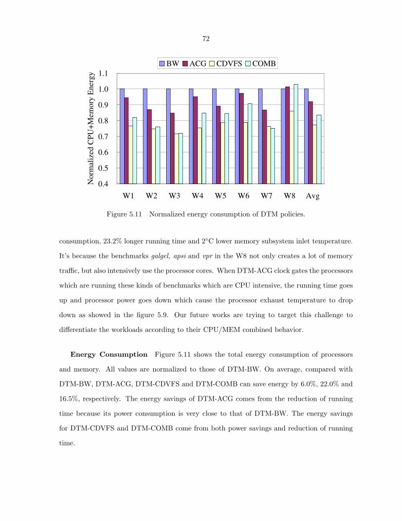
72
Figure 5.11 Normalized energy consumption of DTM policies.
consumption, 23.2% longer running time and 2◦C lower memory subsystem inlet temperature.
It’s because the benchmarks galgel, apsi and vpr in the W8 not only creates a lot of memory
traffic, but also intensively use the processor cores. When DTM-ACG clock gates the processors
which are running these kinds of benchmarks which are CPU intensive, the running time goes
up and processor power goes down which cause the processor exhaust temperature to drop
down as showed in the figure 5.9. Our future works are trying to target this challenge to
differentiate the workloads according to their CPU/MEM combined behavior.
Energy Consumption Figure 5.11 shows the total energy consumption of processors
and memory. All values are normalized to those of DTM-BW. On average, compared with
DTM-BW, DTM-ACG, DTM-CDVFS and DTM-COMB can save energy by 6.0%, 22.0% and
16.5%, respectively. The energy savings of DTM-ACG comes from the reduction of running
time because its power consumption is very close to that of DTM-BW. The energy savings
for DTM-CDVFS and DTM-COMB come from both power savings and reduction of running
time.

73
Figure 5.12 Normalized running time on Intel SR1500AL at a room systemambient temperature (26◦C).
5.4.5 Sensitivity Analysis of DTM Parameters
Ambient Temperature The performance of DTM policies shown in Section 5.4.2 on
the SR1500AL is from the experiments with a system ambient temperature of 36◦C and an
AMB TDP of 100◦C. We have also run experiments on SR1500AL with a lower system ambient
temperature of 26◦C and with an artificial AMB TDP of 90◦C. This setting is the same as
that used on the PE1950, and has the same gap (64◦C) between the ambient temperature and
the TDP temperature as the first set of experiments on the SR1500AL. The experiment has
two purposes. First, by keeping the temperature gap the same while changing the ambient
temperature, the new result will help us understand how the ambient temperature affects
performance. Second, because the performance improvements are different on the two servers,
the new result may reveal whether the difference is related to their differences in ambient
temperatures.
Figure 5.12 compares the performance of four policies on SR1500AL in the new setting. It
indicates that the performance is very similar to that on the same machine with higher system
ambient temperature of 36◦C. On average, DTM-BW degrades performance by 60.6% over

74
no-limit. The degradation is 59.3% with the higher ambient temperature. On average, DTM-
ACG and DTM-CDVFS improve performance by 7.5% and 14.1% over DTM-BW, respectively.
The improvements are 6.7% and 13.2% with an ambient temperature of 36◦C, respectively.
The performance comparison regarding individual workload is similar with the two ambient
temperatures. The similarity indicates that the performance of DTM schemes is more related to
the gap between the ambient temperature and AMB TDP than the ambient temperature itself.
The performance difference on the two machines with the same ambient temperature indicates
that the performance difference as shown in Figure 5.6 is more related to machine configurations
(including motherboard layout and cooling package) than the ambient temperature.
Processor Frequency In previous experiments, we ran processor cores at full speed (3.0
GHz) for DTM-BW and DTM-ACG. We also want to see what happens if a lower processor
speed (2.0 GHz) is used. Figure 5.13 compares the performance with two processor speeds for
DTM-BW and DTM-ACG on the SR1500AL. First, On average, the performance with the
lower processor speed is degraded by 3.0% and 6.7% compared with that with the higher speed
for DTM-BW and DTM-ACG, respectively. We find that the less memory-intensive workload
W8 has larger performance degradation than others. This is expected since the performance
of compute-intensive workloads is more sensitive to processor frequency. Isci et al. also present
that the performance degradation is small for memory-intensive workloads with low frequency
mode [25]. If W8 is excluded, the performance degradation is only 2.1% and 0.9% for DTM-BW
and DTM-ACG, respectively. Second, DTM-ACG improves performance similarly under both
modes. On average, the performance improvement is 3.4% with the lower processor speed and
is 6.7% with the higher speed, respectively. When W8 is excluded, the average performance
improvement is 7.8% and 11.0%, respectively.
DTM TDP and Thermal Emergency Levels Figure 5.14 shows the normalized run-
ning time averaged on all workloads on PE1950 when the thermal design point (TDP) of AMB
changes. The thermal emergency levels also change with the AMB TDPs, following the ratio-
nales discussed in Section 5.2. The performance of three AMB TDPs is shown: 88◦C, 90◦C

75
Figure 5.13 Comparison of performance between DTM-ACG and DT-M-BW under two different processor frequencies on IntelSR1500AL.
and 92◦C. As expected, the performance loss is reduced with higher TDPs. Compared with
that of no-limit, the performance of DTM-BW is degraded by 23.8%, 18.5% and 14.0% with
AMB TDPs of 88◦C, 90◦C and 92◦C, respectively. The performance improvement by three
policies over DTM-BW is similar under different AMB TDPs. The performance improvement
by DTM-ACG is 11.7%, 12.2% and 11.4$, respectively. They are 8.0%, 9.7% and 9.7% by
DTM-CDVFS and 12.4%, 11.6% and 10.7% by DTM-COMB, respectively. The similarity in-
dicates that the three policies may work equally well in future systems with different thermal
constraints.
Switching Frequency in Linux Scheduling for DTM-ACG In DTM-ACG, two
programs may share a processor core when another core is disabled. The switching frequency
between the execution of two programs is determined by the base time quantum of the pro-
grams. It is calculated based on the default time slice, static priority and dynamic priority of
the programs. We set the static priority the same for all programs and observe that the dy-
namic priority does not change for all programs. Therefore, the execution switching frequency
is determined by the default time slice that is a constant value defined in the Linux kernel.

76
Figure 5.14 Normalized running time averaged for all workloads on PE1950with different AMB TDPs.
The default time slice is set to 100ms in the kernel.
Figure 5.15 compares the normalized running time and number of L2 cache misses averaged
for all workloads on PE1950 with different base time quantum settings. The running time
and number of L2 cache misses are normalized to those with default time quantum for each
workload. The results show that the average normalized running time does not have visible
changes when the base time quantum is longer than 20ms. When it is set to a value shorter
than 20ms, both running time and number L2 cache misses increase steadily. The average
running time is increased by 4.2% and 7.2% when the base time quantum is set to 10ms
and 5ms, respectively. We find that the major reason for the performance degradation is the
increase on L2 cache misses. The average number of L2 cache misses is increased by 7.6%
and 12.0%, respectively. This indicates that to avoid cache thrashing with DTM-ACG, the
default time slice cannot be shorter than 20ms for the processors with 4MB L2 cache used in
our experiments.

77
Figure 5.15 Normalized running time and number of L2 cache misses av-eraged for all workloads on PE1950 with different switchingfrequencies.
5.5 Conclusion
We have performed a case study of dynamic thermal management (DTM) of memory
subsystems on multicore systems with Linux OS. Through extensive experiments, we have
demonstrated that two system-level policies, adaptive core gating and coordinated DVFS,
yield significant performance improvements and/or power savings. Our analyses show that the
thermal impact of the processor on memory should be a significant factor in memory thermal
modeling and management. We have also proposed a new policy that combines the strength
of those two policies, and further identified several directions to improving those policies.

78
CHAPTER 6. Conclusion and Future Work
Thermal issues are becoming critically important for DRAM memory subsystems. To study
these issues, we have developed an integrated thermal model and a detailed simulator for fully
buffered DIMM (FBDIMM) memory subsystems designed for multi-core processors. We have
also proposed and implemented two new and efficient DTM (dynamic thermal management)
schemes for DRAM-based memory subsystems. As shown in this thesis, with careful designs,
the proposed schemes significantly reduce the performance penalty caused by the DRAM ther-
mal constraint.
Future work on DTM scheme evaluation and design can be conducted in several directions.
First, beside the multiprogramming workloads used in this thesis, we can validate the proposed
schemes using parallel workloads as well. Second, we can study coordinated schemes that con-
sider both the processor and memory power and thermal requirements. Third, we can study
shared cache-aware OS job scheduling to reduce total memory traffic and DRAM heat gener-
ation. Fourth, we can extend our DRAM thermal model for fully buffered DIMM (FBDIMM)
to other types of memory subsystems, such as DDR2 and DDR3 DRAM memory. Last, we can
integrate our two-level DRAM simulator with existing processor and disk simulator to study
system level power and thermal issues.

79
BIBLIOGRAPHY
[1] Advanced Micro Devices. AMD Multi-Core G3MX DRAM Interface Details Emerge.
[2] N. L. Binkert, R. G. Dreslinski, L. R. Hsu, K. T. Lim, A. G. Saidi, and S. K. Reinhardt. The M5
simulator: Modeling networked systems. IEEE Micro, 2006.
[3] D. Brooks and M. Martonosi. Dynamic thermal management for high-performance microproces-
sors. In Proceedings of the 7th International Symposium on High-Performance Computer Archi-
tecture, 2001.
[4] D. C. Burger and T. M. Austin. The simplescalar tool set, version 2.0. Technical Report CS-TR-
1997-1342, University of Wisconsin, Madison, 1997.
[5] J. Carter, W. Hsieh, L. Stoller, M. Swansony, L. Zhang, E. Brunvand, A. Davis, C.-C. Kuo,
R. Kuramkote, M. Parker, L. Schaelicke, and T. Tateyama. Impulse: Building a smarter memory
controller. In Proceedings of the Fifth International Symposium on High-Performance Computer
Architecture, 1999.
[6] J. Choi, Y. Kim, and A. Sivasubramaniam. Modeling and managing thermal profiles of rack-
mounted servers with thermostat. In Proceedins of the 13th International Symposium on High-
Performance Computer Architecture, 2007.
[7] V. Cuppu and B. Jacob. Concurrency, latency, or system overhead: Which has the largest impact
on uniprocessor DRAM-system performance? In Proceedings of the 28th Annual International
Symposium on Computer Architecture, 2001.
[8] V. Delaluz, M. T. Kandemir, N. Vijaykrishnan, A. Sivasubramaniam, and M. J. Irwin. DRAM
energy management using software and hardware directed power mode control. In Proceedins of
the 7th International Symposium on High-Performance Computer Architecture, 2001.
[9] J. Donald and M. Martonosi. Techniques for multicore thermal management: Classification and
new exploration. In Proceedings of the 33rd International Symposium on Computer Architecture,
2006.
[10] X. Fan, C. Ellis, and A. Lebeck. Memory controller policies for DRAM power management. In
Proceedings of the 2001 International Symposium on Low Power Electronics and Design, 2001.

80
[11] B. Ganesh, A. Jaleel, D. Wang, and B. Jacob. Fully-buffered DIMM memory architectures: Under-
standing mechanisms, overheads and scaling. In Proceedings of the 13th International Symposium
on High Performance Computer Architecture, 2007.
[12] S. Gurumurthi, A. Sivasubramaniam, and V. K. Natarajan. Disk drive roadmap from the thermal
perspective: A case for dynamic thermal management. In Proceedings of the 32nd International
Symposium on Computer Architecture, 2005.
[13] J. Haas and P. Vogt. Fully-Buffered DIMM technology moves enterprise platforms to the next
level. http://www.intel.com/technology/magazine/computing/fully-buffered-dimm-0305.
pdf, 2005.
[14] A. R. Hambley. Electrical engineering: Principles and applications, pages 143–147. Prentice-Hall,
Inc., 2nd edition, 2002.
[15] T. Heath, A. P. Centeno, P. George, L. Ramos, Y. Jaluria, and R. Bianchini. Mercury and Freon:
temperature emulation and management for server systems. In Proceedings of the 12th inter-
national conference on Architectural support for programming languages and operating systems,
2006.
[16] Hewlett-Packed Development Company. Perfmon project. http://www.hpl.hp.com/research/
linux/perfmon.
[17] S. I. Hong, S. A. McKee, M. H. Salinas, R. H. Klenke, J. H. Aylor, and W. A. Wulf. Access order
and effective bandwidth for streams on a Direct Rambus memory. In Proceedings of the Fifth
International Symposium on High-Performance Computer Architecture, 1999.
[18] H. Huang, P. Pillai, and K. G. Shin. Design and implementation of power-aware virtual memory.
In USENIX Annual Technical Conference, General Track, 2003.
[19] I. Hur and C. Lin. Adaptive history-based memory schedulers. In Proceedings of the 37th Annual
International Symposium on Microarchitecture, 2004.
[20] IBM Corp. EDO DRAM 4M x 16 Part No. IBM0165165PT3C.
[21] IBM Corp. SDRAM 1M x 16 x 4Bank Part No. IBM0364164.
[22] Intel Corp. Dual-core intel xeon processor 5000 series. ftp://download.intel.com/design/
Xeon/datashts/31307901.pdf, 2006.
[23] Intel Corp. Intel fully buffered DIMM specification addendum. http://www.intel.com/
technology/memory/FBDIMM/spec/Intel FBD Spec Addendum rev p9.pdf, 2006.
[24] C. Isci, A. Buyuktosunoglu, C.-Y. Cher, P. Bose, and M. Martonosi. An analysis of efficient multi-
core global power management policies: Maximizing performance for a given power budget. In
Proceedings of the 39th International Symposium on Microarchitecture, 2006.
81
[25] C. Isci, G. Contreras, and M. Martonosi. Live, runtime phase monitoring and prediction on real
systems with application to dynamic power management. In Proceedings of the 39th International
Symposium on Microarchitecture, 2006.
[26] J. Iyer, C. L. Hall, J. Shi, and Y. Huang. System memory power and thermal management in
platforms built on intel centrino Duo mobile technology. Intel Technology Journal, 10, 2006.
[27] Y. Kim, S. Gurumurthi, and A. Sivasubramaniam. Understanding the performance-temperature
interactions in disk I/O of server workloads. In Proceedings of the 12th International Symposium
on High-Performance Computer Architecture, 2006.
[28] A. R. Lebeck, X. Fan, H. Zeng, and C. Ellis. Power aware page allocation. In Proceedings of the
9th International Conference on Architectural Support for Programming Languages and Operating
Systems, 2000.
[29] Y. Li, B. Lee, D. Brooks, Z. Hu, and K. Skadron. CMP design space exploration subject to physical
constraints. In Proceedins of the 12th International Symposium on High-Performance Computer
Architecture, 2006.
[30] D. Liaptan. FBDIMM mechanical heat spreader design methdology, 2006. Intel Developer Forum.
[31] J. Lin, H. Zheng, Z. Zhu, H. David, and Z. Zhang. Thermal modeling and management of DRAM
memory systems. In Proceedings of the 34th annual international symposium on Computer archi-
tecture, 2007.
[32] J. Lin, H. Zheng, Z. Zhu, E. Gorbatov, H. David, and Z. Zhang. Software thermal management
of DRAM memory for multicore systems. In Proceedings of the 2008 International Conference on
Measurement and Modeling of Computer Systems, 2008.
[33] K. Man. Bensley FBDIMM performance/thermal management, 2006. Intel Developer Forum.
[34] B. K. Mathew, S. A. McKee, J. B. Carter, and A. Davis. Design of a parallel vector access
unit for SDRAM memory systems. In Proceedings of the Sixth International Symposium on High-
Performance Computer Architecture, 2000.
[35] S. A. Mckee. Maximizing Memory Bandwidth for Streamed Computations. PhD thesis, University
of Virginia, School of Engineering and Applied Science, 1995.
[36] S. A. McKee, A. Aluwihare, B. H. Clark, R. H. Klenke, T. C. Landon, C. W. Oliver, M. H.
Salinas, A. E. Szymkowiak, K. L. Wright, W. A. Wulf, and J. H. Aylor. Design and evaluation
of dynamic access ordering hardware. In Proceedings of the Tenth International Conference on
Supercomputing, 1996.
[37] S. A. McKee and W. A. Wulf. Access ordering and memory-conscious cache utilization. In
Proceedings of the First IEEE Symposium on High-Performance Computer Architecture, 1995.
82
[38] S. A. McKee and W. A. Wulf. A memory controller for improved performance of streamed compu-
tations on symmetric multiprocessors. In Proceedings of the 10th International Parallel Processing
Symposium, 1996.
[39] Micron Technology, Inc. 1Gb: x4, x8, x16 DDR3 SDRAM Data Sheet.
[40] Micron Technology, Inc. 256Mb: x4, x8, x16 DDR SDRAM Data Sheet.
[41] Micron Technology, Inc. 256Mb: x4, x8, x16 DDR2 SDRAM Data Sheet.
[42] Micron Technology, Inc. DDR2 SDRAM system-power calculator. http://www.micron.com/
support/designsupport/tools/powercalc/powercalc.
[43] J. Moore, J. Chase, P. Ranganathan, and R. Sharma. Temperature-aware resource assignment in
data centers. In Proceedins of USENIX, 2005.
[44] S. A. Moyer. Access Ordering and Effective Memory Bandwidth. PhD thesis, University of Virginia,
Department of Computer Science, 1993.
[45] Rambus Inc. 64/72Mbit Concurrent RDRAM Data Sheet.
[46] Rambus Inc. Direct RDRAM 64/72Mbit Data Sheet.
[47] S. Rixner. Memory controller optimizations for web servers. In Proceedings of the 37th Annual
International Symposium on Microarchitecture, 2004.
[48] S. Rixner, W. J. Dally, U. J. Kapasi, B. Khailany, A. Lopez-Lagunas, P. R. Mattson, and J. D.
Owens. A bandwidth-efficient architecture for media processing. In Proceedings of the 31st Annual
International Symposium on Microarchitecture, 1998.
[49] S. Rixner, W. J. Dally, U. J. Kapasi, P. Mattson, and J. D. Owens. Memory access scheduling. In
Proceedings of the 27th International Symposium on Computer Architecture, 2000.
[50] Samsung Semiconductor. FPM DRAM 4M x 16 Part No. KM416V4100C.
[51] T. Sherwood, E. Perelman, G. Hamerly, and B. Calder. Automatically characterizing large scale
program behavior. In Proceedings of the 10th International Conference on Architectural Support
for Programming Languages and Operating Systems, 2002.
[52] K. Skadron, T. Abdelzaher, and M. R. Stan. Control-theoretic techniques and thermal-RC mod-
eling for accurate and localized dynamic thermal management. In Proceedings of the 8th Interna-
tional Symposium on High-Performance Computer Architecture, 2002.
[53] K. Skadron and D. W. Clark. Design issues and tradeoffs for write buffers. In Proceedings of the
Third International Symposium on High Performance Computer Architecture, 1997.
[54] K. Skadron, M. R. Stan, W. Huang, S. Velusamy, K. Sankaranarayanan, and D. Tarjan.
Temperature-aware microarchitecture. In Proceedings of the 30th International Symposium on
Computer Architecture, 2003.

83
[55] Standard Performance Evaluation Corporation. SPEC CPU2000. http://www.spec.org.
[56] D. C. Steere, A. Goel, J. Gruenberg, D. McNamee, C. Pu, and J. Walpole. A feedback-driven
proportion allocator for real-rate scheduling. In Operating Systems Design and Implementation,
1999.
[57] Q. Wu, P. Juang, M. Martonosi, and D. W. Clark. Formal online methods for voltage/frequency
control in multiple clock domain microprocessors. In Proceedings of the 11th International Con-
ference on Architectural Support for Programming Languages and Operating Systems, 2004.
[58] C. Zhang and S. A. McKee. Hardware-only stream prefetching and dynamic access ordering. In
Proceedings of the 14th International Conference on Supercomputing, 2000.
[59] L. Zhang, Z. Fang, M. Parker, B. K. Mathew, L. Schaelicke, J. B. Carter, W. C. Hsieh, and S. A.
McKee. The impulse memory controller. IEEE Transactions on Computers, 50(11), 2001.
[60] Z. Zhu, Z. Zhang, and X. Zhang. Fine-grain priority scheduling on multi-channel memory systems.
In Proceedings the Eighth International Symposium on High-Performance Computer Architecture,
2002.

84
ACKNOWLEDGMENTS
First of all, I would like to take this opportunity to thank my adviser Zhao Zhang with
deep gratitude. He opens the door of the exciting research in computer system architecture to
me, gives me freedom in seeking out challenging problems, guides me through the process of
finding this dissertation topic as well as many other great research topics, puts his own hands
on solving many difficult and detailed problems in getting and parsing results, and teaches me
how to write research papers and how to present ideas in conferences and seminars. He always
encourages me to aim high. Without his encouragement, I could not have reached this far.
Professor Zhang is not only a great mentor who teaches me how to do research, but is also one
of my best friends. I still remember the scenario on the second day after I arrived in the US
for my PhD study: He walked with me through the beautiful university campus and took me
to Memorial Union for lunch. During the five years after that moment, his patience, calmness,
passion, and belief in me have been great sources of inspiration to me. My professional and
personal life has greatly benefited from Zhao’s encouragement and support. Thank you!
I’d like to thank the rest of my thesis committee – Professors Morris Chang, Akhilesh
Tyagi, Masha Sosonkina, and Arun K Somani for their feedback and suggestions to improve
this dissertation. I especially thank Professor Chang, as I benefited a lot from the collaboration
with his group during my early stage of graduate study.
Throughout my years in graduate study, I had the privilege to interact with and learn from
many professors in other universities and researchers in industry. Professor Zhichun Zhu at
University of Illinois at Chicago has provided valuable insights into my research. Professor
Xiaodong Zhang at The Ohio State University was a great mentor when I collaborated with
his group on multi-core cache management projects. His enthusiasm for scientific research

85
influenced me a lot. Howard David at Intel was a great supervisor when I worked as an intern
at Intel. This dissertation research is largely inspired by my experience in Intel. I also thank
Eugene Gorbatov at Intel for his suggestions and comments on this dissertation research.
I want to thank my collaborators Hongzhong Zheng, Qingda Lu, Xiaoning Ding, and Wei
Huang. I owe you a lot. I especially thank Hongzhong Zheng at University of Illinois at
Chicago. It was always my pleasure to chat with you on Skype when we were waiting for
simulation results. I thank Qingda at The Ohio State University for his encouragement during
our long and stressful job hunting procedure.
I want to thank my officemates, Souvik Ray and Yong-Joon Park for making our office
Durham 372 a place where I wanted to stay day and night. I am grateful for their support
during the rehearsals of my talks.
I thank my friends Yingzhou Du, Sanyi Zhan, Mallory Parmerlee, Judy Parmerlee, Song
Lu, Jerry Cao, Jacky Yan, and many others for making my stay at Ames a memorable one.
Lastly I thank my family. My deepest thanks to my wife Xiaofei for her enduring and
refreshing love. This dissertation could have never been finished without her support! I thank
my wonderful daughter Shannon and son Isaac for their ways of teaching me to be patient and
humble. I thank my parents for their love, support and always encouraging me to pursue my
dream. I thank my brother Hui Lin for his belief in me. I hope you have a peaceful life now.