
Improving the Performance of Block-based DRAM Caches ... - Sci-Hub
Upload
khangminh22Category
view
1download
0
Datasheet Please read the Important Notice and Warnings at the end of this document 002-31339 Rev. *Cwww.infineon.com page 1 of 53 2021-09-27
S80KS2563
256 Mb: HYPERRAM™ self-refre sh dynamic RAM (DRAM) wit h Octal xSPI interface1.8 V
Features• Interface
- xSPI (Octal) interface- 1.8 V interface support
• Single ended clock (CK) - 11 bus signals• Optional differential clock (CK, CK#) - 12 bus signals
- Chip select (CS#)- 8-bit data bus (DQ[7:0])- Hardware reset (RESET#)- Bidirectional read-write data strobe (RWDS)
• Output at the start of all transactions to indicate refresh latency• Output during read transactions as read data strobe• Input during write transactions as write data mask
• Performance, power, and packages- 200 MHz maximum clock rate- DDR - transfers data on both edges of the clock- Data throughput up to 400 MBps (3,200 Mbps) - Configurable burst characteristics
• Linear burst• Wrapped burst lengths:
16 bytes (8 clocks) 32 bytes (16 clocks)64 bytes (32 clocks)128 bytes (64 clocks)
• Hybrid option - one wrapped burst followed by linear burst- Configurable output drive strength- Power modes
• Hybrid sleep mode• Deep power down
- Array refresh• Partial memory array (1/8, 1/4, 1/2, and so on)• Full
- Package • 24-ball FBGA
- Operating temperature range• Industrial (I): –40 °C to +85 °C• Industrial Plus (V): –40 °C to +105 °C• Automotive, AEC-Q100 Grade 3: –40 °C to +85 °C• Automotive, AEC-Q100 Grade 2: –40 °C to +105°C• Automotive, AEC-Q100 Grade 1: –40 °C to +125 °C
• Technology• 25-nm DRAM

Datasheet 2 of 53 002-31339 Rev. *C2021-09-27
256 Mb: HYPERRAM™ self-refresh dynamic RAM (DRAM) with Octal xSPI interface1.8 VPerformance summary
Performance summar y
Logi c block diagram
Read transaction timings UnitMaximum clock rate at 1.8 V VCC/VCCQ 200 MHzMaximum access time (tACC) 35 ns
Maximum current consumption UnitBurst read/write (linear burst at 200 MHz) 22 mA/25 mAStandby (105 °C) 1.55 mADeep power down (105 °C) 15 µA
Memory
Control Logic
Data Path
X D
ecod
ersCS#
CK/CK#
RWDS
DQ[7:0]
RESET#
I/OY Decoders
Data Latch

Datasheet 3 of 53 002-31339 Rev. *C2021-09-27
256 Mb: HYPERRAM™ self-refresh dynamic RAM (DRAM) with Octal xSPI interface1.8 VTable of contents
Table of contents1 General description.........................................................................................................................51.1 xSPI (Octal) interface ..............................................................................................................................................52 Product overview ...........................................................................................................................82.1 xSPI (Octal) interface ..............................................................................................................................................83 Signal description ...........................................................................................................................93.1 Input/output summary...........................................................................................................................................94 xSPI (Octal) transaction details......................................................................................................104.1 Command/address/data bit assignments...........................................................................................................114.2 RESET ENABLE transaction ..................................................................................................................................124.3 RESET transaction.................................................................................................................................................124.4 READ ID transaction ..............................................................................................................................................134.5 DEEP POWER DOWN transaction .........................................................................................................................144.6 READ transaction ..................................................................................................................................................154.7 WRITE transaction.................................................................................................................................................164.8 WRITE ENABLE transaction ..................................................................................................................................174.9 WRITE DISABLE transaction .................................................................................................................................174.10 READ ANY REGISTER transaction .......................................................................................................................174.11 WRITE ANY REGISTER transaction......................................................................................................................184.12 Data placement during memory READ/WRITE transactions ............................................................................194.13 Data placement during register READ/WRITE transactions..............................................................................205 Memory space ..............................................................................................................................215.1 xSPI (Octal) interface ............................................................................................................................................215.2 Density and row boundaries ................................................................................................................................216 Register space access ....................................................................................................................226.1 xSPI (Octal) interface ............................................................................................................................................226.2 Device identification registers..............................................................................................................................226.3 Device configuration registers .............................................................................................................................236.3.1 Configuration register 0 (CR0) ...........................................................................................................................236.3.2 Configuration register 1.....................................................................................................................................267 Interface states ............................................................................................................................288 Power conservation modes............................................................................................................298.1 Interface standby ..................................................................................................................................................298.2 Active clock stop ...................................................................................................................................................298.3 Hybrid sleep ..........................................................................................................................................................298.4 Deep power down .................................................................................................................................................309 Electrical specifications.................................................................................................................319.1 Absolute maximum ratings ..................................................................................................................................319.2 Input signal overshoot..........................................................................................................................................319.3 Latch-up characteristics .......................................................................................................................................329.4 Operating ranges ..................................................................................................................................................329.4.1 Temperature ranges ..........................................................................................................................................329.4.2 Power supply voltages.......................................................................................................................................329.5 DC characteristics .................................................................................................................................................339.5.1 Capacitance characteristics ..............................................................................................................................369.6 Power-up initialization .........................................................................................................................................379.7 Power down ..........................................................................................................................................................389.8 Hardware reset......................................................................................................................................................3910 Timing specifications ..................................................................................................................4010.1 Key to switching waveforms...............................................................................................................................4010.2 AC test conditions ...............................................................................................................................................4010.3 CLK characteristics .............................................................................................................................................41

Datasheet 4 of 53 002-31339 Rev. *C2021-09-27
256 Mb: HYPERRAM™ self-refresh dynamic RAM (DRAM) with Octal xSPI interface1.8 VTable of contents
10.4 AC characteristics................................................................................................................................................4210.4.1 Read transactions ............................................................................................................................................4210.4.2 Write transactions............................................................................................................................................4310.5 Timing reference levels.......................................................................................................................................4511 Physical interface .......................................................................................................................4611.1 FBGA 24-ball 5 x 5 array footprint ......................................................................................................................4611.2 Physical diagrams ...............................................................................................................................................4712 Ordering information ..................................................................................................................4812.1 Ordering part number.........................................................................................................................................4812.2 Valid combinations .............................................................................................................................................4912.3 Valid combinations - Automotive Grade / AEC-Q100 ........................................................................................4913 Acronyms ...................................................................................................................................5014 Document conventions................................................................................................................5114.1 Units of measure .................................................................................................................................................51Revision history ..............................................................................................................................52

Datasheet 5 of 53 002-31339 Rev. *C2021-09-27
256 Mb: HYPERRAM™ self-refresh dynamic RAM (DRAM) with Octal xSPI interface1.8 V
General description
1 General descriptionThe 256 Mb HYPERRAM™ device is a high-speed CMOS, self-refresh DRAM, with xSPI (Octal) interface. The DRAM array uses dynamic cells that require periodic refresh. Refresh control logic within the device manages the refresh operations on the DRAM array when the memory is not being actively read or written by the xSPI interface master (host). Since the host is not required to manage any refresh operations, the DRAM array appears to the host as though the memory uses static cells that retain data without refresh. Hence, the memory is more accurately described as pseudo static RAM (PSRAM). Since the DRAM cells cannot be refreshed during a read or write transaction, there is a requirement that the host limit read or write burst transfers lengths to allow internal logic refresh operations when they are needed. The host must confine the duration of transactions and allow additional initial access latency, at the beginning of a new transaction, if the memory indicates a refresh operation is needed.
1.1 xSPI (Octal) interfacexSPI (Octal) is a SPI-compatible low signal count, DDR interface supporting eight I/Os. The DDR protocol in xSPI (Octal) transfers two data bytes per clock cycle on the DQ input/output signals. A read or write transaction on xSPI (Octal) consists of a series of 16-bit wide, one clock cycle data transfers at the internal RAM array with two corresponding 8-bit wide, one-half-clock-cycle data transfers on the DQ signals. All inputs and outputs are LV-CMOS compatible. Device are available as 1.8 V VCC/VCCQ (nominal) for array (VCC) and I/O buffer (VCCQ) supplies, through different ordering part number (OPN). Each transaction on xSPI (Octal) must include a command whereas address and data are optional. The transac-tions are structures as follows:
• Each transaction begins with CS# going LOW and ends with CS# returning HIGH.
• The serial clock (CK) marks the transfer of each bit or group of bits between the host and memory. All transfers occur on every CK edge (DDR mode).
• Each transaction has a 16-bit command which selects the type of device operation to perform. The 16-bit command is based on two 8-bit opcodes. The same 8-bit opcode is sent on both edges of the clock.
• A command may be stand-alone or may be followed by address bits to select a memory location in the device to access data.
• Read transactions require a latency period after the address bits and can be zero to several CK cycles. CK must continue to toggle during any read transaction latency period. During the command and address parts of a transaction, the memory can indicate whether an additional latency period is needed for a required refresh time (tRFH) which is added to the initial latency period; by driving the RWDS signal to the HIGH state.
• Write transactions to registers do not require a latency period.
• Write transactions to the memory array require a latency period after the address bits and can be zero to several CK cycles. CK must continue to toggle during any write transaction latency period. During the command and address parts of a transaction, the memory can indicate whether an additional latency period is needed for a required refresh time (tRFH) which is added to the initial latency period by driving the RWDS signal to the HIGH state.
• In all transactions, command and address bits are shifted in the device with the most significant bits (MSb) first. The individual data bits within a data byte are shifted in and out of the device MSb first as well. All data bytes are transferred with the lowest address byte sent out first.
Datasheet 6 of 53 002-31339 Rev. *C2021-09-27
256 Mb: HYPERRAM™ self-refresh dynamic RAM (DRAM) with Octal xSPI interface1.8 V
General description
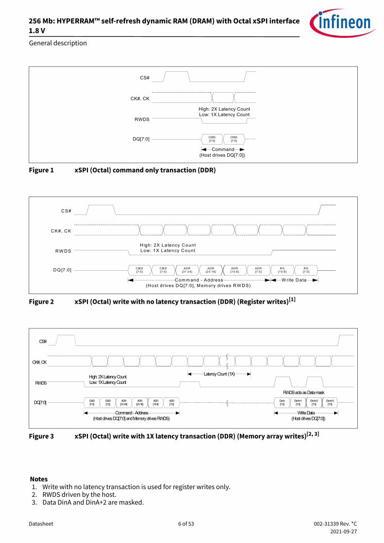
Figure 1 xSPI (Octal) command only transaction (DDR)
Figure 2 xSPI (Octal) write with no latency transaction (DDR) (Register writes)[1]
Figure 3 xSPI (Octal) write with 1X latency transaction (DDR) (Memory array writes)[2, 3]
CS#
CK#, CK
RWDS
DQ[7:0] CMD[7:0]
CMD[7:0]
Command(Host drives DQ[7:0])
High: 2X Latency CountLow: 1X Latency Count
CS#
CK#, CK
RW DS
DQ[7:0] CM D[7:0]
CM D[7:0]
ADR[31:24]
ADR[23:16]
ADR[15:8]
ADR[7:0]
Com m and - Address
RG[15:8]
RG[7:0]
W rite Data
H igh: 2X Latency CountLow: 1X Latency Count
(Host drives DQ[7:0], M em ory drives RW DS)
Notes1. Write with no latency transaction is used for register writes only.2. RWDS driven by the host.3. Data DinA and DinA+2 are masked.
CS#
CK#, CK
RWDS
DQ[7:0] CMD[7:0]
CMD[7:0]
ADR[31:24]
ADR[23:16]
ADR[15:8]
ADR[7:0]
Command - Address
DinA[7:0]
DinA+1[7:0]
DinA+2[7:0]
DinA+3[7:0]
Write Data
RWDS acts as Data mask
High: 2X Latency CountLow: 1X Latency Count
(Host drives DQ[7:0] and Memory drives RWDS) (Host drives DQ[7:0])
Latency Count (1X)

Datasheet 7 of 53 002-31339 Rev. *C2021-09-27
256 Mb: HYPERRAM™ self-refresh dynamic RAM (DRAM) with Octal xSPI interface1.8 V
General description
Figure 4 xSPI (Octal) write with 2X latency transaction (DDR) (Memory array writes)[4, 5]
Figure 5 xSPI (Octal) read with 1X latency transaction (DDR) (All reads)[6]
Figure 6 xSPI (Octal) read with 2X latency transaction (DDR) (All reads)[7]
CS#
CK#, CK
RWDS
DQ[7:0]CMD[7:0]
CMD[7:0]
ADR[31:24]
ADR[23:16]
ADR[15:8]
ADR[7:0]
Command - Address
DinA[7:0]
DinA+1[7:0]
DinA+2[7:0]
DinA+3[7:0]
Write Data
RWDS acts as Data Mask
High: 2X Latency CountLow: 1X Latency Count
(Host drives DQ[7:0] and Memory drives RWDS) (Host drives DQ[7:0])
Latency Count (2X)
Notes4. RWDS driven by HYPERRAM™ during command & address cycles for 2X latency and then driven by the host
for data masking.5. Data DinA and DinA+2 are masked.6. RWDS is driven by HYPERRAM™ phase aligned with data.7. RWDS is driven by HYPERRAM™ during command & address cycles for 2X latency and then driven again phase
aligned with data.
CS#
CK#, CK
RWDS
DQ[7:0] CMD[7:0]
CMD[7:0]
ADR[31:24]
ADR[23:16]
ADR[15:8]
ADR[7:0]
Command - Address
DoutA[7:0]
DoutA+1[7:0]
DoutA+2[7:0]
DoutA+3[7:0]
Read Data
RWDS & Data are edge aligned
High: 2X Latency CountLow: 1X Latency Count
(Host drives DQ[7:0] and Memory drives RWDS) (Memory drives RWDS)
Latency Count (1X)
CS#
CK#, CK
RWDS
DQ[7:0] CMD[7:0]
CMD[7:0]
ADR[31:24]
ADR[23:16]
ADR[15:8]
ADR[7:0]
Command - Address
DoutA[7:0]
DoutA+1[7:0]
DoutA+2[7:0]
DoutB+3[7:0]
Read Data
RWDS & Data are edge aligned
High: 2X Latency CountLow: 1X Latency Count
(Host drives DQ[7:0] and Memory drives RWDS) (Memory drives RWDS)
Latency Count (2X)

Datasheet 8 of 53 002-31339 Rev. *C2021-09-27
256 Mb: HYPERRAM™ self-refresh dynamic RAM (DRAM) with Octal xSPI interface1.8 V
Product overview
2 Product overviewThe 256 Mb HYPERRAM™ device is 1.8 V array and I/O, synchronous self-refresh dynamic RAM (DRAM). The HYPERRAM™ device provides an xSPI (Octal) slave interface to the host system. The xSPI (Octal) interface has an 8-bit (1 byte) wide DDR data bus and use only word-wide (16-bit data) address boundaries. Read transactions provide 16 bits of data during each clock cycle (8 bits on both clock edges). Write transactions take 16 bits of data from each clock cycle (8 bits on each clock edge).
Figure 7 xSPI (Octal) HYPERRAM™ interface[8]
2.1 xSPI (Octal) interfaceRead and write transactions require three clock cycles to define the target row/column address and then an initial access latency of tACC. During the CA part of a transaction, the memory will indicate whether an additional latency for a required refresh time (tRFH) is added to the initial latency; by driving the RWDS signal to the HIGH state. During a read (or write) transaction, after the initial data value has been output (or input), additional data can be read from (or written to) the row on subsequent clock cycles in either a wrapped or linear sequence. When configured in linear burst mode, the device will automatically fetch the next sequential row from the memory array to support a continuous linear burst. Simultaneously accessing the next row in the array while the read or write data transfer is in progress, allows for a linear sequential burst operation that can provide a sustained data rate of 400 MBps (1 byte (8 bit data bus) * 2 (data clock edges) * 200 MHz = 400 MBps).
CS#
CK#
CKDQ[7:0]
RWDS
VSS
VSSQ
VCC
VCCQ
RESET#
Note8. CK# is used in differential clock mode, but optional.
Datasheet 9 of 53 002-31339 Rev. *C2021-09-27
256 Mb: HYPERRAM™ self-refresh dynamic RAM (DRAM) with Octal xSPI interface1.8 V
Signal description
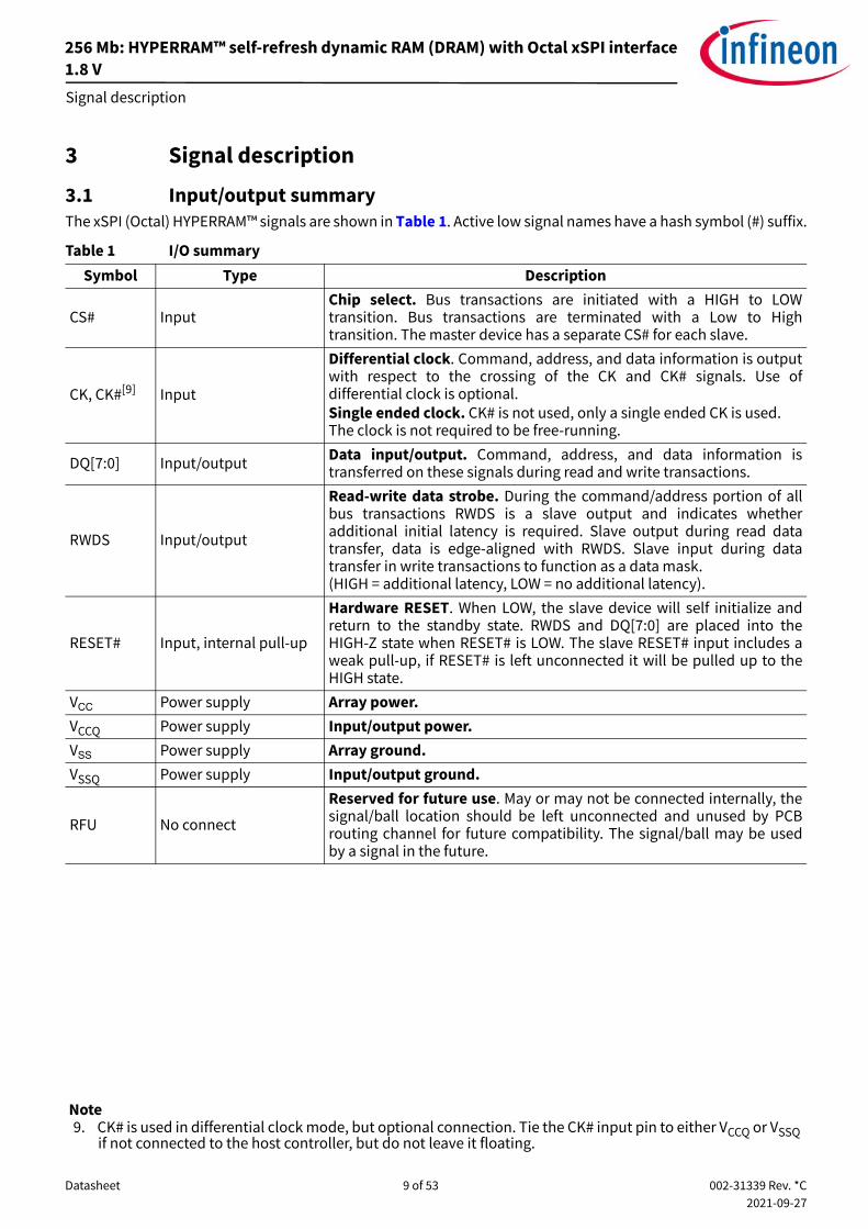
3 Signal description
3.1 Input/output summaryThe xSPI (Octal) HYPERRAM™ signals are shown in Table 1. Active low signal names have a hash symbol (#) suffix.
Table 1 I/O summary Symbol Type Description
CS# InputChip select. Bus transactions are initiated with a HIGH to LOWtransition. Bus transactions are terminated with a Low to Hightransition. The master device has a separate CS# for each slave.
CK, CK#[9] Input
Differential clock. Command, address, and data information is outputwith respect to the crossing of the CK and CK# signals. Use ofdifferential clock is optional.Single ended clock. CK# is not used, only a single ended CK is used. The clock is not required to be free-running.
DQ[7:0] Input/output Data input/output. Command, address, and data information istransferred on these signals during read and write transactions.
RWDS Input/output
Read-write data strobe. During the command/address portion of allbus transactions RWDS is a slave output and indicates whetheradditional initial latency is required. Slave output during read datatransfer, data is edge-aligned with RWDS. Slave input during datatransfer in write transactions to function as a data mask. (HIGH = additional latency, LOW = no additional latency).
RESET# Input, internal pull-up
Hardware RESET. When LOW, the slave device will self initialize andreturn to the standby state. RWDS and DQ[7:0] are placed into theHIGH-Z state when RESET# is LOW. The slave RESET# input includes aweak pull-up, if RESET# is left unconnected it will be pulled up to theHIGH state.
VCC Power supply Array power.VCCQ Power supply Input/output power.VSS Power supply Array ground.VSSQ Power supply Input/output ground.
RFU No connect
Reserved for future use. May or may not be connected internally, thesignal/ball location should be left unconnected and unused by PCBrouting channel for future compatibility. The signal/ball may be usedby a signal in the future.
Note9. CK# is used in differential clock mode, but optional connection. Tie the CK# input pin to either VCCQ or VSSQ
if not connected to the host controller, but do not leave it floating.

Datasheet 10 of 53 002-31339 Rev. *C2021-09-27
256 Mb: HYPERRAM™ self-refresh dynamic RAM (DRAM) with Octal xSPI interface1.8 V
xSPI (Octal) transaction details
4 xSPI (Octal) transaction detailsThe xSPI (Octal) master begins a transaction by driving CS# LOW while clock is idle. Then the clock begins toggling while CA words are transferred.For memory read and write transactions, the xSPI (Octal) master then continues clocking for a number of cycles defined by the latency count setting in configuration register 0 (Register write transactions do not require any latency count). The initial latency count required for a particular clock frequency is based on RWDS. If RWDS is LOW during the CA cycles, one latency count is inserted. If RWDS is HIGH during the CA cycles, an additional latency count is inserted. Once these latency clocks have been completed the memory starts to simultaneously transition the RWDS and output the target data. During the read data transfers, read data is output edge-aligned with every transition of RWDS. Data will continue to be output as long as the host continues to transition the clock while CS# is LOW. Note that burst transactions should not be so long as to prevent the memory from doing distributed refreshes. During the write data transfers, write data is center-aligned with the clock edges. The first byte of data in each word is captured by the memory on the rising edge of CK and the second byte is captured on the falling edge of CK. RWDS is driven by the host master interface as a data mask. When data is being written and RWDS is HIGH the byte will be masked and the array will not be altered. When data is being written and RWDS is LOW the data will be placed into the array. Because the master is driving RWDS during write data transfers, neither the master nor the HYPERRAM™ device are able to indicate a need for latency within the data transfer portion of a write trans-action. The acceptable write data burst length setting is also shown in configuration register 0.Wrapped bursts will continue to wrap within the burst length and linear burst will output data in a sequential manner across row boundaries. When a linear burst read reaches the last address in the array, continuing the burst beyond the last address will provide data from the beginning of the address range. Read transfers can be ended at any time by bringing CS# HIGH when the clock is idle. The clock is not required to be free-running. The clock may remain idle while CS# is HIGH.

Datasheet 11 of 53 002-31339 Rev. *C2021-09-27
256 Mb: HYPERRAM™ self-refresh dynamic RAM (DRAM) with Octal xSPI interface1.8 V
xSPI (Octal) transaction details
4.1 Command/address/data bit assignmentsTable 2 Command set[10-14]
Command Code CA-Data Address (bytes) Latency cycles Data
(bytes) Prerequisite
Software resetREST ENABLE 0x66 8-0-0 0 0 0RESET 0x99 8-0-0 0 0 0 RESET ENABLEIdentificationREAD ID[10] 0x9F 8-8-8 4 (0x00) 3-7 4Power modesDEEP POWER DOWN 0xB9 8-0-0 0 0 0Read memory arrayREAD (DDR) 0xEE 8-8-8 4 3-7 1 to ∞Write memory arrayWRITE (DDR) 0xDE 8-8-8 4 3-7 1 to ∞ WRITE ENABLEWrite enable / disableWRITE ENABLE 0x06 8-0-0 0 0 0WRITE DISABLE 0x04 8-0-0 0 0 0Read registersREAD ANY REGISTER 0x65 8-8-8 4 3-7 2Write registersWRITE ANY REGISTER 0x71 8-8-8 4 0 2 WRITE ENABLENotes10.The two identification registers contents are read together - identification 0 followed by identification 1.11.Write enable provides protection against inadvertent changes to memory or register values. It sets the inter-
nal write enable latch (WEL) which allows write transactions to execute afterwards. 12.Write disable can be used to disable write transactions from execution. It resets the internal write enable
latch (WEL). 13.The WEL latch stays set to ‘1’ at the end of any successful memory write transaction. After a power down /
power up sequence, or a hardware/software reset, WEL latch is cleared to ‘0’.14.The internal WEL latch is cleared to ‘0’ at the end of any successful register write transaction.

Datasheet 12 of 53 002-31339 Rev. *C2021-09-27
256 Mb: HYPERRAM™ self-refresh dynamic RAM (DRAM) with Octal xSPI interface1.8 V
xSPI (Octal) transaction details
4.2 RESET ENABLE transactionThe RESET ENABLE transaction is required immediately before a RESET transaction. Any transaction other than RESET following RESET ENABLE will clear the reset enable condition and prevent a later RESET transaction from being recognized.
Figure 8 RESET ENABLE transaction (DDR)
4.3 RESET transactionThe RESET transaction immediately following a RESET ENABLE will initiate the software reset process. The software reset provides a software method of returning the device to the standby state. During tSR (400 ns, max) the device will draw ICC5 current. A software reset will:
• Cause the configuration registers to return to their default values
• Halt self-refresh operation during the software reset process - memory array data is considered invalidAfter software reset finishes, the self-refresh operation will resume. Because self-refresh operation is stopped, and the self-refresh row counter is reset to its default value, some rows may not be refreshed within the required array refresh interval. This may result in the loss of DRAM array data. The host system should consider DRAM array data is lost after software reset and reload any required data.
Figure 9 RESET transaction (DDR)
CS#
CK#, CK
RWDS
DQ[7:0] CMD[7:0]
CMD[7:0]
Command(Host drives DQ[7:0])
High: 2X Latency CountLow: 1X Latency Count
CS#
CK#, CK
RWDS
DQ[7:0] CMD[7:0]
CMD[7:0]
Command(Host drives DQ[7:0])
High: 2X Latency CountLow: 1X Latency Count

Datasheet 13 of 53 002-31339 Rev. *C2021-09-27
256 Mb: HYPERRAM™ self-refresh dynamic RAM (DRAM) with Octal xSPI interface1.8 V
xSPI (Octal) transaction details
4.4 READ ID transactionThe READ ID transaction provides read access to device identification registers 0 and 1. The registers contain the manufacturer’s identification along with device identification. The read data sequence is as follows.Table 3 READ ID data sequence
Address space Byte order Byte position Word data Bit DQ
Register 0 Big-endian
A
15 714 613 512 411 310 29 18 0
B
7 76 65 54 43 32 21 10 0
Register 1 Big-endian
A
15 714 613 512 411 310 29 18 0
B
7 76 65 54 43 32 21 10 0

Datasheet 14 of 53 002-31339 Rev. *C2021-09-27
256 Mb: HYPERRAM™ self-refresh dynamic RAM (DRAM) with Octal xSPI interface1.8 V
xSPI (Octal) transaction details
Figure 10 READ ID with 1X latency transaction (DDR)[15]
Figure 11 READ ID with 2X latency transaction (DDR)[16]
4.5 DEEP POWER DOWN transactionDEEP POWER DOWN transaction brings the device into deep power down state which is the lowest power consumption state. Writing a “0” to CR0[15] will also bring the device in deep power down state. All register contents are lost in deep power down state and the device powers-up in its default state.
Figure 12 DEEP POWER DOWN transaction (DDR)
CS#
CK#, CK
RWDS
DQ[7:0] CMD[7:0]
CMD[7:0]
0x00 0x00 0x00 0x00
Command - Address
IDRG 0[15:8]
IDRG 0[7:0]
IDRG 1[15:8]
IDRG 1[7:0]
Read Data
RWDS & Data are edge aligned
High: 2X Latency CountLow: 1X Latency Count
(Host drives DQ[7:0] and Memory drives RWDS) (Memory drives RWDS)
Latency Count (1X)
CS#
CK#, CK
RWDS
DQ[7:0] CMD[7:0]
CMD[7:0]
0x00 0x00 0x00 0x00
Command - Address
Latency Count (2X)
IDRG 0[15:8]
IDRG 0[7:0]
IDRG 1[15:8]
IDRG 1[7:0]
Read Data
RWDS & Data are edge aligned
High: 2X Latency CountLow: 1X Latency Count
(Host drives DQ[7:0] and Memory drives RWDS) (Memory drives RWDS)
Notes15. RWDS is driven by HYPERRAM™ phase aligned with data.16. RWDS is driven by HYPERRAM™ during command & address cycles for 2X latency and then is driven again
phase aligned with data.
CS#
CK#, CK
RWDS
DQ[7:0] CMD[7:0]
CMD[7:0]
Command(Host drives DQ[7:0])
High: 2X Latency CountLow: 1X Latency Count

Datasheet 15 of 53 002-31339 Rev. *C2021-09-27
256 Mb: HYPERRAM™ self-refresh dynamic RAM (DRAM) with Octal xSPI interface1.8 V
xSPI (Octal) transaction details
4.6 READ transactionThe READ transaction reads data from the memory array. It has a latency requirement (dummy cycles) which allows the device’s internal circuitry enough time to access the addressed memory location. During these latency cycles, the host can tristate the data bus DQ[7:0].
Figure 13 READ with 1X latency transaction (DDR)[17]
Figure 14 READ with 2X latency transaction (DDR)[18]
Notes17. RWDS is driven by HYPERRAM™ phase aligned with data.18. RWDS is driven by HYPERRAM™ during command & address cycles for 2X latency and then is driven again
phase aligned with data.
CS#
CK#, CK
RWDS
DQ[7:0] CMD[7:0]
CMD[7:0]
ADR[31:24]
ADR[23:16]
ADR[15:8]
ADR[7:0]
Command - Address
DoutA[7:0]
DoutA+1[7:0]
DoutA+2[7:0]
DoutA+3[7:0]
Read Data
RWDS & Data are edge aligned
High: 2X Latency CountLow: 1X Latency Count
(Host drives DQ[7:0] and Memory drives RWDS) (Memory drives RWDS)
Latency Count (1X)
CS#
CK#, CK
RWDS
DQ[7:0] CMD[7:0]
CMD[7:0]
ADR[31:24]
ADR[23:16]
ADR[15:8]
ADR[7:0]
Command - Address
DoutA[7:0]
DoutA+1[7:0]
DoutA+2[7:0]
DoutB+3[7:0]
Read Data
RWDS & Data are edge aligned
High: 2X Latency CountLow: 1X Latency Count
(Host drives DQ[7:0] and Memory drives RWDS) (Memory drives RWDS)
Latency Count (2X)

Datasheet 16 of 53 002-31339 Rev. *C2021-09-27
256 Mb: HYPERRAM™ self-refresh dynamic RAM (DRAM) with Octal xSPI interface1.8 V
xSPI (Octal) transaction details
4.7 WRITE transactionThe WRITE transaction writes data to the memory array. It has a latency requirement (dummy cycles) which allows the device’s internal circuitry enough time to access the addressed memory location. During these latency cycles, the host can tristate the data bus DQ[7:0].WRITE ENABLE transaction which sets the WEL latch must be executed before the first WRITE. The WEL latch stays set to ‘1’ at the end of any successful memory write transaction. It must be reset by WRITE DISABLE transaction to prevent any inadvertent writes to the memory array.
Figure 15 WRITE with 1X latency transaction (DDR)[19, 20]
Figure 16 WRITE with 2X latency transaction (DDR)[21, 22]
CS#
CK#, CK
RWDS
DQ[7:0] CMD[7:0]
CMD[7:0]
ADR[31:24]
ADR[23:16]
ADR[15:8]
ADR[7:0]
Command - Address
DinA[7:0]
DinA+1[7:0]
DinA+2[7:0]
DinA+3[7:0]
Write Data
RWDS acts as Data mask
High: 2X Latency CountLow: 1X Latency Count
(Host drives DQ[7:0] and Memory drives RWDS) (Host drives DQ[7:0])
Latency Count (1X)
CS#
CK#, CK
RWDS
DQ[7:0]CMD[7:0]
CMD[7:0]
ADR[31:24]
ADR[23:16]
ADR[15:8]
ADR[7:0]
Command - Address
DinA[7:0]
DinA+1[7:0]
DinA+2[7:0]
DinA+3[7:0]
Write Data
RWDS acts as Data Mask
High: 2X Latency CountLow: 1X Latency Count
(Host drives DQ[7:0] and Memory drives RWDS) (Host drives DQ[7:0])
Latency Count (2X)
Notes19. RWDS is driven by the host.20. Data DinA and DinA+2 are masked.21. RWDS is driven by HYPERRAM™ during command and address cycles for 2X latency and then is driven by the
host for data masking.22. Data DinA and DinA+2 are masked.

Datasheet 17 of 53 002-31339 Rev. *C2021-09-27
256 Mb: HYPERRAM™ self-refresh dynamic RAM (DRAM) with Octal xSPI interface1.8 V
xSPI (Octal) transaction details
4.8 WRITE ENABLE transactionThe WRITE ENABLE transaction must be executed prior to any transaction that modifies data either in the memory array or the registers.
Figure 17 WRITE ENABLE transaction (DDR)
4.9 WRITE DISABLE transactionThe WRITE DISABLE transaction inhibits writing data either in the memory array or the registers.
Figure 18 WRITE DISABLE transaction (DDR)
4.10 READ ANY REGISTER transactionThe READ ANY REGISTER transaction reads all the device registers. It has a latency requirement (dummy cycles) which allows the device’s internal circuitry enough time to access the addressed register location. During these latency cycles, the host can tristate the data bus DQ[7:0].
Figure 19 READ ANY REGISTER with 1X latency transaction (DDR)[23]
CS#
CK#, CK
RW DS
DQ[7:0] CMD[7:0]
CMD[7:0]
Command(Host drives DQ[7:0])
High: 2X Latency CountLow: 1X Latency Count
CS#
CK#, CK
RWDS
DQ[7:0] CMD[7:0]
CMD[7:0]
Command(Host drives DQ[7:0])
High: 2X Latency CountLow: 1X Latency Count
Note23. RWDS is driven by HYPERRAM™ phase aligned with data.
CS#
CK#, CK
RWDS
DQ[7:0] CMD[7:0]
CMD[7:0]
ADR[31:24]
ADR[23:16]
ADR[15:8]
ADR[7:0]
Command - Address
RG[15:8]
RG[7:0]
RWDS & Data are edge aligned
High: 2X Latency CountLow: 1X Latency Count
(Host drives DQ[7:0] and Memory drives RWDS)Read Data
(Memory Drives RWDS)
Latency Count (1X)
Datasheet 18 of 53 002-31339 Rev. *C2021-09-27
256 Mb: HYPERRAM™ self-refresh dynamic RAM (DRAM) with Octal xSPI interface1.8 V
xSPI (Octal) transaction details
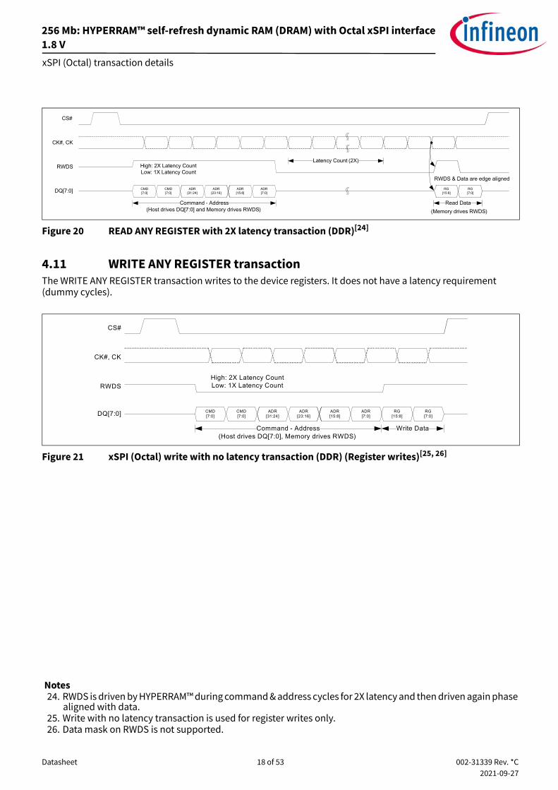
Figure 20 READ ANY REGISTER with 2X latency transaction (DDR)[24]
4.11 WRITE ANY REGISTER transactionThe WRITE ANY REGISTER transaction writes to the device registers. It does not have a latency requirement (dummy cycles).
Figure 21 xSPI (Octal) write with no latency transaction (DDR) (Register writes)[25, 26]
CS#
CK#, CK
RWDS
DQ[7:0] CMD[7:0]
CMD[7:0]
ADR[31:24]
ADR[23:16]
ADR[15:8]
ADR[7:0]
Command - Address
Latency Count (2X)
RG [15:8]
RG[7:0]
Read Data
RWDS & Data are edge aligned
High: 2X Latency CountLow: 1X Latency Count
(Host drives DQ[7:0] and Memory drives RWDS) (Memory drives RWDS)
CS#
CK#, CK
RWDS
DQ[7:0] CMD[7:0]
CMD[7:0]
ADR[31:24]
ADR[23:16]
ADR[15:8]
ADR[7:0]
Command - Address
RG[15:8]
RG[7:0]
Write Data
High: 2X Latency CountLow: 1X Latency Count
(Host drives DQ[7:0], Memory drives RWDS)
Notes24. RWDS is driven by HYPERRAM™ during command & address cycles for 2X latency and then driven again phase
aligned with data.25. Write with no latency transaction is used for register writes only.26. Data mask on RWDS is not supported.

Datasheet 19 of 53 002-31339 Rev. *C2021-09-27
256 Mb: HYPERRAM™ self-refresh dynamic RAM (DRAM) with Octal xSPI interface1.8 V
xSPI (Octal) transaction details
4.12 Data placement during memory READ/WRITE transactionsData placement during memory read/write is dependent upon the host. The device will output data (read) as it was written in (write). Hence both Big Endian and Little Endian are supported for the memory array.Table 4 Data placement during memory READ and WRITE
Address space
Byte order Byte position
Word data bit
DQ Bit order
Memory
Big-endian
A
15 7
When data is being accessed in memory space: The first byte of each word read or written is the “A” byte and the second is the “B” byte. The bits of the word within the A and B bytes depend on how the data was written. If the word lower address bits 7-0 are written in the A byte position and bits 15-8 are written into the B byte position, or vice versa, they will be read back in the same order.
So, memory space can be stored and read in either little-endian or big-endian order.
14 613 512 411 310 29 18 0
B
7 76 65 54 43 32 21 10 0
Little-endian
A
7 76 65 54 43 32 21 10 0
B
15 714 613 512 411 310 29 18 0

Datasheet 20 of 53 002-31339 Rev. *C2021-09-27
256 Mb: HYPERRAM™ self-refresh dynamic RAM (DRAM) with Octal xSPI interface1.8 V
xSPI (Octal) transaction details
4.13 Data placement during register READ/WRITE transactionsData placement during register read/write is Big Endian.Table 5 Data placement during register READ/WRITE transactions
Address space
Byte order Byte position Word data
bit DQ Bit order
Register Big-endian
A
15 7
When data is being accessed in register space: During a read transaction on the xSPI (Octal) two bytes are transferred on each clock cycle. The upper order byte A (Word[15:8]) is transferred between the rising and falling edges of RWDS (edge-aligned). The lower order byte B (Word[7:0]) is transferred between the falling and rising edges of RWDS.
During a write, the upper order byte A (Word[15:8]) is trans-ferred on the CK rising edge and the lower order byte B (Word[7:0]) is transferred on the CK falling edge.So, register space is always read and written in Big-endian order because registers have device dependent fixed bit location and meaning definitions.
14 613 512 411 310 29 18 0
B
7 76 65 54 43 32 21 10 0

Datasheet 21 of 53 002-31339 Rev. *C2021-09-27
256 Mb: HYPERRAM™ self-refresh dynamic RAM (DRAM) with Octal xSPI interface1.8 V
Memory space
5 Memory space
5.1 xSPI (Octal) interface
5.2 Density and row boundariesThe DRAM array size (density) of the device can be determined from the total number of system address bits used for the row and column addresses as indicated by the row address bit count and column address bit count fields in the ID0 register. For example: a 256 Mb HYPERRAM™ device has 10 column address bits and 15 row address bits for a total of 25 address bits (byte address) = 225 = 32M bytes (16M words). The 10 column address bits indicate that each row holds 210 = 1K bytes or 512 words. The row address bit count indicates there are 32768 rows to be refreshed within each array refresh interval. The row count is used in calculating the refresh interval.
Table 6 Memory space address map (byte based - 8 bits with least significant bit A(0) always set to ‘0’)
Unit type Count System byte address bits Address bits Notes
Rows within 256 Mb device 32,768 (rows) A24 - A10 24 - 10 -
Row 64 (half-pages) A9 - A4 9 - 4Each row has 64 half-pages. Each half-page has 16 bytes. Each column has 1K bytes).
Half-page 16 (byte addresses) A3 - A0 3 - 0
Half-page (HP) address is also refer-enced as upper column address. A word within a HP address is also referenced as lower column address.A0 always set to “0”

Datasheet 22 of 53 002-31339 Rev. *C2021-09-27
256 Mb: HYPERRAM™ self-refresh dynamic RAM (DRAM) with Octal xSPI interface1.8 V
Register space access
6 Register space access
6.1 xSPI (Octal) interface
6.2 Device identification registersThere are two read-only, nonvolatile, word registers, that provide information on the device selected when CS# is LOW. The device information fields identify:
• Manufacturer
• Type
• Density- Row address bit count- Column address bit count
• Refresh type
ID0 value for S80KS2563 is 0x0E96.
Table 7 Register space address map (Address bit A0 always set to ‘0’)
Registers Address (Byte addressable)
Identification registers 0 (ID0[15:0]) 0x00000000
Identification registers 1 (ID1[15:0]) 0x00000002
Configuration registers 0 (ID0[15:0]) 0x00000004
Configuration registers 1 (ID1[15:0]) 0x00000006
Table 8 Identification register 0 (ID0) bit assignments
Bits Function Settings (binary)[15:14] Reserved 00b - Default
13 Reserved 0b - Default[12:8] Row address bit count 01110b - Fifteen row address bits (256 Mb)[7:4] Column address bit count 1001b - Ten column address bits (default)[3:0] Manufacturer 0110b
Table 9 Identification register 1 (ID1) bit assignments
Bits Function Settings (binary)[15:4] Reserved 0000_0000_0000b (default)[3:0] Device type 0001b - HYPERRAM™ 2.0

Datasheet 23 of 53 002-31339 Rev. *C2021-09-27
256 Mb: HYPERRAM™ self-refresh dynamic RAM (DRAM) with Octal xSPI interface1.8 V
Register space access
6.3 Device configuration registers
6.3.1 Configuration register 0 (CR0)Configuration register 0 (CR0) is used to define the power state and access protocol operating conditions for the HYPERRAM™ device. Configurable characteristics include:
• Wrapped burst length (16, 32, 64, or 128 byte aligned and length data group)
• Wrapped burst type- Legacy wrap (sequential access with wrap around within a selected length and aligned group)- Hybrid wrap (Legacy wrap once then linear burst at start of the next sequential group)
• Initial latency
• Variable latency- Whether an array read or write transaction will use fixed or variable latency. If fixed latency is selected the
memory will always indicate a refresh latency and delay the read data transfer accordingly. If variable latency is selected, latency for a refresh is only added when a refresh is required at the same time a new transaction is starting.
• Output drive strength
• Deep power down (DPD) mode
Table 10 Configuration register 0 (CR0) bit assignments
CR0 bit Function Settings (binary)
[15] Deep power down enable
1 - Normal operation (default). HYPERRAM™ will automatically set this value to ‘1’ after DPD exit0 - Writing 0 causes the device to enter deep power down
[14:12] Drive strength
000 - 34 ohms (default)001 - 115 ohms010 - 67 ohms011 - 46 ohms100 - 34 ohms101 - 27 ohms110 - 22 ohms111 - 19 ohms
[11:8] Reserved1 - Reserved (default)Reserved for future use. When writing this register, these bits should be set to 1 for future compatibility.
[7:4] Initial latency
0000 - 5 clock latency @ 133 MHz Max frequency0001 - 6 clock latency @ 166 MHz Max frequency0010 - 7 clock latency @ 200 MHz Max frequency (default)0011 - Reserved0100 - Reserved ...1101 - Reserved1110 - 3 clock latency @ 85 MHz Max frequency1111 - 4 clock latency @ 104 MHz Max frequency
[3] Fixed latency enable
0 - Variable latency - 1 or 2 times initial latency depending on RWDS during CA cycles.1 - Fixed 2 times initial latency (default)
[2] Hybrid burst enable
0: Wrapped burst sequence to follow hybrid burst sequencing1: Wrapped burst sequence in legacy wrapped burst manner (default)

Datasheet 24 of 53 002-31339 Rev. *C2021-09-27
256 Mb: HYPERRAM™ self-refresh dynamic RAM (DRAM) with Octal xSPI interface1.8 V
Register space access
Wrapped burstA wrapped burst transaction accesses memory within a group of words aligned on a word boundary matching the length of the configured group. Wrapped access groups can be configured as 16, 32, 64, or 128 bytes alignment and length. During wrapped transactions, access starts at the CA selected location within the group, continues to the end of the configured word group aligned boundary, then wraps around to the beginning location in the group, then continues back to the starting location. Wrapped bursts are generally used for critical word first instruction or data cache line fill read accesses. Hybrid burstThe beginning of a hybrid burst will wrap within the target address wrapped burst group length before continuing to the next half-page of data beyond the end of the wrap group. Continued access is in linear burst order until the transfer is ended by returning CS# HIGH. This hybrid of a wrapped burst followed by a linear burst starting at the beginning of the next burst group, allows multiple sequential address cache lines to be filled in a single access. The first cache line is filled starting at the critical word. Then the next sequential line in memory can be read in to the cache while the first line is being processed.
[1:0] Burst length00 - 128 bytes01 - 64 bytes10- 16 bytes11 - 32 bytes (default)
Table 11 CR0[2] Control of wrapped burst sequence
Bit Default value Setting details
CR0[2] 1bHybrid burst enableCR0[2] = 0: Wrapped burst sequence to follow hybrid burst sequencingCR0[2] = 1: Wrapped burst sequence in legacy wrapped burst manner
Table 12 Example wrapped burst sequences (Addressing)
Burst typeWrap
boundary (bytes)
Start address (Hex) Sequence of byte addresses (Hex) of data words
Hybrid 6464 wrap
once then linear
XXXXXX02
02, 04, 06, 08, 0A, 0C, 0E, 10, 12, 14, 16, 18, 1A, 1C, 1E, 20, 22, 24, 26, 28, 2A, 2C, 2E, 30, 32, 34, 36, 38, 3A, 3C, 3E, 00(wrap complete, now linear beyond the end of the initial 64 byte wrap group) 40, 42, 44, 46, 48, 4A, 4C, 4E, 50, 52, ...
Hybrid 6464 wrap
once then linear
XXXXXX2E
2E, 30, 32, 34, 36, 38, 3A, 3C, 3E, 00, 02, 04, 06, 08, 0A, 0C, 0E, 10, 12, 14, 16, 18, 1A, 1C, 1E, 20, 22, 24, 26, 28, 2A, 2C, (wrap complete, now linear beyond the end of the initial 64 byte wrap group) 40, 42, 44, 46, 48, 4A, 4B, 4C, 4D, 4E, 4F, 50, 52, ...
Hybrid 1616 wrap
once then linear
XXXXXX02
02, 04, 06, 08, 0A, 0C, 0E, 00(wrap complete, now linear beyond the end of the initial 16 byte wrap group) 10, 12, 14, 16, 18, 1A, ..
Hybrid 1616 wrap
once then linear
XXXXXX0C
0C, 0E, 00, 02, 04, 06, 08, 0A(wrap complete, now linear beyond the end of the initial 16 byte wrap group) 10, 12, 14, 16, 18, 1A, ...
Table 10 Configuration register 0 (CR0) bit assignments (continued)
CR0 bit Function Settings (binary)

Datasheet 25 of 53 002-31339 Rev. *C2021-09-27
256 Mb: HYPERRAM™ self-refresh dynamic RAM (DRAM) with Octal xSPI interface1.8 V
Register space access
Initial latencyMemory space read and write transactions or register space read transactions require some initial latency to open the row selected by the CA. This initial latency is tACC. The number of latency clocks needed to satisfy tACC depends on the clock input frequency can vary from 3 to 7 clocks. The value in CR0[7:4] selects the number of clocks for initial latency. The default value is 7 clocks, allowing for operation up to a maximum frequency of 200MHz prior to the host system setting a lower initial latency value that may be more optimal for the system.In the event a distributed refresh is required at the time a memory space read or write transaction or register space read transaction begins, the RWDS signal goes High during the CA to indicate that an additional initial latency is being inserted to allow a refresh operation to complete before opening the selected row.Register space write transactions always have zero initial latency. RWDS may be HIGH or LOW during the CA period. The level of RWDS during the CA period does not affect the placement of register data immediately after the CA, as there is no initial latency needed to capture the register data. A refresh operation may be performed in the memory array in parallel with the capture of register data. Fixed latencyA configuration register option bit CR0[3] is provided to make all memory space read and write transactions or register space read transactions require the same initial latency by always driving RWDS HIGH during the CA to indicate that two initial latency periods are required. This fixed initial latency is independent of any need for a distributed refresh, it simply provides a fixed (deterministic) initial latency for all of these transaction types. Fixed latency is the default POR or reset configuration. The system may clear this configuration bit to disable fixed latency and allow variable initial latency with RWDS driven HIGH only when additional latency for a refresh is required.Drive strengthDQ and RWDS signal line loading, length, and impedance vary depending on each system design. Configuration register bits CR0[14:12] provide a means to adjust the DQ[7:0] and RWDS signal output impedance to customize the DQ and RWDS signal impedance to the system conditions to minimize high speed signal behaviors such as overshoot, undershoot, and ringing. The default POR or reset configuration value is 000b to select the mid point of the available output impedance options. The impedance values shown are typical for both pull-up and pull-down drivers at typical silicon process condi-tions, nominal operating voltage (1.8 V) and 50°C. The impedance values may vary from the typical values depending on the process, voltage, and temperature (PVT) conditions. Impedance will increase with slower process, lower voltage, or higher temperature. Impedance will decrease with faster process, higher voltage, or lower temperature.
Hybrid 3232 wrap
once then linear
XXXXXX0A
0A, 0C, 0E, 10, 12, 14, 16, 18, 1A, 1C, 1E, 00, 02, 04, 06, 08(wrap complete, now linear beyond the end of the initial 32 byte wrap group) 20, 22, 24, 26, 28, 2A, ...
Wrap 64 64 XXXXXX02 02, 04, 06, 08, 0A, 0C, 0E, 10, 12, 14, 16, 18, 1A, 1C, 1E, 20, 22, 24, 26, 28, 2A, 2C, 2E, 30, 32, 34, 36, 38, 3A, 3C, 3E, 00, ...
Wrap 64 64 XXXXXX2E2E, 30, 32, 34, 36, 38, 3A, 3C, 3E, 00, 02, 04, 06, 08, 0A, 0C, 0E, 10, 12, 14, 16, 18, 1A, 1C, 1E, 20, 22, 24, 26, 28, 2A, 2C, 2E, 30, ….
Wrap 16 16 XXXXXX02 02, 04, 06, 08, 0A, 0C, 0E, 00, ...Wrap 16 16 XXXXXX0C 0C, 0E, 00, 02, 04, 06, 08, 0A, ...Wrap 32 32 XXXXXX0A 0A, 0C, 0E, 10, 12, 14, 16, 18, 1A, 1C, 1E, 00, 02, 04, 06, 08, ...
Linear Linear burst XXXXXX02 02, 04, 06, 08, 0A, 0C, 0E, 10, 12, 14, 16, 18, 1A, 1C, 1E, 20, 22, ...
Table 12 Example wrapped burst sequences (Addressing) (continued)
Burst typeWrap
boundary (bytes)
Start address (Hex) Sequence of byte addresses (Hex) of data words

Datasheet 26 of 53 002-31339 Rev. *C2021-09-27
256 Mb: HYPERRAM™ self-refresh dynamic RAM (DRAM) with Octal xSPI interface1.8 V
Register space access
Each system design should evaluate the data signal integrity across the operating voltage and temperature ranges to select the best drive strength settings for the operating conditions.Deep power downWhen the HYPERRAM™ device is not needed for system operation, it may be placed in a very low power consuming state called deep power down (DPD), by writing 0 to CR0[15]. When CR0[15] is cleared to 0, the device enters the DPD state within tDPDIN time and all refresh operations stop. The data in RAM is lost, (becomes invalid without refresh) during DPD state. Exiting DPD requires driving CS# LOW then HIGH, POR, or a reset. Only CS# and RESET# signals are monitored during DPD mode. For additional details, see “Deep power down” on page 30.
6.3.2 Configuration register 1Configuration register 1 (CR1) is used to define the refresh array size, refresh rate and hybrid sleep for the HYPERRAM™ device. Configurable characteristics include:
• Partial array refresh
• Hybrid sleep state
• Refresh rate
Burst typeTwo burst types, namely linear and wrapped, are supported in xSPI (Octal) mode by HYPERRAM™. CR1[7] selects which type to use.Master clock typeTwo clock types, namely single ended and differential, are supported. CR1[6] selects which type to use.
• In the single ended clock mode (by default), CK# input is not enabled; hence it may be left either floating or biased to HIGH or LOW.
• In the differential clock mode (when enabled), the CK# input can't be left floating. It must be either driven by the host, or biased to HIGH or LOW.
Table 13 Configuration register 1 (CR1) bit assignments
CR1 bit Function Setting (binary)
[15:8] Reserved11111111 - Reserved (default)When writing this register, these bits should keep 0xFFh for future compat-ibility.
[7] Burst type 1 - Linear burst (default)0 - Wrapped burst
[6] Master clock type 1 - Single ended - CK (default)0 - Differential - CK#, CK
[5] Hybrid sleep 1 - Causes the device to enter hybrid sleep state0 - Normal operation (default)
[4:2] Partial arrayrefresh
000 - Full array (default)001 - Bottom 1/2 array010 - Bottom 1/4 array011 - Bottom 1/8 array100 - none101 - Top 1/2 array110 - Top 1/4 array111 - Top 1/8 array
[1:0] Distributed refreshinterval
10 - 1µs tCSM (Industrial plus temperature range devices)11 - Reserved00 - Reserved01 - 4µs tCSM (Industrial temperature range devices)

Datasheet 27 of 53 002-31339 Rev. *C2021-09-27
256 Mb: HYPERRAM™ self-refresh dynamic RAM (DRAM) with Octal xSPI interface1.8 V
Register space access
Partial array refreshThe partial array refresh configuration restricts the refresh operation in HYPERRAM™ to a portion of the memory array specified by CR1[5:3]. This reduces the standby current. The default configuration refreshes the whole array.Hybrid sleep (HS)When the HYPERRAM™ is not needed for system operation but data in the device needs to be retained, it may be placed in hybrid sleep state to save more power. Enter hybrid sleep state by writing 1 to CR1[5]. Bringing CS# LOW will cause the device to exit HS state and set CR1[5] to 0. Also, POR, or a hardware reset will cause the device to exit hybrid sleep state. Note that a POR or a hardware reset disables refresh where the memory core data can potentially get lost.Distributed refresh interval The HYPERRAM™ device is built with volatile DRAM array which requires periodic refresh of all bits in it. The refresh operation can be done by an internal self-refresh logic that will evenly refresh the memory array automatically. The automatic refresh operation can only be done when the memory array is not actively read or written by the host system. The refresh logic waits for the end of any active read or write before doing a refresh, if a refresh is needed at that time. If a new read or write begins before the refresh is completed, the memory will drive RWDS high during the CA period to indicate that an additional initial latency time is required at the start of the new access in order to allow the refresh operation to complete before starting the new access. The evenly distributed refresh operations require a maximum refresh interval between two adjacent refresh operations. The maximum distributed refresh interval varies with temperature as shown in Table 14.
The distributed refresh operation requires that the host does not perform burst transactions longer than the distributed refresh interval to prevent the memory from unable doing the distributed refreshes operation when it is needed. This sets an upper limit on the length of read and write transactions so that the automatic distributed refresh operation can be done between transactions. This limit is called the CS# low maximum time (tCSM) and the tCSM will be equal to the maximum distributed refresh interval. The host system is required to respect the tCSM value by terminating each transaction before violating tCSM. This can be done by host memory controller splitting long transactions when reaching the tCSM limit, or by host system hardware or software not performing a single burst read or write transaction that would be longer than tCSM. As noted in Table 14, the maximum refresh interval is longer at lower temperatures such that tCSM could be increased to allow longer transactions. The host may determine the operating temperature from a temperature sensor in the system and use the tCSM value from the table accordingly, or it may determine dynamically by reading the read only CR1[1:0] bits in order to set the distributed refresh interval prior to the HYPERRAM™ access.
Table 14 Array refresh interval per temperature
Operating temperature Refresh interval tCSM CR1[1:0]TA ≤ 85 °C 4 µs 01b
85 °C < TA ≤ 125 °C 1 µs 10b

Datasheet 28 of 53 002-31339 Rev. *C2021-09-27
256 Mb: HYPERRAM™ self-refresh dynamic RAM (DRAM) with Octal xSPI interface1.8 V
Interface states
7 Interface statesTable 15 describes the required value of each signal for each interface state.
LegendL = VIL; H = VIH; X = either VIL or VIH; Y= either VIL or VIH or VOL or VOH; Z = either VOL or VOH; L/H = rising edge;
H/L = falling edge; T = Toggling during information transfer; Idle = CK is LOW and CK# is HIGH;
Valid = all bus signals have stable L or H level
Table 15 Interface states
Interface state VCC / VCCQ CS# CK, CK# DQ7-DQ0 RWDS RESET#Power-off < VLKO X X HIGH-Z HIGH-Z XPower-on (cold) reset ≥ VCC / VCCQ min X X HIGH-Z HIGH-Z XHardware (warm) reset ≥ VCC / VCCQ min X X HIGH-Z HIGH-Z LInterface standby ≥ VCC / VCCQ min H X HIGH-Z HIGH-Z H
CA ≥ VCC / VCCQ min L T Master output valid Y H
Read initial access latency (data bus turn around period)
≥ VCC / VCCQ min L T HIGH-Z L H
Write initial access latency (RWDS turn around period) ≥ VCC / VCCQ min L T HIGH-Z HIGH-Z H
Read data transfer ≥ VCC / VCCQ min L T Slave output valid
Slave output validZ or T
H
Write data transfer with initial latency ≥ VCC / VCCQ min L T Master
output valid
Master output valid
X or TH
Write data transfer without initial latency [27] ≥ VCC / VCCQ min L T Master
output validSlave output L or HIGH-Z H
Active clock stop [28] ≥ VCC / VCCQ min L Idle
Master or slave output
valid or HIGH-Z
Y H
Deep power down ≥ VCC / VCCQ min H X or T HIGH-Z HIGH-Z HHybrid sleep ≥ VCC / VCCQ min H X or T HIGH-Z HIGH-Z HNotes27. Writes without initial latency (with zero initial latency), do not have a turn around period for RWDS. The
HYPERRAM™ device will always drive RWDS during the CA period to indicate whether extended latency is required. Since master write data immediately follows the CA period the HYPERRAM™ device may continue to drive RWDS LOW or may take RWDS to HIGH-Z. The master must not drive RWDS during writes with zero latency. writes with zero latency do not use RWDS as a data mask function. All bytes of write data are written (full word writes).
28. Active clock stop is described in “Active clock stop” on page 29. DPD is described in “Deep power down” on page 30

Datasheet 29 of 53 002-31339 Rev. *C2021-09-27
256 Mb: HYPERRAM™ self-refresh dynamic RAM (DRAM) with Octal xSPI interface1.8 V
Power conservation modes
8 Power conservation modes
8.1 Interface standbyStandby is the default, low power, state for the interface while the device is not selected by the host for data transfer (CS# = HIGH). All inputs, and outputs other than CS# and RESET# are ignored in this state.
8.2 Active clock stopDesign Note: Active Clock Stop feature is pending device characterization to determine if it will be supported. The active clock stop state reduces device interface energy consumption to the ICC6 level during the data transfer portion of a read or write operation. The device automatically enables this state when clock remains stable for tACC + 30 ns. While in active clock Stop state, read data is latched and always driven onto the data bus. ICC6 shown in “DC characteristics” on page 33.Active clock stop state helps reduce current consumption when the host system clock has stopped to pause the data transfer. Even though CS# may be LOW throughout these extended data transfer cycles, the memory device host interface will go into the active clock stop current level at tACC + 30 ns. This allows the device to transition into a lower current state if the data transfer is stalled. Active read or write current will resume once the data transfer is restarted with a toggling clock. The active clock stop state must not be used in violation of the tCSM limit. CS# must go HIGH before tCSM is violated. Clock can be stopped during any portion of the active transaction as long as it is in the LOW state. Note that it is recommended to avoid stopping the clock during register access.
Figure 22 Active clock stop during read transaction (DDR)[29]
8.3 Hybrid sleepIn the hybrid sleep (HS) state, the current consumption is reduced (IHS). HS state is entered by writing a 1 to CR1[5]. The device reduces power within tHSIN time. The data in memory space and register space is retained during HS state. Bringing CS# LOW will cause the device to exit HS state and set CR1[5] to 0. Also, POR, or a hardware reset will cause the device to exit hybrid sleep state. Note that a POR or a hardware reset disables refresh where the memory core data can potentially get lost. Returning to standby state requires tEXITHS time. Following the exit from HS due to any of these events, the device is in the same state as entering hybrid sleep.
Figure 23 Enter HS transaction
CS#
CK#, CK
RWDS
DQ[7:0] CMD[7:0]
CMD[7:0]
ADR[31:24]
ADR[23:16]
ADR[15:8]
ADR[7:0]
Command - Address
DoutA[7:0]
DoutB[7:0]
DoutA+1[7:0]
DoutB+1[7:0]
Read Data
RWDS & Data are edge aligned
High: 2X Latency CountLow: 1X Latency Count
(Host drives DQ[7:0] and Memory drives RWDS)
Clock Stopped
Output Driven
Latency Count (1X)
Note29. RWDS is LOW during the CA cycles. In this read transaction there is a single initial latency count for read data
access because, this read transaction does not begin at a time when additional latency is required by the slave.
C S#
C K#, C K
R W D S
D Q [7:0] CM D[7:0]
CM D[7:0]
AD R[31 :24 ]
AD R[23 :16]
AD R[15 :8 ]
AD R[7 :0]
C om m and - Address
RG[15:8 ]
RG[7:0 ]
W rite D ataC R 0 Value
H igh: 2X La tency C ountLow: 1X La tency C ount
(H ost d rives D Q[7:0], M em ory d rives R W D S)
Enter H ybrid S leep tH SIN
H S
tH SIN

Datasheet 30 of 53 002-31339 Rev. *C2021-09-27
256 Mb: HYPERRAM™ self-refresh dynamic RAM (DRAM) with Octal xSPI interface1.8 V
Power conservation modes
Figure 24 Exit HS transaction
8.4 Deep power downIn the deep power down (DPD) state, current consumption is driven to the lowest possible level (IDPD). DPD state is entered by writing a 0 to CR0[15]. The device reduces power within tDPDIN time and all refresh operations stop. The data in memory space is lost, (becomes invalid without refresh) during DPD state. Driving CS# LOW then HIGH will cause the device to exit DPD state. Also, POR, or a hardware reset will cause the device to exit DPD state. Returning to standby state requires tEXTDPD time. Returning to standby state following a POR requires tVCS time, as with any other POR. Following the exit from DPD due to any of these events, the device is in the same state as following POR. Note In xSPI (Octal), deep power down transaction or write any register transaction can be used to enter DPD.
Figure 25 Enter DPD transaction
Figure 26 Exit DPD transaction
Table 16 Hybrid sleep timing parameters
Parameter Description Min Max UnittHSIN Hybrid sleep CR1[5] = 0 register write to DPD power level - 3 µstCSHS CS# pulse width to exit HS 60 3000 nstEXTHS CS# exit hybrid sleep to standby wakeup time - 100 µs
Table 17 Deep power down timing parameters
Parameter Description Min Max UnittDPDIN Deep power down CR0[15] = 0 register write to DPD power level - 3 µstCSDPD CS# pulse width to exit DPD 200 3000 nstEXTDPD CS# exit deep power down to standby wakeup time - 150 µs
tCSHStEXTHS
CS#
CS#
C K#, CK
RW DS
DQ[7:0] CM D[7:0]
CM D[7:0 ]
ADR[31:24]
ADR[23:16]
ADR[15:8]
ADR[7:0 ]
C om m and - Address
RG[15:8]
RG[7:0 ]
W rite DataC R0 Value
H igh: 2X Latency C ountLow: 1X Latency C ount
(H ost drives DQ[7:0], M em ory drives RW D S)
Enter Deep Power Down tD PD IN
D PD
tD PD IN
tCSDPDtEXTDPD
CS#

Datasheet 31 of 53 002-31339 Rev. *C2021-09-27
256 Mb: HYPERRAM™ self-refresh dynamic RAM (DRAM) with Octal xSPI interface1.8 V
Electrical specifications
9 Electrical specifications
9.1 Absolute maximum ratings
9.2 Input signal overshootDuring DC conditions, input or I/O signals should remain equal to or between VSS and VCC. During voltage transitions, inputs or I/Os may negative overshoot VSS to -1.0V or positive overshoot to VCC +1.0V, for periods up to 20 ns.
Figure 27 Maximum negative overshoot waveform
Figure 28 Maximum positive overshoot waveform
Storage temperature plastic packages -65 °C to +150 °CAmbient temperature with power applied -65 °C to +135 °CVoltage with respect to ground all signals[30] -0.5 V to + (VCC + 0.5 V)Output short circuit current[31] 100 mAVoltage on VCC, VCCQ pins relative to VSS -0.5 V to +2.5 VElectrostatic discharge voltage:Human body model (JEDEC Std JESD22-A114-B)Charged device model (JEDEC Std JESD22-C101-A)
2000 V500 V
Notes30. Minimum DC voltage on input or I/O signal is -1.0V. During voltage transitions, input or I/O signals may
undershoot VSS to -1.0V for periods of up to 20 ns. See Figure 27. Maximum DC voltage on input or I/O signals is VCC +1.0V. During voltage transitions, input or I/O signals may overshoot to VCC +1.0V for periods up to 20 ns. See Figure 28.
31. No more than one output may be shorted to ground at a time. Duration of the short circuit should not be greater than one second.
32. Stresses above those listed under “Absolute maximum ratings” on page 31 may cause permanent dam-age to the device. This is a stress rating only; functional operation of the device at these or any other con-ditions above those indicated in the operational sections of this data sheet is not implied. Exposure of the device to absolute maximum rating conditions for extended periods may affect device reliability.
VSSQ to VCCQ
- 1.0V
20 ns≤
VCCQ + 1.0V
20 ns
VSSQ to VCCQ
≤

Datasheet 32 of 53 002-31339 Rev. *C2021-09-27
256 Mb: HYPERRAM™ self-refresh dynamic RAM (DRAM) with Octal xSPI interface1.8 V
Electrical specifications
9.3 Latch-up characteristics
9.4 Operating rangesOperating ranges define those limits between which the functionality of the device is guaranteed.
9.4.1 Temperature ranges
9.4.2 Power supply voltagesTable 20 Power supply voltages
Table 18 Latch-up specification[33]
Description Min Max UnitInput voltage with respect to VSSQ on all input only connections - 1.0 VCCQ + 1.0
VInput voltage with respect to VSSQ on all I/O connections -1.0 VCCQ + 1.0
VCCQ current -100 +100 mANote33. Excludes power supplies VCC/VCCQ. Test conditions: VCC = VCCQ, one connection at a time tested, connec-
tions not being tested are at VSS.
Table 19 Temperature ranges
Parameter Symbol DeviceSpec
UnitMin Max
Ambient temperature TA
Industrial (I) –40 85
°CIndustrial plus (V) –40 105
Automotive, AEC-Q100 Grade 3 (A) –40 85Automotive, AEC-Q100 Grade 2 (B) –40 105Automotive, AEC-Q100 Grade 1 (M) –40 125
Description Min Max UnitVCC power supply 1.7 2.0 V

Datasheet 33 of 53 002-31339 Rev. *C2021-09-27
256 Mb: HYPERRAM™ self-refresh dynamic RAM (DRAM) with Octal xSPI interface1.8 V
Electrical specifications
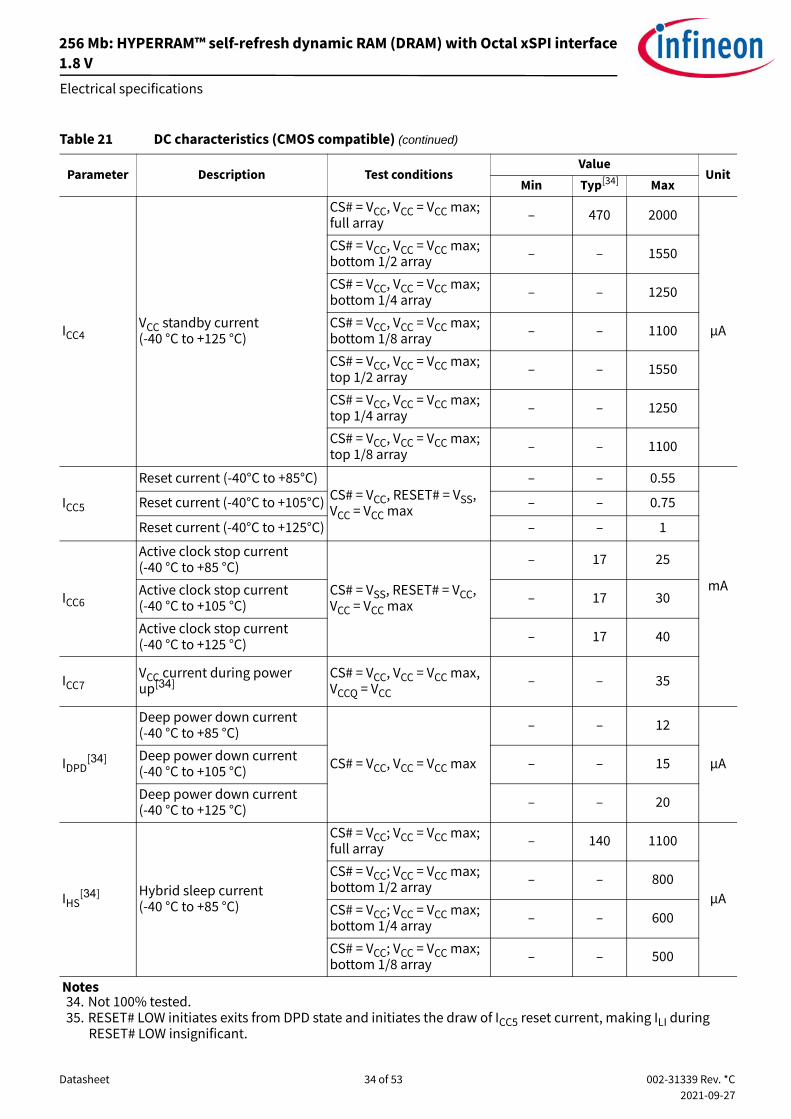
9.5 DC characteristicsTable 21 DC characteristics (CMOS compatible)
Parameter Description Test conditionsValue
UnitMin Typ[34] Max
ILI2Input leakage current.Device reset signal HIGH VIN = VSS to VCC, VCC = VCC
max
– – 2
µA
ILI4Input leakage currentDevice reset signal LOW[35] – – 15
ICC1VCC Active read currentOperating temperature range CS# = VSS, CK@200 MHz,
VCC = VCC max
– 14 20
mA
ICC2VCC Active write currentOperating temperature range – 16 22
ICC4
VCC standby current (-40 °C to +85 °C)
CS# = VCC, VCC = VCC max; full array – 470 1200
µA
CS# = VCC, VCC = VCC max; bottom 1/2 array – – 850
CS# = VCC, VCC = VCC max; bottom 1/4 array – – 700
CS# = VCC, VCC = VCC max; bottom 1/8 array – – 600
CS# = VCC, VCC = VCC max; top 1/2 array – – 850
CS# = VCC, VCC = VCC max; top 1/4 array – – 700
CS# = VCC, VCC = VCC max; top 1/8 array – – 600
VCC standby current (-40 °C to +105 °C)
CS# = VCC, VCC = VCC max; full array – 470 1550
µA
CS# = VCC, VCC = VCC max; bottom 1/2 array – – 1150
CS# = VCC, VCC = VCC max; bottom 1/4 array – – 950
CS# = VCC, VCC = VCC max; bottom 1/8 array – – 850
CS# = VCC, VCC = VCC max; top 1/2 array – – 1150
CS# = VCC, VCC = VCC max; top 1/4 array – – 950
CS# = VCC, VCC = VCC max; top 1/8 array – – 850
Notes34. Not 100% tested.35. RESET# LOW initiates exits from DPD state and initiates the draw of ICC5 reset current, making ILI during
RESET# LOW insignificant.
Datasheet 34 of 53 002-31339 Rev. *C2021-09-27
256 Mb: HYPERRAM™ self-refresh dynamic RAM (DRAM) with Octal xSPI interface1.8 V
Electrical specifications
ICC4VCC standby current (-40 °C to +125 °C)
CS# = VCC, VCC = VCC max; full array – 470 2000
µA
CS# = VCC, VCC = VCC max; bottom 1/2 array – – 1550
CS# = VCC, VCC = VCC max; bottom 1/4 array – – 1250
CS# = VCC, VCC = VCC max; bottom 1/8 array – – 1100
CS# = VCC, VCC = VCC max; top 1/2 array – – 1550
CS# = VCC, VCC = VCC max; top 1/4 array – – 1250
CS# = VCC, VCC = VCC max; top 1/8 array – – 1100
ICC5
Reset current (-40°C to +85°C)CS# = VCC, RESET# = VSS, VCC = VCC max
– – 0.55
mA
Reset current (-40°C to +105°C) – – 0.75
Reset current (-40°C to +125°C) – – 1
ICC6
Active clock stop current (-40 °C to +85 °C)
CS# = VSS, RESET# = VCC,VCC = VCC max
– 17 25
Active clock stop current (-40 °C to +105 °C) – 17 30
Active clock stop current (-40 °C to +125 °C) – 17 40
ICC7VCC current during power up[34]
CS# = VCC, VCC = VCC max, VCCQ = VCC
– – 35
IDPD[34]
Deep power down current (-40 °C to +85 °C)
CS# = VCC, VCC = VCC max
– – 12
µADeep power down current (-40 °C to +105 °C) – – 15
Deep power down current (-40 °C to +125 °C) – – 20
IHS[34] Hybrid sleep current
(-40 °C to +85 °C)
CS# = VCC; VCC = VCC max;full array – 140 1100
µA
CS# = VCC; VCC = VCC max;bottom 1/2 array – – 800
CS# = VCC; VCC = VCC max;bottom 1/4 array – – 600
CS# = VCC; VCC = VCC max;bottom 1/8 array – – 500
Table 21 DC characteristics (CMOS compatible) (continued)
Parameter Description Test conditionsValue
UnitMin Typ[34] Max
Notes34. Not 100% tested.35. RESET# LOW initiates exits from DPD state and initiates the draw of ICC5 reset current, making ILI during
RESET# LOW insignificant.

Datasheet 35 of 53 002-31339 Rev. *C2021-09-27
256 Mb: HYPERRAM™ self-refresh dynamic RAM (DRAM) with Octal xSPI interface1.8 V
Electrical specifications
IHS[34]
Hybrid sleep current (-40 °C to +85 °C)
CS# = VCC; VCC = VCC max;top 1/2 array – – 800
µACS# = VCC; VCC = VCC max;top 1/4 array – – 600
CS# = VCC; VCC = VCC max;top 1/8 array – – 500
Hybrid sleep current (-40 °C to +105 °C)
CS# = VCC; VCC = VCC max;full array – 140 1250
µA
CS# = VCC; VCC = VCC max;bottom 1/2 array – – 850
CS# = VCC; VCC = VCC max;bottom 1/4 array – – 650
CS# = VCC; VCC = VCC max;bottom 1/8 array – – 550
CS# = VCC; VCC = VCC max;top 1/2 array – – 850
CS# = VC; VCC = VCC max;top 1/4 array – – 650
CS# = VCC; VCC = VCC max;top 1/8 array – – 550
Hybrid sleep current (-40 °C to +125 °C)
CS# = VCC; VCC = VCC max;full array – 140 1500
µA
CS# = VCC; VCC = VCC max;bottom 1/2 array – – 1150
CS# = VCC; VCC = VCC max;bottom 1/4 array – – 900
CS# = VCC; VCC = VCC max;bottom 1/8 array – – 750
CS# = VCC; VCC = VCC max;top 1/2 array – – 1150
CS# = VCC; VCC = VCC max;top 1/4 array – – 900
CS# = VCC; VCC = VCC max;top 1/8 array – – 750
VIL Input low voltage – -0.15 × VCCQ – 0.30 × VCCQ
VVIH Input high voltage – 0.70 × VCCQ – 1.15 × VCCQ
VOL Output low voltageIOL = 100 µA for DQ[7:0]
– – 0.2
VOH Output high voltage VCCQ - 0.20 – –
Table 21 DC characteristics (CMOS compatible) (continued)
Parameter Description Test conditionsValue
UnitMin Typ[34] Max
Notes34. Not 100% tested.35. RESET# LOW initiates exits from DPD state and initiates the draw of ICC5 reset current, making ILI during
RESET# LOW insignificant.

Datasheet 36 of 53 002-31339 Rev. *C2021-09-27
256 Mb: HYPERRAM™ self-refresh dynamic RAM (DRAM) with Octal xSPI interface1.8 V
Electrical specifications
9.5.1 Capacitance characteristicsTable 22 Capacitive characteristics[36-38]
Description Parameter256 Mb
UnitMax
Input capacitance (CK, CK#, CS#) CI 3.0
pFDelta input capacitance (CK, CK#) CID 0.25Output capacitance (RWDS) CO 3.0IO capacitance (DQx) CIO 3.0IO capacitance delta (DQx) CIOD 0.25Notes36. These values are guaranteed by design and are tested on a sample basis only.37. Contact capacitance is measured according to JEP147 procedure for measuring capacitance using a vector
network analyzer. VCC, VCCQ are applied and all other signals (except the signal under test) floating. DQs should be in the high impedance state.
38. Note that the capacitance values for the CK, CK#, RWDS and DQx signals must have similar capacitance values to allow for signal propagation time matching in the system. The capacitance value for CS# is not as critical because there are no critical timings between CS# going active (LOW) and data being presented on the DQ’s bus.
Table 23 Thermal resistance
Parameter[39] Description Test conditions 24-ball FBGA package Unit
θJA Thermal resistance(junction to ambient)
Test conditions follow standard test methods and procedures for measuring thermal impedance, per EIA/JESD51.
40.8
°C/WθJC Thermal resistance
(junction to case)8
Note39. This parameter is guaranteed by characterization; not tested in production.

Datasheet 37 of 53 002-31339 Rev. *C2021-09-27
256 Mb: HYPERRAM™ self-refresh dynamic RAM (DRAM) with Octal xSPI interface1.8 V
Electrical specifications
9.6 Power-up initializationHYPERRAM™ products include an on-chip voltage sensor used to launch the power-up initialization process. VCC and VCCQ must be applied simultaneously. When the power supply reaches a stable level at or above VCC(min), the device will require tVCS time to complete its self-initialization process. The device must not be selected during power-up. CS# must follow the voltage applied on VCCQ until VCC (min) is reached during power-up, and then CS# must remain high for a further delay of tVCS. A simple pull-up resistor from VCCQ to chip select (CS#) can be used to insure safe and proper power-up.If RESET# is LOW during power up, the device delays start of the tVCS period until RESET# is HIGH. The tVCS period is used primarily to perform refresh operations on the DRAM array to initialize it. When initialization is complete, the device is ready for normal operation.
Figure 29 Power-up with RESET# HIGH
Figure 30 Power-up with RESET# LOW
Table 24 Power up and reset parameters[40-42]
Parameter Description Min Max UnitVCC VCC Power supply 1.7 2.0 V
tVCSVCC and VCCQ ≥ minimum and RESET# HIGH to first access - 150 µs
Notes40. Bus transactions (read and write) are not allowed during the power-up reset time (tVCS).41. VCCQ must be the same voltage as VCC.42. VCC ramp rate may be non-linear.
Vcc_VccQ
CS#
RESET#
tVCS
VCC Minimum
Device Access Allowed
Vcc_VccQ
CS#
RESET#
tVCS
VCC Minimum
Device Access Allowed

Datasheet 38 of 53 002-31339 Rev. *C2021-09-27
256 Mb: HYPERRAM™ self-refresh dynamic RAM (DRAM) with Octal xSPI interface1.8 V
Electrical specifications
9.7 Power downHYPERRAM™ devices are considered to be powered-off when the array power supply (VCC) drops below the VCC lock-out voltage (VLKO). During a power supply transition down to the VSS level, VCCQ should remain less than or equal to VCC. At the VLKO level, the HYPERRAM™ device will have lost configuration or array data.VCC must always be greater than or equal to VCCQ (VCC ≥ VCCQ). During power-down or voltage drops below VLKO, the array power supply voltages must also drop below VCC Reset (VRST) for a power down period (tPD) for the part to initialize correctly when the power supply again rises to VCC minimum. See Figure 31. If during a voltage drop the VCC stays above VLKO the part will stay initialized and will work correctly when VCC is again above VCC minimum. If VCC does not go below and remain below VRST for greater than tPD, then there is no assurance that the POR process will be performed. In this case, a hardware reset will be required ensure the device is properly initialized.
Figure 31 Power down or voltage drop
The following section describes HYPERRAM™ device dependent aspects of power down specifications.
Table 25 Power-down voltage and timing[42]
Symbol Parameter Min Max UnitVCC VCC power supply 1.7 2.0 VVLKO VCC lock-out below which re-initialization is required 1.5 - VVRST VCC low voltage needed to ensure initialization will occur 0.7 - VtPD Duration of VCC ≤ VRST 50 - µs
VCC (Max)
VCC (Min)
VLKO
VRST
tVCSDevice Access
Allowed
No Device Access Allowed
t
Time
VCC
PD

Datasheet 39 of 53 002-31339 Rev. *C2021-09-27
256 Mb: HYPERRAM™ self-refresh dynamic RAM (DRAM) with Octal xSPI interface1.8 V
Electrical specifications
9.8 Hardware resetThe RESET# input provides a hardware method of returning the device to the standby state.During tRPH the device will draw ICC5 current. If RESET# continues to be held LOW beyond tRPH, the device draws CMOS standby current (ICC4). While RESET# is LOW (during tRP), and during tRPH, bus transactions are not allowed.A hardware reset will do the following:
• Cause the configuration registers to return to their default values
• Halt self-refresh operation while RESET# is LOW - memory array data is considered as invalid
• Force the device to exit the hybrid sleep state
• Force the device to exit the deep power down stateAfter RESET# returns HIGH, the self-refresh operation will resume. Because self-refresh operation is stopped during RESET# LOW, and the self-refresh row counter is reset to its default value, some rows may not be refreshed within the required array refresh interval per Table 14. This may result in the loss of DRAM array data during or immediately following a hardware reset. The host system should assume DRAM array data is lost after a hardware reset and reload any required data.
Figure 32 Hardware reset timing diagram
Table 26 Power-up and reset parameters
Parameter Description Min Max UnittRP RESET# Pulse Width 200 - nstRH Time between RESET# (HIGH) and CS#
(LOW)200 - ns
tRPH RESET# LOW to CS# LOW 400 - ns
RESET#
CS#
tRP
tRH
tRPH

Datasheet 40 of 53 002-31339 Rev. *C2021-09-27
256 Mb: HYPERRAM™ self-refresh dynamic RAM (DRAM) with Octal xSPI interface1.8 V
Timing specifications
10 Timing specificationsThe following section describes HYPERRAM™ device dependent aspects of timing specifications.
10.1 Key to switching waveforms
Figure 33 Key to switching waveforms
10.2 AC test conditions
Figure 34 Test setup
Figure 35 Input waveforms and measurement levels[45]
Table 27 Test specification[44]
Parameter All Speeds UnitsOutput load capacitance, CL 15 pFMinimum input rise and fall slew rates (1.8 V)[43] 1.13 V/nsInput pulse levels 0.0-VCCQ VInput timing measurement reference levels VCCQ/2 VOutput timing measurement reference levels VCCQ/2 VNotes43. All AC timings assume this input slew rate.44. Input and output timing is referenced to VCCQ/2 or to the crossing of CK/CK#.
Valid_High_or_Low
High_to_Low_Transition
Low_to_High_Transition
Invalid
High_Impedance
Device Under Test
CL
Note45. Input timings for the differential CK/CK# pair are measured from clock crossings.
VccQ
Vss
Input VccQ / 2 Measurement Level VccQ / 2 Output

Datasheet 41 of 53 002-31339 Rev. *C2021-09-27
256 Mb: HYPERRAM™ self-refresh dynamic RAM (DRAM) with Octal xSPI interface1.8 V
Timing specifications
10.3 CLK characteristics
Figure 36 Clock characteristics
Table 29 Clock AC/DC electrical characteristics[49, 50]
Table 28 Clock timings[46-48]
Parameter Symbol200 MHZ
UnitMin Max
CK period tCK 5 – nsCK half period - duty cycle tCKHP 0.45 0.55 tCK
CK half period at frequencyMin = 0.45 tCK minMax = 0.55 tCK min
tCKHP 2.25 2.75 ns
Notes46. Clock jitter of ±5% is permitted47. Minimum frequency (Maximum tCK) is dependent upon maximum CS# low time (tCSM), initial latency, and
burst length.48. CK and CK# input slew rate must be ≥ 1 V/ns (2 V/ns if measured differentially).
Parameter Symbol Min Max Unit DC input voltage VIN –0.3 VCCQ + 0.3 VDC input differential voltage VID(DC) VCCQ x 0.4 VCCQ + 0.6 VAC input differential voltage VID(AC) VCCQ x 0.6 VCCQ + 0.6 VAC differential crossing voltage VIX VCCQ x 0.4 VCCQ x 0.6 VNotes49. VID is the magnitude of the difference between the input level on CK and the input level on CK#.50. The value of VIX is expected to equal VCCQ/2 of the transmitting device and must track variations in the DC
level of VCCQ.
tCK
tCKHP tCKHPCK#
CK
VIX (Max)
VIX (Min)
VCCQ / 2

Datasheet 42 of 53 002-31339 Rev. *C2021-09-27
256 Mb: HYPERRAM™ self-refresh dynamic RAM (DRAM) with Octal xSPI interface1.8 V
Timing specifications
10.4 AC characteristics
10.4.1 Read transactions
Figure 37 Read timing diagram — No additional latency required
Table 30 HYPERRAM™ specific read timing parameters
Parameter Symbol200 MHZ
UnitMin Max
Chip select high between transactions tCSHI 6.0 – nsHYPERRAM™ read-write recovery time tRWR 35 – nsChip select setup to next CK rising edge tCSS 4.0 – nsData strobe valid tDSV – 5.0 nsInput setup tIS 0.5 – nsInput hold tIH 0.5 – nsHYPERRAM™ read initial access time tACC 35 – nsClock to DQs Low Z tDQLZ 0 – nsCK transition to DQ valid tCKD 1.0 5.0 nsCK transition to DQ invalid tCKDI 0 4.2 nsData valid (tDV min = the lesser of: tCKHP min - tCKD max + tCKDI max) or tCKHP min - tCKD min + tCKDI min) tDV
[51, 52] 1.45 – ns
CK transition to RWDS valid tCKDS 1.0 5.0 nsRWDS transition to DQ valid tDSS –0.4 +0.4 nsRWDS transition to DQ invalid tDSH –0.4 +0.4 nsChip select hold after CK falling edge tCSH 0 – nsChip select inactive to RWDS High-Z tDSZ – 5.0 nsChip select inactive to DQ High-Z tOZ – 5.0 nsRefresh time tRFH 35 – nsCK transition to RWDS low @CA phase @read tCKDSR 1.0 5.5 nsNotes51. Refer to Figure 39 for data valid timing.52. The tDV timing calculation is provided for reference only, not to determine the spec limit. The spec limit is
guaranteed by testing.
CS#
CK#, CK
RWDS
DQ[7:0] CMD[7:0]
CMD[7:0]
ADR[31:24]
ADR[23:16]
ADR[15:8]
ADR[7:0]
Command - Address
DnA
Memory drives DQ[7:0]and RWDS
Low: 1X Latency Count
Host drives DQ[7:0] and Memory drives RWDS
tRWR=Read Write Recovery
tDSV
tIS
4 cycle latency
tDQLZ
Dn+3A
Dn+1A
Dn+2A
tIH
RWDS and Dataare edge aligned
tCKDS
tCKD
tDSS
tDSH
tCSS
tCSH
tDSZ
tOZ
tACC

Datasheet 43 of 53 002-31339 Rev. *C2021-09-27
256 Mb: HYPERRAM™ self-refresh dynamic RAM (DRAM) with Octal xSPI interface1.8 V
Timing specifications
Figure 38 Read timing diagram — with additional latency required
Figure 39 Data valid timing[53-55]
10.4.2 Write transactionsTable 31 Write timing parameters
Parameter Symbol200 MHz
UnitMin Max
Read-write recovery time tRWR 35 – nsAccess time tACC 35 – nsRefresh time tRFH 35 – nsChip select maximum low time (85 °C) tCSM – 4 µsChip select maximum low time (105/125 °C) tCSM – 1 µsRWDS data mask valid tDMV 0 – µs
CS#
CK#, CK
RWDS
DQ[7:0] CMD[7:0]
CMD[7:0]
ADR[31:24]
ADR[23:16]
ADR[15:8]
ADR[7:0]
Command - Address
DnA
Memory drives DQ[7:0]and RWDS
High: 2X Latency Count
Host drives DQ[7:0] and Memory drives RWDS
tRWR=Read Write Recovery
tCSS
tDSV
tIS
4 cycle latency 1
tDQLZ
Dn+3A
Dn+1A
Dn+2A
tIH
RWDS and Dataare edge aligned
tCKDS
tCKD
tDSS
tDSH
tCSS
tCSH
tDSZ
tOZ
tACC
tCSHI
4 cycle latency 2
Additional latency
tCKDSR
CS#
CK
CK#
RWDS
DQ[7:0]
tCKHP tCSHS tCSS
tOZ
tDSZ
tDQLZ tCKD
tCKDS
tCKD tCKDI
tDVtDSH
tDSS
DnA
DnB
Dn+1A
Dn+1B
Notes53. tCKD and tCKDI parameters define the beginning and end position of data valid period.54. tDSS and tDSH define how early or late DQ may transition relative to RWDS. This is a potential skew between
the CK to DQ delay tCKD and CK to RWDS delay tCKDS.55. Since DQ and RWDS are the same output types, the tCKD, and tCKDS values track together (vary by the same
ratio).

Datasheet 44 of 53 002-31339 Rev. *C2021-09-27
256 Mb: HYPERRAM™ self-refresh dynamic RAM (DRAM) with Octal xSPI interface1.8 V
Timing specifications
Figure 40 Write timing diagram — no additional latency
Figure 41 Write timing diagram — with additional latency required
CS#
CK#, CK
RWDS
DQ[7:0] CMD[7:0]
CMD[7:0]
ADR[31:24]
ADR[23:16]
ADR[15:8]
ADR[7:0]
Command - Address
DnA
Host drives DQ[7:0]and RWDS
Low: 1X Latency Count
Host drives DQ[7:0] and Memory drives RWDS
tRWR=Read Write Recovery
tDSV
tIS
Dn+3A
Dn+1A
Dn+2A
tIH
CK and Dataare center aligned
tCSS
tCSH
tDSZ tDMV
tIS tIH
tIS tIH
CS#
CK#, CK
RWDS
DQ[7:0] CMD[7:0]
CMD[7:0]
ADR[31:24]
ADR[23:16]
ADR[15:8]
ADR[7:0]
Command - Address
DnA
Host drives DQ[7:0]and RWDS
High: 2X Latency Count
Host drives DQ[7:0] and Memory drives RWDS
tRWR=Read Write Recovery
tDSV
tIS
4 cycle latency1
Dn+3A
Dn+1A
Dn+2A
tIH
CK and DataAre center aligned
tCSS
tCSH
tACC 2tCK
tDSZ
tDMV
tIS tIH
tIS tIH
Additional Latency
4 cycle latency2

Datasheet 45 of 53 002-31339 Rev. *C2021-09-27
256 Mb: HYPERRAM™ self-refresh dynamic RAM (DRAM) with Octal xSPI interface1.8 V
Timing specifications
10.5 Timing reference levels
Figure 42 DDR input timing reference levels
Figure 43 DDR output timing reference levels
tCK
tIS tIH tIS tIHVCCQ
VSSQ
VIH(min)
VIL(max)
VCCQ
VSSQ
CK, CK#
DQ[7:0]
VT
VT
tIS tIH tIS tIHVCCQ
VSSQ
VIH(min)
VIL(max)RWDS VT
tSCK
RWDS
VOH(min)
VOL(max)
VCCQ
VSSQ
DQ[7:0]
tDSS tDSH
VCCQ
VSSQ
VT
VT

Datasheet 46 of 53 002-31339 Rev. *C2021-09-27
256 Mb: HYPERRAM™ self-refresh dynamic RAM (DRAM) with Octal xSPI interface1.8 V
Physical interface
11 Physical interface
11.1 FBGA 24-ball 5 x 5 array footprintHYPERRAM™ devices are provided in fortified ball grid array (FBGA), 1 mm pitch, 24-ball, 5 x 5 ball array footprint, with 6mm x 8mm body.
Figure 44 24-ball FBGA, 6 x 8 mm, 5 x 5 ball footprint, top view
32 41
CS#RFU RESET#
B
D
E
A
C
VssCK VccCK#
RWDSRFU DQ2VssQ
DQ0DQ1 DQ3VccQ
DQ5DQ6 VccQDQ7
RFU
RFU
RFU
DQ4
VssQ
5

Datasheet 47 of 53 002-31339 Rev. *C2021-09-27
256 Mb: HYPERRAM™ self-refresh dynamic RAM (DRAM) with Octal xSPI interface1.8 V
Physical interface
11.2 Physical diagrams
Figure 45 Fortified ball grid array 24-ball 6 x 8 x 1.0 mm (VAA024)
N IS THE NUMBER OF POPULATED SOLDER BALL POSITIONS FOR MATRIX SIZE MD X ME.
WHEN THERE IS AN EVEN NUMBER OF SOLDER BALLS IN THE OUTER ROW, "SD" = eD/2 AND "SE" = eE/2.
WHEN THERE IS AN ODD NUMBER OF SOLDER BALLS IN THE OUTER ROW "SD" OR "SE" = 0.
POSITION OF THE CENTER SOLDER BALL IN THE OUTER ROW.
"SD" AND "SE" ARE MEASURED WITH RESPECT TO DATUMS A AND B AND DEFINE THE
SYMBOL "ME" IS THE BALL MATRIX SIZE IN THE "E" DIRECTION.
SYMBOL "MD" IS THE BALL MATRIX SIZE IN THE "D" DIRECTION.
"e" REPRESENTS THE SOLDER BALL GRID PITCH.
DIMENSION "b" IS MEASURED AT THE MAXIMUM BALL DIAMETER IN A PLANE PARALLEL TO DATUM C.
BALL POSITION DESIGNATION PER JEP95, SECTION 3, SPP-020.
DIMENSIONING AND TOLERANCING METHODS PER ASME Y14.5M-1994.
"+" INDICATES THE THEORETICAL CENTER OF DEPOPULATED BALLS.
A1 CORNER TO BE IDENTIFIED BY CHAMFER, LASER OR INK MARK, METALLIZED MARK INDENTATION9.
8.
7
NOTES:
6
5.
4.
3.
2.
1.
ALL DIMENSIONS ARE IN MILLIMETERS.
SD
b
eD
eE
ME
N
0.35
0.00 BSC
1.00 BSC
1.00 BSC
0.40
24
5
0.45
D1
MD
E1
E
D
A
A1 0.20
-
4.00 BSC
4.00 BSC
5
6.00 BSC
8.00 BSC
-
- 1.00
-
SE 0.00 BSC
DIMENSIONSSYMBOL
MIN. NOM. MAX.
OR OTHER MEANS.
JEDEC SPECIFICATION NO. REF: N/A10. 002-15550 *A

Datasheet 48 of 53 002-31339 Rev. *C2021-09-27
256 Mb: HYPERRAM™ self-refresh dynamic RAM (DRAM) with Octal xSPI interface1.8 V
Ordering information
12 Ordering information
12.1 Ordering part numberThe ordering part number is formed by a valid combination of the following:S80KS 256 3 GA B H I 02 0
Packing type0 = Tray 3 = 13” Tape and reel
Model number (Additional ordering options)02 = Standard 6 x 8 x 1.0 mm package (VAA024)
Temperature range / gradeI = Industrial (–40 °C to + 85 °C)V = Industrial Plus (–40 °C to + 105 °C)A = Automotive, AEC-Q100 Grade 3 (–40 °C to + 85 °C)B = Automotive, AEC-Q100 Grade 2(–40 °C to + 105 °C)M = Automotive, AEC-Q100 Grade 1(–40 °C to + 125 °C)
Package materials
H = Low-Halogen, Pb-free
Package typeB = 24-ball FBGA, 1.00 mm pitch (5x5 ball footprint)
SpeedGA = 200MHz
Device technology2 = HYPERBUS™3 = Octal xSPI4 = HYPERBUS™ Extended-IO
Density 256 = 256 Mb
Device familyS80KS - Infineon Memory 1.8 V-only, HYPERRAM™ self-refresh DRAM

Datasheet 49 of 53 002-31339 Rev. *C2021-09-27
256 Mb: HYPERRAM™ self-refresh dynamic RAM (DRAM) with Octal xSPI interface1.8 V
Ordering information
12.2 Valid combinationsThe recommended combinations table lists configurations planned to be available in volume. Table 32 will be updated as new combinations are released. Contact your local sales representative to confirm availability of specific combinations and to check on newly released combinations.
12.3 Valid combinations - Automotive Grade / AEC-Q100Table 33 list configurations that are Automotive Grade / AEC-Q100 qualified and are planned to be available in volume. The table will be updated as new combinations are released. Contact your local sales representative to confirm availability of specific combinations and to check on newly released combinations. Production part approval process (PPAP) support is only provided for AEC-Q100 grade products.Products to be used in end-use applications that require ISO/TS-16949 compliance must be AEC-Q100 grade products in combination with PPAP. Non-AEC-Q100 grade products are not manufactured or documented in full compliance with ISO/TS-16949 requirements.AEC-Q100 grade products are also offered without PPAP support for end-use applications that do not require ISO/TS-16949 compliance.
Table 32 Valid combinations - standard
Device family Density Technology Speed
Package, material, and temperature
Modelnumber
Packingtype Ordering part number Package marking
S80KS 256 3 GA BHI 02 0 S80KS2563GABHI020 8KS2563GAHI02
S80KS 256 3 GA BHI 02 3 S80KS2563GABHI023 8KS2563GAHI02
S80KS 256 3 GA BHV 02 0 S80KS2563GABHV020 8KS2563GAHV02
S80KS 256 3 GA BHV 02 3 S80KS2563GABHV023 8KS2563GAHV02
Table 33 Valid combinations - Automotive Grade / AEC-Q100
Device family Density Technology Speed
Package, material, and temperature
Modelnumber
Packingtype Ordering part number Package marking
S80KS 256 3 GA BHA 02 0 S80KS2563GABHA020 8KS2563GAHA02
S80KS 256 3 GA BHA 02 3 S80KS2563GABHA023 8KS2563GAHA02
S80KS 256 3 GA BHB 02 0 S80KS2563GABHB020 8KS2563GAHB02
S80KS 256 3 GA BHB 02 3 S80KS2563GABHB023 8KS2563GAHB02
S80KS 256 3 GA BHM 02 0 S80KS2563GABHM020 8KS2563GAHM02
S80KS 256 3 GA BHM 02 3 S80KS2563GABHM023 8KS2563GAHM02

Datasheet 50 of 53 002-31339 Rev. *C2021-09-27
256 Mb: HYPERRAM™ self-refresh dynamic RAM (DRAM) with Octal xSPI interface1.8 V
Acronyms
13 AcronymsTable 34 Acronyms used in this document
Acronym DescriptionCMOS complementary metal oxide semiconductorDCARS DDR Center-Aligned Read StrobeDDR double data rateDPD deep power downDRAM dynamic RAMHS hybrid sleepMSb most significant bitPOR power-on resetPSRAM pseudo static RAMPVT process, voltage, and temperatureRWDS read-write data strobeSPI serial peripheral interfacexSPI expanded serial peripheral interface

Datasheet 51 of 53 002-31339 Rev. *C2021-09-27
256 Mb: HYPERRAM™ self-refresh dynamic RAM (DRAM) with Octal xSPI interface1.8 V
Document conventions
14 Document conventions
14.1 Units of measure
Table 35 Units of measureSymbol Unit of measure
°C degree CelsiusMHz megahertzµA microampereµs microsecondmA milliamperemm millimeterns nanosecondΩ ohm% percentpF picofaradV voltW watt

Datasheet 52 of 53 002-31339 Rev. *C2021-09-27
256 Mb: HYPERRAM™ self-refresh dynamic RAM (DRAM) with Octal xSPI interface1.8 VRevision history
Revision histor y
Document version Date of release Description of changes
*C 2021-09-27 Publish to web.

Edition 2021-09-27Published byInfineon Technologies AG81726 Munich, Germany
© 2021 Infineon Technologies AG.All Rights Reserved.
Do you have a question about this document?Go to www.cypress.com/support
Document reference 002-31339 Rev. *C
IMPORTANT NOTICEThe information given in this document shall in noevent be regarded as a guarantee of conditions orcharacteristics (“Beschaffenheitsgarantie”).
With respect to any examples, hints or any typicalvalues stated herein and/or any informationregarding the application of the product, InfineonTechnologies hereby disclaims any and allwarranties and liabilities of any kind, includingwithout limitation warranties of non-infringement ofintellectual property rights of any third party.
In addition, any information given in this documentis subject to customer’s compliance with itsobligations stated in this document and anyapplicable legal requirements, norms and standardsconcerning customer’s products and any use of theproduct of Infineon Technologies in customer’sapplications.
The data contained in this document is exclusivelyintended for technically trained staff. It is theresponsibility of customer’s technical departmentsto evaluate the suitability of the product for theintended application and the completeness of theproduct information given in this document withrespect to such application.
For further information on the product, technology,delivery terms and conditions and prices pleasecontact your nearest Infineon Technologies office(www.infineon.com).
WARNINGSDue to technical requirements products may containdangerous substances. For information on the typesin question please contact your nearest InfineonTechnologies office.
Except as otherwise explicitly approved by InfineonTechnologies in a written document signed byauthorized representatives of InfineonTechnologies, Infineon Technologies’ products maynot be used in any applications where a failure of theproduct or any consequences of the use thereof canreasonably be expected to result in personal injury.
TrademarksAll referenced product or service names and trademarks are the property of their respective owners.
Copyright © 2022 FDOKUMEN