Understanding and mitigating refresh overheads in high ...
12
Understanding and Mitigating Refresh Overheads in High-Density DDR4 DRAM Systems Janani Mukundan Computer Systems Laboratory Cornell University Ithaca, NY USA [email protected] Hillery Hunter IBM Thomas J. Watson Research Center Yorktown Heights, NY USA [email protected] Kyu-hyoun Kim IBM Thomas J. Watson Research Center Yorktown Heights, NY USA [email protected] Jeffrey Stuecheli IBM Systems and Tech. Group Austin, TX USA [email protected] José F. Martínez Computer Systems Laboratory Cornell University Ithaca, NY USA [email protected] ABSTRACT Recent DRAM specifications exhibit increasing refresh latencies. A refresh command blocks a full rank, decreasing available paral- lelism in the memory subsystem significantly, thus decreasing per- formance. Fine Granularity Refresh (FGR) is a feature recently announced as part of JEDEC’s DDR4 DRAM specification that at- tempts to tackle this problem by creating a range of refresh options that provide a trade-off between refresh latency and frequency. In this paper, we first conduct an analysis of DDR4 DRAM’s FGR feature, and show that there is no one-size-fits-all option across a variety of applications. We then present Adaptive Refresh (AR),a simple yet effective mechanism that dynamically chooses the best FGR mode for each application and phase within the application. When looking at the refresh problem more closely, we identify in high-density DRAM systems a phenomenon that we call command queue seizure, whereby the memory controller’s command queue seizes up temporarily because it is full with commands to a rank that is being refreshed. To attack this problem, we propose two complementary mechanisms called Delayed Command Expansion (DCE) and Preemptive Command Drain (PCD). Our results show that AR does exploit DDR4’s FGR effectively. However, once our proposed DCE and PCD mechanisms are added, DDR4’s FGR becomes redundant in most cases, except in a few highly memory-sensitive applications, where the use of AR does provide some additional benefit. In all, our simulations show that the proposed mechanisms yield 8% (14%) mean speedup with re- spect to traditional refresh, at normal (extended) DRAM operating temperatures, for a set of diverse parallel applications. 1. INTRODUCTION The dynamic nature of DRAM requires logic to track carefully the DRAM lines that need to be refreshed, and to issue refresh com- Permission to make digital or hard copies of all or part of this work for personal or classroom use is granted without fee provided that copies are not made or distributed for profit or commercial advantage and that copies bear this notice and the full citation on the first page. To copy otherwise, to republish, to post on servers or to redistribute to lists, requires prior specific permission and/or a fee. ISCA’13, June 23–27, 2013, Tel-Aviv, Israel. Copyright 2013 ACM 978-1-4503-2079-5/13/06 ...$15.00. mands in a timely fashion. In the past, refresh commands were rela- tively short and infrequent, and thus system performance and power were not significantly impacted. As DRAM density increased and more bits needed to be refreshed, the industry decided to design for a constant per-cell retention time (64 ms) and refresh interval (tREFI ), changing instead the time that each refresh command takes to complete (tRFC). Essentially, a strategic decision was made to refresh a larger number of rows per refresh command, rather than issuing more refresh commands. As tRFC increases, concern has been raised about the perfor- mance impact of refresh [8, 17]. When a refresh command is is- sued, it blocks a full rank, decreasing available parallelism in the memory subsystem significantly. Memory requests to the rank cur- rently being refreshed stall until the refresh command completes, affecting system performance. To attack this problem, recent ap- proaches rely on issuing refresh commands less frequently than specified by the DRAM manufacturer [8], or scheduling refresh commands at opportune times [17]. (We comment on related work in Section 3.) 1.1 DDR4 DRAM and Fine Granularity Re- fresh First discussed in US Patent 2012/0151131 [7], a Fine Granular- ity Refresh (FGR) feature has been recently announced as part of JEDEC’s DDR4 DRAM specification [1]. FGR attempts to tackle increases in tRFC by creating a range of refresh options for memory controller use: 1x refresh is a direct extension of DDR2 and DDR3 refresh: each refresh command takes tRFC ns, and it must be issued every tREFI =7.8 μs. 2x and 4x modes require that refresh commands be issued twice and four times as frequently–at 3.9 and 1.95μs in- tervals, respectively. However, in these modes, fewer DRAM rows are refreshed per command, and as a result, their refresh latencies tRFC_2x and tRFC_4x are shorter (although not proportionally). Ta- ble 1 lists the FGR parameters specified for DDR4 DRAM. 1.2 Contributions This paper makes the following contributions: – We conduct an analysis of DDR4 DRAM’s FGR feature, and determine that there is no single mode that works well across all the applications studied. – We propose Adaptive Refresh, a simple yet highly effective mech- 48
-
Upload
khangminh22 -
Category
Documents
-
view
0 -
download
0
Transcript of Understanding and mitigating refresh overheads in high ...

Understanding and Mitigating Refresh Overheads inHigh-Density DDR4 DRAM Systems
Janani MukundanComputer Systems Laboratory
Cornell UniversityIthaca, NY USA
Hillery HunterIBM Thomas J. Watson
Research CenterYorktown Heights, NY USA
Kyu-hyoun KimIBM Thomas J. Watson
Research CenterYorktown Heights, NY USA
Jeffrey StuecheliIBM Systems and Tech. Group
Austin, TX [email protected]
José F. MartínezComputer Systems Laboratory
Cornell UniversityIthaca, NY USA
ABSTRACTRecent DRAM specifications exhibit increasing refresh latencies.A refresh command blocks a full rank, decreasing available paral-lelism in the memory subsystem significantly, thus decreasing per-formance. Fine Granularity Refresh (FGR) is a feature recentlyannounced as part of JEDEC’s DDR4 DRAM specification that at-tempts to tackle this problem by creating a range of refresh optionsthat provide a trade-off between refresh latency and frequency.
In this paper, we first conduct an analysis of DDR4 DRAM’sFGR feature, and show that there is no one-size-fits-all option acrossa variety of applications. We then present Adaptive Refresh (AR), asimple yet effective mechanism that dynamically chooses the bestFGR mode for each application and phase within the application.
When looking at the refresh problem more closely, we identify inhigh-density DRAM systems a phenomenon that we call commandqueue seizure, whereby the memory controller’s command queueseizes up temporarily because it is full with commands to a rankthat is being refreshed. To attack this problem, we propose twocomplementary mechanisms called Delayed Command Expansion(DCE) and Preemptive Command Drain (PCD).
Our results show that AR does exploit DDR4’s FGR effectively.However, once our proposed DCE and PCD mechanisms are added,DDR4’s FGR becomes redundant in most cases, except in a fewhighly memory-sensitive applications, where the use of AR doesprovide some additional benefit. In all, our simulations show thatthe proposed mechanisms yield 8% (14%) mean speedup with re-spect to traditional refresh, at normal (extended) DRAM operatingtemperatures, for a set of diverse parallel applications.
1. INTRODUCTIONThe dynamic nature of DRAM requires logic to track carefully
the DRAM lines that need to be refreshed, and to issue refresh com-
Permission to make digital or hard copies of all or part of this work forpersonal or classroom use is granted without fee provided that copies arenot made or distributed for profit or commercial advantage and that copiesbear this notice and the full citation on the first page. To copy otherwise, torepublish, to post on servers or to redistribute to lists, requires prior specificpermission and/or a fee.ISCA’13, June 23–27, 2013, Tel-Aviv, Israel.Copyright 2013 ACM 978-1-4503-2079-5/13/06 ...$15.00.
mands in a timely fashion. In the past, refresh commands were rela-tively short and infrequent, and thus system performance and powerwere not significantly impacted. As DRAM density increased andmore bits needed to be refreshed, the industry decided to designfor a constant per-cell retention time (64 ms) and refresh interval(tREFI), changing instead the time that each refresh command takesto complete (tRFC). Essentially, a strategic decision was made torefresh a larger number of rows per refresh command, rather thanissuing more refresh commands.
As tRFC increases, concern has been raised about the perfor-mance impact of refresh [8, 17]. When a refresh command is is-sued, it blocks a full rank, decreasing available parallelism in thememory subsystem significantly. Memory requests to the rank cur-rently being refreshed stall until the refresh command completes,affecting system performance. To attack this problem, recent ap-proaches rely on issuing refresh commands less frequently thanspecified by the DRAM manufacturer [8], or scheduling refreshcommands at opportune times [17]. (We comment on related workin Section 3.)
1.1 DDR4 DRAM and Fine Granularity Re-fresh
First discussed in US Patent 2012/0151131 [7], a Fine Granular-ity Refresh (FGR) feature has been recently announced as part ofJEDEC’s DDR4 DRAM specification [1]. FGR attempts to tackleincreases in tRFC by creating a range of refresh options for memorycontroller use: 1x refresh is a direct extension of DDR2 and DDR3refresh: each refresh command takes tRFC ns, and it must be issuedevery tREFI=7.8 µs. 2x and 4x modes require that refresh commandsbe issued twice and four times as frequently–at 3.9 and 1.95µs in-tervals, respectively. However, in these modes, fewer DRAM rowsare refreshed per command, and as a result, their refresh latenciestRFC_2x and tRFC_4x are shorter (although not proportionally). Ta-ble 1 lists the FGR parameters specified for DDR4 DRAM.
1.2 ContributionsThis paper makes the following contributions:
– We conduct an analysis of DDR4 DRAM’s FGR feature, anddetermine that there is no single mode that works well across allthe applications studied.
– We propose Adaptive Refresh, a simple yet highly effective mech-
48

Table 1: Refresh cycle times (tRFC = amount of time each re-fresh command takes) and refresh intervals (tREFI = how fre-quently refresh commands must be issued) in the DDR4 DRAMspecification [1]. Values for large chips are extrapolated.
Chip Size tRFC_1x tRFC_2x tRFC_4x
8 Gb 350 ns 260 ns 160 ns16 Gb 480 ns 350 ns 260 ns32 Gb 640 ns 480 ns 350 nstREFI 7.8 µs 3.9 µs 1.95 µs
anism that leverages FGR, by dynamically choosing the mode thatbest suits each application, and each phase within the application.
– We introduce command queue seizure, a phenomenon that weshow will become a concern in systems built with high-densityDRAM chips (16 and 32 Gb). Command queue seizure occurswhen the memory controller issues a refresh command to a rank,only to find that it is soon unable to process memory requests toother ranks because the command queue is taken up by commandsassociated with the rank being refreshed (and are thus ineligible forprocessing).
– We propose Delayed Command Expansion (DCE) and Preemp-tive Command Drain (PCD), two complementary mechanisms toaddress the command queue seizure phenomenon. In DCE, thememory controller withholds expansion of memory requests intothe command queue if such requests are to ranks that are currentlybeing refreshed. In PCD, the scheduler prioritizes commands in thecommand queue that map to ranks about to be refreshed, so thatthey may leave the queue and not occupy valuable slots during theupcoming refresh cycle. The net result is a higher availability of thecommand queue to memory requests that can proceed concurrentlyto specific refresh actions.
Our results show that AR does exploit DDR4’s FGR effectively.However, once our proposed DCE and PCD mechanisms are added,FGR becomes redundant in most cases, except in a few highlymemory-sensitive applications, where the use of AR does providesome additional benefit. In all, AR+DCE+PCD yields 8 and 14%performance gains with respect to traditional refresh at normal andextended DRAM operating temperatures, respectively.
2. BACKGROUNDModern DRAM-based memory systems are organized with many
degrees of parallelism. Each microprocessor chip has one or morememory controllers, which control one or more channels. Eachchannel has a small number of ranks, where each rank contains ahandful of DRAM chips (including ECC). Within each chip are ahandful of banks. All chips in a DRAM rank respond in tandemto commands, meaning a memory controller has scheduling paral-lelism opportunities across banks, ranks, and channels.
For server memory systems, total system capacity is a primarydesign objective. Logically speaking, a memory controller may beable to support as many as 32 ranks (2 LRDIMMs with 2 phys-ical ranks/DIMM and 8-high DRAM stacks per rank). However,electrically, channels are much more constrained, due to I/O chan-nel signaling limitations. The faster a channel is run, the morepower is burned in signaling and termination. In this paper wesimulate an energy-efficient server-class configuration: a four-ranksystem at a power-friendly data rate of 1,600 Mbps. In the future,lower-power, higher-frequency offerings may be possible through3D TSV-Stacked Master-Slave (3DS) technology [6].
2.1 JEDEC DDR4 DRAM SpecificationThe initial JEDEC DDR4 DRAM specification was released in
September 2012 [1], and initial server products with DDR4 DRAMchips are anticipated to begin shipping in 2014 [20]. There areseveral key new features of this standard: memory speeds are ex-panded to 3,200 Mbps (compared to 1,600 Mbps for the initialDDR3 specification) with high-tap (VDDQ) termination; core andI/O supply voltage (VDD/VDDQ) are lowered to 1.2 V (comparedto 1.5 V for DDR3 and 1.35 V for DDR3L) with a new supply(VPP) added for word-line voltage; several reliability features areadded, such as write data CRC, command/address bus parity, anddynamic bus inversion; and architecturally, a key change is the con-cept of a bank group, with the number of banks increased fromeight (DDR3) to sixteen. Two (x16) to four (x4/x8) bank groupsper chip allow interleaving of column access operations betweendifferent bank groups at the periphery blocks (data lines and datasense amplifier) keeping column cycle time (tCCD) to the minimumtiming (4 cycles). To help with core power, the page size for x4parts will be cut in half, dropping from 1 kByte to 512 Bytes. Sev-eral standby power reduction features are also added, such as geardown mode, chip-select-to-address latency, and maximum powersaving mode.
2.2 DDR4 DRAM Refresh ChallengesAs technology scaling advances, DRAM tends to maintain the
same number of electrons in its storage capacitor (Yoon and Tressler[21] estimate on the order of 100,000), so unlike NAND tech-nology, which will soon reach tens of electrons per floating-gatecell [21], DRAM can theoretically continue to scale. However,concerns about the end of scaling remain well founded, since itwill become increasingly difficult to maintain the same amount ofcharge in the storage capacitor in future technologies. One majorreason is that the per-cell capacitance will decrease as lithographicscaling results in physically smaller DRAM cells, but the aspectratio of the deep-trench cell capacitor cannot keep growing. Sup-ply voltage scaling to meet power reduction demands also causescharge loss. Increased series resistance of the cell access transistorand the bit line (due to smaller cell geometry) makes restorationof charge into the cell slower, and leaves insufficient charge in thestorage capacitor. In addition to a decrease in charge, the input off-set voltage of the sense amplifier also increases due to increasedvariability in its transistor pair, which makes it more difficult tosense data, even if the amount of charge is the same.
All of these scaling issues make it more difficult to meet JEDEC’sDRAM cell retention time specification of 64 ms in future technol-ogy. Thus, in addition to increases in tRFC as DRAM chip densityincreases, it is anticipated that tREFI may also worsen.
To tackle the refresh problem, DDR4 includes several new con-cepts, one of which we leverage in this paper: Fine GranularityRefresh. In addition, DDR4 includes low power auto self-refreshand temperature-controlled refresh mode, but these are related tosaving refresh power at low temperature and when idling, and arenot within the scope of this work.
3. RELATED WORKRAIDR – Liu et al. propose RAIDR [8], a clever attempt to min-imize refresh operations by exploiting inter-cell variation in reten-tion time. The authors assert that only a small number of weak cellsrequire a conservative refresh interval of 64 ms. DRAM rows aregrouped into several retention bins, based on the measured mini-mum retention time across all cells in the corresponding row. Rowsare then refreshed at different rates based on the bin they are clas-sified in.
49
While this may be well suited to certain domains, we believethere are four important reasons why caution is in order when op-erating DRAMs outside the standards specified mechanisms forserver systems, where data integrity is frequently a non-negotiabledesign constraint.
– Corner sensitivity: The manifestation of a retention failure isdependent not just on the amount of charge retained in a DRAMcell capacitor, but also on the ability of the sensing mechanism todistinguish a 0 from a 1. Retention characteristics are thereforehighly dependent on the combination of temperature, voltage, andDRAM internal noise encountered during a particular test, becausethe effects which must be considered are not just at the DRAMcell, but also in the sensing mechanism. While chip temperature issomething which can be measured during an in-system chip char-acterization run, a system operator generally has little control overthe voltages and noise in the memory subsystem, and no ability toknow the internal noise sensitivities of a part (since these will behighly design-dependent). The weak-cell conclusions of a partic-ular characterization pass may thus not represent worst-case reten-tion characteristics, and it is very challenging for a system-level testto control voltage supply variability and internal DRAM noise.
– Manufacturer freedom: JEDEC specifications only dictate a com-mand called “Refresh” along with its duration, necessary frequency,and how to measure the current consumed during this operation(Idd5). Manufacturers are actually free to do whatever needs to bedone to maintain the DRAM during the tRFC duration of the re-fresh command. From this perspective, an assumption that a re-fresh command may only refresh some rows, or may only refresh aparticular number of rows during tRFC, is technically unsafe. Whilethese assumptions may be accurate for certain DRAMs, they arenot guaranteed to apply over all DRAMs across manufacturers, andacross the lifetime of any standard.
– Access-pattern-dependent mechanisms: A DRAM cell’s or row’sretention time of its contents may not only be related to the lasttime at which it was written, but may also be sensitive to the datapattern which is stored or the access patterns to surrounding cells.
– VRT: Variable Retention Time is not a single phenomenon, butrather a general characterization of DRAMs, which states that thereare factors which cause some percentage of DRAM cells to ex-hibit different retention characteristics at different points in time(e.g., exposure to very high temperature during component assem-bly). VRT effects occur both during manufacturing and in the field.While ECC and other error-tolerance mechanisms are designed tohandle intermittent errors, extending the interval at which cells arerefreshed introduces the risk that total error accumulation, due toVRT, standard retention, soft errors, and other effects, may riseabove the initial design threshold for a system.
The combination of these four factors means that it may be riskyto operate DRAM cells at a refresh interval beyond the specifica-tion range that DRAM manufacturers guarantee using their owntest methodology. We believe it is crucial to address the refreshchallenge through alternate means, for those systems where dataintegrity is essential. For systems where the risk of weak-cell mi-gration or incorrect characterization is acceptable, the work pre-sented in this paper is largely complementary to prior refresh in-terval extension approaches, and can be used in conjunction withthose techniques.
Elastic Refresh – JEDEC specifications allow some flexibility inissuing refresh commands: up to eight refresh commands can bepostponed or issued in advance. Stuecheli et al. [17] propose Elas-
tic Refresh, a technique that effectively exploits the flexible dy-namic range allowed in the JEDEC refresh specification, by beingless aggressive in issuing refresh commands. The primary idea be-hind elastic refresh is to use predictive mechanisms that decreasethe probability of a read or a write operation from colliding with arefresh operation. Earlier techniques make use of the flexibility inissuing refresh operations by scheduling them any time the bus orthe rank queues are idle. The elastic refresh algorithm extends thisconcept by waiting an additional period after the rank becomes idlebefore it issues the refresh operation. This additional idle delay notonly reduces the priority of the refresh command, but also exploitsbursty behavior in applications.
Although Elastic Refresh lowers the priority of refresh commandsand tries to reduce collisions with reads and writes, as DRAMscales, the increase in tRFC effectively reduces the probability ofavoiding such collisions. In this sense, our Adaptive Refresh mech-anism is better suited for adapting to bursty behavior in systems andavoiding collisions by moving between DDR4 DRAM’s 1x and 4xmodes. Additionally, the concept of Elastic Refresh can be easilyintegrated with our proposed Adaptive Refresh scheme.
Smart Refresh and Selective DRAM Refresh – Ghosh et al. [5]and Song [16] propose similar techniques that eliminate unneces-sary DRAM refresh commands and overheads. The Smart Refreshalgorithm proposed in [5] maintains a “refresh-needed“ counter foreach row that gets reset every time the row gets read out or writ-ten to. Smart Refresh relies heavily on data access patterns of theworkloads, as the number of refreshes issued only reduces if a largenumber of rows are being activated. Additionally, it has a high areaoverhead: for a 2 GB DRAM module, it requires 131,072 counters,each 3-bit wide. Song’s Selective DRAM Refresh [16] proposesthe use of a reference bit for each DRAM row, which is set whenbeing accessed. During refresh, if a row’s reference bit is set, re-fresh is skipped. This proposal suffers from similar issues as SmartRefresh.
RAPID and Flikker – RAPID, proposed by Venkatesan et al. [18],is a software solution that exploits retention time variation amongdifferent DRAM cells. The primary idea is to allocate pages withlonger retention time before those with shorter retention time. Thisallows selection of a refresh period that is dependent on the shortestallocated page retention. RAPID risks similar problems as RAIDR,caused by dynamic variation in retention time and DRAM scaling.In addition, its performance is based on the utilization of the mem-ory pages. Flikker [9], another software solution, proposes parti-tioning data into critical and non-critical groups. Non-critical datais then refreshed at much lower rates than critical data. However,identifying data criticality requires substantial programmer effortand is orthogonal to our Adaptive Refresh mechanism.
4. UNDERSTANDING DDR4 DRAM’S FINEGRANULARITY REFRESH (FGR)
The internal operation of DRAM during refresh includes activat-ing some number of pages, waiting for data to be fully restored,and then precharging those pages. The number of pages that arerefreshed together depends on the device density, and can be calcu-lated as (Density/PageSize)× (tREFI/64 ms). This corresponds to256 pages on a 16 Gb x8 DDR4 DRAM chip for the 1x mode.
Activating a large number of pages simultaneously generatesmore sensing current than the internal regulator or the power de-livery network can sustain. Therefore, refresh pages are internallydivided into subgroups, and refresh is performed per subgroup se-quentially, with some time delay between subgroups to reduce the
50

art cg
equake fft mgoce
anradix
scalparc
swim
GMean0.80
0.85
0.90
0.95
1.00
1.05Speedup w
rt 1
x1x 2x 4x
Figure 1: Performance (higher is better) of the 1x, 2x and 4xmodes, running in the normal temperature range (below 85◦C),normalized to the 1x mode.
peak noise current. For example, 256 pages can be divided into 32subgroups, with each group having 8 pages, and the 32 subrefreshoperations are staggered every 10 ns (manufacturer and technologydependent).
For a normal activation-precharge operation, the minimum rowcycle time is denoted as tRC cycles, and determines the minimumtime between accesses to different rows; but for refresh operations,the cycle time is longer than tRC, as each sub-refresh operation acti-vates more than one page and generates more sensing noise. We de-note this as tRC_Refresh. When the subrefresh staggering delay tSTAG
is added, the time to complete one refresh operation in 1x mode canbe expressed as tRFC_1x = (N − 1) × tSTAG + tRC_Refresh, where Nrepresents the number of subgroups.
For the 2x or 4x modes, there are N/2 or N/4 subgroups, re-spectively. Thus, the time to complete one refresh operations in 2xmode is tRFC_2x = ((N/2)− 1)× tSTAG + tRC_Refresh, and similarlyfor 4x mode.
Note that tRFC_2x is longer than half of tRFC_1x, and that tRFC_4x
is also longer than half of tRFC_2x, both due to the term tRC_Refresh.In other words, for each subrefresh operation, there is a startup andcompletion overhead time tRC_Refresh which must be amortized. Forthe 2x and 4x modes, this is amortized over a smaller number ofrefreshes, so the total time spent doing refreshes in 2x and 4x modegrows, as this initiation cost is paid 2x and 4x more frequently.This introduces a tradeoff: total DRAM stall time due to refreshis minimized when long-latency (many-row) 1x mode is used, butthe average stall time should be smallest when shorter refresh op-erations are used, allowing arriving reads to be issued as soon aspossible.
4.1 FGR CharacterizationTo understand the impact of FGR on performance, we run ex-
periments on a set of parallel applications using the 1x, 2x and 4xrefresh modes. (A detailed description of the experimental method-ology can be found in Section 7.) Figure 1 shows the correspond-ing performance data. From the plot we see that, on average, the 1xmode tends to perform better than both the 2x and 4x modes. How-ever, for certain applications like art and swim, the 4x mode tendsto perform better than both 1x and 2x modes. We also observe that2x is always either the second best or the worst performing amongall modes. The reason is because, when moving from 1x to 2x to4x, while tREFI scales linearly, tRFC doesn’t, and this makes the 2xmode sub-optimal. Therefore, for the remaining part of the paperwe do not consider the 2x mode for our experiments
In order to gain insight as to why certain applications performedbetter in the 1x mode and others performed better in the 4x mode,
0 500 1000 1500 2000 2500 3000 3500 4000Interval
0
100
200
300
400
500
600
Avera
ge r
ead late
ncy
per
inte
rval (c
ycl
es)
Application: swim
1x 4x
Figure 2: Average read latency for swim in 1x and 4x FGRmodes (lower is better for performance).
we choose two applications to analyze: swim (which has better 4xperformance) and equake (which has better 1x performance). Wefind that for memory-intensive applications, there is a clear benefitfrom short-latency refresh operations (4x mode). This is becausethe command queue will often receive requests for a rank that isbeing refreshed, and these commands will sit in the queue waitingfor refresh to complete. The result is a longer average DRAM ac-cess time. Figure 2 shows the average read latency for swim (fromthe SPEC-OMP parallel suite) when running in 1x and 4x modes.4x mode has on average a smaller read latency than the 1x mode,because DRAM commands spend less time waiting for a refresh tocomplete in the 4x mode, therefore improving performance.
0 2000 4000 6000 8000 10000Interval
1000
1500
2000
2500
3000
3500
Idle
cycl
es
per
inte
rval
when a
rank
is r
efr
esh
ing
Application: equake
1x 4x
Figure 3: Number of cycles the controller remains idle while arank is refreshing (lower is better for performance) for equakein 1x and 4x FGR modes.
On the other hand, for applications with low memory utiliza-tion, longer refresh commands are less disruptive to overall per-formance. The cumulative time spent doing refreshes is lower forlong-latency commands–more rows are refreshed per command,thus better amortizing tRC_Refresh. Figure 3 shows the average num-ber of cycles the memory controller remains idle due to refresh forequake (also from the SPEC-OMP parallel suite) when running the1x and 4x refresh mode configurations. The 4x mode yields moreidle cycles than the 1x mode, which affects performance negatively.
5. ADAPTIVE REFRESHFrom our above analysis, we conclude that no single refresh
mode works best in all cases. Thus, we set out to design an adaptiveFGR mechanism capable of determining the best refresh mode fora particular workload during the course of its execution.
We propose a very simple Adaptive Refresh mechanism to achi-eve this goal. The mechanism tracks data bus utilization as a proxy
51

measurement for performance, because it is directly observable atthe memory controller, and because it tends to correlate stronglywith system performance for memory-bound applications. Specif-ically, at each interval, we use a counter that is incremented everytime the memory controller issues a read or a write—the two com-mands that involve an actual data transfer.
Algorithm 1 Simple FGR-Aware Adaptive Refresh1: while application is still running do2: Choose 1x mode and run the application for n intervals, while mon-
itoring data bus utilization3: Choose 4x mode and run the application for n intervals, while mon-
itoring data bus utilization4: if utilization in 1x mode ≥ utilization in 4x mode then5: Choose 1x mode and run the application for m � n intervals6: else7: Choose 4x mode and run the application for m � n intervals8: end if9: end while
Algorithm 1 shows the simple procedure for our Adaptive Re-fresh mechanism. We start by initially running the application inthe 1x mode for a training period of n intervals, while monitoringdata bus bandwidth. At the end of n intervals, we switch from the1x mode to the 4x mode, and train for a period of another n in-tervals, again while monitoring data bus bandwidth. At the end ofthese 2n intervals, we compare the measured utilization for both re-fresh modes, and pick the mode that has yielded the higher utiliza-tion. We then continue to run using the chosen mode for a periodof m � n intervals. This whole process is repeated periodicallyin order to accommodate changes in phase behavior of the applica-tion.
Picking the right n, m, and interval duration is important. In ourexperiments, we empirically determined the refresh rate for the 1xmode (tREFI) to be a good value for our algorithm’s interval. This isconvenient because a refresh command is sent out every tREFI cyclesin the 1x mode (twice/four times as often for the 2x/4x modes), sopicking this interval trivially guarantees that the controller does notmiss any refreshes, even when switching modes. As for n and m,we empirically determine that n = 5 and m = 100 is a goodcompromise when all the associated overheads are accounted for.We evaluate this Adaptive Refresh mechanism in Section 8.1.
Micro-architectural Support for Adaptive RefreshVery few minor additions are required to a memory scheduler in or-der to incorporate Adaptive Refresh. Note that a scheduler alreadyhas registers that store the current values of tRFC and tREFI. Twoadditional registers are required to store the value of the trainingand testing intervals: n (3-bit register) and m (7-bit register). An-other 7-bit register and a 7-bit adder are needed to keep track of theelapsed intervals during the training and testing phases. Modern-day memory controllers already have the capability of measuringdata bus utilization, and therefore no additional hardware is re-quired to monitor the bandwidth of the data bus. However, a 13-bit adder and two 15-bit registers are required to keep track of thecumulative utilization across n intervals during the two trainingphases. Finally, a 15-bit comparator is necessary to compare theutilization measured during training in the 1x and 4x modes and a2-to-1 multiplexor is needed to choose the FGR mode based on theoutput of the comparator.
6. INCREASING THE COMMAND QUEUEEFFECTIVENESS OF HIGH - DENSITYDRAM
During a typical refresh operation, the controller cannot issueany DRAM commands to a rank while it is being refreshed. For-tunately, modern server memory systems have multiple ranks, andthus when a refresh operation to a rank is underway, the controllercan still issue DRAM commands to the other ranks that are not be-ing refreshed. In earlier technology generations like DDR3 DRAM,the refresh latency tRFC was still small enough that issuing DRAMcommands to non-refreshing ranks could likely keep the controllerbusy. However, for very dense DRAM chips, this may no longer bethe case.
Recall that, as DRAM’s chip density increases, the time requiredto refresh these DRAM chips also increases. As refresh latencybegins to grow, we notice that our modeled controller remains idlefor a longer period of time despite the presence of multiple ranksin the memory system. In this section, we introduce and analyzea new phenomenon caused by refresh commands on the memorycontroller: command queue seizure.
For a memory system designed with multiple ranks, refreshesare staggered across the ranks. This is done primarily for two rea-sons: (1) Issuing simultaneous refreshes to all ranks can push mem-ory systems close to (or over) their peak power budgets (or causevoltage drop issues). This is because refresh is the most power-hungry DRAM operation, and the Vdd voltage rail is commonlyshared across all chips in the system. Although not specifically re-ported in DDR JEDEC specifications, almost all the modern multi-rank memory controllers of which we are aware stagger refreshesamong ranks for this reason (because it is a system design issueinvolving power budgets). (2) From a performance perspective,staggering refreshes to multiple ranks ensures that the controllerdoes not remain idle while a rank is being refreshed. Due to thecomplexity involved in the design of command queues for on-chipmemory controllers in current memory systems, a majority of sys-tem designs opt for a common command queue for all requests tar-geting any DRAM rank on a given memory channel [14].1 For ahigh-performance memory system, addresses will be hashed acrosschannels and ranks, enabling maximum system parallelism. An un-derstanding of the impact of refresh on the command queue can beobtained by looking at Figures 4 and 5. These plots show the ef-fect of command queue seizure when running a micro-benchmarkwith an even distribution of commands arriving to each rank, for asystem modeled using 4 Gb and 32 Gb DDR4 DRAM chips.
In Figure 4, we see the command queue occupancy and the num-ber of reads being issued per cycle for a two-rank and four-ranksystem using a 4 Gb chip. Let us first analyze the two-rank system.In interval 3120, a refresh is issued to rank 0. It remains idle forthe duration of refresh while the scheduler issues commands to theother rank in the system, rank 1. However, due to the even distri-bution of the memory stream, the controller will steadily drain thecommand queue of rank 1 requests, while filling it with requeststo rank 0. When the command queue gets filled up with requeststo rank 0, the controller stalls, as it can no longer issue any morecommands. This is indicated by the plateaus in the “# reads” line,which tracks the cumulative count of issued read operations to alllocations in the memory system. For a four-rank system using 4 Gbchips, this poses less of a problem, as the extra ranks add sufficientvariety of commands to the queue’s available scheduling resources.
1Additionally, experiments conducted using per-rank commandqueues (as opposed to per-channel command queues) did not pro-vide a significant improvement in performance to warrant the need.
52
500 1500 2500 35000
5
10
15
20
25
30
35C
om
mand
Queue
Occ
upancy Refresh issued
for rank 0
Refresh issuedfor rank 1
4Gb, 2 rank system
rank 0 rank 1
0
500
1000
1500
2000
Num
ber
of
Reads
Com
ple
ted
# reads
0 500 1000 1500 2000 2500 3000 3500 4000Elaspsed Clock Cycles (in multiples of two)
05
101520253035
Com
mand
Queue
Occ
upancy
Refresh issuedfor rank 0
Refresh issuedfor rank 1
Refresh issuedfor rank 2
Refresh issuedfor rank 3
4Gb, 4 rank system
rank 0 rank 1 rank 2 rank 3rank 3
0
500
1000
1500
2000
Num
ber
of
Reads
Com
ple
ted# reads
Figure 4: Analysis of the command queue seizure phenomenon for a 4 Gb DRAM chip running a micro-benchmark with an evendistribution of loads and stores across ranks and banks. For a two-rank system, the command queue can fill up with DRAM com-mands to a rank being refreshed, momentarily stalling command issue and increasing the idle time of the scheduler, thereby hurtingperformance. For a four-rank system, the problem is alleviated with sufficient command variety in the queue, and the controller isable to continue to issue commands while a refresh operation completes in a target rank.
The queue seldom fills up with pending commands to the rank be-ing refreshed, and the controller is continuously able to issue oper-ations to the memory system (“# reads” increases monotonically).
The situation changes significantly if we consider the increasedrefresh cycle times of high density DRAMs (32 Gb chips) (fig-ure 5). Here the increased refresh latency (tRFC) blocks the rankbeing refreshed for a longer period of time. This gives the com-mand queue more time to fill up with commands to the rank beingrefreshed. The situation becomes untenable for high-density mem-ory with longer refresh latencies, and causes the controller to stallfor relatively long periods of time. The phenomenon actually wors-ens for a four-rank system when compared to a two-rank system, asthe number of refresh commands sent in one refresh interval (tREFI)is also twice as many.
6.1 Preemptive Command DrainIn this section we propose a new scheduling technique that helps
mitigate the negative effects of command queue seizure, which wecall Preemptive Command Drain (PCD). The idea behind PCD isto drain the command queue of commands to a rank that is about tobe refreshed, by prioritizing them over commands to other ranks.This is easily accomplished by checking whether the refresh count-down of each DRAM rank is below a certain threshold. In this way,when the refresh operation is actually issued by the controller, therewill be fewer (possibly none) commands to the refreshing rank inthe command queue, and more commands to non-refreshing ranks.This gives the memory controller more opportunities for successfulcommand scheduling while the refresh operation is taking place,thereby reducing idle cycles.
For this to be effective, it is important to pick the right refreshcountdown threshold. In the general case, we could use a simple
interval adaptation scheme, similar to the one proposed for Adap-tive Refresh (Section 5), to determine the right threshold for eachapplication and each application phase. In our experimental setup,however, we conducted a sensitivity study, and found that a thresh-old of 150-250 cycles was universally optimal across the studiedapplications and phases. Thus, without losing generality, in ourevaluation we show PCD results with a constant threshold of 200cycles (Section 8.2).
Micro-architectural Support for PCDMost modern memory schedulers use some variant of the FR-FCFSscheduling algorithm proposed by Rixner et al. [12]. The basicFR-FCFS scheduling policy prioritizes CAS commands over RAScommands and to break ties, older over younger commands. In or-der to incorporate PCD into FR-FCFS, a few minor changes to thescheduling algorithm would be needed. PCD + FR-FCFS wouldneed to prioritizes commands in the following order: (a) CAS com-mands over RAS commands for the soon-to-be-refreshed rank; (b)older commands over younger commands for the soon-to-be-refres-hed rank; (c) CAS commands over RAS commands for other ranks;and finally (d) older commands over younger commands for otherranks. An 8-bit comparator would be required to check if the re-fresh countdown of a DRAM rank is below a particular threshold.If so, commands mapping to this rank would then be selected withhigher priority.
6.2 Delayed Command ExpansionMemory controllers typically hold loads and stores received from
the last-level cache in a transaction queue. As space becomes avail-able in the command queue, these memory requests are expandedinto the appropriate DRAM commands and transferred to the com-
53

500 1500 2500 35000
5
10
15
20
25
30
35C
om
mand
Queue
Occ
upancy Refresh issued
for rank 0
Refresh issuedfor rank 1
32Gb, 2 rank system
rank 0 rank 1
020040060080010001200140016001800
Num
ber
of
Reads
Com
ple
ted
# reads
0 500 1000 1500 2000 2500 3000 3500 4000Elaspsed Clock Cycles ( in multiples of two)
05
101520253035
Com
mand
Queue
Occ
upancy
Refresh issuedfor rank 0
Refresh issuedfor rank 1
Refresh issuedfor rank 2
Refresh issuedfor rank 3
32Gb, 4 rank system
rank 0 rank 1 rank 2 rank 3rank 3
020040060080010001200140016001800
Num
ber
of
Reads
Com
ple
ted# reads
Figure 5: Analysis of the command queue seizure phenomenon for a 32 Gb DRAM chip running a micro-benchmark with an evendistribution of loads and stores across ranks and banks. In large capacity DRAM chips, for a two-rank system, once the commandqueue has been filled with commands to the rank being refreshed, long tRFC times quickly leads to the memory scheduler stalling forlonger. The problem worsens for four-rank systems as the number of refresh commands issued per refresh interval doubles. The netresult is an increase in the idle time of the scheduler, which leads to a loss in performance.
mand queue. The PCD algorithm explained above tackles the neg-ative effects of refresh on the command queue, by prioritizing thescheduling of commands to a rank about to be refreshed, so theycan be drained from the command queue instead of getting stuckin place for the duration of the refresh operation. This processcan also be optimized on the transaction queue side: We proposethat the memory controller be allowed to temporarily put off mem-ory requests to a rank that is being refreshed, instead expandingand transferring to the command queue requests to non-refreshingranks. This helps increase the number of issuable commands in-side the command queue, potentially improving performance. Wecall this Delayed Command Expansion (DCE), and evaluate it inSection 8.2.
Micro-architectural Support for DCEIn our model, when memory requests arrive at the transaction queue,they are expanded into DRAM commands in FIFO order and placedin the command queue. In order to incorporate DCE, an additionalcomparison of the rank id’s of the memory requests with the currentrank that is being refreshed would also be needed. As a conserva-tive estimate, this requires a 2-bit comparator for each transactionqueue entry. However, it is also possible for multiple entries toshare a single comparator, as long as they are used serially. DCE istriggered only when a rank is refreshing. Any memory controllerwould already have this information stored, and hence additionalhardware would not be required to support this. Similar to PCD,the information of whether a rank is being refreshed or not wouldbe determined using a comparator, and if so commands mapping tothis rank would then be selected with lower priority for expansioninto the command queue.
7. EXPERIMENTAL METHODOLOGY
7.1 Architecture ModelOur baseline processor model integrates eight cores and supports
a DDR4-1600 memory subsystem with one independent memorychannel (we model our memory subsystem based on the configura-tions used in IBM Power7TM systems 710, 720 and 730, where theratio of threads to memory controllers is eight [14]). The DIMMstructure and timing parameters of our memory model follow JE-DEC’s DDR4 SDRAM specification [1]. For power and energycalculations, we use Idd values estimated from discussions withauthors of the JEDEC DDR4 standard and DRAM chip manufac-turers. The micro-architectural features of the baseline processorare shown in Table 2; the parameters of the L2 cache, the memorysystem, and the DRAM power model are shown in Tables 3 and 4.
7.2 Simulation Setup and ApplicationsAll our experiments have been carried out by extending the SESC
simulation environment [11] with DRAMSim2 [13], which has beenmodified to model JEDEC’s DDR4 specification, including bankand rank groups, and Fine Granularity Refresh. We evaluate a num-ber of configurations as follows: The configuration 1x representsthe baseline auto-refresh policy present in current day memory sys-tems; the 4x configuration makes use of the corresponding FGRrefresh mode; AR is our proposed adaptive refresh technique thatleverages FGR; PCD denotes our proposed Preemptive CommandDrain mechanism, wherein the scheduler prioritizes commands inthe command queue that are mapped to ranks that are about to berefreshed; and finally, DCE is our proposed Delayed Command Ex-pansion scheme, that withholds expansion of memory requests intothe command queue if they are to a refreshing rank. We evalu-
54

ate our proposed schemes on a set of parallel applications, runningeight threads each, to completion. Our parallel workloads con-stitute a good mix of scalable scientific programs from differentbenchmark suites, as shown in Table 5.
7.3 DDR4 Extended Temperature RangeIn the normal operating temperature range for DRAMs (below
85◦C), the average time between refresh commands (tREFI) is 7.8 µs.DRAMs can also operate in the extended temperature range (be-tween 85◦C and 95◦C), particularly in server type environmentsand while using 3DS technology [6, 15]. The required time be-tween refresh commands at high temperatures is halved to 3.9 µs.There is global interest in expanding the operating temperature ran-ges of data centers, driven mostly by the desire for achieving higheroperating efficiency and lower total cost of ownership [2]. In-creasing operating temperature ranges in a data center environ-ment causes all components in servers (including memory) to seehigher temperatures. Evaluation of the extended temperature rangeis hence both necessary and critical when evaluating high-densitymemory systems.
Table 2: Core Parameters.
Technology 32 nmFrequency 3.2 GHz
Number of cores 8Fetch/issue/commit width 4/4/4
Int/FP/Ld/St/Br Units 2/2/2/2/2Int/FP Multipliers 1/1
Int/FP issue queue size 32/32 entriesROB (reorder buffer) entries 96
Int/FP registers 96 / 96Ld/St queue entries 24/24Max. unresolved br. 24Br. mispred. penalty 9 cycles min.
Br. predictor Alpha 21264 (tournament)RAS entries 32
BTB size 512 entries, Direct-mappediL1/dL1 size 32 kB
iL1/dL1 block size 32 B/32 BiL1/dL1 round-trip latency 2/3 cycles (uncontended)
iL1/dL1 ports 1 / 2iL1/dL1 MSHR entries 16/16
iL1/dL1 associativity Direct-mapped/4-wayMemory Disambiguation Perfect
Coherence protocol MESIConsistency model Release consistency
8. EVALUATION
8.1 Adaptive RefreshFigure 6 shows the performance obtained by the 1x, 4x, and AR
configurations in the normal DRAM operating temperature range,normalized to the performance of the 1x configuration. Our pro-posed AR essentially matches the performance of the refresh modethat works best for each individual application. For applicationsthat are not as memory-sensitive (which tend to work better in the1x configuration), like mg, cg, equake and radix, AR outperformsthe 4x configuration significantly and is within less than 2% of the1x configuration. For more memory-sensitive applications like art,AR performs better than the 1x configuration, and it is within 1.5%of the performance of the 4x mode. For some applications like fft,ocean, scalparc, and swim, AR outperforms both the 1x and the4x configurations, as AR successfully adapts to application phasechanges.Analysis – Let’s look into what is happening. We first take anexample from the class of applications that are less memory sen-
Table 3: Parameters of the shared L2 and DRAM.
Shared L2 Cache SubsystemShared L2 Cache 4 MB, 64 B block, 8-wayL2 MSHR entries 64
L2 round-trip latency 32 cycles (uncontended)Write buffer 64 entries
DDR4 @1600 Mbps DRAM – 16Gb chip sizeTransaction Queue 128 entries
Command Queue 32 entriesNumber of Channels 1
DIMM Configuration Quad rankNumber of Banks 16 per rank
Row Buffer Size 1 KBAddress Mapping Page Interleaving
Row Policy Closed Pagea
Burst Length 8tRCD 10 DRAM cyclestCL 10 DRAM cyclestWL 12 DRAM cyclestCCD 4 DRAM cycles
tCCD_L 5 DRAM cyclestWTR 2 DRAM cycles
tWTR_L 6 DRAM cyclestWR 15 DRAM cyclestRTP 6 DRAM cyclestRP 10 DRAM cyclestRRD 4 DRAM cyclestRTRS 2 DRAM cyclestRAS 28 DRAM cyclestRC 28 DRAM cyclestFAW 20 DRAM cyclestCKE 4 DRAM cycles
Refresh Parameters: DDR4 @1600 Mbps DRAM – 16Gb chip sizetREFI 7.8 µs
tREFI-XTemp 3.9 µstRFC_1x 384 DRAM cyclestRFC_2x 280 DRAM cyclestRFC_4x 208 DRAM cycles
aWe have conducted our experiments with open page policy andthe results and insights closely follow those for closed page, whichwe present.
Table 4: Parameters used for 16 Gb DDR4 @ 1600 Mbps DRAM power man-agement features.
IDD0 24 mAIDD1 32 mA
IDD3P 7.2 mAIDD2P 6.4 mAIDD2N 10.1 mAIDD3N 16.6 mAIDD4R 60 mA
IDD4W 58 mAIDD5 102 mAIDD6 6.7 mAIDD7 107 mA
Table 5: Simulated parallel applications and their input sets.
Data Mining [10]scalparc Decision Tree 125k pts., 32 attributes
NAS OpenMP [4]mg Multigrid Solver Class Acg Conjugate Gradient Class A
SPEC OpenMP [3]swim-omp Shallow water model MinneSPEC-Large
equake-omp Earthquake model MinneSPEC-Largeart-omp Self-organizing Map MinneSPEC-Large
Splash-2 [19]ocean Ocean movements 514×514 ocean
fft Fast Fourier transform 1M pointsradix Integer radix sort 2M integers
55
0 100 200 300 400 500 600 700 800Interval
1000
1500
2000
2500
3000
3500N
um
ber
of
idle
cycl
es
per
inte
rval w
hen
a r
ank
is r
efr
esh
ing
Application: mg
1x 4x
0 100 200 300 400 500 600 700 800Interval
1000
1500
2000
2500
3000
3500
Num
ber
of
idle
cycl
es
per
inte
rval w
hen
a r
ank
is r
efr
esh
ing
Application: mg
AR 4x
Figure 7: Number of cycles per interval the controller remains idle (lower is better) while a rank is refreshing and the commandqueue is not empty for the application mg. The plot to the left shows idle cycles for the 1x and 4x FGR configurations. The plot tothe right shows the same for the 4x mode and our proposed AR configuration. AR closely follows the FGR mode that has the fewestscheduler idle cycles (1x in this case), which translates to improved performance.
0 500 1000 1500 2000Interval
500
1000
1500
2000
2500
3000
3500
Num
ber
of
idle
cycl
es
per
inte
rval w
hen
a r
ank
is r
efr
esh
ing
Application: swim
100
200
300
400
500
600
tRFC
per
inte
rval (n
s)4x
AR AR-tRFC
Figure 8: Number of cycles per interval the controller remains idle (lower is better) while a rank is refreshing and the commandqueue is not empty for the application swim when running the 4x and AR configurations. The plot shows that AR closely tracks the4x mode for the most part, but also has periodic drops in idle cycles. These drops correspond to a profitable switch from the 4x tothe 1x FGR mode due to a phase change in the application, as indicated by the overlaid tRFC plot which jumps to 480ns from 260ns(when the switch occurs).
art cgequake fft mg
oceanradix
scalparcswimGMean
0.80
0.85
0.90
0.95
1.00
1.05
Speedup w
rt 1
x
1x 4x AR
Figure 6: Performance (higher is better) in the normal DRAMtemperature range for the 1x, 4x and AR configurations, nor-malized to the performance of the 1x configuration.
sitive: mg. Figure 7 is divided into two plots: The left plot showsthe number of cycles per interval the memory controller remainsidle while a rank is refreshing (lower is better), in spite of the com-mand queue not being empty, when running the 1x and 4x config-urations. The right plot shows the same for AR and the 4x config-
urations. From the plot on the left, we see that the 1x configurationhas fewer scheduler idle cycles than the 4x configuration, whichtranslates into improved system performance. We can see that AR(right plot) closely tracks the behavior of the 1x configuration. Theright plot does show some periodic, narrow spikes for the AR con-figuration. These correspond to AR’s training phase in 4x mode.As it turns out, mg doesn’t have phase changes that alter the refreshmode patterns significantly, and 4x mode is never picked by AR.Fortunately, since the training phase is a small fraction of the over-all execution, it affects system performance minimally, as shownearlier.
Next we look at an example from the class of applications forwhich AR performs better than both 1x and 4x modes: swim. Asbefore, Figure 8 shows the number of cycles per interval the mem-ory controller remains idle while a rank is refreshing (lower is bet-ter), when the command queue is not empty. Similar to mg, the plotshows that AR closely tracks the better configuration, 4x in thiscase. However this time AR exhibits wide, periodic drops in idletime. These correspond to adaptation to program phase changes,where AR concludes that a temporary switch to 1x mode is prof-itable. The overlaid plot of tRFC shows that this is indeed what ishappening. The net result is better performance than the static 4xconfiguration, as shown before (Figure 6).
56

art cgequake fft mg
oceanradix
scalparcswimGMean
0.7
0.8
0.9
1.0
1.1
1.2Speedup w
rt 1
x-X
Tem
p 1x-XTemp4x-XTempAR-XTemp
Figure 9: Performance (higher is better) in the extendedDRAM temperature range for the 1x, 4x and AR configura-tions, normalized to the performance of the 1x configuration.
Extended DRAM temperature range – Figure 9 shows the per-formance obtained by the 1x, 4x and AR configurations in ex-tended DRAM operating temperature range, normalized to the per-formance of the 1x configuration. (Recall that operating in ex-tended DRAM temperature range is an important consideration forhigh-performance configurations.) In the extended temperature ran-ge (XTemp), the volume of refresh commands issued essentiallydoubles within the same refresh interval. This means that the con-troller spends more time performing refresh operations. The resultsshow the same trends as in the earlier case of normal DRAM tem-perature mode, only the performance benefit of picking the rightrefresh mode is larger, and thus AR is even more beneficial.
8.2 Delayed Command Expansion and Pree-mptive Command Drain
art cgequake fft mg
oceanradix
scalparcswimGMean
0.80
0.85
0.90
0.95
1.00
1.05
1.10
1.15
1.20
1.25
Speedup w
rt 1
x
DCE1xPCD1x
DCE1x+PCD1x
Figure 10: Performance (higher is better) in the normal DRAMtemperature range for DCE, PCD and DCE+PCD when run-ning in the 1x mode, normalized to the performance of the 1xconfiguration.
Figure 10 shows the performance obtained by the 1x, DelayedCommand Expansion in 1x mode (DCE1x), Preemptive CommandDrain in 1x mode (PCD1x), and DCE1x+PCD1x configurations,run under normal DRAM operating temperature conditions, andnormalized to the performance of the 1x configuration. We see thatDCE1x and PCD1x improve performance on average by 3% and5.5% over the 1x configuration, respectively. Moreover, combiningthe two schemes has an additive effect: DCE1x+PCD1x shows animprovement in performance of 8% over the 1x configuration.Analysis – To understand where this improvement is coming from,let’s look at art a bit more closely. Recall that both the DCE andPCD mechanisms attempt to increase the number of commands to
0 200 400 600 800 1000Interval
0
20
40
60
80
100
Perc
enta
ge c
om
mands
to n
on-r
efr
esh
ing
ranks
duri
ng r
efr
esh
Application: art
1x DCE1x+PCD1xDCE1x+PCD1x
Figure 11: Fraction of commands to non-refreshing ranks inthe command queue (higher is better) while a rank is being re-freshed for the application art when running the 1x configura-tion and the DCE+PCD configuration in the 1x mode.
non-refreshing ranks in the command queue, by proactively drain-ing the queue of commands to the refreshing rank, and by prior-itizing commands to non-refreshing ranks. Figure 11 shows thepercentage of command queue slots taken up by commands to non-refreshing ranks per interval for the application art when runningthe 1x and DCE1x+PCD1x configurations. The results show thatthe configuration DCE1x+PCD1x has a much higher number ofcommands to non-refreshing ranks in the command queue per in-terval, when compared to the 1x configuration. This increases theopportunity for issuing more commands per interval, reducing idlecycles in the controller and improving throughput, ultimately im-proving performance.
8.3 Putting It All Together: AR+DCE+PCD
art cg
equake fft mgoce
anradix
scalparc
swim
GMean0.7
0.8
0.9
1.0
1.1
1.2
Speedup w
rt 1
x
DCE1x+PCD1xDCE4x+PCD4x
AR+DCE+PCD
Figure 12: Performance (higher is better) in the normal DRAMtemperature range when running DCE+PCD in the 1x, 4x andAR modes, normalized to the performance of the 1x configura-tion.
Figures 12 and 13 show the performance obtained by combin-ing our three proposed schemes when running in both normal andextended DRAM temperature ranges, and normalized to the appro-priate 1x mode in each case. A few interesting observations can bemade from these plots: First, for most applications, adding DCEand PCD to the 4x mode reduces performance when compared toadding the schemes to the 1x mode. This is because the 4x modecumulatively spends more time on refresh than the 1x mode. Wenotice that the increase in refresh commands while running the 4xmode increases the idle time during refresh, especially for those ap-plications that do not provide a constant stream of loads and stores(which helps DCE and PCD). Second, following from the above
57

0 200 400 600 800 1000Interval
6
7
8
9
10
11
12B
andw
idth
per
Inte
rval (G
B/s
)
Application: art
100
200
300
400
500
600
tRFC
per
inte
rval (n
s)DCE1x+PCD1x
AR+PCD+DCE AR+PCD+DCE-tRFC
Figure 14: Effective data bandwidth for the application art when running DCE+PCD in the 1x and AR configurations. AR closelyfollows the 1x configuration for the most part, but also makes profitable switches to the 4x mode when it finds an opportunity forincreasing data bus utilization. This is indicated by the the overlaid tRFC plot in the AR configuration which jumps to 260ns from480ns when these switches occur.
art cgequake fft mg
oceanradix
scalparcswimGMean
0.7
0.8
0.9
1.0
1.1
1.2
1.3
1.4
1.5
Speedup w
rt 1
x-X
Tem
p DCE1x+PCD1x-XTempDCE4x+PCD4x-XTempAR+DCE+PCD-XTemp
Figure 13: Performance (higher is better) in the extendedDRAM temperature range when running DCE+PCD in the 1x,4x and AR modes, normalized to the performance of the 1xconfiguration.
argument, adding AR to DCE and PCD provides no significant im-provement in performance when compared to adding the schemesto the 1x mode. The combination of AR, DCE, and PCD, improvesperformance over the 1x configuration by 8 and 14% on averagein normal and extended DRAM temperature ranges, respectively.These results are remarkably close (in fact, virtually identical inthe case of normal DRAM temperature range) to the ones obtainedby DCE1x+PCD1x alone. What this means is that, on averagefor these applications, leveraging DDR4 DRAM’s Fine GranularityRefresh feature offers little advantage once our proposed DCE andPCD mechanisms are in place. For applications that are particu-larly memory sensitive and/or exhibit refresh phase behavior (artand swim), we do observe an improvement by adding AR on topof DCE and PCD, especially in the extended DRAM temperaturerange.Analysis – To provide further insight, we look at the access patternof the application art, one of the two that benefit from combiningAR to DCE+PCD. Figure 14 shows the effective data bandwidthper interval for the DCE1x+PCD1x and the AR+DCE+PCD con-figurations on the primary y-axis (left), and tRFC per interval for theAR+DCE+PCD configuration on the secondary y-axis (right). (ForDCE1x+PCD1x, tRFC remains constant at 480 ns.) Around the 650interval time frame, the application art has a memory phase change.AR+DCE+PCD detects this change and immediately switches tothe 4x mode. DCE1x + PCD1x, however, remains in the 1x mode.
As a result, AR + DCE + PCD is able to sustain a high effectivedata bandwidth, whereas DCE1x+PCD1x drops in bandwidth atthat point.
8.4 Energy Calculations
Performance Energy ED ED^20.6
0.7
0.8
0.9
1.0
1.1
1.2
1.3M
etr
ics
norm
aliz
ed t
o 1
x 1x 4x AR AR+DCE+PCD
Figure 15: Mean performance, energy, energy-delay andenergy-delay squared in the normal DRAM temperature rangefor the 1x, 4x, AR and AR+DCE+PCD configurations, normal-ized to that of the 1x configuration.
Performance Energy ED ED^20.6
0.8
1.0
1.2
1.4
1.6
Metr
ics
norm
aliz
ed t
o 1
x-X
Tem
p
1x-XTemp4x-XTemp
AR-XTempAR+DCE+PCD-XTemp
Figure 16: Mean performance, energy, energy-delay andenergy-delay squared in the extended DRAM temperaturerange for the 1x, 4x, AR and AR+DCE+PCD configurations,normalized to that of the 1x configuration.
Figures 15 and 16 show average performance, energy, energy-delay and energy-delay squared numbers for the 1x, 4x, AR, and
58
AR+DCE+PCD configurations, normalized to that of the 1x config-uration in each case, in both normal and extended DRAM temper-ature ranges. In the normal DRAM temperature range, AR+DCE+PCD improves performance by 8% on average, and reduces energy-delay and energy-delay squared by 7 and 14%, respectively. Inthe extended DRAM temperature range, AR+DCE+ PCD improvesperformance by 14% on average, and reduces energy-delay andenergy-delay squared by 14 and 24%, respectively. As expected,because of the increase in the volume of refresh operations, the 4xconfiguration exhibits the highest energy consumption. Thus, ourproposed AR+DCE+PCD not only improves performance signifi-cantly, it does so by consuming the same amount of energy whencompared to the 1x configuration, for an overall improvement inenergy efficiency.
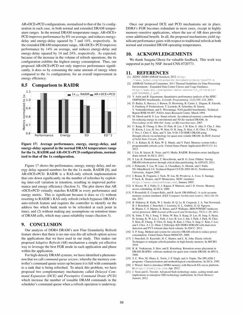
8.5 Comparison to RAIDR
Performance Energy ED ED^20.6
0.7
0.8
0.9
1.0
1.1
Metr
ics
norm
aliz
ed t
o 1
x 1x RAIDR AR+DCE+PCD
Figure 17: Average performance, energy, energy-delay, andenergy-delay squared in the normal DRAM temperature rangefor the 1x, RAIDR and AR+DCE+PCD configurations, normal-ized to that of the 1x configuration.
Figure 17 shows the performance, energy, energy delay, and en-ergy delay squared numbers for the the 1x mode, RAIDR [8], andAR+DCE+PCD. RAIDR is a RAS-only refresh implementationthat cuts down significantly on the number of refreshes by exploit-ing inter-cell variation in retention, resulting in improved perfor-mance and energy efficiency (Section 3). The plot shows that AR+DCE+PCD virtually matches RAIDR in every performance andenergy metric. This is significant because it does so (1) withoutresorting to RAIDR’s RAS-only refresh (which bypasses DRAM’sauto-refresh feature and requires the controller to identify on theaddress bus which bank needs to be refreshed at each point intime), and (2) without making any assumptions on retention timesof DRAM cells, which may cause reliability issues (Section 3).
9. CONCLUSIONOur analysis of DDR4 DRAM’s new Fine Granularity Refresh
feature shows that there is no one-size-fits-all refresh option acrossthe applications that we have used in our study. This makes ourproposed Adaptive Refresh (AR) mechanism a simple yet effectiveway to leverage the best FGR mode in each application and phasewithin the application.
For high-density DRAM systems, we have identified a phenome-non that we call command queue seizure, whereby the memory con-troller’s command queue seizes up because it is full with commandsto a rank that is being refreshed. To attack this problem, we haveproposed two complementary mechanisms called Delayed Com-mand Expansion (DCE) and Preemptive Command Drain (PCD)which increase the number of issuable DRAM commands in thescheduler’s command queue when a refresh operation is underway.
Once our proposed DCE and PCD mechanisms are in place,DDR4’s FGR becomes redundant in most cases, except in highlymemory-sensitive applications, where the use of AR does providesome additional benefit. In all, the proposed mechanisms yield sig-nificant performance gains with respect to traditional refresh at bothnormal and extended DRAM operating temperatures.
10. ACKNOWLEDGEMENTSWe thank Saugata Ghose for valuable feedback. This work was
supported in part by NSF Award CNS-0720773.
11. REFERENCES[1] JEDEC DDR4 SDRAM Standard, 2012. http:
//www.jedec.org/standards-documents/docs/jesd79-4.[2] ASHRAE Technical Committee. 2011 Thermal Guidelines for Data Processing
Environments - Expanded Data Center Classes and Usage Guidance.http://www.eni.com/green-data-center/it_IT/static/pdf/ASHRAE_1.pdf.
[3] V. Aslot and R. Eigenmann. Quantitative performance analysis of the SPECOMPM2001 benchmarks. Scientific Programming, 11(2):105–124, 2003.
[4] D. Bailey, E. Barszcz, J. Barton, D. Browning, R. Carter, L. Dagum, R. Fatoohi,S. Fineberg, P. Frederickson, T. Lasinski, R. Schreiber, H. Simon,V. Venkatakrishnan, and S. Weeratunga. NAS parallel benchmarks. TechnicalReport RNR-94-007, NASA Ames Research Center, March 1994.
[5] M. Ghosh and H. S. Lee. Smart refresh: An enhanced memory controller designfor reducing energy in conventional and 3D die-stacked DRAMs. InProceedings of the 40th Intl. Symp. on Microarchitecture, 2007.
[6] U. Kang, H. Chung, S. Heo, D. Park, H. Lee, J. H. Kim, S. Ahn, S. Cha, J. Ahn,D. Kwon, J. Lee, H. Joo, W. Kim, D. H. Jang, N. Kim, J.-H. Choi, T. Chung,J. Yoo, J. Choi, C. Kim, and Y. Jun. 8 Gb 3-D DDR3 DRAM usingthrough-silicon-via technology for quasi-non-volatile DRAM. In IEEE Journalof Solid State Circuits, 2010.
[7] C. A. Kilmer, K. H. Kim, W. E. Maule, and V. Patel. Memory system with aprogrammable refresh cycle. United States Patent Application #0151131 A1,2012.
[8] J. Liu, B. Jaiyen, R. Veras, and O. Mutlu. RAIDR: Retention-aware intelligentdram refresh. In ISCA, 2012.
[9] S. Liu, K. Pattabiraman, T. Moscibroda, and B. G. Zorn. Flikker: SavingDRAM refresh-power through critical data partitioning. In ASPLOS, 2011.
[10] J. Pisharath, Y. Liu, W. Liao, A. Choudhary, G. Memik, and J. Parhi.NU-MineBench 2.0. Technical Report CUCIS-2005-08-01, NorthwesternUniversity, August 2005.
[11] J. Renau, B. Fraguela, J. Tuck, W. Liu, M. Prvulovic, L. Ceze, S. Sarangi,P. Sack, K. Strauss, and P. Montesinos. SESC simulator.http://sesc.sourceforge.net, January 2005.
[12] S. Rixner, W. J. Dally, U. J. Kapasi, P. Mattson, and J. D. Owens. Memoryaccess scheduling. In ISCA, 2000.
[13] P. Rosenfeld, E. Cooper-Balis, and B. Jacob. DRAMSim2: A cycle accuratememory system simulator. IEEE Computer Architecture Letters, 10(1):16–19,Jan. 2011.
[14] B. Sinharoy, R. Kalla, W. J. Starke, H. Q. Le, R. Cargnoni, J. A. Van Norstrand,B. J. Ronchetti, J. Stuecheli, J. Leenstra, G. L. Guthrie, D. Q. Nguyen,B. Blaner, C. F. Marino, E. Retter, and P. Williams. IBM POWER7 multicoreserver processor. IBM Journal of Research and Technology, 55(3):1–29, 2011.
[15] K. Sohn, T. Na, I. Song, Y. Shim, W. Bae, S. Kang, D. Lee, H. Jung, S. Hyun,H. Jeoung, K. W. Lee, J. Park, J. Lee, B. Lee, I. Jun, J. Park, J. Park, H. Choi,S. Kim, H. Chung, Y. Choi, D. Jung, B. Kim, J. Choi, S. Jang, C. Kim, J. Lee,and J. Choi. A 1.2v 30nm 3.2Gb/s/pin 4Gb DDR4 SDRAM with dual-errordetection and PVT-tolerant data-fetch scheme. In ISSCC, 2012.
[16] S. P. Song. Method and system for selective DRAM refresh to reduce powerconsumption. United States Patent #6094705, 2000.
[17] J. Stuecheli, D. Kaseridis, H. C. Hunter, and L. K. John. Elastic refresh:Techniques to mitigate refresh penalties in high density memory. In MICRO,2010.
[18] R. K. Venkatesan, S. Herr, and E. Rotenberg. Retention-aware placement inDRAM (RAPID): software methods for quasi-non-volatile DRAM. In HPCA,2006.
[19] S. C. Woo, M. Ohara, E. Torrie, J. P. Singh, and A. Gupta. The SPLASH-2programs: Characterization and methodological considerations. In ISCA, 1995.
[20] J. Worrel. Intel to introduce DDR4 memory with Haswell-EX server platform.In http://fudzilla.com, Apr. 2012.
[21] J. Yoon and G. Tressler. Advanced flash technology status, scaling trends andimplications to enterprise SSD technology enablement. In Flash MemorySummit, 2012.
59