
I-65 Interchange Modification at SR 267 and I-65 ... - IN.gov
Upload
khangminh22Category
view
1download
0
www.cypress.com Document No. 001-88889 Rev. *C 1
AN88889
Mitigating Single-Event Upsets Using Cypress’s 65-nm Asynchronous SRAM
Author: Nilesh Badodekar
Associated Project: No
Associated Part Family: CY621xxG30/CY7C10xxG30/ CY621xxGE30/CY7C10xxGE30
Related Application Notes: None
This application note introduces the error correcting code (ECC) feature of Cypress’s 65-nm 16-Mb asynchronous
SRAMs. It explains the major causes of single-event upsets in systems and how they are mitigated conventionally. This
application note also provides an overview of the ECC architecture implemented in Cypress’s 16-Mb devices and
explains the usage model of a new feature that detects and corrects single-bit upsets in Cypress’s SRAMs.
Contents
1 Introduction ............................................................... 1 2 Single-Event Upset ................................................... 2
2.1 Causes of SEU ................................................ 2 3 Mitigating SEUs ........................................................ 3
3.1 Change in Process Technology and Cell Layout ....................................................... 3 3.2 Changes in Chip Design and Architecture ....... 3 3.3 System-Level Mitigation ................................... 4
4 Soft-Error Mitigation in Cypress’s 65-nm Asynchronous SRAM .................................... 5
4.1 Hamming Code ................................................ 5 4.2 Error Correction with Cypress’s SRAM ............ 5
4.3 Soft Error Accumulation Effect in ECC-Protected Memories ................................ 6 4.4 Advantages of 32-Bit Memory Architecture ..... 7
5 Interfacing Cypress’s 65-nm SRAM with ASIC/FPGA/Controller .............................................. 8
5.1 Interfacing the ERR Pin ................................... 8 6 Working Example of Single-Bit Error Correction ..... 10 7 Summary ................................................................ 12 Document History ............................................................ 13 Worldwide Sales and Design Support ............................. 14
1 Introduction
Reliability and data integrity are two of the most important concerns of system designers with regard to memory devices. Modern systems cannot tolerate data corruption in memories due to environmental factors such as radiation. System designers have to rely on techniques such as off-chip error correction or redundancy to achieve higher reliability. These techniques result in overhead, in terms of either PCB space or additional processing time. Cypress’s latest generation of SRAMs offers a single-chip solution with on-chip error correcting code (ECC), reducing board space, cost, and design complexity. These SRAMs are immune to soft errors
1 (FIT rates of less than 0.1 FIT/Mb)
compared to SRAMs without built-in ECC (FIT rate of greater than 150 FIT/Mb). This application note introduces a new feature of Cypress SRAMs that allows system designers to monitor error correction inside the SRAM.
1 Soft errors are possible only through accumulation effect. More details here
Mitigating Single-Event Upsets Using Cypress’s 65-nm Asynchronous SRAM
www.cypress.com Document No. 001-88889 Rev. *C 2
2 Single-Event Upset
Single-event effects are defined as a change of logic states or transients in a device induced by energetic radiation particles from the environment in which the device is operated. The interaction of high-energy particles with semiconductor devices can result in either a bit flip, called a “soft error,” or permanent damage, called a “hard error.” Soft errors are nondestructive because resetting or rewriting the device restores normal behavior. They are unrelated to components or manufacturing failures. Hard errors damage the device. A common example of a hard error is a single-event latch up and the subsequent damage due to high current or thermal runaway.
Soft errors due to single radiation events are called “single-event upsets (SEUs).” SEUs can manifest themselves as either single-bit upsets (SBUs) or multiple-cell upsets (MCUs). SBU refers to the flipping of one bit due to the bombarding of a single energetic particle. MCU refers to the flipping of several bits in the memory array due to the passage of one or more radiation particles.
Whether an MCU event leads to multiple-bit upsets (MBUs) in the output data depends on the architecture of the device. An MBU is an event that occurs if multiple-bit flips happen in such a way that many bits in one output data word are affected. Generally, MBUs need to be mitigated and avoided since they will impair common Hamming code error correction schemes, which work successfully only in SBUs.
With the shrinking of process technology (250 nm to 65 nm and beyond), memory cell size is getting smaller, resulting in a lower core voltage (3.3 V to 1.2 V and lower). This reduces the capacitance inside the memory cell. As a result, the critical charge (the minimum charge for a cell to retain data) required to cause an upset decreases, making memory cells more prone to SEUs. Even an alpha particle or a cosmic ray–generated neutron can disturb the cell.
SEUs are random and rarely catastrophic, as they do not damage the device. Many commercial systems can tolerate some level of soft error. However, for mission-critical applications, soft errors can have a serious impact and may lead not only to data corruption but also to complete system failure.
2.1 Causes of SEU
The major causes of SEU are as follows:
Alpha particles
High-energy neutrons
Thermal neutrons
2.1.1 Alpha Part ic les
Alpha particles are generated by the radioactive decay of trace uranium-238 and thorium-232 in the quartz filler used in mold compounds. These impurities release alpha particles. Alpha particles cannot traverse large distances in
matter, and their effect is limited to the immediate vicinity of their emission site (about 50 m). Thus, external alpha particle sources cannot usually affect packaged semiconductor devices. Manufacturers use ultra-low-alpha (ULA) particle emission mold compounds to reduce the occurrence of soft errors caused by alpha particles.
2.1.2 High-Energy Neutrons
High-energy cosmic particles (mostly protons) react with the upper atmosphere of the earth. Their collisions, modulated by the earth’s magnetic field, generate high-energetic recoil particles such as muons, pions, and neutrons. Only the chargeless high-energy neutrons have the potential to reach the earth’s surface to interact with semiconductor devices. Their remaining energy is about 1-500 MeV when they reach the earth’s surface.
For a high-energy neutron to cause a soft error, it must produce ionized particles by colliding with the silicon nucleus and undergo impact ionization with the silicon nuclei. This collision can generate alpha particles and other heavier ions, producing electron-hole pairs, but with higher energies than a typical alpha particle from mold compounds.
Neutrons are particularly troublesome, because they can penetrate most manmade constructions. For example, a neutron can pass through five feet of concrete. The flux rate is geoposition dependent and increases at higher altitudes due to the lower shielding effect of the atmosphere. Commonly known good moderators of neutrons are water and soil. Therefore, low-neutron environments can be found in tunnels, caves, and submarines.
Mitigating Single-Event Upsets Using Cypress’s 65-nm Asynchronous SRAM
www.cypress.com Document No. 001-88889 Rev. *C 3
2.1.3 Thermal Neutrons
Thermal neutrons are low-energy neutrons at the end of a cosmic shower. They start off as high-energy neutrons but lose energy due to multiple collisions as they travel toward the surface of the earth. Each collision takes away some energy, so by the time they reach the surface, the amount of energy that thermal neutrons have is very low (about 25 meV).
Usually, thermal neutrons never cause soft errors by themselves. However, 10B, an isotope of boron found in borophosphosilicate glass (BPSG) oxide films of semiconductors, interacts with thermal neutrons and decays into lithium, helium nuclei, and a gamma ray, which leads to soft errors. To prevent the effect of thermal neutrons, the semiconductor industry has shifted from BPSG to phosphosilicate glass (PSG) oxide films. Cypress’s 65-nm asynchronous SRAMs do not contain BPSG and therefore are not susceptible to thermal neutrons.
3 Mitigating SEUs
The primary methods of soft-error mitigation in asynchronous SRAMs are as follows:
Change in process technology and cell layout to reduce soft-error susceptibility
Changes in chip design and architecture
System-level mitigation
3.1 Change in Process Technology and Cell Layout
Soft errors occur when the charge generated by the interaction of high-energy particles with the semiconductor substrate exceeds the critical charge (QCRIT) stored in a SRAM cell. According to a model proposed by Roche, et al. (Equation 1), QCRIT is a function of the node capacitance (CN), operating voltage (VDD), maximum drain conduction current (IDP), and flipping time of the cell (TF). The reliability of a SRAM device can be enhanced by increasing the cell capacitance.
Equation 1. Critical Charge (QCRIT)
QCRIT = CN* VDD + IDP* TF
However, mitigation techniques based on process technology and cell layout changes come at a cost. The use of an additional capacitor or larger cell sizes increases the access time and standby current (current consumed by the SRAM in disabled condition), negatively impacting the device’s performance.
3.2 Changes in Chip Design and Architecture
Architectural enhancements, such as embedded ECC and bit interleaving, can be used to limit the effects of soft errors on semiconductor devices. Cypress’s 65-nm asynchronous SRAMs implement both the techniques mentioned in this section to mitigate soft errors.
3.2.1 Embedded ECC
The error correction and coding scheme implemented in software can be hard-coded into the chip architecture to make the correction transparent to the system designer.
3.2.2 Bit In ter leaving
The collision of high-energy particles with semiconductor atoms may affect multiple cells. An MBU occurs when a single energetic particle affects two or more bits in the same data word. Bit interleaving techniques eliminate MBU events in SRAMs from a single particle hit.
Bit interleaving arranges SRAM cells so that physically adjacent bit lines are mapped to different word registers. The bit interleaving distance separates two consecutive bits mapped to the same word register. If the bit interleaving distance is greater than the spread of a multi cell upset (MCU), it results in multiple SBUs in multiple words instead of an MBU in a single word. In a bit-interleaved memory, the single-bit error correction algorithm can be used to detect and correct all errors.
Figure 1 and Figure 2 illustrate how bit interleaving is advantageous when an MCU occurs. In non-interleaved memory (Figure 1), when an MCU occurs, multiple cells in the same word may be affected. When the system reads this word, single-bit ECC cannot correct it, which leads to the system reading and processing incorrect data.

Mitigating Single-Event Upsets Using Cypress’s 65-nm Asynchronous SRAM
www.cypress.com Document No. 001-88889 Rev. *C 4
However, in interleaved memory, when an MCU occurs, multiple cells are affected, but they are spread out to multiple words. Therefore, each word will have only an SBU. When the system reads these words, single-bit ECC can correct them, so the system processes the correct data for all words.
Figure 1. Non-Interleaved Memory
Address1
Address2
Address3
Address4
Address5
Address6
Address7
Address8
8-bit Memory Array
Address1 Data
Multiple cells affected
Single address with
multiple bit upsets
Figure 2. Interleaved Memory
Address1 Data
Bit Interleaving Distance
Address2 Data Address3 Data
Multiple cells
affected
3.3 System-Level Mitigation
At the system level, soft errors can be mitigated by implementing redundancy or ECC in software.
In the triple modular redundancy scheme, data is stored in three SRAMs simultaneously. Thus, on every read, all three SRAMs are read together, and the outputs are fed to a majority voting scheme. If one SRAM is affected by an SEU, then the majority voting scheme ensures that the final output data is correct, as the remaining two SRAMs have not been affected by the SEU.
System designers can implement an ECC scheme in software in which the controller or ASIC generates parity bits for all the data bits and stores them in a separate SRAM. In this way, during every read cycle, the controller accesses both the data bits and parity bits and corrects the data if an error has occurred.
Using redundant SRAMs or implementing an ECC scheme in software adds overhead in terms of board space and execution time. It also makes the design complex due to additional design efforts for the board and software.

Mitigating Single-Event Upsets Using Cypress’s 65-nm Asynchronous SRAM
www.cypress.com Document No. 001-88889 Rev. *C 5
4 Soft-Error Mitigation in Cypress’s 65-nm Asynchronous SRAM
Cypress’s 65-nm SRAMs use Hamming code for single-bit soft error mitigation. Hamming code is the simplest, most reliable, and well-known ECC scheme. This section explains the Hamming code used in Cypress’s SRAMs.
4.1 Hamming Code
Hamming codes are a family of linear ECCs. Equation 2 summarizes the basic equation for Hamming code for any length n.
Equation 2. Hamming Code Formula
Where, k = number of data bits m = number of parity check bits n = code length, n = m + k
The memory array for Cypress’s SRAM is arranged as a 32-bit word space. For a 32-bit data word, the lowest value of m is 6. This results in a code length (n) of 38. Therefore, Cypress uses a (32, 38) Hamming code for single-bit error detection and correction.
4.2 Error Correction with Cypress’s SRAM
Cypress’s 65-nm asynchronous SRAM has a hardware ECC block that performs all ECC-related functions inline. This encoding happens without user intervention and without affecting the access-time performance of the device.
The single-bit error detection and correction capability is supplemented by a 16-bit interleaving scheme to prevent the occurrence of multi-bit errors. Figure 3 illustrates the block diagram of a 65-nm Cypress asynchronous SRAM.
Figure 3. Internal Organization of 65-nm Asynchronous SRAM
The 6 parity bits are generated and stored along with the 32-bit data word during every write operation. The (32, 38) Hamming architecture allows Cypress’s 65-nm SRAMs to detect and correct single-bit errors during every read operation.
Cypress’s 65-nm asynchronous SRAMs with an ordering code that includes an “E” (for example, CY7C1061GE30) have an additional output pin called “ERR” on the package. This ERR pin allows system designers to monitor the output of the SRAM’s ECC logic during every read cycle. During a read cycle, if there is no single-bit error, the ERR pin is deasserted. However, if there is a single-bit error in the 32-bit word being read from the SRAM, then the ERR pin is asserted HIGH for the current read cycle.
Mitigating Single-Event Upsets Using Cypress’s 65-nm Asynchronous SRAM
www.cypress.com Document No. 001-88889 Rev. *C 6
The ECC logic allows the read data to be corrected even if the original copy of this corrupted data in memory remains corrupted. During read cycles in which no single-bit error detection and correction has happened, the ERR pin will be deasserted. Over a period of time, subsequent SEUs may accumulate in the memory array if not overwritten by the application. This will lead to an increasing number of “stored” soft errors in the memory array. If the number of stored soft errors reaches a critical threshold NTH, the very next soft error may result in MBUs in the same data word, since the data words in the memory array have already been polluted with one SBU. This effect, called the “accumulation effect,” is discussed in detail in the next section.
The detection and correction of MBUs is not supported by Cypress’s ECC architecture. Devices with the ERR pin will flag the MBU; however, the condition of the data is not corrected in such a scenario, and it may contain MBUs. However, the time to reach the critical accumulated soft error threshold NTH depends on the generation rate of the soft errors and the application mode. One option to completely eliminate this potential issue is to refresh the impacted memory cells with the correct data whenever an upset is detected and flagged by the ERR pin. This will prevent multiple SEUs from accumulating and turning into MBUs. If immediate rewriting into memory is not possible, the next section provides application-specific guidelines.
4.3 Soft Error Accumulation Effect in ECC-Protected Memories
The accumulation effect applies to all types of ECC-protected memories such as DRAM, SRAM, and nonvolatile memories. Whether the accumulation effect is causing MBU events at the memory data level depends on the implementation of the embedded/system ECC algorithms. Higher bit count ECC schemes such as Reed-Solomon and double-error detection/correction Hamming code schemes can successfully correct potential double bits originating from the accumulation effect. Economic single-error detection and correction schemes require further analyses to determine the time to reach the critical threshold of accumulated soft errors NTH.
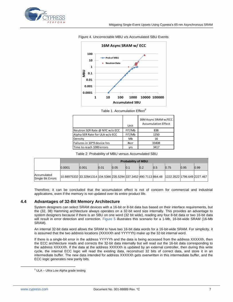
A modified birthday statistic2 has been used to calculate the probability of an uncorrectable double-bit error for a
given number of accumulated single-bit errors in the memory array. Figure 4 depicts the probability of such an MBU event, including experimental verification of the probability slope with alpha particle and heavy ion measurement results for Cypress’s 16-Mb asynchronous SRAM device (Table 1).
Based on the experimental data shown in Figure 4 and Table 1, the critical threshold for accumulated soft error has been determined to be NTH=1,000 errors. If more than NTH errors are accumulated in the memory, then an MBU event will occur. The worst-case application modes to accumulate soft errors are the data retention mode and read-only access mode. The memory is not written to at all in both cases, and soft errors are accumulated over the operating time of the memory. The worst-case accumulation rate is the non-ECC-protected failure rate of 838 FIT/Mb in data retention mode. However, it would take up to 3,417 years at the NYC location to accumulate 1,000 soft errors in the memory array.
Table 2 gives the probability of MBU to occur for given number of SBU errors. This data can be used to predict the likelihood of an MBU in a system that can expect a particular number SBUs. For example, if a system experiences 864 single bit errors, it is 50% likely that the system will experience a double bit event which the ECC won’t be able to correct (An MBU).
2 Tausch, H.J., “Simplified Birthday Statistics and Hamming EDAC,” IEEE Transactions on Nuclear Science, Vol 56(2), 2009,
pp.474-478.
Mitigating Single-Event Upsets Using Cypress’s 65-nm Asynchronous SRAM
www.cypress.com Document No. 001-88889 Rev. *C 7
Figure 4. Uncorrectable MBU v/s Accumulated SBU Events
Table 1. Accumulation Effect3
Table 2: Probability of MBU versus Accumulated SBU
Probability of MBU
0.0001 0.001 0.01 0.05 0.1 0.2 0.5 0.75 0.95 0.99
Accumulated Single Bit Errors
10.88975332 33.32841314 104.5366 235.5294 337.3452 490.7113 864.48 1222.3522 1796.649 2227.467
Therefore, it can be concluded that the accumulation effect is not of concern for commercial and industrial applications, even if the memory is not updated over its entire product life.
4.4 Advantages of 32-Bit Memory Architecture
System designers can select SRAM devices with a 16-bit or 8-bit data bus based on their interface requirements, but the (32, 38) Hamming architecture always operates on a 32-bit word size internally. This provides an advantage to system designers because if there is an SBU on one word (32 bit wide), reading any four 8-bit data or two 16-bit data will result in error detection and correction. Figure 5 illustrates this scenario for a 1-Mb, 16-bit-wide SRAM (16-Mb SRAM).
An internal 32-bit data word allows the SRAM to have two 16-bit data words for a 16-bit-wide SRAM. For simplicity, it is assumed that the two address locations (XXXXXh and YYYYYh) make up the 32-bit internal word.
If there is a single-bit error in the address YYYYYh and the data is being accessed from the address XXXXXh, then the ECC architecture reads and corrects the 32-bit data internally but will read out the 16-bit data corresponding to the address XXXXXh. If the data at the address XXXXXh is updated by an external controller, then during this write cycle, the internal ECC logic will read the existing data, reconstruct 32 bits of correct data, and store it in an intermediate buffer. The new data intended for address XXXXXh gets overwritten in this intermediate buffer, and the ECC logic generates new parity bits.
3 ULA – Ultra Low Alpha grade testing
0.0001
0.001
0.01
0.1
1
10
100
1 10 100 1000 10000 100000
MB
U
Accumulated SBU
16M Async SRAM w/ ECC
Prob of MBU
Neutron Data
Unit
16M Async SRAM w/ECC
Accumulation Effect
Neutron SER Rate @ NYC w/o ECC FIT/Mb 838
Alpha SER Rate for ULA w/o ECC FIT/Mb 1250
Density Mb 16
Failures in 10^9 device hrs #err 33408
Time to reach 1000 errors yrs 3417
Mitigating Single-Event Upsets Using Cypress’s 65-nm Asynchronous SRAM
www.cypress.com Document No. 001-88889 Rev. *C 8
Due to this intrinsic scrubbing, the data corresponding to address YYYYYh gets corrected automatically. Thus, for a 16-bit SRAM, every write cycle allows the user to correct data in one more 16-bit location, while for an 8-bit SRAM, 3 such locations get updated during every write cycle. For devices with an ERR pin, as the SRAM has detected and corrected an error in the 32-bit word, the ERR pin will be asserted even while accessing the address XXXXXh. System designers should acknowledge this ERR assertion and write back the same data that was read from the address XXXXXh previously. During this writeback, the internal ECC logic will generate new parity bits and correct the complete 32-bit data word. This corrects the address YYYYYh as well and thus helps maintain data integrity.
Figure 5. 16-Bit Data Word Read From a 32-Bit Internal Word
D31 D30 D29 D28 D27 D26 D25 D24 D23 D22 D21 D20 D19 D18 D17 D31D16 D15 D14 D13 D12 D11 D10 D9 D8 D7 D6 D5 D4 D3 D2 D1 D0
Data for Address XXXXXh Data for Address YYYYYh
Corrupted cellAddress read by user
5 Interfacing Cypress’s 65-nm SRAM with ASIC/FPGA/Controller
System designers can use the ERR pin to monitor the integrity of the data in SRAM. As the ERR signal gets asserted only when the SRAM detects and corrects a single-bit error, it is recommended to weakly pull down the signal to avoid intermediate voltage levels during write operations or when the SRAM is disabled. During write cycles or chip disable cycles, the ERR pin is in HI-Z state.
5.1 Interfacing the ERR Pin
Cypress SRAMs without the ERR pin can be interfaced in the system just like legacy SRAMs. For SRAMs with the ERR option, system designers need to interface the ERR pin correctly in the system. If the ERR pin is not used in the system, then it can be left open. This section explains interfacing the ERR pin in three basic scenarios using SRAMs.
Systems with a single SRAM
Width expansion
Depth expansion
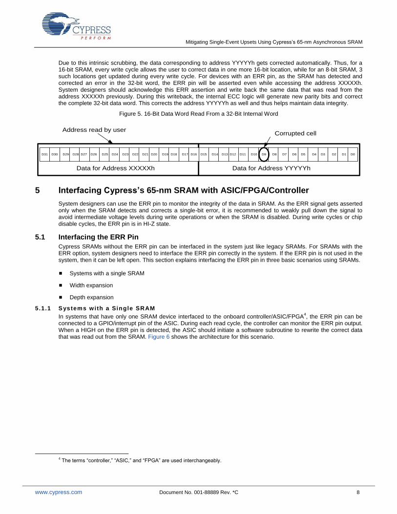
5.1.1 Systems with a Single SRAM
In systems that have only one SRAM device interfaced to the onboard controller/ASIC/FPGA4, the ERR pin can be
connected to a GPIO/interrupt pin of the ASIC. During each read cycle, the controller can monitor the ERR pin output. When a HIGH on the ERR pin is detected, the ASIC should initiate a software subroutine to rewrite the correct data that was read out from the SRAM. Figure 6 shows the architecture for this scenario.
4 The terms “controller,” “ASIC,” and “FPGA” are used interchangeably.
Mitigating Single-Event Upsets Using Cypress’s 65-nm Asynchronous SRAM
www.cypress.com Document No. 001-88889 Rev. *C 9
Figure 6. Interfacing Cypress SRAM
ASIC/
CONTROLLER/
FPGA
CYPRESS’ 65nm Async
16M SRAM With ERR
ERR
CE#
WE#
OE#
GPIO/INTR
D15:D0
A19:A0
CE#
WE#
OE#
D15:D0
A19:A0
RPD
5.1.2 Width Expansion
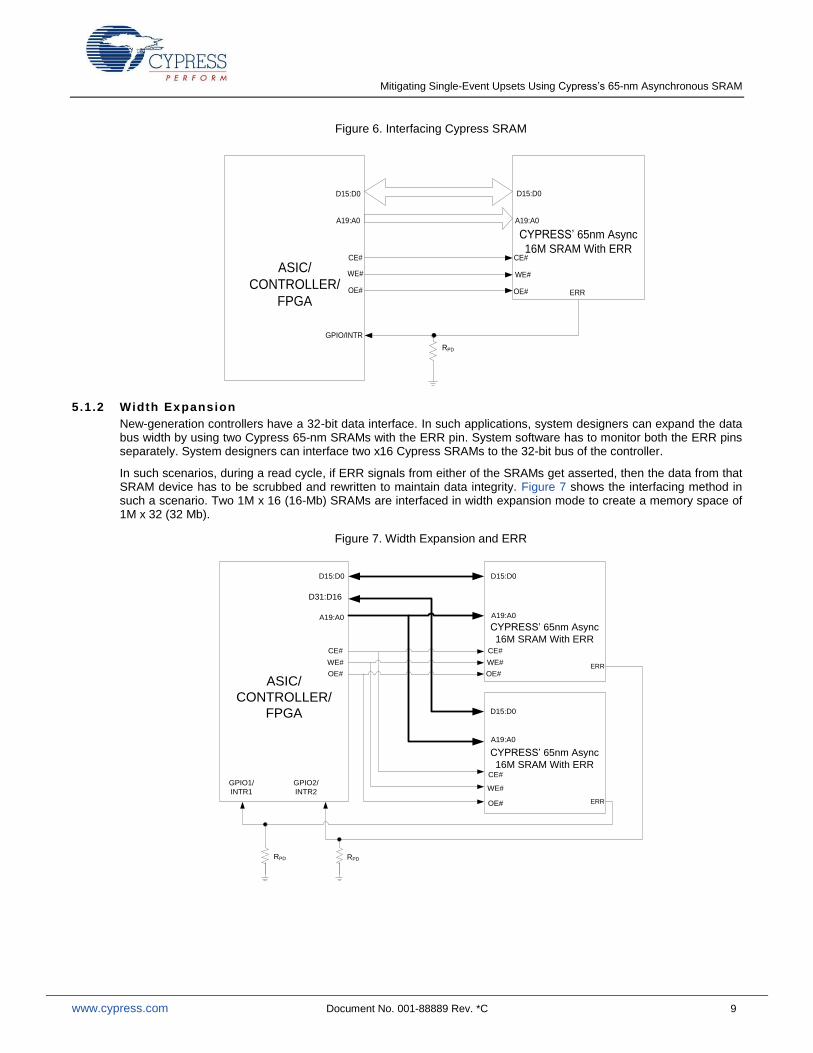
New-generation controllers have a 32-bit data interface. In such applications, system designers can expand the data bus width by using two Cypress 65-nm SRAMs with the ERR pin. System software has to monitor both the ERR pins separately. System designers can interface two x16 Cypress SRAMs to the 32-bit bus of the controller.
In such scenarios, during a read cycle, if ERR signals from either of the SRAMs get asserted, then the data from that SRAM device has to be scrubbed and rewritten to maintain data integrity. Figure 7 shows the interfacing method in such a scenario. Two 1M x 16 (16-Mb) SRAMs are interfaced in width expansion mode to create a memory space of 1M x 32 (32 Mb).
Figure 7. Width Expansion and ERR
CYPRESS’ 65nm Async
16M SRAM With ERR
ASIC/
CONTROLLER/
FPGA
CYPRESS’ 65nm Async
16M SRAM With ERR
ERR
CE#
WE#
OE#
GPIO1/
INTR1
D15:D0
A19:A0
CE#
WE#
OE#
D15:D0
A19:A0
CE#
WE#
OE#
A19:A0
D15:D0
D31:D16
ERR
GPIO2/
INTR2
RPDRPD
Mitigating Single-Event Upsets Using Cypress’s 65-nm Asynchronous SRAM
www.cypress.com Document No. 001-88889 Rev. *C 10
5.1.3 Depth Expansion
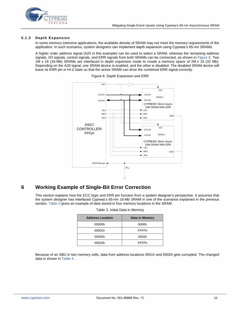
In some memory-intensive applications, the available density of SRAM may not meet the memory requirements of the application. In such scenarios, system designers can implement depth expansion using Cypress’s 65-nm SRAMs.
A higher order address signal (A20 in this example) can be used to select a SRAM, whereas the remaining address signals, I/O signals, control signals, and ERR signals from both SRAMs can be connected, as shown in Figure 8. Two 1M x 16 (16-Mb) SRAMs are interfaced in depth expansion mode to create a memory space of 2M x 16 (32 Mb). Depending on the A20 signal, one SRAM device is enabled, and the other is disabled. The disabled SRAM device will leave its ERR pin in HI-Z state so that the active SRAM can drive the combined ERR signal correctly.
Figure 8. Depth Expansion and ERR
ASIC/
CONTROLLER/
FPGA
CYPRESS’ 65nm Async
16M SRAM With ERR
ERR
CE#
WE#
OE#
D15:D0
A19:A0
CE#
WE#
OE#
D15:D0
A19:A0
CYPRESS’ 65nm Async
16M SRAM With ERRCE#
WE#
OE#
D15:D0
A19:A0
ERR
CE2
CE2
A20
GPIO/Interrupt
SRAM 1
SRAM 2
RPD
6 Working Example of Single-Bit Error Correction
This section explains how the ECC logic and ERR pin function from a system designer’s perspective. It assumes that the system designer has interfaced Cypress’s 65-nm 16-Mb SRAM in one of the scenarios explained in the previous section. Table 3 gives an example of data stored in four memory locations in the SRAM.
Table 3. Initial Data in Memory
Address Location Data in Memory
00000h 0000h
00001h FFFFh
00002h 0002h
00003h FFFFh
Because of an SBU in two memory cells, data from address locations 0001h and 0002h gets corrupted. The changed data is shown in Table 4.

Mitigating Single-Event Upsets Using Cypress’s 65-nm Asynchronous SRAM
www.cypress.com Document No. 001-88889 Rev. *C 11
Table 4. Data in Memory After SBU
Address Location Data in Memory
00000h 0000h
00001h FFFEh
00002h 0003h
00003h FFFFh
If a read access is performed on these four addresses, the ECC logic will correct the data word that was corrupted, and you will get the corrected data at the output. A device with the ERR pin will see this pin getting asserted during the read cycle of a corrected data word. During read cycles without any single-bit error correction, the ERR pin will be deasserted by the SRAM. Table 5 shows the final output and state of the ERR pin.
Table 5. Read Cycles
Address Location
Data in Memory
Data at I/O during Read Cycle
ERR Pin Status
00000h 0000h 0000h 0
00001h FFFEh FFFFh 1
00002h 0003h 0002h 1
00003h FFFFh FFFFh 0
Every single-bit error will be detected and corrected, while devices with the ERR pin option provide the additional advantage of flagging every correction. The status of the ERR pin can be used in application software to initiate a subroutine and write back the correct data to affected address locations. Figure 9 summarizes the entire read operation and highlights the key timing parameters. Refer to the device datasheet for the timing parameters of the ERR pin.
Figure 9. Address-Controlled Read Cycles and ERR Pin Status During Error Correction
Address
I/O
OE#
WE#
CE#
ERR
tAA
tAA tAA
tRC
00000h 00001h 00002h 00003h
0000h FFFFh 0002h FFFFh
Don’t Care
High
Impedance
Address-Controlled Read Cycles and ERR Pin Behavior During Error Correction
Mitigating Single-Event Upsets Using Cypress’s 65-nm Asynchronous SRAM
www.cypress.com Document No. 001-88889 Rev. *C 12
7 Summary
Data integrity is an essential feature of modern systems. SEUs pose a threat to data stored in SRAMs in terms of bit upsets. Implementing error detection and correction in the system software or at the system level, however, imposes a penalty in terms of PCB area and timing performance. Cypress’s 65-nm asynchronous SRAM allows system designers to offload the single-bit error correction functionality to SRAM. The optional ERR feature lets users monitor the SRAM data for single-bit errors and maintain data integrity by refreshing the corrupted data.
About the Author
Name: Nilesh Badodekar.
Title: Applications Engineer Staff
Background: Nilesh Badodekar has a Master’s degree in Visual Information Processing and Embedded Systems from I.I.T. Kharagpur, India.
Mitigating Single-Event Upsets Using Cypress’s 65-nm Asynchronous SRAM
www.cypress.com Document No. 001-88889 Rev. *C 13
Document History
Document Title: AN88889 – Mitigating Single-Event Upsets Using Cypress’s 65-nm Asynchronous SRAM
Document Number: 001-88889
Revision ECN Orig. of Change
Submission Date
Description of Change
** 4365000 NILE 04/29/2014 New Application Note
*A 4378473 NILE 05/13/2014 Quoted CY7C1061GE30 device for ERR feature
*B 4665757 HRP/NILE 03/31/3015 Added section about accumulation effect
Updated Figure 6, Figure 7, and Figure 8 to recommend a weak pull-down
Clarified the write process in ECC SRAMs
Updated template
*C 4938409 HRP/NILE 09/29/2015 Added Table 2
Added TOC
Updated template
Mitigating Single-Event Upsets Using Cypress’s 65-nm Asynchronous SRAM
www.cypress.com Document No. 001-88889 Rev. *C 14
Worldwide Sales and Design Support
Cypress maintains a worldwide network of offices, solution centers, manufacturer’s representatives, and distributors. To find the office closest to you, visit us at Cypress Locations
Products
Automotive cypress.com/go/automotive
Clocks & Buffers cypress.com/go/clocks
Interface cypress.com/go/interface
Lighting & Power Control cypress.com/go/powerpsoc
Memory cypress.com/go/memory
PSoC cypress.com/go/psoc
Touch Sensing cypress.com/go/touch
USB Controllers cypress.com/go/usb
Wireless/RF cypress.com/go/wireless
PSoC® Solutions
psoc.cypress.com/solutions
PSoC 1 | PSoC 3 | PSoC 4 | PSoC 5LP
Cypress Developer Community
Community | Forums | Blogs | Video | Training
Technical Support
cypress.com/go/support
PSoC is a registered trademark of Cypress Semiconductor Corp. All other trademarks or registered trademarks referenced herein are the property of their respective owners.
Cypress Semiconductor 198 Champion Court San Jose, CA 95134-1709
Phone : 408-943-2600 Fax : 408-943-4730 Website : www.cypress.com
© Cypress Semiconductor Corporation, 2014-2015. The information contained herein is subject to change without notice. Cypress Semiconductor Corporation assumes no responsibility for the use of any circuitry other than circuitry embodied in a Cypress product. Nor does it convey or imply any license under patent or other rights. Cypress products are not warranted nor intended to be used for medical, life support, life saving, critical control or safety applications, unless pursuant to an express written agreement with Cypress. Furthermore, Cypress does not authorize its products for use as critical components in life-support systems where a malfunction or failure may reasonably be expected to result in significant injury to the user. The inclusion of Cypress products in life-support systems application implies that the manufacturer assumes all risk of such use and in doing so indemnifies Cypress against all charges. This Source Code (software and/or firmware) is owned by Cypress Semiconductor Corporation (Cypress) and is protected by and subject to worldwide patent protection (United States and foreign), United States copyright laws and international treaty provisions. Cypress hereby grants to licensee a personal, non-exclusive, non-transferable license to copy, use, modify, create derivative works of, and compile the Cypress Source Code and derivative works for the sole purpose of creating custom software and or firmware in support of licensee product to be used only in conjunction with a Cypress integrated circuit as specified in the applicable agreement. Any reproduction, modification, translation, compilation, or representation of this Source Code except as specified above is prohibited without the express written permission of Cypress. Disclaimer: CYPRESS MAKES NO WARRANTY OF ANY KIND, EXPRESS OR IMPLIED, WITH REGARD TO THIS MATERIAL, INCLUDING, BUT NOT LIMITED TO, THE IMPLIED WARRANTIES OF MERCHANTABILITY AND FITNESS FOR A PARTICULAR PURPOSE. Cypress reserves the right to make changes without further notice to the materials described herein. Cypress does not assume any liability arising out of the application or use of any product or circuit described herein. Cypress does not authorize its products for use as critical components in life-support systems where a malfunction or failure may reasonably be expected to result in significant injury to the user. The inclusion of Cypress’ product in a life-support systems application implies that the manufacturer assumes all risk of such use and in doing so indemnifies Cypress against all charges. Use may be limited by and subject to the applicable Cypress software license agreement.
Copyright © 2022 FDOKUMEN