Towards a Unified Framework for Cohesion Measurement in Aspect-Oriented Systems
18
Notice of Violation of IEEE Publication Principles “A multi-rate 9.953-12.5-GHz 0.2- μm SiGe BiCMOS LC oscillator using a resistor-tuned varactor and a supply pushing cancellation circuit” by Maxim, A. in the IEEE Journal of Solid-State Circuits, Volume 41, Issue 4, April 2006 Page(s):918 - 934 After careful and considered review, it has been determined that the above paper is in violation of IEEE's Publication Principles. Specifically, the paper contains information that Adrian Maxim admits had been falsified. In response to an inquiry on this misconduct, Mr. Maxim acknowledged that the following people who have been listed as co-authors on several of his papers are fabricated names and that he is the only author: C. Turinici D. Smith S. Dupue M. Gheorge R. Johns D. Antrik Additionally, in papers by Mr. Maxim that have co-authors other than those listed above, it was discovered in some cases that he had not consulted with them while writing the papers, and submitted papers without their knowledge. Although Mr. Maxim maintains that not all of the data is falsified, IEEE nevertheless cannot assure the integrity of papers posted by him because of his repeated false statements. Due to the nature of this violation, reasonable effort should be made to remove all past references to the above paper, and to refrain from any future references.
Transcript of Towards a Unified Framework for Cohesion Measurement in Aspect-Oriented Systems

Notice of Violation of IEEE Publication Principles
“A multi-rate 9.953-12.5-GHz 0.2- μm SiGe BiCMOS LC oscillator using a resistor-tuned varactor and a supply pushing cancellation circuit” by Maxim, A. in the IEEE Journal of Solid-State Circuits, Volume 41, Issue 4, April 2006 Page(s):918 - 934
After careful and considered review, it has been determined that the above paper is in violation of IEEE's Publication Principles.
Specifically, the paper contains information that Adrian Maxim admits had been falsified. In response to an inquiry on this misconduct, Mr. Maxim acknowledged that the following people who have been listed as co-authors on several of his papers are fabricated names and that he is the only author:
C. Turinici D. Smith S. Dupue M. Gheorge R. Johns D. Antrik
Additionally, in papers by Mr. Maxim that have co-authors other than those listed above, it was discovered in some cases that he had not consulted with them while writing the papers, and submitted papers without their knowledge. Although Mr. Maxim maintains that not all of the data is falsified, IEEE nevertheless cannot assure the integrity of papers posted by him because of his repeated false statements. Due to the nature of this violation, reasonable effort should be made to remove all past references to the above paper, and to refrain from any future references.
918 IEEE JOURNAL OF SOLID-STATE CIRCUITS, VOL. 41, NO. 4, APRIL 2006
A Multi-Rate 9.953–12.5-GHz 0.2-�m SiGeBiCMOS LC Oscillator Using a Resistor-Tuned
Varactor and a Supply Pushing Cancellation CircuitAdrian Maxim, Member, IEEE
Abstract—A multi-rate 9.953–12.5-GHz low phase noise LCoscillator was realized in a 90-GHz 0.2 m SiGe BiCMOSprocess. It achieves a 36% tuning range by combining a 35%open-loop frequency calibration range having a sub-0.1% residualerror with a 1% closed-loop varactor frequency tuning. Theoscillator gain is below 130 MHz/V, while having less than 10%variation over the entire tuning range. The varactor is realizedwith multiple parallel-connected cells consisting of constant capac-itors and voltage-controlled resistors that bring a lower processvariation and a higher quality factor in comparison with standarddiode and MOS varactors. A dual regulator architecture was usedto provide both high PSRR and low output voltage noise. Thesupply pushing was reduced below 100 kHz/V by using a pushingcancellation circuit that balances the negative and positive voltagecoefficients of the different nonlinear capacitors connected to theLC tank. A discrete-time automatic amplitude control loop using avariable tail resistor architecture was implemented to optimize theVCO’s phase noise performance. The VCO specifications include9.953–12.5-GHz frequency range, 0.1% frequency calibrationerror, 122 dBc/Hz phase noise at 1 MHz offset, 3 kHz 1 3
corner frequency, 80 dBc spurious tones, 250 400 m2 diearea and 5-mA bias current from a 3.3-V supply.
Index Terms—BiCMOS, frequency calibration, LC oscillators,optical communications, phase noise, SiGe, SONET, varactor.
I. INTRODUCTION
BUILDING low phase noise oscillators for 10-Gb/s opticalcommunications is challenging even in modern processes
having high transition frequencies ( 50–100 GHz). In theearly days of optical communications integration Si-bipolar [1]and GaAs [2] processes have dominated the serializer–deseri-alizer (SERDES) applications. With the latest technology ad-vancements, the SiGe heterojunction bipolar transistor (HBT)[5]–[8] and the deep-submicron CMOS [9]–[22] processes be-came predominant in the 10-Gb/s SERDES market. In order toachieve a low phase noise oscillator, the of the active de-vices needs to be at least a factor of 5–10 higher than the os-cillating frequency. This ensures a negligible delay through theoscillator amplifier and therefore a relative independence of theoscillating frequency on the active device parameters, temper-ature, and supply voltage. One solution to build 10-GHz oscil-lators in processes that have a low transition frequency (25–50 GHz) is to first generate a 5-GHz clock and then use a
Manuscript received September 5, 2005; revised December 19, 2005.The author is with Silicon Laboratories, Austin, TX 78735 USA (e-mail: ac-
[email protected]).Digital Object Identifier 10.1109/JSSC.2006.870914
polyphase filter and a frequency doubler to multiply the clockfrequency up to 10 GHz [7].
The major advantages of using a bipolar VCO amplifierversus a CMOS implementation are, first, a larger , whichresults in less delay in the amplifier, and therefore a betterfrequency stability with lower phase noise impact from theautomatic amplitude control loop (AAC) and tail current sourcenoise, and, second, a larger device breakdown voltage, whichallows a higher oscillating amplitude with a quadratic impact onphase noise reduction [23]. Moreover, the bipolar devices havelower nonlinear parasitic capacitances that lead to a reducedsupply pushing and AM-to-PM conversion [8]. In contrast,MOSFETs are much better suited for the implementation ofthe frequency calibration network that requires a quasi-idealswitch function [16].
Another challenge in building 10-Gb/s optical commu-nications compliant oscillators is to ensure a large tuningrange that covers all existing standards [8], [10], [22]: OC192SONET/SDH 9.953 GHz, 10 Gbit Ethernet 10.31 GHz, OpticalTransport Networks 10.71 GHz, or systems with super forwarderror correction 12.5 GHz. In the past, multi-oscillator solutionswere used, in which a separate LC oscillator was integratedfor each supported communication frequency [7]. This bringsa large area penalty, as the synthesizer die estate is dominatedby the on-chip planar inductors.
Covering a wide 9.953–12.5-GHz frequency range, while en-suring an additional 10% to 15% range to accommodate theprocess, temperature, and supply variation of the LC oscillatorfrequency, leads to an oscillator with an ultra-wide tuning range,in which most of the tank capacitance needs to be implementedas varactors [11]–[18]. The lower quality factor of the varac-tors in comparison with the fixed capacitors leads to a degradedVCO phase noise performance. Furthermore, a large frequencyrange and a low available control voltage range (limited by thesupply voltage and device breakdown voltages) results in a largeoscillator gain, which increases both intrinsic device noise andcoupled spurious tones up-conversion around the carrier [23],[24].
This paper presents an oscillator that uses a high-resolutionfrequency calibration network that covers a 35% range (25% forfrequency change and 10% for process variation) and brings thefrequency within 0.1% of the target value [8]. Therefore, a 1%varactor tuning range was sufficient in the VCO to compensatefor the residual calibration error and the subsequent temperatureor supply frequency pushing. This results in a low VCO gain thatsignificantly improves the phase noise performance.
0018-9200/$20.00 © 2006 IEEE

MAXIM: SIGE BICMOS LC OSCILLATOR USING A RESISTOR-TUNED VARACTOR AND A SUPPLY PUSHING CANCELLATION CIRCUIT 919
Widely used varactors in 10-GHz oscillators are the reversed-biased bipolar diode [3], [4], [19] and the accumulation MOScapacitor [10]–[18]. The first one suffers from low quality factorat 10 GHz, due to the large series resistance of the nondepletedsilicon layer, which usually dominates the LC tank losses andthus the VCO phase noise level [7]. Furthermore, its qualityfactor varies significantly across the VCO tuning range. The ac-cumulation MOS-capacitor varactor achieves a higher qualityfactor and ratio. It can use either a single-ended[10]–[15] or a differential control voltage [16]. Its drawbacksare a large process variation that requires a larger frequency cal-ibration range, and a wide change of the tuning gain over thecontrol voltage range that degrades the frequency synthesizerperformance due to the loop gain variation. A more complexphase-locked-loop (PLL) loop filter is required to compensatefor the loop gain changes with frequency [10].
Most existing bipolar processes have available only the re-verse-biased diode varactors, which are often connected to a tapin the LC tank [7], in order to increase the maximum oscilla-tion amplitude and reduce their low quality factor impact onthe VCO’s phase noise. CMOS processes usually provide bothdiode [14], [19] and MOS varactors [11]–[13], [16]–[18], thelast ones being preferred in low phase noise and wide tuningrange VCOs. The availability at a competitive cost of BiCMOSprocesses that offer both high bipolar transistors and deep-submicron CMOS transistors opens new opportunities for lowphase noise 10-GHz oscillator architectures. This paper uses analternative technique to achieve a variable capacitor (varactor)using constant capacitors and voltage-controlled resistors [8],[33]. This implementation brings a much higher quality factor,a lower process variation, and a more constant gain in compar-ison with the reversed-biased diode and accumulation MOS var-actors. Connecting in parallel several such varactor cells havingtheir characteristics shifted one from another provides avirtually constant tuning gain [8]. As a consequence, a simplerPLL loop filter can be used, and also a lower frequency cal-ibration resolution is required, which in turns reduces the LCtank losses. Combining a high bipolar VCO amplifier witha MOSFET frequency calibration network and tuning varactorleads to a BiCMOS LC oscillator with performances net supe-rior to what the bipolar [4]–[7] and CMOS [9]–[21] implemen-tations can do separately.
Stand-alone low phase noise oscillators are not of greatpractical interest. In most applications, the oscillator is in-tegrated together with a large size digital circuitry within amixed-signal IC. In these practical situations, the reduction ofthe supply and substrate noise coupling becomes a key factor.Using a regulator to bias the oscillator is a standard procedurein present-day frequency synthesizers [8], [10], [12]. However,the contradicting requirements of high power supply rejectionratio (PSRR) and low noise are hard to achieve simultaneously.Most designs compromise either the spurious tones level (havelower PSRR), or the close-in phase noise performance (havehigher regulator noise). This paper proposes a dual regulatorarchitecture that solves the PSRR–noise tradeoff using a cas-cade of a wide bandwidth regulator that ensures the high PSRRrequirement and a narrow bandwidth regulator that gives thelow noise performance.
Fig. 1. 9.953–12.5-GHz LC-VCO top level diagram.
II. MULTI-RATE 9.953–12.5-GHZ LC OSCILLATOR
CIRCUIT DESCRIPTION
Fig. 1 shows the top level diagram of the proposed9.953–12.5-GHz LC oscillator. It uses a cross-coupled NPNdifferential pair (Q10, Q11) to generate the negative transcon-ductance required to cancel the LC tank losses. Although the0.18- m NFET devices of the considered BiCMOS processhave a reasonably high to be able to operate at 10 GHz,they have a 2-V breakdown voltage, which is considerablylower than the 5-V breakdown voltage of the NPNtransistors, leading to a reduced oscillating amplitude and thusa degraded phase noise performance [23]. The cross-coupledpositive feedback connection was realized through a differen-tial MIM capacitor divider – , such that the oscillatingamplitude at the collectors of , is not limited by thebase-collector junction forward bias voltage. The center ca-pacitance was realized with two back-to-back connectedMIM capacitors such that it presents a well-balanced parasiticcapacitance on both terminals and thus does not impact theoscillator symmetry. The capacitor division ratio was selectedto set the VCO loop gain between 2 and 3 over design corners.The two bias resistors provide the DC bias voltage tothe bases of the NPN transistors. Their value was selected asa compromise between the amplifier noise figure degradation(requires a low value) and the loading on the LC tank(requires a high value). The – capacitor divideralso helps reducing the loading presented by the resistorand the nonlinear , device input capacitance whenreflected back on the LC tank, resulting in an improved phasenoise performance.
The amplitude of oscillation is set by an AAC loop thatsenses the instantaneous amplitude level with a front-endpeak detector and generates an appropriate VCO tail currentthrough the tail resistor DAC (R-DAC), such that the oscillatingamplitude matches the value of a low noise reference voltage

920 IEEE JOURNAL OF SOLID-STATE CIRCUITS, VOL. 41, NO. 4, APRIL 2006
. A supply pushing cancellation circuit was used to reducethe supply noise up-conversion. It consists of two banks ofMOS gate capacitors (having a positive voltage coefficient)that together with the NPN base-emitter diffusion capacitancescompensate the negative voltage coefficient of all the junctiondiode capacitors connected in parallel with the LC tank (comingfrom the VCO amplifier, the frequency calibration circuit andthe resistor-tuned varactor).
To minimize the oscillator gain and thus reduce the frequencysynthesizer output clock phase noise and spurious tones, theVCO’s operating frequency is first calibrated in open-loop modeto within 0.1% of its target value. Only the small residual fre-quency difference due to calibration error and the subsequentvoltage and temperature variations are eliminated with a closed-loop varactor tuning circuit. In SERDES applications, there areno particular restrictions on how fast the switching between thedifferent communication frequencies need to be. Therefore, aslow but very high accuracy open-loop frequency calibration al-gorithm can be performed. The calibration process consists ofcounting the number of VCO clock periods within a very longtime interval window using a frequency measurement counterand then based on its final count value the state machine sets thedigital control for a capacitor DAC that changes the amount ofconstant MIM capacitance in parallel with the LC tank (see Sec-tion II-A). To increase the resolution of the frequency calibra-tion process, the capacitor DAC was split in two sub-DACs: anMSB-DAC connected directly on the LC tank and an LSB-DACconnected at a 2-to-1 tap available in the tank spiral inductor.
To avoid using of an active summation amplifier in the PLL’sfeed-forward loop filter, which generally degrades the outputclock phase-noise, a split control path was implemented [7],[8]. The integral voltage coming from the loop filterintegral capacitor drives the integral varactor, while the propor-tional loop filter voltage drives the proportional var-actor. The summation between the integral and proportionalcontrol voltages is performed by the VCO varactor tuning cir-cuit, eliminating the need for a noisy summing amplifier. Byusing large MIM capacitors in the varactor circuit, the MOSFETparasitic capacitances become negligible. This was achieved byconnecting both varactor blocks (described in Section II-B) at a2-to-1 inductor tap. To minimize the supply injected noise, theVCO is biased from a low noise and high PSRR regulator, whichis presented in detail in Section II-D.
The VCO amplitude is set by the tail current of the Q10, Q11differential amplifier. The way in which this current is generatedhas a crucial role in setting the maximum limit for the amplitudeand also in the noise up-conversion process due to the mixingaction of the VCO switching differential pair [24]. Reducingboth the voltage drop on the tail leg and minimizing its noisecontribution was achieved by using a simple tail resistorto set the differential amplifier tail current. In this case, the dif-ferential pair base bias voltage needs to be referenced toground in order to avoid a supply modulation of the VCO tailcurrent and thus a parasitic amplitude modulation (AM) of theoutput signal. The AM can be converted into phase modulation(PM) by the nonlinear capacitors on the oscillator output,degrading the VCO’s phase noise. Using a base bias voltage ref-erenced to ground prevents the supply pushing cancellation
as done in [7], [8], if the VCO is biased directly from the globalsupply voltage. Using a regulator to bias the VCO makes the
voltage independent of the global supply value and thusminimizes the supply pushing. However, in the proposedcalibrated frequency VCO, significant nonlinear capacitance isalso contributed by the MOSFET switches. Additional supplypushing cancellation schemes need to be developed for this case(see Section II-E). To implement an AAC loop, the value ofthe tail resistor needs to be changed. This architecture is moresuitable for digital AAC implementations where switches canbe used to change the tail resistor value in discrete steps [28].The major advantages of the tail resistor biasing are a minimalvoltage drop on the tail leg that maximizes the oscillating ampli-tude and also the fact that the noise was eliminated from thetail leg, leading to a much lower phase noise component.
The present design uses a 0.4-nH, three-turn symmetrical in-ductor. The middle point of the inner turn was used to providethe regulated bias voltage to the oscillator, while the middleturn was used to realize a 2-to-1 tap for the frequency calibra-tion and tuning network. The mutual coupling between adja-cent turns helps to increase the inductance value. Therefore, fora given inductance value, the area of the three-turn inductor issignificantly smaller in comparison with a single-turn inductor.This leads to a smaller parasitic capacitance to the substratethat lowers the substrate losses and the substrate noise injec-tion. It also increases the inductor self-resonance frequency. Aquality factor in excess of 30 over the entire frequency range(9.953–12.5 GHz) was achieved by etching the silicon substrateunderneath the inductor down to the SOI buried oxide and thendepositing a thick high-quality oxide on which the inductor isplaced.
A. VCO Frequency Calibration Network
Reducing the frequency synthesizer output clock phase noiserequires a minimization of the oscillator gain [10], [19]. Thetargeted 0.5 double-sided integrated phase noise (aboutseven times better than the 0.1UI SONET specification)requires an oscillator gain around 100–150 MHz/V, which witha 1.5-V tuning voltage range (limited by the 2-V breakdown ofthe MOSFETs used in the varactor block) results in around a1.5% frequency tuning range. To achieve a functional oscillatorover all process, temperature, and supply voltage corners,while using such a narrow tuning range varactor, requires ahigh-resolution frequency calibration network. The temperaturevariation of the oscillating frequency is about 0.2%, while alow supply pushing gain was achieved by using a pushing can-cellation circuit. Covering the frequency calibration error andthe frequency temperature variation, while ensuring reasonablemargins, requires a 0.1% calibration resolution, which turnsinto a 0.2% frequency step. For the selected 0.4-nH inductor,at the maximum operating frequency of 12.5 GHz, the 0.2%frequency step requires a 1.25-fF increment for the differen-tial capacitor across the LC tank in the frequency calibrationnetwork.
There exist several solutions to realize the switches for thefrequency calibration network. Fig. 2 presents the most pop-ular existing switch implementations, together with the solutionused in the present design. The all-NFET switches architecture
MAXIM: SIGE BICMOS LC OSCILLATOR USING A RESISTOR-TUNED VARACTOR AND A SUPPLY PUSHING CANCELLATION CIRCUIT 921
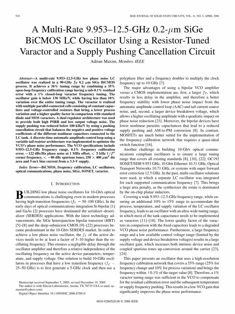
Fig. 2. Frequency calibration capacitor leg: (a) all-NFET switches; (b) CMOS pull-up and pull-down; (c) reduced nonlinear capacitance; (d) high VCO amplitude.
presented in Fig. 2(a) is widely used in integrated VCOs [29],[30]. It consists of a main nMOS differential switch thatprovides a low on-state resistance to connect the two capacitors
and to the LC tank, and two pull-down minimum sizeNFET devices that bring the drain and source of the mainswitch to ground when it is ON. This maximizes switchoverdrive voltage, leading to a minimum resistance for agiven supply voltage headroom. The high on-state resistance ofthe devices is not an issue since they provide only a DClevel. The drain diffusion capacitance of the devices addsto the diffusion capacitance of the main switch to give thetotal nonlinear capacitance presented by the calibration leg tothe LC tank. When the main switch is OFF, its drain and sourceare floating, their potential being set by the leakage currents.Having floating nodes in the calibration leg is not acceptable. Ifthese potentials are driven to ground (e.g., by the NFET switchesdrain and source diffusion diodes leakage current), then at themaximum negative amplitude of the oscillation there is a riskof turning the drain and source diodes of the switches ON. Thismay lead to significant loading of the LC tank and thus result ina severe degradation of the VCO phase noise.
Fig. 2(b) shows one possible solution to resolve the floatingnodes’ potential. It uses two pull-up PFETs in parallelwith the and capacitors of the calibration leg [31]. Whenthe leg is not selected, these PFET switches short the floatingnodes to the collectors of the VCO amplifier, providing a knownpotential level. Minimum-size PFETs were used to reduce thenonlinear capacitance shown to the LC tank, since their large
resistance is of no concern. When the main switchis OFF, it is required to present a minimum parasitic capacitanceto the LC tank. The PFETs pull the source and drains of the
switch to the positive supply ensuring a minimal diffusioncapacitance. The NFET pull-down and PFET pull-up devicesconstitute an inverter that drives the drain and source nodes ofthe main switch. The drawback of this implementation is thelarger nonlinear capacitance shown to the LC tank due to theusage of two inverters per capacitor leg.
Fig. 2(c) presents one solution to reduce the nonlinear ca-pacitance shown to the LC tank by replacing the two pull-up/pull-down CMOS inverters connected in the signal path with asingle inverter connected at the common-mode voltage [8]. Theparasitic capacitances of the pull-up and pull-down devices are
further isolated from the main switch with the high valuebias resistors. A moderately large value resistor was con-nected in series with the gates of the MOS switches in orderto isolate the drain diffusion output capacitance of the drivinginverter from the frequency calibration leg. In a perfectly sym-metric circuit, this would have no impact since it is connected toan AC ground node. In reality, any imbalance in the frequencycalibration leg will reflect a fraction of the gate control inverternonlinear output capacitance (need to be kept negligible) backon the LC tank.
The digital gate control signals that determine the ON or OFFstate of the MOS switches in the calibration network come fromthe digital core of the IC and are referenced to the digital sup-plies, which carry a significant amount of noise. To avoid thenoise leakage from the digital ground into the analog groundof the VCO, each digital control line has a dedicated ,filter. The series resistance increases the impedance lookingtoward the analog circuit, preventing the digital noisy currentfrom going into the analog VCO ground, while the capac-itor connected at the digital ground closes locally the digitalnoise. To avoid noise coupling from the positive supply of thedigital circuit, each digital control line is buffered with two in-verters biased from the same low noise and high PSRR regu-lator used by the LC-VCO core. If the buffers would have beenbiased from the noisy global supply, then the variation of the
supply voltage would propagate to the gates of the MOSswitches, causing a parasitic modulation of their series channelresistance. Considering the parasitic capacitance of the MOSswitch and the MIM capacitor of the calibration leg, the LCtank sees an RC network having three series-connected capaci-tors from which the center one that has a much smaller value isshorted by a voltage-controlled resistor ( switch). As willbe shown in Section II-B, such a network is equivalent to avoltage-controlled capacitor that appears in parallel with the LCtank and determines a parasitic modulation of the oscillating fre-quency. This variable capacitance results in an up-conversion ofthe supply noise and spurs around the VCO carrier, degradingits phase noise performance. To solve this issue, a regulatedvoltage was used to bias the inverters that buffer the dig-ital control lines going to the MOS switches of the calibrationnetwork. Since there is no dynamic current going through thesestatic input inverters of the frequency calibration network, they

922 IEEE JOURNAL OF SOLID-STATE CIRCUITS, VOL. 41, NO. 4, APRIL 2006
Fig. 3. Frequency calibration network top level (MSB and LSB C-DACs).
can be connected to the same regulator used by the LC-VCOcore.
Using a differential switch has the advantage of providing theminimum series resistance for a given supply voltage level and atargeted MOS switch parasitic capacitance value. However, theswitch is exposed to the large peak-to-peak differential swingof the oscillator. Optimizing the VCO phase noise requires themaximization of this voltage. Usually bipolar devices have amuch larger breakdown voltage in comparison with the MOS-FETs (5 V versus 2 V in the selected BiCMOS process). Themaximum collector voltage for the amplifier devices is obtainedwhen the base is driven to ground by the complementary device.This grounded base voltage stress of the HBTs leads to a largereffective breakdown voltage, which approaches thevalue. The targeted 100 dBc/Hz phase noise at 100-kHz offsetrequires a 6-V differential peak-to-peak amplitude that cannotbe sustained by a single MOS switch in the calibration legs. Theamplifier’s bipolar devices are exposed to a maximum voltageof 4 V ( 2.5 V plus 1.5-V single-ended peak amplitude),which is below their 5-V breakdown voltage. A low phase noiseoscillator design should have the single-ended amplitude asclose as possible to the available regulated supply voltage. Theamplitude reduction comes from the minimum voltagerequired for the VCO amplifier devices to keep them out ofsaturation and the voltage drop on the tail current leg. Anoptimal architecture should provide equal voltage stresses tothe bipolar and MOS devices, taking into consideration thedifferences in their breakdown voltages. For the calibration legshown in Fig. 2(c), the MOSFET switches are the amplitudelimiting factor [8]. Fig. 2(d) presents a higher amplitude versionof the single CMOS inverter-driven differential switch. It usestwo grounded source switches ( and ) instead of asingle differential switch . This doubles the maximumdifferential voltage sustained by the calibration leg allowing therequired 6-V peak-to-peak differential swing. The price paidis doubling the series resistance and thus halving the quality
factor of the calibration network. As there is no DC current inthe MOS switches, they can tolerate a larger drain-to-sourcevoltage (e.g., 3 V) than the process-recommended maximumvoltage (2 V).
The frequency calibration range needs to cover the 25%output frequency range (9.953–12.5 GHz) and also the 10%process variation coming from both inductor value inaccu-racy (small) and the tank capacitance variation (usually thedominant factor). Achieving a 35% calibration range, whilemaintaining a 1.25-fF minimal capacitor step requires at leasta 10-bit resolution in the frequency calibration network. Thisis generally implemented as a capacitor DAC that switchesthe appropriately sized capacitor legs in or out of the LC tank,ensuring the VCO operation at the desired communication fre-quency. Fig. 3 presents the detailed schematic of the frequencycalibration network. To accommodate the 10-fF minimum-sizeMIM capacitor while achieving a 1.25-fF unit capacitor step,a differential capacitor structure (which doubles the minimumrequired capacitance unit) was used in conjunction with a2-to-1 tap in the inductor ( – and – ). A 2-to-1tap reduces the size of a capacitor connected to it by a factor offour when reflected back on the LC tank. The 10-bit frequencycalibration DAC was split into two sub-DACs: an LSB-DACconnected at the 2-to-1 inductor tap and an MSB-DAC con-nected directly on the LC tank. A minimum of two LSB bitsneeds to be connected at the 2-to-1 tap in order to achievethe required 1.25-fF capacitor step. The accuracy of the MIMcapacitors degrades sharply when going toward their minimum10-fF size. Furthermore, maintaining a high quality factor forthe LC tank requires large-area series MOS switches that havesizable parasitic capacitances, which may limit the calibrationresolution if they become comparable with the switched MIMcapacitor size. To achieve a good monotonicity of the capacitorDAC, four LSBs were connected at the 2-to-1 tap, while sixMSBs were connected directly on the LC tank. Overlappingbetween the adjacent frequency ranges was built in the ca-
MAXIM: SIGE BICMOS LC OSCILLATOR USING A RESISTOR-TUNED VARACTOR AND A SUPPLY PUSHING CANCELLATION CIRCUIT 923
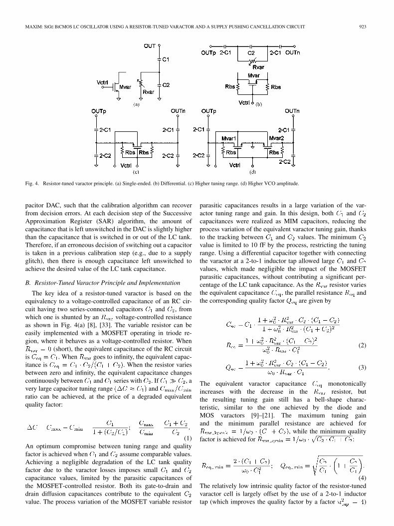
Fig. 4. Resistor-tuned varactor principle. (a) Single-ended. (b) Differential. (c) Higher tuning range. (d) Higher VCO amplitude.
pacitor DAC, such that the calibration algorithm can recoverfrom decision errors. At each decision step of the SuccessiveApproximation Register (SAR) algorithm, the amount ofcapacitance that is left unswitched in the DAC is slightly higherthan the capacitance that is switched in or out of the LC tank.Therefore, if an erroneous decision of switching out a capacitoris taken in a previous calibration step (e.g., due to a supplyglitch), then there is enough capacitance left unswitched toachieve the desired value of the LC tank capacitance.
B. Resistor-Tuned Varactor Principle and Implementation
The key idea of a resistor-tuned varactor is based on theequivalency to a voltage-controlled capacitance of an RC cir-cuit having two series-connected capacitors and , fromwhich one is shunted by an voltage-controlled resistanceas shown in Fig. 4(a) [8], [33]. The variable resistor can beeasily implemented with a MOSFET operating in triode re-gion, where it behaves as a voltage-controlled resistor. When
(short), the equivalent capacitance of the RC circuitis . When goes to infinity, the equivalent capac-itance is . When the resistor variesbetween zero and infinity, the equivalent capacitance changescontinuously between and series with . If , avery large capacitor tuning range andratio can be achieved, at the price of a degraded equivalentquality factor:
(1)An optimum compromise between tuning range and qualityfactor is achieved when and assume comparable values.Achieving a negligible degradation of the LC tank qualityfactor due to the varactor losses imposes small andcapacitance values, limited by the parasitic capacitances ofthe MOSFET-controlled resistor. Both its gate-to-drain anddrain diffusion capacitances contribute to the equivalentvalue. The process variation of the MOSFET variable resistor
parasitic capacitances results in a large variation of the var-actor tuning range and gain. In this design, both andcapacitances were realized as MIM capacitors, reducing theprocess variation of the equivalent varactor tuning gain, thanksto the tracking between and values. The minimumvalue is limited to 10 fF by the process, restricting the tuningrange. Using a differential capacitor together with connectingthe varactor at a 2-to-1 inductor tap allowed large andvalues, which made negligible the impact of the MOSFETparasitic capacitances, without contributing a significant per-centage of the LC tank capacitance. As the resistor variesthe equivalent capacitance , the parallel resistance andthe corresponding quality factor are given by
(2)
(3)
The equivalent varactor capacitance monotonicallyincreases with the decrease in the resistor, butthe resulting tuning gain still has a bell-shape charac-teristic, similar to the one achieved by the diode andMOS varactors [9]–[21]. The maximum tuning gainand the minimum parallel resistance are achieved for
, while the minimum qualityfactor is achieved for :
(4)The relatively low intrinsic quality factor of the resistor-tunedvaractor cell is largely offset by the use of a 2-to-1 inductortap (which improves the quality factor by a factor )
924 IEEE JOURNAL OF SOLID-STATE CIRCUITS, VOL. 41, NO. 4, APRIL 2006
and the large ratio between the total tank capacitance and thevaractor capacitance . The minimum varactorparallel resistor result in a reflected quality factor on the LCtank well in excess of 50. Therefore, the loaded of the LCtank is dominated by the calibrationnetwork MOSFET switches series resistance and the inductorintrinsic losses.
A differential version of the resistor-tuned varactor can alsobe realized. There are at least three solutions for the differentialresistor-tuned varactor, as shown in Fig. 4(b)–(d). The first solu-tion is using a single differential capacitance and a differentialMOSswitch,asshowninFig.4(b).Alternatively, the capacitorcan be implemented with two grounded capacitors con-nectedat thedifferentialnodesof theMOSFETswitch[Fig.4(c)],resulting in a higher tuning range. Finally, two grounded ca-pacitors and two grounded source switches can be used as shownin Fig. 4(d). This results in twice as large breakdown voltage ofthe equivalent varactor, allowing a larger VCO amplitude andthus improving by 6 dB the oscillator phase noise.
There are two possibilities for connection of the bias re-sistors that provide the DC potential to the source and drain ofthe controlled resistor MOSFETs. The first one is to connectresistors to the bulk of the FETs where the PLL loop filtercontrol voltage is applied. This configuration avoids thebody effect, which can significantly distort (tilt) the resulting
characteristic of the varactor. The drawback of this con-figuration is the limited amplitude that can be tolerated on thevaractor due to the turning on of the drain and source diffusiondiodes of the FET at the peak negative VCO amplitude.The other solution is to connect the resistors to the gateof , as shown in Fig. 4. This solves the limited amplitudeissue since now the drain and sources can go below thevoltage by one FET threshold voltage plus one PN junctionforward bias voltage before turning on the drain and source bodydiodes. Furthermore, connecting the varactor at the 2-to-1 tapdoubles the allowed VCO amplitude. This elevated VCO ampli-tude comes at the price of a body effect in the voltage-controlledresistor FETs. To compensate for the body effect and keep a flatplateau in the resulting curve, the resistor divider that pro-vides the offset bias voltages uses a nonuniform voltagestep to compensate for the of each FET resistor due to itsbody effect.
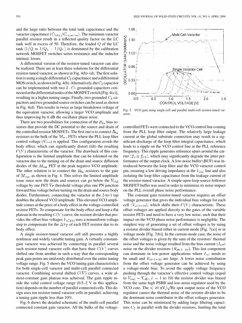
A single resistor-tuned varactor cell still presents a highlynonlinear and widely variable tuning gain. A virtually constant-gain varactor was achieved by connecting in parallel severalsuch resistor-tuned varactor cells that have their curvesshifted one from another in such a way that the correspondingpeak gain points are uniformly distributed over the entire tuningvoltage range. Fig. 5 shows the VCO tuning gain characteristicsfor both single-cell varactor and multi-cell parallel connectedvaractor. Combining several shifted curves, a wide al-most-constant gain plateau was achieved. The gain ripple in-side the valid control voltage range (0.5–2 V in this applica-tion) depends on the number of parallel connected cells. This de-sign uses ten resistor-tuned varactor cells in parallel, achievinga tuning gain ripple less than 10%.
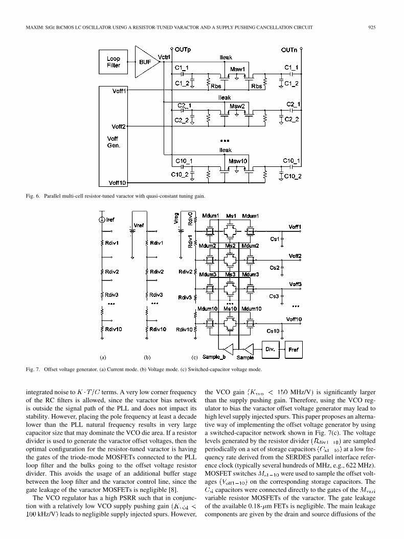
Fig. 6 shows the detailed schematic of the multi-cell parallelconnected constant gain varactor. All the bulks of the voltage-
Fig. 5. VCO gain using single-cell and parallel multi-cell resistor-tuned var-actor.
controlled FETs were connected to the VCO control line comingfrom the PLL loop filter output. The relatively large leakagecurrent at the global substrate connection may result in a sig-nificant discharge of the loop filter integral capacitance, whichleads to a ripple on the VCO control line at the PLL referencefrequency. This ripple generates reference spurs around the car-rier , which may significantly degrade the jitter per-formance of the output clock. A low-noise buffer (BUF) was in-troduced between the loop filter and the VCO varactor controlpin, ensuring a low driving impedance at the line and alsoisolating the loop filter capacitance from the leakage current ofthe resistor-tuned varactor. A simple open-loop source-followerMOSFET buffer was used in order to minimize its noise impacton the PLL overall phase noise performance.
The constant gain resistor-tuned varactor requires an offsetvoltage generator that gives the individual bias voltage for eachcell , which shifts their characteristic. Theseoffset voltages are applied directly to the gates of the variableresistor FETs and need to have a very low noise, such that theirimpact on the VCO phase noise performance is negligible. Thesimplest way of generating a set of offset voltages is by usinga resistor divider biased either in current mode [Fig. 7(a)] or involtage mode [Fig. 7(b)]. In the current-mode case, the noise ofthe offset voltages is given by the sum of the resistors’ thermalnoise and the noise voltage resulted from the bias currentnoise on the divider resistors . This last componentcan dominate in low-power applications where needs tobe small and are large. A lower noise contributionfrom the offset voltage generator can be achieved by usinga voltage-mode bias. To avoid the supply voltage frequencypushing through the varactor’s effective control voltage (equalto , 1 to 10) the resistor divider was biasedfrom the same high PSRR and low-noise regulator used by theVCO core. The nV Hz spot output noise of the VCOregulator causes the thermal noise of the resistor divider to bethe dominant noise contributor in the offset voltages generator.This noise can be minimized by adding large filtering capaci-tors in parallel with the divider resistors, limiting the total
MAXIM: SIGE BICMOS LC OSCILLATOR USING A RESISTOR-TUNED VARACTOR AND A SUPPLY PUSHING CANCELLATION CIRCUIT 925
Fig. 6. Parallel multi-cell resistor-tuned varactor with quasi-constant tuning gain.
Fig. 7. Offset voltage generator. (a) Current mode. (b) Voltage mode. (c) Switched-capacitor voltage mode.
integrated noise to terms. A very low corner frequencyof the RC filters is allowed, since the varactor bias networkis outside the signal path of the PLL and does not impact itsstability. However, placing the pole frequency at least a decadelower than the PLL natural frequency results in very largecapacitor size that may dominate the VCO die area. If a resistordivider is used to generate the varactor offset voltages, then theoptimal configuration for the resistor-tuned varactor is havingthe gates of the triode-mode MOSFETs connected to the PLLloop filter and the bulks going to the offset voltage resistordivider. This avoids the usage of an additional buffer stagebetween the loop filter and the varactor control line, since thegate leakage of the varactor MOSFETs is negligible [8].
The VCO regulator has a high PSRR such that in conjunc-tion with a relatively low VCO supply pushing gain
kHz/V leads to negligible supply injected spurs. However,
the VCO gain MHz/V is significantly largerthan the supply pushing gain. Therefore, using the VCO reg-ulator to bias the varactor offset voltage generator may lead tohigh level supply injected spurs. This paper proposes an alterna-tive way of implementing the offset voltage generator by usinga switched-capacitor network shown in Fig. 7(c). The voltagelevels generated by the resistor divider are sampledperiodically on a set of storage capacitors at a low fre-quency rate derived from the SERDES parallel interface refer-ence clock (typically several hundreds of MHz, e.g., 622 MHz).MOSFET switches were used to sample the offset volt-ages on the corresponding storage capacitors. The
capacitors were connected directly to the gates of thevariable resistor MOSFETs of the varactor. The gate leakageof the available 0.18- m FETs is negligible. The main leakagecomponents are given by the drain and source diffusions of the

926 IEEE JOURNAL OF SOLID-STATE CIRCUITS, VOL. 41, NO. 4, APRIL 2006
controlled resistor FETs, which may result in a discharge of thestorage capacitors. The ripple on the offset voltage nodes
leads to output spurs whose amplitude is proportional withoscillator gain and leakage current, while being inverselyproportional to the refresh frequency . The refresh rate ofthe switched-capacitor bias generator needs to be high enoughsuch that the resulting voltage ripple is lower than 1 V, whichresults in negligible spurs ( 80 dBc). To minimize the rippleat the offset voltage nodes, each sampling switch has a pair ofhalf-size dummy switches connected on its either sidesto cancel (at least partially) the channel charge injection andreduce the clock feed-through. The price paid is the twice aslarge leakage current due to the extra source and drain diffu-sions connected to the storage capacitors . By having thesampling switches turned off most of the time minimizes thesupply spur injection. The power of the injected tone is reducedby the sampling signal duty cycle. To achieve a large attenua-tion the sampling signal needs to have a very low duty cycle (1to 5%), requiring a large division factor from the SERDES par-allel reference clock.
C. Automatic Amplitude Control Loop
To ensure a safe oscillator start-up, the small-signal positivefeedback loop gain needs to be greater than 1 (usual values are 2to 3). As the amplitude grows, the large-signal transcondutancedecreases below the small-signal level and the amplitude stabi-lizes at a value that provides a perfect cancellation between thelarge-signal negative impedance of the amplifier and the totaltank losses (self limiting). The bipolar devices transconductanceis practically process independent, but it has a pronounced tem-perature variation . A large loop gain willresult in operating the amplifier in limiting conditions (supplylimiting). In this case, the amplitude of oscillation depends onthe total tank losses and the VCO amplifier tail current. If thedevices are entering the saturation region, a strong loading isshown to the LC tank, resulting in a sharp phase noise degrada-tion. Therefore, the limiting needs to be generated by the turningoff of the amplifier devices and not by their saturation.
AAC loops are commonly used to set the VCO amplitudeclose to the maximum value allowed by the available supplyvoltage and the device breakdown voltages, thus minimizingits phase noise [11], [26]–[28]. The main advantages broughtby the presence of an AAC loop are a safe start-up under alldesign corners, low harmonic distortion of the output clock,and supply, process, and temperature independence of the os-cillating amplitude. However, the AAC loops have the draw-back of introducing additional noise to the oscillator [27]. Noiseis contributed by all three building blocks of a standard AACloop: peak detector, reference voltage generator, and loop am-plifier/comparator. The reference voltage generator is outsidethe loop and its noise can be rejected with a low corner fre-quency low-pass filter, without impacting the AAC loop sta-bility. In contrast, the peak detector and loop amplifier noiseare hard to reject with filtering techniques, without impactingthe AAC loop stability and bandwidth.
Most existing integrated LC oscillators use continuous-timeAAC loops [11], [26]–[28] in which the comparison between theinstantaneous amplitude measured by the peak detector and the
reference voltage is performed in a continuous manner. It pro-vides an accurate amplitude value, but comes at the price of anelevated noise contribution from the AAC loop. Discrete-timeAAC loops [28] have gained popularity lately due to their lowernoise contribution, since the noisy analog amplifier is replacedwith a noiseless digital comparator (state machine). They usu-ally consist of a peak detector that samples the oscillating ampli-tude, a high-resolution ADC that converts it into a digital wordrepresentation, and a state machine that compares the targetedreference amplitude with the sampled amplitude value and gen-erates a control signal for the DAC that controls the oscillator tailcurrent. Both current and resistor DACs are widely used [28].
The present design uses a simplified discrete AAC architec-ture, presented in Fig. 8. Instead of using a high-resolution ADCthat increases the circuit complexity, the proposed AAC loopuses only two comparators to define a window in which theVCO amplitude needs to be contained [28]. The targeted low
and high amplitude levels aregenerated with low-noise calibrated referenced generators(see Section II-D). The output signals of the two comparators(High and Low) are sent to the digital state machine, which de-termines the control word for the tail resistor DAC. The peak de-tector consists of a high-frequency rectifier , , followedby an RC filter that rejects the high-frequency ripple from thesampled amplitude.
There are two main mechanisms through which the noise ofthe AAC loop impacts the VCO phase noise [27]. First, the noiseof the AAC loop and of the tail current leg determines a variationof the VCO bias current, which in turn generate a modulationof the oscillating amplitude. Ideally, an AM modulation shouldnot impact the zero crossings of the generated sine-wave andtherefore should not create any phase noise (jitter). A limiter(edge-squaring buffer) is often placed after the VCO to elim-inate the parasitic AM modulation from the clock path. How-ever, the nonlinear capacitance connected to the LC tankresults in a finite AM-to-PM conversion, which degrades theVCO phase noise [27], [28]. The second phase noise degrada-tion mechanism is more subtle. The oscillation frequency of anLC-VCO is not determined solely by the inductor and capac-itor values, but it also depends on the delay introduced by theamplifier (phase shift). The noise of the AAC loop changes theVCO biasing current that generates a parasitic modulation ofthe delay introduced by the amplifier and thus creates a modula-tion of the oscillating frequency, resulting in jitter (phase noise).This phenomenon is particularly troublesome in oscillators op-erating close to the transition frequency of the amplifier devices(low ratios), when the amplifier delay can be a significantpercentage of the oscillating period. To reduce this effect, theamplifier devices need to be biased at peak current density.
The proposed digital amplitude control loop with windowcomparison operates in open-loop mode when the amplitudedoes not cross the boundaries of the valid amplitude window
. Therefore, most of the time the AAC loop is inopen-loop mode and does not compensate for the amplitudemodulation due to the tail current noise. In large gain oscilla-tors having a high-value AM-to-PM conversion rate, this canbe one of the dominant phase noise mechanisms [28]. In suchsituations, continuous-time AAC loops are better suited. The

MAXIM: SIGE BICMOS LC OSCILLATOR USING A RESISTOR-TUNED VARACTOR AND A SUPPLY PUSHING CANCELLATION CIRCUIT 927
Fig. 8. VCO’s automatic amplitude control loop using a window amplitude comparison and a tail resistor DAC.
proposed VCO has a very low AM-to-PM conversion (see Sec-tion II-E on supply pushing compensation). This makes a dis-crete variable tail resistor the ideal candidate for the AAC loopimplementation.
The resolution of the tail resistor DAC needs to be highenough such that the AAC loop can generate a tail currentthat will give an amplitude inside the windowfor all the process, supply, and temperature (PVT) corners. An8-bit resistor DAC was found sufficient to ensure an amplitudewindow of 50 mV around a 1.5-V single-ended peak value. Theavailability of low parasitic capacitance FET switches in theselected BiCMOS process allows an easy implementation of avariable tail resistor AAC loop. The tail resistor DAC switches
do not contribute any noise as they operate intriode region. This significantly reduces the phase noisecomponent of the VCO. Furthermore, the voltage drop onthe tail leg was reduced down to only few hundred millivolts,resulting in a significant increase of the VCO amplitude incomparison with the transistor-based tail current architecture[3], [8], [10], [11], [14].
D. VCO Supply Regulator
In high-frequency VCOs (10–12.5 GHz), the percentage ofthe tank capacitance coming from the nonlinear device parasiticcapacitance is large, leading to a higher supply pushing gain
in comparison with the low-frequency VCOs, wheremost of the tank capacitance is contributed by the linear MIM ormetal capacitors. Furthermore, in large mixed-signal ICs (e.g.,SERDES) the supply voltage is highly contaminated with spu-rious tones coupled both magnetically and electrically from theswitching digital circuits. Using an off-chip filtered supply ded-icated only to the low-noise oscillator eliminates the board-levelnoise coupling, but it does not solve the supply noise injec-tion through magnetic coupling between the different IC bond-wires. On-chip filtering usually requires a very large die area.Increasing the distance between the sensitive analog pads andthe aggressor digital pads and using a 90 orientation betweenthe corresponding bondwires helps to reduce the coupling. Flip-
chip assemblies can be used to avoid the bondwire coupling, butat a significant cost increase penalty.
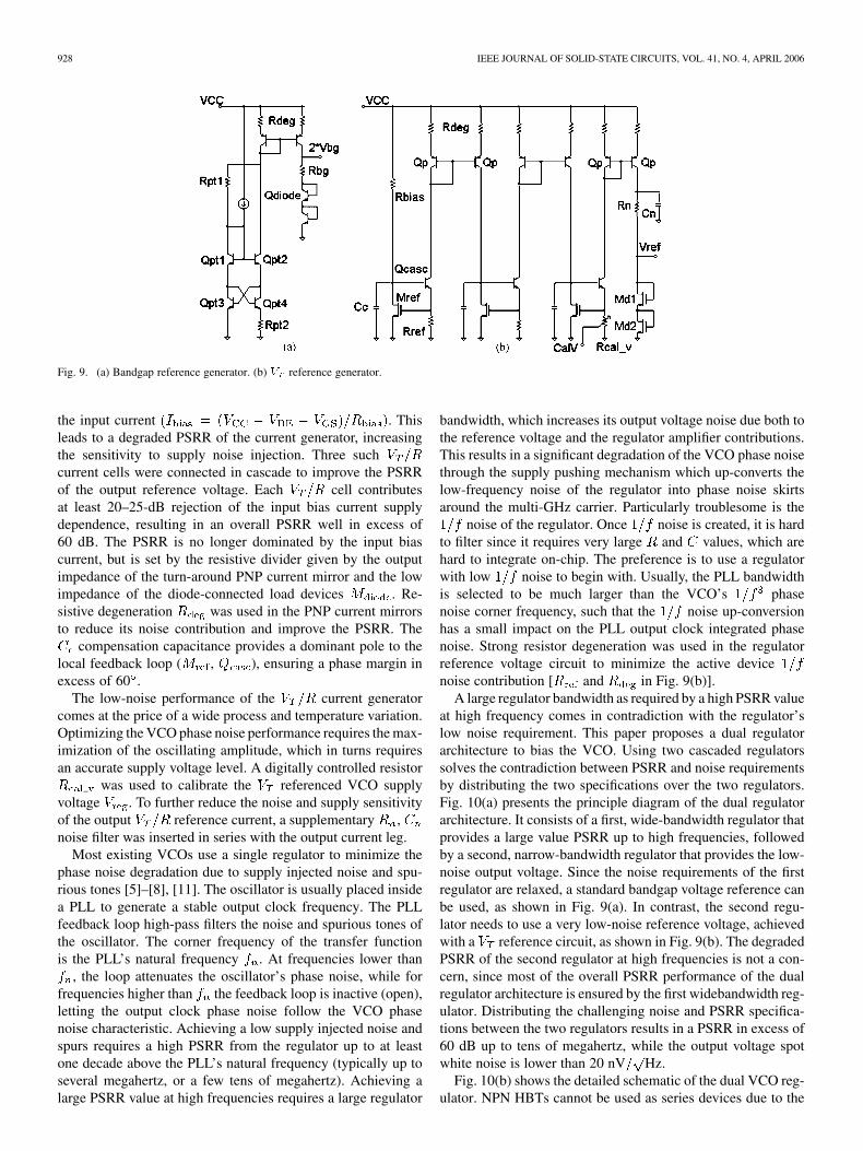
Reducing the supply noise injection of a VCO operatingin a large mixed-signal IC mandates the usage of a dedicatedVCO regulator. An isolation regulator can successfully rejectthe supply noise and spur injection, but it has noise of itselfthat may impact the VCO phase noise performance. Achievinga low-noise regulator needs a low-noise reference voltage. Themost common way to generate a reference voltage is by using abandgap circuit [7], [8]. Fig. 9(a) shows an open-loop bandgapreference [8]. It achieves lower noise in comparison with aclosed-loop implementation that has an additional operationalamplifier. Transistors – generate a PTAT current thatis mirrored around and injected into the diode device and its
series resistor. Bandgap references have a good process andtemperature stability but come with a large output noise. Thewideband noise can be filtered out with an RC filter. However,rejecting the noise requires a very low corner frequency,which results in a large area penalty. This design proposesan alternative way of achieving a low-noise reference voltageusing a referenced circuit, as shown in Fig. 9(b) [34]. The
device provides the reference voltage, which createsan current through the resistor. Thecascode device boosts the output impedance of the currentgenerator, helping to improve its PSRR. If enough loop gain isprovided to the local feedback loop ( and ) the noiseof the output current is dominated by the thermal noise of the
resistor. Using a large resistor value reduces the referencecurrent noise at the expense of a low current value. A referencevoltage was generated by injecting the currentinto a low impedance load constituted by two diode-connectedMOSFET devices . The current generator canbe biased using either an input current or a bias resistor
. For a given headroom voltage and current value. thenoise of a bias resistor is significantly lower than that of acurrent mirror (e.g., pA Hz for a 20-k resistor, versusabout 6 pA Hz for a 100 A current source). However, usingan resistor brings a strong supply voltage dependence of
928 IEEE JOURNAL OF SOLID-STATE CIRCUITS, VOL. 41, NO. 4, APRIL 2006
Fig. 9. (a) Bandgap reference generator. (b) V reference generator.
the input current . Thisleads to a degraded PSRR of the current generator, increasingthe sensitivity to supply noise injection. Three suchcurrent cells were connected in cascade to improve the PSRRof the output reference voltage. Each cell contributesat least 20–25-dB rejection of the input bias current supplydependence, resulting in an overall PSRR well in excess of60 dB. The PSRR is no longer dominated by the input biascurrent, but is set by the resistive divider given by the outputimpedance of the turn-around PNP current mirror and the lowimpedance of the diode-connected load devices . Re-sistive degeneration was used in the PNP current mirrorsto reduce its noise contribution and improve the PSRR. The
compensation capacitance provides a dominant pole to thelocal feedback loop ( , ), ensuring a phase margin inexcess of 60 .
The low-noise performance of the current generatorcomes at the price of a wide process and temperature variation.Optimizing the VCO phase noise performance requires the max-imization of the oscillating amplitude, which in turns requiresan accurate supply voltage level. A digitally controlled resistor
was used to calibrate the referenced VCO supplyvoltage . To further reduce the noise and supply sensitivityof the output reference current, a supplementary ,noise filter was inserted in series with the output current leg.
Most existing VCOs use a single regulator to minimize thephase noise degradation due to supply injected noise and spu-rious tones [5]–[8], [11]. The oscillator is usually placed insidea PLL to generate a stable output clock frequency. The PLLfeedback loop high-pass filters the noise and spurious tones ofthe oscillator. The corner frequency of the transfer functionis the PLL’s natural frequency . At frequencies lower than
, the loop attenuates the oscillator’s phase noise, while forfrequencies higher than the feedback loop is inactive (open),letting the output clock phase noise follow the VCO phasenoise characteristic. Achieving a low supply injected noise andspurs requires a high PSRR from the regulator up to at leastone decade above the PLL’s natural frequency (typically up toseveral megahertz, or a few tens of megahertz). Achieving alarge PSRR value at high frequencies requires a large regulator
bandwidth, which increases its output voltage noise due both tothe reference voltage and the regulator amplifier contributions.This results in a significant degradation of the VCO phase noisethrough the supply pushing mechanism which up-converts thelow-frequency noise of the regulator into phase noise skirtsaround the multi-GHz carrier. Particularly troublesome is the
noise of the regulator. Once noise is created, it is hardto filter since it requires very large and values, which arehard to integrate on-chip. The preference is to use a regulatorwith low noise to begin with. Usually, the PLL bandwidthis selected to be much larger than the VCO’s phasenoise corner frequency, such that the noise up-conversionhas a small impact on the PLL output clock integrated phasenoise. Strong resistor degeneration was used in the regulatorreference voltage circuit to minimize the active devicenoise contribution [ and in Fig. 9(b)].
A large regulator bandwidth as required by a high PSRR valueat high frequency comes in contradiction with the regulator’slow noise requirement. This paper proposes a dual regulatorarchitecture to bias the VCO. Using two cascaded regulatorssolves the contradiction between PSRR and noise requirementsby distributing the two specifications over the two regulators.Fig. 10(a) presents the principle diagram of the dual regulatorarchitecture. It consists of a first, wide-bandwidth regulator thatprovides a large value PSRR up to high frequencies, followedby a second, narrow-bandwidth regulator that provides the low-noise output voltage. Since the noise requirements of the firstregulator are relaxed, a standard bandgap voltage reference canbe used, as shown in Fig. 9(a). In contrast, the second regu-lator needs to use a very low-noise reference voltage, achievedwith a reference circuit, as shown in Fig. 9(b). The degradedPSRR of the second regulator at high frequencies is not a con-cern, since most of the overall PSRR performance of the dualregulator architecture is ensured by the first widebandwidth reg-ulator. Distributing the challenging noise and PSRR specifica-tions between the two regulators results in a PSRR in excess of60 dB up to tens of megahertz, while the output voltage spotwhite noise is lower than 20 nV Hz.
Fig. 10(b) shows the detailed schematic of the dual VCO reg-ulator. NPN HBTs cannot be used as series devices due to the
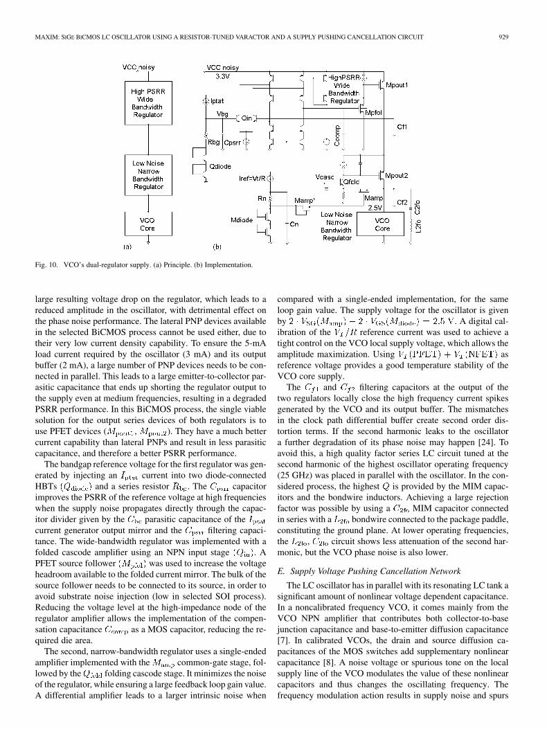
MAXIM: SIGE BICMOS LC OSCILLATOR USING A RESISTOR-TUNED VARACTOR AND A SUPPLY PUSHING CANCELLATION CIRCUIT 929
Fig. 10. VCO’s dual-regulator supply. (a) Principle. (b) Implementation.
large resulting voltage drop on the regulator, which leads to areduced amplitude in the oscillator, with detrimental effect onthe phase noise performance. The lateral PNP devices availablein the selected BiCMOS process cannot be used either, due totheir very low current density capability. To ensure the 5-mAload current required by the oscillator (3 mA) and its outputbuffer (2 mA), a large number of PNP devices needs to be con-nected in parallel. This leads to a large emitter-to-collector par-asitic capacitance that ends up shorting the regulator output tothe supply even at medium frequencies, resulting in a degradedPSRR performance. In this BiCMOS process, the single viablesolution for the output series devices of both regulators is touse PFET devices ( , ). They have a much bettercurrent capability than lateral PNPs and result in less parasiticcapacitance, and therefore a better PSRR performance.
The bandgap reference voltage for the first regulator was gen-erated by injecting an current into two diode-connectedHBTs and a series resistor . The capacitorimproves the PSRR of the reference voltage at high frequencieswhen the supply noise propagates directly through the capac-itor divider given by the parasitic capacitance of thecurrent generator output mirror and the filtering capaci-tance. The wide-bandwidth regulator was implemented with afolded cascode amplifier using an NPN input stage . APFET source follower was used to increase the voltageheadroom available to the folded current mirror. The bulk of thesource follower needs to be connected to its source, in order toavoid substrate noise injection (low in selected SOI process).Reducing the voltage level at the high-impedance node of theregulator amplifier allows the implementation of the compen-sation capacitance as a MOS capacitor, reducing the re-quired die area.
The second, narrow-bandwidth regulator uses a single-endedamplifier implemented with the common-gate stage, fol-lowed by the folding cascode stage. It minimizes the noiseof the regulator, while ensuring a large feedback loop gain value.A differential amplifier leads to a larger intrinsic noise when
compared with a single-ended implementation, for the sameloop gain value. The supply voltage for the oscillator is givenby . A digital cal-ibration of the reference current was used to achieve atight control on the VCO local supply voltage, which allows theamplitude maximization. Using asreference voltage provides a good temperature stability of theVCO core supply.
The and filtering capacitors at the output of thetwo regulators locally close the high frequency current spikesgenerated by the VCO and its output buffer. The mismatchesin the clock path differential buffer create second order dis-tortion terms. If the second harmonic leaks to the oscillatora further degradation of its phase noise may happen [24]. Toavoid this, a high quality factor series LC circuit tuned at thesecond harmonic of the highest oscillator operating frequency(25 GHz) was placed in parallel with the oscillator. In the con-sidered process, the highest is provided by the MIM capac-itors and the bondwire inductors. Achieving a large rejectionfactor was possible by using a MIM capacitor connectedin series with a bondwire connected to the package paddle,constituting the ground plane. At lower operating frequencies,the , circuit shows less attenuation of the second har-monic, but the VCO phase noise is also lower.
E. Supply Voltage Pushing Cancellation Network
The LC oscillator has in parallel with its resonating LC tank asignificant amount of nonlinear voltage dependent capacitance.In a noncalibrated frequency VCO, it comes mainly from theVCO NPN amplifier that contributes both collector-to-basejunction capacitance and base-to-emitter diffusion capacitance[7]. In calibrated VCOs, the drain and source diffusion ca-pacitances of the MOS switches add supplementary nonlinearcapacitance [8]. A noise voltage or spurious tone on the localsupply line of the VCO modulates the value of these nonlinearcapacitors and thus changes the oscillating frequency. Thefrequency modulation action results in supply noise and spurs
930 IEEE JOURNAL OF SOLID-STATE CIRCUITS, VOL. 41, NO. 4, APRIL 2006
up-conversion around the output carrier frequency, degradingthe clock phase noise performance. A typical output noisevoltage of a bandgap referenced regulator is few hundrednV Hz, which in conjunction with the intrinsic VCO supplypushing of several MHz/V may constitute the dominant VCOphase noise contribution at low frequency offsets [8]. Tominimize the oscillator phase noise degradation due to supplypushing mechanism, the noise and spurs on the VCO localsupply need to be reduced (for example, by using a high PSRRand low output noise regulator as shown in Section II-D), andthe oscillator supply pushing gain needs to be reduced.
The collector–base junction capacitances of the VCO NPNamplifier devices, which have a negative voltage coefficient, ap-pear practically in parallel with the LC tank ( dividerhas only a small impact on the reflected capacitance). In tailcurrent source biased VCOs, the pushing can be compen-sated by biasing the bases of the two bipolar devices such that aconstant average voltage is maintained on the capaci-tances [7]. If were to have a symmetric characteristicaround the VCO equilibrium point, then a perfect cancellationof the supply pushing would result. In reality, the isnot perfectly symmetric and a finite residual supply pushing isleft.
In tail resistor biased VCOs, the base voltage needs to be ref-erenced to ground. This design proposes an alternative way ofbiasing the bases of the VCO amplifier by using a very lownoise based voltage, presented in Section II-D. Injecting alow-noise current into two diode-connected MOStransistors leads to a supply independent and a very low-noisevoltage across the capacitance (equal to , both
and being referenced to ground), making negligibleits phase noise impact. The main drawback of the refer-enced voltages is a relatively large process and temperature vari-ation. This would require extra margins in the design of the basevoltage value, reducing the oscillating amplitude and thus de-grading the VCO phase noise. A digitally controlled calibra-tion network was used to cancel the process variation of thereferenced voltage and thus maximize the VCO amplitude.The noise of the bias source appears as a common-modenoise to the VCO, generating only amplitude modulation. Thelow AM-to-PM conversion gain of the proposed VCO makesnegligible the noise contribution to the overall oscillatorphase noise performance.
In the present calibrated frequency VCO design, the calibra-tion network and the resistor tuned varactor use MOSFETs thathave significant nonlinear drain and source diffusion capaci-tance. Ensuring a high quality factor for the LC tank requireslow on-state resistance MOS switches, which in turn leads tolarge-size FETs with high-value parasitic capacitances. Thesenonlinear voltage-dependent capacitances appear directly inparallel with the LC tank, contributing a large supply pushinggain. Achieving phase noise levels of 100 dBc/Hz at 100-kHzoffset requires pushing gains of less than 100 kHz/V. To achievethis goal, a supply pushing cancellation circuit was introducedto compensate for the impact of the MOS switches’ drain andsource diffusion capacitances’ negative voltage coefficient. Inprinciple, this negative supply pushing can be compensatedby adding in parallel with the LC tank a capacitance that has
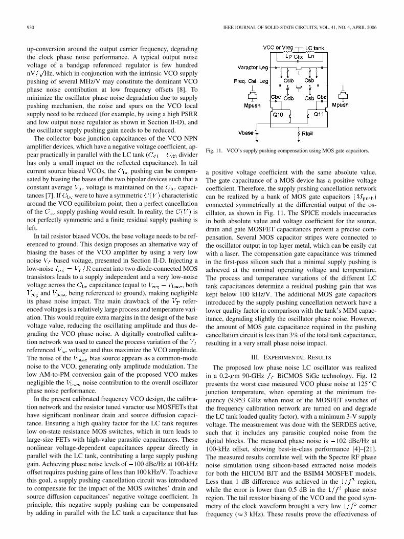
Fig. 11. VCO’s supply pushing compensation using MOS gate capacitors.
a positive voltage coefficient with the same absolute value.The gate capacitance of a MOS device has a positive voltagecoefficient. Therefore, the supply pushing cancellation networkcan be realized by a bank of MOS gate capacitorsconnected symmetrically at the differential output of the os-cillator, as shown in Fig. 11. The SPICE models inaccuraciesin both absolute value and voltage coefficient for the source,drain and gate MOSFET capacitances prevent a precise com-pensation. Several MOS capacitor stripes were connected tothe oscillator output in top layer metal, which can be easily cutwith a laser. The compensation gate capacitance was trimmedin the first-pass silicon such that a minimal supply pushing isachieved at the nominal operating voltage and temperature.The process and temperature variations of the different LCtank capacitances determine a residual pushing gain that waskept below 100 kHz/V. The additional MOS gate capacitorsintroduced by the supply pushing cancellation network have alower quality factor in comparison with the tank’s MIM capac-itance, degrading slightly the oscillator phase noise. However,the amount of MOS gate capacitance required in the pushingcancellation circuit is less than 3% of the total tank capacitance,resulting in a very small phase noise impact.
III. EXPERIMENTAL RESULTS
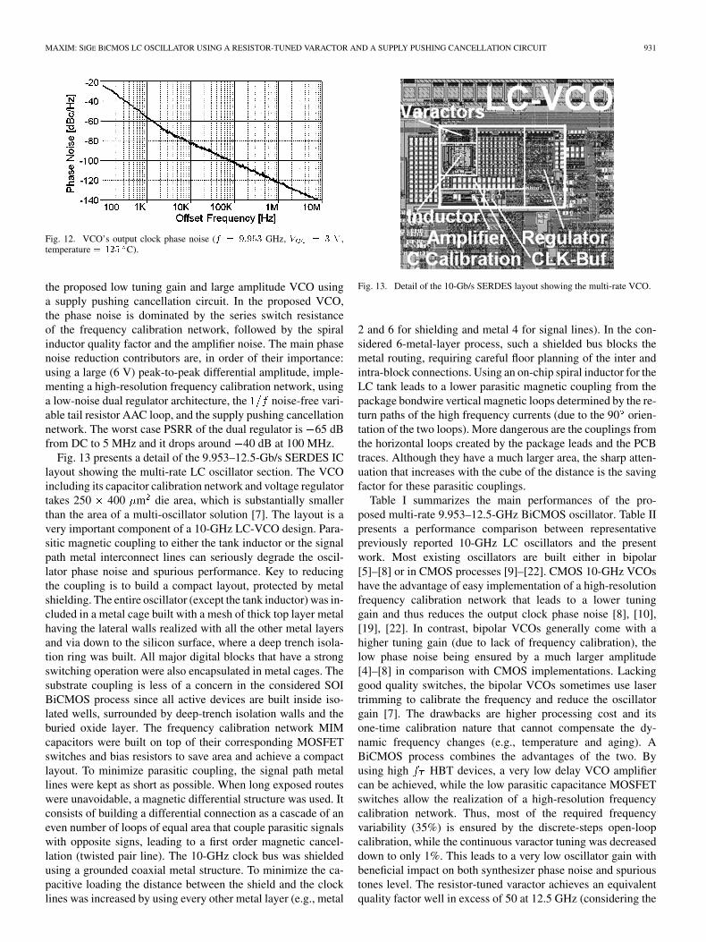
The proposed low phase noise LC oscillator was realizedin a 0.2- m 90-GHz BiCMOS SiGe technology. Fig. 12presents the worst case measured VCO phase noise at 125 Cjunction temperature, when operating at the minimum fre-quency (9.953 GHz when most of the MOSFET switches ofthe frequency calibration network are turned on and degradethe LC tank loaded quality factor), with a minimum 3-V supplyvoltage. The measurement was done with the SERDES active,such that it includes any parasitic coupled noise from thedigital blocks. The measured phase noise is 102 dBc/Hz at100-kHz offset, showing best-in-class performance [4]–[21].The measured results correlate well with the Spectre RF phasenoise simulation using silicon-based extracted noise modelsfor both the HICUM BJT and the BSIM4 MOSFET models.Less than 1 dB difference was achieved in the region,while the error is lower than 0.5 dB in the phase noiseregion. The tail resistor biasing of the VCO and the good sym-metry of the clock waveform brought a very low cornerfrequency ( 3 kHz). These results prove the effectiveness of
MAXIM: SIGE BICMOS LC OSCILLATOR USING A RESISTOR-TUNED VARACTOR AND A SUPPLY PUSHING CANCELLATION CIRCUIT 931
Fig. 12. VCO’s output clock phase noise (f = 9:953 GHz, V = 3 V,temperature = 125 C).
the proposed low tuning gain and large amplitude VCO usinga supply pushing cancellation circuit. In the proposed VCO,the phase noise is dominated by the series switch resistanceof the frequency calibration network, followed by the spiralinductor quality factor and the amplifier noise. The main phasenoise reduction contributors are, in order of their importance:using a large (6 V) peak-to-peak differential amplitude, imple-menting a high-resolution frequency calibration network, usinga low-noise dual regulator architecture, the noise-free vari-able tail resistor AAC loop, and the supply pushing cancellationnetwork. The worst case PSRR of the dual regulator is 65 dBfrom DC to 5 MHz and it drops around 40 dB at 100 MHz.
Fig. 13 presents a detail of the 9.953–12.5-Gb/s SERDES IClayout showing the multi-rate LC oscillator section. The VCOincluding its capacitor calibration network and voltage regulatortakes 250 400 m die area, which is substantially smallerthan the area of a multi-oscillator solution [7]. The layout is avery important component of a 10-GHz LC-VCO design. Para-sitic magnetic coupling to either the tank inductor or the signalpath metal interconnect lines can seriously degrade the oscil-lator phase noise and spurious performance. Key to reducingthe coupling is to build a compact layout, protected by metalshielding. The entire oscillator (except the tank inductor) was in-cluded in a metal cage built with a mesh of thick top layer metalhaving the lateral walls realized with all the other metal layersand via down to the silicon surface, where a deep trench isola-tion ring was built. All major digital blocks that have a strongswitching operation were also encapsulated in metal cages. Thesubstrate coupling is less of a concern in the considered SOIBiCMOS process since all active devices are built inside iso-lated wells, surrounded by deep-trench isolation walls and theburied oxide layer. The frequency calibration network MIMcapacitors were built on top of their corresponding MOSFETswitches and bias resistors to save area and achieve a compactlayout. To minimize parasitic coupling, the signal path metallines were kept as short as possible. When long exposed routeswere unavoidable, a magnetic differential structure was used. Itconsists of building a differential connection as a cascade of aneven number of loops of equal area that couple parasitic signalswith opposite signs, leading to a first order magnetic cancel-lation (twisted pair line). The 10-GHz clock bus was shieldedusing a grounded coaxial metal structure. To minimize the ca-pacitive loading the distance between the shield and the clocklines was increased by using every other metal layer (e.g., metal
Fig. 13. Detail of the 10-Gb/s SERDES layout showing the multi-rate VCO.
2 and 6 for shielding and metal 4 for signal lines). In the con-sidered 6-metal-layer process, such a shielded bus blocks themetal routing, requiring careful floor planning of the inter andintra-block connections. Using an on-chip spiral inductor for theLC tank leads to a lower parasitic magnetic coupling from thepackage bondwire vertical magnetic loops determined by the re-turn paths of the high frequency currents (due to the 90 orien-tation of the two loops). More dangerous are the couplings fromthe horizontal loops created by the package leads and the PCBtraces. Although they have a much larger area, the sharp atten-uation that increases with the cube of the distance is the savingfactor for these parasitic couplings.
Table I summarizes the main performances of the pro-posed multi-rate 9.953–12.5-GHz BiCMOS oscillator. Table IIpresents a performance comparison between representativepreviously reported 10-GHz LC oscillators and the presentwork. Most existing oscillators are built either in bipolar[5]–[8] or in CMOS processes [9]–[22]. CMOS 10-GHz VCOshave the advantage of easy implementation of a high-resolutionfrequency calibration network that leads to a lower tuninggain and thus reduces the output clock phase noise [8], [10],[19], [22]. In contrast, bipolar VCOs generally come with ahigher tuning gain (due to lack of frequency calibration), thelow phase noise being ensured by a much larger amplitude[4]–[8] in comparison with CMOS implementations. Lackinggood quality switches, the bipolar VCOs sometimes use lasertrimming to calibrate the frequency and reduce the oscillatorgain [7]. The drawbacks are higher processing cost and itsone-time calibration nature that cannot compensate the dy-namic frequency changes (e.g., temperature and aging). ABiCMOS process combines the advantages of the two. Byusing high HBT devices, a very low delay VCO amplifiercan be achieved, while the low parasitic capacitance MOSFETswitches allow the realization of a high-resolution frequencycalibration network. Thus, most of the required frequencyvariability (35%) is ensured by the discrete-steps open-loopcalibration, while the continuous varactor tuning was decreaseddown to only 1%. This leads to a very low oscillator gain withbeneficial impact on both synthesizer phase noise and spurioustones level. The resistor-tuned varactor achieves an equivalentquality factor well in excess of 50 at 12.5 GHz (considering the

932 IEEE JOURNAL OF SOLID-STATE CIRCUITS, VOL. 41, NO. 4, APRIL 2006
TABLE IPROPOSED 9.953–12.5-GHZ LC-VCO PERFORMANCE SUMMARY
TABLE IIPERFORMANCE COMPARISON WITH EXISTING 10-GHZ LC-VCOS
2-to-1 tap factor of the inductor and the largecapacitance ratio), no longer being the dominant contributorto the tank losses as is the case for the reversed-biased diodevaractors [7].
Modern deep-submicron CMOS processes (0.13 and0.09 m) offer MOSFETs with transition frequencies compa-rable with that achieved by bipolar and SiGe HBT processes(50–100 GHz). However, their breakdown voltage is sig-nificantly lower (1.3 V or even 1 V), drastically limiting
the maximum oscillating amplitude [10], [12], [16], [19].Achieving a 3-V peak differential amplitude and a VCO gainbelow 150 MHz/V are the key reasons for the substantiallylower phase noise achieved in the present BiCMOS oscillatorin comparison with previous designs [4]–[21].
The requirement for multi-standard operation results in ei-ther a much larger die area if a separate oscillator is built foreach communication frequency [7], or a degraded phase noiseif a single oscillator is used to cover the entire frequency range

MAXIM: SIGE BICMOS LC OSCILLATOR USING A RESISTOR-TUNED VARACTOR AND A SUPPLY PUSHING CANCELLATION CIRCUIT 933
[11]–[21]. Using a high-resolution frequency calibration net-work resolves this issue [8], [10], [22].
The CMOS oscillators show a much larger phase noisecomponent, with corner frequencies as large as 100–1000kHz [9]–[21]. Increasing the FET sizes to reduce devicenoise brings down their frequency, making them unusablefor 10-GHz VCOs. The solution is to use a much larger PLLbandwidth, since the VCO phase noise is high-passed by thePLL transfer function. However, this choice results into alarger phase noise contribution coming from the PLL front-endcircuits (reference clock buffer, charge pump, and to a lesserextent, the phase-frequency detector and the feedback divider).Alternatively, CMOS VCOs with reduced phase noisewere achieved by using a tail-current-free voltage-mode biasingof the oscillator amplifier [13], [15]. This architecture is notviable for bipolar implementations due to the lack of highPNPs. In standard current-biased VCO architectures, most ofthe phase noise comes from the tail current noiseup-conversion [7], [8], [11]. Using a variable tail resistor AACloop significantly reduces the phase noise component,since neither the tail resistor, nor the triode mode tail FEThave any noise component. In this design, the phasenoise is contributed by the VCO amplifier devices, which havetheir noise up-converted due to circuit asymmetries andmismatches [24].
IV. CONCLUSION
A very low phase noise 9.953–12.5-GHz LC oscillator formulti-rate optical communication applications was imple-mented in a 90-GHz 0.2- m BiCMOS process. It takesadvantage of the high 0.2- m NPN HBTs for building alow-delay VCO amplifier and of the low parasitic capacitance0.18- m CMOS FETs for building frequency calibration andtuning networks.
The oscillator gain was minimized by using a high-resolu-tion frequency calibration network. Two capacitor DACs wereused: a MSB-DAC connected directly on the LC tank, whichprovides a coarse frequency calibration, and an LSB-DAC con-nected to a 2-to-1 inductor tap, which ensures the fine frequencysteps. A 35% calibration range with less than 0.1% error wasimplemented to cover the different communication frequenciesranging between 9.953 and 12.5 GHz, while also compensatingfor the process variation of the oscillating frequency.
A 1% continuous varactor frequency tuning was imple-mented to compensate for the residual frequency calibrationerror and also for any subsequent temperature and supplyvoltage induced frequency variations. A higher varactor qualityfactor and a lower process variation in comparison with existingPN diode and MOS varactors was realized with a resistor-tunedvaractor consisting of MIM capacitors and voltage-controlledresistors. A stable tuning gain with less than 10% ripple overthe entire control voltage range was achieved by connectingin parallel several such varactor structures having theircharacteristics shifted from one another, such that when addedtogether a wide constant tuning gain plateau was achieved.
A high PSRR and low-noise VCO supply was achieved witha dual regulator architecture. A first, wide-bandwidth regulator
provides a high PSRR up to frequencies one decade above thenatural frequency of the frequency synthesizer, while a second,narrow-bandwidth regulator ensures a low-noise performance.Using a two cascaded regulator architecture, the phase noiseand spurious tones degradation due to supply pushing wasminimized. To further reduce the supply pushing sensitivity,a cancellation circuit was connected at the VCO differentialoutput. It compensates the negative voltage coefficient of alldiffusion diode capacitors connected to the LC tank with a care-fully trimmed positive voltage coefficient MOS gate capacitor.
A digital AAC loop was used to maximize the oscillating am-plitude. Its value is limited by the active devices (HBTs andMOFETs) breakdown voltages. The supply pushing cancella-tion circuit leads also to a low AM-to-PM conversion, whichallowed the usage of a much simpler window amplitude com-parison. This was possible since the amplitude modulation dueto the noise in the AAC loop creates a negligible PM during thetime that the discrete AAC operates in open-loop mode. Using a
noise-free VCO resistive tail leg results in a reducedphase noise component. This minimizes the required PLL band-width and reduces the 10-GHz clock integrated phase noise.
REFERENCES
[1] R. Walker, K. Hsieh, T. Knott, and C. Yen, “A 10 Gb/s Si-bipolarTX/RX chipset for computer data transmission,” in IEEE Int. Solid-State Circuits Conf. (ISSCC) Dig. Tech. Papers, 1998, pp. 302–303.
[2] A. Buchwald et al., “A 6 GHz integrated phase locked loop usingAlGaAs/GaAs heterojunction bipolar transistors,” IEEE J. Solid-StateCircuits, vol. 27, no. 12, pp. 1752–1762, Dec. 1992.
[3] H. Cong et al., “A 10 Gb/s 16:1 multiplexer and 10 GHz clock synthe-sizer in 0.25 �mSiGe BiCMOS,” IEEE J. Solid-State Circuits, vol. 36,no. 12, pp. 1946–1953, Dec. 2003.
[4] Y. Greshishchev et al., “SiGe clock and data recovery IC with lineartype PLL for 10 Gb/s SONET applications,” in Proc. Bipolar/BiCMOSCircuits and Technology Meeting (BCTM), 1999, pp. 169–172.
[5] A. Coban et al., “A highly-tunable 12 GHz quadrature LC-VCO inSiGe BiCMOS process,” in Symp. VLSI Circuits Dig. Tech. Papers,2001, pp. 119–120.
[6] B. Jung and R. Harjani, “A 20 GHz VCO with 5 GHz tuning rangein 0.25 �mSiGe BiCMOS,” in IEEE Int. Solid-State Circuits Conf.(ISSCC) Dig. Tech. Papers, 2004, pp. 107–108.
[7] A. Maxim, “A 10 GHz SiGe OC192 frequency synthesizer using a pas-sive feedforward loop filter and a half rate oscillator,” in Proc. Eur.Solid-State Circuits Conf. (ESSCIRC), 2004, pp. 363–366.
[8] ——, “A multi-rate 9.953-12.5 GHz 0.2 �mSiGe BiCMOS LC oscil-lator with �120 dBc/Hz phase noise at 1 MHz offset using a vari-able resistor based varactor,” in Symp. VLSI Circuits Dig. Tech. Papers,2005, pp. 202–205.
[9] M. Green et al., “OC192 transmitter in standard 0.18-�m CMOS,” inIEEE Int. Solid-State Circuits Conf. (ISSCC) Dig. Tech. Papers, 2002,pp. 248–249.
[10] S. Li, I. Kipnis, and M. Ismail, “A 10 GHz CMOS quadrature LC-VCOfor multi-rate optical applications,” IEEE J. Solid-State Circuits, vol.38, no. 10, pp. 1626–1634, Oct. 2003.
[11] H. Mutholi et al., “A CMOS 10 Gb/s SONET transceiver,” IEEE J.Solid-State Circuits, vol. 39, no. 7, pp. 1026–1033, Jul. 2004.
[12] L. Hendrikson et al., “Low power fully integrated 10 Gb/sSONET/SDH transceiver in 0.13 �mCMOS,” IEEE J. Solid-StateCircuits, vol. 38, no. 10, pp. 1595–1601, Oct. 2003.
[13] Z. Gu et al., “Fully integrated 10 GHz CMOS LC VCO,” in Proc. Eur.Microwave Conf., 2003, pp. 583–586.
[14] W. Cook and M. Steyart, “A CMOS 10 GHz voltage-controlled oscil-lator with integrated high Q inductor,” in Proc. Eur. Solid-State CircuitsConf. (ESSCIRC), Sep. 2001, pp. 473–476.
[15] J. Cao et al., “OC-192 transmitter and receiver in standard 0.18-�mCMOS,” IEEE J. Solid-State Circuits, vol. 37, no. 12, pp. 1768–1780,Dec. 2002.
[16] D. Mukherjee et al., “A differential-tuned CMOS LC VCO for low-voltage full-rate 10 Gb/s CDR circuit,” in Proc. MTT-S/RFIC Conf.,2002, pp. 707–710.

934 IEEE JOURNAL OF SOLID-STATE CIRCUITS, VOL. 41, NO. 4, APRIL 2006
[17] A. Ravi et al., “An integrated 10/5 GHz injection-locked quadratureLC-VCO in a 0.18-�m digital CMOS process,” in Proc. Eur. Solid-State Circuits Conf. (ESSCIRC), 2002, pp. 543–546.
[18] D. Axelrod et al., “A multi-phase 10 GHz VCO in CMOS/SOI for40 Gbit/s SONET OC768 clock and data recovery circuits,” in Proc.IEEE Radio Frequency Integrated Circuits (RFIC) Symp., 2005, pp.573–576.
[19] H. Werker et al., “A 10 GB/s SONET compliant CMOS transceiverwith low cross-talk and intrinsic jitter,” in IEEE Int. Solid-State CircuitsConf. (ISSCC) Dig. Tech. Papers, 2004, pp. 103–104.
[20] R. Beek et al., “A 2.5 to 10 GHz clock multiplier unit with 0.22 psrms jitter in a 0.18-�m CMOS technology,” in IEEE Int. Solid-StateCircuits Conf. (ISSCC) Dig. Tech. Papers, 2003, pp. 231–232.
[21] T. Liu, “1.5 V 10–12.5 GHz integrated CMOS oscillator,” in Symp.VLSI Circuits Dig. Tech. Papers, 1999, pp. 55–56.
[22] A. Maxim et al., “9.953–12.5 GHz 0.13 �mCMOS LC VCO using ahigh resolution calibration and a constant gain varactor,” in Proc. IEEECustom Integrated Circuits Conf. (CICC), Sep. 2005, pp. 545–548.
[23] A. Hajimiri and T Lee, “A general theory of phase noise in electricaloscillators,” IEEE J. Solid-State Circuits, vol. 33, no. 2, pp. 179–194,Feb. 1998.
[24] J. Rael and A. Abidi, “Physical processes of phase noise in differen-tial LC oscillators,” in Proc. IEEE Custom Integrated Circuits Conf.(CICC), 2000, pp. 569–572.
[25] E. Hegazi and A. Abidi, “A filtering technique to lower LC oscil-lator phase noise,” IEEE J. Solid-State Circuits, vol. 36, no. 12, pp.1921–1930, Dec. 2001.
[26] M. Margarit et al., “A low-noise, low-power VCO with automatic am-plitude control for wireless applications,” IEEE J. Solid-State Circuits,vol. 34, no. 6, pp. 761–771, Jun. 1999.
[27] A. Zanchi et al., “Impact of AAC design on phase noise performanceof VCOs,” IEEE Trans. Circuits Syst. II, Analog Digit. Signal Process.,vol. 48, no. 6, pp. 537–547, Jul. 2001.
[28] J. Rogers et al., “A study of digital and analog automatic-amplitudecontrol circuitry for voltage-controlled oscillators,” IEEE J. Solid-StateCircuits, vol. 38, no. 2, pp. 352–356, Feb. 2003.
[29] S. Wovcienhowsky, “A 10 GHz LC-tuned VCO with coarse and finefrequency control,” Electron Lett., pp. 917–918, 1997.
[30] A. Kral et al., “RF-CMOS oscillators with switched tuning,” in Proc.IEEE Custom Integrated Circuits Conf. (CICC), 1998, pp. 555–558.
[31] A. Maxim, “A 9.953/10.7/12.5 GHz 0.13 �m CMOS LC oscillatorusing capacitor calibration and a V /R based low noise regulator,” inProc. IEEE Radio Frequency Integrated Circuits (RFIC) Symp., 2005,pp. 411–414.
[32] R. Bunch et al., “Large-signal analysis of MOS varactors in CMOS-G LC VCOs,” IEEE J. Solid-State Circuits, vol. 38, no. 8, pp.1325–1332, Aug. 2003.
[33] D. Welland, “ Method and apparatus for generating a variable capac-itance for synthesizing high-frequency signals for wireless communi-cations,” U.S. patent 6,327,463, Dec. 2001.
[34] A. Maxim, “A 0.16-2.55 GHz CMOS active clock deskewing PLLusing analog phase interpolation,” IEEE J. Solid-State Circuits, vol.40, no. 1, pp. 110–131, Jan. 2005.
Adrian Maxim was born in Iasi, Romania, in 1968.He received the B.S.E.E. degree (with honors) andthe M.S.E.E. degree from the Technical Universityof Iasi, Romania, in 1992 and 1994, respectively. Hereceived the Ph.D. degree in 1998 from the TechnicalUniversity of Iasi and the National PolytechnicInstitute of Toulouse, France, for his work on SPICEmacromodeling of semiconductor devices. He re-ceived the Leopold Escande award for outstandingPh.D. in electrical engineering from the NationalPolytechnic Institute of Toulouse, France.
He was a Teaching Professor from 1994 to 1998 at the Department of Elec-tronics and Telecommunications, Technical University of Iasi, where he wasinvolved in research on power semiconductor devices physics and modeling.During 1998, he was an Invited Professor at the National Polytechnic Instituteof Toulouse, France. From 1998 to 2001, he was with Crystal SemiconductorDivision of Cirrus Logic, Austin, TX, as a Senior Mixed Analog–Digital De-sign Engineer and worked on multi-GHz frequency synthesizers for large mixedanalog-digital ICs. From 2001 to 2004, he was with Maxim Integrated Productsas a Senior Member of Technical Staff in the Fiber Optic Division, designingICs for 10-Gb/s optical links and clocking applications. He is now with Sil-icon Laboratories, Austin, TX, as a Senior RF Design Engineer working on RFtuners and wireless transceivers. His research interests are in advanced PLL syn-thesizers and RF front-end architectures for wireless and wireline applications.He has authored three books on SPICE modeling of semiconductor devices andcircuits and over 50 technical papers in IEEE journals and conferences.
Dr. Maxim is a technical reviewer for the IEEE International Symposiumon Circuits and Systems (ISCAS) and the IEEE International Symposium onSignals Circuits and Systems (ISSCS).


![[Revised] Revisiting Verb Aspect in T'boli](https://static.fdokumen.com/doc/165x107/631ef9e50ff042c6110c9f71/revised-revisiting-verb-aspect-in-tboli.jpg)