Explicit resolutions of double point singularities of surfaces
Upload
khangminh22Category
view
1download
0
Topological phase singularities in atomically thinhigh-refractive-index materialsGeorgy Ermolaev
Moscow Institute of Physics and Technology, https://orcid.org/0000-0002-0895-818XKirill Voronin
MIPT https://orcid.org/0000-0002-8911-1166Denis Baranov
Moscow Institute of Physics and Technology https://orcid.org/0000-0002-8071-1587Vasyl Kravets
University of ManchesterG. Tselikov
Moscow Institute of Physics and Technology https://orcid.org/0000-0002-6664-7881Yury Stebunov
University of ManchesterDmitry Yakubovsky
Moscow Institute of Physics and TechnologySergey Novikov
Moscow Institute of Physics and TechnologyAndrey Vyshnevyy
Moscow Institute of Physics and TechnologyArslan Mazitov
Moscow Institute of Physics and Technology https://orcid.org/0000-0002-6549-7324Ivan Kruglov
Dukhov Research Institute of AutomaticsSergey Zhukov
Moscow Institute of Physics and TechnologyRoman Romanov
Moscow Institute of Physics and TechnologyAndrey Markeev
Moscow Institute of Physics and TechnologyAleksey Arsenin
Moscow Institute of Physics and TechnologyKonstantin Novoselov
National University Singapore https://orcid.org/0000-0003-4972-5371Alexander Grigorenko

University of ManchesterValentyn Volkov ( [email protected] )
Moscow Institute of Physics and Technology https://orcid.org/0000-0003-2637-1371
Article
Keywords: Atomically thin transition metal dichalcogenides, photonics, topological phase singularities
Posted Date: August 26th, 2021
DOI: https://doi.org/10.21203/rs.3.rs-829403/v1
License: This work is licensed under a Creative Commons Attribution 4.0 International License. Read Full License
Version of Record: A version of this preprint was published at Nature Communications on April 19th,2022. See the published version at https://doi.org/10.1038/s41467-022-29716-4.

1
Topological phase singularities in atomically thin high-1
refractive-index materials 2
Georgy Ermolaev†,1 Kirill Voronin
†,1, 2
Denis G. Baranov,1 Vasyl Kravets,
3 Gleb Tselikov,
1 Yury 3
Stebunov,4 Dmitry Yakubovsky,
1 Sergey Novikov,
1 Andrey Vyshnevyy,
1 Arslan Mazitov,
1, 5 Ivan 4
Kruglov,1, 5
Sergey Zhukov,1 Roman Romanov,
6 Andrey M. Markeev,
1 Aleksey Arsenin,
1 Kostya 5
S. Novoselov,4, 7, 8
Alexander N. Grigorenko,3 and Valentyn Volkov
1 6
1Center for Photonics and 2D Materials, Moscow Institute of Physics and Technology, 7
Dolgoprudny 141700, Russia. 8
2Skolkovo Institute of Science and Technology, Moscow 121205, Russia. 9
3Department of Physics and Astronomy, University of Manchester, Manchester M13 9PL, UK. 10
4National Graphene Institute (NGI), University of Manchester, Manchester M13 9PL, UK. 11
5Dukhov Research Institute of Automatics (VNIIA), Moscow 127055, Russia. 12
6National Research Nuclear University MEPhI (Moscow Engineering Physics Institute), 13
Moscow 115409, Russian Federation. 14
7Department of Materials Science and Engineering, National University of Singapore, Singapore 15
03-09 EA, Singapore. 16
8Chongqing 2D Materials Institute, Chongqing 400714, China. 17
e-mail: [email protected] 18

2
ABSTRACT 19
Atomically thin transition metal dichalcogenides (TMDCs) present a promising platform for 20
numerous photonic applications due to excitonic spectral features, possibility to tune their 21
constants by external gating, doping, or light, and mechanical stability. Utilization of such 22
materials for sensing or optical modulation purposes would require a clever optical design, as by 23
itself the 2D materials can offer only a small optical phase delay – consequence of the atomic 24
thickness. To address this issue, we combine films of 2D semiconductors which exhibit excitonic 25
lines with the Fabry-Perot resonators of the standard commercial SiO2/Si substrate, in order to 26
realize topological phase singularities in reflection. Around these singularities, reflection spectra 27
demonstrate rapid phase changes while the structure behaves as a perfect absorber. Furthermore, 28
we demonstrate that such topological phase singularities are ubiquitous for the entire class of 29
atomically thin TMDCs and other high-refractive-index materials, making it a powerful tool for 30
phase engineering in flat optics. As a practical demonstration, we employ PdSe2 topological 31
phase singularities for a refractive index sensor and demonstrate its superior phase sensitivity 32
compared to typical surface plasmon resonance sensors. 33
INTRODUCTION 34
Optical waves carry energy and information encoded in their electric field amplitude, phase, and 35
polarization. While light field amplitude is still used the most in various applications, optical 36
phase manipulation could lie in the core of next-generation information technologies.1–3 37
Generally, the phase acquired by light upon reflection, scattering, or transmission varies rapidly 38
when the amplitude of the light (reflected, scattered, or transmitted, respectively) goes to zero.4–7 39
Reflection zeros can be encountered in the effect of plasmonic blackbody,8 perfect absorption,9,10 40
coherent perfect absorption,11 Brewster angle12,13 or more sophisticated examples of zero-41
reflection modes.5,14 Such zeros of response function always reveal phase singularities4,5,15,16 42
which are accompanied by a non-trivial topological charge = ∮ ( ), where is the 43

3
response function phase while the integration is performed along a path enclosing the singular 44
point (zero response point) in two-dimensional parameter space.5,15,16 45
To demonstrate how phase singularities associated with zero-reflection can be topologically 46
protected, let us consider light reflection from a planar structure shown in Figure 1a, where an 47
atomically thin layer of a high-refractive index material (HRIM) is placed on top of SiO2/Si 48
substrate. For a given thickness of HRIM film, an angle of incidence ( ), the photon energy (E), 49
and polarization, reflection from the structure can be made exactly zero by calculating 50
appropriate values for the dielectric permittivity of the HRIM film (Re(ε) and Im(ε)), which can 51
be always found by the nature of Fresnel coefficients for the structure.17 When we change an 52
angle of incidence and a photon energy in some range, a zero-reflection surface will appear, see 53
the blue surface in Figure 1b. Any point on the zero-reflection surface corresponds to zero-54
reflection (at some angle of incidence and light wavelength) for the studied structure. Now we 55
plot an actual dependence of the dielectric constants HRIM on the photon energy on the same 56
graph (the so-called material dispersion curve), see the red line in Figure 1b. In the presence of a 57
reasonably large resonance feature, this curve would look like a spiral in the space of (E, Re(ε) 58
and Im(ε)) and hence will inevitably cross the surface of zero-reflection as shown in Figure 1b. 59
For a Lorentz resonance feature,17 there will be two intersection points between the material 60
dispersion curve and the zero-reflection point resulting in two zeros of reflection from the 61
structure in Figure 1a. It is necessary to stress that these intersection points are protected by the 62
Jordan theorem.5,6 Indeed, minor variations of the material dispersion curve caused by material 63
imperfections will not change the relative alignment of the curve and the zero-reflection surface 64
and cannot lead to disappearance of the zero-reflection points which lead to the idea of 65
topological darkness.5,6 Our structure relies on the atomic flatness of the interfaces and on the 66
sharp changes of the refractive indexes, which offer a non-trivial possibility to realize zero-67
reflection and topological singularities for atomically thin layers in this structure at visible light, 68
which was never achieved before. 69

4
Zero-reflection implies perfect absorption of the light that falls onto the discussed structure 70
(as transmission through the silicon substrate should be zero). Zero-reflection entails phase 71
singularity due to the singular nature of light phase at zero light amplitude (where the phase of 72
light is not defined). Figure 1c represents the map of the p-polarized wave reflection phase in 73
space of E and , which contains two phase singularities corresponding to the zero-reflection 74
points with topological charges equal to −1 and +1 (the topological points of Figure 1b). Of 75
immediate interest is a bifurcation behavior of optical phase in the vicinity of topological point 76
(Figure 1d). In other words, phase reveals abrupt ±π-jumps near a zero-reflection when plotted as 77
a function of wavelength for a fixed incidence angle close to a phase singularity. It gives an 78
indispensable degree of freedom for efficient phase manipulation. 79

5
80
Figure 1. Topology of the reflection phase near the singular point. a Schematics of 81
generalized structure for observation of phase singularities, arising from interaction of Fabry-82
Perot resonator’s (280 nm SiO2/Si) modes with ultrathin films of HRIM. b Phase singularity 83
point arises when zero-reflection surface of the system HRIM/SiO2/Si intersects with the 84
material dispersion curve of HRIM. c In close vicinity of zero-reflection points, phase becomes 85
singular and acquires topological charge = −1 or +1, corresponding to –2π or +2π phase 86
round-trip accumulation. d Phase has opposite π-gradient for angles slightly above and below 87
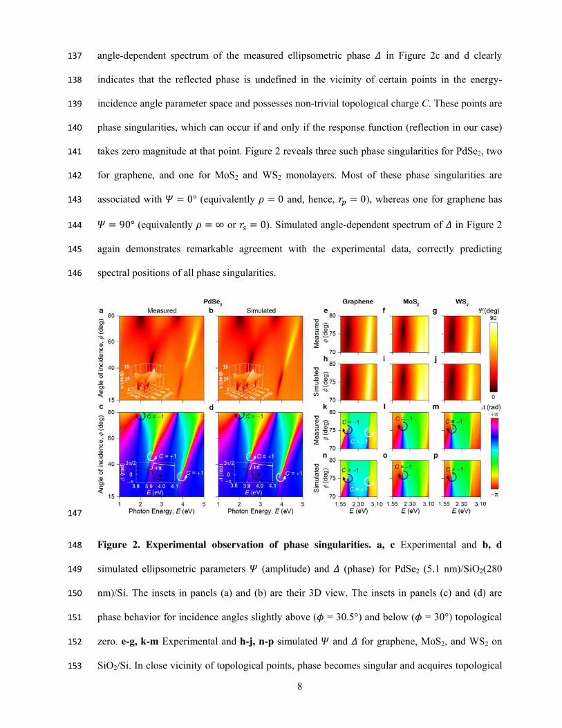
singular point (dashed lines in panel (c)) giving rise to topological charge with 2π round-trip 88
6
around zero-reflection point. The inset is a dielectric permittivity of the model HRIM used for 89
calculation of (b) and (c). 90
The most exciting consequence of such optical phase control is the realization of “flat optics” 91
paradigm – flexible manipulation of the optical wavefront by an arrangement of subwavelength 92
planar objects to shape the desired phase pattern.1,18–20 Such “flat optics” paradigm enables 93
miniaturized metalenses21–23 and meta-holograms,24–26 and two-dimensional (2D) materials27 94
such as graphene,28 transition metal dichalcogenides,29 and organic semiconductors30 provide an 95
excellent platform for implementation of these components. Although these works constitute an 96
important step towards truly flat optics, the efficiency of current devices is limited by the 97
fundamental constraints. Indeed, the typical wavefront manipulation applications require that the 98
phase accumulated by a light wave upon interaction with such a device can be tuned at least 99
within the range of . However, in the monolayer limit ( ∼0.65 nm and ∼4) for visible light 100
( ∼600 nm), the resulting phase delay, which is approximately determined by the optical 101
thickness of the 2D material layer, is only about 0.01 . Consequently, finding new ways to 102
induce strong optical phase variations in atomically thin structures is vital for flat optics. 103
Here, we demonstrate a platform for efficient optical phase manipulation presented by 104
atomically thin high-refractive-index materials (HRIMs) that often possess excitonic resonances. 105
We experimentally observe zero-reflection, phase singularities, and rapid phase variation of 106
reflected light in extremely thin layers (down to single monolayer!) of PdSe2, graphene, MoS2, 107
and WS2 films placed on SiO2/Si substrate. Combined theoretical and experimental analysis 108
indicates that the zero-reflection points are accompanied by a non-trivial topological charge. We 109
derive an analytical condition for such points to occur in layered structures containing optically 110
thin films and predict the occurrence of these points in structures containing a broader family of 111
atomically thin HRIMs and substrates. The observed effect is highly robust and does not require 112
complicated fabrication steps guaranteeing its reproducibility and reliability. In contrast to 113

7
optical darkness observed for dielectric materials and multilayers which disappears with layer 114
irregularities (e.g., at Brewster angle conditions) the effect is topologically protected. It can be 115
used in numerous applications, including label-free bio- and chemical sensing, photo-detection 116
and photo-harvesting, perfect light absorption in 2D monolayers, quantum communication and 117
security. As a practical application of this platform, we demonstrate a refractive index sensor that 118
can rival modern plasmon resonance-based counterparts.31 Therefore, our phase engineering 119
approach as a whole offers an advanced tool for current and next-generation 2D flat optics. 120
RESULTS 121
Phase singularities in reflection 122
To examine topological properties of the light reflectance from thin HRIM films placed on 123
SiO2/Si substrates, we utilized spectroscopic ellipsometry (Methods). The unique advantage of 124
this technique is the simultaneous determination of reflection amplitude and phase in terms of 125
the ellipsometric parameters and , which are defined through the complex reflection ratio ρ:32 126
= tan( ) = (1)
where and are the amplitude reflection coefficients of p- and s-polarized plane waves. 127
Therefore, ellipsometry provides us with the information not only about the reflected light 128
amplitude, but also about the light phase. 129
Unexpectedly, we found that light reflection measured from 5.1 nm thick PdSe2 as well as for 130
monolayers of graphene, MoS2, and WS2 on SiO2/Si substrate showed a number of zero-131
reflection points as explained in Figure 2. Remarkably, the measured amplitude parameter in 132
Figure 2a is in excellent agreement with the simulated spectrum in Figure 2b calculated using the 133
transfer-matrix method.33 However, the spectra of alone do not definitively indicate if an exact 134
zero was attained in reflection at the position of any of dips. This can be deduced from the 135
behavior of relevant phase which was measured using spectroscopic ellipsometry (phase ). The 136
8
angle-dependent spectrum of the measured ellipsometric phase in Figure 2c and d clearly 137
indicates that the reflected phase is undefined in the vicinity of certain points in the energy-138
incidence angle parameter space and possesses non-trivial topological charge C. These points are 139
phase singularities, which can occur if and only if the response function (reflection in our case) 140
takes zero magnitude at that point. Figure 2 reveals three such phase singularities for PdSe2, two 141
for graphene, and one for MoS2 and WS2 monolayers. Most of these phase singularities are 142
associated with = 0° (equivalently = 0 and, hence, = 0), whereas one for graphene has 143 = 90° (equivalently = ∞ or = 0). Simulated angle-dependent spectrum of in Figure 2 144
again demonstrates remarkable agreement with the experimental data, correctly predicting 145
spectral positions of all phase singularities. 146
147
Figure 2. Experimental observation of phase singularities. a, c Experimental and b, d 148
simulated ellipsometric parameters (amplitude) and (phase) for PdSe2 (5.1 nm)/SiO2(280 149
nm)/Si. The insets in panels (a) and (b) are their 3D view. The insets in panels (c) and (d) are 150
phase behavior for incidence angles slightly above ( = 30.5°) and below ( = 30°) topological 151
zero. e-g, k-m Experimental and h-j, n-p simulated and for graphene, MoS2, and WS2 on 152
SiO2/Si. In close vicinity of topological points, phase becomes singular and acquires topological 153
9
charge = −1 or +1. Optical constants of PdSe2 for simulations are taken from Figure 3k. 154
Meanwhile optical constants for graphene, MoS2, and WS2 were adopted from several 155
reports.34,35 156
Previous works4–6 realized these topological phase singularities only in metallic 157
nanostructures through careful engineering of optical properties of nanostructured materials. 158
Later, singular phase behavior was achieved in simple plasmonic heterostructures36 where thin 159
layers of metals (~20nm) and dielectric were used to generate zero reflection and phase 160
singularities. Figure 2 proves that the heterostructure approach is quite general and could be 161
realized even for 2D materials with ultimate atomic thickness in the simplest structure – 2D 162
material/SiO2/Si. The reason for this counterintuitive result is a rapid dielectric function variation 163
(for example, due to excitons in TMDCs) in atomically thin HRIM. This rapid variation 164
guarantees intersection with the zero-reflection surface (Figure 1b). Note that a thick layer is 165
unsuitable for this purpose because absorption in that layer will prohibit interaction with the 166
substrate’s Fabry-Perot resonances. 167
To predict the position zero-reflection points for p- and s-polarized reflection in our structure 168
shown in Figure 1a, we derived analytical expressions for the permittivities and of a thin 169
film placed on a dielectric substrate which would result in the absence of the reflection for p- and 170
s-polarized light, respectively (Supplementary Note 1): 171
= 1 + − tan( )tan( ) + (2)
= 1 + − tan( )tan( ) + (3)
where and are thicknesses of the high-refractive-index material and dielectric layer 172
respectively; , , and are the dielectric permittivity of top halfspace, dielectric layer and 173
bottom halfspace, in our case, that is air, SiO2, and Si, respectively; = / =174
10
− sin ( ) is the normalized z-component (perpendicular to layers) of the wavevector in 175
medium number i, = / , is the frequency, is the speed of light, and is the angle of 176
incidence. If the bottom halfspace is filled with a perfect electric conductor, the expressions can 177
be simplified greatly to: 178
= cot( ) = (4)
= cot( ) = (5)
where , and , are the real and imaginary parts of dielectric permittivity , . 179
Equations (2) and (3) define a zero-reflection surface in the parameter space of wavelength, 180
real and imaginary parts of the permittivity ( , Re[ ] and Im[ ], respectively). Intersections of 181
the material dispersion curve in this parameter space with the zero-reflection surface of the 182
system (thin film of HRIM/SiO2/Si) define zero-reflection points for the particular material of 183
the film, as shown in Figure 1b. The topology of mutual arrangement of the curve and the 184
surface underlies the robustness of the zero-reflection effect to external perturbations (roughness, 185
temperature change, etc.). If a perturbation is introduced to the thin film, a displacement of the 186
material dispersion curve and/or the zero-reflection surface will only result in a shift of the zero-187
reflection point in the parameter space, but will not lead to its disappearance (Figure 1b). This 188
argument is in line with non-trivial topological charges of the observed phase singularities: small 189
changes in the parameters of the system cannot lead to a change in the phase round-trip around a 190
point, since it is an integer of 2 , thus making the zero-reflection point topologically protected.37 191
Spectral positions of topological phase singularities can be controlled by either the thickness 192
or the dielectric permittivity of the material. The derived analytical expressions allow us to 193
generalize the effect of phase singularities to other high-refractive-index materials 194
(Supplementary Note 2). Hence, the effect of rapid phase change is universal for all atomically 195

11
thin materials and substrates. It allows us hereafter to focus on PdSe2, which demonstrates rich 196
and spectra with a series of peaks and dips in Figure 2a-b. We begin with a detailed 197
characterization of PdSe2 film, and then switch to unique applications and features of topological 198
phase gradient. 199
Morphological and optical study of PdSe2 200
PdSe2 thin films were prepared through chemical vapor deposition (CVD)38 resulted in a uniform 201
sample as confirmed by representative optical and scanning electron microscopy (SEM) images 202
in Figure 3b-c. X-ray diffraction (XRD) spectrum showed pronounced peak in Figure 3b 203
validating the high crystallinity of the film.39 Next, we validated the material’s purity by X-ray 204
photoemission spectroscopy (XPS) in Figure 3g-h. It shows that Se:Pd atomic concentration ratio 205
equals 1.92, close to the expected value of 2. Additionally, Raman spectra in Figure 3e-f have 206
characteristic phonon modes , , , and inherent to PdSe2 with puckered pentagonal 207
crystal structure presented in Figure 3a.40 This crystal configuration naturally has high 208
geometrical and, therefore, high optical anisotropy (see Supplementary Note 3).41,42 209
To investigate anisotropic optical response, we measured Mueller matrices (Methods), which 210
nonzero off-diagonal elements relate to sample anisotropy (see Supplementary Note 3). 211
Interestingly, Mueller matrix’ elements vary from point to point, as seen from Figure 3i-j. 212
Conceivably, it comes from the random growth during the CVD synthesis since Mueller 213
matrices’ values in Figure 3i follow Gaussian law for random numbers. A similar random local 214
anisotropic response is observed by polarized optical microscopy and Raman spectroscopy 215
(Supplementary Note 3). Hence, at a macroscopic scale, our PdSe2 layer exhibits an isotropic 216
dielectric response. It allowed us to investigate optical constants by classical ellipsometric and 217
reflectance measurements (see Supplementary Note 3) using the isotropic model for PdSe2 with 218
5.1 nm thickness obtained by atomic force microscopy (AFM) in Figure 3d. The resulting 219
broadband dielectric function is presented in Figure 3k. As expected, PdSe2 has pronounced 220

12
excitonic peaks43 and a metallic Drude response caused by p-doping revealed by XPS (see 221
Supplementary Note 3). Note that excitonic peaks of PdSe2 align with Fabry-Perot resonances of 222
the standard SiO2 (280 nm)/Si substrate, making system PdSe2/SiO2(280 nm)/Si promising for 223
enhancement of the PdSe2 optical response. 224
225
Figure 3. Characterization of PdSe2. a Schematic illustration of PdSe2 crystal structure. b 226
Optical image of the sample. The inset shows PdSe2 XRD diffraction pattern with pronounced 227
peaks corresponding to the (0,0,2) crystal plane. Another peak is from Si substrate. c SEM image 228
of the film. Small dots are seeding promoters for CVD growth. d AFM topography gives 5.1 nm 229
film thickness. e-f Raman spectrum of PdSe2 at excitation wavelengths =532 nm (green line) 230
and 632.8 nm (red line). g-h XPS spectra of PdSe2. i-j Relative frequency and map of m32 (off-231
diagonal element of Mueller Matrix), indicating an anisotropic optical response. Although the 232
material is highly anisotropic (m32 0), its random growth results in overall isotropic behavior 233

13
(average m32 = 0). The full Mueller Matrix is in Supplementary note 3. The red curve in panel (i) 234
is a Gaussian fit. k Optical constants of PdSe2 in the broad spectral range 0.124 – 6 eV (200 – 235
10000 nm). For PdSe2 optical model, see Supplementary Note 4. Interestingly, the excitonic 236
peaks of PdSe2 coincide with the Fabry-Perot resonances of SiO2 (280 nm)/Si. 237
Applications of topological zeros: sensing 238
Simple planar structures studied here are easy to incorporate and leverage in industrial and 239
scientific devices where the optical phase plays a critical role.5,24,25,31,44 The most prominent 240
practical examples are holography,24,25,44 image processing45,46, label-free bio- or chemical 241
sensing,47–50 and quantum key distribution.51,52 To validate the concept, we demonstrated that the 242
liquid/PdSe2/SiO2/Si system is already an ultrahigh sensitive sensor owing to rapid phase change 243
around the topological point. Note that for sensing measurements we used ellipsometer in the 244
most accurate nulling mode (Methods) and 7.1 nm PdSe2 thin film to have topological zero in the 245
operation range of our device since liquid changes zero’s spectral and angle position according 246
to Equations (2-3). 247
For demonstration, we used water with 0, 2.5, 5, 15, and 20 % volume concentration of 248
isopropanol. Notably, the measured and in water are in agreement with the predicted values 249
(see Supplementary Note 5) whereby confirming the water stability of PdSe2 in addition to its 250
recently shown air stability.40 Then, to alter the refractive index (RI), we injected isopropanol 251
into the solution and recorded and (Figure 4a-b) for each water solution. As predicted, the 252
change in amplitude response, , (Figure 4a and c) is relatively small due to the resonance’s 253
topological nature, whereas (Figure 4b and d) shows a dramatic dependence on RI of liquid. 254
Noteworthy, the phase sensitivity in our device of 7.5·104 degrees per refractive index unit 255
(deg/RIU) exceeds that of the cutting-edge sensor based on plasmonic surface lattice resonance 256
with 5.7·104 deg/RIU.31 Therefore, the investigated system PdSe2/SiO2/Si is already a ready-to-257
use scalable device with outstanding performance thanks to the pronounced phase effect in 258
topological points. 259

14
260
Figure 4. Sensor based on topology of PdSe2 film on SiO2/Si. a, b The dependence of 261
ellipsometric parameters (amplitude) and (phase) on the refractive index (RI) of the 262
investigated liquid recorded at the incidence angle =49.4°, corresponding to the topological 263
zero. c Spectral shift of the resonance position of spectrum with the change of the medium RI. 264
d The maximum phase shift of the measured spectra with respect to the media with RI = 1.35 265
(water). The inset shows the phase shift of the measured spectra with respect to the media with 266
RI = 1.35 (water). 267
Evolution of phase singularities 268

15
So far we have considered and observed reflection phase singularities with unitary topological 269
charge, wherein the argument makes a ±2 round-trip around the singularity. These points, 270
however, are not stationary and evolve with the material parameters, as Equations (2-3) suggest. 271
When two points with opposite charges (+1 and −1) meet in the parameter space, they annihilate 272
leaving no phase singularity. We theoretically observe such annihilation with variation of the 273
PdSe2 film thickness, , when two phase singularities with opposite topological charges meet at 274
around ≈ 3.2 nm (Figure 5a). This case happens when the material dispersion curve in Figure 275
5b becomes tangent to zero-reflection surface. The corresponding angle-resolved spectrum of 276
shown in Figure 5b plotted for =3.2 nm reveals the absence of any phase singularities. 277
Therefore, by varying the thickness one is able to control the position and amount of phase 278
singularities, which appear or disappear in pairs, so that the total topological charge preserves. 279
Next, we examine the possibility of phase singularities with higher topological charges, | | > 280
1. One potential opportunity for the emergence of a non-unitary topological charge is when a 281
phase singularity either in or exhibits a non-unitary charge. Unfortunately, for non-magnetic 282
materials in a planar system, zeros in or are essentially non-degenerate (Supplementary 283
Note 6). 284
However, since is the ratio of two reflection coefficients, another possibility is when a 285 = ±1 phase singularity of coincides in the parameter space with a = ∓1 phase singularity 286
of . This gives rise to a = ±2 phase singularity of , which can be detected by spectroscopic 287
ellipsometry. Equating the right-hand sides of Equations (2) and (3), we obtain an equation that 288
determines, for a given substrate, the position of the point at which the zero-reflection conditions 289
for both polarizations coincide; then we can immediately calculate the dielectric constant of the 290
film that satisfies this condition. The charge of a point is determined by the derivative of the 291
material dispersion curve, so the last step is to choose the direction of the material dispersion 292
curve near the zero-reflection point. By using the set of parameters satisfying these conditions 293
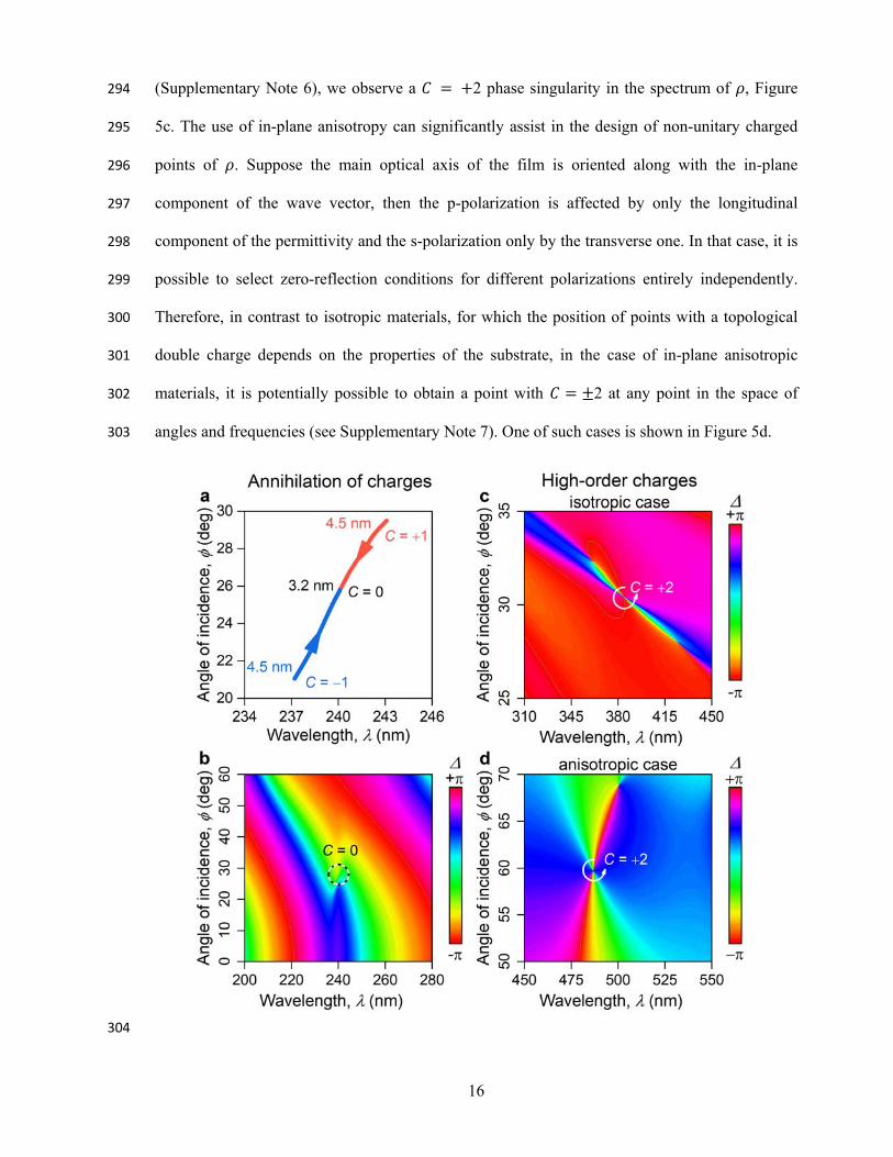
16
(Supplementary Note 6), we observe a = +2 phase singularity in the spectrum of , Figure 294
5c. The use of in-plane anisotropy can significantly assist in the design of non-unitary charged 295
points of . Suppose the main optical axis of the film is oriented along with the in-plane 296
component of the wave vector, then the p-polarization is affected by only the longitudinal 297
component of the permittivity and the s-polarization only by the transverse one. In that case, it is 298
possible to select zero-reflection conditions for different polarizations entirely independently. 299
Therefore, in contrast to isotropic materials, for which the position of points with a topological 300
double charge depends on the properties of the substrate, in the case of in-plane anisotropic 301
materials, it is potentially possible to obtain a point with = ±2 at any point in the space of 302
angles and frequencies (see Supplementary Note 7). One of such cases is shown in Figure 5d. 303
304

17
Figure 5. Topological effects in phase singularities. a, b The parameter change, here the 305
thickness of PdSe2, alters the positions of topological points, resulting, at specific thickness ( =306 3.2 nm), in annihilation of opposite topological charges. c, d Topological charges with = +2 307
for ellipsometric phase with isotropic and anisotropic thin films with system’s parameters 308
collected in Supplementary Note 7. 309
For = ±2 singularities demonstrated in Figure 5c-d, the phase makes a ±4 round-trip 310
around such a singularity, thus increasing the local phase gradient approximately by a factor of 311
two, which could significantly improve phase applications. For instance, the sensitivity of the 312
corresponding refractive index sensor may increase approximately two-fold. 313
The scenario of non-unitary phase singularities is somewhat reminiscent of exceptional points 314
in non-Hermitian optical systems.53 Such points, which correspond to coalescent eigenstates of a 315
non-Hermitian Hamiltonian, feature a strong ( − ) /( ) dependence of the eigenenergies of 316
the optical system on a perturbation parameter in the vicinity of the exceptional point (with 317
being the order of the exceptional point), which has been used for boost the sensitivity. 318
Additionally, upon appropriate engineering of the system the same concept of topological 319
phase manipulation could also be applied in transmission regime, thus bridging our phase 320
engineering approach with metasurfaces. 321
DISCUSSION 322
Flat optics enable the design of optical components into thin, planar, and CMOS-compatible 323
structures. Coupled with 2D materials, it evolves into 2D flat optics with ultracompact and 324
tunable devices. Nevertheless, atomically thin optical elements suffer from low efficiency of 325
phase manipulation. To lift this limitation and achieve phase control with 2D materials, we 326
utilized topologically protected zeros of a simple heterostructure. We showed both 327
experimentally and theoretically that a whole set of high-index 2D materials could provide rapid 328
phase variations revealed by spectroscopic ellipsometry. In addition, we demonstrate that 329

18
topological approach leads to high-performance devices on the sensing example and propose the 330
future direction of topological phase effects such as annihilation and high-order charges. From a 331
broader perspective, our results open new avenues for effective application of atomically thin 332
high-refractive-index materials as phase materials in photonics. 333
ACKNOWLEDGMENTS 334
G.E., K.V., D.G.B., G.T., D.Y., S.N., A.V., A.M., I.K., A.A., and V.V. gratefully 335
acknowledges the financial support from the Ministry of Science and Higher Education of the 336
Russian Federation (Agreement No. 075-15-2021-606). A.N.G. acknowledge EU Graphene 337
Flagship, Core 3 (881603). 338
AUTHOR CONTRIBUTIONS 339
†These authors contributed equally. A.N.G., V.V., K.S.N., V.K., and A.A. suggested and 340
directed the project. G.E., V.K., G.T., Y.S., D.Y., S.N., S.Z., R.R., and A.M.M. performed the 341
measurements and analyzed the data. K.V., D.G.B., G.E., A.M., I.K., and A.V. provided 342
theoretical support. G.A.E., K.V., and D.G.B. wrote the original manuscript. G.E., K.V., D.G.B., 343
A.N.G., K.S.N., V.V., and A.A. reviewed and edited the paper. All authors contributed to the 344
discussions and commented on the paper. 345
COMPETING INTERESTS 346
The authors declare no competing interests. 347
METHODS 348
Ellipsometry measurements. For visualization of topological charge in phase, we used a 349
variable-angle spectroscopic ellipsometer (VASE, J.A. Woollam Co.) since it measures 350
amplitude and phase of complex reflection ratio simultaneously. Measurements were done over a 351
wide wavelength range from 248 to 1240 nm (1 – 5 eV) in steps of 1 nm and multiple angles of 352
incidence in the range 15-80° with 0.5° step. Ellipsometer has a single chamber monochromator 353

19
with two gratings: 1200 g/mm for visible light (248 – 1040 nm) with 4.6 nm bandwidth and 600 354
g/mm for near-infrared interval (1040 – 1240 nm) with 9.2 nm bandwidth. 355
For accurate refractive index sensing, we performed the nulling ellipsometry with Accurion 356
nanofilm_ep4 ellipsometer. During the measurement light was initially directed through the 357
polarizer then through the compensator, whose settings were adjusted until the reflection from 358
the sample became linearly polarized. Afterward, the analyzer was set to achieve the minimum 359
in the signal at the photodetector. The final positions of polarizer and analyzer at signal’s 360
minimum uniquely define ellipsometric parameters and . Measurements were done over a 361
wavelength range from 300 to 360 nm in steps of 0.1 nm with 4 nm bandwidth and at 49.4° 362
incident angle corresponding to the singular point of PdSe2 in water. 363
To probe anisotropic response, we also measured 11 elements of Mueller Matrix (m12, m13, m21, 364
m22, m23, m24, m31, m32, m33, m34) on Accurion nanofilm_ep4 ellipsometer over 400 – 1000 nm 365
wavelength range in 5 nm step with 4 nm bandwidth at 50° incident angle in a rotation 366
compensator mode to get access to Stokes parameters in the input branch of ellipsometer. 367
Optical visualization. The surface images (2400 × 2400 pixels) of PdSe2 were captured by an 368
optical microscope (Nikon LV150L) with a digital camera DS-Fi3. 369
Atomic force microscopy. The thickness and surface morphology of the PdSe2 film were 370
accurately characterized by an atomic force microscope (AFM, NT-MDT Spectrum Instruments 371
“Ntegra”) using AFM in a peak-force mode at ambient conditions. AFM measurements were 372
carried out using cantilever tips from NT-MDT (ETALON, HA_NC) with a spring constant of 373
3.5 N/m, a tip radius < 10 nm and a resonant frequency of 140 kHz. Images of PdSe2 surface 374
were taken with 512 × 512 pixels and scan rate of 0.5 Hz, after that data were analyzed by 375
Gwyddion software. 376
Scanning electron microscopy. Scanning electron microscopy (SEM, JEOL JSM-7001F) with a 377
Schottky emitter in secondary electron imaging mode with a voltage of 30 kV and current of 378
20
67 µA, and a working distance of ~ 6.3 mm was applied to study in detail surface features and 379
homogeneity of the PdSe2 film surface within different areas using 1960 × 1280 pixel scan. 380
XPS characterization. The chemical states of the elements in the film, as well as the valence 381
band were analyzed by X-ray photoelectron spectroscopy (XPS) in Theta Probe tool (Thermo 382
Scientific) under ultrahigh vacuum conditions (base pressure < 10-9 mBar) with a 383
monochromatic Al-Kα X-ray source (1486.6 eV). Photoelectron spectra were acquired using 384
fixed analyzer transmission (FAT) mode with 50 eV pass energy. The spectrometer energy scale 385
was calibrated on the Au 4f7/2 line (84.0 eV). 386
X-ray diffraction. X-ray powder diffractometrer (XRD, Thermo ARL X'TRA) equipped with 387
Cu Kα radiation λ = 0.154 nm was used to characterize the crystalline structure and phase of 388
PdSe2 film. The XRD pattern was taken at ambient conditions by 2 -scan over the range of 20–389
75° with a step of 0.05° and accumulation time of 2 s. 390
Reflectance measurements. Fourier-transform spectrometer Bruker Vertex 80v has been used 391
to measure the reflection coefficient at the normal incident at room temperature in the frequency 392
range from 1000 to 24000 cm-1, as the reference was used the reflection from the gold mirror. 393
Raman characterization. The experimental setup used for Raman measurements was a 394
confocal scanning Raman microscope Horiba LabRAM HR Evolution (HORIBA Ltd., Kyoto, 395
Japan). All measurements were carried out using linearly polarized excitation at wavelengths 396
532 and 632.8 nm,1800 lines/mm diffraction grating, and ×100 objective (N.A. = 0.90), whereas 397
we used un-polarized detection to have a significant signal-to-noise ratio. The spot size was 398
approximately 0.43μm. The Raman images were recorded by mapping the spatial dependence of 399
Raman intensity integrated at the main Raman peaks within the shift range 136 – 156 cm−1, for 400
each of the 45 × 45 points in the scan, with an integration time of 500 ms at each point and 401
incident power P = 1.7 mW. 402
DATA AVAILABILITY 403

21
The datasets generated during and/or analyzed during the current study are available from the 404
corresponding author on reasonable request. 405
406
REFERENCES 407
1. Yu, N. et al. Light Propagation with Phase Discontinuities: Generalized Laws of 408
Reflection and Refraction. Science 334, 333–337 (2011). 409
2. Deng, Z.-L. & Li, G. Metasurface optical holography. Mater. Today Phys. 3, 16–32 410
(2017). 411
3. Jung, C. et al. Near-zero reflection of all-dielectric structural coloration enabling 412
polarization-sensitive optical encryption with enhanced switchability. Nanophotonics 10, 413
919–926 (2020). 414
4. Grigorenko, A. N., Nikitin, P. I. & Kabashin, A. V. Phase jumps and interferometric 415
surface plasmon resonance imaging. Appl. Phys. Lett. 75, 3917–3919 (1999). 416
5. Kravets, V. G. et al. Singular phase nano-optics in plasmonic metamaterials for label-free 417
single-molecule detection. Nat. Mater. 12, 304–309 (2013). 418
6. Malassis, L. et al. Topological Darkness in Self-Assembled Plasmonic Metamaterials. 419
Adv. Mater. 26, 324–330 (2014). 420
7. Hein, S. M. & Giessen, H. Retardation-induced phase singularities in coupled plasmonic 421
oscillators. Phys. Rev. B 91, 205402 (2015). 422
8. Kravets, V. G., Schedin, F. & Grigorenko, A. N. Plasmonic blackbody: Almost complete 423
absorption of light in nanostructured metallic coatings. Phys. Rev. B 78, 205405 (2008). 424
9. Kim, S. et al. Electronically Tunable Perfect Absorption in Graphene. Nano Lett. 18, 971–425
979 (2018). 426
10. Zhu, L. et al. Angle-selective perfect absorption with two-dimensional materials. Light 427
Sci. Appl. 5, e16052–e16052 (2016). 428
11. Pichler, K. et al. Random anti-lasing through coherent perfect absorption in a disordered 429
medium. Nature 567, 351–355 (2019). 430
12. Jackson, J. D. Electrodynamics, Classical. in digital Encyclopedia of Applied Physics 431
(Wiley-VCH Verlag GmbH & Co. KGaA, 2003). 432
13. Baranov, D. G., Edgar, J. H., Hoffman, T., Bassim, N. & Caldwell, J. D. Perfect 433
interferenceless absorption at infrared frequencies by a van der Waals crystal. Phys. Rev. 434
B 92, 1–6 (2015). 435
14. Sweeney, W. R., Hsu, C. W. & Stone, A. D. Theory of reflectionless scattering modes. 436
Phys. Rev. A 102, 1–20 (2020). 437
15. Yan, C., Raziman, T. V. & Martin, O. J. F. Phase Bifurcation and Zero Reflection in 438
Planar Plasmonic Metasurfaces. ACS Photonics 4, 852–860 (2017). 439
16. Berkhout, A. & Koenderink, A. F. Perfect Absorption and Phase Singularities in Plasmon 440
Antenna Array Etalons. ACS Photonics 6, 2917–2925 (2019). 441

22
17. Born, M. et al. Principles of Optics. (Cambridge University Press, 1999). 442
18. Kildishev, A. V., Boltasseva, A. & Shalaev, V. M. Planar Photonics with Metasurfaces. 443
Science 339, 1232009–1232009 (2013). 444
19. Yu, N. & Capasso, F. Flat optics with designer metasurfaces. Nat. Mater. 13, 139–150 445
(2014). 446
20. Gomez-Diaz, J. S. & Alù, A. Flatland Optics with Hyperbolic Metasurfaces. ACS 447
Photonics 3, 2211–2224 (2016). 448
21. Wang, S. et al. A broadband achromatic metalens in the visible. Nat. Nanotechnol. 13, 449
227–232 (2018). 450
22. Chen, W. T. et al. A broadband achromatic metalens for focusing and imaging in the 451
visible. Nat. Nanotechnol. 13, 220–226 (2018). 452
23. Lin, H. et al. Diffraction-limited imaging with monolayer 2D material-based ultrathin flat 453
lenses. Light Sci. Appl. 9, 137 (2020). 454
24. Zheng, G. et al. Metasurface holograms reaching 80% efficiency. Nat. Nanotechnol. 10, 455
308–312 (2015). 456
25. Ni, X., Kildishev, A. V. & Shalaev, V. M. Metasurface holograms for visible light. Nat. 457
Commun. 4, 2807 (2013). 458
26. Yue, Z., Xue, G., Liu, J., Wang, Y. & Gu, M. Nanometric holograms based on a 459
topological insulator material. Nat. Commun. 8, 15354 (2017). 460
27. Xia, F., Wang, H., Xiao, D., Dubey, M. & Ramasubramaniam, A. Two-dimensional 461
material nanophotonics. Nat. Photonics 8, 899–907 (2014). 462
28. Li, Z. et al. Graphene Plasmonic Metasurfaces to Steer Infrared Light. Sci. Rep. 5, 12423 463
(2015). 464
29. Mak, K. F. & Shan, J. Photonics and optoelectronics of 2D semiconductor transition metal 465
dichalcogenides. Nat. Photonics 10, 216–226 (2016). 466
30. Shi, Y.-L., Zhuo, M.-P., Wang, X.-D. & Liao, L.-S. Two-Dimensional Organic 467
Semiconductor Crystals for Photonics Applications. ACS Appl. Nano Mater. 3, 1080–468
1097 (2020). 469
31. Danilov, A. et al. Ultra-narrow surface lattice resonances in plasmonic metamaterial 470
arrays for biosensing applications. Biosens. Bioelectron. 104, 102–112 (2018). 471
32. Harland G. Tompkins, J. N. H. Spectroscopic Ellipsometry Practical Application to Thin 472
Film Characterization. (Momentum Press, 2016). 473
33. Passler, N. C. & Paarmann, A. Generalized 4 × 4 matrix formalism for light propagation 474
in anisotropic stratified media: study of surface phonon polaritons in polar dielectric 475
heterostructures. J. Opt. Soc. Am. B 34, 2128 (2017). 476
34. El-Sayed, M. A. et al. Optical Constants of Chemical Vapor Deposited Graphene for 477
Photonic Applications. Nanomaterials 11, 1230 (2021). 478
35. Ermolaev, G. A., Yakubovsky, D. I., Stebunov, Y. V., Arsenin, A. V. & Volkov, V. S. 479
Spectral ellipsometry of monolayer transition metal dichalcogenides: Analysis of 480
excitonic peaks in dispersion. J. Vac. Sci. Technol. B 38, 014002 (2020). 481
36. Sreekanth, K. V. et al. Biosensing with the singular phase of an ultrathin metal-dielectric 482
23
nanophotonic cavity. Nat. Commun. 9, 369 (2018). 483
37. Lu, L., Joannopoulos, J. D. & Soljačić, M. Topological photonics. Nat. Photonics 8, 821–484
829 (2014). 485
38. Zeng, L. H. et al. Controlled Synthesis of 2D Palladium Diselenide for Sensitive 486
Photodetector Applications. Adv. Funct. Mater. 29, 1–9 (2019). 487
39. Zhang, G. et al. Optical and electrical properties of two-dimensional palladium diselenide. 488
Appl. Phys. Lett. 114, (2019). 489
40. Oyedele, A. D. et al. PdSe2: Pentagonal Two-Dimensional Layers with High Air Stability 490
for Electronics. J. Am. Chem. Soc. 139, 14090–14097 (2017). 491
41. Yu, J. et al. Direct Observation of the Linear Dichroism Transition in Two-Dimensional 492
Palladium Diselenide. Nano Lett. 20, 1172–1182 (2020). 493
42. Ermolaev, G. A. et al. Giant optical anisotropy in transition metal dichalcogenides for 494
next-generation photonics. Nat. Commun. 12, 854 (2021). 495
43. Kuklin, A. V. & Ågren, H. Quasiparticle electronic structure and optical spectra of single-496
layer and bilayer PdSe2: Proximity and defect-induced band gap renormalization. Phys. 497
Rev. B 99, 245114 (2019). 498
44. Wang, Y. et al. Atomically Thin Noble Metal Dichalcogenides for Phase-Regulated Meta-499
optics. Nano Lett. 20, 7811–7818 (2020). 500
45. Zhu, T. et al. Topological optical differentiator. Nat. Commun. 12, 680 (2021). 501
46. Huo, P. et al. Photonic Spin-Multiplexing Metasurface for Switchable Spiral Phase 502
Contrast Imaging. Nano Lett. 20, 2791–2798 (2020). 503
47. Grigorenko, A. et al. Dark-field surface plasmon resonance microscopy. Opt. Commun. 504
174, 151–155 (2000). 505
48. Kravets, V. G., Schedin, F., Kabashin, A. V. & Grigorenko, A. N. Sensitivity of collective 506
plasmon modes of gold nanoresonators to local environment. Opt. Lett. 35, 956 (2010). 507
49. Wu, F. et al. Layered material platform for surface plasmon resonance biosensing. Sci. 508
Rep. 9, 20286 (2019). 509
50. Kabashin, A. V. et al. Phase�Responsive Fourier Nanotransducers for Probing 2D 510
Materials and Functional Interfaces. Adv. Funct. Mater. 29, 1902692 (2019). 511
51. Hiskett, P. A. et al. Long-distance quantum key distribution in optical fibre. New J. Phys. 512
8, 193–193 (2006). 513
52. Takesue, H. et al. Quantum key distribution over a 40-dB channel loss using 514
superconducting single-photon detectors. Nat. Photonics 1, 343–348 (2007). 515
53. Özdemir, Ş. K., Rotter, S., Nori, F. & Yang, L. Parity–time symmetry and exceptional 516
points in photonics. Nat. Mater. 18, 783–798 (2019). 517
518

Supplementary Files
This is a list of supplementary �les associated with this preprint. Click to download.
SupplementaryInformationNatComm.pdf
Copyright © 2022 FDOKUMEN