TLK6002 - Texas Instruments
98
TLK6002 www.ti.com SLLSE34A – MAY 2010 – REVISED AUGUST 2010 Dual Channel 0.47Gbps to 6.25Gbps Multi-Rate Transceiver Check for Samples: TLK6002 1 Introduction 1.1 Transceiver Features 1 • Dual Channel 470Mbps to 6.25Gbps • Dual Power Supply: 1.0V Core, and 1.5V/1.8V Continuous/Multi-Rate Transceiver I/O Nominal Supply • Supports all CPRI and OBSAI Data Rates • Serial Side Three Tap Transmit De-emphasis and Receive Adaptive Equalization to Allow • Integrated Latency Measurement Function, Extended Backplane Reach Accuracy of ±814 ps • Programmable Output Swing on Serial Output • CPRI/OBSAI Automated Rate Sense (ARS) Function • Minimum Receiver Differential Input Thresholds of 100mV dfpp • Supports SERDES Operation, 8B/10B Data Modes (20-bit and 16-bit + Controls) • Loss of Signal (LOS) detection (≤75 mV dfpp ) • 20-bit HSTL Single-Ended Parallel Data • Interface to Back Plane, Copper Cables, or Interface (Integrated Source and End Optical Modules Termination) • Hot Plug Protection • Shared or Independent Reference Clock per • JTAG; IEEE 1149.1 /1149.6 Test Interface Channel • MDIO; IEEE 802.3 Clause-22 Support • Latency/Depth Configurable Transmit and • 65nm Advanced CMOS Technology Receive FIFOs. • Industrial Ambient Operating Temp (–40°C to • Loopback Capability (Serial and Parallel Side), 85°C) at Full Rate OBSAI Compliant • Device Package; 324 PBGA • Supports Serial Retime Operation • Supports PRBS (2 7 –1), (2 23 – 1) and (2 31 –1) and CRPAT Long/Short Generation and Verification 1.2 Applications • WI Infrastructure • CPRI and OBSAI Links • Proprietary Links • Backplane • High Speed Point- to-Point Transmission Systems 1.3 Overview 1.3.1 Device Description The TLK6002 is a member of a portfolio of multi-gigabit transceivers, intended for use in ultra-high-speed bi-directional point-to-point data transmission systems. It is specifically intended for base station RRH (Remote Radio Head) application, but may also be used in other high speed applications. The TLK6002 supports a serial interface speed of 0.470 Gbps to 6.25 Gbps. Rate support includes all the CPRI and OBSAI rates (0.6144/0.768/1.2288/1.536/2.4576/3.072/4.9152/6.144 Gbps) using a single fixed reference clock frequency (either 122.88 MHz or 153.6 MHz). 1 Please be aware that an important notice concerning availability, standard warranty, and use in critical applications of Texas Instruments semiconductor products and disclaimers thereto appears at the end of this data sheet. PRODUCTION DATA information is current as of publication date. Copyright © 2010, Texas Instruments Incorporated Products conform to specifications per the terms of the Texas Instruments standard warranty. Production processing does not necessarily include testing of all parameters.
-
Upload
khangminh22 -
Category
Documents
-
view
1 -
download
0
Transcript of TLK6002 - Texas Instruments
TLK6002
www.ti.com SLLSE34A–MAY 2010–REVISED AUGUST 2010
Dual Channel 0.47Gbps to 6.25Gbps Multi-Rate TransceiverCheck for Samples: TLK6002
1 Introduction
1.1 Transceiver Features1
• Dual Channel 470Mbps to 6.25Gbps • Dual Power Supply: 1.0V Core, and 1.5V/1.8VContinuous/Multi-Rate Transceiver I/O Nominal Supply
• Supports all CPRI and OBSAI Data Rates • Serial Side Three Tap Transmit De-emphasisand Receive Adaptive Equalization to Allow• Integrated Latency Measurement Function,Extended Backplane ReachAccuracy of ±814 ps
• Programmable Output Swing on Serial Output• CPRI/OBSAI Automated Rate Sense (ARS)Function • Minimum Receiver Differential Input
Thresholds of 100mVdfpp• Supports SERDES Operation, 8B/10B DataModes (20-bit and 16-bit + Controls) • Loss of Signal (LOS) detection (≤75 mVdfpp)
• 20-bit HSTL Single-Ended Parallel Data • Interface to Back Plane, Copper Cables, orInterface (Integrated Source and End Optical ModulesTermination) • Hot Plug Protection
• Shared or Independent Reference Clock per • JTAG; IEEE 1149.1 /1149.6 Test InterfaceChannel • MDIO; IEEE 802.3 Clause-22 Support
• Latency/Depth Configurable Transmit and • 65nm Advanced CMOS TechnologyReceive FIFOs. • Industrial Ambient Operating Temp (–40°C to
• Loopback Capability (Serial and Parallel Side), 85°C) at Full RateOBSAI Compliant • Device Package; 324 PBGA
• Supports Serial Retime Operation• Supports PRBS (27–1), (223 – 1) and (231–1) and
CRPAT Long/Short Generation and Verification
1.2 Applications• WI Infrastructure• CPRI and OBSAI Links• Proprietary Links• Backplane• High Speed Point- to-Point Transmission Systems
1.3 Overview
1.3.1 Device Description
The TLK6002 is a member of a portfolio of multi-gigabit transceivers, intended for use in ultra-high-speedbi-directional point-to-point data transmission systems. It is specifically intended for base station RRH(Remote Radio Head) application, but may also be used in other high speed applications. The TLK6002supports a serial interface speed of 0.470 Gbps to 6.25 Gbps. Rate support includes all the CPRI andOBSAI rates (0.6144/0.768/1.2288/1.536/2.4576/3.072/4.9152/6.144 Gbps) using a single fixed referenceclock frequency (either 122.88 MHz or 153.6 MHz).
1
Please be aware that an important notice concerning availability, standard warranty, and use in critical applications of TexasInstruments semiconductor products and disclaimers thereto appears at the end of this data sheet.
PRODUCTION DATA information is current as of publication date. Copyright © 2010, Texas Instruments IncorporatedProducts conform to specifications per the terms of the TexasInstruments standard warranty. Production processing does notnecessarily include testing of all parameters.

TLK6002
SLLSE34A–MAY 2010–REVISED AUGUST 2010 www.ti.com
This integrated circuit can be damaged by ESD. Texas Instruments recommends that all integrated circuits be handled withappropriate precautions. Failure to observe proper handling and installation procedures can cause damage.
ESD damage can range from subtle performance degradation to complete device failure. Precision integrated circuits may be moresusceptible to damage because very small parametric changes could cause the device not to meet its published specifications.
TLK6002 20-bit parallel interface operates in 1.5V or 1.8V HSTL single-ended format. The 20-bit interfaceallows low speed signals on the parallel side and therefore enabling the use of low cost FPGA in thesystem design. The parallel interface can be programmed to be in SDR (Single Data Rate) or DDR(Double Data Rate) modes. The line rate may be set to full (≤6.25Gbps), half (≤3.75Gbps), quarter(≤1.88Gbps) or eighth (≤0.94Gbps). The line rate can be set using either device inputs or software controlregisters.
The TLK6002 performs data conversion parallel-to-serial, serial-to-parallel and clock extraction as aphysical layer interface device. The serial transceiver interface operates at a maximum serial data rate of6.25 Gbps.
TLK6002 accepts single-ended HSTL signals at its parallel transmit and receive data buses. If the internal8B/10B coding and decoding are enabled, TDA/B_[19:0] are latched by TXCLK_A/B and sent to theinternal 8b/10b encoder, where the resulting encoded words are serialized and transmitted differentiallyusing a line clock derived from the SERDES reference clock at the desired line rate. If the internal codingand decoding are disabled, TDA/B_[19:0] are defined as 20-bits of data being serialized and transmittedunmodified according to the desired line rate.
The receive direction performs the serial-to-parallel conversion on the input serial data synchronizing theresulting 20-bit parallel data to the recovered byte clock (RXCLK_A/B). The optionally decoded receivedata is available on the RDA/B_[19:0] output signals.
The serial transmitter and receiver are implemented using differential Current Mode Logic (CML) withintegrated termination resistors.
The TLK6002 provides two local (parallel side) and two remote (serial side) loopback modes for self-testand system diagnostic purposes.
The TLK6002 has an integrated loss of signal (LOS) detection function, which is asserted in conditionswhere the serial input signal does not have sufficient voltage amplitude (≤75 mVdfpp). Note that the inputsignal must be ≥150 mVdfpp when loss of signal replacement of the receive datapath data is enabled(register bit 6.6).
2 Introduction Copyright © 2010, Texas Instruments Incorporated
Submit Documentation FeedbackProduct Folder Link(s): TLK6002

TXAN
TXAP
TDA_[19:0]
Channel A
20
-bit
RE
GIS
TE
R
8B
/10
B
En
co
de
r
Parallel to
SerialTXCLK_A
TDB_[19:0]
TXBN
TXBP
Channel B
20
-bit
RE
GIS
TE
R
8B
/10
B
En
co
de
r
Parallel to
SerialTXCLK_B
2x2
Mux
RXAP
RXAN
Channel A
RDA_[19:0]
Serial to
COMMA
Detect &
Decoding
RXCLK_A
RXBP
RXBN
Channel B
RDB_[19:0]
Serial to
Parallel
COMMA
Detect &
8B/10B
Decoding
20
-bit
RE
GIS
TE
R
RXCLK_B
2x2
Mux
20-b
itR
EG
IST
ER
8B/10B Parallel
TLK6002
www.ti.com SLLSE34A–MAY 2010–REVISED AUGUST 2010
Figure 1-1. TLK6002 Block Diagram
Copyright © 2010, Texas Instruments Incorporated Introduction 3Submit Documentation FeedbackProduct Folder Link(s): TLK6002

Interpolator and
Clock Recovery
&
Adaptive EQB
itC
lk
Clock
Synthesizer
JTAGTMS
TDO
TRST_N
TCK
TDI
TXAN
TXAP
10-bitMUX
Parallel to
Serial
TLK6002
Block Diagram Channel A
BIAS
Withpre-emphasis
MDIO
Interface
PRTAD[4:0]
MDC
MDIO
RESET_N
PD_TRXA_N
SCL
SDI
CS_N
SDO
ReferenceCLock
Rate_A[2:0]
CODEA_EN
20
-bit
reg
iste
r&
TX
FIF
O
8B
/10
B
En
co
de
r
]
Pattern
Generator 10
TXCLK_A
10-bit
10-bit
Sc
ram
ble
r
Pattern
Verifier
10Serial
to
Parallel
20
-bit
RE
GIS
TE
R
RXAP
RXAN
COMMA
Detect &
8B/10B
Decoding
&
De-
scrambler
EQ10
LOSA
RDA_[19:0]
EQ
PRBSA_PASS
RXCLK_A
RX
_F
IFO
10-bit
10 10TDA_[19:0
TLK6002
SLLSE34A–MAY 2010–REVISED AUGUST 2010 www.ti.com
Figure 1-2. TLK6002 Detail Block Diagram (Channel A)
4 Introduction Copyright © 2010, Texas Instruments Incorporated
Submit Documentation FeedbackProduct Folder Link(s): TLK6002

-
+
-
+
REFCLK_0_P/N
REFCLK_1_P/N
01
01
REFCLK_A_SEL
REFCLK_B_SEL
S/W0.1
S/W0.0
RXBCLK_A
TXBCLK_A
RXDA[9:0]
TXDA[9:0]
Channel A
SERDES
REFCLKP/N
RXBCLK_B
TXBCLK_B
RXDB[9:0]
TXDB[9:0]Channel B
SERDES
REFCLKP/N
1 0CLK_OUT_SEL
1/N0.5:4
-+
-+
RXAP
RXAN
TXAP
TXAN
-+
-+
RXBP
RXBN
TXBP
TXBN
CLK_OUT_P/N
RX
TX
RX
TX
= Primary Device Pin
S/W
x.x:x
Legend:
= Software Programmable / Register Address.Bit
RXBCLK_*, TXBCLK_* frequency is Serial Bit Rate Divided by 10
RXBCLK_* is referred to as the recovered byte clock, and is always
synchronous with the incoming serial data rate (when valid).
S/W0.6
10
ARS Channel A
ARS Channel B
ARS
Control /
Divider
Incoming Serial Bit Rate *(1/2/4/8 Full/Half/Quarter/Eighth) / 4
Incoming Serial Bit Rate *(1/2/4/8 Full/Half/Quarter/Eighth) / 4
Note: Also equal in frequency to MPY*REFCLK/2
TDA_[19:0]
TDB_[19:0]
01
10
A S/W3.10
B S/W3.10
TX A FIFO
TX B FIFO
TXDB_INT[9:0]
TXBCLK_B
TXDA_INT[9:0]
TXBCLK_A
TXCLK_B
TXCLK_A
01
10
`
TX A Datapath
CH A TXDatapath
TXDA[9:0]
TXBCLK_A TX A DatapathChannel A
TX SERDES
TX A Datapath
CH B TXDatapath
TXDB[9:0]
TXBCLK_B TX A Datapath
Channel B
TX SERDES
= Primary Device Pin
S/Wx.x:x
Legend:
= Software Programmable / Register Address.Bit
RXBCLK_*, TXBCLK_* frequency is Serial Bit Rate Divided by 10
TLK6002
www.ti.com SLLSE34A–MAY 2010–REVISED AUGUST 2010
Figure 1-3. TLK6002 Reference Clock/Output Clock Architecture
Figure 1-4. TLK6002 Transmit Clock Architecture
Copyright © 2010, Texas Instruments Incorporated Introduction 5Submit Documentation FeedbackProduct Folder Link(s): TLK6002

RDB_[19:0]
RXCLK_B
S/W3.9
S/W{3.9,3.8}
RX A FIFO
RX B FIFO
RDA_[19:0]01
01
00
01
10
11
TXBCLK_B
RXBCLK_B
TXBCLK_A
RXBCLK_A
RXCLK_A
S/W{3.9,3.8}
00
01
10
11
TXBCLK_A
RXBCLK_A
TXBCLK_B
RXBCLK_B
S/W3.9
RXDB_INT[9:0]
RXBCLK_B
RXDA_INT[9:0]
RXBCLK_A TX A Datapath
CH A RXDatapath
RXDA[9:0]
RXBCLK_A TX A Datapath
Channel A
RX SERDES
TX A Datapath
CH B RXDatapath
RXDB[9:0]
RXBCLK_B TX A Datapath
Channel B
RX SERDES
= Primary Device Pin
S/Wx.x:x
Legend:
= Software Programmable / Register Address.Bit
RXBCLK_*, TXBCLK_* frequency is Serial Bit Rate Divided by 10
DDR: 4
SDR: 2
DDR: 4
SDR: 2
614.4 /
1228. 8 /
2457. 6 /
3072 /
4915. 2 /
6144 Mbps
Line rates for CPRI Line rates for OBSAI
768 /
1536 /
3072 /
6144Mbps
PA
LO _ 1
RF
DuplexerLNAADC
DR
12- bit
ADC
IF 1IF 261. 44 MHz
TLK 6002
( Serdes
TLK6002
TLK3131 /
32 /34
Serdes
CPRI /
OBSAI
ADS5232ADS5240
ADS528 x
61.44 MHz
245.76 MHz
61.4
4M
Hz
DAC5682 zDAC 5688
DAC 5687
Σ
LO _ 1
090
16 - bitDAC
FIR
16 - bit
DACFIR
DDC
GC 6016
I / Q
61. 44 MHz
CDCEX52005
X - tal
FPGA
TX _CLK
I/QDUC
GC 6016FPGA
RX_CLK
TLK6002
SLLSE34A–MAY 2010–REVISED AUGUST 2010 www.ti.com
Figure 1-5. TLK6002 Receive Clock Architecture
Figure 1-6. TLK6002 Application Diagram
6 Introduction Copyright © 2010, Texas Instruments Incorporated
Submit Documentation FeedbackProduct Folder Link(s): TLK6002
TLK6002
www.ti.com SLLSE34A–MAY 2010–REVISED AUGUST 2010
2 Description
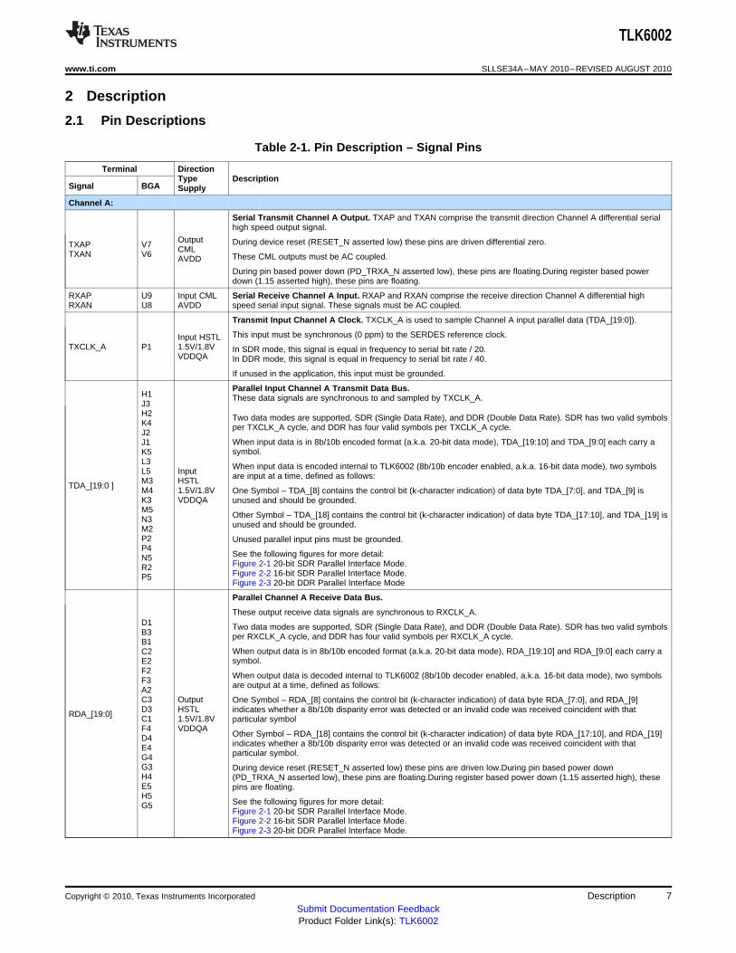
2.1 Pin Descriptions
Table 2-1. Pin Description – Signal Pins
Terminal DirectionType Description
Signal BGA Supply
Channel A:
Serial Transmit Channel A Output. TXAP and TXAN comprise the transmit direction Channel A differential serialhigh speed output signal.
Output During device reset (RESET_N asserted low) these pins are driven differential zero.TXAP V7 CMLTXAN V6 These CML outputs must be AC coupled.AVDD
During pin based power down (PD_TRXA_N asserted low), these pins are floating.During register based powerdown (1.15 asserted high), these pins are floating.
RXAP U9 Input CML Serial Receive Channel A Input. RXAP and RXAN comprise the receive direction Channel A differential highRXAN U8 AVDD speed serial input signal. These signals must be AC coupled.
Transmit Input Channel A Clock. TXCLK_A is used to sample Channel A input parallel data (TDA_[19:0]).
This input must be synchronous (0 ppm) to the SERDES reference clock.Input HSTLTXCLK_A P1 1.5V/1.8V In SDR mode, this signal is equal in frequency to serial bit rate / 20.
VDDQA In DDR mode, this signal is equal in frequency to serial bit rate / 40.
If unused in the application, this input must be grounded.
Parallel Input Channel A Transmit Data Bus.H1 These data signals are synchronous to and sampled by TXCLK_A.J3H2 Two data modes are supported, SDR (Single Data Rate), and DDR (Double Data Rate). SDR has two valid symbolsK4 per TXCLK_A cycle, and DDR has four valid symbols per TXCLK_A cycle.J2
When input data is in 8b/10b encoded format (a.k.a. 20-bit data mode), TDA_[19:10] and TDA_[9:0] each carry aJ1symbol.K5
L3 When input data is encoded internal to TLK6002 (8b/10b encoder enabled, a.k.a. 16-bit data mode), two symbolsL5 Input are input at a time, defined as follows:M3 HSTLTDA_[19:0 ] M4 1.5V/1.8V One Symbol – TDA_[8] contains the control bit (k-character indication) of data byte TDA_[7:0], and TDA_[9] isK3 VDDQA unused and should be grounded.M5
Other Symbol – TDA_[18] contains the control bit (k-character indication) of data byte TDA_[17:10], and TDA_[19] isN3unused and should be grounded.M2
P2 Unused parallel input pins must be grounded.P4
See the following figures for more detail:N5Figure 2-1 20-bit SDR Parallel Interface Mode.R2Figure 2-2 16-bit SDR Parallel Interface Mode.P5Figure 2-3 20-bit DDR Parallel Interface Mode
Parallel Channel A Receive Data Bus.
These output receive data signals are synchronous to RXCLK_A.D1 Two data modes are supported, SDR (Single Data Rate), and DDR (Double Data Rate). SDR has two valid symbolsB3 per RXCLK_A cycle, and DDR has four valid symbols per RXCLK_A cycle.B1
When output data is in 8b/10b encoded format (a.k.a. 20-bit data mode), RDA_[19:10] and RDA_[9:0] each carry aC2symbol.E2
F2 When output data is decoded internal to TLK6002 (8b/10b decoder enabled, a.k.a. 16-bit data mode), two symbolsF3 are output at a time, defined as follows:A2C3 Output One Symbol – RDA_[8] contains the control bit (k-character indication) of data byte RDA_[7:0], and RDA_[9]D3 HSTL indicates whether a 8b/10b disparity error was detected or an invalid code was received coincident with thatRDA_[19:0] C1 1.5V/1.8V particular symbolF4 VDDQA
Other Symbol – RDA_[18] contains the control bit (k-character indication) of data byte RDA_[17:10], and RDA_[19]D4indicates whether a 8b/10b disparity error was detected or an invalid code was received coincident with thatE4particular symbol.G4
G3 During device reset (RESET_N asserted low) these pins are driven low.During pin based power downH4 (PD_TRXA_N asserted low), these pins are floating.During register based power down (1.15 asserted high), theseE5 pins are floating.H5
See the following figures for more detail:G5Figure 2-1 20-bit SDR Parallel Interface Mode.Figure 2-2 16-bit SDR Parallel Interface Mode.Figure 2-3 20-bit DDR Parallel Interface Mode.
Copyright © 2010, Texas Instruments Incorporated Description 7Submit Documentation FeedbackProduct Folder Link(s): TLK6002

TLK6002
SLLSE34A–MAY 2010–REVISED AUGUST 2010 www.ti.com
Table 2-1. Pin Description – Signal Pins (continued)Terminal Direction
Type DescriptionSignal BGA Supply
Channel A Rate select pins. These pins put channel A into one of the four supported (full/half/quarter/eighth)channel operation rates, enable software control, or enable Auto Rate Sense (ARS):000 – Full Rate mode001 – Half Rate mode010 – Quarter rate mode011 – Eighth rate mode100 – Software Selectable Rate (Recommended default board configuration)101 – Channel A Auto Rate Sense (ARS) Function Enabled
Channel A SERDES settings are determined by Channel A ARS machine.CLK_OUT_P/N selected by CLK_OUT_SELSee Table 2-9 for additional details on CLK_OUT_P/N.
110 – Channel A Auto Rate Sense (ARS) Function Enabled
Channel A SERDES settings are determined by Channel A ARS machine.CLK_OUT_P/N is not selected by CLK_OUT_SEL
Input Channel B may not be simultaneously configured with RATE_B=110V2 LVCMOS With respect to CLK_OUT_P/N, this setting has the highest priority.RATE_A[2:0] T4 1.5V/1.8V See Table 2-9 for additional details on CLK_OUT_P/N.U3 VDDO3111 – Channel A Auto Rate Sense (ARS) Function Enabled – Slave Mode
If Channel B ARS is enabled (RATE_B=101 or 110 only):Channel A SERDES settings are determined by Channel B ARS machine.CLK_OUT_P/N is not selected by CLK_OUT_SELSee Table 2-9 for additional details on CLK_OUT_P/N.If Channel B ARS is not enabled (RATE_B=000/001/010/011/111):Channel A SERDES settings are determined by Channel A MDIO registers.CLK_OUT_P/N selected by CLK_OUT_SELSee Table 2-9 for additional details on CLK_OUT_P/N.
Channel A and B should not be in slave mode simultaneously. Both directions of Channel A are controlled by theseinput signals.
The RATE_A[2] pin should be routed to an uninstalled header so that it could be driven externally in the event thatdevice debug is required. In application mode, it should be biased with a pull up or pull down resistor, and notconnected directly to a power or ground plane.
Receive Output Channel A Clock. RXCLK_A is synchronous to RDA_[19:0], and may be used externally tosample Channel A output parallel data.
Output In SDR mode, this signal is equal in frequency to serial bit rate / 20.HSTLRXCLK_A F1 In DDR mode, this signal is equal in frequency to serial bit rate / 40.1.5V/1.8VVDDQA During device reset (RESET_N asserted low) this pin is driven low.
During pin based power down (PD_TRXA_N asserted low), this pin is floating.During register based power down (1.15 asserted high), these pins are floating.
Receive PRBS Channel A Error Free (Pass) IndicatorWhen PRBS test is enabled (PRBS_EN=1):PRBSA_PASS=1 indicates that PRBS pattern reception is error free.OutputPRBSA_PASS=0 indicates that a PRBS error is detected.LVCMOSDuring device reset (RESET_N asserted low) this pin is driven low.PRBSA_PASS V3 1.5V/1.8VDuring pin based power down (PD_TRXA_N asserted low), this pin is floating.VDDO3 40ΩDuring register based power down (1.15 asserted high), this pin is floating.DriverIt is highly recommended that PRBSA_PASS be brought to easily accessible point on the application board(header), in the event that debug is required.
Encoder/Decoder Channel A Enable: When this pin is asserted high, the internal 8b/10b encoder/decoder isInput enabled. This signal is OR’d with MDIO register bits, and should be pulled low through a resistor if software controlLVCMOSCODEA_EN V4 is desired. This pin should be routed to an uninstalled header so that it could be driven externally in the event that1.5V/1.8V device debug is required. In application mode, it should be biased with a pull up or pull down resistor, and notVDDO3 connected directly to a power or ground plane.
Channel A Receive Loss Of Signal (LOS) Indicator.LOSA = 0, signal detected.LOSA = 1, Loss of signal (6.10 enabled).Loss of signal detection is based on the input signal level.
Output When RXAP/N has an input signal of ≤75 mVdfpp, LOSA will be asserted (if enabled). The input signal should be ≥LVCMOS 150 mVdfpp for this function to operate reliably.
LOSA U4 1.5V/1.8VOther functions can be observed on LOSA realtime, configured via MDIO.VDDO3 40Ω
Driver During device reset (RESET_N asserted low) this pin is driven low. During pin based power down (PD_TRXA_Nasserted low), this pin is floating. During register based power down (1.15 asserted high), this pin is floating.
It is highly recommended that LOSA be brought to easily accessible point on the application board (header), in theevent that debug is required.
8 Description Copyright © 2010, Texas Instruments Incorporated
Submit Documentation FeedbackProduct Folder Link(s): TLK6002

TLK6002
www.ti.com SLLSE34A–MAY 2010–REVISED AUGUST 2010
Table 2-1. Pin Description – Signal Pins (continued)Terminal Direction
Type DescriptionSignal BGA Supply
Input Transceiver Power down. When this pin is held low (asserted), Channel A is placed in power down mode. WhenLVCMOS deasserted , Channel A operates normally. After deassertion, a software datapath reset should be issued throughPD_TRXA_N T6 1.5V/1.8V the MDIO interface.VDDO3
Channel B:
Serial Transmit Channel B Output. TXBP and TXBN comprise the transmit direction Channel B differential highspeed serial output signal. During device reset (RESET_N asserted low) these pins are driven differential zero.
OutputTXBP U12 CML These CML outputs must be AC coupled.TXBN U13 AVDDDuring pin based power down (PD_TRXB_N asserted low), these pins are floating. During register based powerdown (1.15 asserted high), these pins are floating.
Input Serial Receive Channel B Input. RXBP and RXBN comprise the receive direction Channel B differential highRXBP V10 CML speed serial input signal. These signals must be AC coupled.RXBN V11 AVDD
Channel B Rate select pins. These pins put channel B into one of the four supported (full/half/quarter/eighth)channel operation rates, enable software control, or enable Auto Rate Sense (ARS):000 – Full Rate mode001 – Half Rate mode010 – Quarter rate mode011 – Eighth rate mode100 – Software Selectable Rate (Recommended if ARS not used)101 – Channel B Auto Rate Sense (ARS) Function Enabled
Channel B SERDES settings are determined by Channel B ARS machine.CLK_OUT_P/N selected by CLK_OUT_SELSee Table 2-9 for additional details on CLK_OUT_P/N.
110 – Channel B Auto Rate Sense (ARS) Function Enabled
Channel B SERDES settings are determined by Channel B ARS machine.CLK_OUT_P/N is not selected by CLK_OUT_SEL
Input Channel A may not be simultaneously configured with RATE_A=110U16 LVCMOS With respect to CLK_OUT_P/N, this setting has the highest priority.RATE_B[2:0] U17 1.5V/1.8V See Table 2-9 for additional details on CLK_OUT_P/N.U18 VDDO2111 – Channel B Auto Rate Sense (ARS) Function Enabled – Slave Mode
If Channel A ARS is enabled (RATE_A=101 or 110 only):Channel B SERDES settings are determined by Channel A ARS machine.CLK_OUT_P/N is not selected by CLK_OUT_SELSee Table 2-9 for additional details on CLK_OUT_P/N.If Channel A ARS is not enabled (RATE_A=000/001/010/011/111):Channel B SERDES settings are determined by Channel B MDIO registers.CLK_OUT_P/N selected by CLK_OUT_SELSee Table 2-9 for additional details on CLK_OUT_P/N.
Channel A and B should not be in slave mode simultaneously.Both directions of Channel B are controlled by these input signals.
The RATE_B[2] pin should be routed to an uninstalled header so that it could be driven externally in the event thatdevice debug is required. In application mode, it should be biased with a pull up or pull down resistor, and notconnected directly to a power or ground plane.
Transmit Input Channel B Clock. TXCLK_B is used to sample Channel B input parallel data(TDB_[19:0]).
Input HSTL This input must be synchronous (0 ppm) to the SERDES reference clock.TXCLK_B T18 1.5V/1.8V
In SDR mode, this signal is equal in frequency to serial bit rate / 20.VDDQBIn DDR mode, this signal is equal in frequency to serial bit rate / 40.
If unused in the application, this input must be grounded.
Copyright © 2010, Texas Instruments Incorporated Description 9Submit Documentation FeedbackProduct Folder Link(s): TLK6002

TLK6002
SLLSE34A–MAY 2010–REVISED AUGUST 2010 www.ti.com
Table 2-1. Pin Description – Signal Pins (continued)Terminal Direction
Type DescriptionSignal BGA Supply
Parallel Input Channel B Transmit Data Bus.J17
These data signals are synchronous to and sampled by TXCLK_B.H17J16 Two data modes are supported, SDR (Single Data Rate), and DDR (Double Data Rate). SDR has two valid symbolsH18 per TXCLK_B cycle, and DDR has four valid symbols per TXCLK_B cycle.K15
When input data is in 8b/10b encoded format (a.k.a. 20-bit data mode), TDB_[19:10] and TDB_[9:0] each carry aK16symbol.L14
L16 When input data is encoded internal to TLK6002 (8b/10b encoder enabled, a.k.a. 16-bit data mode), two symbolsM14 Input HSTL are input at a time, defined as follows:M16TDB_[19:0] 1.5V/1.8VM15 One Symbol – TDB_[8] contains the control bit (k-character indication) of data byte TDB_[7:0], and TDB_[9] isVDDQBP17 unused and should be grounded.N14
Other Symbol – TDB_[18] contains the control bit (k-character indication) of data byte TDB_[17:10], and TDB_[19] isN16unused and should be grounded.J18
M17 Unused parallel input pins must be grounded.R17
See the following figures for more detail:P15Figure 2-1 20-bit SDR Parallel Interface ModeP14Figure 2-2 16-bit SDR Parallel Interface ModeP18Figure 2-3 20-bit DDR Parallel Interface Mode
Parallel Channel B Receive Data Bus.These output receive data signals are synchronous to RXCLK_B.
Two data modes are supported, SDR (Single Data Rate), and DDR (Double Data Rate). SDR has two valid symbolsD18per RXCLK_B cycle, and DDR has four valid symbols per RXCLK_B cycle.E17
B18 When output data is in 8b/10b encoded format (a.k.a. 20-bit data mode), RDB_[19:10] and RDB_[9:0] each carry aC17 symbol.F16
When output data is decoded internal to TLK6002 (8b/10b decoder enabled, a.k.a. 16-bit data mode), two symbolsF17are output at a time, defined as follows:A17
B16 One Symbol - RDB_[8] contains the control bit (k-character indication) of data byte RDB_[7:0], and RDB_[9]C16 Output indicates whether a 8b/10b disparity error was detected or an invalid code was received coincident with thatD16 HSTL particular symbolRDB_[19:0] C18 1.5V/1.8V
Other Symbol - RDB_[18] contains the control bit (k-character indication) of data byte RDB_[17:10], and RDB_[19]F15 VDDQBindicates whether a 8b/10b disparity error was detected or an invalid code was received coincident with thatA16particular symbol.B15
D15 During device reset (RESET_N asserted low) these pins are driven low. During pin based power downE15 (PD_TRXB_N asserted low), these pins are floating. During register based power down (1.15 asserted high), theseG16 pins are floating.H15
See the following figures for more detail:G15Figure 2-1 20-bit SDR Parallel Interface ModeG14Figure 2-2 16-bit SDR Parallel Interface ModeFigure 2-3 20-bit DDR Parallel Interface Mode
Receive Output Channel B Clock. RXCLK_B is synchronous to RDB_[19:0], and may be used externally tosample Channel B output parallel data.
Output In SDR mode, this signal is equal in frequency to serial bit rate / 20.HSTLRXCLK_B F18 In DDR mode, this signal is equal in frequency to serial bit rate / 40.1.5V/1.8VVDDQB During device reset (RESET_N asserted low) this pin is driven low.
During pin based power down (PD_TRXB_N asserted low), this pin is floating.During register based power down (1.15 asserted high), these pins are floating.
Receive PRBS Channel B Error Free (Pass) IndicatorWhen PRBS test is enabled (PRBS_EN=1):PRBSB_PASS=1 indicates that PRBS pattern reception is error free.
Output PRBSB_PASS=0 indicates that a PRBS error is detected.LVCMOS
PRBSB_PASS V18 1.5V/1.8V During device reset (RESET_N asserted low) this pin is driven low.VDDO2 40Ω During pin based power down (PD_TRXB_N asserted low), this pin is floating.Driver During register based power down (1.15 asserted high), this pin is floating.
It is highly recommended that PRBSB_PASS be brought to easily accessible point on the application board(header), in the event that debug is required.
Input Encoder/Decoder Channel B Enable: When this pin is asserted high, the internal 8b/10b encoder/decoder isLVCMOS enabled. This signal is OR’d with MDIO register bits, and should be tied low if software control is desired.CODEB_EN V16 1.5V/1.8VVDDO2
10 Description Copyright © 2010, Texas Instruments Incorporated
Submit Documentation FeedbackProduct Folder Link(s): TLK6002

TLK6002
www.ti.com SLLSE34A–MAY 2010–REVISED AUGUST 2010
Table 2-1. Pin Description – Signal Pins (continued)Terminal Direction
Type DescriptionSignal BGA Supply
Channel B Receive Loss Of Signal (LOS) Indicator.LOSB=0, signal detected.LOSB=1, Loss of signal (6.10 enabled).Loss of signal detection is based on the input signal level.When RXBP/N has an input signal of ≤75 mVdfpp, LOSB will be asserted (if enabled). The input signal should be ≥Output150 mVdfpp for this function to operate reliably.LVCMOS
LOSB V17 1.5V/1.8V Other functions can be observed on LOSB realtime, configured via MDIO.VDDO2 40Ω
During device reset (RESET_N asserted low) this pin is driven low.DriverDuring pin based power down (PD_TRXB_N asserted low), this pin is floating.During register based power down (1.15 asserted high), this pin is floating.
It is highly recommended that LOSB be brought to easily accessible point on the application board (header), in theevent that debug is required.
Input Transceiver Power down. When this pin is held low (asserted), Channel B is placed in power down mode. WhenLVCMOS deasserted , Channel B operates normally. After deassertion, a software datapath reset should be issued throughPD_TRXB_N U15 1.5V/1.8V the MDIO interface.VDDO2
Signals common to Channels A and B:
Reference Clock Input Zero. This differential input is a clock signal used as a reference to either or both of theInput LVDS/ bidirectional SERDES macros. It can be routed internally to either SERDES macro using device pinsB5REFCLK_0_P/N LVPECL (REFCLK_A_SEL and REFCLK_B_SEL) or through software registers. This input signal must be AC coupled. SeeA5 DVDD Figure 1-3. TLK6002 Reference Clock / Output Clock Architecture for more detail. If unused, REFCLK_0_P/N
should be pulled down to DGND through a shared 100Ω resistor.
Reference Clock Input One. This differential input is a clock signal used as a reference to either or both of theInput LVDS/ bidirectional SERDES macros. It can be routed internally to either SERDES macro using device pinsC6REFCLK_1_P/N LVPECL (REFCLK_A_SEL and REFCLK_B_SEL) or through software registers. This input signal must be AC coupled. SeeD6 DVDD Figure 1-3. TLK6002 Reference Clock / Output Clock Architecture for more detail. If unused, REFCLK_1_P/N
should be pulled down to DGND through a shared 100Ω resistor
Input Reference Clock Select Channel A. This input, when low, selects REFCLK_0_P/N as the clock reference toLVCMOS Channel A SERDES macro. When high, REFCLK_1_P/N is selected as the clock reference to Channel A SERDESREFCLK_A_SEL R6 1.5V/1.8V macro. If software control is desired (register bit 0.1), this input signal should be tied low. See Figure 1-3. TLK6002VDDO3 Reference Clock / Output Clock Architecture for more detail.
Input Reference Clock Select Channel B. This input, when low, selects REFCLK_0_P/N as the clock reference toLVCMOS Channel B SERDES macro. When high, REFCLK_1_P/N is selected as the clock reference to Channel B SERDESREFCLK_B_SEL T2 1.5V/1.8V macro. If software control is desired (register bit 0.0), this input signal should be tied low. See Figure 1-3. TLK6002VDDO3 Reference Clock/Output Clock Architecture for more detail.
Enable PRBS: When this pin is asserted high, the internal PRBS generator and verifier circuits are enabled on bothtransmit and receive data paths of both channels.This signal is logically OR’d with an mdio register bit.
InputPRBS 231-1 is selected by default, and can be changed in MDIO register 7.10:8.LVCMOSPRBS_EN R16 1.5V/1.8V Note that PRBS is not possible in eighth rate mode.
VDDO2The PRBS_EN pin should be routed to an uninstalled header so that it could be driven externally in the event thatdevice debug is required. In application mode, it should be biased with a pull up or pull down resistor (or allow foran isolation mechanism from the on board driver), and not connected directly to a power or ground plane.
Recovered Byte Clock. If ARS is not enabled, and CLK_OUT_SEL is low, an optionally divided version of ChannelA recovered byte clock is output onto CLK_OUT_P/N. If ARS is not enabled, and CLK_OUT_SEL is high, anoptionally divided version of Channel B recovered byte clock is output onto CLK_OUT_P/N. The recovered byteclock is synchronous to the incoming serial data rate for the selected channel. See Figure 1-3. TLK6002 ReferenceClock/Output Clock Architecture for more detail. The recovered byte clock can be divided by one, two, four, or eightas selected in an mdio register.J6 Output CMLCLK_OUT_P/N J7 DVDD If ARS is enabled, the CLK_OUT_P/N output is selected via Table 2-9.
This CML output must be AC coupled.
During device reset (RESET_N asserted low) this pin is driven differential zero. During pin based power down(PD_TRXA_N and PD_TRXB_N asserted low), these pins are floating.During register based power down (1.15 asserted high both channels), these pins are floating.
Output Clock Selection. If ARS is not enabled and CLK_OUT_SEL is low, Channel A recovered byte clock isInput output onto CLK_OUT_P/N. If ARS is not enabled and CLK_OUT_SEL is high, Channel B recovered byte clock isLVCMOSCLK_OUT_SEL T15 output onto CLK_OUT_P/N. If software control is desired (register bit 0.6), this input signal should be tied low. See1.5V/1.8V Figure 1-3. TLK6002 Reference Clock / Output Clock Architecture for more detail. If ARS is enabled, the function ofVDDO2 CLK_OUT_SEL is shown in Table 2-9.
Copyright © 2010, Texas Instruments Incorporated Description 11Submit Documentation FeedbackProduct Folder Link(s): TLK6002

TLK6002
SLLSE34A–MAY 2010–REVISED AUGUST 2010 www.ti.com
Table 2-1. Pin Description – Signal Pins (continued)Terminal Direction
Type DescriptionSignal BGA Supply
Port Address. Used to select the Port ID.
PRTAD[4:1] selects the device port address. TLK6002 has two different PHY addresses (ports). Selecting a uniquePRTAD[4:1] per TLK6002 device allows 16 TLK6002 devices per MDIO bus. Each channel can be accessed bysetting the appropriate port address field within the serial interface protocol transaction.
TLK6002 will respond if the 4 MSB’s of the inband PHY address field on MDIO protocol (PA[4:1]) matchesInputPRTAD[4:1]. The LSB of PHY address field (PA[0]) will determine which channel/port within TLK6002 to respond to.LVCMOSV15 1.5V/1.8V PRTAD[0] is not used functionally, but is present for device testability and compatibility with other devices in theM8 VDDO2/ family of products.PRTAD[4:0] K12 VDDO1/K11 Channel A responds to port address 0 within the block of two port addresses.VDDO1/L11 VDDO1/ Channel B responds to port address 1 within the block of two port addresses.
VDDO1PRTAD[0] should be grounded on the application board.
The PRTAD[3] pin in application mode should be biased with a pull up or pull down resistor (or allow for an isolationmechanism from the on board driver), and not connected directly to a power or ground plane. The application boardshould allow the flexibility of easily reworking the PRTAD[3] signal to a high level if device debug is necessary (byincluding an uninstalled resistor to VDDO1).
Input Low True Device Reset. When asserted (low logic level), this signal resets the entire TLK6002 device. RESET_NLVCMOS must be held asserted for at least 10 µS after device power stabilization.RESET_N V1 1.5V/1.8VVDDO3
Input MDIO clock input. Clock input for the Clause 22 MDIO interface.LVCMOS Note that an external pullup is generally not required on MDC.
MDC T1 w/Hysteresis 1.5V/1.8VVDDO3
MDIO data I/O. MDIO interface data input/output signal for the Clause 22 MDIO interface.Input/ This signal must be externally pulled up to VDDO3, using a 2 kΩ resistor.Output During device reset (RESET_N asserted low) this pin is floating. During software initiated power down theLVCMOSMDIO U2 management interface remains active for control register writes and reads. Certain status bits are not deterministic1.5V/1.8V as their generating clock source may be disabled as a result of asserting either power down input signal. During pinVDDO3 25Ω based power down (PD_TRXA_N and PD_TRXB_N asserted low), this pin is floating. During register based powerDriver down (1.15 asserted high both channels), this pin is driven normally.
SPI Clock (SPI_CLK). Defaults to Output, Driven Low. Can be used as a SPI interface or a generic customercontrollable I/O interface. When used as part of the SPI interface, this signal is the SPI clock to be used withInput/ external TI Jitter cleaner or clock Distribution device.Output Three register bits (15.14:12) control this I/O signal. See the detailed register bit description for operational detail.LVCMOSSCL H13 If unused in the application, this signal can be left floating.1.5V/1.8V Careful programming is required to prevent accidental contention with simultaneous external drivers. During deviceVDDO1 25Ω reset (RESET_N asserted low) this pin is driven low. During pin based power down (PD_TRXA_N and PD_TRXB_NDriver asserted low), this pin is floating. During register based power down (1.15 asserted high both channels), these pinsare driven per register setting
SPI Data. Defaults to Input. Can be used as a SPI interface or a generic customer controllable I/O interface. Whenused as part of the SPI interface, this signal is the SPI data from the external TI Jitter cleaner or clock DistributionInput/ device to the TLK6002.Output Three register bits (15.10:8) control this I/O signal. See the detailed register bit description for operational detail.LVCMOSSDO K13 If unused in the application, this signal should be pulled to ground. Careful programming is required to prevent1.5V/1.8V accidental contention with simultaneous external drivers.VDDO1 25Ω During device reset (RESET_N asserted low) this pin is floating. During pin based power down (PD_TRXA_N andDriver PD_TRXB_N asserted low), this pin is floating. During register based power down (1.15 asserted high bothchannels), these pins are driven per register setting.
SPI Data. Defaults to Output, driven low. Can be used as a SPI interface or a generic customer controllable I/Ointerface. When used as part of the SPI interface, this signal is the SPI data from TLK6002 to the external TI JitterInput/ cleaner or clock Distribution device.Output Three register bits (15.6:4) control this I/O signal. See the detailed register bit description for operational detail.LVCMOSSDI E14 If unused in the application, this signal can be left floating.1.5V/1.8V Careful programming is required to prevent accidental contention with simultaneous external drivers. During deviceVDDO1 25Ω reset (RESET_N asserted low) this pin is driven low.Driver During pin based power down (PD_TRXA_N and PD_TRXB_N asserted low), this pin is floating. During registerbased power down (1.15 asserted high both channels), these pins are driven per register setting.
SPI Chip Select. Defaults to Output, Driven High. Can be used as a SPI interface or a generic customercontrollable I/O interface. When used as part of the SPI interface, this signal is the chip select for the external TIInput/ Jitter cleaner or clock Distribution device. Low=Select Device. High=Device Not Selected.Output Three register bits (15.2:0) control this I/O signal. See the detailed register bit description for operational detail.LVCMOSCS_N D14 If unused in the application, this signal can be left floating. Careful programming is required to prevent accidental1.5V/1.8V contention with simultaneous external drivers.VDDO1 25Ω During device reset (RESET_N asserted low) this pin is driven high. During pin based power down (PD_TRXA_NDriver and PD_TRXB_N asserted low), this pin is floating. During register based power down (1.15 asserted high bothchannels), these pins are driven per register setting.
12 Description Copyright © 2010, Texas Instruments Incorporated
Submit Documentation FeedbackProduct Folder Link(s): TLK6002

TLK6002
www.ti.com SLLSE34A–MAY 2010–REVISED AUGUST 2010
Table 2-1. Pin Description – Signal Pins (continued)Terminal Direction
Type DescriptionSignal BGA Supply
Input JTAG Input Data. TDI is used to serially shift test data and test instructions into the device during the operation ofLVCMOS the test port. In system applications where JTAG is not implemented, this input signal may be left floating.1.5V/1.8V During pin based power down (PD_TRXA_N and PD_TRXB_N asserted low), this pin is not pulled up. DuringTDI R15 VDDO2 register based power down (1.15 asserted high both channels), this pin is pulled up normally.(InternalPullup)
JTAG Output Data. TDO is used to serially shift test data and test instructions out of the device during operation ofOutputthe test port. When the JTAG port is not in use, TDO is in a high impedance state.LVCMOS
TDO R14 1.5V/1.8V During device reset (RESET_N asserted low) this pin is floating. During pin based power down (PD_TRXA_N andVDDO2 50Ω PD_TRXB_N asserted low), this pin is floating. During register based power down (1.15 asserted high bothDriver channels), this pin is floating.
Input JTAG Mode Select. TMS is used to control the state of the internal test-port controller. In system applicationsLVCMOS where JTAG is not implemented, this input signal can be left unconnected.1.5V/1.8V During pin based power down (PD_TRXA_N and PD_TRXB_N asserted low), this pin is not pulled up. DuringTMS R3 VDDO3 register based power down (1.15 asserted high both channels), this pin is pulled up normally.(InternalPullup)
Input JTAG Clock. TCK is used to clock state information and test data into and out of the device during boundary scanLVCMOS operation. In system applications where JTAG is not implemented, this input signal should be grounded.
TCK T16 w/Hysteresis 1.5V/1.8VVDDO2
Input JTAG Test Reset. TRST_N is used to reset the JTAG logic into system operational mode. This input can be leftLVCMOS unconnected in the application and is pulled down internally, disabling the JTAG circuitry. If JTAG is implemented1.5V/1.8V on the application board, this signal should be deasserted (high) during JTAG system testing, and otherwiseTRST_N T3 VDDO3 asserted (low) during normal operation mode.(Internal During pin based power down (PD_TRXA_N and PD_TRXB_N asserted low), this pin is not pulled down. DuringPulldown) register based power down (1.15 asserted high both channels), this pin is pulled down normally.
Input Test Enable. This signal is used during the device manufacturing process. It should be grounded through a resistorLVCMOS in the device application board. The application board should allow the flexibility of easily reworking this signal to aTESTEN T17 1.5V/1.8V high level if device debug is necessary (by including an uninstalled resistor to VDDO2).VDDO2
Input General Purpose Input Zero. This signal is used during the device manufacturing process. It should be groundedLVCMOS through a resistor on the device application board. The application board should also allow the flexibility of easilyGPI0 R4 1.5V/1.8V reworking this signal to a high level if device debug is necessary (by including an uninstalled resistor to VDDO3).VDDO3
Input General Purpose Input One. This signal can be used to logically combine an external status condition with LOSALVCMOS or LOSB if enabled in an mdio register. Note that if GPI1 is low, LOSA/B will be asserted if logical combination isGPI1 K10 1.5V/1.8V enabled. Similarly, if GPI1 is high, LOSA/B will be deasserted. If unused, this input should be grounded in theVDDO1 device application (not floating).
SERDES Channel A Analog Testability I/O. This signal is used during the device manufacturing process. It shouldAMUXA U5 Analog I/O be left unconnected in the device application.
SERDES Channel B Analog Testability I/O. This signal is used during the device manufacturing process. It shouldAMUXB V14 Analog I/O be left unconnected in the device application.
RESRA, K8 HSTL Impedance Matching Resistors. These resistors are used as a reference for internal terminations on theRESTA, M1 Analog HSTL inputs and outputs. Each RES* pin requires it’s own resistor, sharing resistors between RES* pins is notRESRB, J14 Input possible. A 50 ohm 0.5% tolerance resistor should be selected to guarantee device datasheet specified parallelRESTB M18 interface timing specification.
Copyright © 2010, Texas Instruments Incorporated Description 13Submit Documentation FeedbackProduct Folder Link(s): TLK6002

TLK6002
SLLSE34A–MAY 2010–REVISED AUGUST 2010 www.ti.com
Table 2-2. Pin Description – Power Pins
TerminalType Description
Signal BGA
T8 SERDES Digital logic powerVDDD PowerT11 Provides power for digital circuitry internal to the SERDES. 1.0V nominal.
U6T9T10 SERDES Analog PowerAVDD PowerU11 AVDD provides supply voltage for the high-speed analog circuits. 1.0V nominal.T13U14
L6L9L13M10M12 Digital Core PowerDVDD N6 Power DVDD provides supply voltage to the digital core. 1.0V nominal.N13R8R10R12T5
V8 SERDES Analog PowerVDDT PowerV12 VDDT provides supply voltage for the high-speed analog circuits, termination voltage. 1.0V nominal.
T7 SERDES Analog Regulator PowerVDDRA/B PowerT12 VDDRA and VDDRB provide supply voltage for the internal PLL regulator. 1.5V or 1.8V nominal.
A3B2B17C4C15E1E18F5F14G2G17J4J15K1 HSTL I/O PowerVDDQA/B K18 Power VDDQA and VDDQB provide supply voltage for the HSTL inputs and outputs. 1.5V or 1.8V nominal.L4L7L8L12L15L17M6M13N1N18P3P6P13P16
L10 LVCMOS I/O PowerVDDO1/2/3 R13 Power VDDO1, VDDO2, and VDDO3 provide supply voltage for the LVCMOS inputs and outputs. 1.5V or 1.8V nominal.R7
Factory Program VoltageVPP K9 Power Programming supply voltage for TI internal use during device manufacturing. The application must connect this power
supply directly to DVDD.
R9R11T14U7 Analog GroundAGND GroundU10 Analog ground.V5V9V13
14 Description Copyright © 2010, Texas Instruments Incorporated
Submit Documentation FeedbackProduct Folder Link(s): TLK6002

TLK6002
www.ti.com SLLSE34A–MAY 2010–REVISED AUGUST 2010
Table 2-2. Pin Description – Power Pins (continued)Terminal
Type DescriptionSignal BGA
A1A4A6A15A18B4B6C5D2D5D17E3E16G1G18H3H14H16J5K2K6K14K17 Digital GroundDGND GroundL2 Digital groundM7M9M11N2N4N7N8N10N11N12N15N17P7P8P9P10P11P12R1R5R18U1
HSTL Voltage ReferenceVREFTA, L1 Voltage These high impedance voltage reference inputs are used as a signal comparison level for HSTL input signals. TheseVREFTB L18 Reference signals should be created using a resistive voltage divider (dual 1kΩ) between VDDQA or VDDQB and DGND. These
signals should be locally decoupled as close to the device pins as possible.
Copyright © 2010, Texas Instruments Incorporated Description 15Submit Documentation FeedbackProduct Folder Link(s): TLK6002

TLK6002
SLLSE34A–MAY 2010–REVISED AUGUST 2010 www.ti.com
Table 2-2. Pin Description – Power Pins (continued)Terminal
Type DescriptionSignal BGA
A7A8A9A10A11A12A13A14B7B8B9B10B11B12B13B14C7C8C9C10C11C12C13C14D7D8D9D10D11D12D13E6E7E8 No No ConnectNC E9 Connect These BGAs can be left unconnected in the applicationE10E11E12E13F6F7F8F9F10F11F12F13G6G7G8G9G10G11G12G13H6H7H8H9H10H11H12J8J9J10J11J12J13K7
Reserved ReservedNC33 N9 Input This input pin should be connected to DVDD through a zero ohm resistor in the device application.
16 Description Copyright © 2010, Texas Instruments Incorporated
Submit Documentation FeedbackProduct Folder Link(s): TLK6002
1 2 3 4 5 6 7 8 9 10 11 12 13 14 15 16 17 18
A DGND RDA_12 VDDQA DGNDREFCLK_0
_NDGND CGND XTALP CGND PRI_REF2P CGND CGND RC1 RC3 DGND RDB_7 RDB_13 DGND
B RDA_17 VDDQA RDA_18 DGNDREFCLK_0
_PDGND VDD_XTAL XTALN
VDD_PRI_I
N2PRI_REF2N VDD_PLL2 LF2B AMUX RC2 RDB_6 RDB_12 VDDQB RDB_17
C RDA_9 RDA_16 RDA_11 VDDQA DGNDREFCLK_1
_PLF1B VDD_SREF
VDD_SEC_
IN2CGND
VDD_CP2_
PFD2LF2A CGND CMSEL VDDQB RDB_11 RDB_16 RDB_9
D RDA_19 DGND RDA_10 RDA_7 DGNDREFCLK_1
_NLF1A CGND SYNTHREF CGND CGND CGND RFOUTN CS_N RDB_5 RDB_10 DGND RDB_19
E VDDQA RDA_15 DGND RDA_6 RDA_2VDD_CP1_
PFD1VDD_PLL1 CGND CGND CGND CGND VDD_VCO RFOUTP SDI RDB_4 DGND RDB_18 VDDQB
F RXCLK_A RDA_14 RDA_13 RDA_8 VDDQAVDD_PRI_I
N1FBINN CGND CGND CGND CGND
VDD_RF_P
SVDD18 VDDQB RDB_8 RDB_15 RDB_14 RXCLK_B
G DGND VDDQA RDA_4 RDA_5 RDA_0 VDD_FBIN FBINP CGND CGND CGND CGND CGNDVDD_DIG_
IORDB_0 RDB_1 RDB_3 VDDQB DGND
H TDA_19 TDA_17 DGND RDA_3 RDA_1VDD_SEC_
IN1CGND Y3N Y3P Y0N Y0P CGND SCL DGND RDB_2 DGND TDB_18 TDB_16
J TDA_14 TDA_15 TDA_18 VDDQA DGNDCLK_OUT_
P
CLK_OUT_
NVDD_Y4 VDD_Y3 VDD_Y2 VDD_Y1 VDD_Y0 PDN RESRB VDDQB TDB_17 TDB_19 TDB_5
K VDDQA DGND TDA_8 TDA_16 TDA_13 DGND RESETN RESRA VPP GPI1 PRTAD1 PRTAD2 SDO DGND TDB_15 TDB_14 DGND VDDQB
L VREFTA DGND TDA_12 VDDQA TDA_11 DVDD VDDQA VDDQA DVDD VDDO1 PRTAD0 VDDQB DVDD TDB_13 VDDQB TDB_12 VDDQB VREFTB
M RESTA TDA_5 TDA_10 TDA_9 TDA_7 VDDQA DGND PRTAD3 DGND DVDD DGND DVDD VDDQB TDB_11 TDB_9 TDB_10 TDB_4 RESTB
N VDDQA DGND TDA_6 DGND TDA_2 DVDD DGND DGND VDD33 DGND DGND DGND DVDD TDB_7 DGND TDB_6 DGND VDDQB
P TXCLK_A TDA_4 VDDQA TDA_3 TDA_0 VDDQA DGND DGND DGND DGND DGND DGND VDDQB TDB_1 TDB_2 VDDQB TDB_8 TDB_0
R DGND TDA_1 TMS GPI0 DGNDREFCLK_A
_SELVDDO3 DVDD AGND DVDD AGND DVDD VDDO2 TDO TDI PRBS_EN TDB_3 DGND
T MDCREFCLK_B
_SELTRST_N RATE_A1 DVDD
PD_TRXA_
NVDDRA VDDD AVDD AVDD VDDD VDDRB AVDD AGND
CLK_OUT_
SELTCK TESTEN TXCLK_B
U DGND MDIO RATE_A0 LOSA AMUXA AVDD AGND RXAN RXAP AGND AVDD TXBP TXBN AVDDPD_TRXB_
NRATE_B2 RATE_B1 RATE_B0
V RESET_N RATE_A2PRBSA_PA
SSCODEA_EN AGND TXAN TXAP VDDT AGND RXBP RXBN VDDT AGND AMUXB PRTAD4 CODEB_EN LOSB
PRBSB_PA
SS
TLK6002
www.ti.com SLLSE34A–MAY 2010–REVISED AUGUST 2010
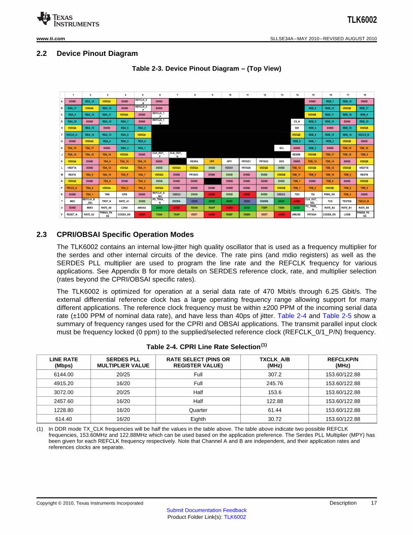
2.2 Device Pinout Diagram
Table 2-3. Device Pinout Diagram – (Top View)
2.3 CPRI/OBSAI Specific Operation Modes
The TLK6002 contains an internal low-jitter high quality oscillator that is used as a frequency multiplier forthe serdes and other internal circuits of the device. The rate pins (and mdio registers) as well as theSERDES PLL multiplier are used to program the line rate and the REFCLK frequency for variousapplications. See Appendix B for more details on SERDES reference clock, rate, and multiplier selection(rates beyond the CPRI/OBSAI specific rates).
The TLK6002 is optimized for operation at a serial data rate of 470 Mbit/s through 6.25 Gbit/s. Theexternal differential reference clock has a large operating frequency range allowing support for manydifferent applications. The reference clock frequency must be within ±200 PPM of the incoming serial datarate (±100 PPM of nominal data rate), and have less than 40ps of jitter. Table 2-4 and Table 2-5 show asummary of frequency ranges used for the CPRI and OBSAI applications. The transmit parallel input clockmust be frequency locked (0 ppm) to the supplied/selected reference clock (REFCLK_0/1_P/N) frequency.
Table 2-4. CPRI Line Rate Selection (1)
LINE RATE SERDES PLL RATE SELECT (PINS OR TXCLK_A/B REFCLKP/N(Mbps) MULTIPLIER VALUE REGISTER VALUE) (MHz) (MHz)
6144.00 20/25 Full 307.2 153.60/122.88
4915.20 16/20 Full 245.76 153.60/122.88
3072.00 20/25 Half 153.6 153.60/122.88
2457.60 16/20 Half 122.88 153.60/122.88
1228.80 16/20 Quarter 61.44 153.60/122.88
614.40 16/20 Eighth 30.72 153.60/122.88
(1) In DDR mode TX_CLK frequencies will be half the values in the table above. The table above indicate two possible REFCLKfrequencies, 153.60MHz and 122.88MHz which can be used based on the application preference. The Serdes PLL Multiplier (MPY) hasbeen given for each REFCLK frequency respectively. Note that Channel A and B are independent, and their application rates andreferences clocks are separate.
Copyright © 2010, Texas Instruments Incorporated Description 17Submit Documentation FeedbackProduct Folder Link(s): TLK6002

TLK6002
SLLSE34A–MAY 2010–REVISED AUGUST 2010 www.ti.com
Table 2-5. OBSAI Line Rate Selection (1)
LINE RATE SERDES PLL RATE SELECT (PINS OR TXCLK_A/B REFCLKP/N(Mbps) MULTIPLIER VALUE REGISTER VALUE) (MHz) (MHz)
6144.00 20/25 Full 307.2 153.60/122.88
3072.00 20/25 Half 153.6 153.60/122.88
1536.00 20/25 Quarter 76.8 153.60/122.88
768.00 20/25 Eighth 38.4 153.60/122.88
(1) In DDR mode TX_CLK frequencies will be half the values in the table above. The table above indicate two possible REFCLKfrequencies, 153.60MHz and 122.88MHz which can be used based on the application preference. The Serdes PLL Multiplier (MPY) hasbeen given for each REFCLK frequency respectively. Note that Channel A and B are independent, and their application rates andreferences clocks are separate.
2.4 Parallel Interface Modes
2.4.1 20-bit SDR (Single Data Rate) Mode (8b/10b Encoder/Decoder Disabled)
Channel A TX: TDA_[19:0] → TXAP/N (using TXCLK_A). RX: RXAP/N → RDA_[19:0] (using RXCLK_A).Channel B TX: TDB_[19:0] → TXBP/N (using TXCLK_B). RX: RXBP/N → RDB_[19:0] (using RXCLK_B).
20 Bits (two symbols) of already encoded (TX) or undecoded (RX) data are transferred per parallelinterface clock cycle. Symbols are defined by a group of 10 parallel bits. Note that four symbols are shownin Figure 2-1: Data0[19:10], Data0[9:0], Data1[19:10], Data1[9:0].
Symbol Transmission Order:When 3.5/3.4 = 0: Data0[19:10] is the first transmitted or received symbol. Data0[9:0] is next, thenData1[19:10].When 3.5/3.4 = 1: Data0[9:0] is the first transmitted or received symbol. Data0[19:0] is next, thenData1[9:0].
Bit Transmission Order within a Symbol:When 8.3/2 = 0, Data[19] or Data[9] bits are serially transmitted first or received first respectively persymbol.When 8.3/2 = 1, Data[10] or Data[0] bits are serially transmitted first or received first respectively persymbol.
18 Description Copyright © 2010, Texas Instruments Incorporated
Submit Documentation FeedbackProduct Folder Link(s): TLK6002

SDR Rising Edge Aligned Timing
SDR Falling Edge Aligned Timing
TXCLK_A/B
TDA/B_[19:0] Data0[19:0] Data1[19:0]
Data0[19:0] Data1[19:0]
RXCLK _A /B
RDA/B_ [19:0]
TXCLK_A/B
TDA/B_[19:0]
RXCLK _A /B
RDA /B_ [ 19:0]
Data0[19:0] Data1[19:0]
Data0[19:0] Data1[19:0]
TLK6002
www.ti.com SLLSE34A–MAY 2010–REVISED AUGUST 2010
Figure 2-1. 20-bit SDR Parallel Interface Mode
Copyright © 2010, Texas Instruments Incorporated Description 19Submit Documentation FeedbackProduct Folder Link(s): TLK6002

TLK6002
SLLSE34A–MAY 2010–REVISED AUGUST 2010 www.ti.com
2.5 16-bit SDR (Single Data Rate) Mode (8b/10b Encoder/Decoder Enabled)
Channel A TX: TDA_[18:10,8:0] → TXAP/N (Using TXCLK_A). RX: RXAP/N → RDA_[19:0] (UsingRXCLK_A).Channel B TX: TDB_[18:10,8:0] → TXBP/N (Using TXCLK_B). RX: RXBP/N → RDB_[19:0] (UsingRXCLK_B).
The 16 Bits (two symbols) of unencoded (TX) or decoded (RX) data are transferred per parallel interfaceclock cycle. Symbols are defined by a group of 9 parallel bits comprising of a K character control bit and abyte of data (plus a high true disparity error or invalid symbol bit in RX only on RD*_[19] and RD*_[9]).Please note that four symbols are shown in Figure 2-1: Data0[18:10]={Control Bit, Data[7:0]}, Data0[8:0]={Control Bit, Data[7:0]}, Data1[18:10] ={Control Bit, Data[7:0]}, Data1[8:0] ={Control Bit, Data[7:0]}.TXDA_[19], TXDA_[9], TXDB_[19], and TXDB_[9] are unused, and should be grounded in this applicationmode. See Appendix C for a full list of control characters supported in the 8b/10b encoder/decoder.
Symbol Transmission Order:When 3.5/3.4 = 0: Data0[18:10] is the first encoded transmitted or decoded received symbol. Data0[8:0] isnext, followed by Data1[18:10].When 3.5/3.4 = 1: Data0[8:0] is the first encoded transmitted or decoded received symbol. Data0[18:10] isnext, followed by Data1[8:0].
Bit Transmission Order within a Symbol:Control Character Bits are always on TD*_[18], TD*_ [8], RD*_[18], RD*_[8]Data bytes are always on TD*_[17:10], TD*_[7:0], RD*_[17:10], RD*_[7:0].
The most significant bit of the data byte is always on TD*_[17], TD*_[7], RD*_[17], RD*_[7], and is bit "H"in Figure 2-2.
When 8.3/8.2 = 1, The "a" bit in Figure 2-2 is serially transmitted first or received first (typical case, shownbelow) per symbol.
When 8.3/8.2 = 0, The "j" bit in Figure 2-2 is serially transmitted first or received first (atypical case,reverse from order Figure 2-2) per symbol.
Figure 2-2. 16-bit SDR Parallel Interface Mode (Serial Bit Order)
20 Description Copyright © 2010, Texas Instruments Incorporated
Submit Documentation FeedbackProduct Folder Link(s): TLK6002

DDR Source Centered Timing
DDR Source Aligned Timing
TXCLK _A/B
TDA/B_[19:0] Data0[19:0] Data1[19:0]
Data0[19:0] Data1[19:0]
RXCLK _A /B
RDA/B_[19:0]
TXCLK _A/B
RXCLK _A /B
RDA/B_[19:0]
Data0[19:0] Data1[19:0]
Data0[19:0] Data1[19:0]
TDA/B_[19:0]
TLK6002
www.ti.com SLLSE34A–MAY 2010–REVISED AUGUST 2010
Figure 2-1 shows the two modes of operation in SDR mode, rising edge aligned mode and falling edgealigned mode. In rising edge aligned mode, TDA_* and TDB_* inputs are sampled on the falling edges ofTXCLK_A and TXCLK_B respectively. In falling edge aligned mode, TDA_* and TDB_* inputs aresampled on the rising edge of TXCLK_A and TXCLK_B respectively. In rising edge aligned mode, RDA_*and RDB_* are timed such that an external device can sample the data using the falling edge ofRXCLK_A and RXCLK_B respectively. In falling edge aligned mode, RDA_* and RDB_* are timed suchthat an external device can sample the data using the rising edge of RXCLK_A and RXCLK_Brespectively.
2.6 20-bit DDR (Double Data Rate) Mode (8b/10b Encoder/Decoder Disabled)
When DDR is enabled with the 8b/10b encoder disabled, the data format is identical to that of "20-bit SDR(Single Data Rate) Mode (8b/10b Encoder/Decoder Disabled)" mode, except that four symbols aretransferred per parallel interface clock cycle instead of two. See the referenced previous section for furtherdetails. Figure 2-3 shows the two modes of operation in DDR mode, source centered and source alignedmode. In source centered mode, TDA_* and TDB_* inputs are sampled on the rising and falling edges ofTXCLK_A and TXCLK_B respectively. In source aligned mode, TDA_* and TDB_* inputs arrivesimultaneously with TXCLK_A and TXCLK_B respectively, and the TXCLK_A and TXCLK_B samplingwindow is created internal to TLK6002 by delaying the clock. In source centered mode, RDA_* and RDB_*are timed such that an external device can sample the data using RXCLK_A and RXCLK_B respectively,where the appropriate timing window for sampling is created by TLK6002. In source aligned mode, RDA_*and RDB_* are aligned with RXCLK_A and RXCLK_B respectively at the outputs of TLK6002, and thesampling window must be created external to TLK6002.
Figure 2-3. 20-bit DDR Parallel Interface Mode
Copyright © 2010, Texas Instruments Incorporated Description 21Submit Documentation FeedbackProduct Folder Link(s): TLK6002

RXCLK_A
RDA_[19:0] Data Data
DataDataData
Source Centered (DDR)
Source Aligned (DDR)
DataData
DataData
Falling Edge Aligned (Rising Edge Sampled) (SDR)
Rising Edge Aligned (Falling Edge Sampled ) (SDR)
RDA_[19:0]
RDA_ [19:0]
RDA_[19:0]
tSETUP tHOLD tSETUP tHOLD
TLK6002
SLLSE34A–MAY 2010–REVISED AUGUST 2010 www.ti.com
2.7 16-bit DDR (Double Data Rate) Mode (8b/10b Encoder/Decoder Enabled)
When DDR is enabled with the 8b/10b encoder enabled, the data format is identical to that of "16-bit SDR(Single Data Rate) Mode (8b/10b Encoder/Decoder Enabled)" mode, except that four symbols aretransferred per parallel interface clock cycle instead of two. See the referenced previous section for furtherdetails.
2.8 Parallel Interface Clocking Modes
The TLK6002 supports source centered timing and source aligned DDR timing on the parallel receiveoutput bus. TLK6002 also supports rising edge aligned and falling edge aligned SDR timing on the parallelreceive output bus. See Figure 2-4 for more details.
Figure 2-4. Receive Interface Timing – Source Centered/Aligned (Channel A is shown).
The transmit input timing modes are shown in Figure 2-5.
Transmit SDR/DDR input timing modes supported are similar to RX modes.
22 Description Copyright © 2010, Texas Instruments Incorporated
Submit Documentation FeedbackProduct Folder Link(s): TLK6002

TXCLK_A
TDA_ [19:0] Data
DataDataData
Source Centered (DDR)
Source Aligned (DDR)
DataData
DataData
Falling Edge Aligned (Rising Edge Sampled ) (SDR)
Rising Edge Aligned (Falling Edge Sampled) (SDR)
TDA_ [19:0]
TDA_[19:0]
TDA_ [19:0]
tSETUP tHOLDtSETUP tHOLD
Data
TLK6002
www.ti.com SLLSE34A–MAY 2010–REVISED AUGUST 2010
Figure 2-5. Transmit Interface Timing (Channel A is shown).
2.9 Scrambler and De-scrambler
TLK6002 incorporates a scrambling function located before the 8b/10b encoder in the transmit datapath,and a de-scrambling function located after the 8b/10b decoder in the receive datapath. The scrambler andde-scrambler can be enabled/disabled using the MDIO management serial interface.
The transmitter applies a 7-degree polynomial to data bytes (not control), and the inverse operation isperformed by the receiver.
The scrambler/descrambler should be disabled if the 8b/10b encoder/decoder is disabled.
To achieve randomness between transmitting lanes, transmitters can be programmed to have differingscrambling offset. Each transmitter seed value is programmed into a register which will be used by thattransmitter. The user should program unique seed values for adjacent TX links.
The receivers also have their own de-scrambling seed value registers. The receiver’s de-scrambling seedvalue must be programmed to be the same as the corresponding transmitting end of the link. There is notraining sequence for transmitting the seed values to the receiver.
The scrambler is a 7-degree polynomial, linear feedback shift register (LFSR). The polynomial is; (X7 + X6
+ 1). K28.1, K28.5, or K28.7 characters reset the LFSR to the seed value. The bit pattern repeats every127 bits.
Copyright © 2010, Texas Instruments Incorporated Description 23Submit Documentation FeedbackProduct Folder Link(s): TLK6002

Data In
Data OutSync Reset
TXAP
TXAN
RXAP
RXAN
TRANSMITTER RECEIVERMEDIA
50 W
GND
0.8*VDDT
50 Transmission LineW
50 Transmission LineW
50 W
TLK6002
SLLSE34A–MAY 2010–REVISED AUGUST 2010 www.ti.com
Figure 2-6. 7-Degree Polynomial Scrambler
2.10 Power Down Mode
The TLK6002 can be put in power down either through device input pins or through MDIO control register(1.15). PD_TRXA_N: Active low, powers down channel A. PD_TRXB_N: Active low, powers down channelB.
The MDIO management serial interface remains operational when in register based power down mode(1.15 asserted for both channels), but status bits may not be valid since the clocks are disabled. The serialoutputs and parallel output interface signals are high impedance when in power down mode. See thedetailed per pin description for behavior of each device I/O signal during pin based and register basedpower down.
2.11 Parallel to Serial (Transmit):
In the transmit direction, the device accepts parallel input data on the TDA_[19:0] and TDB_[19:0] inputpins and converts the data into an optionally scrambled 8b/10b encoded serial stream on the TXAP/N andTXBP/N serial output pins.
2.12 Serial to Parallel (Receive)
Serial data is received on the RXAP/N and RXBP/N pins, and optionally descrambled and 8b/10bdecoded and converted to parallel output data pins RDA_[19:0] and RDB_[19:0]. The interpolator andclock recovery circuit will lock to the data stream if the incoming serial rate is within ±200 PPM of thereference clock for the channel. The recovered byte clock is used to retime and deserialize the input datastream, and is always synchronous with the parallel output data.
2.13 High Speed CML Output
The high speed data output driver is implemented using Current Mode Logic (CML) with integrated pull upresistors, requiring no external components. The transmit outputs must be AC coupled.
Figure 2-7. Example of High Speed I/O AC Coupled Mode (Channel A is shown).
24 Description Copyright © 2010, Texas Instruments Incorporated
Submit Documentation FeedbackProduct Folder Link(s): TLK6002

TLK6002
www.ti.com SLLSE34A–MAY 2010–REVISED AUGUST 2010
Current Mode Logic (CML) drivers often require external components. The disadvantage of the externalcomponent is a limited edge rate due to package and line parasitic. The CML driver on TLK6002 hason-chip 50Ω termination resistors terminated to VDDT, providing optimum performance for increasedspeed requirements. The transmitter output driver is highly configurable allowing output amplitude andde-emphasis to be tuned to a channel's individual requirements. Software programmability allows for veryflexible output amplitude control. Only AC coupled output mode is supported.
When transmitting data across long lengths of PCB trace or cable, the high frequency content of the signalis attenuated due to the skin effect of the media. This causes a "smearing" of the data eye when viewedon an oscilloscope. The net result is reduced timing margins for the receiver and clock recovery circuits. Inorder to provide equalization for the high frequency loss, 3-tap finite impulse response (FIR) transmitde-emphasis is implemented. A highly configurable output driver maximizes flexibility in the end system byallowing de-emphasis and output amplitude to be tuned to a channel’s individual requirements. Outputswing control is via MDIO.
See Figure 4-2 for output waveform flexibility. The level of de-emphasis is programmable via the MDIOinterface through control registers (2.12:4) through pre-cursor and post-cursor settings. Users can controlthe strength of the de-emphasis to optimize for a specific system requirement.
2.14 High Speed Receiver
The high speed receiver is differential CML with internal termination resistors. The receiver requires ACcoupling. The termination impedances of the receivers are configured as 100Ω with the center tap weaklytied to 0.8×VDDT with a capacitor to create an AC ground.
TLK6002 receiver incorporates an adaptive equalizer. This circuit compensates for channel insertion lossby amplifying the high frequency components of the signal, reducing inter-symbol interference.Equalization can be enabled or disabled per register settings. Both the gain and bandwidth of theequalizer are controlled by the receiver equalization logic.
2.15 Loss Of Signal Output Signal Generation (LOS)
Loss of input signal detection is based on the voltage level of each serial input signal RXAP/N andRXBP/N. Anytime the serial receive input differential signal peak to peak voltage level is ≤75 mVdfpp,LOSA or LOSB are asserted (high true) respectively for Channel A and Channel B (if enabled, disabled bydefault). Note that an input signal ≥ 150 mVdfpp is required for reliable operation of the loss of signaldetection circuit. If the input signal is between these two ranges, the SERDES will operate properly, butthe LOS indication will not be valid (or robust). The LOS indications are also directly readable through theMDIO interface in register bits (5.2). The LOS indication per channel can be enabled through register bit6.10 (defaults to disabled).
The following additional critical status conditions can be combined with the loss of signal conditionenabling additional realtime status signal visibility on the LOSA and LOSB outputs per channel:
1. GPI1 – Inverted and Logically OR'd (Register 6.11 enable) with LOS condition(s) when enabled – Thisinput signal, when enabled (disabled by default), is inverted and logically OR'd with the internallygenerated LOS condition (on both channels) to allow easy overlay of additional board or externaldevice status with the other LOSA/LOSB indications.
2. Loss of Channel Synchronization Status – Logically OR'd with LOS condition(s) when enabled –(Register 6.9 enabled). Loss of channel synchronization can be optionally logically OR'd (disabled bydefault) with the internally generated LOS condition (per channel). In 20-bit operational mode, thecomma detection circuit must be enabled to actually enable this OR function. If it is not, this function isnot OR'd with the other LOS generating conditions. This bit should not be enabled unless commadetection is enabled.
3. Loss of PLL Lock Status – Logically OR'd with LOS condition(s) when enabled – (Register 6.8enabled). The internal PLL loss of lock status bit is optionally OR'd (disabled by default) with the otherinternally generated loss of signal conditions (per channel).
4. Receive 8b/10b Decode Error (Invalid Code Word or Running Disparity Error) – Logically OR'd with
Copyright © 2010, Texas Instruments Incorporated Description 25Submit Documentation FeedbackProduct Folder Link(s): TLK6002

LOSA
6.11 (Ch A)
GPI1
6.9 (Ch A)
Channel A In Sync
6.8 (Ch A)
PLL Locked (Ch A)
6.3 (Ch A)
8b/10b Invalid Code (Ch A)
10.14 (Ch A)
ARS Locked (Ch A)
6.10 (Ch A)
Loss of Signal (Ch A)
7.7 (Ch A)
AGCLOCK (Ch A)
7.6 (Ch A)
AZDONE (Ch A)
TLK6002
SLLSE34A–MAY 2010–REVISED AUGUST 2010 www.ti.com
LOS condition(s) when enabled – (Register 6.3 enabled). The occurrence of an 8b/10b decode error(invalid code word or disparity error) is optionally OR'd (disabled by default) with the other internallygenerated loss of signal conditions (per channel).
5. ARS_Locked (ARS State Machine Currently Locked) – Inverted and Logically OR'd with LOScondition(s) when enabled – (Register 10.14 enabled). ARS State Machine unlocked indication isoptionally OR'd (disabled by default) with the other internally generated loss of signal conditions (perchannel).
6. AGCLOCK (Active Gain Control Currently Locked) – Inverted and Logically OR'd with LOSconditions(s) when enabled – (Register 7.7 enabled). RX SERDES adaptive gain control unlockedindication is optionally OR'd (disabled by default) with the other internally generated loss of signalconditions (per channel).
7. AZDONE (Auto Zero Calibration Done) – Inverted and Logically OR'd with LOS conditions(s) whenenabled – (Register 7.6 enabled). RX SERDES auto zero not done indication is optionally OR'd(disabled by default) with the other internally generated loss of signal conditions (per channel).
See Figure 2-8, which shows the detailed implementation of the LOSA signal.
NOTE: LOSA is asserted (driven high) during a failing condition, and deasserted (driven low) otherwise. Any combinations ofstatus signals may be enabled onto LOSA/B based on MDIO register bits indicated above. LOSB circuit is similar.
Figure 2-8. LOSA – Logic Circuit Implementation
26 Description Copyright © 2010, Texas Instruments Incorporated
Submit Documentation FeedbackProduct Folder Link(s): TLK6002

TLK6002
www.ti.com SLLSE34A–MAY 2010–REVISED AUGUST 2010
2.16 Receive Datapath Error Condition Operation
The receive datapath (parallel output), when the 8b/10b decoder is enabled, automatically replaces thereceived symbol with K30.7 (control = 1, data = 0xFE) in the case of an invalid code word or 8b/10bdisparity error.
The following additional conditions optionally enable replacement of received data with K30.7 (control = 1,data = 0xFE) (when enabled through MDIO) when 8b/10b decoding is enabled, or replace the paralleloutput data with all zero data if the 8b/10b decoder is disabled:
1. Loss of Signal Status – (character replacement enabled through register bit 6.6, disabled by default).
2. Loss of Channel Synchronization Status – (character replacement enabled through register bit 6.5,disabled by default). This bit should not be enabled unless comma detection is enabled.
Note: Achieving channel synchronization is not possible if register bit 6.6 is high and LOS is detected.
3. Loss of PLL Lock Status – (character replacement enabled through register bit 6.4, disabled by default)
4. GPI1 – (if GPI1=0, character replacement enabled through register bit 6.7, disabled by default)
5. AZDONE – (if AZDONE=0, character replacement enabled through register bit 7.4, disabled by default)
6. AGCLOCK – (if AGCLOCK=0, character replacement enabled through register bit 7.5, disabled bydefault)
2.17 Loopback Support
TLK6002 supports several loopback configurations.
Local loopback accepts parallel input data, and returns that data on the parallel output for the samechannel.
Remote loopback accepts serial input data, and returns that data on the serial output for the samechannel.
Shallow local loopback data traverses the entire transmit datapath except for serialization, and is returnedthrough the entire receive datapath (except for deserialization). Data is not serialized or deserialized.
Deep local loopback data traverses the entire transmit datapath including serialization, and is returnedthrough the entire receive datapath (including serialization). Data is both serialized and deserialized.
Deep remote loopback data traverses the entire receive datapath including the 20-bit output register, andis returned through the entire transmit datapath (excluding the parallel input buffers). Data is bothdeserialized and serialized.
Shallow remote loopback data traverses the entire receive datapath until just before the 20-bit outputregister, and is returned through the entire transmit datapath (excluding the parallel input buffers). Data isboth serialized and deserialized.
Figure 2-9 and Figure 2-10 show all four loopback modes of operation.
Copyright © 2010, Texas Instruments Incorporated Description 27Submit Documentation FeedbackProduct Folder Link(s): TLK6002

TXAN
TXAP
TDA_[19: 0]
Channel A
20
-b
it
RE
GIS
TE
R
8B
/1
0B
Encod
er
Parallel to
SerialTXCLK_A
Channel A
RXAP
RXAN
RDA_[19: 0]
Serial to
Parallel
COMMA
Detect &
8B/ 10B
Decoding20
-b
it
RE
GIS
TE
R
RXCLK_A
Shallow Local Loopback ( register 7. 0)
TXAN
TXAP
TDA_[19: 0]
Channel A
20
-b
it
RE
GIS
TE
R
8B
/1
0B
Encod
er
Parallel to
SerialTXCLK_A
Channel A
RXAP
RXAN
RDA_[19: 0]
Serial to
Parallel
COMMA
Detect &
8B/ 10B
Decoding20
-b
it
RE
GIS
TE
R
RXCLK_A
Deep Local Loopback ( register 7.1))
TLK6002
SLLSE34A–MAY 2010–REVISED AUGUST 2010 www.ti.com
Figure 2-9. TLK6002 Shallow and Deep Local Loopback (Channel A)
28 Description Copyright © 2010, Texas Instruments Incorporated
Submit Documentation FeedbackProduct Folder Link(s): TLK6002

TXAN
TXAP
TDA_[19: 0]
Channel A
20
-b
it
RE
GIS
TE
R
8B
/1
0B
Encod
er
Parallel to
SerialTXCLK_A
Channel A
RXAP
RXAN
RDA_[19: 0]
Serial to
Parallel
COMMA
Detect &
8B/ 10B
Decoding20
-b
it
RE
GIS
TE
R
RXCLK_A
Shallow Remote Loopback(register 7 .2 )
TXAN
TXAP
TDA_[19: 0]
Channel A
20
-b
it
RE
GIS
TE
R
8B
/1
0B
Encod
er
Parallel to
SerialTXCLK_A
Channel A
RXAP
RXAN
RDA_[19: 0]
Serial to
Parallel
COMMA
Detect &
8B/ 10B
Decoding20
-b
it
RE
GIS
TE
R
RXCLK_A
Deep Remote Loopback (register 7 .3 )
TLK6002
www.ti.com SLLSE34A–MAY 2010–REVISED AUGUST 2010
Figure 2-10. TLK6002 Shallow and Deep Remote Loopback (Channel A)
2.17.1 Link Test Functions
The TLK6002 has an extensive suite of built in test functions to support system diagnostic requirements.Each channel has an internal test pattern generator and verifier. Several patterns can be selected via theMDIO that offer extensive test coverage. The test patterns supported are: 27-1, 223-1, 231-1 PRBS(Pseudo Random Bit Stream), CRPAT Short/Long frequency patterns.
2.18 Serial Retime Mode
TLK6002 supports serial retime mode of operation. Serial retime mode is enabled through an mdioregister bit.
In serial retime mode mode:• Incoming serial data on RXAP/N is sent to both RDA_[19:0] parallel and TXBP/N serial outputs.• Incoming serial data on RXBP/N is sent to both RDB_[19:0] parallel and TXAP/N serial outputs.
In serial retime mode, the incoming serial data rate on Channel A must be synchronous (0 ppm) to thereference clock supplied to Channel B SERDES. Also, the incoming serial data rate on Channel B must besynchronous (0 ppm) to the reference clock supplied to Channel A SERDES.
Note that latency measurement is not possible when in serial retime mode of operation.
Figure 2-11 shows operation of TLK6002 in serial retime mode:
Copyright © 2010, Texas Instruments Incorporated Description 29Submit Documentation FeedbackProduct Folder Link(s): TLK6002

TXAN
TXAP
TDA_[19: 0]
Channel A
20
-b
it
RE
GIS
TE
R
8B
/1
0B
Encod
er
Parallel to
SerialTXCLK_A
Channel A
RXAP
RXAN
RDA_[19: 0]
Serial to
Parallel
COMMA
Detect &
8B/ 10B
Decoding20
-b
it
RE
GIS
TE
R
RXCLK_A
TXBN
TXBP
TDB_[19: 0]
Channel B
20
-b
it
RE
GIS
TE
R
8B
/1
0B
Encod
er
Parallel to
SerialTXCLK_B
Channel B
RXBP
RXBN
RDB_[19: 0]
Serial to
Parallel
COMMA
Detect &
8B/ 10B
Decoding20
-b
it
RE
GIS
TE
R
RXCLK_B
TLK6002
SLLSE34A–MAY 2010–REVISED AUGUST 2010 www.ti.com
Figure 2-11. TLK6002 – Serial Retime Mode of Operation
2.19 Latency Measurement Function
The TLK6002 includes a round trip latency measurement function to support CPRI and OBSAI basestation applications. The elapsed time from a comma (either encoded or unencoded) detected in thetransmit direction of a particular channel to a comma detected in the receive direction of the same channelis measured and reported through the MDIO interface (TDA_[19:0] → RDA_[19:0] -or- TDB_[19:0] →RDB_[19:0]). The function operates on one channel at a time. When 8b/10b encoding/decoding isenabled, the following three control characters (containing commas) are monitored:
1. K28.1 (control = 1, data = 0x3C)
2. K28.5 (control = 1, data = 0xBC)
3. K28.7 (control = 1, data = 0xFC).
When 8b/10b encoding/decoding is disabled, the lower 7 bits of the Tx and Rx data stream are monitoredfor either positive (7’b0011111) or negative (7’b1100000) comma characters.
Whether 8b/10b encoding/decoding is enabled or not, comma detection in the receive datapath must beenabled (register bit 3.7).
The result of this measurement is readable through the MDIO interface through a 20-bit register. Theaccuracy of the measurement is a function of the serial bit rate which the channel being measured isoperating at. The register will return a value of 0xFFFFF if the duration between transmit and receivecomma detection exceeds the depth of the counter. Only one measurement value is stored internally untilthe 20-bit results counter is read. The counter will return zero in cases where a transmit comma was neverdetected (indicating the results counter never began counting).
30 Description Copyright © 2010, Texas Instruments Incorporated
Submit Documentation FeedbackProduct Folder Link(s): TLK6002

TLK6002
www.ti.com SLLSE34A–MAY 2010–REVISED AUGUST 2010
In full rate mode, the latency measurement function runs off of an internal clock which is equal to thefrequency of the transmit serial bit rate divided by four. In half rate mode, the latency measurementfunction runs off of an internal clock which is equal to the serial bit rate divided by two. In quarter ratemode, the latency measurement function runs off of an internal clock which is equal to the serial bit rate.In eighth rate mode, the latency measurement function runs off of a clock which is equal to twice the serialbit rate. The latency measurement accuracy in all cases is equal to plus or minus one latencymeasurement clock period. The measurement clock can be divided down if a longer durationmeasurement is required, in which case the accuracy of the measurement is accordingly reduced. Thehigh speed latency measurement clock is divided by either 1, 2, 4, or 8 via register 16.5:4. Themeasurement clock used is always selected by the channel under test. The high speed latencymeasurement clock may only be used when operating at one of the eight serial rates specified in theCPRI/OBSAI specifications. It is also possible to run the latency measurement function off of therecovered byte clock for the channel under test (and gives a latency measurement clock frequency equalto the serial bit rate divided by 10) via register bit 16.2 (where the 16.5:4 divider value setting is ignored).
The accuracy for the standard based CPRI/OBSAI application rates is shown in Table 2-6, and assumesthe latency measurement clock is not divided down per user selection (division is required to measure aduration greater than 682 µs). For each division of 2 in the measurement clock, the accuracy is alsoreduced by a factor of two.
Table 2-6. CPRI/OBSAI Latency Measurement Function Accuracy(Undivided Measurement Clock)
Clock Frequency AccuracyGbps Rate (GHz) (± ns)
0.6144 Eighth 1.2288 0.8138
0.768 Eighth 1.536 0.6510
1.2288 Quarter 1.2288 0.8138
1.536 Quarter 1.536 0.6510
2.4576 Half 1.2288 0.8138
3.072 Half 1.536 0.6510
4.9152 Full 1.2288 0.8138
6.144 Full 1.536 0.6510
Copyright © 2010, Texas Instruments Incorporated Description 31Submit Documentation FeedbackProduct Folder Link(s): TLK6002

20-bit Latency
Counter
Start
Counter
Stop
Counter
Clock
Synthesizer
Selected
Reference
Clock
10
2:1
MUX
Pattern
Generator 10
TCLK
10-bit
20-b
it
RE
GIS
TE
R
8B
/10B
En
cod
er
TDA_[19:0]MUX
TXCLK _A
10-bit
TX
_F
IFO
20-bit 10-bit
10-bit
10-bit
TXAN
TXAPParallel to
Serial
¼, ½ &
Full rate
set
Scr
am
ble
r
RDA_[19:0]Serial to
Parallel
20-b
it
RE
GIS
TE
R RXAP
RXAN
RXCLK _A
COMMA
Detect&
8B/10B
Decoding
EQ
De-
Scr
am
ble
r
10-bit
10-bit
RX
_F
IFO
10-bit
10-bit
Pattern
Verifier
TLK6002
SLLSE34A–MAY 2010–REVISED AUGUST 2010 www.ti.com
The locations where the comma transmission and reception are measured in TLK6002 are shown inFigure 2-12.
Figure 2-12. Location of TX and RX Comma Character Detection (Only Channel A Shown)
2.20 CPRI/OBSAI Automatic Rate Sense (ARS) Function
An automatic rate sense (ARS) function is implemented in TLK6002 to facilitate determination of theincoming CPRI/OBSAI serial link rate per channel.
When ARS is enabled, only three device input reference clock frequencies are supported: 122.88, 153.6,and 307.2 MHz. ARS should not be enabled unless one of these three frequencies is available on eitherREFCLK_0_P/N or REFCLK_1_P/N.
The ARS function per channel can operate off of either reference clock (REFCLK_0_P/N orREFCLK_1_P/N), and is selected through device pins REFCLK_A_SEL for Channel A, andREFCLK_B_SEL for Channel B (or alternatively mdio registers). The reference clock rate selection isselected through channel A or B MDIO register bits (ARS_REF_FREQ[1:0], register bits 11.15:14), andmust be programmed for proper ARS operation (unless the default values matches the reference clockinput frequency).
32 Description Copyright © 2010, Texas Instruments Incorporated
Submit Documentation FeedbackProduct Folder Link(s): TLK6002

TLK6002
www.ti.com SLLSE34A–MAY 2010–REVISED AUGUST 2010
Using any one of the three supported reference clock frequencies allows all eight currently defined CPRIand OBSAI rates to be achieved with a single reference clock frequency, and eliminates the need forexternal hardware to support multiple frequencies for OBSAI and CPRI operation. See Table 2-7 for a listof supported CPRI/OBSAI rates.
ARS can be enabled/disabled through device pins (RATE_A/B) or channel A or B MDIO register bits(ARS_EN[1:0], register bits 10.13:12), Software control is enabled by setting RATE_A/RATE_B pins to100. Pin control is enabled by setting RATE_A/B pins to 101/110/111. ARS can be enabled or disabledindependently on each channel.
ARS does not support determination of incoming serial rates other than the eight defined by theCPRI/OBSAI specifications. ARS should not be enabled unless one of those incoming serial rates isanticipated. See Table 2-7 for a list of the supported CPRI/OBSAI incoming serial rates.
When ARS is enabled, a state machine will continuously loop through (and override previouslyprogrammed) relevant SERDES control settings for a given input reference clock frequency until either anincoming serial bit rate is successfully determined (indicated by assertion of channel A or B MDIO registerARS_LOCKED, register bit 5.10), or the ARS function is disabled (either through device pin or MDIOsoftware control). Note that the order attempted is always from the highest serial bit rate to the lowestserial bit rate. There is an MDIO register enable per serial bit rate per channel (ARS_SBR_ENABLE[7:0],register bit 11.13:6), such that any number between one and eight of the supported incoming serial ratescan be determined. If an incoming serial bit rate is successfully determined, and then subsequently lost,the state machine will automatically continue searching for a stable rate (as long as ARS is not disabled),first starting with the last successful rate (if existing, effecting a single retry of the last working rate), andthen continuing down sequentially through the enabled lower serial rates (or if there are none, startingover with the highest enabled incoming serial rate settings).
The ARS function monitors the incoming 8b/10b encoded serial receive data, using both the commacharacter and 8b/10b disparity errors for a given channel, to determine and validate the incoming serialdata rate. The channel synchronization state machine is implemented as specified in IEEE802.3-2002Clause 36, Figure 36-9, Page 62. The channel synchronization state machine flowchart is shown inFigure 2-14 Channel Synchronization Flowchart. The 8b/10b decoder is used in tandem with the channelsynchronization state machine to determine if rate sense is successful at a particular device setting. Notethat the 8b/10b decoder is used for the ARS function even if 8b/10b encoding/decoding is disabled for thedatapath of the channel. Parallel output data is always output in the pin/software selected format (i.e.,unencoded or 8b/10b encoded or byte aligned), and is not a function of whether ARS is enabled. Alsonote that the RX SERDES CDR lock indication (AGCLOCK) qualifies channel synchronization.
When an ARS enabled channel is found to be in the channel synchronization state, the following ratesettings (RATE_TX[1:0] register bits 1.7:6, RATE_RX[1:0] register bits 1.5:4, PLL_MULT[3:0] register bits1.3:0) are available to be read through the MDIO interface, as indicated by the per channel ARS Lockedregister bit (ARS_LOCKED register bit 5.10) being asserted high. If the ARS function is not currentlylocked onto the incoming serial data, the ARS locked register bit (ARS_LOCKED register bit 5.10) willread deasserted, and the rate settings are not valid (although they are always readable). It is also possiblethrough MDIO configuration to make the inverse of ARS_LOCKED indication visible on the LOSA/Boutputs per channel, and in this mode can be used as a software interrupt notification. After a successfulrate determination is made, the ARS function will continue to monitor channel synchronization status. Ifchannel synchronization is lost, the ARS state machine will begin looping through SERDES settings(reattempting with the last working setting one time rather than with the next different setting) until eitherARS is disabled or channel synchronization is achieved. The ARS state machine will stay in a particularsetting (expected serial rate) attempting to achieve rate determination for the number of reference clockcycles programmed in ARS_INTERVAL[20:0] (per channel register bits 11.4:0 / 12.15:0), which indicates aduration of time defined as the number of reference clock periods times 1024. This register is sized such
Copyright © 2010, Texas Instruments Incorporated Description 33Submit Documentation FeedbackProduct Folder Link(s): TLK6002

TLK6002
SLLSE34A–MAY 2010–REVISED AUGUST 2010 www.ti.com
that greater than 4.5 seconds of time can be programmed per attempted interval. Thus, the ARS statemachine will attempt to determine a particular serial rate for a programmable number of reference clockperiods where channel synchronization cannot be established before attempting the next (and different)lower serial bit rate, in a repeating/looping fashion when the lowest enabled serial bit rate is attemptedunsuccessfully.
The ARS function overrides the following SERDES register settings (RATE_TX / RATE_RX / PLL_MULT).MDIO writes to these registers do not impact the actual values controlling internal SERDES devicesettings as long as ARS is enabled for that channel, and reads instead return the current settings (whichmay or may not be valid) as controlled by the ARS state machine (and does so until ARS is disabled).
Table 2-7. ARS Looped Device Settings (Looping order highest → lowest enabled bit rate)
Reference Clock (MHz)ARS Rate / Scale / Multiplier Settings Per Reference Clock
153.6 122.88 307.2
Standard Serial Rate (Gbps) Rate Rate Scale SERDES Multiplier Setting Loop
CPRI 0.6144 Eighth 4 16 20 8
OBSAI 0.768 Eighth 4 20 25 10
CPRI 1.2288 Quarter 2 16 20 8
OBSAI 1.536 Quarter 2 20 25 10
CPRI 2.4576 Half 1 16 20 8
CPRI/OBSAI 3.072 Half 1 20 25 10
CPRI 4.9152 Full 0.5 16 20 8
CPRI/OBSAI 6.144 Full 0.5 20 25 10
34 Description Copyright © 2010, Texas Instruments Incorporated
Submit Documentation FeedbackProduct Folder Link(s): TLK6002

TLK6002
www.ti.com SLLSE34A–MAY 2010–REVISED AUGUST 2010
2.21 Clock Out Generation In ARS Mode (CLK_OUT_P/N)
Table 2-8 shows the CLK_OUT_P/N output clock frequency in each of the three reference clock frequencies.
Table 2-8. ARS CLK_OUT_P/N Frequencies
Selected Reference Clock (MHz)ARS CLK_OUT_P/N Frequency Per Reference Clock
VCO Freq./2 (GHz) 153.6 122.88 307.2 153.60 122.88 307.20
Standard Serial Rate (Gbps) CLK_OUT Division from VCO Frequency/2 CLK_OUT_P/N Frequency (MHz)
CPRI 0.6144 1.2288 8 20 8 153.60 61.44 153.60
OBSAI 0.768 1.5360 10 25 10 153.60 61.44 153.60
CPRI 1.2288 1.2288 8 20 8 153.60 61.44 153.60
OBSAI 1.536 1.5360 10 25 10 153.60 61.44 153.60
CPRI 2.4576 1.2288 8 20 8 153.60 61.44 153.60
CPRI/OBSAI 3.072 1.5360 10 25 10 153.60 61.44 153.60
CPRI 4.9152 1.2288 8 20 8 153.60 61.44 153.60
CPRI/OBSAI 6.144 1.5360 10 25 10 153.60 61.44 153.60
Copyright © 2010, Texas Instruments Incorporated Description 35Submit Documentation FeedbackProduct Folder Link(s): TLK6002

TLK6002
SLLSE34A–MAY 2010–REVISED AUGUST 2010 www.ti.com
If supplying reference clock through an external clock jitter cleaning device, the VCXO used with theexternal cleaning device should be chosen such that REFCLK maintains ±100 ppm accuracy during ARSrate determination, since CLK_OUT behavior will not be deterministic during changes between settings.Per the above table, note that CLK_OUT is always a fixed frequency and attempts to remain synchronous(0 ppm) to the incoming serial data rate.
If reference clock of 153.6 MHz is selected, and an external clock jitter cleaning device is used, the clockcleaning device will need to be configured to multiply the output clock by 1x, since CLK_OUT_P/N is153.6MHz.
If reference clock of 122.88 MHz is selected, and an external clock jitter cleaning device is used, the clockcleaning device will need to be configured to multiply the output clock by 2x, since CLK_OUT_P/N is61.44MHz.
If reference clock of 307.2 MHz is selected, and an external clock jitter cleaning device is used, the clockcleaning device will need to be configured to multiply the output clock by 2x, since CLK_OUT_P/N is153.6MHz.
Figure 2-13 shows the flow of the ARS state machine:
36 Description Copyright © 2010, Texas Instruments Incorporated
Submit Documentation FeedbackProduct Folder Link(s): TLK6002

ARS Enabled
En?
No
Yes
Change SERDES Settings
Disable ENRX
Drive ENPLL Low
>16?
PLLLock? Yes
No
Wait for PLL Lock
TO?
NoPLLLock?
Yes
No
Yes
Automatic Datapath Reset
Check CH Synchronization
TO?
NoSync?
Yes
Yes
MDIOGate
Yes
Wait for TX FIFO RST
(ARS Locked)
NoYes
ARS Locked
No
Sync?Yes
No
MDIO
FIFO RST
?
Check Next Lower
Enabled Serial Bit Rate
(If at lowest rate , go to
highest enabled rate )
Try Last
Successful (Same)
Serial Bit Rate
One More Time Before
Continuing With Next
Lower Enabled Rate
Check Highest
Enabled Serial
Bit Rate
Set
ARS_PLL_LOCK_ERR
Bit
StartTimeoutCounter
TX FIFO and
RX FIFO
Auto Reset
Legend:
TO = X*1024 REFCLK Period Counter Timeout
Sync = Channel Synchronization & (AGCLOCK |
!AGCLOCK_EN) & (!6.6 | !LOS)
>16 = Greater Than or Equal to 16 REFCLK Periods
Mdio Gate = ARS_MDIO_GATE
MDIO FIFO RST = Mdio Write to Set TX FIFO RST
No
Enable ENRX &Wait For AZDONE
>16 &
AZDONE
?
Yes
TLK6002
www.ti.com SLLSE34A–MAY 2010–REVISED AUGUST 2010
Figure 2-13. ARS State Machine Flowchart
Copyright © 2010, Texas Instruments Incorporated Description 37Submit Documentation FeedbackProduct Folder Link(s): TLK6002

TLK6002
SLLSE34A–MAY 2010–REVISED AUGUST 2010 www.ti.com
2.22 Transmit Serial Output During ARS Mode
The transmit serial output is always actively driven during ARS mode. The user has flexibility in the valuetransmitted by the serial output during ARS. Note that since the PLL is shared between a TX and RXchannel, that the transmit serial rate will automatically follow the rate setting which ARS is validating in thereceive direction (whether it is subsequently determined to be correct or not).
The following bits impact transmitted serial output data:
1. ARS_TX_DATAPATH_OVERRIDE – ARS Transmit Datapath Override – (per channel Register bit10.10) – When asserted, in tandem with register (ARS_TX_DATA[9:0], register bits 10.9:0), any fixedor repeating sequence of 10 bits can be transmitted during ARS. When deasserted, the transmitparallel interface input data is transmitted and serialized as received during ARS (and may not bedeterministic as the TX FIFO will collide on each rate change unless a fixed (static) pattern is input intothe parallel input interface making the fifo collision unimpacting to the datapath).
2. ARS_TX_MDIO_GATE – ARS Transmit MDIO Gate – per channel Register bit 10.11 – This bit is onlyrelevant if TX_DATAPATH_OVERRIDE is asserted. When this bit is deasserted, upon successful ARSrate determination, the transmit datapath TX FIFO is automatically reset (centered) and continuitybetween the parallel input data and serial output is established without MDIO interaction. When this bitis asserted, the transmit datapath will not automatically switch over to serializing parallel input data atthe time the ARS state machine successfully validates the incoming serial data rate (although the TXand RX FIFO are both automatically reset). This will give the opportunity for local MDIO firmware tointeractively manage any additional device settings. Specifically this gives the device interfacing toTLK6002 the opportunity to read MDIO registers to determine the validated incoming serial rate,manage any other device or system settings required, and also manage TXCLK_A/B synchronicity toREFCLK at the proper data rate. After these steps are complete, the final step is to recenter the TXFIFO (by manually issuing a TX FIFO reset (TXFIFO_RESET register bit 4.2). Transmit datapathreliable operation is fully restored after the TX FIFO reset MDIO write transaction is completed, anddatapath continuity between parallel inputs and serial outputs is established.
At the time when ARS rate determination is successful, both a TX and RX FIFO reset is automaticallyissued internal to TLK6002. Please note that if ARS_TX_MDIO_GATE is not asserted, there may bedifficulty in effectively recentering the transmit fifo. Anytime the TX FIFO collides, it automatically recentersitself. This automatic recentering is triggered by the TXCLK_A/B and SERDES TX byte clock (multipliedup and divided down REFCLK_A/B) being asynchronous or having excessive phase drift. The TX FIFO isonly effectively centered when the relationship between these two clocks has stabilized, at which pointissuing a TX FIFO reset (manual or automatic through collision) will optimally center the TX FIFO. Notethat careful external control of the TXCLK_A/B and REFCLK relationship (0 ppm and TXCLK_A/B at theright data rate) must be managed for the mode where ARS_TX_MDIO_GATE is deasserted to workreliably. If the clock relationship is still changing at the time of automatic recenter, the fifo may at somepoint in the future need to automatically recenter itself (via collision), at which time the transmit serial datawill be briefly corrupted before resuming reliable operation. It is recommended that ARS_TX_MDIO_GATEis asserted unless careful system operation has been analyzed.
In any ARS mode, note that the receive datapath software reset (not the same as RX FIFO reset) shouldnot be issued as channel synchronization will be lost, and ARS would inappropriately begin searching forthe incoming serial rate again (which is undesirable).
2.22.1 Receive Parallel Output Data During ARS Mode
The parallel outputs are always driven during ARS mode. During ARS mode, it is anticipated that channelsynchronization will typically remain lost during the rate determination process, and thus the parallel outputdata will typically behave predictably as indicated in the previous paragraph labeled Receive DatapathError Condition Operation.
38 Description Copyright © 2010, Texas Instruments Incorporated
Submit Documentation FeedbackProduct Folder Link(s): TLK6002

Loss Of Sync
(Enable Alignment)
Sync Status Not Ok
Reset | (6.6 & LOS(Loss of Signal))
Comma
No Comma
Comma Detect 1
(Disable Alignment)
Comma
!Comma & !Invalid Decode
Comma Detect 2
Comma
!Comma & !Invalid Decode
Comma Detect 3
Comma
!Comma & !Invalid Decode
Sync Acquired 1
(Sync Status Ok)
Sync Acquired 2
(good cgs = 0)
Sync Acquired 3
(good cgs = 0)
Sync Acquired 4
(good cgs = 0)
Invalid Decode
Invalid Decode
Invalid Decode
Invalid
Decode
Invalid
Decode
Invalid
Decode
Invalid
Decode
Sync Acquired 2A
good cgs++ !Invalid Decode&
good_cgs !=3
A!invalid Decode &
good_cgs=3
Sync Acquired 4A
good cgs++ !Invalid Decode &
good_cgs !=3
C!invalid Decode&
good_cgs=3
Sync Acquired 3A
good cgs++ !Invalid Decode &
good_cgs !=3
B!invalid Decode &
good_cgs=3
Invalid Decode
Invalid Decode
Invalid Decode
A
B
C
Note:
If CH_SYNC_HYSTERESIS[1:0] (3.12:11) is equal to 2'b00),
machine operates as drawn.
If CH_SYNC_HYSTERESIS[1:0] (3.12:11) is equal to 2'b01/
2’b10/2'b11, then a transition from all Sync Acquired states
occurs immediately upon detection of 1, 2, or 3 adjacent
invalid code words or disparity errors respectively.
!Invalid
Decode
!Invalid
Decode
!Invalid
Decode
TLK6002
www.ti.com SLLSE34A–MAY 2010–REVISED AUGUST 2010
2.22.2 Receive Parallel Output Clock During ARS Mode
Per channel ARS_RX_CLK_EN (register bit 10.15) allows software programmability as to whether therecovered output byte clock (RXCLK_A/B) is allowed to toggle (dynamically changing rates as the ARSrate determination process executes), or if it is held fixed to zero until the incoming serial rate for thechannel has been determined. At the time rate determination is successful, the receive parallel outputinterface clock is automatically allowed to toggle if it was prevented from toggling during ARS (andenabling toggling is not delayed or gated by MDIO interaction in the case where ARS_TX_MDIO_GATE isasserted).
Figure 2-14. Channel Synchronization Flowchart
Copyright © 2010, Texas Instruments Incorporated Description 39Submit Documentation FeedbackProduct Folder Link(s): TLK6002

TLK6002
SLLSE34A–MAY 2010–REVISED AUGUST 2010 www.ti.com
2.23 Output Clock Selection (CLK_OUT_P/N)
Table 2-9 details CLK_OUT_P/N as a function of device settings.
Table 2-9. CLK_OUT_P/N Frequencies (ARS Enabled and Disabled)
Selected Channel A Selected Channel BRATE_A[2:0] RATE_B[2:0] CLK_OUT_SEL CLK_OUT_P/N REFCLK Frequency (MHz) REFCLK Frequency (MHz)
Indicated By ARS_REF_FREQ Indicated By ARS_REF_FREQ
000/001/010/011 000/001/010/011 0 RXBCLK_A/(0.5:4) x x
000/001/010/011 000/001/010/011 1 RXBCLK_B/(0.5:4) x x
110 Not 110 x 153.6 MHz (ppm 0 to RXAP/N) 153.6 x
110 Not 110 x 61.44 MHz (ppm 0 to RXAP/N) 122.88 x
110 Not 110 x 153.6 MHz (ppm 0 to RXAP/N) 307.2 x
110 Not 110 x 61.44 MHz (ppm 0 to RXAP/N) 245.76 x
Not 110 110 x 153.6 MHz (ppm 0 to RXBP/N) x 153.6
Not 110 110 x 61.44 MHz (ppm 0 to RXBP/N) x 122.88
Not 110 110 x 153.6 MHz (ppm 0 to RXBP/N) x 307.2
Not 110 110 x 61.44 MHz (ppm 0 to RXBP/N) x 245.76
101 000/001/010/011 0 153.6 MHz (ppm 0 to RXAP/N) 153.6 x
101 000/001/010/011 0 61.44 MHz (ppm 0 to RXAP/N) 122.88 x
101 000/001/010/011 0 153.6 MHz (ppm 0 to RXAP/N) 307.2 x
101 000/001/010/011 0 61.44 MHz (ppm 0 to RXAP/N) 245.76 x
101 000/001/010/011 1 RXBCLK_B/(0.5:4) x x
000/001/010/011 101 1 153.6 MHz (ppm 0 to RXBP/N) x 153.6
000/001/010/011 101 1 61.44 MHz (ppm 0 to RXBP/N) x 122.88
000/001/010/011 101 1 153.6 MHz (ppm 0 to RXBP/N) x 307.2
000/001/010/011 101 1 61.44 MHz (ppm 0 to RXBP/N) x 245.76
000/001/010/011 101 0 RXBCLK_A/(0.5:4) x x
101 101 0 153.6 MHz (ppm 0 to RXAP/N) 153.6 x
101 101 0 61.44 MHz (ppm 0 to RXAP/N) 122.88 x
101 101 0 153.6 MHz (ppm 0 to RXAP/N) 307.2 x
101 101 0 61.44 MHz (ppm 0 to RXAP/N) 245.76 x
101 101 1 153.6 MHz (ppm 0 to RXBP/N) x 153.6
101 101 1 61.44 MHz (ppm 0 to RXBP/N) x 122.88
101 101 1 153.6 MHz (ppm 0 to RXBP/N) x 307.2
101 101 1 61.44 MHz (ppm 0 to RXBP/N) x 245.76
111 101/110 x 153.6 MHz (ppm 0 to RXBP/N) x 153.6
111 101/110 x 61.44 MHz (ppm 0 to RXBP/N) x 122.88
111 101/110 x 153.6 MHz (ppm 0 to RXBP/N) x 307.2
111 101/110 x 61.44 MHz (ppm 0 to RXBP/N) x 245.76
111 000/001/010/011/111 0 RXBCLK_A/(0.5:4) x x
111 000/001/010/011/111 1 RXBCLK_B/(0.5:4) x x
101/110 111 x 153.6 MHz (ppm 0 to RXAP/N) 153.6 x
101/110 111 x 61.44 MHz (ppm 0 to RXAP/N) 122.88 x
101/110 111 x 153.6 MHz (ppm 0 to RXAP/N) 307.2 x
101/110 111 x 61.44 MHz (ppm 0 to RXAP/N) 245.76 x
000/001/010/011/111 111 0 RXBCLK_A/(0.5:4) x x
000/001/010/011/111 111 1 RXBCLK_B/(0.5:4) x x
2.24 MDIO Management Interface
The TLK6002 supports the Management Data Input/Output (MDIO) Interface as defined in Clause 22 ofthe IEEE 802.3 Ethernet specification. The MDIO allows register-based management and control of theserial links. Normal operation of the TLK6002 is possible without use of this interface. However, somefeatures are accessible only through the MDIO.
The MDIO Management Interface consists of a bi-directional data path (MDIO) and a clock reference(MDC). The port address is determined by control pins (see Table 2-10).
40 Description Copyright © 2010, Texas Instruments Incorporated
Submit Documentation FeedbackProduct Folder Link(s): TLK6002

32 "1's"
0 1Pu1
PA4 PA0 D15 D01 0 0
Idle
1
StartReadCode
PHYAddr
TurnAround DataREG
Addr
RA4 RA0
Preamble
MDC
MDIO
32 "1's"
0 1 1PA[4:0] D15 D00 1 0
Idle
1
StartWriteCode
PHYAddr
TurnAround
DataREGAddr
RA4 RA0
Preamble
MDC
MDIO
TLK6002
www.ti.com SLLSE34A–MAY 2010–REVISED AUGUST 2010
Table 2-10. MDIO Related Signals
SIGNAL TYPE DESCRIPTION
LVCMOSMDC 1.5V/1.8V Management Interface Clock. This clock is used to sample the MDIO signal.
Input VDDO3
LVCMOS Management Interface Data. Bidirectional data line for MDIO Port is sampled on the rising edge of MDC.1.5V/1.8VMDIO THIS SIGNAL MUST BE EXTERNALLY PULLED UP TO VDDO3. Consult IEEE802.3 Clause 22 for an appropriateInput/OutputVDDO3
resistance value.
LVCMOS Port Address. Used to select the Port ID in Clause 22 MDIO mode.1.5V/1.8V
PRTAD[4:1] selects a block of two sequential Clause 22 port addresses. Each channel is implemented as a different portInputaddress, and can be accessed by setting the appropriate port address field within the Clause 22 MDIO transaction.VDDO2/ VDDO1/
VDDO1/ VDDO1/PRTAD[4:0] PRTAD[0] is not used functionally, but is needed for device testability with other devices in the family of products.VDDO1
Channel A responds to port address 0 within the block of two port addresses.Channel B responds to port address 1 within the block of two port addresses.
It is possible for 16 TLK6002 devices to logically share an MDIO bus.
In Clause 22, the top 4 control pins PRTAD[4:1] determine the device port address. In this mode the 2individual channels in TLK6002 are classified as 2 different ports. So for any PRTAD[4:1] value there willbe 2 ports per TLK6002.
TLK6002 will respond if the 4 MSB's of PHY address field on MDIO protocol (PA[4:1]) matchesPRTAD[4:1]. The LSB of PHY address field (PA[0]) will determine which channel/port within TLK6002 torespond to.
If PA[0] = 1b0, TLK6002 Channel A will respond.If PA[0] = 1b1, TLK6002 Channel B will respond.
Write transactions which address an invalid register or device or a read only register will be ignored. Readtransactions which address an invalid register will return a 0.
MDIO Protocol Timing:The Clause 22 timing required to read from the internal registers is shown in Figure 2-9. The Clause 22timing required to write to the internal registers is shown in Figure 2-10.
(1) Note that the 1 in the Turn Around section is externally pulled up, and driven to Z by TLK6002.
Figure 2-15. CL22 – Management Interface Read Timing
Figure 2-16. CL22 – Management Interface Write Timing
Copyright © 2010, Texas Instruments Incorporated Description 41Submit Documentation FeedbackProduct Folder Link(s): TLK6002

32 "1's"
0 1 1PA[4:0] 16'h80000 1 0
Idle
1
StartWrite
Code
PHY
Addr
Turn
AroundData
REG
Addr
5'h1E
Preamble
MDC
MDIO
32 "1's"
0 1 1PA[4:0] DATA0 1 0
Idle
1
StartWrite
Code
PHY
Addr
Turn
AroundData
REG
Addr
5'h1F
Preamble
MDC
MDIO
32 "1's"
0 1 1PA[4:0] 16'h80000 1 0
Idle
1
StartWrite
Code
PHY
Addr
Turn
AroundData
REG
Addr
5'h1E
Preamble
MDC
MDIO
TLK6002
SLLSE34A–MAY 2010–REVISED AUGUST 2010 www.ti.com
The IEEE 802.3 Clause 22 specification defines many of the registers, and additional registers have beenimplemented for expanded functionality.
Clause 22 Indirect Addressing:The TLK6002 Register space is divided into two register groups. One register group can be addresseddirectly through Clause 22, and one register group can be addressed indirectly through Clause 22. Theregister group which can be addressed through Clause 22 indirectly is implemented in vendor specificregister space (16’h8000 onwards). Due to clause 22 register space limitations, an indirect addressingmethod is implemented so that this extended register space can be accessed through clause 22. Toaccess this register space (16’h8000 onwards), an address control register (Reg 30, 5’h1E) should bewritten with the register address followed by a read/write transaction to address data register (Reg 31,5’h1F) to access the contents of the address specified in address control register.
Figure 2-17 and Figure 2-18 illustrate an example write transaction to Register 16’h8000 using indirectaddressing in Clause 22.
Figure 2-17. CL22 – Indirect Address Method – Address Write
Figure 2-18. CL22 – Indirect Address Method – Data Write
Figure 2-19 and Figure 2-20 illustrate an example read transaction to read contents of Register 16’h8000using indirect addressing in Clause 22.
Figure 2-19. CL22 – Indirect Address Method – Address Write
42 Description Copyright © 2010, Texas Instruments Incorporated
Submit Documentation FeedbackProduct Folder Link(s): TLK6002
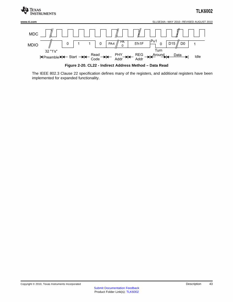
32 "1's"
0 1Pu1
PA4PA
0D15 D01 0 0
Idle
1
StartRead
Code
PHY
Addr
Turn
Around DataREG
Addr
5'h1F
Preamble
MDC
MDIO
TLK6002
www.ti.com SLLSE34A–MAY 2010–REVISED AUGUST 2010
Figure 2-20. CL22 - Indirect Address Method – Data Read
The IEEE 802.3 Clause 22 specification defines many of the registers, and additional registers have beenimplemented for expanded functionality.
Copyright © 2010, Texas Instruments Incorporated Description 43Submit Documentation FeedbackProduct Folder Link(s): TLK6002

TLK6002
SLLSE34A–MAY 2010–REVISED AUGUST 2010 www.ti.com
3 PROGRAMMERS REFERENCE
The following registers can be addressed directly through Clause 22. Channel identification is based onPHY (Port) address field. Registers 0x01- 0x0C, 0X14 are per channel basis.
Channel A can be accessed by setting LSB of PHY address to 0.
Channel B can be accessed by setting LSB of PHY address to 1.
Table 3-1. GLOBAL_CONTROL_1
Address: 0x00 Default: 0x0600
BIT(s) NAME DESCRIPTION ACCESS
0.15 GLOBAL_RESET Global reset (Channel A and B). RWSC (1)
0 = Normal operation (Default 1’b0)
1 = Resets TX and RX datapath including MDIO registers. Equivalent to assertingRESET_N.
0.11 GLOBAL_WRITE Global write enable. RW
0 = Control settings written to Registers 0x01-0x0C, 0x14 are specific to channeladdressed (Default 1’b0)
1 = Control settings written to Registers 0x01-0x0C, 0x14 are applied to both Channel Aand Channel B regardless of channel addressed
0.10:8 HSTL_IMPED_CLK_DIV[2: HSTL Impedance Control clock divide selection. RW0] 000 = Divide by 1
001 = Divide by 2010 = Divide by 4011 = Divide by 8100 = Divide by 16101 = Divide by 32110 = Divide by 64 (Default 3’b110)111 = Divide by 128This value, in tandem with register bit 0.7, selects the frequency and source of the clockused for dynamic voltage, temperature, and impedance compensation in the HSTL I/Obuffers. The division value selected should yield a value less than 10 MHz, and iscalculated by dividing the selected REFCLK_0/1_P/N frequency by the value above.
0.7 HSTL_IMPED_CLK_SEL HSTL Impedance Control reference clock source selection. RW
0 = Selects channel A reference clock (as selected by REFCLK_A_SEL) as clockreference to HSTL impedance control (Default 1’b0)
1 = Selects channel B reference clock (as selected by REFCLK_B_SEL) as clockreference to HSTL impedance control
See register bit 0.10:8 for further details.
0.6 CLKOUT_SEL Output clock select. Selected RXBCLK_A/B or ARS output clock is sent out on RWCLK_OUT_P/N pins . Logically OR’ed with CLK_OUT_SEL pin.
0 = Selects Channel A recovered byte clock (RXBCLK_A) as output clock (Default 1’b0)
1 = Selects Channel B recovered byte clock (RXBCLK_B) as output clock.
See Figure 1-3
0.5:4 CLKOUT_DIV[1:0] Output clock divide setting in non-ARS mode.This value is used to divide selected RWRXBCLK before giving it out onto CLK_OUT_P/N.CLK_OUT_P/N Frequency = (Serial Bit Rate / 10)/(Register 0.5:4 Setting)
00 = Divide by 1 (Default 2’b00)01 = Divide by 210 = Divide by 411 = Divide by 8
See Table 2-9 and Figure 1-3
(1) After reset bit is set to one, it automatically sets itself back to zero on the next MDC clock cycle.
44 PROGRAMMERS REFERENCE Copyright © 2010, Texas Instruments Incorporated
Submit Documentation FeedbackProduct Folder Link(s): TLK6002

TLK6002
www.ti.com SLLSE34A–MAY 2010–REVISED AUGUST 2010
Table 3-1. GLOBAL_CONTROL_1 (continued)
Address: 0x00 Default: 0x0600
BIT(s) NAME DESCRIPTION ACCESS
0.2 RETIME_EN In this mode, serial A input data is sent to both the Parallel A output and Serial B output RWinterface. Serial B input data is sent to both the Parallel B output and Serial A outputinterface.
0 = Normal functional mode (Default 1’b0)
1 = Enable retime mode
Serial A input data rate must match (0 ppm) channel B reference clock.Serial B input data rate must match (0 ppm) channel A reference clockSee Figure 2-11
0.1 REFCLK_A_SEL Channel A Reference clock selection. Logically OR’ed with REFCLK_A_SEL pin. RW
0 = Selects REFCLK_0_P/N as clock reference to Channel A serdes macro (Default1’b0)
1 = Selects REFCLK_1_P/N as clock reference to Channel A serdes macro
See Figure 1-3
0.0 REFCLK_B_SEL Channel B Reference clock selection. Logically OR’ed with REFCLK_B_SEL pin. RW
0 = Selects REFCLK_0_P/N as clock reference to Channel B serdes macro (Default1’b0)
1 = Selects REFCLK_1_P/N as clock reference to Channel B serdes macro
See Figure 1-3
Table 3-2. CHANNEL_CONTROL_1
Address: 0x01 Default: 0x010D
BIT(s) NAME DESCRIPTION ACCESS
Setting this bit high powers down the SERDES datapath channel with exception that MDIOinterface stays active. Logically OR’ed with inverse of PD_TRXx_N.
1.15 POWERDOWN RW0 = Normal operation (Default 1’b0)
1 = Power Down mode is enabled.
1.10 RESERVED For TI use only N/A
Serdes PLL Loop Bandwidth settings
00 = Reserved
1.9:8 LOOP_BANDWIDTH 01 = Applicable when external JC_PLL is NOT used (Default 2’b01) RW
10 = Applicable when external JC_PLL is used
11 = Reserved
Serdes TX rate settings
00 = Full rate (Default 2’b00)
01 = Half rate
10 = Quarter rate
11 = Eighth rate1.7:6 RATE_TX [1:0] RWValues written are valid only when RATE_A/B[2:0] pins are set to 3’b100 and ARS is notenabled (10.13:12 = 2’b00)
In ARS mode, values written to these bits are not considered to determine serdes TX rate.Instead it is automatically determined by ARS machine.
When read, these bits will reflect the final serdes Tx rate values
Copyright © 2010, Texas Instruments Incorporated PROGRAMMERS REFERENCE 45Submit Documentation FeedbackProduct Folder Link(s): TLK6002

TLK6002
SLLSE34A–MAY 2010–REVISED AUGUST 2010 www.ti.com
Table 3-2. CHANNEL_CONTROL_1 (continued)
Address: 0x01 Default: 0x010D
BIT(s) NAME DESCRIPTION ACCESS
Serdes RX rate settings
00 = Full rate (Default 2’b00)
01 = Half rate
10 = Quarter rate
11 = Eighth rate1.5:4 RATE_RX [1:0] RWValues written are valid only when RATE_A/B[2:0] pins are set to 3’b100 and ARS is notenabled (10.13:12 = 2’b00)
In ARS mode, values written to these bits are not considered to determine serdes RX rate.Instead it is automatically determined by ARS machine.
When read, these bits will reflect the final serdes Rx rate values
Serdes PLL multiplier setting (Default 4’b1101). In ARS mode, values written to these bits isnot considered to determine serdes PLL multiplier. Instead it is automatically determined byARS machine and these bits when read will reflect that value.1.3:0 PLL_MULT[3:0] RWRefer Table 3-3
See Appendix B for more information on PLL multiplier mettings
Table 3-3. PLL Multiplier Control
1[3:0] 1[3:0]
VALUE PLL MULTIPLIER FACTOR VALUE PLL MULTIPLIER FACTOR
0000 Reserved 1000 12x
0001 Reserved 1001 Reserved
0010 4x 10¹⁰ 15x
0011 5x 10¹¹ 16x
0100 6x 1100 16.5x
0101 8x 1101 20x
0110 8.25x 1110 25x
0111 10x 1111 Reserved
Table 3-4. CHANNEL_CONTROL_2
Address: 0x02 Default: 0x000A
Bit(s) Name Description Access
Adjacent post cursor Tap weight. Selects TAP settings for TX waveform. (Default 5’b00000)2.12:8 TWPOST1[4:0] RWRefer Table 3-5
Pre cursor Tap weight. Selects TAP settings for TX waveform. (Default 4’b0000)2.7:4 TWPRE[3:0] RWRefer Table 3-6
Transmitter Output swing control for Serdes. (Default 4’b1010)2.3:0 SWING[3:0] RWRefer Table 3-7
46 PROGRAMMERS REFERENCE Copyright © 2010, Texas Instruments Incorporated
Submit Documentation FeedbackProduct Folder Link(s): TLK6002

TLK6002
www.ti.com SLLSE34A–MAY 2010–REVISED AUGUST 2010
Table 3-5. Post-Cursor Transmit Tap Weights
2[12:8] 2[12:8]
VALUE TAP WEIGHT (%) VALUE TAP WEIGHT (%)
00000 0 10000 0
00001 +2.5 10001 –2.5
00010 +5.0 10010 –5.0
00011 +7.5 10011 –7.5
00100 +10.0 10100 –10.0
00101 +12.5 10101 –12.5
00110 +15.0 10110 –15.0
00111 +17.5 10111 –17.5
01000 +20.0 11000 –20.0
01001 +22.5 11001 –22.5
01010 +25.0 11010 –25.0
01011 +27.5 11011 –27.5
01100 +30.0 11100 –30.0
01101 +32.5 11101 –32.5
01110 +35.0 11110 –35.0
01111 +37.5 11111 –37.5
Table 3-6. Pre-Cursor Transmit Tap Weights
2[7:4] 2[7:4]
VALUE TAP WEIGHT (%) VALUE TAP WEIGHT (%)
0000 0 1000 0
0001 +2.5 1001 –2.5
0010 +5.0 1010 –5.0
0011 +7.5 1011 –7.5
0100 +10.0 1100 –10.0
0101 +12.5 1101 –12.5
0110 +15.0 1110 –15.0
0111 +17.5 1111 –17.5
Copyright © 2010, Texas Instruments Incorporated PROGRAMMERS REFERENCE 47Submit Documentation FeedbackProduct Folder Link(s): TLK6002

TLK6002
SLLSE34A–MAY 2010–REVISED AUGUST 2010 www.ti.com
Table 3-7. AC Mode Output Swing Control
VALUE AC MODETYPICAL AMPLITUDE2[3:0] (mVdfpp)
0000 126
0001 215
0010 303
0011 395
0100 478
0101 572
0110 662
0111 756
1000 839
1001 932
1010 1020
1011 1110
1100 1190
1101 1280
1110 1360
1111 1450
Table 3-8. CHANNEL_CONTROL_3
Address: 0x03 Default: 0x0180
BIT(s) NAME DESCRIPTION ACCESS
Valid only when comma detection (channel synchronization) is enabled.
00 = The channel synchronization, when in the synchronization state, performs theEthernet standard specified hysteresis to return to the unsynchronized state(Default 2’b00)
01 = A single 8b/10b invalid decode error or disparity error causes the channelCH_SYNC_HYSTERESIS3.12:11 synchronization state machine to immediately transition from sync to unsync RW[1:0]10 = Two adjacent 8b/10b invalid decode errors or disparity errors cause the channel
synchronization state machine to immediately transition from sync to unsync
11 = Three adjacent 8b/10b invalid decode errors or disparity errors cause thechannel synchronization state machine to immediately transition from sync tounsync
0 = Selects same channel Tx parallel interface input data as core input data for thatchannel (Default 1’b0)
3.10 TX_SWAP_SEL 1 = Selects partner channel Tx parallel interface input data as core input data for RWthat channel
See Figure 1-4
0 = Selects same channel deserialized input data to be sent out the Rx paralleloutput interface (Default 1’b0)
3.9 RX_SWAP_SEL 1 = Selects partner channel deserialized input data to be sent out the Rx parallel RWoutput interface
See Figure 1-5
Parallel output clock (RXCLK_x) selection
When RX_SWAP_SEL (3.9) is 1’b0
0 = Selects respective channel SERDES TXBCLK clock
1 = Selects respective channel SERDES RXBCLK clock (Default 1’b1)3.8 RXCLK_OUT_SEL RW
When RX_SWAP_SEL (3.9) is 1’b1
0 = Selects partner channel SERDES TXBCLK clock
1 = Selects partner channel SERDES RXBCLK clock (Default 1’b1)
See Figure 1-5
48 PROGRAMMERS REFERENCE Copyright © 2010, Texas Instruments Incorporated
Submit Documentation FeedbackProduct Folder Link(s): TLK6002

TLK6002
www.ti.com SLLSE34A–MAY 2010–REVISED AUGUST 2010
Table 3-8. CHANNEL_CONTROL_3 (continued)
Address: 0x03 Default: 0x0180
BIT(s) NAME DESCRIPTION ACCESS
0 = Disables comma detection
3.7 COMMA_ENABLE 1 = Enables comma detection (Default 1’b1) RW
Comma detection automatically enabled during CRPAT verification.
0 = Enables SDR data mode on parallel Transmit and Receive directions (data isclocked only on rising edge or only on falling edge) (Default 1’b0)
3.6 DDR_ENABLE RW1 = Enables DDR data mode on parallel Transmit and Receive directions (data
clocked on both rising and falling edge)
0 = TDx_[19:10] symbol is serialized before TDx_[9:0]. (Default 1’b0)3.5 TX_SYMBOL_ORDER RW
1 = TDx_[9:0] symbol is serialized before TDx_[19:10].
0 = RDx_[19:10] symbol is deserialized before RDx_[9:0] symbol. (Default 1’b0)3.4 RX_SYMBOL_ORDER RW
1 = RDx_[9:0] symbol is deserialized before RDx_[19:10].
Encoder enable control. Logically OR’ed with CODE*_EN pin.
0 = 8B/10B encode function is disabled (Default 1’b0)3.3 ENCODE_ENABLE RW
1 = 8B/10B encode function is enabled
Encoder automatically enabled during CRPAT test pattern generation.
Decoder enable control. Logically OR’ed with CODE*_EN pin.
0 = 8B/10B decode function is disabled (Default 1’b0)3.2 DECODE_ENABLE RW
1 = 8B/10B decode function is enabled
Decoder automatically enabled during CRPAT verification.
Transmit parallel input interface mode select. (Default 1’b0)
When channel is in DDR mode
0 = Source centered timing on transmit parallel interface. Data is sampled on bothrising and falling clock edges.
1 = Source aligned timing on transmit parallel interface. Data is aligned with bothrising and falling clock edges, and a sampling point is created internal to3.1 TX_EDGE_MODE RWTLK6002 .
When channel is in SDR mode
0 = Falling edge align mode. Incoming data is aligned to falling edge of parallelinput clock. Internally data is sampled at the rising edge of the clock
1 = Rising edge align mode. Incoming parallel data is aligned to rising edge ofparallel input clock. Internally data is sampled at the falling edge of the clock.
Receive Parallel output interface mode select. (Default 1’b0)
When channel is in DDR mode:
0 = Source centered timing on receive parallel interface. Data changing is offsetfrom the rising and falling clock edge per the HSTL Timing specification section,and is easily sampled by external devices.
1 = Source aligned timing on receive parallel interface. Data changes at clock edge,3.0 RX_EDGE_MODE RWand a sampling point must be created by external devices.
When channel is in SDR mode:
0 = Falling edge align mode. Outgoing parallel data is aligned to the falling edge ofthe parallel output clock, and is sampled on the rising edge by external devices.
1 = Rising edge align mode. Outgoing parallel data is aligned to the rising edge ofthe parallel output clock, and is sampled on the falling edge by external devices.
Copyright © 2010, Texas Instruments Incorporated PROGRAMMERS REFERENCE 49Submit Documentation FeedbackProduct Folder Link(s): TLK6002

TLK6002
SLLSE34A–MAY 2010–REVISED AUGUST 2010 www.ti.com
Table 3-9. CHANNEL_CONTROL_4
Address: 0x04 Default: 0x0000
BIT(s) NAME DESCRIPTION ACCESS
Channel datapath reset control. Required once the desired functional mode is configured.
4.3 DATAPATH_RESET 0 = Normal operation. (Default 1’b0)
1 = Resets channel logic excluding MDIO registers. (Resets both Tx and Rx datapath)
Transmit FIFO reset controlRW4.2 TXFIFO_RESET 0 = Normal operation. (Default 1’b0) SC (1)
1 = Resets transmit datapath FIFO.
Receive FIFO reset control
4.1 RXFIFO_RESET 0 = Normal operation. (Default 1’b0)
1 = Resets receive datapath FIFO.
(1) After reset bit is set to one, it automatically sets itself back to zero on the next MDC clock cycle.
Table 3-10. CHANNEL_STATUS_1
Address: 0x05 Default: 0x0000
BIT(s) NAME DESCRIPTION ACCESS
Auto zero complete indicator.5.14 AZ_DONE
When high, indicates auto zero calibration is completeRO/LL
Adaptive gain control loop lock indicator.5.13 AGC_LOCKED
When high, indicates AGC loop is in locked state
Test Pattern status for test pattern selected in 7.10:8 .
0 = Alignment has not achieved5.12 TP_ STATUS RO
1 = Alignment has been determined and correct pattern has been received.
Any bit errors received are reflected in ERROR_COUNTER register (0x0E)
ARS PLL Lock error indicator. Valid only when ARS function is enabled.5.11 ARS_PLL_LOCK_ERROR RO/LHWhen high, indicates ARS did not detect PLL lock within the time specified through
ARS_INTERVAL[20:0] (11.4:0,12.15:0).
ARS lock indicator. Valid only when ARS function is enabled.5.10 ARS_LOCKED RO/LL
When high, indicates ARS has determined incoming serial data rate.
Valid in 16 bit (SDR/DDR) mode (encoder enabled) and during
5.9 ENCODE_INVALID CRPAT test pattern generation. RO/LH
When high, indicates encoder received an invalid control word.
Valid in 16 bit (SDR/DDR) mode (decoder enabled) and during CRPAT test patternverification.
5.8 DECODE_INVALID RO/LHWhen high, indicates decoder received an invalid code word, or a 8b/10b disparity error.In functional mode, number of DECODE_INVALID errors are reflected inERROR_COUNTER register (0x0E)
5.7 TX_FIFO_UNDERFLOW When high, indicates underflow has occurred in the transmit datapath FIFO. RO/LH
5.6 TX_FIFO_OVERFLOW When high, indicates overflow has occurred in the transmit datapath FIFO. RO/LH
5.5 RX_FIFO_UNDERFLOW When high, indicates underflow has occurred in the receive datapath FIFO. RO/LH
5.4 RX_FIFO_OVERFLOW When high, indicates overflow has occurred in the receive datapath FIFO. RO/LH
GPI1 status Indicator.5.3 GPI1 ROReflects GPI1 input signal status.
Loss of Signal Indicator. RO/LH5.2 LOS
When high, indicates that a loss of signal condition is detected on serial receive inputs
Channel synchronization status indicator. Valid only when comma detection is enabled5.1 CHANNEL_SYNC RO/LL
When high, indicates channel synchronization has achieved
Serdes PLL lock indicator5.0 PLL_LOCK RO/LL
When high, indicates Serdes PLL is locked to the selected incoming REFCLK_0/1_P/N
50 PROGRAMMERS REFERENCE Copyright © 2010, Texas Instruments Incorporated
Submit Documentation FeedbackProduct Folder Link(s): TLK6002

TLK6002
www.ti.com SLLSE34A–MAY 2010–REVISED AUGUST 2010
Table 3-11. OVERRIDE_CONTROL
Address: 0x06 Default: 0xC000
BIT(s) NAME DESCRIPTION ACCESS
0 = Holds parallel output clock RXCLK_x output fixed at zero.6.15 RXCLK_OUT_EN RW1 = Allows RXCLK_x output to toggle normally. (Default 1’b1)
TX FIFO Latency Control (Default 3’b100) This selection allows TX FIFO crash immunity tobe traded off against datapath latency. Selecting a large latency allows for the most dynamicphase variation between TXCLK_A/B and the selected SERDES channel reference clock(REFCLK_0/1_P/N). Careful consideration should be made in selecting this value based onthe anticipated phase movement between TXCLK_A/B and selected REFCLK_0/1_P/Nduring system operation to avoid unwanted reoccurring transmit FIFO collision.
TX_FIFO_DEPTH TXCLK_A/B and selected Appendix D Datapath Latency[2:0] REFCLK_0/1_P/N. Relative Maximum Value (Serial Bit
Phase Movement Allowed Times)(Serial Bit Times)
6.14:12 TX_FIFO_DEPTH[2:0] RW000 ±4 Same
001 ±14 Same +20
010 ±34 Same +60
011 ±54 Same +110
1xx (Auto Selection) Full Rate: Same as 011 Consistent with above fourHalf Rate: Same as 010 selections.Quarter Rate: Same as 001Eighth Rate: Same as 000
0 = LOSx pin does not reflect GPI1 input signal status (Default 1’b0)6.11 GPI_OVERLAY RW1 = Allows inverse value of GPI1 input signal to be reflected on LOSx pin
0 = LOSx pin does not reflect Serdes Rx Loss of signal condition (Default 1’b0)6.10 LOS_OVERLAY RW1 = Allows Serdes Rx Loss of signal condition to be reflected on LOSx pin
0 = LOSx pin does not reflect loss of channel synchronization status (Default 1’b0)6.9 CH_SYNC_OVERLAY RW1 = Allows channel loss of synchronization to be reflected on LOSx pin
0 = LOSx pin does not reflect loss of PLL lock status (Default 1’b0)6.8 PLL_LOCK_OVERLAY RW1 = Allows loss of PLL lock status to be reflected on LOSx pin
Receive data replacement control when GPI1 input is low6.7 RX_CHAR_CTRL_GPI1 0 = Data passed through as received (Default 1’b0) RW
1 = Data replaced with K30.7 (when decoder is enabled) or all 0’s (when decoder is disabled)
Receive data replacement control during Loss of signal condition6.6 RX_CHAR_CTRL_LOS 0 = Data passed through as received (Default 1’b0) RW
1 = Data replaced with K30.7 (when decoder is enabled) or all 0’s (when decoder is disabled)
Receive data replacement control during Loss of synchronization condition6.5 RX_CHAR_CTRL_CH_SYNC 0 = Data passed through as received (Default 1’b0) RW
1 = Data replaced with K30.7 (when decoder is enabled) or all 0’s (when decoder is disabled)
Receive data replacement control during Loss of PLL Lock condition6.4 RX_CHAR_CTRL_PLL_LOCK 0 = Data passed through as received (Default 1’b0) RW
1 = Data replaced with K30.7 (when decoder is enabled) or all 0’s (when decoder is disabled)
0 = LOSx pin does not reflect invalid code word error (Default 1’b0)6.3 INVALID_CODE_OVERLAY RW1 = Allows invalid code word error to be reflected on LOSx pin
Slew Rate setting for RX parallel outputs6.2 HSTL_SLEW_RATE 0 = No slew control (fastest edge) (Default 1’b0) RW
1 = 33% slower slew control
Parallel Input Termination setting for TX parallel inputs00 = Termination disable (High Impedance) (Default 2’b00)01 = Half termination strength (200 Ω to VHSTL and GND) – Thevenin equivalent of 100 Ω to6.1:0 HSTL_TERM[1:0] RW(VDDQA/B)/21x = Full termination strength (100 Ω to VHSTL and GND) – Thevenin equivalent of 50 Ω to(VDDQA/B)/2.
Copyright © 2010, Texas Instruments Incorporated PROGRAMMERS REFERENCE 51Submit Documentation FeedbackProduct Folder Link(s): TLK6002

TLK6002
SLLSE34A–MAY 2010–REVISED AUGUST 2010 www.ti.com
Table 3-12. LOOPBACK_TP_CONTROL
Address: 0x07 Default: 0x0700
BIT(s) NAME DESCRIPTION ACCESS
7.15:14 RESERVED For TI use only N/A
0 = Normal operation (Default 1’b0)7.13 TP_GEN_EN RW1 = Activates test pattern generation selected by bits 7.10:8
0 = Normal operation (Default 1’b0)7.12 TP_VERIFY_EN RW1 = Activates test pattern verification selected by bits 7.10:8
Test Pattern Selection000 = Reserved001 = Reserved010 = Reserved
7.10:8 TEST_PATTERN_SEL[2:0] 011 = CRPAT Long (Supported only in half/quarter/eighth rate modes). RW100 = CRPAT Short (Supported only in half/quarter/eighth rate modes).101 = 27 - 1 PRBS pattern110 = 223 - 1 PRBS pattern111 = 231 - 1 PRBS pattern (Default 3’b111)
0 = LOSx pin does not reflect AGC unlock status (Default 1’b0)7.7 AGCLOCK_OVERLAY RW1 = Allows AGC unlock status to be reflected on LOSx pin
0 = LOSx pin does not reflect auto zero calibration not done status (Default 1’b0)7.6 AZDONE_OVERLAY RW1 = Allows auto zero calibration not done status to be reflected on LOSx pin
Receive data replacement control during AGC unlock condition0 = Data passed through as received (Default 1’b0)7.5 RX_CHAR_CTRL_AGCLOCK RW1 = Data replaced with K30.7 (when decoder is enabled) or all 0’s (when decoder isdisabled)
Receive data replacement control during auto zero calibration not done condition0 = Data passed through as received (Default 1’b0)7.4 RX_CHAR_CTRL_AZDONE RW1 = Data replaced with K30.7 (when decoder is enabled) or all 0’s (when decoder isdisabled)
In this mode, serial input data traverses entire Rx datapath just before paralleloutput drivers and is returned through entire Tx datapath and to the channel’s serialoutput. The serial input data will also be available at the parallel output port. Serial
7.3 DEEP_REMOTE_LPBK input data rate must match (0 ppm) reference clock. RW0 = Normal functional mode (Default 1’b0)1 = Enable deep remote loopback modeSee Figure 2-10
In this mode, serial input following decoder is fed back to the channel’s encoderinput and to the serial output. The serial input data will also be available at theparallel output port. Serial input data rate must match (0 ppm) reference clock7.2 SHALLOW_REMOTE_LPBK RW0 = Normal functional mode (Default 1’b0)1 = Enable shallow remote loopback modeSee Figure 2-10
In this mode, parallel input is looped after serializer and fed back to the channel’sparallel output. The parallel input data is not available at the TX serial output. Note:SWING[3:0] must be set to 4’b0000 in this mode.0 = Normal functional mode (Default 1’b0)7.1 DEEP_LOCAL_LPBK RW1 = Enable deep local loopback modeSee figure Figure 2-9Note that AZDONE must be asserted before asserting DEEP_LOCAL_LPBK. Alsonote that AGCLOCK is not valid during DEEP_LOCAL_LPBK.
In this mode, parallel input after the encoder and before the serializer is fed back tothe channel’s parallel output. The parallel input data will also be serialized andavailable at the TX serial port7.0 SHALLOW_LOCAL_LPBK RW0 = Normal functional mode (Default 1’b0)1 = Enable shallow local loopback modeSee Figure 2-9
52 PROGRAMMERS REFERENCE Copyright © 2010, Texas Instruments Incorporated
Submit Documentation FeedbackProduct Folder Link(s): TLK6002

TLK6002
www.ti.com SLLSE34A–MAY 2010–REVISED AUGUST 2010
Table 3-13. SERDES_CONTROL_1
Address: 0x08 Default: 0x3D4C
BIT(s) NAME DESCRIPTION ACCESS
Serdes Rx precursor equalizer selection000 = 1/9 cursor amplitude001 = 3/9 cursor amplitude010 = 5/9 cursor amplitude
8.14:12 EQPRE[2:0] 011 = 7/9 cursor amplitude (Default 3’b011) RW100 = 9/9 cursor amplitude101 = 11/9 cursor amplitude110 = 13/9 cursor amplitude111 = Disable
Clock data recovery algorithm threshold selection00 = Four vote threshold
8.11:10 CDRTHR[1:0] 01 = Eight vote threshold RW10 = Sixteen vote threshold11 = Thirty two vote threshold (Default 2’b11)
Clock data recovery algorithm frequency multiplication selection00 = First order. Frequency offset tracking disabled
8.9:8 CDRFMULT[1:0] 01 = Second order. 1x mode (Default 2’b01) RW10 = Second order. 2x mode11 = Reserved
Adaptive gain control loop00 = Attenuator will not change after lock has been achieved, even if AGC becomesunlocked
8.7:6 AGCCTRL[1:0] 01 = Attenuator will not change when in lock state, but could change when AGC becomes RWunlocked (Default 2’b01)10 = Force the attenuator off.11 = Force the attenuator on
Auto zero calibration.00 = Auto zero calibration initiated when receiver is enabled (Default 2’b00)
8.5:4 AZCAL[1:0] 01 = Auto zero calibration disabled RW10 = Forced with automatic update.11 = Forced without automatic update
Determines whether LSB or MSB of the parallel inputs to be sent out first on serialtransmit pins.8.3 TX_PMA_BIT_ORDER RW0 = TDx[19] or TDx[9] (MSB) is serially transmitted first1 = TDx[10] or TDx[0] (LSB) is serially transmitted first (Default 1’b1)
Determines whether serially received first bit to be sent out on LSB or MSB of the paralleloutputs.8.2 RX_PMA_BIT_ORDER RW0 = RDx[19] or RDx[9] (MSB) is serially received first1 = RDx[10] or RDx[0] (LSB) is serially received first (Default 1’b1)
Transmitter polarity.0 = Normal polarity. TXxP considered positive data and TXxN considered negative data8.1 TX_INVPAIR RW(Default 1’b0)1 = Inverted polarity. TXxP considered negative data and TXxN considered positive data
Receiver polarity.0 = Normal polarity. RXxP considered positive data. RXxN considered negative data8.0 RX_INVPAIR RW(Default 1’b0)1 = Inverted polarity. RXxP considered negative data. RXxN considered positive data
Table 3-14. SCRAMBLER_CONTROL
Address: 0x09 Default: 0x0000
BIT(s) NAME DESCRIPTION ACCESS
0 = Disables scrambler on the transmit datapath (Default 1’b0)9.15 TX_SCRAMBLER_EN RW1 = Enables scrambler on the transmit datapath
7 bit scrambler seed used when TX scrambler is enabled.9.14:8 TX _SCRAMBLER_SEED[6:0] RW(Default 7’b0000000)
0 = Disables De-scrambler on the receive datapath (Default 1’b0)9.7 RX_DESCRAMBLER_EN RW1 = Enables De-scrambler on the receive datapath
7 bit De-scrambler seed used when RX De-scrambler is enabled.9.6:0 RX_DESCRAMBLER_SEED[6:0] RW(Default 7’b0000000)
Copyright © 2010, Texas Instruments Incorporated PROGRAMMERS REFERENCE 53Submit Documentation FeedbackProduct Folder Link(s): TLK6002

TLK6002
SLLSE34A–MAY 2010–REVISED AUGUST 2010 www.ti.com
Table 3-15. ARS_CONTROL_1
Address: 0x0A Default: 0x0800
BIT(s) NAME DESCRIPTION ACCESS
Valid only when ARS function is enabled.0 = Holds parallel output clock RXCLK_x output fixed at zero until serial data10.15 ARS_RX_CLK_EN RWrate is determined by the ARS. (Default 1’b0)1 = Allows RXCLK_x output to toggle normally.
Valid only when ARS function is enabled.10.14 ARS_ LOCK_OVERLAY 0 = LOSx pin does not reflect ARS loss of lock status (Default 1’b0) RW
1 = Allows ARS loss of lock status to be reflected on LOSx pin
ARS enable software control. Applicable when RATE_x[2:0] pins are set to3’b100.00 = Serdes settings are determined by MDIO (Default 2’b00)01 = Enable ARS function in respective channel.Serdes settings for respective channel are determined by ARS in the samechannel. Refer RATE_x[2:0] 3’b101 setting for more information.
10 = Enable ARS function in respective channel.10.13:12 ARS_ EN[1:0] Serdes settings for respective channel are determined by ARS in the same RW
channel. Refer RATE_x[2:0] 3’b110 setting for more information.
11 = Enable ARS function in respective channel as slave mode.If ARS is enabled in partner channel, serdes settings in this channel aredetermined by ARS in partner channel.If ARS is not enabled in partner channel, serdes settings in this channel aredetermined by MDIO.Refer RATE_x[2:0] 3’b111 setting for more information.
Valid only when ARS_TX_DATAPATH_OVERRIDE (10.10) is set0 = When ARS successfully determines incoming serial data rate, TX_FIFOis automatically reset and parallel data is serialized and sent through serial
10.11 ARS_TX_MDIO_GATE output pins. RW1 = When ARS successfully determines incoming serial data rate, TX FIFOneeds to be manually reset by writing to register bit 4.2 to enable properserialization of the parallel data. (Default 1’b1)
Applicable during serial data rate determination by ARS0 = Transmit parallel input data is serialized as received and sent through
10.10 ARS_TX_DATAPATH_OVERRIDE serial output pins. (Default 1’b0) RW1 = 10 bit data specified in ARS_TX_DATA (10.9:0) is serialized and sentthrough serial output pins.
10 bit data to be serialized during serial rate determination by ARS.10.9:0 ARS_TX_DATA[9:0] If TX_PMA_BIT_ORDER (8.3) is set, ARS_TX_DATA [9] is serially RW
transmitted first else ARS_TX_DATA [0] is serially transmitted first.
54 PROGRAMMERS REFERENCE Copyright © 2010, Texas Instruments Incorporated
Submit Documentation FeedbackProduct Folder Link(s): TLK6002

TLK6002
www.ti.com SLLSE34A–MAY 2010–REVISED AUGUST 2010
Table 3-16. ARS_CONTROL_2
Address: 0x0B Default: 0x7FFF
BIT(s) NAME DESCRIPTION ACCESS
Input reference clock frequency selection in ARS mode.00 = If input reference clock frequency is 122.88 MHz.
11.15:14 ARS_REF_FREQ[1:0] 01 = If input reference clock frequency is 153.60 MHz. (Default 2’b01) RW10 = Reserved11 = If input reference clock frequency is 307.20 MHz.
Control to enable rate determination through ARS for each of the 8 supported bitrates. ARS_SBR_ENABLE[7] for the highest serial bit rate and11.13:6 ARS_SBR_ENABLE[7:0] RWARS_SBR_ENABLE[0] for the lowest serial bit rate. Refer Table 2-6 for supportedserial bit rates.
11.5 RESERVED For TI use only N/A
5 MSB’s of 21 bit wide counter defined in terms of number of REFCLK cycles todetermine amount of time that ARS state machine needs to stay in a particularsetting to achieve rate determination.
11.4:0 ARS_INTERVAL[20:16] Wait time is calculated as ARS_INTERVAL[20:0] × 1024 REFCLK periods. RWIf ARS state machine does not achieve rate determination within the wait timespecified by this counter, ARS state machine will move into next lower serial ratesetting to achieve rate determination.
Table 3-17. ARS_CONTROL_3
Address: 0x0C Default: 0xFFFF
BIT(s) NAME DESCRIPTION ACCESS
12.15:0 ARS_INTERVAL[15:0] 16 LSB’s of 21 bit wide counter defined in terms of number of REFCLK cycles todetermine amount of time that ARS state machine needs to stay in a particularsetting to achieve rate determination.
Wait time is calculated as ARS_INTERVAL[20:0] × 1024 REFCLK periods. RW
If ARS state machine does not achieve rate determination within the wait timespecified by this counter, ARS state machine will move into next lowest serial ratesetting to achieve rate determination.
Table 3-18. ARS_CONTROL_4
Address: 0x0D Default: 0x3000
BIT(s) NAME DESCRIPTION ACCESS
13.15 RESERVED For TI use only
13.14 RESERVED For TI use only
13.13 RESERVED For TI use only N/A
13.12 RESERVED For TI use only
13.11:0 RESERVED For TI use only
Table 3-19. ERROR_COUNTER
Address: 0x0E Default: 0xFFFD
BIT(s) NAME DESCRIPTION ACCESS
In functional mode if 8b/10b decoder is enabled, this counter reflects number ofinvalid code words (includes disparity errors) received by decoder.
In test pattern verification mode (7.12 = 1’b1), this counter reflects error count for the14.15:0 ERROR_COUNTER[15:0] CORtest pattern selected through 7.10:8
When PRBS_EN pin is set, this counter reflects error count for selected PRBSpattern. Counter value cleared to 16’h0000 when read.
Copyright © 2010, Texas Instruments Incorporated PROGRAMMERS REFERENCE 55Submit Documentation FeedbackProduct Folder Link(s): TLK6002

TLK6002
SLLSE34A–MAY 2010–REVISED AUGUST 2010 www.ti.com
Table 3-20. TI_RESERVED_CONTROL STATUS
Address: 0x0F Default: 0x0205
BIT(s) NAME DESCRIPTION ACCESS
15.14 RESERVED For TI use only
15.13 RESERVED For TI use only
15.12 RESERVED For TI use only
15.10 RESERVED For TI use only
15.9 RESERVED For TI use only
15.8 RESERVED For TI use onlyN/A
15.6 RESERVED For TI use only
15.5 RESERVED For TI use only
15.4 RESERVED For TI use only
15.2 RESERVED For TI use only
15.1 RESERVED For TI use only
15.0 RESERVED For TI use only
Table 3-21. LATENCY_MEASURE_CONTROL
Address: 0x10 Default: 0x0000
BIT(s) NAME DESCRIPTION ACCESS
16.10 RESERVED For TI use only
16.9 RESERVED For TI use only N/A
16.8 RESERVED For TI use only
Latency measurement clock divide control. Valid only when bit 16.2 is 0.Divides clock to needed resolution. Higher the divide value, lesser the latencymeasurement resolution00 = Divide by 1 (Default 2’b00) (Most Accurate Measurement)16.5:4 LATENCY_MEAS_CLK_DIV[1:0] RW01 = Divide by 210 = Divide by 411 = Divide by 8 (Longest Measurement Capability)See Table 2-6
Latency measurement clock selection.0 = Selects clock listed in Table 2-6. Bits 16.5:4 can be used to divide this clock
16.2 LATENCY_MEAS_CLK_SEL to achieve needed resolution. (Default 1’b0) RW1 = Selects respective channel recovered byte clock (Frequency = Serial bitrate/ 10).
Latency measurement enable16.1 LATENCY_MEAS_EN 0 = Disable Latency measurement (Default ’b0) RW
1 = Enable Latency measurement
Latency measurement channel selection16.0 LATENCY_MEAS_CH_SEL 0 = Selects Latency measurement for channel A (Default ’b0) RW
1 = Selects Latency measurement for channel B
56 PROGRAMMERS REFERENCE Copyright © 2010, Texas Instruments Incorporated
Submit Documentation FeedbackProduct Folder Link(s): TLK6002

TLK6002
www.ti.com SLLSE34A–MAY 2010–REVISED AUGUST 2010
Table 3-22. LATENCY_COUNTER_2
Address: 0x11 Default: 0x0000
BIT(s) NAME DESCRIPTION ACCESS
Comma indication for the current latency measurement. Cleared whenRegister 0x12 is read17.15 LATENCY_MEAS_TX_COMMA 0 = Indicates Latency measurement detected comma on TXD[19:10]1 = Indicates Latency measurement detected comma on TXD[9:0]
Comma indication for the current latency measurement. Cleared whenRegister 0x12 is read17.14 LATENCY_MEAS_RX_COMMA RO/LH (1)0 = Indicates Latency measurement detected comma on RXD[19:10]1 = Indicates Latency measurement detected comma on RXD[9:0]
Latency measurement ready indicator0 = Indicates latency measurement not complete.17.4 LATENCY_ MEAS_READY 1 = Indicates latency measurement is complete and value in latencymeasurement counter (LATENCY_MEAS_COUNT[19:0]) is ready to be read.
Bits[19:16] of 20 bit wide latency measurement counter.Latency measurement counter value represents the latency in number of clock
17.3:0 LATENCY_MEAS_COUNT[19:16] cycles. This counter will return 20’h00000 if it is read before rx comma is COR (1)
received. If latency is more than 20’hFFFFF clock cycles then this counterreturns 20’hFFFFF.
(1) User has to make sure Register 0x11 has to be read first before reading Register 0x12. Latency measurement counter value resets to20’h00000 when Register 0x12 is read. Comma indication (17.15 and 17.14) and count valid (17.4) bits are also cleared when Register0x12 is read.
Table 3-23. LATENCY_COUNTER_1
Address: 0x12 Default: 0x0000
BIT(s) NAME DESCRIPTION ACCESS
18.15:0 LATENCY_MEAS_COUNT[15:0] Bits[15:0] of 20 bit wide latency measurement counter. COR (1)
(1) User has to make sure Register 0x11 has to be read first before reading Register 0x12. Latency measurement counter value resets to20’h00000 when Register 0x12 is read. Comma indication (17.15 and 17.14) and count valid (17.4) bits are also cleared when Register0x12 is read.
Table 3-24. TI_RESERVED_CONTROL_1
Address: 0x13 Default: 0x0200
BIT(s) NAME DESCRIPTION ACCESS
19.12 RESERVED For TI use only
19.9 RESERVED For TI use only
19.8 RESERVED For TI use onlyN/A
19.7 RESERVED For TI use only
19.3 RESERVED For TI use only
19.0 RESERVED For TI use only
Copyright © 2010, Texas Instruments Incorporated PROGRAMMERS REFERENCE 57Submit Documentation FeedbackProduct Folder Link(s): TLK6002
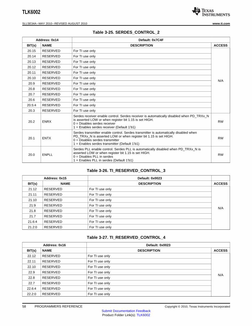
TLK6002
SLLSE34A–MAY 2010–REVISED AUGUST 2010 www.ti.com
Table 3-25. SERDES_CONTROL_2
Address: 0x14 Default: 0x7C4F
BIT(s) NAME DESCRIPTION ACCESS
20.15 RESERVED For TI use only
20.14 RESERVED For TI use only
20.13 RESERVED For TI use only
20.12 RESERVED For TI use only
20.11 RESERVED For TI use only
20.10 RESERVED For TI use onlyN/A
20.9 RESERVED For TI use only
20.8 RESERVED For TI use only
20.7 RESERVED For TI use only
20.6 RESERVED For TI use only
20.5:4 RESERVED For TI use only
20.3 RESERVED For TI use only
Serdes receiver enable control. Serdes receiver is automatically disabled when PD_TRXx_Nis asserted LOW or when register bit 1.15 is set HIGH.20.2 ENRX RW0 = Disables serdes receiver1 = Enables serdes receiver (Default 1’b1)
Serdes transmitter enable control. Serdes transmitter is automatically disabled whenPD_TRXx_N is asserted LOW or when register bit 1.15 is set HIGH.20.1 ENTX RW0 = Disables serdes transmitter1 = Enables serdes transmitter (Default 1’b1)
Serdes PLL enable control. Serdes PLL is automatically disabled when PD_TRXx_N isasserted LOW or when register bit 1.15 is set HIGH.20.0 ENPLL RW0 = Disables PLL in serdes1 = Enables PLL in serdes (Default 1’b1)
Table 3-26. TI_RESERVED_CONTROL_3
Address: 0x15 Default: 0x0023
BIT(s) NAME DESCRIPTION ACCESS
21.12 RESERVED For TI use only
21.11 RESERVED For TI use only
21.10 RESERVED For TI use only
21:9 RESERVED For TI use onlyN/A
21.8 RESERVED For TI use only
21.7 RESERVED For TI use only
21.6:4 RESERVED For TI use only
21.2:0 RESERVED For TI use only
Table 3-27. TI_RESERVED_CONTROL_4
Address: 0x16 Default: 0x0023
BIT(s) NAME DESCRIPTION ACCESS
22.12 RESERVED For TI use only
22.11 RESERVED For TI use only
22.10 RESERVED For TI use only
22.9 RESERVED For TI use onlyN/A
22.8 RESERVED For TI use only
22.7 RESERVED For TI use only
22.6:4 RESERVED For TI use only
22.2:0 RESERVED For TI use only
58 PROGRAMMERS REFERENCE Copyright © 2010, Texas Instruments Incorporated
Submit Documentation FeedbackProduct Folder Link(s): TLK6002

TLK6002
www.ti.com SLLSE34A–MAY 2010–REVISED AUGUST 2010
Table 3-28. TI_RESERVED_CONTROL_5
Address: 0x17 Default: 0x0008
BIT(s) NAME DESCRIPTION ACCESS
23.15 RESERVED For TI use only
23.14 RESERVED For TI use only
23.13:8 RESERVED For TI use only N/A
23.7:5 RESERVED For TI use only
23.3 RESERVED For TI use only
Table 3-29. TI_RESERVED_STATUS_1
Address: 0x18 Default: 0x0000
BIT(s) NAME DESCRIPTION ACCESS
24.13 RESERVED For TI use only
24.12 RESERVED For TI use only
24.9:4 RESERVED For TI use only
24.3 RESERVED For TI use only N/A
24.2 RESERVED For TI use only
24.1 RESERVED For TI use only
24.0 RESERVED For TI use only
Table 3-30. TI_RESERVED_CONTROL_6
Address: 0x19 Default: 0x0000
BIT(s) NAME DESCRIPTION ACCESS
25.6 RESERVED For TI use only
25.5:4 RESERVED For TI use only N/A
25.3:0 RESERVED For TI use only
Table 3-31. TI_RESERVED_CONTROL_7
Address: 0x1A Default: 0x0000
BIT(s) NAME DESCRIPTION ACCESS
26.15:0 RESERVED For TI use only N/A
Table 3-32. TI_RESERVED_STATUS_2
Address: 0x1B Default: 0x0000
BIT(s) NAME DESCRIPTION ACCESS
27.15:0 RESERVED For TI use only N/A
Table 3-33. TI_CONTROL_8
Address: 0x1C Default: 0x0001
BIT(s) NAME DESCRIPTION ACCESS
Enable CLK_OUT_P/N output28.14 CLKOUT_OBS_EN 0 = Disable clock out observe mode (Default 1'b0) RW
1 = Enable clock out observe mode
28.13 RESERVED For TI use only
28.12 RESERVED For TI use only
28.8 RESERVED For TI use only N/A
28.7:4 RESERVED For TI use only
28.0 RESERVED For TI use only
Copyright © 2010, Texas Instruments Incorporated PROGRAMMERS REFERENCE 59Submit Documentation FeedbackProduct Folder Link(s): TLK6002

TLK6002
SLLSE34A–MAY 2010–REVISED AUGUST 2010 www.ti.com
Table 3-34. TI_RESERVED_STATUS_3
Address: 0x1D Default: 0x0200
BIT(s) NAME DESCRIPTION ACCESS
29.9 RESERVED For TI use only
29.8:4 RESERVED For TI use only N/A
29.3:0 RESERVED For TI use only
Table 3-35. TI_RESERVED_CONTROL_9
Address: 0x1E Default: 0x0000
BIT(s) NAME DESCRIPTION ACCESS
30.15:0 RESERVED For TI use only N/A
Table 3-36. TI_RESERVED_CONTROL_10
Address: 0x1F Default: 0x0000
BIT(s) NAME DESCRIPTION ACCESS
31.15:0 RESERVED For TI use only N/A
Table 3-37. TI_RESERVED_STATUS_4
Address: 0x8000 Default: 0x0000
BIT(s) NAME DESCRIPTION ACCESS
32768.15:0 RESERVED For TI use only N/A
Table 3-38. TI_RESERVED_STATUS_5
Address: 0x8001 Default: 0x0000
BIT(s) NAME DESCRIPTION ACCESS
32769.15:0 RESERVED For TI use only N/A
Table 3-39. TI_RESERVED_STATUS_6
Address: 0x8002 Default: 0x0000
BIT(s) NAME DESCRIPTION ACCESS
32770.15:0 RESERVED For TI use only N/A
Table 3-40. TI_RESERVED_STATUS_7
Address: 0x8003 Default: 0x0000
BIT(s) NAME DESCRIPTION ACCESS
32771.15:0 RESERVED For TI use only N/A
Table 3-41. TI_RESERVED_STATUS_8
Address: 0x8004 Default: 0x0000
BIT(s) NAME DESCRIPTION ACCESS
32772.15:0 RESERVED For TI use only N/A
Table 3-42. TI_RESERVED_STATUS_9
Address: 0x8005 Default: 0x0000
BIT(s) NAME DESCRIPTION ACCESS
32773.15:0 RESERVED For TI use only N/A
60 PROGRAMMERS REFERENCE Copyright © 2010, Texas Instruments Incorporated
Submit Documentation FeedbackProduct Folder Link(s): TLK6002

TLK6002
www.ti.com SLLSE34A–MAY 2010–REVISED AUGUST 2010
Table 3-43. TI_RESERVED_STATUS_10
Address: 0x8006 Default: 0x0000
BIT(s) NAME DESCRIPTION ACCESS
32774.15:0 RESERVED For TI use only N/A
Table 3-44. TI_RESERVED_STATUS_11
Address: 0x8007 Default: 0x0000
BIT(s) NAME DESCRIPTION ACCESS
32775.15:0 RESERVED For TI use only N/A
3.1 LL = Latched Low
Latched low means that if a condition is occurring, the register bit will read low. Latched low also meansthat if a condition has occurred since the last time the register was read, it will read low. If a latched lowregister bit reads high, it means that the condition is not occurring presently, and it has not occurred sincethe last time the register was read. A latched low register, when read low, should be read again todistinguish if a condition occurred previously or is still occurring. If it occurred previously, the second readwill read high. If it is still occurring, the second read will read low.
3.2 LH = Latched High
Latched high means that if a condition is occurring, the register bit will read high. Latched high also meansthat if a condition has occurred since the last time the register was read, it will read high. If a latched highregister bit reads low, it means that the condition is not occurring presently, and it has not occurred sincethe last time the register was read. A latched high register, when read high, should be read again todistinguish if a condition occurred previously or is still occurring. If it occurred previously, the second readwill read low. If it is still occurring, the second read will read high.
3.3 COR = Clear On Read
Counters indicated as COR are cleared after being read.
Copyright © 2010, Texas Instruments Incorporated PROGRAMMERS REFERENCE 61Submit Documentation FeedbackProduct Folder Link(s): TLK6002

TLK6002
SLLSE34A–MAY 2010–REVISED AUGUST 2010 www.ti.com
4 ELECTRICAL SPECIFICATIONS
4.1 ABSOLUTE MAXIMUM RATINGSover operating free-air temperature range (unless otherwise noted) (1) (2)
VALUE / UNIT
DVDD, AVDD, VDDT, VPP, VDDD –0.3 to 1.4 VSupply voltage
VDDRA/B, VDDO1/2/3, VDDQA/B, VREFTA/B –0.3 to 2.2 V
Input Voltage, VI (LVCMOS/LVPECL/HSTL/CML/Analog) –0.3 to Supply + 0.3 V
Storage temperature –65°C to 150°C
Electrostatic HBM 1 KVDischarge CDM 500 V
Characterized free-air operating temperature range –40°C to 85°C
(1) Stresses beyond those listed under "absolute maximum ratings" may cause permanent damage to the device. These are stress ratingsonly, and functional operation of the device at these or any other conditions beyond those indicated under "recommended operatingconditions" is not implied. Exposure to absolute-maximum-rated conditions for extended periods may affect device reliability.
(2) All voltages are with respect to ground (AGND/DGND).
4.2 RECOMMENDED OPERATING CONDITIONSover operating free-air temperature range (unless otherwise noted)
PARAMETER CONDITION MIN NOM MAX UNIT
VDDDAVDDDVDD Digital / Analog Supply Voltages 0.95 1.00 1.05 VVDDTVPP
VREFTA VDDQA/2 or VDDQB/2 VoltageHSTL Voltage Reference Accuracy –1% 1%VREFTB Variance
1.5V Nominal 1.4 1.5 1.6VDDQA/B HSTL I/O Supply Voltages V
1.8V Nominal 1.7 1.8 1.9
1.5V Nominal 1.425 1.5 1.575VDDRA SERDES PLL Regulator Voltage VVDDRB 1.8V Nominal 1.71 1.8 1.89
1.5V Nominal 1.425 1.5 1.575VDDO1/2/3 LVCMOS I/O Supply Voltage V
1.8V Nominal 1.71 1.8 1.89
VDDD 75
AVDD 250
DVDD + VPP 200IDD VDDT 15Supply 6.144 Gbps mA
VDDQA/B (1.5V /1.8V Mode) 650/800CurrentVDDRA + VDDRB (1.5V /1.8V Mode) 40/40
VDDO1+VDDO2+VDDO3 (1.5V /1.8V Mode) 5/10
VREFTA + VREFTB (1.5V /1.8V Mode) 0.5/0.5
PD All Supplies Worst Case See Table 4-3. W
VDDD 28
AVDD 15
DVDD + VPP 62
VDDT 1ISD
VDDQA/B (1.5V Mode /1.8V Mode) 5/5Shutdown PD* Asserted mACurrent VDDRA + VDDRB (1.5V Mode /1.8V Mode) 1/1
VDDO1+VDDO2+VDDO3 (1.5V Mode /1.8V 1/2Mode)
0.05/0.0VREFTA + VREFTB (1.5V /1.8V Mode) 5
62 ELECTRICAL SPECIFICATIONS Copyright © 2010, Texas Instruments Incorporated
Submit Documentation FeedbackProduct Folder Link(s): TLK6002

TLK6002
www.ti.com SLLSE34A–MAY 2010–REVISED AUGUST 2010
4.3 Reference Clock Timing Requirement (REFCLK_0/1_P/N)PARAMETER CONDITION MIN NOM MAX UNIT
Frequency 122.88 – 800 MHz
Relative to Nominal Serial Data Rate –100 100Accuracy ppm
Relative to Incoming Serial Data Rate –200 200
Accuracy to TXCLK_A/B Synchronous (Multiple/Divide) 0 0 0 ppm
Duty Cycle High Time 45% 50% 55%
Jitter Random and deterministic 40 ps
4.4 Differential Reference Clock Electrical Characteristics (REFCLK_0/1_P/N)PARAMETER CONDITION MIN NOM MAX UNIT
Vid Differential Input Voltage 250 2000 mVdfpp
CIN Input Capacitance 3 pF
RIN Input Differential Impedance 80 100 120 ΩTrise Rise Time 20% to 80% 50 600 ps
4.5 Differential Clock Output Electrical Characteristics (CLK_OUT_P/N)PARAMETER CONDITION MIN NOM MAX UNIT
Vod Differential Output Voltage Peak to peak 1000 2000 mVdfpp
TRise Output Rise Time 10 to 90% 2pF lumped C loadAC Coupled 180 ps
RTERM Output Termination CLK_OUT_P/N to DVDD 40 50 60 ΩFMAX Output Frequency 0 625 MHz
4.6 LVCMOS Electrical Characteristics (VDDO = VDDO1/VDDO2/VDDO3)PARAMETER CONDITION MIN NOM MAX UNIT
IOH = 2 mA, Driver Enabled (1.8 V) VDDO – 0.45 VDDOVOH High-level output voltage V
IOH = 2 mA, Driver Enabled (1.5 V) 0.75×VDDO VDDO
VOL IOL = –2 mA, Driver Enabled (1.8 V) 0 0.45 VLow-level output voltage
IOL = –2 mA, Driver Enabled (1.5 V) 0 0.25×VDDO
VIH High-level input voltage 0.65×VDDO VDDO+0.3 V
VIL Low-level input voltage -0.3 0.35×VDDO V
IIH, IIL Receiver Only Low/High Input Current ±170 µA
Driver Only Driver Disabled ±25 µAIOZ Driver/Receiver With Pullup/Pulldown Driver DisabledWith Pull Up/Down ±195 µA
Enabled
CIN Input capacitance 3 pF
4.7 HSTL Signals Electrical Characteristics (VDDQA/B = 1.5/1.8V)PARAMETER CONDITION MIN NOM MAX UNIT
VOH(dc) High-level output voltage VDDQA/B – 0.4 VDDQA/B + 0.3 V
VOL(dc) Low-level output voltage 0.40 V
VOH(ac) High-level output voltage VDDQA/B – 0.5 VDDQA/B + 0.3 V
VOL(ac) Low-level output voltage 0.50 V
VIH(dc) High-level DC input voltage DC input, logic high VREFTA/B+ 0.10 VDDQA/B + 0.3 V
VIL(dc) Low-level DC input voltage DC input, logic low -0.30 VREFTA/B – 0.1 V
VIH(ac) High-level AC input voltage AC input, logic high VREFTA/B + 0.20 VDDQA/B + 0.3 V
Copyright © 2010, Texas Instruments Incorporated ELECTRICAL SPECIFICATIONS 63Submit Documentation FeedbackProduct Folder Link(s): TLK6002

TLK6002
SLLSE34A–MAY 2010–REVISED AUGUST 2010 www.ti.com
HSTL Signals Electrical Characteristics (VDDQA/B = 1.5/1.8V) (continued)
PARAMETER CONDITION MIN NOM MAX UNIT
VIL(ac) Low-level AC input voltage AC input, logic low –0.30 VREFTA/B – V0.20
IOH(dc) High output current 8 mA
IOL(dc) Low output current –8 mA
IIH Input High Current 10 µA
IIL Input Low Current –10 µA
CIN Input Capacitance 4 pF
Tacr AC Test Condition Rise Time Rate (In 20 → 80% Swing 1 1 1 ns/VRegion)
Tacs AC Test Condition Signal Swing 1 1 1 V
4.8 Serial Transmitter CharacteristicsPARAMETER CONDITION MIN NOM MAX UNIT
SWING (2.3:0) = 0000 84 126 160
SWING (2.3:0) = 0001 163 215 253
SWING (2.3:0) = 0010 247 303 347
SWING (2.3:0) = 0011 331 395 444
SWING (2.3:0) = 0100 415 478 538
SWING (2.3:0) = 0101 499 572 633
SWING (2.3:0) = 0110 582 662 735
TX Output Differential Peak-to-Peak voltage SWING (2.3:0) = 0111 668 756 835VOD(pp) swing mVdfpp
SWING (2.3:0) = 1000 740 839 927See Figure 4-1 and Figure 4-2
SWING (2.3:0) = 1001 831 932 1020
SWING (2.3:0) = 1010 904 1020 1130
SWING (2.3:0) = 1011 988 1110 1220
SWING (2.3:0) = 1100 1060 1190 1340
SWING (2.3:0) = 1101 1150 1280 1430
SWING (2.3:0) = 1110 1220 1360 1530
SWING (2.3:0) = 1111 1300 1450 1630
See register bits TWPOST1 2.12:8 andTX Output Pre/Post Cursor Emphasis –17.5/ +17.5/Vpre/post TWPRE 2.7:4 for de-emphasis settings.Voltage –37.5% +37.5%See Figure 4-2.
VDDT –VCMT TX output common mode voltage See Figure 4-1 mV[0.25×VOD(pp)]
CPRI LV 15
tskew Output Skew CPRI HV 25 ps
CPRI LV-II (DCD ≤ 0.05UI) 15
CPRI LV (Note: MIN is not per CPRI) 54 – –Differential output signal rise, fall time (20%tr, tf CPRI HV (Note: MIN is not per CPRI) 55 – 327 psto 80%)Differential Load = 100Ω
CPRI LV-II 30 – –
Serial Rate ≤ 3.072 Gbps(Not Applicable to LV-II) 0.35Serial Output Total JitterJT UI(CPRI LV/LV-II and OBSAI rates) Serial Rate > 3.072 Gbps(And All LV-II Rates) 0.30
Serial Rate ≤ 3.072 Gbps(Not Applicable to LV-II) 0.17Serial Output Deterministic JitterJD UI(CPRI LV/LV-II and OBSAI rates) Serial Rate > 3.072 Gbps(And All LV-II Rates) 0.15
Serial Output Total JitterJitter (CPRIJT 0.279E.6/12.HV)CPRI E.6/12.HV(0.6144 and 1.2288 Gbps)
Serial Output Deterministic Jitter (CPRIJD 0.14E.6/12.HV)
BitT(LATENCY) Transmit Latency See latency specifications in Appendix D. – – – Times
64 ELECTRICAL SPECIFICATIONS Copyright © 2010, Texas Instruments Incorporated
Submit Documentation FeedbackProduct Folder Link(s): TLK6002

VCMT
bit
time
0.5* V *
VDE
OD(pp)
0.5*VOD(pp)
0.25* V *DEVOD(pp)
0.25* VO(pp)t tr f,
0
-Vss
-Vpre
-Vpst
-V0/0
+V0/0
+Vpst
+Vpre
+Vss
UI
h-1 = TWPRE (0% -17.5% for typical application) setting
h1 = TWPOST1 (0% -37.5% for typical application) setting
h0 = 1 - |h1| - |h-1|
V0/0 = Output Amplitude with TWPRE = 0%, TWPOST = 0%.
Vss = Steady State Output Voltage = V0/0 * | h1 + h0 + h-1|
Vpre = PreCursor Output Voltage = V0/0 * | -h1 – h0 + h-1|
Vpst = PostCursor Output Voltage = V0/0 * | -h1 + h0 + h-1|
0 0 .175 0 .39 0 .61 0 .825 1
0 X 1 X 2 1-X 2 1 -X 1 1
+ 800 mV
+ 400 mV
- 400 mV
- 800 mV
0 V
+ A2
+ A1
- A1
- A2
0
TLK6002
www.ti.com SLLSE34A–MAY 2010–REVISED AUGUST 2010
Figure 4-1. Transmit Output Waveform Parameter Definitions
Figure 4-2. Pre/Post Cursor Swing Definitions
Figure 4-3. CPRI TX LV Mask for: E.6/12/24/30.LV (0.6144/1.2288/2.4576/3.072 Gbps)
Copyright © 2010, Texas Instruments Incorporated ELECTRICAL SPECIFICATIONS 65Submit Documentation FeedbackProduct Folder Link(s): TLK6002

0 0 .14 0 .34 0 .66 0 .86 1
0 X 1 X 2 1-X 2 1 -X1 1
+ 1000 mV
+ 550 mV
- 550 mV
- 1000 mV
0 V
+ A2
+ A1
- A1
- A2
0
0 0 .175 0 .39 0 .61 0 .825 1
0 X 1 X 2 1-X 2 1 -X 1 1
+ 800 mV
+ 200 mV
- 200 mV
- 800 mV
0 V
+ A2
+ A1
- A1
- A2
0
0 0 .15 0 .4 0 .6 0 .85 1
0 X 1 X 2 1-X 2 1 -X 1 1
+ 600 mV
+ 400 mV
- 400 mV
- 600 mV
0 V
+ A2
+ A1
- A1
- A2
0
TLK6002
SLLSE34A–MAY 2010–REVISED AUGUST 2010 www.ti.com
Figure 4-4. CPRI TX HV Output Mask for: E.6/12.HV (0.6144/1.2288 Gbps)
Figure 4-5. OBSAI TX Output Mask for Rates ≤ 3.072 Gbps
Figure 4-6. OBSAI 6.144 Gbps and CPRI (LV-II) (All Rates) TX Output Mask
Note: Due to process variation, the output mask cannot always be achieved with a common setting for alldevices. However, for a given device, a particular swing setting will pass output mask requirements.
66 ELECTRICAL SPECIFICATIONS Copyright © 2010, Texas Instruments Incorporated
Submit Documentation FeedbackProduct Folder Link(s): TLK6002

0 0 .275 0 .4 0.6 0 .725 1
0 X X 2 1-X2 1-X1 1
+ 800 mV
+ 100 mV
- 100 mV
- 800mV
0 V
+ A2
+ A1
- A1
- A2
0
0 0 .33 0 .5 0.5 0 .67 1
0 X X 2 1-X2 1-X1 1
+ 1000 mV
+ 200 mV
- 200 mV
- 1000mV
0 V
+ A2
+ A1
- A1
- A2
0
TLK6002
www.ti.com SLLSE34A–MAY 2010–REVISED AUGUST 2010
4.9 Serial Receiver CharacteristicsPARAMETER CONDITION MIN NOM MAX UNIT
Full Rate AC Coupled 50 600 mVVID RX input differential voltage|RXP – RXN|
Half/Quarter/Eighth Rate AC Coupled 50 800
RX input differential peak-to-peak voltage Full Rate AC Coupled 100 1200VID(pp) swing mVdfppHalf/Quarter/Eighth Rate AC Coupled 100 1600
2×|RXP – RXN|
CI RX input capacitance 2 pF
Zero crossing Half/Quarter/Eighth Rate 0.66 UIp-pJitter Tolerance, Total Jitter at Serial InputJTOL (DJ + RJ)(BER 10-15) Zero crossing Full Rate 0.65
Zero crossing Half/Quarter/Eighth Rate 0.50JDR Serial Input Deterministic Jitter(BER 10-15)
Zero crossing Full Rate 0.35
See latency specifications in Appendix D – – – BitT(LATENCY) Receive Latency Times
Figure 4-7. CPRI LV Receiver Mask for E.6/12/24/30.LV (0.6144/1.2288/2.4576/3.072 Gbps)
Figure 4-8. CPRI HV Receiver Mask for E.6/12.HV (0.6144/1.2288 Gbps)
Copyright © 2010, Texas Instruments Incorporated ELECTRICAL SPECIFICATIONS 67Submit Documentation FeedbackProduct Folder Link(s): TLK6002

0 0 .275 0 .5 0.5 0 .725 1
0 X 1 X 2 1-X2 1-X1 1
+ 800 mV
+ 100 mV
- 100 mV
- 800 mV
0 V
+ A2
+ A1
- A1
- A2
0
0 0 .3 0 .5 0.5 0 .7 1
0 X 1 X 2 1-X2 1-X1 1
+ 600mV
+ 50mV
- 50 mV
- 600 mV
0 V
+ A2
+ A1
- A1
- A2
0
TLK6002
SLLSE34A–MAY 2010–REVISED AUGUST 2010 www.ti.com
Figure 4-9. OBSAI Receiver Mask for Rates ≤ 3.072 Gbps
Figure 4-10. OBSAI 6.144 Gbps and CPRI LV-II (All Rates) Receiver Mask
68 ELECTRICAL SPECIFICATIONS Copyright © 2010, Texas Instruments Incorporated
Submit Documentation FeedbackProduct Folder Link(s): TLK6002

Frequencyf1 f2 20 MHz
Sinusoidal
Jitter
Amplitude(UI )
UI1pp
UI2pp
TLK6002
www.ti.com SLLSE34A–MAY 2010–REVISED AUGUST 2010
Jitter Tolerance:The peak to peak total jitter tolerance for the RP3 receiver is 0.65 UI. This total jitter is composed of threecomponents; deterministic jitter, random jitter, and an additional sinusoidal jitter.
The deterministic jitter tolerance is 0.37 UI minimum. The sum of deterministic and random jitter is 0.55 UIminimum. The additional sinusoidal jitter which the receiver must tolerate will have frequencies and amplitudesconforming to the mask presented in Figure 4-11 and Table 4-1.
Figure 4-11. OBSAI Sinusoidal Jitter Mask
Table 4-1. Sinusoidal Jitter Mask Values
Frequency f1 f2 UI1pp UI2pp(MBaud) (kHz) (kHz)
768 5.4 460.8 0.1 8.5
1536 10.9 921.6 0.1 8.5
3072 21.8 1843.2 0.1 8.5
6114 36.9 3686 0.05 8.5
Copyright © 2010, Texas Instruments Incorporated ELECTRICAL SPECIFICATIONS 69Submit Documentation FeedbackProduct Folder Link(s): TLK6002

JDR
JR JRJTOL
RXCLK_x
RDx
tPERIOD
tSETUP tHOLD tSETUP tHOLD
VOH(ac)
VDDQ/2
VOL(ac)
VDDQ/2
VOL(ac)
VOH(ac)
TLK6002
SLLSE34A–MAY 2010–REVISED AUGUST 2010 www.ti.com
Input Jitter Definition
NOTE: JTOL = JR + JDR, where JTOL is the receive jitter tolerance, JDR is the received deterministic jitter, and JR is theGaussian random edge jitter distribution at a maximum BER = 10-12 for CPRI link and BER = 10-15 for OBSAI (RP3)link.
4.10 HSTL Output Switching Characteristics (DDR Timing Mode Only)(over recommended operating conditions unless otherwise noted).
PARAMETER CONDITION MIN MAX UNIT
tsetup RDx (1) setup prior to RXCLK_x transition high or Source Centered. See Figure 4-12 (2) 0.15 × pslow tperiod
thold RDx hold after RXCLK_x transition high or low Source Centered. See Figure 4-12 (2) 0.15 × pstperiod
Tduty RXCLK_x (3) Duty Cycle Source Centered and Source Aligned. (2) 45% 55%
tperiod RXCLK_x Period Source Centered and Source Aligned. 6.4 85.11 ns
Tfreq RXCLK_x Frequency Source Centered and Source Aligned. 11.75 156.25 MHz
Tpd RXCLK_x rising or falling to RDx valid. Source Aligned See Figure 4-13(2) –0.10 × +0.10 × pstperiod tperiod
(1) RDx refers to either RDA or RDB for channels A and B respectively(2) Cload = 10pF, using timing reference of (VDDQA/B)/2.(3) RXCLK_x refers to RXCLK_A or RXCLK_B for channels A and B respectively.
Figure 4-12. HSTL (DDR Timing Mode Only) Source Centered Output Timing Requirements
70 ELECTRICAL SPECIFICATIONS Copyright © 2010, Texas Instruments Incorporated
Submit Documentation FeedbackProduct Folder Link(s): TLK6002

RXCLK_x
RDx
Tpd Tpd
VOH(ac)
VDDQ/2
VOL(ac)
VOH(ac)
VDDQ/2
VOL(ac)
RXCLK_x
RDx
tPERIOD
VOH(ac)
VDDQ/2
VOL(ac)
VOH(ac)
VDDQ/2
VOL(ac)
TPD
RXCLK_x
RDx
tPERIOD
VOH(ac)
VDDQ/2
VOL(ac)
VOH(ac)
VDDQ/2
VOL(ac)
TPD
TLK6002
www.ti.com SLLSE34A–MAY 2010–REVISED AUGUST 2010
Figure 4-13. HSTL (DDR Timing Mode Only) Source Aligned Output Timing Requirements
4.11 HSTL Output Switching Characteristics (SDR Timing Mode Only)PARAMETER CONDITION MIN MAX UNIT
Tduty RXCLK_x (1) Duty Cycle Rising and Falling Edge Aligned Data (2) 40% 60%
tperiod RXCLK_x Period Rising and Falling Edge Aligned Data 3.2 42.55 ns
Tfreq RXCLK_x Frequency Rising and Falling Edge Aligned Data 23.5 312.5 MHz
RXCLK_x rising to RDx (3) valid. Rising Edge Aligned, See Figure 4-14. (2) –0.10 × +0.10 × pstperiod tperiod
TpdRXCLK_x falling to RDx valid. Falling Edge Aligned, See Figure 4-15. (2) –0.10 × +0.10 × ps
tperiod tperiod
(1) RXCLK_x refers to RXCLK_A or RXCLK_B for channels A and B respectively.(2) Cload = 10pF, using timing reference of (VDDQA/B)/2.(3) RDx refers to either RDA or RDB for channels A and B respectively.
Figure 4-14. HSTL (SDR Timing Mode Only) Rising Edge Aligned Output Timing Requirements
Figure 4-15. HSTL (SDR Timing Mode Only) Falling Edge Aligned Output Timing Requirements
Copyright © 2010, Texas Instruments Incorporated ELECTRICAL SPECIFICATIONS 71Submit Documentation FeedbackProduct Folder Link(s): TLK6002

TXCLK_x
TDxVIH(ac)
VDDQ/2
VIL(ac)
VIH(ac)
VDDQ/2
VIL(ac)
tPERIOD
tSETUP tHOLD tSETUP tHOLD
TXCLK_x
TDx
VOH(ac)
VDDQ/2
VOL(ac)
VOH(ac)
VDDQ/2
VOL(ac)
TSKEWTSKEW
TLK6002
SLLSE34A–MAY 2010–REVISED AUGUST 2010 www.ti.com
4.12 HSTL (DDR Timing Mode Only) Input Timing RequirementsPARAMETER CONDITION MIN MAX UNIT
TDx (1) setup prior to TXCLK_x (2) transition high Source Centered, See Figure 4-16tsetup 0.075 × tperiod psor low and (3)
Source Centered, See Figure 4-16thold TDx hold after TXCLK_x transition high or low 0.075 × tperiod psand (3)
Source Centered, See Figure 4-16 40% 60%and (3)
tduty TXCLK_x Duty CycleSource Aligned, See Figure 4-17 45% 55%and (3)
tperiod TXCLK_x Period Source Centered and Aligned 6.4 85.11 ns
Tfreq TXCLK_x Frequency Source Centered and Aligned 11.75 156.25 MHz
Tskew(4) (5 Source Aligned, See Figure 4-17TXCLK_x rising or falling to TDx valid. –0.14 × tperiod +0.14 × tperiod ps) and (3)
(1) TDx refers to either channel A (TDA) or B (TDB).(2) TXCLK_x refers to either channel A (TXCLK_A) or channel B (TXCLK_B).(3) Input timing reference of (VDDQA/B)/2 with ±1 ns/V rise time on all input signals.(4) When Tfreq ≤60 MHz, Tskew Minimum is –3ns.(5) When Tfreq ≤60 MHz, Tskew Maximum is 3ns.
Figure 4-16. HSTL (DDR Timing Mode Only) Source Centered Data Input Timing Requirements
Figure 4-17. HSTL (DDR Timing Mode Only) Source Aligned Data Input Timing Requirements
72 ELECTRICAL SPECIFICATIONS Copyright © 2010, Texas Instruments Incorporated
Submit Documentation FeedbackProduct Folder Link(s): TLK6002

TXCLK_x
TDx
VIH(ac)
VDDQ/2
VIL(ac)
VIH(ac)
VDDQ/2
VIL(ac)
tPERIOD
tSETUPH tHOLDH
TXCLK_x
TDx
VIH(ac)
VDDQ/2
VIL(ac)
VIH(ac)
VDDQ/2
VIL(ac)
tPERIOD
tSETUPL tHOLDL
TLK6002
www.ti.com SLLSE34A–MAY 2010–REVISED AUGUST 2010
4.13 HSTL (SDR Timing Mode Only) Input Timing RequirementsPARAMETER CONDITION MIN MAX UNIT
tsetupH TDx (1) setup prior to TXCLK_x (2) transition 480 psFalling Edge Aligned (Rising Edge Sampled) Data, (3) SeehighFigure 4-18
tholdH TDx hold after TXCLK_x transition high 480 ps
tsetupL TDx setup prior to TXCLK_x transition low 480 psRising Edge Aligned (Falling Edge Sampled) Data, (3) SeeFigure 4-19tholdL TDx hold after TXCLK_x transition low 480 ps
tduty TXCLK_x Duty Cycle Rising and Falling Edge Sampled Data 40% 60%
tperiod TXCLK_x Period Rising and Falling Edge Aligned Data 3.2 42.5 ns5
Tfreq TXCLK_x Frequency Rising and Falling Edge Aligned Data 23.5 312. MHz5
(1) TDx refers to either channel A (TDA) or B (TDB).(2) TXCLK_x refers to either channel A (TXCLK_A) or channel B (TXCLK_B).(3) Input timing reference of (VDDQA/B)/2 with ±1 ns/V rise time on all input signals.
Figure 4-18. HSTL (SDR Timing Mode Only) Falling Edge Aligned (Rising Edge Sampled) Data InputTiming Requirements
Figure 4-19. HSTL (SDR Timing Mode Only) Rising Edge Aligned (Falling Edge Sampled) Data InputTiming Requirements
Copyright © 2010, Texas Instruments Incorporated ELECTRICAL SPECIFICATIONS 73Submit Documentation FeedbackProduct Folder Link(s): TLK6002

MDC
MDIO
tPERIOD
tSETUP tHOLD
TCK
TDI/TMS/TRST_N
TDO
tPERIOD
tSETUP tHOLD
tVALID
TLK6002
SLLSE34A–MAY 2010–REVISED AUGUST 2010 www.ti.com
4.14 MDIO Timing Requirements Over Recommended Operating Conditions (unlessotherwise noted)
PARAMETER CONDITION MIN NOM MAX UNIT
tperiod MDC period See Figure 4-20 100
tsetup MDIO setup to ↑ MDC 10
thold MDIO hold to ↑ MDC 10
Tvalid MDIO valid from MDC ↑ 0 40 ns
Figure 4-20. MDIO Read/Write Timing
4.15 JTAG Timing Requirements Over Recommended Operating Conditions (unlessotherwise noted)
PARAMETER CONDITION MIN NOM MAX UNIT
Tperiod TCK period 66.67 ns
Tsetup TDI/TMS/TRST_N setup to ↑ TCK 3 nsSee Figure 4-21
Thold TDI/TMS/TRST_N hold from ↑ TCK 5 ns
Tvalid TDO delay from TCK Falling 0 10 ns
Figure 4-21. JTAG Timing
74 ELECTRICAL SPECIFICATIONS Copyright © 2010, Texas Instruments Incorporated
Submit Documentation FeedbackProduct Folder Link(s): TLK6002

OUTPUT INPUTPCB
50 W
VDDQ
VDDQ
GND
GND
50 transmission lineW
1 kW
1 kW
100 /200 /open ( )W W W
100 /200 /open ( )W W W
VREF* (VDDQ/2)
TLK6002
www.ti.com SLLSE34A–MAY 2010–REVISED AUGUST 2010
4.16 Power Sequencing Guidelines
The TLK6002 allows either the core or I/O power supply to be powered up for an indefinite period of timewhile the other supply is not powered up, if all of the following conditions are met:
1. All maximum ratings and recommending operating conditions are followed
2. Bus contention while 1.5/1.8V power is applied (>0V) must be limited to 100 hours over the projectedlifetime of the device.
3. Junction temperature is less than 105°C during device operation. Note: Voltage stress up to theabsolute maximum voltage values for up to 100 hours of lifetime operation at a TJ of 105°C or lowerwill minimally impact reliability.
The TLK6002 inputs are not failsafe (i.e. cannot be driven with the I/O power disabled). TLK6002 inputsshould not be driven high until their associated power supply is active.
4.17 HSTL Interface
The HSTL interface allows for either 1.5V or 1.8V operation. Source series (output) and parallel end(input) resistance is dynamically updated to compensate for process, voltage, and temperature. RES*device pins are referenced to accurately set the impedances.
The source series (HSTL output) impedance is dynamically calibrated to 50 Ω using an external 50 Ωresistor.
There are three options on parallel end (HSTL input) termination:
1. No end termination. This yields the lowest power dissipation, at the cost of signal integrityperformance.
2. Half Strength Mode – 100 Ω Thevenin Equivalent – This mode is comprised of two 200 Ω resistors,placed between the input signal and VDDQA/B, and the input signal and DGND. This selection yields ablend between signal integrity performance and power dissipation.
3. Full Strength Mode – 50 Ω Thevenin Equivalent – This mode is comprised of two 100 Ω resistors,placed between the input signal and VDDQA/B, and the input signal and DGND. This selection yieldsthe best signal integrity performance at the cost of highest power dissipation.
All three HSTL input modes can be selected through the MDIO interface on a per channel basis throughregister bits (6.1:0). The HSTL output driver slew rate is also selectable, and is selected in register bit(6.2).
Figure 4-22 shows the schematic of the internal HSTL driver and internal HSTL receiver.
Figure 4-22. HSTL I/O Schematic
Copyright © 2010, Texas Instruments Incorporated ELECTRICAL SPECIFICATIONS 75Submit Documentation FeedbackProduct Folder Link(s): TLK6002

TLK6002
SLLSE34A–MAY 2010–REVISED AUGUST 2010 www.ti.com
4.18 Device Initialization
The following subsections provide proper provisioning sequences for various TLK6002 operating modesusing the MDIO interface. Please note that the provisioning method for optimal serial link performance isdependent on system characteristics such as the length of an electrical cable or printed circuit board traceconnected to the serial interface. For long electrical serial links such as long backplane and cablechannels, the standard MDIO provisioning method is preferred. For short electrical serial links such asbetween the SERDES and an optical module, the STCI-via-MDIO provisioning method is preferred. TheSTCI-via-MDIO provisioning method provides a way to further fine-tune the serial link performance. TheSTCI-via-MDIO provisioning method is described in detail in the “TLK6002 Provisioning for Optimal SerialLink Performance” application note.
4.18.1 20-Bit Interface Mode (8b/10b Encoder/Decoder Disabled) (All CPRI/OBSAI Rates)
Note: Assume both channel A and channel B have the same setup.
REFCLK frequency = 122.88 MHz, Mode = Transceiver, Parallel Interface = 20-Bit SDR Falling EdgeAligned Mode, RXCLK_A/B out = RXBCLK_A/B, Serial Data Rate is CPRI/OBSAI standard rate as shownbelow.• Device Pin Setting(s) – Pin settings allow for maximum software configurability.
– Ensure CODEA_EN input pin is Low.– Ensure CODEB_EN input pin is Low.– Ensure RATE_A[2:0] input pins are 3’b100 (High, Low, Low) to enable software control.– Ensure RATE_B[2:0] input pins are 3’b100 (High, Low, Low) to enable software control.– Ensure PD_TRXA_N input pin is High.– Ensure PD_TRXB_N input pin is High.– Ensure PRBS_EN input pin is Low.– Ensure REFCLK_A_SEL input pin is Low to enable software control.– Ensure REFCLK_B_SEL input pin is Low to enable software control.
• Reset Device– Issue a hard or soft reset (RESET_N asserted for at least 10 µs -or- Write 1’b1 to 0.15
GLOBAL_RESET) after power supply stabilization.• Enable MDIO global write so that each MDIO write affects both channels to shorten provisioning time
– Write 1’b1 to 0.11 GLOBAL_WRITE• Clock Configuration
– Select Channel A SERDES REFCLK input (Default = REFCLK_0_P/N)• If REFCLK_0_P/N used – Write 1’b0 to 0.1 REFCLK_A_SEL• If REFCLK_1_P/N used – Write 1’b1 to 0.1 REFCLK_A_SEL
– Select Channel B SERDES REFCLK input (Default = REFCLK_0_P/N)• If REFCLK_0_P/N used – Write 1’b0 to 0.0 REFCLK_B_SEL• If REFCLK_1_P/N used – Write 1’b1 to 0.0 REFCLK_B_SEL
• Data Rate Setting (select one of the following 8 cases)– If serial data rate is 6144.00Mbps: write 2’b00 to 1.7:6 RATE_TX[1:0], write 2’b00 to 1.5:4
RATE_RX[1:0], write 4’b1110 to 1.3:0 PLL_MULT[3:0] to select FULL rate and 25x MPY(CHANNEL_CONTROL_1 = 0x010E).
– If serial data rate is 4915.20Mbps: Write 2’b00 to 1.7:6 RATE_TX[1:0], write 2’b00 to 1.5:4RATE_RX[1:0], write 4’b1101 to 1.3:0 PLL_MULT[3:0] to select FULL rate and 20x MPY(CHANNEL_CONTROL_1 = 0x010D).
– If serial data rate is 3072.00Mbps: Write 2’b01 to 1.7:6 RATE_TX[1:0], write 2’b01 to 1.5:4RATE_RX[1:0], write 4’b1110 to 1.3:0 PLL_MULT[3:0] to select HALF rate and 25x MPY(CHANNEL_CONTROL_1 = 0x015E).
– If serial data rate is 2457.60Mbps: Write 2’b01 to 1.7:6 RATE_TX[1:0], write 2’b01 to 1.5:4
76 ELECTRICAL SPECIFICATIONS Copyright © 2010, Texas Instruments Incorporated
Submit Documentation FeedbackProduct Folder Link(s): TLK6002

TLK6002
www.ti.com SLLSE34A–MAY 2010–REVISED AUGUST 2010
RATE_RX[1:0], write 4’b1101 to 1.3:0 PLL_MULT[3:0] to select HALF rate and 20x MPY(CHANNEL_CONTROL_1 = 0x015D).
– If serial data rate is 1536.00Mbps: Write 2’b10 to 1.7:6 RATE_TX[1:0], write 2’b10 to 1.5:4RATE_RX[1:0], write 4’b1110 to 1.3:0 PLL_MULT[3:0] to select QUARTER rate and 25x MPY(CHANNEL_CONTROL_1 = 0x01AE).
– If serial data rate is 1228.80Mbps: Write 2’b10 to 1.7:6 RATE_TX[1:0], write 2’b10 to 1.5:4RATE_RX[1:0], write 4’b1101 to 1.3:0 PLL_MULT[3:0] to select QUARTER rate and 20x MPY(CHANNEL_CONTROL_1 = 0x01AD).
– If serial data rate is 768.00Mbps: Write 2’b11 to 1.7:6 RATE_TX[1:0], write 2’b11 to 1.5:4RATE_RX[1:0], write 4’b1110 to 1.3:0 PLL_MULT[3:0] to select EIGHTH rate and 25x MPY(CHANNEL_CONTROL_1 = 0x01FE).
– If serial data rate is 614.40Mbps: Write 2’b11 to 1.7:6 RATE_TX[1:0], write 2’b11 to 1.5:4RATE_RX[1:0], write 4’b1101 to 1.3:0 PLL_MULT[3:0] to select EIGHTH rate and 20x MPY(CHANNEL_CONTROL_1 = 0x01FD).
• Serial Configuration– Configure the following bits per the desired application
• 1.9:8 (LOOP_BANDWIDTH[1:0])• 2.12:8 (TWPOST1[4:0])• 2.7:4 (TWPRE[3:0])• 2.3:0 (SWING[3:0])• 8.14:12 (EQPRE[2:0])• 8.11:10 (CDRTHR[1:0]) = 2’b01• 8.9:8 (CDRFMULT[1:0]) = 2’b00
• Mode Control– Channel synchronization (comma enable) is on by default and the parallel output 10 bit codes are
byte aligned.– The default MDIO register settings should enable TBI SDR Falling Edge Aligned mode. To use a
different parallel IO align mode:• If SDR Rising Edge Aligned: write 0x0183 to CHANNEL_CONTROL_3 register.• If DDR Source Centered: write 0x01C0 to CHANNEL_CONTROL_3 register.• If DDR Source Aligned: write 0x01C3 to CHANNEL_CONTROL_3 register.
• Enable desired status signals to LOSA and LOSB for real time monitoring per channel. Any number ofsignals can be enabled at once.– If SERDES Rx Loss of Signal condition monitored: write 1’b1 to 6.10 LOS_OVERLAY.– If channel synchronization status monitored: write 1’b1 to 6.9 CH_SYNC_OVERLAY.– If PLL lock status monitored: write 1’b1 to 6.8 PLL_LOCK_OVERLAY.– If SERDES AGC unlock status monitored: write 1’b1 to 7.7 AGCLOCK_OVERLAY.– If SERDES AZDONE status monitored: write 1’b1 to 7.6 AZDONE_OVERLAY.
• Check SERDES PLL Status for Locked State– Poll 5.0 PLL_LOCK (per channel) until it is asserted (high)
• Toggle ENRX– Write 1’b0 to 20.2 (ENRX)– Write 1’b1 to 20.2 (ENRX)
• Final CDR Configuration– Wait until either AGC_LOCKED asserted or 250M UI– Write 8.9:8 (CDRFMULT[1:0]) = 2’b01– Poll 5.13 AGC_LOCKED (1’b1) (per channel)
• Issue Data path Reset– Write 1’b1 to 4.3 DATAPATH_RESET
Copyright © 2010, Texas Instruments Incorporated ELECTRICAL SPECIFICATIONS 77Submit Documentation FeedbackProduct Folder Link(s): TLK6002

TLK6002
SLLSE34A–MAY 2010–REVISED AUGUST 2010 www.ti.com
• Clear Latched Registers– Read 5 CHANNEL_STATUS_1 to clear (per channel)
• Device provisioning has completed at this point• Periodically Check Device Operational Mode Status (Non-Errored Read Values Shown Below):
– Read 5 CHANNEL_STATUS_1 and verify the following bits:• 5.14 AZ_DONE (1’b1) (per channel)• 5.13 AGC_LOCKED (1’b1) (per channel)• 5.7 TX_FIFO_UNDERFLOW (1’b0) (per channel)• 5.6 TX_FIFO_OVERFLOW (1’b0) (per channel)• 5.5 RX_FIFO_UNDERFLOW (1’b0) (per channel)• 5.4 RX_FIFO_OVERFLOW (1’b0) (per channel)• 5.2 LOS (1’b0) (per channel). This read value is only useful if the serial input is guaranteed to
be above 150mVdfpp.• 5.1 CHANNEL_SYNC (1’b1) (per channel)• 5.0 PLL_LOCK (1’b1) (per channel)
78 ELECTRICAL SPECIFICATIONS Copyright © 2010, Texas Instruments Incorporated
Submit Documentation FeedbackProduct Folder Link(s): TLK6002

TLK6002
www.ti.com SLLSE34A–MAY 2010–REVISED AUGUST 2010
4.18.2 16-Bit Interface Mode (8b/10b Encoder/Decoder Enabled) (All CPRI/OBSAI Rates)
Note: Assume both channel A and channel B have the same setup.
REFCLK frequency = 122.88 MHz, Mode = Transceiver, Parallel Interface = 16-Bit DDR Source AlignedMode, RXCLK_A/B out = RXBCLK_A/B, Serial Data Rate is CPRI/OBSAI standard rate as shown below.• Device Pin Setting(s) – Pin settings allow for maximum software configurability.
– Ensure CODEA_EN input pin is Low.– Ensure CODEB_EN input pin is Low.– Ensure RATE_A[2:0] input pins are 3’b100 (High, Low, Low) to enable software control.– Ensure RATE_B[2:0] input pins are 3’b100 (High, Low, Low) to enable software control.– Ensure PD_TRXA_N input pin is High.– Ensure PD_TRXB_N input pin is High.– Ensure PRBS_EN input pin is Low.– Ensure REFCLK_A_SEL input pin is Low to enable software control.– Ensure REFCLK_B_SEL input pin is Low to enable software control.
• Reset Device– Issue a hard or soft reset (RESET_N asserted for at least 10 us -or- Write 1’b1 to 0.15
GLOBAL_RESET) after power supply stabilization.• Enable MDIO global write so that each MDIO write affects both channels to shorten provisioning time
– Write 1’b1 to 0.11 GLOBAL_WRITE• Clock Configuration
– Select Channel A SERDES REFCLK input (Default = REFCLK_0_P/N)• If REFCLK_0_P/N used – Write 1’b0 to 0.1 REFCLK_A_SEL• If REFCLK_1_P/N used – Write 1’b1 to 0.1 REFCLK_A_SEL
– Select Channel B SERDES REFCLK input (Default = REFCLK_0_P/N)• If REFCLK_0_P/N used – Write 1’b0 to 0.0 REFCLK_B_SEL• If REFCLK_1_P/N used – Write 1’b1 to 0.0 REFCLK_B_SEL
• Data Rate Setting (select one of the following 8 cases)– If serial data rate is 6144.00Mbps: Write 2’b00 to 1.7:6 RATE_TX[1:0], write 2’b00 to 1.5:4
RATE_RX[1:0], write 4’b1110 to 1.3:0 PLL_MULT[3:0] to select FULL rate and 25x MPY(CHANNEL_CONTROL_1 = 0x010E).
– If serial data rate is 4915.20Mbps: Write 2’b00 to 1.7:6 RATE_TX[1:0], write 2’b00 to 1.5:4RATE_RX[1:0], write 4’b1101 to 1.3:0 PLL_MULT[3:0] to select FULL rate and 20x MPY(CHANNEL_CONTROL_1 = 0x010D).
– If serial data rate is 3072.00Mbps: Write 2’b01 to 1.7:6 RATE_TX[1:0], write 2’b01 to 1.5:4RATE_RX[1:0], write 4’b1110 to 1.3:0 PLL_MULT[3:0] to select HALF rate and 25x MPY(CHANNEL_CONTROL_1 = 0x015E).
– If serial data rate is 2457.60Mbps: Write 2’b01 to 1.7:6 RATE_TX[1:0], write 2’b01 to 1.5:4RATE_RX[1:0], write 4’b1101 to 1.3:0 PLL_MULT[3:0] to select HALF rate and 20x MPY(CHANNEL_CONTROL_1 = 0x015D).
– If serial data rate is 1536.00Mbps: Write 2’b10 to 1.7:6 RATE_TX[1:0], write 2’b10 to 1.5:4RATE_RX[1:0], write 4’b1110 to 1.3:0 PLL_MULT[3:0] to select QUARTER rate and 25x MPY(CHANNEL_CONTROL_1 = 0x01AE).
– If serial data rate is 1228.80Mbps: Write 2’b10 to 1.7:6 RATE_TX[1:0], write 2’b10 to 1.5:4RATE_RX[1:0], write 4’b1101 to 1.3:0 PLL_MULT[3:0] to select QUARTER rate and 20x MPY(CHANNEL_CONTROL_1 = 0x01AD).
– If serial data rate is 768.00Mbps: Write 2’b11 to 1.7:6 RATE_TX[1:0], write 2’b11 to 1.5:4RATE_RX[1:0], write 4’b1110 to 1.3:0 PLL_MULT[3:0] to select EIGHTH rate and 25x MPY(CHANNEL_CONTROL_1 = 0x01FE).
– If serial data rate is 614.40Mbps: Write 2’b11 to 1.7:6 RATE_TX[1:0], write 2’b11 to 1.5:4
Copyright © 2010, Texas Instruments Incorporated ELECTRICAL SPECIFICATIONS 79Submit Documentation FeedbackProduct Folder Link(s): TLK6002

TLK6002
SLLSE34A–MAY 2010–REVISED AUGUST 2010 www.ti.com
RATE_RX[1:0], write 4’b1101 to 1.3:0 PLL_MULT[3:0] to select EIGHTH rate and 20x MPY(CHANNEL_CONTROL_1 = 0x01FD).
• Serial Configuration– Configure the following bits per the desired application
• 1.9:8 (LOOP_BANDWIDTH[1:0])• 2.12:8 (TWPOST1[4:0])• 2.7:4 (TWPRE[3:0])• 2.3:0 (SWING[3:0])• 8.14:12 (EQPRE[2:0])• 8.11:10 (CDRTHR[1:0]) = 2’b01• 8.9:8 (CDRFMULT[1:0]) = 2’b00
• Mode Control– Channel synchronization (comma enable) is on by default and the parallel output 9 bit codes are
byte aligned.– Write 1’b1 to 3.3 ENCODE_ENABLE– Write 1’b1 to 3.2 DECODE _ENABLE– Set the DDR Source Aligned Mode
• Write 1’b1 to 3.6 DDR_ENABLE• Write 1’b1 to 3.1 TX_EDGE_MODE to select Transmit DDR Source Aligned Mode• Write 1’b1 to 3.0 RX_EDGE_MODE to select Receive DDR Source Aligned Mode
• If a different parallel IO align mode used:– If SDR Falling Edge Aligned: write 0x018C to CHANNEL_CONTROL_3 register.– If SDR Rising Edge Aligned: write 0x018F to CHANNEL_CONTROL_3 register.– If DDR Source Centered: write 0x01CC to CHANNEL_CONTROL_3 register.
• Enable desired status signals to LOSA and LOSB for real time monitoring per channel. Any number ofsignals can be enabled at once.– If SERDES Rx Loss of Signal condition monitored: write 1’b1 to 6.10 LOS_OVERLAY.– If channel synchronization status monitored: write 1’b1 to 6.9 CH_SYNC_OVERLAY.– If PLL lock status monitored: write 1’b1 to 6.8 PLL_LOCK_OVERLAY.– If invalid code word status monitored: write 1’b1 to 6.3 INVALID_CODE_OVERLAY– If SERDES AGC unlock status monitored: write 1’b1 to 7.7 AGCLOCK_OVERLAY.– If SERDES AZDONE status monitored: write 1’b1 to 7.6 AZDONE_OVERLAY.
• Check SERDES PLL Status for Locked State– Poll 5.0 PLL_LOCK (per channel) until it is asserted (high).
• Toggle ENRX– Write 1’b0 to 20.2 (ENRX)– Write 1’b1 to 20.2 (ENRX)
• Final CDR Configuration– Wait until either AGC_LOCKED asserted or 250M UI– Write 8.9:8 (CDRFMULT[1:0]) = 2’b01– Poll 5.13 AGC_LOCKED (1’b1) (per channel)
• Issue Data path Reset– Write 1’b1 to 4.3 DATAPATH_RESET
• Clear Latched Registers– Read 5 CHANNEL_STATUS_1 to clear all (per channel)– Read 14.15:0 ERROR_COUNTER to clear (per channel)
• Device provisioning has completed at this point
80 ELECTRICAL SPECIFICATIONS Copyright © 2010, Texas Instruments Incorporated
Submit Documentation FeedbackProduct Folder Link(s): TLK6002

TLK6002
www.ti.com SLLSE34A–MAY 2010–REVISED AUGUST 2010
• Periodically Check Device Operational Mode Status (Non-Errored Read Values Shown Below):– Read 5 CHANNEL_STATUS_1 and verify the following bits:
• 5.14 AZ_DONE (1’b1) (per channel)• 5.13 AGC_LOCKED (1’b1) (per channel)• 5.9 ENCODE_INVALID (1’b0) (per channel)• 5.8 DECODE_INVALID (1’b0) (per channel)• 5.7 TX_FIFO_UNDERFLOW (1’b0) (per channel)• 5.6 TX_FIFO_OVERFLOW (1’b0) (per channel)• 5.5 RX_FIFO_UNDERFLOW (1’b0) (per channel)• 5.4 RX_FIFO_OVERFLOW (1’b0) (per channel)• 5.2 LOS (1’b0) (per channel). This read value is only useful if the serial input is guaranteed to
be above 150mVdfpp.• 5.1 CHANNEL_SYNC (1’b1) (per channel)• 5.0 PLL_LOCK (1’b1) (per channel)
– Read 14.15:0 ERROR_COUNTER[15:0] and verify it is 0 (per channel)
4.19 JITTER TEST PATTERN GENERATION AND VERIFICATION PROCEDURES
Use one of the following procedures to generate and verify the respective test patterns. It is assumed thatan appropriate external cable has been connected between serial outputs and serial inputs. No externalparallel side connections are necessary.
4.19.1 IEEE802.3 Clause 36A Based Continuous Random Pattern (CRPAT) Long/ShortTest Pattern:
• Reset Device:– Issue a hard or soft reset (RESET_N asserted –or- Write 1 to 0.15 GLOBAL_RESET)
• Select SERDES Reference Clock Input:– If REFCLK_0_P/N used - Ensure REFCLK_A_SEL (or REFCLK_B_SEL if channel B is used)
primary input pin is low– If REFCLK_1_P/N used - Ensure REFCLK_A_SEL (or REFCLK_B_SEL if channel B is used)
primary input pin is high• Ensure a legal reference clock operation frequency is selected based on Appendix B (Continuous Rate
Device Configuration), and provision CHANNEL_CONTROL_1 register accordingly.• Serial Configuration
– Configure the following bits per the desired application:• 1.9:8 (LOOP_BANDWIDTH[1:0])• 2.12:8 (TWPOST1[4:0])• 2.7:4 (TWPRE[3:0])• 2.3:0 (SWING[3:0])• 8.14:12 (EQPRE[2:0])• 8.11:10 (CDRTHR[1:0]) = 2’b01• 8.9:8 (CDRFMULT[1:0]) = 2’b00• 1.3:0 PLL_MULT[3:0]• 1.7:6 RATE_TX[1:0] (CRPAT supported only in half/quarter/eighth rate modes• 1.5:4 RATE_RX[1:0] (CRPAT supported only in half/quarter/eighth rate modes).
• Check SERDES PLL Status for Locked State– Poll 5.0 PLL_LOCK (per channel) until it is asserted (high).
• Toggle ENRX– Write 1’b0 to 20.2 (ENRX)
Copyright © 2010, Texas Instruments Incorporated ELECTRICAL SPECIFICATIONS 81Submit Documentation FeedbackProduct Folder Link(s): TLK6002

TLK6002
SLLSE34A–MAY 2010–REVISED AUGUST 2010 www.ti.com
– Write 1’b1 to 20.2 (ENRX)• Select Test Pattern:
– If CRPAT Long Pattern is desired:• Write 3’b011 to 7.10:8 TEST_PATTERN_SEL[2:0]
– If CRPAT Short Pattern is desired:• Write 3’b100 to 7.10:8 TEST_PATTERN_SEL[2:0]
• Enable Test Pattern Generation:– Write 1’b1 to 7.13 TP_GEN_EN– Poll 5.13 AGC_LOCKED (1’b1) (per channel)
• Final CDR Configuration– Wait until either AGC_LOCKED asserted or 250M UI– Write 8.9:8 (CDRFMULT[1:0]) = 2’b01– Poll 5.13 AGC_LOCKED (1’b1) (per channel)
• Issue Data path Reset– Write 1’b1 to 4.3 DATAPATH_RESET
• Enable Test Pattern Verification:– Write 1’b1 to 7.12 TP_VERIFY_EN
• Clear Counters:– Read 14.15:0 ERROR_COUNTER[15:0] and discard the value.
• Verify Test In Progress:– Poll 5.12 TP_STATUS until asserted.
• The pattern verification is now in progress.• Verify Error Free Operation (as many times as desired during the duration of the test period):
– Read 14.15:0 ERROR_COUNTER[15:0], and verify 16’h0000 is read to confirm error freeoperation.
If more than one test is specified results are unpredictable.
If another test type is desired, begin at the first step of that procedure.
82 ELECTRICAL SPECIFICATIONS Copyright © 2010, Texas Instruments Incorporated
Submit Documentation FeedbackProduct Folder Link(s): TLK6002

TLK6002
www.ti.com SLLSE34A–MAY 2010–REVISED AUGUST 2010
4.19.2 PRBS TEST GENERATION AND VERIFICATION PROCEDURES
Use one of the following procedures to generate and verify the respective PRBS test patterns. It isassumed that an appropriate external cable has been connected between serial outputs and serial inputs.No external parallel side connections are necessary.
4.19.2.1 27-1 / 223-1 / 231-1 PRBS Register Based Testing
• Note: PRBS TX does not support eighth rate mode.• Reset Device:
– Issue a hard or soft reset (RESET_N asserted -or- Write 1 to 0.15 GLOBAL_RESET)• Select SERDES Reference Clock Input:
– If REFCLK_0_P/N used – Ensure REFCLK_A_SEL (or REFCLK_B_SEL if channel B is used)primary input pin is low
– If REFCLK_1_P/N used – Ensure REFCLK_A_SEL (or REFCLK_B_SEL if channel B is used)primary input pin is high
• Ensure a legal reference clock operation frequency is selected based on Appendix B (Continuous RateDevice Configuration), and provision CHANNEL_CONTROL_1 register accordingly. (Note: EighthRate TX Is Not Supported).
• Serial Configuration– Configure the following bits per the desired application:
• 1.9:8 (LOOP_BANDWIDTH[1:0])• 2.12:8 (TWPOST1[4:0])• 2.7:4 (TWPRE[3:0])• 2.3:0 (SWING[3:0])• 8.14:12 (EQPRE[2:0])• 8.11:10 (CDRTHR[1:0]) = 2’b01• 8.9:8 (CDRFMULT[1:0]) = 2’b00• 1.3:0 PLL_MULT[3:0]• 1.7:6 RATE_TX[1:0]• 1.5:4 RATE_RX[1:0]
• Check SERDES PLL Status for Locked State– Poll 5.0 PLL_LOCK (per channel) until it is asserted (high).
• Toggle ENRX– Write 1’b0 to 20.2 (ENRX)– Write 1’b1 to 20.2 (ENRX)
• Select Test Pattern:– If 27-1 PRBS Pattern is desired:
• Write 3’b101 to 7.10:8 TEST_PATTERN_SEL[2:0]– If 223-1 PRBS Pattern is desired:
• Write 3’b110 to 7.10:8 TEST_PATTERN_SEL[2:0]– If 231-1 PRBS Pattern is desired:
• Write 3’b111 to 7.10:8 TEST_PATTERN_SEL[2:0]• Enable Test Pattern Generation:
– Write 1’b1 to 7.13 TP_GEN_EN• Final CDR Configuration
– Wait until either AGC_LOCKED asserted or 250M UI– Write 8.9:8 (CDRFMULT[1:0]) = 2’b01– Poll 5.13 AGC_LOCKED (1’b1) (per channel)
• Issue Data path Reset
Copyright © 2010, Texas Instruments Incorporated ELECTRICAL SPECIFICATIONS 83Submit Documentation FeedbackProduct Folder Link(s): TLK6002

TLK6002
SLLSE34A–MAY 2010–REVISED AUGUST 2010 www.ti.com
– Write 1’b1 to 4.3 DATAPATH_RESET• Enable Test Pattern Verification:
– Write 1’b1 to 7.12 TP_VERIFY_EN• The pattern verification is now in progress.• PRBSA_PASS contains a real time output that when low indicates the input PRBS pattern on RXAP/N
contains error.• PRBSB_PASS contains a real time output that when low indicates the input PRBS pattern on RXBP/N
contains error.• The following steps can be performed if the number of errors needs to be monitored:
– Read 14.15:0 ERROR_COUNTER[15:0] and discard the value.– Read 14.15:0 ERROR_COUNTER[15:0], and verify 16’h0000 is read to confirm error free
operation. (as many times as desired during the duration of the test period)
4.19.2.2 27-1 / 223-1 / 231-1 PRBS Pin Based Testing
• Note: PRBS TX does not support eighth rate mode.• Device Pin Setting(s):
– Ensure PRBS_EN primary input pin is high.– PRBS Selection
• PRBS 231-1 will be selected by default.• Reset Device:
– Issue a hard or soft reset (RESET_N asserted –or- Write 1 to 0.15 GLOBAL_RESET)• Select SERDES Reference Clock Input:
– If REFCLK_0_P/N used - Ensure REFCLK_A_SEL (or REFCLK_B_SEL if channel B is used)primary input pin is low
– If REFCLK_1_P/N used - Ensure REFCLK_A_SEL (or REFCLK_B_SEL if channel B is used)primary input pin is high
• Ensure a legal reference clock operation frequency is selected based on Appendix B (Continuous RateDevice Configuration), and provision CHANNEL_CONTROL_1 register accordingly. (Note: EighthRate TX Is Not Supported).
• Serial Configuration– Configure the following bits per the desired application:
• 1.9:8 (LOOP_BANDWIDTH[1:0])• 2.12:8 (TWPOST1[4:0])• 2.7:4 (TWPRE[3:0])• 2.3:0 (SWING[3:0])• 8.14:12 (EQPRE[2:0])• 8.11:10 (CDRTHR[1:0]) = 2’b01• 8.9:8 (CDRFMULT[1:0]) = 2’b00• 1.3:0 PLL_MULT[3:0]• 1.7:6 RATE_TX[1:0]• 1.5:4 RATE_RX[1:0]
• Check SERDES PLL Status for Locked State– Poll 5.0 PLL_LOCK (per channel) until it is asserted (high).
• Toggle ENRX– Write 1’b0 to 20.2 (ENRX)– Write 1’b1 to 20.2 (ENRX)
• Select Test Pattern if either 27-1 or 223-1 PRBS Pattern is desired. Skip this step if 231-1 PRBSPattern is desired.
84 ELECTRICAL SPECIFICATIONS Copyright © 2010, Texas Instruments Incorporated
Submit Documentation FeedbackProduct Folder Link(s): TLK6002
TLK6002
www.ti.com SLLSE34A–MAY 2010–REVISED AUGUST 2010
– If 27-1 PRBS Pattern is desired:• Write 3’b101 to 7.10:8 TEST_PATTERN_SEL[2:0]
– If 223-1 PRBS Pattern is desired:• Write 3’b110 to 7.10:8 TEST_PATTERN_SEL[2:0]
• Final CDR Configuration– Wait until either AGC_LOCKED asserted or 250M UI– Write 8.9:8 (CDRFMULT[1:0]) = 2’b01– Poll 5.13 AGC_LOCKED (1’b1) (per channel)
• Issue Data path Reset– Write 1’b1 to 4.3 DATAPATH_RESET
• The pattern verification is now in progress.• PRBSA_PASS contains a real time output that when low indicates the input PRBS pattern on RXAP/N
contains error.• PRBSB_PASS contains a real time output that when low indicates the input PRBS pattern on RXBP/N
contains error.• The following steps can be performed if the number of errors needs to be monitored:
– Read 14.15:0 ERROR_COUNTER[15:0] and discard the value.– Read 14.15:0 ERROR_COUNTER[15:0], and verify 16’h0000 is read to confirm error free
operation. (as many times as desired during the duration of the test period)
4.20 PACKAGE DISSIPATION RATINGS
The following tables detail the thermal characteristics of the TLK6002 package.
Table 4-2. Package Thermal Characteristics
JEDEC CUSTOM TYPICALSTANDARD BOARD APPLICATION BOARDPARAMETER
VALUE VALUE
qJA Theta-JA 24.3 19.2
qJB Theta-JB 11.6 11.6
qJC Theta-JC 4.5 4.5
ΨJT Psi-JT 4.5 4.5
ΨJB Psi-JB 11.5 11.3
Note: Custom Typical Application Board Characteristics:• 10 x 15 inches• 12 layer
– 8 power/ground layers – 95% copper (1oz)– 4 signal layers – 20% copper (1oz)
ΨJB = (TJ – TB)/(Total Device Power Dissipation)
TJ = Device Junction TemperatureTB = Temperature of PCB 1mm from device edge.
ΨJT = (TJ – TC)/(Total Device Power Dissipation)
TJ = Device Junction TemperatureTC = Hottest temperature on the case of the package
4.21 Device Total Worst Case Power Dissipation
The following table details the worst case total device power dissipation:
Copyright © 2010, Texas Instruments Incorporated ELECTRICAL SPECIFICATIONS 85Submit Documentation FeedbackProduct Folder Link(s): TLK6002

TLK6002
SLLSE34A–MAY 2010–REVISED AUGUST 2010 www.ti.com
Table 4-3. Device Worst Case Total Power Dissipation
VDDQA/B, VDDRA/B, VDDO1/2/3 = 1.6V VDDQA/B, VDDRA/B, VDDO1/2/3 = 1.9V
HSTL Input Termination HSTL Input Termination
Serial Rate Disabled Half Strength Full Strength Disabled Half Strength Full Strength(Gbps) (6.1:0 = 2'b00) (6.1:0 = 2'b01) (6.1:0 = 2'b1x) (6.1:0 = 2'b00) (6.1:0 = 2'b01) (6.1:0 = 2'b1x)
0.47 552 994 1322 674 1301 1775
0.6144 596 1024 1351 727 1348 1813
0.768 653 1067 1395 781 1395 1864
1.2288 677 1065 1371 834 1389 1842
1.536 750 1129 1443 906 1462 1889
2.4576 829 1162 1440 1032 1498 1898
3.072 917 1225 1499 1131 1574 1954
4.9512 975 1245 1507 1210 1612 1952
6.144 1046 1315 1562 1305 1690 2038
6.25 1057 1320 1580 1286 1696 2064
The test conditions for above data are: two channels active in transceiver mode, parallel/serial loopbackconnections installed external to the device, CRPAT Long data pattern, all unlisted power supplies at1.05V, and T=85C.
Device Errata:
If VDDQ power supply ramp leads DVDD, the following items must be noted:
1. Register 0x0F usage is not possible
2. CS_N/GPI1/SDI/SDO/DCI signals are not usable (left unconnected)
3. Register 28.14 must be asserted manually for CLK_OUT_P/N normal operation
86 ELECTRICAL SPECIFICATIONS Copyright © 2010, Texas Instruments Incorporated
Submit Documentation FeedbackProduct Folder Link(s): TLK6002
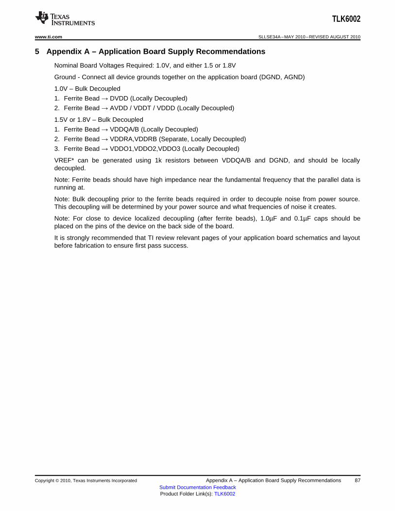
TLK6002
www.ti.com SLLSE34A–MAY 2010–REVISED AUGUST 2010
5 Appendix A – Application Board Supply Recommendations
Nominal Board Voltages Required: 1.0V, and either 1.5 or 1.8V
Ground - Connect all device grounds together on the application board (DGND, AGND)
1.0V – Bulk Decoupled
1. Ferrite Bead → DVDD (Locally Decoupled)
2. Ferrite Bead → AVDD / VDDT / VDDD (Locally Decoupled)
1.5V or 1.8V – Bulk Decoupled
1. Ferrite Bead → VDDQA/B (Locally Decoupled)
2. Ferrite Bead → VDDRA,VDDRB (Separate, Locally Decoupled)
3. Ferrite Bead → VDDO1,VDDO2,VDDO3 (Locally Decoupled)
VREF* can be generated using 1k resistors between VDDQA/B and DGND, and should be locallydecoupled.
Note: Ferrite beads should have high impedance near the fundamental frequency that the parallel data isrunning at.
Note: Bulk decoupling prior to the ferrite beads required in order to decouple noise from power source.This decoupling will be determined by your power source and what frequencies of noise it creates.
Note: For close to device localized decoupling (after ferrite beads), 1.0µF and 0.1µF caps should beplaced on the pins of the device on the back side of the board.
It is strongly recommended that TI review relevant pages of your application board schematics and layoutbefore fabrication to ensure first pass success.
Copyright © 2010, Texas Instruments Incorporated Appendix A – Application Board Supply Recommendations 87Submit Documentation FeedbackProduct Folder Link(s): TLK6002

TLK6002
SLLSE34A–MAY 2010–REVISED AUGUST 2010 www.ti.com
6 Appendix B – Continuous Rate Device Configuration
The REFCLK needed based on a particular SERDES configuration is as follows:
SERDES Reference Clock = (Rate Scale) × (Serial Bit Rate) / (Serdes Multiplier)
Note that Table 6-1 indicates legal ranges for each setting.
Table 6-1. Continuous Rate SERDES Configuration Settings
SERDES Serial Rate Configuration
SERDES Reference Clock Serial Rate (Gbps)
FrequencyPeriod (ns) Full Half Quarter EighthSERDES (MHz)Multiplier
Min Max Max Min Max Max Min Max Max Min Max Max
4 1.25 2.14 800 467 3.74 6.25 1.87 3.20 0.93 1.60 0.47 0.80
5 1.33 2.67 752 375 3.75 6.25 1.87 3.76 0.94 1.88 0.47 0.94
6 1.6 3.2 625 313 3.75 6.25 1.88 3.75 0.94 1.88 0.47 0.94
8 2.13 4.26 469 235 3.76 6.25 1.88 3.76 0.94 1.88 0.47 0.94
8.25 2.19 4.4 457 227 3.75 6.25 1.88 3.77 0.94 1.88 0.47 0.94
10 2.67 5.33 375 188 3.75 6.25 1.88 3.75 0.94 1.87 0.47 0.94
12 3.2 6.4 313 156 3.75 6.25 1.88 3.75 0.94 1.88 0.47 0.94
15 4 8.14 250 122.88 3.69 6.25 1.84 3.75 0.92 1.88 0.46 0.94
16 4.25 8.14 235 122.88 3.93 6.25 1.97 3.76 0.98 1.88 0.49 0.94
16.5 4.39 8.14 228 122.88 4.06 6.25 2.03 3.76 1.01 1.88 0.51 0.94
20 5.33 8.14 188 122.88 4.92 6.25 2.46 3.75 1.23 1.88 0.61 0.94
25 6.67 8.14 150 122.88 6.14 6.25 3.07 3.75 1.54 1.87 0.77 0.94
Note: In Full Rate Mode, the SERDES Reference Clock range shown above must be limited such that serial side operation does not exceed6.25 Gbps.
Full Half Quarter EighthRate Scale
0.5 1 2 4
Serial performance is optimal when the highest reference clock and lowest SERDES multiplier is chosenfor a given application rate.
88 Appendix B – Continuous Rate Device Configuration Copyright © 2010, Texas Instruments Incorporated
Submit Documentation FeedbackProduct Folder Link(s): TLK6002

TLK6002
www.ti.com SLLSE34A–MAY 2010–REVISED AUGUST 2010
7 Appendix C – 8b/10B Control Characters Supported
Table 7-1 contains 8b/10b control characters are valid and are supported in TLK6002.
The K28.7 usage is not advised as comma characters can be created on non-symbol boundaries withoutdepending upon adjacent characters.
Further detail on 8b/10b encoding/decoding of data characters can be found in IEEE802.3-2002 Clause36.
Table 7-1. 8b/10b Control Characters Supported
CONTROL CONTAINS COMMADATA BYTECHARACTER CHARACTER
K28.0 0x1C
K28.1 0x3C Y
K28.2 0x5C
K28.3 0x7C
K28.4 0x9C
K28.5 0xBC Y
K28.6 0xDC
K28.7 0xFC Y
K23.7 0xF7
K27.7 0xFB
K29.7 0xFD
K30.7 0xFE
Copyright © 2010, Texas Instruments Incorporated Appendix C – 8b/10B Control Characters Supported 89Submit Documentation FeedbackProduct Folder Link(s): TLK6002

TLK6002
SLLSE34A–MAY 2010–REVISED AUGUST 2010 www.ti.com
8 Appendix D – Device Latency Specification
The following tables show the absolute device latency in each operation mode.
Table 8-1. Device Absolute Transmit Latency – SDR and DDR Modes
SDR TRANSMIT ABSOLUTE LATENCY (Serial Bit Times)
Note: TX FIFO, in register 6.14:12, defaults to Auto Selection Mode. This table contains latencies when the TX FIFO is set in the minimumlatency mode (6.14:12 = 3'b000).
LATENCY COMPONENTS
Item Minimum Maximum Description
A 8 12 Sampling edge of TXCLK_* to TX FIFO Input Register
B 10 40 TX FIFO Input Register to TX FIFO Output Register
C 20 20 TX FIFO Output Register to 8b/10b Encoder Register
D 10 10 8b/10b Encoder Register to PMA Retime Register
E 20 20 PMA Retime Register to TX SERDES Input Register
F 16 22 TX SERDES Input Register to Serialized Output Bit
Bit Detail Latency Minimum Maximum Assumption: TX*_[19] is first transmitted bit. TX*_[19:10] is first transmittedsymbol. 8b/10b encoder is enabled. Disabling 8b/10b encoder reduces latencyTX*_[19] 0 84 124by 10 bit times.
TX*_[10] 9 93 133
TX*_[9] 10 94 134
TX*_[0] 19 103 143
Latency Encoder Enabled Encoder DisabledSummary Minimum Maximum Minimum Maximum
TX*_[19] 84 124 74 114
TX*_[10] 93 133 83 123
TX*_[9] 94 134 84 124
TX*_[0] 103 143 93 133
DDR TRANSMIT ABSOLUTE LATENCY (Serial Bit Times)
DDR Transmit Latency is the same as transmit SDR mode, except that all numbers are 8 to12 bit times larger.
Latency Encoder Enabled Encoder DisabledSummary Minimum Maximum Minimum Maximum
TX*_[19] 92 136 82 126
TX*_[10] 101 145 91 135
TX*_[9] 102 146 92 136
TX*_[0] 111 155 101 145
90 Appendix D – Device Latency Specification Copyright © 2010, Texas Instruments Incorporated
Submit Documentation FeedbackProduct Folder Link(s): TLK6002

TLK6002
www.ti.com SLLSE34A–MAY 2010–REVISED AUGUST 2010
Table 8-2. Device Absolute Receive Latency – SDR and DDR Modes
RX SDR/DDR RECEIVE ABSOLUTE LATENCY
Note: RX FIFO Depth (When FIFO Enabled) is 4 words.
Latency Components
Item Minimum Maximum Description
A 47 57 Serial Input Bit to RX SERDES Output Register
B 10 10 RX SERDES Output Register to RX PMA Register
C 10 10 RX PMA Register to Channel Sync Input Register
D 10 20 Channel Sync Input Register to Channel Sync Output Register
E 10 10 Channel Sync Output Register to 8b/10b Decoder Input Register
F 10 10 8b/10b Decoder Input Register to 8b/10b Output Register
G 10 10 8b/10b Output Register to RX FIFO Input Register
H 10 40 RX FIFO Input Register to RX FIFO Output Register
I 10 20 RXFIFO Output Register to RX Parallel Output Register Driven
Bit Detail Latency Minimum Maximum Assumption: RX*_[10 and 0] are the first received bits.
RX*_[19] 0 127 187
RX*_[10] 9 136 196
RX*_[9] 0 127 187
RX*_[0] 9 136 196
Disabling Channel Synchronization Reduces Above Numbers by 20 Minimum and 30 Maximum bit times.
Disabling Decoder Reduces Above Numbers by 20 bit times.
Bypassing RX FIFO Reduces Above Numbers by 20 Minimum and 50 Maximum bit times.
Latency RX FIFO RX FIFO RX FIFO RX FIFOSummary Bypassed Bypassed Bypassed Enabled
Channel Channel Sync Channel ChannelSync On On Sync Off Sync On
8b/10b 8b/10b Decoder 8b/10b 8b/10bDecoder On Off Decoder Off Decoder On
Minimum Maximum Minimum Maximum Minimum Maximum Minimum Maximum
RX*_[19] 107 137 87 117 67 87 127 187
RX*_[10] 116 146 96 126 76 96 136 196
RX*_[9] 107 137 87 117 67 87 127 187
RX*_[0] 116 146 96 126 76 96 136 196
Table 8-3 show the static latency variance. Note that static latency variation is the difference in absolutelatency values possible across device reset/power ups.
Copyright © 2010, Texas Instruments Incorporated Appendix D – Device Latency Specification 91Submit Documentation FeedbackProduct Folder Link(s): TLK6002

TLK6002
SLLSE34A–MAY 2010–REVISED AUGUST 2010 www.ti.com
Table 8-3. Device Static Latency Variance
TRANSMIT STATIC LATENCY VARIANCE – Maximum
8b/10b Encoder Interface Mode Serial Bit Times
Enabled SDR 33
Enabled DDR 33
Disabled SDR 33
Disabled DDR 33
Note: TX_FIFO_DEPTH[2:0] = 3'b000
RECEIVE STATIC LATENCY VARIANCE – Maximum
Receive FIFO Channel 8b/10b Decoder Serial Bit TimesSynchronization
Bypassed Enabled Enabled 30
Bypassed Enabled Disabled 30
Bypassed Disabled Disabled 20
Enabled Enabled Enabled 60
Table 8-4 shows the device dynamic latency variance. Note that the dynamic latency variation is thedifference in latency when voltage and temperature are varied for a particular absolute static latency, aftertraffic (including channel synchronization) has been established. The dynamic latency variance numbersdo not include phase movement between the parallel input clocks and input reference clocks.
Table 8-4. Device Dynamic Latency Variance
Transmit Dynamic Latency Variance Receive Dynamic Latency Variance
Minimum Maximum Minimum Maximum
0 ns 2 ns 0 ns 2 ns
92 Appendix D – Device Latency Specification Copyright © 2010, Texas Instruments Incorporated
Submit Documentation FeedbackProduct Folder Link(s): TLK6002

TLK6002
www.ti.com SLLSE34A–MAY 2010–REVISED AUGUST 2010
9 Appendix E – Device Test Modes
This device can be placed into one of the four modes: functional mode including JTAG testing mode, scan1 testing mode, scan 2 testing mode, and Cooper/eFuse testing mode. The scan 1, scan 2 andCooper/eFuse testing modes are for TI use only, and may be ignored by external users of this device.
Table 9-1. Device Mode Configuration
FUNCTIONAL DEVICE FUNCTIONAL MODE/JTAG SCAN 1 MODE SCAN 2 MODE COOPER/EFUSE MODEPIN NAME TESTING
TESTEN 0 0 1 1
GPI0 0 1 0 1
Table 9-2. Device Test Mode Pin Configuration
FUNCTIONAL FUNCTIONAL TEST MODE FUNCTIONAL COOPER/EFUSEDEVICE PIN MODE SIGNAL SIGNAL MODE/JTAG SCAN 1 MODE SCAN 2 MODE MODENAME DIRECTION DIRECTION TESTING
CODEA_EN I I CODEA_EN Scan In 8 Scan In 8 STCICFG0
RATE_A2 I I RATE_A2 Scan In 7 Scan In 7 STCI_D
RATE_A1 I I RATE_A1 Scan In 6 Scan In 6 EFUSE_TMS
RATE_A0 I I RATE_A0 Scan In 5 Scan In 5 EFUSE_TDI
RATE_B2 I I RATE_B2 Scan In 4 Scan In 4 STCICFG1
RATE_B1 I I RATE_B1 Scan In 3 Scan In 3 EFUSE_INITZ
RATE_B0 I I RATE_B0 Scan In 2 Scan In 2 EFUSE_TRST
REFCLK_A_SEL I I REFCLK_A_SEL Scan In 1 Scan In 1 REFCLK_A_SEL
REFCLK_B_SEL I I REFCLK_B_SEL Scan Enable Scan Enable REFCLK_B_SEL
CLK_OUT_SEL I I CLK_OUT_SEL At Speed Scan Enable HSTL Force Up EFUSE_TCK0: stuck-at fault1: transition fault
CODEB_EN I I CODEB_EN Scan Clock Select (0: HSTL Force Down EFUSE_SYS_CLKfrom device pin, 1: fromCooper), alsoEFUSE_SYS_CLK
TDI I I TDI Adaptive Scan Enable Adaptive Scan TDI(Test Mode) Enable (Test Mode)
PRBS_EN I I PRBS_EN Scan Clock Scan Clock STCICLK
PRTAD4 I O or I PRTAD4 Scan Out 8 (O) Scan Out 8 (O) TESTCLK_R (I)
PRTAD3 I O or I PRTAD3 Scan Out 7 (O) Scan Out 7 (O) efuse_cooper_sel (I)(0: Cooper mode, 1:eFuse mode)
PRTAD2 I O or I PRTAD2 Scan Out 6 (O) Scan Out 6 (O) TESTCLK_T (I)
PRTAD1 I O or I PRTAD1 Scan Out 5 (O) Scan Out 5 (O) Not Used (I)
PRTAD0 I O or I PRTAD0 Scan Out 4 (O) Scan Out 4 (O) Not Used (I)
PRBSA_PASS O O PRBSA_PASS Scan Out 3 (O) Scan Out 3 (O) Tied Low
LOSA O O LOSA Scan Out 2 (O) Scan Out 2 (O) STCI_Q
PRBSB_PASS O O PRBSB_PASS Scan Out 1 (O) Scan Out 1 (O) EFUSE_TDO
LOSB O O LOSB Burnin_Output Burnin_Output Burnin_Output
Copyright © 2010, Texas Instruments Incorporated Appendix E – Device Test Modes 93Submit Documentation FeedbackProduct Folder Link(s): TLK6002

TLK6002
SLLSE34A–MAY 2010–REVISED AUGUST 2010 www.ti.com
Revision HistoryNOTE: Page numbers for previous revisions may differ from page numbers in the current version.
Changes from Original (May 2010) to A Revision ........................................................................................................... Page
• Changed SPI_CONTROL_STATUS table to TI_RESERVED_CONTROL STATUS ...................................... 56• Changed table 3-33, TI_RESERVED_CONTROL_8, to TI_CONTOL_8 ................................................... 59• Changed bit 28.14 in TI_CONTROL_8 table ................................................................................... 59• Changed Device Initialization section ............................................................................................ 76
94 Appendix E – Device Test Modes Copyright © 2010, Texas Instruments Incorporated
Submit Documentation FeedbackProduct Folder Link(s): TLK6002

PACKAGE OPTION ADDENDUM
www.ti.com 10-Dec-2020
Addendum-Page 1
PACKAGING INFORMATION
Orderable Device Status(1)
Package Type PackageDrawing
Pins PackageQty
Eco Plan(2)
Lead finish/Ball material
(6)
MSL Peak Temp(3)
Op Temp (°C) Device Marking(4/5)
Samples
TLK6002ZEU ACTIVE BGA ZEU 324 84 RoHS & Green SNAGCU Level-4-260C-72 HR -40 to 85 TLK6002
(1) The marketing status values are defined as follows:ACTIVE: Product device recommended for new designs.LIFEBUY: TI has announced that the device will be discontinued, and a lifetime-buy period is in effect.NRND: Not recommended for new designs. Device is in production to support existing customers, but TI does not recommend using this part in a new design.PREVIEW: Device has been announced but is not in production. Samples may or may not be available.OBSOLETE: TI has discontinued the production of the device.
(2) RoHS: TI defines "RoHS" to mean semiconductor products that are compliant with the current EU RoHS requirements for all 10 RoHS substances, including the requirement that RoHS substancedo not exceed 0.1% by weight in homogeneous materials. Where designed to be soldered at high temperatures, "RoHS" products are suitable for use in specified lead-free processes. TI mayreference these types of products as "Pb-Free".RoHS Exempt: TI defines "RoHS Exempt" to mean products that contain lead but are compliant with EU RoHS pursuant to a specific EU RoHS exemption.Green: TI defines "Green" to mean the content of Chlorine (Cl) and Bromine (Br) based flame retardants meet JS709B low halogen requirements of <=1000ppm threshold. Antimony trioxide basedflame retardants must also meet the <=1000ppm threshold requirement.
(3) MSL, Peak Temp. - The Moisture Sensitivity Level rating according to the JEDEC industry standard classifications, and peak solder temperature.
(4) There may be additional marking, which relates to the logo, the lot trace code information, or the environmental category on the device.
(5) Multiple Device Markings will be inside parentheses. Only one Device Marking contained in parentheses and separated by a "~" will appear on a device. If a line is indented then it is a continuationof the previous line and the two combined represent the entire Device Marking for that device.
(6) Lead finish/Ball material - Orderable Devices may have multiple material finish options. Finish options are separated by a vertical ruled line. Lead finish/Ball material values may wrap to twolines if the finish value exceeds the maximum column width.
Important Information and Disclaimer:The information provided on this page represents TI's knowledge and belief as of the date that it is provided. TI bases its knowledge and belief on informationprovided by third parties, and makes no representation or warranty as to the accuracy of such information. Efforts are underway to better integrate information from third parties. TI has taken andcontinues to take reasonable steps to provide representative and accurate information but may not have conducted destructive testing or chemical analysis on incoming materials and chemicals.TI and TI suppliers consider certain information to be proprietary, and thus CAS numbers and other limited information may not be available for release.
In no event shall TI's liability arising out of such information exceed the total purchase price of the TI part(s) at issue in this document sold by TI to Customer on an annual basis.

TRAY
Chamfer on Tray corner indicates Pin 1 orientation of packed units.
*All dimensions are nominal
Device PackageName
PackageType
Pins SPQ Unit arraymatrix
Maxtemperature
(°C)
L (mm) W(mm)
K0(µm)
P1(mm)
CL(mm)
CW(mm)
TLK6002ZEU ZEU BGA 324 84 6X14 150 315 135.9 7620 21.34 18.79 14.6
PACKAGE MATERIALS INFORMATION
www.ti.com 5-Jan-2022
Pack Materials-Page 1


IMPORTANT NOTICE AND DISCLAIMERTI PROVIDES TECHNICAL AND RELIABILITY DATA (INCLUDING DATA SHEETS), DESIGN RESOURCES (INCLUDING REFERENCE DESIGNS), APPLICATION OR OTHER DESIGN ADVICE, WEB TOOLS, SAFETY INFORMATION, AND OTHER RESOURCES “AS IS” AND WITH ALL FAULTS, AND DISCLAIMS ALL WARRANTIES, EXPRESS AND IMPLIED, INCLUDING WITHOUT LIMITATION ANY IMPLIED WARRANTIES OF MERCHANTABILITY, FITNESS FOR A PARTICULAR PURPOSE OR NON-INFRINGEMENT OF THIRD PARTY INTELLECTUAL PROPERTY RIGHTS.These resources are intended for skilled developers designing with TI products. You are solely responsible for (1) selecting the appropriate TI products for your application, (2) designing, validating and testing your application, and (3) ensuring your application meets applicable standards, and any other safety, security, regulatory or other requirements.These resources are subject to change without notice. TI grants you permission to use these resources only for development of an application that uses the TI products described in the resource. Other reproduction and display of these resources is prohibited. No license is granted to any other TI intellectual property right or to any third party intellectual property right. TI disclaims responsibility for, and you will fully indemnify TI and its representatives against, any claims, damages, costs, losses, and liabilities arising out of your use of these resources.TI’s products are provided subject to TI’s Terms of Sale or other applicable terms available either on ti.com or provided in conjunction with such TI products. TI’s provision of these resources does not expand or otherwise alter TI’s applicable warranties or warranty disclaimers for TI products.TI objects to and rejects any additional or different terms you may have proposed. IMPORTANT NOTICE
Mailing Address: Texas Instruments, Post Office Box 655303, Dallas, Texas 75265Copyright © 2022, Texas Instruments Incorporated