LCD Digital VCOM Using the DAC43701 - Texas Instruments
11
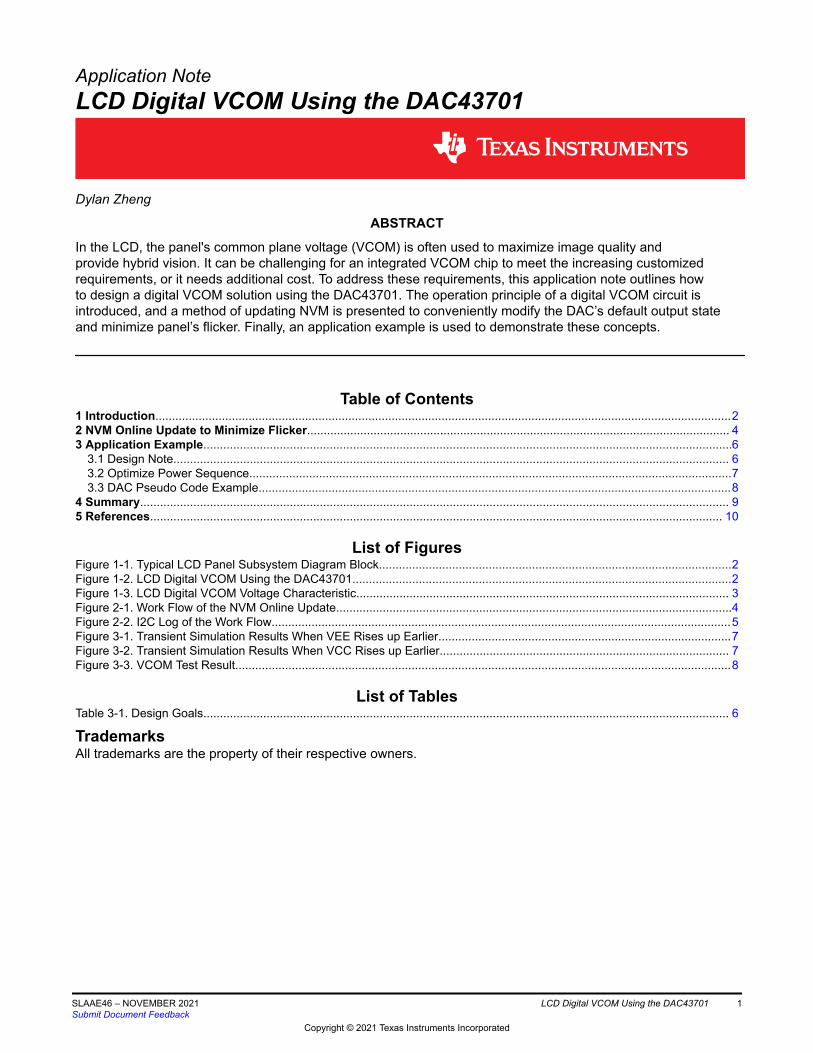
Application Note LCD Digital VCOM Using the DAC43701 Dylan Zheng ABSTRACT In the LCD, the panel's common plane voltage (VCOM) is often used to maximize image quality and provide hybrid vision. It can be challenging for an integrated VCOM chip to meet the increasing customized requirements, or it needs additional cost. To address these requirements, this application note outlines how to design a digital VCOM solution using the DAC43701. The operation principle of a digital VCOM circuit is introduced, and a method of updating NVM is presented to conveniently modify the DAC’s default output state and minimize panel’s flicker. Finally, an application example is used to demonstrate these concepts. Table of Contents 1 Introduction............................................................................................................................................................................. 2 2 NVM Online Update to Minimize Flicker............................................................................................................................... 4 3 Application Example...............................................................................................................................................................6 3.1 Design Note....................................................................................................................................................................... 6 3.2 Optimize Power Sequence.................................................................................................................................................7 3.3 DAC Pseudo Code Example.............................................................................................................................................. 8 4 Summary................................................................................................................................................................................. 9 5 References............................................................................................................................................................................ 10 List of Figures Figure 1-1. Typical LCD Panel Subsystem Diagram Block.......................................................................................................... 2 Figure 1-2. LCD Digital VCOM Using the DAC43701.................................................................................................................. 2 Figure 1-3. LCD Digital VCOM Voltage Characteristic................................................................................................................ 3 Figure 2-1. Work Flow of the NVM Online Update.......................................................................................................................4 Figure 2-2. I2C Log of the Work Flow.......................................................................................................................................... 5 Figure 3-1. Transient Simulation Results When VEE Rises up Earlier........................................................................................ 7 Figure 3-2. Transient Simulation Results When VCC Rises up Earlier....................................................................................... 7 Figure 3-3. VCOM Test Result..................................................................................................................................................... 8 List of Tables Table 3-1. Design Goals.............................................................................................................................................................. 6 Trademarks All trademarks are the property of their respective owners. www.ti.com Table of Contents SLAAE46 – NOVEMBER 2021 Submit Document Feedback LCD Digital VCOM Using the DAC43701 1 Copyright © 2021 Texas Instruments Incorporated
-
Upload
khangminh22 -
Category
Documents
-
view
0 -
download
0
Transcript of LCD Digital VCOM Using the DAC43701 - Texas Instruments
Application NoteLCD Digital VCOM Using the DAC43701
Dylan Zheng
ABSTRACT
In the LCD, the panel's common plane voltage (VCOM) is often used to maximize image quality and provide hybrid vision. It can be challenging for an integrated VCOM chip to meet the increasing customized requirements, or it needs additional cost. To address these requirements, this application note outlines how to design a digital VCOM solution using the DAC43701. The operation principle of a digital VCOM circuit is introduced, and a method of updating NVM is presented to conveniently modify the DAC’s default output state and minimize panel’s flicker. Finally, an application example is used to demonstrate these concepts.
Table of Contents1 Introduction.............................................................................................................................................................................22 NVM Online Update to Minimize Flicker............................................................................................................................... 43 Application Example...............................................................................................................................................................6
3.1 Design Note....................................................................................................................................................................... 63.2 Optimize Power Sequence.................................................................................................................................................73.3 DAC Pseudo Code Example..............................................................................................................................................8
4 Summary................................................................................................................................................................................. 95 References............................................................................................................................................................................ 10
List of FiguresFigure 1-1. Typical LCD Panel Subsystem Diagram Block..........................................................................................................2Figure 1-2. LCD Digital VCOM Using the DAC43701..................................................................................................................2Figure 1-3. LCD Digital VCOM Voltage Characteristic................................................................................................................ 3Figure 2-1. Work Flow of the NVM Online Update.......................................................................................................................4Figure 2-2. I2C Log of the Work Flow..........................................................................................................................................5Figure 3-1. Transient Simulation Results When VEE Rises up Earlier........................................................................................7Figure 3-2. Transient Simulation Results When VCC Rises up Earlier....................................................................................... 7Figure 3-3. VCOM Test Result.....................................................................................................................................................8
List of TablesTable 3-1. Design Goals.............................................................................................................................................................. 6
TrademarksAll trademarks are the property of their respective owners.
www.ti.com Table of Contents
SLAAE46 – NOVEMBER 2021Submit Document Feedback
LCD Digital VCOM Using the DAC43701 1
Copyright © 2021 Texas Instruments Incorporated
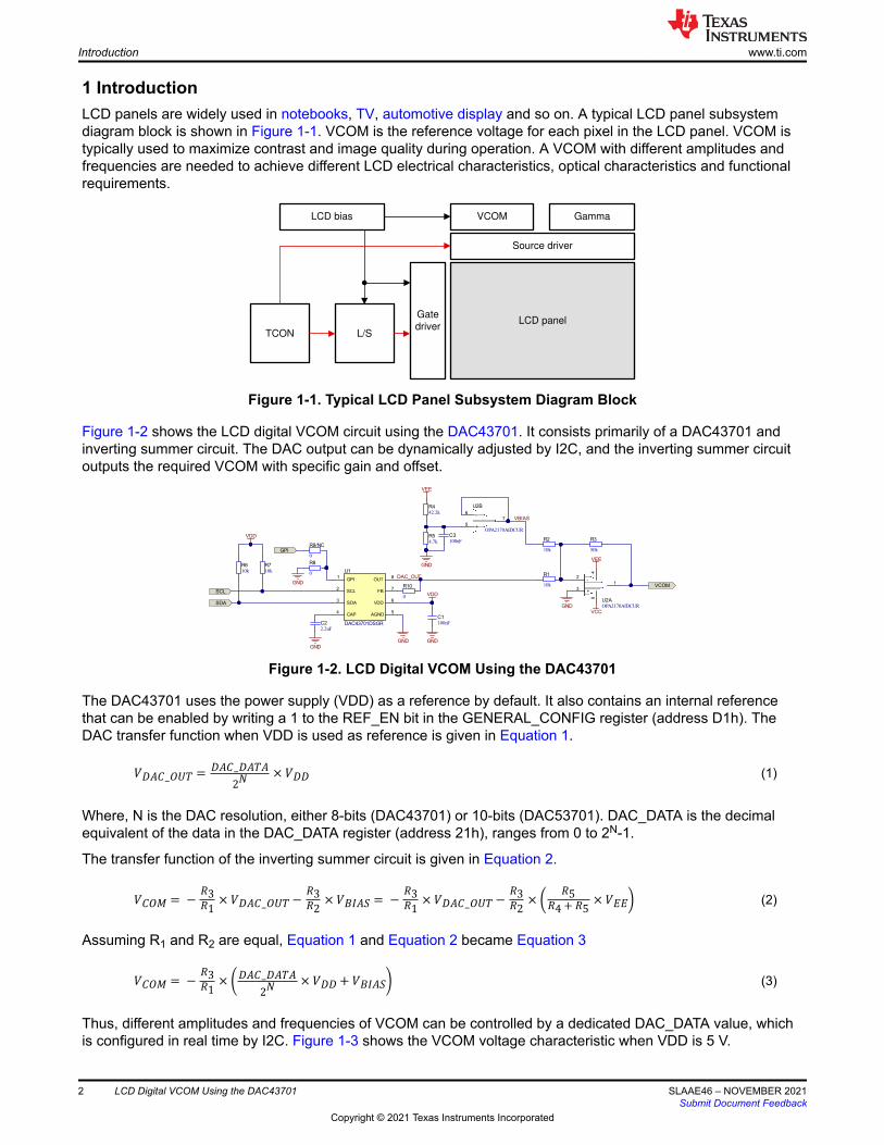
1 IntroductionLCD panels are widely used in notebooks, TV, automotive display and so on. A typical LCD panel subsystem diagram block is shown in Figure 1-1. VCOM is the reference voltage for each pixel in the LCD panel. VCOM is typically used to maximize contrast and image quality during operation. A VCOM with different amplitudes and frequencies are needed to achieve different LCD electrical characteristics, optical characteristics and functional requirements.
TCON L/S
Gate
driverLCD panel
Source driver
LCD bias VCOM Gamma
Figure 1-1. Typical LCD Panel Subsystem Diagram Block
Figure 1-2 shows the LCD digital VCOM circuit using the DAC43701. It consists primarily of a DAC43701 and inverting summer circuit. The DAC output can be dynamically adjusted by I2C, and the inverting summer circuit outputs the required VCOM with specific gain and offset.
GPI1
SCL2
CAP4
SDA3
AGND5
VDD6
FB7
OUT8
U1
DAC43701DSGR
-2
+3
4
1
8
U2AOPA2170AIDCUR
+5
-6
7
U2B
OPA2170AIDCUR
0
R8
GND
GND
100nF
C1
GND
VDD
10k
R710k
R6
2.2uF
C2
GND
VCC
VEE
10k
R1
10k
R2
50k
R3
0
R10
VDD
GND
42.2k
R4
4.7k
R5
GND
VEE
100nF
C3
SCL
SDA
VCOM
DAC_OUT
0
R9/NCGPI
VBIAS
Figure 1-2. LCD Digital VCOM Using the DAC43701
The DAC43701 uses the power supply (VDD) as a reference by default. It also contains an internal reference that can be enabled by writing a 1 to the REF_EN bit in the GENERAL_CONFIG register (address D1h). The DAC transfer function when VDD is used as reference is given in Equation 1.
VDAC_OUT = DAC_DATA2N × VDD (1)
Where, N is the DAC resolution, either 8-bits (DAC43701) or 10-bits (DAC53701). DAC_DATA is the decimal equivalent of the data in the DAC_DATA register (address 21h), ranges from 0 to 2N-1.
The transfer function of the inverting summer circuit is given in Equation 2.
VCOM = − R3R1 × VDAC_OUT− R3R2 × VBIAS = − R3R1 × VDAC_OUT− R3R2 × R5R4 + R5 × VEE (2)
Assuming R1 and R2 are equal, Equation 1 and Equation 2 became Equation 3
VCOM = − R3R1 × DAC_DATA2N × VDD+ VBIAS (3)
Thus, different amplitudes and frequencies of VCOM can be controlled by a dedicated DAC_DATA value, which is configured in real time by I2C. Figure 1-3 shows the VCOM voltage characteristic when VDD is 5 V.
Introduction www.ti.com
2 LCD Digital VCOM Using the DAC43701 SLAAE46 – NOVEMBER 2021Submit Document Feedback
Copyright © 2021 Texas Instruments Incorporated
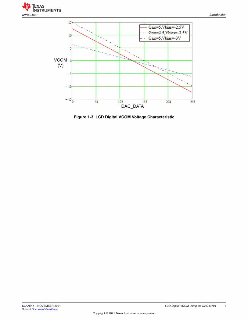
Figure 1-3. LCD Digital VCOM Voltage Characteristic
www.ti.com Introduction
SLAAE46 – NOVEMBER 2021Submit Document Feedback
LCD Digital VCOM Using the DAC43701 3
Copyright © 2021 Texas Instruments Incorporated
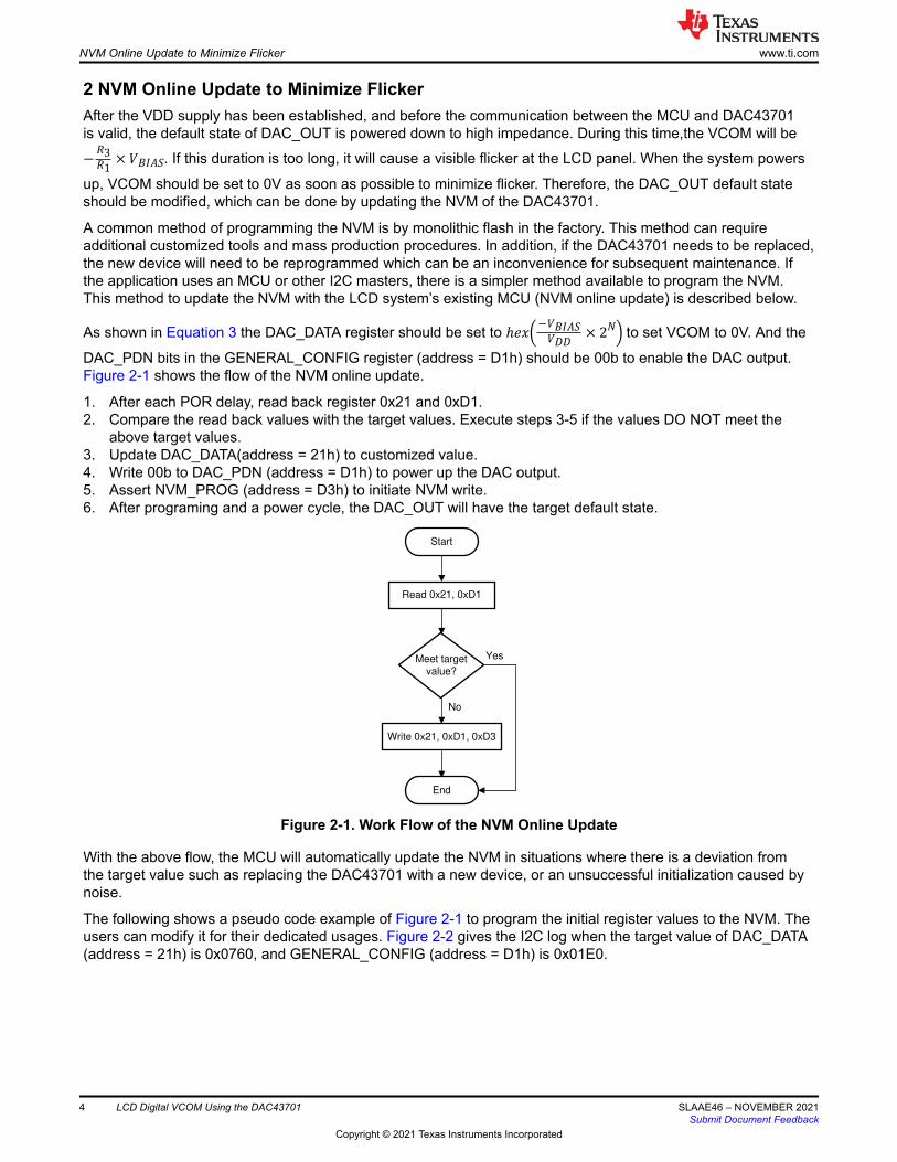
2 NVM Online Update to Minimize FlickerAfter the VDD supply has been established, and before the communication between the MCU and DAC43701 is valid, the default state of DAC_OUT is powered down to high impedance. During this time,the VCOM will be − R3R1 × VBIAS. If this duration is too long, it will cause a visible flicker at the LCD panel. When the system powers
up, VCOM should be set to 0V as soon as possible to minimize flicker. Therefore, the DAC_OUT default state should be modified, which can be done by updating the NVM of the DAC43701.
A common method of programming the NVM is by monolithic flash in the factory. This method can require additional customized tools and mass production procedures. In addition, if the DAC43701 needs to be replaced, the new device will need to be reprogrammed which can be an inconvenience for subsequent maintenance. If the application uses an MCU or other I2C masters, there is a simpler method available to program the NVM. This method to update the NVM with the LCD system’s existing MCU (NVM online update) is described below.
As shown in Equation 3 the DAC_DATA register should be set to ℎex −VBIASVDD × 2N to set VCOM to 0V. And the
DAC_PDN bits in the GENERAL_CONFIG register (address = D1h) should be 00b to enable the DAC output. Figure 2-1 shows the flow of the NVM online update.
1. After each POR delay, read back register 0x21 and 0xD1.2. Compare the read back values with the target values. Execute steps 3-5 if the values DO NOT meet the
above target values.3. Update DAC_DATA(address = 21h) to customized value.4. Write 00b to DAC_PDN (address = D1h) to power up the DAC output.5. Assert NVM_PROG (address = D3h) to initiate NVM write.6. After programing and a power cycle, the DAC_OUT will have the target default state.
Start
Read 0x21, 0xD1
Meet target
value?
Write 0x21, 0xD1, 0xD3
End
Yes
No
Figure 2-1. Work Flow of the NVM Online Update
With the above flow, the MCU will automatically update the NVM in situations where there is a deviation from the target value such as replacing the DAC43701 with a new device, or an unsuccessful initialization caused by noise.
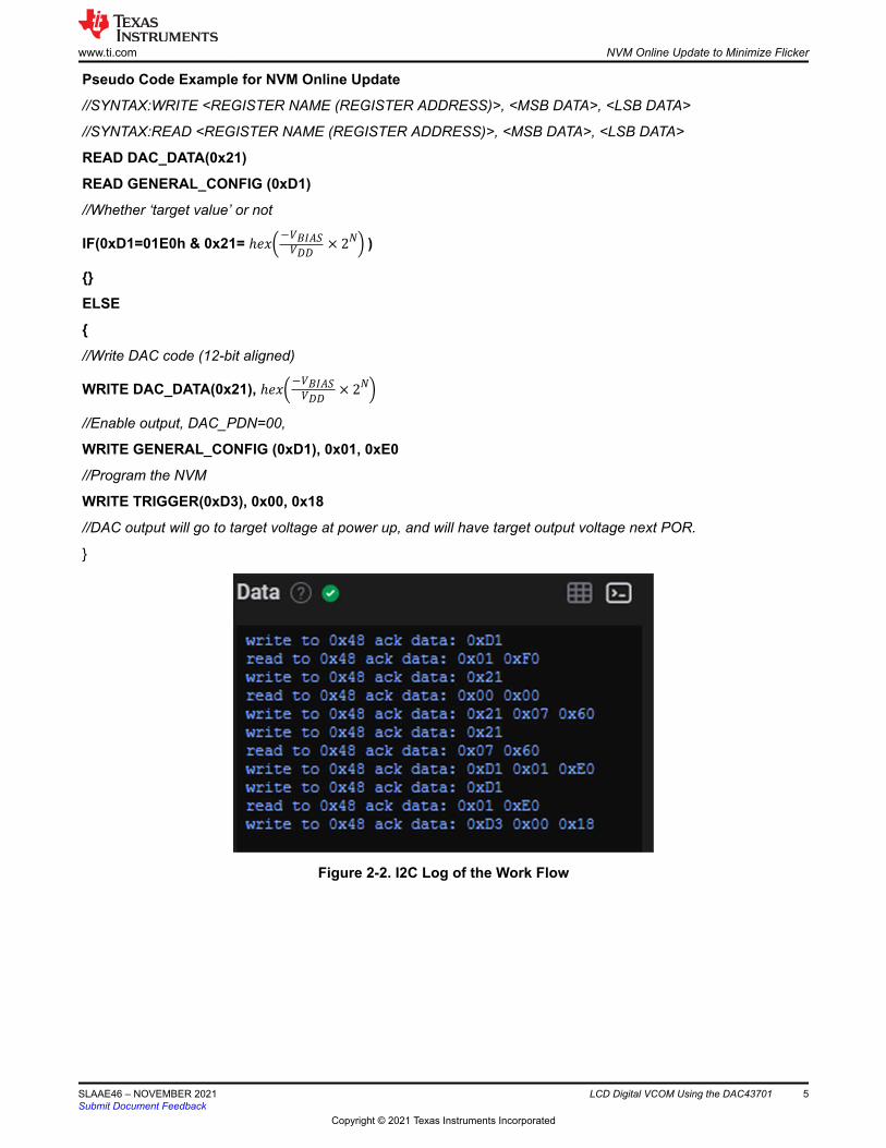
The following shows a pseudo code example of Figure 2-1 to program the initial register values to the NVM. The users can modify it for their dedicated usages. Figure 2-2 gives the I2C log when the target value of DAC_DATA (address = 21h) is 0x0760, and GENERAL_CONFIG (address = D1h) is 0x01E0.
NVM Online Update to Minimize Flicker www.ti.com
4 LCD Digital VCOM Using the DAC43701 SLAAE46 – NOVEMBER 2021Submit Document Feedback
Copyright © 2021 Texas Instruments Incorporated
Pseudo Code Example for NVM Online Update
//SYNTAX:WRITE <REGISTER NAME (REGISTER ADDRESS)>, <MSB DATA>, <LSB DATA>
//SYNTAX:READ <REGISTER NAME (REGISTER ADDRESS)>, <MSB DATA>, <LSB DATA>
READ DAC_DATA(0x21)
READ GENERAL_CONFIG (0xD1)
//Whether ‘target value’ or not
IF(0xD1=01E0h & 0x21= ℎex −VBIASVDD × 2N )
ELSE
//Write DAC code (12-bit aligned)
WRITE DAC_DATA(0x21), ℎex −VBIASVDD × 2N //Enable output, DAC_PDN=00,
WRITE GENERAL_CONFIG (0xD1), 0x01, 0xE0
//Program the NVM
WRITE TRIGGER(0xD3), 0x00, 0x18
//DAC output will go to target voltage at power up, and will have target output voltage next POR.
Figure 2-2. I2C Log of the Work Flow
www.ti.com NVM Online Update to Minimize Flicker
SLAAE46 – NOVEMBER 2021Submit Document Feedback
LCD Digital VCOM Using the DAC43701 5
Copyright © 2021 Texas Instruments Incorporated
3 Application ExampleThis section gives short design notes for generating a square wave VCOM using the circuit shown in Figure 1-2. The design goals are shown in Table 3-1.
Table 3-1. Design GoalsVDAC- VDAC+ VCOM- VCOM+ fsquare VCC VEE VDD0.2V 2.2V -5V 5V 140Hz 12V -12V 2.6V
3.1 Design NoteFor this design, the gain required should be:
GV = −R3R1 = VCOM+ − VCOM−VDAC+ − VDAC − = 5 (4)
And the bias voltage should be:
VBIAS = R5R4 + R5 × VEE = − VDAC+ + VDAC −2 = − 1.2V (5)
Select reasonable resistance values for R3 and R5R3 = 50kΩ, R5 = 4.7kΩ (6)
From Equation 4 through Equation 6, the required R1 and R4 can be calculated.R1 = R2 = 10kΩ, R4 ≈ 42.2kΩ (7)
Some parameters should be checked to make the circuits stable and robust.
Calculate the small signal circuit bandwidth using Equation 8 to ensure it is greater than the 140Hz requirement.
BW = GBOPA2170NG = 1.2MHz1 + R3R1 R2 = 109kHz (8)
Where, NG is the noise gain of the inverting summer circuit.
Calculate the minimum slew rate required using Equation 9.SR > 2 × π × fsquare × VCOM+ = 4.4mV/μs (9)
The slew rate of OPA2170 is 0.4V/µs which meets the requirements.
For better stability, the zero created by the gain setting resistors and input capacitance of the OPA2170 should be greater than the bandwidth calculated in Equation 8.
fzero = 12 × π × Ccm+ Cdiff × R1 R2 R3 = 5.8MHz > = 109kHz (10)
Where, Ccm and Cdiff are the common-mode input capacitance and differential input capacitance of the OPA2170 respectively.
Application Example www.ti.com
6 LCD Digital VCOM Using the DAC43701 SLAAE46 – NOVEMBER 2021Submit Document Feedback
Copyright © 2021 Texas Instruments Incorporated
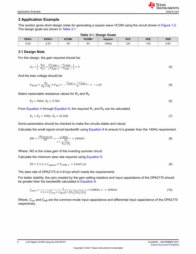
3.2 Optimize Power SequenceIn addition, the common-mode voltage range should be considered to avoid the amplifier working in a nonlinear state. The common-mode voltage of the circuit in Figure 1-2 is 0V, and the common-mode voltage range of the OPA2170 is from (VEE-0.1V) to (VCC-2V). As the bias voltage is divided from VEE, if the VEE supply is applied earlier than VCC, the clipping voltage will be observed at the VCOM output as shown in Figure 3-1, which may cause unexpected flicker.
Figure 3-1. Transient Simulation Results When VEE Rises up Earlier
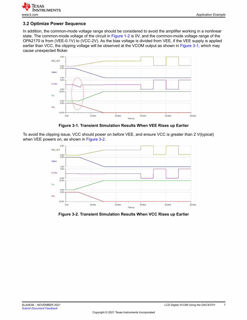
To avoid the clipping issue, VCC should power on before VEE, and ensure VCC is greater than 2 V(typical) when VEE powers on, as shown in Figure 3-2.
Figure 3-2. Transient Simulation Results When VCC Rises up Earlier
www.ti.com Application Example
SLAAE46 – NOVEMBER 2021Submit Document Feedback
LCD Digital VCOM Using the DAC43701 7
Copyright © 2021 Texas Instruments Incorporated
3.3 DAC Pseudo Code ExampleThis section gives a pseudo code example for the design goals in Table 3-1. From Equation 1, the DAC_DATA register should be 14h and D9h for VDAC- and VDAC+ respectively. To generate the customized square wave, MCU can update the DAC_DATA at a frequency of 140Hz through I2C.
Pseudo Code Example for Programmable Square Wave VCOM
//SYNTAX:WRITE <REGISTER NAME (REGISTER ADDRESS)>, <MSB DATA>, <LSB DATA>
//Enable output, use VDD as DAC reference,
WRITE GENERAL_CONFIG (0xD1), 0x01, 0xE0
WHILE ()
//Write DAC code (12-bit aligned), For 2.6-V VDD as DAC reference, the 8-bit hex code for 0.2 V is 0x14
//Left aligned this becomes 0x0140
WRITE DAC_DATA(0x21), 0x01, 0x40
//Duration is 1/280 second
DELAY(1/280)
//Write DAC code (12-bit aligned), For 2.6-V VDD as DAC reference, the 8-bit hex code for 2.2 V is 0xD9
//Left aligned this becomes 0x0D90
WRITE DAC_DATA(0x21), 0x0D, 0x90
//Duration is 1/280 second
DELAY(1/280)
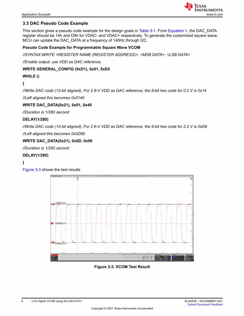
Figure 3-3 shows the test results
Figure 3-3. VCOM Test Result
Application Example www.ti.com
8 LCD Digital VCOM Using the DAC43701 SLAAE46 – NOVEMBER 2021Submit Document Feedback
Copyright © 2021 Texas Instruments Incorporated

4 SummaryThis application note described a digital VCOM circuit using a smart DAC and its NVM online update solution. It is important to consider the DAC default output and circuit power sequence to maximize LCD image quality. An application example is given to validate the performance and help users change to suit their applications.
www.ti.com Summary
SLAAE46 – NOVEMBER 2021Submit Document Feedback
LCD Digital VCOM Using the DAC43701 9
Copyright © 2021 Texas Instruments Incorporated
5 References1. Texas Instruments, DAC43701 data sheet.2. Texas Instruments, DAC53701 data sheet.3. Texas Instruments, Analog Engineer's Circuit Cookbook: Amplifiers.4. Texas Instruments, OPA2170 data sheet.
References www.ti.com
10 LCD Digital VCOM Using the DAC43701 SLAAE46 – NOVEMBER 2021Submit Document Feedback
Copyright © 2021 Texas Instruments Incorporated
IMPORTANT NOTICE AND DISCLAIMERTI PROVIDES TECHNICAL AND RELIABILITY DATA (INCLUDING DATA SHEETS), DESIGN RESOURCES (INCLUDING REFERENCE DESIGNS), APPLICATION OR OTHER DESIGN ADVICE, WEB TOOLS, SAFETY INFORMATION, AND OTHER RESOURCES “AS IS” AND WITH ALL FAULTS, AND DISCLAIMS ALL WARRANTIES, EXPRESS AND IMPLIED, INCLUDING WITHOUT LIMITATION ANY IMPLIED WARRANTIES OF MERCHANTABILITY, FITNESS FOR A PARTICULAR PURPOSE OR NON-INFRINGEMENT OF THIRD PARTY INTELLECTUAL PROPERTY RIGHTS.These resources are intended for skilled developers designing with TI products. You are solely responsible for (1) selecting the appropriate TI products for your application, (2) designing, validating and testing your application, and (3) ensuring your application meets applicable standards, and any other safety, security, regulatory or other requirements.These resources are subject to change without notice. TI grants you permission to use these resources only for development of an application that uses the TI products described in the resource. Other reproduction and display of these resources is prohibited. No license is granted to any other TI intellectual property right or to any third party intellectual property right. TI disclaims responsibility for, and you will fully indemnify TI and its representatives against, any claims, damages, costs, losses, and liabilities arising out of your use of these resources.TI’s products are provided subject to TI’s Terms of Sale or other applicable terms available either on ti.com or provided in conjunction with such TI products. TI’s provision of these resources does not expand or otherwise alter TI’s applicable warranties or warranty disclaimers for TI products.TI objects to and rejects any additional or different terms you may have proposed. IMPORTANT NOTICE
Mailing Address: Texas Instruments, Post Office Box 655303, Dallas, Texas 75265Copyright © 2021, Texas Instruments Incorporated