SIGNAL PATH designer - Texas Instruments
12
DS50PCI401,DS64BR401 Driving High-Speed Signals in Data Center Servers and Storage Area Networks Literature Number: SNLA212
-
Upload
khangminh22 -
Category
Documents
-
view
1 -
download
0
Transcript of SIGNAL PATH designer - Texas Instruments

DS50PCI401,DS64BR401
Driving High-Speed Signals in Data Center Servers and Storage Area Networks
Literature Number: SNLA212

SIGNAL PATH designer®
No. 119
With less capital available for continuous system “upgrades”, new data center solutions must be space- and energy-effi cient while
supporting multi-faceted expansion to keep ahead of users’ data storage needs. Engineers are leveraging open industry standards like PCI Express (PCIe) and SAS/SATA to create effi cient architectures that address current and future data center requirements. With only limited input and output signal conditioning written directly into these standards, hardware design has been constrained by cable and PCB attenuation of high-speed serial data. Even within a single rack of equipment, signals that remain on backplanes will exhibit losses beyond those detailed in the PCIe standard.
Th is article explains how a pair of National’s new PowerWise® 4-lane bi-directional transceivers (DS50PCI401 and DS64BR401) directly address interconnect attenuation challenges with capabilities beyond standards-dictated signal conditioning. PCIe 2.0 sets a maximum transmit de-emphasis of 6 dB and SAS recommends 3 dB. However, PCIe cable assembly response indicates that 12 dB of compensation is needed to optimize 7m 24 AWG cable performance. Similar loss compensation will be needed for 24” to 30” backplane traces commonly found in server designs today. Th e DS50PCI401 transceiver provides a gain of up to 26 dB for PCIe applications, while
the DS64BR401 transceiver provides a gain of up to 33 dB for SAS/SATA and other high-speed signaling technologies.
Working with PCIe and SAS/SATA standards can pose some additional challenges for silicon products designed to extend data transmission distances. Multiple sideband signals, remote detection mechanisms, and high-level signaling techniques such as out-of-band (OOB) and Beacon need to be properly handled to ensure robust initiator – target or root complex – endpoint-state machine synchronization.
PCIe-Specifi c CommunicationPCI Express links can be broken down into two distinct operating environments; namely, a PCIe external cable or a backplane slot. Within a PCIe cable, several sideband signals have been defi ned and must be implemented. Th ey include CPWRON, CPERST#, and CPRSNT#. Depending on the system design, several options for hardware control are possible. CPWRON is an indication for the upstream system that its supply voltage rails have achieved the minimum nominal value. CPERST#, short for cable platform reset, provides the downstream subsystem with an indication of the reset state from the upstream subsystem. CPRSNT# is a response from the downstream subsystem that it is indeed present and its power supply is functioning within nominal limits.
Driving High-Speed Signals in Data Center Servers and Storage Area Networks— Lee Sledjeski, Applications Engineer
Expert tips and techniques for PowerWise® energy-effi cient design
national.com/spdesigner
Feature Article ........................................................1-8
Basestation Solutions............................................9
Design Tools ............................................................10

2
SIGNAL PATH designer
Driving High-Speed Signals in Data Center Servers and Storage Area Networks
Using the cabling environment (shown in Figure 1) as an example, initial communication from the downstream subsystem to the upstream subsystem is achieved with the CPRSNT# auxiliary signal. Th e CPRSNT# signal is asserted Low by the downstream circuitry after the "Power Good" condition has been established. Th is mechanism allows for the upstream subsystem to determine whether the power is good within the downstream subsystem, enable the reference clock, and initiate the link training sequence.
Th e auxiliary signals could be easily replicated within the downstream subsystem and used to control the RXDETA/B inputs on the DS50PCI401 transceiver. Often an onboard microcontroller will be used to handle events like power-up, power-down, power-saving modes, and hot insertion. Th e microcontroller would use the same information to determine when to enable and disable the
DS50PCI401 input termination. In applications that require SMBus control, the microcontroller could also delay any response to the upstream subsystem to allow suffi cient time to correctly program the DS50PCI401 transceiver and other devices on the board.
Prior to software confi guration of the PCIe link, the PCIe transmitter (Tx) will enact a receiver (Rx) detection process, as shown in Figure 1. Th e detection process begins with the Tx invoking a common-mode shift above the GND potential onto its high-speed outputs. When a Rx is present, the Rx will interact with and terminate the common-mode voltage shift. Circuitry that monitors the response must be able to decipher between the terminated (Rx present) and unterminated (Rx absent) conditions. Control over the DS50PCI401 Rx termination can be achieved directly through the RXDETA/B inputs.
Detect.Quiet Detect. Active
Polling
1 μs (max)
Electrical Idle
(DS50PCI401 input – copy of CPERST#)
CPRSNT# to RESET Removal 5 ms (min)
RESET Removed and REFCLK Stable
RXDETA/B
Root ComplexLTSSM
(PCle)Root Complex Tx
(PCle)CREFCLK
(PCle)CPRSNT#
(PCle)CPERST#
(PCle)CPWRON
RXDETA/B to DS50PCI401 Termination Active
RESET
1 ms(min)
12 ms (min)
OV
OV
OV
OV
Figure 1. PCIe Cabling Event Timing

SIGNAL PATH designer
In backplane applications using the PCIe standard, all of the auxiliary signals may not be present. In order to facilitate some high-level communication between the root complex and endpoint, PCIe has defi ned a signaling technique called Beacon. Beacon is a slow (30 KHz to 500 MHz) signal sent on at least Lane 0 of the high-speed serial data bus. Th e objective of sending a Beacon signal is to request the reapplication of power and exit the L2 or low-power state. Th is operation can also be achieved using the WAKE# sideband signal. Although Beacon is an optional signal that does not need to be implemented in systems operating at GEN2 or 5 Gbps, older GEN1 devices may necessitate its ongoing support. In order to pass a Beacon signal, the DS50PCI401 device must have the 50W input terminations “active”. Otherwise the Beacon signal will not be retransmitted on the DS50PCI401 outputs.
Additional methods of communication that are used in backplane/server applications include a subset of sideband signals such as PRSNT# or physical mechanisms such as a manual retention latch (MRL).
SAS/SATA-Specifi c CommunicationWithout auxiliary signals to convey state-change information, the SAS/SATA high-speed signal path doubles as a low-speed communication port. Like a modern form of Morse code, Out-Of-Band (OOB) signaling (Figure 2) is a series of signal burst, idle, and negation times transmitted and detected across a SAS/SATA link. Link initiators and targets use this information to begin communication and establish link protocol. For the DS64BR401 transceiver, the key OOB-related specifi cations are the active-to-idle and idle-to-active propagation delays which are closely matched to minimize any OOB-signaling envelope distortion.
Figure 2. Nominal Out-of-Band Signal Timing
OOB Burst
COMWAKE
COMINIT/COMRESET
COMSAS
106.6 ns 106.6 ns
106.6 ns 106.6 ns
320 ns 320 ns
960 ns
COMSAS Idle
D24.3 Primatives
COMWAKE Idle
COMWAKE Idle
106.6 ns
106.6 ns 106.6 ns
3
SIGNAL PATH designer
Th e desired outcome of SAS/SATA OOB signaling is to move the physical layer State Machines into the speed-negotiation and identifi cation-sequence states. For SAS-to-SAS communication, the target device responds to COMSAS with COMSAS. For SAS-to-SATA connections, the SATA target will not respond to COMSAS. Th is diff erence allows the initiating device to proceed as a SAS host or emulate a SATA host.
Th e SAS speed-negotiation sequence seeks to establish physical link communications at the highest possible transmission rate. No longer initiator and target, the SAS speed-negotiation sequence is a peer-to-peer communication. Th e rules for speed negotiation are the same for both participating devices, with the outcome being robust bidirectional communication at the highest speed possible for the initiator – interconnect – target combination.
Standard-Based Signal ConditioningPCIe and SAS/SATA have kept performance statements about transmit and receive equalization to a minimum requirement. While this has made the implementation easier and kept the costs low for a general case, it will not work in every desired application. As designers push PCIe across the entire system at GEN2 speeds and users demand higher-speed storage, signal attenuation across system interconnects becomes a common issue.
Th ere are two primary mechanisms that result in frequency-dependent loss in cables and PCB traces.
1. Skin Loss: Skin eff ect causes most of the high- frequency current to travel on the outer surface (skin) of the conductor. Consequently, the eff ective resistance of the conductor increases with frequency. Skin loss is directly proportional to the square root of signal frequency resulting in a more gradual frequency roll-off .
2. Dielectric Loss: As the signal travels in a conductor that is insulated from another by a dielectric material, some of the signal gets absorbed by the dielectric material. Dielectric loss is directly proportional to signal frequency resulting in a steeper frequency roll-off .
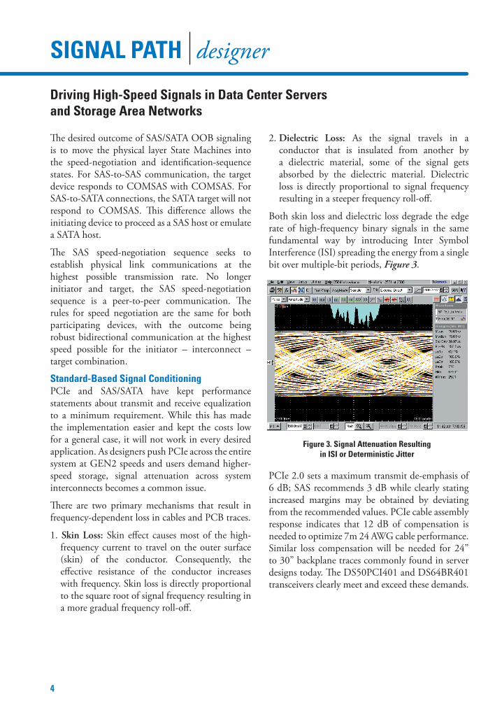
Both skin loss and dielectric loss degrade the edge rate of high-frequency binary signals in the same fundamental way by introducing Inter Symbol Interference (ISI) spreading the energy from a single bit over multiple-bit periods, Figure 3.
PCIe 2.0 sets a maximum transmit de-emphasis of 6 dB; SAS recommends 3 dB while clearly stating increased margins may be obtained by deviating from the recommended values. PCIe cable assembly response indicates that 12 dB of compensation is needed to optimize 7m 24 AWG cable performance. Similar loss compensation will be needed for 24” to 30” backplane traces commonly found in server designs today. Th e DS50PCI401 and DS64BR401 transceivers clearly meet and exceed these demands.
Driving High-Speed Signals in Data Center Servers and Storage Area Networks
Figure 3. Signal Attenuation Resulting in ISI or Deterministic Jitter
4

national.com/spdesigner
SIGNAL PATH designer
5
De-Emphasis Performance In order to support multiple generations of a serial standard with an optimal signal conditioning response, it is vital to understand the underlying data rate of the signal passing through the device. Internal device circuitry detects PCIe 2.5/5.0G and SAS/SATA 3.0/6.0G operation and adjusts the output DE pulse width accordingly. For 100% compliance with PCIe and SAS/SATA electrical specifi cations, both devices include settings designed to the individual standards.
In Figure 4, a detailed oscilloscope waveform shows diff erent styles of De-Emphasis (DE) with approximately 6 dB of gain. Th e ideal DE pulse width will quickly reach maximum amplitude, but decay over a slightly longer period of time. Th is analog de-emphasis behaves in a manner very similar to the multi-tap design of a high-speed digital serializer, producing maximum gain at the Nyquist frequency and reduced gain as the frequency decreases. Th is technique best approximates and compensates for attenuation in the transmission media.
Figure 4. De-Emphasis Waveforms for 2.5G and 5.0G Operation
Media: 28” FR4 stripline Setting: -12 dB output de-emphasis Vertical eye opening: 170 mVMedia attenuation: -11.5 dB at 1.25 GHz Datarate: 5.0 Gbps with a PRBS7 pattern Total jitter (peak-peak): 25.0 ps
Figure 5. DS50PCI401 Output Signal Conditioning
Signal conditioning devices play a critical role in compensating for media loss. At multi-Gbps speeds, attenuation in cables and PCB traces can impact communication within and between systems. Robust communication can be maintained by employing input and output signal conditioning techniques on lossy interconnects. Since the PCIe and SAS/SATA standards utilize full-duplex high-speed signaling paths, the DS50PCI401 and DS64BR401 signal conditioning devices off er both receive equalization and transmit de-emphasis (EQ and DE) techniques in a single IC.
Figure 5 shows typical results using the DS50PCI401 device in a backplane/server application. To emulate the backplane, 28” of 5-mil 100W diff erential stripline are attached to the transceiver evaluation board via short 50W SMA cables.
SIGNAL PATH designer
Equalization Performance Unfortunately, simply having the ability to equalize long cables or large backplanes is not enough. Th e equalizer setting must be easy to set and forgiving to diff erent data rates and even cable lengths. Th e DS50PCI5401 Continuous Time Linear Equalization (CTLE) will not need to be retuned or adjusted for each data rate. Perhaps it is a design cycle upgrade or a mix of old and new cards in a server, but multiple data rates may be present in many systems. Th e setting for 2.5 Gbps is also the setting for 5.0 Gbps. Th is, in conjunction with the automatic
6
de-emphasis adjustment for data rate, allows dynamic PCIe and SAS/SATA speed negotiation to take place without altering any signal conditioning settings on the link.
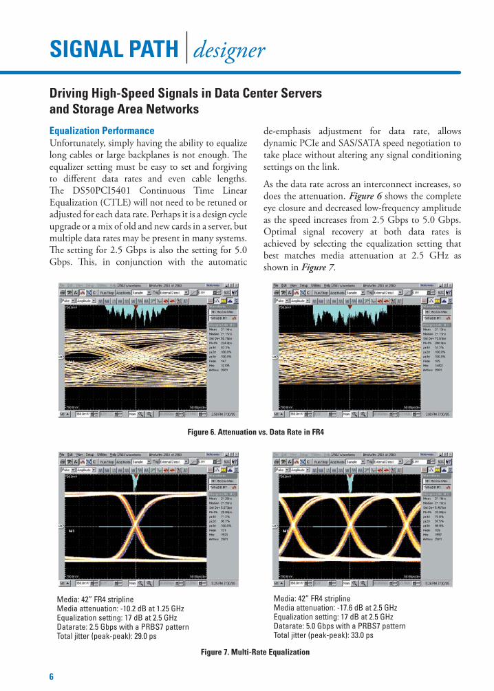
As the data rate across an interconnect increases, so does the attenuation. Figure 6 shows the complete eye closure and decreased low-frequency amplitude as the speed increases from 2.5 Gbps to 5.0 Gbps. Optimal signal recovery at both data rates is achieved by selecting the equalization setting that best matches media attenuation at 2.5 GHz as shown in Figure 7.
Figure 6. Attenuation vs. Data Rate in FR4
Driving High-Speed Signals in Data Center Servers and Storage Area Networks
Figure 7. Multi-Rate Equalization
Media: 42” FR4 stripline Media attenuation: -10.2 dB at 1.25 GHzEqualization setting: 17 dB at 2.5 GHzDatarate: 2.5 Gbps with a PRBS7 patternTotal jitter (peak-peak): 29.0 ps
Media: 42” FR4 striplineMedia attenuation: -17.6 dB at 2.5 GHzEqualization setting: 17 dB at 2.5 GHzDatarate: 5.0 Gbps with a PRBS7 patternTotal jitter (peak-peak): 33.0 ps

national.com/spdesigner
SIGNAL PATH designer
7
For external cabling applications, designers may be forced to select one equalization setting to compensate for multiple cable lengths. Th e equalization setting is more critical and the received signals smaller as cable lengths increase. PCIe cables provide some built-in compensation for length. Short cables are built with 28 AWG wires which increase the attenuation per unit length. Th e longer cables use 24 AWG wire to minimize losses, thereby reducing the overall change in attenuation between the shortest and longest cable assemblies.
Th e input design of both transceivers contains an active equalizer. As the name implies, the design uses active transistors to gain up signals at high
Figure 8. DS50PCI401 Single-Setting Equalization Across Multiple Cable Lengths
frequencies without attenuating low frequencies. Th is equalization scheme works well even when low-signal amplitudes are expected at the equalizer input, providing for an extended compensation en-velope and enabling longer, lighter cable assemblies to be utilized. In addition, most active equalizers can tolerate high-input amplitudes equally well, providing good fl exibility when the cable length is unknown. Figure 8 highlights this fl exibility show-ing equalizer response to PCIe cable assemblies one to ten meters in length. Th e results are achieved without adjusting the equalizer setting, allowing designers to specify use of multiple cable lengths without the need to reprogram any system fi rmware.
Media: 1 meter 28 AWG PCIe 4x cable Equalization setting: 17 dB at 2.5 GHzDatarate: 5.0 Gbps with a PRBS7 pattern Total jitter (peak-peak): 45.0 ps
Media: 7 meter 24 AWG PCIe 4x cable Equalization setting: 17 dB at 2.5 GHzDatarate: 5.0 Gbps with a PRBS7 pattern Total jitter (peak-peak): 33.0 ps
Media: 5 meter 26 AWG PCIe 4x cable Equalization setting: 17 dB at 2.5 GHzDatarate: 5.0 Gbps with a PRBS7 pattern Total jitter (peak-peak): 30.0 ps
Media: 10 meter 24 AWG PCIe 4x cable Equalization setting: 17 dB at 2.5 GHzDatarate: 5.0 Gbps with a PRBS7 pattern Total jitter (peak-peak): 22.0 ps

8
SIGNAL PATH designer
Beyond the EQ setting used in Figure 8, National’s transceivers can provide, via pin or SMBus control, up to 10 dB of additional input equalization at 3.0 GHz. With the ability to compensate for more attenuation, a designer can specify cable assemblies with smaller gauge wire. Lighter cable reduces strain on connectors and chassis and allows for increased cable density and enhanced cable fl exibility in tight installations.
Design for SuccessSuccessful recovery of attenuated signals involves much more then just a good equalizer; it actually starts with the transmitter. Having a transmitter with low output jitter is pretty obvious, but equally important is having good return-loss characteristics. All primary waveforms on the link begin at the transmitter; at this point in the transmission media, they contain the maximum level of high-frequency harmonic content. Any energy refl ected back into the transmitter can impact following data if not completely absorbed in the transmitter output structure.
Between the transmitter and receiver it is likely several opportunities exist for impedance discontinuities. Everything that can be done to minimize the size and magnitude of each discontinuity will reduce residual jitter and add margin to the system. Paying particular attention to changes in transmission structure and return-path continuity will help to ensure the best possible signal fi delity. Th e following list highlights and discusses several problems and strategies to address them.
Vias:Vias are part of a link structure that are absolutely required, but would be nice to live without. Fortunately several things can be done to remove them from the ‘signal integrity radar’.
1. A return-current via should be added always to eliminate common-mode noise on the reference planes and minimize any impedance discontinuity arising from a change in the signal-reference plane.
2. Particular attention should be paid to the overall via construction as vias tend to hold excess capacitance. Spending a little time with a modeling tool should result in a stack-up that matches the impedance of the transmission line. Within a thick PCB, it is possible to create a stub with a portion of the via barrel; back drilling will extend the bandwidth of the structure.
Space:Connectors and components are always bottlenecks for high-speed pairs. Multiple PCB layers should be used and signals should be distributed evenly to maximize the distance between signal pairs.
Symmetry:In an ideal world everything would be perfectly symmetrical – allowing a pure diff erential signal at the transmitter to reach the receiver attenuated, but still remains a pure diff erential signal. Th e fi rst step is to match the electrical length of both signals in the diff erential pair. Th e second step is to treat each trace equally; test points and other loads should have a mirror image looking from one trace to another. Th e most signifi cant benefi t of this extra work is reduced system EMI. Any common signal can escape easily from the product enclosure.
ConclusionExpanding the reach of PCIe, SAS/SATA, and other serial links provides a competitive advantage to system developers. With input and output signal conditioning that works across backplanes, cable assemblies, and over multiple data rates, National’s DS50PCI401 and DS64BR401 transceivers provide designers with a fl exible and effi cient signal conditioning solution for today’s challenging serial link applications.
For more information about National's communication infrastructure solutions, visit: national.com/comms
Driving High-Speed Signals in Data Center Servers and Storage Area Networks


550263-019
©2009, National Semiconductor Corporation. National Semiconductor, , PowerWise, WEBENCH, and Signal Path Designer are registered trademarks of National Semiconductor. All other brand or product names are trademarks or registered trademarks of their respective holders. All rights reserved.
Design ToolsResources for Next-Generation Design
Register to receive updates on the products and technical topics that interest you—spam-free!national.com/newsletter
Application NotesAccess hundreds of application notes on a variety of design topics from product to end application-specific app notes.national.com/appnotes
Application SolutionsAccess over 100 dynamic diagrams for medical systems, consumer electronics, communications, and many more applications.national.com/solutions
FPGA Design GuidesThese design guides feature National device solutions by part number for different FPGA manufacturers, including Xilinx and Altera.national.com/selguide
Tune in to learn technical energy-saving tips, hosted by National’s PowerWise® Technologist, Richard Zarr, and streamed 24/7 on the web.national.com/powerwisetv
Design, build, and test analog circuits in this online design and prototyping environment.national.com/webench
Parametric Catalog and Search Search for desired product folder, product database by attributes of interest.national.com/cat
Tools for Energy-Efficient DesignsAccess white papers, reference designs, and application notes on PowerWise® products and systems.national.com/powerwise
Document LibraryFind end market solutions and products using National’s Solutions Guides.national.com/selguide
Published bi-monthly, the Power Designer technical articles cover key power design tips and techniques for today’s design engineers.national.com/powerdesigner
Published bi-monthly, the Signal Path Designer technical articles cover analog signal path tips and techniques for today’s design engineers.national.com/spdesigner
Easy, natural-language online search engine provides quick access to products and technical information.www.national.com/kbase
Expand your knowledge and understanding of analog with our free online educational training tool.national.com/training
National’s monthly analog design technical journal.national.com/edge
National Semiconductor2900 Semiconductor DriveSanta Clara, CA 950511 800 272 9959
Visit our website at:www.national.com
Mailing address:PO Box 58090Santa Clara, CA 95052
For more information,send email to:[email protected]

IMPORTANT NOTICE
Texas Instruments Incorporated and its subsidiaries (TI) reserve the right to make corrections, modifications, enhancements, improvements,and other changes to its products and services at any time and to discontinue any product or service without notice. Customers shouldobtain the latest relevant information before placing orders and should verify that such information is current and complete. All products aresold subject to TI’s terms and conditions of sale supplied at the time of order acknowledgment.
TI warrants performance of its hardware products to the specifications applicable at the time of sale in accordance with TI’s standardwarranty. Testing and other quality control techniques are used to the extent TI deems necessary to support this warranty. Except wheremandated by government requirements, testing of all parameters of each product is not necessarily performed.
TI assumes no liability for applications assistance or customer product design. Customers are responsible for their products andapplications using TI components. To minimize the risks associated with customer products and applications, customers should provideadequate design and operating safeguards.
TI does not warrant or represent that any license, either express or implied, is granted under any TI patent right, copyright, mask work right,or other TI intellectual property right relating to any combination, machine, or process in which TI products or services are used. Informationpublished by TI regarding third-party products or services does not constitute a license from TI to use such products or services or awarranty or endorsement thereof. Use of such information may require a license from a third party under the patents or other intellectualproperty of the third party, or a license from TI under the patents or other intellectual property of TI.
Reproduction of TI information in TI data books or data sheets is permissible only if reproduction is without alteration and is accompaniedby all associated warranties, conditions, limitations, and notices. Reproduction of this information with alteration is an unfair and deceptivebusiness practice. TI is not responsible or liable for such altered documentation. Information of third parties may be subject to additionalrestrictions.
Resale of TI products or services with statements different from or beyond the parameters stated by TI for that product or service voids allexpress and any implied warranties for the associated TI product or service and is an unfair and deceptive business practice. TI is notresponsible or liable for any such statements.
TI products are not authorized for use in safety-critical applications (such as life support) where a failure of the TI product would reasonablybe expected to cause severe personal injury or death, unless officers of the parties have executed an agreement specifically governingsuch use. Buyers represent that they have all necessary expertise in the safety and regulatory ramifications of their applications, andacknowledge and agree that they are solely responsible for all legal, regulatory and safety-related requirements concerning their productsand any use of TI products in such safety-critical applications, notwithstanding any applications-related information or support that may beprovided by TI. Further, Buyers must fully indemnify TI and its representatives against any damages arising out of the use of TI products insuch safety-critical applications.
TI products are neither designed nor intended for use in military/aerospace applications or environments unless the TI products arespecifically designated by TI as military-grade or "enhanced plastic." Only products designated by TI as military-grade meet militaryspecifications. Buyers acknowledge and agree that any such use of TI products which TI has not designated as military-grade is solely atthe Buyer's risk, and that they are solely responsible for compliance with all legal and regulatory requirements in connection with such use.
TI products are neither designed nor intended for use in automotive applications or environments unless the specific TI products aredesignated by TI as compliant with ISO/TS 16949 requirements. Buyers acknowledge and agree that, if they use any non-designatedproducts in automotive applications, TI will not be responsible for any failure to meet such requirements.
Following are URLs where you can obtain information on other Texas Instruments products and application solutions:
Products Applications
Audio www.ti.com/audio Communications and Telecom www.ti.com/communications
Amplifiers amplifier.ti.com Computers and Peripherals www.ti.com/computers
Data Converters dataconverter.ti.com Consumer Electronics www.ti.com/consumer-apps
DLP® Products www.dlp.com Energy and Lighting www.ti.com/energy
DSP dsp.ti.com Industrial www.ti.com/industrial
Clocks and Timers www.ti.com/clocks Medical www.ti.com/medical
Interface interface.ti.com Security www.ti.com/security
Logic logic.ti.com Space, Avionics and Defense www.ti.com/space-avionics-defense
Power Mgmt power.ti.com Transportation and Automotive www.ti.com/automotive
Microcontrollers microcontroller.ti.com Video and Imaging www.ti.com/video
RFID www.ti-rfid.com
OMAP Mobile Processors www.ti.com/omap
Wireless Connectivity www.ti.com/wirelessconnectivity
TI E2E Community Home Page e2e.ti.com
Mailing Address: Texas Instruments, Post Office Box 655303, Dallas, Texas 75265Copyright © 2011, Texas Instruments Incorporated