Impedance measurement solution_CN - Texas Instruments
62
August 2021 Andrew Wang Impedance measurement solution 抗阻測量解決方案 1
-
Upload
khangminh22 -
Category
Documents
-
view
4 -
download
0
Transcript of Impedance measurement solution_CN - Texas Instruments

August 2021
Andrew Wang
Impedance measurement solution抗阻測量解決方案
1

Agenda
• LCR Meter Front-End - TIDA-060029:
– LCR Meter Analog Front-End Reference Design
• Discrete Impedance Spectroscopy Design
• Resistive Impedance measurement
2

High Speed Amplifiers for LCR meter
Key OPAMP Care Abouts / Key Parts Applications: Output Driv er in a Composite Loop
• SBOA496: Application brief- Optimizing LCR Meter and
Impedance Analyzer Front-End Design for Accurate
Impedance Measurements
• TIDA-060029: LCR Meter Analog Front-End Reference Design
Useful Reference Designs and Collateral
• LCR Meter
• Impedance Analyzers
• Electrochemical analysis
• Semiconductor Manufacturing
Key End Equipments
Used in a composite loop to measure impedance of the DUT using the ABB architecture .
• FET-Input amplifier for current-to-voltage conversion and DUT voltage measurements
• OPA810 offers extremely high input impedance at low power consumption
• High current output drive for driving low impedance DUT
• Fully protected for sturdy design• The BUF634A is fully protected by an internal current limit in
its output stage and by thermal shutdown, making the device rugged and enabling the customer to use without any other discrete protection circuitry .

LCR Meter Front-End
4

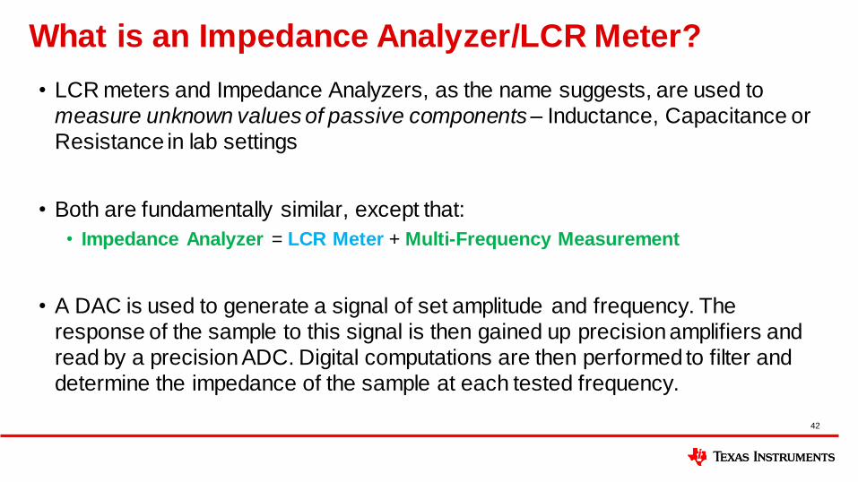
What is an Impedance Analyzer/LCR Meter?
• LCR meters and Impedance Analyzers, as the name suggests, are used to
measure unknown values of passive components – Inductance, Capacitance or
Resistance in lab settings
• Both are fundamentally similar, except that:
• Impedance Analyzer = LCR Meter + Multi-Frequency Measurement
5

Design Challenge/Problem statement
• Circuit stability across types and values (from 1Ω to 10MΩ) of unknown DUT impedance, typically a
problem with capacitive DUTs.
• High-frequency (up to 1MHz) impedance measurement.
• Single-point DUT Voltage/Current measurement.
• Ability to measure small value impedance. (even 1Ω)
• ADC based digitization and impedance measurement.
6

TIDA-060029 Reference Design
7
• Inherently Stable Signal Chain
• No Tuning Requirements
• Auto-Balance Technique provides good
accuracy over wide range of impedance
https://www.ti.com/tool/TIDA-060029

TIDA-060029 Schematic
8

Principle of Operation:
• Measure Voltage & Current through an unknown impedance, to give:
– Where 𝑉𝑋∠θ𝑉 and I X∠θ𝐼 are the DUT
voltage and current, respectively.
• Auto-Balancing Method
of impedance measurement:
9
𝑍∠θ =𝑉𝑋∠θ𝑉I X∠θ𝐼
Ground-referenced
DUT voltage
measurement
Test signal Resultant
Current-Flow
DUT Current causes
resistor voltage drop
VO output
voltage
due to DUT
current
Transimpedance Amplifier (TIA) Circuit
for current measurement
Measure
Voltage
Measure
Current (Voltage
equiv alent)
𝑉𝑋𝑍𝑋
= 𝐼𝑋 =𝑉𝑜𝑅𝐹
𝑉O𝑉X
=RFZX

Foundation:
T
Time (s)
50.00m 50.50m 51.00m 51.50m 52.00m
Ix
-8.00m
8.00m
VC
-20.00
20.00
VL
-40.00m
40.00m
VR
-800.00m
800.00m
Capacitor:
I leads V by 90°
Inductor:
I lags V by 90°

What Differentiates this Subsystem Solution?
• Auto balancing impedance measurement systems deliver high accuracy over a
wide measurement range without any turning requirements
– Measures wide range of components (L, C, R) with impedance values ranging from 1
Ω to 10 MΩ
– Tested at 100 Hz, 1 kHz, 10 kHz, 100 kHz
– Impedance accuracy of 0.1 %
• Inherent Stability in the signal chain
• Low cost, small form factor solution with high accuracy.
13

Impedance Measurement Methods
14

Impedance Measurement Methods
15
Reference:LCR / Impedance Measurement Basics by Greg Amorese (HP)

Measurement Range
16
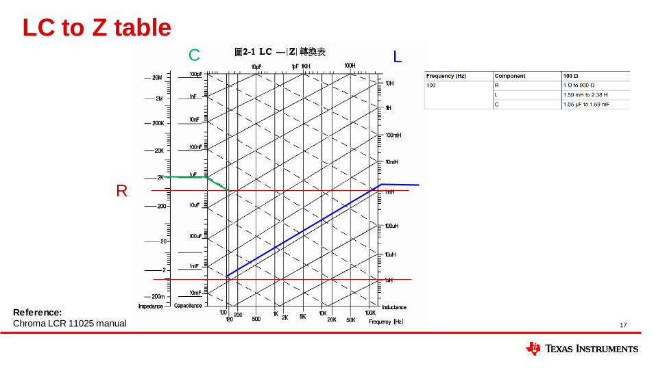
LC to Z table
17
Reference:Chroma LCR 11025 manual
C L
R

Impedance Analyzers & LCR MetersAnalog Front-End using Amplifiers
18
TI Information – Selective Disclosure
Forced Input
Voltage and
IDUT drive
buffer
DUT
Multi-Feedback
Compensation
Current-
Measurement
Path
Voltage-
Measurement
Path
Optional GND-
measurement
amplifier
Transimpedance
Amplifier
Input-
Buffer
Design Challenges Solved!
High-Iout
Buffer for
DUT-drive
DUT
Voltage-Meas
Unity-Gain Buffer
High-Iout
Buffer for
feedback-
current drive
Differential
input SAR-ADC
drivers
Optional GND-
measurement
amplifier
FET-Input
amplifier
as a TIA
A
A
A
B
B
C
• Circuit stability across types and values (from 1Ω to 10MΩ) of unknown DUT
impedance, typically a problem with capacitive DUTs
• Multi-feedback TIA compensation using high-speed VFAs
• High-frequency (upto 1MHz) impedance measurement
• Small ~pA bias current FET-input amplifier used as TIA for DUT
current-measurement
• Single-point DUT Voltage/Current measurement
• Large Aol of high-speed amplifiers ensures virtual ground at
inverting input of TIA
• Ability to measure small value impedance (even 1Ω)
• High-Iout (upto 250mA) buffer easily drives small -impedance DUTs
and multi-feedback transimpedance resistors
• ADC based digitization and impedance measurement
• High-speed FDAs available to drive SAR ADC Inputs!
A
A
A
B
C
Key Devices for easy LCR meter design:
• OPA810: 70MHz, 27V, low-power, RRIO FET-Input amplifier used as
voltage buffer and TIA
• BUF634A: 210MHz, 250mA output, unity-gain buffer for large IOUT drive
• THS4561: Low-power, 60 MHz, 12V, Single-Ended/Fully-Differential SAR
ADC Input Driver
A
B
C
A

Optimizing Accuracy on LCR Meter Front-End
1. Using multiple feedback resistor paths
o Single value for RF is not enough to provide wide range of measurement
o Series switches, for both RF & RG, will allow for multiple measurement ranges
2. Adding series resistor RG increases systems phase stability
o Series resistor introduces pole to cancel out zero in the circuit
3. Using High Z input amplifiers for large value measurements
o Input amplifiers with ~pA range bias currents
19

Measuring Without Node A2
• Front-End can be configured to work with Single-ended ADCs.
• Inverting node of A2 is not measured due to virtual ground concept.
• In reality small voltage will appear at the inverting node.
– Voltage inversely proportional to AOL of A2.
• The higher the AOL of the amp, the smaller the error.
20
external

Measuring With Node A2
• Nullifies error introduced by voltage at inverting node of A2.
• Configuration requires differential ADC for measurements.
• Can allow for higher accuracy, but with high enough AOL from A2 the accuracy
can be similar enough.
21
external

Phase Stability of Measurement Circuit
• Typical measurement circuit and the corresponding Bode plot
• Zero frequency (fZ) depends on unknown capacitance (CX)
• Loop gain has rate of closure of 40 dB/dec
22

Phase Stability of TIDA-060029 Circuit
• Presence of series resistor (RG) introduces pole
• Pole cancels out the zero, restoring phase stability
• Loop gain rate of closure 20 dB/dec
23

Large Z value measurements
• High accuracy measurements should be buffered with high Z input amplifiers.
(Shown in figure)
• If open loop gain (AOL) is large enough, amplifier measuring inverting node can
be removed.
• General rule-of-thumb is to ensure A1 has >60 dB AOL at the highest frequency
of interest for high accuracy measurements.
24
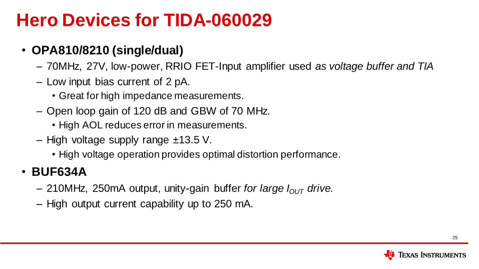
Hero Devices for TIDA-060029
• OPA810/8210 (single/dual)
– 70MHz, 27V, low-power, RRIO FET-Input amplifier used as voltage buffer and TIA
– Low input bias current of 2 pA.
• Great for high impedance measurements.
– Open loop gain of 120 dB and GBW of 70 MHz.
• High AOL reduces error in measurements.
– High voltage supply range ±13.5 V.
• High voltage operation provides optimal distortion performance.
• BUF634A
– 210MHz, 250mA output, unity-gain buffer for large IOUT drive.
– High output current capability up to 250 mA.
25

Impedance Measurement Procedure
• One-time calibration procedure that consists of 4 different calibration
measurements. Done for all frequencies of operation (100Hz, 1kHz, 10kHz, and
100kHz)
• Purpose is to fine calibrated values of RF for all resistor settings at each
frequency of operation.
1. Impedance Cal
2. Short Cal
3. 100k Setting Cal
4. Open Cal
26

Impedance Cal
• Only for 100 Ω and 5 kΩ settings.
• A known 500 Ω (RCAL) is used as ZX.
• Measure the exact value of RF using the equation shown.
– VIN = VX as shown in the figure.
• 500 Ω is used for best calibration accuracy.
• The accuracy of RCAL will affect the calibration accuracy.
• The calibrated values below are now identified:
– RF = 500 Ω
– RF = 5 kΩ
27

Short Cal
• ZX is shorted and the ratio between VO and VIN is measured.
• VIN is the voltage across RG + ZX.
• Only needed to calibrate RF = RG = 100k
• Ratio is classified as GCAL
28

100k Setting Cal
• Set RG = 100 kΩ and short ZX. RF is the calibrated value of 5 kΩ from previous
step.
• Measuring the Gain, G1, the calibrated of RG = 100 kΩ can now be found.
• Once the calibrated value of RG = 100 kΩ is found, the calibrated value of RF =
100 kΩ can now be identified using GCAL from “Short Cal”.
• All calibrated values of RF have been obtained.
29

Open Cal
• ZX is kept open (ZOPEN)
• GOPEN is given by: 𝐺𝑂𝑃𝐸𝑁 = −𝑅𝐹
𝑍𝑂𝑃𝐸𝑁
• Significance of this calibration is mainly for higher frequencies when the
parasitic capacitance in parallel with ZX is large enough to affect the
measurement significantly.
30
Zx: Effective impedance formed by the parallel combination of an actual unknown impedance Zo: Open circuit Impedance). Zx’: Actual value of the unknown impedance

Data Acquisition and Processing
Reference:https://www.analog.com/media/en/analog-dialogue/volume-48/number-4/articles/synchronous-detectors-facilitate-precision.pdfhttps://www.thinksrs.com/downloads/pdfs/applicationnotes/Lock-In%20Basics.pdf
ωr = ωL &
Low Pass Filter
In-phase (I)
Quadrature (Q)
DC Signal!
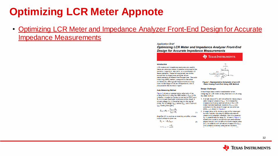
Optimizing LCR Meter Appnote
• Optimizing LCR Meter and Impedance Analyzer Front-End Design for Accurate
Impedance Measurements
32

Comparison to Keysight E4980A LCR meter
33
• For testing, an input of 3.6 VPP was used and results were measured with a
board utilizing the THS4551 and ADS9224R.

Example of measurement accuracy
34
Reference:Keysight Technologies - Impedance Measurement Handbook

Using the OPA3S328
• Using the OPA3S328 in the design can simplify the design.
• Dual high precision op-amps and 6 integrated switches in a 2 x 2 mm DSBGA
package.
• High GBW of 40 MHz.
• High AOL of 122 dB.
35

TIDA-060029 Schematic
36
OPA3S328 integrates red
circled components into
one device!
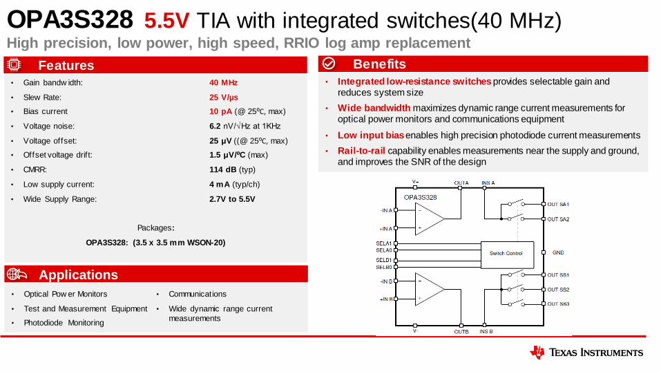
• Integrated low-resistance switches provides selectable gain and reduces system size
• Wide bandwidth maximizes dynamic range current measurements for optical power monitors and communications equipment
• Low input bias enables high precision photodiode current measurements
• Rail-to-rail capability enables measurements near the supply and ground, and improves the SNR of the design
• Gain bandw idth: 40 MHz
• Slew Rate: 25 V/µs
• Bias current 10 pA (@ 25⁰C, max)
• Voltage noise: 6.2 nV/√Hz at 1KHz
• Voltage offset: 25 μV ((@ 25⁰C, max)
• Offset voltage drift: 1.5 μV/⁰C (max)
• CMRR: 114 dB (typ)
• Low supply current: 4 mA (typ/ch)
• Wide Supply Range: 2.7V to 5.5V
Packages:
OPA3S328: (3.5 x 3.5 mm WSON-20)
OPA3S328 5.5V TIA with integrated switches(40 MHz)High precision, low power, high speed, RRIO log amp replacement
• Optical Pow er Monitors
• Test and Measurement Equipment
• Photodiode Monitoring
• Communications
• Wide dynamic range current
measurements
Features Benefits
Applications

• Device Product Overview: LINK
• Device Evaluation Board (EVM): LINK
• Support: LINK
OPA810 Single Channel FET-Input RRIO 27 V, Low Power Amplifier
• Single Channel, High Voltage, FET Input, Rail-to-rail input/output amp• +4.75V to +27V Single Supply Operation• Iq: 3.7 mA trimmed supply current• Bandwidth: 140 MHz (G = 1V/V)• Input Voltage Noise: 6.3 nV/√Hz (f > 500kHz)
• HD2/3: -101/-101dBc @ 2Vpp, 1MHz• +/-2.5μV/°C Typical Offset Drift, 0.55mV max offset• -40°C to 125°C Operating Temperature
Applications
•High Speed Photodiode TIA•Current Sensing
•T&M – oscilloscopes, current probes, power analyzers, etc.•Multi-channel sensor interface
• Ideal for transimpedance circuits, current sensing, test & measurement and general signal buffering from sources with
high/unknown impedance • Very low power for hand-held/portable systems• High bandwidth and slew rate to offer low distortion at high
speed >1MHz and large signal swing ~20Vpp
• Low flat band and 1/f noise for best signal integrity and SNR in high performance systems
• Wide supply voltage range, rail to rail input/output for best system flexibility
• Current limit to protect device against fault conditions
OPAx810 as High voltage, Hi-Z Buffer Stage
Packages Body Size
5-pin SOT-23 1.6 mm x 2.9 mm
5-pin SC70 2.0 mm x 1.25 mm
8-pin SOIC 3.91 mm x 4.9 mm
Features Benefits
Applications
Tools & Resources
+VCC
-VEE
+VCC
+
-½ OPAx810
-VEE
-½ OPAx810
Charge
Bucket
Filter
+
-THS45xx ADC
3
+
Vin
+
-

• Device Product Overview: LINK
• Device Evaluation Board (EVM): LINK
• Support: LINK
OPA2810 Dual FET-Input RRIO 27 V, Low Power Amplifier
• Dual Channel, High Voltage, FET Input, Rail-to-rail input/output amp• +4.75V to +27V Single Supply Operation• Iq: 3.6 mA trimmed supply current• Bandwidth: 105 MHz (G = 1V/V)• Input Voltage Noise: 6 nV/√Hz (f > 500kHz)
• HD2/3: -99/-104dBc @ 2Vpp, 1MHz• +/-2μV/°C Typical Offset Drift, 1.5mV max offset• -40°C to 125°C Operating Temperature
Applications
•High Speed Photodiode TIA•Current Sensing
•T&M – oscilloscopes, current probes, power analyzers, etc.•Multi-channel sensor interface
• Ideal for transimpedance circuits, current sensing, test & measurement and general signal buffering from sources with
high/unknown impedance • Very low power for hand-held/portable systems• High bandwidth and slew rate to offer low distortion at high
speed >1MHz and large signal swing ~20Vpp
• Low flat band and 1/f noise for best signal integrity and SNR in high performance systems
• Wide supply voltage range, rail to rail input/output for best system flexibility
• Current limit to protect device against fault conditions
OPAx810 as High voltage, Hi-Z Buffer Stage
Packages Body Size
8-pin SOT-23 2.8 mm x 2.9 mm
8-pin VSSOP 4.9 mm x 3.0 mm
8-pin SOIC 3.91 mm x 4.9 mm
Features Benefits
Applications
Tools & Resources
+VCC
-VEE
+VCC
+
-½ OPAx810
-VEE
-½ OPAx810
Charge
Bucket
Filter
+
-THS45xx ADC
3
+
Vin
+
-

40
Applications
Features
• Adjustable Small Signal Bandwidth: 35 - 210 MHz
• Slew Rate : 3750 V/µsec
• High output drive capability: 250 mA
• Low quiescent current with 35MHz BW: 1.5mA, 210MHz:
8.5mA
• Wide supply range from +/-2.25V to +/-18V
• Low 3.4 nV/√Hz Output noise in high-BW mode
• Fast settling performance to 0.1% (20V step): 90ns
• Package: SOIC-8 , 3X3 SON , SOIC-8 with power pad
• Supply Voltage Flexibility for variety of applications
• Excellent for high speed open loop applications Adaptable for application needs
• High output current drive for capacitive loads and line drivers
• Flexibility to choose lower power & bandwidth vs. higher power & bandwidth
• Internal current limit and thermal shutdown protection
• Very low output impedance , thus capable of driving high cap values
• Radar and Sonar Drivers
• Low power servo drivers
• Closed-loop current buffer
• Test Equipment/ATE Pin Driver
• Audio headphone driver
• DAC reference drive
• Line drivers and multiplexing
Benefits
BUF634A250 mA, 210 MHz, High Speed Unity-Gain Buffer with adjustable IQ
Production
BUF634DRB Sampling NOW and SOIC-8 power pad option to be available soon !

Discrete Impedance Spectroscopy Design
41
What is an Impedance Analyzer/LCR Meter?
• LCR meters and Impedance Analyzers, as the name suggests, are used to
measure unknown values of passive components – Inductance, Capacitance or
Resistance in lab settings
• Both are fundamentally similar, except that:
• Impedance Analyzer = LCR Meter + Multi-Frequency Measurement
• A DAC is used to generate a signal of set amplitude and frequency. The
response of the sample to this signal is then gained up precision amplifiers and
read by a precision ADC. Digital computations are then performed to filter and
determine the impedance of the sample at each tested frequency.
42

What Impedance Spectroscopy can do?
43
Reference:Electrochemical Impedance Spectroscopy for Online Battery Monitoring - Power Electronics Control (IEEE)

What Differentiates This Subsystem Solution
• Better performance in the market.
– High resolution (<0.1°phase resolution) and SNR (70 dB @ 100KHz) across
impedance range.
– Wider excitation voltage range (<1 mV – 5 V+)
– Suitable for voltage sensitive applications that can be damaged at higher voltages.
– Wider excitation frequency (0.1 Hz to 100 KHz)
• Flexibility and configurability allows for optimized design.
– Multi-Sourcing available, less risk for EOL.
– Configurable discrete components for specific design requirements.
44

Impedance Signal Chain Schematic

Phase Shift Simulations
• Phase Shift at 10kHz = -0.91°
• Phase Shift at 100kHz = -8.88°
Calibration = 100kOhm
• Phase Shift at 10kHz = -0.92°
• Phase Shift at 100kHz = -8.96°
• Phase difference at 10kHz = (-0.91°) - (-0.92°) = .01°
• Phase difference at 100kHz = (-8.88°) - (-8.96°) = .08°
Sample = 100kOhm + 1pF

Phase Shift Simulations
• Phase Shift at 10kHz = -0.93°
• Phase Shift at 100kHz = -9.04°
Sample = 100kOhm + 2pF
• Phase Shift at 10kHz = -0.93°
• Phase Shift at 100kHz = -9.12°
• Phase difference at 10kHz = (-0.93°) - (-0.93°) = .00°
• Phase difference at 100kHz = (-9.04°) - (-9.12°) = .08°
Sample = 100kOhm + 3pF
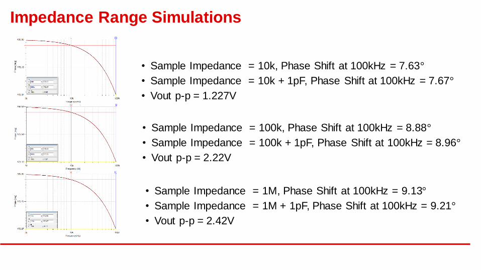
Impedance Range Simulations
• Sample Impedance = 10k, Phase Shift at 100kHz = 7.63°
• Sample Impedance = 10k + 1pF, Phase Shift at 100kHz = 7.67°
• Vout p-p = 1.227V
• Sample Impedance = 100k, Phase Shift at 100kHz = 8.88°
• Sample Impedance = 100k + 1pF, Phase Shift at 100kHz = 8.96°
• Vout p-p = 2.22V
• Sample Impedance = 1M, Phase Shift at 100kHz = 9.13°
• Sample Impedance = 1M + 1pF, Phase Shift at 100kHz = 9.21°
• Vout p-p = 2.42V

Signal to Noise Ratio
SNR @ output = 70.30dB @ 100kHz
SNR @ Sample Excitation = 106.16dB @ 100kHz

Simulation Models
• Simulation models for both single-ended and differential models exist in
ADS7057 product page. Under “Design tools & simulation”
50
Single-Ended ->
<- Differential
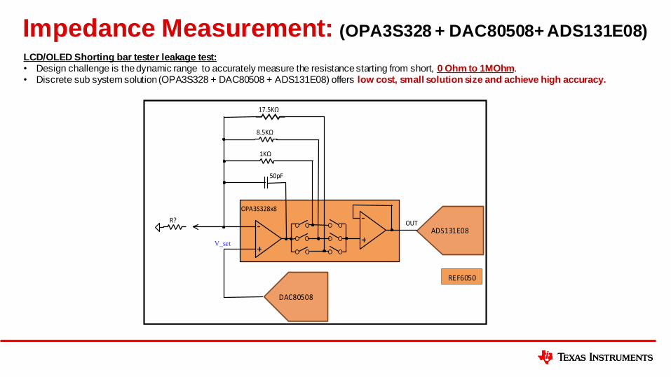
Impedance Measurement: (OPA3S328 + DAC80508+ ADS131E08)
V_set
OUT
OPA3S328x8
1K
8.5K
17.5K
DAC80508
REF6050
ADS131E08
R?
50pF
LCD/OLED Shorting bar tester leakage test:• Design challenge is the dynamic range to accurately measure the resistance starting from short, 0 Ohm to 1MOhm. • Discrete sub system solution (OPA3S328 + DAC80508 + ADS131E08) offers low cost, small solution size and achieve high accuracy.

OPA3S328 Schematic
52
What Differentiates this Subsystem Solution
• Reasonable good accuracy performance in a dense and low cost offering.
• Higher measurement accuracy.
– Reduced # of switches in the OPA3S328 amplifier architecture reducing parasitic
current draw.
• Simplified design allows for competitive size density.
– Does not require additional external components for additional range.
– Only common power rails needed (1.8 V – 5 V). No need for uncommon 15 V supplies.
– Scalable for multi-channel applications.
53

Calculated and Measured Resistance
Using Ohm’s law, our measured resistance (Rm) would be
Re-writing the gain equation, our calculated resistance (Rcal) would be
𝑅𝑚 =𝑉𝑟𝑚(𝑥)
𝐴𝑟𝑚(𝑥)
𝑅𝑐𝑎𝑙 =𝑉𝑠𝑒𝑡𝑢𝑝 ∗ 𝑅𝑓𝑉𝑜 − 𝑉𝑠𝑒𝑡𝑢𝑝
*Feedback of 1k Ω used
Where 𝐴𝑟𝑚(𝑥) =𝑉𝑟𝑚𝑅𝑚
= 𝑉𝑜−𝑉𝑟𝑚𝑅𝑓
𝐴𝑟𝑚(𝑥) =𝑉𝑜 − 𝑉𝑟𝑚
𝑅𝑓𝑉𝑟𝑚 = 𝑉𝑠𝑒𝑡𝑢𝑝
𝑅𝑚 =𝑉𝑟𝑚(𝑥)
𝐴𝑟𝑚(𝑥)=
𝑉𝑠𝑒𝑡𝑢𝑝
(𝑉𝑜−𝑉𝑠𝑒𝑡𝑢𝑝
𝑅𝑓)
VO

Measuring Error
• To find the error, our equation would be:
𝐸𝑟𝑟𝑜𝑟 𝑝𝑝𝑚 =𝑅𝑐𝑎𝑙 − 𝑅𝑚
𝑅𝑚∗ 1 𝑚𝑖𝑙𝑙𝑖𝑜𝑛

Simulations in TINA-TI
From our simulations,
we found feedback
resistors 1k, 8.5k and
17.5k gave us great
range (500 Ω to 1M Ω)
while measuring the
unknown resistance
accurately.

Lowest Possible Error
Rf = 1k Ω Rf = 8.5k Ω Rf = 17.5k Ω
Vsetup = 0.001007*Rm + 0.502
Rf = 1k Resistor (Ω) V_set (V) Error (ppm)
200 0.69899 0.01441
300 0.80146 0.00969
690 1.2 0.00749
880 1.39 0.00524
1.07k 1.58 0.00508
1.45k 1.96 0.00387
1.64k 2.15 0.00315
2.21k 2.73 0.00314
2.59k 3.11 0.00247
3k 3.51 0.00287
Rf = 8.5k Resistor (Ω) V_set (V) Error (ppm)
2.21k 0.101 0.90443
15.46k 0.29871 0.14157
28.71k 0.49632 0.20687
55.22k 0.89962 0.10364
94.97k 1.51 0.04246
121.48k 1.91 0.05005
161.24k 2.52 0.02416
187.74k 2.93 0.02808
214.24k 3.33 0.00422
300k 4.66 0.01421
Vsetup = 1.528e-5*Rm + 0.05748 Vsetup = 3.675e-6*Rm -0.005343
Rf = 17.5k Resistor (Ω) V_set (V) Error (ppm)
200k 0.73893 0.21781
254k 0.93874 0.04845
336.89k 1.24 0.09149
419.78k 1.53 0.09097
502.67k 1.84 0.0567
585.56k 2.14 0.03323
668.44k 2.44 0.05447
834.22k 3.06 0.0256
917.11k 3.37 0.02989
1.1M 4.06 0.03201
Range : 200 Ω to 3k Ω Range : 2.21k Ω to 300k Ω Range : 200k Ω to 1.1M Ω

Graph (Error vs Resistance)

Shorted Simulation
With all of the switches turned on, we can calculate Rm from 1 Ω to 200 Ω
Using probes Vrm, Vo and Arm, our new feedback resistance would be
𝑅𝑓 =𝑉𝑜 −𝑉𝑟𝑚𝐴𝑟𝑚
Giving us a resistance of Rf = 871.180915
Ω

Graph (Error vs Resistance)

Thank you!

IMPORTANT NOTICE AND DISCLAIMERTI PROVIDES TECHNICAL AND RELIABILITY DATA (INCLUDING DATASHEETS), DESIGN RESOURCES (INCLUDING REFERENCEDESIGNS), APPLICATION OR OTHER DESIGN ADVICE, WEB TOOLS, SAFETY INFORMATION, AND OTHER RESOURCES “AS IS”AND WITH ALL FAULTS, AND DISCLAIMS ALL WARRANTIES, EXPRESS AND IMPLIED, INCLUDING WITHOUT LIMITATION ANYIMPLIED WARRANTIES OF MERCHANTABILITY, FITNESS FOR A PARTICULAR PURPOSE OR NON-INFRINGEMENT OF THIRDPARTY INTELLECTUAL PROPERTY RIGHTS.These resources are intended for skilled developers designing with TI products. You are solely responsible for (1) selecting the appropriateTI products for your application, (2) designing, validating and testing your application, and (3) ensuring your application meets applicablestandards, and any other safety, security, or other requirements. These resources are subject to change without notice. TI grants youpermission to use these resources only for development of an application that uses the TI products described in the resource. Otherreproduction and display of these resources is prohibited. No license is granted to any other TI intellectual property right or to any third partyintellectual property right. TI disclaims responsibility for, and you will fully indemnify TI and its representatives against, any claims, damages,costs, losses, and liabilities arising out of your use of these resources.TI’s products are provided subject to TI’s Terms of Sale (https:www.ti.com/legal/termsofsale.html) or other applicable terms available eitheron ti.com or provided in conjunction with such TI products. TI’s provision of these resources does not expand or otherwise alter TI’sapplicable warranties or warranty disclaimers for TI products.IMPORTANT NOTICE
Mailing Address: Texas Instruments, Post Office Box 655303, Dallas, Texas 75265Copyright © 2021, Texas Instruments Incorporated