
RS-485 Basics Series - Texas Instruments
17
Technical White Paper RS-485 Basics Series Kankan Wang, Hao Liu Transceiver Interface 1 Introduction Since its definition in 1983, RS-485 has become the preferred interface standard for many industrial fieldbus applications. This article is intended to provide a useful, informative, and centralized resource for understanding the fundamentals of RS-485 and addressing common application questions that arise when designing RS-485 networks. RS-485, formally known as American National Standards Institute (ANSI) Telecommunications Industry Association (TIA)/Electronic Industries Alliance (EIA)-485-A, is a balanced data transmission standard for serial communication. RS-485 allows for robust transmission of moderate data rates over long distances in multipoint communication applications, such as factory and building automation, motor control, and other field bus applications. The RS-485 standard only specifies the electrical characteristics of drivers and receivers; it does not specify a protocol. Many higher-level interface standards reference RS-485 for their physical layer, such as Modicon bus (ModBus), process field bus (ProfiBus), DMX512, and others. Figure 1-1 illustrates some common interface standards. RS-485 improves noise immunity and extends the distance supported by RS-232 by implementing a differential, rather than single-ended, signaling technique. And while electrically similar, RS-485 extends RS-422 to allow for bidirectional communication. Figure 1-1. Common Interface Standards www.ti.com Introduction SLLA545 – FEBRUARY 2021 Submit Document Feedback RS-485 Basics Series 1 Copyright © 2021 Texas Instruments Incorporated
-
Upload
khangminh22 -
Category
Documents
-
view
3 -
download
0
Transcript of RS-485 Basics Series - Texas Instruments

Technical White PaperRS-485 Basics Series
Kankan Wang, Hao Liu Transceiver Interface
1 IntroductionSince its definition in 1983, RS-485 has become the preferred interface standard for many industrial fieldbusapplications. This article is intended to provide a useful, informative, and centralized resource for understandingthe fundamentals of RS-485 and addressing common application questions that arise when designing RS-485networks.
RS-485, formally known as American National Standards Institute (ANSI) Telecommunications IndustryAssociation (TIA)/Electronic Industries Alliance (EIA)-485-A, is a balanced data transmission standard for serialcommunication. RS-485 allows for robust transmission of moderate data rates over long distances in multipointcommunication applications, such as factory and building automation, motor control, and other field busapplications.
The RS-485 standard only specifies the electrical characteristics of drivers and receivers; it does not specify aprotocol. Many higher-level interface standards reference RS-485 for their physical layer, such as Modicon bus(ModBus), process field bus (ProfiBus), DMX512, and others.
Figure 1-1 illustrates some common interface standards. RS-485 improves noise immunity and extends thedistance supported by RS-232 by implementing a differential, rather than single-ended, signaling technique. Andwhile electrically similar, RS-485 extends RS-422 to allow for bidirectional communication.
Figure 1-1. Common Interface Standards
www.ti.com Introduction
SLLA545 – FEBRUARY 2021Submit Document Feedback
RS-485 Basics Series 1
Copyright © 2021 Texas Instruments Incorporated

Additionally, RS-485 allows for communication over greater distances than multipoint low-voltage differentialsignaling (M-LVDS) because of its larger signaling levels and wider common-mode range. However, for datarates higher than 50 megabits per second, M-LVDS becomes increasingly advantageous for its reduced powerconsumption relative to RS-485.
RS-485 networks consist of multiple nodes connected in parallel to a bus. Figure 1-2 shows the typical networkconnections for half- and full-duplex RS-485 implementations. The majority of RS-485 applications implementhalf-duplex (two-wire) communication. Full-duplex communication requires two signal pairs (four-wire), andfacilitates higher throughput by allowing nodes to transmit and receive data simultaneously. Modern transceiverdesigns allow hundreds of nodes to connect to the bus.
RT
R
A B
R RE DE D
DR
A B
R RE DE D
D
R
D
R
RE
DE
D
A
B
R
D
R
RE
DE
D
A
B
RT RT
R
DR
DE
RE
D
Y
Z R
D
R
RE
DE
A
B
RT RT
B
A
Z
Y
R
D
R RE DE D
Z YBA
Master Slave
Slave
RT
Figure 1-2. Half- and Full-Duplex RS-485 Network Connections
Section 2 and Section 4, respectively, discuss the basic design and operation of the RS-485 driver and receiver.This document also covers receiver failsafe operation, transceiver power dissipation, transient protection, andmore.
Introduction www.ti.com
2 RS-485 Basics Series SLLA545 – FEBRUARY 2021Submit Document Feedback
Copyright © 2021 Texas Instruments Incorporated

2 The RS-485 DriverMany common RS-485 questions can be resolved with a basic understanding of the structure and operation ofthe driver and receiver. This section discusses the RS-485 driver and the relevant specifications in the RS-485standard.
Figure 2-1 shows the equivalent output schematic for the driver of the THVD1550 half-duplex transceiver fromTI. The output structure consists of an H-bridge driver with high- and low-side transistors on each of the A and Boutputs, which are in parallel with electrostatic discharge (ESD) cells on each terminal. The diodes in-series witheach transistor prevent reverse current flow from the bus terminals to the power supply if the voltage on A or B isgreater than VCC, or from ground to the bus terminals if the voltage on A or B is below the ground potential.
Vcc
16 V
A
B
Figure 2-1. Differential Output Driver Structure
Figure 2-2 shows that the basic operation of the driver simplifies to the high- and low-output logic states.
VCC
Q2 = OFF Q1 = ON
Q4 = ON Q3 = OFF
B Rt A
VOD +±
VCC
Q2 = ON Q1 = OFF
Q4 = OFF Q3 = ON
B Rt A
VOD+ ±
a) D = HIGH a) D = LOW
Figure 2-2. RS-485 Output Driver Operation
www.ti.com The RS-485 Driver
SLLA545 – FEBRUARY 2021Submit Document Feedback
RS-485 Basics Series 3
Copyright © 2021 Texas Instruments Incorporated

The resulting waveform can be modeled as a positive and negative differential voltage superimposed onto acommon-mode offset voltage, which is typically close to VCC/2, as Figure 2-3 shows.
D RD
VOSVD / 2
VD / 2
+
±
±
+
+VD / 2
íVD / 2
A
B
íVD+VD
VA = VOS ±|VD| / 2
VB = VOS ±|VD| / 2
VOS
Figure 2-3. RS-485 Driver Output Waveform
The RS-485 standard specifies that a compliant driver must produce a differential output voltage greater than1.5 V with a 54-Ω load. Figure 2-4 illustrates the relevant RS-485 test circuit.
27
27
1.5 V < VOD < 5 V
-1 V < VOS < 3 V
Figure 2-4. RS-485 Output Driver Test Circuit
Therefore, the on-resistance of the high- and low-side transistors must be low enough to source sufficient currentto produce 1.5 V across 54 Ω. A common guideline is to assume a typical on-resistance of between 20 Ω and30 Ω for each transistor.
Additionally, the RS-485 standard also requires that a compliant driver produce a differential output voltagegreater than 1.5 V with a 60-Ω differential load and common-mode load of 375 Ω from each of the A and Boutputs to –7 V to 12 V. Figure 2-5 provides an example.
60 1.5 V < VOD < 5 V
375
375
í7 V < V < 12 V+±
Figure 2-5. RS-485 Output Driver Test Circuit Over Common-Mode
The RS-485 Driver www.ti.com
4 RS-485 Basics Series SLLA545 – FEBRUARY 2021Submit Document Feedback
Copyright © 2021 Texas Instruments Incorporated

Further, the on-resistance of each leg of the H-bridge output must be well-matched (that is, Q1 ≈ Q2, and Q3 ≈Q4). The RS-485 standard specifies that the difference in magnitude of VOD when the output is positive and VODwhen the output is negative must be less than 200 mV. When each leg of the H-bridge output is perfectlymatched, this value, denoted as ∆|VOD| in the data sheet, is zero. For the THVD2450, ∆|VOD| has a maximumvalue of 50 mV. Large imbalances in VOD for different logic states result in increased common-mode noise andhigher levels of radiated electromagnetic interference (EMI).
A final important characteristic of any RS-485 driver is its output rise and fall time, which is determined by aseparate circuit that controls the switching of transistors Q1, Q2, Q3, and Q4 (see Figure 2-2). The output riseand fall time limits the maximum data rate at which the transceiver can operate. Typically, the rise and fall time ofthe driver should be no more than one-third the total bit time at a given data rate. Further, for a given data rate, atransceiver with slower rise and fall times is preferable to a transceiver with faster rise and fall times, as it willradiate less electromagnetic interference (EMI) into adjacent circuitry.
Large differential output voltage and wide common-mode range differentiate RS-485 from other signalingstandards and make it suitable for use in noisy electrical environments and applications, such as industrialautomation, e-metering, and motor control.
www.ti.com The RS-485 Driver
SLLA545 – FEBRUARY 2021Submit Document Feedback
RS-485 Basics Series 5
Copyright © 2021 Texas Instruments Incorporated

3 How to Calculate Unit Loads and the Maximum Number of Nodes on the NetworkFigure 3-1 illustrates that the RS-485 is a multipoint differential bus. This means that all of the nodes on the busshare one common transmission medium, and therefore every node placed onto the bus adds a load in parallelto all of the existing network transceivers and termination resistors. As the total number of nodes increases, theloading on each and every driver increases as well.
Load # 1
Load # 2 Load # 3 Load # N-1
Load # N
120 120
Figure 3-1. Multipoint RS-485 bus
To set practical and measurable limits for RS-485 output drivers, the Telecommunications Industry Association(TIA)/Electronic Industries Alliance (EIA)-485 standard created a hypothetical “unit load,” and then limited themaximum number of unit loads that can be presented to any driver on an RS-485 bus to 32. The standard statesthat a driver must be able to drive a minimum 1.5 differential signal across a maximum of 32 unit loads in parallelwith two 120-Ω termination resistors.
Determine the unit-load parameter by sweeping the input voltage from –7 to 12 V on one bus pin, with the otherbus pin held at ground, and then measuring the input leakage current. Measure both bus pins individually, withthe transceiver both in a powered and unpowered state. As expected, the input leakage current depends on theinput voltage; thus, when calculating the unit load, Equation 1 uses the worst-case ratio of input voltage toleakage current:
INVUnit Load Max
iLeakage
ª º « »
¬ ¼ (1)
where
• VIN –7 … + 12 V
In Figure 3-2, the bounds of –7 and 12 V in the standard are meant to allow up to ±7 V of ground-potentialdifference (GPD) between a driver output and a receiver, with the output voltage of the driver varying betweenGND and 5 V. Therefore, –7 V represents a receiver noting a respective driver pin driving the bus low with a –7-V GPD, while 12 V represents a receiver noting a respective driver pin driving the bus high with a 7-V GPD.
Receiving
NodeSeding
Node
RT RTD R
Max +7 V
A
B
A
B
R
RE
D
DE
0 V -> 5 V
0 V -> 5 V
Figure 3-2. Maximum GPD of a Standard RS-485 Transceiver
How to Calculate Unit Loads and the Maximum Number of Nodes on the Network www.ti.com
6 RS-485 Basics Series SLLA545 – FEBRUARY 2021Submit Document Feedback
Copyright © 2021 Texas Instruments Incorporated

One unit load is equivalent to 1 mA of input leakage current at 12 V. This load represents a single-ended loadwith respect to ground. Another easy way to think of the unit load is the equivalent of a 12-kΩ resistance fromeither the A or B bus pins (and the Y and Z pins for full-duplex transceivers) to ground.
Once the maximum ratio of input voltage to leakage current is determined, the equivalent unit load can becalculated by dividing that ratio by 12 kΩ, expressing the result in terms of a fraction of the unit load.
Using this unit-load ratio, the maximum number of any variety of transceivers that the network can handle can becalculated. For example, when considering the THVD1520 RS-485 transceiver, which has a one-eighth unit-loadinput impedance, you would be able to place a theoretical maximum of 256 nodes on the network, as shown inEquation 2:
32 32# of Nodes 256 Nodes
Equivalent Unit Loading 1 8
(2)
Table 3-1 shows the relationship between unit load, bus leakage current, equivalent input resistance, and themaximum number of devices that can be on the network for a few typical unit loads.
Table 3-1. Unit-Load CharacteristicsUnit Load Bus Leakage Current
at 12 VEquivalent InputResistance
Maximum Nodes onOne Network
1 1 mA 12 kΩ 32
1/2 500 µA 24 kΩ 64
1/4 250 µA 48 kΩ 128
1/8 125 µA 96 kΩ 256
Recall from Section 2, the common-mode load for an RS-485 driver-output test circuit is 375 Ω; see Figure 3-3.This is because it is the equivalent of 32 unit loads (12 kΩ) in parallel.
60 1.5 V < VOD < 5 V
375
375
í7 V < V < 12 V+±
Figure 3-3. RS-485 Driver-Output Test Circuit With Common-Mode Load
Moreover, if you are trying to figure out how many transceivers you can place on your network, this data sheetwill have a unit-load parameter or a maximum input leakage current that can be used for calculating the unitload. The smaller the unit load, the more devices you can place onto the network.
www.ti.com How to Calculate Unit Loads and the Maximum Number of Nodes on the Network
SLLA545 – FEBRUARY 2021Submit Document Feedback
RS-485 Basics Series 7
Copyright © 2021 Texas Instruments Incorporated

4 The RS-485 ReceiverThis section discusses the RS-485 receiver and the relevant parameters in the RS-485 standard.
RS-485 transceivers such as the THVD1429 half-duplex family have an equivalent receiver input schematic likethe one shown in Figure 4-1. The receiver input circuitry consists of electro-static discharge (ESD) protection, aresistor-divider network, and a biasing current, all of which play a role in shaping the magnitude and common-mode voltage that reaches the differential comparator.
R1
R2
R3 R4
R5 R6
VCC
R
R1 = R2
R3 = R4
R5 = R6
A
B
16 V
Figure 4-1. Differential Receiver Input Structure
ESD protection
The most important thing to note in terms of ESD protection for half-duplex transceivers is that the driver andreceiver share the same ESD protection, saving space. But for a full-duplex transceiver, both the driver (Y and Zpins) and receiver (A and B pins) need independent ESD protection. This means that twice the area is needed tosupport ESD protection.
Resistor-divider network
The resistor-divider network on the A and B inputs serves two functions. The first function is to attenuate largesignals that are beyond the range of the supply voltage of the receiver. This attenuation factor is necessarybecause the RS-485 standard states that voltages as low as –7 V and as high as 12 V can exist on the busterminals to account for ground-potential differences that may exist between transceivers on a shared network.These high voltages need attenuation down to voltages that 3.3 V or 5 V transceivers can handle. A typicalattenuation factor is on the order of 10-to-1, greatly reducing the magnitude of the voltages seen internally at thecomparator.
The second important function of the resistor-divider network is to bias the bus voltages toward VCC/2. This isnecessary because simply attenuating a negative signal will not bring the voltage between the local ground ofthe receiver and VCC. Attenuating the signal and biasing it toward VCC/2 prevents the inputs of the comparatorfrom getting saturated; thus enabling the comparator to properly evaluate the differential voltage between the Aand B terminals.
This ability to bias the voltages also allows the system to perform without a common ground connection betweenthe remote ground of the RS-485 driver and the ground of the local RS-485 receiver. Figure 4-2 shows how aninput signal is both attenuated and biased from the bus terminals to the input of the comparator through theresistor-divider network.
The RS-485 Receiver www.ti.com
8 RS-485 Basics Series SLLA545 – FEBRUARY 2021Submit Document Feedback
Copyright © 2021 Texas Instruments Incorporated

Figure 4-2. Receiver Input-Voltage Attenuation
The series combination of R1 and R3 || R5 (resistors R3 and R5 in parallel) is the primary factor that determinesthe input impedance of the receiver. The RS-485 standard specifies that the input leakage current of a compliantreceiver must remain within the shaded region shown in Figure 4-3 when applying –7 V to 12 V to the inputterminals for both powered and unpowered conditions.
Figure 4-3. RS-485 Receiver Input I-V Characteristic
The trade-off that exists with receiver attenuator design is that in order to lower the leakage current, higherresistor values must be used, which increases the size of the resistors in the attenuator. Larger-sizedcomponents create a more expensive die and more parasitic capacitance. This stray capacitance and the inputcapacitance of the comparator sit in parallel to the resistance of the attenuator, creating a low-pass filter, which inturn limits the maximum bandwidth of the receiver. Therefore, there is a balance between the input leakagecurrent and resistor values and the bandwidth and size of the attenuator. With the THVD1450 device, thehighest-speed device in the THVD14xx family, it is apparent that it also has the highest bus input-leakage currentdue to the lower resistor-value attenuator circuit that was needed.
www.ti.com The RS-485 Receiver
SLLA545 – FEBRUARY 2021Submit Document Feedback
RS-485 Basics Series 9
Copyright © 2021 Texas Instruments Incorporated

Biasing Current
Figure 4-4 shows the effect of the current source connected between the B input terminal of the comparator andground. By using the superposition principle, it is evident that the current source will cause a voltage drop acrossR4 and R6 connected to the negative-input terminal of the comparator. This creates a fail-safe bias voltage thatcauses the negative terminal to have a lower voltage than the positive terminal and the output of the comparatorto be in a known high state when applying a 0-V differential voltage to the A and B pins.
This fail-safe biasing helps ensure that the R output will be high in the presence of bus idle or bus short-circuitconditions. In the VIT numbers for the THVD1451 family, the positive threshold has a typical value of –100 mVand the negative threshold is typically –130 mV. Without fail-safe biasing, transceiver thresholds would becentered around 0 V and in an indeterminate state with a 0-V differential input voltage.
R1
R2
R3 R4
R5 R6
VCC
R
R1 = R2
R3 = R4
R5 = R6
A
B
16 V
+
±
Figure 4-4. Effect of the Offset Bias Current
In summary, understanding the basic input structures of an RS-485 receiver helps recognize important receiverelectrical specifications like input-leakage current and positive and negative input thresholds.
The RS-485 Receiver www.ti.com
10 RS-485 Basics Series SLLA545 – FEBRUARY 2021Submit Document Feedback
Copyright © 2021 Texas Instruments Incorporated
5 Two Methods to Fail-Safe Bias the NetworkThis section explores two common methods for handling idle bus conditions so a logical state on the bus isensured.
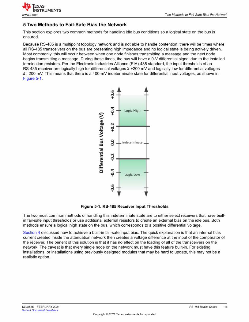
Because RS-485 is a multipoint topology network and is not able to handle contention, there will be times whereall RS-485 transceivers on the bus are presenting high impedance and no logical state is being actively driven.Most commonly, this will occur between when one node finishes transmitting a message and the next nodebegins transmitting a message. During these times, the bus will have a 0-V differential signal due to the installedtermination resistors. Per the Electronic Industries Alliance (EIA)-485 standard, the input thresholds of anRS-485 receiver are logically high for differential voltages ≥ +200 mV and logically low for differential voltages≤ –200 mV. This means that there is a 400-mV indeterminate state for differential input voltages, as shown inFigure 5-1.
Figure 5-1. RS-485 Receiver Input Thresholds
The two most common methods of handling this indeterminate state are to either select receivers that have built-in fail-safe input thresholds or use additional external resistors to create an external bias on the idle bus. Bothmethods ensure a logical high state on the bus, which corresponds to a positive differential voltage.
Section 4 discussed how to achieve a built-in fail-safe input bias. The quick explanation is that an internal biascurrent created inside the attenuation network then creates a voltage difference at the input of the comparator ofthe receiver. The benefit of this solution is that it has no effect on the loading of all of the transceivers on thenetwork. The caveat is that every single node on the network must have this feature built-in. For existinginstallations, or installations using previously designed modules that may be hard to update, this may not be arealistic option.
www.ti.com Two Methods to Fail-Safe Bias the Network
SLLA545 – FEBRUARY 2021Submit Document Feedback
RS-485 Basics Series 11
Copyright © 2021 Texas Instruments Incorporated

The second way to handle idle bus conditions is to use two external resistors: one from the A terminal to VCCand the other from B terminal to ground. See the two red resistors in Figure 5-2.
RT RT
A
B
A
B
R
D
R
D
RFS2
RFS1
VCC
VCC
R
RE
DE
D
R
RE
DE
D
VCC
Figure 5-2. Fail-Safe Resistor Placement
As RFS1 shows, the two parallel termination resistors (RT) and (RFS2) create a simple voltage divider circuit. Theresistors only need to be installed in one node on the entire network, typically on the leader node. Additionally,RFS1 and RFS2 are set equal to each other so that the common mode is balanced between VCC and ground.
Equation 3 is the simplest way to calculate the value of these fail-safe resistors. Take the minimum input voltagethat results in a known state (200 mV), the equivalent termination resistors in parallel (60 Ω) and the minimumVCC for the node that will have the fail-safe resistors populated (use 4.5 V) and solve the simple voltage-dividerequation:
FS CC,min
FS1 e q FS2
ReqV V
R R R
§ · ¨ ¸¨ ¸ © ¹ (3)
Substituting VFS = 200 mV, Req = 60 Ω and setting RFS1 + RFS2 = 2 × RFS (since they are set equal to eachother), provides:
FS
FS
600.2 4.5 R 645
2 R 60
§ · u !! ¨ ¸¨ ¸u © ¹ (4)
This shows that the benefit to this solution only takes two resistors to accomplish, and it works for all nodes on anetwork. The caveat is that the two 645-Ω resistors create a common-mode load. Recall from Section 3, eachRS-485 driver is required to handle a 375-Ω common-mode load (32 unit loads in parallel), as shown in Figure5-3.
RFS
RT
RFS
375
375
VCC
A
BVCM
Figure 5-3. Thirty-Two Unit Loads in Parallel Presenting a Common-Mode Load
Two Methods to Fail-Safe Bias the Network www.ti.com
12 RS-485 Basics Series SLLA545 – FEBRUARY 2021Submit Document Feedback
Copyright © 2021 Texas Instruments Incorporated

The issue is that the fail-safe resistors alone are presenting a common-mode load of 645 Ω. It is now importantto calculate what additional common-mode load may be present in parallel before a common-mode loading of375 Ω is present:
CM
1375 RCM 8963
1 1
R 645
o |
(5)
Since each unit load can be approximated by a 12-kΩ common-mode load, calculate the maximum number ofunit loads in parallel that can be used before presenting a common-mode load of less than 896 Ω:
UL
UL
12000896 n 13.4
n o !
(6)
This means that the fail-safe resistors place a common-mode loading equivalent to 18.6 (32 – 13.4) unit loads,thereby drastically reducing the total number of allowable nodes on the network. Both methods of handling idlebus conditions have pros and cons, so it is up the designer to decide which method works best for theirapplication.
www.ti.com Two Methods to Fail-Safe Bias the Network
SLLA545 – FEBRUARY 2021Submit Document Feedback
RS-485 Basics Series 13
Copyright © 2021 Texas Instruments Incorporated

6 When Termination is Necessary, and How to do it ProperlyMany signal integrity and communication issues with RS-485 networks stem from terminations, either from a lackof termination or improper termination. This section discusses when not terminating your RS-485 network works,and when termination is required, and how to use standard (parallel) terminations and alternating current (AC)termination networks.
As shown in Section 5, the driver of an RS-485 transceiver must be able to drive 1.5 V across 32 unit loads andtwo 120-Ω terminations. Not included in that section is the fact that the 120-Ω value for termination resistorsstems from what is known as the differential-mode characteristic impedance of the twisted-pair bus wires. Simplyput, the wire gauge, insulation type and thickness, and number of twists per unit length all contribute to animpedance that high-speed data signals “detect". This impedance is denoted in ohms and typically ranges from100 Ω to 150 Ω for twisted-pair cables. The writers of the RS-485 standard choose 120 Ω as the nominalcharacteristic impedance; therefore, to match this impedance the termination resistors also have a default valueof 120 Ω.
Why termination networks exist
Matching the characteristic impedance of the cabling to the termination network enables the receiver on the endof the bus to determine the maximum signal power. By leaving a transmission line unterminated, or terminatedwith some value unequal to the impedance of the cable, a mismatch is introduced that creates reflections at theends of the network. A reflection is where some of the energy of the signal literally returns back up the line,which can then constructively or destructively interfere with the next bits propagating down the bus. A destructiveexample is if the reflected signal which bounces back is out of phase with the incoming signal, resulting in thereceiver detecting a smaller incoming signal. If the mismatch is large enough, the energy reflected back cancause subsequent bits to be misinterpreted and incorrectly decoded by the receiver.
Equation 7 shows that for the reflection coefficient to approach zero, the input impedance, ZL, needs to matchthe source impedance, ZS. If there is a large discrepancy in load and source impedance, almost the entire signalcan reflect.
L S
L S
Z Zr
Z Z
(7)
For optimal signal integrity, it is always best to match the AC line impedance with a termination of equal value.There is a reason that all designers would not choose to do this. Because adding termination networks adds costto the overall system, and these termination networks also add a parallel load to the drivers, causing largersteady-state load currents. In power-sensitive applications where lowering power consumption is critical (such asin battery-powered applications), one option to save power is to leave the bus unterminated. The next sectiondiscusses when removing termination is a viable option.
Networks that do not need termination
One situation which does not need termination networks is when the two-way loop time of the network is muchgreater than a single bit time (approximately < 0.1 × two-way loop delay). In such scenarios, the reflections willlose energy each time they reach an end of the network.
As Figure 6-1 shows, the amplitude of the reflections will continue to decay each time the signal reflects at theend of the cable. Figure 6-1 shows three round trips for the signal and a total of six reflections.
When Termination is Necessary, and How to do it Properly www.ti.com
14 RS-485 Basics Series SLLA545 – FEBRUARY 2021Submit Document Feedback
Copyright © 2021 Texas Instruments Incorporated

A
B
A
B
R
D
R
D
R
RE
DE
D
R
RE
DE
D
Amplitude
Original Signal
2nd Reflection 3rd Reflection
1st Reflection
5th Reflection
6th Reflection
4th Reflection
End ofCable
Cable
Unterminated
Figure 6-1. Amplitude of Reflection Decay Each Time a Reflection Occurs
Estimating that the unterminated end of the bus has a 96-kΩ input impedance (a one-eighth unit load), and thesource impedance of the driver is 60 Ω, the signal reflections would decay according to the calculations listed inTable 6-1.
Table 6-1. Example Signal-Decay Calculations
Signal Percentage of Signal Calculation§ ·¨ ¸¨ ¸© ¹
L S
L S
Z Z
Z Z
Original signal 100%
After first reflection 99.75% § ·u ¨ ¸
© ¹
96,000 1201 0.9975
96,000 120
After second reflection –33.24% § ·u ¨ ¸
© ¹
60 1200.9975 0.3324
60 120
After third reflection –33.16% § · u ¨ ¸
© ¹
96,000 1200.3324 0.3317
96,000 120
After fourth reflection 11.05% § · u ¨ ¸
© ¹
60 1200.3317 0.1106
60 120
After fifth reflection 11.02% § ·u ¨ ¸
© ¹
96,000 1200.1106 0.1102
96,000 120
After sixth reflection –3.68% § ·u ¨ ¸
© ¹
60 1200.1102 0.0368
60 120
As Table 6-1 shows, by the time the signal reflects for the sixth time, it has decayed to under 4% of its originalmagnitude. After this point the reflections are no longer capable of causing signal-integrity issues. Since thesample point of a bit typically occurs between 50%–75% of the way through the bit, make sure that these threeround-trip delays occur before the sample point.
www.ti.com When Termination is Necessary, and How to do it Properly
SLLA545 – FEBRUARY 2021Submit Document Feedback
RS-485 Basics Series 15
Copyright © 2021 Texas Instruments Incorporated

Networks that need termination
For applications where the bit time is not substantially longer than the loop time of the cable, termination iscrucial for minimizing reflections. The most basic termination networks, which are known as standard terminationor parallel termination networks, consist of a single resistor (Figure 6-2).
RTERM
A
B
RS-485
Transceiver
Figure 6-2. Standard Termination Network
For standard termination, match the termination resistor value with the differential-mode characteristicimpedance of the cabling on both ends of the network. This ensures the proper termination of signals traveling inboth directions on the bus. As previously mentioned, the major drawback for this type of termination scheme isthat whenever the driver is active, the resistors are placing a direct current (DC) load on the driver.
Using AC terminations helps alleviate this power dissipation without having as long of a bit-time requirement withrespect to bus length. Figure 6-3 shows an AC termination scheme.
CTERM
RTERM
A
B
RS-485
Transceiver
Figure 6-3. AC Termination Network
Since current typically flows from one side of an RS-485 driver through the termination network, then through theother side of the driver, by placing a series capacitor the steady state current goes to zero. The two caveats ofthis type of termination are that it requires one extra component on each termination network, and the seriesresistor and capacitor introduce a resistor-capacitor (RC) delay. The RC time constant will slow the rising andfalling edge of the differential signal and limit the maximum data rate of the network.
Table 6-2. Summary of Termination TechniquesTermination Network Power Dissipation Data Rate Signal IntegrityNo termination Low Low Good at low data rates, poor at high data rates
Standard termination High High Great
AC termination Low Medium Good
For optimal signal integrity, it is always best to match the differential-mode characteristic impedance of the cablewith a termination of equal impedance. But if the proper steps are taken, it is also possible to successfullyimplement AC terminations or avoid termination altogether.
When Termination is Necessary, and How to do it Properly www.ti.com
16 RS-485 Basics Series SLLA545 – FEBRUARY 2021Submit Document Feedback
Copyright © 2021 Texas Instruments Incorporated

IMPORTANT NOTICE AND DISCLAIMERTI PROVIDES TECHNICAL AND RELIABILITY DATA (INCLUDING DATASHEETS), DESIGN RESOURCES (INCLUDING REFERENCEDESIGNS), APPLICATION OR OTHER DESIGN ADVICE, WEB TOOLS, SAFETY INFORMATION, AND OTHER RESOURCES “AS IS”AND WITH ALL FAULTS, AND DISCLAIMS ALL WARRANTIES, EXPRESS AND IMPLIED, INCLUDING WITHOUT LIMITATION ANYIMPLIED WARRANTIES OF MERCHANTABILITY, FITNESS FOR A PARTICULAR PURPOSE OR NON-INFRINGEMENT OF THIRDPARTY INTELLECTUAL PROPERTY RIGHTS.These resources are intended for skilled developers designing with TI products. You are solely responsible for (1) selecting the appropriateTI products for your application, (2) designing, validating and testing your application, and (3) ensuring your application meets applicablestandards, and any other safety, security, or other requirements. These resources are subject to change without notice. TI grants youpermission to use these resources only for development of an application that uses the TI products described in the resource. Otherreproduction and display of these resources is prohibited. No license is granted to any other TI intellectual property right or to any third partyintellectual property right. TI disclaims responsibility for, and you will fully indemnify TI and its representatives against, any claims, damages,costs, losses, and liabilities arising out of your use of these resources.TI’s products are provided subject to TI’s Terms of Sale (https:www.ti.com/legal/termsofsale.html) or other applicable terms available eitheron ti.com or provided in conjunction with such TI products. TI’s provision of these resources does not expand or otherwise alter TI’sapplicable warranties or warranty disclaimers for TI products.IMPORTANT NOTICE
Mailing Address: Texas Instruments, Post Office Box 655303, Dallas, Texas 75265Copyright © 2021, Texas Instruments Incorporated