TEXAS INSTRUMENTS - NASA Technical Reports Server
184
GPO PRICE $ CSFTI PRICE(S) $ Hard copy (HC) Microfiche (MF) ff 653 July 65 STUDY OF SOLID-STATE INTEGRATED MICROWAVE CIRCUITS Scientific Report No. 4 U26-8 11500-26 30 June 1967 NASA STl FACILITY INPtiT BRANGM TEXAS INSTRUMENTS INCORPORATED c ,rn ,I I 3
-
Upload
khangminh22 -
Category
Documents
-
view
1 -
download
0
Transcript of TEXAS INSTRUMENTS - NASA Technical Reports Server

GPO PRICE $
CSFTI PRICE(S) $
Hard copy (HC)
Microfiche (MF)
ff 653 July 65
STUDY OF SOLID-STATE INTEGRATED MICROWAVE CIRCUITS
Scientific Report No. 4
U26-8 11500-26
30 June 1967
NASA STl FACILITY
INPtiT BRANGM TEXAS INSTRUMENTS I N C O R P O R A T E D
c , r n , I I 3
Prepared for
STUDY OF SOLID-STATE INTEGRATED MICROWAVE CIRCUITS
Scientific Report No. 4
U26-811500-26
30 June 1967
NATIONAL AERONAUTICS AND SPACE ADMINISTRATION
Electronics Research Center Cambridge, Massachusetts
Work Performed Under Contract No. NAS 12-75 Control No. ERC/R&D 65-45
TEXAS INSTRUMENTS I N C O R P O R A T E D
PRECEDING PAGE BLANK 'NOT FILMED.
ABSTRACT
Microwave components, devices, and integrated techniques applicable to a low-noisey solid-state receiver in the 1- to 6-GHz frequency range are presented in this report. Data is also given on devices such as the field-effect transistor and linear integrated circuits with frequency responses extending to the VHF region.
This report relates the microwave properties of ferrites, dielectrics thin-filmy and microstrip as used in filters, isolators, and circulators. The characteristics of Schottky-barrier, varactor, avalanche and tunnel diodes are discussed as well as the power application and low-noise behavior of different transistor geometries. A sum- mary of the characteristics of these components and devices is given in Section 11.
iii

PREFACE
This report covers work performed during the period from 13 March 1967 through 16 June 1967 under Contract No. NAS 12-75, Part 11, Paragraph B, item 9, for the Electronic Research Center of the National Aeronautics and Space Adminstration.
The relative merits of microwave components, devices , and techniques regarding their utilization in receiver applications are given in this report as well as reviews on recent developments in integrated microwave circuits and devices, therefore, bringing to-date earlier work performed under item 1. Although, much af the information presented is recent and subject to continued research, it will be used in subsequent efforts to design and build an S-band telemetry receiver. Later developments and newer technologies will also be utilized where appropriate.
iv

Section
I
I1
I11
TABLEOFCONTENTS
Title
INTRODUCTION .................................. SUMMARY ..................................... A . Transistors ................................. B . Semiconductor Devices .......................... C . Linear Integrated Circuits ....................... D . ThinFilms ................................. E . Ferrites ................................... F . Filters .................................... G . Mixers .................................... TRANSISTORS ................................... A . General ...................................
1 . Germanium ............................. 2 . Silicon ................................ 3 . Gallium Arsenide ......................... 4 . Field Effect Transistors .....................
B . Basic Considerations ........................... C . Power Generation with Microwave Transistors . . . . . . . . . .
1 . L158 Geometry ........................... 2 . L187 Geometry ........................... 3 . Other Microwave Power Devices . . . . . . . . . . . . . . .
D . High Frequency Field Effect Transistors . . . . . . . . . . . . . . E . Noise Sources in Microwave Transistors . . . . . . . . . . . . .
1 . General ............................... 2 . Field Effect Transistor .....................
F . Advances in Low Noise Microwave Transistors . . . . . . . . . 1 . L-148 Geometry .......................... 2 . L-146B Geometry ......................... 3 . Other Small Signal Geometries . . . . . . . . . . . . . . . .
G . Microwave Amplifiers .......................... 1 . S-Band Amplifier (1.7-2.4 GHz) . . . . . . . . . . . . . . . 2 . S-Band Power Amplifier (2.25 GHz) . . . . . . . . . . . .
rv SEMICONDUCTORDEVICES ......................... A . General ................................... B . Varactors ................................... C . Schottky Barrier Diodes ......................... D . The Gunn Effect Devices ......................... E . The Tunnel Diode .............................
1 . General ................................ 2 . Tunnel Diode Amplifier ..................... 3 . The Tunnel Diode Oscillator . . . . . . . . . . . . . . . . . . 4 . The Tunnel Diode Converter . . . . . . . . . . . . . . . . . . 5 . Tunnel Diode Noise ........................
F. AvalancheDiodes ............................. 1 . General ................................ 2 . Operation of an Avalanche Diode . . . . . . . . . . . . . . . 3 . Noise Considerations .......................
V
Page
1
11
11 11 11 12 12 12 14 14 14 14 20 29 29 33 34 34 35 36 4 1 4 1 42
47
47 47 50 50 54 54 56 60 64 64 66 66 67 68
TABLE OF CONTENTS (Continued)
Section
V
Title Page
75
75 75 78 89
LINEAR INTEGRATED CIRCUITS ...................... A, Genera l . . .................................. B. Basic Circuit Considerations ..................... C. R F and IF Amplifiers .......................... D. Limiters ................................... T H I N F I L M S . . . . . . . . . . . . . . . . . . . . . . . . . . . . . . . . . . . . . A. General .................................... B. Microstrip .................................
1. Theory ................................ 2. Selection of Substrates ..................... 3. High Dielectric Substrates ................... 4. Circui ts . . ..............................
C. Lumped Elements .............................
93 93 93 93 99 99
102 107
VI >mi-
,\ ”.
VI1 117 117 117 123 124 127
FERRITES ..................................... A, Introduction ................................ B. Microwave Properties .......................... C. RFAttenuators ............................. D. Circulators ................................. E. Isolators ...................................
VI11 FILTERS ....................................... A. Introduction .................................
1. Genera l . . .............................. 2. Fixed Tuned Filters ........................ 3, Variable Tuned Filters ......................
B. Stripline Filters ............................. YIG Magnetically Tunable Filters . . . . . . . . . . . . . . . . . . . C.
13 1
13 1 13 1 13 1 13 1 133 137
MIXERS ....................................... A. General ................................... B. TheMixingProcess ............................ C. Mixer Diodes ................................ D. Mixer Performance ............................ E. Field-EffectTransistor.. ........................
14 9
14 9 14 9 152 155 169
X
XI
171 PROGRAMPERSONNEL ........................... CONCLUSION ................................... 173
175 BIBLIOGRAPHY ..................................
vi

LIST OF ILLUSTRATIONS
I Figure Title
1 2 3 4 5 6 7 8 9
10 11 12 13 14 15 16 17 18 19 20 2 1 22 23 24 25 26 27
28 29 30 31 32 33 34 35 36 37
38 39 40
41 42 43 44 45 46 47
Photograph showing L158B Geometry . . . . . . . . . . . . . . . . . . . Photograph showing L158C Geometry . . . . . . . . . . . . . . . . . . . Typical L158 Transistor Output Power . . . . . . . . . . . . . . . . . Power Gain of L158 Family Class C Amplifier Using L158C Devices
......................... . . . . . . . . . . . . . . . . I,- 187 Performance .............................. Oscillator Performance of the L187 and L158 Devices . . . . . . . . Cross-Section of Silicon Overlay Power Transistor . . . . . . . . . . Power Performance for Overlay Transistors . . . . . . . . . . . . . . Power Performance of 2N4012 Harmonic Amplifier State-of-the-Art Performance of Overlay Transistor . . . . . . . (a) Diffused FET Transistor. (b) Electrical Circuit . . . . . . . . Cross-Section of Junction FET Device . . . . . . . . . . . . . . . . . . Semiconductor Bar ................................ Junction FET Equivalent Circuit ..................... Circuit Presentation of Thermal Noise Current . . . . . . . . . . . . Circuit Presentation of Shot Noise Current . . . . . . . . . . . . . . . Noise Model for Junction Transistor Noise Model for the FET ........................... Noise Figure and Insertion Gain of TIXM103 . . . . . . . . . . . . . . . Geometry of the L146B ............................ Forward Power Gain of L-146B Device Power Gain of L-83 and TIXM103 ...................... Noise Figure of Si NPN Double Diffused Transistor . . . . . . . . . . Noise Performance of Ge and Si Devices27 . . . . . . . . . . . . . . . Power Gain of TIXM105. L-83. and L153B Versus Frequency . . . Transducer Gain and Noise Figure Versus Frequency for
Graph Breadboard S-Band Amplifier Frequency Response Photograph of a 5-Stage S-Band Amplifier Breadboard
Reverse Bias Versus Frequency ...................... Varactor Bias Versus Frequency ...................... Tunnel Diode V-I Characteristics ..................... The Tunnel Diode Equivalent Circuit and its External Circuit Tunnel Diode Parallel Connection Amplifier Simplified Tunnel Diode Series Connection Amplifier
. . . . . . . . .
. . . . . . . . . . . . . . . . . . .
. . . . . . . . . . . . . . . . . .
TIXM103 3-Stage Teflon Microstrip Amplifier . . . . . . . . . . . . . . . . . . . . . . . Junction Capacitance Versus Reverse Bias . . . . . . . . . . . . . . .
. . . . . . . . . . . . . . . . . . . . . . . . . Simplified Schematic for a Tunnel Diode Amplifier or
Oscillator ................................... Graphical Conditions for Operating Stability for Tunnel Diodes . . Oscillator Limit Cycles ............................ Nyquist Plot of Tunnel Diode Impedance Versus Frequency for
Series-Parallel Circuit for a Tunnel Diode Oscillator . . . . . . . . Im(Y) as a Function of Frequency for Two Resonant Circuits . . . . Tunnel Diode Converter Circuit ....................... Equivalent Circuit for the Avalanche Diode V-I Characteristics of an Avalanche Diode . . . . . . . . . . . . . . . . Spectral Noise Density Versus Temperature . . . . . . . . . . . . . . . Spectral Noise Density Versus Breakdown Voltage . . . . . . . . . . .
Two Tunnel Diodes D1 and D2 ......................
. . . . . . . . . . . . . . .
Page
15 16 17 18 19 20 21 22 22 22 23 24 25 28 29 31 31 32 33 36 38 39 40 41 42 43
44 45 46 48 51 52 55 57 58 58
59 60 61
63 63 65 65 67 67 69 70
vii

LIST OF ILLUSTRATIONS (Continued)
Figure
48 49 50 51 52 53 54
55 56 57 58 59
60 61
62
63
64
65
66
67
68
69
70 7 1 72 73 74
75
76
Title
Series Resistance Versus Current . . . . . . . . . . . , . . . , . . . . Series Resistance Versus Breakdown Voltage . . . . . . . . . . . . . Spectral Noise Density Versus Current . . . , , . . . . . , , . . . . . . Monolithic Fabrication Process . . . . . , , . . . . . . . . . . . . Capacitance per Unit Area Versus Thickness . . . . . . . , . . . . Basic Circuit Configuration for a Differential Amplifier . . , . . . Typical Circuit Functions Obtainable Through Feedback Around
a Standard Amplifier . . . . . . . . . . . . . . . , . . . . . . . . . . . SN5510 Device Circuit Diagram . . . . . . . . . . . . . . . . . . . , . Effect of Source Resistance on SN5510 Open Loop Response . . , SN5510 10-dB Closed Loop Amplifier . . . . . . . . . . . . . . . . . .I Differential Amplifier Configuration . . . . . . . . . . , . . . . . Optimum Noise Figure, Optirnum Source Resistance and . Series-Pair Integrated Circuit . , . . . . . . . . . . . . . . . . . . . . Differential Stage, Balanced Differential Amplifier Circuit
Diagram ...................................... Representative Noise Performance When Operating in a
Differential-Amplif ier Configuration . . . . . . . . . . , . . . . Representative Noise Performance When Operating in a
Cascade-Amplifier Configuration . . . . . . . . . . . . . . . . . Gain Control Characteristics a s a Function of the DC Gain
Control Voltage Applied to the Bias Network of Transistor Q3 , Gain Control Characteristics as a Function of the DC Offset
Voltage, VBB Applied to the Differential Pair of Transistors Q1 and Q2 . . . . . . . . . . . . . . . . . . . . , , . . . .
Maximum Gain Control Provided by Variation in the Current through Transistor Q3 as a Function of Frequency . . , . . . . .
Gain Control as a Function of the Input Voltage from an Undesired Carrier that will Produce Cross-Modulation Distortion, of ten percent for Balanced Differential Amplifier Operation. The gain-control voltage is applied to bias network of the constant-current transistor, Q3. . , . . .
Gain Control in a Cascade Configuration, as a Function of the Undesired Carrier Voltage that wil l Produce ten Percent Cross Modulation Distortion when the Gain is Controlled by a Negative Bias Voltage Applied to the Base of Transistor Q3. The schematic diagram illustrates the circuit configuration . .
10.7-MHz Transfer Characteristics in the Cascade or Differential Connection . , , . . . . . . . . . . . . . . . . . , . . .
Limiting Characteristics of a Linear Integrated Circuit . , . . . . . Cross-Section of the Microstrip Transmission Line. . . . . . . . . . Microstripline Loss as a Function of Dielectric Resistivity . . . . Microstripline Loss on 1500 Ohm Silicon Substrate . , . , . . . . , . Character istic Impedance Versus W/h Ratio for Micr ostr iplines
on Aluminum Oxide . . , . . . . . . . . . , . . , . . . . , . . , Free Space to Microstrip Wavelength Ratio ( X o/X g) Versus
Frequency for Microstrip on Aluminum Oxide Substrates. . . . Characteristic Impedance Versus Dielectric Constant and
Geometry ............... ....................
Available Power Gain Versus Frequency , . . . . . . . . . .
Page
7 1 72 74 76 77 78
79 80 81 82 82
83 84
85
86
86
87
88
88
89
90
91 91 93 96 96
97
98
100
1 i
viii
Figure
77 78 79 80 81 82 83 84
85 86 87 88 89 90
91 92 93
94 95 96 97 98 99
100 101 102 103 104 105 106 107
108 109 110
111 112 113 114 115
116 117 118 119
LIST OF ILLUSTRATIONS (Continued)
Title Page
Xo/Xg Versus Dielectric Constant and Geometry . . . . . . . . . . . . 101 Differential Forms of Microstrip Directional Coupler . . . . . . . . . 103 Two-Section Parallel Coupled Resonator Filter . . . . . . . . . . . . . 104 Insertion Loss Versus Frequency of Parallel Coupled Filters . . . . 105 VSWR Characteristics of Parallel Coupled Filters ........... 106 One-Section Direct Coupled Resonator Filter . . . . . . . . . . . . . . . 107 Two-Section Direct Coupled Filter - VSWR Versus Frequency 108 Two-Section Direct Coupled Filter - Insertion Loss Versus
. , . Frequency 109 ....................................
110 111 112
Bandpass Filter, 20-mil Ceramic ...................... 113 Measured Frequency Variation of Indicator Q . . . . . . . . . . . . . . 114 Measured Frequency Response of the Reactance of a Lumped LC
Circuit ...................................... 114
Highpass Filter, 10-mil Ceramic ....................... Lowpass Filter, 10-mil Ceramic ...................... Different Configuration of a High Pass Filter, 10-mil Ceramic . .
RF Circuit Diagram for Power Amplifier Layout of 2-GHz Integrated Lumped Circuit Amplifier . . . . . . . . . 115/116
. . . . . . . . . . . . . . . . 115/116
Ferrite Permeability for Circularly Polarized Waves a s a Function of Internal Magnetic Field . . . . . . . . . . . . . . . . . . . 118
Electrical Controlled Attenuator ....................... 124 Two 3-Port Circulators ............................ 125 Bipolar Mode of a Dielectric Disc with and without Magnetization. . 126 Three-Port Integrated Circulator ...................... 128 Four-Port Circulator with Closed Magnetic Path . . . . . . . . . . . . 12 9 Faraday Rotation Isolator ............................ 13 0 Periodic Nature of Transmission Line Filter . . . . . . . . . . . . . . . 132 Parallel Coupled (Folded) Fil ter. ....................... 133 Vertical Parallel Coupled Filter ....................... 133 Parallel Coupled Filter - Insertion Loss Versus Frequency . . . . . 135 Finished Stripline Filters ............................ 136 Composite Bandpass - Band Reject Filter . . . . . . . . . . . . . . . . . 137 A Composite Bandpass - Band Reject Interdigital Filter . . . . . . . 13 8 Attenuation Versus Frequency for Bandpass and Band Reject
Sections of the Interdigital Filter ..................... 139 Single YIG Sphere ................................. 14 0 Unloaded Q of YIG ................................. 14 1 Variation of the First Order Magnetic Anisotropy Versus
Temperature .................................. 142 YIGFilter ...................................... 143 Parallel YIG Filter ................................ 144 Multiple Coupled Magnetically Tunable Bandpass Filter . . . . . . . . 144 Theoretical Qe Versus Resonator Diameter . . . . . . . . . . . . . . . . 145 Characteristics of the Two Resonator Sidewall Coupled YIG
Filter Versus Frequency .......................... 14 7 S-Band Receiver .................................. 14 8 General Circuit of Single End Diode Mixer . . . . . . . . . . . . . . . . 15 0 Complete Equivalent Circuit of Microwave Mixer Diode . . . . . . . . 155 Forward Response of Mixer Diodes ..................... 156
ix
Figure
12 0 12 1
122 12 3 12 4
12 5
12 6
12 7
12 8 129
Table
I I1
111 lv V
VI VI1
VI11 IX x
XI XI1 XlII XIV
xv XVI
XVII
XVIII
XIX
LIST OF ILLUSTRATIONS (Continued)
Title
Schottky Barrier Noise Figure Versus Local Oscillator Power . . Silicon Schottky Barrier Intermediate Frequency Impedance
at30MHz . . . . . . . . . . . . . . . . . . . . . . . . . . . . . . . . . . A Plot of Noise Temperature Versus Frequency The Hybrid Ring Circuit . . . . . . . . . . . . . . . . . . . . . . . . . . .
. . . . . . . . . . . Noise Figure Versus Frequency of S-Band Ceramic Balanced
Noise Figure Versus Frequency of S-Band Ceramic Balanced Mixer with Silicon Schottky Barrier Diodes
Performance of High Dielectric S-Band Balanced Mixer Versus Local Oscillator Frequency . . . . . . . . . . . . . . . . . . . . .
Performance of C-Band Image Terminated Mixer Versus Local Oscillator Frequency . . . . . . . . . . . . . . . . . . . . . . . . . .
Combination of Two Balanced Mixers FET Mixer Circuit . . . . . . . . . . . . . . . . . . . . . . . . . . . . . .
Mixer with Gallium Arsenide Schottky Barrier Diodes . . . . . . . . . . . . . . . . .
. . . . . . . . . . . . . . . . . .
LIST OF TABLES
Title
Power Efficiency . L158 Family Performance of L158 Devices ........................ Parameters of the K187 ............................. Electrical Characteristics .......................... Parameters of a Typical TIXM103 Transistor Parameters of a Typical TMM105 and TIXM106 Transistor Characterization Data for the L146-A Design Objectives for the L153-B ...................... Schottky Barrier Diode Design Objectives
Tunnel Diode Characteristics ........................ Characteristics of the SN5510 ....................... Typical Integrated Linear Amplifier Parameters Losses of 50-Ohm Microstrip Lines in Microwave Integrated
Circuits .................................... Saturation Magnetization of Ferrites ................... Classification of Microwave Ferrite Devices .............. Effects of Grain-Size Variation at 9.4-GHz for Magnesium
Manganese ................................... Parameters of Materials Used in Cryogenic Circulators
......................
............. .... .................. ................
Gallium Arsenide Gum Effect Diodes ................... ...........
(Sample 10 mm x 1 mm) ......................... .................. Schottky Barrier Diode Noise Figures
Page
157
159 163 164
165
166
167
168 169 170
1
Page,
17 19 19
26/27 35 37 ... 40 43 52 53 55 81 83
91 119 121
122
123 152 d
‘ 1
X
SECTION I
INTRODUCTION
I .
m i
In recent years, the capability of solid state components and techniques has been expanded well into the region of microwave frequencies. Although the basic principles of transmitting and receiving a microwave signal remain essentially the same today, many of these functions are performed by solid-state microwave devices. These advances in microwave semiconductor technology were discussed in Scientific Report No. 1 along with the recent technological advances in the use of dielectrics, thin-films, and ferrites at microwave frequencies. In this report current state-of-the-art micro- wave components, devices, and techniques are reviewed with special consideration given to receiver applications.
The crowded frequency spectrum necessitated moving portions of the military and space agencies telemetry bands to U H F frequencies. At. these frequencies, low atmospheric noise requires the use of low noise receivers. Today's transistor can comply with this requirement and provide reasonable gain, thus competing with tunnel- diode and TWT devices.
Similarly, the rapid advancement in semiconductor devices out- dates the inno- For ex- vations from early days of radar and line-of-sight communication networks.
ample, the mechanical tuning of cavities may be eliminated by magnetically-tuned microwave filters, and the extremely high noise figures of mixers using crystal diodes have been drastically reduced by the use of Gallium Arsenide diodes. In similar fashion, the frequency multiplication of a lower oscillator frequency to obtain a microwave frequency for injection into the first mixer stage may now be replaced by a single transistor oscillator. In addition, linear, low level functions previously performed to 200 MHz with discrete components in a receiver, are now obtainable in linear integrated circuits .
Thus, i t is clear that many receiver functions a t microwave frequencies may be performed by solid state electronics and integrated techniques without any degradation in performance. In this report, current devices and techniques are discussed and limitations which exist today are presented. In keeping pace with the ever expanding semiconductor technology, i t may be expected that current restraints and limitations will be overcome.
SECTION I1
SUMMARY
A. TRANSISTORS
Inherent noise properties is an important consideration which must be given to transistors when they are used to amplify low level signals. This is especially true of microwave transistors since their noise level asymptotically increases to a 6-dB per octave slope as the operating frequency approaches the alpha cut-off frequency of the device. The noise property of microwave transistors is the result of thermal and shot noise mechanisms in the base-emitter junction and in the collector regions. Analytical considerations given to these noise generating sources permit deriving a high frequency noise model of the microwave transistor as well as an expression for the noise figure of the device. This same analytical approach may be extended to derive the noise fig- ure of a field-effect transistor.
Other than noise considerations, ultimate physical limitations place an upper boundary on the frequency response of a microwave transistors and this is of concern because such a limitation places constraints upon the frequency response. This limi- tation is base width as the charge-carrier transit time is dependent upon the distance which base carr iers must travel.
i J Power generation at microwave frequencies create thermal problems as heat
dissipation is confined to a small area. In order to dissipate more power,the device areas involved should be enlarged. Scaling-up must be accomplished while keeping the high frequency parameters intact, i. e., the r c product should stay the same. b c
One approach to power generation is the use of overlay geometry. Present state- of-the-art overlay geometries, such as the 2N4012 device, delivers three watts at L-band when used as a fundamental amplifier. One watt at 2-GHz is obtained when the device is used as a quadrupler.
Germanium and silicon remains the major semiconductor material used in microwave transistors. The advances in diffusion technology have led to the develop- ment of new geometries such as the L187 epitaxial planar silicon structure which has a measured power gain of 7 dB at 4.0 GHz, and NPN double diffused planar Germanium devices which have a measured noise figure of 5.0 dB and a power gain of 6.5 dB at 3 GHz. The cut-off frequencies of these devices range to 7 or 8.5 GHz. The L158 geometry developed for the MERA program has a pulsed 2-watt output power at S-band. This 85-stripe device also has excellent CW performance as a class A or class C power amplifier.
The field effect transistor is now developed so that designers may utilize the low noise, vacuum tube characteristics of these devices at L-band frequencies. These devices perform well as R F amplifiers o r mixers in the VHF region in stripline config- urations, and microstrip techniques a re certainly feasible.
3
B. SEMICONDUCTOR DEVICES
Varactor diodes have found wide application as frequency multipliers , divider circuits, and as capacitors in tuned networks. The capacitance of the junction may be made to vary as much as 11 to 1 by applying a reverse dc voltage bias.
Two types of varactors are in use; the abrupt junction (Schottky barrier) and the diffused junction varactor. The junction capacitance of either varactor is made to vary by variation of an applied reverse biasing voltage. In the case of the abrupt junction diode, the junction capacitance varies approximately inversely to the square root of the reverse bias voltage, whereas, the junction capacitance of a diffused junction diode varies inversely to the 1/3 power of the reverse bias voltage.
Therefore, theoretically, an octave could be tuned with as little as an 11-Vdc reverse bias with an abrupt junction varactor and 38 Vdc with a diffused junction varactor. If any circuit capacitance (either series or parallel) is present it diminishes the effect of junction capacitance change. Yet it is possible to overcome the effects of the external capacitance and achieve one-octave tuning with a conventional 28-Vdc supply voltage.
The Schottky barrier technique has also been very successfully applied to the con- struction of mixer diodes. In fact, all mixer diodes being constructed by Texas Instruments are of the Schottky barrier type. Research at Texas Instruments indicates that in the very near future the noise figure will be as low as five decibels at S-band and six decibels at X-band.
Two factors were responsible for the recent breakthrough to the long life Gunn effect device. The first was development of a high purity epitaxial GaAs chip. The thickness and doping levels were optimized for Gunn effect performance. The second critical factor is heat dissipation. Gunn effect devices are very inefficient (0.5 to 0.3% efficiency typical); therefore, great amounts of heat must be removed from the chip. Improved mounting techniques have resulted in proven long term CW operation at powers up to ten milliwatts. Continuous long-term output up to 50 mW or more will not be an unrealistic goal in the very near future.
In the 2-3-GHz range, the chip thickness becomes relatively large and resonant cavities become cumbersome. These facts plus low efficiency and poor frequency stability make it undesirable to use Gunn effect devices at 2.5-GHz at this time, especially in view of the fact that microwave transistors will operate reliably at this frequency.
The tunnel diode is a unique device which exhibits a region of negative resistance, i. e. , the current decreases with increasing applied voltage. By definition, a positive resistance dissipates energy, so conversely, a negative resistance should be capable of supplying energy, and such is the case.
The tunnel diode is a two terminal device consisting of a single P N junction, but the conductivity of the P and N materials is 1000 times as high as that used in conven- tional diodes. As a result, the width of the junction (the depletion layer) is very small,
of the order of lom6 inch. The very small junction thickness makes it possible for valence electrons under the influence of a small forward or reverse de bias to "tunnel'' the junction without overcoming the potential barrier at the junction, A s the forward dc bias is increased the flow of valence electrons across the junction decreases giving
4
’1 * i
i,
“I
rise to the negative resistance effect. Then as the bias is further increased, holes and electrons gain the energy to overcome the potential barrier at the junction and behavior corresponding to that of a conventional diode results. The theoretical frequency
7 limit for this phenomenon is 10 MHz. The practical limit is a function of the packag- ing and connecting techniques. In microwave packaging, frequencies over 10 GHz a re poss ible .
The tunnel diode amplifier operates by virtue of the fact that when the source and load conductance are made very nearly equal in magnitude to the negative conductance of the tunnel diode at the chosen bias point, the total conductance of the circuit is near zero (resistance very high). Therefore, a small varying signal introduced into the circuit (e. g. the source) results in much larger signal variations at the individual components of the circuit (e. g. , the output). When the tunnel diode is connected in parallel with the source and the load, the voltage gain is unity and the current gain may be up to 30 dl3. gain may be up to 30 dB.
If the connection is series, the current gain is unity and the voltage
The primary advantages of the tunnel diode amplifier a re high frequency capability, low power consumption, low noise, and circuit simplicity. The disadvantages are relatively low power output, a large dependence on all conductances (source, diode, and load) remaining constant over the entire operating environment, and the resulting necessity for temperature compensation.
The main application of the tunnel diode amplifiers is the first R F amplifier in microwave receivers.
The tunnel diode oscillator differs from the amplifier only in the value of the total series resistance of the circuit. It has the same advantages and disadvantages as the amplifier except that impedance matching over the environmental range is not as critical. The circuit must be designed to oscillate at the most critical environment and temperature compensation is determined by the frequency stability requirements. If these requirements are severe, crystal control may be used.
Two types of oscillations are possible. Sinusoidal oscillations utilize only the relatively linear portion of the negative conductance region. Harmonic content is held to a minimum, but as a consequence, the output power is quite low. Greater power out- put at the expense of considerable harmonic content can be achieved with relaxation oscillations which traverse large portions of the static VI characteristics of the diode.
The tunnel diode circuit may operate as a mixer-converter by simultaneously performing oscillation at the LO frequency, amplification at the RF frequency, mixing due to non-linearity, and amplification at the IF frequency.
Another two-terminal active device is the avalanche diode. With these diodes, microwave oscillation or amplification is obtained by biasing into the avalanche (Zener) breakdown region. The efficiency and power output are superior to Gunn devices, but a very high noise figure and frequency instability overshadow the advantages. Presently several researchers are categorizing the noise cause and effects. In one case, avalanche diodes show promise as a source for standard noise generators.
5

C. LINEAR INTEGRATED CIRCUITS
Current linear integrated circuits are fabricated using monolithic silicon epitaxial construction and will perform well in the frequency spectrum from dc to 200 MHz. Within this frequency range, the monolithic linear integrated circuit satisfies many functions required in receiver design. A standard operational amplifier or balanced differential configuration will perform such functions as amplification, limiting and mixing. Performance may be varied by changing external biasing or feedback con- figurations; therefore, a degree of circuit standardization is offered the circuit designer. The use of integrated configurations also offers the designer an increase in reliability as the number of interconnections to the active element is reduced by the monolithic diffusion process.
Operation at higher frequencies normally requires the use of thin-film hybrid processes. Although, monolithic microwave structures are feasible in theory this technology is not sufficiently developed. Presently, the semi-conductor substrate employed in monolithic fabrication presents a lossy structure at higher frequencies. As microwave frequencies are approached, the conventional passive networks require transmission line construction which present matching and isolation properties. These problems are overcome by use of thin-film processes which have provided circuits that have been successful in microwave applications.
D. THIN FILMS
A s a specialized area of thin film technology, microstrip construction offers many advantages to circuit design. Even though no exact theoretical analysis of the parameters of microstrip exists, they have been determined experimentally with a sufficient degree of accuracy to ensure reliable design. The primary advantage of the microstrip is that it is deposited in a single plane and, therefore, can make direct connection to other deposited components. In similar fashion, external connections such as those from a chip device may be made easily and with the shortest possible leads.
The characteristic impedance of a microstrip is determined by the width of the line, the width of the substrate, and the dielectric constant of the substrate. This constant may range from 20 to 100 ohms with substrate materials such as silicon and ceramic. For a given substrate, the characteristic impedance is directly proportional
w to the h ratio, where W is the width of the conductor and h is distance from the con- ductor to the ground plane, i. e. , the substrate thickness.
The ratio of a wavelength in free space to a wavelength in the microstrip is for all practical purposes, constant in the 1-10 GHz range for a given characteristic impedance and dielectric substrate. impedance increases and/or the dielectric constant decreases.
The ratio decreases as the characteristic
Another important consideration is the loss per unit length of microstrip. Loss is a function of resistivity and substrate temperature and it decreases as the resistivity increases, This loss is relatively constant from 0-100OC but increases beyond this range.
6

< - .I J
”’ I
L . I I ” @ I 11 I
In applications where extremely small size is important, it is possible to use very high dielectric material. By increasing the dielectric constant from 10 to 100 the guide wavelength of a 50-ohm microstrip line can be reduced by a factor of 0.35. How- ever, in many cases, the disadvantages will outweigh the advantage of decreased size.
The thermal conductivity of all the present high-dielectric materials is very poor. High characteristic impedances cannot be obtained because the width of the conductor must be very small or else the substrate thickness must be relatively large. A thick substrate is not desirable from the standpoint of heat dissipation.
In some cases it is desirable, from the standpoint of size or performance, to use lumped element components. These components are small enough so that dis- tributed effects play no part in their operation. In the microwave region inductors may be fabricated by a small thin-film spiral with a diameter on the order of 0.060 inches or smaller. Capacitors and resistors may also be deposited onto the same substrate making an entire circuit to which the active elements may be chip mounted,
E. FERRITES
Ferri te materials exhibit ferromagnetic properties which a re particularly applica- ble in the design of such microwave components as circulators and isolators.
The electrical behavior of a ferrite substance is specified by its complex perme- ability which is different for opposing circular polarization. Thus, a right circular polarized wave has different transmission constants through a ferrite sample than a negatively circular polarized wave. This nonreciprocal electrical property principle is employed to construct circulators and isolators. In the case of an isolator, this property allows transmitting a microwave signal with a minimal amount of transmis- sion loss and prevents reflections from the load from interacting with the generating source. For circulators, this property accounts for the circulation of the applied sig- nal to the respective ports.
For high frequency operation, ferrite dimensions on the order of 0.5cm a re required. This size is compatible with integrated circuitry. The dc magnetic bias requirements are not excessive due to present high remanent ferrite materials and X-band integrated circulators are easily feasible. Integrated X-band isolators have not been reported in the literature, but such devices are also feasible.
Preparation of fine grain ferrite materials have resulted in an order of magni- tude increase in the power absorption threshold, Pcric of ferrite materials. Thus,
ferrites devices may now be devised which are capable of higher peak power handling capabilities. Previously, the small external fields required to achieve resonance would not saturate the ferrite sample and operation in the VHF range was impractical. Synthesized hexagonal ferrite of polycrystalline compounds have high values of mag- netic anisotropy. Thus, smaller external magnetic fields are required for saturation and operation at lower frequency ranges are more easily obtainable.
7
F. FILTERS
Conventional design of microstrip ceramic parallel coupled filters at lower microwave frequencies results in physical configurations that may lead to cracking and mechanical instability. Attempts to circumvent this problem and to reduce the total length led to "folded" and vertical folded configurations having the same performance characteristics as the conventional design. Development work on two such folded 3-pole filters, indicates that the performance characteristics of the conventional design can be maintained.
Bandpass filters exhibiting extremely steep rejection skirts can be realized by Employing a pair of band rejection means of a composite bandpass, bandstop filter.
filters in the composite structure, reduces the number of resonators required to achieve a given response, and permits lower midband insertion loss, and lower Q resonators.
In recent years , magnetically tunable filters constructed with such ferromag- netic materials as yttruim iron garnet (YIG) and galluim substituted YIG (GAYIG) have attracted attention. These devices have unloaded Q's greater than 1500 in a 600-MHz to 12-GHz frequency range, resulting in narrow bandwidths and low insertion loss. These filters are capable of being electronically tuned by an external magnetic field.
G. MIXERS
Microwave receivers generally require a mixing operation in order to translate the RF signal to a lower frequency where gain may be readily achieved. The mixing of the RF signal with a signal produced by a local oscillator produces a different fre- quency which effectively converts the incoming signal to a lower frequency. A t micro- wave frequencies , the mixing process is conventionally accomplished by utilizing the nonlinearities of Schottky barrier mixer diodes. The nonlinearity of these diodes produce undesired spurious responses which, to some extent, may be reduced by proper filtering. In the case where two diodes are employed in the mixer configuration, an improvement is spurious reduction is achieved by applying different biasing voltages to the individual diodes. This technique reduces the higher ordered terms appearing in the power expansion expression for diode non-linearity.
The inherent intrinsic properties of the diode contribute a conversion loss to the mixing process which degrades its noise performance. In receivers where R F gain precedes the mixer stage, the noise figure performance of the mixer is not significant, but when RF gain is lacking the noise figure of the mixer causes concern. The con- version loss of modern planar junction Schottky barrier diodes is much lower as compared to older crystal point contact diodes. The major contribution to conversion loss is the series resistance of the diode. In modern diodes made of silicon and galluim arsenide, the series resistance is typically much less than 10 ohms as com- pared to the 50 to 100 ohms for crystal point contact diodes.
Another consideration in mixers is the proper termination of the image frequency. The broadband mixer will respond equally well to an image frequency which increases conversion losses and degrades noise performance.
8

A balanced mixer using a hybrid-ring configuration in which the image frequency was terminated into an open circuit and in which the RF losses were carefully con- trolled, the measured noise figure was 2.0 dB. Balanced S-band mixers built by Texas Instruments as a complete integrated structure on a ceramic substrate, in the develop- mental stage, had measured noise figures of 6.8 to 7.0 dB.
A t frequencies within the VHF range, the Field-Effect-Transistor, FET, may be used as a mixer to provide conversion gain, low noise figures, and a minimum of cross-modulation. The nearly ideal square law transfer function for the FET reduces the spurious intermodulation products for this type of mixer (as compared to the diode or bipolar transistor stage).
9/10
SECTION I11
TRANSISTORS
- 1 I i
. d ‘1
A. GENERAL
In Scientific Report No. 1, the basic principles of transistor construction which characterizes high frequency performance were considered. This section extends the discussion to. the noise mechanisms inherent to high frequency devices. Recent develop- ments in interdigital structures which permit power generation at microwave frequencies and low noise silicon and germanium devices developed since the earlier study are also discussed.
The performance of an S-band power amplifier and the noise characteristics of a low noise S-band preamplifier given in the section demonstrates the higher frequency performance obtained with active devices since the reporting of the integrated 500 MBz IF amplifier in the first report.
Research at Texas Instruments directed toward extending the frequency response and power handling capabilities of microwave transistors has resulted in diffusion pro- cesses and geometries that permit developmental silicon devices to have 7-dB power
3 gains at 4.0 GHzl’ and germanium devices to have 5.4 dB noise figures at 4.0 GHz . The advances in semiconductor technologies a re reviewed in the following paragraphs.
1. Germanium
Advances in the alloy diffused planar process allows the same order of dimensions, tolerance control, and geometry in germanium that previously existed in the production of silicon transistors. Although germanium is the best material for achieving the highest maximum frequency of oscillation, f in semiconductors, max’ these transistors were limited by base and emitter stripes large enough to allow bond- ing to wires. Now, advances in the planarization technique allow bonding to expanded contacts, thus, freeing stripe size from the limitation3.
Commercially available P N P planar germanium transistors such as the TIXM105 which offers low noise and high gain up to 2.25 GHz, and experimental NPN double diffused planar devices with noise figures of 5+0.5 dB and gains greater than 6.5 dB, have been achieved consistently at 3 GHz4. %ese latter devices have exhibited cutoff frequencies in the range of 7-8.5 GHz5.
2. Silicon
Silicon remains the major semiconductor material used for power generation at high frequencies. In the past, low noise microwave transistors made of silicon could not compete with the low noise performance of germanium, but late developments in new geometries, have brought the noise figure of silicon devices to within 0.25 dB of that offered by planar germanium devices.
11
3. Gallium Arsenide
Gallium arsenide transistors were briefly discussed in the first scientific report and it was mentioned that these transistors a re characterized by high noise figures. The development of these transistors as power devices has not been fully realized and the low noise requirement makes these transistors unsuited for receiver applications.
4. Field Effect Transistors
The low noise and low cross-modulation distortion properties of insulated gate and junction FET's a re very useful in many receiver applications; however, the state-of-the-art of these devices does not extend to microwave frequencies. The pre- sent useful frequency region extends to L-Band. In this frequency range, the FET performs well as an RF amplifier o r mixer for UHF systems and in high frequency IF stages of microwave receivers. A practical application of these devices i s in stages requiring gain control because these devices afford ease of control in various AGC modes of operation.
B. BASIC CONSIDERATIONS
The question whether an ultimate physical limitation exists which places an upper bound on the frequency and power capabilities of microwave transistors should be examined. Such a theoretical limit has been shown to exist6 and it is related to material parameters which are independent of device design. The relationship is given in Equation (1).
v f = K (1 1 m T 11
where K equals 2 x 10l1 volts/sec for silicon o r 1 x 10 volts/sec for germanium. V is the maximum allowable applied emitter-collector voltage. The parameter f is m T the charge-carrier transit-time cutoff frequency, more commonly called the gain- bandwidth frequency, and is defined:
f = - T 27rr (2 1
1
where T is the transit time for a charge carrier to transverse the emitter-collector distance while moving at an average velocity. off frequency since the minimum value of V m is sufficiently greater than thermal noise voltage to ensure normal transistor action of the base collector junction. Thus, for silicon devices, a theoretical upper limit of 200 GHz is determined, and for germanium, the highest obtainable frequency would be 100 GHz. In a practical sense, these frequencies would be less than that indicated because of such assumptions regarding uniform electric field stresses and carriers velocities are made in deriving Equation (1).
This relationship defines the upper cut- must have some value, say one volt, that
For maximum power gain at high frequencies, the magnitude of rb*Cc becomes important. This is demonstrated in the familiar expression for the maximum avail- able power of a common emitter stage given in Equation (3).
12
I
where f = frequency of operation
T f = gain bandwidth frequency in MHz
rbl = base spreading resistance in ohms
C = intrinsic collector capacitance in pfd. C
7 The ? term implies a 6-dB per-octave roll-off of power gain as stated previously . This equation may be solved for a particular frequency at which the stage power
gain is equal to unity. The result is a frequency denoted as fmax. Thus,
f C
(4)
Since the power gain is unity at this frequency, f
of oscillation of the transistor.
represents the maximum frequency max
It is evident that extending fm, requires extending fT, which is related to base
width because the charge-carrier transit time is dependent upon the distance that the base vicinity carriers must travel. tions is base width. where base widths as low as 0.25 micron have been realized5. increases r
100-200 ohms
being examined. In addition, the emitter junction area should be as small as possible to achieve the smallest emitter junction capacitance consistent with the allowable current rating.
Thus, one of the most important frequency limita- Presently this base width is controlled in the diffusion process
In experimental N P N germanium devices, the base resistances a re Thinning the base
‘8 and means to reduce these values while maintaining f T constant are
Geometries used in microwave power transistor create thermal problems since the heat which must be dissipated is confined in a very small area. To overcome the problem of heat dissipation, power devices were evolved from scaling up the small area (7 mil2) of the low power transistor. Scaling to a larger area must be done with- out sacrificing the high frequency parameters; i. e. , fT and the rbl Cc product mugt remainconstant . However, the collector capacity will increase roughly in the ratio of device areas.
8
A successful approach to scaled is to make a larger number of interdigitated fingers in one structure. stripe width and spacing to 0.2 mils. number of small active areas spaced apart but connected electrically by a metalization pattern over SiOz.
can be minimized by choosing a suitable length-to-width ratio for the geometry.
This has been accomplished, keeping the emitter and base Electrically it is more efficient than using a
Thermal resistance problems arising from the former technique
13

6. POWER GENERATION WITH MICROWAVE TRANSISTORS
Recent advances in diffusion processes have extended the state-of-the-art of silicon devices in the field of power generation and amplification at microwave fre- quencies. From such advances and from the continuing research at Texas Instruments, the L187 silicon epitaxial geometry evolved making possible 7 dB power gain at 4.0 GHz without resorting to harmonic generation. These new developments in more complex diffusion techniques and base contacting systems5 resulted from research under several programs currently conducted at Texas Instruments and are reported in the following sub- paragr aph s.
1. L158 Geometry
The L158 family of silicon planar-epitaxial transistors consists of an 85- stripe device (L158 A), a 59-stripe device (L158 B) and a 17-stripe device (L158 C). Figures 1 and 2 show the configuration of L158-B and L158-C. The power output of a typical L158 device is shown, plotted as a function of frequency, in Figure 3. Extra- polating the power characteristics shown in Figure 3 at a theoretical 6-dB per octave roll off, it is seen the device provides useful power amplification between three and four gigahertz.
These devices have been used successfully on the MERA program in the fabrication of an S-band power amplifier. The performance of these devices as inter- mediate power devices in pulsed operation is shown in Table I. These power gains were obtained from a four-stage amplifier where the devices were cascaded to form a power amplifier operating at an S-band frequency of 2.25 GHz. The common b s e power gain versus frequency characteristic of each device is shown in Figure 4 3 .
The L158A and L158C geometries have been successfully employed in a The bread- breadboard power amplifier configuration producing CW power outputs.
board power amplifier utilized the E158A device as a class A driver and as a class C power amplifier to produce a 1-watt power level at 2.25 GHz. The L158C device was also used as a class C amplifier shown in Figure 5. The power output of the L158A devices was limited to 540 mW to ensure safe heat dissipation of the device, The per- formance of the L158 devices is summarized in table 11.
2. L187 Geometry
A silicon planar N P N epitaxial device, the L187 has resulted from changing the base contact system of the L146B geometry which was discussed in the first scientific report. The L187 was designed initially for use in a C-Band (5.0 GHz) oscillato;. Typical common base electrical characteristics for a device housed in a TI-line package a re given in Table 111.
The power gain performance of the L187 is given as a function of frequency in Figure 6. The oscillator performance of the L158 and L187 devices are compared in Figure 7. It may be seen that 1 .0 watt of power output available at 2.0 GHz is generated by an oscillator employing the L158 device.
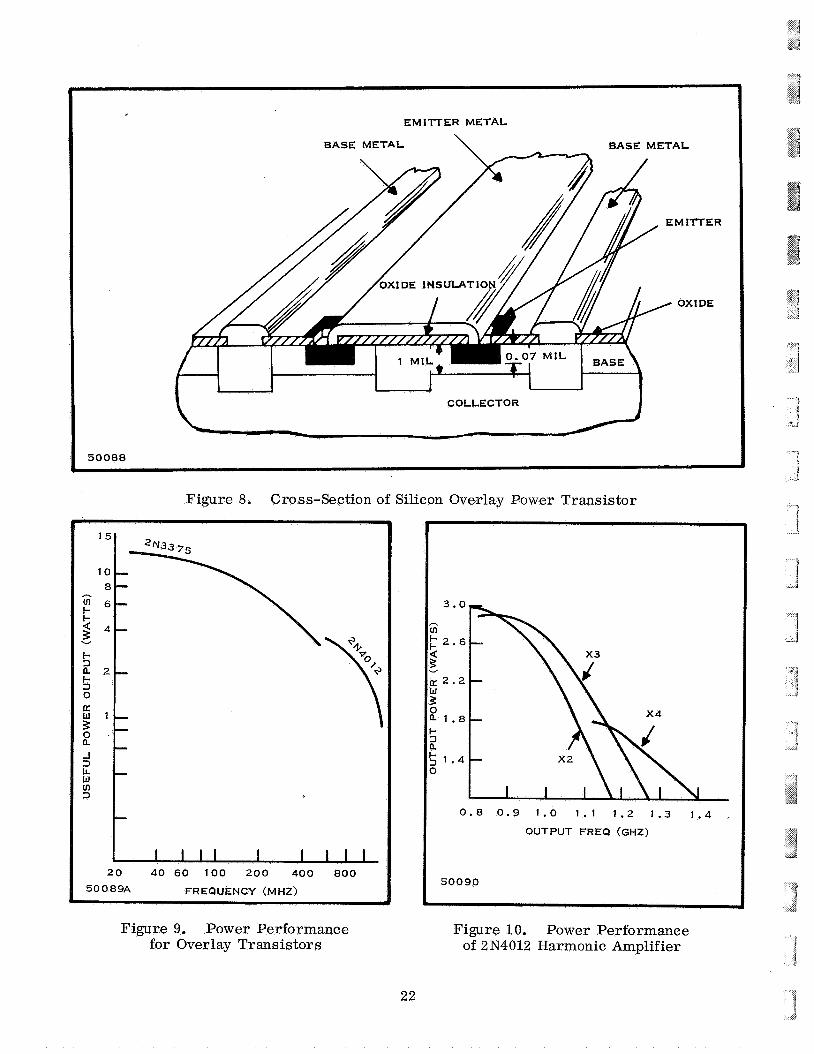
3. Other Microwave Power Devices One ap roach to power generation at microwave frequencies is to use an
overlay transistorfo. The overlay construction is illustrated in Figure 8 and permits suitable scaling to large area geometry by increasing the emitter edge proportionally
* Trademark of Texas Instruments Incorporated
14
15
16
F:
E 0 .c, 0 c pc
1 .o 2.0 3.0 4.0
FREQUENCY (GHZ)
Device P out (Pulsed)
500 83
P in (Rlsed)
Figure 3. Typical L158 Transistor Output Power
L158 C (17-stripe) 350 mW 57 mW
17
m
0 > 0 m o
0 c
N 0
n ;
? N
m N
h N I
> N U * z N W
3
9
s L
c
N
0
N
4,' * o m u , 0 0 o u E n m
18
i i
i " i
Frequency, 2.25 GHz, Vcc = +24 Vdc Device
5 0 0 8 5 A CLASS C STAGES
P in Pout IC mW mW mA
Figure 5. Class C Amplifier Using L158C Devices
Table 11. Performance of L158 Devices
L158 C, class A driver 30 2 55 2 3
L158 C, class C amplifier 59 270 30
L158 A, class C amplifier 2 57 540 96
Table III. Parameters of the L187
l BVCBO I C = l o m A , I E = o 30V
VCE = lOV, IC = 15 mA
Vcc = 15V, IC = 30 mA
hFE
Po
f = 4.0 GHz
10
30 mW 40 mW
19

1 I I . 1 .o .2.0 . 4 . 0
FREQUENCY (GHZ)
50086A
Figure 6. L-187 Performance
as the emitter area is increased. The high currents required of a transistor operating at high power outputs are handled easily by the increased ratio of emitter periphery to emitter area.
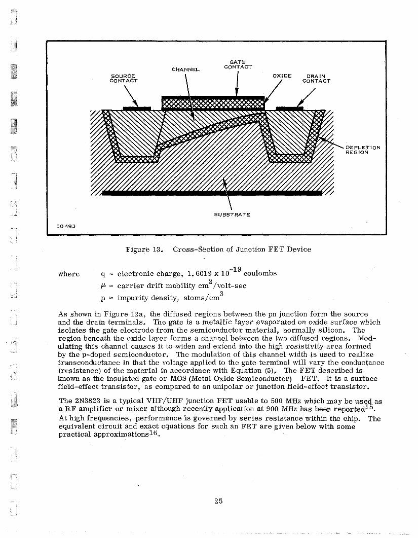
The new emitter electrode overlay was first used in the 2N3375 transistor, and is now used in a new unit, the 2N4012 transistorll.Both transistors are N P N planar epitaxial with a collector area of 400 square mils, emitter area of 40 square mils, and an emitter edge of 300 mils. 2N4012 can provide more than 2.5 watts at a frequency of one gigahertz with an efficiency of 25 percent o r higher when used as a tripler. The power performance of the two devices are plotted versus frequency in Figures 9 and 10. From Figure 10, the 2N4012 used in the common emitter confi
and delivers 1.7 watts at 1.2-GHz when used as a quadrupler. State-of-the-art power output capabilities achieved in an overlay transistor operated at 28 volts are shown in
Figure 11. Continuous power outputs of 20 watts at 400-MHz, 18 watts a t 500-MHz, 7 watts a t 1-GHz, and 1 watt at 2-GHz have been obtained with developmental units.
The 2N3375 generates three watts at 500 MHz, and the
ration delivers three watts of output power at 800 MHz when used as a doubler 1T .It supplies 2.7 watts at 1-GHz when used as a tripler
D. HIGH FREQUENCY FIELD EFFECT TRANSISTORS
The metal-oxide semiconductor field effect transistor (MOS-FET) and junction FET's high frequency performance has been extended to L-Band as a result of the technology advances in the fabrication of silicon microwave transistors14. The FET is particularly well suited in many VHF and UHF receiver stages requiring high input impedance, low cross-modulation distortion and low noise. The devices are
20
2000
1000
500
200
100
50
20
10
5
2
50087A
.0
0 1 2 3 4 5 6 7
FREQUENCY (GHZ)
Figure 7. Oscillator Performance of the L187 and L E 8 Devices
21
E M l l T E R METAL
COLLECTOR I
Figure 8. Cross-Section of Silicon Overlay Power Trans is tor
20 40 60 100 200 400 800
5 0 0 8 9 A FREQUENCY (MHZ) I Figure 9. Power Performance
for Overlay Trans i s to r s
0.8 0.9 1.0 1 . 1 1 . 2 1 . 3 1 . 4 . OUTPUT FREQ (GHZ)
50090
Figure 10. Power Performance of 2 N4012 Harmonic Amplifier
22

!*
especially well suited as IF and audio amplifiers and can be controlled in either forward or reverse AGC modes. Present commercially available FET's have gain bandwidth products of 75 to 100 MHz so that low noise, low distortion amplifiers and mixers in the VHF region are prac- tical. Developmental FET's have been reported with larger gain bandwidth . products that work satisfactorily at 1 GHz as amplifiers and oscillators and the commercially available 2N3823 has been used for a 900 MHz common-gate amp- lifier . 15
A field effect transistor (FET) is essentially a semiconductor current path whose conductance is controlled by apply- ing an electric field perpendicular to the current. A typical diffused field-effect transistor is shown in Figure 12a and its electrical equivalent diagram is shown in Figure 12b.
30
20 r.
t-" $ 16
I-
% v
2 12
s a 8 ; B
0
4
I I I I I J 0 . 1 0.2 0 . 4 0.6 1.0 2
FREQ (GHZ)
50220
The devices consist of a single P o r N type semiconductor bar with a contact at each end. N-type impurities are introduced into opposite sides of a P type bar as shown in Figure 12a. Contacts to
Figure 11. State-of-the-Art Performance of Overlay
Transistor
the N type impurities provide the rlgatell input. The contacts at each end of the bar are the drain and source connections. Comparing the FET to a vacuum tube, the "source" is analogous to the cathode, the rlgatel' corresponds to the grid, and the "drain" can be compared to the anode o r plate. The field effect also has electrical properties similar to a vacuum tube, and as in vacuum tubes, the gain factor is expressed in transcon- ductance, (gm). Amplification is achieved by the action of the majority of carr iers within the device. For this reason, the FET is an unipolar device as compared to the bipolar junction transis tor.
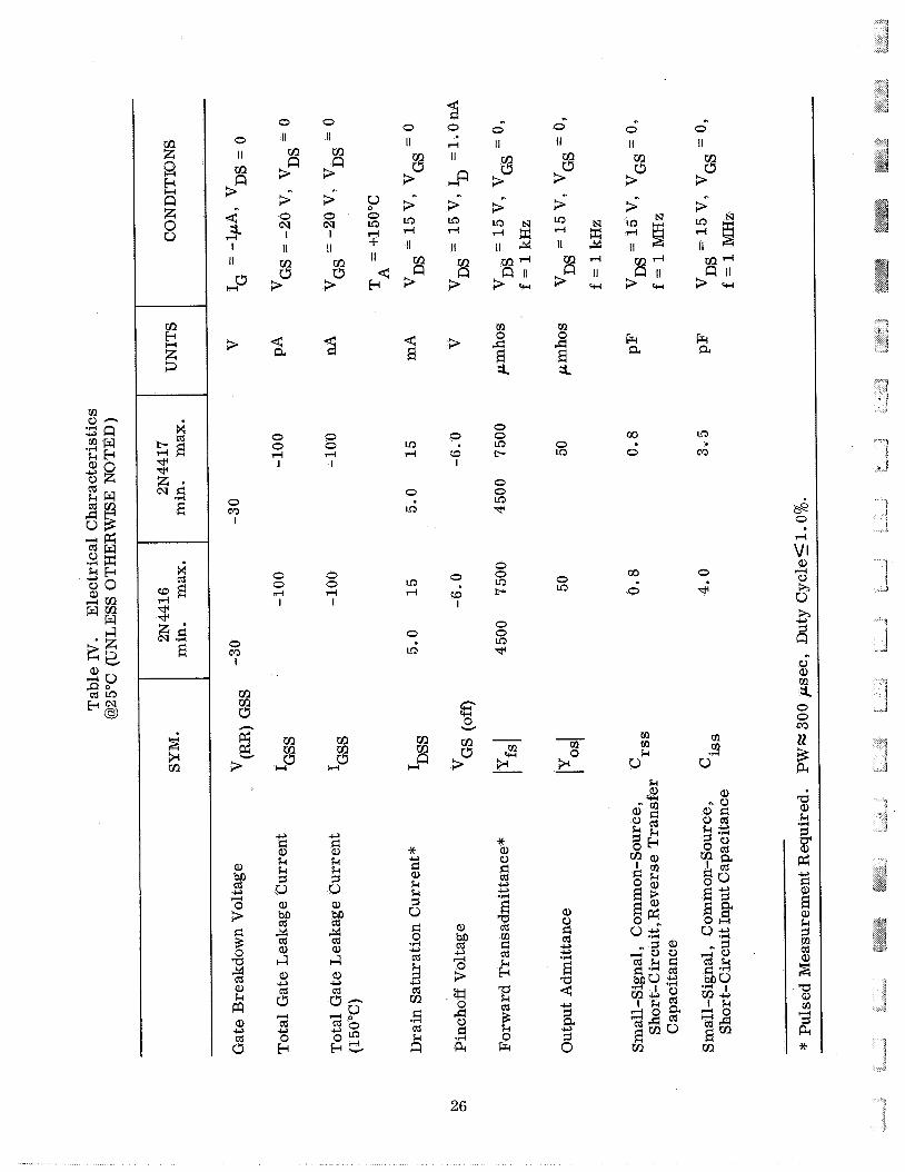
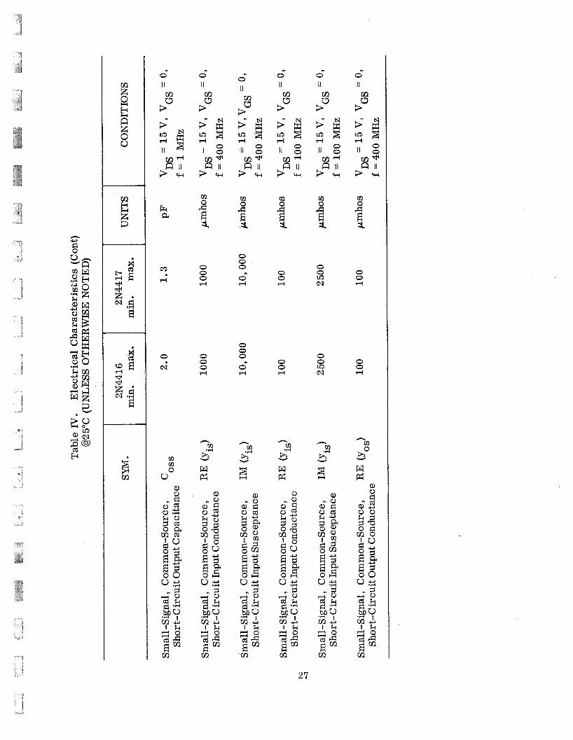
The construction of a high frequency FET is similar to that of the interdigitated bipolar transistor, and it is constructed in much the same fashion, except in the location of the junction relative to the terminals. To produce an n-channel device, a p-type silicon wafer with a resistivity of 3 to 10 ohm/cm is used as a starting material. A number of heavily doped n-type stripes are diffused into the surface. The ends of alternate strips are connected together and form the drain and source contacts. An insulating layer of silicon dioxide or silicon nitride is placed over the areas between the diffused n stripes. The thickness of this insulating layer is typically one to two thous- and angstroms. A metalized layer is then deposited on top of the dielectric insulating layer to form the gate electrode. A cross section of this structure is shown in Figure 13. device is presented in Table IV. Operation of a FET can be better understood by con- sidering a semiconductor bar having the dimensions as shown in Figure 14. The con- ductances through the length of the bar depends on the dimensions of the bar and the
The electrical characteristics of a 2N4417 n-channel expitaxial planar silicon
,c
23

conductivity of the semiconductor. The conductance of the bar is proportional to the total number of current car r ie rs present. tration of impurity atoms contributed by doping. every part of the bar, the conductance of the bar is
The latter being a function of large concen- If this concentration is uniform in
"DS
- :I11 +
N
/ /
P
A N -
(A) STRUCTURE
B I A S
DRAIN
"D
SOURCE
(B) DEVICE SYMBOL ' 4332114
* OPPOSING P-REGIONS ARE i NT ER NALLY CONNECTED
Figure 12. (a) Diffused FET Transistor, @) Electrical Circuit
24
SOURCE CONTACT
GAT E CONTACT CHANNEL
\ I OXIDE DRAIN / CONTACT
DEPLET REGION
'ION
SUBSTRATE
50493
Figure 13. Cross-Section of Junction FET Device
-19 where q = electronic charge, 1.6019 x 10 coulombs 2 P = carrier drift mobility cm /volt-sec
p = impurity density, atoms/cm 3
As shown in Figure 12a, the diffused regions between the pn junction form the source and the drain terminals. isolates the gate electrode from the semiconductor material, normally silicon. region beneath the oxide layer forms a channel between the two diffused regions. Mod- ulating this channel causes it to widen and extend into the high resistivity area formed by the p-doped semiconductor. The modulation of this channel width is used to realize transconductance in that the voltage applied to the gate terminal will vary the conductance (resistance) of the material in accordance with Equation (5). known as the insulated gate o r MOS (Metal Oxide Semiconductor) field-effect transistor, as compared to an unipolar o r junction field-effect transistor.
The 2N3823 is a typical VHF/UHF junction FET usable to 500 MHz which may be used as a R F amplifier or mixer although recently application at 900 MHz has been reported15. At high frequencies, performance is governed by series resistance within the chip. The equivalent circuit and exact equations for such an FET are given below with some practical approximations16.
The gate is a metallic layer evaporated on oxide surface which The
The FET described is FET. It is a surface
2 5
0 II
8 3
$ I
/I * H
3
0 m I
0 m
I
m 8 is F
a, 3 u d
e
P
a, 3 G s a, U
0
II m n
j
8
2
3
0 cu I II
3
0 0 rl
I
0 0 0 0 4 4 I I
m m * H
U
5 2
3 s s
k
u a,
a, U
c5 d
U m
U
5 k k 5 u a, 3 3 a, I4
d
I-p s
0
I-l II
u3 rl
II m n
3
3
0
co I
0
co I
E
8 0 W
3
a, 2 s 2 %
U d
c .A
PI
26
.. 0 II
: 3
00
0
n
0 II
8 s 3
2 8 I I m d
3 % n II
Fr a
u3
cr3
0 u3
00
0
0
-4
m m k u
m m .A u
z rl
a, 0 3 U 3
v r3
+-1 z c; a; u:
C C c5
$ P
a
E a Fr
T F .r r
c E
i a ; U n t : T U
a
a c
6 *
n 0
I I
8
rl m z
3
0 ' 0 m * R II
3 %
m B E 3.
0 0 0 rl
0 0 0 rl
n m A- -
27

DRAIN
43320
~
Figure 14. Semiconductor Bar
The equations for the common source VHF complex admittance parameters are approx- imated:
2 2 = w (Cgs+Cgd) Rg+jw (Cgs+Cgd)
2 2 - -o Cgd (Rg+Rd) - j w Cgd = gfs - j o Cgd =
y11 y12
y22
-
y2 1 7 gos+w' Cgd2 Cgd2(Rg+Rd) + j o Cgd
The input and output admittance transfer characteristics clearly show that the admit- tances increase as the square of the frequency (Figure 15). The power gain of a FET device may be defined as
= 1 /2 [1+ (-1 € P 2 ] G1 c3
where gm is the transconductance and C3 is the combined external gate to drain capac- itance and channel to gate capacitance. As seen in Equation ( lo) , increasing the ratio of gm/C will increase the power gain. gate source path and involves a reverse biased junction. As this junction is large in area, it presents a large input capacitance, thus, limiting the high frequency response. The gm term is high frequency dependent and can be expressed as
The high input impedance is the result of the 3
28
50222
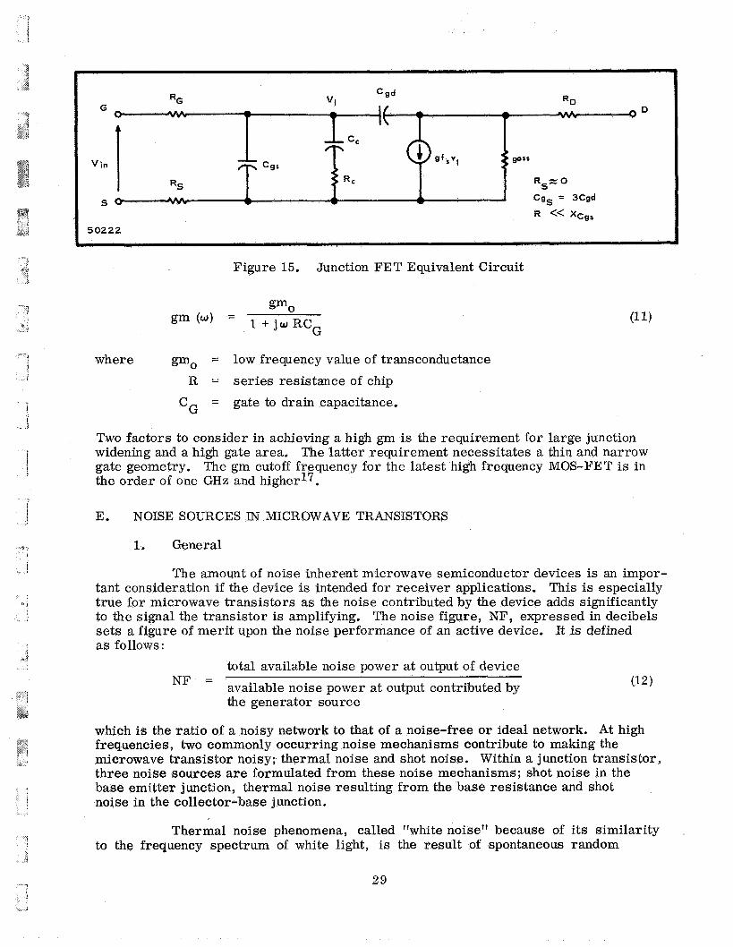
Figure 15. Junction FET Equivalent Circuit
where gmo = low frequency value of transconductance
R = series resistance of chip
CG = gate to drain capacitance.
Two factors to consider in achieving a hi& gm is the requirement for large junction widening and a high gate area. The latter requirement necessitates a thin and narrow gate geometry. The gm cutoff frequency for the latest high frequency MOS-FET is in the order of one GHz and higher17.
E. NOISE SOURCES IN MICROWAVE TRANSISTORS
1. General
The amount of noise inherent microwave semiconductor devices is an impor- tant consideration if the device is intended for receiver applications. This is especially true for microwave transistors as the noise contributed by the device adds significantly to the signal the transistor is amplifying. The noise figure, NF, expressed in decibels sets a figure of merit upon the noise performance of an active device. It is defined as follows:
total available noise power at output of device
NF = available noise power at output contributed by the generator source
which is the ratio of a noisy network to that of a noise-free or ideal network. At high frequencies, two commonly occurring noise mechanisms contribute to making the microwave transistor noisy; thermal noise and shot noise. Within a junction transistor, three noise sources are formulated from these noise mechanisms; shot noise in the base emitter junction, thermal noise resulting from the base resistance and shot noise in the collector-base junction.
Thermal noise phenomena, called "white noise" because of i ts similarity to the frequency spectrum of white light, is the result of spontaneous random
29
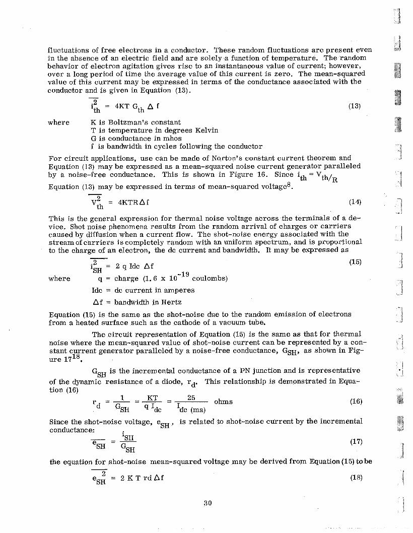
fluctuations of free electrons in a conductor. These random fluctuations are present even in the absence of an electric field and are solely a function of temperature. The random behavior of electron agitation gives rise to an instantaneous value of current; however, over a long period of time the average value of this current is zero. The mean-squared value of this current may be expressed in terms of the conductance associated with the conductor and is given in Equation (13).
i2 = 4KT Gth A f th where K is Boltzman's constant
T is temperature in degrees Kelvin G is conductance in mhos f is bandwidth in cycles following the conductor
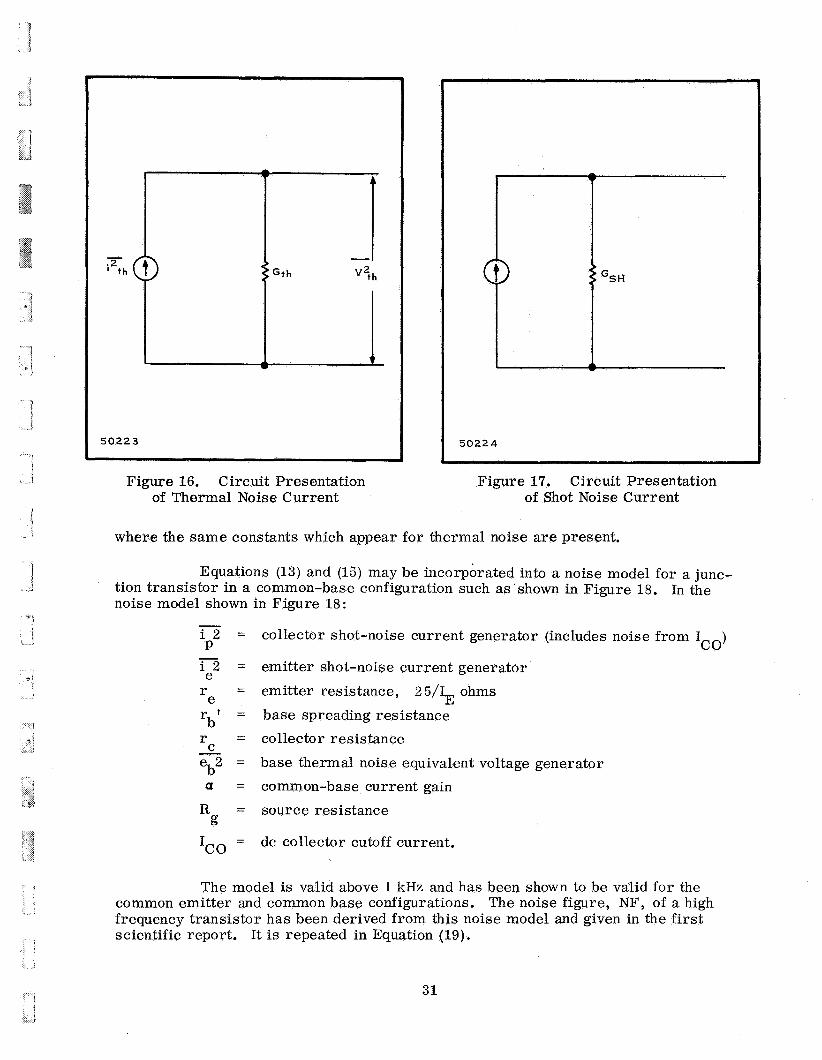
For circuit applications, use can be made of Norton's constant current theorem and Equation (13) may be expressed as a mean-squared noise current generator paralleled by a noise-free conductance. This is shown in Figure 16. Since ith-
Equation (13) may be expressed in terms of mean-squared voltage8. - 'th/,
(14) 2 Vth = 4KTRAf
This is the general expression for thermal noise voltage across the terminals of a de- vice. Shot noise phenomena results from the random arrival of charges o r carr iers caused by diffusion when a current flow. The shot-noise energy associated with the stream of carr iers is completely random with an uniform spectrum, and is proportional to the charge of an electron, the dc current and bandwidth. It may be expressed as
iL = 2 q Idc Af SH where q = charge (1.6 x 1 O - l ' coulombs)
Idc = dc current in amperes
Af = bandwidth in Hertz
Equation (15) is the same as the shot-noise due to the random emission of electrons from a heated surface such as the cathode of a vacuum tube.
The circuit representation of Equation (15) is the same as that for thermal noise where the mean-squared value of shot-noise current can be represented by a con- stant current generator paralleled by a noise-free conductance, GSH, as shown in Fig- ure 1718.
GSH is the incremental conductance of a P N junction and is representative of the dynamic resistance of a diode, rd' This relationship is demonstrated in Equa- tion (16)
25 ohms - 1 - KT - - - - - - rd GSH cy 'dc 'dc (ma)
Since the shot-noise voltage, eSH , is related to shot-noise current by the incremental conductance:
- ISH sH GSH
e = -
the equation for shot-noise mean-squared voltage may be derived from Equation (15) to be - = 2 K T r d A f (18) eSH
30
i
- I Gth v?h
50224
'SH
Figure 16. Circuit Presentation of Thermal Noise Current
Figure 17. Circuit Presentation of Shot Noise Current
where the same constants which appear for thermal noise are present.
Equations (13) and (15) may be incorporated into a noise model for a junc- tion transistor in a common-base configuration such as shown in Figure 18. In the noise model shown in Figure 18:
- i 2 =
i 2 =
r =
P
e e b
-
r ! =
r = C - eb2 - -
a =
R = g
- IC0 -
eo) collector shot-noise current generator (includes noise from I
emitter shot-noise current generator
emitter resistance, 2 5/IE ohms
base spreading resistance collector resistance
base thermal noise equivalent voltage generator common-base current gain
source resistance
dc collector cutoff current.
The model is valid above 1 kHz and has been shown to be valid for the common emitter and common base configurations. frequency transistor has been derived from this noise model and given in the first scientific report. It is repeated in Equation (19).
The noise figure, N F , of a high
31
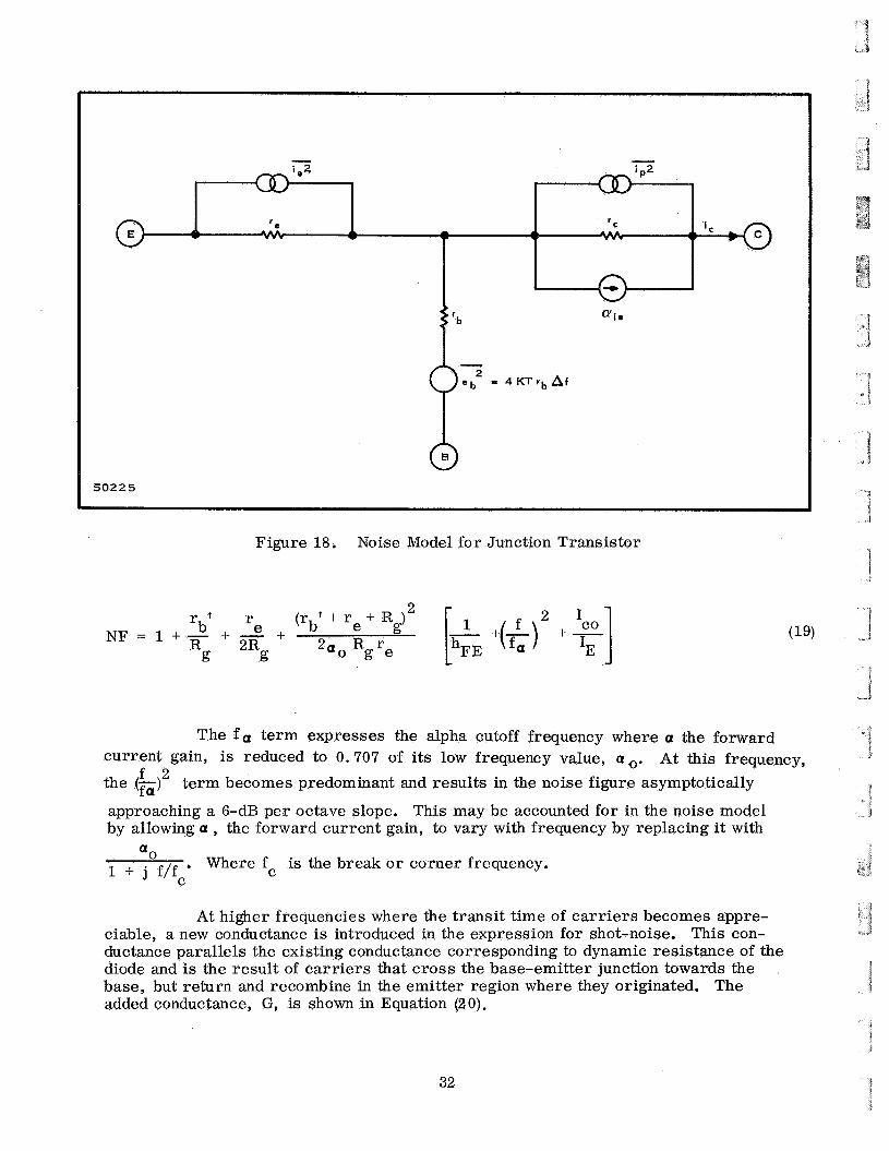
50225
Figure 18. Noise Model for Junction Transistor
r 1 r (rb' + re + Rg' 2 2 1 e
g 2R R r + - + b N F = 1 + - R
g 2ao g e
The fa term expresses the alpha cutoff frequency where a the forward current gain, is reduced to 0 .707 of its low frequency value, Q o.
f 2 the (g) approaching a 6-dB per octave slope. This may be accounted for in the noise model by allowing a , the forward current gain, to vary with frequency by replacing it with
At this frequency, term becomes predominant and results in the noise figure asymptotically
aO
1 + j f/fc' Where fc is the break o r corner frequency.
At higher frequencies where the transit time of carr iers becomes appre- ciable, a new conductance is introduced in the expression for shot-noise. This con- ductance parallels the existing conductance corresponding to dynamic resistance of the diode and is the result of carr iers that cross the base-emitter junction towards the base, but return and recombine in the emitter region where they originated. The added conductance, G, is shown in Equation (20).
32

' I J
i
2 SH i + 4 KT (G - GsH)A€
2. Field Effect Transistor
The field-effect transistor (FET) is subject to the same types of noise found in conventional transistors. The noise mechanisms in the FET are quite similar to those in the diffusion transistor except for the part which capacitance plays. The noise model for the FET shown in Figure 19 accounts for the division of channel resistance 18 .
In the noise model shown in Figure 19,
= channel resistance RCH rd = dynamic drain resistance
r = incremental source resistance
C = gate to drain capacitance C = gate to source capacitance
S
gd
gs
i = gate to source noise current generator P
eth = equivalent noise voltage generator
50226
9m"
Figure 19. Noise Model for the FET
33

The noise generating mechanism operative in an FET are caused by the following physical phenomena:
a. The gate leakage current, which generates full shot-noise
b. A thermal noise voltage generated in the conducting channel which modulates the space-charge layer height
c, Generation - recombination noise in the space-charge layer.
The generation-recombination noise in the space-charge layer modifies the thermal noise voltage in the conducting channel and gives it a l / f o r flicker noise dependence. However, the l / f noise does not become significant unless the FET is operatinq at very low frequencies. For surface o r insulated gate FET's, the effect of shot noise created by the gate leakage current may be neglected as this current is small enough to be negligible.
For all frequencies above the region where the l / f flicker noise is effective, the noise figure of the FET derived from the above noise model may be written as:
G = source conductance S where g m s . ' w C c gd
a constant that defines the division of channel resistance
F. ADVANCES IN LOW NOISE MICROWAVE TRANSISTORS
Present planar double-diffused germanium transistors in which bases a re diffused to a depth of 0.5 and 0.8 p m a re exhibiting base resistances as low as 18 ohms and base-collector time constants as low as 1 psec. applied to development of N P N germanium transistors for low-noise amplification at S- and C-band. The noise performance of these transistors have noise figures of 5-tO.5 dB at 3 GHz with measured gains of 6.5 to 6.8 dB. The application of double dzfusion technology to N P N silicon semiconductors has resulted in the L-83 device that has a noise figure within 0.25 dB of planarized germanium devices while yielding higher gains1.
These technology advances are being
1. L-148 Geometry
The L148 alloy emitter, diffused base planar germanium geometry has
The TIXM105 and the TIXM103 offer the lowest noise figure. The produced the TIXMl03, 104, 105 and 106 alloy emitters, diffused base planar german- ium transistor. noise figures of these devices are 4-5 dB at 3 GHz.
In a practical microwave receiver, the TIXMl03 would serve as a low- noise input stage followed by the TIXM104 as a subsequent high-gain amplifier. A typical IXMl04 device in a second stage provides 6.5-dB gain and 6.5-dB noise at 1.5 GHz . At 1.5 GHz, the TIXMl03 is rated for typical 8.5 dB gains and a 5-dB noise figure when used in a high gain circuit.
3
34
-1
Parameter Minimum
"I%
1 - 3
Maximum Unit
'cbo
hfe ('CE = -gv, I C = 7mA
f = 400 MHz)
Ccb (VCB = -9v, IE = 0
f = 1MHz)
N F (f = 3 GHz)
-12
4.5
0.2
Volt
-
Pfd
dB
Gain bandwidth product 1.8 GHz
Power Gain @ 3 GHz 3 dB
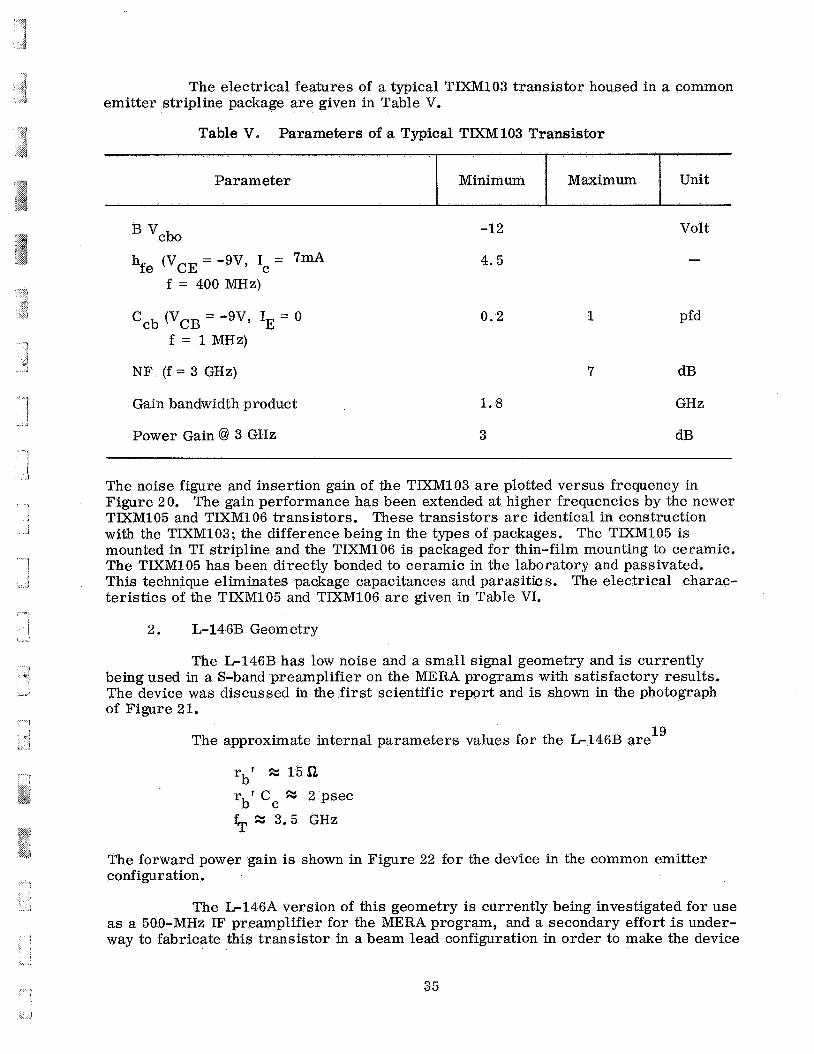
The noise figure and insertion gain of the TIXM103 are plotted versus frequency in Figure 20. The gain performance has been extended at higher frequencies by the newer TMM105 and TIXMl06 transistors. These transistors are identical in construction with the TIXM103; the difference being in the types of packages. mounted in TI stripline and the TIXMl06 is packaged for thin-film mounting to ceramic. The TIXMl05 has been directly bonded to ceramic in the laboratory and passivated. This technique eliminates package capacitances and parasitic s. The electrical charac- teristics of the TMM105 and TIXMlO6 a re given in Table VI.
The TIXM105 is
2. L-146B Geometry
The L-146B has low noise and a small signal geometry and is currently being used in a S-band preamplifier on the MERA programs with satisfactory results. The device was discussed in the first scientific report and is shown in the photograph of Figure 21.
19 The approximate internal parameters values for the L-146B are
rbf x 1552
rbf Cc x 2 psec
5 X 3.5 GHz
The forward power gain is shown in Figure 22 for the device in the common emitter configuration.
The L146A version of this geometry is currently being investigated for use as a 500-MHz IF preamplifier for the MERA program, and a secondary effort is under- way to fabricate this transistor in a beam lead configuration in order to make the device
35

I- U W m z
50227
IO
9
8
7
E
e
4
7 -
i
1
-
-
I I I I 1 . o 1 . 5 2.0 2 . 5 3.0
FREQUENCY (GHZ)
Figure 20. Noise Figure and Insertion Gain of TMM103
compatible with thin-film circuitry. Characterization data for epitaxially construction of the L-146A transistor is shown in the Table VII. due to a low ft. At the present time, transistor fabrication is being modified to improve the parameters.
The excessive N F at 500 MHz is
3. Other Small Signal Geometries
The L-83 is a silicon device which has a 2 . 5 micron emitter compared to the 7.5 micron emitter of the TIXM103 germanium planar transistor. The power gain of these two devices as a function of frequency is shown in Figure 23 where the super- ior power capability of silicon is evident. The L-83 can deliver 1 0 mW at 4 GHz. The advantage of the smaller dimensions is that it helps to extend the frequency response of the device.
36

k 0 rn rn c cd
4.2
.d
G s ki
W 0
E .a c: cd m 0
2 i5 E 4 Q 0 .d
8
8 8
s 2
cd w 0 rn k a, U
cd k
a,
E
a, k 1 cd k a,
U
z s
a,
m cd
E
u v3 N
cd rn 0
u1 k a, 0 cd k
u cd
k 0 a,
U
.d U
.d
U
2 t-4
.o, U
4 w
3
N rl I
0 I1 w H
4 0 0 rl I I1 0
H
a 3
k
I$
U t-4
c
3 a,
+ k a, rn 0 0 a,
0 u
U
t-4 t-4
0 0 0 a w F 9
R a
rl
N 0
.. 0
I I w H
s n ? d I 1 2 F 9 r ' u I1
3 %
a,
cd
0 cd a cd u a, rn
z 3
+ k 0 0 a,
0 u
U
4 4
% u
37
a, k 1 cd k a,
U
; ; s 2
a cd
m N
cd rn 0
rn k a, 0 cd k
u m r: cd k a,
U
.d U
.d
U
2
.d U
0"
@I u m N
Sl
cd
1
x
U
E E .d
3 2
2
m -;tr a,
m R .d
a, rn .d
5 a, a, El cd k cd
U
a

38
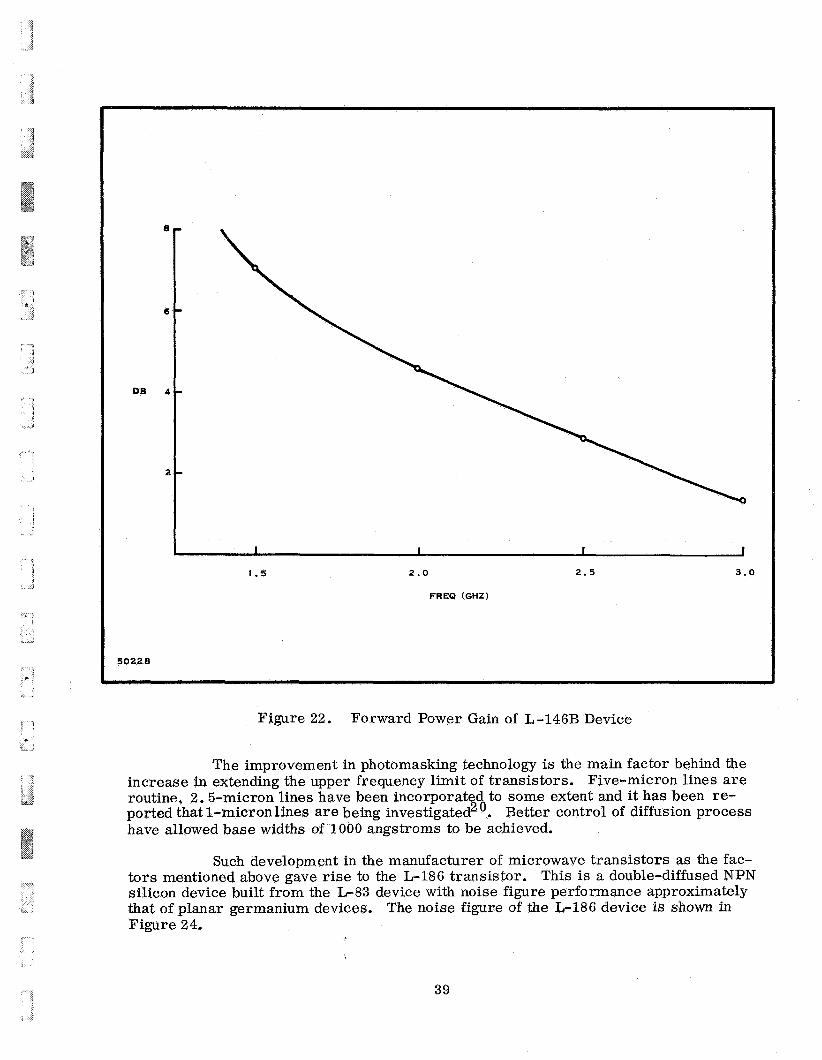
6 -
6 -
DB 4 -
2 -
I I I I
1.5 2 . 0 2 . 5 3.0
FREQ (GHZ)
50228
Figure 22. Forward Power Gain of L-146B Device
The improvement in photomasking technology is the main factor behind the increase in extending the upper frequency limit of transistors. Five-micron lines a re routine, 2.5-micron lines have been incorporated to some extent and it has been re- ported that 1-micronlines a re being investigated2 '. Better control of diffusion process have allowed base widths of 1000 angstroms to be achieved,
Such development in the manufacturer of microwave transistors as the fac- tors mentioned above gave rise to the E186 transistor. This is a double-diffused N P N silicon device built from the L-83 device with noise figure performance approximately that of planar germanium devices. The noise figure of the L-186 device is shown in Figure 24.
39
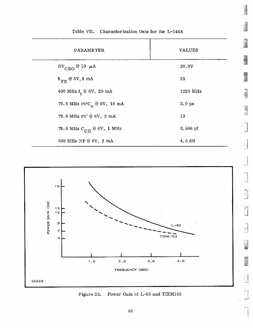
PARAMETER
BVCBO @ 1 0 p A
hFE @ 6V,2 mA
400 MHz f t @ 6V, 20 mA
79.8 MHz rb'Cc @ 6V, 10 mA
VALUES
79.8 MHz rb' @ 6V, 2 mA
79.8 MHz CCB @ 6V, 1 MHz
500 MHz N F @ 6V, 2 mA
30. OV
35
1325 MHz
3.0 ps
1 0
0.586 pf
4.5 dB
\
T l X M 103
Figure 23. Power Gain of L-83 and TIXMl03
40

5 . 5
h m 0 v
W lx 3
lL
‘3 4.5
W
0 z 2
3 . 0
2.8
TlXM103 L--148
/ L-83
- -
I I 1 I
1 .o 2.0 3 . 0 4.0
- -
I I 1 I
1 .o 2.0 3 . 0 4.0
503 1 9 A FREQUENCY (GHZ)
Figure 24. Noise Figure of Si N P N Double Diffused Transistor
The noise figure of the new silicon unit is approaching that of the TIXMl05 (L-148) planar germanium transistors and it may be seen that the noise figure of both units closely match the noise performance of traveling wave tubes and Ga Sb tunnel diodes in Figure 25.
The power gain of the TIXMl05 (L-148) transistor and the L-83 silicon device is compared in Figure 26 to a N P N germanium double diffused device, the L153B. The latter device is currently being developed at Texas Instruments to meet the spec- ifications given in Table VIII.
The double diffused germanium device L153B has much better gain than the alloy L-148 eometry and is expected for exceed the performance of the E 1 4 8 at higher frequencies2q. New double diffused silicon devices are currently being pursued in the laboratory which exhibit a maximum available gain (MAG) of 14-dB at 2 GHz with a noise figure of 5.5 dB. It is expected that these devices will have a MAG in excess of 15 dB and a noise figure of three decibels in the near future.
G. MICROWAVE AMPLIFIERS
1. S-Band Amplifier (1.7 - 2.4 GHz)
A low noise, three stage microwave amplifier consisting of double-bonded TIXM103(L148) transistors biased at nine volts and two milliamperes has been con- structed in Texas Instruments laboratories. The breadboard amplifier response is given in Figure 27 and indicates a measured power gain of 14 dB at band center. The
41
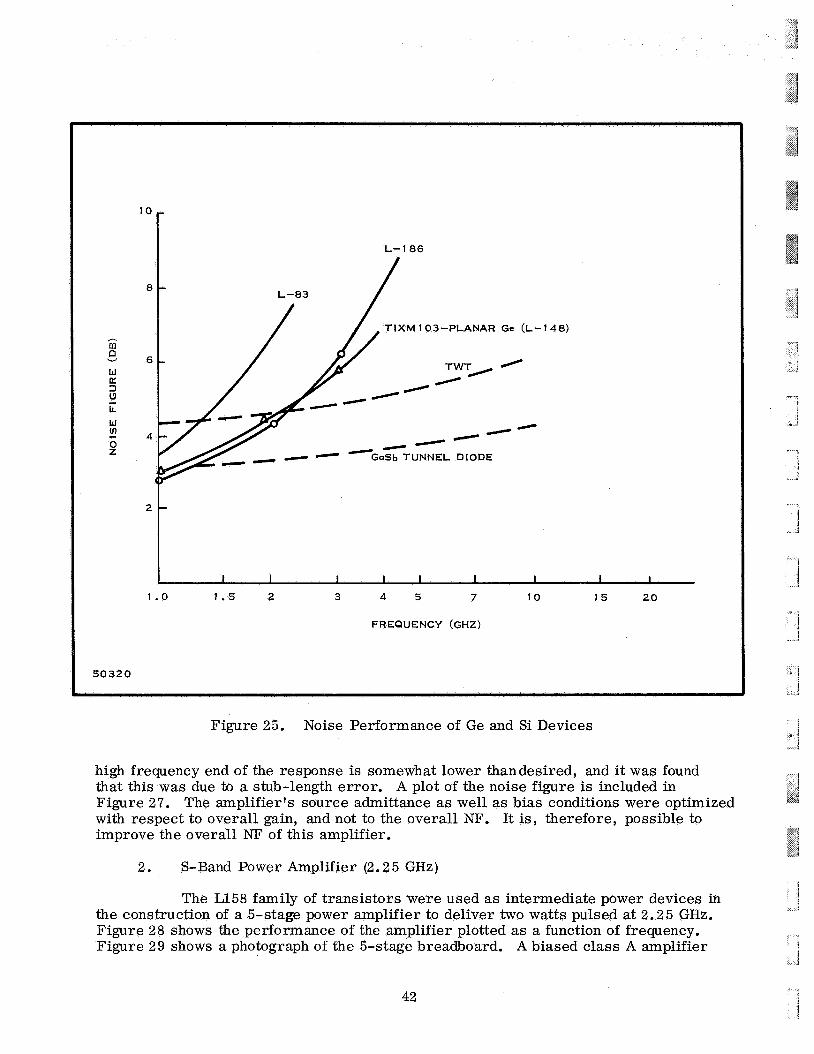
h
m a v
W CT 3 k9 Lr W
0 z
- F!
50320
10
8
TIXM 103-PLANAR G e (L-148)
6
4
2
1 . O 1.5 2 3 4 5 7 10 15 20
FREQUENCY (GHZ)
Figure 25. Noise Performance of Ge and Si Devices
high frequency end of the response is somewhat lower thandesired, and it was found that this was due to a stub-length error. A plot of the noise figure is included in Figure 27. The amplifier's source admittance as well as bias conditions were optimized with respect to overall gain, and not to the overall NF. It is, therefore, possible to improve the overall NF of this amplifier.
2. S-Band Power Amplifier (2.25 GHz)
The L158 family of transistors were used as intermediate power devices in the construction of a 5-stage power amplifier to deliver two watts pulsed at 2.25 GHz. Figure 28 shows the performance of the amplifier plotted as a function of frequency. Figure 29 shows a photograph of the 5-stage breadboard. A biased class A amplifier
42
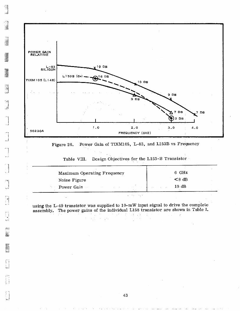
POWER G A I N R ELAT I VE
Maximum Operating Frequency Noise Figure Power Gain
L-83 SILICON
6 GHz <8 dB 10 dB
-1XM 105 (L 148)
5 0 2 3 0 A
L1 538 (Gel .rr
1 .o 2.0 3.0 4.0 FREQUENCY (GHZ)
DB
Figure 26. Power Gain of TIXMl05, L-83, and L153B vs Frequency
43
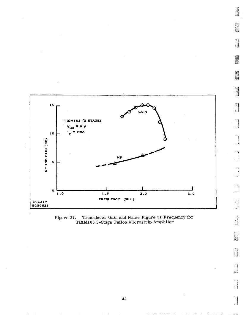
n
V
2
0
2 d a 2
2 n
v
5023 1 A
1 5
10
TIXMIOJ (3 STAGE) 4
I I I 1 .o 1 . 5 2 . 0 3 . 0
FREQUENCY (GHZ )
S C 0 6 6 3 1
i.
Figure 27. Transducer Gain and Noise Figure vs Frequency for TIXM103 3-Stage Teflon Microstrip Amplifier
44
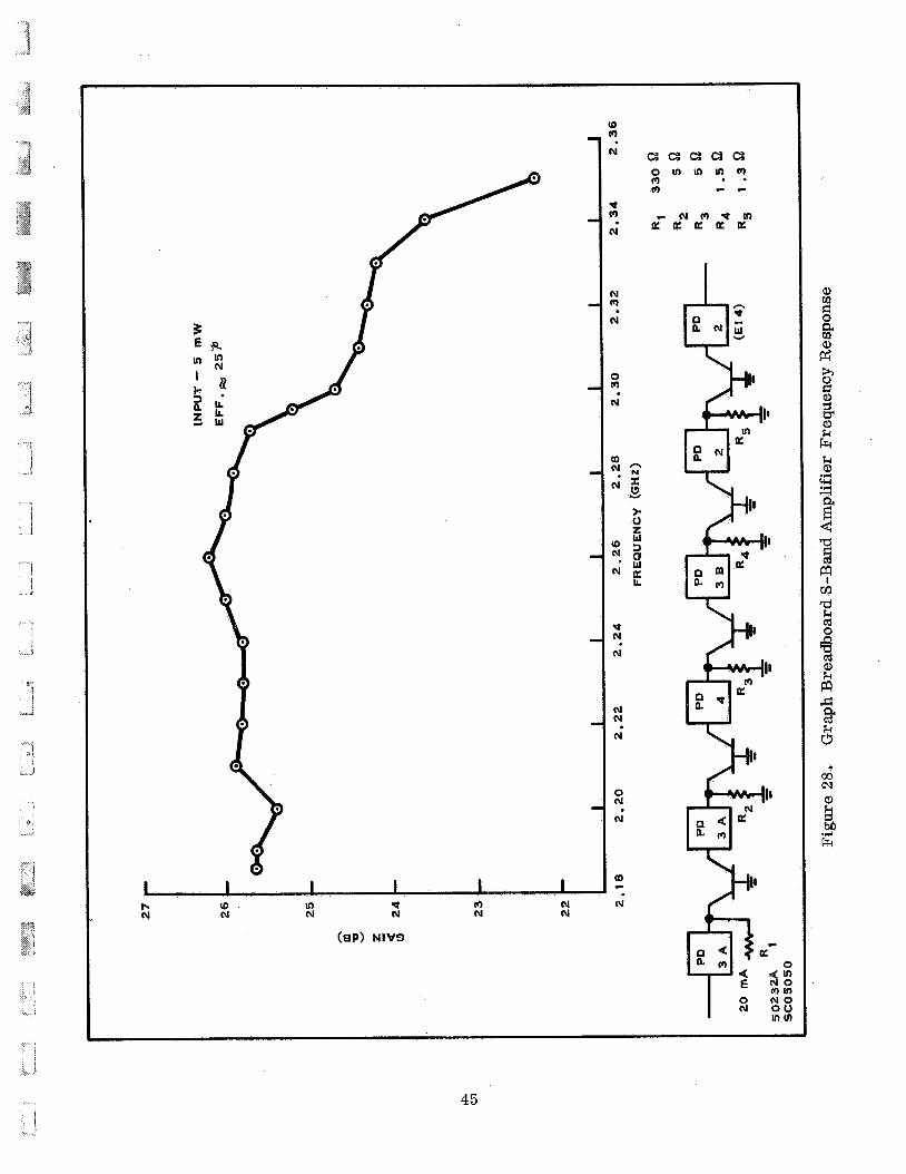
I I I I I I ln t m N
N w N h N N N N
(EP) NlVB
0 r) <
v 3
N
N m N
0 m N
Y N N = s?
w w N ’ - 8
L
). 0 z
N
* N N
01 N N
0 N N
03
N
-
45
c 3 8

a Fi a
I rn

SECTION IV
SEMICONDUCTOR DEVICES
A. GENERAL
The first and third Scientific Reports discuss in detail the characteristics of varactors, Schottky barrier diodes, PIN diodes, Step recovery diodes and to some extent the Gum device. This report updates and expands these subjects where applicable and introduces tunnel diodes and avalanche diodes.
B. VARACTORS
In the first report the discussion of varactors is confined to their use in frequency multiplication and division circuits along with their application to integrated circuits. This report adds to those applications by examining the varactor as a variable capaci- tance for use in circuit tuning. In this capacity, the diffused junction varactor is corn- pared to the abrupt junction (Schottky barrier) varactor.
The total capacitance at the terminals of a varactor may be varied by adjusting the reverse bias from 0 Vdc to its zener breakdown voltage. The exact relationship is shown in Equation (22).
= Capacitance of the package
= Capacitance of the junction when Vb is zero
= Reverse bias in Vdc
= Capacitance of the junction at any value of Vb.
cP Where
C
Vb C
n = Exponent determined by junction characteristics. Equal to approx-
$ = Contact potential equal to 0 . 7 for silicon devices.
jo
j
imately 1/3 for diffused junctions and 1/2 for abrupt junction.
If the junction capacitance is much larger than the package capacitance, Equation (22) becomes
r-4
This equation is shown in Figure 30 for different values of n representing a typical abrupt junction and a diffused junction varactor diode. This figure illustrates that for positive values of reverse bias, a voltage of 65 Vdc is required to cause the
47

0 Q1 m b UY Lo rf m N c - 0 0 0 0 0 0 0 0 0
0 ' 1 = O r 3 01 aZIZI1VWHON 93NV113VdV3 NOII3NIl.T
48
0 II)
0 N
0 c
0
Lo
7 N
0
c
II)
0
N
0
c
0
capacitance of the abrupt junction varactor to become one tenth of its value at zero bias. A voltage of 80 Vdc is required to cause the diffused junction varactor to become one fifth its value at zero bias. Any capacitance in parallel or series with the junction capacitance decreases the capacitance change ratio. Unfortunately, at microwave frequencies shunt capacitances may become appreciable. The package capacitance can be reduced to 25% or less by careful design. In cases where other parallel capaci- tances becomes too large, the varactor may be placed in series with an inductance large enough SO that the junction capacitance change is regarded by the circuit as an inductive change.
A varactor may be used for tuning so long as the following requirements are met.
1. The effect of circuit capacitance is overcome either by the method out- lined above or by keeping it substantially lower than the junction capacitance C..
J 2. The Q of the circuit need not be extremely high. It should be noted that Q
diminishes with increasing frequency, a s shown by:
Q = - fco f
where
f = frequency of operation
fco = cutoff frequency = 1
277R C s j
where R = series resistance
S
(24)
3 . it will cause the varactor capacitance to change enough to significantly detune the circuit. If the ac peak-to-peak voltage is more than 2 volts, the minimum reverse bias should be about 1 0 vdc. Of course, these factors a re relative to the total circuit Q and to whether the circuit being tuned is an oscillator, filter, or amplifier.
The ac signal swing must be small compared to the reverse bias otherwise
4. A dc voltage source capable of supplying adequate magnitudes of voltage must be available. A typical 28-volt supply for example, will give only about a 6.2- to -1 or 3 .5 - to -1 capacitance ratio, depending on the type of junction, and less when constant capacitances must be considered.
5 . Total capacitance variation must be enough to accomplish the desired tuning. Assuming the resonating inductance to be constant, the frequency-capacitance relation- ship is
(2 6 ) K
where
49
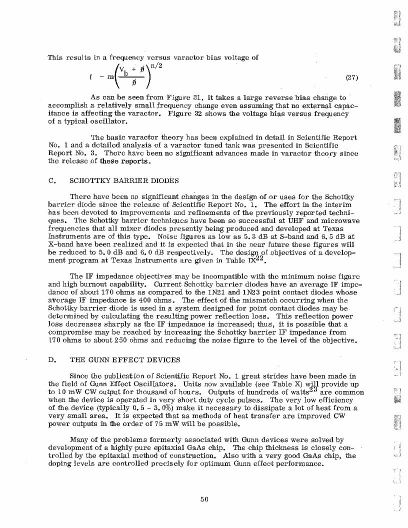
This results in a frequency versus varactor bias voltage of
As can be seen from Figure 31, it takes a large reverse bias change to accomplish a relatively small frequency change even assuming that no external capac- itance is affecting the varactor. Figure 32 shows the voltage bias versus frequency of a typical oscillator.
The basic varactor theory has been explained in detail in Scientific Report No. 1 and a detailed analysis of a varactor tuned tank was presented in Scientific Report No. 3. There have been no significant advances made in varactor theory since the release of these reports.
C. SCHOTTKY BARRIER DIODES
There have been no significant changes in the design of or uses for the Schottky barrier diode since the release of Scientific Report No. 1. The effort in the interim has been devoted to improvements and refinements of the previously reported techni- ques. The Schottky barrier techniqes have been so successful at UHF and microwave frequencies that all mixer diodes presently being produced and developed at Texas Instruments are of this type. Noise figures as low as 5.3 dB at S-band and 6.5 dB at X-band have been realized and it is expected that in the near future these figures will be reduced to 5.0 dB and 6.0 dB respectively. The design of objectives of a develop- ment program at Texas Instruments are given in Table IX22.
The IF impedance objectives may be incompatible with the minimum noise figure and high burnout capability. Current Schottky barr ier diodes have an average IF impe- dance of about 170 ohms as compared to the 1N21 and 1N23 point contact diodes whose average IF impedance is 400 ohms. The effect of the mismatch occurring when the Schottky barr ier diode is used in a system designed for point contact diodes may be determined by calculating the resulting power reflection loss. This reflection power loss decreases sharply as the IF impedance is increased; thus, it is possible that a compromise may be reached by increasing the Schottky barr ier IF impedance from 170 ohms to about 250 ohms and reducing the noise figure to the level of the objective.
D. THE GUNN EFFECT DEVICES
Since the publication of Scientific Report No. 1 great strides have been made in the field of Gunn Effect Oscillators. Units now available (see Table X) will provide up to 10 mW CW output for thousand of hours. Outputs of hundreds of watts23 are common when the device is operated in very short duty cycle pulses. The very low efficiency of the device (typically 0.5 - 3.0%) make it necessary to dissipate a lot of heat from a very small area. It is expected that as methods of heat transfer are improved CW power outputs in the order of 75 mW will be possible.
Many of the problems formerly associated with Gunn devices were solved by development of a highly pure epitaxial GaAs chip. The chip thickness is closely con- trolled by the epitaxial method of construction. Also with a very good GaAs chip, the doping levels are controlled precisely for optimum Gunn effect performance.
50

I I t 1
\
(D d N 0 al (D d N 0 v N 0 00
m m m N N N N N c - - - 7
0 = 'A 1V 0' 1 01 ( I X Z l l V W t l O N - A 3 N 3 ~ B 3 t l J
m 0
N
0
c
0
m N 0 In
51

50235
~
S -Band
Minimum Maximum Parameter
50
40
30
20
10
X -Band
Minimum Maximum
1250 1500 1750 2000 2250 2500
OSCILLATOR FREQUENCY ( M H Z )
Figure 32. Varactor Bias vs Frequency
Table IX. Schottky Barrier Diode Design Objectives
Intermediate Frequency 350 ohms 450 ohms 335 ohms 465 ohms Impedance ( ZIF)
Conversion Loss (Le) - 5 dB - 5 dB
Noise Figure (NFo) - 5 dB - 6 dB
Output Noise Ratio - 1 . 2 - 1.2
VSWR 1 .3 1 .3
Burnout by Single Pulse ergs 10 ergs (Bo)
Lc Unbalance
XIF Unbalance
0 .3 dB - 0.3 dB -
- 25 ohms - 25 ohms
52

Table X. Gallium Arsenide Gunn Effect Diodes (Texas Instruments Inc.)
Frequency
I I I Test Conditions
Maximum Operating Typical
'th Voltage Operating Current Type No. Oscillator Power
(mW) (Note 1)
C -Band L-188 0-1 - 1.0 7 Volts 12 Volts 100 mA - 200 mA
L-188A 1.0 - 5.0 f 1 Volt
L-188B 5.0 -10.0
X-Bmd L- 189 0.1 - 1.0 5 Volts
L-189A 1.0 - 5.0 f 1 Volt 1 0 Volts 100 mA - 300 mA
L-189B 5.0 -10.0
Ku-Band L-190 0.1 - 1.0 3 Volts
L-19 OA 1.0 - 5.0 f 1 Volt 7 Volts 100 mA - 300 mA
L-190B 5.0 -10.0
OPERATING NOTES:
1. Adequate heat sink must be provided.
2. Current limiting power supply is recommended.
Nearly all the research at Texas Instruments has been done in the frequency range from 4 GHz to 9 GHz. It was felt that the present transistor technology could provide oscillators up to 6 GHz with at least the same power output a s the Gunn oscil- lators. Furthermore, transistor oscillators a re more frequency stable.
There are two modes of operation of the Gunn oscillator. In the frequency range from 4 GHz to 30 GHz, the normal Gunn effect mode is used. In this mode, the fre- quency is determined by the thickness of the chip (i. e., f = the reciprocal of electron transit time), but small frequency changes (10 - 100 MHz) can be made by changing the applied voltage - 3.1.0 Vdc within the band of oscillation.
The second mode of operation is called Limited Space-Charge Accumulation (LSA). In this mode of operation, oscillation frequency is determined by circuit resonance rather than by transit time, The power output and efficiency are equal to o r higher than when the device is operated in the transit time mode. The frequency range for the LSA mode is approximately 30 to 100 GHz.
53
Very little research has been done in the 2- to 3-GHz range. At these frequencies the chip thickness becomes relatively large and the resonant cavaties become cumber- some. (one part in lo4) make it undesirable to use the Gunn devices at 2 . 5 GHz at this time.
These facts plus the low efficiency (0.5-3%) and the poor frequency stability
E. THE TUNNEL DIODE
1. General
The tunnel diode offers a unique physical mechanism for semiconductor operation and at the same time offers a unique se t of electrical characteristics for improved circuit design. In comparison with transistors, the tunnel diode offers advantages of extremely high frequency operation, low noise, small size, low oper- ating power levels, and high reliability4.
The tunnel diode is a two-terminal device consisting of single P N junction. The essential difference between it and a conventional diode is that the conductivity of the P and N material is more than 1000 times as high as the conductivity of the material used in conventional diodes.
Because of the very high conductivity of the P and N materials, the width of the junction (the depletion layer) is very small, of the order of inches. There- fore, it is possible for electrons to tunnel through the junction even though they do not have enough energy to surmount the potential barrier of the junction. Although tunnel- ing is impossible in terms of classical physics, it can be explained in terms of quantum mechanics. For this reason the mechanism is commonly called quantum mechanical tunneling.
Under conditions of reverse bias of a conventional diode there are no free- holes o r electrons to conduct charge across the junction. In the tunnel diode, however, a small reverse bias will cause the valence electrons of the semiconductor atoms near the junction to tunnel across the junction into the N region and, thus, the tunnel diode will conduct under reverse bias. In the tunnel diode a small forward bias will cause electrons in the N region to tunnel across the junction to the P region (appearing as valence electrons in the semiconductor atoms), and the tunnel diode will conduct. (Figure 33.) If the forward bias is increased, the energy of the free electrons in the N regions will become greater than the energy of the valence electrons in the P region and consequencly the tunneling current will decrease. This decrease in tunneling current with increasing forward bias causes the negative conductance characteristic which is typical of the tunnel diode. As the forward bias is increased further, the free holes and electrons will have enough energy to flow over the potential barr ier of the junction in a manner identical to that of a conventional diode.
7 Quantum mechanical tunneling has a theoretical frequency limit of 10 MHz
and is inherently a much higher frequency mechanism than the drift and diffusion mech- anisms involved in the operation of conventional diodes and transistors. In practice, the frequency limitation of the tunnel diode is determined by parasitic capacity, induc- tance, and resistance of the device (Table XI).
The characteristics described in the preceding paragraphs a re presented graphically in Figure 33. The portion of the static curve from V = 0 to V = Vp exhibits a low ac positive resistance. The portion from V = Vp to V = Vv is the negative resis- tance region as the current decreases with increasing voltage. The portion V>Vv is
54
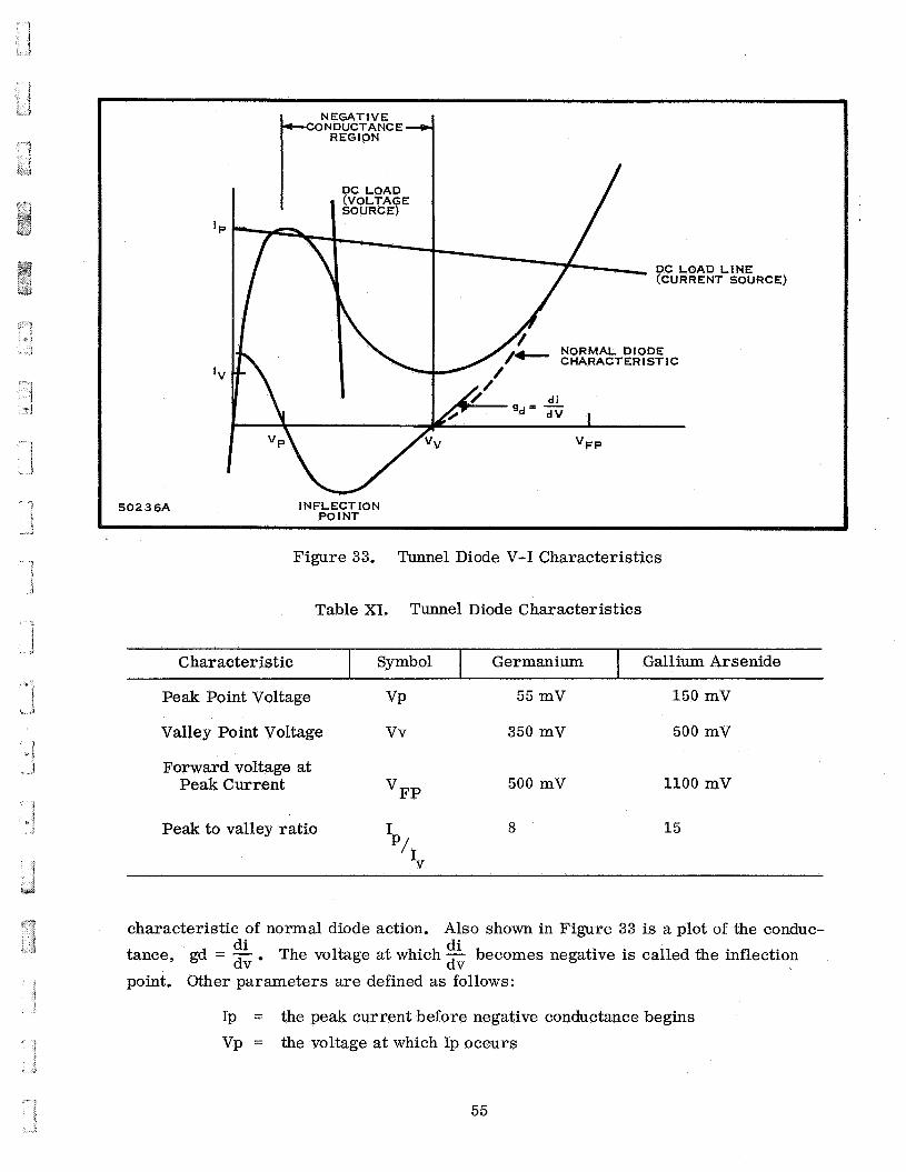
" I L_ J
Characteristic
" I
I
I Germanium I Gallium Arsenide Symbol
'P
'V
50236A
N EGAT I V E CONDUCTANCE
DC LOAD LINE (CURRENT SOURCE)
NORMAL DIODE CHARACTERISTIC
INFLECTION PO I NT
Figure 33. Tunnel Diode V-I Characteristics
Table XI. Tunnel Diode Characteristics
Peak Point Voltage VP 55 mV 150 mV
Valley Point Voltage v v 350 mV 500 mV
Forward voltage at Peak Current 500 mV 1100 mV 'FP
Peak to valley ratio I 8 15
p'I V
characteristic of normal diode action. Also shown in Figure 33 is a plot of the conduc- di di dv tance, gd = - dv
point. Other parameters a re defined as follows:
The voltage at which - becomes negative is called the inflection
Ip = the peak current before negative conductance begins Vp = the voltage at which Ip occurs
55

Iv =
Vv = the voltage at which Iv occurs
the minimum current at the end of the negative conductance region
= the voltage in the conventional diode characteristic region at which the current is equal in value to I
P' vFp
Tunnel diodes are commonly constructed from two materials, germanium and gallium arsenide, and both exhibit the general characteristics shown in Figure 33. Table XI lists the typical parameters of each type.
The negative conductance region of the tunnel diode has many applications. It may be used for amplification, oscillation, frequency conversion, and switching. To be used as an active device, the tunnel diode must be biased into its negative conduc- tion region with a constant voltage source. A constant current source bias is required in switching applications.
The operational stability of a tunnel diode circuit is determined by the total series resistance, RT = Rx+Rs, as shown by Figure 34.
2. Tunnel Diode Amplifier
A positive conductance by definition dissipates energy; therefore, it follows that a negative conductance will supply energy. This is the basis for negative resis- tance amplifiers.
Upon examination of the tunnel diode VI characteristics (Figure 33), it be- comes evident that for amplifier operation the "operating point" must be in the negative conductance region. Furthermore, to secure a stable operating point, the bias must be from a voltage source. tude of the anticipated signal swing, the required signal-to-noise ratio, and the oper- ating temperature range. In most cases it is required to bias the tunnel diode at the point of maximum negative conductance.
The location of this operating point will depend on the magni-
The greatest bias problem is that the negative conductance region is non- linear; thus it is necessary to match the diode conductance closely to the circuit con- ductance if high gain is to be achieved. Slight variations in the bias point with conse- quent variations in diode conductance can cause large changes in circuit gain. Conse- quently, it is very important to ensure a very stable bias voltage. Some possible methods for obtaining stable voltage from low impedance sources are:
the use of mercury cells
the use of forward bias diodes as voltage regulators
the use of zener diodes as voltage regulators.
In oscillators where matching is not required, it is important that, at the lowest operating temperature, the device is driven from a voltage source. have been operated successfully over a remarkably wide temperature range from -269OC to 30OoC. But in amplifiers, matching must be maintained over the entire operating temperature range. Stable amplification may be accomplished by negative feedback, direct temperature compensation, or by deliberately making the bias network temper- ature sensitive.
Oscillators
56

------ 0 Jth& I A
RX LX RS LS .I
r
I I I I
I I
EXTERNAL ClRCUlT
-gd z--
50237
L ------ RT P RS + RX ~i TOTAL S E R I E S RESISTANCE
LT P L s + L x zc TOTAL S E R I E S INDUCTANCE
TUNNEL DIODE EQUIVALENT CIRCUIT
Figure 34. The Tunnel Diode Equivalent Circuit and External Circuit
The tunnel diode will not amplify above its resistive cutoff frequency (fro)
and it should be pointed out that in a physical circuit external components contribute . In a transistor package, the frequency limit is about 1 GHz, due primarily to to fro lead inductance, but with microstrip and microwave packaging this figure may be increased by an order of magnitude o r more.
The tunnel diode may be'placed in a parallel circuit to achieve current gain o r it may be placed in a series circuit to obtain a voltage gain. It can be seen from Figure 35 that the voltage gain of the parallel circuit is unity. Current gain is accom- plished when g + gl = -g ; the current in the g + g branch increases with voltage at
the same rate as the current in the -gd branch decreases with voltage. The net result
is that a large current variation in the g + g branch is achieved with a very small
current variation in the source with a current gain of up to 30 dB. In the series con- nection shown in Figure 36, the current gain is unity.
g d g 1
g 1
Successful linear operation of the tunnel diode amplifier depends on the stability of the complete system, including in particular, the internal impedance of the bias supply and the signal source impedance. The basic amplifier circuit can be reduced to that shown in Figure 37 where RT = R + 9 +R s, LT = Ls+Ll is the total circuit
inductance and -g is the negative conductance of the diode at the operating current
and voltage. d
57
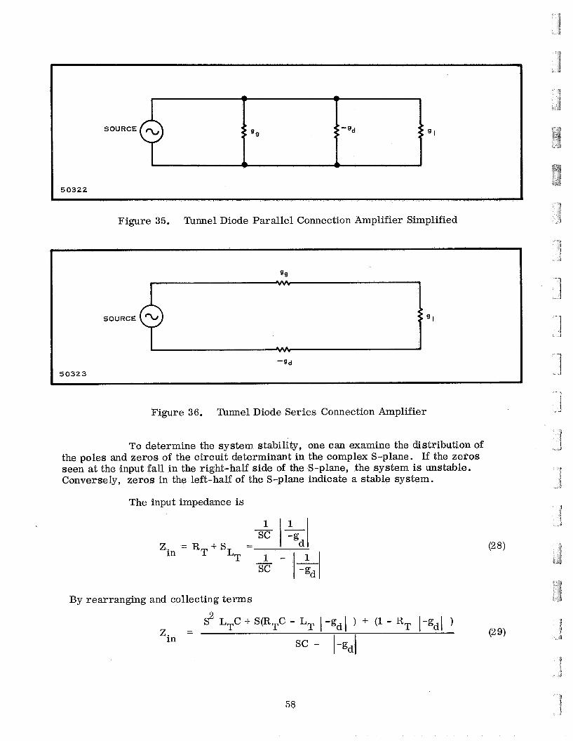
I 50322 Figure 35. Tunnel Diode Parallel Connection Amplifier Simplified
I 99 *
hM,
-gd
50323 I
Figure 36. Tunnel Diode Series Connection Amplifier
To determine the system stability, one can examine the distribution of the poles and zeros of the circuit determinant in the complex S-plane. If the zeros seen at the input fall in the right-half side of the S-plane, the system is unstable. Conversely, zeros in the left-half of the S-plane indicate a stable system.
The input impedance is
in Z RT + S
LT
By rearranging and collecting terms
58
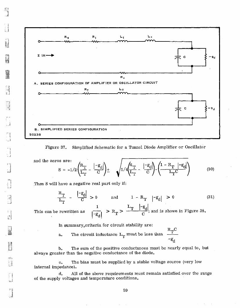
3
-- c i a
Figure 37. Simplified Schematic for a Tunnel Diode Amplifier o r Oscillator
f
and the zeros are:
Then S will have a negative real part only if:
In summary,criteria for circuit stability are: R-C 1
a. The circuit inductance LT must be less than - ’gd
b. The sum of the positive conductances must be nearly equal to, but always greater than the negative conductance of the diode.
c.
d.
The bias must be supplied by a stable voltage source (very low
All of the above requirements must remain satisfied over the range internal impedance).
of the supply voltages and temperature conditions.
59
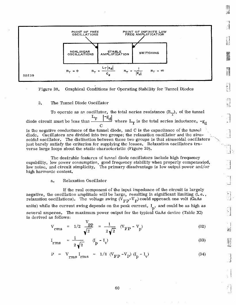
POINT OF FREE POINT OF INFINITE LOW 0 SC ILLATIONS FREQ AMPLIFICATION
SWITCHING NONLINEAR
I 50239 Figure 38. Graphical Conditions for Operating Stability for Tunnel Diodes
3. The Tunnel Diode Oscillator
To operate as an oscillator, the total series resistance (Rm), of the tunnel I L
-gd diode circuit must be less than where LT is the total series inductance, C
is the negative conductance of the tunnel diode, and C is the capacitance of the tunnel diode. Oscillators are divided into two groups; the relaxation oscillator and the sinu- ~
soidal oscillator. The distinction between these two groups is that sinusoidal oscillators just barely satisfy the criterion for supplying the losses. Relaxation oscillators tra- verse large loops about the static characteristic (Figure 39).
I '"..
The desirable features of tunnel diode oscillators include high frequency capability, low power consumption, good frequency stability when properly compensated, low noise, and circuit simplicity. The primary disadvantage is low output power and/or high harmonic content.
a. Relaxation Oscillator
If the real component of the input impedance of the circuit is largely negative, the oscillation amplitude will be large, resulting in significant limiting (i. e., relaxation oscillations). The voltage swing (VFp-Vp) could approach one volt (GaAs units) while the current swing depends on the peak current, I and could be as high as
B' 4 several amperes. The maximum power output for the typicai GaAs device (Table XI) is derived as follows:
T T
(33)
I
I P = V I = 1/8 (VFp-V ) (I - Iv) (34) rms rms P P 3
60
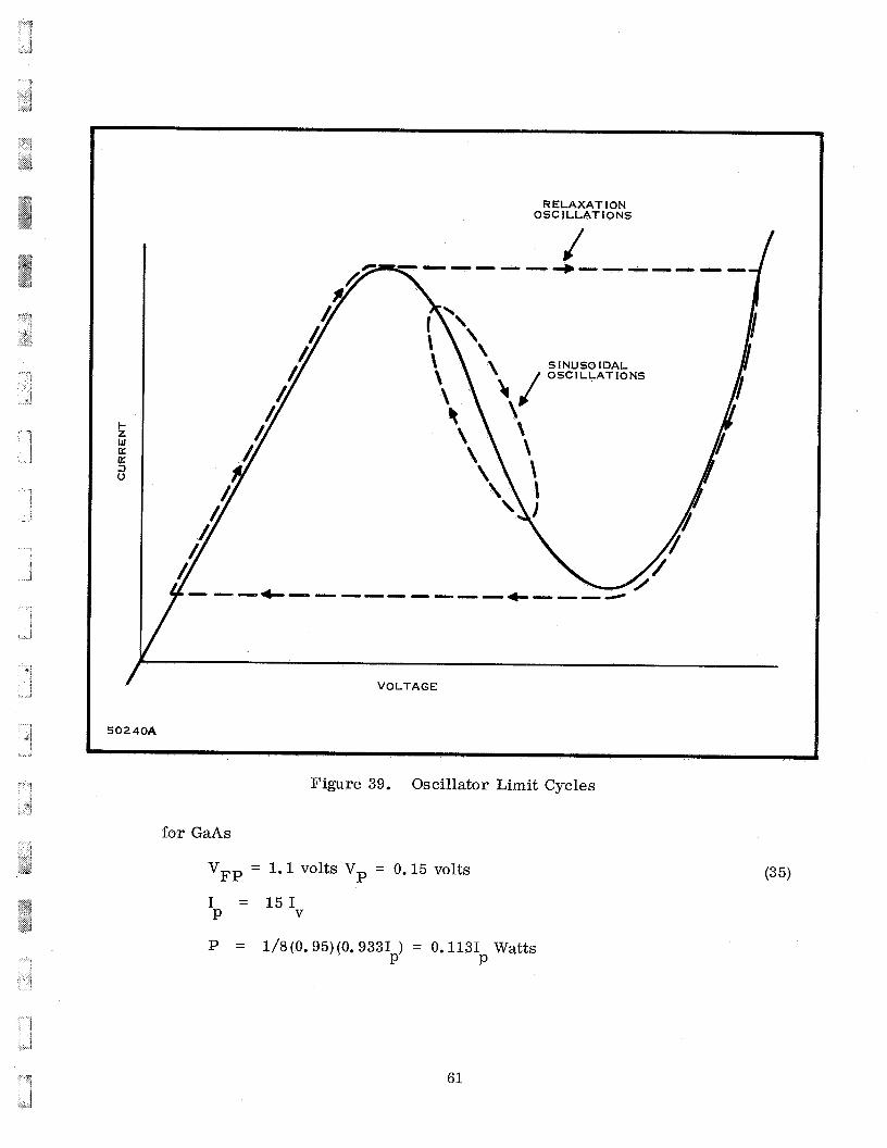
I- z W Cc [1: 3 u
I
RELAXAT I O N OSClLLATl O N S
5024049
VOLTAGE
Figure 39. Oscillator Limit Cycles
for GaAs
VFp = 1.1 volts Vp = 0.15 volts
I = 1 5 1 P V
P = 1/8(0.95)(0.9331 ) = 0.1131 Watts P P
61
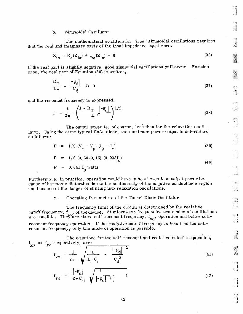
b. Sinusoidal Oscillator
The mathematical condition for "free" sinusoidal oscillations requires that the real and imaginary parts of the input impedance equal zero.
If the real part is slightly negative, good sinusoidal oscillations will occur. case, the real part of Equation (30) is written,
For this
and the resonant frequency is expressed:
1 1 - R T 1 /2
27r
The output power is, of course, less than for the relaxation oscil- lator. Using the same typical GaAs diode, the maximum power output is determined as follows:
P = i / 8 (0.50-0.1s) (0.9331 ) P
P = 0.041 I watts P
Furthermore, in practice, operation would have to be at even less output power be- cause of harmonic distortion due to the nonlinearity of the negative conductance region and because of the danger of shifting into relaxation oscillations.
e. Operating Parameters of the Tunnel Diode Oscillator
The frequency limit of the circuit is determined by the resistive cutoff frequency, f are possible. resonant frequency operation. If the resistive cutoff frequency is less than the self- resonant frequency, only one mode of operation is possible.
, of the device. At microwave frequencies two modes of oscillations ro They are above self-resonant frequency, fxo, operation and below self-
The equations for the self-resonant and resistive cutoff frequencies, fxo and fro respectively, are:
I n
62
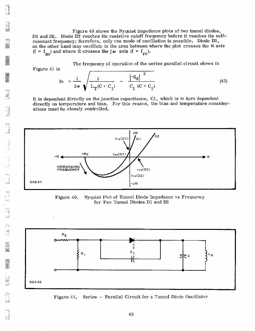
3
I " i
*I
I r J
Figure 40 shows the Nyquist impedance plots of two tunnel diodes, D1 and D2. Diode D2 reaches its resistive cutoff frequency before it reaches its self- resonant frequency; therefore, only one mode of oscillation is possible. Diode D2, on the other hand may oscillate in the area between where the plot crosses the R axis (f = f ) and where it crosses the j w axis (f = fro). xo
The frequency of operation of the series parallel circuit shown in Figure 41 is
/-"dl - 1 1 fo = - (43)
It is dependent directly on the junction capacitance, C1, which is in turn dependent directly on temperature and bias. For this reason, the bias and temperature consider- ations must be closely controlled.
5024 1
-R d -R 4 I
I FREQUENCY NCR EAS I NG \\ I-JW
Figure 40. Nyquist Plot of Tunnel Diode Impedance vs Frequency for Two Tunnel Diodes D1 and D2
I 50242
Figure 41. Series - Parallel Circuit for a Tunnel Diode Oscillator
63

constant bias.
4. The
The diode when it is
a.
b.
C.
d.
Several approaches have been used to stabilize the frequency. One method is to make the frequency of oscillation relatively independent of junction capac- itance. This can be achieved by weakly coupling the tunnel diode to a high Q resonant circuit by tapping the diode into the circuit at a low voltage point on a capacitive voltage divider. If wideband tuning is desired, one capacitor of the voltage divider can be a varactor.
I
The frequency of operation of the tunnel diode oscillator changes in sharp steps as the bias voltage is varied making it necessary to maintain a very
Tunnel Diode Converter
following simultaneous functions must be performed by a single tunnel used a s a high gain self-oscillating converter:
oscillation at the LO frequency
- 3 amplification at the RF frequency
mixing due to non-linearity - 1
amplification at the IF frequency. 1 On a mathematical basis:
The imaginary part of the external circuit admittance across the negative conductance of the diode should have zeros at the local oscillator and IF frequencies.
I-gdl The real term of the external circuit admittance, Y, across
at the LO frequency must be smaller than the negative conduc- tance of the diode.
kgdl must be The real part of the external admittance across
at the IF frequency.
The imaginary part of the external circuit admittance is shown plotted rgdl
larger than the magnitude of
against frequency in Figure 42. diode converter circuit is shown in Figure 43.
This condition satisfies (a) above. A possible tunnel
5. Tunnel Diode Noise
In the tunnel diode the major contributor to noise is shot-noise. The noise figure equation is:
201DC + T1 81
gg Tg gg N F = 1 + (44)
64
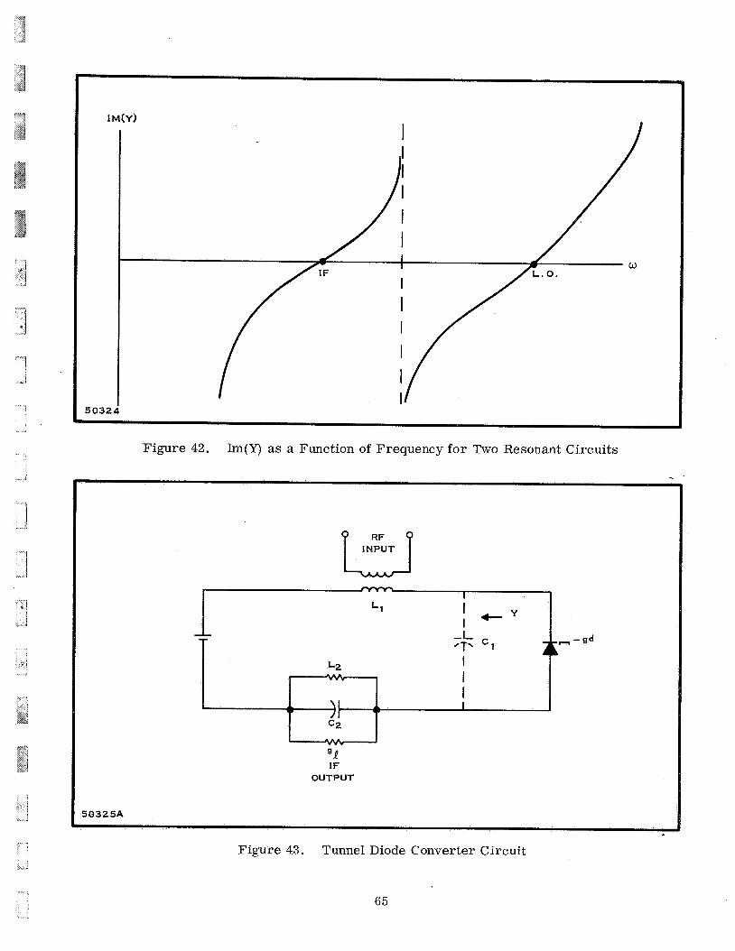
50326
Figure 42. Im(Y) as a Function of Frequency for Two Resonant Circuits
INPUT u L T
12 I T I I I
- gd
I
gQ IF
OUTPUT
50325A
Figure 43. Tunnel Diode Converter Circuit
65

Where
is DC bias current through the tunnel diode 'DC
g is the conductance of the generator g g1 is the conductance of the load
TI is the effective noise temperature of the load
It is evident that g should be large and g1 should be small, but for highest g
gain g + g = g 1 I-gd[
Therefore, g should be nearly equal to I -gdl . g
F. AVALANCHE DIODES
1. General
In 1958, Read26 predicted microwave oscillations from avalanche diodes. At that time, special doping gradients were recommended in order to achieve a highly localized avalanche zone at one side of a high-field depletion region in a semiconductor diode. Since that time, a great amount of effort has been devoted to the development of solid-state microwave generators. Many diodes, other than Read devices, are showing promise as oscillators and amplifiers when biased into the avalanche break- down region. silicon computer diodes. with GaAs varactor diodes and silicon devices
In 1965, the generation of substantial power was obtained by avalanching Later, high CW operation with good efficiency was obtained
27 . A detailed discussion of how an avalanche diode generates power will not
be given here; however, it is pointed out that avalanche effects, induced by reverse- bias, breakdown, and a transit time delay of carr iers across the junction combine to yield negative resistance and gain.
Oscillations have been observed in p++-nf-n-nf+ diodes over a wide fre- quency range extending to 8 GHz where transit time effects may have been present. How- ever, the absenceof a lower cutoff frequency showed that transit time was not essential for the oscillations. Instead they could be attributed to a negative resistance which be- gins at a critical current density corresponding to carrier concentrations slightly smaller than the impurity concentration in the n+ zone. Therefore, space-charge effects must be considered28. Inductance (related to the avalanche process) , capacitance (related to the depletion layer), and negative conductance and a noise generator is shown in Figure 44. It has been established that a satisfactory small-signal equivalent circuit for the p-n junction avalanche diode is a parallel combination of the above elements. Probably the most serious disadvantage to avalanche diodes is a high noise level.
The problem of frequency stability has not been studied extensively, but it is known that the frequency of operation is dependent on the dc current at the avalanche condition. The characteristic of the avalanche diode illustrated in Figure 45 shows that the current is controlled by limiting rather than by the dc bias voltage. Therefore, currents smaller than the limit current, and the resulting frequency shifts, are probable.
66

b i * i
NOISE rERM INALS GENERATOI
50243
Figure 44. Equivalent Circuit for the Avalanche Diode
2. Operation of an Avalanche Diode
The negative conductance of an avalanche diode is apparent over a wide frequency range; therefore, it can oscillate at several frequencies simultaneously over a range. The output at a specific frequency is dependent upon the tuning of the e a1 circuit. Even the most sophisticated filtering techniques are generally un- satisfactory because several fundamentals are present and harmonic and parametric oscillations may exist as well. ticular frequency component it is essential to use signal substitution methods.
To determine accurately the power content of any par-
Many microwave oscillators have been built using avalanche diodes. A silicon diode which generates 1.1 watts of C W at 12-GHz with 8-percent efficiency has been constructed. 30 Some GaAs varactors have delivered 25 to 30 mW between 13 - 14-GHz with a 5-6-percent efficiency. with an avalanche voltage of 45 to 55 volts.
The bias current was 10 mA
An avalanche diode may also be used to amplify. Avalanched GaAs varactors have given gain when used in a circulator-coupled network which forms a negative- r e s is tance , reflection type amplifier. The amplification was quite stable and oscillations were easily suppress ed.
Saturation occurred at levels above 0 dBm and discernable signal levels of -90 dBm were consistently observed. With +10 dl3m input, the power gain was more than 5 dl3 with a 3 dl3 bandwidth of 100 MHz. At -60 dBm input, the gain was +52 dB with a
I
\ CURRENT LIMIT
50244
Figure 45. V-I Characteristics of an Avalanche Diode
.~ i 67

bandwidth of 10 MHz. The ability to operate with input levels greater than 0 dBm is one of the significant advantages of the GaAs avalanche diode amplifier. Low power requirements is another advantage.
In addition to the noise limitation, the narrow bandwidth may prove to be troublesome in avalanche diode amplifiers. Although, the noise figure of the avalanche diode is prohibitive at the present time, it is very likely that in the near future they will be competitive with, if not better than, Gunn devices and tunnel diodes.
The power output and the high level input make them very attractive. This is a very new and fast growing aspect of solid-state electronics which will bear much attention in the future.
3. Noise Considerations
A s stated previously, noise is the major disadvantage of the avalanche process. Studies of avalanche noise in commercially available avalanche diodes reveal large noise variations from diode to diode. 31 The spectral noise density passes through a sequence of maxima and minima with increasing avalanche current.
The maxima and minima are associated with microplasma especially at lower currents (100 p A or less). A microplasma is a localized region of avalanche breakdown. At small magnitudes of current, e. g., of the order of 3 0 p A , the avalanche discharge of the microplasma is unstable and switches on and off. As the current increases, the discharge becomes stable, the on-off switching ceases, and the spectral noise density decreases. Several microplasma may exist at different levels of current, so that as one becomes stable another may become unstable. When all the microplasma are stable (or inactive) the spectral noise density falls off sharply until the noise level of stable discharge is reached.
i
Microplasma-free uniform avalanche diodes have been prepared by the guard ring technique. The guard ring is a region of high breakdown voltage around the active area of the device. and a sufficiently large radius of curvature so that the central region breaks down before the surface of the ring. Diodes with diameters from six microinches to 90 microinches and breakdown voltages from 5.9 volt to 46 volt were used. Each wafer also contained
a planar n p o r p n diode without the guard ring for capacitance-voltage measurements
which are required to determine the width of the depletion layer in the breakdown region
It must have a lower impurity gradient at the junction
+ + 85 .
The spectral noise density has three contributors. 1
Noise, I is the diode current F Excess noise at low current densities
Excess noise at high current densities
The l/n noise is independent of temperature from -196OC to 200OC.
It can be seen that it is a linear function of breakdown voltage Any deviation from the l/n plot is due to excess noise temperature dependence (Figures 46 and 47). when plotted on log-log paper.
i
68

0 0 N
e
e a
e @ I I 0 0 u) 0 c "
U z N
e
t e
0 0 N 1 0 0 -
0
0 0
I c
0 0 -
0 Lo 0 7
ZH /A AIISNZCI 3SION lVH133dS IJ .I
i5 rt N 0 Lo
69
v1 3
al v1 .d
al
M 2 iz
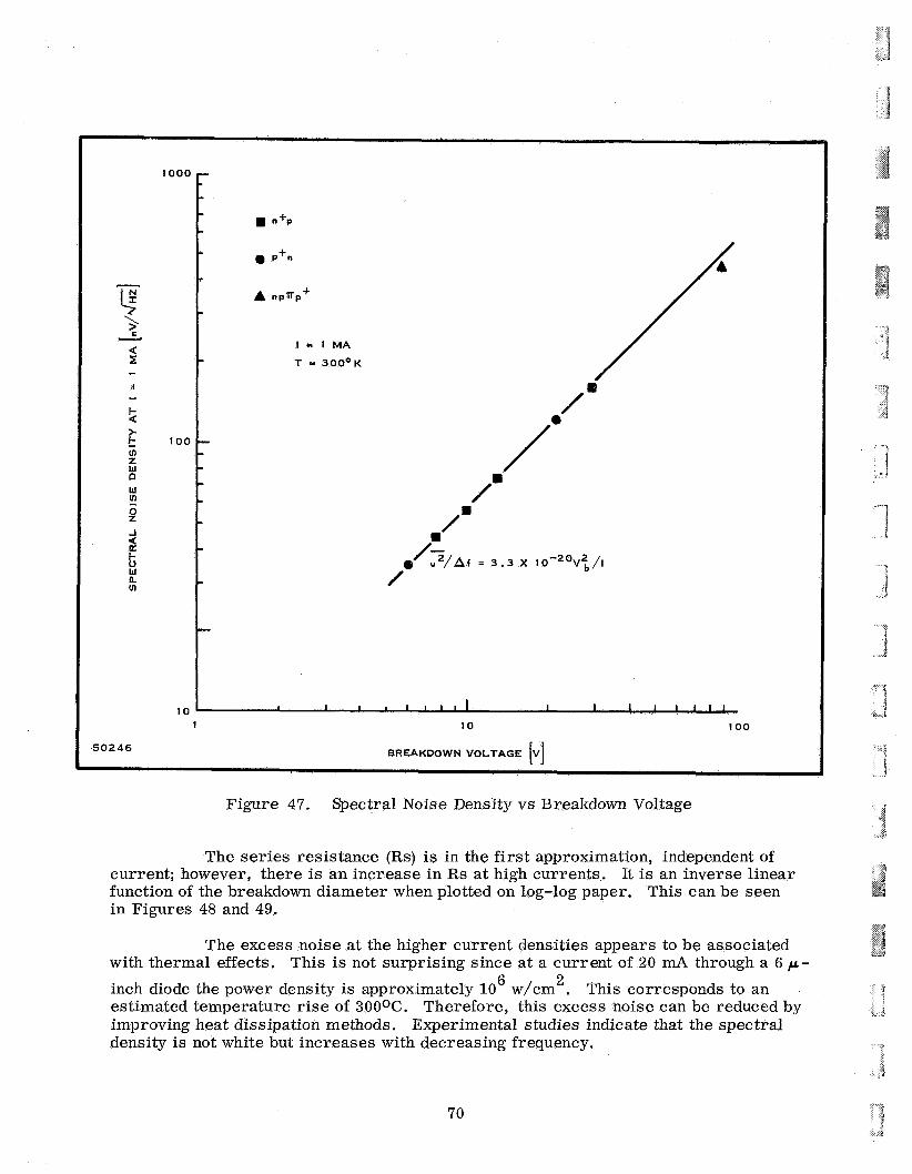
1 = 1 M A
T = 3 0 0 ° K
10 ' I 1 I I I I I I I I I 1 I I I I
1 10 100
BREAKDOWN VOLTAGE [VI
Figure 47. Spectral Noise Density vs Breakdown Voltage
The series resistance (Rs) is in the first approximation, independent of current; however, there is an increase in Rs at high currents. It is an inverse linear function of the breakdown diameter when plotted on log-log paper. This can be seen in Figures 48 and 49.
The excess noise at the higher current densities appears to be associated with thermal effects. This is not surprising since at a current of 20 mA through a 6 p-
inch diode the power density is approximately 10 w/cm . estimated temperature rise of 300OC. Therefore, this excess noise can be reduced by improving heat dissipation methods. Experimental studies indicate that the spectral density is not white but increases with decreasing frequency.
6 2 This corresponds to an
70
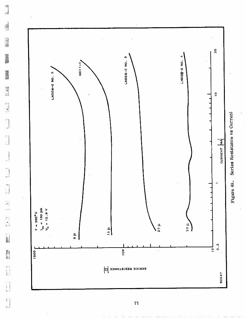
0
N I N n z J
3
2
0 m
0 c
a .I
t; W U E B
c
N I ' 8 1 1 . I ,
0 c
!?
I I 1 1 1 1 I I I 1 I 0 0
0 0
71
u % k k 5 u rn 3 a,
u 3 rn rn . I 4
2 rn a, k a, M
.d
%
iz
a, k 1 M

. I C
a m
w u
I-
m w IL: m
2 !!!
w a w m
1 ooc
100
10
3
\ CALCULATED
MEASURED WITH ERROR LIMIT INDICATED -I-
+
vb % 13 v T = 3 0 0 ° K
\ I 1 I l l l l 1 I I I I I 1 1 1
10
BREAKDOWN DIAMETER D
30 0
Figure 49. Series Resistance vs Breakdown Diameter
72
The excess noise at low current densities seems to be associated with non- uniformities of the avalanche breakdown. The non-uniformities causing the noise peaks consist of small variations of Vb which are likely caused by small local varia-
tions of the doping concentration in the starting material.
A s previously explained, the foregoing analysis was based on diodes made by the guard ring technique. These diodes will not function as oscillators o r ampli- fiers because their capacitance is too high. They will serve as noise generators, low noise avalanche diodes, and low current avalanche diodes.
A s noise generators they have several features which make them ideal. Their solid-state design guarantees low weight, small volume, low power consumption, high reliability, and ease of operation. In the case of small diodes, which are free of excess noise at low currents and follow the l / q low of noise vs current (Figure 50), the reproducibility is considerably improved over conventional solid-state sources, The noise variation from diode to diode from the same batch is less than 5 percent. Their open circuit spectral noise density is flat (+1 dB) from 10 Hz to at least 1-GHz with levels 40 to 50 dB above the thermal noise of Rs. Another feature is the possi- bility to adjust the noise level by varying the dc current.
“ 1
73

n z
c -
0 0 -
0 -
c
c
[ 9 / A u ] ALISN3a 3SION lVt1133dS
74
SECTION V
LINEAR INTEGRATED CIRCUITS
A. GENERAL
Linear integrated circuits are becoming increasingly available for use up to the VHF region. The use of "off-the-shelf" linear IC's satisfy many requirements applica- ble to receiver design. The operational amplifier and cascode configurations serve many functions from RF amplification to mixing and detection. These devices were not covered in Scientific Report No. 1 as they were in the state of infancy. Now, however, continued development and applicability to lower frequency integrated stages in a microwave receiver warrants their discussion.
The most common linear integrated circuit today is fabricated by monolithic silicon epitaxial construction and will perform all low level requirements from dc to 200 MHz. In addition to offering the system designer a savings in space and weight, an increased reliability is realized. In systems converted from discrete components to integrated devices, a reliability improvement of six to thirty is feasible.
The present state-of-the-art monolithic transistors have a frequency response extending beyond 1 GHz due to improved photographic techniques which help reduce device geometry and associated capacitances. Nevertheless, integrated circuits encounter special problems in such linear applications a s RF and IF amplifiers due to parasitic capacitances between elements in the monolithic substrates, and the lack of frequency selective schemes compatible with integrated structures.
The problems due to parasitic capacitances prevent the full frequency capability of integrated transistor from being fully realized, and the restricted range of com- ponent values allowed by monolithic construction in some instances prevents the integrated circuit from performing as well as it's discrete component counterpart.
B. BASIC CIRCUIT CONSIDERATIONS
Monolithic linear integrated circuits a r e fabricated by the same process which produces digital building blocks for logic systems. That is, the active and passive components are fabricated in a single structure, and all connections are made simultaneously by forming a metal interconnection pattern on the surface of a silicon bar. The forming process is illustrated in Figure 51.
To date, linear integrated circuits for operation at microwave frequencies a re not available in monolithic construction. Although in theory, such circuits a r e possible, hybrid integrated circuits have been more successful. In hybrid construction, high unloaded circuit Q's can be maintained with etched o r deposited passive components to which silicon chip transistors o r diodes a re bonded. The propagation characteristics of a microwave linear circuit requires some form of transmission line circuitry to keep losses low. If the transmission line must propagate energy at microwave fre- quencies with low losses, the insulating substrate should be a good dielectric. The
75
n+ ( E M I T T E R ) ALU MI NU M
SU B S T RAT E
v Si02
ISOLATI NG BARR 1 ER
502 SO I ,
Figure 51. Monolithic Fabrication Process
low resistive semiconductor substrate used in monolithic construction does not serve these needs as well a s hybrid techniques which use ceramic o r glass substrates.
In Figure 51, it can be noted that each component is completely surrounded by a dielectric material, silicon dioxide (SiOz). One of the major problems stemming from monolithic construction is that individual components need to be isolated from each other. Several techniques such as using high resistivity substrate or reverse-biased P N junction have been used to achieve the required isolation. The latter method has been more predominant a s it is easier to fabricate and provides more complete isola- tion. However, this method provides capacitive coupling to the substrate. Recent developments seem to indicate dielectric isolation techniques a re more advantageous. Dielectric isolation offers the possibility of making and using P N P and N P N devices on the same chip and reduces capacitances as the oxide thickness also controls the capacitance per unit area. The capacitance per unit area is shown in Figure 52 plotted versus oxide thickness. With a two micron dielectric and a typical monocrystalline transistor island, the capacitance would be approximately 0.3 pfd. This is about an order of magnitude less than that obtained for P N junctions.
The only disadvantage of using dielectric isolation over other methods is a slightly reduced power handling capability a s silicon dioxide has a lower thermal conductivitythan silicon. However, this is not expected to be too great a problem since the total thermal resistance can be controlled by the thickness of oxide used.
76

P W 2 0.036~ 10-3 c =
t
0 . 5 1.0 1 . 5 2 . 0
THICKNESS (p)
Figure 52. Capacitance per Unit Area vs Thickness
i i
The greater range of circuit design requirements in systems utilizing linear i I circuits essentially prohibits standardization which is common in logic systems that I 4 employ digital building blocks. In many instances, linear circuits a r e "customized"
to meet a particular circuit application.
The nearest thing to standardization is the differential amplifier configuration. Figure 53 shows the basic circuit configuration used for a broad line of multiple functions. The configuration is basically that of a balanced differential amplifier in which the currents to the emitter-coupled differential pair o r transistors are supplied from a controlled source. A wide use of linear integrated circuits for analog appli- cations from dc to frequencies into the vhf region such a s mixing, limiting, product detection, frequency multiplication, and amplitude modulation in addition to linear amplification can be obtained from such a versatile configuration.
The differential amplifier may be used a s a normal operational amplifier by ignoring one of the outputs. The single output and an inverting and noninverting input makes it possible for a positive o r negative feedback to be applied. This feedback concept is well suited to integrated ciecuits because the complete circuit specification is dependent on tolerance of one o r two components rather than components of inte- grated operational amplifier. Many different circuit functions can be performed with an operational amplifier by using different feedback networks around the amplifier as illustrated in Figure 54. Linear integrated circuits with the operational amplifier configuration and utilizing such feedback a r e ideally suited for instrument and analog use or in control systems.
77

50327 1 Figure 53. Basic Circuit Configuration for a Differential Amplifier
In Figure 55, a schematic diagram of a video'operational amplifier (derived from the differential amplifier), is shown. This operational amplifier is Texas Instrument No. SN5510 which offers medium gain and wide bandwidths. The charac- teristics of the SN5510 a re listed in Table XII. Note that this amplifier has extremely wide bandwidths (40 MHz) and is applicable to wideband-video or tuned circuit appli- cations.
The open loop frequency response characteristic is shown in Figure 56 as well a s the input impedance as a function of frequency. A closed loop amplifier frequency response is shown in Figure 57 to illustrate that in various applications it is possible to design 100-MHz amplifiers even though the closed loop gain is relatively low.
C. RF AND IF AMPLIFIERS
The major advantage of integrated circuits is realized when many similar stages can be cascaded in a single package. In receiver applications such advantages can not be fully utilized as each stage of amplification is followed, conventionally, by a tuned coil. The lack of suitable inductive reactance compatible with integrated circuits prevents full realization of cascading similar stages and alternate frequency selective schemes must be considered. One approach has been the use of T-notch filters, composed of lumped RC networks, operating at frequencies below 500-kHz. Another means of providing frequency discrimination is the use of a crystal filter followed by a high gain, wideband (video) amplifier; o r at frequencies above 30 MHz, distributed techniques may be used.
78

Ei I
I I + - ~ ~ O
-Ro
Ri EO P - Ei
Eo
c I R o
Ei
dE i
dE EO = -Ro C , -
E3 0 - Eo
0 1, # o
502 5 1
Figure 54. Through Feedback Around a Standard Amplifier
Typical Circuit Functions Obtainable
79

c_O +6 V
OUTPUT 1 __o
OUTPUT 2 __o
6 -6 V
Figure 55. SN5510 Device Circuit Diagram
A typical emitter-coupled, integrated linear amplifier utilizing 2N918 type tran- sistors commercially available for RF and IF amplifiers in the frequency range from dc to 300 MHz is shown schematically in Figure 58. It offers high power gain and increased stability margins. The electrical characteristics of the device a re summar- ized in Table XI11 and a re shown in Figure 59. This amplifier has been used in a 200-MHz tuned amplifier and as can be seen in Figure 59, noise figures less than 6 dB are possible.
Several linear integrated circuits a r e available for video application in different circuit configurations. The most applicable for wideband use is the one in which
80

Table XI. Characteristics of the SN5510
Function Specification
Open-loop voltage gain
3 dB Bandwidth
Input Impedance
Input capacitance
Total power dissipation
Maximum linear output voltage
Output impedance
Common .mode rejection
Input current
40 dB
40 MHz
6 KQ
10 pF
165 mW
4 v P-P
35 a 85 dB
50 p A
50253A
70
60
50
40
30
2 0
10
r 6-DB BREAKPOINT
100 KHZ 1 MHZ 10 MHZ 100 MHZ FREQUENCY
1000 MHZ
Figure 56. Effect of Source Resistance on SN5510 Open Loop Response
81
70 -
60 -
50 -
r. rn 40 - z D v
3 30 -
TEST CIRCUIT
9 - D *OUT 0 1,
C1 E 230 PF 20 R~ a 1 0 52
10
0 100 KHZ 1 MHZ 10 MHZ 100 MHZ
50254 FREQUENCY
Figure 57. SN5510 10-dB Closed Loop Amplifier
series-parallel feedback pairs are used as building blocks to form the complete amplifier. Such an amplifier is shown in Figure 60; selection of the appropriate RC network in place of Z provides this circuit with two gain ranges, 34 k 1 dB with a 40-MHz bandwidth o r 52 f l dB with a 35-MHz bandwidth. Either net- work provides an integrated circuit with a low distortion of 0.2 percent at 200 Hz and a temperature drift kO.002 dB/OC. The' noise figure of either circuit config- uration is 5 dE3 for a 30 MHz bandwidth. The typical gain bandwidth product, ft , for either circuit is in excess of 2 GHz.
50255 6 A balanced differential configuration, consisting of three integrated transistors, is available as shown in Figure 61a. This Figure 58. Differential Amplifier circuit is basically a single-stage differ- ential amplifier composed of transistors Q1 and Qz driven from a constant-current source Q3. Each of the terminals must be provided with a biasing network. The circuit may be used in the cascode configuration in which, a common-emitter stage drives a common-base stage. Terminal connections to external biasing networks are shown in Figure 61 b and c for a differential amplifier and cascade amplifier with AGC capability,
Configuration
82

Table XIII. Typical Integrated Linear Amplifier Parameters ~~
Power Supply Voltage vcc 10 Vdc
VEE 14 Vdc Power Supply Voltage
Total Power Dissipation Pd 0.5 watt
Operating temperature OC -55 to +125
Maximum Input Level (RMS) Vain 2 V@MS)
Operating Current
(Vcc = 5 Vdc, Vee = -4.7 Vdc, Vin = 0) 4 mAdc
22 dB Transducer Power Gain
(Vcc = 5V, Vee = -4V, f = 100 MHz, BN = 3 MHz)
Noise figure
(Vcc = 5V, Vee = -4V, f = 100 MHz, R = RSO) 6 dB g
Figure 59. Series-Pair Integrated Circuit
83
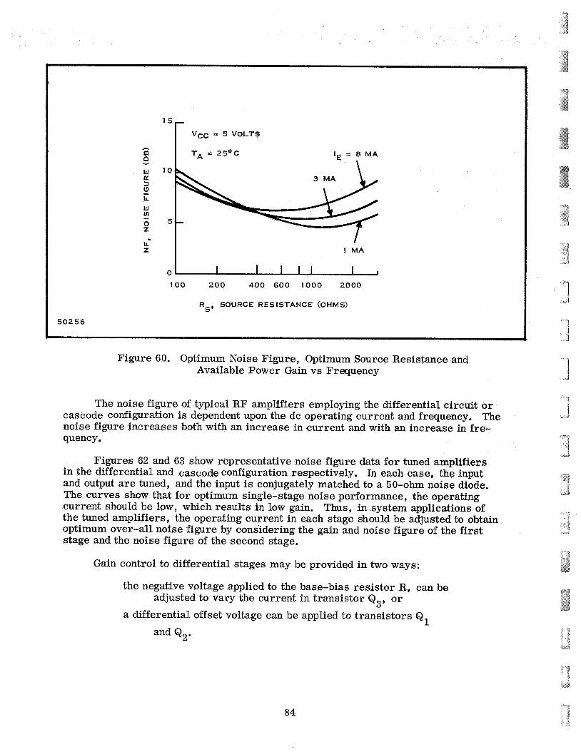
15
Vcc = 5 VOLTS
h rn n w 10
13
E! 0 5
v
9: 3
LL w
z LL z .
0
100 200 400 600 1000 2000
R SOURCE RESISTANCE (OHMS) S'
50256
Figure 60. Optimum Noise Figure, Optimum Source Resistance and Available Power Gain vs Frequency
The noise figure of typical RF amplifiers employing the differential circuit or cascode configuration is dependent upon the dc operating current and frequency. The noise figure increases both with an increase in current and with an increase in fre- quency.
Figures 62 and 63 show representative noise figure data for tuned amplifiers in the differential and cascade configuration respectively. In each case, the input and output a r e tuned, and the input is conjugately matched to a 50-ohm noise diode. The curves show that for optimum single-stage noise performance, the operating current should be low, which results in low gain. Thus, in system applications of the tuned amplifiers, the operating current in each stage should be adjusted to obtain optimum over-all noise figure by considering the gain and noise figure of the first stage and the noise figure of the second stage.
Gain control to differential stages may be provided in two ways:
the negative voltage applied to the base-bias resistor R, can be
a differential offset voltage can be applied to transistors Q
adjusted to vary the current in transistor Q,, or
and Q2. 1
84
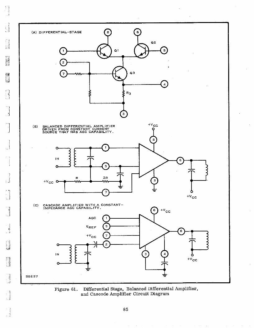
2 i
' 01
L J
! I
'I 3
FFERENT IAL-STAGE (87
: B)
( C)
50257
BALANCED DIFFERENTIAL AMPLIFIER DRIVEN FROM CONSTANT CURRENT SOURCE THAT HAS AGC CAPABILITY.
+vcc
P
+VCC
+vcc W
CASCADE AMPLIFIER WITH A CONSTANT- IMPEDANCE AGC CAPABILITY.
AGC
E R E F
+"CC
- - 1~~ -
Figure 61. Differential Stage, Balanced Differential Amplifier, and Cascode Amplifier Circuit Diagram
85

m n
I a 2
E
W 3
L W
0 z
I O
f
4
2
C
50258
- INPUT CONJUGATELY MATCHED TO 50 a NOISE DIODE
I I I I I 0 1.16 2.4 3.7 5.1 T O T A L DC CURRENT (I&-MA
I I I 1 I
2 4 6 8 10 NEGATIVE DC S U P P L Y VOLTS-V,,
Figure 62. Representative Noise Performance When Operating in a Differential-Amplifier Configuration
m n I a 2
w 3
c W uf 0 Z
-
50259
INPUT CONJUGATELY MATCHED TO 50 NOISE DIODE
2
4~ 01 I I I I 1
0 1.22 2.54 3.9 5.35 T O T A L E M I T T E R CURRENT Q3-MA
I i I I I J
2 4 6 8 10 NEGATIVE DC S U P P L Y VOLTS-VEE
Figure 63. Representative Noise Performance When Operating in a Cascode-Amplifier Configuration
86
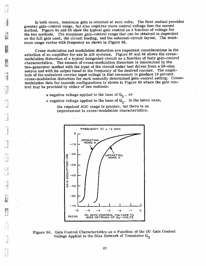
In both cases, maximum gain is obtained at zero volts. The first method provides greater gain-control range, but also requires more control voltage than the second method. Figure 64 and 65 show the typical gain control as a function of voltage for the two methods. The maximum gain-control range that can be obtained is dependent on the full gain used, the circuit loading, and the external-circuit layout. The maxi- mum range varies with frequency as shown in Figure 66.
Cross modulation and modulation distortion are important considerations in the selection of an amplifier for use in AM systems. Figure 67 and 68 shows the cross- modulation distortion of a typical integrated circuit a s a function of their gain-control characteristics. The amount of cross-modulation distortion is determined by the two-generator method with the input of the circuit under test driven from a 50-ohm source and with its output tuned to the frequency of the desired carrier. The ampli- tude of the undesired carr ier input voltage is that necessary to produce 10 percent cross-modulation distortion for each manually determined gain-control setting. Cross- modulation data for cascode configurations is shown in Figure 68 where the gain con- t rol may be provided by either of two methods:
a negative voltage applied to the base of Q3 a negative voltage applied to the base of Q1. In the latter case,
the required AGC range is greater, but there is no improvement in cross-modulation characteristics.
or
FREQUENCY ( f ) = 12 MHZ
0
-10
* -20
I 0
z - 0 -30 I- u 3 0 w -40 [L:
$ -50 E
-60
-70 I I I I I I -6 -5 -4 -3 -2 - 1 0
DC GAIN-CONTROL VOLTAGE TO 50260 BIAS NETWORK O F Q3-VOLTS
Figure 64. Gain Control Characteristics as a Function of the DC Gain Control Voltage Applied to the Bias Network of Transistor Q3
87

. EE(-6 V)
V
50261
0
-10
m 0 -20 I t 0 I- 0 -30 3 I3 W
-
a -40 4
-50
-60
OPERATION MODE D \FREQUENCY (f) = 12 MHZ
NEGATIVE VOLTAGE VOLTAGE TO \ TERMINAL NO. 1
-
0 0.1 0 .2 0.3 0 . 4
GAIN CONTROL VOLTAGE (VB,)-VOLTC
Figure 65. Gain Control Characteristics as a Function of the DC Offset Voltage, VBB Applied to the Differential Pair
of Transistors Q and Q2 1
OPERATING MODE D
- 2 0 ~
40 60 80 100 10 20
FREQUENCY -M HZ 50262
Figure 66. Maximum Gain Control Provided by Variations in the Current through Transistor Q3 as a Function of Frequency
88

n I
t,
z 0 - 3 W 9:
n
5
502 63
0
-10
-20
-3 0
-40
-50
-6 0
-70
1 .o 3 6 10 30 60 100 300 600
UNDESIRED CARRIER INPUT VOLTAGE- MILLIVOLTS R M S
Figure 67. Gain Control as a Function of the Input Voltage from an Undesired Carrier that will Produce Cross-Modulation
Distortion of ten percent for Balanced Differential Amplifier Operation. The gain-control voltage is applied to bias network of the constant-current
transistor, Q 3'
Figure 69 shows the power gain and noise performance for either the differential o r cascode amplifier configuration as a function of AGC voltage. From this figure, it may be noted that a typical integrated RF amplifier can achieve a 5.5 dB noise figure and a 15 dB power gain at 100 MHz.
D. LIMITERS
Linear integrated circuit also function well as limiters in both the differential- amplifier and cascode configurations. The advantage of the differential configuration is that collector saturation of either transistor Q1 or Q2 can be avoided because of the action of the constant current transistor Q3. The transfer characteristics of Figure
7 0 show the excellent limiting capabilities achieved because the constant-current transistor, Q limits the operating current so that the collectors of the differential- pair do not saturate. As saturation must be .prevented for good limiting, the load resistance and low Ievel voltage gain are limited for a given bias current and supply voltage.
3
89

'PUT
0
-10 h rn s -20
Z 0 - -30 I- o 3
K -40
z 2 -50 a
-60
-70
50264
- FREQUENCY O F
DESIRED CARRIER = 12 MH
FREQUENCY OF UNDESIRED
- - CARRIER P 16 MHZ
- - - -
1 3 6 10 30 60 100 300 600
UNDESlRED INPUT VOLTAGE (MILLIVOLTS RMS)
- Figure 68. Gain Control in a Cascode Configuration, a s a Function of
the Undesired Carrier Voltage that will Produce ten per- cent Cross Modulation Distortion when the Gain is Controlled by a Negative Bias Voltage Applied to the
Base of Transistor Q3. The Schematic diagram
illustrates the circuit configuration.
90

rn v 20 r 0 FREQUENCY = 100 MHZ
E i-9 v GAIN z
4 II: 16 k\vcc w
- z - 16
II:
I 2 12
0
II: 3
w 8
z 4 w
0 0 r?
' 9 8 7 6 5 4 3 2
POSITIVE DC BIAS VOLTAGE ON TERMINAL 7-V
I 50265
Figure 69. 10.7-MHz Transfer Characteristics in the Cascode or Differ entia1 Connection
50266
12 v
vcc = 9v
FREQUENCY = 10 .7 MHZ
I I I I I I I 1
0.05 0 . 1 0 0. 15 0 . 2 0
INPUT VOLTAGE-V
Figure 70. Limiting Characteristics of a Linear Integrated Circuit
91/92

SECTION VI
THIN FILMS ii i
A. GENERAL
Scientific Report No. 1 discussed the subject of thin film from the aspect of materials, process methods, parameter limits, and resistor and capacitor character- istics. This report discusses the usefulness of microstrip circuits, the relative merits of various substrates, and the applications of lumped element components.
B. MICROSTRIP
1. Theory
- 7
i 3
The parameters of strip line has been fairly well established for several years. However, because of its non-symmetrical nature (Figure 71), microstrip has been somewhat neglected. Even now an exact theoretical analysis of the microstrip mode is lacking, but this medium can be accurately characterized by suitable measure- ment techniques. The characteristic impedance, Zo, wavelength, Xg, and loss per wavelength can be determined as a function of frequency and other pertinent parameters for microstrip lines.
€-FIELD IwI
f h
I GROUND PLANE I
50267
Figure 71. Cross-Section of the Microstrip Transmission Line
93
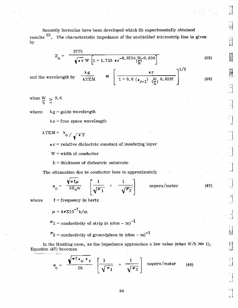
Recently formulas have been developed which f i t experimentally obtained
results 32. The characteristic impedance of the unshielded microstrip line is given by
377h
1 "= F W [1+1.735 E r (@ -0.0724 W-0.836
Xg and the wavelength by FM
when W > 0.6 I;=.
r
where Xg = guide wavelength
Xo = free space wavelength
NN 1 + 0 . 6 ( Z ) W 0,0297 ]
r-1 (h)
E T = relative dielectric constant of insulating layer
W = width of conductor
h = thickness of dielectric substrate
The attenuation due to conductor loss is approximately
(45)
,-
. ;I
nepe r s /met er 1
a = + C
where f = frequency in hertz
p = 4sX10-7h/m
1 = conductivity of strip in (ohm - m)-' U
U 2 = conductivity of groundplane in (ohm - m)-'
(47 )
In the limiting case, as the impedance approaches a low value (when W/h >> l), Equation (47) becomes
94

x
6x
Line
I i!
Dielectric e r Loss dB/cm Q of a$ Resonator
Material I Thickness 2 GHz I 10 GHz 2 GHz I 10 GHz Conductor
and from this equation it may be seen that large h (obtained by thick substrates) is required to minimize a c’
The losses due to the insulating substrate can be neglected for hybrid circuits on ceramic. However, losses on silicon can not be neglected and may be approximated by
1/2 zo
Ph ‘d SEMICOND. W
where P = Substrate resistivity in ohm-cm.
Calculated losses of lines on ceramic and silicon are tabulated in Table XIV.
B Gold Ceramic 25 mils 9.9 0.039 0.088 12 0 2 65
C Gold Si(150nCM) 10 mils 1.3 1.44 2 9
D Gold Si(15OOSLCM) 10 mils 0.24 0.38 14 50
Another source 33 shows resistivity of silicon substrate versus line loss (Figure 72). However, as the temperature increases, charge carr iers are thermally excited, lowering the resistivity of the material. Even at lower temperatures, the resistivity decreases due to the increase in mobility of the charge carr iers with de- creasing temperature. This curve is shown in Figure 73.
For circuits not requiring extremely high Q, microstrip on silicon can be very useful. If a higher Q is necessary it can be achieved, up to a limit, by using a higher dielectric substrate such a s ceramic. A hybrid IC will then be necessary.
The characteristic impedance of straight line segments of microstrip trans- mission line of various widths was measured by slotted line and time domain reflecto-
meter technique^^^. The lines were made from gold, silver o r aluminum. The sub- strate was either glazed A1203 or unglazed A1203. The characteristic impedance
versus the width to height ratio is given in Figure 74.
The results of these measurements are given in Figure 75. Note that Xo / x g is nearly independent of frequency, but is dependent on the characteristic impedance Z o , and the substrate material. This is in agreement with Equations (45) and (46).
95
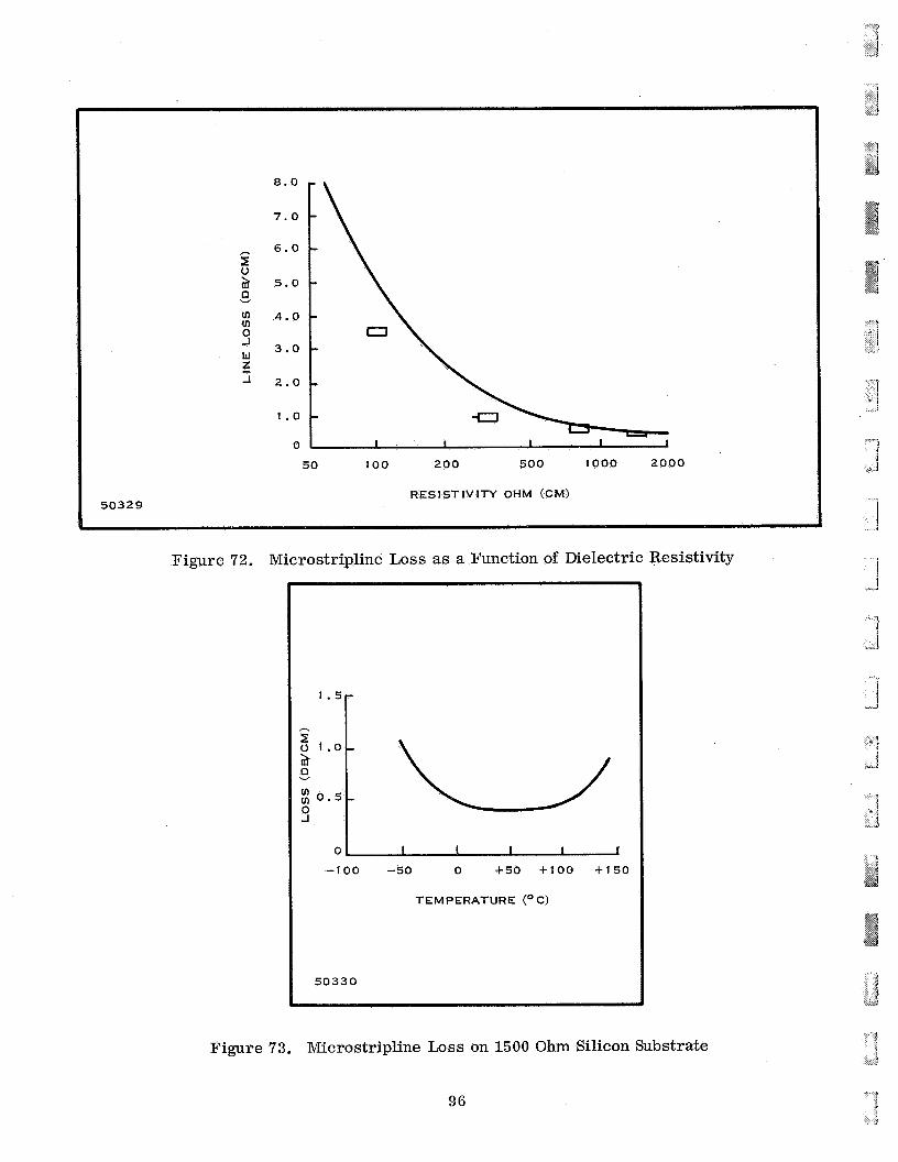
8.0
7.0
6.0
5.0
4.0
3.0
2.0
1 .o
0 I I 1 I I
50 100 200 500 1000 2000
RES I ST IV ITY OHM (CM) 50329
~~~
Figure 72. Microstripline Loss as a Function of Dielectric Resistivity
Figure 73. Microstripline Loss on 1500 Ohm Silicon Substrate
96
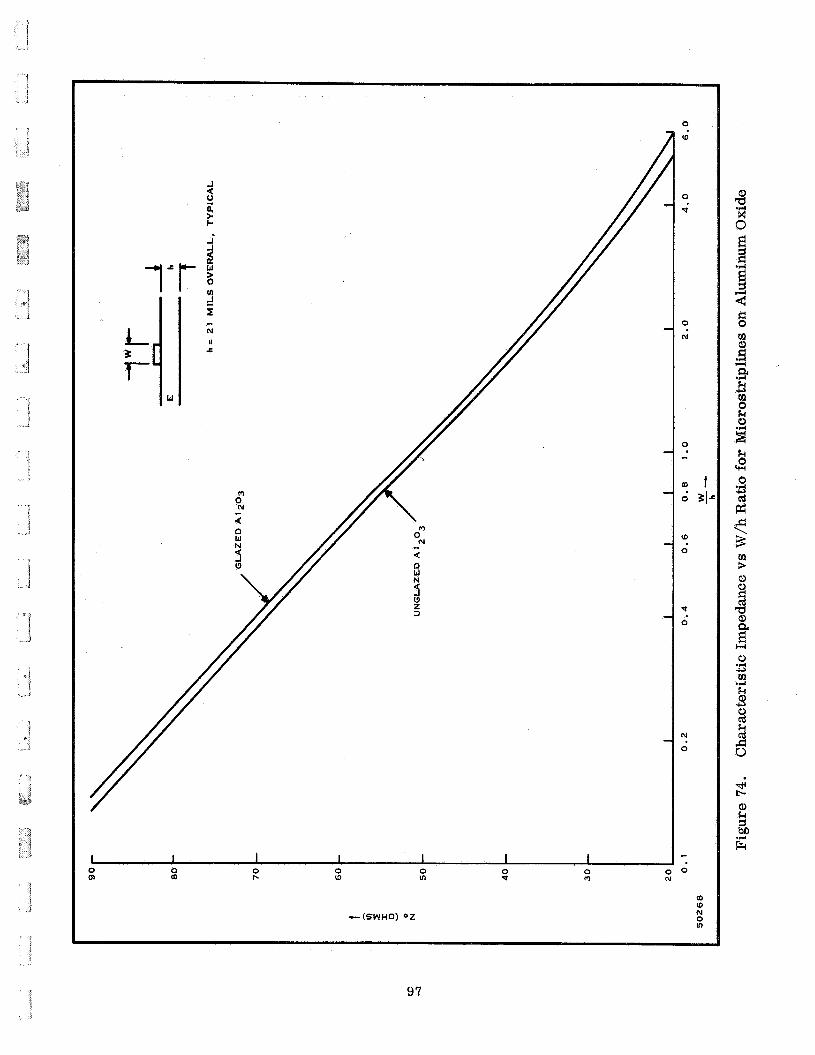
J 4
0. > I-
2
m ON
// c
4
I 1 1 I I I I 0 0 0 0 0 0 0 01 m PI W In -a m
.- (SWHO) 02
97
0
0 .d +.,
2 c \ 3
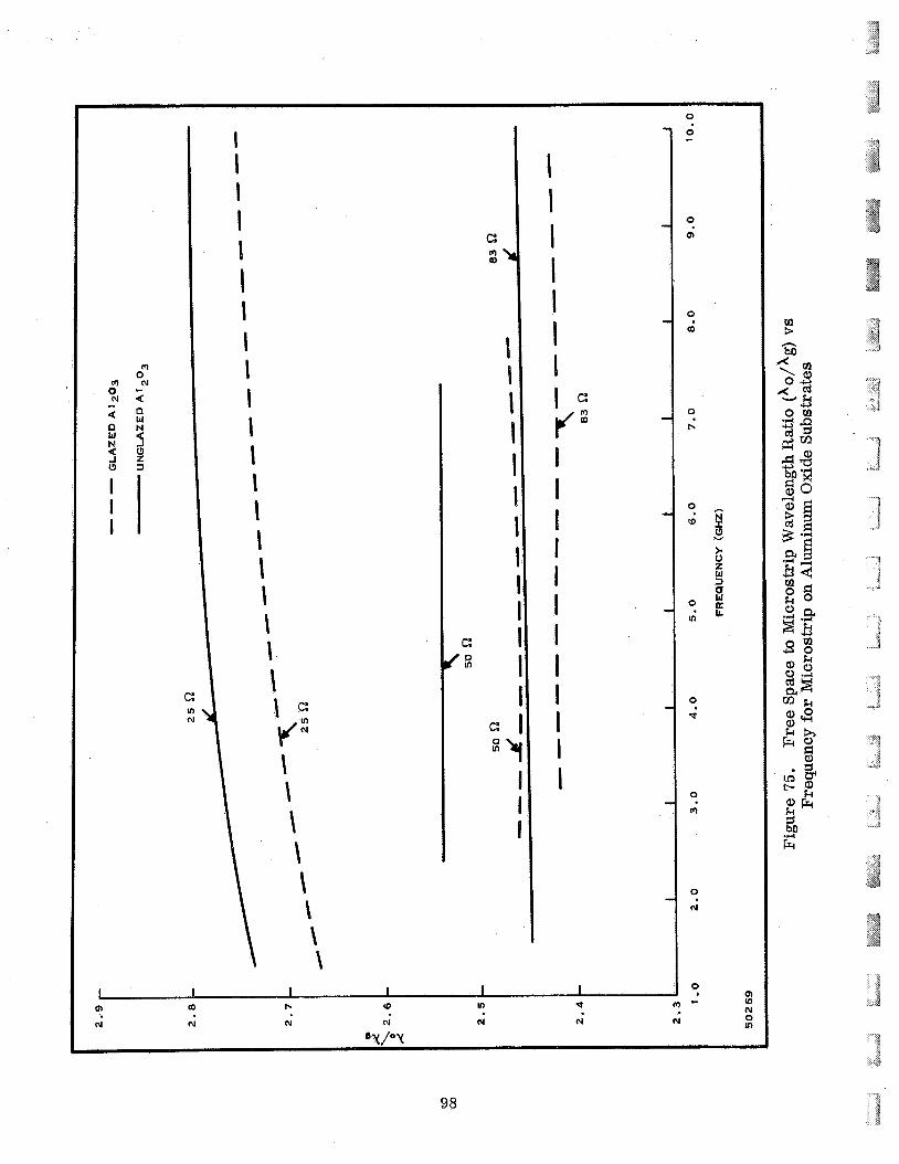
I 1 I I I I 1 I 1 I I 1 I I I I I I I I I C
I \ \ \ \ \ \ \
P
c '5:
I 1 I I 1 I I I C f g I I I I I I I I I I I I
1 1 I I I I OD I* 0 v) -! 0)
N N N N N N N
: 1 i
in J
The Q (quality factor) of a microstrip resonator is an important design considera- tion. If the microstrip is an open or shorted section, the unloaded Qu of a quarter-
wavelength resonator is Qu - -- QdQc where Qc is the Q of the conductor and Qd is the Q
of the substrate. If all the conductors a r e of the same material Qd+Qc
The Q of the substrate, (Qd), is approximately the Q of the dielectric; for semicon-
ductor substrates Qd wp c r e o
The calculated values of Q from Table XIV show that microstrip resonators have lower Q's than conventional cavity resonators and that the penalty in performance is greatest in the monolithic IC type of microstrip.
2. Selection of Substrates
Selection of a microwave IC substrate is critical in that the substrate is an integral part of the circuitry and must be chosen for low dielectric loss. The chosen substrate must be homogeneous both within itself and from batch to batch. The thin- film must strongly adhere to the substrate, and even if the substrate is only 10 to 50 mils thick, neither the substrate nor the conductors should deform by temperature cycling. The substrate thermal conductivity should be high and its surface must be free of pits for uniform transmission lines and short free capacitors to be deposited. Usually substrate thickness is a tradeoff between conductor Q and the maximum allowable thermal resistance of the substrate.
3. High Dielectric Substrates
The primary advantage of a substrate having a higher dielectric than ceramic ( e 2 9.6) is size reduction. By increasing the dielectric constant of the
substrate from 10 to 100, the guide wavelength of a 50-ohm microstrip line can be
reduced by a factor of 0.35 and low loss and microstrip lines can be fabricated . r
35
The measured and calculated impedance is plotted in Figure 76 a s a function of geometry and dielectric constant. The calculated impedance is based on the conformal mapping solution given by Wheeler 36. Notice that the high dielectric sub- strates require smaller values of w/h for high impedance levels because of the higher transmission line capacitance. Since the width is restricted by thin film technology limitations, thicker substrates will be required for high-impedance microstrip cir- cuit s .
The measured and calculated ratio of free space-wavelength to micro- strip wavelength is plotted in Figure 77 as a function of dielectric constant and geometry. This ratio has been computed also from a conformal mapping solution given by
Wheeler 35,36
High-dielectric substrates, consisting of a temperature-compensated titanium dioxide homogeneous mixture, have been shown to have the properties
99
0 m 0 t-
0 (D
0 0 In -3
(1E>OZ
0 c
0 0 m cu
I
0 : t - I
N 0 m
100
1’ - \ \ \ \ \ \ 1
1
4 m
101
required for reduced-size microwave integrated circuits. strip wavelength, characteristic impedance, and attenuation with geometry and dielec- t r ic constant a r e in good agreement with the theory. The low values of attenuation and guide wavelength make this material particularly attractive for low loss microwave circuitry.
The variations of micro-
At the present state-of-the art, only smaller physical size justifies using high dielectric materials because other factors tend to discourage its use. The rough surface of titanium dioxide makes it impossible to form thin film capacitors without shorting. The very small circuit dimensions makes it difficult to make external connections. In order to get characteristic impedances at the higher levels, a thick substrate is required, and to add to the problem the temperature conductivity is quite low: 0.05 for Ti02, 0.15 for ceramic, and 1.0 for silicon. And finally there is a problem with energy lost from surface waves which a re independent from the TEM wave of the Microstrip.
4. Circuits
Printed microstrip has made possible a variety of integrated components such as directional couplers. One type of directional coupler is shown in Figure 78a which uses the fringing effect to accomplish coupling. Tight coupling requires very close spacing between conductors (e. g. less than 0.5 mm) or very long sections (e. g. several wavelengths). It is possible that the circuit will resonate in the balanced twin strip mode. Another disadvantage of this type of coupling is the difficulty of control-37 ling both the phase change coefficient and the coupling factor in a prescribed manner .
A second type of coupler, shown in Figure 78b, is known as the branched arm coupler. It has certain advantages over the parallel-line coupler, but if a high value of directivity over a large bandwidth is required, the number of branches becomes rather large (e, g. more than 3) and the impedance of the outer arms tends to become higher than can be realized in this or any similar form of construction (e. g. more than 150 ohms).
A third method (Figure 78c) employs two microstrip conductors back to back over a common ground plane, Coupling is accomplished by slotting the ground plane between the two strips. By the proper choice of slots, a wide variation in coupling strength is possible and either forward or reverse directivity can be obtained.
Microstrip filters may be one of three types. The parallel coupled reson- ator, shown in Figure 79, employs half wave sections which overlap adjacent section by one-quarter wave. (These sections need not be in a straight line. They can be in the form of a semicircle to conserve space. ) The large amount of overlap results in both electrostatic and electromagnetic coupling. The coupling affects the image impe- dance of the lines so it is necessary to adjust the width of the sections to control the characteristic impedance. The insertion loss vs. frequency of three experimental filters is shown in Figure 80. Responses were also observed at 2 w and 3 wo. The
VSWR characteristics a r e shown in Figure 81. 0
The direct-coupled filter, (Figure 82), has sections which are approximately one-half wave length long and are coupled to each other at each end by gap capacitances.
102
i (A) PARALLEL LINE COUPLER
( B ) BRANCHED ARM COUPLER
TRANSVERSE SLOTS IN COMMON GROUND PLANE
(C) BACK-TO-BACK SLOT-COUPLED COUPLER
502 72
Figure 78. Differential Forms of Microstrip Directional Coupler
103

z N
z N
104
36
32
28
24
20
3 -D
1.7 1.9 2.1 2.3 2.5 2.7 2.9 3.1
FREQUENCY (GHZ)
50274
Figure 80. Insertion Loss vs Frequency of Parallel Coupled Filters
10 5
V S W R CHARACTER 1ST ICs
50275A
Figure 81. VSWR Characteristics of Parallel Coupled Filters
A computer program using equations by Matthaei 38 was written to determine gap widths and conductor lengths. The resulting filter characteristics a re shown in Figures 83 and 84.
The third type filter uses either open or shorted tuning stubs. The char- acteristics of some thin-film filters using stubs and parallel coupling are shown in Figures 85, 86, 87, and 88.
Couplers, filters, and transforming sections must be fabricated from trans- mission line sections having low loss and well defined characteristic impedance pro- perties using process and materials compatible with other circuitry components.
106
Z IN
50276
Figure 82, One-Section Direct Coupled Resonator Filter
One problem is the loss characteristics. For short interconnection of 50-ohm circuits, a loss of 3 - 5 dB/cm can be tolerated, The design of filters and couplers requires that the loss be no greater than 0.5 to 1.0 dB/wavelength. Bandpass filters require a few hundredths of a dB per wavelength for steep skirts and low inser- tion loss.
An additional advantage can be gained by using microstrip on the same sub- strate a s the active components, By using high resistivity silicon, microstrip trans- mission lines loss can, at room temperature, approach conducter losses only.
C. LUMPED ELEMENTS
If the dimensions of a circuit element are so much smaller than a wavelength that distributed effects play no part in its operation, it is called a lumped element. At microwave frequencies lumped elements are very small. It has been more practical to build large distributed circuits of waveguides and coaxial cables because the circuits have higher Q due to a higher storage volume. But in IC’s these elements a r e not practical; consequently minute lumped elements a re now being fabricated with exacting precision. The phase shift over the element is zero because they a re so short. If extra amplification stages do not circumvent the low Q problem, the idea of using IC’s for circuits requiring high Q may have to be abandoned. Lumped ele- ments in hybrid o r monolithic IC’s may be practical up to 3 GHz.
In the microwave region, inductors may be fabricated by thin-filming a spiral, loop, o r a meandor line on a high dielectric substrate. At 2 GHz, a 5-turn spiral, 0.040 inch in diameter, on glass has an inductance of 10 nh and a Q of 45. A 0.060- inch coil has an inductance of 25 nh and a Q of 60. Figure 89 shows a plot of
Q2 versus f for such an inductor (the linear variation is expected for a true inductor).
The results for a series LC circuit are shown in Figure 90. The straight line response shows the absence of distributed effects; therefore, the circuit behaves like a lumped series LC circuit across the band 0.5 to 2.5 GHz. The element values shown were determined from circuit response and a re close to design values 39.
107
a 2 >
502 7 7
2 0
15
10
5
8. 5 9.0
FREQUENCY (GHZ)
9.5
Figure 83. Two-Section Direct Coupled Filter - VSWR vs Frequency
Figure 9 1 is a thin-film lumped element circuit to match an experimental tran- sistor pellet to 50-ohm transmission lines. The entire amplifier occupies an area 130 mils by 110 mils. This amplifier yielded 2.4 dB of gain at 1. 86 GHz. Using stub tuners to compensate for faulty input match, the gain was increased to 4.4 dB. In other circuits with stub tuners to adjust for parasitic reactances introduced by the bread- boarding, gains as high as 3 . 8 dB have been achieved at 2 GHz with 0.5-watt output power and 25 percent collector efficiency. Thin-film lumped elements might also be used a s chokes and bypass capacitors in distributed stages.
Figure 92 illustrates the relative sizes of the different circuit elements of an integrated 2 GHz lumped element amplifier. A 2 GHz microstrip amplifier using the same transistor and designed for minimum size is about 10 times as large. As a
10 8

30
2 5
20
h
m 0 v
50278
’15
10
I I 8.5 9 . 0 9 . 5
FREQUENCY (GHZ)
Figure 84. Two-Section Direct Coupled Filter - Insertion Loss vs Frequency
further indication of relative size, a 10-nh coil and a 0.636-pf film capacitor form a simple LC resonator with a Q of 25 at 2 GHz in about 2000 square mils. In contrast, a microstrip resonator constructed from a 50-ohm line in a 25 mil thick alumina sub- strate will have a Q of 120, but its area is about 15,000 square mils. Thus, the desig- ner is faced with an area vs. Q tradeoff.
Thin-film capacitors a re suitable to microwaves and an extensive report on con- struction and characteristics is available7. Thin-film resonant circuits are not sub- ject to variable tuning so correct values must be fabricated initially. Tuning may be possible using active filters; however, this field is as yet relatively unexplored.
109
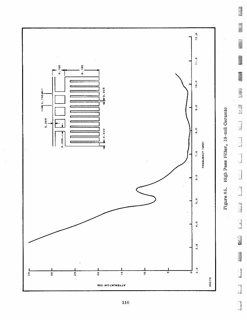
~ l n I'
I1 t l II
n 0 n 0 n 0 n 0 N m m N
9 N c
0
-
0
0
0
m
0
m
0
r.
0
10
0
111
0
t
0
m
0
N
cn r. N 0 n
110
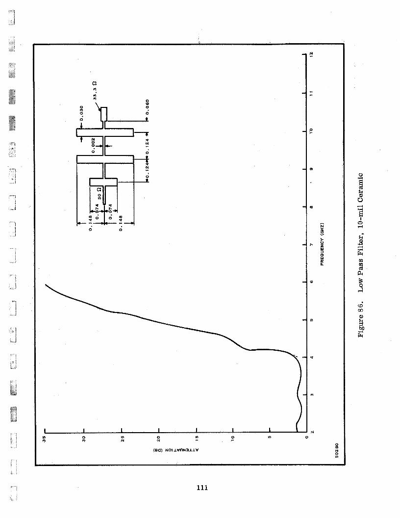
C m m m
0
0 0
I I I I I I I ln 0 m 0 0 m 0 m m m N
(ea) NOIIV~NZIIIV
- - N
N L
" c
0
Q
m
ln
m
N
0
N 0 ln
Lo
111

m 0
1 f
1. ni fi 0
- i o t
I 0 m 0
0
m m N N c
0
p!
0 - c
0
0
0
01
0
4;
0
c
0
10
3 n
3 P
0
m
3 N
112
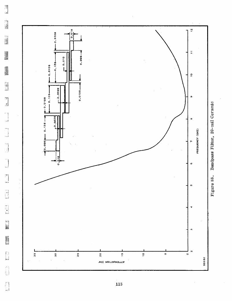
D
0
t m 0
0
0
-
n m
II) N
n - 0 N
113

Q2
4~ lo3
3 x 10 '
2 x 10:
1 x 10:
C I I I 1
0 0 . 5 1 .o 1 . 5 2 . 0 FREQUENCY-f (GHZ)
502 € 3 3 ~
--,
Figure 89. Measured Frequency Variation of Inductor Q
10 x
5 x
r C
CIRCUIT A + k O
VALUES EXTRACTED FROM MEASUREMENTS 10" - L E 6 . 1 NH
C = 5 . 2 PF
10" -
0 . I -2 x 101'
0.5 X lo2' 1.0 X l o 2 ' 1.5 X lo2' 2 . 0 X l o 2 ' 2.5 X lo2' 0
w 2 ( R A W S E C ) ~
-.. .
Figure 90. Measured Frequency Response of the Reactance of a Lumped LC Circuit
114

- 5 0 2 0 5 A - I
Figure 91. RF Circuit Diagram for Power Amplifier
TUN I NG INDUCTOR
I I TRANSISTOR / OUTPUT
CAPACITOR EMITTER
CHOKE I
B+ B Y P A S S
AND CHOKE
100 MILS
1 - L-* 125 M I L S
50206
Figure 92. Layout of 2-GHz Integrated Lumped Circuit Amplifier
1
11 5/116

SECTION VI1
.FERRITES
A . INTRODUCTION
The first scientific report considered the general ferromagnetic properties of ferrite materials. In this report, these properties are further described and their application to microwqve components is extended.
The unilateral transmission properties of ferrite materials are well suited for use in circulators and isolators where the propagation characteristics must differ for different directions of propagation. At higher frequencies, ferrites are easily inte- grated into microstrip fabrication of these devices.
Better understanding of the behavior of the intrinsic properties of ferrite materials E have resulted in such nonlinear applications as frequency doublers, power limiters, and ! modulators. Difficulties which have been experienced in the past such as high dielec-
~ tric constant, operation at high power levels and large insertion loss at ultrahigh fre- ' quencies are being reduced by better preparation of ferrite materials.
The principles underlying the ferromagnetic behavior of ferrite materials is well documented 40941 but a r e briefly reviewed below along with a discussion of recent developments in ferrite materials and devices.
B. MICROWAVE PROPERTIES
The electrical characteristics of ferrites a r e specified by their complex permeability which may be written as
P * = p o [ut - juffJ
where
p ' p f f = imaginary part which is the loss componi
= real part which determines phase shift
nt f permeability
(49)
p o = permeability of free space (4n x h/M)
The response of a ferrite sample to a circular polarization wave is shown in Figure 93 where it is seen that the loss and phase shift through a ferrite sample is different for opposite wave polarization.
117
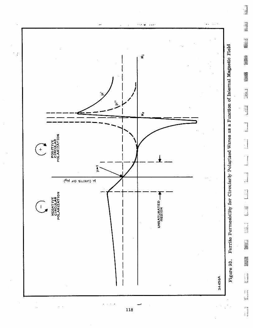
I I
I I
I I I I I I I I I I
I
f
c E
7- -7-
d
118

The magnetization properties of ferrites is the result of the separate ferrite electrons spinning about their own axis as they orbit the nucleus of their parent atom. Electron spin is the principal contributor to the magnetic properties which arise mainly from the magnetic dipole moment associated with the electron spin. The total magnetic moment of the ferrite atom is given
Material
where J is the quantum number associated with the total angular momentum resulting from the spin and orbital moment, pB is the magnetic dipole moment of the electron and equal to 9.27 x 10⁻²¹ ergs/gauss and g is the Lande spectroscopic-splitting factor. When the ferrite material is placed in a dc magnetic field (Hdc), the spin axis of the electrons become aligned in the direction of the applied magnetic field, and the mag- netic dipoles tend to align themselves parallel to the applied field. Consequently, a net magnetization results which is the sum of the separate magnetization contributed by each electron. The magnetization of a ferrite specimen is density of magnetic dipoles per unit volume
then given as the
Saturation Magnetization M s
(oersteds)
+ M = N p .
-+ For a large external magnetic field which saturates the ferrite sample, M becomes 3 s . The whole sample behaves in the same fashion as a large single magnetic dipole. The saturation magnetization, Ms, for common ferrites is given in Table X V . 42
Nickel Zinc Ferrite
Nickel Aluminate
Nickel Cobalt Aluminates
Manganese-magnes ium Ferrite
Manganese- magnesium Aluminate
YIG
Substituted YIG
5000
5 00-17 00
1500- 3000
2100
600-1700
1780
300-1200
When subjected to an RF magnetic field alternating at a micLowave frequency superimposed upon a dc magnetic field, the magnetization vector M of the ferrite sample wil l precess a s a gyroscope about the axis of the applied dc magnetic field.
119
i
The precessional frequency is proportional to the externally applied dc field and may be written,
.3 Wo = YBo .
This frequency is commonly referred to the gyromagnetic resonance frequency a s it is dependent upon the gyromagnetic ratio, Y . This ratio is the ratio of the magnetic +
moment of the ferrite material to the angular momentum of its magnetization vector, M. The gyromagnetic ratio may be expressed a s
I Y I = 1.4 g MHz/oe (53)
where g is the Lande spectroscopic-splitting factor and is normally taken to be equal to 2 for most ferrite materials.
--+ The magnetic induction vector, B, shown in
bility tensor, the magnetic field intensity vector, (51) relates the permea-,
magnetization vector, M, a s seen in the relation43944
3 -+ B = /A 0 [z+%]=pO p] H (54 1
where pd p] is the complex permeability tensor in rationalized mks system, and po is the permeability of free space (4r x 10-7 h / ~ ) .
The applied magnetic field required for ferromagnetic resonance in an infinite ferrite medium is given a s
Ho = w / l y l - (55)
If the microwave frequency is held constant and the magnetic field is varied around the value required for resonance, the -3 dB points in the response will define the magnetic field "line width, v t AH. Narrow linewidth then corresponds to high Q material, since linewidth represents the ''bandwidth" of a material 40945. This relationship may be express ed
I
A f w Y A H . (56)
Linewidth is a function of frequency a s well a s temperature. At a room temperature of 300°K and at 9.34 FHz, linewidth may range from 0.1 oersteds (Oe) to 10 Oe for highly polished YIG garnets. Impure samples of YIG may have linewidths of 100 Oe. In this sense any substitution such as gallium is an impurity and accounts for the relatively larger linewidths of substituted (GA YIG) specimens.
The manner in which various ferent microwave devices is shown
operating regions for ferrite materials yields dif- in Table XVI.
120
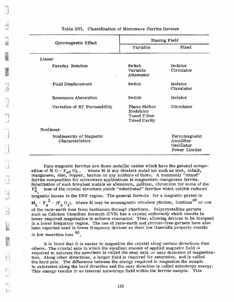
Table XVI. Classification of Microwave Ferrite Devices
Gyromagnetic Effect Biasing Field
Variable Fixed ~
Linear
Faraday Rotation
Field Displacement
Resonance Absorption
Variation of RF Permeability
Nonlinear
Nonlinearity of Magnetic Characteristics
Switch Variable Attenuator
Switch
Switch
Phase Shifter Modulator Tuned Filter Tuned Cavity
Isolator Circulator
Isolator Circulator
Isolator
Circulator
Ferromagnetic Amplifier Oscillator Power Limiter
Pure magnetic ferrites a r e those metallic oxides which have the general compo- sition of M 0 - Fez 0 3 , , where M is any divalent metal ion such a s iron, cobalt, manganese, zinc, copper, barium or any mixture of these. A commonly llmixedl' ferrite composition for microwave applications is magnesium-manganese ferrite. Substitution of such trivalent metals as aluminum, gallium, chromium for some of the F3
magnetic losses in the UHF region. The general formula for a magnetic garnet is
M3 * Fe of the rare-earth ions from lanthanum through ytterbium. Polycrystalline garnets such as Calcium Vanadium Bismuth (CVB) has a crystal uniformity which results in lower required magnization to achieve resonance. Thus, allowing devices to be designed in a lower frequency region. The use of rare-earth and yttrium-free garnets have also been reported used in lower frequency devices as their low linewidth property results in low insertion loss .
ions of the crystal structure yields "substituted" ferrites which exhibit reduced e+
2 (Fe 04), where M may be nonmagnetic trivalent yttrium, lutetium4' o r one
46
It is found that it is easier to magnetize the crystal along certain directions than others. The crystal axis in which the smallest amount of applied magnetic field is required to saturate the specimen is called the easy axis or easy direction of magnetiza- tion. Along other directions, a larger field is required for saturation, and is called the hard axis. The difference between the energy required to magnetize the sample to saturation along the hard direction and the easy direction is called anisotropy energy. This energy results in an internal anisotropy field within the ferrite sample. This
121
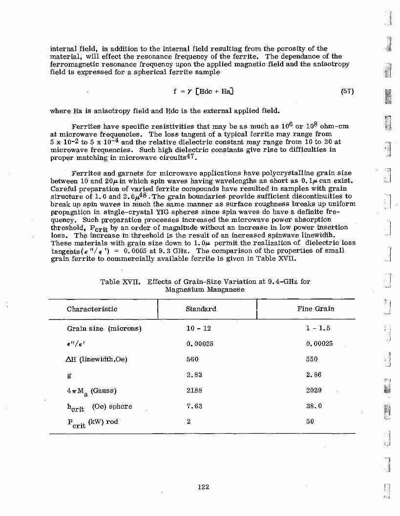
internal field, in addition to the internal field resulting from the porosity of the material, wil l effect the resonance frequency of the ferrite. The dependance of the ferromagnetic resonance frequency upon the applied magnetic field and the anisotropy field is expressed for a spherical ferrite sample
Characteristic
f = Y [Hdc+Ha]
Standard Fine Grain
(57)
where Ha is anisotropy field and Hdc is the external applied field.
Ferrites have specific resistivities that may be as much as lo6 or lo8 ohm-cm at microwave frequencies. The loss tangent of a typical ferrite may range from 5 x 10⁻² to 5 x 10⁻⁴ and the relative dielectric constant may range from 10 to 20 at microwave frequencies. Such high dielectric constants give rise to difficulties in proper matching in microwave circuits47.
Ferrites and garnets for microwave applications have polycrystalline grain size between 10 and 2 0 p in which spin waves having wavelengths a s short as 0.1p can exist. Careful preparation of varied ferrite compounds have resulted in samples with grain structure of 1.0 and 2 .0~48 . The grain boundaries provide sufficient discontinuities to break up spin waves in much the same manner as surface roughness breaks up uniform propagation in single-crystal YIG spheres since spin waves do have a definite fre- quency. Such preparation processes increased the microwave power absorption threshold, Pcrit by an order of magnitude without an increase in low power insertion loss. The increase in threshold is the result of an increased spinwave linewidth. These materials with grain size down to 1. Op permit the realization of dielectric loss tangents( E ''/E ') = 0.0005 at 9.3 GHz. The comparison of the properties of small grain ferrite to commercially available ferri te is given in Table XVII.
Grain size (microns) 10 - 12
f "/€ ' 0.00025
AH (linewidth,Oe) 560
g 2.83
4wMs (Gauss) 2188
1 - 1.5
0.00025
550
2.86
2029
38.0
50
b ! i
122
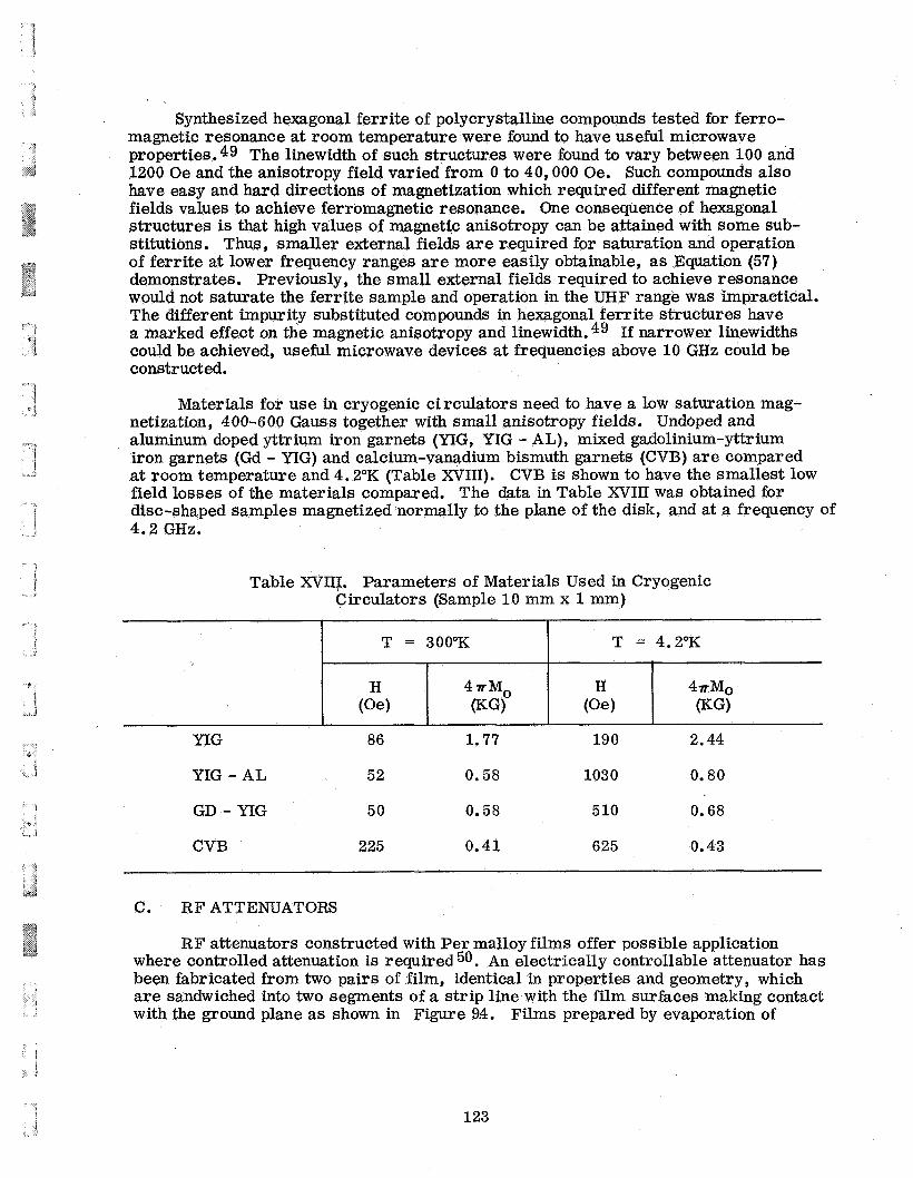
'7 *!
Synthesized hexagonal ferrite of polycrystalline compounds tested for ferro- magnetic resonance at room temperature were found to have useful microwave properties.49 The linewidth of such structures were found to vary between 100 and 1200 Oe and the anisotropy field varied from 0 to 40,000 Oe. Such compounds also have easy and hard directions of magnetization which required different magnetic fields values to achieve ferromagnetic resonance. One consequence of hexagonal structures is that high values of magnetic anisotropy can be attained with some sub- stitutions. Thus, smaller external fields a r e required for saturation and operation of ferrite at lower frequency ranges are more easily obtainable, as Equation (57) demonstrates. Previously, the small external fields required to achieve resonance would not saturate the ferrite sample and operation in the UHF range was impractical. The different impurity substituted compounds in hexagonal ferrite structures have a marked effect on the magnetic anisotropy and linewidth.49 If narrower linewidths could be achieved, useful microwave devices at frequencies above 10 GHz could be constructed.
Materials for use in cryogenic circulators need to have a low saturation mag- netization, 400-600 Gauss together with small anisotropy fields. Undoped and aluminum doped yttrium iron garnets (YIG, YIG - AL), mixed gadolinium-yttrium iron garnets (Gd - YIG) and calcium-vanadium bismuth garnets (CVB) a r e compared at room temperature and 4.2"K (Table XVIII). CVB is shown to have the smallest low field losses of the materials compared. The data in Table XVIII was obtained for disc-shaped samples magnetized normally to the plane of the disk, and at a frequency of 4.2 GHz.
Table XVIII. Parameters of Materials Used in Cryogenic Circulators (Sample 10 mm x 1 mm)
YIG - AL 52 0.58 1030 0.80
GD - YIG 50 0.58 5 10 0.68
CVB 225 0.41 625 0.43
C. RF ATTENUATORS
RF attenuators constructed with Per malloy films offer possible application where controlled attenuation is required 50. An electrically controllable attenuator has been fabricated from two pairs of film, identical in properties and geometry, which a r e sandwiched into two segments of a strip line with with the ground plane a s shown in Figure 9.4. Films
123
the film surfaces making contact prepared by evaporation of

FILM SAMPLES
CENTER CONDUCTOR
50287
GROUND PLANES
Figure 94. Electrical Controlled Attenuator
81/19 NiFe onto heated 0.15 mm glass substrates yielded an attenuation-range that varied almost linearly with frequency. The attenuation ranged from 15 dB at 1-GHz to 27 dB at 2.7 GHz while insertion loss decreased from 9.8 to 3.5 dB. The attenua- tion is proportional to the film thickness and length and inversely proportional to the glass thickness.
D. CIRCUMTORS
Ferrite Y-junction or three port circulators offer many advantages in communi- cation systems operating from L-Band to X-Band. In addition to their use as duplexers in Radar systems, circulators work fine in microwave relays or transponders since the transmitter and receiver usually operate at different frequencies. The circulator also enables simultaneous use of the transmitter and receiver with a single antenna. Because of its low loss, circulators may be utilized in law noise receivers without contributing to receiver noise. In such applications, two 3-port circulators, with one terminated by a matched load, are used with parametric preamplifiers or Helium- cooled masers. Four-port circulators may also be used in this application, but they are inherently more narrow band. The use of two to three port circulators to provide the proper matching impedances is shown in Figure 95.
A circulator is a three or four-port device in which energy introduced at one port circulates only to a second port while energy introduced at the second port circulates only to the third port. The third port is connected to but isolated from the first port.
124
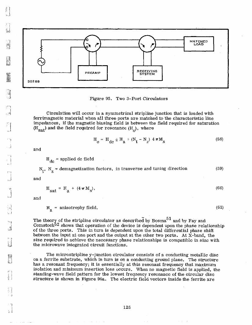
RECEIVING
502 88
Figure 95. Two 3-Port Circulators
Circulation will occur in a symmetrical stripline junction that is loaded with ferrimagnetic material when all three ports are matched to the characteristic line impedances, if the magnetic biasing field is between the field required for saturation (Hsat) and the field required for resonance (Ho), where
H = H -I: Ha + (Nt - Nz) 4 n M s o dc
and
= applied dc field
N , N = demagnetization factors, in tranverse and tuning direction
dc
t z
and
= H + (47rMs), Hsat a and
H = anisotrophy field, a
(59)
The theor of the stripline circulator as describe; by Bosma51 and by Fay and Comstock 2 shows that operation of the device is dependent upon the phase relationship of the three ports. This in turn is dependent upon the total differential phase shift between the input at one port and the output at the other two ports. At X-band, the size required to achieve the necessary phase relationships is compatible in size with the microwave integrated circuit functions.
The microstripline y-junction circulator consists of a conducting metallic disc on a ferrite substrate, which in turn is on a conducting ground plane. The structure has a resonant frequency; it is essentially at this resonant frequency that maximum isolation and minimum insertion loss occurs. When no magnetic field is applied, the standing-wave field pattern for the lowest frequency resonance of the circular disc structure is shown in Figure 96a. The electric field vectors inside the ferrite a r e
125

A .
INPUT
B.
INPUT
50209
MAGNETIC
WALL
(B) H i n t FOR CIRCULATION
OUTPUT /\
Figure 96. Bipolar Mode of a Dielectric Disc with and without Magnetization
126
i ..J
perpendicular to the plane of the disc and the RF magnetic field vectors a r e parallel to the plane of the disc. Ports 2 and 3, if open-circuited, will see voltages which are 180 degrees out of phase and approximately half the magnitude of the input voltage. If the field pattern is rotated, as in Figure 96b, port 3 is at the voltage null position of the disc while the voltages at ports 1 and 2 a r e equal.
Small circulators have been constructed using strip transmission line conductors and ferrite discs to provide the circulator action. One such integrated circulator was fabricated recently at Texas Instruments. This circulator was of the y-junction type and was designed to utilize microstrip lines with a small disc of YIG ferrite 216 mils in diameter and 20 mils thick. This circulator had good isolation (X5dB maximum); how- ever the bandwidth was less than desired. The bandwidth is primarily determined by the matching or coupling into the ferrite media. No attempt was made to optimize this in the initial design. This circulator also used an external magnet and no attempt was made to optimize the magnetic path or integrate the magnetic structure.
Of the possible circulator configurations, the symmetrical junction circulator appears the most attractive for application at X-band. It should result in the smallest size, the simplest construction and also the lowest insertion loss. Figure 97 illustrates an integrated circulator using a ferrite substrate. The design of the magnetic return path may be improved for compactness; a return path is virtually necessary in order to minimize fringing fields which could couple strongly to the outside world.
A 4-port circulator could be obtained by putting two 3-port circulators end to end, as shown in Figure 98, in which case the magnetic path may be closed in a useful way.
E. ISOLATORS
Ferrites a r e used in many various types of isolators such as;
Faraday -r otat ion type
Resonance- isolator
Field displacement
The nonreciprocal electrical properties of ferrite material in which the trans- mission coefficient is not the same for different directions of propagation is employed in microwave isolators. Isolators of several types, depending upon their region of operation regarding the resonance absorption curve, have been constructed utilizing the nonreciprocal property. Such devices allow transmitting a microwave signal with a minimal amount of transmission loss and prevents reflections from the load from interacting with the generating source. The advantages these devices offer a r e to minimize power output variations from power amplifiers and frequency pulling of an oscillator as variations in load impedances occur.
127
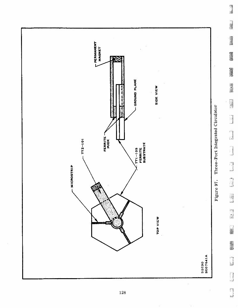
128

W
k E
3 w > c
3 w > c
c m f i t 0 in
129

An isolator that is a one-way transmission device or absorption device is the Faraday-rotation isolator which is essentially a four-port circulator where two ports a r e terminated with matched loads. Practical isolators of these types omit the two extra ports by mounting resistive elements internally within the devices. The resistive elements are separated by a cylindrical ferrite rod which is magnetized along its axis by an external field (Figure 99). The resistive elements are aligned to permit unaffected Faraday rotation of the plane of the propagated wave. This rotation principle results in the reverse wave being rotated 45 degrees counterclockwise by the ferrite rod with the electric vector parallel to the second resistive element; thus the reflected energy is completely absorbed. This type if isolator is referred to as an absorption isolator and it is a low power device because the amount of RF power absorbed is limited by the resistive element. Faraday-rotation type of isolators normally will provide about 30 dB of isolation over a 10 percent bandwidth with less than a 0.58 dB insertion loss a t X-band.
2
FERRITE ROD
50292
Figure 99. Faraday Rotation Isolator
130
SECTION VIII
FILTERS
'i * I i
A. INTRODUCTION
1. General
The first scientific report discussed several types of non-tunable transmis- sion line filters which were compatible with integrated circuits and their passband characteristics could be maintained in microstrip construction. In this report, the discussion of parallel-coupled filters is continued and recent attempts to reduce the size of these filters at S-Band a re examined. In addition, magnetically tunable YIG filters, which a re finding wide spread use in modern microwave receivers, a re dis- cussed.
Good RF selectivity and a high degree of spurious rejection in microwave receivers requires the use of bandpass filters a s preselectors. Ideally, the preselec- tor affords perfect transmission for all frequencies which fall within the passband and infinite attenuation of signals and noise within the stop band. Such characteristics as these a re obtained in basic bandpass filters employing multiple resonators or in structures that superimpose bandpass and band reject filters to obtain the desired com- posite characteristics. Generally, the bandpass characteristics a re obtained from transmission line filters which exhibit periodic response as shown in Fig-we 100. The desired bandpass frequency performance of this type of filter is designed from lowpass prototypes using insertion-loss methods. The design techniques a re well documented for the basic classes of filters such as lowpass, highpass,and bandpass. This section is restricted to a discussion of fixed tuned and electrically tuned bandpass filters which would normally function as a component of a microwave receiver.
2. Fixed Tuned Filters
Lumped-constant LC resonators at microwave frequencies are impracti- cal, so out of necessity, desired frequency characteristics are synthesized from dis- tributed parameter elements such as that offerred by transmission line techniques. The present day use of microstrip makes such techniques applicable to integrated structures in which the desired LC resonant properties a re obtained by open or shorted transmission lines. These filters a re discussed in Section VI. However, such filters fabricated in microstrip as an integrated circuit may not be tuned.
3. Variable Tuned Filters
Filters can be tuned electronically or by a magnetic field. Magnetically tunable filters using single-crystal yttrium iron garnets (YIG) obtain high unloaded Q at microwave frequencies making it possible to build bandpass filters with relatively low insertion loss. The lowest frequency at which a pure YIG sphere will resonate is about 2 GHz. A pure YIG disk sample can be tuned to much lower frequencies, but have the disadvantage of being difficult to machine and are fragile. For this reason, operation at lower frequencies generally employ gallium substituted ferrite resonators, (GaYIG). The substituted material has a reduced saturation magnetization which per- mits operation down to a few hundred megacycles. However, such substituted materials reduces the unloaded Q which results in increased filter losses.
131
fo 2 f o 3 f o
Figure 100. Periodic Nature of Transmission Line Filter
Materials possessing high dielectric constants may be used as dielectric resonators in the construction of tunable filters. The use of small volumes of such material which have dielectric constants on the order of 80, allow high unloaded Q's of 10 to be obtained. These filters can be tuned by adjusting the spacing between resona- tors, or if ferroelectric material is used, by tuning the resonance electrically by ap- plication of a high electric field. The chief disadvantage of high- dielectric constant resonators constructed of present day materials is the excessive dependence of the resonant frequency on temperature.
4
132

B. STRIPLINE FILTERS
The conventional design of the parallel-coupled filter at lower microwave fre- quencies gives a physical configuration that is long and narrow. When such a con- figuration is constructed on microstrip ceramic cracking and mechanical instability results. To minimize the size of the filter, two different designs where attempted, (1) “folding”, and (2) a vertical parallel-coupled filter. These configurations are shown in Figures 101 and 102. The insertion loss charateristic of these filters is shown in Figures 103 and 104.
50294
Figure 101. Parallel Coupled (Folded) Filter
50295
Figure 102. Vertical Parallel Coupled Filter
133

I
a a
Both filters were constructed on stripline and designed as a 3-pole network with center frequency (fo) of 1 .6 GHz and a desired skirt response which would result in greater than 30-dB insertion loss at 200 MHz from fo. Figures 103 and 104 illus-
trate that the filters center frequency differs slightly from the design center frequency; other than that, the effects of folding appear negligible.
Since the effective coupling area of each filter is reduced from a quarter wave- length, i t was necessary to compensate the gap coupling while maintaining the overall element length at one-half wavelength. This was accomplished by decreasing the gap in an amount proportional to the decreased coupling length.
Considering briefly the adaptation of the stripline bandpass filter design to micro- strip circuitry on ceramic, it is important to note that of the basic design differences, the most significant change in the design procedure results from the absence of the upper ground plane and corresponding dielectric material. Utilizing design informa- tion and calculations of gap capacitance based on the normal filter equations, it is possible to progress from a stripline design to the desired microstrip of thin-film design. However, it may be necessary to compensate the coupling and redesign the filter.
Bandpass filters exhibiting low passband insertion loss and extremely steep rejection skirts can be realized by means of a composite bandpass, bandstop filter structure. A pair of band reject filters, each one exhibiting the desired rejection at the portion the frequency spectrum corresponding to their designated reject frequencies, coupled with a bandpass filter determines the overall pass band characteristic. One of the direct advantages of such a structure is that the number of resonators needed to achieve a given response is reduced. In addition, lower midband insertion loss is obtained and lower Q resonators a re required. A typical attenuation response for a composite bandpass, band reject filter is shown in Figure 105. As is seen from the figure, the band reject filters independently set the slope or skirt selectivity.
The optimum design for the composite filter is one which uses the fewest number of resonators to achieve the desired slope and utilizes a large number of stagger-tuned band reject filters to achieve the rejection bandwidth as dissipative losses occuring at the lower edges of the band reject filter slope, have the effect of rounding the edges of the passband response. Thus, the required unloaded Q needed for a slope filter is determined by the permissible rounding at the passband edges.
A composite bandpass, band reject interdigital filter has been designed which successfully offers frequency separation in a multiplexer unit. The stripline config- uration is illustrated in Figure 106. Both the bandpass and the band reject filter had the same number of elements in order to accomplish a constant-resistance input that equalled the generating source resistance. This arrangement permitted a number of filters to be cascaded without harmful interaction effects.
The design center frequency of the filter combination was 1.5GHz with a desired bandwidth of 5 percent. The measured VSWR was better than 1.25 in the passband; and insertion loss at band center was 0.38dB. shown in Figure 107.
The performance characteristics a re
134
O m Lo N
0 N
Lo 0 - c
(sa) ssoi N O I U ~ S N I
> t J z W 3 0 W E - LL
135

0
/’
I I I I I I b v) 0 v)
c c 0 v) 0 m N N
(Ea) S S O l NOllYBSNl
136
rn k 6) c., 4
iz 2
3f
.d 4
.d a k
a 4 .d
El iz
rl
6) k 5 brJ iz
I
BAND REJECT BAND P A S S BAND REJECT FILTER 1 FILTER FILTER 2 b b
v) v) 0 J
5 0 2 9 8 A
\ CO M POS ITE BAND REJECT
FILTER 2
BANDPASS FILTER CHARACTER 1 S T l C S
Figure 105. Composite Bandpass - Band Reject Filter
C. YIG MAGNETICALLY TUNABLE FILTERS
In recent years attention has been given to bandpass and bandstop filters con- structed with highly polished spheres or discs of ferromagnetic materials such as yttrium iron garnet (YIG) and gallium substituted YIG (GAYIG). The magnetic proper- ties of such materials have been incorporated into microwave devices which offer unique advantages as resonators and preselectors. These devices have unloaded Q’s greater than 1500 in a 600-MHz to 12GHz frequency range which results in narrow bandwidths with high-offband rejection and are capable of being electronically tuned by an external
magnetic field . 53
The principle of operation of a single YIG sphere is shown in Figure 108. h t h i s figure, it may be seen that an uniform dc magnetic field Hdc is applied in the z direction and an R F magnetic field is applied in2he x direction. A gyroscopic effect results in which the magnetic moment vector M precesses about the Z axis causing R F energy to be coupled out of the coils in the y direction. Maximum energy is coupled to the load when ferromagnetic resonance occurs. This resonance is expressed simply as
f (megahertz) = 2.8 Hdc (Gauss) (62)
Coupling of energy from the RF source to the load at frequencies away from resonance is typically 50dB down due to the orthogonal arrangement of the coil
45 loops .
137
D
I 4
I BANDPASS FILTER
3
I 2
I N
1 =A
Z T ZA = RB I 1 'I 3
\ / 50299
BANDSTOY FILTER
Figure 106. A Composite Bandpass - Band Reject Interdigital Filter
YIG filters are operated from 2.0-GHz to mm wave bands. The upper frequency is limited to available magnetic fields. The low frequency limitation is due to poor coupling and low values of unloaded Q. Extending YIG filters to VHF regions requires the use of YIG disc ferromagnetics instead of spheres or the use of GAYIG which has a lower saturation magnetization. The lower frequency limitations may be seen from Equation (63) which defines the unloaded Q of a sphere as
Hdc - M/3 A H Qu =
where AH is the intrinsic line width, and M the saturation magnetization of the material. For YIG, M = 1785 gauss and AH = 0.5 oersteds at room temperature. Consquently, Qu becomes zero for an applied magnetic field of 595 gauss. This corresponds to a frequency of approximately 1700 MHz. The unloaded Q characteristic as a function of frequency is shown in Figure 109.
Measurements of YIG and GAYIG bandwidths as a function of temperature indicate that a change of 10 percent may be expected over a -50°C to +70°C temperature range. The worst frequency drift is experienced at colder temperatures, but can be minimized if the YIG resonator temperature is maintained as high as possible. For a fixed mag- netic field, the frequency shift about the center frequency of the passband of the reson- ator may be written as
(64) K1 Af = 3. 7A- M
138
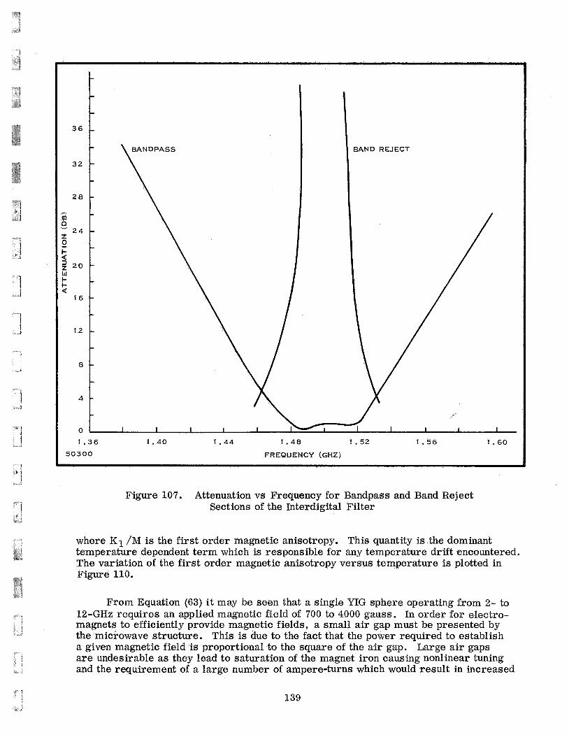
3
- -
36 - -
32 - -
28 - - - m
'24 - z 0 - t; 2 20 - W I- - c Q
16 - -
12 - -
8 -
- 4 -
.-
BAND PASS BAND REJECT
,' I I 1 I I I I I 1
1.36 1.40 1.44 1.48 1.52 1 . 56 1.60 0
50300 FREQUENCY (GHZ)
Figure 107. Attenuation vs Frequency for Bandpass and Band Reject Sections of the Interdigital Filter
where K1 /M is the first order magnetic anisotropy. This quantity is the dominant temperature dependent term which is responsible for any temperature drift encountered. The variation of the first order magnetic anisotropy versus temperature is plotted in Figure 110.
From Equation (63) i t may be seen that a single YIG sphere operating from 2- to 12-GHz requires an applied magnetic field of 700 to 4000 gauss. In order for electro- magnets to efficiently provide magnetic fields, a small air gap must be presented by the microwave structure. This is due to the fact that the power required to establish a given magnetic field is proportional to the square of the air gap. Large air gaps are undesirable as they lead to saturation of the magnet iron causing nonlinear tuning and the requirement of a large number of ampere-turns which would result in increased
139
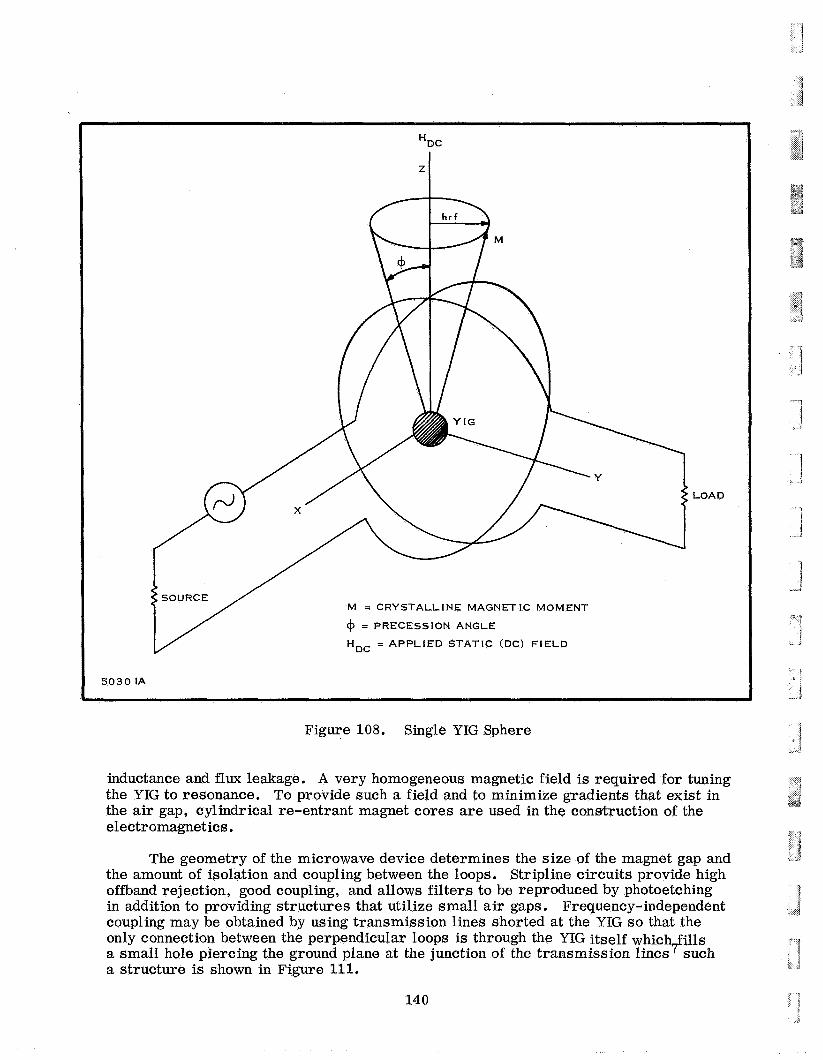
SOL. r:. 5030 1A
LOAD
M = CRYSTALLINE MAGNETIC MOMENT 9 = PRECESSION ANGLE
= APPLIED STATIC (DC) FIELD DC
Figure 108. Single YIG Sphere
inductance and flux leakage. A very homogeneous magnetic field is required for tuning the YIG to resonance. To provide such a field and to minimize gradients that exist in the air gap, cylindrical re-entrant magnet cores a re used in the construction of the electromagnetics.
The geometry of the microwave device determines the size of the magnet gap and the amount of isolation and coupling between the loops. Stripline circuits provide high offband rejection, good coupling, and allows filters to be reproduced by photoetching in addition to providing structures that utilize small air gaps. Frequency-independent coupling may be obtained by using transmission lines shorted a t the YIG so that the only connection between the perpendicular loops is through the YIG itself which7fllls a small hole piercing the ground plane at the junction of the transmission lines such a structure is shown in Figure 111.
140
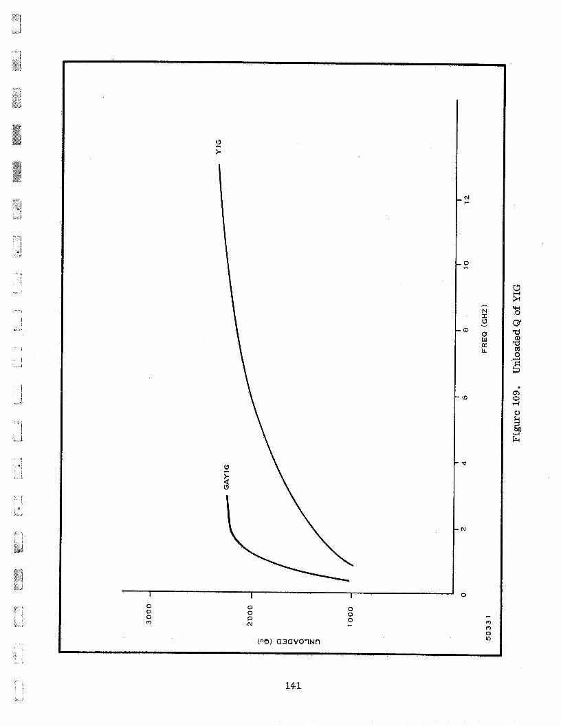
i L .
i" 1 \. 'I .
i i
.. r
, * *
I I I 0 0 0 m
0 0 0 N
0 0 0 c
141

250 300 3 50 40 0
TEMPERATURE (OK)
50332A
Figure 110. Variation of the First Order Magnetic Anisotropy v s Temperature
142

I 50302
Figure 111. YIG Filter
In the case of two-resonator filters, the transmission lines are not necessarily placedatrightangles but may be in parallel as illustrated in Figure 112.
The length of the magnet air gap required for this arrangement is increased pro- portionally by the number of resonators used. When two or more resonators a re multiple - coupled to provide a magnetically tunable band-pass filter characteristic, a coupling slot in the common side all between two strip-transmission lines will result in the smallest possible air gap ”. This arrangement is shown in Figure 113.
Figure 114 gives curves of the theoretical &e plotted against the diameter of spherical resonators for various line dimensions for a short-circuited symmetrical str ip line transmission line. The curves can be used for ellipsoidal resonators by
143
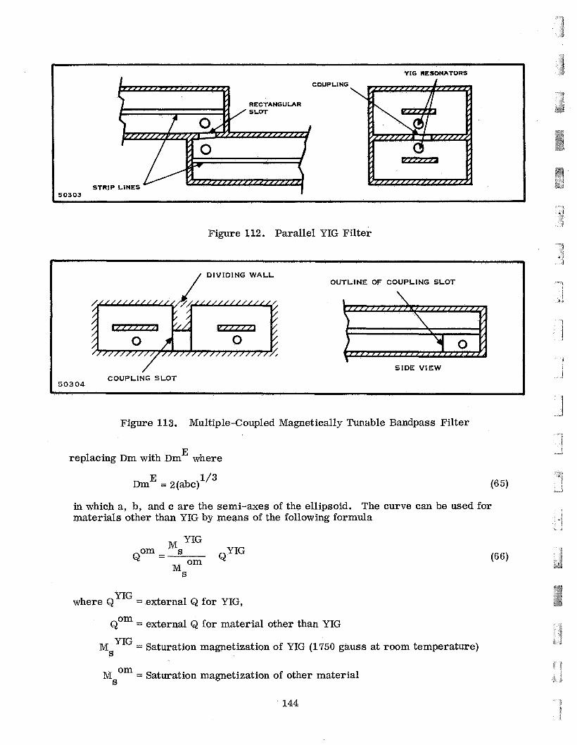
YIG RESONATORS
COUPLI NG
RECTANGULAR
STRIP LINES . 50303
Figure 112. Parallel YIG Filter
OUTLINE OF COUPLING SLOT I
/ S I D E VIEW COUPLING SLOT I 50304
Figure 113. Multiple-Coupled Magnetically Tunable Bandpass Filter
E replacing Dm with Dm where
E 1/3 Dm = 2(abc)
in which a, b, and c are the semi-axes of the ellipsoid. The curve can be used for materials other than YIG by means of the following formula
Qom = QYIG om
where QyIG = external Q for YIG,
Qom = external Q for material other than YIG
MsYIG = Saturation magnetization of YIG (1750 gauss at room temperature)
Msom = Saturation magnetization of other material
144
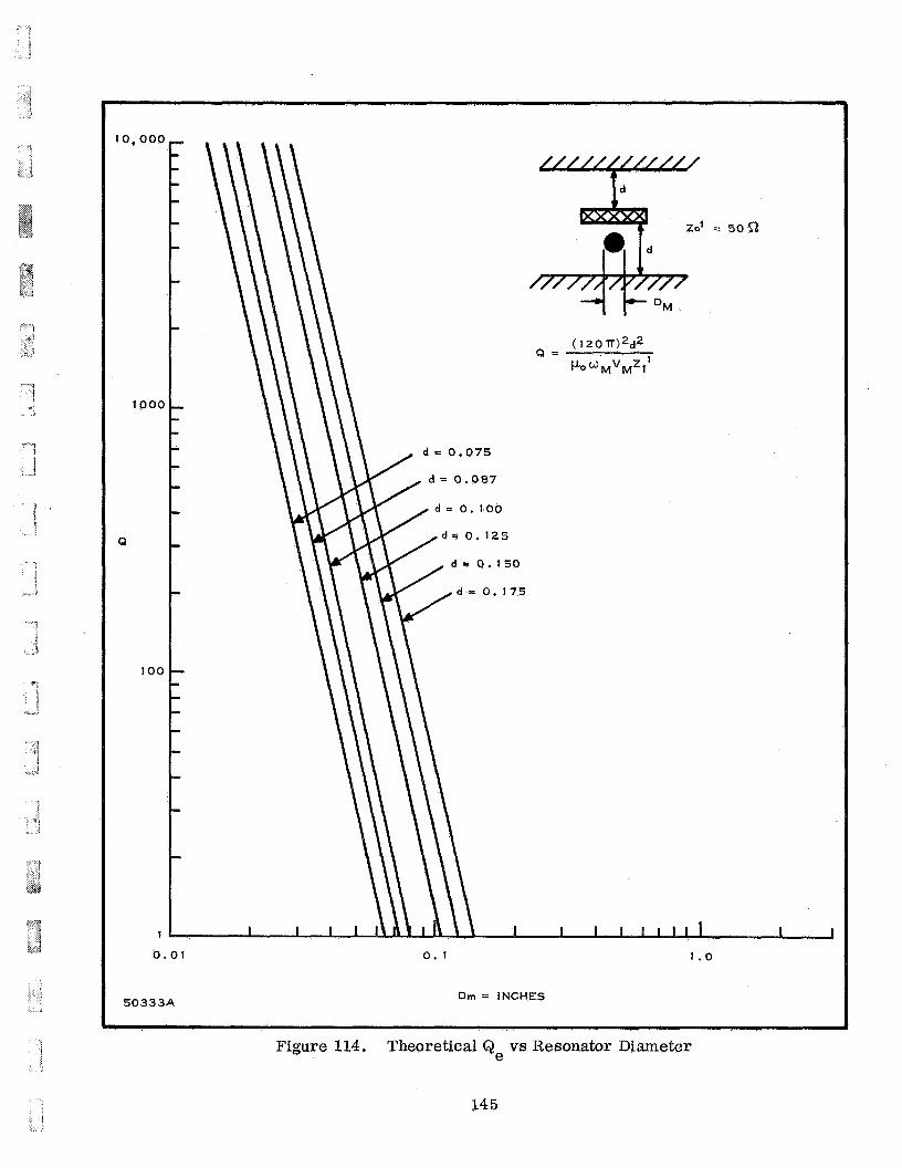
Q
0.01 0 . 1 1.0
Drn = INCHES 50333.4
Figure 114. Theoretical Q vs Resonator Diameter e
14 5
The dimensions of the coupling slot and the spacing between resonators are determined largely by experiment.
Figure 115 summarizes the performance of the two-resonator sidewall-coupled YIG filter constructed with a center frequency of 2.0 GHz. Insertion loss at band center varies between 2.4 dB for a center frequency of 2.0 GHz and a minimum value of 1.2 dB at a center frequency of 3.0 GHz. The 3 dB and 30 dB bandwidths of the filter varied only slightly as the center frequency was tuned over the 2- to 4-GHZ range.
The use of YIG resonators a s preselectors in a superheterodyne receiver is shown in Figure 116. This figure illustrates the many uses of YIG filters which were employed in an S-Band superhet receiver built by LORAL. A YIG filter selects the desired har- monic output and provides the matching structure between the oscillator and the first mixer. A microwave discriminator utilizes a YIG filter to compensate for the non- linear tuning of the varactor tuned VCO.
Another tunable filter is the dielectric-loaded microwave cavity. A single or double-ended cavity filled with a high dielectric material will support highQ resonances, and movable shorting plungers at one o r both ends allow frequency tuning. Tuning may be accomplished over an octave o r more. These structures may be used as microwave resonators in solid-state communication equipment; however, integration of the cavity resonator itself into an "integrated" or thin-film component is unlikely; therefore, it will not be discussed in this report.
146
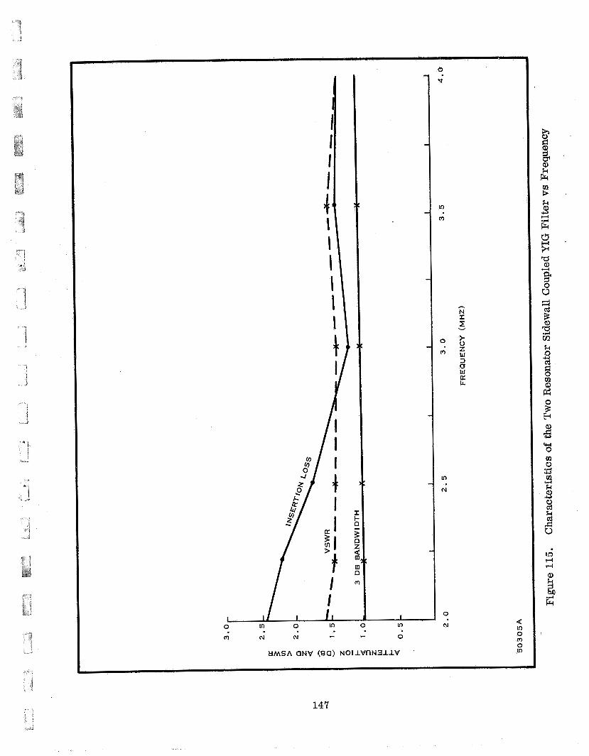
m N N
I m 0 c -
HMSA QNV (sa) N O l l V t l N 3 l l V
0
P
in
n
0
m
in
(\I
0
N a m 0 m 0 m
147
rn 3
5 2 Fr

7 r - t - i
W 0 m 0 Ln
SECTION IX
MIXERS
A. GENERAL
Scientific Report No. 1 reviewed the basic characteristics of Schottky barrier diodes. In this section, the discussion presented earlier is extended to cover the conversion loss and noise figure characteristics of these devices. The application of these diodes in integrated balanced S and C-band mixers and the mixing process required for superheterodyne detection a re reviewed.
B. THE MIXING PROCESS
The mixer stage in a superheterodyne receiver is essentially a frequency con- verter which translates the received signal frequency to a relatively lower inter- mediate frequency where amplification may be more readily achieved. Where it is desired to further remove spurious input signals from the local oscillator signal, more than one mixer stage may be used to transform one intermediate frequency to one lower in frequency as in the case of multiple conversion receivers. Such use of mixers is referred to a s heterodyne detection and wil l form the subject of this section, although the mixing process may be employed in other applications such as sideband generation in suppressed carrier systems.
I
At lower UHF regions where R F amplification is realizable, R F amplifiers commonly precede the first mixer stage and the noise figure of the mixer has almost insignificant bearing upon overall noise performance of the receiver i f the amplifier gain is sufficiently high. In this case, where the mixer is preceded by RF gain, the overall noise figure of the receiver may be expressed in terms of cascaded networks which a r e representative of the RF stages preceeding the mixer, the mixer itself and the following IF amplifier. This relationship is given in Equation (67)58 .
T2L G12
NFo = F1+
where N F is the overall noise figure 0
F1 is the noise factor of the first stage
F is the noise factor of the second stage
F is the noise factor of the third stage 2
3
G and G12 a re the power gains associated with the corresponding stages. 11
14 9
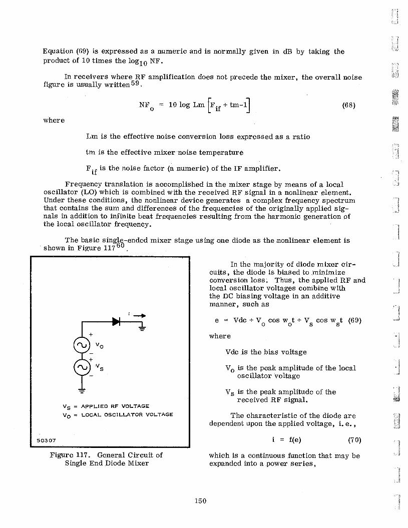
Equation (69) is expressed a s a numeric and is normally given in dB by taking the product of 10 times the loglo NF.
In receivers where RF amplification does not precede the mixer, the overall noise figure is usually written59.
N F ~ = 10 log Lm Pif + tm-l]
where
Lm is the effective noise conversion loss expressed as a ratio
tm is the effective mixer noise temperature
Fif is the noise factor (a numeric) of the IF amplifier.
Frequency translation is accomplished in the mixer stage by means of a local oscillator (LO) which is combined with the received RF signal in a nonlinear element. Under these conditions , the nonlinear device generates a complex frequency spectrum that contains the sum and differences of the frequencies of the originally applied sig- nals in addition to infinite beat frequencies resulting from the harmonic generation of the local oscillator frequency.
The basic single-ended mixer stage using one diode as the nonlinear element is shown in Figure 11760.
Vs = APPLIED R F VOLTAGE
Vo x LOCAL OSCILLATOR VOLTAGE
I 50307
Figure 117. General Circuit of Single End Diode Mixer
In the majority of diode mixer cir- cuits, the diode is biased to minimize conversion loss. Thus, the applied R F and local oscillator voltages combine with the DC biasing voltage in an additive manner, such as
e = Vdc + Vo cos wot + Vs cos wst (69)
where
Vdc is the bias voltage
Vo is the peak amplitude of the local oscillator voltage
Vs is the peak amplitude of the received RF signal.
The characteristic of the diode a re dependent upon the applied voltage, i. e. ,
i = f(e) (70)
which is a continuous function that may be expanded into a power series,
150
2 3 i = a + a e + a e + a e + . . . + 0 1 2 3
In the literature, this expansion, with Equation (69) substituted, has been carried out to the fifth order term and a representative account of the IF frequency spectrum is obtained61. In sensitive receivers, the amplitude of the local oscillator voltage is normally much greater than the received signal voltage. Operating the local oscillator at high levels has the advantage of optimizing the mixer's performance by expanding the mixer's dynamic range and improving intermodulation rejection.
The nonlinearity of the mixing element causes harmonics of the local oscillator frequency to appear in the IF outputs which beat with the signals present in the input, thereby creating new frequencies. These frequency components fall into three categories : 64
Spurious mixer products a r e the extraneous frequency components in the mixer output other than the desired sum o r difference terms.
"Crossovers" a r e undesired frequency components that fall within the passband of the mixer outputs and may be heard in the audio portion of the receiver.
Intermodulation is frequency components that result from two signals, one desired, the other undesired being impressed upon mixer input and combining with the local oscillator.
Of these spurious response, intermodulation is the worst in superheterodyne receivers. It is the direct result of the third and higher order characteristics of the mixer ele- ment and can not be completely eliminated by preceding the mixer with a narrowband filter. Reduction of these frequency components can only be obtained by making effective use of the mixer element and by making proper choice of the dc operating point. Such steps, in turn reduces the magnitude of the higher ordered terms in the power series .
It has been recently published that applying different biasing voltages to two diodes in a balanced mixer have resulted in intermodulation response ratios than 100 dB and ratios of 80 dB or better in the case of single-ended stages biasing scheme reported reduces the magnitude of the 4th and 6th order terms of the power expansion thereby reducing the interaction of these components within the mixer 69
Some of these spurious frequencies in the input a r e subharmonics of the IF frequency and fall within the IF passband. The general expression for the case of two spurious input frequencies is
mf2 - nfl = P fLO * fIF
The spurious signals that a r e separated from the local oscillator by submultiples of the IF is given when n = 0, m = p
15 1
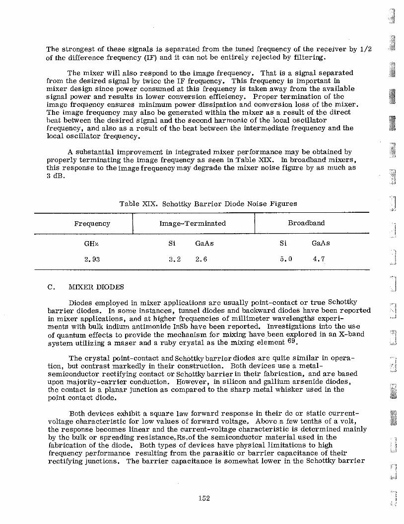
The strongest of these signals is separated from the tuned frequency of the receiver by 1/2 of the difference frequency (IF) and it can not be entirely rejected by filtering.
The mixer wil l also respond to the image frequency. That is a signal separated from the desired signal by twice the IF frequency. This frequency is important in mixer design since power consumed at this frequency is taken away from the available signal power and results in lower conversion efficiency. Proper termination of the image frewency ensures minimum power dissipation and conversion loss of the mixer. The image frequency may also be generated within the mixer as a result of the direct beat between the desired signal and the second harmonic of the local oscillator frequency, and also as a result of the beat between the intermediate frequency and the local oscillator frequency.
Frequency Image-T er minated
A substantial improvement in integrated mixer performance may be obtained by properly terminating the image frequency as seen in Table XM. In broadband mixers, this response to the image frequency may degrade the mixer noise figure by as much a s 3 dB.
Broadband
2.93 3 . 2 2 .6 5 . 0 4 .7
C. MIXER DIODES
Diodes employed in mixer applications a r e usually point-contact o r true Schottky barrier diodes. In some instances, tunnel diodes and backward diodes have been reported in mixer applications , and a t higher frequencies of millimeter wavelengths experi- ments with bulk indium antimonide InSb have been reported. Investigations into the use of quantum effects to provide the mechanism for mixing have been explored in an X-band system utilizing a maser and a ruby crystal a s the mixing element 69.
The crystal point-contact and Schottky barrier diodes a r e quite similar in opera- tion, but contrast markedly in their construction. Both devices use a metal- semiconductor rectifying contact or Schottky barrier in their fabrication, and a r e based upon majority-carrier conduction. However , in silicon and gallium arsenide diodes , the contact is a planar junction a s compared to the sharp metal whisker used in the point contact diode.
Both devices exhibit a square law forward response in their de o r static current- voltage characteristic for low values of forward voltage. Above a few tenths of a volt, the response becomes linear and the current-voltage characteristic is determined mainly by the bulk or spreading resistance,Rs,of the semiconductor material used in the fabrication of the diode. Both types of devices have physical limitations to high frequency performance resulting from the parasitic o r barrier capacitance of their rectifying junctions. The barrier capacitance is somewhat lower in the Schottky barr ier
152

* I J
: I j
devices because of its planar construction: Nevertheless, the shunting effect of this barrier capacitance at the rectifying contact becomes important at higher frequencies.
Other advantages of the Schottky barrier are that they are readily adaptable to integrated circuit structures and yield better reproducibility during fabrication. For the latter reason they afford economical selection of matched pairs for use in balanced mixer circuit configurations. In addition, the planar area contact between the metal and the semiconductor results in uniform contact potential and uniform current dis- tribution throughout the junction. This, in turn, results in low series resistance and greater resistance to transient pulse burnout.
The high frequency attributes of the diode and its characteristic behavior become evident in mixer applications where diode noise figure, conversion losses and IF and R F impedances a r e critical factors.
The diode parameters are related to the materials used in the construction 65, 72 For example, if a circular area of contact i s assumed, the spreading resistance RS, is related to the geometry of the diode by
1 4 a a Rs = - (74 1
where ais the conductivity of the semiconductor and llalf is radius of the circular area of contact between the rectifying junction and the semiconductor. The barrier resistance, Rb? is derived from the theoretical expression of an ideal diode I-V characteristics of the junction , Typically, the current of a rectifying unit increases exponentially for applied voltages of a few tenths of a volt in the forward direction and may be expressed,
7 1
where Is is the saturation current and is dependent upon the junction area and type of metal and semiconductor material used. The remaining parameters a r e defined:
q is the electron charge = 1.6 x 1O-l' coulombs
T is the temperature in degrees Kelvin (OK)
k is Boltzman's constant = 1.38 x joules/"K
v is the voltage applied across the diode junction. That is the applied RF voltage minus the drop across Rs
n is the diode ideal factor. In Schottky Barrier diodes it is close to one- approximating the ideal diode characteristics. For point contact diodes it is somewhat higher.
153
From this expression, the barrier resistance, Rb may be derived
where i is the RF signal current in milliamperes. Since a biasing current Io normally exists, the above definition of Rb may be rewritten a s
26 i + I 0
Rb = (77)
where Io is expressed in milliamperes. The capacitance rising from the storage of charge in the boundary or depletion layer for diodes fabricated with uniform impurity density is given
C O
This capacitance is referred to a s the barrier capacitance of an abrupt junction. It is nonlinear in that it is dependent upon the thickness of the barrier layer which in turn is a function of applied voltage. The other parameters a r e defined:
V is the applied voltage
C is the zero bias junction capacitance
v b is the barrier potential, usually about 0.7 volts.
0
At higher frequencies the shunting effects of this capacitance reduces the RF voltage across the barrier.
The dynamic or barrier resistance, Rb, is associated with either the point con- tact o r Schottky barrier diode. In the case of small signal applications, this resistance is dependent upon the current flow through the diode. In practice this current is the sum of the quiescent current and the current generated by the local oscillator.
The aforementioned parameters and the package parasitic parameters may be combined into an equivalent circuit representing a typical microwave diode as shown in Figure 118.
The equivalent circuit has been found to be valid to approximately 600 GHz. The parasitic elements Rs and Cb limit the upper frequency range, however, below 1 GHz, the shunting effect of the nonlinear barrier capacitance may be neglected as well as the package parasites. The remaining two resistive elements Rs and Rb are summed into what is normally termed the video resistance, Rv. Thus,
RV = Rs + Rb . (79)
154
i !
- 1
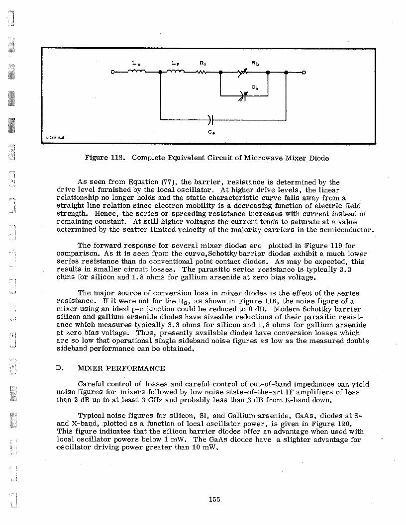
50334
Figure 118. Complete Equivalent Circuit of Microwave Mixer Diode
A s seen from Equation (77) , the barrier, resistance is determined by the drive level furnished by the local oscillator. At higher drive levels, the linear relationship no longer holds and the static characteristic curve falls away from a straight line relation since electron mobility is a decreasing function of electric field strength. Hence, the series or spreading resistance increases with current instead of remaining constant. At still higher voltages the current tends to saturate at a value determined by the scatter limited velocity of the majority carr iers in the semiconductor.
The forward response for several mixer diodes are plotted in Figure 119 for comparison. As it is seen from the curve,Schottkybarrier diodes exhibit a much lower series resistance than do conventional point contact diodes. A s may be expected, this results in smaller circuit losses. The parasitic series resistance is typically 3 . 3 ohms for silicon and 1.8 ohms for gallium arsenide at zero bias voltage.
The major source of conversion loss in mixer diodes is the effect of the series resistance. If it were not for the Rs, as shown in Figure 118, the noise figure of a mixer using an ideal p-n junction could be reduced to 0 dB. Modern Schottky barrier silicon and gallium arsenide diodes have sizeable reductions of their parasitic resist- ance which measures typically 3 . 3 ohms for silicon and 1.8 ohms for gallium arsenide at zero bias voltage. Thus, presently available diodes have conversion losses which a r e so low that operational single sideband noise figures as low as the measured double sideband performance can be obtained.
D. MIXER PERFORMANCE
Careful control of losses and careful control of out-of-band impedances can yield noise figures for mixers followed by low noise state-of-the-art IF amplifiers of less than 2 dB up to at least 3 GHz and probably less than 3 dB from K-band down.
Typical noise figures for silicon, Si, and Gallium arsenide, GaAs, diodes at S- and X-band, plotted as a function of local oscillator power, is given in Figure 120. This figure indicates that the silicon barrier diodes offer an advantage when used with local oscillator powers below 1 mW. The GaAs diodes have a slighter advantage for oscillator driving power greater than 10 mW.
155

h
m W a W a E d I- z W U 3 u 0
v
a
$ (L:
e I LL -
-1 IO c
-2 IO c
-3 10
-6 10
-7 10
0 0.1 0.2 0.3 0.4 0.5 0.6 0.7 0 . 8 0.9 1.0
VF-FORWARD VOLTAGE (VOLTS)
50308
Figure 119. Forward Response of Mixer Diodes
156

A I -
\
\ \ \
4l
b I I
157
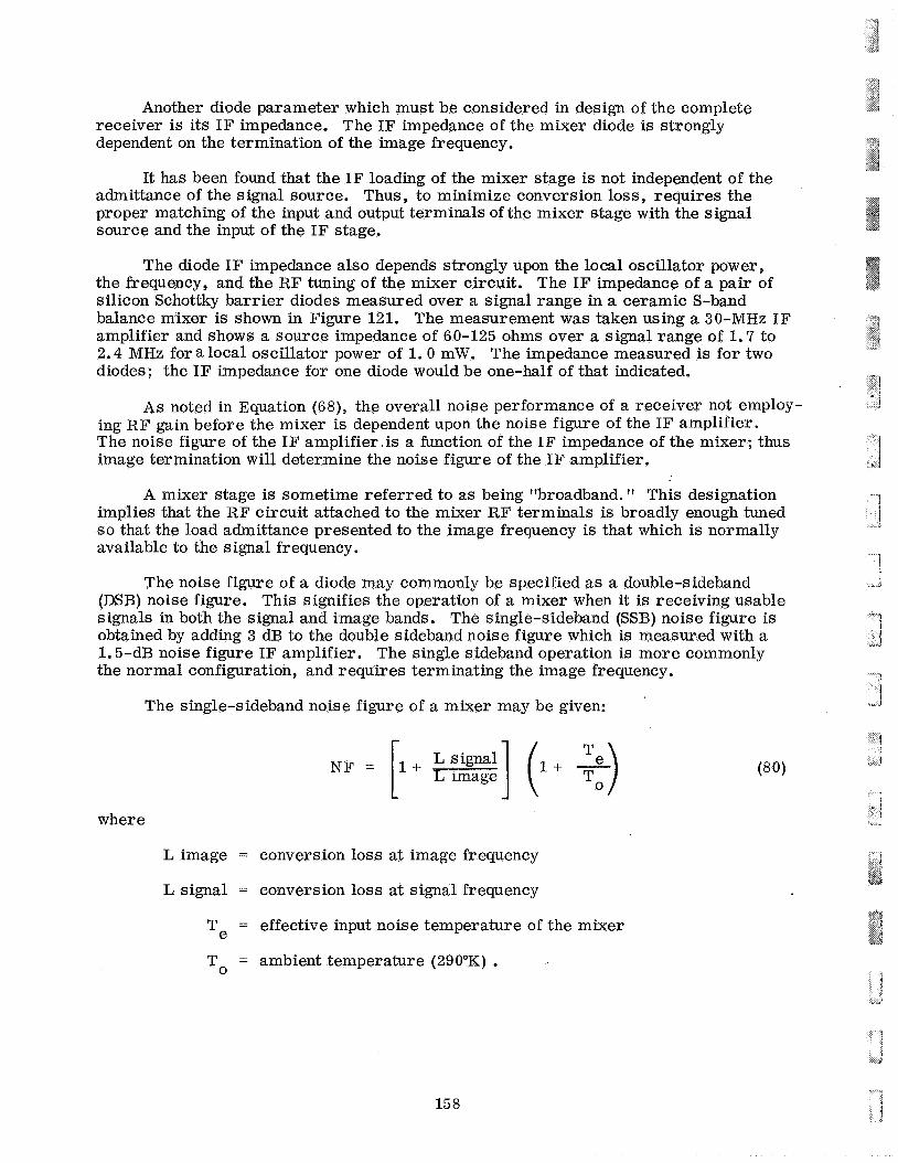
Another diode parameter which must be considered in design of the complete receiver is its IF impedance. The IF impedance of the mixer diode is strongly dependent on the termination of the image frequency.
It has been found that the IF loading of the mixer stage is not independent of the admittance of the signal source. Thus, to minimize conversion loss, requires the proper matching of the input and output terminals of the mixer stage with the signal source and the input of the IF stage.
The diode IF impedance also depends strongly upon the local oscillator power, the frequency, and the RF tuning of the mixer circuit. The IF impedance of a pair of silicon Schottky barrier diodes measured over a signal range in a ceramic S-band balance mixer is shown in Figure 121. The measurement was taken using a 30-MHz IF amplifier and shows a source impedance of 60-125 ohms over a signal range of 1.7 to 2.4 MHz for a local oscillator power of 1.0 mW. The impedance measured is for two diodes; the IF impedance for one diode would be one-half of that indicated.
A s noted in Equation (68), the overall noise performance of a receiver not employ- ing RF gain before the mixer is dependent upon the noise figure of the IF amplifier. The noise figure of the IF amplifier .is a function of the IF impedance of the mixer; thus image termination will determine the noise figure of the IF amplifier.
A mixer stage is sometime referred to as being "broadband. This designation implies that the RF circuit attached to the mixer RF terminals is broadly enough tuned s o that the load admittance presented to the image frequency is that which is normally available to the signal frequency.
The noise figure of a diode may commonly be specified as a double-sideband (DSB) noise figure. This signifies the operation of a mixer when it is receiving usable signals in both the signal and image bands. The single-sideband (SSB) noise figure is obtained by adding 3 dB to the double sideband noise figure which is measured with a 1.5-dB noise figure IF amplifier. The single sideband operation is more commonly the normal configuration, and requires terminating the image frequency.
The single-sideband noise figure of a mixer may be given:
where
L image = conversion loss at image frequency
L signal = conversion loss at signal frequency
Te = effective input noise temperature of the mixer
To = ambient temperature (290°K) .
I
,_i
15 8
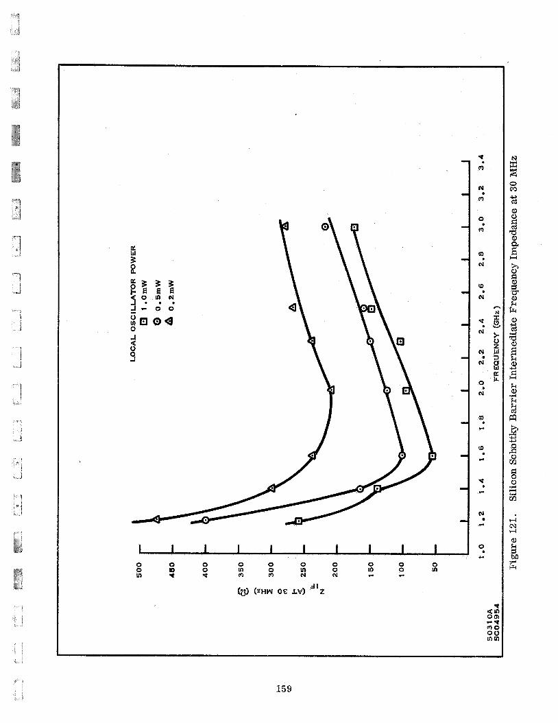
I I I I I I I I I I 0 0 0 0 0 0 0
0 IC) 0 ln 0 m m N N 0 rp IC) '(I q
0 0 0 IC) 0 In c c
Tt
m
lu
m e
0
m *
? N
10
N e
t N *
tu N
e
0
N .
?J
c
(D b r
.4 . c
N
.-
9 c
15 9
For the broadband mixer, L image = L signal and the noise figure is degraded by 3 dB. If the conversion loss of the diode is assumed to be essentially constant at the signal and image frequencies, the ratio of L signal to L image is equal to the ratio of the mismatch losses at the signal and image frequencies. Using this ratio, mismatch losses in the above expression gives an indication of the manner in which the noise figure of the mixer is increased over the case where the mismatch loss at the image frequency is infinite.
The image-terminated mixer reduces signal power loss by preventing any of the signal power, which is converted by the mixer diode to frequencies other than the IF, from being dissipated in the source o r any other termination. By presenting an open circuit to the mixer diodes, the noise temperature of the diode is reduced because the noise currents generated by the image frequency are prevented from flowing and can not be converted to appear as noise at the IF. The open circuit image termination wil l reflect back the image signal produced by the mixing action of the diode.
An image-terminated mixer requires a frequency selective matching network which provides the desired impedance to the image frequency. Care must be taken to match the local oscillator and signal source to the mixer diode. These matching conditions propose a restriction upon the tuning range of the image terminated mixer, as narrow-band tuning range is required in order to simultaneously match the signal, L. 0. and image frequencies.
Very low noise microwave mixers using gallium arsenide diodes in a hybrid-ring configuration and in which the image frequency was terminated into an open circuit has been built at 2 .7 GHz. A 30-MHz IF amplifier with a noise figure of 0.78 dB followed
the mixer 80. The hybrid-ring losses were less than 0.1 dB, the VSWR was below 1.15 and this isolation was greater than 30 dB from 2.5 to 2.9 GHz The measured single- sideband noise figure of the mixer was 2.09 h0.05 dB after losses of the RF filter were subtracted.
noise figure of a mixer for any given IF and bandwidth. The conversion loss, Lm, in Equation (68) is the effective loss realized in a specific mixer. It is really a sum of three types of losses. The f i rs t type of loss depends on the degree of match obtained at
the R F and IF ports. It can be expressed as:
The effective mixer conversion loss as shown in Equation (68) determines the
59
(S2 + 112 L1 = 10 log (sl + + 10 log
4s1 4s2
where S1 is the RF VSWR and S2 is the IF VSWR.
and can be evaluated from the diode's equivalent circuit. This loss is the ratio of The second loss represents a loss of signal power due to the diode parameters
I- - L2 = 10 log 1 + - I Rs Rb + 9CBRSRBl
160

The third factor affecting the overall conversion loss is the actual conversion loss at the diode junction. For the image terminated case, the loss is
where
(E$ ! ) 2
- -2 - 2 2
-! x -! x - 2 y l -
- - - - x + l x - 3 Y 2 - 1 - 1
2 . 2 -
- x = log i2/i1/10g V Z / V ~
The value of is the slope of the log-log plot of the static or V I characteristic.
The noise temperature of a mixer diode is defined as the output noise ratio of the noise power developed by the diode to the thermal noise of an equivalent resistance at 290'K.
For the Schottky barrier diode, the noise temperature of the diode is defined.
Kn Id td = tw + 7 where f is operating frequency
Id is the biasing current flowing through the diode
tw is a constant representing shot and thermal noise
Kn is a constant . In the case of planar functions such as that for Schottky barrier Kn is 1.8 H z h a and tw is typically 0.8. The noise temperature over a given band of frequencies is
16 1
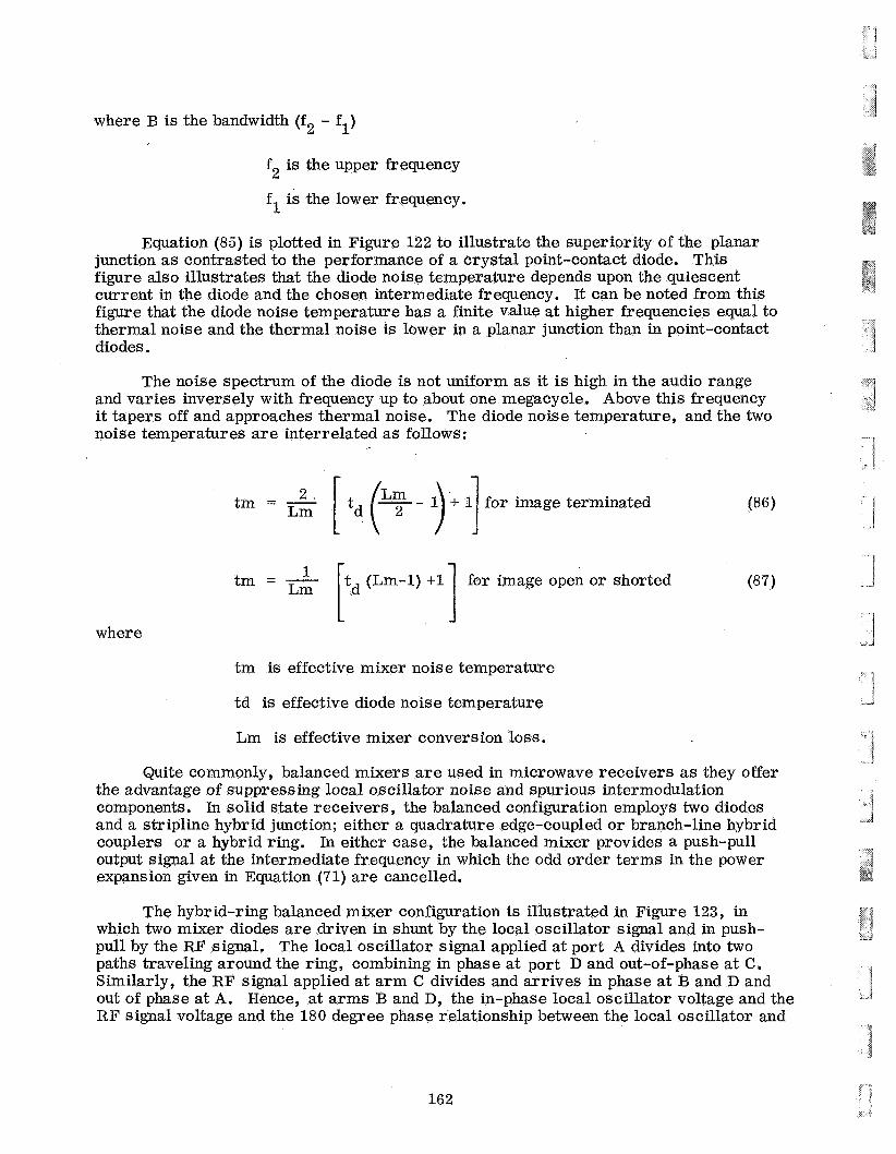
where B is the bandwidth (f2 - fl)
f2 is the upper frequency
fl is the lower frequency.
Equation (85) is plotted in Figure 122 to illustrate the superiority of the planar junction a s contrasted to the performance of a crystal point-contact diode. This figure also illustrates that the diode noise temperature depends upon the quiescent current in the diode and the chosen intermediate frequency. It can be noted from this figure that the diode noise temperature has a finite value at higher frequencies equal to thermal noise and the thermal noise is lower in a planar junction than in point-contact diodes.
The noise spectrum of the diode is not uniform as it is high in the audio range and varies inversely with frequency up to about one megacycle, Above this frequency it tapers off and approaches thermal noise. The diode noise temperature, and the two noise temperatures are interrelated a s follows:
tm = 2 Lm 1 td (*- I) + 11 for image terminated
tm = & ~ (Lm-1) + ~ ] for image open or shorted (87)
where
tm is effective mixer noise temperature
td is effective diode noise temperature
Lm is effective mixer conversion loss.
Quite commonly, balanced mixers a r e used in microwave receivers a s they offer the advantage of suppressing local oscillator noise and spurious intermodulation components. In solid state receivers , the balanced configuration employs two diodes and a stripline hybrid junction; either a quadrature edge-coupled or branch-line hybrid couplers o r a hybrid ring. In either case, the balanced mixer provides a push-pull output signal a t the intermediate frequency in which the odd order terms in the power expansion given in Equation (71) a re cancelled.
The hybrid-ring balanced mixer configuration is illustrated in Figure 123, in which two mixer diodes a r e driven in shunt by the local oscillator signal and in push- pull by the RF signal. The local oscillator signal applied at port A divides into two paths traveling around the ring, combining in phase at port D and out-of-phase at C. Similarly, the RF signal applied at a rm C divides and arrives in phase at B and D and out of phase at A. Hence, at arms B and D, the in-phase local oscillator voltage and the RF signal voltage and the 180 degree phase relationship between the local oscillator and
162

3 D
0 P
0 0
0 N
0 -
r E: 0 0 c
N r E: 0 -
2 I -
N
5 0 0
r Y 0 -
? Y c
N I 0 0 -
N
0 r c
c I
m 0 In
163
m * a, k 5 cd k a, a
u
E 8

A
503 12
D
Figure 123. The Hybrid Ring Circuit
signal voltage produce opposing IF signals. The IF signals a r e added together in push-pull in a balanced input circuit of the following IF stage. The amplitudes of the IF voltages are equal if the conversion losses of the diodes are matched. The deeoupling between the local oscillator and the RF signal arms of the hybrid-ring circuit makes possible the use of a oscillator with relatively low power as compared to the single diode mixer.
The noise figure performance of an experimental S-band balanced mixer using silicon Schottky barrier diodes is given in Figure 124. The same characteristics for gallium arsenide barrier diodes is shown in Figure 125. In comparing the noise properties of the silicon diodes to the gallium arsenide diodes it is seen that the silicon circuit gives equivalent noise figures with one-tenth the local oscillator drive required for the gallium arsenide diode mixer. The optimum noise figure for the silicon mixer occurs for a local oscillator power between 2 to 4 mW.
The performance of an experimental S-band balanced mixer using silicon Schottky barrier diodes mounted on an A1203 substrate is shown in Figure 126. The mixer was constructed using 90 degrees branch hybrid line couplers. The couplers required high impedance lines to obtain a broad bandwidth ( Z = 90 ohms) so 0.7-mil line widths w e r e used in the high dielectric A1203 substrate.
The performance of a stripline image-terminated mixer using an external band- pass filter is given in Figure 127. The mixer shows a 3-dB improvement in noise figure over the broadband mixer model. The mixer was constructed for use at C-Band using 1/16 inch Teflon fiber glass board. The circuit consists of an RF matching network, a
164

l 7 j
16
15c h
m, 14
U
9 0. 13
u 5 2 12 4 w p! 1 1 3
IL P w l o 9 0 2 9
8
7
6
5 ?
L
P LOCAL OSCILLATOR POWER = OPTIMUM (10-L0=201 mW
503 13A S C 0 4 9 5 3
Figure 124. Noise Figure vs Frequency of S-Rand Ceramic Balanced Mixer with Gallium Arsenide Schottky Barrier Diodes
165
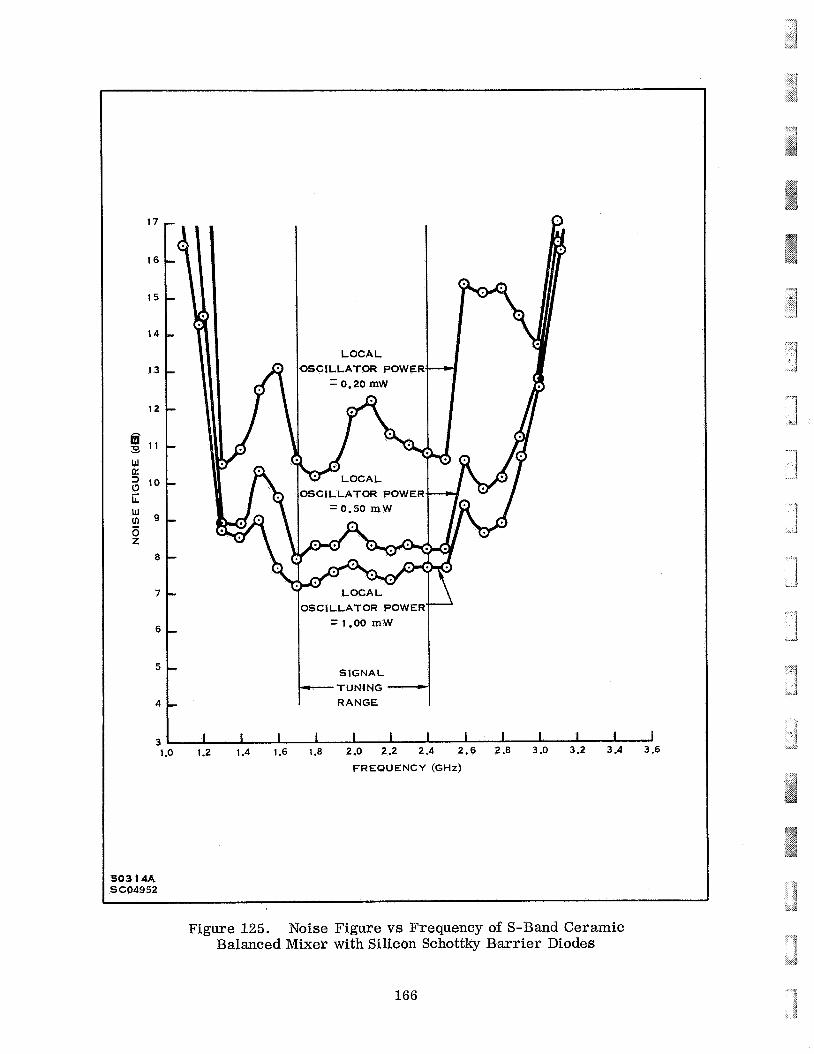
17
16
15
14
13
12
- 3 1 1
W a! ; IO w 9 b G
z 8
7
6
5
4
3
h
- TUNING - S I G N A L
OSCILLATOR POWER = 1.00 m W
RANGE
503 14A SC04952
Figure 125. Noise Figure v s Frequency of S-Band Ceramic Balanced Mixer with Silicon Schottky Barrier Diodes
166
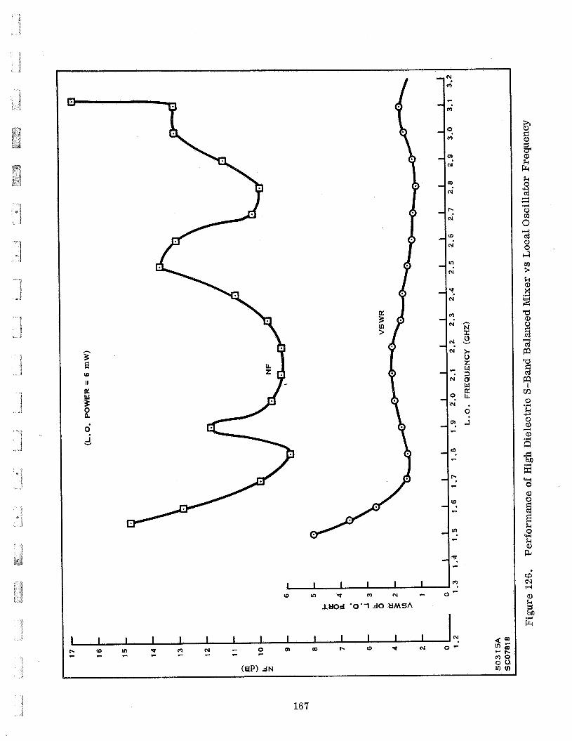
Y
r
0
?
n.
*
N
m N
h
N
ID
N
v)
N
? N
m N
N. N
c
N
9
9
N
c
a0
c
7
'9
c
c
VI c
(0 v) P m N c 0 -
LUOd * O * l A 0 UMSA
I I I I I I I I b - c c P c c
I I I I I I a m b I D W N 0 -
N
2 - c
N c
m ( o m
(aP) A N
16 7
i
I I I I I I I I 0, c w - 2 -
I I I I I I In m 0 Po r - 1 0 In P m ( U -
c - r - ( D
9 In
In
P
3 P
In
m
3 m
h
!i!
s
E
u u
z w 3 a w
0
$5: e
- m n o ot) * t n
168
1/4 open-circuit stub for RF ground and a silicon Schottky barrier diode, The signal and local oscillator were coupled by an external 10 dB coupler. A VSWR of 30 existed at the image frequency, reflecting back 88 percent of the image power to the diode. The circuit operated with a 500-MHz IF over a signal range of 4.6 to 5 . 0 GHz with a image termination giving a calculated mismatch loss of 9 dB at the image frequency f1. A local oscillator power of 0.6 mW gave the best noise figure.
The ordinary microwave balanced mixer will respond to either of two signals which are displaced from the local oscillator by the intermediate frequency. One signal is normally the desired signal and the other is the image signal. The inability of a balanced mixer to distinguish between the proper signal may be enhanced by combining two balanced mixers, four diodes, into an image suppression mixer which readily pro- vides some 20 dB reduction to the image response of a receiver. Such a configuration is shown in Figure 128.
Two balanced mixers used with a quadrature hybrid and a hybrid tee for coupling the local oscillator and the RF input signal to the mixers comprise the microwave circuit of a common form of the image suppression mixers. The two balanced mixers are connected so that the IF components produced by the image a re of such a phase to add at the output port where they can be resistively terminated.
Figure 128 illustrates a low frequency version of the ring image-suppression mixer. In this circuit, the diodes connected in a bridge configuration is driven by two broadband transformers more than 100 mc wide. The use of the double-balanced circuit cancels higher order products and reduces the primary signal giving a wide dynamic range.
D. FIELD EFFECT TRANSISTOR
In some instances, double conversion may be applicable to the overall design of a given microwave feceiver. In such a case, the use of a FET a s the second mixer offers many advantages. The FET operates well in the VHF/VHF, offering conversion gain as well as high immunity to spurious response and extremely low noise figures. Operating a s a mixer with gain, eliminates the low noise requirement for the following IF amplifier. The cross-modulation characteristics of diode mixers is almost com- pletely eliminated in the FET by its nearly perfected square law transfer function.
LO INPUT
W 503 I7
Figure 128. Combination of Two Balanced Mixers
169

Maximum gain is obtained by applying the RF signal to the gate and good isolation is achieved with the local oscillator signal feed into the source. The input impedance of the mixer varies with different levels of LO injection and with sufficient oscillator drive into the source, the impedance into the gate is well below 100 ohms.
The optimum operating point where the transfer characteristic are almost square law is very near pinch-off bias of the FET where the drain current, Id = 0. However, conversion gain of the IF signal results when Id is increased because the transconductance, gm, is increased. The dilemma of these two different considerations is resolved by self-biasing the FET well below Id = 1 mA with a suitable source resistor, then apply- ing a large LO signal to drive the FET on during positive half-cycles a t the LO fre- quency. The effective, gm, at the IF will then be sufficient to provide gain.
A FET mixer constructed with stripline is illustrated in Figure 129 which has the performance characteristics as listed below.
R F input 575 MHz
LO input 620 MHz
IF output 45 MHz
Conversion gain 9 dB IF Bandwidth 9 MHz
Noise Figure 6.5 dB
503 18 IF OUTPUT 50Q
Figure 129. FET Mixer Circuit
17 0
1 I '
7
SECTION X
PROGRAM PERSONNEL
Name
Ben S. Skinner
Charles T. Johnston
Eldon Gordon
Title
Project Engineer
Engineer
Engineer
171/172
SECTION XI
CONCLUSION
This study was performed under item 9 of the WOTn statement which required that an analytical study of solid-state integrated microwave circuits, techniques and components be undertaken prior to the development of an S-band FM telemetry re- ceiver subsystem. The results of this study indicate that sufficient semiconductor microwave technology exists to make the development of a receiver in the 2200- to 2300-MHz frequency region feasible. This study considered microwave components, devices and techniques applicable to receiver applications. Correlated with the phase I1 study of telemetry receiver configurations, these data will be used to provide specific circuits within current technology to meet this design objective. As time passes, it may be necessary to up-date this report due to continued research in microwave semi- conductor technology. Nevertheless, the current state-of-the-art will be utilized in subsequent work performed under this contract.
173/174
BIBLIOGRAPHY
1. Private Communication with Harry Cooke, Texas Instruemtns Incorporated
2.
3.
Private Communication with A. J. Anderson, Texas Instruments, Incorporated
Editorial, "Low-Noise Germanium Transistors Priced to Win Phased-Array Market'', Microwaves, Vol. 5, No. 3, March 1966, pp. 114-116
4. Texas Instruments Incorporated, Study of Solid-state Integrated Microwave Cir- cuits. Scientific Report No, 3, 30 June 1967
5. Texas Instruments Incorporated, Microwave Transistors Technical Report ECOM-01371-5, by George Johnson, David Boone, Julius Lange, Quarterly Report No. 5, Contract No. DA 28-043 AMC-O137l(E), DA Project No. 1P6-22001-A-056, Task 04, Jan. 1967
6. E.O. Johnson, "Physical Limitations on Frequency and Power Parameters of Transistors", RCA Review Vol. 26, June 1965, pp. 163-177
7. Texas Instruments Incorporated, Study of Solid-state Integrated Microwave Cir- cuits Scientific Report No. 1, 31 Dec. 1965
8. Harry F. Cooke, "Microwave Transistor Circuits", Microwaves, Vol. 3, No. 8, Aug. 1964, p. 28
9. Texas Instruments Incorporated, Microwave Transistors Technical Report ECOM-01371-6, by George Johnson, David Boone, Julius Lange, Quarterly Report No. 6, Contract No. DA 28-043 AMC-O1371(E), DA Project No. 1E6-22001-A-056, Task 06, April 1967
10. Donald R. Carley, Patrick L. McGeough, and Joseph F. O'Brien, "The Overlay Transistor", Electronics, Vol. 38, No. 17, Aug. 1965, p. 70
H. C. Lee and George Gilbert, TIOverlay Transistors Move Into Microwave Region", Electronics, Vol. 39, No. 6, 21 March 1966, p. 93
11.
12. Robert Minton, "Semiconductor High-Frequency Power-Amplifier Design", WESCON Record, 23 Aug. 1966
13. H. C. Lee, "Microwave Power Generation Using Overlay Transistors", RCA Review, Vol. 27, June 1966, pp. 199-215
14. Paul Kolk, "MOS-FET High Frequency Amplifiers, ' I WESCON Record, 23 Aug. 1966
15. Joe Schurmann, "Junction FET Revises VHF Tuner", The Electronic Engineer, Vol. 26, No. 4, April 1967, p. 63
175
16.
17.
18.
19.
20.
21.
22.
23.
24.
25.
26.
27.
28.
29.
30.
31.
J. B. Compton, "Junction FET High Frequency Applications", WESCON Record, 23 Aug. 1966
G. C. Luettgenau and A. R. Brand, "Circuit Simplification with IGFETS", WESCON Record, 23 Aug. 1966
Texas Instruments Microlibrary, Communication Handbook, Part 11, 1965, Chapter 6
Texas Instruments Incorporated, Molecular Electronics for Radar Applications, by T. M. Hyltin and L. R. Pfeifer,' Jr, , Interim Engineering Report No. 4, Contract A F 33(615)-1993, BPSN 4-6399-415906, MERA No. 3 and S-674159-415906, Jan. 1967
Rodger R. Webster, "Microwave Transistors", Microwave Journal, Vol. 9, NO. 7, July 1966, pp. 99-102
Private Communication with Bernie Landress, Texas Instruments Incorporated, Dallas, Texas
Texas Instruments, A Proposal to Develop, Produce, and Deliver Schottky Barrier Microwave Mixer Diodes, Part I Technical Discussion, 15 September 1966, 57SC66, prepared for Department of the A i r Force Headquarters Systems Engineering Group (AFSC), Wright Patterson A i r Force Base, Ohio, in response to RFP No. F3361567R1153, Aug. 15, 1966
"Record Gunn Effect Power Levels and New Tube Techniques", Reported at British Microwave Conference, Microwaves, Nov. 1966, p. 12
D. Cawsey, MA "Design of Wide Range Varactor Tuned Microwave Tunnel Diode Oscillators", Proc. of the IEEE, Vol. 113, No. 6, June 1966, pp. 943-947
C. H. Manney and H. H. Doemland", A Tunnel Diode Discrete-Frequency Oscil- lator" IEEE Trans. on Circuit Theory, Vol. CT-13, No. 1, March 1966, pp. 71-73
W. T. Read, Jr. , "A Proposed High Frequency, Negative-Resistance Diode" Bell System Technical Journal, Vol. 37, March 1958, pp.401-446
"A Bit of History", Microwaves, Vol 5, No. 8, Aug. 1966, pp.26
B. Hoefflinger, !?High Frequency Oscillations of p Avalanche Diodes Below the Transit-Time Cutoff", IEEE Trans on Electron Devices, Vol. ED-13, No. 1, Jan. 1966,pp. 151-157
++ + ++ -n -n-n
V. Higgins, J. Baranoski, and M. McCormick, "Avalanche Transit-Time Diodes", Microwaves, Vol. 5, No. 8, Aug. 1966, pp. 24-29
T. Hasty, P. Cunningham, and W. Wisseman, "Microwave Oscillations in Epitaxial Layers of GaAs", IEEE Trans on Electron Devices, Vol. ED-13, No. 1, Jan. 1966, pp. 114-117
R. Haitz, Noise of a Self-sustaining Avalanche Discharge in Silicon, Part I Low Frequency Noise Studies, Texas Instruments Incorporated, Dallas, Texas
176
32. H. Soboa, "Extending IC Technology to Microwave Equipment", Electronics, Vol. 40, No. 6, 20 March 1967, pp. 112-124
33. R. Ciarametaro, Microstrip Filters and Gap Capacitances, 1966 Summer De- velopment Program Report, Texas Instruments Inc., Dallas, Texas, 25 Aug. 1966
34. B. Vincent, "Ceramic Microstrip for Microwave Hybrid Intergrated Circuitry", 1966, IEEE G-MTT Symposium, Palo Alto, California
35. G. Vendelin, "High Dielectric Substrates for Microwave Hybrid Integrated Cir- cuitry", G-MTT Symposium Digest Cat, No. 17C66, 1967, pp. 125-128
H. Wheeler, "Transmission Line Properties of Parallel Strips Separated by a 36. Dielectric Sheet", IEEE Trans. on Microwave Theory and Techniques, Vol. MTT-13, No. 3, March 1965
37. J. Dukes, "Broadband Slot Coupled Directional Couplers", The Institution of Electrical Engineers, Paper No. 2402R, Aug. 1957
38. G. Mathhaei, L. Young, E. Jones, Microwave Filters, Impedance Matching Networks, and Coupling Structures, McGraw-Hill, 1964
39. P. Daly, S. Knight, M. Coulton,and R. Ekholdt, "Lumped Elements in Micro- wave Integrated Circuits", G-MTT Symposium Digest Cat. No. 17C66, 1967, pp. 139-141
40. B. Lax and K. Button, Microwave Ferrites and Ferrimagnetics, McGraw-Hill, 1962
41. ITT, Reference Data for Radio Engineers, Fourth Edition, 1966
42. Dwight Caswell, "Understanding Circulators", Microwaves, Vol. 2, No. 8, Aug. 1963, p. 24
43. W. H. VonAulock, "Theory of Linear-Ferrite Devices for Microwave Applica- tions", Journal of Applied Physics, Vol. 37, No. 3, March 1966, pp. 939-946
44. W. H. VonAulock, "Selection of Ferrite Materials for Microwave Device Appli- cations", IEEE Transactions, Vol. MAG-2, No. 3, Sept. 1966, pp. 251-255
George H. Thiess, I'Theory and Design of Tunable Y1G Filters", Microwaves, Vol. 3, No. 9, Sept. 1964, p. 14
45.
46. Kenneth A. L e h a n , "L-Band Properties of Single Crystal 600G Calcium Vanadium Bismuth Iron Garnet", Journal of Applied Physics, Vol. 3 7, No. 3 , March 1966, pp. 1087-1089
47.
48.
R. N. Chase, Microwave Circuit Theory and Analysis, McGraw-Hill, 1963
A. C. Blankenship and R. L. Huntt, "Microwave Characteristics of Fine-Grain High Power Garnets and Spinets," Journal of Applied Physics, Vol. 37, No. 3, 1 March 1966, pp. 1066-1068
177
49.
50.
51.
52.
53.
54.
55.
56.
57.
58.
59.
60.
61.
62.
63.
64.
R. A. Braden, I. Gordon, R. L. Harvey, "Microwave Properties of Planar Hexagonal Ferrites", IEEE Transactions, Vol. MAG-2, No. 1 March 1966, pp. 43-54
D. T. Ngo, "Constant- Phase Electrically Controllable R F Attenuator Using Permalliy.Film at Resonance", Journal -of Applied Physics, Vol. 37, No. 3, March 1966, pp. 1077-1078
H. Bosma, "On Stripline Y - Circulation at UHF, If IEEE Trans. on Microwave Theory and Techniques, Vol. MTT-12, Jan. 1964, pp. 61-72
6. E. Fay and R. L. Comstock, "Operation of the Ferrite Junction Circulator", IEEE -I Transactions on Microwave Theory and Techniques, Vol. MTT-13, No. 1, Jan. 1965, pp. 15-27"
Robert Blau, "Y1G Microwave Electronically Tunable Preselectors" , Micro- wave Journal, Vol. 5, No. 5, May 1962, pp. 98-102
R. V. Pound, Microwave Mixers, Vol. 16, Radiation Laboratory Series, McGraw-Hill, 1 9 5 0
Philip S. Carter, "Side- Wall-Coupler, Strip-Transmission Line Magnetically Tunable Filters Employing Ferrimagnetic YIG Resonators", IEEE Transactions on Microwave Theory and Techniques, Vol. MTT-13, May 1965, pp. 306-315
V. Uzunoglu, Semiconductor Network Analysis and Design, McGraw-Hill, 1964
B. T. Vincent, Jr., H. F. Cooke, and A. J. Anderson, "Microwave Power Generation and Amplification Using Transistors", The Microwave Journal, Vol. 9, NO. 7, July 1966, pp. 63-68
William A. Rheinfelder, Design of Low-Noise Transistor Input Circuits, Hayden Book Company, 1964
H P application note 907, "The Hot-Carrier Diode, Theory, Design, and Applica- tion"
Earl L. Cwnmins, "Overloading and Spurious Responses in Transistor FM Tuners", Fairchild Application Note, TP-24, Nov. 1963, Presented at IEEE Spring Conference of PGBTR, Chicago, Illinois, July 1963
Herbert W. Pollock and Morris Engelson, "An Analysis of Spurious Response Levels in Microwave Receivers", Microwave Journal, Dee. 1962
L. Becker and R. L. Ernst, "Nonlinear- Admittance Mixers", RCA Review, Vol, 25, Dee. 1964, pp. 662-691
J. H. Lepoff and A. M. Cowley, "Improved Intermodulation Rejection in Mixers", IEEE Transactions on Microwave Theory and Techniques, Vol. MTT-14, No. 12, Dee. 1966, pp. 618-623
E. W. Pappenfus, Warren B. Bruene, and E. 0. Schoenike, Single Sideband Principles and Circuits, McGraw-Hill, 1964
178
65.
66.
- 1
J " 1
' I m i
6 7.
68.
69.
70.
71.
72.
73.
74,
75.
76.
77.
78.
79.
Henry C. Torrey and Charles A. Whitmer, Crystal Rectifiers, Vol. 15, Radiation Laboratory Series, McGraw-Hill, 1950
A. M. Cowley and H. 0. Sorensen, "Quantitative Comparison of Solid State Microwave Detectorst1, IEEE Transactions on Microwave Theory and Techniques, Vol. MTT-14, No. 12, Dee. 1966, pp. 588-602
C. A. Burrus and D. T. Young, "Formed Point-Contact Gallium Arsenide Back- ward Diodes for Millimeter Wave Applications", NO. 1, Jan. 1966, pp. 49-58
T. Oxley and F. .Hilsden, "The Performance of Backward Diodes as Mixers and Detectors at Microwave Frequencies", Radio and Electronic Engineer, Vol. 31, No. 3, March 1966, pp. 181-191
F. Arams, C. Allen, B. Peyton, and E. Sard, "Millimeter Mixing and Detection in Bulk in Sb.", Roc . of IEEE, Vol. 54, No. 4, April 1966, p. 612
Walter H. Higa, "Low- Level Microwave Mixing in Ruby'' - Correspondence, Proc. of IEEE, Vol, 54, Oct. 1966, p. 1453
G. C. Messenger and C. T. McCoy, "Theory and Operation of Crystal Diodes as Mixers", Proc. of IRE, Vol. 45, Sept. 1957, pp. 1269-1283
George N. Kaposhilin, "Hot-Carrier Diode Opens New Vistas" , Electronic De- sign, Vol. 14, 15 March 1966, pp. 178-185 - David F. Allison, "Dielectric Isolation for Integrated Circuits", Solid State Design, Vol. 6, No. 1, Jan. 1965, pp. 29-34
Radio Corporation of America, RCA Linear Integrated Circuit Fundamentals, Technical Series IC-40, 1966
H. C. Kiehn, "Application of the RCA-CA3028 Integrated Circuit RF Amplifier in the H F and VHF Ranges", RCA Integrated Circuits Application Note, IC AN- 5 3 3 7
David Leenov, Design, Vol. 6, No. 5, May 1965, pp. 33-37
PIN Diode Microwave Switches and Modulators", Solid-state
C. Forge, "Driving the PIN Diode Switch", Microwaves, Vol. 6, No. 4, April 1967, pp. 30-36
S . Hamilton and R. Hall, "Shunt Mode Harmonic Generation Using Step Recovery Diodes", The Microwave Journal, Vol. 8, No. 4, April 1967, pp. 69-78
D. Chakroborty and R. Coackley, "Characterization of Varactor Diodes at Low Temperatures", The Radio and Electronic Engineer, Vol. 33, No. 2, Feb. 1967, pp. 97-104
179
80.
81.
82.
83.
84.
85.
86.
87.
88.
89.
90.
Robert P. Rafuse and Joze Vugrinec, Very Low Noise P N Junction Microwave Mixers, Massachusetts Institute of Technology Report for Electronic Research Center, NASA, Cambridge, Mass. , Grant NSG-419 and Grant NGR 22-009-163
J. Dangl and K. Steele, "Using Strip Transmission Line to Design Microwave Circuits, Part I", Electronics, Vol. 39, No. 3, 7 Feb. 1966, pp. 72-83
J. Dangl and K. Steele, "Using Strip Transmission Line to Design Microwave Circuits, Part II", Electronics, I__ Vol. 39, No. 4, 21 Feb. 1966, pp. 90-100
J. Helszajn, "A Ferrite Ring Stripline Junction Circulator", The Radio and Electronic Engineer, Vol. 32, No, 1, July 1966
Leonce J. Sevin, Jr. , Field-Effect Transistors, Texas Instruments Electronic Series, McGraw-Hill, 1965
T. K. Ishii, "Ferrite Cylinder Modulator Microwave Signals", Electronics, Vol. 39, NO. 17, 22 Aug. 1966, pp. 96-97
L. R. Hodges Jr., G. P. Rodrique, G. R. Harrison, and A. D. Sanders, If Magnetic and Microwave Properties of Calcium Vandadium-Substituted Garnets", Journal of Applied Physics, Vol. 37, No. 3, 1 March 1966, pp. 1085-1086
D. H. Roth, "Investigation of Ferrimagnetic Materials at Low Temperatures and some Applications in Low-Noise Receivers", IEEE Transactions, Vol. MAG-2, No. 3, Sept. 1966, pp. 256-259
D. Greig and H. Englemann, "Microstrip - A New Transmission Technique for the Kilomegacycle Range", Proc. of the IRE, Vol. 40, Dee. 1952, pp. 1644- 1650
D. Boswell and D. Giles, "Thin Film Circuits, A Review", Electrical Com- munication, Vol. 41, No. 4, 1966 Edition, pp. 378-390
M. Gilden and M. Hines, "Electronic Tuning Effects in the Read Microwave Avalanche Diodeff, IEEE Trans. on Electron Devices, Vol. ED-13, Jan. 1966, pp. 169-175.
180