ADS9120EVM-PDK - Texas Instruments
38
1 SBAU262 – August 2016 Submit Documentation Feedback Copyright © 2016, Texas Instruments Incorporated ADS9120EVM-PDK multiSPI is a registered trademark of Texas Instruments. Microsoft, Windows are registered trademarks of Microsoft Corporation. LabVIEW is a trademark of National Instruments. All other trademarks are the property of their respective owners. User's Guide SBAU262 – August 2016 ADS9120EVM-PDK This user's guide describes the characteristics, operation, and use of the ADS9120 evaluation module (EVM) performance demonstration kit (PDK). This kit is an evaluation platform for the ADS9120, which is an 16-bit, 2.5-MSPS, fully-differential input, successive approximation register (SAR) analog-to-digital converter (ADC) that features an enhanced serial multiSPI ® digital interface. The EVM-PDK eases the evaluation of the ADS9120 device with hardware, software, and computer connectivity through the universal serial bus (USB) interface. This user's guide includes complete circuit descriptions, schematic diagrams, and a bill of materials. The following related documents are available through the Texas Instruments web site at www.ti.com. Related Documentation Device Literature Number ADS9120 SBAS710 OPA625 SBOS688 OPA376 SBOS406 OPA378 SBOS417 REF5050 SBOS410 TPS7A4700 SBVS204
-
Upload
khangminh22 -
Category
Documents
-
view
0 -
download
0
Transcript of ADS9120EVM-PDK - Texas Instruments
1SBAU262–August 2016Submit Documentation Feedback
Copyright © 2016, Texas Instruments Incorporated
ADS9120EVM-PDK
multiSPI is a registered trademark of Texas Instruments.Microsoft, Windows are registered trademarks of Microsoft Corporation.LabVIEW is a trademark of National Instruments.All other trademarks are the property of their respective owners.
User's GuideSBAU262–August 2016
ADS9120EVM-PDK
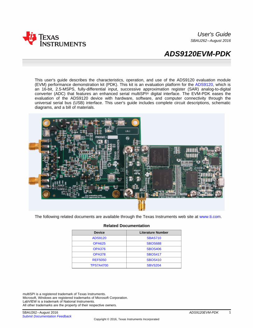
This user's guide describes the characteristics, operation, and use of the ADS9120 evaluation module(EVM) performance demonstration kit (PDK). This kit is an evaluation platform for the ADS9120, which isan 16-bit, 2.5-MSPS, fully-differential input, successive approximation register (SAR) analog-to-digitalconverter (ADC) that features an enhanced serial multiSPI® digital interface. The EVM-PDK eases theevaluation of the ADS9120 device with hardware, software, and computer connectivity through theuniversal serial bus (USB) interface. This user's guide includes complete circuit descriptions, schematicdiagrams, and a bill of materials.
The following related documents are available through the Texas Instruments web site at www.ti.com.
Related DocumentationDevice Literature Number
ADS9120 SBAS710OPA625 SBOS688OPA376 SBOS406OPA378 SBOS417REF5050 SBOS410
TPS7A4700 SBVS204
www.ti.com
2 SBAU262–August 2016Submit Documentation Feedback
Copyright © 2016, Texas Instruments Incorporated
ADS9120EVM-PDK
Contents1 Overview ...................................................................................................................... 4
1.1 ADS9120EVM-PDK Features ..................................................................................... 41.2 ADS9120EVM Features ........................................................................................... 4
2 Analog Interface.............................................................................................................. 52.1 Connectors for Differential Signal Source ....................................................................... 52.2 ADC Differential Input Signal Driver.............................................................................. 52.3 Onboard ADC Reference .......................................................................................... 8
3 Digital Interfaces ............................................................................................................. 83.1 multiSPI® for ADC Digital IO ...................................................................................... 8
4 Power Supplies .............................................................................................................. 95 ADS9120EVM-PDK Initial Setup .......................................................................................... 9
5.1 Default Jumper Settings ........................................................................................... 95.2 EVM Graphical User Interface (GUI) Software Installation.................................................... 9
6 ADS9120EVM-PDK Operation ........................................................................................... 136.1 EVM GUI Global Settings for ADC Control .................................................................... 156.2 Register Map Configuration Tool................................................................................ 176.3 Time Domain Display Tool ....................................................................................... 186.4 Spectral Analysis Tool ............................................................................................ 196.5 Histogram Tool .................................................................................................... 216.6 Linearity Analysis Tool............................................................................................ 22
7 Bill of Materials, PCB Layout, and Schematics......................................................................... 247.1 Bill of Materials .................................................................................................... 247.2 PCB Layout ........................................................................................................ 277.3 Schematics ......................................................................................................... 30
List of Figures
1 OPA625 Differential Input Driving Path .................................................................................. 62 Common-Mode Selection Jumpers........................................................................................ 73 Onboard Reference Signal Path........................................................................................... 84 ADS9120 Software Installation Prompts ................................................................................ 105 Device Driver Installation Wizard Prompts.............................................................................. 106 LabVIEW Run-Time Engine Installation................................................................................. 117 ADS9120EVM Folder Post-Installation .................................................................................. 128 EVM-PDK Hardware Setup and LED Indicators ....................................................................... 139 Launch the EVM GUI Software........................................................................................... 1410 EVM GUI Global Input Parameters ...................................................................................... 1511 Register Map Configuration............................................................................................... 1712 Time Domain Display Tool Options...................................................................................... 1813 Spectral Analysis Tool ..................................................................................................... 2014 Histogram Analysis Tool .................................................................................................. 2115 Linearity Analysis Tool..................................................................................................... 2316 ADS9120EVM PCB Layer 1: Top Layer ................................................................................ 2717 ADS9120EVM PCB Layer 2: GND Plane............................................................................... 2818 ADS9120EVM PCB Layer 3: Power Planes............................................................................ 2919 ADS9120EVM PCB Layer 4: Bottom Layer ............................................................................ 3020 Schematic Diagram (Page 1) of the ADS9120EVM PCB............................................................. 3121 Schematic Diagram (Page 2) of the ADS9120EVM PCB............................................................. 3222 Schematic Diagram (Page 3) of the ADS9120EVM PCB............................................................. 33
List of Tables
www.ti.com
3SBAU262–August 2016Submit Documentation Feedback
Copyright © 2016, Texas Instruments Incorporated
ADS9120EVM-PDK
1 J7 and J3 SMA Connectors Description.................................................................................. 52 J4 and J6 Headers Description ............................................................................................ 53 J1 and J2 Configuration per Input Common-Mode...................................................................... 74 External Source Requirements for Evaluation of the ADS9120 ..................................................... 195 External Source Requirements for ADS9120 Evaluation ............................................................. 226 ADS9120EVM Bill of Materials .......................................................................................... 24

Overview www.ti.com
4 SBAU262–August 2016Submit Documentation Feedback
Copyright © 2016, Texas Instruments Incorporated
ADS9120EVM-PDK
1 OverviewThe ADS9120EVM-PDK is a platform for evaluating the performance of the ADS9120 SAR ADC, which isa fully-differential input, 16-bit, 2.5-MSPS device. The evaluation kit includes the ADS9120EVM board andthe precision host interface (PHI) controller board that enables the accompanying computer software tocommunicate with the ADC over USB for data capture and analysis.
The ADS9120EVM board includes the ADS9120 SAR ADC, all the peripheral analog circuits, andcomponents required to extract optimum performance from the ADC.
The PHI board primarily serves three functions:• Provides a communication interface from the EVM to the computer through a USB port• Provides the digital input and output signals necessary to communicate with the ADS9120EVM• Supplies power to all active circuitry on the ADS9120 board
Along with the ADS9120EVM and PHI controller board, this evaluation kit includes an A-to-micro-B USBcable to connect to a computer.
1.1 ADS9120EVM-PDK FeaturesThe ADS9120EVM-PDK includes the following features:• Hardware and software required for diagnostic testing as well as accurate performance evaluation of
the ADS9120 ADC• USB powered—no external power supply is required• The PHI controller that provides a convenient communication interface to the ADS9120 ADC over a
USB 2.0 (or higher) for power delivery as well as digital input and output• Easy-to-use evaluation software for Microsoft® Windows® 7, Windows® 8, 64-bit operating systems• The software suite includes graphical tools for data capture, histogram analysis, spectral analysis and
linearity analysis. This suite also has a provision for exporting data to a text file for post-processing.
1.2 ADS9120EVM FeaturesThe ADS9120EVM includes the following features:• Onboard low-noise and low distortion ADC input drivers optimized to meet ADC performance• Onboard precision 5.0-V voltage reference filtered and followed by a low-noise, low-offset and low-
impedance buffer. The reference driver circuit is optimized for 1-LSB voltage regulation undermaximum loading conditions at full device throughput of 2.5 MSPS.
• Jumper-selectable 0-V and 2.5-V input common-mode options allow unipolar and bipolar inputs.• Onboard ultralow noise low-dropout (LDO) regulator for excellent 5.2-V single-supply regulation of all
operation amplifiers and voltage reference.
www.ti.com Analog Interface
5SBAU262–August 2016Submit Documentation Feedback
Copyright © 2016, Texas Instruments Incorporated
ADS9120EVM-PDK
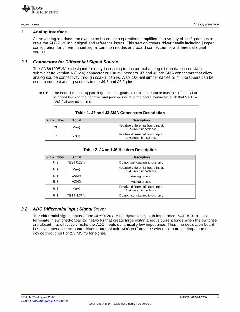
2 Analog InterfaceAs an analog interface, the evaluation board uses operational amplifiers in a variety of configurations todrive the ADS9120 input signal and reference inputs. This section covers driver details including jumperconfiguration for different input signal common modes and board connectors for a differential signalsource.
2.1 Connectors for Differential Signal SourceThe ADS9120EVM is designed for easy interfacing to an external analog differential source via asubminiature version A (SMA) connector or 100-mil headers. J7 and J3 are SMA connectors that allowanalog source connectivity through coaxial cables. Also, 100-mil jumper cables or mini-grabbers can beused to connect analog sources to the J4:2 and J6:2 pins.
NOTE: The input does not support single-ended signals. The external source must be differential orbalanced keeping the negative and positive inputs to the board symmetric such that Vs(+) =–Vs(–) at any given time.
Table 1. J7 and J3 SMA Connectors Description
Pin Number Signal Description
J3 Vs(–) Negative differential board input,1-kΩ input impedance
J7 Vs(+) Positive differential board input,1-kΩ input impedance
Table 2. J4 and J6 Headers Description
Pin Number Signal DescriptionJ4:3 TEST 0.23 V Do not use: diagnostic use only
J4:2 Vs(–) Negative differential board input,1-kΩ input impedance
J4:1 AGND Analog groundJ6:3 AGND Analog ground
J6:2 Vs(+) Positive differential board input,1-kΩ input impedance
J6:1 TEST 4.77 V Do not use: diagnostic use only
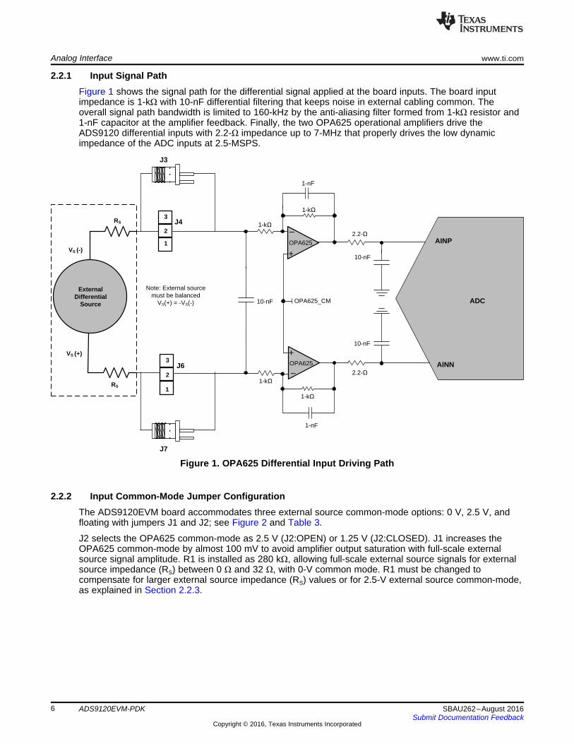
2.2 ADC Differential Input Signal DriverThe differential signal inputs of the ADS9120 are not dynamically high impedance. SAR ADC inputsterminate in switched-capacitor networks that create large instantaneous current loads when the switchesare closed that effectively make the ADC inputs dynamically low impedance. Thus, the evaluation boardhas low impedance on board drivers that maintain ADC performance with maximum loading at the fulldevice throughput of 2.5-MSPS for signal.
ADC
AINP
AINNOPA625
+
±
OPA625
±
+
.
.
.
...
ExternalDifferential
Source
Note: External sourcemust be balanced
VS(+) = -VS(-)
3
2
1
3
2
1
RS
RS
VS (-)
VS (+)
J4
J6
J7
1-k
1-k
1-nF
10-nF
1-k 2.2-
2.2-
10-nF
10-nF
OPA625_CM
1-k
1-nF
J3
Analog Interface www.ti.com
6 SBAU262–August 2016Submit Documentation Feedback
Copyright © 2016, Texas Instruments Incorporated
ADS9120EVM-PDK
2.2.1 Input Signal PathFigure 1 shows the signal path for the differential signal applied at the board inputs. The board inputimpedance is 1-kΩ with 10-nF differential filtering that keeps noise in external cabling common. Theoverall signal path bandwidth is limited to 160-kHz by the anti-aliasing filter formed from 1-kΩ resistor and1-nF capacitor at the amplifier feedback. Finally, the two OPA625 operational amplifiers drive theADS9120 differential inputs with 2.2-Ω impedance up to 7-MHz that properly drives the low dynamicimpedance of the ADC inputs at 2.5-MSPS.
Figure 1. OPA625 Differential Input Driving Path
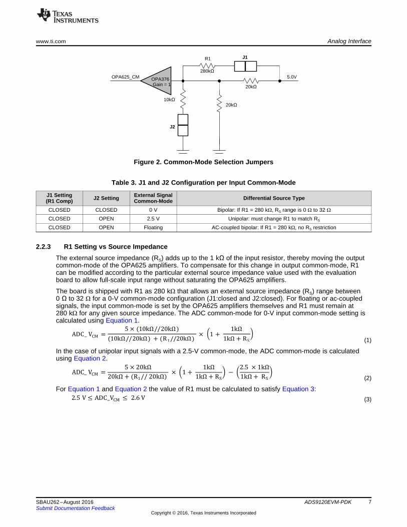
2.2.2 Input Common-Mode Jumper ConfigurationThe ADS9120EVM board accommodates three external source common-mode options: 0 V, 2.5 V, andfloating with jumpers J1 and J2; see Figure 2 and Table 3.
J2 selects the OPA625 common-mode as 2.5 V (J2:OPEN) or 1.25 V (J2:CLOSED). J1 increases theOPA625 common-mode by almost 100 mV to avoid amplifier output saturation with full-scale externalsource signal amplitude. R1 is installed as 280 kΩ, allowing full-scale external source signals for externalsource impedance (RS) between 0 Ω and 32 Ω, with 0-V common mode. R1 must be changed tocompensate for larger external source impedance (RS) values or for 2.5-V external source common-mode,as explained in Section 2.2.3.
2.5 V Q ADC_VCM Q 2.6 V
ADC_ VCM =5 × trÀ
trÀ + (R1// trÀ) × l1 +
sÀ
sÀ + RS
p F l2.5 × sÀ
sÀ+ RS
p
ADC_ VCM =5 × (srÀ//trÀ)
(srÀ//trÀ) + (R1//trÀ) × l1 +
sÀ
sÀ + RS
p
20k
280k 5.0V
20k 10k
OPA625_CM OPA376Gain = 1
J2
J1R1
www.ti.com Analog Interface
7SBAU262–August 2016Submit Documentation Feedback
Copyright © 2016, Texas Instruments Incorporated
ADS9120EVM-PDK
Figure 2. Common-Mode Selection Jumpers
Table 3. J1 and J2 Configuration per Input Common-Mode
J1 Setting(R1 Comp) J2 Setting External Signal
Common-Mode Differential Source Type
CLOSED CLOSED 0 V Bipolar: If R1 = 280 kΩ, RS range is 0 Ω to 32 Ω
CLOSED OPEN 2.5 V Unipolar: must change R1 to match RS
CLOSED OPEN Floating AC-coupled bipolar: If R1 = 280 kΩ, no RS restriction
2.2.3 R1 Setting vs Source ImpedanceThe external source impedance (RS) adds up to the 1 kΩ of the input resistor, thereby moving the outputcommon-mode of the OPA625 amplifiers. To compensate for this change in output common-mode, R1can be modified according to the particular external source impedance value used with the evaluationboard to allow full-scale input range without saturating the OPA625 amplifiers.
The board is shipped with R1 as 280 kΩ that allows an external source impedance (RS) range between0 Ω to 32 Ω for a 0-V common-mode configuration (J1:closed and J2:closed). For floating or ac-coupledsignals, the input common-mode is set by the OPA625 amplifiers themselves and R1 must remain at280 kΩ for any given source impedance. The ADC common-mode for 0-V input common-mode setting iscalculated using Equation 1.
(1)
In the case of unipolar input signals with a 2.5-V common-mode, the ADC common-mode is calculatedusing Equation 2.
(2)
For Equation 1 and Equation 2 the value of R1 must be calculated to satisfy Equation 3:(3)
OPA378
1µF
+
±OPA625
±
+
30k
1k 499
4.7 1k
4.99k
2.49N
10pF
220nF 3×10µF
REF
100nF
100nF
5.0V from REF5050
Analog Interface www.ti.com
8 SBAU262–August 2016Submit Documentation Feedback
Copyright © 2016, Texas Instruments Incorporated
ADS9120EVM-PDK
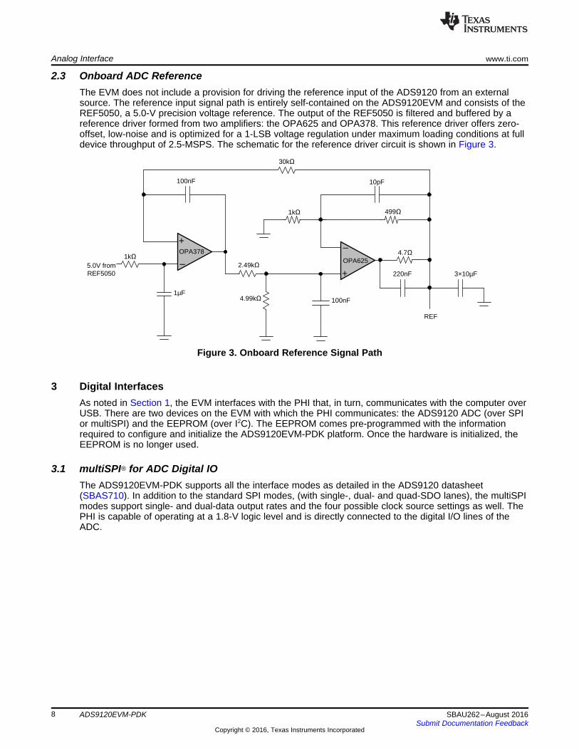
2.3 Onboard ADC ReferenceThe EVM does not include a provision for driving the reference input of the ADS9120 from an externalsource. The reference input signal path is entirely self-contained on the ADS9120EVM and consists of theREF5050, a 5.0-V precision voltage reference. The output of the REF5050 is filtered and buffered by areference driver formed from two amplifiers: the OPA625 and OPA378. This reference driver offers zero-offset, low-noise and is optimized for a 1-LSB voltage regulation under maximum loading conditions at fulldevice throughput of 2.5-MSPS. The schematic for the reference driver circuit is shown in Figure 3.
Figure 3. Onboard Reference Signal Path
3 Digital InterfacesAs noted in Section 1, the EVM interfaces with the PHI that, in turn, communicates with the computer overUSB. There are two devices on the EVM with which the PHI communicates: the ADS9120 ADC (over SPIor multiSPI) and the EEPROM (over I2C). The EEPROM comes pre-programmed with the informationrequired to configure and initialize the ADS9120EVM-PDK platform. Once the hardware is initialized, theEEPROM is no longer used.
3.1 multiSPI® for ADC Digital IOThe ADS9120EVM-PDK supports all the interface modes as detailed in the ADS9120 datasheet(SBAS710). In addition to the standard SPI modes, (with single-, dual- and quad-SDO lanes), the multiSPImodes support single- and dual-data output rates and the four possible clock source settings as well. ThePHI is capable of operating at a 1.8-V logic level and is directly connected to the digital I/O lines of theADC.

www.ti.com Power Supplies
9SBAU262–August 2016Submit Documentation Feedback
Copyright © 2016, Texas Instruments Incorporated
ADS9120EVM-PDK
4 Power SuppliesThe PHI provides multiple power-supply options for the EVM, derived from the computer’s USB supply.
The EEPROM on the ADS9120EVM use a 3.3-V power supply generated directly by the PHI. The ADCand analog input drive circuits are powered by the TPS7A4700 onboard the EVM, which is a low-noiselinear regulator that uses the 5.5-V supply out of a switching regulator on the PHI to generate a muchcleaner 5.2-V output. The 1.8-V supply to the digital section of the ADC is provided directly by an LDO onthe PHI.
The power supply for each active component on the EVM is bypassed with a ceramic capacitor placedclose to that component. Additionally, the EVM layout uses thick traces or large copper fill areas wherepossible between bypass capacitors and their loads to minimize inductance along the load current path.
5 ADS9120EVM-PDK Initial SetupThis section explains the initial hardware and software setup procedure that must be completed for theproper operation of the ADS9120EVM-PDK.
5.1 Default Jumper SettingsJumper settings are determined by common mode and source impedance of the external source thatprovides a differential signal to the board. Remove shunts from J4 and J6 and set J2 and J1 according tothe external source as described in Section 2.
5.2 EVM Graphical User Interface (GUI) Software InstallationDownload the latest version of the EVM GUI installer from the Tools and Software folder of the ADS9120and run the GUI installer to install the EVM GUI software on the user’s computer.
CAUTIONManually disable any antivirus software running on the computer beforedownloading the EVM GUI installer onto the local hard disk. Otherwise,depending on the antivirus settings, an error message such as the one inFigure 4 may appear or the installer.exe file may be deleted.
Accept the license agreements and follow the on-screen instructions to complete the installation.

ADS9120EVM-PDK Initial Setup www.ti.com
10 SBAU262–August 2016Submit Documentation Feedback
Copyright © 2016, Texas Instruments Incorporated
ADS9120EVM-PDK
Figure 4. ADS9120 Software Installation Prompts
As a part of the ADS9120EVM GUI installation, a prompt with a Device Driver Installation will appear onthe screen. Click Next to proceed.
Figure 5. Device Driver Installation Wizard Prompts
www.ti.com ADS9120EVM-PDK Initial Setup
11SBAU262–August 2016Submit Documentation Feedback
Copyright © 2016, Texas Instruments Incorporated
ADS9120EVM-PDK
NOTE: A notice may appear on the screen stating that Widows cannot verify the publisher of thisdriver software. Select Install this driver software anyway.
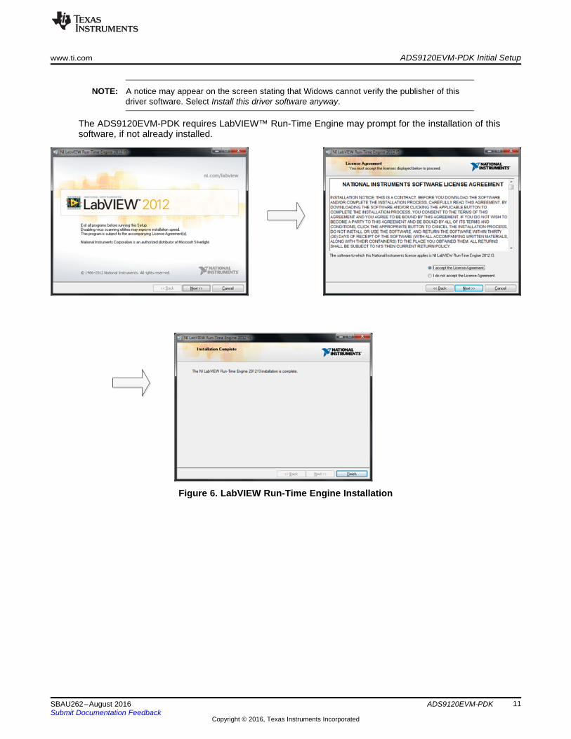
The ADS9120EVM-PDK requires LabVIEW™ Run-Time Engine may prompt for the installation of thissoftware, if not already installed.
Figure 6. LabVIEW Run-Time Engine Installation
ADS9120EVM-PDK Initial Setup www.ti.com
12 SBAU262–August 2016Submit Documentation Feedback
Copyright © 2016, Texas Instruments Incorporated
ADS9120EVM-PDK
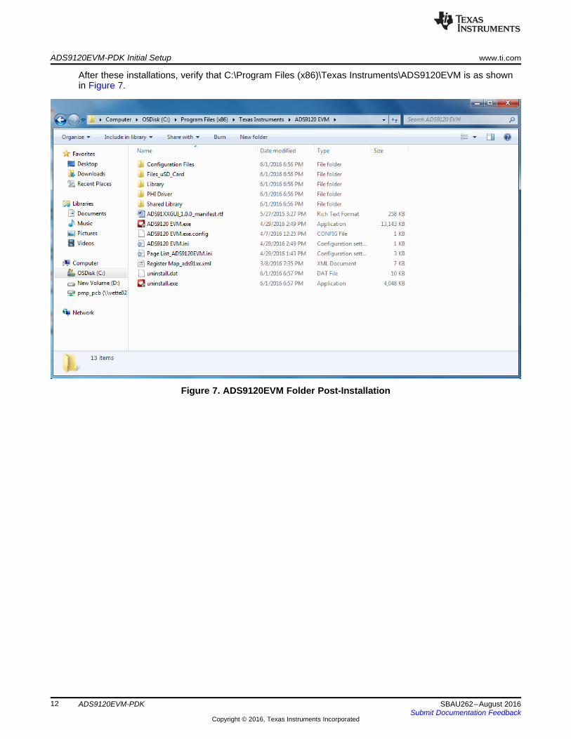
After these installations, verify that C:\Program Files (x86)\Texas Instruments\ADS9120EVM is as shownin Figure 7.
Figure 7. ADS9120EVM Folder Post-Installation
www.ti.com ADS9120EVM-PDK Operation
13SBAU262–August 2016Submit Documentation Feedback
Copyright © 2016, Texas Instruments Incorporated
ADS9120EVM-PDK
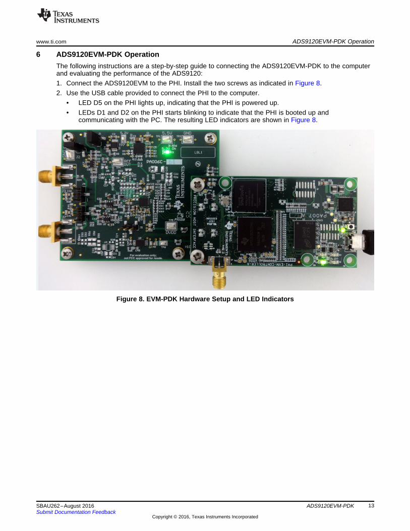
6 ADS9120EVM-PDK OperationThe following instructions are a step-by-step guide to connecting the ADS9120EVM-PDK to the computerand evaluating the performance of the ADS9120:1. Connect the ADS9120EVM to the PHI. Install the two screws as indicated in Figure 8.2. Use the USB cable provided to connect the PHI to the computer.
• LED D5 on the PHI lights up, indicating that the PHI is powered up.• LEDs D1 and D2 on the PHI starts blinking to indicate that the PHI is booted up and
communicating with the PC. The resulting LED indicators are shown in Figure 8.
Figure 8. EVM-PDK Hardware Setup and LED Indicators
ADS9120EVM-PDK Operation www.ti.com
14 SBAU262–August 2016Submit Documentation Feedback
Copyright © 2016, Texas Instruments Incorporated
ADS9120EVM-PDK
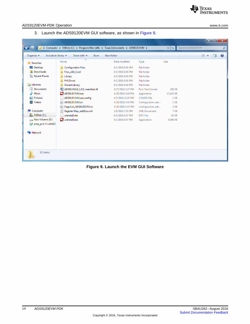
3. Launch the ADS9120EVM GUI software, as shown in Figure 9.
Figure 9. Launch the EVM GUI Software
www.ti.com ADS9120EVM-PDK Operation
15SBAU262–August 2016Submit Documentation Feedback
Copyright © 2016, Texas Instruments Incorporated
ADS9120EVM-PDK
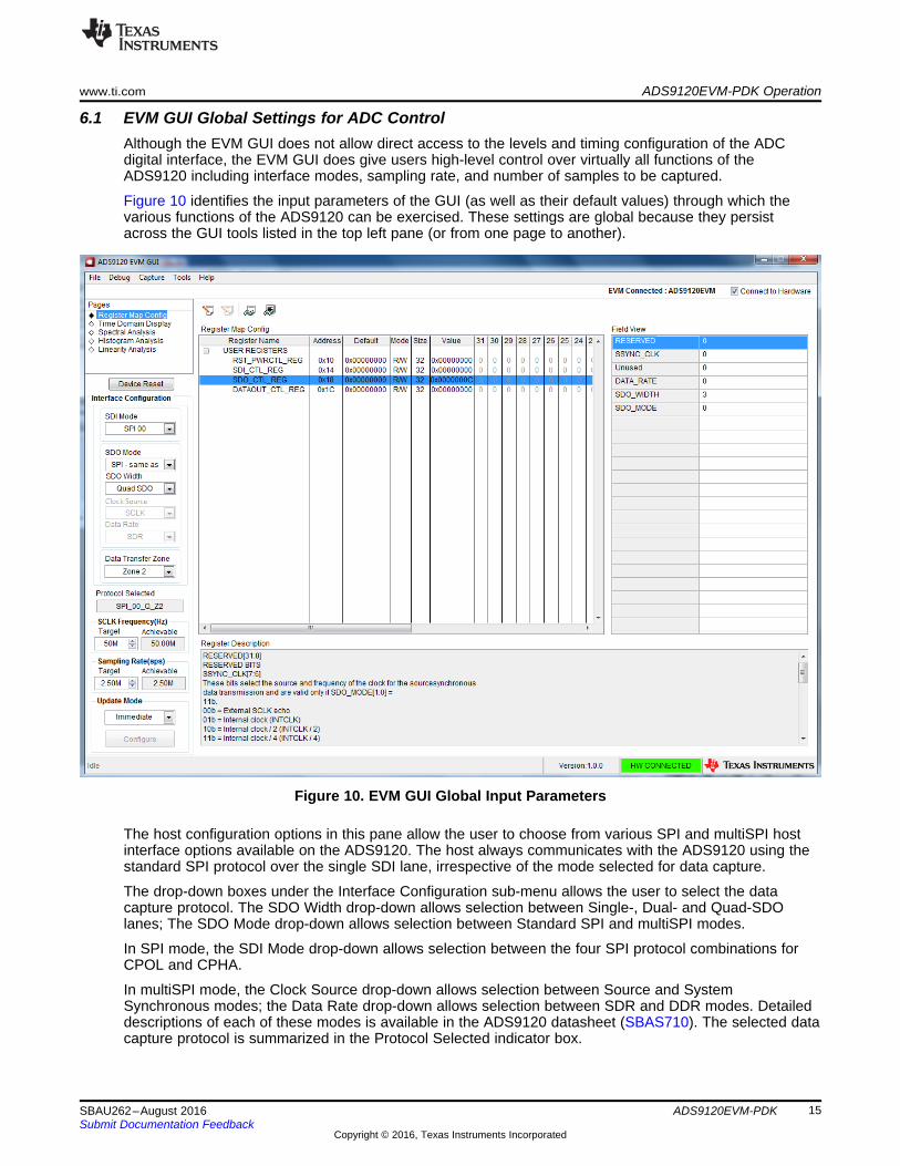
6.1 EVM GUI Global Settings for ADC ControlAlthough the EVM GUI does not allow direct access to the levels and timing configuration of the ADCdigital interface, the EVM GUI does give users high-level control over virtually all functions of theADS9120 including interface modes, sampling rate, and number of samples to be captured.
Figure 10 identifies the input parameters of the GUI (as well as their default values) through which thevarious functions of the ADS9120 can be exercised. These settings are global because they persistacross the GUI tools listed in the top left pane (or from one page to another).
Figure 10. EVM GUI Global Input Parameters
The host configuration options in this pane allow the user to choose from various SPI and multiSPI hostinterface options available on the ADS9120. The host always communicates with the ADS9120 using thestandard SPI protocol over the single SDI lane, irrespective of the mode selected for data capture.
The drop-down boxes under the Interface Configuration sub-menu allows the user to select the datacapture protocol. The SDO Width drop-down allows selection between Single-, Dual- and Quad-SDOlanes; The SDO Mode drop-down allows selection between Standard SPI and multiSPI modes.
In SPI mode, the SDI Mode drop-down allows selection between the four SPI protocol combinations forCPOL and CPHA.
In multiSPI mode, the Clock Source drop-down allows selection between Source and SystemSynchronous modes; the Data Rate drop-down allows selection between SDR and DDR modes. Detaileddescriptions of each of these modes is available in the ADS9120 datasheet (SBAS710). The selected datacapture protocol is summarized in the Protocol Selected indicator box.

ADS9120EVM-PDK Operation www.ti.com
16 SBAU262–August 2016Submit Documentation Feedback
Copyright © 2016, Texas Instruments Incorporated
ADS9120EVM-PDK
The user can select SCLK Frequency and Sampling Rate on this pane and is dependent of the Protocolselected. The GUI allows the user to enter the targeted values for these two parameters and the GUIcomputes the best values that can be achieved, considering the timing constraints of the selected DeviceProtocol.
The user can specify a target SCLK frequency (in Hz) and the GUI tries to match this frequency as closelyas possible by changing the PHI PLL settings and the achievable frequency that can differ from the targetvalue displayed. Similarly, the sampling rate of the ADC can be adjusted by modifying the TargetSampling Rate argument (also in Hz). The achievable ADC sampling rate can differ from the target value,depending on the applied SCLK frequency and selected Device Mode and the closest match achievable isdisplayed. This pane therefore allows the user to try various settings available on the ADS9120 in aniterative fashion until the user converges to the best settings for the corresponding test scenario.
The final option in this pane is the selection for the Update Mode. The default value is Immediate,indicating that the interface settings selection made by the user is applied to configure both the host andthe ADS9120 instantly. Manual indicates that the selection made is made only when the user finalizestheir choices and is ready to configure the device.
The Device Reset button functions as a Master RESET to both the ADS9120EVM and the GUI. When thebutton is pressed, the ADC RESETs to the RESET configuration explained in the datasheet (SBAS710).The GUI also updates the Interface Configuration settings and the Register Map to reflect the deviceRESET state.

www.ti.com ADS9120EVM-PDK Operation
17SBAU262–August 2016Submit Documentation Feedback
Copyright © 2016, Texas Instruments Incorporated
ADS9120EVM-PDK
6.2 Register Map Configuration ToolThe register map configuration tool allows the user to view and modify the registers of the ADS9120. Thistool can be selected by clicking on the Register Map Config radio button at the Pages section of the leftpane, as indicated in Figure 11. On power-up, the values on this page correspond to the HostConfiguration Settings that enable ADC sampling at the maximum sampling rate specified for the ADC.The register values can be edited by double-clicking the corresponding value field. If interface modesettings are affected by the change in register values, this change reflects on the left pane immediately.The effect of changes in the register value reflect on the ADS9120 device on ADS9120EVM-PDK basedon the Update Mode selection, as described in Section 6.1.
Figure 11. Register Map Configuration
Section 6.3 through Section 6.6 describe the data collection and analysis features of the ADS9120EVM-PDK GUI.

ADS9120EVM-PDK Operation www.ti.com
18 SBAU262–August 2016Submit Documentation Feedback
Copyright © 2016, Texas Instruments Incorporated
ADS9120EVM-PDK
6.3 Time Domain Display ToolThe time domain display tool allows visualization of the ADC response to a given input signal. This tool isuseful for both studying the behavior and debugging any gross problems with the ADC or drive circuits.
The user can trigger a capture of the data of the selected number of samples from the ADS9120, as perthe current interface mode settings using the capture button as indicated in Figure 12. The sample indicesare on the x-axis and there are two y-axes showing the corresponding output codes as well as theequivalent analog voltages based on the specified reference voltage. Switching pages to any of theAnalysis tools described in the subsequent sections, triggers calculations to be performed on the same setof data.
Figure 12. Time Domain Display Tool Options

www.ti.com ADS9120EVM-PDK Operation
19SBAU262–August 2016Submit Documentation Feedback
Copyright © 2016, Texas Instruments Incorporated
ADS9120EVM-PDK
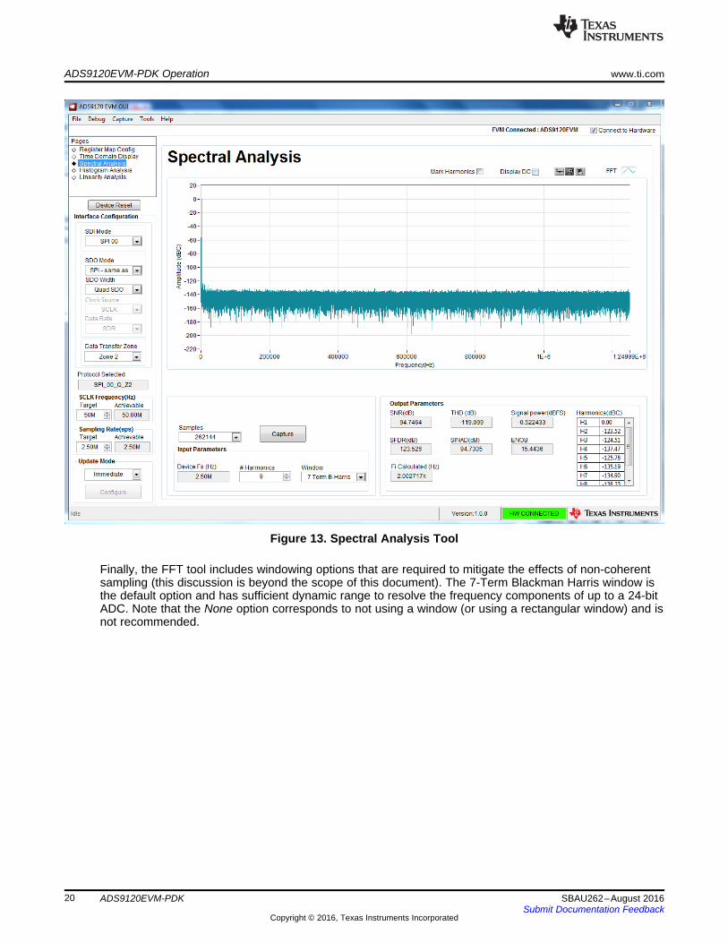
6.4 Spectral Analysis ToolThe spectral analysis tool is intended to evaluate the dynamic performance (SNR, THD, SFDR, SINAD,and ENOB) of the ADS9120 SAR ADC through single-tone sinusoidal signal FFT analysis using the 7-term Blackman-Harris window setting. Also, the window setting of None can be used to search for noisespurs over frequency in dc inputs.
For dynamic performance evaluation, the external differential source must have better specifications thanthe ADC itself to ensure that the measured system performance is not limited by the performance of thesignal source. Therefore, the external reference source must meet the source requirements mentioned inTable 4.
Table 4. External Source Requirements for Evaluation of the ADS9120
Specification Description Specification ValueSignal frequency 2 kHz
External source type Balanced differential
External source common-mode 0 V or floating(see Section 2.2.2 for jumper settings)
External source impedance (RS) 10 Ω–30 Ω
External source differential impedance(RS_DIFF = 2 × RS) 20 Ω–60 Ω
Source differential signal(VPP Amplitude for –0.1 dBFS)
(2 × RS × 4.45 × 10⁻³) + 8.9 Vor
(RS_DIFF × 4.45 × 10⁻³) + 8.9 VMaximum noise 10 µVRMS
Maximum SNR 110 dBMaximum THD –130 dB
For 2-kHz SNR and ENOB evaluation at a maximum throughput of 2.5 MSPS, the number of samplesmust be 32768 or 65536. More samples brings the noise floor so low that the external source phase noisecan dominate the SNR and ENOB calculations. On the contrary, for THD and SFDR evaluation, a muchlarge number of samples must be used to reduce the noise floor below –140 dBc to analyze noise-freeharmonics and spurs in the order of –120 dBc. Such analysis requires at least 262144 samples.
ADS9120EVM-PDK Operation www.ti.com
20 SBAU262–August 2016Submit Documentation Feedback
Copyright © 2016, Texas Instruments Incorporated
ADS9120EVM-PDK
Figure 13. Spectral Analysis Tool
Finally, the FFT tool includes windowing options that are required to mitigate the effects of non-coherentsampling (this discussion is beyond the scope of this document). The 7-Term Blackman Harris window isthe default option and has sufficient dynamic range to resolve the frequency components of up to a 24-bitADC. Note that the None option corresponds to not using a window (or using a rectangular window) and isnot recommended.
www.ti.com ADS9120EVM-PDK Operation
21SBAU262–August 2016Submit Documentation Feedback
Copyright © 2016, Texas Instruments Incorporated
ADS9120EVM-PDK
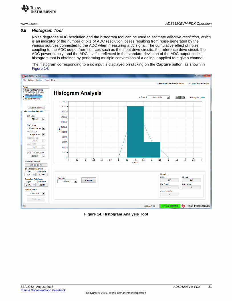
6.5 Histogram ToolNoise degrades ADC resolution and the histogram tool can be used to estimate effective resolution, whichis an indicator of the number of bits of ADC resolution losses resulting from noise generated by thevarious sources connected to the ADC when measuring a dc signal. The cumulative effect of noisecoupling to the ADC output from sources such as the input drive circuits, the reference drive circuit, theADC power supply, and the ADC itself is reflected in the standard deviation of the ADC output codehistogram that is obtained by performing multiple conversions of a dc input applied to a given channel.
The histogram corresponding to a dc input is displayed on clicking on the Capture button, as shown inFigure 14:
Figure 14. Histogram Analysis Tool

ADS9120EVM-PDK Operation www.ti.com
22 SBAU262–August 2016Submit Documentation Feedback
Copyright © 2016, Texas Instruments Incorporated
ADS9120EVM-PDK
6.6 Linearity Analysis ToolThe linearity analysis tool measures and generates the DNL and INL plots over code for the specificADS9120 installed in the evaluation board. A 2-kHz sinusoidal input signal is required, which is slightlysaturated (35 mV outside the full-scale range at each input or 0.13 dBFS) with very low distortion. Theexternal source linearity must be better than the ADC linearity. The measured system performance mustreflect the linearity errors of the ADC and must not be limited by the performance of the signal source. Tomake sure that the DNL and INL of the ADC are correctly measured, the external source must meet therequirements in Table 5.
Table 5. External Source Requirements for ADS9120 Evaluation
Specification Description Specification ValueSignal frequency 2 kHz
External source type Balanced differential
External source common mode 0 V or floating(see Section 2.2.2 for jumper settings)
External source impedance (RS) 10 Ω–30 Ω
External source differential impedance(RS_DIFF = 2 × RS) 20 Ω–60 Ω
Source differential signal(VPP amplitude for –0.1 dBFS)
(2 × RS × 4.57 × 10⁻³) + 9.14 Vor
(RS_DIFF × 4.57 × 10⁻³) + 9.14 VMaximum noise 30 µVRMS
Maximum SNR 100 dBMaximum THD –130 dB
The number-of-hits setting depends on the external noise source. For a 110-dB SNR external source withapproximately 10 µVrms of noise, total number of hits must be 512. For a source with 100-dB SNR, therecommended number of hits is 1024.
NOTE: This analysis can take a couple of minutes to run and the evaluation board must remainundisturbed during the complete duration of the analysis.

www.ti.com ADS9120EVM-PDK Operation
23SBAU262–August 2016Submit Documentation Feedback
Copyright © 2016, Texas Instruments Incorporated
ADS9120EVM-PDK
Figure 15. Linearity Analysis Tool

Bill of Materials, PCB Layout, and Schematics www.ti.com
24 SBAU262–August 2016Submit Documentation Feedback
Copyright © 2016, Texas Instruments Incorporated
ADS9120EVM-PDK
7 Bill of Materials, PCB Layout, and SchematicsThis section contains the ADS9120EVM bill of materials, PCB layout, and the EVM schematics.
7.1 Bill of MaterialsTable 6 lists the ADS9120EVM BOM.
Table 6. ADS9120EVM Bill of Materials
Manufacturer PartNumber Qty Reference Designators Manufacturer DescriptionPA006 1 !PCB Any Printed Circuit Board for Evaluation of ADS9120PHI-EVM-CONTROLLER(Edge# 6591636 rev. B) 1 !PCB2 Texas Instruments USB Controller Board for ADC EVMs (Kit Item)
C3216X5R1E476M160AC 2 C1, C3 TDK CAP, CERM, 47 µF, 25 V, +/- 20%, X5R, 1206
GRM188R71E105KA12D 9 C2, C5, C6, C8, C12, C32,C38, C40, C43 MuRata CAP, CERM, 1 µF, 25 V, +/- 10%, X7R, 0603
GRM21BR71A106KE51L 6 C4, C21, C26, C41, C44,C48 MuRata CAP, CERM, 10 µF, 10 V, +/- 10%, X7R, 0805
C0603C104J3RACTU 4 C7, C9, C10, C17 Kemet CAP, CERM, 0.1 µF, 25 V, +/- 5%, X7R, 0603
ZRB18AD71A106KE01L 9 C13, C15, C27, C28, C29,C39, C45, C50, C51 MuRata CAP, CERM, 10 µF, 10 V, +/- 10%, X7T, 0603
GRM1885C1H102FA01J 3 C16, C31, C42 MuRata CAP, CERM, 1000 pF, 50 V, +/- 1%, C0G/NP0, 0603C0603C100F5GAC7867 1 C18 Kemet CAP, CERM, 10 pF, 50 V, +/- 1%, C0G/NP0, 0603C0603C224J3RAC7867 1 C19 Kemet CAP, CERM, 0.22 µF, 25 V, +/- 5%, X7R, 0603C0805C103F1GACTU 3 C34, C35, C37 Kemet CAP, CERM, 0.01 µF, 100 V, +/- 1%, C0G/NP0, 0805GRM155R71C104KA88D 2 C47, C49 MuRata CAP, CERM, 0.1 µF, 16 V, +/- 10%, X7R, 0402APT2012LZGCK 1 D1 Kingbright LED, Green, SMDCUS05S40,H3F 1 D2 Toshiba Diode, Schottky, 40 V, 0.5 A, SOD-323PMSSS 440 0025 PH 4 H1, H2, H3, H4 B&F Fastener Supply MACHINE SCREW PAN PHILLIPS 4-401891 4 H5, H6, H7, H8 Keystone 3/16 Hex Female Standoff9774050360R 2 H9, H10 Wurth Elektronik ROUND STANDOFF M3 STEEL 5MMRM3X4MM 2701 2 H14, H15 APM HEXSEAL Machine Screw Pan PHILLIPS M387898-0204 2 J1, J2 Molex Header, 2.54 mm, 2x1, Gold, R/A, SMT142-0701-801 2 J3, J7 Johnson Connector, End launch SMA, 50 ohm, SMTTSM-103-01-L-SV 3 J4, J6, J8 Samtec Header, 100mil, 3x1, Gold, SMTQTH-030-01-L-D-A 1 J5 Samtec Header(Shrouded), 19.7mil, 30x2, Gold, SMTTHT-14-423-10 1 LBL1 Brady Thermal Transfer Printable Labels, 0.650" W x 0.200" H - 10,000 per rollRG2012P-2803-B-T5 1 R1 Susumu Co Ltd RES, 280 k, 0.1%, 0.125 W, 0805

www.ti.com Bill of Materials, PCB Layout, and Schematics
25SBAU262–August 2016Submit Documentation Feedback
Copyright © 2016, Texas Instruments Incorporated
ADS9120EVM-PDK
Manufacturer PartNumber Qty Reference Designators Manufacturer DescriptionERJ-3RSFR10V 1 R2 Panasonic RES, 0.1, 1%, 0.1 W, 0603RG1608P-103-B-T5 1 R5 Susumu Co Ltd RES, 10.0 k, 0.1%, 0.1 W, 0603ERJ-2RKF1002X 3 R6, R23, R65 Panasonic RES, 10.0 k, 1%, 0.1 W, 0402
ERJ-2GE0R00X 17
R7, R11, R12, R32, R34,R35, R37, R40, R42, R43,R46, R47, R49, R51, R53,R63, R64
Panasonic RES, 0, 5%, 0.063 W, 0402
ERJ-3RQFR22V 2 R8, R58 Panasonic RES, 0.22, 1%, 0.1 W, 0603RG1608P-203-B-T5 3 R10, R15, R20 Susumu Co Ltd RES, 20.0 k, 0.1%, 0.1 W, 0603
RG1608P-102-B-T5 6 R16, R29, R41, R45, R54,R55 Susumu Co Ltd RES, 1.00 k, 0.1%, 0.1 W, 0603
RG1608P-4991-B-T5 1 R17 Susumu Co Ltd RES, 4.99 k, 0.1%, 0.1 W, 0603ERJ-3GEY0R00V 5 R19, R24, R57, R59, R60 Panasonic RES, 0, 5%, 0.1 W, 0603RG1608P-4990-B-T5 2 R21, R30 Susumu Co Ltd RES, 499, 0.1%, 0.1 W, 0603RG1608P-2491-B-T5 1 R22 Susumu Co Ltd RES, 2.49 k, 0.1%, 0.1 W, 0603RG1608P-303-B-T5 1 R27 Susumu Co Ltd RES, 30.0 k, 0.1%, 0.1 W, 0603CRCW06034R75FKEA 1 R31 Vishay-Dale RES, 4.75, 1%, 0.1 W, 0603RG1608P-101-B-T5 2 R38, R44 Susumu Co Ltd RES, 100, 0.1%, 0.1 W, 0603CRCW06032R21FKEA 2 R48, R50 Vishay-Dale RES, 2.21, 1%, 0.1 W, 0603881545-2 3 SH-J1, SH-J2, SH-J3 TE Connectivity Shunt, 100mil, Gold plated, Black5016 5 TP1, TP2, TP3, TP4, TP5 Keystone Test Point, Compact, SMT5015 2 TP6, TP7 Keystone Test Point, Miniature, SMT
REF5050AIDGKT 1 U1 Texas Instruments Low Noise, Very Low Drift, Precision Voltage Reference, -40 to 125 degC, 8-pin VSSOP (DGK),Green (RoHS & no Sb/Br)
TPS7A4700RGW 1 U2 Texas Instruments 36-V, 1-A, 4.17-µVRMS, RF LDO Voltage Regulator, RGW0020AOPA376AIDBVR 1 U3 Texas Instruments Low-Noise, Low Quiescent Current, Precision Operational Amplifier e-trim Series, DBV0005A
OPA378AIDBVT 1 U5 Texas Instruments Low-Noise, 900 kHz, RRIO, Precision Operational Amplifier, Zerø-Drift Series, 2.2 to 5.5 V, -40 to125 degC, 5-pin SOT23 (DBV0005A), Green (RoHS & no Sb/Br)
OPA625IDBVR 3 U6, U9, U10 Texas Instruments High-Bandwidth, High-Precision, Low THD+N, 16-Bit and 18-Bit Analog-to-Digital Converter (ADC)Drivers, DBV0006A
BR24G32FVT-3AGE2 1 U8 Rohm I2C BUS EEPROM (2-Wire), TSSOP-B8ADS9120IRGER 1 U11 Texas Instruments 16-Bit, 2.5-MSPS, 20-mW, SAR ADC with Enhanced Serial Interface, RGE0024HEMK212BJ475KG-T 0 C11 Taiyo Yuden CAP, CERM, 4.7 µF, 16 V, +/- 10%, X5R, 0805ZRB18AD71A106KE01L 0 C14, C24, C52, C53 MuRata CAP, CERM, 10 µF, 10 V, +/- 10%, X7T, 0603C2012X7S1A226M125AC 0 C20, C55, C57 TDK CAP, CERM, 22 µF, 10 V, +/- 20%, X7S, 0805GRM188R71A105KA61D 0 C22 MuRata CAP, CERM, 1uF, 10V, +/-10%, X7R, 0603GRM21BR71A106KE51L 0 C23 MuRata CAP, CERM, 10 µF, 10 V, +/- 10%, X7R, 0805

Bill of Materials, PCB Layout, and Schematics www.ti.com
26 SBAU262–August 2016Submit Documentation Feedback
Copyright © 2016, Texas Instruments Incorporated
ADS9120EVM-PDK
Manufacturer PartNumber Qty Reference Designators Manufacturer DescriptionGRM21BR71A106KE51L 0 C25 MuRata CAP, CERM, 10uF, 10V, +/-10%, X7R, 0805GRM155R71C104KA88D 0 C30 MuRata CAP, CERM, 0.1 µF, 16 V, +/- 10%, X7R, 0402GRM32ER71A476KE15L 0 C33 MuRata CAP, CERM, 47 µF, 10 V, +/- 10%, X7R, 1210GRM188R71E105KA12D 0 C36 MuRata CAP, CERM, 1 µF, 25 V, +/- 10%, X7R, 0603C0603C224J3RAC7867 0 C54 Kemet CAP, CERM, 0.22 µF, 25 V, +/- 5%, X7R, 0603GMK212BJ474KG-T 0 C56 Taiyo Yuden CAP, CERM, 0.47 µF, 35 V, +/- 10%, X5R, 0805
N/A 0 FID1, FID2, FID3, FID4,FID5, FID6 N/A Fiducial mark. There is nothing to buy or mount.
102-1092-BL-00100 0 H12 CNC Tech CABLE USB A MALE-B MICRO MALE 1M (Kit Item)
ERJ-2GE0R00X 0 R3, R4, R9, R13, R14,R18, R52, R61, R62 Panasonic RES, 0, 5%, 0.063 W, 0402
ERJ-3RQFR22V 0 R25, R26 Panasonic RES, 0.22 ohm, 1%, 0.1W, 0603ERJ-2RKF1002X 0 R28 Panasonic RES, 10.0 k, 1%, 0.1 W, 0402RC0603FR-071RL 0 R33 Yageo America RES, 1.00, 1%, 0.1 W, 0603ERJ-3RQFR22V 0 R36, R39 Panasonic RES, 0.22, 1%, 0.1 W, 0603ERJ-6GEYJ4R7V 0 R56 Panasonic RES, 4.7, 5%, 0.125 W, 0805LM7705MM/NOPB 0 U4 Texas Instruments Low Noise Negative Bias Generator, 8-pin Mini SOIC, Pb-FreeREF6025AIDGK 0 U7 Texas Instruments High-Precision Voltage Reference with Integrated High-Bandwidth Buffer, DGK0008A

www.ti.com Bill of Materials, PCB Layout, and Schematics
27SBAU262–August 2016Submit Documentation Feedback
Copyright © 2016, Texas Instruments Incorporated
ADS9120EVM-PDK
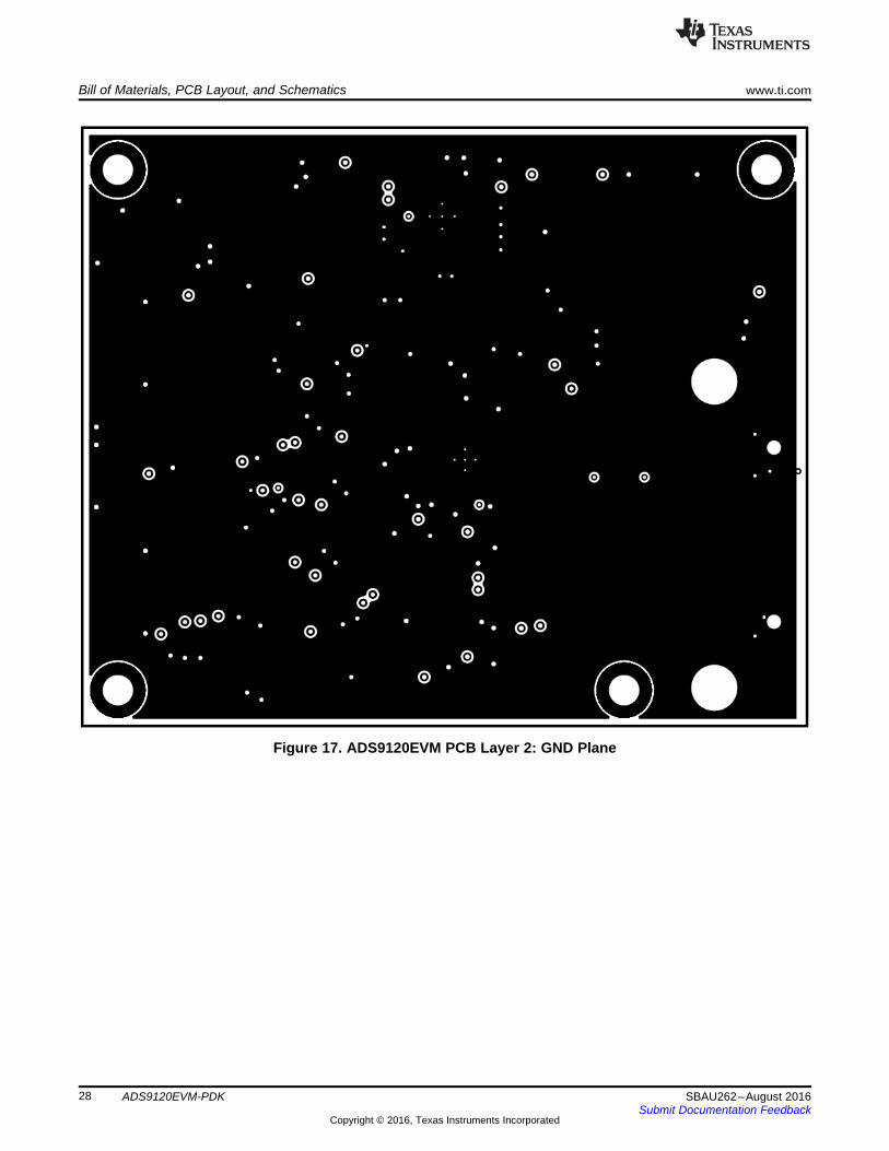
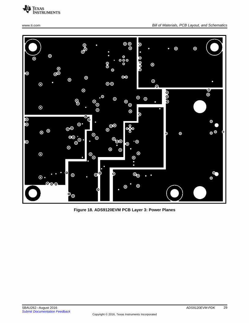
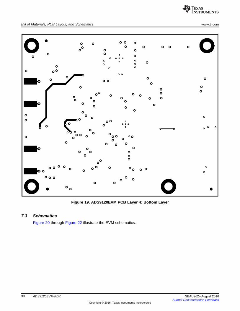
7.2 PCB LayoutFigure 16 through Figure 19 illustrate the EVM PCB layout.
Figure 16. ADS9120EVM PCB Layer 1: Top Layer
Bill of Materials, PCB Layout, and Schematics www.ti.com
28 SBAU262–August 2016Submit Documentation Feedback
Copyright © 2016, Texas Instruments Incorporated
ADS9120EVM-PDK
Figure 17. ADS9120EVM PCB Layer 2: GND Plane
www.ti.com Bill of Materials, PCB Layout, and Schematics
29SBAU262–August 2016Submit Documentation Feedback
Copyright © 2016, Texas Instruments Incorporated
ADS9120EVM-PDK
Figure 18. ADS9120EVM PCB Layer 3: Power Planes
Bill of Materials, PCB Layout, and Schematics www.ti.com
30 SBAU262–August 2016Submit Documentation Feedback
Copyright © 2016, Texas Instruments Incorporated
ADS9120EVM-PDK
Figure 19. ADS9120EVM PCB Layer 4: Bottom Layer
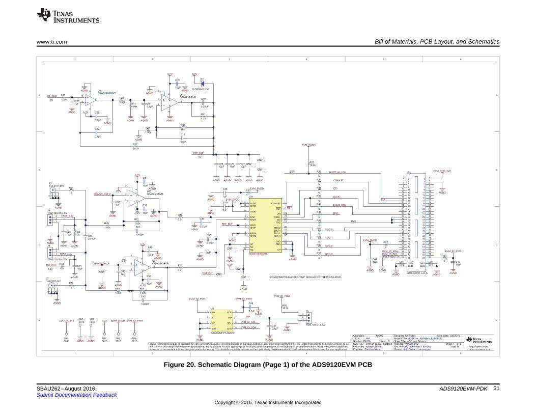
7.3 SchematicsFigure 20 through Figure 22 illustrate the EVM schematics.
1
1
2
2
3
3
4
4
5
5
6
6
D D
C C
B B
A A
1 3
5/5/2016
PA006C_Schematic1.SchDoc
Sheet Title:
Size:
Mod. Date:
File:Sheet: of
B http://www.ti.comContact: http://www.ti.com/support
ADS91xx_ADS89xx_EVM-PDKProject Title:Designed for: Public
Assembly Variant: 002
© Texas Instruments 2016
Drawn By:Engineer: Shridhar More
Texas Instruments and/or its licensors do not warrant the accuracy or completeness of this specification or any information contained therein. Texas Instruments and/or its licensors do notwarrant that this design will meet the specifications, will be suitable for your application or fit for any particular purpose, or will operate in an implementation. Texas Instruments and/or itslicensors do not warrant that the design is production worthy. You should completely validate and test your design implementation to confirm the system functionality for your application.
Version control disabledSVN Rev:PA006Number: Rev: C
TID #: N/AOrderable:
1
2 3 4 5
J3142-0701-801
1
2 3 4 5
J7142-0701-801
AGND
SDO-0
SDO-1
SDO-2
SDO-3
SCLK_RTN
SDI
CONVST
CS
SCLKSDI
AGND AGND
HOST_A1_IO6
AGND
0
R34
0
R35
0
R37
0
R47
0
R42
0
R43
0
R46
0
R49
0
R51
0
R40
0
R32
RVS
EVM_ID_PWR
10μFC48
AGND
0
R60
EVM_DVDD
0
R57
EVM_ID_SDAEVM_ID_SCL
10μFC44
AGND
5015TP6
EVM_ID_PWR
5016TP5
EVM_DVDD
A01
A12
A23
VSS4
SDA5
SCL6
WP7
VCC8
U8
BR24G32FVT-3AGE2
EVM_ID_SDA
EVM_ID_SCL
EVM_ID_PWR
WP
AGND
EVM_ID_PWR
10.0kR65
EVM_ID_PWR
AGND
0.1μF
C49
AGND
RST
10.0kR23
EVM_DVDD
EVM_PRSNT_N
AGND
AGND
EVM_REG_5V5
5016TP2
AGND
5016TP3
AGND
LDO_IN_5V5
5016TP1
0
R24
0
R59
Rafael Ordonez
0.1μFC47
AGND
TEST_4.3V
1
2
3
J4TSM-103-01-L-SV
AGND
TEST_0.2V
100R38
10μFC26
AGND
100
R44
10μFC41
AGND
REFOUT
4.5V
AGND
0.01 FμC35
AGND
AGND
1
2
3
J6
TSM-103-01-L-SV
AGND
1 FμC36DNP
AGND
0
R52DNP
5.2V
1 Fμ
C40
AGND
1 Fμ
C38
AGND EVM_DVDD
REF_BUF0.01μF
C34
AGND
0.01 Fμ
C37
10μFC28
10μFC29
10μFC27
10μFC24DNP
AGND AGND AGND AGND
10.0k
R28DNP
REFOUT
10μFC23DNP
AGND
22μFC20DNP
AGND
1.00R33
DNP
3
1
2
4
6
5
V+
V-
U9OPA625IDBVR
10μF
C45
AGND
5.2V
1.00k
R54
1.00k
R55
1 FμC43
AGND
1000pF
C42
OPA625_CM_N
2.21
R50
3
1
2
4
6
5
V+
V-
U10OPA625IDBVR
10μF
C39
AGND
5.2V
1.00k
R41
1.00k
R45
1 FμC32
AGND
1000pF
C31
OPA625_CM_P
2.21
R48
0
R53EVM_DVDD
3
1
2
4
6
5
V+
V-
U6OPA625IDBVR
AGND
AGND
10μF
C15
AGND
5.2V
1.00k
R29
AGND
D2
CUS05S40,H3F
0.22μF
C19
499
R30
4.75
R31
5.2V
10pF
C18
2.49k
R22
0.1μFC9
AGND
4.99kR17
AGND
1
2
3
4
5U5OPA378AIDBVT
0.1μF
C175.2V
AGND
AGND
0.1μF
C10
30.0k
R27
REF_BUF
1.00k
R16REFOUT
5V
1 FμC12
AGND
ADC and Drivers
COMPONENTS MARKED 'DNP' SHOULD NOT BE POPULATED.
PA006
SDO-218
CONVST1
RST2
DVDD16
REFM4
SDO-317
REFP5
NC6
AVDD14
GND15
AVDD13
NC3
EP25
SDO-119
SDO-020
RVS21
SDI22
SCLK23
CS24
REFP7
REFM8
AINP9
AINM10
NC12
GND11
U11
ADS9120IRGER
11
33
55
77
99
1111
1313
1515
1717
1919
2121
2323
2525
2727
2929
3131
3333
3535
3737
3939
4141
4343
4545
4747
4949
5151
5353
5555
5757
5959
22
44
66
88
1010
1212
1414
1616
1818
2020
2222
2424
2626
2828
3030
3232
3434
3636
3838
4040
4242
4444
4646
4848
5050
5252
5454
5656
5858
6060
GNDMP1
GNDMP2
GNDMP3
GNDMP4
J5
QTH-030-01-L-D-A
10μF
C51
10μF
C50
AGND
AGND
-0.2V
-0.2V
-0.2V
-0.2V
0
R18DNP
AGND
5V
5015TP7
5.2V
RST
0
R62DNP
AGND
1
2
3
J8
TSM-103-01-L-SV
www.ti.com Bill of Materials, PCB Layout, and Schematics
31SBAU262–August 2016Submit Documentation Feedback
Copyright © 2016, Texas Instruments Incorporated
ADS9120EVM-PDK
Figure 20. Schematic Diagram (Page 1) of the ADS9120EVM PCB

1
1
2
2
3
3
4
4
5
5
6
6
D D
C C
B B
A A
2 3
2/12/2016
PA006C_Schematic2.SchDoc
Sheet Title:
Size:
Mod. Date:
File:Sheet: of
B http://www.ti.comContact: http://www.ti.com/support
ADS91xx_ADS89xx_EVM-PDKProject Title:Designed for: Public
Assembly Variant: 002
© Texas Instruments 2016
Drawn By:Engineer: Shridhar More
Texas Instruments and/or its licensors do not warrant the accuracy or completeness of this specification or any information contained therein. Texas Instruments and/or its licensors do notwarrant that this design will meet the specifications, will be suitable for your application or fit for any particular purpose, or will operate in an implementation. Texas Instruments and/or itslicensors do not warrant that the design is production worthy. You should completely validate and test your design implementation to confirm the system functionality for your application.
Version control disabledSVN Rev:PA006Number: Rev: C
TID #: N/AOrderable:
Rafael Ordonez
AGND
APT2012LZGCK
Gre
en
12
D1
LDO_IN_5V5
10.0kR6
10μFC21
AGND
EVM_REG_5V5
1000pFC16
AGND
0
R19
LDO_IN_5V5
LDO_EN
47μFC1
AGND
0
R4DNP
0
R9DNP
0
R12
0
R13DNP
0
R14DNP
0
R11
0
R7
0
R3DNP
AGND
1 Fμ
0603
C5
AGND
AGND
47μFC3
AGND
5.2V
0.1R2
AGND
1 FμC2
AGND
5.2V
0.22R8
10μFC4
AGND
5016TP4
REFOUT
10.0kR5
20.0k
R15
20.0kR10
AGND
J287898-0204
AGND
J187898-0204
280k
R1
1 FμC6
AGND
4
3
2
1
5
V+
V-
U3OPA376AIDBVR
AGND
20.0k
R20
0.1μF
C7
AGND
5.2V
1 Fμ
C8
499
R21OPA625_CM_P
LDO and Reference
COMPONENTS MARKED 'DNP' SHOULD NOT BE POPULATED.
PA006
OUT1
NC2
SENSE3
6P4V24
6P4V15
3P2V6
GND7
1P6V8
0P8V9
0P4V10
0P2V11
0P1V12
EN13
NR14
IN15
IN16
NC17
NC18
NC19
OUT20
PAD21
U2
TPS7A4700RGW
AGND
VIN2
TEMP3
GND4
TRIM/NR5
VOUT6
U1A
REF5050AIDGKT
+3.3V_flt
10μFC53DNP
10μFC52DNP
AGNDAGND
-0.2V
CF+1
VSS5
VOUT6
CRES7
CF-8
VDD4
SD3
VSS2
U4
LM7705MM/NOPB
DNPAGND
0
R61DNP
4.7μFC11DNP
0.22μFC54DNP
10μFC14DNP
AGND
5.2V
AGND
22μFC57DNP
AGND
0.1μFC30DNP
AGND
22μFC55DNP 0.47μF
C56DNP
AGND AGND
4.7
R56DNP
0.22
R36DNP
0.22
R39DNP
10μFC25DNP
1 FμC22DNP
0.22R26
DNP
VIN1
EN2
FILT3
SS4
OUT_S5
OUT_F6
GND_F7
GND_S8
U7
REF6025AIDGK
DNP
0.22R25
DNP
47μFC33DNP
5.2VREFOUT
0
R63
0R64
EVM_DVDD
10μFC13
AGND
+3.3V_flt0.22
R58
AGND
AGNDAGND
AGND
OPA625_CM_N
Bill of Materials, PCB Layout, and Schematics www.ti.com
32 SBAU262–August 2016Submit Documentation Feedback
Copyright © 2016, Texas Instruments Incorporated
ADS9120EVM-PDK
Figure 21. Schematic Diagram (Page 2) of the ADS9120EVM PCB

1
1
2
2
3
3
4
4
5
5
6
6
D D
C C
B B
A A
3 3
2/12/2016
PA006C_Hardware.SchDoc
Sheet Title:
Size:
Mod. Date:
File:Sheet: of
B http://www.ti.comContact: http://www.ti.com/support
ADS91xx_ADS89xx_EVM-PDKProject Title:Designed for: Public
Assembly Variant: 002
© Texas Instruments 2016
Drawn By:Engineer: Shridhar More
Texas Instruments and/or its licensors do not warrant the accuracy or completeness of this specification or any information contained therein. Texas Instruments and/or its licensors do notwarrant that this design will meet the specifications, will be suitable for your application or fit for any particular purpose, or will operate in an implementation. Texas Instruments and/or itslicensors do not warrant that the design is production worthy. You should completely validate and test your design implementation to confirm the system functionality for your application.
Version control disabledSVN Rev:PA006Number: Rev: C
TID #: N/AOrderable:
FID5
DNP
FID4
DNP
FID6
DNP
PA006
C
PCB Number:
PCB Rev:
Printed Circuit Board for Evaluation of ADS9110
PCB Label
LBL1
Size: 0.65" x 0.20 "
Label Table
Variant Label Text
001 ADS9110EVM-PDK
LOGOPCBLogo1
Pb-Free Symbol
LOGOPCBLogo3
FCC disclaimer
Rafael Ordonez
H5
1891
H8
1891
H6
1891
H7
1891
H1
PMSSS 440 0025 PH
H2
PMSSS 440 0025 PH
H3
PMSSS 440 0025 PH
H4
PMSSS 440 0025 PH
LOGOPCBLogo2
Texas Instruments
Label Assembly NoteZZ1
This Assembly Note is for PCB labels only
Assembly NoteZZ2
These assemblies are ESD sensitive, ESD precautions shall be observed.
Assembly NoteZZ3
These assemblies must be clean and free from flux and all contaminants. Use of no clean flux is not acceptable.
Assembly NoteZZ4
These assemblies must comply with workmanship standards IPC-A-610 Class 2, unless otherwise specified.
H14
RM3X4MM 2701
H15
RM3X4MM 2701
SH-J1
SH-J2
SH-J3
Assembly NoteZZ5
Place H14 and H15 screws in H9 and H10 standoffs
Assembly NoteZZ6
Place H1, H2, H3, H4 screws in H5, H6, H8, H9 standoffs
MECH102-1092-BL-00100
H12
CABLE USB A MALE-B MICRO MALE 1M (Kit Item)
DNP
PCB: PHI-EVM-CONTROLLER (Edge# 6591636 rev. B)
USB Controller Board for ADC EVMs (Kit Item)
DNP
Assembly NoteZZ7
Mount Shuts at: J2, J4:1-2, and J6:2-3
PA006
H9
9774050360R
H10
9774050360R
FID1
DNP
FID3
DNP
FID2
DNP
002 ADS9120EVM-PDK
003 ADS8900BEVM-PDK
004 ADS8910BEVM-PDK
005 ADS8920BEVM-PDK
www.ti.com Bill of Materials, PCB Layout, and Schematics
33SBAU262–August 2016Submit Documentation Feedback
Copyright © 2016, Texas Instruments Incorporated
ADS9120EVM-PDK
Figure 22. Schematic Diagram (Page 3) of the ADS9120EVM PCB

STANDARD TERMS AND CONDITIONS FOR EVALUATION MODULES1. Delivery: TI delivers TI evaluation boards, kits, or modules, including any accompanying demonstration software, components, or
documentation (collectively, an “EVM” or “EVMs”) to the User (“User”) in accordance with the terms and conditions set forth herein.Acceptance of the EVM is expressly subject to the following terms and conditions.1.1 EVMs are intended solely for product or software developers for use in a research and development setting to facilitate feasibility
evaluation, experimentation, or scientific analysis of TI semiconductors products. EVMs have no direct function and are notfinished products. EVMs shall not be directly or indirectly assembled as a part or subassembly in any finished product. Forclarification, any software or software tools provided with the EVM (“Software”) shall not be subject to the terms and conditionsset forth herein but rather shall be subject to the applicable terms and conditions that accompany such Software
1.2 EVMs are not intended for consumer or household use. EVMs may not be sold, sublicensed, leased, rented, loaned, assigned,or otherwise distributed for commercial purposes by Users, in whole or in part, or used in any finished product or productionsystem.
2 Limited Warranty and Related Remedies/Disclaimers:2.1 These terms and conditions do not apply to Software. The warranty, if any, for Software is covered in the applicable Software
License Agreement.2.2 TI warrants that the TI EVM will conform to TI's published specifications for ninety (90) days after the date TI delivers such EVM
to User. Notwithstanding the foregoing, TI shall not be liable for any defects that are caused by neglect, misuse or mistreatmentby an entity other than TI, including improper installation or testing, or for any EVMs that have been altered or modified in anyway by an entity other than TI. Moreover, TI shall not be liable for any defects that result from User's design, specifications orinstructions for such EVMs. Testing and other quality control techniques are used to the extent TI deems necessary or asmandated by government requirements. TI does not test all parameters of each EVM.
2.3 If any EVM fails to conform to the warranty set forth above, TI's sole liability shall be at its option to repair or replace such EVM,or credit User's account for such EVM. TI's liability under this warranty shall be limited to EVMs that are returned during thewarranty period to the address designated by TI and that are determined by TI not to conform to such warranty. If TI elects torepair or replace such EVM, TI shall have a reasonable time to repair such EVM or provide replacements. Repaired EVMs shallbe warranted for the remainder of the original warranty period. Replaced EVMs shall be warranted for a new full ninety (90) daywarranty period.
3 Regulatory Notices:3.1 United States
3.1.1 Notice applicable to EVMs not FCC-Approved:This kit is designed to allow product developers to evaluate electronic components, circuitry, or software associated with the kitto determine whether to incorporate such items in a finished product and software developers to write software applications foruse with the end product. This kit is not a finished product and when assembled may not be resold or otherwise marketed unlessall required FCC equipment authorizations are first obtained. Operation is subject to the condition that this product not causeharmful interference to licensed radio stations and that this product accept harmful interference. Unless the assembled kit isdesigned to operate under part 15, part 18 or part 95 of this chapter, the operator of the kit must operate under the authority ofan FCC license holder or must secure an experimental authorization under part 5 of this chapter.3.1.2 For EVMs annotated as FCC – FEDERAL COMMUNICATIONS COMMISSION Part 15 Compliant:
CAUTIONThis device complies with part 15 of the FCC Rules. Operation is subject to the following two conditions: (1) This device may notcause harmful interference, and (2) this device must accept any interference received, including interference that may causeundesired operation.Changes or modifications not expressly approved by the party responsible for compliance could void the user's authority tooperate the equipment.
FCC Interference Statement for Class A EVM devicesNOTE: This equipment has been tested and found to comply with the limits for a Class A digital device, pursuant to part 15 ofthe FCC Rules. These limits are designed to provide reasonable protection against harmful interference when the equipment isoperated in a commercial environment. This equipment generates, uses, and can radiate radio frequency energy and, if notinstalled and used in accordance with the instruction manual, may cause harmful interference to radio communications.Operation of this equipment in a residential area is likely to cause harmful interference in which case the user will be required tocorrect the interference at his own expense.
SPACER
SPACER
SPACER
SPACER
SPACER
SPACER
SPACER
SPACER
FCC Interference Statement for Class B EVM devicesNOTE: This equipment has been tested and found to comply with the limits for a Class B digital device, pursuant to part 15 ofthe FCC Rules. These limits are designed to provide reasonable protection against harmful interference in a residentialinstallation. This equipment generates, uses and can radiate radio frequency energy and, if not installed and used in accordancewith the instructions, may cause harmful interference to radio communications. However, there is no guarantee that interferencewill not occur in a particular installation. If this equipment does cause harmful interference to radio or television reception, whichcan be determined by turning the equipment off and on, the user is encouraged to try to correct the interference by one or moreof the following measures:
• Reorient or relocate the receiving antenna.• Increase the separation between the equipment and receiver.• Connect the equipment into an outlet on a circuit different from that to which the receiver is connected.• Consult the dealer or an experienced radio/TV technician for help.
3.2 Canada3.2.1 For EVMs issued with an Industry Canada Certificate of Conformance to RSS-210
Concerning EVMs Including Radio Transmitters:This device complies with Industry Canada license-exempt RSS standard(s). Operation is subject to the following two conditions:(1) this device may not cause interference, and (2) this device must accept any interference, including interference that maycause undesired operation of the device.
Concernant les EVMs avec appareils radio:Le présent appareil est conforme aux CNR d'Industrie Canada applicables aux appareils radio exempts de licence. L'exploitationest autorisée aux deux conditions suivantes: (1) l'appareil ne doit pas produire de brouillage, et (2) l'utilisateur de l'appareil doitaccepter tout brouillage radioélectrique subi, même si le brouillage est susceptible d'en compromettre le fonctionnement.
Concerning EVMs Including Detachable Antennas:Under Industry Canada regulations, this radio transmitter may only operate using an antenna of a type and maximum (or lesser)gain approved for the transmitter by Industry Canada. To reduce potential radio interference to other users, the antenna typeand its gain should be so chosen that the equivalent isotropically radiated power (e.i.r.p.) is not more than that necessary forsuccessful communication. This radio transmitter has been approved by Industry Canada to operate with the antenna typeslisted in the user guide with the maximum permissible gain and required antenna impedance for each antenna type indicated.Antenna types not included in this list, having a gain greater than the maximum gain indicated for that type, are strictly prohibitedfor use with this device.
Concernant les EVMs avec antennes détachablesConformément à la réglementation d'Industrie Canada, le présent émetteur radio peut fonctionner avec une antenne d'un type etd'un gain maximal (ou inférieur) approuvé pour l'émetteur par Industrie Canada. Dans le but de réduire les risques de brouillageradioélectrique à l'intention des autres utilisateurs, il faut choisir le type d'antenne et son gain de sorte que la puissance isotroperayonnée équivalente (p.i.r.e.) ne dépasse pas l'intensité nécessaire à l'établissement d'une communication satisfaisante. Leprésent émetteur radio a été approuvé par Industrie Canada pour fonctionner avec les types d'antenne énumérés dans lemanuel d’usage et ayant un gain admissible maximal et l'impédance requise pour chaque type d'antenne. Les types d'antennenon inclus dans cette liste, ou dont le gain est supérieur au gain maximal indiqué, sont strictement interdits pour l'exploitation del'émetteur
3.3 Japan3.3.1 Notice for EVMs delivered in Japan: Please see http://www.tij.co.jp/lsds/ti_ja/general/eStore/notice_01.page 日本国内に
輸入される評価用キット、ボードについては、次のところをご覧ください。http://www.tij.co.jp/lsds/ti_ja/general/eStore/notice_01.page
3.3.2 Notice for Users of EVMs Considered “Radio Frequency Products” in Japan: EVMs entering Japan may not be certifiedby TI as conforming to Technical Regulations of Radio Law of Japan.
If User uses EVMs in Japan, not certified to Technical Regulations of Radio Law of Japan, User is required by Radio Law ofJapan to follow the instructions below with respect to EVMs:1. Use EVMs in a shielded room or any other test facility as defined in the notification #173 issued by Ministry of Internal
Affairs and Communications on March 28, 2006, based on Sub-section 1.1 of Article 6 of the Ministry’s Rule forEnforcement of Radio Law of Japan,
2. Use EVMs only after User obtains the license of Test Radio Station as provided in Radio Law of Japan with respect toEVMs, or
3. Use of EVMs only after User obtains the Technical Regulations Conformity Certification as provided in Radio Law of Japanwith respect to EVMs. Also, do not transfer EVMs, unless User gives the same notice above to the transferee. Please notethat if User does not follow the instructions above, User will be subject to penalties of Radio Law of Japan.
SPACER
SPACER
SPACER
SPACER
SPACER
【無線電波を送信する製品の開発キットをお使いになる際の注意事項】 開発キットの中には技術基準適合証明を受けていないものがあります。 技術適合証明を受けていないもののご使用に際しては、電波法遵守のため、以下のいずれかの措置を取っていただく必要がありますのでご注意ください。1. 電波法施行規則第6条第1項第1号に基づく平成18年3月28日総務省告示第173号で定められた電波暗室等の試験設備でご使用
いただく。2. 実験局の免許を取得後ご使用いただく。3. 技術基準適合証明を取得後ご使用いただく。
なお、本製品は、上記の「ご使用にあたっての注意」を譲渡先、移転先に通知しない限り、譲渡、移転できないものとします。上記を遵守頂けない場合は、電波法の罰則が適用される可能性があることをご留意ください。 日本テキサス・イ
ンスツルメンツ株式会社東京都新宿区西新宿6丁目24番1号西新宿三井ビル
3.3.3 Notice for EVMs for Power Line Communication: Please see http://www.tij.co.jp/lsds/ti_ja/general/eStore/notice_02.page電力線搬送波通信についての開発キットをお使いになる際の注意事項については、次のところをご覧ください。http://www.tij.co.jp/lsds/ti_ja/general/eStore/notice_02.page
SPACER4 EVM Use Restrictions and Warnings:
4.1 EVMS ARE NOT FOR USE IN FUNCTIONAL SAFETY AND/OR SAFETY CRITICAL EVALUATIONS, INCLUDING BUT NOTLIMITED TO EVALUATIONS OF LIFE SUPPORT APPLICATIONS.
4.2 User must read and apply the user guide and other available documentation provided by TI regarding the EVM prior to handlingor using the EVM, including without limitation any warning or restriction notices. The notices contain important safety informationrelated to, for example, temperatures and voltages.
4.3 Safety-Related Warnings and Restrictions:4.3.1 User shall operate the EVM within TI’s recommended specifications and environmental considerations stated in the user
guide, other available documentation provided by TI, and any other applicable requirements and employ reasonable andcustomary safeguards. Exceeding the specified performance ratings and specifications (including but not limited to inputand output voltage, current, power, and environmental ranges) for the EVM may cause personal injury or death, orproperty damage. If there are questions concerning performance ratings and specifications, User should contact a TIfield representative prior to connecting interface electronics including input power and intended loads. Any loads appliedoutside of the specified output range may also result in unintended and/or inaccurate operation and/or possiblepermanent damage to the EVM and/or interface electronics. Please consult the EVM user guide prior to connecting anyload to the EVM output. If there is uncertainty as to the load specification, please contact a TI field representative.During normal operation, even with the inputs and outputs kept within the specified allowable ranges, some circuitcomponents may have elevated case temperatures. These components include but are not limited to linear regulators,switching transistors, pass transistors, current sense resistors, and heat sinks, which can be identified using theinformation in the associated documentation. When working with the EVM, please be aware that the EVM may becomevery warm.
4.3.2 EVMs are intended solely for use by technically qualified, professional electronics experts who are familiar with thedangers and application risks associated with handling electrical mechanical components, systems, and subsystems.User assumes all responsibility and liability for proper and safe handling and use of the EVM by User or its employees,affiliates, contractors or designees. User assumes all responsibility and liability to ensure that any interfaces (electronicand/or mechanical) between the EVM and any human body are designed with suitable isolation and means to safelylimit accessible leakage currents to minimize the risk of electrical shock hazard. User assumes all responsibility andliability for any improper or unsafe handling or use of the EVM by User or its employees, affiliates, contractors ordesignees.
4.4 User assumes all responsibility and liability to determine whether the EVM is subject to any applicable international, federal,state, or local laws and regulations related to User’s handling and use of the EVM and, if applicable, User assumes allresponsibility and liability for compliance in all respects with such laws and regulations. User assumes all responsibility andliability for proper disposal and recycling of the EVM consistent with all applicable international, federal, state, and localrequirements.
5. Accuracy of Information: To the extent TI provides information on the availability and function of EVMs, TI attempts to be as accurateas possible. However, TI does not warrant the accuracy of EVM descriptions, EVM availability or other information on its websites asaccurate, complete, reliable, current, or error-free.
SPACER
SPACER
SPACER
SPACER
SPACER
SPACER

SPACER6. Disclaimers:
6.1 EXCEPT AS SET FORTH ABOVE, EVMS AND ANY WRITTEN DESIGN MATERIALS PROVIDED WITH THE EVM (AND THEDESIGN OF THE EVM ITSELF) ARE PROVIDED "AS IS" AND "WITH ALL FAULTS." TI DISCLAIMS ALL OTHERWARRANTIES, EXPRESS OR IMPLIED, REGARDING SUCH ITEMS, INCLUDING BUT NOT LIMITED TO ANY IMPLIEDWARRANTIES OF MERCHANTABILITY OR FITNESS FOR A PARTICULAR PURPOSE OR NON-INFRINGEMENT OF ANYTHIRD PARTY PATENTS, COPYRIGHTS, TRADE SECRETS OR OTHER INTELLECTUAL PROPERTY RIGHTS.
6.2 EXCEPT FOR THE LIMITED RIGHT TO USE THE EVM SET FORTH HEREIN, NOTHING IN THESE TERMS ANDCONDITIONS SHALL BE CONSTRUED AS GRANTING OR CONFERRING ANY RIGHTS BY LICENSE, PATENT, OR ANYOTHER INDUSTRIAL OR INTELLECTUAL PROPERTY RIGHT OF TI, ITS SUPPLIERS/LICENSORS OR ANY OTHER THIRDPARTY, TO USE THE EVM IN ANY FINISHED END-USER OR READY-TO-USE FINAL PRODUCT, OR FOR ANYINVENTION, DISCOVERY OR IMPROVEMENT MADE, CONCEIVED OR ACQUIRED PRIOR TO OR AFTER DELIVERY OFTHE EVM.
7. USER'S INDEMNITY OBLIGATIONS AND REPRESENTATIONS. USER WILL DEFEND, INDEMNIFY AND HOLD TI, ITSLICENSORS AND THEIR REPRESENTATIVES HARMLESS FROM AND AGAINST ANY AND ALL CLAIMS, DAMAGES, LOSSES,EXPENSES, COSTS AND LIABILITIES (COLLECTIVELY, "CLAIMS") ARISING OUT OF OR IN CONNECTION WITH ANYHANDLING OR USE OF THE EVM THAT IS NOT IN ACCORDANCE WITH THESE TERMS AND CONDITIONS. THIS OBLIGATIONSHALL APPLY WHETHER CLAIMS ARISE UNDER STATUTE, REGULATION, OR THE LAW OF TORT, CONTRACT OR ANYOTHER LEGAL THEORY, AND EVEN IF THE EVM FAILS TO PERFORM AS DESCRIBED OR EXPECTED.
8. Limitations on Damages and Liability:8.1 General Limitations. IN NO EVENT SHALL TI BE LIABLE FOR ANY SPECIAL, COLLATERAL, INDIRECT, PUNITIVE,
INCIDENTAL, CONSEQUENTIAL, OR EXEMPLARY DAMAGES IN CONNECTION WITH OR ARISING OUT OF THESETERMS ANDCONDITIONS OR THE USE OF THE EVMS PROVIDED HEREUNDER, REGARDLESS OF WHETHER TI HASBEEN ADVISED OF THE POSSIBILITY OF SUCH DAMAGES. EXCLUDED DAMAGES INCLUDE, BUT ARE NOT LIMITEDTO, COST OF REMOVAL OR REINSTALLATION, ANCILLARY COSTS TO THE PROCUREMENT OF SUBSTITUTE GOODSOR SERVICES, RETESTING, OUTSIDE COMPUTER TIME, LABOR COSTS, LOSS OF GOODWILL, LOSS OF PROFITS,LOSS OF SAVINGS, LOSS OF USE, LOSS OF DATA, OR BUSINESS INTERRUPTION. NO CLAIM, SUIT OR ACTION SHALLBE BROUGHT AGAINST TI MORE THAN ONE YEAR AFTER THE RELATED CAUSE OF ACTION HAS OCCURRED.
8.2 Specific Limitations. IN NO EVENT SHALL TI'S AGGREGATE LIABILITY FROM ANY WARRANTY OR OTHER OBLIGATIONARISING OUT OF OR IN CONNECTION WITH THESE TERMS AND CONDITIONS, OR ANY USE OF ANY TI EVMPROVIDED HEREUNDER, EXCEED THE TOTAL AMOUNT PAID TO TI FOR THE PARTICULAR UNITS SOLD UNDERTHESE TERMS AND CONDITIONS WITH RESPECT TO WHICH LOSSES OR DAMAGES ARE CLAIMED. THE EXISTENCEOF MORE THAN ONE CLAIM AGAINST THE PARTICULAR UNITS SOLD TO USER UNDER THESE TERMS ANDCONDITIONS SHALL NOT ENLARGE OR EXTEND THIS LIMIT.
9. Return Policy. Except as otherwise provided, TI does not offer any refunds, returns, or exchanges. Furthermore, no return of EVM(s)will be accepted if the package has been opened and no return of the EVM(s) will be accepted if they are damaged or otherwise not ina resalable condition. If User feels it has been incorrectly charged for the EVM(s) it ordered or that delivery violates the applicableorder, User should contact TI. All refunds will be made in full within thirty (30) working days from the return of the components(s),excluding any postage or packaging costs.
10. Governing Law: These terms and conditions shall be governed by and interpreted in accordance with the laws of the State of Texas,without reference to conflict-of-laws principles. User agrees that non-exclusive jurisdiction for any dispute arising out of or relating tothese terms and conditions lies within courts located in the State of Texas and consents to venue in Dallas County, Texas.Notwithstanding the foregoing, any judgment may be enforced in any United States or foreign court, and TI may seek injunctive reliefin any United States or foreign court.
Mailing Address: Texas Instruments, Post Office Box 655303, Dallas, Texas 75265Copyright © 2015, Texas Instruments Incorporated
spacer

IMPORTANT NOTICE
Texas Instruments Incorporated and its subsidiaries (TI) reserve the right to make corrections, enhancements, improvements and otherchanges to its semiconductor products and services per JESD46, latest issue, and to discontinue any product or service per JESD48, latestissue. Buyers should obtain the latest relevant information before placing orders and should verify that such information is current andcomplete. All semiconductor products (also referred to herein as “components”) are sold subject to TI’s terms and conditions of salesupplied at the time of order acknowledgment.TI warrants performance of its components to the specifications applicable at the time of sale, in accordance with the warranty in TI’s termsand conditions of sale of semiconductor products. Testing and other quality control techniques are used to the extent TI deems necessaryto support this warranty. Except where mandated by applicable law, testing of all parameters of each component is not necessarilyperformed.TI assumes no liability for applications assistance or the design of Buyers’ products. Buyers are responsible for their products andapplications using TI components. To minimize the risks associated with Buyers’ products and applications, Buyers should provideadequate design and operating safeguards.TI does not warrant or represent that any license, either express or implied, is granted under any patent right, copyright, mask work right, orother intellectual property right relating to any combination, machine, or process in which TI components or services are used. Informationpublished by TI regarding third-party products or services does not constitute a license to use such products or services or a warranty orendorsement thereof. Use of such information may require a license from a third party under the patents or other intellectual property of thethird party, or a license from TI under the patents or other intellectual property of TI.Reproduction of significant portions of TI information in TI data books or data sheets is permissible only if reproduction is without alterationand is accompanied by all associated warranties, conditions, limitations, and notices. TI is not responsible or liable for such altereddocumentation. Information of third parties may be subject to additional restrictions.Resale of TI components or services with statements different from or beyond the parameters stated by TI for that component or servicevoids all express and any implied warranties for the associated TI component or service and is an unfair and deceptive business practice.TI is not responsible or liable for any such statements.Buyer acknowledges and agrees that it is solely responsible for compliance with all legal, regulatory and safety-related requirementsconcerning its products, and any use of TI components in its applications, notwithstanding any applications-related information or supportthat may be provided by TI. Buyer represents and agrees that it has all the necessary expertise to create and implement safeguards whichanticipate dangerous consequences of failures, monitor failures and their consequences, lessen the likelihood of failures that might causeharm and take appropriate remedial actions. Buyer will fully indemnify TI and its representatives against any damages arising out of the useof any TI components in safety-critical applications.In some cases, TI components may be promoted specifically to facilitate safety-related applications. With such components, TI’s goal is tohelp enable customers to design and create their own end-product solutions that meet applicable functional safety standards andrequirements. Nonetheless, such components are subject to these terms.No TI components are authorized for use in FDA Class III (or similar life-critical medical equipment) unless authorized officers of the partieshave executed a special agreement specifically governing such use.Only those TI components which TI has specifically designated as military grade or “enhanced plastic” are designed and intended for use inmilitary/aerospace applications or environments. Buyer acknowledges and agrees that any military or aerospace use of TI componentswhich have not been so designated is solely at the Buyer's risk, and that Buyer is solely responsible for compliance with all legal andregulatory requirements in connection with such use.TI has specifically designated certain components as meeting ISO/TS16949 requirements, mainly for automotive use. In any case of use ofnon-designated products, TI will not be responsible for any failure to meet ISO/TS16949.
Products ApplicationsAudio www.ti.com/audio Automotive and Transportation www.ti.com/automotiveAmplifiers amplifier.ti.com Communications and Telecom www.ti.com/communicationsData Converters dataconverter.ti.com Computers and Peripherals www.ti.com/computersDLP® Products www.dlp.com Consumer Electronics www.ti.com/consumer-appsDSP dsp.ti.com Energy and Lighting www.ti.com/energyClocks and Timers www.ti.com/clocks Industrial www.ti.com/industrialInterface interface.ti.com Medical www.ti.com/medicalLogic logic.ti.com Security www.ti.com/securityPower Mgmt power.ti.com Space, Avionics and Defense www.ti.com/space-avionics-defenseMicrocontrollers microcontroller.ti.com Video and Imaging www.ti.com/videoRFID www.ti-rfid.comOMAP Applications Processors www.ti.com/omap TI E2E Community e2e.ti.comWireless Connectivity www.ti.com/wirelessconnectivity
Mailing Address: Texas Instruments, Post Office Box 655303, Dallas, Texas 75265Copyright © 2016, Texas Instruments Incorporated