DP83826EVM User's Guide - Texas Instruments
27
1 SNLU262 – December 2019 Submit Documentation Feedback Copyright © 2019, Texas Instruments Incorporated DP83826EVM User’s Guide User's Guide SNLU262 – December 2019 DP83826EVM User’s Guide This User’s Guide discusses how to properly operate and configure the DP83826EVM.
-
Upload
khangminh22 -
Category
Documents
-
view
0 -
download
0
Transcript of DP83826EVM User's Guide - Texas Instruments

1SNLU262–December 2019Submit Documentation Feedback
Copyright © 2019, Texas Instruments Incorporated
DP83826EVM User’s Guide
User's GuideSNLU262–December 2019
DP83826EVM User’s Guide
This User’s Guide discusses how to properly operate and configure the DP83826EVM.

Definitions www.ti.com
2 SNLU262–December 2019Submit Documentation Feedback
Copyright © 2019, Texas Instruments Incorporated
DP83826EVM User’s Guide
Contents1 Definitions .................................................................................................................... 22 Introduction ................................................................................................................... 43 Board Setup Details ......................................................................................................... 94 Configurations Options .................................................................................................... 105 EMI Results ................................................................................................................. 106 DP83826EVM Schematics ................................................................................................ 147 DP83826EVM BOM........................................................................................................ 19
List of Figures
1 DP83826EVM – Top Side .................................................................................................. 52 DP83826EVM – Bottom Side ............................................................................................. 63 DP83826EVM Power Headers............................................................................................. 74 DP83826EVM Power Inputs ............................................................................................... 75 DP83826EVM External MSP Connection ................................................................................ 86 DP83826EVM Block Diagram.............................................................................................. 97 Block Diagram Setup for EMI Testing ................................................................................... 118 EMI Testing Setup in Chamber........................................................................................... 119 Radiated Emissions 100M MII............................................................................................ 1210 Radiated Emissions 100M RMII Master................................................................................. 1211 Conducted Emissions 100M MII ......................................................................................... 1312 Conducted Emissions 100M RMII Master .............................................................................. 1313 DP83826EVM Power Schematic......................................................................................... 1414 DP83826EVM Main Schematic........................................................................................... 1515 DP83826EVM USB HUB and EZFET Schematic...................................................................... 1616 DP83826EVM MSP430 and SMI Schematic ........................................................................... 1717 DP83826EVM Breakout Board Schematic.............................................................................. 18
List of Tables
1 Terminology .................................................................................................................. 22 DP83826EVM Applications ............................................................................................... 103 DP83826EVM EMI Tests Performed .................................................................................... 104 DP83826EVM BOM........................................................................................................ 19
TrademarksAll trademarks are the property of their respective owners.
1 Definitions
Table 1. Terminology
ACRONYM DEFINITIONPHY Physical Layer TransceiverMAC Media Access ControllerSMI Serial Management InterfaceMDIO Management Data I/OMDC Management Data ClockMII Media Independent InterfaceRMII Reduced Media Independent InterfaceSFD Start-of-Frame DetectionVDDA Analog Core Supply Rail

www.ti.com Definitions
3SNLU262–December 2019Submit Documentation Feedback
Copyright © 2019, Texas Instruments Incorporated
DP83826EVM User’s Guide
Table 1. Terminology (continued)ACRONYM DEFINITION
VDDIO Digital Supply RailPD PulldownPU PullupMCU MicrocontrollerPMD Physical Medium DependentPRBS Pseudo Random Binary Sequence

Introduction www.ti.com
4 SNLU262–December 2019Submit Documentation Feedback
Copyright © 2019, Texas Instruments Incorporated
DP83826EVM User’s Guide
2 IntroductionThe DP83826 is a low latency, deterministic, and low power Ethernet Physical Layer transceiver withintegrated PMD sublayers to support both 10BASE-Te and 100BASE-TX Ethernet protocols. TheDP83826 interfaces directly to twisted pair media via an external transformer and offers integrated cablediagnostic tools, built-in self-test and loopback capabilities for ease of use. It interfaces to the MAC layerthrough a Media Independent Interface (MII) or a Reduced MII (RMII) both in Master and Slave mode. The50 MHz clock in RMII Master mode is synchronized to the MDI derived clock to improve the system's jitter.The DP83826EVM will demonstrate all features of DP83826. The EVM supports 10BASE-Te and100BASE-TX Ethernet protocols. The EVM includes connections to use the DP83826 MII and RMII pinsthrough header pins.
2.1 Key Features• 100Base-TX, 10Base-Te with Auto-Negotiation and Force 100M Mode• Onboard Clock• Output Clock• Onboard MSP430F5529 for easy MDIO Register Access• Onboard MSP430F5528 for flashing firmware• LDO and External Power Supply Options• Status LEDs• 100BASE-TX Data Transfer Over 150 Meters CAT5 Cable• Fiber Optic transceivers option for MDIO/MDC• EMI/EMC Compliance Testing Completed:
• CISPR 22 Radiated Emissions Class B• CISPR 22 Conducted Emissions Class B• IEC 61000-4-2 ESD: ±8 kV contact, ±15 kV air• IEC 61000-4-4 EFT: ±4 kV @ 5 kHz, 100 kHz

www.ti.com Introduction
5SNLU262–December 2019Submit Documentation Feedback
Copyright © 2019, Texas Instruments Incorporated
DP83826EVM User’s Guide
Figure 1. DP83826EVM – Top Side

Introduction www.ti.com
6 SNLU262–December 2019Submit Documentation Feedback
Copyright © 2019, Texas Instruments Incorporated
DP83826EVM User’s Guide
Figure 2. DP83826EVM – Bottom Side
www.ti.com Introduction
7SNLU262–December 2019Submit Documentation Feedback
Copyright © 2019, Texas Instruments Incorporated
DP83826EVM User’s Guide
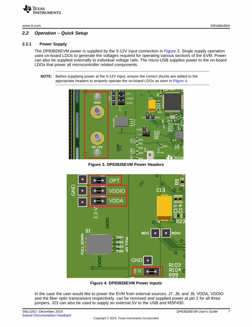
2.2 Operation – Quick Setup
2.2.1 Power SupplyThe DP83826EVM power is supplied by the 5-12V input connection in Figure 3. Single supply operationuses on-board LDOs to generate the voltages required for operating various sections of the EVM. Powercan also be supplied externally to individual voltage rails. The micro-USB supplies power to the on-boardLDOs that power all microcontroller related components.
NOTE: Before supplying power at the 5-12V input, ensure the correct shunts are added to theappropriate headers to properly operate the on-board LDOs as seen in Figure 4.
Figure 3. DP83826EVM Power Headers
Figure 4. DP83826EVM Power Inputs
In the case the user would like to power the EVM from external sources, J7, J8, and J9, VDDA, VDDIOand the fiber optic transceivers respectively, can be removed and supplied power at pin 2 for all threejumpers. J23 can also be used to supply an external 5V to the USB and MSP430.

Introduction www.ti.com
8 SNLU262–December 2019Submit Documentation Feedback
Copyright © 2019, Texas Instruments Incorporated
DP83826EVM User’s Guide
2.2.2 SoftwareThe on-board MSP430 comes pre-programmed and ready to use. When using this EVM for the first timeon a Windows 7 (or above) PC, MSP430 drivers and USB-2-MDIO software utility will have to be installed.USB-2-MDIO software can be used for accessing the PHY's registers. In the case where an externalMSP430 or EZFET is needed, the user may simply connect the TST and RST pins of their device to theDP83826EVM.
Figure 5. DP83826EVM External MSP Connection
2.2.2.1 MSP430 DriverInstall the latest MSP430 drive from this website: http://software-dl.ti.com/msp430/msp430_public_sw/mcu/msp430/MSP430_FET_Drivers/latest/index_FDS.html .
2.2.2.2 USB-2-MDIO SoftwareDownload the software from http://www.ti.com/tool/usb-2-mdio .
The webpage also contains the User’s Guide for installing and using the software. Because the MSP430is on-board the DP83826EVM, it is not necessary to purchase a separate MSP430 Launchpad kit andconnect to the PHY using wires.
In the case the on-board MSP430 cannot be used for some reason, MDIO and MDC pins are also brokenout on J1 and J2 pins, respectively. Users can connect an MSP430 launchpad or their own MDIO-MDCutility on J1 and J2 to access the PHY.

www.ti.com Board Setup Details
9SNLU262–December 2019Submit Documentation Feedback
Copyright © 2019, Texas Instruments Incorporated
DP83826EVM User’s Guide
3 Board Setup Details
3.1 Block Diagram
Figure 6. DP83826EVM Block Diagram

Board Setup Details www.ti.com
10 SNLU262–December 2019Submit Documentation Feedback
Copyright © 2019, Texas Instruments Incorporated
DP83826EVM User’s Guide
3.2 EVM High Level Summary
Table 2. DP83826EVM Applications
N0. TEST CASES APPLICATIONS HOW TO USE
1 MII/RMII to Copper
Run traffic between MII/RMII and Copper. Connect to DP83826 EVM or MAC Systemusing Header pins.
Perform IEEE and UNH compliance testing Using onboard MSP430 and software.
Run EMI/EMC Test on EVM Use internal PRBS and loopback. OnboardMSP430 can be used for register access.
Measure Power Dissipation Connect external power supplies.
External MAC loopback Connect external MAC to headers and useMAC loopback register settings
50MHz output clock Optional Clock out SMA
2 Loopback Data received by the PHY can be looped backthrough the interface without needing a MAC. Use onboard MSP430 to enable loopback.
3 Repeater Mode RMII back to back as range extender. Two EVMs can be connected back to backusing custom header cable.
4 Low Power modesDemonstrate EEE Use onboard MSP430 to enable EEE.
Demonstrate Sleep and Power down mode Use onboard MSP430 to activate lowpower mode
4 Configurations Options
4.1 MDIO Register AccessTo update or read the registers of the device, the user can simply connect the DP83826EVM to acomputer and use the USB-2-MDIO software. The EVM is designed to easily enable and test strapfunctionality through software instead without the need to modify the board and hardware. This allows forsimple hardware and software support for those that do not have MDIO communication capability. Theregister map used for the DP83826EVM can be found in section 8.7 of the DP83826E Datasheet.
More information on how to access the DP83826 MDIO status and control registers can be found in theUSB-2-MDIO Software User's Guide .
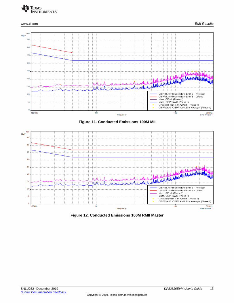
5 EMI ResultsThis section provides details of the EMI tests performed and its results.
Table 3. DP83826EVM EMI Tests Performed
TEST STANDARD TEST LEVEL RESULTRadiated Emissions100M MII
CISPR 22 Class B Below Limit Levels
Radiated Emissions100M RMII MasterConducted Emissions100M MIIConducted Emissions100M RMII Master

www.ti.com EMI Results
11SNLU262–December 2019Submit Documentation Feedback
Copyright © 2019, Texas Instruments Incorporated
DP83826EVM User’s Guide
5.1 SetupBelow are a simple diagram and photo outlining the setup of the DP83826EVM in a 10m anechoicchamber.
Figure 7. Block Diagram Setup for EMI Testing
Figure 8. EMI Testing Setup in Chamber

EMI Results www.ti.com
12 SNLU262–December 2019Submit Documentation Feedback
Copyright © 2019, Texas Instruments Incorporated
DP83826EVM User’s Guide
5.2 Results
Figure 9. Radiated Emissions 100M MII
Figure 10. Radiated Emissions 100M RMII Master
www.ti.com EMI Results
13SNLU262–December 2019Submit Documentation Feedback
Copyright © 2019, Texas Instruments Incorporated
DP83826EVM User’s Guide
Figure 11. Conducted Emissions 100M MII
Figure 12. Conducted Emissions 100M RMII Master

OUT3
5 6
EN1
ADJ/BYP4
8 7
IN2
GND
TL5209DRU11
10uF
C32
1uF
C31
GND GND
GND
470pF
C36
D2
10uFC25
22uFC24
J4
12 3
4
T1
5V-12V
GND
165kR31
100kR28
GND
GND
2.2uF
C33
GND
2.2uFC34
10uFC35
GND GND
3V3_LDO
VDDA3P3
MCU_VCC
0R27
0R30
DNP
Green
12
LD1
470R29
GND
5V-12V
100kR25
24.9kR26
GND
GND
GND
5V
22µF
C28
22µF
C29
22µF
C30
22µF
C27
5V
GND
1µFC26
GND
220nFC20
220nFC22
4.7uF
C21
4.7uF
C19
GND
0.1uFC230
R24
5V-12V
5V-12V
5V
10uH
L1
OUT3
5 6
EN1
ADJ/BYP4
8 7
IN2
GND
TL5209DRU12
35V10uF
C38
1uF
C37
GND GND
GND
470pF
C42
165kR36
100kR33
GND
GND
2.2uF
C39
GND
2.2uF
C4035V10uF
C41
GND GND
0R32
0R35
DNP
Green
12
LD2
470R34
GND
USB_VBUS
3V3_LDO3V3_LDO
VDDIO
1
J11
1
J12
GND
D3
1
J10
GND
3V3_LDO3V3_OPT
1
J13
XF1
1
2
J6
1
2
J7
1
2
J8
1
2
J9
PGND1
VIN2
NC3
BOOT4
VCC5
AGND6
FB7
PG8
EN9
VIN10
PGND11
SW12
LMR33620ARNXT
U10
J5
1A
100uF
C18
3A
J15
575-4
J21575-4
1
J23
DP83826EVM Schematics www.ti.com
14 SNLU262–December 2019Submit Documentation Feedback
Copyright © 2019, Texas Instruments Incorporated
DP83826EVM User’s Guide
6 DP83826EVM Schematics
Figure 13. DP83826EVM Power Schematic

6.49k
R48
RD_N
S1
S2
J17
1µFC52
1µFC54
0.1µFC47
RD_P
RX_ER
RX_D0
RX_D1RX_DV
MDIO
MDC
RESETPWDN
CLK_OUTLED_0
TD_NTD_P
TX_EN
TX_D0TX_D1
XOXI_C
TD_PTD_N
RD_NRD_P
RBIAS
TD_P
TD_N
RD_P
RD_N
TD_CH1_P
TD_CH1_N
TD_CH2_P
TD_CH2_N
D1+
D1-
6
7
9
10
D2+
D2-
GND8
TPD4E05U06DQAR
U13
TD_PTD_N
RD_PRD_N
75.0R43
75.0R44
75.0R45
75.0R46
0.1uFC55
0.1uFC56
0.1uFC45
0.1uFC46
XO
XI_C
EXT_REF_CLK
1.00MR39
22pFC43
22pFC44
1
3
GG
XTAL1
Green
2
LD4
LED_0
2.49k
R54
Green
2
LD5
470
R57
470
R55
CLK_OUT
S3
TX_D0
RX_D0
TX_D1
TX_EN
RX_D1
RX_ER
2.2k
R47
4700pFC624700pFC61
1.00MR51 1.00MR52
1
J16
2.49k
R59
4700pFC63
0.1µFC49
0.01uFC60
1000pF
C58
1000pF
C59
0R37
0R40
0R42
DP83826ERHB
ModeSelect
CEXT
VDDA3.3
RD_M
RD_P
TD_M
TD_P
8
9
10MDIO
MDC
13
14
15
16
VDDIO
18
19
20
21
22
TX_EN
TX_D0
TX_D1
TX_D2
TX_D3
28
29
30
31
RST_N
33
U14
TX_D2TX_D3
RX_D2RX_D3
RX_D2RX_D3
TX_D2TX_D3
TX_CLK
TX_CLK
CRS
CRS_S
COL
RX_CLK
0.1µFC57
MDCMDIO
0.01uF
C51
0.01uF
C53
2.2kR50
LED_1
COL
LED_2
CRS
LED_3
9
10
11
12
13
14
15
16
T2
PWDN
GND
GND
GNDRX_CLKRX_DVGND
GND
GND
GND
GNDRESET
Green
2
LD6
Green
2
LD3
470
R53
2.49k
R56
470
R58
2.49k
R60
RBIAS 1% Tolerance
0R1030R1020R1010R1000R990R980R970R96
0R78
0R104
0R190R18 MDC_S
MDIO_S
10uF
C48
10uF
C50
COL_S
0
R41
0
R88
2.2k
R105
1
3
5
7
9
11
13
15
17
19
21
23
25
27
29
31
33
35
37
39
41
43
45
47
49
51
53
55
57
59
MP1
MP2
MP3
MP4
J18
ERF8-030-01-L-D-EM2-TR
CRS_SCOL_S
XI
XI
0R107 XI_S
XI_S
CLK_OUT 0R108 CLK_OUT_S
470R49
Ferrite bead canreplace 0 ohmresistors R41 andR88
VDDA3P3
DNP
DNP
DNP
DNP
DNP
VDDA3P3
GND
GND
GND
GND GND
VDDIO
VDDIO
GND
GNDGND
GND GND
VDDIO
GNDGND
GND
DNP
DNP
DNP
GND GND
GND
GND
GND GND
GND
DNP
DNP
DNP
23
2
11
7
6
25
3
24
27
12
4
5
17
26
32
1
EARTH_GND EARTH_GND
EARTH_GND
GND
GND
GND
GND
GND
www.ti.com DP83826EVM Schematics
15SNLU262–December 2019Submit Documentation Feedback
Copyright © 2019, Texas Instruments Incorporated
DP83826EVM User’s Guide
Figure 14. DP83826EVM Main Schematic

VBUS1
D-2
D+3
ID4
GND5
678
11
10
9
J19
USB_N
USB_P
GND
33R75
0.1µFC65
GND
4.7uFC64
USB_VBUS
GND
EZFET_PUR
EZFET_PUD_N
EZFET_PUD_P
GND
HUB_D2_N
HUB_D2_P
USB_NUSB_P
D0_ND0_P
GND
MCU_VCC
GND
OC_N
GNDGND
GND GNDGND GND
HUB_D1_NHUB_D1_P
D1_ND1_P
GND GNDGND GND
HUB_D2_NHUB_D2_P
D2_ND2_P
GND
XTAL1
XTAL2
DM3DP3
DM4DP4
DM3
DP3DM4
DP4GND
GND
XTAL1
XTAL2
MCU_VCC
MCU_VCC
MCU_VCC
MCU_VCC
27
R66
27
R63
10pFC70
10pFC71
TARGET_D_N HUB_D1_N
HUB_D1_P
GND
TARGET_D_P
GND
EZFET_AVBUSEZFET_AVCOUT2ADC
EZFET_VREF
GND
GND
GNDGND
EZFET_LED0EZFET_LED1
EZFET_UARTCTSEZFET_UARTRTS
EZFET_UARTTXDEZFET_UARTRXD
GND
GND
EZFET_SBW_RSTEZFET_SBW_TST
EZFET_PUD_PEZFET_PUD_N
EZFET_PUR
EZFET_VUSB
EZFET_XINEZFET_XOUT
GND
EZFET_RSTEZFET_TEST
MCU_VCC
USB_VBUS
MCU_VCC
USB_VBUS
GND
EZFET_AVCOUT2ADC
GND
EZFET_TESTEZFET_RST
EZFET_SBW_TSTEZFET_SBW_RST
TEST/SBWTCKRST/SBWTDIO
MCU_VCC
GND
1
34
2GG
Y3
GND
GND
EZFET_XIN
EZFET_XOUT
GND
GND
GND
36pF
C90
36pF
C9133pF
C79
33pFC80
P6.0/CB0/A01
P6.1/CB1/A12
P6.2/CB2/A23
P6.3/CB3/A34
P6.4/CB4/A45
P6.5/CB5/A56
P6.6/CB6/A67
P6.7/CB7/A78
P5.0/A8/VREF+/VEREF+9
P5.1/A9/VREF-/VEREF-10
AVCC111
P5.4/XIN12
P5.5/XOUT13
AVSS114
DVCC115
DVSS116
VCORE17
P1.0/TA0CLK/ACLK18
P1.1/TA0.019
P1.2/TA0.120
P1.3/TA0.221
P1.4/TA0.322
P1.5/TA0.423
P1.6/TA1CLK/CBOUT24
P1.7/TA1.025
P2.0/TA1.126
P2.1/TA1.227
P2.2/TA2CLK/SMCLK28
P2.3/TA2.029
P2.4/TA2.130
P2.5/TA2.231
P2.6/RTCCLK/DMAE032
P2.7/UCB0STE/UCA0CLK33
P3.0/UCB0SIMO/UCB0SDA34
P3.1/UCB0SOMI/UCB0SCL35
P3.2/UCB0CLK/UCA0STE36
P3.3/UCA0TXD/UCA0SIMO37
P3.4/UCA0RXD/UCA0SOMI38
DVSS239
DVCC240
P4.0/PM_UCB1STE/PM_UCA1CLK41
P4.1/PM_UCB1SIMO/PM_UCB1SDA42
P4.2/PM_UCB1SOMI/PM_UCB1SCL43
P4.3/PM_UCB1CLK/PM_UCA1STE44
P4.4/PM_UCA1TXD/PM_UCA1SIMO45
P4.5/PM_UCA1RXD/PM_UCA1SOMI46
P4.6/PM_NONE47
P4.7/PM_NONE48
VSSU49
PU.0/DP50
PUR51
PU.1/DM52
VBUS53
VUSB54
V1855
AVSS256
P5.2/XT2IN57
P5.3/XT2OUT58
TEST/SBWTCK59
PJ.0/TDO60
PJ.1/TDI/TCLK61
PJ.2/TMS62
PJ.3/TCK63
RST/NMI/SBWTDIO64
QFN PAD65
MSP430F5528IRGCR
U16
DP01
DM02
VCC3
RESET4
EECLK5
EEDATA/GANGED6
GND7
BUSPWR8
PWRON19
OVRCUR110
DM111
DP112
PWRON213
OVRCUR214
DM215
DP216
PWRON317
OVRCUR318
DM319
DP320
PWRON421
OVRCUR422
DM423
DP424
VCC25
EXTMEM26
TSTPLL/48MCLK27
GND28
XTAL229
XTAL130
TSTMODE31
SUSPND32
EP33
TUSB2046BIRHBT
U15
0
R38
0R94
0R95
470R86 470
R87
240kR89
220kR90
220kR92150k
R91
47kR79
47k
R93
27
R76
27
R80
22 R64
22 R6522 R6722 R68
22 R7122 R72
15.0kR69
15.0kR70
15.0kR73
15.0kR74
15.0kR82
15.0kR83
15.0kR84
15.0kR85
10kR62
1.00MR81
1.50kR61
1.40kR77
Green
12
D5
Orange
21
D4
1 2
3 4
J20
10uF
C85
470nF C82
10pFC75
10pFC76
1000pF
C83
0.1µF
C74
0.1µF
C77
0.1µF
C78
0.1µF
C86
0.1µF
C87
1
2
3
6MHz
Y21.50kR106
0.22µFC81
0.22µF
C84
22pFC66
22pFC67
22pFC68
22pFC69
22pFC72
22pFC73
DP83826EVM Schematics www.ti.com
16 SNLU262–December 2019Submit Documentation Feedback
Copyright © 2019, Texas Instruments Incorporated
DP83826EVM User’s Guide
Figure 15. DP83826EVM USB HUB and EZFET Schematic
P1.0
P1.1
Rg
12
GR
D1
47kR22
1000pFC17
RST/SBWTDIO
1
2
3
4
P7.0/CB8/A12
P7.1/CB9/A13
P7.2/CB10/A14
P7.3/CB11/A15
P5.0/A8/VREF+/VEREF+
P5.1/A9/VREF-/VEREF-
AVCC1
P5.4/XIN
P5.5/XOUT
14
15
16
17
DVCC119
VCORE
P1.0/TA0CLK/ACLK
P1.1/TA0.0
P1.2/TA0.1
P1.3/TA0.2
P1.4/TA0.3
P1.5/TA0.4
P1.6/TA1CLK/CBOUT
P1.7/TA1.0
29
30
31
32
33
34
35
36
P3.0/UCB0SIMO/UCB0SDA
P3.1/UCB0SOMI/UCB0SCL
P3.2/UCB0CLK/UCA0STE
P3.3/UCA0TXD/UCA0SIMO
P3.4/UCA0RXD/UCA0SOMI
P3.5/TB0.5
P3.6/TB0.6
P3.7/TB0OUTH/SVMOUT
45
46
47
48
49DVCC2
51
52
53
54
P5.6/TB0.0
P5.7/TB0.1
P7.4/TB0.2
P7.5/TB0.3
P7.6/TB0.4
P7.7/TB0CLK/MCLK
61
62
63
64
VBUS
VUSB
V18
68
P5.2/XT2IN
P5.3/XT2OUT
71
72
73
74
75
76
77
78
79
80
U8
MSP430F5529IPN
MSP_XOUT
4.7uF C11
0
R23
10uFC13
P1.0
MSP_XIN
0 R13
P1.1
MDC_MSPMDIO_MSP
TARGET_D_N
1.00MR21
TARGET_PUR
1.40kR20
TARGET_D_P
TEST/SBWTCK
RST/SBWTDIO
470R14
470R15
0.1µF
C14
0.1µF
C16
0.1µF
C15
0.22uF C9
0.22uF
C12
470nF C10
S2
8
VREF_A
A1
1
6
7
A25
LSF0102DQER
U2 200kR1
PWDN
RESET
0
R10
0
R11
MSP_PWDN
MSP_RESET
PWDN_LVL
RESET_LVL
PWDN_LVL
RESET_LVL 0.1uFC5
MSP_PWDNMSP_RESET
6
8
7
5
S1SW4SW3SW2SW1
1
3GG
Y1
2
4
J3
RST/SBWTDIOTEST/SBWTCK
P4.4/UCA1TXDP4.5/UCA1RXD
P6.7
SW1SW2SW3SW4
P1.7
8
VREF_A
A1
1
6
7
A25
LSF0102DQER
U3 200kR2
MDC
MDIO
MDC_LVL
MDIO_LVL 0.1uFC6
0
R90
R8TX_OPT
RX_OPT
UART_TX
UART_RX
1A
C
4
5
A
A
8
U6
HFBR-1412PZ
TX_OPT
1
VCC
COMMON
4
5
DATA
COMMON8
U5
HFBR-2412TZ
TX_OPT
2.2kR4
5V
22pFC4
0.1uF
C2
NC
4
5 U1
102
R5
1
VCC
COMMON
4
5
DATA
COMMON8
U4
HFBR-2412TZ
RX_OPT
2.2kR3
5V
22pFC3
0
R6
0.1uF
C1
SEL
VDD
3
S1
5
S2
TMUX1219DCKR
U7
SEL
VDD
3
S1
5
S2
TMUX1219DCKR
U9
MDIO_MSP
MDC_MSP
MDIO_LVL
MDC_LVL
TX_OPT
RX_OPT
J1
1
J2
UART_RXUART_TX
24.9kR12
330
R7
Internal GPIO Pull Up
P1.2
P1.3
Rg
12
GR
D6
470R16
470R17
P1.2P1.3
MDC Optics MDIO Optics
36pFC7
36pFC8
0
R109
0
R110
MDC
MDIO
MDC_LVL
MDIO_LVL
Use J1 and J2for direct line toMDC and MDIO
S1 = MSP, USB_VBUS
S2 = OPT, GND
DNP
DNP
DNP
DNP
DNP
DNP
DNP
DNP
DNP
DNP
MCU_VCC
VDDIO VDDIO
3V3_OPT 3V3_OPT 3V3_OPT3V3_OPT
DNPDNP
DNP
DNPDNP
5V
USB_VBUS
MCU_VCC
21
22
23
24
25
26
27
28
37
38
39
40
41
42
43
44
9
10
69
70
12
13
55
56
5
6
7
8
57
58
59
60
57
67
20
65
66
11
18
50
GND
MCU_VCC
GND
GND
GND
GND
GND GND
GND
GND
GND
GND
GND GND GND GND
GND GND
GND
GND
GND
GND
GND
GND
GNDGNDGNDGND
34 34
GND
GND
GND
DNP
DNP
DNP
DNP
DNP
DNP
DNP
DNP
DNP
DNP
DNP
DNP
2
4
P2.0/TA1.1
P2.1/TA1.2
P2.2/TA2CLK/SMCLK
P2.3/TA2.0
P2.4/TA2.1
P2.5/TA2.2
P2.6/RTCCLK/DMAE0
P2.7/UCB0STE/ICA0CLK
P1.0/TA0CLK/ACLK
P1.1/TA0.0
P1.2/TA0.1
P1.3/TA0.2
P1.4/TA0.3
P1.5/TA0.4
P1.6/TA1CLK/CBOUT
P1.7/TA1.0
P4.0/PM_UCB1STE/PM_UCA1CLK
P4.3/PM_UCB1CLK/PM_UCA1STE
P4.5/PM_UCA1RXD/PM_UCA1SOMI
P4.6/PM_NONE
P4.7/PM_NONE
P6.0/CB0/A0
P8.0
P8.1
P8.2
PJ.0/TDO
PJ.1/TDI/TCLK
PJ.2/TMS
PJ.3/TCK
RST/NMI/SBWTDIO
TEST/SBWTCK
PU.0/DP
PU.1/DM
VSSU
AVSS1
AVSS2
DVSS1
DVSS2
P4.1/PM_UCB1SIMO/PM_UCB1SDAP4.2/PM_UCB1SOMI/PM_UCB1SCL
PUR
P4.4/PM_UCA1TXD/PM_UCA1SIMO
P6.1/CB1/A1
P6.2/CB2/A2
P6.3/CB3/A3
P6.4/CB4/A4
P6.5/CB5/A5P6.6/CB6/A6P6.7/CB7/A7
www.ti.com DP83826EVM Schematics
17SNLU262–December 2019Submit Documentation Feedback
Copyright © 2019, Texas Instruments Incorporated
DP83826EVM User’s Guide
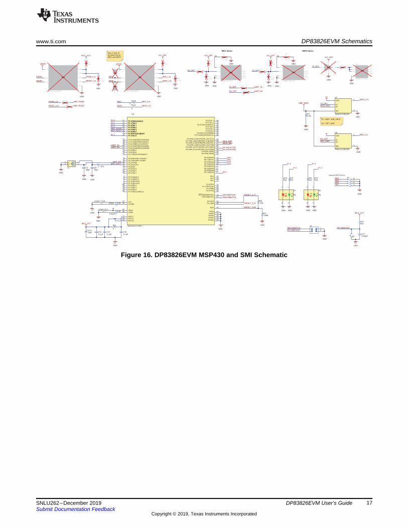
Figure 16. DP83826EVM MSP430 and SMI Schematic

TX_D0_EXT
RX_D0_EXT
TX_D1_EXT
TX_EN_EXT
RX_D1_EXT
XI_S_EXT
RX_ER_EXT
RX_D2_EXTRX_D3_EXT
TX_D2_EXTTX_D3_EXT
TX_CLK_EXT
CRS_EXT
MDC_EXTMDIO_EXT
PWDN_EXT
GND_EXT
GND_EXT
GND_EXTRX_CLK_EXTRX_DV_EXTGND_EXT
GND_EXT
GND_EXT
GND_EXT
GND_EXTRESET_EXT
RESET_EXT
MDC_EXTMDIO_EXT
RX_D3_EXTRX_D2_EXTRX_D1_EXTRX_D0_EXTRX_CLK_EXT
TX_CLK_EXT
TX_D3_EXTTX_D2_EXTTX_D1_EXTTX_D0_EXT
TX_EN_EXT
CRS_EXT
RX_DV_EXTRX_ER_EXT
PWDN_EXT
COL_EXT
2
4
6
8
10
12
14
16
18
20
22
24
26
28
30
32
34
36
38
40
42
44
J22
COL_EXT
1
3
5
7
9
11
13
15
17
19
21
23
25
27
29
31
33
35
37
39
41
43
45
47
49
51
53
55
57
59
MP1MP2
MP3MP4
J14
ERM8-030-01-L-D-EM2-TR
CLK_OUT_EXT
CLK_OUT_EXT
XI_S_EXT
1
3
5
7
9
11
13
15
17
19
21
23
25
27
29
31
33
35
38
40
42
44
GND_EXT
VDDA3P3_EXT
2
4
6
8
10
12
14
16
18
20
22
24
26
28
30
32
34
36
38
40
42
44
46
48
50
52
54
56
58
60
MP1
MP3
MP2
MP4
VDDA3P3_EXT
GND_EXT
GND_EXT GND_EXT
DP83826EVM Schematics www.ti.com
18 SNLU262–December 2019Submit Documentation Feedback
Copyright © 2019, Texas Instruments Incorporated
DP83826EVM User’s Guide
Figure 17. DP83826EVM Breakout Board Schematic

www.ti.com DP83826EVM BOM
19SNLU262–December 2019Submit Documentation Feedback
Copyright © 2019, Texas Instruments Incorporated
DP83826EVM User’s Guide
7 DP83826EVM BOM
Table 4. DP83826EVM BOM
Designator Quantity Value Description PackageReference
Part Number Manufacturer
!PCB1 1 Printed CircuitBoard
HSDC077 Any
C7, C8, C90,C91
4 36pF CAP, CERM, 36pF, 50 V,+/- 5%,C0G/NP0, 0402
0402 CL05C360JB5NNNC
SamsungElectro-Mechanics
C9, C12 2 0.22uF CAP, CERM,0.22 uF, 16 V,+80/-20%, Y5V,0603
0603 C0603C224Z4VACTU
Kemet
C10 1 0.47uF CAP, CERM,0.47 uF, 16 V,+/- 10%, X7R,AEC-Q200Grade 1, 0603
0603 GCM188R71C474KA55D
MuRata
C11 1 4.7uF CAP, CERM, 4.7uF, 35 V, +/-10%, X5R, 0603
0603 C1608X5R1V475K080AC
TDK
C13, C85 2 10uF CAP, TA, 10 uF,35 V, +/- 10%,0.125 ohm, SMD
7343-31 TPSD106K035R0125
AVX
C14, C15, C16,C47, C49, C57,C65
7 0.1uF CAP, CERM, 0.1µF, 10 V,+/-10%, X7R, 0402
0402 C0402C104K8RACTU
Kemet
C17, C83 2 1000pF CAP, CERM,1000 pF, 50 V,+/- 5%,C0G/NP0, 0402
0402 C1005NP01H102J050BA
TDK
C18 1 100uF CAP, AL, 100uF, 50 V, +/-20%, SMD
HA0 EMVE500ADA101MHA0G
Chemi-Con
C19, C21 2 4.7uF CAP, CERM, 4.7uF, 50 V, +/-10%, X7R, AEC-Q200 Grade 1,1210
1210 CGA6P3X7R1H475K250AB
TDK
C20, C22 2 0.22uF CAP, CERM,0.22 uF, 50 V,+/- 10%, X7R,AEC-Q200Grade 1, 0603
0603 CGA3E3X7R1H224K080AB
TDK
C23 1 0.1uF CAP, CERM, 0.1uF, 50 V, +/-10%, X7R, AEC-Q200 Grade 1,0402
0402 GCM155R71H104KE02D
MuRata
C24 1 22uF CAP, CERM, 22uF, 16 V, +/-20%, X7R, AEC-Q200 Grade 1,1210
1210 CGA6P1X7R1C226M250AC
TDK
C25 1 10uF CAP, CERM, 10uF, 25 V, +/-20%, X7R, AEC-Q200 Grade 1,1210
1210 CGA6P1X7R1E106M250AC
TDK

DP83826EVM BOM www.ti.com
20 SNLU262–December 2019Submit Documentation Feedback
Copyright © 2019, Texas Instruments Incorporated
DP83826EVM User’s Guide
Table 4. DP83826EVM BOM (continued)C26 1 1uF CAP, CERM, 1
uF, 35 V, +/-10%, X7R, AEC-Q200 Grade 1,0603
0603 CGA3E1X7R1V105K080AC
TDK
C27, C28, C29,C30
4 22uF CAP, CERM, 22µF, 25 V,+/-10%, X7R, AEC-Q200 Grade 1,1210
1210 TMK325B7226KMHP
Taiyo Yuden
C31, C37 2 1uF CAP, CERM, 1uF, 35 V, +/-20%, X5R, 0402
0402 GRM155R6YA105ME11D
MuRata
C32, C35, C38,C41
4 10uF CAP, CERM, 10uF, 35 V, +/-20%, X5R, 0603
0603 GRM188R6YA106MA73D
Murata
C33, C34, C39,C40
4 2.2uF CAP, CERM, 2.2uF, 16 V, +/-10%, X6S, 0402
0402 GRM155C81C225KE11D
MuRata
C36, C42 2 470pF CAP, CERM,470 pF, 50 V, +/-10%, X7R, AEC-Q200 Grade 1,0402
0402 GCM155R71H471KA37D
MuRata
C43, C44 2 22pF CAP, CERM, 22pF, 50 V, +/- 5%,C0G/NP0, AEC-Q200 Grade 1,0603
0603 CGA3E2C0G1H220J080AA
TDK
C45, C46, C55,C56
4 0.1uF CAP, CERM, 0.1uF, 10 V, +/-10%, X7R, 0603
0603 C0603C104K8RACTU
Kemet
C48, C50 2 10uF CAP, CERM, 10uF, 6.3 V, +/-20%, X5R, 0402
0402 CL05A106MQ5NUNC
SamsungElectro-Mechanics
C51, C53, C60 3 0.01uF CAP, CERM,0.01 uF, 16 V,+/- 10%, X7R,0402
0402 885012205031 Wurth Elektronik
C52, C54 2 1uF CAP, CERM, 1µF, 10 V,+/-20%, X5R, 0402
0402 CC0402MRX5R6BB105
Yageo America
C58, C59 2 1000pF CAP, CERM,1000 pF, 2000V, +/- 10%, X7R,AEC-Q200Grade 1, 1206
1206 C1206C102KGRACAUTO
Kemet
C61 1 4700pF CAP, CERM,4700 pF, 2000V, +/- 10%, X7R,1812
1812 1812GC472KAT1A
AVX
C64 1 4.7uF CAP, TA, 4.7 uF,35 V, +/- 10%,1.3 ohm, SMD
7343-31 293D475X9035D2TE3
Vishay-Sprague
C66, C67, C68,C69, C72, C73
6 22pF CAP, CERM, 22pF, 50 V,+/- 5%,C0G/NP0, 0402
0402 C1005NP01H220J050BA
TDK
C70, C71, C75,C76
4 10pF CAP, CERM, 10pF, 50 V, +/- 5%,C0G/NP0, 0603
0603 CGA3E2NP01H100D080AA
TDK
C74, C77, C78,C86, C87
5 0.1uF CAP, CERM, 0.1µF, 16 V,+/-10%, X7R, 0402
0402 CL05B104KO5NNNC
Walsin

www.ti.com DP83826EVM BOM
21SNLU262–December 2019Submit Documentation Feedback
Copyright © 2019, Texas Instruments Incorporated
DP83826EVM User’s Guide
Table 4. DP83826EVM BOM (continued)C79, C80 2 33pF CAP, CERM, 33
pF, 50 V,+/- 5%,C0G/NP0, AEC-Q200 Grade 1,0402
0402 GCM1555C1H330JA16D
MuRata
C81, C84 2 0.22uF CAP, CERM,0.22 µF, 50 V,+/-10%, X5R, 0603
0603 CL10A224KB8NNNC
SamsungElectro-Mechanics
C82 1 0.47uF CAP, CERM,0.47 uF, 50 V,+/- 10%, X7R,AEC-Q200Grade 1, 0603
0603 CGA3E3X7R1H474K080AB
TDK
D1, D6 2 Rg LED, Rg, SMD 1.6x0.8mm HSMF-C165 AvagoD2, D3 2 60V Diode, Schottky,
60 V, 1 A, AEC-Q101, SMA
SMA NRVBA160T3G ONSemiconductor
D4 1 Orange LED, Orange,SMD
1x0.5mm APHHS1005SECK
Kingbright
D5, LD1, LD2,LD3, LD4, LD5,LD6
7 Green LED, Green,SMD
2x1.25mm QTLP630C4TR Everlight
F1 1 Fuse, 3 A,63VAC/VDC,SMD
7.4x3.1mm 3402.0014.11 Schurter
H1, H2, H3, H4 4 Machine Screw,Round, #4-40 x1/4, Nylon,Philips panhead
Screw NY PMS 4400025 PH
B&F FastenerSupply
H5, H6, H7, H8 4 Standoff, Hex,1"L #4-40 Nylon
Standoff 1902E Keystone
J3, J20 2 Header, 100mil,2x2, Gold, TH
2x2 Header TSW-102-07-G-D
Samtec
J4, J5 2 Terminal, Turret,TH, Double
Keystone1502-2 1502-2 Keystone
J6, J7, J8, J9 4 Header, 100mil,2x1, Tin, TH
Header, 2 PIN,100mil, Tin
PEC02SAAN SullinsConnectorSolutions
J10, J11, J12,J13, J23
5 Header, 1x1, Tin,TH
Header, 1x1 PEC01SAAN SullinsConnectorSolutions
J14 1 Receptacle,0.8mm, 30x2,Tin, Edge mount
Receptacle,0.8mm, 30x2,Edge mount
ERM8-030-01-L-D-EM2-TR
Samtec
J15, J21 2 StandardBanana Jack,Uninsulated,5.5mm
Keystone_575-4 575-4 Keystone
J17 1 RJ45, 1.27mm,R/A, Gold, TH
RJ-45, 1.27mm,R/A, TH
SS-7188S-A-NF StewartConnector
J18 1 Receptacle,0.8mm, 30x2,Gold, EdgeMount
Receptacle,0.8mm, 30x2,Edge Mount
ERF8-030-01-L-D-EM2-TR
Samtec
J19 1 Connector,Receptacle,Micro-USB TypeAB, R/A, BottomMount SMT
5.6x2.5x8.2mm 475890001 Molex
J22 1 Header,2.54mm, 22x2,Gold, TH
Header,2.54mm, 22x2,TH
TSW-122-07-G-D
Samtec

DP83826EVM BOM www.ti.com
22 SNLU262–December 2019Submit Documentation Feedback
Copyright © 2019, Texas Instruments Incorporated
DP83826EVM User’s Guide
Table 4. DP83826EVM BOM (continued)L1 1 10uH Inductor,
Shielded, Ferrite,10 uH, 2.75 A,0.128 ohm, SMD
Inductor,5.7x2.8x5.2mm
SRP5030T-100M
Bourns
R12, R26 2 24.9k RES, 24.9 k, 1%,0.1 W, AEC-Q200 Grade 0,0603
0603 CRCW060324K9FKEA
Vishay-Dale
R13, R23 2 0 RES, 0, 5%,0.063 W, AEC-Q200 Grade 0,0402
0402 CRCW04020000Z0ED
Vishay-Dale
R14, R15, R16,R17, R49
5 470 RES, 470, 5%,0.05 W, 0201
0201 RC0201JR-07470RL
Yageo America
R20, R77 2 1.40k RES, 1.40 k, 1%,0.063 W, AEC-Q200 Grade 0,0402
0402 CRCW04021K40FKED
Vishay-Dale
R21, R81 2 1.00Meg RES, 1.00 M,1%, 0.063 W,AEC-Q200Grade 0, 0402
0402 CRCW04021M00FKED
Vishay-Dale
R22, R79, R93 3 47k RES, 47 k, 5%,0.063 W, AEC-Q200 Grade 0,0402
0402 CRCW040247K0JNED
Vishay-Dale
R24 1 0 RES, 0, 1%, 0.1W, AEC-Q200Grade 0, 0603
0603 RMCF0603ZT0R00
StackpoleElectronics Inc
R25 1 100k RES, 100 k, 1%,0.1 W, AEC-Q200 Grade 0,0603
0603 CRCW0603100KFKEA
Vishay-Dale
R27, R32 2 0 RES, 0, 5%, 0.1W, AEC-Q200Grade 0, 0603
0603 ERJ-3GEY0R00V
Panasonic
R28, R33 2 100k RES, 100 k,0.5%, 0.063 W,AEC-Q200Grade 0, 0402
0402 CRCW0402100KDHEDP
Vishay-Dale
R29, R34, R53,R55, R57, R58,R86, R87
8 470 RES, 470, 5%,0.063 W, AEC-Q200 Grade 0,0402
0402 CRCW0402470RJNED
Vishay-Dale
R31, R36 2 165k RES, 165 k, 1%,0.063 W, AEC-Q200 Grade 0,0402
0402 CRCW0402165KFKED
Vishay-Dale
R37, R40, R78,R96, R97, R98,R99, R100,R101, R102,R103, R104
12 0 RES, 0, 5%,0.05 W, 0201
0201 CRCW02010000Z0ED
Vishay-Dale
R38, R94, R95 3 0 RES, 0, 5%,0.063 W, 0402
0402 RC0402JR-070RL
Yageo America
R41, R88 2 0 RES, 0, 5%, 0.1W, AEC-Q200Grade 0, 0603
0603 CRCW06030000Z0EA
Vishay-Dale
R43, R44, R45,R46
4 75.0 RES, 75.0, 1%,0.125 W, AEC-Q200 Grade 0,0805
0805 CRCW080575R0FKEA
Vishay-Dale

www.ti.com DP83826EVM BOM
23SNLU262–December 2019Submit Documentation Feedback
Copyright © 2019, Texas Instruments Incorporated
DP83826EVM User’s Guide
Table 4. DP83826EVM BOM (continued)R47 1 2.2k RES, 2.2 k, 5%,
0.063 W, AEC-Q200 Grade 0,0402
0402 CRCW04022K20JNED
Vishay-Dale
R48 1 6.49k RES, 6.49 k, 1%,0.063 W, AEC-Q200 Grade 0,0402
0402 CRCW04026K49FKED
Vishay-Dale
R51 1 1.00Meg RES, 1.00 M,1%, 1 W, 2010
2010 HVCB2010FKC1M00
StackpoleElectronics Inc
R54, R56, R59,R60
4 2.49k RES, 2.49 k, 1%,0.063 W, AEC-Q200 Grade 0,0402
0402 CRCW04022K49FKED
Vishay-Dale
R61, R106 2 1.50k RES, 1.50 k, 1%,0.063 W, AEC-Q200 Grade 0,0402
0402 CRCW04021K50FKED
Vishay-Dale
R62 1 10k RES, 10 k, 5%,0.063 W, AEC-Q200 Grade 0,0402
0402 CRCW040210K0JNED
Vishay-Dale
R63, R66, R76,R80
4 27 RES, 27, 5%,0.063 W, AEC-Q200 Grade 0,0402
0402 CRCW040227R0JNED
Vishay-Dale
R64, R65, R67,R68, R71, R72
6 22 RES, 22, 5%,0.063 W, AEC-Q200 Grade 0,0402
0402 CRCW040222R0JNED
Vishay-Dale
R69, R70, R73,R74, R82, R83,R84, R85
8 15.0k RES, 15.0 k, 1%,0.063 W, AEC-Q200 Grade 0,0402
0402 CRCW040215K0FKED
Vishay-Dale
R75 1 33 RES, 33, 5%,0.063 W, AEC-Q200 Grade 0,0402
0402 CRCW040233R0JNED
Vishay-Dale
R89 1 240k RES, 240 k, 5%,0.063 W, AEC-Q200 Grade 0,0402
0402 CRCW0402240KJNED
Vishay-Dale
R90, R92 2 220k RES, 220 k, 5%,0.063 W, AEC-Q200 Grade 0,0402
0402 CRCW0402220KJNED
Vishay-Dale
R91 1 150k RES, 150 k, 5%,0.063 W, AEC-Q200 Grade 0,0402
0402 CRCW0402150KJNED
Vishay-Dale
R109, R110 2 0 RES, 0, 5%, 0.1W, AEC-Q200Grade 0, 0402
0402 ERJ-2GE0R00X Panasonic
S1 1 Switch, Slide,SPST 4 poles,SMT
SW, SMT HalfPitch 4SPST,5.8x2.7x6.25 mm
218-4LPST CTSElectrocomponents
S2, S3 2 Switch, Normallyopen, 2.3Nforce, 200koperations, SMD
KSR KSR221GLFS C&KComponents

DP83826EVM BOM www.ti.com
24 SNLU262–December 2019Submit Documentation Feedback
Copyright © 2019, Texas Instruments Incorporated
DP83826EVM User’s Guide
Table 4. DP83826EVM BOM (continued)SH-J1, SH-J2,SH-J3, SH-J4
4 Single Operation2.54mm PitchOpen TopJumper Socket
Single Operation2.54mm PitchOpen TopJumper Socket
M7582-05 Harwin
T1 1 Coupledinductor, 5 A,0.01 ohm, SMD
9x7mm ACM9070-701-2PL-TL01
TDK
T2 1 350uH Transformer, 350uH, SMT
12.7x9.09mm HX1188FNLT PulseEngineering
U8 1 25 MHz MixedSignalMicrocontrollerwith 128 KBFlash, 8192 BSRAM and 63GPIOs, -40 to 85degC, 80-pinQFP (PN),Green (RoHS &no Sb/Br)
PN0080A MSP430F5529IPN
TexasInstruments
U10 1 3.8-V to 36-V 2-A SynchronousStep-DownVoltageRegulator,RNX0012B(VQFN-HR-12)
RNX0012B LMR33620ARNXT
TexasInstruments
U11, U12 2 Single OutputLow Noise LDO,500 mA,Adjustable 1.3 to6.5 V Output, 2.5to 16 V Input, 8-pin SOIC (D),-40 to 125 degC,Green (RoHS &no Sb/Br)
D0008A TL5209DR TexasInstruments
U13 1 4-Channel Ultra-Low-Capacitance IECESD ProtectionDiode,DQA0010A(USON-10)
DQA0010A TPD4E05U06DQAR
TexasInstruments
U14 1 DP83826ERHB,RHB0032M(VQFN-32)
RHB0032M DP83826ERHB TexasInstruments
U15 1 4-Port Full-Speed USB Hub,3.3V, -40 to 85degC, 32-PinQFN (RHB),Green (RoHS &no Sb/Br)
RHB0032E TUSB2046BIRHBT
TexasInstruments
U16 1 16-Bit Ultra-Low-PowerMicrocontroller,128KB Flash,8KB RAM, USB,12Bit ADC, 2USCIs, 32Bit HWMPY,RGC0064B(VQFN-64)
RGC0064B MSP430F5528IRGCR
TexasInstruments

www.ti.com DP83826EVM BOM
25SNLU262–December 2019Submit Documentation Feedback
Copyright © 2019, Texas Instruments Incorporated
DP83826EVM User’s Guide
Table 4. DP83826EVM BOM (continued)XF1 1 FUSE HLDR
CARTRIDGE125V 5A SMD
12x5.2mm 0031.7701.11 Schurter
XTAL1 1 Crystal, 25 MHz,20 ppm, AEC-Q200 Grade 1,SMD
2.5x3.2mm ECS-250-12-33Q-JES-TR
ECS Inc.
Y1, Y3 2 Crystal, 24 MHz,20pF, SMD
3.2x2.5mm ECS-240-20-33-DU-TR
ECS Inc.
Y2 1 Resonator, 6MHz, 15pF SMD
4.5x1.2x2 mm CSTCR6M00G53Z-R0
MuRata
C1, C2, C5, C6 0 0.1uF CAP, CERM, 0.1uF, 50 V, +/-10%, X7R, AEC-Q200 Grade 1,0402
0402 GCM155R71H104KE02D
MuRata
C3, C4 0 22pF CAP, CERM, 22pF, 50 V, +/- 5%,C0G/NP0, AEC-Q200 Grade 1,0603
0603 CGA3E2C0G1H220J080AA
TDK
C62, C63 0 4700pF CAP, CERM,4700 pF, 2000V, +/- 10%, X7R,1812
1812 1812GC472KAT1A
AVX
FID1, FID2,FID3, FID4,FID5, FID6
0 Fiducial mark.There is nothingto buy or mount.
N/A N/A N/A
J1, J2 0 Header, 1x1, Tin,TH
Header, 1x1 PEC01SAAN SullinsConnectorSolutions
J16 0 SMA StraightPCB Socket DieCast, 50 Ohm,TH
SMA StraightPCB Socket DieCast, TH
5-1814832-1 TE Connectivity
R1, R2 0 200k RES, 200 k, 5%,0.1 W, AEC-Q200 Grade 0,0603
0603 CRCW0603200KJNEA
Vishay-Dale
R3, R4 0 2.2k RES, 2.2 k, 5%,0.1 W, AEC-Q200 Grade 0,0603
0603 ERJ-3GEYJ222V
Panasonic
R5 0 102 RES, 102, 1%,0.1 W, AEC-Q200 Grade 0,0603
0603 CRCW0603102RFKEA
Vishay-Dale
R6, R30, R35 0 0 RES, 0, 5%, 0.1W, AEC-Q200Grade 0, 0603
0603 ERJ-3GEY0R00V
Panasonic
R7 0 330 RES, 330, 5%,0.1 W, AEC-Q200 Grade 0,0603
0603 CRCW0603330RJNEA
Vishay-Dale
R8, R9, R10,R11
0 0 RES, 0, 5%, 0.1W, AEC-Q200Grade 0, 0402
0402 ERJ-2GE0R00X Panasonic
R18, R19, R42,R107, R108
0 0 RES, 0, 5%,0.05 W, 0201
0201 CRCW02010000Z0ED
Vishay-Dale
R39 0 1.00Meg RES, 1.00 M,1%, 0.063 W,0402
0402 RC0402FR-071ML
Yageo America

DP83826EVM BOM www.ti.com
26 SNLU262–December 2019Submit Documentation Feedback
Copyright © 2019, Texas Instruments Incorporated
DP83826EVM User’s Guide
Table 4. DP83826EVM BOM (continued)R50, R105 0 2.2k RES, 2.2 k, 5%,
0.05 W, 02010201 CRCW02012K20
JNEDVishay-Dale
R52 0 1.00Meg RES, 1.00 M,1%, 1 W, 2010
2010 HVCB2010FKC1M00
StackpoleElectronics Inc
U1 0 AutomotiveCatalog SingleInverter,DBV0005A,LARGE T&R
DBV0005A SN74LVC1G04QDBVRQ1
TexasInstruments
U2, U3 0 DualBidirectionalMulti-VoltageLevel Translator,DQE0008A(X2SON-8)
DQE0008A LSF0102DQER TexasInstruments
U4, U5 0 Fiber OpticReceiver 5MBd,TH
12.7x27.2mm HFBR-2412TZ BroadcomLimited
U6 0 Fiber OpticTransmitter820nm, TH
12.7x27.2mm HFBR-1412PZ BroadcomLimited

IMPORTANT NOTICE AND DISCLAIMER
TI PROVIDES TECHNICAL AND RELIABILITY DATA (INCLUDING DATASHEETS), DESIGN RESOURCES (INCLUDING REFERENCE DESIGNS), APPLICATION OR OTHER DESIGN ADVICE, WEB TOOLS, SAFETY INFORMATION, AND OTHER RESOURCES “AS IS” AND WITH ALL FAULTS, AND DISCLAIMS ALL WARRANTIES, EXPRESS AND IMPLIED, INCLUDING WITHOUT LIMITATION ANY IMPLIED WARRANTIES OF MERCHANTABILITY, FITNESS FOR A PARTICULAR PURPOSE OR NON-INFRINGEMENT OF THIRD PARTY INTELLECTUAL PROPERTY RIGHTS.These resources are intended for skilled developers designing with TI products. You are solely responsible for (1) selecting the appropriate TI products for your application, (2) designing, validating and testing your application, and (3) ensuring your application meets applicable standards, and any other safety, security, or other requirements. These resources are subject to change without notice. TI grants you permission to use these resources only for development of an application that uses the TI products described in the resource. Other reproduction and display of these resources is prohibited. No license is granted to any other TI intellectual property right or to any third party intellectual property right. TI disclaims responsibility for, and you will fully indemnify TI and its representatives against, any claims, damages, costs, losses, and liabilities arising out of your use of these resources.TI’s products are provided subject to TI’s Terms of Sale (www.ti.com/legal/termsofsale.html) or other applicable terms available either on ti.com or provided in conjunction with such TI products. TI’s provision of these resources does not expand or otherwise alter TI’s applicable warranties or warranty disclaimers for TI products.
Mailing Address: Texas Instruments, Post Office Box 655303, Dallas, Texas 75265Copyright © 2020, Texas Instruments Incorporated