ADS6145, ADS6144 ADS6143, ADS6142 - Texas Instruments
66
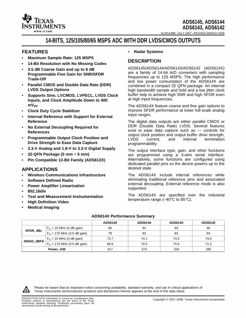
1FEATURES DESCRIPTION APPLICATIONS ADS6145, ADS6144 ADS6143, ADS6142 SLWS198B–JULY 2007–REVISED MARCH 2008 www.ti.com 14-BITS, 125/105/80/65 MSPS ADC WITH DDR LVDS/CMOS OUTPUTS • Radar Systems • Maximum Sample Rate: 125 MSPS • 14-Bit Resolution with No Missing Codes ADS6145/ADS6144/ADS6143/ADS6142 (ADS614X) • 3.5 dB Coarse Gain and up to 6 dB are a family of 14-bit A/D converters with sampling Programmable Fine Gain for SNR/SFDR frequencies up to 125 MSPS. The high performance Trade-Off and low power consumption of the ADS614X are • Parallel CMOS and Double Data Rate (DDR) combined in a compact 32 QFN package. An internal LVDS Output Options high bandwidth sample and hold and a low jitter clock buffer help to achieve high SNR and high SFDR even • Supports Sine, LVCMOS, LVPECL, LVDS Clock at high input frequencies. Inputs, and Clock Amplitude Down to 400 mV PP The ADS614X feature coarse and fine gain options to improve SFDR performance at lower full-scale analog • Clock Duty Cycle Stabilizer input ranges. • Internal Reference with Support for External Reference The digital data outputs are either parallel CMOS or DDR (Double Data Rate) LVDS. Several features • No External Decoupling Required for exist to ease data capture such as — controls for References output clock position and output buffer drive strength, • Programmable Output Clock Position and LVDS current, and internal termination Drive Strength to Ease Data Capture programmability. • 3.3-V Analog and 1.8-V to 3.3-V Digital Supply The output interface type, gain, and other functions • 32-QFN Package (5 mm × 5 mm) are programmed using a 3-wire serial interface. Alternatively, some functions are configured using • Pin Compatible 12-Bit Family (ADS612X) dedicated parallel pins so the device powers up to the desired state. The ADS614X include internal references while • Wireless Communications Infrastructure eliminating traditional reference pins and associated • Software Defined Radio external decoupling. External reference mode is also • Power Amplifier Linearization supported. • 802.16d/e The ADS614X are specified over the industrial • Test and Measurement Instrumentation temperature range (–40°C to 85°C). • High Definition Video • Medical Imaging ADS614X Performance Summary ADS6145 ADS6144 ADS6143 ADS6142 F in = 10 MHz (0 dB gain) 90 91 93 95 SFDR, dBc F in = 170 MHz (3.5 dB gain) 78 82 83 84 F in = 10 MHz (0 dB gain) 73.7 74.1 74.5 74.6 SINAD, dBFS F in = 170 MHz (3.5 dB gain) 68.6 70.5 70.6 71.5 Power, mW 417 374 318 285 1 Please be aware that an important notice concerning availability, standard warranty, and use in critical applications of Texas Instruments semiconductor products and disclaimers thereto appears at the end of this data sheet. PRODUCTION DATA information is current as of publication date. Copyright © 2007–2008, Texas Instruments Incorporated Products conform to specifications per the terms of the Texas Instruments standard warranty. Production processing does not necessarily include testing of all parameters.
-
Upload
khangminh22 -
Category
Documents
-
view
2 -
download
0
Transcript of ADS6145, ADS6144 ADS6143, ADS6142 - Texas Instruments
1FEATURES
DESCRIPTION
APPLICATIONS
ADS6145, ADS6144ADS6143, ADS6142
SLWS198B–JULY 2007–REVISED MARCH 2008www.ti.com
14-BITS, 125/105/80/65 MSPS ADC WITH DDR LVDS/CMOS OUTPUTS• Radar Systems
• Maximum Sample Rate: 125 MSPS• 14-Bit Resolution with No Missing Codes
ADS6145/ADS6144/ADS6143/ADS6142 (ADS614X)• 3.5 dB Coarse Gain and up to 6 dBare a family of 14-bit A/D converters with samplingProgrammable Fine Gain for SNR/SFDRfrequencies up to 125 MSPS. The high performanceTrade-Off and low power consumption of the ADS614X are
• Parallel CMOS and Double Data Rate (DDR) combined in a compact 32 QFN package. An internalLVDS Output Options high bandwidth sample and hold and a low jitter clock
buffer help to achieve high SNR and high SFDR even• Supports Sine, LVCMOS, LVPECL, LVDS Clockat high input frequencies.Inputs, and Clock Amplitude Down to 400
mVPP The ADS614X feature coarse and fine gain options toimprove SFDR performance at lower full-scale analog• Clock Duty Cycle Stabilizerinput ranges.• Internal Reference with Support for External
Reference The digital data outputs are either parallel CMOS orDDR (Double Data Rate) LVDS. Several features• No External Decoupling Required forexist to ease data capture such as — controls forReferencesoutput clock position and output buffer drive strength,
• Programmable Output Clock Position and LVDS current, and internal terminationDrive Strength to Ease Data Capture programmability.
• 3.3-V Analog and 1.8-V to 3.3-V Digital Supply The output interface type, gain, and other functions• 32-QFN Package (5 mm × 5 mm) are programmed using a 3-wire serial interface.
Alternatively, some functions are configured using• Pin Compatible 12-Bit Family (ADS612X)dedicated parallel pins so the device powers up to thedesired state.
The ADS614X include internal references while• Wireless Communications Infrastructureeliminating traditional reference pins and associated• Software Defined Radioexternal decoupling. External reference mode is also• Power Amplifier Linearization supported.
• 802.16d/eThe ADS614X are specified over the industrial• Test and Measurement Instrumentationtemperature range (–40°C to 85°C).• High Definition Video
• Medical Imaging
ADS614X Performance SummaryADS6145 ADS6144 ADS6143 ADS6142
Fin = 10 MHz (0 dB gain) 90 91 93 95SFDR, dBc
Fin = 170 MHz (3.5 dB gain) 78 82 83 84Fin = 10 MHz (0 dB gain) 73.7 74.1 74.5 74.6
SINAD, dBFSFin = 170 MHz (3.5 dB gain) 68.6 70.5 70.6 71.5Power, mW 417 374 318 285
1
Please be aware that an important notice concerning availability, standard warranty, and use in critical applications ofTexas Instruments semiconductor products and disclaimers thereto appears at the end of this data sheet.
PRODUCTION DATA information is current as of publication date. Copyright © 2007–2008, Texas Instruments IncorporatedProducts conform to specifications per the terms of the TexasInstruments standard warranty. Production processing does notnecessarily include testing of all parameters.

www.ti.com
SHA14-BitADC
CLOCKGEN
Reference
DigitalEncoder
andSerializer
ControlInterface
INP
INM
CLKP
CLKM
VCM
CLKOUTP
CLKOUTM
D0_D1_P
D0_D1_M
D2_D3_P
D4_D5_P
D6_D7_P
D8_D9_P
D10_D11_P
D12_D13_P
D2_D3_M
D4_D5_M
D6_D7_M
D8_D9_M
D10_D11_M
D12_D13_M
ADS614X
SC
LK
SE
N
SD
ATA
RE
SE
T
LVDS MODE
AV
DD
AG
ND
DR
VD
D
DR
GN
D
PD
N
ADS6145, ADS6144ADS6143, ADS6142SLWS198B–JULY 2007–REVISED MARCH 2008
This integrated circuit can be damaged by ESD. Texas Instruments recommends that all integrated circuits be handled withappropriate precautions. Failure to observe proper handling and installation procedures can cause damage.
ESD damage can range from subtle performance degradation to complete device failure. Precision integrated circuits may be moresusceptible to damage because very small parametric changes could cause the device not to meet its published specifications.
ADS61XX FAMILY125 MSPS 105 MSPS 80 MSPS 65 MSPS
ADS614X ADS6145 ADS6144 ADS6143 ADS614214 BitsADS612X ADS6125 ADS6124 ADS6123 ADS612212 Bits
2 Submit Documentation Feedback Copyright © 2007–2008, Texas Instruments Incorporated
Product Folder Link(s): ADS6145, ADS6144 ADS6143, ADS6142
www.ti.com
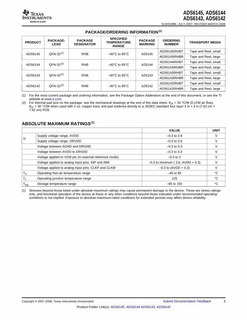
ABSOLUTE MAXIMUM RATINGS (1)
ADS6145, ADS6144ADS6143, ADS6142
SLWS198B–JULY 2007–REVISED MARCH 2008
PACKAGE/ORDERING INFORMATION (1)
SPECIFIEDPACKAGE- PACKAGE PACKAGE ORDERINGPRODUCT TEMPERATURE TRANSPORT MEDIALEAD DESIGNATOR MARKING NUMBERRANGEADS6145IRHBT Tape and Reel, small
ADS6145 QFN-32 (2) RHB –40°C to 85°C AZ6145ADS6145IRHBR Tape and Reel, largeADS6144IRHBT Tape and Reel, small
ADS6144 QFN-32 (2) RHB –40°C to 85°C AZ6144ADS6144IRHBR Tape and Reel, largeADS6143IRHBT Tape and Reel, small
ADS6143 QFN-32 (2) RHB –40°C to 85°C AZ6143ADS6143IRHBR Tape and Reel, largeADS6142IRHBT Tape and Reel, small
ADS6142 QFN-32 (2) RHB –40°C to 85°C AZ6142ADS6142IRHBR Tape and Reel, large
(1) For the most current package and ordering information, see the Package Option Addendum at the end of this document, or see the TIwebsite at www.ti.com.
(2) For thermal pad size on the package, see the mechanical drawings at the end of this data sheet. θJA = 34 °C/W (0 LFM air flow),θJC = 30 °C/W when used with 2 oz. copper trace and pad soldered directly to a JEDEC standard four layer 3 in × 3 in (7.62 cm ×7.62 cm) PCB.
VALUE UNITSupply voltage range, AVDD –0.3 to 3.9 V
VI Supply voltage range, DRVDD –0.3 to 3.9 VVoltage between AGND and DRGND –0.3 to 0.3 VVoltage between AVDD to DRVDD –0.3 to 3.3 VVoltage applied to VCM pin (in external reference mode) –0.3 to 2 VVoltage applied to analog input pins, INP and INM –0.3 to minimum ( 3.6, AVDD + 0.3) VVoltage applied to analog input pins, CLKP and CLKM –0.3 to (AVDD + 0.3) V
TA Operating free-air temperature range –40 to 85 °CTJ Operating junction temperature range 125 °CTstg Storage temperature range –65 to 150 °C
(1) Stresses beyond those listed under absolute maximum ratings may cause permanent damage to the device. These are stress ratingsonly, and functional operation of the device at these or any other conditions beyond those indicated under recommended operatingconditions is not implied. Exposure to absolute-maximum-rated conditions for extended periods may affect device reliability.
Copyright © 2007–2008, Texas Instruments Incorporated Submit Documentation Feedback 3
Product Folder Link(s): ADS6145, ADS6144 ADS6143, ADS6142
www.ti.com
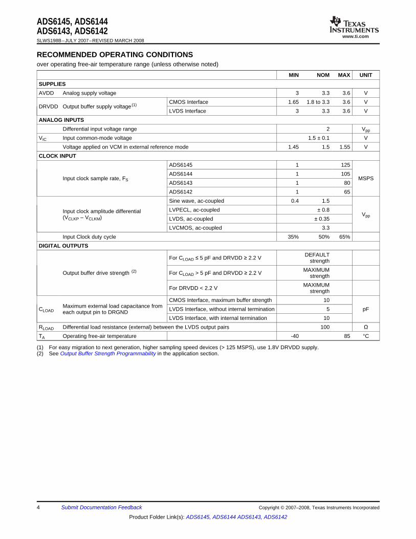
RECOMMENDED OPERATING CONDITIONS
ADS6145, ADS6144ADS6143, ADS6142SLWS198B–JULY 2007–REVISED MARCH 2008
over operating free-air temperature range (unless otherwise noted)
MIN NOM MAX UNITSUPPLIESAVDD Analog supply voltage 3 3.3 3.6 V
CMOS Interface 1.65 1.8 to 3.3 3.6 VDRVDD Output buffer supply voltage (1)
LVDS Interface 3 3.3 3.6 VANALOG INPUTS
Differential input voltage range 2 Vpp
VIC Input common-mode voltage 1.5 ± 0.1 VVoltage applied on VCM in external reference mode 1.45 1.5 1.55 V
CLOCK INPUTADS6145 1 125ADS6144 1 105
Input clock sample rate, FS MSPSADS6143 1 80ADS6142 1 65Sine wave, ac-coupled 0.4 1.5LVPECL, ac-coupled ± 0.8Input clock amplitude differential Vpp(VCLKP – VCLKM) LVDS, ac-coupled ± 0.35LVCMOS, ac-coupled 3.3
Input Clock duty cycle 35% 50% 65%DIGITAL OUTPUTS
DEFAULTFor CLOAD ≤ 5 pF and DRVDD ≥ 2.2 V strengthMAXIMUMOutput buffer drive strength (2) For CLOAD > 5 pF and DRVDD ≥ 2.2 V strengthMAXIMUMFor DRVDD < 2.2 V strength
CMOS Interface, maximum buffer strength 10Maximum external load capacitance fromCLOAD LVDS Interface, without internal termination 5 pFeach output pin to DRGND
LVDS Interface, with internal termination 10RLOAD Differential load resistance (external) between the LVDS output pairs 100 ΩTA Operating free-air temperature -40 85 °C
(1) For easy migration to next generation, higher sampling speed devices (> 125 MSPS), use 1.8V DRVDD supply.(2) See Output Buffer Strength Programmability in the application section.
4 Submit Documentation Feedback Copyright © 2007–2008, Texas Instruments Incorporated
Product Folder Link(s): ADS6145, ADS6144 ADS6143, ADS6142
www.ti.com
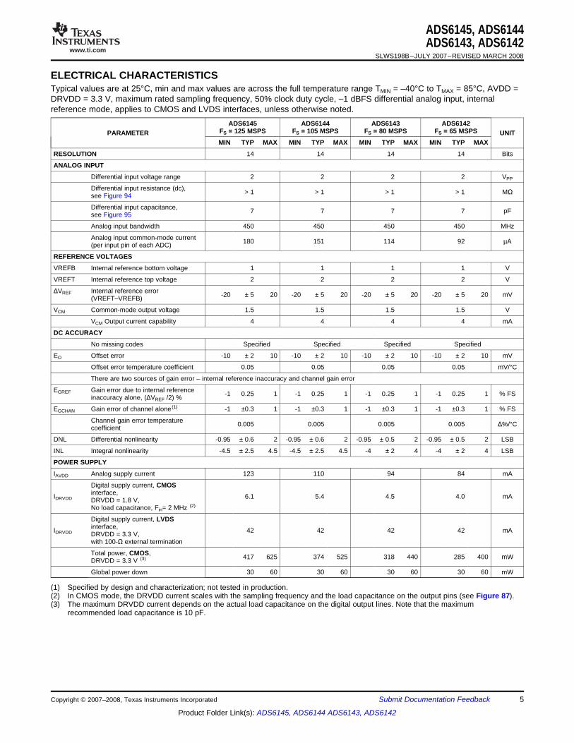
ELECTRICAL CHARACTERISTICS
ADS6145, ADS6144ADS6143, ADS6142
SLWS198B–JULY 2007–REVISED MARCH 2008
Typical values are at 25°C, min and max values are across the full temperature range TMIN = –40°C to TMAX = 85°C, AVDD =DRVDD = 3.3 V, maximum rated sampling frequency, 50% clock duty cycle, –1 dBFS differential analog input, internalreference mode, applies to CMOS and LVDS interfaces, unless otherwise noted.
ADS6145 ADS6144 ADS6143 ADS6142FS = 125 MSPS FS = 105 MSPS FS = 80 MSPS FS = 65 MSPSPARAMETER UNITMIN TYP MAX MIN TYP MAX MIN TYP MAX MIN TYP MAX
RESOLUTION 14 14 14 14 Bits
ANALOG INPUT
Differential input voltage range 2 2 2 2 VPP
Differential input resistance (dc), > 1 > 1 > 1 > 1 MΩsee Figure 94
Differential input capacitance, 7 7 7 7 pFsee Figure 95
Analog input bandwidth 450 450 450 450 MHz
Analog input common-mode current 180 151 114 92 µA(per input pin of each ADC)
REFERENCE VOLTAGES
VREFB Internal reference bottom voltage 1 1 1 1 V
VREFT Internal reference top voltage 2 2 2 2 V
ΔVREF Internal reference error -20 ± 5 20 -20 ± 5 20 -20 ± 5 20 -20 ± 5 20 mV(VREFT–VREFB)
VCM Common-mode output voltage 1.5 1.5 1.5 1.5 V
VCM Output current capability 4 4 4 4 mA
DC ACCURACY
No missing codes Specified Specified Specified Specified
EO Offset error -10 ± 2 10 -10 ± 2 10 -10 ± 2 10 -10 ± 2 10 mV
Offset error temperature coefficient 0.05 0.05 0.05 0.05 mV/°C
There are two sources of gain error – internal reference inaccuracy and channel gain error
EGREF Gain error due to internal reference -1 0.25 1 -1 0.25 1 -1 0.25 1 -1 0.25 1 % FSinaccuracy alone, (ΔVREF /2) %
EGCHAN Gain error of channel alone (1) -1 ±0.3 1 -1 ±0.3 1 -1 ±0.3 1 -1 ±0.3 1 % FS
Channel gain error temperature 0.005 0.005 0.005 0.005 Δ%/°Ccoefficient
DNL Differential nonlinearity -0.95 ± 0.6 2 -0.95 ± 0.6 2 -0.95 ± 0.5 2 -0.95 ± 0.5 2 LSB
INL Integral nonlinearity -4.5 ± 2.5 4.5 -4.5 ± 2.5 4.5 -4 ± 2 4 -4 ± 2 4 LSB
POWER SUPPLY
IAVDD Analog supply current 123 110 94 84 mA
Digital supply current, CMOSinterface,IDRVDD 6.1 5.4 4.5 4.0 mADRVDD = 1.8 V,No load capacitance, Fin= 2 MHz (2)
Digital supply current, LVDSinterface,IDRVDD 42 42 42 42 mADRVDD = 3.3 V,with 100-Ω external termination
Total power, CMOS, 417 625 374 525 318 440 285 400 mWDRVDD = 3.3 V (3)
Global power down 30 60 30 60 30 60 30 60 mW
(1) Specified by design and characterization; not tested in production.(2) In CMOS mode, the DRVDD current scales with the sampling frequency and the load capacitance on the output pins (see Figure 87).(3) The maximum DRVDD current depends on the actual load capacitance on the digital output lines. Note that the maximum
recommended load capacitance is 10 pF.
Copyright © 2007–2008, Texas Instruments Incorporated Submit Documentation Feedback 5
Product Folder Link(s): ADS6145, ADS6144 ADS6143, ADS6142
www.ti.com
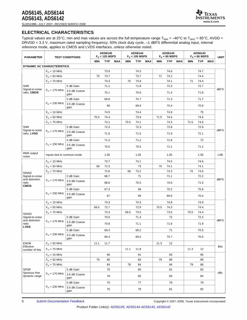
ELECTRICAL CHARACTERISTICS
ADS6145, ADS6144ADS6143, ADS6142SLWS198B–JULY 2007–REVISED MARCH 2008
Typical values are at 25°C, min and max values are across the full temperature range TMIN = –40°C to TMAX = 85°C, AVDD =DRVDD = 3.3 V, maximum rated sampling frequency, 50% clock duty cycle, –1 dBFS differential analog input, internalreference mode, applies to CMOS and LVDS interfaces, unless otherwise noted.
ADS6145 ADS6144 ADS6143 ADS6142FS = 125 MSPS FS = 105 MSPS FS = 80 MSPS FS = 65 MSPSPARAMETER TEST CONDITIONS UNIT
MIN TYP MAX MIN TYP MAX MIN TYP MAX MIN TYP MAX
DYNAMIC AC CHARACTERISTICS
Fin = 10 MHz 73.9 74.3 74.6 74.7
Fin = 50 MHz 70 73.7 73.7 71 74.2 74.4
Fin = 70 MHz 73.3 70 73.9 74.1 71 74.4
SNR 0 dB Gain 71.1 71.8 72.3 72.7Signal-to-noise dBFSFin = 170 MHz 3.5 dB Coarseratio, CMOS 70.1 70.9 71.4 71.8gain
0 dB Gain 69.8 70.7 71.3 71.7Fin = 230 MHz 3.5 dB Coarse 69 69.9 70.4 70.9gain
Fin = 10 MHz 74.5 74.4 74.9 75
Fin = 50 MHz 70.5 74.4 73.9 71.5 74.4 74.6
Fin = 70 MHz 74.1 70.5 74.1 74.3 71.5 74.6
SNR 0 dB Gain 72.3 72.3 72.8 72.9Signal-to-noise dBFSFin = 170 MHz 3.5 dB Coarseratio, LVDS 71.5 71.5 71.9 72.1gain
0 dB Gain 71.2 71.2 71.8 72Fin = 230 MHz 3.5 dB Coarse 70.5 70.5 71.1 71.2gain
RMS output Inputs tied to common-mode 1.05 1.05 1.05 1.05 LSBnoise
Fin = 10 MHz 73.7 74.1 74.5 74.6
Fin = 50 MHz 69 72.3 73 70 74.1 74.1
Fin = 70 MHz 72.6 69 73.2 73.3 70 74.0SINADSignal-to-noise 0 dB Gain 68.7 71 71.1 72.2and distortion dBFSFin = 170 MHz 3.5 dB Coarseratio 68.6 70.5 70.6 71.5gainCMOS
0 dB Gain 67.3 69 70.2 70.6Fin = 230 MHz 3.5 dB Coarse 67 69 69.9 70.4gain
Fin = 10 MHz 74.3 74.3 74.8 74.9
Fin = 50 MHz 69.5 72.7 72.9 70.5 74.3 74.4
Fin = 70 MHz 73.4 69.5 73.5 73.6 70.5 74.4SINADSignal-to-noise 0 dB Gain 70.6 71.4 72 72.4and distortion dBFSFin = 170 MHz 3.5 dB Coarseratio 70.8 71.1 71.6 71.9gainLVDS
0 dB Gain 69.4 69.2 71 70.5Fin = 230 MHz 3.5 dB Coarse 69.4 69.4 70.7 70.5gain
ENOB Fin = 50 MHz 11.1 11.7 11.3 12Effective Bits
Fin = 70 MHz 11.1 11.8 11.3 12number of bits
Fin = 10 MHz 90 91 93 95
Fin = 50 MHz 76 80 83 79 89 89
Fin = 70 MHz 84 78 84 84 79 86
SFDR 0 dB Gain 76 80 81 82Spurious free dBcFin = 170 MHz 3.5 dB Coarsedynamic range 78 82 83 84gain
0 dB Gain 75 77 79 79Fin = 230 MHz 3.5 dB Coarse 76 79 81 82gain
6 Submit Documentation Feedback Copyright © 2007–2008, Texas Instruments Incorporated
Product Folder Link(s): ADS6145, ADS6144 ADS6143, ADS6142
www.ti.com
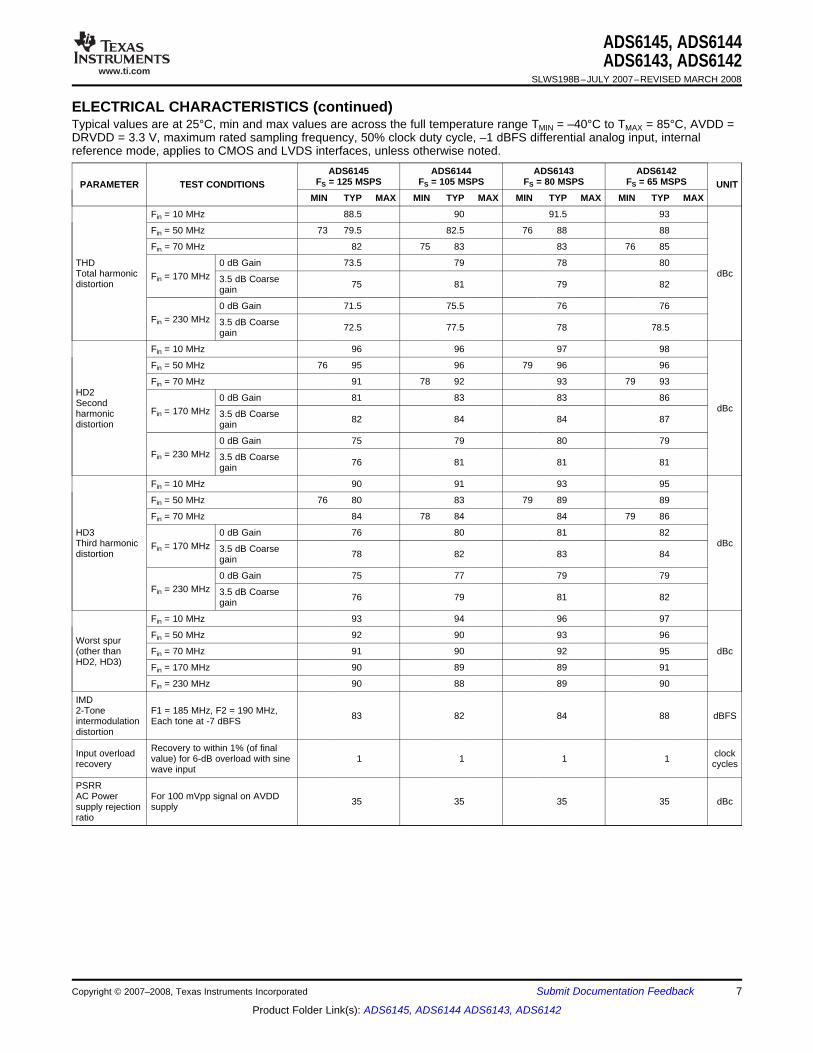
ADS6145, ADS6144ADS6143, ADS6142
SLWS198B–JULY 2007–REVISED MARCH 2008
ELECTRICAL CHARACTERISTICS (continued)Typical values are at 25°C, min and max values are across the full temperature range TMIN = –40°C to TMAX = 85°C, AVDD =DRVDD = 3.3 V, maximum rated sampling frequency, 50% clock duty cycle, –1 dBFS differential analog input, internalreference mode, applies to CMOS and LVDS interfaces, unless otherwise noted.
ADS6145 ADS6144 ADS6143 ADS6142FS = 125 MSPS FS = 105 MSPS FS = 80 MSPS FS = 65 MSPSPARAMETER TEST CONDITIONS UNIT
MIN TYP MAX MIN TYP MAX MIN TYP MAX MIN TYP MAX
Fin = 10 MHz 88.5 90 91.5 93
Fin = 50 MHz 73 79.5 82.5 76 88 88
Fin = 70 MHz 82 75 83 83 76 85
THD 0 dB Gain 73.5 79 78 80Total harmonic dBcFin = 170 MHz 3.5 dB Coarsedistortion 75 81 79 82gain
0 dB Gain 71.5 75.5 76 76Fin = 230 MHz 3.5 dB Coarse 72.5 77.5 78 78.5gain
Fin = 10 MHz 96 96 97 98
Fin = 50 MHz 76 95 96 79 96 96
Fin = 70 MHz 91 78 92 93 79 93HD2 0 dB Gain 81 83 83 86Second dBcFin = 170 MHzharmonic 3.5 dB Coarse 82 84 84 87distortion gain
0 dB Gain 75 79 80 79Fin = 230 MHz 3.5 dB Coarse 76 81 81 81gain
Fin = 10 MHz 90 91 93 95
Fin = 50 MHz 76 80 83 79 89 89
Fin = 70 MHz 84 78 84 84 79 86
HD3 0 dB Gain 76 80 81 82Third harmonic dBcFin = 170 MHz 3.5 dB Coarsedistortion 78 82 83 84gain
0 dB Gain 75 77 79 79Fin = 230 MHz 3.5 dB Coarse 76 79 81 82gain
Fin = 10 MHz 93 94 96 97
Fin = 50 MHz 92 90 93 96Worst spur(other than Fin = 70 MHz 91 90 92 95 dBcHD2, HD3) Fin = 170 MHz 90 89 89 91
Fin = 230 MHz 90 88 89 90
IMD2-Tone F1 = 185 MHz, F2 = 190 MHz, 83 82 84 88 dBFSintermodulation Each tone at -7 dBFSdistortion
Recovery to within 1% (of finalInput overload clockvalue) for 6-dB overload with sine 1 1 1 1recovery cycleswave input
PSRRAC Power For 100 mVpp signal on AVDD 35 35 35 35 dBcsupply rejection supplyratio
Copyright © 2007–2008, Texas Instruments Incorporated Submit Documentation Feedback 7
Product Folder Link(s): ADS6145, ADS6144 ADS6143, ADS6142
www.ti.com
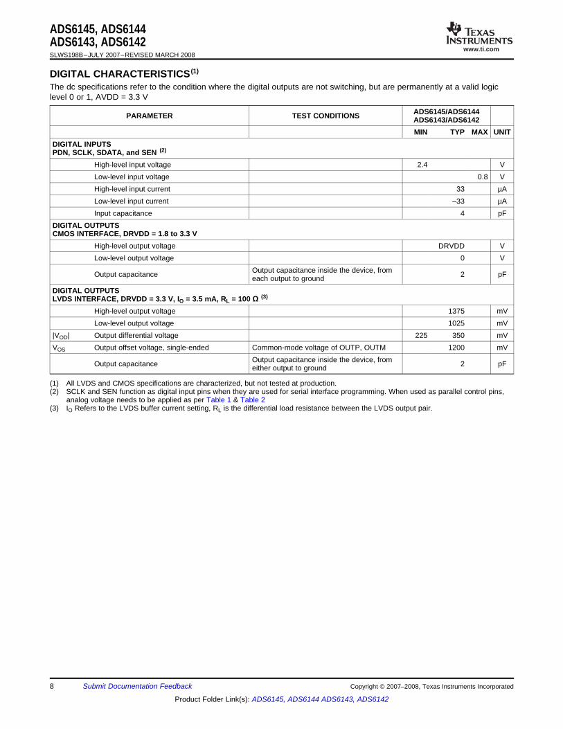
DIGITAL CHARACTERISTICS (1)
ADS6145, ADS6144ADS6143, ADS6142SLWS198B–JULY 2007–REVISED MARCH 2008
The dc specifications refer to the condition where the digital outputs are not switching, but are permanently at a valid logiclevel 0 or 1, AVDD = 3.3 V
ADS6145/ADS6144PARAMETER TEST CONDITIONS ADS6143/ADS6142MIN TYP MAX UNIT
DIGITAL INPUTSPDN, SCLK, SDATA, and SEN (2)
High-level input voltage 2.4 VLow-level input voltage 0.8 VHigh-level input current 33 µALow-level input current –33 µAInput capacitance 4 pF
DIGITAL OUTPUTSCMOS INTERFACE, DRVDD = 1.8 to 3.3 V
High-level output voltage DRVDD VLow-level output voltage 0 V
Output capacitance inside the device, fromOutput capacitance 2 pFeach output to groundDIGITAL OUTPUTSLVDS INTERFACE, DRVDD = 3.3 V, IO = 3.5 mA, RL = 100 Ω (3)
High-level output voltage 1375 mVLow-level output voltage 1025 mV
|VOD| Output differential voltage 225 350 mVVOS Output offset voltage, single-ended Common-mode voltage of OUTP, OUTM 1200 mV
Output capacitance inside the device, fromOutput capacitance 2 pFeither output to ground
(1) All LVDS and CMOS specifications are characterized, but not tested at production.(2) SCLK and SEN function as digital input pins when they are used for serial interface programming. When used as parallel control pins,
analog voltage needs to be applied as per Table 1 & Table 2(3) IO Refers to the LVDS buffer current setting, RL is the differential load resistance between the LVDS output pair.
8 Submit Documentation Feedback Copyright © 2007–2008, Texas Instruments Incorporated
Product Folder Link(s): ADS6145, ADS6144 ADS6143, ADS6142

www.ti.com
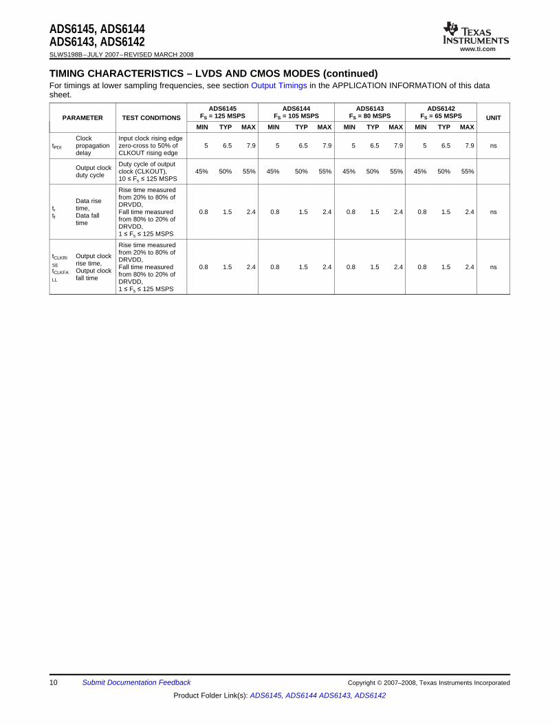
TIMING CHARACTERISTICS – LVDS AND CMOS MODES (1)
ADS6145, ADS6144ADS6143, ADS6142
SLWS198B–JULY 2007–REVISED MARCH 2008
Typical values are at 25°C, min and max values are across the full temperature range TMIN = –40°C to TMAX = 85°C, AVDD =DRVDD = 3.3 V, maximum rated sampling frequency, sine wave input clock, 1.5 VPP clock amplitude, CL = 5 pF (2), IO = 3.5mA, RL = 100 Ω (3), no internal termination, unless otherwise noted.For timings at lower sampling frequencies, see section Output Timings in the APPLICATION INFORMATION of this datasheet.
ADS6145 ADS6144 ADS6143 ADS6142FS = 125 MSPS FS = 105 MSPS FS = 80 MSPS FS = 65 MSPSPARAMETER TEST CONDITIONS UNIT
MIN TYP MAX MIN TYP MAX MIN TYP MAX MIN TYP MAX
Apertureta 0.7 1.5 2.5 0.7 1.5 2.5 0.7 1.5 2.5 0.7 1.5 2.5 nsdelay
Aperturetj 150 150 150 150 fs rmsjitter
From global power 15 50 15 50 15 50 15 50 µsdownWake-uptime From standby 15 50 15 50 15 50 15 50 µs(to valid From output CMOS 100 200 100 200 100 200 100 200 nsdata) buffer
LVDS 200 500 200 500 200 500 200 500 nsdisable
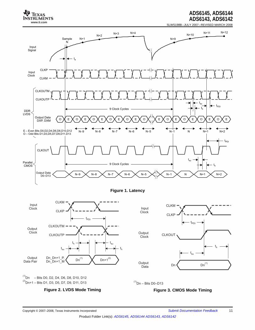
clockLatency 9 9 9 9 cycles
DDR LVDS MODE (4), DRVDD = 3.3 V
Data valid (6) toData setuptsu zero-cross of 1.7 2.3 2.5 3.1 3.9 4.5 5.4 6.0 nstime (5)CLKOUTP
Zero-cross ofData holdth CLKOUTP to data 0.7 1.7 0.7 1.7 0.7 1.7 0.7 1.7 nstime (5)becoming invalid (6)
Input clock rising edgeClock zero-cross to outputtPDI propagation 4.3 5.8 7.3 4.3 5.8 7.3 4.3 5.8 7.3 4.3 5.8 7.3 nsclock rising edgedelay zero-cross
Duty cycle ofLVDS bit differential clock,clock duty (CLKOUTP- 40% 47% 55% 40% 47% 55% 40% 47% 55% 40% 47% 55%cycle CLKOUTM),
10 ≤ Fs ≤ 125 MSPS
Rise time measuredfrom –50 mV to 50Data rise mV,tr time, Fall time measured 70 100 170 70 100 170 70 100 170 70 100 170 pstf Data fall from 50 mV to –50time mV,1 ≤ Fs ≤ 125 MSPS
Rise time measuredfrom –50 mV to 50tCLKRI Output clock mV,
SE rise time, Fall time measured 70 100 170 70 100 170 70 100 170 70 100 170 pstCLKFA Output clock from 50 mV to –50LL fall time mV,
1 ≤ Fs ≤ 125 MSPS
PARALLEL CMOS MODE, DRVDD = 2.5 V to 3.3 V, default output buffer drive strength (7)
Data setup Data valid (8) to 50% oftsu 2.9 4.4 3.6 5.1 5.1 6.6 6.5 8.0 nstime (5) CLKOUT rising edge
50% of CLKOUT risingData holdth edge to data becoming 1.3 2.7 2.1 3.5 3.6 5.0 5.1 6.5 nstime (5)invalid (8)
(1) Timing parameters are specified by design and characterization and not tested in production.(2) CL is the Effective external single-ended load capacitance between each output pin and ground.(3) IO Refers to the LVDS buffer current setting; RL is the differential load resistance between the LVDS output pair.(4) Measurements are done with a transmission line of 100 Ω characteristic impedance between the device and the load.(5) Setup and hold time specifications take into account the effect of jitter on the output data and clock.(6) Data valid refers to a logic high of +100 mV and logic low of –100 mV.(7) For DRVDD < 2.2 V, it is recommended to use an external clock for data capture and NOT the device output clock signal (CLKOUT).
See Parallel CMOS interface in the application section.(8) Data valid refers to a logic high of 2 V (1.7 V) and logic low of 0.8 V (0.7 V) for DRVDD = 3.3 V (2.5 V).
Copyright © 2007–2008, Texas Instruments Incorporated Submit Documentation Feedback 9
Product Folder Link(s): ADS6145, ADS6144 ADS6143, ADS6142
www.ti.com
ADS6145, ADS6144ADS6143, ADS6142SLWS198B–JULY 2007–REVISED MARCH 2008
TIMING CHARACTERISTICS – LVDS AND CMOS MODES (continued)For timings at lower sampling frequencies, see section Output Timings in the APPLICATION INFORMATION of this datasheet.
ADS6145 ADS6144 ADS6143 ADS6142FS = 125 MSPS FS = 105 MSPS FS = 80 MSPS FS = 65 MSPSPARAMETER TEST CONDITIONS UNIT
MIN TYP MAX MIN TYP MAX MIN TYP MAX MIN TYP MAX
Clock Input clock rising edgetPDI propagation zero-cross to 50% of 5 6.5 7.9 5 6.5 7.9 5 6.5 7.9 5 6.5 7.9 ns
delay CLKOUT rising edge
Duty cycle of outputOutput clock clock (CLKOUT), 45% 50% 55% 45% 50% 55% 45% 50% 55% 45% 50% 55%duty cycle 10 ≤ Fs ≤ 125 MSPS
Rise time measuredfrom 20% to 80% ofData rise DRVDD,tr time, Fall time measured 0.8 1.5 2.4 0.8 1.5 2.4 0.8 1.5 2.4 0.8 1.5 2.4 nstf Data fall from 80% to 20% oftime DRVDD,1 ≤ Fs ≤ 125 MSPS
Rise time measuredfrom 20% to 80% oftCLKRI Output clock DRVDD,
SE rise time, Fall time measured 0.8 1.5 2.4 0.8 1.5 2.4 0.8 1.5 2.4 0.8 1.5 2.4 nstCLKFA Output clock from 80% to 20% ofLL fall time DRVDD,
1 ≤ Fs ≤ 125 MSPS
10 Submit Documentation Feedback Copyright © 2007–2008, Texas Instruments Incorporated
Product Folder Link(s): ADS6145, ADS6144 ADS6143, ADS6142
www.ti.com
O O O O O O O OO OE E E E E E E EE E
InputClock
CLKOUTM
CLKOUTP
Output DataDXP, DXM
DDRLVDS
N–9 N–8 N–7 N–6 N–5 N–1 N N+1 N+2
N–9 N–8 N–7 N–6 N–5 N N+2
9 Clock Cycles
9 Clock Cycles
CLKOUT
Output DataD0–D13
ParallelCMOS
InputSignal
SampleN
N+1N+2
N+3 N+4
th
tPDI
ta
tsu
thtPDI
CLKP
CLKM
N+9
N+10N+11 N+12
tsu
E – Even Bits D0,D2,D4,D6,D8,D10,D12O – Odd Bits D1,D3,D5,D7,D9,D11,D13
N+1N–1
InputClock
OutputClock
OutputData Pair
CLKM
CLKOUTP
Dn_Dn+1_P,Dn_Dn+1_M
CLKP
tPDI
tsu th
th tsu
CLKOUTM
(1)Dn – Bits D0, D2, D4, D6, D8, D10, D12
(2)Dn+1 – Bits D1, D3, D5, D7, D9, D11, D13
Dn(1)
Dn+1(2)
InputClock
OutputClock
OutputData
CLKM
Dn
CLKP
tPDI
tsu
th
CLKOUT
(1)Dn – Bits D0–D13
Dn(1)
ADS6145, ADS6144ADS6143, ADS6142
SLWS198B–JULY 2007–REVISED MARCH 2008
Figure 1. Latency
Figure 2. LVDS Mode Timing Figure 3. CMOS Mode Timing
Copyright © 2007–2008, Texas Instruments Incorporated Submit Documentation Feedback 11
Product Folder Link(s): ADS6145, ADS6144 ADS6143, ADS6142
www.ti.com
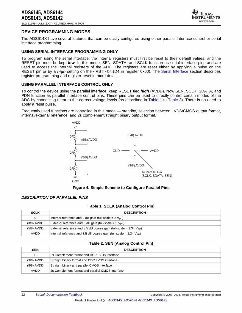
DEVICE PROGRAMMING MODES
USING SERIAL INTERFACE PROGRAMMING ONLY
USING PARALLEL INTERFACE CONTROL ONLY
(3/8) AVDD
(3/8) AVDD
To Parallel Pin(SCLK, SDATA, SEN)
3R
AVDD
AVDDGND
3R
2R
(5/8) AVDD
(5/8) AVDD
GND
ADS6145, ADS6144ADS6143, ADS6142SLWS198B–JULY 2007–REVISED MARCH 2008
The ADS614X have several features that can be easily configured using either parallel interface control or serialinterface programming.
To program using the serial interface, the internal registers must first be reset to their default values, and theRESET pin must be kept low. In this mode, SEN, SDATA, and SCLK function as serial interface pins and areused to access the internal registers of the ADC. The registers are reset either by applying a pulse on theRESET pin or by a high setting on the <RST> bit (D4 in register 0x00). The Serial Interface section describesregister programming and register reset in more detail.
To control the device using the parallel interface, keep RESET tied high (AVDD). Now SEN, SCLK, SDATA, andPDN function as parallel interface control pins. These pins can be used to directly control certain modes of theADC by connecting them to the correct voltage levels (as described in Table 1 to Table 3). There is no need toapply a reset pulse.
Frequently used functions are controlled in this mode — standby, selection between LVDS/CMOS output format,internal/external reference, and 2s complement/straight binary output format.
Figure 4. Simple Scheme to Configure Parallel Pins
DESCRIPTION OF PARALLEL PINS
Table 1. SCLK (Analog Control Pin)SCLK DESCRIPTION
0 Internal reference and 0 dB gain (full-scale = 2 VPP)(3/8) AVDD External reference and 0 dB gain (full-scale = 2 VPP)(5/8) AVDD External reference and 3.5 dB coarse gain (full-scale = 1.34 VPP)
AVDD Internal reference and 3.5 dB coarse gain (full-scale = 1.34 VPP)
Table 2. SEN (Analog Control Pin)SEN DESCRIPTION
0 2s Complement format and DDR LVDS interface(3/8) AVDD Straight binary format and DDR LVDS interface(5/8) AVDD Straight binary and parallel CMOS interface
AVDD 2s Complement format and parallel CMOS interface
12 Submit Documentation Feedback Copyright © 2007–2008, Texas Instruments Incorporated
Product Folder Link(s): ADS6145, ADS6144 ADS6143, ADS6142
www.ti.com
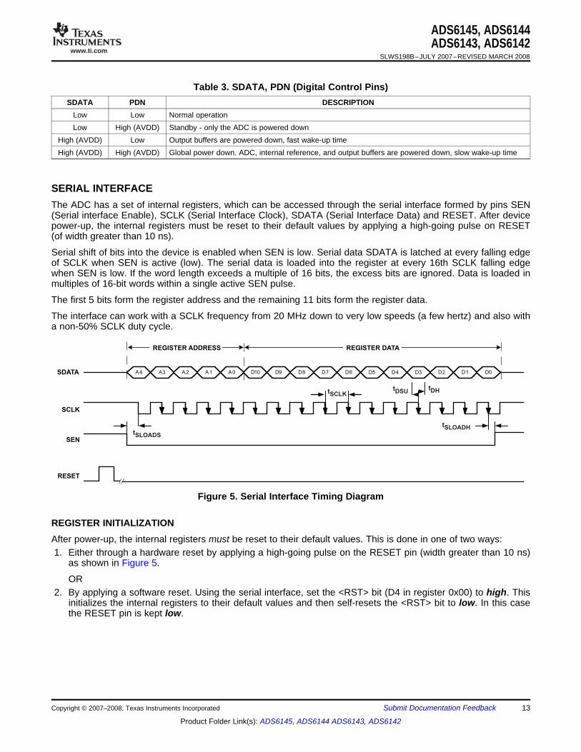
SERIAL INTERFACE
SCLK
SEN
A4 A3 A2 A1 A0 D10 D9 D8 D7 D6 D5 D4 D3 D2 D1 D0
REGISTER ADDRESS REGISTER DATA
SDATA
RESET
tSCLK
tDSU
tDH
tSLOADS
tSLOADH
REGISTER INITIALIZATION
ADS6145, ADS6144ADS6143, ADS6142
SLWS198B–JULY 2007–REVISED MARCH 2008
Table 3. SDATA, PDN (Digital Control Pins)SDATA PDN DESCRIPTION
Low Low Normal operationLow High (AVDD) Standby - only the ADC is powered down
High (AVDD) Low Output buffers are powered down, fast wake-up timeHigh (AVDD) High (AVDD) Global power down. ADC, internal reference, and output buffers are powered down, slow wake-up time
The ADC has a set of internal registers, which can be accessed through the serial interface formed by pins SEN(Serial interface Enable), SCLK (Serial Interface Clock), SDATA (Serial Interface Data) and RESET. After devicepower-up, the internal registers must be reset to their default values by applying a high-going pulse on RESET(of width greater than 10 ns).
Serial shift of bits into the device is enabled when SEN is low. Serial data SDATA is latched at every falling edgeof SCLK when SEN is active (low). The serial data is loaded into the register at every 16th SCLK falling edgewhen SEN is low. If the word length exceeds a multiple of 16 bits, the excess bits are ignored. Data is loaded inmultiples of 16-bit words within a single active SEN pulse.
The first 5 bits form the register address and the remaining 11 bits form the register data.
The interface can work with a SCLK frequency from 20 MHz down to very low speeds (a few hertz) and also witha non-50% SCLK duty cycle.
Figure 5. Serial Interface Timing Diagram
After power-up, the internal registers must be reset to their default values. This is done in one of two ways:1. Either through a hardware reset by applying a high-going pulse on the RESET pin (width greater than 10 ns)
as shown in Figure 5.
OR2. By applying a software reset. Using the serial interface, set the <RST> bit (D4 in register 0x00) to high. This
initializes the internal registers to their default values and then self-resets the <RST> bit to low. In this casethe RESET pin is kept low.
Copyright © 2007–2008, Texas Instruments Incorporated Submit Documentation Feedback 13
Product Folder Link(s): ADS6145, ADS6144 ADS6143, ADS6142
www.ti.com
SERIAL INTERFACE TIMING
RESET TIMING
t1
t3
t2
Power SupplyAVDD, DRVDD
RESET
SEN
ADS6145, ADS6144ADS6143, ADS6142SLWS198B–JULY 2007–REVISED MARCH 2008
Typical values at 25°C, min and max values across the full temperature range TMIN = –40°C to TMAX = 85°C,AVDD = DRVDD = 3.3 V (unless otherwise noted)
MIN TYP MAX UNITfSCLK SCLK Frequency = 1/tSCLK > DC 20 MHztSLOADS SEN to SCLK Setup time 25 nstSLOADH SCLK to SEN Hold time 25 nstDSU SDATA Setup time 25 nstDH SDATA Hold time 25 ns
Typical values at 25°C, min and max values across the full temperature range TMIN = –40°C to TMAX = 85°C,AVDD = DRVDD = 3.3 V (unless otherwise noted)
PARAMETER TEST CONDITIONS MIN TYP MAX UNITt1 Power-on delay Delay from power-up of AVDD and DRVDD to RESET pulse active 5 mst2 Reset pulse width Pulse width of active RESET signal 10 nst3 Register write delay Delay from RESET disable to SEN active 25 nstPO Power-up time Delay from power-up of AVDD and DRVDD to output stable 6.5 ms
NOTE: A high-going pulse on the RESET pin is required in serial interface mode in the case of initialization through ahardware reset. For parallel interface operation, RESET has to be tied permanently HIGH.
Figure 6. Reset Timing Diagram
14 Submit Documentation Feedback Copyright © 2007–2008, Texas Instruments Incorporated
Product Folder Link(s): ADS6145, ADS6144 ADS6143, ADS6142
www.ti.com
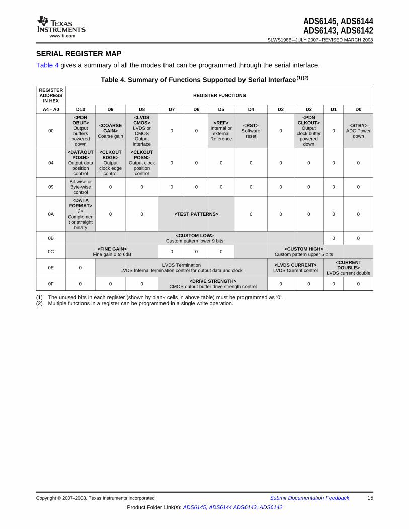
SERIAL REGISTER MAP
ADS6145, ADS6144ADS6143, ADS6142
SLWS198B–JULY 2007–REVISED MARCH 2008
Table 4 gives a summary of all the modes that can be programmed through the serial interface.
Table 4. Summary of Functions Supported by Serial Interface (1) (2)
REGISTERADDRESS REGISTER FUNCTIONS
IN HEX
A4 - A0 D10 D9 D8 D7 D6 D5 D4 D3 D2 D1 D0
<PDN <LVDS <PDNOBUF> CMOS> <REF> CLKOUT><COARSE <RST> <STBY>Output LVDS or Internal or Output00 GAIN> 0 0 Software 0 0 ADC Powerbuffers CMOS external clock bufferCoarse gain reset downpowered Output Reference powereddown interface down
<DATAOUT <CLKOUT <CLKOUTPOSN> EDGE> POSN>
04 Output data Output Output clock 0 0 0 0 0 0 0 0position clock edge positioncontrol control control
Bit-wise or09 Byte-wise 0 0 0 0 0 0 0 0 0 0
control
<DATAFORMAT>
2s0A 0 0 <TEST PATTERNS> 0 0 0 0 0Complement or straight
binary
<CUSTOM LOW>0B 0 0Custom pattern lower 9 bits
<FINE GAIN> <CUSTOM HIGH>0C 0 0 0Fine gain 0 to 6dB Custom pattern upper 5 bits
<CURRENTLVDS Termination <LVDS CURRENT>0E 0 DOUBLE>LVDS Internal termination control for output data and clock LVDS Current control LVDS current double
<DRIVE STRENGTH>0F 0 0 0 0 0 0 0CMOS output buffer drive strength control
(1) The unused bits in each register (shown by blank cells in above table) must be programmed as ‘0’.(2) Multiple functions in a register can be programmed in a single write operation.
Copyright © 2007–2008, Texas Instruments Incorporated Submit Documentation Feedback 15
Product Folder Link(s): ADS6145, ADS6144 ADS6143, ADS6142
www.ti.com
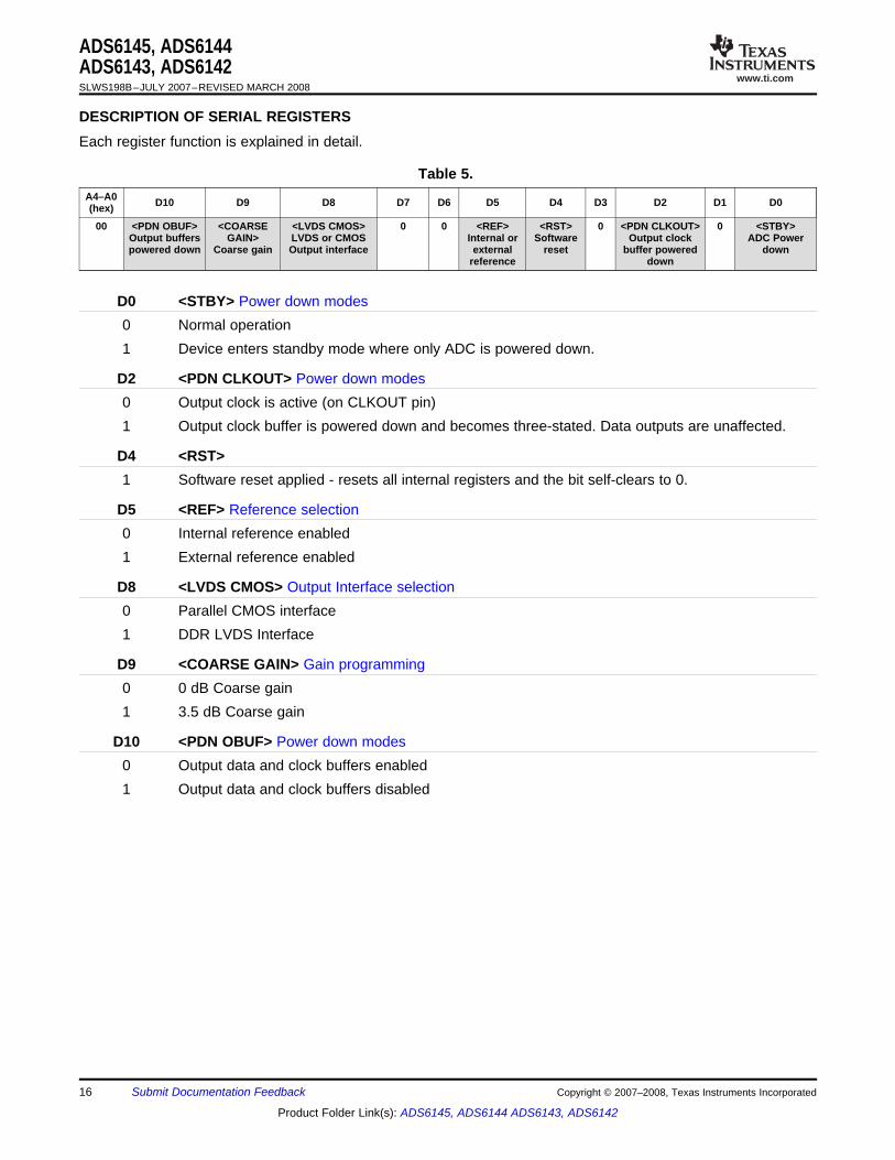
DESCRIPTION OF SERIAL REGISTERS
ADS6145, ADS6144ADS6143, ADS6142SLWS198B–JULY 2007–REVISED MARCH 2008
Each register function is explained in detail.
Table 5.A4–A0 D10 D9 D8 D7 D6 D5 D4 D3 D2 D1 D0(hex)
00 <PDN OBUF> <COARSE <LVDS CMOS> 0 0 <REF> <RST> 0 <PDN CLKOUT> 0 <STBY>Output buffers GAIN> LVDS or CMOS Internal or Software Output clock ADC Powerpowered down Coarse gain Output interface external reset buffer powered down
reference down
D0 <STBY> Power down modes0 Normal operation1 Device enters standby mode where only ADC is powered down.
D2 <PDN CLKOUT> Power down modes0 Output clock is active (on CLKOUT pin)1 Output clock buffer is powered down and becomes three-stated. Data outputs are unaffected.
D4 <RST>1 Software reset applied - resets all internal registers and the bit self-clears to 0.
D5 <REF> Reference selection0 Internal reference enabled1 External reference enabled
D8 <LVDS CMOS> Output Interface selection0 Parallel CMOS interface1 DDR LVDS Interface
D9 <COARSE GAIN> Gain programming0 0 dB Coarse gain1 3.5 dB Coarse gain
D10 <PDN OBUF> Power down modes0 Output data and clock buffers enabled1 Output data and clock buffers disabled
16 Submit Documentation Feedback Copyright © 2007–2008, Texas Instruments Incorporated
Product Folder Link(s): ADS6145, ADS6144 ADS6143, ADS6142

www.ti.com
ADS6145, ADS6144ADS6143, ADS6142
SLWS198B–JULY 2007–REVISED MARCH 2008
Table 6.A4–A0 D10 D9 D8 D7 D6 D5 D4 D3 D2 D1 D0(hex)
04 <DATAOUT POSN> <CLKOUT EDGE> <CLKOUT POSN> 0 0 0 0 0 0 0 0Output data position Output Clock edge Output clock
control control position control
D8 <CLKOUT POSN> Output clock position control0 Default output clock position after reset. The setup/hold timings for this clock position are specified
in the timing specifications table.1 Output clock shifted (delayed) by 400 ps
D9 <CLKOUT EDGE>0 Use rising edge to capture data1 Use falling edge to capture data
D10 <DATAOUT_POSN>0 Default position (after reset)1 Data transition delayed by half clock cycle with respect to default position
Table 7.A4–A0 D10 D9 D8 D7 D6 D5 D4 D3 D2 D1 D0(hex)
09 Bit-wise or 0 0 0 0 0 0 0 0 0 0Byte-wise control
D10 Bit-wise or byte-wise selection (DDR LVDS mode only)0 Bit-wise sequence - Even data bits (D0, D2, D4,..D12) are output at the rising edge of CLKOUTP
and odd data bits (D1, D3, D5,..D13) at the falling edge of CLKOUTP1 Byte-wise sequence - Lower 7 data bits (D0-D7) are output at the rising edge of CLKOUTP and
upper 7 data bits (D8-D13) at the falling edge of CLKOUTP
Copyright © 2007–2008, Texas Instruments Incorporated Submit Documentation Feedback 17
Product Folder Link(s): ADS6145, ADS6144 ADS6143, ADS6142
www.ti.com
ADS6145, ADS6144ADS6143, ADS6142SLWS198B–JULY 2007–REVISED MARCH 2008
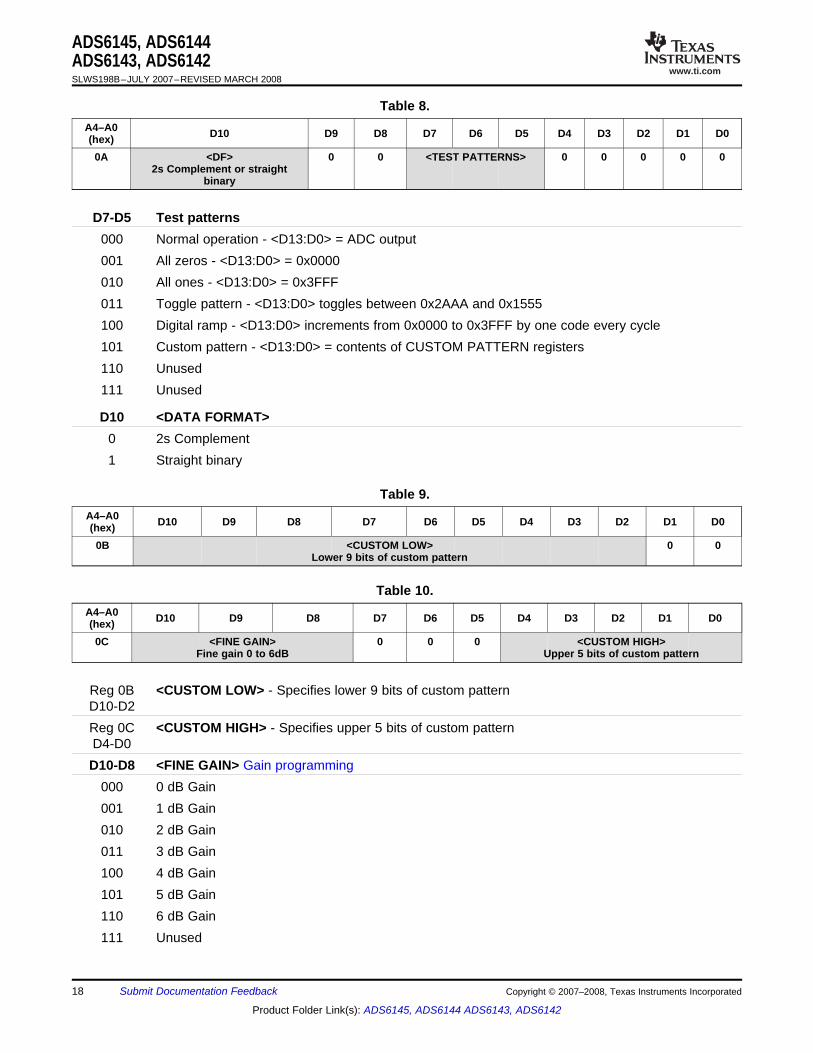
Table 8.A4–A0 D10 D9 D8 D7 D6 D5 D4 D3 D2 D1 D0(hex)
0A <DF> 0 0 <TEST PATTERNS> 0 0 0 0 02s Complement or straight
binary
D7-D5 Test patterns000 Normal operation - <D13:D0> = ADC output001 All zeros - <D13:D0> = 0x0000010 All ones - <D13:D0> = 0x3FFF011 Toggle pattern - <D13:D0> toggles between 0x2AAA and 0x1555100 Digital ramp - <D13:D0> increments from 0x0000 to 0x3FFF by one code every cycle101 Custom pattern - <D13:D0> = contents of CUSTOM PATTERN registers110 Unused111 Unused
D10 <DATA FORMAT>0 2s Complement1 Straight binary
Table 9.A4–A0 D10 D9 D8 D7 D6 D5 D4 D3 D2 D1 D0(hex)
0B <CUSTOM LOW> 0 0Lower 9 bits of custom pattern
Table 10.A4–A0 D10 D9 D8 D7 D6 D5 D4 D3 D2 D1 D0(hex)
0C <FINE GAIN> 0 0 0 <CUSTOM HIGH>Fine gain 0 to 6dB Upper 5 bits of custom pattern
Reg 0B <CUSTOM LOW> - Specifies lower 9 bits of custom patternD10-D2Reg 0C <CUSTOM HIGH> - Specifies upper 5 bits of custom patternD4-D0D10-D8 <FINE GAIN> Gain programming
000 0 dB Gain001 1 dB Gain010 2 dB Gain011 3 dB Gain100 4 dB Gain101 5 dB Gain110 6 dB Gain111 Unused
18 Submit Documentation Feedback Copyright © 2007–2008, Texas Instruments Incorporated
Product Folder Link(s): ADS6145, ADS6144 ADS6143, ADS6142
www.ti.com
ADS6145, ADS6144ADS6143, ADS6142
SLWS198B–JULY 2007–REVISED MARCH 2008
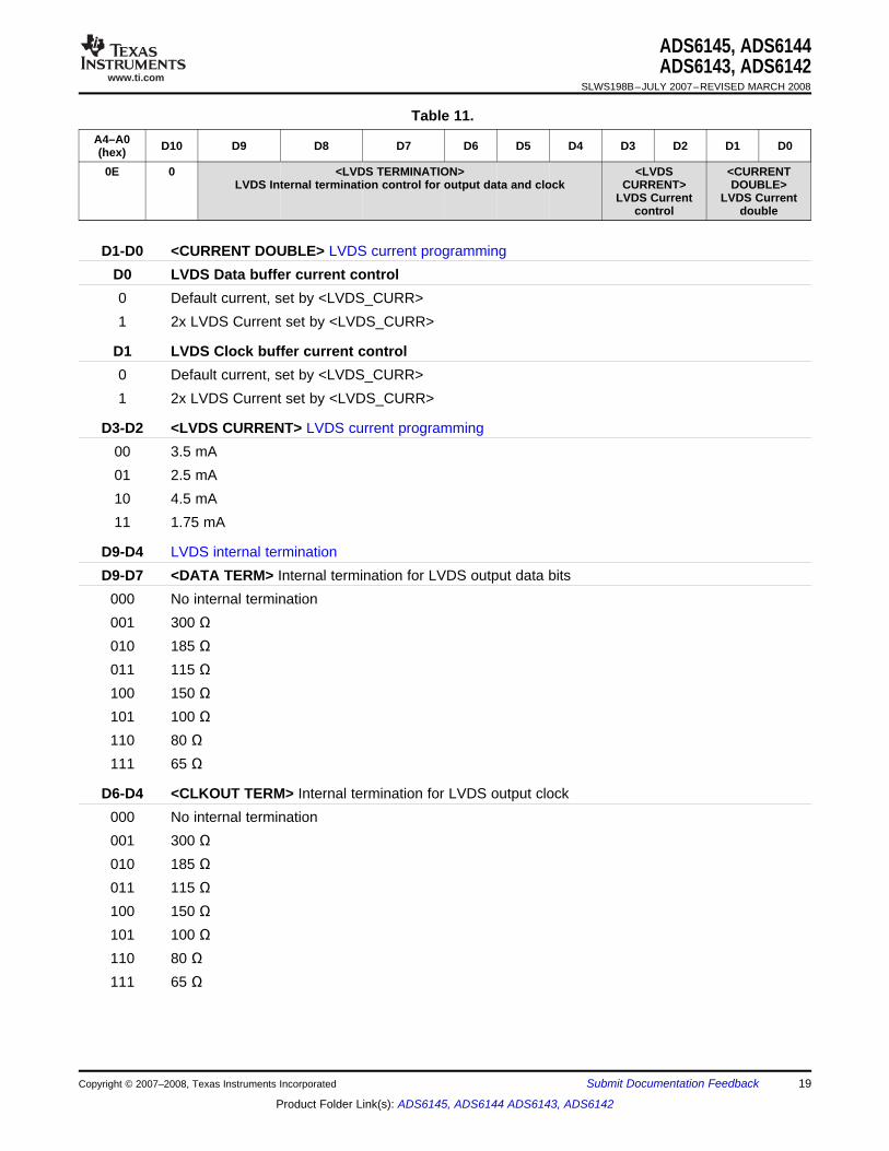
Table 11.A4–A0 D10 D9 D8 D7 D6 D5 D4 D3 D2 D1 D0(hex)
0E 0 <LVDS TERMINATION> <LVDS <CURRENTLVDS Internal termination control for output data and clock CURRENT> DOUBLE>
LVDS Current LVDS Currentcontrol double
D1-D0 <CURRENT DOUBLE> LVDS current programmingD0 LVDS Data buffer current control0 Default current, set by <LVDS_CURR>1 2x LVDS Current set by <LVDS_CURR>
D1 LVDS Clock buffer current control0 Default current, set by <LVDS_CURR>1 2x LVDS Current set by <LVDS_CURR>
D3-D2 <LVDS CURRENT> LVDS current programming00 3.5 mA01 2.5 mA10 4.5 mA11 1.75 mA
D9-D4 LVDS internal terminationD9-D7 <DATA TERM> Internal termination for LVDS output data bits
000 No internal termination001 300 Ω010 185 Ω011 115 Ω100 150 Ω101 100 Ω110 80 Ω111 65 Ω
D6-D4 <CLKOUT TERM> Internal termination for LVDS output clock000 No internal termination001 300 Ω010 185 Ω011 115 Ω100 150 Ω101 100 Ω110 80 Ω111 65 Ω
Copyright © 2007–2008, Texas Instruments Incorporated Submit Documentation Feedback 19
Product Folder Link(s): ADS6145, ADS6144 ADS6143, ADS6142
www.ti.com
ADS6145, ADS6144ADS6143, ADS6142SLWS198B–JULY 2007–REVISED MARCH 2008
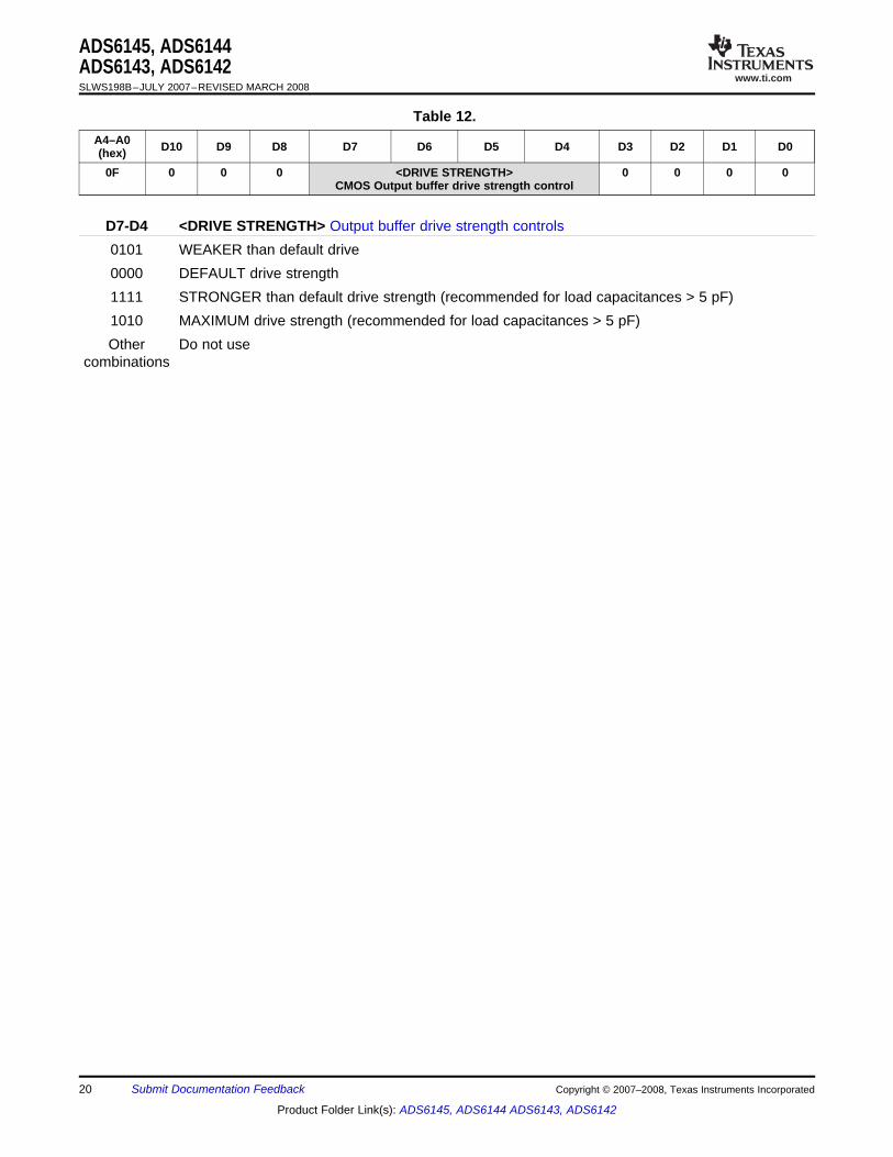
Table 12.A4–A0 D10 D9 D8 D7 D6 D5 D4 D3 D2 D1 D0(hex)
0F 0 0 0 <DRIVE STRENGTH> 0 0 0 0CMOS Output buffer drive strength control
D7-D4 <DRIVE STRENGTH> Output buffer drive strength controls0101 WEAKER than default drive0000 DEFAULT drive strength1111 STRONGER than default drive strength (recommended for load capacitances > 5 pF)1010 MAXIMUM drive strength (recommended for load capacitances > 5 pF)Other Do not use
combinations
20 Submit Documentation Feedback Copyright © 2007–2008, Texas Instruments Incorporated
Product Folder Link(s): ADS6145, ADS6144 ADS6143, ADS6142
www.ti.com
PIN CONFIGURATION (CMOS MODE)
PD
N
DRVDD
AG
ND
INP
OV
R
INM
CLK
OU
T
AG
ND
AV
DD
AV
DD
AGND
CLKP
CLKM
1
2
3
4
5
6
7
8
9 10
11
12
13
14
15
16
D13
D12
D1D
11
D0D
10
D9
D8
RESET
D7
SCLK
D6
SDATA
D5
SEN
D4
D3
D2
24
23
22
21
20
19
18
17
31
30
29
28
27
26
25
Pad Connected To
DRGND
32
VC
M
ADS6145, ADS6144ADS6143, ADS6142
SLWS198B–JULY 2007–REVISED MARCH 2008
RHB PACKAGE(TOP VIEW)
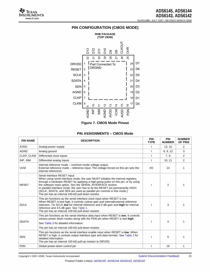
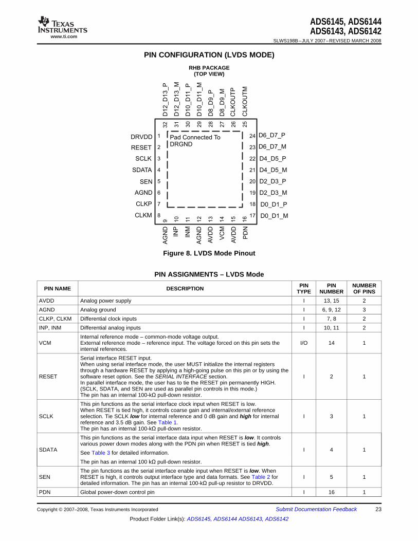
Figure 7. CMOS Mode Pinout
PIN ASSIGNMENTS – CMOS ModePIN PIN NUMBERPIN NAME DESCRIPTION TYPE NUMBER OF PINS
AVDD Analog power supply I 13, 15 2AGND Analog ground I 6, 9, 12 3CLKP, CLKM Differential clock inputs I 7, 8 2INP, INM Differential analog inputs I 10, 11 2
Internal reference mode – common-mode voltage output.VCM External reference mode – reference input. The voltage forced on this pin sets the I/O 14 1
internal references.Serial interface RESET input.When using serial interface mode, the user MUST initialize the internal registersthrough a hardware RESET by applying a high-going pulse on this pin, or by using
RESET the software reset option. See the SERIAL INTERFACE section. I 2 1In parallel interface mode, the user has to tie the RESET pin permanently HIGH.(SCLK, SDATA, and SEN are used as parallel pin controls in this mode.)The pin has an internal 100-kΩ pull-down resistor.This pin functions as the serial interface clock input when RESET is low.When RESET is tied high, it controls coarse gain and internal/external reference
SCLK selection. Tie SCLK low for internal reference and 0 dB gain and high for internal I 3 1reference and 3.5 dB gain. See Table 1.The pin has an internal 100-kΩ pull-down resistor.This pin functions as the serial interface data input when RESET is low. It controlsvarious power down modes along with the PDN pin when RESET is tied high.
SDATA I 4 1See Table 3 for detailed information.The pin has an internal 100-kΩ pull-down resistor.This pin functions as the serial interface enable input when RESET is low. WhenRESET is high, it controls output interface type and data formats. See Table 2 forSEN I 5 1detailed information.The pin has an internal 100-kΩ pull-up resistor to DRVDD.
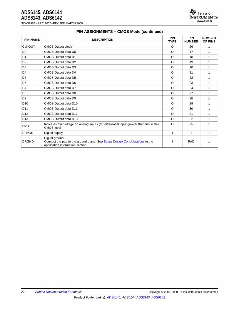
PDN Global power-down control pin I 16 1
Copyright © 2007–2008, Texas Instruments Incorporated Submit Documentation Feedback 21
Product Folder Link(s): ADS6145, ADS6144 ADS6143, ADS6142
www.ti.com
ADS6145, ADS6144ADS6143, ADS6142SLWS198B–JULY 2007–REVISED MARCH 2008
PIN ASSIGNMENTS – CMOS Mode (continued)PIN PIN NUMBERPIN NAME DESCRIPTION TYPE NUMBER OF PINS
CLKOUT CMOS Output clock O 26 1D0 CMOS Output data D0 O 17 1D1 CMOS Output data D1 O 18 1D2 CMOS Output data D2 O 19 1D3 CMOS Output data D3 O 20 1D4 CMOS Output data D4 O 21 1D5 CMOS Output data D5 O 22 1D6 CMOS Output data D6 O 23 1D7 CMOS Output data D7 O 24 1D8 CMOS Output data D8 O 27 1D9 CMOS Output data D9 O 28 1D10 CMOS Output data D10 O 29 1D11 CMOS Output data D11 O 30 1D12 CMOS Output data D12 O 31 1D13 CMOS Output data D13 O 32 1
Indicates overvoltage on analog inputs (for differential input greater than full-scale), O 25 1OVR CMOS levelDRVDD Digital supply I 1 1
Digital ground.DRGND Connect the pad to the ground plane. See Board Design Considerations in the I PAD 1
application information section.
22 Submit Documentation Feedback Copyright © 2007–2008, Texas Instruments Incorporated
Product Folder Link(s): ADS6145, ADS6144 ADS6143, ADS6142
www.ti.com
PIN CONFIGURATION (LVDS MODE)
PD
N
DRVDD
AG
ND
INP
CLK
OU
TM
INM
CLK
OU
TP
AG
ND
AV
DD
AV
DD
AGND
CLKP
CLKM
1
2
3
4
5
6
7
8
9 10
11
12
13
14
15
16
D12_D
13_P
D12_D
13_M
D0_D1_P
D1
0_
D11
_P
D0_D1_M
D1
0_
D11
_M
D8_D
9_P
D8_D
9_M
RESET
D6_D7_P
SCLK
D6_D7_M
SDATA
D4_D5_P
SEN
D4_D5_M
D2_D3_P
D2_D3_M
24
23
22
21
20
19
18
17
31
30
29
28
27
26
25
Pad Connected ToDRGND
32
VC
M
ADS6145, ADS6144ADS6143, ADS6142
SLWS198B–JULY 2007–REVISED MARCH 2008
RHB PACKAGE(TOP VIEW)
Figure 8. LVDS Mode Pinout
PIN ASSIGNMENTS – LVDS ModePIN PIN NUMBERPIN NAME DESCRIPTION TYPE NUMBER OF PINS
AVDD Analog power supply I 13, 15 2AGND Analog ground I 6, 9, 12 3CLKP, CLKM Differential clock inputs I 7, 8 2INP, INM Differential analog inputs I 10, 11 2
Internal reference mode – common-mode voltage output.VCM External reference mode – reference input. The voltage forced on this pin sets the I/O 14 1
internal references.Serial interface RESET input.When using serial interface mode, the user MUST initialize the internal registersthrough a hardware RESET by applying a high-going pulse on this pin or by using the
RESET software reset option. See the SERIAL INTERFACE section. I 2 1In parallel interface mode, the user has to tie the RESET pin permanently HIGH.(SCLK, SDATA, and SEN are used as parallel pin controls in this mode.)The pin has an internal 100-kΩ pull-down resistor.This pin functions as the serial interface clock input when RESET is low.When RESET is tied high, it controls coarse gain and internal/external reference
SCLK selection. Tie SCLK low for internal reference and 0 dB gain and high for internal I 3 1reference and 3.5 dB gain. See Table 1.The pin has an internal 100-kΩ pull-down resistor.This pin functions as the serial interface data input when RESET is low. It controlsvarious power down modes along with the PDN pin when RESET is tied high.
SDATA I 4 1See Table 3 for detailed information.The pin has an internal 100 kΩ pull-down resistor.The pin functions as the serial interface enable input when RESET is low. When
SEN RESET is high, it controls output interface type and data formats. See Table 2 for I 5 1detailed information. The pin has an internal 100-kΩ pull-up resistor to DRVDD.
PDN Global power-down control pin I 16 1
Copyright © 2007–2008, Texas Instruments Incorporated Submit Documentation Feedback 23
Product Folder Link(s): ADS6145, ADS6144 ADS6143, ADS6142
www.ti.com
ADS6145, ADS6144ADS6143, ADS6142SLWS198B–JULY 2007–REVISED MARCH 2008
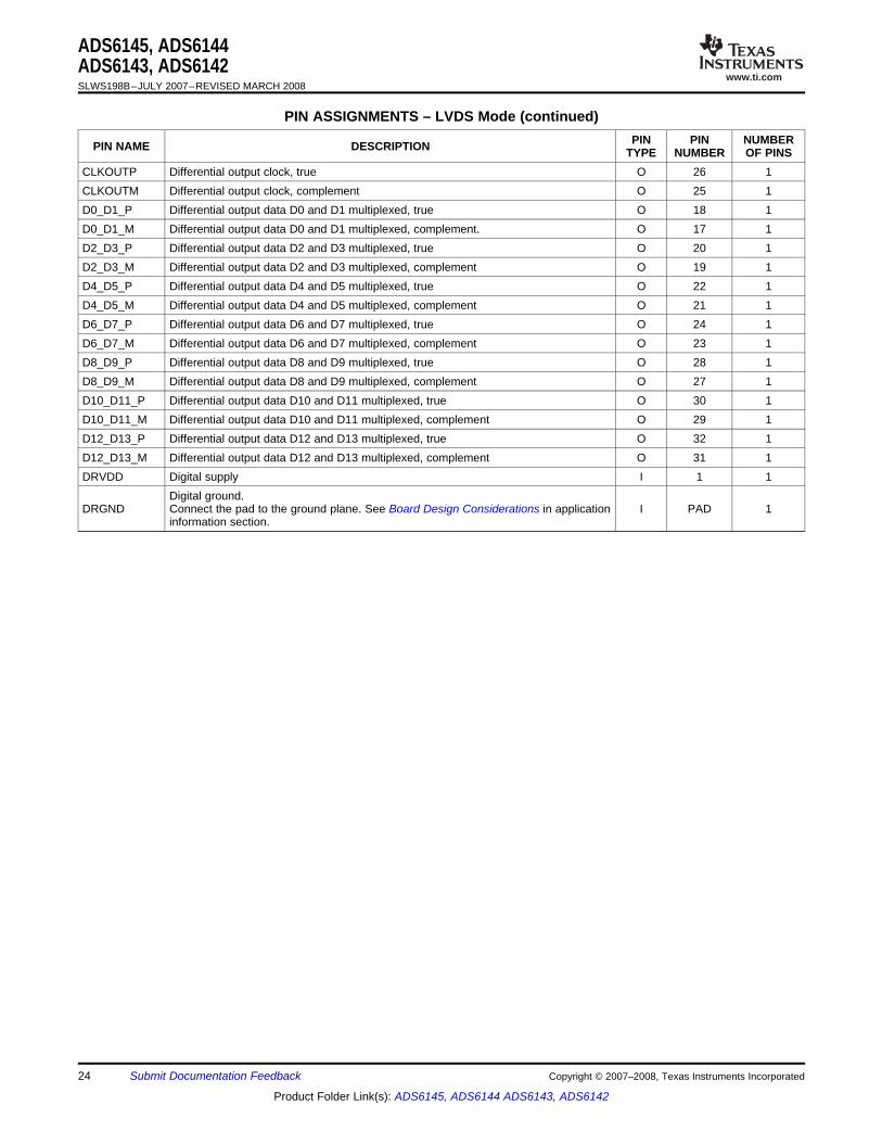
PIN ASSIGNMENTS – LVDS Mode (continued)PIN PIN NUMBERPIN NAME DESCRIPTION TYPE NUMBER OF PINS
CLKOUTP Differential output clock, true O 26 1CLKOUTM Differential output clock, complement O 25 1D0_D1_P Differential output data D0 and D1 multiplexed, true O 18 1D0_D1_M Differential output data D0 and D1 multiplexed, complement. O 17 1D2_D3_P Differential output data D2 and D3 multiplexed, true O 20 1D2_D3_M Differential output data D2 and D3 multiplexed, complement O 19 1D4_D5_P Differential output data D4 and D5 multiplexed, true O 22 1D4_D5_M Differential output data D4 and D5 multiplexed, complement O 21 1D6_D7_P Differential output data D6 and D7 multiplexed, true O 24 1D6_D7_M Differential output data D6 and D7 multiplexed, complement O 23 1D8_D9_P Differential output data D8 and D9 multiplexed, true O 28 1D8_D9_M Differential output data D8 and D9 multiplexed, complement O 27 1D10_D11_P Differential output data D10 and D11 multiplexed, true O 30 1D10_D11_M Differential output data D10 and D11 multiplexed, complement O 29 1D12_D13_P Differential output data D12 and D13 multiplexed, true O 32 1D12_D13_M Differential output data D12 and D13 multiplexed, complement O 31 1DRVDD Digital supply I 1 1
Digital ground.DRGND Connect the pad to the ground plane. See Board Design Considerations in application I PAD 1
information section.
24 Submit Documentation Feedback Copyright © 2007–2008, Texas Instruments Incorporated
Product Folder Link(s): ADS6145, ADS6144 ADS6143, ADS6142
www.ti.com
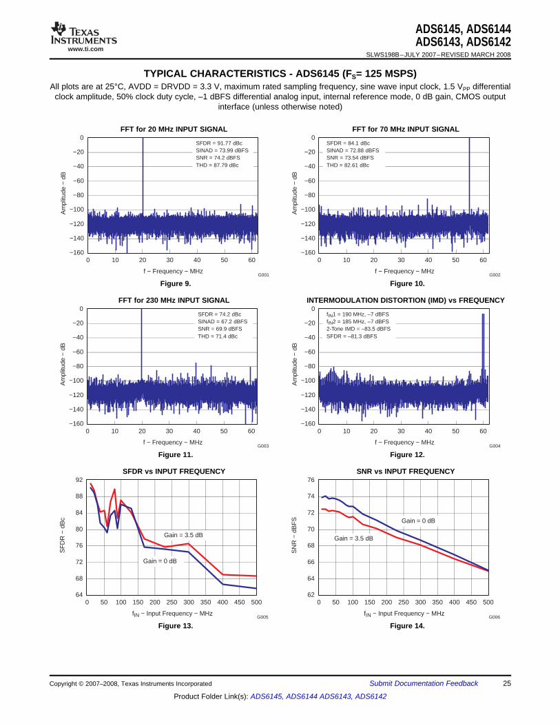
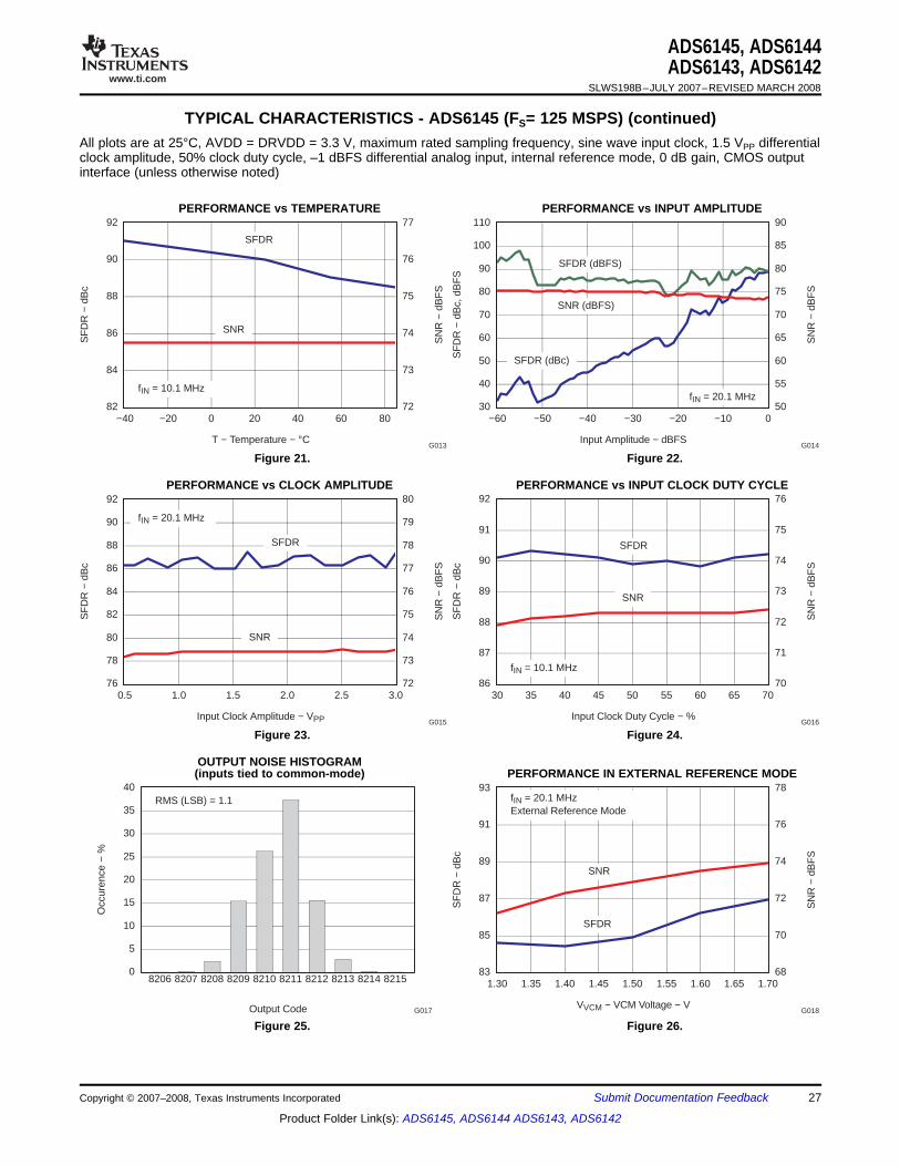
TYPICAL CHARACTERISTICS - ADS6145 (FS= 125 MSPS)
f − Frequency − MHz
−160
−140
−120
−100
−80
−60
−40
−20
0
0 10 20 30 40 50 60
Am
plitu
de −
dB
G001
SFDR = 91.77 dBcSINAD = 73.99 dBFSSNR = 74.2 dBFSTHD = 87.79 dBc
f − Frequency − MHz
−160
−140
−120
−100
−80
−60
−40
−20
0
0 10 20 30 40 50 60
Am
plitu
de −
dB
G002
SFDR = 84.1 dBcSINAD = 72.88 dBFSSNR = 73.54 dBFSTHD = 82.61 dBc
f − Frequency − MHz
−160
−140
−120
−100
−80
−60
−40
−20
0
0 10 20 30 40 50 60
Am
plitu
de −
dB
G003
SFDR = 74.2 dBcSINAD = 67.2 dBFSSNR = 69.9 dBFSTHD = 71.4 dBc
f − Frequency − MHz
−160
−140
−120
−100
−80
−60
−40
−20
0
0 10 20 30 40 50 60
Am
plitu
de −
dB
G004
fIN1 = 190 MHz, –7 dBFSfIN2 = 185 MHz, –7 dBFS2-Tone IMD = –83.5 dBFSSFDR = –81.3 dBFS
fIN − Input Frequency − MHz
64
68
72
76
80
84
88
92
0 50 100 150 200 250 300 350 400 450 500
SF
DR
− d
Bc
G005
Gain = 0 dB
Gain = 3.5 dB
fIN − Input Frequency − MHz
62
64
66
68
70
72
74
76
0 50 100 150 200 250 300 350 400 450 500
SN
R −
dB
FS
G006
Gain = 0 dB
Gain = 3.5 dB
ADS6145, ADS6144ADS6143, ADS6142
SLWS198B–JULY 2007–REVISED MARCH 2008
All plots are at 25°C, AVDD = DRVDD = 3.3 V, maximum rated sampling frequency, sine wave input clock, 1.5 VPP differentialclock amplitude, 50% clock duty cycle, –1 dBFS differential analog input, internal reference mode, 0 dB gain, CMOS output
interface (unless otherwise noted)
FFT for 20 MHz INPUT SIGNAL FFT for 70 MHz INPUT SIGNAL
Figure 9. Figure 10.
FFT for 230 MHz INPUT SIGNAL INTERMODULATION DISTORTION (IMD) vs FREQUENCY
Figure 11. Figure 12.
SFDR vs INPUT FREQUENCY SNR vs INPUT FREQUENCY
Figure 13. Figure 14.
Copyright © 2007–2008, Texas Instruments Incorporated Submit Documentation Feedback 25
Product Folder Link(s): ADS6145, ADS6144 ADS6143, ADS6142

www.ti.com
fIN − Input Frequency − MHz
64
68
72
76
80
84
88
92
0 50 100 150 200 250 300 350 400 450 500
SF
DR
− d
Bc
G007
Gain = 0 dB
Gain = 3.5 dB
fIN − Input Frequency − MHz
62
64
66
68
70
72
74
76
0 50 100 150 200 250 300 350 400 450 500
SN
R −
dB
FS
G008
Gain = 0 dB
Gain = 3.5 dB
fIN − Input Frequency − MHz
60
65
70
75
80
85
90
95
0 100 200 300 400 500
SF
DR
− d
Bc
G009
Input adjusted to get −1dBFS input
1 dB
0 dB
5 dB
6 dB
2 dB
3 dB
4 dB
fIN − Input Frequency − MHz
60
62
64
66
68
70
72
74
76
0 100 200 300 400 500
SIN
AD
− d
BF
S
G010
2 dB
5 dB
1 dB0 dB
4 dB
6 dB
Input adjusted to get −1dBFS input
3 dB
SN
R −
dB
FS
DRVDD − Supply Voltage − V
86
88
90
92
94
96
1.8 2.0 2.2 2.4 2.6 2.8 3.0 3.2 3.4 3.6
SF
DR
− d
Bc
G012
fIN = 10.1 MHzAVDD = 3.3 V
SNR
SFDR
71
72
73
74
75
76
AVDD − Supply Voltage − V
72
74
76
78
80
82
84
86
88
3.0 3.1 3.2 3.3 3.4 3.5 3.6
SF
DR
− d
Bc
G011
SNR
SFDR
fIN = 70.1 MHzDRVDD = 3.3 V
SN
R −
dB
FS
70
71
72
73
74
75
76
77
78
ADS6145, ADS6144ADS6143, ADS6142SLWS198B–JULY 2007–REVISED MARCH 2008
TYPICAL CHARACTERISTICS - ADS6145 (FS= 125 MSPS) (continued)All plots are at 25°C, AVDD = DRVDD = 3.3 V, maximum rated sampling frequency, sine wave input clock, 1.5 VPP differentialclock amplitude, 50% clock duty cycle, –1 dBFS differential analog input, internal reference mode, 0 dB gain, CMOS outputinterface (unless otherwise noted)
SFDR vs INPUT FREQUENCY (LVDS interface) SNR vs INPUT FREQUENCY (LVDS interface)
Figure 15. Figure 16.
SFDR vs INPUT FREQUENCY ACROSS GAINS SINAD vs INPUT FREQUENCY ACROSS GAINS
Figure 17. Figure 18.
PERFORMANCE vs AVDD PERFORMANCE vs DRVDD
Figure 19. Figure 20.
26 Submit Documentation Feedback Copyright © 2007–2008, Texas Instruments Incorporated
Product Folder Link(s): ADS6145, ADS6144 ADS6143, ADS6142
www.ti.com
T − Temperature − °C
82
84
86
88
90
92
−40 −20 0 20 40 60 80
SF
DR
− d
Bc
G013S
NR
− d
BF
S
72
73
74
75
76
77
fIN = 10.1 MHz
SNR
SFDR
Input Amplitude − dBFS
30
40
50
60
70
80
90
100
110
−60 −50 −40 −30 −20 −10 0
fIN = 20.1 MHz
SF
DR
− d
Bc,
dB
FS
G014
SFDR (dBc)
SFDR (dBFS)
SNR (dBFS)
50
55
60
65
70
75
80
85
90
SN
R −
dB
FS
76
78
80
82
84
86
88
90
92
0.5 1.0 1.5 2.0 2.5 3.0
SF
DR
− d
Bc
Input Clock Amplitude − VPP G015
SNR
SFDR
fIN = 20.1 MHz
SN
R −
dB
FS
72
73
74
75
76
77
78
79
80
Input Clock Duty Cycle − %
86
87
88
89
90
91
92
30 35 40 45 50 55 60 65 70
SF
DR
− d
Bc
G016
SNR
SFDR
fIN = 10.1 MHz
SN
R −
dB
FS
70
71
72
73
74
75
76
VVCM − VCM Voltage − V
83
85
87
89
91
93
1.30 1.35 1.40 1.45 1.50 1.55 1.60 1.65 1.70
fIN = 20.1 MHzExternal Reference Mode
SF
DR
− d
Bc
G018
SNR
SFDR
SN
R −
dB
FS
68
70
72
74
76
78
Output Code
0
5
10
15
20
25
30
35
40
8206 8207 8208 8209 8210 8211 8212 8213 8214 8215
Occ
uren
ce −
%
G017
RMS (LSB) = 1.1
ADS6145, ADS6144ADS6143, ADS6142
SLWS198B–JULY 2007–REVISED MARCH 2008
TYPICAL CHARACTERISTICS - ADS6145 (FS= 125 MSPS) (continued)All plots are at 25°C, AVDD = DRVDD = 3.3 V, maximum rated sampling frequency, sine wave input clock, 1.5 VPP differentialclock amplitude, 50% clock duty cycle, –1 dBFS differential analog input, internal reference mode, 0 dB gain, CMOS outputinterface (unless otherwise noted)
PERFORMANCE vs TEMPERATURE PERFORMANCE vs INPUT AMPLITUDE
Figure 21. Figure 22.
PERFORMANCE vs CLOCK AMPLITUDE PERFORMANCE vs INPUT CLOCK DUTY CYCLE
Figure 23. Figure 24.
OUTPUT NOISE HISTOGRAM(inputs tied to common-mode) PERFORMANCE IN EXTERNAL REFERENCE MODE
Figure 25. Figure 26.
Copyright © 2007–2008, Texas Instruments Incorporated Submit Documentation Feedback 27
Product Folder Link(s): ADS6145, ADS6144 ADS6143, ADS6142
www.ti.com
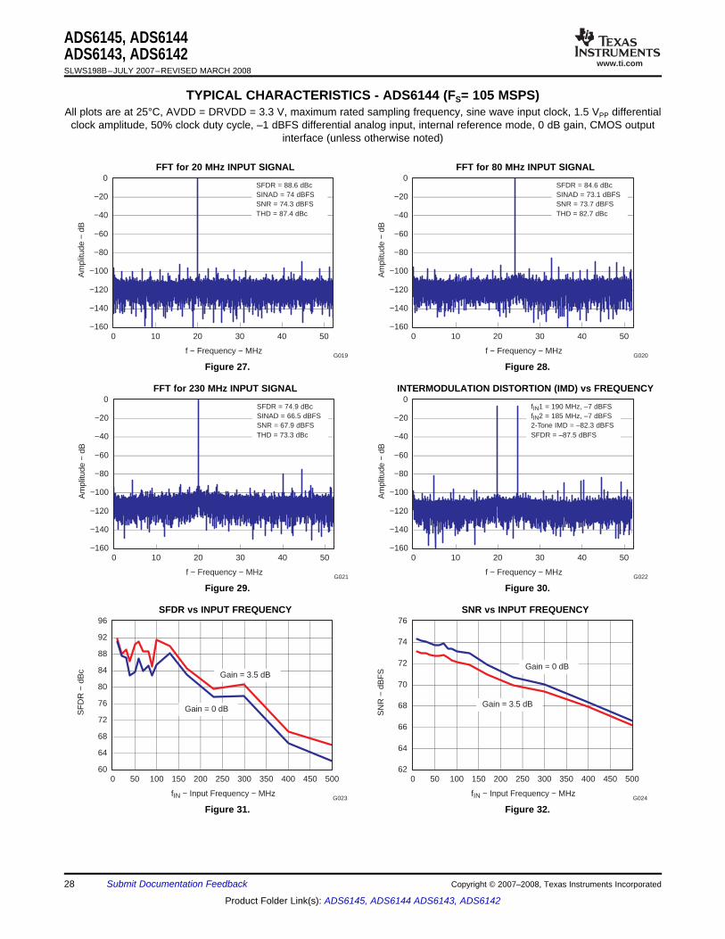
TYPICAL CHARACTERISTICS - ADS6144 (FS= 105 MSPS)
f − Frequency − MHz
−160
−140
−120
−100
−80
−60
−40
−20
0
0 10 20 30 40 50
Am
plitu
de −
dB
G019
SFDR = 88.6 dBcSINAD = 74 dBFSSNR = 74.3 dBFSTHD = 87.4 dBc
f − Frequency − MHz
−160
−140
−120
−100
−80
−60
−40
−20
0
0 10 20 30 40 50
Am
plitu
de −
dB
G020
SFDR = 84.6 dBcSINAD = 73.1 dBFSSNR = 73.7 dBFSTHD = 82.7 dBc
f − Frequency − MHz
−160
−140
−120
−100
−80
−60
−40
−20
0
0 10 20 30 40 50
Am
plitu
de −
dB
G021
SFDR = 74.9 dBcSINAD = 66.5 dBFSSNR = 67.9 dBFSTHD = 73.3 dBc
f − Frequency − MHz
−160
−140
−120
−100
−80
−60
−40
−20
0
0 10 20 30 40 50
Am
plitu
de −
dB
G022
fIN1 = 190 MHz, –7 dBFSfIN2 = 185 MHz, –7 dBFS2-Tone IMD = –82.3 dBFSSFDR = –87.5 dBFS
fIN − Input Frequency − MHz
60
64
68
72
76
80
84
88
92
96
0 50 100 150 200 250 300 350 400 450 500
SF
DR
− d
Bc
G023
Gain = 0 dB
Gain = 3.5 dB
fIN − Input Frequency − MHz
62
64
66
68
70
72
74
76
0 50 100 150 200 250 300 350 400 450 500
SN
R −
dB
FS
G024
Gain = 0 dB
Gain = 3.5 dB
ADS6145, ADS6144ADS6143, ADS6142SLWS198B–JULY 2007–REVISED MARCH 2008
All plots are at 25°C, AVDD = DRVDD = 3.3 V, maximum rated sampling frequency, sine wave input clock, 1.5 VPP differentialclock amplitude, 50% clock duty cycle, –1 dBFS differential analog input, internal reference mode, 0 dB gain, CMOS output
interface (unless otherwise noted)
FFT for 20 MHz INPUT SIGNAL FFT for 80 MHz INPUT SIGNAL
Figure 27. Figure 28.
FFT for 230 MHz INPUT SIGNAL INTERMODULATION DISTORTION (IMD) vs FREQUENCY
Figure 29. Figure 30.
SFDR vs INPUT FREQUENCY SNR vs INPUT FREQUENCY
Figure 31. Figure 32.
28 Submit Documentation Feedback Copyright © 2007–2008, Texas Instruments Incorporated
Product Folder Link(s): ADS6145, ADS6144 ADS6143, ADS6142
www.ti.com
fIN − Input Frequency − MHz
60
64
68
72
76
80
84
88
92
96
0 50 100 150 200 250 300 350 400 450 500
SF
DR
− d
Bc
G025
Gain = 0 dB
Gain = 3.5 dB
fIN − Input Frequency − MHz
62
64
66
68
70
72
74
76
0 50 100 150 200 250 300 350 400 450 500
SN
R −
dB
FS
G026
Gain = 0 dB
Gain = 3.5 dB
fIN − Input Frequency − MHz
60
65
70
75
80
85
90
95
0 100 200 300 400 500
SF
DR
− d
Bc
G027
Input adjusted to get −1dBFS input
1 dB0 dB
5 dB6 dB
2 dB
4 dB
3 dB
fIN − Input Frequency − MHz
60
62
64
66
68
70
72
74
76
0 100 200 300 400 500
SIN
AD
− d
BF
S
G028
2 dB
5 dB1 dB
0 dB
3 dB
4 dB 6 dB
Input adjusted to get −1dBFS input
AVDD − Supply Voltage − V
76
78
80
82
84
86
88
90
92
3.0 3.1 3.2 3.3 3.4 3.5 3.6
G029
fIN = 70.1 MHzDRVDD = 3.3 V
SF
DR
− d
Bc
SN
R −
dB
FS
72
73
74
75
76
77
78
79
80
SNR
SFDR
SN
R −
dB
FS
DRVDD − Supply Voltage − V
88
90
92
94
96
98
100
102
1.8 2.0 2.2 2.4 2.6 2.8 3.0 3.2 3.4 3.6
SF
DR
− d
Bc
G030
fIN = 10.1 MHzAVDD = 3.3 V
SNR
SFDR
70
71
72
73
74
75
76
77
ADS6145, ADS6144ADS6143, ADS6142
SLWS198B–JULY 2007–REVISED MARCH 2008
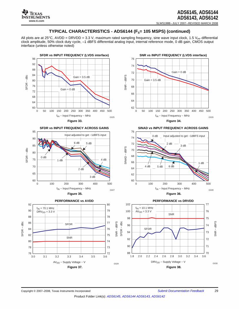
TYPICAL CHARACTERISTICS - ADS6144 (FS= 105 MSPS) (continued)All plots are at 25°C, AVDD = DRVDD = 3.3 V, maximum rated sampling frequency, sine wave input clock, 1.5 VPP differentialclock amplitude, 50% clock duty cycle, –1 dBFS differential analog input, internal reference mode, 0 dB gain, CMOS outputinterface (unless otherwise noted)
SFDR vs INPUT FREQUENCY (LVDS interface) SNR vs INPUT FREQUENCY (LVDS interface)
Figure 33. Figure 34.
SFDR vs INPUT FREQUENCY ACROSS GAINS SINAD vs INPUT FREQUENCY ACROSS GAINS
Figure 35. Figure 36.
PERFORMANCE vs AVDD PERFORMANCE vs DRVDD
Figure 37. Figure 38.
Copyright © 2007–2008, Texas Instruments Incorporated Submit Documentation Feedback 29
Product Folder Link(s): ADS6145, ADS6144 ADS6143, ADS6142

www.ti.com
70
72
74
76
78
80
SN
R −
dB
FS
Input Amplitude − dBFS
20
40
60
80
100
120
−60 −50 −40 −30 −20 −10 0
SF
DR
− d
Bc,
dB
FS
G032
fIN = 20.1 MHz
SFDR (dBc)
SFDR (dBFS)
SNR (dBFS)
T − Temperature − °C
83
85
87
89
91
93
−40 −20 0 20 40 60 80
SF
DR
− d
Bc
G031S
NR
− d
BF
S
72
73
74
75
76
77
fIN = 10.1 MHz
SNR
SFDR
76
78
80
82
84
86
88
90
92
0.5 1.0 1.5 2.0 2.5 3.0
SF
DR
− d
Bc
Input Clock Amplitude − VPP G033
SNR
SFDR
fIN = 20.1 MHz
SN
R −
dB
FS
72
73
74
75
76
77
78
79
80
Input Clock Duty Cycle − %
80
82
84
86
88
90
92
94
96
30 35 40 45 50 55 60 65 70
SF
DR
− d
Bc
G034
SN
R −
dB
FS
71
72
73
74
75
76
77
78
79
SNR
SFDR
fIN = 10.1 MHz
VVCM − VCM Voltage − V
86
88
90
92
94
96
1.30 1.35 1.40 1.45 1.50 1.55 1.60 1.65 1.70
fIN = 20.1 MHzExternal Reference Mode
SF
DR
− d
Bc
G036
SNR
SFDR
SN
R −
dB
FS
68
70
72
74
76
78
Output Code
0
5
10
15
20
25
30
35
40
8206 8207 8208 8209 8210 8211 8212 8213 8214 8215
Occ
uren
ce −
%
G035
RMS (LSB) = 1.049
ADS6145, ADS6144ADS6143, ADS6142SLWS198B–JULY 2007–REVISED MARCH 2008
TYPICAL CHARACTERISTICS - ADS6144 (FS= 105 MSPS) (continued)All plots are at 25°C, AVDD = DRVDD = 3.3 V, maximum rated sampling frequency, sine wave input clock, 1.5 VPP differentialclock amplitude, 50% clock duty cycle, –1 dBFS differential analog input, internal reference mode, 0 dB gain, CMOS outputinterface (unless otherwise noted)
PERFORMANCE vs TEMPERATURE PERFORMANCE vs INPUT AMPLITUDE
Figure 39. Figure 40.
PERFORMANCE vs CLOCK AMPLITUDE PERFORMANCE vs INPUT CLOCK DUTY CYCLE
Figure 41. Figure 42.
OUTPUT NOISE HISTOGRAM WITHINPUTS TIED TO COMMON-MODE PERFORMANCE IN EXTERNAL REFERENCE MODE
Figure 43. Figure 44.
30 Submit Documentation Feedback Copyright © 2007–2008, Texas Instruments Incorporated
Product Folder Link(s): ADS6145, ADS6144 ADS6143, ADS6142
www.ti.com
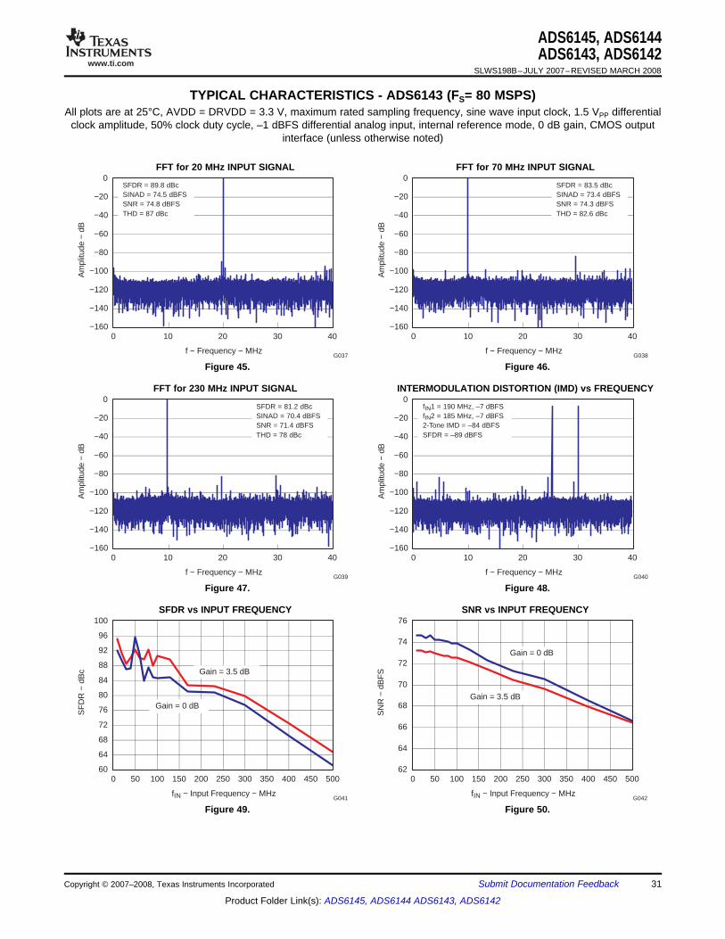
TYPICAL CHARACTERISTICS - ADS6143 (FS= 80 MSPS)
f − Frequency − MHz
−160
−140
−120
−100
−80
−60
−40
−20
0
0 10 20 30 40
Am
plitu
de −
dB
G037
SFDR = 89.8 dBcSINAD = 74.5 dBFSSNR = 74.8 dBFSTHD = 87 dBc
f − Frequency − MHz
−160
−140
−120
−100
−80
−60
−40
−20
0
0 10 20 30 40
Am
plitu
de −
dB
G038
SFDR = 83.5 dBcSINAD = 73.4 dBFSSNR = 74.3 dBFSTHD = 82.6 dBc
f − Frequency − MHz
−160
−140
−120
−100
−80
−60
−40
−20
0
0 10 20 30 40
Am
plitu
de −
dB
G039
SFDR = 81.2 dBcSINAD = 70.4 dBFSSNR = 71.4 dBFSTHD = 78 dBc
f − Frequency − MHz
−160
−140
−120
−100
−80
−60
−40
−20
0
0 10 20 30 40
Am
plitu
de −
dB
G040
fIN1 = 190 MHz, –7 dBFSfIN2 = 185 MHz, –7 dBFS2-Tone IMD = –84 dBFSSFDR = –89 dBFS
fIN − Input Frequency − MHz
60
64
68
72
76
80
84
88
92
96
100
0 50 100 150 200 250 300 350 400 450 500
SF
DR
− d
Bc
G041
Gain = 0 dB
Gain = 3.5 dB
fIN − Input Frequency − MHz
62
64
66
68
70
72
74
76
0 50 100 150 200 250 300 350 400 450 500
SN
R −
dB
FS
G042
Gain = 0 dB
Gain = 3.5 dB
ADS6145, ADS6144ADS6143, ADS6142
SLWS198B–JULY 2007–REVISED MARCH 2008
All plots are at 25°C, AVDD = DRVDD = 3.3 V, maximum rated sampling frequency, sine wave input clock, 1.5 VPP differentialclock amplitude, 50% clock duty cycle, –1 dBFS differential analog input, internal reference mode, 0 dB gain, CMOS output
interface (unless otherwise noted)
FFT for 20 MHz INPUT SIGNAL FFT for 70 MHz INPUT SIGNAL
Figure 45. Figure 46.
FFT for 230 MHz INPUT SIGNAL INTERMODULATION DISTORTION (IMD) vs FREQUENCY
Figure 47. Figure 48.
SFDR vs INPUT FREQUENCY SNR vs INPUT FREQUENCY
Figure 49. Figure 50.
Copyright © 2007–2008, Texas Instruments Incorporated Submit Documentation Feedback 31
Product Folder Link(s): ADS6145, ADS6144 ADS6143, ADS6142

www.ti.com
fIN − Input Frequency − MHz
60
64
68
72
76
80
84
88
92
96
100
0 50 100 150 200 250 300 350 400 450 500
SF
DR
− d
Bc
G043
Gain = 0 dB
Gain = 3.5 dB
fIN − Input Frequency − MHz
62
64
66
68
70
72
74
76
0 50 100 150 200 250 300 350 400 450 500
SN
R −
dB
FS
G044
Gain = 0 dB
Gain = 3.5 dB
fIN − Input Frequency − MHz
60
65
70
75
80
85
90
95
0 100 200 300 400 500
SF
DR
− d
Bc
G045
Input adjusted to get −1dBFS input
1 dB
0 dB5 dB
6 dB2 dB
3 dB
4 dB
fIN − Input Frequency − MHz
60
62
64
66
68
70
72
74
76
0 100 200 300 400 500
SIN
AD
− d
BF
S
G046
2 dB
5 dB
1 dB
0 dB
3 dB
4 dB6 dB
Input adjusted to get −1dBFS input
SN
R −
dB
FS
DRVDD − Supply Voltage − V
88
90
92
94
96
98
100
102
1.8 2.0 2.2 2.4 2.6 2.8 3.0 3.2 3.4 3.6
SF
DR
− d
Bc
G048
fIN = 10.1 MHzAVDD = 3.3 V
SNR
SFDR
70
71
72
73
74
75
76
77
AVDD − Supply Voltage − V
72
74
76
78
80
82
84
86
88
3.0 3.1 3.2 3.3 3.4 3.5 3.6
SF
DR
− d
Bc
G047
SNR
SFDRfIN = 70.1 MHzDRVDD = 3.3 V
SN
R −
dB
FS
70
71
72
73
74
75
76
77
78
ADS6145, ADS6144ADS6143, ADS6142SLWS198B–JULY 2007–REVISED MARCH 2008
TYPICAL CHARACTERISTICS - ADS6143 (FS= 80 MSPS) (continued)All plots are at 25°C, AVDD = DRVDD = 3.3 V, maximum rated sampling frequency, sine wave input clock, 1.5 VPP differentialclock amplitude, 50% clock duty cycle, –1 dBFS differential analog input, internal reference mode, 0 dB gain, CMOS outputinterface (unless otherwise noted)
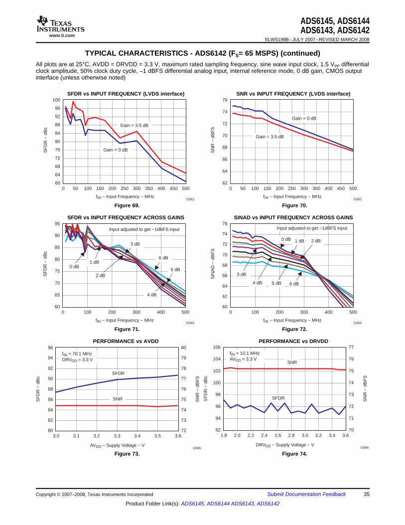
SFDR vs INPUT FREQUENCY (LVDS interface) SNR vs INPUT FREQUENCY (LVDS interface)
Figure 51. Figure 52.
SFDR vs INPUT FREQUENCY ACROSS GAINS SINAD vs INPUT FREQUENCY ACROSS GAINS
Figure 53. Figure 54.
PERFORMANCE vs AVDD PERFORMANCE vs DRVDD
Figure 55. Figure 56.
32 Submit Documentation Feedback Copyright © 2007–2008, Texas Instruments Incorporated
Product Folder Link(s): ADS6145, ADS6144 ADS6143, ADS6142
www.ti.com
T − Temperature − °C
85
87
89
91
93
95
−40 −20 0 20 40 60 80
SF
DR
− d
Bc
G049
72
73
74
75
76
77
SN
R −
dB
FS
fIN = 10.1 MHz
SFDR
SNR
Input Amplitude − dBFS
30
40
50
60
70
80
90
100
110
−60 −50 −40 −30 −20 −10 0
SF
DR
− d
Bc,
dB
FS
G050
SFDR (dBc)
SFDR (dBFS)
SNR (dBFS)
50
55
60
65
70
75
80
85
90
SN
R −
dB
FS
fIN = 20 MHz
Input Clock Duty Cycle − %
80
82
84
86
88
90
92
94
96
30 35 40 45 50 55 60 65 70
SF
DR
− d
Bc
G052
SN
R −
dB
FS
72
73
74
75
76
77
78
79
80
SNR
SFDR
fIN = 10.1 MHz
76
78
80
82
84
86
88
90
92
0.5 1.0 1.5 2.0 2.5 3.0
SF
DR
− d
Bc
Input Clock Amplitude − VPP G051
SNR
SFDR
fIN = 20.1 MHz
SN
R −
dB
FS
72
73
74
75
76
77
78
79
80
VVCM − VCM Voltage − V
82
84
86
88
90
92
1.30 1.35 1.40 1.45 1.50 1.55 1.60 1.65 1.70
fIN = 20.1 MHzExternal Reference Mode
SF
DR
− d
Bc
G054
SNR
SFDR
SN
R −
dB
FS
72
74
76
78
80
82
Output Code
0
5
10
15
20
25
30
35
40
8204 8205 8206 8207 8208 8209 8210 8211 8212 8213
Occ
uren
ce −
%
G053
RMS (LSB) = 1.037
ADS6145, ADS6144ADS6143, ADS6142
SLWS198B–JULY 2007–REVISED MARCH 2008
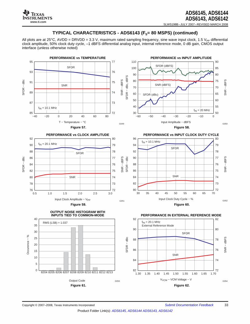
TYPICAL CHARACTERISTICS - ADS6143 (FS= 80 MSPS) (continued)All plots are at 25°C, AVDD = DRVDD = 3.3 V, maximum rated sampling frequency, sine wave input clock, 1.5 VPP differentialclock amplitude, 50% clock duty cycle, –1 dBFS differential analog input, internal reference mode, 0 dB gain, CMOS outputinterface (unless otherwise noted)
PERFORMANCE vs TEMPERATURE PERFORMANCE vs INPUT AMPLITUDE
Figure 57. Figure 58.
PERFORMANCE vs CLOCK AMPLITUDE PERFORMANCE vs INPUT CLOCK DUTY CYCLE
Figure 59. Figure 60.
OUTPUT NOISE HISTOGRAM WITHINPUTS TIED TO COMMON-MODE PERFORMANCE IN EXTERNAL REFERENCE MODE
Figure 61. Figure 62.
Copyright © 2007–2008, Texas Instruments Incorporated Submit Documentation Feedback 33
Product Folder Link(s): ADS6145, ADS6144 ADS6143, ADS6142
www.ti.com
TYPICAL CHARACTERISTICS - ADS6142 (FS= 65 MSPS)
f − Frequency − MHz
−160
−140
−120
−100
−80
−60
−40
−20
0
0 10 20 30
Am
plitu
de −
dB
G055
SFDR = 91.3 dBcSINAD = 74.8 dBFSSNR = 75 dBFSTHD = 89.5 dBc
f − Frequency − MHz
−160
−140
−120
−100
−80
−60
−40
−20
0
0 10 20 30
Am
plitu
de −
dB
G056
SFDR = 83 dBcSINAD = 73.5 dBFSSNR = 74.4 dBFSTHD = 82.2 dBc
f − Frequency − MHz
−160
−140
−120
−100
−80
−60
−40
−20
0
0 10 20 30
Am
plitu
de −
dB
G057
SFDR = 83 dBcSINAD = 71.2 dBFSSNR = 71.9 dBFSTHD = 79.8 dBc
f − Frequency − MHz
−160
−140
−120
−100
−80
−60
−40
−20
0
0 10 20 30
Am
plitu
de −
dB
G058
fIN1 = 190 MHz, –7 dBFSfIN2 = 185 MHz, –7 dBFS2-Tone IMD = –88 dBFSSFDR = –92 dBFS
fIN − Input Frequency − MHz
60
64
68
72
76
80
84
88
92
96
100
0 50 100 150 200 250 300 350 400 450 500
SF
DR
− d
Bc
G059
Gain = 0 dB
Gain = 3.5 dB
fIN − Input Frequency − MHz
62
64
66
68
70
72
74
76
0 50 100 150 200 250 300 350 400 450 500
SN
R −
dB
FS
G060
Gain = 0 dB
Gain = 3.5 dB
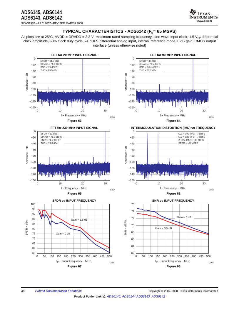
ADS6145, ADS6144ADS6143, ADS6142SLWS198B–JULY 2007–REVISED MARCH 2008
All plots are at 25°C, AVDD = DRVDD = 3.3 V, maximum rated sampling frequency, sine wave input clock, 1.5 VPP differentialclock amplitude, 50% clock duty cycle, –1 dBFS differential analog input, internal reference mode, 0 dB gain, CMOS output
interface (unless otherwise noted)
FFT for 20 MHz INPUT SIGNAL FFT for 90 MHz INPUT SIGNAL
Figure 63. Figure 64.
FFT for 230 MHz INPUT SIGNAL INTERMODULATION DISTORTION (IMD) vs FREQUENCY
Figure 65. Figure 66.
SFDR vs INPUT FREQUENCY SNR vs INPUT FREQUENCY
Figure 67. Figure 68.
34 Submit Documentation Feedback Copyright © 2007–2008, Texas Instruments Incorporated
Product Folder Link(s): ADS6145, ADS6144 ADS6143, ADS6142
www.ti.com
fIN − Input Frequency − MHz
60
64
68
72
76
80
84
88
92
96
100
0 50 100 150 200 250 300 350 400 450 500
SF
DR
− d
Bc
G061
Gain = 0 dB
Gain = 3.5 dB
fIN − Input Frequency − MHz
62
64
66
68
70
72
74
76
0 50 100 150 200 250 300 350 400 450 500
SN
R −
dB
FS
G062
Gain = 0 dB
Gain = 3.5 dB
fIN − Input Frequency − MHz
60
65
70
75
80
85
90
95
0 100 200 300 400 500
SF
DR
− d
Bc
G063
Input adjusted to get −1dBFS input
1 dB0 dB
5 dB2 dB
3 dB
4 dB
6 dB
fIN − Input Frequency − MHz
60
62
64
66
68
70
72
74
76
0 100 200 300 400 500
SIN
AD
− d
BF
S
G064
2 dB
5 dB
1 dB0 dB
4 dB 6 dB
Input adjusted to get −1dBFS input
3 dB
AVDD − Supply Voltage − V
80
82
84
86
88
90
92
94
96
3.0 3.1 3.2 3.3 3.4 3.5 3.6
SF
DR
− d
Bc
G065
SNR
SFDR
fIN = 70.1 MHzDRVDD = 3.3 V
SN
R −
dB
FS
72
73
74
75
76
77
78
79
80
SN
R −
dB
FS
DRVDD − Supply Voltage − V
92
94
96
98
100
102
104
106
1.8 2.0 2.2 2.4 2.6 2.8 3.0 3.2 3.4 3.6
SF
DR
− d
Bc
G066
fIN = 10.1 MHzAVDD = 3.3 V
SNR
SFDR
70
71
72
73
74
75
76
77
ADS6145, ADS6144ADS6143, ADS6142
SLWS198B–JULY 2007–REVISED MARCH 2008
TYPICAL CHARACTERISTICS - ADS6142 (FS= 65 MSPS) (continued)All plots are at 25°C, AVDD = DRVDD = 3.3 V, maximum rated sampling frequency, sine wave input clock, 1.5 VPP differentialclock amplitude, 50% clock duty cycle, –1 dBFS differential analog input, internal reference mode, 0 dB gain, CMOS outputinterface (unless otherwise noted)
SFDR vs INPUT FREQUENCY (LVDS interface) SNR vs INPUT FREQUENCY (LVDS interface)
Figure 69. Figure 70.
SFDR vs INPUT FREQUENCY ACROSS GAINS SINAD vs INPUT FREQUENCY ACROSS GAINS
Figure 71. Figure 72.
PERFORMANCE vs AVDD PERFORMANCE vs DRVDD
Figure 73. Figure 74.
Copyright © 2007–2008, Texas Instruments Incorporated Submit Documentation Feedback 35
Product Folder Link(s): ADS6145, ADS6144 ADS6143, ADS6142
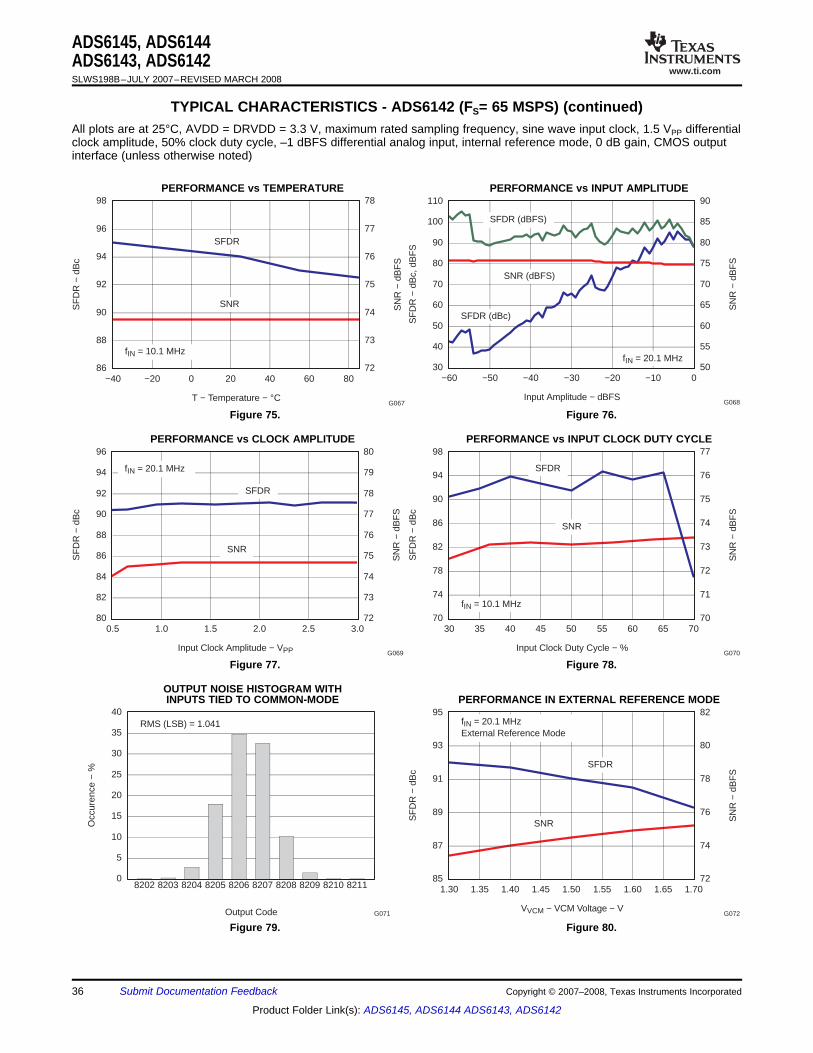
www.ti.com
Input Amplitude − dBFS
30
40
50
60
70
80
90
100
110
−60 −50 −40 −30 −20 −10 0
fIN = 20.1 MHz
SF
DR
− d
Bc,
dB
FS
G068
SFDR (dBc)
SFDR (dBFS)
SNR (dBFS)
50
55
60
65
70
75
80
85
90
SN
R −
dB
FS
SN
R −
dB
FS
72
73
74
75
76
77
78
T − Temperature − °C
86
88
90
92
94
96
98
−40 −20 0 20 40 60 80
SF
DR
− d
Bc
G067
fIN = 10.1 MHz
SNR
SFDR
80
82
84
86
88
90
92
94
96
0.5 1.0 1.5 2.0 2.5 3.0
SF
DR
− d
Bc
Input Clock Amplitude − VPP G069
SNR
SFDR
fIN = 20.1 MHz
SN
R −
dB
FS
72
73
74
75
76
77
78
79
80
SN
R −
dB
FS
70
71
72
73
74
75
76
77
Input Clock Duty Cycle − %
70
74
78
82
86
90
94
98
30 35 40 45 50 55 60 65 70
SF
DR
− d
Bc
G070
SNR
SFDR
fIN = 10.1 MHz
SN
R −
dB
FS
72
74
76
78
80
82
VVCM − VCM Voltage − V
85
87
89
91
93
95
1.30 1.35 1.40 1.45 1.50 1.55 1.60 1.65 1.70
SF
DR
− d
Bc
G072
fIN = 20.1 MHzExternal Reference Mode
SNR
SFDR
Output Code
0
5
10
15
20
25
30
35
40
8202 8203 8204 8205 8206 8207 8208 8209 8210 8211
Occ
uren
ce −
%
G071
RMS (LSB) = 1.041
ADS6145, ADS6144ADS6143, ADS6142SLWS198B–JULY 2007–REVISED MARCH 2008
TYPICAL CHARACTERISTICS - ADS6142 (FS= 65 MSPS) (continued)All plots are at 25°C, AVDD = DRVDD = 3.3 V, maximum rated sampling frequency, sine wave input clock, 1.5 VPP differentialclock amplitude, 50% clock duty cycle, –1 dBFS differential analog input, internal reference mode, 0 dB gain, CMOS outputinterface (unless otherwise noted)
PERFORMANCE vs TEMPERATURE PERFORMANCE vs INPUT AMPLITUDE
Figure 75. Figure 76.
PERFORMANCE vs CLOCK AMPLITUDE PERFORMANCE vs INPUT CLOCK DUTY CYCLE
Figure 77. Figure 78.
OUTPUT NOISE HISTOGRAM WITHINPUTS TIED TO COMMON-MODE PERFORMANCE IN EXTERNAL REFERENCE MODE
Figure 79. Figure 80.
36 Submit Documentation Feedback Copyright © 2007–2008, Texas Instruments Incorporated
Product Folder Link(s): ADS6145, ADS6144 ADS6143, ADS6142
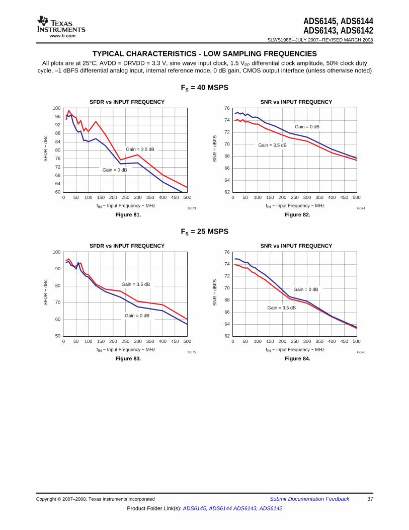
www.ti.com
TYPICAL CHARACTERISTICS - LOW SAMPLING FREQUENCIES
FS = 40 MSPS
fIN − Input Frequency − MHz
60
64
68
72
76
80
84
88
92
96
100
0 50 100 150 200 250 300 350 400 450 500
SF
DR
− d
Bc
G073
Gain = 0 dB
Gain = 3.5 dB
fIN − Input Frequency − MHz
62
64
66
68
70
72
74
76
0 50 100 150 200 250 300 350 400 450 500
SN
R −
dB
FS
G074
Gain = 0 dB
Gain = 3.5 dB
FS = 25 MSPS
fIN − Input Frequency − MHz
50
60
70
80
90
100
0 50 100 150 200 250 300 350 400 450 500
SF
DR
− d
Bc
G075
Gain = 0 dB
Gain = 3.5 dB
fIN − Input Frequency − MHz
62
64
66
68
70
72
74
76
0 50 100 150 200 250 300 350 400 450 500
SN
R −
dB
FS
G076
Gain = 0 dB
Gain = 3.5 dB
ADS6145, ADS6144ADS6143, ADS6142
SLWS198B–JULY 2007–REVISED MARCH 2008
All plots are at 25°C, AVDD = DRVDD = 3.3 V, sine wave input clock, 1.5 VPP differential clock amplitude, 50% clock dutycycle, –1 dBFS differential analog input, internal reference mode, 0 dB gain, CMOS output interface (unless otherwise noted)
SFDR vs INPUT FREQUENCY SNR vs INPUT FREQUENCY
Figure 81. Figure 82.
SFDR vs INPUT FREQUENCY SNR vs INPUT FREQUENCY
Figure 83. Figure 84.
Copyright © 2007–2008, Texas Instruments Incorporated Submit Documentation Feedback 37
Product Folder Link(s): ADS6145, ADS6144 ADS6143, ADS6142

www.ti.com
COMMON PLOTS
f − Frequency − MHz
−100
−90
−80
−70
−60
−50
−40
−30
−20
−10
0
0 50 100 150 200 250 300
CM
RR
− d
Bc
G077fS − Sampling Frequency − MSPS
0.0
0.1
0.2
0.3
0.4
0.5
0.6
0.7
0.8
0 25 50 75 100 125
PD
− P
ower
Dis
sipa
tion
− W
G078
LVDS
CMOS
fIN = 2.5 MHzCL = 5 pF
fS − Sampling Frequency − MSPS
0
5
10
15
20
25
30
0 25 50 75 100 125
DR
VD
D C
urre
nt −
mA
G079
1.8 V, 5 pF
3.3 V, 5 pF
3.3 V, 10 pF
1.8 V, No Load
3.3 V, No Load
ADS6145, ADS6144ADS6143, ADS6142SLWS198B–JULY 2007–REVISED MARCH 2008
All plots are at 25°C, AVDD = DRVDD = 3.3 V, sine wave input clock, 1.5 VPP differential clock amplitude, 50% clock dutycycle, –1 dBFS differential analog input, internal reference mode, 0 dB gain, CMOS output interface (unless otherwise noted)
POWER DISSIPATION vsCOMMON-MODE REJECTION RATIO vs FREQUENCY SAMPLING FREQUENCY (DDR LVDS and CMOS)
Figure 85. Figure 86.
DRVDD current vsSAMPLING FREQUENCY ACROSS LOAD CAPACITANCE
(CMOS)
Figure 87.
38 Submit Documentation Feedback Copyright © 2007–2008, Texas Instruments Incorporated
Product Folder Link(s): ADS6145, ADS6144 ADS6143, ADS6142
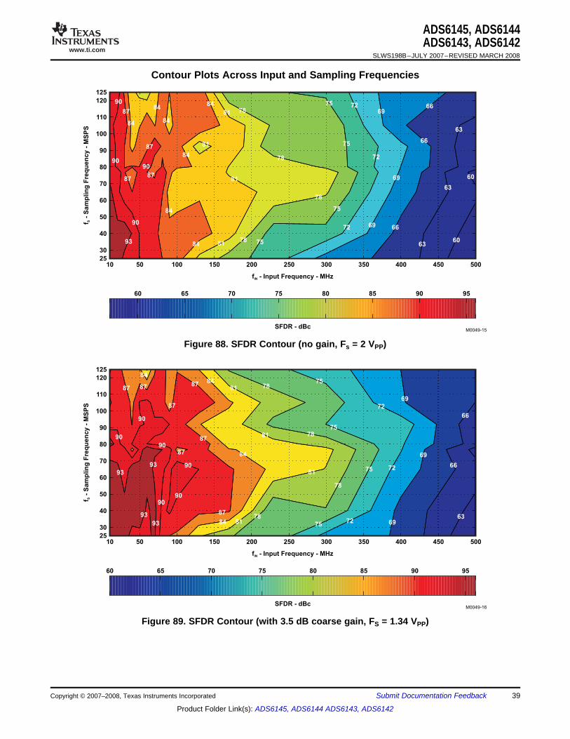
www.ti.com
Contour Plots Across Input and Sampling Frequencies
10 50 100 150
f - Input Frequency - MHzIN
f-
Sam
plin
g F
req
uen
cy -
MS
PS
S
SFDR - dBc
200 250 300 400 450350 50025
30
40
50
100
60
70
80
90
110
120
125
60 65 75
M0049-15
87
87
8787
90
84
84
81
81
84
84 84
8484
78
72
75
75
75
69
72
72
69
66
6966
66
80 8570 90 95
90
90
90
93
78
81
8178
78
63
63
60
6063
75
10 50 100 150
f - Input Frequency - MHzIN
f-
Sam
plin
g F
req
uen
cy -
MS
PS
S
SFDR - dBc
200 250 300 400 450350 50025
30
40
50
100
60
70
80
90
110
120
125
60 65 75
M0049-16
87 8787
87
87
87
90
84
81
81
84
8484
78
72
75
75
75
69
72
72
69
66
69
66
80 8570 90 95
90
90
90
90
93
93
93
93
78
81
8178
78
63
75
87
90
ADS6145, ADS6144ADS6143, ADS6142
SLWS198B–JULY 2007–REVISED MARCH 2008
Figure 88. SFDR Contour (no gain, Fs = 2 VPP)
Figure 89. SFDR Contour (with 3.5 dB coarse gain, FS = 1.34 VPP)
Copyright © 2007–2008, Texas Instruments Incorporated Submit Documentation Feedback 39
Product Folder Link(s): ADS6145, ADS6144 ADS6143, ADS6142

www.ti.com
10 50 100 150
f - Input Frequency - MHzIN
f-
Sam
plin
g F
req
uen
cy -
MS
PS
S
SNR - dBFS
200 250 300 400 450350 50025
30
40
50
100
60
70
80
90
110
120
125
64 66 68
M0048-15
73
73
73
71
71
71
71
72
72
72
70
70
70
70
69
69
69
69
68
68
68
68
67
67
67
66
666564
74
74
74
75
70 72 74
10 50 100 150
f - Input Frequency - MHzIN
f-
Sam
plin
g F
req
uen
cy -
MS
PS
S
SNR - dBFS
200 250 300 400 450350 50025
30
40
50
100
60
70
80
90
110
120
125
64 66 68
M0048-16
73
73
73
71
71
71
72
72
72
70
70
70
70
69
69
69
69
68
68
68
68
67
67
67
66
66 6564
70 72 74
ADS6145, ADS6144ADS6143, ADS6142SLWS198B–JULY 2007–REVISED MARCH 2008
Contour Plots Across Input and Sampling Frequencies (continued)
Figure 90. SNR Contour (no gain, FS = 2 VPP)
Figure 91. SNR Contour (with 3.5 dB coarse gain, FS = 1.34 VPP)
40 Submit Documentation Feedback Copyright © 2007–2008, Texas Instruments Incorporated
Product Folder Link(s): ADS6145, ADS6144 ADS6143, ADS6142

www.ti.com
APPLICATION INFORMATION
THEORY OF OPERATION
ANALOG INPUT
Resr
200 W
Lpkg
nH»1 25 W
SamplingCapacitor
Csamp4.0 pF
INP
INM
Cbond
pF»1
50 W
Cpar10.8 pF
Cpar21 pF
Ron
15 W
Ron
10 W
Ron
15 W
Cpar21 pF
50 W
3.2 pF
Lpkg
1 nH»
25 WCbond
pF»1Resr
200 W
Csamp4.0 pF
SamplingCapacitor
SamplingSwitch
SamplingSwitch
RCR Filter
ADS6145, ADS6144ADS6143, ADS6142
SLWS198B–JULY 2007–REVISED MARCH 2008
The ADS614X devices are a family of low power, 14-bit pipeline ADCs in a CMOS process with up to a 125MSPS sampling frequencies. These devices are based on switched capacitor technology and run off a single3.3-V supply. The conversion process is initiated by the rising edge of the external input clock. Once the signal iscaptured by the input sample and hold, the input sample is sequentially converted by a series of lower resolutionstages, with the outputs combined in a digital correction logic block. At every clock edge, the sample propagatesthrough the pipeline resulting in a data latency of 9 clock cycles. The output is available as 14-bit data, in DDRLVDS or CMOS and coded in either straight offset binary or binary 2s complement format.
The analog input consists of a switched-capacitor based differential sample and hold architecture, shown inFigure 92.
This differential topology results in good ac-performance even for high input frequencies at high sampling rates.The INP and INM pins have to be externally biased around a common-mode voltage of 1.5 V available on theVCM pin. For a full-scale differential input, each input pin (INP, INM) has to swing symmetrically between VCM +0.5 V and VCM – 0.5 V, resulting in a 2VPP differential input swing. The maximum swing is determined by theinternal reference voltages REFP (2.5 V nominal) and REFM (0.5 V, nominal).
Figure 92. Input Stage
The input sampling circuit has a high 3dB bandwidth that extends up to 450 MHz (measured from the input pinsto the voltage across the sampling capacitors).
Copyright © 2007–2008, Texas Instruments Incorporated Submit Documentation Feedback 41
Product Folder Link(s): ADS6145, ADS6144 ADS6143, ADS6142
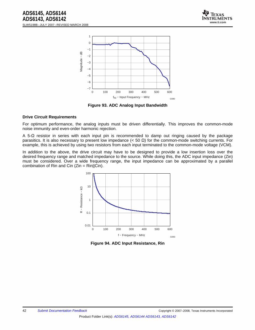
www.ti.com
fIN − Input Frequency − MHz
−7
−6
−5
−4
−3
−2
−1
0
1
0 100 200 300 400 500 600
Mag
nitu
de −
dB
G080
Drive Circuit Requirements
f − Frequency − MHz
0 100 200 300 400 500 600
R −
Res
ista
nce
− k
Ω
100
10
0.1
0.01
G083
1
ADS6145, ADS6144ADS6143, ADS6142SLWS198B–JULY 2007–REVISED MARCH 2008
Figure 93. ADC Analog Input Bandwidth
For optimum performance, the analog inputs must be driven differentially. This improves the common-modenoise immunity and even-order harmonic rejection.
A 5-Ω resistor in series with each input pin is recommended to damp out ringing caused by the packageparasitics. It is also necessary to present low impedance (< 50 Ω) for the common-mode switching currents. Forexample, this is achieved by using two resistors from each input terminated to the common-mode voltage (VCM).
In addition to the above, the drive circuit may have to be designed to provide a low insertion loss over thedesired frequency range and matched impedance to the source. While doing this, the ADC input impedance (Zin)must be considered. Over a wide frequency range, the input impedance can be approximated by a parallelcombination of Rin and Cin (Zin = Rin||Cin).
Figure 94. ADC Input Resistance, Rin
42 Submit Documentation Feedback Copyright © 2007–2008, Texas Instruments Incorporated
Product Folder Link(s): ADS6145, ADS6144 ADS6143, ADS6142
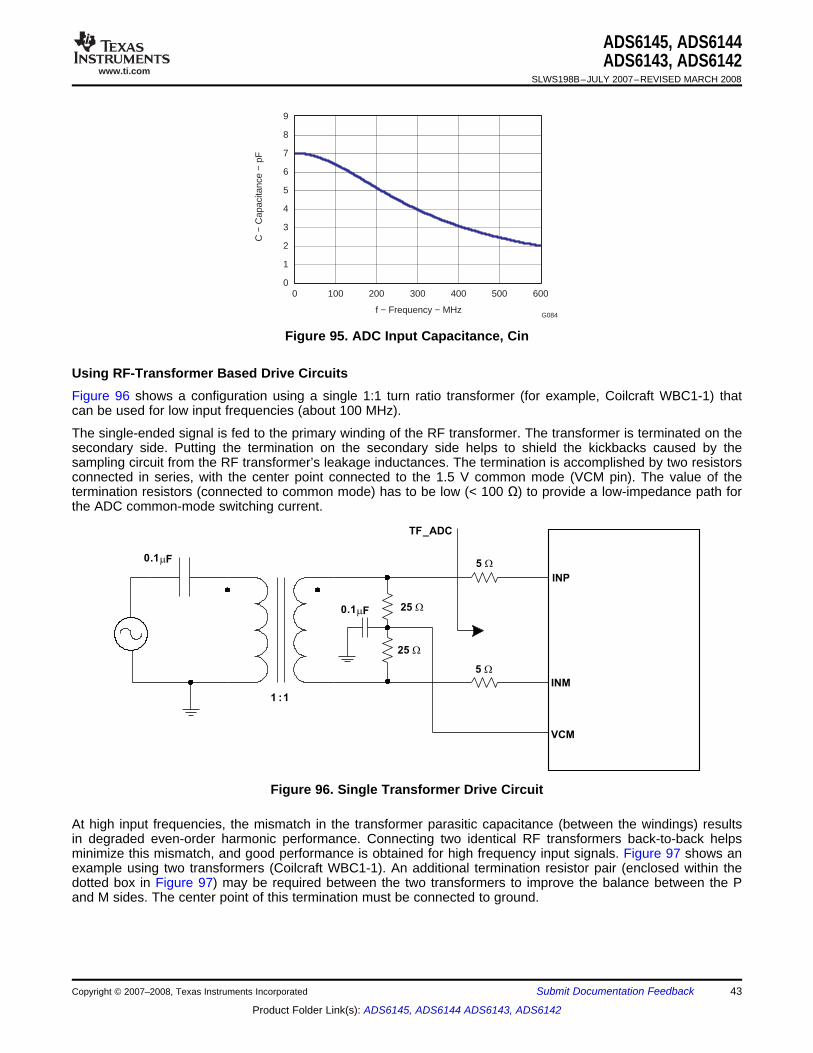
www.ti.com
f − Frequency − MHz
0
1
2
3
4
5
6
7
8
9
0 100 200 300 400 500 600
C −
Cap
acita
nce
− pF
G084
Using RF-Transformer Based Drive Circuits
INP
INM
VCM
1 :1
5 W
0.1mF
0.1mF
25 W
TF_ADC
25 W
5 W
ADS6145, ADS6144ADS6143, ADS6142
SLWS198B–JULY 2007–REVISED MARCH 2008
Figure 95. ADC Input Capacitance, Cin
Figure 96 shows a configuration using a single 1:1 turn ratio transformer (for example, Coilcraft WBC1-1) thatcan be used for low input frequencies (about 100 MHz).
The single-ended signal is fed to the primary winding of the RF transformer. The transformer is terminated on thesecondary side. Putting the termination on the secondary side helps to shield the kickbacks caused by thesampling circuit from the RF transformer’s leakage inductances. The termination is accomplished by two resistorsconnected in series, with the center point connected to the 1.5 V common mode (VCM pin). The value of thetermination resistors (connected to common mode) has to be low (< 100 Ω) to provide a low-impedance path forthe ADC common-mode switching current.
Figure 96. Single Transformer Drive Circuit
At high input frequencies, the mismatch in the transformer parasitic capacitance (between the windings) resultsin degraded even-order harmonic performance. Connecting two identical RF transformers back-to-back helpsminimize this mismatch, and good performance is obtained for high frequency input signals. Figure 97 shows anexample using two transformers (Coilcraft WBC1-1). An additional termination resistor pair (enclosed within thedotted box in Figure 97) may be required between the two transformers to improve the balance between the Pand M sides. The center point of this termination must be connected to ground.
Copyright © 2007–2008, Texas Instruments Incorporated Submit Documentation Feedback 43
Product Folder Link(s): ADS6145, ADS6144 ADS6143, ADS6142
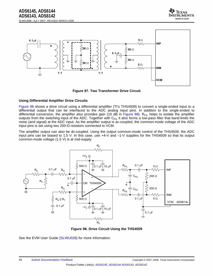
www.ti.com
INP
INM
VCM
1:1
5 W0 .1mF
1:1
50 W
50 W
0 .1mF
50 W
50 W
5 W
Using Differential Amplifier Drive Circuits
RG
RF
RF
RFIL
RFIL
CFIL
CFILRG
0.1 Fm
0.1 Fm
0.1 Fm
0.1 Fm
0.1 Fm
0.1 Fm
0.1 Fm
10 Fm
10 Fm
RS
RS T|| R
RT
+VS
CM
INP
INM
ADS614x
THS4509
VCM
500 W
200 W
200 W
5 W
5 W500 W
0.1 Fm
–VS
ADS6145, ADS6144ADS6143, ADS6142SLWS198B–JULY 2007–REVISED MARCH 2008
Figure 97. Two Transformer Drive Circuit
Figure 98 shows a drive circuit using a differential amplifier (TI's THS4509) to convert a single-ended input to adifferential output that can be interfaced to the ADC analog input pins. In addition to the single-ended todifferential conversion, the amplifier also provides gain (10 dB in Figure 98). RFIL helps to isolate the amplifieroutputs from the switching input of the ADC. Together with CFIL it also forms a low-pass filter that band-limits thenoise (and signal) at the ADC input. As the amplifier output is ac-coupled, the common-mode voltage of the ADCinput pins is set using two 200-Ω resistors connected to VCM.
The amplifier output can also be dc-coupled. Using the output common-mode control of the THS4509, the ADCinput pins can be biased to 1.5 V. In this case, use +4-V and –1-V supplies for the THS4509 so that its outputcommon-mode voltage (1.5 V) is at mid-supply.
Figure 98. Drive Circuit Using the THS4509
See the EVM User Guide (SLWU028) for more information.
44 Submit Documentation Feedback Copyright © 2007–2008, Texas Instruments Incorporated
Product Folder Link(s): ADS6145, ADS6144 ADS6143, ADS6142
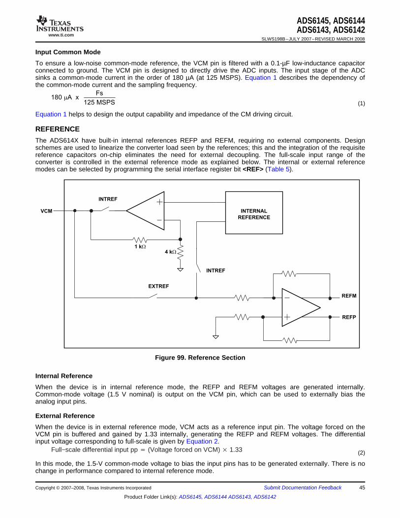
www.ti.com
Input Common Mode
Fs180 A x
125 MSPSm
(1)
REFERENCE
VCM
REFM
REFP
INTREF
INTREF
EXTREF
INTERNAL
REFERENCE
1 kW
4 kW
Internal Reference
External Reference
Full−scale differential input pp (Voltage forced on VCM) 1.33 (2)
ADS6145, ADS6144ADS6143, ADS6142
SLWS198B–JULY 2007–REVISED MARCH 2008
To ensure a low-noise common-mode reference, the VCM pin is filtered with a 0.1-µF low-inductance capacitorconnected to ground. The VCM pin is designed to directly drive the ADC inputs. The input stage of the ADCsinks a common-mode current in the order of 180 µA (at 125 MSPS). Equation 1 describes the dependency ofthe common-mode current and the sampling frequency.
Equation 1 helps to design the output capability and impedance of the CM driving circuit.
The ADS614X have built-in internal references REFP and REFM, requiring no external components. Designschemes are used to linearize the converter load seen by the references; this and the integration of the requisitereference capacitors on-chip eliminates the need for external decoupling. The full-scale input range of theconverter is controlled in the external reference mode as explained below. The internal or external referencemodes can be selected by programming the serial interface register bit <REF> (Table 5).
Figure 99. Reference Section
When the device is in internal reference mode, the REFP and REFM voltages are generated internally.Common-mode voltage (1.5 V nominal) is output on the VCM pin, which can be used to externally bias theanalog input pins.
When the device is in external reference mode, VCM acts as a reference input pin. The voltage forced on theVCM pin is buffered and gained by 1.33 internally, generating the REFP and REFM voltages. The differentialinput voltage corresponding to full-scale is given by Equation 2.
In this mode, the 1.5-V common-mode voltage to bias the input pins has to be generated externally. There is nochange in performance compared to internal reference mode.
Copyright © 2007–2008, Texas Instruments Incorporated Submit Documentation Feedback 45
Product Folder Link(s): ADS6145, ADS6144 ADS6143, ADS6142
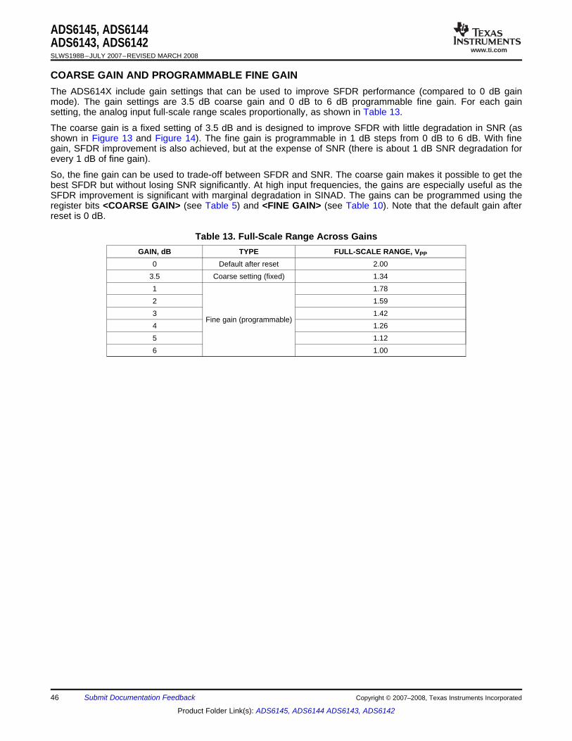
www.ti.com
COARSE GAIN AND PROGRAMMABLE FINE GAIN
ADS6145, ADS6144ADS6143, ADS6142SLWS198B–JULY 2007–REVISED MARCH 2008
The ADS614X include gain settings that can be used to improve SFDR performance (compared to 0 dB gainmode). The gain settings are 3.5 dB coarse gain and 0 dB to 6 dB programmable fine gain. For each gainsetting, the analog input full-scale range scales proportionally, as shown in Table 13.
The coarse gain is a fixed setting of 3.5 dB and is designed to improve SFDR with little degradation in SNR (asshown in Figure 13 and Figure 14). The fine gain is programmable in 1 dB steps from 0 dB to 6 dB. With finegain, SFDR improvement is also achieved, but at the expense of SNR (there is about 1 dB SNR degradation forevery 1 dB of fine gain).
So, the fine gain can be used to trade-off between SFDR and SNR. The coarse gain makes it possible to get thebest SFDR but without losing SNR significantly. At high input frequencies, the gains are especially useful as theSFDR improvement is significant with marginal degradation in SINAD. The gains can be programmed using theregister bits <COARSE GAIN> (see Table 5) and <FINE GAIN> (see Table 10). Note that the default gain afterreset is 0 dB.
Table 13. Full-Scale Range Across GainsGAIN, dB TYPE FULL-SCALE RANGE, VPP
0 Default after reset 2.003.5 Coarse setting (fixed) 1.341 1.782 1.593 1.42
Fine gain (programmable)4 1.265 1.126 1.00
46 Submit Documentation Feedback Copyright © 2007–2008, Texas Instruments Incorporated
Product Folder Link(s): ADS6145, ADS6144 ADS6143, ADS6142

www.ti.com
CLOCK INPUT
CLKP
5 kW
VCM
5 kW
6 pF
10 W
10 W
CLKM
Clock Buffer
Ceq Ceq
Ceq 1 to 3 pF, equivalent input capacitance of clock buffer»
Lpkg
1 nH»
Lpkg
1 nH»
Cbond
1 pF»
Cbond
1 pF»
Resr
100» W
Resr
100» W
ADS6145, ADS6144ADS6143, ADS6142
SLWS198B–JULY 2007–REVISED MARCH 2008
The clock inputs of the ADS614X can be driven differentially (SINE, LVPECL, or LVDS) or single-ended(LVCMOS), with little or no difference in performance between configurations. The common-mode voltage of theclock inputs is set to VCM using internal 5-kΩ resistors as shown in Figure 100. This allows the use oftransformer-coupled drive circuits for the sine wave clock, or ac-coupling for the LVPECL, LVDS clock sources(see Figure 102 and Figure 103).
For best performance, it is recommended to drive the clock inputs differentially, reducing susceptibility tocommon-mode noise. In this case, it is best to connect both clock inputs to the differential input clock signal with0.1-µF capacitors, as shown in Figure 102. A single-ended CMOS clock can be ac-coupled to the CLKP input,with CLKM connected to ground with a 0.1-µF capacitor, as shown in Figure 103.
For high input frequency sampling, a clock source with very low jitter is recommended. Band-pass filtering of theclock source can help reduce the effect of jitter. There is no change in performance with a non-50% duty cycleclock input. Figure 24 shows the performance of the ADC versus clock duty cycle.
Figure 100. Internal Clock Buffer
Copyright © 2007–2008, Texas Instruments Incorporated Submit Documentation Feedback 47
Product Folder Link(s): ADS6145, ADS6144 ADS6143, ADS6142
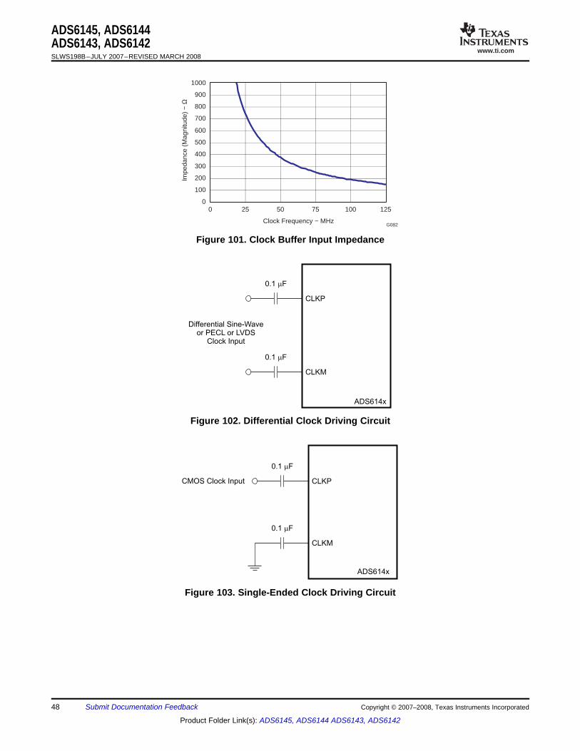
www.ti.com
Clock Frequency − MHz
0
100
200
300
400
500
600
700
800
900
1000
0 25 50 75 100 125
Impe
danc
e (M
agni
tude
) −
Ω
G082
CLKP
CLKM
Differential Sine-Waveor PECL or LVDS
Clock Input
ADS614x
0.1 Fm
0.1 Fm
CLKP
CLKM
CMOS Clock Input
ADS614x
0.1 Fm
0.1 Fm
ADS6145, ADS6144ADS6143, ADS6142SLWS198B–JULY 2007–REVISED MARCH 2008
Figure 101. Clock Buffer Input Impedance
Figure 102. Differential Clock Driving Circuit
Figure 103. Single-Ended Clock Driving Circuit
48 Submit Documentation Feedback Copyright © 2007–2008, Texas Instruments Incorporated
Product Folder Link(s): ADS6145, ADS6144 ADS6143, ADS6142
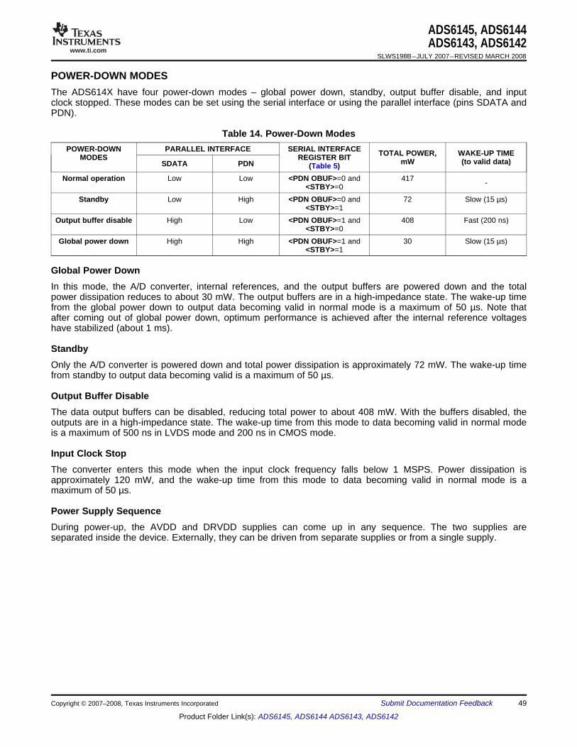
www.ti.com
POWER-DOWN MODES
Global Power Down
Standby
Output Buffer Disable
Input Clock Stop
Power Supply Sequence
ADS6145, ADS6144ADS6143, ADS6142
SLWS198B–JULY 2007–REVISED MARCH 2008
The ADS614X have four power-down modes – global power down, standby, output buffer disable, and inputclock stopped. These modes can be set using the serial interface or using the parallel interface (pins SDATA andPDN).
Table 14. Power-Down ModesPOWER-DOWN PARALLEL INTERFACE SERIAL INTERFACE TOTAL POWER, WAKE-UP TIMEMODES REGISTER BIT mW (to valid data)SDATA PDN (Table 5)
Normal operation Low Low <PDN OBUF>=0 and 417 -<STBY>=0Standby Low High <PDN OBUF>=0 and 72 Slow (15 µs)
<STBY>=1Output buffer disable High Low <PDN OBUF>=1 and 408 Fast (200 ns)
<STBY>=0Global power down High High <PDN OBUF>=1 and 30 Slow (15 µs)
<STBY>=1
In this mode, the A/D converter, internal references, and the output buffers are powered down and the totalpower dissipation reduces to about 30 mW. The output buffers are in a high-impedance state. The wake-up timefrom the global power down to output data becoming valid in normal mode is a maximum of 50 µs. Note thatafter coming out of global power down, optimum performance is achieved after the internal reference voltageshave stabilized (about 1 ms).
Only the A/D converter is powered down and total power dissipation is approximately 72 mW. The wake-up timefrom standby to output data becoming valid is a maximum of 50 µs.
The data output buffers can be disabled, reducing total power to about 408 mW. With the buffers disabled, theoutputs are in a high-impedance state. The wake-up time from this mode to data becoming valid in normal modeis a maximum of 500 ns in LVDS mode and 200 ns in CMOS mode.
The converter enters this mode when the input clock frequency falls below 1 MSPS. Power dissipation isapproximately 120 mW, and the wake-up time from this mode to data becoming valid in normal mode is amaximum of 50 µs.
During power-up, the AVDD and DRVDD supplies can come up in any sequence. The two supplies areseparated inside the device. Externally, they can be driven from separate supplies or from a single supply.
Copyright © 2007–2008, Texas Instruments Incorporated Submit Documentation Feedback 49
Product Folder Link(s): ADS6145, ADS6144 ADS6143, ADS6142
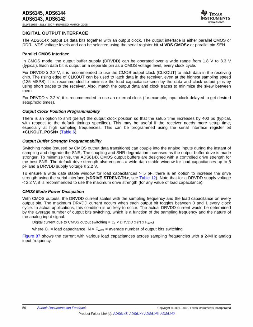
www.ti.com
DIGITAL OUTPUT INTERFACE
Parallel CMOS Interface
ADS6145, ADS6144ADS6143, ADS6142SLWS198B–JULY 2007–REVISED MARCH 2008
The ADS614X output 14 data bits together with an output clock. The output interface is either parallel CMOS orDDR LVDS voltage levels and can be selected using the serial register bit <LVDS CMOS> or parallel pin SEN.
In CMOS mode, the output buffer supply (DRVDD) can be operated over a wide range from 1.8 V to 3.3 V(typical). Each data bit is output on a separate pin as a CMOS voltage level, every clock cycle.
For DRVDD ≥ 2.2 V, it is recommended to use the CMOS output clock (CLKOUT) to latch data in the receivingchip. The rising edge of CLKOUT can be used to latch data in the receiver, even at the highest sampling speed(125 MSPS). It is recommended to minimize the load capacitance seen by the data and clock output pins byusing short traces to the receiver. Also, match the output data and clock traces to minimize the skew betweenthem.
For DRVDD < 2.2 V, it is recommended to use an external clock (for example, input clock delayed to get desiredsetup/hold times).
Output Clock Position ProgrammabilityThere is an option to shift (delay) the output clock position so that the setup time increases by 400 ps (typical,with respect to the default timings specified). This may be useful if the receiver needs more setup time,especially at high sampling frequencies. This can be programmed using the serial interface register bit<CLKOUT_POSN> (Table 6).
Output Buffer Strength ProgrammabilitySwitching noise (caused by CMOS output data transitions) can couple into the analog inputs during the instant ofsampling and degrade the SNR. The coupling and SNR degradation increases as the output buffer drive is madestronger. To minimize this, the ADS614X CMOS output buffers are designed with a controlled drive strength forthe best SNR. The default drive strength also ensures a wide data stable window for load capacitances up to 5pF and a DRVDD supply voltage ≥ 2.2 V.
To ensure a wide data stable window for load capacitances > 5 pF, there is an option to increase the drivestrength using the serial interface (<DRIVE STRENGTH>, see Table 12). Note that for a DRVDD supply voltage< 2.2 V, it is recommended to use the maximum drive strength (for any value of load capacitance).
CMOS Mode Power DissipationWith CMOS outputs, the DRVDD current scales with the sampling frequency and the load capacitance on everyoutput pin. The maximum DRVDD current occurs when each output bit toggles between 0 and 1 every clockcycle. In actual applications, this condition is unlikely to occur. The actual DRVDD current would be determinedby the average number of output bits switching, which is a function of the sampling frequency and the nature ofthe analog input signal.
Digital current due to CMOS output switching = CL × DRVDD x (N x FAVG)
where CL = load capacitance, N × FAVG = average number of output bits switching
Figure 87 shows the current with various load capacitances across sampling frequencies with a 2-MHz analoginput frequency.
50 Submit Documentation Feedback Copyright © 2007–2008, Texas Instruments Incorporated
Product Folder Link(s): ADS6145, ADS6144 ADS6143, ADS6142
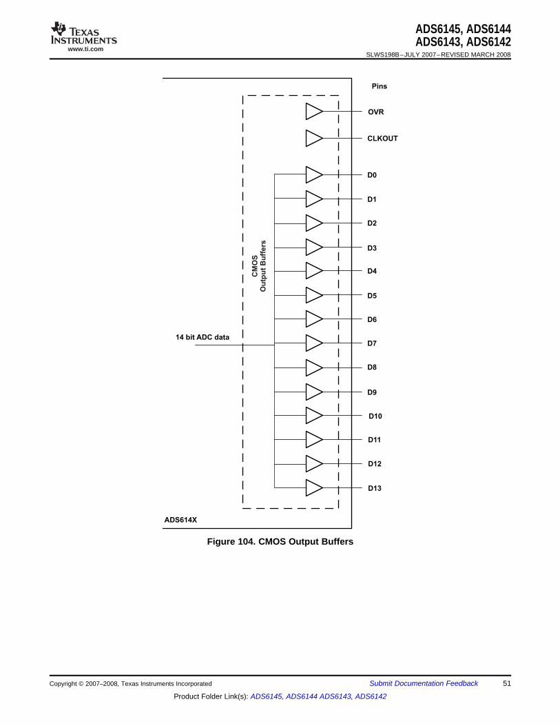
www.ti.com
D0
D1
D2
D3
D4
D5
D6
D7
D8
D9
D10
D11
ADS614X
Pins
D12
D13
CLKOUT
14 bit ADC data
OVR
CM
OS
Ou
tpu
t B
uff
ers
ADS6145, ADS6144ADS6143, ADS6142
SLWS198B–JULY 2007–REVISED MARCH 2008
Figure 104. CMOS Output Buffers
Copyright © 2007–2008, Texas Instruments Incorporated Submit Documentation Feedback 51
Product Folder Link(s): ADS6145, ADS6144 ADS6143, ADS6142
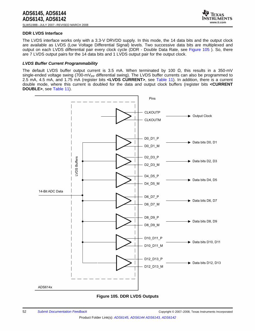
www.ti.com
DDR LVDS Interface
CLKOUTP
CLKOUTM
D0_D1_P
D0_D1_M
D2_D3_P
D2_D3_M
D4_D5_P
D4_D5_M
D6_D7_P
D6_D7_M
D8_D9_P
D8_D9_M
D10_D11_P
D10_D11_M
Output Clock
Data bits D0, D1
Data bits D2, D3
Data bits D4, D5
Data bits D6, D7
Data bits D8, D9
Data bits D10, D11
ADS614x
Pins
D12_D13_P
D12_D13_MData bits D12, D13
14-Bit ADC Data
LV
DS
Buffers
ADS6145, ADS6144ADS6143, ADS6142SLWS198B–JULY 2007–REVISED MARCH 2008
The LVDS interface works only with a 3.3-V DRVDD supply. In this mode, the 14 data bits and the output clockare available as LVDS (Low Voltage Differential Signal) levels. Two successive data bits are multiplexed andoutput on each LVDS differential pair every clock cycle (DDR - Double Data Rate, see Figure 105 ). So, thereare 7 LVDS output pairs for the 14 data bits and 1 LVDS output pair for the output clock.
LVDS Buffer Current ProgrammabilityThe default LVDS buffer output current is 3.5 mA. When terminated by 100 Ω, this results in a 350-mVsingle-ended voltage swing (700-mVPP differential swing). The LVDS buffer currents can also be programmed to2.5 mA, 4.5 mA, and 1.75 mA (register bits <LVDS CURRENT>, see Table 11). In addition, there is a currentdouble mode, where this current is doubled for the data and output clock buffers (register bits <CURRENTDOUBLE>, see Table 11).
Figure 105. DDR LVDS Outputs
52 Submit Documentation Feedback Copyright © 2007–2008, Texas Instruments Incorporated
Product Folder Link(s): ADS6145, ADS6144 ADS6143, ADS6142
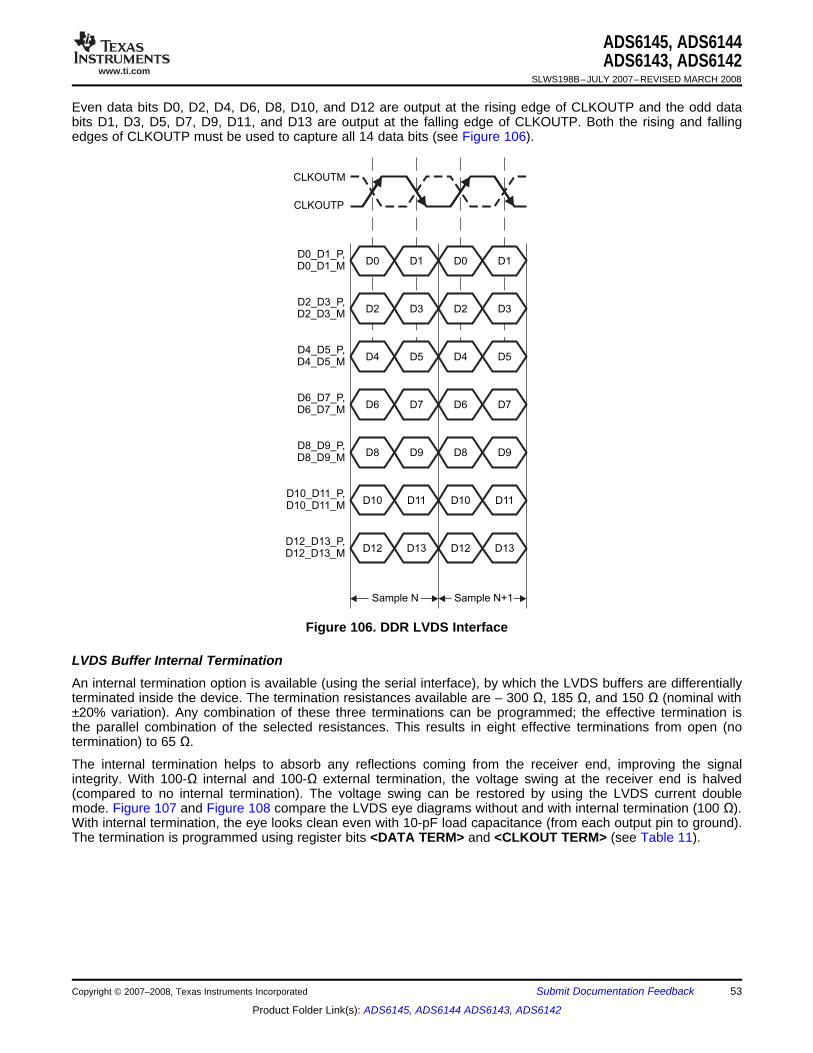
www.ti.com
CLKOUTP
D0_D1_P,D0_D1_M
D2_D3_P,D2_D3_M
D4_D5_P,D4_D5_M
D6_D7_P,D6_D7_M
D8_D9_P,D8_D9_M
D10_D11_P,D10_D11_M
D12_D13_P,D12_D13_M
D0
D2
D4
D6
D8
D10
D12
Sample N+1Sample N
D0
D2
D4
D6
D8
D10
D12
D1
D3
D5
D7
D9
D11
D13
D1
D3
D5
D7
D9
D11
D13
CLKOUTM
ADS6145, ADS6144ADS6143, ADS6142
SLWS198B–JULY 2007–REVISED MARCH 2008
Even data bits D0, D2, D4, D6, D8, D10, and D12 are output at the rising edge of CLKOUTP and the odd databits D1, D3, D5, D7, D9, D11, and D13 are output at the falling edge of CLKOUTP. Both the rising and fallingedges of CLKOUTP must be used to capture all 14 data bits (see Figure 106).
Figure 106. DDR LVDS Interface
LVDS Buffer Internal TerminationAn internal termination option is available (using the serial interface), by which the LVDS buffers are differentiallyterminated inside the device. The termination resistances available are – 300 Ω, 185 Ω, and 150 Ω (nominal with±20% variation). Any combination of these three terminations can be programmed; the effective termination isthe parallel combination of the selected resistances. This results in eight effective terminations from open (notermination) to 65 Ω.
The internal termination helps to absorb any reflections coming from the receiver end, improving the signalintegrity. With 100-Ω internal and 100-Ω external termination, the voltage swing at the receiver end is halved(compared to no internal termination). The voltage swing can be restored by using the LVDS current doublemode. Figure 107 and Figure 108 compare the LVDS eye diagrams without and with internal termination (100 Ω).With internal termination, the eye looks clean even with 10-pF load capacitance (from each output pin to ground).The termination is programmed using register bits <DATA TERM> and <CLKOUT TERM> (see Table 11).
Copyright © 2007–2008, Texas Instruments Incorporated Submit Documentation Feedback 53
Product Folder Link(s): ADS6145, ADS6144 ADS6143, ADS6142

www.ti.com
Output Data Format
Output Timings
ADS6145, ADS6144ADS6143, ADS6142SLWS198B–JULY 2007–REVISED MARCH 2008
Figure 107. LVDS Eye Diagram - No Internal Termination Figure 108. LVDS Eye Diagram with 100-Ω Internal5-pF Load Capacitance Termination
Blue Trace - Output Clock (CLKOUT) 10-pF Load CapacitancePink Trace - Output Data Blue Trace - Output Clock (CLKOUT)
Pink Trace - Output Data
Two output data formats are supported – 2s complement and offset binary. They can be selected using theparallel control pin SEN or the serial interface register bit <DATA FORMAT> (see Table 8).
The tables below show the timings at lower sampling frequencies.
Table 15. Timing Characteristics at Lower Sampling Frequencies (1) (2)
tsu DATA SETUP TIME, ns th DATA HOLD TIME, ns tPDI CLOCK PROPAGATION DELAY, nsFs, MSPS
MIN TYP MAX MIN TYP MAX MIN TYP MAX
CMOS INTERFACE, DRVDD = 2.5 V to 3.3 V
40 11.3 12.8 10 11.2 5 6.5 7.9
20 23 25 21 23
10 48 50 46 48
DDR LVDS INTERFACE, DRVDD = 3.3 V
40 10.2 10.8 0.7 1.7 4.3 5.8 7.3
20 22 23 0.7 1.7 4.5 6.5 8.5
10 47 48 0.7 1.7 4.5 6.5 8.5
(1) Timing parameters are specified by design and characterization and not tested in production.(2) Timings are specified with default output buffer drive strength and CL= 5 pF.
54 Submit Documentation Feedback Copyright © 2007–2008, Texas Instruments Incorporated
Product Folder Link(s): ADS6145, ADS6144 ADS6143, ADS6142
www.ti.com
BOARD DESIGN CONSIDERATIONS
Grounding
Supply Decoupling
Exposed Thermal Pad
ADS6145, ADS6144ADS6143, ADS6142
SLWS198B–JULY 2007–REVISED MARCH 2008
A single ground plane is sufficient to give good performance, provided the analog, digital, and clock sections ofthe board are cleanly partitioned. See the EVM User Guide (SLWU028) for details on layout and grounding.
As the ADS614X already include internal decoupling, minimal external decoupling can be used without loss inperformance. Note that decoupling capacitors can help filter external power supply noise, so the optimumnumber of capacitors would depend on the actual application. The decoupling capacitors should be placed veryclose to the converter supply pins.
It is recommended to use separate supplies for the analog and digital supply pins to isolate digital switchingnoise from sensitive analog circuitry. In case only a single 3.3-V supply is available, it should be routed first toAVDD. It can then be tapped and isolated with a ferrite bead (or inductor) with decoupling capacitor, before beingrouted to DRVDD.
It is necessary to solder the exposed pad at the bottom of the package to a ground plane for best thermalperformance. For detailed information, see application notes QFN Layout Guidelines (SLOA122) and QFN/SONPCB Attachment (SLUA271).
Copyright © 2007–2008, Texas Instruments Incorporated Submit Documentation Feedback 55
Product Folder Link(s): ADS6145, ADS6144 ADS6143, ADS6142
www.ti.com
DEFINITION OF SPECIFICATIONS
Analog Bandwidth
Aperture Delay
Aperture Uncertainty (Jitter)
Clock Pulse Width/Duty Cycle
Maximum Conversion Rate
Minimum Conversion Rate
Differential Nonlinearity (DNL)
Integral Nonlinearity (INL)
Gain Error
Offset Error
Temperature Drift
ADS6145, ADS6144ADS6143, ADS6142SLWS198B–JULY 2007–REVISED MARCH 2008
The analog input frequency at which the power of the fundamental is reduced by 3 dB with respect to the lowfrequency value.
The delay in time between the rising edge of the input sampling clock and the actual time at which the samplingoccurs.
The sample-to-sample variation in aperture delay.
The duty cycle of a clock signal is the ratio of the time the clock signal remains at a logic high (clock pulse width)to the period of the clock signal. Duty cycle is typically expressed as a percentage. A perfect differentialsine-wave clock results in a 50% duty cycle.
The maximum sampling rate at which certified operation is given. All parametric testing is performed at thissampling rate unless otherwise noted.
The minimum sampling rate at which the ADC functions.
An ideal ADC exhibits code transitions at analog input values spaced exactly 1 LSB apart. The DNL is thedeviation of any single step from this ideal value, measured in units of LSBs.
The INL is the deviation of the ADC’s transfer function from a best fit line determined by a least squares curve fitof that transfer function, measured in units of LSBs.
The gain error is the deviation of the ADC’s actual input full-scale range from its ideal value. The gain error isgiven as a percentage of the ideal input full-scale range.
The offset error is the difference, given in number of LSBs, between the ADC’s actual average idle channeloutput code and the ideal average idle channel output code. This quantity is often mapped into mV.
The temperature drift coefficient (with respect to gain error and offset error) specifies the change per degreeCelsius of the parameter from TMIN to TMAX. It is calculated by dividing the maximum deviation of the parameteracross the TMIN to TMAX range by the difference TMAX–TMIN.
56 Submit Documentation Feedback Copyright © 2007–2008, Texas Instruments Incorporated
Product Folder Link(s): ADS6145, ADS6144 ADS6143, ADS6142
www.ti.com
Signal-to-Noise Ratio
SNR 10Log10PsPN (4)
Signal-to-Noise and Distortion (SINAD)
SINAD 10Log10Ps
PN PD (5)
Effective Number of Bits (ENOB)
ENOB SINAD 1.766.02 (6)
Total Harmonic Distortion (THD)
THD 10Log10PsPN (7)
Spurious-Free Dynamic Range (SFDR)
Two-Tone Intermodulation Distortion
DC Power Supply Rejection Ratio (DC PSRR)
ADS6145, ADS6144ADS6143, ADS6142
SLWS198B–JULY 2007–REVISED MARCH 2008
SNR is the ratio of the power of the fundamental (PS) to the noise floor power (PN), excluding the power at dcand the first nine harmonics.
SNR is either given in units of dBc (dB to carrier) when the absolute power of the fundamental is used as thereference, or dBFS (dB to full scale) when the power of the fundamental is extrapolated to the converter’sfull-scale range.
SINAD is the ratio of the power of the fundamental (PS) to the power of all the other spectral componentsincluding noise (PN) and distortion (PD), but excluding dc.
SINAD is either given in units of dBc (dB to carrier) when the absolute power of the fundamental is used as thereference, or dBFS (dB to full scale) when the power of the fundamental is extrapolated to the converter’sfull-scale range.
The ENOB is a measure of a converter’s performance as compared to the theoretical limit based on quantizationnoise.
THD is the ratio of the power of the fundamental (PS) to the power of the first nine harmonics (PD).
THD is typically given in units of dBc (dB to carrier).
The ratio of the power of the fundamental to the highest other spectral component (either spur or harmonic).SFDR is typically given in units of dBc (dB to carrier).
IMD3 is the ratio of the power of the fundamental (at frequencies f1 and f2) to the power of the worst spectralcomponent at either frequency 2f1–f2 or 2f2–f1. IMD3 is either given in units of dBc (dB to carrier) when theabsolute power of the fundamental is used as the reference, or dBFS (dB to full scale) when the power of thefundamental is extrapolated to the converter’s full-scale range.
The DC PSSR is the ratio of the change in offset error to a change in analog supply voltage. The DC PSRR istypically given in units of mV/V.
Copyright © 2007–2008, Texas Instruments Incorporated Submit Documentation Feedback 57
Product Folder Link(s): ADS6145, ADS6144 ADS6143, ADS6142

www.ti.com
AC Power Supply Rejection Ratio (AC PSRR)
(Expressed in dBc)DVSUP
DVOUT10PSRR = 20Log(8)
Common-Mode Rejection Ratio (CMRR)
(Expressed in dBc)DVCM
DVOUT10CMRR = 20Log(9)
Voltage Overload Recovery
ADS6145, ADS6144ADS6143, ADS6142SLWS198B–JULY 2007–REVISED MARCH 2008
AC PSRR is the measure of rejection of variations in the supply voltage of the ADC. If ΔVSUP is the change in thesupply voltage and ΔVOUT is the resultant change in the ADC output code (referred to the input), then
CMRR is the measure of rejection of variations in the input common-mode voltage of the ADC. If ΔVcm is thechange in the input common-mode voltage and ΔVOUT is the resultant change in the ADC output code (referredto the input), then
The number of clock cycles taken to recover to less than 1% error for a 6-dB overload on the analog inputs. A6-dBFS sine wave at Nyquist frequency is used as the test stimulus.
58 Submit Documentation Feedback Copyright © 2007–2008, Texas Instruments Incorporated
Product Folder Link(s): ADS6145, ADS6144 ADS6143, ADS6142
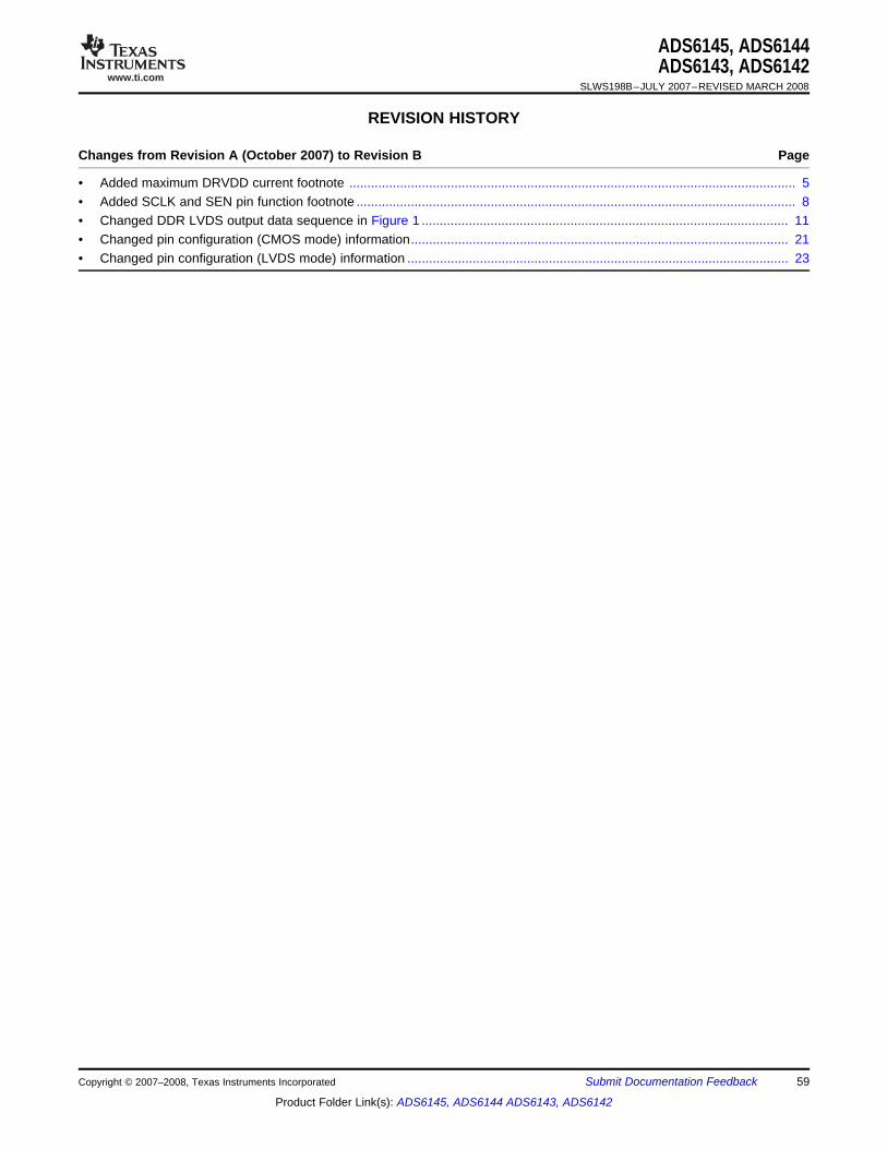
www.ti.com
ADS6145, ADS6144ADS6143, ADS6142
SLWS198B–JULY 2007–REVISED MARCH 2008
REVISION HISTORY
Changes from Revision A (October 2007) to Revision B ............................................................................................... Page
• Added maximum DRVDD current footnote ........................................................................................................................... 5• Added SCLK and SEN pin function footnote ......................................................................................................................... 8• Changed DDR LVDS output data sequence in Figure 1 ..................................................................................................... 11• Changed pin configuration (CMOS mode) information........................................................................................................ 21• Changed pin configuration (LVDS mode) information ......................................................................................................... 23
Copyright © 2007–2008, Texas Instruments Incorporated Submit Documentation Feedback 59
Product Folder Link(s): ADS6145, ADS6144 ADS6143, ADS6142
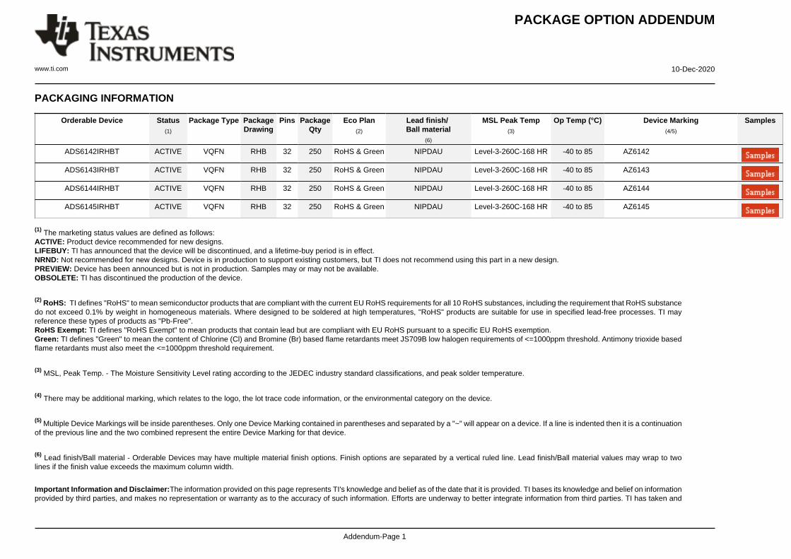
PACKAGE OPTION ADDENDUM
www.ti.com 10-Dec-2020
Addendum-Page 1
PACKAGING INFORMATION
Orderable Device Status(1)
Package Type PackageDrawing
Pins PackageQty
Eco Plan(2)
Lead finish/Ball material
(6)
MSL Peak Temp(3)
Op Temp (°C) Device Marking(4/5)
Samples
ADS6142IRHBT ACTIVE VQFN RHB 32 250 RoHS & Green NIPDAU Level-3-260C-168 HR -40 to 85 AZ6142
ADS6143IRHBT ACTIVE VQFN RHB 32 250 RoHS & Green NIPDAU Level-3-260C-168 HR -40 to 85 AZ6143
ADS6144IRHBT ACTIVE VQFN RHB 32 250 RoHS & Green NIPDAU Level-3-260C-168 HR -40 to 85 AZ6144
ADS6145IRHBT ACTIVE VQFN RHB 32 250 RoHS & Green NIPDAU Level-3-260C-168 HR -40 to 85 AZ6145
(1) The marketing status values are defined as follows:ACTIVE: Product device recommended for new designs.LIFEBUY: TI has announced that the device will be discontinued, and a lifetime-buy period is in effect.NRND: Not recommended for new designs. Device is in production to support existing customers, but TI does not recommend using this part in a new design.PREVIEW: Device has been announced but is not in production. Samples may or may not be available.OBSOLETE: TI has discontinued the production of the device.
(2) RoHS: TI defines "RoHS" to mean semiconductor products that are compliant with the current EU RoHS requirements for all 10 RoHS substances, including the requirement that RoHS substancedo not exceed 0.1% by weight in homogeneous materials. Where designed to be soldered at high temperatures, "RoHS" products are suitable for use in specified lead-free processes. TI mayreference these types of products as "Pb-Free".RoHS Exempt: TI defines "RoHS Exempt" to mean products that contain lead but are compliant with EU RoHS pursuant to a specific EU RoHS exemption.Green: TI defines "Green" to mean the content of Chlorine (Cl) and Bromine (Br) based flame retardants meet JS709B low halogen requirements of <=1000ppm threshold. Antimony trioxide basedflame retardants must also meet the <=1000ppm threshold requirement.
(3) MSL, Peak Temp. - The Moisture Sensitivity Level rating according to the JEDEC industry standard classifications, and peak solder temperature.
(4) There may be additional marking, which relates to the logo, the lot trace code information, or the environmental category on the device.
(5) Multiple Device Markings will be inside parentheses. Only one Device Marking contained in parentheses and separated by a "~" will appear on a device. If a line is indented then it is a continuationof the previous line and the two combined represent the entire Device Marking for that device.
(6) Lead finish/Ball material - Orderable Devices may have multiple material finish options. Finish options are separated by a vertical ruled line. Lead finish/Ball material values may wrap to twolines if the finish value exceeds the maximum column width.
Important Information and Disclaimer:The information provided on this page represents TI's knowledge and belief as of the date that it is provided. TI bases its knowledge and belief on informationprovided by third parties, and makes no representation or warranty as to the accuracy of such information. Efforts are underway to better integrate information from third parties. TI has taken and
PACKAGE OPTION ADDENDUM
www.ti.com 10-Dec-2020
Addendum-Page 2
continues to take reasonable steps to provide representative and accurate information but may not have conducted destructive testing or chemical analysis on incoming materials and chemicals.TI and TI suppliers consider certain information to be proprietary, and thus CAS numbers and other limited information may not be available for release.
In no event shall TI's liability arising out of such information exceed the total purchase price of the TI part(s) at issue in this document sold by TI to Customer on an annual basis.
OTHER QUALIFIED VERSIONS OF ADS6142 :
NOTE: Qualified Version Definitions:

www.ti.com
GENERIC PACKAGE VIEW
Images above are just a representation of the package family, actual package may vary.Refer to the product data sheet for package details.
VQFN - 1 mm max heightRHB 32PLASTIC QUAD FLATPACK - NO LEAD5 x 5, 0.5 mm pitch
4224745/A
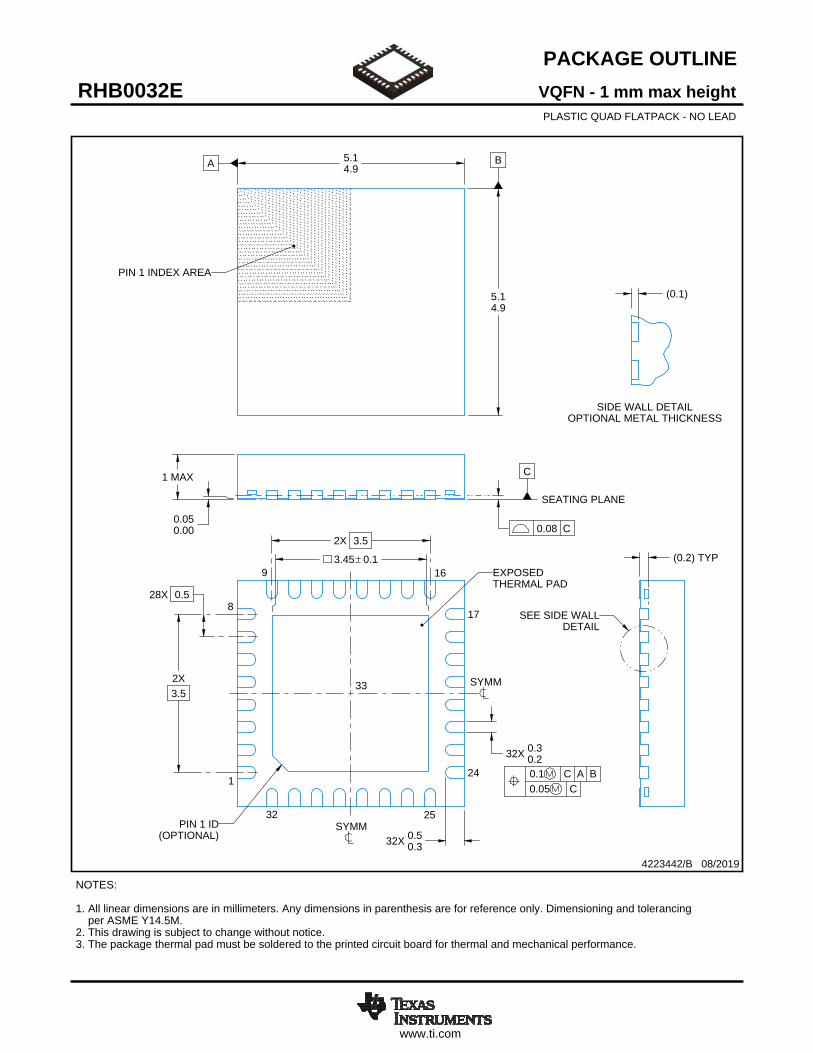
www.ti.com
PACKAGE OUTLINE
C
32X 0.30.2
3.45 0.1
32X 0.50.3
1 MAX
(0.2) TYP
0.050.00
28X 0.5
2X3.5
2X 3.5
A 5.14.9
B
5.14.9
(0.1)
VQFN - 1 mm max heightRHB0032EPLASTIC QUAD FLATPACK - NO LEAD
4223442/B 08/2019
PIN 1 INDEX AREA
0.08 C
SEATING PLANE
1
817
24
9 16
32 25
(OPTIONAL)PIN 1 ID
0.1 C A B0.05 C
EXPOSEDTHERMAL PAD
33 SYMM
SYMM
NOTES: 1. All linear dimensions are in millimeters. Any dimensions in parenthesis are for reference only. Dimensioning and tolerancing per ASME Y14.5M. 2. This drawing is subject to change without notice. 3. The package thermal pad must be soldered to the printed circuit board for thermal and mechanical performance.
SCALE 3.000
SEE SIDE WALLDETAIL
20.000
SIDE WALL DETAILOPTIONAL METAL THICKNESS
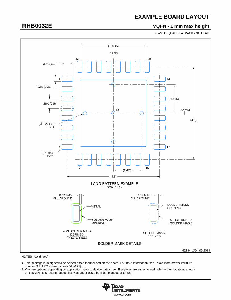
www.ti.com
EXAMPLE BOARD LAYOUT
(1.475)
0.07 MINALL AROUND
0.07 MAXALL AROUND
32X (0.25)
32X (0.6)
( 0.2) TYPVIA
28X (0.5)
(4.8)
(4.8)
(1.475)
( 3.45)
(R0.05)TYP
VQFN - 1 mm max heightRHB0032EPLASTIC QUAD FLATPACK - NO LEAD
4223442/B 08/2019
SYMM
1
8
9 16
17
24
2532
SYMM
LAND PATTERN EXAMPLESCALE:18X
NOTES: (continued) 4. This package is designed to be soldered to a thermal pad on the board. For more information, see Texas Instruments literature number SLUA271 (www.ti.com/lit/slua271).5. Vias are optional depending on application, refer to device data sheet. If any vias are implemented, refer to their locations shown on this view. It is recommended that vias under paste be filled, plugged or tented.
33
SOLDER MASKOPENING
METAL UNDERSOLDER MASK
SOLDER MASKDEFINED
METAL
SOLDER MASKOPENING
SOLDER MASK DETAILS
NON SOLDER MASKDEFINED
(PREFERRED)
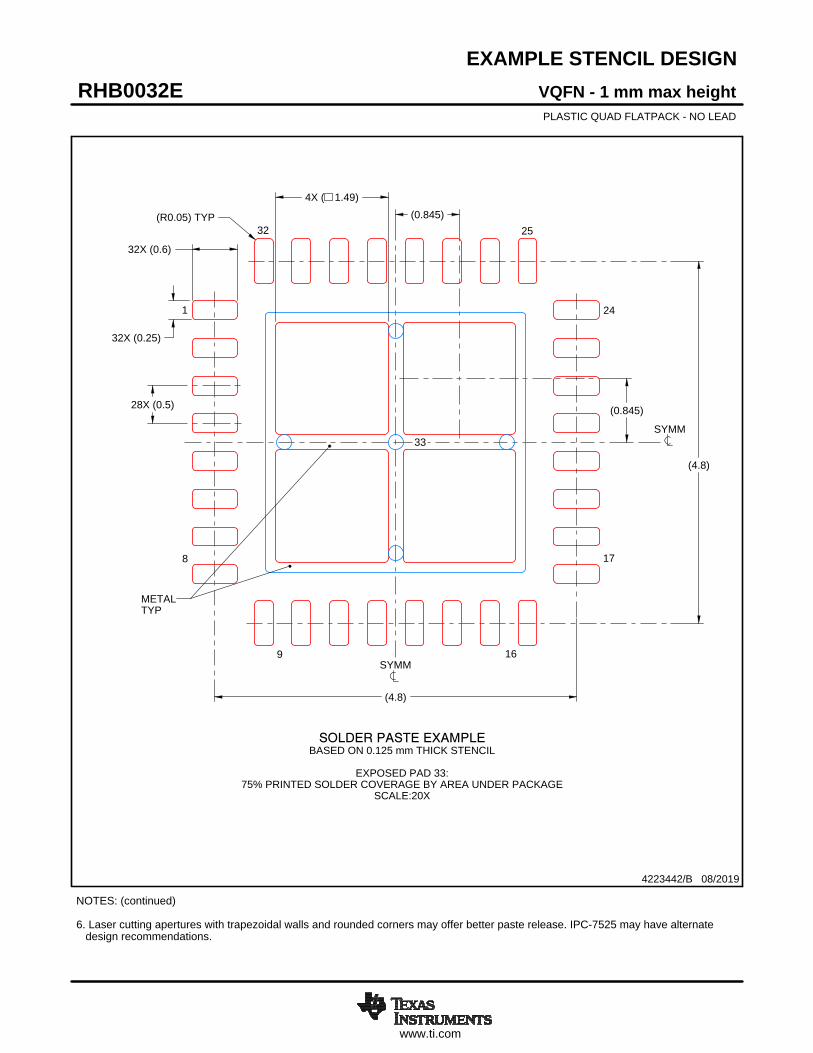
www.ti.com
EXAMPLE STENCIL DESIGN
32X (0.6)
32X (0.25)
28X (0.5)
(4.8)
(4.8)
4X ( 1.49)
(0.845)
(0.845)(R0.05) TYP
VQFN - 1 mm max heightRHB0032EPLASTIC QUAD FLATPACK - NO LEAD
4223442/B 08/2019
NOTES: (continued) 6. Laser cutting apertures with trapezoidal walls and rounded corners may offer better paste release. IPC-7525 may have alternate design recommendations.
33
SYMM
METALTYP
SOLDER PASTE EXAMPLEBASED ON 0.125 mm THICK STENCIL
EXPOSED PAD 33:
75% PRINTED SOLDER COVERAGE BY AREA UNDER PACKAGESCALE:20X
SYMM
1
8
9 16
17
24
2532

IMPORTANT NOTICE AND DISCLAIMERTI PROVIDES TECHNICAL AND RELIABILITY DATA (INCLUDING DATASHEETS), DESIGN RESOURCES (INCLUDING REFERENCEDESIGNS), APPLICATION OR OTHER DESIGN ADVICE, WEB TOOLS, SAFETY INFORMATION, AND OTHER RESOURCES “AS IS”AND WITH ALL FAULTS, AND DISCLAIMS ALL WARRANTIES, EXPRESS AND IMPLIED, INCLUDING WITHOUT LIMITATION ANYIMPLIED WARRANTIES OF MERCHANTABILITY, FITNESS FOR A PARTICULAR PURPOSE OR NON-INFRINGEMENT OF THIRDPARTY INTELLECTUAL PROPERTY RIGHTS.These resources are intended for skilled developers designing with TI products. You are solely responsible for (1) selecting the appropriateTI products for your application, (2) designing, validating and testing your application, and (3) ensuring your application meets applicablestandards, and any other safety, security, or other requirements. These resources are subject to change without notice. TI grants youpermission to use these resources only for development of an application that uses the TI products described in the resource. Otherreproduction and display of these resources is prohibited. No license is granted to any other TI intellectual property right or to any third partyintellectual property right. TI disclaims responsibility for, and you will fully indemnify TI and its representatives against, any claims, damages,costs, losses, and liabilities arising out of your use of these resources.TI’s products are provided subject to TI’s Terms of Sale (https:www.ti.com/legal/termsofsale.html) or other applicable terms available eitheron ti.com or provided in conjunction with such TI products. TI’s provision of these resources does not expand or otherwise alter TI’sapplicable warranties or warranty disclaimers for TI products.IMPORTANT NOTICE
Mailing Address: Texas Instruments, Post Office Box 655303, Dallas, Texas 75265Copyright © 2021, Texas Instruments Incorporated