OPA340, OPA2340, OPA4340 - Texas Instruments
44
ADS7816 12-Bit A/D DCLOCK D OUT OPA340 +5V V IN V+ 2 +In 3 -In V REF 8 4 GND Serial Interface 1 0.1 F m 0.1 F m 7 6 5 NOTE: A/D Input = 0 to V REF V = 0V to 5V for IN 0V to 5V output. RC network filters high-frequency noise. 500W 3300pF CS/SHDN Copyright © 2016, Texas Instruments Incorporated Product Folder Sample & Buy Technical Documents Tools & Software Support & Community Reference Design An IMPORTANT NOTICE at the end of this data sheet addresses availability, warranty, changes, use in safety-critical applications, intellectual property matters and other important disclaimers. PRODUCTION DATA. OPA340, OPA2340, OPA4340 SBOS073C – SEPTEMBER 1997 – REVISED AUGUST 2016 OPAx340 Single-Supply, Rail-to-Rail Operational Amplifiers MicroAmplifier™ Series 1 1 Features 1• Rail-to-Rail Input • Rail-to-Rail Output (Within 1 mV) • MicroSize Packages • Wide Bandwidth: 5.5 MHz • High Slew Rate: 6 V/μs • Low THD + Noise: 0.0007% (f = 1 kHz) • Low Quiescent Current: 750 μA/Channel • Single, Dual, and Quad Versions 2 Applications • Driving A/D Converters • PCMCIA Cards • Data Acquisition • Process Control • Audio Processing • Communications • Active Filters • Test Equipment 3 Description The OPA340 series rail-to-rail CMOS operational amplifiers are optimized for low-voltage, single-supply operation. Rail-to-rail input and output and high- speed operation make them ideal for driving sampling analog-to-digital (A/D) converters. They are also well- suited for general purpose and audio applications as well as providing I/V conversion at the output of digital-to-analog (D/A) converters. Single, dual, and quad versions have identical specifications for design flexibility. The OPA340 series operate on a single supply as low as 2.5 V with an input common-mode voltage range that extends 500 mV below ground and 500 mV above the positive supply. Output voltage swing is to within 1 mV of the supply rails with a 100-kΩ load. These devices offer excellent dynamic response (BW = 5.5 MHz, SR = 6 V/μs), yet quiescent current is only 750 A. Dual and quad designs feature completely independent circuitry for lowest crosstalk and freedom from interaction. The single (OPA340) packages are the tiny 5-pin SOT-23 surface mount, 8-pin SOIC surface mount, and 8-pin DIP. The dual (OPA2340) comes in the miniature 8-pin VSSOP surface mount, 8-pin SOIC surface mount, and 8-pin PDIP packages. The quad (OPA4340) packages are the space-saving 16-pin SSOP surface mount and 14-pin SOIC surface mount. All are specified from –40°C to 85°C and operate from –55°C to 125°C. A SPICE macromodel is available for design analysis. Device Information (1) PART NUMBER PACKAGE BODY SIZE (NOM) OPA340 SOT-23 (5) 3.00 mm × 3.00 mm OPA340, OPA2340 PDIP (8) 9.81 mm × 6.35 mm SOIC (8) 4.90 mm × 3.91 mm OPA2340 VSSOP (8) 3.00 mm × 3.00 mm OPA4340 SOIC (14) 8.65 mm × 3.91 mm SSOP (16) 4.90 mm × 3.90 mm (1) For all available packages, see the orderable addendum at the end of the data sheet. OPA340 in Noninverting Configuration Driving ADS7816
-
Upload
khangminh22 -
Category
Documents
-
view
0 -
download
0
Transcript of OPA340, OPA2340, OPA4340 - Texas Instruments

ADS7816
12-Bit A/D
DCLOCK
DOUTOPA340
+5V
VIN
V+
2
+In
3
-In
VREF8
4GND
Serial
Interface
1
0.1 Fm 0.1 Fm
7
6
5
NOTE: A/D Input = 0 to VREF
V = 0V to 5V forIN
0V to 5V output.
RC network filters high-frequency noise.
500W
3300pF
CS/SHDN
Copyright © 2016, Texas Instruments Incorporated
Product
Folder
Sample &Buy
Technical
Documents
Tools &
Software
Support &Community
ReferenceDesign
An IMPORTANT NOTICE at the end of this data sheet addresses availability, warranty, changes, use in safety-critical applications,intellectual property matters and other important disclaimers. PRODUCTION DATA.
OPA340, OPA2340, OPA4340SBOS073C –SEPTEMBER 1997–REVISED AUGUST 2016
OPAx340 Single-Supply, Rail-to-Rail Operational AmplifiersMicroAmplifier™ Series
1
1 Features1• Rail-to-Rail Input• Rail-to-Rail Output (Within 1 mV)• MicroSize Packages• Wide Bandwidth: 5.5 MHz• High Slew Rate: 6 V/µs• Low THD + Noise: 0.0007% (f = 1 kHz)• Low Quiescent Current: 750 µA/Channel• Single, Dual, and Quad Versions
2 Applications• Driving A/D Converters• PCMCIA Cards• Data Acquisition• Process Control• Audio Processing• Communications• Active Filters• Test Equipment
3 DescriptionThe OPA340 series rail-to-rail CMOS operationalamplifiers are optimized for low-voltage, single-supplyoperation. Rail-to-rail input and output and high-speed operation make them ideal for driving samplinganalog-to-digital (A/D) converters. They are also well-suited for general purpose and audio applications aswell as providing I/V conversion at the output ofdigital-to-analog (D/A) converters. Single, dual, andquad versions have identical specifications for designflexibility.
The OPA340 series operate on a single supply as lowas 2.5 V with an input common-mode voltage rangethat extends 500 mV below ground and 500 mVabove the positive supply. Output voltage swing is towithin 1 mV of the supply rails with a 100-kΩ load.These devices offer excellent dynamic response(BW = 5.5 MHz, SR = 6 V/µs), yet quiescent currentis only 750 A. Dual and quad designs featurecompletely independent circuitry for lowest crosstalkand freedom from interaction.
The single (OPA340) packages are the tiny 5-pinSOT-23 surface mount, 8-pin SOIC surface mount,and 8-pin DIP. The dual (OPA2340) comes in theminiature 8-pin VSSOP surface mount, 8-pin SOICsurface mount, and 8-pin PDIP packages. The quad(OPA4340) packages are the space-saving 16-pinSSOP surface mount and 14-pin SOIC surfacemount. All are specified from –40°C to 85°C andoperate from –55°C to 125°C. A SPICE macromodelis available for design analysis.
Device Information(1)
PART NUMBER PACKAGE BODY SIZE (NOM)OPA340 SOT-23 (5) 3.00 mm × 3.00 mm
OPA340, OPA2340PDIP (8) 9.81 mm × 6.35 mmSOIC (8) 4.90 mm × 3.91 mm
OPA2340 VSSOP (8) 3.00 mm × 3.00 mm
OPA4340SOIC (14) 8.65 mm × 3.91 mmSSOP (16) 4.90 mm × 3.90 mm
(1) For all available packages, see the orderable addendum atthe end of the data sheet.
OPA340 in Noninverting Configuration Driving ADS7816
2
OPA340, OPA2340, OPA4340SBOS073C –SEPTEMBER 1997–REVISED AUGUST 2016 www.ti.com
Product Folder Links: OPA340 OPA2340 OPA4340
Submit Documentation Feedback Copyright © 1997–2016, Texas Instruments Incorporated
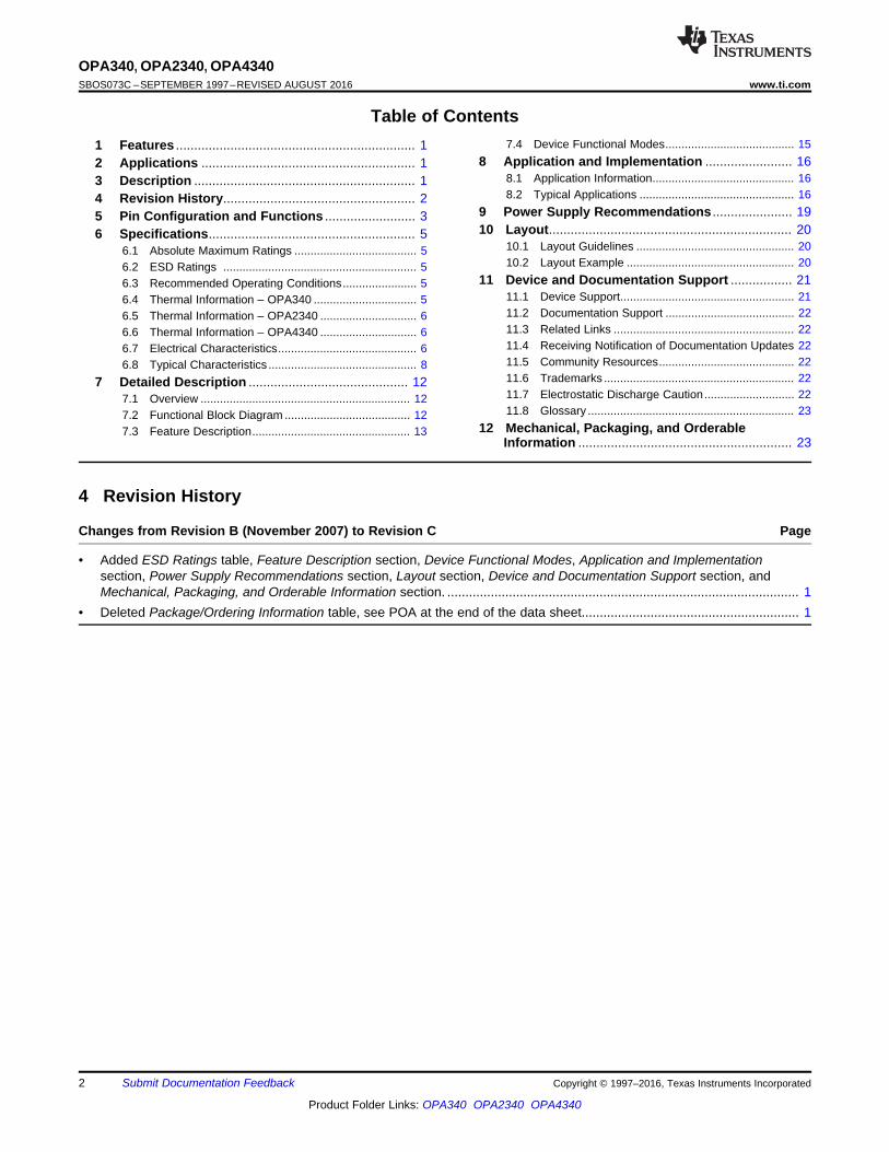
Table of Contents1 Features .................................................................. 12 Applications ........................................................... 13 Description ............................................................. 14 Revision History..................................................... 25 Pin Configuration and Functions ......................... 36 Specifications......................................................... 5
6.1 Absolute Maximum Ratings ...................................... 56.2 ESD Ratings ............................................................ 56.3 Recommended Operating Conditions....................... 56.4 Thermal Information – OPA340 ................................ 56.5 Thermal Information – OPA2340 .............................. 66.6 Thermal Information – OPA4340 .............................. 66.7 Electrical Characteristics........................................... 66.8 Typical Characteristics .............................................. 8
7 Detailed Description ............................................ 127.1 Overview ................................................................. 127.2 Functional Block Diagram ....................................... 127.3 Feature Description................................................. 13
7.4 Device Functional Modes........................................ 158 Application and Implementation ........................ 16
8.1 Application Information............................................ 168.2 Typical Applications ................................................ 16
9 Power Supply Recommendations ...................... 1910 Layout................................................................... 20
10.1 Layout Guidelines ................................................. 2010.2 Layout Example .................................................... 20
11 Device and Documentation Support ................. 2111.1 Device Support...................................................... 2111.2 Documentation Support ........................................ 2211.3 Related Links ........................................................ 2211.4 Receiving Notification of Documentation Updates 2211.5 Community Resources.......................................... 2211.6 Trademarks ........................................................... 2211.7 Electrostatic Discharge Caution............................ 2211.8 Glossary ................................................................ 23
12 Mechanical, Packaging, and OrderableInformation ........................................................... 23
4 Revision History
Changes from Revision B (November 2007) to Revision C Page
• Added ESD Ratings table, Feature Description section, Device Functional Modes, Application and Implementationsection, Power Supply Recommendations section, Layout section, Device and Documentation Support section, andMechanical, Packaging, and Orderable Information section. ................................................................................................. 1
• Deleted Package/Ordering Information table, see POA at the end of the data sheet............................................................ 1
3
OPA340, OPA2340, OPA4340www.ti.com SBOS073C –SEPTEMBER 1997–REVISED AUGUST 2016
Product Folder Links: OPA340 OPA2340 OPA4340
Submit Documentation FeedbackCopyright © 1997–2016, Texas Instruments Incorporated
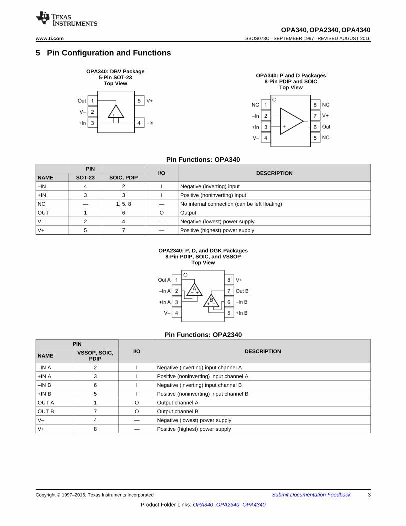
5 Pin Configuration and Functions
OPA340: DBV Package5-Pin SOT-23
Top ViewOPA340: P and D Packages
8-Pin PDIP and SOICTop View
Pin Functions: OPA340PIN
I/O DESCRIPTIONNAME SOT-23 SOIC, PDIP–IN 4 2 I Negative (inverting) input+IN 3 3 I Positive (noninverting) inputNC — 1, 5, 8 — No internal connection (can be left floating)OUT 1 6 O OutputV– 2 4 — Negative (lowest) power supplyV+ 5 7 — Positive (highest) power supply
OPA2340: P, D, and DGK Packages8-Pin PDIP, SOIC, and VSSOP
Top View
Pin Functions: OPA2340PIN
I/O DESCRIPTIONNAME VSSOP, SOIC,
PDIP–IN A 2 I Negative (inverting) input channel A+IN A 3 I Positive (noninverting) input channel A–IN B 6 I Negative (inverting) input channel B+IN B 5 I Positive (noninverting) input channel BOUT A 1 O Output channel AOUT B 7 O Output channel BV– 4 — Negative (lowest) power supplyV+ 8 — Positive (highest) power supply
4
OPA340, OPA2340, OPA4340SBOS073C –SEPTEMBER 1997–REVISED AUGUST 2016 www.ti.com
Product Folder Links: OPA340 OPA2340 OPA4340
Submit Documentation Feedback Copyright © 1997–2016, Texas Instruments Incorporated
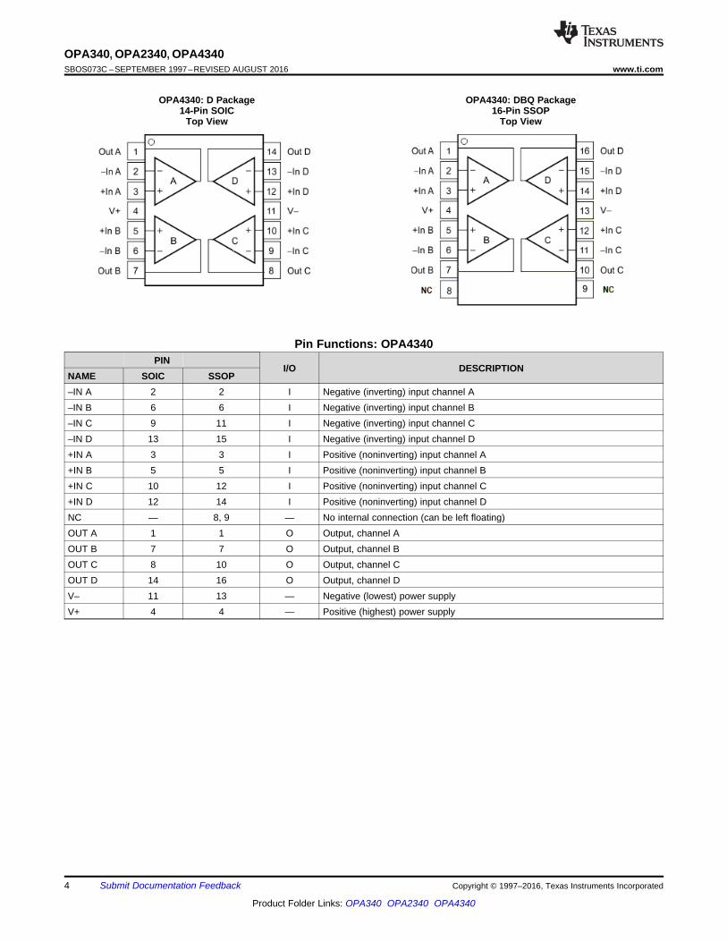
OPA4340: D Package14-Pin SOIC
Top View
OPA4340: DBQ Package16-Pin SSOP
Top View
Pin Functions: OPA4340PIN
I/O DESCRIPTIONNAME SOIC SSOP–IN A 2 2 I Negative (inverting) input channel A–IN B 6 6 I Negative (inverting) input channel B–IN C 9 11 I Negative (inverting) input channel C–IN D 13 15 I Negative (inverting) input channel D+IN A 3 3 I Positive (noninverting) input channel A+IN B 5 5 I Positive (noninverting) input channel B+IN C 10 12 I Positive (noninverting) input channel C+IN D 12 14 I Positive (noninverting) input channel DNC — 8, 9 — No internal connection (can be left floating)OUT A 1 1 O Output, channel AOUT B 7 7 O Output, channel BOUT C 8 10 O Output, channel COUT D 14 16 O Output, channel DV– 11 13 — Negative (lowest) power supplyV+ 4 4 — Positive (highest) power supply
5
OPA340, OPA2340, OPA4340www.ti.com SBOS073C –SEPTEMBER 1997–REVISED AUGUST 2016
Product Folder Links: OPA340 OPA2340 OPA4340
Submit Documentation FeedbackCopyright © 1997–2016, Texas Instruments Incorporated
(1) Stresses beyond those listed under Absolute Maximum Ratings may cause permanent damage to the device. These are stress ratingsonly, which do not imply functional operation of the device at these or any other conditions beyond those indicated under RecommendedOperating Conditions. Exposure to absolute-maximum-rated conditions for extended periods may affect device reliability.
(2) Input terminals are diode-clamped to the power-supply rails. Input signals that can swing more than 0.5 V beyond the supply rails shouldbe current limited to 10 mA or less.
(3) Short-circuit to ground, one amplifier per package.
6 Specifications
6.1 Absolute Maximum Ratingsover operating free-air temperature range (unless otherwise noted) (1)
MIN MAX UNIT
VoltageSupply voltage 5.5
VSignal input terminals (2) –0.5 0.5
CurrentSignal input terminals (2) 10 mAOutput short circuit (3) Continuous
TemperatureOperating, TA –55 125
°CJunction, TJ 150Storage, Tstg –55 125
(1) JEDEC document JEP155 states that 500-V HBM allows safe manufacturing with a standard ESD control process.(2) JEDEC document JEP157 states that 250-V CDM allows safe manufacturing with a standard ESD control process.
6.2 ESD RatingsVALUE UNIT
V(ESD)Electrostaticdischarge
Human-body model (HBM), per ANSI/ESDA/JEDEC JS-001 (1) ±600V
Charged-device model (CDM), per JEDEC specification JESD22-C101 (2) ±250
6.3 Recommended Operating Conditionsover operating free-air temperature range (unless otherwise noted)
MIN MAX UNITSupply voltage 2.7 5.5 VSpecified temperature –40 125 °C
(1) For more information about traditional and new thermal metrics, see the Semiconductor and IC Package Thermal Metrics applicationreport.
6.4 Thermal Information – OPA340
THERMAL METRIC (1)
OPA340
UNITDBV(SOT-23)
P(PDIP)
D(SOIC)
D(SOIC)
5 PINS 8 PINS 8 PINS 14 PINS
RθJA Junction-to-ambient thermal resistance 207.9 53.1 142 83.8 °C/W
RθJC(top) Junction-to-case (top) thermal resistance 71.2 42.5 90.2 70.7 °C/W
RθJB Junction-to-board thermal resistance 36.0 30.3 82.5 59.5 °C/W
ψJT Junction-to-top characterization parameter 2.0 19.7 39.4 11.6 °C/W
ψJB Junction-to-board characterization parameter 35.2 30.2 82 37.7 °C/W
RθJC(bot) Junction-to-case (bottom) thermal resistance — — — — °C/W
6
OPA340, OPA2340, OPA4340SBOS073C –SEPTEMBER 1997–REVISED AUGUST 2016 www.ti.com
Product Folder Links: OPA340 OPA2340 OPA4340
Submit Documentation Feedback Copyright © 1997–2016, Texas Instruments Incorporated
(1) For more information about traditional and new thermal metrics, see the Semiconductor and IC Package Thermal Metrics applicationreport.
6.5 Thermal Information – OPA2340
THERMAL METRIC (1)
OPA2340
UNITD(SOIC)
DGK(VSSOP)
8 PINS 8 PINS
RθJA Junction-to-ambient thermal resistance 138.4 169.2 °C/W
RθJC(top) Junction-to-case (top) thermal resistance 89.5 62.8 °C/W
RθJB Junction-to-board thermal resistance 78.6 89.8 °C/W
ψJT Junction-to-top characterization parameter 29.9 7.5 °C/W
ψJB Junction-to-board characterization parameter 78.1 88.2 °C/W
RθJC(bot) Junction-to-case (bottom) thermal resistance — — °C/W
(1) For more information about traditional and new thermal metrics, see the Semiconductor and IC Package Thermal Metrics applicationreport.
6.6 Thermal Information – OPA4340
THERMAL METRIC (1)
OPA4340
UNITDBQ(SSOP)
16 PINS
RθJA Junction-to-ambient thermal resistance 115.8 °C/W
RθJC(top) Junction-to-case (top) thermal resistance 67 °C/W
RθJB Junction-to-board thermal resistance 58.3 °C/W
ψJT Junction-to-top characterization parameter 19.9 °C/W
ψJB Junction-to-board characterization parameter 57.9 °C/W
RθJC(bot) Junction-to-case (bottom) thermal resistance — °C/W
(1) VS = 5 V.
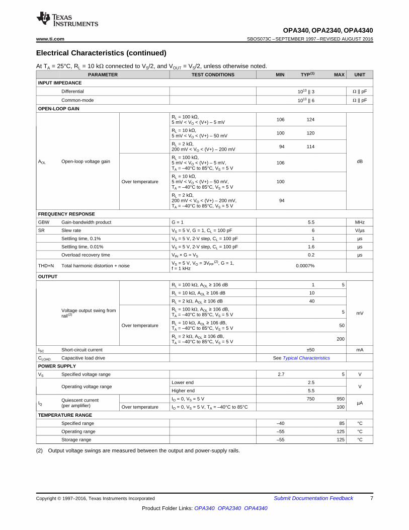
6.7 Electrical CharacteristicsAt TA = 25°C, RL = 10 kΩ connected to VS/2, and VOUT = VS/2, unless otherwise noted.
PARAMETER TEST CONDITIONS MIN TYP (1) MAX UNIT
OFFSET VOLTAGE
VOS Input offset voltage VS = 5 V ±150 ±500 µV
dVOS/dt Input offset voltage vs temperature TA = –40°C to 85°C, VS = 5 V ±2.5 µV/°C
PSRR Input offset voltage vspower supply
VS = 2.7 V to 5.5 V, VCM = 0 V 30 120 µV/V
Over temperature VS = 2.7 V to 5.5 V, VCM = 0 V,TA = –40°C to 85°C, VS = 5 V 120 µV/°C
Channel separation, DC 0.2 µV/V
INPUT BIAS CURRENT
IS Input bias current±0.2 ±10
pAOver temperature TA = –40°C to 85°C, VS = 5 V ±60
IOS Input offset current ±0.2 ±10 pA
NOISE
Input voltage noise f = 0.1 kHz to 50 kHz 8 µVRMS
en Input voltage noise density f = 1 kHz 25 nV/√Hz
in Current noise density f = 1 kHz 3 fA/√Hz
INPUT VOLTAGE RANGE
VCM Common-mode voltage range –0.3 (V+) + 0.3 V
CMRR Common-mode rejection ratio
–0.3 V < VCM < (V+) – 1.8 V 80 92
dBVS = 5 V, –0.3 V < VCM < 5.3 V 70 84
VS = 2.7 V, –0.3 V < VCM < 3 V 66 80
7
OPA340, OPA2340, OPA4340www.ti.com SBOS073C –SEPTEMBER 1997–REVISED AUGUST 2016
Product Folder Links: OPA340 OPA2340 OPA4340
Submit Documentation FeedbackCopyright © 1997–2016, Texas Instruments Incorporated
Electrical Characteristics (continued)At TA = 25°C, RL = 10 kΩ connected to VS/2, and VOUT = VS/2, unless otherwise noted.
PARAMETER TEST CONDITIONS MIN TYP (1) MAX UNIT
(2) Output voltage swings are measured between the output and power-supply rails.
INPUT IMPEDANCE
Differential 1013 || 3 Ω || pF
Common-mode 1013 || 6 Ω || pF
OPEN-LOOP GAIN
AOL Open-loop voltage gain
RL = 100 kΩ,5 mV < VO < (V+) – 5 mV 106 124
dB
RL = 10 kΩ,5 mV < VO < (V+) – 50 mV 100 120
RL = 2 kΩ,200 mV < VO < (V+) – 200 mV 94 114
Over temperature
RL = 100 kΩ,5 mV < VO < (V+) – 5 mV,TA = –40°C to 85°C, VS = 5 V
106
RL = 10 kΩ,5 mV < VO < (V+) – 50 mV,TA = –40°C to 85°C, VS = 5 V
100
RL = 2 kΩ,200 mV < VO < (V+) – 200 mV,TA = –40°C to 85°C, VS = 5 V
94
FREQUENCY RESPONSE
GBW Gain-bandwidth product G = 1 5.5 MHz
SR Slew rate VS = 5 V, G = 1, CL = 100 pF 6 V/µs
Settling time, 0.1% VS = 5 V, 2-V step, CL = 100 pF 1 µs
Settling time, 0.01% VS = 5 V, 2-V step, CL = 100 pF 1.6 µs
Overload recovery time VIN × G = VS 0.2 µs
THD+N Total harmonic distortion + noise VS = 5 V, VO = 3VPP(2), G = 1,
f = 1 kHz 0.0007%
OUTPUT
Voltage output swing fromrail (2)
RL = 100 kΩ, AOL ≥ 106 dB 1 5
mV
RL = 10 kΩ, AOL ≥ 106 dB 10
RL = 2 kΩ, AOL ≥ 106 dB 40
Over temperature
RL = 100 kΩ, AOL ≥ 106 dB,TA = –40°C to 85°C, VS = 5 V 5
RL = 10 kΩ, AOL ≥ 106 dB,TA = –40°C to 85°C, VS = 5 V 50
RL = 2 kΩ, AOL ≥ 106 dB,TA = –40°C to 85°C, VS = 5 V 200
ISC Short-circuit current ±50 mA
CLOAD Capacitive load drive See Typical Characteristics
POWER SUPPLY
VS Specified voltage range 2.7 5 V
Operating voltage rangeLower end 2.5
VHigher end 5.5
IQQuiescent current(per amplifier)
IO = 0, VS = 5 V 750 950µA
Over temperature IO = 0, VS = 5 V, TA = –40°C to 85°C 100
TEMPERATURE RANGE
Specified range –40 85 °C
Operating range –55 125 °C
Storage range –55 125 °C
0.1
0.01
0.001
0.0001
TH
D+
N (
%)
Frequency (Hz)
20 100 1k 10k 20k
R = 600L
G = 10
G = 1
R = 2kWL
R = 2kWL
R = 10kWL
R = 600L
R = 10kWL
5k
4k
3k
2k
1k
0
Outp
ut R
esis
tance (
)W
Frequency (Hz)
10 100 1k 10k 100k 1M 10M
G = 100
G = 10
G = 1
10k
1k
100
10
1
1k
100
10
1
0.1
Voltage N
ois
e (
nV
/)
ÖH
z
Frequency (Hz)
1 10 100 1k 10k 100k 1M
Curr
ent N
ois
e (
fA/
)ÖH
z
Current Noise
Voltage Noise
Frequency (Hz)
Ch
an
ne
l S
ep
ara
tio
n (
dB
)
140
130
120
110
100
10010 1k 10k 100k
G = 1, All Channels
0.1 1
160
140
120
100
80
60
40
20
0
-20
Voltage G
ain
(dB
)
0
-45
-90
-135
-180
Phase (
)°
Frequency (Hz)
10 100 1k 10k 100k 1M 10M
100
80
60
40
20
0
PS
RR
, C
MR
R (
dB
)
Frequency (Hz)
1 10 100 1k 10k 100k 1M
PSRR
CMRR
8
OPA340, OPA2340, OPA4340SBOS073C –SEPTEMBER 1997–REVISED AUGUST 2016 www.ti.com
Product Folder Links: OPA340 OPA2340 OPA4340
Submit Documentation Feedback Copyright © 1997–2016, Texas Instruments Incorporated
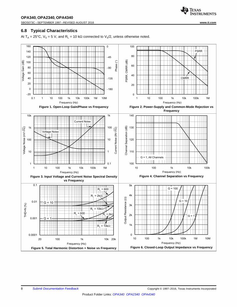
6.8 Typical CharacteristicsAt TA = 25°C, VS = 5 V, and RL = 10 kΩ connected to VS/2, unless otherwise noted.
Figure 1. Open-Loop Gain/Phase vs Frequency Figure 2. Power-Supply and Common-Mode Rejection vsFrequency
Figure 3. Input Voltage and Current Noise Spectral Densityvs Frequency
Figure 4. Channel Separation vs Frequency
Figure 5. Total Harmonic Distortion + Noise vs Frequency Figure 6. Closed-Loop Output Impedance vs Frequency
Temperature ( C)°
Sh
ort
-Circu
it C
urr
en
t (m
A)
100
90
80
70
60
50
40
30
20
10
0
-75 -50 -25 0 25 50 75 100 125
-ISC
+ISC
Supply Voltage (V)
Short
-Circuit C
urr
ent (m
A)
60
50
40
30
2.0 2.5 3.0 3.5 4.0 4.5 5.0 5.5 6.0
+ISC
-ISC
1000
900
800
700
600
500
Quie
scent C
urr
ent (
A)
m
Temperature ( C)°
-75 -50 -25 0 25 50 75 100 125
Per Amplifier
Supply Voltage (V)
Quie
scent C
urr
ent (
A)
m
800
750
700
650
600
2.0 2.5 3.0 3.5 4.0 4.5 5.0 5.5 6.0
Per Amplifier
130
120
110
100
90
80
A, P
SR
R (
dB
)O
L
Temperature ( C)°
-75 -50 -25 0 25 50 75 100 125
R = 100kWL
R = 10kWL
R = 2kWL
AOL
PSRR
100
90
80
70
60
50
40
CM
RR
(dB
)
Temperature ( C)°
-75 -50 -25 0 25 50 75 100 125
V = 5V, V = -0.3V to 5.3VS CM
V = 2.7V, V = -0.3V to 3VS CM
V = 2.7V to 5V, V = -0.3V to (V+) 1.8V-S CM
9
OPA340, OPA2340, OPA4340www.ti.com SBOS073C –SEPTEMBER 1997–REVISED AUGUST 2016
Product Folder Links: OPA340 OPA2340 OPA4340
Submit Documentation FeedbackCopyright © 1997–2016, Texas Instruments Incorporated
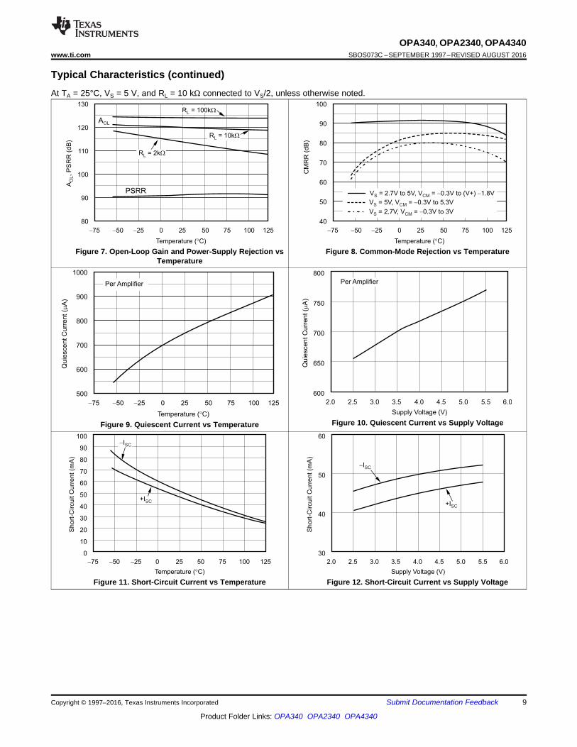
Typical Characteristics (continued)At TA = 25°C, VS = 5 V, and RL = 10 kΩ connected to VS/2, unless otherwise noted.
Figure 7. Open-Loop Gain and Power-Supply Rejection vsTemperature
Figure 8. Common-Mode Rejection vs Temperature
Figure 9. Quiescent Current vs Temperature Figure 10. Quiescent Current vs Supply Voltage
Figure 11. Short-Circuit Current vs Temperature Figure 12. Short-Circuit Current vs Supply Voltage
Perc
ent ofA
mplif
iers
(%
)
Offset Voltage ( V)m
18
16
14
12
10
8
6
4
2
0
Typical production
distribution of
packaged units.
-500
-400
-300
-200
-100 0
100
200
300
400
500
Pe
rce
nt
ofA
mp
lifie
rs (
%)
Offset Voltage Drift ( V/ C)m °
25
20
15
10
5
0
Typical production
distribution of
packaged units.
0 1 2 3 4 5 6 7 8 9 10 11 12 13 15
Output Current (mA)
Outp
ut V
oltage (
V)
5
4
3
2
1
00 ±10
+125 C° +25 C° -55 C°
+125 C° +25 C° -55 C°
±20 ±30 ±40 ±50 ±60 ±70 ±80 ±90 ±100 10M1M
Frequency (Hz)
100k
6
5
4
3
2
1
0
Ou
tpu
t V
olta
ge
(V
)P
P
V = 5.5VS
V = 2.7VS
Maximum output
voltage without
slew rate-induced
distortion.
Common-Mode Voltage (V)
Inp
ut
Bia
s C
urr
en
t (p
A)
1.0
0.8
0.6
0.4
0.2
0
-0.2
-0.4
-0.6
-0.8
-1.0
-1 0 1 2 3 4 5 6-75 -50 -25 0 25 50 75 100 125
1k
100
10
1
0.1
Input B
ias C
urr
ent (p
A)
Temperature ( C)°
10
OPA340, OPA2340, OPA4340SBOS073C –SEPTEMBER 1997–REVISED AUGUST 2016 www.ti.com
Product Folder Links: OPA340 OPA2340 OPA4340
Submit Documentation Feedback Copyright © 1997–2016, Texas Instruments Incorporated
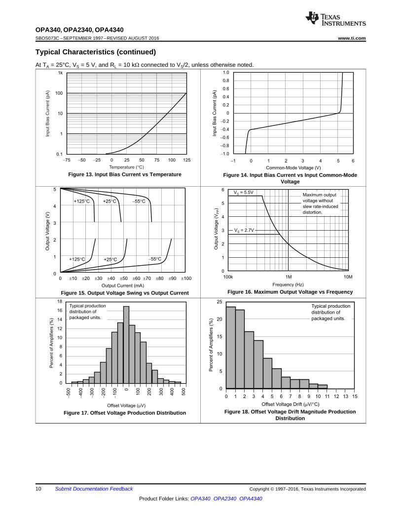
Typical Characteristics (continued)At TA = 25°C, VS = 5 V, and RL = 10 kΩ connected to VS/2, unless otherwise noted.
Figure 13. Input Bias Current vs Temperature Figure 14. Input Bias Current vs Input Common-ModeVoltage
Figure 15. Output Voltage Swing vs Output Current Figure 16. Maximum Output Voltage vs Frequency
Figure 17. Offset Voltage Production Distribution Figure 18. Offset Voltage Drift Magnitude ProductionDistribution
100
10
1
0.1
Se
ttlin
gT
ime
(s)
m
Closed-Loop Gain (V/V)
1 10 100 1000
0.1%
0.01%
10k1000
Load Capacitance (pF)
100
60
50
40
30
20
10
0
Ove
rsh
oo
t (%
) G = +1
G = 1-
G = 5-
See text for
reducing overshoot.
G = +5
50
mV
/div
1 s/divm
1V
/div
1 s/divm
11
OPA340, OPA2340, OPA4340www.ti.com SBOS073C –SEPTEMBER 1997–REVISED AUGUST 2016
Product Folder Links: OPA340 OPA2340 OPA4340
Submit Documentation FeedbackCopyright © 1997–2016, Texas Instruments Incorporated
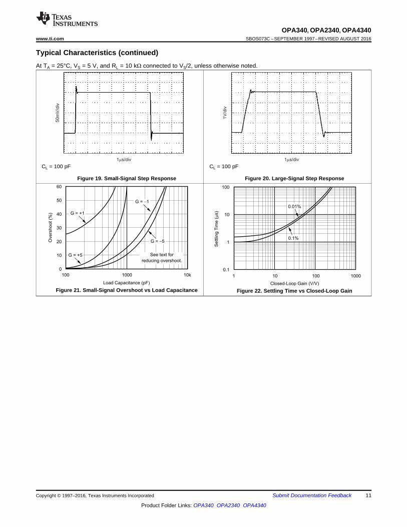
Typical Characteristics (continued)At TA = 25°C, VS = 5 V, and RL = 10 kΩ connected to VS/2, unless otherwise noted.
CL = 100 pF
Figure 19. Small-Signal Step Response
CL = 100 pF
Figure 20. Large-Signal Step Response
Figure 21. Small-Signal Overshoot vs Load Capacitance Figure 22. Settling Time vs Closed-Loop Gain
VBIAS1
VBIAS2
V +IN V -IN
Class AB
Control
Circuitry
VO
V-
(Ground)
V+
Reference
Current
Copyright © 2016, Texas Instruments Incorporated
V = +5, G = +1, R = 10kWS L
5
5
0
VIN
VOUT
2V
/div
12
OPA340, OPA2340, OPA4340SBOS073C –SEPTEMBER 1997–REVISED AUGUST 2016 www.ti.com
Product Folder Links: OPA340 OPA2340 OPA4340
Submit Documentation Feedback Copyright © 1997–2016, Texas Instruments Incorporated
7 Detailed Description
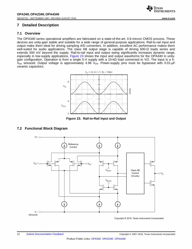
7.1 OverviewThe OPA340 series operational amplifiers are fabricated on a state-of-the-art, 0.6-micron CMOS process. Thesedevices are unity-gain stable and suitable for a wide range of general-purpose applications. Rail-to-rail input andoutput make them ideal for driving sampling A/D converters. In addition, excellent AC performance makes themwell-suited for audio applications. The class AB output stage is capable of driving 600-Ω loads series andextends 500 mV beyond the supply. Rail-to-rail input and output swing significantly increases dynamic range,especially in low-supply applications. Figure 23 shows the input and output waveforms for the OPA340 in unity-gain configuration. Operation is from a single 5-V supply with a 10-kΩ load connected to V/2. The input is a 5-VPP sinusoid. Output voltage is approximately 4.98 VPP. Power-supply pins must be bypassed with 0.01-µFceramic capacitors.
Figure 23. Rail-to-Rail Input and Output
7.2 Functional Block Diagram
5kW
OPAx34010mA max
V+
VIN
VOUT
IOVERLOAD
Copyright © 2016, Texas Instruments Incorporated
13
OPA340, OPA2340, OPA4340www.ti.com SBOS073C –SEPTEMBER 1997–REVISED AUGUST 2016
Product Folder Links: OPA340 OPA2340 OPA4340
Submit Documentation FeedbackCopyright © 1997–2016, Texas Instruments Incorporated
7.3 Feature Description
7.3.1 Operating VoltageThe OPA340 series operational amplifiers are fully specified from 2.7 V to 5 V. However, supply voltage mayrange from 2.5 V to 5.5 V. Parameters are ensured over the specified supply range—a unique feature of theOPA340 series. In addition, many specifications apply from –40°C to 85°C. Most behavior remains virtuallyunchanged throughout the full operating voltage range. Parameters which vary significantly with operatingvoltages or temperature are shown in the Typical Characteristics.
7.3.2 Rail-to-Rail InputThe input common-mode voltage range of the OPA340 series extends 500 mV beyond the supply rails. Thisextended range is achieved with a complementary input stage—an N-channel input differential pair in parallelwith a P-channel differential pair. The N-channel pair is active for input voltages close to the positive rail, typically(V+) – 1.3 V to 500 mV above the positive supply, while the P-channel pair is on for inputs from 500 mV belowthe negative supply to approximately (V+) – 1.3 V. There is a small transition region, typically (V+) – 1.5 V to(V+) – 1.1 V, in which both pairs are on. This 400-mV transition region can vary ±300 mV with process variation.Thus, the transition region (both stages on) can range from (V+) – 1.8 V to (V+) – 1.4 V on the low end, up to(V+) – 1.2 V to (V+) – 0.8 V on the high end.
OPA340 series operational amplifiers are laser-trimmed to the reduce offset voltage difference between the N-channel and P-channel input stages, resulting in improved common-mode rejection and a smooth transitionbetween the N-channel pair and the P-channel pair. However, within the 400-mV transition region PSRR, CMRR,offset voltage, offset drift, and THD may be degraded compared to operation outside this region.
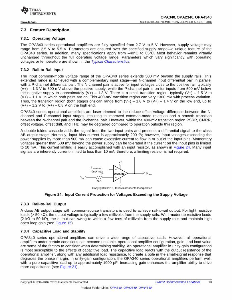
A double-folded cascode adds the signal from the two input pairs and presents a differential signal to the classAB output stage. Normally, input bias current is approximately 200 fA; however, input voltages exceeding thepower supplies by more than 500 mV can cause excessive current to flow in or out of the input pins. Momentaryvoltages greater than 500 mV beyond the power supply can be tolerated if the current on the input pins is limitedto 10 mA. This current limiting is easily accomplished with an input resistor, as shown in Figure 24. Many inputsignals are inherently current-limited to less than 10 mA; therefore, a limiting resistor is not required.
Figure 24. Input Current Protection for Voltages Exceeding the Supply Voltage
7.3.3 Rail-to-Rail OutputA class AB output stage with common-source transistors is used to achieve rail-to-rail output. For light resistiveloads (> 50 kΩ), the output voltage is typically a few millivolts from the supply rails. With moderate resistive loads(2 kΩ to 50 kΩ), the output can swing to within a few tens of millivolts from the supply rails and maintain highopen-loop gain (see Figure 15).
7.3.4 Capacitive Load and StabilityOPA340 series operational amplifiers can drive a wide range of capacitive loads. However, all operationalamplifiers under certain conditions can become unstable. operational amplifier configuration, gain, and load valueare some of the factors to consider when determining stability. An operational amplifier in unity-gain configurationis most susceptible to the effects of capacitive load. The capacitive load reacts with the output resistance of theoperational amplifier, along with any additional load resistance, to create a pole in the small-signal response thatdegrades the phase margin. In unity-gain configuration, the OPA340 series operational amplifiers perform well,with a pure capacitive load up to approximately 1000 pF. Increasing gain enhances the amplifier ability to drivemore capacitance (see Figure 21).
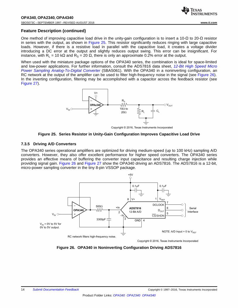
ADS7816
12-Bit A/D
DCLOCK
DOUTOPA340
+5V
VIN
V+
2
+In
3
-In
VREF8
4GND
Serial
Interface
1
0.1 Fm 0.1 Fm
7
6
5
NOTE: A/D Input = 0 to VREF
V = 0V to 5V forIN
0V to 5V output.
RC network filters high-frequency noise.
500W
3300pF
CS/SHDN
Copyright © 2016, Texas Instruments Incorporated
10 toW
20W
OPAx340
V+
VIN
VOUT
RS
RLCL
Copyright © 2016, Texas Instruments Incorporated
14
OPA340, OPA2340, OPA4340SBOS073C –SEPTEMBER 1997–REVISED AUGUST 2016 www.ti.com
Product Folder Links: OPA340 OPA2340 OPA4340
Submit Documentation Feedback Copyright © 1997–2016, Texas Instruments Incorporated
Feature Description (continued)One method of improving capacitive load drive in the unity-gain configuration is to insert a 10-Ω to 20-Ω resistorin series with the output, as shown in Figure 25. This resistor significantly reduces ringing with large capacitiveloads. However, if there is a resistive load in parallel with the capacitive load, it creates a voltage dividerintroducing a DC error at the output and slightly reduces output swing. This error can be insignificant. Forinstance, with RL = 10 kΩ and RS = 20 Ω, there is only an approximate 0.2% error at the output.
When used with the miniature package options of the OPA340 series, the combination is ideal for space-limitedand low-power applications. For further information, consult the ADS7816 data sheet, 12-Bit High Speed MicroPower Sampling Analog-To-Digital Converter (SBAS061). With the OPA340 in a noninverting configuration, anRC network at the output of the amplifier can be used to filter high-frequency noise in the signal (see Figure 26).In the inverting configuration, filtering may be accomplished with a capacitor across the feedback resistor (seeFigure 27).
Figure 25. Series Resistor in Unity-Gain Configuration Improves Capacitive Load Drive
7.3.5 Driving A/D ConvertersThe OPA340 series operational amplifiers are optimized for driving medium-speed (up to 100 kHz) sampling A/Dconverters. However, they also offer excellent performance for higher speed converters. The OPA340 seriesprovides an effective means of buffering the converter input capacitance and resulting charge injection whileproviding signal gain. Figure 26 and Figure 27 show the OPA340 driving an ADS7816. The ADS7816 is a 12-bit,micro-power sampling converter in the tiny 8-pin VSSOP package.
Figure 26. OPA340 in Noninverting Configuration Driving ADS7816

243kW
10MW
10MW
1.74MW
220pF
47pF200pF
1/2
OPA2340
+5V
VIN
RL
1/2
OPA2340
Filters 160Hz to 2.4kHz
Copyright © 2016, Texas Instruments Incorporated
ADS7816
12-Bit A/D
DCLOCK
DOUTOPA340
+5V
VIN V+
2
+In
3
-In
VREF8
4GND
Serial
Interface
1
0.1 Fm 0.1 Fm
7
6
5
NOTE: A/D Input = 0 to VREF
5kW5kW
330pF
V = 0V to 5V for 0V to 5V output.-IN
CS/SHDN
Copyright © 2016, Texas Instruments Incorporated
15
OPA340, OPA2340, OPA4340www.ti.com SBOS073C –SEPTEMBER 1997–REVISED AUGUST 2016
Product Folder Links: OPA340 OPA2340 OPA4340
Submit Documentation FeedbackCopyright © 1997–2016, Texas Instruments Incorporated
Feature Description (continued)
Figure 27. OPA340 in Inverting Configuration Driving ADS7816
Figure 28. Speech Bandpass Filter
7.4 Device Functional ModesThe OPAx340 has a single functional mode and is operational when the power-supply voltage is greater than2.7 V (±1.35 V). The maximum power supply voltage for the OPAx340 is 5.5 V (±2.75 V).

16
OPA340, OPA2340, OPA4340SBOS073C –SEPTEMBER 1997–REVISED AUGUST 2016 www.ti.com
Product Folder Links: OPA340 OPA2340 OPA4340
Submit Documentation Feedback Copyright © 1997–2016, Texas Instruments Incorporated
8 Application and Implementation
NOTEInformation in the following applications sections is not part of the TI componentspecification, and TI does not warrant its accuracy or completeness. TI’s customers areresponsible for determining suitability of components for their purposes. Customers shouldvalidate and test their design implementation to confirm system functionality.
8.1 Application InformationThe OPAx340 amplifier is a single-supply, CMOS operational amplifier with 5.5-MHz unity-gain bandwidth andsupply current of 950 µA. Its performance is optimized for low-voltage (2.7 V to 5.5 V), single-supply applications,with its input common-mode voltage linear range extending 300 mV beyond the rails and the output voltageswing within 5 mV of either rail. The OPAx340 series features wide bandwidth and unity-gain stability with rail-to-rail input and output for increased dynamic range. Power-supply pins must be bypassed with 0.01-µF ceramiccapacitors.
8.2 Typical Applications
8.2.1 Single-Pole, Low-Pass FilterFigure 29 shows the OPA340 in a typical noninverting application with the input signal bandwidth limited by theinput lowpass filter.
Figure 29. Single-Pole, Low-Pass Filter
Equation 1 through Equation 2 show calculations for corner frequency and gain:
(1)
(2)
40
20
0
-20
-40
Gain
= V
/V(d
B)
OU
TIN
1 10 100 1 k 10 k 100 k 1 M
Frequency (Hz)
C = 1 F1 m
C = 10 nF1
C = 01
17
OPA340, OPA2340, OPA4340www.ti.com SBOS073C –SEPTEMBER 1997–REVISED AUGUST 2016
Product Folder Links: OPA340 OPA2340 OPA4340
Submit Documentation FeedbackCopyright © 1997–2016, Texas Instruments Incorporated
Typical Applications (continued)8.2.1.1 Design RequirementsWhen receiving low-level signals, limiting the bandwidth of the incoming signals into the system is often required.The simplest way to establish this limited bandwidth is to place an RC filter at the noninverting terminal of theamplifier, as shown in Figure 29. If a steeper attenuation level is required, a two-pole or higher-order filter may beused.
8.2.1.2 Detailed Design ProcedureThe design goals for this circuit include these parameters:• A noninverting gain of 10 V/V (20 dB)• Design a single-pole response circuit with –3-dB rolloff at 15.9 kHz and 159 Hz• Modify the design to increase attenuation level to –40 dB/decade (Sallen-Key Filter)
Use these design values:• C1 = 0 nF, 10 nF, 1 µF• R1 = 1 kΩ• RG = 10 kΩ• RF = 90 kΩ
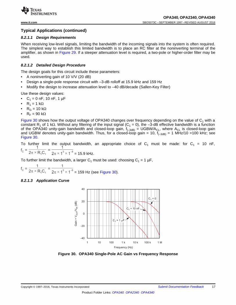
Figure 30 shows how the output voltage of OPA340 changes over frequency depending on the value of C1 with aconstant R1 of 1 kΩ. Without any filtering of the input signal (C1 = 0), the –3-dB effective bandwidth is a functionof the OPA340 unity-gain bandwidth and closed-loop gain, f(–3dB) = UGBW/ACL, where ACL is closed-loop gainand UGBW denotes unity-gain bandwidth. Thus, for a closed-loop gain = 10, f(–3dB) = 1 MHz/10 =100 kHz; seeFigure 30.
To further limit the output bandwidth, an appropriate choice of C1 must be made: for C1 = 10 nF,
= 15.9 kHz.
To further limit the bandwidth, a larger C1 must be used: choosing C1 = 1 µF,
= 159 Hz (see Figure 30).
8.2.1.3 Application Curve
Figure 30. OPA340 Single-Pole AC Gain vs Frequency Response

18
OPA340, OPA2340, OPA4340SBOS073C –SEPTEMBER 1997–REVISED AUGUST 2016 www.ti.com
Product Folder Links: OPA340 OPA2340 OPA4340
Submit Documentation Feedback Copyright © 1997–2016, Texas Instruments Incorporated
Typical Applications (continued)8.2.2 Two-Pole, Low-Pass FilterIf even more attenuation is required, a multiple pole filter is required. The Sallen-Key filter may be used for thistask, as shown in Figure 31. For best results, the amplifier must have effective bandwidth that is at least 10 timeshigher than the filter cutoff frequency. Failure to follow this guideline results in a phase shift of the amplifier,which in turn leads to lower precision of the filter bandwidth. Additionally, to minimize the loading effect betweenmultiple RC pairs on overall the filter cutoff frequency, choose R = 10 × R1 and C2 = C1/10; see Figure 32.
Figure 31. Two-Pole, Lowpass Filter
Equation 3 through Equation 5 show calculations for corner frequency and gain:
(3)
(4)
(5)
8.2.2.1 Detailed Design ProcedureUse these design values:• C1 = 10 nF and C2 = 1 nF• R1 = 1 kΩ and R2= 10 kΩ• RG = 10 kΩ• RF = 90 kΩ
Figure 32 shows the Sallen-Key filter second-order response for different RC values: for R and C values above,
= 15.9 kHz.
To further limit the bandwidth, a larger RC value must be used: increasing C values 100 times, such asC1 = 1 µF and C2 = 0.1 µF, with unchanged resistors, results in the second-order rolloff at
= 159 Hz. See Figure 32.

19
OPA340, OPA2340, OPA4340www.ti.com SBOS073C –SEPTEMBER 1997–REVISED AUGUST 2016
Product Folder Links: OPA340 OPA2340 OPA4340
Submit Documentation FeedbackCopyright © 1997–2016, Texas Instruments Incorporated
Typical Applications (continued)8.2.2.2 Application Curve
Figure 32. OPA340 Two-Pole, Lowpass Sallen-Key AC Gain vs Frequency Response
9 Power Supply RecommendationsThe OPAx340 is specified for operation from 2.7 V to 5.5 V (±1.35 V to ±2.75 V).
CAUTIONSupply voltages larger than 7 V can permanently damage the device (see the AbsoluteMaximum Ratings).
TI recommends placing 0.1-μF bypass capacitors close to the power-supply pins to reduce errors coupling infrom noisy or high-impedance power supplies.
RG RF
+
±
Copyright © 2016,Texas Instruments Incorporated
VINVOUT
N/C
–IN
+IN
V–
N/C
V+
OUTPUT
N/CUse low-ESR, ceramic
bypass capacitor
GND
VS+
Run the input tracesas far away fromthe supply lines
as possible
Place componentsclose to device and
to eachother toreduce parasitic
errors
GND
VIN
RF
GND
RG
Use low-ESR,ceramic bypass
capacitor
VS–VOUT
Copyright © 2016, Texas Instruments Incorporated
20
OPA340, OPA2340, OPA4340SBOS073C –SEPTEMBER 1997–REVISED AUGUST 2016 www.ti.com
Product Folder Links: OPA340 OPA2340 OPA4340
Submit Documentation Feedback Copyright © 1997–2016, Texas Instruments Incorporated
10 Layout
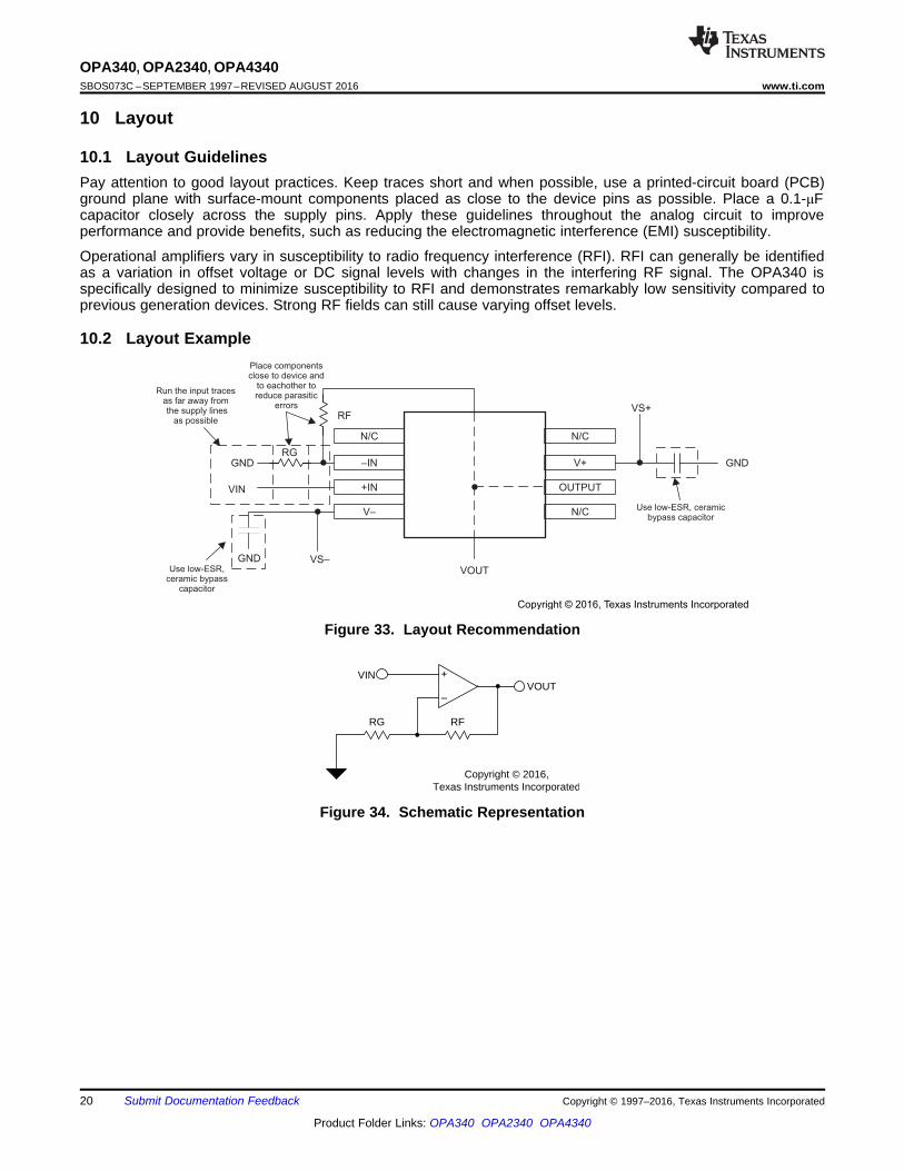
10.1 Layout GuidelinesPay attention to good layout practices. Keep traces short and when possible, use a printed-circuit board (PCB)ground plane with surface-mount components placed as close to the device pins as possible. Place a 0.1-μFcapacitor closely across the supply pins. Apply these guidelines throughout the analog circuit to improveperformance and provide benefits, such as reducing the electromagnetic interference (EMI) susceptibility.
Operational amplifiers vary in susceptibility to radio frequency interference (RFI). RFI can generally be identifiedas a variation in offset voltage or DC signal levels with changes in the interfering RF signal. The OPA340 isspecifically designed to minimize susceptibility to RFI and demonstrates remarkably low sensitivity compared toprevious generation devices. Strong RF fields can still cause varying offset levels.
10.2 Layout Example
Figure 33. Layout Recommendation
Figure 34. Schematic Representation
21
OPA340, OPA2340, OPA4340www.ti.com SBOS073C –SEPTEMBER 1997–REVISED AUGUST 2016
Product Folder Links: OPA340 OPA2340 OPA4340
Submit Documentation FeedbackCopyright © 1997–2016, Texas Instruments Incorporated
11 Device and Documentation Support
11.1 Device Support
11.1.1 Development Support
11.1.1.1 TINA-TI™ (Free Software Download)TINA™ is a simple, powerful, and easy-to-use circuit simulation program based on a SPICE engine. TINA-TI™ isa free, fully-functional version of the TINA software, preloaded with a library of macro models in addition to arange of both passive and active models. TINA-TI provides all the conventional DC, transient, and frequencydomain analysis of SPICE, as well as additional design capabilities.
Available as a free download from the Analog eLab Design Center, TINA-TI offers extensive post-processingcapability that allows users to format results in a variety of ways. Virtual instruments offer the ability to selectinput waveforms and probe circuit nodes, voltages, and waveforms, creating a dynamic quick-start tool.
NOTEThese files require that either the TINA software (from DesignSoft™) or TINA-TI softwarebe installed. Download the free TINA-TI software from the TINA-TI folder.
11.1.1.2 DIP Adapter EVMThe DIP Adapter EVM tool provides an easy, low-cost way to prototype small surface mount ICs. The evaluationtool these TI packages: D or U (SOIC-8), PW (TSSOP-8), DGK (MSOP-8), DBV (SOT23-6, SOT23-5 andSOT23-3), DCK (SC70-6 and SC70-5), and DRL (SOT563-6). The DIP Adapter EVM may also be used withterminal strips or may be wired directly to existing circuits.
11.1.1.3 Universal Operational Amplifier EVMThe Universal Op Amp EVM is a series of general-purpose, blank circuit boards that simplify prototyping circuitsfor a variety of IC package types. The evaluation module board design allows many different circuits to beconstructed easily and quickly. Five models are offered, with each model intended for a specific package type.PDIP, SOIC, MSOP, TSSOP and SOT23 packages are all supported.
NOTEThese boards are unpopulated, so users must provide their own ICs. TI recommendsrequesting several operational amplifier device samples when ordering the Universal OpAmp EVM.
11.1.1.4 TI Precision DesignsTI Precision Designs are analog solutions created by TI’s precision analog applications experts and offer thetheory of operation, component selection, simulation, complete PCB schematic and layout, bill of materials, andmeasured performance of many useful circuits. TI Precision Designs are available online athttp://www.ti.com/ww/en/analog/precision-designs/.
11.1.1.5 WEBENCH® Filter DesignerWEBENCH® Filter Designer is a simple, powerful, and easy-to-use active filter design program. The WEBENCHFilter Designer lets you create optimized filter designs using a selection of TI operational amplifiers and passivecomponents from TI's vendor partners.
Available as a web-based tool from the WEBENCH® Design Center, WEBENCH® Filter Designer allows you todesign, optimize, and simulate complete multistage active filter solutions within minutes.

22
OPA340, OPA2340, OPA4340SBOS073C –SEPTEMBER 1997–REVISED AUGUST 2016 www.ti.com
Product Folder Links: OPA340 OPA2340 OPA4340
Submit Documentation Feedback Copyright © 1997–2016, Texas Instruments Incorporated
11.2 Documentation Support
11.2.1 Related DocumentationFor related documentation, see the following application reports and publications (available for download fromwww.ti.com):• 12-Bit High Speed Micro Power Sampling Analog-To-Digital Converter (SBAS061)• A Dual-Polarity, Bidirectional Current-Shunt Monitor (SLYT311)• OPA340, OPA2340, OPA4340 EMI Immunity Performance (SBOZ010)• Getting the Full Potential from your ADC (SBAA069)• Feedback Plots Define Op Amp AC Performance (SBOA015)• Capacitive Load Drive Solution Using an Isolation Resistor (TIPD128)• Circuit Board Layout Techniques (SLOA089)
11.3 Related LinksTable 1 lists quick access links. Categories include technical documents, support and community resources,tools and software, and quick access to sample or buy.
Table 1. Related Links
PARTS PRODUCT FOLDER SAMPLE & BUY TECHNICALDOCUMENTS
TOOLS &SOFTWARE
SUPPORT &COMMUNITY
OPA340 Click here Click here Click here Click here Click hereOPA2340 Click here Click here Click here Click here Click hereOPA4340 Click here Click here Click here Click here Click here
11.4 Receiving Notification of Documentation UpdatesTo receive notification of documentation updates, navigate to the device product folder on ti.com. In the upperright corner, click on Alert me to register and receive a weekly digest of any product information that haschanged. For change details, review the revision history included in any revised document.
11.5 Community ResourcesThe following links connect to TI community resources. Linked contents are provided "AS IS" by the respectivecontributors. They do not constitute TI specifications and do not necessarily reflect TI's views; see TI's Terms ofUse.
TI E2E™ Online Community TI's Engineer-to-Engineer (E2E) Community. Created to foster collaborationamong engineers. At e2e.ti.com, you can ask questions, share knowledge, explore ideas and helpsolve problems with fellow engineers.
Design Support TI's Design Support Quickly find helpful E2E forums along with design support tools andcontact information for technical support.
11.6 TrademarksMicroAmplifier, TINA-TI, E2E are trademarks of Texas Instruments.WEBENCH is a registered trademark of Texas Instruments.TINA, DesignSoft are trademarks of DesignSoft, Inc.All other trademarks are the property of their respective owners.
11.7 Electrostatic Discharge CautionThese devices have limited built-in ESD protection. The leads should be shorted together or the device placed in conductive foamduring storage or handling to prevent electrostatic damage to the MOS gates.

23
OPA340, OPA2340, OPA4340www.ti.com SBOS073C –SEPTEMBER 1997–REVISED AUGUST 2016
Product Folder Links: OPA340 OPA2340 OPA4340
Submit Documentation FeedbackCopyright © 1997–2016, Texas Instruments Incorporated
11.8 GlossarySLYZ022 — TI Glossary.
This glossary lists and explains terms, acronyms, and definitions.
12 Mechanical, Packaging, and Orderable InformationThe following pages include mechanical, packaging, and orderable information. This information is the mostcurrent data available for the designated devices. This data is subject to change without notice and revision ofthis document. For browser-based versions of this data sheet, refer to the left-hand navigation.
PACKAGE OPTION ADDENDUM
www.ti.com 29-Apr-2022
Addendum-Page 1
PACKAGING INFORMATION
Orderable Device Status(1)
Package Type PackageDrawing
Pins PackageQty
Eco Plan(2)
Lead finish/Ball material
(6)
MSL Peak Temp(3)
Op Temp (°C) Device Marking(4/5)
Samples
OPA2340EA/250 ACTIVE VSSOP DGK 8 250 RoHS & Green NIPDAUAG Level-2-260C-1 YEAR A40A
OPA2340EA/250G4 ACTIVE VSSOP DGK 8 250 RoHS & Green NIPDAUAG Level-2-260C-1 YEAR A40A
OPA2340EA/2K5 ACTIVE VSSOP DGK 8 2500 RoHS & Green NIPDAUAG Level-2-260C-1 YEAR A40A
OPA2340EA/2K5G4 ACTIVE VSSOP DGK 8 2500 RoHS & Green NIPDAUAG Level-2-260C-1 YEAR A40A
OPA2340PA NRND PDIP P 8 50 RoHS & Green NIPDAU N / A for Pkg Type OPA2340PA
OPA2340PAG4 NRND PDIP P 8 50 RoHS & Green NIPDAU N / A for Pkg Type OPA2340PA
OPA2340UA ACTIVE SOIC D 8 75 RoHS & Green NIPDAU Level-2-260C-1 YEAR -40 to 85 OPA2340UA
OPA2340UA/2K5 ACTIVE SOIC D 8 2500 RoHS & Green NIPDAU Level-2-260C-1 YEAR OPA2340UA
OPA2340UA/2K5G4 ACTIVE SOIC D 8 2500 RoHS & Green NIPDAU Level-2-260C-1 YEAR OPA2340UA
OPA340NA/250 ACTIVE SOT-23 DBV 5 250 RoHS & Green NIPDAU Level-2-260C-1 YEAR -40 to 85 A40
OPA340NA/250G4 ACTIVE SOT-23 DBV 5 250 RoHS & Green NIPDAU Level-2-260C-1 YEAR -40 to 85 A40
OPA340NA/3K ACTIVE SOT-23 DBV 5 3000 RoHS & Green NIPDAU Level-2-260C-1 YEAR -40 to 85 A40
OPA340NA/3KG4 ACTIVE SOT-23 DBV 5 3000 RoHS & Green NIPDAU Level-2-260C-1 YEAR -40 to 85 A40
OPA340PA ACTIVE PDIP P 8 50 RoHS & Green NIPDAU N / A for Pkg Type -40 to 85 OPA340PA
OPA340UA ACTIVE SOIC D 8 75 RoHS & Green NIPDAU Level-2-260C-1 YEAR -40 to 85 OPA340UA
OPA340UA/2K5 ACTIVE SOIC D 8 2500 RoHS & Green NIPDAU Level-2-260C-1 YEAR -40 to 85 OPA340UA
OPA340UA/2K5G4 ACTIVE SOIC D 8 2500 RoHS & Green NIPDAU Level-2-260C-1 YEAR -40 to 85 OPA340UA
OPA4340EA/250 ACTIVE SSOP DBQ 16 250 RoHS & Green NIPDAU Level-2-260C-1 YEAR -40 to 85 OPA4340EA
OPA4340EA/250G4 ACTIVE SSOP DBQ 16 250 RoHS & Green NIPDAU Level-2-260C-1 YEAR -40 to 85 OPA4340EA
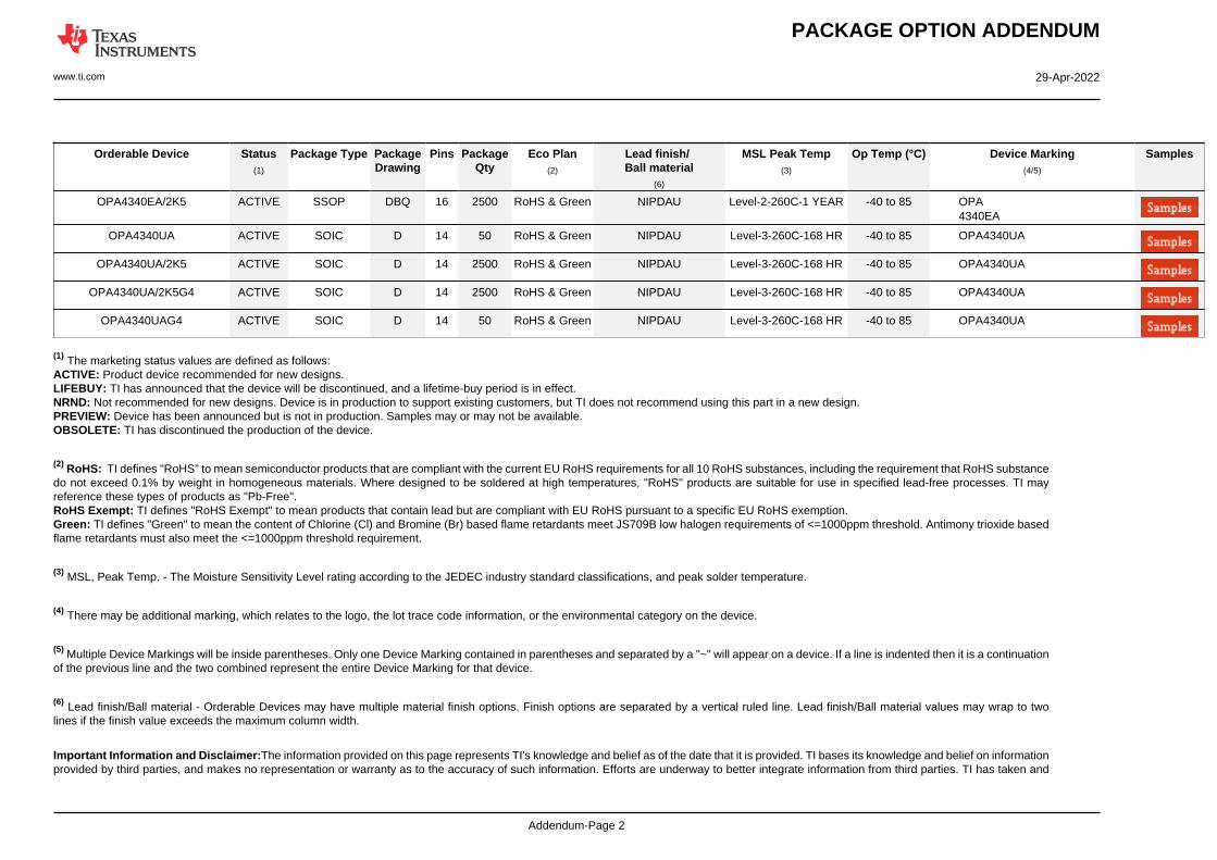
PACKAGE OPTION ADDENDUM
www.ti.com 29-Apr-2022
Addendum-Page 2
Orderable Device Status(1)
Package Type PackageDrawing
Pins PackageQty
Eco Plan(2)
Lead finish/Ball material
(6)
MSL Peak Temp(3)
Op Temp (°C) Device Marking(4/5)
Samples
OPA4340EA/2K5 ACTIVE SSOP DBQ 16 2500 RoHS & Green NIPDAU Level-2-260C-1 YEAR -40 to 85 OPA4340EA
OPA4340UA ACTIVE SOIC D 14 50 RoHS & Green NIPDAU Level-3-260C-168 HR -40 to 85 OPA4340UA
OPA4340UA/2K5 ACTIVE SOIC D 14 2500 RoHS & Green NIPDAU Level-3-260C-168 HR -40 to 85 OPA4340UA
OPA4340UA/2K5G4 ACTIVE SOIC D 14 2500 RoHS & Green NIPDAU Level-3-260C-168 HR -40 to 85 OPA4340UA
OPA4340UAG4 ACTIVE SOIC D 14 50 RoHS & Green NIPDAU Level-3-260C-168 HR -40 to 85 OPA4340UA
(1) The marketing status values are defined as follows:ACTIVE: Product device recommended for new designs.LIFEBUY: TI has announced that the device will be discontinued, and a lifetime-buy period is in effect.NRND: Not recommended for new designs. Device is in production to support existing customers, but TI does not recommend using this part in a new design.PREVIEW: Device has been announced but is not in production. Samples may or may not be available.OBSOLETE: TI has discontinued the production of the device.
(2) RoHS: TI defines "RoHS" to mean semiconductor products that are compliant with the current EU RoHS requirements for all 10 RoHS substances, including the requirement that RoHS substancedo not exceed 0.1% by weight in homogeneous materials. Where designed to be soldered at high temperatures, "RoHS" products are suitable for use in specified lead-free processes. TI mayreference these types of products as "Pb-Free".RoHS Exempt: TI defines "RoHS Exempt" to mean products that contain lead but are compliant with EU RoHS pursuant to a specific EU RoHS exemption.Green: TI defines "Green" to mean the content of Chlorine (Cl) and Bromine (Br) based flame retardants meet JS709B low halogen requirements of <=1000ppm threshold. Antimony trioxide basedflame retardants must also meet the <=1000ppm threshold requirement.
(3) MSL, Peak Temp. - The Moisture Sensitivity Level rating according to the JEDEC industry standard classifications, and peak solder temperature.
(4) There may be additional marking, which relates to the logo, the lot trace code information, or the environmental category on the device.
(5) Multiple Device Markings will be inside parentheses. Only one Device Marking contained in parentheses and separated by a "~" will appear on a device. If a line is indented then it is a continuationof the previous line and the two combined represent the entire Device Marking for that device.
(6) Lead finish/Ball material - Orderable Devices may have multiple material finish options. Finish options are separated by a vertical ruled line. Lead finish/Ball material values may wrap to twolines if the finish value exceeds the maximum column width.
Important Information and Disclaimer:The information provided on this page represents TI's knowledge and belief as of the date that it is provided. TI bases its knowledge and belief on informationprovided by third parties, and makes no representation or warranty as to the accuracy of such information. Efforts are underway to better integrate information from third parties. TI has taken and
PACKAGE OPTION ADDENDUM
www.ti.com 29-Apr-2022
Addendum-Page 3
continues to take reasonable steps to provide representative and accurate information but may not have conducted destructive testing or chemical analysis on incoming materials and chemicals.TI and TI suppliers consider certain information to be proprietary, and thus CAS numbers and other limited information may not be available for release.
In no event shall TI's liability arising out of such information exceed the total purchase price of the TI part(s) at issue in this document sold by TI to Customer on an annual basis.
OTHER QUALIFIED VERSIONS OF OPA340 :
• Enhanced Product : OPA340-EP
NOTE: Qualified Version Definitions:
• Enhanced Product - Supports Defense, Aerospace and Medical Applications
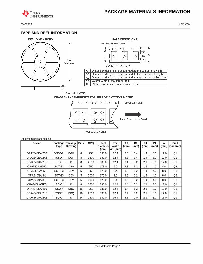
TAPE AND REEL INFORMATION
*All dimensions are nominal
Device PackageType
PackageDrawing
Pins SPQ ReelDiameter
(mm)
ReelWidth
W1 (mm)
A0(mm)
B0(mm)
K0(mm)
P1(mm)
W(mm)
Pin1Quadrant
OPA2340EA/250 VSSOP DGK 8 250 330.0 12.4 5.3 3.4 1.4 8.0 12.0 Q1
OPA2340EA/2K5 VSSOP DGK 8 2500 330.0 12.4 5.3 3.4 1.4 8.0 12.0 Q1
OPA2340UA/2K5 SOIC D 8 2500 330.0 12.4 6.4 5.2 2.1 8.0 12.0 Q1
OPA340NA/250 SOT-23 DBV 5 250 178.0 9.0 3.3 3.2 1.4 4.0 8.0 Q3
OPA340NA/250 SOT-23 DBV 5 250 179.0 8.4 3.2 3.2 1.4 4.0 8.0 Q3
OPA340NA/3K SOT-23 DBV 5 3000 178.0 9.0 3.3 3.2 1.4 4.0 8.0 Q3
OPA340NA/3K SOT-23 DBV 5 3000 179.0 8.4 3.2 3.2 1.4 4.0 8.0 Q3
OPA340UA/2K5 SOIC D 8 2500 330.0 12.4 6.4 5.2 2.1 8.0 12.0 Q1
OPA4340EA/250 SSOP DBQ 16 250 180.0 12.4 6.4 5.2 2.1 8.0 12.0 Q1
OPA4340EA/2K5 SSOP DBQ 16 2500 330.0 12.4 6.4 5.2 2.1 8.0 12.0 Q1
OPA4340UA/2K5 SOIC D 14 2500 330.0 16.4 6.5 9.0 2.1 8.0 16.0 Q1
PACKAGE MATERIALS INFORMATION
www.ti.com 5-Jan-2022
Pack Materials-Page 1
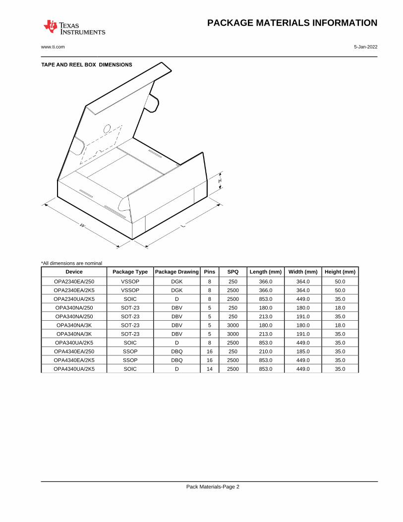
*All dimensions are nominal
Device Package Type Package Drawing Pins SPQ Length (mm) Width (mm) Height (mm)
OPA2340EA/250 VSSOP DGK 8 250 366.0 364.0 50.0
OPA2340EA/2K5 VSSOP DGK 8 2500 366.0 364.0 50.0
OPA2340UA/2K5 SOIC D 8 2500 853.0 449.0 35.0
OPA340NA/250 SOT-23 DBV 5 250 180.0 180.0 18.0
OPA340NA/250 SOT-23 DBV 5 250 213.0 191.0 35.0
OPA340NA/3K SOT-23 DBV 5 3000 180.0 180.0 18.0
OPA340NA/3K SOT-23 DBV 5 3000 213.0 191.0 35.0
OPA340UA/2K5 SOIC D 8 2500 853.0 449.0 35.0
OPA4340EA/250 SSOP DBQ 16 250 210.0 185.0 35.0
OPA4340EA/2K5 SSOP DBQ 16 2500 853.0 449.0 35.0
OPA4340UA/2K5 SOIC D 14 2500 853.0 449.0 35.0
PACKAGE MATERIALS INFORMATION
www.ti.com 5-Jan-2022
Pack Materials-Page 2

TUBE
*All dimensions are nominal
Device Package Name Package Type Pins SPQ L (mm) W (mm) T (µm) B (mm)
OPA2340PA P PDIP 8 50 506 13.97 11230 4.32
OPA2340PAG4 P PDIP 8 50 506 13.97 11230 4.32
OPA2340UA D SOIC 8 75 506.6 8 3940 4.32
OPA340PA P PDIP 8 50 506 13.97 11230 4.32
OPA340UA D SOIC 8 75 506.6 8 3940 4.32
OPA4340UA D SOIC 14 50 506.6 8 3940 4.32
OPA4340UAG4 D SOIC 14 50 506.6 8 3940 4.32
PACKAGE MATERIALS INFORMATION
www.ti.com 5-Jan-2022
Pack Materials-Page 3

www.ti.com
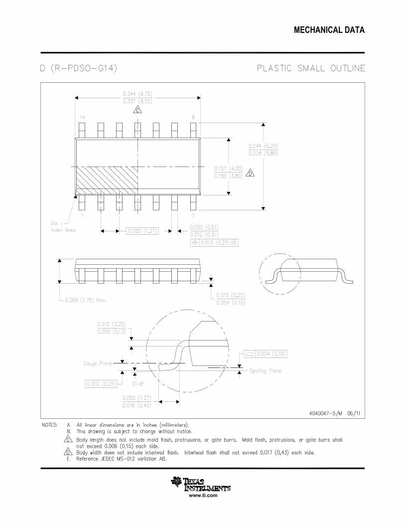
PACKAGE OUTLINE
C
0.220.08 TYP
0.25
3.02.6
2X 0.95
1.9
1.450.90
0.150.00 TYP
5X 0.50.3
0.60.3 TYP
80 TYP
1.9
A
3.052.75
B1.751.45
(1.1)
SOT-23 - 1.45 mm max heightDBV0005ASMALL OUTLINE TRANSISTOR
4214839/F 06/2021
NOTES: 1. All linear dimensions are in millimeters. Any dimensions in parenthesis are for reference only. Dimensioning and tolerancing per ASME Y14.5M.2. This drawing is subject to change without notice.3. Refernce JEDEC MO-178.4. Body dimensions do not include mold flash, protrusions, or gate burrs. Mold flash, protrusions, or gate burrs shall not exceed 0.25 mm per side.
0.2 C A B
1
34
5
2
INDEX AREAPIN 1
GAGE PLANE
SEATING PLANE
0.1 C
SCALE 4.000
www.ti.com
EXAMPLE BOARD LAYOUT
0.07 MAXARROUND
0.07 MINARROUND
5X (1.1)
5X (0.6)
(2.6)
(1.9)
2X (0.95)
(R0.05) TYP
4214839/F 06/2021
SOT-23 - 1.45 mm max heightDBV0005ASMALL OUTLINE TRANSISTOR
NOTES: (continued) 5. Publication IPC-7351 may have alternate designs. 6. Solder mask tolerances between and around signal pads can vary based on board fabrication site.
SYMM
LAND PATTERN EXAMPLEEXPOSED METAL SHOWN
SCALE:15X
PKG
1
3 4
5
2
SOLDER MASKOPENINGMETAL UNDER
SOLDER MASK
SOLDER MASKDEFINED
EXPOSED METAL
METALSOLDER MASKOPENING
NON SOLDER MASKDEFINED
(PREFERRED)
SOLDER MASK DETAILS
EXPOSED METAL

www.ti.com
EXAMPLE STENCIL DESIGN
(2.6)
(1.9)
2X(0.95)
5X (1.1)
5X (0.6)
(R0.05) TYP
SOT-23 - 1.45 mm max heightDBV0005ASMALL OUTLINE TRANSISTOR
4214839/F 06/2021
NOTES: (continued) 7. Laser cutting apertures with trapezoidal walls and rounded corners may offer better paste release. IPC-7525 may have alternate design recommendations. 8. Board assembly site may have different recommendations for stencil design.
SOLDER PASTE EXAMPLEBASED ON 0.125 mm THICK STENCIL
SCALE:15X
SYMM
PKG
1
3 4
5
2


www.ti.com
PACKAGE OUTLINE
C
.228-.244 TYP[5.80-6.19]
.069 MAX[1.75]
6X .050[1.27]
8X .012-.020 [0.31-0.51]
2X.150[3.81]
.005-.010 TYP[0.13-0.25]
0 - 8 .004-.010[0.11-0.25]
.010[0.25]
.016-.050[0.41-1.27]
4X (0 -15 )
A
.189-.197[4.81-5.00]
NOTE 3
B .150-.157[3.81-3.98]
NOTE 4
4X (0 -15 )
(.041)[1.04]
SOIC - 1.75 mm max heightD0008ASMALL OUTLINE INTEGRATED CIRCUIT
4214825/C 02/2019
NOTES: 1. Linear dimensions are in inches [millimeters]. Dimensions in parenthesis are for reference only. Controlling dimensions are in inches. Dimensioning and tolerancing per ASME Y14.5M. 2. This drawing is subject to change without notice. 3. This dimension does not include mold flash, protrusions, or gate burrs. Mold flash, protrusions, or gate burrs shall not exceed .006 [0.15] per side. 4. This dimension does not include interlead flash.5. Reference JEDEC registration MS-012, variation AA.
18
.010 [0.25] C A B
54
PIN 1 ID AREA
SEATING PLANE
.004 [0.1] C
SEE DETAIL A
DETAIL ATYPICAL
SCALE 2.800
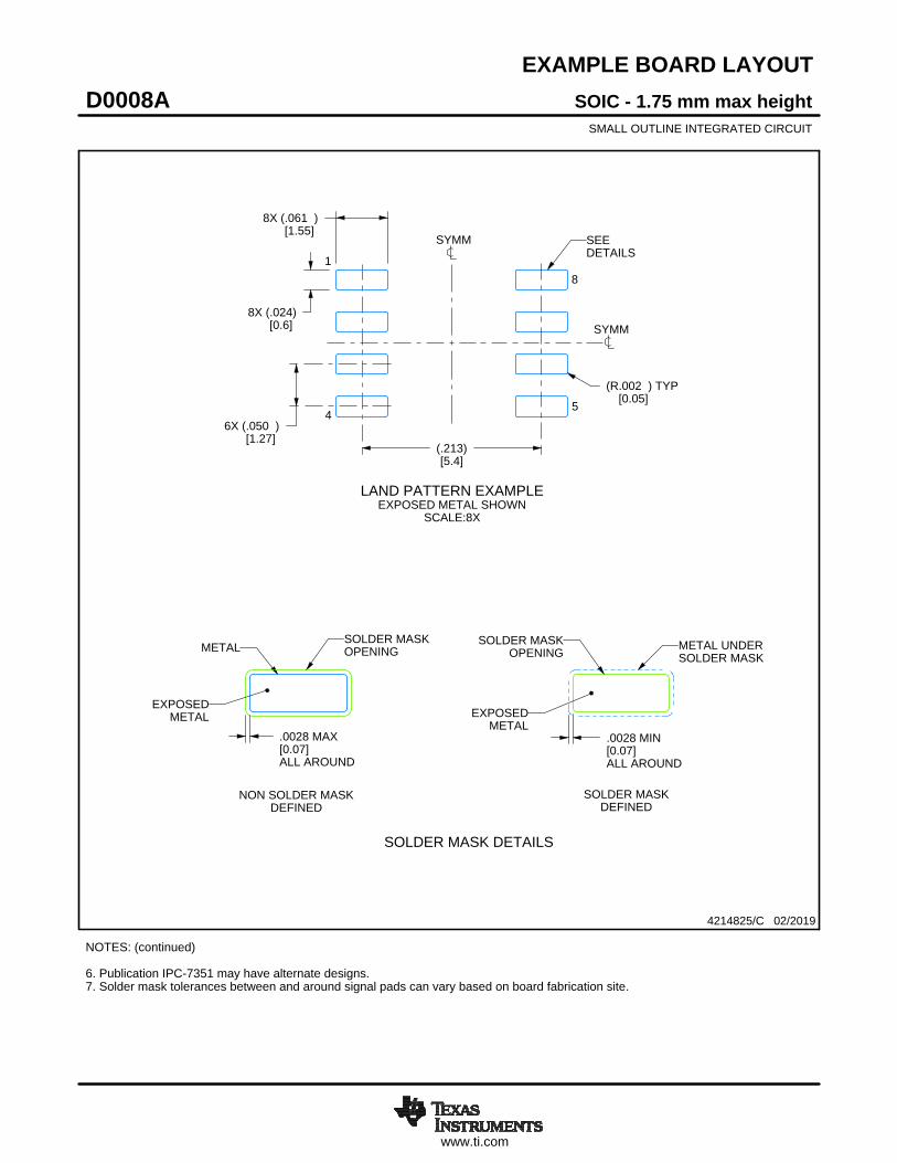
www.ti.com
EXAMPLE BOARD LAYOUT
.0028 MAX[0.07]ALL AROUND
.0028 MIN[0.07]ALL AROUND
(.213)[5.4]
6X (.050 )[1.27]
8X (.061 )[1.55]
8X (.024)[0.6]
(R.002 ) TYP[0.05]
SOIC - 1.75 mm max heightD0008ASMALL OUTLINE INTEGRATED CIRCUIT
4214825/C 02/2019
NOTES: (continued) 6. Publication IPC-7351 may have alternate designs. 7. Solder mask tolerances between and around signal pads can vary based on board fabrication site.
METALSOLDER MASKOPENING
NON SOLDER MASKDEFINED
SOLDER MASK DETAILS
EXPOSEDMETAL
OPENINGSOLDER MASK METAL UNDER
SOLDER MASK
SOLDER MASKDEFINED
EXPOSEDMETAL
LAND PATTERN EXAMPLEEXPOSED METAL SHOWN
SCALE:8X
SYMM
1
45
8
SEEDETAILS
SYMM
www.ti.com
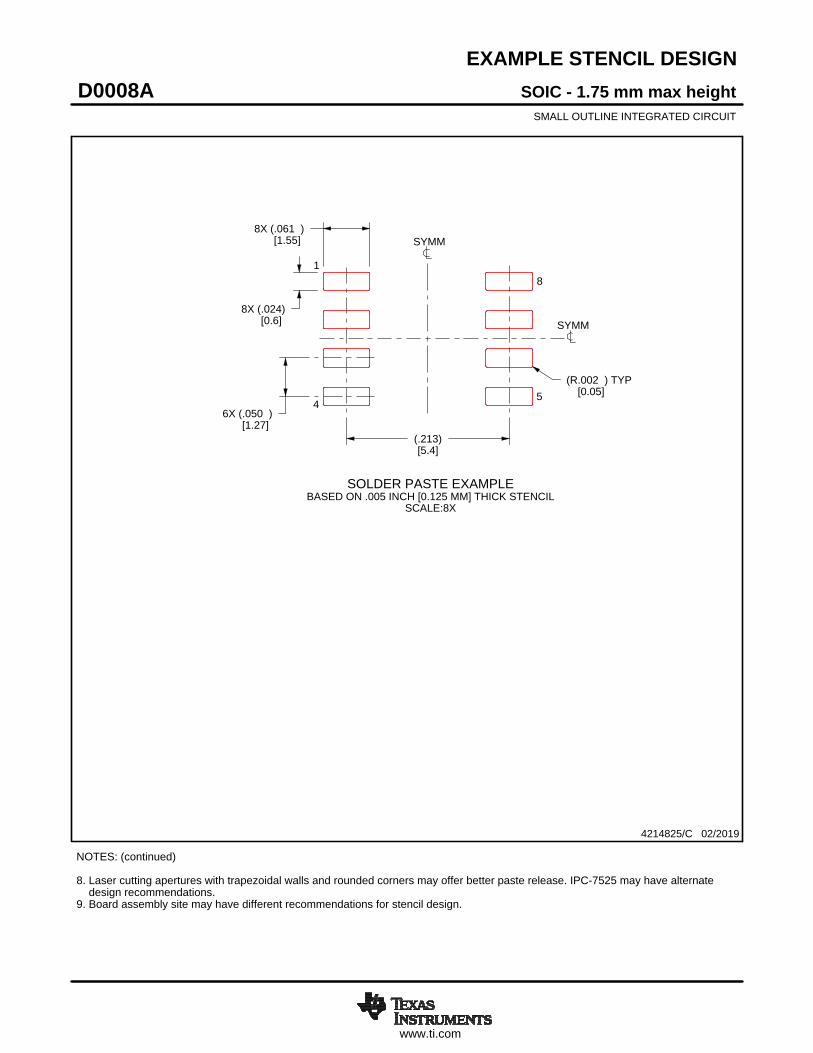
EXAMPLE STENCIL DESIGN
8X (.061 )[1.55]
8X (.024)[0.6]
6X (.050 )[1.27]
(.213)[5.4]
(R.002 ) TYP[0.05]
SOIC - 1.75 mm max heightD0008ASMALL OUTLINE INTEGRATED CIRCUIT
4214825/C 02/2019
NOTES: (continued) 8. Laser cutting apertures with trapezoidal walls and rounded corners may offer better paste release. IPC-7525 may have alternate design recommendations. 9. Board assembly site may have different recommendations for stencil design.
SOLDER PASTE EXAMPLEBASED ON .005 INCH [0.125 MM] THICK STENCIL
SCALE:8X
SYMM
SYMM
1
45
8
www.ti.com
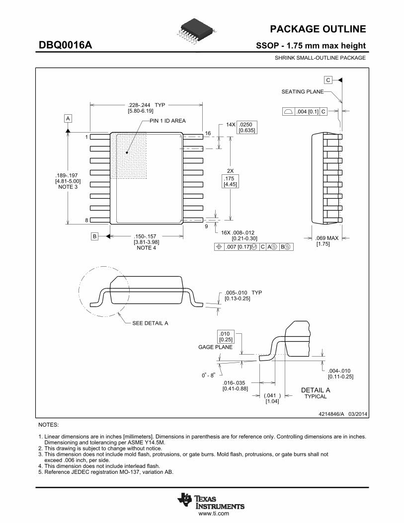
PACKAGE OUTLINE
C
TYP-.244.228-6.195.80[ ]
.069 MAX[1.75]
14X .0250[0.635]
16X -.012.008-0.300.21[ ]
2X.175[4.45]
TYP-.010.005-0.250.13[ ]
0 - 8-.010.004-0.250.11[ ]
(.041 )[1.04]
.010[0.25]
GAGE PLANE
-.035.016-0.880.41[ ]
A
NOTE 3
-.197.189-5.004.81[ ]
B
NOTE 4
-.157.150-3.983.81[ ]
SSOP - 1.75 mm max heightDBQ0016ASHRINK SMALL-OUTLINE PACKAGE
4214846/A 03/2014
NOTES: 1. Linear dimensions are in inches [millimeters]. Dimensions in parenthesis are for reference only. Controlling dimensions are in inches. Dimensioning and tolerancing per ASME Y14.5M. 2. This drawing is subject to change without notice. 3. This dimension does not include mold flash, protrusions, or gate burrs. Mold flash, protrusions, or gate burrs shall not exceed .006 inch, per side. 4. This dimension does not include interlead flash.5. Reference JEDEC registration MO-137, variation AB.
116
.007 [0.17] C A B
98
PIN 1 ID AREA
SEATING PLANE
.004 [0.1] C
SEE DETAIL A
DETAIL ATYPICAL
SCALE 2.800
www.ti.com
EXAMPLE BOARD LAYOUT
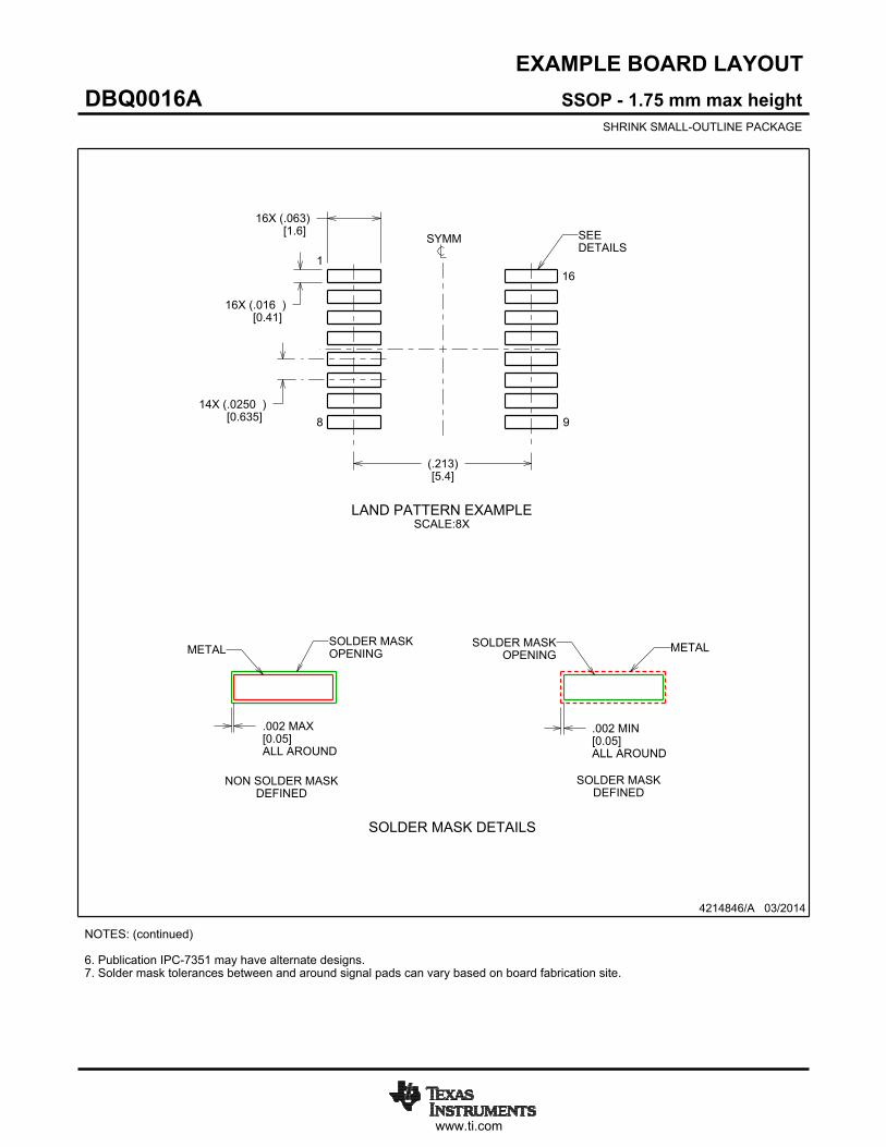
.002 MAX[0.05]ALL AROUND
.002 MIN[0.05]ALL AROUND
(.213)[5.4]
14X (.0250 )[0.635]
16X (.063)[1.6]
16X (.016 )[0.41]
SSOP - 1.75 mm max heightDBQ0016ASHRINK SMALL-OUTLINE PACKAGE
4214846/A 03/2014
NOTES: (continued) 6. Publication IPC-7351 may have alternate designs. 7. Solder mask tolerances between and around signal pads can vary based on board fabrication site.
METALSOLDER MASKOPENING
NON SOLDER MASKDEFINED
SOLDER MASK DETAILS
OPENINGSOLDER MASK METAL
SOLDER MASKDEFINED
LAND PATTERN EXAMPLESCALE:8X
SYMM
1
8 9
16
SEEDETAILS
www.ti.com
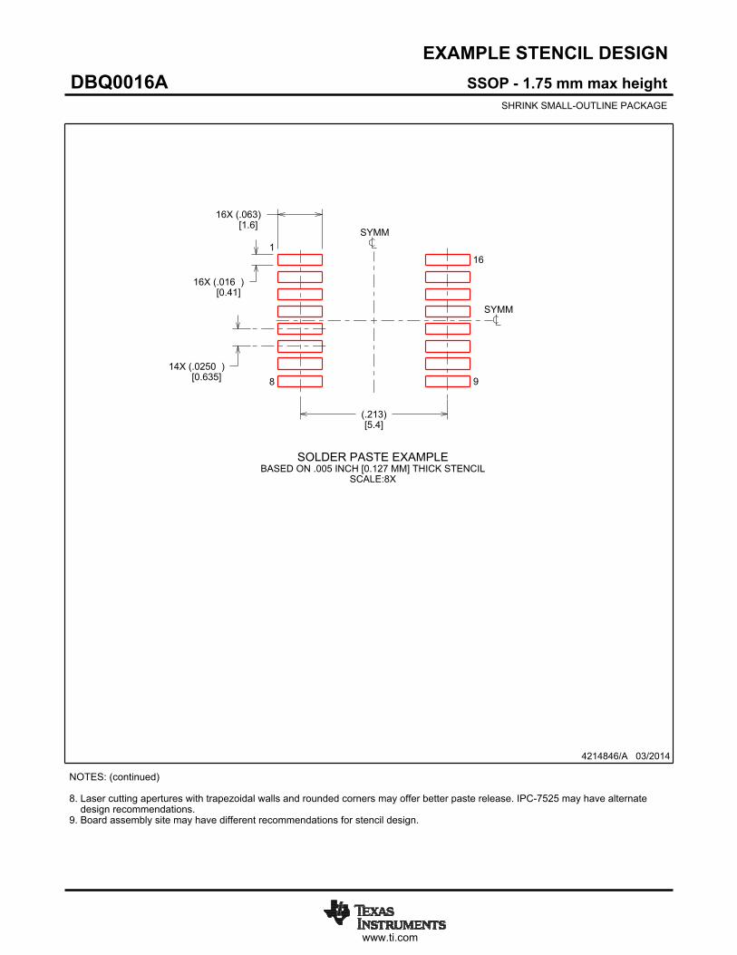
EXAMPLE STENCIL DESIGN
16X (.063)[1.6]
16X (.016 )[0.41]
14X (.0250 )[0.635]
(.213)[5.4]
SSOP - 1.75 mm max heightDBQ0016ASHRINK SMALL-OUTLINE PACKAGE
4214846/A 03/2014
NOTES: (continued) 8. Laser cutting apertures with trapezoidal walls and rounded corners may offer better paste release. IPC-7525 may have alternate design recommendations. 9. Board assembly site may have different recommendations for stencil design.
SOLDER PASTE EXAMPLEBASED ON .005 INCH [0.127 MM] THICK STENCIL
SCALE:8X
SYMM
SYMM
1
8 9
16

IMPORTANT NOTICE AND DISCLAIMERTI PROVIDES TECHNICAL AND RELIABILITY DATA (INCLUDING DATA SHEETS), DESIGN RESOURCES (INCLUDING REFERENCE DESIGNS), APPLICATION OR OTHER DESIGN ADVICE, WEB TOOLS, SAFETY INFORMATION, AND OTHER RESOURCES “AS IS” AND WITH ALL FAULTS, AND DISCLAIMS ALL WARRANTIES, EXPRESS AND IMPLIED, INCLUDING WITHOUT LIMITATION ANY IMPLIED WARRANTIES OF MERCHANTABILITY, FITNESS FOR A PARTICULAR PURPOSE OR NON-INFRINGEMENT OF THIRD PARTY INTELLECTUAL PROPERTY RIGHTS.These resources are intended for skilled developers designing with TI products. You are solely responsible for (1) selecting the appropriate TI products for your application, (2) designing, validating and testing your application, and (3) ensuring your application meets applicable standards, and any other safety, security, regulatory or other requirements.These resources are subject to change without notice. TI grants you permission to use these resources only for development of an application that uses the TI products described in the resource. Other reproduction and display of these resources is prohibited. No license is granted to any other TI intellectual property right or to any third party intellectual property right. TI disclaims responsibility for, and you will fully indemnify TI and its representatives against, any claims, damages, costs, losses, and liabilities arising out of your use of these resources.TI’s products are provided subject to TI’s Terms of Sale or other applicable terms available either on ti.com or provided in conjunction with such TI products. TI’s provision of these resources does not expand or otherwise alter TI’s applicable warranties or warranty disclaimers for TI products.TI objects to and rejects any additional or different terms you may have proposed. IMPORTANT NOTICE
Mailing Address: Texas Instruments, Post Office Box 655303, Dallas, Texas 75265Copyright © 2022, Texas Instruments Incorporated