TPS62840-1YBGEVM56 User's Guide - Texas Instruments
14
1 SLUUC17 – May 2019 Submit Documentation Feedback Copyright © 2019, Texas Instruments Incorporated TPS62840-1YBGEVM56 User's Guide User's Guide SLUUC17 – May 2019 TPS62840-1YBGEVM56 User's Guide The TPS62840-1YBGEVM56 (BSR056-001) facilitates the evaluation of the TPS6284xYBG family of 750- mA, step-down converters with 60-nA I Q in tiny 1.47-mm by 0.97-mm WCSP packages with 0.4-mm pitch. The EVM contains 2 separate circuits to create output voltages between 0.8 V and 3.3 V from higher input voltages between 1.8 V and 6.5 V. All circuits have a maximum height of 1 mm. Due to its extremely low I Q , the TPS6284x provides a long battery lifetime for systems which have very low current consumption states such as wearables, Internet of Things- (IoT-) connected devices, and other portable end equipment. Contents 1 Introduction ................................................................................................................... 2 2 Setup .......................................................................................................................... 4 3 TPS62840-1YBGEVM56 Test Results .................................................................................... 5 4 Board Layout ................................................................................................................. 6 5 Schematic and Bill of Materials (BOM) .................................................................................. 12 List of Figures 1 Loop Response Measurement Modification .............................................................................. 3 2 TPS62840 Thermal Performance (V IN = 3.6 V, V OUT = 1.8 V, I OUT = 750 mA) ........................................ 5 3 Loop Response (V IN = 3.6 V, V OUT = 1.8 V, I OUT = 750 mA) ............................................................. 5 4 Top Assembly ................................................................................................................ 6 5 Top Layer ..................................................................................................................... 7 6 Internal Layer 1 .............................................................................................................. 8 7 Internal Layer 2 .............................................................................................................. 9 8 Bottom Layer................................................................................................................ 10 9 TPS62840-1YBGEVM56 Angled View .................................................................................. 11 10 TPS62840-1YBGEVM56 Overhead View............................................................................... 11 11 TPS62840 Schematic...................................................................................................... 12 12 TPS62841 Schematic...................................................................................................... 12 List of Tables 1 BSR056 Circuit Options..................................................................................................... 2 2 Performance Specification Summary ..................................................................................... 2 3 TPS62840 Bill of Materials ................................................................................................ 13 4 TPS62841 Bill of Materials ................................................................................................ 13 Trademarks All trademarks are the property of their respective owners.
-
Upload
khangminh22 -
Category
Documents
-
view
0 -
download
0
Transcript of TPS62840-1YBGEVM56 User's Guide - Texas Instruments

1SLUUC17–May 2019Submit Documentation Feedback
Copyright © 2019, Texas Instruments Incorporated
TPS62840-1YBGEVM56 User's Guide
User's GuideSLUUC17–May 2019
TPS62840-1YBGEVM56 User's Guide
The TPS62840-1YBGEVM56 (BSR056-001) facilitates the evaluation of the TPS6284xYBG family of 750-mA, step-down converters with 60-nA IQ in tiny 1.47-mm by 0.97-mm WCSP packages with 0.4-mm pitch.The EVM contains 2 separate circuits to create output voltages between 0.8 V and 3.3 V from higher inputvoltages between 1.8 V and 6.5 V. All circuits have a maximum height of 1 mm. Due to its extremely lowIQ, the TPS6284x provides a long battery lifetime for systems which have very low current consumptionstates such as wearables, Internet of Things- (IoT-) connected devices, and other portable end equipment.
Contents1 Introduction ................................................................................................................... 22 Setup .......................................................................................................................... 43 TPS62840-1YBGEVM56 Test Results.................................................................................... 54 Board Layout ................................................................................................................. 65 Schematic and Bill of Materials (BOM) .................................................................................. 12
List of Figures
1 Loop Response Measurement Modification.............................................................................. 32 TPS62840 Thermal Performance (VIN = 3.6 V, VOUT = 1.8 V, IOUT = 750 mA) ........................................ 53 Loop Response (VIN = 3.6 V, VOUT = 1.8 V, IOUT = 750 mA)............................................................. 54 Top Assembly ................................................................................................................ 65 Top Layer ..................................................................................................................... 76 Internal Layer 1 .............................................................................................................. 87 Internal Layer 2 .............................................................................................................. 98 Bottom Layer................................................................................................................ 109 TPS62840-1YBGEVM56 Angled View .................................................................................. 1110 TPS62840-1YBGEVM56 Overhead View............................................................................... 1111 TPS62840 Schematic...................................................................................................... 1212 TPS62841 Schematic...................................................................................................... 12
List of Tables
1 BSR056 Circuit Options..................................................................................................... 22 Performance Specification Summary ..................................................................................... 23 TPS62840 Bill of Materials................................................................................................ 134 TPS62841 Bill of Materials................................................................................................ 13
TrademarksAll trademarks are the property of their respective owners.

Introduction www.ti.com
2 SLUUC17–May 2019Submit Documentation Feedback
Copyright © 2019, Texas Instruments Incorporated
TPS62840-1YBGEVM56 User's Guide
1 IntroductionThe TPS6284x is a family of synchronous, step-down converters in a 1.47-mm × 0.97-mm wafer chip-scale package (WCSP) with 0.4-mm pitch. The BSR056 EVM contains 2 completely independent circuits,each for a different IC version. See Table 1 for a summary of the BSR056 EVMs.
The reference designator order is grouped together by sub-circuit. Reference designators beginning with'1' (for example, R1x, J1x, C1x) are part of one sub-circuit. The second digit of each reference designatoris the same for the same component in different sub-circuits. R11 and R21, for example, refer to the sameresistor in each sub-circuit.
Table 1. BSR056 Circuit OptionsEVM Version IC Installed Output Voltage Output Voltage Range Output Current
TPS62840-1YBGEVM56(BSR056-001)
TPS62840 (U11) 1.8 V 1.8 - 3.3 V (selectable) 750 mA
TPS62841 (U21) 1.2 V 0.8 - 1.55 V (selectable) 750 mA
1.1 Performance SpecificationTable 2 provides a summary of the TPS62840-1YBGEVM56 performance specifications.
Table 2. Performance Specification Summary
SPECIFICATION MIN TYP MAX UNITInput voltage 1.8 3.6 6.5 VOutput voltage See Table 1 VOutput current 0 See Table 1 mA
1.2 ModificationsThe printed-circuit board (PCB) for this EVM uses the adjustable output voltage versions of this integratedcircuit (IC). Additional input and output capacitors can also be added. Finally, the loop response of the ICcan be measured.
1.2.1 Adjusting the Output VoltageThe output voltage is adjusted though the choice of Rx1 and Rx3 resistors. Since Rx1 and Rx3 are inparallel, only Rx1 or Rx3 should be installed at the same time. Rx1 is an 0201 size to represent a typicalfinal solution. However, such a small size is difficult to manually replace. Therefore, Rx3 is provided in an0603 size to easily change the output voltage. Simply remove Rx1 and install Rx3 in the desired value.
1.2.2 Input and Output CapacitorsCx4 is provided for an additional input capacitor. This capacitor is not required for proper operation butcan be used to reduce the input voltage ripple.
Cx5, Cx6, and Cx7 are provided for additional output capacitors. These capacitors are not required forproper operation but can be used to reduce the output voltage ripple and to improve the load transientresponse. The total output capacitance must remain within the recommended range in the data sheet forproper operation.

Cut trace
as shown
www.ti.com Introduction
3SLUUC17–May 2019Submit Documentation Feedback
Copyright © 2019, Texas Instruments Incorporated
TPS62840-1YBGEVM56 User's Guide
1.2.3 Loop Response MeasurementThe loop response of the EVM can be measured with two simple changes to the circuitry. First, cut thetrace between the VOS pin and the output capacitor on the top layer. This change is shown in Figure 1.Second, install a 10-Ω resistor across the resistor pads on the back of the PCB at Rx2. The pads arespaced to allow installation of an 0603-sized resistor. With these changes, an ac signal (10-mV, peak-to-peak amplitude recommended) can be injected into the control loop across the added resistor. Details ofmeasuring the control loop of DCS-Control devices are found in How to Measure the Control Loop ofDCS-Control™ Devices. The results of this test are shown in Figure 3.
Figure 1. Loop Response Measurement Modification

Setup www.ti.com
4 SLUUC17–May 2019Submit Documentation Feedback
Copyright © 2019, Texas Instruments Incorporated
TPS62840-1YBGEVM56 User's Guide
2 SetupThis section describes how to properly use the TPS62840-1YBGEVM56.
2.1 Input/Output Connector Descriptions
Jx1, Pin 1 and 2 – VIN Positive input connection from the input supply for the EVM.Jx1, Pin 3 and 4 – S+/S- Input voltage sense connections. Measure the input voltage at this point.Jx1, Pin 5 and 6 – GND Input return connection from the input supply for the EVM.Jx2, Pin 1 and 2 – VOUT Output voltage connection.Jx2, Pin 3 and 4 – S+/S- Output voltage sense connections. Measure the output voltage at this point.Jx2, Pin 5 and 6 – GND Output return connection.
JPx1 – EN EN pin input jumper. Place the supplied jumper across ON and EN to turnon the IC. Place the jumper across OFF and EN to turn off the IC.
2.2 SetupTo operate the EVM, set jumper JPx1 to the desired position per Section 2.1. Connect the input supply toJx1 and connect the load to Jx2.

Frequency (Hz)
Gai
n (d
B)
Pha
se (
deg)
100 200 5001000 10000 100000 1000000-60 -180
-50 -150
-40 -120
-30 -90
-20 -60
-10 -30
0 0
10 30
20 60
30 90
40 120
50 150
60 180
D001
www.ti.com TPS62840-1YBGEVM56 Test Results
5SLUUC17–May 2019Submit Documentation Feedback
Copyright © 2019, Texas Instruments Incorporated
TPS62840-1YBGEVM56 User's Guide
3 TPS62840-1YBGEVM56 Test ResultsThe TPS62840-1YBGEVM56 was used to take all the data in the 1.8V-6.5V, 750mA, 60nA IQ Step-DownConverter data sheet. See the device data sheet for the performance of this EVM. The only difference isthe inductor used. This EVM was designed for the smallest solution size and uses a 0805-size inductor.The data sheet inductor achieves higher efficiency but is a 0806 size and taller.
Figure 2 shows the thermal performance of the EVM.
Figure 2. TPS62840 Thermal Performance (VIN = 3.6 V, VOUT = 1.8 V, IOUT = 750 mA)
Figure 3. Loop Response (VIN = 3.6 V, VOUT = 1.8 V, IOUT = 750 mA)

Board Layout www.ti.com
6 SLUUC17–May 2019Submit Documentation Feedback
Copyright © 2019, Texas Instruments Incorporated
TPS62840-1YBGEVM56 User's Guide
4 Board LayoutThis section provides the TPS62840-1YBGEVM56 board layout and illustrations in Figure 4 throughFigure 8. The Gerbers are available on the EVM product page: TPS62840-1YBGEVM56.
Figure 4. Top Assembly

www.ti.com Board Layout
7SLUUC17–May 2019Submit Documentation Feedback
Copyright © 2019, Texas Instruments Incorporated
TPS62840-1YBGEVM56 User's Guide
Figure 5. Top Layer

Board Layout www.ti.com
8 SLUUC17–May 2019Submit Documentation Feedback
Copyright © 2019, Texas Instruments Incorporated
TPS62840-1YBGEVM56 User's Guide
Figure 6. Internal Layer 1

www.ti.com Board Layout
9SLUUC17–May 2019Submit Documentation Feedback
Copyright © 2019, Texas Instruments Incorporated
TPS62840-1YBGEVM56 User's Guide
Figure 7. Internal Layer 2

Board Layout www.ti.com
10 SLUUC17–May 2019Submit Documentation Feedback
Copyright © 2019, Texas Instruments Incorporated
TPS62840-1YBGEVM56 User's Guide
Figure 8. Bottom Layer
www.ti.com Board Layout
11SLUUC17–May 2019Submit Documentation Feedback
Copyright © 2019, Texas Instruments Incorporated
TPS62840-1YBGEVM56 User's Guide
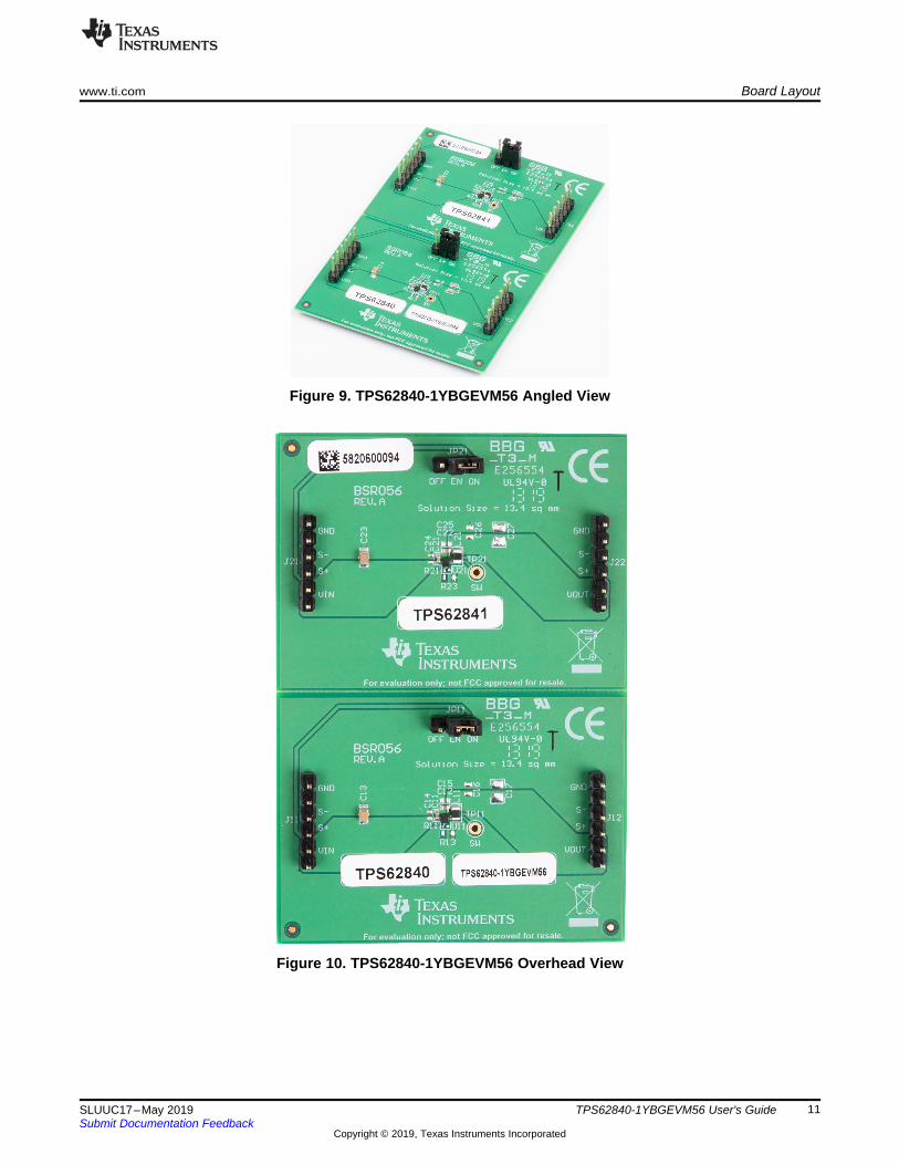
Figure 9. TPS62840-1YBGEVM56 Angled View
Figure 10. TPS62840-1YBGEVM56 Overhead View

Schematic and Bill of Materials (BOM) www.ti.com
12 SLUUC17–May 2019Submit Documentation Feedback
Copyright © 2019, Texas Instruments Incorporated
TPS62840-1YBGEVM56 User's Guide
5 Schematic and Bill of Materials (BOM)This section provides the TPS62840-1YBGEVM56 schematic and bill of materials.
5.1 SchematicFigure 11 illustrates the TPS62840 EVM schematic.
Figure 11. TPS62840 Schematic
Figure 12 illustrates the TPS62841 EVM schematic.
Figure 12. TPS62841 Schematic

www.ti.com Schematic and Bill of Materials (BOM)
13SLUUC17–May 2019Submit Documentation Feedback
Copyright © 2019, Texas Instruments Incorporated
TPS62840-1YBGEVM56 User's Guide
5.2 Bill of MaterialsTable 3 lists the TPS62840 EVM BOM.
Table 3. TPS62840 Bill of MaterialsREF DES QTY DESCRIPTION PART NUMBER MANUFACTURER
C11 1 CAP, CERM, 4.7 µF, 10 V, ±20%, X5R, 0402 GRM155R61A475MEAAD Murata
C12 1 CAP, CERM, 10 µF, 4 V, ±20%, X5R, 0402 GRM155R60G106ME44D Murata
C13 1 CAP, CERM, 47 µF, 10 V, ±20%, X5R, 0805 GRM21BR61A476ME15L Murata
L11 1 Inductor, Shielded, Metal Composite, 2.2 µH, 1.5 A, 127 mΩ, SMD DFE201210S-2R2M=P2 Murata
R11 1 RES, 0 Ω, 1%, 0.05 W, 0201 Std Std
U11 1 1.8V to 6.5V, 750mA, 60nA IQ Step Down Converter in WCSPPackage TPS62840YBG Texas Instruments
Table 4 lists the TPS62841 EVM BOM.
Table 4. TPS62841 Bill of MaterialsREF DES QTY DESCRIPTION PART NUMBER MANUFACTURER
C21 1 CAP, CERM, 4.7 µF, 10 V, ±20%, X5R, 0402 GRM155R61A475MEAAD Murata
C22 1 CAP, CERM, 10 µF, 4 V, ±20%, X5R, 0402 GRM155R60G106ME44D Murata
C23 1 CAP, CERM, 47 µF, 10 V, ±20%, X5R, 0805 GRM21BR61A476ME15L Murata
L21 1 Inductor, Shielded, Metal Composite, 2.2 µH, 1.5 A, 127 mΩ, SMD DFE201210S-2R2M=P2 Murata
R21 1 RES, 15.8 kΩ, 1%, 0.05 W, 0201 Std Std
U21 1 1.8V to 6.5V, 750mA, 60nA IQ Step Down Converter in WCSPPackage TPS62841YBG Texas Instruments

IMPORTANT NOTICE AND DISCLAIMERTI PROVIDES TECHNICAL AND RELIABILITY DATA (INCLUDING DATA SHEETS), DESIGN RESOURCES (INCLUDING REFERENCE DESIGNS), APPLICATION OR OTHER DESIGN ADVICE, WEB TOOLS, SAFETY INFORMATION, AND OTHER RESOURCES “AS IS” AND WITH ALL FAULTS, AND DISCLAIMS ALL WARRANTIES, EXPRESS AND IMPLIED, INCLUDING WITHOUT LIMITATION ANY IMPLIED WARRANTIES OF MERCHANTABILITY, FITNESS FOR A PARTICULAR PURPOSE OR NON-INFRINGEMENT OF THIRD PARTY INTELLECTUAL PROPERTY RIGHTS.These resources are intended for skilled developers designing with TI products. You are solely responsible for (1) selecting the appropriate TI products for your application, (2) designing, validating and testing your application, and (3) ensuring your application meets applicable standards, and any other safety, security, regulatory or other requirements.These resources are subject to change without notice. TI grants you permission to use these resources only for development of an application that uses the TI products described in the resource. Other reproduction and display of these resources is prohibited. No license is granted to any other TI intellectual property right or to any third party intellectual property right. TI disclaims responsibility for, and you will fully indemnify TI and its representatives against, any claims, damages, costs, losses, and liabilities arising out of your use of these resources.TI’s products are provided subject to TI’s Terms of Sale or other applicable terms available either on ti.com or provided in conjunction with such TI products. TI’s provision of these resources does not expand or otherwise alter TI’s applicable warranties or warranty disclaimers for TI products.TI objects to and rejects any additional or different terms you may have proposed. IMPORTANT NOTICE
Mailing Address: Texas Instruments, Post Office Box 655303, Dallas, Texas 75265Copyright © 2022, Texas Instruments Incorporated