
THÈSE de DOCTORAT Université Pierre et Marie Curie
165
THÈSE de DOCTORAT Université Pierre et Marie Curie - Paris VI École doctorale de Chimie Physique et de Chimie Analytique de Paris Centre (ED 388) ROLES OF THE n-TYPE OXIDE LAYER IN HYBRID PEROVSKITE SOLAR CELLS Présentée par Jie ZHANG Pour obtenir le grade de docteur Soutenance le 22 Octobre 2015 Devant un jury composé de: Dr. Thierry Pauporté Directeur de Recherche CNRS– ENSCP – Paris Directeur de thèse Pr. Bernard Ratier. Professeur – Université de Limoges Rapporteur Dr. Samir Farhat Maître de Conférence – Université Paris XIII – Villetaneuse Rapporteur Dr. Zhuoying Chen Chargée de Recherche CNRS– ESPCI – Paris Examinateur Pr. Christel Laberty Professeur – Université P. et M. Curie – Paris Examinateur Pr. Nicolas Mercier Professeur – Université d’Angers Examinateur
-
Upload
khangminh22 -
Category
Documents
-
view
0 -
download
0
Transcript of THÈSE de DOCTORAT Université Pierre et Marie Curie
THÈSE de DOCTORAT
Université Pierre et Marie Curie - Paris VI
École doctorale de Chimie Physique et de Chimie Analytique de Paris Centre(ED 388)
ROLES OF THE n-TYPE OXIDE LAYER IN HYBRID
PEROVSKITE SOLAR CELLS
Présentée par
Jie ZHANG
Pour obtenir le grade de docteur
Soutenance le 22 Octobre 2015
Devant un jury composé de:
Dr. Thierry Pauporté Directeur de Recherche CNRS–
ENSCP – Paris
Directeur de thèse
Pr. Bernard Ratier. Professeur – Université de Limoges Rapporteur
Dr. Samir Farhat Maître de Conférence – Université
Paris XIII – Villetaneuse
Rapporteur
Dr. Zhuoying Chen Chargée de Recherche CNRS– ESPCI
– Paris
Examinateur
Pr. Christel Laberty Professeur – Université P. et M. Curie
– Paris
Examinateur
Pr. Nicolas Mercier Professeur – Université d’Angers Examinateur


I dedicate this thesis to my family
for their constant support and unconditional love.
I love you all dearly.


ACKNOWLEDGEMENTS
It would not have been possible to write this doctoral thesis without the help and
support of the kind people around me. Though many individuals aided me, I would like to
highlight and thank in particular the following people.
I would like to acknowledge the Guangzhou Government for financing my scholarship
(Oversea Study Program of the Guangzhou Elite Project).
I would like to express my deepest appreciation to my thesis director, Dr. Thierry
Pauporté, for giving me the chance to work on this interesting topic. I would like to thank him
for his guidance and advice during these past three years of research, investigation and his
help in writing publications. I am grateful for his patience and endless support while
correcting my thesis manuscript. I feel I have developed a stronger understanding of research
and scientific writing.
I would like to thank Dr. Odile Majérus, Dr. Bruno Viana, and Patrick Aschehoug for
assistance in performing the Raman, the PL measurements and other characterization
techniques during these three years.
I would like to thank Pr. Bernard Ratier, and Dr. Samir Farhat for accepting to be my
rapporteurs, as well as Dr. Zhuoying Chen and Pr. Christel Laberty for being my examiners.
I am deeply grateful to all my colleagues and friends for their help, their support, for
all the great times we shared, and the many scientific discussions. I would like to thank in
particular Dr. Yuly Kusumawati, Ricardo D’Angelo, Alexandra Szemjonov, Sana Koussi, Fan
Sun, Dr. Mongia Hosni, Ronghua Li, Yanpeng Xue and many others.
Lastly I would like to thank my family for all their love and encouragement. For my
parents, who raised me with love and always supported me in all my pursuits.
Thank you

vii
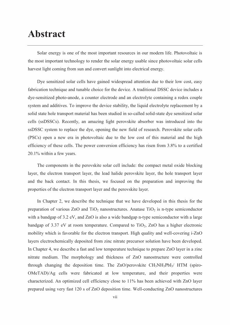
Abstract
Solar energy is one of the most important resources in our modern life. Photovoltaic is
the most important technology to render the solar energy usable since photovoltaic solar cells
harvest light coming from sun and convert sunlight into electrical energy.
Dye sensitized solar cells have gained widespread attention due to their low cost, easy
fabrication technique and tunable choice for the device. A traditional DSSC device includes a
dye-sensitized photo-anode, a counter electrode and an electrolyte containing a redox couple
system and additives. To improve the device stability, the liquid electrolyte replacement by a
solid state hole transport material has been studied in so-called solid-state dye sensitized solar
cells (ssDSSCs). Recently, an amazing light perovskite absorber was introduced into the
ssDSSC system to replace the dye, opening the new field of research. Perovskite solar cells
(PSCs) open a new era in photovoltaic due to the low cost of this material and the high
efficiency of these cells. The power conversion efficiency has risen from 3.8% to a certified
20.1% within a few years.
The components in the perovskite solar cell include: the compact metal oxide blocking
layer, the electron transport layer, the lead halide perovskite layer, the hole transport layer
and the back contact. In this thesis, we focused on the preparation and improving the
properties of the electron transport layer and the perovskite layer.
In Chapter 2, we describe the technique that we have developed in this thesis for the
preparation of various ZnO and TiO2 nanostructures. Anatase TiO2 is n-type semiconductor
with a bandgap of 3.2 eV, and ZnO is also a wide bandgap n-type semiconductor with a large
bandgap of 3.37 eV at room temperature. Compared to TiO2, ZnO has a higher electronic
mobility which is favorable for the electron transport. High quality and well-covering i-ZnO
layers electrochemically deposited from zinc nitrate precursor solution have been developed.
In Chapter 4, we describe a fast and low temperature technique to prepare ZnO layer in a zinc
nitrate medium. The morphology and thickness of ZnO nanostructure were controlled
through changing the deposition time. The ZnO/perovskite CH3NH3PbI3/ HTM (spiro-
OMeTAD)/Ag cells were fabricated at low temperature, and their properties were
characterized. An optimized cell efficiency close to 11% has been achieved with ZnO layer
prepared using very fast 120 s of ZnO deposition time. Well-conducting ZnO nanostructures
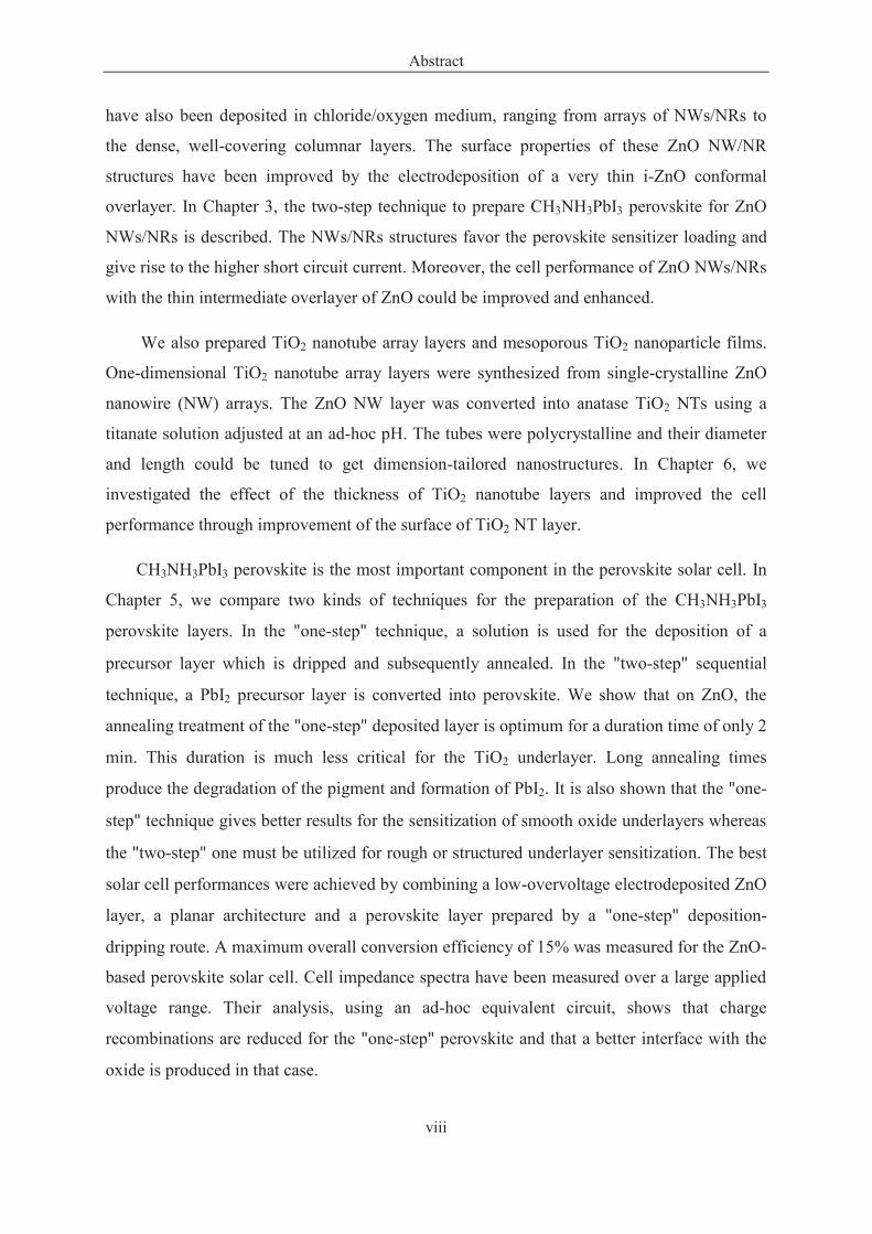
Abstract
viii
have also been deposited in chloride/oxygen medium, ranging from arrays of NWs/NRs to
the dense, well-covering columnar layers. The surface properties of these ZnO NW/NR
structures have been improved by the electrodeposition of a very thin i-ZnO conformal
overlayer. In Chapter 3, the two-step technique to prepare CH3NH3PbI3 perovskite for ZnO
NWs/NRs is described. The NWs/NRs structures favor the perovskite sensitizer loading and
give rise to the higher short circuit current. Moreover, the cell performance of ZnO NWs/NRs
with the thin intermediate overlayer of ZnO could be improved and enhanced.
We also prepared TiO2 nanotube array layers and mesoporous TiO2 nanoparticle films.
One-dimensional TiO2 nanotube array layers were synthesized from single-crystalline ZnO
nanowire (NW) arrays. The ZnO NW layer was converted into anatase TiO2 NTs using a
titanate solution adjusted at an ad-hoc pH. The tubes were polycrystalline and their diameter
and length could be tuned to get dimension-tailored nanostructures. In Chapter 6, we
investigated the effect of the thickness of TiO2 nanotube layers and improved the cell
performance through improvement of the surface of TiO2 NT layer.
CH3NH3PbI3 perovskite is the most important component in the perovskite solar cell. In
Chapter 5, we compare two kinds of techniques for the preparation of the CH3NH3PbI3
perovskite layers. In the "one-step" technique, a solution is used for the deposition of a
precursor layer which is dripped and subsequently annealed. In the "two-step" sequential
technique, a PbI2 precursor layer is converted into perovskite. We show that on ZnO, the
annealing treatment of the "one-step" deposited layer is optimum for a duration time of only 2
min. This duration is much less critical for the TiO2 underlayer. Long annealing times
produce the degradation of the pigment and formation of PbI2. It is also shown that the "one-
step" technique gives better results for the sensitization of smooth oxide underlayers whereas
the "two-step" one must be utilized for rough or structured underlayer sensitization. The best
solar cell performances were achieved by combining a low-overvoltage electrodeposited ZnO
layer, a planar architecture and a perovskite layer prepared by a "one-step" deposition-
dripping route. A maximum overall conversion efficiency of 15% was measured for the ZnO-
based perovskite solar cell. Cell impedance spectra have been measured over a large applied
voltage range. Their analysis, using an ad-hoc equivalent circuit, shows that charge
recombinations are reduced for the "one-step" perovskite and that a better interface with the
oxide is produced in that case.

Abstract
ix
Briefly, several ZnO and TiO2 nanostructures have been developed in this work applied
to perovskite solar cells. We have characterized the properties of these structures and
fabricated perovskite solar cells. Some effects of cell performances have been investigated
and used to improve the cell efficiency for the future work.
Keywords: ZnO, TiO2, CH3NH3PbI3, perovskite solar cell, electrochemical deposition, spin-
coating, Impedance spectroscopy.

x

xi
Contents
Abstract .................................................................................................................................... vii
Chapter 1: Context ..................................................................................................................... 1
1.1 Introduction .......................................................................................................................... 1
1.1.1 Solar energy ............................................................................................................... 1
1.1.2 Photovoltaic solar cells .............................................................................................. 2
1.2 Dye-Sensitized solar cells ................................................................................................ 4
1.3 Electron transport process in the ssDSSCs ...................................................................... 7
1.4 Solar cell photovoltaic characteristics .............................................................................. 8
1.4.1 Standard solar spectral irradiance .............................................................................. 8
1.4.2 Current-voltage characteristics .................................................................................. 9
1.4.3 Quantum efficiency measurement ........................................................................... 12
1.4.4 Impedance Spectroscopy ......................................................................................... 13
1.5 Perovskite sensitized solar cells ..................................................................................... 19
1.5.1 Introduction of perovskite component ..................................................................... 20
1.5.2 Recent milestones in the halide perovskite solar cell .............................................. 22
1.6 The components in the perovskite solar cell .................................................................. 28
1.6.1 The compact metal oxide blocking layer ................................................................. 28
1.6.2 The electron transport layer ..................................................................................... 28
1.6.3 The halide perovskite layer ...................................................................................... 29
1.6.4 The hole transport layer ........................................................................................... 30
1.6.5 The back contact ...................................................................................................... 32
References ............................................................................................................................ 33
Chapter 2: Synthesis and morphological properties of oxide contact layers ........................... 41
2.1 Introduction .................................................................................................................... 41
2.2 ZnO layers electrodeposited from nitrate precursor ....................................................... 42
2.2.1 Experimental ............................................................................................................ 42
2.2.2 Results ..................................................................................................................... 43
2.3 Electrodeposition of ZnO in the Chloride/Oxygen System ........................................... 45
2.3.1 Experimental ............................................................................................................ 45
Contents
xii
2.3.2 Results ..................................................................................................................... 45
2.4 One-dimensional TiO2 nanotube arrays ......................................................................... 50
2.4.1 Experimental ............................................................................................................ 50
2.4.2 Results and discussions ........................................................................................... 51
2.5 Thin mesoporous TiO2 layer .......................................................................................... 52
2.5.1 Experimental ............................................................................................................ 52
2.5.2 Results ..................................................................................................................... 53
2.6 Conclusion ...................................................................................................................... 53
References ............................................................................................................................ 54
Chapter 3: Electrochemical design of ZnO structured layers for efficient PSC application ... 58
3.1 Sensitization of ZnO electrodeposited structures by CH3NH3PbI3 perovskite layers .... 58
3.1.1 Experimental ............................................................................................................ 59
3.1.2 The characteristics of CH3NH3PbI3 layer ................................................................ 60
3.2 Perovskite sensitized solar cells ..................................................................................... 62
3.3 Conclusion ...................................................................................................................... 66
References ........................................................................................................................... 66
Chapter 4: A fast and low temperature preparation method of ZnO films for PSC applications
.................................................................................................................................................. 77
4.1 Perovskite sensitized solar cells based on i-ZnO ETL ................................................... 77
4.1.1 Effect of the deposition time of i-ZnO layer ........................................................... 77
4.1.2 Effect of the transparent conductive oxide (TCO) substrate ................................... 79
4.2 Conclusion ...................................................................................................................... 83
References ............................................................................................................................ 83
Chapter 5: Effect of oxide contact layer on the properties of CH3NH3PbI3 for PSC
applications .............................................................................................................................. 97
5.1 The preparation and properties of oxide contact layer ................................................... 97
5.1.1 Preparation of oxide contact layer ........................................................................... 98
5.1.2 Oxide layer characterizations .................................................................................. 98
5.2 Effect of oxide substrate on the perovskite preparation ............................................... 102
5.2.1 Effect of oxide substrate on the one-step perovskite preparation .......................... 103
5.2.2 Effect of oxide substrate on the two-step perovskite preparation ......................... 106
5.2.3 The properties of the heterostructures ................................................................... 107
Contents
xiii
5.3 Effect of ETL and perovskite preparation route on the solar cell performances ......... 111
5.3 Conclusion .................................................................................................................... 116
References .......................................................................................................................... 117
Chapter 6: One-dimensional self-standing TiO2 nanotube arrayed layers designed for PSC
applications ............................................................................................................................ 119
6.1 The preparation and properties of TiO2 layers ............................................................. 120
6.1.1 The preparation of TiO2 nanotube arrays. ............................................................. 120
6.1.2 The properties of TiO2 nanotube arrays. ............................................................... 121
6.2 The properties of perosvskite sensitized solar cells ..................................................... 125
6.3 Conclusions .................................................................................................................. 129
References .......................................................................................................................... 129
General conclusion and perspectives ..................................................................................... 132
Annexe I: The preparation and properties of CH3NH3I ......................................................... 136
Annexe II: The properties of TiO2 NT layers based dye sensitized solar cells ..................... 138
List of figures ......................................................................................................................... 141
List of tables ........................................................................................................................... 147
List of the abbreviations and symbols ................................................................................... 149
List of publications ................................................................................................................ 151

xiv
1
Chapter 1: Context
1.1 Introduction
1.1.1 Solar energy
Energy is one of the most important needs in our modern life. The traditional source of
energy, coming from fossil fuels, has been identified as the main reason for the
environmental damages caused by the global warming, a consequence of the CO2
concentration increase. Moreover, the fossil fuels are not a renewable source of energy and is
rapidly exhausting.[1], [2] Green and renewable energies, such as wind, photovoltaics and
hydropower, have been considered as important resources in many countries.[3]–[6] The IEA
(International Energy Agency) has estimated that renewable energies are expected to
contribute to 450 billion kWh per year by 2030, and the electricity coming from photovoltaic
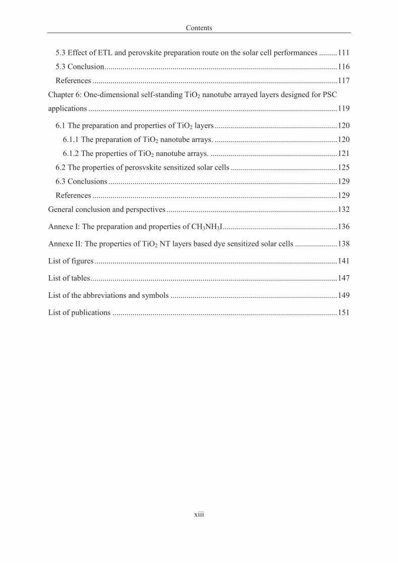
will reach 4572TWh (Figure 1.1).[7] Solar energy has many advantages including: low
carbon emission, cleanness, long term resources, low cost and so on….
Figure 1.1 Projected non-hydro power renewable electricity generation worldwide.[8]
Chapter 1: Context
2
1.1.2 Photovoltaic solar cells
Photovoltaic (PV) solar cells harvest light coming from sun and convert sunlight into
electrical energy. PV is the most important technology to render usable the solar energy.[9]
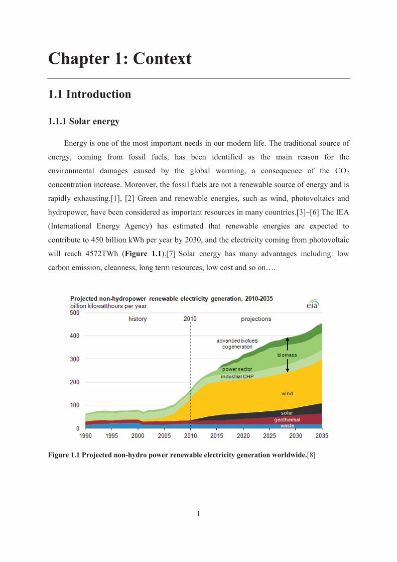
In order to enhance the device properties, the understanding of the photo-process
mechanisms is necessary. In a crystalline semiconductor, without any dopants, the Fermi
energy level lies between the valence band and conduction band. When the material is doped
Figure 1.2 The Band pictures of n-type and p-type semiconductors before (a) and after (b) joining resulting in a p-n junction. (c) Schematic of a classical sandwich solar cell composed of
p- and n-type semiconductor under illumination.
with an electron-donor, the material becomes electron rich and the Fermi level moves closer
to the conduction band. This material is called n-type semiconductor. Similarly, when the
semiconductor is doped by an electron-acceptor, the Fermi level moves closer to the valence
band, and the material is called p-type semiconductor. When an n-type semiconductor is
contacted with a p-type semiconductor, the excess electron in the n-type material flows into
Chapter 1: Context
3
p-type to recombine the excess holes in the p-type material and similarly the holes flow
toward the n-type semiconductor until an equilibrium is reached (Figure 1.2a). Then, the
atoms of p-type semiconductor, near the p-n junction, become negatively charged, whereas
the atoms of n-type semiconductor, near the p-n junction, become positively charged, an
electric field is built (Figure 1.2b). In a classical sandwich solar cell illuminated by photons
with an energy level higher than the absorber bandgap, electrons of the valence band are
excited and prompted to the conduction band. Due to the presence of an electric field, the
electrons drift towards the n-type material and the holes drift toward the p-type material.
Finally, the electrons will travel through external wire from the n-type to p-type material and
generate a current (Figure 1.2c).
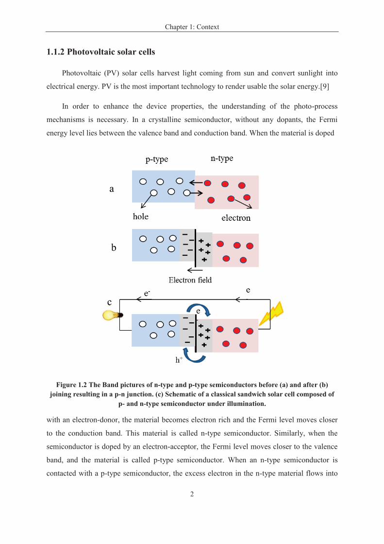
Crystalline silicon photovoltaic devices are called “first generation solar cells” and
represent the main photovoltaic products on the market. This technology has limitations due
to the high cost of starting material which requires a high purity.[10] The thin film solar cells
are classified as “second generation solar cells”, this technology is cheaper but less efficient
than silicon photovoltaic. Moreover, its development in the commercial market is limited by
the rare (indium…) or toxic (cadmium…) elements.[11] The emerging photovoltaic
technologies, called “third generation photovoltaic”, offers the possibility of very low cost
fabrication. The dye sensitized solar cells (DSSCs) or the organic photovoltaics (OPV)
belong to this category. They are based on cheap starting materials, such as organic
molecules, ZnO and TiO2.[12]
Figure 1.3 Images of photovoltaic devices: (a) silicon solar cells, (b) thin-film solar cells, (c) dye-sensitized solar cells.
Chapter 1: Context
4
1.2 Dye-Sensitized solar cells
Dye-sensitized solar cells have gained widespread attention due to their low cost, easy
fabrication technique and tunable choice for the device.[13] A first low cost, high-efficiency
dye-sensitized solar cell was reported in 1991 by M. Grätzel group.[14] Until now, a highest
efficiency of 13% has been achieved using a porphyrin-sensitizer and a liquid electrolyte.[15]
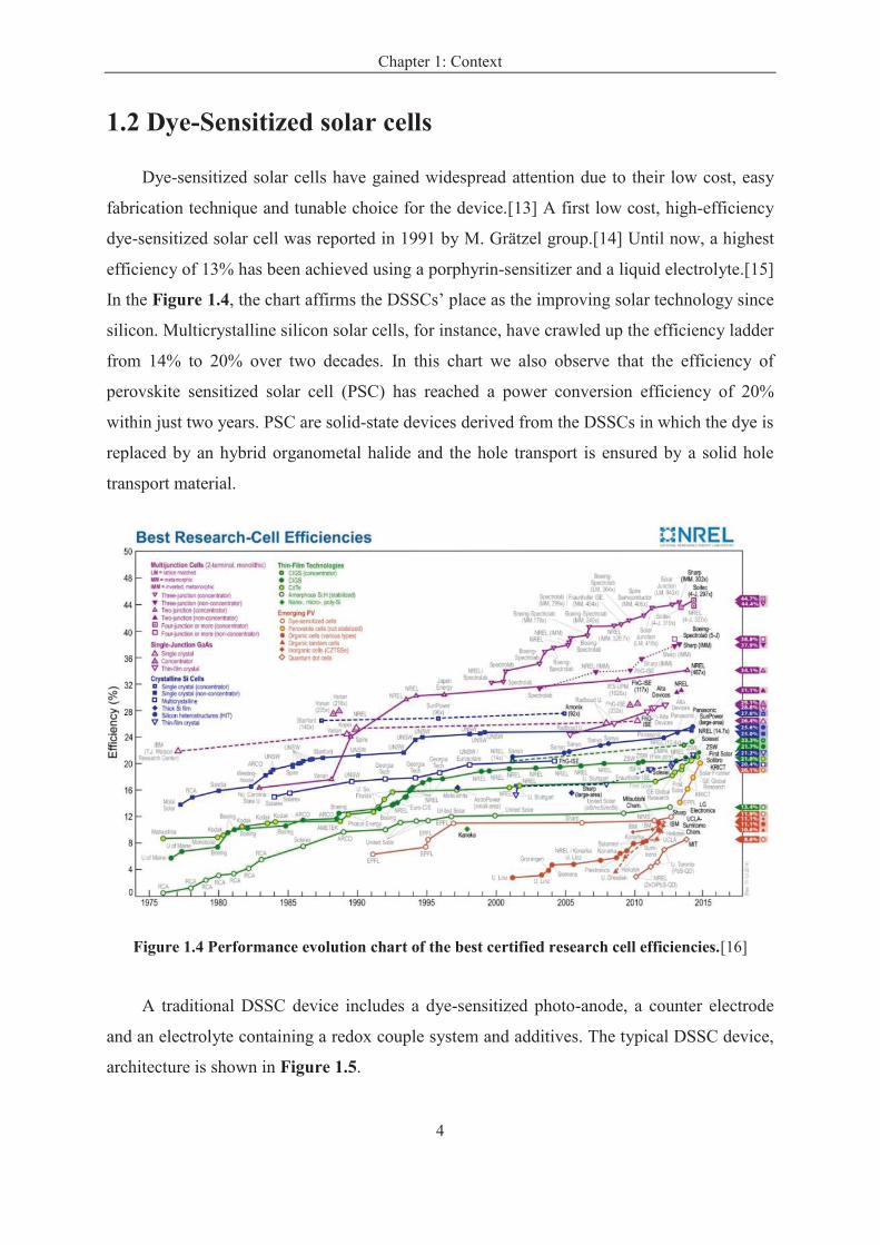
In the Figure 1.4, the chart affirms the DSSCs’ place as the improving solar technology since
silicon. Multicrystalline silicon solar cells, for instance, have crawled up the efficiency ladder
from 14% to 20% over two decades. In this chart we also observe that the efficiency of
perovskite sensitized solar cell (PSC) has reached a power conversion efficiency of 20%
within just two years. PSC are solid-state devices derived from the DSSCs in which the dye is
replaced by an hybrid organometal halide and the hole transport is ensured by a solid hole
transport material.
Figure 1.4 Performance evolution chart of the best certified research cell efficiencies.[16]
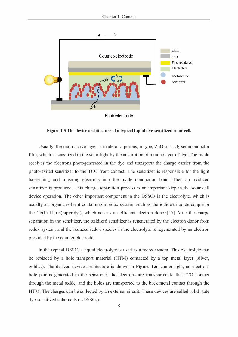
A traditional DSSC device includes a dye-sensitized photo-anode, a counter electrode
and an electrolyte containing a redox couple system and additives. The typical DSSC device,
architecture is shown in Figure 1.5.
Chapter 1: Context
5
Figure 1.5 The device architecture of a typical liquid dye-sensitized solar cell.
Usually, the main active layer is made of a porous, n-type, ZnO or TiO2 semiconductor
film, which is sensitized to the solar light by the adsorption of a monolayer of dye. The oxide
receives the electrons photogenerated in the dye and transports the charge carrier from the
photo-exited sensitizer to the TCO front contact. The sensitizer is responsible for the light
harvesting, and injecting electrons into the oxide conduction band. Then an oxidized
sensitizer is produced. This charge separation process is an important step in the solar cell
device operation. The other important component in the DSSCs is the electrolyte, which is
usually an organic solvent containing a redox system, such as the iodide/triiodide couple or
the Co(II/III)tris(bipyridyl), which acts as an efficient electron donor.[17] After the charge
separation in the sensitizer, the oxidized sensitizer is regenerated by the electron donor from
redox system, and the reduced redox species in the electrolyte is regenerated by an electron
provided by the counter electrode.
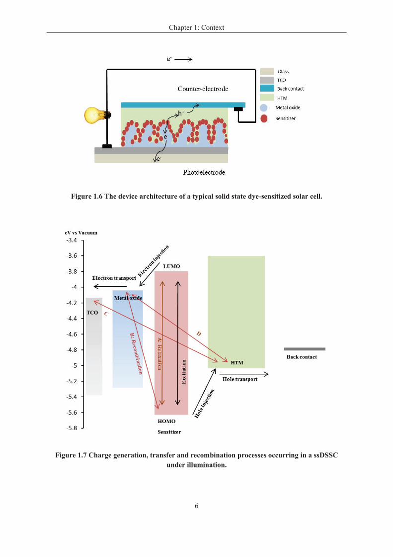
In the typical DSSC, a liquid electrolyte is used as a redox system. This electrolyte can
be replaced by a hole transport material (HTM) contacted by a top metal layer (silver,
gold…). The derived device architecture is shown in Figure 1.6. Under light, an electron-
hole pair is generated in the sensitizer, the electrons are transported to the TCO contact
through the metal oxide, and the holes are transported to the back metal contact through the
HTM. The charges can be collected by an external circuit. These devices are called solid-state
dye-sensitized solar cells (ssDSSCs).
Chapter 1: Context
6
Figure 1.6 The device architecture of a typical solid state dye-sensitized solar cell.
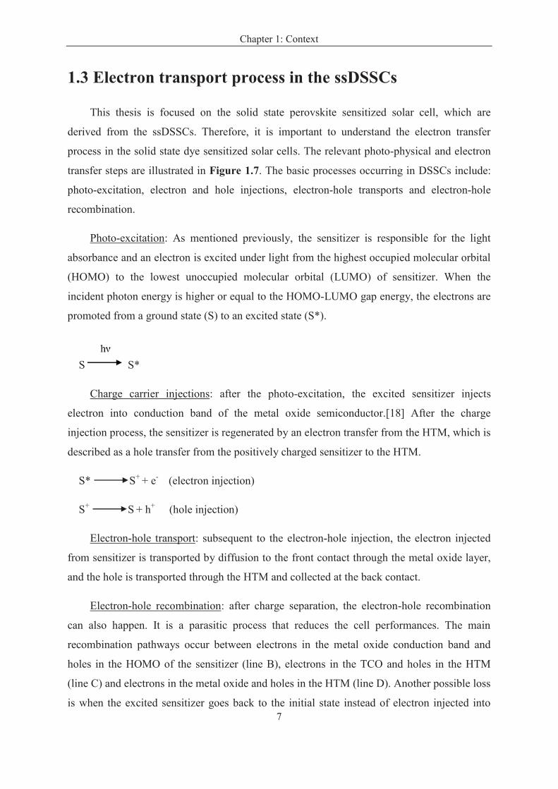
Figure 1.7 Charge generation, transfer and recombination processes occurring in a ssDSSC under illumination.
Chapter 1: Context
7
1.3 Electron transport process in the ssDSSCs
This thesis is focused on the solid state perovskite sensitized solar cell, which are
derived from the ssDSSCs. Therefore, it is important to understand the electron transfer
process in the solid state dye sensitized solar cells. The relevant photo-physical and electron
transfer steps are illustrated in Figure 1.7. The basic processes occurring in DSSCs include:
photo-excitation, electron and hole injections, electron-hole transports and electron-hole
recombination.
Photo-excitation: As mentioned previously, the sensitizer is responsible for the light
absorbance and an electron is excited under light from the highest occupied molecular orbital
(HOMO) to the lowest unoccupied molecular orbital (LUMO) of sensitizer. When the
incident photon energy is higher or equal to the HOMO-LUMO gap energy, the electrons are
promoted from a ground state (S) to an excited state (S*).
S S*
Charge carrier injections: after the photo-excitation, the excited sensitizer injects
electron into conduction band of the metal oxide semiconductor.[18] After the charge
injection process, the sensitizer is regenerated by an electron transfer from the HTM, which is
described as a hole transfer from the positively charged sensitizer to the HTM.
S* S+
+ e- (electron injection)
S+ S
+ h
+ (hole injection)
Electron-hole transport: subsequent to the electron-hole injection, the electron injected
from sensitizer is transported by diffusion to the front contact through the metal oxide layer,
and the hole is transported through the HTM and collected at the back contact.
Electron-hole recombination: after charge separation, the electron-hole recombination
can also happen. It is a parasitic process that reduces the cell performances. The main
recombination pathways occur between electrons in the metal oxide conduction band and
holes in the HOMO of the sensitizer (line B), electrons in the TCO and holes in the HTM
(line C) and electrons in the metal oxide and holes in the HTM (line D). Another possible loss
is when the excited sensitizer goes back to the initial state instead of electron injected into
Chapter 1: Context
8
metal oxide (line A). However, the latter phenomenon is avoided by the fast charge injection
to the oxide conduction band, this step being much faster than the relaxation one.
In order to reduce the recombination and increase the relative rates of the electron
process, the materials selected to fabricate the solar cell are of utmost importance. Many
works have been done to improve the charge transport rate and reduce the charge
recombination by developing new sensitizers, using different semiconductors, treating the
metal oxide surface and so on….
1.4 Solar cell photovoltaic characteristics
1.4.1 Standard solar spectral irradiance
Classical photovoltaic solar cells are electronic devices that use p-n junctions to directly
convert sunlight into electrical power. The purpose of the solar cell research is to develop
photovoltaic devices that can efficiently convert the energy coming from sun into a usable
electrical energy. Because the actual solar spectrum received by a device will vary due to the
weather, season, time of day, and location, a standard spectrum has been defined for the
determination of the solar cell characteristics and to permit the comparison of devices
prepared in various laboratories.
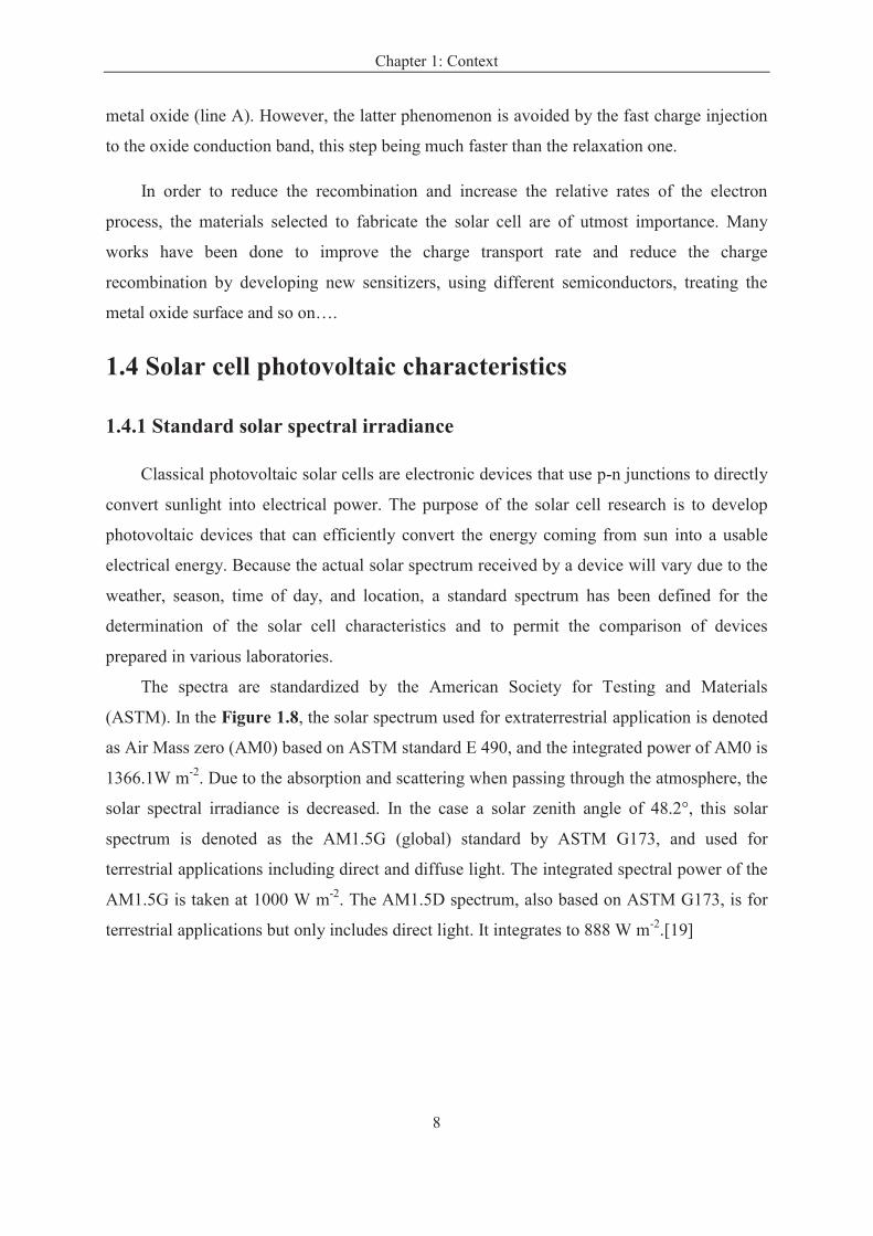
The spectra are standardized by the American Society for Testing and Materials
(ASTM). In the Figure 1.8, the solar spectrum used for extraterrestrial application is denoted
as Air Mass zero (AM0) based on ASTM standard E 490, and the integrated power of AM0 is
1366.1W m-2
. Due to the absorption and scattering when passing through the atmosphere, the
solar spectral irradiance is decreased. In the case a solar zenith angle of 48.2°, this solar
spectrum is denoted as the AM1.5G (global) standard by ASTM G173, and used for
terrestrial applications including direct and diffuse light. The integrated spectral power of the
AM1.5G is taken at 1000 W m-2
. The AM1.5D spectrum, also based on ASTM G173, is for
terrestrial applications but only includes direct light. It integrates to 888 W m-2
.[19]
Chapter 1: Context
9
Figure 1.8 Reference solar irradiation spectra according to the standards by American Society for Testing and Materials (ASTM).
1.4.2 Current-voltage characteristics
The current-voltage characteristics (J-V curves) are measured in the dark and under
illumination, for evaluating the performance of solar cells. This process is done by applying
an external potential bias when measuring the current-voltage characteristics. They are
measured in the dark and under AM1.5G calibrated illumination. Basically, the forward
current, for which the applied potential is referred to as forward bias, involves electrons
injection into the cell from the photoanode. The reverse current, for which the applied
potential is referred to as reverse bias, involves electrons injection from the counter electrode
side.
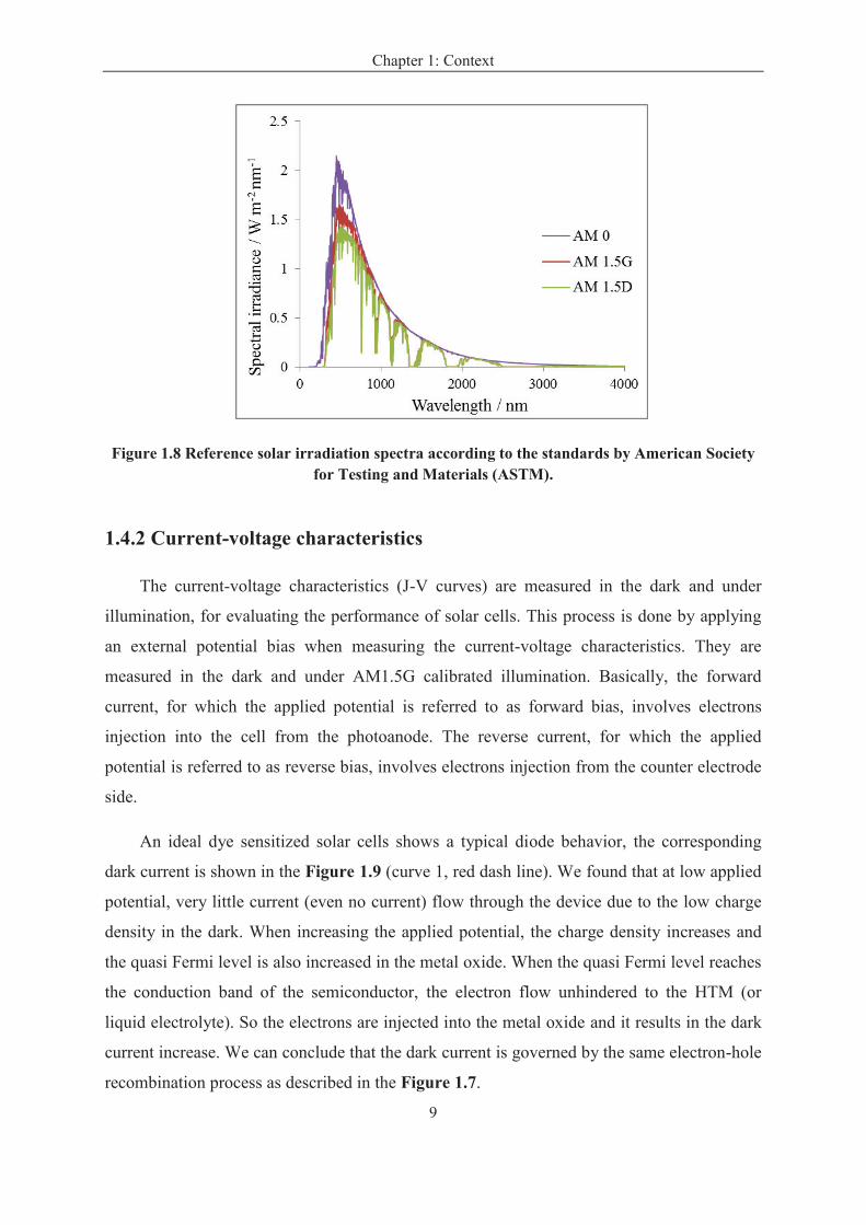
An ideal dye sensitized solar cells shows a typical diode behavior, the corresponding
dark current is shown in the Figure 1.9 (curve 1, red dash line). We found that at low applied
potential, very little current (even no current) flow through the device due to the low charge
density in the dark. When increasing the applied potential, the charge density increases and
the quasi Fermi level is also increased in the metal oxide. When the quasi Fermi level reaches
the conduction band of the semiconductor, the electron flow unhindered to the HTM (or
liquid electrolyte). So the electrons are injected into the metal oxide and it results in the dark
current increase. We can conclude that the dark current is governed by the same electron-hole
recombination process as described in the Figure 1.7.

Chapter 1: Context
10
Figure 1.9 I-V curve of a typical solar cell under illumination (line) and in the dark (dashed line).
Under illumination, the photocurrent is generated and flows opposite to the diode (dark)
current. A typical I-V curve is displayed in the Figure 1.9 (curve 2, red full line). It is
governed by two competing processes: the photocurrent generation and electron-hole
recombination. At the low potential, most of the charge carriers are collected before they
recombine. In that case, the photocurrent does not change with the increasing applied
potential. With increasing applied potential, the recombination rate is increased whereas the
charge carrier rate is decreased, the photocurrent starts to decrease until without net current
flowing to the photoelectrode. When the current is zero, the applied potential point is denoted
as the open-circuit potential (Voc). When the external bias is zero, the current is denoted as
the short-circuit photocurrent (Jsc).
The power conversion efficiency (PCE) is the most important parameter for comparing
the performance of solar cells. PCE is defined as the ratio of maximum output electrical
power (Pmax) to incident power (Pin), as described in the Equation 1.1. The electrical power (P)
is defined as the product of J and V, which is displayed in the Figure 1.9 (curve 3, green line).
The maximum of the power curve is called the maximum power point (Pmax), the
corresponding voltage and current are denoted as Jmax and Vmax, described with the Equation
1.2.
PCE=Pmax
P i n (1.1)
Chapter 1: Context
11
Pmax=J maxV max (1.2)
Another parameter is the fill factor (FF), defined as the ratio between the maximum
electrical power (Pmax) to the product of Voc and Jsc. Graphically, the FF also is a measure of
“squareness” of the solar cell characteristic and defined as the ratio of area A to the area B.
Finally, the PCE is defined as the Equation 1.4.
FF=Pmax
J scV oc
=J maxV max
J sc V oc (1.3)
PCE=Pmax
P i n
=J maxV max
P i n
=FF J sc V oc
P i n (1.4)
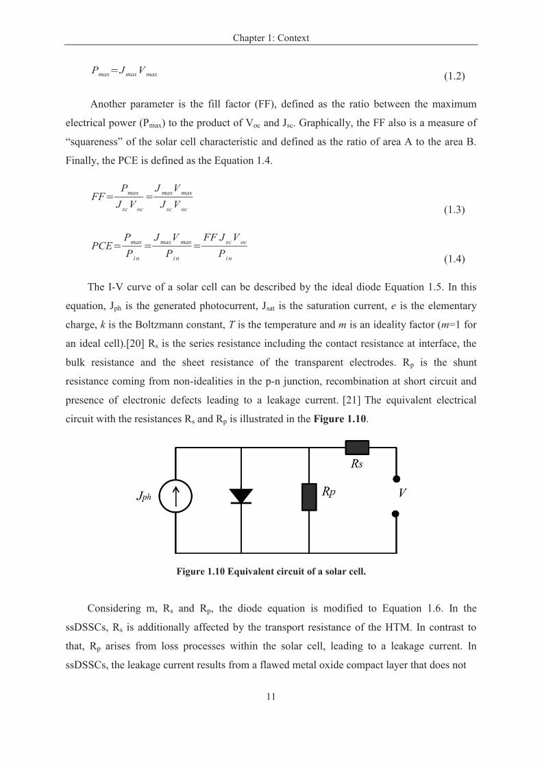
The I-V curve of a solar cell can be described by the ideal diode Equation 1.5. In this
equation, Jph is the generated photocurrent, Jsat is the saturation current, e is the elementary
charge, k is the Boltzmann constant, T is the temperature and m is an ideality factor (m=1 for
an ideal cell).[20] Rs is the series resistance including the contact resistance at interface, the
bulk resistance and the sheet resistance of the transparent electrodes. Rp is the shunt
resistance coming from non-idealities in the p-n junction, recombination at short circuit and
presence of electronic defects leading to a leakage current. [21]
The equivalent electrical
circuit with the resistances Rs and Rp is illustrated in the Figure 1.10.
Figure 1.10 Equivalent circuit of a solar cell.
Considering m, Rs and Rp, the diode equation is modified to Equation 1.6. In the
ssDSSCs, Rs is additionally affected by the transport resistance of the HTM. In contrast to
that, Rp arises from loss processes within the solar cell, leading to a leakage current. In
ssDSSCs, the leakage current results from a flawed metal oxide compact layer that does not
Chapter 1: Context
12
entirely prevent the contact between the TCO and the HTM.
(1.5)
(1.6)
1.4.3 Quantum efficiency measurement
In order to determine the ratio of collected charge to the incident photons, the quantum
efficiency was introduced. The quantum efficiency can be expressed as the external quantum
efficiency (EQE) and internal quantum efficiency (IQE).
The EQE (external quantum efficiency), is also noted as IPCE, for incident photon-to-
electron conversion efficiency. This measurement also includes photons which have been lost
by optical transmission and reflection. The IPCE is usually measured at the short circuit and
can be calculated according to the Equation 1.7, where Jsc is the short circuit current of the
cell under the incident monochromatic light with wavelength (l) and photon flux (J0), and e
is the elementary charge.
0
( )( ) scJ
IPCEeJ
ll = (1.7)
The IPCE also can be expressed as the product of the efficiency of four separate
physical processes, as shown in the Equation 1.8. Where ηlh is light-harvesting efficiency of
sensitized oxide layer, ηinj is the efficiency of electron injection from the sensitizer into the
oxide, ηcol is the electron collection efficiency, and ηrej is the absorber regeneration
efficiency.[20]
( ) ( ) ( ) ( ) ( )lh inj col rejIPCE l h l h l h l h l= (1.8)
The internal quantum efficiency (IQE) also referred to as the absorbed photon-to-current
conversion efficiency (APCE), corresponds only to the photons absorbed by the device. The
equation is:
( ) ( ) ( ) ( )inj col rejIQE l h l h l h l=
(1.9)
(exp( ) 1)ph sat
eVJ J J
kT= - -
( )(exp( ) 1)s s
ph satp
e V JR V JRJ J J
mkT R
+ += - - +
Chapter 1: Context
13
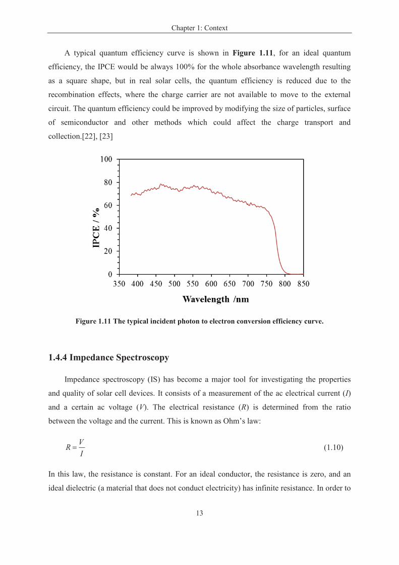
A typical quantum efficiency curve is shown in Figure 1.11, for an ideal quantum
efficiency, the IPCE would be always 100% for the whole absorbance wavelength resulting
as a square shape, but in real solar cells, the quantum efficiency is reduced due to the
recombination effects, where the charge carrier are not available to move to the external
circuit. The quantum efficiency could be improved by modifying the size of particles, surface
of semiconductor and other methods which could affect the charge transport and
collection.[22], [23]
Figure 1.11 The typical incident photon to electron conversion efficiency curve.
1.4.4 Impedance Spectroscopy
Impedance spectroscopy (IS) has become a major tool for investigating the properties
and quality of solar cell devices. It consists of a measurement of the ac electrical current (I)
and a certain ac voltage (V). The electrical resistance (R) is determined from the ratio
between the voltage and the current. This is known as Ohm’s law:
V
RI
= (1.10)
In this law, the resistance is constant. For an ideal conductor, the resistance is zero, and an
ideal dielectric (a material that does not conduct electricity) has infinite resistance. In order to
Chapter 1: Context
14
extend this concept to alternating current (ac) circuit, the voltage (V) and current (I) need to
be treated as time (t), the equations described as:
[ ]( ) exp ( )VV V i tw w f= + (1.11)
[ ]( ) exp ( )II I i tw w f= + (1.12)
2 fw p= (1.13)
where w is angular frequency. For the real conductor, the electrical impedance Z is the
complex ratio of the voltage and the current (Equation 1.14) and taken into account both
magnitude and phase, j is the phase difference between the voltage and current. For a direct
current (dc) circuit, the resistance of the system can be taken as impedance with the same
magnitude and zero phase angle.
[ ][ ]
exp ( )( ) exp( )
exp ( )
'( ) ''( )
V
I
V i tZ Z i
I i t
Z iZ
w fw f
w f
w w
+= = -
+
= +
(1.14)
V If f f= + (1.15)
In ac circuit, in addition to the resistance present in the dc circuit, two other impedance
phenomena must be considered:
(1) The inductance by which voltage are induced in conductor by the magnetic field
generated by current.
(2) The capacitance, the electrostatic storage of charge induced by an applied voltage
between conductors. Collectively the inductance and the capacitance form the imaginary part
of the complex impedance Z” in Equation 1.14, which is referred to as the reactance while the
resistance forms the real part Z’.
The capacitance can be determined from the measurement of the change in the electrical
charge, which is described by the equation 1.16.
( ) 1
( )( ) ( )
IC
i V i Z
ww
w w w w= = (1.16)
Chapter 1: Context
15
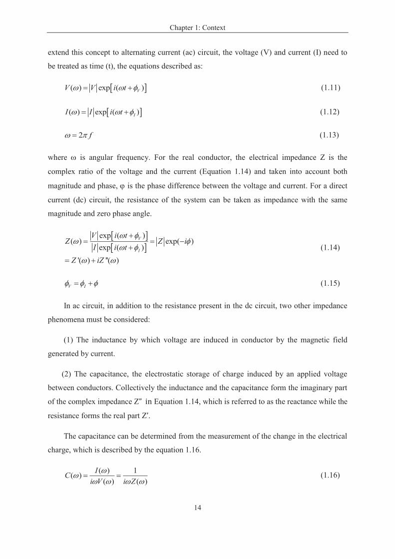
Many measure of IS can be described by equivalent circuits composed of combinations
of a few elements that are indicated in Table 1.1.
Table 1.1 Relationship and impedance corresponding to bulk electrical elements. Furthermore, the corresponding electrical equivalent circuit symbols are presented. The graphical
representation of the impedance is displayed in the Nyquist plots where Z¢ and Z¢¢ are the real and imaginary components respectively.
Element Relation Impedance Symbol Nyquist
Resistor R V = IR ZR = R
Capacitor C dV
I Cdt
= 1 i
Zci C Cw w
= = -
Constant Phase
Element Q
1
( )
1
CPE nZ
i Q
QZ
w=
=
Inductor L dI
V Ldt
= LZ i Lw=
Equivalent circuits are formed by connecting these elements by wires, representing low
resistance paths in the system. When connected in series the current passing through
components is the same, while when in parallel they experience the same voltage. The
impedance of element in series is additive, and for parallel elements the total impedance is
the inverse of the sum of the inverse impedance of the individual components. The
impedance for the parallel combination of a resistor and a capacitor is described in
Equation1.17.
1
0
1( ) ( )
1 1
1
R RZ i C
R i RC i
RC
w ww wt
tw
-= + = =+ +
= = (1.17)
Chapter 1: Context
16
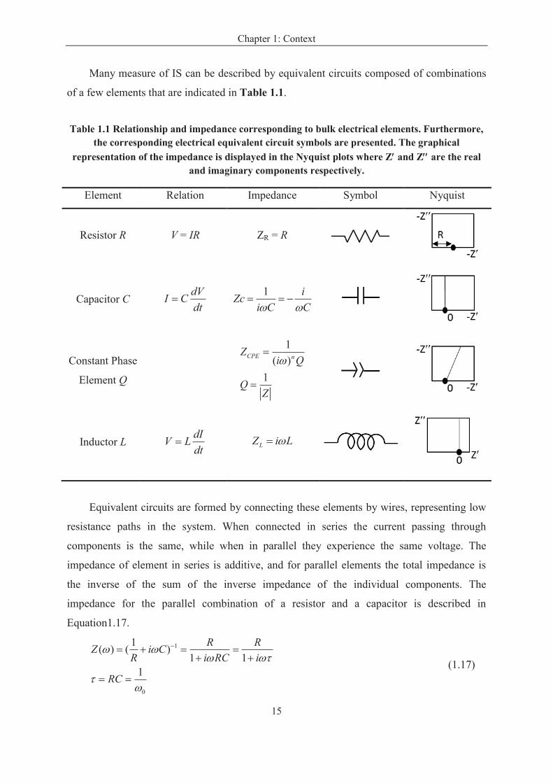
An equivalent circuit consisting of the parallel combination of a R and a C element in
addition to a simple series resistance R1 is shown in the Figure 1.12a. Figure 1.12b-d display
the perspective of the individual planes. The complex Nyquist plot (Figure 1.12c) of the
imaginary impedance component as a function of the real component manifests as an arc,
often called RC-arc. The top of the arc occurs at the characteristic frequency w0
corresponding to a relaxation time t (Equation 1.17).
Figure 1.12 (a) Equivalent circuit. (b) Nyquist plot of the spectrum (imaginary as a function of real component). The maximum of the RC-arc takes place at the characteristics angular
frequency w0 as indicated. (c, d) Bode representations of the impedance spectrum: (c) Magnitude versus the frequency and (d) phase versus the frequency. The simulation was
conducted from 1 MHz to 1 mHz.
The high frequency intercept of the arc on the real axis provides a measure of the
magnitude of the resistance R1 associated with the system and the low frequency intercept is
equal to R1 + R2. The addition of a series resistance, R1 results in the shift of the RC-arc along
the real axis. Consequently the dc resistance of this system is the sum of the individual
resistors, Z(0)= Rdc = R1 + R2, which in this case is 210 W. Hence the data representation in
the Nyquist plot is crucial to discern information about the contributions of various
Chapter 1: Context
17
resistances within a system. The frequency dependence of the real and imaginary components
presented in Figure 1.12 gives a first indication of the behavior of the magnitude |Z| and
phase j of the impedance as a function of the frequency. This is useful in the identification of
relaxation processes with different time constants, which therefore manifest at different
frequencies.
The definitions discussed above correspond to the ideal cases. To take into account the
deviation from ideality, constant phase elements (CPEs) are employed in place of ideal
capacitors. The electrical symbol and impedance expression for a CPE are given in the Table
1.1 and Figure 1.13a. A CPE is typically used to describe a capacitive process which is
accompanied by frequency dispersion. The exponent, n accounts for the deviation from the
ideal case where n = 1 describes an ideal capacitor while n = 0 corresponds to a pure resistor.
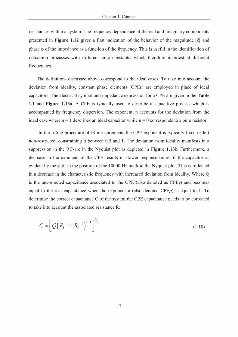
In the fitting procedure of IS measurements the CPE exponent is typically fixed or left
non-restricted, constraining it between 0.5 and 1. The deviation from ideality manifests in a
suppression in the RC-arc in the Nyquist plot as depicted in Figure 1.13b. Furthermore, a
decrease in the exponent of the CPE results in slower response times of the capacitor as
evident by the shift in the position of the 10000 Hz mark in the Nyquist plot. This is reflected
in a decrease in the characteristic frequency with increased deviation from ideality. Where Q
is the uncorrected capacitance associated to the CPE (also denoted as CPET) and becomes
equal to the real capacitance when the exponent n (also denoted CPEp) is equal to 1. To
determine the correct capacitance C of the system the CPE capacitance needs to be corrected
to take into account the associated resistance R:
( )1
11 1
1 2
n nC Q R R
-- -é ù= +ê úë û (1.18)
Chapter 1: Context
18
Figure 1.13 (a) Equivalent circuit. (b) Nyquist plot. Bode (c) Magnitude and (d) Phase plot versus the frequency from simulation using the presented values for R1, R2 and CPE. The exponent of CPE was changed from the ideal case between 1 and 0.5. The red points in the
Nyquist plot correspond to the 10000 Hz freqency. The simulation was conducted from 10 MHz to 1 mHz.
In order to use IS as a tool to examine real system it is necessary to correlate its physical
properties with electrical circuit elements. This allows the system to be represented by an
equivalent circuit model that can be used to interpret and analyze the IS response of the
system. To establish this relationship for solar cells, it is necessary to associate the potentials
of the model circuit with the electrochemical potential of the charge carriers in the device.
Chapter 1: Context
19
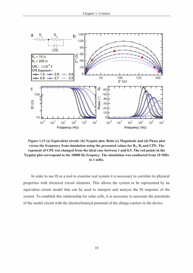
Figure 1.14 Equivalent circuit employed for fitting the impedance spectra.
The simplest IS model of a solar cell consists of a two series combination of CPE//R in
series with a high frequency resistance (Rs), as shown in Figure 1.14. Rs is due to the
contacts and FTO layer. In the case of the PSCs, we will see that the high frequency
resistance, Rsc is due to the selective contacts and CPE-sc is related to interfacial the
capacitances between the ETM and the HTM and the perovskite. The low frequency loop is
assigned to the recombination due to perovskite which gives rise to a resistance noted Rrec
and a CPE-dr which is related to the perovskite dielectric relaxation capacitance. Csc is
determined from Equation 1.18 using Rs as R1 and Rsc as R2. For the determination of Cdr,
(Rs+Rsc) is used as R1 and Rrec as R2.
The recombination resistance needs to be sufficiently large to allow the accumulation of
charge carriers in the capacitive element to produce a large solar cell Voc. Selective contacts
are essential to direct the flow of charges and prevent the internal short-circuiting of the
device. The low frequency capacitance is a measure of the charge density and is associated
with the splitting of the Fermi levels, thus generating a photovoltage.
1.5 Perovskite sensitized solar cells
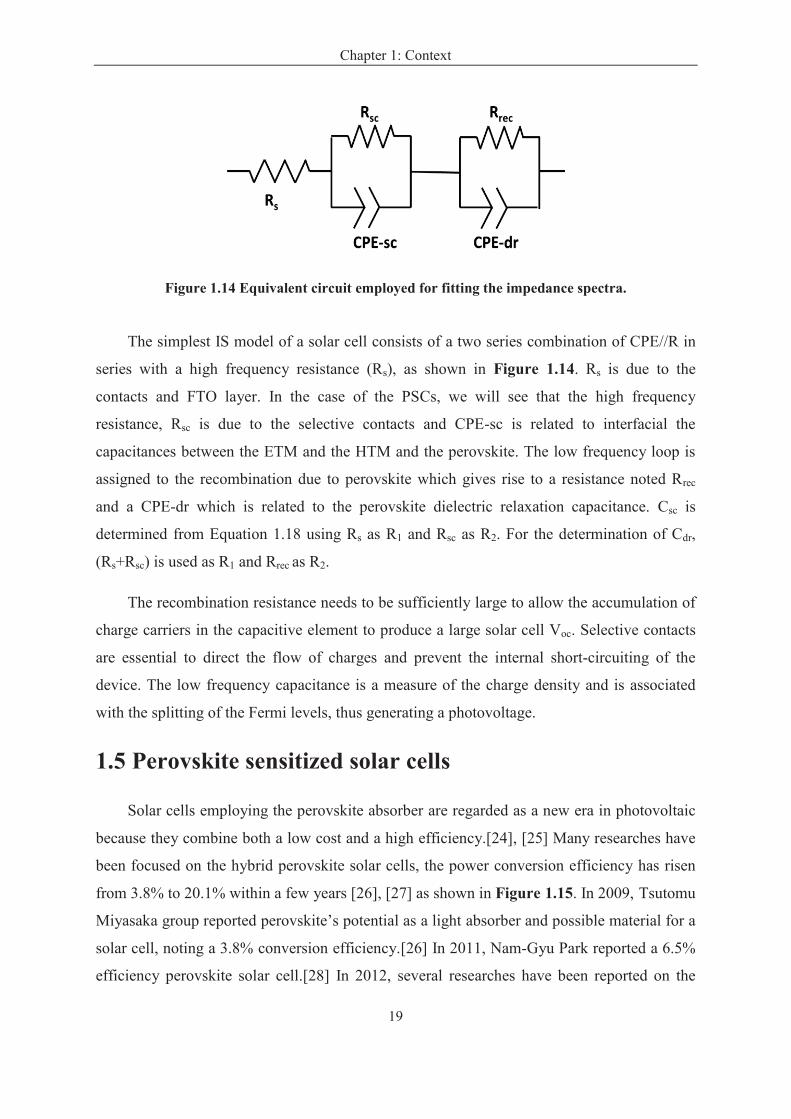
Solar cells employing the perovskite absorber are regarded as a new era in photovoltaic
because they combine both a low cost and a high efficiency.[24], [25] Many researches have
been focused on the hybrid perovskite solar cells, the power conversion efficiency has risen
from 3.8% to 20.1% within a few years [26], [27] as shown in Figure 1.15. In 2009, Tsutomu
Miyasaka group reported perovskite’s potential as a light absorber and possible material for a
solar cell, noting a 3.8% conversion efficiency.[26] In 2011, Nam-Gyu Park reported a 6.5%
efficiency perovskite solar cell.[28] In 2012, several researches have been reported on the
Chapter 1: Context
20
improving of perovskite performances. Such as, Michael Grätzel reported a conversion
efficiency of exceeding 9% with perovskite in the journal Nature Scientific Reports.[29]
Henry J. Snaith reported a “meso-superstructured solar cell” with a power conversion
efficiency of 10.9% in a single-junction device under simulated full sunlight. This perovskite
solar cell exhibited exceptionally few fundamental energy losses and generated an open-
circuit photovoltages of more than 1.1 volts.[30] In the 2013, the efficiency have climbed up
to more than 15%.[31], [32] Until now, the highest certified efficiency reached up to
20.1%.[33]
Figure 1.15 Number of publications and efficiency evolution of the perovskite solar cells (updated up to 2015.02.01). The inset is the crystal structure of perovskite (ABX3) with a cubic
symmetry.[34]
1.5.1 Introduction of perovskite component
Historically, the term perovskite has been used to describe the materials with same type
of crystal structure as calcium titanium oxide (CaTiO3), which was discovered in 1839 by
Lev Alexeïevitch Perovski.[35]
The chemical formula of the perovskite compounds is AMX3, where A is a large cation
coordinated to 12 X anions and filled in the holes among the octahedral, M is a metal bonded
to 6 X anions and X is the anion bonds to A and M. The ideal cubic-symmetry perovskite
structure has the M cation in 6 fold coordination, surrounded by the MX6 octahedron anions,
and MX6 octahedron are corner-connected to form a three dimensional framework (Figure
Chapter 1: Context
21
1.16). Consequently, only small organic cations, for example those consisting of three or less
C-C or C-N bonds, could be fitted into the structure. Mostly, a slightly perovskite structure
distortions can be observed with larger A cation, many physical properties of perovskites,
particularly the electronic, magnetic or ferrimagnetism depend on the details of these
distortions, which are important for the application of perovskite material.[36]–[38]
Figure 1.16 (a) Ball and stick model (b) three dimensional of cubic perovskite of general formula AMX3.
Halide perovskite (AMX3) is a large perovskite family with X representing halogen
anions (F-, Cl
-, Br
-, I
-). A
+ can be a monovalent alkali (Li
+, Na
+, K
+, Rb
+, Cs
+) or an organic
cations (aliphatic amine or aromatic ammonium), M2+
is a divalent metal cation (Cu2+
, Fe2+
,
Pb2+
, etc). They form the alkali metal halide perovskite and organo-metal halide
perovskite.[39] In 1980, Salau first reported that the direct energy gap of KPbI3 ranges
between 1.4 and 2.2 eV, suggesting its potential used as a solar energy converter.[40]
Distinct from the alkali metal halide perovskite, the organo-metal halide perovskite
family has been discovered more recently but has attracted more interest due to its good
optoelectronic properties and its potential for application in low temperature device
fabrication.[41], [42] The interest about the organo-metal halide perovskite was focused on
the photo- and ionic conductivity and semiconducting properties for organic light emitting
diodes and thin film transistors applications.[14], [32]
Chapter 1: Context
22
1.5.2 Recent milestones in the halide perovskite solar cell
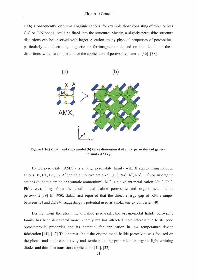
In 2009, Miyasaka first reported the use of organo-lead halide perovskite compounds to
efficiently sensitize TiO2 for visible-light conversion in solar cell. The resulting PCEs were
3.81% for CH3NH3PbI3 and 3.31% for the CH3NH3PbBr3.[26] A schematic of the perovskite
sensitized TiO2 and the IPCE action spectra are shown in Figure 1.17. In 2011, N.G. Park
and co-authors fabricated solar cells using TiO2 layer sensitized by about 2-3 nm sized
CH3NH3PbI3 pigment and bumped up the conversion efficiency to 6.54%.[28] However, the
stability of these cells was poor and they were degraded in a few minutes due to the
perovskite dissolution in the liquid electrolyte.
Figure 1.17 (a) A schematic illustration of perovskite-sensitized TiO2 undergoing photoexcitation and electron transfer. (b) IPCE action spectra for photoelectrochemical cells
using CH3NH3PbBr3/TiO2 (solid line) and CH3NH3PbI3/TiO2 (dashed line).[26]
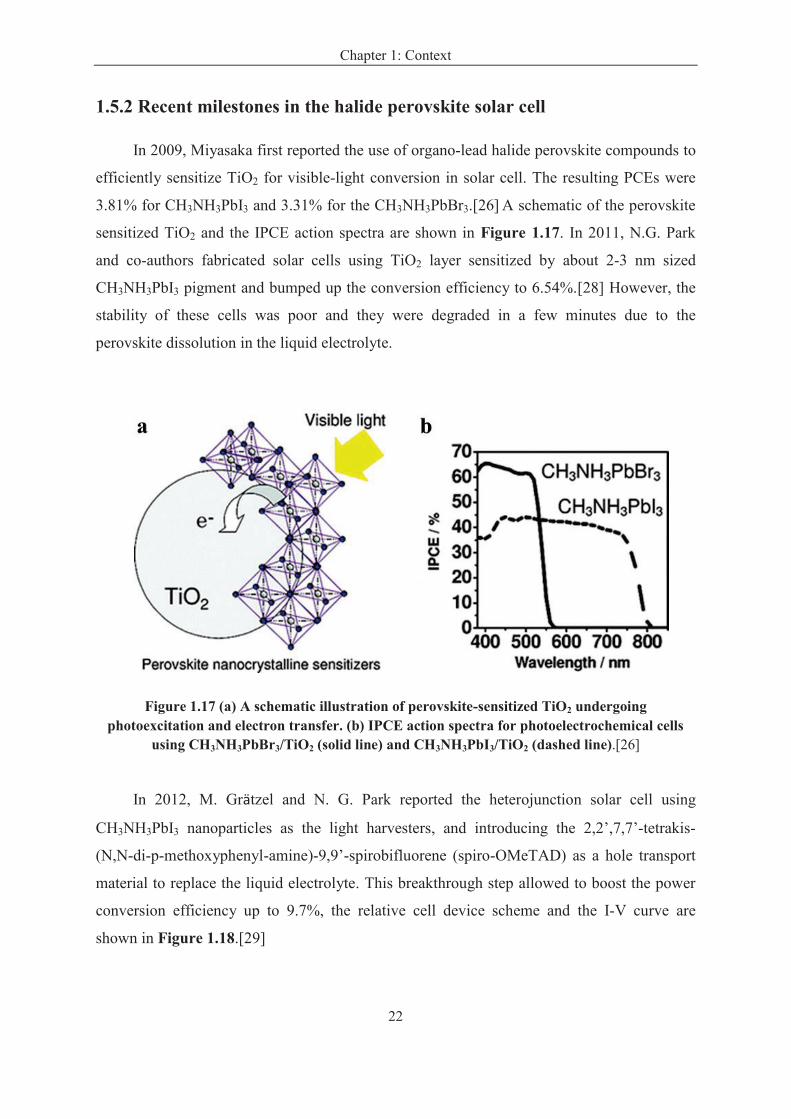
In 2012, M. Grätzel and N. G. Park reported the heterojunction solar cell using
CH3NH3PbI3 nanoparticles as the light harvesters, and introducing the 2,2’,7,7’-tetrakis-
(N,N-di-p-methoxyphenyl-amine)-9,9’-spirobifluorene (spiro-OMeTAD) as a hole transport
material to replace the liquid electrolyte. This breakthrough step allowed to boost the power
conversion efficiency up to 9.7%, the relative cell device scheme and the I-V curve are
shown in Figure 1.18.[29]
Chapter 1: Context
23
Figure 1.18 CH3NH3PbI3 perovskite sensitized solar cell device and its photovoltaic characteristics. (a) Real solid-state device. (b) Cross-sectional structure of the device. (c) Cross-sectional SEM image of the device. (d) Photocurrent density as a function of the forward bias
voltage.[29]
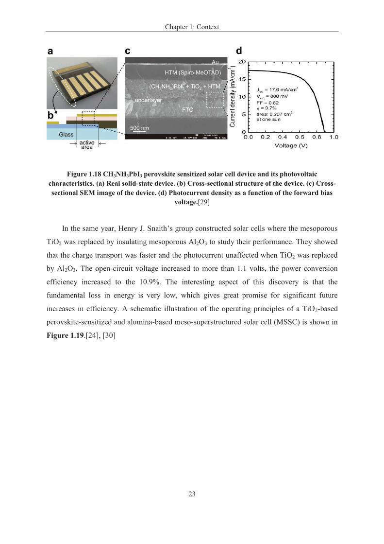
In the same year, Henry J. Snaith’s group constructed solar cells where the mesoporous
TiO2 was replaced by insulating mesoporous Al2O3 to study their performance. They showed
that the charge transport was faster and the photocurrent unaffected when TiO2 was replaced
by Al2O3. The open-circuit voltage increased to more than 1.1 volts, the power conversion
efficiency increased to the 10.9%. The interesting aspect of this discovery is that the
fundamental loss in energy is very low, which gives great promise for significant future
increases in efficiency. A schematic illustration of the operating principles of a TiO2-based
perovskite-sensitized and alumina-based meso-superstructured solar cell (MSSC) is shown in
Figure 1.19.[24], [30]
Chapter 1: Context
24
Figure 1.19 Schematic illustrating the charge transfer and charge transport in a perovskite-sensitized TiO2 solar cell (left) and a noninjecting Al2O3-based solar cell
(right); a representation of the energy landscape is shown below, with electrons shown as solid circles and holes as open circles.[30]
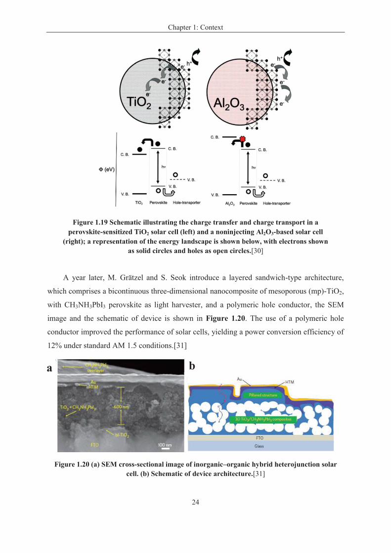
A year later, M. Grätzel and S. Seok introduce a layered sandwich-type architecture,
which comprises a bicontinuous three-dimensional nanocomposite of mesoporous (mp)-TiO2,
with CH3NH3PbI3 perovskite as light harvester, and a polymeric hole conductor, the SEM
image and the schematic of device is shown in Figure 1.20. The use of a polymeric hole
conductor improved the performance of solar cells, yielding a power conversion efficiency of
12% under standard AM 1.5 conditions.[31]
Figure 1.20 (a) SEM cross-sectional image of inorganic–organic hybrid heterojunction solar cell. (b) Schematic of device architecture.[31]
a b
Chapter 1: Context
25
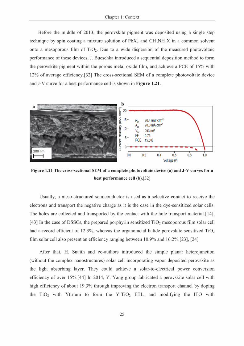
Before the middle of 2013, the perovskite pigment was deposited using a single step
technique by spin coating a mixture solution of PbX2 and CH3NH3X in a common solvent
onto a mesoporous film of TiO2. Due to a wide dispersion of the measured photovoltaic
performance of these devices, J. Bueschka introduced a sequential deposition method to form
the perovskite pigment within the porous metal oxide film, and achieve a PCE of 15% with
12% of average efficiency.[32] The cross-sectional SEM of a complete photovoltaic device
and J-V curve for a best performance cell is shown in Figure 1.21.
Figure 1.21 The cross-sectional SEM of a complete photovoltaic device (a) and J-V curves for a
best performance cell (b).[32]
Usually, a meso-structured semiconductor is used as a selective contact to receive the
electrons and transport the negative charge as it is the case in the dye-sensitized solar cells.
The holes are collected and transported by the contact with the hole transport material.[14],
[43] In the case of DSSCs, the prepared porphyrin sensitized TiO2 mesoporous film solar cell
had a record efficient of 12.3%, whereas the organometal halide perovskite sensitized TiO2
film solar cell also present an efficiency ranging between 10.9% and 16.2%.[23], [24]
After that, H. Snaith and co-authors introduced the simple planar heterojunction
(without the complex nanostructures) solar cell incorporating vapor deposited perovskite as
the light absorbing layer. They could achieve a solar-to-electrical power conversion
efficiency of over 15%.[44] In 2014, Y. Yang group fabricated a perovskite solar cell with
high efficiency of about 19.3% through improving the electron transport channel by doping
the TiO2 with Yttrium to form the Y-TiO2 ETL, and modifying the ITO with
a b

Chapter 1: Context
26
polyethyleneimine ethoxylated (PEIE) to reduce the work function of ITO.[27] The device
structure and energy level of each functional layer is shown in the Figure 1.22.
Figure 1.22 Cross-sectional SEM images of the cell device (A), and diagram of energy level of
each layer in the device (B).[27]
They also investigated the stability of their perovskite solar cells, when the cell was
stored in dry air or nitrogen, the efficiency of device retain 80% of the initial performance in
24h, but only retain 20% of initial efficiency after 6 days of storage in dry air or N2
atmosphere, as shown in Figure 1.23. In that case, stabilizing techniques will be needed for
the practical use of these perovskite solar cells.
Figure 1.23 Stability of cells stored in the ambient air, dry air and N2 atmosphere.[27]
Chapter 1: Context
27
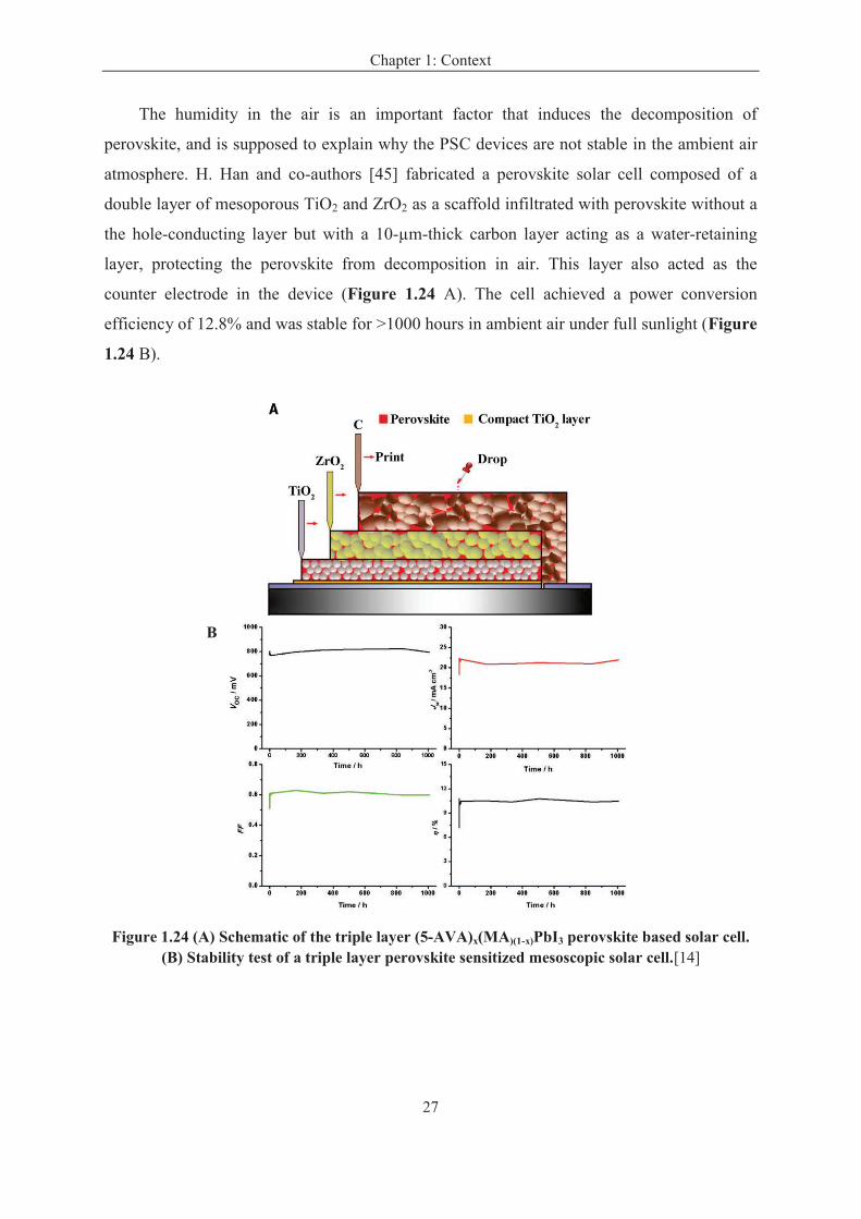
The humidity in the air is an important factor that induces the decomposition of
perovskite, and is supposed to explain why the PSC devices are not stable in the ambient air
atmosphere. H. Han and co-authors [45] fabricated a perovskite solar cell composed of a
double layer of mesoporous TiO2 and ZrO2 as a scaffold infiltrated with perovskite without a
the hole-conducting layer but with a 10-µm-thick carbon layer acting as a water-retaining
layer, protecting the perovskite from decomposition in air. This layer also acted as the
counter electrode in the device (Figure 1.24 A). The cell achieved a power conversion
efficiency of 12.8% and was stable for >1000 hours in ambient air under full sunlight (Figure
1.24 B).
Figure 1.24 (A) Schematic of the triple layer (5-AVA)x(MA)(1-x)PbI3 perovskite based solar cell. (B) Stability test of a triple layer perovskite sensitized mesoscopic solar cell.[14]
B
Chapter 1: Context
28
1.6 The components in the perovskite solar cell
1.6.1 The compact metal oxide blocking layer
In order to prevent the direct contact between the TCO and perovskite, a dense metal
oxide blocking layer, which fully covers the TCO surface is first deposited on the TCO
substrate. Usually, the blocking layer and mesoporous film (electron transport layer) are
made of the same material.
Several techniques have been developed to fabricate the metal oxide blocking layer.
Aerosol spray pyrolysis and spin-coating are most commonly techniques used.[29], [32] The
typical thickness of a blocking layer ranges between 20 and 100 nm, which can be controlled
by the concentration of the precursor solution and the spin-coating time.
1.6.2 The electron transport layer
Basically, the metal oxide layer works as a scaffold for the sensitizer and as an electron
transport layer for the transfer of the electrons from the sensitized surface to the conductive
front substrate. So far, the TiO2 mesoporous layer, which pores are filled with the perovskite
material, yield to a higher PCE, and is the most popular structure for the perovsktie solar
cell.[29] TiO2 nanorods[46] and TiO2 nanowire[47], which have the higher electron mobility
in the one dimensional structure compared the TiO2 nanoparticle, have been used to fabricate
a perovskite sensitized solar cell with efficiency of 9.4% and 4.29%. For the other
morphology, a TiO2 nanotube,[48] TiO2 nanofiber[49] and TiO2 nanoplatelets[50] have also
been used for the PSSC device.
Compared to TiO2 nanostucture, the ZnO nanostructure is second in popularity. A close
inspection of the perovskite sensitized ZnO show that they can achieve a higher short circuit
current, but a lower recombination resistance and a higher recombination rate induces a lower
fill factor, which resulted a lower PCE for the ZnO.[51] D. Liu fabricated the CH3NH3PbI3-
based solar cell on ZnO planar nanostructure, and got a conversion efficiency as high as 15.7%
on ITO glass and 10.2% on a flexible substrate.[52] Except the TiO2 and ZnO, m-Al2O3 or
ZrO2 and also phenyl-C61-butyric acid methyl ester (PCBM), an organic ETL could work as
scaffold in the hybrid perovskite solar cell.[30], [45]
Chapter 1: Context
29
1.6.3 The halide perovskite layer
Material for the solar light harvesting must have a broad and strong absorbance over the
visible to near infrared region of the solar spectrum, this implies a bandgap optimum of 1.4-
1.5 eV. This bandgap determines the strength of electrical field which is the voltage. When it
is too low, the cell with this semiconductor will collect extra current by absorbing more
photons, but having a small voltage. In this case, to balancing these two effects, the optimal
band gap for a single junction solar cell is between about 1.4-1.5 eV.[53]
Halide perovskite (AMX3) optical bandgap can be varied by changing the A cation, the
metal cation and the halide cation. The bandgap of perovskite (CH3NH3PbI3 and
CH3NH3PbI3-xClx), usually used in the literature, is 1.58 eV[29] and 1.55 eV[30], respectively.
For the small A cation, such as Cs+, methylammonium (MA
+) or formanidinium (FA
+),
APbI3 prefer to form a three dimensional framework with PbI6 network, and an increase in
the cation size (RCs+ < RMA
+ < RFA
+) results in a reduction in the band gap, since the values
are 1.73 eV, 1.58 eV and 1.48 eV for the CsPbI3, MAPbI3 and FAPbI3, respectively.
Therefore, a higher efficiency is expected for the FAPbI3 compound compared to
MAPbI3.[53] For the influence of the metal cation, taking the example of AMI3 (M=Sn, Pb),
the band gap of AMSnI3 (1.20 eV) is lower than AMPbI3 (1.58 eV).[54] People have
investigated the influence of the halide anion, the band gap of this group follows the trend
AMPbI3 (1.5 eV) < AMPbBr3 (2.2 eV), but the efficiency depends on the ratio of I and Br in
AMPbI3-xBrx.[55]
Compared to the traditional dye solution, the fabrication techniques of the perovskite
layers are diverse. The common and simple film deposition methods are one-step precursor
solution depositions[56] and the two-step sequential deposition,[32] which two methods have
reported the highest efficiency of 19.3% [27] and 15% [32]. The dual-source vapor
deposition method permits to prepare an extremely uniform perovskite layer without pin-
holes. An efficiency of 15.4% was reported by Liu et al.[44] Y. Yang group reported a low-
temperature vapor-assisted solution process to get perovskite film with full surface coverage,
small surface roughness and grain size up to the micron scale. The device in a planar
architecture with excellent CH3NH3PbI3 film achieved a PCE of 12.1%.[57]
Chapter 1: Context
30
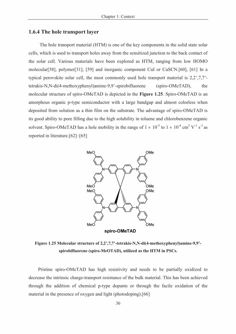
1.6.4 The hole transport layer
The hole transport material (HTM) is one of the key components in the solid state solar
cells, which is used to transport holes away from the sensitized junction to the back contact of
the solar cell. Various materials have been explored as HTM, ranging from low HOMO
molecular[58], polymer[31], [59] and inorganic component CuI or CuSCN.[60], [61] In a
typical perovskite solar cell, the most commonly used hole transport material is 2,2’,7,7’-
tetrakis-N,N-di(4-methoxyphenyl)amine-9,9’-spirobifluorene (spiro-OMeTAD), the
molecular structure of spiro-OMeTAD is depicted in the Figure 1.25. Spiro-OMeTAD is an
amorphous organic p-type semiconductor with a large bandgap and almost colorless when
deposited from solution as a thin film on the substrate. The advantage of spiro-OMeTAD is
its good ability to pore filling due to the high solubility in toluene and chlorobenzene organic
solvent. Spiro-OMeTAD has a hole mobility in the range of 1 ´ 10-5
to 1 ´ 10-4
cm2 V
-1 s
-1 as
reported in literature.[62]–[65]
Figure 1.25 Molecular structure of 2,2’,7,7’-tetrakis-N,N-di(4-methoxyphenyl)amine-9,9’-
spirobifluorene (spiro-MeOTAD), utilized as the HTM in PSCs.
Pristine spiro-OMeTAD has high resistivity and needs to be partially oxidized to
decrease the intrinsic charge-transport resistance of the bulk material. This has been achieved
through the addition of chemical p-type dopants or through the facile oxidation of the
material in the presence of oxygen and light (photodoping).[66]
Chapter 1: Context
31
Several additives are added to the spiro-OMeTAD solution to improve its transport
properties.[64] The common additives are: 4-tert-butylpyridine (TBP), lithium
bis(trifluoromethylsulfonyl)imide (LiTFSI) attributed, or a p-dopant.[32] Usually, the effect
of the TBP is believed to be an upward shift of the metal oxide conduction band or a
retardation of the electron-hole recombination rate, which leads to an increase in the
Voc.[67]–[69] In contrast, the effect of an addition of LiTFSI is a downwards shift of the
metal oxide and accelerate the electron injection. The result is an increase in Jsc.[70], [71]
Furthermore common additives such as Li+ ions have been shown to also contribute to the
oxidation and increased hole mobility of spiro-OMeTAD.
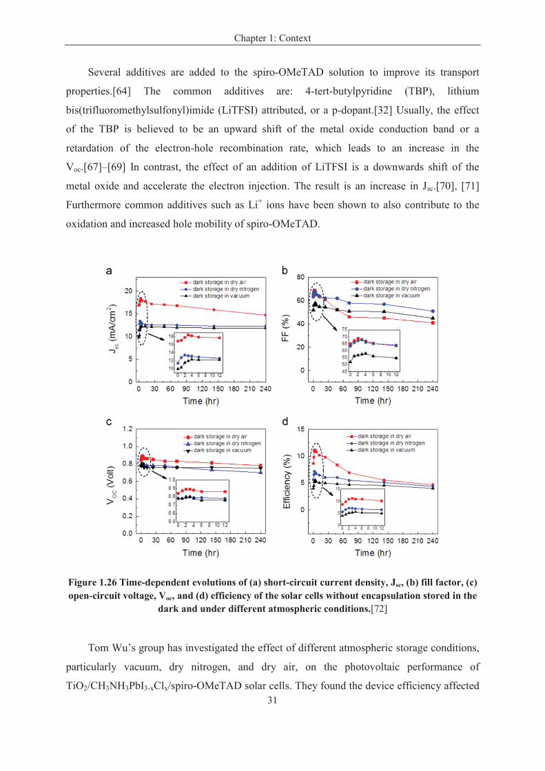
Figure 1.26 Time-dependent evolutions of (a) short-circuit current density, Jsc, (b) fill factor, (c) open-circuit voltage, Voc, and (d) efficiency of the solar cells without encapsulation stored in the
dark and under different atmospheric conditions.[72]
Tom Wu’s group has investigated the effect of different atmospheric storage conditions,
particularly vacuum, dry nitrogen, and dry air, on the photovoltaic performance of
TiO2/CH3NH3PbI3-xClx/spiro-OMeTAD solar cells. They found the device efficiency affected
Chapter 1: Context
32
by the ambient atmospheric conditions during the drying process of spiro-OMeTAD (Figure
1.26). The results demonstrated the important role of fully functionalizing hole-transporting
spiro-OMeTAD in achieving the optimal solar cell performance. Dry air was the most
promising storage ambient during the drying process of spiro-OMeTAD.[72]
1.6.5 The back contact
The back contact in the typical PSCs is silver or gold thin film formed by thermal
evaporation of the metal. The silver is more used than gold, which is due to a lower cost and
a higher conductivity. Another benefit is the higher reflectivity induced to a higher short
circuit photocurrent.[73] Compared to the expensive silver and gold contacts, the low-cost
carbon materials have attracted some attention especially with the layer preparation by screen
printable deposition technique. Moreover, the carbon layer can work as a water repellent
layer to protect the cell from water, which is an important point for the stability of PSCs
device.[27], [47]
This thesis presents the preparation of active electron transport layers and the fabrication
and characterizations of perovskite sensitized solar cells.
Chapter 2 presents the electrochemical deposition of ZnO nanowires/nanorods from the
chloride/oxygen system, and the ZnO nanostructures electrodeposited in a nitrate bath.
Except the ZnO nanostructures, we also synthesized TiO2 nanotube and TiO2 mesoporous
layers. The TiO2 nanotube arrayed layer was prepared by a liquid phase deposition method at
room temperature, stating from an electrodeposited ZnO template, and the TiO2 mesoporous
layers, with a thickness less than 500 nm, were prepared by a spin-coating technique, starting
from a nanoparticle paste.
In Chapter 3, we synthesized well-conducting ZnO nanostructures and fabricated the
efficient ZnO/perovskite CH3NH3PbI3/HTM (spiro-OMeTAD) solid-state solar cells. The
ZnO nanostructures were characterized by SEM, XRD and Raman to evaluate the properties.
We also deposited a perovskite layer and HTL to prepare a complete cell device. The
comparisons of cell properties highlight the importance of thin intermediate ZnO overlayer
for an application in perovskite solar cells.
Chapter 1: Context
33
Chapter 4 presents a fast and low temperature electrochemical deposition technique,
which is used to prepare rough ZnO layer. The ZnO films were designed with changing
deposition time ranging from 20 s to 300 s, the well-covering and not well-covering ZnO
films were prepared. The properties of ZnO nanostructure were characterized with SEM,
XRD and Raman technique. We also prepared and measured the properties of the ZnO based
solar cells and investigated the importance of well-covering ETM for an application in
perovskite solar cells.
In Chapter 5, we synthesized CH3NH3PbI3 perovskite layers with one-step and two-step
techniques on various ETL sub-layers. The morphology and other properties of CH3NH3PbI3
layers prepared by the two different techniques were measured and compared. We also
deposited the perovskite on the ZnO and TiO2, separately. We investigated the effect of oxide
contact layer on the preparation and properties of CH3NH3PbI3 for the perovskite solar cell
application.
Chapter 6 reports the preparation of one-dimensional free-standing TiO2 nanotube array
structures at room temperature using electrodeposited ZnO templates. The morphology of
TiO2 nanotubes was optimized for the perovskite solar cell application. We notably
investigated the effect of the TiO2 thickness on the perovskite solar cell performances.
References
[1] M. Beccali, M. Cellura, and M. Mistretta, “Environmental effects of energy policy in
sicily: The role of renewable energy,” Renew. Sustain. Energy Rev., vol. 11, no. 2, pp.
282–298, Feb. 2007.
[2] H. Lund, “Renewable energy strategies for sustainable development,” Energy, vol. 32,
no. 6, pp. 912–919, Jun. 2007.
[3] G. M. Montes, M. del Mar Serrano López, M. del Carmen Rubio Gámez, and A. M.
Ondina, “An overview of renewable energy in Spain. The small hydro-power case,”
Renew. Sustain. Energy Rev., vol. 9, no. 5, pp. 521–534, Oct. 2005.
[4] C. K. N. Cavaliero and E. P. Da Silva, “Electricity generation: regulatory mechanisms to
incentive renewable alternative energy sources in Brazil,” Energy Policy, vol. 33, no. 13,
pp. 1745–1752, Sep. 2005.
Chapter 1: Context
34
[5] F. Hvelplund, “Renewable energy and the need for local energy markets,” Energy, vol.
31, no. 13, pp. 2293–2302, Oct. 2006.
[6] J. M. Huacuz, “The road to green power in Mexico-reflections on the prospects for the
large-scale and sustainable implementation of renewable energy,” Energy Policy, vol.
33, no. 16, pp. 2087–2099, Nov. 2005.
[7] M. M. Aman, K. H. Solangi, M. S. Hossain, A. Badarudin, G. B. Jasmon, H. Mokhlis, A.
H. A. Bakar, and S. N. Kazi, “A review of Safety, Health and Environmental (SHE)
issues of solar energy system,” Renew. Sustain. Energy Rev., vol. 41, pp. 1190–1204,
Jan. 2015.
[8] “EIA projects U.S. non-hydro renewable power generation increases, led by wind and
biomass.” [Online]. Available: http://www.eia.gov/todayinenergy/detail.cfm?id=5170.
[9] X.-Z. Gao, Z.-X. Hou, Z. Guo, and X.-Q. Chen, “Reviews of methods to extract and
store energy for solar-powered aircraft,” Renew. Sustain. Energy Rev., vol. 44, pp. 96–
108, Apr. 2015.
[10] T. Saga, “Advances in crystalline silicon solar cell technology for industrial mass
production,” NPG Asia Mater., vol. 2, no. 3, pp. 96–102, Jul. 2010.
[11] K. L. Chopra, P. D. Paulson, and V. Dutta, “Thin-film solar cells: an overview,” Prog.
Photovolt. Res. Appl., vol. 12, no. 2–3, pp. 69–92, Des. 2004.
[12] M. A. Green, Third generation photovoltaics: advanced solar energy conversion. Berlin:
Springer, 2006.
[13] M. Grätzel, “Dye-sensitized solar cells,” J. Photochem. Photobiol. C Photochem. Rev.,
vol. 4, no. 2, pp. 145–153, Oct. 2003.
[14] B. O’Regan and M. Graetzel, “A low cost, high-efficiency solar cell based on dye-
sensitized colloidal TiO2 films,” Nature, vol. 353, pp. 737–739, Oct. 1999.
[15] S. Mathew, A. Yella, P. Gao, R. Humphry-Baker, B. F. E. Curchod, N. Ashari-Astani, I.
Tavernelli, U. Rothlisberger, M. K. Nazeeruddin, and M. Grätzel, “Dye-sensitized solar
cells with 13% efficiency achieved through the molecular engineering of porphyrin
sensitizers,” Nat. Chem., vol. 6, no. 3, pp. 242–247, Feb. 2014.
[16] “Best Rearch Cell Efficiencies,” 2015. [Online]. Available:
http://www.nrel.gov/ncpv/images/efficiency_chart.jpg.
[17] A. Yella, H.-W. Lee, H. N. Tsao, C. Yi, A. K. Chandiran, M. K. Nazeeruddin, E. W.-G.
Diau, C.-Y. Yeh, S. M. Zakeeruddin, and M. Gratzel, “Porphyrin-Sensitized Solar Cells

Chapter 1: Context
35
with Cobalt (II/III)-Based Redox Electrolyte Exceed 12 Percent Efficiency,” Science,
vol. 334, no. 6056, pp. 629–634, Nov. 2011.
[18] R. Katoh and A. Furube, “Electron injection efficiency in dye-sensitized solar cells,” J.
Photochem. Photobiol. C Photochem. Rev., vol. 20, pp. 1–16, Sep. 2014.
[19] S. J. Fonash, Solar cell device physics, 2nd ed. Burlington, MA: Academic
Press/Elsevier, 2010.
[20] A. Hagfeldt and P. Laurence, Dye-sensitized Solar Cells. Lausanne; Boca Raton: EPFL
Press ; Distributed by CRC Press, 2010.
[21] A. D. Dhass, E. Natarajan, and L. Ponnusamy, “Influence of shunt resistance on the
performance of solar photovoltaic cell,” in Emerging Trends in Electrical Engineering
and Energy Management (ICETEEEM), 2012 International Conference on, 2012, pp.
382–386.
[22] S. M. Nejad, S. G. Samani, and E. Rahimi, “Characterization of responsivity and
quantum efficiency of TiO2-Based photodetectors doped with Ag nanoparticles,” in
Mechanical and Electronics Engineering (ICMEE), 2010 2nd International Conference
on, 2010, vol. 2, pp. V2–394.
[23] S. S. Shin, J. S. Kim, J. H. Suk, K. D. Lee, D. W. Kim, J. H. Park, I. S. Cho, K. S. Hong,
and J. Y. Kim, “Improved Quantum Efficiency of Highly Efficient Perovskite BaSnO3-
Based Dye-Sensitized Solar Cells,” ACS Nano, vol. 7, no. 2, pp. 1027–1035, Feb. 2013.
[24] H. J. Snaith, “Perovskites: The Emergence of a New Era for Low-Cost, High-Efficiency
Solar Cells,” J. Phys. Chem. Lett., vol. 4, no. 21, pp. 3623–3630, Nov. 2013.
[25] T.-B. Song, Q. Chen, H. Zhou, C. Jiang, H.-H. Wang, Y. (Michael) Yang, Y. Liu, J.
You, and Y. Yang, “Perovskite solar cells: film formation and properties,” J Mater
Chem A, vol. 3, no. 17, pp. 9032–9050, Mar. 2015.
[26] A. Kojima, K. Teshima, Y. Shirai, and T. Miyasaka, “Organometal Halide Perovskites
as Visible-Light Sensitizers for Photovoltaic Cells,” J. Am. Chem. Soc., vol. 131, no. 17,
pp. 6050–6051, May 2009.
[27] H. Zhou, Q. Chen, G. Li, S. Luo, T. -B. Song, H.-S. Duan, Z. Hong, J. You, Y. Liu, and
Y. Yang, “Interface engineering of highly efficient perovskite solar cells,” Science, vol.
345, no. 6196, pp. 542–546, Aug. 2014.
[28] J.-H. Im, C.-R. Lee, J.-W. Lee, S.-W. Park, and N.-G. Park, “6.5% efficient perovskite
quantum-dot-sensitized solar cell,” Nanoscale, vol. 3, no. 10, pp. 4088–4093, Sep. 2011.
Chapter 1: Context
36
[29] H.-S. Kim, C.-R. Lee, J.-H. Im, K.-B. Lee, T. Moehl, A. Marchioro, S.-J. Moon, R.
Humphry-Baker, J.-H. Yum, J. E. Moser, M. Grätzel, and N.-G. Park, “Lead Iodide
Perovskite Sensitized All-Solid-State Submicron Thin Film Mesoscopic Solar Cell with
Efficiency Exceeding 9%,” Sci. Rep., vol. 2, pp.1–7, Aug. 2012.
[30] M. M. Lee, J. Teuscher, T. Miyasaka, T. N. Murakami, and H. J. Snaith, “Efficient
Hybrid Solar Cells Based on Meso-Superstructured Organometal Halide Perovskites,”
Science, vol. 338, no. 6107, pp. 643–647, Nov. 2012.
[31] J. H. Heo, S. H. Im, J. H. Noh, T. N. Mandal, C.-S. Lim, J. A. Chang, Y. H. Lee, H.
Kim, A. Sarkar, M. K. Nazeeruddin, M. Grätzel, and S. I. Seok, “Efficient inorganic–
organic hybrid heterojunction solar cells containing perovskite compound and
polymeric hole conductors,” Nat. Photonics, vol. 7, no. 6, pp. 486–491, May 2013.
[32] J. Burschka, N. Pellet, S.-J. Moon, R. Humphry-Baker, P. Gao, M. K. Nazeeruddin, and
M. Grätzel, “Sequential deposition as a route to high-performance perovskite-sensitized
solar cells,” Nature, vol. 499, no. 7458, pp. 316–319, Jul. 2013.
[33] W. S. Yang, J. H. Noh, N. J. Jeon, Y. C. Kim, S. Ryu, J. Seo, and S. I. Seok, “High-
performance photovoltaic perovskite layers fabricated through intramolecular exchange,”
Science, vol. 348, no. 6240, pp. 1234–1237, Jun. 2015.
[34] L. Zheng, D. Zhang, Y. Ma, Z. Lu, Z. Chen, S. Wang, L. Xiao, and Q. Gong,
“Morphology control of the perovskite films for efficient solar cells,” Dalton Trans, vol.
44, no. 23, pp. 10582–10593, Mar. 2015.
[35] D. B. Mitzi, “Templating and structural engineering in organic–inorganic perovskites,”
J. Chem. Soc. Dalton Trans., no. 1, pp. 1–12, Dec. 2001.
[36] H. L. Feng, M. Arai, Y. Matsushita, Y. Tsujimoto, Y. Guo, C. I. Sathish, X. Wang, Y.-H.
Yuan, M. Tanaka, and K. Yamaura, “High-Temperature Ferrimagnetism Driven by
Lattice Distortion in Double Perovskite Ca2FeOsO6,” J. Am. Chem. Soc., vol. 136, no. 9,
pp. 3326–3329, Mar. 2014.
[37] R. Aso, D. Kan, Y. Shimakawa, and H. Kurata, “Atomic level observation of octahedral
distortions at the perovskite oxide heterointerface,” Sci. Rep., vol. 3, pp. 1–16, Jul. 2013.
[38] I. Chung, B. Lee, J. He, R. P. H. Chang, and M. G. Kanatzidis, “All-solid-state dye-
sensitized solar cells with high efficiency,” Nature, vol. 485, no. 7399, pp. 486–489,
May 2012.
[39] L. Etgar, “Semiconductor Nanocrystals as Light Harvesters in Solar Cells,” Materials,
vol. 6, no. 2, pp. 445–459, Feb. 2013.
Chapter 1: Context
37
[40] A. M. Salau, “Fundamental absorption edge in PbI2: KI alloys,” Sol. Energy Mater., vol.
2, no. 3, pp. 327–332, Mar. 1980.
[41] T. Ishihara, J. Takahashi, and T. Goto, “Exiton State In Two-Dimensonal Perovskite
Semiconductor (C10H21NH3)2PbI4,” Solide State Commun., vol. 69, no. 9, pp. 933–936,
Sep. 1989.
[42] J. M. Ball, M. M. Lee, A. Hey, and H. J. Snaith, “Low-temperature processed meso-
superstructured to thin-film perovskite solar cells,” Energy Environ. Sci., vol. 6, no. 6,
pp. 1739–1743, 2013.
[43] J. J. M. Halls, C. A. Walsh, N. C. Greenham, E. A. Marseglia, R. H. Friend, S. C.
Moratti, and A. B. Holmes, “Efficient photodiodes from interpenetrating polymer
networks,” Nature, vol. 376, pp. 498–500, Aug. 1995.
[44] M. Liu, M. B. Johnston, and H. J. Snaith, “Efficient planar heterojunction perovskite
solar cells by vapour deposition,” Nature, vol. 501, no. 7467, pp. 395–398, Sep. 2013.
[45] A. Mei, X. Li, L. Liu, Z. Ku, T. Liu, Y. Rong, M. Xu, M. Hu, J. Chen, Y. Yang, M.
Gratzel, and H. Han, “A hole-conductor-free, fully printable mesoscopic perovskite
solar cell with high stability,” Science, vol. 345, no. 6194, pp. 295–298, Jul. 2014.
[46] H.-S. Kim, J.-W. Lee, N. Yantara, P. P. Boix, S. A. Kulkarni, S. Mhaisalkar, M. Grätzel,
and N.-G. Park, “High Efficiency Solid-State Sensitized Solar Cell-Based on
Submicrometer Rutile TiO2 Nanorod and CH3NH3PbI3 Perovskite Sensitizer,” Nano
Lett., vol. 13, no. 6, pp. 2412–2417, Jun. 2013.
[47] J. Qiu, Y. Qiu, K. Yan, M. Zhong, C. Mu, H. Yan, and S. Yang, “All-solid-state hybrid
solar cells based on a new organometal halide perovskite sensitizer and one-dimensional
TiO2 nanowire arrays,” Nanoscale, vol. 5, no. 8, pp. 3245–3248, Mar. 2013.
[48] X. Gao, J. Li, J. Baker, Y. Hou, D. Guan, J. Chen, and C. Yuan, “Enhanced photovoltaic
performance of perovskite CH3NH3PbI3 solar cells with freestanding TiO2 nanotube
array films,” Chem. Commun., vol. 50, no. 48, pp. 6368–6371, Apr. 2014.
[49] S. Dharani, H. K. Mulmudi, N. Yantara, P. T. Thu Trang, N. G. Park, M. Graetzel, S.
Mhaisalkar, N. Mathews, and P. P. Boix, “High efficiency electrospun TiO2 nanofiber
based hybrid organic–inorganic perovskite solar cell,” Nanoscale, vol. 6, no. 3, pp.
1675–1679, Oct. 2014.
[50] M. I. Dar, F. J. Ramos, Z. Xue, B. Liu, S. Ahmad, S. A. Shivashankar, M. K.
Nazeeruddin, and M. Grätzel, “Photoanode Based on (001)-Oriented Anatase
Chapter 1: Context
38
Nanoplatelets for Organic–Inorganic Lead Iodide Perovskite Solar Cell,” Chem. Mater.,
vol. 26, no. 16, pp. 4675–4678, Aug. 2014.
[51] E. J. Juarez-Perez, M. Wuβler, F. Fabregat-Santiago, K. Lakus-Wollny, E. Mankel, T.
Mayer, W. Jaegermann, and I. Mora-Sero, “Role of the Selective Contacts in the
Performance of Lead Halide Perovskite Solar Cells,” J. Phys. Chem. Lett., vol. 5, no. 4,
pp. 680–685, Feb. 2014.
[52] D. Liu and T. L. Kelly, “Perovskite solar cells with a planar heterojunction structure
prepared using room-temperature solution processing techniques,” Nat. Photonics, vol.
8, no. 2, pp. 133–138, Dec. 2013.
[53] G. E. Eperon, S. D. Stranks, C. Menelaou, M. B. Johnston, L. M. Herz, and H. J. Snaith,
“Formamidinium lead trihalide: a broadly tunable perovskite for efficient planar
heterojunction solar cells,” Energy Environ. Sci., vol. 7, no. 3, pp. 982–988, Jan. 2014.
[54] C. C. Stoumpos, C. D. Malliakas, and M. G. Kanatzidis, “Semiconducting Tin and Lead
Iodide Perovskites with Organic Cations: Phase Transitions, High Mobilities, and Near-
Infrared Photoluminescent Properties,” Inorg. Chem., vol. 52, no. 15, pp. 9019–9038,
Aug. 2013.
[55] J. H. Noh, S. H. Im, J. H. Heo, T. N. Mandal, and S. I. Seok, “Chemical Management
for Colorful, Efficient, and Stable Inorganic-Organic Hybrid Nanostructured Solar
Cells,” Nano Lett., pp. 1764–1769, Mar. 2013.
[56] N. J. Jeon, J. H. Noh, Y. C. Kim, W. S. Yang, S. Ryu, and S. I. Seok, “Solvent
engineering for high-performance inorganic–organic hybrid perovskite solar cells,” Nat.
Mater., vol. 13, no. 9, pp. 897–903, Jul. 2014.
[57] Q. Chen, H. Zhou, Z. Hong, S. Luo, H.-S. Duan, H.-H. Wang, Y. Liu, G. Li, and Y.
Yang, “Planar Heterojunction Perovskite Solar Cells via Vapor-Assisted Solution
Process,” J. Am. Chem. Soc., vol. 136, no. 2, pp. 622–625, Jan. 2014.
[58] E. Edri, S. Kirmayer, D. Cahen, and G. Hodes, “High Open-Circuit Voltage Solar Cells
Based on Organic-Inorganic Lead Bromide Perovskite,” J. Phys. Chem. Lett., vol. 4, no.
6, pp. 897–902, Mar. 2013.
[59] B. Cai, Y. Xing, Z. Yang, W.-H. Zhang, and J. Qiu, “High performance hybrid solar
cells sensitized by organolead halide perovskites,” Energy Environ. Sci., vol. 6, no. 5,
pp. 1480–1485, Mar. 2013.
Chapter 1: Context
39
[60] J. A. Christians, R. C. M. Fung, and P. V. Kamat, “An Inorganic Hole Conductor for
Organo-Lead Halide Perovskite Solar Cells. Improved Hole Conductivity with Copper
Iodide,” J. Am. Chem. Soc., vol. 136, no. 2, pp. 758–764, Jan. 2014.
[61] S. Chavhan, O. Miguel, H.-J. Grande, V. Gonzalez-Pedro, R. S. Sánchez, E. M. Barea, I.
Mora-Seró, and R. Tena-Zaera, “Organo-metal halide perovskite-based solar cells with
CuSCN as the inorganic hole selective contact,” J. Mater. Chem. A, vol. 2, no. 32, pp.
12754–12760, Jun. 2014.
[62] T. Leijtens, J. Lim, J. Teuscher, T. Park, and H. J. Snaith, “Charge Density Dependent
Mobility of Organic Hole-Transporters and Mesoporous TiO2 Determined by Transient
Mobility Spectroscopy: Implications to Dye-Sensitized and Organic Solar Cells,” Adv.
Mater., vol. 25, no. 23, pp. 3227–3233, Jun. 2013.
[63] O. Rana, R. Srivastava, R. Grover, M. Zulfequar, M. Husain, and M. N. Kamalasanan,
“Charge transport studies in thermally evaporated 2,2′,7,7′-tetrakis-(N,N-di-4-
methoxyphenylamino)-9,9′-spirobifluorene (spiro-MeOTAD) thin film,” Synth. Met.,
vol. 161, no. 9–10, pp. 828–832, May 2011.
[64] H. J. Snaith and M. Grätzel, “Enhanced charge mobility in a molecular hole transporter
via addition of redox inactive ionic dopant: Implication to dye-sensitized solar cells,”
Appl. Phys. Lett., vol. 89, no. 26, p. 262114/1–262114/3, Dec. 2006.
[65] D. Poplavskyy and J. Nelson, “Nondispersive hole transport in amorphous films of
methoxy-spirofluorene-arylamine organic compound,” J. Appl. Phys., vol. 93, no. 1, p.
341–346, Jan. 2003.
[66] J. Burschka, A. Dualeh, F. Kessler, E. Baranoff, N.-L. Cevey-Ha, C. Yi, M. K.
Nazeeruddin, and M. Grätzel, “Tris(2-(1H -pyrazol-1-yl)pyridine)cobalt(III) as p-Type
Dopant for Organic Semiconductors and Its Application in Highly Efficient Solid-State
Dye-Sensitized Solar Cells,” J. Am. Chem. Soc., vol. 133, no. 45, pp. 18042–18045,
Nov. 2011.
[67] M. Dürr, A. Yasuda, and G. Nelles, “On the origin of increased open circuit voltage of
dye-sensitized solar cells using 4-tert-butyl pyridine as additive to the electrolyte,” Appl.
Phys. Lett., vol. 89, no. 6, pp. 061110/1–061110/3, Aug. 2006.
[68] S. E. Koops, B. C. O’Regan, P. R. F. Barnes, and J. R. Durrant, “Parameters Influencing
the Efficiency of Electron Injection in Dye-Sensitized Solar Cells,” J. Am. Chem. Soc.,
vol. 131, no. 13, pp. 4808–4818, Apr. 2009.
Chapter 1: Context
40
[69] J. Krüger, R. Plass, L. Cevey, M. Piccirelli, M. Grätzel, and U. Bach, “High efficiency
solid-state photovoltaic device due to inhibition of interface charge recombination,”
Appl. Phys. Lett., vol. 79, no. 13, pp. 2085–2087, Sep. 2001.
[70] J. R. Jennings and Q. Wang, “Influence of Lithium Ion Concentration on Electron
Injection, Transport, and Recombination in Dye-Sensitized Solar Cells,” J. Phys. Chem.
C, vol. 114, no. 3, pp. 1715–1724, Jan. 2010.
[71] U. B. Cappel, A. L. Smeigh, S. Plogmaker, E. M. J. Johansson, H. Rensmo, L.
Hammarström, A. Hagfeldt, and G. Boschloo, “Characterization of the Interface
Properties and Processes in Solid State Dye-Sensitized Solar Cells Employing a
Perylene Sensitizer,” J. Phys. Chem. C, vol. 115, no. 10, pp. 4345–4358, Mar. 2011.
[72] A. D. Sheikh, A. Bera, M. A. Haque, R. B. Rakhi, S. D. Gobbo, H. N. Alshareef, and T.
Wu, “Atmospheric effects on the photovoltaic performance of hybrid perovskite solar
cells,” Sol. Energy Mater. Sol. Cells, vol. 137, pp. 6–14, Jun. 2015.
[73] H. J. Snaith, A. J. Moule, C. Klein, K. Meerholz, R. H. Friend, and M. Grätzel,
“Efficiency Enhancements in Solid-State Hybrid Solar Cells via Reduced Charge
Recombination and Increased Light Capture,” Nano Lett., vol. 7, no. 11, pp. 3372–3376,
Nov. 2007.
[74] M. Xu, G. Liu, X. Li, H. Wang, Y. Rong, Z. Ku, M. Hu, Y. Yang, L. Liu, T. Liu, J.
Chen, and H. Han, “Efficient monolithic solid-state dye-sensitized solar cell with a low-
cost mesoscopic carbon based screen printable counter electrode,” Org. Electron., vol.
14, no. 2, pp. 628–634, Feb. 2013.
41
Chapter 2: Synthesis and morphological
properties of oxide contact layers
In this chapter, we describe the techniques that we have developed in this thesis for the
preparation of ZnO and TiO2 nanostructures and we show their morphological properties.
The ZnO contact layers were prepared by electrochemical deposition. The free-standing TiO2
nanotube arrays were synthesized by a liquid phase deposition technique using a ZnO
template. The thin mesoporous TiO2 layers were prepared by spin-coating. In the present
chapter, we focus on the morphological properties of the synthesized layer. The other
properties will be developed in the following chapters.
2.1 Introduction
Inorganic oxides, such as TiO2 or ZnO, prepared as thin layers, are key materials in the
third generation photovoltaic devices. In the DSSCs, they permit the transfer of electrons
injected from the excited sensitizer to the front contact. Since 1991, when O’Regan and
Grätzel published the first efficient dye sensitized solar cell, a tremendous amount of research
about TiO2 used in the dye sensitized solar cell had been published.[1]–[4] Anatase TiO2 is n-
type semiconductor with a bandgap of 3.2 eV, and ZnO also is also a wide-band-gap n-type
semiconductor with a large bandgap of 3.37 eV.[5], [6] Moreover, ZnO has a higher
electronic mobility which is favorable for the electron transport. It is then expected to give
rise to less recombination loss in the photoprocess in DSSCs.[5], [7] However, the chemical
stability of ZnO is less than TiO2, and ZnO can be dissolved by acidic or basic solution.
ZnO and TiO2 with various morphologies, such as, nanoparticles, nanowires, nanorods
and nanotubes have been prepared.[8]–[12] Many oxide layer fabrication techniques have
been developed in the literature: sol-gel method,[13] solvothermal and hydrothermal
method,[14] electrochemical deposition[11] and other methods. Among these methods,
electrochemical deposition is an easy and low cost way for the preparation of nanostructured
or 2D films. The two section present ZnO nanostructured arrays prepared by electrochemical
deposition techniques.

Chapter 2: Synthesis and morphological properties of oxide contact layers
42
2.2 ZnO layers electrodeposited from nitrate precursor
Electrochemical deposition of metal oxide layers using nitrate precursor solution is a
traditional method since 1983.[15] By the technique ZrO2, TiO2, NiO and other crystalline
oxides have been obtained directly or indirectly from nitrate precursor solution, ZnO is a
special example for which nice and well-crystallized ZnO films can be directly obtained by
electrodeposition.[15]-[17]
2.2.1 Experimental
Ø Experimental setup
In this thesis, the electrochemical deposition was carried out in a three electrode cell,
(see Figure 2.2) the counter electrode was a zinc wire, and the reference electrode
was a saturated calomel electrode (SCE) (with a potential at +0.25V vs NHE) placed
in a separate compartment maintained at room temperature. Prior to all the
electrochemical depositions, the transparent conducting oxide (TCO) substrate was
cleaned with soap, sonicated 5 min in ethanol, 5 min in acetone, and HNO3 (45%) for
2 min, and finally abundantly rinsed with MilliQ quality water (18.2 MW.cm).
Ø Experimental conditions
In this electrochemical deposition, the deposition bath was a solution of Zn(NO3)2 at a
concentration of 0.08 M dissolved in MilliQ quality water (18.2 MW.cm) maintained
at 60°C. The applied voltage was varied at -1.15 V/ SCE, -0.95 V/ SCE or -0.9 V/SCE,
the deposition time was set at 300 s in Figure 2.1 and Table 2.1.
Ø Experimental reaction
The reaction for the electrochemical deposition of ZnO from nitrate precursor solution
is:
NO3- +H2O + 2e
- → NO2
- + 2OH
- (2.1)
Zn2+
+ 2OH- → ZnO + H2O (2.2)
Nitrate ions in the reaction can be reduced only with the presence of certain metal
cations as catalyst.[18]
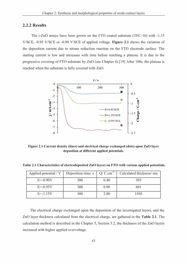
Chapter 2: Synthesis and morphological properties of oxide contact layers
43
2.2.2 Results
The i-ZnO arrays have been grown on the FTO coated substrate (TEC-10) with -1.15
V/SCE, -0.95 V/SCE or -0.90 V/SCE of applied voltage. Figure 2.1 shows the variation of
the deposition current due to nitrate reduction reaction on the FTO electrode surface. The
starting current is low and increases with time before reaching a plateau. It is due to the
progressive covering of FTO substrate by ZnO (see Chapter 4).[19] After 100s, the plateau is
reached when the substrate is fully covered with ZnO.
Figure 2.1 Current density (lines) and electrical charge exchanged (dots) upon ZnO layer deposition at different applied potentials.
Table 2.1 Characteristics of electrodeposited ZnO layers on FTO with various applied potentials.
Applied potential / V Deposition time/ s Q/ C.cm-2
Calculated thickness/ nm
E=-0.90V 300 0.40 303
E=-0.95V 300 0.80 601
E=-1.15V 300 2.00 1503
The electrical charge exchanged upon the deposition of the investigated layers, and the
ZnO layer thickness calculated from the electrical charge, are gathered in the Table 2.1. The
calculation method is described in the Chapter 5, Section 5.2, the thickness of the ZnO layers
increased with higher applied overvoltage.
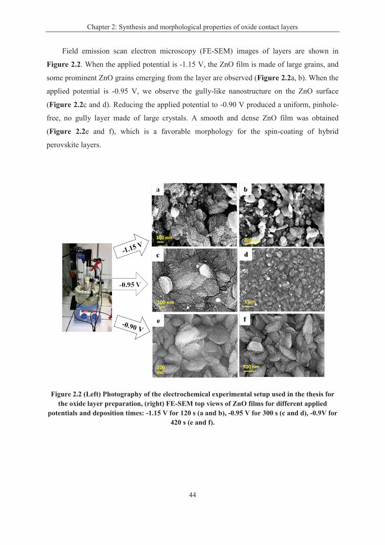
Chapter 2: Synthesis and morphological properties of oxide contact layers
44
Field emission scan electron microscopy (FE-SEM) images of layers are shown in
Figure 2.2. When the applied potential is -1.15 V, the ZnO film is made of large grains, and
some prominent ZnO grains emerging from the layer are observed (Figure 2.2a, b). When the
applied potential is -0.95 V, we observe the gully-like nanostructure on the ZnO surface
(Figure 2.2c and d). Reducing the applied potential to -0.90 V produced a uniform, pinhole-
free, no gully layer made of large crystals. A smooth and dense ZnO film was obtained
(Figure 2.2e and f), which is a favorable morphology for the spin-coating of hybrid
perovskite layers.
Figure 2.2 (Left) Photography of the electrochemical experimental setup used in the thesis for the oxide layer preparation, (right) FE-SEM top views of ZnO films for different applied
potentials and deposition times: -1.15 V for 120 s (a and b), -0.95 V for 300 s (c and d), -0.9V for 420 s (e and f).
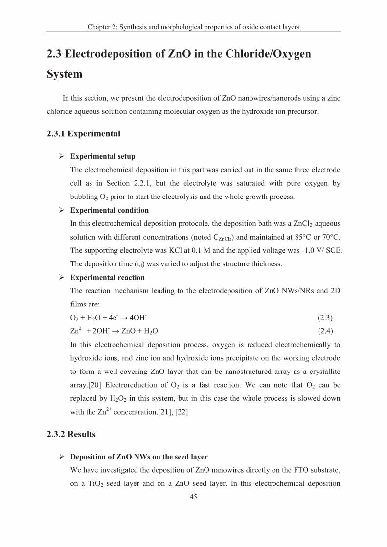
Chapter 2: Synthesis and morphological properties of oxide contact layers
45
2.3 Electrodeposition of ZnO in the Chloride/Oxygen
System
In this section, we present the electrodeposition of ZnO nanowires/nanorods using a zinc
chloride aqueous solution containing molecular oxygen as the hydroxide ion precursor.
2.3.1 Experimental
Ø Experimental setup
The electrochemical deposition in this part was carried out in the same three electrode
cell as in Section 2.2.1, but the electrolyte was saturated with pure oxygen by
bubbling O2 prior to start the electrolysis and the whole growth process.
Ø Experimental condition
In this electrochemical deposition protocole, the deposition bath was a ZnCl2 aqueous
solution with different concentrations (noted CZnCl2) and maintained at 85°C or 70°C.
The supporting electrolyte was KCl at 0.1 M and the applied voltage was -1.0 V/ SCE.
The deposition time (td) was varied to adjust the structure thickness.
Ø Experimental reaction
The reaction mechanism leading to the electrodeposition of ZnO NWs/NRs and 2D
films are:
O2 + H2O + 4e- → 4OH
- (2.3)
Zn2+
+ 2OH- → ZnO + H2O (2.4)
In this electrochemical deposition process, oxygen is reduced electrochemically to
hydroxide ions, and zinc ion and hydroxide ions precipitate on the working electrode
to form a well-covering ZnO layer that can be nanostructured array as a crystallite
array.[20] Electroreduction of O2 is a fast reaction. We can note that O2 can be
replaced by H2O2 in this system, but in this case the whole process is slowed down
with the Zn2+
concentration.[21], [22]
2.3.2 Results
Ø Deposition of ZnO NWs on the seed layer
We have investigated the deposition of ZnO nanowires directly on the FTO substrate,
on a TiO2 seed layer and on a ZnO seed layer. In this electrochemical deposition
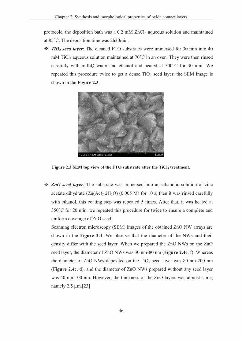
Chapter 2: Synthesis and morphological properties of oxide contact layers
46
protocole, the deposition bath was a 0.2 mM ZnCl2 aqueous solution and maintained
at 85°C. The deposition time was 2h30min.
v TiO2 seed layer: The cleaned FTO substrates were immersed for 30 min into 40
mM TiCl4 aqueous solution maintained at 70°C in an oven. They were then rinsed
carefully with milliQ water and ethanol and heated at 500°C for 30 min. We
repeated this procedure twice to get a dense TiO2 seed layer, the SEM image is
shown in the Figure 2.3.
Figure 2.3 SEM top view of the FTO substrate after the TiCl4 treatment.
v ZnO seed layer: The substrate was immersed into an ethanolic solution of zinc
acetate dihydrate (Zn(Ac)2×2H2O) (0.005 M) for 10 s, then it was rinsed carefully
with ethanol, this coating step was repeated 5 times. After that, it was heated at
350°C for 20 min. we repeated this procedure for twice to ensure a complete and
uniform coverage of ZnO seed.
Scanning electron microscopy (SEM) images of the obtained ZnO NW arrays are
shown in the Figure 2.4. We observe that the diameter of the NWs and their
density differ with the seed layer. When we prepared the ZnO NWs on the ZnO
seed layer, the diameter of ZnO NWs was 30 nm-80 nm (Figure 2.4e, f). Whereas
the diameter of ZnO NWs deposited on the TiO2 seed layer was 80 nm-200 nm
(Figure 2.4c, d), and the diameter of ZnO NWs prepared without any seed layer
was 40 nm-100 nm. However, the thickness of the ZnO layers was almost same,
namely 2.5 µm.[23]
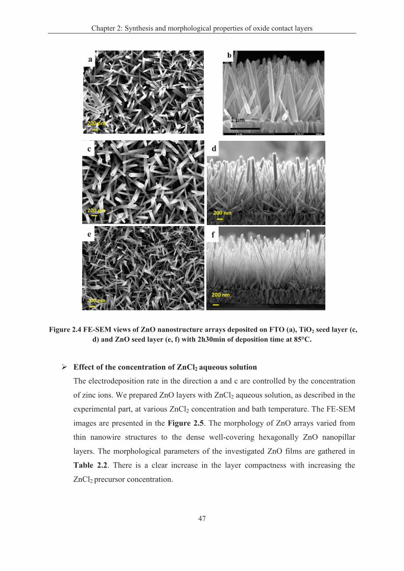
Chapter 2: Synthesis and morphological properties of oxide contact layers
47
Figure 2.4 FE-SEM views of ZnO nanostructure arrays deposited on FTO (a), TiO2 seed layer (c, d) and ZnO seed layer (e, f) with 2h30min of deposition time at 85°C.
Ø Effect of the concentration of ZnCl2 aqueous solution
The electrodeposition rate in the direction a and c are controlled by the concentration
of zinc ions. We prepared ZnO layers with ZnCl2 aqueous solution, as described in the
experimental part, at various ZnCl2 concentration and bath temperature. The FE-SEM
images are presented in the Figure 2.5. The morphology of ZnO arrays varied from
thin nanowire structures to the dense well-covering hexagonally ZnO nanopillar
layers. The morphological parameters of the investigated ZnO films are gathered in
Table 2.2. There is a clear increase in the layer compactness with increasing the
ZnCl2 precursor concentration.
a
200 nm
200 nm
c d
200 nm
e
200 nm
f
200 nm
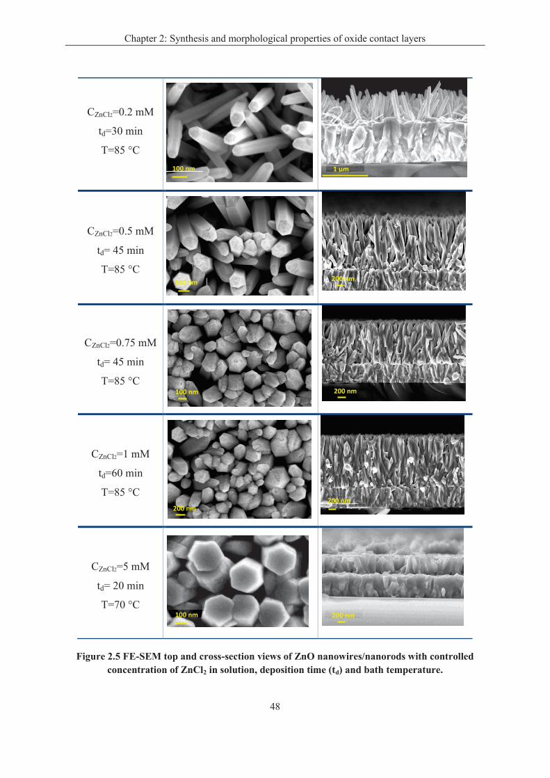
Chapter 2: Synthesis and morphological properties of oxide contact layers
48
CZnCl2=0.2 mM
td=30 min
T=85 °C
CZnCl2=0.5 mM
td= 45 min
T=85 °C
CZnCl2=0.75 mM
td= 45 min
T=85 °C
CZnCl2=1 mM
td=60 min
T=85 °C
CZnCl2=5 mM
td= 20 min
T=70 °C
Figure 2.5 FE-SEM top and cross-section views of ZnO nanowires/nanorods with controlled concentration of ZnCl2 in solution, deposition time (td) and bath temperature.
100 nm 1 µm
100 nm 200 nm
100 nm 200 nm
200 nm 200 nm
200 nm 100 nm
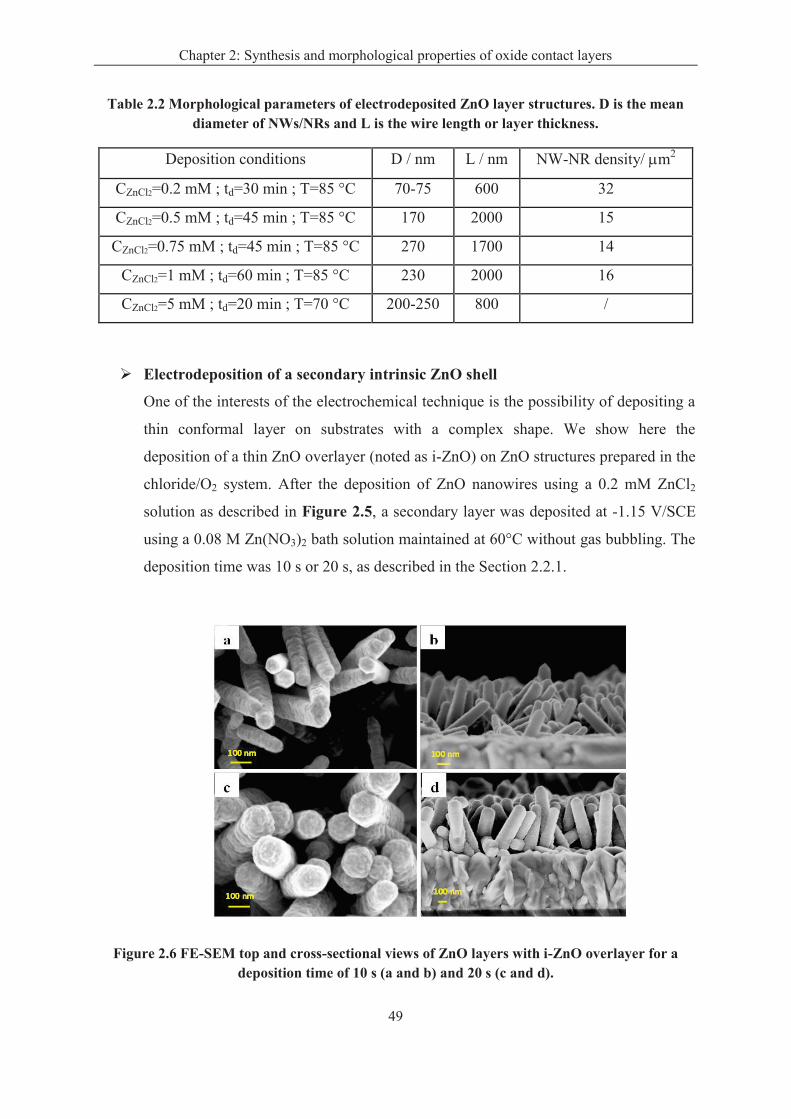
Chapter 2: Synthesis and morphological properties of oxide contact layers
49
Table 2.2 Morphological parameters of electrodeposited ZnO layer structures. D is the mean diameter of NWs/NRs and L is the wire length or layer thickness.
Deposition conditions D / nm L / nm NW-NR density/ mm2
CZnCl2=0.2 mM ; td=30 min ; T=85 °C 70-75 600 32
CZnCl2=0.5 mM ; td=45 min ; T=85 °C 170 2000 15
CZnCl2=0.75 mM ; td=45 min ; T=85 °C 270 1700 14
CZnCl2=1 mM ; td=60 min ; T=85 °C 230 2000 16
CZnCl2=5 mM ; td=20 min ; T=70 °C 200-250 800 /
Ø Electrodeposition of a secondary intrinsic ZnO shell
One of the interests of the electrochemical technique is the possibility of depositing a
thin conformal layer on substrates with a complex shape. We show here the
deposition of a thin ZnO overlayer (noted as i-ZnO) on ZnO structures prepared in the
chloride/O2 system. After the deposition of ZnO nanowires using a 0.2 mM ZnCl2
solution as described in Figure 2.5, a secondary layer was deposited at -1.15 V/SCE
using a 0.08 M Zn(NO3)2 bath solution maintained at 60°C without gas bubbling. The
deposition time was 10 s or 20 s, as described in the Section 2.2.1.
Figure 2.6 FE-SEM top and cross-sectional views of ZnO layers with i-ZnO overlayer for a deposition time of 10 s (a and b) and 20 s (c and d).
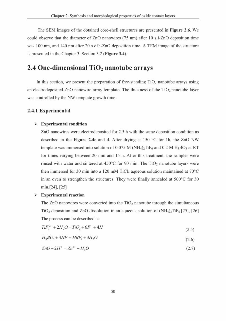
Chapter 2: Synthesis and morphological properties of oxide contact layers
50
The SEM images of the obtained core-shell structures are presented in Figure 2.6. We
could observe that the diameter of ZnO nanowires (75 nm) after 10 s i-ZnO deposition time
was 100 nm, and 140 nm after 20 s of i-ZnO deposition time. A TEM image of the structure
is presented in the Chapter 3, Section 3.2 (Figure 3.4).
2.4 One-dimensional TiO2 nanotube arrays
In this section, we present the preparation of free-standing TiO2 nanotube arrays using
an electrodeposited ZnO nanowire array template. The thickness of the TiO2 nanotube layer
was controlled by the NW template growth time.
2.4.1 Experimental
Ø Experimental condition
ZnO nanowires were electrodeposited for 2.5 h with the same deposition condition as
described in the Figure 2.4c and d. After drying at 150 °C for 1h, the ZnO NW
template was immersed into solution of 0.075 M (NH4)2TiF6 and 0.2 M H3BO3 at RT
for times varying between 20 min and 15 h. After this treatment, the samples were
rinsed with water and sintered at 450°C for 90 min. The TiO2 nanotube layers were
then immersed for 30 min into a 120 mM TiCl4 aqueous solution maintained at 70°C
in an oven to strengthen the structures. They were finally annealed at 500°C for 30
min.[24], [25]
Ø Experimental reaction
The ZnO nanowires were converted into the TiO2 nanotube through the simultaneous
TiO2 deposition and ZnO dissolution in an aqueous solution of (NH4)2TiF6.[25], [26]
The process can be described as:
2
6 2 22 6 4TiF H O TiO F H- - ++ = + + (2.5)
3 3 4 24 3H BO HF HBF H O+ = + (2.6)
2
22ZnO H Zn H O+ ++ = + (2.7)

Chapter 2: Synthesis and morphological properties of oxide contact layers
51
2.4.2 Results and discussions
The ZnO NWs have been synthesized on the FTO substrate covered by a TiO2 seed
layer, the same deposition condition as described in the Figure 2.4c, d. The length of ZnO
NWs was about 2.5 µm with 2.5 h of deposition time. When the ZnO template was immersed
into a solution of (NH4)2TiF6 and H3BO3, the deposition of TiO2 and the ZnO dissolution of
ZnO occured simultaneously by the reaction of (NH4)2TiF6 and moderate low pH (about 4.3)
fixed by H3BO3. We investigated a reaction time ranging from 20 min to 15 h. After
annealing, we observed that a TiO2 NT array was formed (see Figure 2.7). For the 20 min of
immersion time, most tubes were broken, because of the very thin wall thickness due to the
short growth time. When the immersing time was increased to 90 min, we could get nice and
complete tubes (Figure 2.7b), which diameter was about 110 nm.
Figure 2.7 (a-f) FE-SEM images top view of TiO2 nanotubes prepared from a ZnO NW template with 20 min (a), 90 min (b), 3 h (c), 4.5 h (d), 6 h (e) and 15 h (f) of titanate treatment time. The
cross sectional view of TiO2 nanotube with 6 h (g) and 15 h (h) of growth time.
100 nm
f
100 nm
a
100 nm
b
100 nm
c
100 nm
d
100 nm
e
h g
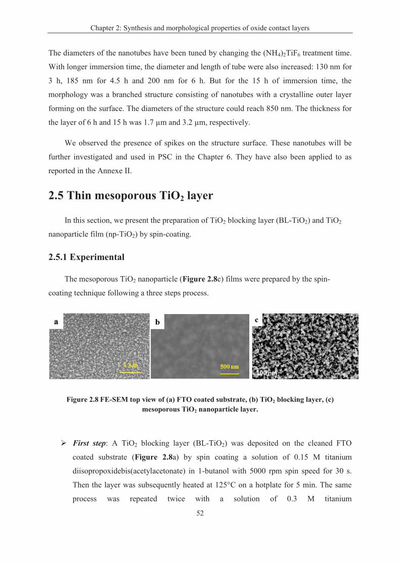
Chapter 2: Synthesis and morphological properties of oxide contact layers
52
The diameters of the nanotubes have been tuned by changing the (NH4)2TiF6 treatment time.
With longer immersion time, the diameter and length of tube were also increased: 130 nm for
3 h, 185 nm for 4.5 h and 200 nm for 6 h. But for the 15 h of immersion time, the
morphology was a branched structure consisting of nanotubes with a crystalline outer layer
forming on the surface. The diameters of the structure could reach 850 nm. The thickness for
the layer of 6 h and 15 h was 1.7 µm and 3.2 µm, respectively.
We observed the presence of spikes on the structure surface. These nanotubes will be
further investigated and used in PSC in the Chapter 6. They have also been applied to as
reported in the Annexe II.
2.5 Thin mesoporous TiO2 layer
In this section, we present the preparation of TiO2 blocking layer (BL-TiO2) and TiO2
nanoparticle film (np-TiO2) by spin-coating.
2.5.1 Experimental
The mesoporous TiO2 nanoparticle (Figure 2.8c) films were prepared by the spin-
coating technique following a three steps process.
Figure 2.8 FE-SEM top view of (a) FTO coated substrate, (b) TiO2 blocking layer, (c) mesoporous TiO2 nanoparticle layer.
Ø First step: A TiO2 blocking layer (BL-TiO2) was deposited on the cleaned FTO
coated substrate (Figure 2.8a) by spin coating a solution of 0.15 M titanium
diisopropoxidebis(acetylacetonate) in 1-butanol with 5000 rpm spin speed for 30 s.
Then the layer was subsequently heated at 125°C on a hotplate for 5 min. The same
process was repeated twice with a solution of 0.3 M titanium
Chapter 2: Synthesis and morphological properties of oxide contact layers
53
diisopropoxidebis(acetylacetonate) in 1-butanol. This BL was finally heated at 500 °C
for 15 min in a furnace, Figure 2.8b is a SEM top view of the layer.
Ø Second step: The TiO2 blocking layer was treated in a 0.04 M aqueous solution of
TiCl4 for 30 min at 70 °C, rinsed with water and annealed at 500 °C for 20 min.
Ø Third step: The mesoporous TiO2 composed of 18-nm-sized particles was prepared
by spin-coating a TiO2 paste (Dyesol 18NR-T diluted in ethanol with a 2:7 weight
ratio) at a spin speed at 5000 rpm for 30 s. After drying at 125°C for 10 min, the TiO2
film was gradually heated up to 500°C for 15 min (Figure 2.8c).
2.5.2 Results
The thickness of the mesoporous TiO2 layer is a key parameter to achieve good cell
efficiency.[27] This parameter is set by a variation of spin-coating speed and a variation of
the concentration of TiO2 paste. Usually, the 300-350 nm of TiO2 film have the highest cell
efficiency.[27] We prepared TiO2 mesoporous layers made of sintered nanoparticles that
covered the TiO2 BL. The Figure 2.8c shows the top view of TiO2 nanoparticle structure
prepared by spin-coating. Their mean thickness was 280 nm and the surface was flat with a
Rrms measured by profilometry of 30 nm. These structures have been investigated for the PSC
application in Chapter 4.
2.6 Conclusion
In conclusion, we have developed the preparation of ZnO and TiO2 structures with well-
controlled morphological characteristics. Three kinds of ZnO nanostructures were prepared
from a 0.08 M nitrate precursor solution by electrodeposition. A dense and flat ZnO film (i-
ZnO-420s) was obtained with -0.9 V/SCE of electrodeposition potential and 420 s of
deposition time. This layer was made of large ZnO crystallite, with a quite smooth and
uniform surface. Another ZnO layer (i-ZnO-120s) was prepared with -1.15 V/SCE of
electrodeposition potential and 120 s of deposition time, which is made of large ZnO grains
and with a rough surface.
ZnO nanowires/nanorods/nanopillars layers were prepared using a chloride/oxygen
system. The morphology of the nanostructures was different when ZnO NWs were deposited
on different seeded or not substrates. When the ZnO NWs were prepared on the TiO2 seed
layer, the mean diameter of nanowire were larger than when they were deposited on the ZnO
Chapter 2: Synthesis and morphological properties of oxide contact layers
54
seed layer. The layer morphology could also be controlled by varying the ZnCl2
concentration and bath temperature.
We have also developed the deposition of a conformal secondary i-ZnO layer on the
ZnO NWs arrays. We will show in Chapter 3 that this thin layer improves the interface
between the oxide and the absorber in the solar cells.[28] We prepared the i-ZnO layer on the
ZnO NWs using 10 s and 20 s of deposition time. Compared to the ZnO layer without i-ZnO
deposition, the NW diameter and length increased with longer i-ZnO deposition time.
A novel method for the TiO2 nanotube preparation was introduced in this chapter. When
the ZnO template was immersed into a solution of (NH4)2TiF6 and H3BO3, the deposition of
TiO2 and ZnO dissolution simultaneously happened. After annealing, a TiO2 nanotubes array
was obtained. Because the dissolution rate of ZnO is faster than the TiO2 growth, we couldn’t
obtained complete nanotubes for impression liquid phase treatment time shorter than 20 min.
After 90 min of immersion time, a complete nanotube layer was obtained, and the nanotube
diameter increased with the liquid phase deposition time.
The thicknesses for the above ZnO and TiO2 layers were above 500 nm. We have also
developed the deposition of mesoporous TiO2 film by spin-coating. Thin and uniform TiO2
films made of sintered nanoparticle have been prepared which thickness could be controlled
by the paste viscosity and the spin coating speed. These layers have been deposited on a TiO2
blocking layer.
References
[1] B. O’Regan and M. Graetzel, “A low cost, high-efficiency solar cell based on dye-
sensitized colloidal TiO2 films,” Nature, vol. 353, pp. 737–739, Oct. 1999.
[2] M. Grätzel, “Dye-sensitized solar cells,” J. Photochem. Photobiol. C Photochem. Rev.,
vol. 4, no. 2, pp. 145–153, Oct. 2003.
[3] R. Katoh and A. Furube, “Electron injection efficiency in dye-sensitized solar cells,” J.
Photochem. Photobiol. C Photochem. Rev., vol. 20, pp. 1–16, Sep. 2014.
[4] C. Magne, F. Dufour, F. Labat, G. Lancel, O. Durupthy, S. Cassaignon, and T. Pauporté,
“Effects of TiO2 nanoparticle polymorphism on dye-sensitized solar cell photovoltaic
properties,” J. Photochem. Photobiol. Chem., vol. 232, pp. 22–31, Mar. 2012.
Chapter 2: Synthesis and morphological properties of oxide contact layers
55
[5] Q. Zhang, C. S. Dandeneau, X. Zhou, and G. Cao, “ZnO Nanostructures for Dye-
Sensitized Solar Cells,” Adv. Mater., vol. 21, no. 41, pp. 4087-4108, Nov. 2009.
[6] S. D. Oosterhout, M. M. Wienk, S. S. van Bavel, R. Thiedmann, L. Jan Anton Koster, J.
Gilot, J. Loos, V. Schmidt, and R. A. J. Janssen, “The effect of three-dimensional
morphology on the efficiency of hybrid polymer solar cells,” Nat. Mater., vol. 8, no. 10,
pp. 818–824, Oct. 2009.
[7] J. Tornow and K. Schwarzburg, “Transient Electrical Response of Dye-Sensitized ZnO
Nanorod Solar Cells,” J. Phys. Chem. C, vol. 111, no. 24, pp. 8692–8698, Jun. 2007.
[8] F. Xu, P. Zhang, A. Navrotsky, Z.-Y. Yuan, T.-Z. Ren, M. Halasa, and B.-L. Su,
“Hierarchically Assembled Porous ZnO Nanoparticles: Synthesis, Surface Energy, and
Photocatalytic Activity,” Chem. Mater., vol. 19, no. 23, pp. 5680–5686, Nov. 2007.
[9] O. Lupan, V. M. Guérin, I. M. Tiginyanu, V. V. Ursaki, L. Chow, H. Heinrich, and T.
Pauporté, “Well-aligned arrays of vertically oriented ZnO nanowires electrodeposited
on ITO-coated glass and their integration in dye sensitized solar cells,” J. Photochem.
Photobiol. Chem., vol. 211, no. 1, pp. 65–73, Mar. 2010.
[10] P. Yang, H. Yan, S. Mao, R. Russo, J. Johnson, R. Saykally, N. Morris, J. Pham, R. He,
and H.-J. Choi, “Controlled growth of ZnO nanowires and their optical properties,” Adv.
Funct. Mater., vol. 12, no. 5, pp. 323–331, May 2002.
[11] V. M. Guerin, C. Magne, T. Pauporté, T. Le Bahers, and J. Rathousky,
“Electrodeposited Nanoporous versus Nanoparticulate ZnO Films of Similar Roughness
for Dye-Sensitized Solar Cell Applications,” ACS Appl. Mater. Interfaces, vol. 2, no. 12,
pp. 3677–3685, Dec. 2010.
[12] Q. Li, V. Kumar, Y. Li, H. Zhang, T. J. Marks, and R. P. H. Chang, “Fabrication of ZnO
Nanorods and Nanotubes in Aqueous Solutions,” Chem. Mater., vol. 17, no. 5, pp.
1001–1006, Mar. 2005.
[13] M. Ristić, S. Musić, M. Ivanda, and S. Popović, “Sol-gel synthesis and characterization
of nanocrystalline ZnO powders,” J. Alloys Compd., vol. 397, no. 1–2, pp. L1–L4, Jul.
2005.
[14] K. H. Tam, C. K. Cheung, Y. H. Leung, A. B. Djurišić, C. C. Ling, C. D. Beling, S.
Fung, W. M. Kwok, W. K. Chan, D. L. Phillips, L. Ding, and W. K. Ge, “Defects in
ZnO Nanorods Prepared by a Hydrothermal Method,” J. Phys. Chem. B, vol. 110, no. 42,
pp. 20865–20871, Oct. 2006.
Chapter 2: Synthesis and morphological properties of oxide contact layers
56
[15] D. Tench and L. F. Warren, “Electrodeposition of Conducting Transition Metal
Oxide/Hydroxide Films from Aqueous Solution,” J. Electrochmical Soc., vol. 130, no. 4,
pp. 869–872, Jan. 1983.
[16] S. T. Chang, I. C. Leu, and M. H. Hon, “Preparation and Characterization of
Nanostructured Tin Oxide Films by Electrochemical Deposition,” Electrochem. Solid-
State Lett., vol. 5, no. 8, pp. C71–C74, May. 2002.
[17] C. Natarajan and G. Nogami, “Cathodic Electrodeposition of Nanocrystalline Titanium
Dioxide Thin Films,” J. Electrochmical Soc., vol. 143, no. 5, pp. 1547–1550, May 1996.
[18] M. Izaki and T. Omi, “Transparent zinc oxide films prepared by electrochemical
reaction,” Appl. Phys. Lett., vol. 68, no. 17, p. 2439, Apr. 1996.
[19] J. Zhang, E. J. Juárez-Pérez, I. Mora-Seró, B. Viana, and T. Pauporté, “Fast and low
temperature growth of electron transport layers for efficient perovskite solar cells,” J
Mater Chem A, vol. 3, no. 9, pp. 4909–4915, Jan. 2015.
[20] S. Peulon and J. L. Lincol, “Cathodic Electrodeposition from Aqueous Solution of
Dense or Open-Structured Zinc Oxide Films,” Adv. Mater., vol. 8, no. 2, pp. 166–170,
Feb. 1996.
[21] T. Pauporté, T. Yoshida, A. Goux, and D. Lincot, “One-step electrodeposition of
ZnO/eosin Y hybrid films from a hydrogen peroxide oxygen precursor,” J. Electroanal.
Chem., vol. 534, no. 1, pp. 55–64, Oct. 2002.
[22] T. Yoshida and T. Pauporté, “Cathodic Electrodeposition of ZnO/Eosin Y Hybrid Thin
Films from Oxygen-Saturated Aqueous Solution of ZnCl2 and Eosin Y,” J.
Electrochmical Soc., vol. 150, no. 9, pp. C608–C615, Jul. 2003.
[23] T. Pauporté, G. Bataille, L. Joulaud, and F. J. Vermersch, “Well-Aligned ZnO Nanowire
Arrays Prepared by Seed-Layer-Free Electrodeposition and Their Cassie-Wenzel
Transition after Hydrophobization,” J. Phys. Chem. C, vol. 114, no. 1, pp. 194–202, Jan.
2010.
[24] C. Xu, P. H. Shin, L. Cao, J. Wu, and D. Gao, “Ordered TiO2 Nanotube Arrays on
Transparent Conductive Oxide for Dye-Sensitized Solar Cells,” Chem. Mater., vol. 22,
no. 1, pp. 143–148, Jan. 2010.
[25] J.-H. Lee, I.-C. Leu, M.-C. Hsu, Y.-W. Chung, and M.-H. Hon, “Fabrication of Aligned
TiO 2 One-Dimensional Nanostructured Arrays Using a One-Step Templating Solution
Approach,” J. Phys. Chem. B, vol. 109, no. 27, pp. 13056–13059, Jul. 2005.
Chapter 2: Synthesis and morphological properties of oxide contact layers
57
[26] X. Lan, J. Bai, S. Masala, S. M. Thon, Y. Ren, I. J. Kramer, S. Hoogland, A. Simchi, G.
I. Koleilat, D. Paz-Soldan, Z. Ning, A. J. Labelle, J. Y. Kim, G. Jabbour, and E. H.
Sargent, “Self-Assembled, Nanowire Network Electrodes for Depleted Bulk
Heterojunction Solar Cells,” Adv. Mater., vol. 25, no. 12, pp. 1769–1773, Mar. 2013.
[27] J. Burschka, N. Pellet, S.-J. Moon, R. Humphry-Baker, P. Gao, M. K. Nazeeruddin, and
M. Grätzel, “Sequential deposition as a route to high-performance perovskite-sensitized
solar cells,” Nature, vol. 499, no. 7458, pp. 316–319, Jul. 2013.
[28] J. Zhang, P. Barboux, and T. Pauporté, “Electrochemical Design of Nanostructured ZnO
Charge Carrier Layers for Efficient Solid-State Perovskite-Sensitized Solar Cells,” Adv.
Energy Mater., vol. 4, no. 18, pp. 1400932/1–1400932/8, Dec. 2014.
58
Chapter 3: Electrochemical design of
ZnO structured layers for efficient PSC
application
This chapter deals with the preparation of CH3NH3PbI3 perovskite layers, the
electrochemical design of ZnO nanostructures and the fabrication of efficient ZnO/perovskite
CH3NH3PbI3/HTM (spiro-OMeTAD) solid-state solar cells. The results have been published
in the journal «Advanced Energy Materials».[1]
Well-conducting ZnO nanostructure layers were deposited in chloride/oxygen medium,
ranging from arrays of NWs/NRs to the dense, well-covering columnar layers (see Chapter 2,
Section 2.3). CH3NH3PbI3 perovskite was used as the sensitizer in the fabricated solar cells.
Their efficiency was affected by the nanostructure. We concluded that: the NWs/NRs
structures favor the sensitizer loading and give rise to the higher short circuit current.
Moreover, a thin intermediate overlayer of ZnO deposited from a nitrate precursor system (i-
ZnO) was used to improve the efficiency of the ZnO nanostructures deposited from the
chloride/oxygen system. The morphology of ZnO NW/NR layers could be improved and the
cell performances were enhanced. The best efficiency for the solar cell with an optimized
design was 10.28% at one sun illumination.
3.1 Sensitization of ZnO electrodeposited structures by
CH3NH3PbI3 perovskite layers
Methyl ammonium lead iodide CH3NH3PbI3 has received great deal of attention for
solar cell application due to its suitable bandgap and perfect absorbance performance.[2]–[5]
In this chapter, the CH3NH3PbI3 layer was prepared by a two-step technique and large cubic
perovskite crystallites were obtained.[6], [7] In the next sections, we explain the protocol
used to prepare the perovskite layer and the characteristics of this CH3NH3PbI3 layer.
Chapter 3: Electrochemical design of ZnO structured layers for efficient PSC application
59
3.1.1 Experimental
The CH3NH3PbI3 perovskite layer was deposited by a two-step sequential method,
therefore, this technique will be hereafter denoted as “two-step”.[6] The process is described
in the Figure 3.1.
Ø Step 1: 70 µL of PbI2 solution at 70°C (dissolved in N, N-dimethylformamide at
a concentration of 460 mg. mL-1
) was spin-coated on top of oxide ETL layer at
3,000 r.p.m. for 15 s. The PbI2 layer was dried at 70°C for 30 minutes in air in an
oven.
Ø Step 2: The substrate covered by the PbI2 layer was immersed into a solution of
CH3NH3I (prepared as described in the Annexe I) in 2-propanol (10 mg.ml-1
) for
30 s. Before this step, the PbI2 layer was pre-wetted for 1-2 s in 2-propanol
solvent. Finally the brown perovskite layer was annealed at 70°C for 30 minutes
in air in an oven.
Figure 3.1 Two-step preparation protocol of CH3NH3PbI3 perovskite layer.
Chapter 3: Electrochemical design of ZnO structured layers for efficient PSC application
60
3.1.2 The characteristics of CH3NH3PbI3 layer
Ø SEM
By this two-step method, CH3NH3PbI3 was infiltrated into the space between the
ZnO NWs, which means a good sensitization performance (Figure 3.2a), but we
did not obtain a capping layer. Therefore, on FE-SEM top view images we could
observe the presence of white spots of uncovered ZnO structures (Figure 3.2b).
Figure 3.2 SEM cross sectional view (a) and top-view (b) of the CH3NH3PbI3 layer deposited on the ZnO nanowire arrays.
Ø XRD
A typical XRD pattern of perovskite deposited on the ZnO nanowires is
displayed in the Figure 3.3. It shows a well crystalline CH3NH3PbI3 perovskite
by the two-step method which is suited for the deposition of perovskite layer on
the ZnO structures. In this pattern, we also observe the presence of (001) and
(110) PbI2 diffraction peaks at 12.8° and 39.7°, respectively, which indicates
traces of PbI2 that were not be fully converted into the organometal halide
perovskite.[8]–[10]
100 nm 100 nm
a b
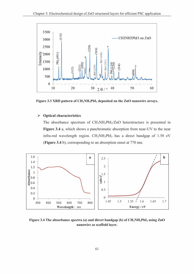
Chapter 3: Electrochemical design of ZnO structured layers for efficient PSC application
61
Figure 3.3 XRD pattern of CH3NH3PbI3 deposited on the ZnO nanowire arrays.
Ø Optical characteristics
The absorbance spectrum of CH3NH3PbI3/ZnO heterstructure is presented in
Figure 3.4 a, which shows a panchromatic absorption from near-UV to the near
infra-red wavelength region. CH3NH3PbI3 has a direct bandgap of 1.58 eV
(Figure 3.4 b), corresponding to an absorption onset at 770 nm.
Figure 3.4 The absorbance spectra (a) and direct bandgap (b) of CH3NH3PbI3 using ZnO nanowire as scaffold layer.
0
0.2
0.4
0.6
0.8
1
1.2
1.4
1.6
350 450 550 650 750 850
Ab
sorb
ance
Wavelength / nm
0
0.5
1
1.5
2
2.5
1.45 1.5 1.55 1.6 1.65 1.7
(ah
v)2
Energy / eV
a b
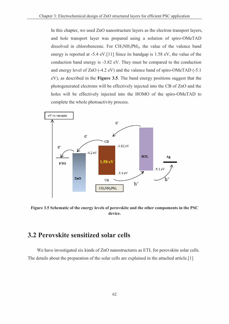
Chapter 3: Electrochemical design of ZnO structured layers for efficient PSC application
62
In this chapter, we used ZnO nanostructure layers as the electron transport layers,
and hole transport layer was prepared using a solution of spiro-OMeTAD
dissolved in chlorobenzene. For CH3NH3PbI3, the value of the valence band
energy is reported at -5.4 eV.[11] Since its bandgap is 1.58 eV, the value of the
conduction band energy is -3.82 eV. They must be compared to the conduction
and energy level of ZnO (-4.2 eV) and the valence band of spiro-OMeTAD (-5.1
eV), as described in the Figure 3.5. The band energy positions suggest that the
photogenerated electrons will be effectively injected into the CB of ZnO and the
holes will be effectively injected into the HOMO of the spiro-OMeTAD to
complete the whole photoactivity process.
Figure 3.5 Schematic of the energy levels of perovskite and the other compoments in the PSC device.
3.2 Perovskite sensitized solar cells
We have investigated six kinds of ZnO nanostructures as ETL for perovskite solar cells.
The details about the preparation of the solar cells are explained in the attached article.[1]
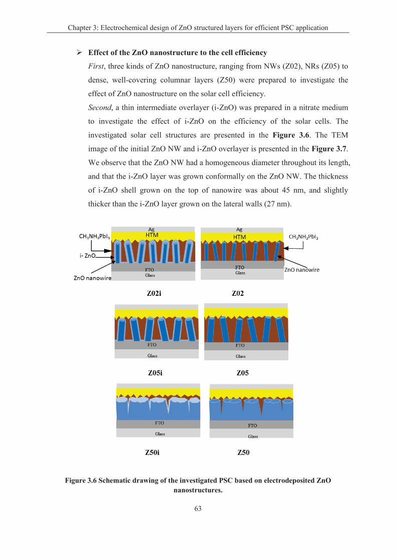
Chapter 3: Electrochemical design of ZnO structured layers for efficient PSC application
63
Ø Effect of the ZnO nanostructure to the cell efficiency
First, three kinds of ZnO nanostructure, ranging from NWs (Z02), NRs (Z05) to
dense, well-covering columnar layers (Z50) were prepared to investigate the
effect of ZnO nanostructure on the solar cell efficiency.
Second, a thin intermediate overlayer (i-ZnO) was prepared in a nitrate medium
to investigate the effect of i-ZnO on the efficiency of the solar cells. The
investigated solar cell structures are presented in the Figure 3.6. The TEM
image of the initial ZnO NW and i-ZnO overlayer is presented in the Figure 3.7.
We observe that the ZnO NW had a homogeneous diameter throughout its length,
and that the i-ZnO layer was grown conformally on the ZnO NW. The thickness
of i-ZnO shell grown on the top of nanowire was about 45 nm, and slightly
thicker than the i-ZnO layer grown on the lateral walls (27 nm).
Figure 3.6 Schematic drawing of the investigated PSC based on electrodeposited ZnO nanostructures.
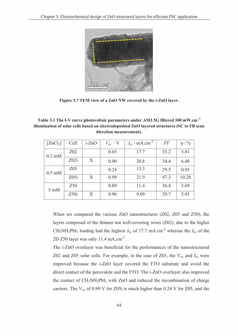
Chapter 3: Electrochemical design of ZnO structured layers for efficient PSC application
64
Figure 3.7 TEM view of a ZnO NW covered by the i-ZnO layer.
Table 3.1 The I-V curve photovoltaic parameters under AM1.5G filtered 100 mW.cm−2 illumination of solar cells based on electrodeposited ZnO layered structures (SC to FB scan
direction measurement).
[ZnCl2] Cell i-ZnO Voc / V Jsc / mA.cm-2
FF h / %
0.2 mM Z02 0.65 17.7 33.2 3.81
Z02i X 0.90 20.8 34.4 6.48
0.5 mM Z05 0.24 13.3 29.5 0.95
Z05i X 0.99 21.9 47.3 10.28
5 mM Z50 0.89 11.4 36.4 3.69
Z50i X 0.96 9.09 39.7 3.45
When we compared the various ZnO nanostructures (Z02, Z05 and Z50), the
layers composed of the thinner not well-covering wires (Z02), due to the higher
CH3NH3PbI3 loading had the highest Jsc of 17.7 mA.cm-2
whereas the Jsc of the
2D Z50 layer was only 11.4 mA.cm-2
.
The i-ZnO overlayer was beneficial for the performances of the nanostructured
Z02 and Z05 solar cells. For example, in the case of Z05, the Voc and Jsc were
improved because the i-ZnO layer covered the FTO substrate and avoid the
direct contact of the perovskite and the FTO. The i-ZnO overlayer also improved
the contact of CH3NH3PbI3 with ZnO and reduced the recombination of charge
carriers. The Voc of 0.99 V for Z05i is much higher than 0.24 V for Z05, and the
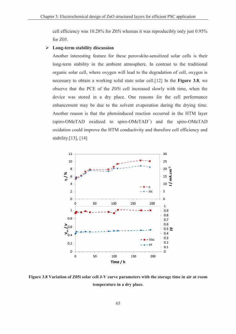
Chapter 3: Electrochemical design of ZnO structured layers for efficient PSC application
65
cell efficiency was 10.28% for Z05i whereas it was reproducibly only just 0.95%
for Z05.
Ø Long-term stability discussion
Another interesting feature for these perovskite-sensitized solar cells is their
long-term stability in the ambient atmosphere. In contrast to the traditional
organic solar cell, where oxygen will lead to the degradation of cell, oxygen is
necessary to obtain a working solid state solar cell.[12] In the Figure 3.8, we
observe that the PCE of the Z05i cell increased slowly with time, when the
device was stored in a dry place. One reasons for the cell performance
enhancement may be due to the solvent evaporation during the drying time.
Another reason is that the photoinduced reaction occurred in the HTM layer
(spiro-OMeTAD oxidized to spiro-OMeTAD+) and the spiro-OMeTAD
oxidation could improve the HTM conductivity and therefore cell efficiency and
stability.[13], [14]
Figure 3.8 Variation of Z05i solar cell J-V curve parameters with the storage time in air at room
temperature in a dry place.
Chapter 3: Electrochemical design of ZnO structured layers for efficient PSC application
66
In this chapter, the thickness of HTM layer was about 750 nm, which could be observed
from the Figure 5 in the attached file. The cell performance improved with time just
observed with the thicker HTM layer, which performance we did not observed with thinner
HTM layer (in the Chapter 4).
3.3 Conclusion
In this chapter, several well-crystallized ZnO structures have been prepared by
electrochemical deposition at low temperature ranging between ZnO NW, ZnO NR and 2D
layers. We have also introduced the electrodeposition of i-ZnO conformal overlayer (20-45
nm), prepared in a zinc nitrate bath. The two-step technique to prepare CH3NH3PbI3
perovskite with a suitable performance for ZnO solar cell is described. The perovskite layer
shows a panchromatic absorbance from near-UV to near-infrared region and ad-hoc band
energy position for an excellent charge collection performance. Spiro-OMeTAD dissolved in
chlorobenzene was used as hole transport material to fabricate solid state perovskite
sensitized solar cell, the thickness of HTL layer was quite high at 750 nm to be sure to fully
cover the underlayers. Through designing the ZnO carrier layer, a high efficiency of 10.28%
was achieved, which is much better than the results obtained from traditional liquid dye
sensitized solar cell, for instance 5.3% in our group.[15], [16]
References :
[1] J. Zhang, P. Barboux, and T. Pauporté, “Electrochemical Design of Nanostructured ZnO
Charge Carrier Layers for Efficient Solid-State Perovskite-Sensitized Solar Cells,” Adv.
Energy Mater., vol. 4, no. 18, pp. 1400932/1–1400932/8, Dec. 2014.
[2] B. V. Lotsch, “New Light on an Old Story: Perovskites Go Solar,” Angew. Chem. Int.
Ed., vol. 53, no. 3, pp. 635–637, Jan. 2014.
[3] M. A. Green, A. Ho-Baillie, and H. J. Snaith, “The emergence of perovskite solar cells,”
Nat. Photonics, vol. 8, no. 7, pp. 506–514, Jun. 2014.
[4] T.-B. Song, Q. Chen, H. Zhou, C. Jiang, H.-H. Wang, Y. (Michael) Yang, Y. Liu, J.
You, and Y. Yang, “Perovskite solar cells: film formation and properties,” J Mater
Chem A, vol. 3, no. 17, pp. 9032–9050, Mar. 2015.
[5] J. M. Ball, S. D. Stranks, M. T. Hörantner, S. Hüttner, W. Zhang, E. J. W. Crossland, I.
Ramirez, M. Riede, M. B. Johnston, R. H. Friend, and H. J. Snaith, “Optical properties
Chapter 3: Electrochemical design of ZnO structured layers for efficient PSC application
67
and limiting photocurrent of thin-film perovskite solar cells,” Energy Env. Sci, vol. 8, no.
2, pp. 602–609, Dec. 2015.
[6] J. Burschka, N. Pellet, S.-J. Moon, R. Humphry-Baker, P. Gao, M. K. Nazeeruddin, and
M. Grätzel, “Sequential deposition as a route to high-performance perovskite-sensitized
solar cells,” Nature, vol. 499, no. 7458, pp. 316–319, Jul. 2013.
[7] D. Liu and T. L. Kelly, “Perovskite solar cells with a planar heterojunction structure
prepared using room-temperature solution processing techniques,” Nat. Photonics, vol.
8, no. 2, pp. 133–138, Dec. 2013.
[8] L. Zheng, Y. Ma, S. Chu, S. Wang, B. Qu, L. Xiao, Z. Chen, Q. Gong, Z. Wu, and X.
Hou, “Improved light absorption and charge transport for perovskite solar cells with
rough interfaces by sequential deposition,” Nanoscale, vol. 6, no. 14, pp. 8171–8176,
May 2014.
[9] Y. Wu, A. Islam, X. Yang, C. Qin, J. Liu, K. Zhang, W. Peng, and L. Han, “Retarding
the crystallization of PbI2 for highly reproducible planar-structured perovskite solar cells
via sequential deposition,” Energy Environ. Sci., vol. 7, no. 9, pp. 2934–2938, Jun. 2014.
[10] I. Koutselas, K. Dimos, A. Bourlinos, D. Gournis, A. Avgeropoulos, S. Agathopoulos,
and M. A. Karakassides, “Synthesis and characterization of PbI2 semiconductor
quantum wires within layered solids,” J. Optoelectron. Adv. Mater., vol. 10, no. 1, pp.
58–65, Jan. 2008.
[11] H.-S. Kim, C.-R. Lee, J.-H. Im, K.-B. Lee, T. Moehl, A. Marchioro, S.-J. Moon, R.
Humphry-Baker, J.-H. Yum, J. E. Moser, M. Grätzel, and N.-G. Park, “Lead Iodide
Perovskite Sensitized All-Solid-State Submicron Thin Film Mesoscopic Solar Cell with
Efficiency Exceeding 9%,” Sci. Rep., vol. 2, no. 2:591, pp. 1–7, Aug. 2012.
[12] M. Jørgensen, K. Norrman, and F. C. Krebs, “Stability/degradation of polymer solar
cells,” Sol. Energy Mater. Sol. Cells, vol. 92, no. 7, pp. 686–714, Jul. 2008.
[13] U. B. Cappel, T. Daeneke, and U. Bach, “Oxygen-Induced Doping of Spiro-MeOTAD in
Solid-State Dye-Sensitized Solar Cells and Its Impact on Device Performance,” Nano
Lett., vol. 12, no. 9, pp. 4925–4931, Sep. 2012.
[14] P. Docampo and H. J. Snaith, “Obviating the requirement for oxygen in SnO2-based
solid-state dye-sensitized solar cells,” Nanotechnology, vol. 22, no. 22, pp. 225403/1–
225403/8, Jun. 2011.

Chapter 3: Electrochemical design of ZnO structured layers for efficient PSC application
68
[15] V.-M. Guérin and T. Pauporté, “From nanowires to hierarchical structures of template-
free electrodeposited ZnO for efficient dye-sensitized solar cells,” Energy Environ. Sci.,
vol. 4, no. 8, pp. 2971–2979, Jun. 2011.
[16] M. Hosni, Y. Kusumawati, S. Farhat, N. Jouini, A. L. Ivansyah, M. A. Martoprawiro,
and T. Pauporté, “Ruthenium Polypyridyl TG6 Dye for the Sensitization of
Nanoparticle and Nanocrystallite Spherical Aggregate Photoelectrodes,” ACS Appl.
Mater. Interfaces, vol. 7, no. 3, pp. 1568–1577, Jan. 2015.
FULL PAPER
© 2014 WILEY-VCH Verlag GmbH & Co. KGaA, Weinheim (1 of 8) 1400932wileyonlinelibrary.com
Electrochemical Design of Nanostructured ZnO Charge Carrier Layers for Effi cient Solid-State Perovskite-Sensitized Solar Cells
Jie Zhang , Philippe Barboux , and Thierry Pauporté *
J. Zhang, Prof. P. Barboux, Dr. T. Pauporté Institut de Recherche de Chimie Paris (IRCP) CNRS-Chimie ParisTech-Paris Sciences et Lettres PSL UMR8247, 11 rue Pierre et Marie Curie 75005 , Paris , France E-mail: [email protected]
DOI: 10.1002/aenm.201400932
conduction and valence bands and also in the very high mobility of their charge carriers that allow an effi cient charge col-lection when sandwiched between an electron transport material (ETM), usually anatase TiO 2 , and a HTM. [ 12,13 ] The perfor-mances of perovskite sensitized solar cells (PSSCs) increased dramatically during the last two years and the record cell effi cien-cies are now exceeding 16%. [ 14 ]
Interest in the PSSCs mainly lies in the low temperature that can be used for the layer deposition and in the fact that all the active layers can be solution-processed. They open the gate to mass production at a very low-cost. [ 15 ] In this context, ZnO is a major candidate for the ETM layer. [ 16,17 ] ZnO is a wide bandgap semiconductor which can be grown with a high struc-tural quality at low temperature by various techniques. [ 18,19 ] The conductivity of ZnO is several orders of magnitude higher
than that of TiO 2 that favors the electron transport toward the back contact. [ 20 ] Moreover, during the last decade many works have developed the preparation of tailored nanostructured ZnO layers. [ 19,21–23 ] However, in the literature, the effect of nano-structuration of ZnO in PSSC performances remains unclear. Mathews et al. [ 24 ] found a power conversion effi ciency (PCE) of 8.90% for nanorod ZnO layers prepared by chemical deposition with a signifi cant enhancement compared to the ZnO planar confi guration. On the other hand, Kelly et al. [ 16 ] have recently reported remarkably high effi ciencies using a thin layer of dense planar ZnO prepared by spin-coating.
The effi ciency losses in the low-temperature processed PSSC originate mainly due to recombination at imperfect interfaces and structural or chemical defects in perovskite fi lms. Therefore, the development of low-cost high effi ciency solar cells requires an in-depth investigation on these aspects. Electron collection can be increased i) by using nanostruc-tured ETM, [ 8,24–28 ] ii) by using well-conducting oxide, and iii) by engineering the interface between the perovskite and the oxide layer. [ 16 ] The present work focuses on these three aspects in the case of ZnO layers prepared with tailored properties by electrochemical deposition. [ 29 ] The advantages of the technique include the deposition at low temperature of high quality mate-rial, the precise control of the (nano)structure morphology and thickness, the control of the electrical properties and the excel-lent electrical contact between the deposited layers and the
The preparation of ZnO structured fi lms designed to act as electron trans-
port layers in effi cient ZnO/perovskite CH 3 NH 3 PbI 3 /spirobifl uorene (spiro-
OMeTAD) solid-state solar cells by electrochemical deposition is reported.
Well-conducting ZnO layers are deposited in chloride medium and grown
with tailored (nano)structures ranging from arrays of nanowires to a compact,
well-covering fi lm. Moreover, the effect of a thin intermediate overlayer of
ZnO conformally electrodeposited in nitrate medium and with a low n-type
doping (i-ZnO) is discussed. The results show higher power conversion
effi ciencies for the nanostructured oxide layers compared to the dense one.
Moreover, the presence of the i-ZnO layer is shown to markedly improve the
cell short-circuit current and the open-circuit voltage due to charge recombi-
nation reduction. For the best cells, the active layers effi ciently absorb light
over a large spectral range from near-UV to near infrared region and exhibit
excellent charge collection effi ciencies. Solar cells based on an optimized
design generate a very large photocurrent and the power conversion effi -
ciency at one sun is as high as 10.28%.
1. Introduction
Solution-processed organic and hybrid organic−inorganic solar cells, such as dye-sensitized solar cells (DSSC), quantum-dot-sensitized solar cells (QD-SSC) and bulk heterojunction organic solar cells, have been intensely developed during the last two decades. [ 1 ] A major breakthrough was achieved recently by the use of lead halide perovskites as the light absorber mate-rial in the cells. The perovskite polycrystalline structure is com-posed of CH 3 NH 3 PbX 3 , where X is a halogen atom (I, Cl, Br, or a combination of some of them). This light harvester was fi rst proposed by Miyasaka et al. who used it as replacement of dye in the DSSC confi guration. [ 2 ] Subsequently, to avoid the disso-lution of the light harvester material, the liquid electrolyte was replaced by solid hole transport materials (HTM) and remark-able improvements in performance could be achieved. [ 3–13 ] The singular properties of the lead halide perovskites lie in their bandgap being close to the ideal one, in the position of their
Adv. Energy Mater. 2014, 1400932
www.MaterialsViews.comwww.advenergymat.de
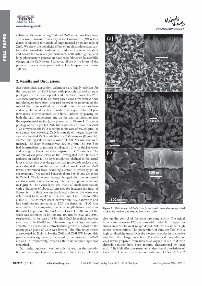
FULL PAPER
© 2014 WILEY-VCH Verlag GmbH & Co. KGaA, Weinheim1400932 (2 of 8) wileyonlinelibrary.com
substrate. Well-conducting Cl-doped ZnO structures have been synthesized ranging from arrayed ZnO nanowires (NWs) to a dense conducting fi lm made of large merged prismatic rods of ZnO. We show the benefi cial effect of an electrodeposited con-formal intermediate overlayer that reduces the recombination and boosts the solar cell performances. Cells with high V oc and large photocurrent generation have been fabricated by carefully designing the ZnO layers. Moreover, all the active layers of the prepared devices were processed at low temperatures (below 150 °C).
2. Results and Discussions
Electrochemical deposition techniques are highly relevant for the preparation of ZnO layers with precisely controlled mor-phological, structural, optical and electrical properties. [ 30,31 ] Nanowires/nanorods (NWs/NRs) based ZnO fi lms with various morphologies have been prepared in order to understand the role of the oxide scaffold, of an oxide intermediate overlayer and of preferential electron transfer pathways on the cell per-formances. The structured ZnO fi lms, tailored by playing on both the bath temperature and on the bath composition (see the experimental section), are presented in Figure 1 . The mor-phology of the deposited ZnO fi lms was varied from thin ZnO NWs arrayed on the FTO substrate in the case of Z02 (Figure 1 a) to a dense, well-covering, ZnO fi lm made of merged large hex-agonally facetted ZnO crystallites for Z50 samples (Figure 1 c). In Z50, the crystallites had a width of 200–250 nm and were merged. The layer thickness was 800–850 nm. The Z05 fi lm had intermediate characteristics (Figure 1 b) with thicker wires and a slightly lower density compared to Z02 samples. The morphological parameters of the investigated ZnO fi lms are gathered in Table 1 . The layer roughness, defi ned as the actual layer surface area over the geometrical (projected) surface area, was estimated from the geometrical parameters of the ZnO layers determined from scanning electron microscopy (SEM) observations. They ranged between about 2 to 15 and are given in Table 1 . The layer morphology changed after the conformal electrodeposition of a secondary intermediate phase as shown in Figure 2 . The i-ZnO layer was made of small nanocrystals with a diameter of about 20 nm (see for instance the inset of Figure 2 c). Its thickness on the lateral sides of the wires was determined to be 40–42 nm for Z02i and 13–15 nm for Z05i (Table 1 ). Due to more space between the Z02 nanowires and less confi nement compared to Z05, the deposited i-ZnO fi lm was thicker. By comparing the wire length before and after the i-ZnO deposition, the thickness of i-ZnO on the top of the wires was estimated to be 120 and 100 nm for Z02i and Z05i, respectively. In the case of Z50i, the i-ZnO layer thickness was estimated to be 80–100 nm. The resulting ZnO layer was quite smooth. In all cases the electrochemical growth of i-ZnO on the (0001) polar plane of ZnO was favored. The fi lm roughnesses are reported in Table 1 . For the Z02i and Z05i NW layers, this parameter was signifi cantly increased by the presence of i-ZnO (12 and 18, respectively), whereas the Z50 compact layer was smoothed.
Our design approach was not only focused on the modula-tion of the morphological parameters of the ZnO scaffolds but
also on the control of the structure conductivity. The initial fi lms were grown in KCl medium with molecular oxygen pre-cursor in order to yield n-type doped ZnO with a rather high carrier concentration. The preparation of ZnO scaffold with a high conductivity must favor the electron transfer in the device and then the charge collection. The electrical properties of ZnO layers prepared from molecular oxygen in a 5 mM zinc chloride solution have been recently characterized by Izaki et al. [ 32 ] By Hall effect measurements, they found a resistivity of 4.4 × 10 −2 Ω.cm with a carrier concentration of 2.5 × 10 19 cm −3
Adv. Energy Mater. 2014, 1400932
www.MaterialsViews.comwww.advenergymat.de
Figure 1. SEM images of ZnO (nano)structured layers electrodeposited in chloride medium: a) Z02, b) Z05, and c) Z50.
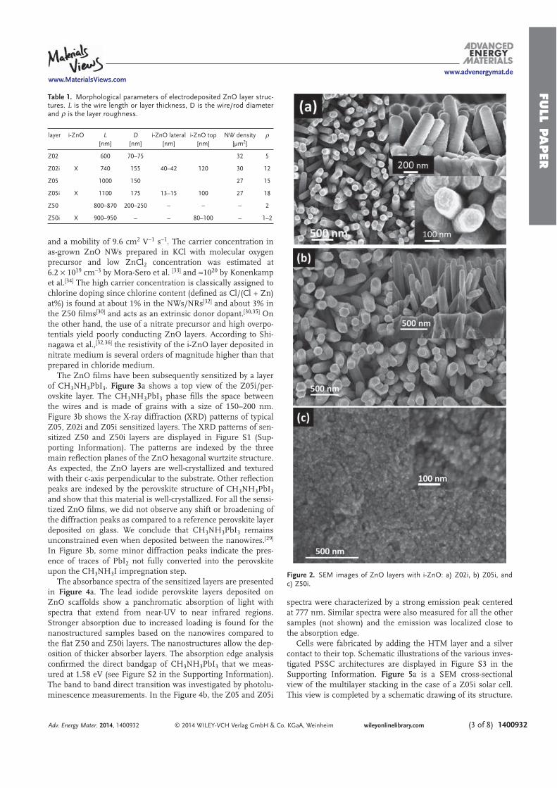
FULL PAPER
© 2014 WILEY-VCH Verlag GmbH & Co. KGaA, Weinheim (3 of 8) 1400932wileyonlinelibrary.com
and a mobility of 9.6 cm 2 V −1 s −1 . The carrier concentration in as-grown ZnO NWs prepared in KCl with molecular oxygen precursor and low ZnCl 2 concentration was estimated at 6.2 × 10 19 cm −3 by Mora-Sero et al. [ 33 ] and ≈10 20 by Konenkamp et al. [ 34 ] The high carrier concentration is classically assigned to chlorine doping since chlorine content (defi ned as Cl/(Cl + Zn) at%) is found at about 1% in the NWs/NRs [ 32 ] and about 3% in the Z50 fi lms [ 30 ] and acts as an extrinsic donor dopant. [ 30,35 ] On the other hand, the use of a nitrate precursor and high overpo-tentials yield poorly conducting ZnO layers. According to Shi-nagawa et al., [ 32,36 ] the resistivity of the i-ZnO layer deposited in nitrate medium is several orders of magnitude higher than that prepared in chloride medium.
The ZnO fi lms have been subsequently sensitized by a layer of CH 3 NH 3 PbI 3 . Figure 3 a shows a top view of the Z05i/per-ovskite layer. The CH 3 NH 3 PbI 3 phase fi lls the space between the wires and is made of grains with a size of 150–200 nm. Figure 3 b shows the X-ray diffraction (XRD) patterns of typical Z05, Z02i and Z05i sensitized layers. The XRD patterns of sen-sitized Z50 and Z50i layers are displayed in Figure S1 (Sup-porting Information). The patterns are indexed by the three main refl ection planes of the ZnO hexagonal wurtzite structure. As expected, the ZnO layers are well-crystallized and textured with their c-axis perpendicular to the substrate. Other refl ection peaks are indexed by the perovskite structure of CH 3 NH 3 PbI 3 and show that this material is well-crystallized. For all the sensi-tized ZnO fi lms, we did not observe any shift or broadening of the diffraction peaks as compared to a reference perovskite layer deposited on glass. We conclude that CH 3 NH 3 PbI 3 remains unconstrained even when deposited between the nanowires. [ 29 ] In Figure 3 b, some minor diffraction peaks indicate the pres-ence of traces of PbI 2 not fully converted into the perovskite upon the CH 3 NH 3 I impregnation step.
The absorbance spectra of the sensitized layers are presented in Figure 4 a. The lead iodide perovskite layers deposited on ZnO scaffolds show a panchromatic absorption of light with spectra that extend from near-UV to near infrared regions. Stronger absorption due to increased loading is found for the nanostructured samples based on the nanowires compared to the fl at Z50 and Z50i layers. The nanostructures allow the dep-osition of thicker absorber layers. The absorption edge analysis confi rmed the direct bandgap of CH 3 NH 3 PbI 3 that we meas-ured at 1.58 eV (see Figure S2 in the Supporting Information). The band to band direct transition was investigated by photolu-minescence measurements. In the Figure 4 b, the Z05 and Z05i
spectra were characterized by a strong emission peak centered at 777 nm. Similar spectra were also measured for all the other samples (not shown) and the emission was localized close to the absorption edge.
Cells were fabricated by adding the HTM layer and a silver contact to their top. Schematic illustrations of the various inves-tigated PSSC architectures are displayed in Figure S3 in the Supporting Information. Figure 5 a is a SEM cross-sectional view of the multilayer stacking in the case of a Z05i solar cell. This view is completed by a schematic drawing of its structure.
Adv. Energy Mater. 2014, 1400932
www.MaterialsViews.comwww.advenergymat.de
Table 1. Morphological parameters of electrodeposited ZnO layer struc-tures. L is the wire length or layer thickness, D is the wire/rod diameter and ρ is the layer roughness.
layer i-ZnO L [nm]
D [nm]
i-ZnO lateral [nm]
i-ZnO top [nm]
NW density [µm 2 ]
ρ
Z02 600 70–75 32 5
Z02i X 740 155 40–42 120 30 12
Z05 1000 150 27 15
Z05i X 1100 175 13–15 100 27 18
Z50 800–870 200–250 – – – 2
Z50i X 900–950 – – 80–100 – 1–2
Figure 2. SEM images of ZnO layers with i-ZnO: a) Z02i, b) Z05i, and c) Z50i.
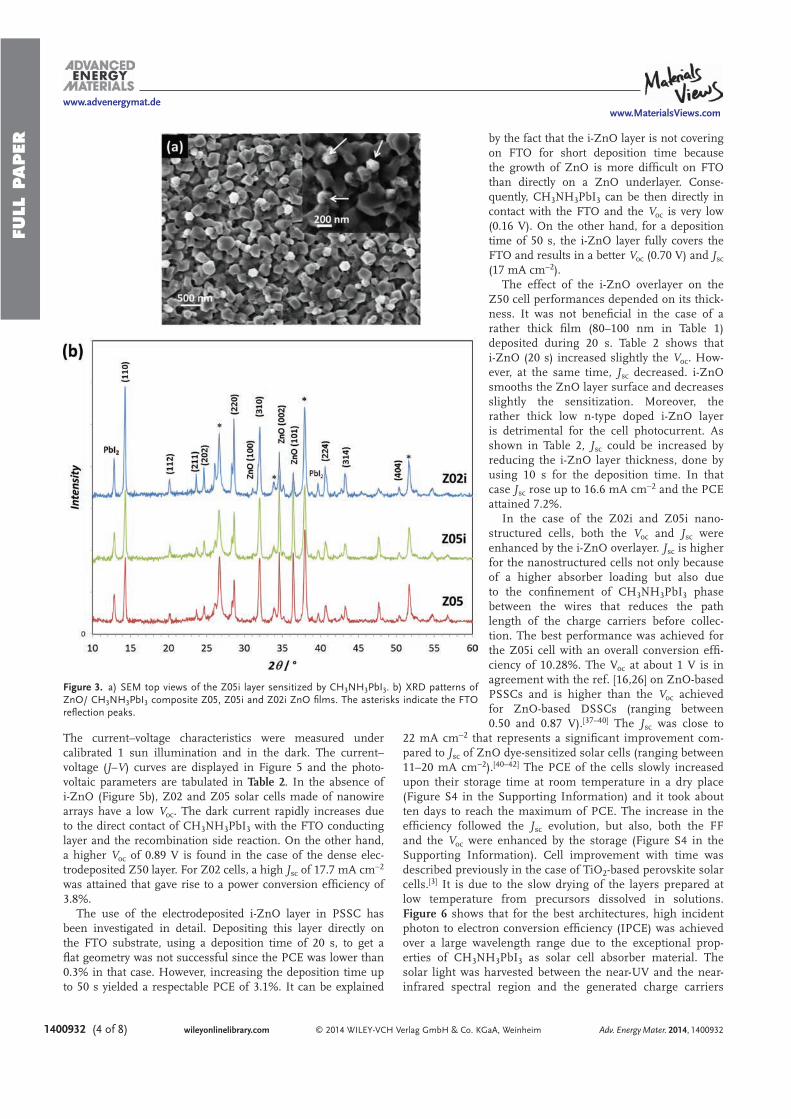
FULL PAPER
© 2014 WILEY-VCH Verlag GmbH & Co. KGaA, Weinheim1400932 (4 of 8) wileyonlinelibrary.com
The current–voltage characteristics were measured under calibrated 1 sun illumination and in the dark. The current–voltage ( J – V ) curves are displayed in Figure 5 and the photo-voltaic parameters are tabulated in Table 2 . In the absence of i-ZnO (Figure 5 b), Z02 and Z05 solar cells made of nanowire arrays have a low V oc . The dark current rapidly increases due to the direct contact of CH 3 NH 3 PbI 3 with the FTO conducting layer and the recombination side reaction. On the other hand, a higher V oc of 0.89 V is found in the case of the dense elec-trodeposited Z50 layer. For Z02 cells, a high J sc of 17.7 mA cm −2 was attained that gave rise to a power conversion effi ciency of 3.8%.
The use of the electrodeposited i-ZnO layer in PSSC has been investigated in detail. Depositing this layer directly on the FTO substrate, using a deposition time of 20 s, to get a fl at geometry was not successful since the PCE was lower than 0.3% in that case. However, increasing the deposition time up to 50 s yielded a respectable PCE of 3.1%. It can be explained
by the fact that the i-ZnO layer is not covering on FTO for short deposition time because the growth of ZnO is more diffi cult on FTO than directly on a ZnO underlayer. Conse-quently, CH 3 NH 3 PbI 3 can be then directly in contact with the FTO and the V oc is very low (0.16 V). On the other hand, for a deposition time of 50 s, the i-ZnO layer fully covers the FTO and results in a better V oc (0.70 V) and J sc (17 mA cm −2 ).
The effect of the i-ZnO overlayer on the Z50 cell performances depended on its thick-ness. It was not benefi cial in the case of a rather thick fi lm (80–100 nm in Table 1 ) deposited during 20 s. Table 2 shows that i-ZnO (20 s) increased slightly the V oc . How-ever, at the same time, J sc decreased. i-ZnO smooths the ZnO layer surface and decreases slightly the sensitization. Moreover, the rather thick low n-type doped i-ZnO layer is detrimental for the cell photocurrent. As shown in Table 2 , J sc could be increased by reducing the i-ZnO layer thickness, done by using 10 s for the deposition time. In that case J sc rose up to 16.6 mA cm −2 and the PCE attained 7.2%.
In the case of the Z02i and Z05i nano-structured cells, both the V oc and J sc were enhanced by the i-ZnO overlayer. J sc is higher for the nanostructured cells not only because of a higher absorber loading but also due to the confi nement of CH 3 NH 3 PbI 3 phase between the wires that reduces the path length of the charge carriers before collec-tion. The best performance was achieved for the Z05i cell with an overall conversion effi -ciency of 10.28%. The V oc at about 1 V is in agreement with the ref. [ 16,26 ] on ZnO-based PSSCs and is higher than the V oc achieved for ZnO-based DSSCs (ranging between 0.50 and 0.87 V). [ 37–40 ] The J sc was close to
22 mA cm −2 that represents a signifi cant improvement com-pared to J sc of ZnO dye-sensitized solar cells (ranging between 11–20 mA cm −2 ). [ 40–42 ] The PCE of the cells slowly increased upon their storage time at room temperature in a dry place (Figure S4 in the Supporting Information) and it took about ten days to reach the maximum of PCE. The increase in the effi ciency followed the J sc evolution, but also, both the FF and the V oc were enhanced by the storage (Figure S4 in the Supporting Information). Cell improvement with time was described previously in the case of TiO 2 -based perovskite solar cells. [ 3 ] It is due to the slow drying of the layers prepared at low temperature from precursors dissolved in solutions. Figure 6 shows that for the best architectures, high incident photon to electron conversion effi ciency (IPCE) was achieved over a large wavelength range due to the exceptional prop-erties of CH 3 NH 3 PbI 3 as solar cell absorber material. The solar light was harvested between the near-UV and the near-infrared spectral region and the generated charge carriers
Adv. Energy Mater. 2014, 1400932
www.MaterialsViews.comwww.advenergymat.de
Figure 3. a) SEM top views of the Z05i layer sensitized by CH 3 NH 3 PbI 3 . b) XRD patterns of ZnO/ CH 3 NH 3 PbI 3 composite Z05, Z05i and Z02i ZnO fi lms. The asterisks indicate the FTO refl ection peaks.
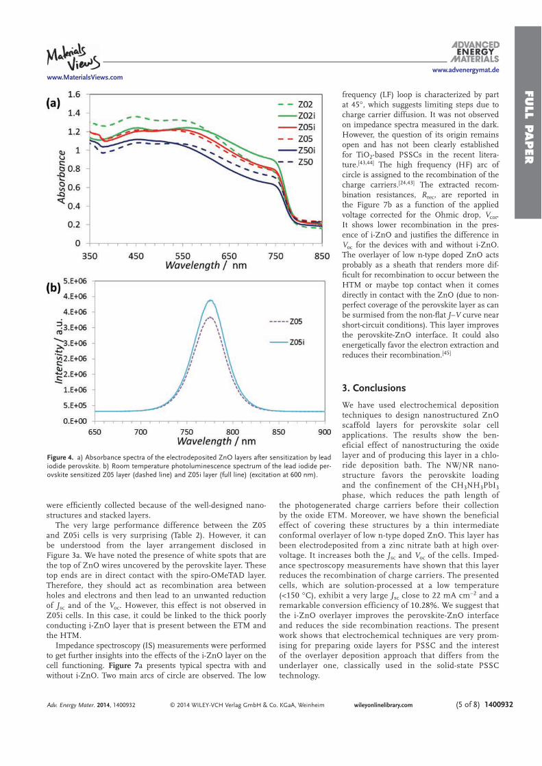
FULL PAPER
© 2014 WILEY-VCH Verlag GmbH & Co. KGaA, Weinheim (5 of 8) 1400932wileyonlinelibrary.com
were effi ciently collected because of the well-designed nano-structures and stacked layers.
The very large performance difference between the Z05 and Z05i cells is very surprising (Table 2 ). However, it can be understood from the layer arrangement disclosed in Figure 3 a. We have noted the presence of white spots that are the top of ZnO wires uncovered by the perovskite layer. These top ends are in direct contact with the spiro-OMeTAD layer. Therefore, they should act as recombination area between holes and electrons and then lead to an unwanted reduction of J sc and of the V oc . However, this effect is not observed in Z05i cells. In this case, it could be linked to the thick poorly conducting i-ZnO layer that is present between the ETM and the HTM.
Impedance spectroscopy (IS) measurements were performed to get further insights into the effects of the i-ZnO layer on the cell functioning. Figure 7 a presents typical spectra with and without i-ZnO. Two main arcs of circle are observed. The low
frequency (LF) loop is characterized by part at 45°, which suggests limiting steps due to charge carrier diffusion. It was not observed on impedance spectra measured in the dark. However, the question of its origin remains open and has not been clearly established for TiO 2 -based PSSCs in the recent litera-ture. [ 43,44 ] The high frequency (HF) arc of circle is assigned to the recombination of the charge carriers. [ 24,43 ] The extracted recom-bination resistances, R rec , are reported in the Figure 7 b as a function of the applied voltage corrected for the Ohmic drop, V cor . It shows lower recombination in the pres-ence of i-ZnO and justifi es the difference in V oc for the devices with and without i-ZnO. The overlayer of low n-type doped ZnO acts probably as a sheath that renders more dif-fi cult for recombination to occur between the HTM or maybe top contact when it comes directly in contact with the ZnO (due to non-perfect coverage of the perovskite layer as can be surmised from the non-fl at J – V curve near short-circuit conditions). This layer improves the perovskite-ZnO interface. It could also energetically favor the electron extraction and reduces their recombination. [ 45 ]
3. Conclusions
We have used electrochemical deposition techniques to design nanostructured ZnO scaffold layers for perovskite solar cell applications. The results show the ben-eficial effect of nanostructuring the oxide layer and of producing this layer in a chlo-ride deposition bath. The NW/NR nano-structure favors the perovskite loading and the confinement of the CH 3 NH 3 PbI 3 phase, which reduces the path length of
the photogenerated charge carriers before their collection by the oxide ETM. Moreover, we have shown the beneficial effect of covering these structures by a thin intermediate conformal overlayer of low n-type doped ZnO. This layer has been electrodeposited from a zinc nitrate bath at high over-voltage. It increases both the J sc and V oc of the cells. Imped-ance spectroscopy measurements have shown that this layer reduces the recombination of charge carriers. The presented cells, which are solution-processed at a low temperature (<150 °C), exhibit a very large J sc close to 22 mA cm −2 and a remarkable conversion efficiency of 10.28%. We suggest that the i-ZnO overlayer improves the perovskite-ZnO interface and reduces the side recombination reactions. The present work shows that electrochemical techniques are very prom-ising for preparing oxide layers for PSSC and the interest of the overlayer deposition approach that differs from the underlayer one, classically used in the solid-state PSSC technology.
Adv. Energy Mater. 2014, 1400932
www.MaterialsViews.comwww.advenergymat.de
Figure 4. a) Absorbance spectra of the electrodeposited ZnO layers after sensitization by lead iodide perovskite. b) Room temperature photoluminescence spectrum of the lead iodide per-ovskite sensitized Z05 layer (dashed line) and Z05i layer (full line) (excitation at 600 nm).
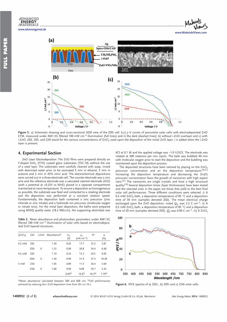
FULL PAPER
© 2014 WILEY-VCH Verlag GmbH & Co. KGaA, Weinheim1400932 (6 of 8) wileyonlinelibrary.com
4. Experimental Section
ZnO Layer Electrodeposition : The ZnO fi lms were prepared directly on F-doped SnO 2 (FTO) coated glass substrates (TEC-10) without the use of a seed layer. The substrates were carefully cleaned with soap, rinsed with deionized water prior to be sonicated 5 min in ethanol, 5 min in acetone and 2 min in 45% nitric acid. The electrochemical depositions were carried out in a three-electrode cell. The counter-electrode was a zinc wire and the reference electrode was a saturated calomel electrode (SCE) (with a potential at +0.25V vs NHE) placed in a separate compartment maintained at room temperature. To ensure a deposition as homogeneous as possible, the substrate was fi xed and contacted to a rotating electrode and the deposition was performed at a constant rotation speed. Fundamentally, the deposition bath contained a zinc precursor (zinc chloride or zinc nitrate) and a hydroxide ion precursor (molecular oxygen or nitrate ions). For the initial layer deposition, the baths were prepared using MilliQ quality water (18.2 MΩ.cm), the supporting electrolyte was
KCl at 0.1 M and the applied voltage was –1.0 V/SCE. The electrode was rotated at 300 rotations per min (rpm). The bath was bubbled 40 min with molecular oxygen prior to start the deposition and the bubbling was maintained upon the deposition process. The deposited structures have been tailored by playing on the ZnCl 2
precursor concentration and on the deposition temperature. [ 30,31 ] Increasing the deposition temperature and decreasing the Zn(II) precursor concentration favor the growth of nanowires with high aspect ratio. [ 31 ] The nanowires are single crystals and have a high structural quality. [ 19 ] Several deposition times (layer thicknesses) have been tested and the retained ones in the paper are those that yield to the best fi nal solar cell performances. Three different conditions were selected. i) A 0.2 mM ZnCl 2 bath, a deposition temperature of 85 °C and a deposition time of 30 min (samples denoted Z02). The mean electrical charge exchanged upon the ZnO deposition, noted Q d , was 2.2 C cm −2 . ii) A 0.5 mM ZnCl 2 bath, a deposition temperature of 85 °C and a deposition time of 20 min (samples denoted Z05). Q d was 0.90 C cm −2 . iii) A ZnCl 2
Adv. Energy Mater. 2014, 1400932
www.MaterialsViews.comwww.advenergymat.de
Figure 5. a) Schematic drawing and cross-sectional SEM view of the Z05i cell. b,c) J – V curves of perovskite solar cells with electrodeposited ZnO ETM, measured under AM1.5G fi ltered 100 mW cm −2 illumination (full lines) and in the dark (dashed lines): b) without i-ZnO overlayer and c) with i-ZnO. Z02, Z05, and Z50 stand for the various concentrations of ZnCl 2 used upon the deposition of the initial ZnO layer. i is added when the i-ZnO layer is present.
Table 2. Mean absorbance and photovoltaic parameters under AM1.5G fi ltered 100 mW cm −2 illumination of solar cells based on electrodepos-ited ZnO layered structures.
[ZnCl 2 ] Cell i-ZnO Absorbance a) V oc [V]
J sc [mA cm −2 ]
FF η [%]
0.2 mM Z02 1.30 0.65 17.7 33.2 3.81
Z02i X 1.23 0.90 20.8 34.4 6.48
0.5 mM Z05 1.19 0.24 13.3 29.5 0.95
Z05i X 1.20 0.99 21.9 47.3 10.28
5 mM Z50 1.05 0.89 11.4 36.4 3.69
Z50i X 1.00 0.96 9.09 39.7 3.45
0.95 b) 16.6 b) 45.5 b) 7.19 b)
a) Mean absorbance calculated between 500 and 600 nm; b) Cell performances achieved by reducing the i-ZnO deposition time from 20 s to 10 s. Figure 6. IPCE spectra of a) Z02i , b) Z05i and c) Z50i solar cells.
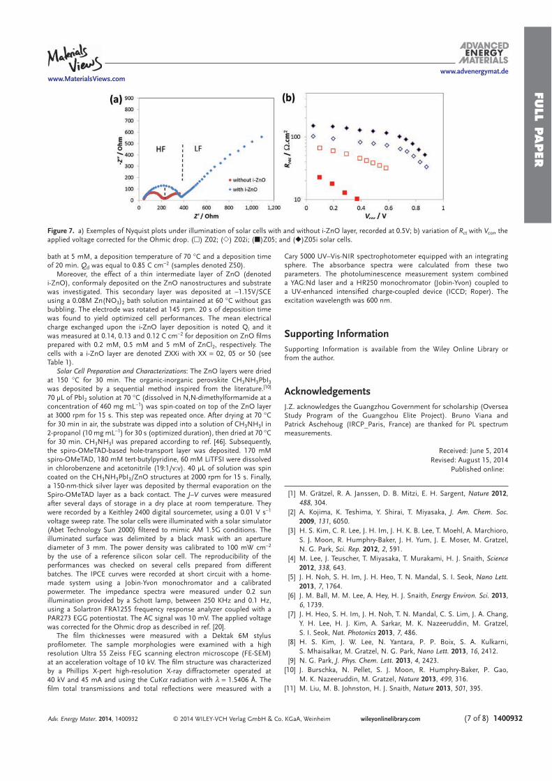
FULL PAPER
© 2014 WILEY-VCH Verlag GmbH & Co. KGaA, Weinheim (7 of 8) 1400932wileyonlinelibrary.comAdv. Energy Mater. 2014, 1400932
www.MaterialsViews.comwww.advenergymat.de
bath at 5 mM, a deposition temperature of 70 °C and a deposition time of 20 min. Q d was equal to 0.85 C cm −2 (samples denoted Z50). Moreover, the effect of a thin intermediate layer of ZnO (denoted
i-ZnO), conformaly deposited on the ZnO nanostructures and substrate was investigated. This secondary layer was deposited at –1.15V/SCE using a 0.08M Zn(NO 3 ) 2 bath solution maintained at 60 °C without gas bubbling. The electrode was rotated at 145 rpm. 20 s of deposition time was found to yield optimized cell performances. The mean electrical charge exchanged upon the i-ZnO layer deposition is noted Q i and it was measured at 0.14, 0.13 and 0.12 C cm −2 for deposition on ZnO fi lms prepared with 0.2 mM, 0.5 mM and 5 mM of ZnCl 2 , respectively. The cells with a i-ZnO layer are denoted ZXXi with XX = 02, 05 or 50 (see Table 1 ). Solar Cell Preparation and Characterizations : The ZnO layers were dried
at 150 °C for 30 min. The organic-inorganic perovskite CH 3 NH 3 PbI 3 was deposited by a sequential method inspired from the literature. [ 10 ] 70 µL of PbI 2 solution at 70 °C (dissolved in N,N-dimethylformamide at a concentration of 460 mg mL −1 ) was spin-coated on top of the ZnO layer at 3000 rpm for 15 s. This step was repeated once. After drying at 70 °C for 30 min in air, the substrate was dipped into a solution of CH 3 NH 3 I in 2-propanol (10 mg mL −1 ) for 30 s (optimized duration), then dried at 70 °C for 30 min. CH 3 NH 3 I was prepared according to ref. [ 46 ] . Subsequently, the spiro-OMeTAD-based hole-transport layer was deposited. 170 mM spiro-OMeTAD, 180 mM tert-butylpyridine, 60 mM LiTFSI were dissolved in chlorobenzene and acetonitrile (19:1/v:v). 40 µL of solution was spin coated on the CH 3 NH 3 PbI 3 /ZnO structures at 2000 rpm for 15 s. Finally, a 150-nm-thick silver layer was deposited by thermal evaporation on the Spiro-OMeTAD layer as a back contact. The J – V curves were measured after several days of storage in a dry place at room temperature. They were recorded by a Keithley 2400 digital sourcemeter, using a 0.01 V s −1 voltage sweep rate. The solar cells were illuminated with a solar simulator (Abet Technology Sun 2000) fi ltered to mimic AM 1.5G conditions. The illuminated surface was delimited by a black mask with an aperture diameter of 3 mm. The power density was calibrated to 100 mW cm −2 by the use of a reference silicon solar cell. The reproducibility of the performances was checked on several cells prepared from different batches. The IPCE curves were recorded at short circuit with a home-made system using a Jobin-Yvon monochromator and a calibrated powermeter. The impedance spectra were measured under 0.2 sun illumination provided by a Schott lamp, between 250 KHz and 0.1 Hz, using a Solartron FRA1255 frequency response analyzer coupled with a PAR273 EGG potentiostat. The AC signal was 10 mV. The applied voltage was corrected for the Ohmic drop as described in ref. [ 20 ] . The fi lm thicknesses were measured with a Dektak 6M stylus
profi lometer. The sample morphologies were examined with a high resolution Ultra 55 Zeiss FEG scanning electron microscope (FE-SEM) at an acceleration voltage of 10 kV. The fi lm structure was characterized by a Phillips X-pert high-resolution X-ray diffractometer operated at 40 kV and 45 mA and using the CuKα radiation with λ = 1.5406 Å. The fi lm total transmissions and total refl ections were measured with a
Cary 5000 UV–Vis-NIR spectrophotometer equipped with an integrating sphere. The absorbance spectra were calculated from these two parameters. The photoluminescence measurement system combined a YAG:Nd laser and a HR250 monochromator (Jobin-Yvon) coupled to a UV-enhanced intensifi ed charge-coupled device (ICCD; Roper). The excitation wavelength was 600 nm.
Supporting Information
Supporting Information is available from the Wiley Online Library or from the author.
Acknowledgements
J.Z. acknowledges the Guangzhou Government for scholarship (Oversea Study Program of the Guangzhou Elite Project). Bruno Viana and Patrick Aschehoug (IRCP_Paris, France) are thanked for PL spectrum measurements.
Received: June 5, 2014 Revised: August 15, 2014
Published online:
[1] M. Grätzel , R. A. Janssen , D. B. Mitzi , E. H. Sargent , Nature 2012 , 488 , 304 .
[2] A. Kojima , K. Teshima , Y. Shirai , T. Miyasaka , J. Am. Chem. Soc. 2009 , 131 , 6050 .
[3] H. S. Kim , C. R. Lee , J. H. Im , J. H. K. B. Lee , T. Moehl , A. Marchioro , S. J. Moon , R. Humphry-Baker , J. H. Yum , J. E. Moser , M. Gratzel , N. G. Park , Sci. Rep. 2012 , 2 , 591 .
[4] M. Lee , J. Teuscher , T. Miyasaka , T. Murakami , H. J. Snaith , Science 2012 , 338 , 643 .
[5] J. H. Noh , S. H. Im , J. H. Heo , T. N. Mandal , S. I. Seok , Nano Lett. 2013 , 7 , 1764 .
[6] J. M. Ball , M. M. Lee , A. Hey , H. J. Snaith , Energy Environ. Sci. 2013 , 6 , 1739 .
[7] J. H. Heo , S. H. Im , J. H. Noh , T. N. Mandal , C. S. Lim , J. A. Chang , Y. H. Lee , H. J. Kim , A. Sarkar , M. K. Nazeeruddin , M. Gratzel , S. I. Seok , Nat. Photonics 2013 , 7 , 486 .
[8] H. S. Kim , J. W. Lee , N. Yantara , P. P. Boix , S. A. Kulkarni , S. Mhaisalkar , M. Gratzel , N. G. Park , Nano Lett. 2013 , 16 , 2412 .
[9] N. G. Park , J. Phys. Chem. Lett. 2013 , 4 , 2423 . [10] J. Burschka , N. Pellet , S. J. Moon , R. Humphry-Baker , P. Gao , M. K. Nazeeruddin , M. Gratzel , Nature 2013 , 499 , 316 .
[11] M. Liu , M. B. Johnston , H. J. Snaith , Nature 2013 , 501 , 395 .
Figure 7. a) Exemples of Nyquist plots under illumination of solar cells with and without i-ZnO layer, recorded at 0.5V; b) variation of R ct with V cor , the applied voltage corrected for the Ohmic drop. ( h ) Z02; (e) Z02i; (j)Z05; and (r)Z05i solar cells.
FULL PAPER
© 2014 WILEY-VCH Verlag GmbH & Co. KGaA, Weinheim1400932 (8 of 8) wileyonlinelibrary.com Adv. Energy Mater. 2014, 1400932
www.MaterialsViews.comwww.advenergymat.de
[12] a) S. D. Stranks , G. E. Eperon , G. Grancini , C. Manelaou , M. J. P. Alcocer , T. Leijteins , L. M. Herz , A. Petrozza , H. J. Snaith , Sci-
ence 2013 , 342 , 341 ; b) H. S. Kim , I. Mora-Sero , V. Gonzalez-Pedro , F. Fabregat-Santiago , E. J. Juarez-Perez , N. G. Park , J. Bisquert , Nat.
Commun. 2013 , 4 , 2242 . [13] G. Xing , N. Mathews , S. Sun , S. S. Lim , Y. M. Lam , M. Grätzel , S. Mhaisalkar , T. C. Sum , Science 2013 , 342 , 344 .
[14] R. F. Service , Science 2014 , 344 , 458 . [15] a) F. Matteocci , S. Razza , F. Di Giacomo , S. Casaluci , G. Mincuzzi , T. M. Brown , A. D'Epifanio , S. Licoccia , A. Di Carlo , Phys. Chem.
Chem. Phys. 2014 , 16 , 3918 ; b) J. Seo , S. Park , Y. C. Kim , N. J. Jeon , J. H. Noh , S. C. Yoon , S. I. Seok , Energy Environ. Sci. 2014 , 7 , 2642 .
[16] D. Liu , T. L. Kelly , Nat. Photonics 2014 , 8 , 133 . [17] E. J. Juarez-Perez , M. Wussler , F. Fabregat-Santiago , K. Lakus-Wollny , E. Mankel , T. Mayer , W. Jaegermann , I. Mora-Sero , J. Phys. Chem. Lett. 2014 , 5 , 680 .
[18] Z. L. Wang , J. Phys. Condens. Matter 2004 , 16 , R829 . [19] O. Lupan , V. M. Guérin , I. M. Tiginyanu , V. V. Ursaki , L. Chow , H. Heinrich , T. Pauporté , J. Photochem. Photobiol. A 2010 , 211 , 65 .
[20] C. Magne , T. Moehl , M. Urien , M. Grätzel , T. Pauporté , J. Mater.
Chem. A 2013 , 1 , 2079 . [21] L. Vayssière , Adv. Mater. 2003 , 15 , 464 . [22] J. Elias , C. Levy-Clement , M. Bechelany , J. Michler , G. Y. Wang , Z. Wang , L. Philippe , Adv. Mater. 2010 , 22 , 1607 .
[23] A. Goux , T. Pauporté , T. Yoshida , D. Lincot , Langmuir 2006 , 22 , 10545 .
[24] M. H. Kumar , N. Yantara , S. Dharani , M. Graetzel , S. Mhaisalkar , P. P. Boix , N. Mathews , Chem. Commun. 2013 , 49 , 11089 .
[25] H. Elbelghiti , T. Pauporté , D. Lincot , Phys. Status Solidi (a) 2008 , 205 , 2360 .
[26] D. Q. Bi , G. Boschloo , S. Schwarzmuller , L. Yang , E. M. J. Johansson , A. Hagfeldt , Nanoscale 2013 , 5 , 11686 .
[27] J. H. Qiu , Y. C. Qiu , K. Y. Yan , M. Zhong , C. Mu , H. Yan , S. H. Yang , Nanoscale 2013 , 5 , 3245 .
[28] F. J. Ramos , M. C. Lopez-Santos , E. Guillen , M. K. Nazeeruddin , M. Gratzel , A. R. Gonzalez-Elipe , S. Ahmad , ChemPhysChem 2014 , 15 , 1148 .
[29] V. M. Guérin , Th. Pauporté , Energy Environ. Sci. 2011 , 4 , 2971 . [30] T. Pauporté , E. Jouanno , F. Pellé , B. Viana , P. Aschehoug , J. Phys.
Chem. C 2009 , 113 , 10422 . [31] T. Pauporté , G. Bataille , L. Joulaud , F. J. Vermersch , J. Phys. Chem.
C 2010 , 114 , 194 . [32] M. Izaki , T. Ohta , M. Kondo , T. Takahashi , M. Fariza , J. Sasano , T. Shinagawa , T. Pauporté , ACS Appl. Mater. Interface 2014 , 6 , 13461 .
[33] I. Mora-Sero , F. Fabregat-Santiago , B. Denier , J. Bisquert , R. Tena-Zaera , J. Elias , C. Levy-Clement , Appl. Phys. Lett. 2006 , 89 , 203117 .
[34] R. Könenkamp , K. Boedecker , M. C. Lux-Steiner , M. Poschenrieder , F. Zenia , C. Lévy-Clement , S. Wagner , Appl. Phys. Lett. 2000 , 77 , 2575 .
[35] J. Rousset , E. Saucedo , D. Lincot , Chem. Mater. 2009 , 21 , 534 . [36] T. Shinagawa , M. Chigane , K. Murase , M. Izaki , J. Phys. Chem. C
2012 , 116 , 15925 . [37] E. Guillen , E. Azaceta , A. Vega-Poot , J. Idigoras , J. Echeberria , A. Anta , R. Tena-Zaera , J. Phys. Chem. C 2013 , 117 , 13365 .
[38] T. Yoshida , J. Zhang , D. Komatsu , S. Sawatani , H. Minoura , T. Pauporté , D. Lincot , T. Oekermann , D. Schlettwein , H. Tada , D. Wörhle , K. Funabiki , M. Matsui , H. Miura , H. Yanagi , Adv. Funct.
Mater. 2009 , 19 , 17 . [39] C. Magne , M. Urien , I. Ciofi ni , T. Tugsuza , T. Pauporté , RSC Adv.
2012 , 2 , 11836 . [40] E. Puyoo , G. Rey , E. Appert , V. Consonni , D. Bellet , J. Phys. Chem. C
2012 , 116 , 18117 . [41] M. Saito , S. Fujihara , Energy. Environ. Sci. 2008 , 1 , 280 . [42] N. Memarian , I. Concina , A. Braga , S. M. Rozati , A. Vomiero , G. Sberveglieri , Angew. Chem. 2011 , 123 , 12529 .
[43] A. Dualeh , T. Moehl , N. Tétreault , J. Teuscher , P. Gao , M. K. Nazeeruddin , M. Grätzel , ACS Nano 2014 , 8 , 362 .
[44] V. Gonzalez-Pedro , E. J. Juarez-Perez , W. S. Arsyad , E. M. Barea , F. Fabregat-Santiago , I. Mora-Sero , J. Bisquert , Nano Lett. 2014 , 14 , 888 .
[45] M. Law , L. E. Greene , J. C. Johnson , R. Saykally , P. Yang , Nat. Mater. 2005 , 4 , 455 .
[46] L. Etgar , P. Gao , Z. Xue , Q. Pen , A. K. Chandiran , B. Liu , M. K. Nazeeruddin , M. Grätzel , J. Am. Chem. Soc. 2012 , 134 , 17396 .
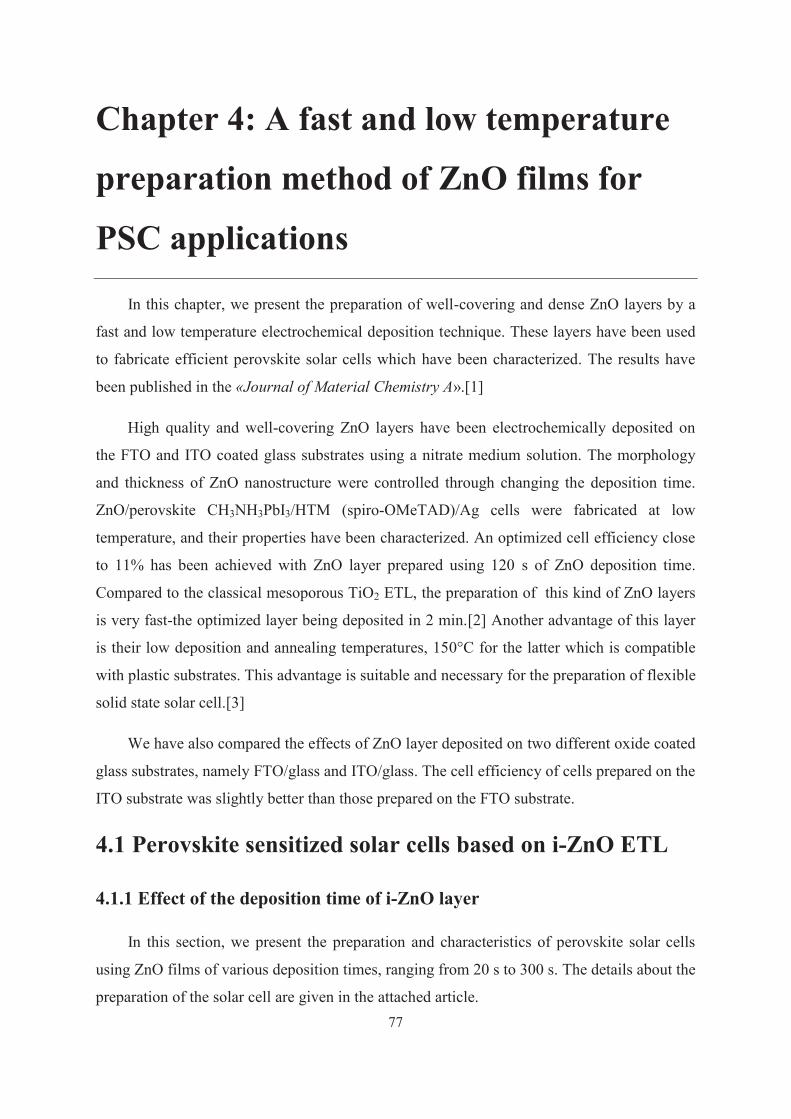
77
Chapter 4: A fast and low temperature
preparation method of ZnO films for
PSC applications
In this chapter, we present the preparation of well-covering and dense ZnO layers by a
fast and low temperature electrochemical deposition technique. These layers have been used
to fabricate efficient perovskite solar cells which have been characterized. The results have
been published in the «Journal of Material Chemistry A».[1]
High quality and well-covering ZnO layers have been electrochemically deposited on
the FTO and ITO coated glass substrates using a nitrate medium solution. The morphology
and thickness of ZnO nanostructure were controlled through changing the deposition time.
ZnO/perovskite CH3NH3PbI3/HTM (spiro-OMeTAD)/Ag cells were fabricated at low
temperature, and their properties have been characterized. An optimized cell efficiency close
to 11% has been achieved with ZnO layer prepared using 120 s of ZnO deposition time.
Compared to the classical mesoporous TiO2 ETL, the preparation of this kind of ZnO layers
is very fast-the optimized layer being deposited in 2 min.[2] Another advantage of this layer
is their low deposition and annealing temperatures, 150°C for the latter which is compatible
with plastic substrates. This advantage is suitable and necessary for the preparation of flexible
solid state solar cell.[3]
We have also compared the effects of ZnO layer deposited on two different oxide coated
glass substrates, namely FTO/glass and ITO/glass. The cell efficiency of cells prepared on the
ITO substrate was slightly better than those prepared on the FTO substrate.
4.1 Perovskite sensitized solar cells based on i-ZnO ETL
4.1.1 Effect of the deposition time of i-ZnO layer
In this section, we present the preparation and characteristics of perovskite solar cells
using ZnO films of various deposition times, ranging from 20 s to 300 s. The details about the
preparation of the solar cell are given in the attached article.
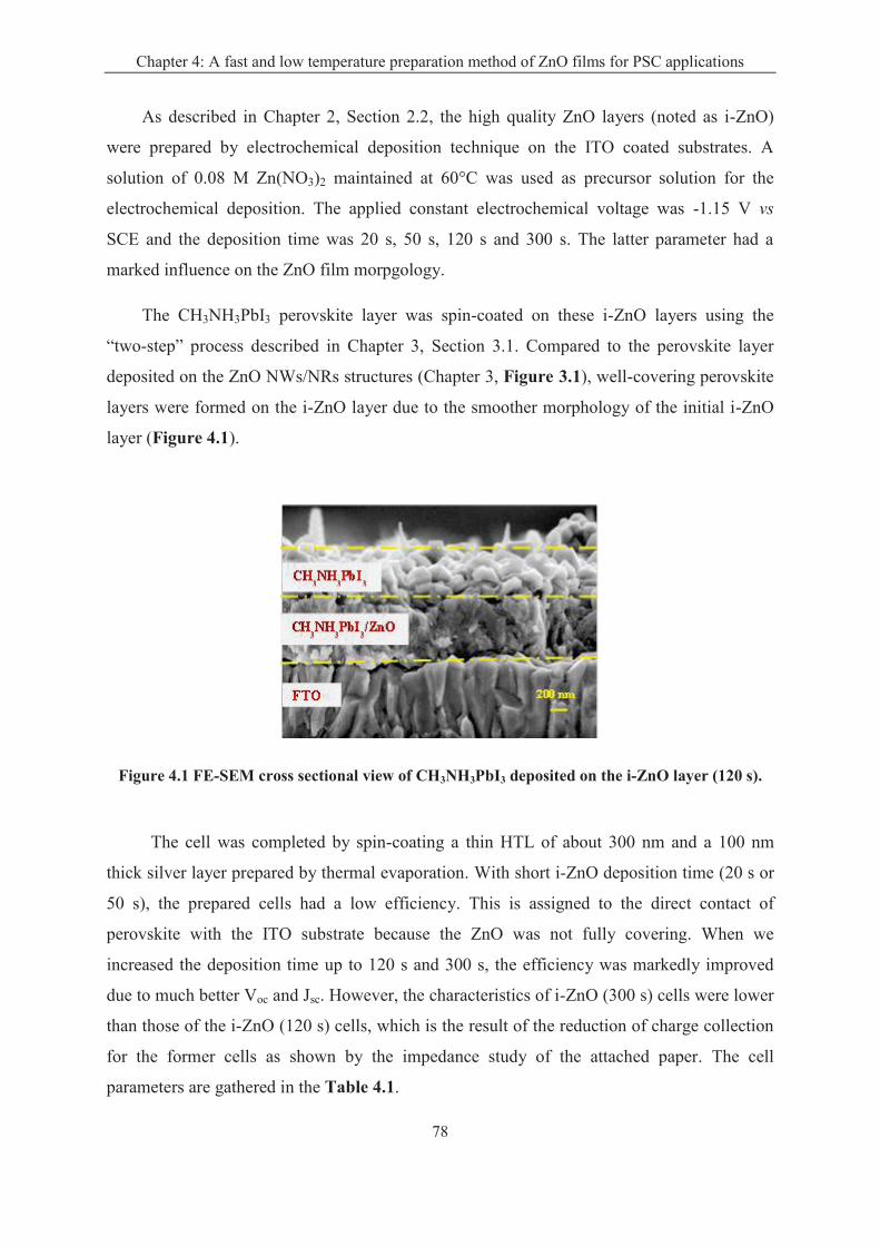
Chapter 4: A fast and low temperature preparation method of ZnO films for PSC applications
78
As described in Chapter 2, Section 2.2, the high quality ZnO layers (noted as i-ZnO)
were prepared by electrochemical deposition technique on the ITO coated substrates. A
solution of 0.08 M Zn(NO3)2 maintained at 60°C was used as precursor solution for the
electrochemical deposition. The applied constant electrochemical voltage was -1.15 V vs
SCE and the deposition time was 20 s, 50 s, 120 s and 300 s. The latter parameter had a
marked influence on the ZnO film morpgology.
The CH3NH3PbI3 perovskite layer was spin-coated on these i-ZnO layers using the
“two-step” process described in Chapter 3, Section 3.1. Compared to the perovskite layer
deposited on the ZnO NWs/NRs structures (Chapter 3, Figure 3.1), well-covering perovskite
layers were formed on the i-ZnO layer due to the smoother morphology of the initial i-ZnO
layer (Figure 4.1).
Figure 4.1 FE-SEM cross sectional view of CH3NH3PbI3 deposited on the i-ZnO layer (120 s).
The cell was completed by spin-coating a thin HTL of about 300 nm and a 100 nm
thick silver layer prepared by thermal evaporation. With short i-ZnO deposition time (20 s or
50 s), the prepared cells had a low efficiency. This is assigned to the direct contact of
perovskite with the ITO substrate because the ZnO was not fully covering. When we
increased the deposition time up to 120 s and 300 s, the efficiency was markedly improved
due to much better Voc and Jsc. However, the characteristics of i-ZnO (300 s) cells were lower
than those of the i-ZnO (120 s) cells, which is the result of the reduction of charge collection
for the former cells as shown by the impedance study of the attached paper. The cell
parameters are gathered in the Table 4.1.
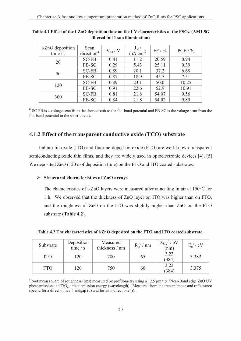
Chapter 4: A fast and low temperature preparation method of ZnO films for PSC applications
79
Table 4.1 Effect of the i-ZnO deposition time on the I-V characteristics of the PSCs. (AM1.5G filtered full 1 sun illumination)
i-ZnO deposition
time / s
Scan
directiona
Voc / V Jsc /
mA.cm-2
FF / % PCE / %
20 SC-FB 0.41 11.2 20.59 0.94
FB-SC 0.29 5.43 25.11 0.39
50 SC-FB 0.89 20.1 37.2 6.68
FB-SC 0.87 18.9 45.5 7.51
120 SC-FB 0.89 23.1 50.0 10.25
FB-SC 0.91 22.6 52.9 10.91
300 SC-FB 0.81 21.8 54.07 9.56
FB-SC 0.84 21.8 54.02 9.89
a SC-FB is a voltage scan from the short circuit to the flat-band potential and FB-SC is the voltage scan from the
flat-band potential to the short-circuit.
4.1.2 Effect of the transparent conductive oxide (TCO) substrate
Indium-tin oxide (ITO) and fluorine-doped tin oxide (FTO) are well-known transparent
semiconducting oxide thin films, and they are widely used in optoelectronic devices.[4], [5]
We deposited ZnO (120 s of deposition time) on the FTO and ITO coated substrates.
Ø Structural characteristics of ZnO arrays
The characteristics of i-ZnO layers were measured after annealing in air at 150°C for
1 h. We observed that the thickness of ZnO layer on ITO was higher than on FTO,
and the roughness of ZnO on the ITO was slightly higher than ZnO on the FTO
substrate (Table 4.2).
Table 4.2 The characteristics of i-ZnO deposited on the FTO and ITO coated substrate.
Substrate Deposition
time / s
Measured
thickness / nm Rq
c / nm
lUVd / eV
(nm) Eg
e / eV
ITO 120 780 65 3.23
(384) 3.382
FTO 120 750 60 3.23
(384) 3.375
cRoot mean square of roughness (rms) measured by profilometry using a 12.5 μm tip.
dNear-Band edge ZnO UV
photoemission and TiO2 defect emission energy (wavelength). eMeasured from the transmittance and reflectance
spectra for a direct optical bandgap (d) and for an indirect one (i).
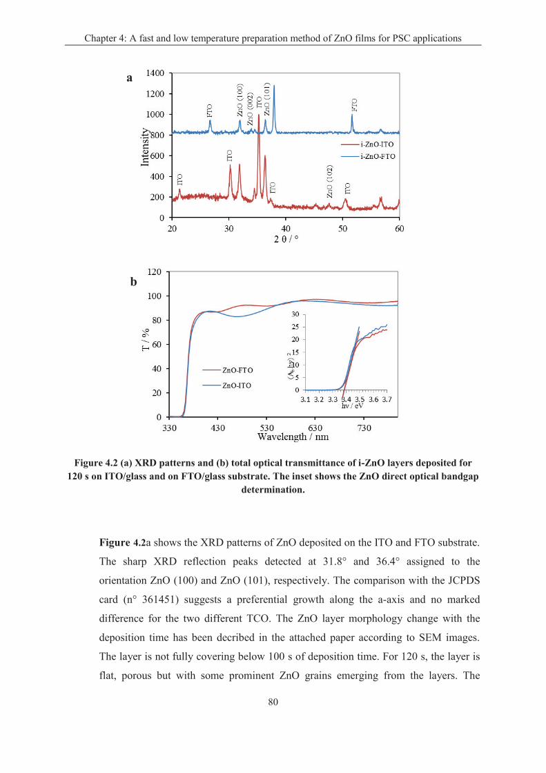
Chapter 4: A fast and low temperature preparation method of ZnO films for PSC applications
80
Figure 4.2 (a) XRD patterns and (b) total optical transmittance of i-ZnO layers deposited for 120 s on ITO/glass and on FTO/glass substrate. The inset shows the ZnO direct optical bandgap
determination.
Figure 4.2a shows the XRD patterns of ZnO deposited on the ITO and FTO substrate.
The sharp XRD reflection peaks detected at 31.8° and 36.4° assigned to the
orientation ZnO (100) and ZnO (101), respectively. The comparison with the JCPDS
card (n° 361451) suggests a preferential growth along the a-axis and no marked
difference for the two different TCO. The ZnO layer morphology change with the
deposition time has been decribed in the attached paper according to SEM images.
The layer is not fully covering below 100 s of deposition time. For 120 s, the layer is
flat, porous but with some prominent ZnO grains emerging from the layers. The
a
b
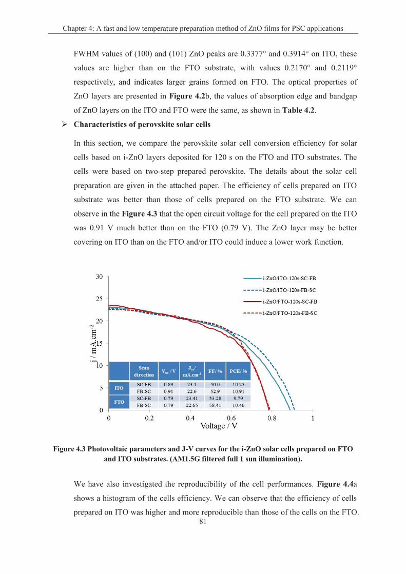
Chapter 4: A fast and low temperature preparation method of ZnO films for PSC applications
81
FWHM values of (100) and (101) ZnO peaks are 0.3377° and 0.3914° on ITO, these
values are higher than on the FTO substrate, with values 0.2170° and 0.2119°
respectively, and indicates larger grains formed on FTO. The optical properties of
ZnO layers are presented in Figure 4.2b, the values of absorption edge and bandgap
of ZnO layers on the ITO and FTO were the same, as shown in Table 4.2.
Ø Characteristics of perovskite solar cells
In this section, we compare the perovskite solar cell conversion efficiency for solar
cells based on i-ZnO layers deposited for 120 s on the FTO and ITO substrates. The
cells were based on two-step prepared perovskite. The details about the solar cell
preparation are given in the attached paper. The efficiency of cells prepared on ITO
substrate was better than those of cells prepared on the FTO substrate. We can
observe in the Figure 4.3 that the open circuit voltage for the cell prepared on the ITO
was 0.91 V much better than on the FTO (0.79 V). The ZnO layer may be better
covering on ITO than on the FTO and/or ITO could induce a lower work function.
Figure 4.3 Photovoltaic parameters and J-V curves for the i-ZnO solar cells prepared on FTO and ITO substrates. (AM1.5G filtered full 1 sun illumination).
We have also investigated the reproducibility of the cell performances. Figure 4.4a
shows a histogram of the cells efficiency. We can observe that the efficiency of cells
prepared on ITO was higher and more reproducible than those of the cells on the FTO.
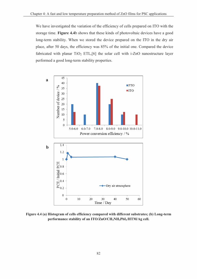
Chapter 4: A fast and low temperature preparation method of ZnO films for PSC applications
82
We have investigated the variation of the efficiency of cells prepared on ITO with the
storage time. Figure 4.4b shows that these kinds of photovoltaic devices have a good
long-term stability. When we stored the device prepared on the ITO in the dry air
place, after 50 days, the efficiency was 85% of the initial one. Compared the device
fabricated with planar TiO2 ETL,[6] the solar cell with i-ZnO nanostructure layer
performed a good long-term stability properties.
Figure 4.4 (a) Histogram of cells efficiency compared with different substrates; (b) Long-term performance stability of an ITO/ZnO/CH3NH3PbI3/HTM/Ag cell.
a
b
Chapter 4: A fast and low temperature preparation method of ZnO films for PSC applications
83
4.2 Conclusion
In this chapter, we have prepared electrochemically ZnO films by a fast and low
temperature technique in a zinc nitrate medium. The well crystallized ZnO could be obtained
after only two minutes of electrochemical deposition time at 60°C, and a subsequent drying
step at 150°C before the cell fabrication. The best efficiency of CH3NH3PbI3 sensitized ZnO
solar cell was close to 11% with an optimized ZnO layer deposition time of two minutes. We
also discussed the characteristics of ZnO layer deposited on the different TCO substrates. The
cells were prepared on ITO had a better result than those prepared using FTO coated glass
substrates. Moreover, we have been able to prepare perovskite solar cells with i-ZnO ETL on
ITO-coated polyethylene terephthalate flexible substrate. The results are described in the
attached paper.
References
[1] J. Zhang, E. J. Juárez-Pérez, I. Mora-Seró, B. Viana, and T. Pauporté, “Fast and low
temperature growth of electron transport layers for efficient perovskite solar cells,” J
Mater Chem A, vol. 3, no. 9, pp. 4909-4915, Jan. 2015.
[2] S. Dharani, H. A. Dewi, R. R. Prabhakar, T. Baikie, C. Shi, D. Yonghua, N. Mathews, P.
P. Boix, and S. G. Mhaisalkar, “Incorporation of Cl into sequentially deposited lead
halide perovskite films for highly efficient mesoporous solar cells,” Nanoscale, vol. 6,
no. 22, pp. 13854–13860, Sep. 2014.
[3] M. H. Kumar, N. Yantara, S. Dharani, M. Graetzel, S. Mhaisalkar, P. P. Boix, and N.
Mathews, “Flexible, low-temperature, solution processed ZnO-based perovskite solid
state solar cells,” Chem. Commun., vol. 49, no. 94, pp. 11089–11091, Oct. 2013.
[4] M. Xu, G. Liu, X. Li, H. Wang, Y. Rong, Z. Ku, M. Hu, Y. Yang, L. Liu, T. Liu, J.
Chen, and H. Han, “Efficient monolithic solid-state dye-sensitized solar cell with a low-
cost mesoscopic carbon based screen printable counter electrode,” Org. Electron., vol.
14, no. 2, pp. 628–634, Feb. 2013.
[5] T. Minami, “Transparent conducting oxide semiconductors for transparent electrodes”
Semicond. Sci. Technol., vol. 20, no. 4, pp. S35–S44, Apr. 2005.

Chapter 4: A fast and low temperature preparation method of ZnO films for PSC applications
84
[6] H. Zhou, Q. Chen, G. Li, S. Luo, T. -b. Song, H.-S. Duan, Z. Hong, J. You, Y. Liu, and
Y. Yang, “Interface engineering of highly efficient perovskite solar cells” Science, vol.
345, no. 6196, pp. 542–546, Aug. 2014.
Fast and low temperature growth of electrontransport layers for efficient perovskite solar cells†
Jie Zhang,a Emilio Jose Juarez-Perez,b Ivan Mora-Sero,b Bruno Vianaa
and Thierry Pauporte*a
We describe a fast, simple and low temperature electrochemical technique for the preparation of zinc oxide
layers on rigid and flexible substrates. The layers, prepared from a zinc nitrate precursor, are of high
structural and optical quality. They have been optimized to be applied as efficient electron transport
layers in CH3NH3PbI3-sensitized perovskite solar cells (PSCs). We show that an electrodeposition time of
only two minutes and a low processing temperature are sufficient to fabricate solar cells with a power
conversion efficiency close to 11%, with a high short circuit current and a small J–V curve hysteresis. The
key parameters of the cell functioning have been analyzed over a large applied voltage range by the
impedance spectroscopy technique. The solar cell characteristic changes with the ZnO layer deposition
time are explained by the variation of the recombination and charge transfer resistances.
1. Introduction
Solution-processed organic and hybrid organic–inorganic solar
cells have been intensely developed during the last two
decades.1–3 Very recently, perovskite solar cells (PSCs) have
emerged as the most promising new generation of hybrid
photovoltaic devices.4–13 The power conversion efficiency of this
newcomer has increased fast and very recently a certied power
conversion efficiency (PCE) higher than 20% has been repor-
ted.14 The most extended perovskite materials used for the solar
light absorption and charge generation are hybrid organic–
inorganic compounds with a 3D crystal structure of general
formula CH3NH3PbX3 (with X ¼ Cl, Br or I). The electron and
hole charge collection is ensured by the two adjacent selective
contact phases that generate the driving force for the charge
separation. The electrons are usually selectively collected by a
wide bandgap oxide material, also called the electron transport
layer (ETL), while holes are selectively transferred to a hole
transport layer (HTL), usually made of an organic molecular
glass. Spiro-OMeTAD is the most common material employed
for this purpose.
Currently, most state-of-the-art PSCs utilize mesoporous
TiO2 scaffold layers on top of a compact titania layer to provide a
substrate on which the perovskite can be grown.7 The prepara-
tion of these layers requires annealing and sintering processes
at high temperature, typically 500 "C. On the other hand, other
wide bandgap oxides and low temperature processing of the
ETL are much less-documented. The low temperature and fast
processing are desirable to reduce the production cost and for
the preparation of exible lightweight devices on plastic
substrates. ZnO is a wide bandgap semiconductor with an
electron affinity similar to TiO2. It can be grown by various
techniques with a high structural quality at low temperature.15,16
It is therefore a very promising candidate for the PSC applica-
tion.17–24 Moreover, the conductivity of ZnO is several orders of
magnitude higher than the TiO2 one and that favors the elec-
tron transport toward the front contact.25,26 Kelly et al.21 have
recently reported remarkably high efficiency PSCs using a thin
layer of dense planar ZnO prepared by spin-coating. The review
of the literature on ZnO–PSCs also indicates that remarkably
high Jsc can be achieved with ZnO ETM.17,20
The present work focuses on the preparation by electro-
chemical deposition of ZnO layers with tailored properties. The
advantages of the technique include the deposition of high
quality materials at low temperature, the precise control of the
(nano)structure morphology and thickness, the control of the
electrical properties and the excellent electrical contact between
the deposited layers and the substrate.27–29 Hereaer, we
describe the fast and low temperature electrochemical growth
of fully covered ZnO layers using zinc nitrate as the deposition
precursor. We show that the deposited material is ZnO and is of
high optical and structural quality. The interest of using this
layer as an ETL is demonstrated. Aer sensitization by
aInstitut de Recherche de Chimie-Paris (IRCP), CNRS-Chimie ParisTech-Paris Sciences
et Lettres UMR8247, 11 rue Pierre et Marie Curie, 75005 Paris, France. E-mail: thierry.
[email protected] Jaume I, Department of Physics, Photovoltaic and Optoelectronic Devices
Group, Castellon de La Plana 12071, Spain
† Electronic supplementary information (ESI) available: SEM view of i-ZnO
deposit at short deposition time, Raman and photoluminescence spectra of the
i-ZnO layers, bandgap determination and photoluminescence of the
CH3NH3PbI3 layer, IPCE curves, Rs and capacitance cell parameters at various
voltages and exible cell characteristics. See DOI: 10.1039/c4ta06416j
Cite this: J. Mater. Chem. A, 2015, 3,4909
Received 24th November 2014Accepted 19th January 2015
DOI: 10.1039/c4ta06416j
www.rsc.org/MaterialsA
This journal is © The Royal Society of Chemistry 2015 J. Mater. Chem. A, 2015, 3, 4909–4915 | 4909
Journal ofMaterials Chemistry A
PAPER
Publi
shed
on 2
0 J
anuar
y 2
015. D
ow
nlo
aded
by U
niv
ersi
te P
ierr
e et
Mar
ie C
uri
e on 1
4/0
4/2
015 1
0:0
5:4
7.
View Article OnlineView Journal | View Issue
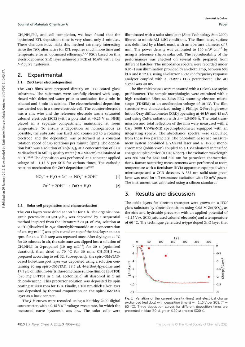
CH3NH3PbI3 and cell completion, we have found that the
optimized ETL deposition time is very short, only 2 minutes.
These characteristics make this method extremely interesting
since the TiO2 alternative for ETL requires much more time and
temperature for an optimized efficiency.4,5,7 PSCs based on this
electrodeposited ZnO layer achieved a PCE of 10.6% with a low
J–V curve hysteresis.
2. Experimental2.1. ZnO layer electrodeposition
The ZnO lms were prepared directly on ITO coated glass
substrates. The substrates were carefully cleaned with soap,
rinsed with deionized water prior to sonication for 5 min in
ethanol and 5 min in acetone. The electrochemical deposition
was carried out in a three-electrode cell. The counter-electrode
was a zinc wire and the reference electrode was a saturated
calomel electrode (SCE) (with a potential at +0.25 V vs. NHE)
placed in a separate compartment maintained at room
temperature. To ensure a deposition as homogeneous as
possible, the substrate was xed and connected to a rotating
electrode and the deposition was performed at a constant
rotation speed of 145 rotations per minute (rpm). The deposi-
tion bath was a solution of Zn(NO3)2 at a concentration of 0.08
M dissolved in MilliQ quality water (18.2 MU cm) maintained at
60 "C.30,31 The deposition was performed at a constant applied
voltage of #1.15 V per SCE for various times. The cathodic
reaction mechanism for ZnO deposition is:28,29
NO3# + H2O + 2e# / NO2
# + 2OH# (1)
Zn2+ + 2OH#/ ZnO + H2O (2)
2.2. Solar cell preparation and characterization
The ZnO layers were dried at 150 "C for 1 h. The organic–inor-
ganic perovskite CH3NH3PbI3 was deposited by a sequential
method inspired from the literature.6 70 mL of PbI2 solution at
70 "C (dissolved in N,N-dimethylformamide at a concentration
of 460mgmL#1) was spin-coated on top of the ZnO layer at 3000
rpm. for 15 s. This step was repeated once. Aer drying at 70 "C
for 30 minutes in air, the substrate was dipped into a solution of
CH3NH3I in 2-propanol (10 mg mL#1) for 30 s (optimized
duration), then dried at 70 "C for 30 min. CH3NH3I was
prepared according to ref. 32. Subsequently, the spiro-OMeTAD-
based hole-transport layer was deposited using a solution con-
taining 80 mg spiro-OMeTAD, 28.5 mL 4-tertbutylpyridine and
17.5 mL of lithium-bis(triuoromethanesulfonyl)imide (Li-TFSI)
(520 mg Li-TFSI in 1 mL acetonitrile) all dissolved in 1 ml
chlorobenzene. This precursor solution was deposited by spin
coating at 2000 rpm for 15 s. Finally, a 100 nm-thick silver layer
was deposited by thermal evaporation on the spiro-OMeTAD
layer as a back contact.
The J–V curves were recorded using a Keithley 2400 digital
sourcemeter, with a 0.15 V s#1 voltage sweep rate, for which the
measured curve hysteresis was low. The solar cells were
illuminated with a solar simulator (Abet Technology Sun 2000)
ltered to mimic AM 1.5G conditions. The illuminated surface
was delimited by a black mask with an aperture diameter of 3
mm. The power density was calibrated to 100 mW cm#2 by
using a reference silicon solar cell. The reproducibility of the
performances was checked on several cells prepared from
different batches. The impedance spectra were recorded under
0.95–1 sun illumination provided by a Schott lamp, between 600
kHz and 0.12 Hz, using a Solartron FRA1255 frequency response
analyzer coupled with a PAR273 EGG potentiostat. The AC
signal was 20 mV.
The lm thicknesses were measured with a Dektak 6M stylus
prolometer. The sample morphologies were examined with a
high resolution Ultra 55 Zeiss FEG scanning electron micro-
scope (FE-SEM) at an acceleration voltage of 10 kV. The lm
structure was characterized using a Phillips X-Pert high-reso-
lution X-ray diffractometer (XRD) operating at 40 kV and 45 mA
and using CuKa radiation with l ¼ 1.54056 A. The total trans-
mission and total reection of the lm were measured with a
Cary 5000 UV-Vis-NIR spectrophotometer equipped with an
integrating sphere. The absorbance spectra were calculated
from these two parameters. The photoluminescence measure-
ment system combined a YAG:Nd laser and a HR250 mono-
chromator (Jobin-Yvon) coupled to a UV-enhanced intensied
charge-coupled device (ICCD; Roper). The excitation wavelength
was 266 nm for ZnO and 600 nm for perovskite characteriza-
tions. Raman scattering measurements were performed at room
temperature with a Renishaw INVIA apparatus equipped with a
microscope and a CCD detector. A 532 nm solid-state green
laser was used for off-resonance excitation with 50 mW power.
The instrument was calibrated using a silicon standard.
3. Results and discussion
The oxide layers for electron transport were grown on a ITO/
glass substrate by electrodeposition using 0.08 M Zn(NO3)2 as
the zinc and hydroxide precursor with an applied potential of
#1.15 V vs. SCE (saturated calomel electrode) and a temperature
of 60 "C. The technique generated n-type doped ZnO layer that
Fig. 1 Variation of the current density (lines) and electrical chargeexchanged (red dots) with deposition time (E ¼ #1.15 V per SCE, T" ¼
60 "C). Three deposition curves for different deposition times arepresented in blue (50 s), green (120 s) and red (300 s).
4910 | J. Mater. Chem. A, 2015, 3, 4909–4915 This journal is © The Royal Society of Chemistry 2015
Journal of Materials Chemistry A Paper
Publi
shed
on 2
0 J
anuar
y 2
015. D
ow
nlo
aded
by U
niv
ersi
te P
ierr
e et
Mar
ie C
uri
e on 1
4/0
4/2
015 1
0:0
5:4
7.
View Article Online
is hereaer noted as i-ZnO. Fig. 1 shows the variation of the
deposition current due to the nitrate reduction reaction on the
ITO electrode surface. The cathodic current rapidly decreased
before stabilization at a low value of #0.35 mA cm#2 and then
leveled off aer 20 s of deposition time (td). Aer 100 s, the
deposition current reached a plateau at #9.5 mA cm#2. The
shape of the curve is similar to that observed for the electro-
deposition of ZnO at room temperature using a chloride
medium.33 It is explained by the progressive nucleation of ZnO
on the ITO surface. We show below that more than 100 s is
necessary to fully cover the electrode surface. The electrical
charge exchanged during the deposition of the investigated
layers (corresponding to 20 s, 50 s, 120 s and 300 s of td) is
plotted in Fig. 1. From this parameter, we have calculated the
equivalent ZnO layer thickness deposited onto the electrode for
various electrodeposition times. The values are gathered in
Table 1 and are compared to the actual layer thicknesses
measured by prolometry. The latter values are signicantly
higher than the calculated ones with a gap between the two
values which decreases with time. We also observed that the
roughness increased with the td (Table 1).
Scanning electron microscopy (SEM) images of the layers are
shown in Fig. 2a–d. Aer 20 s, the deposit is made of grains
dispersed on the ITO surface (Fig. S1, ESI†). Aer 50 s the
substrate is not fully covered and in Fig. 2a the arrows point out
the bare ITO substrate zones uncovered by the deposit.
However, aer 120 s, a layer made of large grains that perfectly
covers the ITO substrate is observed (Fig. 2b–c). From the cross-
sectional view of Fig. 2d, it is observed that some prominent
ZnO grains emerge from the layers that explain the roughness
observed by prolometry. A close inspection of the grain surface
shows no crystal facets but ten-nanometer-sized asperities
(Fig. 2c). Moreover the cross-sectional view (Fig. 2d) exhibits the
presence of pinholes in the grains. These voids suggest some
porosity of the layers that explains in part the underestimation
of the calculated layer thicknesses compared to the measured
ones in Table 1.
The i-ZnO layers have been characterized aer an annealing
treatment in air at 150 "C for 1 h. The XRD measurements are
presented in Fig. 3a. For 20 s of td no ZnO was detected. Aer 50
s, the (101) ZnO reection peaks could be observed and for
longer deposition times the main diffraction peaks were
assigned to the hexagonal wurtzite structure of ZnO. The
comparison of the relative intensity of the peaks with the JCPDS
036-145134 reference card34 shows that there was no special
texturation of the layer. Raman spectra of the layer are pre-
sented in Fig. S2a (ESI†). The optical phonons at the G point of
the Brillouin zone belong to the representation: Gopt ¼ A1(z) +
2B1 + E1(x, y) + 2E2 where x, y, and z represent the polarization
directions. A1 and E1modes are polar and split into TO-trans-
verse optical and LO-longitudinal optical components.35 The E2
modes are Raman active only. The B1 modes are infrared and
Raman inactive or silent modes. The dominant emission peaks
at 100 cm#1 and 438 cm#1 are attributed to the low-E2 and high-
E2 modes of non-polar optical phonons, respectively. The broad
peak at about 331 cm#1, seen in the spectrum of i-ZnO(300 s) is
attributed to a EH2 –E
L2 (multiphonon) mode.36,37 The sharpness
and high intensity of the E2-mode emissions conrm the well-
crystallization of the wurtzite ZnO lms beyond two minutes of
deposition time.
Table 1 Effect of i-ZnO deposition time on the layer characteristics after annealing at 150 "C for 1 h
Deposition
time/s Qa/C cm#2 Calculated thicknessb/nm Measured thickness/nm Rqc/nm lUV
d/eV (nm) Ege/eV
20 0.031 23 X X X X50 0.170 128 250 18 3.26 (380) 3.40
120 0.645 485 780 65 3.23 (384) 3.38
300 2.005 1510 1900 120 3.22 (385) 3.32
a Q, the electrical charge density exchanged during the electrodeposition process. b Obtained from the measured total electrical charge exchanged,
see Fig. 1, as: D ðmmÞ ¼Q
nF
MW
r¼ 0:7519 Q ðC cm#2Þ; with n being the number of electrons exchanged in the electrochemical reaction (1) and (2)
(n ¼ 2), F, the Faraday constant (96 485 C mol#1), MW, the molar weight of ZnO (81.4 g mol#1) and r, the density of ZnO (5.61 g cm#3). c Root meansquare of roughness (RMS). d Near-band edge UV photoemission energy (wavelength). e Optical bandgap measured from the transmittance andreectance spectra.
Fig. 2 FE-SEM images of (a) i-ZnO layer deposited on ITO for 50 s, (b–d) i-ZnO layer deposited on ITO for 120 s (b and c) top views, (d) cross-sectional view.
This journal is © The Royal Society of Chemistry 2015 J. Mater. Chem. A, 2015, 3, 4909–4915 | 4911
Paper Journal of Materials Chemistry A
Publi
shed
on 2
0 J
anuar
y 2
015. D
ow
nlo
aded
by U
niv
ersi
te P
ierr
e et
Mar
ie C
uri
e on 1
4/0
4/2
015 1
0:0
5:4
7.
View Article Online
The optical properties of the layer are presented in Fig. 3b.
The i-ZnO(20 s) transmission curve exhibits a very small UV-edge
due to its thinness and noncovering nature. For i-ZnO(50 s) the
low wavelength transmission is not zero because the ZnO elec-
trodeposited layer does not fully cover the ITO substrate. From
the absorption edge at about 370 nm, the ZnO optical bandgap
(Eg) has been calculated for the various layers (see inset in
Fig. 3b) and the values are gathered in Table 1. They slightly
decreased with the deposition time. The photoluminescence at
room temperature is shown in Fig. S2b (ESI†). The spectra are
characterized by a strong near-band-edge UV emission which
increases in intensity with the deposition time and then with the
layer thickness. There is also a weak green emission centered at
530 nm due to intrinsic defects. The intensity ratio between the
UV emission and the visible one clearly increases with td. It is the
signature of an improvement of the layer structural quality with
this parameter. The wavelengths of the UV emission, reported in
Table 1, slightly shi towards a lower energy with the oxide
deposition time, which maybe because of a reduction of the
hydroxide content in the deposit.
The i-ZnO layers have been sensitized by the CH3NH3PbI3hybrid perovskite using a two-step technique described in the
Experimental section.6,17 The perovskite deposition process
resulted in the covering of the i-ZnO surface by grains with a
mean size of about 300 nm (Fig. 4a). The XRD patterns, shown
in Fig. 4b, are characteristics of well-crystallized CH3NH3PbI3irrespective of the i-ZnO deposition time used. The mean
reection peaks are indexed in Fig. 4b. The absorbance spectra
are shown in Fig. 4c. The lead iodide perovskite layers deposited
on ZnO scaffolds show a panchromatic absorption of light with
spectra that extend from the near-UV to near infra-red regions.
The absorbance intensity does not depend on the i-ZnO depo-
sition time and also on the roughness of the initial i-ZnO layer.
The band edge analysis shows that the prepared CH3NH3PbI3has a direct bandgap of 1.58 eV (Fig. S3a, ESI†). The high
structural quality of the perovskite layers has been conrmed by
the photoluminescence measurements at room temperature
with a strong emission peak centered at 777 nm (Fig. S3b, ESI†).
The sensitized i-ZnO structures were completed by spin-
coating a thin HTL of spiro-OMeTAD. Finally, a silver contact
was evaporated on the top of the HTL. Fig. 5a shows a SEM
Fig. 3 (a) XRD patterns of i-ZnO layers (the ITO substrate reflectionsare marked with stars). (b) Total optical transmittance of the i-ZnOlayer for various deposition times. The inset shows the direct opticalbandgap determination.
Fig. 4 (a) FE-SEM top view of a i-ZnO(120 s) layer sensitized withCH3NH3PbI3. (b) XRD patterns (the substrate reflections are markedwith stars) and (c) absorbance of i-ZnO/CH3NH3PbI3 layers.
4912 | J. Mater. Chem. A, 2015, 3, 4909–4915 This journal is © The Royal Society of Chemistry 2015
Journal of Materials Chemistry A Paper
Publi
shed
on 2
0 J
anuar
y 2
015. D
ow
nlo
aded
by U
niv
ersi
te P
ierr
e et
Mar
ie C
uri
e on 1
4/0
4/2
015 1
0:0
5:4
7.
View Article Online
cross-sectional view of the multilayer stacking in the case of a i-
ZnO(120 s) cell. The cell performances have been evaluated by
recording the current–voltage curves under calibrated 1 sun
illumination. In Fig. 5b, we present the curves measured in the
short-circuit (SC) to forward bias (FB) and in the FB to SC
scanning directions to account for the J–V curve hysteresis.38
The photovoltaic parameters of typical cells are tabulated in
Table 2 for the two scan directions. The cells prepared with i-
ZnO(20 s) had a very low efficiency with a low Voc, FF and Jscbecause the oxide selective contact was almost absent in that
case. It resulted in the direct contact of the perovskite with the
ITO substrate layer and the cell was not stable. The i-ZnO(50 s)
cell exhibited a higher Jsc, Voc and FF. The best PCE was ach-
ieved for i-ZnO(120 s) devices. In that case the Jsc was high (&23
mA cm#2). Taking the actual cell PCE as the mean value for the
two scan directions,38 we found an actual PCE value of 10.6%.
Increasing the i-ZnO deposition time was detrimental for the
cell performances. In that case the FF slightly increased, but the
cell Voc and Jsc were reduced compared to i-ZnO(120 s). The
slight photocurrent reduction of i-ZnO(300 s) cannot be
assigned to a reduced light harvesting efficiency since the active
layer absorbance does not vary signicantly with the i-ZnO
deposition time (Fig. 4c). The IPCE curves (Fig. S4, ESI†) suggest
that the charge injection/collection is slightly reduced in i-
ZnO(300 s) giving rise to a slightly lower Jsc.
In order to understand the variation in the Voc and FF
between the most efficient devices, impedance spectroscopy (IS)
measurements have been performed under illumination over a
large applied voltage and frequency range. We have focused on
Fig. 5 (a) FE-SEM cross-sectional view of ITO/i-ZnO/CH3NH3PbI3/Agcell. (b) Effect of i-ZnO deposition time on the J–V curves. (100 mWcm#2 AM1.5G filtered illumination). Full line FB-SC, dashed line SC-FBscanning directions. Pale blue: i-ZnO(20 s); blue: i-ZnO(50 s); green: i-ZnO(120 s); red: i-ZnO(300 s).
Table 2 Effect of the deposition time of the i-ZnO layer on the J–V
curve characteristics (AM1.5G filtered full 1 sun illumination, FF is thecurve fill factor)
i-ZnO deposition
time/s
Scan
directiona Voc/V Jsc/mA cm#2 FF/% PCE/%
20 SC-FB 0.41 11.2 20.59 0.94
FB-SC 0.29 5.43 25.11 0.39
50 SC-FB 0.89 20.1 37.2 6.68FB-SC 0.87 18.9 45.5 7.51
120 SC-FB 0.89 23.1 50.0 10.25
FB-SC 0.91 22.6 52.9 10.91
300 SC-FB 0.81 21.8 54.07 9.56FB-SC 0.84 21.8 54.02 9.89
a SC-FB: short circuit to forward bias. FB-SC: forward bias to shortcircuit.
Fig. 6 (a) Nyquist plot under illumination at 0.5 V applied bias. (b)Equivalent circuit employed for fitting the impedance spectra (HF: highfrequency; LF: low frequency). (c) Recombination resistance, Rrec, and(d) selective contact resistance, Rsc, under illumination at differentapplied biases, V.
This journal is © The Royal Society of Chemistry 2015 J. Mater. Chem. A, 2015, 3, 4909–4915 | 4913
Paper Journal of Materials Chemistry A
Publi
shed
on 2
0 J
anuar
y 2
015. D
ow
nlo
aded
by U
niv
ersi
te P
ierr
e et
Mar
ie C
uri
e on 1
4/0
4/2
015 1
0:0
5:4
7.
View Article Online

stable cells, i-ZnO(120 s) and i-ZnO(300 s), where the ZnO
covering of ITO is complete. Those with shorter i-ZnO layer
deposition times were not stable under prolonged polarization
at various voltages, as required for an adequate IS analysis. The
obtained IS spectra only contain a couple of arcs (Fig. 6a). These
spectra can be tted using the simple equivalent electrical
circuit shown in Fig. 6b.20 Rs is the contact resistance due to
wiring and ITO layer measured at high frequency. The high
frequency arc is ascribed to the parallel association of Rsc, a
resistance dominated by the selective contact (sc) in parallel
with Csc, which is an interfacial capacitance. Rsc resistance is
inuenced by transport resistance at the ETL and HTL, but also
by the charge transfer resistance at the sc–perovskite inter-
faces.20 In most of the cases, the current between two different
materials experiences a resistive effect when the charge moves
from one material to the other, originating a charge transfer
resistance at the interface. This interfacial resistance decreases
as the interfacial area increases as resistivity is inversely
proportional to the area. In the analyzed case, as perovskite/
HTL does not change, the observed differences can be attrib-
uted to the perovskite/ZnO interface. At low frequency, another
arc is found, originating from the parallel association of Rrec,
the recombination resistance, in parallel with a dielectric
relaxation capacitance39 (modelled by a constant phase element
(CPE)) and related to the perovskite layer.
Very similar Rs, Csc and Cdr have been obtained for both
samples (see Fig. S5, ESI†). However, signicant information
can be obtained from Rsc and Rrec analysis. Fig. 6c shows the Rrec
for both cells. At low applied voltages similar values are
obtained but at a high applied bias, i-ZnO(120 s) presents the
highest recombination resistance (the lowest recombination
rate). Consequently, higher Voc observed for i-ZnO(120 s) in
comparison with i-ZnO(300 s) can be unambiguously explained
as a result of the lower recombination.40 Moreover, higher Rsc
has been also obtained for the i-ZnO(120 s) sample (Fig. 6d). As
the HTL material and its deposition process are analogous for
both samples, the differences observed can be attributed to the
differences introduced by the ETL. The inuence of ETL in Rsc is
associated with two factors, rstly, the transport resistance of
electrons through the ZnO ETL. Due to the rather good
conductivity of ZnO layers, this resistance can be considered
low even for a thicker ZnO layer (sample i-ZnO(300 s)). Secondly,
we can suppose that Rsc is mainly governed by the charge
transfer resistance at the ZnO–perovskite interface, decreasing
as the roughness of the interface increases. This fact can explain
the slightly lower FF of this sample in comparison with that of
the i-ZnO(300 s) sample, as this resistance contributes to the
total series resistance (Table 2).
The described i-ZnO deposition technique is performed
under so conditions and low temperature. Therefore, it is
compatible with lightweight plastic substrates. We have
successfully deposited this ETL on PET/ITO sheets and we have
prepared exible solar cells as shown in Fig. S6 (ESI†). The
efficiency is low compared to those on ITO/glass (Fig. S6†) and
would need optimization, however, the prepared cells clearly
establish the proof of concept that electrodeposition is a rele-
vant technique for the preparation of ETM for exible PSCs.
4. Conclusions
We have reported here the development of a simple and fast
deposition method of ETL at low temperature. The progressive
nucleation and growth yield to a fully covering lm aer only
two minutes of deposition time. XRD, photoluminescence and
Raman spectroscopy analyses have shown that the covering
layers are made of high quality ZnO. Moreover the technique
can be implemented on ITO-coated exible plastic substrates.
An optimized deposition time of 2 minutes has been dened for
their application as ETL in perovskite solar cells. For a longer
deposition time, the efficiency decreases due to a slight reduc-
tion in Jsc and Voc. Impedance spectroscopy investigation has
shown that the charge transfer resistance between perovskite
and ZnO ETL depends strongly on the roughness of the ZnO
layer, decreasing as this parameter increases. On the other hand
the ZnO ETL also inuences the recombination rate. The
optimum conditions with an adequate balance of these factors
have been determined for PSCs with close to 11% efficiency,
prepared completely under low temperature conditions. The
present work could have important implications in the imple-
mentation of low cost industrial processes.
Acknowledgements
J.Z. acknowledges the Guangzhou Government for scholarship
(Oversea Study Program of the Guangzhou Elite Project). We
thank Dr Odile Majerus for the help in Raman spectroscopy
measurements.
Notes and references
1 M. Gratzel, R. A. Janssen, D. B. Mitzi and E. H. Sargent,
Nature, 2012, 488, 304.
2 R. Plass, S. Pelet, J. Krueger, M. Gratzel and U. Bach, J. Phys.
Chem. B, 2002, 106, 7578.
3 C. Goh, S. R. Scully and M. D. McGehee, J. Appl. Phys., 2007,
101, 114503.
4 H. S. Kim, C. R. Lee, J. H. Im, K. H. Lee, T. Moehl,
A. Marchioro, S. J. Moon, R. Humphry-Baker, J. E. Moser
and M. Gratzel, Sci. Rep., 2012, 2, 591.
5 M. M. Lee, J. Teuscher, T. Miyasaka, T. N. Murakami and
H. J. Snaith, Science, 2012, 338, 643.
6 J. Burschka, N. Pellet, S. J. Moon, R. Humphy-Baker, P. Gao,
M. K. Nazeeruddin and M. Gratzel, Nature, 2013, 499, 316.
7 M. Liu, M. B. Johnson and H. J. Snaith, Nature, 2013, 501,
395.
8 J. H. Heo, S. H. Im, J. H. Noh, T. N. Mandal, C. S. Lim,
J. A. Chang, Y. H. Lee, H. J. Kim, A. Sarkar,
M. K. Nazeeruddin, M. Gratzel and S. I. Seok, Nat.
Photonics, 2013, 7, 487.
9 J. H. Noh, S. H. Im, J. H. Heo, T. N. Mandal and S. I. Seok,
Nano Lett., 2013, 13, 1764.
10 N. J. Jeon, J. H. Noh, Y. C. Kim, W. S. Yang, S. Ryu and
S. I. Seok, Nat. Mater., 2014, 13, 897.
11 H. Zhou, Q. Chen, G. Li, S. Luo, T. B. Song, H. S. Duan,
Z. Hong, J. You, Y. Liu and Y. Yang, Science, 2014, 345, 542.
4914 | J. Mater. Chem. A, 2015, 3, 4909–4915 This journal is © The Royal Society of Chemistry 2015
Journal of Materials Chemistry A Paper
Publi
shed
on 2
0 J
anuar
y 2
015. D
ow
nlo
aded
by U
niv
ersi
te P
ierr
e et
Mar
ie C
uri
e on 1
4/0
4/2
015 1
0:0
5:4
7.
View Article Online
12 F. Hao, C. C. Stoumpos, D. H. Cao, R. P. H. Chang and
M. G. Kanatzidis, Nat. Photonics, 2014, 8, 489.
13 M. Gratzel, Nat. Mater., 2014, 13, 838.
14 Research Cell Efficiency Records, NREL, http://
www.nrel.gov/ncpv/images/efficiency_chart.jpg.
15 T. Pauporte, E. Jouanno, F. Pelle, B. Viana and P. Aschehoug,
J. Phys. Chem. C, 2009, 113, 10422.
16 B. Liu and H. C. Zeng, J. Am. Chem. Soc., 2003, 125, 4430.
17 J. Zhang, P. Barboux and T. Pauporte, Adv. Energy Mater.,
2014, 4, 1400932.
18 D. Q. Bi, G. Boschloo, S. Schwarzmuller, L. Yang,
E. M. J. Johansson and A. Hagfeldt, Nanoscale, 2013, 5,
11686.
19 M. H. Kumar, N. Yantara, S. Dharani, M. Gratzel,
S. Mhaisalkar, P. P. Boix and N. Mathews, Chem. Commun.,
2013, 49, 11089.
20 E. J. Juarez-Perez, M. Wussler, F. Fabregat-Santiago,
K. Lakus-Wollny, E. Mankel, T. Mayer and W. Jaegermann,
J. Phys. Chem. Lett., 2014, 5, 680.
21 D. Liu and T. L. Kelly, Nat. Photonics, 2014, 8, 133.
22 K. Mahmood, B. S. Swain and H. S. Jung, Nanoscale, 2014, 6,
9127.
23 D. Y. Son, J. H. Im, H. S. Kim and N. G. Park, J. Phys. Chem. C,
2014, 118, 16567.
24 J. Dong, Y. Zhao, J. Shi, H. Wei, J. Xiao, X. Xu, J. Luo, J. Xu,
Y. Li, Y. Luo and Q. Meng, Chem. Commun., 2014, 50, 13381.
25 C. Magne, T. Moehl, M. Urien, M. Gratzel and T. Pauporte, J.
Mater. Chem. A, 2013, 1, 2079.
26 M. Law, L. E. Greene, J. C. Johnson, R. Saykally and
P. D. Yang, Nat. Mater., 2005, 4, 455.
27 V. M. Guerin and T. Pauporte, Energy Environ. Sci., 2011, 4,
2971–2979.
28 M. Izaki and T. Omi, Appl. Phys. Lett., 1996, 68, 2439.
29 M. Izaki and T. Omi, J. Electrochem. Soc., 1996, 143, L53.
30 T. Shinagawa, M. Chigane, K. Murase and M. Izaki, J. Phys.
Chem. C, 2012, 116, 15925.
31 M. Izaki, T. Ohta, M. Kondo, T. Takahashi, M. Fariza,
J. Sasano, T. Shinagawa and T. Pauporte, ACS Appl. Mater.
Interfaces, 2014, 6, 13461.
32 L. Etgar, O. Gao, Z. Xue, Q. Pen, A. K. Chandiran, B. Liu,
M. K. Nazeeruddin and M. Gratzel, J. Am. Chem. Soc., 2012,
134, 17396.
33 T. Pauporte and I. Jirka, Electrochim. Acta, 2009, 54, 7558.
34 Powder Diffraction File Card 36-1451, Joint Committee on
Powder Diffraction Standards, ICDD, Newtown Square
(PA), 2001.
35 O. Lupan, T. Pauporte, L. Chow, B. Viana, F. Pelle, B. Roldan
Cuenya, L. K. Ono andH. Heinrich, Appl. Surf. Sci., 2010, 256,
1895.
36 R. Cusco, E. Alarcon-Llado, J. Ibanez and L. Artus, Phys. Rev.
B: Condens. Matter Mater. Phys., 2007, 75, 165202.
37 O. Lupan, L. Chow, L. K. Ono, B. Roldan Cuenya, G. Chai,
H. Khallaf, S. Park and A. Schulte, J. Phys. Chem. C, 2010,
114, 12401.
38 H. J. Snaith, A. Abate, J. Ball, G. E. Eperon, T. Leijtens,
N. K. Noel, S. D. Stranks, T. J. W. Wang, K. Wojciechowski
and W. Zhang, J. Phys. Chem. Lett., 2014, 5, 1511.
39 J. Bisquert, L. Bertoluzzi, I. Mora-Sero and G. Garcia-
Belmonte, J. Phys. Chem. C, 2014, 118, 18983.
40 B. Suarez, V. Gonzalez-Pedro, T. S. Ripolles, R. S. Sanchez,
L. Otero and I. Mora-Sero, J. Phys. Chem. Lett., 2014, 5, 1628.
This journal is © The Royal Society of Chemistry 2015 J. Mater. Chem. A, 2015, 3, 4909–4915 | 4915
Paper Journal of Materials Chemistry A
Publi
shed
on 2
0 J
anuar
y 2
015. D
ow
nlo
aded
by U
niv
ersi
te P
ierr
e et
Mar
ie C
uri
e on 1
4/0
4/2
015 1
0:0
5:4
7.
View Article Online
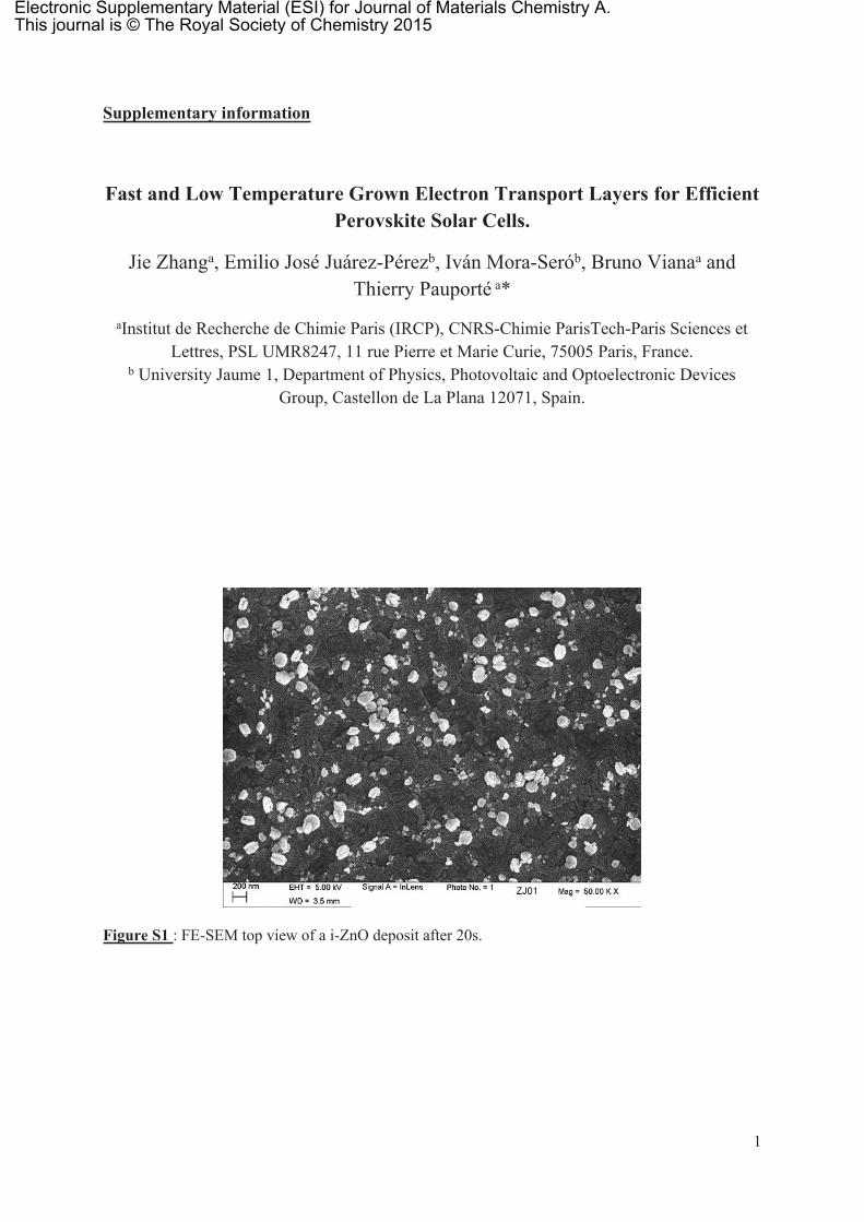
1
Supplementary information
Fast and Low Temperature Grown Electron Transport Layers for Efficient
Perovskite Solar Cells.
Jie Zhanga, Emilio José Juárez-Pérezb, Iván Mora-Serób, Bruno Vianaa and
Thierry Pauporté a*
aInstitut de Recherche de Chimie Paris (IRCP), CNRS-Chimie ParisTech-Paris Sciences et
Lettres, PSL UMR8247, 11 rue Pierre et Marie Curie, 75005 Paris, France.b University Jaume 1, Department of Physics, Photovoltaic and Optoelectronic Devices
Group, Castellon de La Plana 12071, Spain.
Figure S1 : FE-SEM top view of a i-ZnO deposit after 20s.
Electronic Supplementary Material (ESI) for Journal of Materials Chemistry A.This journal is © The Royal Society of Chemistry 2015
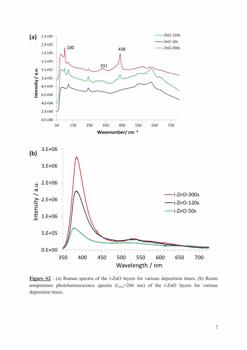
2
Figure S2 : (a) Raman spectra of the i-ZnO layers for various deposition times. (b) Room
temperature photoluminescence spectra (λexc=266 nm) of the i-ZnO layers for various
deposition times.
(a)
(b)

3
Figure S3 : (a) Determination of the CH3NH3PbI3 direct optical bandgap. (b) Room
temperature photoluminescence of the CH3NH3PbI3 layer spin-coated on i-ZnO
(λexc=600nm).
Eg= 1.58eV
(a)
(b)

4
400 500 600 700 800
0
10
20
30
40
50
60
70
80
90
i-ZnO(120s)
i-ZnO(300s)
Wavelength (nm)
IPC
E (
%)
Figure S4 : Incident photon to electron conversion efficiency (IPCE) spectra.
Figure S5 : (a) Series resistance, Rs, and (b) dielectric relaxation capacitance, Cdr, and
selective contact capacitance, Csc, of the samples analyzed by IS.
(a) (b)

5
td / s Scan
direction
Voc/
V
Jsc/
mV.c
m-2
FF/
%
PCE/ %
SC-FB 0.86 4.46 31.91 1.22
120s
FB-SC 0.89 4.24 43.33 1.63
Figure S6 : Picture and J-V curve characteristics of a flexible cell (1 sun).
97
Chapter 5: Effect of oxide contact layer
on the properties of CH3NH3PbI3 for
PSC applications
In this chapter, we present the effect of the nature (ZnO and TiO2) and the structure of
the oxide contact layer on the preparation of CH3NH3PbI3 film by two different techniques.
According to the preparation process, we have noted these techniques as “one-step”
technique and “two-step” technique. In the “one-step” technique, a CH3NH3PbI3 precursor
solution is spin-coated on the ETL and is subsequently annealed to form the perovskite layer.
In the “two-step” technique, a precursor PbI2 solution is spin-coated on the ETL, and is
converted into the perovskite layer by dipping in a CH3NH3I solution. The characteristics and
properties of perovskite layers prepared by the two different techniques were measured and
compared.
A special attention has been paid on the effect of oxide contact layer and annealing time
on the properties of CH3NH3PbI3. Long annealing times produce the degradation of the
perovskite pigment and formation of PbI2 in the case of ZnO underlayer. The degradation is
much slower on TiO2 underlayer. Efficient HTM (spiro-OMeTAD) solution and Ag were
used to complete the fabrication of perovskite solar cells. The best solar cell performances
were achieved by combining a low-voltage electrodeposited ZnO layer and a perovskite layer
prepared by the “one-step” technique. A maximum conversion efficiency of 15% was
obtained for the ZnO-based solar cell. The results have been published in «The Journal of
Physical Chemistry C».[1]
5.1 The preparation and properties of oxide contact layer
In this section, we present the preparation and properties of the ETM ZnO and TiO2 thin
layers. Two kinds of ZnO layers were prepared by electrochemical deposition. On the other
hand, mesoscopic nanoparticle TiO2 films prepared on a TiO2 blocking layer by the spin-
coating technique have also been investigated.

Chapter 5: Effect of oxide contact layer on the properties of CH3NH3PbI3 for PSC applications
98
5.1.1 Preparation of oxide contact layer
Ø ZnO thin films
ZnO films were deposited in a solution of Zn(NO3)2 at a concentration of 0.08 M
dissolved in MilliQ quality water (18.2 MW.cm) and maintained at 60°C. The i-ZnO-
120s layers were electrodeposited by applying a constant voltage of -1.15 V / SCE for
120 s. On the other hand, the i-ZnO-420s layers were prepared by applying a voltage
of -0.9 V / SCE for 420 s. The experimental details can be found in Chapter 2, Section
2.2.
Ø TiO2 thin film
A thin, flat, homogeneous, mesoscopic nanoparticle TiO2 thin layer (noted as np-TiO2)
was prepared by spin-coating technique. The experimental details can be found in
Chapter 2, Section 2.5.
5.1.2 Oxide layer characterizations
One of the objectives of the present work was to compare ZnO and TiO2 layers as
selective contact semiconductor materials in perovskite solar cells and to investigate the
oxide layer role in the CH3NH3PbI3 preparation and properties.
The SEM images of the ZnO deposited films are presented in Figure 5.1. The i-ZnO-
420s layer is a uniform, pinhole free, covers the entire substrate and is made of large grains
(Figure 5.1a). The cross sectional view (Figure 5.1a inset) shows a flat ZnO surface, The
Rrms roughness measured by profilometry was equal to 31 nm and the mean layer thickness
was 420 nm (Table 5.1). The i-ZnO-120s was made of large grains that fully-covered the
FTO substrate (Figure 5.1b). On the cross-sectional view (Figure 5.1c), some protruding
ZnO grains emerged from the layer. The Rrms roughness measured by profilometry was 60
nm (Table 5.1). The close inspection of the grain surface showed no crystal facets but ten-
nanometer-sized asperities. Moreover, the cross-sectional view exhibited the presence of
pinholes in the grain. Figure 5.1d shows a top-view of the mesoscopic nanoparticle TiO2
layer. The layers were made of sintered nanoparticle that covered the TiO2 BL. Their mean
thickness was 280 nm and the surface was flat with a Rrms measured by profilometry of 30
nm (Table 5.1).
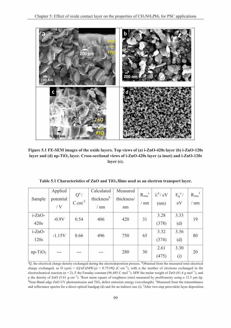
Chapter 5: Effect of oxide contact layer on the properties of CH3NH3PbI3 for PSC applications
99
Figure 5.1 FE-SEM images of the oxide layers. Top views of (a) i-ZnO-420s layer (b) i-ZnO-120s layer and (d) np-TiO2 layer. Cross-sectional views of i-ZnO-420s layer (a inset) and i-ZnO-120s
layer (c).
Table 5.1 Characteristics of ZnO and TiO2 films used as an electron transport layer.
Sample
Applied
potential
/ V
Qa /
C.cm-2
Calculated
thicknessb
/ nm
Measured
thickness/
nm
Rrmsc
/ nm
ld / eV
(nm)
Ege /
eV
Rrmsf
/ nm
i-ZnO-
420s -0.9V 0.54 406 420 31
3.28
(378)
3.33
(d) 19
i-ZnO-
120s -1.15V 0.66 496 750 65
3.32
(374)
3.36
(d) 80
np-TiO2 --- --- --- 280 30 2.61
(475)
3.30
(i)
20
aQ, the electrical charge density exchanged during the electrodeposition process. bObtained from the measured total electrical
charge exchanged, as D (μm) = (Q/nF)(MW/ρ) = 0.7519Q (C·cm−2), with n the number of electrons exchanged in the
electrochemical reaction (n = 2), F the Faraday constant (96,485 C·mol−1), MW the molar weight of ZnO (81.4 g·mol−1), and
ρ the density of ZnO (5.61 g·cm−3). cRoot mean square of roughness (rms) measured by profilometry using a 12.5 μm tip. dNear-Band edge ZnO UV photoemission and TiO2 defect emission energy (wavelength). eMeasured from the transmittance
and reflectance spectra for a direct optical bandgap (d) and for an indirect one (i). fAfter two-step perovskite layer deposition.
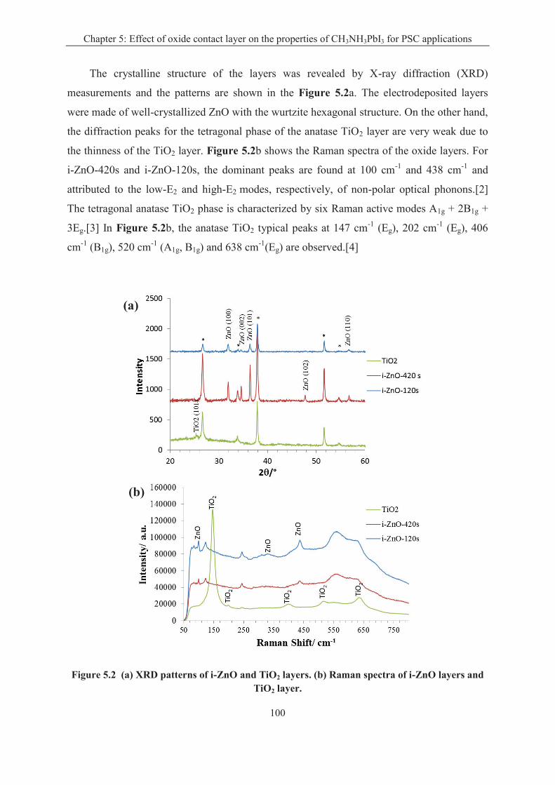
Chapter 5: Effect of oxide contact layer on the properties of CH3NH3PbI3 for PSC applications
100
The crystalline structure of the layers was revealed by X-ray diffraction (XRD)
measurements and the patterns are shown in the Figure 5.2a. The electrodeposited layers
were made of well-crystallized ZnO with the wurtzite hexagonal structure. On the other hand,
the diffraction peaks for the tetragonal phase of the anatase TiO2 layer are very weak due to
the thinness of the TiO2 layer. Figure 5.2b shows the Raman spectra of the oxide layers. For
i-ZnO-420s and i-ZnO-120s, the dominant peaks are found at 100 cm-1
and 438 cm-1
and
attributed to the low-E2 and high-E2 modes, respectively, of non-polar optical phonons.[2]
The tetragonal anatase TiO2 phase is characterized by six Raman active modes A1g + 2B1g +
3Eg.[3] In Figure 5.2b, the anatase TiO2 typical peaks at 147 cm-1
(Eg), 202 cm-1
(Eg), 406
cm-1
(B1g), 520 cm-1
(A1g, B1g) and 638 cm-1
(Eg) are observed.[4]
Figure 5.2 (a) XRD patterns of i-ZnO and TiO2 layers. (b) Raman spectra of i-ZnO layers and TiO2 layer.
(a)
(b)
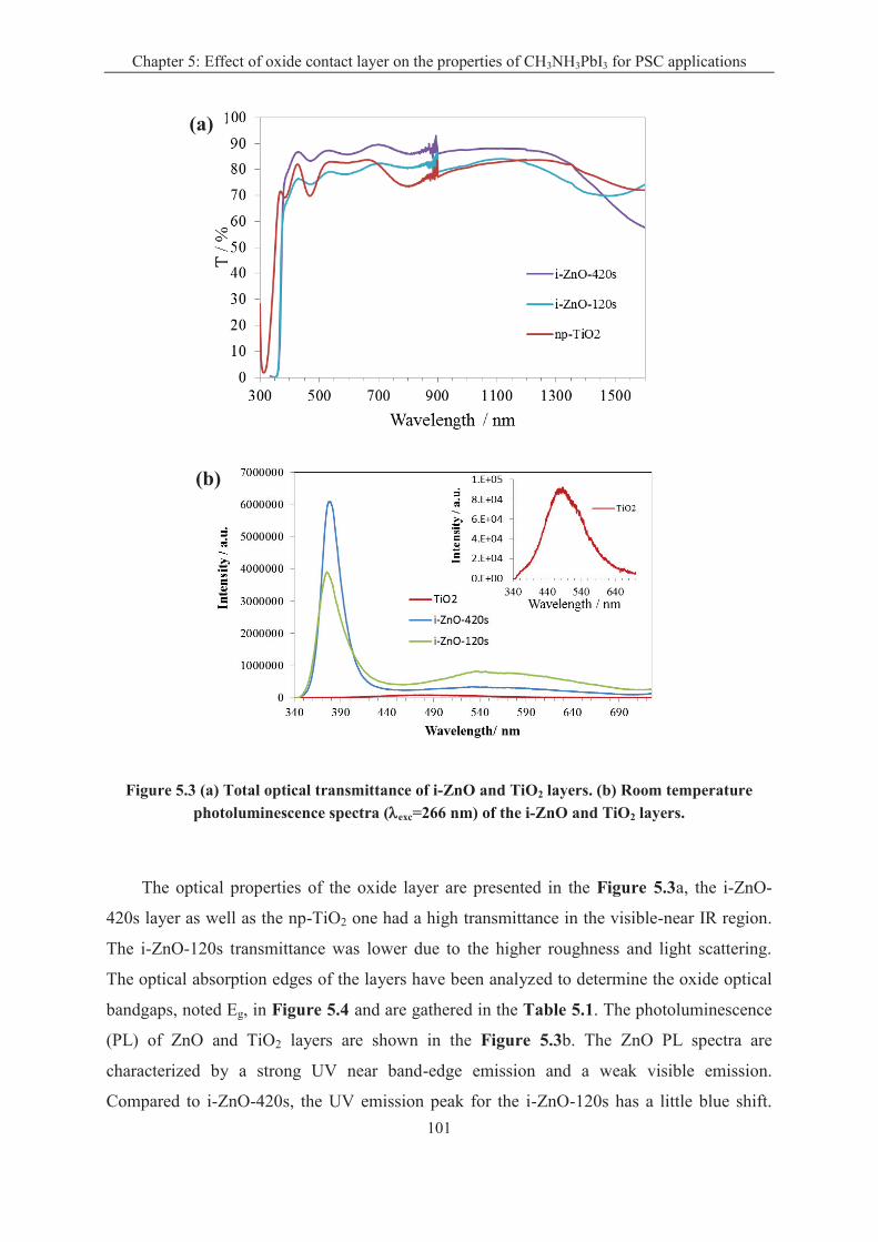
Chapter 5: Effect of oxide contact layer on the properties of CH3NH3PbI3 for PSC applications
101
Figure 5.3 (a) Total optical transmittance of i-ZnO and TiO2 layers. (b) Room temperature
photoluminescence spectra (lexc=266 nm) of the i-ZnO and TiO2 layers.
The optical properties of the oxide layer are presented in the Figure 5.3a, the i-ZnO-
420s layer as well as the np-TiO2 one had a high transmittance in the visible-near IR region.
The i-ZnO-120s transmittance was lower due to the higher roughness and light scattering.
The optical absorption edges of the layers have been analyzed to determine the oxide optical
bandgaps, noted Eg, in Figure 5.4 and are gathered in the Table 5.1. The photoluminescence
(PL) of ZnO and TiO2 layers are shown in the Figure 5.3b. The ZnO PL spectra are
characterized by a strong UV near band-edge emission and a weak visible emission.
Compared to i-ZnO-420s, the UV emission peak for the i-ZnO-120s has a little blue shift.
(a)
(b)
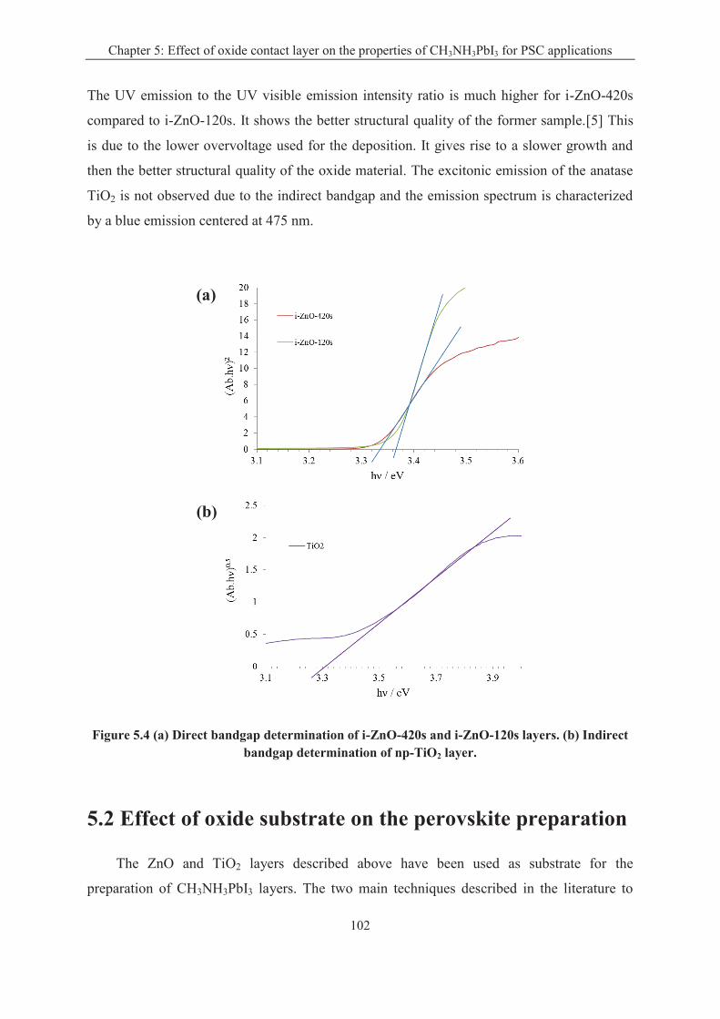
Chapter 5: Effect of oxide contact layer on the properties of CH3NH3PbI3 for PSC applications
102
The UV emission to the UV visible emission intensity ratio is much higher for i-ZnO-420s
compared to i-ZnO-120s. It shows the better structural quality of the former sample.[5] This
is due to the lower overvoltage used for the deposition. It gives rise to a slower growth and
then the better structural quality of the oxide material. The excitonic emission of the anatase
TiO2 is not observed due to the indirect bandgap and the emission spectrum is characterized
by a blue emission centered at 475 nm.
Figure 5.4 (a) Direct bandgap determination of i-ZnO-420s and i-ZnO-120s layers. (b) Indirect bandgap determination of np-TiO2 layer.
5.2 Effect of oxide substrate on the perovskite preparation
The ZnO and TiO2 layers described above have been used as substrate for the
preparation of CH3NH3PbI3 layers. The two main techniques described in the literature to
(a)
(b)
Chapter 5: Effect of oxide contact layer on the properties of CH3NH3PbI3 for PSC applications
103
yield high efficiency solar cells, namely a one-step and a two-step sequential technique, have
been investigated.
5.2.1 Effect of oxide substrate on the one-step perovskite preparation
Ø Experimental
After preparation of oxide contact layer, a precursor solution with a concentration of
45 wt% was produced by mixing CH3NH3I (0.2 g) and PbI2 (0.578 g) in N, N-
dimethylformamide (1 mL) and stirring at room temperature for 20 min.[6] The
CH3NH3PbI3 solution (60 µL) was dropped on the ZnO or TiO2 layer, the substrate
was then two-step spun at 1000 rpm for 5 s and 2500 rpm for 25 s. After 21 seconds,
150 µL chlorobenzene was dropped on the center of the substrate. The perovskite
layer was subsequently annealed on a hotplate at 100°C for various duration times.
Ø Results and Discussion
In the one-step process, the annealing is performed on a hotplate at 100°C. We have
followed the changes induced by this treatment on the precursor layer. In the case of either i-
ZnO-120s or i-ZnO-420s substrate, a metachromism phenomenon of the layer is observed.
The film had initially the shiny grey color of a mixture of CH3NH3I, PbI2, and solvent
(Figure 5.5a).[6] After one minute of annealing, the solvent was evaporated and
CH3NH3PbI3 was formed. The color changed to dark-brown. For an annealing time of more
than ten minutes the color gradually became yellow. The film was full yellow-colored after
an annealing time of 40 min.
These changes have been further characterized by XRD measurements (Figure 5.5b).
After 1 minute of annealing time, the diffractogram peaks are indexed by CH3NH3PbI3, ZnO
and SnO2. After more than two minutes, an additional peak is found at 12.72° assigned to the
(001) reflection of the 2H polytype of PbI2 (JCPDS card n°00-007-0235). With increasing the
annealing time, this PbI2 peak increased in intensity and those related to CH3NH3PbI3
decreased. We also noted the appearance of peaks at 25.96°, 39.63° and 52.29° assigned to
PbI2 (101), PbI2 (110) and PbI2 (004), respectively. A fast degradation of the perovskite layer
deposited on ZnO and heated at 100°C is observed. The sample noted 2 days was stored in a
dry place during this time. Some darkening was observed that suggests some partial reverse
reaction and perovskite reformation. We have noted that this metachromism sequence was
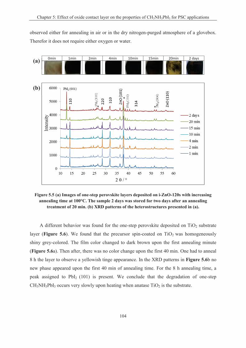
Chapter 5: Effect of oxide contact layer on the properties of CH3NH3PbI3 for PSC applications
104
observed either for annealing in air or in the dry nitrogen-purged atmosphere of a glovebox.
Therefor it does not require either oxygen or water.
Figure 5.5 (a) Images of one-step perovskite layers deposited on i-ZnO-120s with increasing annealing time at 100°C. The sample 2 days was stored for two days after an annealing
treatment of 20 min. (b) XRD patterns of the heterostructures presented in (a).
A different behavior was found for the one-step perovskite deposited on TiO2 substrate
layer (Figure 5.6). We found that the precursor spin-coated on TiO2 was homogeneously
shiny grey-colored. The film color changed to dark brown upon the first annealing minute
(Figure 5.6a). Then after, there was no color change upon the first 40 min. One had to anneal
8 h the layer to observe a yellowish tinge appearance. In the XRD patterns in Figure 5.6b no
new phase appeared upon the first 40 min of annealing time. For the 8 h annealing time, a
peak assigned to PbI2 (101) is present. We conclude that the degradation of one-step
CH3NH3PbI3 occurs very slowly upon heating when anatase TiO2 is the substrate.
0min 1min 2min 4min 10min 15min 20min 2 days
(a)
(b)
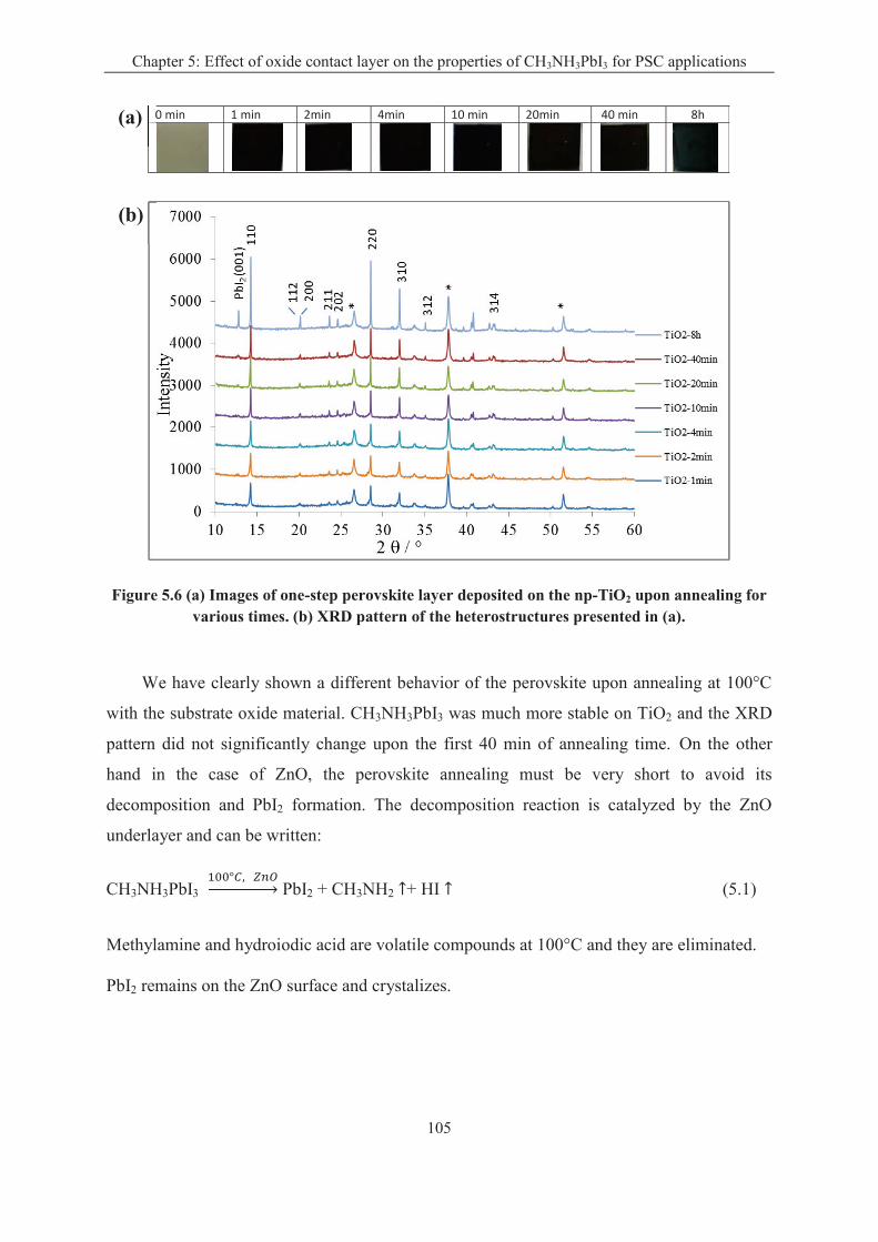
Chapter 5: Effect of oxide contact layer on the properties of CH3NH3PbI3 for PSC applications
105
Figure 5.6 (a) Images of one-step perovskite layer deposited on the np-TiO2 upon annealing for various times. (b) XRD pattern of the heterostructures presented in (a).
We have clearly shown a different behavior of the perovskite upon annealing at 100°C
with the substrate oxide material. CH3NH3PbI3 was much more stable on TiO2 and the XRD
pattern did not significantly change upon the first 40 min of annealing time. On the other
hand in the case of ZnO, the perovskite annealing must be very short to avoid its
decomposition and PbI2 formation. The decomposition reaction is catalyzed by the ZnO
underlayer and can be written:
CH3NH3PbI3 PbI2 + CH3NH2 + HI (5.1)
Methylamine and hydroiodic acid are volatile compounds at 100°C and they are eliminated.
PbI2 remains on the ZnO surface and crystalizes.
0 min 1 min 2min 4min 10 min 20min 40 min 8h
0 (a)
(b)
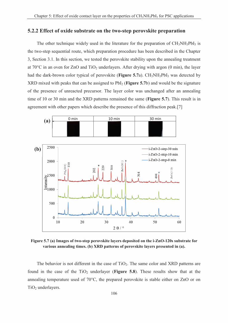
Chapter 5: Effect of oxide contact layer on the properties of CH3NH3PbI3 for PSC applications
106
5.2.2 Effect of oxide substrate on the two-step perovskite preparation
The other technique widely used in the literature for the preparation of CH3NH3PbI3 is
the two-step sequential route, which preparation procedure has been described in the Chapter
3, Section 3.1. In this section, we tested the perovskite stability upon the annealing treatment
at 70°C in an oven for ZnO and TiO2 underlayers. After drying with argon (0 min), the layer
had the dark-brown color typical of perovskite (Figure 5.7a). CH3NH3PbI3 was detected by
XRD mixed with peaks that can be assigned to PbI2 (Figure 5.7b) and would be the signature
of the presence of unreacted precursor. The layer color was unchanged after an annealing
time of 10 or 30 min and the XRD patterns remained the same (Figure 5.7). This result is in
agreement with other papers which describe the presence of this diffraction peak.[7]
Figure 5.7 (a) Images of two-step perovskite layers deposited on the i-ZnO-120s substrate for various annealing times. (b) XRD patterns of perovskite layers presented in (a).
The behavior is not different in the case of TiO2. The same color and XRD patterns are
found in the case of the TiO2 underlayer (Figure 5.8). These results show that at the
annealing temperature used of 70°C, the prepared perovskite is stable either on ZnO or on
TiO2 underlayers.
0 min 10 min 30 min
(a)
(b)
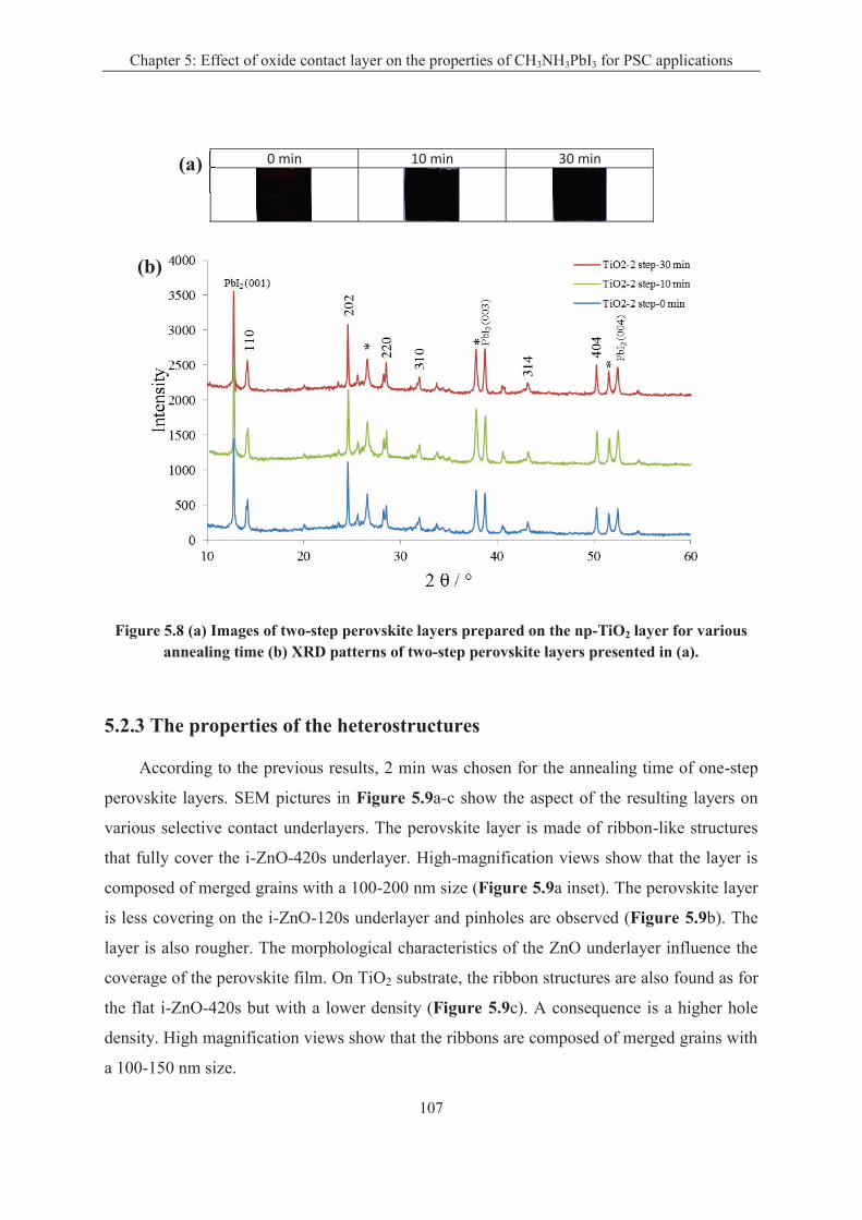
Chapter 5: Effect of oxide contact layer on the properties of CH3NH3PbI3 for PSC applications
107
Figure 5.8 (a) Images of two-step perovskite layers prepared on the np-TiO2 layer for various annealing time (b) XRD patterns of two-step perovskite layers presented in (a).
5.2.3 The properties of the heterostructures
According to the previous results, 2 min was chosen for the annealing time of one-step
perovskite layers. SEM pictures in Figure 5.9a-c show the aspect of the resulting layers on
various selective contact underlayers. The perovskite layer is made of ribbon-like structures
that fully cover the i-ZnO-420s underlayer. High-magnification views show that the layer is
composed of merged grains with a 100-200 nm size (Figure 5.9a inset). The perovskite layer
is less covering on the i-ZnO-120s underlayer and pinholes are observed (Figure 5.9b). The
layer is also rougher. The morphological characteristics of the ZnO underlayer influence the
coverage of the perovskite film. On TiO2 substrate, the ribbon structures are also found as for
the flat i-ZnO-420s but with a lower density (Figure 5.9c). A consequence is a higher hole
density. High magnification views show that the ribbons are composed of merged grains with
a 100-150 nm size.
0 min 10 min 30 min
(a)
(b)
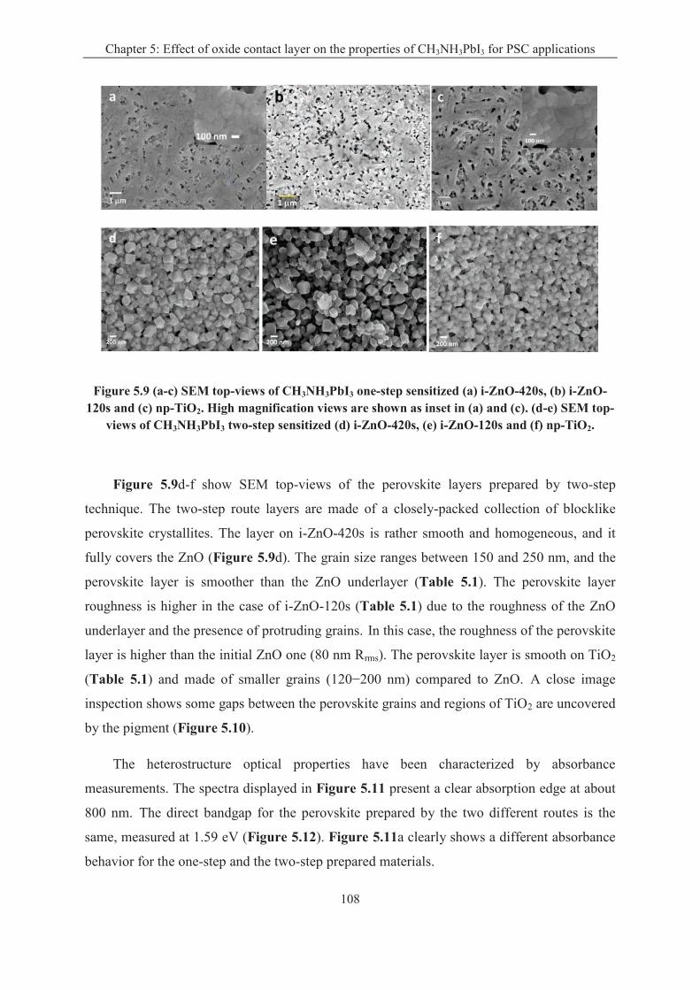
Chapter 5: Effect of oxide contact layer on the properties of CH3NH3PbI3 for PSC applications
108
Figure 5.9 (a-c) SEM top-views of CH3NH3PbI3 one-step sensitized (a) i-ZnO-420s, (b) i-ZnO-120s and (c) np-TiO2. High magnification views are shown as inset in (a) and (c). (d-e) SEM top-
views of CH3NH3PbI3 two-step sensitized (d) i-ZnO-420s, (e) i-ZnO-120s and (f) np-TiO2.
Figure 5.9d-f show SEM top-views of the perovskite layers prepared by two-step
technique. The two-step route layers are made of a closely-packed collection of blocklike
perovskite crystallites. The layer on i-ZnO-420s is rather smooth and homogeneous, and it
fully covers the ZnO (Figure 5.9d). The grain size ranges between 150 and 250 nm, and the
perovskite layer is smoother than the ZnO underlayer (Table 5.1). The perovskite layer
roughness is higher in the case of i-ZnO-120s (Table 5.1) due to the roughness of the ZnO
underlayer and the presence of protruding grains. In this case, the roughness of the perovskite
layer is higher than the initial ZnO one (80 nm Rrms). The perovskite layer is smooth on TiO2
(Table 5.1) and made of smaller grains (120−200 nm) compared to ZnO. A close image
inspection shows some gaps between the perovskite grains and regions of TiO2 are uncovered
by the pigment (Figure 5.10).
The heterostructure optical properties have been characterized by absorbance
measurements. The spectra displayed in Figure 5.11 present a clear absorption edge at about
800 nm. The direct bandgap for the perovskite prepared by the two different routes is the
same, measured at 1.59 eV (Figure 5.12). Figure 5.11a clearly shows a different absorbance
behavior for the one-step and the two-step prepared materials.
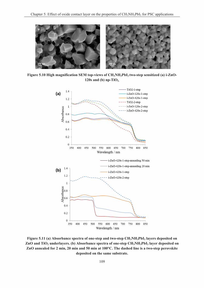
Chapter 5: Effect of oxide contact layer on the properties of CH3NH3PbI3 for PSC applications
109
Figure 5.10 High magnification SEM top-views of CH3NH3PbI3 two-step sensitized (a) i-ZnO-120s and (b) np-TiO2.
Figure 5.11 (a) Absorbance spectra of one-step and two-step CH3NH3PbI3 layers deposited on ZnO and TiO2 underlayers. (b) Absorbance spectra of one-step CH3NH3PbI3 layer deposited on ZnO annealed for 2 min, 20 min and 50 min at 100°C. The dashed line is a two-step perovskite
deposited on the same substrate.
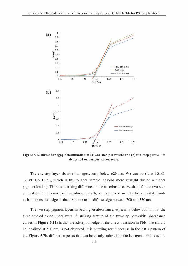
Chapter 5: Effect of oxide contact layer on the properties of CH3NH3PbI3 for PSC applications
110
Figure 5.12 Direct bandgap determination of (a) one-step perovskite and (b) two-step perovskite deposited on various underlayers.
The one-step layer absorbs homogeneously below 620 nm. We can note that i-ZnO-
120s/CH3NH3PbI3, which is the rougher sample, absorbs more sunlight due to a higher
pigment loading. There is a striking difference in the absorbance curve shape for the two-step
perovskite. For this material, two absorption edges are observed, namely the perovskite band-
to-band transition edge at about 800 nm and a diffuse edge between 700 and 550 nm.
The two-step pigment layers have a higher absorbance, especially below 700 nm, for the
three studied oxide underlayers. A striking feature of the two-step perovskite absorbance
curves in Figure 5.11a is that the adsorption edge of the direct transition in PbI2, that should
be localized at 520 nm, is not observed. It is puzzling result because in the XRD pattern of
the Figure 5.7b, diffraction peaks that can be clearly indexed by the hexagonal PbI2 stucture
(a)
(b)
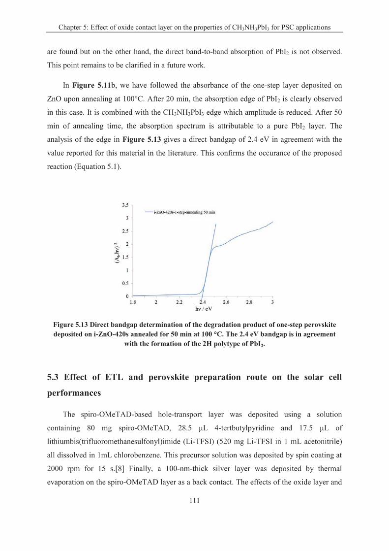
Chapter 5: Effect of oxide contact layer on the properties of CH3NH3PbI3 for PSC applications
111
are found but on the other hand, the direct band-to-band absorption of PbI2 is not observed.
This point remains to be clarified in a future work.
In Figure 5.11b, we have followed the absorbance of the one-step layer deposited on
ZnO upon annealing at 100°C. After 20 min, the absorption edge of PbI2 is clearly observed
in this case. It is combined with the CH3NH3PbI3 edge which amplitude is reduced. After 50
min of annealing time, the absorption spectrum is attributable to a pure PbI2 layer. The
analysis of the edge in Figure 5.13 gives a direct bandgap of 2.4 eV in agreement with the
value reported for this material in the literature. This confirms the occurance of the proposed
reaction (Equation 5.1).
Figure 5.13 Direct bandgap determination of the degradation product of one-step perovskite deposited on i-ZnO-420s annealed for 50 min at 100 °C. The 2.4 eV bandgap is in agreement
with the formation of the 2H polytype of PbI2.
5.3 Effect of ETL and perovskite preparation route on the solar cell
performances
The spiro-OMeTAD-based hole-transport layer was deposited using a solution
containing 80 mg spiro-OMeTAD, 28.5 μL 4-tertbutylpyridine and 17.5 μL of
lithiumbis(trifluoromethanesulfonyl)imide (Li-TFSI) (520 mg Li-TFSI in 1 mL acetonitrile)
all dissolved in 1mL chlorobenzene. This precursor solution was deposited by spin coating at
2000 rpm for 15 s.[8] Finally, a 100-nm-thick silver layer was deposited by thermal
evaporation on the spiro-OMeTAD layer as a back contact. The effects of the oxide layer and
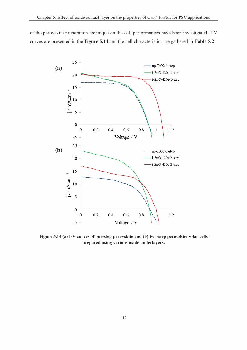
Chapter 5: Effect of oxide contact layer on the properties of CH3NH3PbI3 for PSC applications
112
of the perovskite preparation technique on the cell performances have been investigated. I-V
curves are presented in the Figure 5.14 and the cell characteristics are gathered in Table 5.2.
Figure 5.14 (a) I-V curves of one-step perovskite and (b) two-step perovskite solar cells prepared using various oxide underlayers.
(b)
(a)
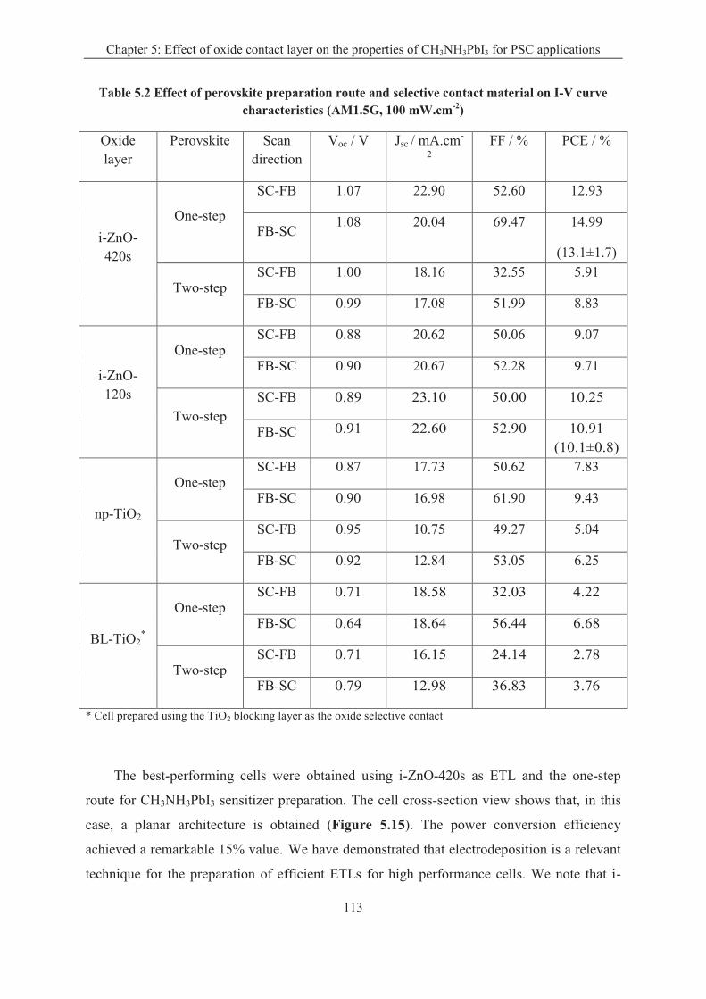
Chapter 5: Effect of oxide contact layer on the properties of CH3NH3PbI3 for PSC applications
113
Table 5.2 Effect of perovskite preparation route and selective contact material on I-V curve characteristics (AM1.5G, 100 mW.cm-2)
Oxide
layer
Perovskite Scan
direction
Voc / V Jsc / mA.cm-
2
FF / % PCE / %
i-ZnO-
420s
One-step
SC-FB 1.07 22.90 52.60 12.93
FB-SC 1.08 20.04 69.47 14.99
(13.1±1.7)
Two-step SC-FB 1.00 18.16 32.55 5.91
FB-SC 0.99 17.08 51.99 8.83
i-ZnO-
120s
One-step SC-FB 0.88 20.62 50.06 9.07
FB-SC 0.90 20.67 52.28 9.71
Two-step
SC-FB 0.89 23.10 50.00 10.25
FB-SC 0.91 22.60 52.90 10.91
(10.1±0.8)
np-TiO2
One-step SC-FB 0.87 17.73 50.62 7.83
FB-SC 0.90 16.98 61.90 9.43
Two-step SC-FB 0.95 10.75 49.27 5.04
FB-SC 0.92 12.84 53.05 6.25
BL-TiO2*
One-step SC-FB 0.71 18.58 32.03 4.22
FB-SC 0.64 18.64 56.44 6.68
Two-step SC-FB 0.71 16.15 24.14 2.78
FB-SC 0.79 12.98 36.83 3.76
* Cell prepared using the TiO2 blocking layer as the oxide selective contact
The best-performing cells were obtained using i-ZnO-420s as ETL and the one-step
route for CH3NH3PbI3 sensitizer preparation. The cell cross-section view shows that, in this
case, a planar architecture is obtained (Figure 5.15). The power conversion efficiency
achieved a remarkable 15% value. We have demonstrated that electrodeposition is a relevant
technique for the preparation of efficient ETLs for high performance cells. We note that i-
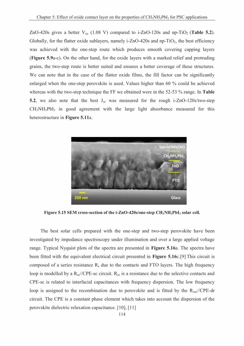
Chapter 5: Effect of oxide contact layer on the properties of CH3NH3PbI3 for PSC applications
114
ZnO-420s gives a better Voc (1.08 V) compared to i-ZnO-120s and np-TiO2 (Table 5.2).
Globally, for the flatter oxide sublayers, namely i-ZnO-420s and np-TiO2, the best efficiency
was achieved with the one-step route which produces smooth covering capping layers
(Figure 5.9a-c). On the other hand, for the oxide layers with a marked relief and protruding
grains, the two-step route is better suited and ensures a better coverage of these structures.
We can note that in the case of the flatter oxide films, the fill factor can be significantly
enlarged when the one-step perovskite is used. Values higher than 60 % could be achieved
whereas with the two-step technique the FF we obtained were in the 52-53 % range. In Table
5.2, we also note that the best Jsc was measured for the rough i-ZnO-120s/two-step
CH3NH3PbI3 in good agreement with the large light absorbance measured for this
heterostructure in Figure 5.11a.
Figure 5.15 SEM cross-section of the i-ZnO-420s/one-step CH3NH3PbI3 solar cell.
The best solar cells prepared with the one-step and two-step perovskite have been
investigated by impedance spectroscopy under illumination and over a large applied voltage
range. Typical Nyquist plots of the spectra are presented in Figure 5.16a. The spectra have
been fitted with the equivalent electrical circuit presented in Figure 5.16c.[9] This circuit is
composed of a series resistance Rs due to the contacts and FTO layers. The high frequency
loop is modelled by a Rsc//CPE-sc circuit. Rsc is a resistance due to the selective contacts and
CPE-sc is related to interfacial capacitances with frequency dispersion. The low frequency
loop is assigned to the recombination due to perovskite and is fitted by the Rrec//CPE-dr
circuit. The CPE is a constant phase element which takes into account the dispersion of the
perovskite dielectric relaxation capacitance. [10], [11]
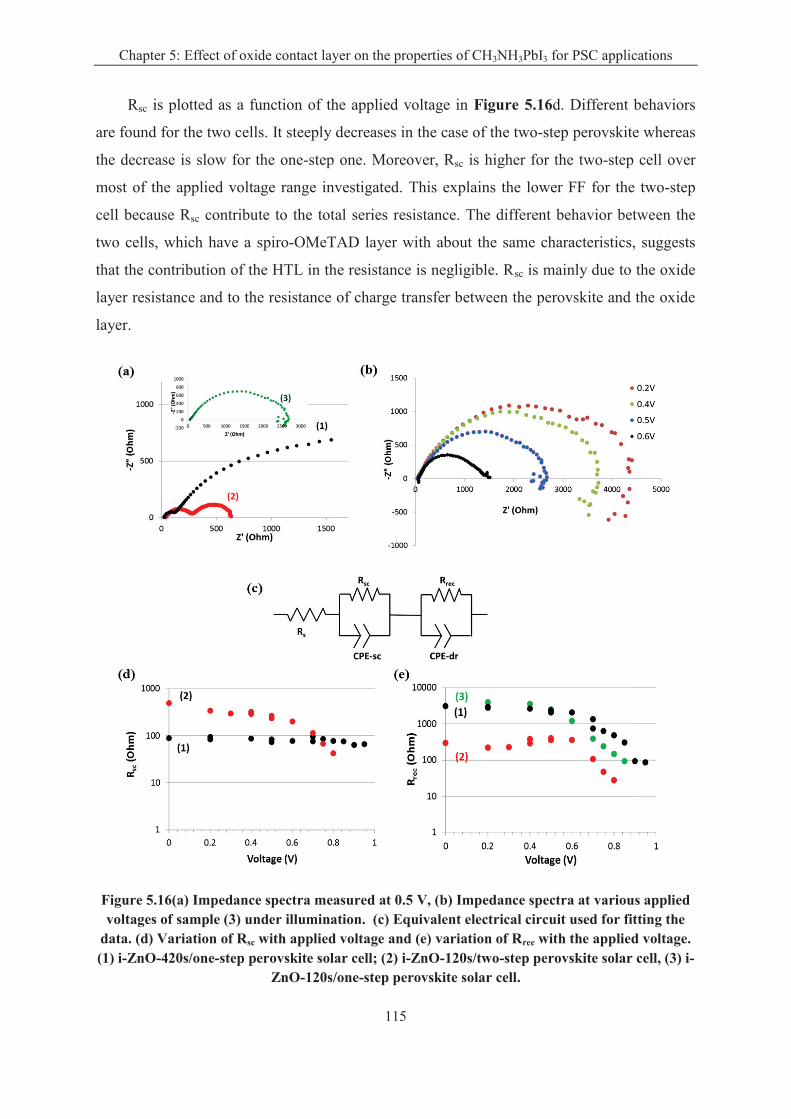
Chapter 5: Effect of oxide contact layer on the properties of CH3NH3PbI3 for PSC applications
115
Rsc is plotted as a function of the applied voltage in Figure 5.16d. Different behaviors
are found for the two cells. It steeply decreases in the case of the two-step perovskite whereas
the decrease is slow for the one-step one. Moreover, Rsc is higher for the two-step cell over
most of the applied voltage range investigated. This explains the lower FF for the two-step
cell because Rsc contribute to the total series resistance. The different behavior between the
two cells, which have a spiro-OMeTAD layer with about the same characteristics, suggests
that the contribution of the HTL in the resistance is negligible. Rsc is mainly due to the oxide
layer resistance and to the resistance of charge transfer between the perovskite and the oxide
layer.
Figure 5.16(a) Impedance spectra measured at 0.5 V, (b) Impedance spectra at various applied voltages of sample (3) under illumination. (c) Equivalent electrical circuit used for fitting the
data. (d) Variation of Rsc with applied voltage and (e) variation of Rrec with the applied voltage. (1) i-ZnO-420s/one-step perovskite solar cell; (2) i-ZnO-120s/two-step perovskite solar cell, (3) i-
ZnO-120s/one-step perovskite solar cell.
Chapter 5: Effect of oxide contact layer on the properties of CH3NH3PbI3 for PSC applications
116
Figure 5.16e shows the variation of Rrec with the applied voltage. Higher Rrec values are
found for the one-step cell. We can conclude that there are less recombinations in the one-
step perovskite due to a better quality of the material. For both perovskite routes, Rrec slowly
decreases or is almost constant at low voltage. Above a certain voltage threshold, Rrec
decreases markedly. The recombination side reaction is promoted by applying high voltage
and the total current decreases. The higher threshold voltage and Rrec for the i-ZnO-420s/one-
step solar cells explains their high open circuit voltage (Table 5.2).
The impedance spectra of the i-ZnO-120s/one-step solar cell are presented in the inset of
Figure 5.16a (curve 3) and in the Figure 5.16b. The shape is different and looks like the
spectra of perovskite solar cells measured in the dark. No clear high frequency loop could be
analyzed. The spectra are dominated by an arc of circle in the high-middle frequency range.
At low frequency, an additional loop is found with a positive imaginary part due to a negative
capacitance. The resistance of the middle frequency range loop has been extracted and is
presented in Figure 5.16e. Its behavior and order of magnitude are the same as for the i-ZnO-
420s/one-step perovskite cell. This resistance is then attributed to the recombination and is
plotted in Figure 5.16e. Rrec decreases more rapidly for i-ZnO-120s cell compared to i-ZnO-
420s cell, and consequently the cell Voc is significantly lower for the former compared to the
latter (Table 5.2).
5.3 Conclusion
In conclusion, we have investigated the effect of oxide ETL underlayer and perovskite
preparation route on the sensitizer layer characteristics, solar cell performances and electrical
properties. ZnO layers with a planar 2D geometry and ZnO layers with some roughness and
protruding grains have been investigated. They have been compared to nanoparticle TiO2
films. We show that the oxide underlayer has a marked influence on the one-step perovskite
preparation. CH3NH3PbI3 is degraded to form PbI2 after several minutes of annealing at
100°C. The same process has been observed in the case of TiO2 underlayer but with a much
slower kinetics. ZnO catalyzes the degradation at 100°C and the optimized annealing time
was found to be 2 min. In the case of the two-step route, the annealing is performed at lower
temperature and the perovskite layer is not degraded. The XRD patterns show the presence of
peaks that can be assigned to unreacted PbI2. However, the absorbance spectra of the
obtained product do not show the presence of PbI2 direct transition at 520 nm but a diffuse
Chapter 5: Effect of oxide contact layer on the properties of CH3NH3PbI3 for PSC applications
117
absorbance edge. The two-step route gives rise to more absorbing layers than the one-step
route especially in the green-blue wavelength region. It is globally beneficial for the solar
light harvesting.
The best Performances were achieved by combining a low-overvoltage electrodeposited
ZnO layer, a planar architecture and a perovskite layer prepared by a one-step deposition-
dripping route. A maximum overall conversion efficiency of about 15% was measured.
Globally, for the flatter oxide sublayers, namely i-ZnO-420s and np-TiO2, the best efficiency
was achieved with the one-step CH3NH3PbI3 synthetic route because it results in a quite
smooth perovskite coating. On the other hand, the two-step route is more suitable for rough
or structured (nanorods (see Chapter 3), nanotubes (see Chapter 6)…) underlayers because
the technique ensures a better coverage of these structures. The investigation of the cells by
impedance spectroscopy has shown that the one-step perovskite gives rise to a perovskite
material in which the charge recombinations are reduced compared to the two-step material.
Moreover, our investigations suggest that a better oxide-perovskite interface is created and
that the interfacial resistance is consequently reduced. These results are promising since the
best cell is prepared at low temperature and this opens the gate to the fabrication of flexible
solar cells on plastic substrate. More work is ongoing to improve the one-step perovskite
layer compactness and covering and to produce larger grains to reduce, in a more extend,
bulk defects and grain boundaries. It should improve the charge carrier mobility and limit the
recombination phenomena.
References
[1] J. Zhang and T. Pauporté, “Effects of Oxide Contact Layer on the Preparation and
Properties of CH3NH3PbI3 for Perovskite Solar Cell Application,” J. Phys. Chem. C, vol.
119, no. 27, pp. 14919–14928, Jul. 2015.
[2] O. Lupan, T. Pauporté, L. Chow, B. Viana, F. Pellé, L. K. Ono, B. Roldan Cuenya, and
H. Heinrich, “Effects of annealing on properties of ZnO thin films prepared by
electrochemical deposition in chloride medium,” Appl. Surf. Sci., vol. 256, no. 6, pp.
1895–1907, Jan. 2010.
[3] R. Cuscó, E. Alarcón-Lladó, J. Ibáñez, L. Artús, J. Jiménez, B. Wang, and M. J.
Callahan, “Temperature dependence of Raman scattering in ZnO,” Phys. Rev. B, vol. 75,
no. 16, pp. 165202/1-165202/11, Apr. 2007.
Chapter 5: Effect of oxide contact layer on the properties of CH3NH3PbI3 for PSC applications
118
[4] T. Ohsaka, F. Izumi, and Y. Fujiki, “Raman spectrum of anatase TiO2” J. Raman
Spectrosc., vol. 7, no. 6, pp. 321–324, Apr. 1978.
[5] T. Pauporté, E. Jouanno, F. Pellé, B. Viana, and P. Aschehoug, “Key Growth
Parameters for the Electrodeposition of ZnO Films with an Intense UV-Light Emission
at Room Temperature,” J. Phys. Chem. C, vol. 113, no. 24, pp. 10422–10431, Jun. 2009.
[6] M. Xiao, F. Huang, W. Huang, Y. Dkhissi, Y. Zhu, J. Etheridge, A. Gray-Weale, U.
Bach, Y.-B. Cheng, and L. Spiccia, “A Fast Deposition-Crystallization Procedure for
Highly Efficient Lead Iodide Perovskite Thin-Film Solar Cells,” Angew. Chem. Int. Ed.,
vol. 53, no. 37, pp. 9898–9903, Sep. 2014.
[7] D. Liu, M. K. Gangishetty, and T. L. Kelly, “Effect of CH3NH3PbI3 thickness on device
efficiency in planar heterojunction perovskite solar cells,” J Mater Chem A, vol. 2, no.
46, pp. 19873–19881, Oct. 2014.
[8] D. Liu and T. L. Kelly, “Perovskite solar cells with a planar heterojunction structure
prepared using room-temperature solution processing techniques,” Nat. Photonics, vol.
8, no. 2, pp. 133–138, Dec. 2013.
[9] E. J. Juarez-Perez, M. Wuβler, F. Fabregat-Santiago, K. Lakus-Wollny, E. Mankel, T.
Mayer, W. Jaegermann, and I. Mora-Sero, “Role of the Selective Contacts in the
Performance of Lead Halide Perovskite Solar Cells,” J. Phys. Chem. Lett., vol. 5, no. 4,
pp. 680–685, Feb. 2014.
[10] B. Suarez, V. Gonzalez-Pedro, T. S. Ripolles, R. S. Sanchez, L. Otero, and I. Mora-Sero,
“Recombination Study of Combined Halides (Cl, Br, I) Perovskite Solar Cells,” J. Phys.
Chem. Lett., vol. 5, no. 10, pp. 1628–1635, May 2014.
[11] J. Bisquert, L. Bertoluzzi, I. Mora-Sero, and G. Garcia-Belmonte, “Theory of
Impedance and Capacitance Spectroscopy of Solar Cells with Dielectric Relaxation,
Drift-Diffusion Transport, and Recombination,” J. Phys. Chem. C, vol. 118, no. 33, pp.
18983–18991, Aug. 2014.
119
Chapter 6: One-dimensional self-
standing TiO2 nanotube arrayed layers
designed for PSC applications
In this chapter, we present the preparation of one-dimensional TiO2 nanotube array
layers starting from arrayed self-standing single-crystalline ZnO nanowire (NW) arrays
prepared by electrochemical deposition. The ZnO NW layer was converted into anatase TiO2
NTs using a titanate solution adjusted at an ad-hoc pH. The tubes were polycristalline and
their diameter and length could be tuned to get dimension-tailored nanostrutures. The TiO2
NT layers have been integrated in perovskite solar cells. We have investigated the effect of
the thickness of TiO2 nanotube layers and the effect of the treatment with TiCl4 to the surface
of TiO2 NT layer. A best efficiency of 9.33% was obtained.
The perovskite layer is sandwiched between two adjacent phases that act as selective
contacts and generate the driving force for the charge separation.[1] The electrons are
transferred to the conduction band of a material layer called the electron transport layer (ETL)
and the holes are transferred to a hole transport material (HTM), usually an organic glass.
ETL and its interfaces with the organometal trihalide are keys to get efficient and stable cells.
The ETL not only receives and transport the electronic charges but it also influences the
sensitization through various aspects: the perovskite layer morphology and loading, which
depend on the structure and roughness of the ETL, the quality of the ETL/perovskite interface
and the quality of the perovskite itself since the ETL intervenes in the full precursor
conversion into perovskite. Using one-dimensional oxide (TiO2, ZnO…) arrayed structures
appears attractive for the application to get a fast charge collection, increase the pigment
loading and manage light before its absorption by the perovskite layer.[2], [3]
TiO2 nanotubes (NT) arrays have been widely investigated as one-dimensional
structures for advanced applications. These structures combine a large surface to volume ratio,
a one-dimensionality and high surface reactivity. They have been applied in catalysis and
photocatalysis, oxidative photoelectrochemistry, gas sensors, batteries, dye-sensitized solar
cells, colloidal quantum dot solar cells, supercapacitors and so on.[4]–[8] For most of these
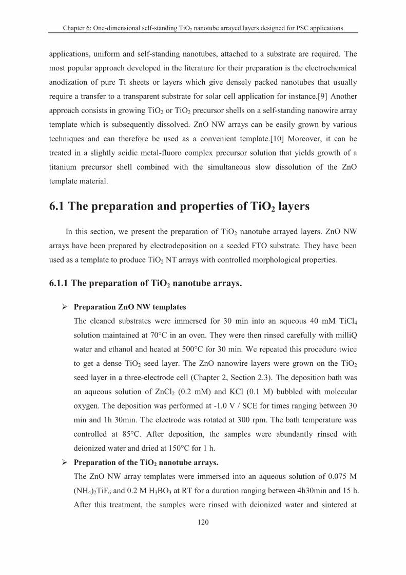
Chapter 6: One-dimensional self-standing TiO2 nanotube arrayed layers designed for PSC applications
120
applications, uniform and self-standing nanotubes, attached to a substrate are required. The
most popular approach developed in the literature for their preparation is the electrochemical
anodization of pure Ti sheets or layers which give densely packed nanotubes that usually
require a transfer to a transparent substrate for solar cell application for instance.[9] Another
approach consists in growing TiO2 or TiO2 precursor shells on a self-standing nanowire array
template which is subsequently dissolved. ZnO NW arrays can be easily grown by various
techniques and can therefore be used as a convenient template.[10] Moreover, it can be
treated in a slightly acidic metal-fluoro complex precursor solution that yields growth of a
titanium precursor shell combined with the simultaneous slow dissolution of the ZnO
template material.
6.1 The preparation and properties of TiO2 layers
In this section, we present the preparation of TiO2 nanotube arrayed layers. ZnO NW
arrays have been prepared by electrodeposition on a seeded FTO substrate. They have been
used as a template to produce TiO2 NT arrays with controlled morphological properties.
6.1.1 The preparation of TiO2 nanotube arrays.
Ø Preparation ZnO NW templates
The cleaned substrates were immersed for 30 min into an aqueous 40 mM TiCl4
solution maintained at 70°C in an oven. They were then rinsed carefully with milliQ
water and ethanol and heated at 500°C for 30 min. We repeated this procedure twice
to get a dense TiO2 seed layer. The ZnO nanowire layers were grown on the TiO2
seed layer in a three-electrode cell (Chapter 2, Section 2.3). The deposition bath was
an aqueous solution of ZnCl2 (0.2 mM) and KCl (0.1 M) bubbled with molecular
oxygen. The deposition was performed at -1.0 V / SCE for times ranging between 30
min and 1h 30min. The electrode was rotated at 300 rpm. The bath temperature was
controlled at 85°C. After deposition, the samples were abundantly rinsed with
deionized water and dried at 150°C for 1 h.
Ø Preparation of the TiO2 nanotube arrays.
The ZnO NW array templates were immersed into an aqueous solution of 0.075 M
(NH4)2TiF6 and 0.2 M H3BO3 at RT for a duration ranging between 4h30min and 15 h.
After this treatment, the samples were rinsed with deionized water and sintered at
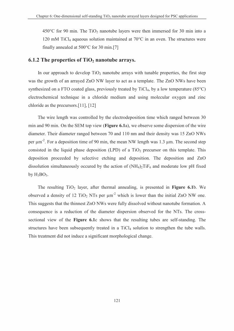
Chapter 6: One-dimensional self-standing TiO2 nanotube arrayed layers designed for PSC applications
121
450°C for 90 min. The TiO2 nanotube layers were then immersed for 30 min into a
120 mM TiCl4 aqueous solution maintained at 70°C in an oven. The structures were
finally annealed at 500°C for 30 min.[7]
6.1.2 The properties of TiO2 nanotube arrays.
In our approach to develop TiO2 nanotube arrays with tunable properties, the first step
was the growth of an arrayed ZnO NW layer to act as a template. The ZnO NWs have been
synthesized on a FTO coated glass, previously treated by TiCl4, by a low temperature (85°C)
electrochemical technique in a chloride medium and using molecular oxygen and zinc
chloride as the precursors.[11], [12]
The wire length was controlled by the electrodeposition time which ranged between 30
min and 90 min. On the SEM top view (Figure 6.1a), we observe some dispersion of the wire
diameter. Their diameter ranged between 70 and 110 nm and their density was 15 ZnO NWs
per µm-2
. For a deposition time of 90 min, the mean NW length was 1.3 µm. The second step
consisted in the liquid phase deposition (LPD) of a TiO2 precursor on this template. This
deposition proceeded by selective etching and deposition. The deposition and ZnO
dissolution simultaneously occured by the action of (NH4)2TiF6 and moderate low pH fixed
by H3BO3.
The resulting TiO2 layer, after thermal annealing, is presented in Figure 6.1b. We
observed a density of 12 TiO2 NTs per µm-2
which is lower than the initial ZnO NW one.
This suggests that the thinnest ZnO NWs were fully dissolved without nanotube formation. A
consequence is a reduction of the diameter dispersion observed for the NTs. The cross-
sectional view of the Figure 6.1c shows that the resulting tubes are self-standing. The
structures have been subsequently treated in a TiCl4 solution to strengthen the tube walls.
This treatment did not induce a significant morphological change.
Chapter 6: One-dimensional self-standing TiO2 nanotube arrayed layers designed for PSC applications
122
Figure 6.1: SEM top views of (a) ZnO NW array and (b) TiO2 NT array. (c) SEM cross-sectional view of TiO2 NT array. (d) TEM view of electrodeposited ZnO NW (inset selected area
electron diffraction (SAED) pattern). (e) TEM view of TiO2 nanotube structure (inset SAED pattern).
The diameters of the nanotubes have been tuned by changing the (NH4)2TiF6 treatment
time. As shown in the Table 6.1 their mean value was 120 nm, 200 nm and 850 nm for
treatment times of 4.5 h, 6 h and 15 h, respectively. The mean tube length was slightly
shortened by the LPD compared to the initial ZnO NW length. It is assigned to some
dissolution of the ZnO wire top occurring upon the initial stage of the (NH4)2TiF6 treatment.
TEM observation in Figure 6.1d shows that the initial ZnO NWs had a homogeneous
Chapter 6: One-dimensional self-standing TiO2 nanotube arrayed layers designed for PSC applications
123
diameter throughout their length and the selected area electron diffraction spot pattern shows
that each nanowire was a single crystal. The (NH4)2TiF6 treatment yielded to the structure
presented in Figure 6.1e. The TEM image establishes the formation of a hollow tube with no
trace of the initial ZnO material due to its full dissolution. The TiO2 nanotubes were made of
assembled nanocrystals with a 7-8 nm average size (Figure 6.1e). The crystallization and
polycrystallinity of the sample was confirmed by the selected area electron diffraction ring
pattern presented as an inset in Figure 6.1e.
Table 6.1: TiO2 NT structure properties and solar cell performances under AM1.5 G filtered 100 mW.cm-2 illumination. The reference cell was prepared using a nanoparticle TiO2 scaffold
layer. The PCE is the power conversion efficiency and HI is the hysteresis index.
(NH4)2TiF6
treament
time
TiCl4
Structure
diameter /
nm
Layer
thickness
/ µm
Scan
directiona
Voc / V Jsc /
mA.cm-2
FF / %
PCE
/ % HI
4.5h - 110 1.1 SC-FB 0.75 10.64 37.32 2.99
FB-SC 0.77 8.39 54.54 3.53
4.5h X 120 1.1 SC-FB 0.86 20.72 48.50 8.64
0.071 FB-SC 0.87 20.25 53.16 9.33
6h X 200 1.3 SC-FB 0.81 19.92 49.66 8.04
0.115 FB-SC 0.82 19.40 55.62 8.81
15h X 850 2.3 SC-FB 0.80 12.65 39.56 4.02
0.177 FB-SC 0.82 12.35 48.30 4.88
TiO2 NPb _ _ 0.28
SC-FB 0.88 13.52 54.84 6.52 0.113
FB-SC 0.88 12.86 65.83 7.45
a SC-FB is a scan from the short circuit to the flat band potential and FB-SC is a scan from the flatband potential
to the short circuit. b Reference cell prepared with a mesoporous nanoparticle TiO2 ETL.
The XRD pattern in Figure 6.2a reveals that the initial NWs were ZnO crystallized with
the wurtzite hexagonal structure and textured along the c-axis. The dominant Raman emission
peaks at 100 cm-1
and 438 cm-1
in Figure 6.2b are attributed to the low-E2 and high-E2 modes
of non-polar ZnO optical phonons, respectively. After the (NH4)2TiF6 treatment a broad X-
ray diffraction peak is present at 25.3° assign to anatase TiO2 (Figure 6.2a). Its broadness is
due to the nanocrystallinity of the structure. The tetragonal anatase TiO2 phase is
characterized by six Raman active modes A1g + 2B1g + 3Eg. In Figure 6.2b, the anatase TiO2
typical peaks at 147 cm-1
(Eg), 202 cm-1
(Eg), 406 cm-1
(B1g), 520 cm-1
(A1g, B1g) and 638 cm-
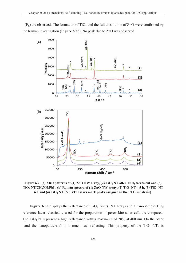
Chapter 6: One-dimensional self-standing TiO2 nanotube arrayed layers designed for PSC applications
124
1 (Eg) are observed. The formation of TiO2 and the full dissolution of ZnO were confirmed by
the Raman investigation (Figure 6.2b). No peak due to ZnO was observed.
Figure 6.2: (a) XRD patterns of (1) ZnO NW array, (2) TiO2 NT after TiCl4 treatment and (3) TiO2 NT/CH3NH3PbI3. (b) Raman spectra of (1) ZnO NW array, (2) TiO2 NT 4.5 h, (3) TiO2 NT
6 h and (4) TiO2 NT 15 h. (The stars mark peaks assigned to the FTO substrate).
Figure 6.3a displays the reflectance of TiO2 layers. NT arrays and a nanoparticle TiO2
reference layer, classically used for the preparation of perovskite solar cell, are compared.
The TiO2 NTs present a high reflectance with a maximum of 28% at 400 nm. On the other
hand the nanoparticle film is much less reflecting. This property of the TiO2 NTs is
(a)
(b)

Chapter 6: One-dimensional self-standing TiO2 nanotube arrayed layers designed for PSC applications
125
interesting to increase the light diffusion pathway in the cell and then improve the light
harvesting.
6.2 The properties of perosvskite sensitized solar cells
The TiO2 NT layers prepared with various LPD treatment times and which
characteristics are gathered in Table 6.1. These layers have been sensitized with CH3NH3PbI3
by a "two-step" sequential deposition technique.
The formation of CH3NH3PbI3 has been shown by XRD. In Figure 6.2a curve (3), the
XRD pattern presents additional diffraction peaks compared to the bare TiO2 which are due
to the presence of the tetragonal perovskite. The optical absorbance of the TiO2
NT/CH3NH3PbI3 structures is presented in Figure 6.3b for various LPD times.
Figure 6.3 (a) Reflectance spectra of (1) TiO2 NP layer and (2) TiO2 NT 4.5 h. (b) Absorbance spectra of the CH3NH3PbI3 sensitized structures based on (1) reference TiO2 NP, (2) TiO2 NT
4.5 h, (3) TiO2 NT 6 h and (4) TiO2 NT 15 h.
(a)
(b)
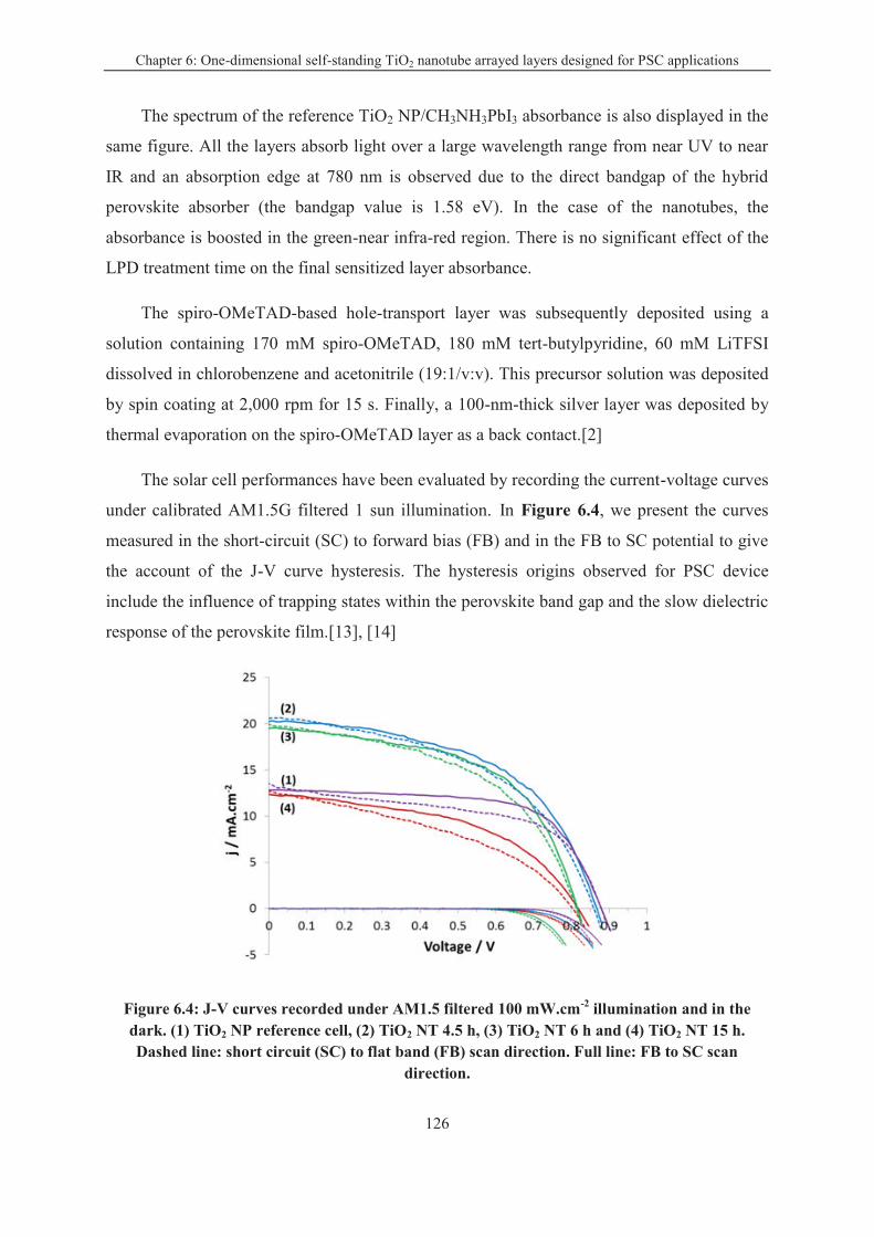
Chapter 6: One-dimensional self-standing TiO2 nanotube arrayed layers designed for PSC applications
126
The spectrum of the reference TiO2 NP/CH3NH3PbI3 absorbance is also displayed in the
same figure. All the layers absorb light over a large wavelength range from near UV to near
IR and an absorption edge at 780 nm is observed due to the direct bandgap of the hybrid
perovskite absorber (the bandgap value is 1.58 eV). In the case of the nanotubes, the
absorbance is boosted in the green-near infra-red region. There is no significant effect of the
LPD treatment time on the final sensitized layer absorbance.
The spiro-OMeTAD-based hole-transport layer was subsequently deposited using a
solution containing 170 mM spiro-OMeTAD, 180 mM tert-butylpyridine, 60 mM LiTFSI
dissolved in chlorobenzene and acetonitrile (19:1/v:v). This precursor solution was deposited
by spin coating at 2,000 rpm for 15 s. Finally, a 100-nm-thick silver layer was deposited by
thermal evaporation on the spiro-OMeTAD layer as a back contact.[2]
The solar cell performances have been evaluated by recording the current-voltage curves
under calibrated AM1.5G filtered 1 sun illumination. In Figure 6.4, we present the curves
measured in the short-circuit (SC) to forward bias (FB) and in the FB to SC potential to give
the account of the J-V curve hysteresis. The hysteresis origins observed for PSC device
include the influence of trapping states within the perovskite band gap and the slow dielectric
response of the perovskite film.[13], [14]
Figure 6.4: J-V curves recorded under AM1.5 filtered 100 mW.cm-2 illumination and in the dark. (1) TiO2 NP reference cell, (2) TiO2 NT 4.5 h, (3) TiO2 NT 6 h and (4) TiO2 NT 15 h. Dashed line: short circuit (SC) to flat band (FB) scan direction. Full line: FB to SC scan
direction.
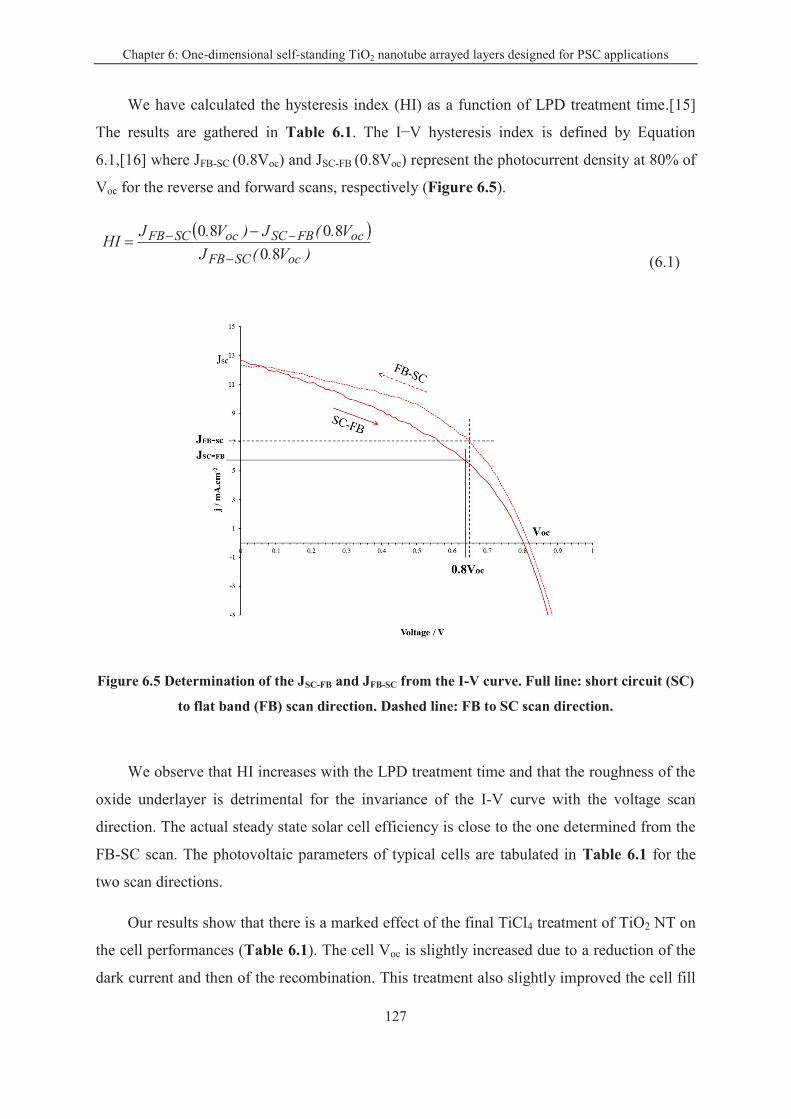
Chapter 6: One-dimensional self-standing TiO2 nanotube arrayed layers designed for PSC applications
127
We have calculated the hysteresis index (HI) as a function of LPD treatment time.[15]
The results are gathered in Table 6.1. The I−V hysteresis index is defined by Equation
6.1,[16] where JFB-SC (0.8Voc) and JSC-FB (0.8Voc) represent the photocurrent density at 80% of
Voc for the reverse and forward scans, respectively (Figure 6.5).
( ))V.(J
V.(J)V.JHI
ocSCFB
ocFBSCocSCFB
80
8080
-
-- -=
(6.1)
Figure 6.5 Determination of the JSC-FB and JFB-SC from the I-V curve. Full line: short circuit (SC)
to flat band (FB) scan direction. Dashed line: FB to SC scan direction.
We observe that HI increases with the LPD treatment time and that the roughness of the
oxide underlayer is detrimental for the invariance of the I-V curve with the voltage scan
direction. The actual steady state solar cell efficiency is close to the one determined from the
FB-SC scan. The photovoltaic parameters of typical cells are tabulated in Table 6.1 for the
two scan directions.
Our results show that there is a marked effect of the final TiCl4 treatment of TiO2 NT on
the cell performances (Table 6.1). The cell Voc is slightly increased due to a reduction of the
dark current and then of the recombination. This treatment also slightly improved the cell fill
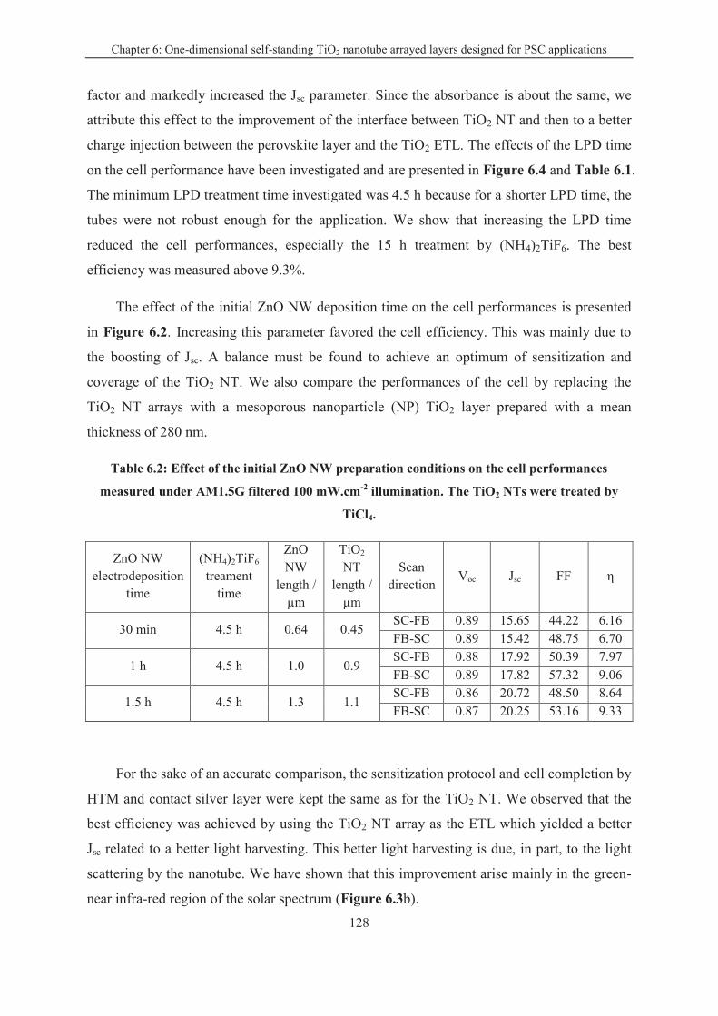
Chapter 6: One-dimensional self-standing TiO2 nanotube arrayed layers designed for PSC applications
128
factor and markedly increased the Jsc parameter. Since the absorbance is about the same, we
attribute this effect to the improvement of the interface between TiO2 NT and then to a better
charge injection between the perovskite layer and the TiO2 ETL. The effects of the LPD time
on the cell performance have been investigated and are presented in Figure 6.4 and Table 6.1.
The minimum LPD treatment time investigated was 4.5 h because for a shorter LPD time, the
tubes were not robust enough for the application. We show that increasing the LPD time
reduced the cell performances, especially the 15 h treatment by (NH4)2TiF6. The best
efficiency was measured above 9.3%.
The effect of the initial ZnO NW deposition time on the cell performances is presented
in Figure 6.2. Increasing this parameter favored the cell efficiency. This was mainly due to
the boosting of Jsc. A balance must be found to achieve an optimum of sensitization and
coverage of the TiO2 NT. We also compare the performances of the cell by replacing the
TiO2 NT arrays with a mesoporous nanoparticle (NP) TiO2 layer prepared with a mean
thickness of 280 nm.
Table 6.2: Effect of the initial ZnO NW preparation conditions on the cell performances
measured under AM1.5G filtered 100 mW.cm-2 illumination. The TiO2 NTs were treated by
TiCl4.
ZnO NW
electrodeposition
time
(NH4)2TiF6
treament
time
ZnO
NW
length /
µm
TiO2
NT
length /
µm
Scan
direction Voc Jsc FF η
30 min 4.5 h 0.64 0.45 SC-FB 0.89 15.65 44.22 6.16
FB-SC 0.89 15.42 48.75 6.70
1 h 4.5 h 1.0 0.9 SC-FB 0.88 17.92 50.39 7.97
FB-SC 0.89 17.82 57.32 9.06
1.5 h 4.5 h 1.3 1.1 SC-FB 0.86 20.72 48.50 8.64
FB-SC 0.87 20.25 53.16 9.33
For the sake of an accurate comparison, the sensitization protocol and cell completion by
HTM and contact silver layer were kept the same as for the TiO2 NT. We observed that the
best efficiency was achieved by using the TiO2 NT array as the ETL which yielded a better
Jsc related to a better light harvesting. This better light harvesting is due, in part, to the light
scattering by the nanotube. We have shown that this improvement arise mainly in the green-
near infra-red region of the solar spectrum (Figure 6.3b).
Chapter 6: One-dimensional self-standing TiO2 nanotube arrayed layers designed for PSC applications
129
We have also investigated the use of the prepared the TiO2 NT in dye sensitized solar
cells. The TiO2 nanostructure layers were prepared as described in the Chapter 2, Section 2.4.
The SEM views are shown in the Figure 2.6. The layers were sensitized by the N719 dye for
24 h and integrated in DSSC devices prior to be characterized under normalized 1 sun
illumination. Their photovoltaic characteristics and I-V curves are gathered in the Annexe II.
6.3 Conclusions
We have described the preparation of self-supported anatase TiO2 nanotube arrays
starting from a template made of arrayed ZnO NW prepared by electrodeposition. The LPD
treatment fully dissolved the ZnO matrix due to the presence of boric acid and produced the
deposition of hollow TiO2 structures made of nanocrystals with a 7-8 nm mean size. The
nanotube length was shorter than the initial ZnO NW one due to some top polar plane
dissolution. Moreover, we have shown that the diameter and length of these tubes could be
controlled by the treatment time. We have defined the optimal structure for perovskite solar
cells with the best efficiency. The I-V curve hysteresis index was low for the best NT
morphology and significantly increased with the tube length and diameter that result from
longer LPD treatment times. Using an array of TiO2 nanotubes as an electron transport layer
had a beneficial effect on the solar light harvesting in the green-near infra-red solar spectral
region compared to the reference nanoparticle solar cells and these structures permitted to
reach encouraging conversion efficiencies.
References
[1] E. J. Juarez-Perez, M. Wuβler, F. Fabregat-Santiago, K. Lakus-Wollny, E. Mankel, T.
Mayer, W. Jaegermann, and I. Mora-Sero, “Role of the Selective Contacts in the
Performance of Lead Halide Perovskite Solar Cells,” J. Phys. Chem. Lett., vol. 5, no. 4,
pp. 680–685, Feb. 2014.
[2] J. Zhang, P. Barboux, and T. Pauporté, “Electrochemical Design of Nanostructured ZnO
Charge Carrier Layers for Efficient Solid-State Perovskite-Sensitized Solar Cells,” Adv.
Energy Mater., vol. 4, no. 18, pp. 1400932/1–1400932/8, Dec. 2014.
[3] F. J. Ramos, M. C. López-Santos, E. Guillén, M. K. Nazeeruddin, M. Grätzel, A. R.
Gonzalez-Elipe, and S. Ahmad, “Perovskite Solar Cells Based on Nanocolumnar
Chapter 6: One-dimensional self-standing TiO2 nanotube arrayed layers designed for PSC applications
130
Plasma-Deposited ZnO Thin Films,” ChemPhysChem, vol. 15, no. 6, pp. 1148–1153,
Apr. 2014.
[4] I. Paramasivam, H. Jha, N. Liu, and P. Schmuki, “A Review of Photocatalysis using
Self-organized TiO2 Nanotubes and Other Ordered Oxide Nanostructures,” Small, vol. 8,
no. 20, pp. 3073–3103, Oct. 2012.
[5] K. Shankar, J. I. Basham, N. K. Allam, O. K. Varghese, G. K. Mor, X. Feng, M. Paulose,
J. A. Seabold, K.-S. Choi, and C. A. Grimes, “Recent Advances in the Use of TiO2
Nanotube and Nanowire Arrays for Oxidative Photoelectrochemistry,” J. Phys. Chem. C,
vol. 113, no. 16, pp. 6327–6359, Apr. 2009.
[6] J. Xu, C. Jia, B. Cao, and W. F. Zhang, “Electrochemical properties of anatase TiO2
nanotubes as an anode material for lithium-ion batteries,” Electrochimica Acta, vol. 52,
no. 28, pp. 8044–8047, Nov. 2007.
[7] C. Xu, P. H. Shin, L. Cao, J. Wu, and D. Gao, “Ordered TiO2 Nanotube Arrays on
Transparent Conductive Oxide for Dye-Sensitized Solar Cells,” Chem. Mater., vol. 22,
no. 1, pp. 143–148, Jan. 2010.
[8] X. Lan, J. Bai, S. Masala, S. M. Thon, Y. Ren, I. J. Kramer, S. Hoogland, A. Simchi, G.
I. Koleilat, D. Paz-Soldan, Z. Ning, A. J. Labelle, J. Y. Kim, G. Jabbour, and E. H.
Sargent, “Self-Assembled, Nanowire Network Electrodes for Depleted Bulk
Heterojunction Solar Cells,” Adv. Mater., vol. 25, no. 12, pp. 1769–1773, Mar. 2013.
[9] X. Gao, J. Li, J. Baker, Y. Hou, D. Guan, J. Chen, and C. Yuan, “Enhanced photovoltaic
performance of perovskite CH3NH3PbI3 solar cells with freestanding TiO2 nanotube
array films,” Chem. Commun., vol. 50, no. 48, pp. 6368–6371, Apr. 2014.
[10] J.-H. Lee, I.-C. Leu, M.-C. Hsu, Y.-W. Chung, and M.-H. Hon, “Fabrication of Aligned
TiO 2 One-Dimensional Nanostructured Arrays Using a One-Step Templating Solution
Approach,” J. Phys. Chem. B, vol. 109, no. 27, pp. 13056–13059, Jul. 2005.
[11] T. Pauporté, G. Bataille, L. Joulaud, and F. J. Vermersch, “Well-Aligned ZnO Nanowire
Arrays Prepared by Seed-Layer-Free Electrodeposition and Their Cassie-Wenzel
Transition after Hydrophobization,” J. Phys. Chem. C, vol. 114, no. 1, pp. 194–202, Jan.
2010.
[12] O. Lupan, T. Pauporté, and B. Viana, “Low-Temperature Growth of ZnO Nanowire
Arrays on p-Silicon (111) for Visible-Light-Emitting Diode Fabrication,” J. Phys. Chem.
C, vol. 114, no. 35, pp. 14781–14785, Sep. 2010.
Chapter 6: One-dimensional self-standing TiO2 nanotube arrayed layers designed for PSC applications
131
[13] B. Suarez, V. Gonzalez-Pedro, T. S. Ripolles, R. S. Sanchez, L. Otero, and I. Mora-Sero,
“Recombination Study of Combined Halides (Cl, Br, I) Perovskite Solar Cells,” J. Phys.
Chem. Lett., vol. 5, no. 10, pp. 1628–1635, May 2014.
[14] H. J. Snaith, A. Abate, J. M. Ball, G. E. Eperon, T. Leijtens, N. K. Noel, S. D. Stranks, J.
T.-W. Wang, K. Wojciechowski, and W. Zhang, “Anomalous Hysteresis in Perovskite
Solar Cells,” J. Phys. Chem. Lett., vol. 5, no. 9, pp. 1511–1515, May 2014.
[15] H.-S. Kim and N.-G. Park, “Parameters Affecting I-V Hysteresis of CH3NH3PbI3
Perovskite Solar Cells: Effects of Perovskite Crystal Size and Mesoporous TiO2 Layer,”
J. Phys. Chem. Lett., vol. 5, no. 17, pp. 2927–2934, Sep. 2014.
[16] R. S. Sanchez, V. Gonzalez-Pedro, J.-W. Lee, N.-G. Park, Y. S. Kang, I. Mora-Sero,
and J. Bisquert, “Slow Dynamic Processes in Lead Halide Perovskite Solar Cells.
Characteristic Times and Hysteresis,” J. Phys. Chem. Lett., vol. 5, no. 13, pp. 2357–
2363, Jul. 2014.
132
General conclusion and perspectives
The present Ph.D work aimed at achieving perovskite solar cells of higher performance,
and at better understanding the preparation and the functioning of the cells. In order to reach
these goals, we have investigated the use of the electrochemical deposition technique for the
preparation of electron transport layers with controlled optical, electrical, morphological and
structural properties. We have investigated the effect of the ETM oxide layer on the
preparation and properties of CH3NH3PbI3 perovskite films and we have also studied the
effect of annealing time on the properties of CH3NH3PbI3.
In the Chapter 1 we have presented the context about the research on the solar cells, with
a special focus on the perovskite solar cells. Renewable energy research has become very
important, and, during the last few years, the perovskite sensitized solar cells have arisen as a
simple and inexpensive device compared to other proposed ones. In this chapter, we have
introduced the structure and the functioning mechanism of these cells, along with the recent
research progresses made in the topic.
Chapter 2 presents the electrochemical deposition of ZnO nanowire/nanorod arrayed
structures from the chloride/oxygen system, and the ZnO nanostructures electrodeposited
from a nitrate precursor solution. ZnO nanowires/nanorods were deposited using a zinc
chloride aqueous solution containing molecular oxygen as the hydroxide ion precursor. We
have investigated the deposition of ZnO nanowires, in which the deposition bath was a 0.2
mM ZnCl2 aqueous solution and maintained at 85°C, directly on the FTO substrate, on a TiO2
seed layer and on a ZnO seed layer. We also have investigated the morphology of ZnO
deposits that could be varied from thin nanowire arrayed structures to the dense well-
conducting hexagonally shaped ZnO nanopillar layers, this by changing the concentration of
zinc chloride solution, the deposition time and the bath temperature. The i-ZnO layers were
prepared from Zn(NO3)2 solutions, and the structures were controlled using different applied
voltages and deposition times. Except the ZnO nanostructure, we also synthesized TiO2
nanotube and TiO2 mesoporous layers. The one-dimensional TiO2 nanotube arrays were
prepared by a liquid phase deposition method at room temperature, using an electrodeposited
ZnO nanowire array template. The TiO2 blocking layer (BL-TiO2) and TiO2 nanoparticle film
(np-TiO2) were prepared by the spin-coating technique. The thickness of TiO2 thin film could
be controlled by the paste viscosity and the spin coating speed.

General conclusion and perspectives
133
In Chapter 3, we described the preparation of CH3NH3PbI3 perovskite layer by two-step
technique, and sensitized the ZnO nanostructure to fabricate the efficient ZnO/perovskite
CH3NH3PbI3/HTM (spiro-OMeTAD) solid-state solar cells. In the two-step route, PbI2
solution was introduced into the ZnO structures and subsequently exposed to a solution of
CH3NH3I forming the perovskite layer. The perovskite layer showed a panchromatic
absorbance from near-UV to near-infrared region and ad-hoc band energy position for an
excellent charge collection performance. Six kinds of ZnO nanostructures ranging between
ZnO NW, ZnO NR and 2D layers were used as ETL for perovskite solar cells. The
performances showed that the NWs/NRs structure favored the perovskite loading and the
confinement of the CH3NH3PbI3 phase. We also investigated the effect of covering with a
thin intermediate conformal ZnO overlayer. We found that the electrodeposition of a thin
intermediate ZnO conformal layer improved the perovskite-ZnO interface and reduced the
side recombination reactions. This gave rise a best conversion efficiency of 10.28%.
In Chapter 4 we have presented the preparation of well-covering and dense ZnO layers
by a fast and low temperature electrochemical deposition technique. The morphology and
thickness of ZnO nanostructure were controlled through changing the deposition time.
CH3NH3PbI3 perovskite were prepared by a two-step technique and ZnO/CH3NH3PbI3
perovskite/HTM (spiro-OMeTAD)/Ag cells were fabricated. After the performance
measurement of these cells, the best cell efficiency was close to 11%. The impedance
spectroscopy investigation showed that the charge transfer resistance between perovskite and
ZnO ETL decreased with rougher ZnO layer. But the ZnO ETL also influenced the
recombination rate. The optimized condition for the best conversion efficiency was 2 min
deposition time.
In Chapter 5, we discussed the preparation of CH3NH3PbI3 by two synthetic routes: the
“two-step” technique, employed and discussed in Chapter 3 and 4, and the “one-step”
technique. For the latter, a CH3NH3PbI3 precursor solution was directly spin-coated on the
ETL and subsequently annealed to form the perovskite layer. We have investigated the effect
of the nature (ZnO and TiO2) and the structure of the oxide contact layer on the preparation
of CH3NH3PbI3 film by the two different techniques. We found CH3NH3PbI3 degraded to
form PbI2 after several minutes of annealing at 100°C in the one-step route. ZnO catalyzes
the degradation at 100°C but this process happened slower on TiO2 underlayer. In the two-
step route, due to the lower temperature annealing process, the perovskite layer was not
General conclusion and perspectives
134
degraded. In this chapter, we found that for the flatter oxide sublayers, the best cell efficiency
achieved was 15% in the case of the one-step CH3NH3PbI3 synthetic route because it results
in a quite smooth perovskite coating. On the other hand, the two-step route is more suitable
for rough or structured (nanorods (see Chapter 3), nanotubes (see Chapter 6)…) underlayers
because the technique ensures a better coverage of these structures.
In Chapter 6 we have presented the preparation of self-supported anatase TiO2 nanotube
arrays starting from a template made of arrayed ZnO NW prepared by electrochemical
deposition. The liquid phase deposition (LPD) treatment fully dissolved the ZnO matrix due
to the presence of boric acid and produced the deposition of hollow TiO2 structures made of
nanocrystals with a 7-8 nm mean size. The diameter and length of these tubes could be
controlled by the treatment time. We also investigated the use of the prepared TiO2 NT in
perovskite solar cells and dye sensitized solar cells. The cell efficiency for the optimized
perovskite sensitized TiO2 NT was 9.3%, which is much higher than N719 sensitized solar
device, the best conversion efficiency of which is only 3.08%.
The investigations presented in this Ph.D work show the high potential of perovskite
sensitized ZnO and TiO2 solar cells. As described in the Chapter 1, the certified record power
conversion efficiency of 20.1% is very high but remains far from the Shockley–Queisser limit
(above 30%). It indicates that the researches on PSCs have not been exhausted yet.
In the future, the development of ZnO or TiO2 structures and of the perovskite material,
not just CH3NH3PbI3, would improve the performances of solar cell devices. The problems of
cell stability and hysteresis must be overcome. This will lead to investigate the effect of the
oxide chemical nature and structure on the degradation of the perovskite. Photocatalysis and
catalysis of the degradation processes will be further investigated and the optimized oxides
and structures will be determined. The stability of the cell will be also improved by moving
to hybrid perovskites other than CH3NH3PbI3, the one on which we have focus this Ph.D
work. The stability will also be improved by testing new HTMs and protective overlayers.
For the HTM, compounds less expensive than spiro-OMeTAD will be investigated and
collaboration between the University of Cergy-Pontoise and our group has started on the
topic. Last and not least, we have used the powerful impedance spectroscopy technique for
the in-deep investigation of the cells. More sophisticated ad-hoc models must be developed to
better analyze the measured spectra. The effect of the various layers and materials used in the

General conclusion and perspectives
135
cell must be better understood and the limiting step(s) must be avoided. Impedance
spectroscopy can also be a powerful tool to understand the aging of these cells.
We are committed to the fabrication of clean and environment friendly solar energy
conversion devices; the perovskite solar cell gives us a right direction.
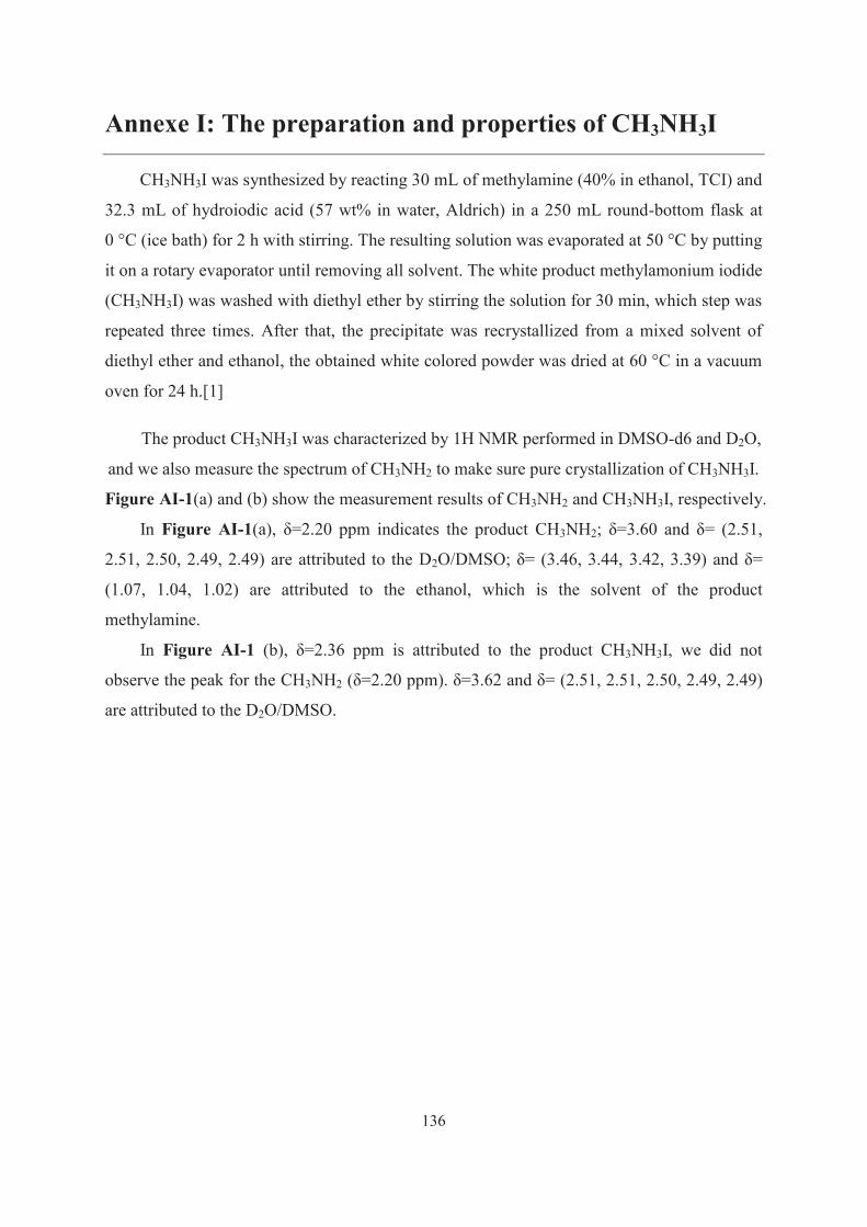
136
Annexe I: The preparation and properties of CH3NH3I
CH3NH3I was synthesized by reacting 30 mL of methylamine (40% in ethanol, TCI) and
32.3 mL of hydroiodic acid (57 wt% in water, Aldrich) in a 250 mL round-bottom flask at
0 °C (ice bath) for 2 h with stirring. The resulting solution was evaporated at 50 °C by putting
it on a rotary evaporator until removing all solvent. The white product methylamonium iodide
(CH3NH3I) was washed with diethyl ether by stirring the solution for 30 min, which step was
repeated three times. After that, the precipitate was recrystallized from a mixed solvent of
diethyl ether and ethanol, the obtained white colored powder was dried at 60 °C in a vacuum
oven for 24 h.[1]
The product CH3NH3I was characterized by 1H NMR performed in DMSO-d6 and D2O,
and we also measure the spectrum of CH3NH2 to make sure pure crystallization of CH3NH3I.
Figure AI-1(a) and (b) show the measurement results of CH3NH2 and CH3NH3I, respectively.
In Figure AI-1(a), δ=2.20 ppm indicates the product CH3NH2; δ=3.60 and δ= (2.51,
2.51, 2.50, 2.49, 2.49) are attributed to the D2O/DMSO; δ= (3.46, 3.44, 3.42, 3.39) and δ=
(1.07, 1.04, 1.02) are attributed to the ethanol, which is the solvent of the product
methylamine.
In Figure AI-1 (b), δ=2.36 ppm is attributed to the product CH3NH3I, we did not
observe the peak for the CH3NH2 (δ=2.20 ppm). δ=3.62 and δ= (2.51, 2.51, 2.50, 2.49, 2.49)
are attributed to the D2O/DMSO.
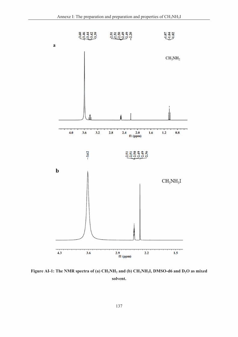
Annexe I: The preparation and preparation and properties of CH3NH3I
137
Figure AI-1: The NMR spectra of (a) CH3NH2 and (b) CH3NH3I, DMSO-d6 and D2O as mixed
solvent.
138
Annexe II: The properties of TiO2 NT layers based dye
sensitized solar cells
The TiO2 NT layers were prepared as described in Chapter 2, Section 2.4. They were
finally annealed at 500°C for 30 min. The layers were immersed upon cooling in a 0.5
mmol.L-1
N719 dye solution. The dye was dissolved in a solvent mixture of acetonitrile and
tert-butanol (1:1) plus one equivalent of tetrabutylammonium hydroxide. The sensitization
occurred in the dark, at room temperature for 24h. For the counter electrode preparation,
TEC-7 FTO glass substrates were cleaned by ultrasound in acetone and ethanol for 5 min
each. They were then treated in a furnace for 30 min at 450°C to remove organic
contaminants. The Pt catalyst was deposited on the FTO glass by coating with a droplet of
H2PtCl6 solution (6 mg in 1 mL ethanol) and subsequently heated at 400°C for 20 min. This
step was repeated once. The two electrodes were sealed with a 50 mm hot melt spacer (Surlyn,
DuPont). The internal space was filled with the electrolyte through a hole drilled in the
counter electrode, which was subsequently sealed with Surlyn and an aluminum foil. The
electrolyte employed was a solution of 0.6 mol.L-1
1,2-dimethyl-3-propylimidazolium iodide
(DMPII), 0.1 mol.L-1
LiI, 0.05 mol.L-1
I2, 0.10 mol.L-1
guanidinium thiocyanate and 0.5
mol.L-1
4-tertbutylpyridine in a mixture of acetonitrile and valeronitrile (85/15 volume
ratio).[2]
Their photovoltaic characteristics are gathered in Table AII-1. The I-V curves are
shown in the Figure AII-1. The efficiency increased with longer (NH4)2TiF6 treatment time
and ZnO NW electrodeposition time due to the thicker TiO2 layer. Moreover, for long
treatment time the structures were covered by spikes as shown in Figure 2.6e, f, which
significantly increase the internal surface area and then the dye loading. The best N719
sensitized TiO2 solar cell efficiency was 3.08%. It was achieved by increasing the ZnO NW
template deposition time at 5 h instead of 2h30min.
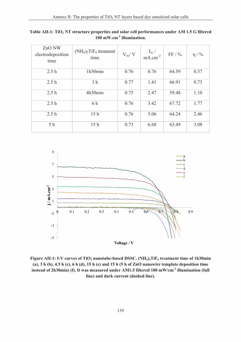
Annexe II: The properties of TiO2 NT layers based dye sensitized solar cells
139
Table AII-1: TiO2 NT structure properties and solar cell performances under AM 1.5 G filtered 100 mW.cm-2 illumination.
ZnO NW
electrodeposition
time
(NH4)2TiF6 treament
time Voc/ V
Jsc /
mA.cm-2
FF / % η / %
2.5 h 1h30min 0.76 0.76 64.59 0.37
2.5 h 3 h 0.77 1.41 66.91 0.73
2.5 h 4h30min 0.75 2.47 59.48 1.10
2.5 h 6 h 0.76 3.42 67.72 1.77
2.5 h 15 h 0.76 5.06 64.24 2.46
5 h 15 h 0.73 6.68 63.49 3.08
Figure AII-1: I-V curves of TiO2 nanotube-based DSSC. (NH4)2TiF6 treatment time of 1h30min (a), 3 h (b), 4.5 h (c), 6 h (d), 15 h (e) and 15 h (5 h of ZnO nanowire template deposition time instead of 2h30min) (f). It was measured under AM1.5 filtered 100 mW/cm-2 illumination (full
line) and dark current (dashed line).

Annexe II: The properties of TiO2 NT layers based dye sensitized solar cells
140
References
[1] L. Etgar, P. Gao, Z. Xue, Q. Peng, A.K. Chandiran, B. Liu, M.K. Nazeeruddin, M.
Grätzel, “Mesoscopic CH3NH3PbI3/TiO2 Heterojunction Solar Cells,” J. Am. Chem.
Soc., vol. 134, no. 42, pp. 17396–17399, Oct. 2012. [2] Y. Kusumawati, M.A. Martoprawiro, T. Pauporté, “Effects of Graphene in
Graphene/TiO2 Composite Films Applied to Solar Cell Photoelectrode,” J. Phys. Chem.
C, vol. 118, no. 19, pp. 9974–9981, Apr. 2014.
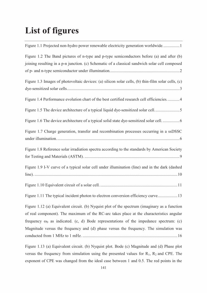
141
List of figures
Figure 1.1 Projected non-hydro power renewable electricity generation worldwide. ............... 1
Figure 1.2 The Band pictures of n-type and p-type semiconductors before (a) and after (b)
joining resulting in a p-n junction. (c) Schematic of a classical sandwich solar cell composed
of p- and n-type semiconductor under illumination. .................................................................. 2
Figure 1.3 Images of photovoltaic devices: (a) silicon solar cells, (b) thin-film solar cells, (c)
dye-sensitized solar cells............................................................................................................ 3
Figure 1.4 Performance evolution chart of the best certified research cell efficiencies. ........... 4
Figure 1.5 The device architecture of a typical liquid dye-sensitized solar cell. ....................... 5
Figure 1.6 The device architecture of a typical solid state dye-sensitized solar cell. ................ 6
Figure 1.7 Charge generation, transfer and recombination processes occurring in a ssDSSC
under illumination. ..................................................................................................................... 6
Figure 1.8 Reference solar irradiation spectra according to the standards by American Society
for Testing and Materials (ASTM). ........................................................................................... 9
Figure 1.9 I-V curve of a typical solar cell under illumination (line) and in the dark (dashed
line). ......................................................................................................................................... 10
Figure 1.10 Equivalent circuit of a solar cell. .......................................................................... 11
Figure 1.11 The typical incident photon to electron conversion efficiency curve................... 13
Figure 1.12 (a) Equivalent circuit. (b) Nyquist plot of the spectrum (imaginary as a function
of real component). The maximum of the RC-arc takes place at the characteristics angular
frequency w0 as indicated. (c, d) Bode representations of the impedance spectrum: (c)
Magnitude versus the frequency and (d) phase versus the frequency. The simulation was
conducted from 1 MHz to 1 mHz. ........................................................................................... 16
Figure 1.13 (a) Equivalent circuit. (b) Nyquist plot. Bode (c) Magnitude and (d) Phase plot
versus the frequency from simulation using the presented values for R1, R2 and CPE. The
exponent of CPE was changed from the ideal case between 1 and 0.5. The red points in the

List of figures
142
Nyquist plot correspond to the 10000 Hz freqency. The simulation was conducted from 10
MHz to 1 mHz. ........................................................................................................................ 18
Figure 1.14 Equivalent circuit employed for fitting the impedance spectra. ........................... 19
Figure 1.15 Number of publications and efficiency evolution of the perovskite solar cells
(updated up to 2015.02.01). The inset is the crystal structure of perovskite (ABX3) with a
cubic symmetry. ....................................................................................................................... 20
Figure 1.16 (a) Ball and stick model (b) three dimensional of cubic perovskite of general
formula AMX3. ........................................................................................................................ 21
Figure 1.17 (a) A schematic illustration of perovskite-sensitized TiO2 undergoing
photoexcitation and electron transfer. (b) IPCE action spectra for photoelectrochemical cells
using CH3NH3PbBr3/TiO2 (solid line) and CH3NH3PbI3/TiO2 (dashed line). ......................... 22
Figure 1.18 CH3NH3PbI3 perovskite sensitized solar cell device and its photovoltaic
characteristics. (a) Real solid-state device. (b) Cross-sectional structure of the device. (c)
Cross-sectional SEM image of the device. (d) Photocurrent density as a function of the
forward bias voltage. ................................................................................................................ 23
Figure 1.19 Schematic illustrating the charge transfer and charge transport in a perovskite-
sensitized TiO2 solar cell (left) and a noninjecting Al2O3-based solar cell (right); a
representation of the energy landscape is shown below, with electrons shown as solid circles
and holes as open circles .......................................................................................................... 24
Figure 1.20 (a) SEM cross-sectional image of inorganic–organic hybrid heterojunction solar
cell. (b) Schematic of device architecture ................................................................................ 24
Figure 1.21 The cross-sectional SEM of a complete photovoltaic device (a) and J-V curves
for a best performance cell (b). ................................................................................................ 25
Figure 1.22 Cross-sectional SEM images of the cell device (A), and diagram of energy level
of each layer in the device (B). ................................................................................................ 26
Figure 1.23 Stability of cells stored in the ambient air, dry air and N2 atmosphere. ............... 26
Figure 1.24 (A) Schematic of the triple layer (5-AVA)x(MA)(1-x)PbI3 perovskite based solar
cell. (B) Stability test of a triple layer perovskite sensitized mesoscopic solar cell. ............... 27
List of figures
143
Figure 1.25 Molecular structure of 2,2’,7,7’-tetrakis-N,N-di(4-methoxyphenyl)amine-9,9’-
spirobifluorene (spiro-MeOTAD), utilized as the HTM in PSCs. ........................................... 30
Figure 1.26 Time-dependent evolutions of (a) short-circuit current density, Jsc, (b) fill factor,
(c) open-circuit voltage, Voc, and (d) efficiency of the solar cells without encapsulation stored
in the dark and under different atmospheric conditions. .......................................................... 31
Figure 2.1 Current density (lines) and electrical charge exchanged (dots) upon ZnO layer
deposition at different applied potentials. ................................................................................ 43
Figure 2.2 (Left) Photography of the electrochemical experimental setup used in the thesis for
the oxide layer preparation, (right) FE-SEM top views of ZnO films for different applied
potentials and deposition times: -1.15 V for 120 s (a and b), -0.95 V for 300 s (c and d), -0.9V
for 420 s (e and f). .................................................................................................................... 44
Figure 2.3 SEM top view of the FTO substrate after the TiCl4 treatment. .............................. 46
Figure 2.4 FE-SEM views of ZnO nanostructure arrays deposited on FTO (a), TiO2 seed layer
(c, d) and ZnO seed layer (e, f) with 2h30min of deposition time at 85°C.............................. 47
Figure 2.5 FE-SEM top and cross-section views of ZnO nanowires/nanorods with controlled
concentration of ZnCl2 in solution, deposition time (td) and bath temperature. ...................... 48
Figure 2.6 FE-SEM top and cross-sectional views of ZnO layers with i-ZnO overlayer for a
deposition time of 10 s (a and b) and 20 s (c and d). ............................................................... 49
Figure 2.7 (a-f) FE-SEM images top view of TiO2 nanotubes prepared from a ZnO NW
template with 20 min (a), 90 min (b), 3 h (c), 4.5 h (d), 6 h (e) and 15 h (f) of titanate
treatment time. The cross sectional view of TiO2 nanotube with 6 h (g) and 15 h (h) of growth
time. ......................................................................................................................................... 51
Figure 2.8 FE-SEM top view of (a) FTO coated substrate, (b) TiO2 blocking layer, (c)
mesoporous TiO2 nanoparticle layer. ....................................................................................... 52
Figure 3.1 Two-step preparation protocol of CH3NH3PbI3 perovskite layer........................... 59
Figure 3.2 SEM cross sectional view (a) and top-view (b) of the CH3NH3PbI3 layer deposited
on the ZnO nanowire arrays. .................................................................................................... 60
List of figures
144
Figure 3.3 XRD pattern of CH3NH3PbI3 deposited on the ZnO nanowire arrays. .................. 61
Figure 3.4 The absorbance spectra (a) and direct bandgap (b) of CH3NH3PbI3 using ZnO
nanowire as scaffold layer. ...................................................................................................... 61
Figure 3.5 Schematic of the energy levels of perovskite and the other compoments in the PSC
device. ...................................................................................................................................... 62
Figure 3.6 Schematic drawing of the investigated PSC based on electrodeposited ZnO
nanostructures. ......................................................................................................................... 63
Figure 3.7 TEM view of a ZnO NW covered by the i-ZnO layer. .......................................... 64
Figure 3.8 Variation of Z05i solar cell J-V curve parameters with the storage time in air at
room temperature in a dry place. ............................................................................................. 65
Figure 4.1 FE-SEM cross sectional view of CH3NH3PbI3 deposited on the i-ZnO layer (120 s).
.................................................................................................................................................. 78
Figure 4.2 (a) XRD patterns and (b) total optical transmittance of i-ZnO layers deposited for
120s on ITO/glass and on FTO/glass substrate. The inset shows the ZnO direct optical
bandgap determination. ............................................................................................................ 80
Figure 4.3 Photovoltaic parameters and J-V curves for the i-ZnO solar cells prepared on FTO
and ITO substrates. (AM1.5G filtered full 1 sun illumination). .............................................. 81
Figure 4.4 (a) Histogram of cells efficiency compared with different substrates; (b) Long-
term performance stability of an ITO/ZnO/CH3NH3PbI3/HTM/Ag cell. ................................ 82
Figure 5.1 FE-SEM images of the oxide layers. Top views of (a) i-ZnO-420s layer (b) i-ZnO-
120s layer and (d) np-TiO2 layer. Cross-sectional views of i-ZnO-420s layer (a inset) and i-
ZnO-120s layer (c). .................................................................................................................. 99
Figure 5.2 (a) XRD patterns of i-ZnO and TiO2 layers. (b) Raman spectra of i-ZnO layers
and TiO2 layer. ....................................................................................................................... 100
Figure 5.3 (a) Total optical transmittance of i-ZnO and TiO2 layers. (b) Room temperature
photoluminescence spectra (lexc=266 nm) of the i-ZnO and TiO2 layers. ............................ 101
List of figures
145
Figure 5.4 (a) Direct bandgap determination of i-ZnO-420s and i-ZnO-120s layers. (b)
Indirect bandgap determination of np-TiO2 layer. ................................................................. 102
Figure 5.5 (a) Images of one-step perovskite layers deposited on i-ZnO-120s with increasing
annealing time at 100°C. The sample 2 days was stored for two days after an annealing
treatment of 20 min. (b) XRD patterns of the heterostructures presented in (a). .................. 104
Figure 5.6 (a) Images of one-step perovskite layer deposited on the np-TiO2 upon annealing
for various times. (b) XRD pattern of the heterostructures presented in (a). ......................... 105
Figure 5.7 (a) Images of two-step perovskite layers deposited on the i-ZnO-120s substrate for
various annealing times. (b) XRD patterns of perovskite layers presented in (a). ................ 106
Figure 5.8 (a) Images of two-step perovskite layers prepared on the np-TiO2 layer for various
annealing time (b) XRD patterns of two-step perovskite layers presented in (a). ................. 107
Figure 5.9 (a-c) SEM top-views of CH3NH3PbI3 one-step sensitized (a) i-ZnO-420s, (b) i-
ZnO-120s and (c) np-TiO2. High magnification views are shown as inset in (a) and (c). (d-e)
SEM top-views of CH3NH3PbI3 two-step sensitized (d) i-ZnO-420s, (e) i-ZnO-120s and (f)
np-TiO2. ................................................................................................................................. 108
Figure 5.10 High magnification SEM top-views of CH3NH3PbI3 two-step sensitized (a) i-
ZnO-120s and (b) np-TiO2. .................................................................................................... 109
Figure 5.11 (a) Absorbance spectra of one-step and two-step CH3NH3PbI3 layers deposited
on ZnO and TiO2 underlayers. (b) Absorbance spectra of one-step CH3NH3PbI3 layer
deposited on ZnO annealed for 2 min, 20 min and 50 min at 100°C. The dashed line is a two-
step perovskite deposited on the same substrate. ................................................................... 109
Figure 5.12 Direct bandgap determination of (a) one-step perovskite and (b) two-step
perovskite deposited on various underlayers. ........................................................................ 110
Figure 5.13 Direct bandgap determination of the degradation product of one-step perovskite
deposited on i-ZnO-420s annealed for 50 min at 100 °C. The 2.4 eV bandgap is in agreement
with the formation of the 2H polytype of PbI2. ..................................................................... 111
Figure 5.14 (a) I-V curves of one-step perovskite and (b) two-step perovskite solar cells
prepared using various oxide underlayers.............................................................................. 112
List of figures
146
Figure 5.15 SEM cross-section of the i-ZnO-420s/one-step CH3NH3PbI3 solar cell. ........... 114
Figure 5.16(a) Impedance spectra measured at 0.5V, (b) Impedance spectra at various applied
voltages of sample (3) under illumination. (c) Equivalent electrical circuit used for fitting the
data. (d) Variation of Rsc with applied voltage and (e) variation of Rrec with the applied
voltage. (1) i-ZnO-420s/one-step perovskite solar cell; (2) i-ZnO-120s/two-step perovskite
solar cell, (3) i-ZnO-120s/one-step perovskite solar cell. ...................................................... 115
Figure 6.1: SEM top views of (a) ZnO NW array and (b) TiO2 NT array. (c) SEM cross-
sectional view of TiO2 NT array. (d) TEM view of electrodeposited ZnO NW (inset selected
area electron diffraction (SAED) pattern). (e) TEM view of TiO2 nanotube structure (inset
SAED pattern). ....................................................................................................................... 122
Figure 6.2: (a) XRD patterns of (1) ZnO NW array, (2) TiO2 NT after TiCl4 treatment and (3)
TiO2 NT/CH3NH3PbI3. (b) Raman spectra of (1) ZnO NW array, (2) TiO2 NT 4.5 h, (3) TiO2
NT 6 h and (4) TiO2 NT 15 h. (The stars mark peaks assigned to the FTO substrate). ......... 124
Figure 6.3 (a) Reflectance spectra of (1) TiO2 NP layer and (2) TiO2 NT 4.5 h. (b)
Absorbance spectra of the CH3NH3PbI3 sensitized structures based on (1) reference TiO2 NP,
(2) TiO2 NT 4.5 h, (3) TiO2 NT 6 h and (4) TiO2 NT 15 h. .................................................. 125
Figure 6.4: J-V curves recorded under AM1.5 filtered 100 mW.cm-2
illumination and in the
dark. (1) TiO2 NP reference cell, (2) TiO2 NT 4.5 h, (3) TiO2 NT 6 h and (4) TiO2 NT 15 h.
Dashed line: short circuit (SC) to flat band (FB) scan direction. Full line: FB to SC scan
direction. ................................................................................................................................ 126
Figure 6.5 Determination of the JSC-FB and JFB-SC from the I-V curve. Full line: short circuit
(SC) to flat band (FB) scan direction. Dashed line: FB to SC scan direction........................ 127
Figure AI-1: The NMR spectra of (a) CH3NH2 and (b) CH3NH3I, DMSO-d6 and D2O as
mixed solvent. ...………….…………………………………………………………….…137
Figure AII-1: I-V curves of TiO2 nanotube-based DSSC. (NH4)2TiF6 treatment time of
1h30min (a), 3 h (b), 4.5 h (c), 6 h (d), 15 h (e) and 15 h (5 h of ZnO nanowire template
deposition time instead of 2h30min) (f). It was measured under AM1.5 filtered 100 mW/cm-2
illumination (full line) and dark current (dashed line). …………………………………….139

147
List of tables
Table 1.1 Relationship and impedance corresponding to bulk electrical elements. Furthermore,
the corresponding electrical equivalent circuit symbols are presented. The graphical
representation of the impedance is displayed in the Nyquist plots where Z¢ and Z¢¢ are the real
and imaginary components respectively. ................................................................................. 15
Table 2.1 Characteristics of electrodeposited ZnO layers on FTO with various applied
potentials. ................................................................................................................................. 43
Table 2.2 Morphological parameters of electrodeposited ZnO layer structures. D is the mean
diameter of NWs/NRs and L is the wire length or layer thickness. ......................................... 49
Table 3.1 The I-V curve photovoltaic parameters under AM1.5G filtered 100 mW.cm−2
illumination of solar cells based on electrodeposited ZnO layered structures (SC to FB scan
direction measurement). ........................................................................................................... 64
Table 4.1 Effect of the i-ZnO deposition time on the I-V characteristics of the PSCs.
(AM1.5G filtered full 1 sun illumination) ............................................................................... 79
Table 4.2 The characteristics of i-ZnO deposited on the FTO and ITO coated substrate. ...... 79
Table 5.1 Characteristics of ZnO and TiO2 films used as an electron transport layer. ............ 99
Table 5.2 Effect of perovskite preparation route and selective contact material on I-V curve
characteristics (AM1.5G, 100 mW.cm-2
) ............................................................................... 113
Table 6.1: TiO2 NT structure properties and solar cell performances under AM1.5 G filtered
100 mW.cm-2
illumination. The reference cell was prepared using a nanoparticle TiO2
scaffold layer. The PCE is the power conversion efficiency and HI is the hysteresis
index………………………………………………………………………………………...123
Table 6.2: Effect of the initial ZnO NW preparation conditions on the cell performances
measured under AM1.5G filtered 100 mW.cm-2
illumination. The TiO2 NTs were treated by
TiCl4. ...................................................................................................................................... 128
Table AII-1: TiO2 NT structure properties and solar cell performances under AM 1.5 G
filtered 100 mW.cm-2
illumination. …...…………………………………………...……….138

148

149
List of the abbreviations and symbols
PV
Photovoltaic
DSSC Dye-sensitized solar cell
ssDSSC Solid state dye sensitized solar cell
PSC Perovskite solar cell
HTL Hole transport layer
TCO Transparent conductive oxide
ETL Electron transport layer
LUMO Lowest unoccupied molecular orbital
HOMO Highest occupied molecular orbital
Voc Open-circuit potential
Jsc Short-circuit photocurrent
FF Fill factor
PCE Power conversion efficiency
IPCE Incident photon-to-current conversion efficiency
APCE Absorbed photon-to-current conversion efficiency
Pmax Maximum output electrical power
Pin Incident power
e Elementary charge
k Boltzman constant
T Temperature
Rs Series resistance
Rp Shunt resistance
Rrec Recombination resistance
CB Conduction band
VB Valence band
l Wavelength
ν Light frequency
η Cell efficiency=PCE
ηcoll Charge collection efficiency
eV Electron volt
List of the abbreviations and symbols
150
IS Impedance spectroscopy
FTO Fluorine-doped tin oxide
ITO Indium tin oxide
TBP 4-tert-butylpyridine
LiTFSI Bis(trifluoromethane)sulfonimide lithium salt
FE-SEM Field emission scan electron microscopy
XRD X-ray diffraction
BL-TiO2 TiO2 blocking layer
np-TiO2 TiO2 nanoparticle
Rrms Root mean square of roughness
Q Electrical charge density
PL Photoluminescence
LPD Liquid phase deposition
SC-FB Short circuit to forward bias
HI Hysteresis index
DMPII 1,2-dimethyl-3-Propylimidazolium iodide
TiO2 NT TiO2 nanotube
NW/NR nanowire/nanorod
ETM Electron transport material

151
List of publications
(1) Jie, Zhang; Philippe, Barboux; Thierry, Pauporte, Electrochemical Design of
Nanostructured ZnO Charge Carrier Layers for Efficient Solid-State Perovskite-Sensitized
Solar Cells, ADVANCED ENERGY MATERIALS, 4, 1400932.
(2) Jie Zhang, Emilio José Juárez-Pérez, Iván Mora-Seró, Bruno Viana, Thierry Pauporté,
Fast and low temperature growth of electron transport layers for efficient perovskite solar
cells, Journal of Materials Chemistry A.2015,3, 4909-4915.
(3) Jie Zhang, Thierry Pauporté, Effect of Oxide Contact Layer on the Preparation and
Properties of CH3NH3PbI3 for Perovskite Solar Cell Application, The Journal of Physical
Chemistry C. 2015, 119, 14919–14928.
(4) Jie Zhang, Thierry Pauporté, One-Dimensional Self-Standing TiO2 Nanotube Array
Layers Designed for Perovskite Solar Cell Applications, ChemPhysChem, accepted.
(5) Zhang, H; Babichev, AV; Jacopin, G; Lavenus, P; Julien, FH; Egorov, AY; Zhang, J;
Pauporte, T; Tchernycheva, M, Characterization and modeling of a ZnO nanowire ultraviolet
photodetector with graphene transparent contact, JOURNAL OF APPLIED PHYSICS,
2013,114, 234505(1-9).
(6) Thierry Pauporté, Oleg Lupan, Jie Zhang, Tugba Tugsuz, Ilaria Ciofini, Frédéric Labat,
Bruno Viana, Low Temperature Preparation of Ag-doped ZnO Nanowire Arrays, DFT Study
and Application to Light Emitting Diode, ACS Applied Materials & Interfaces, 2015, 7,
11871−11880.
(7) J. Zhang and T Pauporté, Low temperature preparation of (nano)structrured oxide
films as selective contacts in perovskite solar cells, oral presentation. E-MRS Spring Meeting
2015.