Incremental construction of classifier and discriminant ensembles
Upload
independentCategory
view
0download
0
Thermoelectric power factors of nanocarbon ensembles as a function of temperatureD. M. Gruen, P. Bruno, R. Arenal, J. Routbort, D. Singh, and M. Xie
Citation: Journal of Applied Physics 105, 073710 (2009); doi: 10.1063/1.3103244 View online: http://dx.doi.org/10.1063/1.3103244 View Table of Contents: http://scitation.aip.org/content/aip/journal/jap/105/7?ver=pdfcov Published by the AIP Publishing Articles you may be interested in Thermoelectric properties of PbTe with encapsulated bismuth secondary phase J. Appl. Phys. 113, 123707 (2013); 10.1063/1.4796148 The role of boron segregation in enhanced thermoelectric power factor of CoSi1xBx alloys J. Appl. Phys. 110, 123711 (2011); 10.1063/1.3671066 Induction annealing and subsequent quenching: Effect on the thermoelectric properties of boron-dopednanographite ensembles Rev. Sci. Instrum. 81, 043909 (2010); 10.1063/1.3378681 Configurational, electronic entropies and the thermoelectric properties of nanocarbon ensembles Appl. Phys. Lett. 92, 143118 (2008); 10.1063/1.2909150 Structure of nanocrystalline Re–Si thin film composites and their unusual thermoelectric properties J. Appl. Phys. 89, 3229 (2001); 10.1063/1.1333738
[This article is copyrighted as indicated in the article. Reuse of AIP content is subject to the terms at: http://scitation.aip.org/termsconditions. Downloaded to ] IP:
198.11.30.111 On: Fri, 26 Sep 2014 23:54:56
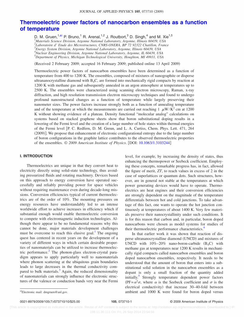
Thermoelectric power factors of nanocarbon ensembles as a functionof temperature
D. M. Gruen,1,a� P. Bruno,1 R. Arenal,1,2 J. Routbort,3 D. Singh,4 and M. Xie1,5
1Materials Science Division, Argonne National Laboratory, Argonne, Illinois 60439, USA2Laboratoire d’ Etude des Microstructures, CNRS-ONERA, BP 72 92322 Chatillon, France3Energy System Division, Argonne National Laboratory, Argonne, Illinois 60439, USA4Nuclear Engineering Division, Argonne National Laboratory, Argonne, IL 60439, USA5Department of Physics, Michigan Technological University, Houghton, MI 49931, USA
�Received 2 February 2009; accepted 16 February 2009; published online 13 April 2009�
Thermoelectric power factors of nanocarbon ensembles have been determined as a function oftemperature from 400 to 1200 K. The ensembles, composed of mixtures of nanographite or disperseultrananocrystalline diamond with B4C, are formed into mechanically rigid compacts by reaction at1200 K with methane gas and subsequently annealed in an argon atmosphere at temperatures up to2500 K. The ensembles were characterized using scanning electron microscopy, Raman, x-raydiffraction, and high resolution transmission electron microscopy techniques and found to undergoprofound nanostructural changes as a function of temperature while largely preserving theirnanometer sizes. The power factors increase strongly both as a function of annealing temperatureand of the temperature at which the measurements are carried out reaching 1 �W /K2 cm at 1200K without showing evidence of a plateau. Density functional “molecular analog” calculations onsystems based on stacked graphene sheets show that boron substitutional doping results in alowering of the Fermi level and the creation of a large number of hole states within thermal energiesof the Fermi level �P. C. Redfern, D. M. Greun, and L. A. Curtiss, Chem. Phys. Lett. 471, 264�2009��. We propose that enhancement of electronic configurational entropy due to the large numberof boron configurations in the graphite lattice contributes to the observed thermoelectric propertiesof the ensembles. © 2009 American Institute of Physics. �DOI: 10.1063/1.3103244�
I. INTRODUCTION
Thermoelectrics are unique in that they convert heat toelectricity directly using solid-state technology, thus avoid-ing pressurized fluids and rotating machinery. Devices basedon this approach to energy conversion have operated suc-cessfully and reliably providing power for space vehicleswithout requiring maintenance even during decade-long mis-sions. Conversion efficiencies typical of current thermoelec-trics are of the order of 10%. The mounting pressures onenergy resources have understandably led to an intenseworldwide effort to achieve increases in efficiency which ifsubstantial enough would enable thermoelectric conversionto compete with electromagnetic induction technologies. Al-though there appear to be no fundamental reasons why thiscannot be done, major materials development challengesmust be overcome to reach this elusive goal.1 The ongoingquest has centered in recent years on the development of avariety of different ways in which certain desirable proper-ties of nanomaterials can be utilized to increase thermoelec-tric performance.2 The phonon-glass electron-crystal para-digm appears to apply particularly well to nanomaterialswhere phonon scattering at the ubiquitous grain boundariesleads to large decreases in the thermal conductivity com-pared to bulk materials.3 Again, the reduced dimensionalityof nanomaterials can strongly influence the electronic struc-tures of the valence or conduction bands very near the Fermi
level, for example, by increasing the density of states, thusenhancing the thermopower or Seebeck coefficient. Employ-ing these concepts, remarkable progress has, in fact, allowedthe figure of merit, ZT, to reach values in excess of 2 in thecase of superlattices or quantum dots. Such structures, how-ever, are in general not stable at the temperatures at whichpower generating devices would have to operate. Thermo-electrics are heat engines and their conversion efficienciesare strongly dependent on the magnitude of the temperaturedifferentials between hot and cold junctions. To take advan-tage of this fact, one wants to operate the hot junction con-tinuously at temperatures of about 1400 K. Very few materi-als preserve their nanocrystallinity under such conditions. Itis for this reason that carbon and, in particular, boron dopednanocarbons were chosen as model systems for studies oftheir thermoelectric performance characteristics.4
In that earlier work it was shown that reaction of dis-perse ultrananocrystalline diamond �UNCD� and mixtures ofUNCD with 10%–20% nano-boron-carbide �B4C� withmethane gas at temperatures near 1200 K results in mechani-cally rigid compacts called nanocarbon ensembles and borondoped nanocarbon ensembles, respectively. It needs to beunderstood that the amount of boron that enters into a sub-stitutional solid solution in the nanocarbon ensembles as adopant is only a small fraction of the quantity addedinitially.5 Strongly temperature dependent power factors�PF=�2�, where � is the Seebeck coefficient and � is theelectrical conductivity� that increase 30–40-fold betweenambient and 1000 K were found for boron doped versusa�Electronic mail: [email protected].
JOURNAL OF APPLIED PHYSICS 105, 073710 �2009�
0021-8979/2009/105�7�/073710/10/$25.00 © 2009 American Institute of Physics105, 073710-1
[This article is copyrighted as indicated in the article. Reuse of AIP content is subject to the terms at: http://scitation.aip.org/termsconditions. Downloaded to ] IP:
198.11.30.111 On: Fri, 26 Sep 2014 23:54:56
undoped material.4 Here we present recent results aimed atenhancing the thermoelectric performance of these en-sembles including materials prepared by reacting methanewith boron doped nanographite �NG� starting materials. Inthe current paper, measurements of PFs have been made upto 1200 K on samples annealed at temperatures up to 2500K. Anticipating the detailed discussion of the results we notethat the PFs continue to increase even at 1200 K, the currentlimit of our measuring apparatus. For a given temperature,they are more than an order of magnitude larger than forunannealed nanocarbon ensembles due both to increasingSeebeck coefficients and electrical conductivities.
The current work is part of a materials development pro-gram based on multicomponent nanoensembles chosen inpart for its flexible processing conditions. This approach en-ables one to exploit advantageously a large parameter spacethat can be varied over a wide range. An important goal ofthe research is the discovery of optimization criteria operat-ing in concert on all three quantities entering the expressionfor the figure of merit of thermoelectric materials. Optimizedproperties, particularly if they reinforce one another, mightbe able to overcome to some degree the performance limita-tions of current thermoelectric materials.
II. EXPERIMENTAL DETAILS
Disperse UNCD �5–10 nm particle size� or NG �30 nmparticle size� powders,6,7 either pristine or mechanicallymixed with 5 wt % of nano-B4C �50 nm particle size�,8 wereplaced in 20�10�5 mm3 highly oriented pyrolitic graphitecrucibles and treated with methane gas in a quartz vesselheated in several intervals from ambient temperatures to1200 K in a tube furnace. The contents of the cruciblesgained between 70% and 100% in weight with the greatestchange occurring between 950 and 1050 K. For UNCD, NG,and their mixtures with B4C this procedure resulted in theformation of mechanically rigid compacts with densities of1.5–1.7 g /cm3. From now on the ensembles containingUNCD will be referred to as NDEs and those containing NGas NGEs. The corresponding samples mixed with B4C willbe labeled as doped NDEs and doped NGEs, respectively.Ensembles heated to 1200 K are called “as-fabricated”samples to distinguish from samples that have been annealedin a mixture of Ar-4%H2 in a furnace with SiC heating ele-ments to 1700 K and in a carbon furnace in argon to 2500 Kfor varying lengths of times. Some of the samples experi-enced a minor weight loss after annealing.
Scanning electron microscopy �SEM� micrographs wereobtained using a HITACHI S-4700 field emission gun scan-ning electron microscope. Raman spectra at an excitationwavelength of 632.8 nm were collected at room temperature,using a Renishaw micro-Raman RM2000 on a 50� objectiveover the range of 50–4000 cm−1 using an �1 �m spot size.No sample preparation was required as measurements werefound to be highly reproducible for different sample areas.X-ray diffraction �XRD� data �Rigaku miniflex+diffractometer with Cu K� radiation ��=0,154 nm�� werecollected from 3° to 90° 2� with a scan speed of 2 s/step anda step size of 0.02°. Diffraction patterns were taken of as
fabricated and as well as of annealed samples. Phase identi-fication was based on the International Center for DiffractionData database.
High resolution transmission electron microscopy �HR-TEM� was performed using a field emission FEI Tecnai F20operating at 200 keV. The transmission electron microscopy�TEM� samples were prepared by scraping the compact bulksamples and dispersing the resulting powders in ethanol. Thedispersions were ultrasonicated and subsequently depositedon a holey carbon 3 mm copper grid.
Seebeck coefficients and dc electrical conductivitieswere measured using an apparatus based on a well-established design.9 It consists of a 1800 K, single-zone tube�mullite, 4.4 cm inside diameter� furnace and controller, aKeithley 2700 multimeter/data acquisition system, and aKeithley 6220 current source, all controlled by a computerusing LABVIEW. The ends of the tube were water cooled andsealed with end caps that allowed fittings for thermocouplesand gas inlet/outlet valves.
The alumina sample holder made from a closed-end tubefits into a larger outer tube. One-half of the outer wall wasremoved about 10 cm from the closed end for access. Aspring-loaded alumina push rod was used to hold the sample�25�8�3 mm3� against Pt foils placed at each end of thesample. Pt /Pt+10% Rh thermocouples were spot welded tothe foils. The thermocouples were used both to measure tem-perature and to supply 10 mA of current for the conductivitymeasurements as well as the temperature. Two small notchescut in the sample by a thin �0.175 mm� diamond saw blade atpositions about 1/3 and 2/3 from the sample ends served tohold thin, tightly wound �0.075 mm� Pt wires cemented tothe sample using Pt ink. These wires secured two additionalPt /Pt+10% Rh thermocouples to measure the voltage gener-ated by the 10 mA current. The data acquisition system re-corded the conductivities as well as the six voltages and tem-peratures generated by the temperature gradient. Thegradient could be adjusted by moving the sample holder’sposition within the furnace. The Seebeck coefficient �=−lim �T→0��V /�T� was calculated from the slope of a plotof �V versus �T in the limit of �T=0. At high temperatures,there was larger scatter in the data. However, � values wereconsidered only if the regression fit parameter R2�0.90.Correction for the voltage arising from the differences in thelength of the Pt wires was included. All measurements wereperformed in flowing argon gas.
III. RESULTS
A. SEM
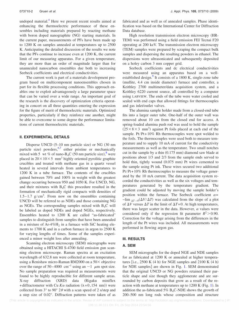
SEM micrographs for the doped NGE and NDE samplesfor as fabricated at 1200 K or annealed at higher tempera-tures �i.e., 2500 K �4 h� for NGE samples and 2100 K �4 h�for NDE samples� are shown in Fig. 1. SEM demonstratedthat the original UNCD or NG powders retained their par-ticle shape and size though they agglomerate and are sur-rounded by carbon deposits that grow as a result of the re-action with methane at temperatures up to 1200 K �Fig. 1�. Inaddition the as-fabricated 5% B4C-NDE shows the growth of200–500 nm long rods whose composition and structure
073710-2 Gruen et al. J. Appl. Phys. 105, 073710 �2009�
[This article is copyrighted as indicated in the article. Reuse of AIP content is subject to the terms at: http://scitation.aip.org/termsconditions. Downloaded to ] IP:
198.11.30.111 On: Fri, 26 Sep 2014 23:54:56
have not yet been determined. These disappear upon anneal-ing to 2100 K. No further discussion of the SEM micro-graphs will be given here. The reader is referred to Sec. III Dwhere the structural transformations of sp2 bonded carbonformed by thermal decomposition of methane are followedas a function of annealing temperature. In that section, men-tion is also made of the gradual graphitization of the UNCDparticles at the higher annealing temperatures.
B. Raman spectroscopy
Raman scattering experiments have been carried out onthe ensembles. Defect structures in the nanocarbon compo-nents of the ensembles break the hexagonal symmetry of thegraphite lattice and modify the optical selection rules for thelattice vibrational modes. A single Raman line, the G peak, istheoretically expected for single crystal graphite and is, infact, observed around 1580 cm−1 in natural graphite andstress annealed pyrolitic graphite. An additional Raman lineis observed in the range 1330–1360 cm−1 in glassy carbon,polycrystalline graphite or diamondlike carbon. This wellknown D peak, which also relates to graphitic sp2-bonding,is associated with structural disordering and its position isknown to change with excitation wavelength. The D peak is
said to arise from graphite containing disorganized regionsnear crystal edges and lattice defects �i.e., dislocations, va-cancies, and interstitial carbon atoms between the basalplanes of carbon atoms�.10
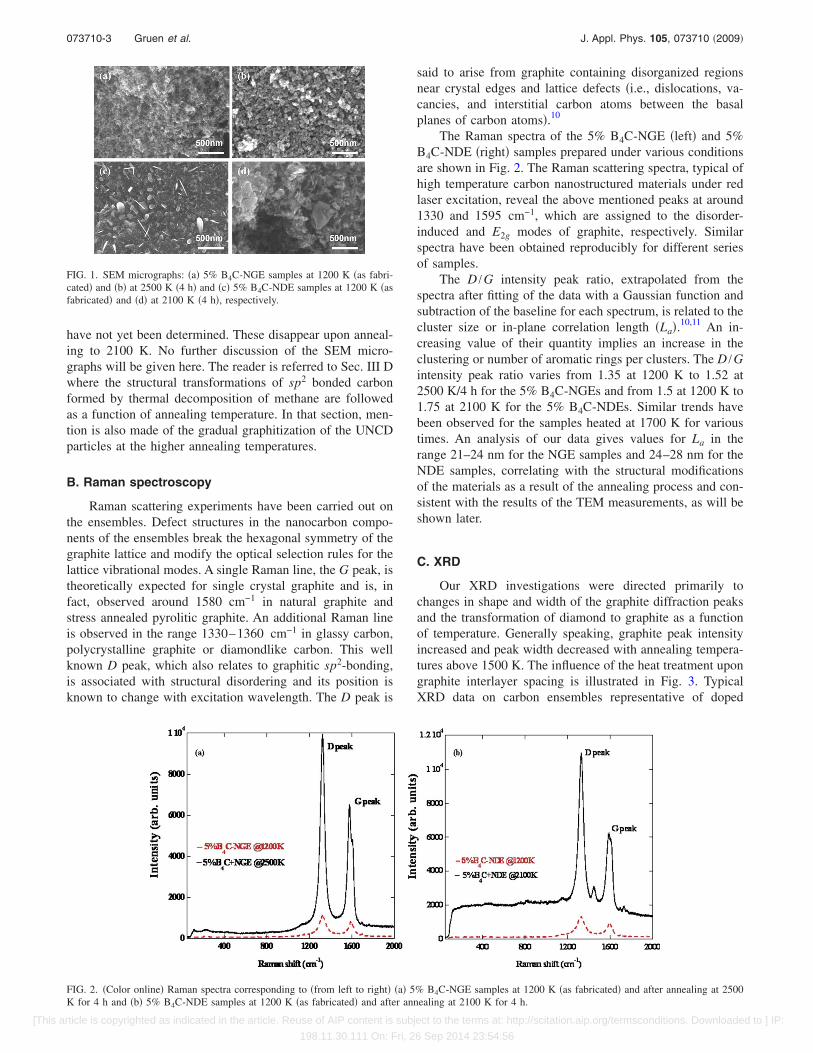
The Raman spectra of the 5% B4C-NGE �left� and 5%B4C-NDE �right� samples prepared under various conditionsare shown in Fig. 2. The Raman scattering spectra, typical ofhigh temperature carbon nanostructured materials under redlaser excitation, reveal the above mentioned peaks at around1330 and 1595 cm−1, which are assigned to the disorder-induced and E2g modes of graphite, respectively. Similarspectra have been obtained reproducibly for different seriesof samples.
The D /G intensity peak ratio, extrapolated from thespectra after fitting of the data with a Gaussian function andsubtraction of the baseline for each spectrum, is related to thecluster size or in-plane correlation length �La�.10,11 An in-creasing value of their quantity implies an increase in theclustering or number of aromatic rings per clusters. The D /Gintensity peak ratio varies from 1.35 at 1200 K to 1.52 at2500 K/4 h for the 5% B4C-NGEs and from 1.5 at 1200 K to1.75 at 2100 K for the 5% B4C-NDEs. Similar trends havebeen observed for the samples heated at 1700 K for varioustimes. An analysis of our data gives values for La in therange 21–24 nm for the NGE samples and 24–28 nm for theNDE samples, correlating with the structural modificationsof the materials as a result of the annealing process and con-sistent with the results of the TEM measurements, as will beshown later.
C. XRD
Our XRD investigations were directed primarily tochanges in shape and width of the graphite diffraction peaksand the transformation of diamond to graphite as a functionof temperature. Generally speaking, graphite peak intensityincreased and peak width decreased with annealing tempera-tures above 1500 K. The influence of the heat treatment upongraphite interlayer spacing is illustrated in Fig. 3. TypicalXRD data on carbon ensembles representative of doped
FIG. 1. SEM micrographs: �a� 5% B4C-NGE samples at 1200 K �as fabri-cated� and �b� at 2500 K �4 h� and �c� 5% B4C-NDE samples at 1200 K �asfabricated� and �d� at 2100 K �4 h�, respectively.
FIG. 2. �Color online� Raman spectra corresponding to �from left to right� �a� 5% B4C-NGE samples at 1200 K �as fabricated� and after annealing at 2500K for 4 h and �b� 5% B4C-NDE samples at 1200 K �as fabricated� and after annealing at 2100 K for 4 h.
073710-3 Gruen et al. J. Appl. Phys. 105, 073710 �2009�
[This article is copyrighted as indicated in the article. Reuse of AIP content is subject to the terms at: http://scitation.aip.org/termsconditions. Downloaded to ] IP:
198.11.30.111 On: Fri, 26 Sep 2014 23:54:56
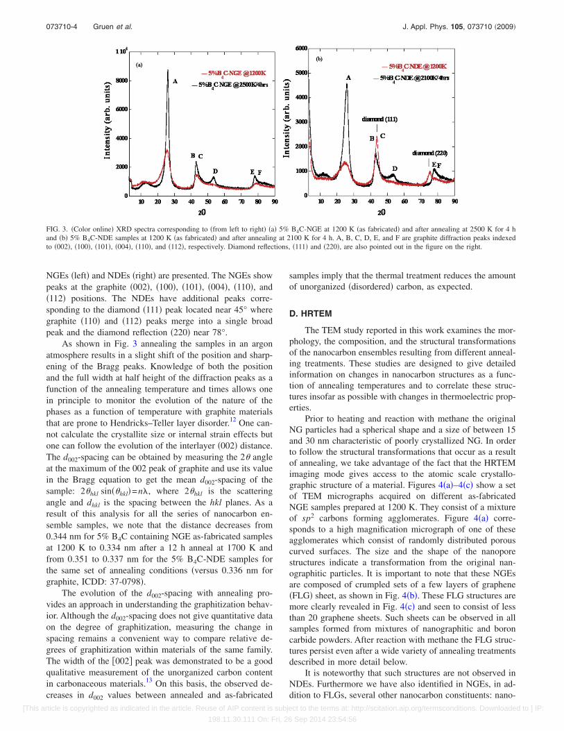
NGEs �left� and NDEs �right� are presented. The NGEs showpeaks at the graphite �002�, �100�, �101�, �004�, �110�, and�112� positions. The NDEs have additional peaks corre-sponding to the diamond �111� peak located near 45° wheregraphite �110� and �112� peaks merge into a single broadpeak and the diamond reflection �220� near 78°.
As shown in Fig. 3 annealing the samples in an argonatmosphere results in a slight shift of the position and sharp-ening of the Bragg peaks. Knowledge of both the positionand the full width at half height of the diffraction peaks as afunction of the annealing temperature and times allows onein principle to monitor the evolution of the nature of thephases as a function of temperature with graphite materialsthat are prone to Hendricks–Teller layer disorder.12 One can-not calculate the crystallite size or internal strain effects butone can follow the evolution of the interlayer �002� distance.The d002-spacing can be obtained by measuring the 2� angleat the maximum of the 002 peak of graphite and use its valuein the Bragg equation to get the mean d002-spacing of thesample: 2�hkl sin��hkl�=n�, where 2�hkl is the scatteringangle and dhkl is the spacing between the hkl planes. As aresult of this analysis for all the series of nanocarbon en-semble samples, we note that the distance decreases from0.344 nm for 5% B4C containing NGE as-fabricated samplesat 1200 K to 0.334 nm after a 12 h anneal at 1700 K andfrom 0.351 to 0.337 nm for the 5% B4C-NDE samples forthe same set of annealing conditions �versus 0.336 nm forgraphite, ICDD: 37-0798�.
The evolution of the d002-spacing with annealing pro-vides an approach in understanding the graphitization behav-ior. Although the d002-spacing does not give quantitative dataon the degree of graphitization, measuring the change inspacing remains a convenient way to compare relative de-grees of graphitization within materials of the same family.The width of the �002� peak was demonstrated to be a goodqualitative measurement of the unorganized carbon contentin carbonaceous materials.13 On this basis, the observed de-creases in d002 values between annealed and as-fabricated
samples imply that the thermal treatment reduces the amountof unorganized �disordered� carbon, as expected.
D. HRTEM
The TEM study reported in this work examines the mor-phology, the composition, and the structural transformationsof the nanocarbon ensembles resulting from different anneal-ing treatments. These studies are designed to give detailedinformation on changes in nanocarbon structures as a func-tion of annealing temperatures and to correlate these struc-tures insofar as possible with changes in thermoelectric prop-erties.
Prior to heating and reaction with methane the originalNG particles had a spherical shape and a size of between 15and 30 nm characteristic of poorly crystallized NG. In orderto follow the structural transformations that occur as a resultof annealing, we take advantage of the fact that the HRTEMimaging mode gives access to the atomic scale crystallo-graphic structure of a material. Figures 4�a�–4�c� show a setof TEM micrographs acquired on different as-fabricatedNGE samples prepared at 1200 K. They consist of a mixtureof sp2 carbons forming agglomerates. Figure 4�a� corre-sponds to a high magnification micrograph of one of theseagglomerates which consist of randomly distributed porouscurved surfaces. The size and the shape of the nanoporestructures indicate a transformation from the original nan-ographitic particles. It is important to note that these NGEsare composed of crumpled sets of a few layers of graphene�FLG� sheet, as shown in Fig. 4�b�. These FLG structures aremore clearly revealed in Fig. 4�c� and seen to consist of lessthan 20 graphene sheets. Such sheets can be observed in allsamples formed from mixtures of nanographitic and boroncarbide powders. After reaction with methane the FLG struc-tures persist even after a wide variety of annealing treatmentsdescribed in more detail below.
It is noteworthy that such structures are not observed inNDEs. Furthermore we have also identified in NGEs, in ad-dition to FLGs, several other nanocarbon constituents: nano-
FIG. 3. �Color online� XRD spectra corresponding to �from left to right� �a� 5% B4C-NGE at 1200 K �as fabricated� and after annealing at 2500 K for 4 hand �b� 5% B4C-NDE samples at 1200 K �as fabricated� and after annealing at 2100 K for 4 h. A, B, C, D, E, and F are graphite diffraction peaks indexedto �002�, �100�, �101�, �004�, �110�, and �112�, respectively. Diamond reflections, �111� and �220�, are also pointed out in the figure on the right.
073710-4 Gruen et al. J. Appl. Phys. 105, 073710 �2009�
[This article is copyrighted as indicated in the article. Reuse of AIP content is subject to the terms at: http://scitation.aip.org/termsconditions. Downloaded to ] IP:
198.11.30.111 On: Fri, 26 Sep 2014 23:54:56
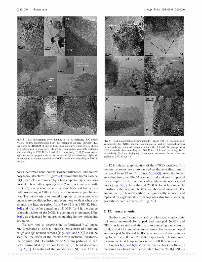
horns, deformed nano-onions, isolated fullerenes, and hollowpolyhedral structures.14 Figure 4�f� shows that boron carbide�BxC� particles surrounded by a few graphitic layers are alsopresent. Their lattice spacing �0.282 nm� is consistent withthe �123� interplanar distance of rhombohedral boron car-bide. Annealing at 1700 K leads to an increase in graphitiza-tion. The wide variety of curved graphitic surfaces producedunder these conditions becomes even more evident when oneextends the heating period from 8 to 12 h at 1700 K, Figs.4�d� and 4�e�. After annealing at 2100 K for 4 h, the degreeof graphitization of the NGEs is even more pronounced �Fig.4�g��, as evidenced by an area containing hollow polyhedralstructures.
We turn now to describe the as-fabricated B4C dopedNDEs prepared at 1200 K. These NDEs consist of a mixtureof sp2 and sp3 bonded carbons �Figs. 5�a� and 5�b��. It can beseen that the effect of the reaction with methane transformsthe original UNCD constituted of 5–8 nm particles to par-ticles surrounded by several kinds of sp2 bonded carbons�Fig. 5�b��. Annealing of the as-fabricated NDEs at 1700 K
for 12 h induces graphitization of the UNCD particles. Thisprocess becomes more pronounced as the annealing time isincreased from 12 to 16 h, Figs. 5�d�–5�f�. After the longerannealing time, the UNCD content is reduced and is replacedby a complex mixture of nanocarbon filaments, needles, andcones �Fig. 5�e��. Annealing at 2500 K for 4 h completelytransforms the original NDE’s as-fabricated material. Theamount of sp3 bonded carbon is significantly reduced andreplaced by agglomerates of nanoporous structures, showinggraphitic curved surfaces, see Fig. 5�f�.
E. TE measurements
Seebeck coefficient ��� and dc electrical conductivity��� were measured for doped and undoped NGE’s andNDE’s as fabricated and after various annealing temperaturesfor 4, 8, and 12 cumulative anneal times. Furthermore dopedand undoped NGEs and NDEs were measured after anneal-ing for 4 h at 2500 and 2100 K, respectively. Thermopowermeasurements at temperatures up to 1200 K were made.
Figures 6�a� and 6�b� show that the Seebeck coefficientsmeasured as a function of temperature for the 5% B4C-NGEs
FIG. 4. TEM micrographs corresponding to �a� as-fabricated B4C dopedNGEs, �b� low magnification TEM micrograph of an area showing FLGstructures, �c� HRTEM of one of these FLG structures where several sheetsof graphene can be discerned, ��d� and �e�� nanocarbon ensemble materialsafter annealing at 1700 K for 8 and 12 h, respectively, �f� BxC nanoparticleagglomerate and graphitic curved surfaces, and �g� area showing polyhedri-cal nanopore structures acquired in a NCE sample after annealing at 2100 Kfor 4 h.
FIG. 5. TEM micrographs corresponding to ��a� and �b�� HRTEM images ofas-fabricated B4C NDEs, showing a mixture of sp2 and sp3 bounded carbons�a� and only sp2 bounded carbon structures �b�. �c� and �d� correspond toNDE materials after annealing at 1700 K for 12 h and �e� during 16 h,respectively. �f� Area displaying the nanopore structures formed after an-nealing at 2500 K for 4 h.
073710-5 Gruen et al. J. Appl. Phys. 105, 073710 �2009�
[This article is copyrighted as indicated in the article. Reuse of AIP content is subject to the terms at: http://scitation.aip.org/termsconditions. Downloaded to ] IP:
198.11.30.111 On: Fri, 26 Sep 2014 23:54:56

and 5% B4C-NDEs for various annealing temperatures andtimes were found to increase monotonically with measuringtemperature in both sets of samples. There is a pronouncedincrease in the magnitude of the Seebeck coefficient for theannealed as compared to the as-fabricated samples.
For the 5% B4C-NGE samples, the Seebeck coefficientdepends to a considerable extent on the annealing time. An-nealing at 2500 K for 4 h showed similar values as the 4 h1700 K anneal. It should be noted that data for as-fabricatedand 1700 K anneal were for the same sample, whereas the2500 K annealing was conducted on a different sample fab-ricated under identical conditions.
Seebeck behavior for the 5% B4C-NDEs was similar tothe 5% B4C-NGEs. Annealing temperature and timesshowed enhancement in the Seebeck coefficients at all tem-peratures of measurement. A general trend of increasing See-beck coefficient with the temperature was observed for allsamples. There seems to be a systematic increase in � withannealing time for the NDEs. However, it appears that themagnitude of the Seebeck coefficient is somewhat smallerthan those observed for the 5% B4C-NGEs. Here again, data
for as-fabricated and 1700 K annealing were from the samesample, and 2100 K anneal test was conducted on a differentsample.
Figures 7�a� and 7�b� show the dc electrical conductivityfor 5% B4C-NGEs and 5% B4C-NDEs. The as-fabricatedNGEs exhibited about two times higher conductivity com-pared to NDEs. With annealing at 1700 K for various times,the increase in electrical conductivity was much larger forthe NDE samples. Also, the magnitudes for both NGE andNDE samples were similar to values of approximately 150S/cm. After �2100 K annealing treatment, both sets ofsamples showed significant increases in room temperatureelectrical conductivity with values of 350 and 280 S/cm forthe NGE and NDE samples, respectively. As a function oftemperature, NGEs showed somewhat decreasing valueswhile for the NDEs the conductivity appears to increaseslightly with temperature and to saturate at 300 S/cm.
PFs ��2�� for 5% B4C containing NGEs and NDEs werecalculated and plotted in Figs. 8�a� and 8�b�. It can be seenthat annealing dramatically increases the PF by as much asan order of magnitude. The 2500 K anneal showed the high-
FIG. 6. �Color online� Seebeck coefficients of �a� 5% B4C-NGEs and �b� 5% B4C-NDEs as a function of temperature and annealing times.
FIG. 7. �Color online� dc electrical conductivity �a� 5% B4C-NGEs and �b� 5% B4C-NDEs as a function of temperature and annealing times.
073710-6 Gruen et al. J. Appl. Phys. 105, 073710 �2009�
[This article is copyrighted as indicated in the article. Reuse of AIP content is subject to the terms at: http://scitation.aip.org/termsconditions. Downloaded to ] IP:
198.11.30.111 On: Fri, 26 Sep 2014 23:54:56

est PF in part because of the dramatic increase in electricalconductivity. With our measuring system, we are limited toreliable Seebeck and electrical conductivity measurementsup to 1200 K.
Figure 9 shows the PFs for the undoped NGE samplemeasured as a function of temperature for the as-fabricatedsample and after annealing for 4 h at 1700 K. ComparingFigs. 8�a� and 9 gives insight into the role of boron additions.For both boron doped and undoped samples, as-fabricatedPFs are almost identical as a function of temperature. How-ever, the effect of boron additions becomes very apparentafter annealing of the samples. The PFs are enhanced by atleast a factor of 3 when B4C is added to the NG or nanodia-mond powders before reaction with methane.
IV. DISCUSSION
The approach to the development of more efficient ther-moelectric materials underlying the present work is based on
the idea that bulk readily available, nontoxic, relatively inex-pensive nanostructured materials that resist recrystallizationcould limit detrimental electrical and thermal losses whileusing straightforward fabrication routes. It was recognized atthe outset that one of the challenges that must be overcomeby such an approach is electron scattering at interfaces be-tween randomly oriented grains leading to a concurrent re-duction in both the electrical and thermal conductivities.1
The most thoroughly studied system exemplifying this ap-proach appears to be that based on boron doped silicon-germanium where recent work suggests that nanostructuredSiGe does, in fact, enhance ZT.2 However, it appears to usthat a systematic study of the degree to which thermopoweras well as electrical and thermal conductivities can be inde-pendently controlled and optimized taking advantage ofstructural and compositional variations in intimately mixednanocomposite structures has not been carried out on amodel system. We have chosen nanocarbon ensembles as amodel system because of its suitability with regard both to itsphysicochemical properties and because it lends itself to arigorous and detailed quantum-mechanical theoretical treat-ment.
The initial results presented here confirm that the nano-carbon ensembles fulfill the requirements of a model systemin both regards. For example, substantial PFs of1 �W /K2 cm have already been reached with boron dopedNG ensembles after anneals at 2500 K �Figs. 6–8�. The verysubstantial increase in PF over earlier work carried out at1200 K �Ref. 4� is believed to be primarily due to the highannealing temperatures which lead to higher boron dopinglevels and thus to higher Seebeck coefficients as well as tonanostructural changes that result in a doubling and triplingof the electrical conductivity. Preliminary measurementshave shown that the thermal conductivities of the nanoen-sembles are in the range 0.03–0.07 W /cm K.15 Taken to-gether, these results which will be discussed in detail belowindicate that the nanocarbon ensembles have considerablepromise as thermoelectric materials. Clearly, however,marked improvement in their performance is required in or-der for them to function as efficient energy convertors. To
FIG. 8. �Color online� PFs of �a� 5% B4C-NGEs and �b� 5% B4C-NDEs as a function of annealing temperature and times.
FIG. 9. �Color online� PFs as a function of temperature of NGEs for varioustemperatures for the as-fabricated sample and after annealing for 4 h at 1700K.
073710-7 Gruen et al. J. Appl. Phys. 105, 073710 �2009�
[This article is copyrighted as indicated in the article. Reuse of AIP content is subject to the terms at: http://scitation.aip.org/termsconditions. Downloaded to ] IP:
198.11.30.111 On: Fri, 26 Sep 2014 23:54:56

reach that goal, future generations of ensembles must displaysubstantial increases in thermopower, for example, without aconcomitant decrease in their electrical or increase in theirthermal conductivities.
A rational approach to the solution of this extremelychallenging problem will depend on how successfully onecan establish an interplay between experimental approacheswhile at the same time achieving a better theoretical under-standing of the factors determining transport in these mate-rials. A particularly difficult aspect concerning thermoelectricphenomena has been the question of electronic entropy trans-port in a thermal gradient which determines the magnitudeand temperature dependence of the Seebeck coefficient. Thenanocarbon ensembles offer an interesting opportunity tomake progress in this difficult area. It has been known for along time that boron doping induces an acceptorlike featurenear the top of the valence band of graphitic substances.16,17
However, the crucial role in determining thermoelectricproperties played by the unique nature of the graphite latticein providing a multitude of boron substitutional configura-tions each with its distinctive energy signature appears tohave been explicitly recognized for the first time in our ear-lier work.4 This recognition led us to examine in detail thenature of the acceptorlike feature using density functionalcalculations on boron substituted polyaromatics that serve asmolecular models for finite as well as stacked graphenesheets.18 These calculations provide insight into the relativestabilities of high spin versus low spin states as a function ofgraphene sheet size, Kekule versus non-Kekule structures, aswell as the effects on orbital energetics of various boronsubstitutional configurations.
Insights emerging from this theoretical work provide de-tailed understanding of the many thousands of possible bo-ron geometric configurations each one associated with a dis-tinct “molecular analog” electronic state. Our calculationspredict a lowering of the Fermi level by about 0.1 eV due toboron doping, thus creating a vast number of empty, perhapsnearly degenerate states that can be populated thermallyleading to a situation that could foster an augmentation ofelectronic entropy. This cluster approach in exploring theelectronic structure of boron doped nanocarbons can hope-fully be extended to help establish a better understanding ofthe factors determining the magnitudes and temperature de-pendencies of the decisive entropic flows that determine theergodic processes accompanying hole as well as electrontransport in thermal gradients A deep understanding of thecomplex issues underlying these phenomena is clearly a firststep in the fashioning of more efficient heat to electricityconversion materials.
The interplay between experimental and theoretical re-sults in establishing the nanocarbon ensembles as model sys-tems to help in understanding the factors underlying thermo-electric behavior in a more general sense will be clarified inthe following discussion. The extensive and highly reproduc-ible thermoelectric measurements made on several sets ofsamples leave no doubt that both annealing temperatures andannealing times profoundly affect the magnitude and tem-perature dependencies of the Seebeck coefficients and theelectrical conductivities. The effects of annealing profiles on
boron doped ensembles, however, are different for NGEs andNDEs, as is evident from an examination of Figs. 6�a� and6�b�. The dramatic effects of boron concentration, �B�, onboth the magnitude and the temperature dependence of theSeebeck coefficient, �, are illustrated in Figs. 6�a� and 6�b�.If � were linearly dependent on �B� one would expect thatquantity to increase by at least two orders of magnitude ingoing from 1200 to 2500 K anneals based on the boron solu-bility data of Lowell5 who determined the solubility of boronin graphite as a function of temperature. The smaller thanexpected observed factor of 5 increase in � for measure-ments made at 1200 K probably reflects boron partially com-ing out of solid solution to reform B4C as the NG ensembleslowly cools over a period of hours in the large resistanceheated graphite furnace. This interpretation gathers supportfrom data taken on a nanodiamond ensemble after a 2100 Kanneal in the same furnace which displays an � value inter-mediate between 2500 and 1700 K anneals. An accurate de-termination of the functional relationship between � and �B�will require the development of a procedure that allows dop-ing to be done in a controlled way and we are exploringpaths to accomplish to this end.
Boron is known to be a dopant both for diamond and forgraphite.19,20 The difference in behavior of � between NGEsand NDEs is probably due to a difference in the effect ofboron on the thermoelectric properties of these two allot-ropes of carbon. Here we wish merely to point out that con-tinued annealing up to 12 h of NDEs at 1700 K gives �values that increase with heating time approaching those ob-served with NGEs �compare Figs. 6�b� and 6�a��. XRD mea-surements show that nanodiamond slowly converts to NG atthese temperatures and we believe that the observed increasein � is traceable to this circumstance. This question will beconsidered in more detail after a discussion of the electricalconductivity and PF results.
The difference in behavior of the electrical conductivity��� between NGEs and NDEs displayed graphically in Figs.7�a� and 7�b� is due to two important considerations. In theNGEs, the nanocarbon constituent is entirely NG except forthe presence of 5% B4C. The � for the 1200 K as-fabricatedsamples are not changed much after annealing at 1700 K.However, at 2500 K, a large increase in � by a factor of 2 or3 is observed which we attribute to a major structural order-ing of the NG component. This important reorganizationphenomenon has been followed in detail by HRTEM andXRD. By comparison, a marked increase in � is observed inthe NDEs when the 1200 K as-fabricated samples are an-nealed at 1700 K because the major original nanodiamondcomponent slowly converts to NG at this temperature. Inter-estingly, the � of NDEs annealed at 2100 K are quite similarto those of NGEs annealed at 2500 K, indicating that con-version of diamond to graphite may be virtually complete at2100 K.
The PFs ��2�� for the NGE and NDE compacts areshown in Figs. 8�a� and 8�b�. For both sets of samples, thePFs increase strongly with temperature and continue to do soeven at 1200 K, the upper limit of our thermoelectric mea-surements, with no indication of reaching a plateau. Signifi-cantly, a value of 1 �W /K2 cm is attained with NGE com-
073710-8 Gruen et al. J. Appl. Phys. 105, 073710 �2009�
[This article is copyrighted as indicated in the article. Reuse of AIP content is subject to the terms at: http://scitation.aip.org/termsconditions. Downloaded to ] IP:
198.11.30.111 On: Fri, 26 Sep 2014 23:54:56

pacts annealed at 2500 K. Preliminary measurements of thethermal conductivity of the compacts have been carried out15
and give values in the range �3–7��10−2 W /cm K. Figuresof merit calculated using PF and thermal conductivity valueson the current generation of samples are too low to be ofinterest for applications. Considerable improvement in theperformance of the nanocarbon ensembles is required andefforts in this direction are underway.
As already stated in Sec. III, prior to heating and reac-tion with methane, the original NG particles in the NGEs hada spherical shape and a size of between 15 and 30 nm. Theyare formed of a poorly crystallized graphite structure. Reac-tion with methane at 1200 K produces a 70%–100% weightgain due to the growth of intergranular carbon that stronglybonds the loosely agglomerated NG particles into mechani-cally rigid compacts. Although the detailed mechanism ofthis process has not been elucidated, certain aspects of thereaction leading to the transformation can be understood onthe basis of HRTEM data. Crumpled sheets of graphene�Figs. 4�b� and 4�c�� are formed at 1200 K as well as acomplex mixture of nanohorns, deformed nano-onions,fullerenes, and hollow polyhedral nanostructures. The an-nealing at 1700 K increases the graphitization of these ma-terials. Finally, annealing at 2100 K produces a reduction inthe number of crystalline defects concomitant with an in-crease in the degree of ordering due to higher stacking per-fection of carbon layers.
The nanostructural changes due to annealing shown byHRTEM are also reflected in the XRD data �Fig. 3�a�� whichcan be indexed to graphite reflections as follows: near 25°�002�, near 45° �100� and �101�, and near 80° �110� and�112�. Annealing to 2500 K causes the expected narrowing ofthe �002� peak that is known to accompany an increase in theordering of the graphitic planes. The small shift of that peakto larger values of theta is generally attributed to a decreasein the interplanar distance, in our case from 0.344 to 0.334nm following extensive “graphitization” associated with theordering of layers.
The magnitude of � suggests that one is dealing withhopping conductivity21 characteristic of disordered materialswith a local disordering length of a few interatomic dis-tances. A qualitative description of the conductivity changesobserved in the nanocarbon ensembles can be given on thebasis of Mott’s concept of hopping conductivity.22 At anneal-ing temperatures up to 1700 K conductivity occurs primarilyalong carbon chains and defected planes. At higher tempera-tures, graphene sheets, fullerenic structures, and other curvedsurfaces provide better conduction paths. Finally at the high-est annealing temperatures employed in the present work,2500 K, the formation of hollow polyhedral NG structureswith reduced numbers of defects provides excellent conduc-tion paths leading to � values of 300 S/cm and above.Clearly, a more detailed understanding of conductivity inthese materials will require both extensive experimentalmeasurements, for example, of the temperature dependenceand the Hall coefficients as well as a thorough theoreticaltreatment of electronic transport in these nanoporous materi-als.
From a theoretical point of view, the main features of the
TE performance of the NGEs have been shown in recentdensity functional calculations to arise from changes in theelectronic structure of NG as a result of boron doping.18
These cluster or molecular analog calculations can be use-fully compared to results from a simple two band modelelaborated to explain the performance of boron doped bulkgraphite thermocouples.20 As already discussed, the dramaticeffects of annealing on the magnitude of � and � can bequalitatively understood on the basis of an increased solubil-ity of boron in graphite with temperature on the one handand more favorable conduction paths arising from highly or-dered and less defective graphite layers on the other hand.
The results on the NDEs �Figs. 6–8� are interesting par-ticularly from the point of view of the light they shed on thetransformation of UNCD to NG as a function of temperature.Of particular importance for the present study is the work ofKuznetsov and and Butenko21 and Kuznetsov et al.23 as wellas that of Andersson et al.17 This by now quite well devel-oped subject will be discussed here only to the extent that itrelates to NDE thermoelectric properties. Annealing affects� and � not only because of changes in boron solubility andordering of graphene structures but also because of the trans-formation of UNCD to NG. In the as-fabricated NDE,UNCD is the primary constituent prior to reaction with meth-ane. The UNCD to NG transformation has been followed inour work using XRD, HRTEM, and Raman characterizationtechniques. An exemplar of the XRD data is shown in Fig.3�b�. The diamond �111� reflection is at a somewhat smaller2� angle than the graphite �100� and �101� reflections andoverlaps the latter two reflections, thus making it difficult touse this Bragg region to follow the transformation quantita-tively. Our data analysis is therefore based on a determina-tion of the ratios of intensities of the diamond �002� near 75°relative to the graphite reflections near 80°. In this Braggregion, the diamond and graphite reflections are reasonablywell resolved. The detailed work of Andersson et al.17 pro-vides us with baseline information regarding the temperaturedependent transformation of disperse UNCD to graphite.Their data and ours are in excellent agreement.
The HRTEM micrographs �see Figs. 4 and 5� substanti-ate the conclusions reached on the basis of the XRD mea-surements. As an example, NDEs annealed at 2100 K show agreatly diminished number of UNCD crystallites comparedto the as-fabricated compacts with only a few 2–5 nm UNCDparticles remaining at that temperature. Structures displayinggraphitic and curved surfaces abound with equidistant sheetsforming essentially defect free layers.
V. CONCLUSIONS
Thermoelectric PFs of nanocarbon ensembles have beendetermined as a function of temperature from 400 to 1200 K.The ensembles are composed of �a� mixtures of NG and 5%B4C called NGEs or �b� mixtures of UNCD disperse pow-ders and 5% B4C called NDEs. The mixtures are formed intomechanically rigid compacts by reaction with methane gas attemperatures up to 1200 K. They are then annealed at vari-ous temperatures and various lengths of time up to 2500 K.
073710-9 Gruen et al. J. Appl. Phys. 105, 073710 �2009�
[This article is copyrighted as indicated in the article. Reuse of AIP content is subject to the terms at: http://scitation.aip.org/termsconditions. Downloaded to ] IP:
198.11.30.111 On: Fri, 26 Sep 2014 23:54:56

Boron substitutional doping occurs primarily during the an-nealing steps up to maximum concentrations estimated to beabout 1%.
The ensembles were characterized using SEM, Ramanscattering, XRD, and HRTEM techniques to gain insight intothe structural changes attending high temperature treatmentof the nanocarbons. The compacts retain their nanostructuralcharacteristics up to the highest annealing temperatures butdisplay complex structural transformations going in the caseof NGEs from turbostratic NG to a complex mixture offullerenes, nano-onions, and nanotubes to hollow nanopoly-hedra as the temperature is increased. For NDEs, the tem-perature at which UNCD transforms to NG overlaps the tem-perature regime where a variety of NGs evolve withincreasing temperature and annealing time. Our results onUNCD graphitization are in agreement with detailed litera-ture studies on this topic.
The thermoelectric PFs of the ensembles increasestrongly both as a function of annealing temperature and ofthe temperature at which the measurements are carried out.They reach values of 1 �W /K2 cm at a 1200 K measuringtemperature for samples annealed at 2500 K. Seebeck coef-ficients of 60 �V /K and electrical conductivities of near350 S/cm have been measured. Preliminary results of ther-mal conductivity are in the range 0.03–0.07 W /cm K. Fig-ures of merit based on these measurements are too low to beof practical interest. We conclude that the most promisingnext step for improved performance is to attempt to raise thevalues of the Seebeck coefficient.
Detailed density functional calculations of molecularanalog model systems18 have shown that boron substitutingfor carbon on graphite lattice sites leads to a lowering of theFermi level and the creation of a large number of emptystates within thermal excitation energies of the Fermi level.We attribute the magnitude and temperature dependence ofthe thermoelectric PFs to the enhancement of electronic con-figurational entropy resulting from the boron “doping” of thenanocarbons that comprise the ensembles.
ACKNOLEDGEMENTS
This work was performed under the auspices of the U.S.Department of Energy, Office of Basic Energy Science andEnergy Efficiency Renewable Energy, Office of Vehicle
Technologies, under Contract No. DE-AC02-06CH11357 atArgonne National Laboratory, managed by the University ofChicago, LLC. The authors are grateful to Dr. Hsin Wangand Dr. Wallace Porter at the High-Temperature MaterialLaboratory at ORNL for measuring the thermal conductivityand to Dr. Eric J. Wuchina at the Naval Surface WarfaceCenter for the anneals at temperatures higher than 1700 K.Furthermore, they acknowledge ANL’s Electron MicroscopyCenter for the use of their facilities.
1G. J. Snyder and E. S. Toberer, Nature Mater. 7, 105 �2008�.2M S. Dresselhaus, G. Chen, M. Y. Tang, H. Lee, D. Z. Wang, Z. F. Ren, J.P. Fleurial, and P. Gogna, Adv. Mater. �Weinheim, Ger.� 19, 1043 �2007�.
3G. A. Slack, in CRC Handbook of Thermoelectrics, edited by M. Rowe�CRC, Boca Raton, FL, 1995�, pp. 407–440.
4D. M. Gruen, P. Bruno, and M. Xie, Appl. Phys. Lett. 92, 143118 �2008�.5C. E. Lowell, J. Am. Ceram. Soc. 50, 142 �1967�.6Obtained from ITC Corporation, Raleigh, NC, http://www.itc-inc.org/nanodiamond2.html.
7Obtained from MTI Corporation, Richmond, CA, http://www.mtixtl.com/.8Obtained from American Elements, Merelex Corporation, Los Angeles,CA, http://www.americanelements.com/.
9B.-S. Hong, S. J. Ford, and T. O. Mason, Key Eng. Mater. 125–126, 163�1997�.
10A. C. Ferrari and J. Robertson, Phys. Rev. B 64, 075414 �2001�.11R. Arenal, G. Montagnac, P. Bruno, and D. M. Gruen, Phys. Rev. B 76,
245316 �2007�.12P. A. Heiney, M. E. Huster, V. B. Cajipe, and J. E. Fischer, Synth. Met. 12,
21 �1985�.13J. R. Dahn, A. K. Sleigh, H. Shi, J. N. Reimers, Q. Zong, and B. M. Way,
Electrochim. Acta 38, 1179 �1993�.14R. Arenal, O. Stephan, P. Bruno, and D. M.Gruen, Appl. Phys. Lett. 94,
111905 �2009�.15Measurements of thermal conductivity and confirmation of Seebeck coef-
ficient made at ORNL.16D. L. Carroll, Ph. Redlich, X. Blase, J.-C. Charlier, S. Curran, P. M.
Ajayan, S. Roth, and M. Rühle, Phys. Rev. Lett. 81, 2332 �1998�.17O. E. Andersson, B. L. V. Prasad, H. Sato, T. Enoki, Y. Hishiyama, Y.
Kaburagi, M. Yoshikawa, and S. Bandow, Phys. Rev. B 58, 16387 �1998�.18P. C. Redfern, D. M. Gruen, and L. A. Curtiss, Chem. Phys. Lett. 471, 264
�2009�.19A. Balducci, M. Marinelli, M. E. Morgada, G. Pucella, G. Rodriguez, M.
Scoccia, and G. Verona-Rinati, Microsyst. Technol. 12, 365 �2006�.20C. A. Klein, in Chemistry and Physics of Carbon, edited by P. L. Walker
�Dekker, New York, 1966�, Vol. 2, p. 225.21V. L. Kuznetsov and Y. V. Butenko, in Ultrananocrystalline Diamond,
edited by O. A. Shenderova and D. M. Gruen �William Andrew, Norwich,NY, 2006�, p. 405.
22N. Mott, Conduction in Non-Crystalline Materials, 2nd ed. �Oxford Sci-ence, New York, 1993�.
23V. L. Kuznetsov, Y. V. Butenko, A. L. Chuvilin, A. I. Romanenko, and A.V. Okotrub, Chem. Phys. Lett. 336, 397 �2001�.
073710-10 Gruen et al. J. Appl. Phys. 105, 073710 �2009�
[This article is copyrighted as indicated in the article. Reuse of AIP content is subject to the terms at: http://scitation.aip.org/termsconditions. Downloaded to ] IP:
198.11.30.111 On: Fri, 26 Sep 2014 23:54:56
Copyright © 2022 FDOKUMEN