Principles of Microfabrication Marc Madou.pdf - Gorodetsky ...
Upload
independentCategory
view
0download
0
Single-mask multiple lateral nanodiamond field emission devices fabrication techniqueK. Subramanian, W. P. Kang, J. L. Davidson, B. K. Choi, and M. Howell
Citation: Journal of Vacuum Science & Technology B 24, 953 (2006); doi: 10.1116/1.2185653 View online: http://dx.doi.org/10.1116/1.2185653 View Table of Contents: http://scitation.aip.org/content/avs/journal/jvstb/24/2?ver=pdfcov Published by the AVS: Science & Technology of Materials, Interfaces, and Processing Articles you may be interested in Nanodiamond vacuum field emission device with gate modulated triode characteristics Appl. Phys. Lett. 102, 203105 (2013); 10.1063/1.4807128 Enhanced electron-field emission from nanodiamond ridge-structured emission arrays capped on micropatternedsilicon pillars J. Vac. Sci. Technol. B 28, 1016 (2010); 10.1116/1.3488608 Carbon nanostructure field emission devices J. Vac. Sci. Technol. B 24, 1008 (2006); 10.1116/1.2181987 Electron field emission properties of nanodiamonds synthesized by the chemical vapor deposition process J. Vac. Sci. Technol. B 19, 975 (2001); 10.1116/1.1349207 Microstructure and its effect on field electron emission of grain-size-controlled nanocrystalline diamond films J. Appl. Phys. 88, 2967 (2000); 10.1063/1.1287602
Redistribution subject to AVS license or copyright; see http://scitation.aip.org/termsconditions. Download to IP: 129.59.93.63 On: Wed, 06 Aug 2014 16:26:30
Redistr
Single-mask multiple lateral nanodiamond field emission devicesfabrication technique
K. Subramanian, W. P. Kang,a� J. L. Davidson, B. K. Choi, and M. HowellDepartment of Electrical Engineering and Computer Science, Vanderbilt University, Nashville,Tennessee 37235
�Received 5 December 2005; accepted 16 February 2006; published 27 March 2006�
We report an efficient microfabrication process technique developed to realize multiple lateraldiamond field emitter structures on the same wafer using a single mask. Nanodiamond films withgrain size of 5–10 nm deposited by CH4/H2/N2 microwave plasma enhanced chemical vapordeposition were selectively micropatterned using reactive ion etching at an etch rate of 0.5 �m/min.Several nanodiamond lateral field emission diodes and triodes of different emitter geometries andelectrode configurations have been batch fabricated on a silicon-on-insulator wafer. Interelectrodespacing down to 2 �m was achieved in arrays of devices on a SiO2 dielectric layer. This fabricationprocess technique, with its single-mask utility, high manufacturability, combined with itsreproducibility, is an efficient and cost-effective approach to realize various configurations of fieldemission structures in wafer process technology. These nanodiamond vacuum nanoelectronic lateraldevices hold high-speed and high-frequency operation potential. © 2006 American Vacuum
Society. �DOI: 10.1116/1.2185653�I. INTRODUCTION
Nanocrystalline diamond �nanodiamond� is an emergingmaterial that holds promise for vacuum nanoelectronicapplications.1–4 The attractive mechanical, chemical, and lowelectron affinity properties of microcrystalline diamond arealso possessed by nanodiamond, which has a smaller grainsize �1–100 nm�,5 increased sp2-carbon content, higher elec-trical conductivity, and decreased surface roughness.1 But, inorder to apply these favorable properties for enhanced elec-tron field emitters, a reliable and reproducible process tech-nique is required. We have recently developed a simple pro-cess to fabricate uniform arrays of micropatterned lateralfield emitters using reactive ion etching of the nanodiamondfilm. Field emitters in lateral configuration may offer signifi-cant advantages for high-speed and high-frequency deviceoperation with their efficient electrode geometry and smallinterelectrode spacing. Lateral nanodiamond field emitterstructure microfabrication technique, described here, canachieve batch fabrication of a variety of emitter devices withhigh yield, suggesting a useful approach to realize potentialelectron field emission devices.
II. EXPERIMENT
The fabrication process was initiated with the growth of a2 �m thick nanodiamond film on a silicon-on-insulator�SOI� wafer with 2 �m active Si on 1 �m of buried oxide�BOX�, all on a 625 �m thick Si substrate wafer. The fabri-cation process scheme is outlined in Fig. 1. The nanodia-mond deposition process by CH4/H2/N2 microwave plasmaenhanced chemical vapor deposition �MPECVD� has beenreported in detail.1 A 0.5 �m thick masking layer of alumi-num was deposited on the nanodiamond film. Conventional
a�
Electronic mail: [email protected]953 J. Vac. Sci. Technol. B 24„2…, Mar/Apr 2006 1071-1023/2006
ibution subject to AVS license or copyright; see http://scitation.aip.org/term
photolithography was performed with a single mask to pat-tern different lateral field emitter device structures on thealuminum. The exposed aluminum was then etched away bywet chemical etching using commercially available phos-phoric acid etchant �80% H3PO4; 5% HNO3; 5%CH3COOH; 10% H2O� and the photoresist removed. Withaluminum as the mask, the nanodiamond was micropatternedby reactive ion etching �RIE� in oxygen plasma using an STSAdvanced Oxide Etch �AOE™� inductively coupled plasma�ICP�-RIE system, which combines a high conductance, highvacuum compatible process chamber with an ICP source toproduce very high ion density at low pressures. The nanodia-mond ICP-RIE process parameters include coil rf power of700 W and platen rf power of 150 W, O2 flow rate of30 SCCM �SCCM denotes cubic centimeter per minute atSTP� and a low pressure of 10 mTorr. The final step was toetch the silicon to isolate the electrodes/devices of the nano-diamond lateral emitters/structures. This was performed,with the aluminum/nanodiamond serving as the mask, usingthe STS Advanced Silicon Etch �ASE™� DRIE system inSF6/O2 �130 SCCM/13 SCCM� plasma at 600 W/12 W�coil/platen� rf power, and 21 mTorr pressure. The resultingstructure consists of micropatterned nanodiamond lateralemitter devices on the silicon layer underneath, sitting on theSiO2 layer, on the silicon substrate. A Ti/Au metallizationtechnique, without the use of an additional mask, was ap-plied to provide good electrical contact for field emissioncharacterization of the nanodiamond lateral devices. The pro-cess involved the deposition of a 1000 Å thick Ti/Au metallayer over the nanodiamond film, prior to the application ofthe aluminum mask. Subsequent patterning of the Ti/Aulayer was performed by wet chemical etch in a readily avail-able gold etchant solution �KI-I2 complex� after the alumi-num mask formation, using the same photoresist pattern as
the mask.953/24„2…/953/5/$23.00 ©2006 American Vacuum Society
sconditions. Download to IP: 129.59.93.63 On: Wed, 06 Aug 2014 16:26:30
954 Subramanian et al.: Single-mask multiple lateral nanodiamond field 954
Redistr
Several other micropatterning experimentation trials wereconducted to establish the nanodiamond lateral emitter fab-rication process. The nanodiamond RIE process was variedby employing different rf power and reactant pressure con-ditions. A CF4/O2 plasma etch chemistry was implementedto investigate its effect on the diamond etch rate. Maskinglayer of metals including titanium and gold for nanodiamondRIE was also applied in different trials in order to identifythe masking material offering the best selectivity.
III. RESULTS AND DISCUSSION
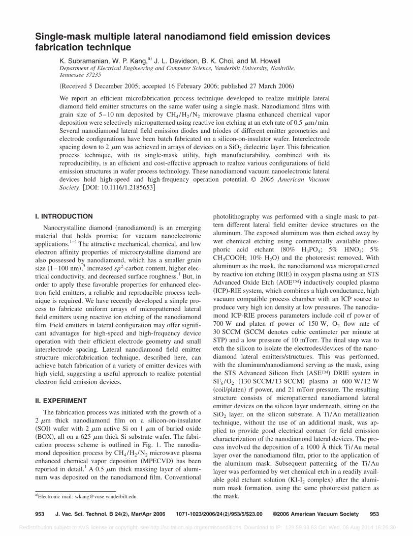
Figure 2 displays a variety of lateral nanodiamond emitterstructures which were batch fabricated on the same waferusing a single mask. Arrays of lateral diode and triode ge-ometries with interelectrode spacing as small as 2 �m havebeen achieved, enabling low voltage operation. The nanodia-mond cathode in the lateral devices is equipped with a “fin-gerlike” emitter geometry, ending with a sharp apex. Thelateral aspect ratio of a finger was found to be as high as�4000, which was estimated by modeling the nanodiamondfinger as a conical tip with lateral tip height of h and tipradius curvature of r, with the lateral aspect ratio defined by
the factor h /r. A close examination of the cathode tip topol-J. Vac. Sci. Technol. B, Vol. 24, No. 2, Mar/Apr 2006
ibution subject to AVS license or copyright; see http://scitation.aip.org/term
ogy by high magnification scanning electron microscope�SEM� imaging showed that the finger comprised of verysmall grain geometries of size of 5–10 nm, which is typi-cally representative of the nanodiamond film1 applied in thefabrication of the lateral emitter. Thus, the nanodiamondgives the lateral emitter a higher geometrical field enhance-ment factor due to its tip topology at a much more localregion than the lithographic pattern. The nanodiamond anodedesign avoids the high aspect ratio fingerlike shape and pos-sesses a straight edge geometry giving the cathode the recti-fying geometrical field enhancement factor compared to theanode. The 1 �m thick buried SiO2 layer of the SOI waferforms the dielectric isolation between devices. The SEM mi-crographs in Figs. 2�a� and 2�b� represent the four-finger andsix-finger nanodiamond lateral field emission diodes, respec-tively, with 4 �m anode-cathode spacing. Figure 2�c� consti-tutes the nanodiamond lateral comb device. The comb-shaped lateral diode includes 65 high aspect ratio fingeredcathode emitters set in a comblike arrangement with the an-ode, maintaining a constant interelectrode distance through-out the configuration for high-current applications.
Different designs of nanodiamond lateral triodes have also
FIG. 1. Single-mask, high throughputfabrication process scheme of thenanodiamond lateral field emissiondevices.
been fabricated. The triode device structure �see Fig. 2�d��
sconditions. Download to IP: 129.59.93.63 On: Wed, 06 Aug 2014 16:26:30
955 Subramanian et al.: Single-mask multiple lateral nanodiamond field 955
Redistr
involves a single fingered nanodiamond emitter acting as thecathode, with two nanodiamond fingers in close proximitywith the emitter on either side forming the gate, and thestraight-edge geometry serving as the anode. A small gate-cathode distance of 2 �m was achieved by precise control ofphotolithography and the subsequent etch processes. Fabri-cated anode-cathode distances per design were set to varybetween 20 �m and 1 mm, so as to have a wider range toobserve the modulation effect of the gate on the triode char-acteristics. Moreover, integrated nanodiamond lateral triodes,sharing a common cathode with two fingered lateral emittersat opposite ends, and a set of gate-anode combination foreach of the emitters were fabricated, shown in Fig. 2�e�. Theelectrodes in all of these nanodiamond lateral devices areequipped with pads large enough to aid visual probing forvacuum field emission characterization �see Figs. 2�e� and2�f��.
A high diamond etch rate of �0.5 �m/min was achievedduring the micropatterning process by rf-assisted pure O2
plasma RIE. The aluminum masking offered high selectivity,allowing the lateral emitters to retain the beneficial proper-ties of the nanodiamond. The RIE condition of high rf power�700 W/150 W� and low pressure �10 mTorr� at an O2 flowrate of 30 SCCM achieved good anisotropy, the high energyreactive ions with minimum ion scattering yielding a highdiamond etch rate and selectivity. It is important to note that
the SiO2 dielectric is well protected from any plasma-JVST B - Microelectronics and Nanometer Structures
ibution subject to AVS license or copyright; see http://scitation.aip.org/term
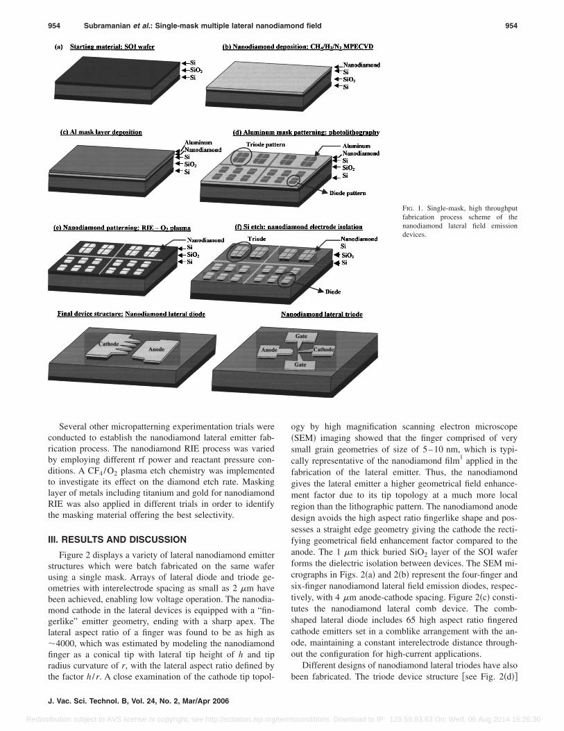
induced damage during the nanodiamond RIE by the pres-ence of the active Si layer of the SOI substrate. Once thenanodiamond is micropatterned with the lateral emitter struc-tures, the silicon layer beneath the nanodiamond is deliber-ately undercut to promote the nanodiamond layer gap prox-imity, ensuring that electron emission occurs only from thediamond. Figure 3 SEM images illustrate the result of the Sietch.
The Ti/Au metallization scheme provides satisfactoryelectrical contact for the nanodiamond lateral devices. Thecontact layer formation process was also an overetch tech-nique to remove any Ti/Au metal at the nanodiamond fin-gers. Figure 4�a� is the comb-shaped lateral device display-ing the uniformly integrated Ti/Au metallization contactlayer on the nanodiamond, and Fig. 4�b� is a high-magnification SEM image exhibiting the undercut Ti/Aulayer, illustrating that the nanodiamond emission regions aredevoid of any metal. The Ti/Au metallization, developed inthis work, is an innovative technique to integrate a contactmetal in the field emission device structure, without the useof any additional mask or complex processes. Its utility mayalso lie in vacuum packaging of these devices, where themetal layer can aid wire bonding.
An experiment employing CF4/O2 plasma for RIE ofnanodiamond did not increase the etch rate significantly,while the process selectivity suffered severely. Also, titanium
FIG. 2. SEM micrographs of different lateral nanodia-mond field emitter structures fabricated using a singlemask: �a� four-finger emitter diode, �b� six-finger emit-ter diode, �c� comb-shaped emitter diode with 65 fin-gers, �d� gated triode, �e� integrated triodes with com-mon cathode, and �f� lateral triode showing the 1�1 mm contact pads of the electrodes.
and gold �0.5 �m thick� did not act as good masking mate-
sconditions. Download to IP: 129.59.93.63 On: Wed, 06 Aug 2014 16:26:30
the intentionally overetched Ti/Au metal contact.
956 Subramanian et al.: Single-mask multiple lateral nanodiamond field 956
Redistr
rials, with the micropatterned metal layer beginning to wearout and peel off under the same nanodiamond reactive ionetch process conditions applied with aluminum as the mask.
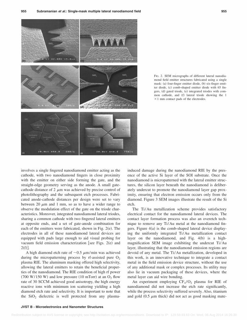
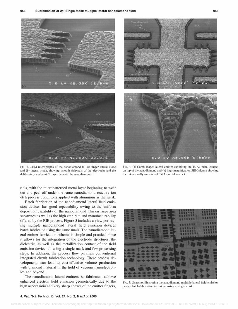
Batch fabrication of the nanodiamond lateral field emis-sion devices has good repeatability owing to the uniformdeposition capability of the nanodiamond film on large areasubstrates as well as the high etch rate and manufacturabilityoffered by the RIE process. Figure 5 includes a view portray-ing multiple nanodiamond lateral field emission devicesbatch fabricated using the same mask. The nanodiamond lat-eral emitter fabrication scheme is simple and practical sinceit allows for the integration of the electrode structures, thedielectric, as well as the metallization contact of the fieldemission device, all using a single mask and few processingsteps. In addition, the process flow parallels conventionalintegrated circuit fabrication technology. These process de-velopments can lead to cost-effective volume productionwith diamond material in the field of vacuum nanoelectron-ics and beyond.
The nanodiamond lateral emitters, so fabricated, achieveenhanced electron field emission geometrically due to the
FIG. 3. SEM micrographs of the nanodiamond �a� six-finger lateral diodeand �b� lateral triode, showing smooth sidewalls of the electrodes and thedeliberately undercut Si layer beneath the nanodiamond.
high aspect ratio and very sharp apexes of the emitter fingers,
J. Vac. Sci. Technol. B, Vol. 24, No. 2, Mar/Apr 2006
ibution subject to AVS license or copyright; see http://scitation.aip.org/term
FIG. 4. �a� Comb-shaped lateral emitter exhibiting the Ti/Au metal contacton top of the nanodiamond and �b� high-magnification SEM picture showing
FIG. 5. Snapshot illustrating the nanodiamond multiple lateral field emission
device batch-fabrication technique using a single mask.sconditions. Download to IP: 129.59.93.63 On: Wed, 06 Aug 2014 16:26:30

957 Subramanian et al.: Single-mask multiple lateral nanodiamond field 957
Redistr
and materially from the advantageous properties of the nano-diamond such as increased sp2-carbon content1 and higherelectrical conductivity from nitrogen incorporation. While,the sp2 content enhances field emission by decreasing thewidth of tunneling distance at the metal-diamond interfacesignificantly,1,6–8 nitrogen doping can lead to the formationof deep donor levels, which raises the Fermi level and re-duces the work function, thereby augmenting the electronemission.9,10 The amount of nitrogen incorporated in thenanodiamond film applied in the lateral devices was quanti-fied by Rutherford backscattering spectrometry �RBS� to be�4.5�1021 cm−3 in the near-surface region. Figure 6 showsthe field emission characteristics �I-E� exhibited by a six-finger nanodiamond lateral diode �3 �m anode-cathode spac-ing� in a vacuum of �10−7 Torr at different temperatures of27, 100, and 200 °C, the turn-on electric field being as lowas �3.5 V/�m. The current density achieved can be ex-pressed as 1.25 �A/cathode finger and �13 A/cm2 based onthe anode geometry at an electric field of 7.9 V/�m. Theunchanged emission behavior at varied temperatures signi-fies the absence of any leakage current in the observed fieldemission, thus confirming the integrity of the SiO2 isolationlayer applied for the lateral device. The emission currentfrom the diode structure conforms to Fowler-Nordheim be-havior and the corresponding Fowler-Nordheim �FN� plotsare given as an inset in Fig. 6. The shallow slope ��−84� ofthe FN plots implies a high field enhancement factor for thelateral device. The electron emission from the device wasfound to be stable over time even at high current. Figure 7displays the emission stability of a multifingered nanodia-mond lateral comb diode �device construct shown in Fig.2�c�� at a current of �2 mA. The current fluctuation of lessthan 4% measured over a period of 5 h under a fixed anode
FIG. 6. Field emission behavior �I-E� of a six-finger nanodiamond lateraldiode at different temperatures of 27, 100, and 200 °C.
JVST B - Microelectronics and Nanometer Structures
ibution subject to AVS license or copyright; see http://scitation.aip.org/term
voltage indicates the potential of the nanodiamond lateraldevice in terms of uniformity of the emission. The vacuumfield emission characteristics of the other nanodiamond lat-eral emitter devices will be presented in future publications.
IV. CONCLUSIONS
A technique, compatible with the microelectronic inte-grated circuit �IC� fabrication technology, for fabricatingmultiple lateral field emitter structures of nanodiamond usinga single mask has been presented. Arrays of different lateraldiode and triode geometries with interelectrode spacing assmall as 2 �m have been achieved. The capability for uni-form deposition of nanodiamond on large areas �wafer-scale�and the high etch rate and yield achieved by the nanodia-mond micropatterning process developed here play a keyrole in the batch fabrication of these emitters. The Ti/Aumetallization process technique has also been developed forvacuum field emission devices. The lateral nanodiamondfield emitter structure microfabrication technique can pro-vide a practical approach to fabricate vacuum field emissiondevices. The nanodiamond lateral devices are applicable tovacuum nanoelectronics, sensors, and nanoelectromechanicalsystems �NEMS�.
1K. Subramanian, W. P. Kang, J. L. Davidson, and W. H. Hofmeister,Diamond Relat. Mater. 14, 404 �2005�.
2A. R. Krauss et al., J. Appl. Phys. 89, 2958 �2001�.3T. D. Corrigan, D. M. Gruen, A. R. Krauss, P. Zapol, and R. P. H. Chang,Diamond Relat. Mater. 11, 43 �2002�.
4D. Zhou, A. R. Krauss, L. C. Qin, T. G. McGauley, D. M. Gruen, T. D.Corrigan, R. P. H. Chang, and H. Gnaser, J. Appl. Phys. 82, 4546 �1997�.
5A. R. Krauss et al., Diamond Relat. Mater. 10, 1952 �2001�.6A. Wisitsorat-at, Ph.D. dissertation, Vanderbilt University, 2002.7N. S. Xu and R. V. Latham, J. Phys. D 19, 477 �1986�.8J. G. Simmons, R. R. Verderber, J. Lytollis, and R. Lomax, Phys. Rev.Lett. 17, 675 �1966�.
9S. G. Wang et al., Surf. Coat. Technol. 167, 143 �2003�.10S. Bhattacharyya et al., Appl. Phys. Lett. 79, 1441 �2001�.
FIG. 7. Typical current stability �I vs t� data obtained from a multifingerednanodiamond lateral comb device.
sconditions. Download to IP: 129.59.93.63 On: Wed, 06 Aug 2014 16:26:30
Copyright © 2022 FDOKUMEN