microstructural prediction in metal cutting and improvement of ...

Thin nanodiamond membranes and their microstructural, optical and photoelectrical properties
V. Mortet1,2, J. D’Haen2, J. Potmesil1, R. Kravets1, I. Drbohlav1, V. Vorlicek1, J.
Rosa1, M. Vanecek1*
1Institute of Physics, Academy of Sciences of the Czech Republic, Czech Republic; 2Institute for Materials Research, Limburgs Universitair Centrum, Belgium
Abstract We have grown variety of thin nanocrystalline diamond thin layers on silicon substrates with thicknesses ranging from 100 to 2000 nm. Using a bias enhanced nucleation for nucleation density over 1010 cm-2 and changing the deposition conditions and/or using argon dilution we have obtained nanodiamond layers of different structural properties. The nucleation process and growth was monitored with Scanning Electron Microscopy (SEM); cross-section SEM and micro-Raman measurements were used to access the nanodiamond microstructure. Surface topography was followed by SEM and Atomic Force Microscopy. Windows were opened in the silicon substrate to get self-supporting diamond membrane. Diamond membranes are very smooth, homogeneous and transparent from UV to IR. Fourier Transform Photocurrent Spectroscopy has been used to access main electronic defects in the gap of this material. New defects were observed with photoionization energy of 0.37 and 0.40 eV. Keywords: nanodiamond, structural characterization, optical properties, defect spectroscopy. 1. Introduction There is a growing interest in utilization of polycrystalline or nanocrystalline CVD diamond films as a material for sensor applications because of diamond’s superior properties and biocompatibility [1]. Nanocrystalline diamond (nanodiamond) offers optimal properties because of its smooth surface and excellent, homogeneous mechanical and thermal properties, approaching to the single crystal diamond values. Diamond membranes are particularly interesting for high sensitivity flexural plate wave (FPW) sensors [2]. High quality surface acoustic wave (SAW) filters based on aluminum nitride/diamond structure have been demonstrated [3,4]. Sub-micron, ion sensitive field effect transistors (IS-FET) are being developed on the hydrogen terminated nanodiamond surface [5]. For IS-FETs, the defect states in the gap of nanodiamond are of the outmost importance for device performance. Typically, nanodiamond is deposited from the methane/hydrogen, methane /argon or methane/hydrogen/argon plasma and a high nucleation density (1010-1011 cm-2) is prerequisite for growth [6,7]. Nanocrystalline films studied here are perfectly transparent below 5.4 eV, undoped, photosensitive, with Raman signature of pure diamond bonding. They are different from “ultrananodiamond” films [8].

2. Experimental details High nucleation density was achieved by “bias enhanced nucleation” (BEN) process in our microwave plasma enhanced chemical vapor deposition (MWPECVD) system (Aixtron P6). Silicon substrates (15x15 mm2; 1 or 2 in. in diameter wafers also possible) were biased with DC power supply. After a first substrate cleaning step (12 minutes in hydrogen plasma), the BEN process was applied applied for 12 minutes (-180 V at the substrate, 5 % of methane in hydrogen, 20 mbar, temperature around 900ºC) . Nucleation density from 1010 to 1011 cm2 has been achieved. This enabled a growth of variety of submicron thin nanodiamond films on (100) and (111) oriented silicon substrates with thicknesses ranging from 100 to 2000 nm. By changing the deposition conditions around a fixed point (total pressure: 30 mbar, 0.5% of methane in hydrogen, substrate temperature: 950ºC) and/or using argon dilution up to 90%, we have influenced the secondary nucleation and the strain in the layers and obtained nanodiamond layers of different structural properties. Temperature and the growth rate were monitored by optical pyrometer [9], optical emission spectroscopy was used to characterize the plasma composition and temperature of different species of the palsma [10]. The nucleation process was monitored with a high magnification Scanning Electron Microscopy (SEM). Cross-section SEM and micro-Raman measurements were used to access the nanodiamond microstructure. Surface topography was followed by SEM and Atomic Force Microscopy (AFM). Using photolithography and KOH etching, 6x6 mm windows were opened in the (100) silicon substrate masked with silicon nitride to get the self-supporting, transparent diamond membrane. Optical transmission of self-supporting membranes was measured in the spectral range from 200 nm to 25 µm by Hitachi UV-IR spectrometer and by Nicolet FTIR spectrometer. Fourier Transform Photocurrent Spectroscopy has been used to access main electronic defects in the gap of this material [11]. Graphite electrodes in coplanar configuration were deposited on nanodiamond layers in 3 different ways: either keeping the membrane on Si substrate (no Si etching), or using just the area of self-supporting membrane after etching the 6x6 mm window in silicon or after transferring this membrane from silicon to glass, hence, measurement in the last case was done without any influence of Si substrate. Samples were placed in a liquid nitrogen cryostat and investigated in the temperature range of 77-300 K. 3. Results and discussion A nanodiamond film thickness was ranging between 100 and 2000 nm. All 15x15 mm2 films were mirror-like, slightly thicker at the edges, as it can be seen from interference colors on Fig. 1. High nucleation density (around 1x1011 cm2) is a prerequisite for nonporous thin film growth. This was achieved by applying BEN. Nucleation density was directly measured by SEM (Fig. 2), typical value was 4x1010 cm2 of nuclei with dimensions 10-40 nm. Under some conditions, yet higher density (3x1011 cm2) of small nuclei around 10 nm were observed. Structure and properties of nanodiamond are sensitive to the deposition conditions and plasma composition. They develop with increasing thickness under our “standard conditions” (0.5% of methane in hydrogen, total flow of 500 sccm, pressure of 30 mbar, power adjusted for substrate temperature 950ºC and no Ar dillution), as it can

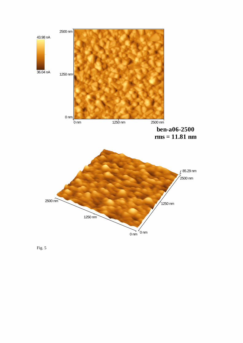
be seen from micro-Raman measurements (514 nm laser excitation) presented in Fig. 3. Typical growth rate under these conditions is 0.25 µm/hour. Addition of argon changes the texture, a strong secondary nucleation pattern develops at 90% of argon. Fig. 4 shows SEM picture of the surface of nanodiamond film grown under “standard conditions” with thickness between 0.5 and 1 µm. Typical grain size ranges between 30 and 100 nm. AFM picture of another sample is in Fig. 5, the root mean square (rms) roughness is around 12 nm. It starts at 7 nm for the thinnest films and approximately saturates around 25 nm for the thickest ones. Ar dilution or lower deposition temperature reduces further this roughness, but also the growth rate. After opening the 6x6 mm window in (100) Si substrate by chemical etching, some membranes were flat (see Fig. 6b), the others were warped, all looked perfectly transparent. This behavior depends on the grain size and orientation of deposited films and seems to be also influenced by residual nitrogen contamination, the stress and thickness inhomogeneity. Further study is necessary to get this under full control. Transmittance of a typical sample is plotted in Fig. 6b. FTIR spectrometry with pyroelectric detector was used in the infrared, Si photodiode in the 200-800 nm spectral region. Light spot dimensions and position were different in both spectrometers. Therefore the interference fringes did not match in the overlap region. We can see 100% transmittance in the interference maximum in the IR (i.e. no absorption in the layer and good optical quality) and from the modulation depth of interference fringes in non-absorbing region, we can determine index of refraction n=2.32 in the middle IR region (compared to n=2.38 of IIa diamond [12]). Suppression of interference fringes in the visible and disappearance in the UV region is due to light scattering, the roughness to wavelength ratio being the decisive parameter [13, 14]. Nanodiamond samples exhibit surface conductivity in the “as grown” state and they are photosensitive. They behave similarly as the standard CVD polycrystalline material [15]. We have applied Fourier transform photocurrent spectroscopy in the subgap region to search for the electronic defects (for the optical transitions leading to the photogenerated hole or electron) [11]. Results are presented in Figs. 7 and 8. Fig. 7 shows the normalized (i.e. divided by the signal from a spectrally independent pyroelectric detector) FTPS signal as a function of temperature. Observed interference fringes are due to good optical quality of deposited films, signal with the threshold energy below 1 eV comes from the Dx defect, described in our previous work for thick CVD diamond wafers [16,17]. New peaks in FTPS signal (proportional to the optical absorptance) can be seen around 0.4 eV at 77K. They are at higher photon energy than the boron peaks, always found in B doped (or contaminated) samples [18]. Similar but broader peak was observed in Ia diamond after heavy electron irradiation [12]. Also H related defect were found in this spectral region [12]. Therefore, we can speculate that this can happen also in our layers (electron irradiation during growth, residual H in layers), but we have not enough supplementing data to elucidate origin of these defect states. 5. Conclusions Variety of thin nanocrystalline diamond films on silicon substrates were grown with thicknesses ranging from 100 to 2000 nm. Windows were opened in the silicon substrate to get the self-supporting, transparent diamond membrane on a silicon frame. Nanodiamond membranes were characterized by SEM, AFM, Raman and

optical spectroscopies. Deposited membranes are very smooth, homogeneous with average grain size 30-100 nm and transparent from UV to IR. Fourier Transform Photocurrent Spectroscopy has been used to access main electronic defects in the gap of this material. New defects were observed with photoionization energy of 0.37 and 0.40 eV. Acknowledgement This work was supported by the Research Training Network of EC, contract HPRN-CT-1999-00139, by bilateral Czech-Flemish collaboration, project 2004-2005-05 and by the Grant Agency of the Czech Republic, contract 202/02/0218. References [1] L. Tang, C. Tsai, W. W. Gerbirich, L. Kruckeberg, and D. R. Kanai, Biomaterials 18, 483 (1995). [2] T. Laurent, F. O. Bastien, J.-C. Pommier, A. Cachard, D. Remiens, E. Cattan., Sensors and Actuators 87 (2000) 26 [3] V. Mortet, O. Elmayria, M. Nesladek, M.B. Assouar, G. Vanhoyland, J.D’Haen, M. D’Olieslaeger, P. Alnot, Appl. Phys. Lett. 81 (2002) 1720 [4] B. Bi, W.S. Huang, J. Asmussen, B. Golding, Diamond Relat. Mater. 11 (2002) 677 [5] J.A.Garrido, C.E.Nebel, R. Todt, M.C. Amann, O.A. Williams, R. Jackman, M. Nesladek, M. Stutzmann, phys. stat. sol. (a) 199 (2003) 56 [6] Y. Liu, C. Liu, Y. Chen, Y. Tzeng, P. Tso, I. Lin, Diamond Relat. Mater. 13 (2004) 671 [7] J. Philip, P. Hess, T. Feygelson, J.E. Butler, S. Chattopadhyay, K.H. Chen, L.C. Chen, J. Appl. Phys. 93 (2003) 2164 [8] S. Jiao, A. Sumant, M.A. Kirk, D.M. Grun, A.R. Krauss, O. Auciello, J. Appl. Phys. 90 (2001) 118 [9] V. Mortet, A. Kromka, R. Kravets, J. Rosa, V. Vorlicek, J. Zemek, M. Vanecek, Diamond Relat. Mater. 13 (2004) 604 [10]V. Mortet, Y. Hubicka, V. Vorlicek, K. Jurek, J. Rosa, M. Vanecek, phys. stat. sol. A (2004) 604 [11]M. Vanecek, R. Kravets, A. Poruba, J. Rosa, M. Nesladek, S. Koizumi, Diamond Relat. Mater. 12 (2003) 521 [12]A.M. Zaitsev, Optical Properties of Diamond, Springer, Berlin 2001 [13]A. Poruba, A. Fejfar, Z. Remes, J. Springer, M. Vanecek, J. Kocka, J. Meier, P. Torres, A. Shah, J. Appl. Phys. 88 (2000) 148 [14] Z. Yin, H.S. Tan, F.W. Smith, Diamond Relat. Mater. 5 (1996) 1490. [15]J. Ristein, in: C.E. Nebel and J. Ristein (Eds.) Thin-Film Diamond II. Semiconductors and Semimetals, Vol. 77, Elsevier/Academic Press, Amsterdam 2004, p.37. [16]M. Nesladek, L.M. Stals, A. Stesmans, K. Iakoubovskij, G.J. Adriaenssens, J. Rosa, M. Vanecek, Appl. Phys. Lett. 72 (1998) 3306 [17]M. Nesladek, K. Haenen, M. Vanecek in: C.E. Nebel and J. Ristein (Eds.) Thin-Film Diamond I. Semiconductors and Semimetals, Vol. 76, Elsevier/Academic Press, Amsterdam 2003, p.325. [18]R. Kravets, M. Vanecek, C. Piccirillo, A. Mainwood, M.E. Newton, Diamond Relat. Mater. 13 (2004) 1785.

Figure caption: Fig. 1: Nanodiamond film deposited on 15x15 mm2 silicon substrate. Fig. 2: SEM picture of the silicon substrate after the BEN process. Fig. 3: Nanodiamond’s Raman spectra as a function of the deposition time. Fig. 4: Surface morphology of a 0.6 µm thick nanodiamond film SEM image. Fig. 5: AFM image of the surface morphology of a 0.6 µm thick nanodiamond film. Fig. 6: (a) Transparent nanodiamond membrane on its Si frame, (b) IR-Vis-UV transmission spectrum of a typical nanodiamond membrane. Fig. 7: Normalized photocurrent signal as a function of the temperature.

Fig. 1
Fig. 2

1000 1200 1400 1600 180010
15
20
25
30
35
40
8 hours4 hours
1 hour
30 min
BEN 12'
Ram
an s
igna
l int
ensi
ty (a
.u.)
wavenumber (cm-1)
Fig.3
Fig.4 BEN M04 Jurek-Hulinsky
2500 nm
1250 nm
0 nm
2500 nm
1250 nm
0 nm
85.29 nm
2500 nm
0 nm
1250 nm
2500 nm0 nm 1250 nm
36.04 nA
43.98 nA
ben-a06-2500rms = 11.81 nm
Fig. 5

Fig. 6a
Fig. 6b
0 1 2 3 4 5 60.0
0.2
0.4
0.6
0.8
1.0
trans
mitt
ance
photon energy (eV)
UV-VIS FTIR
BEN-M16

Fig. 7
0 .6 1 .2 1 .8
1 0 -2
1 0 -1
1 0 0
1 0 1
B E N -M 1 7W L ,C a F ,K C 1 4K B r, W L ,S i(A R C )
norm
aliz
ed F
TPS
sign
al (a
.u.)
p h o to n e n e rg y (e V )
T = 7 7 K T = 1 4 0 K T = 2 0 0 K T = 3 0 0 K
Copyright © 2022 FDOKUMEN