Principles of Microfabrication Marc Madou.pdf - Gorodetsky ...
38
Dr. Marc Madou Principles of Microfabrication University of California, Irvine, the University of Texas Dallas, Occidental College, and Mt. St. Mary’s College First Annual Biological Nanomanufacturing Summer School, UCI May 13, 2013
-
Upload
khangminh22 -
Category
Documents
-
view
1 -
download
0
Transcript of Principles of Microfabrication Marc Madou.pdf - Gorodetsky ...

Dr. Marc Madou
Principles of Microfabrication
University of California, Irvine, the University of Texas Dallas, Occidental College, and Mt. St. Mary’s College
First Annual Biological Nanomanufacturing Summer School, UCI May 13, 2013

Content Definition of MEMS Top-down vs. Bottom-up Definition of BIOMEMS and Why
BIOMEMS is so different MEMS and BIOMEMS manufacturing
methods: – Bulk Micromachining with wet etching – Wafer Bonding – Deep reactive ion etching-DRIE – Surface Micromachining-CVD – Laser beam machining-LBM – Electron beam machining-EBM – Electrodischarge machining-DM – Electrochemical Machining-ECM – Ultrasonic Machining-USM – LIGA – Etc.
Accelerometer element –Mechanical MEMS
Needle array for drug delivery- BIOMEMS
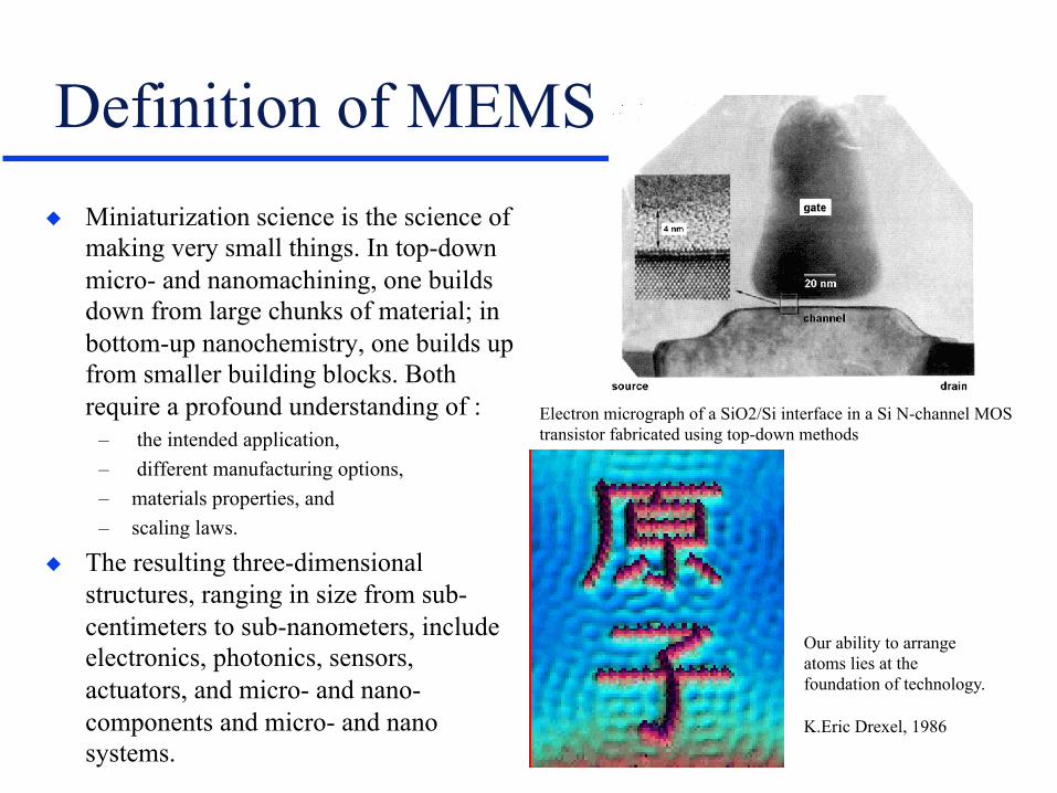
Definition of MEMS Miniaturization science is the science of
making very small things. In top-down micro- and nanomachining, one builds down from large chunks of material; in bottom-up nanochemistry, one builds up from smaller building blocks. Both require a profound understanding of :
– the intended application, – different manufacturing options, – materials properties, and – scaling laws.
The resulting three-dimensional structures, ranging in size from sub-centimeters to sub-nanometers, include electronics, photonics, sensors, actuators, and micro- and nano-components and micro- and nano systems.
Electron micrograph of a SiO2/Si interface in a Si N-channel MOS transistor fabricated using top-down methods
Our ability to arrange atoms lies at the foundation of technology. K.Eric Drexel, 1986

Top-down vs. Bottom-up Top-down nanofabrication is principally based on lithography and traditional
mechanical machining, etching and grinding whereas bottom-up nanochemistry is based in chemical synthesis, self-assembly and positional assembly.
The distinction is clarified in the Figure below. These complementary developments constitute different aspects of nanotechnology, both aim to create and use, structures, devices and systems in the size range of about 0.1 nm to 100 nm (covering the atomic, molecular and macromolecular length scales).

Top-down vs. Bottom-up Whereas top-down methods essentially ‘impose’ a structure or pattern on a substrate, in self-assembly
and self-organized based bottom-up methods the assembly or organization of atomic and molecular constituents into larger structures is inherent through processes in the manipulated system.
Self-assembly and self-organization are driven by thermodynamics and hold the intriguing potential of delegating more and more mechanical or logical operations to materials instead of to manufacturing machines.
Assembly of atoms or molecules into larger aggregates in chemical synthesis is driven by chemical reactions with the Gibbs free energy changes dominated by the enthalpy changes associated with breaking and creating bonds (ΔG=ΔH-TΔS). In self-assembly the driving forces are weak.

Top-down vs. Bottom-up Example bottom-up machining: DNA staples. The sequence of DNA provides unique
addresses for each location. “Staple strands” bind locations together according to the design.
The design for a desired shape is made by raster filling the shape with the 7-kilobase single-stranded scaffold molecule and by choosing over 200 short oligonucleotide staple strands to hold the scaffold in place.4

Definition of BIOMEMS and Why BIOMEMS is so Different ‘Miniaturization engineering’ is
a more appropriate name than MEMS (NEMS), but the name MEMS (NEMS) is more popular.
Miniaturization engineering or MEMS applied to biotechnology is called BIOMEMS.
BIOMEMS is very different from MEMS: – the number of materials involved is
much larger – modularity is often a must (not
integration as in ICs !) – costs often need to be less than
what’s possible with Si and batch processes are not always the answer ( continuous manufacturing need !).

Bulk Micromachining What is bulk micromachining?
– Etching into the substrate (subtractive process
– Aggressive etching (1-500 µm) Anisotropic wet crystal etching Anisotropic dry vertical etching (Deep
RIE) Isotropic dry and wet etching New processes : e.g., combination of bulk
and surface micromachining Why bulk micromachining?
– Sensors and actuators (beginning of MEMS)
– Accelerometers, micropumps, nozzles, etc…

Bulk Micromachining Planes (h k l) : Miller indices (e.g.,
(111), (110), (100)) plane intersects with x,y,z axes at p,q,r and h=1/p; k=1/q; l=1/r
(100), (010), (001), (100) {100} is a family of planes

Bulk Micromachining Reaction limited etching Etchants: KOH, EDP (Ethylene Diamine Pycocatechol) , TMAH
(TetraMethylAmmonium Hydroxide) Masks: LPCVD Si3N4 and Thermal SiO2
Etching rate depends on mixing ratio, temperature, and crystal orientation Typically (E(100))
– Temp=80C – KOH / water ratio = 30 % – Etching rate = ~1 m /min – E(100)/E(111)=35 (EDP) – E(100)/E(111)=400 (KOH)
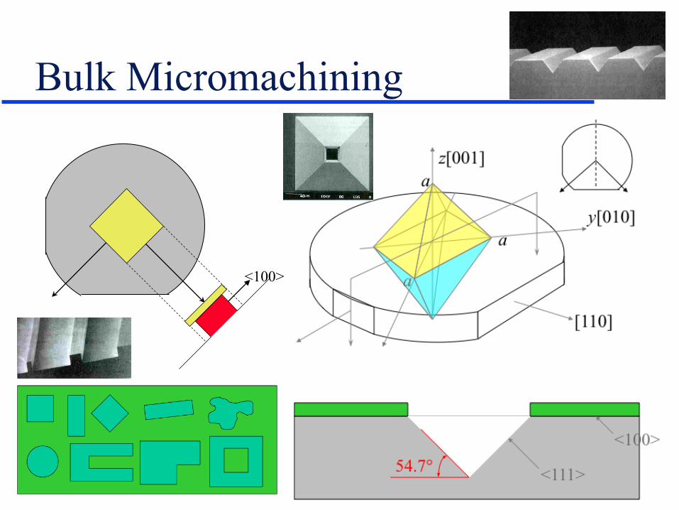
Bulk Micromachining
<100>

Bulk Micromachining Boron (P+) etch stop: at
concentrations of B >71019 cm-3 the etching rate drops 50 times (EDP)
This enables the control of 1-20 µm thick membranes
Membrane in tension (B < Si) Not effective with KOH Incompatible with CMOS
process

Wafer Bonding Combines complex shapes from
multiple wafers Si-Si fusion bonding:
– Fusion – high temp (1000ºC) Si-Glass wafers
– Anodic – low temp, high voltage (700V)

Deep Reactive Ion Etching- DRIE
Alternating RIE - polymer deposition
Protection of side walls during material removal
CHF3/Ar forms Teflon-like layer
Issues: Scalloping and tapering
14/ 50
Milanovic et al, IEEE TED, Jan. 2001.

Surface Micromachining

Surface Micromachining and CVD
Gases dissociate on surfaces at high temperature
Typically done at low pressure (LPCVD) rather than atmospheric (APCVD)
LPCVD pressures around 300mT (0.05% atm)
Moderate temperatures – SiO2 : 450 °C – Polysilicon : 580-650 °C
SixNy : 800 °C Very dangerous gases
– Silane: SiH4
– Arsine, phosphine, diborane: AsH3, PH3, B2H6
Gas phase is injected into the chamber
Thermal decomposition and/or reaction of gaseous compounds occur on the substrate surface
Desired material is deposited directly from the gas phase to form thin layer

Surface Micromachining and CVD Effects of residual stress Good for mechanical
applications Little use in BIOMEMS

LASER MACHINING
Subtractive
Additive
10 µm

LASER MACHINING
Laser usage in machining: – Heat treatment – Welding – Ablation – Deposition – Etching – Lithograpy – Photopolymerization (stereo lithography) – Microelectroforming – Focused beam milling
In laser ablation, spatial resolution is 1 µm by 1 µm by 1 µm
In ablation reactive gases may be added to avoid debris
640 µm
Al2O3
Laser ablation Ultrasonic

LASER MACHINING
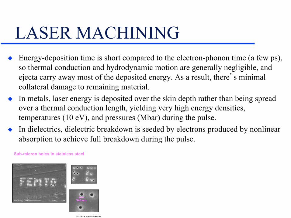
LASER MACHINING Energy-deposition time is short compared to the electron-phonon time (a few ps),
so thermal conduction and hydrodynamic motion are generally negligible, and ejecta carry away most of the deposited energy. As a result, there’s minimal collateral damage to remaining material.
In metals, laser energy is deposited over the skin depth rather than being spread over a thermal conduction length, yielding very high energy densities, temperatures (10 eV), and pressures (Mbar) during the pulse.
In dielectrics, dielectric breakdown is seeded by electrons produced by nonlinear absorption to achieve full breakdown during the pulse.
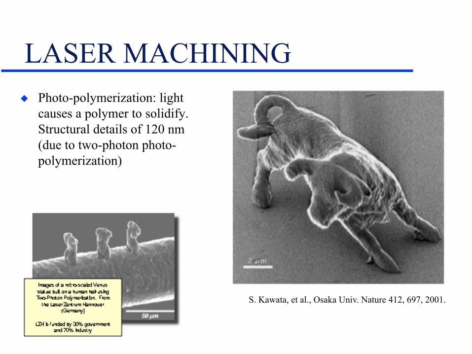
LASER MACHINING Photo-polymerization: light
causes a polymer to solidify. Structural details of 120 nm (due to two-photon photo-polymerization)
S. Kawata, et al., Osaka Univ. Nature 412, 697, 2001.

Electron-Beam Machining (EBM): additive and subtractive Removal processes: Melting and
vaporizing e.g. 0.1 mm diameter holes through 10 mm thick plates
Forming processes: precursor gas e.g. Al(CH3)3 for Al
Laser is often more cost effective but cannot make the very small holes and features possible with EBM
Laser is less expensive and does not require a vacuum
Requires a good vacuum

Electro Discharge Machining-EDM EDM (die sink): mostly used for machining hard,
brittle metals. In the manufacturing process the work piece is submerged in a dielectric fluid
Sparking erodes both anode workpiece and cathode tool (100 Hz to hundreds of kilohertz)
In wire EDM the cathode is a fine wire (e.g. Cu), WEDM is starting to make impact in micromachining
http://www.mercatech.com/mtiEDM.html
http://www.amtmfg.com/wirex.html Tiny specialized shapes can be precisely created with EDM. These parts are made within .001" tolerance.

Electro Discharge Machining-EDM-WC Sparks between electrode-work-
piece Dielectric flushes the metal
powder Inexpensive, precise, complex
shapes Workpiece must be a conductor
Handheld EDM at Panasonic
Electrode EDM

Electro Discharge Machining-EDM-WC Electrical discharge machining
wire cutting (EDM-WC). Schematic illustration of the wire EDM process. As much as 50 hours of machining can be performed with one reel of wire, which is then discarded.
The µ-EDM-WC tool features micro-wire tension control and wire vibration suppression. The tool allows vertical, horizontal and slanted wire cutting. µ-EDM-WC at the National Taiwan University (Prof. Y.S. Liao).

Electro discharge machining-EDM-WC The vertical, horizontal and slanted cutting with the µ-EDM-WC tool
has successfully fabricated complex features and parts. An example is the impressive Chinese pagoda (1.25 mm × 1.75 mm) shown below in Al (vertical and horizontal µ-EDM-WC cuts are demonstrated).

Electrodeposition example: making of coils for thin film magnetic heads
Problems for plating in small plastic cavities
Electrochemical machining (ECM) is electrochemical etching with a cathode shaped to provide an etched form in the anode workpiece (highly conductive materials are corroded in electrolyte solutions)--accuracy better than 10 µm
Often applied to high-strength and very hard materials (aircraft, automotive, and business machines e.g. pistons, fuel-injection nozzles)
Electrochemical Machining-ECM

Electrochemical Machining-ECM Schematic illustration of the
electrochemical-machining process. This process is the reverse of electroplating.
Typical parts made by electrochemical machining. (a) Turbine blade made of a nickel alloy, 360 HB. Source: Metal Handbook, 9th ed., Vol. 3, Materials Park, OH: ASM International, 1980, p. 849. (b) Thin slots on a 4340-steel roller-bearing cage. (c) Integral airfoils on a compressor disk.

Ultrasonic Machining (USM)

Ultrasonic Machining (USM). Almost any hard material (even brittle) can be ultrasonically machined Tools have the shape of the cavity we want to machine in the workpiece Non-thermal and non-chemical, non-electrical so it produces virtually stress free shapes Abrasive particle size determines surface finish Holes as small as 0.076 mm have been made but 0.25 is more the norm Tools might be made by electrodischarge wire cutting
(a) Schematic illustration of the ultrasonic-machining process by which material is process by which material is removed through microchipping and erosion. (b) and (c) typical examples of holes produced by ultrasonic machining. Note the dimensions of cut and the types of workpiece materials.

CNC-Ultra-High Precision Machining
Radius of the edge is estimated at less than 0.0 5µm
Diamond
Lathe

Computer numerical controlled (CNC) machines became available in 1977
By 1993 these machines could reproducibly machine at 0.05 µm
Submicron precision is also achieved through more stable lathes (better bearings, laser interferometry, etc.)
Most micromachinery will be made by a set of complementary machining technologies
CNC-Ultra-High Precision Machining
7 mm
NC machine Al Ni plate for the shell of the car
Remove Al with KOH

CNC Machining Numerical control is a method
of automatically operating a manufacturing machine based on a code of letters, numbers, and special characters.
The numerical data required to produce a part is provided to a machine in the form of a program, called part program or CNC program.
The program is translated into the appropriate electrical signals for input to motors that run the machine.

CNC Machining-Desk-Top Factories
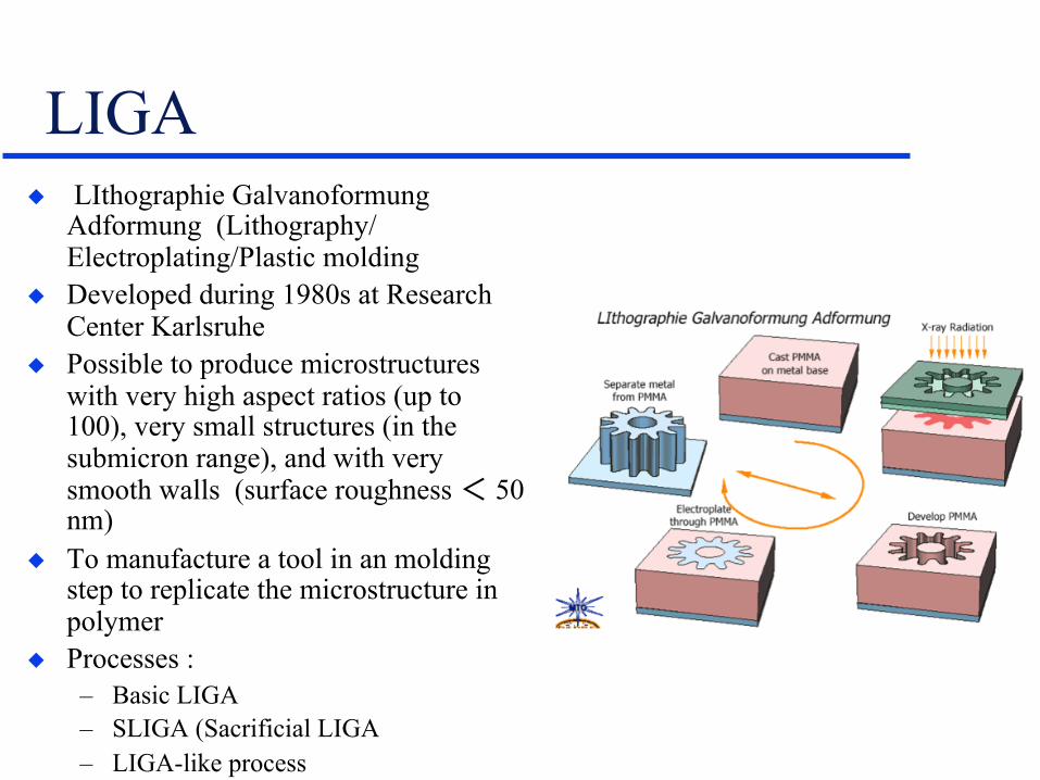
LIGA LIthographie Galvanoformung
Adformung (Lithography/Electroplating/Plastic molding
Developed during 1980s at Research Center Karlsruhe
Possible to produce microstructures with very high aspect ratios (up to 100), very small structures (in the submicron range), and with very smooth walls (surface roughness < 50 nm)
To manufacture a tool in an molding step to replicate the microstructure in polymer
Processes : – Basic LIGA – SLIGA (Sacrificial LIGA – LIGA-like process

LIGA

Thank you.