Quantitative sub-surface and non-contact imaging using Scanning Microwave Microscopy
10
This content has been downloaded from IOPscience. Please scroll down to see the full text. Download details: This content was downloaded by: enricobrinciott IP Address: 206.49.51.4 This content was downloaded on 10/03/2015 at 12:12 Please note that terms and conditions apply. Quantitative sub-surface and non-contact imaging using scanning microwave microscopy View the table of contents for this issue, or go to the journal homepage for more 2015 Nanotechnology 26 135701 (http://iopscience.iop.org/0957-4484/26/13/135701) Home Search Collections Journals About Contact us My IOPscience
Transcript of Quantitative sub-surface and non-contact imaging using Scanning Microwave Microscopy

This content has been downloaded from IOPscience. Please scroll down to see the full text.
Download details:
This content was downloaded by: enricobrinciott
IP Address: 206.49.51.4
This content was downloaded on 10/03/2015 at 12:12
Please note that terms and conditions apply.
Quantitative sub-surface and non-contact imaging using scanning microwave microscopy
View the table of contents for this issue, or go to the journal homepage for more
2015 Nanotechnology 26 135701
(http://iopscience.iop.org/0957-4484/26/13/135701)
Home Search Collections Journals About Contact us My IOPscience

Quantitative sub-surface and non-contactimaging using scanning microwavemicroscopy
Georg Gramse1,6, Enrico Brinciotti2,6, Andrea Lucibello3,Samadhan B. Patil4, Manuel Kasper1, Christian Rankl2,Rajiv Giridharagopal5, Peter Hinterdorfer1, Romolo Marcelli3 andFerry Kienberger2
1 Johannes Kepler University of Linz, Institute for Biophysics, Gruberstrasse 40, A-4020 Linz, Austria2Keysight Technologies Austria GmbH, Keysight Labs, Gruberstrasse 40, A-4020 Linz, Austria3 CNR-IMM Roma, Via del Fosso del Cavaliere 100, I-00133 Rome, Italy4 London Centre for Nanotechnology, 19 Gordon St, London WC1H 0AH, UK5 Intel Corporation, Technology Manufacturing Group Labs, 2501 NW 229th Ave, Hillsboro, OR, USA
E-mail: [email protected]
Received 11 December 2014, revised 12 January 2015Accepted for publication 20 January 2015Published 9 March 2015
AbstractThe capability of scanning microwave microscopy for calibrated sub-surface and non-contactcapacitance imaging of silicon (Si) samples is quantitatively studied at broadband frequenciesranging from 1 to 20 GHz. Calibrated capacitance images of flat Si test samples with varyingdopant density (1015–1019 atoms cm−3) and covered with dielectric thin films of SiO2
(100–400 nm thickness) are measured to demonstrate the sensitivity of scanning microwavemicroscopy (SMM) for sub-surface imaging. Using standard SMM imaging conditions thedopant areas could still be sensed under a 400 nm thick oxide layer. Non-contact SMM imagingin lift-mode and constant height mode is quantitatively demonstrated on a 50 nm thick SiO2 testpad. The differences between non-contact and contact mode capacitances are studied withrespect to the main parameters influencing the imaging contrast, namely the probe tip diameterand the tip–sample distance. Finite element modelling was used to further analyse the influenceof the tip radius and the tip–sample distance on the SMM sensitivity. The understanding of howthe two key parameters determine the SMM sensitivity and quantitative capacitances representsan important step towards its routine application for non-contact and sub-surface imaging.
Keywords: nanotechnology, calibration, complex impedance, capacitance, sub-surface imaging,scanning microwave microscopy
(Some figures may appear in colour only in the online journal)
1. Introduction
Sub-surface imaging of complex structures using scanningprobe microscopy (SPM) has recently attracted considerableinterest. Information on sub-surface features can be obtainedexploiting the mechanical heterogeneity within the sample byfrequency dependent mechanical measurements [3–7].
Similarly, frequency dependent electrical measurements canbe used to probe local electric properties at certain depthwithin the sample. For established electrical SPM techniqueslike scanning capacitance microscopy and electrostatic forcemicroscopy that operate at a single frequency or in a limitedfrequency range below 1 GHz, sub-surface imaging has stillnot been reported. Scanning microwave microscopy (SMM)[1, 2], a quantitative nanoscale electrical characterizationtechnique operating at broadband microwave frequencies [8],
Nanotechnology
Nanotechnology 26 (2015) 135701 (9pp) doi:10.1088/0957-4484/26/13/135701
6 Equally contributing author.
0957-4484/15/135701+09$33.00 © 2015 IOP Publishing Ltd Printed in the UK1

can be used to selectively sense the sub-surface of the samplesunder study [9, 10].
The SMM consists of an atomic force microscope (AFM)combined with a vector network analyser (VNA) operatingbetween 1 and 20 GHz. It combines the nanoscale spatialresolution of the AFM with the broadband electrical mea-surement capabilities of the VNA [11]. In the SMM reflectionmode, the VNA sends an incident microwave signal through aconductive tip of a platinum–iridium cantilever. Dependingon the impedance of the tip/sample interface, part of themicrowave signal is reflected and measured by the VNA asthe scattering S11 reflection signal [12]. The SMM has beensuccessfully used to obtain calibrated values of relevantphysical quantities, such as complex impedance, capacitance,and resistance [13, 14] and surface localized physical sampleproperties (electric permittivity, dopant density, and resistiv-ity) with nanoscale spatial resolution [13–17]. Most of theadvances in the SMM community were achieved studyingsurface structures including semiconductor devices. To thebest of our knowledge, to date only studies on metallic andinsulating substrates were reported that took advantage of thepenetration ability of microwaves through materials [9, 10].In these works, qualitative SMM imaging was performedexploiting the long-range electromagnetic (EM) interactionbetween microwaves and matter. Electrical contrast wasobtained for flat samples with dielectric variations [9],whereas for metallic samples the dependence of EM pene-tration depth on the applied frequency through the metallicskin effect was used as contrast mechanism [10].
Here, we extend subsurface SMM imaging to dopedsemiconductors samples. For the first time we show calibratedcapacitance images of buried semiconductor structures. Alsothe sensitivity of SMM for the measurement of subsurfaceelements is quantitatively studied. To obtain quantitativecapacitance from the raw S11 measurements we calibrate theSMM using a procedure recently reported [13]. Additionally,we took advantage of the long-range sensitivity of the GHzEM field [18–20] to study the capability of SMM for cali-brated non-contact capacitance imaging.
The sensitivity of the SMM for sub-surface imaging isstudied experimentally and theoretically by finite elementmodelling (FEM) under different conditions as a function ofthe tip radius and the tip–sample distance [21]. Understandingthe effects of the key parameters on the SMM sensitivityrepresents an important step for future studies in thisfield [22].
2. Materials and methods
2.1. SMM setup
A commercial transmission line SMM (Keysight Technolo-gies, Santa Rosa, CA, USA) consisting of a standard 5600AFM interfaced with a 20 GHz VNA both from KeysightTechnologies, was used. Rocky Mountain Nanotechnology(RMN) solid platinum AFM tips were used. All measure-ments were carried out in dry atmosphere (RH< 5%). A
schematic of the SMM experimental setup is shown infigure 1(a). The AFM tip is used as a nanoscale imaging andmicrowave probe, enabling simultaneous topographic andEM characterization of the sample under test. The VNAmeasures the ratio of the incident and reflected signal at thetip, the so called scattering S11 parameter. To transform thehigh impedance of the tip–sample contact to the sensitive50Ω of the VNA, a half-wavelength coaxial resonator inconjunction with a 50Ω shunt resistor is used [23]. A highsignal-to-noise ratio with good matching conditions is typi-cally obtained every ∼2 GHz with the exact value dependingon the cable lengths. Since the admittance Y scales linearlywith the frequency f (ω= 2πf) and the capacitance C, Y∼ jωC,it is favourable to measure at high frequencies. All the mea-surements presented in this work were performed at fre-quencies between 18 and 20 GHz while the SMM works inthe range of 1–20 GHz. An intermediate bandwidth frequencyof 100 Hz and 500 Hz has been used during the measure-ments, leading to a scan speed of 0.26 and 0.81 lines s-1 at 256points/line, respectively.
2.2. Calibration workflow
In order to convert measured reflection S11 values intocapacitance values, a systematic calibration workflow has tobe applied [24]. We applied the calibration procedure recentlyproposed by Gramse et al [13]. The measured reflectioncoefficient S11 is converted into the complex impedance Zusing the one-port black-box calibration. The defined cali-bration standards to calculate three complex error parameterse00, e01, and e11 are provided by simultaneously acquiringelectrostatic force microscopy (EFM) and S11 approachcurves. For this the tip is approached towards the surface untilit gets into contact and both the EFM and the S11 signals arerecorded. No external capacitance calibration sample isrequired. The main advantages of this approach are that itworks in situ on the sample under test and that the calibrationplane is located directly before the cantilever chip.
For calibration, topography and complex S11 (amplitudeand phase) images of the sample under test are acquired and acombined EFM/S11 approach curve is performed. From theelectrostatic force, ωF ,es,2 measured at the second harmonic ofthe excitation voltage ω=v t V t( ) sin( ),0 the gradient of thecapacitance with respect to the tip–sample distance isobtained by = ωC z F Vd /d 2 / .es,2 0
2 The capacitance zC ( ) canbe calculated by integration. Assuming that the change inimpedance Z z( )in is only capacitive (strictly true only for non-lossy materials like dielectrics or highly conductive materi-als), three error parameters (e00, e01 and e11) can be calculatedusing = + −S e e S e S/(1 ),a a11 00 01 11, 11 11, where
= − +S Z Z Z Z( )/( ),11,a in ref in ref and Zref is the char-acteristic impedance of the VNA (i.e. 50Ω). Using the threee-parameters, from the complex S11 (amplitude and phase)image the calibrated capacitance image can be obtained.
As shown elsewhere [13, 28, 29], the tip radius R can beobtained from the capacitance approach curve using the
2
Nanotechnology 26 (2015) 135701 G Gramse et al

approximation:
θ ε = + +( )C R H c c z h C C C, , , , , , , , (1)rstray apex cone stray
πεε
ε ε θ=
++ + −
C Rh z
h R z R2 ln
( ) sin, (2)r
r rapex 0
πεθ
εθ
εθ
εε
θ
=
× + + −
− + −
× + + −
−
−( )
C
z Hh
z R
hR
hz R
2
(ln (tan /2))
ln (1 sin )
1 sin
ln (1 sin ) , (3)
r
r
rr
cone0
2
1
1
⎛
⎝⎜⎜
⎛
⎝⎜⎜
⎛⎝⎜⎜
⎞⎠⎟
⎞
⎠⎟⎟
⎛⎝⎜
⎞⎠⎟
⎛⎝⎜
⎛⎝⎜
⎞⎠⎟
⎞⎠⎟
⎞⎠⎟⎟
= +C c z c, (4)stray stray
where, H is the cone height (nominally 80 μm), θ the coneangle (nominally 15°), z the tip–sample distance, h thethickness of the dielectric thin film, and εr its dielectricconstant.
2.3. Samples preparation
The topographically flat doped silicon (Si) samples[15, 25, 26], were provided by Professor Smoliner fromTechnical University of Vienna. They consist of 20 μm widen-type doped regions with the doping density arranged in astaircase like structure in epitaxially grown multilayer Si. Thedoping concentrations are, from the edge to the bulk of thesample, 4× 10¹⁹ atoms cm−3, 1× 10¹⁸ atoms cm−3, 8×10¹⁷ atoms cm−3 and 1 × 10¹⁶ atoms cm−3, separated by 5 μm
wide bulk interface layers at 1 × 10¹⁴ atoms cm−3. The regionwith doping level of 1× 10¹⁸ atoms cm−3 contains dopant sub-levels with very fine variations of ∼1× 10¹⁷ atoms cm−3.
The doped Si surface to be imaged was covered side byside with a SiO2 layer, 120 nm and 200 nm thick, using ashadow metal mask. A thickness gradient region between 120and 200 nm of SiO2 was micro-patterned and etched to yieldSiO2 free region. This effectively produces buried doped Sisurface with SiO2 spacer dielectric of 120 nm, 200 nm and nospacer region as control (shown in figure 1).
A second sample with the same doped Si staircasestructure (shown in figure 2) was covered with SiO2 layershaving thickness of 100 nm, 200 nm and 400 nm. Thedielectric thin films were deposited through a SiH4 basedplasma enhanced chemical vapour deposition process. Inorder to achieve the goal of 400 nm of SiO2, three separatedeposition steps have been necessary.
The 50 nm thick SiO2 structures on the highly doped Sisubstrate shown in figures 3 and 4 (resistivity of 0.001–0.005Ω cm) were purchased from AMO GmbH (Aachen,Germany).
2.4. Finite element modelling
FEM was carried out with Comsol Multiphysics 4.3 (2Daxisymmetric, ac/dc module, electric currents, frequencydomain). The simulations resemble the experimental condi-tions of the experiments in figure 3 (50 nm thick oxide of6 μm diameter on a metallic substrate; 80 μm high AFM tipwith cone angle of 15°; cantilever excelling the cone end by10 μm) with variable tip substrate distance and tip radius. Thetip bias is set to 1 V and the metallic substrate is set to ground.Similar models have been used in [13, 27].
Figure 1. Experimental setup for sub-surface imaging of a doped Si substrate partly covered with SiO2. (a) The scanning microwavemicroscope (SMM) consists of a vector network analyser (VNA) and an atomic force microscope (AFM). In reflection mode a GHzmicrowave signal is sent through a conductive platinum cantilever to electrically characterize the sample under investigation. One port of theVNA is used to measure the reflection coefficient S11. (b),(d) SMM images of a doped Si substrate partly covered with 120 nm and 200 nm.Panels (b),(d) show the topography images with a sketch of the sample (inset) and panels (c),(e) show the reflection S11 phase images with thesubsurface dopant features.
3
Nanotechnology 26 (2015) 135701 G Gramse et al
3. Results and discussion
3.1. Sub-surface imaging of a SiO2 covered doped Si sample
To explore the sub-surface imaging capabilities of the SMMwe used a topographically flat Si test sample exhibiting var-ious dopant stripes with increasing dopant density, from1× 1016 atoms cm−3 to 4 × 10¹⁹ atoms cm−3, intersected withbulk interface layers (1 × 10¹⁴ atoms cm−3). The dopant sam-ple was partially covered with a layer of SiO2 having twodifferent oxide thicknesses, 120 nm and 200 nm (figure 1).The partial SiO2 coverage was obtained by CVD oxidegrowth and subsequent focused ion beam milling and isclearly visible in the topographical images (figures 1(b) and(d)). The oxide thickness was verified using topographycross-section analysis. The surface of the doped Si sample isflat according to the topographical image (surface roughnessless than 3 nm) and the doping pattern is only visible in theS11 images (figures 1(c) and (e)). Therefore, no cross-talk ofthe S11 image with the topography is obtained on those flat Sisamples. The areas that are not covered with oxide show astrong S11 signal generated from the differently doped stripes.Even though the S11 signal is smaller on the oxide-coveredareas, it can be noticed that the different dopant densities canstill be detected both at 120 nm and 200 nm oxide coverage.In particular, the bulk interface layers that separate the indi-vidually doped areas can be clearly observed. However, veryfine dopant differences within the second dopant stripe canonly observed on the bare sample. These results confirm thatthe SMM can be used to electrically probe oxide buriedstructures as also shown by Plassard et al [10] for metallicsamples and by Lai et al [9] on insulators.
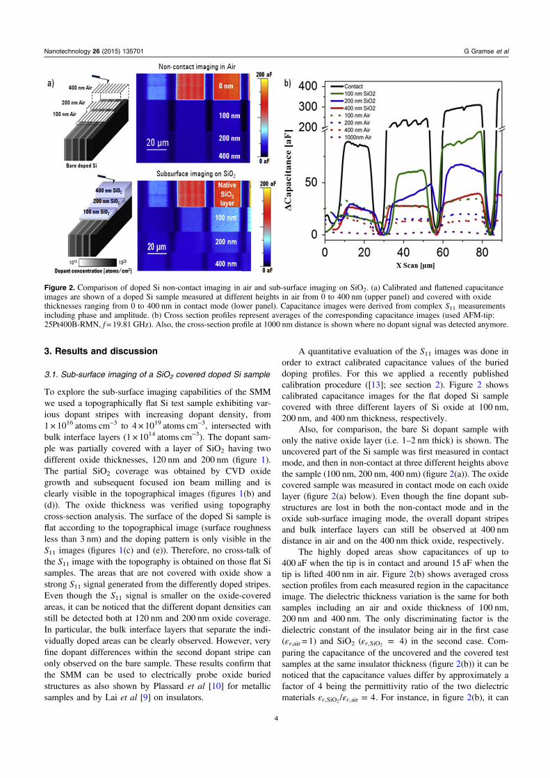
A quantitative evaluation of the S11 images was done inorder to extract calibrated capacitance values of the burieddoping profiles. For this we applied a recently publishedcalibration procedure ([13]; see section 2). Figure 2 showscalibrated capacitance images for the flat doped Si samplecovered with three different layers of Si oxide at 100 nm,200 nm, and 400 nm thickness, respectively.
Also, for comparison, the bare Si dopant sample withonly the native oxide layer (i.e. 1–2 nm thick) is shown. Theuncovered part of the Si sample was first measured in contactmode, and then in non-contact at three different heights abovethe sample (100 nm, 200 nm, 400 nm) (figure 2(a)). The oxidecovered sample was measured in contact mode on each oxidelayer (figure 2(a) below). Even though the fine dopant sub-structures are lost in both the non-contact mode and in theoxide sub-surface imaging mode, the overall dopant stripesand bulk interface layers can still be observed at 400 nmdistance in air and on the 400 nm thick oxide, respectively.
The highly doped areas show capacitances of up to400 aF when the tip is in contact and around 15 aF when thetip is lifted 400 nm in air. Figure 2(b) shows averaged crosssection profiles from each measured region in the capacitanceimage. The dielectric thickness variation is the same for bothsamples including an air and oxide thickness of 100 nm,200 nm and 400 nm. The only discriminating factor is thedielectric constant of the insulator being air in the first case(εr,air = 1) and SiO2 (ε = 4)r,SiO2 in the second case. Com-paring the capacitance of the uncovered and the covered testsamples at the same insulator thickness (figure 2(b)) it can benoticed that the capacitance values differ by approximately afactor of 4 being the permittivity ratio of the two dielectricmaterials ε ε =/ 4.r r,SiO ,air2 For instance, in figure 2(b), it can
Figure 2. Comparison of doped Si non-contact imaging in air and sub-surface imaging on SiO2. (a) Calibrated and flattened capacitanceimages are shown of a doped Si sample measured at different heights in air from 0 to 400 nm (upper panel) and covered with oxidethicknesses ranging from 0 to 400 nm in contact mode (lower panel). Capacitance images were derived from complex S11 measurementsincluding phase and amplitude. (b) Cross section profiles represent averages of the corresponding capacitance images (used AFM-tip:25Pt400B-RMN, f= 19.81 GHz). Also, the cross-section profile at 1000 nm distance is shown where no dopant signal was detected anymore.
4
Nanotechnology 26 (2015) 135701 G Gramse et al
be noticed that the capacitance at 100 nm height in air over-laps with the capacitance at 400 nm SiO2. The factor of 4resulting from ε ε/r r,SiO ,air2 indicates that the measured capa-citance depends on the ratio C∼ εr h
−1 and the higher is thetip–substrate distance the lower is the capacitance.
Additionally, a scan in air was performed at 1000 nmdistance from the substrate (purple dashed line in figure 2(b))resulting in a flat capacitance signal, indicating that the SMMsensitivity limit was reached and the S11 signal was below thenoise level of ∼1 aF. It can be noticed that the plateaus on thedifferent dopant levels are not always perfectly horizontal dueto a flattening artefact.
3.2. SMM lift-mode and constant-height imaging
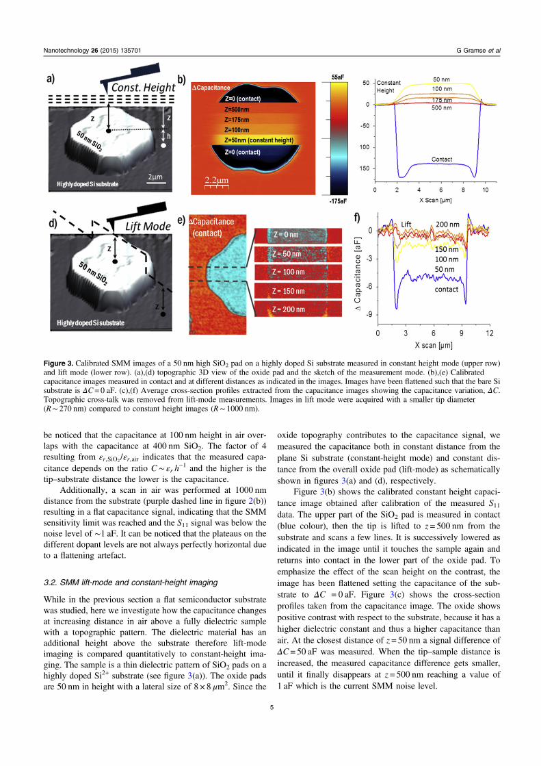
While in the previous section a flat semiconductor substratewas studied, here we investigate how the capacitance changesat increasing distance in air above a fully dielectric samplewith a topographic pattern. The dielectric material has anadditional height above the substrate therefore lift-modeimaging is compared quantitatively to constant-height ima-ging. The sample is a thin dielectric pattern of SiO2 pads on ahighly doped Si2+ substrate (see figure 3(a)). The oxide padsare 50 nm in height with a lateral size of 8 × 8 μm2. Since the
oxide topography contributes to the capacitance signal, wemeasured the capacitance both in constant distance from theplane Si substrate (constant-height mode) and constant dis-tance from the overall oxide pad (lift-mode) as schematicallyshown in figures 3(a) and (d), respectively.
Figure 3(b) shows the calibrated constant height capaci-tance image obtained after calibration of the measured S11data. The upper part of the SiO2 pad is measured in contact(blue colour), then the tip is lifted to z= 500 nm from thesubstrate and scans a few lines. It is successively lowered asindicated in the image until it touches the sample again andreturns into contact in the lower part of the oxide pad. Toemphasize the effect of the scan height on the contrast, theimage has been flattened setting the capacitance of the sub-strate to ΔC = 0 aF. Figure 3(c) shows the cross-sectionprofiles taken from the capacitance image. The oxide showspositive contrast with respect to the substrate, because it has ahigher dielectric constant and thus a higher capacitance thanair. At the closest distance of z= 50 nm a signal difference ofΔC= 50 aF was measured. When the tip–sample distance isincreased, the measured capacitance difference gets smaller,until it finally disappears at z= 500 nm reaching a value of1 aF which is the current SMM noise level.
Figure 3. Calibrated SMM images of a 50 nm high SiO2 pad on a highly doped Si substrate measured in constant height mode (upper row)and lift mode (lower row). (a),(d) topographic 3D view of the oxide pad and the sketch of the measurement mode. (b),(e) Calibratedcapacitance images measured in contact and at different distances as indicated in the images. Images have been flattened such that the bare Sisubstrate is ΔC= 0 aF. (c),(f) Average cross-section profiles extracted from the capacitance images showing the capacitance variation, ΔC.Topographic cross-talk was removed from lift-mode measurements. Images in lift mode were acquired with a smaller tip diameter(R∼ 270 nm) compared to constant height images (R∼ 1000 nm).
5
Nanotechnology 26 (2015) 135701 G Gramse et al

In figure 3(e) the same sample was measured in lift modeat increasing lift-height from the sample. Compared to theprevious constant height measurement, a smaller tip size wasused to achieve lower capacitance values that are closer to theSMM noise level. The tip–radius was determined using aquantitative approach-curve analysis as described inequation (1) of the section 2. A tip apex radius of R= 1000 nmand R= 270 nm for figures 3(b) and (d) was calculated,respectively. In figure 3(e) at z= 0 nm (i.e. contact mode) thesmaller tip gives a capacitance contrast of 6 aF which issignificantly lower than for the larger tip measurement
(150 aF in figure 3(c)). It should be noted that the non-localtopography-cross talk in figure 3(e) was removed by takingthe topography image into account. The image has been alsoflattened setting the capacitance on the Si substrate to ΔC= 0 aF. With increasing lift height the contrast disappearsrapidly and is almost completely lost at z= 100 nm. The lift-mode capacitance images and cross-section profiles show thatthe SiO2 pad has inverted contrast with respect to the con-stant-height measurements. To understand this better, it isinstructive to look at quantitative capacitance versus distancecurves when approaching the tip to the Si2+ and to theSiO2 pad.
3.3. Quantitative approach curve analysis
Figure 4 shows calibrated capacitance approach curves on theoxide pad and the bare Si (Si2+) substrate from the sampleshown in figure 3. For constant-height mode (figure 4(a)) thedistance is denoted with respect to the flat Si2+ substrate andfor lift-mode (figure 4(b)) with respect to the overall sampletopography. This results essentially in a shift of the SiO2
approach curve of h = 50 nm along the z-axis, z’ = z+ h.The approach curves are plotted for the smaller tip
(R∼ 270 nm) and the bigger tip (R∼ 1000 nm). The bigger tipgives a higher signal difference between Si and SiO2, espe-cially close to contact as observed also in the images infigure 3. Also the inversion of the contrast between constant-height mode and lift mode observed in figure 3 is obtained inthe approach curves with the SiO2 curve in figure 4(a) aboveand in figure 4(b) below the Si curve. This again is an effectof the shift along the z-axis. On top of the contrast inversion,two practical differences between lift-mode and constant-height mode can be found when looking at the capacitancedifference between the approach curves on the Si and theSiO2 as shown in figure 4(c).
Firstly, in lift mode there is a constant offset in the dif-ference signal (marked by the blue scattered line), because thecapacitance from the non-local parts of the AFM tip (e.g.upper cone, cantilever) change nearly linearly when the tip–substrate distance is changed. This so-called topographycross-talk is an undesired artefact but plays only a significantrole for small AFM tips and can also be subtracted from themeasurements as done in figure 3 [13, 28]. In constant-heightmode there is no topography cross-talk.
Secondly, a capacitance contrast in lift mode can be onlyobserved when the tip is relatively close to the surface and thecontrast decreases for higher dielectric constants of thedielectric layer as shown in the inset of figure 4(c). In constantheight mode a contrast can be observed also at higher dis-tances, and it increases with higher dielectric constant. This isbecause the capacitance is a function of C(h εr
−1) in lift modeand C(h/εr−h) in constant height mode as described in [13]and also discussed in [28, 29]. Independently of acquiring animage in lift mode or constant height mode, in principle thesame result for εr is expected.
In summary, acquisition of capacitance images in con-stant height mode is experimentally more demanding than inlift mode, especially if the substrate is not completely flat.
Figure 4. Calibrated capacitance approach curves on the oxide pad(black) and the bare silicon substrate (Si2+, red). (a) Constant heightmode taking the Si substrate as reference distance; (b) lift modetaking the sample surface as reference distance. Curves are shownfor small tips (Rapex∼ 270 nm) and big tips (Rapex∼ 1000 nm). (c)Difference of approach curves on Si and SiO2 (small tip) for lift andconstant-height mode. Inset shows the theoretical difference curvesfor three dielectric constants, εr = 3,4,5. Calculations were done withequation (1) using the parameters Rapex = 270 nm, θ= 15° andh= 50 nm.
6
Nanotechnology 26 (2015) 135701 G Gramse et al

However, capacitance images from constant height mode areeasier to handle for quantification, since crosstalk does nothave to be removed and thus the extraction of dielectricproperties is straight forward.
3.4. Sensitivity analysis by FEM
For an extended sensitivity analysis we used FEM to studyhow the capacitance and dielectric contrast depends on thetwo parameters tip radius and tip–sample distance (figure 5).
The electric potential and capacitance were calculated forthe specific tip sample geometry shown in figure 5(b) (seesection 2). The modelled capacitance differences infigure 5(a) represent the difference between the capacitanceabove the oxide and the bare conductive substrate, similar tothe experiments. The capacitance difference decays therebymonotonically with increasing distance similar to theexperimental approach curves in figure 4. Note the logarith-mical scale in the vertical axis. For a big tip of 1000 nm apexradius the signal difference even at large distances (e.g.1000 nm) is well above the SMM noise level of 1 aF. For verysmall tips with e.g. 20 nm tip radius the difference in thecontrast disappears at 300 nm distance. The experimentalSMM noise level of 1 aF that is indicated here is for mea-suring at relatively low speed of 10 ms/pixel (0.4 line s−1,256 pixels per line, 100 Hz intermediate frequency bandwidthfilter of the VNA). For normal speed imaging the noise levelis typically around 2 aF (2 ms/pixel) or 3 aF (1 ms/pixel).Based on the capacitance modelling, this means that verysmall tips do not provide enough electrical contrast to dif-ferentiate the SiO2 from the bare substrate when measuring atnormal speed. The inset shows this dependency for a widerrange of tip radii indicating also the different noise levels atdifferent imaging speeds. In general the tip-size has to be
selected such that the S11 signal is above the noise level at agiven imaging speed and lift height. This guarantees that localcapacitive and dielectric properties are measured and not justtopography cross-talk. For example, a noise level of 4 aF canbe achieved with a scan speed slower than 1 ms/pixel; underthese conditions a lift height lower than 30 nm is required tostill resolve a signal on the sample with a tip as small asR = 60 nm.
4. Conclusions and perspectives
Sub-surface and non-contact SMM imaging of doped Sisamples and nanoscale SiO2 structures has been presented inthis work. Reflection S11 SMM images have been calibratedand converted to quantitative capacitance images. The sen-sitivity of the SMM capacitance images has been studied withrespect to sub-surface material changes under different con-ditions including lift-mode and constant-height mode. An n-type doping staircase (1014–1019 atoms cm−3) Si samplecovered with SiO2 (100–400 nm thick) resulted in capacitanceimages with differences of 10–75 aF depending on the oxidethickness. The same doping staircase Si structure was mea-sured without SiO2 in constant height mode (100–400 nm tip–sample distance). The latter sample resulted in capacitancedifferences of up to 25 aF. With the current SMM noise levelof 1 aF and the corresponding tip diameter the electricalsample properties could be clearly measured on oxides withmore than 400 nm thickness at reduced lateral resolutionthough. A pattern of SiO2 pads has been measured in contact,lift and constant height mode. The best capacitance contrastdue to local material differences can be obtained in contact orat low lift heights and with big AFM tips. With ∼1 μm tipdiameter the local capacitance signal was lost when scanned
Figure 5. Simulated lift-mode capacitance difference between 50 nm thick SiO2 (εr = 4) and the highly conductive Si2+ substrate (metallicbehaviour assumed). (a) ΔC as a function of the tip sample distance shown for two different tip radii (20 nm—blue and 1000 nm—red). TheSMM noise level region (below 1 aF) is highlighted with a dark grey colour. Note the logarithmical scale in the vertical axis. The 2D colourmap in the inset shows the dependence of ΔC on the tip radius and the tip sample distance. (b) Simulated model with obtained potentialdistribution with zoom of the tip/sample region.
7
Nanotechnology 26 (2015) 135701 G Gramse et al

at 500 nm height above the sample. To generalize theexperimental findings the tip radius and the tip–sample dis-tance effects on the capacitance sensitivity have been studiedby analytical and numerical FEM calculations. Understandinghow the two key parameters determine the SMM sensitivityrepresents an important step towards its routine applicationfor more complex sample geometries.
The results also confirm that the SMM can be used toaccurately perform quantitative nanoscale probing of dielec-tric materials and to perform calibrated capacitance char-acterization of buried structures. This can for example find
applications in the field of semiconductor failure analysisstudies including process optimizations for integrated chipfabrication. Figure 6 shows an example of sub-surface ima-ging on a semiconductor device using differential capacitanceimaging.
Backside wafer imaging was done on a thin wafer of Siin order to demonstrate non-invasive and non-destructivethrough-Si imaging of SRAM structures. The backside of a Siwafer was mechanically polished down to a thickness rangingfrom 50 nm to 450 nm and imaged with the SMM in differ-ential dC/dV capacitance mode [17] as shown in the sketch infigure 6(a). The active device region is thus beneath 50 nm–
450 nm of doped Si. The SRAM structure, which is on theopposite side of the tip–sample contact, could be imagedthrough the wafer with a thickness of 50 nm (figure 6(b)),200 nm (figure 6(c)), and up to 450 nm (figure 6(d)). On awafer thickness of more than 450 nm no dC/dV signal wasdetected anymore due to the noise limit of the SMM. In thefuture, the calibration and workflow procedures presented inthis paper will be applied to more advanced sample designs insemiconductor failure analysis as well as for the imaging ofbio-cell interiors.
Acknowledgments
The authors would like to thank J Smoliner from TU Vienna(Austria); L Fumagalli and G Gomila from IBEC (Spain); MMoertelmaier, M Richter and H Tanbakuchi from KeysightTechnologies for helpful technical discussions. This work hasbeen supported by the EU-FP7 (NMP-2011-280516,VSMMART-Nano, and PEOPLE-2012-ITN-317116,Nanomicrowave).
References
[1] Vlahacos C P et al 1996 Near-field scanning microwavemicroscope with 100 mm resolution Appl. Phys. Lett. 693272–4
[2] Feenstra B J et al 1998 Near-field scanning microwavemicroscopy: measuring local microwave properties andelectric field distributions IEEE MTT-S Int. MicrowaveSymp. Digest pp 965–8
[3] Verbiest G J, Oosterkamp T H and Rost M J 2013 Subsurface-AFM: sensitivity to the heterodyne signal Nanotechnology24 365701
[4] Shekhawat G S and Dravid V P 2005 Nanoscale imaging ofburied structures via scanning near-field ultrasoundholography Science 310 89–92
[5] Shekhawat G et al 2009 Ultrasound holography fornoninvasive imaging of buried defects and interfaces foradvanced interconnect architectures Appl. Phys. Lett. 95263101
[6] Vitry P et al 2014 Advances in quantitative nanoscalesubsurface imaging by mode-synthesizing atomic forcemicroscopy Appl. Phys. Lett. 105 053110
[7] Stan G et al 2014 Nanoscale mechanics by tomographiccontact resonance atomic force microscopy Nanoscale 6962–9
Figure 6. Sub-surface imaging applied to semiconductor waferdevices. (a) Semiconductor device structures (SRAM) were imagedat the backside of the silicon wafer at three different thicknessesincluding (b) 50 nm, (c) 200 nm and (d) 450 nm. The left panelshows the topographical images and the right panel shows thedifferential capacitance images (dS11/dV amplitude).
8
Nanotechnology 26 (2015) 135701 G Gramse et al
[8] Tselev A et al 2007 Broadband dielectric microwavemicroscopy on micron length scales Rev. Sci. Instrum. 78044701
[9] Lai K et al 2007 Atomic-force-microscope-compatible near-field scanning microwave microscope with separatedexcitation and sensing probes Rev. Sci. Instrum. 78 063702
[10] Plassard C et al 2011 Detection of defects buried in metallicsamples by scanning microwave microscopy Phys. Rev. B83 121409
[11] Lee J et al 2010 Atomic resolution imaging at 2.5 GHz using near-field microwave microscopy Appl. Phys. Lett. 97 183111
[12] Karbassi A et al 2008 Quantitative scanning near-fieldmicrowave microscopy for thin film dielectric constantmeasurement Rev. Sci. Instrum. 79 094706
[13] Gramse G et al 2014 Calibrated complex impedance andpermittivity measurements with scanning microwavemicroscopy Nanotechnology 25 145703
[14] Hoffmann J et al 2012 A calibration algorithm for nearfieldscanning microwave microscopes 12th IEEE Conf. onNanotechnology 2012 (New York: IEEE)
[15] Huber H P et al 2012 Calibrated nanoscale dopant profiling usinga scanning microwave microscope J. Appl. Phys. 111 014301
[16] Huber H P et al 2010 Calibrated nanoscale capacitancemeasurements using a scanning microwave microscope Rev.Sci. Instrum. 81 113701
[17] Humer I et al 2012 Tip geometry effects in dopant profiling byscanning microwave microscopy J. Appl. Phys. 111 044314
[18] Talanov V V et al 2006 Noncontact dielectric constantmetrology of low-k interconnect films using a near-fieldscanned microwave probe Appl. Phys. Lett. 88 192906
[19] Ohara K, Cho Y et al 2005 Non-contact scanning nonlineardielectric microscopy Nanotechnology 16 S54–8
[20] Vlahacos C P et al 2000 Non-contact imaging of dielectricconstant with a near-field scanning microwave microscopeMicrosc. Anal. 2000 13–15
[21] Lai K et al 2008 Modeling and characterization of a cantilever-based near-field scanning microwave impedance microscopeRev. Sci. Instrum. 79 063703
[22] Imtiaz A et al 2006 Effect of tip geometry on contrast andspatial resolution of the near-field microwave microscopeJ. Appl. Phys. 100 044304
[23] Tanbakuchi H et al 2009 Nanoscale materials and devicecharacterization via a scanning microwave microscope IEEEInt. Conf. on Microwaves, Communications, Antennas andElectronics Systems—COMCAS 2009 p 4
[24] Farina et al October 2011 Calibration protocol for broadbandnear-field microwave microscopy IEEE Trans. Microw.Theory Tech. 59 7–10
[25] Kundhikanjana W et al 2013 Unexpected surface implantedlayer in static random access memory devices observed bymicrowave impedance microscope Semicond. Sci. Technol.28 025010
[26] Imtiaz A et al 2007 Nanometer-scale material contrast imagingwith a near-field microwave microscope Appl. Phys. Lett. 90143106
[27] Gomila G, Gramse G and Fumagalli L 2014 Finite-size effectsand analytical modeling of electrostatic force microscopyapplied to dielectric films Nanotechnology 25 255702
[28] Gomila G, Toset J and Fumagalli L 2008 Nanoscalecapacitance microscopy of thin dielectric films J. Appl. Phys.104 024315
[29] Fumagalli L et al 2007 Dielectric-constant measurement of thininsulating films at low frequency by nanoscale capacitancemicroscopy Appl. Phys. Lett. 91 243110
9
Nanotechnology 26 (2015) 135701 G Gramse et al