
Direct observation of local chemical surface properties by scanning tunneling microscopy
Upload
khangminh22Category
view
1download
0
Voltage-dependent scanning tunneling microscopy on the110-surfaces of GaAs, AlGaAs, and their heterostructuresCitation for published version (APA):Raad, de, G. J. (2001). Voltage-dependent scanning tunneling microscopy on the 110-surfaces of GaAs,AlGaAs, and their heterostructures. Technische Universiteit Eindhoven. https://doi.org/10.6100/IR543694
DOI:10.6100/IR543694
Document status and date:Published: 01/01/2001
Document Version:Publisher’s PDF, also known as Version of Record (includes final page, issue and volume numbers)
Please check the document version of this publication:
• A submitted manuscript is the version of the article upon submission and before peer-review. There can beimportant differences between the submitted version and the official published version of record. Peopleinterested in the research are advised to contact the author for the final version of the publication, or visit theDOI to the publisher's website.• The final author version and the galley proof are versions of the publication after peer review.• The final published version features the final layout of the paper including the volume, issue and pagenumbers.Link to publication
General rightsCopyright and moral rights for the publications made accessible in the public portal are retained by the authors and/or other copyright ownersand it is a condition of accessing publications that users recognise and abide by the legal requirements associated with these rights.
• Users may download and print one copy of any publication from the public portal for the purpose of private study or research. • You may not further distribute the material or use it for any profit-making activity or commercial gain • You may freely distribute the URL identifying the publication in the public portal.
If the publication is distributed under the terms of Article 25fa of the Dutch Copyright Act, indicated by the “Taverne” license above, pleasefollow below link for the End User Agreement:www.tue.nl/taverne
Take down policyIf you believe that this document breaches copyright please contact us at:[email protected] details and we will investigate your claim.
Download date: 14. Mar. 2022

Voltage-dependent Scanning Tunneling
Microscopy on the 110-surfaces of
GaAs, AlGaAs and their
heterostructures
PROEFSCHRIFT
ter verkrijging van de graad van doctor aan de Technische
Universiteit Eindhoven, op gezag van de Rector Magnificus,
prof.dr. M. Rem, voor een commissie aangewezen door het
College voor Promoties in het openbaar te verdedigen op
maandag 22 januari 2001 om 16.00 uur
door
Gijs Jan de Raad
geboren te Ede.
Dit proefschrift is goedgekeurd door de promotoren:
prof.dr. J.H. Wolter
en
prof.dr. H. van Kempen
en de Copromotor:
dr. P.M. Koenraad.
CIP-DATA LIBRARY TECHNISCHE UNIVERSITEIT EINDHOVEN
Raad, de, Gijs Jan
Voltage-dependent Scanning Tunneling Microscopy on the 110-surfaces of GaAs,
AlGaAs and their heterostructures / by Gijs Jan de Raad. - Eindhoven : Technische
Universiteit Eindhoven, 2001. -
Proefschrift.
ISBN 90-386-1709-7
NUGI 812
Trefw.: Scanning Tunneling Mikroscopie; III-V halfgeleiders; oppervlaktetoestanden;
doteringen; tip; wolfraam.
Subject headings: Scanning Tunneling Microscopy; III-V semiconductors; surface
states; dopants; tip; tungsten.
The work described in this thesis was carried out at the COBRA Inter-University
Research Institute on Communication Technology of the Department of Physics of the
Eindhoven University of Technology and was part of the research program of the Dutch
Foundation for Fundamental Research on Matter (FOM), which is financially supported
by the Dutch Organization for the Advancement of Research (NWO).

Aan tante Cock
“Een relatie kan alleen dán goed zijn,als ze goed is voor beide partijen.”
Speijk de Raad, mijn vader.


Contents
INTRODUCTION i
The STM and how we use it iBias-voltage dependent effects in STM iiiThe spatial distribution of dopants in STM vThe experimental setup and methods viReferences viii
1: THEORY 1
1.1 Introduction 11.2 The tunneling current 21.3 Some properties of the tunneling current 41.4 Atomically resolved STM-images 61.5 Lateral motion of electrons and sample density of states 81.6 Tunneling for a tungsten tip: non-s tip states 91.7 Tip-sample interaction 111.8 Effects of the tip-sample interaction 131.9 Tip-induced band bending 151.10 Summary 17
References 18
2: STM-SETUP AND SAMPLE PREPARATION 21
2.1 Introduction 212.2 Outline of measurement procedure 212.3 The UHV-system and STM 222.4 Sample preparation 252.5 The measurement 282.6 Typical morphology of cleaved surfaces 302.7 Discussion on the cleavage process 342.8 Summary 39
References 40
Contents
3: PREPARATION OF STM-TIPS AND RELATED EXPERIMENTS 41
3.1 Introduction 413.2 Tip preparation method 42
3.2.1 Tip etching 443.2.2 Heating 453.2.3 Self-sputtering 463.2.4 Argon ion bombardment 463.2.5 Tip characterization 473.2.6 Regeneration of tips 47
3.3 Description of the self-sputtering behaviour 493.4 Characterization of STM-tips by field emission 503.5 Discussion on self-sputtering behaviour and field
emission characterization 563.6 The occurrence and prevention of vacuum-arcs 593.7 Comments on the argon-ion bombardment 623.8 Summary 63
References 64
4: TUNEABILITY OF THE SURFACE-CORRUGATION ON GaAs (110) SURFACES: THE PRECISE ROLE OF TIP-INDUCED BAND
BENDING 67
4.1 Introduction 674.2 Experimental 704.3 STM: Corrugation-change on n-GaAs and p-GaAs-(110) 744.4 Model results: Different scenarios of band bending 784.5 Discussion 90
4.5.1 p-GaAs, empty states 904.5.2 n-GaAs, filled states 914.5.3 n-GaAs, empty states 914.5.4 p-GaAs, filled states 934.5.5 The reliable use of the model 984.5.6 Atomic resolution on GaAs (110) in
type I depletion 994.6 Some other examples of corrugation-change on GaAs (110) 1034.7 Summary 107
References 108
Contents
5: OBSERVATION OF A NEW IMAGE-FORM OF GaAs-(110) SHOWING THE TOP- AND BOTTOM ZIG-ZAG ROWS OF THE SURFACE 113
5.1 Introduction 1135.2 Experimental 1155.3 True lattice resemblant corrugation 1155.4 Discussion 1195.5 Summary and conclusion 123
References 124
6: VOLTAGE-DEPENDENT CHANGES IN THE FILLED- AND EMPTY- STATES IMAGES OF AlGaAs AND OF GaAs/AlGaAs THIN LAYERS 127
6.1 Introduction 1276.2 Experiment 1306.3 Results 1316.4 Expected tip-induced band bending 145
6.4.1 The thick AlGaAs layer 1456.4.2 The GaAs/AlGaAs superlattice 148
6.5 Discussion on the thick AlGaAs layer 1516.5.1 Filled-states images 1516.5.2 Empty-states images 1536.5.3 Comparison between the filled- and empty-states
of the same area of AlGaAs 1566.6 Discussion on the GaAs/AlGaAs superlattice 158
6.6.1 Filled states images 1586.6.2 Empty states images 161
6.7 Summary, conclusions, outlook 167References 165
Contents
7: NANO-SCALE CHARACTERIZATION OFSi δ-DOPED LAYERS IN GaAs 169
7.1 Introduction 1697.2 Identification of dopants in filled-states STM-images of n-GaAs 1717.3 Sample structure and STM-results 1797.4 Individual features occurring in Si δ-doped layers 1817.5 Spatial distribution of Si-dopants within a δ-doped layer 1897.6 Discussion on the spatial distribution of Si-dopants within
a δ-doped layer 1937.6.1 Ordering effects during growth of
delta-doped layers 1937.6.2 Detecting short-range order in δ-layers
using X-STM. 1967.7 Summary 198
References 199
SUMMARY 203
NEDERLANDSE SAMENVATTING 207
VOOR NIET-NATUURKUNDIGEN 212
Wat is een STM? 212Wat kunnen we in een STM-beeld zien? 217Waarover gaat dit proefschrift? 218
LIST OF ABBREVIATIONS 223
DANKWOORD 224
LIST OF PUBLICATIONS 226
CURRICULUM VITAE 227
i
Introduction
The STM and how we use it
Ever since the days of Galileo Galilei (1564 - 1642) and van Leeuwenhoek (1632 -1723), telescopes and microscopes have played a vital role in the advancement ofscience. The importance of these instruments comes from the fact that they enable us tosee what the physical universe looks like at a different characteristic length-scale thanthe one we know from our daily lives. And when we observe the universe at anotherlength-scale than our own, it looks so different that it seems as if we enter an entirelynew world. But do we really? In fact, we do not. Because regardless of the length-scaleat which we choose to observe the universe, the physical laws that govern it remain thesame. This means that what we observe at one length-scale, must have implications forthe physical reality as we observe it at other length-scales. Herein lies the scientificvalue of microscopes and telescopes, whether we look at living cells and try tounderstand their chemistry, whether we gaze at stars and wonder about the physicalprocesses that make them hot enough to emit vast amounts of light, or whether we studya crystal surface and ask ourselves what determines the distribution of its electronicstates.
A more recent addition to the different types of microscope available toscientists is the Scanning Tunneling Microscope (STM). The STM was invented byBinnig and Rohrer at the IBM research-laboratory near Zürich, Switzerland, in 1981.Over the last 20 years, it has evolved from a new and interesting gadget to the fully-fledged experimental technique it is today. The first major success of the STM as anexperimental tool has been the real-space imaging of the 7x7-reconstruction of the Si-(111) surface [1 (page 10), 2]. Nowadays, the STM and the other Scanning Probetechniques that have spun off are used to investigate a very wide range of scientifictopics: Ordering effects in epitaxially grown ternary compound semiconductors, theappearance of dopant atoms in STM, the spatial distribution of dopants in epitaxiallygrown semiconductor devices, friction at the atomic scale, and the dynamics of mono-atomic steps on metal surfaces at elevated temperature are but a few examples.
The research-group at the University of Eindhoven that I was part of during thisPdD-project uses Molecular Beam Epitaxy (MBE) and Chemical Beam Epitaxy (CBE)to grow III-V semiconductor materials and heterostructures. These materials andheterostructures can then be characterized and studied by a variety of methods,including magneto-transport measurements, Photo-Luminescence (PL) and Photo-Luminescence Exitation (PLE), and X-ray diffraction. A setup for Cross-sectional STMin Ultra-High Vacuum (UHV) was added to the set of tools available for the study ofthe grown materials and structures at the start of this PhD-project. At a later stage, a
Introductionii
setup for in-plane STM at low temperature and in magnetic fields has been added, aswell as an ambient Atomic Force Microscope (AFM). The setup for Cross-sectionalSTM (X-STM) in UHV, which is the main experimental tool used for this thesis, hasbeen aquired for the specific purpose of studying the atomic-scale properties of III-Vsemiconductor materials and structures. We use it to address topics like atomic-scaleroughening of interfaces between GaAs and AlxGa(1-x)As layers, the spatial distributionof dopants in epitaxially grown layers, or the shape and local In content of self-assembled InAs quantum dots in GaAs.
X-STM has several advantages over competing techniques such as High-Resolution Transmission Electron Microscopy (HR-TEM) [30 (p. 6-8)] or in-plane STM[14]: In HR-TEM, the beam of electrons that probes the sample always passes through athin layer of material, which has a thickness of up to 100 nm [29 (p. 31)]. This means thatthe representation of the sample structure as obtained by HR-TEM is always an averageover many atomic layers. X-STM, on the other hand, images only the surface layer.This makes the technique ideal for the study of interface roughness in heterostructuresor alloy fluctuations in ternary materials like AlxGa(1-x)As. Another advantage of STM isthat this technique can image individual dopant atoms.
An advantage of X-STM over in-plane STM is that it images hetero-structures ofdifferent semiconducting materials or dopant-structures such as a δ-doped layer, aftergrowth of the entire sample including the cap layer: After a semiconductor structure hasbeen grown by epitaxial techniques such as MBE or CBE, it is buried by a cap layer inorder to isolate the structure from the ambient. This means that the newly grownstructure remains at growth temperature for some time. During this time, redistributionof atoms can occur due to diffusion or segregation effects [28]. Such redistribution cancause broadening of δ-doped layer, or roughening of interfaces between the differentmaterials that make up a heterostructure. The technique of in-plane STM has been usedvery successfully by Däweritz et al. [14] to study the dynamics of dopant atoms as theyreside on the sample surface during epitaxial growth of the sample. In this thesis,however, we are interested mainly in the final form of dopant- or heterostructures. Thismakes the technique of X-STM more suitable for our purposes than in-plane STM.
The research in this thesis focuses two topics, apart from the research that wascarried out in relation to the experimental methods: The first topic consists of thechanges in the atomic-scale morphology of the 110-surface of GaAs, AlxGa(1-x)As andthat of a GaAs/AlGaAs superlattice. The second one is the spatial distribution of Sidopant atoms which make up a Si δ-doped layer in GaAs. The rest of this introduction isorganized as follows: We first reflect on bias-voltage dependent effects in STM, inparticular the ones that are observed on the 110-surfaces of III-V semiconductors.This part explains the relations between chapters four, five and six, and also the relationthat each of these chapters has with existing literature. The second part explains why weare interested in the spatial distribution of dopants in δ-doped layers in GaAs, which isthe topic of chapter 7. The last part of this introduction briefly considers our methods ofsample- and tip preparation, and the experimental work that has been spent on makingthe methods work as they should (chapters 2 and 3). Chapter one is not discussed inthis introduction: This chapter qualitatively explains some basic aspects of tunnelingbetween a metal tip and a semiconducting sample.
Introduction iii
Bias-voltage dependent effects in STM
Any textbook on scanning tunneling microscopy (STM) explains that atomicallyresolved images are in reality maps of the local electronic surface density of states(surface-DOS or LDOS), and do not show the atoms themselves. Within the STM-community this fact is so well-known that it seems trivial to even mention it here. Andyet, it is important: if an STM were to show the atomic surface lattice of a sampledirectly, the voltage-dependent effects that are one of the main subjects of this thesis,would not exist.
If the STM images the surface-DOS rather than the atoms of the surface, thenwhy is it said that we “see atoms” in STM, and why should the appearance of the“atoms” depend on the tunneling voltage that is applied? The reason is that the atomicstructure of a crystal surface and its electronic surface-DOS are very closely related: Inthe bulk of the crystal, the motion and spatial distribution of the electrons are describedby Bloch-states. The amplitude of these Bloch-wavefunctions is modulated with thesame periodicity as that of the atomic lattice [30 (p. 194, 195)]. This should hardly besurprising as the Bloch-states are the solutions to a Schrödinger equation of which thepotential-term is determined by the atomic lattice.
The surface of a crystal is build up of a two dimensional surface lattice of atoms.As a consequence, the spatial distribution of the electrons at and near the surface isdescribed by similar Bloch-states. However, in this case the electronic states aresolutions to a Schrödinger equation of which the potential-term is defined by the firstfew crystal-planes at the surface of the crystal. Depending on their localization in thedirection perpendicular to the surface, such near-surface states are known as(terminated) bulk states, surface states, or surface resonances. Surface states can bedivided further into dangling bond states and back-bond states [4,31]. The sum of thesestates makes up the surface-DOS. As the surface-DOS consists of the solutions to aSchrödinger equation of which the potential-term is determined by the atomic latticenear the surface, the surface-DOS must reflect the periodicity of the atomic surfacelattice. This is why we “see atoms” in STM.
The spatial distribution of the solutions to a given Schrödinger equation ingeneral depends on the energy associated with that solution. We can see that from thedifference in spatial distribution between the cosine wavefunction and the sinewavefunction, which describe the two energetically lowest states of a square potentialwell. For the electronic states that make up the surface-DOS, this applies as well. Thatis why the spatial distribution of the surface-DOS varies with the electron-energy [3,4,7].When we apply a different voltage to the tunneling junction formed between our tip andsample, electronic states with a different energy and a possibly different spatialdistribution become involved in the tunneling process (see sections 1.2 and 1.3). This iswhy the appearance of the “atoms” in STM-images can change as a function of appliedbias voltage.
Voltage-dependent changes in the morphology of atomically resolved STM-images have been reported before [3,4,5,6]. Of particular importance to this thesis is thework performed by Ebert et al. [3] and Engels et al. [4], who report voltage-dependentchanges in the atomic morphology of several III-V semiconductor 110-surfaces.
Introductioniv
These authors also show the relation between the voltage-dependent changes and thelocal surface-DOS of these surfaces. The 110-surfaces of GaAs, InP and GaP haveseveral surface states. Four of these states are located on either side of the bulk band gapof the semiconductor and are the only surface states relevant for STM [3,4,7]. The statesare designated as A5, A4, C3, and C4. The voltage-dependent changes in the atomicmorphology of GaAs 110, InP 110 and GaP 110 are caused by these surfacestates contributing in varying relative amounts to the total tunneling current.
When imaging a semiconducting sample in STM using a metal tip, the electro-static field between the tip and sample penetrates into the semiconducting sample,thereby shifting the energetic location of the surface states relative to the sample Fermilevel (see section 1.9 and chapter 4). The effect is known as Tip-Induced Band Bending(TIBB). From I(V) spectroscopy it is evident that TIBB has a profound influence on thetunneling process between a metal tip and a semiconducting sample [8]. It is also knownthat the amount of TIBB, or local changes in the amount of TIBB, can influence theatomic morphology of a given STM-image by changing the contribution to the totaltunneling current of one surface state relative to the other surface states [9]. In order tounderstand voltage-dependent effects in STM-images of semiconducting surfaces, theeffects of TIBB have to be taken into account. In refs. 3 and 4, however, the effects ofTIBB are only considered qualitatively.
In chapter 4 of this thesis, voltage-dependent changes in the atomic morphologyof GaAs 110 are compared to the results of a one-dimensional model which calculatesthe amount of TIBB. The purpose of the model is to provide a general description ofTIBB. It is very helpful in showing for which circumstances the amount of TIBBbecomes strongly dependent on the applied bias voltage. A main result shown in chapter4 is that certain voltage regions exist for which none of the four relevant surface states(A5, A4, C3, C4) can contribute to the tunneling current. For these voltages, tunnelingoccurs between the tip and bulk states of the sample through a depletion zone at thesemiconductor surface. In spite of that atomic, surface-like corrugation is observedunder these circumstances. The effect is observed for both p-type GaAs and n-typeGaAs. In chapter 4, several possible explanations for this effect are discussed. In anycase, the way in which atomic resolution on semiconductor surfaces is usuallyunderstood, cannot be regarded as complete.
In chapter 5, we present an unusual image-form of GaAs-110 which weoccasionally observe when imaging the surface at small, positive sample voltage. Weassume that the image-mode involves a tip-sample distance which is significantlysmaller than usual: When the bias voltage in a given STM-experiment is varied whilethe set-point for the tunneling current is kept constant, the tip-sample distance will varyas a function of bias voltage (see figure 4.8 b,e). For normal imaging conditions, weexpect that the tip-sample distance is about 6 or 7 Ångstrøm (1 Å = 0.1 nm), asexplained in section 1.7. When a small absolute value for the bias voltage is chosen, thetip will approach the sample surface more closely. When the tip comes within a fewÅngstrøm of the sample surface, tip-sample interaction effects will start to determinethe appearance of the resulting STM-image. Images of GaAs 110 obtained atsignificantly reduced tip-sample distance have been reported by Heinrich [10] and Jäger[11]. At the same time, tip-sample interaction effects between a GaAs 110-surface anda Si tip have been described theoretically by Ke et al [12]. Their calculations predict that

Introduction v
as the tip apex atom approaches the GaAs 110 surface to within some 3 Å, a chemicalbond is likely form between the tip apex and a Ga atom in the top row of the surface. Inchapter 5, we present an unusual image-form of n-doped GaAs 110 imaged in theempty-states tunneling mode. The morphology of this image clearly shows the top zig-zag rows of the surface, while it also shows traces of the bottom zig-zag rows that lie inbetween. The image thereby closely resembles the atomic lattice of the surface as it isshown by the ball-and-stick drawings in many textbooks. We attribute the occurrence ofthis image-form to the formation of a chemical bond between the tip and sample asdescribed by Ke et al. [12].
As is shown in chapter 6, the voltage-dependent changes in the atomicmorphology of the STM-images of GaAs-110 are also observed for AlxGa(1-x)As-110, and for the 110-surface of a crystal consisting of a GaAs/AlxGa(1-x)Assuperlattice. However, since AlxGa(1-x)As is a heterogeneous material, many othereffects are seen as well [13]. The essence of a series of voltage-dependent images is thatit combines spectroscopic information with atomic lateral resolution. As a result, muchcan be learned about the electronic structure of the sample surface from a series ofvoltage-dependent images.
One very important result shown in chapter 6 is based on two STM-images ofthe same patch of AlGaAs-surface obtained at positive and negative bias voltage,respectively: The shapes and positions of the alloy-related minima are voltage-dependent. The effect can be understood from the fact that a given surface atom in anAlGaAs-crystal can have many different bonding configurations: It can have only Gaatoms as next-nearest neighbors, it can have one other Al atom occupying a next-nearestneighbor site, and so on. A common “rule of thumb” in the interpretation of STM-images of AlGaAs is that the dark portions of the image represent areas with a highlocal content of Al. The dissimilarity of the empty states and filled states images ofAlGaAs casts doubt over the validity of this assumption. Another result shown inchapter 6 is that the images of a GaAs/AlGaAs superlattice obtained at intermediatepositive sample voltage (+0.59 V < V < +0.71 V) show an apparent broadening of theGaAs-layers in the superlattice. For these voltages, we expect to be sensitive to theconfined electron-levels that are present in the GaAs-layers of the superlattice. Since thespatial distribution of these levels extends into the AlGaAs barriers, we think that theobserved broadening of the GaAs-layers reflects the spatial distribution of the confinedelectron-level in the GaAs quantum-wells of the superlattice.
The spatial distribution of dopants in δ-doped layers
The last chapter deals with the spatial distribution of Si dopants in δ-doped layers inGaAs. It has been shown by several authors that considerable redistribution of dopantsin a δ-doped layer can occur, both as the dopants are adsorbed onto the growth surfaceprior to incorporation [14], as well as during the growth of the cap layer that covers theδ-doped layer. A major factor that determines the final distribution of dopants in a δ-doped layer is Coulomb-repulsion which occurs between dopants when the screened
Introductionvi
Coulomb-potentials associated with these dopants overlap (see figure 7.9). As aconsequence, a maximum local concentration of dopants in GaAs exists [15]. For thesame reason it is also suspected that a minimum distance between any two given dopantatoms in a δ-doped layer layer exists [16]. Such a minimum distance between dopants isexpected to enhance the mobility of electrons in the potential well formed by the δ-doped layer [17,18,19]. For these reasons, the spatial distribution of dopants within a δ-doped layer becomes a scientifically interesting topic.
Our own images of Si δ-doped layers in GaAs indicate that there is indeed anapparent minimum distance of about 2 nm between any two given dopants within the δ-layer. However, the observed spatial distribution of the dopants can also be explainedfrom the fact that a dopant appears as a fairly large feature in STM. When two dopantatoms lie close enough to each other for their screened Coulomb potential-fields tooverlap, it becomes difficult to observe the dopant atoms separately, as is shown infigure 7.7 of this thesis. It is thus possible that closely separated dopant-pairs are notclearly resolved in the STM-image and are instead interpreted as one single dopant. Thismay cause an artificial minimum distance between dopants to appear in the STM-images. Since the apparent size of a dopant in STM depends on the spatial extent of thescreened Coulomb potential [39], such an artificial minimum distance between twodopants would be related to the spatial extent of the screened Coulomb-potentialassociated with a dopant as well (see figures 7.7, 7.8 and 7.9).
The redistribution of impurities during the epitaxial growth of the sample andthe apparent feature-size of a dopant in STM are both related to the spatial extent of thescreened Coulomb potential associated with a dopant embedded in the semiconductor.This leads to a problematic situation: The real minimum distance between dopantscaused by redistribution of dopants during the epitaxial growth of the crystal is expectedto have about the same value as the minimum distance between dopants that mightappear artificially due to the fact that closely separated dopants are possibly notresolved in STM. Therefore, we cannot decide from the value of the observed minimumdistance between the dopants whether it is real or artificial. The last part of chapter 7discusses ways in which the STM-measurement might be adapted to overcome thisproblem.
The experimental setup and methods
The first part of this project has been spent on the assembly of the experimental setupand on getting the methods for tip- and sample preparation right. These are the topics ofchapters 2 and 3.
Cross-sectional STM on III-V semiconductor (110)-surfaces in UHV has beenpioneered by Salemink and Albrektsen et al. [32]. They used the technique to studyinterfaces between layers of different materials (mainly GaAs/AlGaAs) which occur inepitaxially grown heterostructures [32,33,34,35]. Salemink et al. were also the first toapply the technique to study alloy-fluctuations in the ternary compound semiconductorAlGaAs, and to image electrically active dopants that lie inside or just beneath the
Introduction vii
surface of the sample crystal [36,37,38]. The work presented in these papers quite clearlydemonstrates that the technique of Cross-Sectional STM can be used very effectively toanalize (epitaxially grown) semiconductor devices and heterostructures.
Preparation of sample surfaces by cleavage sounds deceptively simple: Youmake your sample, bring it into the vacuum, push something against it, and it breaks.However, one of the major issues in the field of cross-sectional STM on semiconductorsurfaces is, and has been for some time, how to cleave the sample in such a way that thedensity of (mono-atomic) steps on the surface is minimized [20,21,22]. Our experimentalsetup and method of sample preparation are described in chapter 2. The chapter endswith a discussion on cleavage, which we hope will make a meaningful contribution tothe ongoing effort to produce smooth sample surfaces by cleavage in a controlled andreproducible way.
In high-resolution STM, the ability to prepare high-quality tips is crucial. Thisproject was no exception. We use electro-chemically etched tungsten (W) tips. Thesetips are then heated and self-sputtered by Ne+-ions in the way that is described byAlbrektsen et al. [23]. At a later stage, an Ar+-ion gun was added for head-on sputteringof tips. It is has been shown that during the Ne+ self-sputter process which we apply toour tips, a “head and neck” structure can form on the tip [24]. As the sputtering processcontinues, the head is at some point torn off by the electrostatic force present betweenthe tip and the counterelectrode. In chapter 3 it is shown that occurrence of this“decapitation” process can be recognized from a change in the signal to noise ratio ofthe applied sputter voltage when the sputtering process is carried out in the constantcurrent mode. This allows us to choose the moment to terminate the sputtering processappropriately, which is immediately after the decapitation of the tip has occurred. Thelast part of chapter 3 describes a theoretical model that we use to characterize STM-tipsfrom field emission measurements.

Introductionviii
REFERENCES
1: C.J. Chen: Introduction to Scanning Tunneling Microscopy. Oxford UniversityPress, New York (1993).
2: G. Binnig, H. Rohrer, Ch. Gerber, E. Weibel: 7x7 reconstruction on Si (111)resolved in real space. Phys. Rev. Lett, Vol. 50, pp. 120 – 123 (1983).
3: Ph. Ebert, B. Engels, P. Richard, K. Schroeder, S. Blügel, C. Domke, M.Heinrich, K. Urban: Contribution of surface resonances to Scanning TunnelingMicroscopy images: (110) surfaces of III-V semiconductors. Phys. Rev. Lett,Vol. 77, No. 14, pp. 2997-3000 (1996).
4: B. Engels, P. Richard, K. Schroeder, S. Blügel, Ph. Ebert, K. Urban:Comparison between ab initio theory and Scanning Tunneling Microscopy for(110)-surfaces of III-V semiconductors. Phys. Rev. B, Vol. 58, No. 12, pp. 7799– 7814 (1998).
5: J.F. Zheng, X. Liu, E.R. Weber, D.F. Ogletree, M. Salmeron: Si donors (SiGa)observed by Scanning Tunneling Microscopy. Journal of Vac. Sci. and Tech. B,Vol. , pp. 2104 – 2106 (1994).
6: J.A. Stroscio, R.M. Feenstra, A.P. Fein: Local state density and long-rangescreening of adsorbed oxygen atoms on the GaAs (110) surface. Phys. Rev. Lett,Vol. 58, No. 16, pp. 1668 – 1671 (1987).
7: J.R. Chelikowski, M.L. Cohen: Self-consistent pseudopotential calculation forthe relaxed (110) surface of GaAs. Phys. Rev. B, Vol. 20, pp. 4150-4159 (1979).
8: R.M. Feenstra, J.A. Stroscio: Tunneling Spectroscopy of the GaAs (110) surface.JVST-B, Vol. 5, No. 4, page 923 (1987).
9: C.S. Jiang,T. Nakayama, M. Aono: Tip-induced occupation of an unoccupiedsurface state in Scanning Tunneling Microscopy imaging of a GaAs (110)surface with Ag clusters. Japn. Journal of Appl. Phys, Vol. 36, pp. L1336-L1339(1997).
10: A.J. Heinrich, M. Wenderoth, M.A. Rosentreter, M.A. Schneider, R.G. Ulrich:Scanning Tunneling Microscopy of the atomic structure of the GaAs (110)surface at reduced tip sample separation. Appl. Phys. Lett, Vol. 70, No. 4, pp449 – 451 (1996).
Introduction ix
11: N.D. Jäger, X. Liu, J.F. Zheng, N Newman, D.F. Olgletree, E.R. Weber, M.Salmeron: Scanning Tunneling Microscoy of the GaAs (110) surface at low bias:23rd International Conference on the Physics of Semiconductors (WorldScientific, Berlin), pp. 847 – 850.
12: S.H. Ke, T. Uda, R. Perez, I. Stich, K. Terakura: First-principles investigationon GaAs (110) surface: Implications for atomic force and scanning tunnelingmicroscopies. To be published in Phys. Rev. B, issue of oct. 15, 1999.
13: Our experiments on AlGaAs and on the GaAs/AlGaAs superlattice involve n-type material only.
14: L. Däweritz, K. Hagenstein, P. Schützendübe: Self-organization during Siincorporation in MBE-grown vicinalGaAs (001) surfaces. Journ. of Cryst.growth, Vol. 127, pp. 1051 – 1055 (1993).
15: E.F. Schubert, G.H. Gilmer, R.F. Kopf, H.S. Luftman: Maximum concentrationof impurities in semiconductors. Phys. Rev. B, Vol. 46, No. 23, pp. 15078 –15084 (1992).
16: M.B. Johnson, P.M. Koenraad, W.C. v.d. Vleuten, H.W.M. Salemink, J.H.Wolter: Be delta-doped layers in GaAs imaged with atomic resolution usingSTM. Phys. Rev. Lett, Vol. 75, No. 8, pp. 1606 – 1609 (1995).
17: A.F.J. Levi, S.L. Mc Call, P.M. Platzman: Nonrandom doping and elasticscattering of carriers in semiconductors. Appl. Phys. Lett, Vol. 54, No. 10, pp.940 – 942 (1989)
18: R.L. Headrick, L.C. Feldman, B.E. Weir: Ordered delta-doping, in: Delta-doping of semiconductors, ed. by E.F. Schubert, Cambridge Univ. Press,Cambridge, pp. 461 - 484 (1996). The paper discusses ordered δ-doping in Si.
19: P.M. Koenraad: Electron mobility in δ-doped layers, in: Delta-doping ofsemiconductors, ed. by E.F. Schubert, Cambridge Univ. Press, Cambridge, pp.407 – 443 (1996).
20: O. Albrektsen: Scanning Tunneling Microscopy and Spectroscopy on III-VSemiconductor compounds and their interfaces. PhD-thesis by O. Albrektsen,Technical University of Denmark, page 71 (1990).
21: M.A. Rosentreter, M. Wenderoth, N.H. Theuerkrauf, A.J. Heinrich, M.A.Schneider, R.G. Ulbrich: Non-equilibrium configurations of mono-atomic stepson cleaved GaAs (110) surfaces. Phys. Rev. B, Vol. 56, No. 16, pp 10538 –10543.
Introductionx
22: K. Sauthoff, M. Wenderoth, M.A. Rosentreter, K.J. Engel, T.C.G. Reusch, R.G.Ulbrich: Non-linear dinamic instability in brittle fracture of GaAs. Phys. Rev. B,Vol. 60, No. 7, pp. 4789 – 4795 (1999).
23: O. Albrektsen: Reliable tip preparation for high-resolution STM. Journ. of Vac.Sci and Technology B12 (6) Nov/Dec 1994 page 3187.
24: Christoph Schiller, Arie Koomans, Theo van Rooy, Christian Schönenberger,Herman Elswijk: Decapitation of tungsten field emitter tips during sputtersharpening. Surface Science Letters, 339 (1995) p. L925 – L930.
25: J. Bardeen: Tunneling from a many-particle point of view. Phys. Rev. Lett. Vol.6, No. 12, page 57 – 59 (1961).
26: J. Tersoff and D.R. Hamann: Theory and Application for the ScanningTunneling Microscope. Phys. Rev. Lett. Vol. 50, No 25, page 1998 – 2001(1983).
27: J. Tersoff and D.R. Hamann: Theory of the Scanning Tunneling Microscope.Phys. Rev. B, Vol 31, No 2, page 805 – 813 (1985).
28: E.F. Schubert: Doping in III-V Semiconductors, chapter 8. Cambridge UniversityPress, Cambridge (1993). This reference deals specifically with theredistribution of dopants during epitaxial growth. Similar effects can also occurfor, for instance, Al atoms near a GaAs/AlGaAs interface.
29: D. Hull, D.J. Bacon: Introduction to dislocations. Pergamon Press, Oxford, thirdedition (1984). The 100 nm mentioned in this reference is an upper limit.Nevertheless, even when the sample thickness is in the order of only 10 or 20nm, the electron beam still passes some 50 atomic layers.
30: H.P. Myers: Introductory solid state physics. Taylor and Francis, London(1990).
31: J.A. Appelbaum, D.R. Hamann: Surface States and Surface Bonds of Si (111).Phys. Rev. Lett, Vol. 31, No. 2, pp. 106 – 109 (1973).
32: O. Albrektsen, D.J. Ahrent, H.P. Meier, H.W.M. Salemink: Tunnelingmicroscopy and spectroscopy of molecular beam epitaxy grown GaAs-AlGaAsinterfaces. Appl. Phys. Lett, Vol. 57, Iss. 1, pp. 31 – 33 (1990).
33: M.B. Johnson, U. Maier, H.P. Meier, H.W.M. Salemink: Atomic-scale view ofAlGaAs/GaAs heterostructures with cross-sectional scanning tunnelingmicroscopy. Appl. Phys. Lett, Vol. 63, Iss. 9, pp. 1273 – 1275 (1993).
Introduction xi
34: H.W.M. Salemink, O. Albrektsen: Tunneling microscopy and spectroscopy oncross-sections of molecular beam epitaxy grown (Al)GaAs multilayers. Journ. ofVac. Sci. and Tech. B, Vol. 9, Iss. 2, pp. 779 – 782 (1991).
35: O. Albrektsen, H.P. Meier, K.J. Arent, H.W.M. Salemink: Terracing and stepbunching in interfaces of molecular beam epitaxy grown (Al)GaAs multilayers.Appl. Phys. Lett, Vol. 62, Iss. 17, pp. 2105 – 2107 (1993).
35: H.W.M. Salemink, O. Albrektsen: Atomic scale survey of III-V epitaxialinterfaces. Journ. of Vac. Sci. and Tech. B, Vol. 10, Iss. 4, pp. 1799 – 1802(1992).
36: H.W.M. Salemink, O. Albrektsen: Atomic-scale composition fluctuations in III-V semiconductor alloys. Phys. Rev. B, Vol. 47, No. 23, pp. 16044 – 16047(1993).
37: M.B. Johnson, H.P. Meier, H.W.M. Salemink: Dopant and carrier profiling inmodulation-doped GaAs multilayers with cross-sectional scanning tunnelingmicroscopy. Appl. Phys. Lett, Vol. 63, Iss. 26, pp. 3636 – 3638 (1993).
38: M.B. Johnson, O. Albrektsen, R.M. Feenstra, H.W.M. Salemink: Direct imagingof dopants in GaAs with cross-sectional scanning tunneling microscopy. Appl.Phys. Lett, Vol. 63, Iss. 21, pp. 2923 – 2925 (1993).
39: J.F. Zheng, X. Liu, N. Newmann, E.R. Weber, D.F. Ogletree, M. Salmeron:Scanning Tunneling Microscopy studies of Si donors (SiGa) in GaAs. Phys. Rev.Lett, Vol. 72, No. 10, pp. 1490 – 1493 (1994).

Introductionxii
1
CHAPTER 1: THEORY
1.1 Introduction
In this chapter, some key aspects of the theory behind atomically resolved STM onsemiconductor surfaces are discussed. The treatment is mostly in qualitative terms. Theinterpretation of experimental results presented later in this thesis is also mostlyqualitative, as some experimental parameters are not known in a typical STM-experiment (precise tip-sample distance, tip-state, etc).
First, a short outline of the Modified Bardeen Approach [4 (page 65)] is presented,on which the analytic expression for the tunneling current is based. Some properties ofthe tunneling current are evident from its analytic expression, which is shown in section1.3. In that section we also establish the link between the tunneling matrix element andthe amplitude of the sample wave function. For an s-like tip state, the tunneling matrixelement is proportional to the absolute value of the sample wave function. Thisunderlies the interpretation of atomically resolved STM-images of semiconductingsurfaces. In the limit of small tip-sample voltage, this results in the Tersoff-Hamanntheory [2,3].
We then discuss surface states in general and dangling bond states in particular,as well as the role these states play in atomically resolved STM on semiconductors. Therole of the tip density of states (tip-DOS) in atomically resolved STM is well known [4(p. 126), 11,12,13,14] . In Sect. 1.6, the role of non-s tip states is discussed, for which thetheoretical interpretation of the tunneling current must be slightly modified. The pz anddz
2 –like states are particularly important as they enhance atomic corrugation. Fortungsten tips ending in a single atom, it can be expected that a dz
2 – like state dominatesthe tip-DOS [11,12].
When the tip and sample are at tunneling distance, there can be a significant tip-sample interaction. The main effects are modifications to, and energetic shifts of, thetip- and sample states, as well as a lowering of the potential barrier between the sampleand the tip (see sections 1.7 and 1.8).
Finally, we will discuss the role of electro-static band bending. This effect isspecific to STM on semiconductors and significantly changes the potential profile of thetunneling barrier and surface region of the sample. As chapter 4 will show, this effectcan populate or de-populate states at the surface, which may influence the appearance ofthe atomically resolved lattice.
CHAPTER 12
1.2 The tunnelling current
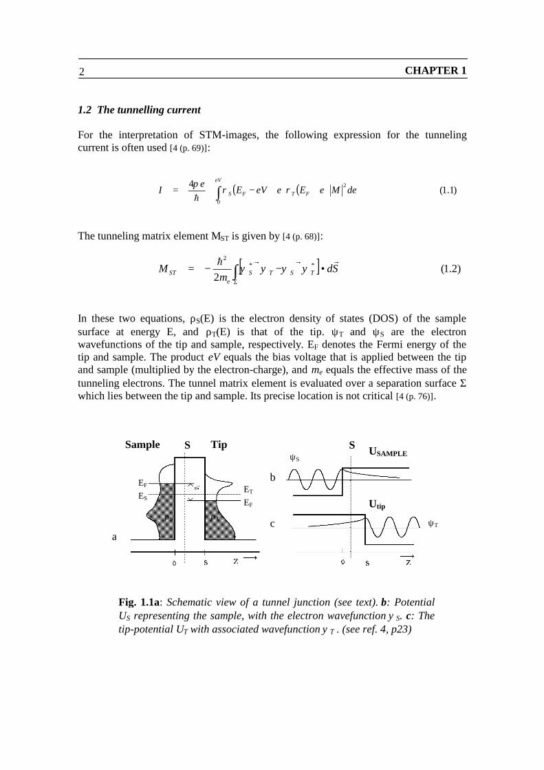
For the interpretation of STM-images, the following expression for the tunnelingcurrent is often used [4 (p. 69)]:
The tunneling matrix element MST is given by [4 (p. 68)]:
In these two equations, ρS(E) is the electron density of states (DOS) of the samplesurface at energy E, and ρT(E) is that of the tip. ψ T and ψ S are the electronwavefunctions of the tip and sample, respectively. EF denotes the Fermi energy of thetip and sample. The product eV equals the bias voltage that is applied between the tipand sample (multiplied by the electron-charge), and me equals the effective mass of thetunneling electrons. The tunnel matrix element is evaluated over a separation surface Σwhich lies between the tip and sample. Its precise location is not critical [4 (p. 76)].
( ) ( ) )1.1(4
0
2∫ ++−=eV
FTFS dMEeVEe
I εερερπh
[ ] )2.1(2
**2
∫Σ
•∇−∇−= Sdm
M TSTSe
ST
rrrh ψψψψ
Fig. 1.1a: Schematic view of a tunnel junction (see text). b: PotentialUS representing the sample, with the electron wavefunction ψ S. c: Thetip-potential UT with associated wavefunction ψ T . (see ref. 4, p23)
ρS ρT ψ T
Σ Σ
b
ca
ψ SUSAMPLE
Utip
EF
EFES
ET
Sample Tip
THEORY 3
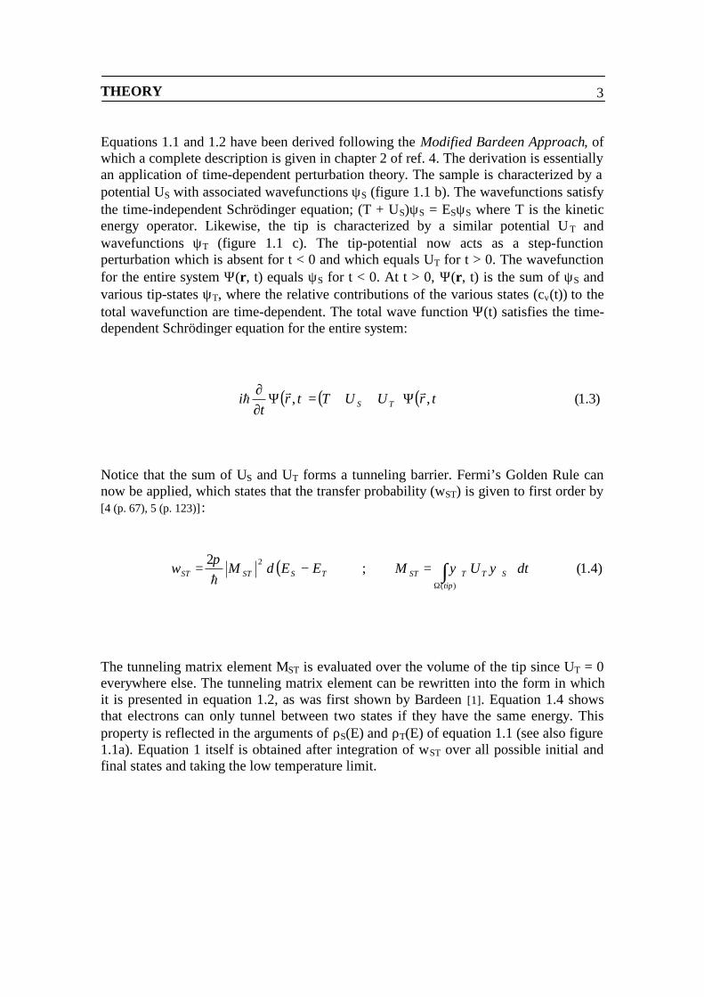
Equations 1.1 and 1.2 have been derived following the Modified Bardeen Approach, ofwhich a complete description is given in chapter 2 of ref. 4. The derivation is essentiallyan application of time-dependent perturbation theory. The sample is characterized by apotential US with associated wavefunctions ψ S (figure 1.1 b). The wavefunctions satisfythe time-independent Schrödinger equation; (T + US)ψ S = ESψ S where T is the kineticenergy operator. Likewise, the tip is characterized by a similar potential U T andwavefunctions ψ T (figure 1.1 c). The tip-potential now acts as a step-functionperturbation which is absent for t < 0 and which equals UT for t > 0. The wavefunctionfor the entire system Ψ (r, t) equals ψ S for t < 0. At t > 0, Ψ (r, t) is the sum of ψ S andvarious tip-states ψ T, where the relative contributions of the various states (cν(t)) to thetotal wavefunction are time-dependent. The total wave function Ψ (t) satisfies the time-dependent Schrödinger equation for the entire system:
Notice that the sum of US and UT forms a tunneling barrier. Fermi’s Golden Rule cannow be applied, which states that the transfer probability (wST) is given to first order by[4 (p. 67), 5 (p. 123)]:
The tunneling matrix element MST is evaluated over the volume of the tip since UT = 0everywhere else. The tunneling matrix element can be rewritten into the form in whichit is presented in equation 1.2, as was first shown by Bardeen [1]. Equation 1.4 showsthat electrons can only tunnel between two states if they have the same energy. Thisproperty is reflected in the arguments of ρS(E) and ρT(E) of equation 1.1 (see also figure1.1a). Equation 1 itself is obtained after integration of wST over all possible initial andfinal states and taking the low temperature limit.
( ) ( ) ( ) )3.1(,, trUUTtrt
i TSrr
h Ψ++=Ψ∂∂
( ) )4.1(;2
)(
2 ∫Ω
=−=tip
STTSTTSSTST dUMEEMw τψψδπh
CHAPTER 14
1.3 Some properties of the tunneling current
According to the Tersoff-Hamann theory, STM-images show the local density of states(LDOS) of the sample surface [2,3]. This result was derived under the condition that therelevant tip-state is an s-wave, and under the condition of small bias voltage. The latteris often the case for metals but need not be the case when imaging semiconductors.When the tip-state is (dominated by) an s-wave, it can be shown that the tunnelingmatrix element equals [2, 4 (p. 83)]:
The amplitude of the sample wave function |ψ |2 is evaluated at r0 , the centre of the apexatom of the tip. C is a normalization constant, and κ = (2meφ)1/2/h. For |M|2 proportionalto |ψ S(r0)|2 , it readily follows that the integrant in eq. 1 is proportional to the LDOS ofthe sample surface. For small bias voltage, the total tunneling current becomesproportional to ρS(EF)ρT(EF), the DOS of the sample and tip at the (almost common)Fermi level. For larger bias voltage, provided that |M| 2 remains constant over theenergy-range involved, equation 1 shows that the tunneling current becomes aconvolution of the tip- and sample DOS. Combined with eq. 5, this yields an expressionwhich represents the qualitative interpretation of topographic STM-data generally used:
If the tip-state is predomenantly p- or d-like, the tunnel matrix element is no longerproportional to |ψ S(r0)|2. Rather, it becomes proportional to one of the spatial derivativesof ψ S(r0) for px , py or pz states, or to second derivatives of ψ S(r0) for d-like states [4 (p.83)]. This can have several effects on (atomically resolved) images, including anenhancement of atomic corrugation or an inversion of contrast [4 (p. 126, p. 138)]. Thelikelyhood of occurrence and consequenses of a non-s tip state will be discussed later insection 1.6.
One of the best-known features of tunneling is the exponential dependence ofthe tunneling current on the tip-sample separation. This dependence follows fromequation 1.6, as it is a direct consequence of the proportionality of the tunneling currentto |ψ S(r0)|2. The sample wave functions decay exponentially as they extend into thevacuum barrier, behaving asymptotically like exp[ -( 2 me ∆E )1/2 / h * z] (see figure
( ) )5.1(2
0rmC
M Se
STrhψ
κπ=
( ) ( ) ( ) )6.1(~ 20
0
εψερερ drEeVEI SF
eV
TFSr++−∫
THEORY 5
1.1), with ∆E equal to the energy difference between the sample state and the topof the tunneling barrier. The factor |ψ S(r0)|2 is therefore proportional toexp[ -2 ( 2 me ∆E )1/2 / h * |r0| ].
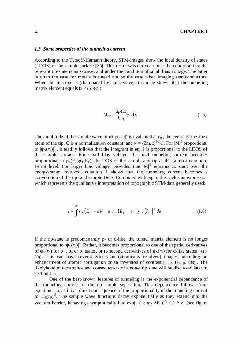
An other property is shown in figure 1.2: The DOS of a given sample surfacecan be made up of a number of different surface states (see figure 4.1). Each of thosestates has a wave-function ψ S(r), a (mean) energy and a density of states ρS
i(E)associated with it. Also, the tunneling matrix element for each of the states willgenerally be different, as not all states extend equally far into the vacuum [6,8]. The totaltunneling current then equals the sum of the contributions of the individual states.
Fig. 1.3: Three types of wavefunctions at surfaces(after ref 30, p. 19). Further details in section 1.4
Fig. 1.2: Tunneling current from more than onesample state.
ψ 1, E1
ψ 2 , E2
VACUUM SOLID
CHAPTER 16
1.4 Atomically resolved STM-images
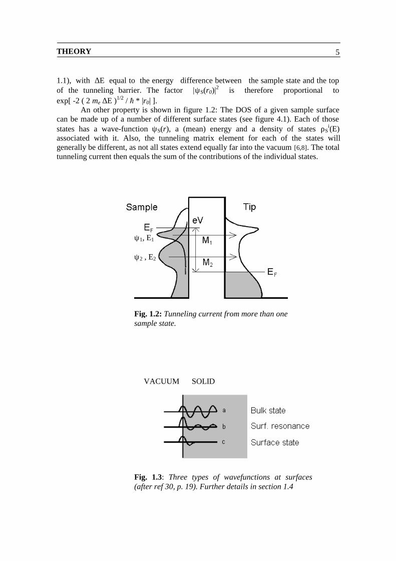
The ability to resolve the atomic lattice, for which STM has become famous, is due toits sensitivity to the local density of states. The LDOS of a crystalline surface reflectsthe periodicity of the underlying surface lattice, which results in an STM-image thatcontains a corrugation with the same periodicity as the surface lattice being imaged.This is the “atomically resolved” image.
The LDOS of a crystalline surface can be made up of three kinds of states: Bulkstates, surface states and surface resonances (figure 1.3). The bulk states are Blochwaves terminated at the surface. They are periodic in the bulk of the crystal and becomeevanescent in the vacuum. The surface states are evanescent both in the bulk of thecrystal and in the vacuum, and exist only near the surface of the crystal. Surfaceresonances are formed when a surface state and a bulk state combine, resulting in a statewhich is periodic in the bulk of the crystal, which decays exponentially in the vacuum,and which has an increased amplitude near the surface [30, 4 (p. 91)].
For an unreconstructed surface (i.e. the surface of a truncated bulk crystal) thesurface states can be expected to lie energetically within the bulk band gap, as wasshown for the first time by Tamm [4 (p. 99), 9] for a truncated Krönig-Penney potential.When a realistic three-dimensional (3-D) potential is concidered, surface states similarto the so-called “Tamm-states” are obtained, as was shown by Appelbaum and Hamann[6,7,10] for the 111-surface of silicon. The unreconstructed configuration of a surfaceis often energetically unfavourable, so in many crystal surfaces, (some of) the atomsshift in position to reduce the free energy of the surface. The reconstructed surface canhave a significantly different LDOS with respect to the unreconstructed surface. Anexample of this effect is the 110-surface of GaAs [8] and other zincblende III-Vsemiconductors, or the 111-surface of Si [4].
In ref. 6, three bands of surface states were found for the Si-111 surface: Oneis located energetically inside the bulk band gap and had spatial lobes above and beloweach surface atom. The lobes are localized, with the top lobe extending only 1 Å in thedirections parallel to the surface. In the reconstructed case, its integrated electrondensity is 0.7, indicating that the state is only partially filled. Unity corresponds to thestate being fully occupied, in which case it contains two electrons (spin degeneracy).The state is identified as a “dangling bond” state. A second band of states was found tolie energetically within the bulk valence band, and is localized on the lines connectingeach surface atom to its three nearest neighbors which lie slightly deeper inside thecrystal. The integrated electron density for this band is 0.9. This is a back bond state.The third state which was found lies deep within the valence band (at –11 eV withrespect to the top of the valence band) and is therefore unavailable to the tunnelingprocess
There is an alternative way to consider dangling bond states: Many covalentlybonded crystals form either the diamond lattice (Si, Ge, C) or the zinc-blende lattice(GaAs, InP, etc). The bonds in crystals of these structures are formed by sp 3 hybridizedstates which extend from each atom to its four nearest neighbors. Each such statecontains two electrons. When such a crystal is separated into two parts, all bonds alongone crystal-plane are broken. On the newly created surfaces the severed bonds form
THEORY 7
localized states, each located at or above a surface atom and each containing oneelectron instead of two.
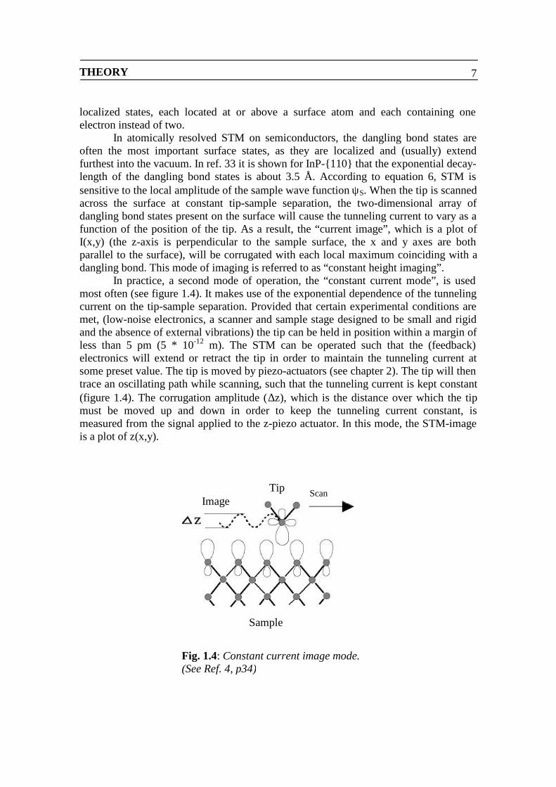
In atomically resolved STM on semiconductors, the dangling bond states areoften the most important surface states, as they are localized and (usually) extendfurthest into the vacuum. In ref. 33 it is shown for InP-110 that the exponential decay-length of the dangling bond states is about 3.5 Å. According to equation 6, STM issensitive to the local amplitude of the sample wave function ψ S. When the tip is scannedacross the surface at constant tip-sample separation, the two-dimensional array ofdangling bond states present on the surface will cause the tunneling current to vary as afunction of the position of the tip. As a result, the “current image”, which is a plot ofI(x,y) (the z-axis is perpendicular to the sample surface, the x and y axes are bothparallel to the surface), will be corrugated with each local maximum coinciding with adangling bond. This mode of imaging is referred to as “constant height imaging”.
In practice, a second mode of operation, the “constant current mode”, is usedmost often (see figure 1.4). It makes use of the exponential dependence of the tunnelingcurrent on the tip-sample separation. Provided that certain experimental conditions aremet, (low-noise electronics, a scanner and sample stage designed to be small and rigidand the absence of external vibrations) the tip can be held in position within a margin ofless than 5 pm (5 * 10-12 m). The STM can be operated such that the (feedback)electronics will extend or retract the tip in order to maintain the tunneling current atsome preset value. The tip is moved by piezo-actuators (see chapter 2). The tip will thentrace an oscillating path while scanning, such that the tunneling current is kept constant(figure 1.4). The corrugation amplitude (∆z), which is the distance over which the tipmust be moved up and down in order to keep the tunneling current constant, ismeasured from the signal applied to the z-piezo actuator. In this mode, the STM-imageis a plot of z(x,y).
Fig. 1.4: Constant current image mode.(See Ref. 4, p34)
Sample
ImageTip Scan
CHAPTER 18
The response of the feed back loop present in any STM-system can be varied in order tooptimize the image [1 (p. 1)]: It can be set to a slow response needed to keep the tip fromcrashing into the sample surface or drifting out of tunneling range, or to a fast one usedto follow the surface (or rather: the contours of the surface-DOS) very accurately. Whenthe feedback loop is set to a response which is too fast, it begins to oscillate. Forconstant current images, one would expect the feedback loop to be set just below thevalue at which oscillation sets in. In practice, the “best” z(x,y) images in constantcurrent mode are obtained at an intermediate setting, for which some corrugation in theI(x,y) image is still visible [16].
1.5 Lateral motion of electrons and sample density of states
Although the surface states can be highly localized, as is the case for dangling bondstates, the electrons that occupy them remain mobile. Their motion is, however,confined to the surface region. The lateral motion of the electrons can be described bytwo-dimensional Bloch-waves matching the two-dimensional lattice formed by theatoms in the surface region. For many surfaces, dispersion curves for the lateral motionof electrons occupying surface states have been determined [8, 4 (p. 106), 15 (p. 158, p.176)]. The dispersion relations calculated for the relaxed GaAs 110 and AlAs (110)surfaces are shown as examples in chapter 6.
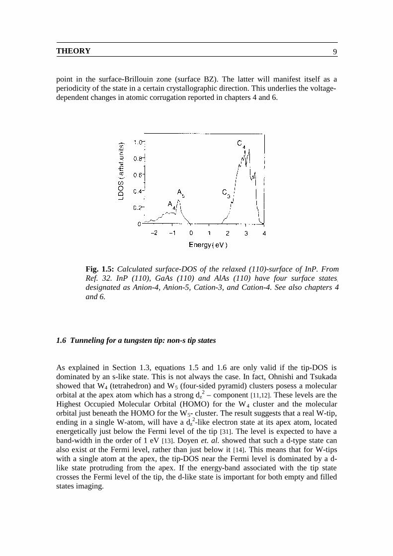
Figure 1.5 shows the calculated density of states (DOS) of InP 110 as anexample. In general, the total DOS will be the sum of the individual densities of statesof the different states present at the surface. The energy-dependence of each of thoseindividual densities of states depends on the number of degrees of freedom available tothe electrons, and on the dispersion curve associated with the state. In a firstapproximation, the DOS for the bulk valence band and bulk conduction band can betaken as ρS(E) ~ |E|1/2 and ρS(E) ~ |E-Eg|1/2 , respectively (E measured is with respect tothe Valance Band Maximum). Under the circumstances common for STM onsemiconductors, only the band edges participate in the tunneling process. Near the bandedges, the dispersion curves can be assumed parabolic. Since the bulk states allow theelectrons to travel in all three directions, the DOS becomes proportional to |E| 1/2.
A similar argument does not apply to surface states. Unlike the dispersion curvesfor bulk bands, the surface-state dispersion curves do not extend over a very wideenergy-range. Consequently, the entire energy-range of a surface-state dispersion curvecan be accessible to tunneling using normal bias voltages [25], and the surfacedispersion curve can therefore not be assumed to be parabolic. The different surfacestates on the GaAs 110- surface manifest themselves as a series of peaks in the totalsurface DOS (see figure 1.5).
For the purposes of this thesis, two things are important to keep in mind: Thefirst is that the total surface-DOS is composed of the contributions of the differentelectronic states that lie inside the relevant energy-window. The other is that theelectronic states can have a lateral momentum, i.e. have a k//-vector that lies at a certain
THEORY 9
point in the surface-Brillouin zone (surface BZ). The latter will manifest itself as aperiodicity of the state in a certain crystallographic direction. This underlies the voltage-dependent changes in atomic corrugation reported in chapters 4 and 6.
1.6 Tunneling for a tungsten tip: non-s tip states
As explained in Section 1.3, equations 1.5 and 1.6 are only valid if the tip-DOS isdominated by an s-like state. This is not always the case. In fact, Ohnishi and Tsukadashowed that W4 (tetrahedron) and W5 (four-sided pyramid) clusters posess a molecularorbital at the apex atom which has a strong dz
2 – component [11,12]. These levels are theHighest Occupied Molecular Orbital (HOMO) for the W4 cluster and the molecularorbital just beneath the HOMO for the W5- cluster. The result suggests that a real W-tip,ending in a single W-atom, will have a dz
2-like electron state at its apex atom, locatedenergetically just below the Fermi level of the tip [31]. The level is expected to have aband-width in the order of 1 eV [13]. Doyen et. al. showed that such a d-type state canalso exist at the Fermi level, rather than just below it [14]. This means that for W-tipswith a single atom at the apex, the tip-DOS near the Fermi level is dominated by a d-like state protruding from the apex. If the energy-band associated with the tip statecrosses the Fermi level of the tip, the d-like state is important for both empty and filledstates imaging.
Fig. 1.5: Calculated surface-DOS of the relaxed (110)-surface of InP. FromRef. 32. InP (110), GaAs (110) and AlAs (110) have four surface states,designated as Anion-4, Anion-5, Cation-3, and Cation-4. See also chapters 4and 6.
CHAPTER 110
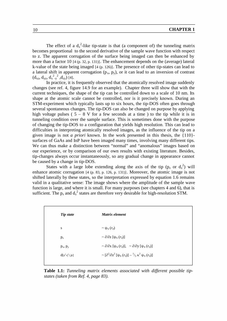
The effect of a dz2-like tip-state is that (a component of) the tunneling matrix
becomes proportional to the second derivative of the sample wave function with respectto z. The apparent corrugation of the surface being imaged can then be enhanced bymore than a factor 10 [4 (p. 32, p. 131)]. The enhancement depends on the (average) lateralk-value of the state being imaged [4 (p. 126)]. The presence of other tip-states can lead toa lateral shift in apparent corrugation (px, py), or it can lead to an inversion of contrast(dxz, dyz, dx
2-y
2 ,dzy) [4].In practice, it is frequently observed that the atomically resolved image suddenly
changes (see ref. 4, figure 14.9 for an example). Chapter three will show that with thecurrent techniques, the shape of the tip can be controlled down to a scale of 10 nm. Itsshape at the atomic scale cannot be controlled, nor is it precisely known. During anSTM-experiment which typically lasts up to six hours, the tip-DOS often goes throughseveral spontaneous changes. The tip-DOS can also be changed on purpose by applyinghigh voltage pulses ( 5 – 8 V for a few seconds at a time ) to the tip while it is intunneling condition over the sample surface. This is sometimes done with the purposeof changing the tip-DOS to a configuration that yields high resolution. This can lead todifficulties in interpreting atomically resolved images, as the influence of the tip on agiven image is not a priori known. In the work presented in this thesis, the 110-surfaces of GaAs and InP have been imaged many times, involving many different tips.We can thus make a distinction between “normal” and “anomalous” images based onour experience, or by comparison of our own results with existing literature. Besides,tip-changes always occur instantaneously, so any gradual change in appearance cannotbe caused by a change in tip-DOS.
States with a large lobe extending along the axis of the tip (pz or dz2) will
enhance atomic corrugation [4 (p. 83, p. 126, p. 131)] . Moreover, the atomic image is notshifted laterally by these states, so the interpretation expressed by equation 1.6 remainsvalid in a qualitative sense: The image shows where the amplitude of the sample wavefunction is large, and where it is small. For many purposes (see chapters 4 and 6), that issufficient. The pz and dz
2 states are therefore very desirable for high-resolution STM.
Tip state Matrix element
s ~ ψ S (r0)
pz ~ ∂/∂z [ψ S (r0)]
px, py ~ ∂/∂x [ψ S (r0)], ~ ∂/∂y [ψ S (r0)]
d[z2-(1/3)r] ~ [∂2/∂z2 [ψ S (r0)] – 1/3 κ2 ψ S (r0)]
Table 1.1: Tunneling matrix elements associated with different possible tip-states (taken from Ref. 4, page 83).

THEORY 11
1.7 Tip – sample interaction
When the tip and sample are far apart, they can be thought of as non-interacting. The tipstates (ψ T) and sample states (ψ S) are then described by the wave-functions belonging tothe free sample and tip. When the tip and sample are brought into distances typical fortunneling, they do have an interaction. As a consequence, the tip and sample exert anattractive force to each other, the tip- and sample states are modified and the potentialbarrier between the tip and sample gradually collapses as the two electrodes approacheach other. The following discussion is based mainly on the theoretical treatmentpresented by Ciraci [18] and references therein [15, 20, 21]. Although Ciraci’s treatment isapplied to metal or graphite samples and metal tips, we will use it to provide aqualitative description of the interaction that takes place between a semiconductorsample and metal tip.
Three regimes of interaction can be identified [18 (p. 179, p. 182)]: For a tip-sampledistance of roughly 10 Å, only the van der Waals interaction is important. For distancesranging from 3 - 7 Å (measured from the nucleus of the apex atom to that of the samplefacing it) the tip- and sample wave functions begin to overlap. This leads to a shortrange, attractive force. At even shorter distance, when the separation between the apexatom and the nearest sample atom becomes comparable to the inter-atomic spacingwithin the tip- and sample material, the interaction becomes repulsive. This is the onsetof mechanical contact. When at this point the (macroscopic) tip and sample areapproached further (for example during a tip-crash), both electrodes will irreversiblydeform.
In a tunneling experiment, the absolute tip-sample distance is not known.However, based on the results reported by Heinrich et al. [27,29] it is estimated to beabout 6 – 7 Å. The experiments of Heinrich et al. were carried out on p-doped GaAs(Zn: 4 – 7 * 1019 cm-3), using VSAMPLE = -2.0 V and I = 300 pA. Although we generallyuse smaller tunneling currents (~ 100 pA) and sample material with a lower dopingconcentration (1018 cm-3), it is reasonable to assume that in our experiments, theabsolute tip-sample distance is usually similar to the tip-sample distances found byHeinrich et al. At a tip-sample distance of 6 – 7 Å, both the short-range interaction andthe van der Waals interaction may have a role in the tip-sample interaction.
The short-range attractive interaction is a quantum-mechanical effect that occursas a result of the wave functions of the tip and sample overlapping. What happens is thatthe electron state(s) extending from the outermost tip atom(s) combine with samplestates to form bonding and antibonding combinations (see also chapter 4). In thesimplest picture, the interaction takes place between one tip state and one sample state.A suitable model system for that situation is the hydrogen molecular ion (H2
+) [4 (p.177)]. The tip- and sample state can form two combinations, (χν + ψ µ) and (χν - ψ µ) withenergies (E + M) and (E – M), respectively. E is the (common) energy of the two states(see eq. 4) and M is proportional to the tunneling matrix element (see equation 1.2).Both E and M are negative as they are measured with respect to the vacuum level, sothe symmetric combination (χν + ψ µ), i.e. the bonding state, has the lowest energy (E +M).
The tunneling process always involves one filled and one empty state, so thecombined system of the tip- and sample state will always contain one electron. This
CHAPTER 112
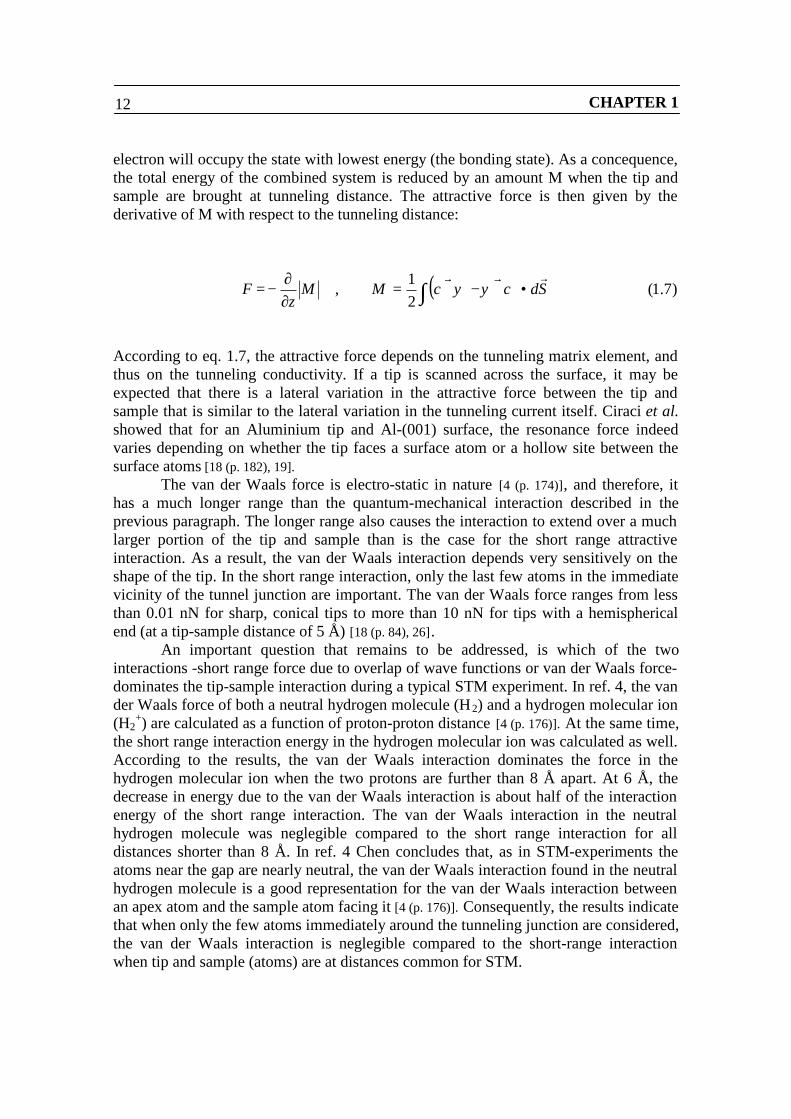
electron will occupy the state with lowest energy (the bonding state). As a concequence,the total energy of the combined system is reduced by an amount M when the tip andsample are brought at tunneling distance. The attractive force is then given by thederivative of M with respect to the tunneling distance:
According to eq. 1.7, the attractive force depends on the tunneling matrix element, andthus on the tunneling conductivity. If a tip is scanned across the surface, it may beexpected that there is a lateral variation in the attractive force between the tip andsample that is similar to the lateral variation in the tunneling current itself. Ciraci et al.showed that for an Aluminium tip and Al-(001) surface, the resonance force indeedvaries depending on whether the tip faces a surface atom or a hollow site between thesurface atoms [18 (p. 182), 19].
The van der Waals force is electro-static in nature [4 (p. 174)], and therefore, ithas a much longer range than the quantum-mechanical interaction described in theprevious paragraph. The longer range also causes the interaction to extend over a muchlarger portion of the tip and sample than is the case for the short range attractiveinteraction. As a result, the van der Waals interaction depends very sensitively on theshape of the tip. In the short range interaction, only the last few atoms in the immediatevicinity of the tunnel junction are important. The van der Waals force ranges from lessthan 0.01 nN for sharp, conical tips to more than 10 nN for tips with a hemisphericalend (at a tip-sample distance of 5 Å) [18 (p. 84), 26].
An important question that remains to be addressed, is which of the twointeractions -short range force due to overlap of wave functions or van der Waals force-dominates the tip-sample interaction during a typical STM experiment. In ref. 4, the vander Waals force of both a neutral hydrogen molecule (H2) and a hydrogen molecular ion(H2
+) are calculated as a function of proton-proton distance [4 (p. 176)]. At the same time,the short range interaction energy in the hydrogen molecular ion was calculated as well.According to the results, the van der Waals interaction dominates the force in thehydrogen molecular ion when the two protons are further than 8 Å apart. At 6 Å, thedecrease in energy due to the van der Waals interaction is about half of the interactionenergy of the short range interaction. The van der Waals interaction in the neutralhydrogen molecule was neglegible compared to the short range interaction for alldistances shorter than 8 Å. In ref. 4 Chen concludes that, as in STM-experiments theatoms near the gap are nearly neutral, the van der Waals interaction found in the neutralhydrogen molecule is a good representation for the van der Waals interaction betweenan apex atom and the sample atom facing it [4 (p. 176)]. Consequently, the results indicatethat when only the few atoms immediately around the tunneling junction are considered,the van der Waals interaction is neglegible compared to the short-range interactionwhen tip and sample (atoms) are at distances common for STM.
( ) )7.1(21
, ∫ •∇−∇=∂∂−= SdMMz
Frrr
χψψχ

THEORY 13
This is, however, only part of the problem. As already mentioned, the van derWaals interaction has a longer range and so, the number of atoms in the tip and sampleparticipating in the interaction will be (far) greater than the number of atoms involved inthe short range interaction, for which only the few atoms in the immediate vicinity ofthe tunneling junction are important. Therefore, while the van der Waals interaction peratom is small compared to the short range interaction per atom involved, the total vander Waals force may well be comparable to, or even exceed, the total short range force.An other effect is that the short range force acts on the apex of the tip, while the van derWaals force, because of the greater number of atoms involved, acts on the part of the tipbehind the apex. If the van der Waals interaction is sufficiently strong, the apex atom(s)may have a repulsive interaction with the sample while the tip and sample as a wholeare still attracted to each other [24].
As Chapter 3 will show, the tips we make have a typical apex radius of 10 nm,which is supported by a conical shank with an inner half-angle of about 15o. For a tip-sample distance of 7.5 Å, this would mean that for our tips, the van der Waals force is inthe order of 1 nN, which is quite comparable to the short range interaction [18 (p. 184, p.182), 4 (p. 176), 26] .
1.8 Effects of the tip-sample interaction
One obvious consequence of the tip-sample interaction, is that the tip and sample willdeform. We will ignore the possibility of an avalanche effect as described by Smith etal.[28] as the resulting contact seems incompatible with atomic resolution. In atomicallyresolved STM, the deformation will cause a difference between the measuredcorrugation amplitude and the actual amplitude of the corrugated path traced by theapex. This is caused by the fact that the tip-sample interaction depends on the lattice-sitefacing the apex atom [19]: As the tip is scanned across the surface, it will relax in- andoutward as it passes the different lattice sites, even if the back of the tip were held at thesame height above the sample. When operating the STM in constant current mode, theextensions and retractions of the tip apex due to relaxation are added to the excursionsthat are applied to the back of the tip by the feedback mechanism of the STM.
At small tip-sample distance, the most important consequence of the tip-sampleinteraction is the modification of tip- and sample states, and the appearance of TipInduced Localized States (TILS) [24, 18 (p. 182)]. When the tip and sample approach eachother, the wavefunctions of the tip and sample overlap and form bonding andantibonding combinations. This is accompanied by a change in spatial distribution ofthe states and by a shift in energetic location of the states. Both effects have beendescribed in detail by Ciraci, Baratoff and Batra for an Al tip and graphite sample [24].The same authors have also studied the change in spatial distribution of the states for anAluminum tip-atom and Al-(111) surface [19]. It was shown that the sample wavefunction differs from the wave function of the free sample surface for a tip-sampledistance of 4.2 Å or less. At 2.6 Å, the electron resolution resembles that of an atomicbond [19]. The shift in energy for the different states as a function of tip-sampledistance, studied in ref. 24 (see also ref. 18 , p. 194), showed that as the tip-sample

CHAPTER 114
distance is varied from 4.0 Å down to 1.4 Å, some states shift over 1 or 2 eV in energy.As some states move up in energy whereas others move down, crossings between statesmay occur.
A related effect is that as the tip and sample approach each other, the potentialbarrier gradually decreases. Due to exchange and correlation effects, electrons localizedwithin the tunneling junction experience a potential that is lower than the vacuum level,which is the height of the potential barrier when the two electrodes are far apart. Theeffect is reproduced in the theoretical calculations presented in refs. 19 and 24. The topof the potential barrier may actually sink below the Fermi level of the tip or sample,creating a channel in which electrons are classically allowed. This is the onset ofmechanical contact.
The lowering of the potential barrier is caused by an exchange and correlationpotential modifying the tunneling barrier. It is thus a many particle effect. The imagepotential, which is the classical formalism to treat an electron in the presence of manyother free charges, often used to evaluate the lowering of the potential barrier [4 (p. 56)].For the model considered in ref. 4 (a “jellium” surface), the classical image potentialprovides an adequate approximation for the exchange- and correlation potentialexperienced by an electron localized in the vacuum region near a metal surface[4 (p. 94)].
Summarizing, we expect an attractive interaction between the tip and sample,either due to the short range interaction or due to the van der Waals interaction. If thevan der Waals interaction is strong, the part of the tip behind the apex might be attractedto the sample while the apex has a repulsive interaction with the sample. As a result ofthe tip-sample interaction, the electron-states are deformed and shift in energy, and thepotential barrier between the tip and sample is lowered.
Although at the tip-sample distances commonly encountered in STM (7 – 10 Åaccording to figure 4.8, see also refs. 27 and 29) there is a non-zero force between tipand sample, the tip-sample interaction is usually not essential in the interpretation ofatomically resolved STM-images. Most of the results shown in chapters 4,6 and 7 canbe interpreted without explicitely considering the tip-sample interaction apart from tip-induced band bending, which is discussed in the next section. However, in some casesthe tip-sample interaction becomes essential in the interpretation of the images, as is thecase for some of the results shown in chapter 4. In chapter 5, where we present anunusual image-form of GaAs (110) which is thought to arise when a chemical bondforms between the tip and sample, the tip-sample interaction obviously becomes veryimportant as well.
THEORY 15
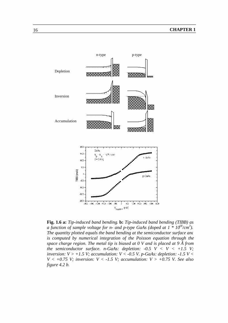
1.9 Tip-induced band bending
In addition to the interaction-effects described in the previous section, tip induced bandbending (TIBB) occurs when a semiconducting surface is being approached by a(metal) tip. The electro-static field between the tip and sample penetrates into thesemiconductor surface, which rearranges the free charge carriers near the surface. Theresult is that a net charge is present on the surface, which will locally raise or lower thevalence and conduction band of the semiconductor (see figure 1.6). Below the surfaceof the semiconductor, the net charge screens the field induced by the tip, and thevalence and conduction bands lie at their normal positions with respect to the Fermilevel. The effect is sensitive to the doping concentration of the semiconducting material:When the doping concentration increases, the width of the space-charge layer decreasesas the screening becomes more effective. In metals, which have a far higherconcentration of free carriers than semiconductors, the space-charge layer becomesexceedingly narrow [17]. At the same time, the electric field must remain continuousacross the metal-vacuum interface meaning that the potential gradient near the interfacemust remain finite. Consequently, no band bending can occur in the tip.
The amount of band bending occurring between a metal tip and semiconductingsample can be calculated numerically by using a one-dimensional model [22,23]. Thecalculation consists of solving the one-dimensional Poisson-equation under theboundary condition that at the semiconductor-metal interface, the electric field (i.e. thepotential gradient) be continuous. There are three possible situations for band bendingin the semiconductor region, in both p- and n-type material: Depletion, inversion andaccumulation (see figure 1.6 a). In the case of depletion, the resulting potential profile isparabolic since the charge in the depletion layer is generated by ionized dopants, whichare immobile and assumed to be uniformly distributed throughout the semiconductor.When accumulation occurs, all dopants near the surface are unionized, and the bandbending is caused by majority charge carriers that have accumulated near the surface.The amount of band bending, in turn, influences the charge density profile near thesurface, causing the charge density and surface band bending to influence each other. Inthe case of inversion, the potential-profile is determined by the charge from the ionizedimpurities as well as from the charge of the minority carriers accumulated at the surface.
Using the model described in chapter 4, we have calculated the amount of TIBB(φ) as a function of applied bias voltage for a fixed tip-sample distance (figure 1.6 b).The regions of depletion, accumulation and inversion manifest themselves in the slopeof the data-points. In case of depletion, the depletion width can be calculated from wφ =(2ε0εr/(Ne2) )1/2, where N is the doping concentration [22]. Even for small amounts ofband bending, the depletion layer can extend several tens of nanometers (nm) into thesemiconductor (N = 1018 cm-3, φ = 0.2 eV, wφ = 169 Å; N = 1018 cm-3, φ = 0.5 eV, wφ =267 Å). When analysing spectroscopic data, TIBB must be taken into account in orderto interprete the results correctly [18]. Also, due to accumulation or inversion, certainsurface-states may become populated or emptied depending on the applied bias voltage.This influences the morphology of the atomically resolved lattice. The voltage-dependent changes of the atomically resolved (110)-surface of GaAs and AlxGa(1-x)As,and the influence of TIBB on these changes, will be discussed at length in chapters 4and 6, respectively.
CHAPTER 116
Fig. 1.6 a: Tip-induced band bending. b: Tip-induced band bending (TIBB) asa function of sample voltage for n- and p-type GaAs (doped at 1 * 1018/cm3).The quantity plotted equals the band bending at the semiconductor surface andis computed by numerical integration of the Poisson equation through thespace charge region. The metal tip is biased at 0 V and is placed at 9 Å fromthe semiconductor surface. n-GaAs: depletion: -0.5 V < V < +1.5 V;inversion: V > +1.5 V; accumulation: V < -0.5 V. p-GaAs: depletion: -1.5 V <V < +0.75 V; inversion: V < -1.5 V; accumulation: V > +0.75 V. See alsofigure 4.2 b.
n-type p-type
Inversion
Depletion
Accumulation
THEORY 17
1.10 Summary
The tunneling current is proportional to the convolution of the tip- and sample densityof states. It is also assumed proportional to the local amplitude of the samplewavefunction(s) being probed, which causes the lateral variation in the tunnelingcurrent. When several states contribute to the total tunneling current, their contributionscombine.
The surface-DOS of the sample is made up of different surface states andterminated bulk states. The different surface states manifest themselves as differentpeaks in the surface-DOS. The spatial distribution of the surface-DOS reflects theperiodicity of the surface lattice, and as a consequence, STM images will reflect thisperiodicity as well. This is what makes atomically resolved STM possible.
For atomically sharp STM-tips, it is expected that the tip-DOS is dominated by adz-like state which protrudes from the apex. Although the proportionality to the samplewave function expressed in eq. 6 is only valid for s- like tip-states, it can still be used ina qualitative sense for pz and dz-like tip-states as well. Such states can significantlyenhance atomic corrugation.
During tunneling, the tip and sample experience an attractive interaction, causedby the tip- and sample states combining into bonding and antibonding pairs. Atdistances typical for STM, the wave functions and the tip structure may be reversiblymodified. The force between tip and sample varies as the tip faces different lattice-siteson the sample surface. Also, the top of the potential barrier may be loweredsignificantly.
Finally, the electro-static field between tip and sample causes band bending inthe near-surface region of the sample when imaging semiconductors. Band bending canextend several tens of nm into the sample. At the surface, it causes the surface states toshift 1 eV or more in energy with respect to the sample Fermi level. The distortion ofthe bands can extend several tens of nm below the sample surface, depending on dopingconcentration.
At this point, we wish to introduce the term of “regular tunneling”. As is explained insection 1.3, atomically resolved images of semiconducting surfaces are usually thoughtto represent the local variation of the surface-DOS of the sample material, integratedover the energy-window between the tip Fermi level and the sample Fermi level. Thisview is represented mathematically by equations 1.5 and 1.6, and transforms into theTersoff-Hamann theory in the limit of small bias voltage [2,3]. This interpretation,however, is only valid at larger tip-sample distances where the effects of the tip-sampleinteraction may be neglected. This interpretation implicitely also assumes an s-like tip-DOS, although it remains valid in a qualitative sense for a pz- and d[z2-1/3r]-like tip-state.“Regular tunneling” is tunneling under the conditions of finite voltage, neglegible tip-sample interaction (apart from tip-induced band bending) and a tunneling matrix-element that is proportional only to ψ S (r0) or to spatial derivatives with respect to z ofψ S (r0). Later in this thesis it will become apparent that many atomically resolvedimages of semiconductor surfaces can be explained within the framework of regulartunneling, although some experimental circumstances exist where other mechanisms foratomic corrugation have to be considered.

CHAPTER 118
REFERENCES
1: J. Bardeen: Tunneling from a many-particle point of view. Phys. Rev. Lett. Vol.6, No. 12, page 57 – 59 (1961).
2: J. Tersoff, D.R. Hamann: Theory and Application for the Scanning TunnelingMicroscope. Phys. Rev. Lett. Vol. 50, No 25, page 1998 – 2001 (1983). Forbackground to eq. 5, the reader is also referred to ref. 1, p. 83.
3: J. Tersoff, D.R. Hamann: Theory of the Scanning Tunneling Microscope. Phys.Rev. B, Vol 31, No 2, page 805 – 813 (1985).
4: C.J. Chen: Introduction to Scanning Tunneling Microscopy. Oxford UniversityPress, New York, 1993.
5: A. Yariv: Theory and Applications of Quantum Mechanics. John Wiley andsons, New York, 1982.
6: J.A. Appelbaum, D.R. Hamann: Surface states and surface bonds of Si (111).Phys. Rev. Lett Vol. 31, No. 2, page 106 – 109 (1973)
7: J.A. Appelbaum, D.R. Hamann: Surface Potential, Charge Density, andIonization Potential for Si(111) – A self-consistent calculation. Phys. Rev. Lett,Vol. 32, No. 5, page 225 – 228 (1973).
8: J.R. Chelikowski, M.L. Cohen: Self-consistent pseudopotential calculation forthe relaxed (110)-surface of Gallium Arsenide. Phys. Rev. B, Vol. 20, No. 10,page 4150 – 4159 (1979).
9: I. Tamm: Über eine Mögliche Art der Elektronenbindung undKristalloberflächen. Phys. Z. der Sowjetunion 1, page 733 – 746 (1932).
10: J.A. Appelbaum, D.R. Hamann: Self-consistent Electronic structure of solidsurfaces. Phys. Rev. B, Vol. 6, No. 6, page 2166 – 2177 (1972).
11: S. Ohnishi, M. Tsukada: Molecular orbital theory for the STM. Solid StateComm., Vol. 71, No. 5, page 391 – 394 (1989).
THEORY 19
12: M. Tsukada, K. Kobayashi, S. Ohnishi: First-principles theory of the scanningtunneling microscopy simulation. Journal of Vac. Sci. and Tech. A 8, No. 1,page 160 – 165 (1990).
13: M. Tsukada, K. Kobayashi, N. Isshiki: Effect of tip atomic and electronicstructure on STM/STS. Surf. Sci. 242 page 12 – 17 (1991).
14: G. Doyen, E. Kötter, J.P. Vigneron, M. Scheffler: Theory of STM. AppliedPhysics A51, page 281 – 288 (1990).
15: W. Mönch: Semiconductor surfaces and interfaces (2nd ed.), Springer Verlag,Berlin, 1995.
16: The parameter which is varied when the feedback loop is set to a certain value,is its Unity Gain Bandwidth. See: SPM Control Unit Technical ReferenceManual, version 2.3 (aug. 1995), page 14. This manual is supplied with ourcommercially bought STM-system (OMICRON STM-1).
17: For semiconductors, the free carrier concentration is in the same order as thedoping concentration, typically 1018 cm-3 for the GaAs used in our experiments.For metals, it is in the order of the atom-density of the lattice, which is 6 * 1022
cm-3 for tungsten.
18: S. Ciraci: Theory of tip – sample interactions, in: Scanning TunnelingMicroscopy III, (2nd edition) page 179 - 206, edited by R. Wiesendanger andH.J. Güntherodt. Springer Verlag, Berlin, 1996.
19: S. Ciraci, A. Baratoff, I. Batra: Site – dependent electronic effects, forces anddeformations in STM of flat metal surfaces. Phys. Rev. B, Vol. 42, No. 12, page7618 – 7621 (1990).
20: J. Wang, T.A. Arias, J.D. Joannopoulos, G.W. Turner, O.L. Alerhand: ScanningTunneling Microscopy signatures and chemical identifications of the (110)-surface of Si-doped GaAs. Phys. Rev. B, Vol. 47, No. 16, page 10326 – 10334(1993).
21: R.M. Feenstra, J.A. Stroscio, J. Tersoff, A.P. Fein: Atom-selective Imaging ofthe GaAs (110)- surface. Phys. Rev. Lett, Vol. 58, No. 12, page 1192 – 1195(1987).
22: R.M. Feenstra, J.A. Stroscio: Tunneling Spectroscopy of the GaAs (110) surface.Journ. of Vac. Sci & Tech. B, Vol. 5, No. 4, page 923 – 929 (1987).
23: R. Seiwatz, M. Green: Space Charge Calculations for Semiconductors. Journ. ofAppl. Phys, Vol. 29, No. 7, page 1034 – 1040 (1958).
20
24: S. Ciraci, A. Baratoff, I.P. Batra: Tip-sample interaction effects in ScanningTunneling and Atomic Force Microscopy. Phys. Rev. B, Vol. 41, No. 5, page2763 – 2775 (1990).
25: A “normal” bias voltage would be any voltage less than about 3 V in eitherpolarity. When the bias voltage exceeds 5 V, the tunneling current signalbecomes very noisy. Usually, the sample surface shows evidence of having beenmodified after an attempt to tunnel at high voltages. Also, the tip-DOS maychange.
26: S. Ciraci, E. Tekman, A. Baratoff, I.P. Batra: Theoretical study of short- andlong-range forces and atom transfer in Scanning Force Microscopy. Phys. Rev.B, Vol. 46, No. 16, page 10411 – 10422 (1992).
27: A.J. Heinrich: Ordering in Ternary Compound Semiconductors on the AtomicScale. Cuvillier Verlag Göttingen. Phd-thesis presented by A.J. Heinrich at theuniversity of Göttingen, Germany (1998).
28: J.R. Smith, G. Bozzolo, A. Banerjea, J. Ferrante: Avalanche in Adhesion. Phys.Rev. Lett, Vol. 63, No. 12, page 1296 – 1272 (1989).
29: A.J. Heinrich, M Wenderoth, M.A. Rosentreter, M.A. Schneider, R.G. Ulbrich:Scanning Tunneling Microscopy of the atomic structure of the GaAs (110)surface at reduced tip-sample separation. Appl. Phys. Lett. Vol. 70, No. 4, page449 – 451 (1996).
30: F.J. Himpsel: Angle-resolved measurements of the photoemission of electrons inthe study of solids. Advances in Physics, Vol. 32, No. 1, page 1 – 51 (1983).
31: Although an STM-tip can be made out of any conducting material, the two mostcommonly used materials are Tungsten (W) and a Platinum-Iridium alloy (Pt/Ir90%/10%). We use polycrystalline Tungsten wire of 0.25 mm diameter.
32: Ph. Ebert, B. Engels, P. Richard, K. Schroeder, S. Blügel, C. Domke, M.Heinrich, K. Urban: Contribution of surface resonances to Scanning TunnelingMicroscopy images: (110) surfaces of III-V semiconductors. Phys. Rev. Lett,Vol. 77, No. 14, pp. 2997-3000 (1996).
33: B. Engels, P. Richard, K. Schroeder, S. Blügel, Ph. Ebert, K. Urban:Comparison between ab initio theory and scanning tunneling mircoscopy for(110) surfaces of III-V semiconductors. Phys. Rev. B, Vol. 58, No. 12, pp. 7799– 7815 (1998).
21
CHAPTER 2:
STM-SETUP AND SAMPLE PREPARATION
2.1 Introduction
In the following two chapters, we describe the experimental procedures and equipmentused to perform the research presented in this thesis. In chapter 2, we will first brieflyoutline the entire sequence of tip- and sample preparation and subsequent measurement.We will then describe the STM-setup used, and we will give a more detailed descriptionof the sample preparation and a typical STM measurement. In the second part of chapter2, we will show the typical morphology of our cleaved sample surfaces, and we willdiscuss cleavage in general. A lot of experimental work has been spent on theimplementation, and later improvement, of the tip-preparation method described byAlbrektsen et al. [1]. The method of tip-preparation is therefore described separately inchapter 3. That chapter will also describe the research that we have carried out inrelation to the preparation of tips.
2.2 Outline of measurement procedure
We fabricate our samples by cutting a small strip from the wafer we wish to investigate.The wafer often has an epitaxially grown structure on top of it. The strip is thinneddown by mechanically polishing away part of the substrate. After a tin-contact (Sn) hasbeen placed on the front side of the sample, it is mounted as shown in fig. 2.1. Aftermounting, we make a scratch on the sample surface to fix the point at which the fracturewill start during cleaving. Parallel to this, several tips are prepared in the way describedin the next chapter.
After loading the tips and samples into the vacuum system, these are outgassed.We can load four items at a time. The samples are now ready for use, the tips stillreceive further treatment. When the preparation of the tips and samples has beencompleted, they are placed in a storage caroussel in the STM-chamber which will holdup to eight items. During an STM-session we can investigate several samples and haveseveral tips at our disposal. We can change tips or samples without breaking the vacuumof the STM-chamber, although the movement of the manipulator (wobble-stick) duringtip-changing will cause a pressure-burst.
During the measurement, all mechanical pumps are switched off to avoidvibrations affecting the measurement. The STM-chamber is pumped down by an ion-getter pump, keeping base pressure below 4 * 10-11 torr. Other measures taken tominimize the effect of external vibrations are described in Sect. 2.3. At the start of the
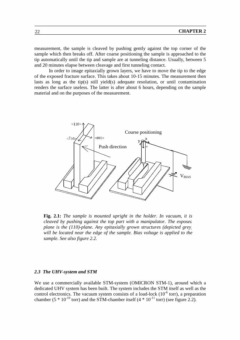
CHAPTER 222
measurement, the sample is cleaved by pushing gently against the top corner of thesample which then breaks off. After coarse positioning the sample is approached to thetip automatically until the tip and sample are at tunneling distance. Usually, between 5and 20 minutes elapse between cleavage and first tunneling contact.
In order to image epitaxially grown layers, we have to move the tip to the edgeof the exposed fracture surface. This takes about 10-15 minutes. The measurement thenlasts as long as the tip(s) still yield(s) adequate resolution, or until contaminationrenders the surface useless. The latter is after about 6 hours, depending on the samplematerial and on the purposes of the measurement.
2.3 The UHV-system and STM
We use a commercially available STM-system (OMICRON STM-1), around which adedicated UHV system has been built. The system includes the STM itself as well as thecontrol electronics. The vacuum system consists of a load-lock (10-6 torr), a preparationchamber (5 * 10-10 torr) and the STM-chamber itself (4 * 10-11 torr) (see figure 2.2).
Fig. 2.1: The sample is mounted upright in the holder. In vacuum, it iscleaved by pushing against the top part with a manipulator. The exposedplane is the (110)-plane. Any epitaxially grown structures (depicted grey)will be located near the edge of the sample. Bias voltage is applied to thesample. See also figure 2.2.
Course positioning
Push direction
VBIAS

STM-SETUP AND SAMPLE PREPARATION 23
The preparation chamber contains a heating stage in which samples and tips canbe outgassed to a temperature of 150 – 200 oC. The heating is accomplished by passinga current through a tungsten coil placed near the sample or tip. The heat is thentransferred by radiation. Apart from that, the preparation chamber contains a number offacilities for the preparation of tips. These are a filament for glowing tips, a counterelectrode for characterization by field emission and self sputtering, an inlet for neon-gas, and an Ar+ ion gun (see chapter 3).
The STM itself really consists of two parts, the scanner and the sample stage(figure 2.2 b). We use a tripod scanner (TS-2 scanner). In order to minimize electronicnoise, the I-V converter is integrated in the scanner, thus minimizing the length of cableover which the current signal must travel before amplification. The tip and sampleholder are placed upright in the scanner and sample stage, respectively.
The scanning itself and fine positioning of the tip is carried out by three piezo-tubes placed perpendicularly to each other. In figure 2.2 b, the z-piezo lies horizontallyand the x and y piezo are at a 45o angle next to and underneath the block that holds thetip. See figure 2.6 d for the resulting orientation of the STM-images with respect to themacroscopic shape of the sample. The scanner has a lateral range of 2 µm x 2 µm, and avertical range of 60 nm.
The sample stage rests on three vertically placed piezo tubes. A sawtooth signalcan be applied to the tubes, so that the sample stage can be moved in the x-z plane bystick-slip motion. This allows for coarse approach (z) and coarse positioning along aline perpendicular to the epitaxial side of the sample (x). This line coincides with thegrowth direction of our samples. There is no possibility for coarse movement in the y-direction.
One very important factor affecting the performance of an STM-system isadequate vibration isolation. The floor on which the system is built has a vibrationaccelleration of about 30 µm/s2 (base level), with some peaks at various frequenciesranging up to 150 µm/s2. The peak lowest in frequency occurs at 7 Hz. The entire frameis placed on four air-damped feet, and the table on which the STM is built rests on eightrubber tabs which are placed between the frame and the table (figure 2.2). Inside thevacuum system, the STM-unit itsef (i.e. the scanner and sample stage) is placed on asmall table. When the STM is in operation, the table hangs from four springs. Along therim of the table, a series of copper fins falls partly between a row of magnets to providea damping mechanism. The resonance frequency of this arrangement is about one hertz.The entire arrangement, combined with the electronics, is such that we can measureapparent height differences of down to 5 pm. In spite of the vibration-isolation presenton our system, we often carry out our STM-measurements at night.
SS
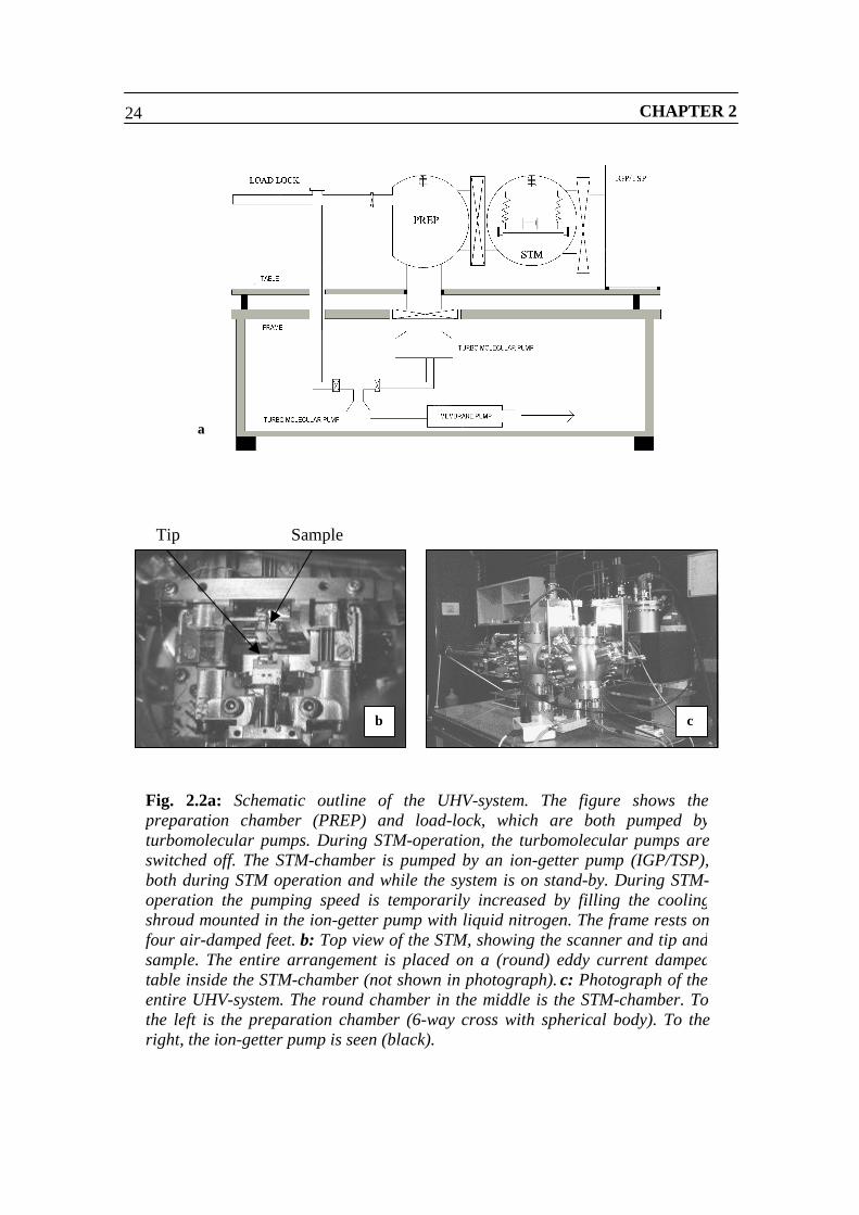
CHAPTER 224
Fig. 2.2a: Schematic outline of the UHV-system. The figure shows thepreparation chamber (PREP) and load-lock, which are both pumped byturbomolecular pumps. During STM-operation, the turbomolecular pumps areswitched off. The STM-chamber is pumped by an ion-getter pump (IGP/TSP),both during STM operation and while the system is on stand-by. During STM-operation the pumping speed is temporarily increased by filling the coolingshroud mounted in the ion-getter pump with liquid nitrogen. The frame rests onfour air-damped feet. b: Top view of the STM, showing the scanner and tip andsample. The entire arrangement is placed on a (round) eddy current dampedtable inside the STM-chamber (not shown in photograph). c: Photograph of theentire UHV-system. The round chamber in the middle is the STM-chamber. Tothe left is the preparation chamber (6-way cross with spherical body). To theright, the ion-getter pump is seen (black).
Tip Sample
a
b c
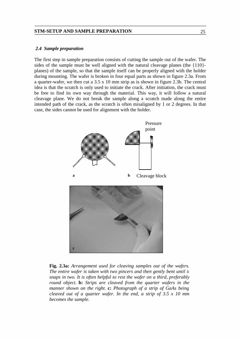
STM-SETUP AND SAMPLE PREPARATION 25
2.4 Sample preparation
The first step in sample preparation consists of cutting the sample out of the wafer. Thesides of the sample must be well aligned with the natural cleavage planes (the 110-planes) of the sample, so that the sample itself can be properly aligned with the holderduring mounting. The wafer is broken in four equal parts as shown in figure 2.3a. Froma quarter-wafer, we then cut a 3.5 x 10 mm strip as is shown in figure 2.3b. The centralidea is that the scratch is only used to initiate the crack. After initiation, the crack mustbe free to find its own way through the material. This way, it will follow a naturalcleavage plane. We do not break the sample along a scratch made along the entireintended path of the crack, as the scratch is often misaligned by 1 or 2 degrees. In thatcase, the sides cannot be used for alignment with the holder.
Fig. 2.3a: Arrangement used for cleaving samples out of the wafers.The entire wafer is taken with two pincers and then gently bent until itsnaps in two. It is often helpful to rest the wafer on a third, preferablyround object. b: Strips are cleaved from the quarter wafers in themanner shown on the right. c: Photograph of a strip of GaAs beingcleaved out of a quarter wafer. In the end, a strip of 3.5 x 10 mmbecomes the sample.
a b
c
Cleavage block
Pressurepoint
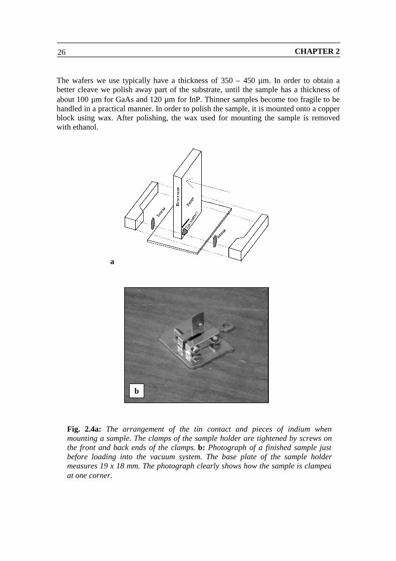
CHAPTER 226
The wafers we use typically have a thickness of 350 – 450 µm. In order to obtain abetter cleave we polish away part of the substrate, until the sample has a thickness ofabout 100 µm for GaAs and 120 µm for InP. Thinner samples become too fragile to behandled in a practical manner. In order to polish the sample, it is mounted onto a copperblock using wax. After polishing, the wax used for mounting the sample is removedwith ethanol.
Fig. 2.4a: The arrangement of the tin contact and pieces of indium whenmounting a sample. The clamps of the sample holder are tightened by screws onthe front and back ends of the clamps. b: Photograph of a finished sample justbefore loading into the vacuum system. The base plate of the sample holdermeasures 19 x 18 mm. The photograph clearly shows how the sample is clampedat one corner.
a
b
STM-SETUP AND SAMPLE PREPARATION 27
The third step in the process is the application of an electrical contact. Due to the oxide-layer present on the semiconductor, a simple mechanical contact between the sampleand sample holder is not sufficient to provide a good electrical contact. We make thecontact by placing a small ball of tin (Sn) on the front side of the sample. The tin is thenpartly diffused into the semiconductor by heating the sample and tin ball in a N2/H2atmosphere (80 % / 20 %). The sample is heated to 300 oC for typically two or threeminutes. The contact is placed in the lower corner of the sample, at the point where thesample is clamped in the holder. In the ideal case, the contact, the scratch and the pointat which the sample is pushed during cleaving, are along one line extending along thefront edge of the sample.
The samples are now ready for mounting. They are usually kept under ethanolfor up to 30 minutes, while in the meantime the sample holders and the tools to handlethem are cleaned. Cleaning is done ultrasonically in four consecutive liquids: a warm,aquaous solution of soap, warm water, distilled water, and ethanol. Between the steps,the items are carefully rinsed with the same liquid as the one that is used for thefollowing cleaning-step.
During the early stages of this project we used thick samples (400 µm), whichcan simply be clamped. Thin samples (150 µm or less), however, will break if theclamps of the sample holders are fastened too tight. At the same time, if they are set tooloose, there is a high probability that the sample will fall out of the holder when insidethe vacuum system. We solve this by placing a small amount of indium metal betweenthe sample and the holder, on both sides (figure 2.4). The clamps of the sample holderare opened widely, and we press some indium onto the inner sides of the clamps whereit will stick to the sample holder. The sample is then placed in between, allowing it tohang towards the back side. Then the contraption is put onto a heating plate, until theindium melts [4]. We then gently slide the loose clamp up against the fixed one, andtighten the two screws. During this stage, it is also important to check if the sides of thesample are well aligned with the holder itself. If that’s the case, the cleavage plane iswell aligned with the top of the clamps. After the sample is allowed to cool off, thescrews are very gently tightened some more. Basically, we just check whether thescrews have not loosened as the different parts of the holder contracted during coolingoff. When the indium melts during mounting, the tin appears to mix with it. Aftermounting, a rather thin layer of metal is present between the front and back sides of thesample and the clamps, and the tin ball is no longer there. The applied temperatureitself, however, is below the melting point of tin. The whole procedure can be carriedout with relative ease after some practice.
The last part of mounting is the placement of the scratch, just above the top ofthe clamp on the epilayer side (see figure 2.1). This is a tricky moment, since thesamples become very fragile after they have been thinned down. When making thescratch by hand it is quite easy to break the sample by accidentally applying too muchforce. After mounting, the samples are loaded into the vacuum system. Inside thepreparation chamber, they are outgassed for about an hour at a temperature between 150oC and 200 oC. The indium used for keeping the sample in its place will melt, but sincemolten indium is quite sticky, the sample remains in place. When the outgassing iscompleted, the sample is placed in the carrousel until the start of the measurement.
CHAPTER 228
Since part of the experimental work consists of the study of the spatial distribution ofdopants (chapter 7), it is essential to ensure that the temperature treatments appliedduring sample preparation do not cause diffusion of the dopants. During preparation, thesamples are subjected to 300 oC for 3 minutes or less while the electrical contact isapplied, and to less than 200 oC for up to an hour as they are outgassed in the vacuum.To our knowledge, these treatments will not cause significant diffusion.
2.5 The measurement
At the start of the measurement, the sample is cleaved by pushing against the top cornerof it with the wobble-stick (see figure 2.1). We can choose the position of the pressure-point on the sample within a margin of 0.5 mm. Again, the thought behind the way wecleave is that we want the crack to be free to find its own path through the material.Clamping the sample at only the front edge helps to ensure that, even if the alignmentwith the top of the sample holder is less than perfect. Another condition we try to avoidduring cleavage, is the presence of torque along the long axis of the sample. This canoccur during cleavage if the back edge of the sample is caught accidentally in one of thefixation screws, or if the pressure-point is misplaced. One of the topics that we are stillinvestigating is at which point exactly the pressure should be applied during cleavage inorder to obtain the smoothest possible surface. Up to now, we always choose the topcorner of the sample as our pressure-point, in the way that is indicated in figure 2.1.Recent experiments have shown that placing the pressure-point at the corner of thesample does induce torque in the sample during cleavage. If torque is to be minimized,the pressure-point should be chosen at the top edge of the sample, at about 1/3 of thewidth of the sample from the corner. The effects of the chosen location of the pressure-point on the quality of the cleaved surface is at present still under investigation.
After cleavage, the sample is taken out of the carousel and placed in the samplestage of the STM (the top part that was broken off remains in the carousel). Themovement of the wobble-stick and of the STM itself, which has to be lowered from itslocked position into its operating position, causes a pressure-burst. We estimate it to beless than 2 * 10-10 torr. The tip and sample are aligned using a CCD-camera. Anexperimental trick to carry out the alignment quickly is to place the camera such that thereflection of the tip will show in the sample surface. When the alignment is satisfactory,we use the automatic approach provided with the electronics to bring the tip intunneling contact.
After first contact, we can either start imaging right away, or we can move to theedge of the sample to image epitaxially grown structures. We locate the edge byretracting the tip, moving the sample a short distance (between 250 nm and several µm)and extending the tip again to establish tunneling contact. When the tip can be extended
STM-SETUP AND SAMPLE PREPARATION 29
over the entire range of the (fine) z-piezo actuator without coming within tunnelingrange to the sample, the tip has been moved past the edge and is moved back a bit. Wecan locate the edge to within 250 nm this way, within 10-15 minutes after first contact.For this method to work properly, the (macroscopic) shape of the tip is quite essential.The important features are the absence of many different microtips, and a long,reasonably thin shank. The macroscopic shape of electrochemically etched tungsten tipsis ideal for this method. We have not been able to locate the edge with mechanically cutPt-Ir tips, probably because such tips do posess many microtips near the apex.Occasionally, the shank of the tip comes into tunneling contact with the edge of thesample. We have not observed this to be harmful as long as it is not attempted to scanthe tip in this condition.
We apply a background correction to the images that involves a “line-by-line tiltcorrection”: from the height along each fast scan-line (horizontal in the images) a linearfit is made, which is then subtracted from the original height-curve along that scan-line.This same type of correction is commonly applied as an on-line correction during theacquisition of the data. In our measurements, the tip is usually scanned with a frequencybetween 2.5 and 5 Hz. External vibrations with a frequency of a few Hz tend to raise orlower a fast scan-line, and also to tilt it. When the scanning-frequency of the tip is largerthan 4 times the frequency of the external vibration, the vibration introduces only littlecurvature into the height-profile along the scan-line. This line-by-line correction is thenvery effective in filtering out the effects of such low-frequency external vibrationswithout otherwise altering the data. The effectiveness increases when the method isapplied to smaller cut-outs of a frame.
The same background correction can also be applied to all pixels lying in a lineperpendicular to the fast scan-direction (vertical in our images). Some of the imagesshown in this thesis are cut-outs from larger frames, where the top right corner is choseninside a depression in the surface (see chapter 5). The height-surface [z(x,y)] is thuswarped instead of planar. We eliminate much of this warping by applying the line-by-line correction first in the horizontal direction and then in the vertical direction, whichallows us to show details of the atomic lattice in all portions of the frame. In someimages in chapters 5 and 7, details of the atomic lattice around dopants or other featuresare shown by applying a (high-pass) fast-Fourier transform filter. Whenever thistechnique is used, it will be stated clearly in the figure caption.
CHAPTER 230
2.6 Typical morphology of cleaved surfaces
The preparation of samples for cross-sectional STM in UHV is a non-trivial task, as apoorly prepared sample will have a rough fracture-surface. On such surfaces, only stepswith atomically resolved terraces in between can be imaged meaningfully. The contrastof a given STM-image is determined by the maximum height-differences present in thedata. If a mono-atomic step (∆z = 260 pm) is present in the frame, the resulting contrastis such that other features like dopants (∆z = 50 - 70 pm) or interfaces between differentmaterials (∆z = 20 pm) cannot be recognized. Atomic corrugation, in spite of the smalldifference in apparent height associated with it (∆z = 20 pm) can often be recognized onone of the terraces of a rough image if the colour scale is adjusted appropriately. This isthe case because atomic corrugation is a short-range effect, recognizable even if a smallpatch of it is visible, and also because atomic corrugation extends throughout the frame,so it is always possible to optimize the contrast for a given terrace. To a lesser extent,the same is true for interfaces between different materials. Dopants, on the other hand,manifest themselves as a gentle rise in the atomically resolved image and lie scatteredas isolated points in the image. In practice, this makes them very hard to recognize inrough images. Even if a few dopants are found in a rough image, the study of the spatialdistribution of dopants in, for example, a δ-doped layer, becomes quite meaningless.
Our sample preparation procedure has become rather elaborate in order toproduce fracture surfaces that are as smooth as possible, especially near the edge on theepitaxial side of the sample. The “art” of creating smooth surfaces by cleavage in UHVremains a topic of applied research, both in our group as well as elsewhere [2,3].
Figure 2.5 shows two limiting cases of the macroscopic∗ morphology that weobserve on our cleaved samples (figure 2.5b: rough morphology, figure 2.5 c: smoothmorphology). In all cases, the area adjacent to the scratch contains a high density ofsteps, and is useless for STM. The remaining part of the sample surface can be devidedinto two regions: The first is the “edge region”, a narrow strip along the edge of thesample which usually looks optically flat. The second region is the “bulk region”, whichcan be either optically flat or which can show steps that fan out from the edge region.
∗ We define “macroscopic” as anything observable by the naked eye or opticalmicroscope.
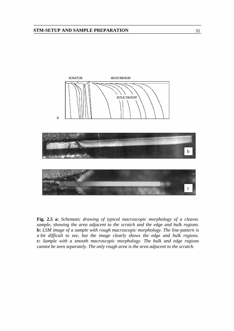
STM-SETUP AND SAMPLE PREPARATION 31
b
c
Fig. 2.5 a: Schematic drawing of typical macroscopic morphology of a cleavedsample, showing the area adjacent to the scratch and the edge and bulk regions.b: LSM image of a sample with rough macroscopic morphology. The line-pattern isa bit difficult to see, but the image clearly shows the edge and bulk regions.c: Sample with a smooth macroscopic morphology. The bulk and edge regionscannot be seen separately. The only rough area is the area adjacent to the scratch.
a
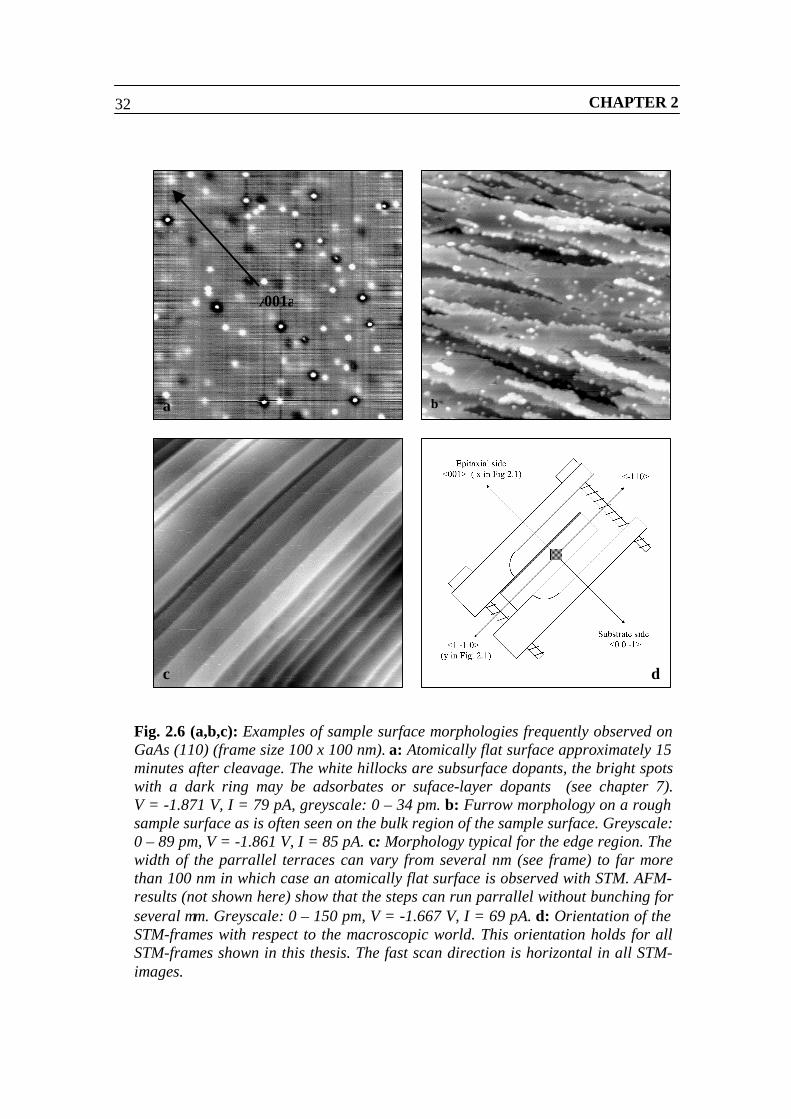
CHAPTER 232
a b
c d
Fig. 2.6 (a,b,c): Examples of sample surface morphologies frequently observed onGaAs (110) (frame size 100 x 100 nm). a: Atomically flat surface approximately 15minutes after cleavage. The white hillocks are subsurface dopants, the bright spotswith a dark ring may be adsorbates or suface-layer dopants (see chapter 7).V = -1.871 V, I = 79 pA, greyscale: 0 – 34 pm. b: Furrow morphology on a roughsample surface as is often seen on the bulk region of the sample surface. Greyscale:0 – 89 pm, V = -1.861 V, I = 85 pA. c: Morphology typical for the edge region. Thewidth of the parrallel terraces can vary from several nm (see frame) to far morethan 100 nm in which case an atomically flat surface is observed with STM. AFM-results (not shown here) show that the steps can run parrallel without bunching forseveral µm. Greyscale: 0 – 150 pm, V = -1.667 V, I = 69 pA. d: Orientation of theSTM-frames with respect to the macroscopic world. This orientation holds for allSTM-frames shown in this thesis. The fast scan direction is horizontal in all STM-images.
⟨001⟩
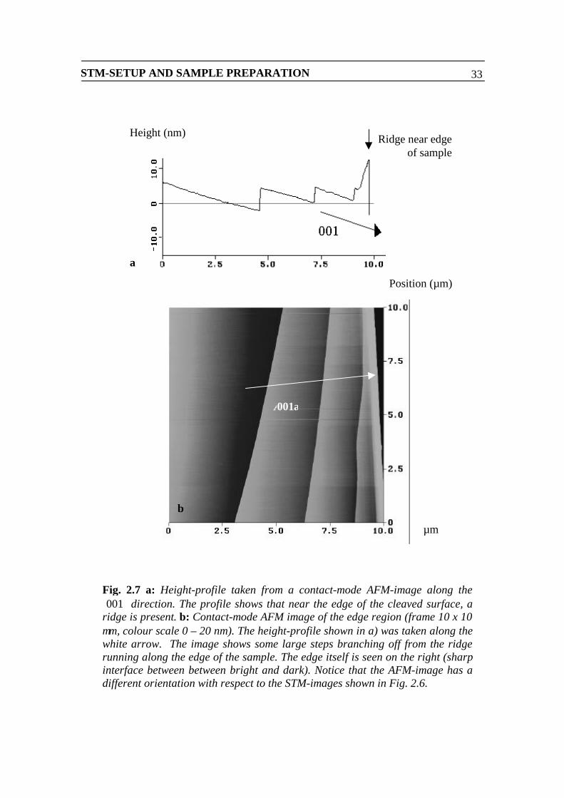
STM-SETUP AND SAMPLE PREPARATION 33
Fig. 2.7 a: Height-profile taken from a contact-mode AFM-image along the⟨001⟩ direction. The profile shows that near the edge of the cleaved surface, aridge is present. b: Contact-mode AFM image of the edge region (frame 10 x 10µm, colour scale 0 – 20 nm). The height-profile shown in a) was taken along thewhite arrow. The image shows some large steps branching off from the ridgerunning along the edge of the sample. The edge itself is seen on the right (sharpinterface between between bright and dark). Notice that the AFM-image has adifferent orientation with respect to the STM-images shown in Fig. 2.6.
Height (nm)
µm
⟨001⟩
Position (µm)
Ridge near edgeof sample
a
b
CHAPTER 234
On a scale of 10 µm down to the atomic scale, the trends in the macroscopicmorphology are reproduced. Near the edge, the steps run mostly along the ⟨-110⟩direction, parallel to the edge and, if these are present, to the epitaxial layers. Betweenthe steps are very long, straight terraces. The width of the terraces varies from far morethan 100 nm down to 10 or 20 nm (figure 2.6 c). STM-frames of 100 x 100 nm taken inthe bulk region of the sample show either an atomically flat surface (figure 2.6 a), orthey can show mono-atomic steps in STM (figure 2.6 b). These steps are often V-shaped, forming what is called the “furrow morphology” in recent literature [2,3]. Ifsteps are present in the bulk region, the general direction of the steps gradually changesfrom ⟨-110⟩ near the edge region to ⟨001⟩ as one moves towards the back of the sample.In the bulk region, we encounter atomically flat surfaces and V-shaped steps aboutequally often. We observe that usually the edge region lies somewhat higher than therest of the sample surface, forming a sort of ridge (figure 2.7 a,b).
Finally, the macroscopic morphology is often smoother as one moves away fromthe scratch (the right end of the sample surface shown in figure 2.5 b,c). We have theimpression that also on the atomic scale, the surface tends to become smoother as onemoves further away from the scratch, but we have no experimental results to confirmthis notion. We sometimes observe significant differences in morphology whenchanging tips. This indicates that there are differences in morphology as a function ofposition on the sample, since the tips contact the sample at a different location.
For the study of epitaxial layers, it is desirable that the terraces are as wide aspossible. For the study of δ-layers, a terrace width of about 100 nm or more is desirable.For the study of interfaces, the width can be somewhat smaller. When the averageterrace width is about 10 nm, the study of any kind of epitaxial structure becomes quitedifficult.
2.7 Discussion on the cleavage process
As the precise nature of the cleavage process is at best only partially understood [2], thepreparation of usable sample surfaces by cleavage in UHV is mostly done by trial anderror. The following section will discuss some of the literature on cleavage that we areaware of, along with some observations of our own. Most of the considerations concernthe region near the epitaxial side of the sample (epilayer region) since our main interestis in imaging epitaxially grown layers. Our own understanding of cleavage is by nomeans complete. At present, cleavage and how to obtain smooth sample surfaces bycleavage remains a topic of ongoing research [2,3].
It has been shown by Rosentreter et al. that at room temperature, the surfacemorphology obtained by cleavage does not correspond to the morphology expected fora surface that has reached thermal equilibrium. The article concludes that themorphology is created by the fracture-process and that “relaxation towards thermalequilibrium is not the dominant mechanism responsible for the arrangement of thesteps” [2]. Another very important point is that the crack tip may propagate either
STM-SETUP AND SAMPLE PREPARATION 35
smoothly through the material, or in an oscillatory manner [5,6,9,10,11]. According to ref.5, the crack propagates through a (triangular) lattice smoothly when the external strainis below a critical value. If the strain exceeds this value, smaller cracks branch off fromthe main crack periodically, creating a rough surface morphology. The samecalculations also predict a rather complex relation between the external strain and thecrack tip velocity [5].
The motion of a crack propagating through a GaAs sample has been investigatedby Sauthoff et al. [3]. The results showed that the entire cleavage process takes about 14to 20 µs. The samples were 3.6 mm (fracture length) by 0.3 mm (sample thickness).During cleavage, the crack-front proceeds along the front edge of the sample from theedge towards the bottom end of the sample. After the crack has reached the bottom endof the sample, it takes about 5 to 8 µs more before the crack reaches the back side of thesample. The experiment showed that as the crack approaches the back side of thesample, it travels perpendicularly to it. The cleavage process thus involves a change ofthe propagation direction of the crack by 90 o. Observed crack velocities ranged from250 m/s to 3000 m/s. Those samples that had a low crack propagation velocity (v < 600m/s) had a smooth morphology, both on the macroscopic and on the atomic scale [3].When breaking an entire wafer into four quarts in the manner shown in figure 2.3, wesometimes observe a behaviour which is consistent with Sauthoff’s results: We bendthese wafers very gently, gradually increasing pressure until the wafer snaps.Sometimes, before the wafer actually breaks, a very thin line appears in the surface ofthe wafer extending from the scratch along the intended cleavage path. It usuallytraverses ¾ of the wafer and does not reach the rim of the wafer opposite from thescratch. At this point the wafer is still one integral body: One can hold it at one side andthe other half of the wafer remains in place. When more pressure is applied, the waferbreaks in two.
Before we started using the sample holders shown in figure 2.1 which onlyclamp the sample at the front edge, we used sample holders that clamped the samplealong the entire length of the bottom end, similar to the one drawn in figure 2.8 b. Thefollowing STM-image (figure 2.8 c) shows the effect of poor alignment of the samplecleavage plane with respect to the top edges of the clamps holding the sample.
The STM-image shown in figure 2.8 c was taken within a distance of 250 nmfrom the epitaxial side of the sample. The image shows many V-shaped terraces.Traveling in the [-110] direction (from the lower left corner towards the upper rightcorner) one moves up a staircase, the steps of the stairs appearing very pointed andjagged. This is a clear contrast to the typical morphology shown in figure 2.6 c, wherethe steps do not seem to terminate anywhere on a scale of several hundred nm, andwhich does not have any kind of staircase in the [-110] direction. The propagationdirection of the crack was from the lower left corner towards the upper right one forboth images as both frames were taken within the edge region of the sample. The workof Sauthoff et al. [3] shows that in the edge region, the crack proceeds in the [-110]direction along the entire length of the sample. Notice that the image also shows astaircase morphology in the perpendicular direction, with the steps rising as one movesin the [001] direction (from the bottom right towards the upper left corner). This isconsistent with the presence of a ridge similar to the one shown in figure 2.7 a,b.
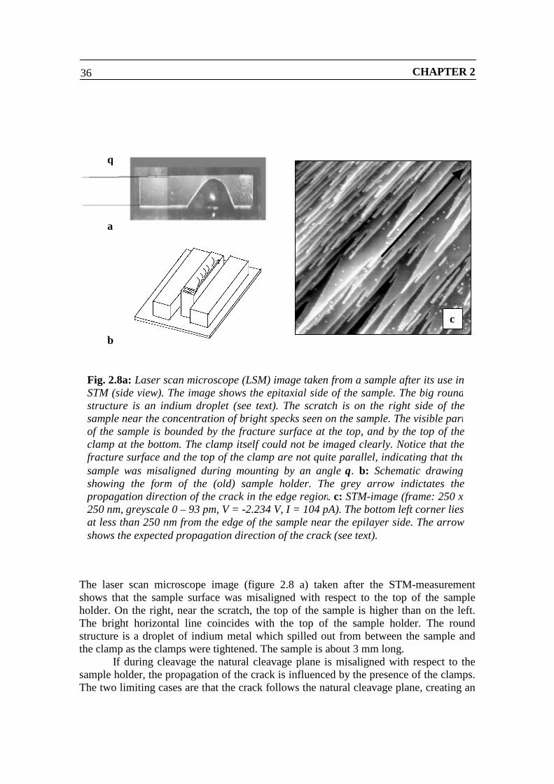
CHAPTER 236
The laser scan microscope image (figure 2.8 a) taken after the STM-measurementshows that the sample surface was misaligned with respect to the top of the sampleholder. On the right, near the scratch, the top of the sample is higher than on the left.The bright horizontal line coincides with the top of the sample holder. The roundstructure is a droplet of indium metal which spilled out from between the sample andthe clamp as the clamps were tightened. The sample is about 3 mm long.
If during cleavage the natural cleavage plane is misaligned with respect to thesample holder, the propagation of the crack is influenced by the presence of the clamps.The two limiting cases are that the crack follows the natural cleavage plane, creating an
Fig. 2.8a: Laser scan microscope (LSM) image taken from a sample after its use inSTM (side view). The image shows the epitaxial side of the sample. The big roundstructure is an indium droplet (see text). The scratch is on the right side of thesample near the concentration of bright specks seen on the sample. The visible partof the sample is bounded by the fracture surface at the top, and by the top of theclamp at the bottom. The clamp itself could not be imaged clearly. Notice that thefracture surface and the top of the clamp are not quite parallel, indicating that thesample was misaligned during mounting by an angle θ. b: Schematic drawingshowing the form of the (old) sample holder. The grey arrow indictates thepropagation direction of the crack in the edge region. c: STM-image (frame: 250 x250 nm, greyscale 0 – 93 pm, V = -2.234 V, I = 104 pA). The bottom left corner liesat less than 250 nm from the edge of the sample near the epilayer side. The arrowshows the expected propagation direction of the crack (see text).
θ
b
a
c
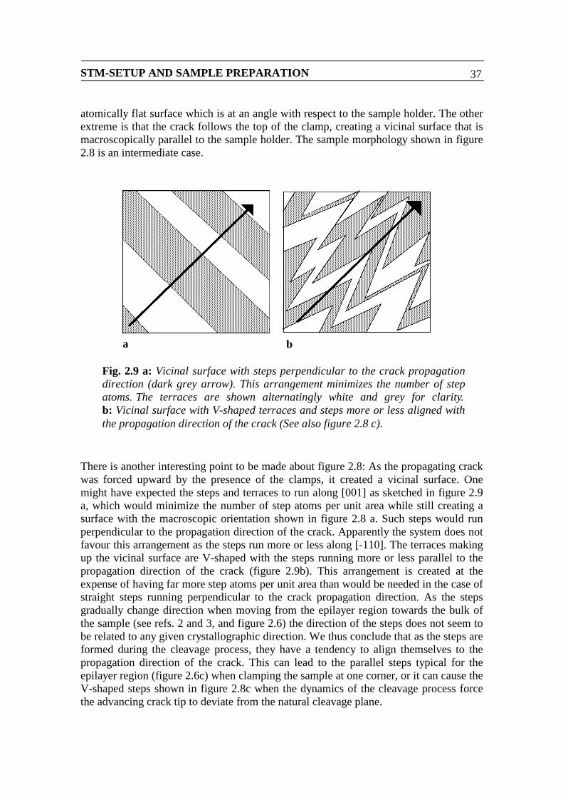
STM-SETUP AND SAMPLE PREPARATION 37
atomically flat surface which is at an angle with respect to the sample holder. The otherextreme is that the crack follows the top of the clamp, creating a vicinal surface that ismacroscopically parallel to the sample holder. The sample morphology shown in figure2.8 is an intermediate case.
There is another interesting point to be made about figure 2.8: As the propagating crackwas forced upward by the presence of the clamps, it created a vicinal surface. Onemight have expected the steps and terraces to run along [001] as sketched in figure 2.9a, which would minimize the number of step atoms per unit area while still creating asurface with the macroscopic orientation shown in figure 2.8 a. Such steps would runperpendicular to the propagation direction of the crack. Apparently the system does notfavour this arrangement as the steps run more or less along [-110]. The terraces makingup the vicinal surface are V-shaped with the steps running more or less parallel to thepropagation direction of the crack (figure 2.9b). This arrangement is created at theexpense of having far more step atoms per unit area than would be needed in the case ofstraight steps running perpendicular to the crack propagation direction. As the stepsgradually change direction when moving from the epilayer region towards the bulk ofthe sample (see refs. 2 and 3, and figure 2.6) the direction of the steps does not seem tobe related to any given crystallographic direction. We thus conclude that as the steps areformed during the cleavage process, they have a tendency to align themselves to thepropagation direction of the crack. This can lead to the parallel steps typical for theepilayer region (figure 2.6c) when clamping the sample at one corner, or it can cause theV-shaped steps shown in figure 2.8c when the dynamics of the cleavage process forcethe advancing crack tip to deviate from the natural cleavage plane.
Fig. 2.9 a: Vicinal surface with steps perpendicular to the crack propagationdirection (dark grey arrow). This arrangement minimizes the number of stepatoms. The terraces are shown alternatingly white and grey for clarity.b: Vicinal surface with V-shaped terraces and steps more or less aligned withthe propagation direction of the crack (See also figure 2.8 c).
a b
CHAPTER 238
In practice, it is difficult to mount the sample in such way that the natural cleavageplane is perfectly aligned with the top of the sample holder [7]. This is why we usesample holders that clamp the sample only at one corner: Away from the corner that isclamped, the crack is free to propagate through the material without influence from theclamps of the sample holder. Although long, parallel steps as shown in figure 2.6c areseen frequently in the epilayer region when using the modified sample holders (seefigure 2.1), we have never observed V-shaped terraces in the epilayer region whenclamping the sample only at one corner.
Interpreting the foregoing, it is clear that the cleavage process involves a crackpropagating through the epitaxial side of the sample from the scratch towards the otherend of the sample. Either at the same time or slightly afterwards, the crack alsopropagates through the bulk of the sample. The experiments by Sauthoff et al. [3]indicated that the crack reaches the back side traveling in the [00-1] direction. Thecleavage process thus involves a change in the propagation direction of the crack by 90degrees.
The pattern of long, parallel terraces extending in the propagation direction ofthe crack typical for the edge region (figure 2.6 c) shows that in this region, the cracktravels smoothly through the material. Any oscillatory behaviour of the crack-tip asdiscussed in the literature [5,6,9,10,11] would result in steps perpendicular to thepropagation direction of the crack, or in V-shaped terraces like the ones shown in figure2.8 c. The external strain acting on the crack tip is apparently small enough in order toavoid oscillatory behaviour of the crack. We thus propose that the parallel steps arecreated as the atomic plane through which the crack propagates, is shifted by one ormore unit cells for different positions along the advancing crack-front (figure 2.10).
The main remaining challenge regarding cleavage is to cleave in such a way thatthe parallel steps in the epilayer region lie as far apart as possible. A rough morphologyin the bulk region presents less of a problem, as the bulk material takes up most of thesample surface. This gives more possibilities to move around on the sample in order tofind an area with a suitable morphology. Should that fail, then there is usually enoughmaterial available to make a new sample. For the study of epitaxial layers this is not thecase: The available area on the sample surface is limited by the extent of the epitaxiallayer in the [001] direction and by the range of the scanner (2 µm). Also, the amount ofsample material available is often limited to one (2 inch) wafer or one quarter wafer,allowing only a certain number of samples to be made.
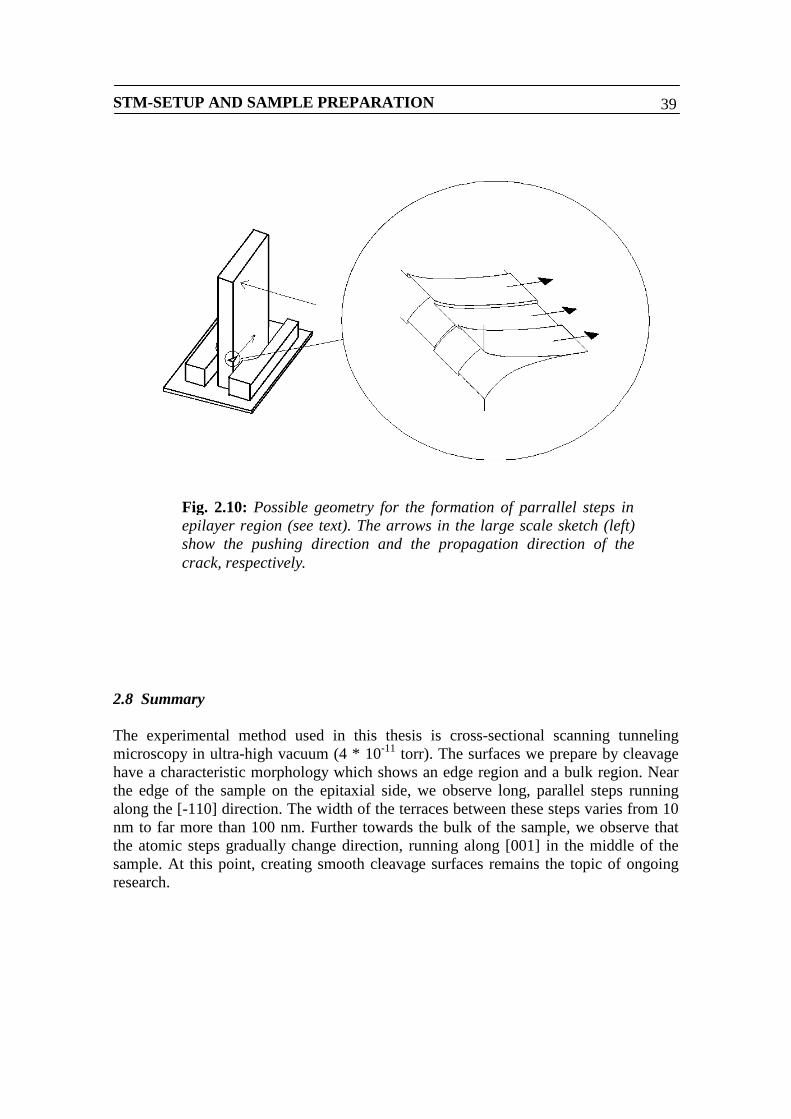
STM-SETUP AND SAMPLE PREPARATION 39
2.8 Summary
The experimental method used in this thesis is cross-sectional scanning tunnelingmicroscopy in ultra-high vacuum (4 * 10-11 torr). The surfaces we prepare by cleavagehave a characteristic morphology which shows an edge region and a bulk region. Nearthe edge of the sample on the epitaxial side, we observe long, parallel steps runningalong the [-110] direction. The width of the terraces between these steps varies from 10nm to far more than 100 nm. Further towards the bulk of the sample, we observe thatthe atomic steps gradually change direction, running along [001] in the middle of thesample. At this point, creating smooth cleavage surfaces remains the topic of ongoingresearch.
Fig. 2.10: Possible geometry for the formation of parrallel steps inepilayer region (see text). The arrows in the large scale sketch (left)show the pushing direction and the propagation direction of thecrack, respectively.

CHAPTER 240
REFERENCES
1: O. Albrektsen, H.W.M. Salemink, K.A. Morch, A.R. Thölen: Reliable tippreparation for high-resolution scanning tunneling microscopy. JVST B12 (6)page 3187 (1994)
2: M.A. Rosentreter, M. Wenderoth, N.H. Theuerkrauf, A.J. Heinrich, M.A.Schneider, R.G. Ulbrich: Non-equilibrium configurations of mono-atomic stepson cleaved GaAs (110) surfaces. Phys. Rev. B, Vol. 56, No. 16, pp 10538 –10543 (1997).
3: K. Sauthoff, M. Wenderoth, M.A. Rosentreter, K.J. Engel, T.C.G. Reusch, R.G.Ulbrich: Non-linear dinamic instability in brittle fracture of GaAs. Phys. Rev. B,Vol. 60, No. 7, pp. 4789 – 4795 (1999).
4: The temperature of the sample during mounting lies between 156 oC (meltingpoint of indium) and 200 oC (set-point of the heating plate).
5: M. Marder and Xiangming Liu: Instability in Lattice Fracture. Phys. Rev. Lett,Vol. 71, No. 15, pp 2417 – 2420 (1993).
6: R. Blumenfeld: Nonequilibrium brittle fracture propagation: Steady state,oscillations, and intermittency. Phys. Rev. Lett Vol. 76, No. 20, pp 3703 – 3706(1996).
7: When taking special measures, it is possible to align the sample with itscleavage direction parrallel to the sample holder accurately enough to produce asatisfactory surface: Phd-thesis presented by O. Albrektsen, Laboratory ofApplied Physics (LTF), Technical University of Denmark (Supervisor: Prof.Lic. Tech. K.A. Mørch). Also: Personal communication with dr. H. Salemink,IBM-Zürich.
8: W.D. Callister: Materials science and engeneering (2nd ed.), John Wiley andsons, New York, p. 199 (1985).
9: J. Fineberg, S.P. Gross, M. Marder, H.L. Swinney: Instability in dynamicfracture. Phys. Rev. Lett. Vol. 67, No. 4, pp. 457 – 460 (1991).
10: M. Marder, J. Fineberg: How things break. Phys. Today, Sept. 1996, pp. 24 –29.
11: J. Fineberg, S.P. Gross, M. Marder, H.L. Swinney: Instability in the propagationof fast cracks. Phys. Rev. B, Vol. 45, No. 10, pp. 5146 – 5154 (1992).
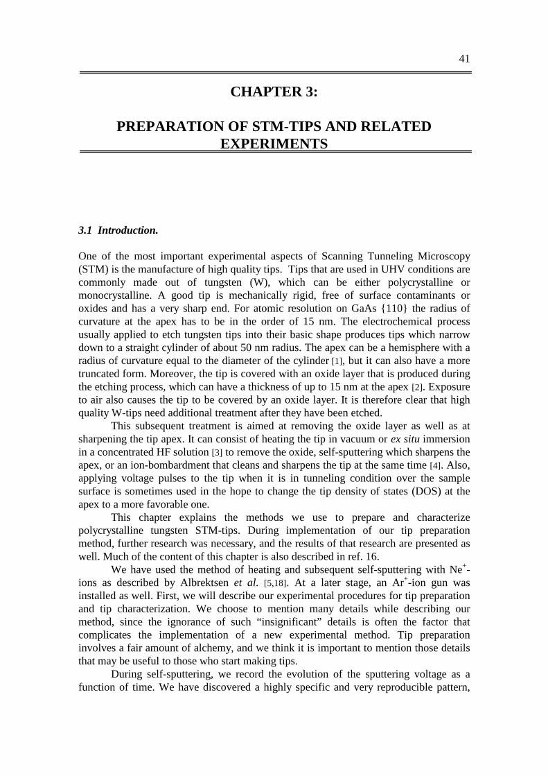
CHAPTER 3:
PREPARATION OF STM-TIPS AND RELATEDEXPERIMENTS
41
3.1 Introduction.
One of the most important experimental aspects of Scanning Tunneling Microscopy(STM) is the manufacture of high quality tips. Tips that are used in UHV conditions arecommonly made out of tungsten (W), which can be either polycrystalline ormonocrystalline. A good tip is mechanically rigid, free of surface contaminants oroxides and has a very sharp end. For atomic resolution on GaAs 110 the radius ofcurvature at the apex has to be in the order of 15 nm. The electrochemical processusually applied to etch tungsten tips into their basic shape produces tips which narrowdown to a straight cylinder of about 50 nm radius. The apex can be a hemisphere with aradius of curvature equal to the diameter of the cylinder [1], but it can also have a moretruncated form. Moreover, the tip is covered with an oxide layer that is produced duringthe etching process, which can have a thickness of up to 15 nm at the apex [2]. Exposureto air also causes the tip to be covered by an oxide layer. It is therefore clear that highquality W-tips need additional treatment after they have been etched.
This subsequent treatment is aimed at removing the oxide layer as well as atsharpening the tip apex. It can consist of heating the tip in vacuum or ex situ immersionin a concentrated HF solution [3] to remove the oxide, self-sputtering which sharpens theapex, or an ion-bombardment that cleans and sharpens the tip at the same time [4]. Also,applying voltage pulses to the tip when it is in tunneling condition over the samplesurface is sometimes used in the hope to change the tip density of states (DOS) at theapex to a more favorable one.
This chapter explains the methods we use to prepare and characterizepolycrystalline tungsten STM-tips. During implementation of our tip preparationmethod, further research was necessary, and the results of that research are presented aswell. Much of the content of this chapter is also described in ref. 16.
We have used the method of heating and subsequent self-sputtering with Ne+-ions as described by Albrektsen et al. [5,18]. At a later stage, an Ar+-ion gun wasinstalled as well. First, we will describe our experimental procedures for tip preparationand tip characterization. We choose to mention many details while describing ourmethod, since the ignorance of such “insignificant” details is often the factor thatcomplicates the implementation of a new experimental method. Tip preparationinvolves a fair amount of alchemy, and we think it is important to mention those detailsthat may be useful to those who start making tips.
During self-sputtering, we record the evolution of the sputtering voltage as afunction of time. We have discovered a highly specific and very reproducible pattern,
CHAPTER 3: PREPARATION OF42
which we will show to be associated with the decapitation process described earlier for⟨111⟩-oriented monocrystalline tungsten tips by Schiller et al. [1]: During the self-sputterprocess, a “head-and-neck” structure forms just behind the apex. At some point, thehead is torn off, which leaves a very sharp tip. We can recognize the moment at whichthe head is torn off from the pattern in the sputtering voltage. By terminating the self-sputter process immediately after the decapitation as observed from the pattern in thesputtering voltage, we are able to produce high-quality STM-tips by self-sputtering withhigh reliability (success-rate is about 75 %). Our tips routinely yield atomic resolutionon the 110-surfaces of GaAs and InP.
We will also present a model that is used to interpret field emissioncharacterization measurements. This model allows us to estimate the apex radius of a tipfrom field emission measurements within a margin of 5 nm. The field emissionmeasurements suggest that the polycrystalline, nominally unoriented tungsten wire thatwe use for the manufacture of STM-tips, has a preferential orientation of the ⟨110⟩-crystal axis along the long axis of the wire. Such orientation is a known effect of wireproduction [12,13].
An experimental complication when using the self-sputtering method is thepossible occurrence of vacuum-arcs, which can completely destroy the apex of a tip.Our experience on vacuum-arcs and their prevention is explained. Finally, we makecomments on our experiences with regards to the Ar+-ion bombardment and itscombination with the self-sputtering technique.
3.2 Tip preparation method.
Our method of tip preparation has four steps, which will each be described in detail inthis section. First the tips are etched. Inside the UHV-system, the tips are outgassed (seesection 2.3) after which they are heated to remove the oxide layer. The third step in thepreparation process is self-sputtering in order to decrease the radius of curvature of theapex from about 50 nm, which is usual for an etched tip, to about 10 – 15 nm. A lot ofexperimental effort has been devoted to the proper implementation of this step, and itwill therefore be described in much detail. The last step is a light Ar+-ion bombardment.After these treatments have been completed, the tip can be used for STM. In the last partof this section we will explain the characterization measurements that we carry out onour tips (in situ field emission measurement and ex situ characterization by SEM for alimited number of tips). We will also describe the method that we use to regenerate tipsthat have been used in a previous measurement, in order to use them a second time.
STM-TIPS AND RELATED EXPERIMENTS 43
Fig 3.1a: Schematic drawing of etching-setup. b: Set-up for self-sputtering. Thesystem is electrically isolated from the UHV system. c: Photograph of the beaker-glass with the tip (left) and counterelectrode (right). d: Position of the tip duringheating. The Λ-shaped filament is oriented more or less vertical. The shaft of thetip is placed such that it catches underneath the filament when the tip is raisedwith the manupulator. During the treatment, the tip (including the shaft) glowsbrightly orange. The filament itself glows white. We have two filaments in thesystem, one serves as backup. e: Photograph showing the tip and hemisphericalcounterelectrode (diameter 20 mm) during self-sputtering. The tip and tipholderare placed in a carrier plate used for transport inside the UHV system.
b
d
c
a
5 VPt-Rh W-wire
2M KOH
Voltage supply (0 – 12 V)and electronic interruptor
e
1 MΩ
0.5–3.0 kV
UHV chamber
CHAPTER 3: PREPARATION OF44
3.2.1 Tip etching
Our tips are made out of 99.98% pure polycrystalline tungsten wire [7] (∅ 0.25 mm), ofwhich a 1 cm piece is spotwelded onto a tipholder. The wire is then etched two times:the first etch is meant to remove the end of the wire which has been split by themechanical cutting, the second etch produces the actual tip. The tips, carrier plates (seefigure 3.1 d,e) and the pincers to handle the tips are cleaned ultrasonically between thefirst and second etch in the same way as the sample holders are cleaned (see Sect. 2.4).We use the standard DC-drop off method [8 (p. 283)] for etching with the followingcharacteristics: The electrolyte is a 2 M. KOH solution, etching voltage is 5 V, thecounter electrode is a small Pt-Rh spiral. The process is carried out in a beaker-glass thathas a partition in the middle which ensures that the flow around the W-wire is notdisturbed by the H2-gas produced at the counterelectrode. As the reaction products(mainly WO4
2-(aq)) [8 (p. 282)] dissolve in the etchant, they sink down along the wire. The
effect is visible since the reaction products locally changes the diffractive index of theliquid. We found the effect very useful for monitoring the etching process. The “tail” ofreaction products drooping from the wire being etched should hang straight down fromthe wire, or at least, look stable in time. The process is cut by an electronic interruptorwhich opens the circuit when the current drops below a preset value (switching time isabout 10-6 sec). The tip is then immersed in de-ionized water for a few minutes toremove any remnants of the KOH-solution. After inspection with an optical microscopeit is stored under ethanol for up to a few hours until a complete batch of 4 tips is readyfor loading into the UHV-system.
We found that it is necessary to pay a lot of attention to the quality of the etchingsolution. For instance, when the etchant is stored in a plastic bottle over longer periodsof time, the tips that are etched with it are partly covered with a contamination thatlooks like sea-weed in Scanning Electron Microscopy (SEM). We suspect that thiscontaminant consists of strands of the plastic of which the storage bottle in which wekept our etchant, was made. The contaminant shows up dark in SEM, which isconsistent with the contaminant being a non-conductive material. Furthermore, thenotion that a 2M KOH-solution would dissolve small amounts of (certain) plastics is aplausible one as well [19]. Also, it seems that small quantities of dissolved metalaccallerate the etching process. When using a metal spoon to weigh and stir the solution,the etching process proceeds a lot faster than usual and the normal flow of reactionproducts around the wire does not form. The resulting tip shape is quite peculiar (sort ofstep-like) and the apex is blunt. As countermeasures, we do not keep any etchingsolution ready for use for longer than a day and we use only glass objects to prepare andhandle the etchant. Such “alchemistic” effects however, may well differ from onelaboratory to the next.
After loading into the UHV-system the tips and carrier plates are outgassed inthe same fashion as the samples (see Sect. 2.4). After that, the subsequent steps in thepreparation process (heating, self-sputtering and Ar+-ion bombardment) are carried out.
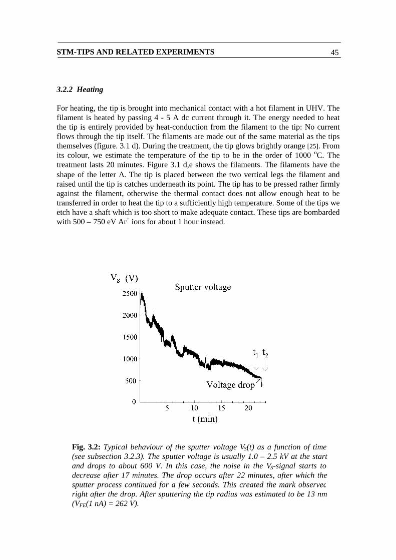
STM-TIPS AND RELATED EXPERIMENTS 45
3.2.2 Heating
For heating, the tip is brought into mechanical contact with a hot filament in UHV. Thefilament is heated by passing 4 - 5 A dc current through it. The energy needed to heatthe tip is entirely provided by heat-conduction from the filament to the tip: No currentflows through the tip itself. The filaments are made out of the same material as the tipsthemselves (figure. 3.1 d). During the treatment, the tip glows brightly orange [25]. Fromits colour, we estimate the temperature of the tip to be in the order of 1000 oC. Thetreatment lasts 20 minutes. Figure 3.1 d,e shows the filaments. The filaments have theshape of the letter Λ. The tip is placed between the two vertical legs the filament andraised until the tip is catches underneath its point. The tip has to be pressed rather firmlyagainst the filament, otherwise the thermal contact does not allow enough heat to betransferred in order to heat the tip to a sufficiently high temperature. Some of the tips weetch have a shaft which is too short to make adequate contact. These tips are bombardedwith 500 – 750 eV Ar+ ions for about 1 hour instead.
Fig. 3.2: Typical behaviour of the sputter voltage VS(t) as a function of time(see subsection 3.2.3). The sputter voltage is usually 1.0 – 2.5 kV at the startand drops to about 600 V. In this case, the noise in the VS-signal starts todecrease after 17 minutes. The drop occurs after 22 minutes, after which thesputter process continued for a few seconds. This created the mark observedright after the drop. After sputtering the tip radius was estimated to be 13 nm(VFE(1 nA) = 262 V).
CHAPTER 3: PREPARATION OF46
3.2.3 Self-sputtering
After removal of the oxide layer, the tip is placed in front of a 10 mm radius stainlesssteel hemisphere acting as a counterelectrode, to carry out the self-sputter process(figure 3.1 e). This process has been used earlier by Albrektsen et al. [5,18] and byEkvall et al. [17]. The distance between the tip and the counterelectrode is 5 ± 1 mm.Neon gas is let into the vacuum chamber to a pressure of about 1.5 – 2.0 x 10⁻⁵ torr(base pressure is less than 1 x 10⁻⁹ torr), and a negative voltage is put on the tip. Thissputter voltage (VS) is typically about 2 kV and is chosen such that a field emissioncurrent of 10 µA is generated. Our high voltage supply (Fug HCN 14-12500) is operatedin constant current mode. We monitor the sputter process by recording the sputtervoltage as a function of time [VS(t)]. The typical behaviour is shown in figure 3.2. Asthe tip sharpens during sputtering, the voltage decreases to about 600 V. In this regime avery specific pattern consisting of a decrease of the noise-amplitude of the sputtervoltage, followed by a very fast drop in the order of 50 V, occurs. After this drop theprocess is cut off.
We can carry out the self-sputtering process with high reliability. Presently weachieve a success-rate of about 75 %, which was estimated from about 100 attemptedsputtering treatments carried out as part of our normal use of the STM-setup, over aperiod of 10 months. In this estimate, the regenerated tips have been included.Achievement of the reported success-rate during self-sputtering, however, dependsstrongly on several experimental conditions: Firstly, the tip must have a certainsharpness at the beginning of the sputter process. If prior to sputtering the field emissionvoltage of a tip [VFE(1 nA)] exceeds 2 kV, we will not attempt to sputter it. Secondly,the sputtering-gas must be free of contaminants to avoid vacuum-arcs (see section 3.6).For the same reason, it is important that the oxide layer present on the tip is adequatelyremoved. Lastly, the setup for self-sputtering (tip holder and manupulator, counterelectrode and wiring) must be designed in such a way that no significant amount ofcurrent can leak away from those parts of the setup that are at high voltage. For thisreason, placing the setup well away from the walls of the vacuum chamber and avoidinga design having many sharp edges or corners, is preferable.
3.2.4 Argon ion bombardment
The last step in the preparation process is a light, head-on Ar+-ion bombardment. Wecurrently favour the following parameters: 750 eV, 6 µA/cm2, and between 7 and 10minutes of sputter-time depending on the initial sharpness of the tip. The width of theion-beam is 0.5 cm, so positioning the tip with respect to the ion-gun is not very critical.The purpose of the ion-bombardment is to increase the stability of the tip: According toref. 1, the tips that are self-sputtered in the way as we described it have a very small“tail” at the apex. The ion bombardment is applied to remove any such structures in acontrolled way. Tips that had a VFE (1 nA) of more than 300 V at the start of the ionbombardment tend to get slightly sharper during the bombardment, whereas tips that hada VFE (1 nA) of less than 300 V become slightly blunter. The difference in field
STM-TIPS AND RELATED EXPERIMENTS 47
emission voltage before and after the treatment is usually less than 20 V. The ion-bombardment is not needed to obtain high resolution on GaAs 110 or InP 110.Before the installation of the ion-gun, we routinely obtained atomic resolution with tipsthat had been only heated and self-sputtered. We show figure 3.3 as an example, whichwas obtained with a tip that had been heated and self-sputtered, but which was notbombarded with Ar+-ions.
3.2.5 Tip characterization
The self-sputtering technique features an inherent possibility for characterization of thetips by field emission. In the same geometry as in which a tip is self-sputtered, wemeasure the voltage needed to draw 1 nA of field emission current [VFE(1 nA)]. Thefield emission current is limited to 1 nA because at higher currents, the tip apex isfrequently altered during the measurement. The voltage is kept constant and the currenttypically fluctuates by a factor 0.3. After etching and heating, the tips generally emit 1nA at VFE = 1.0 ± 0.5 kV, indicating a radius of the order of 50 nm. The self-sputterprocess decreases this voltage to between 200 and 400 V. In that case, the apex has anestimated radius of 8 – 15 nm. This radius is also typical for our completed STM-tips.Our tips give good topographic results on in situ cleaved GaAs and InP (110) surfaces,with the best tips having a VFE(1 nA) value of about 250 V.
A limited number of tips has been investigated using Scanning ElectronMicroscopy (SEM). The tips were transported to the SEM (JEOL JSM-6400F FEGSEMoperated at 15 kV) through the ambient air, involving an exposure of about 30 minutes.
3.2.6 Regeneration of tips
We often regenerate tips that have been used in previous measurements. This practiceyields good tips and saves time. We estimate that at present, between a fourth and onehalf of our measurements are carried out using regenerated tips. The regenerationprocess consists of repeating the self-sputter process and Ar+-ion bombardment. In bothsteps the same parameters are used as during the preparation of a new tip. After its usein STM, the field emission voltage of a tip is usually around 300 - 400 V. We favourrepeating the self-sputter process for a used tip, even if the field emission voltage is low.The reason is that during the measurement, the tip may have been deformed orcontaminated during the measurement. This might show in the field emissionmeasurement, but if the damage is on the atomic scale, it also might not. Theobservation that the tip shows “normal” sputtering behaviour is used as an indicationthat this is not the case, and that the tip can be expected to behave as a new one does.Sputtering a used, already sharp tip often takes longer as the sputter voltage is lowerthan for a new tip (300 – 500 V). This decreases the energy of the incident ions, whichin turn decreases the sputtering yield of the ions. After being used in a measurement for
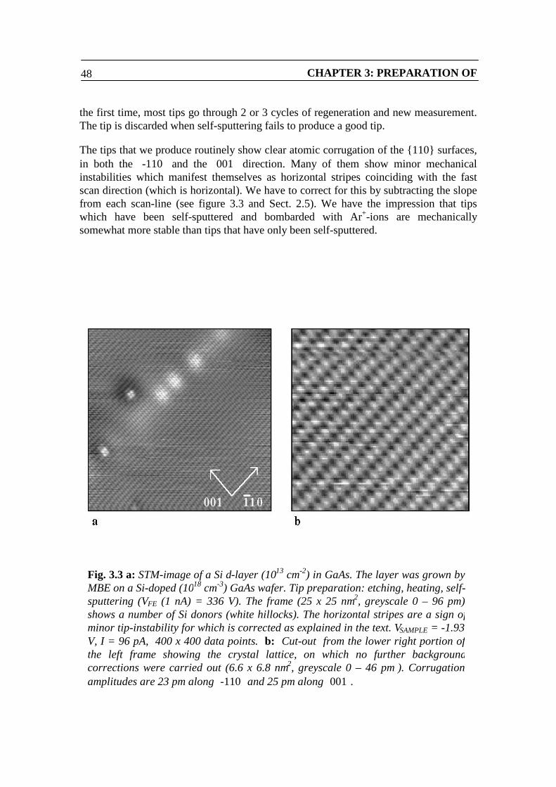
CHAPTER 3: PREPARATION OF48
the first time, most tips go through 2 or 3 cycles of regeneration and new measurement.The tip is discarded when self-sputtering fails to produce a good tip.
The tips that we produce routinely show clear atomic corrugation of the 110 surfaces,in both the ⟨-110⟩ and the ⟨001⟩ direction. Many of them show minor mechanicalinstabilities which manifest themselves as horizontal stripes coinciding with the fastscan direction (which is horizontal). We have to correct for this by subtracting the slopefrom each scan-line (see figure 3.3 and Sect. 2.5). We have the impression that tipswhich have been self-sputtered and bombarded with Ar+-ions are mechanicallysomewhat more stable than tips that have only been self-sputtered.
Fig. 3.3 a: STM-image of a Si δ-layer (1013 cm-2) in GaAs. The layer was grown byMBE on a Si-doped (1018 cm-3) GaAs wafer. Tip preparation: etching, heating, self-sputtering (VFE (1 nA) = 336 V). The frame (25 x 25 nm2, greyscale 0 – 96 pm)shows a number of Si donors (white hillocks). The horizontal stripes are a sign ofminor tip-instability for which is corrected as explained in the text. VSAMPLE = -1.93V, I = 96 pA, 400 x 400 data points. b: Cut-out from the lower right portion ofthe left frame showing the crystal lattice, on which no further backgroundcorrections were carried out (6.6 x 6.8 nm2, greyscale 0 – 46 pm ). Corrugationamplitudes are 23 pm along ⟨-110⟩ and 25 pm along ⟨001⟩.
STM-TIPS AND RELATED EXPERIMENTS 49
3.3 Description of the self-sputtering behaviour.
As outlined in the previous section, we monitor the sputter voltage during the process. Atypical sputter curve (VS as a function of time) is shown in figure 3.2, along with anSTM-image on GaAs 110 as we typically obtain it with tips made as described in thischapter (figure 3.3). The behaviour of the sputter voltage typically consists of threephases: First, VS drops from its initial value to about 600 V. Then the amplitude of thenoise in the VS signal decreases. Finally, VS suddenly drops. The time-scale of the dropis far less than one second. If the sputter process is then allowed to continue, the sputtervoltage often slowly increases to a value compareble to the value of VS at the time justbefore the voltage drop. The noise level has then increased again to its old value. Aftera varying amount of time the whole sequence of a decrease in noise followed by asudden drop can be repeated.
It has been shown by Schiller et. al. that during the self-sputter process which weuse, it is possible that a “head and neck” structure forms just behind the apex of the tip[1]. Their tips were etched from ⟨111⟩-oriented monocrystals. At some point during thesputter process, the neck becomes too thin to withstand the electrostatic force that actson the head, and the head breaks off. The existence of the head and neck structure wasshown by Transmission Electron Microscopy (TEM), the head measures 20 by 50 nm.Its formation is accompanied by a very specific pattern in the angular distribution of theemitted electrons which Schiller and his co-workers studied using a phosphor screen asthe counter electrode. When the head breaks off, the emission pattern changes radicallyand a drop in sputter voltage is also observed. In its final shape, the tip has a very small“tail” at the apex. The formation of the “neck-and-head” structure occurs only forrelatively sharp tips (apex radius less than about 100 nm) and low field emissioncurrents (IFE < 20 µA) [1].
We now show SEM-micrographs of two tips for which the sputter process wasterminated at different times (figure 3.4): For the first tip (figure 3.4 a), the sputterprocess was terminated during the decrease of the noise amplitude, at the moment thatwe thought the expected drop of the sputter voltage was eminent (t1 in figure 3.2). Forthe second tip (figure 3.4 b), the sputter process was allowed to progress untilimmediately after the expected voltage drop (t2 in figure 2), in the same manner that wenormally use for manufacturing STM-tips.
Figure 4a clearly shows that a neck and head structure has formed, similar to thestructure reported by Schiller et. al. After the drop in VS(t)-signal, the head and neckstructure is no longer there (figure 3.4b). We therefore conclude that the decapitationprocess as it is described by Schiller et al. [1] occurs during the sputter treatment that weapply to our tips, and that this is accompanied by an observed decrease in noise in theVS-signal. As the formed head is torn away from the tip, the sputter voltage suddenlydrops. This gives us the possibility to recognize the moment at which the head is tornoff, and thus the most favourable moment to terminate the sputter process, without theuse of a phosphor screen.

CHAPTER 3: PREPARATION OF50
3.4 Characterization of STM-tips by field emission.
We use field emission measurements as a quick and simple way to characterize our tips,both between the different stages of the in vacuo treatment as well as after thecompletion of the preparation process. As we have standardized the parameters (fieldemission current: 1 nA, tip – counter electrode distance: 5 mm) of the measurement, wecan more or less predict the performance of a tip in STM from the field emissionmeasurement based on our experience alone. We have nevertheless developed a modelwhich allows us to estimate the radius of the tip from the field emission measurements.
Fig. 3.4 a: Tip for which the sputter process was cut off at t1: A neck and headstructure has formed on the tip. The structure on the tip shaft (left) is acontamination, possibly a remnant of the KOH-solution used for etching the tip. Theimages are slightly deformed along the left edge, this is an artefact of the SEM.Magnification: 250000 times, acc. voltage: 15 kV. b: Tip for which the sputterprocess was cut off at t2: The apex has no neck at all. VFE (1 nA) = 268 V.Magnification: 330000 times, acc. voltage: 15 kV.
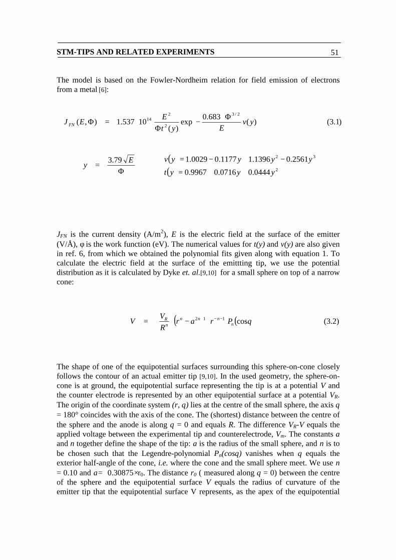
STM-TIPS AND RELATED EXPERIMENTS 51
The model is based on the Fowler-Nordheim relation for field emission of electronsfrom a metal [6]:
JFN is the current density (A/m2), E is the electric field at the surface of the emitter(V/Å), φ is the work function (eV). The numerical values for t(y) and v(y) are also givenin ref. 6, from which we obtained the polynomial fits given along with equation 1. Tocalculate the electric field at the surface of the emittting tip, we use the potentialdistribution as it is calculated by Dyke et. al.[9,10] for a small sphere on top of a narrowcone:
The shape of one of the equipotential surfaces surrounding this sphere-on-cone closelyfollows the contour of an actual emitter tip [9,10]. In the used geometry, the sphere-on-cone is at ground, the equipotential surface representing the tip is at a potential V andthe counter electrode is represented by an other equipotential surface at a potential VR.The origin of the coordinate system (r, θ) lies at the centre of the small sphere, the axis θ= 180° coincides with the axis of the cone. The (shortest) distance between the centre ofthe sphere and the anode is along θ = 0 and equals R. The difference VR-V equals theapplied voltage between the experimental tip and counterelectrode, Vm. The constants aand n together define the shape of the tip: a is the radius of the small sphere, and n is tobe chosen such that the Legendre-polynomial Pn(cosθ) vanishes when θ equals theexterior half-angle of the cone, i.e. where the cone and the small sphere meet. We use n= 0.10 and a= 0.30875⋅ r0. The distance r0 ( measured along θ = 0) between the centreof the sphere and the equipotential surface V equals the radius of curvature of theemitter tip that the equipotential surface V represents, as the apex of the equipotential
)1.3()(683.0
exp)(
10537.1),(2/3
2
214
Φ⋅−
Φ⋅=Φ yv
EytE
EJ FN
Φ= E
y79.3 ( )
( ) 2
32
0444.00716.09967.0
2561.01396.11177.00029.1
yyyt
yyyyv
++=−+−=
( ) ( ) )2.3(cos112 θnnnn
nR Prar
RV
V −−+ ⋅−
=
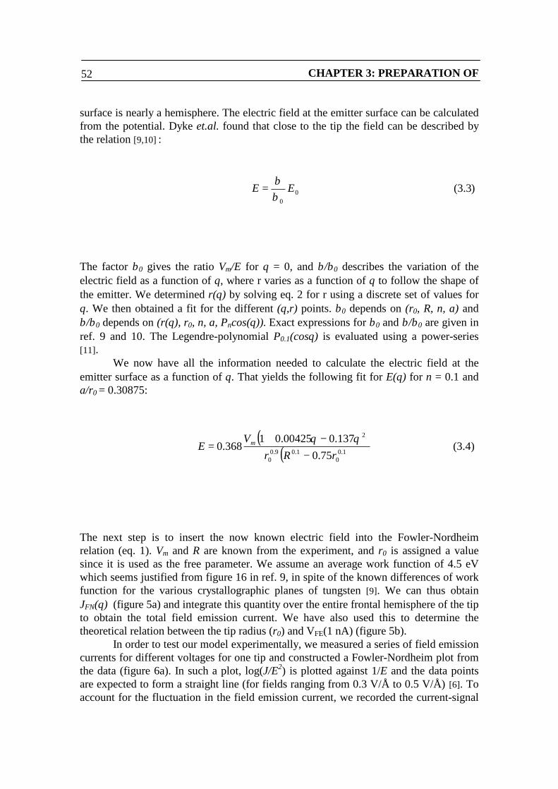
CHAPTER 3: PREPARATION OF52
surface is nearly a hemisphere. The electric field at the emitter surface can be calculatedfrom the potential. Dyke et.al. found that close to the tip the field can be described bythe relation [9,10] :
The factor β0 gives the ratio Vm/E for θ = 0, and β/β0 describes the variation of theelectric field as a function of θ, where r varies as a function of θ to follow the shape ofthe emitter. We determined r(θ) by solving eq. 2 for r using a discrete set of values forθ. We then obtained a fit for the different (θ,r) points. β0 depends on (r0, R, n, a) andβ/β0 depends on (r(θ), r0, n, a, Pncos(θ)). Exact expressions for β0 and β/β0 are given inref. 9 and 10. The Legendre-polynomial P0.1(cosθ) is evaluated using a power-series[11].
We now have all the information needed to calculate the electric field at theemitter surface as a function of θ. That yields the following fit for E(θ) for n = 0.1 and a/r0 = 0.30875:
The next step is to insert the now known electric field into the Fowler-Nordheimrelation (eq. 1). Vm and R are known from the experiment, and r0 is assigned a valuesince it is used as the free parameter. We assume an average work function of 4.5 eVwhich seems justified from figure 16 in ref. 9, in spite of the known differences of workfunction for the various crystallographic planes of tungsten [9]. We can thus obtainJFN(θ) (figure 5a) and integrate this quantity over the entire frontal hemisphere of the tipto obtain the total field emission current. We have also used this to determine thetheoretical relation between the tip radius (r0) and VFE(1 nA) (figure 5b).
In order to test our model experimentally, we measured a series of field emissioncurrents for different voltages for one tip and constructed a Fowler-Nordheim plot fromthe data (figure 6a). In such a plot, log(J/E2) is plotted against 1/E and the data pointsare expected to form a straight line (for fields ranging from 0.3 V/Å to 0.5 V/Å) [6]. Toaccount for the fluctuation in the field emission current, we recorded the current-signal
)3.3(00
EEββ=
( )( ) )4.3(
75.0137.000425.01
368.01.0
01.09.0
0
2
rRrV
E m
−−+= θθ
STM-TIPS AND RELATED EXPERIMENTS 53
to determine the lower and upper bound of the current. These upper and lower bounds ofthe field emission current correspond to the upper and lower ends of the error bars infigure 6a. As the field and current density change as a function of θ, we use E0 and J0 (Eresp. J for θ = 0) to make the Fowler-Nordheim plot. We estimate the experimentalvalue for J0 from:
While making the plot, we have used the tip radius as the free parameter to optimize theagreement between the theoretical and experimental data. As the assumed radius wasvaried, the intersection between the theoretical line and the line formed by theexperimental points shifted from the bottom right for r0 = 17 nm to the upper left for r0
= 20 nm. We therefore estimate the tip radius to be 18 ± 2 nm. This is in goodagreement with the value for the tip-radius that we estimate from the SEM-micrograph(figure 6b) which is 17 ± 5 nm. We have repeated the same field emission experimentfor a tip which was etched from a ⟨111⟩-oriented monocrystal. The fluctuations in thecurrent were less than 5 % for all but one data point, which is much less than is typicalfor polycrystalline tips, so no error-bars are drawn for the monocrystalline tip.
( ) )5.3(2/
0 0
exp0
∫= π
θθd
JJ
IJ
theory
theorymeasured

CHAPTER 3: PREPARATION OF54
Fig. 3.5a: Field emission current density vs.θ as predicted by the model (normalizedso that J(θ = 0) equals 1). Curve (a): I = 1 nA, VFE = 400 V. Curve (b): I = 10 µA,VFE = 689 V. The squares on curve (b) have no other meaning than as a way todistinguish the two curves. Note that for the higher voltage, the current is emittedover a wider area on the tip. The current density vanishes for θ > 60o, meaning thatpractically no current is emitted from the tip shank. The tip radius is 16 nm.b: Theoretical relationship between the tip radius (r0) and field emission voltage.Curve (a): I = 1 nA. Curve (b): I = 1 µA. The squares on curve (b) have no othermeaning than as a way to distinguish the two curves. For three tips, we plotted theexperimental VFE (1 nA) against the tip radius obtained by SEM for comparison. Theleft point (430 V, 1 nA) was generated by the same tip that was used for figure 6. Theother two points come from tips that were etched and heated, but not sputtered.
Electron emission angle: θ

STM-TIPS AND RELATED EXPERIMENTS 55
Fig. 3.6a: Fowler-Nordheim plot taken from a typical STM-tip (squares with error-bars). The estimate for the tip radius is 18 ± 2 nm. We have included the results ofthe same measurement taken from a tip which was etched from a ⟨111⟩-orientedmonocrystal for comparison (diamonds). Radius of the ⟨111⟩-oriented tip was 8 nm.We attribute the deviation of the data point on the far left to the fact that themeasurement may have altered the tip. The point corresponds to the last (I,V) pointtaken, which had the highest applied voltage. b: SEM-micrograph of the same tiptaken ex situ. From the micrograph we estimate the radius to be 17 ± 5 nm(magnification 330.000 times, acceleration voltage 15 kV).
330.000 15 kV 100 nm
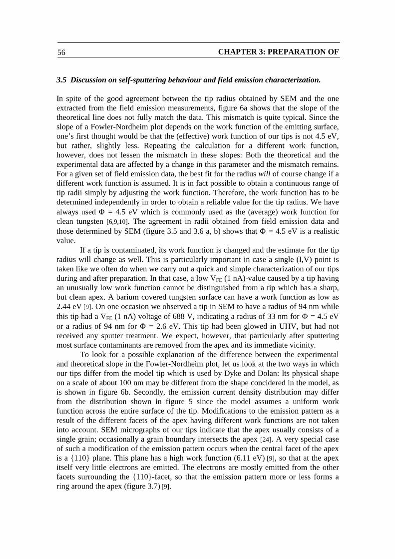
CHAPTER 3: PREPARATION OF56
3.5 Discussion on self-sputtering behaviour and field emission characterization.
In spite of the good agreement between the tip radius obtained by SEM and the oneextracted from the field emission measurements, figure 6a shows that the slope of thetheoretical line does not fully match the data. This mismatch is quite typical. Since theslope of a Fowler-Nordheim plot depends on the work function of the emitting surface,one’s first thought would be that the (effective) work function of our tips is not 4.5 eV,but rather, slightly less. Repeating the calculation for a different work function,however, does not lessen the mismatch in these slopes: Both the theoretical and theexperimental data are affected by a change in this parameter and the mismatch remains.For a given set of field emission data, the best fit for the radius will of course change if adifferent work function is assumed. It is in fact possible to obtain a continuous range oftip radii simply by adjusting the work function. Therefore, the work function has to bedetermined independently in order to obtain a reliable value for the tip radius. We havealways used Φ = 4.5 eV which is commonly used as the (average) work function forclean tungsten [6,9,10]. The agreement in radii obtained from field emission data andthose determined by SEM (figure 3.5 and 3.6 a, b) shows that Φ = 4.5 eV is a realisticvalue.
If a tip is contaminated, its work function is changed and the estimate for the tipradius will change as well. This is particularly important in case a single (I,V) point istaken like we often do when we carry out a quick and simple characterization of our tipsduring and after preparation. In that case, a low VFE (1 nA)-value caused by a tip havingan unusually low work function cannot be distinguished from a tip which has a sharp,but clean apex. A barium covered tungsten surface can have a work function as low as2.44 eV [9]. On one occasion we observed a tip in SEM to have a radius of 94 nm whilethis tip had a VFE (1 nA) voltage of 688 V, indicating a radius of 33 nm for Φ = 4.5 eVor a radius of 94 nm for Φ = 2.6 eV. This tip had been glowed in UHV, but had notreceived any sputter treatment. We expect, however, that particularly after sputteringmost surface contaminants are removed from the apex and its immediate vicinity.
To look for a possible explanation of the difference between the experimentaland theoretical slope in the Fowler-Nordheim plot, let us look at the two ways in whichour tips differ from the model tip which is used by Dyke and Dolan: Its physical shapeon a scale of about 100 nm may be different from the shape concidered in the model, asis shown in figure 6b. Secondly, the emission current density distribution may differfrom the distribution shown in figure 5 since the model assumes a uniform workfunction across the entire surface of the tip. Modifications to the emission pattern as aresult of the different facets of the apex having different work functions are not takeninto account. SEM micrographs of our tips indicate that the apex usually consists of asingle grain; occasionally a grain boundary intersects the apex [24]. A very special caseof such a modification of the emission pattern occurs when the central facet of the apexis a 110 plane. This plane has a high work function (6.11 eV) [9], so that at the apexitself very little electrons are emitted. The electrons are mostly emitted from the otherfacets surrounding the 110-facet, so that the emission pattern more or less forms aring around the apex (figure 3.7) [9].
STM-TIPS AND RELATED EXPERIMENTS 57
This geometry could be quite common as the process of wire drawing induces apreferential orientation of the crystal-grains along the wire-axis [12]. In bcc metals liketungsten, this is the ⟨110⟩ direction [12]. At the same time, the crystals become thin andelongated with the long axis parallel to the wire axis. Since the polycrystalline,nominally unoriented tungsten wire that we use is drawn through holes (“dies”) to thin itdown to size [7,13], we expect that the crystal grains in the wire are oriented with the⟨110⟩ direction along the wire axis, causing the central facet of the tip to be a 110-facet. The thin, fibre like structure expected for such wires we have also observed bystudying the fracture surface of a split tungsten wire by optical microscope. We wouldlike to emphasize that the wire we use is commercially available, standard tungstenwire. If one orders polycrystalline tungsten wire of a given diameter without any furtherspecifications, this is the type of wire one is likely to get.
For all our tips, the circumstances of wire production have been the same as theyhave all come from the same roll of tungsten wire. This orientation leads to a fieldemission current density distribution which is significantly different from the onepredicted by the model. For this reason, we suspect that the mismatch between thetheoretical and the experimental slope is caused by it. Moreover, since all our tips havecome from the same wire, this could also explain why this mismatch occurs with thehigh reproducibility that we have observed. If the mismatch were to be caused by theshape of the tip, we would expect more variation in the mismatch. This notion is alsosupported by the fact that the mismatch does not occur in the Fowler-Nordheim plot thatwe took from a ⟨111⟩ oriented monocrystalline tip, which has an emission pattern thatagrees much better to the pattern assumed in the model [14]. The mismatch that we justdiscussed still allows us to estimate the tip radius from the field emission measurementsas figures 3.5 and 3.6 show. We have also found that the VFE (1 nA) voltage is a goodindicator of a tip’s performance in STM.
The formation of the “neck and head” which leads to the decapitation duringsputtering can be caused by one of several mechanisms, three of which are mentioned bySchiller et al. and references therein: 1) The density of impinging ions is larger on theshank, 2) the ions strike the tip surface at an angle instead of perpendicularly, whichgives them a higher sputtering yield, and 3) the high-index planes making up the sidesof the ⟨111⟩ oriented monocrystal used by Schiller et.al. are preferentially sputtered [1].
In case polycrystalline wire is used which is oriented with a ⟨110⟩ direction alongthe wire axis, most of the electrons will be emitted from a ring just behind the apex.Such an orientation can be either intentional or the accidental result of of thinning downthe wire. The density of impinging ions will then also be highest in that area of the tip,which could easily cause a neck and head structure to form. At this point, we have noindication as to which of these mechanisms should be dominant. The ring-like emissionpattern of a ⟨110⟩ oriented wire can certainly cause a neck and head to form duringsputtering, but the results from Schiller et al. show that a ring-like electron emissionpattern is no necessary condition for the decapitation process to occur.
CHAPTER 3: PREPARATION OF58
We have no clear ideas about the mechanism that connects the formation of the neck-and-head structure to the decrease of the noise in the sputter voltage. The results that wepresent in figures 3.2 and 3.4 merely show that the two effects accompany each other,not why this is the case. As already stated in the previous section, the field emissionvoltage signal from the ⟨111⟩-oriented monocrystalline tip showed remarably little noisein comparison to the field emission voltage of a polycrystalline tip. Possibly, the amountof noise in the field emission voltage signal depends on which of the crysstallographicplanes making up the apex emits (most of) the current, or on the geometry of theemission pattern. An emission pattern which is unstable as a function of time could wellbe a cause for noise in the field emission voltage. One might suspect that the emssionpattern of a ⟨111⟩-oriented tip is more stable than the ring-like emission pattern of a⟨110⟩-oriented tip, but it is at present unknown to us whether this is really the case ornot. It is interesting to note that Schiller et al. report that during the neck-and-headformation, part of the current is emitted from the neck and from the back of the head [1].
Fig 3.7a, b: Field emission microscopy images of a ⟨110⟩-oriented tip and a⟨111⟩-oriented tungsten tip, respectively. c, d: Diagram showing the variousfacets making up the apex for the ⟨110⟩-oriented tip and ⟨111⟩-oriented tip(from ref. 14).
cd
a b
STM-TIPS AND RELATED EXPERIMENTS 59
A possible hypothesis is that during the formation of the neck-and-head structure, theemission pattern changes to a more stable configuration due to the presence of the head.In order to clarify the mechanics behind the decapitation process and the accompanyingdecrease in the noise of the sputter voltage, an obvious next step would be to study theemission pattern of a polycrystalline tip by means of a phosphor screen during self-sputtering. Such a test would confirm or disprove our expectation that polycrystallinetungsten wire has a preferential orientation along the ⟨110⟩-axis, it would show whichcrystallographic planes contribute to the total field emission current at different stages ofthe process, and finally, it would indicate if the stability of the emission pattern changesduring the formation of the neck-and-head structure. This experiment, however, liesoutside the capabilities of our set-up.
A final remark to make about the characterization measurements by fieldemission, is that the field emission process and the tunneling process involve differentlength-scales. For the field emission process, the apex as a whole matters, involvingdistances in the order of 10 nm. It may therefore be insensitive to features on the apexthat are of atomic scale, such as two atoms sitting at the very apex instead of one, or anapex with an unusual local density of states. In principle, this can cause discrepanciesbetween the performance of a tip as predicted by field emission measurements and theactual performance of the tip in STM. Although we generally do not observe suchdescrepancies, this point is important to remember when interpreting field emissionresults.
3.6 The occurrence and prevention of vacuum-arcs.
A phenomenon well documented in literature on field emission (microscopy) is thevacuum-arc [9 (p. 122 - 128)]. Several possible causes or initiating factors are listed in ref.9 and references therein. Our experience is that inadequately heated tips are particularlyprone to experience vacuum-arcs, and we therefore regard the mechanism described byBennett [15] as the most plausible explanation for the vacuum-arcs that occasionallyoccur when we prepare tips. The mechanism involves an excess amount of positive ionsthat are generated near the tip apex. As the ions and electrons move in oppositedirections, they have an attractive Lorentz interaction. This can cause the volumethrough which the charge travels between the tip and counterelectrode to contract into avery narrow cylindre. The resulting high current density heats the tip apex which thenemits yet more electrons by thermionic emission. In this runaway process thetemperature of the apex quickly rises to beyond the melting point of the tip material,(partially) melting the apex (see figure 3.8). The occurrence of vacuum-arcs (orpreferably: their absence) is often the factor that limits the success-rate of the self-sputter process. If the wrong experimental procedures are adhered to, persistentlyoccurring vacuum-arcs can decrease the success-rate of the tip preparation procedure toless than 25 %.
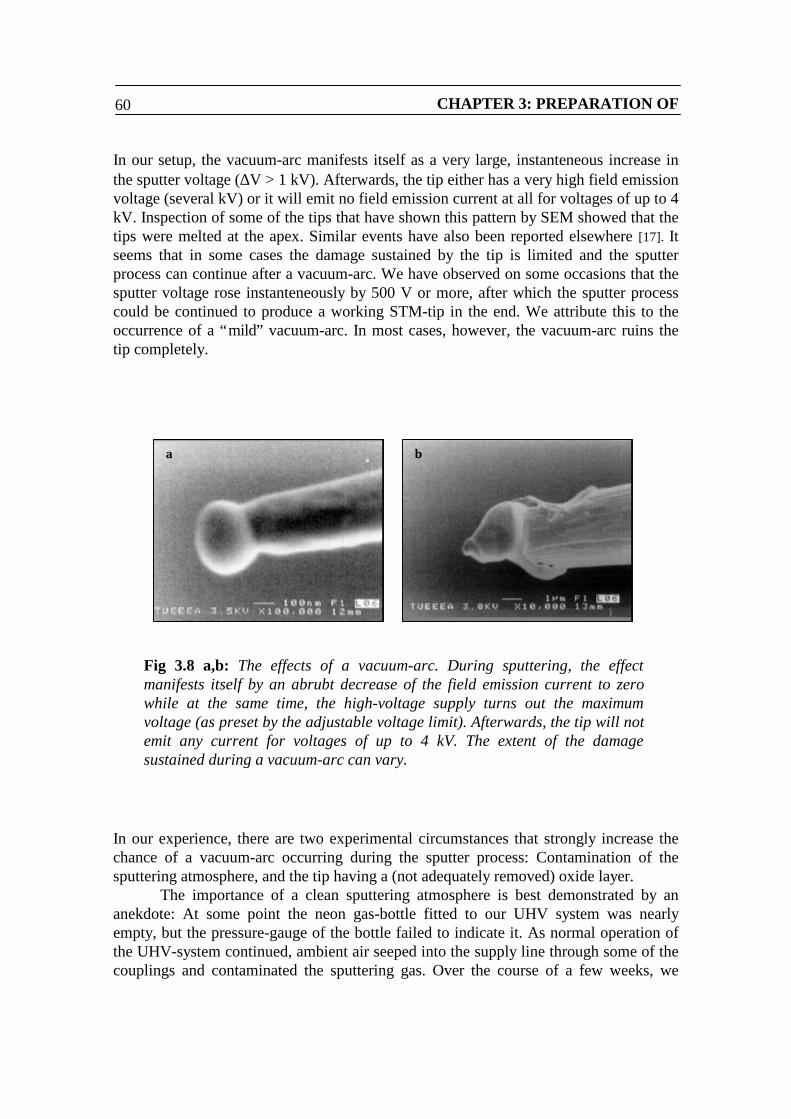
CHAPTER 3: PREPARATION OF60
In our setup, the vacuum-arc manifests itself as a very large, instanteneous increase inthe sputter voltage (∆V > 1 kV). Afterwards, the tip either has a very high field emissionvoltage (several kV) or it will emit no field emission current at all for voltages of up to 4kV. Inspection of some of the tips that have shown this pattern by SEM showed that thetips were melted at the apex. Similar events have also been reported elsewhere [17]. Itseems that in some cases the damage sustained by the tip is limited and the sputterprocess can continue after a vacuum-arc. We have observed on some occasions that thesputter voltage rose instanteneously by 500 V or more, after which the sputter processcould be continued to produce a working STM-tip in the end. We attribute this to theoccurrence of a “mild” vacuum-arc. In most cases, however, the vacuum-arc ruins thetip completely.
In our experience, there are two experimental circumstances that strongly increase thechance of a vacuum-arc occurring during the sputter process: Contamination of thesputtering atmosphere, and the tip having a (not adequately removed) oxide layer.
The importance of a clean sputtering atmosphere is best demonstrated by ananekdote: At some point the neon gas-bottle fitted to our UHV system was nearlyempty, but the pressure-gauge of the bottle failed to indicate it. As normal operation ofthe UHV-system continued, ambient air seeped into the supply line through some of thecouplings and contaminated the sputtering gas. Over the course of a few weeks, we
Fig 3.8 a,b: The effects of a vacuum-arc. During sputtering, the effectmanifests itself by an abrubt decrease of the field emission current to zerowhile at the same time, the high-voltage supply turns out the maximumvoltage (as preset by the adjustable voltage limit). Afterwards, the tip will notemit any current for voltages of up to 4 kV. The extent of the damagesustained during a vacuum-arc can vary.
a b
STM-TIPS AND RELATED EXPERIMENTS 61
observed a very high incidence of vacuum-arcs. The problem was solved by changingthe gas-bottle and heating the supply-line for a few hours while flushing it with neon.
We also find it important to keep the supply line at overpressure (0.6 bar withrespect to the ambient). The fact that it is needed to heat the supply line after it has beenexposed to the ambient (this happens when changing gas bottles or removing the gasbottle during bake-out of the system) suggests that water vapour is involved in theinitiation of vacuum-arcs. An other measure currently in place is that we only initiate thesputtering process when the background pressure of the vacuum chamber is below 2.0 x10⁻⁹ torr.
There are various ways to clean a tip prior to self-sputtering [2,5,17]: When westarted to implement our method of tip preparation, we chose to heat the tips by electronbombardment (see refs 5 and 17 for a description of the method). Vacuum-arcs occurredvery frequently during that time. About 3 out of 4 sputter attempts would end with avacuum-arc. That ended when we adopted the heating method described in Sect. 3.2.We suspect that during the electron bombardment, the tips were not heated enough todesorb the oxide layer completely. Field emission measurements taken before and aftersuch electron bombardment showed that the tip apex generally did not melt significantlyduring the treatment. At the same time, we never observed the apex to glow as has beenreported elsewhere although the effect is difficult to observe [18 (p. 67)].
Heating tips by electron bombardment is a fairly common way to desorb theoxide layer from etched tungsten STM-tips [5,17]. We do not favour this method becauseit is difficult to assess the temperature of the tip during heating and because only theapex is heated [17]. When the tip is pressed against a hot filament for heating, the colourof the tip can be observed easily. This can be used to assess the temperature or to carryout the heating process reproducibly. Also, the tip is cleaned over a wide area, so that noadsorbed contaminants can migrate to the apex after cleaning. A drawback of ourmethod is that positioning the tip against the filament is a bit tricky.
The presence of an oxide layer can be recognized very easily by a specificbehaviour of the tip when characterized by field emission for the first time: As the fieldemission voltage is gradually increased, an oxide covered tip will not show any fieldemission until at a certain voltage, the oxide layer experiences a local voltagebreakdown somewhere on the apex. This manifests itself by a sudden increase of thefield emission current, typically to 10 – 100 nA. After that, the tip shows more or lessstable field emission with VFE (1 nA) significantly below the voltage at which fieldemission first set in. When the voltage is decreased to zero and then gradually increaseda second (or subsequent) time, no such hysteresis is observed. The tip then shows thesame value for VFE (1 nA) as it did after breakdown on the first attempt. The effect isoften accompanied by an unusually low field emission voltage: VFE (1 nA) is about 400V rather than 750 V < VFE (1 nA) < 1200 V which is typical for a clean, unsputtered tip.The latter is possibly due to a decrease in tip work function caused by the oxide layer.At the time that we still heated our tips by electron bombardment, this hysteresis-likefield emission behaviour was very typical for our tips. Presently, we will heat the tip asecond time before attempting to sputter it if we observe the hysteresis effect duringfield emission characterization of the tip.

CHAPTER 3: PREPARATION OF62
The measures that we currently apply to prevent vacuum-arcs, are: 1) We ensureadequate heating of the tip. The temperature of the tip is assessed from its colour whichmust be bright orange. 2) We maintain the neon gas supply line at overpressure. 3) Weheat the supply line for several hours while flushing it with neon whenever the inside ofthe supply line has been exposed to the ambient. 4) We do not initiate the self sputterprocess if the background pressure of the vacuum chamber exceeds 2.0 x 10⁻⁹ torr.These measures seem effective in preventing vacuum-arcs, which we experience onlyoccasionally.
3.7 Comments on the argon-ion bombardment.
Head-on sputtering by Ar+-ion bombardment is a widely used technique to clean andsharpen STM-tips [2,4,17,20]. During such ion-bombardment the sides of the apex aresputtered faster than the apex itself, because ions striking a given surface at an anglehave a higher sputtering yield at a given energy than normally incident ones [4,21,23].The sputtering yield of Ar+-ions on tungsten is for the energies used in our setup in theorder of 1 [22].
For the experimental parameters stated in section 3.2, we estimate that the ionbombardment removes 7 monolayers of tungsten from the tip, assuming that thesputtering yield of the ions equals 1. When a tip is sputtered for a long time, it becomessharper at first, then reaches a point where the apex radius is minimal, after which thetip becomes blunter as sputtering continues. This observation was made when two tipswere sputtered for a prolonged time at 1500 eV and 12 µA/cm2 while the sputteringprocess was periodically interrupted to perform a field emission measurement.Minimum VFE (1 nA) values were 552 V and 474 V, which were attained after 1h 45min
and 1 hour of sputtering time, respectively. When the tips are sputtered with lowerenergies, however, they become sharper. Those tips that we sputter with Ar+-ions inorder to clean them have been observed to have a VFE (1 nA) value of about 250 V (500– 750 eV, 6 – 8 µA/cm2, 1 hour). During subsequent self-sputtering, such tips showquite normal sputtering behaviour. We have at present not tried out a tip in STM thatwas cleaned and sharpened by Ar+-ion bombardment alone, but there is no reason tosuspect that such a tip would not give atomic resolution. We have presently not yet fullyexplored all possibilities for tip preparation by Ar+-ion bombardment, but it seems thation-energies between 0.5 keV and 1.0 keV are well-suited for sharpening tips.
It may seem redundant to equip a UHV-system with both an Ar+-ion gun and asetup for self-sputtering. When the UHV-system was designed, we in fact intended touse the self-sputter process alone. As problems to reliably produce working STM-tipspersisted, the decision was taken to install an ion-gun as an alternative to self-sputtering.By the time the ion-gun was installed, however, our understanding of self-sputtering hadincreased sufficiently in order to use the self-sputter process reliably.
STM-TIPS AND RELATED EXPERIMENTS 63
In hindsight, it has proven very useful to posess both sputter techniques. Theycan be used very well in a complementary fashion, since in both cases the trajectories ofthe incoming ions are quite different. Ref. 14 shows typical ion-trajectories during self-sputtering. The ions from an ion-gun travel in straight, parallel lines. The ion-gun can beused to clean the tip from contaminants over a much wider area than can be treated withthe self sputter process. Especially the very sharp tips [VFE (1 nA < 200 V)] are at timesmechanically unstable, and it is then disirable to have a technique that can make a tipslightly blunter in a controlled way. An advantage of the self-sputter process is itsinherent possibility for characterization, both by dedicated field emission measurementsas well as by observation of anomalities during self-sputtering. Even if only the ion-gunis relied upon to sharpen and clean the tips after etching, the tips still have to becharacterized during and after preparation. As far as we know field emission is by farthe most practical method to do that. When the setup for field emission characterizationis already in place, implementation of the self-sputter process requires very little extraequipment: The hardware needed for characterization is the same as that needed for theself-sputter process, except for a second needle valve and a bottle of neon-gas.
We think that having the two sputter techniques available offers a lot ofpossibility in the field of preparing high-quality STM-tips: As the understanding of thesputter process in general increases with experience, it should in the future be possibleto recognize certain conditions of the tip (presence of oxide layer, whiskers, etc.) fromfield emission measurements or perhaps other simple characterization methods. Thiswould allow to tailor the preparation method to that particular tip, rather than relying ona standard preparation method as we do now. This would further improve the reliabilityof our tip preparation.
3.8 Summary.
In this chapter, the tip preparation method is described. We also describe the researchthat we carried out in relation to the preparation of tips. Our preparation method consistsof four steps: electro-chemical etching, heating, self-sputtering with Ne+-ions andbombardment with Ar+-ions.
The electro-chemical etching is carried out in a similar way as is described in ref.8, p. 283. Heating the tip is accomplished by pressing the tip against a hot filament.Adequate removal of the oxide layer during heating is essential in order to reliably carryout the self-sputter process that follows heating. The self-sputter process has beendescribed earlier by Albrektsen et al. [5] and involves the tip emitting electrons by fieldemission. These electrons ionize the neon atoms that are let in the UHV-chamber, whichin turn sputter the tip. After completion of this process, the apex radius has decreased to7 – 15 nm [200 V < VFE(1 nA) < 400 V]. This is sharp enough to obtain atomicresolution on GaAs-110 and InP-110. Nevertheless, we apply a light Ar+-ionbombardment to the tip in order to make them slightly more stable. We characterize ourtips by field emission measurements and occasionally by SEM. We often regenerate tips
CHAPTER 3: PREPARATION OF64
used in previous measurements by repeating the self-sputter process and ion-bombardment.
We have shown that during our sputter process, the Schiller-decapitation processcan occur [1]. Furthermore, it is accompanied by a highly specific, reproducible patternin the evolution of the sputtering voltage as a function of time. We recognize theoccurrence of the decapitation process from the pattern in the sputter voltage alone, andwe use this to determine the most favourable moment to terminate the self-sputteringprocess, which is immediately after the decapitation process has occurred.
We also present a theoretical model based on field emission from a metalsurface, which allows us to calculate the apex radius of an experimental tips from fieldemission measurements. The results are correct within a margin of 5 nm. A slight, butsystematic deviation between our experimental results and the results predicted by themodel suggests that the tungsten wire that we use posesses a preferential orientationwith its ⟨110⟩-direction along the long axis of the wire. The process of wire-drawing isknown to induce such orientation [12].
We have discussed the phenomenon of vacuum-arcs, which occasionally occurduring self-sputtering and which can ruin a tip. In order to prevent their occurrence, theoxide layer must be adequately removed from the tip and the sputter-gas should be freeof contaminants (neon pressure / background pressure ~ 104). Water vapour appears toplay a role in the initiation of vacuum-arcs.
The Ar+-ion bombardment is meant to make the tips slightly more stable. Wethink that using the self-sputter technique and the Ar+-ion bombardment in acomplementary fashion offers great opportunities to make high-quality STM-tips withhigh reliability. Although our present tip preparation method and success rate are quiteadequate in the for the purposes of our measurements, we lack the understanding tomake full use of the possibilities offered by having both the self-sputter technique andthe ion-gun available.
REFERENCES:
1: Christoph Schiller, Arie Koomans, Theo van Rooy, Christian Schönenberger,Herman Elswijk: Decapitation of tungsten field emitter tips during sputtersharpening. Surface Science Letters, 339 (1995) p. L925 – L930.
2: K.N. Eltsov, V.M Shevlyuga, V.Yu. Yurov, A.V Kivit, M.S. Kogan: Sharptungsten tips prepared for STM study of deep nanostructures in UHV. Physics ofLow Dimensional structures, 9/10 (1996) p. 7 - 14.
STM-TIPS AND RELATED EXPERIMENTS 65
3: Lisa A. Hockett, Stephen E Creager: A convenient method for removing surfaceoxides from W STM tips. Rev. Sci. Instr, 64, (1) Jan 1993 p. 263
4: Joel A. Kubby and Benjamin Siegel: High resolution strucuturing of emitter tipsfor the gaseous field ionization source. Journ. of Vac. Science and TechnologyB4 (1) Jan/Feb 1986. p. 120.
5: O. Albrektsen, H.W.M. Salemink, K.A. Mørch, A.R. Thölen: Reliable tippreparation for high-resolution STM. Journ. of Vac. Sci. and Technology B12(6) Nov/Dec 1994 page 3187
6: A. Modinos: Field, Thermionic, and Secondary Electron Emission Spectroscopy.Plenum Press (New York and London, 1984), p. 13 – 18.
7: Personal communication with manufacturer of our tungsten wire: JohnsonMatthey represented by Alfa, Zeppelinstrasse 7, D-76057 Karlsruhe, Germany.
8: C.J. Chen: Introduction to Scanning Tunneling Microscopy. (Oxford UniversityPress, 1993).
9: W.P. Dyke and W.W. Dolan: Field Emission, in Advances in Electronics andElectron Physics, vol VIII (1956) page 89 – 185. (Academic Press, New York,1956).
10: W.P. Dyke, J.K. Trolan, W.W. Dolan, George Barnes: The Field emitter:Fabrication, Electron microscopy, and Electric Field calculations. Journal ofApplied Physics vol 24, No 5 (May 1953) page 570.
11: W.R. Smythe: Static and Dynamic Electricity. 3rd ed. (McGraw-Hill, New York,1968), p. 157
12: R. Gomer: Field emission and field ionization. (Harvard Univ. Press, 1961), p.45
13: Stephen W.H. Yih, Chen. T. Wang: Tungsten: Sources, Metallurgy, Propertiesand Applications. (Plenum Press, New York and London, 1979) p. 209-222
14: J.Y. Cavaille and M. Drechsler: Ion impact on field emitter crystals. Revue dePhysique Appliquée, TOME 12, octobre 1977, p. 1631.
15: W.H. Bennet: Magnetically self-focusing streams. Physical Review, Vol. 45(1933) p. 890
CHAPTER 3: PREPARATION OF66
16: De Raad, Koenraad, Wolter: Use of the Schiller-decapitation process for themanufacture of high-qualtity tungsten STM tips. Journal of Vac. Sci. and Tech.-B, Vol. 17, No. 5, pp. 1946 – 1953 (1999).
17: I. Ekvall, E. Wahlström, D. Claesson, H. Olin, E. Olsson: Preparation andcharacterization of electrochemically etched tungsten tips for STM. Meas. Sci.Technol. 10 (1999), p. 11 – 18.
18: O. Albrektsen: Scanning Tunneling Microscopy and Spectroscopy on III-Vsemiconductors and their interfaces. Phd-thesis presented by O. Albrektsen,Laboratory of Applied Physics (LTF), Danish University of Technology, Lyngby,Denmark (1990).
19: Personal communication with ir. R.J. Bruls, Technical University of Eindhoven(Chemistry dept.).
20: M.A. Rosentreter, M. Wenderoth, N.H. Theuerkrauf, A.J. Heinrich, M.A.Schneider, R.G. Ulbrich: Nonequilibrium configurations of monoatomic steps oncleaved GaAs (110) surfaces. Phys. Rev. B, Vol. 56, No. 16, pp. 10538 – 10543.
21: H. Oechsner: Untersuchungen zur Festkörperzerstäubung bei schiefwinkligemIonenbeschuβ polykristalliner Metalloberflächen im Energiebereich um 1 keV.Z. Physik, 261, 37 – 58 (1973).
22: H.H. Andersen and H.L. Bay : Sputtering yield measurements, in Sputtering byparticle bombardment I, edited by R. Behrisch, Springer Verlag, Berlin, 1981, p.184.
23: This is the general trend. When the incident ions strike the surface of amonocyrstal parrallel to certain crystal directions, the sputtering yield maydeviate. See “Sputtering yields of single cyrstalline targets” by H.E. Roosendaal,in Sputtering by particle bombardment I, edited by R. Behrisch, Springer Verlag,Berlin, 1981, p. 220.
24: The presence of a grain boundary intersecting the surface near the apex can causea “split tip”. Such grain boundaries have a rough surface morphology, whichdecreases the workfunction (see ref. 9, p. 116). As the grain boundary ispreferentially sputtered, two adjacent microtips are formed. We have observedsuch tips in SEM occasionally. The effect seems not to degrade the performanceof the tip in STM, possibly because one microtip is always a little closer to thesurface than the other.
25: The colour should be a little brighter than that of a sodium street-light.
67
CHAPTER 4:
TUNEABILITY OF THE SURFACE-CORRUGATION ONGaAs (110) SURFACES: THE PRECISE ROLE OF TIP-
INDUCED BAND BENDING
4.1 Introduction
As was shown by Ebert et al. [1] for GaAs, GaP and InP, the apparent direction of theatomic rows on the (110)-surfaces of these materials can change from the [-110]direction to the [001] direction as a function of applied bias voltage, when imaged byatomically resolved Scanning Tunneling Microscopy (STM). The (110)-surface of thesesemiconductors is made up of zig-zag rows of alternating anions and cations extendingalong [-110] (figure 4.1a). It was shown that the apparent direction of the atomic rows isgoverned by different surface states contributing in varying relative amounts to the totaltunneling current. These states have a different location and spatial extent within thesurface unit cell. When the relative contributions of these states to the total tunnelingcurrent change, so does the appearance of the surface in atomically resolved STM.
Exactly which of the surface states contributes to the total tunneling currentdepends on the applied bias voltage, as well as on the amount of tip-induced bandbending (TIBB). The influence of TIBB was already demonstrated qualitatively byJiang et al. [2] who observed local changes in the atomic corrugation around Ag nano-clusters deposited on a GaAs (110) surface. In order to understand the voltage-dependent changes in atomically resolved STM-images of GaAs (110), knowledge ofthe electronic structure of the surface and information about the amount of TIBB as afunction of applied bias voltage, are both essential. To obtain the latter, we calculate theamount of tip-induced band bending from a one-dimensional model.
In the energetic range accessible with STM, the surface-density of states (DOS)of these surfaces is dominated by four states (A5, A4, C3 and C4) [1,3,4]. For therelaxed, free InP (110)-surface Ebert et.al. identify the following energy ranges for thestates with respect to the valence band maximum (VBM): A5: 0 eV to –0.95 eV, A4:-0.95 eV to –1.77 eV, C3: 0 to +2.27 eV, C4: +2.27 eV to 2.81 eV. These same stateswith similar energetic location are also found on GaAs (110) [3]. The surface-DOS ofInP has recently been described in great detail by Engels et al. [4]. The A5 and A4 statesare both localized on the anions and extend along [-110]. The A5 state has a danglingbond character and the A4 state is a back-bond state [1,4]. The C3 state is localized onthe cations and extends along the [001] direction [1,4]. The state is an empty danglingbond with pz character [4]. The state commonly designated as C4 in reality consists ofseveral empty surface resonances with different spatial extent and slightly differentenergetic location [4]. Close to the surface (2.23 a0 = 1.1 Å from the outwardly rotated P

CHAPTER 4: TUNEABILITY OF THE68
atoms), the C4 state is localized on both the cations and anions and appears as a zig-zagrow. Further away from the surface (6.53 a0 from the surface anion) the state shows asmaxima centered on the cations extending along [-110] [1,4]. Refs. 1 and 4 also showthat if both the C3 and C4 states contribute to the tunneling current, the C4 state willdominate in the STM-image. Consequently, the atomic rows will appear to run along[001] if the contribution from the C3 state dominates the tunneling current. If any of theother states dominates, the rows will appear to run along [-110]. In intermediate cases,the image will show clear atomic corrugation in both directions.
Fig. 4.1a: Relaxed GaAs-(110) surface (top view). b: Side view. c: Energeticlocation of the four most important surface states. C4: CBM + 1.1 eV, C3: CBM+ 0.6 eV, A5: VBM – 0.6 eV, A4: VBM – 1.3 eV (From refs. 1 and 2).
c
5.56 Å
4.0 Å
VBM CBM
SURFACE-CORRUGATION ON GaAs (110) SURFACES 69
Another important point to note is that, although no surface state on the GaAs (110) iscentered inside the bulk bandgap, the shoulder of the unoccupied surface states doesextend into the bandgap [4,5]. Chelikowski had already noted that the bottom of the“empty cation derived surface band” had its localization along the ⟨001⟩ bulk directionand showed that the onset of this surface band lies at about 0.7 eV below theConduction Band Minimum (CBM) [5]. However, the portion of the surface-DOS lyingwithin the bulk bandgap does not extend very far into the vacuum: At 6.53 a0 from therelaxed anions, the integrated local surface-DOS shows no sign of a shoulder extendinginto the bandgap any more [4].
Atomic resolution on semiconductor surfaces is usually understood in terms ofelectrons tunneling directly into or out of surface states. The STM-images are thenessentially microscopic maps that show the lateral variation in intensity of the DOSassociated with (combinations of) the surface states (Tersoff-Hamann theory) [6]. In thisview, only those states that lie energetically between the TFL and SFL are available tothe tunneling process. Another important point in this theory is that the tunneling matrixelement is proportional to the local sample surface DOS evaluated at the position of thecentre of the tip apex atom [7]: The STM-image shows the vacuum-tails of the surfacestates. A direct consequence is that in the framework of the Tersoff-Hamann theory,features in the sample-DOS that lie within the surface layer do not appear in the STM-image. This is the way in which most often, atomic resolution on semiconductorsurfaces is understood. We will refer to this process as “regular tunneling” (see section1.10).
Ebert et al. reported that the change in the direction of atomic corrugation wasmost apparent when imaging the empty states on n-doped material [1]. When imaging p-doped material in filled states mode, no dramatic changes in atomic corrugation werereported. In this paper, we report voltage-dependent changes for the GaAs (110) surfacefor both p-type and n-type material, for both polarities of the applied bias voltage. Wewill show that these changes can be understood when the electro-static band bendinginduced by the electric field between tip and sample is taken into full account. We willalso demonstrate that some of the voltage-dependent changes cannot be understood ifonly the four surface states of the GaAs (110) surface are considered: When imaging p-GaAs at small negative bias voltage, the electrons tunnel from bulk states near the topof the valence band, through a depletion zone several nm wide, to the tip. In this voltageregime, all of the four surface states lie outside the energetic window between the tipFermi level and the sample Fermi level which defines the interval of tip-DOS andsample-DOS available to the tunneling process. In spite of that, we observe anatomically resolved STM-image for such voltages that is similar in appearance to thelateral distribution of the A5 state. When imaging n-type GaAs at small positivevoltage, we can observe the lateral distribution of the low energy shoulder of the C3state as electrons tunnel resonantly through this shoulder into the bulk states near thebottom of the conduction band.

CHAPTER 4: TUNEABILITY OF THE70
4.2 Experimental
The STM-work was performed in UHV (OMICRON STM-1 setup operated at 4 * 10-11
torr) on in situ cleaved GaAs samples. Doping concentrations were 1018 cm-3 Si for n-doped material (n-doped substrate) and 1018 cm-3 Be for p-doped material (1 µm thickMBE-grown layer on p-doped substrate). Our tips are etched electrochemically from ø0.25 mm polycrystalline tungsten wire. After heating, Ne+-ion self-sputtering andbombardment by Ar+ ion-gun, our tips routinely yield atomic resolution on GaAs/InP(110) (apex radius ~10 nm) [8] (see also chapter 3). The bias voltage is applied to thesample. Our STM-setup is equipped with a “dual mode” feature, which enables us toapply one set of scan parameters (bias voltage, tunneling current, feedback parameter)on the forward scan and another set of parameters on the backward one. We can thusimage a given area of sample simultaneously for two different sets of parameters. Allimages shown in this chapter are height-images [z(x,y)] that were obtained whileoperating the STM in constant current mode.
Changes in the atomic corrugation are commonly expressed as the ratio ofcorrugation amplitudes along the [-110] and [001] directions [1]. We deviate from that,as changes in the appearance of the lattice occur not only as changes in the corrugationamplitude along a given axis, but also as changes in the spatial extent of the maxima. Toour opinion, a number that is sensitive to both effects is then more appropriate. Our“corrugation number” (CN) is calculated from two line profiles, which are taken along[-110] and [001], respectively, and which both pass through the atomic maxima of theimage. We calculate the average height along both profiles. The difference in averageheight is divided by the corrugation amplitude along either [-110] or [001], whicheveris largest. The resulting CN lies between –0.5 and 0.5, corresponding to a corrugationappearing as straight, parallel lines along [-110] for CN = +0.5, and to one appearing asstraight, parallel lines along [001] for CN = -0.5. A CN close to zero corresponds to aclearly resolved atomic corrugation in both directions.
During high-resolution STM, tip changes which alter the appearance of theatomically resolved lattice are a common occurrence. Such changes are easilyrecognized as a sudden and spontaneous change in apparent corrugation and tip-sampleseparation. If during the acquisition of a series of voltage-dependent images (onecolumn in figure 4.4) a tip-change is observed to irreversibly change the corrugation, weonly compare those images that were recorded either before or after the tip change inorder to ensure that only those images are compared that were recorded while the tiphad the same tip-DOS. Another way to verify that the changes in atomic morphologyare not influenced by a change in the tip-DOS during the measurement, is to record areference image at some fixed voltage at regular intervals during the measurement, oron the backward leg of the tip motion while operating the STM in dual mode. A tip-change will manifest itself as a change in the reference image.
In practice, tip changes do not present much of a problem. A good tip usuallyyields stable and reproducible images throughout most of the intended voltage region.Most of the tip changes occur near the extremities of the intended voltage range whereeither the tip-sample distance becomes small or the electric field between the tip andsample becomes large. If a tip is observed to yield unstable images, it is exchanged for
SURFACE-CORRUGATION ON GaAs (110) SURFACES 71
another one. By choosing the temporal order in which the images are recorded sensibly,one can avoid the event that an unfortunate tip-change renders one half of the imageswithin a measurement incomparable to the other. In many cases, a tip-change causes a(slight) shift in the voltage at which the change in atomic corrugation occurs. Thegeneral trends usually remain the same.
As an aid in the interpretation of the results, we also calculated the amount ofTIBB (φ) and the tunneling current (IT) for GaAs/AlxGa(1-x)As surfaces duringtunneling. Main parameters are bias voltage (V), tip-sample distance (z), tip workfunction (WTIP), sample surface electron affinity (χ), bulk doping level (ND, NA),aluminum concentration (set 0 for GaAs), and density and energetic distribution ofsurface states. It is a one-dimensional model, which only describes the tunnelingjunction in the direction perpendicular to the sample surface (z-axis). It is based on themodel presented by Feenstra et al. [9].
Based on a given bias voltage and tip-sample distance, the model calculates theamount of TIBB and the length over which the band bending extends into thesemiconductor surface. Based on the tip work function and sample electron affinity, theentire potential profile can then be constructed. To calculate the potential profile, thePoisson-equation is solved under the constraint that the potential-gradient (electric field)be continuous throughout the region of interest. The resulting potential profile has atrapezoidal shape in the vacuum barrier. To account for effects due to the image charge,the (z-dependent) image potential felt by an electron between two metal plates issubtracted from the calculated potential in the vacuum barrier. In our model, the image-charge lowers the potential barrier but does not affect the amount of TIBB in thesemiconductor. Then the tunneling probability as a function of energy is calculated andintegrated over the energy-window between the tip- and sample Fermi level. Thetunneling probability is calculated using the Tersoff-Hamann theory [6,7], therebyimplicitely assuming an s-like tip-state. The resulting tunneling current density ismultiplied by a fictitious “tip surface” which we have set at 10 x 10 Å to obtain the totaltunneling current. Part of the tunneling current is generated by electrons tunneling frombulk valence band (BVB) states or into bulk conduction band (BCB) states. Theseelectrons tunnel through the vacuum barrier and the depletion layer near thesemiconductor surface. The contributions from the BVB states and BCB states arecalculated by our model in the same way as in ref. 9 (see figure 4.2).
Most important “unknowns” affecting the model calculations are the absolutetip-sample distance, tip work function and the tip-state involved in tunneling. Thedensities of surface states are assumed constant (4.42 * 1014/cm2). We have assumed a1 eV wide surface states band extending from the CBM up into the conduction band,and a 1 eV wide surface states band extending from the VBM down into the valenceband.
In the depletion regime, screening is provided by ionized dopants which aredistributed homogeneously throughout the sample material. Solving the Poisson-equation is then quite straightforward, leading to a parabolic potential-profile. When thesample surface is in accumulation or inversion, screening is provided by accumulatedmajority or minority carriers, respectively. In these two regimes, the charge density nearthe surface is determined by the 3-dimensional (3-D) densities of states of theconduction- and valence band of the semiconductor. This allows for higher charge-
CHAPTER 4: TUNEABILITY OF THE72
densities near the surface than in the case of depletion, causing relatively little TIBBwhen the surface is in accumulation, and causing the amount of TIBB to level off whenthe regime of depletion has been passed and inversion sets in. Our model results are ingood agreement with the results obtained by Feenstra for TIBB [9]. Only at large voltage(-2.5 V and +2.5 V) a deviation from Feenstra’s results is apparent since our modelincludes the influence of the two surface-states bands. When these two bands are leftout, the model accurately reproduces Feenstra’s results.
It should be noted that the shoulder of the conduction band surface states whichextends into the bandgap has an influence on TIBB: The occupation or depopulation ofsurface state shoulder provides the surface with an additional screening mechanism.This is not considered in neither our own model nor that of Feenstra’s. To assess theimportance of this mechanism, we calculated TIBB for p-GaAs with a surface statesband (4.42 * 1014 cm-2) extending from CBM - 0.5 eV to CBM + 0.5 eV. This simulatesa surface states band that is partly resonant with the conduction band, and which partlyextends into the bandgap. We compared the results with those obtained for “normal” p-GaAs, in which the surface states band extends from the CBM to CBM + 1.0 eV. Forboth cases, simulated sample voltage was –0.9 V, and the tip-sample distance wasoptimized to obtain a calculated current of 55 pA. The presence of a surface donor bandwhich extends partly into the bandgap decreases TIBB from –1202 meV to –1127 meV,confirming that this mechanism has no significant effect on TIBB. For the rest of thischapter we will ignore this screening mechanism.
As a result of some of the incertainties in the model (tip state, absolute tip-sample distance, relation between calculated tunneling current density and total currentemitted by a real tip), a direct, quantitative agreement between the model and ourexperiments cannot always be obtained. The main feature of the model is that itcalculates band bending realistically. In this work, we use the model to calculate theeffects of TIBB as a function of bias voltage, while varying the tip-sample distance atthe same time to maintain an in principle arbitrary, but constant tunneling current foreach of the different bias voltages.

SURFACE-CORRUGATION ON GaAs (110) SURFACES 73
Fig. 4.2a: Definition of the various constants used in the model. The dotted lineindicates the potential inside the vacuum-barrier when the image-charge is takeninto account. This is the potential barrier used to calculate the tunneling current.The two bands of surface states are also indicated. b: Calculated TIBB for n-GaAsand p-GaAs for a fixed tip-sample distance (9 Å).
BVB
BCB
Position (Å)
Energy (eV)
Vacuum levelTip work function (eV)
Electron affinity (eV)
TIBB (eV)
z
Eg (eV)
CBM
VBM
SFL
TFL
a
b
CHAPTER 4: TUNEABILITY OF THE74
4.3 STM: Corrugation-change on n-GaAs and p-GaAs-(110)
We now present voltage-dependent images of p-GaAs and n-GaAs (110), which showclear changes in the apparent direction of the atomic rows as the bias voltage ischanged. We have also expressed the changes in terms of the corrugation number (CN)defined in section 4.2 (figure 5). On p-type material, the corrugation change is onlypartial: For large bias voltage of either polarity, the corrugation is in the [001]-direction(CN > 0, atomic rows are along [-110]). At intermediate voltage, there is a mixedcorrugation. This is also reflected by the CN which close to zero at these voltages. Atsmall voltage, the corrugation is again in the [001]-direction, similar to the corrugationobserved for large voltage. On n-type GaAs there is a complete change in the directionof atomic rows: For large voltage the corrugation is in the [001]-direction, and for smallvoltage it is in the [-110]-direction. We have not observed significant differencesbetween the empty states frames obtained at small tunneling current (50 pA), and thoseaquired using a larger current (254 pA). When using tunneling currents in the range of50 – 75 pA, we have repeatedly observed that the resolution gradually deteriorates for V> +1.5 V. The reason for this is that as the bias voltage increases, so does the tip-sampledistance. With that, the apparent height of the atomic corrugation decreases, until atsome point, the corrugation is lost in the background noise. This problem was solved bychoosing the larger tunneling current (254 pA). On one occasion while using a smalltunneling current, we have observed that the corrugation-change reverses for very lowvoltage (figure 4.4: n-GaAs, I = 50 pA, V = +0.346 V and V = +0.305 V; figure 4.5 b:open circles with dark rim). We present this as an interesting, but non-typical result thatwe will discuss later in this chapter.
Another feature of the empty-states results on n-GaAs is that we switched fromone value for the applied bias voltage to the next one shortly after the start of a newframe, rather than between consecutive frames as was done for the other STM-images(see figure 4.3b). By including the transition from one value of the applied bias voltageto the next, we can observe shifts in the position of the atomic maxima, should theseoccur. From the changes in the tip-sample distance (see figure 4.3a) we can calculatethe quantity |dz/dV|. We will show later in this chapter that the value of |dz/dV| canchange dramatically as a function of applied bias voltage, and that from these changesconclusions may be drawn about the amount of TIBB as a function of applied biasvoltage.

SURFACE-CORRUGATION ON GaAs (110) SURFACES 75
Fig. 4.3a:.Height-profile taken along [-110] (see black line in figure 4.3 b).From the change in apparent height and the voltage difference between theupper and lower parts, |dz/dV| is calculated. b: Typical STM-image of n-GaAs:Applied bias voltage: 0.879 V -> 0.817 V , I = 254 pA. Frame size: 20 x 20 nm,gray scale 0 - 120 pm. The corrugation numbers and representative frames infigures 4.4 and 4.5 are obtained from cut-outs (white rectangle). The horizontalstripes in the image are caused by noise. On the cut-out we apply a backgroundcorrection on each individual (horizontal) scan-line
+ 0.879 V
+ 0.819 V
a
b
∆V
∆z
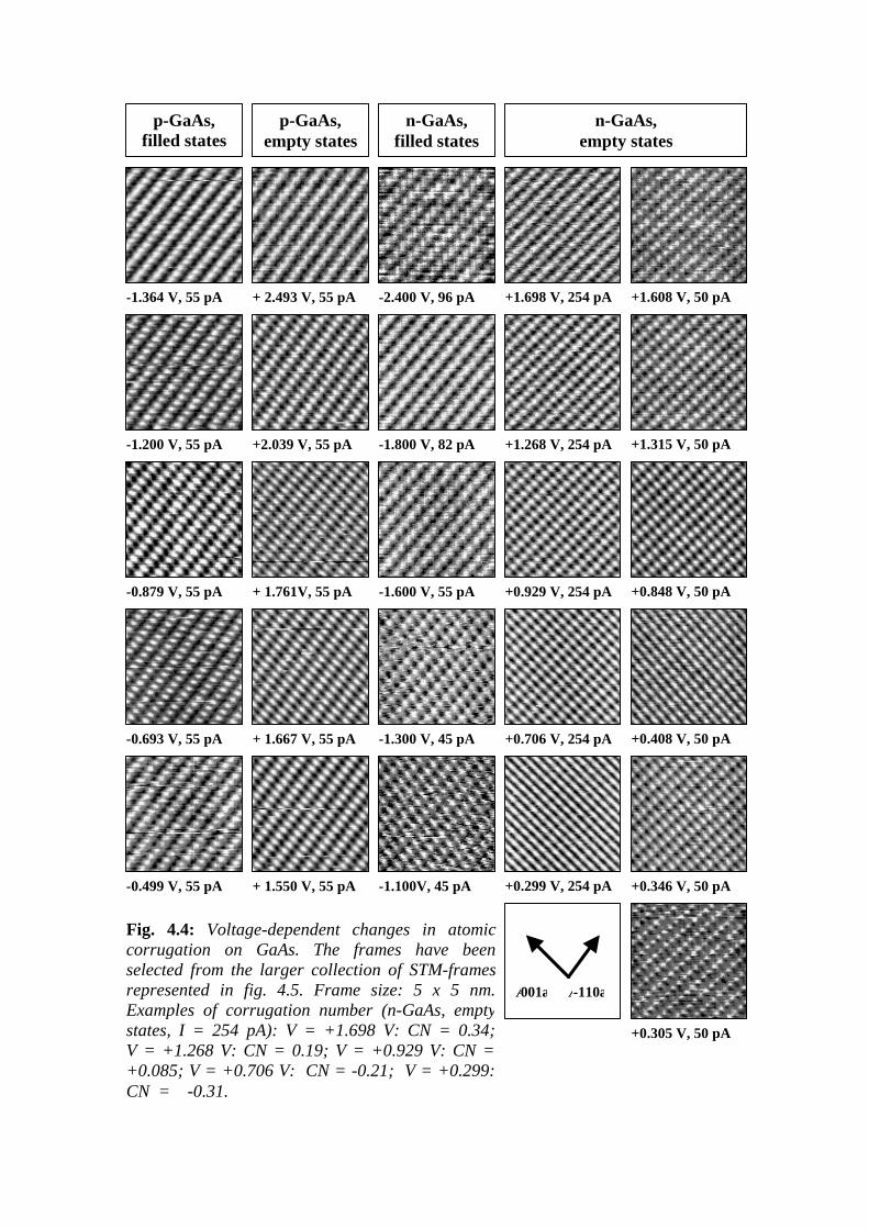
CHAPTER 4: TUNEABILITY OF THE76 p-GaAs,filled states
-1.364 V, 55 pA
-1.200 V, 55 pA
-0.879 V, 55 pA
-0.693 V, 55 pA
-0.499 V, 55 pA
p-GaAs,empty states
+ 2.493 V, 55 pA
+2.039 V, 55 pA
+ 1.761V, 55 pA
+ 1.550 V, 55 pA
n-GaAs,filled states
n-GaAs,empty states
-2.400 V, 96 pA
-1.800 V, 82 pA
-1.600 V, 55 pA
-1.300 V, 45 pA
-1.100V, 45 pA
⟨001⟩ ⟨-110⟩
+ 1.667 V, 55 pA
+0.299 V, 254 pApA pA
+0.706 V, 254 pA
+0.929 V, 254 pA
+1.268 V, 254 pAA
+1.698 V, 254 pApA pA
Fig. 4.4: Voltage-dependent changes in atomiccorrugation on GaAs. The frames have beenselected from the larger collection of STM-framesrepresented in fig. 4.5. Frame size: 5 x 5 nm.Examples of corrugation number (n-GaAs, emptystates, I = 254 pA): V = +1.698 V: CN = 0.34;V = +1.268 V: CN = 0.19; V = +0.929 V: CN =+0.085; V = +0.706 V: CN = -0.21; V = +0.299:CN = -0.31.
+1.608 V, 50 pApA pA
+1.315 V, 50 pApA pA
+0.848 V, 50 pApA pA
+0.408 V, 50 pApA pA
+0.346 V, 50 pA A pA
+0.305 V, 50 pApApA
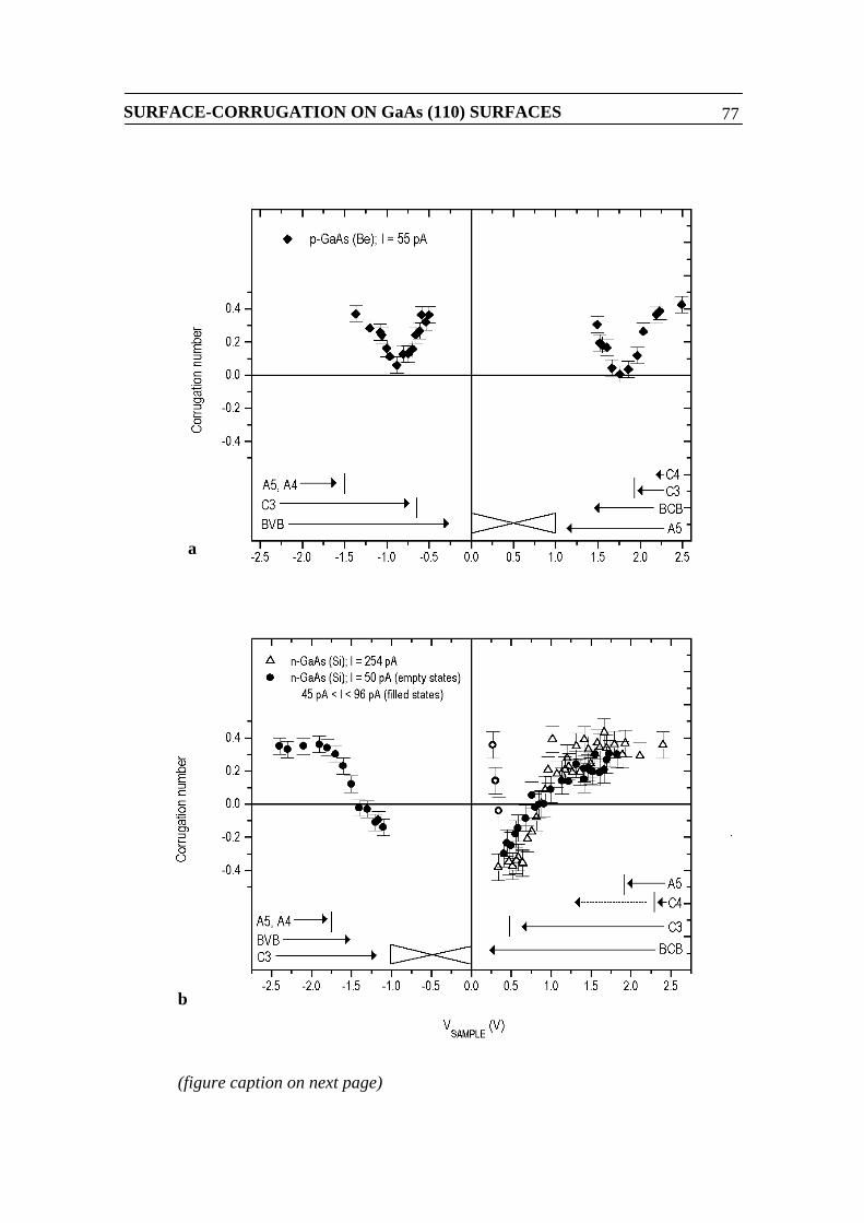
SURFACE-CORRUGATION ON GaAs (110) SURFACES 77
a
(figure caption on next page)
b
CHAPTER 4: TUNEABILITY OF THE78
4.4 Model results: Different scenarios of band bending
Tip-Induced Band Bending (TIBB) is the main factor that determines which of thesurface states contributes to the tunneling current at a given bias voltage, and therebydetermines the appearance of the atomic corrugation. For this reason we have used ourmodel to calculate the amount of TIBB, given the bias voltages that we applied in ourexperiments. We have chosen the tip-sample distances in such a way that the totaltunneling current calculated by the model equals the currents used in (most of) ourmeasurements. In our discussions, we use an absolute scale for the applied bias voltage(-2 V > -1 V). The commonly used value of the (average) work function of polycrystallinetungsten is 4.5 eV [10]. However, the different crystal facets of tungsten are known topossess different work functions, varying between 4.3 eV (116) [10,11] and 5.22 eV(110) [11]. We have reasons to suspect that the polycrystalline wire from which wefabricate our tips, has a preferential orientation along ⟨110⟩, which could be a cause fora higher work function than the value used in the model [8]. On the other hand, acontamination near the apex of the tip could well lower the work function. Also, a roughmorphology of the surface is known to decrease the work function [10,12], suggestingthat for a tip apex, the work function is inherently reduced. The assumption of a tipwork function different from the average value of tungsten is therefore not at allunrealistic. As a working hypothesis, we assume that the work function of our tipsusually lies between 4.0 and 4.6 eV.
From figure 4.2 can be seen that an increase (decrease) in tip workfunction willbend the bands of the semiconductor upwards (downwards). To illustrate the verystrong influence that the tip work function has on the band bending behaviour, we showthe calculated amount of TIBB for several tip work functions (4.45 eV and 4.6 eV for p-GaAs and 4.3 eV, 4.35 eV, and 4.6 eV for n-GaAs). Other parameters, such as the tip-sample distance (chosen tunneling current) and the doping concentration also have aninfluence. However, in the simulations, the influence of the tip work function is muchstronger than the influence of the chosen value for the tunneling current. We do not vary
Fig. 4.5 (preceeding page) a: Corrugation number (CN) for p-GaAs. Each pointrepresents one STM-frame. The arrows represent the voltage-intervals over which weexpect contributions from the various surface states (see details in section 4.5). b: CNfor n-GaAs. At low positive voltage, three a-typical data points are plotted (opencircles). These are discussed in sect. 4.5. The arrows represent the voltage-intervalsfor which we expect contributions from the various surface-states. The dotted linewhich is drawn to show the contribution of the C4 state (empty states) signifies that atthese voltages, we expect the contribution to be from the low-energy shoulder of theC4 state (see further details in sect. 4.5).
SURFACE-CORRUGATION ON GaAs (110) SURFACES 79
the doping concentration in our simulations since the doping concentration of a givensample is usually known in an experiment [13].
The quantity plotted in figures 4.6 and 4.7 is the amount of TIBB relative to theSample Fermi Level (SFL). The amount of TIBB is indicated by the solid symbols. Forp-GaAs, the amount of TIBB equals the energetic position of the surface-VBM and forn-GaAs that of the surface-CBM (see figure 2). The surface-CBM for p-GaAs and thesurface-VBM for n-GaAs have also been indicated (open symbols). We assume that theenergetic positions of the surface-states remain constant relative to the surface-VBMand surface-CBM. Consequently, the energetic location of the four surface-states isassumed to vary with the applied bias voltage in the same way as the amount of TIBBitself, except for an offset. The band bending plots shown in figures 4.6 and 4.7 shouldthus be read in the following way: the part of the surface-DOS that falls within the sharptriangle formed between the lines denoting the SFL and TFL (Tip Fermi Level), liesbetween the TFL and SFL and is thus energetically available to the tunneling process.
For p-GaAs, we identify 6 different situations, which we label (1) type II inversion, (2)type I inversion, (3) type I depletion, (4) dead region, (5) type I accumulation, and (6)type II accumulation. The potential-profiles of each of these different situations havebeen sketched in figure 4.6 c. The significant difference between type I and type IIinversion is that in the latter case, the (absolute) bias voltage exceeds the amount ofTIBB. This means that the Tip Fermi Level (TFL) lies energetically below the sampleValence Band Maximum (VBM), so that the valence band surface states (A4 and A5)can contribute to the tunneling current. A similar distinction is made between type I andtype II accumulation and type I and type II depletion.
We will now discuss the band bending behaviour of p-GaAs from the fig. 6a(WTIP = 4.6 eV): Suppose one is to change the bias voltage between a tip and a p-GaAssample from large negative value down to zero, and then from zero towards largepositive values. First, the surface will be in type II inversion. The filled states currentconsists of three contributions: One from the A5 and A4 states, one from the bulkvalence band states (BVB) and one from the conduction band surface state (C3), whichhas become populated due to the inversion. As the voltage is decreased, the tip fermilevel (TFL) rises above the VBM of the sample, and the contribution of the A4 and A5states is no longer there (type I inversion). When the voltage is decreased even further,the conduction band minimum (CBM) rises above the sample fermi level (SFL), andonly the contribution from the BVB states is left (type I depletion). When the biasvoltage is reversed, there is still a voltage region for which the surface band bending isnegative. For a free GaAs surface, band bending is such that the Fermi level lies in themiddle of the bandgap, irrespective of the type of doping of the material. For very smallpositive voltage, no tunneling of any kind is possible (dead region).

CHAPTER 4: TUNEABILITY OF THE80
a
b
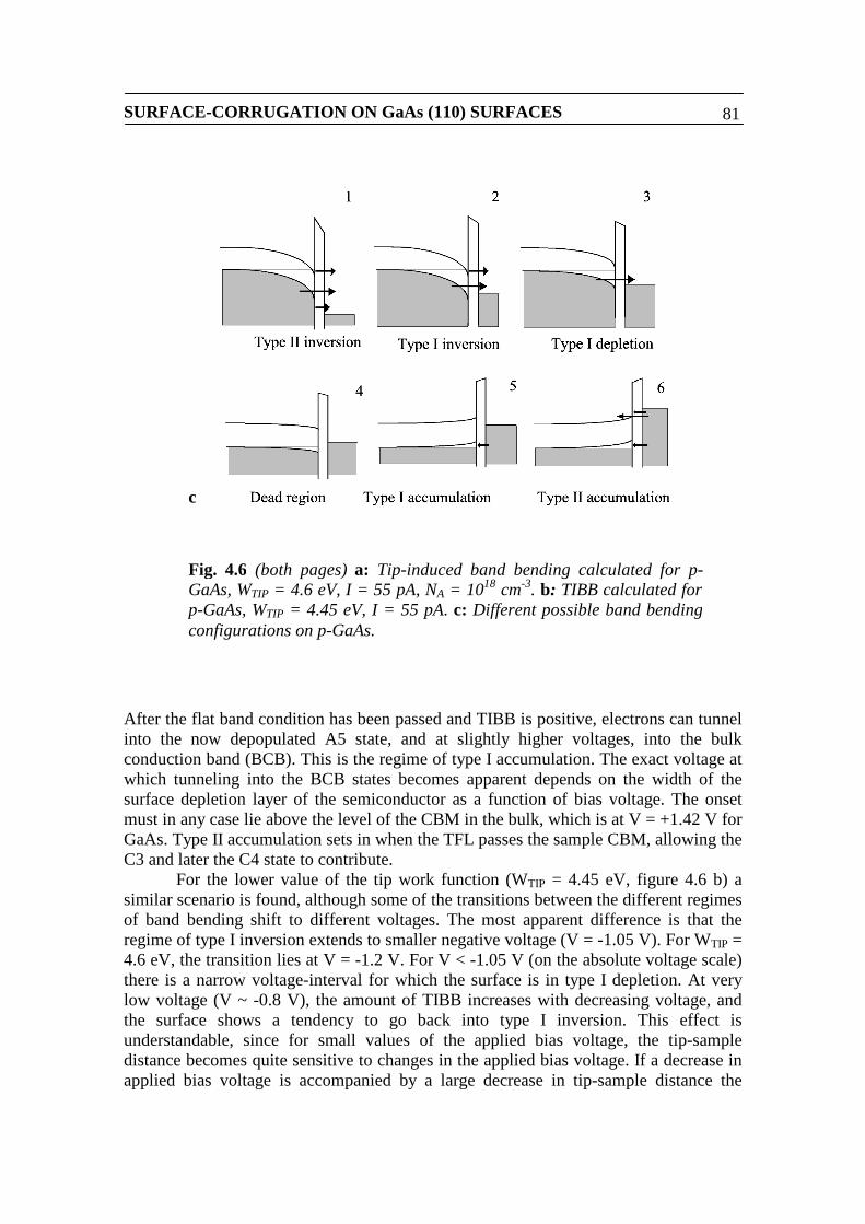
SURFACE-CORRUGATION ON GaAs (110) SURFACES 81
After the flat band condition has been passed and TIBB is positive, electrons can tunnelinto the now depopulated A5 state, and at slightly higher voltages, into the bulkconduction band (BCB). This is the regime of type I accumulation. The exact voltage atwhich tunneling into the BCB states becomes apparent depends on the width of thesurface depletion layer of the semiconductor as a function of bias voltage. The onsetmust in any case lie above the level of the CBM in the bulk, which is at V = +1.42 V forGaAs. Type II accumulation sets in when the TFL passes the sample CBM, allowing theC3 and later the C4 state to contribute.
For the lower value of the tip work function (WTIP = 4.45 eV, figure 4.6 b) asimilar scenario is found, although some of the transitions between the different regimesof band bending shift to different voltages. The most apparent difference is that theregime of type I inversion extends to smaller negative voltage (V = -1.05 V). For WTIP =4.6 eV, the transition lies at V = -1.2 V. For V < -1.05 V (on the absolute voltage scale)there is a narrow voltage-interval for which the surface is in type I depletion. At verylow voltage (V ~ -0.8 V), the amount of TIBB increases with decreasing voltage, andthe surface shows a tendency to go back into type I inversion. This effect isunderstandable, since for small values of the applied bias voltage, the tip-sampledistance becomes quite sensitive to changes in the applied bias voltage. If a decrease inapplied bias voltage is accompanied by a large decrease in tip-sample distance the
Fig. 4.6 (both pages) a: Tip-induced band bending calculated for p-GaAs, WTIP = 4.6 eV, I = 55 pA, NA = 1018 cm-3. b: TIBB calculated forp-GaAs, WTIP = 4.45 eV, I = 55 pA. c: Different possible band bendingconfigurations on p-GaAs.
c

CHAPTER 4: TUNEABILITY OF THE82
electric field between tip and sample may increase, causing the amount of TIBB toincrease as well. In figure 6b, we have chosen to abort the calculation for V = -0.8 Vand less: In the model, the tunneling current originates completely from the surfacestates in the conduction band that are populated by inversion for those voltages. In themodel, the density of surface states is assumed constant, whereas in reality the DOSassociated with the surface states is very much reduced near the edges of the bandgap ofthe semiconductor. The calculated value for the tunneling current may thus well be anoverestimation.
For n-GaAs (see figure 4.7), we can work out the various band bending situations thesame fashion as was done for p-GaAs. For large negative voltage, the surface is type IIaccumulated and we expect contributions from the A4 and A5 states, the BVB statesand the C3 state which has become populated due to the downward band bending.When the bias is decreased, the TFL passes the sample VBM and type I accumulationsets in. In this regime, there is a contribution from the C3 state and the BVB states, butthe A4/A5 contribution is gone. As the bias voltage is decreased further, thecontribution from the BVB states slowly diminishes and for small negative voltages,only the contribution from the C3 state is left. For very small negative voltage, there is adead region similar to the one found for p-GaAs. Except for a slight shift in the voltageat which the transition between type I and type II accumulation occurs, there are nodifferences in the filled-states band bending behaviour of n-GaAs for the differentmodel parameters.
For positive values of the applied bias voltage, on the other hand, the bandbending behaviour of n-GaAs becomes very strongly dependent on the assumed valuesfor the model parameters, the tip work function in particular. For the lower two valuesof the assumed tip work function (4.30 and 4.35 eV), electrons tunnel into the BCBstates for V < 0.5 V (type I depletion). When the applied bias voltage exceeds 0.5 V, theTFL passes the CBM and type II depletion sets in. The voltage-regime of type IIdepletion is rather large. For V > 1.8 V, type II inversion sets in. For the type II invertedsurface, we expect contributions from the A5 state, the BCB states, the C3 state, and forlarger voltages, the C4 state.
For the higher value of the tip work function, the amount of TIBB remainscomparable to the bandgap of the semiconductor for all voltages. For a small appliedbias voltage, the surface is predicted to be in type I depletion. For the current chosen inthe calculation, the voltage at which the TFL passes the CBM coincides with the voltageat which inversion sets in. Therefore, as the bias voltage is increased, the surface goesdirectly from type I depletion into type II inversion. If a larger tunneling current(smaller tip-sample distance) is used, TIBB at a given voltage is stronger. If the bias isthen gradually increased, inversion sets in before the TFL passes the CBM of thesample, causing type I inversion similar to what is seen on p-GaAs. For a smallercurrent, inversion will set in after the TFL has passed the sample CBM, causing type IIdepletion (see figure 4.7 d, configuration 5). The surface shows a tendency towards typeI inversion for very small positive voltage, in a similar way to what is observed for p-GaAs in figure 4.6 b.
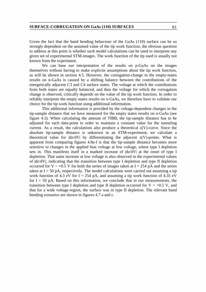
SURFACE-CORRUGATION ON GaAs (110) SURFACES 83
Given the fact that the band bending behaviour of the GaAs (110) surface can be sostrongly dependent on the assumed value of the tip work function, the obvious questionto address at this point is whether such model calculations can be used to interprete anygiven set of experimental STM-images. The work function of the tip used is usually notknown from the experiment.
We can base our interpretation of the results on p-GaAs on the imagesthemselves without having to make explicite assumptions about the tip work function,as will be shown in section 4.5. However, the corrugation-change in the empty-statesresults on n-GaAs is caused by a shifting balance between the contributions of theenergetically adjacent C3 and C4 surface states. The voltage at which the contributionsfrom both states are equally balanced, and thus the voltage for which the corrugationchange is observed, critically depends on the value of the tip work function. In order toreliably interprete the empty states results on n-GaAs, we therefore have to validate ourchoice for the tip work function using additional information.
This additional information is provided by the voltage-dependent changes in thetip-sample distance that we have measured for the empty states results on n-GaAs (seefigure 4.3). When calculating the amount of TIBB, the tip-sample distance has to beadjusted for each data-point in order to maintain a constant value for the tunnelingcurrent. As a result, the calculations also produce a theoretical z(V)-curve. Since theabsolute tip-sample distance is unknown in an STM-experiment, we calculate atheoretical value for |dz/dV| by differentiating the adjacent z(V)-points. What isapparent from comparing figures 4.8a-f is that the tip-sample distance becomes moresensitive to changes in the applied bias voltage at low voltage, where type I depletionsets in. This manifests itself in a marked increase of |dz/dV| at the onset of type Idepletion. That same increase at low voltage is also observed in the experimental valuesof |dz/dV|, indicating that the transition between type I depletion and type II depletionoccurred for V ~ +0.5 V for both the series of images taken at I = 254 pA and the seriestaken at I = 50 pA, respectively. The model calculations were carried out assuming a tipwork function of 4.3 eV for I = 254 pA, and assuming a tip work function of 4.35 eVfor I = 50 pA. Based on this information, we conclude that in our measurements, thetransition between type I depletion and type II depletion occurred for V = +0.5 V, andthat for a wide voltage-region, the surface was in type II depletion. The relevant bandbending scenarios are shown in figures 4.7 a and c.

CHAPTER 4: TUNEABILITY OF THE84
Fig. 4.7 (both pages) a: Tip-induced band bending calculated for n-GaAs (WTIP =4.3 eV, ND = 1018 cm-3 ). Simulated currents: 45 pA < I < 96 pA (filled states),254 pA (empty states). We have varied the value of the tunneling current in thefilled states simulation in order to mimick the corresponding measurement.b: TIBB calculated for n-GaAs (WTIP = 4.6 eV, ND = 1018 cm-3). Simulatedcurrents: 45 pA < I < 96 pA (filled states), 65 pA (empty states). For theseparameters, the model predicts a direct transition from type I depletion to type IIinversion (see text).
a
b
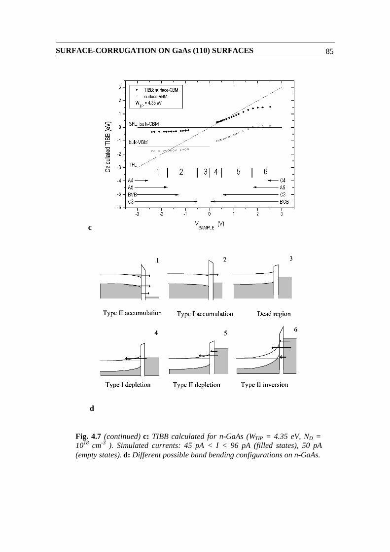
SURFACE-CORRUGATION ON GaAs (110) SURFACES 85
Fig. 4.7 (continued) c: TIBB calculated for n-GaAs (WTIP = 4.35 eV, ND =1018 cm-3 ). Simulated currents: 45 pA < I < 96 pA (filled states), 50 pA(empty states). d: Different possible band bending configurations on n-GaAs.
c
d
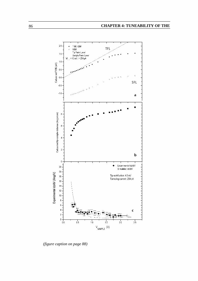
CHAPTER 4: TUNEABILITY OF THE86
a
c
(figure caption on page 88)
SFL
TFL
b
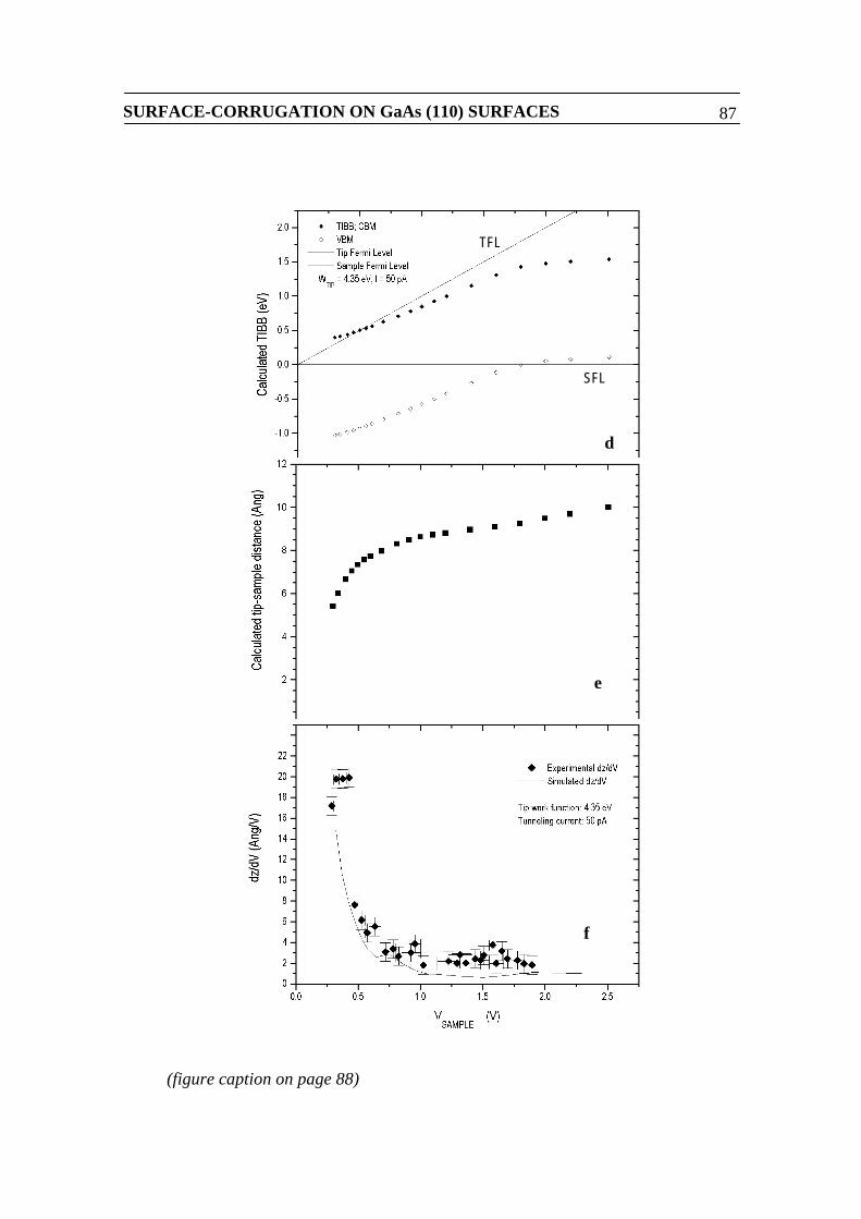
SURFACE-CORRUGATION ON GaAs (110) SURFACES 87
d
(figure caption on page 88)
SFL
TFL
e
f
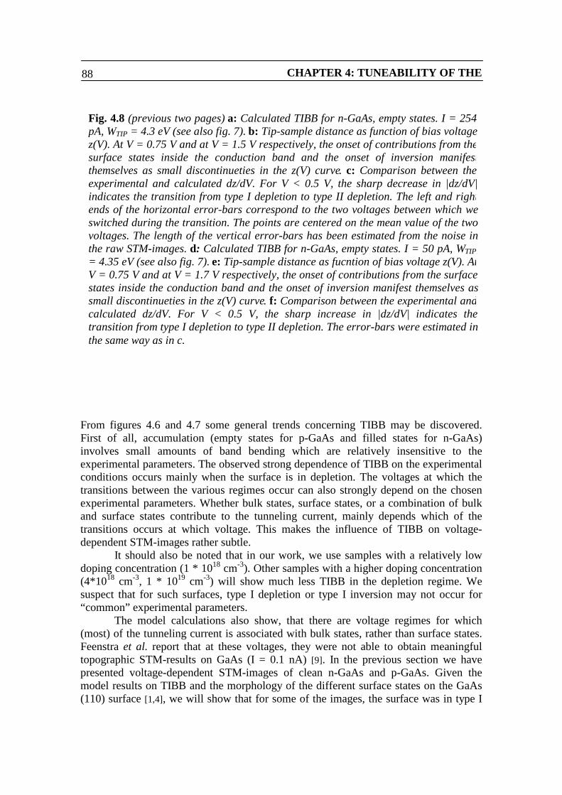
CHAPTER 4: TUNEABILITY OF THE88
From figures 4.6 and 4.7 some general trends concerning TIBB may be discovered.First of all, accumulation (empty states for p-GaAs and filled states for n-GaAs)involves small amounts of band bending which are relatively insensitive to theexperimental parameters. The observed strong dependence of TIBB on the experimentalconditions occurs mainly when the surface is in depletion. The voltages at which thetransitions between the various regimes occur can also strongly depend on the chosenexperimental parameters. Whether bulk states, surface states, or a combination of bulkand surface states contribute to the tunneling current, mainly depends which of thetransitions occurs at which voltage. This makes the influence of TIBB on voltage-dependent STM-images rather subtle.
It should also be noted that in our work, we use samples with a relatively lowdoping concentration (1 * 1018 cm-3). Other samples with a higher doping concentration(4*1018 cm-3, 1 * 1019 cm-3) will show much less TIBB in the depletion regime. Wesuspect that for such surfaces, type I depletion or type I inversion may not occur for“common” experimental parameters.
The model calculations also show, that there are voltage regimes for which(most) of the tunneling current is associated with bulk states, rather than surface states.Feenstra et al. report that at these voltages, they were not able to obtain meaningfultopographic STM-results on GaAs (I = 0.1 nA) [9]. In the previous section we havepresented voltage-dependent STM-images of clean n-GaAs and p-GaAs. Given themodel results on TIBB and the morphology of the different surface states on the GaAs(110) surface [1,4], we will show that for some of the images, the surface was in type I
Fig. 4.8 (previous two pages) a: Calculated TIBB for n-GaAs, empty states. I = 254pA, WTIP = 4.3 eV (see also fig. 7). b: Tip-sample distance as function of bias voltagez(V). At V = 0.75 V and at V = 1.5 V respectively, the onset of contributions from thesurface states inside the conduction band and the onset of inversion manifestthemselves as small discontinueties in the z(V) curve. c: Comparison between theexperimental and calculated dz/dV. For V < 0.5 V, the sharp decrease in |dz/dV|indicates the transition from type I depletion to type II depletion. The left and rightends of the horizontal error-bars correspond to the two voltages between which weswitched during the transition. The points are centered on the mean value of the twovoltages. The length of the vertical error-bars has been estimated from the noise inthe raw STM-images. d: Calculated TIBB for n-GaAs, empty states. I = 50 pA, WTIP= 4.35 eV (see also fig. 7). e: Tip-sample distance as fucntion of bias voltage z(V). AtV = 0.75 V and at V = 1.7 V respectively, the onset of contributions from the surfacestates inside the conduction band and the onset of inversion manifest themselves assmall discontinueties in the z(V) curve. f: Comparison between the experimental andcalculated dz/dV. For V < 0.5 V, the sharp increase in |dz/dV| indicates thetransition from type I depletion to type II depletion. The error-bars were estimated inthe same way as in c.
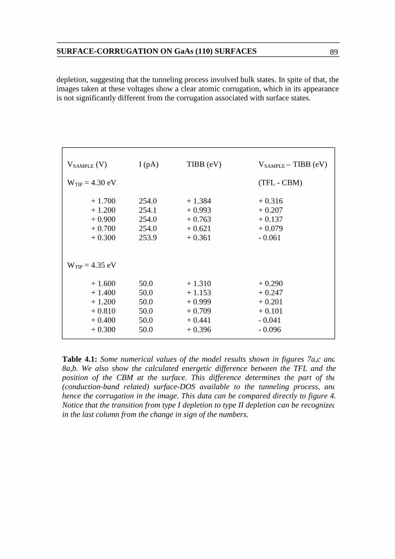
SURFACE-CORRUGATION ON GaAs (110) SURFACES 89
depletion, suggesting that the tunneling process involved bulk states. In spite of that, theimages taken at these voltages show a clear atomic corrugation, which in its appearanceis not significantly different from the corrugation associated with surface states.
Table 4.1: Some numerical values of the model results shown in figures 7a,c and8a,b. We also show the calculated energetic difference between the TFL and theposition of the CBM at the surface. This difference determines the part of the(conduction-band related) surface-DOS available to the tunneling process, andhence the corrugation in the image. This data can be compared directly to figure 4.Notice that the transition from type I depletion to type II depletion can be recognizedin the last column from the change in sign of the numbers.
VSAMPLE (V) I (pA) TIBB (eV) VSAMPLE – TIBB (eV)
WTIP = 4.30 eV (TFL - CBM)
+ 1.700 254.0 + 1.384 + 0.316+ 1.200 254.1 + 0.993 + 0.207+ 0.900 254.0 + 0.763 + 0.137+ 0.700 254.0 + 0.621 + 0.079+ 0.300 253.9 + 0.361 - 0.061
WTIP = 4.35 eV
+ 1.600 50.0 + 1.310 + 0.290+ 1.400 50.0 + 1.153 + 0.247+ 1.200 50.0 + 0.999 + 0.201+ 0.810 50.0 + 0.709 + 0.101+ 0.400 50.0 + 0.441 - 0.041+ 0.300 50.0 + 0.396 - 0.096
CHAPTER 4: TUNEABILITY OF THE90
4.5 Discussion
In this discussion, several questions will be addressed: First we will compare the STM-images with the model-results concerning TIBB in order to interprete the voltage-dependent changes in atomic corrugation that we have observed. The empty-statesresults on p-GaAs (subsection 4.5.1) and the filled-states results on n-GaAs (4.5.2) aretreated first, since these cases involve accumulation and are thus very simple tointerpret. Then we will discuss the empty-states results on n-GaAs (4.5.3) and the filled-states results on p-GaAs (4.5.4). After discussing the experimental results we will makecomments on the validity and reliable use of our model (4.5.5). In subsections 4.5.3 and4.5.4 it will be made clear that at some voltages, the surface is in type I depletion. Forthese voltages, the atomic corrugation that is observed in the images must be attributedto a tunneling current that is associated with bulk states rather than surface states.Atomic corrugation which is observed while the surface is in type I depletion cannot beexplained within the framework of “regular tunneling”. The last subsection (4.5.6)therefore theorizes about possible alternative mechanisms for atomic corrugation on the(110)-surface of GaAs.
4.5.1 p-GaAs, empty states
The empty-states results of p-GaAs are shown in the first column of figure 4.4. Theyshow that the atomic corrugation is in the [001]-direction for large positive voltage(+ 2.5 V), or equivalently, that the atomic rows appear to run in the [-110]-direction forlarge, positive voltage. Then the atomic corrugation partly changes into an atomiccorrugation that is clearly resolved in both directions for intermediate voltage (+ 1.8 V).At small positive voltage (+ 1.5 V), the corrugation is again in the [001]-direction. Theinterpretation of the empty states behaviour of p-GaAs is quite straightforward as theamount of TIBB remains relatively constant throughout the voltage range of interest(see figure 4.6). At the lowest voltage (V = +1.5 V), tunneling occurs into the A5 statewhich has become depopulated by the upward band bending (type I accumulation). Thecorrugation is then in [001]. When the bias voltage is increased, the BCB statescontribute more and more to the tunneling current. Somewhere in the range between V= +1.5 V and V = +1.8 V, the TFL passes the CBM (type II accumulation) and the C3state starts to contribute as well. This is reflected by the change in CN. When the biasvoltage is increased further, the C4 state starts to contribute, causing the corrugation tochange back again. For the highest voltage (V = +2.5 V) the corrugation is completelyin [001].
In subsection 4.5.3, it will be shown that the contribution from the BCB-states isaccompanied by a corrugation in the [-110]-direction. The effect is caused by electronstunneling resonantly through the low-energy shoulder of the C3-state, of which it isknown that it extends into the bandgap [5]. In this case, the effect of the contributionfrom the BCB-states to the tunneling current is that the contribution of the C3-state

SURFACE-CORRUGATION ON GaAs (110) SURFACES 91
appears slightly stronger than would otherwise be the case. One can also expect thecorrugation-change to appear at slightly lower voltages due to this effect. In this case,however, these effects are unimportant.
It is worth to note that at the lowest voltage at which we measured, the value ofthe CN indicates that there still is a minor contribution from the (shoulder of the) C3state. It is also clear that at V = +1.8 V, where we expect a simultaneous contributionfrom the C3- and the A5-states, a mixture of the atomic corrugation occurs: The C3-state causes a corrugation in the [-110]-direction whereas the A5-state causes an atomiccorrugation in the [001]-direction. The simultaneous contribution of both states resultsin an atomic corrugation that is clearly resolved in both directions.
4.5.2 n-GaAs, filled states
The filled states results on n-GaAs show that for high voltage, the corrugation is in[001]. As voltage is decreased, the corrugation appears not to change very much until V= -1.8 V. Below this voltage, the corrugation changes until for V = -1.1V, it hascompletely changed to a corrugation in [-110]. In contrast to what is seen for p-GaAs,the change in the direction of the atomic corrugation is monotonous as a function of biasvoltage.
At high voltage, the surface is in type II accumulation and we expectcontributions from the A5 and A4 states, from the BVB states and a minor contributionfrom the C3 state which is populated due to the downward band bending. As the A5 andA4 states and BVB states dominate, corrugation is in [001]. As will be shown insubsection 4.5.4, the contribution from the BVB-states is (very likely to be)accompanied by an atomic corrugation in the [001]-direction. When the voltage isdecreased, the TFL will rise with respect to the sample surface states as in this voltageregime, TIBB is relatively constant. The contribution of the A4 and A5 states will thusgradually decrease. At lower voltages where type I accumulation sets in, thecontribution from the BVB states will decrease as well. At low voltages, only thecontribution from the populated C3 state is left. For these voltages, the corrugation hasclearly changed towards one in the [-110] direction, as is indicated by the negative CN.
4.5.3 n-GaAs, empty states
The empty-states images of n-GaAs show a gradual corrugation-change: At largevoltage, the corrugation is in the [001]-direction, and at low voltage it is in [-110]. Thechange is most apparent between V = +0.706 V and V = +1.268 V. In the recordedtransitions between the applied voltages we have not observed any shifts in the atomicrows (see figure 4.10 for an example of such a shift). This indicates that the atomicmaxima seen in the images are centered on the same atom-species throughout the entirerange of applied bias voltages. For the lower voltages, we can identify the corrugationunambiguously as being associated with the C3 state. Since the local maxima in the
CHAPTER 4: TUNEABILITY OF THE92
DOS associated with this state are centered on the Ga atoms, the atomic maxima in therows along (-110) which are observed at higher voltage are also centered on the Gaatoms. This confirms that the corrugation observed for higher voltage is associated withthe C4 state. Also, the images are in qualitative agreement with the results obtained byEbert et al. [1], although in our work the corrugation change occurs at a slightly lowervoltage. We thus attribute the corrugation-change to a shifting balance between thecompeting contributions of the C3 and C4 states. The empty-states results obtained onn-GaAs also contain a non-typical rise of the CN for very low voltage (V < 0.4 V, 50pA). This result will be discussed in sub-section 4.5.6.
The point at which the CN changes sign lies near V = +0.9 V. According to themodel calculations the TFL lies 137 meV above the CBM for that voltage. This isenergetically below the energies at which both the C3 and C4 states are centered. Thisfact appears strange: If the corrugation change is supposed to be caused by thecontributions from two competing states, it would seem logical that the corrugationchange takes place at a voltage for which the TFL lies energetically between the (peakpositions of) two states. According to figures 4.7a and b, that situation is only expectedto occur for V > 2.0 V, since the TFL rises very slowly in energy with respect to thesample surface states as the bias voltage is increased. Since the model calculationsreproduces the voltage-dependent-changes in the tip-sample distance quite well (seefigure 4.8) we are convinced that the model calculations describe the band bendingbehaviour correctly, at least in qualitative terms. The slow rise of the TFL with respectto the sample surface predicted in the model is also consistent with the experimentalobservation that the corrugation changes quite gradually as a function of applied biasvoltage.
One possible explanation is the hypothesis that the low energy shoulder of theC4 state extends to much lower energies than one might at first glance expect. From thecalculated surface-DOS on InP (110) (see figure 1 in ref. 1), the C3 state appears as asmall peak superimposed on a some background. If the low energy shoulder of the C4state forms a background on which the DOS associated with the C3 state issuperimposed, it is conceivable that the C4 state influences the corrugation even forenergies that lie below the value at which the lower lying C3 state is centered. Forenergies below CBM + 150 meV, the low energy shoulder of the C3 state would thendominate the surface-DOS, causing the corrugation to change.
From figure 4.7 it is clear that for V < +0.5 V, the surface was in type I depletionas the images were recorded. For these voltages, the atomic rows run along [001]. Weinterpret this as the influence of the low energy shoulder of the C3 state, from which itis known that it extends into the bandgap [4,5]. We do not think that the low energyshoulder of the C3 state is imaged by the process of regular tunneling. The portion ofthe DOS associated with the C3 state that lies inside the bandgap only extends 4.4 a0(2.2 Å) into the vacuum [4]. According to the Tersoff-Hamann theory, this would meanthat for these images, the tip-sample distance would also be around 2 Å [7]. This seemsan unlikely event since at these small tip-sample distances, a non-neglegible influencefrom the tip-sample interaction is to be expected. Theoretically it is expected that achemical bond forms between the tip and sample at such short tip-sample distances[14,15,16,17]. From figure 4.7b the tip-sample distance is expected to be larger than 2 Åas well. To our opinion, the following interpretation is much more plausible: If the
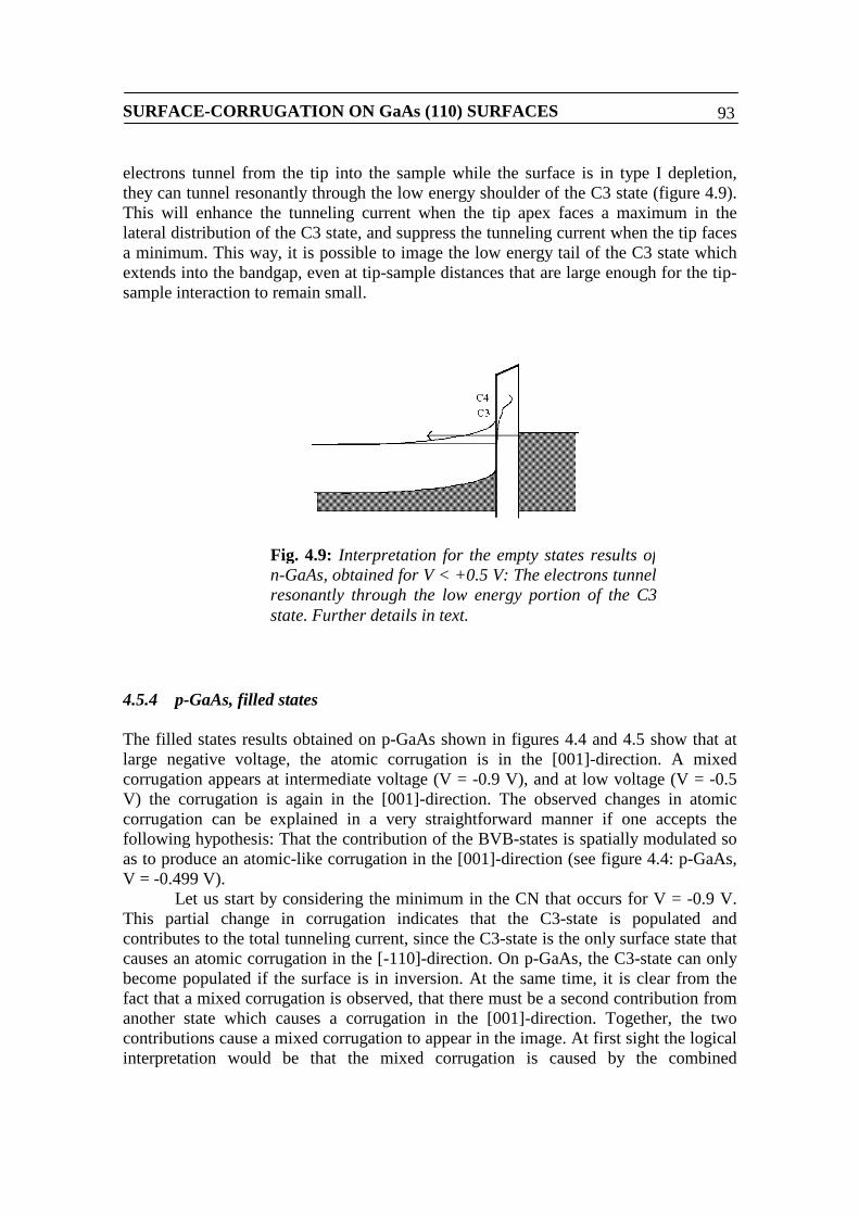
SURFACE-CORRUGATION ON GaAs (110) SURFACES 93
electrons tunnel from the tip into the sample while the surface is in type I depletion,they can tunnel resonantly through the low energy shoulder of the C3 state (figure 4.9).This will enhance the tunneling current when the tip apex faces a maximum in thelateral distribution of the C3 state, and suppress the tunneling current when the tip facesa minimum. This way, it is possible to image the low energy tail of the C3 state whichextends into the bandgap, even at tip-sample distances that are large enough for the tip-sample interaction to remain small.
4.5.4 p-GaAs, filled states
The filled states results obtained on p-GaAs shown in figures 4.4 and 4.5 show that atlarge negative voltage, the atomic corrugation is in the [001]-direction. A mixedcorrugation appears at intermediate voltage (V = -0.9 V), and at low voltage (V = -0.5V) the corrugation is again in the [001]-direction. The observed changes in atomiccorrugation can be explained in a very straightforward manner if one accepts thefollowing hypothesis: That the contribution of the BVB-states is spatially modulated soas to produce an atomic-like corrugation in the [001]-direction (see figure 4.4: p-GaAs,V = -0.499 V).
Let us start by considering the minimum in the CN that occurs for V = -0.9 V.This partial change in corrugation indicates that the C3-state is populated andcontributes to the total tunneling current, since the C3-state is the only surface state thatcauses an atomic corrugation in the [-110]-direction. On p-GaAs, the C3-state can onlybecome populated if the surface is in inversion. At the same time, it is clear from thefact that a mixed corrugation is observed, that there must be a second contribution fromanother state which causes a corrugation in the [001]-direction. Together, the twocontributions cause a mixed corrugation to appear in the image. At first sight the logicalinterpretation would be that the mixed corrugation is caused by the combined
Fig. 4.9: Interpretation for the empty states results ofn-GaAs, obtained for V < +0.5 V: The electrons tunnelresonantly through the low energy portion of the C3state. Further details in text.
CHAPTER 4: TUNEABILITY OF THE94
contributions of the A5-state and the C3-state, assuming that the latter has becomepopulated by inversion.
However, it becomes clear that this interpretation must be wrong when thevoltage at which the mixed corrugation occurs, is considered. If the C3-state is tocontribute to the filled-states tunneling current, it must lie energetically below theSample Fermi Level (SFL). The fact that the C3-state lies energetically near the SFLimplies that the A5 and A4-states must lie well below the Tip Fermi Level (TFL) andthus cannot contribute to the total tunneling current. The reason for this is that the biasvoltage at which the mixed corrugation occurs, equals –0.9 V. This is less than theenergetic separation of the A5 and C3 states, which lie on either side of the bandgap ofthe semiconductor. It is thus certain that at V = -0.9 V, the surface is in type I inversion.From figure 4.6 we now identify the BVB-states as the origin of the second contributionto the total tunneling current at V = -0.9 V. In order to explain the fact that we observe amixed corrugation at this voltage, we have to assume that the contribution from theBVB-states is associated with an atomic-like corrugation in the [001]-direction.
When the voltage is decreased from V = -0.9 V to V = -0.5 V, the corrugationchanges to one in the [001]-direction. According to figure 4.6 the amount of TIBBgradually decreases with decreasing (absolute) voltage. Consequently, the C3-statebecomes less and less populated, causing a gradual decrease of the contribution to thetotal tunneling current from the C3 state relative to the one from the BVB-states. Thiscauses the corrugation to change. At some point, the C3-state rises above the SFL andonly the contribution from the BVB-states is left. At V = -0.5 V, we thus expect that thetotal tunneling current originates purely from the BVB-states.
As the voltage increases from V = -0.9 V to V = -1.4 V, the CN increases aswell. Our explanation is that, as the voltage increases, the contribution from the BVBstates increases more rapidly than the contribution from the C3 state, thus leading to acorrugation which is stronger in [001]. This is understandable from the fact that theamount of TIBB levels off at the onset of inversion: When inversion sets in, thecontribution from the C3-state remains more or less constant whereas the one from theBVB-states increases with increasing voltage. It is quite obvious that a strongercontribution from the A5 state would also lead to a corrugation in [001]. However, forthe A5 state to contribute, the TFL has to lie energetically below the VBM. Since thesurface must be in type I inversion for V = -0.9 V and larger (absolute) bias voltages,the A5 state must lie energetically at –1.4 eV or more below the SFL. Consequently, wecannot expect to observe the A5 state for 0 < V < -1.4 V. The change in corrugationbetween V = -0.9 V and V = - 1.4 V must therefore occur entirely while the surface is intype I inversion.
Summarizing, we interpret the filled-states images obtained on p-GaAs in thefollowing way: At low voltage (V = -0.5 V), we expect to observe only a contributionfrom the BVB-states. We assume that the contribution from the BVB-states has anatomic-like corrugation to it in the [001]-direction. At intermediate voltage (V = -0.9V), inversion sets in and the resulting contribution from the C3-state causes a partialcorrugation-change. At large negative voltage, both the BVB-states and the C3-statescontribute to the total tunneling current, but we expect the contribution from the BVB-states to dominate, causing a corrugation in the [001]-direction.
SURFACE-CORRUGATION ON GaAs (110) SURFACES 95
The idea that a tunneling current from the BVB-states would be accompanied by atomiccorrugation is a somewhat radical one, since it assumes a mechanism for atomiccorrugation that lies outside the framework of the Tersoff-Hamann theory (see section1.10). In the following we will therefore give two supporting arguments for thisassumption. In subsection 4.5.6, we will comment on the possible nature of corrugation-mechanisms that lie outside the framework of the Tersoff-Hamann theory.
The most compelling supportive argument is that we have based ourinterpretation on a bandbending behaviour that is consistent with the results presentedby Feenstra et al. [9]. In that paper, the authors compare experimental I(V)-spectra ofGaAs-(110) with model calculations. The model very specifically considers the effectsof electrons tunneling into or out of bulk states through a surface depletion layer causedby TIBB. The authors find that the experimental results can only be reproduced by themodel if the current generated by electrons tunneling through a surface depletion layerinto or out of bulk states, is included. It is thus clear that it is very well possible toobtain a measurable tunneling current from electrons tunneling out of bulk statesthrough a surface depletion zone. In fact, the phenomenon seems a very commonoccurrence from ref. 9. When this band bending behaviour is combined with theassumption that a contribution from the BVB-states is somehow associated with atomic-like corrugation in the [001]-direction, the explanation of our own experimental resultsfollows in a very straightforward and natural way.
A second argument can be made by attempting to explain the measuredcorrugation-changes within the framework of regular tunneling, i.e. assuming thatatomic corrugation can only be caused by electrons tunneling directly into or out ofsurface states. The remainder of this subsection will show that such an alternativeexplanation is strictly speaking possible, but necessarily involves a band bendingbehaviour that is very questionable.
Since the surface is in inversion at V = -0.9 V, we can exclude any contributionfrom the A4 and A5 states in the voltage-range –0.9 V < V < -1.4 V. At lower voltagewhere we no longer expect inversion, we can exclude a contribution from the A4 andA5 states for the following reason: The partial corrugation change at V = -0.9 V verystrongly suggests that there is a simultaneous contribution from two states, one with acorrugation in [-110] (the C3 state) and one with a corrugation in [001]. The change incorrugation at low voltage further suggests that of these two states, only the one withcorrugation in the [001]-direction remains at lower voltage. It thus seems that theelectronic state that determines the atomic morphology of the images at V = -0.5 V, alsomust contribute to the total tunneling current at V = -0.9 V.
Besides, a contribution of the A5 state at V = -0.5 V combined with acontribution from the C3-state at V = -0.9 V would imply a very sharp, almostdiscontinuous decrease in the amount of TIBB with decreasing voltage. The decrease inTIBB would actually have to exceed the decrease in the applied bias voltage. Fromfigures 4.6 and 4.7, such sharp changes in TIBB are not to be expected. Such a sharpdecrease in TIBB would also imply that at V = -0.9 V, only the C3-state wouldcontribute to the tunneling current as the A5- and A4-states lie too low in energy. Acontribution of only the C3 state at V = -0.9 V would manifest itself in a corrugation in[-110] rather than the mixed corrugation that is observed in the images. We can thus

CHAPTER 4: TUNEABILITY OF THE96
exclude a contribution from the A4 and A5-states for the entire range of applied biasvoltages.
In the absence of the A4- and A5-states, the only remaining surface-state thatwould cause a corrugation in the [001]-direction is the C4-state. The alternativeexplanation would therefore involve the following band bending scenario: At largevoltage (V = -1.4 V), the surface would have to be in type I inversion to such an extentthat the C4-state becomes populated and contributes to the filled states current. For V =-0.9 V, TIBB would have to decrease slightly so that the contribution from the C3-statewould become somewhat stronger. At lower voltage, still, the amount of TIBB wouldhave to increase in order to re-populate the C4-state.
In our model, an increase of TIBB with decreasing absolute voltage can occur ifthe decrease in voltage is accompanied by a larger relative decrease in tip-sampledistance. Note that our measurements were obtained a fixed tunneling current, andtherefore the tip-sample distance changes from one frame to the next. We have noindications that such a non-monotonous behaviour of TIBB indeed occurs under normalexperimental circumstances, but we will assume that it might occur for the sake of theargument.
We first have to consider whether or not it is possible for the C4-state to becomepopulated by inversion in the first place. It would seem that no circumstances exist forwhich the C4-state becomes populated by inversion as it is centered 1.1 eV above theCBM. According to our model, the amount of TIBB levels off at the onset of inversion,populating the conduction-band related surface states only up to some 300 meV. This isconsistent with our filled-states images of n-GaAs: For V = -1.1 V, the conduction-bandrelated surface states are populated due to (type I) accumulation. At the same time, theatomic corrugation seen in the filled-states images of n-GaAs shows no sign of acontribution from the C4-state. However, from the empty-states images of n-GaAs inwhich the conduction-band related surface-DOS of the GaAs-surface is probed directly,it seems that the influence of the C4-state in the surface-DOS manifests itself even atenergies that lie slightly above the CBM: In the empty-states images of n-GaAs (seesubsection 4.5.3), it is seen that the corrugation does not change when the TFL liessomewhere between the peaks of the C3 and C4 states: Rather, the corrugation changeswhen the TFL lies at a far lower energy relative to the sample surface-DOS, about 140meV above the CBM. Apparently the low energy shoulder of the C4 state extends torelatively low energies and makes up a significant part of the surface-DOS, even atenergies that lie below the value at which the lower lying C3 state is centered. Fromfigures 4.6 a and b it can be seen that it is very well possible to populate the conductionband up to 150 meV above the CBM by inversion. It is thus perhaps possible that due toinversion of the surface, the low-energy shoulder of the C4-state can become populatedand thus influences the atomic corrugation of the filled-states images of p-GaAs.
The other crucial element in the alternative explanation is that the band bendingbehaviour must be non-monotonic in order to reproduce the corrugation-changes thatwe have observed experimentally. For some parameters, we have observed that theamount of TIBB increases slightly with decreasing voltage. Such effects, however, areminor and always occur near the transition from type I inversion to type I depletion (seefigures 4.6 b, 4.7 b). The reason for this is that the transition from type I inversion totype I depletion usually involves a large decrease in tip-sample distance. If the relative
SURFACE-CORRUGATION ON GaAs (110) SURFACES 97
decrease in tip-sample distance is larger than the relative decrease in the bias voltage,the electric field present between the tip and sample increases and the amount of TIBBincreases as well.
In our model, we found no set of parameters which produces a non-monotonouschange in the amount of TIBB at the right voltage: It is possible in the model topopulate the conduction-band by inversion at V = -0.9 V and I = 55 pA when a tipworkfunction of 4.0 eV is assumed. The calculated amount of TIBB is then –1.572 eV,implying that the CBM at the surface lies 148 meV below the SFL. Since the empty-states results on n-GaAs suggest that the corrugation changes when the TFL lies about140 meV above the surface-CBM, we assume for the moment that this situation wouldproduce an atomic corrugation similar to the mixed corrugation that we have observedexperimentally. To account for the fact that near the CBM the surface-DOS decreasesasymptotically to zero, we also set the density of the surface-state bands to 4.42 * 1013
cm-2, which is 1/10 of the usual value. For these parameters, the amount of TIBB variesmonotonically from –1.450 eV at V = -0.55 V to –1.702 eV at V = -1.5 V. This type ofscenario would therefore cause a monotonous change in the atomic corrugation ratherthan a partial change which is reversed. This argument also holds if a different value forthe work function is assumed in the model. In order to mimick the experimentallyobserved mixed corrugation at V = -0.9 V, the tip-sample distance has to be adjusted inorder to reproduce the same amount of TIBB (-1.572 eV). The (constant) simulatedcurrent will then change accordingly. If then the bias voltage is varied in order tosimulate the entire measurement, the same monotonous change in the amount of TIBBis predicted.
Whether or not such a non-monotonous behaviour of the TIBB can be excludedfor a real inverted surface as well, is not fully certain. In a real inversion layer theelectrons are confined and thus occupy quantized energy-levels. These levels lie nearthe top of the tip-induced potential well, which is near the SFL. In our model, the largechanges in tip-sample distance that cause a non-monotonous behaviour of the amount ofTIBB only occur when the CBM passes the SFL. In the presence of quantized levels,the lowest occupied electron-states do not lie at the surface-CBM, but rather, at aslightly higher energy. As a consequence, the non-monotonous changes in the amountof TIBB are expected to occur when the lowest quantized level passes the SFL. Verystrictly speaking, this might create the non-monotonous band bending behaviour at theright tip-sample voltage needed to complete the alternative explanation. However, theargument seems quite far-fetched, and we therefore regard it as implausible.
It is clear that the alternative explanation for our experimental results is strictlyspeaking possible, but that it crucially depends on two assumptions that are very muchopen to debate: it is possible, but by no means certain, that TIBB can invert the p-GaAssurface to such an extent that the C4-state becomes populated. In fact, based on ourfilled-states images of n-GaAs we expect the opposite. Secondly, it remains to be seenwhether or not the non-monotonous band bending behaviour can really occur. In ourmodel, a non-monotonous change in band bending that occurs at the right voltage inorder to explain our experimental results, could not be simulated. We thus conclude thatthe only reasonable explanation for the corrugation changes that we have shown infigure 4.4, involves electrons tunneling from the BVB-states into the tip through asurface depletion layer. This tunneling current is spatially modulated in such a way that

CHAPTER 4: TUNEABILITY OF THE98
when the contribution from the BVB-states dominates the total tunneling current, anatomic-like corrugation in the [001]-direction is observed in the STM-image.
4.5.5 The reliable use of the model
The use of a one-dimensional model to describe band bending seems justified from thedistances over which TIBB extends into the semiconductor. For typical parameters, theeffects of TIBB extend between 10 and 50 nm into the semiconductor. If the bandbending extends over similar distances laterally, it will appear uniform on the scale ofone or two surface unit cells. Furthermore, the model relies on the Tersoff-Hamanntheory to calculate the tunneling probability. Consequently all problems that are usuallyassociated with the application of this theory will also be relevant for this model.Whenever the simulated tip-sample distance decreases to less than about 4 Å, we expectdeviations from the model due to significant tip-sample interaction. We observe that forvery low voltages in the band bending situation of type I depletion, the modelsometimes fails to reproduce experimentally observed I(V) points. Instead, the modelindicates that no tunneling current can be measured for those parameters. We attributethis deviation to the effects of tip-sample interaction, possibly a collapse of thetunneling barrier [18].
Another approximation that is made in the model is that the tip and surfacestates have constant densities of states as a function of energy. The latter approximationcan cause small discontinueties in the calculated tip-sample distance (figure 4.8b, d) orkinks in the band bending behaviour. Such features occur at the transitions between thedifferent band bending situations. Experimentally, sharp peaks in the tip-DOS can causeone portion of the surface-DOS to contribute more strongly to the total tunneling currentthan the rest of surface-DOS that lies inside the energetically accessible windowbetween the TFL and SFL. The consequence of that is that the model can only be usedto determine which of the surface states might contribute to the tunneling current on thebasis of whether they are energetically avialable or not. Questions about which surfacestate is likely to dominate over the others at a given voltage cannot be answered fromthe model alone.
In the light of the assumptions and approximations made in the model it wouldseem problematic to obtain a meaningful comparison between the experimental andtheoretical z(V) points for a given measurement. Fortunately, however, many of theunknown parameters in the model (such as the tip-state) are constant throughout therange of applied bias voltages. Thus a theoretical z(V) curve should at least beproportional to its experimental counterpart, so that voltage-dependent changes in z(V)can still be interpreted meaningfully. Besides, the agreement between the experimental|dz/dV| points and the theoretical |dz/dV| curve indicates that the accuracy of the modelis quite reasonable.
We are convinced that when the limitations of the model are kept in mind, it canbe used reliably. The most important issue when applying the model, is finding theappropriate values for some of the parameters, in particular the tip work function. Atpresent, we base our interpretation of the results on the experimental STM-images
SURFACE-CORRUGATION ON GaAs (110) SURFACES 99
themselves, and then use the model to verify whether the interpretation is realistic fromthe point of view of band bending. Notice that our main conclusions do not criticallydepend on assumptions for any of the model parameters: The conclusion that acontribution from the BVB states is associated with atomic corrugation is based on theobservation that for a particular voltage the surface must be inverted. That inversion isseen directly from the observed corrugation. The complementary argument thatexcludes a contribution from the C4 state in those circumstances also remains valid fordifferent sets of model-parameters. The interpretation of the results for n-GaAs pivotsaround the fact that the transition from type I depletion to type II depletion occurs for V= +0.5 V. This transition can be seen experimentally from the increase in |dz/dV|. Theinterpretation of the results for n-GaAs therefore does not depend on assumptions madein the model, either. In case of accumulation (filled states results for n-GaAs and emptystates results for p-GaAs) the band bending behaviour itself does not depend verystrongly on the assumed parameters.
4.5.6 Atomic resolution on GaAs (110) in type I depletion
Atomic resolution on semiconductor surfaces is usually understood in terms of regulartunneling of electrons into or out of surface states. In this view, only those states that lieenergetically between the TFL and SFL are available to the tunneling process. For mostof the experimental results presented in this paper, the concept of regular tunneling isperfectly adequate to understand the observed corrugation. However, when tunnelingtakes place while the sample surface is in type I depletion, alternative mechanisms foratomic corrugation have to be considered. In this subsection we will theorize on suchpossible mechanisms for atomic corrugation while tunneling takes place between a tipand the bulk states of a sample in type I depletion.
It is in any case clear that the corrugation observed in the type I depletion regimemust be associated with the surface of the crystal. At the surface, there is a cleardistinction between the top row As sites and the bottom row As sites (figure 4.1b).Inside the crystal, the As atoms located on a [110]-axis below a top row As surfaceatom are equivalent to the As atoms located below a bottom row As surface atom. If theinside of the crystal (more specifically: the spatial distribution of the valence bandcharge in the bulk) could be imaged by electrons tunneling through the depletion layer,this would manifest itself as a doubling of the periodicity in the observed lattice. Fromfigure 4.4 it is evident that this is in conflict with our experimental observation.
Besides, it is doubtful whether the bulk of the crystal can be imaged withadequate resolution: In order to image the atomic scale variations of the bulk valenceband charge through a depletion zone of some 5 nm, the electrons participating in thetunneling process have to travel almost perpendicularly to the surface. If the cone of“allowed” directions of travel has a half-angle of more than about 1 degree, atomicresolution will be lost. It is known from Ballistic Electron Emission Microscopy(BEEM) that such channeling of electrons can indeed occur due to the existence of a“critical angle” [19]. However, for typical circumstances this critical angle is slightly too
CHAPTER 4: TUNEABILITY OF THE100
large (about 6 degrees) [19]. Moreover, this effect is caused by the constraint that thelateral momentum of the tunneling electrons must be conserved across a metal-semiconductor interface. This interface manifests itself as a potential-step which islower than the energy of the tunneling electron itself. In our situation, no such lowpotential step exists near the tunneling junction. We therefore suspect that the current ofelectrons tunneling from the BVB states contain no (observable) information about theinner structure of the crystal. However, as the tip is scanned across the surface, thesurface structure may modulate the tunneling current by some other process than regulartunneling.
In the case of type I depletion on n-GaAs we can explain the observedcorrugation by assuming that the tunneling current is modulated by resonant tunnelingthrough the low energy shoulder of the C3 state, which extends into the bandgap [4,5](see sub-section 4.5.3). For p-GaAs, on the other hand, it is not clear whether the sameargument can be applied. According to ref. 5, the A5 state does not have a shoulder thatextends into the bandgap as is the case for the C3 state. The same is evident from refs. 1and 4 for the (110) surface of InP. The plotted surface-DOS of GaAs (110) in ref. 3,however, does suggest that the A5 state has a small high-energy shoulder which extendsinto the bandgap, although no specific reference or comment about this is made by theauthors of the paper. It is therefore not clear to us whether on GaAs (110) the A5 statehas a (small) shoulder extending into the bandgap or not. If the A5 state does not haveany such shoulder, we have to consider alternative mechanisms that can cause atomiccorrugation when electrons tunnel from BVB into the tip.
The non-typical result in the empty states images on n-GaAs (V < +0.4 V, 50pA) can certainly not be explained by resonant tunneling through the low-energyshoulder of the C3-state. At these very low voltages, the corrugation is in the [001]-direction. At the same time, we have observed that the positions of the atomic maximahas not shifted during the corrugation-change, indicating that the atomic maxima in thecorrugation are centered on the top row Ga sites. This identifies the observedcorrugation as the one being associated with the C4 state. For a tunneling junctionbetween a tip and an n-GaAs (110) surface, it is sometimes possible for the amount ofTIBB to become negative for very small positive values of the applied bias voltage.This will cause the C3 state to sink below the SFL, so that only a contribution from theC4 state is left. For this to occur, however, the tip work function has to be less than theelectron affinity of the semiconductor (4.07 eV for GaAs [20]). Given the fact that wecould reproduce the experimentally observed values for |dz/dV| in that measurement forWTIP = 4.35 eV (figure 4.8d), this mechanism cannot be used to explain the observedincrease of the CN at low voltage. In order to explain the involvement of the C4 state inthe tunneling process at these very low voltages, we have to consider alternativemechanisms for atomic corrugation as well.
One possible mechanism is that the corrugation is caused by atomic-scalevariations of the tunneling barrier-height. Such variations have been observedexperimentally for different reconstructions of the Si (111) surface and for the 2xn-reconstruction of Si (001) [21,22]. Two other possible mechanisms are caused by theinteraction between the tip- and sample electronic states that becomes important whenthe tip and sample are sufficiently close. This interaction, and the resulting appearanceof Tip-Induced Localized States (TILS), has been described by several authors
SURFACE-CORRUGATION ON GaAs (110) SURFACES 101
[23,24,25,26]. The interaction can be understood in qualitative terms from the molecularorbitals that exist in di-atomic molecules.
In ref. 7 (p. 177 and further), the tip-sample interaction for tip-sample distancesbetween 4 Å and 8 Å is modeled by considering a hydrogen molecular ion (H2
+). As theH2 molecule is formed from two separated H-atoms, the two 1s levels of the atomscombine into a bonding and an antibonding molecular orbital [27]. The bonding orbitalis shifted downward in energy with respect to the unperturbed 1s levels, whereas theantibonding orbital shifts upward. An attraction between the two hydrogen-nuclei existsbecause the hydrogen molecule only contains two electrons which can both beaccommodated in the bonding orbital, which lowers the energy of the entire system. Inref. 7, the H2
+-ion rather than the neutral H2 molecule was chosen as the model sincethat mimicks the fact in STM that tunneling always involves one occupied and oneempty state. A similar interaction, only more complicated, exists between the 1s orbitalof a hydrogen atom and the 2p orbital of a fluorine atom when they combine to formhydrogen fluoride (HF) [27]. The significant difference between H2 and HF is that forHF, the interacting atomic orbitals do not have equal energies. Also, the molecularorbitals that result from the interaction between the 1s and the 2p orbital do nonecessarily lie energetically between the two parent states: One molecular HF-orbitallies energetically below the two non-interacting parent states, some have the sameenergy as the unperturbed 2p-states, and one lies energetically above the two non-interacting parent states.
In a real tunneling junction, the same type of interaction takes place between the(molecular) states of the atom-cluster that makes up the apex of the tip [28] and thesurface states of the sample. In general, these states do not have equal energies, so thatthe interaction between a real tip and sample may be compared to the formation ofmolecular orbitals in di-atomic, heteronuclear molecules such as HF. A significantdifference is that the distance between tip and sample in STM is usually larger than thebond length found in these molecules (0.9 Å for HF) [27]. The tip-sample interaction inSTM is therefore similar to the onset of molecular orbital formation as the atomsapproach each other. Furthermore, the tip-sample interaction is site-dependent as it isthe result of a spatial overlap of the interacting states: If the tip faces a maximum in thesample-DOS, the interaction will be stronger than in the case that it faces a minimum(see also ref. 7, sect. 7.3 and ref. 23).
In the case that tunneling takes place between the bulk states of a semiconductor(surface) in type I depletion and a tip, this interaction has two important consequences:The first is that the interaction may cause new states to appear inside the energeticwindow between the TFL and SFL, since in general the molecular orbitals do not havethe same energies as the non-interacting (parent) states. The electrons involved in thetunneling process can then tunnel resonantly through such a “molecular orbital” formedbetween tip and sample if it happens to lie at the appropriate energy. Because the tip-sample interaction is site-dependent, this effect will modulate the tunneling current asthe tip is scanned across the sample. The resulting STM-image will reflect the lateralvariations in the tip-sample interaction. It will thereby also reflect the lateral distributionof the sample state with which the tip state interacts. This is the first mechanism.
The second mechanism is related to the first one in the sense that it is also basedon the site-dependency of the tip-sample interaction. As the tip is scanned across the
CHAPTER 4: TUNEABILITY OF THE102
surface, it will relax under the influence of the site-dependent interaction. If theinteraction is attractive, the tip apex will approach the sample surface where theinteraction is strong, and it will be pulled away by the elastic forces inside the body ofthe tip where the interaction is weaker. If the STM is operated in the constant heightmode, this will cause a modulation in the current. If the STM is operated in the constantcurrent mode, the feedback mechanism will try to compensate for the modulations inthe current by retracting or extending the (back of) the tip, causing a corrugation in theheight-image.
If the tip-sample interaction indeed provides an alternative mechanism foratomic corrugation, it might have an observable feature to it: The interaction betweenelectronic states is likely to be stronger if the two states are closer in energy [27]. At thesame time, an STM-tip often has an electronic state just below the Fermi Level thatdominates the tip-DOS [28,29,30]. In the case of type I depletion on p-GaAs, the A5-stateis closest to the TFL, so that an atomic corrugation caused by the interaction of theelectronic states of the tip and sample is likely to reflect the spatial distribution of theA5 state. In the case of type I depletion on n-GaAs, on the other hand, the TFL liesclosest to the conduction band related states, C3 and C4. Of these two states, the C3state lies closest to the TFL, but it is also weak in comparison to the C4 state. In anycase, the atomic corrugation that the interaction might cause, must have its localmaxima centered on the Ga-sites of the surface. If atomic-scale variations in the workfunction of the sample surface were to cause the observed corrugation, we do not expectto observe a selection between the different surface states of the GaAs (110) surfacebased on whether p-GaAs or n-GaAs is imaged in type I depletion.
From our measurements, it appears that such a selection between the surfacestates indeed occurs: We suspect that the non-typical result observed in the emptystates-images of n-GaAs may have been caused by an interaction between the C4 stateof the sample and the dominant electronic state of the tip. The corrugation associatedwith the BVB-states is similar in its appearance to the corrugation caused by regulartunneling out of the A5 state, but since we have not recorded the transitions from onevalue of the applied bias voltage to the next, we do not know whether the atomicmaxima have shifted or not. We are thus unable to determine with certainty whether theatomic maxima observed the images are centered on the As atoms or the Ga atoms.
The hypothesis that the interaction between the electronic states of the tip andsample surface causes the observed corrugation would provide a very naturalexplanation for the apparent similarity between the atomic corrugation observed in thetype I depletion regime and the atomic corrugation associated with regular tunneling.However, the matter is made more complicated by the fact that resonant tunnelingthrough the low energy shoulder of the C3 state also causes corrugation (on type Idepleted n-GaAs). This mechanism seems to dominate in most cases. Whether the tip-sample interaction really can cause atomic corrugation in STM-images in the regime oftype I depletion, and whether there are circumstances in which this mechanism is thedominant one, still remains to be determined.
The above considerations can at best give a qualitative insight into the tip-sample interaction between a tip and a semiconducting sample, and into the mechanismsby which such interaction might lead to atomic corrugation in the absence of regulartunneling into or out of surface states. The real proof for any possible mechanism must
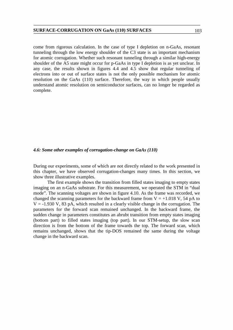
SURFACE-CORRUGATION ON GaAs (110) SURFACES 103
come from rigorous calculation. In the case of type I depletion on n-GaAs, resonanttunneling through the low energy shoulder of the C3 state is an important mechanismfor atomic corrugation. Whether such resonant tunneling through a similar high-energyshoulder of the A5 state might occur for p-GaAs in type I depletion is as yet unclear. Inany case, the results shown in figures 4.4 and 4.5 show that regular tunneling ofelectrons into or out of surface states is not the only possible mechanism for atomicresolution on the GaAs (110) surface. Therefore, the way in which people usuallyunderstand atomic resolution on semiconductor surfaces, can no longer be regarded ascomplete.
4.6: Some other examples of corrugation-change on GaAs (110)
During our experiments, some of which are not directly related to the work presented inthis chapter, we have observed corrugation-changes many times. In this section, weshow three illustrative examples.
The first example shows the transition from filled states imaging to empty statesimaging on an n-GaAs substrate. For this measurement, we operated the STM in “dualmode”. The scanning voltages are shown in figure 4.10. As the frame was recorded, wechanged the scanning parameters for the backward frame from V = +1.018 V, 54 pA toV = -1.930 V, 83 pA, which resulted in a clearly visible change in the corrugation. Theparameters for the forward scan remained unchanged. In the backward frame, thesudden change in parameters constitutes an abrubt transition from empty states imaging(bottom part) to filled states imaging (top part). In our STM-setup, the slow scandirection is from the bottom of the frame towards the top. The forward scan, whichremains unchanged, shows that the tip-DOS remained the same during the voltagechange in the backward scan.
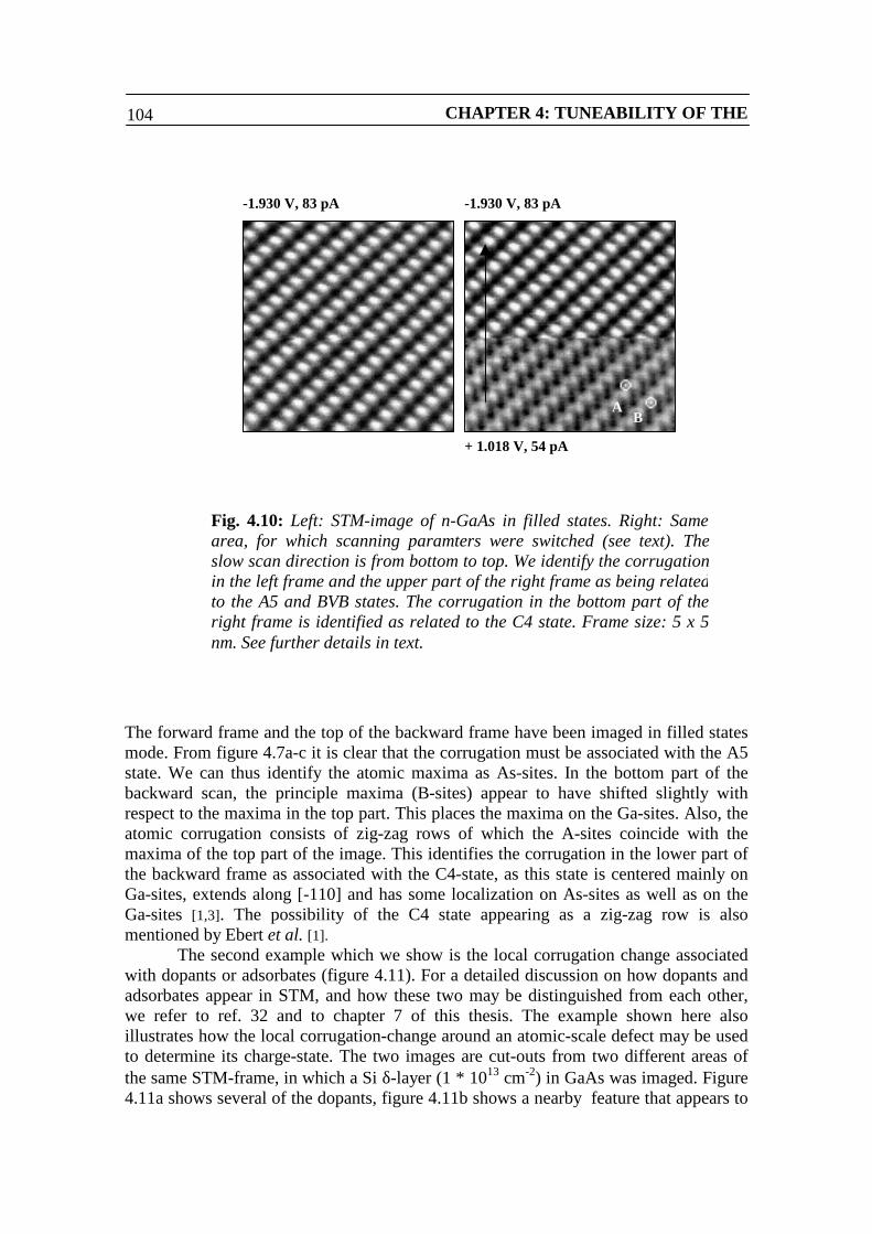
CHAPTER 4: TUNEABILITY OF THE104
The forward frame and the top of the backward frame have been imaged in filled statesmode. From figure 4.7a-c it is clear that the corrugation must be associated with the A5state. We can thus identify the atomic maxima as As-sites. In the bottom part of thebackward scan, the principle maxima (B-sites) appear to have shifted slightly withrespect to the maxima in the top part. This places the maxima on the Ga-sites. Also, theatomic corrugation consists of zig-zag rows of which the A-sites coincide with themaxima of the top part of the image. This identifies the corrugation in the lower part ofthe backward frame as associated with the C4-state, as this state is centered mainly onGa-sites, extends along [-110] and has some localization on As-sites as well as on theGa-sites [1,3]. The possibility of the C4 state appearing as a zig-zag row is alsomentioned by Ebert et al. [1].
The second example which we show is the local corrugation change associatedwith dopants or adsorbates (figure 4.11). For a detailed discussion on how dopants andadsorbates appear in STM, and how these two may be distinguished from each other,we refer to ref. 32 and to chapter 7 of this thesis. The example shown here alsoillustrates how the local corrugation-change around an atomic-scale defect may be usedto determine its charge-state. The two images are cut-outs from two different areas ofthe same STM-frame, in which a Si δ-layer (1 * 1013 cm-2) in GaAs was imaged. Figure4.11a shows several of the dopants, figure 4.11b shows a nearby feature that appears to
-1.930 V, 83 pA
Fig. 4.10: Left: STM-image of n-GaAs in filled states. Right: Samearea, for which scanning paramters were switched (see text). Theslow scan direction is from bottom to top. We identify the corrugationin the left frame and the upper part of the right frame as being relatedto the A5 and BVB states. The corrugation in the bottom part of theright frame is identified as related to the C4 state. Frame size: 5 x 5nm. See further details in text.
-1.930 V, 83 pA
+ 1.018 V, 54 pA
AB
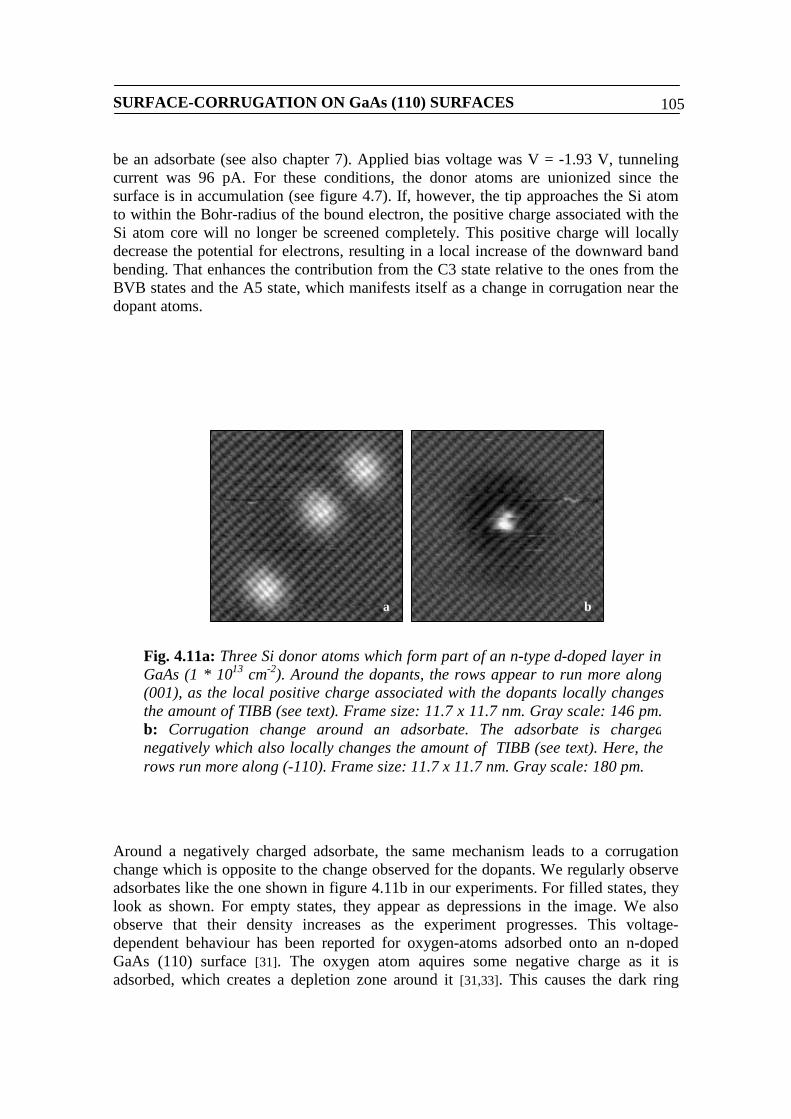
SURFACE-CORRUGATION ON GaAs (110) SURFACES 105
be an adsorbate (see also chapter 7). Applied bias voltage was V = -1.93 V, tunnelingcurrent was 96 pA. For these conditions, the donor atoms are unionized since thesurface is in accumulation (see figure 4.7). If, however, the tip approaches the Si atomto within the Bohr-radius of the bound electron, the positive charge associated with theSi atom core will no longer be screened completely. This positive charge will locallydecrease the potential for electrons, resulting in a local increase of the downward bandbending. That enhances the contribution from the C3 state relative to the ones from theBVB states and the A5 state, which manifests itself as a change in corrugation near thedopant atoms.
Around a negatively charged adsorbate, the same mechanism leads to a corrugationchange which is opposite to the change observed for the dopants. We regularly observeadsorbates like the one shown in figure 4.11b in our experiments. For filled states, theylook as shown. For empty states, they appear as depressions in the image. We alsoobserve that their density increases as the experiment progresses. This voltage-dependent behaviour has been reported for oxygen-atoms adsorbed onto an n-dopedGaAs (110) surface [31]. The oxygen atom aquires some negative charge as it isadsorbed, which creates a depletion zone around it [31,33]. This causes the dark ring
Fig. 4.11a: Three Si donor atoms which form part of an n-type δ-doped layer inGaAs (1 * 1013 cm-2). Around the dopants, the rows appear to run more along(001), as the local positive charge associated with the dopants locally changesthe amount of TIBB (see text). Frame size: 11.7 x 11.7 nm. Gray scale: 146 pm.b: Corrugation change around an adsorbate. The adsorbate is chargednegatively which also locally changes the amount of TIBB (see text). Here, therows run more along (-110). Frame size: 11.7 x 11.7 nm. Gray scale: 180 pm.
a b

CHAPTER 4: TUNEABILITY OF THE106
around the adsorbate. The negative charge locally raises the potential, raising theamount of TIBB in the vicinity of the adsorbate. This decreases the contribution fromthe C3 state relative to the contributions of the BVB states and the A5 state, whichcauses a change in corrugation as shown.
The last example that we wish to show is the corrugation change around a pnjunction (figure 4.12). This junction was formed by a Be δ-layer (1 * 1013 cm-2) and ann-doped cap layer (Si: 4 * 1018 cm-3) that was grown on top of it. The δ-layer wasovergrown by 27 nm of non-intentionally doped GaAs and then by n-type GaAs.Somewhere between the Be δ-layer and the the cap layer, a p-n junction formed whichwe recognized in our image from the depletion zone that is associated with such ajunction (figure 4.12). The bright spot near the depletion zone is a Si dopant. Near thebottom of the frame, where the depletion zone is curved, there is a second Si dopantwhich falls just outside the frame. The image was obtained at V = -1.698 V, 85 pA.
n-GaAs
p-GaAs
Fig. 4.12 a: STM-image of a pn-junction in GaAs (see text). Frame size: 35 x 35nm, V = -1.698 V, I = 85 pA. The depletion region associated with the pn-junction isvisible as a dark band running from the lower left part of the frame towards theupper right corner. The bright features in the n-GaAs part of the frame aresubsurface Si dopants, the bright feature surrounded by a dark ring can be either asurface layer dopant or an adsorbate (see chapter 7). b: The local change in atomiccorrugation on either side of a pn-junction. The area shown in (b) is indicated in (a)by the black box. Frame size: 20 x 20 nm, grey scale: 0 – 236 pm.
-110001a b
SURFACE-CORRUGATION ON GaAs (110) SURFACES 107
The n-GaAs portion of the image shows rows running along (001) whereas the p-GaAsportion shows rows running along (-110). The interpretation is relativelystraightforward: Due to the downward band bending, the n-GaAs portion of the surfaceis in accumulation. This populates the C3 state and causes the corrugation to be in the[-110]-direction. For the p-type portion of the surface, we expect contributions from theBVB states or possibly the A5 state, causing the corrugation to be in [001]. Thequantitative treatment of TIBB given earlier in this chapter is not very well applicablesince the model was developed for bulk materials. Due to the presence of the junction,the bandbending behaviour of the two portions of the frame may differ from the TIBBexpected for bulk material. Also, the fact that for the p-type material all dopants areconcentrated in a single δ-layer located at some distance from the junction mayinfluence the band bending behaviour.
4.7 Summary
In this chapter, we have combined voltage-dependent images of the GaAs (110) surfacewith calculated values for tip-induced band bending obtained from a one-dimensionalmodel, in order to study the influence of Tip-Induced Band Bending (TIBB) on voltage-dependent STM-images of GaAs-(110). For the empty-states results on n-GaAs we havevalidated the model by comparing measured and theoretical values for |dz/dV| as afunction of applied bias voltage. The work shows that TIBB influences the morphologyof the observed atomic lattice quite profoundly. Furthermore, for both p-GaAs and n-GaAs a voltage-regime exists for which no surface state lies inside the window ofenergetically accessible states between the Tip Fermi Level (TFL) and Sample FermiLevel (SFL) (type I depletion). Instead, tunneling occurs between the tip and bulk statesof the sample. In spite of that, atomic, surface-like corrugation is observed in thisvoltage regime, both on p-GaAs and on n-GaAs. In the case of n-GaAs, the observedcorrugation can be explained by resonant tunneling of electrons through the low-energyshoulder of the C3 state, for which it is known that it extends into the bandgap. For p-GaAs, several possible mechanisms exist. The corrugation might arise from resonanttunneling through a high-energy shoulder of the A5 state, if the A5 state has a shoulderwhich extends into the bandgap like the shoulder of the C3 state. The corrugation mightalso be caused by atomic-scale variations in the tunneling barrier-height as shown inrefs. 21 and 22, or by the interaction between tip- and sample electronic states. In anycase, the corrugation observed for the type I depletion regime cannot be explained byregular tunneling, which is the common way to understand atomic resolution onsemiconductor surfaces.
Looking ahead, a few things are apparent: In previous articles on voltage-dependent images of III-V semiconductor (110)-surfaces, band bending is only
CHAPTER 4: TUNEABILITY OF THE108
considered qualitatively [1,2,4]. In this work, we have established a connection betweenthe amount of TIBB and the corrugation observed in the image, which can be veryhelpful for the interpretation of existing and future STM-data. Local changes in thecorrugation provide a straightforward way to determine the charge-state of an atomic-scale surface defect. Another very exciting prospect is the fact that some of our STM-images show atomic corrugation in the absence of regular tunneling into or out ofsurface states. Understanding the mechanisms by which atomic corrugation might occurin the band bending regime of type I depletion represents a clear challenge.
REFERENCES:
1: Ph. Ebert, B. Engels, P. Richard, K. Schroeder, S. Blügel, C. Domke, M.Heinrich, K. Urban: Contribution of surface resonances to Scanning TunnelingMicroscopy images: (110) surfaces of III-V semiconductors. Phys. Rev. Lett,Vol. 77, No. 14, pp. 2997-3000 (1996).
2: C.S. Jiang,T. Nakayama, M. Aono: Tip-induced occupation of an unoccupiedsurface state in Scanning Tunneling Microscopy imaging of a GaAs (110)surface with Ag clusters. Japn. Journal of Appl. Phys, Vol. 36, pp. L1336-L1339(1997).
3: J.R. Chelikowski, M.L. Cohen: Self-consistent pseudopotential calculation forthe relaxed (110) surface of GaAs. Phys. Rev. B, Vol. 20, pp. 4150-4159 (1979).
4: B. Engels, P. Richard, K. Schroeder, S. Blügel, Ph. Ebert, K. Urban:Comparison between ab initio theory and Scanning Tunneling Microscopy for(110)-surfaces of III-V semiconductors. Phys. Rev. B, Vol. 58, No. 12, pp. 7799– 7814 (1998).
5: J.R. Chelikowski, S.G. Louie, M.L. Cohen: Relaxation effects on the (110)surface of GaAs. Phys. Rev. B, Vol. 14, No. 10, pp. 4724 - 4726 (1976).
SURFACE-CORRUGATION ON GaAs (110) SURFACES 109
6: J. Tersoff and D.R. Hamann, Phys. Rev. Lett. Vol. 50, No. 25, page 1998 –2001. Also: Phys. Rev. B, Vol. 31, No. 2, page 805 – 813.
7: C.J. Chen: Introduction to Scanning Tunneling Microscopy. Oxford UniversityPress, Oxford, 1993. Chapter 3 explains that for an s-like tip state, the tunnelingmatrix element is proportional to the surface-DOS of the sample evaluated at thecentre of the tip apex atom. The concept of “regular tunneling” is summarizedby equations 2.36 and 3.26.
8: G.J. de Raad, P.M. Koenraad, J.H. Wolter: The use of the Schiller-decapitationprocess for the manufacture of high-quality tungsten STM-tips. Journal of Vac.Sci. and Tech.-B, Vol. 17, No. 5, pp. 1946 - 1953 (1999).
9: R.M. Feenstra, J.A. Stroscio: Tunneling Spectroscopy of the GaAs (110) surface.JVST-B, Vol. 5, No. 4, page 923 (1987).
10: W.P. Dyke and W.W. Dolan: Field Emission, in Advances in Electronics andElectron Physics, vol VIII (1956) page 89 – 185. (Academic Press, New York,1956). See p. 114.
11: Handbook of Chemistry and Physics, Ed. 79, page 12-124.
12: R. Smoluchowski: Anisotropy of the electronic work function of metals. PhysicalReview, Vol. 60, pp. 661 – 674 (1941).
13: We use commercially available n-doped GaAs wafers with a nominal dopingconcentration of 1 * 1018 cm-3. The actual doping concentration may lie between1 and 2 * 1018 cm-3.
14: S.H. Ke, T. Uda, R. Perez, I. Stich, K. Terakura: First-principles investigationon GaAs (110) surface: Implications for atomic force and scanning tunnelingmicroscopies. To be published in Phys. Rev. B, issue of oct. 15, 1999. In thework presented in refs 9, 14 and 15, the tip is represented by a 4-atom Sitetrahedron. On the back side of the tetrahedron, the dangling bonds have beensaturated with hydrogen atoms.
15: R. Perez, I. Stich, M.C. Payne, K. Terakura: Surface-tip interactions in non-contact atomic-force microscopy on reactive surfaces: Si (111). Phys. Rev. B,Vol. 58, No. 16, pp. 10835 – 10849 (1998).
16: J. Tobik, I. Stich, R. Perez, K. Terakura: Simulation of tip-surface interactionsin atomic force microscopy of InP (110) surface with a Si tip. To be published inPhys.Rev. B, issue of oct. 15, 1999.
CHAPTER 4: TUNEABILITY OF THE110
17: G.J. de Raad, D.M. Bruls, P.M. Koenraad, and J.H. Wolter: Observation of anew image-form on GaAs-(110) showing the top- and bottom zig-zag rows of thesurface. Submitted to Phys. Rev. B.
18: Ciraci in: Scanning Tunneling Microscopy III, ed: Wiesendanger and Günteroth,Springer Verlag Berlin,p. 182, p. 197 (1996).
19: L.D. Bell, W.J. Kaiser, M.H. Hecht: Ballistic Electron Emission Microscopy, inScanning Tunneling Microscopy. (pp. 307 - 348). Edited by J.A. Stroscio andW.J. Kaiser. Academic Press, San Diego (1993).
20: E.F. Schubert: Doping in III-V semiconcductors. Cambridge University Press,Cambridge, p. 541 (1993).
21: N. Horiguchi, K. Yonei, M. Miyano: Local tunneling barrier height on Si (111)reconstructed surfaces. Japn. Journ. of Appl. Phys, Vol. 37, Part 1, No. 6B, pp.3782 – 3784 (1998).
22: H. Fukumizu, S. Kurokawa, A. Sakai, Y. Hasegawa: Barrier-height imaging ofSi (001) 2xn. Japn. Journ. of Appl. Phys, Vol. 37, Part 1, No. 6B, pp. 3785 –3788 (1998).
23: S. Ciraci, A. Baratoff, I.P. Batra: Site-dependent electronic effects, forces anddeformations in STM on flat metal surfaces. Phys. Rev. B, Vol. 42, No. 12, pp.7618 – 7621 (1990).
24: S. Ciraci, A. Baratoff, I.P. Batra: Tip-sample interaction effects in ScanningTunneling Microscopy and Atomic Force Microscopy. Phys. Rev. B, Vol. 41,No. 5, pp. 2763 – 2775 (1990).
25: E. Tekman, S. Ciraci: Atomic theory of Scanning Tunneling Microscopy. Phys.Rev. B, Vol. 40, No. 15, pp 10286 – 10293 (1989).
26: P.I. Arseev, N.S. Maslova: Features of tunneling in microjunctions. Sov. Phys.JETP, Vol. 75, No. 3, pp. 575 – 581 (1992).
27: R.L. DeKock, H.B. Gray: Chemical strucuture and bonding. TheBenjamin/Cummings Publishing Company, Menlo Park, CA (USA). (1980). Seep. 193, 253.
28: S. Ohnishi, M. Tsukada: Molecular orbital theory for Scanning TunnelingMicroscopy. Solid state comm. Vol. 71, No. 5, pp. 391 – 394 (1989).
29: M. Tsukada, K. Kobayashi, S. Ohnishi: First principle theory of ScanningTunneling Microscopy simulation. Journ. of Vac. Sci. and Tech. A, Vol. 8, No.1, pp. 160 – 165 (1990).
SURFACE-CORRUGATION ON GaAs (110) SURFACES 111
30: A.L. Vázquez de Parga, O.S. Hernán, R. Miranda, A. Levy Yeyati, n. Mingo, A.martín-Rodero, F. Flores: Electron resonances in sharp tips and their role intunneling spectroscopy. Phys. Rev. Lett, Vol. 80, No. 2, pp. 357 – 360 (1998).
31: J.A. Stroscio, R.M. Feenstra, A.P. Fein: Local state density and long-rangescreening of adsorbed oxygen atoms on the GaAs (110) surface. Phys. Rev. Lett,Vol. 58, No. 16, pp. 1668 – 1671 (1987).
32: Ph. Ebert: Nano-scale properties of defects in compound semiconductorsurfaces. Surf. Sci. Reports, Vol. 33, pp. 121 – 303 (1999).
33: J.A. Stroscio, R.M. Feenstra: Scanning tunneling spectroscopy of oxygenadsorbates on the GaAs (110) surface. Journ. of Vac. Sci. and Tech-B, Vol. 6,No. 4, pp. 1472 – 1478 (1988).
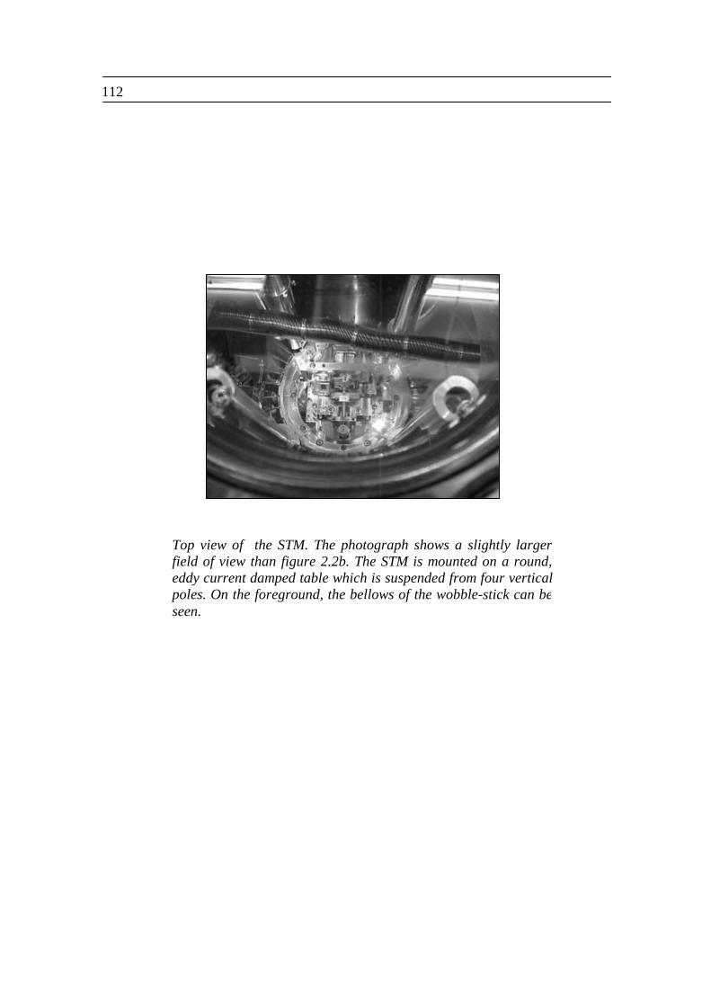
112
Top view of the STM. The photograph shows a slightly largerfield of view than figure 2.2b. The STM is mounted on a round,eddy current damped table which is suspended from four verticalpoles. On the foreground, the bellows of the wobble-stick can beseen.
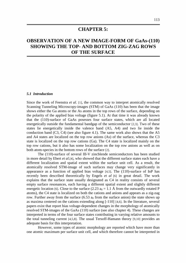
113
CHAPTER 5:
OBSERVATION OF A NEW IMAGE-FORM OF GaAs-(110)SHOWING THE TOP- AND BOTTOM ZIG-ZAG ROWS
OF THE SURFACE
5.1 Introduction
Since the work of Feenstra et al. [1], the common way to interpret atomically resolvedScanning Tunneling Microscopy-images (STM) of GaAs (110) has been that the imageshows either the Ga atoms or the As atoms in the top rows of the surface, depending onthe polarity of the applied bias voltage (figure 5.1). At that time it was already knownthat the (110)-surface of GaAs posesses four surface states, which are all locatedenergetically outside the fundamental bandgap of the semiconductor [2,3]. Two of thesestates lie energetically inside the valence band (A5, A4) and two lie inside theconduction band (C3, C4) (see also figure 4.1). The same work also shows that the A5and A4 states are localized on the top row anions (As) of the surface, whereas the C3state is localized on the top row cations (Ga). The C4 state is localized mainly on thetop row cations, but it also has some localization on the top row anions as well as onboth atom-species in the bottom rows of the surface [2].
The (110)-surface of several III-V zincblende semiconductors has been studiedin more detail by Ebert et al.[4], who showed that the different surface states each have adifferent localization and spatial extent within the surface unit cell. As a result, theatomically resolved STM-image of such surfaces may change very significantly inappearance as a function of applied bias voltage [4,5]. The (110)-surface of InP hasrecently been described theoretically by Engels et al [6] in great detail. The workexplains that the surface state usually designated as C4 in reality consists of severalempty surface resonances, each having a different spatial extent and slightly differentenergetic location [6]. Close to the surface (2.23 a0 = 1.1 Å from the outwardly rotated Patoms), the C4 state is localized on both the cations and anions and appears as a zig-zagrow. Further away from the surface (6.53 a0 from the surface anion) the state shows upas maxima centered on the cations extending along [-110] [4,6]. In the literature, severalpapers exist that report bias voltage-dependent changes in the morphology of atomicallyresolved STM-images of the GaAs (110) surface (see also chapter 4). These changes areinterpreted in terms of the four surface states contributing in varying relative amounts tothe total tunneling current [4,5,8]. The usual Tersoff-Hamann theory [9,10] provides anadequate basis for this interpretation.
However, some types of atomic morphology are reported which have more thanone atomic maximum per surface unit cell, and which therefore cannot be interpreted in
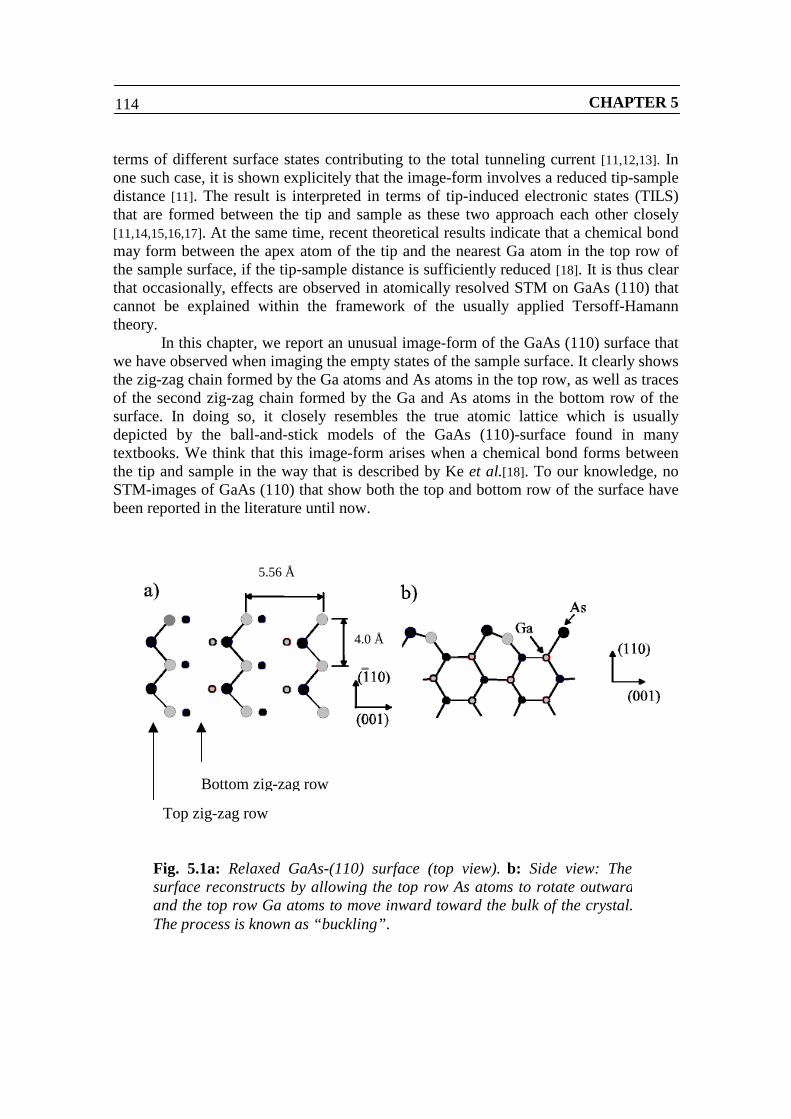
CHAPTER 5114
terms of different surface states contributing to the total tunneling current [11,12,13]. Inone such case, it is shown explicitely that the image-form involves a reduced tip-sampledistance [11]. The result is interpreted in terms of tip-induced electronic states (TILS)that are formed between the tip and sample as these two approach each other closely[11,14,15,16,17]. At the same time, recent theoretical results indicate that a chemical bondmay form between the apex atom of the tip and the nearest Ga atom in the top row ofthe sample surface, if the tip-sample distance is sufficiently reduced [18]. It is thus clearthat occasionally, effects are observed in atomically resolved STM on GaAs (110) thatcannot be explained within the framework of the usually applied Tersoff-Hamanntheory.
In this chapter, we report an unusual image-form of the GaAs (110) surface thatwe have observed when imaging the empty states of the sample surface. It clearly showsthe zig-zag chain formed by the Ga atoms and As atoms in the top row, as well as tracesof the second zig-zag chain formed by the Ga and As atoms in the bottom row of thesurface. In doing so, it closely resembles the true atomic lattice which is usuallydepicted by the ball-and-stick models of the GaAs (110)-surface found in manytextbooks. We think that this image-form arises when a chemical bond forms betweenthe tip and sample in the way that is described by Ke et al.[18]. To our knowledge, noSTM-images of GaAs (110) that show both the top and bottom row of the surface havebeen reported in the literature until now.
Fig. 5.1a: Relaxed GaAs-(110) surface (top view). b: Side view: Thesurface reconstructs by allowing the top row As atoms to rotate outwardand the top row Ga atoms to move inward toward the bulk of the crystal.The process is known as “buckling”.
Top zig-zag row
Bottom zig-zag row
5.56 Å
4.0 Å
OBSERVATION OF A NEW IMAGE-FORM OF GaAs-(110) 115
Notice that the appearance of the bottom zig-zag row of the surface cannot be explainedwithin the framework of regular tunneling (see section 1.10). An important point in theTersoff-Hamann theory is that the tunneling matrix element is proportional to the localsample surface DOS evaluated at the position of the centre of the tip apex atom [7]: TheSTM-image shows the vacuum-tails of the surface states. A direct consequence is thatin the framework of the Tersoff-Hamann theory, features in the sample-DOS that liewithin the surface layer do not appear in the STM-image.
5.2 Experimental
The STM-work was performed in UHV on in situ cleaved GaAs crystals. The sampleswere doped n-type (Si) to a dopant concentration [19] of 1018 cm-3. The bias voltage isapplied to the sample. All images shown in this chapter were obtained while operatingthe STM in constant current mode. To most of the images, we have applied abackground correction to the images that involves the “line-by-line tilt correction”,which is descibed in detail in section 2.5. For figure 5.3 d we used a band-pass fastFourier transform (FFT) filter to show details of the lattice in all parts of the frame.
5.3 True Lattice Resemblant Corrugation
The novel image-form that we report occurs occasionally as an anomaly when we makevoltage-dependent images of GaAs (110). So far, we have observed the image-form,which we label “True Lattice Resemblant Corrugation” (TLRC: see figure 2a), whenimaging the empty states of n-GaAs (110) using a small value for the bias voltage (0 V< Vbias < 0.5 V). The image-form is stable for a variable amount of time: It sometimeslasts no longer than several seconds or a minute, or it can last for up to 30 minutes as wehave observed on one occasion. The image-form TLRC can be reproduced, but wecannot obtain it at will or in a very controlled manner. The method that we apply toobtain TLRC is by imaging the (110) surface of GaAs at positive sample voltage so asto produce normal-looking atomic resolution, which we can obtain routinely. From thatpoint, we gradually decrease the applied bias voltage and/or increase the tunnelingcurrent, so as to decrease the tip-sample distance. Some of these attempts produceTLRC, the others simply fail with a tip-crash.
The appearance of TLRC always involves a sudden transition from the normalimaging mode in which the atomically resolved lattice of the GaAs-(110) surfaceappears as it usually does (see e.g. refs. 1, 5, 20), to an anomalous mode which involvesTLRC. An example of such a transition is shown in figure 2c. In this particular case, theonset of TLRC involved a sudden transition from the normal morphology of the
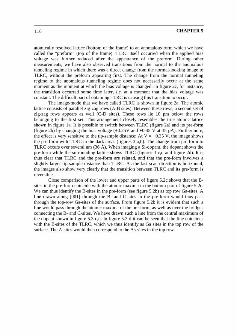
CHAPTER 5116
atomically resolved lattice (bottom of the frame) to an anomalous form which we havecalled the “preform” (top of the frame). TLRC itself occurred when the applied biasvoltage was further reduced after the appearance of the preform. During othermeasurements, we have also observed transitions from the normal to the anomaloustunneling regime in which there was a direct change from the normal-looking image toTLRC, without the preform appearing first. The change from the normal tunnelingregime to the anomalous tunneling regime does not necessarily occur at the samemoment as the moment at which the bias voltage is changed: In figure 2c, for instance,the transition occurred some time later, i.e. at a moment that the bias voltage wasconstant. The difficult part of obtaining TLRC is causing this transition to occur.
The image-mode that we have called TLRC is shown in figure 2a. The atomiclattice consists of parallel zig-zag rows (A-B sites). Between these rows, a second set ofzig-zag rows appears as well (C-D sites). These rows lie 10 pm below the rowsbelonging to the first set. This arrangement closely resembles the true atomic latticeshown in figure 1a. It is possible to switch between TLRC (figure 2a) and its pre-form(figure 2b) by changing the bias voltage (+0.25V and +0.45 V at 35 pA). Furthermore,the effect is very sensitive to the tip-sample distance: At V = +0.35 V, the image showsthe pre-form with TLRC in the dark areas (figures 3 a,b). The change from pre-form toTLRC occurs over several nm (36 Å). When imaging a Si-dopant, the dopant shows thepre-form while the surrounding lattice shows TLRC (figures 3 c,d and figure 2d). It isthus clear that TLRC and the pre-form are related, and that the pre-form involves aslightly larger tip-sample distance than TLRC. As the fast scan direction is horizontal,the images also show very clearly that the transition between TLRC and its pre-form isreversible.
Close comparison of the lower and upper parts of figure 5.2c shows that the B-sites in the pre-form coincide with the atomic maxima in the bottom part of figure 5.2c.We can thus identify the B-sites in the pre-form (see figure 5.2b) as top row Ga-sites. Aline drawn along [001] through the B- and C-sites in the pre-form would thus passthrough the top-row Ga-sites of the surface. From figure 5.2b it is evident that such aline would pass through the atomic maxima of the pre-form, as well as over the bridgesconnecting the B- and C-sites. We have drawn such a line from the central maximum ofthe dopant shown in figure 5.3 c,d. In figure 5.3 d it can be seen that the line coincideswith the B-sites of the TLRC, which we thus identify as Ga sites in the top row of thesurface. The A-sites would then correspond to the As-sites in the top row.
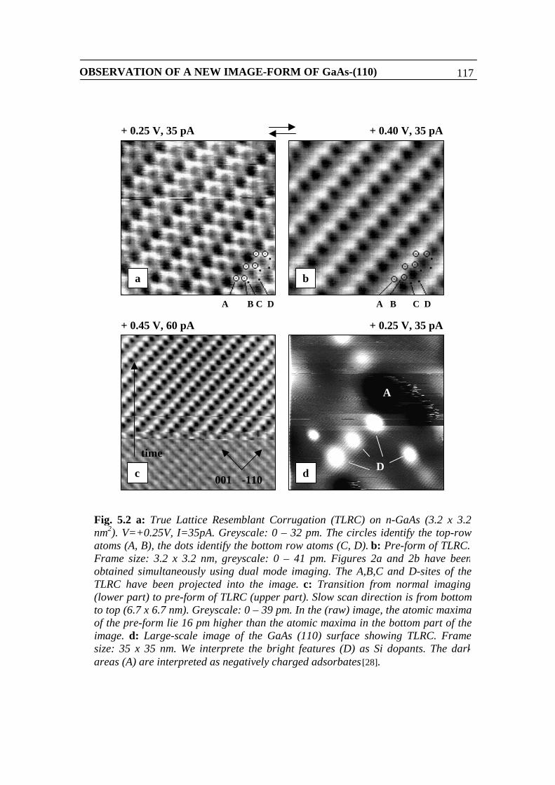
OBSERVATION OF A NEW IMAGE-FORM OF GaAs-(110) 117
ba
A B C D
+ 0.25 V, 35 pA + 0.40 V, 35 pA
A B C D
+ 0.45 V, 60 pA
time
c -110001 d
+ 0.25 V, 35 pA
D
A
Fig. 5.2 a: True Lattice Resemblant Corrugation (TLRC) on n-GaAs (3.2 x 3.2nm2). V=+0.25V, I=35pA. Greyscale: 0 – 32 pm. The circles identify the top-rowatoms (A, B), the dots identify the bottom row atoms (C, D). b: Pre-form of TLRC.Frame size: 3.2 x 3.2 nm, greyscale: 0 – 41 pm. Figures 2a and 2b have beenobtained simultaneously using dual mode imaging. The A,B,C and D-sites of theTLRC have been projected into the image. c: Transition from normal imaging(lower part) to pre-form of TLRC (upper part). Slow scan direction is from bottomto top (6.7 x 6.7 nm). Greyscale: 0 – 39 pm. In the (raw) image, the atomic maximaof the pre-form lie 16 pm higher than the atomic maxima in the bottom part of theimage. d: Large-scale image of the GaAs (110) surface showing TLRC. Framesize: 35 x 35 nm. We interprete the bright features (D) as Si dopants. The darkareas (A) are interpreted as negatively charged adsorbates [28].
CHAPTER 5118
+ 0.35 V, 35 pA
b
+0.25V, 35 pA (FFT)+0.25V, 35 pA
a D
D
ADep
+ 0.35 V, 35 pA
Fig. 5.3 a,b: Transition from the pre-form to TLRC (V = 0.35 V, I = 35 pA). Suchtransitions occur in areas where the local tunneling probability changes, whichcauses an adjustment in the tip-sample distance. The top right corner of figure 3b ispart of a shallow, circular depression that lies 78 – 108 pm below the surroundinglattice (Dep). The depression is about 10 nm in diameter, and possibly represents a(negatively charged) subsurface SiAs acceptor. Similar transitions from the pre-form to TLRC occur near adsorbates (A). Figure a: frame size: 20 x 20 nm; figureb: frame size: 6.7 x 6.7 nm, greyscale: 0 – 34 pm. c: High-resolution imageshowing one of the Si dopant shown in figure 2d in detail. Near the dopant, the pre-form is seen while around the dopant the image shows TLRC. The apparent heightof the dopant is 149 pm with respect to the surrounding lattice. V = +0.25 V, I = 35pA, frame size: 5.8 x 5.8 nm, greyscale: 0 – 199 pm. d: Same as (c), afterapplication of a band-pass fast Fourier transform filter. Greyscale: 0 – 27 pm. Aline drawn along [001] from the maxima of the pre-form coincides with the B-sitesof the TLRC.
c d
OBSERVATION OF A NEW IMAGE-FORM OF GaAs-(110) 119
5.4 Discussion
In earlier literature, STM-images obtained in the filled states mode showing both the Gaand As atoms in the top row of the surface have been reported by Jäger et al.[12] andHeinrich et al.[11]. In ref. 11 it was shown that this type of imaging involves asignificantly smaller tip-sample distance than usual. To our knowledge, however, noSTM-images of GaAs-(110) that also show traces of also the bottom zig-zag row havebeen reported in the literature. An image-form similar to TLRC has also been observedon InAs (110) [13].
From the model and experimental results presented in chapter 4 concerning“normal” atomically resolved images of GaAs-(110), it is clear that for small positivesample bias, the distance between the tunneling tip and an n-type sample becomes verysensitive to changes in the applied bias voltage (figure 4.8). Also, the tip-sampledistance can rapidly decrease to a few Å at small bias voltage (figure 4.8 b,e). Thevoltage at which the rapid decrease in tip-sample distance sets in, depends on the exactvalue of the tip work function [5]. The tip work function, in its turn, varies from oneexperiment to the next and usually also changes when a spontaneous change in the tip-DOS occurs. However, given the fact that TLRC occurs for low bias voltage, thehypothesis that the mechanism behind it involves a short tip-sample distance is logical.
Recent theoretical calculations predict that the-(110)-surface of GaAs undergoessome very significant changes as it is being approached closely by a tip. The calculationhas been carried out in order to model the atomic resolution recently obtained in non-contact AFM on GaAs-(110). Using a four-atom Si cluster to represent an AFM-tip, ithas been predicted by Ke et al. that under influence of the tip-sample interaction, thenearest Ga atom in the top row can relax outward: When the tip approaches the samplesurface to within 3 Å, a chemical bond may form between the Si apex atom and one ofthe Ga atoms in the top row of the surface. The vertical displacement of the Ga atom inthis configuration can be up to 1 Å. This decreases, or even partly reverses the bucklingangle of the surface, since the displacement of the nearest As atom in the top row, for atip-sample distance of 3 Å, is less than the displacement of the Ga atom [18]. If the tip iswithdrawn again, the tip-sample distance has to be increased to about 5 Å before thebond between the apex atom and the Ga atom is ruptured. When, after the formation ofthe bond, the tip is approached further still, the Ga atom and Si apex atom relax slightlyfurther. For a tip-sample distance of less than about 2 Å, the interaction becomesrepulsive [18]. The method used by Ke et al. has been based on earlier work by Perez etal.[21] in which the tip-sample interaction between a similar Si tip cluster and a Si-(111)surface has been modeled in great detail. A calculation similar to the one performed byKe et al. has also been carried out for InP-(110) by Tobik et al.[22], showing that therelaxation of the InP-(110) surface under the influence of tip-sample interaction differsfrom the relaxation predicted for GaAs-(110).
The decrease of the buckling angle by itself has a profound effect on theelectronic structure of the GaAs-(110) surface: As has been shown by Chelikowski, theC3 state moves up in energy whereas the C4 state comes down [2,3]. For the unrelaxed(truncated bulk) surface, the C4 state lies energetically near the middle of the bulkbandgap whereas the C3 state lies in the bulk conduction band. The significance of thisis that it thus becomes possible to image only the C4-state at small positive bias voltage
A B
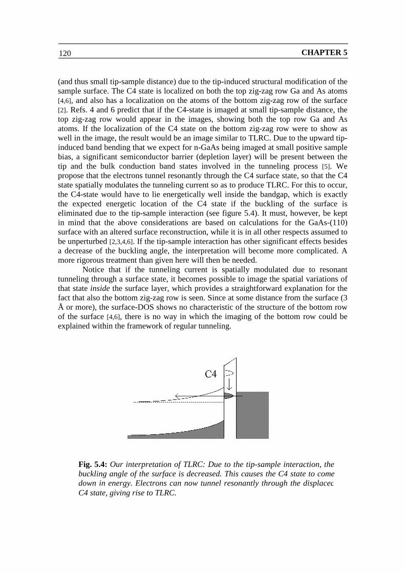
CHAPTER 5120
(and thus small tip-sample distance) due to the tip-induced structural modification of thesample surface. The C4 state is localized on both the top zig-zag row Ga and As atoms[4,6], and also has a localization on the atoms of the bottom zig-zag row of the surface[2]. Refs. 4 and 6 predict that if the C4-state is imaged at small tip-sample distance, thetop zig-zag row would appear in the images, showing both the top row Ga and Asatoms. If the localization of the C4 state on the bottom zig-zag row were to show aswell in the image, the result would be an image similar to TLRC. Due to the upward tip-induced band bending that we expect for n-GaAs being imaged at small positive samplebias, a significant semiconductor barrier (depletion layer) will be present between thetip and the bulk conduction band states involved in the tunneling process [5]. Wepropose that the electrons tunnel resonantly through the C4 surface state, so that the C4state spatially modulates the tunneling current so as to produce TLRC. For this to occur,the C4-state would have to lie energetically well inside the bandgap, which is exactlythe expected energetic location of the C4 state if the buckling of the surface iseliminated due to the tip-sample interaction (see figure 5.4). It must, however, be keptin mind that the above considerations are based on calculations for the GaAs-(110)surface with an altered surface reconstruction, while it is in all other respects assumed tobe unperturbed [2,3,4,6]. If the tip-sample interaction has other significant effects besidesa decrease of the buckling angle, the interpretation will become more complicated. Amore rigorous treatment than given here will then be needed.
Notice that if the tunneling current is spatially modulated due to resonanttunneling through a surface state, it becomes possible to image the spatial variations ofthat state inside the surface layer, which provides a straightforward explanation for thefact that also the bottom zig-zag row is seen. Since at some distance from the surface (3Å or more), the surface-DOS shows no characteristic of the structure of the bottom rowof the surface [4,6], there is no way in which the imaging of the bottom row could beexplained within the framework of regular tunneling.
Fig. 5.4: Our interpretation of TLRC: Due to the tip-sample interaction, thebuckling angle of the surface is decreased. This causes the C4 state to comedown in energy. Electrons can now tunnel resonantly through the displacedC4 state, giving rise to TLRC.
OBSERVATION OF A NEW IMAGE-FORM OF GaAs-(110) 121
If an atomic bond is formed between the tip and sample, and this bond is dragged alongthe surface as the tip is scanned, the Ga atoms over which the tip apex passes will relaxoutward, modifying the electronic structure of the surface accordingly. The suddenformation of an atomic bond would provide a very natural explanation for the suddenonset of the pre-form of TLRC which is seen in figure 5.2c. It would also explain whythe image mode remained stable afterward, as the formation and rupture of this bondinvolves hysteresis. Although the hysteresis is reported to be strongest at lowtemperature, it is still expected to be there at room temperature as well [18]. Finally,since the Ga atom and Si apex atom in the model relax slightly more if the tip andsample approach each other even more closely after the formation of the bond [18], itwould also explain the many smooth transitions between TLRC and the pre-form thatwe have observed. It is clear that once the atomic bond between the tip and sample hasformed, the interpretation of the resulting STM-image must be done in terms of tip-induced localized states (TILS) [15,17], in a fashion similar to the way that the results inref. 11 are interpreted. All in all, it seems plausible that the formation of a chemicalbond between the apex atom of the tip and the Ga atoms of the sample is the underlyingmechanism of TLRC and its pre-form.
We have considered alternative possible explanations for TLRC. The most importantone is the hypothesis that TLRC is caused by an unusual tip-state. The central idea isthat somehow, the tip-DOS is such that the regular surface-DOS of the GaAs-(110)surface is imaged twice. If the two atomically resolved images are shifted with respectto each other, the resulting image might show two maxima and two minima per unitcell. An unfortunate arrangement of these two images could, in theory, result in animage similar to the one shown in fig. 2a. Although it is unclear to us how thismechanism might explain the observed dependence of TLRC on the tip-sample distanceand bias voltage, the thought in itself is hardly surprising: The sudden transition shownin figure 5.2c looks very similar to the image obtained when a spontaneous tip-changeoccurs during scanning. It is also known that, for instance, monoatomic steps aresometimes imaged twice, indicating that the tip has a double apex. Other examples ofsuch “double imaging” have been reported by Mizes et al. [23] and Park et al. [24].
In our experiments it sometimes occurs that the tunneling tip has a double apex.The presence of such a double apex is easily recognized because in that case mono-atomic steps, adsorbates, dopants and other features of a larger scale than the atomiclattice appear in pairs in the image. Moreover, the features in one such pair have a fixeddistance and relative orientation. If the tip used in the measurement would have had adouble apex, this would have manifested itself in the larger-scale images (figures 2d and3a) that we aquired during the same measurement. These images show no sign of a tipwith a double apex. Besides, on those occasions that the tip does have a double apex, itis observed that the atomic lattice of the surface can be imaged quite normally, becauseone of the two apeces is (almost) always slightly closer to the sample surface than theother. We are thus convinced that the images presented in this paper have been acquiredwith a tip that only had a single apex. Moreover, the atomic resolution that we obtainedboth before and after the sudden onset of the pre-form (figure 5.2c), suggests that theapex of the tip that was used ended in a single atom rather than a micro-facet.
CHAPTER 5122
For a tip that ends in a single atom, some electronic states exist that have two spatiallyseparated lobes extending equally far towards the sample surface (see e.g. the dxz-state)[10]. Let us now consider the likelihood of occurrence and possible effects on the STM-image of such a “double lobed” tip state with regards to TLRC. Based on the results ofcluster (W4 and W5) calculations [10,25,26,27] it is generally agreed that for a tungsten tipending in a single apex atom, a dz
2-like surface state dominates the tip-DOS near theFermi level. In the same energetic region a dxy-state is also predicted, but this state onlycarries a fraction of the total tunneling current (10-4) when such a cluster is broughtclose to a model surface. Even when a tip-sample distance of 3 Å is assumed in thesecalculations, the dz
2-dominates the dxy-state. Furthermore, Sachs and Noguera [30] showfor a clean tungsten tip that s- and d- type states dominate the DOS of a tungsten tipapex near the Fermi level, although a p-type state may dominate the tip-DOS if aforeign atom is adsorbed on the apex.
A very important point has been made by Kobayashi et al. [31] by simulating thetunneling process between a graphite surface and the bonding and antibondingmolecular orbitals of the H2-molecule: If the active tunneling orbital has two spatiallyseparated lobes which both carry a portion of the tunneling current, the resulting STM-image need not be a superposition of the two independent images. The two tunnelingcurrents interfere with each other. In the case of tunneling between the bonding orbitaland the graphite surface, the calculated STM-image was similar to the ideal STM-imageof graphite. For tunneling between the antibonding orbital and the graphite surface, theimage was severely distorted, the distortion depending on the orientation of the orbitalwith respect to the graphite surface. In neither of the two cases, a period-doubling of thegraphite lattice was found. A distorted image similar to the one found for theantibonding orbital is predicted for a dzx-like orbital [31] and for the tunneling activeorbital of a ⟨110⟩-oriented W-tip with a missing apex atom [26,32].
These results are in apparent conflict with the experimental results reported byPark et al.[24], who reports the occurrence of two superimposed, independent images ofthe adatom pattern of the (7x7)-reconstruction of Si-(111). Some of the shifts betweenthe images are as small as 4 Å. It must however be noted that the tips used in theirexperiment were used immediately after ac etching, without further in vacuo treatment.This means that their tips must certainly have had a thin oxide layer on them. We do notknow how this affects the interference effect described by Kobayashi, but it is clear thatan oxide layer with saturated bonds does not represent the situation considered in ref.31. Furthermore, the adatoms in the 7x7 reconstruction of Si (111) studied by Park et al.lie relatively far apart (7.68 Å). It is possible that the tip has imaged each of the adatomsseparately, rather than having an interaction with the electronic structure of the surfacelattice as is the case for tunneling on an atomically flat surface. This may also explainthe difference between their conclusions and the predictions made in ref 31.
We expect that our own tips, given the elaborate in vacuo treatment [20] that weapply and the fact that we routinely obtain atomic resolution on GaAs 110 [5,20], aresharp and free of oxides. From the larger-scale images taken during the samemeasurement it seems very unlikely that the tip used in our measurement had a doubleapex. For a clean tungsten tip ending in a single apex atom, the presence of a tip-statewith two lobes extending to the surface does not lead to a superposition of twoindependent images [25,26,27,31]. We therefore conclude that the interpretation of TLRC

OBSERVATION OF A NEW IMAGE-FORM OF GaAs-(110) 123
in terms of a chemical bond forming between the tip apex and the Ga atoms in thesurface is the most plausible one.
At this point, the physical meaning of atomically resolved STM-images of the(110)-surface of GaAs and other zincblende III-V semiconductors seems wellunderstood as long as the tip-sample interaction remains small enough for the Tersoff-Hamann theory to apply [4,6]. However, once the tip-sample interaction does becomesignificant, the images can change in drastic and poorly understood ways. Although therecent theoretical work on the interaction between a semiconductor surface and a nearbytip [18,21,22] was meant to explain the recently obtained atomic resolution onzincblende-(110) surfaces by dynamic Scanning Force Microscopy [29], it certainly hasequally much relevance to STM-images as well. The occasional occurrence of TLRCand related image-forms [11,12,13] on such zincblende-(110) surfaces shows that the tip-sample interaction can profoundly influence the appearance of the atomically resolvedlattice in STM. Although this influence is often unwanted, it can in principle also beused to obtain new image-forms. Understanding these new image-forms and making useof the tip-sample interaction to obtain them, holds interesting challenges for theoristsand experimentalists alike.
5.5: Summary and conclusion
We report an unusual image-form of the GaAs (110) surface that occasionally occurswhen imaging the empty states of that surface. It closely resembles the true atomiclattice. We propose that the image-form arises when a chemical bond forms between thetip and sample in the way that is predicted theoretically by Ke et al.[18]. This involves asignificant reduction of the buckling angle of the surface. For the free GaAs (110)surface, such a reduction of the buckling angle is known to shift the C3 and C4 surfacestates, causing the C4-state to lie well inside the bandgap of the semiconductor [2]. Ifelectrons then tunnel resonantly through the shifted C4 state, the resulting image willshow the localization of the C4 state within the surface layer, resulting in TLRC.We have considered the possibility that the image form that we have observed mighthave been caused by an unusual electronic state present at the apex of the tunneling tip.From simulations of tunneling between a multi-lobed tip-state and a sample surface thatare reported in the literature, it seems unlikely that such a tip state will lead to an image-form with more than one atomic maximum per surface unit cell [31]. The results show aclear perspective to a new and very interesting way to image the (110)-surface of GaAs.

CHAPTER 5124
RERENCES:
1: R.M. Feenstra, J.A. Stroscio, J.A. Tersoff, A.P. Fein: Atom-selective imaging ofthe GaAs (110) surface. Phys. Rev. Lett, Vol. 58, No. 12, pp. 1192 – 1195(1985).
2: J.R. Chelikowski, M.L. Cohen: Self-consistent pseudopotential calculation forthe relaxed (110) surface of GaAs. Phys. Rev. B, Vol. 20, pp. 4150-4159 (1979).
3: J.R. Chelikowski, S.G. Louie, M.L. Cohen: Relaxation effects on the (110)surface of GaAs. Phys. Rev. B, Vol. 14, No. 10, pp. 4724 - 4726 (1976).
4: Ph. Ebert, B. Engels, P. Richard, K. Schroeder, S. Blügel, C. Domke, M.Heinrich, K. Urban: Contribution of surface resonances to Scanning TunnelingMicroscopy images: (110) surfaces of III-V semiconductors. Phys. Rev. Lett,Vol. 77, No. 14, pp. 2997-3000 (1996).
5: G.J. de Raad, D.M. Bruls, P.M. Koenraad, J.H. Wolter: Interplay between tip-induced band bending and voltage-depending surface-corrugation on GaAs-(110) surfaces. (To be published). The series of frames preceeding TLRC is anearly measurement similar to the results shown in this reference. See alsochapter 4 of this thesis.
6: B. Engels, P. Richard, K. Schroeder, S. Blügel, Ph. Ebert, K. Urban:Comparison between ab initio theory and Scanning Tunneling Microscopy for(110)-surfaces of III-V semiconductors. Phys. Rev. B, Vol. 58, No. 12, pp. 7799– 7814 (1998).
8: C.S. Jiang,T. Nakayama, M. Aono: Tip-induced occupation of an unoccupiedsurface state in Scanning Tunneling Microscopy imaging of a GaAs (110)surface with Ag clusters. Jap. Journal of Appl. Phys, Vol. 36, pp. L1336-L1339(1997).
9: J. Tersoff and D.R. Hamann, Phys. Rev. Lett. Vol. 50, No. 25, page 1998 –2001. Also: Phys. Rev. B, Vol. 31, No. 2, page 805 – 813.
10: C.J. Chen: Introduction to Scanning Tunneling Microscopy. Oxford UniversityPress, Oxford, 1993. Chapter 3 explains that for an s-like tip state, the tunnelingmatrix element is proportional to the surface-DOS of the sample evaluated at thecentre of the tip apex atom. The usual interpretation of STM-results is wellsummarized by equations 2.36 and 3.26
OBSERVATION OF A NEW IMAGE-FORM OF GaAs-(110) 125
11: A.J. Heinrich, M. Wenderoth, M.A. Rosentreter, M.A. Schneider, R.G. Ulrich:Scanning Tunneling Microscopy of the atomic structure of the GaAs (110)surface at reduced tip sample separation. Appl. Phys. Lett, Vol. 70, No. 4, pp449 – 451 (1996). See also: Ordering in Ternary compound Semiconductors onthe atomic scale. PhD-thesis by A.J. Heinrich, Cuvillier Verlag, Göttingen,Germany (1998). The thesis shows that for small tip-sample distance, thebandgap evident in I(V)-spectra taken at normal tip-sample distances disappears.
12: N.D. Jäger, X. Liu, J.F. Zheng, N Newman, D.F. Olgletree, E.R. Weber, M.Salmeron: Scanning Tunneling Microscoy of the GaAs (110) surface at low bias:23rd International Conference on the Physics of Semiconductors (WorldScientific, Berlin), pp. 847 – 850.
13: A. Depuydt et al, University of Leuven, Belgium. Private communication.
14: Ciraci in: Scanning Tunneling Microscopy III, ed: Wiesendanger and Günteroth,Springer Verlag Berlin,p. 182, p. 197 (1996).
15: S. Ciraci, A. Baratoff, I.P. Batra: Site-dependent electronic effects, forces anddeformations in STM on flat metal surfaces. Phys. Rev. B, Vol. 42, No. 12, pp.7618 – 7621 (1990).
16: S. Ciraci, A. Baratoff, I.P. Batra: Tip-sample interaction effects in ScanningTunneling Microscopy and Atomic Force Microscopy. Phys. Rev. B, Vol. 41,No. 5, pp. 2763 – 2775 (1990).
17: E. Tekman, S. Ciraci: Atomic theory of Scanning Tunneling Microscopy. Phys.Rev. B, Vol. 40, No. 15, pp 10286 – 10293 (1989).
18: S.H. Ke, T. Uda, R. Perez, I. Stich, K. Terakura: First-principles investigationon GaAs (110) surface: Implications for atomic force and scanning tunnelingmicroscopies. Phys. Rev. B, Vol. 60, Iss. 16, pp. 11631 - 11639 (1999). In thework presented in refs 9, 14 and 15, the tip is represented by a 4-atom Sitetrahedron. On the back side of the tetrahedron, the dangling bonds have beensaturated with hydrogen atoms.
19: We use commercially available n-doped GaAs wafers with a nominal dopingconcentration of 1 * 1018 cm-3. The actual doping concentration may lie between1 and 2 * 1018 cm-3.
20: G.J. de Raad, P.M. Koenraad, J.H. Wolter: The use of the Schiller-decapitationprocess for the manufacture of high-quality tungsten STM-tips. Journ. of Vac.Sci. and Tech-B, Vol. 17, Iss. 5, pp. 1946 – 1953 (1999).

CHAPTER 5126
21: R. Perez, I. Stich, M.C. Payne, K. Terakura: Surface-tip interactions in non-contact atomic-force microscopy on reactive surfaces: Si (111). Phys. Rev. B,Vol. 58, No. 16, pp. 10835 – 10849 (1998). See also chapter 3 of this thesis.
22: J. Tobik, I. Stich, R. Perez, K. Terakura: Simulation of tip-surface interactionsin atomic force microscopy of InP (110) surface with a Si tip. Phys.Rev. B, Vol.60, pp. 11659 (1999).
23: H.A. Mizes, S.I. Park, W.A. Harrison: Multiple-tip interpretation of anomalousScanning Tunneling Microscopy images of layered materials. Phys. Rev. B, Vol.36, No. 8, pp. 4491 – 4494 (1987).
24: S.I. Park, J. Nogami, C.F. Quate: Effect of tip morphology on images obtainedby Scanning Tunneling Microscopy. Phys. Rev. B, Vol. 36, No. 5, pp. 2863 –2866 (1987).
25: S. Ohnishi, M. Tsukada: Molecular orbital theory for Scanning TunnelingMicroscopy. Solid state comm. Vol. 71, No. 5, pp. 391 – 394 (1989).
26: M. Tsukada, K. Kobayashi, S. Ohnishi: First principle theory of ScanningTunneling Microscopy simulation. Journ. of Vac. Sci. and Tech. A, Vol. 8, No.1, pp. 160 – 165 (1990).
27: M. Tsukada, N. Shima, S. Ohnishi, Y. Chiba: Effect of the tip/sample surfaceelectronic states and the electron-phonon coupling on the current in ScanningTunneling Microscopy. Journal de Physique, Colloque 6, Suppl. 11, Tome 48,nov. 1987.
28: J.A. Stroscio, R.M. Feenstra, A.P. Fein: Local state density and long-rangescreening of adsorbed oxygen atoms on the GaAs (110) surface. Phys. Rev. Lett,Vol. 58, No. 16, pp. 1668 – 1671 (1987).
29: A. Schwarz, W. Allers, U.D. Schwarz, R. Wiesendanger: Simultaneous imagingof the In and As sublattice on InAs (110) 1x1 with dynamic scanning forcemicroscopy. Appl. Surf. Sci, Vol. 140, pp. 293 – 297 (1999).
30: W. Sacks, C. Noguera: Generalized expression for the tunneling current inScanning Tunneling Microscopy. Phys. Rev. B, Vol. 43, No. 14, pp. 11612 –11622 (1991).
31: K. Kobayashi, M. Tsukada: Effect of microscopic tip electronic state onScanning Tunneling Microscopy image of graphite. Journ. of Phys. Soc. ofJapan, Vol. 58, No. 7, pp. 2238 – 2241 (1989).
32: M. Tsukada, K. Kobayashi, N. Isshiki: First-principles theory of ScanningTunneling Microscopy. Surface Science Reports 13 (1991), pp. 265 – 304.
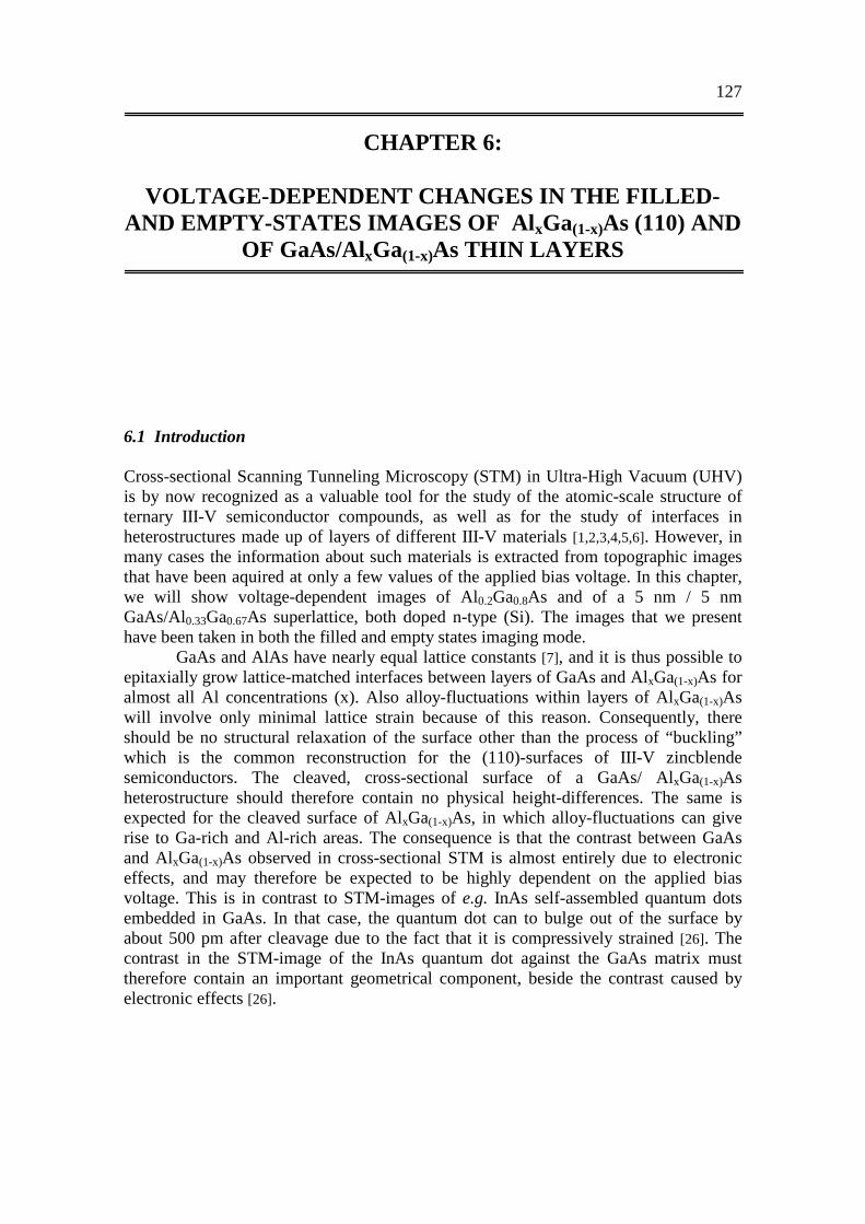
127
CHAPTER 6:
VOLTAGE-DEPENDENT CHANGES IN THE FILLED-AND EMPTY-STATES IMAGES OF AlxGa(1-x)As (110) AND
OF GaAs/AlxGa(1-x)As THIN LAYERS
6.1 Introduction
Cross-sectional Scanning Tunneling Microscopy (STM) in Ultra-High Vacuum (UHV)is by now recognized as a valuable tool for the study of the atomic-scale structure ofternary III-V semiconductor compounds, as well as for the study of interfaces inheterostructures made up of layers of different III-V materials [1,2,3,4,5,6]. However, inmany cases the information about such materials is extracted from topographic imagesthat have been aquired at only a few values of the applied bias voltage. In this chapter,we will show voltage-dependent images of Al0.2Ga0.8As and of a 5 nm / 5 nmGaAs/Al0.33Ga0.67As superlattice, both doped n-type (Si). The images that we presenthave been taken in both the filled and empty states imaging mode.
GaAs and AlAs have nearly equal lattice constants [7], and it is thus possible toepitaxially grow lattice-matched interfaces between layers of GaAs and AlxGa(1-x)As foralmost all Al concentrations (x). Also alloy-fluctuations within layers of AlxGa(1-x)Aswill involve only minimal lattice strain because of this reason. Consequently, thereshould be no structural relaxation of the surface other than the process of “buckling”which is the common reconstruction for the (110)-surfaces of III-V zincblendesemiconductors. The cleaved, cross-sectional surface of a GaAs/ AlxGa(1-x)Asheterostructure should therefore contain no physical height-differences. The same isexpected for the cleaved surface of AlxGa(1-x)As, in which alloy-fluctuations can giverise to Ga-rich and Al-rich areas. The consequence is that the contrast between GaAsand AlxGa(1-x)As observed in cross-sectional STM is almost entirely due to electroniceffects, and may therefore be expected to be highly dependent on the applied biasvoltage. This is in contrast to STM-images of e.g. InAs self-assembled quantum dotsembedded in GaAs. In that case, the quantum dot can to bulge out of the surface byabout 500 pm after cleavage due to the fact that it is compressively strained [26]. Thecontrast in the STM-image of the InAs quantum dot against the GaAs matrix musttherefore contain an important geometrical component, beside the contrast caused byelectronic effects [26].
CHAPTER 6: VOLTAGE-DEPENDENT IMAGES128
Fig. 6.1a: Calculated electronic band structrure of the GaAs-(110) surface. Theprojected bulk band structure is shown as the hatched regions. Taken from ref.12. b: Calculated electronic band structure of the AlAs-(110) surface. Theprojected bulk band structure is represented by the hatched regions. Taken fromref. 24.
a b
GaAs (110) AlAs (110)

OF AlGaAs AND OF GaAs/AlGaAs THIN LAYERS 129
To our knowledge, no theoretical STM-images have been calculated for the (110)-surface of AlxGa(1-x)As or AlAs, although the band structure and relaxation of the AlAs(110) surface has been described by Grossi et al. [24] (figure 1). The electronic structureof AlAs is very similar to that of GaP [15,16]. In both semiconductors the top of thevalence-band lies at the Γ-point of the Brillouin zone (BZ), whereas the bottom of theconduction-band lies at or near the X-point. In a direct semiconductor like GaAs or InP,both the valence band maximum (VBM) and the conduction band minimum (CBM)occur at the Γ-point of the bulk BZ [15]. In ref. 8, voltage-dependent changes in atomicmorphology are presented for GaP, InP and GaAs (110). In qualitative terms thechanges are the same for all three compounds, and can be compared meaningfully totheoretical STM-images that the authors calculate from the surface-density of states(surface-DOS) of InP (110).
The (110)-surface of GaP has been described theoretically by Manghi et al. [19].Comparison of that article with the work of Chelikowski et al. [20] and with that ofGrossi et al. [24] shows that the surface-DOS of the relaxed (110)-surfaces of GaAs,GaP and AlAs are similar to each other. Near the fundamental bandgap, the same sufacestates exist (A4, A5, C3, C4). They also have the same relative energetic positions,although for GaP (110) the energetic location of the surface states is only given at thefour symmetry-points of the surface-BZ. We can thus assume that for AlAs (110) andAlxGa(1-x)As (110), the same voltage-dependent changes in the atomic morphology willoccur as for GaAs (110), InP (110) and GaP (110). A significant difference between thesurface electronic structure of GaP (110) and that of GaAs (110) is the fact that theconduction-band related surface states (C3 and C4) of GaP lie energetically inside theupper part of the bandgap of the semiconductor [19,20]. This appears not to influence thevoltage-dependent changes in atomic corrugation reported in ref. 8. For AlAs (110), thedispersion-curve of the C3-state has its minimum near the X-point in the surfaceBrioullin zone [24]. For most k-points in the surface Brioullin zone, the dispersion-curveof the C3 –state lies near the bulk-CBM [24].
Since in our experiments the nominal Al fractions were 0.20 and 0.33, theAlxGa(1-x)As layers that we studied should still be “GaAs-like”, having a direct bandgapwith the smallest energetic distance between the conduction-band and valence-band atthe Γ-point of the BZ [15]. However, the material may be “AlAs-like”, i.e. have anindirect bandgap, in areas where the local Al fraction exceeds 0.33 [15]. Wheninterpreting the voltage-dependent changes in the atomic corrugation that we observe onn-AlGaAs (110), we make the assumption that the surface-DOS is essentially like thatof GaAs (110). The complete similarity of the corrugation-changes observed for n-AlGaAs with those that we have seen on n-GaAs is consistent with that assumption [11].From ref. 24, it seems likely that for AlxGa(1-x)As (110), the influence of (the lower partof) the C3-state on the corrugation in the image is stronger than it is for GaAs (110).
The voltage-dependent images presented in this chapter show that the atomicmorphology of AlxGa(1-x)As and thin GaAs/AlxGa(1-x)As layers indeed very stronglydepends on the value of the applied bias voltage, and involves several other effectsbesides the changes in the apparent direction of the atomic rows which are alsoobserved on binary III-V semiconductors [8,9,10,11]. When an n-type semiconductor isimaged at small, negative sample voltage, an accumulation layer of electrons occupiesthe electron-states located just above the bottom of the conduction-band. At small,
CHAPTER 6: VOLTAGE-DEPENDENT IMAGES130
negative voltage we observe for AlGaAs (110) a morphology that we interprete in termsof fluctuations in the density of electrons in this accumulation layer. Moreover, weobserve for the superlattice an inversion of contrast between GaAs and AlGaAs for lowvoltage of either polarity. In the empty-states mode at intermediate voltage, an apparentwidening of the GaAs layers in the GaAs/AlGaAs superlattice indicates that we imagethe confined electron-level of the quantum wells that are formed by the GaAs layerssandwiched between the AlGaAs layers.
We also observe that the positions of local maxima and minima associated withalloy-fluctuations do not coincide when the same area of AlGaAs-surface is imagedsimultaneously in filled and empty states mode. This means that the surface-DOS of thevalence-band related surface states (A4 and A5) [10,12,13] significantly differs from thesurface-DOS of the conduction-band related surface states (C3 and C4), and that therelation between the atomic structure and the resulting surface-DOS is far morecomplicated than is often assumed. Until this relation is fully known, unambiguousstatements about the atomic structure of AlxGa(1-x)As cannot be made from atomicallyresolved STM-images.
6.2 Experiment
The STM-work was performed in UHV (OMICRON STM-1 setup operated at 4 * 10-11
torr) on in situ cleaved samples. These samples consisted of a GaAs substrate (nominaldoping concentration 1018 cm-3 Si), on which a GaAs/AlGaAs superlattice andsubsequently a bulk AlGaAs layer were grown by Molecular Beam Epitaxy (MBE). Thesuperlattice was n-doped (Si), GaAs: 1018 cm-3, Al0.33Ga0.67As: 6.67*1017 cm-3. TheGaAs and AlGaAs layers in the superlattice were each 50 Å, the total thickness of thesuperlattice was 1 µm. On top of the superlattice, a 4 µm Al0.2Ga0.8As layer (dopingconcentration: 5 * 1017 cm-3 Si) was deposited. The bias voltage is applied to thesample. All images shown in this chapter are height-images [z(x,y)] that were obtainedwhile operating the STM in constant current mode. We use a one-dimensional model tocalculate the amount of tip-induced band bending (TIBB) that we expect in ourexperiments on AlGaAs (see chapter 4). We have used another model to calculate theband offsets and position of the Fermi level in the superlattice (figure 6.11). Whilediscussing the voltage-dependent changes in our images, we use an absolute scale forthe applied bias voltage (-1 V < -2 V).

OF AlGaAs AND OF GaAs/AlGaAs THIN LAYERS 131
6.3 Results
We now present voltage-dependent images of n-type Al0.2Ga0.8As (110) (figures 6.2:filled states; figure 6.3: empty states). In figure 6.4, we present cut-outs showing detailsof the atomically resolved lattice. It can be seen that the atomic morphology of theAlGaAs-surface depends quite strongly on the applied bias voltage. The voltage-dependent changes in the apparent direction of the atomic rows are similar to what isreported in chapter 4 for GaAs (110). However, due to the heterogenic nature ofAlxGa(1-x)As, other voltage-dependent effects are seen as well. We will also presentfilled and empty-states images of the same area of Al0.2Ga0.8As (figure 6.6). In theseimages, it is seen very clearly that the shapes and locations of the alloy-related minimachange as a function of the polarity of the applied bias voltage. Finally, we presentvoltage-dependent images of an n-type GaAs/Al0.33Ga0.67As superlattice (5 nm / 5 nm).These images also consist of both filled and empty states images (figures 6.7 and 6.8).
The filled-states images (figure 6.2) were taken on roughly the same patch ofsample surface, although we did experience some drift as the images were aquired.From the last four images where adsorbates can be used as reference-points, it is evidentthat the bright areas do not shift in position on the surface as the voltage is changed. Theheight-profiles shown in fig. 5 show that the height-differences associated with thebright spots are larger than the height-differences associated with the Al-relateddepressions observed at higher voltage.
The empty-states images (figure 6.3) have been aquired at a different location onthe same AlGaAs-layer. The bright, sharp-bordered feature is interpreted as anadsorbate in analogy with figure 6.9 d,e where a similar feature appears in the imageduring scanning. We interprete the fuzzy, bright feature above it as a Si dopant. Theentire sequence of empty-states images has been obtained in “dual mode”: On theforward leg of the tip-motion the voltage was varied, on the backward one it was keptconstant at V = -2.193 V. We can thus directly compare the filled and empty statesimages of Al0.2Ga0.8As. We have analyzed one such pair of a filled-states and an empty-states image of the same area as a representative example (-2.193 V, 75 pA / +1.222 V,54 pA).
In order to correlate the dark and bright areas in the two frames, we haveprojected varying sets of contour-lines of the filled-states image into the empty-statesimage and vice versa (figure 6.6). In the empty-states image we have drawn thecontour-line z = 9 pm, which encloses all minima, and z = 23 pm, which encloses allmaxima (see inset in figure 6.6a). A second contour line at z = 75 pm encloses theadsorbate and is used for alignment. For the filled states image, similar contour lineswere drawn for z = 8 pm and z = 18 pm. At low positive voltage, small ridges orientedalong the [-110]-direction appear in the image. Figures 6.6 g and 6.6 h are used tocompare the position of these ridges with the position of the alloy-related maxima andalloy-related minima that appear at large, positive voltage.
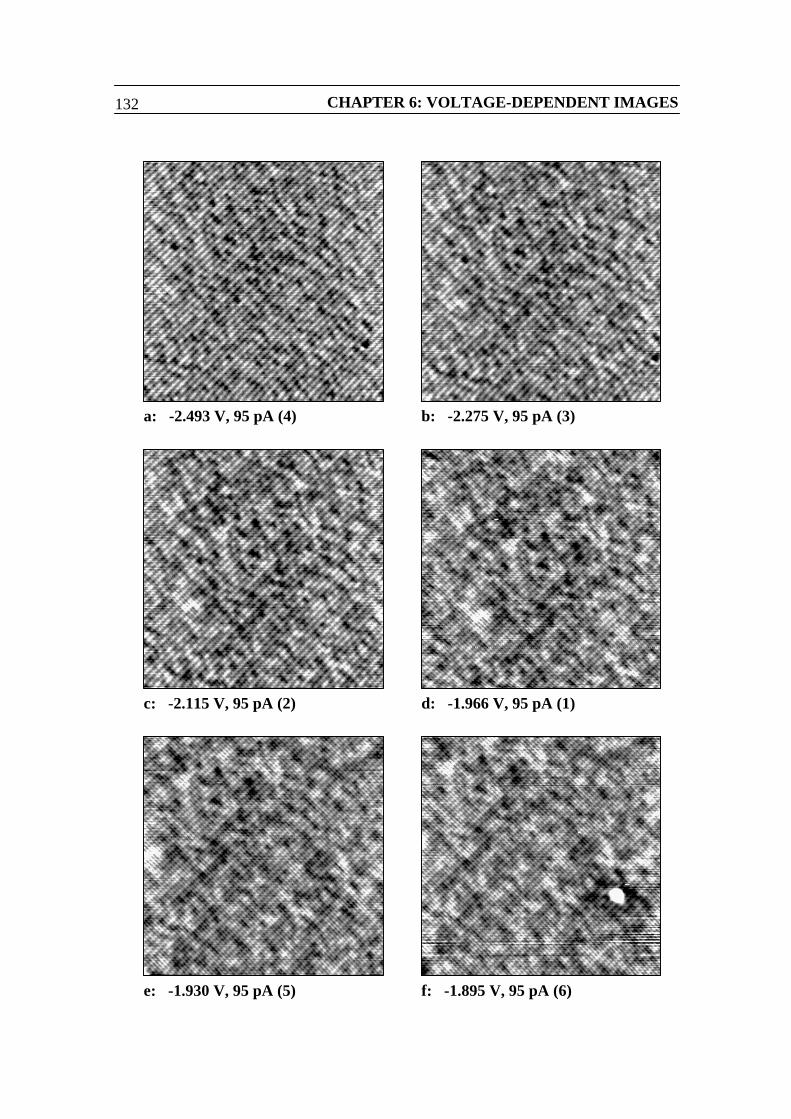
CHAPTER 6: VOLTAGE-DEPENDENT IMAGES132
a: -2.493 V, 95 pA (4) b: -2.275 V, 95 pA (3)
c: -2.115 V, 95 pA (2) d: -1.966 V, 95 pA (1)
e: -1.930 V, 95 pA (5) f: -1.895 V, 95 pA (6)

OF AlGaAs AND OF GaAs/AlGaAs THIN LAYERS 133
i: -1.667 V, 95 pA (9)
h: -1.730 V, 95 pA (8)g: -1.827 V, 95 pA (7)
Fig. 6.2: (both pages) Filled states STM-images of n-type Al0.2Ga0.8As. Framesize: 25 x 25 nm. The number in parenthesis indicates the order in time in whichthe images were aquired. In the last four images, adsorbates appear.
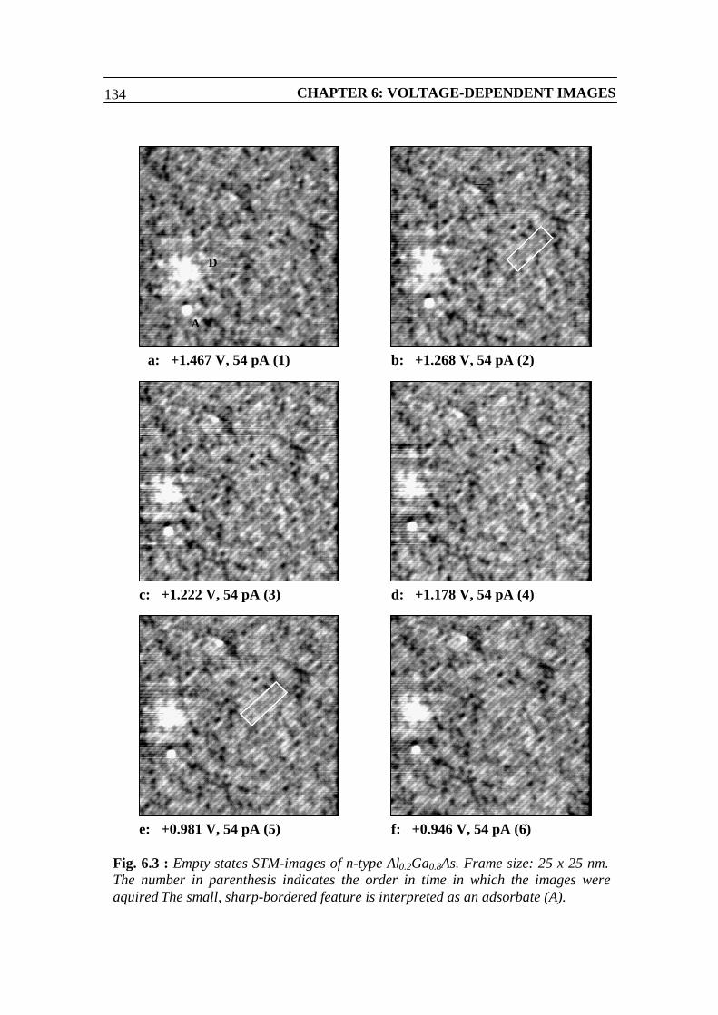
CHAPTER 6: VOLTAGE-DEPENDENT IMAGES134
a: +1.467 V, 54 pA (1) b: +1.268 V, 54 pA (2)
c: +1.222 V, 54 pA (3) d: +1.178 V, 54 pA (4)
e: +0.981 V, 54 pA (5) f: +0.946 V, 54 pA (6)
Fig. 6.3 : Empty states STM-images of n-type Al0.2Ga0.8As. Frame size: 25 x 25 nm.The number in parenthesis indicates the order in time in which the images wereaquired The small, sharp-bordered feature is interpreted as an adsorbate (A).
D
A
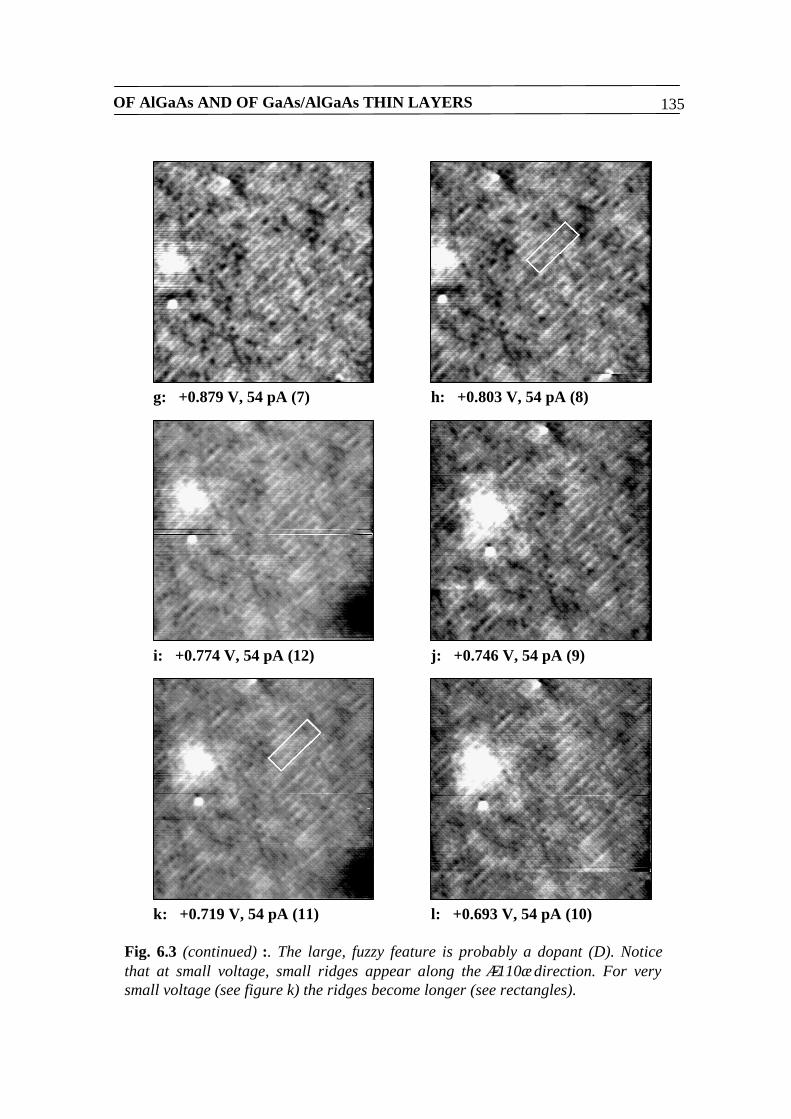
OF AlGaAs AND OF GaAs/AlGaAs THIN LAYERS 135
l: +0.693 V, 54 pA (10)k: +0.719 V, 54 pA (11)
j: +0.746 V, 54 pA (9)i: +0.774 V, 54 pA (12)
h: +0.803 V, 54 pA (8)g: +0.879 V, 54 pA (7)
Fig. 6.3 (continued) :. The large, fuzzy feature is probably a dopant (D). Noticethat at small voltage, small ridges appear along the ⟨-110⟩ direction. For verysmall voltage (see figure k) the ridges become longer (see rectangles).
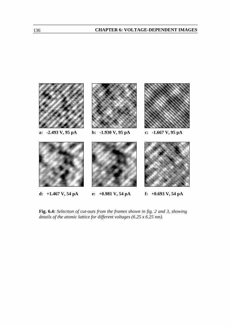
CHAPTER 6: VOLTAGE-DEPENDENT IMAGES136
b: -1.930 V, 95 pA c: -1.667 V, 95 pAa: -2.493 V, 95 pA
d: +1.467 V, 54 pA e: +0.981 V, 54 pA f: +0.693 V, 54 pA
Fig. 6.4: Selection of cut-outs from the frames shown in fig. 2 and 3, showingdetails of the atomic lattice for different voltages (6.25 x 6.25 nm).
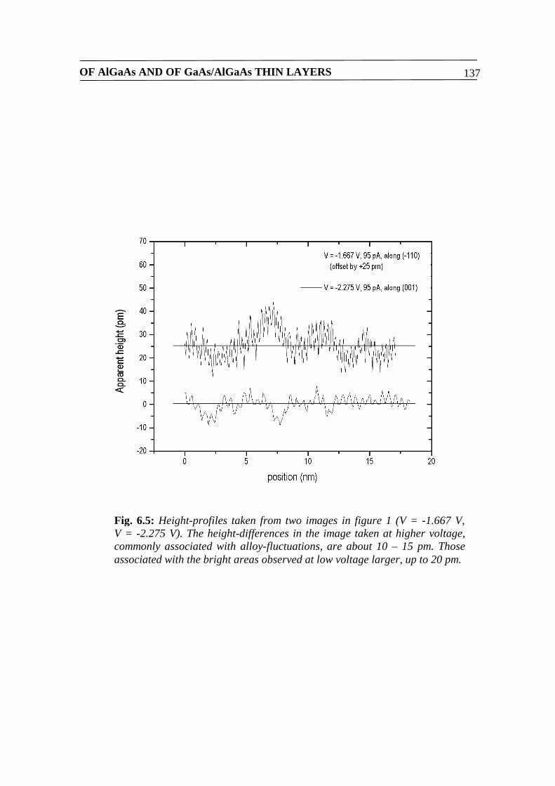
OF AlGaAs AND OF GaAs/AlGaAs THIN LAYERS 137
Fig. 6.5: Height-profiles taken from two images in figure 1 (V = -1.667 V,V = -2.275 V). The height-differences in the image taken at higher voltage,commonly associated with alloy-fluctuations, are about 10 – 15 pm. Thoseassociated with the bright areas observed at low voltage larger, up to 20 pm.
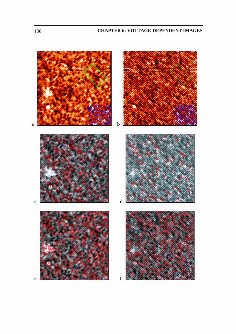
CHAPTER 6: VOLTAGE-DEPENDENT IMAGES138
a b
c d
e f
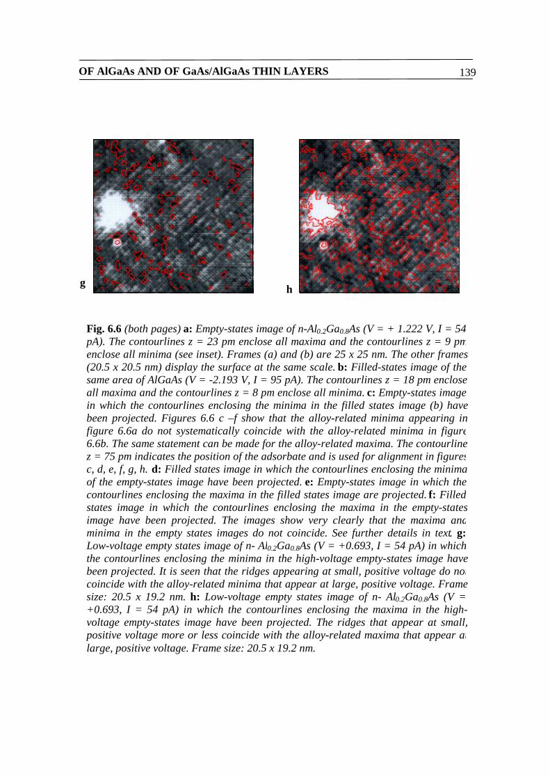
OF AlGaAs AND OF GaAs/AlGaAs THIN LAYERS 139
Fig. 6.6 (both pages) a: Empty-states image of n-Al0.2Ga0.8As (V = + 1.222 V, I = 54pA). The contourlines z = 23 pm enclose all maxima and the contourlines z = 9 pmenclose all minima (see inset). Frames (a) and (b) are 25 x 25 nm. The other frames(20.5 x 20.5 nm) display the surface at the same scale. b: Filled-states image of thesame area of AlGaAs (V = -2.193 V, I = 95 pA). The contourlines z = 18 pm encloseall maxima and the contourlines z = 8 pm enclose all minima. c: Empty-states imagein which the contourlines enclosing the minima in the filled states image (b) havebeen projected. Figures 6.6 c –f show that the alloy-related minima appearing infigure 6.6a do not systematically coincide with the alloy-related minima in figure6.6b. The same statement can be made for the alloy-related maxima. The contourlinez = 75 pm indicates the position of the adsorbate and is used for alignment in figuresc, d, e, f, g, h. d: Filled states image in which the contourlines enclosing the minimaof the empty-states image have been projected. e: Empty-states image in which thecontourlines enclosing the maxima in the filled states image are projected. f: Filledstates image in which the contourlines enclosing the maxima in the empty-statesimage have been projected. The images show very clearly that the maxima andminima in the empty states images do not coincide. See further details in text. g:Low-voltage empty states image of n- Al0.2Ga0.8As (V = +0.693, I = 54 pA) in whichthe contourlines enclosing the minima in the high-voltage empty-states image havebeen projected. It is seen that the ridges appearing at small, positive voltage do notcoincide with the alloy-related minima that appear at large, positive voltage. Framesize: 20.5 x 19.2 nm. h: Low-voltage empty states image of n- Al0.2Ga0.8As (V =+0.693, I = 54 pA) in which the contourlines enclosing the maxima in the high-voltage empty-states image have been projected. The ridges that appear at small,positive voltage more or less coincide with the alloy-related maxima that appear atlarge, positive voltage. Frame size: 20.5 x 19.2 nm.
g h
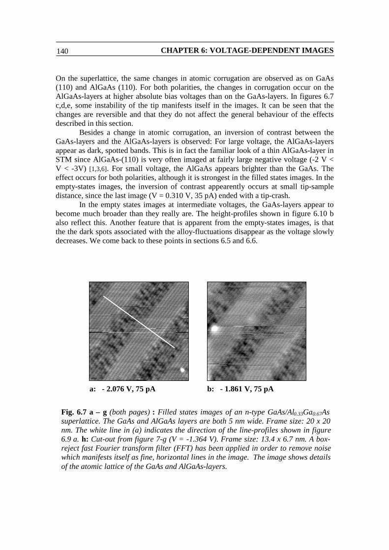
CHAPTER 6: VOLTAGE-DEPENDENT IMAGES140
On the superlattice, the same changes in atomic corrugation are observed as on GaAs(110) and AlGaAs (110). For both polarities, the changes in corrugation occur on theAlGaAs-layers at higher absolute bias voltages than on the GaAs-layers. In figures 6.7c,d,e, some instability of the tip manifests itself in the images. It can be seen that thechanges are reversible and that they do not affect the general behaviour of the effectsdescribed in this section.
Besides a change in atomic corrugation, an inversion of contrast between theGaAs-layers and the AlGaAs-layers is observed: For large voltage, the AlGaAs-layersappear as dark, spotted bands. This is in fact the familiar look of a thin AlGaAs-layer inSTM since AlGaAs-(110) is very often imaged at fairly large negative voltage (-2 V <V < -3V) [1,3,6]. For small voltage, the AlGaAs appears brighter than the GaAs. Theeffect occurs for both polarities, although it is strongest in the filled states images. In theempty-states images, the inversion of contrast appearently occurs at small tip-sampledistance, since the last image (V = 0.310 V, 35 pA) ended with a tip-crash.
In the empty states images at intermediate voltages, the GaAs-layers appear tobecome much broader than they really are. The height-profiles shown in figure 6.10 balso reflect this. Another feature that is apparent from the empty-states images, is thatthe the dark spots associated with the alloy-fluctuations disappear as the voltage slowlydecreases. We come back to these points in sections 6.5 and 6.6.
iFig. 6.7 a – g (both pages) : Filled states images of an n-type GaAs/Al0.33Ga0.67Assuperlattice. The GaAs and AlGaAs layers are both 5 nm wide. Frame size: 20 x 20nm. The white line in (a) indicates the direction of the line-profiles shown in figure6.9 a. h: Cut-out from figure 7-g (V = -1.364 V). Frame size: 13.4 x 6.7 nm. A box-reject fast Fourier transform filter (FFT) has been applied in order to remove noisewhich manifests itself as fine, horizontal lines in the image. The image shows detailsof the atomic lattice of the GaAs and AlGaAs-layers.
a: - 2.076 V, 75 pA b: - 1.861 V, 75 pA
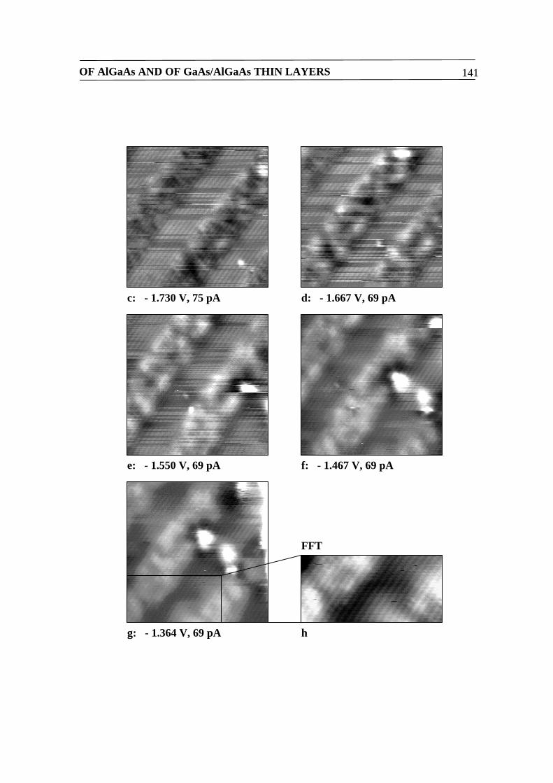
OF AlGaAs AND OF GaAs/AlGaAs THIN LAYERS 141
c: - 1.730 V, 75 pA d: - 1.667 V, 69 pA
e: - 1.550 V, 69 pA f: - 1.467 V, 69 pA
g: - 1.364 V, 69 pA h
FFT
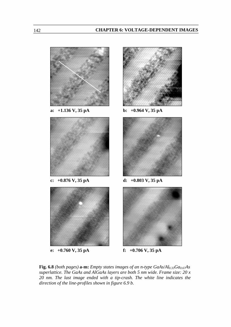
CHAPTER 6: VOLTAGE-DEPENDENT IMAGES142
e: +0.760 V, 35 pA f: +0.706 V, 35 pA
a: +1.136 V, 35 pA b: +0.964 V, 35 pA
c: +0.876 V, 35 pA
Fig. 6.8 (both pages) a-m: Empty states images of an n-type GaAs/Al0.33Ga0.67Assuperlattice. The GaAs and AlGaAs layers are both 5 nm wide. Frame size: 20 x20 nm. The last image ended with a tip-crash. The white line indicates thedirection of the line-profiles shown in figure 6.9 b.
d: +0.803 V, 35 pA
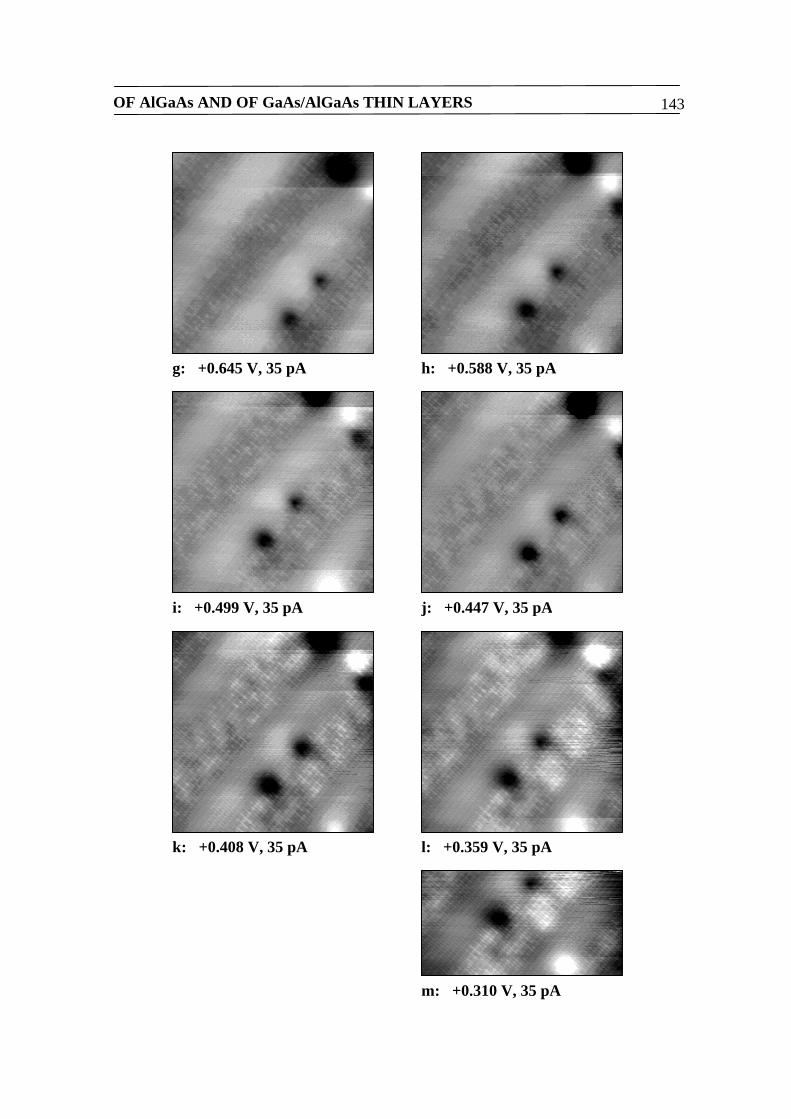
OF AlGaAs AND OF GaAs/AlGaAs THIN LAYERS 143
g: +0.645 V, 35 pA h: +0.588 V, 35 pA
i: +0.499 V, 35 pA j: +0.447 V, 35 pA
k: +0.408 V, 35 pA l: +0.359 V, 35 pA
m: +0.310 V, 35 pA
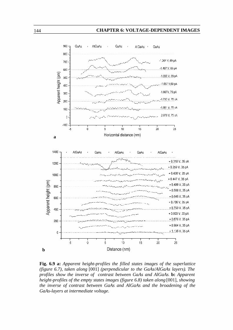
CHAPTER 6: VOLTAGE-DEPENDENT IMAGES144
Fig. 6.9 a: Apparent height-profiles the filled states images of the superlattice(figure 6.7), taken along [001] (perpendicular to the GaAs/AlGaAs layers). Theprofiles show the inverse of contrast between GaAs and AlGaAs. b: Apparentheight-profiles of the empty states images (figure 6.8) taken along [001], showingthe inverse of contrast between GaAs and AlGaAs and the broadening of theGaAs-layers at intermediate voltage.
a
b
OF AlGaAs AND OF GaAs/AlGaAs THIN LAYERS 145
6.4 Expected tip-induced band bending
As is made clear in chapter 4, it is very important to take the effects of Tip-InducedBand Bending (TIBB) into account when interpreting voltage-dependent STM-imagesof a semiconductor surface. In order to do so, we have used the model described insection 4.2 to calculate the bandbending behaviour that we expect for the thick AlGaAslayer.
Determining the expected band bending behaviour for the GaAs/AlGaAssuperlattice is slightly more complicated as the model described in section 4.2 lendsitself only to calculations pertaining to a sample made up of a single material. It cannotdeal with heterostructures. In subsection 6.4.2, therefore, we will first consider theelectronic structure of a superlattice (figure 6.11). It will be shown that for an n-typesuperlattice surface, there are five screening mechanisms: 1) population of theconduction-bands of both the GaAs and AlGaAs layers by accumulation, 2) populationof the conduction-band by accumulation of only the GaAs-layers and not the AlGaAs-layers, 3) population or depopulation of the Si dopants in both the GaAs and AlGaAslayers (depletion), 4) depopulation of the valence-band of only the GaAs-layers byinversion, and 5), depopulation of the valence-band of both the GaAs and AlGaAslayers by inversioin. We have to consider these various screening mechanisms, andassess their relative strengths by roughly estimating the density of free charge that eachof these mechanisms must involve. From this, we can then construct a more or lessqualitative description the band bending behaviour that we expect for a superlattice ingeneral.
6.4.1 The thick AlGaAs layer
Figure 6.10 shows the behaviour of TIBB that we expect for the thick AlGaAs layershown in figures 6.2, 6.3, 6.4 and 6.6. For Al0.2Ga0.8As the following values are knownfor the bandgap and electron affinity [7]: Eg = 1.67 eV and χ = 3.85 eV. For the tip workfunction, we have chosen WTIP = 4.125 eV. This choice places the transition betweentype I depletion and type II depletion (see figure 6.10) near V = +0.75 V. At this volage,we observe in our experiments that the atomic corrugation is completely in the [-110]direction. The chosen value for the tip work function yields a TIBB-behaviour for n-AlGaAs that is in all respects similar what we have observed experimentally for n-GaAs[11]. The corrugation changes that one might expect from the expected TIBB-bahaviourare thus also similar to the corrugation-changes that we have observed for n-GaAs. Thisexpectation is confirmed by our experimental results on n-AlGaAs. We have notrecorded the voltage-dependent changes in the tip-sample distance during thismeasurement, and we are therefore unable to validate our choice for the tip work
CHAPTER 6: VOLTAGE-DEPENDENT IMAGES146
function from the voltage-dependent changes in |dz/dV| like we have done in chapter 4.However, from the preceeding arguments the value of WTIP = 4.125 eV seems a veryjustifiable choice.
From figure 6.10 we thus expect the following behaviour for the TIBB of thethick Al0.2Ga0.8As-layer: For large, negative voltage, the amount of TIBB levels off atabout –0.3 eV, and the A5, A4, BVB and C3 states contribute to the tunneling current.We expect the contributions from the A5 and BVB states to dominate the tunnelingcurrent at these voltages, and therefore the corrugation should be in the [001]-direction(atomic rows along [-110]). In figure 6.10, the transition between type I accumulationand type II accumulation occurs for V = -2.0 V. For low voltage, we expect only acontribution from the C3 state, since the contributions from the other states graduallydecrease as the voltage is decreased, whereas the contribution of the C3 state remainsrelatively constant. This causes the corrugation to be in the [-110] direction (atomicrows along [001]).
For large positive voltage, we expect mainly contributions from the C4 and C3states. As the C3 state is a weak state in comparison to the C4 state, the C4 statedetermines the corrugation observed in the image at large positive voltage [8,10]. For V> 2.0 V, we expect type II inversion which involves a contribution from the A5 state aswell. However, it is possible that the contribution from the A5 state is too weak incomparison with the contributions from the other states to manifest itself in thecorrugation. The peak in the surface-DOS associated with the C4 state falls outside theenergetically accessible window of states for most voltages of interest (V < +2.5 V), butwe expect a significant influence on the corrugation from the low-energy shoulder ofthe C4 state at lower voltage, based on our previous results on n-GaAs [11]. Theinfluence of the low energy shoulder is depicted in figure 6.7a by the dotted arrow.Furthermore, we expect a rather wide voltage-interval for which the surface is in type IIdepletion (+0.75 V < V < 2.0 V). In this region we expect the corrugation-change tooccur due to a shifting balance between the competing contributions of the C3 and C4states, in a fashion completely analogous to the behaviour that we have observedexperimentally on n-GaAs [11].

OF AlGaAs AND OF GaAs/AlGaAs THIN LAYERS 147
a
Fig. 6.10 a: Calculated amount of tip-induced band bending (TIBB): WTIP =4.125 eV, ND = 5 * 1017 cm-3. Filled states: I = 54 pA, empty states: I = 54pA. All features of the surface-DOS that fall inside the two sharp trianglesformed by the lines SFL and TFL are energetically accessible to thetunneling process. b: The different band bending configurations.
b
CHAPTER 6: VOLTAGE-DEPENDENT IMAGES148
6.4.2 The GaAs/AlGaAs superlattice
The calculated electronic structure of the GaAs/AlGaAs superlattice is displayed infigure 6.11. The nominal Al fraction in the AlxGa(1-x)As layers is x=0.33. ForAl0.33Ga0.67As, ref. 7 yields Eg = 1.836 eV for the bandgap and χ = 3.707 eV for theelectron affinity. For the band offsets, it is generally accepted for a GaAs/AlxGa(1-x)Asheterojunction that the offset in the conduction-band equals 2/3 of the difference inbandgap between the two materials, whereas the offset in the valence-band equals 1/3 ofthe difference in bandgap. This means that in our superlattice, the conduction-bandoffset equals 0.247 eV and the valence-band offset equals 0.165 eV. The calculation-results displayed in figure 6.11 also reflect this. From the same calculation it is evidentthat a confined electron-level exists in the quantum wells formed by the GaAs-layers. Itlies energetically at about 1/3 of the conduction-band offset (0.08 eV) above the GaAs-CBM. The Fermi level of the structure lies slightly above the confined level (0.036 eV).Slightly below the GaAs-VBM, there is a confined hole-level.
In general, the band bending behaviour of a given surface depends on thescreening mechanisms that are available, and on the difference between the tip workfunction and the electron-affinity of the sample material. For the superlattice, this meansthat we have to include the screening effects caused by population of the superlattice,and that we have to consider the fact that GaAs and AlGaAs have different electron-affinities. For the superlattice, we identify five different screening mechanisms. Thefirst three involve depletion, inversion and accumulation of both the GaAs and AlGaAslayers of the superlattice. These screening mechanisms are similar to the ones that arealso relevant for sample surfaces made up of a single material [11,23]. A fourth screeningmechanism is provided by the population of the GaAs-quantum wells by accumulation,while at the same time the conduction-band of the AlGaAs-barriers remainsunpopulated. The last screening mechanism occurs when the valence-band of the GaAs-layers becomes depopulated by inversion, whereas the valence-band of the AlGaAs-barriers remains populated. The relative strengths of these screening mechanisms maybe estimated from the densities of states and doping concentrations of the materialsmaking up the superlattice, since these quantities determine the charge-densities that areavailable for screening in the different band-bending regimes.
In the depletion regime, screening is provided by the ionized dopants. Sincetypical depletion-lengths are significantly longer than the period of the superlattice (10nm), we can use the average of the doping-concentrations in the GaAs and AlGaAs,which is 8*1017 cm-3. The charge-density available for screening when the surface is inaccumulation can be estimated from the 3D-DOS of the conduction-band of GaAs andAlGaAs. For a parabolic dispersion-relation, the 3D-DOS is proportional to E1/2 [25].We have chosen to integrate the 3D-DOS for AlGaAs from E = 0 to E = 0.1 eV and the3D-DOS for GaAs from E = 0.25 eV to E = 0.35 eV. This simulates the circumstancethat the surface is populated by accumulation to up to 0.1 eV above the CBM of theAlGaAs barriers. Notice that for E < 0.25 eV, the electrons in the GaAs-layers aredescribed by the DOS associated with the superlattice. The results indicate that for theGaAs-layers, the charge-density associated with accumulation should be around 1 *1019 cm-3. For the AlGaAs-layers, this density should be about 2 * 1020 cm-3. The length
OF AlGaAs AND OF GaAs/AlGaAs THIN LAYERS 149
over which accumulation extends into the semiconductor is typically in the order of 20nm in our calculations on band bending for the thick AlGaAs-layer, which justifies theassumption that the screening-behaviour is characterized by the averaged charge-densities in the GaAs- and AlGaAs-layers, which is 1 * 1020 cm-3. The analogouscalculation for the valence-band shows that the charge-density available for screeningwhen the surface is in inversion, is around 2 * 1020 cm-3.
The fourth screening mechanism becomes relevant when the downward bandbending partly populates the superlattice but is insufficient to popolate the conduction-band of the AlGaAs-barriers. The charge-density involved with this screeningmechanism may be estimated from the DOS of a two-dimensional electron-gas [25]. Wehave used the effective mass of a conduction-band electron in GaAs for the estimation[7]. The superlattice may be populated from the confined level in the quantum wells upto the CBM of the AlGaAs-barriers, which is an energy-range of 0.17 eV. This yields atotal 2D-DOS which, when divided by the period of the superlattice, translates to a 3D-DOS of 5 * 1018 cm-3. A similar calculation for the valence-band of the superlatticeyields a 3D-DOS of 7 * 1019 cm-3.
Although the above estimates are quite crude, they are adequate for giving aqualitative description of the band bending behaviour of the superlattice surface. Wewill first consider the case of negative sample voltage. At large, negative voltage, theconduction-bands of both the GaAs and AlGaAs layers are populated due toaccumulation. In a similar way as is observed for a surface consisting of a singlematerial, accumulation involves small amounts of band bending due to the large densityof charge available for screening. We also expect the band bending behaviour to berelatively insensitive to the applied bias voltage and other parameters such as tip workfunction [11]. However, when at smaller negative voltage the screening properties of thesurface are deterimined by the superlattice, we expect the amount of TIBB to becomemore sensitive to the applied bias voltage. For very small negative voltage, no tunnelingis possible on n-type material.
For positive bias voltage, screening can be provided by ionized dopants(depletion), by depopulation of the valence-band of the GaAs quantum wells, or bydepopulation of the valence-band of both the GaAs- and AlGaAs-layers (inversion).
The average concentration of dopants is very much lower than the chargedensity generated by the depopulation of the GaAs valence-band, or by thesimultaneous depopulation of the valence-bands of the GaAs- and AlGaAs-layers. Wemay thus expect that in the regime of depletion, the amount of TIBB is quite sensitive tothe applied bias voltage. From chapter 4 it is also clear that in the depletion regime ingeneral, the amount of TIBB depends very sensitively on other parameters like the tipwork function or doping concentration. We therefore expect that in this regime of bandbending, the amout of TIBB fluctuates as the tip alternatingly faces a GaAs-layer and anAlGaAs-layer, since the two materials have different electron affinities. The samefluctuations might also occur in the other band bending regimes, but probably to a lesserextent due to the higher charge-densities that are involved in screening.
When depopulation of the GaAs valence-band occurs at larger positive voltage,the amount of TIBB is expected to level off. It is not certain if any voltage exists forwhich the valence-band to the AlGaAs-layers becomes depopulated as well. In figure6.10 a, inversion depopulates the valence-band of the thick AlGaAs-layer only down to
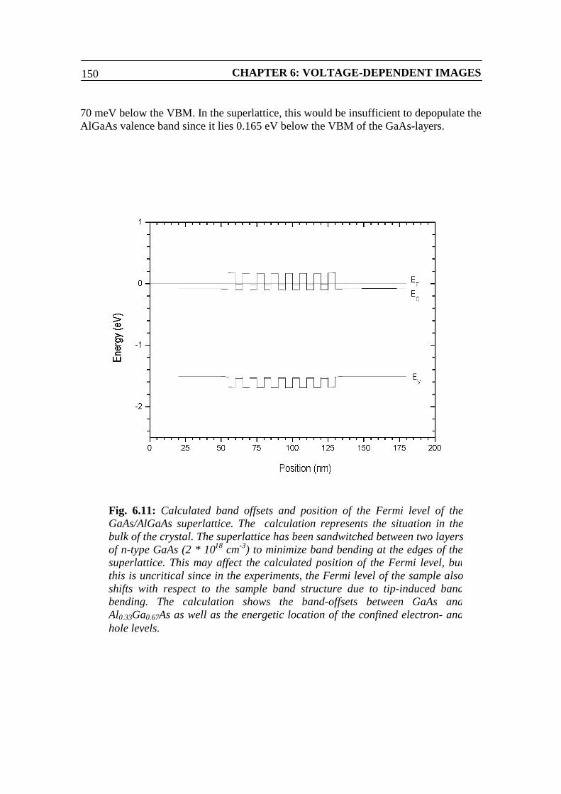
CHAPTER 6: VOLTAGE-DEPENDENT IMAGES150
70 meV below the VBM. In the superlattice, this would be insufficient to depopulate theAlGaAs valence band since it lies 0.165 eV below the VBM of the GaAs-layers.
Fig. 6.11: Calculated band offsets and position of the Fermi level of theGaAs/AlGaAs superlattice. The calculation represents the situation in thebulk of the crystal. The superlattice has been sandwitched between two layersof n-type GaAs (2 * 1018 cm-3) to minimize band bending at the edges of thesuperlattice. This may affect the calculated position of the Fermi level, butthis is uncritical since in the experiments, the Fermi level of the sample alsoshifts with respect to the sample band structure due to tip-induced bandbending. The calculation shows the band-offsets between GaAs andAl0.33Ga0.67As as well as the energetic location of the confined electron- andhole levels.
OF AlGaAs AND OF GaAs/AlGaAs THIN LAYERS 151
6.5 Discussion on the thick AlGaAs layer
6.5.1 Filled-states images
The filled-states images (figure 6.2) show essentially two voltage-dependent changes:The first is a corrugation-change similar to the one that we have also reported for n-GaAs [11]. For large negative voltage, the atomic rows appear to run along [-110]. Atsmall values the rows appear to run along [001]. The second change is that the atomic-scale fluctuations in the image, commonly associated with the presence of Al [1,3,4,22],gradually disappear. At low voltage, these alloy-related fluctuations are replaced bybright and dark areas several nm in diameter. The observed corrugation-changes arecompletely consistent with the behaviour that we expect based on the band bendingarguments given in section 6.4. It is thus clear that for large voltage, we observe thespatial distribution of the valence-band related surface-DOS (mainly the A5-state). Forlow voltage, we image the C3-state which is populated due to the downward bandbending of the surface.
The change in atomic corrugation is accompanied by the appearance of dark andbright areas for small negative voltage (figure 6.2 g,h,i). For these voltages (-1.667 V <V < -1.827 V), the tunneling current must orginate exclusively from the accumulationlayer of electrons at the suface according to the band bending arguments given insection 6.4. This is confirmed by the appearance of the atomic corrugation whichreflects the spatial distribution of the C3 state.
We interprete the appearance of these bright and dark areas as fluctuations ofelectron-density in this accumulation-layer: Due to small spatial variations in the localAl-content, the conduction-band electron-DOS near the surface varies as well. Theelectron-states in the conduction band near the surface are occupied due to thedownward TIBB expected for negative voltage. The spatial distribution of the electronsin the accumulation layer is now influenced by two factors: The electron-DOS of theconduction-band near the surface, and by the interaction that exists between theelectrons themselves. In general, the interaction between electrons making up anelectron-gas consists of the repulsive Coulomb interaction and the exchange-correlationinteraction. We postulate that the combined effect of the inhomogeneous surface-DOSand the (total) electron-electron interaction leads to the appearance of the bright anddark areas.
Let us consider the accumulation layer of electrons more closely: It consists offree electrons that occupy electron-states in a certain volume of crystal near the surface,due to the effects of TIBB. These electron-states are the solutions to a Schrödingerequation of which the potential is the sum of three terms: The atomic potential built bythe crystal lattice at and near the surface; the interaction between the electronsthemselves, and the rather wide potential well caused by TIBB itself. In this discussion(as well as throughout this thesis) we neglect the effects of the last term, although it cangive rise to quantized levels in the accumulation layer [29]. In a quantum-mechanicalsystem of free electrons, the electron-electron interaction contains the (conventional)
CHAPTER 6: VOLTAGE-DEPENDENT IMAGES152
Coulomb-term as well as potential-terms arising from the exchange and correlationinteractions [25 (p. 51,52), 27 (p. 184)]. Following the argument made in ref. 25 (p. 43) wewill assume that the electron-electron interaction is dominated by the Coulomb-interaction, although that argument (the “Hartree approximation”) relates to theenergetic location of an electron-state rather than its spatial distribution. The Coulomb-term (and the exchange and correlation terms as well, for that matter [25 (p. 52), 27 (p.184)]) contains the electron-density. If we were to evaluate the local density of electron-states in the accumulation layer, we would therefore have to solve the Schrödinger andthe Poisson equations self-consistently [25 (p. 52), 27 (p. 184)]. The sum of the self-consistent solutions to these two equations (at an infinitesimal energetic interval) thenequals a new near-surface DOS which includes the electron-electron interaction. Theimages shown in figure 6.2 g,h,i, thus reflect a “modified” conduction-band relatedsurface-DOS for which the influence of the electron-electron interaction manifests itselfin its spatial variation.
The significance of this becomes apparent when one compares the filled-statesSTM-images shown in figure 6.2 g,h,i, with the empty-states images shown in figure6.3 j,k,l. Both sets of images show the lower part of the conduction-band relatedsurface-DOS (the C3-state). However, the empty-states images (figure 6.3 j,k,l) showthe surface-DOS in the absence of electron-electron interaction, as the electron-statesare unoccupied while the image is aquired. The filled-states images (figure 6.2 g,h,i), onthe other hand, reflect the same energetic part of the surface-DOS. However, in this casethe electron-states are occupied by free electrons during the measurement. Thedifference in appearance between the images shown in figure 6.2 g,h,i and those shownin figure 6.3 j,k,l is thus a manifestation of the way in which the electron-electroninteraction influences the distribution of free electrons near the surface of the AlGaAs-crystal.
We base this interpretation of the dark and bright areas on several aspects of ourexperimental observations: First of all, the effect is very clearly connected to theinhomogeneous nature of the AlGaAs surface. For the filled states results on n-GaAs(chapter 4), the bright and dark areas do not appear at all. At the same time, the bandbending situation for small, negative voltage can be expected to be quite similar for bothmaterials, as is confirmed by the similarity in the voltage-dependent changes in atomiccorrugation observed for n-AlGaAs and n-GaAs.
The second aspect is that the dark and bright areas seem to have a characteristicsize of a few nm. This length scale is about one order of magnitude larger than theatomic length scale on which the surface-DOS is observed to vary at other voltages. Thelength scale of a few nm agrees remarkably well with the (apparent) size of the twocharged adsorbates that are present on the surface as well. The dark ring around theadsorbates is of a similar size as the bright areas, although the rings are slightly larger.Such a ring is characteristic for a negatively charged adsorbate on n-type GaAs imagedin filled states [11,14,21]. The dark ring is caused by the fact that the charged adsorbatecreates a depletion zone around itself. The width of that depletion zone depends on thescreening length of the material. If Coulomb-repulsion dominates the electron-electroninteraction of the free electrons occupying the accumulation layer, the bright and darkareas should have a lateral extent that is similar to that of the depletion zone around anegetively charged adsorbate.
OF AlGaAs AND OF GaAs/AlGaAs THIN LAYERS 153
A very important argument is that the appearance of the bright and dark areasdoes not occur in the empty-states images, althought it remains possible that the effectoccurs outside the range of voltages that we have applied in our experiment. This pointis relevant because in general, an electron occupying a bound state of a potential wellhas a finite localization. The spatial extent of such a bound state is usually several nm ormore, as is evident from the effective Bohr-radius of an electron bound to a donorimpurity in a semiconductor [7 (p. 3, p. 11)]. If the imhomogenieties in the surface-DOSform small potential-wells in which the electrons in the accumulation layer can bebound, such bound states would probably also have a spatial extent of several nm. Thiseffect could therefore in theory provide an alternative explanation for the appearance ofthe bright and dark areas. However, we reject this hypothesis on account of the fact thatin this case, bright and dark areas of a similar length scale should also be observed inthe empty states images. Besides, it remains to be seen whether the atomic-scalefluctuations in the atomic structure of an AlGaAs-surface can create potential-wells thatare deep enough to give rise to bound electron-states. In the absence of bound electron-states, it seems plausible to assume that the interaction between the electrons themselvesmust cause the modification to the spatial distribution of the near-surface electron-states. Moreover, the characteristic length-scale of the bright and dark areas suggeststhat this interaction, at least for the circumstances at hand, is dominated by theCoulomb-interaction.
It is interesting to note that the accumulation layer is also present at largenegative voltage, and that the contribution to the tunneling current from the C3 stateshould vary spatially in accordance with the bright and dark areas. However, at largevoltage the contribution from the A5 and BVB-states apparently dominates thetunneling current, as is evident from the observed atomic corrugation.
We thus interprete the filled states results on the thick AlGaAs-layer in thefollowing way: For large voltage, the image shows the surface-DOS of the sampleassociated with the valence-band (A5-state). At small voltage, only the C3-state isavailable to the tunneling process. The bright and dark areas are attributed tofluctuations of the local density of electrons in the accumulation layer near the surface.The variations in the density of electrons in the accumulation layer are determined bythe combined effects of the inhomogeneous DOS of the AlGaAs-surface and theinteraction between the electrons themselves.
6.5.2 Empty-states images
The empty-states images also show a change in atomic corrugation. For large voltage,the rows appear to run along [-110]. The behaviour is similar to the corrugation-changesseen in the empty-states images on n-GaAs that we have reported previously [11]. Atlow voltage, small, bright “ridges” along [-110] appear. It also seems that the alloy-related minima in the images are less pronounced with respect to the images taken athigher voltage.
CHAPTER 6: VOLTAGE-DEPENDENT IMAGES154
Based on the band bending arguments given in section 6.4 we explain the corrugation-change as a result of a shifting balance between the competing contributions of the C3-state and the low-energy shoulder of the C4-state. That interpretation is completelyanalogous to the one we have proposed for the corrugation-change observed in theempty-states images of n-GaAs [11]. Therefore, at large positive voltage, the imagesshould reflect the spatial distribution of the upper part of the conduction-band relatedsurface-DOS (C4 state). At large voltage, the lower part of the conduction-band relatedsurface-DOS (C3 state) also contributes to the total tunneling current, but since itscontribution is relatively small, it should not influence the topography of the image[8,10]. For the lower voltages, the images show the lower part of the conduction-bandrelated surface-DOS.
It is known for GaAs (110) that the C3 state has a low-energy shoulder whichextends into the bandgap of the semiconductor. We have shown that electrons cantunnel resonantly through this shoulder, causing atomic corrugation in the STM-imageof n-GaAs (110) when the surface is in type I depletion during imaging [11]. Since theC3 state is centered very near the CBM for AlAs (110) [17], it is reasonable to suspectthat this mechanism also becomes relevant for the imaging of AlxGa(1-x)As (110) whenthe appropriate bias voltage is chosen. Whether it has played a role in our experimentsis unclear, since we cannot determine the voltage at which the transition from type Idepletion to type II depletion occurred from the experiment (see section 6.4).
At low voltage, small ridges 5 - 10 surface unit cells in length appear along the[-110]-direction. They extend 1 surface unit cell in the [001]-direction. Some alloy-related minima are also visible. Many of the ridges coincide with the alloy-relatedmaxima observed at higher voltage, although the correlation is not complete (figure 6.6h). The depressions also roughly coincide with those obtained at higher voltage, butagain, not completely (figure 6.6 g). The trend in the images as one goes from largepositive voltage to small positive voltage, appears to be that the ridges along [-110] firstappear and then become longer, and that the alloy-related depressions slowly disappear.It is interesting to compare the low-voltage morphology of the thick AlGaAs-layer tothe low-voltage morphology of the AlGaAs-layers in the superlattice, since theAlGaAs-layers in the superlattice contain more Al. The AlGaAs-layers in thesuperlattice show no ridges along [-110] at low voltage. At the same time, the alloy-related depressions disappear completely. The appearance of the ridges, and thedisappearance of the alloy-related minima, thus appear to be sensitive to the Al-contentof the material.
The orientation and strong anisotropy of the ridges suggests that the electron-states that are involved have a finite k//-vector in the [001]-direction, and a muchsmaller k//-vector in the [-110]-direction. This means that the k//-vectors of the statesrelevant for the appearance of the ridges must lie near the X’-point of the surfaceBrillouin zone [12]. In principle, the states that are involved can be either surface statesor bulk states (see figure 6.1 a). In those parts of the surface-BZ where the dispersion-curve of a surface-state is overlaps with the projected bulk electronic structure, thesurface state and bulk states combine into a surface resonance, making the distinctionbetween bulk and surface states for that part of the surface-BZ irrelevant [31 (p. 91)].
From the surface band structure of GaAs (110) [12] it is clear that near the CBMof the material, the energetically lowest lying electron-states have k//-vectors on the line
OF AlGaAs AND OF GaAs/AlGaAs THIN LAYERS 155
joining the Γ-point and the X’-point of the surface BZ. Notice that near the Γ-point ofthe surface-BZ, the C3-surface state is resonant with the projected bulk band structure.There are two more local minima in the projected band structure of the bulk conductionband which occur near the X-point and at the M-point, but these lie at slightly higherenergies. Consequently, there is a small band of states just above the CBM that have ak//-vector near the Γ-point, on the line joining the Γ-point and the X’-point. Immediatelyabove it is a second band of states with a k//-vector near the X’-point. Both bands ofstates have little or no localization in the [-110]-direction. Moreover, the second band ofstates has a peridicity in the [001]-direction of one surface unit cell, and thuscorresponds to the two main features of the ridges that appear in the images at lowvoltage.
At higher energies, bulk states with k//-vectors near the X- and M-points alsobecome available to the tunneling process. This should cause the ridges to disappear, aselectron-states with k//-vectors in all parts of the surface-BZ now become available tothe tunneling process. At the same time, the local minimum of the C3-state near the X-point of the surface-BZ lies at an energy that remains available to the tunneling processfor all (positive) sample voltages, which manifests itself in the atomic corrugation in the[-110]-direction that is superimposed on the ridges.
Since the above arguments are based on the band structure GaAs (110), onemight wonder why the ridges have been observed only on AlxGa(1-x)As (110). Weexplain this from the fact that GaAs is a homogeneous material, whereas AlxGa(1-x)As isnot. If on GaAs (110) the individual electron-states contributing to the tunneling currentall appear as identical features, none of them will show up with more contrast than itsneighbors in order to appear as an individual ridge. Instead, the collective pattern mightappear as atomic rows along [-110]. Combined with the corrugation in the [-110]-direction caused by the minimum in the dispersion curve of the C3 surface state near theX-point, the image as a whole would appear as an atomically resolved image of thesurface lattice. On AlxGa(1-x)As, on the other hand, the structural inhomogeniety of thematerial makes it possible that at some spots, the low-lying bulk conduction band stateshave a slightly stronger contribution to the total tunneling current than the low-lyingbulk conduction band states in the immediate vicinity. This way, one such state canstand out from its neighbors and appear as a single ridge.
If our interpretation of the ridges along [-110] is correct, then the effect shouldbe highly sensitive to the Al-content of the material. For x > 0.33, the band structure ofAlxGa(1-x)As becomes indirect, and the lowest-lying bulk conduction band states havek//-vectors near the X-point. For n-AlxGa(1-x)As with a high content of Al, we thusexpect the ridges to appear along the [001]-direction at low positive voltage. For x =0.33, the lowest lying bulk conduction band states have k//-vectors near the Γ-point andX-point, as for this concentration of Al, the Γ-minimum and the X-minimum in the bulkconduction-band structure lie at the same energy [15]. We therefore do not expect to seeridges in either the [001]-direction or the [-110]-direction for this value of the Al-concentration. Our images of the GaAs/AlGaAs superlattice are consistent with thatprediction: In the images of the thin AlGaAs-layers taken at low positive voltage, weobserve no ridges in the [-110]-direction. Instead, some small ridges along [001] areseen.
CHAPTER 6: VOLTAGE-DEPENDENT IMAGES156
The appearance of the alloy-related depressions in the images also depends on theapplied bias voltage. In the thick AlGaAs-layer, they become less pronounced for lowvoltage, although they have not disappeared completely for the lowest value of appliedbias voltage (V = +0.693 V). On the GaAs/AlGaAs superlattice, some alloy-relateddepressions still appear for V = +0.706 V, but they disappear for lower values of theapplied bias voltage. Given the fact that the alloy-related depressions tend to disappearfor voltages at which the C3 state dominates the tunneling current, one might speculatethat the local DOS associated with the C3 state is insensitive to local variations in Al-content. Since the lower conduction-band states are unoccupied for positive voltage, wecannot explain the disappearance of the alloy-related minima from electron-electroninteraction effects like we have done for the filled states images. The precisemechanism for the disappearance of the alloy-related minima remains at present unclearto us.
Summarizing, the empty-states images of the thick AlGaAs-layer show theconduction-band related surface-DOS. For large voltage the images show the upper partof the surface-DOS (C4 state), and for small voltage the images show the lower part (C3state). This interpretation is consistent with the observed changes in atomic corrugation.For small voltage, small ridges along [-110] appear in the image. We suspect that theridges are associated with the bulk states near the bottom of the conduction band. Wealso suspect that the appearance of the ridges is sensitive to the Al-content of thematerial. Finally, we observe that the alloy-related minima which are seen in the imageat large, positive voltage, tend to disappear for low voltage.
6.5.3 Comparison between filled- and empty-states images of AlGaAs
A common feature of STM-images of AlxGa(1-x)As (110) obtained at relatively largebias voltage (2.0 V – 2.5 V of either polarity) is that for filled-states images, the alloy-related minima appear between the atomic rows, whereas for the empty-states images,they appear centered on the atomic rows [1,6,30]. In figures 6.2 a,b and 6.3 a,b, the sameeffect is seen, confirming that our experimental results are consistent with existingliterature.
The general trend that the alloy-related minima appear between the atomic[-110]-rows for filled-states images and centered on the [-110]-rows for empty-statesimages, is by itself not surprizing: The Al atoms in AlGaAs occupy the cation-sites ofthe crystal lattice, and thus lie centered on the [-110]-rows for positive sample voltage,and between the [-110] rows when a negative sample voltage is applied. However, it isknown for Al atoms that only have Ga atoms as next-nearest neighbors, that this trenddoes not apply [22. The position of the alloy-related minima in STM-images of AlGaAsmay for this reason be a more complicated matter than it appears at first sight.
OF AlGaAs AND OF GaAs/AlGaAs THIN LAYERS 157
In figure 6.6, it is seen very clearly that the the alloy-related minima in the empty statesimage and those in the filled states image of the same area do not systematicallycoincide (figure 6.6 c and d). Instead, their distrubutions appear completelyuncorrellated. The same observation is made for the alloy-related maxima in the twoimages (figure 6.6 e and f). It is also seen that in the filled-states image (figure 6.6 b),the alloy-related minima tend to be elongated and roughly orientated along [001].Although some of the minima in the empty states image show signs of a similarordering, the effect is much weaker in the empty states image (figure 6.6 a). It is thusclear that the alloy-related variations in the valence-band related surface-DOS aresignificantly different from the alloy-related variations in the conduction-band relatedsurface-DOS.
One very interesting point is that some of the features in the filled and emptystates images coincide in part: An example is seen in figures 6.6 a,b in the area enclosedby the rectangular box, where an elongated alloy-related minimum in the filled statesimage coincides in part with a smaller alloy-related minimum in the empty-states image.The area in the empty-states image that corresponds to the total area of the minimum inthe filled states image, is seen to consist of a dark portion (lower right) and a portionthat is darker than the average colour of the image, but lighter than the first portion(upper left). It is thus clear that the feature consists of two adjacent parts with a differentatomic structure: The lower right part of the feature has an atomic structure that stronglysuppresses both the valence-band related surface-DOS and the conduction-band relatedsurface-DOS. The upper right part has a different atomic structure, which suppresses thevalence-band related surface-DOS, but which suppresses the conduction-band relatedsurface-DOS to a lesser extent, causing the upper left part of the feature to appear lessdark in the empty-states image.
One of the main reasons to study a ternary material like AlxGa(1-x)As is to learnabout its atomic structure. For instance, the appearance of elongated dark features thattend to have a preferential orientation in the crystal in filled states images has beenreported several times, and is usually attributed to clustering of Al during the epitaxialgrowth of the AlGaAs-layer [1,3,5,6]. Underlying this interpretation of such elongatedfeatures seems to be the assumption that dark patches in the image represent areas witha high local Al-content [3], although in ref. 6 the relation between the atomic structureof the material and the associated surface-DOS is considered in more detail. From ref.22 it is clear that the presence of Al need not always cause a decrease in the localsurface-DOS, even in the relatively simple case of dilute AlGaAs where one mayassume that most of the Al-atoms in the top and bottom rows of the surface only haveGa as their next-nearest neighbors. In our own experiments which involve AlxGa(1-x)Aswith Al-fractions of 0.20 and 0.33, several different bonding configurations are (aboutequally) likely to occur. This makes the relation between the atomic structure of thematerial and the resulting surface-DOS a very complicated one. Although the atomicstructure uniquely defines the surface-DOS, the spatial distribution of the conduction-band related surface-DOS is different from the spatial distribution of the valence-bandrelated surface-DOS as our results show. At this point, we have no reason to assumethat one of the two types of images (filled or empty states) reflects the atomic structureof the material better than the other. In order to deduce the atomic structure of AlGaAsfrom a given STM-image, detailed knowledge of the relation between the atomic

CHAPTER 6: VOLTAGE-DEPENDENT IMAGES158
structure of the material and the resulting spatial distribution of (the relevant part of) thesurface-DOS is needed. Until this relation is known in full, statements about the atomicstructure of AlGaAs cannot be made from STM-images without ambiguity.
On the other hand, the information about the (surface) DOS of the material thatis shown directly by an STM-image may for many purposes be more useful than adetailed knowledge of the atomic structure itself. For example, the interest in atomic-scale roughness of hetero-structure interfaces originates from the concern that suchroughness might influence the performance of semiconductor devices in which suchinterfaces are used. The physics and performance of such devices are directly related tothe (atomic scale) DOS of the materials from which they are made. From this point ofview, knowledge of the variations in the local DOS of the material at various energy-intervals seems more important than a precise knowledge of the atomic structure thatunderlies the observed DOS. To obtain information about the atomic-scale DOS, STM-images can be used directly.
6.6 Discussion on the GaAs/AlGaAs superlattice
In section 6.4, we have shown the electronic structure of a superlattice, and we havereflected on the kind of band bending behaviour that might, generally speaking, beexpected for such a structure. Based on section 6.4, we will now discuss the voltage-dependent images of the superlattice that we show in figures 6.7 and 6.8.
6.6.1 Filled-states images
For the filled states images of the superlattice, we expect that the conduction-band statesof both the GaAs and AlGaAs layers must have been populated due to accumulationduring the entire measurement. The AlGaAs-CBM must have been below the SFLthroughout the measurement, which can be seen from the fact that for the entire range ofapplied bias voltages, the GaAs-layers appear unbroadened. Had the downward bandbending of the surface been such that the AlGaAs-CBM was above the SFL and theGaAs-CBM below it, then the electrons would have tunneled from the confined levelsin the GaAs-layers. Since the energetic location of the confined levels effectivelydeterimines the SFL (see figure 6.11), the condition of downward band bending issufficient to populate the confined levels. The sides of these levels extend into theAlGaAs-barriers. Consequently, if the contribution from the confined levels were todominate the tunneling current, this would manifest itself as an apparent broadening ofthe GaAs-layers (see figure 6.8 f,g,h,i). Such broadening is not seen.
OF AlGaAs AND OF GaAs/AlGaAs THIN LAYERS 159
Besides, it is questionable whether the confined levels of the quantum-wells canbe imaged at negative voltage. Population of only the GaAs conduction-band, if itoccurs, is expected to happen only for relatively small negative voltage. In that regimeno contribution from the A5-state or BVB-states is expected, so that no state other thanthe confined states of the quantum wells would contribute to the tunneling current. If thequantum wells are deep, the tails of the confined levels decay rapidly in the AlGaAs-barriers. Since no other state would then be available for the tunneling process, the tipwould probably crash when it is over an AlGaAs-layer. If the quantum wells aresufficiently shallow for the superlattice-state to have significant localization in theAlGaAs-barriers as well, the state can be imaged at small negative voltage in filledstates. However, this would necessarily involve a superlattice in which the electrons arenot confined to two-dimensional motion inside the quantum wells.
At large negative voltage, the atomic rows are along [-110], indicating a strongcontribution from the A5-state. The AlGaAs-layers show the same alloy-related featuresas those observed for the thick AlGaAs-layer, which confirms that the features areindeed associated with the presence of Al. The alloy-related minima appear between therows, like they also do in the filled-states images of the thick AlGaAs-layer. For smallervoltage the rows are more and more along [001], although the changes in corrugationare difficult to observe due to the tip-instabilities that are apparent in the images. Thecorrugation-change is accompanied by the appearance of bright and dark areas in theAlGaAs-layers, similar to the bright and dark areas seen on the thick AlGaAs-layer.
The onset of the corrugation-change in the AlGaAs-layers and the appearance ofthe bright and dark areas lies at V = -1.730 V. Given the fact that the conduction-bandstates of the AlGaAs-layers must be populated, the VBM of the AlGaAs-layers must lie1.836 eV or more below the SFL. Consequently, the A5-states of the AlGaAs-surfacedo not contribute to the tunneling current for V < -1.730 V. At V = -1.667 V and smaller(absolute) voltage, the contribution of the BVB-states of the AlGaAs-layers must havevanished as well since the TFL then lies energetically higher than the AlGaAs-VBM inthe bulk. However, the contributions of the A5-state and BVB-states of the GaAs-layersare still available to the tunneling process at these voltages. These contributionsmanifest themselves in the apparent direction of the atomic rows in the GaAs-layerswhich is along [-110], and in an enhancement of the contrast in apparent height betweenthe GaAs- and AlGaAs-layers.
At V = -1.550 V and smaller voltages, the inversion of contrast between theGaAs- and AlGaAs-layers sets in. The corrugation in the GaAs-layers also changes,although no complete change in corrugation is observed (figure 6.7h). Since the bulk-VBM of the GaAs-layers lies at 1.504 eV below the SFL, the tunneling current mustoriginate completely from the populated conduction-band states for these smallvoltages. Given the fact that the GaAs-layers appear unbroadened, the amount ofdownward TIBB must exceed –0.17 eV, so that for V < -1.59 V, no contribution fromthe GaAs-A5 state is to be expected. We explain the inversion of contrast from the factthat the (bulk) conduction-band of AlxGa(1-x)As has a higher 3D-DOS than theconduction-band of GaAs [7] (see also our discussion on the screening behaviour of thesuperlattice surface). In this regime where the tunneling current originates purely fromthe conduction-band of the GaAs- and AlGaAs-layers, this apparently causes theAlGaAs to appear brighter than the GaAs.
CHAPTER 6: VOLTAGE-DEPENDENT IMAGES160
It appears quite odd that the change in apparent direction of the atomic rows inthe GaAs-layers is not complete, even though we expect only the conduction-bandrelated surface states to contribute at low voltage. It is interesting to notice that in thefilled states images of n-GaAs (110) (chapter 4), some corrugation in the [001]-directionremains in the images at low voltage as well. This in spite of the fact that for the lowestvoltage involved in that measurement, the TFL lies energetically higher than the VBMin the bulk, so that only a contribution from the conduction-band related surface-DOS ispossible.
It is possible that the effect is related to the quality of the tunneling tip: It is seenin the other images that there are alternating horizontal bands in the images with twoslightly different atomic morphologies. Apparently the tip had a bi-stable configurationduring the measurement. We suspect, however, that the observed atomic morphology inthe GaAs-layers is influenced by the low-energy shoulder of the C4-state. The C4-stateinfluences the conduction-band related surface-DOS even for energies that lie below thepeak position of the lower lying C3-state, as is made clear in chapter 4 (see also section6.4). At the same time, the conduction-band of the GaAs-layers becomes populated byaccumulation up to a higher energy than would be the case for a homogeneous GaAs-surface: The first 0.25 eV of the conduction-band related surface-DOS fallsenergetically within the superlattice, which does not screen as efficiently as theconduction-band of a homogeneous GaAs-surface.
It is in any case certain that at V = -1.364 V, no contribution from the A5-state of the GaAs-layers is to be expected. Since this voltage is less than the value of thebandgap in GaAs, a contribution from the A5-state to the filled states current at thisvoltage would require upward band bending. This would depopulate the C3-state, andthe resulting dominance of the A5-state should lead to an atomic morphology that issimilar to what is observed at high voltage. This is clearly not seen. Besides, a positiveamount of TIBB at V = -1.364 V would require a tip work function of about 5.6 eV. Fora tungsten STM-tip, such a high work function would be exceptional [11,14].
We thus summarize the interpretation of the filled states images of theGaAs/AlGaAs superlattice as follows: At large negative voltage, the image shows thevalence-band related surface-DOS of both the GaAs- and AlGaAs-layers. At smallernegative voltage, we expect for both the GaAs- and AlGaAs-layers that the tunnelingcurrent is dominated by the contribution from the accumulated conduction bands. Thefact that the GaAs-layers appear unbroadened means that throughout the measurement-series, the CBM of the AlGaAs-layers remained below the SFL. We explain theinversion of contrast between the GaAs- and AlGaAs-layers from the fact that theconduction-band has a larger 3D-DOS in AlGaAs than in GaAs.

OF AlGaAs AND OF GaAs/AlGaAs THIN LAYERS 161
6.6.2 Empty-states images
In the empty-states images of the superlattice, several changes occur: At large positivevoltage the AlGaAs-layers appear as dark, spotted bands. The alloy-related minimaappear centered on the [-110]-rows, in the same way as is observed for the thickAlGaAs-layer. For decreasing voltage, the apparent direction of the atomic rowschanges for the AlGaAs-layers from [-110] to [001]. Then follows a regime in whichthe GaAs-layers appear broadened. The broadening disappears while the apparentdirection of the atomic rows in the GaAs-layers changes as well. For very low voltage,the contrast between AlGaAs and GaAs inverts, although the effect is much weakerthan it is for the filled states images. The black circles that appear for lower voltage arenegatively charged adsorbates [21]. Another type of adsorbate appears in the image at V= +0.803 V, and remains in the two subsequent frames until for V = +0.645 V, it fallsoutside the frame. At V = + 1.136 V, the bright feature in one of the AlGaAs-layers isinterpreted as a dopant. For V < +0.645 V, the bright features in the GaAs-layers areinterpreted as dopants as well.
As explained in the discussion on the filled states images of the superlattice, theinfluence of the confined levels in the GaAs quantum-wells of the superlattice manifestsitself as an apparent broadening of the GaAs-layers. The confined level defines thebottom of the lowest miniband of the superlattice. In the plane of the GaAs quantum-wells the electrons are free to move, whereas in the direction perpendicular to thelayers, the spatial variation of the DOS is determined by the spatial variation of (thesquared amplitude of) the confined level. The GaAs-layers appear broadened becausethe sides of the confined levels extend into the AlGaAs-barriers, so that inside theAlGaAs-barriers, a finite DOS associated with the superlattice-miniband remains. Whenthe TFL rises energetically above the AlGaAs-CBM, the electron-states associated witha 3D-motion of electrons in the conduction bands of the GaAs- and AlGaAs-layersbecome available to the tunneling process. The density of these states is much largerthan the DOS associated with the superlattice, as is seen in our discussion on thescreening behaviour of the superlattice-surface. Therefore, when the TFL risesenergetically above the AlGaAs-CBM, the broadening of the GaAs-layers shoulddisappear since the confined levels are no longer the dominant feature in the accessibleenergetic range of the surface-DOS. This broadening can be seen in the empty-statesimages for +0.588 V < V < +0.706 V. We can use this effect to draw conclusions aboutthe band bending behaviour of the superlattice-surface as it must have occurred duringthe measurement: The appearance and disappearance of the broadened GaAs-layersindicate that for +0.706 V < +0.876 V, the TFL passes the AlGaAs-CBM. For + 0.499V < V < + 0.588, the TFL passes the confined level.
These two conclusions are consistent with the voltage-dependent changes inatomic corrugation on the GaAs- and AlGaAs-layers: The atomic corrugation in theGaAs-layers changes very gradually as the voltage decreases. The direction in which theatomic rows are most apparent changes from [-110] to [001] at around V = +0.588 V.This indicates that for that voltage, the TFL is about 0.15 eV above the GaAs-CBM [11].The confined level in the GaAs-layers lies at about the same energy in the surface-DOS.It should therefore be expected that the lower end of the voltage-range for which thebroadening of the GaAs-layers occurs, coincides with the voltage at which the (most)

CHAPTER 6: VOLTAGE-DEPENDENT IMAGES162
apparent direction of the atomic rows in the GaAs-layers, changes from [-110] to [001].In the range +0.706 V < V < +0.803 V, the upper limit of the voltage-range for whichthe broadening of the GaAs-layers occurs, indicates that the TFL is near the AlGaAs-CBM (when it faces a GaAs-layer). The TFL must thus be at around 0.25 eV above theGaAs-CBM. For V = +0.706 V, the atomic rows in the GaAs-layers are along [-110].This is in accordance with the results presented in chapter 4.
A factor that complicates the interpretation is the fact that the GaAs- andAlGaAs-layers have different electron-affinities, which causes the amount of TIBB tofluctuate as the tip alternatingly faces a GaAs- and an AlGaAs-layer. Since the electron-affinity of GaAs is larger than that of AlGaAs [7], the amount of upward band bendingis greater for AlGaAs than for GaAs at the same applied bias voltage. This has thefollowing consequence: If the tip faces a GaAs-layer and the amount of TIBB is suchthat the TFL lies at or slightly above the AlGaAs-CBM, it may happen that the TFL liesbelow the AlGaAs-CBM when the tip faces the adjacent AlGaAs-layer, due to thedifference in the electron-affinities of GaAs and AlGaAs. We thus expect that a voltage-interval exists in which for the GaAs-layers, the conduction-band related surface-DOSlying energetically slightly above the AlGaAs-CBM is imaged, whereas, due to theincreased band bending, the tails of the confined levels are imaged when the tip faces anAlGaAs-layer.
In the range +0.760 V < V < +0.803 V, the GaAs-layers do not appearbroadened, but the interfaces between GaAs and AlGaAs appear fuzzy. This may be dueto the effect we just described. It may also simply be a feature that is associated with thesurface-DOS at that energy. In any case, for V > +0.876 V, the interfaces between theGaAs- and AlGaAs-layers appear sharp, which suggests that the confined levels in theGaAs-layers no longer influence the topography of the images. This means that forthese voltages, the TFL lies energetically above the CBM of the AlGaAs-layers, bothwhen it faces a GaAs-layer and when it faces an AlGaAs-layer.
Notice that in the AlGaAs-layers, the change in corrugation appears to takeplace in the range +0.706 V < V < +0.876 V. We expect the corrugation-change tooccur when the TFL lines up with the lower part of the conduction-band related surface-DOS, in analogy with our observations for n-GaAs (110) [11]. This is consistent withour expectation that at similar voltages (+0.706 < V < +0.803 V), the TFL passes theAlGaAs-CBM when the tip is over an AlGaAs-layer.
We thus expect the following band bending behaviour for the empty-statesimages of the GaAs/AlGaAs superlattice: For large voltage, the TFL lies energeticallyabove the CBM of the GaAs- and AlGaAs-layers. At lower voltage, possibly in therange +0.760 V < V < +0.803 V, a voltage-interval may exist for which the TFL isabove the AlGaAs-CBM when the tip faces a GaAs-layer and below it when it faces anAlGaAs-layer. When the voltage is decreased further (+0.588 V < V < +0.706 V), thetip lies between the GaAs-CBM and the AlGaAs-CBM for all locations on the surface,and the confined levels in the GaAs quantum-wells are imaged. For V < +0.499, weexpect that the TFL lies energetically below the CBM of the GaAs- and AlGaAs-layers.The electrons then tunnel from the tip, through a surface depletion zone, into the bulkstates near the bottom of the conduction-band (BCB-states) for both types of layers.This is analogous to what happens for a homogeneous surface in type I depletion [11].
OF AlGaAs AND OF GaAs/AlGaAs THIN LAYERS 163
Based on the preceeding arguments, it is clear that the inversion of contrast betweenGaAs and AlGaAs occurs when the electrons tunnel from the tip to the BCB-states forboth the GaAs- and AlGaAs-layers. In this regime, we expect that the atomiccorrugation is caused by electrons tunneling resonantly through the low-energy shoulderof the C3-state which extends into the bandgap [11,12,13]. Since the 3D-DOS of theAlGaAs conduction-band is larger than the 3D-DOS of the GaAs conduction-band [7],we suspect that this difference causes the inversion of contrast at low voltage betweenthe GaAs- and AlGaAs-layers. From ref. 11 it is clear that when electrons tunnel intothe BCB-states of an n-type surface in type I depletion, this involves a short tip-sampledistance. We expect a similar band bending situation for the superlattice-surface in thevoltage-range in which the inversion of contrast occurs. At the same time, the imagethat shows the inversion of contrast most clearly (V = 0.310 V), ended with a crash ofthe STM-tip. In view of the expected band bending situation and short tip-sampledistance, this is no surprise.
A last point to make about the empty-states images of the superlattice is acomparison between the images taken at large voltage, and the ones showing thebroadening of the GaAs-layers. Although the relation between the atomic structure ofAlxGa(1-x)As and the resulting surface-DOS is not fully clear, the presence or absence ofAl can be recognized from the presence or absence of alloy-related variations in thesurface-DOS at large voltage of either polarity. This local presence or absence of Al isalso the factor that determines the local value of the bandgap of the surface. Thesevariations in the local bandgap form the potential-landscape that is characteristic of asuperlattice, and give rise to the confined levels in the GaAs-layers. At the same time,the images at a lower voltage reflect the spatial distribution of the confined levelsthemselves. In the images taken at intermediate voltage, the spatial distribution of theconfined levels appears very smooth. This might suggest that the atomic-scaleroughness of a GaAs/AlGaAs interface need not influence the spatial distribution orenergetic location of the confined levels very strongly, provided that the roughness ofthe interface does not exceed one or two atomic layers. From a more educational pointof view, the images taken at large voltage may be said to reflect the spatial variation ofthe potential, whereas the images showing the broadening of the GaAs-layers reflect thespatial variation of the corresponding solution of the Schrödinger equation.
6.6 Summary, conclusions, outlook
We have presented voltage-dependent images of a thick Al0.2Ga0.8As-layer and of aGaAs/Al0.33Ga0.67As superlattice. These images show both the filled and empty states ofthe surfaces. The voltage-dependent images of the thick AlGaAs-layer show a change inatomic corrugation similar to the one that has been reported previously for n-GaAs[8,11]. At the same time, bright and dark areas appear at low negative voltage which weexplain in terms of fluctuations in the electron-density of the surface-accumulationlayer. In the empty states images, small ridges along [-110] appear at low voltage. From

CHAPTER 6: VOLTAGE-DEPENDENT IMAGES164
the anisotropic band-structure near the bottom of the bulk conduction-band we speculatethat the appearance of the ridges is connected with the bulk states lying at the CBM nearthe X’-point of the surface Brioullin zone. Furthermore, it is shown that the alloy-related features in a filled-states image and an empty-states image of the same patch ofAlGaAs, do not coincide. This means that the relation between the atomic structure ofthe material and the resulting surface-DOS has to be understood in more detail than isnow the case. Until this relation is understood in full, no unambiguous conclusionsabout the atomic structure of AlxGa(1-x)As can be drawn from atomically resolved STM-images.
The voltage-dependent images of the superlattice show that for both polarities ofthe sample voltage, the change in atomic corrugation occurs at larger absolute biasvoltage for AlgaAs than for GaAs. At the same time, an inversion of contrast betweenthe GaAs- and AlGaAs-layers is observed at low voltage of either polarity, although theeffect is strongest in the filled states images. For the empty-states imaging mode, theinversion of contrast apparently is accompanied by a small tip-sample distance. Weattribute the inversion to the fact that the 3D-DOS of the (bulk) conduction band ofAlGaAs is greater than that of GaAs. Finally, an apparent broadening of the GaAs-layers shows the spatial extent of the confined levels inside the GaAs-layers of thesuperlattice.
Looking ahead, it is clear that the relation between the atomic-scale structure ofAlxGa(1-x)As and the resulting surface-DOS has to be investigated further: Filled statesimages of AlxGa(1-x)As usually suggest very strongly that clustering of Al takes placeduring the epitaxial growth of the material. However, the same is not so evident fromthe empty-states images. For a binary III-V semiconductor (110)-surface, the relationbetween the atomic structure and resulting surface-DOS is well understood. Since bothreflect the same periodicity, the distinction between the two may even seem trivial attimes. For AlxGa(1-x)As (110), this is clearly not the case. The detailed investigation ofthe relation between the atomic structure of AlxGa(1-x)As and the resulting surface-DOSof the (110)-surface represents an interesting basis for future work, mainly in thetheoretical field.
At the same time, we are convinced that the images in this paper demonstratevery clearly the potential and usefulness of voltage-dependent imaging. A series ofvoltage-dependent images of the same area essentially combines spectroscopicinformation with atomic lateral resolution, and that is the main reason why voltage-dependent images are as informative as they are. In this way, a voltage-dependent seriesof images can characterize a given material or heterostructure in many more ways than aseries of images taken at only a single voltage. Another point, although perhaps moreeducational than scientific, is that the voltage-dependent changes illustrate verybeautifully the basic physical principle behind the STM.
OF AlGaAs AND OF GaAs/AlGaAs THIN LAYERS 165
REFERENCES
1: H.W.M. Salemink, M.B. Johnson, O. Albrektsen: Cross-sectional scanningtunneling microscopy on heterostructures: Atomic resolution, compositionfluctuations and doping. Journ. of Vac. Sci. & Tech. B12, No. 1, pp. 362 – 368(1994).
2: R.M. Feenstra, D.A. Collins, D.Z.Y. Ting, T.C. McGill: Scanning TunnelingMicroscopy of InAs/GaSb superlattices: Subbands, Interface roughness, andinterface asymmetry. Journ. of Vac. Sci. & Tech. B12, No. 4, pp. 2592 – 2597(1994).
3: M.B. Johnson, U. Maier, H.W.M. Salemink: Atomic-scale view of AlGaAs/GaAsheterostructures with cross-sectional scanning tunneling microscopy. Appl.Phys. Lett, Vol. 63, No. 9, pp. 1273 – 1275 (1993).
4: A.R. Smith, K.J. Chao, C.K. Shih, Y.C. Shih, B.G. Streetman: Cross-sectionalscanning tunneling microscopy study of GaAs/AlAs short period superlattices:The influence of growth interrupt on interfacial structure. Appl. Phys. Lett, Vol.66, No. 4, pp. 478 – 480 (1995).
5: R.M. Feenstra: Cross-sectional scanning tunneling microscopy of III-Vsemiconductor structures (Review article). Semiconductor Sci. & Tech, Vol .9,pp. 2157 – 2168 (1994).
6: A.J. Heinrich: Ordering in Ternary compound Semiconductors on the atomicscale. Phd-thesis by A.J. Heinrich, Cuvillier Verlag, Göttingen, Germany(1998). See also: Appl. Phys. A, Vol. 66, pp. S959 – S962 (1998).
7: E.F. Schubert: Doping in III-V semiconcductors. Cambridge University Press,Cambridge, p. 542 (1993).
8: Ph. Ebert, B. Engels, P. Richard, K. Schroeder, S. Blügel, C. Domke, M.Heinrich, K. Urban: Contribution of surface resonances to Scanning TunnelingMicroscopy images: (110) surfaces of III-V semiconductors. Phys. Rev. Lett,Vol. 77, No. 14, pp. 2997-3000 (1996).
9: C.S. Jiang,T. Nakayama, M. Aono: Tip-induced occupation of an unoccupiedsurface state in Scanning Tunneling Microscopy imaging of a GaAs (110)surface with Ag clusters. Japn. Journal of Appl. Phys, Vol. 36, pp. L1336-L1339(1997).
CHAPTER 6: VOLTAGE-DEPENDENT IMAGES166
10: B. Engels, P. Richard, K. Schroeder, S. Blügel, Ph. Ebert, K. Urban:Comparison between ab initio theory and Scanning Tunneling Microscopy for(110)-surfaces of III-V semiconductors. Phys. Rev. B, Vol. 58, No. 12, pp. 7799– 7814 (1998).
11: G.J. de Raad, D.M. Bruls, P.M. Koenraad, J.H. Wolter: Interplay between tip-induced band bending and voltage-dependent surface-corrugation on GaAs(110) surfaces (to be published). See also chapter 4 of this thesis.
12: J.R. Chelikowski, M.L. Cohen: Self-consistent pseudopotential calculation forthe relaxed (110) surface of GaAs. Phys. Rev. B, Vol. 20, pp. 4150-4159 (1979).
13: J.R. Chelikowski, S.G. Louie, M.L. Cohen: Relaxation effects on the (110)surface of GaAs. Phys. Rev. B, Vol. 14, No. 10, pp. 4724 - 4726 (1976).
14: G.J. de Raad, P.M. Koenraad, J.H. Wolter: The use of the Schiller-decapitationprocess for the manufacture of high-quality tungsten STM-tips. Journal of Vac.Sci. & Tech.-B, Vol. 17, No. 5, pp. 1946 – 1953 (1999).
15: M. Guzzi, J.L. Staehli: Band structure of the GaAs/AlAs solid solutions, inPhysics of DX centres in GaAs Alloys, ed. J.C. Bourgoin, Sci-Tech pubications,Brookfield VT, USA and Vaduz, Lichtenstein (1990). See p. 29.
16: I.M. Tsidilkovski: Band structure of semiconductors. Pergamon Press, Oxford(1982). See p. 131.
17: R.E. Allen, H.P. Hjalmarson, J.D. Dow: Surface electronic states in GaAs(1-x)Px.Surf. Sci. Lett, Vol. 110, pp. L625 – L629 (1981).
18: D. Straub, M. Skibowski, F.J. Himpsel: Unoccupied surface state andconduction band critical points of GaP (110): A high-resolution photoemissionstudy. Journ. of Vac. Sci. and Tech. – A, Vol. 3, pp. 1484 – 1486 (1985).
19: F. Manghi, C.M. Bertoni, C. Calandra, E. Molinari: Theoretical study of theelectronic structure of GaP (110). Phys. Rev. B, Vol. 24, No. 10, pp. 6029 –6042 (1981).
20: C.M. Bertoni, O. Bisi, F. Manghi: Surface bands in relaxed surface of GaP.Journal of Vac. Sci. and Tech, Vol. 15, No. 4, pp. 1256 – 1261 (1978).
21: J.A. Stroscio, R.M. Feenstra, A.P. Fein: Local state density and long-rangescreening of adsorbed oxygen atoms on the GaAs (110) surface. Phys. Rev. Lett,Vol. 58, No. 16, pp. 1668 – 1671 (1987).
OF AlGaAs AND OF GaAs/AlGaAs THIN LAYERS 167
22: A.R. Smith, K.J. Chao, C.K. Shih: Identification of first and second layeraluminum atoms in dilute AlGaAs using cross-sectional STM. Appl. Phys. Lett,Vol. 69, No. 9, ppl 1214 – 1216 (1996).
23: R.M. Feenstra, J.A. Stroscio: Tunneling Spectroscopy of the GaAs (110) surface.JVST-B, Vol. 5, No. 4, page 923 (1987).
24: A.C.A.S. Grossi, J.L.A. Alves, A.C. Ferraz: Band structure and surfacegeometry of AlAs (110), in Proceedings of the 5th Brazilian school ofsemiconductor physics, pp. 326 - 330. Ed: J.R. Leite et al. World Scientific,Singapore, 1992.
25: C. Weisbuch, B. Vinter: Quantum semiconductor structures: Fundamentals andapplications. Academic Press, London, 1991. In this reference, the “Coulombinteraction” is named the “Hartree potential”.
26: H. Eisele, O. Flebbe, T. Kalka, M. Dähne-Prietsch: Cross-sectional STM-studyof InAs quantum dots for layer devices. Surface and Interface Analysis, Vol. 27,pp. 537 – 541 (1999). Also: D.M. Bruls, Technical Univ. of Eindhoven: To bepublished.
27: H.P. Myers: Introductory Solid State Physics. Taylor and Francis, London,1990.
28: J.F. Zheng, X. Liu, E.R. Weber, D.F. Ogletree, M. Salmeron: Si donors (SiGa)observed by Scanning Tunneling Microscopy. Journal of Vac. Sci. and Tech. B,Vol. , pp. 2104 – 2106 (1994).
29: M.A. Rosentreter: Rastertunnelmikroskopie auf der GaAs (110)-Oberfläche beiTemperaturen von 8 K – 300 K. Phd-thesis by M.A Rosentreter, CuvillierVerlag, Göttingen, Germany (1997).
30: O. Albrektsen, H.P. Meier, D.J. Ahrent, H.W.M. Salemink: Terracing and stepbunching in interfaces of molecular beam epitaxy-grown (Al)GaAs multilayers.Appl. Phys. Lett, Vol. 62, Iss. 17, pp. 2105 – 2107 (1993).
31: C.J. Chen: Introduction to Scanning Tunneling Microscopy. Oxford UniversityPress, New York, 1993.

CHAPTER 6: VOLTAGE-DEPENDENT IMAGES168
The GaAs / AlGaAs superlattice discussed in chapter 6once more (filled states, frame size 50 x 50 nm). This imagevery clearly demonstrates the necessity of a smooth samplesurface morphology. The difference in apparent heightassociated with the mono-atomic step is about 200 pm. Thedifference in apparent height between the GaAs andAlGaAs layers is in the order of 20 pm. The inset is a cut-out of the frame showing part of the lower terrace.
169
CHAPTER 7:
NANO-SCALE CHARACTERIZATION OF Si δ-DOPEDLAYERS IN GaAs
7.1 Introduction
This last chapter deals with the spatial distribution of Si-dopants (n-type) making updelta-doped layers (δ-layers) in GaAs. Silicon atoms incorporate mainly on the Ga-sitesof the GaAs-lattice, forming donors (SiGa) [1 (page 193)]. A small fraction of the Si atomscan also incorporate on an As-site, forming acceptors (SiAs) [1 (p. 193)]. Delta-dopedlayers are commonly prepared by interrupting the epitaxial growth of the host material.Then, the growth surface is exposed to a flux of dopant atoms for some time (typicallytens of seconds), after which the epitaxial growth of the host material is resumed. Whenthe growth temperature is chosen appropriately (T < 550 oC for Si in GaAs [2]),redistribution of impurities during the growth of the cap layer is minimal, and verynarrow doping profiles (20 - 40 Å) can be achieved [2,27]. In the ideal δ-layer, alldopants lie in the same atomic plane (see figure 7.1).
Delta-doped layers can be used in a variety of electronic and opticalsemicondcutor devices, as is made clear in ref. 1. In a Field-Effect Transistor (FET), aδ-doped layer can serve as the conductive path between the source and drain (the“channel”) which improves the electrical performance of such a FET with respect to aconventional FET with a homogeneously doped channel [1 (p. 467)]. Delta-doped layerscan also be used to minimize the contact resistance in metal-semiconductor contacts [1(p. 463)]. Finally, a structure of alternating p- and n-type δ-layers, or doping superlattice,has been used in the active region of Light-Emitting Diodes (LED) or LASERs [1 (p.471)].
One remaining question about δ-layers in general is whether the dopants aredistributed randomly within the dopant plane, or whether some type of ordering ofdopants takes place. For Be δ-doped layers in GaAs, it has been shown by Johnson et al.[3] that considerable broadening of δ-layers can occur. The broadening is thought to bethe result of drift of the impurities caused by the mutual Coulombic repulsion of theionized dopants, after incorporation in the crystal. The spatial distribution of the dopantswithin the dopant plane was also deterimined in that article, using cross-sectional STM.These measurements suggest that inside the dopant plane, a minimum-distance betweenany two given Be atoms exists due to the mutual Coulombic repulsion between theionized dopant atoms.
Similar broadening of δ-doped layers is also reported by Schubert et al. [17].These results indicate that a maximum local concentration of Be in GaAs exists of about1020 cm-3. More recently, the diffusion-behaviour of Si atoms in a Si δ-doped layer inGaAs has been simulated by Averkiev et al. using Monte Carlo simulation [18]. In thatpaper it is shown that Coulombic repulsion between ionized dopants during growth canlead to a non-Gaussian dopant density profile when the surface-density of dopants
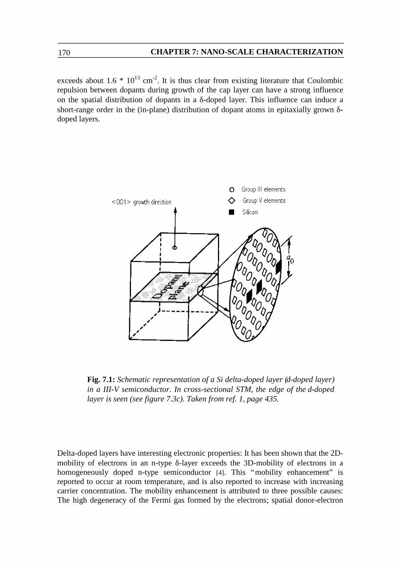
CHAPTER 7: NANO-SCALE CHARACTERIZATION170
exceeds about 1.6 * 1013 cm-2. It is thus clear from existing literature that Coulombicrepulsion between dopants during growth of the cap layer can have a strong influenceon the spatial distribution of dopants in a δ-doped layer. This influence can induce ashort-range order in the (in-plane) distribution of dopant atoms in epitaxially grown δ-doped layers.
Delta-doped layers have interesting electronic properties: It has been shown that the 2D-mobility of electrons in an n-type δ-layer exceeds the 3D-mobility of electrons in ahomogeneously doped n-type semiconductor [4]. This “mobility enhancement” isreported to occur at room temperature, and is also reported to increase with increasingcarrier concentration. The mobility enhancement is attributed to three possible causes:The high degeneracy of the Fermi gas formed by the electrons; spatial donor-electron
Fig. 7.1: Schematic representation of a Si delta-doped layer (δ-doped layer)in a III-V semiconductor. In cross-sectional STM, the edge of the δ-dopedlayer is seen (see figure 7.3c). Taken from ref. 1, page 435.
OF Si δ-DOPED LAYERS IN GaAs 171
separation in the odd-numbered subbands which have a node in the dopant plane; andscreening of the impurity charges [4]. At low temperature (T < 100 K) the dominantmechanism that determines the electron-mobility in a δ-doped layer is ionized impurityscattering [13]. It has been shown by Levi et al. [14] that ionized impurity scattering isgreatly reduced when the spatial distribution of the dopant atoms within a δ-doped layeris (partially) ordered. The same point is explained in detail by Headrick et al. [15]. Thus,an ordered in-plane distribution of dopants in a δ-layer is expected to enhance themobility of electrons in that δ-layer, particularly at low temperature.
The focus of this chapter will be on the accurate determination of the spatialdistribution of Si dopants in a δ-doped layer, using cross-sectional STM. Allexperimental results shown in this chapter involve n-type material. The emphasis in thisthesis lies on the voltage-dependent effects described in chapters 4, 5 and 6. As a result,the scope and depth of the study presented in this chapter has been limited by the timeavailable for it.
The outline of the rest of this chapter is as follows: In section 7.2 we discuss theidentification of dopants from other nano-scale features in a given STM-image (seefigure 7.3). This is a non-trivial matter, since Si donor atoms that lie in the surface layerof the crystal can have an appearance in STM that is similar to the morpology of certainother defects, like negatively charged adsorbates [5,6]. Subsurface Si donor atoms, onthe other hand, can be identified in the images without ambiguity.
Section 7.3 describes the sample containing the δ-doped layers that we used inthe experiments (see figure 7.4). In section 7.4, we will present high-resolution STM-images of Si-δ-doped layers in GaAs and discuss the kinds of features that are present inthese layers (see figure 7.5). The identification of some of the features reported insection 7.4 is based on the discussion presented in section 7.2.
In section 7.5, the in-plane spatial distribution of Si dopant atoms in a δ-dopedlayer in GaAs is investigated (see figure 7.6). The analysis is analogous to the one usedby Johnson et al. [3], and is based on the positions of the subsurface Si donor atoms inseveral large-scale images of the same δ-doped layer (see figure 7.4 c). It is shown thatthere is an apparent minimum distance of 2 nm between any two given dopants in theimages. This may indicate that short-range ordering of dopants has occurred during theepitial growth of the δ-layers. The apparent minimum distance may, however, also be anartefact caused by the fact that two very closely separated dopant atoms cannot beresolved very clearly by STM (see figure 7.7). In section 7.6, the experimental results ofsection 7.5 are discussed.

CHAPTER 7: NANO-SCALE CHARACTERIZATION172
7.2 Identification of dopants in filled-states STM-images of n-GaAs
As figures 7.2a and 7.3a show, a typical filled-states STM-image of Si-doped GaAs-(110) shows two types of features: Bright hillocks and bright features that aresurrounded by a dark ring, to which we refer as “rosettes”. We identify the brighthillocks as subsurface SiGa donor atoms based on exisiting literature [6 (p. 226), 8, 10]. Arosette, on the other hand, can represent one of several defects. It can represent asurface-layer SiGa donor atom [5, 6 (p. 233)], or any type of negatively charged defect likea SiAs acceptor [26], an adsorbed oxygen atom [7], or a surface vacancy [6 (p. 163, p. 165)].In this section, we will discuss the identification of Si-dopants in filled-states STM-images of n-type GaAs (110). The focus will be on how to distinguish rosettesrepresenting a surface-layer SiGa donor atom from the other rosettes that represent otherdefects.
Dopants are reported to manifest themselves as bright hillocks of about 2 nm indiameter in the STM-image [5,6,8,9,10]. The bright contrast of dopants in STM-imageshas been explained from the fact that the presence of such a subsurface dopant locallyincreases the surface-DOS [10]. In an alternative model proposed by Zheng et al. thebright contrast of a dopant in an STM-image is explaned from the dopant’s influence onthe local amount of Tip-Induced Band Bending (TIBB): A dopant has an electric chargeassociated with it [31], which locally changes the amount of TIBB. In ref. 8, the apparentheight of a dopant in an STM-image can be up to 1 nm. In our experiments whichinvolve smaller tunneling currents, the apparent height of a dopant can be up to about100 pm with respect to the surrounding lattice. The dopant-height thus depends on theimaging-conditions, and also gradually decreases for dopants that lie deeper inside thecrystal surface [8, 10]. From section 7.5, we expect to see dopants that lie up to 2 nmbelow the sample surface (see also ref. 10). The spatial extent of the feature thatrepresents a dopant in STM varies with the spatial extent of the screened Coulombpotential that is associated with a dopant lying near the surface [6 (p. 230), 8, 25].
It has been shown recently that surface-layer Si-donors can have an oscillatingcontrast, consisting of a bright central part surrounded by a dark ring [5,6] (see figure 7.2and 7.3 c). For n-type material, the oscillating contrast only occurs in the filled-statesimaging mode: For the empty-states imaging mode, the dopant appears as a brighthillock without the surrounding depression. The depth of the dark ring which is seen inthe filled states images is found to be highly dependent on the value of the applied biasvoltage [5,6]. It is therefore expected to be highly dependent on the tip-DOS of thetunneling tip that is used during the experiment. The authors of ref. 6 also show thatapart from the long-range signature (~ 1 nm or more) of a dopant, the “defect state”associated with a dopant can give rise to a feature in the STM-image that only extendsover the nearest surface unit cells [6 (p. 203)] (see figures 7.2 b and 7.5 c, e). The exactmorphology of such a defect-state depends critically on the location of the dopant(surface layer, the second subsurface layer, the third layer, etc). SiGa donor atoms thatlie deeper below the surface show this oscillating contrast only very weakly or not at all.Those SiGa donors that do not show this oscillating contrast appear as bright hillocksinstead [6 (p. 226)].
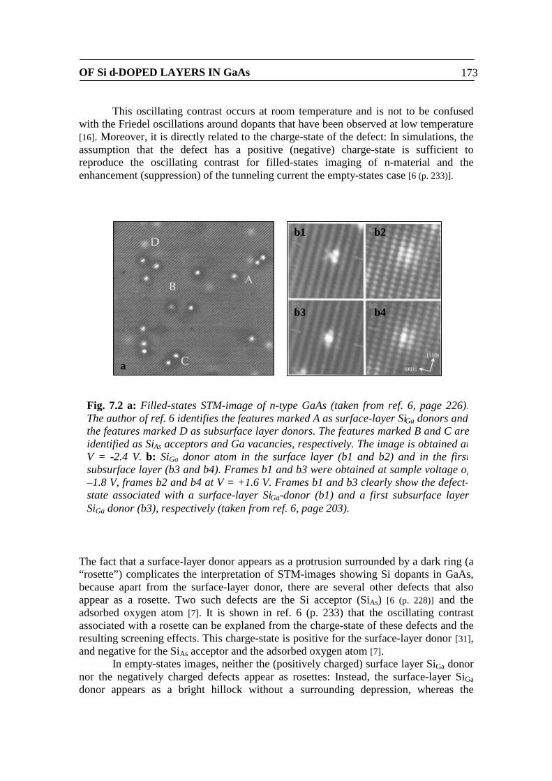
OF Si δ-DOPED LAYERS IN GaAs 173
This oscillating contrast occurs at room temperature and is not to be confusedwith the Friedel oscillations around dopants that have been observed at low temperature[16]. Moreover, it is directly related to the charge-state of the defect: In simulations, theassumption that the defect has a positive (negative) charge-state is sufficient toreproduce the oscillating contrast for filled-states imaging of n-material and theenhancement (suppression) of the tunneling current the empty-states case [6 (p. 233)].
The fact that a surface-layer donor appears as a protrusion surrounded by a dark ring (a“rosette”) complicates the interpretation of STM-images showing Si dopants in GaAs,because apart from the surface-layer donor, there are several other defects that alsoappear as a rosette. Two such defects are the Si acceptor (SiAs) [6 (p. 228)] and theadsorbed oxygen atom [7]. It is shown in ref. 6 (p. 233) that the oscillating contrastassociated with a rosette can be explaned from the charge-state of these defects and theresulting screening effects. This charge-state is positive for the surface-layer donor [31],and negative for the SiAs acceptor and the adsorbed oxygen atom [7].
In empty-states images, neither the (positively charged) surface layer SiGa donornor the negatively charged defects appear as rosettes: Instead, the surface-layer SiGadonor appears as a bright hillock without a surrounding depression, whereas the
Fig. 7.2 a: Filled-states STM-image of n-type GaAs (taken from ref. 6, page 226).The author of ref. 6 identifies the features marked A as surface-layer SiGa donors andthe features marked D as subsurface layer donors. The features marked B and C areidentified as SiAs acceptors and Ga vacancies, respectively. The image is obtained atV = -2.4 V. b: SiGa donor atom in the surface layer (b1 and b2) and in the firstsubsurface layer (b3 and b4). Frames b1 and b3 were obtained at sample voltage of–1.8 V, frames b2 and b4 at V = +1.6 V. Frames b1 and b3 clearly show the defect-state associated with a surface-layer SiGa-donor (b1) and a first subsurface layerSiGa donor (b3), respectively (taken from ref. 6, page 203).
a
b1 b2
b3 b4
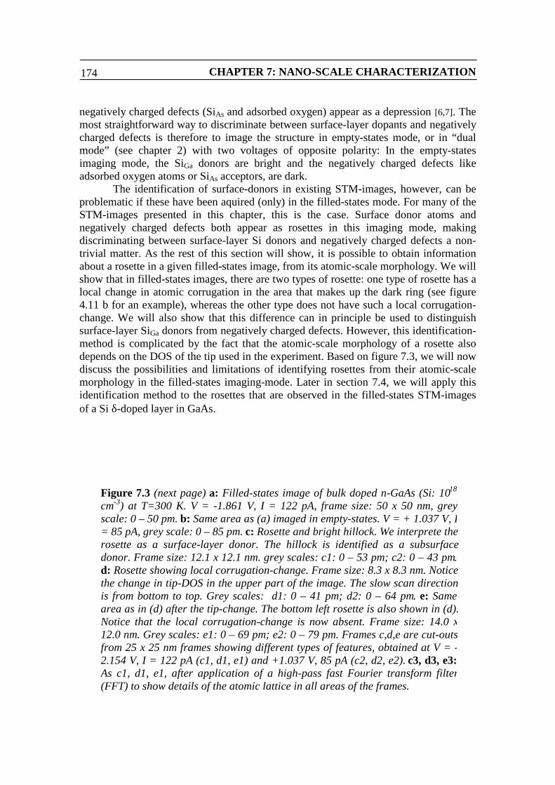
CHAPTER 7: NANO-SCALE CHARACTERIZATION174
negatively charged defects (SiAs and adsorbed oxygen) appear as a depression [6,7]. Themost straightforward way to discriminate between surface-layer dopants and negativelycharged defects is therefore to image the structure in empty-states mode, or in “dualmode” (see chapter 2) with two voltages of opposite polarity: In the empty-statesimaging mode, the SiGa donors are bright and the negatively charged defects likeadsorbed oxygen atoms or SiAs acceptors, are dark.
The identification of surface-donors in existing STM-images, however, can beproblematic if these have been aquired (only) in the filled-states mode. For many of theSTM-images presented in this chapter, this is the case. Surface donor atoms andnegatively charged defects both appear as rosettes in this imaging mode, makingdiscriminating between surface-layer Si donors and negatively charged defects a non-trivial matter. As the rest of this section will show, it is possible to obtain informationabout a rosette in a given filled-states image, from its atomic-scale morphology. We willshow that in filled-states images, there are two types of rosette: one type of rosette has alocal change in atomic corrugation in the area that makes up the dark ring (see figure4.11 b for an example), whereas the other type does not have such a local corrugation-change. We will also show that this difference can in principle be used to distinguishsurface-layer SiGa donors from negatively charged defects. However, this identification-method is complicated by the fact that the atomic-scale morphology of a rosette alsodepends on the DOS of the tip used in the experiment. Based on figure 7.3, we will nowdiscuss the possibilities and limitations of identifying rosettes from their atomic-scalemorphology in the filled-states imaging-mode. Later in section 7.4, we will apply thisidentification method to the rosettes that are observed in the filled-states STM-imagesof a Si δ-doped layer in GaAs.
Figure 7.3 (next page) a: Filled-states image of bulk doped n-GaAs (Si: 1018
cm-3) at T=300 K. V = -1.861 V, I = 122 pA, frame size: 50 x 50 nm, greyscale: 0 – 50 pm. b: Same area as (a) imaged in empty-states. V = + 1.037 V, I= 85 pA, grey scale: 0 – 85 pm. c: Rosette and bright hillock. We interprete therosette as a surface-layer donor. The hillock is identified as a subsurfacedonor. Frame size: 12.1 x 12.1 nm. grey scales: c1: 0 – 53 pm; c2: 0 – 43 pm.d: Rosette showing local corrugation-change. Frame size: 8.3 x 8.3 nm. Noticethe change in tip-DOS in the upper part of the image. The slow scan directionis from bottom to top. Grey scales: d1: 0 – 41 pm; d2: 0 – 64 pm. e: Samearea as in (d) after the tip-change. The bottom left rosette is also shown in (d).Notice that the local corrugation-change is now absent. Frame size: 14.0 x12.0 nm. Grey scales: e1: 0 – 69 pm; e2: 0 – 79 pm. Frames c,d,e are cut-outsfrom 25 x 25 nm frames showing different types of features, obtained at V = -2.154 V, I = 122 pA (c1, d1, e1) and +1.037 V, 85 pA (c2, d2, e2). c3, d3, e3:As c1, d1, e1, after application of a high-pass fast Fourier transform filter(FFT) to show details of the atomic lattice in all areas of the frames.
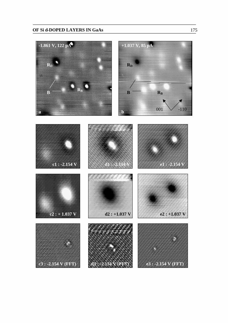
OF Si δ-DOPED LAYERS IN GaAs 175
a b
-1.861 V, 122 pA +1.037 V, 85 pA
d1 : -2.154 V
d2 : +1.037 V
e1 : -2.154 V
e2 : +1.037 V
c1 : -2.154 V
c2 : + 1.037 V
c3 : -2.154 V (FFT) d3 : -2.154 V (FFT) e3 : -2.154 V (FFT)
B RB
RD
RB
RD
B
⟨-110⟩⟨001⟩
CHAPTER 7: NANO-SCALE CHARACTERIZATION176
Figure 7.3 shows STM-images of a Si-doped GaAs-substrate of a nominal dopingconcentration of 1018 cm-3. In the two large-scale images (figure 7.3 a and b) brighthillocks are seen (B). These hillocks appear as bright protrusions in the filled-statesimage (a), and are also bright in the empty-states image (b). According to refs. 5 and6, this identifies the hillocks as subsurface SiGa donors [5, 6 (p. 226)]. Moreover, thesubsurface SiGa donor is the only defect reported to manifest itself as a bright featurewithout oscillating contrast in both filled and empty states images [6 (p. 226)]. This is incontrast to the rosettes, where a given rosette can represent one of several defects [5,6,7].In figure 7.3 a, we observe 12 bright hillocks on a sample area of 50 x 50 nm2. If weassume that we can observe dopants that lie up to 2 nm below the sample surface (seesection 7.5), this areal density of bright hillocks translates to a Si dopant density of 2.4 *1018 cm-3. This is consistent with the nominal doping concentration of the n-dopedGaAs substrate used in this experiment. Furthermore, the Si δ-doped layers that areinvestigated in this chapter consist mainly of bright hillocks (see figure 7.4 c,d andfigure 7.5). In Si δ-doped layers of a nominal areal density of less than 1013 cm-2, Siincorporates mainly as a SiGa donor [1 (p. 459)]. Therefore, the occurrence of the brighthillocks must be related to the presence of SiGa donors in the GaAs host crystal
It should be kept in mind that the bright hillock which represents a subsurfacelayer SiGa donor is the signature of the screened Coulomb-potential that is associatedwith the dopant. Therefore, any subsurface defect that has a charge-state of +1 e (with ethe elementary charge) will show up as a bright hillock which is in all aspects similar tothe bright hillock that represents a subsurface SiGa donor. Fortunately, however, mosttypes of defects that are commonly encountered on the (110)-surface of Si-doped GaAsdo not have a positive charge-state: Ga surface vacancies (VGa) and As surfacevacancies (VAs) are negatively charged [6 (p. 163, p. 165)], SiAs acceptors [5, 6 (p. 228), 26]and adsorbed oxygen atoms [7] are negatively charged as well, and SiGa-VGa complexesas well as Si clusters are neutral [28]. We therefore make the assumption that any defectwith an apparently positive charge-state is in fact a SiGa donor atom.
Two types of rosette can be seen in figures 7.3 a and b: There are rosettes thatbecome bright protrusions in the corresponding empty states image (RB), and rosettesthat turn into depressions (RD). We identify the rosettes that remain bright in the emptystates image (RB) as surface-layer donors (SiGa) [6 (p. 227, p. 233), 31]: In ref. 6 (p. 229),only surface-layer SiGa-impurities are reported to manifest themselves as rosettes whichremain bright in the corresponding empty-states image (RB), although in principle, anytype of positively charged defect might be expected to appear as an RB-type rosette [6 (p.233)]. We observe two RB-rosettes in figure 7.3 a and b, which represents a sample areaof 50 x 50 nm. When these rosettes are assumed to represent surface-layer SiGaimpurities, this areal density of RB rosettes would translate to a bulk Si-concentration inthe crystal of 4 * 1018 cm-3. That is roughly consistent with the nominal dopingconcentration of the crystal which is 1 * 1018 cm-3.
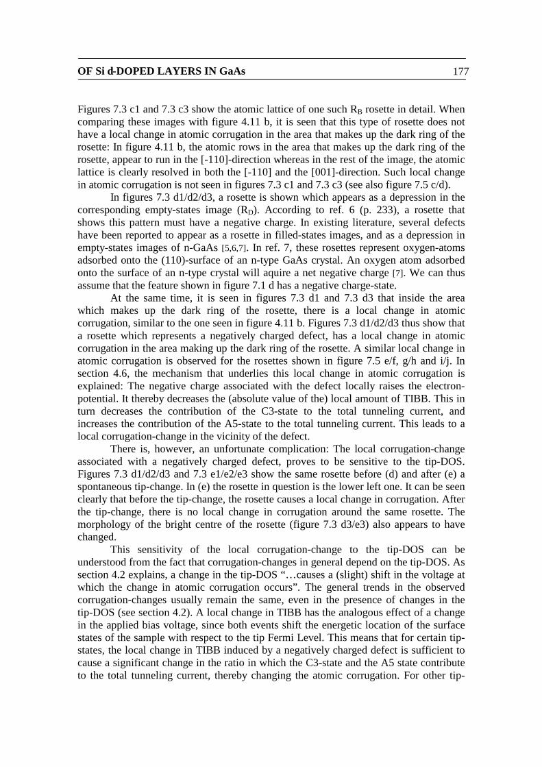
OF Si δ-DOPED LAYERS IN GaAs 177
Figures 7.3 c1 and 7.3 c3 show the atomic lattice of one such RB rosette in detail. Whencomparing these images with figure 4.11 b, it is seen that this type of rosette does nothave a local change in atomic corrugation in the area that makes up the dark ring of therosette: In figure 4.11 b, the atomic rows in the area that makes up the dark ring of therosette, appear to run in the [-110]-direction whereas in the rest of the image, the atomiclattice is clearly resolved in both the [-110] and the [001]-direction. Such local changein atomic corrugation is not seen in figures 7.3 c1 and 7.3 c3 (see also figure 7.5 c/d).
In figures 7.3 d1/d2/d3, a rosette is shown which appears as a depression in thecorresponding empty-states image (RD). According to ref. 6 (p. 233), a rosette thatshows this pattern must have a negative charge. In existing literature, several defectshave been reported to appear as a rosette in filled-states images, and as a depression inempty-states images of n-GaAs [5,6,7]. In ref. 7, these rosettes represent oxygen-atomsadsorbed onto the (110)-surface of an n-type GaAs crystal. An oxygen atom adsorbedonto the surface of an n-type crystal will aquire a net negative charge [7]. We can thusassume that the feature shown in figure 7.1 d has a negative charge-state.
At the same time, it is seen in figures 7.3 d1 and 7.3 d3 that inside the areawhich makes up the dark ring of the rosette, there is a local change in atomiccorrugation, similar to the one seen in figure 4.11 b. Figures 7.3 d1/d2/d3 thus show thata rosette which represents a negatively charged defect, has a local change in atomiccorrugation in the area making up the dark ring of the rosette. A similar local change inatomic corrugation is observed for the rosettes shown in figure 7.5 e/f, g/h and i/j. Insection 4.6, the mechanism that underlies this local change in atomic corrugation isexplained: The negative charge associated with the defect locally raises the electron-potential. It thereby decreases the (absolute value of the) local amount of TIBB. This inturn decreases the contribution of the C3-state to the total tunneling current, andincreases the contribution of the A5-state to the total tunneling current. This leads to alocal corrugation-change in the vicinity of the defect.
There is, however, an unfortunate complication: The local corrugation-changeassociated with a negatively charged defect, proves to be sensitive to the tip-DOS.Figures 7.3 d1/d2/d3 and 7.3 e1/e2/e3 show the same rosette before (d) and after (e) aspontaneous tip-change. In (e) the rosette in question is the lower left one. It can be seenclearly that before the tip-change, the rosette causes a local change in corrugation. Afterthe tip-change, there is no local change in corrugation around the same rosette. Themorphology of the bright centre of the rosette (figure 7.3 d3/e3) also appears to havechanged.
This sensitivity of the local corrugation-change to the tip-DOS can beunderstood from the fact that corrugation-changes in general depend on the tip-DOS. Assection 4.2 explains, a change in the tip-DOS “… causes a (slight) shift in the voltage atwhich the change in atomic corrugation occurs”. The general trends in the observedcorrugation-changes usually remain the same, even in the presence of changes in thetip-DOS (see section 4.2). A local change in TIBB has the analogous effect of a changein the applied bias voltage, since both events shift the energetic location of the surfacestates of the sample with respect to the tip Fermi Level. This means that for certain tip-states, the local change in TIBB induced by a negatively charged defect is sufficient tocause a significant change in the ratio in which the C3-state and the A5 state contributeto the total tunneling current, thereby changing the atomic corrugation. For other tip-
CHAPTER 7: NANO-SCALE CHARACTERIZATION178
states, however, the same local change in TIBB may be insufficient to change therelative contributions of the C3- and A5 states to the total tunneling current verystrongly, so that no local corrugation-change is observed [32].
This leads to a complication when identifying a given rosette from its atomic-scale morphology: When the rosette does not have a local corrugation-change in thearea that makes up the dark ring, this can mean two things: It can mean that the rosettehas a positive charge-state, but it can also mean for the applied bias voltage or the tip-DOS involved in the experiment, the change in the amount of TIBB is insufficientinduce the expected corrugation-change. Therefore, the absence of a local corrugation-change in the dark ring of the rosette can only be interpreted as an indication that therosette must represent a positively charged defect, when in the same measurement (forthe same bias voltage and tip-DOS) other rosettes are observed that do show this localchange in atomic corrugation.
Based on the foregoing, we will use the following method for identifyingrosettes in STM-images of n-type GaAs (110) in the case that only filled states imagesare available: First, it should be established whether the images contain rosettes with alocal corrugation-change as well as rosettes without a local corrugation change. Whenthe images contain both types of rosette, it is certain that the chosen bias voltage and thetip-DOS are appropriate for the local corrugation-change to appear in a negativelycharged rosette. A rosette with such a local corrugation-change can then be interpretedas a negatively charged defect. A rosette without a local corrugation-change must becharged positively, and is interpreted as a surface-layer dopant in accordance withref. 6.

OF Si δ-DOPED LAYERS IN GaAs 179
7.3 Sample structure and STM-results
The sample on which the images shown in figure 7.4 were obtained consists of an n-type GaAs substrate (Si 1018 cm-3) on which a total 12 Si δ-doped layers was grown byMolecular Beam Epitaxy (MBE). The epitaxial structure on the sample consists of threeidentical stacks of four Si-δ-doped layers (figure 7.4 a). The layers have an increasingnominal areal density of Si (3 * 1011 cm-2, 1 * 1012 cm-3, 3 * 1012 cm-2, 1 * 1013 cm-2).The stacks themselves are separated by Al0.2Ga0.8As marker layers. Within a stack, theSi δ-doped layers are separated by 25 nm of non-intentionally doped GaAs. Theseparation between the first δ-layer of each stack and the nearest marker layer (on thesubstrate side) is 25 nm as well. The separation between the fourth δ-layer and thefollowing marker (nearest marker on the epilayer side) is 35 nm. The markersthemselves also have a finite spatial extent: M1: 2.5 nm; M2 and M3: 10 nm; M4: 17.5nm. The entire structure has been grown at T = 480 oC. The δ-layer structure has beengrown on top of an n-GaAs buffer layer (500 nm thickness, 5.4 * 1018 cm-3 Si), and hasbeen buried under an n-GaAs cap layer (300 nm) with the same doping concentration.
Our description of the δ-layers is based on two sets of images: To identify themain features that make up the δ-layers we rely on atomically resolved images (25 x 25nm) of individual features or small clusters (see figure 7.4 d). In order to characterizethe distribution of dopants, we use overlapping large-scale images (figure 7.4 a,c,e: 150x 150 nm): The positions of the δ-layers relative to the markers has (see table 7.1) hasbeen measured from 4 overlapping large-scale images that cover a stripe running alongthe [001]-direction, extending over all three stacks of δ-layers (figure 7.4 e). The in-plane distribution of dopants has been measured from 6 overlapping large-scale imagesof the third stack of δ-doped layers (figure 7.4 a, c). The distances that occur betweendopants have been measured for δ 3.4, resulting in the pair-distribution functionpresented in figure 7.6. The large frame-size (150 x 150 nm) has been chosen in order tomaximize the number of dopants considered, which reduces the amount of expectedstatistical fluctuation in the pair-distribution function (the error-bars in figure 7.6).

CHAPTER 7: NANO-SCALE CHARACTERIZATION180
M4 Surface
δ 3.4 1* 1013 cm-2 Siδ 3.3 3 * 1012 cm-2 Siδ 3.2 1 * 1012 cm-2 Siδ 3.1 3 * 1011 cm-2 Si
M3δ 2.4 1* 1013 cm-2 Siδ 2.3 3 * 1012 cm-2 Siδ 2.2 1 * 1012 cm-2 Siδ 2.1 3 * 1011 cm-2 Si
M2δ 1.4 1* 1013 cm-2 Siδ 1.3 3 * 1012 cm-2 Siδ 1.2 1 * 1012 cm-2 Siδ 1.1 3 * 1011 cm-2 Si
M1 Substrate
a b
c d
f
M4δ 3.4 δ 3.3 δ 3.2
δ 3.1
M3
Step
e
Layout large-scale images for table 7.1
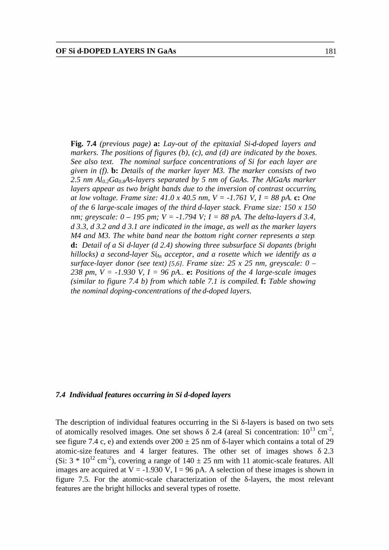
OF Si δ-DOPED LAYERS IN GaAs 181
7.4 Individual features occurring in Si δ-doped layers
The description of individual features occurring in the Si δ-layers is based on two setsof atomically resolved images. One set shows δ 2.4 (areal Si concentration: 1013 cm-2,see figure 7.4 c, e) and extends over 200 ± 25 nm of δ-layer which contains a total of 29atomic-size features and 4 larger features. The other set of images shows δ 2.3(Si: 3 * 1012 cm-2), covering a range of 140 ± 25 nm with 11 atomic-scale features. Allimages are acquired at V = -1.930 V, I = 96 pA. A selection of these images is shown infigure 7.5. For the atomic-scale characterization of the δ-layers, the most relevantfeatures are the bright hillocks and several types of rosette.
Fig. 7.4 (previous page) a: Lay-out of the epitaxial Si-δ-doped layers andmarkers. The positions of figures (b), (c), and (d) are indicated by the boxes.See also text. The nominal surface concentrations of Si for each layer aregiven in (f). b: Details of the marker layer M3. The marker consists of two2.5 nm Al0.2Ga0.8As-layers separated by 5 nm of GaAs. The AlGaAs markerlayers appear as two bright bands due to the inversion of contrast occurringat low voltage. Frame size: 41.0 x 40.5 nm, V = -1.761 V, I = 88 pA. c: Oneof the 6 large-scale images of the third δ-layer stack. Frame size: 150 x 150nm; greyscale: 0 – 195 pm; V = -1.794 V; I = 88 pA. The delta-layers δ 3.4,δ 3.3, δ 3.2 and δ 3.1 are indicated in the image, as well as the marker layersM4 and M3. The white band near the bottom right corner represents a step.d: Detail of a Si δ-layer (δ 2.4) showing three subsurface Si dopants (brighthillocks) a second-layer SiAs acceptor, and a rosette which we identify as asurface-layer donor (see text) [5,6]. Frame size: 25 x 25 nm, greyscale: 0 –238 pm, V = -1.930 V, I = 96 pA.. e: Positions of the 4 large-scale images(similar to figure 7.4 b) from which table 7.1 is compiled. f: Table showingthe nominal doping-concentrations of the δ-doped layers.
CHAPTER 7: NANO-SCALE CHARACTERIZATION182
The bright hillocks (figure 7.5 a) are the most numerous of all atomic-scale features,accounting for two thirds of all features observed. We identify the hillocks assubsurface donors (SiGa) based on section 7.2 [5,6 (p. 226)]. Moreover, it can be seenfigure 7.5a that in the area that makes up the bright hillock, there is a slight, localchange in atomic corrugation. Inside the hillock, the atomic rows appear to run more orless along the [001]-direction, which is not the case in the surrounding lattice. Theeffect can also be seen for the bright hillock shown in figure 7.5 b, or the one shown infigure 4.11 a. As is explained in section 4.6, this local change in atomic corrugationindicates that in the area which makes up the bright hillock, the contribution of the C3-state has increased with respect to the contribution of the A5-state. For n-GaAs imagedat negative sample voltage, this must mean that locally, the absolute amount of TIBBhas increased, which is consistent with the assumption that the bright hillock representsa positively charged defect. For a SiGa donor atom, a positive charge-state is expected[31].
The rosettes account for about one third of the total number of features that isobserved. In the images, we observe rosettes with a local corrugation-change in the areamaking up the dark ring of the rosette (figure 7.5 e/f, g/h, i/j), as well as rosettes that donot have this local corrugation-change (figure 7.5 c/d, see also figure 4.11 b and section7.2). Given the fact that both types of rosette appear in the images, it is certain that therosettes which do not show this local change in atomic corrugation in the dark ring musthave a positive charge-state [31] (see section 7.2). Following the argument made insection 7.2 we identify these rosettes as surface-layer SiGa donor atoms. As is explainedin section 7.2, the rosettes with a local change in corrugation (figure 7.5 e/f, g/h, i/j)must have a negative charge-state. Given this charge-state, they can represent severaltypes of defects, like SiAs-acceptors [6 (p. 228)] or adsorbed oxygen atoms [7].
Having identified the rosette shown in figure 7.5 c/d as surface-layer SiGa-donoratom, we can compare its morphology with the morphology of a surface-layer SiGa-donor as it is reported in refs. 5 and 6 (see ref. 6, p. 226 and 227, or figure 7.2 b). Thiscomparison shows that the morphology of the central bright part does not correspond tothe spatial extent of what is called the “defect state” in refs. 5 and 6. The origin of thisdifference is at present unclear to us, but there are two factors which appear relevant.
First of all, we suspect that the appearance of the defect-state is voltage-dependent: Such voltage-dependency is reported for the morphology of the surface Ga-vacancy on GaP-(110) [6 (p. 173)]. If the appearance of the defect-state of the surface-layer SiGa donor is indeed voltage-dependent, it can also be expected to be sensitive tochanges in the tip-DOS: Tungsten STM-tips that are optimized for high lateralresolution are expected to have a peaked tip-DOS [11]. A change in the tip-DOS canshift the energetic position(s) of the peak(s) in the tip-DOS [33]. This, in turn, will causea change in the relative amounts in which the different sample surface states contributeto the total tunneling current, since the tunneling current consists of a convolution of thetip-DOS and sample-DOS (see equation 1.6). In this respect the effects of a change inthe tip-DOS and the effects of a change in applied bias voltage are similar, so that if themorphology of a given feature depends on the applied bias voltage, it can also beexpected to be sensitive to changes in the tip-DOS.
The second factor is that the experimental circumstances under which ourimages were acquired differ slightly from the ones that surround the images reported by
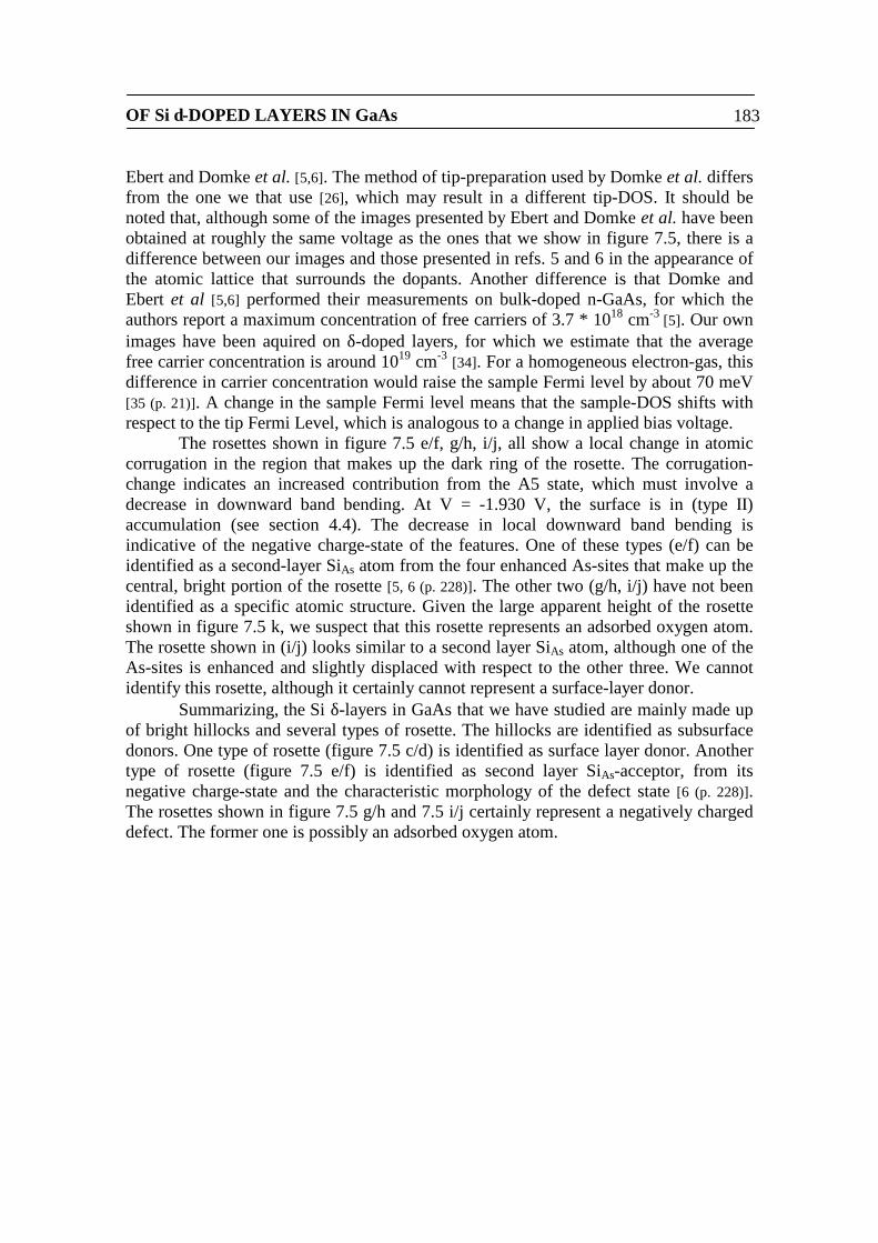
OF Si δ-DOPED LAYERS IN GaAs 183
Ebert and Domke et al. [5,6]. The method of tip-preparation used by Domke et al. differsfrom the one we that use [26], which may result in a different tip-DOS. It should benoted that, although some of the images presented by Ebert and Domke et al. have beenobtained at roughly the same voltage as the ones that we show in figure 7.5, there is adifference between our images and those presented in refs. 5 and 6 in the appearance ofthe atomic lattice that surrounds the dopants. Another difference is that Domke andEbert et al [5,6] performed their measurements on bulk-doped n-GaAs, for which theauthors report a maximum concentration of free carriers of 3.7 * 1018 cm-3 [5]. Our ownimages have been aquired on δ-doped layers, for which we estimate that the averagefree carrier concentration is around 1019 cm-3 [34]. For a homogeneous electron-gas, thisdifference in carrier concentration would raise the sample Fermi level by about 70 meV[35 (p. 21)]. A change in the sample Fermi level means that the sample-DOS shifts withrespect to the tip Fermi Level, which is analogous to a change in applied bias voltage.
The rosettes shown in figure 7.5 e/f, g/h, i/j, all show a local change in atomiccorrugation in the region that makes up the dark ring of the rosette. The corrugation-change indicates an increased contribution from the A5 state, which must involve adecrease in downward band bending. At V = -1.930 V, the surface is in (type II)accumulation (see section 4.4). The decrease in local downward band bending isindicative of the negative charge-state of the features. One of these types (e/f) can beidentified as a second-layer SiAs atom from the four enhanced As-sites that make up thecentral, bright portion of the rosette [5, 6 (p. 228)]. The other two (g/h, i/j) have not beenidentified as a specific atomic structure. Given the large apparent height of the rosetteshown in figure 7.5 k, we suspect that this rosette represents an adsorbed oxygen atom.The rosette shown in (i/j) looks similar to a second layer SiAs atom, although one of theAs-sites is enhanced and slightly displaced with respect to the other three. We cannotidentify this rosette, although it certainly cannot represent a surface-layer donor.
Summarizing, the Si δ-layers in GaAs that we have studied are mainly made upof bright hillocks and several types of rosette. The hillocks are identified as subsurfacedonors. One type of rosette (figure 7.5 c/d) is identified as surface layer donor. Anothertype of rosette (figure 7.5 e/f) is identified as second layer SiAs-acceptor, from itsnegative charge-state and the characteristic morphology of the defect state [6 (p. 228)].The rosettes shown in figure 7.5 g/h and 7.5 i/j certainly represent a negatively chargeddefect. The former one is possibly an adsorbed oxygen atom.
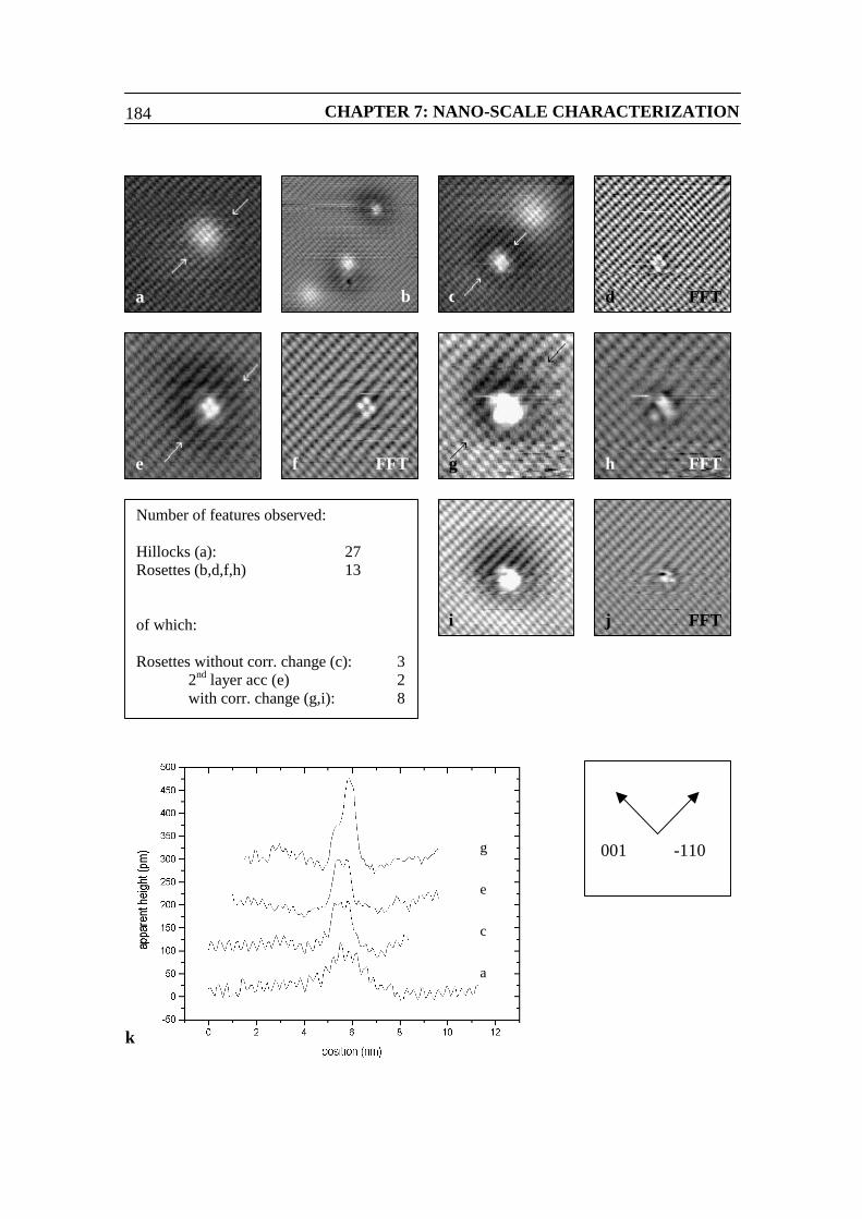
CHAPTER 7: NANO-SCALE CHARACTERIZATION184
FFT
FFT FFTe
k
Number of features observed:
Hillocks (a): 27Rosettes (b,d,f,h) 13
of which:
Rosettes without corr. change (c): 32nd layer acc (e) 2with corr. change (g,i): 8
h
i
gf
a b c d FFT
FFTj
a
c
e
g ⟨-110⟩⟨001⟩
OF Si δ-DOPED LAYERS IN GaAs 185
Fig. 7.5 (preceeding page) a: Bright hillock: corresponds to subsurface donor (seesection 7.2). Frame size: 9.8 x 9.9 nm, colour scale: 0 – 156 pm. b: Larger scaleimage (15.4 x 15.4 nm) showing several features. Bottom right: bright hillock;center: Surface vacancy and rosette without corrugation-change; upper right:Rosette with corrugation change. Colour scale: 0 – 229 pm. c: The central feature isa rosette without corrugation-change in the dark ring. The corrugation-change inthe central part indicates that the feature is positively charged. We associate thistype of rosette with a surface-layer donor. In the top right corner a subsurface donoris seen as well. Frame size: 10.1 x 10.3 nm, colour scale: 0 – 160 pm. (further detailsin sections 7.2 and 7.4) d: As c, after application of a high-pass fast Fouriertransform (FFT) filter in order to show details of the lattice in all areas. Colourscale: 0 – 108 pm. e: Negatively charged rosette. From ref. 6 this type of rosette isidentified as a SiAs atom in the second surface layer. Frame size: 7.2 x 7.6 nm, colourscale: 0 – 172 pm. (further details in section 7.2 and 7.4). f: As e, after application ofa high-pass FFT-filter. Colour scale: 0 – 75 pm. g: Rosette showing a localcorrugation-change in the dark ring, indicating that the feature is negativelycharged. Frame size: 5.8 x 6.0 nm, colour scale: 0 – 87 pm. (further details insection 7.2 and 7.4) h: As g, after application of a high-pass FFT-filter. Colourscale: 0 – 108 pm. i,j: Other type of negatively charged rosette. This type is similarin appearance to the second-layer acceptor (e), although one As-dangling bondappears brighter than the other three. Frame size: 8.4 x 8.4 nm, colour scale 0 – 92pm (h), resp. 0 – 110 pm (i). The peak of the rosette is 135 pm high with respect tothe surrounding lattice. k: Height-profiles through the various features taken alongthe [-110] direction (see arrows). Curve a: bright hillock (figure 7.5 a); Curve c(offset by 100 pm): Positively charged rosette (figure 7.5 c); Curve e (offset by 200pm): 2nd layer SiAs (figure 7.5 e); Curve g (offset by 300 pm): Negatively chargedrosette (figure 7.5 g).

CHAPTER 7: NANO-SCALE CHARACTERIZATION186
7.5 Spatial distribution of Si-dopants within a δ-doped layer
The study of the spatial distribution of Si-dopants within the δ-doped layer is based on 6partly overlapping large-scale images (150 x 150 nm) of δ 3.4, which have been aquiredin the filled states imaging mode (see figure 7.4 a, c). The positions of the δ-layersrelative to the marker layers have been measured from a second set of overlappinglarge-scale images (also 150 x 150 nm) that extends along [001], traversing all threestacks of δ-layers (figure 7.4 e). The large imaging-area has been chosen so that theradial distribution function of the dopants shown in figure 7.6 could be based on a largenumber of dopants (156). The consequence of the large imaging-area is that atomicresolution is lost as the area represented by one pixel becomes about as large as onesurface unit cell (0.375 x 0.375 nm for an image of 400 x 400 pixels). We thereforecannot make a distinction between the various types of rosette on the basis of theiratomic-scale morphology, and the adsorbates and acceptors (SiAs) cannot bedistinguished from surface-layer donors (SiGa). We can, however, identify the brighthillocks as subsurface donors (see section 7.2). The study on the spatial distribution ofthe dopants within the δ-layer is thus based on the distribution of the bright hillocks,which represent subsurface donors, only. The statistical analysis underlying the radialdistribution function shown in figure 7.6 has been carried out for δ 3.4.
The large-scale images show that none of the δ-layers has broadenedsignificantly. Only the most heavily doped layer (δ 3.4) shows a small amount of layer-broadening: The δ-layer falls within a band of 7.5 nm wide. It is also clear that nosignificant segregation of dopants has taken place during growth, since the position ofthe δ-layers with respect to the AlGaAs marker layers matches the intended position ofthe δ-layers (see table 7.1). Segregation of dopants would have decreased the distancebetween the δ-layers with respect to the marker on the epilayer side (see also section7.6). In table 7.1, we have expressed the distances between the δ-layers and the markersas a fraction of the distance between the two marker layers bordering the relevant stackof δ-layers, in order to eliminate scaling-effects caused by the calibration of the piezo-elements of the STM.
The absence of diffusion and segregation of the dopants during growth seemsreasonably consistent with other experimental results found in the literature. Accordingto refs. 1 (e.g. p. 346), 2, and 29 (p. 34), sharp doping profiles of Si in GaAs can begrown at temperatures below 500 oC – 550 oC. The δ-layers shown in figure 7.4 havebeen grown at 480 oC. The effect of growth temperature on the distribution of dopantsin a Si δ-doped layer has also been investigated by Grandidier et al. [9]. In their paper,atomically resolved STM-images of two MBE-grown Si δ-doped layers in GaAs areshown: One layer has been grown at 480 oC, and the other at 580 oC. Nominal surfaceconcentration of dopants is 1.9 * 1013 cm-2 for both layers. For both δ-layers, layer-broadening and a shift of the position towards the growth surface is observed, althoughthe two effects are noticeably stronger for the δ-layer grown at 580 oC: From the STM-image in the paper, the δ-layer grown at 480 oC appears to be about 10 nm wide andappears to have been displaced by about 5 nm towards the growth surface. The δ-layer

OF Si δ-DOPED LAYERS IN GaAs 187
grown at 580 oC appears about 20 nm wide, and appears to be shifted by about 10 nm.The fact that Grandidier et al. observe layer-broadening and a position-shift of the layerat a growth temperature as low as 480 oC appears to be at variance with our ownexperimental results. A possible explanation of this difference is the fact that themaximum concentration of Si used in our δ-doped layers is about half of theconcentration used by Grandidier et al. [9, 37].
Measured ( ± 0.02) Nominal
| M4 – M3 |Measured = 1 | M4 – M3 |Nominal = 1
| δ 3.4 – M4 | / | M4 – M3 | 0.26 0.264| δ 3.3 – M4 | / | M4 – M3 | 0.44 0.445| δ 3.2 – M4 | / | M4 – M3 | 0.66 0.627
| M3 – M2 |Measured = 1 | M3 – M2 |Nominal = 1
| δ 2.3 – M3 | / | M3 – M2 | 0.45 0.445| δ 2.2 – M3 | / | M3 – M2 | 0.62 0.627
| δ 1.4 – M2 | / | M3 – M2 | 0.26 0.264| δ 1.3 – M2 | / | M3 – M2 | 0.45 0.445| δ 1.2 – M2 | / | M3 – M2 | 0.65 0.627
M4 – M3 ** 121 ± 2 nm 137.5 nm106 ± 2 nm
M3 – M2 121 ± 2 nm
** The numerical value of the distance between the two markers variesfrom one frame to the next due to temporal drift in the images.
Table 7.1: Measured and nominal distances between the δ-layers and the markerson the epilayer side. The distances are expressed as fractions of the distancebetween the markers in order to eliminate scaling-effects due to the calibration ofthe piezo-actuators of the STM. The distances are measured within ± 2 nm. The δ-layers δ 1.1, δ 2.1 and δ 3.1 are not considered since the layers are very dilute andusually only a single dopant shows up in an image. M1 and δ 2.4 were invisible dueto mono-atomic steps. The positions within the δ-layer stack of the large-scaleSTM-images from which this table is compiled, are shown in figure 7.4 e.

CHAPTER 7: NANO-SCALE CHARACTERIZATION188
Fig. 7.6 Pair distribution function associated with δ 3.4. The data-points arerepresented by squares, the lines are linear interpolations to guide the eye. Theerror-bars correspond to the square root of the number of distance-pairscounted. Diamonds: Theoretical pair distribution function based on theassumption that closely spaced hillocks cannot be imaged separately. The linesbetween the data-points are linear interpolations. See further details in text.

OF Si δ-DOPED LAYERS IN GaAs 189
Fig. 7.7 a: Typical height-profile of a hillock in a large-scaleimage (150 x 150 nm, see figure 7.4 c). The average FWHM of ahillock is 2.1 nm, standard deviation is 0.6 nm. b: Cluster of threeclosely spaced hillocks imaged at high resolution. Frame size: 10.0x 10.0 nm, grey scale: 0 – 94 pm.
a
b
CHAPTER 7: NANO-SCALE CHARACTERIZATION190
Figure 7.6 shows the pair-distribution function evaluated for δ 3.4. The distributionfunction has been based on 156 subsurface donors (307 distance-pairs). The observeddistances have been catagorized in classes of 1 nm (0 – 1 nm, 1 – 2 nm, 2 – 3 nm, etc.).In figure 7.6, the quatity plotted on the vertical scale is the number of dopant-pairs forwhich the distance between the two constituent dopants was observed to lie between 0and 1 nm, 1 and 2 nm, 2 and 3 nm, and so on. We have ignored possible differences inthe depth of the subsurface donor below the sample surface, so all distances betweendopants are in fact projections of the actual distance onto the sample surface. The totallength of δ-layer imaged is 680 nm. Given the nominal concentration of dopants, thetotal number of subsurface donors that is observed thus would indicate that dopants thatlie up to 2 ± 0.3 nm below the sample surface still appear in the image. The square rootof the number of events counted for a given distance-class is used as an estimate of thestatistical error. The pair-distribution function strongly suggests that a projecteddistance between a given pair of dopant atoms of less than about 2 nm, is less likely tooccur.
There is, however, a problem associated with the pair distribution functionshown in figure 7.6: it is based on the distribution of the bright hillocks, which have afinite spatial extent themselves. As is evident from figure 7.7 b, it becomes difficult toimage the bright hillocks individually when they are separated by only a small distance.If closely separated subsurface donors are preferentially interpreted as one single dopantdue to the finite spatial extent of the hillocks themselves, this can cause an arteficialminimum distance to appear in the pair-distribution function. The spatial extent of thehillocks can be characterized by the full width-half maximum (FWHM) of the apparentheight-profile. The average FWHM of the population of dopants used for the pair-distribution function shown in figure 7.6 is 2.1 ± 0.6 nm (see figure 7.7 a). The standarddeviation of 0.6 nm reflects the differences in size of the hillocks that are caused by thefact that some subsurface donors lie deeper below the sample surface than others. Wewill now show that the measured pair-distribution function can be reproduced from apopulation of randomly distributed dopants, if one assumes that two dopants which areseparated by a distance which is less than the average of the FWHM of the two hillock-profiles, cannot be imaged separately and are interpreted as one single dopant. Thissuggests that the minimum distance observed in figure 7.6 may well be an artefactcaused by the fact that two closely separated subsurface donors cannot be imagedseparately.
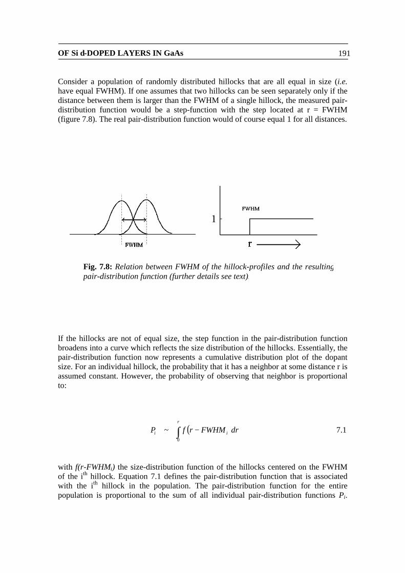
OF Si δ-DOPED LAYERS IN GaAs 191
Consider a population of randomly distributed hillocks that are all equal in size (i.e.have equal FWHM). If one assumes that two hillocks can be seen separately only if thedistance between them is larger than the FWHM of a single hillock, the measured pair-distribution function would be a step-function with the step located at r = FWHM(figure 7.8). The real pair-distribution function would of course equal 1 for all distances.
If the hillocks are not of equal size, the step function in the pair-distribution functionbroadens into a curve which reflects the size distribution of the hillocks. Essentially, thepair-distribution function now represents a cumulative distribution plot of the dopantsize. For an individual hillock, the probability that it has a neighbor at some distance r isassumed constant. However, the probability of observing that neighbor is proportionalto:
with f(r-FWHMi) the size-distribution function of the hillocks centered on the FWHMof the ith hillock. Equation 7.1 defines the pair-distribution function that is associatedwith the ith hillock in the population. The pair-distribution function for the entirepopulation is proportional to the sum of all individual pair-distribution functions Pi.
Fig. 7.8: Relation between FWHM of the hillock-profiles and the resultingpair-distribution function (further details see text).
( ) 1.7~0∫ −r
ii drFWHMrfP
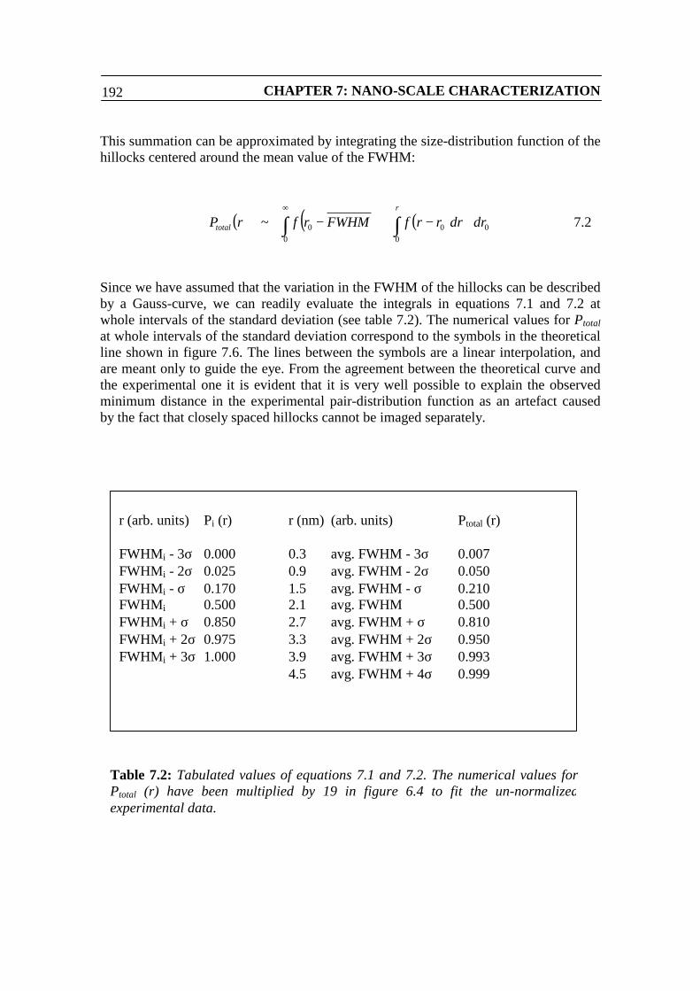
CHAPTER 7: NANO-SCALE CHARACTERIZATION192
This summation can be approximated by integrating the size-distribution function of thehillocks centered around the mean value of the FWHM:
Since we have assumed that the variation in the FWHM of the hillocks can be describedby a Gauss-curve, we can readily evaluate the integrals in equations 7.1 and 7.2 atwhole intervals of the standard deviation (see table 7.2). The numerical values for Ptotalat whole intervals of the standard deviation correspond to the symbols in the theoreticalline shown in figure 7.6. The lines between the symbols are a linear interpolation, andare meant only to guide the eye. From the agreement between the theoretical curve andthe experimental one it is evident that it is very well possible to explain the observedminimum distance in the experimental pair-distribution function as an artefact causedby the fact that closely spaced hillocks cannot be imaged separately.
r (arb. units) Pi (r) r (nm) (arb. units) Ptotal (r)
FWHMi - 3σ 0.000 0.3 avg. FWHM - 3σ 0.007FWHMi - 2σ 0.025 0.9 avg. FWHM - 2σ 0.050FWHMi - σ 0.170 1.5 avg. FWHM - σ 0.210FWHMi 0.500 2.1 avg. FWHM 0.500FWHMi + σ 0.850 2.7 avg. FWHM + σ 0.810FWHMi + 2σ 0.975 3.3 avg. FWHM + 2σ 0.950FWHMi + 3σ 1.000 3.9 avg. FWHM + 3σ 0.993
4.5 avg. FWHM + 4σ 0.999
Table 7.2: Tabulated values of equations 7.1 and 7.2. The numerical values forPtotal (r) have been multiplied by 19 in figure 6.4 to fit the un-normalizedexperimental data.
( ) ( ) ( ) 2.7~ 00 0
00 drdrrrfFWHMrfrPr
total ∫ ∫∞
−−
OF Si δ-DOPED LAYERS IN GaAs 193
7.6 Discussion on the spatial distribution of Si-dopants within a δ-doped layer
This discussion will be limited to questions about the spatial distribution of the dopantsthat make up the δ-doped layers. Most of the features that we observe are brighthillocks, which can be identified as subsurface donors [5, 6 (p. 226)]. We have alsorecognized second-layer acceptors in the images shown in section 7.4, which indicatesthat some silicon-atoms have incorporated on As-sites [6 (p. 228)]. This is a knownphenomenon for GaAs doped with Si at high concentration [1,30].
As for the spatial distribution of the dopants, it is plausible to assume that theinitial distribution of the dopant atoms is random. During the growth interrupt that ispart of the δ-doping process, the dopants arrive at the growth surface as a non-interacting Knudsen gas [36], much like hail-stones do when they reach the ground.From the literature, however, it is clear that significant redistribution of dopants takesplace after deposition. This redistribution, which is highly sensitive to the growthparameters, determines the final distribution of the dopants. We will first discuss thereasons why one might suspect ordering of dopants to take place during the epitaxialgrowth of δ-doped layers. We already explained in the previous section thatinterpretation of figure 7.6 is severely complicated by the fact that dopants in STM-images have an apparent radius of several nm. In the second part of the discussion, wewill therefore discuss possible improvements to the measurement method which mightsolve this problem.
7.6.1 Ordering effects during the epitaxial growth of delta-doped layers.
One very important mechanism by which redistribution of dopants can occur is byCoulomb-repulsion driven diffusion during the growth of the cap layer that covers theδ-doped layer. It has been shown by Schubert et al. that Be in GaAs incorporates onlyup to a local concentration of 1020 cm-3 [17]. They grew Be δ-doped layers of differentnominal areal densities, ranging from 2 * 1013 cm-2 to 4 * 1014 cm-2. These δ-dopedlayers were then analysed using Secondary Ion Mass Spectroscopy (SIMS). For arealdensities of more than 1 * 1014 cm-2, very significant broadening of the δ-doped layersoccurred. The concentration-profiles of the δ-layers were either peaked or had a top-hatshape depending on the total areal density of dopants in the layer. The maximum localconcentration of Be in the top-hat concentration profiles was about 1020 cm-3. It wasshown by numerical simulation that Coulomb-repulsion driven diffusion can accountfor such a maximum concentration, although their simulations also suggest that theconcentration-profile is placed asymmetrically with respect to the intended position ofthe δ-layer. This latter point is at variance with Schubert’s experimental results. Themaximum local Be-concentration of 1020 cm-3 translates to a minimum average distancebetween the dopants of 2.68 nm.
Similar broadening of Be δ-doped layers has also been reported by Johnson etal. [3]. This paper shows radial distribution plots of 3 Be δ-doped layers as well. Like
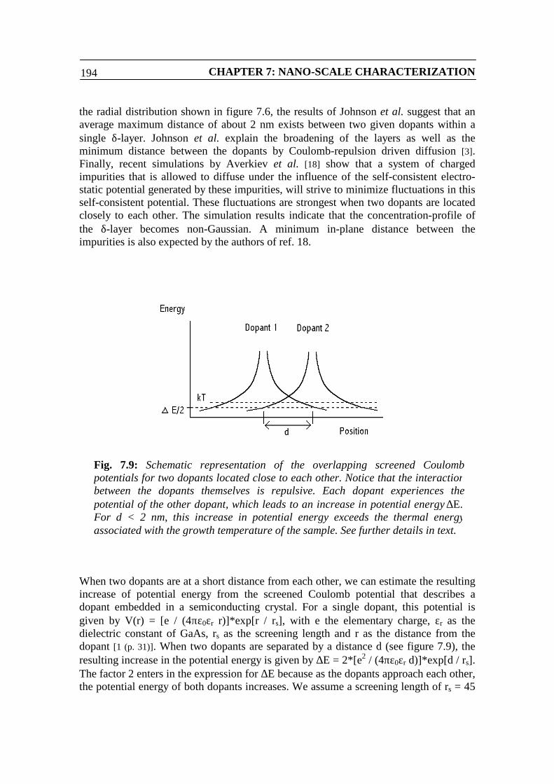
CHAPTER 7: NANO-SCALE CHARACTERIZATION194
the radial distribution shown in figure 7.6, the results of Johnson et al. suggest that anaverage maximum distance of about 2 nm exists between two given dopants within asingle δ-layer. Johnson et al. explain the broadening of the layers as well as theminimum distance between the dopants by Coulomb-repulsion driven diffusion [3].Finally, recent simulations by Averkiev et al. [18] show that a system of chargedimpurities that is allowed to diffuse under the influence of the self-consistent electro-static potential generated by these impurities, will strive to minimize fluctuations in thisself-consistent potential. These fluctuations are strongest when two dopants are locatedclosely to each other. The simulation results indicate that the concentration-profile ofthe δ-layer becomes non-Gaussian. A minimum in-plane distance between theimpurities is also expected by the authors of ref. 18.
When two dopants are at a short distance from each other, we can estimate the resultingincrease of potential energy from the screened Coulomb potential that describes adopant embedded in a semiconducting crystal. For a single dopant, this potential isgiven by V(r) = [e / (4πε0εr r)]*exp[r / rs], with e the elementary charge, εr as thedielectric constant of GaAs, rs as the screening length and r as the distance from thedopant [1 (p. 31)]. When two dopants are separated by a distance d (see figure 7.9), theresulting increase in the potential energy is given by ∆E = 2*[e2 / (4πε0εr d)]*exp[d / rs].The factor 2 enters in the expression for ∆E because as the dopants approach each other,the potential energy of both dopants increases. We assume a screening length of rs = 45
Fig. 7.9: Schematic representation of the overlapping screened Coulombpotentials for two dopants located close to each other. Notice that the interactionbetween the dopants themselves is repulsive. Each dopant experiences thepotential of the other dopant, which leads to an increase in potential energy ∆E.For d < 2 nm, this increase in potential energy exceeds the thermal energyassociated with the growth temperature of the sample. See further details in text.
OF Si δ-DOPED LAYERS IN GaAs 195
Å, which corresponds to a Si doping concentration of 2 * 1018 cm-3 [8]. For d = 20 Å, theresulting increase in potential energy would equal 70 meV. This exceeds the thermalenergy kT at 480 oC (65 meV), which is the temperature at which our sample wasgrown. For this reason, we expect that if Coulomb-driven diffusion has led to short-range ordering of dopants in the δ-doped layers shown in figure 7.4, we should observea minimum distance between the dopants of about 2 nm.
For the δ-doped layers shown in figure 7.4, one might wonder whether diffusionhas played a significant role during growth of the sample, since the layers have notbroadened very much. In fact, the growth parameters that are used for growing δ-dopedstructures are usually chosen in order to minimize diffusion of impurities, so as to avoidlayer-broadening which is an unwanted effect. The absence of layer-broadening in theδ-doped layers shown in figure 7.4 suggests that little or no bulk-diffusion of dopantstook place after incorporation. One might thus suspect that the in-plane distribution ofdopants in these layers is simply a random one.
There is, however, an additional mechanism for in-plane ordering of dopants,caused by the fact that dopants deposited on the growth surface are mobile. The resultsof Däweritz et al. [19] indicate that Si atoms on vicinal GaAs-(001) surfaces canrearrange themselves along the steps of the surface during the growth interrupt. Uponsubsequent growth of the cap layer, the dopants that have aligned themselves along thesteps can form quantum-wires. The average terrace-length is 8 nm (2o miscut), and thegrowth interrupt lasted 180 s at T = 580 oC. Diffusion of Si atoms towards the steps of avicinal growth surface during growth interrupt has also been reported by Wood et al.[20]. Later experiments by Däweritz et al. [21] show that it is possible for the dopants toform ordered arrangements on the growth surface. Growth temperature was 590 oC inthese experiments in order to ensure sufficient mobility of the adsorbed Si atoms. Theordering of adatoms is concluded from changes in the RHEED-pattern (ReflectionHigh-Energy Electron Diffraction) during and after deposition of Si. The Si-concentration profile as measured by Secondary Ion Mass Spectroscopy (SIMS) showeda peak concentration of Si at the intended position of the δ-layers, but also indicated thatsignificant layer-broadening had taken place due to surface segregation. Ordering-effects of dopants on the growth surface have since then also been studied by in plane-STM [22,23,24]. The influence of the growth of the cap-layer to the distribution ofdopants on the growth surface is not described by refs. 22 – 24. The benefit of cross-sectional STM is that it can characterize δ-doped layers after growth of the cap layer,i.e. in their final form.
From the foregoing, it is clear that Coulomb-repulsion driven diffusion duringgrowth of the cap layer is an important mechanism for redistribution of the impuritiesthat make up a δ-doped layer. The effect of such diffusion can be that a minimumdistance between the two given dopants exists. During the growth interrupt that is partof the δ-doping process, the dopant atoms are adsorbed onto the growth surface.Depending on the growth-conditions, in-plane ordering of dopants can take place if anordered arrangement of adsorbed dopants is thermodynamically favourable. Whetherthis ordered arrangement is preserved after growth of the cap-layer is at this pointunclear to us. It is in any case very plausible to assume that the dopants making up anepitaxially grown δ-doped layer have a non-random spatial distribution.
CHAPTER 7: NANO-SCALE CHARACTERIZATION196
7.6.2 Detecting short-range order in delta-doped layers using Cross-Sectional STM.
As seen in the figures 7.6 and 7.7, it becomes difficult to distinguish subsurface donorsfrom each other when they partly overlap in a given STM-image. This can introduce anartificial minimum distance in a radial distribution plot derived from such STM-images.The apparent minimum distance equals the apparent diameter of the dopants in theSTM-image, and thus depends on the spatial extent of the screened Coulomb-potentialof a dopant near the surface [6 (p. 230), 8, 25] (see also section 7.2). At the same time, it isknown that Coulomb-repulsion driven diffusion during growth of the cap-layer canintroduce a real minimum distance between the dopants, which is also related to thespatial extent of the screened Coulomb potential of the dopants (see figure 7.9 andsubsection 7.6.1). Therefore, the two effects, finite apparent diameter of a dopant inSTM and Coulomb-repulsion driven diffusion, are expected to cause the same minimumdistance to appear in a radial distribution plot. The minimum distance seen in figure 7.6can thus be both real and arteficial.
We interprete the apparent oscillations in the radial distribution plot for r > 5 nmas statistical fluctuation since the oscillations are about as large as the expectedstatistical error. The interpretation of figure 7.6 as a whole is then as follows: Distancesbetween dopants that are larger than about 5 nm occur equally frequent, suggesting anabsence of long-range ordering between dopants. Smaller distances between dopantsappear less and less likely to occur as the distance decreases. This can be either theresult of a real short-range order that exists between dopants, or it can be an artefactcaused by the finite apparent diameter of a dopant in STM. If any short-range orderbetween the dopants in our δ-doped layer exists, the minimum distance is in any caseshorter than about 2.5 ± 1 nm.
If the existence any short-range ordering of dopants is to be established by cross-sectional STM, the experiment must be carried out in such a way that two dopants lyingclose enough for their potential wells to overlap, are certainly resolved as two individualdopants. Only if one is certain that two very closely spaced dopants cannot beinterpreted as one single dopant, can the absence of small distances between dopants incross-sectional STM-images be accepted as experimental proof for short-range orderingof dopants. We will now reflect on how a sample containing δ-doped layers should beimaged by cross-sectional STM in order to fulfill this condition. We will also considerother aspects like identification of the various features and statistical accuracy.
At this point the most promising way to image dopants with adequate spatialresolution is to choose the tunneling parameters such that the defect-state associatedwith the dopant (see figure 7.2 b1, b3) manifests itself in the image as clearly aspossible. The work of Domke et al. [26] shows that tunneling parameters that meet thisrequirement exist: Their STM-experiments are no different from our own except for adifferent tip preparation technique and the fact that Domke et al. use slightly highertunneling currents than we do [26]. The defect-state associated with severalconfigurations of Si in GaAs extends over only a few unit cells [6,26]. This is consistent
OF Si δ-DOPED LAYERS IN GaAs 197
with our own results (see figures 7.3c and 7.5 b,c). Dopants lying about 1.5 nm or moreapart should be resolved as separate dopants without problem if the tunnelingparameters are chosen such that the defect-state shows up clearly in the image. Addedbenefits are that the morphology of the defect-state can help identify the feature, andthat it becomes very straightforward to distinguish between dopants lying in the surfacelayer, the first subsurface layer, and so on (see figure 7.2 b).
A major concern when compiling a radial distribution plot from a set of cross-sectional STM-images is that the total number of dopants studied must be large enoughin order to ensure a reasonable statistical accuracy in the number of dopant-pairscounted in each distance-class. In ref. 9, radial distribution plots are compiled fromatomically resolved images of two δ-doped layers, but the significance of these plots isseverely limited by the small number of dopants that is studied. In figure 7.6, statisticalaccuracy is quite reasonable but the spatial resolution is limited by the large scale of theimages. Even if the large-scale images underlying figure 7.6 had been obtained at bothpolarities of the applied bias voltage, distinction between dopants in different layersnear the surface on the basis of their defect-state would have been impossible due to thelack of atomic resolution.
Probably the best way to characterize a δ-doped layer is from a large collectionof small-scale images, so that adequate spatial resolution is combined with statisticalaccuracy. In our experience, a frame size of 25 x 25 nm or 35 x 35 nm (400 x 400pixels) is well-suited to show details of the atomic-scale morphology of defects. At thesame time, these frame sizes are large enough to cover a reasonable total length of δ-layer within a reasonable amount of time. The images shown in figure 7.5 are cut-outsfrom overlapping 25 x 25 nm frames, which show a total of 340 ± 50 nm. These imageswere aquired in 70 minutes time. Covering a total length of 700 nm, which is the lengthof δ-layer imaged in the large-scale images underlying figure 7.6 would thus requireroughly 21/2 hours of imaging-time. Experimentally, this is quite feasable.
It is reasonable to assume, however, that the defect-state of a dopant can only beimaged if the dopant lies near the surface. Of the deepest lying dopants, we expect toimage only the Coulomb-field since this has a longer range. On the other extreme, it isclear from ref. 26 that of the dopants in the surface layer and first subsurface layer, thedefect-state can be imaged. If only those dopants that lie in the surface layer and thefirst subsurface layer are used to compile the radial distribution plot, the expectedminimum length of δ-layer to be imaged in order to obtain adequate statistical accuracyincreases to 1250 nm. A practical consequence is that it becomes very important tounderstand and control the cleavage-process well enough to ensure a high success-ratein cleavage. The estimate of 1250 nm is made as follows: If the radial distribution plotis to be meaningful for the first 5 nm using a distance-class size of 1 nm, one would liketo image at least 50 dopants (on average 10 for each distance-class). Given the arealdensity of 1013 cm-2, one expects 4 dopants in the first two layers of the surface per 100nm of δ-layer. To reach a total of 50, a strip of 1250 nm of δ-layer must be imaged.
Ideally, the sequence of measurements carried out to characterize δ-doped layerswould then be the following. First, voltage-dependent images of dopants should bemade in order to find the most suitable imaging-parameters. These parameters maydiffer from the ones used by Domke et al. [26], especially if a different tip-preparationtechnique is used. It goes without saying that all measurements of dopant-like features
CHAPTER 7: NANO-SCALE CHARACTERIZATION198
should be carried out simultaneously in the filled- and empty-states imaging mode sothat the features can be identified. These preparatory measurements can be carried outon bulk-doped material. Any problems regarding cleavage, if and when they occur, canalso be addressed at this point (see chapter 2). Once the voltage-dependent morphologyof individual dopants is known, the δ-doped layers can be characterized. In our opinion,the most useful measurement would be a set of small-scale images (25 x 25 nm) thatcovers a total length of δ-layer that is long enough to ensure adequate statisticalaccuracy.
7.7 Summary
In this chapter, a Si δ-doped layer in GaAs is characterized from cross-sectional STM-images. Identification of subsurface donors is straightforward since these show up asbright hillocks in filled-states STM-images. Surface layer donors as well as negativelycharged adsorbates and SiAs-acceptors are known to show up as bright protrusionssurrounded by a dark ring (a “rosette”). Identification of these rosettes is thereforedifficult when only filled-states images are available. Some types of rosette can,however, be identified from details of their atomic-scale morphology. We haveidentified one type of rosette as SiAs in the first subsurface layer, confirming that someSi-atoms incorporate as acceptors rather than donors. Two other types of rosette aretentatively identified as surface layer donors and negatively charged adsorbate,respectively.
A radial distribution plot of the dopants in the layer is made from several large-scale images of a δ-layer of high concentration (Si: 1013 cm-2). This radial distributionplot is based on the positions of the subsurface donors in the STM-images. In the radialdistribution plot, an apparent minimum distance between dopants is seen of 2.5 ± 1 nm.However, this apparent minimum distance can very well be explained as an artefactcaused by the finite apparent size of a subsurface donor in STM. In order to establishwhether or not short-range ordering of dopants really takes place during the epitaxialgrowth of δ-doped layers, the δ-doped layers should be imaged using such parametersthat the defect-state associated with a dopant shows clearly in the image. Statisticalaccuracy can be achieved by combining many small-scale images.
OF Si δ-DOPED LAYERS IN GaAs 199
RERERENCES:
1: E.F. Schubert: Doping in III-V semiconcductors. Cambridge University Press,Cambridge, p. 542 (1993).
2: E.F. Schubert, J.B. Stark, B. Ullrich, J.E. Cunningham: Spatial localization ofimpurities in δ-doped GaAs. Appl. Phys. Lett, Vol. 52, No. 18, pp. 1508 – 1510(1988).
3: M.B. Johnson, P.M. Koenraad, W.C. v.d. Vleuten, H.W.M. Salemink, J.H.Wolter: Be delta-doped layers in GaAs imaged with atomic resolution usingSTM. Phys. Rev. Lett, Vol. 75, No. 8, pp. 1606 – 1609 (1995).
4: E.F. Schubert, J.E. Cunningham, W.T. Tsang: Electron-mobility enhancementand electron-concentration enhancement in δ-doped n-GaAs at T = 300 K. SolidState Comm. Vol 63, No. 7, pp. 591 – 594 (1987).
5: C. Domke, M. Heinrich, Ph. Ebert, K. Urban: Oscillating contrast in room-temperature STM-images of localized charges in III-V semiconductorcompounds. Journal of Vac. Sci. and Tech. B, Vol. 16, No. 5, pp. 2825 – 2832(1998).
6: Ph. Ebert: Nano-scale properties of defects in compound semiconductorsurfaces. Surface Science Reports, Vol. 33, pp. 121 – 303 (1999).
7: J.A. Stroscio, R.M. Feenstra, A.P. Fein: Local state density and long-rangescreening of adsorbed oxygen atoms on the GaAs (110) surface. Phys. Rev. Lett,Vol. 58, No. 16, pp. 1668 – 1671 (1987).
8: J.F. Zheng, X. Liu, N. Newman, E.R. Weber, D.F. Ogletree, M. Salmeron:Scanning Tunneling Microscopy Studies of Si donors (SiGa) in GaAs. Phys. Rev.Lett, Vol. 72, No. 10, pp. 1490 – 1493 (1994).
9: B. Grandidier, D. Stiévenard, J.P. Nys, X. Wallart: Microscopic behaviour ofsilicon in delta-doped layer in GaAs. Appl. Phys. Lett, Vol. 72, No. 19,pp. 2454 – 2456 (1998).
10: M.B. Johnson, O. Albrektsen, R. Feenstra, H.W.M. Salemink: Direct imaging ofdopants in GaAs with cross-sectional Scanning Tunneling Microscopy. Appl.Phys. Lett, Vol. 63, No. 21, pp. 2923 – 2925 (1993).
11: S. Ohnishi, M. Tsukada: Molecular orbital theory for Scanning TunnelingMicroscopy. Solid state comm. Vol. 71, No. 5, pp. 391 – 394 (1989).
CHAPTER 7: NANO-SCALE CHARACTERIZATION200
12: S. Muto, S. Takeda, M. Hirata, K. Fuji, K. Ibe: Structure of planar aggregates ofSi in heavily Si-doped GaAs. Phil. Mag. A, Vol. 66, No. 2, pp. 257 – 268 (1992).
13: P.M. Koenraad: Electron mobility in δ-doped layers, in: Delta-doping ofsemiconductors, ed. by E.F. Schubert, Cambridge Univ. Press, Cambridge, pp.407 – 443 (1996).
14: A.F.J. Levi, S.L. Mc Call, P.M. Platzman: Nonrandom doping and elasticscattering of carriers in semiconductors. Appl. Phys. Lett, Vol. 54, No. 10, pp.940 – 942 (1989).
15: R.L. Headrick, L.C. Feldman, B.E. Weir: Ordered delta-doping, in: Delta-doping of semiconductors, ed. by E.F. Schubert, Cambridge Univ. Press,Cambridge, pp. 461 - 484 (1996). The paper discusses ordered δ-doping in Si.
16: M.C.M.M. van der Wielen, A.J.A. van Roij, H. van Kempen: Direct observationof Friedel oscillations around incorporated SiGa dopants in GaAs by low-temperature STM. Phys. Rev. Lett, Vol. 76, No. 7, pp. 1075 – 1078 (1996). Seealso: Study of imperfections near the cleaved GaAs (110) surface by low-temperature STM. Phd-thesis by M.C.M.M. van der Wielen, Univ. of Nijmegen,the Netherlands (1998).
17: E.F. Schubert, G.H. Gilmer, R.F. Kopf, H.S. Luftman: Maximum concentrationof impurities in semiconductors. Phys. Rev. B, Vol. 46, No. 23, pp. 15078 –15084 (1992).
18: N.S. Averkiev, A.M. Monakhov, A. Shik, P.M. Koenraad, J.H. Wolter: Randomelectric fields and impurity diffusion in δ-layers. Phys. Rev. B, Vol. 61, No. 4,pp. 3033 – 3038 (2000)
19: L. Däweritz, K. Hagenstein, P. Schützendübe: Self-organization during Siincorporation in MBE-grown vicinalGaAs (001) surfaces. Journ. of Cryst.growth, Vol. 127, pp. 1051 – 1055 (1993).
20: C.E.C. Wood: Dopant-surface migration and interactions from reflection high-energy electron diffraction dynamics. Journ. of Appl. Phys, Vol. 71, No. 4, pp.1760 – 1763 (1992).
21: L. Däweritz, P. Schützendübe, K. Stahrenberg, M. Maier, K. Ploog: Real-timestudy of dopant incorporation and segregation during MBE growth of GaAs(001): Si. Proceedings of IEEE: 24th International symposium on compoundsemiconductors (1995), pp. 51 – 56.
22: M. Wassermeier, S. Kellermann, J. Behrend, L. Däweritz, K.Ploog:Submonolayer Si deposition at low temperatures on the GaAs (001)-(2x4)surface studied by STM. Surface Science, Vol. 414, pp. 289 – 303 (1998).
OF Si δ-DOPED LAYERS IN GaAs 201
23: H. Oigawa, M. Wassermeier, J. Behrend, L. Däweritz, K.H. Ploog:Reconstruction of the GaAs (001) surface induced by submonolayer Bedeposition. Surface Science, Vol. 376, pp. 185 – 191 (1997).
24: H. Oigawa, M. Wassermeier, J. Behrend, L. Däweritz, K.H. Ploog: Controlledanisotropic ordering of Be deposited on the GaAs (001) surface. SurfaceScience, Vol. 399, pp. 39 – 48 (1998).
25: K. Kobayashi: Scattering theory of subsurface impurities observed in STM.Phys. Rev. B, Vol. 54, No. 23, pp. 17029 – 17038 (1996).
26: C. Domke, Ph. Ebert, K. Urban: Atomic-scale properties of the amphotericdopant Si in GaAs (110) surfaces. Surface Science, Vol. 415, pp. 285 – 298(1998). The tungsten tips used in this work are etched electro-chemically andthen conditioned in vacuum by field emission. Tunneling currents range from0.2 – 0.5 nA.
27: P.M. Koenraad, F.A.P. Blom, C.J.G. Langerak, M.R. Leys, J.A.A.J. Perenboom,J. Singleton, S.J.R.M. Spermon, W.C. van der Vleuten, A.P.J. Voncken, J.H.Wolter: Observation of high mobility and cyclotron resonance in 20 Å silicon δ-doped GaAs grown by MBE at 480 oC. Semiconductor Science and Technology,Vol. 5, ppl 861 – 866 (1990).
28: C. Domke, Ph. Ebert, M. Heinrich, K. Urban: Microscopic identification of thecompensation mechanisms in Si-doped GaAs. Phys. Rev. B, Vol. 54, No. 15, pp.10288 – 10291 (1996).
29: A.F.W. van der Stadt: Magnetotransport in Si-δ-doped GaAs/AlxGa(1-x)Asstructures. PhD-thesis by A.F.W.van der Stadt, University of Eindhoven, theNetherlands, 1998.
30: P.M. Koenraad, I. Bársony, J.C.M. Henning, J.A.A.J. Perenboom, J.H. Wolter:Diffusion of Si in δ-doped GaAs studied by magneto transport, in SemiconductorInterfaces at the sub-nanometer scale, pp. 35 – 43. Ed. by H.W.M. Salemink andM.D. Pashley, Kluwer Academics Publishers, the Netherlands, 1993.
31: A donor impurity embedded in n-type material can either have a positive charge-state, or a neutral one, depending on whether it lies energetically above or belowthe Fermi level. When the surface of an n-type material is imaged in the filled-states imaging mode, the donor atoms lie below the sample Fermi level andtherefore they are, as a whole, neutral. However, when the tip approaches thedonor atom to within the effective Bohr-radius of the bound electron, thepositive charge of the impurity atom is no longer screened completely by thebound electron, and the dopant atom manifests itstelf as a positively chargeddefect. The analogous argument applies to the un-ionized acceptor.

CHAPTER 7: NANO-SCALE CHARACTERIZATION202
32: An apparent insensitivity of the observed atomic corrugation to local changes inthe amount of TIBB is not as strange as it might appear: On n-type material, therosettes appear for negative sample voltage, i.e. when the surface is inaccumulation. For a surface in accumulation, the amount of TIBB can berelatively insensitive to changes in the applied bias voltage (see section 4.4). If alarge, negative bias voltage is chosen (or the tip has a low work function), thenegative charge associated with the defect may not cause a very large localchange in TIBB. A second circumstance to consider is the presence of a peak inthe tip-DOS which coincides energetically with the A5-state. In this case, theA5-state can remain the dominant contributor to the total tunneling current inspite of small changes in the amount of TIBB.
33: C.J. Chen: In-situ characterization of tip electronic structure in ScanningTunneling Microscopy. Ultramicroscopy, Vol. 42 – 44, pp. 147 – 153 (1992).
34: The estimate for the free carrier concentration is made as follows: Thedeltalayers are grown in an epitaxial layer of 445 nm thickness, while the sum ofthe areal densities of Si of all layers equals 4.3 * 1013 cm-3. If we make the rathercrude assumption that all dopants are distributed homogeneously throughout thisepitxial layer of 445 nm, then these figures translate to a bulk Si concentrationof 1019 cm-3. We can justify this assumption from the width of the V-shapedpotential well associated with a δ-doped layer: According to ref. 1 (p. 442), thispotential well of a Si δ-doped layer in GaAs of an areal concentration of 5 * 1012
cm-2 has a width of 40 nm, suggesting that in our structure, the potential wells ofthe adjacent δ-layers overlap. The concentration of free carriers may deviatefrom the nominal concentration of impurities due to autocompensation, but thiseffect only becomes significant for δ-layers with an areal concentrationexceeding 1013 cm-2 (ref. 1, p. 277 and p. 459).
35: C. Weisbuch, B. Vinter: Quantum Semiconductor Structures. Academic Press,Boston (1991).
36: C. Kittel, H. Kroemer: Thermal Physics. W.H. Freeman and Company, NewYork, 2nd ed. (1980). p. 397.
37: Y.G. Chai, R. Chow, C.E.C. Wood: The effect of growth conditions on Siincorporation in Molecular Beam Epitaxy GaAs. Appl. Phys. Lett, Vol. 39, Iss.10, pp. 800 – 802 (1981). In this paper it is shown that Si can form electricallyinactive SiGa-SiAs pairs or precipitates when it is attempted to incorporate Si inan average concentration of more than 6 * 1018 cm-3 during MBE-growth.
203
Summary
The first chapter is meant to explain in qualitative terms some aspects of the theoreticalbackground to tunneling between a metal tip and a semiconducting sample. The view oftunneling adopted in this thesis is expressed by equation 1.6. It is based on the ModifiedBardeen Approach and the Tersoff-Hamann theory. In the thesis this view of tunnelingis referred to as “regular tunneling”.
Semiconductor surfaces posess electronic surface-states which are imaged inSTM and thus make it possible to obtain atomic resolution. The Tersoff-Hamann theorystates that for an s-like tip-state, the tunneling matrix element is proportional to the localamplitude of the wavefunction representing the sample state involved in the tunnelingprocess. However, most STM-tips have tip-states with a different symmetry. For a non-stip state, the tunneling matrix element becomes proportional to a spatial derivative ofthe local amplitude of the relevant sample-state wavefunction. For a pz- or dz
2-like tip-state, the tunneling matrix element is proportional to spatial derivatives of the sample-state wavefunction with respect to z (i.e. perpendicular to the sample surface).Consequently, for the qualitative interpretation of topographic STM-data the Tersoff-Hamann theory remains applicable when the tip has a pz- or dz
2-like tip state.It is assumed that the absolute tip-sample distance in STM on semiconductors is
slightly less than 10 Å (7 – 10 Å). Therefore, even an STM-image is obtained under“normal” circumstances, the presence of a tip-sample interaction is to be expected. Oneof the most important consequences of the tip-sample interaction is that the spatialdistribution of the electronic states involved in the tunneling process, is distorted. Thisresults in a lowering of the tunneling barrier height, or in the formation of a chemicalbond between the tip and one of the sample surface atoms if the tip and sampleapproach each other very closely (3 Å). Although a tip-sample interaction is usuallypresent during STM on semiconductors under commonly used circumstances,topographic STM-data can often be interpreted without taking the influence of the tip-sample interaction into account.
Finally, the influence of Tip-Induced Band Bending (TIBB) is reviewed. TIBBarises due to the fact that the electric field present between the tip and sample penetratesinto the semiconducting crystal. One of its effects is that it shifts the energetic positionof surface states with respect to the sample Fermi level. In order to interprete voltage-dependent effects, it is indispensable to take TIBB into account.
Chapter 2 describes the experimental setup and sample preparation. We use acommercially available UHV-STM setup around which a dedicated vacuum-system hasbeen built. The essence of cross-sectional STM is that one prepares a sample which isbroken or cleaved inside the vacuum. The STM-experiment is then carried out on thefreshly exposed fracture surface (figure 2.1). A remaining problem associated with thetechnique of sample preparation by cleavage is the presence of mono-atomic steps onthe cleaved surface. We typically observe mono-atomic steps running parallel to thesample edge in the epilayer region of the sample surface (figure 2.6c). The absence ofV-shaped steps suggests that in our samples the velocity with which the crack

Summary204
propagates through the sample material is in the low-velocity (i.e. the non-oscillatory)regime.
We prepare our polycrystalline tungsten (W) STM-tips by electro-chemicaletching (chapter 3). The tips are then heated, self-sputtered with Ne+-ions, and subjectedto an Ar+-ion bombardment in UHV. When tungsten STM-tips are sharpened by self-sputtering, the Schiller-decapitation process can occur. It is shown that this process isaccompanied by a very specific pattern in the sputter voltage as a function of time. Thismakes it possible to use the decapitation process for the manufacture of high-qualitySTM-tips. Secondly, we present a model which enables us to calculate the radius ofcurvature of the tip apex based on Fowler-Nordheim plots. Verification with ScanningElectron Microscopy (SEM) shows that our model is correct within 5 nm. A slightdeviation of the experimental data from the theory suggests that our polycrystalline wirehas a preferential crystal orientation. A potential problem with the use of the self-sputtertreatment is the occurrence of vacuum-arcs, which can severely decrease the success-rate of this process. In order to prevent vacuum-arcs from occurring, the sputtering-gasmust be kept clean (background pressure < 2 * 10-9 torr) and adequate removal of theoxide layer present on the as-etched tips must be ensured.
In chapter 4 atomically resolved, voltage-dependent STM-images of GaAs (110)are compared to the results of a one-dimensional model used to calculate the amount ofTip-Induced Band Bending (TIBB) for a tunneling junction between a metal and asemiconductor. The voltage-dependent changes in the morphology of the atomic latticeare caused by the four surface states of the GaAs (110) surface contributing in varyingrelative amounts to the total tunneling current. Tip-induced band bending determineswhich of these states contributes to the total tunneling current at a given bias voltage,and thus has a profound influence on the voltage-dependent STM-images. In principle,this effect can be used to extract information about the amount of tip-induced bandbending from the atomic morphology seen in the image. It is shown that certain voltageregions exist, for which none of the surface states present at the GaAs-(110) surface cancontribute to the tunneling current. For these voltages, tunneling occurs between the tipand bulk states of the sample through a surface depletion layer several nm wide.Nevertheless, atomic, surface-like corrugation is observed for these circumstances. Theeffect may be caused by electrons tunneling resonantly through the low energy shoulderof the C3 state which extends into the bandgap of the semiconductor, or by theinteraction between the electronic states of the tip and sample. We finally show threeillustrative examples of a voltage-dependent change in atomic corrugation: The changein atomic morphology caused by a sudden transition from empty states imaging to filledstates imaging, the local corrugation-change around dopants and adsorbates, and thedifference in atomic corrugation on either side of a p-n junction.
Not all experimental results presented in this thesis can be interpreted withoutexplicite consideration of tip-sample interaction effects: In chapter 5, we present anunusual image-form of the GaAs (110) surface observed in cross-sectional STM inUHV. It clearly shows the zig-zag row formed between the cations and anions in the toprow of the GaAs (110) surface, as well as traces of the bottom row that lies between thetop rows. It thereby closely resembles the true atomic lattice usually depicted by ball-and-stick models. We interprete the occurrence of this image-form in terms of achemical bond that forms between the apex of the tip and the nearest Ga atom in the top

Summary 205
row of the sample surface. The formation of such a bond has recently been predictedtheoretically. The results thus show that the tip-sample interaction, when it becomessignificant, can give rise to entirely new and interesting image-forms.
The voltage-dependent effects observed on GaAs-110 have also beenobserved for the 110-surface of n-type Al0.2Ga0.8As and for the 110-surface of acrystal containing an n-type GaAs/Al0.33Ga0.67As-superlattice (chapter 6). Theappearance of AlGaAs-(110) at large bias voltage is well known: At large negativesample voltage (VSAMPLE ~ -3 V), the images show atomic rows along the [-110]direction, and the alloy-related minima appear between the atomic rows. At largepositive sample voltage (VSAMPLE ~ +2 V) the images also show atomic rows along the[-110] direction, but the alloy-related minima now appear to be centered on the atomicrows. This appearance changes radically when a small (absolute) value is chosen for thebias voltage. In the empty states imaging mode (VSAMPLE > 0) the lower portion of theconduction-band related surface-DOS is imaged. Apart from a change in atomiccorrugation that is similar to the one which we observed for n-GaAs 110, small ridgesthat are oriented along the [-110]-direction appear in the image. The appearance of theseridges can be understood qualitatively from the electronic band structures of GaAs-110 and AlAs-110. At small negative bias voltage, bright and dark areas that areseveral nm in lateral extent, appear in the image. We interprete these bright and darkareas in terms of fluctuations in the density of electrons that have accumulated at thesample surface due to TIBB.
An important conclusion can be drawn from two images that show the very samepatch of AlGaAs-(110) surface in both the filled- and empty-states imaging modes: Theshape and location of the alloy-related minima change as a function of the polarity ofthe applied bias voltage. This effect can be understood from the fact that a given Alatom in the sample surface can have several different bonding configurations.
The images of the GaAs/AlGaAs superlattice show similar effects. Apart fromthat, they also show that the contrast between GaAs and AlGaAs inverts for small biasvoltage. The inversion of contrast occurs for both polarities of the bias voltage,althought the effect is stronger in the filled-states case (negetive sample voltage).Finally, the images of the superlattice obtained at intermediate positive sample voltage(+0.59 V < V < +0.71 V) show an apparent broadening of the GaAs-layers in thesuperlattice. For these voltages, we expect to be sensitive to the confined electron-levelsthat are present in the GaAs-layers of the superlattice. Since the spatial distribution ofthese levels extends into the AlGaAs barriers, we think that the observed broadening ofthe GaAs-layers indicates that for these voltages, the confined electron level in theGaAs quantum-well of the superlattice is imaged directly.
From the literature, it is known that during the epitaxial growth of Si δ-dopedlayers in GaAs, Coulomb-repulsion between dopants can have a significant influence onthe spatial distribution of the dopants making up the δ-doped layer (chapter 7). For thisreason it is suspected that a minimum distance may exist between any two givendopants within a δ-doped layer. This partial ordering is expected to enhance themobility of electrons occupying the potential-well formed by the δ-doped layer. It isalso known from existing literature that subsurface donors (SiGa) atoms appear as brighthillocks several nm in diameter in STM-images. Surface-layer donors (SiGa) appear asprotrusions surrounded by a dark ring (a “rosette”) in filled-states images and as a bright
Summary206
hillock in empty-states images. Acceptors (SiAs) and negatively charged adsorbatesappear as rosettes in filled-states images and as depressions in empty-states images.Furthermore, surface-layer donors and acceptors have a “defect state” associated withthem which can appear in the image as well. In chapter 4 of this thesis it is shown thatthe polarity of the charge-state of a rosette can be determined from the local change inatomic corrugation around it.
In chapter 7 of this thesis, STM-images of Si δ-doped layers in GaAs arepresented. It is evident that some of the Si atoms have incorporated on As-sites ratherthan Ga-sites. In order to investigate the spatial distribution of the dopants making upthe δ-layers, a pair-distribution function has been determined for one of the δ-dopedlayers (figure 7.4). The pair-distribution function shows that a distance between any twogiven dopants of less than 2 nm is less likely to occur. This result, however, cannot beaccepted as experimental proof for the existence of an ordered arrangement of dopantsin δ-doped layers. In STM-images dopants show up as features that are several nm indiameter. It thus becomes difficult to image two very closely spaced dopant atomsindividually (figure 7.5). If two closely spaced dopants are interpreted as one singledopant lying close to the sample surface, a minimum distance between dopants wouldappear in the pair-distribution function as an artefact.
A real minimum distance between the dopants due to Coulomb-repulsion isexpected to depend on the spatial extent of the screened Coulomb-potential associatedwith a Si-dopant in GaAs. An artificial minimum distance caused by the finite feature-size of Si dopants in STM also depends on the spatial extent of the screened Coulomb-potential associated with a dopant, since this quantity determines the feature-size of adopant in STM. Therefore, the apparent minimum distance between two dopants of 2nm found in figure 7.6 can be both real and artificial. A way to resolve this problemmay be to image the dopants under such circumstances that the defect-states of thedopants manifest themselves clearly in the image.

207
Nederlandse samenvatting
Het eerste hoofdstuk is bedoeld om in kwalitatieve termen enkele aspecten van detheoretische achtergrond van het tunnelproces tussen een metalen tip en eenhalfgeleidend preparaat uit te leggen. Het mentale beeld van het tunnelproces dat in ditproefschrift wordt gebruikt is uitgedrukt in vergelijking 1.6. Het is gebaseerd op deModified Bardeen Approach en de Tersoff-Hamann theorie. In dit proefschrift wordt ditbeeld van het tunnelproces aangeduid als “regulier tunnelen”.
Halfgeleideroppervlakken bezitten oppervlakte-electronentoestanden die met deSTM worden afgebeeld, en het zo mogelijk maken om atomaire resolutie te verkrijgen.De Tersoff-Hamann theorie stelt dat, als de tipelectronentoestand een s-achtig karakterheeft, het tunnelmatrixelement recht evenredig is met de locale amplitude van degolffunctie die de bij het tunnelproces betrokken electronentoestand vertegenwoordigt.Echter, de meeste STM-tips hebben tiptoestanden met een andere symmetrie. Voor eenniet-s tip-toestand wordt het tunnelmatrixelement evenredig met een ruimtelijkeafgeleide van de locale amplitude van de relevante preparaat-toestandsgolffunctie. Vooreen pz- of dz
2- achtige tiptoestand is het tunnelmatrixelement evenredig met ruimtelijkeafgeleiden van de preparaat-toestandsgolffunctie naar de z-richting (d.w.z. loodrecht ophet preparaatoppervlak). Dientengevolge blijft voor de kwalitatieve interpretatie vantopografische STM-data de Tersoff-Hamann theorie toepasbaar als de tip een pz- of dz
2-achtige tiptoestand heeft.
Het wordt aangenomen dat de absolute tip-preparaat afstand in STM iets minderis dan 10 Å (7 Å – 10 Å). Daarom is, zelfs als een STM-beeld onder “normale”omstandigheden werd gemaakt, de aanwezigheid van een interactie tussen de tip en hetpreparaat te verwachten. Eén van de belangrijkste gevolgen van die tip-preparaatinteractie is dat de ruimtelijke verdeling van de electronentoestanden die betrokken zijnbij het tunnelproces, wordt verstoord. Dit resulteert in een verlaging van detunnelbarrièrehoogte, of in de vorming van een chemische binding tussen de tip en éénvan de oppervlakteatomen in het preparaat, als de tip en het preparaat elkaar zeer dichtnaderen (3Å). Hoewel een tip-preparaat interactie meestal aanwezig is tijdens STM ophalfgeleiders onder gewoonlijk gebruikte omstandigheden, kan topografische STM-datavaak worden geïnterpreteerd zonder rekening te hoeven houden met de tip-preparaatinteractie.
Tenslotte wordt de invloed van tip-geinduceerde bandverbuiging (Tip-InducedBand Bending: TIBB) bekeken. TIBB ontstaat doordat het electrisch veld, dat aanwezigis tussen de tip en het preparaat, doordringt in het halfgeleidend kristal. Eén van deeffecten daarvan is dat de energetische ligging van de oppervlaktetoestanden verschuiftten opzichte van het Ferminiveau van het preparaat. Om spanningsafhankelijke effectente kunnen interpreteren, is het zonder meer noodzakelijk om TIBB in rekening tebrengen.
Nederlandse samenvatting208
Hoofdstuk 2 beschrijft de experimentele opstelling en de wijze waarop het preparaatgemaakt wordt. We gebruiken een commercieel beschikbaar UHV-STM systeemwaaromheen een speciaal ontworpen vacuumsysteem is gebouwd. De essentie vancross-sectionele STM is dat men een preparaat maakt dat in het vacuum gebroken ofgekliefd wordt. Het STM-experiment wordt dan uitgevoerd op het verse breukvlak(figuur 2.1). Een blijvend probleem dat hoort bij de aanmaak van preparaten doormiddel van klieven is de aanwezigheid van mono-atomaire stappen op het gekliefdeoppervlak. Typisch zien we dat mono-atomaire stappen parallel langs het epilaag-gebiedvan het preparaatoppervlak lopen (figuur 2.6 c). De afwezigheid van V-vormige stappensuggerreert dat in onze preparaten de snelheid waarmee de breuk zich voortplant in hetlage-snelheidsgebied (d.w.z. het niet-oscillerende regime) ligt.
We maken onze polykristallijne wolfraam (W) STM-tips d.m.v. een electro-chemische ets (hoofdstuk 3). Daarna worden de tips in UHV verhit, en ondergaan ze eenzelf-sputter proces met Ne+-ionen en een Ar+-ionen bombardement. Wanneer eenwolfraam STM-tip aangescherpt wordt door middel van zelfsputteren, kan het Schiller-decapitatieproces optreden. We laten zien dat dit proces vergezeld gaat van eenspecifiek patroon in de sputterspanning als functie van de tijd. Dit maakt het mogelijkom het decapitatieproces te gebruiken voor de aanmaak van STM-tips van hogekwaliteit. Verder presenteren we een model dat ons in staat stelt de kromtestraal van depunt van de tip te berekenen uit een Fowler-Nordheim plot. Verificatie met ScanningElectronen Microscopie (SEM) toont aan dat het model binnen 5 nm correct is. Eenkleine afwijking tussen de experimentele data en de theorie suggerreert dat onspolykristallijn draad een preferentiele kristalorientatie heeft. Een potentieel probleemmet het gebruik van het zelfsputterproces is het voorkomen van vacuum-bogen, hetgeende succes-ratio (aantal goede tips/totaal aantal tips) van het proces ernstig kan verlagen.Om het optreden van vacuum-bogen te voorkomen moet het sputtergas schoongehouden worden (achtergronddruk < 2 * 10-9 torr) en moet de oxidelaag die altijd opeen net-geëtste tip anwezig is, op adequate wijze verwijderd worden.
In hoofdstuk 4 worden atomair opgeloste, spannings-afhankelijke STM-beeldenvan GaAs vergeleken met de resultaten van een één-dimensionaal model dat dehoeveelheid tip-geinduceerde bandverbuiging (TIBB) berekent voor een tunnelcontacttussen een metaal en een halfgeleider. De spannings-afhankelijke veranderingen in demorfologie van het atomaire rooster worden veroorzaakt door de vier relevanteoppervlakte toestanden van GaAs-(110) die in verschillende verhoudingen bijdragenaan de totale tunnelstroom. Tip-geinduceerde bandverbuiging bepaalt welke van dezetoestanden bijdraagt aan de totale tunnelstroom bij een gegeven spanning, en heeft opdie manier een grote invloed op spanningsafhankelijke STM-beelden. In principe kandit effect gebruikt worden om informatie te verkrijgen over de hoeveelheid tip-geinduceerde bandverbuiging op basis van de atomaire morfologie die te zien is in hetSTM-beeld. We laten zien dat er bepaalde spanningsgebieden bestaan waarvoor geenvan de oppervlaktetoestanden van het GaAs-(110) oppervlak aan de tunnelstroom kanbijdragen. Voor deze spanningen vindt tunneling plaats tussen de tip en de bulk-toestanden van het preparaat, door een oppervlaktedepletielaag van enkele nm dikteheen. Toch wordt er onder die omstandigheden een atomaire, oppervlakte-achtigecorrugatie waargenomen. Het effect kan veroorzaakt worden door electronen dieresonant door de laag-energetische schouder van de C3-toestand tunnelen, welke in de
Nederlandse samenvatting 209
bandgap van de halfgeleider doorloopt, of door een interactie tussen de electron-toestanden van de tip en het preparaat. Tenslotte laten we drie illustratieve voorbeeldenzien van een spannings-afhankelijke verandering van de atomaire corrugatie: Deverandering in atomaire morfologie veroorzaakt door een plotselinge overgang van hetafbeelden lege toestanden naar het afbeelden van gevulde toestanden, de localecorrugatie-verandering rondom doteringen en adsorbaten, en het verschil in atomairecorrugatie aan beide zijden van een p-n junctie.
Niet alle experimentele resultaten die in dit proefschrift worden gepresenteerdkunnen worden geinterpreteerd zonder expliciete beschouwing van de tip-preparaatinteractie: In hoofdstuk 5 presenteren we een ongebruikelijk STM-beeld van GaAs(110), waargenomen in cross-sectionele STM in UHV. Het laat duidelijk de zig-zagrijen zien die de anionen en cationen in de bovenste rij van het GaAs-(110) oppervlakvormen, evenals sporen van de onderste rij die tussen de bovenste rijen in ligt. Daarmeelijkt het beeld sterk op het werkelijke atomaire rooster dat gewoonlijk wordt afgebeeldd.m.v. de “ball-and-stick” modellen. We interpreteren het voorkomen van dezebeeldvorm in termen van een chemische binding die zich kan vormen tussen de apexvan de tip en het dichtstbijzijnde Ga-atoom in de bovenste rij van hetpreparaatoppervlak. De vorming van zo’n binding is onlangs theoretisch voorspeld. Deresultaten laten zien dat de tip-preparaat interactie, als ze belangrijk wordt, aanleidingkan geven tot hele nieuwe en interessante beeldvormen.
De spannings-afhankelijke effecten die zijn waargenomen op GaAs-(110), zijnook gezien voor het (110)-oppervlak van n-type Al0.2Ga0.8As, en voor het (110)-oppervlak van een kristal dat een n-type GaAs/Al0.33Ga0.67As-superrooster bevat(hoofdstuk 6). Het uiterlijk van AlGaAs-(110) bij hoge tunnelspanning is zeer bekend:Bij een grote, negatieve preparaatspanning (VSAMPLE ~ -3 V), laten de beelden atomairerijen langs de [-110]-richting zien, waarbij de legeringsgerelateerde minima (alloy-related minima) tussen de atomaire rijen in lijken te liggen. Bij grote, positievepreparaatspanning (VSAMPLE ~ +2 V) laten de beelden ook atomaire rijen langs de[-110]-richting zien, maar nu lijken de legeringsgerelateerde minima gecentreerd teliggen op de atomaire rijen. Dit uiterlijk verandert radicaal wanneer een kleine(absolute) waarde voor de tunnelspanning wordt gekozen. In de lege-toestandenafbeeldingsmodus (VSAMPLE > 0) het lagere deel van de geleidingsband-gerelateerdeoppervlaktetoestandsdichtheid wordt afgebeeld. Behalve een verandering in de atomairecorrugatie die lijkt op de verandering die we voor GaAs-(110) hebben waargenomen,verschijnen er ook kleine richeltjes in het beeld, die geörienteerd zijn langs de [-110]-richting. Het verschijnen van deze richeltjes kan kwalitatief worden begrepen vanuit deelectronsiche bandstructuur van GaAs-110 en AlAs-110. Bij kleine, negatievepreparaatspanning verschijnen er in het beeld kleine lichte en donkere gebiedjes die zichenkele nm uitstrekken. We interpreteren deze lichte en donkere gebiedjes in termen vanfluctuaties in de dichtheid van de electronen die geaccumuleerd zijn aan hetpreparaatoppervlak ten gevolge van TIBB.
Een belangrijke conclusie kan getrokken worden uit twee STM-beelden dieprecies hetzelfde stukje AlGaAs-(110) oppervlak laten zien in zowel de gevulde- als delege-toestanden afbeeldingsmodus: De vorm en plaats van de legeringsgerelateerdeminima verandert als functie van de polariteit van de aangelegde tunnelspanning. Dit
Nederlandse samenvatting210
effect kan begrepen worden vanuit het feit dat een gegeven aluminium atoom in hetpreparaatoppervlak meerdere verschillende bindingsconfiguraties kan hebben.
De beelden van het GaAs/AlGaAs superrooster laten soortgelijke effecten zien.Bovendien laten ze ook nog zien dat het contrast tussen GaAs en AlGaAs inverteertvoor een lage tunnelspanning. De contrastinversie vindt plaats voor beide polariteitenvan de aangelegde tunnelspanning, al is het effect sterker voor het geval dat de gevuldetoestanden worden afgebeeld (negatieve preparaatspanning). Tenslotte laten de beeldenvan het superrooster bij intermediaire positieve preparaatspanning (+0.59 V < V <+0.71 V) een schijnbare verbreding van de GaAs-lagen in het superrooster zien. Voordeze spanningen verwachten we dat de STM gevoelig is voor de opgeslotenelectronentoestanden die aanwezig zijn in de GaAs-lagen van het superrooster. Omdatde ruimtelijke verdeling van deze toestanden in de AlGaAs-lagen doordringt, denken wedat de waargenomen verbreding van de GaAs-lagen aangeeft dat we voor dezespanningen de opgesloten electronentoestand in de GaAs-kwantumput van hetsuperrooster afbeelden.
Vanuit de literatuur is het bekend dat tijdens de epitaxiale groei van Si δ-gedoteerde lagen in GaAs, Coulomb-repulsie tussen de doteringen onderling een sterkeinvloed kan hebben op de ruimtelijke verdeling van de doteringen die samen de δ-laagvormen (hoofdstuk 7). Om die reden wordt vermoed dat er een minimum afstand kanbestaan tussen twee willekeurige doteringen in een δ-laag. Van deze gedeeltelijkeordening wordt verwacht dat ze een gunstige invloed heeft op de mobiliteit vanelectronen die de potentiaalput bevolken die gevormd wordt door de δ-laag. Het isvanuit bestaande literatuur ook bekend dat donoren onder het oppervlak (SiGa) als lichteheuveltjes van enkele nm in doorsnee verschijnen in het STM-beeld. Donoren in deoppervlaktelaag (Siga) verschijnen als uitstulpingen, omgeven door een donkere ring(een “rozet”) in de gevulde-toestandsbeelden in als een licht heuveltje in lege-toestandsbeelden. Acceptoren (SiAs) en negatief geladen adsorbaten verschijnen alsrozetten in gevulde-toestandsbeelden en als kuiltjes in lege-toestandsbeelden.Bovendien hebben oppervlaktelaag-donoren en acceptoren een defect toestand die ookin het beeld kan verschijnen. In hoofdstuk 4 van dit proefschrift wordt getoond dat depolariteit van de ladingstoestand van een rozet kan worden vastgesteld op basis van delocale verandering in de atomaire corrugatie er omheen.
In hoofdstuk 7 van dit proefschrift worden STM-beelden van Si δ-gedoteerdelagen in GaAs gepresenteerd. Het is duidelijk dat sommige van de Si-atomen op As-roosterplaatsen zijn ingebouwd in plaats van op Ga-roosterplaatsen. Om de ruimtelijkeverdeling te onderzoeken van de doteringen die de δ-lagen vormen, is een paar-distributiefunctie vastgesteld voor één van de δ-gedoteerde lagen (figuur 7.4). De paar-distributiefunctie laat zien dat een afstand tussen twee willekeurige doteringen vanminder dan 2 nm minder vaak voorkomt. Dit resultaat, echter, kan niet worden aanvaardals experimenteel bewijs voor het bestaan van een geordende verdeling van doteringenin δ-gedoteerde lagen. In STM-beelden zien doteringen eruit als objecten met eendiameter van enkele nm. Het wordt dus moeilijk om twee heel dicht bij elkaar gelegendoteringen gescheiden af te beelden (zie figuur 7.5). Als twee vlak bij elkaar gelegendoteringen worden geinterpreteerd als één enkele dotering die dicht onder het oppervlakligt, dan zou in de paardistributiefunctie een minimum afstand tussen doteringen kunnenverschijnen als een artefact.

Nederlandse samenvatting 211
Voor een echte minimum afstand tussen de doteringen tengevolge van Coulomb-repulsie is het te verwachten dat deze afhangt van de effectieve reikwijdte van deafgeschermde Coulomb-potentiaal die bij een Si-dotering in GaAs hoort. Eenkunstmatige minimum afstand veroorzaakt door de eindige afmeting van een Si-dotering in STM hangt ook af van de effectieve reikwijdte van de afgeschermdeCoulomb-potentiaal horende bij een dotering af, want van deze grootheid hangt deschijnbare grootte van een dotering in STM af. Daarom kan de in figuur 7.6 gevondenschijnbare minimum afstand tussen twee gegeven doteringen van ongeveer 2 nm zowelecht als kunstmatig zijn. Dit probleem is mogelijk op te lossen door de doteringen onderzodanig omstandigheden af te beelden, dat de defect-toestand duidelijk in het STM-beeld naar voren komt.

212
Voor niet-natuurkundigen…
In dit gedeelte staat een beknopte uitleg van het onderzoek waarvan de bedoeling is, datze toegankelijk is voor diegenen die onbekend zijn met de specifieke vaktaal van deexperimentele natuurkunde. Deze uitleg is in twee stukken ingedeeld: Het eerste stuklegt uit wat een STM is en wat er nou precies in een STM-beeld te zien valt. Het tweededeel gaat over het onderzoek van het proefschrift zelf. Soms ontkom ik er niet aan omtoch een vakterm te gebruiken, of moet ik iets eerst zeggen om het pas daarna te kunnenverduidelijken. Wie iets tegenkomt wat op het eerste gezicht onduidelijk lijkt, kan omdie reden het beste aandachtig verder lezen, in veel gevallen volgt de uitleg vanzelf.
Wat is een STM?
De Scanning Tunneling Microscoop (STM) is uitgevonden door de heren Binnig enRohrer in 1981, in het onderzoekslaboratorium van IBM te Zürich. Net als iederemicroscoop dient een STM om dingen zichbaar te maken die te klein zijn om met hetblote oog te zien. De vergroting gaat bij een STM echter verder dan bij de meesteandere typen microscopen die vandaag de dag bekend zijn: Een “normale” optischemicroscoop vergroot zo’n 400 maal, en kan b.v. de cellen waaruit levend weefsel isopgebouwd zichtbaar maken. Een electronenmicroscoop kan 100.000 tot 1.000.000maal vergroten, afhankelijk van het type electronenmicroscoop waarom het gaat. Meteen electronenmicroscoop kunnen onderdelen van cellen worden afgebeeld.Electronenmicroscopen worden ook gebruikt om bijvoorbeeld roosterfouten in metalente bestuderen. Met een speciaal type electronenmicroscoop, de Hoge-ResolutieTransmissie-electronenmicroscoop (HR-TEM), kan ook het atomaire rooster van eenkristallijne1 stof worden afgebeeld.
Met een STM kan een vergroting van ongeveer 3.000.000 maal of meer worden bereikt(zie figuur 3.3a). Net als de HR-TEM kan een STM het preparaatoppervlak op atomaireschaal zichtbaar maken. Een belangrijke voorwaarde daarbij is dat het materiaal waaruithet preparaat bestaat, electrisch geleidend is. Daarmee is een STM dus geschikt ommetalen en halfgeleiders af te beelden, maar kunnen er b.v. geen keramische materialenof plastics mee worden afgebeeld. Een andere beperking is dat het oppervlak van hetpreparaat dat moet worden afgebeeld, niet te ruw mag zijn. Om een object of materiaalmet een dermate hoge vergroting af te beelden moet het echter vaak wel een specialevoorbehandeling ondergaan, en vaak is die voorbehandeling destructief. Als het af tebeelden object of materiaal d.m.v. die voorbehandeling geschikt gemaakt is om teworden afgebeeld, heet het een “preparaat” of “sample”.
1 In een kristallijne stof zitten de atomen waaruit de stof is opgebouwd netjes gerangschikt in rijen. Zoietswordt het “kristalrooster” genoemd (zie figuur 4.1 a). Heel veel stoffen hebben die eigenschap. Enkelevoorbeelden: Keukenzout en suiker zijn kristallijne stoffen, en de meeste metalen en halfgeleiders ook.Het verschil tussen gewoon glas en kwarts is dat kwarts uit kristallijn silicium-oxide bestaat, terwijl ingewoon glas datzelfde silicium-oxide niet kristallijn is.

Voor niet-natuurkundigen… 213
Figuur 1a: Schematische weergave van het “hart” van een STM: de tip ensample. Het piezo-kristal (of “piezo-buis”) dat in het verlengde van de tipligt regelt de afstand tussen de tip en het preparaat (zie tekst). b: Dezelfdeonderdelen in het echt (zie ook figuur 2.2 van dit proefschrift). In de fotozijn het preparaat, het blok waarin de tip rust en de drie piezo-kristallengoed te zien. De tip is in de foto vanwege zijn kleine afmeting watmoeilijker te herkennen. In dit proefschrift is het preparaat altijd eenstukje halfgeleidermateriaal. Overigens is in de foto de STM watgekanteld afgebeeld ten opzichte van de schets.
a
b
Preparaat
Tip
Blok
Piezo-kristallen
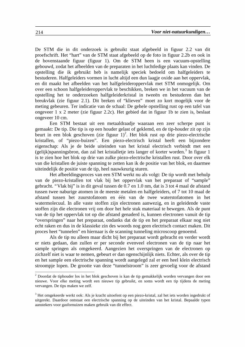
Voor niet-natuurkundigen…214
De STM die in dit onderzoek is gebruikt staat afgebeeld in figuur 2.2 van ditproefschrift. Het “hart” van de STM staat afgebeeld op de foto in figuur 2.2b en ook inde bovenstaande figuur (figuur 1). Om de STM heen is een vacuum-opstellinggebouwd, zodat het afbeelden van de preparaten in het luchtledige plaats kan vinden. Deopstelling die ik gebruikt heb is namelijk speciek bedoeld om halfgeleiders tebestuderen. Halfgeleiders vormen in lucht altijd een dun laagje oxide aan het oppervlak,en dit maakt het afbeelden van het halfgeleideroppervlak met STM onmogelijk. Omover een schoon halfgeleideroppervlak te beschikken, breken we in het vacuum van deopstelling het te onderzoeken halfgeleiderkristal in tweeën en bestuderen dan hetbreukvlak (zie figuur 2.1). Dit breken of “klieven” moet zo kort mogelijk voor demeting gebeuren. Ter indicatie van de schaal: De gehele opstelling rust op een tafel vanongeveer 1 x 2 meter (zie figuur 2.2c). Het gebied dat in figuur 1b te zien is, beslaatongeveer 10 cm.
Een STM bestaat uit een metaaldraadje waaraan een zeer scherpe punt isgemaakt: De tip. Die tip is op een houder gelast of geklemd, en de tip-houder zit op zijnbeurt in een blok geschoven (zie figuur 1)2. Het blok rust op drie piezo-electrischekristallen, of “piezo-buizen”. Een piezo-electrisch kristal heeft een bijzondereeigenschap: Als je de beide uiteinden van het kristal electrisch verbindt met een(gelijk)spanningsbron, dan zal het kristalletje iets langer of korter worden.3 In figuur 1is te zien hoe het blok op drie van zulke piezo-electrische kristallen rust. Door over elkvan die kristallen de juiste spanning te zetten kan ik de positie van het blok, en daarmeeuiteindelijk de positie van de tip, heel nauwkeurig sturen.
Het afbeeldingsproces van een STM werkt nu als volgt: De tip wordt met behulpvan de piezo-kristallen tot vlak bij het oppervlak van het preparaat of “sample”gebracht. “Vlak bij” is in dit geval tussen de 0.7 en 1.0 nm, dat is 3 tot 4 maal de afstandtussen twee naburige atomen in de meeste metalen en halfgeleiders, of 7 tot 10 maal deafstand tussen het zuurstofatoom en één van de twee waterstofatomen in hetwatermolecuul. In alle vaste stoffen zijn electronen aanwezig, en in geleidende vastestoffen zijn die electronen vrij om door het hele stuk materiaal te bewegen. Als de puntvan de tip het oppervlak tot op die afstand genaderd is, kunnen electronen vanuit de tip“overspringen” naar het preparaat, ondanks dat de tip en het preparaat elkaar nog nietecht raken en dus in de klassieke zin des woords nog geen electrisch contact maken. Ditproces heet “tunnelen” en hiernaar is de scanning tunneling microscoop genoemd.
Als de tip nu alleen maar dicht bij het preparaat wordt gebracht en verder wordter niets gedaan, dan zullen er per seconde evenveel electronen van de tip naar hetsample springen als omgekeerd. Aangezien het overspringen van de electronen opzichzelf niet is waar te nemen, gebeurt er dan ogenschijnlijk niets. Echter, als over de tipen het sample een electrische spanning wordt aangelegd zal er een heel klein electrischstroompje lopen. De grootte van deze “tunnelstroom” is zeer gevoelig voor de afstand 2 Doordat de tiphouder los in het blok geschoven is kan de tip gemakkelijk worden vervangen door eennieuwe. Voor elke meting wordt een nieuwe tip gebruikt, en soms wordt een tip tijdens de metingvervangen. De tips maken we zelf.
3 Het omgekeerde werkt ook: Als je kracht uitoefent op een piezo-kristal, zal het iets worden ingedrukt ofuitgerekt. Daardoor ontstaat een electrische spanning op de uiteinden van het kristal. Bepaalde typenaanstekers voor gasfornuizen maken gebruik van dit effect.
Voor niet-natuurkundigen… 215
tussen de tip en het preparaat. De STM wordt door electronica bestuurd, en dieelectronica is zo ingesteld dat de tunnelstroom ten allen tijden op een vooraf ingesteldewaarde gehouden wordt: Is de stroom wat te laag, dan zal de electronica de spanning opéén van de piezo-buizen wat bijregelen zodat de tip iets dichter bij hetpreparaatoppervlak komt (zie figuur 1). Is de stroom wat te hoog, dan zal de electronicade tip wat terugtrekken. Op die manier kunnen we dus de tip op een constante, zeerkleine afstand van het preparaatoppervlak brengen en houden. Tegelijk kan deelectronica de beide piezo-buizen die loodrecht op de tip staan zodanig aansturen dat detip een zijdelingse, heen-en-weergaande beweging zal maken, zodanig dat hijuiteindelijk een heel gebiedje bestreken heeft. Dat heet “scannen”. Zo kan een kleingebiedje van het preparaatoppervlak worden afgetast.
De spanning op de piezo buizen die nodig was om de tip op constante afstandvan het preparaat te houden tijdens de scanbeweging wordt bijgehouden door eencomputer die met de electronica is verbonden. Die spanning vormt het meetsignaal: EenSTM-beeld bestaat (bij ons apparaat) uit een matrix van 400 bij 400 punten, en van elkpunt is bekend welke spanning op de z-piezo buis gezet moest worden om detunnelstroom constant te houden. Hieruit kan dus voor elk punt in het STM-beeldbepaald worden over welke afstand de tip verplaatst moest worden om de tip-preparaatafstand constant te houden. Een STM-beeld is dus eigenlijk een “hoogtekaart” van hetpreparaatoppervlak, precies als de aardrijkskundige hoogtekaarten in een atlas (zie b.v.figuur 2 a,b). Alleen is bij een STM-beeld de schaal vele malen kleiner. Bij diehoogtekaartjes betekent een lichte kleur dat iets “hoog” is, en een donkere kleur dat iets“laag” is.
Hiermee is duidelijk wat een STM is: Het is een zeer scherpe naald die vlak boven hetoppervlak van een preparaat kan worden gehouden, en waarmee je op hele kleine schaalhet oppervlak van dat preparaat kunt aftasten. Het STM-beeld is in feite een soort“hoogtekaart” van het preparaatoppervlak.
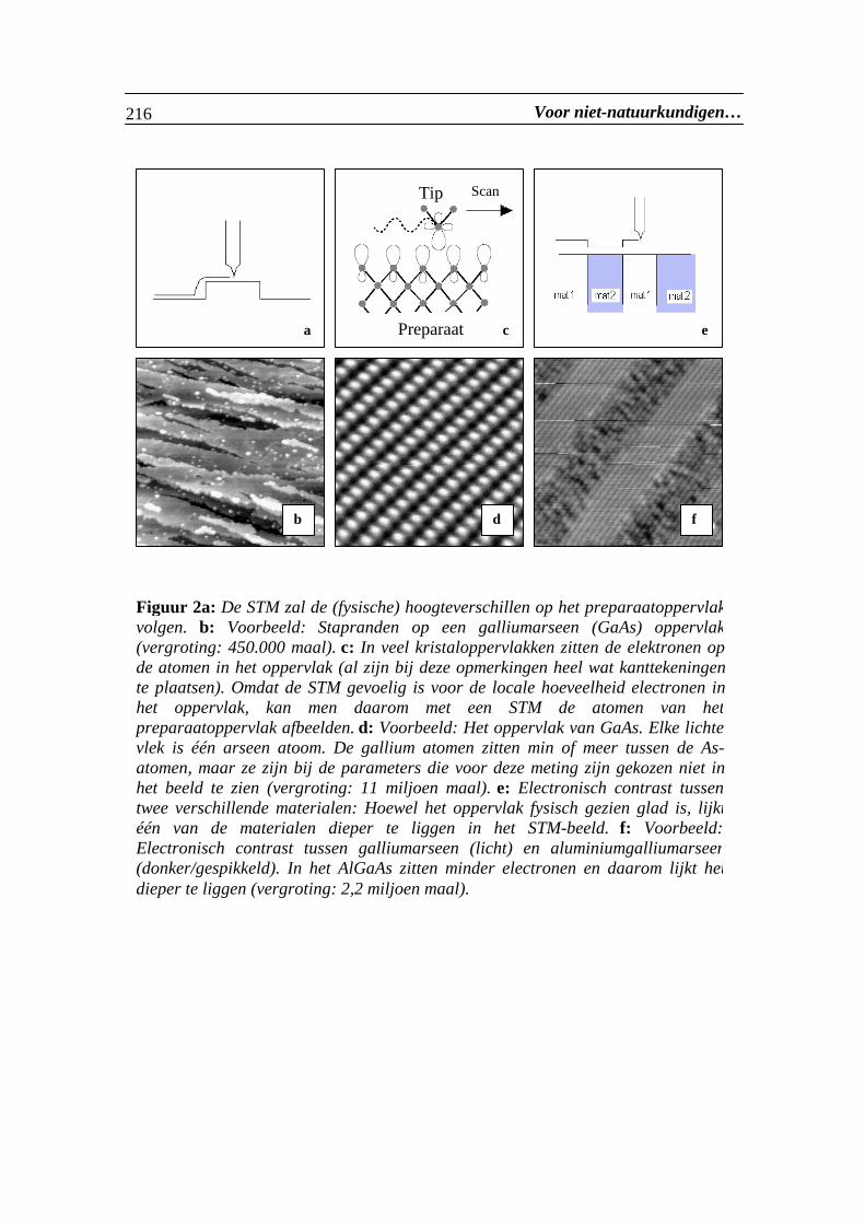
Voor niet-natuurkundigen…216
Figuur 2a: De STM zal de (fysische) hoogteverschillen op het preparaatoppervlakvolgen. b: Voorbeeld: Stapranden op een galliumarseen (GaAs) oppervlak(vergroting: 450.000 maal). c: In veel kristaloppervlakken zitten de elektronen opde atomen in het oppervlak (al zijn bij deze opmerkingen heel wat kanttekeningente plaatsen). Omdat de STM gevoelig is voor de locale hoeveelheid electronen inhet oppervlak, kan men daarom met een STM de atomen van hetpreparaatoppervlak afbeelden. d: Voorbeeld: Het oppervlak van GaAs. Elke lichtevlek is één arseen atoom. De gallium atomen zitten min of meer tussen de As-atomen, maar ze zijn bij de parameters die voor deze meting zijn gekozen niet inhet beeld te zien (vergroting: 11 miljoen maal). e: Electronisch contrast tussentwee verschillende materialen: Hoewel het oppervlak fysisch gezien glad is, lijktéén van de materialen dieper te liggen in het STM-beeld. f: Voorbeeld:Electronisch contrast tussen galliumarseen (licht) en aluminiumgalliumarseen(donker/gespikkeld). In het AlGaAs zitten minder electronen en daarom lijkt hetdieper te liggen (vergroting: 2,2 miljoen maal).
b d f
eca Preparaat
Tip Scan
Voor niet-natuurkundigen… 217
Wat kunnen we in een STM-beeld zien?
De “hoogtekaartjes” die een STM maakt zijn echter geen gewone hoogtekaartjes van hetpreparaatoppervlak. De STM is namelijk niet alleen gevoelig voor hoogteverschillen inhet oppervlak, hij maakt ook zichtbaar of ergens in het preparaatoppervlak veel ofweinig electronen aanwezig zijn.4 En daardoor kan een STM de atomen in eenoppervlak “zien”, want in het oppervlak van een metaal- of halfgeleiderkristal zitten deelectronen vaak op de atomen zelf5 (zie figuur 2 c,d). Ook kun je daardoor in een STM-beeld van halfgeleideroppervlakken sommige typen onzuiverheden zien zitten, omdatdie een extra electron bij zich hebben. Veel halfgeleiders worden via een soort“opdamptechniek” gemaakt, waarbij het mogelijk is om verschillende soorten materiaalop elkaar te stapelen.6 Dit laatste is van groot technologisch belang: Apparaatjes als b.v.halfgeleiderlasers zoals we die in onze CD-spelers vinden, worden nooit van één enkelhalfgeleidermateriaal gemaakt. Ze bevatten altijd meerdere laagjes van verschillendetypen halfgeleidend materiaal die op elkaar gestapeld zijn, en ontlenen juist aan deverschillen tussen die laagjes hun eigenschappen. De overgangen tussen deverschillende materialen in zo’n stapel zijn met een STM ook goed te zien (zie figuur 2e,f).
We moeten onze beschrijving van de STM dus een beetje aanpassen: Het is een zeerscherpe naald waarmee je op hele kleine schaal het preparaatoppervlak kunt aftasten.Het STM-beeld is daarbij in feite een soort hoogtekaart van het preparaatoppervlak,maar wel een heel speciaal soort hoogtekaart: Locale verschillen in de hoeveelheid
4 Dit geldt alleen voor het geval dat de electronen vanuit het preparaatoppervlak naar de tip tunnelen. Inde vaktaal wordt dan gezegd dat de “gevulde electronentoestanden” worden afgebeeld (filled statesimages). Tunnelen de electronen vanuit de tip naar het preparaat, dan laat de STM zien waar deelectronen het liefst in het oppervlak gaan zitten als er nieuwe electronen aan het oppervlak wordentoegevoegd. In vaktaal zeggen we dan dat de “lege electronentoestanden” worden afgebeeld (empty statesimages). Voor deze uitleg is dit verschil echter niet van groot belang, omdat een gevuldeelectronentoestand niet wezenlijk verschilt van een lege. Bovendien kan een gegeven electronentoestandonder sommige experimentele omstandigheden gevuld zijn, maar onder andere juist leeg. Als deaangelegde spanning tussen de tip en het preparaat een positieve waarde heeft, dan tunnelen de electronenvan de tip naar het preparaat en worden de “lege electronentoestanden” afgebeeld. Heeft de aangelegdespanning tussen de tip en het preparaat een negatieve waarde, dan tunnelen de electronen van hetpreparaat naar de tip en zien we in het STM-beeld de “gevulde electronentoestanden”.
5 Dit is een vrij grove vereenvoudiging van de werkelijkheid. Vaak zitten de electronen op de atomen inhet oppervlak, maar waar ze precies zitten hangt heel sterk van het oppervlak af. Wat b.v. bij sommigehalfgeleideroppervlakken wel eens voorkomt, is dat de electronen niet op alle atomen zitten, maar b.v.alternerend wel op het ene atoom en niet op het volgende. Dan zie je in je STM-beeld ook maar de helftvan het werkelijke aantal oppervlakteatomen. Wat ook een groot verschil maakt, is of de electronenvanuit het oppervlak ver “naar buiten” steken, of juist meer in het oppervlak liggen.
6 Dit zijn de zogenaamde “epitaxiale groeitechnieken”. Het zou te ver voeren die technieken hier uit teleggen. De vervaardiging van halfgeleidermaterialen en halfgeleiderstructuren d.m.v. epitaxiale groei isechter een zeer groot en belangrijk wetenschapsveld. De epitaxiale groei van kwalitatief goedehalfgeleidermaterialen en halfgeleiderstructuren is alles behalve triviaal, in tegenstelling tot hetgeen dewat simpele benaming “opdamptechniek” misschien doet vermoeden.
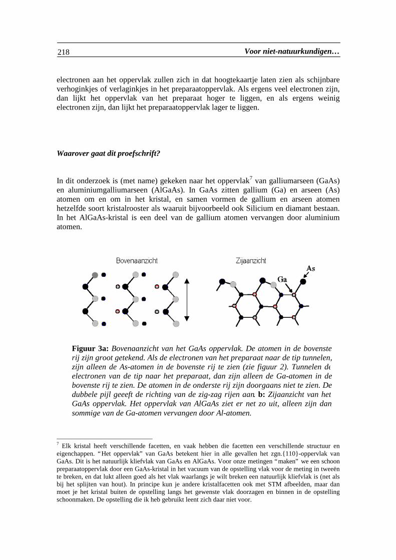
Voor niet-natuurkundigen…218
electronen aan het oppervlak zullen zich in dat hoogtekaartje laten zien als schijnbareverhoginkjes of verlaginkjes in het preparaatoppervlak. Als ergens veel electronen zijn,dan lijkt het oppervlak van het preparaat hoger te liggen, en als ergens weinigelectronen zijn, dan lijkt het preparaatoppervlak lager te liggen.
Waarover gaat dit proefschrift?
In dit onderzoek is (met name) gekeken naar het oppervlak7 van galliumarseen (GaAs)en aluminiumgalliumarseen (AlGaAs). In GaAs zitten gallium (Ga) en arseen (As)atomen om en om in het kristal, en samen vormen de gallium en arseen atomenhetzelfde soort kristalrooster als waaruit bijvoorbeeld ook Silicium en diamant bestaan.In het AlGaAs-kristal is een deel van de gallium atomen vervangen door aluminiumatomen.
7 Elk kristal heeft verschillende facetten, en vaak hebben die facetten een verschillende structuur eneigenchappen. “Het oppervlak” van GaAs betekent hier in alle gevallen het zgn.110-oppervlak vanGaAs. Dit is het natuurlijk kliefvlak van GaAs en AlGaAs. Voor onze metingen “maken” we een schoonpreparaatoppervlak door een GaAs-kristal in het vacuum van de opstelling vlak voor de meting in tweeënte breken, en dat lukt alleen goed als het vlak waarlangs je wilt breken een natuurlijk kliefvlak is (net alsbij het splijten van hout). In principe kun je andere kristalfacetten ook met STM afbeelden, maar danmoet je het kristal buiten de opstelling langs het gewenste vlak doorzagen en binnen in de opstellingschoonmaken. De opstelling die ik heb gebruikt leent zich daar niet voor.
Figuur 3a: Bovenaanzicht van het GaAs oppervlak. De atomen in de bovensterij zijn groot getekend. Als de electronen van het preparaat naar de tip tunnelen,zijn alleen de As-atomen in de bovenste rij te zien (zie figuur 2). Tunnelen deelectronen van de tip naar het preparaat, dan zijn alleen de Ga-atomen in debovenste rij te zien. De atomen in de onderste rij zijn doorgaans niet te zien. Dedubbele pijl geeeft de richting van de zig-zag rijen aan. b: Zijaanzicht van hetGaAs oppervlak. Het oppervlak van AlGaAs ziet er net zo uit, alleen zijn dansommige van de Ga-atomen vervangen door Al-atomen.
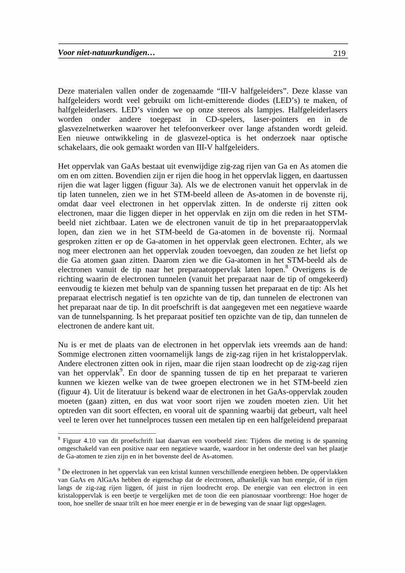
Voor niet-natuurkundigen… 219
Deze materialen vallen onder de zogenaamde “III-V halfgeleiders”. Deze klasse vanhalfgeleiders wordt veel gebruikt om licht-emitterende diodes (LED’s) te maken, ofhalfgeleiderlasers. LED’s vinden we op onze stereos als lampjes. Halfgeleiderlasersworden onder andere toegepast in CD-spelers, laser-pointers en in deglasvezelnetwerken waarover het telefoonverkeer over lange afstanden wordt geleid.Een nieuwe ontwikkeling in de glasvezel-optica is het onderzoek naar optischeschakelaars, die ook gemaakt worden van III-V halfgeleiders.
Het oppervlak van GaAs bestaat uit evenwijdige zig-zag rijen van Ga en As atomen dieom en om zitten. Bovendien zijn er rijen die hoog in het oppervlak liggen, en daartussenrijen die wat lager liggen (figuur 3a). Als we de electronen vanuit het oppervlak in detip laten tunnelen, zien we in het STM-beeld alleen de As-atomen in de bovenste rij,omdat daar veel electronen in het oppervlak zitten. In de onderste rij zitten ookelectronen, maar die liggen dieper in het oppervlak en zijn om die reden in het STM-beeld niet zichtbaar. Laten we de electronen vanuit de tip in het preparaatoppervlaklopen, dan zien we in het STM-beeld de Ga-atomen in de bovenste rij. Normaalgesproken zitten er op de Ga-atomen in het oppervlak geen electronen. Echter, als wenog meer electronen aan het oppervlak zouden toevoegen, dan zouden ze het liefst opdie Ga atomen gaan zitten. Daarom zien we die Ga-atomen in het STM-beeld als deelectronen vanuit de tip naar het preparaatoppervlak laten lopen.8 Overigens is derichting waarin de electronen tunnelen (vanuit het preparaat naar de tip of omgekeerd)eenvoudig te kiezen met behulp van de spanning tussen het preparaat en de tip: Als hetpreparaat electrisch negatief is ten opzichte van de tip, dan tunnelen de electronen vanhet preparaat naar de tip. In dit proefschrift is dat aangegeven met een negatieve waardevan de tunnelspanning. Is het preparaat positief ten opzichte van de tip, dan tunnelen deelectronen de andere kant uit.
Nu is er met de plaats van de electronen in het oppervlak iets vreemds aan de hand:Sommige electronen zitten voornamelijk langs de zig-zag rijen in het kristaloppervlak.Andere electronen zitten ook in rijen, maar die rijen staan loodrecht op de zig-zag rijenvan het oppervlak9. En door de spanning tussen de tip en het preparaat te varierenkunnen we kiezen welke van de twee groepen electronen we in het STM-beeld zien(figuur 4). Uit de literatuur is bekend waar de electronen in het GaAs-oppervlak zoudenmoeten (gaan) zitten, en dus wat voor soort rijen we zouden moeten zien. Uit hetoptreden van dit soort effecten, en vooral uit de spanning waarbij dat gebeurt, valt heelveel te leren over het tunnelproces tussen een metalen tip en een halfgeleidend preparaat 8 Figuur 4.10 van dit proefschrift laat daarvan een voorbeeld zien: Tijdens die meting is de spanningomgeschakeld van een positive naar een negatieve waarde, waardoor in het onderste deel van het plaatjede Ga-atomen te zien zijn en in het bovenste deel de As-atomen.
9 De electronen in het oppervlak van een kristal kunnen verschillende energieen hebben. De oppervlakkenvan GaAs en AlGaAs hebben de eigenschap dat de electronen, afhankelijk van hun energie, óf in rijenlangs de zig-zag rijen liggen, óf juist in rijen loodrecht erop. De energie van een electron in eenkristaloppervlak is een beetje te vergelijken met de toon die een pianosnaar voortbrengt: Hoe hoger detoon, hoe sneller de snaar trilt en hoe meer energie er in de beweging van de snaar ligt opgeslagen.
Voor niet-natuurkundigen…220
zoals dat in een STM plaatsvindt. Zo blijkt onder andere het volgende: De manierwaarop men aankijkt tegen het feit dat de STM atomen kan zien is op zichzelf juist,maar onder sommige experimentele omstandigheden kan die theorie niet opgaan. Tochzien we onder die omstandigheden wel degelijk atomen. Onder die experimenteleomstandigheden moet er dus een ander mechanisme opgaan dat er ook toe leidt dat deSTM atomen af kan beelden. Dit is één van de hoofdonderwerpen van dit proefschrift(hoofdstuk 4).
Dit soort effecten zijn niet alleen voor galliumarseen te zien, maar ook vooraluminiumgalliumarseen (AlGaAs) (zie hoofdstuk 6). Zoals net ook al gezegd is inAlGaAs een deel van de gallium atomen vervangen voor aluminium atomen. Dit zorgtervoor dat het AlGaAs net iets andere eigenschappen heeft dan GaAs. In heel veelhalfgeleider-apparaatjes (b.v. lasers) worden laagjes van deze twee materialen op elkaargestapeld (zie voetnoot 5). De electronen in zo’n stapel hebben de neiging om in hetGaAs te gaan zitten en het AlGaAs te mijden. Uit alle veranderingen die in de STM-beelden optreden als functie van de aangelegde spanning tussen het preparaat en de tip,is heel veel te leren over waar nou de electronen in een materiaal als AlGaAs zitten(figuur 6.2, 6.3). Ook een stapel van afwisselend dunne laagjes GaAs en AlGaAs (eenzgn “superrooster” of “superlattice”) is op die manier te onderzoeken (figuur 6.8, 6.9).
Eén van de resultaten is te zien in figuur 6.6 a en 6.6 b: Dit figuur laat precieshetzelfde stukje AlGaAs-oppervlak zien, één keer voor het geval dat de electronenvanuit de tip het preparaat in tunnelen, en één keer voor het geval dat de electronenprecies de andere kant uit tunnelen. Wie de beide figuren goed met elkaar vergelijkt, zalzien dat de zwarte vlekjes in die twee figuren niet met elkaar samenvallen. Vaak wordt
V = +0.299 V V = +0.706 V V = +0.929 V V = +1.268 V
Figuur 4: In het GaAs-oppervlak zitten sommige electronen langs de zig-zag rijenin het oppervlak, terwijl andere electronen in rijen zitten die loodrecht op die zig-zag rijen staan (zie figuur 3). Welke groep electronen wordt afgebeeld door deSTM hangt af van de spanning die aangelegd is tussen de tip en het preparaat.Overigens zijn deze plaatjes ten opzichte van figuur 3 gedraaid: De zig-zag rijenlopen van linksonder in het STM beeld naar rechtsboven. Bij de spanningentussen preparaat en tip die bij het maken van deze beelden zijn gekozen, tunnelende electronen van de tip naar het preparaat, en dus vallen de verbredingen in deatomaire rijen samen met de galliumatomen. (Vergroting: 5 miljoen maal).
V = +0.299 V V = +0.706 V V = +0.929 V V = +1.268 V
Voor niet-natuurkundigen… 221
beweerd dat zulke donkere vlekjes in het STM-beeld van AlGaAs betekenen dat op dieplaats veel aluminium zit10. Voor mensen die zich bezig houden met de vervaardigingvan “gemengde” halfgeleiders zoals AlGaAs is de precieze verdeling van het aluminiuminteressant, want een vraag die op dit moment leeft, is of het aluminium in AlGaAs deneiging heeft om clusters (“klontjes”) te vormen of juist niet. De bewering “een zwartvlekje in het STM-beeld vertegenwoordigt een hoge locale concentratie aluminium”gaat dus niet zonder meer op, want in dat geval zou de vorm en plaats van die zwartevlekjes nooit kunnen afhangen van de omstandigheden waaronder het AlGaAs wordtafgebeeld.
Een ander belangrijk onderwerp van dit proefschrift is het volgende: Als de spanningtussen de tip en het preparaat wordt gevarieerd terwijl de ingestelde waarde voor detunnelstroom gelijk blijft, dan zal de afstand tussen het preparaat en de tip veranderen.Zo kan het gebeuren dat bij een kleine waarde van de spanning tussen de tip en hetpreparaat de afstand tussen het preparaat en de tip erg klein wordt. Daarbij kan hetgebeuren dat de electronen die in het oppervlak zitten, gaan overlappen met het electrondat op de punt van de tip zit.11 Dit verstoort de electronen aan het preparaatoppervlak enhet electron op de punt van de tip. Als de verstoring groot genoeg is, kan een chemischebinding ontstaan tussen de tip en het preparaat. Je zou dan kunnen verwachten dat de tipaan het preparaatoppervlak vast blijft plakken, maar dat gebeurt niet: Tijdens hetscannen van de tip kan de chemische binding tussen de tip en één van de atomen in hetpreparaatoppervlak overspringen naar een naburig atoom in het preparaatoppervlak12.Hoe dit hele proces precies in zijn werk gaat is uitgerekend door enkele theoretici diedaarover in de vakliteratuur hebben gepubliceerd.
Heel af en toe zien we, als we GaAs afbeelden met de STM, een heel vreemdbeeld (zie figuur 5). Hierin is heel duidelijk de zig-zag structuur van het GaAs-oppervlak te herkennen. Vanuit de literatuur is al bekend dat, als de afstand tussen de tipen het preparaat erg klein wordt, die zig-zag rij in het STM-beeld gezien kan worden endat je dan ook inderdaad zowel de gallium als de arseen atomen in de bovenste rij ziet.In dit beeld, en daarom is het zo bijzonder, is ook de structuur te herkennen van detweede zig-zag rij die wat dieper in het oppervlak ligt (zie figuur 3). Voor zover we
10 Uit bestaande literatuur was eigenlijk al duidelijk dat er uitzonderingen op deze “vuistregel” zijn. Tochwordt ze nog vaak toegepast, al is het maar als eerste benadering. Figuur 6.6 laat zien dat je ook daarmeeuit moet kijken.
11 Een electron dat in een kristaloppervlak zit, steekt altijd een eindje naar buiten. Dat is de reden dat hetfenomeen “tunnelen” überhaupt bestaat. Uit het oppervlak van de tip steken ook electronen. Bij eengoede, scherpe tip is er daarvan maar ééntje betrokken bij het tunnelproces. Alle andere electronen in hetoppervlak van de tip zitten te ver weg van het preparaatoppervlak om deel te kunnen nemen aan hettunnelproces.
12 Het is niet zo dat de chemische binding tijdens het scannen continu gevormd en weer verbroken wordt:Als de tip niet precies boven één atoom in het preparaatoppervlak hangt, maar meer tussen twee atomenin, zijn de electronen in het oppervlak en op de tip nog steeds verstoord. Die verstoring heeft dan nietprecies het karakter van een chemische binding, maar zorgt nog steeds voor een aatrekkende kracht tussende tip en het preparaat. Als de tip wél precies boven een oppervlakte atoom hangt, dan is de aantrekkendekracht tussen de tip en het preparaat uiteraard het sterkst (dat is namelijk het wezen van een chemischebinding).
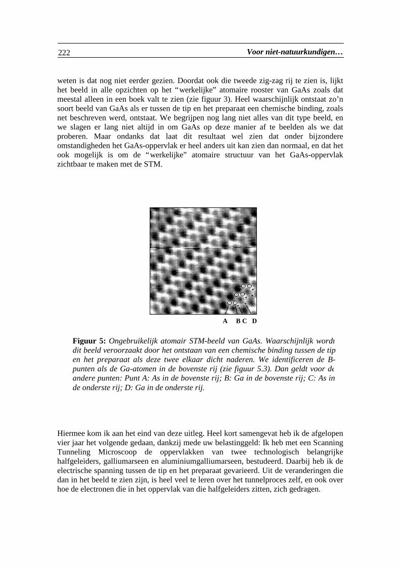
Voor niet-natuurkundigen…222
weten is dat nog niet eerder gezien. Doordat ook die tweede zig-zag rij te zien is, lijkthet beeld in alle opzichten op het “werkelijke” atomaire rooster van GaAs zoals datmeestal alleen in een boek valt te zien (zie figuur 3). Heel waarschijnlijk ontstaat zo’nsoort beeld van GaAs als er tussen de tip en het preparaat een chemische binding, zoalsnet beschreven werd, ontstaat. We begrijpen nog lang niet alles van dit type beeld, enwe slagen er lang niet altijd in om GaAs op deze manier af te beelden als we datproberen. Maar ondanks dat laat dit resultaat wel zien dat onder bijzondereomstandigheden het GaAs-oppervlak er heel anders uit kan zien dan normaal, en dat hetook mogelijk is om de “werkelijke” atomaire structuur van het GaAs-oppervlakzichtbaar te maken met de STM.
Hiermee kom ik aan het eind van deze uitleg. Heel kort samengevat heb ik de afgelopenvier jaar het volgende gedaan, dankzij mede uw belastinggeld: Ik heb met een ScanningTunneling Microscoop de oppervlakken van twee technologisch belangrijkehalfgeleiders, galliumarseen en aluminiumgalliumarseen, bestudeerd. Daarbij heb ik deelectrische spanning tussen de tip en het preparaat gevarieerd. Uit de veranderingen diedan in het beeld te zien zijn, is heel veel te leren over het tunnelproces zelf, en ook overhoe de electronen die in het oppervlak van die halfgeleiders zitten, zich gedragen.
A B C D
Figuur 5: Ongebruikelijk atomair STM-beeld van GaAs. Waarschijnlijk wordtdit beeld veroorzaakt door het ontstaan van een chemische binding tussen de tipen het preparaat als deze twee elkaar dicht naderen. We identificeren de B-punten als de Ga-atomen in de bovenste rij (zie figuur 5.3). Dan geldt voor deandere punten: Punt A: As in de bovenste rij; B: Ga in de bovenste rij; C: As inde onderste rij; D: Ga in de onderste rij.

List of abbreviations
2-D; 3-D Two-dimensional; Three-dimensionalAFM Atomic Force MicroscopyBCB Bulk Conduction Band (states)BEEM Ballistic Electron Emission MicroscopyBVB Bulk Valence Band (states)BZ Brillouin ZoneCBE Chemical Beam EpitaxyCBM Conduction Band MinimumCN Corrugation NumberDC Direct CurrentDOS Density Of StatesFFT Fast Fourier TransformFWHM Full Width Half MaximumHF Hydrogen FluorideHOMO Highest Occupied Molecular OrbitalKOH Potassium HydroxideLDOS Local Density of StatesMBE Molecular Beam EpitaxyPL Photo-LuminescencePLE Photo-Luminescence ExitationSEM Scanning Electron MicroscopyRHEED Reflection High Energy Electron DiffractionSFL Sample Fermi LevelSIMS Secondary Ion Mass SpectroscopySTM Scanning Tunneling MicroscopeTEM Transmission Electron MicroscopyTIBB Tip-Induced Band BendingTILS Tip-Induced Localized StatesTFL Tip Fermi LevelTLRC True Lattice Resemblant CorrugationX-STM Cross-sectional Scanning Tunneling MicroscopyUHV Ultra-High VacuumVBM Valence Band Maximum
223

Bedankt allemaal…
Experimenteel onderzoek doe je nooit alleen. Dat mag als een cliché klinken, wantvrijwel elk proefschrift in de experimentele natuurkunde wijst hierop, maar het isdaarom niet minder waar. Daarom zou ook dit proefschrift niet compleet zijn zonder eenuiting van mijn oprechte dank aan iedereen die me op enig moment tijdens mijnonderzoek geholpen heeft.
Als eerste wil ik mijn directe begeleider, Paul Koenraad, bedanken. Hoewel je me af entoe behoorlijk nerveus kon maken met je ongebreidelde optimisme en vooral met dekorte termijn waarbinnen je meestal denkt dat één en ander wel te realiseren is, heb ikmet heel veel plezier met je samengewerkt. In een goede relatie hoef je het lang nietaltijd eens te zijn, maar kun je de meningsverschillen die er bestaan goed bespreken. Dathebben we vanaf het begin gehad, en ik heb dat altijd ontzettend in je gewaardeerd.
Ook mijn promotor, Professor Wolter, wil ik graag bedanken voor degelegenheid om in zijn groep te promoveren. Als groepsleider bent Ueindverantwoordelijke geweest voor een werkomgeving waarin ik goed heb kunnengedijen en ook groeien. Dank U daarvoor. Verder wil ik de commissieleden, Prof.Salemink, Prof. van Kempen en Prof. Frenken oprecht bedanken voor het kritischdoorlezen van mijn proefschrift. Prof. Salemink ben ik bovendien dank verschuldigdvoor zijn opmerkinen over het sputteren van STM-tips, waar ik veel aan gehad heb.
Dominique Bruls ben ik heel veel dank verschuldigd voor een goede werksfeer,levendige koffietafelconversaties, fluitconcerten, maar vooral ook voor de vele hand- enspandiensten die hij voor me deed. Zo waren er de “dagelijkse” STM-klusjes als hetmaken van tips en samples, of het bestellen van een voeding dat van een dermatebuitenaards type bleek dat geen hond het ding nog in voorraad had. Ook nog bedanktvoor al je hulp met mijn soms weerbarstige PC en voor het “babysitten” tijdens denachtelijke metingen, een taak die grotendeels op jouw en op Paul is neergekomen. Hetis mooi om te zien hoe jij, nu ik zelf de vakgroep verlaten heb, op zo’n naadloze manierhet STM-onderzoek in onze vakgroep hebt overgenomen.
Ook Emile Martens zal een groot stuk van zijn afstudeerwerk in dit proefschriftterugvinden, in hoofdstuk drie waar het model beschreven staat dat develdemissiekarakterisatie theoretisch onderbouwt. Verder wil ik graag Rob Dekkers enNiall Phelan bedanken voor hun werk aan resp. het etsen van Platina tips en hetkliefgedrag van GaAs. Martijn Kemerink gebruikt nu die platina-tips (of heeft dat in elkgeval een lange tijd gedaan) en Niall’s werk heeft ons begrip van het kliefproces weerwat verder gebracht.
Geen experimenteel onderzoek zonder technische ondersteuning, en dat brengtme bij Jos van Ruyven die de vacuum-opstelling in elkaar gesleuteld heeft en MariusBogers en zijn groep die een groot aantal “STM-accesoires” heeft gemaakt. Ook Fransvan Setten wil ik bij deze nogmaals hartelijk danken voor het onderbrekingskastje datwe bij het etsen van tips gebruiken. Verder wil ik Maarten Leys bedanken voor hetgeduldig antwoorden van al mijn vragen over groei en halfgeleideroppervlakken, enPeter Nouwens voor (onder andere) het bereidwillig en min of meer permanent afstaanvan een stuk van zijn zuurkast. Ook Willem van der Vleuten, die het delta-laag sample
224
Bedankt allemaal… 225
en het sample uit hoofdstuk 6 heeft gegroeid, ben ik dank verschuldigd. Jammer dat jeer niet bent om de resultaten van je werk te zien.
In de loop van de tijd heb ik verschillende kamergenoten gehad: MartijnKemerink, altijd goed voor een originele screen-saver tekst, Arnout van der Stadt,waarvan ik me soms afvroeg of hij zich na de lange werkdagen die hij maakte de wegnaar huis nog wel zou weten te herinneren, en (alweer) Dominique, wiens bijdrage aande sfeer in de werkkamer en aan de koffietafel een (overigens positief) verhaal apart is.Verder wil ik alle andere HF-ers bedanken voor alle gezelligheid en antwoorden opfysische en andere vragen.
Buiten mijn eigen groep wil ik graag de groep “Electronische Bouwstenen” vande faculteit electrotechniek bedanken voor het gebruik van hun SEM, en daarbijProfessor Kaufmann, Erik-Jan Geluk en Ben van Roy in het bijzonder. Und auchmöchte ich Martin Wenderoth, Kathi Sauthoff, Klaus Engel und Berhart Spichterdanken für den sehr angenehmen und lehrreichen Besuch in Göttingen. En “last, but byfar not least”: Hans Dalderop, voor zijn enthousiaste uitleg over allerlei scheikundigezaken en voor het feit dat ik de meest gekke chemische stofjes meestal zo van hem konlenen.
In mijn vriendenkring heeft Marcel Davids een bijzondere bijdrage geleverd door éénvan zijn PC’s zo lang aan me uit te lenen. Verder wil ik vooral Jolanda bedanken,eigenlijk in hoofdzaak voor het simpele feit dat ze er is. En ook voor haar begrip als ikvoor de zoveelste keer niet vanachter de PC weg te slepen was, niet meehielp met deafwas, of als ik weer eens vond dat een verjaardag in haar familie ook best zonder mijnaanwezigheid kon worden gevierd. Datzelfde geldt voor mijn zus Machteld, mijn vader,Netty, Arjan, Olivie, Mark, Inna, Jan en Anne-Marijke. En voor tante Cock. Jij, tanteCock, neemt hierin een heel bijzondere plaats in: In de drie jaar dat ik bij je in huiswoonde, heb je me heel veel belangrijke lessen meegegeven. Daarom draag ik ditproefschrift graag aan jou op.
Gijs de Raad, november 2000
List of publications
G.J. de Raad, P.M. Koenraad, J.H. Wolter: Use of the Schiller-decapitation process forthe manufacture of high-quality Tungsten STM-tips. Journal of Vac. Sci. and Tech.-B,Vol. 17, No. 5, pp. 1946 - 1953 (1999). See also chapter 3 of this thesis.
G.J. de Raad, D.M. Bruls, P.M. Koenraad, J.H. Wolter: Interplay between tip-inducedband bending and voltage-depending surface-corrugation on GaAs-(110) surfaces.Submitted for publication in Phys. Rev. B. See also chapter 4 of this thesis.
G.J. de Raad, D.M. Bruls, P.M. Koenraad, J.H. Wolter: Observation of a new image-form of GaAs-(110) showing the top- and bottom zig-zag rows of the surface. Submittedfor publication in Phys. Rev. B. See also chapter 5 of this thesis.
G.J. de Raad, D.M. Bruls, P.M. Koenraad, J.H. Wolter: Voltage-dependent changes inthe filled- and empty-states images of AlxGa(1-x)As (110) and of GaAs / AlxGa(1-x)As thinlayers. Submitted for publication in Phys. Rev. B. See also chapter 6 of this thesis.
226
Curriculum vitae
Naam: Gijs Jan de Raad
Geboren: 26 oktober 1969
Middelbaar onderwijs: VWO-B, doorlopen op de Rijks scholengemeenschap“Professor Zeeman” te Zierikzee en de KatholiekeScholengemeenschap “Veluws College” te Apeldoorn(1982 - 1988).
Uitwisselingsjaar: Senior year aan de “Lakeville High School” te Lakeville,Minnesota, Verenigde Staten (1988 - 1989).
Studie: Technische Natuurkunde, doorlopen aan deRijksuniversiteit Groningen (1989 - 1995).
Industriële stage: The Prickstick: Testing a capacitive soilmoisture measurement probe for tropical conditions.Uitgevoerd bij het International Centre for Research inAgro-Forestry (ICRAF) te Machakos/Nairobi, Kenya.
Afstudeeronderzoek: Scratching the surface: The study ofirradiated and unirradiated NaCl using Atomic ForceMicroscopy. Uitgevoerd aan de RijksuniversiteitGroningen, vakgroep Materiaalkunde (Prof.dr. J. deHosson).
Promotieonderzoek: Voltage-dependent Scanning Tunneling Microscopy on the110-surfaces of GaAs, AlGaAs and theirheterostructures. Uitgevoerd aan de TechnischeUniversiteit Eindhoven, vakgroep Halfgeleiderfysica.Eerste promotor: Prof.dr. J.H. Wolter, copromotor: dr.P.M. Koenraad. (1996 - 2000).
Per 1 maart 2000 in dienst getreden als proces integratie ingenieur bij PhilipsHalfgeleiders te Nijmegen.
227
Stellingen
behorende bij het proefschrift
Voltage-dependent Scanning Tunneling Microscopy on the110-surfaces of GaAs, AlGaAs and their heterostructures
1) Bij het zelfsputterproces van wolfraam STM-tips treedt het Schiller-decapitatiepro cesop, wat te herkennen is aan een specifiek gedrag van de signaal-ruisverhouding van desputterspanning als functie van de tijd. (dit proefschrift, hoofdstuk 3).
2) Atomaire oplossing in STM-beelden van halfgeleideroppervlakken hoeft niet altijdveroorzaakt te worden door het tunnelen van electronen in- of vanuitoppervlaktetoestanden. Onder bepaalde omstandigheden zijn andere mechanismenvoor atomaire oplossing ook mogelijk. (dit proefschrift, hoofdstuk 4 en 5; N.Horiguchi et al., Jap. Journ. of Appl. Phys, Vol. 37, part I, p. 3782; F. Fukumizu et al.,Jap. Journ. of Appl. Phys, Vol. 37, part I, p. 3785).
3) De vaak kwalitatieve behandeling van tip-geinduceerde bandverbuiging in deliteratuur doet onterecht vermoeden dat dit fenomeen weinig méér tot gevolg heeft daneen verschuiving van de tip-sample spanning waarbij een bepaaldeoppervlaktetoestand in het STM-beeld te zien is. De invloed van tip-geinduceerdebandverbuiging kan namelijk veel verder gaan. (dit proefschrift, hoofdstuk 4).
4) De atomaire morfologie van AlGaAs-110 en van GaAs/AlGaAs heterostructuren inSTM is zeer sterk afhankelijk van de aangelegde tunnelspanning. Deze omstandigheidbiedt veel nieuwe mogelijkheden om informatie over de electronische structuur van ditsoort oppervlakken te verkrijgen. (dit proefschrift, hoofdstuk 6).
5) Bij de interpretatie van STM-beelden van AlGaAs wordt wel eens de vuistregel “eenlage schijnbare hoogte vertegenwoordigt een hoge locale concentratie aan aluminium”toegepast. Aan de geldigheid van deze vuistregel moet, zelfs wanneer men die slechtsin eerste benadering toepast, worden getwijfeld. (dit proefschrif, hoofdstuk 6).

6) De atoomkern kan, net als de electronenwolk van een atoom, met behulp van een zgn.“schillenmodel” worden beschreven (Fundamentals of Nuclear Physics, door N.A.Jelley, Cambr. Univ. Press). Gezien de educatieve waarde van dit feit voor studentenzou het wenselijk zijn om dit gegeven een prominentere plaats in het studieprogrammate geven (eigen ervaring bij het tweedejaarspracticum).
7) Met de wichelroede als oudste vertegenwoordiger waren de Scanning ProbeTechnieken al in de Middeleeuwen bekend.
8) Gezien de soms hoge verkoopprijs van moderne, abstracte schilderkunst zou de STM-gemeenschap een belangrijk deel van haar activiteiten moeten kunnen financieren doorde verkoop van experimentele resultaten als kunst.
9) Een planning is zinloos zonder goede afspraken.
10) Een ideaal is te vergelijken met een ster: het ideaal zelf is onbereikbaar, maar je kuntje er wel op orienteren.
Eindhoven, 22 januari 2001 Gijs de Raad
Copyright © 2022 FDOKUMEN