
Creation of stable molecular junctions with a custom-designed scanning tunneling microscope
9
Creation of stable molecular junctions with a custom-designed scanning tunneling microscope This article has been downloaded from IOPscience. Please scroll down to see the full text article. 2011 Nanotechnology 22 485703 (http://iopscience.iop.org/0957-4484/22/48/485703) Download details: IP Address: 141.211.173.82 The article was downloaded on 06/04/2012 at 15:57 Please note that terms and conditions apply. View the table of contents for this issue, or go to the journal homepage for more Home Search Collections Journals About Contact us My IOPscience
-
Upload
independent -
Category
Documents
-
view
4 -
download
0
Transcript of Creation of stable molecular junctions with a custom-designed scanning tunneling microscope

Creation of stable molecular junctions with a custom-designed scanning tunneling microscope
This article has been downloaded from IOPscience. Please scroll down to see the full text article.
2011 Nanotechnology 22 485703
(http://iopscience.iop.org/0957-4484/22/48/485703)
Download details:
IP Address: 141.211.173.82
The article was downloaded on 06/04/2012 at 15:57
Please note that terms and conditions apply.
View the table of contents for this issue, or go to the journal homepage for more
Home Search Collections Journals About Contact us My IOPscience
IOP PUBLISHING NANOTECHNOLOGY
Nanotechnology 22 (2011) 485703 (8pp) doi:10.1088/0957-4484/22/48/485703
Creation of stable molecular junctionswith a custom-designed scanningtunneling microscopeWoochul Lee1 and Pramod Reddy1,2
1 Department of Mechanical Engineering, University of Michigan, Ann Arbor, MI 48109,USA2 Department of Materials Science, University of Michigan, Ann Arbor, MI 48109, USA
E-mail: [email protected]
Received 26 June 2011, in final form 21 September 2011Published 9 November 2011Online at stacks.iop.org/Nano/22/485703
AbstractThe scanning tunneling microscope break junction (STMBJ) technique is a powerful approachfor creating single-molecule junctions and studying electrical transport in them. However,junctions created using the STMBJ technique are usually mechanically stable for relativelyshort times (<1 s), impeding detailed studies of their charge transport characteristics. Here, wereport a custom-designed scanning tunneling microscope that enables the creation ofmetal–single molecule–metal junctions that are mechanically stable for more than 1 minute atroom temperature. This stability is achieved by a design that minimizes thermal drift as well asthe effect of environmental perturbations. The utility of this instrument is demonstrated byperforming transition voltage spectroscopy—at the single-molecule level—onAu–hexanedithiol–Au, Au–octanedithiol–Au and Au–decanedithiol–Au junctions.
S Online supplementary data available from stacks.iop.org/Nano/22/485703/mmedia
(Some figures may appear in colour only in the online journal)
1. Introduction
Nanoscale molecular junctions provide a unique opportunityto probe quantum transport [1] and are being actively studieddue to their potential technological importance in molecularelectronics [2] and organic-based thermoelectrics [3–5]. Infact, a variety of interesting effects including negativedifferential resistance, rectification, switching and gating haveall been observed [6] in molecular junctions. Further, recentcomputational studies [7, 8] have shown that it may bepossible to create molecular junctions with large thermoelectricefficiencies using appropriately tailored organic molecules.
A variety of experimental techniques have been developedrecently to study charge transport in single-molecule junctions.Some of the widely used techniques include the electromi-grated break junction (EBJ) technique [9], the mechanicallycontrollable break junction (MCBJ) technique [10] and thescanning tunneling microscope break junction (STMBJ) tech-nique [11–14]. These techniques often complement each otherand are uniquely suited for specific studies. The MCBJ and
STMBJ techniques are closely related and enable trappingsingle molecules by mechanically manipulating electrodes [6].The MCBJ technique is well known for its superb mechanicalstability and has been widely used in a variety of two-terminal studies of electrical transport in single-moleculejunctions [15, 16]. The STMBJ technique allows for not onlytwo terminal measurements of electrical transport propertiesbut also thermoelectric properties. Further, since the STMBJtechnique employs a scanning tunneling microscope [17] itis possible to image the molecules that are being studied,thus enabling more detailed insights [18]. The EBJ techniqueis well suited for performing three-terminal measurementswhere the electronic structure of the molecular junction iscontrolled via a gate electrode. However, the EBJ techniqueinvolves a substantial effort in micro-fabricating the breakjunction devices, impeding the study of a large number ofmolecular junctions in a short time. In contrast to theEBJ technique, the MCBJ and STMBJ techniques providea convenient approach for performing a large number of
0957-4484/11/485703+08$33.00 © 2011 IOP Publishing Ltd Printed in the UK & the USA1

Nanotechnology 22 (2011) 485703 W Lee and P Reddy
two-terminal measurements (>1000) in a short time (<1 h)enabling a statistical interpretation of results [11].
Recently, the STMBJ technique has been used extensivelyto study the relationship between the molecular structureand the low bias electrical conductance of molecularjunctions [11–14]. However, the STMBJ technique lacksmechanical stability, resulting in single-molecule junctions thatare stable only for short periods of time (<1 s). This poormechanical stability limits a detailed study of the current–voltage characteristics and the thermoelectric properties ofmolecular junctions. This apparent limitation of the STMBJtechnique is due to the mechanical drift in the scanningtunneling microscope (STM), which arises from temperaturevariations and mechanical vibrations.
In this work, we present a custom-designed scanningtunneling microscope (STM) that operates at room temperaturein a high vacuum environment (<10−6 Torr) and is capable ofstably trapping a molecular junction for more than 1 min—at least an order of magnitude better than what was reportedin previous studies using the STMBJ technique [13]. Thisimprovement in stability is achieved by incorporating fourimportant features into the instrument: (1) a scanner thatis designed to suppress drift associated with temperaturechanges, (2) a temperature controller that allows excellenttemperature stability (±1 mK), (3) vibration isolation toattenuate the effect of ground disturbances and (4) operation ina high vacuum environment to eliminate the effect of acousticdisturbances. We demonstrate that these improvements aresufficient to create single-molecule junctions that are stablefor long periods (>1 min). The utility of this instrumentis illustrated by performing transition voltage spectroscopy(TVS) [19] on single-molecule junctions, formed by trappinghexanedithiol (HDT), octanedithiol (ODT) and decanedithiol(DDT) molecules between gold (Au) electrodes to obtain,approximately, the energetic separation between the Fermilevel and the closest molecular orbital of the junctions. Webelieve that this novel instrument will facilitate the study ofthermoelectric and thermal transport phenomena in molecularjunctions, where it is necessary to perform measurements forlong time periods to improve the signal-to-noise ratio.
2. STM design
The STM comprises of a scanner, a temperature-controlledradiation shield, control electronics and a vacuum chamber.Among these, the scanner, the temperature-controlled radiationshield and some of the control electronics were custom-builtand are described below.
2.1. STM scanner
A detailed schematic of the Besocke scanner [20, 21]integrated into the STM is shown in figure 1. The Besockescanner features four piezoelectric tubes, three of whichsupport a sample plate. A sharp Au tip is mounted on thefourth piezoelectric tube (figure 1), which is at an equidistantposition from the other three piezoelectric tubes and is used toscan the sample as well as to trap molecules (explained in detail
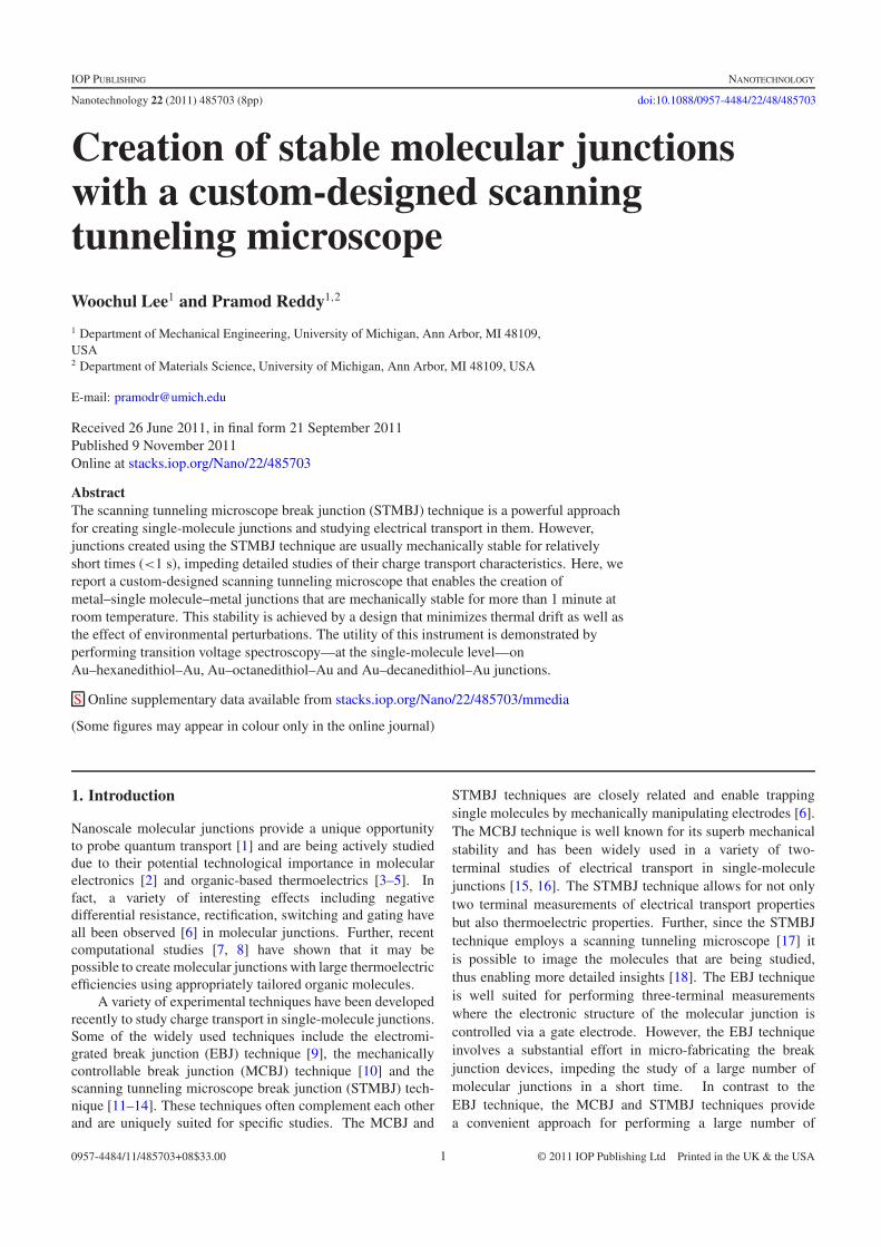
Figure 1. STM scanner assembly and radiation shield. (a) Theschematic of the sample plate. (b) The schematic of the Besockescanner featuring four piezoelectric tubes. (c) The assembly of thesample plate and the STM scanner. (d) The copper enclosure(radiation shield) which houses the scanner.
later). The Besocke scanner is chosen in the present work dueto its excellent ability to suppress thermal drift. In general,temperature changes of the entire scanner lead to a thermalexpansion/contraction of the piezoelectric tubes. In a Besockescanner, this expansion/contraction does not translate into largechanges in the spacing between the STM tip and the sampleplate. This is because the thermal expansion/contraction of theouter piezoelectric tubes supporting the sample plate is almostidentical to that of the expansion/contraction of the innerpiezoelectric tube resulting in suppression of drift between thetip and the sample. More details regarding the estimated driftof the scanner, scanner fabrication and vibration isolation areprovided in the supporting information (SI available at stacks.iop.org/Nano/22/485703/mmedia).
2.2. Temperature-controlled radiation shield
The Besocke scanner design described above allows forgood thermal compensation, ensuring that the scanner isrelatively immune to thermal drift. However, the scanner isnot completely unaffected by temperature variations. Thisis primarily due to the mismatch in the thermal expansioncoefficient of the STM tip (made of gold) and that ofthe tungsten balls mounted on the outer piezoelectric tubes(figure 1(b)). This mismatch results in a drift in thegap between the sample plate and the tip (details in SIavailable at stacks.iop.org/Nano/22/485703/mmedia) when thetemperature changes with time. Therefore, it is essential toensure that the temperature variations are very small.
2
Nanotechnology 22 (2011) 485703 W Lee and P Reddy
Although the scanner is located in a vacuum environment,it is still thermally coupled to the ambient environment wherethe temperature varies significantly, ∼2 K over a period of 24 h.This thermal coupling exists because heat can be transportedfrom the ambient environment via the springs and electricalwires that are connected to the scanner (figure 1(c)) and viathermal radiation. In order to minimize the thermal couplingwith the ambient, the scanner is placed in a copper enclosure(figure 1(d)), which acts not only as a thermal reservoir but alsoas a radiation shield. Further, the temperature of the enclosureis maintained at a constant value by a custom-built controller(proportional and integral control). The control system sensestemperature changes via a thermistor (Omega, 44033–2252 �)and attenuates them by modulating the electrical currentsupplied to an electrical heater integrated into the copperenclosure. Using this approach, it was possible to maintainthe temperature of the copper enclosure at a fixed temperature(∼5 K above the average ambient temperature) with variationsless than ±1 mK in a 3 h period (details in SI available atstacks.iop.org/Nano/22/485703/mmedia).
2.3. Scanner control and calibration
The motion of the STM scanner is controlled by a combinationof a customized real-time controller and a commercialSTM controller (RHK Technology). The commercial STMcontroller is used for the coarse and fine approach stepsthat are essential to place the STM tip in close proximityto the sample surface (i.e. the tunneling region). Further,the commercial STM controller is also used for scanningthe surface to obtain topographical information. The real-time controller is implemented using hardware from NationalInstruments (PXI8110) and is used to increase or decreasethe separation between the STM tip and the sample in smallincrements (as small as 3 pm/step). Such control is essentialfor the creation of stable molecular junctions and is discussedin detail below. In order to calibrate the piezoelectric tubes ofthe Besocke scanner, we adopted an approach similar to thatused by others in the past [22, 23]. Briefly, the X–Y scanparameters of the piezoelectric tubes were adjusted such thatthe correct topography of a highly oriented pyrolytic graphite(HOPG) sample was observed [22]. Further, the sensitivity ofthe piezoelectric tube in the Z direction (perpendicular to thesample) was calibrated by measuring the known step height ofan Au(111) terrace [23].
3. Single-molecule experiments
The stability and use of this STM is demonstrated by studyingelectron transport in single-molecule junctions created fromhexanedithiol (HDT), octanedithiol (ODT) and decanedithiol(DDT) molecules. The protocol used to create the Au–alkanedithiol–Au junctions is described first. Subsequently,the statistical analysis used for determining the conductanceof a single-molecule junction is presented. Finally, we presentresults that demonstrate that single-molecule junctions createdusing this STM are mechanically stable for extended periods(>1 min).
3.1. Creation of single-molecule junctions
The first step in the formation of Au–alkanedithiol–Aujunctions is to create a monolayer of alkanedithiol moleculeson a flat Au surface. The flat Au surface is created using atemplate stripping technique [24]. In this technique, ∼100 nmof gold is deposited on a pristine silicon wafer. Subsequently,epoxy (Epotek 377) is applied evenly on the gold-coatedsilicon wafer and a square glass piece (7 mm × 7 mm) isplaced on top of the epoxy. Next, the entire wafer is curedin an oven at ∼150 ◦C for ∼1.5 h. Later, the glass pieceis cleaved off from the silicon wafer, resulting in a verysmooth Au film (RMS value <1 nm over a 1 μm2 area)that adheres to the glass surface because of the strong bondbetween gold and epoxy. To coat the alkanedithiol moleculeson the flat Au surface, the gold substrate is immersed intoan ∼1 mM solution of alkanedithiol in ethanol for more than12 h. During this time, the alkanedithiol molecules chemicallybind to the Au surface through a thiol–Au bond [25]. Aftertaking out the alkanedithiol-coated gold substrate, the substrateis rinsed with ethanol to remove molecules that are notchemically bound to the gold surface. This concludesthe process of creating a monolayer of molecules on thesurface.
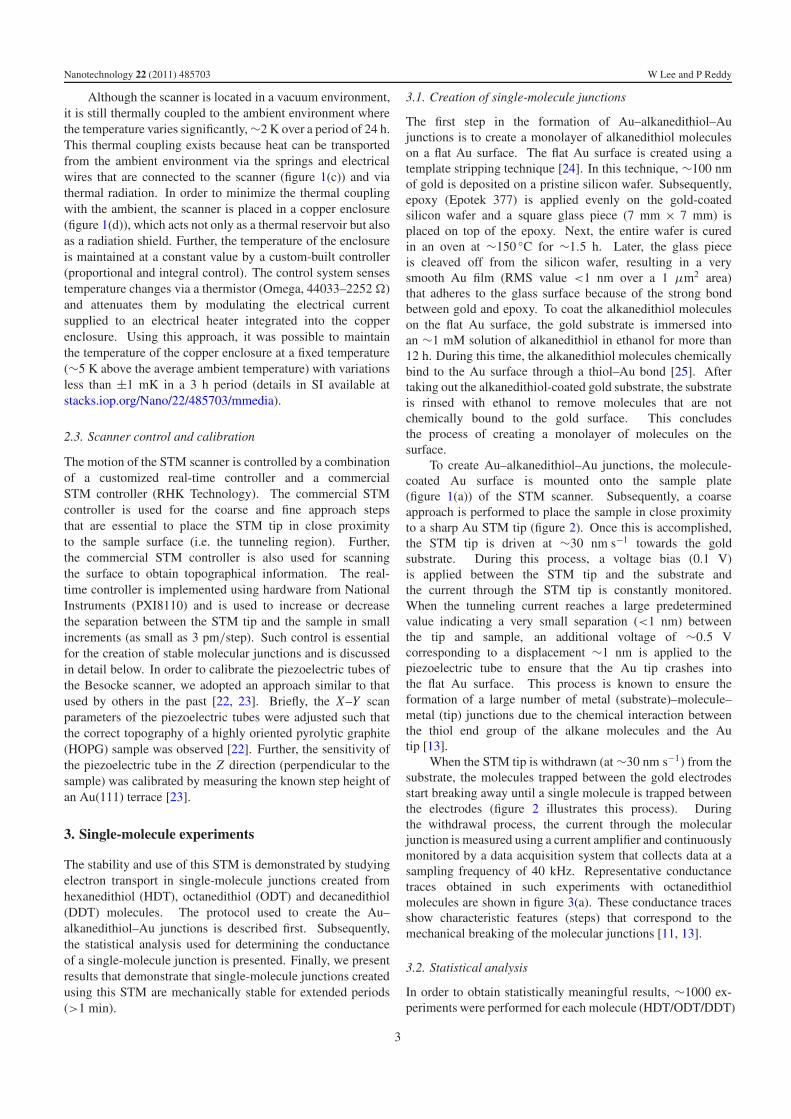
To create Au–alkanedithiol–Au junctions, the molecule-coated Au surface is mounted onto the sample plate(figure 1(a)) of the STM scanner. Subsequently, a coarseapproach is performed to place the sample in close proximityto a sharp Au STM tip (figure 2). Once this is accomplished,the STM tip is driven at ∼30 nm s−1 towards the goldsubstrate. During this process, a voltage bias (0.1 V)is applied between the STM tip and the substrate andthe current through the STM tip is constantly monitored.When the tunneling current reaches a large predeterminedvalue indicating a very small separation (<1 nm) betweenthe tip and sample, an additional voltage of ∼0.5 Vcorresponding to a displacement ∼1 nm is applied to thepiezoelectric tube to ensure that the Au tip crashes intothe flat Au surface. This process is known to ensure theformation of a large number of metal (substrate)–molecule–metal (tip) junctions due to the chemical interaction betweenthe thiol end group of the alkane molecules and the Autip [13].
When the STM tip is withdrawn (at ∼30 nm s−1) from thesubstrate, the molecules trapped between the gold electrodesstart breaking away until a single molecule is trapped betweenthe electrodes (figure 2 illustrates this process). Duringthe withdrawal process, the current through the molecularjunction is measured using a current amplifier and continuouslymonitored by a data acquisition system that collects data at asampling frequency of 40 kHz. Representative conductancetraces obtained in such experiments with octanedithiolmolecules are shown in figure 3(a). These conductance tracesshow characteristic features (steps) that correspond to themechanical breaking of the molecular junctions [11, 13].
3.2. Statistical analysis
In order to obtain statistically meaningful results, ∼1000 ex-periments were performed for each molecule (HDT/ODT/DDT)
3

Nanotechnology 22 (2011) 485703 W Lee and P Reddy
Figure 2. Schematic description of the process of creatingsingle-molecule junctions. (a) An Au STM tip and an octanedithiol(ODT)-coated Au sample are shown. A voltage bias (+0.1 V) isapplied between the STM tip and the substrate and the currentthrough the STM tip is constantly monitored (a positive biascorresponds to a scenario where the substrate is at a higher potentialthan the STM tip). The STM tip approaches the surface until itmakes mechanical contact and is withdrawn immediately aftercontact. During this process ODT molecules are trapped between theAu electrodes. (b) As the Au STM tip is withdrawn the ODTmolecules bridging the two Au electrodes start to break. Ultimately,one molecule bridges the two Au electrodes resulting in asingle-molecule junction.
to obtain conductance traces. The conductance traces wereanalyzed by building a histogram following the approachdescribed by Xu et al [11]. The conductance histogramobtained from the conductance traces of 1000 junctions of Au–ODT–Au without any data selection (conventional conductancehistogram) is shown in figure 3(b). The conductancehistograms of Au–HDT–Au and Au–DDT–Au junctions areshown in the supporting information (available at stacks.iop.org/Nano/22/485703/mmedia). The most probable values ofthe conductance of an Au–HDT–Au, Au–ODT–Au and Au–DDT–Au junction were obtained from a Gaussian fit to thehistogram and corresponds to a value of ∼2.7 × 10⁻⁴G0,∼2.2 × 10⁻⁵G0, and ∼5.2 × 10⁻⁶G0, respectively, whereG0 = 2e2/h is the quantum of electrical conductance (e is thecharge of an electron and h is Planck’s constant). Further, thefull width at half-maximum (FWHM) of the histograms werefound to be ∼5.2 × 10⁻⁴G0 (HDT), ∼6.6 × 10⁻⁵G0 (ODT)and ∼1.38 × 10⁻⁵G0 (DDT) and represent the uncertainty inthe measured conductance. In order to verify that the peak
Figure 3. Measurement of the electrical conductance of asingle-molecule junction. (a) Conductance traces obtained whilewithdrawing the STM tip from the sample at ∼30 nm s−1.(b) Conductance histogram created from 1000 Au–octanedithiol–Aujunctions (blue) shows a peak at ∼2.2 × 10⁻⁵G0. Conductancehistogram obtained in a control experiment where ODT moleculeswere not present (green) shows no peak. Conductance histogramobtained from last step analysis (red) shows a peak at∼2.6 × 10⁻⁵G0.
arises from the alkanedithiol molecules, a control experimentwas performed where measurements were performed on aclean Au surface. The histogram (green) obtained in suchan experiment is shown in figure 3(b) and does not feature apeak. Similar control experiments were performed for Au–HDT–Au and Au–DDT–Au junctions and are presented inthe supporting information (available at stacks.iop.org/Nano/22/485703/mmedia). These experiments clearly confirm thatthe peak in the histogram is obtained only in the presence ofalkanedithiol molecules.
In addition to this conventional histogram-based analysis,we also performed the last step analysis (LSA) [13], whichwas introduced by one of us, in collaboration with others, inthe past. In this analysis, the magnitude of the last step in theconductance traces, which corresponds to the conductance ofa single-molecule junction, is measured from a large number(∼1000) of conductance traces and is reported in the form
4
Nanotechnology 22 (2011) 485703 W Lee and P Reddy
of a histogram (figure 3(b), and in SI available at stacks.iop.org/Nano/22/485703/mmedia). The histograms have a peakfrom the Gaussian fit at ∼2.8 × 10⁻⁴G0 (HDT), ∼2.6 ×10⁻⁵G0 (ODT) and ∼5.5×10⁻⁶G0 (DDT). The correspondinguncertainty of FWHM is ∼3.1 × 10⁻⁴G0 (HDT), ∼4.3 ×10⁻⁵G0 (ODT) and ∼4 × 10⁻⁶G0 (DDT). The peak valueobtained using LSA corresponds well with the result obtainedusing the conventional histogram analysis above. In ourpast work using a commercial STM (molecular imaging,pico-STM) that operated in ambient conditions, it was notpossible to obtain a clear peak using conventional histogramanalysis without data selection. However, using this new ultra-stable STM, a clear peak is also observed in the conventionalconductance histogram. We hypothesize that this improvementin the quality results from the superior stability of our STM,which enhances the amount of time that the most probableconductance value of the junction is obtained in a conductancetrace.
When the measured electrical resistance of the alka-nedithiol junctions is plotted versus the number of carbonatoms in the chain (see SI available at stacks.iop.org/Nano/22/485703/mmedia), it is apparent that the electrical resistanceincreases exponentially with the length of the chain. Suchan exponential dependence of the electrical resistance on thelength of the molecules is expected because electron transportthrough Au–alkanedithiol–Au molecular junctions occurs vianonresonant tunneling. Therefore, the resistance of a single-molecule junctions is proportional to exp(β N), where N isthe number of carbon atoms in the alkanedithiol and β is thetunneling decay constant. A curve fit (see SI available at stacks.iop.org/Nano/22/485703/mmedia) to the measured electricalresistance of the Au–alkanedithiol–Au junctions suggests thatβ is ∼0.99/carbon atom and is in good agreement withprevious reports [26].
3.3. Demonstration of mechanical stability of junctions
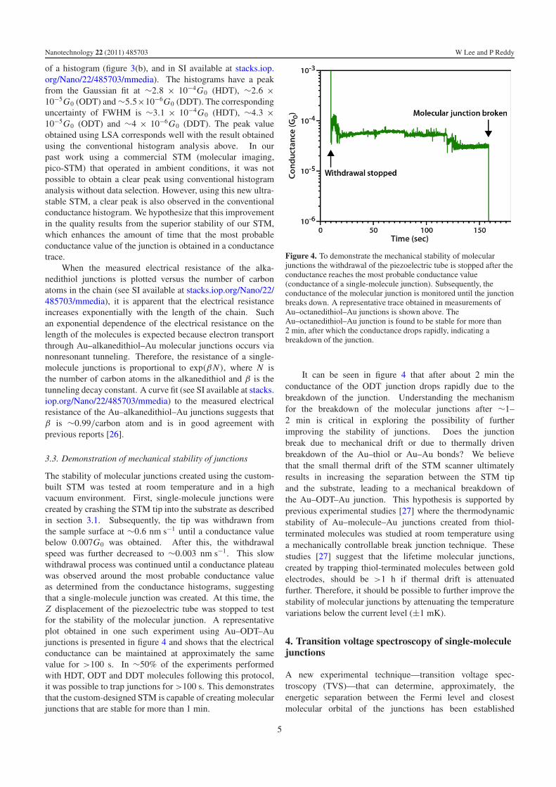
The stability of molecular junctions created using the custom-built STM was tested at room temperature and in a highvacuum environment. First, single-molecule junctions werecreated by crashing the STM tip into the substrate as describedin section 3.1. Subsequently, the tip was withdrawn fromthe sample surface at ∼0.6 nm s−1 until a conductance valuebelow 0.007G0 was obtained. After this, the withdrawalspeed was further decreased to ∼0.003 nm s−1. This slowwithdrawal process was continued until a conductance plateauwas observed around the most probable conductance valueas determined from the conductance histograms, suggestingthat a single-molecule junction was created. At this time, theZ displacement of the piezoelectric tube was stopped to testfor the stability of the molecular junction. A representativeplot obtained in one such experiment using Au–ODT–Aujunctions is presented in figure 4 and shows that the electricalconductance can be maintained at approximately the samevalue for >100 s. In ∼50% of the experiments performedwith HDT, ODT and DDT molecules following this protocol,it was possible to trap junctions for >100 s. This demonstratesthat the custom-designed STM is capable of creating molecularjunctions that are stable for more than 1 min.
Figure 4. To demonstrate the mechanical stability of molecularjunctions the withdrawal of the piezoelectric tube is stopped after theconductance reaches the most probable conductance value(conductance of a single-molecule junction). Subsequently, theconductance of the molecular junction is monitored until the junctionbreaks down. A representative trace obtained in measurements ofAu–octanedithiol–Au junctions is shown above. TheAu–octanedithiol–Au junction is found to be stable for more than2 min, after which the conductance drops rapidly, indicating abreakdown of the junction.
It can be seen in figure 4 that after about 2 min theconductance of the ODT junction drops rapidly due to thebreakdown of the junction. Understanding the mechanismfor the breakdown of the molecular junctions after ∼1–2 min is critical in exploring the possibility of furtherimproving the stability of junctions. Does the junctionbreak due to mechanical drift or due to thermally drivenbreakdown of the Au–thiol or Au–Au bonds? We believethat the small thermal drift of the STM scanner ultimatelyresults in increasing the separation between the STM tipand the substrate, leading to a mechanical breakdown ofthe Au–ODT–Au junction. This hypothesis is supported byprevious experimental studies [27] where the thermodynamicstability of Au–molecule–Au junctions created from thiol-terminated molecules was studied at room temperature usinga mechanically controllable break junction technique. Thesestudies [27] suggest that the lifetime molecular junctions,created by trapping thiol-terminated molecules between goldelectrodes, should be >1 h if thermal drift is attenuatedfurther. Therefore, it should be possible to further improve thestability of molecular junctions by attenuating the temperaturevariations below the current level (±1 mK).
4. Transition voltage spectroscopy of single-moleculejunctions
A new experimental technique—transition voltage spec-troscopy (TVS)—that can determine, approximately, theenergetic separation between the Fermi level and closestmolecular orbital of the junctions has been established
5

Nanotechnology 22 (2011) 485703 W Lee and P Reddy
recently [28, 19, 29]. In TVS the current–voltage charac-teristics of molecular junctions are analyzed by plotting aFowler–Nordheim (FN) curve, ln(I/V 2) against (1/V ). Forasymmetric molecular junctions, an FN plot is expected tofeature a minimum value for either positive or negative biasvoltages [30]. However, if the junction is symmetric the FNplot would feature two minima (one each for positive andnegative biases) that have almost the same magnitude [30].Recently, TVS has been interpreted within a coherent electrontransport model (Landauer formalism) by Huisman et al andAraidai et al [31, 29]. In this approach, the transmissionfunction of the molecular junction is computed and typicallyfeatures peaks at energies corresponding to the HOMO andLUMO orbitals of the molecular junction. Within this modelit has been suggested that the minima in the FN plot occurswhen a certain fraction of the transmission function enters thebias window between the quasi-Fermi levels of the electrodes.The minima obtained using Fowler–Nordheim curves is calledthe transition voltage (Vtrans) and is expected to approximatelyindicate the energetic separation (� ∼ |eVtrans|) between theclosest molecular orbital and the chemical potential (Fermilevel).
Recently, several researchers have used transition voltagespectroscopy to qualitatively study the effect of molecularstructure, gate voltage and molecular length on the energeticseparation of molecular junctions [28, 32, 33]. However, mostof these studies were performed either in junctions wheremultiple molecules were trapped between electrodes or insingle-molecule junctions created using the electromigratedbreak junction technique at low temperatures (4.2 K) [32, 34].Here we demonstrate the utility of the ultra-stable STMby performing TVS—in single-molecule junctions—at roomtemperature.
In order to obtain the I –V characteristics of single-molecule junctions, which are necessary for performingTVS, the withdrawal process (described in section 3.3) isstopped when the conductance equals that of a single-molecule junction. Subsequently, the voltage bias is variedlinearly between −2 and +2 V while monitoring the electriccurrent flowing through the junction. We note that, in ourexperiments, a positive bias corresponds to a scenario wherethe substrate is at a higher potential than the STM tip.Figure 5(a) shows a conductance trace for ODT reflecting theprocedure described above. The region highlighted in green(figure 5(a)) represents the location where the voltage sweepis performed. Two representative I –V characteristics obtainedin such experiments are shown in the inset of figure 5(b). Thecorresponding FN plots obtained using these I –V curves areshown in figure 5(b). The FN plot (red circles) features aminima on both sides and corresponds to the more symmetricI –V curve (solid red line in the inset of figure 5(b)). The twominima are at −0.697 V−1 and 0.6810 V−1 and correspondto transition voltages of −1.43 V and +1.47 V, respectively,suggesting an apparent energetic separation of ∼1.45 eV(between the Fermi level and the closest molecular orbital) forAu–ODT–Au junctions. The FN plot (blue squares) featuresonly one minima at ∼ − 0.63 V−1 and corresponds to theless symmetric I –V curve (dashed blue line in the inset of
Figure 5. Current–voltage (I–V ) characteristics andFowler–Nordheim plots of Au–ODT–Au junctions. (a) The Au STMtip is withdrawn until an electrical conductance of ∼2.6 × 10⁻⁵G0
(the most probable conductance value) is obtained after which thewithdrawal process is stopped (the region shown in green) and thevoltage is varied from −2 to +2 V to obtain the I–V characteristics.The conductance value remains the same after sweeping the voltagebias, indicating that the molecular junction is not destroyed by thelarge bias. (b) The inset shows two representative I–V curvesobtained in measurements. The I–V curve shown in red (solid line)is symmetric and has a Fowler–Nordheim plot (red circles) thatfeatures minima at −1.43 V and +1.47 V, respectively. The I–Vcurve shown in blue (dashed line) is asymmetric and has aFowler–Nordheim plot (blue squares) that features only one minimaat −1.6 V.
figure 5(b)). We note that for HDT, ODT and DDT junctions,among the 300 I –V curves that were obtained for each junctiononly ∼50 showed a minimum for both negative and positivevoltages. Based on past theoretical work [30, 35], we believethat the I –V characteristics that show both a positive andnegative Vtrans, with an almost identical magnitude, correspondto molecular junctions that are symmetric in their geometry.
In order to obtain statistically meaningful results, positiveand negative transition voltages were obtained in ∼50independent experiments each for Au–HDT–Au, Au–ODT–Auand Au–DDT–Au junctions. The mean value and standarddeviation of the obtained transition voltages are presented intable 1. This data suggests that for each molecular junction themeasured positive and negative transition voltages are similarin magnitude, as expected for a geometrically symmetricmolecular junction [30]. Further, the relative invariance of
6

Nanotechnology 22 (2011) 485703 W Lee and P Reddy
Table 1. To obtain statistically meaningful results, positive andnegative transition voltages were obtained in ∼50 independentsingle-molecule experiments each for Au–HDT–Au, Au–ODT–Auand Au–DDT–Au junctions. The mean value and standard deviationof the measured transition voltages are shown.
+Vtrans −Vtrans
Au–HDT–Au 1.39 ± 0.21 −1.37 ± 0.23Au–ODT–Au 1.35 ± 0.14 −1.40 ± 0.17Au–DDT–Au 1.37 ± 0.18 −1.44 ± 0.17
the magnitude of the positive and negative transition voltageswhen the length of the molecular junctions is varied indicatesthat the energetic separation between the chemical potentialand the closest molecular orbital is approximately constant inalkanedithiol junctions. This result is consistent with previousstudies [28] on alkanemonothiol junctions, where a similarlength independence was observed.
5. Discussion and conclusion
We described a custom-built STM, which enables theformation of molecular junctions that are mechanically stablefor time periods as long as 2 min at room temperature. Thisrepresents at least an order-of-magnitude improvement overthe stability observed in past STMBJ measurements. Thisimprovement is accomplished by incorporating a Besockescanner, which is relatively immune to temperature variations,by active control of the temperature, and by attenuating theeffect of acoustic and ground vibrations. We demonstratedthe utility of this stable instrument by performing transitionvoltage spectroscopy at the single-molecule level. Webelieve that this improved stability will not only enablemore detailed electrical transport studies such as transitionvoltage spectroscopy at the single-molecule level but will alsofacilitate the study of thermoelectric and thermal transportphenomena [37] in molecular junctions, where it is necessaryto perform measurements for long time periods to improvethe signal-to-noise ratio. In fact, one of the major goals ofour future work is to integrate this ultra-stable STM with apicowatt-resolution calorimeter [36] to probe heat transport inmolecular junctions with picowatt resolution.
Acknowledgments
PR gratefully acknowledges support from the NSF throughan NSF-CAREER award (CBET 0844902). WL thanksWonho Jeong for help in building the STM scanner. WL andPR thank Edgar Meyhofer for valuable discussions.
References
[1] Datta S 2005 Quantum Transport: Atom to Transistor(Cambridge: Cambridge University Press)
[2] Nitzan A and Ratner M A 2003 Electron transport in molecularwire junctions Science 300 1384–9
[3] Reddy P, Jang S Y, Segalman R A and Majumdar A 2007Thermoelectricity in molecular junctions Science315 1568–71
[4] Malen J A, Yee S K, Majumdar A and Segalman R A 2010Fundamentals of energy transport, energy conversion, andthermal properties in organic–inorganic heterojunctionsChem. Phys. Lett. 491 109–22
[5] Tan A, Balachandran J, Sadat S, Gavini V, Dunietz B D,Jang S Y and Reddy P 2011 Effect of length and contactchemistry on the electronic structure and thermoelectricproperties of molecular junctions J. Am. Chem. Soc.133 8838–41
[6] Tao N J 2006 Electron transport in molecular junctions NatureNanotechnol. 1 173–81
[7] Bergfield J P, Solis M A and Stafford C A 2010 Giantthermoelectric effect from transmission supernodes ACSNano 4 5314–20
[8] Finch C M, Garcia-Suarez V M and Lambert C J 2009 Giantthermopower and figure of merit in single-molecule devicesPhys. Rev. B 79 033405
[9] Park H, Park J, Lim A, Anderson E, Alivisatos A andMcEuen P 2000 Nanomechanical oscillations in asingle-C-60 transistor Nature 407 57–60
[10] Tsutsui M, Taniguchi M and Kawai T 2008 Local heating inmetal–molecule–metal junctions Nano Lett. 8 3293–7
[11] Xu B and Tao N 2003 Measurement of single-moleculeresistance by repeated formation of molecular junctionsScience 301 1221–3
[12] Venkataraman L, Klare J, Nuckolls C, Hybertsen M andSteigerwald M 2006 Dependence of single-moleculejunction conductance on molecular conformation Nature442 904–7
[13] Jang S Y, Reddy P, Majumdar A and Segalman R A 2006Interpretation of Stochastic events in single moleculeconductance measurements Nano Lett. 6 2362–7
[14] Mishchenko A et al 2010 Influence of conformation onconductance of biphenyl-dithiol single-molecule contactsNano Lett. 10 156–63
[15] van Ruitenbeek J M, Smit R H M, Noat Y, Untiedt C,Lang N D and van Hemert M C 2002 Measurement of theconductance of a hydrogen molecule Nature 419 906–9
[16] Dulic D, Pump F, Campidelli S, Lavie P, Cuniberti G andFiloramo A 2009 Controlled stability of molecular junctionsAngew. Chem. Int. Ed. 48 8273–6
[17] Chen C J 2008 Introduction to Scanning Runneling Microscopy(Oxford: Oxford University Press)
[18] Lafferentz L, Ample F, Yu H, Hecht S, Joachim C andGrill L 2009 Conductance of a single conjugated polymer asa continuous function of its length Science 323 1193–7
[19] Beebe J M, Kim B, Gadzuk J W, Frisbie C D andKushmerick J G 2006 Transition from direct tunneling tofield emission in metal–molecule–metal junctions Phys. Rev.Lett. 97 026801
[20] Besocke K 1987 An easily operable scanning tunnelingmicroscope Surf. Sci. 181 145–53
[21] Stipe B C, Rezaei M A and Ho W 1999 A variable-temperaturescanning tunneling microscope capable of single-moleculevibrational spectroscopy Rev. Sci. Instrum. 70 137–43
[22] Osing J and Shvets I V 1998 Bulk defects in graphite observedwith a scanning tunnelling microscope Surf. Sci. 417 145–50
[23] Hallmark V M, Chiang S, Rabolt J F, Swalen J D andWilson R J 1987 Observation of atomic corrugation onAu(111) by scanning tunneling microscopy Phys. Rev. Lett.59 2879
[24] Hegner M, Wagner P and Semenza G 1993 Ultralargeatomically flat template-stripped Au surfaces for scanningprobe microscopy Surf. Sci. 291 39–46
[25] Love J C, Estroff L A, Kriebel J K, Nuzzo R G andWhitesides G M 2005 Self-assembled monolayers ofthiolates on metals as a form of nanotechnology Chem. Rev.105 1103–69
[26] Engelkes V B, Beebe J M and Frisbie C D 2004Length-dependent transport in molecular junctions based onSAMs of alkanethiols and alkanedithiols: effect of metalwork function and applied bias on tunneling efficiency andcontact resistance J. Am. Chem. Soc. 126 14287–96
7

Nanotechnology 22 (2011) 485703 W Lee and P Reddy
[27] Tsutsui M, Shoji K, Morimoto K, Taniguchi M andKawai T 2008 Thermodynamic stability of single moleculejunctions Appl. Phys. Lett. 92 223110
[28] Beebe J M, Kim B, Frisbie C D and Kushmerick J G 2008Measuring relative barrier heights in molecular electronicjunctions with transition voltage spectroscopy ACS Nano2 827–32
[29] Huisman E H, Guedon C M, van Wees B J andvan der Molen S J 2009 Interpretation of transition voltagespectroscopy Nano Lett. 9 3909–13
[30] Mirjani F, Thijssen J M and van der Molen S J 2011Advantages and limitations of transition voltagespectroscopy: a theoretical analysis Phys. Rev. B 84 115402
[31] Araidai M and Tsukada M Theoretical calculations of electrontransport in molecular junctions: inflection behavior inFowler–Nordheim plot and its origin Phys. Rev. B81 235114
[32] Song H, Kim Y, Jang Y H, Jeong H, Reed M A and Lee T 2009Observation of molecular orbital gating Nature 462 1039–43
[33] Tan A, Sadat S and Reddy P Measurement of thermopower andcurrent–voltage characteristics of molecular junctions toidentify orbital alignment Appl. Phys. Lett. 96 013110
[34] Song H, Kim Y, Jeong H, Reed M A and Lee T 2010 Coherenttunneling transport in molecular junctions J. Phys. Chem. C114 20431–5
[35] Chen J Z, Markussen T and Thygesen K S 2010 Quantifyingtransition voltage spectroscopy of molecular junctions: abinitio calculations Phys. Rev. B 82 121412
[36] Sadat S, Chua Y J, Lee W, Ganjeh Y, Kurabayashi K,Meyhofer E and Reddy P 2011 Room temperaturepicowatt-resolution calorimetry Appl. Phys. Lett. 99 043106
[37] Dubi Y and Di Ventra M 2011 Colloquium: Heat flow andthermoelectricity in atomic and molecular junctions Rev.Mod. Phys. 83 131–55
8