Atomic scale modifications of hydrogen-terminated silicon 2×1 and 3×1 (001) surfaces by scanning...
12
Surface Science 411 (1998) 203–214 Atomic scale modifications of hydrogen-terminated silicon 2×1 and 3×1 ( 001 ) surfaces by scanning tunneling microscope C. Thirstrup a,b,*, M. Sakurai a, T. Nakayama a, M. Aono a,c a The Institute of Physical and Chemical Research (RIKEN), Wako, Saitama 351-01, Japan b Core Research for Evolutional Science and Technology (CREST) Program, Japan Science and Technology Corporation (JST), Tokyo, Japan c Department of Precision Science and Technology, Osaka University, Suita, Osaka 565, Japan Received 4 November 1997; accepted for publication 5 May 1998 Abstract Atomic scale desorption and deposition of hydrogen (H) atoms on Si(001)-(2×1)-H and Si(001)-(3×1)-H surfaces have been studied using clean and H covered tips from a scanning tunneling microscope. We report desorption of H atoms from these surfaces at positive and negative sample bias voltages with a resolution of one to two atomic rows and atomic scale phase transitions from 3×1 structures to 2×1 structures and vice versa. At positive sample bias, phase transitions from the 3×1 to 2×1 structures are accompanied with a large number of dangling bonds on the newly crated 2×1 structures, because the desorption of H from the 2×1 structure occurs at a lower tunnel current than the formation of the phase transition. At negative sample bias <-5 V, the situation is reversed with the desorption from the 2×1 structure occurring at a larger tunnel current than the formation of the phase transition, and ‘‘clean’’ local 2×1 structures with few dangling bonds can be achieved. Using H covered tips and increasing the substrate temperatures of Si(001)-(2×1)-H surfaces to #400 K, opposite local phase transitions from 2×1 structure to 3×1 structures are also reported, but such phase transitions were only observed at negative sample bias. © 1998 Elsevier Science B.V. All rights reserved. Keywords: Hydrogen; Scanning tunneling microscopy; Silicon; Surface relaxation and reconstruction; Surface thermodynamics 1. Introduction reconstructed surfaces. The desorption mechanism has been related to vibrational heating by inelastic scattering of electrons in the case of positive sample Because of its potential applications to creation bias [ 5 ], and a similar mechanism based on desorp- of novel atomic- to nanometer-scale electronic tion via a hole resonance has recently been devices, atomic scale modifications of hydrogen reported for the case of negative sample bias [8]. (H ) atoms on H-terminated silicon (Si) surfaces Using an STM, the work reported here focuses on using the tip of a scanning tunneling microscope other aspects of atomic scale manipulations of H (STM ) have been studied recently by many groups on H-terminated Si(001) surfaces reconstructed in [1–8]. Until now, most work has focused on 2×1 and 3×1 structures, i.e. Si(001)-(2×1)-H desorbing H from H-terminated Si(001)2×1- and Si(001)-(3×1)-H surfaces, respectively. It will be shown that H can be desorbed on the atomic scale from these surfaces at both polarities of * Corresponding author: Tel: +81 48-462-1111 (x3124); fax: +81 48-462-4656; e-mail: [email protected] sample bias voltage. In the case of the Si(001)- 0039-6028/98/$ see front matter © 1998 Elsevier Science B.V. All rights reserved. PII: S0039-6028(98)00364-1
Transcript of Atomic scale modifications of hydrogen-terminated silicon 2×1 and 3×1 (001) surfaces by scanning...

Surface Science 411 (1998) 203–214
Atomic scale modifications of hydrogen-terminated silicon 2×1and 3×1 (001) surfaces by scanning tunneling microscope
C. Thirstrup a,b,*, M. Sakurai a, T. Nakayama a, M. Aono a,ca The Institute of Physical and Chemical Research (RIKEN), Wako, Saitama 351-01, Japan
b Core Research for Evolutional Science and Technology (CREST) Program, Japan Science and Technology Corporation (JST), Tokyo,Japan
c Department of Precision Science and Technology, Osaka University, Suita, Osaka 565, Japan
Received 4 November 1997; accepted for publication 5 May 1998
Abstract
Atomic scale desorption and deposition of hydrogen (H) atoms on Si(001)-(2×1)-H and Si(001)-(3×1)-H surfaces have beenstudied using clean and H covered tips from a scanning tunneling microscope. We report desorption of H atoms from these surfacesat positive and negative sample bias voltages with a resolution of one to two atomic rows and atomic scale phase transitions from3×1 structures to 2×1 structures and vice versa. At positive sample bias, phase transitions from the 3×1 to 2×1 structures areaccompanied with a large number of dangling bonds on the newly crated 2×1 structures, because the desorption of H from the 2×1structure occurs at a lower tunnel current than the formation of the phase transition. At negative sample bias <−5 V, the situation isreversed with the desorption from the 2×1 structure occurring at a larger tunnel current than the formation of the phase transition,and ‘‘clean’’ local 2×1 structures with few dangling bonds can be achieved. Using H covered tips and increasing the substratetemperatures of Si(001)-(2×1)-H surfaces to #400 K, opposite local phase transitions from 2×1 structure to 3×1 structures are alsoreported, but such phase transitions were only observed at negative sample bias. © 1998 Elsevier Science B.V. All rights reserved.
Keywords: Hydrogen; Scanning tunneling microscopy; Silicon; Surface relaxation and reconstruction; Surface thermodynamics
1. Introduction reconstructed surfaces. The desorption mechanismhas been related to vibrational heating by inelasticscattering of electrons in the case of positive sampleBecause of its potential applications to creationbias [5], and a similar mechanism based on desorp-of novel atomic- to nanometer-scale electroniction via a hole resonance has recently beendevices, atomic scale modifications of hydrogenreported for the case of negative sample bias [8].(H) atoms on H-terminated silicon (Si) surfacesUsing an STM, the work reported here focuses onusing the tip of a scanning tunneling microscopeother aspects of atomic scale manipulations of H(STM) have been studied recently by many groupson H-terminated Si(001) surfaces reconstructed in[1–8]. Until now, most work has focused on2×1 and 3×1 structures, i.e. Si(001)-(2×1)-Hdesorbing H from H-terminated Si(001)2×1-and Si(001)-(3×1)-H surfaces, respectively. It willbe shown that H can be desorbed on the atomicscale from these surfaces at both polarities of* Corresponding author: Tel: +81 48-462-1111 (x3124);
fax: +81 48-462-4656; e-mail: [email protected] sample bias voltage. In the case of the Si(001)-
0039-6028/98/$ see front matter © 1998 Elsevier Science B.V. All rights reserved.PII: S0039-6028 ( 98 ) 00364-1

204 C. Thirstrup et al. / Surface Science 411 (1998) 203–214
(3×1)-H surface, phase transitions on the atomicscale from the 3×1 structure to the 2×1 structurecan be obtained at both polarities of bias voltage.At positive sample bias, the phase transitions areaccompanied by a large number of dangling bondson the newly created 2×1 structures, because thedesorption from the 2×1 structure occurs at alower tunnel current than the formation of thephase transition. For negative sample bias <−5 V,desorption from 2×1 structures occur at a highertunnel current than the formation of the phasetransition and local 2×1 structures with few dan-gling bonds can be achieved. Using H coveredtungsten tips at substrate temperatures of Si(001)-(2×1)-H surfaces around 400 K, opposite phasetransitions from 2×1 structures to 3×1 structureshave also been obtained at negative sample bias.
2. Experimental
All experiments were performed in an ultra-highvacuum ( UHV ) chamber with a base pressure of#1×10⁻⁸ Pa using a commercial STM (JEOLCorp., JSTM4000XV ) and electrolytically sharp-ened tungsten ( W ) tips. Antimony-doped(1×1018 cm−3) n-type Si(001) samples wereheated at 1500 K in UHV in order to obtain cleanSi(001)-(2×1) surfaces. The Si(001)-(2×1) sur-faces were exposed to atomic H, produced bydissociating H2 using a hot tungsten filament atsample temperatures of 600 K and 400 K to obtainthe Si(001)-(2×1)-H and Si(001)-(3×1)-H sur-face structures, respectively [4,9]. Alternatively,the 3×1 surface could be obtained by exposingthe 2×1 H-terminated surface to atomic H at asubstrate temperature of 400 K with a similarresult. Unless otherwise stated, the STM imagespresented in this paper are filled state imagesrecorded at a sample bias of Vs=−2 V and atunnel current of It=0.2 nA.
Fig. 1. Filled state STM images of (a) the S(001)-(2×1)-H sur-3. Results and discussions face and (b) the Si(001)-(3×1)-H prepared as described in
the text.3.1. 2×1 and 3×1 reconstructed surfaces
reconstructed surfaces prepared as describedabove. The 2×1 reconstructed surface consists ofFig. 1 shows filled state STM images of the
H-terminated Si(001)-(2×1) (a) and -(3×1) (b) terraces with atomic steps at the boundaries

205C. Thirstrup et al. / Surface Science 411 (1998) 203–214
between them and an array of continuous dimer- hydride rows in the 2×1 structure. According tothe empty state image (Fig. 2(a)), the electronicized monohydride rows perpendicular to each
other from one terrace to the next [10–13]. The states for the monohydride rows are essentially inphase with the electronic states for the dihydride3×1 reconstructed surface deviates from the 2×1
reconstructed surface by comprising domains of rows; but in the filled state images (see Fig. 2(b)),the electronic states for the dihydride rows arealternating dihydride rows and dimerized monohy-
dride rows [10,12] on each terrace. In Fig. 1, the displaced compared with the monohydride rows.If the STM images are interpreted as a result ofnumber of defects on the 3×1 reconstructed sur-
face is approximately 2.5% being larger than that probing the H atomic orbitals [14], this picturecan be understood by the schematics in Fig. 2(c).on the 2×1 reconstructed surface #1.2%. This is
presumably due to an increased amount of etching The H atoms on a dihydride row in the 3×1structure are almost in phase with the H atoms onby H atoms on this surface, since creation of local
1×1 structures on the surface will cause repulsive the left or right part of a monohydride dimer rowin the 2×1 structure (in Fig. 2(c), see the rowsinteraction between the dihydride units weakening
the Si–Si back bond and creating etching pits in between the arrows in I and II ). Similarly, the Hatoms on the left (right) part of a monohydridethe surface [12]. The bright spots on both surfaces
are due to exposed Si dangling bonds on monohy- dimer row in the 2×1 structure are almost inphase with the right ( left) part of a monohydridedride sites, since the H coverage is not 100%
complete. dimer row in the 3×1 structure (in Fig. 2(c), seethe rows between the arrows in III and IV ). InIf the temperature of the Si(001) substrates lies
in between 400 and 600 K during the H exposure the filled state image in Fig. 2(b), local maximain the corrugation are close to the center of bothprocedure as described in Section 2, local domains
of 3×1 structure on the 2×1 structure may be the monohydride rows and the dihydride rows,and as expected from Fig. 2(c) resulting in theformed on the surface. As will be shown in
Section 3.3, the STM tip can be employed to create phase shift between these rows in the 2×1 structureand 3×1 structure.such local domains of 2×1 structures on a 3×1
structure or vice versa. Fig. 2 focuses on the bound-ary between the two types of structures by means 3.2. H desorption from the Si(001)-(2×1)-H
surfaceof three-dimensional plots of (a) an empty stateSTM image with a sample bias voltageVs=+1.0 V and a tunnel current It=0.2 nA; and Fig. 3 shows filled-state STM images of the
Si(001)-(2×1)-H surface, where the bright lines(b) a filled state STM image with Vs=−1.0 V andIt=0.2 nA. Fig. 2(c) is a schematic top view of the running from the top right to the bottom left are
chains of Si dangling bonds (DBs) created byboundary corresponding to the region highlightedby solid rectangles in the STM images in (a) and desorbing H atoms scanning the STM tip along a
monohydride dimer row. The desorptions of H(b). Fig. 2(d) shows schematic cross-sectionalviews of the 2×1 structure and the 3×1 structure, were performed in constant current feedback mode
at a scan speed of vs=2 nm s−1 and (a) a samplerespectively. In the empty state image as shown in(a), the dimers of the monohydrides of the 2×1 bias voltage Vs=−7.0 V, a tunnel current
It=3.0 nA; (b) Vs=+3.5 V, It=3.0 nA. Thestructure and 3×1 structure appear as brightresolved rows of pairs of electronic states and the results show that desorption is possible at both
polarities of Vs. It has been possible to desorb Hdihydrides appear as dark single rows of electronicstates. In the filled state image, both the monohy- atoms using such line scans by the STM at both
polarities of sample bias for temperatures rangingdrides and the dihydrides appear as dark rows ofelectronic states, the corrugation of the dihydride from 300 K to 600 K [15,16 ].
The widths of the bright lines in each image inrows being lower than the corrugation of themonohydride rows. The monohydride rows in the Fig. 3 are approximately equal to one monohy-
dride dimer row indicating that the resolution of3×1 structure seem almost identical to the mono-

206 C. Thirstrup et al. / Surface Science 411 (1998) 203–214
Fig. 2. Three-dimensional plots of the boundary region between a 2×1 structure and a 3×1 structure on the Si(001)-H terminatedsurface, (a) empty state STM image with Vs=1.0 V and It=0.2 nA and (b) filled state STM image with Vs=−1.0 V andIt=0.2 nA; (c) schematic top view of the boundary between the 2×1 structure and 3×1 structure corresponding to the region in (a)and (b) highlighted by a solid rectangle, and (d) schematic cross-sectional views of the 2×1 structure and the 3×1 structure. In (d),the dashed line marks the boundary between the two structures and the arrows in I, II, III and IV point to rows of atoms as discussedin the text.
this lithography is #1 nm. Some of the DBs on and C as depicted in Fig. 3(c). In A, one H atomis desorbed from the left of a dimer; in B, one Hthe surface observed away from the bright line in
Fig. 3(a) were generated during the line scan of atom is desorbed from the right of a dimer; andin C, two H atoms are desorbed from a dimer. Asthe STM tip and they are due to the probabilistic
process of H desorption. In the STM images, three observed in Fig. 3, all three processes are possiblefor both polarities of Vs.different extraction processes are indicated A, B

207C. Thirstrup et al. / Surface Science 411 (1998) 203–214
Fig. 4. Schematic diagram of the two phase transition (PT)processes observed between the 2×1 structure and the 3×1structure on a Si(001)-H surface; (A) 2 H atoms are desorbedfrom a unit consisting of one monohydride and two dihydrideson the 3×1 structure and after reconstruction into two mono-hydrides, the 2×1 structure is created; (B) 2 H atoms are depos-ited (from the STM tip) onto two monohydrides on the 2×1structure and after reconstruction into two dihydrides and onemonohydride, the 3×1 structure is created.
3.3. Local phase transitions between (3×1) and(2×1) reconstructed surfaces
Any phase transition (PT) between the 2×1structure and the 3×1 structure only affects thetop layer of H atoms and the Si adatom layer (seeFig. 2(c)) and as will be shown in this section, theSTM tip can induce PTs in both directions betweenthe 2×1 and 3×1 structures. This is illustratedschematically in Fig. 4, where a PT from the 3×1structure to the 2×1 structure (A) can be obtainedby removing two H atoms from a unit consistingof one monohydride and two dihydrides on the3×1 structure. A subsequent phase reconstructionyields the 2×1 structure consisting of two monohy-drides. The opposite process (B) from the 2×1
Fig. 3. Filled state images of Si dangling bonds due to H desorp-tion from the Si(001)-(2×1)-H surface at T=300 K scanning (A) 1 H being desorbed from the left side of a dimer row, (B)the STM tip along a dimer row at a speed vs=2 nm s−1 and 1 H being desorbed from the right side of a dimer row, and (C)(a) Vs=−7 V and It=3.0 nA and (b) Vs=+3.5 V and 2 H being desorbed from both sides of a dimer row. The corre-It=3.0 nA. In (c), three different desorption sites are illustrated, sponding sites are indicated in (a) and (b).

208 C. Thirstrup et al. / Surface Science 411 (1998) 203–214
structure to 3×1 structure requires supply of twoH atoms per unit.
3.3.1. Phase transitions from (3×1) to (2×1)Fig. 5(a) shows a filled state STM image of the
Si(001)-(3×1)-H surface. The STM tip wasscanned along a line from the top right to thebottom left of Fig. 5(a) at vs=2 nm s−1,Vs=−7 V, It=0.1 nA and a substrate temper-ature Ts=300 K. The filled state STM imagerecorded after this procedure is shown in Fig. 5(b).There is a small number of bright spots along thetip scan corresponding to exposed DBs. In thelower left part of this image, the line scan wasperpendicular to the hydride rows and in theregions to the left of the arrow head, 3×1 struc-tures have locally been transformed into 2×1structures.
Scanning the tip parallel to the hydride rowsyields a similar PT. This can be observed inFig. 6, where the STM tip was scanned along aline from the top left to the bottom right atTs=300 K, vs=2 nm s−1 and (a) Vs=−7 V,It=4.0 nA, (b) Vs=−5 V, It=8.0 nA and (c)Vs=+5 V, It=0.27 nA. The arrow heads in Fig. 6point to regions where the PTs have occurred. ForVs=−7 V (a), the PT is most clear occurring witha small number of DBs on the newly created 2×1structures. Note that the widths of the PTs (inFig. 5(b) and Fig. 6(a)) are approximately equalto the width of two monohydride dimer rows, i.e.#2d where d=0.768 nm (two of the four rows inFig. 6(a) pointed to by the arrow heads are partof the neighboring 3×1 structures). In general,however, scanning perpendicular or parallel to thehydride rows does not yield the same resolution in Fig. 5. Filled state STM images of the Si(001)-(3×1)-H surface
at Ts=300 K, (a) before modification and (b) the same area asthe PT. As the tunnel current increases, the width(a) after scanning the STM tip from the top right to the bottomof the PT region becomes larger; but in the caseleft and perpendicular to the hydride rows in the bottom leftof parallel scan to the hydride rows (Fig. 6), thepart of (a) at vs=2 nm s−1, Vs=−7 V and It=0.1 nA. Phase
width increases in steps of 2d=1.54 nm and in the transitions (PTs) from 3×1 structures to 2×1 structures havecase of perpendicular scan to the hydride rows occurred in the regions to the left of the arrow head in (b).(Fig. 5), the width increases in steps equal to thedistance between two dimers on the same dimer scan the H atoms are almost completely extractedrow, i.e. #0.38 nm. from the 2×1 structures and the PT can just be
The PT in Fig. 6(b) and (c) with Vs=−5 V and discerned on the sides of the line scan. Performing+5 V, respectively, occurs with an increasing line scans of the STM tip at lower currents innumber of DBs on the newly created 2×1 struc- these cases yielded a smaller number of DBs, but
also a correspondingly smaller number of PT sites.tures. In the case of Vs=+5 V, during the line

209C. Thirstrup et al. / Surface Science 411 (1998) 203–214
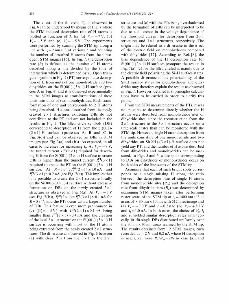
Fig. 7. STM induced desorption rate of H atoms plotted asfunction of It for (a) Vs=−7 V, (b) Vs=−5 V and (c)Vs.=+5 V. Triangular open symbols correspond to desorptionof H atoms from the Si(001)-(3×1)-H surface which exhibit aphase transition (PT) from the 3×1 structure to the 2×1 struc-ture. Filled circular symbols correspond to desorption of Hatoms from the Si(001)-(2×1)-H surface exhibiting danglingbonds (DBs) on the surface.
Fig. 6. Filled state STM images of the Si(001)-(3×1)-H surface Vs=+5 V, It.=0.27 nA. The arrow heads point to regions withat Ts=300 K, after scanning the STM tip from the top left to phase transitions (PTs) from 3×1 structures to 2×1 structures.the bottom right in each image at vs=2 nm s−1, and (a) Note that the number of dangling bonds (DBs) on the newlyVs=−7 V, It=4.0 nA, (b) Vs=−5 V, It.=8.0 nA and (c) created 2×1 structures increase from (a) to (c).
210 C. Thirstrup et al. / Surface Science 411 (1998) 203–214
The effect of the different Vs as observed in structure and (c) with the PTs being overshadowedby the formation of DBs can be interpreted to beFig. 6 can be understood by means of Fig. 7 where
the STM induced desorption rate of H atoms is due to a difference in the voltage dependence ofthe threshold current for desorption from 2×1plotted as function of It for (a) Vs=−7 V, (b)
Vs=−5 V and (c) Vs=+5 V. The experiments structures and 3×1 structures, respectively. Theorigin may be related to a difference in the effectwere performed by scanning the STM tip along a
line with vs=2 nm s−1 at various It and counting of the electric field on monohydrides comparedwith dihydrides [17]. According to Ref. [8], thethe number of desorbed H atoms from the subse-
quent STM images [16]. In Fig. 7, the desorption bias dependence of the H desorption rate forSi(001)-(2×1)-H surfaces (compare the results inrate (R) is defined as the number of H atoms
desorbed along a line divided by the time of Fig. 7(a)–(c) for the filled circles) is mainly due tothe electric field polarizing the Si–H surface states.interaction which is determined by vs. Open trian-
gular symbols in Fig. 7 (PT) correspond to desorp- A possible difference in the polarizability of theSi–H surface states for monohydrides and dihy-tion of H from units of one monohydride and two
dihydrides on the Si(001)-(3×1)-H surface (pro- drides may therefore explain the results as observedin Fig. 7. However, detailed first principles calcula-cess A in Fig. 4) and it is observed experimentally
in the STM images as transformations of these tions have to be carried in order to clarify thispoint.units into units of two monohydrides. Each trans-
formation of one unit corresponds to 2 H atoms From the STM measurements of the PTs, it wasnot possible to determine directly whether the Hbeing desorbed. H atoms desorbed from the newly
created 2×1 structures exhibiting DBs do not atoms were desorbed from monohydride sites ordihydride sites, since the reconstruction from thecontribute to the PT and are not included in the
results in Fig. 7. The filled circle symbols (DB) 2×1 structure to the 3×1 structure occurs on atime scale faster than can be monitored with thecorrespond to desorption of H from the Si(001)-
(2×1)-H surface (processes A, B and C in STM tip. However, single H atom desorption fromthe units consisting of one monohydride and twoFig. 3(c)) and can be observed as DBs in STM
images (see Fig. 3(a) and (b)). As expected, in all dihydrides on Si(001)-(3×1)-H surface does notyield any PT, and the number of H atoms desorbedcases R increases for increasing It. At Vs=−7 V,
the tunnel current I tDB(2×1) required for desorb- from dihydrides and monohydrides can be mea-sured. In Figs. 5 and 6, white spots correspondinging H from the Si(001)-(2×1)-H surface to create
DBs is higher than the tunnel current I tPT(3×1) to DBs on dihydrides or monohydrides occur onboth sides of the line scans of the STM tip.required to create the PT on the Si(001)-(3×1)-H
surface. At R=5 s−1, I tDB(2×1)≈1.0 nA and Assuming that each of such bright spots corres-ponds to a single missing H atom, the ratioI tPT(3×1)≈0.2 nA (see Fig. 7(a)). This implies that
it is possible to create the 2×1 structure locally between the desorption rate of single H atomsfrom monohydride sites (Rm) and the desorptionon the Si(001)-(3×1)-H surface without excessive
formation on DBs on the newly created 2×1 rate from dihydride sites (Rd) was determined byexamining STM images taken after performingstructure as observed in Fig. 6(a). At Vs=−5 V
(see Fig. 7(b)), I tDB(2×1)≈I tPT(3×1)≈0.1 nA for raster scans of the STM tip at vs=1400 nm s−1 atareas of ~30 nm×30 nm with 512 lines/image andR=5 s−1, and the PTs occur with a larger number
of DBs. This feature is even more pronounced in (a) Vs=−7.0 V and It=0.2 nA; (b) Vs=+3.5 Vand It=1.0 nA. In both cases, the choice of Vs, It(c) ((Vs=+5 V ) with I tDB(2×1)≈0.1 nA being
smaller than I tPT(3×1)≈0.4 nA and the creation and vs yielded similar desorption rates with typi-cally 30–50 single DBs distributed uniformly overof the local 2×1 structure on the Si(001)-(3×1)-H
surface is occurring with most of the H atoms the 30 nm×30 nm areas scanned by the STM tip.The results obtained from 12 STM images, eachbeing extracted from the newly created 2×1 struc-
tures. The difference as observed in Fig. 6 between recorded at −2 V and 0.2 nA where H desorptionis negligible, were Rd/Rm=7% in case (a), and(a) with clear PTs from the 3×1 to the 2×1
211C. Thirstrup et al. / Surface Science 411 (1998) 203–214
Rd/Rm=3% in case (b). In both cases, desorptionoccurs preferentially from monohydrides. This isin contrast to thermal desorption of H2 whichoccurs preferentially from dihydride sites [18].
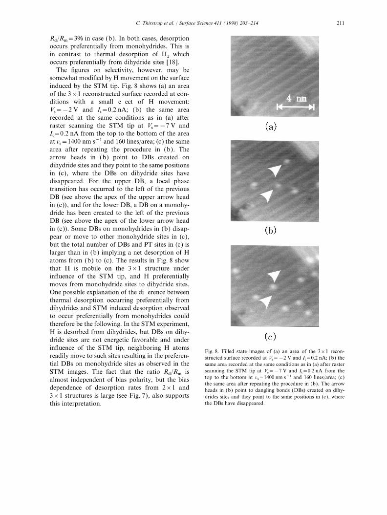
The figures on selectivity, however, may besomewhat modified by H movement on the surfaceinduced by the STM tip. Fig. 8 shows (a) an areaof the 3×1 reconstructed surface recorded at con-ditions with a small effect of H movement:Vs=−2 V and It=0.2 nA; (b) the same arearecorded at the same conditions as in (a) afterraster scanning the STM tip at Vs=−7 V andIt=0.2 nA from the top to the bottom of the areaat vs=1400 nm s−1 and 160 lines/area; (c) the samearea after repeating the procedure in (b). Thearrow heads in (b) point to DBs created ondihydride sites and they point to the same positionsin (c), where the DBs on dihydride sites havedisappeared. For the upper DB, a local phasetransition has occurred to the left of the previousDB (see above the apex of the upper arrow headin (c)), and for the lower DB, a DB on a monohy-dride has been created to the left of the previousDB (see above the apex of the lower arrow headin (c)). Some DBs on monohydrides in (b) disap-pear or move to other monohydride sites in (c),but the total number of DBs and PT sites in (c) islarger than in (b) implying a net desorption of Hatoms from (b) to (c). The results in Fig. 8 showthat H is mobile on the 3×1 structure underinfluence of the STM tip, and H preferentiallymoves from monohydride sites to dihydride sites.One possible explanation of the difference betweenthermal desorption occurring preferentially fromdihydrides and STM induced desorption observedto occur preferentially from monohydrides couldtherefore be the following. In the STM experiment,H is desorbed from dihydrides, but DBs on dihy-dride sites are not energetic favorable and underinfluence of the STM tip, neighboring H atoms
Fig. 8. Filled state images of (a) an area of the 3×1 recon-readily move to such sites resulting in the preferen- structed surface recorded at Vs=−2 V and It=0.2 nA; (b) thetial DBs on monohydride sites as observed in the same area recorded at the same conditions as in (a) after raster
scanning the STM tip at Vs=−7 V and It=0.2 nA from theSTM images. The fact that the ratio Rd/Rm istop to the bottom at vs=1400 nm s−1 and 160 lines/area; (c)almost independent of bias polarity, but the biasthe same area after repeating the procedure in (b). The arrow
dependence of desorption rates from 2×1 and heads in (b) point to dangling bonds (DBs) created on dihy-3×1 structures is large (see Fig. 7), also supports drides sites and they point to the same positions in (c), where
the DBs have disappeared.this interpretation.

212 C. Thirstrup et al. / Surface Science 411 (1998) 203–214
3.3.2. Phase transitions from (2×1) to (3×1) reconstruction of H on Si(001) surfaces using thestandard method as described in Section 3.1Raising the temperature of the substrate to
Ts#400 K and supplying H atoms to the surface [10,12]. At room temperature, the thermal energymay be too low for the deposited H atoms tofrom an H-covered STM tip, it is also possible to
change the phase of H locally on Si(001)-(2×1)-H create dihydrides or the H atoms are less likely todeposit from the STM tip. At higher temperatures,surfaces from the 2×1 structure to the 3×1 struc-
ture (process B in Fig. 4). Before making the the dihydride phase will be decomposed into themonohydride phase [12] and PTs do not occur.modification experiment, H atoms were picked up
from the surface onto the tip apex by scanning the We did not observe any PT from the 2×1 structureto the 3×1 structure at positive Vs at any substrateSTM tip at high voltage and current conditions
until a large number of H atoms had accumulated temperature; one possible explanation being thatfor Vs and It of adequate magnitude to remove Hon the tip. Fig. 9 shows filled state STM images
of (a) the Si(001)-(2×1)-H surface at Ts=380 K from the tip, the desorption of H from the surfacedominates and the number of H atoms suppliedbefore the modification and (b) the same area
after scanning the tip along a line from the top from the tip is insufficient to create the PT.left to the bottom right using vs=2 nm s−1,Vs=−8.5 V and It=5.0 nA. Using this conditionwith a clean STM tip would yield a larger number 4. Conclusionsof H atoms to be desorbed from the surface.
It is observed that H atoms have been partly H atoms on Si(001)-(2×1)-H and Si(001)-(3×1)-H surfaces were desorbed and depositeddesorbed along the line scan exhibiting the exposed
DBs in the image in Fig. 9(b), and a number of locally by means of an STM tip, and atomic scaledesorptions from these surfaces were obtained atnew DBs have also been created away from the
line scan owing to the probabilistic process of both polarities of sample bias voltage. Dependingon the substrate temperature, sample bias voltageatomic manipulation (compare with Fig. 3(a)). To
the left and to the right of the arrow heads, the and the conditions of the STM tip, local phasetransitions from 2×1 structures to 3×1 structures2×1 structure has been transformed into domains
of 3×1 structure owing to deposition of H atoms and vice versa could be made. At a negative samplebias of −7 V, local phase transitions from thefrom the tip and subsequent reconstruction.
However, the regions underneath the STM tip line 3×1 structure to the 2×1 structure were achievedwith a resolution of two monohydride rows. Sincescan have retained their 2×1 structure (see the
region to the left of the arrow with a rod in desorption from the 2×1 structure in this caseoccurs at a higher tunnel current than the forma-Fig. 9(b)). This is also expected according to
Fig. 7(a). Even if 2×1 structures were created tion of the phase transition, the number of dan-gling bonds on the newly created 2×1 structuresunder the tip, they would disappear since at nega-
tive Vs, H atoms are more readily desorbed from was low. In contrast, at a positive sample bias of+5 V the current required for desorption from thethe 3×1 structure than from the 2×1 structure.
However, on the sides of the line scan of the tip 2×1 structure is lower than that required to createthe phase transition on the Si(001)-(3×1)-H sur-where the desorption rate of H atoms by the STM
tip is low, segments of 3×1 structure have been face implying that phase transitions from 3×1 to2×1 structures were accompanied by a largeformed. Note that these PTs have occurred over
an area with a width of 10–20 nm. number of dangling bonds on the newly created2×1 structures.Similar PT formations could be observed at a
higher substrate temperature of 450 K; but in For both polarities of sample bias, single Hatom desorption from Si(001)-(3×1)-H surfacesgeneral, PTs from 2×1 to 3×1 structures were
observed only in a narrow range of Ts around by an STM tip were observed to occur preferen-tially from monohydride sites. This is in contrast400 K. This is not surprising since Ts#400 K is
the temperature which yields the best global 3×1 to thermal desorption of H2 from Si(001) surfaces.

213C. Thirstrup et al. / Surface Science 411 (1998) 203–214
Fig. 9. Filled state STM images of the Si(001)-(2×1)-H surface at Ts=380 K, (a) before modification and (b) the same area as (a)after depositing H atoms using an H-covered STM tip scanned from the top left to the bottom right at vs=2 nm s−1, Vs=−8.5 Vand It=5.0 nA. The arrow heads point to regions on the left and right sides of the line scan that have changed from 2×1 structuresto 3×1 structures. The arrow with a rod points to a region underneath the STM line scan where the 2×1 reconstruction remainsunchanged.

214 C. Thirstrup et al. / Surface Science 411 (1998) 203–214
[3] S.C. Minne, H.T. Soh, P. Flueckiger, C. Quate, Appl. Phys.However, another experiment showed that H isLett. 66 (1995) 703.mobile on the Si(001)-(3×1)-H surface and the
[4] J.W. Lyding, G.C. Abeln, T.-C. Shen, C. Wang, J.R.desorption mechanism may involve desorption Tucker, J. Vac. Sci. Tecnol. B 12 (1994) 3735.from dihydride sites and subsequent movement of [5] T.-C. Shen, C. Wang, G.C. Abeln, J.R. Tucker, J.W.
Lyding, Ph. Avouris, R.E. Walkup, Science 268 (1995)H from monohydride sites to dihydride sites.1590.Using H-covered tips and increasing the temper-
[6 ] D. Huang, Y. Yamamoto, Jpn. J. Appl. Phys. 35 (1996)ature of Si(001)-(2×1)-H surfaces to #400 K at3734.
negative sample bias, local phase transitions from [7] T. Hashizume, S. Heike, M.I. Lutwyche, S. Watanabe, K.2×1 structures to 3×1 structures were obtained Nakajima, T. Nishi, Y. Wada, Jpn. J. Appl. Phys. 35
(1996) L1085.with a resolution of 10–20 nm.[8] K. Stokbro, C. Thirstrup, M. Sakurai, U. Quaade, Ben
Yu-Kuang Hu, P. Perez-Murano, F. Grey, Phys. Rev. Lett.80 (1998) 2618.
[9] T. Sakurai, H.D. Hagstrum, Phys. Rev. B 14 (1976) 1593.[10] J.J. Boland, Phys. Rev. Lett. 26 (1990) 3325.Acknowledgements[11] J.J. Boland, J. Vac. Sci. Technol. A 10 (1992) 2458.[12] X.R. Qin, P.R. Norton, Phys. Rev. B 53 (1996) 11100.The authors would like to thank Dr. K. Stokbro[13] H. Lu, X.D. Wang, C.L. Bai, T. Hashizume, T. Sakurai,
for helpful discussion. Appl. Phys. A 58 (1994) 203.[14] T. Uchiyama, M. Tsukada, Surf. Sci. 313 (1994) 17.[15] C. Thirstrup, M. Sakurai, T. Nakayama, M. Aono,
J. Korean Phys. Soc. 31 (1997) S31.[16 ] M. Sakurai, C. Thirstrup, T. Nakayama, M. Aono, Appl.
References Surf. Sci. 121/122 (1997) 107.[17] Ph. Avouris, R.E. Walkup, A.R. Rossi, T.-C. Shen, G.C.
Abeln, J.R. Tucker, J.W. Lyding, Chem. Phys. Lett. 257[1] J.A. Dagata, J. Schneir, H.H. Harary, J. Bennett, W.Tseng, J. Vac. Sci. Technol. B 9 (1991) 1384. (1996) 148.
[18] P. Nachtigall, K.D. Jordan, C. Sosa, J. Chem. Phys. 101[2] E.S. Snow, P.M. Campbell, P.J. McMarr, Appl. Phys. Lett.63 (1993) 749. (1994) 8073.