Scanning Probe Microscopy in Catalysis - CiteSeerX
132
Scanning Probe Microscopy in Catalysis King Lun Yeung and Nan Yao Department of Chemical Engineering the Hong Kong University of Science and Technology Clear Water Bay, Kowloon, Hong Kong, P.R. China Since the first successful scanning tunneling microscopy (STM) experiment conducted by G. Binnig and coworkers at IBM Zürich Research Laboratory in March 1981, STM has proven to be an important tool for surface and interfacial characterization 1 . The success of STM has led to the proliferation of novel local proximal probe instruments including atomic force microscope (AFM) 2 , scanning ion microscope, scanning chemical potential microscope, scanning thermal/thermal conductivity microscopes (STHM/STCM) and scanning near field optical microscope (SNOM) just to name a few of the more successful designs. The growing family of scanning probe microscopes (SPM) finds uses beyond surface science and has made significant contributions to biology, catalysis, electrochemistry, metrology, polymer science, semiconductor science, micro- and nano-fabrications. SPM is not restricted to the role of passive observer, but can be used actively to engineer and manipulate the sample surface as in microfabrication. The direct manipulation of surface atoms into logos and pictures has been made famous by SPM and illustrates their potential use in the new age of nanotechnology. Several books and review articles on scanning probe microscopy have been written over the last two decades since its discovery. They include general topics that address the theory and operating principles behind the technique, and specialized topics that discuss their application and use in various disciplines. 3-27 This article provides a review of the recent advances in the use
-
Upload
khangminh22 -
Category
Documents
-
view
1 -
download
0
Transcript of Scanning Probe Microscopy in Catalysis - CiteSeerX

Scanning Probe Microscopy in Catalysis
King Lun Yeung and Nan Yao Department of Chemical Engineering the Hong Kong University of Science and Technology Clear Water Bay, Kowloon, Hong Kong, P.R. China
Since the first successful scanning tunneling microscopy (STM) experiment conducted by
G. Binnig and coworkers at IBM Zürich Research Laboratory in March 1981, STM has proven
to be an important tool for surface and interfacial characterization1. The success of STM has led
to the proliferation of novel local proximal probe instruments including atomic force microscope
(AFM)2, scanning ion microscope, scanning chemical potential microscope, scanning
thermal/thermal conductivity microscopes (STHM/STCM) and scanning near field optical
microscope (SNOM) just to name a few of the more successful designs. The growing family of
scanning probe microscopes (SPM) finds uses beyond surface science and has made significant
contributions to biology, catalysis, electrochemistry, metrology, polymer science, semiconductor
science, micro- and nano-fabrications. SPM is not restricted to the role of passive observer, but
can be used actively to engineer and manipulate the sample surface as in microfabrication. The
direct manipulation of surface atoms into logos and pictures has been made famous by SPM and
illustrates their potential use in the new age of nanotechnology.
Several books and review articles on scanning probe microscopy have been written over
the last two decades since its discovery. They include general topics that address the theory and
operating principles behind the technique, and specialized topics that discuss their application
and use in various disciplines.3-27 This article provides a review of the recent advances in the use

SPM technology for real-time monitoring of dynamic events on catalyst surfaces. The structural
and morphological transformation of catalyst during preparation and pretreatment are discussed
in section 1. Section 2 presents the SPM research on adsorption, diffusion and reaction that are
essential steps in a catalytic reaction, as well as surface reconstruction, annealing, coking and
poisoning that are responsible for loss of catalyst activity. In section 3, we reports the use of
SPM for surface manipulation and their potential use in catalysis research.
1. SPM Observation of Catalytic Surfaces
Tables 1, 2 and 3 list some of the catalytic materials investigated by STM and AFM.
Direct imaging of the surface atomic structure is now a routine practice for most metal and metal
oxide single crystal surfaces under clean vacuum environment. Similar atomic resolution is more
difficult but not impossible to obtain for polycrystalline surfaces and dispersed catalyst particles.
Unlike most surface characterization techniques, SPM can be operated under different gas
environment at higher pressures, but at the expense of poorer resolution. Indeed, SPM has been
used in the study of metal surfaces during metal epitaxy76 and even under electrochemical
conditions77. The information on the surface structure and its transformation is vital to our
understanding of catalysis.206
1.1. Model and Unsupported Catalysts
Scanning probe microscopy has successfully revealed the detailed surface atomic
structures of single crystal surfaces of many catalytic metal and metal oxide materials (Table 1 &
2). Platinum is one of the most studied metal surfaces. The detailed surface structure of Pt(100),
Pt(110) and Pt(111) under ultrahigh vaccum and different gaseous environment at different

temperatures and pressures had been reported. 31,43,71 In a recent review, Somorjai207 summarizes
the use of scanning tunneling microscopy (STM) for investigating CO oxidation on Pt(111), NO
and CO mobility on platinum and rhodium (111), ethylene hydrogenation on Pt, and
hydrogenation and dehydrogenation of cyclohexane on Pt(111) and Pt(100). Besides platinum,
gold is the other most studied metal surface. 31,32,41-53 Au(111) was observed to undergo surface
reconstruction to form a (22×√3) structure in order to decrease its surface free energy as shown
in Fig. 1. 208-210
Titanium dioxide has attracted an enormous research interests in recent years, because of
its potential use for harvesting light for energy production, chemical conversion and pollution
remediation. The (110) crystal surface being the most stable of TiO2 crystallographic planes is
widely used as model catalyst surface and has been investigated by different surface
characterization techniques. This surface possesses two ordered surface atomic structure with
(1×1) and (1×2) symmetries. The (1×1) phase is a stoichiometric and bulk-terminated surface.
Heating the (1×1) phase in ultrahigh vacuum (UHV) or mildly reducing atmosphere leads to
(1×2) surface reconstruction. The reconstructed surface is usually described by either missing-
row or added-row models shown in Fig. 2. The missing row model assumes that the
reconstruction results from the removal of alternate rows of bridge-oxygen (Fig. 2a), whereas the
added-row model proposes that the (1×2) structure arises from adding rows of Ti2O3 (Fig. 2b) or
fully reduced (1×1) phase (Fig. 2c) on top of the TiO2 (110)-(1×1) surface.211-213 Although it is
well accepted that high temperature annealing causes the transformation from p(1×1) to p(1×2)
phase, the details of transitional process are not clearly demonstrated until recently. Asari et al.214
reported the transitional structures between TiO2 (110) p(1×1) and p(1×2). On slightly reduced

TiO2 surface, they were able to identify Ti2O unit rows that corresponded to the p(1×2) rows,
while on the heavily reduced surface they found added Ti2O3 structure proposed by the added-
row model. They observed the growth of p(1×2) phase with Ti2O units from bridging oxygen
rows of p(1×1) phase.
Besides inducing surface reconstruction, oxygen vacancies are created in the rows of
bridging oxygen during the high temperature annealing at UHV.215 These surface defects can
play an important role on the catalytic and chemical properties of TiO2. STM study identifies two
types of vacancies. One of them appears as a bright spot centered among the dark rows, and its
intensity decreases when exposed to oxygen at room temperature. The other shows as a dark spot
among the bright rows of atom and remains unaffected by oxygen. Depending on tip bias
voltage, these vacancies can be moved and even removed from the surface. Fukui et al.117
successfully imaged oxygen point defects on TiO2 (110)-(1×1) surface using non-contact atomic
force microscopy. The re-oxidation of annealed TiO2 (110) surface was investigated by Smith et
al.216 using a variable temperature STM. Surface growth was observed during re-oxidation at
temperatures between 573 to 1000 K and oxygen pressures of 5×10⁻⁸ to 2×10⁻⁶ mbar. The
adsorbed oxygen combined with the mobile interstitial Ti3+ originating from the bulk material to
form individual TiO2 units. These TiO2 diffused on the surface and coalesced into the observed
(1×1) islands, (1×2) strings and cross-linked (1×2) features shown in Fig. 3. The surface growth
kinetics was obtained by measuring the topography of the growing surface from the successive
STM images (Fig. 3). The growth rate was reported to be a linear with respect to the oxygen
pressure and an activation energy of 25 ± 4 kJ mol-1.216

Practical catalysts used in industry are mostly in powder form that is difficult to image
with scanning probe microscopy. Care must be exercised during sample preparation to avoid
introducing contaminants and artifacts. Also, the complexity of the powder structure makes data
interpretation difficult. This can be partially overcome by supplementing the STM data with
information from other characterization technique. Asari et al.118 employed STM to investigate a
commercial TiO2 photocatalyst powder (P25, Degussa). The powder was prepared by flame
pyrolysis and consisted of 75% anatase- and 25% rutile-TiO2. They were used as catalysts for
photo-oxidation of organic molecules for chemical syntheses and pollution abatement. They
showed that the TiO2 crystallites came in myriad of shapes and sizes, and displayed stepped
surfaces populated with point defects. They demonstrated that one could identify the phase
structure of the TiO2 crystallite (i.e., anatase and rutile) by measuring the intervals of atomic
rows on the surface of the crystallites. Yeung and coworkers 217-223 described the preparation
nanostructured TiO2 crystal with well-defined crystal and aggregate size and shape using a
modified sol-gel method. The amorphous titanium oxide gel spheres of uniform size and shape
were precipitated from a titanium alkoxide solution. TiO2 crystallites of well-defined size, phase
structure and surface chemistry were crystallized using either a thermal or hydrothermal process.
Atomic force microscopy, transmission electron microscopy, X-ray diffraction and absorption
spectroscopy and Raman microscopy were used to characterize the catalyst structure and
morphology. AFM and TEM experiments showed that the amorphous titanium gel spheres were
completely transformed into aggregate clusters of TiO2 nanocrystals during the crystallization
process. Reaction studies indicated that these nano-TiO2 were very active catalyst for photo-
oxidation of airborne volatile organic pollutants.

Occelli and coworkers224 used an AFM to examine the surface of pillared
montmorillonites. The clay surface appeared as an ordered hexagonal array of bright spots. The
pillaring reaction with Al13 ions consistently led to a larger separation between the
montmorillonite SiO4 layers. The AFM analysis was unable to locate the presence of aluminum
oxide debris or cluster on the surface of silicate layer, which suggested that coking rather than
the formation alumina surface impurities was responsible for the deactivation of the clay catalyst.
Yamamoto et al.206 were the first to employ an AFM to study the surface morphology and
structure of KMn8O16 powder catalyst, which was a working catalyst for the oxidation or
hydration of nitriles to amides. They used the bulk structural data to confirm the needle-like
crystallite morphology and faceted surface structure imaged by AFM. The facets exhibited
regular hill-and-valley topography with a height difference of 0.2-0.3 nm along the long axis
(i.e., c-axis) of the crystallites. They deduced that the surface of the hills had (110) orientation
and the valleys were formed by the removal of O-Mn-O units from the (110) surface. They
further claimed that the periodic structure of the hills corresponded to the configuration of
surface hydroxyl species and bridging oxygen atoms of the (110) plane. They also suggested that
the surface hydroxyl had to lie slightly above the bridging oxygen atoms, which could better
explain the hydration mechanism on this catalyst.
Sol-gel synthesis is an important catalyst preparation method and the structural evolution
during the sol-gel process is an influential factor that determines the final properties of the metal
oxide catalyst. This phenomenon has been investigated at different length and time scales using
various spectroscopic techniques. NMR spectroscopy and chromatographic technique are useful
for identifying the different oligomeric species formed by the hydrolysis, condensation and

polymerization reactions during the early stages of gelation. Infrared and Raman spectroscopies
provide important information on the growth and structure of local inorganic frameworks, and
small-angle-scattering methods using X-rays (SAXS) and visible light give insights into the
formation, growth and topology of colloidal sols and macromolecular gel networks. However,
most of the information on the local structural environment (i.e., 1-100 nm) is deduced from
indirect measurements using photophysical and photochemical probe molecules. Through
quenching method, electron microscopy has provided high magnification snapshot pictures of the
phenomenon, but due to the sensitive nature of sol-gel material this is not often used. In-situ
AFM is a perfect technique for noninvasive monitoring of the genesis and growth of the catalyst
structure during the sol-gel process. A recent work by the author and G.X. Xiong’s group from
the State Key Laboratory of Catalysis at Dalian Institute of Chemical Physics demonstrates the
use of in-situ AFM for the study of sol-gel synthesis of mesoporous aluminosilicate catalysts.
Figures 4a-4c display the optical micrographs showing the formation and growth of
silica-alumina gel networks prepared by sol-gel method under acidic conditions. The formation
of fractal structure was rapid with an inception time of less than 15 s and was complete within 2
minutes. The open, randomly branched structure shown in the figures is a characteristic of
reaction-and/or diffusion-limited cluster-cluster aggregation (RLCA or DLCA) that is expected
to occur under low pH and in the absence of monomer. The fractal structures formed from acid-
catalyzed growth were kinetically stabilized since the absence of monomer specie prevented
further restructuring. However, this does not mean that the internal structure of the branches was
static as shown in Figs. 4d-4i. It is clear from Fig. 4d that the silica-alumina branched structures
are made of aggregated nanometer sized clusters that have an average size of 120 nm. Although

the gross structure remained unchanged (Figs. 4d-4i), the clusters had coarsened and grown in
size during the 720 minutes of observation. The average size of the clusters was about 1.6 µm at
the end of the observation. Two growth mechanisms can be identified from the figures. Groups
of two to six clusters were observed to agglomerate and form larger grains (see label A & B), but
individual clusters were also seen to grow slowly with time through Ostwald ripening process,
whereby the dissolution of smaller clusters fueled the growth of the larger particles (see label C
& D).
The clusters located along the edges grew preferentially due to their higher surface free
energy and more reactive properties (i.e., acidity). Clusters labeled E and F were observed to
grow through agglomeration of smaller clusters and ripening processes, respectively. The genesis
of these clusters can be clearly seen in the figures. Unlike the clusters A to D, they were unstable
and were eventually re-absorbed into the primary structure or re-dissolved into the synthesis
solution. This observation confirmed that although unlikely, depolymerization and dissolution of
clusters did occur at low pH and were possible source of dilute concentration of monomer and
oligomer species. It was highly probable that the dissolved species were rapidly recaptured
within the immediate vicinity of the dissolving clusters, and were therefore difficult to detect in
the liquid phase of the synthesis mixture. Movement and migration of the clusters and aggregates
were also evident (label G & H). These movements were small, mostly in the order of tens of
nanometer and were related to the internal restructuring of the gel network and the relatively
weak bond that held the gel structure to the underlying mica substrate. Since the nanometer-sized
clusters and their packing arrangement dictated the pore size of the silica-alumina catalyst, the
ageing of the gel was therefore a critical factor in the preparation of these materials. The study

showed that although the gross structure of the gel network was static, there was an active
internal restructuring of the constituent clusters through sintering, growth and migration. A better
understanding of these dynamic processes would enable the rational design of sol-gel materials.
1.2. Supported Catalysts
Practical catalysts usually consist of high surface area metal and metal oxide clusters
stabilized on a support material. Carbons and refractory metal oxides such as silica, alumina and
titania are the most common catalyst support because of their large surface area, high thermal
stability and good corrosion resistance. Most industrial and laboratory catalysts are prepared by
wet chemistry (e.g., co-precipitation, impregnation and ion-exchange) on powder support and
possess complex structure and morphology that are difficult to image and interpret. But with care
and effort, one can occasionally succeed in imaging real catalyst surface. Figure 5 is a platinum
catalyst supported on graphite prepared from tetraamine platinum nitrate solution by wet
impregnation, followed by a high temperature treatment in hydrogen at 723 K for 60 h. The
catalyst was dispersed in water by sonication and after quiescence; a thin continuous graphite
layer was formed at the air-water interface. The catalyst was transferred onto a highly oriented
pyrolytic graphite single crystal and imaged using STM. Figure 5 shows that the reduced
platinum particles are cubic in shape but with a truncated height. The surface of the particles is
rough and higher magnification image revealed a faceted surface populated with steps, kinks and
defects. Atomic resolution images showed that the majority of the surface facets display (100)
atomic arrangement as shown in the figure. Defect structures such as kinks, adatoms and missing
surface atoms are common and may play a significant role in the catalyst activity. The high-
resolution image of the graphite bond structure in Fig. 5 is possible only because of the high

density of defects in the powder graphite support. The Pt/graphite catalyst was active for low
temperature 1,2-butadiene hydrogenation at 323 K.
Model supported catalysts prepared by gas phase deposition techniques (e.g., sputtering,
evaporation and electron-beam deposition) on well-defined single crystal surfaces were used in
most of the SPM studies to obtain a basic molecular-level understanding of the mechanism of
heterogeneous catalysis. Ultrafine gold supported on titania is one good example. This catalyst
had been shown to be reactive for low-temperature CO oxidation, 225-227 propylene epoxidation
228-230 and nitrogen oxide reduction.231 It had been shown that size of the Au particles played an
important role in these reactions with 2-4 nm particles having the best catalytic performance.228
Mitchell et al.151 used an in-situ STM to monitor the dynamic behavior of Au nanoparticles
deposited onto TiO2 (110) single crystal support under UHV. Gold evaporated onto the support
grew in discrete islands with a mean diameter of 2 nm at low surface coverage of 0.02 monolayer
(ML) and 5 nm at 0.7 ML. Gold clusters smaller than 5 nm were extremely mobile and diffused
on the TiO2 along the general <001> direction, but the larger gold particles were immobile.
Cluster nucleation, coalescence and growth were observed when the samples were annealed at
750 K. The dominant growth mechanism was still by gold atoms transported across the terraces.
At 873 K, gold evaporation competed with the ripening process. Goodman and coworkers232 also
showed that gold clusters smaller than 4 nm were unstable and sinter at temperatures of about
450 K and oxygen pressures greater than 10-1 torr. They reported that the interaction between the
deposited gold clusters and titania support was significantly weakened at oxygen pressure higher
than 10-4 torr. Indeed, Sykes and coworkers233 observed that gold deposited onto polycrystalline
titania consistently had a larger mean particle size (~20 nm) when exposed to air (Fig. 6a),

compared to the freshly deposited particles (~2.5 nm) imaged by STM in UHV (Fig. 6b). The
exposure to ambient air caused rapid diffusion of Au particles along the grain boundary of titania
resulting in sintering and the process was shown to be driven primarily by oxygen in air, but
water moisture was also suspected to play a role. This demonstrated the need for careful sample
handling and the importance of in-situ observation under controlled environment.
Goodman and coworkers234 investigated the behavior of Au/TiO2 during carbon
monoxide oxidation. The freshly prepared gold catalyst displayed bi-modal particle size
distribution as shown in Fig. 7. Increasing the reactant gas pressure from (1×10⁻⁸-665Pa) resulted
in an overall increase in the number of large particles at the expense of the smaller gold particles
that slowly disappear from the surface. Analysis showed that the support was at a reduced
oxidation state indicating that TiO2 was unstable under the reaction condition. Sintering of the
gold particles and changes in the chemical state of the support were possible explanations for the
observed deactivation of Au/TiO2 catalyst. Some recent review articles by Goodman et al.235, 236
summarized the relevant SPM works on Au/TiO2 catalyst. There was a clear relationship
between gold particles size and catalyst activity. The highest CO conversion was obtained at an
optimum particle size of 3 nm. However at elevated oxygen pressure, particle ripening and
formation of volatile gold species led to a loss in activity. The latter resulted in an accelerated
inter-particle atomic transport. The support material was found to have a great influence on the
ripening kinetics of gold particles.
Catalysts prepared by gas phase deposition under well-defined environment have the
advantage of precise control over the catalyst loading and surface coverage, but because of
economic and technical reasons, pratical catalysts are prepared by wet chemistry from solutions

containing the catalyst precursor. Thermal treatments at elevated temperatures under oxidizing or
reducing atmospheres are needed to convert the deposited precursor into active catalyst. SPM
can monitor the deposition of precursor from solution onto the support. Chusuei et al.237 reported
the preparation of Au/TiO2 model catalysts from a phosphine-stabilized hexagold complex.
Fukui et al.238 used Au(PPh3)(NO3) as precursor for nanostructured Au/TiO2 catalysts. The
precursor was decomposed into metallic gold by either calcination or UV irradiation. Figure 8
shows a monotonic increase in gold particle size for calcination temperatures of 313-423 K, but
the gold particle size was smaller when the sample was calcined at 493 K. These catalysts
exhibited poor activity for low temperature CO oxidation. UV irradiation prior to calcinations
was found to be a good method for preparing active gold catalysts with less than 1 nm particle
size.
Biener and coworkers239 investigated the deposition and growth of vanadium on TiO2
(110)-(1×2) crystal. They found that surface coverage and treatment temperature had a
significant effect on the vanadium morphology. Small, isolated vanadium oxides were formed by
dosing the support with small amount of vanadium metal from gas phase or by heat treating a
thin multi-layer vanadium deposited at elevated temperatures (>700 K) under vacuum. The
vanadium was preferentially deposited along the <001> direction of the underlying TiO2 support.
The vanadium cations preferred to bind on the (1×2) oxide added-rows of TiO2 (110) at low
coverage, but as the amount vanadium increased elongated metallic structures were observed.
They observed that the small vanadium islands (i.e., 1-1.5 nm) produced tended to coalesce and
form two-dimensional overlayer with further addition of vanadium.240 For copper deposited on
TiO2 (110)-(1×2), Reddic et al.241 reported that the size of copper particles was invariant with

surface coverage. They observed that increasing the amount of copper deposited resulted mainly
in an increase in the particle population on the surface. Annealing the samples at 700 K produced
larger copper particles (Fig. 9) that displayed approximately similar size (6-7 nm). They differed
mainly in that the particle population increased with copper coverage. These observations
suggested a self-limiting growth mechanism for Cu/TiO2 system. Silver particles displayed the
same self-limiting behavior on TiO2 (110)-(1×1).242 In a separate study, Hotsenpiller et al.243 used
the latent photochemical properties of TiO2 to induce the photochemical reduction and
deposition of silver from an aqueous solution. They reported that the crystal orientation had a
large influence on the quantum yield and rate of the process.
Murray et al.244 investigated the growth of palladium on TiO2 (100)-(1×3) surface.
Atomic resolution of Pd cluster and underlying TiO2 support were obtained at low palladium
coverages (i.e., 0.01 and 0.17 ML). They observed cluster coalescence and formation of large
particles at higher coverage. Annealing Pd/TiO2 (110) at elevated temperature (i.e, 750 K),
Howard et al.245 observed a transition from a unimodal to a bimodal Pt particles size distribution
(Figs. 10a & 10b). A discernable growth in the size of larger Pt particles is evident from Figs.
10c & 10d. This was accompanied by a net shrinkage in the size of the small particles. This
phenomenon was a clear indication that the growth behavior of Pd particles in this system was by
Ostwald ripening process. Gan et al.246 studied Pt supported on anatase TiO2 (001)-(1×4). They
reported the anisotropic diffusion of large platinum clusters from terrace towards the step edge
along an atomic row (Fig. 11) during annealing at high temperature. Dulub et al.247 investigated
the strong metal-support interaction (SMSI) between platinum and TiO2 (110) substrate. Two
types of particle morphologies were observed. Most of the deposited platinum formed elongated

hexagonal shaped particles (type A) aligned along the <001> direction of the substrate (Fig.
12a), but occasionally square-shaped particles (type B) were also observed. Atomic resolution
image of type A particles revealed a surface consisting of zigzag rows of 5-6 atoms along the
close-packed direction separated by triangular areas containing at most ten atoms (Fig. 12b), but
on the other hand, type B particles possessed an amorphous overlayer. The electronic and
geometric structures of the TiO2 substrate surrounding the deposited particles remained
unaffected.
Besides graphite and TiO2, other planar metal oxides have been used as support materials
in SPM studies. Brookshier et al.248 used spin coating method to prepare CuO/SiO2 model
catalyst with narrow particles size distribution. Figure 13 shows that the particle size of copper
increases with increasing concentration of Cu(Ac)2 precursor. Partridge and coworkers249 used a
similar method to prepare Cu/SiO2 from Cu(CH3COO)2·H2O precursor. They used both AFM
and Rutherford backscattering spectroscopy (RBS) to determine the particle size distribution of
copper catalyst. The results indicated that the tip size affected the particle size measurement and
the AFM was only accurate to approximately 50% when compared to RBS for counting
particles. Schild et al.250 prepared VOx/SiO2/Si model catalysts and studied the influence of gas
environment on the catalyst morphology and chemistry using AFM and XPS. Their experimental
results indicated that surface morphology dictate its activity for selective reduction of NO by
NH3.250
Schildenberger et al.251 fabricated various nanostructure on oxidized silicon by using
laser interference lithography followed by metal deposition. The model catalysts were cleaned

and activated through a series of oxidation (i.e., 673 K) and reduction cycles (i.e., 473 K). The
treatment condition did not significantly affect the structure and composition of thick palladium
foil and film (i.e, 500 nm), but XPS binding energy and peak intensity of Pd and Si for a thin Pd
film changed during the treatment. This was attributed to the topographical rearrangement of the
palladium surface. A similar observation was made for nanostructured samples where there is a
loss in surface area due to morphological transformation and sintering of particles within the
nano-dots (7 nm). Unlike the Pd nano-dot sample, silver in the Ag nano-dots spread over the
surface and covered the whole substrate with a grainy layer of small clusters after similar
treatment cycle. This study provided useful insights into “thermal” and “catalytic etching”
effects during catalyst activation cycle.252 The “pitted” nanostructured catalyst was remarkably
stable against “long-range” etching and was tested for CO oxidation where it performed
exceptionally well.251 Recently, the group of Somorjai253 demonstrated the use of electron beam
lithography to prepare supported catalyst array. Pt nanoparticle arrays were deposited onto planar
alumina and AFM was used to test the adhesion between the nanoparticles and support. AFM tip
could easily displace a 28 nm Pt particle with a force of 30 nN prior to heat treatment, but after
annealing in vacuum at 773 K the AFM was unable to move the particle even with a force of
4000 nN. This clearly indicated that heat treatment led to a stronger bond between the catalyst
and support.
Okumura and his colleagues254 prepared Pt, Rh and Pt-Rh alloy catalysts on α-Al2O3 with
<0001> orientation and studied the catalyst growth behavior under oxidizing and reducing
atmospheres using AFM and RBS. 50 to 200 nm platinum crystallites were formed when the
vacuum deposited Pt film was annealed in an oxidizing atmosphere. The Pt crystallites displayed

a characteristic hexagonal shape with (111) orientation. Similar pretreatment had little effect on
Rh film. The addition of Rh to the Pt film inhibited the particle growth under oxidizing
conditions resulting in smaller crystallite sizes, but when the same sample was annealed in a
reducing atmosphere significant particle growth was observed. The average particle size of Pt-
Rh/α-Al2O3 samples was about 100 nm regardless of composition. The study showed that a Rh
concentration of 10 to 50% was sufficient to inhibit the growth of Pt crystallite. This information
is important for developing better formulation and control strategy for three-way catalysts. The
presence of halogen is known to cause a significant loss in metal surface area. Wodiunig et al.
observed the silver particles rapidly sinter in the presence of trace amount of dichloromethane
gas resulting in significant loss in metal surface area. 255
2. Observation of Surface dynamics using Scanning Probe Microscopy
Adsorption, diffusion and reaction are surface processes involved in catalysis. They have
been studied by various spectroscopic techniques that provided essentially macroscopic data on
these molecular events. The invention of SPM enabled the real time imaging of these dynamic
processes at molecular level under different gas environments and conditions. The last decade
has seen a large body of SPM works on adsorption and diffusion, surface reconstruction and
annealing, and catalyst reaction, deactivation and poisoning. These experiments provided
unprecedented information on surface processes that proved invaluable to our understanding of
catalysis.

2.1. Surface Adsorption and Diffusion
Oxygen adsorbed on metal surfaces was the most common adsorbate imaged by SPM.
Oxygen atoms on Ag(110) were mobile even at room temperature and were observed to diffuse
on the surface until collisions led to the formation of Ag-O-Ag chains that propagated along the
<001> direction of the substrate and appeared as added rows of atoms.259-262 The adsorbed
oxygen formed (2√2×√2)R45º overlayer structure on Cu(100),269 but on Cu(110), oxygen
adsorbed as individual atoms on the terraces forming isolated chain structures aligned along the
<001> direction of the crystal surface that culminated in the formation of a (2×1) oxygen
overlayer structure.273-276 The (2×1) oxygen overlayer was transformed into a c(6×2) structure at
high oxygen coverage.273 Oxygen appeared as protrusions on the reconstructed Pt (110) crystal
surface along the ridges of missing atomic rows,287 whereas it formed disordered islands on
Ru(0001) that slowly annealed to produce ordered (2×2) and (2×1) oxygen overlayer structures
at higher temperatures.293 Table 4 provides a list of adsorbates studied by STM and AFM.
Scanning probe microscopy can operate in both UHV and gas environments bridging the
“pressure gap” between the traditional surface sciences conducted at UHV and actual operating
environment of practical catalysts. The group of Somorjai employed a high pressure, high
temperature scanning tunneling microscope (HPHT-STM) to observe the dynamic behavior of
catalytic surfaces from vacuum to atmospheric pressure at temperatures of 300-675 K under both
oxidizing and reducing environments.294 They reported the co-adsorption and competition
between CO and NO on Rh(111) surface. Gas partial pressures comparable to conditions
experienced in a real automobile catalytic converter were used in the experiment. A (2×2)-3(CO-
NO) overlayer structure was formed at low NO concentration. As the surface fraction of NO

increases, NO molecule replaced CO from the hollow sites and proceeded to occupy the adjacent
top sites in the (2×2) lattice resulting in the formation of NO-rich islands.295 NO (3×3) domains
were also present at high NO partial pressure.
Exposure of TiO2 (110)–(1×1) to oxygen atmosphere led to the appearance of additional
surface features such as dots, Ti2O3 rows and (1×1) terraces as the substrate reacted with
oxygen.296 Even at low oxygen pressure (< 2×10⁻⁶ mbar) adsorbed oxygen reacted with mobile
interstitial Ti3+ from the bulk material to form individual mobile TiO2 units at temperatures of
573-1000 K. These TiO2 diffused and coalesced into (1×1) and (1×2) domains.216 Suzuki and his
coworkers297 examined hydrogen adsorption on TiO2 (110)-(1×1) surface using STM and
electron stimulated desorption (ESD) techniques. Adsorbed hydrogen atoms formed either
surface hydroxyl or hydride compounds on annealed TiO2 surface. Probe molecules such as
ammonia and pyridine were often used to characterize the acidic properties of the metal oxide
catalysts such as TiO2 and imaging the adsorbed probe molecules could provide a physical
picture of the surface acid sites, their nature, strength and location on the oxide catalyst surface.
Iwasawa et al.298, 299 investigated the adsorption of pyridine and 4-methylpyridine on TiO2 (110)-
(1×1) surface. The pyridine molecules were more strongly adsorbed on the four-fold Ti atoms
located at the edge of the monoatomic steps compared to the five-fold coordinated Ti sites on the
(110) terrace. 4-methylpyridine was adsorbed on TiO2 (110)-(1×1) as an upright chemisorbed
molecule, a flat chemisorbed molecule located at oxygen vacancy sites and a flat physisorbed,
mobile molecule. They have also succeeded in preparing a well ordered structure on a rutile
TiO2(001) surface. This surface is an atomically ordered latticework-like structure that consisted
of wide rows running along the [110] and [1 0] directions with steps and narrow terraces on
their slopes. And it was further proven that this latticework structure was stable to against
thermal reactions of formic acid and methanol.300
Onishi and coworkers301 examined the surface structure of carboxylate-covered (RCOO -)
TiO2 (110) using noncontact-AFM. The van der Waals force was found to be responsible for the
observed molecule-dependent topography. In the presence of formic acid, (2×1)-formate
monolayer is formed on TiO2 surface. The adsorbed formate ions could diffuse across the surface
without disturbing the underlying TiO2 structure. The formate molecules moved along the Ti-
rows with its O-C-O plane parallel to the row.296 Analysis showed that the height difference
between co-adsorbed formate (HCOO-) and propiolate (HC≡CCOO-) molecules on TiO2 (110)-
(1×1) surface was 0.20 nm, which was smaller than the calculated value based on the size of the
free molecules.302 Tanner et al.303 showed that the sticking probability of formate molecules on
the anatase TiO2 (001)-(1×4) surface was initially at unity, but decreased rapidly as the surface
coverage reached 1/8 ML.
The mobility of surface atoms and adsorbates is responsible for many surface-related
phenomena including annealing, surface reconstruction and catalytic reaction. Surface diffusion
has been investigated using different techniques including scanning probe microscopy (i.e.,
STM). Wiesendanger304 described two STM operation modes for investigating surface diffusion.
Rapid diffusion is best studied by monitoring the time-dependent changes in the tunneling
current, while the probe tip is held at a fixed position over the surface. A change in tunneling
current from the baseline value occurs when surface atoms and molecules diffuse underneath the
probe tip. Careful analysis of the data provided valuable information on the diffusion rate and
mechanism.305 Alternatively if the diffusion process is slow, STM can capture the event as it
unfolds by taking snap-shots of the surface, giving an unprecedented opportunity for observing
each diffusion steps at atomic scale resolution in real time. This had led to new discoveries in
how atoms and molecules move on surfaces.
The most common way by which adsorbed atoms and molecules move on surfaces is by
random hopping from site-to-site. On metallic surfaces, adsorbates are bound to the surface by
metallic bond, whereas on semiconductor surfaces, they are held by highly directional, covalent
bonds that can severely restrict the freedom of their movement.306 The adsorption and diffusion
of adsorbed hydrogen atoms on Si(111)-(7×7) was investigated using STM by Lo and
coworkers.307 They observed that hydrogen atoms hopped between neighboring silicon rest
atoms (R) via a metastable intermediate adatom state (A). Figure 14 shows the filled-state STM
images of two Si(111)-(7×7) surfaces after hydrogen exposure. Normally, the hydrogen atom
adsorbs on top of a rest atom site (R) and the point defect created by the hydrogen adsorption is
invisible, but as consequence the surrounding adatoms (A) appear brighter in the STM image. At
low temperatures (613 K), the movement of the hydrogen atom was restricted to within a
Si(111)-(7x7) half-cell (Figs. 14a & 14b) and only at higher temperatures could hydrogen cross
the half-cell boundary (Figs. 14c & 14d). The motion of adorbed oxygen molecules on the
Si(111)-(7×7) surface was described by a molecular tumbling model.306, 308 Small and weakly
adsorbed atoms can move across the surface by tunneling process instead of the usually
thermally activated random hopping.306 STM was also instrumental in identifying a third
diffusion process, wherein an adsorbate moved by displacing a substrate atom. This diffusion
process is believed to be energetically more favorable compared to hopping across a bridge site,

where all the atoms involved in the jump process must necessarily maintain a high coordination
number. This diffusion process is observed primarily in reconstruction of surfaces that display
metastable structure.306
SPM has been used to measure the mobility of adatoms and clusters on different surfaces.
The self-diffusion of silicon adatoms on Si crystal surfaces was among the most studied
system.309, 310 Linderoth et al. 311 reported the one-dimensional diffusion of Pt adatoms on the
Pt(110)-(1×2) surface. They showed that Pt adatoms could jump not only to the nearest
neighboring sites but could also skip to the next nearest neighbor sites during self-diffusion.
Cluster diffusion is known to play an important role in film growth and particle sintering.312
Recently, Wen et al.313 showed that large Ag clusters containing 100-720 Ag atoms could diffuse
across the surface of Ag(100). The diffusion process was best described by a 2D evaporation-
condensation mechanism.313 Tsong and coworkers314 reported the diffusion behavior of silicon
“magic” clusters on Si(111)-(7×7). These clusters were stable not only with respect to surface
diffusion, but also to step fluctuations and epitaxial growth. Although the movement of Si magic
cluster is usually confined within a half-cell of Si(111)-(7×7) as shown in Fig. 15, it can on
occasion make long-distance hops across the surface (Fig. 16). Using an immobile defect
(marked O in Fig. 16) as a landmark, the movement of a magic cluster was tracked from the
upper-left corner of the picture in Fig. 16a to lower portion of Fig. 16b in the general direction of
the heating current. A second magic cluster was observed to move in the same direction as the
first cluster (cf. Figs. 16c-16e).315 It was determined from these studies that the magic clusters
played a critical role in many surface processes that occurred on Si(111) surfaces including step
fluctuations and epitaxial growth.315, 316

Surfaces are populated mostly by terraces, steps and kinks with the occasional adatoms
and defects. Steps and kinks are believed to be the primarily vehicle by which a crystal surface
can rearrange. STM studies showed that even at room temperature the step structure of some
metal surface like gold, silver and copper could undergo rapid changes.304 On stepped copper and
silver surfaces, it was observed that the high mobility of the kink sites was due to the rapid
ejection and capture of adatoms diffusing along the step edges.317, 318 Kuipers et al.319 employed a
high-speed, high temperature STM to investigate the dynamic behavior of monoatomic steps on
Au(110) from room temperature to 590 K. Within the temperature range of their study, they
observed that fluctuation in the step structure was caused mainly by diffusion of kinks along the
step. They confirmed that the migration of kinks occurred through direct exchange of atoms
between the kink and adatom sites on adjacent terraces. The mean-square displacement of the
step was shown to be dependent on the kink density and time. Gimzewski et al.320-322 reported the
temporal evolution of the step structure on a Au(110)-(1×2) reconstructed surface. They found
that the kink sites on the reconstructed gold surface were as mobile as on non-reconstructed gold.
In addition, the kink sites appeared to be critical for the nucleation and growth of the (1×2)
phase.
Surface vacancies are shown to play a role in atom transport on surfaces. Frenken and
coworkers323-325 embedded small concentration of indium atoms within the first layer of Cu(001)
as tracers to monitor the movements of surface atoms. They found that the indium atoms were
mobile and could hop over distances larger than one lattice spacing. Some indium atoms were
able to hop as far as five lattice spacing as shown in Fig. 17. They concluded that small amounts
of extremely mobile surface vacancies were responsible for the diffusion of indium atoms. This
means that even at room temperature one cannot assume that surface terraces are static.
Morgenstern et al.326 investigated the movements of vacancy islands on Ag(111) crystal surface.
The single-atom deep, 2-dimensional vacancies were observed to perform a random walk across
the surface. Measuring the diffusion coefficients of vacancy islands as a function of their size, a
new microscopic mechanism for mass transport was described by the group, where the diffusing
adatoms cut across the vacancy island instead of moving around the perimeter.
2.2. Surface Reaction
There are many characterization techniques capable of monitoring surface reactions such
as infrared-visible sum frequency generation (SFG)-vibrational spectroscopy and photoemission
electron microscopy (PEEM) that had been successfully used to study ethylene hydrogenation on
Pt(111) and CO adsorption on oxygen-saturated Ag deposited on Pt(110).327, 328 But none
possesses the unique ability of SPM to observe these processes at atomic level and in real time.
Scanning tunneling microscopy is responsible for revealing the detailed mechanistic steps of
several catalyzed surface reactions. A detailed review of surface reactions on metal surfaces
studied by STM are given in articles written by Murray et al.,329 Leibsle et al.,330 Ertl331 and
Atamny et al.332 The simplest reaction studied by STM is the recombinative desorption of
hydrogen from Si(001) surface. Dürr et al.333 reported that the desorbed hydrogen molecules
were formed from neighboring silicon dimers. Teague et al.334 used STM to examine the reaction
of 1,3-Cyclohexadiene on Si(100)-2×1 surface. In addition to the intradimer [2+2] and [2+4]
products, another two different [2+2] conformers were identified. Wintterlin et al.335 successfully
used the STM to identify the active sites for the dissociation of NO molecules on Ru(0001). The
NO was observed to dissociate into atomic nitrogen and oxygen along the step edge. They

reported two types of step sites (i.e., step I & II). Step I suffered from self-poisoning and could
only dissociate a limited number of NO molecules. Wintterlin et al.336 also investigated the
catalytic oxidation of hydrogen on Pt(111) surface using STM. High-resolution images revealed
that the pre-adsorbed oxygen atoms formed an ordered (2×2) overlayer on the Pt surface.
Hydroxyl (OH) islands appeared when the oxygen layer was exposed to hydrogen. These islands
expanded rapidly into the oxygen-covered surface during the reaction, forming a ring-shaped
reaction front as shown in Fig. 18. The front displayed both uniform velocity and width that are
characteristics of propagating fronts observed in most autocatalytic reaction-diffusion systems.
The OH islands were shown to transform into islands of adsorbed water as the reaction
progressed. The same reaction was also studied on Pd(111) by STM. The observation indicates
that the Pd step edges are the main reaction site and the formation of OH group at these sites
dictates the overall reaction rate.337
Wintterlin and coworkers338 investigated the catalytic oxidation of carbon monoxide on
Pt(111). They observed a similar (2×2) overlayer structure upon chemisorption of oxygen on
Pt(111). The oxygen atoms within the chemisorbed overlayer were less mobile after the addition
of carbon monoxide. The appearance of a c(4×2) ordered structure was attributed to adsorbed
CO. As time progressed, the area occupied by c(4×2) CO overlayer grew at the expense of the
(2×2) oxygen overlayer until the reaction was completed (Fig. 19). The STM images show that
the reaction did not take place randomly, but occurred mainly along the boundary between the
oxygen and carbon monoxide domains on Pt(111) surface. A quantitative analysis of the STM
data provided an atomic level description of the chemical reaction kinetics that was in good
agreement with the macroscopic measurements. Hendriksen and coworkers339 investigated CO-
oxidation reaction on Pt(110) using a specially designed high temperature and high pressure
STM reactor cell. The flow reactor was connected to an on-line mass spectrometer for analysis of
the reaction composition, while simultaneously observing the surface dynamics using the STM.
The surface was observed to switch reversibly between metallic and oxide states depending on
the gas pressure, and the formation of the surface oxide had a dramatic effect on CO2 production
rate. The study also revealed several new surface structures that were absent at low-pressure
experiments and were only observed in the presence of reaction gases.
Over’s group340, 341 also conducted the same reaction on RuO2 (110) surface. Data from
STM, low energy electron diffraction (LEED) and density functional theory (DFT) calculations
indicated that the coordinatively unsaturated ruthenium atoms (cus) of RuO2 (110) were the
active sites for the reaction. The Ru (cus) atoms in RuO2 (110) were bare and were not capped by
an oxygen atom. On RuO2 (110) surface, the CO molecule sat on Ru (cus) and combined with
the bridging oxygen atom to produce carbon dioxide. The ruthenium atoms were observed to
agglomerate with the depletion of bridging oxygen. The agglomeration was rarely observed
under steady-state reaction condition, since the consumed lattice-oxygen could be replenished by
oxygen uptake from the gas phase. Nakagoem and his colleagues observed the clean-off reaction
of O adatoms by CO on Ag(110)-(2×1)-O surface. At low oxygen coverage, the reaction appears
to be faster along the fluctuating AgO chains, clearly demonstrating the effect of heat-induced
structural fructuation on the reaction rate.342 Leibsle and coworkers 343-345 reported the reaction
between methanol and pre-adsorbed oxygen on Cu(110). At room temperature, they observed the
removal of oxygen islands and the formation of methoxy-induced ‘zig-zag’ features alongside
the remaining (2×1) O islands. Large islands of (5×2)-methoxy unit cell were established after

prolonged exposure to methanol. The size of the islands shrank as the adsorbed methoxy
decomposed into formaldehyde and hydrogen. The decomposition occurred mainly along the
island edges. The authors346, 347 also studied the reaction between formic acid and adsorbed
oxygen on Cu(110). They found that the reaction occurred in one-dimension along the Cu-O
rows of the (2×1) O island producing surface formates. Scheibe et al.348 employed STM and
LEED to image the NH3 + O2 reaction on Pt(533) surface at low pressure (10-7-10-3 mbar). They
reported that reaction-induced surface reconstruction and high mobility of Pt atom led to
structural transformation and resulted in a significant change in reaction selectivity.
Besides passive observation of surface processes and dynamics, Somorjai and his
coworkers349 demonstrated that STM probe tip could participate and even mediate surface
reactions. In their experiments, carbonaceous fragments deposited onto Pt(111) were
rehydrogenated using a catalytic STM tip (Pt(80%)-Rh(20%)) in a reactor cell filled with either
pure hydrogen or a mixture containing 10% propylene in hydrogen. Reactor pressures of up to 1
atmosphere were used in the experiment. The carbonaceous deposit was selectively removed
from the surface with a nanometer spatial resolution. The effectiveness of the catalytic tip
decreased with time due to the deposition of surface contaminants. The same catalytic tip could
also catalyze the oxidation of the carbonaceous fragments.350 In these experiments, the gases in
the reactor cell were replaced with oxygen. It was observed that the tip lasted longer under an
oxidizing environment. The platinum tip could not catalyze the reaction when the hydrogen and
oxygen pressures were less than 0.5 and 5×10⁻³ Torr, respectively.351 On the other hand, gold tips
were inactive for the removal of carbonaceous deposit in either reducing or oxidizing
atmospheres. They proposed that the catalytic tip served as a source of reactive hydrogen and
oxygen atoms (Fig. 20). These atoms were transferred to the carbonaceous fragments when the
tip was brought into their proximity resulting in their hydrogenation or oxidation.
2.3. Coke deposition and poisoning
During hydrocarbon conversions, organic molecules can decompose and deposit on the
catalyst surface forming a carbonaceous coke deposit. Coking causes catalyst deactivation and it
is therefore important to understand the coke formation process during catalysis. Land et al.352
reported the deposition of nanometer-sized carbonaceous particles during the dehydrogenation of
acetylene on Pt(111) at ultrahigh vacuum. Somorjai’s group353 investigated the effects of coking
on the surface structure of Pt(111) catalyst surface. The coke was deposited by propylene
decomposition under different gas environments (i.e., vacuum, propylene/hydrogen and carbon
monoxide) at reaction temperatures of 300-800 K. The average step structure of the Pt(111)
surface remained unchanged under reaction conditions in a gas mixture containing 10%
propylene in hydrogen (~1 atm). The carbonaceous deposits formed at 475 K were mobile, but
those formed at 600 K were immobile. The morphology of the carbonaceous deposits was
strongly dependent on the temperature and composition of the ambient gases.353 Gaigneaux et
al.354 examined the coke formation on the surface of MoO3-containing catalyst used in selective
oxidation of isobutene to methacrolein. Comparison of the AFM images obtained before and
after reaction helped identify the 10 nm clusters arranged in parallel rows along the <101>
crystal direction as cokes. The size of the coke was smaller on antimony-containing MoO3
compared to coke formed on pure MoO3.

Occelli et al.355 used AFM along with other characterization methods (i.e., N2
porosimetry, microcalorimetry and microactivity testing) to study the effects of coke deposition
on various fluid cracking catalysts used in gas oil cracking. Commercial catalyst containing 20-
30 wt.% HY-type zeolite stabilized by rare earth cations, 50 wt.% Kaolin with the
aluminosilicate gel making up the rest was examined by AFM after their use in gas oil cracking.
3.5 wt.% coke was deposited onto the spent catalyst after reaction. AFM analysis revealed a
surface covered with molecules and chains of molecules, but there was no evidence of coke
deposition that led to pore blockage although the nitrogen sorption experiment showed that 68 %
of coke was deposited within the catalyst pores. In the case of pillared rectorite catalyst, AFM
images of the spent catalyst showed a fairly uniform deposit of coke on the outer surface of the
catalyst resulting in an increase of surface roughness.356 The carbons were preferentially
deposited on or near the three basal oxygen atoms of the SiO4 units that constituted the clay’s
silicate layer. They also investigated the effect of aging and regeneration on the morphology of
fluid cracking catalyst.357 It was found that fresh, spent and regenerated catalysts possessed
similar surface morphologies. The main distinguishing feature of the spent FCC surface was the
presence of regions containing surface debris that disappeared after regeneration.
Besides deactivation caused by coke, catalysts are vulnerable to poisons. Sulfur-
containing molecules are among the major catalyst poisons and are common impurity found in
fuel and oil-derived feedstock.358, 359 A better understanding of the effects of sulfur on the
structural, chemical and electronic properties of metal and metal oxide surfaces is important for
developing more sulfur-tolerant catalysts. Rodriguez et al.360 gave an excellent review of sulfur
interactions with well-defined metal and metal-oxide surfaces. There was a large body of works
on sulfur-covered palladium surfaces. Adsorbed sulfurs form different overlayer structures on Pd
including (√3×√3)R30° and (√7×√7)R19.1°.361-364 STM studies showed that (√3×√3)R30° S
overlayer on Pd(111) coexisted with the (√7×√7)R19.1°, disordered and (2×2) sulfur domains.364
Speller et al.365 reported that for (√7×√7)R19.1° sulfur overlayer on Pd(111), the sulfurs were
adsorbed on the fcc and hcp sites of Pd. Bürgler et al.366 studied the dynamic behavior of sulfur
layer on the Pd(001) surface. They observed the formation of c(2×2) S-overlayer and a variety of
defect structures including steps, vacancies and anti-phase domain boundaries on the surface.
Zaera et al.367 conducted STM and LEED experiments on co-adsorption of S and CO on
stepped Pt(111) surface. Exposure of Pt surface to sulfur led to the formation of p(2×2) sulfur
overlayer and the slow doubling of the original height as shown in Fig. 21. Subsequent addition
of carbon monoxide reversed the surface reconstruction and induced the formation of 5 nm wide,
CO-covered steps. Exposure of this CO and S covered surface to more carbon monoxide led to
the formation of a complex structure around the steps. Distinct regions of 5 nm wide (2×2) sulfur
structure at the bottom of the step, a narrow CO-covered 2 nm wide intermediate sloped terrace,
and a disordered ledge were found around the steps. The reaction of sulfur dioxide with pre-
adsorbed oxygen on Ag(110) was studied by Alemozafar et al..368 The reaction of SO2 with the
p(2×1)-O oxygen overlayer at 300 K produced a surface covered by sulfite with a c(6×2)
arrangement with six sulfite species in a unit cell. When the temperature increased to 500K, the
sulfite disproportionated to SO2(g), SO3(a) and subsurface oxygen. This resulted in the formation
of p(1×1) structure, which contained irregular rows of c(3×2) unit cells aligned 22° from the
<001> direction. Heating to a higher temperature (i.e., 600 K) resulted in the desorption of SO3(a)
leaving a sulfate-covered surface that displayed a p(3×2) structure, with one sulfate moiety per

unit cell. Recently, the disproportionation of SO2(g) into sulfur and sulfite on Cu(110) and
Cu(110)-p(2x1)-O was investigated with STM. Surface pitting and incorporation of a
stoichiometric quantity of Cu into the sulfite structure was found on Cu(110). On the Cu(110)-
p(2×1)-O surface, SO2(g) tend to react with an equal amount of Cu-O producing a Cu(110)
surface covered with an equal number of SO3 moieties and copper atoms overlayer.369
Rousset et al.370 studied the adsorbate-induced, two-dimensional faceting of steps on
S/Cu(1111) surface. At 0.25 coverage, two different superstructures of sulfur defined by p(2×2)
and c(4×2) symmetries coexisted on the stepped surface of Cu(1111). The orientation of the
steps was strongly correlated to the superstructure present on the adjacent terraces. Ruan et al.371,
372 investigated the structure of S/Cu(111) surface at different sulfur coverage. The and
(√7×√7)R19° surface structures were formed respectively at low and high S coverages. It was
observed that Cu atoms along the step edges were consumed to form during the (√7×√7)R19°
reconstruction of terraces.371 For the S/Ni(111) system, the individual S atoms produced by
decomposition of H2S appeared as protrusions with a height of 0.3-0.4 Å and formed a local
p(2×2) structure near the step edges. The surface underwent a reconstruction to a (5√3×2)
structure after further exposure to H2S. The reconstruction was accompanied by a homogeneous
nucleation of small islands created by the ejection of Ni atoms from the terrace.372 Sulfur
overlayer structure on Fe(110) surface underwent c(6×4), (3×1) and (1×1) reconstructions
depending on the surface coverage (i.e., 0 to 1 monolayer).373 In excess of a monolayer
coverage, a (2×1) superstructure was formed on top of the Fe(110)(1×1)–S structure. Higher
sulfur coverage led to the formation of zigzag structured that ran from the step edge across the

terrace. The zigzag rows were oriented along <1ī1> and <001> directions, and formed a quasi-
ordered parallelogram structure.
The effects of sulfur on oxide surfaces were investigated by the groups of Hartmann 374
and Hebenstreit. 375, 376 Hartmann et al.374 reported the effects of sulfur dioxide on TiO2 (110). In-
situ STM observation showed that the addition of SO2 coincided with the appearance of new
random clusters on the rows of (1×2) reconstructed TiO2 (110) domains on the surface. Higher
exposure led to the formation of ordered adsorbate overlayer with a (2×1) structure that sat on
top of the rows of fivefold coordinated titanium cations found on (1×1) TiO2 (110) domains.
Hebenstreit and coworkers375, 376 found that the sample preparation temperature had a strong
influence on the adsorption of elemental sulfur on TiO2(110) surface. They also observed that the
preferential adsorption of sulfur on the rows of fivefold coordinated titanium atoms on TiO2(110)
surface. At 573 K, the sulfur atoms tended to adsorb on the rows of bridging oxygen instead of
titanium atoms forming short chain-structure along the <1ī0> direction at low coverage. At high
coverage, the overlayer formed a (3×1) superstructure. In their work, the sulfur atom preferred to
substitute for every third bridging oxygen atom of the titanium dioxide substrate. The other
bridging oxygen atoms were completely removed during this process.
Halogens are the other common class of catalyst poisons. Their presence leads to the
formation of inactive halides and in some cases to etching and loss of catalyst materials. Etching
by halogens was extensively investigated for Si(100) mainly for their importance in
microfabrication. These studies focus on the morphologies of the silicon surface produced by

high temperature etching with halogen gases. Chander et al.377 reported the reaction pathway and
energy anisotropies of chlorine etching of Si(100)-(2×1) surface. The halogen molecules were
shown to adsorb dissociatively at the dangling bonds of silicon surface378 and the formation of
surface vacancies was considered to be an important step in silicon etching.379 The adsorption of
halogen on metal surfaces had been well studied by STM.380, 381 The formation of ordered halide
adlayers on gold single crystals had been reported for Au(111),382-388 Au(100)389 and Au(110).389
Cuesta et al.390 also investigated chlorine and bromine adsorption on Au(100) electrodes. Endo et
al.391 showed in their study that bromine adsorbed on Ag(111) formed an ordered hexagonal
(3×3) overlayer structure instead of a (√3×√3)R30°. Addition of cadmium led to the formation of
a tighter close-packed hexagonal overlayer structure with distance of 3.9Å.
Nakakura et al.392-394 and Andryushechkin et al.395, 396 investigated the adsorption of
halogens (i.e., Cl, Br and I) on Cu(100) and Cu(111). Nakakura’s group observed that the
chemisorption of Cl2 was indistinguishable from that of Br2. Both halogen molecules formed
c(2×2) adsorbate overlayer on Cu(100) at trace amounts, but near saturation (i.e. ∼70%) the
overlayer structure could not be easily imaged by STM due to the high mobility of the halogen
adatoms. Faceting of the steps along the <100> direction was observed for chlorine as well as
bromine on Cu(100) close to saturation. The steps remained the main source of copper atoms for
the formation of copper halides. It was discovered that surface defects such as kinks and domain
boundaries did not play any role in the reactivity of the faceted steps for halide formation. The
reactivity of the steps was nonuniform, and was strongly dependent on the treatment conditions.
Annealing at high temperature made the surface less susceptible to halide formation and more
tolerant of the halogen poisons.392-394 Iodine on Cu(111) formed a (√3×√3)R30° adsorbate layer
with one iodine atom per unit mesh at a coverage of less than 0.33 monolayer. A uniaxial
compression of the chemisorbed iodine layer was observed at surface coverage between 0.33 and
0.38 monolayer. Above saturation, copper iodide islands started to form from the chemisorbed
iodine.395 Adsorption of iodine on Cu(100) displayed the p(2×2), disordered (liquid), c(6×2),
c(14×2) and c(5×2) phase structures depending on the surface coverage (Fig. 22). Simple first-
order phase transition theory can explain the transformation from p(2×2) to disordered liquid and
finally to c(6×2) phase structure. It also perfectly described the transition from c(6×2) to c(14×2),
but the phase transformation from c(14×2) to c(5×2) was related to a second-order phase
transition.396
3. Nanomanipulation using Scanning Probe Microscopes
Since the early days of its discovery, scientists have realized that scanning tunneling
microscope offers an unprecedented opportunity for nanoscale manipulation of atoms and
molecules on surfaces. The close proximity of the probe to the surface and the precise control
over its movements enable the use of probe tip to sculpt the surface to create both mundane
features such as pictures and logos or advanced nano-devices and nano-circuitry. The probe can
exert enormous electrical and magnetic fields as well as mechanical pressure on localized
regions of the surface, and thus altering at nanometer-scale the local physical, chemical,
electrical and magnetic properties of the material. Molecules and clusters can be moved and
positioned on surfaces using STM and AFM as nano-tweezers. The probe tip can even guide and
direct surface phenomena such as adsorption, diffusion and reaction at atomic and molecular
levels. This clearly demonstrates the potential use of scanning probe microscopes as nano-
assembler for building complex molecular machines from atoms and molecules.

3.1. Mechanical Patterning
Surface patterning at nanometer-scale using scanning probe-based lithographic (SPL)
method397 has attracted the interest of researchers in both physical and engineering sciences. It
opened a new opportunity for creating complex atomic and molecular-scale surface architectures.
One simple and direct SPL method used the probe tip to mechanically displace materials on the
surface to create dents and grooves as shown in Fig. 23a. About a decade ago, Loenen and
coworkers398 showed that the nanometer-sized surface indentations on Si(110) and Si(001)
created by UHV-STM were made purely by mechanical displacement of silicon atoms rather
than the current-induced local melting of the surface. Soft, malleable metals such as gold, silver
and nickel were easily patterned by this method using either STM or AFM. Both thin films and
single crystals had been employed in these studies 399-406 and had been discussed in detail in an
excellent review by Nyffenegger and coworkers. 407 One such study used the grooves made on
gold surface to study the surface diffusion of gold atoms during the annealing process. The
gradual disappearance of the groove with time was captured in a series of STM pictures.
Atomic force microscope is more widely used for mechanical patterning of surfaces,
since the force applied by the tip can be precisely adjusted to give the desired indentation. Their
use had been demonstrated on both bare surfaces and surfaces covered with organic layers.408, 409
The AFM tip could directly pattern a surface by mechanical indentation and attrition of the bare
substrate or indirectly by selectively removing attached organic molecules from a photoresist
covered surface followed by an etching process to dissolve the exposed substrate.410, 411 A large
body of works was devoted to patterning of polymer resist materials412-414 with the goal of
advancing this technology for microelectronics and nanoelectronics fabrication. The quality and

resolution of the line patterns drawn using the AFM were dependent on the tip material. Regul et
al.415 compared the line widths drawn by a silicon and diamond tip on GaAs/AlGaAs
heterostructures. A coarser line was scribed using the silicon tip (i.e., 250 nm) compared to the
diamond tip (i.e., 90 nm) using the same force of 50 µN. This was mainly due to the better
hardness property of the diamond tip, which was more resistant to wear. The depletion length of
the diamond-engraved sample was roughly half that of the silicon-patterned device. Instead of a
diamond tip, the probe could be modified and sharpened using electron beam deposition to
improve its mechanical strength and durability.416 These tips had been successfully employed for
the fabrications of in-plane-gate transistors and single-electron transistors.417 Figure 24 shows
that finer line width and more precise control can be attained by optimizing the operating
parameters of the AFM lithographic method.418-420 Employing cantilever oscillation of contact-
mode AFM, Hyon and coworkers418 had successfully created finer patterns on GaAs with line
widths as narrow as 10 nm and depth of 1 to 4 nm. Using this nanomachining method, Magno et
al.421 had successfully fabricated several III-V semiconductors. They also used selective wet etch
to transfer the feature deeper into the underlying semiconductor material.
It is clear that the current focus and activities in this area is on the design and fabrication
of electronic nanodevices, however the same technology can be readily adopted for catalysis
research. The opportunity to actively participate and guide surface processes and phenomena at a
molecular and atomic-level and the reward from the new knowledge garnered from these
controlled experiments are great. Indeed, some tentative steps in this direction had been taken by
various researchers. One of the earlier reports on surface fabrication using AFM was conducted
on a catalytic material. Patterns were created on thin molybdenum oxide film exposing the

underlying layer of molybdenum sulfide substrate. Precise pattern depth was demonstrated in the
study. 422 Cluster deposition from chemical vapor deposition of InAs on artificially made surface
features (grooves and anti-dots) on GaAs had been investigated by Hyon et al.423 in order to
establish the relationship between deposition kinetics and surface geometry. They observed
preferential growth along edges and within patterned grooves that contained multi-atomic steps.
Microchemical devices such as microreactors and microseparators can benefit from the advances
in STM and AFM-based micromachining methods. To illustrate this, it displays a micron-sized
channel fabricated onto the (002) face of a Sil-1 zeolite crystal using contact-AFM.424 More
recently, it had been shown that the AFM tip could be used to affect the propagation of lamella
structure during the crystallization thin polymer films.425, 426 The force exerted by the probe tip
can disrupt and deflect the propagation of lamella structure as shown in Fig. 25. This is a clear
example of how one can employ the probe tip to manipulate and study complex surface
processes. Besides surface lithography and patterning, AFM tip could be used to slice
multiwalled carbon nanotubes (MWCNTs). 427
Although this SPL method has been successfully employed in nanopatterning and
nanomachining of surfaces, it suffers from several drawbacks. The probe tip can be easily
damaged and worn down during the process leading to unpredictable and uncontrolled variations
in the generated patterns.407 Changes in the probe tip can also affect the microscope’s resolution
and can contribute to image artifacts. Also, probe materials can contaminate the surface and alter
the local composition and chemistry.

3.2. Probe-induced Chemical Modification of Surfaces
Besides using the probe tip to mechanically pattern the surface, the intense electric field
generated by the tip could also melt and modify the local surface. This method had been used to
create small depressions and bumps on the surface of gold and silver by imposing a large
tunneling current and/or voltage between the probe tip and the surface (Fig. 23b). It had been
first postulated that the nanometer bumps were created by a clean metal-metal point contact
between the tip and the surface whereby a strong cohesive bond between the tip and sample
occurred. The subsequent neck formation during the tip retraction subjected the local region
beneath the tip to a large tensile stress resulting in the formation of surface protrusions.
Contaminated probe tips were thought to have poorer adhesion and therefore produced mostly
surface indentations.428, 429 These nanometer scale surface features tended to anneal rapidly,
disappearing in the time scale of minutes to hour. Subsequent works by other authors clearly
demonstrated that local melting of the surface was involved in the formation of these surface
features. Indeed, Hodel et al.430 created line patterns on 20 nm Ag film grown on silicon by using
the electronic field emission from the probe tip to heat, melt and fuse the individual silver grains
into an elongated island (Fig. 26). The same principle had been used to induce local surface
annealing of multi-layered samples consisting of alternating layers of nickel and carbon film.
Alloy formation was suspected to occur under these conditions, although the evidence was
inconclusive. Subjecting the surface to intense electrical field and mechanical pressure, nickel
metal can be preferentially extruded from the composite layer to create nickel droplets on the
surface. This SPL method is usually conducted under inert environment of ultrahigh vacuum or
on inert samples such as gold to prevent chemical transformation of the material during the
lithographic process.

Lebreton et al.431 were able to create stable nanometer-sized holes on Au(111) film using
STM tip. The hole formation was sensitive to the chemical environment. The presence of water
and ethanol vapor favored the formation of holes at positive voltage pulse. The diameter of the
holes depended on the duration of voltage pulses. York et al.432 also used STM to produce
nanometer-sized pits on silver film grown on Cu(100) and selectively modified the segments of
Ag nanowire arrays. Kim and coworkers 433 reported that application of a voltage pulse by STM
Au tip in air could induce Au atoms diffusion on Au (111) surface. Repeated tip scanning
induces fingerlike stripes to grow from stepped surface. The growth direction is correlated to the
local structure of the Au(111) surface and the tip-scan direction. Mamin et al.434 had
demonstrated that tip material could be controllably transferred to the surface. They showed that
gold STM tip could be used as a miniature solid-state emission source for direct deposition of
nanometer-sized gold structures on surfaces. The transfer of tip materials was field-induced and
the authors were able to write a thousand features using this method with no apparent tip
degradation. The patterned gold structures were stable over a period of weeks. Fujita and
coworkers435 used field-assisted atom transferred from a gold-coated tungsten tip to produce
nanoscale gold dots on Si(111)-(7×7) surface under UHV. Using negative voltage pulses, conical
gold dots were formed with base diameter of 3 to 20 nm. The deposition was found to favor step
edges over the flat (111) terraces owing to the higher electrical field at the step edge. Applying
the similar technique (field-induced deposition and diffusion), Houel et al. showed that atoms
can be transferred from the STM tip to the surface to pattern platinum dots and lines on gold or
silicon samples.436

The electric field generated by the tip could also induce molecule hopping and localized
desorption of surface adatoms and adsorbates. Becker et al.437 reported the selective removal of
hydrogen from H-terminated Si(111)-(1×1) surface at room temperature by electron
bombardment (2-10eV) from the STM tip. This resulted in a spontaneous surface reconstruction
from (1×1) structure to a (2×1) π-bonded chain. The desorption of hydrogen occurred with a
promotion of an electron from σ to σ* band. A detailed study conducted by Shen et al.438
reported that the tip-induced desorption on H-terminated Si(100)-(2×1) surface involved two
distinct mechanisms; the direct electronic excitation of Si-H bond by field-emitted electrons and
multiple-vibration excitation caused by tunneling electrons. Stokbro and coworkers439 also
reported on STM tip-induced desorption of hydrogen from Si(100)-H(2×1). Maeda et al. and
Nakayama et al. found that tunneling current and tunneling electron could induce chlorine (Cl)
and bromine (Br) hopping motion on Si(111)-(7×7) and Si(100)-(2×1) surfaces, respectively. 440-
442
Dagata and coworkers443 successfully exploited the enormous electric field generated by
the STM probe tip to induce localized anodic oxidation of single-crystal Si(111) surface from
which emerged another powerful and versatile SPL technology. The process was similar to the
conventional electrochemical anodization, but with the probe tip acting as the cathode and the
ambient moisture serving as the electrolyte (Fig. 23c). Applying a strong electrical field between
the probe tip and the sample surface caused the dissociation of water molecules trapped within
the meniscus formed between the tip and the surface into hydrogen (H+) and hydroxyl (OH-)
radicals. The hydroxyl ions reacted with holes (h+) present on the surface resulting in the local
formation of nanometer-sized oxide dots.444 The consumed water was replenished by an electric

field enhanced condensation process.445 The oxide patterns formed were usually higher than the
surrounding substrates. Its height was found to be linearly dependent on the sample voltage and
it had been argued that the trapping of the free radical ions within the oxide layer was partly
responsible for the prominent surface protrusion.446 The oxidation rate decreased rapidly as the
oxide layer was formed, which was attributed to the effect of self-limiting influence of
decreasing field strengths and the possible buildup of local stress.444 This SPL method had been
successfully used to create oxide patterns on Si,444, 446, 447-450 Nb,451-453 Al,454,455 Ti,456-459 TiN, 460
Zr, 461 metal silicide,462 SiN,463, 464 III-V semiconductor465 and diamond surface.466, 467 The
technique was also used to fabricate masks468-470 for standard lithographic process, but its
greatest potential was for direct fabrication of nanodevices such as single-electron memory units,
single-electron transistors and field-effect transistors.471-486
Both environmental factors (e.g. humidity 487) and STM operating parameters had been
extensively studied to determine their effects on the oxide pattern formation. Silicon was the
most studied substrate because of its obvious application in microelectronics. In their study,
Dagata et al.488 focused on the role of space charge within the oxide layer during the initial stages
of anodic oxidation. It had been shown that the production of O anions was the rate-limiting step
in the anodic oxidation reaction at the early stages. The effects of ion diffusion, space charge and
mechanical stress only became important at the longer exposure times needed to produce a thick
oxide layer.489 Avouris and coworkers444 demonstrated the importance of ambient humidity in
determining the line width of the oxide pattern. Although water was needed to drive the anodic
oxidation, formation of water film on substrate’s surface at high humidity could lead to
defocusing of the electric field, which degraded the lateral resolution of the pattern. Besides
humidity, Marchi et al.490 showed that strong oxidizers such as ozone could promote oxide
formation. They also examined in detail the effects of tip voltage, scan speed, tip-surface
distance on the growth rate of silicon oxide lines on hydrogenated silicon surface. In their study,
oxides were formed only at negative tip biases above a threshold voltage of about – 2V. Indeed,
Teuschler et al.491 found that the field-induced oxidation could only occur when the applied
voltages exceeded a given threshold value that depended on the type and concentration of
dopants in silicon. The quality of the oxide pattern therefore depends on the substrate properties,
tip voltage, tunneling current, scan speed, pulse duration, contact force and ambient humidity. To
better understand the meniscus formation process and the oxidation mechanism, Kuramochi et
al.492 developed a method for monitoring the faradaic current during anodic oxidation. They
claimed that the humidity effects could be ignored, and it is possible to detect minute current
even at high humidity.
More recently, atomic force microscope equipped with conducting probes had also been
used to create nanoscale oxide patterns such as the grids shown in Fig. 27a. Both contact and
non-contact mode AFM had been used. The latter had the advantage of decreasing the wear on
the probe tip and significantly improving the reproducibility and control over the feature size.
Under non-contact mode, the cantilever was vibrated at its resonance frequency at a few
nanometers above the surface. Two operating voltages were used, the initial threshold voltage
was required for the formation of a water bridge between the probe tip and the surface while the
other voltage drove the oxyanions (OH-, O-) towards the interface to generate the oxide layer.493
Detailed study of the local oxide formation suggested that the overall mechanism was similar to
that observed for the STM. Both the width and height of the oxide pattern displayed a

logarithmic dependence on the pulse duration and increased with the applied voltage for a given
pulse duration. Using short pulses at a high voltage (~20 V) gave the highest height-to-width
ratio for a fixed tip-sample distance. It was believed that the short pulses limited the lateral
diffusion of oxyanion species resulting in narrower line width, while high voltage pulses
encouraged the oxide growth.494, 495 Large oxide array consisting of several thousands of oxide
dots with a periodicity of 40 nm and average pattern size of 10 nm had been successfully
fabricated using this method (Fig. 27b).493
The probe tip can also mediate other surface reactions besides oxidation as demonstrated
by Müller et al.496 They employed a platinum-coated AFM tip to catalytically convert the
terminal azide groups of a self-assembled monolayer into amino groups as illustrated in Fig. 28.
The reduction process was achieved in a hydrogen saturated isopropanol solution.496 This
strategy enabled the local chemical patterning of SAM covered surfaces. Palladium coated AFM
tips had been used to catalyze transfer hydrogenation such as reduction of azides to amines,
addition of solvated aminobutyldimethylsilane to terminal carbon-carbon double bond and
hydrogenation of N-benzyloxycarbonyl protected amines in surface assemblies of
organosiloxanes on glass substrates.497 Reduction process could also be achieved by attaching
reducing agents such as sodium triacetoxyborohydride onto the probe tip. Simply scanning the
tip over a monolayer of imines converts them into amines.498 Abruña et al.499 showed that
applying the appropriate voltage to an AFM tip coated with a hydroquinone self-assembled
monolayer, protons could be liberated at will. This modified tip was used to pattern a pH-
sensitive block copolymer at a controlled electrode potential.

The probe tip can also mediate the gas phase deposition of materials onto different
substrates. This was accomplished by dissociating gas phase precursor molecules using the
electron beam emitted by the probe tip. The deposition was localized within the region
underneath the probe tip. Silver and coworkers500 were the first to demonstrate this concept by
depositing cadmium from dimethylcadmium precursor using STM. Similar method had been
successfully employed to dissociate single decaborane molecules. 501 Metallic and semiconductor
patterns were deposited from organometal, SiH4 and WF6 precursors onto different substrate
materials. SiHx spots and islands were deposited and grown onto Si(111) from SiH4 precursor. In
static mode, the size of the semiconductor deposit was controlled by the tip voltage, emission
current and deposition time, but in scanning mode, the raster sped was also a critical parameter.
502
3.3. Dip-pen Nanolithography
A water bridge is normally formed between the probe tip and substrate surface during the
operation of proximal probe microscopes (e.g., STM and AFM) at ambient conditions. “Dip-
pen” nanolithography (DPN) makes use of this water bridge to deliver surface-active molecules
(e.g., surfactants) and precursor materials to the surface (Fig. 29). The tip drags along the water
bridge as it moves across the surface, transferring the “ink” to the surface creating a pattern on
the surface as shown by the schematic diagram. The “ink” molecules are covalently grafted onto
the surface. It is clear that the success of the DPN technique depends on the solubility of the
“ink”, its transport and adsorption onto the surface. The ability of DPN technique for high
precision patterning at the same location using multiple “inks” enabled it to create complex,
nanometer-sized, two-dimensional structural and chemical patterns.503 Early reports used the
AFM tip as a “nanopen” to write on gold surface using thiol-containing organic molecules as

“ink”.503-505 Today, DPN technology had been extended to direct patterning of nearly any
solvable materials including bio-molecules onto surfaces. 506- 514
Ivanisevic and coworkers515 were the first to apply DPN technology for patterning
semiconductor materials (i.e., silicon and GaAs) with organic molecules. Hexamethyldisilazane
(HMDS) was written onto the semiconductor surface. Even with the addition of base to promote
the chemisorption of HMDS molecules, it still required a longer writing time compared to the
patterning of gold surface with thiol-based molecules. This indicated that both diffusion rate and
“sticking coefficient” of the “ink” molecules were the controlling factors that dictated the writing
speed of the DPN lithographic process.515 Thus, increasing the substrate temperature could allow
faster writing speed. Anionic, cationic and neutral dye molecules had been successfully written
onto both bare and chemically modified Si/SiOx surfaces. Unlike most molecules grafted by
DPN, the dye molecules were linked to the substrate by noncovalent interactions. The DPN-
patterned dye molecules were optically active, and this technology is attractive for
manufacturing miniature high precision optical devices.516 Mckendry and his coworkers517
employed dentritic polymers to create nanoscale patterns on silicon surface using DPN
lithograph. Starburst polyamidoamine and polypropylene imine dendrimers were used to create
100 nm wide patterns. They demonstrated that surfaces could be patterned with polymeric
instead of molecular “inks” without significant loss in pattern resolution. Luminescent
nanopatterns of tetramethylrhodamine-tagged human chorionic gonadotropin (HCG) antibody
had been successfully fabricated onto pretreated glass substrates using DPN technique combined
with scanning optical confocal microscopy imaging.518 This technique was particularly useful
where the written patterns cannot be easily imaged by atomic force microscopy.

Inorganic patterns had been obtained by adding inorganic salts to an amphiphilic block
copolymer poly(ethyleneoxide)-b-poly(propyleneoxide)-b-poly(ethyleneoxide) (EO20-PO70EO20,
Pluronic P-123) and using the mixture as “ink” for DPN lithography.519 The P-123 polymer
served to stabilize the inorganic precursor and also lowered the viscosity of the ink. During the
writing process, the inorganic salt was hydrolyzed and deposited onto the surface along with the
P-123 polymer. Thermal treatment removed the organic polymer and left behind a porous metal
oxide pattern. The nanoporous Al2O3, SiO2 and SnO2 had been successfully patterned onto
surfaces.519 The development of electrochemical “dip-pen” nanolithography (E-DPN) by Liu and
coworkers enabled the direct patterning of metal and semiconductor nanostructures on
surfaces.520 The water bridge formed between the probe tip and the substrate act as an
electrochemical cell, where dissolved metal salts could be electrochemically reduced to metal
and deposited onto the surface. Platinum lines of 30 nm width and 0.4 nm height were drawn
using this technique on silicon wafer. An electroless deposition of Au(III) precursor to Au(0)
was demonstrated during DPN of Au onto silicon wafer.521 The authors believed that by
choosing the correct precursor-substrate system, one could use this method to create a variety of
nanostructured patterns. The ability to create high precision metal and metal oxide patterns made
DPN a promising technique for creating catalyst library for combinatorial studies.
Further improvement of the DPN technology requires a better understanding of the
process and the controlling parameters that govern the quality of lithography. Works had been
conducted to investigate the influence of dissolution kinetics, molecular transport and ambient
humidity on the DPN process.522, 523 It had been suggested by many researchers that the
formation of the water bridge is crucial for DPN,524 but the recent successful patterning of 1,16-

mercaptohexadecanoic acid (MHA) and 1-octadecanethiol (ODT) on gold in the absence of a
liquid meniscus525 suggested the need for a water bridge was not universal. Several refinements
to the DPN technique had been made over the recent years. One refinement made use of DPN to
create a pattern on the surface using one set of molecular “ink” followed by adsorbing a second
set of molecules onto the rest of the substrate surface.526-529 This technique had been
demonstrated using MHA to pattern gold surface. The remaining exposed surface was then
passivated using ODT. Metal precursors, particles and DNA were then added and selectively
adsorbed onto the carboxylic head group of the MHA molecules to create the magnetic Fe3O4 dot
and line features,526 two-dimensional particle arrays527 and DNA nanopattern528 as shown in the
schematic diagram in Fig. 30. The quality of the pattern was found to depend on the MHA
linewidth and DPN writing speed.526 Amro et al.530 developed a new approach by combining
DPN with nanografting method. This novel method used the tip to displace the adsorbed SAM
molecules from a SAM-coated surface and replaced these molecules with a second type of
molecules from the tip. This technique could be used to produce multi-component patterns with
high spatial resolution. These two techniques were better in preserving the patterns’ geometry
and size compared to conventional DPN technique, since the surrounding matrix molecules
inhibited surface diffusion and prevented pattern smearing. Simultaneous DPN writing and
imaging was achieved by Ali et al.531 using two probe tips, while Zhang and coworkers532
realized parallel DPN patterning by using up to 32 silicon nitride cantilever tips separated by a
distance of 100 µm.

3.4. Nanomanipulation of Atoms, Molecules and Clusters
There is a continuing quest to find ways to manipulate materials at ever decreasing length
scale. Scanning probe microscope’s ability to address and probe individual surface sites makes it
an attractive tool for manipulating individual atoms, molecules and clusters on surfaces with high
precision. Probe mediated manipulation wherein the molecule remained intact involves both
vertical and lateral movements. The lateral movement governs the fundamental nanoengineering
operation of re-positioning molecules and is defined in term of pulling, pushing and sliding
modes between the probe tip and the adsorbed molecule. Pulling and sliding modes involve weak
attractive interactions, where the tip pulls or guides the molecules from one surface adsorbate
site to the next. The molecule precedes the tip and hops along the substrate lattice during the
pushing mode.533 The best known examples of atom manipulation were reported by IBM
research group. Xenon atoms on Ni(110)534 as well as iron and cobalt atoms on Cu(111)535, 536
had been successfully positioned using STM to form logos and words. The atoms were
individually positioned by dragging the adatom using the electrostatic force generated by the
STM tip. The success of moving these atoms depended on the delicate balance of the interacting
forces between the tip, adatom and substrate, and the suppression of thermal diffusion. The
method suffered from the need to operate the process at cryogenic temperature (~ 4 K) under
ultrahigh vacuum conditions, and even the simplest pattern required long fabrication time.
Lyo and Avouris537 used a combination of electrochemical and chemical forces to move
single silicon atoms on Si(111)-(7×7) surface by STM tip. These surface atoms were picked up
by the tip and re-deposited by moving the tip to a predetermined surface location. Uchida et al.538
suggested that the process might involve field-induced evaporation when the experiment was

conducted using voltage pulses above 4 V. This was confirmed by the work of Kobayashi and
coworkers.539 Similar observation was made by Tsong540 for gold atoms on a Au substrate. The
field evaporation could occur at both positive and negative electrical field, but in UHV condition
the STM tip had to be kept at negative polarity. The effect of electrical field was also
examined.541 The work of Kondo et al.542 showed that the needed threshold voltage (Vt) in UHV
displayed a linear dependence on the materials’ binding energy. This suggested that the tunneling
electrons supplied most of the energy needed for local sublimation. The Vt value also displayed
similar dependence once the reaction energy needed for local oxidation was taken into
consideration.
STM has been employed for manipulating adsorbed molecules on surfaces. Lee and
Ho543 used the STM probe tip to transfer and guide the reaction of carbon monoxide molecules
with Fe atoms to form Fe(CO) and Fe(CO)2 compounds at low temperature and under UHV
conditions. A diagram of the process is shown in Fig. 31. During the experiment, the authors
imaged the surface at a low sample bias voltage and tunneling current (i.e., 70 mV, 0.1 nA). A
CO molecule was picked up by positioning the tip over an adsorbed molecule at high bias
voltage and current (i.e., 250 mV, 10 nA) as shown in Fig. 31b. The tip then positioned the CO
molecule over a Fe atom (Fig. 31c). The transfer of CO molecule to the Fe and its subsequent
reaction was achieved by changing the tip bias voltage to –70mV with an increase in the
tunneling current to 10 nA followed by a ramping the voltage to –4 mV (Fig. 31d). The tip-
induced transfer and reaction of adsorbed molecule to the surface provided a real time, direct
visualization of the chemical bond formation between molecules and surface atoms.543 The
reviews of related research area are given in the articles by Ho544 and Hla et al. 545

The manipulation of molecules at room temperature and ambient conditions requires that
the interaction between the adsorbed molecule and the substrate is moderately strong to prevent
random surface diffusion. At the same time, the interaction must not be so strong that it hinders
the controlled movement of the molecule by the tip.546, 547 Therefore, the choice of molecule
must simultaneously satisfy the needs for molecule stabilization and ease of positioning. Cuberes
and coworkers548 demonstrated that C60 molecules could be reversibly re-positioned using STM
tip along Cu(111) monoatomic step at room temperature. Using the atomic steps to restrict the
movement of C60 to one dimension, they constructed a molecular “abacus” using C60 as
computing beads as shown in Fig. 32. Jung et al.547 reported that STM tip could push porphyrin-
based molecules on Cu(100) surface into a stable predefined patterns at room-temperature
without disrupting the internal molecular bonds.
The manipulation of self-assembled monolayers has attracted enormous attention owing
to their potential use as template and resist for nanofabrication.549, 550 The STM and AFM
proximal probes have been successfully used for manipulating SAMs. Several manipulation
methods had been defined including AFM’s nanoshaving and nanografting and STM’s electron
induced molecular diffusion and evaporation (Fig. 33). In nanoshaving, the SAM molecules are
displaced using the AFM tip by applying a high shear force. This technique had been used to
fabricate semiconducting wires using sexithiophene molecules.551 Nanografting was achieved by
conducting the experiment in a solution that contained a surface-reactive molecule. The AFM tip
shaved a pattern from the original SAMs matrix to expose the substrate. The surface-reactant
molecules then adsorbed and bonded onto the freshly exposed surface.552 Nanopatterns
comprising of various thiol-based components on gold surface were fabricated using this

method.553, 554 The advantage of nanografting includes the high precision control over the pattern
size, geometry and location on the surface, and the ability to check and correct the written pattern
in real time. The technique can also be used to grow three-dimensional structures from a two-
dimensional pattern. This is achieved by selecting a surface-reactive molecule that is reactive to
the termini of the SAMs on the patterned area of the surface.555 Multi-layer pattern can be built
using layer-by-layer assembly method based on SAMs technology. Because of these advantages,
nanografting method of surface patterning is now widely used for various applications.556-565
Unlike AFM, the STM tip is not in contact with the surface and modification of SAMs matrix is
achieved by field-induced desorption and evaporation of the SAM molecules.552 The experiment
is usually conducted under UHV condition.
Besides the manipulation of atoms, molecules and SAMs, Brandow et al.566 showed that
catalytically active nanoclusters of Au and Pd could be patterned onto silicon oxide and
functionalized silicon surfaces by physically displacing the nanocluster using an AFM tip. A
similar procedure was used by Schaefer et al.567 to fabricate a two-dimensional array of
nanometer-sized Au clusters on atomically smooth graphite (HOPG) substrate at room
temperature. Junno and coworkers568 employed the AFM tip to position a 50 nm Au particle into
the gap between two Au/Ti electrodes as shown in Fig. 34. They also reported using the AFM tip
to move 30 nm GaAs particles on GaAs surface.569 Lieber and his colleagues570 manipulated
MoO3 crystals to form interlocking nanostructured, while Baumeister et al.571 used the probe tip
to selectively remove SiO2-nanotowers. They detected a very sharp threshold force for fracture
initiation. Park et al572, 573 reported that self-organized Ag nanoclusters on a Sb modified Si(100)
surface could be selectively detached and manipulated at room temperature using STM tip as

nano-tweezers. This could be achieved by either mechanical or field-induced detachment of the
cluster using the STM tip. AFM probes coated with poly(vinyferrocene) redox-active film was
used by Abruña et al.574 as nanotweezers to deliberately manipulate and position sulfonated
chromatography beads on surface. The pick-up and release were accomplished by controlling the
redox state of the ferrocene center by applying the appropriate voltage.
4. Some Closing Remarks
The ability of STM to probe surface electronic states575 and surface chemistry576 has been
demonstrated since the early years of its discovery. Information on electronic structure is
obtained from the voltage dependency of tunneling current during scanning tunneling
spectroscopy (STS). In principle, chemical contrast should be attainable as long as the local
electron density of states (LDOS) of the component atoms are different. Avouris and
coworkers577 were among the first to image the different electronic and chemical states in silicon
surfaces. However, loss in atomic resolution during STS is common, since STM imaging of most
surfaces is obtained within a narrow window of tunnel voltage and current. Although chemical
imaging with STM has meet only limited success, selective imaging of different atomic species
had been reported for different surfaces including GaAs (110)578 and Pt alloys.579 This has been
attributed to an enhanced tip-sample interaction where adsorbed tip impurities such as S and CO
altered the tip’s chemical properties.579 Surface atoms that are more reactive to these adsorbed
species will exhibit stronger interaction with the tip and hence appear higher in the topographic
contrast compared to the other surface atoms. In limited cases, it is also possible to directly probe
the local electron density of states under low noise conditions, but the measured constrast is
usually low. It is conceivable that with the current advances in instrumentation and software, it is

possible in the near future to routinely obtain high resolution SPM topographic as well as
chemical images of surfaces. One plausible design is to use multiple-tip assembly to address the
same surface region. Each tip is selectively coated with a specific functional molecule that has
known interaction with a targeted atom/molecule on the surface. Using image processing
software, one can decipher the chemical information from the different topographic images
obtained by the different tips.

References
1. Binnig, G.; Rohrer, H.; Gerber, Ch.; Weibel, E. Appl. Phys. Lett., 40(2), 178, 1982.
2. Binnig, G.; Quate, C. F.; Gerber, Ch. Phys. Rev. Lett., (56), 930, 1986.
3. Hansma, P. K.; Tersoff, J. J. Appl. Phys. 61, R1, 1987
4. Tersoff J.; Hansma, P. K. Phys. Rev. B 31, 805, 1985
5. Chen, C. J. Introduction to Scanning Tunneling Microscopy, Oxford University Press: New
York, 1993.
6. Doyen, G.; Drakova, D. The physical principles of STM & AFM operation, Vch
Verlagsgesellschaft: Mbh, 2002.
7. Güntherodt, H. J.; Wiesendanger, R. (eds.), Scanning Tunneling Microscopy I: General
Principles and Applications to Clean and Absorbate-covered Surface, 2nd ed., Springer:
Berlin, 1994.
8. Wiesendanger, R.; Güntherodt, H.-J. (eds.), Scanning tunneling microscopy II: Further
applications and related scanning techniques, Springer: Berlin, 1995.
9. Wiesendanger, R.; Güntherodt, H. J. (eds.), Scanning Tunneling Microscopy III. Theory of
STM and Related Scanning Probe Methods, Springer-Verlag: Berlin, 1993.
10. Wiesendanger, R. (ed.), Scanning Probe Microscopy: Analytic Methods, Springer-Verlag:
Berlin, Heidelberg, 1998.
11. Bonnell, D. A., (ed.), Scanning Tunneling Microscopy and Spectroscopy: Theory,
Techniques and Application, VCH: New York, 1993.
12. Sarid, D. Scanning Force Microscopy: With Applications to Electric, Magnetic and Atomic
Forces, revised ed.; Oxford University Press: New York, 1994.
13. Cohen, S. H.; Bray, M. T.; Lightbody, M. L. (eds.), Atomic force microscopy/scanning
tunneling microscopy, Plenum Press: New York, 1994.
14. Cohen, S. H.; Lightbody, M. L. (eds.), Atomic force microscopy/scanning tunneling
microscopy 2, Kluwer Academic/Plenum Publishers: New York, 1997.
15. Cohen, S. H.; Lightbody, M. L. (eds.), Atomic force microscopy/scanning tunneling
microscopy 3, Kluwer Academic/Plenum Publishers: New York, 1999.
16. King, D. A.; Woodruff, D. D. (eds.), The chemical physics of solid surfaces, vol. 8: Growth
and properties of ultrathin epitaxial layers, Elsevier: Amsterdam, 1997.

17. Woodruff, D. D. (ed.), The chemical physics of solid surfaces, vol. 9: Oxide surfaces,
Elsevier: Amsterdam, 2001.
18. Woodruff, D. D. (ed.), The chemical physics of solid surfaces, vol. 10: Surface alloys and
alloy surfaces, Elsevier: Amsterdam, 2002.
19. Jena, B. P.; Horber, J. K. H. (eds.), Atomic force microscopy in cell biology, Academic
Press: San Diego, 2002.
20. Morris, V. J.; Kirby, A. R.; Gunning, A. P. Atomic force microscopy for biologists, Imperial
College Press: London, 1999.
21. Bunshi, Y. STM/SFM of Organic Molecules, Kyoritsu Shuppan Co.: Tokyo, 1993.
22. Kitazawa, K. Science, 271, 313, 1996.
23. Hamers, R. J.; Chen, X.; Frank, E. R.; Higgins, S. R.; Shan, J.; Wang, Y. Isr. J. Chem. 36, 11,
1996.
24. Chiang, S. Chem. Rev., 97, 1083, 1997.
25. Bottomley, L. A. Anal. Chem., 70, 425R, 1998.
26. Bottomley, L. A.; Coury, J. E.; First, P. N. Anal. Chem., 68, 185R, 1996.
27. Poggi, M. A.; Bottomley, L. A.; Lillehei, P. T. Anal. Chem., 74, 2851, 2002.
28. Wintterlin, J.; Wiechers, J.; Gritsch, T.; Hoefer, H.; Behm, R. J. J. Microsc., 152(2), 423,
1988.
29. Wintterlin, J.; Wiechers, J.; Brune, H.; Gritsch, T.; Hoefer, H.; Behm, R. J. Phys. Rev. Lett.,
62(1), 59, 1989.
30. Doyen, G.; Drakova, D. Prog. Surf. Sci., 54(3/4), 249, 1997.
31. Koch, R.; Sturmat, M.; Schulz, J. J. Surf. Sci., 454-456, 543, 2000.
32. Li, J. T.; Berndt, R.; Gaisch, R.; Schneider, W.-D. J. Vac. Sci. Technol., B, 14(2), 1149,
1996.
33. Held, G. A.; Goodstein, D. M.; Feenstra, R. M.; Ramstad, M. J.; Noh, D. Y.; Birgeneau, R. J.
Phys. Rev. B: 48(11), 8458, 1993.
34. Ozcomert, J. S.; Pai, W. W.; Bartelt, N. C.; Reutt-Robey, J. E. Surf. Sci., 293(3), 183, 1993.
35. Hashizume, T.; Taniguchi, M.; Motai, K.; Lu, H.; Tanaka, K.; Sakurai, T., Jpn. J. Appl.
Phys., Part 2, 30(8B), L1529, 1991.
36. Koch, R.; Schulz, J. J.; Rieder, K. H. Europhys. Lett., 48(5), 554, 1999.

37. Morgenstern, K.; Rosenfeld, G.; Comsa, G.; Sorensen, M. R.; Hammer, B.; Laegsgaard, E.;
Besenbacher, F. Phys. Rev., B: 63(4), 045412/1, 2001.
38. Kim, H. S.; Zheng, Y. C.; Bryant, P. J. J. Vac. Sci. Technol., A, 8(1), 314, 1990.
39. Hoogeman, M. S.; Schlöβer, D. C.; Sanders, J. B.; Kuipers, L.; Frenken, J. W. M. Phys. Rev.
B: 53(20), R13299, 1996.
40. Buisset, J.; Rust, H.-P.; Schweizer, E. K.; Cramer, L.; Bradshaw, A. M. J. Vac. Sci. Technol.,
B, 14(2), 1117, 1996.
41. Doyen, G.; Drakova, D.; Barth, J. V.; Schuster, R.; Gritsch, T.; Behm, R. J.; Ertl, G. Phys.
Rev. B, 48(3), 1738, 1993.
42. Speller, S.; Bömermann, J.; Molitor, S.; Rauch, T.; Heiland, W. Surf. Sci., 331-333(Pt. B),
1070, 1995.
43. Gritsch, T.; Coulman, D.; Behm, R. J.; Ertl, G. Surf. Sci., 257(1-3), 297, 1991.
44. Speller, S.; Rauch, T.; Heiland, W. Surf. Sci., 342(1-3), 224, 1995.
45. Mizutani, W.; Ohi, A.; Motomatsu, M.; Tokumoto, H. Jpn. J. Appl. Phys., Part 2, 34(9A),
L1151, 1995.
46. Kaiser, W. J.; Jaklevic, R. C. Surf. Sci., 181(1-2), 55, 1987.
47. Brodde, A.; Tosch, S.; Neddermeyer, H. J. Microsc., 152(2), 441, 1988.
48. Wiesendanger, R.; Buergler, D.; Tarrach, G.; Anselmetti, D.; Hidber, H. R.; Güntherodt, H.
J. J. Vac. Sci. Technol., A, 8(1), 339, 1990.
49. Schott, J. H.; White, H. S. Langmuir, 8(8), 1955, 1992.
50. Snyder, S. R. J. Electrochem. Soc., 139(1), C5, 1992.
51. Hallmark, V. M.; Chiang, S.; Rabolt, J. F.; Swalen, J. D.; Wilson, R. J. Phys. Rev. Lett.,
59(25), 2879, 1987.
52. Pourmir, F.; Rousset, S.; Gauthier, S.; Sotto, M.; Klein, J. Microsc., Microanal., Microstruct.,
5(4/5/6), 269, 1994.
53. Borbonus, M.; Koch, R.; Haase, O.; Rieder, K. H. Surf. Sci., 249(1-3), L317, 1991.
54. Girard, J. C.; Samson, Y.; Gauthier, S.; Rousset, S.; Klein, J. Surf. Sci., 302(1-2), 73, 1994.
55. Urbaniak-Kucharczyk, A. Surf. Sci., 200(2-3), 247, 1988.
56. Girard, J. C.; Gauthier, S.; Rousset, S.; Klein, J. Microsc., Microanal., Microstruct., 4(5),
489, 1993.

57. Zou, Z. Q.; Dong, Z. C.; Trifonov, A. S.; Nejo, H. J. Vac. Sci. Technol., B: 20(4), 1567,
2002.
58. Samsavar, A.; Hirschorn, E. S.; Miller, T.; Leibsle, F. M.; Eades, J. A.; Chiang, T. C. Phys.
Rev. Lett., 65(13), 1607, 1990.
59. Hörmandinger, G. Phys. Rev. B, 49(19), 13897, 1994.
60. Reinecke, N.; Reiter, S.; Vetter, S.; Taglauer, E. Appl. Phys., A, 75(1), 1, 2002.
61. Molotkov, S. N.; Nazin, S. S. Surf. Sci., 304(1-2), 109, 1994.
62. Stroscio, J. A.; Pierce, D. T.; Davies, A.; Celotta, R. J.; Weinert, M. Phys. Rev. Lett., 75(16),
2960, 1995.
63. Kawagoe, T.; Tamura, E.; Suzuki, Y.; Koike, K. Phys. Rev. B: 65(2), 024406/1, 2002.
64. Hofer, W. A.; Redinger, J.; Biedermann, A.; Varga, P. Surf. Sci., 466(1-3), L795, 2000.
65. Heinze, S.; Blügel, S.; Pascal, R.; Bode, M.; Wiesendanger, R. Phys. Rev. B: 58(24), 16432,
1998.
66. Schulz, J. J.; Sturmat, M.; Koch, R. Phys. Rev. B: 62(23), 15402, 2000.
67. Kuntze, J.; Bomermann, J.; Rauch, T.; Speller, S.; Heiland, W. Surf. Sci., 394(1-3), 150,
1997.
68. Stelmashenko, N. A.; Walls, M. G.; Brown, L. M.; Milman, Y. V. Acta Metall. Mater.,
41(10), 2855, 1993.
69. Speller, S.; Heiland, W.; Biedermann, A.; Platzgummer, E.; Nagl, C.; Schmid, M.; Varga, P.
Surf. Sci., 331-333(Pt. B), 1056, 1995.
70. An, B.; Fukuyama, S.; Yokogawa, K.; Yoshimura, M. Appl. Surf. Sci., 130-132, 523, 1998.
71. Frohn, J.; Reynolds, J.; Engel, T. Surf. Sci., 320(1/2), 93, 1994.
72. Bischoff, M. M. J.; Konvicka, C.; Quinn, A. J.; Schmid, M.; Redinger, J.; Podloucky, R.;
Varga, P.; Van Kempen H. Surf. Sci., 513(1), 9, 2002.
73. Bischoff, M. M. J.; Konvicka, C.; Quinn, A. J.; Schmid, M.; Redinger, J.; Podloucky, R.;
Varga, P.; Van Kempen H. Phys. Rev. Lett., 86(11), 2396, 2001.
74. Wengelnik, H.; Badt, D.; Neddermeyer, H. Surf. Sci., Part B, 307-309(1-3), 619, 1994.
75. Losovyj, Y. B.; Ciszewski, A.; Zuber, Z. Physica Status Solidi B: 225(1), R6, 2001.
76. Hwang, R. Q.; Bartelt, M. C. Chem. Rev., 97, 1063, 1997.
77. Gewirth, A. A.; Niece, B. K. Chem. Rev., 97, 1129, 1997.

78. Lai, X.; Chusuei, C. C.; Luo, K.; Guo, Q.; Goodman, D. W. Chem. Phys. Lett., 330 (3-4),
226, 2000.
79. Fukui, K.; Namai, Y.; Iwasawa, Y. Appl. Surf. Sci., 188, 252, 2002.
80. Castell, M. R.; Dudarev, S. L.; Briggs, G. A. D.; Sutton, A. P. Phys. Rev. B: 59(11), 7342,
1999.
81. Castell, M. R.; Dudarev, S. L.; Muggelberg, C.; Sutton, A. P.; Briggs, G. A. D.; Goddard, D.
T. Microsc. Microanal., 6(4), 324, 2000.
82. Rizzetti, A.; Xhie, J.; Sattler, K.; Yamamoto, D.; Pong, W. J. Electron Spectrosc. Relat.
Phenom., 58(4), 359, 1992.
83. Condon, N. G.; Leibsle, F. M.; Lennie, A. R.; Murray, P. W.; Parker, T. M.; Vaughan, D. J.;
Thornton, G. Surf. Sci., 397(1-3), 278, 1998.
84. Wang, X.-G.; Weiss, W.; Shaikhutdinov, Sh. K.; Ritter, M.; Petersen, M.; Wagner, F.;
Schlogl, R.; Scheffler, M. Phys. Rev. Lett., 81(5), 1038, 1998.
85. Eggleston, C. M. Am. Mineral., 84(7-8), 1061, 1999.
86. Tarrach, G.; Burgler, D.; Schaub, T.; Wiesendanger, R.; Guntherodt, H.-J. Surf. Sci., 285(1-
2), 1, 1993.
87. Jansen, R.; Nelissen, B. J.; Abraham, D. L.; van Kempen, H.; Brabers, V. A. M. IEEE Trans.
Magn., 30(6, Pt. 1), 4506, 1994.
88. Jansen, R.; Brabers, V. A. M.; van Kempen, H. Surf. Sci., 328(3), 237, 1995.
89. Lennie, A. R.; Condon, N. G.; Leibsle, F. M.; Murray, P. W.; Thornton, G.; Vaughan, D. J.
Phys. Rev. B: 53(15), 10244, 1996.
90. Condon, N. G.; Leibsle, F. M.; Parker, T.; Lennie, A. R.; Vaughan, D. J.; Thornton, G. Phys.
Rev. B: 55(23), 15885, 1997.
91. Jansen, R.; van Kempen, H.; Wolf, R. M. J. Vac. Sci. Technol., B, 14(2), 1173, 1996.
92. Schoenenberger, C.; Alvarado, S. F.; Ortiz, C. J. Appl. Phys., 66(9), 4258, 1989.
93. Valeri, S.; Altieri, S.; del Pennino, U.; di Bona, A.; Luches, P.; Rota, A. Phys. Rev. B:
65(24), 245410/1, 2002.
94. Goonewardene, A. U.; Karunamuni, J.; Kurtz, R. L.; Stockbauer, R. L. Surf. Sci., 501(1-2),
102, 2002.
95. Castell, M. R.; Muggelberg, C.; Dudarev, S. L.; Sutton, A. P.; Briggs, G. A. D.; Goddard, D.
T. Appl. Phys. A: A66, S963, 1998.
96. Castell, M. R.; Wincott, P. L.; Condon, N. G.; Muggelberg, C.; Thornton, G.; Dudarev, S. L.;
Sutton, A. P.; Briggs, G. A. D. Phys. Rev. B: 55(12), 7859, 1997.
97. Hosoi, H.; Sueoka, K.; Hayakawa, K.; Mukasa, K. Appl. Surf. Sci., 157, 218. 2000.
98. Dudarev, S. L.; Liechtenstein, A. I.; Castell, M. R.; Briggs, G. A. D.; Sutton, A. P. Phys.
Rev. B: 56(8), 4900, 1997.
99. Bertrams, Th.; Neddermeyer, H. J. Vac. Sci. Technol., B, 14(2), 1141, 1996.
100. Hannemann, H.; Ventrice, C. A., Jr.; Bertrams, Th.; Brodde, A.; Neddermeyer, H. Phys.
Status Solidi A, 146(1), 289, 1994.
101. Zheng, G.; Altman, E. I. Surf. Sci., 504(1-3), 253, 2002.
102. Over, H.; Kim, Y. D.; Seitsonen, A. P.; Wendt, S.; Lundgren, E.; Schmid, M.; Varga, P.;
Morgante, A.; Ertl, G. Science, 287(5457), 1474, 2000.
103. Over, H.; Seitsonen, A. P.; Lundgren, E.; Schmid, M.; Varga, P. Surf. Sci., 515(1), 143,
2002.
104. Pang, C. L.; Haycock, S. A.; Raza, H.; Moller, P. J.; Thornton, G. Phys. Rev. B: 62
R7775, 2000.
105. Raza, H.; Pang, C. L.; Haycock, S. A.; Thornton, G. Appl. Surf. Sci., 140, 271, 1999.
106. Ruzycki, N.; Herman, G. S.; Boatner, L. A.; Diebold, U. Surface Science, 529(1-2),
L239. 2003.
107. Murray, P. W.; Leibsle, F. M.; Muryn, C. A.; Fisher, H. J.; Flipse, C. F. J.; Thornton, G.
Phys. Rev. Lett., 72(5), 689, 1994.
108. Onishi, H.; Fukui, K.; Iwasawa, Y. Bull. Chem. Soc. Jpn., 68(9), 2447, 1995.
109. Bennett, R. A.; Stone, P.; Bowker, M. Faraday Discuss., 114, 267, 1999.
110. Smith, R. D.; Bennett, R. A.; Bowker, M. Phys. Rev., B, 66, 035409, 2002.
111. Berko, A.; Solymosi, F. Langmuir, 12(5), 1257, 1996.
112. Szabo, A.; Engel, T. Surf. Sci., 329(3), 241, 1995.
113. Fischer, S.; Munz, A. W.; Schierbaum, K. D.; Göpel, W. J. Vac. Sci. Technol., B, 14(2),
961, 1996.
114. Novak, D.; Garfunkel, E.; Gustafsson, T. Phys. Rev. B, 50(7), 5000, 1994.
115. Takakusagi, S.; Fukui, K.I.; Nariyuki, F.; Iwasawa, Y. Surface Science, 523(1-2), L41,
2003.

116. Diebold, U.; Li, M.; Dulub, O.; Hebenstreit, E. L. D.; Hebenstreit, W. Surf. Rev. Lett.,
7(5 & 6), 613, 2000.
117. Fukui, K.; Onishi, H.; Iwasawa, Y. Phys. Rev. Lett., 79, 4202, 1997.
118. Asari, E.; Souda, R. Surf. Sci., 486(3), 203, 2001.
119. Rohrer, G. S.; Henrich, V. E.; Bonnell, D. A. Surf. Sci., 278(1-2), 146, 1992.
120. Smith, R. L.; Lu, W.; Rohrer, G. S., Surf. Sci., 322(1-3), 293, 1995.
121. Oshio, T.; Sakai, Y.; Ehara, S. J. Vac. Sci. Technol., B, 12(3), 2055, 1994.
122. Jones, F. H.; Dixon, R. A.; Brown, A. Surf. Sci., 369(1-3), 343, 1996.
123. Tanner, R. E.; Altman, E. I. J. Vac. Sci. Technol., A: 19(4, Pt. 1), 1502, 2001.
124. Egdell, R. G.; Jones, F. H. J. Mater. Chem., 8(3), 469, 1998.
125. Ganz, E.; Sattler, K.; Clarke, J. Surf. Sci., 219(1-2), 33, 1989.
126. Ganz, E.; Sattler, K.; Clarke, J. J. Vac. Sci. Technol., A, 6(2), 419, 1988.
127. Maurice, V.; Marcus, P. Surf. Sci., 275(1-2), 65, 1992.
128. Patrin, J. C.; Li, Y. Z.; Weaver, J. H. Phys. Rev. B: 45(4), 1756, 1992.
129. Jia, Jinfeng; Wang, Jun-Zhong; Liu, Xi; Xue, Qi-Kun; Li, Zhi-Qiang; Kawazoe, Y.;
Zhang, S. B. Appl. Phys. Lett., 80(17), 3186, 2002.
130. Endo, T.; Sumomogi, T.; Maeta, H.; Ohara, S; Fujita, H. Mater. Trans., JIM, 40(9), 903,
1999.
131. Hu, X. M.; von Blanckenhagen, P. J. Vac. Sci. Technol., B, 17(2), 265, 1999.
132. Lai, X.; Xu, C.; Goodman, D. W. J. Vac. Sci. Technol., A, 16(4), 2562, 1998.
133. Hu, Xiaoming; von Blanckenhagen, P. Appl. Phys. A, A66, S707, 1998.
134. Ohnishi, H.; Yamamoto, Y.; Katayama, I.; Ohba, Y.; Oura, K. Jpn. J. Appl. Phys., Part 2,
33(8A), L1106, 1994.
135. Grimaud, C-M.; Palmer, R. E. J. Phys.: Condensed Matter, 13(9), 1869, 2001.
136. Kenny, D. J.; Weller, S. C.; Couillard, M.; Palmer, R. E.; Sanz-Navarro, C. F.; Smith, R.
Euro. Phys. J. D: 16(1-3), 115, 2001.
137. Jödicke, H.; Schaub, R.; Bhowmick, A.; Monot, R.; Buttet, J.; Harbich, W. Rev. Sci.
Instrum., 71(7), 2818, 2000.
138. Gubin, S. P.; Soldatov, E. S.; Trifonov, A. S.; Khanin, V. V. Inorg. Mater., 32, 1111,
1996.

139. Hövel, H.; Becker, T.; Bettac, A.; Reihl, B.; Tschudy, M.; Williams, E. J. J. Appl. Phys.,
81, 154, 1997.
140. Park, K.-H.; Ha, J. S.; Yun, W. S.; Ko, Y.-J. Jpn. J. Appl. Phys., Part 1, 39(7B), 4629,
2000.
141. Lai, X. F.; St. Clair, T. P.; Goodman, D.W. Faraday Discuss., 114, 279, 1999.
142. Park, K.-H.; Shin, M.; Ha, J. S.; Yun, W. S.; Ko, Y.-J. Appl. Phys. Lett., 75(1), 139, 1999.
143. Vinod, C. P.; Kulkarni, G. U.; Rao, C. N. R. Chem. Phys. Lett., 289(3,4), 329, 1998.
144. Downes, A.; Welland, M. E. Appl. Phys. Lett., 72(21), 2671, 1998.
145. Jiang, C.-S.; Nakayama, T.; Aono, M. Appl. Surf. Sci., 130-132, 425, 1998.
146. Ohba, Y.; Katayama, I.; Numata, T.; Ohnishi, H.; Watamori, M.; Oura, K. Appl. Surf.
Sci., 121/122, 191, 1997.
147. Santra, A. K.; Min, B. K.; Goodman, D. W. Surf. Sci., 515(1), L475, 2002.
148. Baro, A. M.; Bartolome, A.; Vazquez, L.; Garcia, N.; Reifenberger, R.; Choi, E.; Andres,
R. P. Appl. Phys. Lett., 51(20), 1594, 1987.
149. Hou, S. M.; Tao, C. G.; Liu, H. W.; Zhao, X. Y.; Liu, W. M.; Xue, Z. Q. Sci. in China,
Series E, 44(4), 398, 2001.
150. Hu, C. W.; Kasuya, A.; Wawro, A.; Horiguchi, N.; Czajka, R.; Nishina, Y.; Saito, Y.;
Fujita, H. Mater. Sci. Eng., A, A217/218, 103, 1996.
151. Mitchell, C. E. J.; Howard, A.; Carney, M.; Egdell, R. G. Surf. Sci., 490(1-2), 196, 2001.
152. Wang, B.; Xiao, X. D.; Huang, X. X.; Sheng, P.; Hou, J. G. Appl. Phys. Lett., 77(8), 1179,
2000.
153. Humbert, A.; Dayez, M.; Sangay, S.; Chapon, C.; Henry, C. R. J. Vac. Sci. Technol., A,
8(1), 311, 1990.
154. Valden, M.; Lai, X.; Goodman, D. W. Science, 281(5383), 1647, 1998.
155. Ruan, L.; Chen, D. M. Surf. Sci., 393(1-3), L113, 1997.
156. Saito, Y.; Murata, K.; Hamaguchi, K.; Fujita, H.; Kotake, S.; Suzuki, Y.; Senoo, M.; Hu,
C. -W.; Kasuya, A.; Nishina, Y. J. Cluster Sci., 9(2), 123, 1998.
157. Xu, C.; Oh, W. S.; Liu, G.; Kim, D. Y.; Goodman, D. W. J. Vac. Sci. Technol., A, 15(3,
Pt. 2), 1261, 1997.
158. Hövel, H.; Becker, Th.; Bettac, A.; Reihl, B.; Tschudy, M.; Williams, E. J. Appl. Surf.
Sci., 115(2), 124, 1997.

159. Strbac, S.; Rakocevic, Z.; Nenadovic, T. J. Serb. Chem. Soc., 61(12), 1203, 1996.
160. Jiang, Q. D.; Fujita, D.; Sheng, H. Y.; Dong, Z. C.; Nejoh, H. Appl. Phys., A, A64, 619,
1997.
161. Becker, C.; Fries, T.; Wandelt, K.; Kreibig, U.; Schmid, G. J. Vac. Sci. Technol., B, 9(2),
810, 1991.
162. Wierenga, H. A.; Soethout, L.; Gerritsen, Jan W.; Van de Leemput, B. E. C.; Van
Kempen, H.; Schmid, G. Adv. Mater. 2(10), 482, 1990.
163. Van de Leemput, L. E. C.; Gerritsen, J. W.; Rongen, P. H. H.; Smokers, R. T. M.;
Wierenga, H. A.; Van Kempen, H.; Schmid, G. J. Vac. Sci. Technol., B, 9(2), 814, 1991.
164. Bigioni, T. P.; Harrell, L. E.; Gullen, W. G.; Guthrie, D. K.; Whetten, R. L.; First, P. N.
Eur. Phys. J. D, 6(3), 355, 1999.
165. Chi, L. F.; Rakers, S.; Hartig, M.; Gleiche, M.; Fuchs, H.; Schmid, G. Colloids Surf., A,
171(1-3), 241, 2000.
166. Chi, L. F.; Hartig, M.; Drechsler, T.; Schwaack, T.; Seidel, C.; Fuchs, H.; Schmid, G.
Appl. Phys. A: Mater. Sci. A66, S187, 1998.
167. Durston, P. J.; Schmidt, J.; Palmer, R. E.; Wilcoxon, J. P. Appl. Phys. Lett., 71(20), 2940,
1997.
168. Xu, H.; Ng, K. Y. S. J. Vac. Sci. Technol., B, 13(6), 2160, 1995.
169. Wawro, A.; Kasuya, A. Acta Phys. Pol., A, 93(2), 443, 1998.
170. Kandel, S. A.; Weiss, P. S. J. Phys. Chem., B, 105(34), 8102, 2001.
171. Chado, I.; Padovani, S.; Scheurer, F.; Bucher, J. P. Appl. Surf. Sci., 164, 42, 2000.
172. Padovani, S.; Chado, I.; Scheurer, F.; Bucher, J. P. Phys. Rev. B: 59(18), 11887, 1999.
173. Izquierdo, J.; Vega, A.; Balbas, L. C. Phys. Rev. B: 55(1), 445, 1997.
174. Okawa, Y.; Matsumoto, Y.; Tanaka, K. RIKEN Rev., 17, 37, 1998.
175. Whelan, C. M.; Barnes, C. J. Appl. Surf. Sci., 119(3/4), 288, 1997.
176. Wu, Q. F.; Chen, W. H.; Madey, T. E. J. Phys. Chem. B, 106(25), 6419, 2002.
177. Chen, D. A.; Bartelt, M. C.; Hwang, R. Q.; McCarty, K. F. Surf. Sci., 450 (1-2), 78, 2000.
178. Kolb, D. M.; Ullmann, R.; Will, T. Science, 275(5303), 1097, 1997.
179. Berko, A.; Solymosi, F. Surf. Sci., 411(3), L900, 1998.
180. Xu, H.; Ng, K. Y. S. J. Vac. Sci. Technol., B, 15(2), 186, 1997.

181. Helveg, S.; Lauritsen, J. V.; Laegsgaard, E.; Stensgaard, I.; Norskov, J. K.; Clausen, B. S.;
Topsoe, H.; Besenbacher, F. Phys. Rev. Lett., 84(5), 951, 2000.
182. Sakashita, Y.; Aoki, N.; Yoneda, T. Stud. Surf. Sci. Catal., 121, 403, 1999.
183. Shen, J.; Zhu, C.; Ma, Z.; Pang, S.; Xue, Z. Q. Appl. Surf. Sci., 60-61, 648, 1992.
184. Susla, B.; Czajka, R.; Szuba, S.; Kaminski, M.; Hihara, T.; Kasuya, A.; Sumiyama, K.
Colloids Surf., A: 202(2-3), 187, 2002.
185. Bifone, A.; Casalis, L.; Riva, R. Phys. Rev. B: 51(16), 11043, 1995.
186. Aiyer, H. N.; Vijayakrishnan, V.; Subbanna, G. N.; Rao, C. N. R. Surf. Sci., 313(3), 392,
1994.
187. Granjeaud, S.; Yckache, K.; Dayez, M.; Humbert, A.; Chapon, C.; Henry, C. R. Microsc.,
Microanal., Microstruct., 4(5), 409, 1993.
188. Yeung, K. L.; Wolf, E. E. J. Vac. Sci. Technol., A, 10(4), 651, 1992.
189. Piednoir, A.; Perrot, E.; Granjeaud, S.; Humbert, A.; Chapon, C.; Henry, C. R. Surf. Sci.,
391(1-3), 19, 1997.
190. Poulin, J. C.; Kagan, H. B.; Vargaftik, M. N.; Stolarov, I. P.; Moiseev, I. I. J. Mol. Catal.
A: Chem., 95(2), 109, 1995.
191. Reetz, M. T.; Helbig, W.; Quaiser, S. A.; Stimming, U.; Breuer, N.; Vogel, R. Science,
267(5196), 367, 1995.
192. Li, F. L.; Zhang, B. L.; Wang, E. K.; Dong, S. J. J. Electroanal. Chem., 422(1-2), 27,
1997.
193. Ma, Z. L.; Zhu, C. X.; Shen, J.; Pang, S. J.; Xue, Z. Q. Vacuum, 43(11), 1115, 1992.
194. Lee, S.; Permana, H.; Ng, K. Y. S. Catal. Lett., 23(3-4), 281, 1994.
195. Lee, S.; Permana, H.; Ng, K. Y. S. Stud. Surf. Sci. Catal., 75, 1863, 1993.
196. Yeung, K. L.; Wolf, E. E. J. Vac. Sci. Technol., B, 9(2), 798, 1991.
197. Yeung, K. L.; Wolf, E. E. Catal. Lett., 12 (1-3), 213, 1992.
198. Yeung, K. L.; Wolf, E. E. J. Catal. 135 (1), 13, 1992.
199. El-Azab, A.; Gan, S.; Liang, Y. Surf. Sci., 506(1-2), 93, 2002.
200. Somorjai, G. A. Appl. Surf. Sci., 121/122, 1, 1997.
201. Szoko, J.; Berko, A. Vacuum, 71(1-2), 193, 2003.
202. Dubois, J. G. A.; Gerritsen, J. W.; Schmid, G.; van Kempen, H. Physica B, 218(1-4), 262,
1996.

203. Fujimoto, T.; Fukuoka, A.; Ichikawa, M. Chem. Mater., 4(1), 104, 1992.
204. Watanabe, M. O.; Uchida, N.; Kanayama, T. Phys. Rev. B: 61(11), 7219, 2000.
205. Khosravi, A. A.; Kundu, M.; Kuruvilla, B. A.; Shekhawat, G. S.; Gupta, R. P.; Sharma, A.
K.; Vyas, P. D.; Kulkarni, S. K. App. Phys. Lett., 67, 2506, 1995.
206. Yamamoto, S.; Matsuoka, O.; Fukada, I.; Ashida, Y.; Honda, T.; Yamamoto, N. J. Catal.,
159, 401, 1996.
207. Somorjai, G. A. CATTECH, 3(1), 84, 1999.
208. Dishner, M. H.; Hemminger, J. C.; Feher, F. J. Langmuir, 13, 2318, 1997.
209. Chambliss, D. D.; Wilson, R. J. J. Vac. Sci. Technol., B, 9, 928, 1991.
210. Chambliss, D. D.; Wilson, R. J. Chiang, S. J. Vac. Sci. Technol., B, 9, 933, 1991.
211. Sander, M.; Engel, T. Surf. Sci., 302, L263, 1994.
212. Onishi, H.; Iwasawa, Y. Surf. Sci., 313, L783, 1994.
213. Pang, C. L.; Haycock, S. A.; Raza, H.; Murray, P. W.; Thornton, G.; Gülseren, O.; James,
R.; Bullett, D. W. Phys. Rev. B, 58, 1586, 1998.
214. Asari, E.; Souda, R. Appl. Surf. Sci., 193, 70, 2002.
215. Diebold, U.; Lehman, J.; Mahmoud, T.; Kuhn, M.; Leonardelli, G.; Hebenstreit, W.;
Schmid, M.; Varga, P. Surf. Sci., 411, 137, 1998.
216. Smith, R. D.; Bennett, R. A.; Bowker, M. Phys. Rev., B, 66, 035409, 2002.
217. Yeung, K. L.; Maira, A. J.; Stolz, J.; Hung, E. W. C.; Ho, N. K. C.; Wei, A.-C.; Soria, J.;
Chao, K.-J.; Yue, P.-L. J. Phys. Chem. B, 106, 4608, 2002.
218. Maira, A. J.; Yeung, K. L.; Lee, C. Y.; Yue, P. L.; Chan, C. K. J. Catal., 192, 185, 2000.
219. Maira, A. J.; Yeung, K. L.; Chan, C. K.; Porter, J. F.; Yue, P. L. Stud. in Surf. Sci. and
Catal., 130, 1949, 2000.
220. Maira, A. J.; Yeung, K. L.; Soria, J.; Coronado, J. M.; Belver, C.; Lee C. Y.; Augugliaro,
V. Appl. Catal. B Environmental, 29, 327, 2001.
221. Lee, S.-J.; Gavriilidis, A.; Pankhurst, Q. A.; Kyek, A.; Wagner, F. E.; Wong, P. C. L.;
Yeung, K. L. J. Catal., 200, 298, 2001.
222. Coronado, J. M.; Maira, A. J.; Conesa, J. C.; Yeung, K. L.; Augugliaro, V.; Soria, J.
Langmuir, 17, 5368, 2001.
223. Maira, A. J.; Coronado, J. M.; Augugliaro, V.; Yeung, K. L.; Conesa, J. C.; Soria, J. J.
Catal., 202, 413, 2001.

224. Occelli, M. L.; Drake, B.; Gould, S. A. C. J. Catal., 142, 337, 1993.
225. Valden, M.; Pak, S.; Lai, X.; Goodman, D. W. Catal. Lett., 56 (1), 7, 1998.
226. Haruta, M.; Tsubota, S.; Kobayashi, T.; Kageyama, H.; Genet, M. J.; Delmon, B. J.
Catal., 144, 175, 1993.
227. Lin, S. D.; Bollinger, M.; Vannice, M. A. Catal. Lett., 17, 245, 1993.
228. Hayashi, T.; Tanaka, K.; Haruta, M. J. Catal., 178, 566, 1998.
229. Stangland, E. E.; Stavens, K. B.; Andres, R. P.; Delgass, W. N. J. Catal., 191, 332, 2000.
230. Haruta, M.; Date, M. Appl. Catal. A, General, 222 (1-2), 427, 2001.
231. Haruta, M. Catalysis Today, 36, 153, 1997.
232. Kolmakov, A.; Goodman, D. W. Catal. Lett, 70, 93, 2000.
233. Sykes, E. C. H.; Williams, F. J.; Tikhov, M. S.; Lambert, R. M. J. Phys. Chem., B, 106,
5390, 2002.
234. Kolmakov, A.; Goodman, D. W. Surf. Sci., 490, L597, 2001.
235. Lai, X. F.; Goodman, D. W. J. Mol. Catal., A: Chem., 162, 33, 2000.
236. Meier, D. C.; Lai, X. F.; Goodman, D. W. Surface Chemistry and Catalysis, 147-189.
Edited by: Carley, Albert F. Kluwer Academic/Plenum Publishers: New York, N. Y.,
2002.
237. Chusuei, C. C.; Lai, X.; Davis, K. A.; Bowers, E. K.; Fackler, J. P.; Goodman, D. W.
Langmuir, 17, 4113, 2001.
238. Fukui, Ken-ichi; Sugiyama, S.; Iwasawa, Y. Phys. Chem. Chem. Phys., 3, 3871, 2001.
239. Biener, J.; Wang, J.; Madix, R. J. Surf. Sci., 442, 47, 1999.
240. Biener, J.; Bäumer, M.; Wang, J.; Madix, R. J. Surf. Sci., 450, 12, 2000.
241. Reddic, J. E.; Zhou, J.; Chen, D. A. Surf. Sci., 494, L767, 2001.
242. Chen, D. A.; Bartelt, M. C.; Seutter, S. M.; McCarty, K. F. Surf. Sci., 464, L708, 2000.
243. Hotsenpiller, P. A. M.; Bolt, J. D.; Farneth, W. E.; Lowekamp, J. B.; Rohrer, G. S. J. Phys.
Chem., B, 102, 3216, 1998.
244. Murray, P. W.; Shen, J.; Condon, N. G.; Pang, S. J.; Thornton, G. Surf. Sci., 380, L455,
1997.
245. Howard, A.; Mitchell, C. E. J.; Egdell, R. G. Surf. Sci., 515, L504, 2002.
246. Gan, S.; El-azab, A.; Liang, Y. Surf. Sci., 479, L369, 2001.
247. Dulub, O.; Hebenstreit, W.; Diebold, U. Phys. Rev. Lett., 84(16), 3646, 2000.

248. Brookshier, M. A.; Chusuei, C. C.; Goodman, D. W. Langmuir, 15, 2043, 1999.
249. Partridge, A.; Toussaint, S. L. G.; Flipse, C. F. J.; van IJzendoorn, L. J.; van den Oetelaar,
L. C. A. J. Vac. Sci. Technol. B 14(2), 585, 1996.
250. Schild, Ch.; Engweiler, J.; Nickl, J.; Baiker, A.; Hund, M.; Kilo, M.; Wokaun, A. Catal.
Lett., 25, 179, 1994.
251. Schildenberger, M.; Prins, R.; Bonetti, Y. C. J. Phys. Chem. B, 104, 3250, 2000.
252. Wei, T.-C.; Phillips, J. Adv. Catal. 41, 359, 1996.
253. Tsirlin, T.; Zhu, J.; Grunes, J.; Somorjai, G. A. Topics in Catalysis, 19(2), 165, 2002.
254. Okumura, K.; Hyodo, S.-A.; Noda, S.; Maruyama, Y. J. Phys. Chem., B, 102, 2350, 1998.
255. Wodiunig, S.; Keel, J. M.; Wilson, T. S. E.; Zemichael, F. W.; Lambert, R. M. Catalysis
Letters, 87(1-2), 1, 2003.
256. Wintterlin, J.; Brune, H.; Höfer, H.; Behm, R. J. Appl. Phys. A, A47(1), 99, 1988.
257. Brune, H.; Wintterlin, J.; Trost, J.; Ertl, G.; Wiechers, J.; Behm, R. J. J. Chem. Phys.,
99(3), 2128, 1993.
258. Pascual, J. I.; Jackiw, J. J.; Song, Z.; Weiss, P. S.; Conrad, H.; Rust, H.-P. Surf. Sci., 502-
503, 1, 2002.
259. Sakurai, T.; Hashizume, T.; Lu, H. Vacuum, 43(11), 1107, 1992.
260. Hashizume, T.; Taniguchi, M.; Motai, K.; Lu, H.; Tanaka, K.; Sakurai, T. Surf. Sci.,
266(1-3), 282, 1992.
261. Hashizume, T.; Rowe, J. E.; Malic, R. A.; Motai, K.; Cho, K.; Kishimoto, J.; Sakurai, T. J.
Vac. Sci. Technol., B, 12(3), 1809, 1994.
262. Barth, J. V.; Zambelli, T.; Wintterlin, J.; Ertl, G. Chem. Phys. Lett., 270(1,2), 152, 1997.
263. Weaver, M. J.; Gao, X. P.; Zhang, Y. J. Phys. Chem., 96(2), 510, 1992.
264. Gimzewski, J. K.; Modesti, S.; David, T.; Schlittler, R. R. J. Vac. Sci. Technol., B, 12(3),
1942, 1994.
265. Howells, S.; Chen, T.; Gallagher, M.; Sarid, D.; Lichtenberger, D. L.; Wright, L. L.; Ray,
C. D.; Huffman, D. R.; Lamb, L. D. Surf. Sci., 274(1), 141, 1992.
266. Rogero, C.; Pascual, J. I.; Gomez-Herrero, J.; Baro, A. M. J. Chem. Phys., 116(2), 832,
2002.
267. Laakso, A.; Lahtinen, J.; Levlin, M.; Hautojarvi, P. J. Chem. Phys., 115(8), 3763, 2001.

268. Ramsvik, T.; Borg, A.; Venvik, H. J.; Hansteen, F.; Kildemo, M.; Worren, T. Surf. Sci.,
499(2-3), 183, 2002.
269. Wöll, C.; Wilson, R. J.; Chiang, S.; Zeng, H. C.; Mitchell, K. A. R. Phys. Rev. B: 42(18),
11926, 1990.
270. Leibsle, F. M.; Flipse, C. F. J.; Robinson, A. W. Phys. Rev. B: 47(23), 15865, 1993.
271. Doering, M.; Rust, H.-P.; Briner, B. G.; Bradshaw, A. M. Surf. Sci., 410(2/3), L736, 1998.
272. Pedersen, M.O.; Murray, P.W.; Laegsgaard, E.; Stensgaard, I.; Besenbacher, F. Surf. Sci.,
389(1-3), 300, 1997.
273. Coulman, D.; Wintterlin, J.; Barth, J. V.; Ertl, G.; Behm, R. J. Surf. Sci., 240(1-3), 151,
1990.
274. Kuk, Y.; Chua, F. M.; Silverman, P. J.; Meyer, J. A. Phys. Rev. B: 41(18), 12393, 1990.
275. Chua, F. M.; Kuk, Y.; Silverman, P. J. Phys. Rev. Lett., 63(4), 386, 1989.
276. Buisset, J.; Rust, H.-P.; Schweizer, E. K.; Cramer, L.; Bradshaw, A. M. Surf. Sci., 349(3),
L147, 1996.
277. Motai, K.; Hashizume, T.; Shinohara, H.; Saito, Y.; Pickering, H. W.; Nishina, Y.;
Sakurai, T. Jpn. J. Appl. Phys., Part 2, 32(3B), L450, 1993.
278. Matsumoto, T.; Bennett, R. A.; Stone, P.; Yamada, T.; Domen, K.; Bowker, M. Surf. Sci.,
471(1-3), 225, 2001.
279. Kopatzki, E.; Behm, R. J. Surf. Sci., 245(3), 255, 1991.
280. Takehiro, N.; Matsumoto, Y.; Okawa, Y.; Tanaka, K. Phys. Rev. B: 53(7), 4094, 1996.
281. Ichihara, S.; Yoshinobu, J.; Ogasawara, H.; Nantoh, M.; Kawai, M.; Domen, K. J.
Electron Spectrosc. Relat. Phenom., 88-91, 1003, 1998.
282. Katano, S.; Ichihara, S.; Ogasawara, H.; Kato, H. S.; Komeda, T.; Kawai, M.; Domen, K.
Surf. Sci., 502-503, 164, 2002.
283. Kim, J. T.; Kawai, T.; Yoshinobu, J.; Kawai, M. Surf. Sci., 360(1-3), 50, 1996.
284. Komeda, T.; Fukidome, H.; Kim, Y.; Kawai, M.; Sainoo, Y.; Shigekawa, H. Jpn. J. Appl.
Phys., Part 1: 41(7B), 4932, 2002.
285. Rose, M. K.; Mitsui, T.; Dunphy, J.; Borg, A.; Ogletree, D. F.; Salmeron, M.; Sautet, P.
Surf. Sci., 512(1-2), 48, 2002.
286. Hansen K. H.; Sljivancanin, Z.; Hammer, B.; Laegsgaard, E.; Besenbacher, F.; Stensgaard,
I. Surf. Sci., 496(1-2), 1, 2002.

287. Janin, E.; von Schenck, H.; Gothelid, M.; Karlsson, U. O.; Svensson, M. Phys. Rev. B:
61(19), 13144, 2000.
288. Nakagoe, O.; Takagi, N.; Matsumoto, Y. Surf. Sci., 514(1-3), 414, 2002.
289. Morgenstern, M.; Müller, J.; Michely, T.; Comsa, G. Z. Phys. Chem., 198(1/2), 43, 1997.
290. Matsumoto, M.; Fukutani, K.; Okano, T.; Miyake, K.; Shigekawa, H.; Kato, H.; Okuyama,
H.; Kawai, M. Surf. Sci., 454-456, 101, 2000.
291. Horch, S.; Zeppenfeld, P.; Comsa, G. Appl. Phys. A: A60(2), 147, 1995.
292. Nagl, C.; Schuster, R.; Renisch, S.; Ertl, G. Phys. Rev. Lett., 81(16), 3483, 1998.
293. Nilius, N.; Mitte, M.; Neddermeyer, H. Appl. Phys. A: A66, S519, 1998.
294. Jensen, J. A.; Rider, K. B.; Chen, Y.; Salmeron, M.; Somorjai, G. A. J. Vac. Sci. Technol.
B. 17(3), 1080, 1999.
295. Rider, K. B.; Hwang, K. S.; Salmeron, M.; Somorjai, G. A. J. Am. Chem. Soc., 124, 5588,
2002.
296. Onishi, H.; Iwasawa, Y. Surf. Sci., 357-358, 773, 1996.
297. Suzuki, S.; Fukui, Ken-ichi; Onishi, H.; Iwasawa, Y. Phys. Rev. Lett., 84(10), 2156, 2000.
298. Suzuki, S.; Yamaguchi, Y.; Onishi, H.; Fukui, K. I.; Sasaki, T.; Iwasawa, Y. Catal. Lett.,
50, 117, 1998.
299. Suzuki, S.; Onishi, H.; Sasaki, T.; Fukui, K. I.; Iwasawa, Y. Catal. Lett., 54, 177, 1998.
300. Tero, R.; Fukui, K.; Iwasawa, Y. J. Phys. Chem., B, 107(14), 3207, 2003.
301. Onishi, H.; Sasahara, A.; Uetsuka, H.; Ishibashi, T. Appl. Surf. Sci., 188, 257, 2002.
302. Sasahara, A.; Uetsuka, H.; Ishibashi, T. Onishi, H. Appl. Surf. Sci., 188, 265, 2002.
303. Tanner, R. E.; Sasahara, A.; Liang, Y.; Altman, E. I.; Onishi, H. J. Phys. Chem., B, 106,
8211, 2002.
304. Wiesendanger, R. Scanning Probe Microscopy and Spectroscopy, Methods and
applications, Cambridge University Press, 1994.
305. Binnig, G.; Fuchs, H.; Stoll, E. Surf. Sci., 169, L295, 1986.
306. Tsong, T. T. Prog. Surf. Sci., 67, 235, 2001.
307. Lo, R. L.; Hwang, I. S.; Ho, M. S.; Tsong, T. T. Phys. Rev. Lett., 80(25), 5584, 1998.
308. Hwang, I. S.; Lo, R. L.; Tsong, T. T. Phys. Rev. Lett., 78(25), 4797,1997.
309. Mo, Y. W.; Kleiner, J.; Webb, M. B.; Lagally, M. G. Phys. Rev. Lett., 66(15), 1998, 1991.

310. Mo, Y. W.; Kariotis, R.; Swartzentruber, B. S.; Webb, M. B.; Lagally, M. G. J. Vac. Sci.
Technol. A, 8(1), 201, 1990.
311. Linderoth, T. R.; Horch, S.; Laegsgaard, E.; Stensgaard, I.; Besenbacher, F. Phys. Rev.
Lett., 78(26), 4978, 1997.
312. Venables, J. A.; Spiller, G. D. T.; Hanbuecken, M. Rep. Prog. Phys. 47, 399, 1984.
313. Wen, J. M.; Chang, S. L., Burnett, J. W.; Evans, J. W.; Thiel, P. A. Phys. Rev. Lett.,
73(19), 2591, 1994.
314. Hwang, I. S.; Ho, M. S.; Tsong, T. T. Phys. Rev. Lett., 83(1), 120, 1999.
315. Hwang, I. S.; Ho, M. S.; Tsong, T. T. Surf. Sci., 514, 309, 2002.
316. Hwang, I. S.; Ho, M. S.; Tsong, T. T. J. Phys. Chem. Solid., 62(9-10), 1655, 2001.
317. Wolf, J. F.; Vicenzi, B.; Ibach, H. Surf. Sci., 249(1-3), 233, 1991.
318. Frohn, J.; Giesen, M.; Poensgen, M.; Wolf, J. F.; Ibach, H. Phys. Rev. Lett., 67(25), 3543,
1991.
319. Kuipers, L.; Hoogeman, M. S.; Frenken, J. W. M. Phys. Rev. Lett., 71(21), 3517, 1993.
320. Gimzewski, J. K.; Berndt, R.; Schlittler, R. R. Phys. Rev. B, 45(12), 6844, 1992.
321. Gimzewski, J. K.; Berndt, R.; Schlittler, R. R. J. Vac. Sci. Technol., B, 9(2), 897, 1991.
322. Gimzewski, J. K.; Berndt, R.; Schlittler, R. R. Surf. Sci., 247, 327, 1991.
323. Frenken, J. W. M.; van Gastel, R.; van Albada, S. B.; Somfai, E.; van Saarloos, W. Appl.
Phys. A, 75, 11, 2002.
324. van Gastel, R.; Somfai, E.; van Saarloos, W.; Frenken, J. W. M. Nature, 408, 665, 2000.
325. van Gastel, R.; Somfai, E.; van Albada, S. B.; van Saarloos, W.; Frenken, J. W. M. Phys.
Rev. Lett., 86(8), 1562, 2001.
326. Morgenstern, K.; Rosenfeld, G.; Poelsema, B.; Comsa, G. Phys. Rev. Lett., 74(11), 2058,
1995.
327. Cremer, P. S.; Su, X. C.; Shen, Y. R.; Somorjai, G. A. Catal. Lett., 40, 143, 1996.
328. Huang, W. X.; Bao, X. H.; Rotermund, H. H.; Ertl, G. J. Phys. Chem., B, 106, 5645, 2002.
329. Murray P. W.; Besenbacher, F.; Stensgaard, I. Isr. J. Chem., 36, 25, 1996.
330. Leibsle, F. M.; Murray, P. W.; Condon, N. G.; Thornton, G. J. Phys. D, 30, 741, 1997.
331. Ertl, G. J. Mol. Catal., A, Chem. 182-183, 5, 2002.
332. Atamny, F.; Baiker, A. Appl. Catal. A: General, 173, 201, 1998.
333. Dürr, M.; Biedermann, A.; Hu, Z.; Höfer, U.; Heinz, T. F. Science, 296, 1838, 2002.

334. Teague, L. C.; Boland, J. J. J. Phys. Chem. B, 107(16), 3820, 2003.
335. Zambelli, T.; Wintterlin, J.; Trost, J.; Ertl, G. Science, 273, 1688, 1996.
336. Sachs, C.; Hildebrand, M.; Völkening, S.; Wintterlin, J.; Ertl, G. Science, 293, 1635, 2001.
337. Mitsui, T.; Rose, M. K.; Fomin, E.; Ogletree, D. F.; Salmeron, M. J. Chem. Phys.,
117(12), 5855, 2002.
338. Wintterlin, J.; Völkening, S.; Janssens, T. V. W.; Zambelli, T.; Ertl, G. Science, 278,
1931, 1997.
339. Hendriksen, B. L. M.; Frenken, J. W. M. Phys. Rev. Lett., 89(4), 046101, 2002.
340. Over, H.; Kim, Y. D.; Seitsonen, A. P.; Wendt, S.; Lundgren, E.; Schmid, M.; Varga, P.;
Morgante, A.; Ertl, G. Science, 287, 1474, 2000.
341. Over, H.; Seitsonen, A. P.; Lundgren, E.; Schmid, M.; Varga, P. J. Amer. Chem. Soc.,
123, 11807, 2001.
342. Nakagoe, O.; Watanabe, K.; Takagi, N.; Matsumoto, Y. Physical Review Letters, 90(22),
226105/1, 2003.
343. Leibsle, F. M.; Francis, S. M.; Davis, R.; Xiang, N.; Haq, S.; Bowker, M. Phys. Rev. Lett.,
72, 2569, 1994.
344. Francis, S. M.; Leibsle, F. M.; Haq, S.; Xiang, N.; Bowker, M. Surf. Sci., 315, 284, 1994.
345. Leibsle, F. M.; Francis, S. M.; Haq, S.; Bowker, M. Surf. Sci., 318, 46, 1994.
346. Bowker, M.; Rowbotham, E.; Leibsle, F. M.; Haq, S. Surf. Sci., 349, 97, 1996.
347. Haq, S.; Leibsle, F. M. Surf. Sci., 375, 81, 1997.
348. Scheibe, A.; Guenther, S.; Imbihl, R. Catalysis Letters, 86(1-3), 33, 2003.
349. McIntyre, B. J.; Salmeron, M.; Somorjai, G. A. Science, 265, 1415, 1994.
350. Schröder, U.; McIntyre, B. J.; Salmeron, M.; Somorjai, G. A.; Surf. Sci., 331-333, 337,
1995.
351. McIntyre, B. J.; Salmeron, M.; Somorjai, G. A. Catal. Lett., 39, 5, 1996.
352. Land, T. A.; Michely, T.; Behm, R. J.; Hemminger, J. C.; Comsa, G. J. Chem. Phys., 97,
6774, 1992.
353. McIntyre, B. J.; Salmeron, M.; Somorjai, G. A. J. Catal., 164, 184, 1996.
354. Gaigneaux, E. M.; Ruiz, P.; Wolf, E. E.; Delmon, B. J. Catal., 172, 247, 1997.
355. Occelli, M. L.; Olivier, J. P.; Auroux, A. J. Catal., 209, 385, 2002.
356. Occelli, M. L.; Gould, S. A. C. J. Catal., 198, 41, 2001.
357. Occelli, M. L.; Kalwei, M.; Wölker, A.; Eckert, H.; Auroux, A.; Gould, S. A. C. J. Catal.,
196, 134, 2000.
358. Speight, J. G. The Chemistry and Technology of Petroleum, 2nd ed; Dekker: New York,
1991.
359. Taylor, K. C. Catal. Rev. Sci. Eng., 35, 457, 1993.
360. Rodriguez, J. A.; Hrbek, J. Acc. Chem. Res., 32(9), 719, 1999.
361. Patterson, C. H.; Lambert, R. M. Surf. Sci., 187, 339, 1987.
362. Forbes, J. G.; Gellman, A. J.; Dunphy, J. C.; Salmeron, M. Surf. Sci., 279, 68, 1992.
363. Bömermann, J.; Huck, M.; Kuntze, J.; Rauch, T.; Speller, S.; Heiland, W. Surf. Sci.,
357/358, 849, 1996.
364. Speller, S.; Rauch, T.; Bömermann, J.; Borrmann, P.; Heiland, W. Surf. Sci., 441, 107,
1999.
365. Speller, S.; Rauch, T; Postnikov, A.; Heiland, W. Phys. Rev., B, 61(11), 7297, 2000.
366. Bürgler, D.; Tarrach, G.; Schaub, T.; Wiesendanger, R.; Güntherodt, H. J. Phys. Rev. B,
47(15), 9963, 1993.
367. Zaera, F.; Salmeron, M. Langmuir, 14, 1312, 1998.
368. Alemozafar, A. R.; Guo, X. C.; Madix, R. J.; Hartmann, N.; Wang J. Surf. Sci., 504, 223,
2002.
369. Alemozafar, A. R.; Guo, X. C.; Madix, R. J. Surface Science, 524(1-3), L84, 2003.
370. Rousset, S.; Gauthier, S.; Siboulet, O.; Sacks, W.; Belin, M.; Klein, J. Phys. Rev. Lett.,
63(12), 1265, 1989.
371. Ruan, L.; Stensgaard, I.; Besenbacher, F.; Laegsgaard, E. Ultramicroscopy, 42-44(Pt. A),
498, 1992.
372. Ruan, L.; Stensgaard, I.; Besenbacher, F.; Laegsgaard, E. J. Vac. Sci. Technol., B, 12(3),
1772, 1994.
373. Weissenrieder, J.; Göthelid, M.; Le Lay, G.; Karlsson, U. O. Surf. Sci., 515, 135, 2002.
374. Hartmann, N.; Biener, J.; Madix, R. J. Surf. Sci., 505, 81, 2002.
375. Hebenstreit, E. L. D.; Hebenstreit, W.; Diebold, U. Surf. Sci., 461, 87, 2000.
376. Hebenstreit, E. L. D.; Hebenstreit, W.; Diebold, U. Surf. Sci., 470, 347, 2001.
377. Chander, M.; Goetsch, D. A.; Aldao, C. M.; Weaver, J. H. Phys. Rev., B, 52(11), 8288,
1995.

378. Okada, H.; Inagaki, K.; Goto, H.; Endo, K.; Hirose, K.; Mori, Y. Surf. Sci., 515, 287,
2002.
379. Nakayama, K.; Aldao, C. M.; Weaver, J. H. Phys. Rev. B, 59(24), 15893, 1999.
380. Schott, J. H.; White, H. S. Langmuir, 10(2), 486, 1994.
381. Andryushechkin, B. V.; Eltsov, K. N.; Shevlyuga, V. M. Physics of Low-Dimensional
Structures, 11-2: 43, 2001.
382. Haiss, W.; Sass, J. K.; Gao, X.; Weaver, M. J. Surf. Sci., 274, L593, 1992.
383. Tao, N. J.; Lindsay, S. M. J. Phys. Chem., 96, 5213, 1992.
384. Gao, X. P.; Weaver, M. J. J. Amer. Chem. Soc., 114, 8544, 1992.
385. Sugita, S.; Abe, T.; Itaya, K. J. Phys. Chem., 97, 8780, 1993.
386. Batina, N.; Yamada, T.; Itaya, K. Langmuir, 11, 4568, 1995.
387. Yamada, T.; Batina, N.; Itaya, K. J. Phys. Chem., 99, 8817, 1995.
388. Yamada, T.; Batina, N.; Itaya, K. Surf. Sci., 335, 204, 1995.
389. Gao, X. P.; Edens, G. J.; Liu, F. C.; Hamelin, A.; Weaver, M. J. J. Phys. Chem., 98, 8086,
1994.
390. Cuesta, A.; Kolb, D. M. Surf. Sci., 465(3), 310, 2000.
391. Endo, O.; Kondoh, H.; Ohta, T., Surf. Sci., 441(2-3), L924, 1999.
392. Nakakura, C. Y.; Altman, E. I., Surf. Sci., 416(3), 488, 1998.
393. Nakakura, C. Y.; Altman, E. I., Surf. Sci., 398(3), 281, 1998.
394. Nakakura, C. Y.; Zheng, G.; Altman, E. I., Surf. Sci., 401(2), 173, 1998.
395. Andryushechkin, B. V.; Eltsov, K. N.; Shevlyuga, V. M. Surf. Sci., 472, 80, 2001.
396. Andryushechkin, B. V.; Eltsov, K. N.; Shevlyuga, V. M.; Bardi, U.; Cortigiani, B. Surf.
Sci., 497(1-3), 59, 2002.
397. Quate, C. F. Surf. Sci., 299-300, 980, 1994.
398. van Loenen, E. J.; Dijkkamp, D.; Hoeven, A. J.; Lenssinck, J. M.; Dieleman, J.; Appl.
Phys. Lett., 55(13), 1312, 1989.
399. Roberts, C. J.; Wilkins, M. J.; Beamson, G.; Davies, M. C.; Jackson, D. E.; Scholes, P. D.;
Tendler, S. J. B.; Williams, P. M. Nanotechnology, 3, 98, 1992.
400. Sumomogi, T.; Endo, T.; Kuwahara, K.; Kaneko, R.; Miyamoto, T. J. Vac. Sci. Technol.,
B, 12(3), 1876, 1994.

401. Sumomogi, T.; Endo, T.; Kuwahara, K.; Kaneko, R. J. Vac. Sci. Technol., B, 13(3), 1257,
1995.
402. Göbel, H.; von Blanckenhagen, P. J. Vac. Sci. Technol., B, 13(3), 1247, 1995.
403. Silva, L. A.; Laitenberger, P.; Palmer, R. E. J. Vac. Sci. Technol., B, 11(6), 1992, 1993.
404. Wendel, M.; Kühn, S.; Lorenz, H.; Kotthaus, J. P.; Holland, M. Appl. Phys. Lett., 65(14),
1775, 1994.
405. Wendel, M.; Lorenz, H.; Kotthaus, J. P. Appl. Phys. Lett., 67(25), 3732, 1995.
406. Goto, K.; Hane, K. Rev. Sci. Instrum., 67(2), 397, 1996.
407. Nyffenegger, R. M.; Penner, R. M. Chem. Rev., 97, 1195, 1997.
408. Anoikin, E. V.; Yang, M. M.; Chao, J. L.; Elings, J. R.; Brown, D. W. J. Vac. Sci.
Technol., A, 16(3), 1741, 1998.
409. Han, Y. C.; Schmitt, S.; Friedrich, K. Applied Composite Materials, 6, 1, 1999.
410. Kunze, U.; Klehn, B. Adv. Mater., 11(17), 1473, 1999.
411. Wiesauer, K.; Springholz, G. J. Appl. Phys., 88(12), 7289, 2000.
412. Iwata, F.; Matsumoto, T.; Sasaki, A. Nanotechnology, 11, 10, 2000.
413. Heyde, M.; Rademann, K.; Cappella, B.; Geuss, M.; Sturm, H.; Spangenberg, T.; Niehus,
H. Rev. Sci. Instrum., 72(1), 136, 2001.
414. Kato, Z.; Sakairi, M.; Takahashi, H. J. Electrochem. Soc., 148(12), C790, 2001.
415. Regul, J.; Keyser, U. F.; Paesler, M.; Hohls, F.; Zeitler, U.; Haug, R. J.; Malave, A.;
Oesterschulze, E.; Reuter, D.; Wieck, A. D. Appl. Phys. Lett., 81(11), 2023, 2002.
416. Rosa, J. C.; Wendel, M.; Lorenz, H.; Kottaus, J. P.; Thomas, M.; Kroemer, H. Appl. Phys.
Lett., 73(18), 2684, 1998.
417. Schumacher, H. W.; Keyser, U. F.; Zeitler, U.; Haug, R. J.; Eberl, K. Appl. Phys. Letts.,
75(8), 1107, 1999.
418. Hyon, C. K.; Choi, S. C.; Hwang, S. W.; Ahn, D.; Kim, Y.; Kim, E. K. Appl. Phys. Lett.,
75(2), 292, 1999.
419. Fang, T. H.; Weng, C. I.; Chang, J. G. Nanotechnology, 11, 181, 2000.
420. Hyon, C. K.; Choi, S. C.; Hwang, S. W.; Ahn, D.; Kim, Y.; Kim, E. K. Jpn. J. Appl. Phys.,
38, Part 1, No. 12B, 7257, 1999.
421. Magno, R.; Bennett, B. R. Appl. Phys. Lett., 70(14), 1855, 1997.
422. Kim, Y.; Lieber, C. M. Science, 257, 375, 1992.

423. Hyon, C. K.; Choi, S. C.; Song, S. H.; Hwang, S. W.; Son, M. H.; Ahn, D.; Park, Y. J.;
Kim, E. K. Appl. Phys. Letts., 77(16), 2607, 2000.
424. Unpublished data
425. Li, L.; Chan, C.-M.; Yeung, K. L.; Li, J.-X.; Ng, K.-M.; Lei, Y. G. Macromolecules, 34
316, 2001.
426. Li, L.; Chan, C.-M.; Li, J.-X.; Ng, K.-M.; Yeung, K. L.; Weng, L.-T. Macromolecules, 32,
8240, 1999.
427. Kim, D. H.; Koo, J. Y.; Kim, J. J. Physical Review B, 68 (11), 113406, 2003.
428. Schneir, J.; Sonnenfeld, R.; Marti, O.; Hansma, P. K.; Demuth, J. E.; Hamers, R. J. J.
Appl. Phys., 63(3), 717, 1988.
429. Gimzewski, J. K.; Möller, R. Phys. Rev. B, 36(2), 1284, 1987.
430. Hodel, U.; Memmert, U.; Hartmann, U. Phys. Rev. B, 54(24), 17888, 1996.
431. Lebreton, C.; Wang, Z. Z. Appl. Phys. A. 66, S777, 1998.
432. York, S. M.; Leibsle, F. M. Appl. Phys. Letts., 78(18), 2763, 2001.
433. Kim, J.; Uchida, H.; Yoshida, K.; Kim, H.; Nishimura, K.; Inoue, M. Japanese Journal of
Applied Physics, Part 1, 42(6A), 3616, 2003.
434. Mamin, H. J.; Chiang, S.; Birk, H.; Guethner, P. H.; Rugar, D. J. Vac. Sci. Technol. B,
9(2), 1398, 1991.
435. Fujita, D.; Jiang, Q.; Nejoh, H. J. Vac. Sci. Technol. B. 14(6), 3413, 1996.
436. Houel, A.; Tonneau, D.; Bonnail, N.; Dallaporta, H.; Safarov, V. I. Journal of Vacuum
Science & Technology, B: 20(6), 2337, 2002.
437. Becker, R. S.; Higashi, G. S.; Chabal, Y. J.; Becker, A. J. Phys. Rev. Lett., 65(15), 1917,
1990.
438. Shen, T.-C.; Wang, C.; Abeln, G. C.; Tucker, J. R.; Lyding, J. W.; Avouris, Ph.; Walkup,
R. E. Science, 268, 1590, 1995.
439. Stokbro, K.; Thirstrup, C.; Sakurai, M.; Quaade, U.; Hu, B. Y.-K.; Perez-Murano, F.;
Grey, F. Phys. Rev. Lett., 80(12), 2618, 1998.
440. Maeda, K.; Nakamura, Y. Surface Science, 528(1-3), 110, 2003.
441. Nakayama, Koji S.; Graugnard, E.; Weaver, J. H. Physical Review Letters, 89(26),
266106/1, 2002.
442. Nakamura, Y.; Mera, Y.; Maeda, K. Surface Science, 531 (1), 68, 2003.

443. Dagata, J. A.; Schneir, J.; Harary, H. H.; Evans, C. J.; Postek, M. T.; Bennett, J. Appl.
Phys. Lett., 56(20), 2001, 1990.
444. Avouris, P.; Hertel, T.; Martel, R. Appl. Phys. Lett., 71(2), 285, 1997.
445. Bloeβ, H.; Staikov, G.; Schultze, J. W. Electrochimica Acta, 47, 335, 2001.
446. Ma, Y. R.; Yu, C.; Yao, Y. D.; Liou, Y.; Lee, S. F. Phys. Rev. B, 64, art. no. 195324,
2001.
447. Snow, E. S.; Campbell, P. M. Appl. Phys. Lett., 64, 1932, 1994.
448. Nagahara, L. A.; Thundat, T.; Lindsay, S. M. Appl. Phys. Lett., 57, 270, 1990.
449. Garcia, R.; Calleja, M.; Petez-Murano, F. Appl. Phys. Lett., 72, 2295, 1998.
450. Day, H. C.; Allee, D. R. Appl. Phys. Lett., 62, 2691, 1993.
451. Shirakashi, J.; Ishii, M.; Matsumoto, K.; Miura, N.; Konagai, M. Jpn. J. Appl. Phys., Part
2, 35, L1524, 1996.
452. Shirakashi, J.; Matsumoto, K.; Miura, N.; Konagai, M. Jpn. J. Appl. Phys., Part 2, 36,
L1257, 1997.
453. Snow, E. S.; Campbell, P. M.; Rendell, R. W.; Buot, F. A.; Park, D.; Marrian, C. R. K.;
Magno, R. Appl. Phys. Lett., 72(23), 3071, 1998.
454. Snow, E. S.; Park, D.; Campbell, P. M. Appl. Phys. Lett., 69(2), 269, 1996.
455. Davis, Z. J.; Abadal, G.; Hansen, O.; Borise, X.; Barniol, N.; Perez-Murano, F.; Boisen,
A. Ultramicroscopy, 97 (1-4): 467, 2003.
456. Snow, E. S.; Campbell, P. M. Science, 270, 1639, 1995.
457. Sugimura, H.; Uchida, T.; Kitamura, N.; Masuhara, H. Appl. Phys. Lett., 63, 1288, 1993.
458. Sugimura, H.; Uchida, T.; Kitamura, N.; Masuhara, H. Jpn. J. Appl. Phys., Part 2, 32,
L553, 1993.
459. Irmer, B.; Kehrle, M.; Lorenz, H.; Kotthaus, J. P. Appl. Phys. Lett., 71, 1733, 1997.
460. Gwo, S.; Yeh, C. L.; Chen, P. F.; Chou, Y. C.; Chen, T. T.; Chao, T. S.; Hu, S. F.; Huang,
T. Y. Appl. Phys. Lett., 74(8), 1090, 1999.
461. Farkas, N.; Zhang, G.; Evans, E. A.; Ramsier, R. D.; Dagata, J. A. Journal of Vacuum
Science & Technology A, 21 (4), 1188, 2003.
462. Snow, E. S.; Campbell, P. M.; Perkins, F. K. Appl. Phys. Lett., 75(10), 1476, 1999.
463. Chien, F. S. S.; Chang, J. W.; Lin, S. W.; Chou, Y. C.; Chen, T. T.; Gwo, S.; Chao, T. S.;
Hsieh, W. F. Appl. Phys. Lett., 76, 360, 2000.

464. Chien, F. S. S.; Chou, Y. C.; Chen, T. T.; Hsieh, W. F.; Chao, T. S.; Gwo, S. J. Appl.
Phys., 89, 2465, 2001.
465. Dagata, J. A.; Tseng, W.; Bennett, J.; Schneir, J.; Harary, H. H. J. Appl. Phys., 70(7),
3661, 1991.
466. Tachiki, M.; Seo, H.; Banno, T.; Sumikawa, Y.; Umezawa, H.; Kawarada, H. Appl. Phys.
Lett., 81(15), 2854, 2002.
467. Tachiki, M.; Fukuda, T.; Sugata, K.; Seo, H.; Umezawa, H.; Kawarada, H. Jpn. J. Appl.
Phys., Part 1, 7B, 39, 4631, 2000.
468. Chien, F. S. S.; Hsieh, W. F.; Gwo, S.; Vladar, A. E.; Dagata, J. A. J. Appl. Phys., 91(12),
10044, 2002.
469. Gwo, S. J. Phys. Chem. Solids, 62, 1673, 2001.
470. Chien, F. S. S.; Wu, C. L.; Chou, Y. C.; Chen, T. T.; Gwo, S.; Hsieh, W. F. Appl. Phys.
Lett., 75(16), 2429, 1999.
471. Lüscher, S.; Fuhrer, A.; Held, R.; Heinzel, T.; Ensslin, K.; Wegscheider, W. Appl. Phys.
Lett., 75(16), 2452, 1999.
472. Heinzel, T.; Held, R.; Lüscher, S.; Ensslin, K.; Wegscheider, W. Physica, E, 7(3-4), 860,
2000.
473. Heinzel, T.; Held, R.; Lüscher, S.; Ensslin, K.; Wegscheider, W.; Bichler, M. Physica, E,
9(1), 84, 2001.
474. Keyser, U. F.; Schumacher, H. W.; Zeitler, U.; Haug, R. J.; Eberl, K. Physica Status Solidi
B-Basic Research, 224(3), 681, 2001.
475. Lüscher, S.; Held, R.; Fuhrer, A.; Heinzel, T.; Ensslin, K.; Bichler, M.; Wegscheider, W.
Materials Science & Engineering C-Biomimetic and Supramolecular Systems, 15(1-2),
153, 2001.
476. Faucher, M.; Fournier, T.; Pannetier, B.; Thirion, C.; Wernsdorfer, W.; Villegier, J. C.;
Bouchiat, V. Physica C, 368, 211, 2002.
477. Bouchiat, V.; Faucher, M.; Thirion, C.; Wernsdorfer, W.; Fournier, T.; Pannetier, B.;
Appl. Phys. Lett., 79(1), 123, 2001.
478. Curson, N. J.; Nemutudi, R.; Appleyard, N. J.; Pepper, M.; Ritchie, D. A.; Jones, G. A. C.
Appl. Phys. Lett., 78(22), 3466, 2001.

479. Held, R.; Lüscher, S.; Heinzel, T.; Ensslin, K.; Wegscheider, W. Appl. Phys. Lett., 75(8),
1134, 1999.
480. Held, R.; Heinzel, T.; Studerus, P.; Ensslin, K. Appl. Phys. Lett., 71(18), 2689, 1997.
481. Lüscher, S.; Fuhrer, A.; Held, R.; Heinzel, T.; Ensslin, K.; Bichler, M.; Wegscheider, W.
Microelectronics Journal, 33, 319, 2002.
482. Bo, X. Z.; Rokhinson, L. P.; Yin, H. Z.; Tsui, D. C.; Sturm, J. C. Appl. Phys. Lett., 81(17),
3263, 2002.
483. Held, R.; Vancura, T.; Heinzel, T.; Ensslin, K.; Holland, M.; Wegscheider, W. Appl. Phys.
Lett., 73(2), 262, 1998.
484. Matsumoto, K.; Gotoh, Y.; Maeda, T.; Dagata, J. A.; Harris, J. S. Appl. Phys. Lett., 76(2),
239, 2000.
485. Matsumoto, K.; Ishii, M.; Segawa, K.; Oka, Y.; Vartanian, B. J.; Harris, J. S. Appl. Phys.
Lett., 68, 34, 1996.
486. Minne, S. C.; Soh, H. T.; Flueckiger, Ph.; Quate, C. F. Appl. Phys. Lett., 66, 703, 1995.
487. Kuramochi, H.; Ando, K.; Yokoyama, H. Surface Science, 542 (1-2), 56, 2003.
488. Dagata, J. A.; Inoue, T.; Itoh, J.; Matsumoto, K.; Yokoyama, H. J. Appl. Phys., 84(12),
6891, 1998.
489. Snow, E. S.; Jernigan, G. G.; Campbell, P. M. Appl. Phys. Lett., 76(13), 1782, 2000.
490. Marchi, F.; Bouchiat, V.; Dallaporta, H.; Safarov, V.; Tonneau, D.; Doppelt, P. J. Vac.
Sci. Technol., B, 16(6), 2952, 1998.
491. Teuschler, T.; Mahr, K.; Miyazaki, S.; Hundhausen, M.; Ley, L. Appl. Phys. Lett., 67(21),
3144, 1995.
492. Kuramochi, H.; Ando, K.; Yokoyama, H. Japanese Journal of Applied Physics Part 1, 42
(9A), 5892, 2003.
493. García, R.; Calleja, M.; Rohrer, H. J. Appl. Phys., 86(4), 1898, 1999.
494. Calleja, M.; García, R. Appl. Phys. Lett., 76(23), 3427, 2000.
495. Tello, M.; García, R. Appl. Phys. Lett., 79(3), 424, 2001.
496. Müller, W. T.; Klein, D. L.; Lee, T.; Clark, J.; McEuen, P. L.; Schultz, P. G. Science, 268,
(5208), 272, 1995.
497. Blackledge, C.; Engebretson, D. A.; McDonald, J. D. Langmuir, 16, 8317, 2000.
498. Blasdel, L. K.; Banerjee, S.; Wong, S. S. Langmuir, 18, 5055, 2002.

499. Díaz, D. J.; Hudson, J. E.; Storrier, G. D.; Abruña, H. D.; Sundararajan, N.; Ober, C. K.
Langmuir, 17, 5932, 2001.
500. Silver, R. M.; Ehrichs, E. E.; De Lozanne, A. L. Appl. Phys. Lett., 51(4), 247, 1987.
501. Dujardin, G.; Walkup, R. E.; Avouris, Ph. Science, 255, 1232, 1992.
502. Rauscher, H.; Memmert, U.; Behm, R. J. J. Vac. Sci. Technol., B, 13(3), 1216, 1995.
503. Hong, S. H.; Zhu, J.; Mirkin, C. A. Science, 286, 523, 1999.
504. Piner, R. D.; Zhu, J.; Xu, F.; Hong, S. H.; Mirkin, C. A. Science, 283, 661, 1999.
505. Hong, S. H.; Mirkin, C. A. Science, 288, 1808, 2000.
506. Demers, L. M.; Ginger, D. S.; Park, S. J.; Li, Z.; Chung, S. W.; Mirkin, C. A. Science,
296, 1836, 2002.
507. Lee, K. B.; Park, S. J.; Mirkin, C. A.; Smith, J. C.; Mrksich, M. Science, 295, 1702, 2002.
508. Zhang, H.; Li, Z.; Mirkin, C. A. Advanced Materials, 14(20), 1472, 2002.
509. Xu, P.; Kaplan, D. Polymer Preprints, 44(1), 948, 2003.
510. Fu, L.; Liu, X.; Zhang, Y.; Dravid, V. P.; Mirkin, C. A. Nano Letters, 3(6), 757, 2003.
511. Zhang, H.; Chung, S. W.; Mirkin, C. A. Nano Letters, 3(1), 43, 2003.
512. Lim, J. H.; Ginger, D. S.; Lee, K. B.; Heo, J.; Nam, J. M.; Mirkin, C. A. Angewandte
Chemie, International Edition, 42(20), 2309, 2003.
513. Lee, K. B.; Lim, J. H.; Mirkin, C. A. J. Amer. Chem. Soc., 125(19), 5588, 2003.
514. Rozhok, S.; Piner, R.; Mirkin, C. A. Journal of Physical Chemistry B, 107(3), 751, 2003.
515. Ivanisevic, A.; Mirkin, C. A. J. Am. Chem. Soc., 123, 7887, 2001.
516. Su, M.; Dravid, V. P. Appl. Phys. Lett., 80(23), 4434, 2002.
517. Mckendry, R.; Huck, W. T. S.; Weeks, B.; Fiorini, M.; Abell, C.; Rayment, T. Nano
Letters, 2(7), 713, 2002.
518. Noy, A.; Miller, A. E.; Klare, J. E.; Weeks, B. L.; Woods, B. W.; DeYoreo, J. J. Nano
letters, 2(2), 109, 2002.
519. Su, M.; Liu, X. G.; Li, S.Y.; Dravid, V. P.; Mirkin, C. A. J. Am. Chem. Soc., 124(8),
1560, 2002.
520. Li, Y.; Maynor, B. W.; Liu, J. J. Am. Chem. Soc., 123, 2105, 2001.
521. Maynor, B. W.; Li, Y.; Liu, J. Langmuir, 17, 2575, 2001.
522. Weeks, B. L.; Noy, A.; Miller, A. E.; De Yoreo, J. J. Phys. Rev. Lett., 88(25), art. no.
255505, 2002.

523. Sheehan, P. E.; Whitman, L. J. Phys. Rev. Lett., 88(15), art. no. 156104, 2002.
524. Jang, J.; Schatz, G. C.; Ratner, M. A. J. Chem. Phys., 116(9), 3875, 2002.
525. Schwartz, P. V. Langmuir, 18, 4041, 2002.
526. Liu, X. G.; Fu, L.; Hong, S. H.; Dravid, V. P.; Mirkin, C. A. Adv. Mater., 14(3), 231,
2002.
527. Demers, L. M.; Mirkin, C. A. Angew. Chem. Int. Ed., 40(16), 3069, 2001.
528. Demers, L. M.; Park, S. J.; Taton, T. A.; Li, Z.; Mirkin, C. A. Angew, Chem. Int. Ed.,
40(16), 3071, 2001.
529. Weinberger, D. A.; Hong, S. H.; Mirkin, C. A.; Wessels, B. W.; Higgins, T. B. Adv.
Mater., 12 (21), 1600, 2000.
530. Amro, N. A.; Xu, S.; Lu, G. Y. Langmuir, 16, 3006, 2000.
531. Ali, M. B.; Ondarçuhu, T.; Brust, M.; Joachim, C. Langmuir, 18, 872, 2002.
532. Zhang, M.; Bullen, D.; Chung, S. W.; Hong, S. H.; Ryu, K. S.; Fan, Z. F.; Mirkin, C. A.;
Liu, C. Nanotechnology, 13, 212, 2002.
533. Gimzewski, J. K.; Joachim, C. Science, 283, 1683, 1999.
534. Eigler, D. M.; Schweizer, E. K. Nature, 344, 524, 1990.
535. Crommie, M. F.; Lutz, C. P.; Eigler, D. M. Science, 262, 218, 1993.
536. Manoharan, H. C.; Lutz, C. P.; Eigler, D. M. Nature, 403, 512, 2000.
537. Lyo, I-W.; Avouris, P. Science, 253, 173, 1991.
538. Uchida, H.; Huang, D. H.; Grey, F.; Aono, M. Phys. Rev. Lett., 70(13), 2040, 1993.
539. Kobayashi, A.; Grey, F.; Williams, R. S.; Aono, M. Science, 259, 1724, 1993.
540. Chang, C. S.; Su, W. B.; Tsong, T. T. Phys. Rev. Lett., 72(4), 574, 1994.
541. Tsong, T. T. Phys. Rev., B. 44(24), 13703, 1991.
542. Kondo, S.; Heike, S.; Lutwyche, M.; Wada, Y. J. Appl. Phys., 78(1), 155, 1995.
543. Lee, H. J.; Ho, W. Science, 286, 1719, 1999.
544. Ho, W. Acc. Chem. Res., 31, 567, 1998.
545. Hla, S. W.; Rieder, K. H. Annual Review of Physical Chemistry, 54, 307, 2003.
546. Shen, T. C. Surf. Rev. Lett., 7(5-6), 683, 2000.
547. Jung, T. A.; Schlittler, R. R.; Gimzewski, J. K.; Tang, H.; Joachim, C. Science, 271, 181,
1996.
548. Cuberes, M. T.; Schlittler, R. R.; Gimzewski, J. K. Appl. Phys. Lett., 69(20), 3016, 1996.

549. Bernard, A.; Delamarche, E.; Schmid, H.; Michel, B.; Bosshard, H. R.; Biebuyck, H.
Langmuir, 14, 2225, 1998.
550. Bishop, A. R.; Nuzzo, R. G. Curr. Opin. Colloid Interface Sci., 1, 127, 1996.
551. Chwang, A. B.; Granstrom, E. L.; Frisbie, C. D. Adv. Mater., 12(4), 285, 2000.
552. Liu, G. Y.; Xu, S.; Qian, Y. Acc. Chem. Res., 33, 457, 2000.
553. Xu, S.; Liu, G. Y. Langmuir, 13, 127, 1997.
554. Xu, S.; Miller, S.; Laibinis, P. E.; Liu, G. Y. Langmuir, 15, 7244, 1999.
555. Liu, J. F.; Cruchon-Dupeyrat, S.; Garno, J. C.; Frommer, J.; Liu, G. Y. Nano Letters, 2(9),
937, 2002.
556. Kenseth, J. R.; Harnisch, J. A.; Jones, V. W.; Porter, M. D. Langmuir, 17(13), 4105, 2001.
557. Xu, S.; Amro, N. A.; Liu, G. Y. Appl. Surf. Sci., 175, 649, 2001.
558. Wadu-Mesthrige, K.; Xu, S.; Amro, N. A.; Liu, G. Y. Langmuir, 15(25), 8580, 1999.
559. Chen, J. S.; Cousty, J.; Charlier, J.; Lecayon, G. langmuir, 12(13), 3252, 1996.
560. Liu, M. Z.; Amro, N. A.; Chow, C. S.; Liu, G. Y. Nano Lett., 2(8), 863, 2002.
561. Brower, T. L.; Garno, J. C.; Ulman, A.; Liu, G. Y.; Yan, C.; Golzhauser, A.; Grunze, M.
Langmuir, 18(16), 6207, 2002.
562. Schwartz, P. V. Langmuir, 17(19), 5971, 2001.
563. Garno, J. C.; Yang, Y. Y.; Amro, N. A.; Cruchon-Dupeyrat, S.; Chen, S. W.; Liu, G. Y.
Nano letters, 3 (3), 389, 2003.
564. Case, M. A.; McLendon, G. L.; Hu, Y.; Vanderlick, T. K.; Scoles, G. Nano letters, 3 (4):
425, 2003.
565. Wang, X. Z.; Zhou, D. J.; Rayment, T.; Abell, C.
Chemical Communications, (4), 474, 2003.
566. Brandow, S. L.; Dressick, W. J.; Dulcey, C. S.; Koloski, T. S.; Shirey, L. M.; Schmidt, J.;
Calvert, J. M. J. Vac. Sci. Technol. B, 15(5), 1818, 1997.
567. Schaefer, D. M.; Reifenberger, R.; Patil, A.; Andres, R. P. Appl. Phys. Lett., 66(8), 1012,
1995.
568. Junno, T.; Carlsson, S. B.; Xu, H. Q.; Montelius, L.; Samuelson, L. Appl. Phys. Lett.,
72(5), 548, 1998.
569. Junno, T.; Deppert, K.; Montelius, L.; Samuelson, L. Appl. Phys. Lett., 66(26), 3627,
1995.

570. Sheehan, P.; Lieber, C. M. Science, 272, 1158, 1996.
571. Baumeister, B.; Jung, T. A.; Meyer, E. Appl. Phys. Lett., 78(17), 2485, 2001.
572. Park, K. H.; Ha, J. S.; Yun, W. S.; Ko, Y. J. Jpn. J. Appl. Phys., 39, Part 1, (7B), 4629,
2000.
573. Park, K. H.; Ha, J. S.; Yun, W. S.; Lee, E-H. J. Vac. Sci. Technol., A, 17(4), 1441, 1999.
574. Hudson, J. E.; Abruña, H. D. J. Am. Chem. Soc., 118, 6303, 1996.
575. Avouris, Ph.; Wolkow, R. Phys. Rev. B, 34, 5091, 1989.
576. Smith, D. P. E.; Kirk, M. D.; Quate, C. F. J. Chem. Phys. 86, 6034, 1987.
577. Avouris, Ph.; Lyo, I.-W.; Bozso, F. J. Vac. Sci. Technol. B, 9, 424, 1991.
578. Feenstra, R. M.; Stroscio, J. A.; Tersoff, J.; Fein, A. P. Phys. Rev. Lett. 58, 1192, 1987.
579. Schmid, M.; Varga, P. in Woodruff, D. D. (ed.), The chemical physics of solid surfaces,
vol. 10: Surface alloys and alloy surfaces, Elsevier: Amsterdam, 2002.

Table 1. Some catalytic metal surfaces imaged by STM
Metal Method Reference
Al (111) UHV –STM 28, 29, 30
Ag (110) high temperature STM,
UHV-STM, high-performance UHV-mode FI (field ion)-STM
31, 32, 33, 34, 35, 36
Ag (111) Variable temperature UHV-STM
37
Ag (111) thin films on cleaved pyrolytic graphite
STM in air 38
Ag (115) high-speed, high temperature, UHV-STM
39
Au (100) pseudohexagonal (5×27) surface
low temperature UHV-STM 40
Au (110) high temperature STM, UHV-STM, UHV-pocket-size-type-STM, RHEED (reflection high energy electron diffraction)
31, 32, 41, 42, 43, 44
Au (111) STM in air, UHV-STM, STM/STS (scanning tunneling spectroscopy)
45, 46, 47, 48, 49, 50, 51
Au (433) UHV-STM 52
Au (991) UHV-STM, LEED (low energy electron diffraction)
53
Au (111), Au (110) thin films on cleaved pyrolytic graphite
STM in air 38
Polycrystalline Au film vacuum deposited on HOPG (highly oriented pyrolytic graphite)
UHV-STM 48
Cu (100) UHV-STM at room temperature
54, 55, 56, 57

Cu (110) UHV-pocket-size-type STM
41
Cu (111) UHV-STM, STM/STS 47, 58, 59
Cu (11n) n=3,5,9 UHV beetle-type-STM at room temperature
60
Cu (111) thin film on cleaved pyrolytic graphite
STM in air 38
Cr (001) STM/STS at room temperature
61, 62
Fe (001) UHV-STM/STS at room temperature
62, 63
Fe (100) UHV-STM 64
Fe (110) UHV-STM at room temperature
65
Gallium single crystal UHV-STM 48
Ir (110) Variable-temperature UHV-STM, LEED, AES (Auger electron spectroscopy)
66, 67
Mo (100), (110), (111) STM in air 68
Pb (110), Pb (111) UHV-STM 69
Polycrystalline palladium (001), (110) and (111) planes
UHV-STM 70
Pt (110) high temperature STM, UHV-pocket-size-STM
31, 43
Pt (111) UHV-STM 71
Ta (110) UHV-STM 65
V (001) UHV-STM/STS 72, 73
W (100) low temperature UHV-STM, STM in air
68, 74
W (110) UHV-STM, STM in air 65, 68
W (111) STM in air 68
W (112) UHV-STM 75

Table 2. Some metal oxide surfaces imaged by STM and AFM
Materials Method Reference
Al2O3 on Re (0001) STM 78
CeO2 (111) noncontact AFM 79
CoO (001) high temperature STM 80
CoO high temperature STM 81
Oxidized cobalt particles on graphite.
STM, XPS 82
α-Fe2O3 (0001) STM 83, 84
α-Fe2O3 (001) hematite surfaces
STM 85
Fe3O4 (001) STM 86
Fe3O4 (110) STM, UHV-STM, LEED 87, 88
Fe3O4 (111) STM, LEED 89, 90
Fe3O4 (110) on MgO UHV-STM/STS 91
Fe3O4 on Si(100) STM 92
MgO on Ag (001) STM 93
Mg(0001) oxidation STM, electron stimulated desorption ion angular distributions, LEED
94
NiO high temperature STM 81
NiO (001) high temperature STM 80, 95, 96
NiO (100) UHV-noncontact AFM 97
NiO (100) STM 98
NiO (100) on Ag (100) STM, LEED 99
NiO (100), (111) on Au (111)
STM, LEED 100
Pd (100) oxidation In situ variable-temperature STM, TPD (temperature programmed desorption), LEED
101

RuO2 (110) STM, LEED 102
RuO2 (110) on Ru (0001)
STM 103
SnO2 (110)-(4×1), (1×2) reconstructions
noncontact AFM, STM 104
TiO2 (100) noncontact AFM 105
TiO2 anatase (100) STM 106
Rutile TiO2 (100)-(1×3). STM 107
TiO2 (110) STM/STS, variable temperature STM, LEED
108, 109, 110, 111, 112, 113, 114,115
Rutile TiO2 (110) STM 116
TiO2 (110)-(1×1) noncontact AFM 117
TiO2 STM 118
Reduced TiO2-x(110) STM/STS 119
UO2 high temperature STM 81
UO2 (111), UO2 (110), high temperature STM 95
V2O5 (001) STM 120
V2O5 (010) STM/STS 121
WO3 (001) STM 122
Monoclinic γ-WO3 (001) STM, AES, LEED 123
WO3, NaxWO3 STM 124

Table 3. Nanoclusters and nanoparticles
Cluster Substrate Method Reference
Al cluster HOPG STM 125, 127
cleaved graphite STM 126
stepped and unstepped GaAs (110)
STM 128
Si(111)-(7×7) In situ STM 129
HOPG, amorphous carbon
STM 130
Si(111) STM 131, 133
TiO2 (110) STM 132
Ag(111) clusters Si(111) √3 × √3(R30°)-Ag surface
STM 134
Ag3- clusters
(clusters are produced by sputtering)
HOPG STM 135
Ag7- clusters HOPG STM 136
Ag7+ clusters Pt (111) STM, Thermal
energy atom scattering (TEAS)
137
Ag cluster HOPG STM 125, 138, 139
cleaved graphite STM 126
Si(100) STM 140
TiO2 (110) STM, XPS 141
Sb-terminated Si STM/STS 142
Si(111)-(7×7), HOPG
STM 143,144
GaAs (110) STM 145

H-terminated Si(100)-(2×1)
STM 146
Ag cluster oriented SiO2 films on Mo(112).
STM, LEED 147
Au clusters HOPG STM 125, 130, 139, 148, 149, 150
TiO2 (110) STM 151
self-assembled alkanethiol monolayer
STM/STS 152
cleaved graphite STM 126
cleaved surfaces of natural graphite single crystals
In situ STM 153
Si(111)-(7×7), HOPG
STM 143, 144
single crystal surfaces of titania
STM/STS 154
Thin C60 film on Si(111) substrate
STM 155
HOPG, amorphous carbon films
STM 156
TiO2(001)/Mo(100) STM/STS, TPD, ISS (ion scattering spectroscopy)
157
HOPG STM, TEM 158
Au (100) STM 159
Si(111)-(7×7) STM 160
Au55 clusters (i.e., Au55[(C6H5)3P]12Cl6 and Au55[(C6H5)2PC6H4SO3Na]12Cl6)
HOPG STM 161
Au55(PPh3)12Cl6 clusters pyrolytic graphite STM 162
Ligand stabilized A (PPh ) Cl
Au, HOPG STM 163

Au55(PPh3)12Cl6
Gold nanocrystals HOPG, Au(111) on mica
STM/STS 164
Au55 clusters (Au55(PPh3)12Cl6), Au55(T8-OSS)12Cl6
Mica, silicon, flame annealed gold on TempaxTM glass
AFM, STM, BAM (Brewster angle microscopy)
165
Au55 (Ph2PC6H4SO3H)12Cl6 Gold on annealed TempaxTM glass
AFM, STM, LTS (local tunneling spectroscopy)
166
Gold clusters prepared by the inverse micelle method using a non-ionic [CH3(CH2)12-1(CH2CH2O)5OH] surfactant
Graphite STM 167
Cd clusters HOPG STM 143
Co cluster HOPG, silicon STM 168, 169
single crystal MoS2 STM 170
Au (111) STM 171, 172
Co nanoparticles Cu (111) STM 173
Cu6 clusters Ag (110) STM 174
Cu clusters HOPG STM 125, 175
Highly ordered S(4×4)/W(111) surface
STM, AES, LEED
176
Rutile TiO2 (110)-(1×1) surface
STM 177
Au (111) electrode STM 178
Fe clusters Silicon, HOPG STM 169
In clusters Si(111)-(7×7) In situ STM 129
Ir nanoparticles TiO2 (110)-(1×2) surface
STM 179
Mo clusters HOPG STM 180
MoS2 nanoclusters, Au(111), rutile i l l
AFM, STM, AES RHEED
181, 182

single crystal AES, RHEED
Ni clusters clean graphite STM 183
HOPG, single crystal BSCCO (Bi2Sr2CaCu2O8+y)
STM/STS 184
Pd clusters cleaved surfaces of natural graphite single crystals.
In situ STM 153
MgO(100)/Mo(100) STM/STS, TPD, ISS
157
Graphite STM/STS 185
Carbon STM, HRTEM 186
HOPG STM/TEM 175, 187
HOPG STM 143, 188
Graphite, MoS2 STM 189
Pd561 (phen)38±2O200 clusters
(561 palladium atoms stabilized by phenanthrolin and O2)
Au, HOPG STM 163
Pd561(phen)38±2On pyrolytic graphite STM 162
Pd561Phen60O60X60 (X- =PF6-),
Pd561Phen60(OAc)180 clusters HOPG STM 190
Pd clusters stabilized by tetraalkylammonium salts
Quartz slides with vapor-deposited gold film
STM, HRTEM 191
Palladium complex HOPG In situ STM, XPS, cyclic voltammetry
192
Pt3- clusters
(clusters are produced by sputtering)
HOPG STM 135
Pt clusters Graphite STM 183, 193
HOPG STM 188, 194, 195, 196, 197, 198

TiO2(001)-(1×4) STM 199
Platinum nanoparticles Oxide substrates (silica, alumina and titania)
STM, vibrational spectroscopy by sum frequency generation (SFG)
200,201
Pt309Phen36O30 Au(111) STM/STS 202
Platinum carbonyl clusters [NEt4]2[Pt12(CO)24]
HOPG In situ STM 203
Hydrogenated Si cluster Si(111)-(7×7) STM 204
ZnS nanoparticles HOPG STM 205
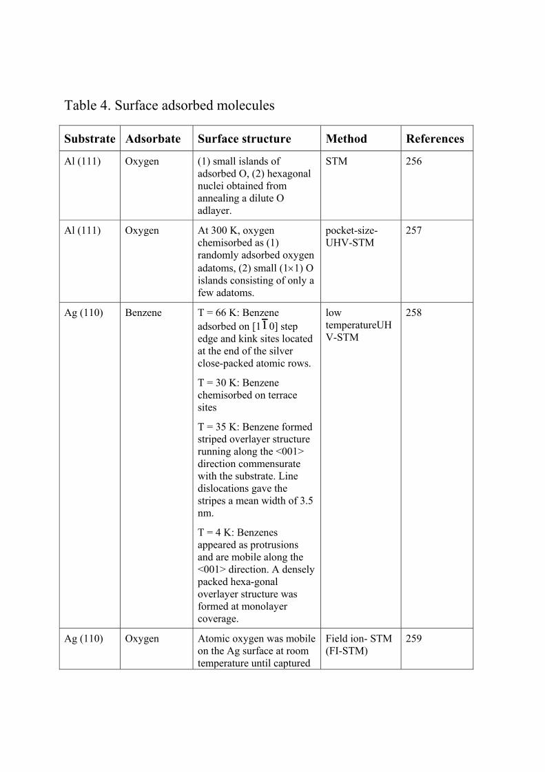
Table 4. Surface adsorbed molecules
Substrate Adsorbate Surface structure Method References
Al (111) Oxygen (1) small islands of adsorbed O, (2) hexagonal nuclei obtained from annealing a dilute O adlayer.
STM 256
Al (111) Oxygen At 300 K, oxygen chemisorbed as (1) randomly adsorbed oxygen adatoms, (2) small (1×1) O islands consisting of only a few adatoms.
pocket-size-UHV-STM
257
Ag (110) Benzene T = 66 K: Benzene adsorbed on [1 0] step edge and kink sites located at the end of the silver close-packed atomic rows.
T = 30 K: Benzene chemisorbed on terrace sites
T = 35 K: Benzene formed striped overlayer structure running along the <001> direction commensurate with the substrate. Line dislocations gave the stripes a mean width of 3.5 nm.
T = 4 K: Benzenes appeared as protrusions and are mobile along the <001> direction. A densely packed hexa-gonal overlayer structure was formed at monolayer coverage.
low temperatureUHV-STM
258
Ag (110) Oxygen Atomic oxygen was mobile on the Ag surface at room temperature until captured
Field ion- STM (FI-STM)
259

to form a Ag-O-Ag linear chain along the <001> direction. A new type of oxygen adsorption exists over the Ag-O-Ag linear chains with much weaker bond to the Ag substrate.
Ag (110) Oxygen One-dimensional linear chains along the <001> direction, perpendicular to the Ag atom rows.
UHV-FI-STM/STS
260
Ag (110)-(1×1)
Oxygen Adsorbed oxygen formed added rows and extra lines.
FI-STM, HREELS
261
Ag (110) Oxygen Oxygen molecules were highly mobile until trapped by collision to form pairs or short strings of molecules along the troughs of the Ag(110).
low temperature UHV-STM
262
Au (110) C60, C70 disordered domain. STM 263
Au (110), Au (111)
C60, C70 Ordered hexagonal C60 overlayer.
In situ STM 264
Au (111) C60, C70 Hexagonal close-packed domain.
STM 263
Epitaxial Au (111) films on mica
C60 Isolated C60 molecules within a hexagonally ordered layer of molecularly resolvable MIBK (methyl isobutyl ketone).
STM in air 265
Au (111) C60 (2×2) UHV-STM/STS at room temperature
266
Au (111) HgCl2 (√7 ×√7)R19.1°-2HgCl2 STM 267
Co
Acetylene An ordered (5×2) carbon overlayer.
UHV-STM, high-resolution core level photoemission spectroscopy, near-edge x-ray
268 (1120)
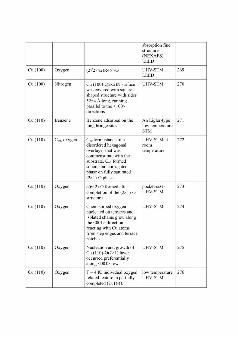
absorption fine structure (NEXAFS), LEED
Cu (100) Oxygen (2√2×√2)R45°-O UHV-STM, LEED
269
Cu (100) Nitrogen Cu (100)-c(2×2)N surface was covered with square-shaped structure with sides 52±4 Å long, running parallel to the <100> directions.
UHV-STM 270
Cu (110) Benzene Benzene adsorbed on the long bridge sites.
An Eigler-type low temperature STM
271
Cu (110) C60, oxygen C60 form islands of a disordered hexagonal overlayer that was commensurate with the substrate. C60 formed square and corrugated phase on fully saturated (2×1)-O phase.
UHV-STM at room temperature
272
Cu (110) Oxygen c(6×2)-O formed after completion of the (2×1)-O structure.
pocket-size-UHV-STM
273
Cu (110) Oxygen Chemisorbed oxygen nucleated on terraces and isolated chains grew along the <001> direction reacting with Cu atoms from step edges and terrace patches.
UHV-STM 274
Cu (110) Oxygen Nucleation and growth of Cu (110)-O(2×1) layer occurred preferentially along <001> rows.
UHV-STM 275
Cu (110) Oxygen T = 4 K: individual oxygen related feature in partially completed (2×1)-O.
low temperature UHV-STM
276

T = 77 K: these features were mobile.
Cu (111) –(1×1)
C60 C60 molecules initially segregated to the terrace edges, but form a close-packed fcc structure at near monolayer coverage. Four different (a,b,c,d) C60 adsorption geometries were identified. a and b were fcc sites, c and d had hcp structure. The only difference between a and b, c and d is the symmetry of the adsorbed C60 with respect to the substrate.
UHV-STM equipped with a room temperature filed ion microscope (FIM)
277
Cu (111) Oxygen Dark fringes along the Cu(111) step edges, dark domains within the Cu(111) terrace and rather mobile light patches on top of the Cu terraces were observed during the initial stage adsorption. Ordered (√73R5.8°×√21R-10.9°)(“44”-structure) were formed when the O/Cu(111) surface were anneal at 473-623 K. Slight disordering of this lattice structure occurred at 723 K. The “44” structure converted to “29” structure (√13R46.1°×7R21.8°) after anneal at 673K in vacuum.
UHV-STM, LEED
278
Ni (100) Oxygen p(2×2), c(2×2) UHV-STM at room temperature
279
Ni (110) Benzene Benzene adsorbed at four-fold coordinated hollow sites.
Eigler-type low temperature STM
271
Ni (110) Nitrogen p(2×3)- Ni (110)-N UHV-STM 280

Pd (110) π-bonded ethylene and ethynyl
At low coverage, π-bonded ethylene molecules formed one-dimensional (3 ×1) structure, while ethynyl species did not form any ordered structure.
STM 281
Pd (110) 1,3-butadiene Each C=C bonds adsorbed on the top sites of the adjacent palladium atoms along (110).
Beetle-type-UHV-STM, HREELS, NEXAFS
282
Pd (110) Pyrimidine The pyrimidine molecules were preferentially adsorbed on terraces.
UHV-STM 283
Pd (110) Water molecules
Water-induced features in a low-coverage region (~ 0.02 ML) can be classified in terms of height; namely, (A) 0.15 Å, (B) 0.3 Å, and (C) 0.55 Å. In a high-coverage region, feature C dominates and forms a local c(2×2) structure.
low temperature UHV-STM
284
Pd (111) CO (√3×√3)R30°, c(4×2)-2CO, (2×2)-3CO, symmetric and lower symmetric (2×2), and several other intermediate coverage structures.
variable temperature UHV-STM
285
Pd (111) NO Ordered c(4×2), c(8×2), and p(2×2) structures.
variable temperature UHV-STM, density functional theory (DFT)
286
Pt (110) Oxygen Oxygen appears as bright protrusions on the ridges of the "missing row" reconstructed surface.
UHV-STM, DFT
287
Pt (111) C2H2 At high C2H2 coverage and T = 120 K: (2 ×2)
UHV-STM 288

structure,
At high C2H2 coverage and T = 220 K: (2 ×2) structure separated by bright lines,
At high C2H2 coverage and T = 370 K: (2 ×2) structure appeared with bright protrusions,
At low C2H2 coverage and T = 120 K: random features,
At low C2H2 coverage and T = 220 K: (2 ×2) islands.
Pt (111) H2O Depending on the preparation conditions the bilayer exhibited three different phases.
Phase (I) was characterized as an ideal ice bilayer rotated +/-7 degrees with respect to the <112>-direction of the Pt(111)-surface.
Phase (IIb) was less dense than phase (I) and appeared as ordered domains of H2O-molecules with the (√ 3×√ 3)R30º -distance of the Pt(111).
Phase (IIa) had a super structure with the same periodicity as phase (IIb), but with a different orientation.
variable temperature STM.
289
Pt (111) NO Ordered (2×2) structure. Two different NO species denoted as α and β were identified. The β species appeared to be higher than α species.
low temperature UHV-STM, HREELS, IRAS (infrared absorption spectroscopy)
290

Pt (111) Xe Hexagonal incommensurate rotated (HIR) phase.
variable-temperature STM
291
Ru (0001) NO N and O form a dense intermixed 2×2 phase in equilibrium with a dilute lattice gas.
UHV-STM 292
Ru (0001) Oxygen T < 130 K: dense, disordered islands partly with a (1×1) configuration,
160 < T < 170 K: onset of diffusion of chemisorbed oxygen atoms,
T > 210 K: formation of (2 ×2) and (2×1) structures.
low temperature UHV-STM
293
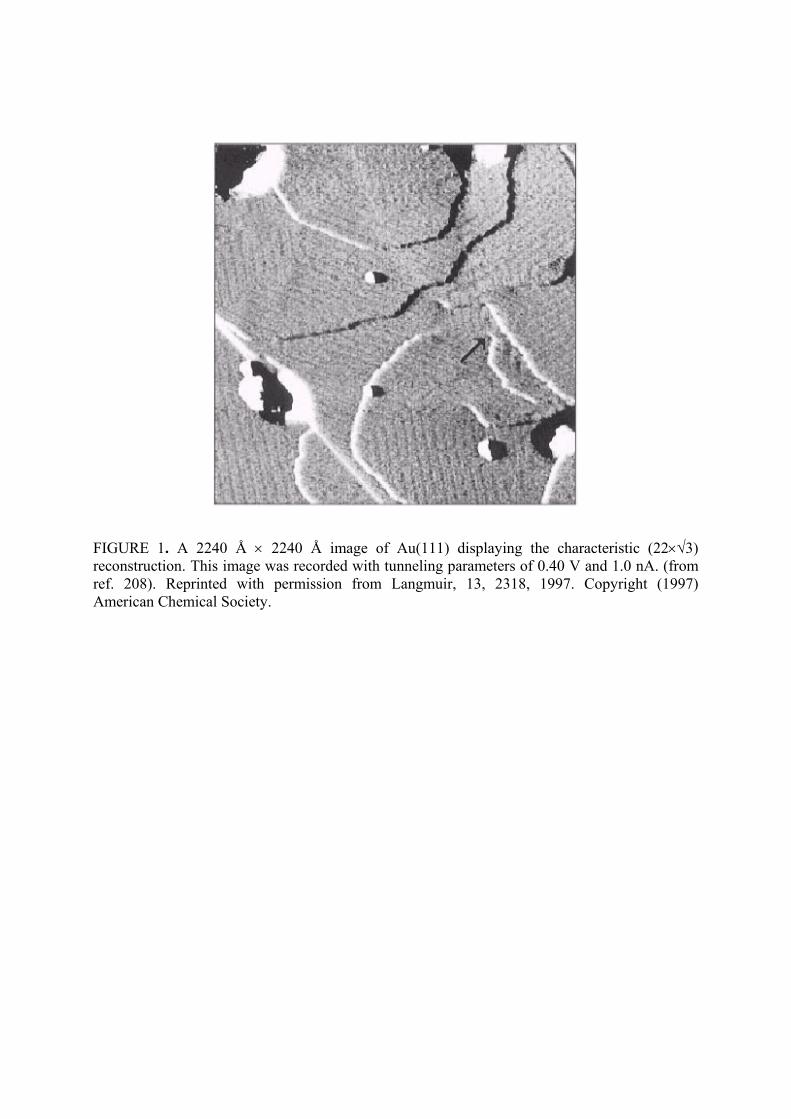
FIGURE 1. A 2240 Å × 2240 Å image of Au(111) displaying the characteristic (22×√3) reconstruction. This image was recorded with tunneling parameters of 0.40 V and 1.0 nA. (from ref. 208). Reprinted with permission from Langmuir, 13, 2318, 1997. Copyright (1997) American Chemical Society.

FIGURE 2. Proposed models for the TiO2(110)-(1×2) surface. Large circles represent O atoms, with Ti atoms represented by small filled circles. Both top and side views are shown. (a) The missing O-row model in which alternate bridging-O rows are removed from the stoichiometric 1×1 termination. (b) The added Ti2O3 structure proposed by Onishi et al (ref.212). Unit cells are outlined in both models. (c) Proposed model for the 1×2 phase, which consists of added rows of a fully reduced 1×1 termination. (From ref. 213). Pang, C. L.; Haycock, S. A.; Raza, H.; Murray, P. W.; Thornton, G.; Gülseren, O.; James, R.; Bullett, D. W. Phys. Rev. B, 58, 1586, 1998. Copyright (1998) by the American Physical Society.
(C)

FIGURE 3. A sequence of images taken during reoxidation of TiO2 (110)-(1×1) surface at an O2 pressure of 1.0×10⁻⁷ mbar and temperature of 723 K. All images are 750 Å × 750 Å, sample bias: +1.1 V, tunnel current 0.10 nA, constant current imaging. The total oxygen exposures for a-f were 609, 622, 654, 682, 709, and 750 L, respectively. This equates to a time interval on average of 370 s between images. Examples of the main features of the images are marked as follows: diffusing features (DF), nucleation points (NP), (1×2) strings (ST), (1×1) islands (IS), area of cross-linked (1×2) (XL). The parallel lines in e highlight the width of the depletion region adjacent to the step edge. (From ref. 216). Smith, R. D.; Bennett, R. A.; Bowker, M. Phys. Rev., B, 66, 035409, 2002. Copyright (2002) by the American Physical Society.
a b
c d
e f

FIGURE 4. Optical microscopy pictures of sol-gelprocess as a function of time. (a) 15 s, (b) 35 s,
(c) 70 s. The bar in the pictures is about 100 µm. AFM images of local morphological
transformation. (d) 5 min, (e) 15 min, (f) 42 min, (g) 193 min, (h) 365 min, (i) 680 min.
C
d
A
B
C
D
E F
H G
a b c
e
A
B
C
D
EF
H G
f
A
B
C
D
EF
H G
g
A
B
C
D
E
F
H G
h
A
B
C
D
E
F
H G
i
A
B
C
D
E
F
H G

FIGURE 5. High resolution STM images of Pt/graphite catalyst.

FIGURE 6. (a) Ex-situ 320 nm × 320 nm STM image (Vtip = +0.7V; I = 0.4 nA) showing the nucleation of 3 equivalent monolayer gold at the edges of the titania nano-crystallites. (b) A 100 nm ×100 nm UHV-STM image (Vtip = +1 V; I =1 nA) showing 0.5 equivalent monolayer freshly deposited gold. (from ref. 233). Reprinted with permission from J. Phys. Chem., B, 106, 5390, 2002. Copyright (2002) American Chemical Society.
a b

FIGURE 7. 100 nm × 100 nm STM images of Au clusters supported on TiO2 (1×1) at 450K. Clusters that moved or disappeared because of tip-cluster interactions are marked with squares; clusters that change in size are highlighted with circles. The conditions for each images are: (a) UHV; (b) Pmixture= 10-4Pa; (c) Pmixture= 1Pa; (d) Pmixture= 360Pa; total exposure (TE)∼2×10⁹L; (e) Pmixture= 720Pa, TE∼3×10¹⁰L; (f) Pmixture= 720Pa, TE∼1.4×10¹¹L. (From ref. 234). Reprinted from Surface Science, 490(1-2), Kolmakov, A.; Goodman, D. W. “Scanning tunneling microscopy of gold clusters on TiO2 (110): CO oxidation at elevated pressures”, L597, Copyright (2001), with permission from Elsevier.
a b
c d
e f
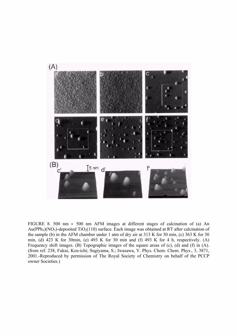
FIGURE 8. 500 nm × 500 nm AFM images at different stages of calcination of (a) An Au(PPh3)(NO3)-deposited TiO2(110) surface. Each image was obtained at RT after calcination of the sample (b) in the AFM chamber under 1 atm of dry air at 313 K for 30 min, (c) 363 K for 30 min, (d) 423 K for 30min, (e) 493 K for 30 min and (f) 493 K for 4 h, respectively. (A) Frequency shift images. (B) Topographic images of the square areas of (c), (d) and (f) in (A). (from ref. 238, Fukui, Ken-ichi; Sugiyama, S.; Iwasawa, Y. Phys. Chem. Chem. Phys., 3, 3871, 2001.-Reproduced by permission of The Royal Society of Chemistry on behalf of the PCCP owner Societies.)

FIGURE 9. 1000 Å × 1000 Å STM images of various Cu coverages deposited on reconstructed TiO2(110) at room temperature and annealed at 700K: (a) 0.14ML, (b)0.35ML, and (c) 0.51ML. (from ref. 241). Reprinted from Surface Science, 494(1), Reddic, J. E.; Zhou, J.; Chen, D. A. “Scanning tunneling microscopy studies of the growth of Cu clusters on a reconstructed TiO2(110)-(1×2) surface”, L767, Copyright (2001), with permission from Elsevier.

FIGURE10. (a) 300 nm × 300 nm STM image following deposition of 0.3 ML of Pd on TiO2(110) at room temperature in a single deposition step. (b) 300 nm × 300 nm STM image following deposition of 0.3 ML of Pd on TiO2(110) at 750 K in a sequence of six equal deposition steps. The image was recorded at 750 K. Note the bimodal distribution of particle sizes. Scanning conditions: tip bias -3 V, 1 nA tunnel current. (c) and (d) are 300 nm × 300 nm STM images of 0.3 ML Pd on TiO2(110) at 750 K. The Pd was deposited in a sequence of six equal deposition steps with a period of 2 h between successive depositions. Image (c) is taken 90 min after the last deposition and image (d) is taken 240 min after the last deposition i.e. there is an elapse time of 150 min between the two images. Scanning conditions: tip bias -3 V, 1 nA tunnel current. (from Ref. 245). Reprinted from Surface Science, 515(2-3), Howard, A.; Mitchell, C. E. J.; Egdell, R. G. “Real time STM observation of Ostwald ripening of Pd nanoparticles on TiO2 (110) at elevated temperature”, L504, Copyright (2002), with permission from Elsevier.
a c
b d

FIGURE 11. STM image of an anatase TiO2 (001)-(1×4) surface covered by 0.2 ML Pt after annealing in UHV at 470K. (from ref. 246). Reprinted from Surface Science, 479(1-3), Gan, S.; El-azab, A.; Liang, Y. “Formation and diffusion of Pt nanoclusters on highly corrugated anatase TiO2 (001)-(1×4) surface”, L369, Copyright (2001), with permission from Elsevier.

FIGURE 12. STM results after the high-temperature treatment. (a) 2000 Å × 2000 Å image shows clusters are approximately 200 Å wide and 40 Å high. Most clusters show hexagonal shape elongated along the substrate [001] direction (type A). A few square clusters (type B) are seen. (b) Atomic-resolution image of an encapsulated “type-A” cluster. (c) Atomic-resolution image of a square “type-B” cluster, showing an amorphous overlayer. (From ref. 247). Dulub, O.; Hebenstreit, W.; Diebold, U. Phys. Rev. Lett., 84(16), 3646, 2000. Copyright (2000) by the American Physical Society.
a
b
c

FIGURE 13. 500 nm × 500 nm AFM images of Cu(ac)2 butanol spin-coated onto oxidized Si(100) at 5000 rpm and calcinated to 450 °C at 300 °C/h for 4 h. The maximum height of the vertical scale is 10 nm for each image: (a) 0.0040 M; (b) 0.0070 M; (c) 0.0085 M; (d) 0.010 M. (from ref. 248). Reprinted with permission from Langmuir, 15, 2043, 1999. Copyright (1999) American Chemical Society.
a b
c d

FIGURE 14. STM images of H-exposed Si(111)-(7×7) surface. (a) and (b) show the hopping motion of single point defect within an unfaulted half cell when H is adsorbed on a rest-atom site. Images (c) and (d) captured the jump of a point defect from an unfaulted half-cell to a neighboring faulted half-cell. (from ref. 307). Lo, R. L.; Hwang, I. S.; Ho, M. S.; Tsong, T. T. Phys. Rev. Lett., 80(25), 5584, 1998. Copyright (1998) by the American Physical Society.
FIGURE 15. (a)-(c) Movement of a Si magic cluster within a Si(111)-(7×7) half-cell. Images were taken at 743 K at the sample bias of -2.0 V. (from ref. 315). Reprinted from Surface Science, 514(1-3), Hwang, I. S.; Ho, M. S.; Tsong, T. T. “Dynamic behavior of Si magic clusters on Si(111) surfaces”, 309, Copyright (2002), with permission from Elsevier.

FIGURE 16. Long-distance anisotropic motion of Si magic clusters on Si(111)-(7×7). These five images are chosen from continuous-time scan of 9s time interval each, taken at the sample bias of -2 V and at 723 K. The image size is 800 Å × 670 Å. The current direction is indicated at the lower-right hand corner of (a), which is in the ascending step (step-up) direction of the substrate. (from ref. 315). Reprinted from Surface Science, 514(1-3), Hwang, I. S.; Ho, M. S.; Tsong, T. T. “Dynamic behavior of Si magic clusters on Si(111) surfaces”, 309, Copyright (2002), with permission from Elsevier.

FIGURE 17. Images (14 nm × 7 nm) taken from a movie recorded by scanning tunneling microscopy, illustrating the diffusion of embedded indium atoms at room temperature. The fine corrugation is due to the atomic lattice of the Cu(001) surface. The four protrusions are individual indium atoms, each one replacing a single copper atom in the surface layer. (a) Initial surface structure at t=0 s, (b) the positions of the four indium atoms remained unchanged after 140 s, but (c) 20 s later, three of the four indium atoms made a sudden translational motion of up to 5 atomic spacings. All motion exhibited similar pattern of long waiting time followed by simultaneous displacement of several indium atoms over long distances. (from Ref. 324). Reprinted with Nature’s copyright permission. Copyright (2000).

FIGURE 18. A series of successive STM images, recorded during dosing of the O-covered Pt(111) surface with H2. (a) – (c) STM images (17 nm × 17 nm) from an experiment conducted at 131 K [P(H2)=8×10⁻⁹ mbar]. The hexagonal pattern in (a) was the (2×2)O structure; O atoms appeared as dark dots and the bright features were the OH islands. In (c), the area is mostly covered by OH, which formed ordered (√3×√3)R30° and (3×3) structures. The white, fuzzy features were H2O-covered areas. (d) – (f) STM images (220 nm × 220 nm) from an experiment conducted at 112 K [P(H2)=2×10⁻⁸ mbar]. In (d), the surface was mostly O-covered (not resolved). The bright dots were small OH islands, most of which were concentrated in the expanding ring. H2O in the interior of the ring was not resolved in the images. Thin, mostly vertical lines were the atomic steps. (from ref. 336). Reprinted (abstracted/excerpted) with permission from [Sachs, C.; Hildebrand, M.; Völkening, S.; Wintterlin, J.; Ertl, G. Science, 293, 1635, 2001.]. Copyright (2001) American Association for the Advancement of Science.
a b c
d e f

FIGURE 19. A series of STM images (180 Å × 170 Å), recorded during the reaction of adsorbed oxygen atoms with co-adsorbed CO molecules at 247 K from the same area of a Pt(111) crystal. Before the experiment, a submonolayer of oxygen atoms was prepared (by an exposure of 3 Langmuirs O2 at 96 K, a short annealing to 298 K and cooling to 247 K), and CO was continuously supplied from the gas phase (PCO=5×10⁻⁸ mbar). At this pressure, the impingement rate of CO molecules was about 1 monolayer per 100 s. The times duration was measured from the start of CO exposure. The structure at the upper left corner is an atomic step of the Pt surface. The tunneling voltage (with respect to the sample) is +0.5V and the tunneling current is 0.8 nA. (from ref. 338). Reprinted (abstracted/excerpted) with permission from [Wintterlin, J.; Völkening, S.; Janssens, T. V. W.; Zambelli, T.; Ertl, G. Science, 278, 1931, 1997.]. Copyright (1997) American Association for the Advancement of Science.

FIGURE 20. Proposed model for Pt-Rh tip catalyzed hydrogenation of coke in a hydrogen-
containing atmosphere. (from ref. 349). Reprinted (abstracted/excerpted) with permission from
[McIntyre, B. J.; Salmeron, M.; Somorjai, G. A. Science, 265, 1415, 1994.]. Copyright (1994)
American Association for the Advancement of Science.

FIGURE 21. STM image (620 Å ×100 Å) of a Pt(111) surface covered with a sulfur p(2×2) ordered overlayer. This image was acquired after a few hours following the sulfur dosing and illustrates the intermediate structures obtained during the step doubling that is induced by the adsorbed sulfur atoms. The p(2×2) pattern can be seen on the terraces and extended all the way to the bottom and top of the steps, which had somewhat rough edges but were nevertheless macroscopically aligned. (from ref. 367). Reprinted with permission from Langmuir, 14, 1312, 1998. Copyright (1998) American Chemical Society.

FIGURE 22. STM images of (a) p(2×2) iodine phase structure at θ =0.25 (115 Å × 99 Å), (b) coexisting liquid and c(6×2) iodine phases (102 Å ×102 Å), (c) coexisting c(6×2) and c(14×2) iodine phases (260 Å × 265 Å). The c(14×2) domains grew near the atomic steps. Arrows indicate the direction of the iodine lattice compression, (d) c(5×2) iodine phase structure (136 Å ×136 Å), and (e) LEED pattern c(5×2) structure shown in (d).The first-order spots belong to Cu(100) and the small spots are from the iodine superstructure. (From ref. 396). Reprinted from Surface Science, 497(1-3), Andryushechkin, B. V.; Eltsov, K. N.; Shevlyuga, V. M.; Bardi, U.; Cortigiani, B. “Structural transitions of chemisorbed iodine on Cu(100)”, 59, Copyright (2002), with permission from Elsevier.
a
b
c
d
e

AFM tip
substrate
substrate
AFM tip
substrate
AFM tip
FIGURE 23 (a) Schematic diagram of mechanical patterning process by SPM tip.

substrate
STM tip
substrate
STM tip
FIGURE 23 (b) Schematic diagram of surface melting process by SPM tip.

water bridge
AFM tip as cathode (-)
Tip induced E-field
substrate anode (+)
Tip-induced oxide V
FIGURE 23 (c) Schematic diagram of tip induced local anodic oxidation.

FIGURE 24 (a) AFM image of the patterned grooves by cantilever oscillation with feedback gains of (1) 0, (2) 3, and (3) 5. The scan speed was fixed at 0.02 µm/s. (b). AFM image of the patterned grooves with the maximum applied force at scan speeds of (1) 0.08 µm/s, (2) 0.04 µm/s, (3) 0.02 µm/s, (4) 0.008 µm/s, and (5) 0.004 µm/s. (from ref. 418). Reprinted with permission from [Hyon, C. K.; Choi, S. C.; Hwang, S. W.; Ahn, D.; Kim, Y.; Kim, E. K. Appl. Phys. Lett., 75(2), 292, 1999.]. Copyright (1999), American Institute of Physics.
a b

FIGURE 25. AFM phase images showing the influence of the AFM probe on the growth
direction of lamellar tips: (a) and (b) set point amplitude ratio of 0.72; (c) and (d) set point
amplitude ratio of 0.60; and, (e) and (f) set point amplitude ratio of 0.44.
a b
c d
0
60dee f
1 µm
1 µm
1 µm
1 µm
2 µm 2 µm
a b
c d
e f
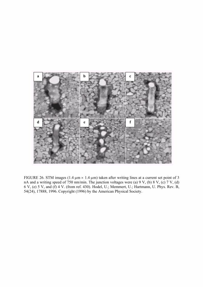
FIGURE 26. STM images (1.4 µm × 1.4 µm) taken after writing lines at a current set point of 3 nA and a writing speed of 750 nm/min. The junction voltages were (a) 9 V, (b) 8 V, (c) 7 V, (d) 6 V, (e) 5 V, and (f) 4 V. (from ref. 430). Hodel, U.; Memmert, U.; Hartmann, U. Phys. Rev. B, 54(24), 17888, 1996. Copyright (1996) by the American Physical Society.
a b c
d e f

FIGURE 27. (a) AFM image of vertically aligned grids of oxidized lines on TiN. Local oxidation conditions: tip scanning speed 0.25 µm/s, sample bias +8 V, relative humidity 65%. (From ref. 460). Reprinted with permission from [Gwo, S.; Yeh, C. L.; Chen, P. F.; Chou, Y. C.; Chen, T. T.; Chao, T. S.; Hu, S. F.; Huang, T. Y. Appl. Phys. Lett., 74(8), 1090, 1999. ], Copyright (1999), American Institute of Physics. (b) AFM image of an array of 4864 dots. The dots are 40 nm apart with an average width of 10 nm. (From ref. 493). Reprinted with permission from [García, R.; Calleja, M.; Rohrer, H. J. Appl. Phys., 86(4), 1898, 1999.], Copyright (1999), American Institute of Physics.
a b

FIGURE 28. Scanning with a platinum-coated AFM tip over a SAM surface containing terminal
azide groups in the presence of H2 leads to the reduction of azide groups to primary amino
groups. Derivatization of the resulting amine surface with aldehyde-modified latex beads or
ATTO-TAG results in specific labeling of the reduced areas. (from ref. 496). Reprinted
(abstracted/excerpted) with permission from [Müller, W. T.; Klein, D. L.; Lee, T.; Clark, J.;
McEuen, P. L.; Schultz, P. G. Science, 268, (5208), 272, 1995.]. Copyright (1995) American
Association for the Advancement of Science.

FIGURE 29. Schematic representation of DPN process. (From ref. 504). Reprinted
(abstracted/excerpted) with permission from [Piner, R. D.; Zhu, J.; Xu, F.; Hong, S. H.; Mirkin,
C. A. Science, 283, 661, 1999.]. Copyright (1999) American Association for the Advancement of
Science.

FIGURE 30. Schematic representation of the procedure used to prepare nanostructure on a Au
substrates. (from ref. 526). Reprinted with the permission from [Liu, X. G.; Fu, L.; Hong, S. H.;
Dravid, V. P.; Mirkin, C. A. Adv. Mater., 14(3), 231, 2002.]. Copyright (2002) WILEY-VCH.

FIGURE 31. Schematic diagram showing the different steps in the formation of a single bond with the STM. (a) The tip is positioned over a single CO molecule to induce the detachment of CO from Ag and its bonding to the tip. Because CO forms a bond predominantly through the carbon, a 180° rotation of the CO occurs in the transfer. (b) The tip with the attached single CO molecule is translated (indicted by the arrow) and positioned over a Fe atom. (c) The bias voltage and the flow of electrons are reversed, inducing the transfer of CO from the tip to the Fe. (d) A single Fe–CO bond is formed. The interaction of the electric field with the dipole moment of CO may also play a role in the transfer of (a) and (c). (from ref. 543). Reprinted (abstracted/excerpted) with permission from [Lee, H. J.; Ho, W. Science, 286, 1719, 1999.]. Copyright (1999) American Association for the Advancement of Science.
a b
c d

FIGURE 32. STM image of an atomic abacus made from C60 molecules (from ref. 548). Reprinted with permission from [Cuberes, M. T.; Schlittler, R. R.; Gimzewski, J. K. Appl. Phys. Lett., 69(20), 3016, 1996.], Copyright (1996), American Institute of Physics.

FIGURE 33. Schematic diagram of four basic manipulation mechanisms using AFM (a and b) and STM (c and d). The imaging and fabrication modes are depicted in the top and bottom rows, respectively. (from ref. 552). Reprinted with permission from Acc. Chem. Res., 33, 457, 2000. Copyright (2000) American Chemical Society.
a b c d
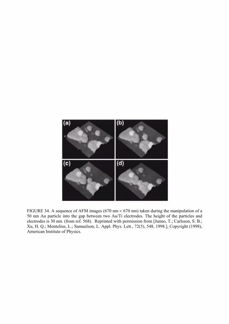
FIGURE 34. A sequence of AFM images (670 nm × 670 nm) taken during the manipulation of a 50 nm Au particle into the gap between two Au/Ti electrodes. The height of the particles and electrodes is 30 nm. (from ref. 568). Reprinted with permission from [Junno, T.; Carlsson, S. B.; Xu, H. Q.; Montelius, L.; Samuelson, L. Appl. Phys. Lett., 72(5), 548, 1998.], Copyright (1998), American Institute of Physics.