PSoC® 3 and PSoC 5LP: Low-Frequency FSK Modulation ...
13
www.cypress.com Document No. 001-60594 Rev. *J 1 AN60594 PSoC ® 3 and PSoC 5LP: Low-Frequency FSK Modulation and Demodulation Author: Todd Dust Associated Project: Yes Associated Part Family: CY8C3xxx,CY8C5xxx LP Software Version: PSoC ® Creator ™4.0 Related Application Notes: AN52705, AN2336, AN2108, AN58827, AN76458 AN60594 describes how to create a frequency shift keying (FSK) modulator and demodulator with PSoC ® 3 or PSoC 5LP, with digital 0s represented by 2100 Hz and digital 1s represented by 1300 Hz. The method described in this application note uses zero CPU—everything is done in PSoC hardware. This application note covers only the physical layer implementation of an FSK transmitter and receiver; higher-level encoding techniques and physical modem connections are not discussed. Contents Introduction ....................................................................... 1 FSK Modulator .................................................................. 2 Transmit Results .......................................................... 3 Generating Different Frequencies ................................ 4 FSK Demodulator .............................................................. 6 Band-pass Filter ........................................................... 6 Zero-Crossing Detector ................................................ 6 Correlator ..................................................................... 6 LPF ............................................................................... 7 Digitize.......................................................................... 7 Receiving Results.............................................................. 8 Design Modifications ......................................................... 9 Attached Projects .............................................................. 9 Summary ........................................................................... 9 About the Author ............................................................... 9 Appendix A ...................................................................... 10 Worldwide Sales and Design Support ............................. 13 Introduction In some applications, it is necessary to transmit digital data through analog signals. This is often due to bandwidth limitations in the transmission medium. There are numerous methods of transmitting digital data through analog signals; this application note specifically focuses on frequency shift keying (FSK) and how to implement an FSK modulator and demodulator in a PSoC 3 or PSoC 5LP device. An FSK modulator converts digital data into two distinct frequencies; one frequency represents a digital 1 and the other represents a digital 0 (see Figure 1). Figure 1. Example FSK Waveform 0 1 0 0 0 1 1 1 The FSK demodulator receives the transmitted analog signal and demodulates it to determine the correct sequence of 1s and 0s. This application note demonstrates how to configure a PSoC 3 or PSoC 5LP device to implement an FSK modulator and demodulator. The example project included with this application note uses 2100 Hz to represent digital 0 and 1300 Hz to represent digital 1.
-
Upload
khangminh22 -
Category
Documents
-
view
1 -
download
0
Transcript of PSoC® 3 and PSoC 5LP: Low-Frequency FSK Modulation ...

www.cypress.com Document No. 001-60594 Rev. *J 1
AN60594
PSoC® 3 and PSoC 5LP: Low-Frequency FSK Modulation and Demodulation
Author: Todd Dust
Associated Project: Yes
Associated Part Family: CY8C3xxx,CY8C5xxx LP
Software Version: PSoC® Creator™4.0
Related Application Notes: AN52705, AN2336, AN2108, AN58827, AN76458
AN60594 describes how to create a frequency shift keying (FSK) modulator and demodulator with PSoC® 3 or
PSoC 5LP, with digital 0s represented by 2100 Hz and digital 1s represented by 1300 Hz. The method described in this
application note uses zero CPU—everything is done in PSoC hardware. This application note covers only the physical
layer implementation of an FSK transmitter and receiver; higher-level encoding techniques and physical modem
connections are not discussed.
Contents
Introduction ....................................................................... 1 FSK Modulator .................................................................. 2
Transmit Results .......................................................... 3 Generating Different Frequencies ................................ 4
FSK Demodulator .............................................................. 6 Band-pass Filter ........................................................... 6 Zero-Crossing Detector ................................................ 6 Correlator ..................................................................... 6 LPF ............................................................................... 7 Digitize.......................................................................... 7
Receiving Results.............................................................. 8 Design Modifications ......................................................... 9 Attached Projects .............................................................. 9 Summary ........................................................................... 9 About the Author ............................................................... 9 Appendix A ...................................................................... 10 Worldwide Sales and Design Support ............................. 13
Introduction
In some applications, it is necessary to transmit digital data through analog signals. This is often due to bandwidth limitations in the transmission medium. There are numerous methods of transmitting digital data through analog signals; this application note specifically focuses on frequency shift keying (FSK) and how to implement an FSK modulator and demodulator in a PSoC 3 or PSoC 5LP device.
An FSK modulator converts digital data into two distinct frequencies; one frequency represents a digital 1 and the other represents a digital 0 (see Figure 1).
Figure 1. Example FSK Waveform
0 1 0 0 01 1 1
The FSK demodulator receives the transmitted analog signal and demodulates it to determine the correct sequence of 1s and 0s.
This application note demonstrates how to configure a PSoC 3 or PSoC 5LP device to implement an FSK modulator and demodulator. The example project included with this application note uses 2100 Hz to represent digital 0 and 1300 Hz to represent digital 1.
PSoC® 3 and PSoC 5LP: Low-Frequency FSK Modulation and Demodulation
www.cypress.com Document No. 001-60594 Rev. *J 2
The advantage of PSoC with an FSK modulator and demodulator is that no CPU intervention is needed. All of the demodulation and modulation is done in the integrated analog and digital blocks of PSoC 3 and PSoC 5LP. The CPU is left free to do other important system tasks.
Note The included example is not a complete modem; it does not include the phone line or other interfaces; it also does not include the data processing code.
If you are looking for information on Power Line Communication (PLC) and application of FSK, see the application note, AN76458.
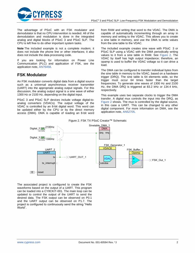
FSK Modulator
An FSK modulator converts digital data from a digital source such as a universal asynchronous receiver transmitter (UART) into the appropriate analog output signals. For this discussion, the analog output signal is a sine wave of either 1300 Hz or 2100 Hz, depending on the digital input.
PSoC 3 and PSoC 5LP devices include voltage digital-to-analog converters (VDACs). The output voltage of the VDAC is controlled by an 8-bit digital word. This word can be updated either by the CPU or by the direct memory access (DMA). DMA is capable of reading an 8-bit word
from RAM and writing that word to the VDAC. The DMA is capable of automatically incrementing through an array in memory and writing to the VDAC. This allows you to create a sine table in memory, and use the DMA to write values from the sine table to the VDAC.
The included example creates sine wave with PSoC 3 or PSoC 5LP using a VDAC with the DMA periodically writing values to it from a sine table in RAM. See Figure 2. The VDAC by itself has high output impedance; therefore, an opamp is used to buffer the VDAC voltage so it can drive a load.
The DMA can be configured to transfer individual bytes from the sine table in memory to the VDAC, based on a hardware trigger (DRQ). The sine table is 64 elements wide, so the trigger must occur 64 times faster than the target frequencies. To generate sine waves of 1300 Hz and 2100 Hz, the DMA DRQ is triggered at 83.2 kHz or 134.4 kHz, respectively.
This example uses two separate clocks to trigger the DMA transfer. A digital mux controls the input into the DRQ, as Figure 2 shows. The mux is controlled by the digital source, in this case a UART. This can be changed to any other digital component. For more information on DMA, see the application note, AN52705.
Figure 2. FSK TX PSoC Creator™ Schematic
The associated project is configured to create the FSK waveforms based on the output of a UART. This program can be loaded into a CY8CKIT-001. The main loop can be updated to control the output of the UART to send the desired data. The FSK output can be observed on P0.1 and the UART output can be observed on P1.7. The project is configured to continuously send the string “Hello World”.

PSoC® 3 and PSoC 5LP: Low-Frequency FSK Modulation and Demodulation
www.cypress.com Document No. 001-60594 Rev. *J 3
Transmit Results
Now that we know how to create an FSK modulator with PSoC 3 or PSoC 5 LP, it is time to look at the quality of the FSK waveforms. Presented below are screen captures of the FSK outputs and their FFTs.
Figure 3. 2100 Hz Output
Figure 4. 2100 Hz FFT
The cursor window in the upper right of Figure 4 shows the fundamental frequency at 1.2 dB and the second harmonic at –41.2 dB, which is approximately 42 dB down.
Figure 5. 2100 Hz Primary Alias
The cursor window in Figure 5 shows that the sample alias noise is located at approximately 131.7 kHz and 135.86 kHz, and has a magnitude of –33.6 dB and –35.2 dB, respectively.
Figure 6. 1300 Hz Output

PSoC® 3 and PSoC 5LP: Low-Frequency FSK Modulation and Demodulation
www.cypress.com Document No. 001-60594 Rev. *J 4
Figure 7. 1300 Hz FFT
The cursor window in Figure 7 shows the fundamental frequency at 3.2 dB and the second harmonic at –41.2 dB, which is approximately 44 dB down.
Figure 8. 1300 Hz Primary Aliases
The cursor window in Figure 8 shows that the sample alias noise is located at approximately 81.9 kHz and 84.9 kHz, and has a magnitude of –35.2 dB and –35.6 dB, respectively.
Figure 9. Combined Output
The FFTs show that the output waveforms are clean. The second harmonic and higher are at least 40 dB below the fundamental. The combined waveform is also clean with no phase errors at bit transitions. With PSoC 3 and PSoC 5LP devices, it is easy to create an FSK modulator that requires no CPU interaction.
Generating Different Frequencies
For your application, 1300 Hz and 2100 Hz may not be the frequencies that you need. This section describes how you can achieve different frequencies.
The FSK output frequency can be calculated by dividing the sample clock frequency by the size of the sine table, as shown in Equation 1.
N
kSampleClocOutputFreq Equation 1
N is the number of elements in the sine table. The sample clock is the clock used to drive the DRQ of the DMA.
To generate a digital 0 in the previous example, a 134.4-kHz sample clock was used with a 64-element sine table. Using Equation 1, the output frequency can be calculated as:
HzOutputFreq
kHzOutputFreq
2100
64
4.134
For a digital 1, an 83.2-kHz sample clock was used with the same 64-element sine table. Again, using Equation 1, the output frequency can be calculated:
HzOutputFreq
kHzOutputFreq
1300
64
2.83
To increase the output frequency, the sample clock can be increased, or the number of sine table elements can be decreased.

PSoC® 3 and PSoC 5LP: Low-Frequency FSK Modulation and Demodulation
www.cypress.com Document No. 001-60594 Rev. *J 5
To decrease the output frequency, the sample clock can be decreased, or the number of sine table elements can be increased.
The question that often arises at this point is how fast can I get my FSK output with this method? This method only works with low frequencies; it will not work for MHz signals. The following paragraphs discuss how to determine the maximum output frequency.
A VDAC configured in the 0 V to 4.048 V range has a maximum sample rate of 250 ksps; using a 64-bit sine table, the maximum output frequency that can be achieved is 3.9 kHz. A VDAC configured in the 0 V to 1.024 V range has a maximum sample rate of 1000 ksps; using a 64-bit sine table, the maximum output frequency that can be achieved is 15.625 kHz.
If an IDAC is used instead of a VDAC, the maximum sample rate is 8000 ksps. This allows for a maximum output frequency of 125 kHz with a 64-element sine table.
If an IDAC is used, the current needs to be routed to an external resistor to convert the current to a voltage. See Figure 10.
Figure 10. Converting an IDAC to a VDAC
Table 1 shows the maximum output frequencies for different sized sine tables.
Table 1. Sine Table Size versus Maximum Output Frequency
Sine Table Elements
IDAC 1-V VDAC 4-V VDAC
256 31.25 kHz 3.9 kHz 976 Hz
128 62.5 kHz 7.8 kHz 1.95 kHz
64 125 kHz 15.6 kHz 3.9 kHz
32 250 kHz 31.25 kHz 7.8 kHz
16 500 kHz 62.5 kHz 15.6 kHz
Decreasing the number of elements in the sine table has the disadvantage of increasing the harmonic and sampling noise. When designing an FSK modulator, the tradeoff between speed and noise needs to be considered. The FFTs shown previously give a good approximation of the noise present in this system for a 64-element sine table.
PSoC® 3 and PSoC 5LP: Low-Frequency FSK Modulation and Demodulation
www.cypress.com Document No. 001-60594 Rev. *J 6
FSK Demodulator
The FSK demodulator takes the analog input signal and demodulates it into the appropriate sequence of digital 1s and 0s. The block diagram for the FSK demodulator is shown in Figure 11.
Figure 11. Demodulator Block Diagram
BPF
Zero
Crossing
Detector
Correlator LPF DigitizeInput
Band-pass Filter
The band-pass filter (BPF) is designed to allow 1300 Hz and 2100 Hz signals to pass through with little attenuation (around 1 dB), and everything else to be attenuated. The purpose of this filter is to remove any out-of-band noise, thus making the demodulation processes easier.
This filter is designed using standard filter design techniques. It has a center frequency close to 1500 Hz. The bandwidth is set to 1570 Hz to achieve less than 1 dB of attenuation at the modulating frequencies. This filter is designed for a gain of 1 V/V. The circuit for the BPF is shown in Figure 12; derivation of component values is a standard design problem, see Appendix A for more detail on how the filter was designed or if you need to design a filter for different frequencies.
In this project, Vdda/2 is provided internally by the PSoC. It is buffered through another opamp and routed to all the locations that need a Vdda/2 connection. Ensure you have a strong Vdda/2 source for the project to work correctly.
Figure 12. BPF Circuit
Figure 13. BPF Bode Plot
This filter is meant to be an example to the designer. The filter should be modified appropriately for the target design. Signaling frequencies, signal amplitude, and out-of-band noise all need to be considered when designing this front-end BPF. The topology in Figure 12 can be modified for increased gain, as well as different center frequencies and bandwidths. If more out-of-band attenuation is needed, a higher-order filter must be constructed out of multiple PSoC opamps.
Zero-Crossing Detector
After the waveforms are filtered, it is important to digitize them for use in the correlator. This is done by constructing a simple zero-crossing detector. This detector can be created with a comparator set to trip at VDD/2.
Figure 14: Zero-Cross Detector
Correlator
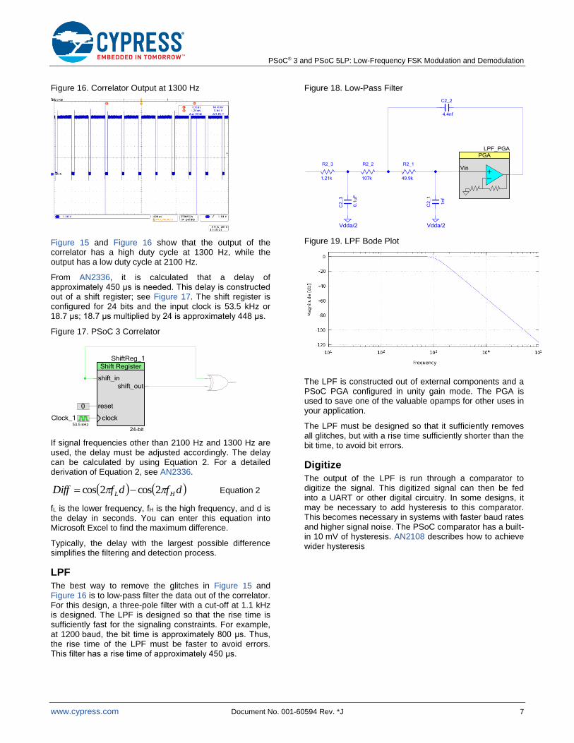
The theory for the correlator is explained in application note AN2336. The basic function of the correlator is to delay the digital signal out of the zero-crossing detector, and then XOR that signal with the non-delayed signal. The result is that one frequency ends up with a high duty cycle, while the other frequency has a low duty cycle at the output of the XOR gate. Figure 15 and Figure 16 are scope captures at the output of the XOR gate for the two different frequencies.
Figure 15. Correlator Output at 2100 Hz
PSoC® 3 and PSoC 5LP: Low-Frequency FSK Modulation and Demodulation
www.cypress.com Document No. 001-60594 Rev. *J 7
Figure 16. Correlator Output at 1300 Hz
Figure 15 and Figure 16 show that the output of the correlator has a high duty cycle at 1300 Hz, while the output has a low duty cycle at 2100 Hz.
From AN2336, it is calculated that a delay of approximately 450 μs is needed. This delay is constructed out of a shift register; see Figure 17. The shift register is configured for 24 bits and the input clock is 53.5 kHz or 18.7 μs; 18.7 μs multiplied by 24 is approximately 448 μs.
Figure 17. PSoC 3 Correlator
If signal frequencies other than 2100 Hz and 1300 Hz are used, the delay must be adjusted accordingly. The delay can be calculated by using Equation 2. For a detailed derivation of Equation 2, see AN2336.
dfdfDiff HL 2cos2cos Equation 2
fL is the lower frequency, fH is the high frequency, and d is the delay in seconds. You can enter this equation into Microsoft Excel to find the maximum difference.
Typically, the delay with the largest possible difference simplifies the filtering and detection process.
LPF
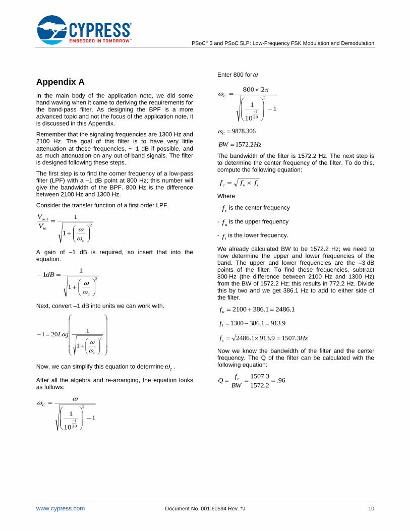
The best way to remove the glitches in Figure 15 and Figure 16 is to low-pass filter the data out of the correlator. For this design, a three-pole filter with a cut-off at 1.1 kHz is designed. The LPF is designed so that the rise time is sufficiently fast for the signaling constraints. For example, at 1200 baud, the bit time is approximately 800 μs. Thus, the rise time of the LPF must be faster to avoid errors. This filter has a rise time of approximately 450 μs.
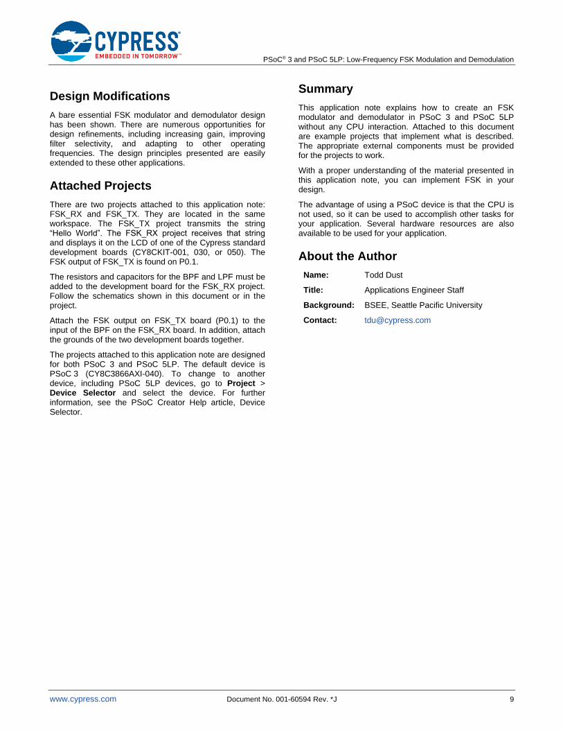
Figure 18. Low-Pass Filter
Figure 19. LPF Bode Plot
The LPF is constructed out of external components and a PSoC PGA configured in unity gain mode. The PGA is used to save one of the valuable opamps for other uses in your application.
The LPF must be designed so that it sufficiently removes all glitches, but with a rise time sufficiently shorter than the bit time, to avoid bit errors.
Digitize
The output of the LPF is run through a comparator to digitize the signal. This digitized signal can then be fed into a UART or other digital circuitry. In some designs, it may be necessary to add hysteresis to this comparator. This becomes necessary in systems with faster baud rates and higher signal noise. The PSoC comparator has a built-in 10 mV of hysteresis. AN2108 describes how to achieve wider hysteresis

PSoC® 3 and PSoC 5LP: Low-Frequency FSK Modulation and Demodulation
www.cypress.com Document No. 001-60594 Rev. *J 8
Receiving Results
Figure 20. Putting It All Together
Figure 20 shows the signals received:
The top signal (UARTOUT) is the output of the TX UART.
The second signal (FSKOUT) is the analog output from the FSK modulator described earlier in this application note.
The third signal (BPFOUT) is the output of the BPF; 2100 Hz has slightly more attenuation because of resistor tolerance issues.
The fourth signal (COMPOUT) is the output of the first zero-crossing detector circuit.
The fifth signal (DELAY) is the output of the shift register, the delayed signal.
The sixth signal (CORROUT) is the XOR of the COMPOUT and DELAY signals; notice that with one input frequency the correlator output has a high duty cycle, while at the other frequency it has a low duty cycle.
The seventh output (LPFOUT) is that of the LPF.
The eighth signal (UARTIN) is the final output that goes to the receive UART. Notice that the eighth signal is essentially a delayed version of the first signal (UARTOUT).
PSoC® 3 and PSoC 5LP: Low-Frequency FSK Modulation and Demodulation
www.cypress.com Document No. 001-60594 Rev. *J 9
Design Modifications
A bare essential FSK modulator and demodulator design has been shown. There are numerous opportunities for design refinements, including increasing gain, improving filter selectivity, and adapting to other operating frequencies. The design principles presented are easily extended to these other applications.
Attached Projects
There are two projects attached to this application note: FSK_RX and FSK_TX. They are located in the same workspace. The FSK_TX project transmits the string “Hello World”. The FSK_RX project receives that string and displays it on the LCD of one of the Cypress standard development boards (CY8CKIT-001, 030, or 050). The FSK output of FSK_TX is found on P0.1.
The resistors and capacitors for the BPF and LPF must be added to the development board for the FSK_RX project. Follow the schematics shown in this document or in the project.
Attach the FSK output on FSK_TX board (P0.1) to the input of the BPF on the FSK_RX board. In addition, attach the grounds of the two development boards together.
The projects attached to this application note are designed for both PSoC 3 and PSoC 5LP. The default device is PSoC 3 (CY8C3866AXI-040). To change to another device, including PSoC 5LP devices, go to Project > Device Selector and select the device. For further information, see the PSoC Creator Help article, Device Selector.
Summary
This application note explains how to create an FSK modulator and demodulator in PSoC 3 and PSoC 5LP without any CPU interaction. Attached to this document are example projects that implement what is described. The appropriate external components must be provided for the projects to work.
With a proper understanding of the material presented in this application note, you can implement FSK in your design.
The advantage of using a PSoC device is that the CPU is not used, so it can be used to accomplish other tasks for your application. Several hardware resources are also available to be used for your application.
About the Author
Name: Todd Dust
Title: Applications Engineer Staff
Background: BSEE, Seattle Pacific University
Contact: [email protected]
PSoC® 3 and PSoC 5LP: Low-Frequency FSK Modulation and Demodulation
www.cypress.com Document No. 001-60594 Rev. *J 10
Appendix A
In the main body of the application note, we did some hand waving when it came to deriving the requirements for the band-pass filter. As designing the BPF is a more advanced topic and not the focus of the application note, it is discussed in this Appendix.
Remember that the signaling frequencies are 1300 Hz and 2100 Hz. The goal of this filter is to have very little
attenuation at these frequencies, ~1 dB if possible, and as much attenuation on any out-of-band signals. The filter is designed following these steps.
The first step is to find the corner frequency of a low-pass filter (LPF) with a –1 dB point at 800 Hz; this number will give the bandwidth of the BPF. 800 Hz is the difference between 2100 Hz and 1300 Hz.
Consider the transfer function of a first order LPF.
2
1
1
c
in
out
V
V
A gain of –1 dB is required, so insert that into the equation.
2
1
11
c
dB
Next, convert –1 dB into units we can work with.
2
1
1201
c
Log
Now, we can simplify this equation to determine c .
After all the algebra and re-arranging, the equation looks as follows:
1
10
1
2
20
1
C
Enter 800 for
1
10
1
2800
2
20
1
C
306.9878C
HzBW 2.1572
The bandwidth of the filter is 1572.2 Hz. The next step is to determine the center frequency of the filter. To do this, compute the following equation:
luc fff
Where
-cf is the center frequency
-uf is the upper frequency
-lf is the lower frequency.
We already calculated BW to be 1572.2 Hz; we need to now determine the upper and lower frequencies of the band. The upper and lower frequencies are the –3 dB points of the filter. To find these frequencies, subtract 800 Hz (the difference between 2100 Hz and 1300 Hz) from the BW of 1572.2 Hz; this results in 772.2 Hz. Divide this by two and we get 386.1 Hz to add to either side of the filter.
1.24861.3862100 uf
9.9131.3861300 lf
Hzfc 3.15079.9131.2486
Now we know the bandwidth of the filter and the center frequency. The Q of the filter can be calculated with the following equation:
96.2.1572
3.1507
BW
fQ c
PSoC® 3 and PSoC 5LP: Low-Frequency FSK Modulation and Demodulation
www.cypress.com Document No. 001-60594 Rev. *J 11
A multi-feedback (MFB) BPF is used here; the generic implementation of a MFB BPF looks as follows:
Following are the equations for the resistor values:
CfC
QR
2
mA
RR
2
21
m
m
AQ
RAR
2
13
2
1mA
Now, we need to choose a value for C. For this project, the value selected is 100 nf. C needs to be chosen such that the values for the resistors are realistic and are not too big or too small. Too big will mean more noise, too small will mean more power.
Using 100 nf and all of the other information, the resistors were calculated to be the following values:
7.20272R
9.10131R
4.12022R
If you need to use different frequencies for your design, then follow the steps in this section; however, change the frequency values.
PSoC® 3 and PSoC 5LP: Low-Frequency FSK Modulation and Demodulation
www.cypress.com Document No. 001-60594 Rev. *J 12
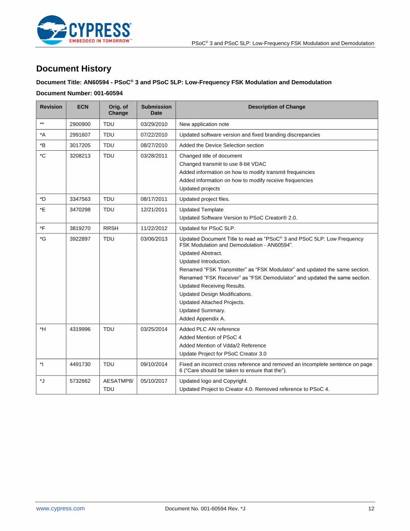
Document History
Document Title: AN60594 - PSoC® 3 and PSoC 5LP: Low-Frequency FSK Modulation and Demodulation
Document Number: 001-60594
Revision ECN Orig. of Change
Submission Date
Description of Change
** 2900900 TDU 03/29/2010 New application note
*A 2991607 TDU 07/22/2010 Updated software version and fixed branding discrepancies
*B 3017205 TDU 08/27/2010 Added the Device Selection section
*C 3208213 TDU 03/28/2011 Changed title of document
Changed transmit to use 8-bit VDAC
Added information on how to modify transmit frequencies
Added information on how to modify receive frequencies
Updated projects
*D 3347563 TDU 08/17/2011 Updated project files.
*E 3470298 TDU 12/21/2011 Updated Template
Updated Software Version to PSoC Creator® 2.0.
*F 3819270 RRSH 11/22/2012 Updated for PSoC 5LP.
*G 3922897 TDU 03/06/2013 Updated Document Title to read as “PSoC® 3 and PSoC 5LP: Low Frequency FSK Modulation and Demodulation - AN60594”.
Updated Abstract.
Updated Introduction.
Renamed “FSK Transmitter” as “FSK Modulator” and updated the same section.
Renamed “FSK Receiver” as “FSK Demodulator” and updated the same section.
Updated Receiving Results.
Updated Design Modifications.
Updated Attached Projects.
Updated Summary.
Added Appendix A.
*H 4319996 TDU 03/25/2014 Added PLC AN reference
Added Mention of PSoC 4
Added Mention of Vdda/2 Reference
Update Project for PSoC Creator 3.0
*I 4491730 TDU 09/10/2014 Fixed an incorrect cross reference and removed an incomplete sentence on page 6 (“Care should be taken to ensure that the”).
*J 5732662 AESATMP8/
TDU
05/10/2017 Updated logo and Copyright.
Updated Project to Creator 4.0. Removed reference to PSoC 4.
PSoC® 3 and PSoC 5LP: Low-Frequency FSK Modulation and Demodulation
www.cypress.com Document No. 001-60594 Rev. *J 13
Worldwide Sales and Design Support
Cypress maintains a worldwide network of offices, solution centers, manufacturer’s representatives, and distributors. To find the office closest to you, visit us at Cypress Locations.
Products
ARM® Cortex® Microcontrollers cypress.com/arm
Automotive cypress.com/automotive
Clocks & Buffers cypress.com/clocks
Interface cypress.com/interface
Internet of Things cypress.com/iot
Memory cypress.com/memory
Microcontrollers cypress.com/mcu
PSoC cypress.com/psoc
Power Management ICs cypress.com/pmic
Touch Sensing cypress.com/touch
USB Controllers cypress.com/usb
Wireless Connectivity cypress.com/wireless
PSoC® Solutions
PSoC 1 | PSoC 3 | PSoC 4 | PSoC 5LP | PSoC 6
Cypress Developer Community
Forums | WICED IOT Forums | Projects | Videos | Blogs | Training | Components
Technical Support
cypress.com/support
All other trademarks or registered trademarks referenced herein are the property of their respective owners.
Cypress Semiconductor 198 Champion Court San Jose, CA 95134-1709
© Cypress Semiconductor Corporation, 2010-2017. This document is the property of Cypress Semiconductor Corporation and its subsidiaries, including Spansion LLC (“Cypress”). This document, including any software or firmware included or referenced in this document (“Software”), is owned by Cypress under the intellectual property laws and treaties of the United States and other countries worldwide. Cypress reserves all rights under such laws and treaties and does not, except as specifically stated in this paragraph, grant any license under its patents, copyrights, trademarks, or other intellectual property rights. If the Software is not accompanied by a license agreement and you do not otherwise have a written agreement with Cypress governing the use of the Software, then Cypress hereby grants you a personal, non-exclusive, nontransferable license (without the right to sublicense) (1) under its copyright rights in the Software (a) for Software provided in source code form, to modify and reproduce the Software solely for use with Cypress hardware products, only internally within your organization, and (b) to distribute the Software in binary code form externally to end users (either directly or indirectly through resellers and distributors), solely for use on Cypress hardware product units, and (2) under those claims of Cypress’s patents that are infringed by the Software (as provided by Cypress, unmodified) to make, use, distribute, and import the Software solely for use with Cypress hardware products. Any other use, reproduction, modification, translation, or compilation of the Software is prohibited.
TO THE EXTENT PERMITTED BY APPLICABLE LAW, CYPRESS MAKES NO WARRANTY OF ANY KIND, EXPRESS OR IMPLIED, WITH REGARD TO THIS DOCUMENT OR ANY SOFTWARE OR ACCOMPANYING HARDWARE, INCLUDING, BUT NOT LIMITED TO, THE IMPLIED WARRANTIES OF MERCHANTABILITY AND FITNESS FOR A PARTICULAR PURPOSE. To the extent permitted by applicable law, Cypress reserves the right to make changes to this document without further notice. Cypress does not assume any liability arising out of the application or use of any product or circuit described in this document. Any information provided in this document, including any sample design information or programming code, is provided only for reference purposes. It is the responsibility of the user of this document to properly design, program, and test the functionality and safety of any application made of this information and any resulting product. Cypress products are not designed, intended, or authorized for use as critical components in systems designed or intended for the operation of weapons, weapons systems, nuclear installations, life-support devices or systems, other medical devices or systems (including resuscitation equipment and surgical implants), pollution control or hazardous substances management, or other uses where the failure of the device or system could cause personal injury, death, or property damage (“Unintended Uses”). A critical component is any component of a device or system whose failure to perform can be reasonably expected to cause the failure of the device or system, or to affect its safety or effectiveness. Cypress is not liable, in whole or in part, and you shall and hereby do release Cypress from any claim, damage, or other liability arising from or related to all Unintended Uses of Cypress products. You shall indemnify and hold Cypress harmless from and against all claims, costs, damages, and other liabilities, including claims for personal injury or death, arising from or related to any Unintended Uses of Cypress products.
Cypress, the Cypress logo, Spansion, the Spansion logo, and combinations thereof, WICED, PSoC, CapSense, EZ-USB, F-RAM, and Traveo are trademarks or registered trademarks of Cypress in the United States and other countries. For a more complete list of Cypress trademarks, visit cypress.com. Other names and brands may be claimed as property of their respective owners.