
PSoC 6 MCU: CY8C61x4, CY8C62x4 Architecture Technical ...
601
www.infineon.com Please note that Cypress is an Infineon Technologies Company. The document following this cover page is marked as “Cypress” document as this is the company that originally developed the product. Please note that Infineon will continue to offer the product to new and existing customers as part of the Infineon product portfolio. Continuity of document content The fact that Infineon offers the following product as part of the Infineon product portfolio does not lead to any changes to this document. Future revisions will occur when appropriate, and any changes will be set out on the document history page. Continuity of ordering part numbers Infineon continues to support existing part numbers. Please continue to use the ordering part numbers listed in the datasheet for ordering.
-
Upload
khangminh22 -
Category
Documents
-
view
0 -
download
0
Transcript of PSoC 6 MCU: CY8C61x4, CY8C62x4 Architecture Technical ...

www.infineon.com
Please note that Cypress is an Infineon Technologies Company.The document following this cover page is marked as “Cypress” document as this is the company that originally developed the product. Please note that Infineon will continue to offer the product to new and existing customers as part of the Infineon product portfolio.
Continuity of document contentThe fact that Infineon offers the following product as part of the Infineon product portfolio does not lead to any changes to this document. Future revisions will occur when appropriate, and any changes will be set out on the document history page.
Continuity of ordering part numbersInfineon continues to support existing part numbers. Please continue to use the ordering part numbers listed in the datasheet for ordering.

PSoC 6 MCU: CY8C61x4, CY8C62x4 Architecture TechnicalReference Manual (TRM) PSoC 61, PSoC 62 MCU
PSoC 6 MCU: CY8C61x4, CY8C62x4 Architecture Technical Reference Manual (TRM)
PSoC 61, PSoC 62 MCU
Document No. 002-30473 Rev. *E
February 28, 2022
Cypress SemiconductorAn Infineon Technologies Company
198 Champion CourtSan Jose, CA 95134-1709
www.cypress.comwww.infineon.com

PSoC 6 MCU: CY8C61x4, CY8C62x4 Architecture TRM, Document No. 002-30473 Rev. *E 2
Copyrights
© Cypress Semiconductor Corporation, 2020-2022. This document is the property of Cypress Semiconductor Corporation, anInfineon Technologies company, and its affiliates (“Cypress”). This document, including any software or firmware included orreferenced in this document (“Software”), is owned by Cypress under the intellectual property laws and treaties of the UnitedStates and other countries worldwide. Cypress reserves all rights under such laws and treaties and does not, except asspecifically stated in this paragraph, grant any license under its patents, copyrights, trademarks, or other intellectual propertyrights. If the Software is not accompanied by a license agreement and you do not otherwise have a written agreement withCypress governing the use of the Software, then Cypress hereby grants you a personal, non-exclusive, nontransferablelicense (without the right to sublicense) (1) under its copyright rights in the Software (a) for Software provided in source codeform, to modify and reproduce the Software solely for use with Cypress hardware products, only internally within yourorganization, and (b) to distribute the Software in binary code form externally to end users (either directly or indirectly throughresellers and distributors), solely for use on Cypress hardware product units, and (2) under those claims of Cypress's patentsthat are infringed by the Software (as provided by Cypress, unmodified) to make, use, distribute, and import the Softwaresolely for use with Cypress hardware products. Any other use, reproduction, modification, translation, or compilation of theSoftware is prohibited.
TO THE EXTENT PERMITTED BY APPLICABLE LAW, CYPRESS MAKES NO WARRANTY OF ANY KIND, EXPRESS ORIMPLIED, WITH REGARD TO THIS DOCUMENT OR ANY SOFTWARE OR ACCOMPANYING HARDWARE, INCLUDING,BUT NOT LIMITED TO, THE IMPLIED WARRANTIES OF MERCHANTABILITY AND FITNESS FOR A PARTICULARPURPOSE. No computing device can be absolutely secure. Therefore, despite security measures implemented in Cypresshardware or software products, Cypress shall have no liability arising out of any security breach, such as unauthorized accessto or use of a Cypress product. CYPRESS DOES NOT REPRESENT, WARRANT, OR GUARANTEE THAT CYPRESSPRODUCTS, OR SYSTEMS CREATED USING CYPRESS PRODUCTS, WILL BE FREE FROM CORRUPTION, ATTACK,VIRUSES, INTERFERENCE, HACKING, DATA LOSS OR THEFT, OR OTHER SECURITY INTRUSION (collectively,"Security Breach"). Cypress disclaims any liability relating to any Security Breach, and you shall and hereby do releaseCypress from any claim, damage, or other liability arising from any Security Breach. In addition, the products described inthese materials may contain design defects or errors known as errata which may cause the product to deviate from publishedspecifications. To the extent permitted by applicable law, Cypress reserves the right to make changes to this documentwithout further notice. Cypress does not assume any liability arising out of the application or use of any product or circuitdescribed in this document. Any information provided in this document, including any sample design information orprogramming code, is provided only for reference purposes. It is the responsibility of the user of this document to properlydesign, program, and test the functionality and safety of any application made of this information and any resulting product."High-Risk Device" means any device or system whose failure could cause personal injury, death, or property damage.Examples of High-Risk Devices are weapons, nuclear installations, surgical implants, and other medical devices. "CriticalComponent" means any component of a High-Risk Device whose failure to perform can be reasonably expected to cause,directly or indirectly, the failure of the High-Risk Device, or to affect its safety or effectiveness. Cypress is not liable, in wholeor in part, and you shall and hereby do release Cypress from any claim, damage, or other liability arising from any use of aCypress product as a Critical Component in a High-Risk Device. You shall indemnify and hold Cypress, including its affiliates,and its directors, officers, employees, agents, distributors, and assigns harmless from and against all claims, costs, damages,and expenses, arising out of any claim, including claims for product liability, personal injury or death, or property damagearising from any use of a Cypress product as a Critical Component in a High-Risk Device. Cypress products are not intendedor authorized for use as a Critical Component in any High-Risk Device except to the limited extent that (i) Cypress's publisheddata sheet for the product explicitly states Cypress has qualified the product for use in a specific High-Risk Device, or (ii)Cypress has given you advance written authorization to use the product as a Critical Component in the specific High-RiskDevice and you have signed a separate indemnification agreement.
Cypress, the Cypress logo, and combinations thereof, PSoC, CapSense, EZ-USB, F-RAM, Traveo, WICED, andModusToolbox are trademarks or registered trademarks of Cypress or a subsidiary of Cypress in the United States or in othercountries. For a more complete list of Cypress trademarks, visit cypress.com. Other names and brands may be claimed asproperty of their respective owners.

PSoC 6 MCU: CY8C61x4, CY8C62x4 Architecture TRM, Document No. 002-30473 Rev. *E 3
Content Overview
Section A: Overview 18
1. Introduction ................................................................................................................... 19
2. Getting Started .............................................................................................................. 24
3. Document Organization and Conventions ....................................................................... 25
Section B: CPU Subsystem 294. CPU Subsystem (CPUSS) ............................................................................................. 31
5. SRAM Controller ........................................................................................................... 38
6. Protection Units ............................................................................................................. 40
7. Inter-Processor Communication ..................................................................................... 58
8. Fault Monitoring ............................................................................................................ 66
9. Interrupts ...................................................................................................................... 73
10. DMA Controller (DW) ..................................................................................................... 90
11. DMAC Controller (DMAC) ............................................................................................ 101
12. Cryptographic Function Block (Crypto) ......................................................................... 110
13. Program and Debug Interface ...................................................................................... 153
14. Nonvolatile Memory ..................................................................................................... 163
15. Boot Code ................................................................................................................... 192
16. eFuse Memory ............................................................................................................ 209
17. Device Security ........................................................................................................... 211
Section C: System Resources Subsystem (SRSS) 21318. I/O System .................................................................................................................. 214
19. Reset System .............................................................................................................. 236
20. Clocking System.......................................................................................................... 240
21. Backup System ........................................................................................................... 255
22. Watchdog Timer .......................................................................................................... 262
23. Power Supply and Monitoring ...................................................................................... 273
24. Device Power Modes ................................................................................................... 280
25. Trigger Multiplexer Block ............................................................................................. 290
Section D: Digital Subsystem 296
26. Serial Communications Block (SCB) ............................................................................ 298
27. Serial Memory Interface (SMIF) ................................................................................... 355
28. CAN FD Controller ...................................................................................................... 372
29. Timer, Counter, PWM .................................................................................................. 427

PSoC 6 MCU: CY8C61x4, CY8C62x4 Architecture TRM, Document No. 002-30473 Rev. *E 4
Content Overview
30. Universal Serial Bus (USB) Host .................................................................................. 489
31. Universal Serial Bus (USB) Device Mode ..................................................................... 506
32. LCD Direct Drive ......................................................................................................... 522
Section E: Analog Subsystem 535
33. CapSense ................................................................................................................... 536
34. Analog Reference Block .............................................................................................. 537
35. Temperature Sensor .................................................................................................... 541
36. SAR ADC .................................................................................................................... 545
37. Low-Power Comparator ............................................................................................... 570
38. Continuous Time DAC ................................................................................................. 576
39. Continuous Time Block mini (CTBm) ............................................................................ 589
40. Analog Routing ............................................................................................................ 597

PSoC 6 MCU: CY8C61x4, CY8C62x4 Architecture TRM, Document No. 002-30473 Rev. *E 5
Contents
Section A: Overview 18
1. Introduction 191.1 Features..................................................................................................................................191.2 PSoC 61 and PSoC 62 MCU Series Differences ...................................................................221.3 Architecture.............................................................................................................................22
2. Getting Started 24
2.1 PSoC 6 MCU Resources ........................................................................................................24
3. Document Organization and Conventions 25
3.1 Major Sections ........................................................................................................................253.2 Documentation Conventions...................................................................................................25
3.2.1 Register Conventions.............................................................................................253.2.2 Numeric Naming ....................................................................................................253.2.3 Units of Measure....................................................................................................263.2.4 Acronyms and Initializations ..................................................................................26
Section B: CPU Subsystem 29
4. CPU Subsystem (CPUSS) 314.1 Features..................................................................................................................................314.2 Architecture.............................................................................................................................32
4.2.1 Address and Memory Maps ...................................................................................334.3 Registers.................................................................................................................................344.4 Operating Modes and Privilege Levels ...................................................................................364.5 Instruction Set.........................................................................................................................37
5. SRAM Controller 38
5.1 Features..................................................................................................................................385.2 Architecture.............................................................................................................................385.3 Wait States .............................................................................................................................39
6. Protection Units 40
6.1 Architecture.............................................................................................................................406.2 PSoC 6 Protection Architecture ..............................................................................................416.3 Register Architecture ..............................................................................................................43
6.3.1 Protection Structure and Attributes ........................................................................436.4 Bus Master Protection Attributes ............................................................................................466.5 Protection Context ..................................................................................................................466.6 Protection Contexts 0, 1, 2, 3 .................................................................................................476.7 Protection Structure ................................................................................................................48
6.7.1 Protection Violation ................................................................................................486.7.2 MPU.......................................................................................................................486.7.3 SMPU.....................................................................................................................48

PSoC 6 MCU: CY8C61x4, CY8C62x4 Architecture TRM, Document No. 002-30473 Rev. *E 6
Contents
6.7.4 PPU........................................................................................................................496.7.5 Protection of Protection Structures ........................................................................556.7.6 Protection Structure Types.....................................................................................56
7. Inter-Processor Communication 58
7.1 Features..................................................................................................................................597.2 Architecture.............................................................................................................................59
7.2.1 IPC Channel...........................................................................................................597.2.2 IPC Interrupt...........................................................................................................607.2.3 IPC Channels and Interrupts..................................................................................60
7.3 Implementing Locks................................................................................................................617.4 Message Passing ...................................................................................................................617.5 Typical Usage Models ............................................................................................................63
7.5.1 Full Duplex Communication ...................................................................................637.5.2 Half Duplex with Independent Event Handling.......................................................647.5.3 Half Duplex with Shared Event Handling ...............................................................64
8. Fault Monitoring 66
8.1 Features..................................................................................................................................668.2 Architecture.............................................................................................................................67
8.2.1 Fault Report ...........................................................................................................678.2.2 Signaling Interface .................................................................................................698.2.3 Monitoring ..............................................................................................................698.2.4 Low-power Mode Operation...................................................................................708.2.5 Using a Fault Structure ..........................................................................................708.2.6 CPU Exceptions Versus Fault Monitoring ..............................................................70
8.3 Fault Sources..........................................................................................................................718.4 Register List............................................................................................................................72
9. Interrupts 739.1 Features..................................................................................................................................739.2 Architecture.............................................................................................................................749.3 Interrupts and Exceptions - Operation ....................................................................................75
9.3.1 Interrupt/Exception Handling..................................................................................759.3.2 Level and Pulse Interrupts .....................................................................................769.3.3 Exception Vector Table ..........................................................................................76
9.4 Exception Sources..................................................................................................................779.4.1 Reset Exception.....................................................................................................779.4.2 Non-Maskable Interrupt Exception.........................................................................779.4.3 HardFault Exception ..............................................................................................789.4.4 Memory Management Fault Exception ..................................................................789.4.5 Bus Fault Exception ...............................................................................................789.4.6 Usage Fault Exception...........................................................................................789.4.7 Supervisor Call (SVCall) Exception .......................................................................799.4.8 PendSupervisory (PendSV) Exception ..................................................................799.4.9 System Tick (SysTick) Exception ...........................................................................79
9.5 Interrupt Sources ....................................................................................................................799.6 Interrupt/Exception Priority .....................................................................................................869.7 Enabling and Disabling Interrupts...........................................................................................869.8 Interrupt/Exception States ......................................................................................................87
9.8.1 Pending Interrupts/Exceptions ...............................................................................879.9 Stack Usage for Interrupts/Exceptions ...................................................................................889.10 Interrupts and Low-Power Modes...........................................................................................88
PSoC 6 MCU: CY8C61x4, CY8C62x4 Architecture TRM, Document No. 002-30473 Rev. *E 7
Contents
9.11 Interrupt/Exception – Initialization/ Configuration ...................................................................889.12 Register List............................................................................................................................89
10. DMA Controller (DW) 90
10.1 Features..................................................................................................................................9010.2 Architecture.............................................................................................................................9110.3 Channels.................................................................................................................................91
10.3.1 Channel Interrupts .................................................................................................9210.4 Descriptors..............................................................................................................................93
10.4.1 Address Configuration ...........................................................................................9510.4.2 Transfer Size..........................................................................................................9610.4.3 Descriptor Chaining ...............................................................................................97
10.5 DMA Controller .......................................................................................................................9810.5.1 Trigger Selection....................................................................................................9810.5.2 Pending Triggers....................................................................................................9810.5.3 Output Triggers ......................................................................................................9810.5.4 Status registers ......................................................................................................9810.5.5 DMA Performance..................................................................................................99
11. DMAC Controller (DMAC) 101
11.1 Features................................................................................................................................10111.2 Architecture...........................................................................................................................10211.3 Channels...............................................................................................................................102
11.3.1 Channel Interrupts ...............................................................................................10311.4 Descriptors............................................................................................................................104
11.4.1 Address Configuration .........................................................................................10611.4.2 Transfer Size........................................................................................................10811.4.3 Descriptor Chaining .............................................................................................108
11.5 DMAC Controller...................................................................................................................10911.5.1 Trigger Selection..................................................................................................10911.5.2 Channel Logic ......................................................................................................10911.5.3 Output Triggers ....................................................................................................109
12. Cryptographic Function Block (Crypto) 11012.1 Features................................................................................................................................11012.2 Architecture...........................................................................................................................11112.3 Instruction Controller.............................................................................................................112
12.3.1 Instructions...........................................................................................................11212.3.2 Instruction Operands............................................................................................11312.3.3 Load and Store FIFO Instructions........................................................................11312.3.4 Register Buffer Instructions..................................................................................115
12.4 Hash Algorithms ...................................................................................................................11912.4.1 SHA1 and SHA2 ..................................................................................................11912.4.2 SHA3....................................................................................................................121
12.5 DES and TDES.....................................................................................................................12212.6 AES.......................................................................................................................................12412.7 CRC ......................................................................................................................................12612.8 PRNG ...................................................................................................................................12812.9 TRNG....................................................................................................................................12912.10 Vector Unit ............................................................................................................................135
12.10.1 VU Register File...................................................................................................13612.10.2 Stack ....................................................................................................................13712.10.3 Memory Operands ...............................................................................................138

PSoC 6 MCU: CY8C61x4, CY8C62x4 Architecture TRM, Document No. 002-30473 Rev. *E 8
Contents
12.10.4 Datapath ..............................................................................................................13812.10.5 Status Register ....................................................................................................13912.10.6 Instructions...........................................................................................................14012.10.7 Instruction Set ......................................................................................................140
13. Program and Debug Interface 153
13.1 Features................................................................................................................................15313.2 Architecture...........................................................................................................................153
13.2.1 Debug Access Port (DAP)....................................................................................15513.2.2 ROM Tables .........................................................................................................15513.2.3 Trace....................................................................................................................15513.2.4 Embedded Cross Triggering ................................................................................156
13.3 Serial Wire Debug (SWD) Interface......................................................................................15613.3.1 SWD Timing Details .............................................................................................15713.3.2 ACK Details..........................................................................................................15713.3.3 Turnaround (Trn) Period Details ..........................................................................158
13.4 JTAG Interface......................................................................................................................15813.5 Programming the PSoC 6 MCU............................................................................................161
13.5.1 SWD Port Acquisition...........................................................................................16113.5.2 SWD Programming Mode Entry...........................................................................16113.5.3 SWD Programming Routine Executions ..............................................................161
13.6 Registers...............................................................................................................................162
14. Nonvolatile Memory 163
14.1 Flash Memory .......................................................................................................................16314.1.1 Features...............................................................................................................16314.1.2 Configuration........................................................................................................16314.1.3 Flash Geometry ...................................................................................................16414.1.4 Flash Controller....................................................................................................16514.1.5 Read While Write (RWW) Support.......................................................................166
14.2 Flash Memory Programming ................................................................................................16614.2.1 Features...............................................................................................................16614.2.2 Architecture..........................................................................................................166
14.3 System Call Implementation .................................................................................................16714.3.1 System Call via CM0+ or CM4.............................................................................16714.3.2 System Call via DAP............................................................................................16814.3.3 Exiting from a System Call...................................................................................16814.3.4 SRAM Usage .......................................................................................................168
14.4 SROM API Library ................................................................................................................16914.5 System Calls.........................................................................................................................170
14.5.1 Cypress ID ...........................................................................................................17014.5.2 Blow eFuse Bit .....................................................................................................17214.5.3 Read eFuse Byte .................................................................................................17314.5.4 Write Row ............................................................................................................17414.5.5 Program Row.......................................................................................................17514.5.6 Erase All...............................................................................................................17714.5.7 Checksum............................................................................................................17814.5.8 FmTransitionToLpUlp...........................................................................................17914.5.9 Compute Hash .....................................................................................................18014.5.10 ConfigureRegionBulk ...........................................................................................18114.5.11 DirectExecute.......................................................................................................18214.5.12 Erase Sector ........................................................................................................18214.5.13 Soft Reset ............................................................................................................183

PSoC 6 MCU: CY8C61x4, CY8C62x4 Architecture TRM, Document No. 002-30473 Rev. *E 9
Contents
14.5.14 Erase Row ...........................................................................................................18414.5.15 Erase Subsector ..................................................................................................18514.5.16 GenerateHash......................................................................................................18614.5.17 ReadUniqueID .....................................................................................................18714.5.18 CheckFactoryHash ..............................................................................................18714.5.19 TransitionToRMA..................................................................................................18814.5.20 ReadFuseByteMargin ..........................................................................................18914.5.21 TransitionToSecure ..............................................................................................190
14.6 System Call Status ...............................................................................................................191
15. Boot Code 192
15.1 Features................................................................................................................................19215.2 ROM Boot .............................................................................................................................192
15.2.1 Data Integrity Checks...........................................................................................19215.2.2 Life-cycle Stages and Protection States ..............................................................19515.2.3 Secure Boot in ROM Boot....................................................................................19815.2.4 Protection Setting.................................................................................................19815.2.5 SWD/JTAG Repurposing .....................................................................................20015.2.6 Waking up from Hibernate ...................................................................................20015.2.7 Disable Watchdog Timer......................................................................................20015.2.8 ROM Boot Flow Chart..........................................................................................200
15.3 Flash Boot.............................................................................................................................20215.3.1 Overview..............................................................................................................20215.3.2 Features of Flash Boot.........................................................................................20215.3.3 Using Flash Boot..................................................................................................20215.3.4 Flash Boot Layout ................................................................................................20215.3.5 Flash Boot Flow Chart .........................................................................................203
16. eFuse Memory 209
16.1 Features................................................................................................................................20916.2 Architecture...........................................................................................................................209
17. Device Security 21117.1 Features................................................................................................................................21117.2 Architecture...........................................................................................................................211
17.2.1 Life Cycle Stages and Protection States..............................................................21117.2.2 Flash Security ......................................................................................................21217.2.3 Hardware-Based Encryption ................................................................................212
Section C: System Resources Subsystem (SRSS) 213
18. I/O System 214
18.1 Features................................................................................................................................21418.2 Architecture...........................................................................................................................215
18.2.1 I/O Cell Architecture .............................................................................................21618.2.2 Digital Input Buffer ...............................................................................................21718.2.3 Digital Output Driver.............................................................................................217
18.3 High-Speed I/O Matrix ..........................................................................................................22018.4 I/O State on Power Up..........................................................................................................22218.5 Behavior in Low-Power Modes .............................................................................................22218.6 Interrupt ................................................................................................................................22218.7 Peripheral Connections ........................................................................................................223
18.7.1 Firmware-Controlled GPIO ..................................................................................22318.7.2 Analog I/O ............................................................................................................224
PSoC 6 MCU: CY8C61x4, CY8C62x4 Architecture TRM, Document No. 002-30473 Rev. *E 10
Contents
18.7.3 LCD Drive ............................................................................................................22418.7.4 CapSense ............................................................................................................224
18.8 Smart I/O .............................................................................................................................22418.8.1 Overview..............................................................................................................22418.8.2 Block Components...............................................................................................22518.8.3 Routing.................................................................................................................23218.8.4 Operation .............................................................................................................234
18.9 Registers...............................................................................................................................235
19. Reset System 236
19.1 Features................................................................................................................................23619.2 Architecture...........................................................................................................................236
19.2.1 Power-on Reset ...................................................................................................23719.2.2 Brownout Reset ...................................................................................................23719.2.3 Watchdog Timer Reset ........................................................................................23719.2.4 Software Initiated Reset.......................................................................................23819.2.5 External Reset .....................................................................................................23819.2.6 Logic Protection Fault Reset................................................................................23819.2.7 Clock-Supervision Logic Reset ............................................................................23819.2.8 Hibernate Wakeup Reset .....................................................................................238
19.3 Identifying Reset Sources.....................................................................................................23819.4 Register List..........................................................................................................................239
20. Clocking System 240
20.1 Features................................................................................................................................24020.2 Architecture...........................................................................................................................24120.3 Clock Sources.......................................................................................................................242
20.3.1 Internal Main Oscillator (IMO) ..............................................................................24220.3.2 External Crystal Oscillator (ECO) ........................................................................24220.3.3 External Clock (EXTCLK) ....................................................................................24220.3.4 Internal Low-speed Oscillator (ILO) .....................................................................24220.3.5 Watch Crystal Oscillator (WCO)...........................................................................243
20.4 Clock Generation ..................................................................................................................24320.4.1 Phase-Locked Loop (PLL) ...................................................................................24320.4.2 Frequency Lock Loop (FLL).................................................................................244
20.5 Clock Trees...........................................................................................................................24920.5.1 Path Clocks..........................................................................................................24920.5.2 High-Frequency Root Clocks ...............................................................................24920.5.3 Medium-Frequency Clock ....................................................................................25020.5.4 Low-Frequency Clock ..........................................................................................25020.5.5 Timer Clock..........................................................................................................25020.5.6 Group Clocks (clk_sys) ........................................................................................25020.5.7 Backup Clock (clk_bak) .......................................................................................250
20.6 CLK_HF[0] Distribution .........................................................................................................25120.6.1 CLK_FAST...........................................................................................................25120.6.2 CLK_PERI............................................................................................................25120.6.3 CLK_SLOW .........................................................................................................251
20.7 Peripheral Clock Dividers .....................................................................................................25120.7.1 Fractional Clock Dividers .....................................................................................25120.7.2 Peripheral Clock Divider Configuration ................................................................251
20.8 Clock Calibration Counters ...................................................................................................254

PSoC 6 MCU: CY8C61x4, CY8C62x4 Architecture TRM, Document No. 002-30473 Rev. *E 11
Contents
21. Backup System 255
21.1 Features................................................................................................................................25521.2 Architecture...........................................................................................................................25621.3 Power Supply........................................................................................................................25621.4 Clocking ................................................................................................................................257
21.4.1 WCO with External Clock/Sine Wave Input .........................................................25721.4.2 Calibration............................................................................................................257
21.5 Reset ....................................................................................................................................25821.6 Real-Time Clock ...................................................................................................................258
21.6.1 Reading RTC User Registers ..............................................................................25821.6.2 Writing to RTC User Registers.............................................................................258
21.7 Alarm Feature .......................................................................................................................25921.8 PMIC Control ........................................................................................................................26021.9 Backup Registers..................................................................................................................26121.10 Register List..........................................................................................................................261
22. Watchdog Timer 262
22.1 Features................................................................................................................................26222.2 Architecture...........................................................................................................................26222.3 Free-running WDT ................................................................................................................263
22.3.1 Overview..............................................................................................................26322.3.2 Watchdog Reset ..................................................................................................26522.3.3 Watchdog Interrupt ..............................................................................................265
22.4 Multi-Counter WDTs .............................................................................................................26622.4.1 Overview..............................................................................................................26622.4.2 Enabling and Disabling WDT...............................................................................26922.4.3 Watchdog Cascade Options ................................................................................27022.4.4 MCDWT Reset.....................................................................................................27122.4.5 MCWDT Interrupt.................................................................................................271
22.5 Reset Cause Detection.........................................................................................................27222.6 Register List..........................................................................................................................272
23. Power Supply and Monitoring 27323.1 Features................................................................................................................................27323.2 Architecture...........................................................................................................................27423.3 Power Supply........................................................................................................................275
23.3.1 Regulators Summary ...........................................................................................27523.3.2 Power Pins and Rails...........................................................................................27723.3.3 Power Sequencing Requirements .......................................................................27723.3.4 Backup Domain....................................................................................................27723.3.5 Power Supply Sources.........................................................................................277
23.4 Voltage Monitoring................................................................................................................27723.4.1 Power-On-Reset (POR) .......................................................................................27723.4.2 Brownout-Detect (BOD) .......................................................................................27723.4.3 Low-Voltage-Detect (LVD) ...................................................................................27823.4.4 Over-Voltage Protection (OVP)............................................................................279
23.5 Register List .........................................................................................................................279
24. Device Power Modes 28024.1 Features................................................................................................................................28024.2 Architecture...........................................................................................................................280
24.2.1 CPU Power Modes ..............................................................................................28224.2.2 System Power Modes ..........................................................................................282
PSoC 6 MCU: CY8C61x4, CY8C62x4 Architecture TRM, Document No. 002-30473 Rev. *E 12
Contents
24.2.3 System Deep Sleep Mode ...................................................................................28224.2.4 System Hibernate Mode ......................................................................................28324.2.5 Other Operation Modes .......................................................................................283
24.3 Power Mode Transitions .......................................................................................................28424.3.1 Power-up Transitions ...........................................................................................28524.3.2 Power Mode Transitions ......................................................................................28524.3.3 Wakeup Transitions .............................................................................................287
24.4 Summary ..............................................................................................................................28824.5 Register List..........................................................................................................................289
25. Trigger Multiplexer Block 290
25.1 Features................................................................................................................................29025.2 Architecture...........................................................................................................................290
25.2.1 Trigger Multiplexer Group ....................................................................................29125.2.2 One-to-one Trigger...............................................................................................29125.2.3 Trigger Multiplexer Block .....................................................................................29125.2.4 Software Triggers.................................................................................................294
25.3 Register List .......................................................................................................................294
Section D: Digital Subsystem 296
26. Serial Communications Block (SCB) 29826.1 Features................................................................................................................................29826.2 Architecture...........................................................................................................................299
26.2.1 Buffer Modes........................................................................................................29926.2.2 Clocking Modes ...................................................................................................299
26.3 Serial Peripheral Interface (SPI) ...........................................................................................30026.3.1 Features...............................................................................................................30026.3.2 General Description .............................................................................................30126.3.3 SPI Modes of Operation.......................................................................................30226.3.4 SPI Buffer Modes.................................................................................................30726.3.5 Clocking and Oversampling .................................................................................31226.3.6 Enabling and Initializing SPI ................................................................................31426.3.7 I/O Pad Connection..............................................................................................31526.3.8 SPI Registers .......................................................................................................317
26.4 UART....................................................................................................................................31826.4.1 Features...............................................................................................................31826.4.2 General Description .............................................................................................31826.4.3 UART Modes of Operation...................................................................................31826.4.4 Clocking and Oversampling .................................................................................32826.4.5 Enabling and Initializing the UART ......................................................................32826.4.6 I/O Pad Connection..............................................................................................32926.4.7 UART Registers ...................................................................................................331
26.5 Inter Integrated Circuit (I2C) .................................................................................................33226.5.1 Features...............................................................................................................33226.5.2 General Description .............................................................................................33226.5.3 External Electrical Connections ...........................................................................33326.5.4 Terms and Definitions ..........................................................................................33426.5.5 I2C Modes of Operation.......................................................................................33426.5.6 I2C Buffer Modes .................................................................................................33626.5.7 Clocking and Oversampling .................................................................................34026.5.8 Enabling and Initializing the I2C...........................................................................34326.5.9 I/O Pad Connections............................................................................................34426.5.10 I2C Registers .......................................................................................................345

PSoC 6 MCU: CY8C61x4, CY8C62x4 Architecture TRM, Document No. 002-30473 Rev. *E 13
Contents
26.6 SCB Interrupts ......................................................................................................................34626.6.1 SPI Interrupts .......................................................................................................34726.6.2 UART Interrupts ...................................................................................................34926.6.3 I2C Interrupts .......................................................................................................353
27. Serial Memory Interface (SMIF) 355
27.1 Features................................................................................................................................35527.2 Architecture...........................................................................................................................355
27.2.1 Tx and Rx FIFOs..................................................................................................35827.2.2 Command Mode ..................................................................................................35927.2.3 XIP Mode .............................................................................................................35927.2.4 Cache...................................................................................................................36027.2.5 Arbitration.............................................................................................................36027.2.6 Deselect Delay.....................................................................................................36027.2.7 Cryptography .......................................................................................................360
27.3 Memory Device Signal Interface...........................................................................................36227.3.1 Specifying Memory Devices.................................................................................36227.3.2 Connecting SPI Memory Devices ........................................................................36227.3.3 SPI Data Transfer ................................................................................................36727.3.4 Example of Setting up SMIF ................................................................................369
27.4 Triggers.................................................................................................................................37027.5 Interrupts...............................................................................................................................37127.6 Sleep Operation....................................................................................................................37127.7 Performance .........................................................................................................................371
28. CAN FD Controller 372
28.1 Overview...............................................................................................................................37228.1.1 Features...............................................................................................................37228.1.2 Features Not Supported.......................................................................................373
28.2 Configuration ........................................................................................................................37328.2.1 Block Diagram......................................................................................................37328.2.2 Dual Clock Sources .............................................................................................37328.2.3 Interrupt Lines ......................................................................................................373
28.3 Functional Description ..........................................................................................................37428.3.1 Operation Modes .................................................................................................37428.3.2 Timestamp Generation ........................................................................................37828.3.3 Timeout Counter ..................................................................................................37928.3.4 RX Handling.........................................................................................................37928.3.5 TX Handling .........................................................................................................38628.3.6 FIFO Acknowledge Handling ...............................................................................38928.3.7 Configuring the CAN Bit Timing ...........................................................................389
28.4 Message RAM ......................................................................................................................39228.4.1 Message RAM Configuration ...............................................................................39228.4.2 RX Buffer and FIFO Element ...............................................................................39328.4.3 TX Buffer Element................................................................................................39528.4.4 TX Event FIFO Element.......................................................................................39628.4.5 Standard Message ID Filter Element ...................................................................39728.4.6 Extended Message ID Filter Element ..................................................................39828.4.7 Trigger Memory Element .....................................................................................40028.4.8 MRAM OFF..........................................................................................................40128.4.9 RAM Watchdog (RWD) ........................................................................................401
28.5 TTCAN Operation .................................................................................................................40128.5.1 Reference Message.............................................................................................401

PSoC 6 MCU: CY8C61x4, CY8C62x4 Architecture TRM, Document No. 002-30473 Rev. *E 14
Contents
28.5.2 TTCAN Configuration...........................................................................................40228.5.3 TTCAN Gap Control.............................................................................................40728.5.4 Stop Watch ..........................................................................................................40828.5.5 Local Time, Cycle Time, Global Time, and External Clock Synchronization........40828.5.6 TTCAN Error Level ..............................................................................................41028.5.7 TTCAN Message Handling ..................................................................................41028.5.8 TTCAN Interrupt and Error Handling ...................................................................41228.5.9 Level 0 .................................................................................................................41228.5.10 Synchronization to External Time Schedule ........................................................414
28.6 Setup Procedures .................................................................................................................41528.6.1 General Program Flow.........................................................................................41528.6.2 Clock Stop Request .............................................................................................41528.6.3 MRAM OFF Operation .........................................................................................41528.6.4 MRAM ON Operation...........................................................................................41528.6.5 Procedures Specific to M_TTCAN Channel.........................................................416
28.7 Registers...............................................................................................................................424
29. Timer, Counter, PWM 427
29.1 Features................................................................................................................................42729.2 Block Diagram ......................................................................................................................428
29.2.1 Enabling and Disabling Counters in TCPWM ......................................................42929.2.2 Clocking ...............................................................................................................42929.2.3 Trigger Inputs.......................................................................................................43029.2.4 Trigger Outputs ....................................................................................................43229.2.5 Internal Events .....................................................................................................43329.2.6 Interrupts..............................................................................................................43629.2.7 Debug Mode ........................................................................................................43729.2.8 PWM Outputs.......................................................................................................43729.2.9 Power Modes .......................................................................................................438
29.3 Operation Modes ..................................................................................................................43829.3.1 Timer Mode..........................................................................................................43929.3.2 Capture Mode ......................................................................................................44629.3.3 Quadrature Decoder Mode ..................................................................................44929.3.4 Pulse Width Modulation (PWM) Mode .................................................................46029.3.5 Pulse Width Modulation with Dead Time Mode ...................................................47629.3.6 Pulse Width Modulation Pseudo-Random Mode (PWM PR) ...............................47829.3.7 Shift Register (SR) ...............................................................................................483
29.4 Design Configuration Parameters.........................................................................................48629.5 Recovery...............................................................................................................................48729.6 Initialize.................................................................................................................................48729.7 Pin Status .............................................................................................................................48729.8 TCPWM Registers ................................................................................................................488
30. Universal Serial Bus (USB) Host 489
30.1 Features................................................................................................................................48930.2 Architecture...........................................................................................................................490
30.2.1 USB Physical Layer (USB PHY) .........................................................................49030.2.2 Clock Control Block..............................................................................................49030.2.3 Interrupt Control Block .........................................................................................49030.2.4 Endpoint n (n=1, 2) ..............................................................................................49030.2.5 DMA Request (DREQ) Control ............................................................................490
30.3 USB Host Operations ...........................................................................................................49130.3.1 Detecting Device Connection...............................................................................491

PSoC 6 MCU: CY8C61x4, CY8C62x4 Architecture TRM, Document No. 002-30473 Rev. *E 15
Contents
30.3.2 Obtaining Transfer Speed of the USB Device......................................................49130.3.3 USB Bus Reset ....................................................................................................49230.3.4 USB Packets........................................................................................................49330.3.5 Retry Function......................................................................................................49730.3.6 Error Status..........................................................................................................49730.3.7 End of Packet (EOP)............................................................................................49830.3.8 Interrupt Sources .................................................................................................49830.3.9 DMA Transfer Function ........................................................................................50030.3.10 Suspend and Resume Operations.......................................................................50430.3.11 Device Disconnection ..........................................................................................504
30.4 USB Host Registers..............................................................................................................505
31. Universal Serial Bus (USB) Device Mode 506
31.1 Features................................................................................................................................50631.2 Architecture...........................................................................................................................507
31.2.1 USB Physical Layer (USB PHY) ..........................................................................50731.2.2 Serial Interface Engine (SIE) ...............................................................................50731.2.3 Arbiter ..................................................................................................................507
31.3 Operation ..............................................................................................................................50831.3.1 USB Clocking Scheme.........................................................................................50831.3.2 USB PHY .............................................................................................................50831.3.3 Endpoints .............................................................................................................50931.3.4 Transfer Types .....................................................................................................50931.3.5 Interrupt Sources .................................................................................................50931.3.6 DMA Support........................................................................................................511
31.4 Logical Transfer Modes ........................................................................................................51231.4.1 Manual Memory Management with No DMA Access ...........................................51431.4.2 Manual Memory Management with DMA Access.................................................51431.4.3 Automatic DMA Mode ..........................................................................................51631.4.4 Control Endpoint Logical Transfer........................................................................518
31.5 USB Power Modes ...............................................................................................................52031.6 USB Device Registers ..........................................................................................................520
32. LCD Direct Drive 522
32.1 Features................................................................................................................................52232.2 Architecture...........................................................................................................................522
32.2.1 LCD Segment Drive Overview .............................................................................52232.2.2 Drive Modes.........................................................................................................52332.2.3 Recommended Usage of Drive Modes ................................................................53232.2.4 Digital Contrast Control........................................................................................532
32.3 PSoC 6 MCU Segment LCD Direct Drive.............................................................................53332.3.1 High-Speed and Low-Speed Master Generators.................................................53332.3.2 Multiplexer and LCD Pin Logic.............................................................................53432.3.3 Display Data Registers ........................................................................................534
32.4 Register List .........................................................................................................................534
Section E: Analog Subsystem 535
33. CapSense 536
34. Analog Reference Block 537
34.1 Features................................................................................................................................53734.2 Architecture...........................................................................................................................538
34.2.1 Bandgap Reference Block ...................................................................................539
PSoC 6 MCU: CY8C61x4, CY8C62x4 Architecture TRM, Document No. 002-30473 Rev. *E 16
Contents
34.2.2 VREF Reference Voltage Selection Multiplexer Options .....................................53934.2.3 Zero Dependency To Absolute Temperature Current Generator (IZTAT).............53934.2.4 Startup Modes......................................................................................................54034.2.5 Low-Power Modes ...............................................................................................540
34.3 Registers...............................................................................................................................540
35. Temperature Sensor 541
35.1 Features................................................................................................................................54135.2 Architecture...........................................................................................................................54135.3 SAR ADC Configuration for Measurement ...........................................................................54335.4 Algorithm...............................................................................................................................54335.5 Registers...............................................................................................................................544
36. SAR ADC 54536.1 Features................................................................................................................................54536.2 Architecture...........................................................................................................................546
36.2.1 SAR ADC Core ....................................................................................................54736.2.2 SAR Reference ....................................................................................................54736.2.3 SARMUX..............................................................................................................54936.2.4 SAR Sequencer (SARSEQ).................................................................................55136.2.5 Injection Channel .................................................................................................55936.2.6 FIFO Buffer ..........................................................................................................56136.2.7 Trigger..................................................................................................................56136.2.8 Timer....................................................................................................................56336.2.9 Low-power SAR ADC Operation..........................................................................56436.2.10 SAR Interrupts .....................................................................................................56636.2.11 SAR ADC Status ..................................................................................................567
36.3 Registers...............................................................................................................................567
37. Low-Power Comparator 57037.1 Features................................................................................................................................57037.2 Architecture...........................................................................................................................571
37.2.1 Input Configuration...............................................................................................57137.2.2 Output and Interrupt Configuration ......................................................................57237.2.3 Power Mode and Speed Configuration ................................................................57337.2.4 Hysteresis ............................................................................................................57437.2.5 Wakeup from Low-Power Modes.........................................................................57437.2.6 Comparator Clock ................................................................................................57537.2.7 Using Low-Power Comparators ...........................................................................575
37.3 Register List .........................................................................................................................575
38. Continuous Time DAC 576
38.1 Features................................................................................................................................57638.2 Architecture...........................................................................................................................577
38.2.1 CTDAC Core........................................................................................................57838.2.2 CTDAC Control Interface .....................................................................................58338.2.3 Deglitch Operation ...............................................................................................58638.2.4 Using CTDAC ......................................................................................................587
38.3 Register List..........................................................................................................................588
39. Continuous Time Block mini (CTBm) 589
39.1 Features................................................................................................................................58939.2 Architecture...........................................................................................................................590
39.2.1 Power Mode and Output Strength Configuration .................................................591

PSoC 6 MCU: CY8C61x4, CY8C62x4 Architecture TRM, Document No. 002-30473 Rev. *E 17
Contents
39.2.2 Deep Sleep Operation .........................................................................................59239.2.3 Charge Pump.......................................................................................................59339.2.4 Reference Currents..............................................................................................59339.2.5 Compensation Trim Bits.......................................................................................59339.2.6 Switching Matrix...................................................................................................59339.2.7 Sample and Hold .................................................................................................59439.2.8 Comparator Mode................................................................................................59539.2.9 Using CTBm Opamp............................................................................................596
39.3 Register List..........................................................................................................................596
40. Analog Routing 597
40.1 Features................................................................................................................................59740.2 Architecture...........................................................................................................................598
40.2.1 AMUXBUS Splitting .............................................................................................59940.3 Register List..........................................................................................................................600
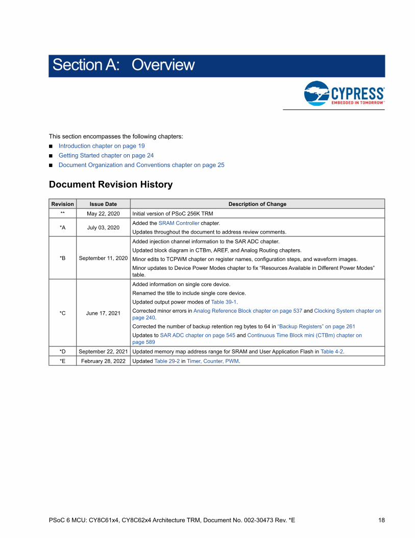
PSoC 6 MCU: CY8C61x4, CY8C62x4 Architecture TRM, Document No. 002-30473 Rev. *E 18
Section A: Overview
This section encompasses the following chapters:
■ Introduction chapter on page 19
■ Getting Started chapter on page 24
■ Document Organization and Conventions chapter on page 25
Document Revision History
Revision Issue Date Description of Change
** May 22, 2020 Initial version of PSoC 256K TRM
*A July 03, 2020Added the SRAM Controller chapter.
Updates throughout the document to address review comments.
*B September 11, 2020
Added injection channel information to the SAR ADC chapter.
Updated block diagram in CTBm, AREF, and Analog Routing chapters.
Minor edits to TCPWM chapter on register names, configuration steps, and waveform images.
Minor updates to Device Power Modes chapter to fix “Resources Available in Different Power Modes” table.
*C June 17, 2021
Added information on single core device.
Renamed the title to include single core device.
Updated output power modes of Table 39-1.
Corrected minor errors in Analog Reference Block chapter on page 537 and Clocking System chapter on page 240.
Corrected the number of backup retention reg bytes to 64 in “Backup Registers” on page 261
Updates to SAR ADC chapter on page 545 and Continuous Time Block mini (CTBm) chapter on page 589
*D September 22, 2021 Updated memory map address range for SRAM and User Application Flash in Table 4-2.
*E February 28, 2022 Updated Table 29-2 in Timer, Counter, PWM.

PSoC 6 MCU: CY8C61x4, CY8C62x4 Architecture TRM, Document No. 002-30473 Rev. *E 19
1. Introduction
The PSoC® MCU is a high-performance, ultra-low-power, and secure MCU platform, purpose-built for IoT applications. TheCY8C6xx4 product family (CY8C61x4 and CY8C62x4), based on the PSoC 6 MCU platform, is a combination of a dual-coremicrocontroller with built-in programmable peripherals. It incorporates integrated low-power flash technology, high-performance analog-to-digital conversion, low-power comparators, touch sensing, serial memory interface with encryption,and standard communication and timing peripherals.
1.1 Features32-bit Dual CPU Subsystem
■ 150-MHz Arm® Cortex®-M4F (CM4) CPU with single-cycle multiply, floating point, and memory protection unit (MPU)
■ 100-MHz Cortex-M0+ (CM0+) CPU with single-cycle multiply and MPU
■ User-selectable core logic operation at either 1.1 V or 0.9 V
■ Active CPU current slope with 1.1-V core operation
■ Active CPU current slope with 0.9-V core operation
■ Three DMA controllers
Memory Subsystem
■ 256-KB application flash and 32-KB supervisory flash (Sflash); read-while-write (RWW) support. Two 8-KB flash caches, one for each CPU.
■ 128-KB SRAM with programmable power control and retention granularity
■ One-time-programmable (OTP) 1-Kb eFuse array
Low-Power 1.7-V to 3.6-V Operation
■ Six power modes for fine-grained power management
■ On-chip DC-DC Buck converter
■ Backup domain and real-time clock
Flexible Clocking Options
■ On-chip crystal oscillators
■ Phase-locked loop (PLL) for multiplying clock frequency
■ Internal main oscillator (IMO)
■ Ultra-low-power internal low-speed oscillator (ILO)
This PSoC 6 MCU technical reference manual (TRM) provides comprehensive and detailed information about thefunctions of the PSoC 6 MCU device hardware. It is divided into two books: architecture TRM and registers TRM. TheTRM is not recommended for those new to the PSoC 6 MCU, nor as a guide for developing PSoC 6 MCU applications.Use these documents instead:
■ PSoC 61 datasheet, PSoC 62 datasheet
■ Peripheral Driver Library (PDL) documentation
■ Application notes
■ Code examples

PSoC 6 MCU: CY8C61x4, CY8C62x4 Architecture TRM, Document No. 002-30473 Rev. *E 20
Introduction
■ Frequency locked loop (FLL) for multiplying IMO frequency
Quad-SPI (QSPI)/Serial Memory Interface (SMIF)
■ Execute-In-Place (XIP) from external Quad SPI Flash
■ On-the-fly encryption and decryption
■ Supports single, dual, quad, dual-quad, and octal interfaces
Segment LCD drive
■ LCD segment direct block support up to 63 segments and up to 8 commons.
■ Operates in System Deep Sleep mode
Serial Communication
■ Seven run-time configurable serial communication blocks (SCBs)
❐ Six SCBs: configurable as SPI, I2C, or UARTs
❐ One Deep Sleep SCB: configurable as SPI or I2C
CAN FD
■ One CAN FD block
Universal Serial Bus (USB)
■ Full-speed device
■ Eight End Points with DMA transfer capability
■ Start Of Frame (SOF) locking for crystal-less operation
Timing and Pulse-Width Modulation
■ Twelve timer/counter pulse-width modulators (TCPWMs)
■ Center-aligned, Edge, and Pseudo-random modes
■ Comparator-based triggering of Kill signals
Programmable Analog
■ Two 12-bit 1-Msps SAR ADCs with synchronized sampling, differential and single-ended modes, and 16-channel sequencer with result averaging
■ One 12-bit voltage mode DAC
■ Two low-power comparators available in Deep Sleep and Hibernate modes
■ Two opamps
■ Always-on low frequency Deep Sleep operation
■ Built-in temp sensor connected to ADC
Up to 62 Programmable GPIOs
■ One Smart I/O port (6 I/Os) enables Boolean operations on GPIO pins; available during system Deep Sleep
■ Programmable drive modes, strengths, and slew rates
Capacitive Sensing
■ CapSense Sigma-Delta (CSD) provides best-in-class SNR, liquid tolerance, and proximity sensing
■ Enables dynamic usage of both self and mutual sensing
■ Automatic hardware tuning (SmartSense™)
Security Built into Platform Architecture
■ ROM-based root of trust via uninterruptible Secure Boot
■ Step-wise authentication of execution images

PSoC 6 MCU: CY8C61x4, CY8C62x4 Architecture TRM, Document No. 002-30473 Rev. *E 21
Introduction
■ Secure execution of code in execute-only mode for protected routines
■ All Debug and Test ingress paths can be disabled
■ Up to eight Protection Contexts
Cryptography Accelerators
■ Hardware acceleration for symmetric and asymmetric cryptographic methods and hash functions
■ True Random Number Generator (TRNG) function

PSoC 6 MCU: CY8C61x4, CY8C62x4 Architecture TRM, Document No. 002-30473 Rev. *E 22
Introduction
1.2 PSoC 61 and PSoC 62 MCU Series Differences
There is only one difference between the PSoC 61 (CY8C61x4) and the PSoC 62 (CY8C62x4) series MCUs.
■ In the PSoC 62 series, both the CPUs (Cortex-M4F and Cortex M0+) are available for applications.
■ In the PSoC 61 series, only the Cortex-M4F CPU is available for applications. The Cortex M0+ is reserved for system functions. When not executing the system functions, the CM0+ will be in CPU Deep Sleep mode.
1.3 Architecture
Figure 1-1 shows the major components of the PSoC 6 MCU architecture.
Figure 1-1. PSoC 6 MCU Architecture Block Diagram
PSoC 61, PSoC 62 MCUCY8C6xx4
CPU Subsystem
SCB
Programmable Analog
2x SAR ADC 12 bit
SA
RM
UX
DAC 12 bit
2x Opamp
Temperature Sensor
I/O S
ub
syst
em:
Up
to 6
2 G
PIO
s (in
clud
ing
2 O
VT
), 8
0-T
QF
P P
acka
geB
ound
ary
Sca
nS
mar
t I/O
Por
t
USBPHY
Sys
tem
Inte
rcon
nec
t (M
ulti
Lay
er A
HB
, IP
C,
MP
U/S
MP
U)
Cortex M4F CPU150/50 MHz, 1.1/0.9 VSWJ, ETM, ITM, CTI
Cortex M0+ CPU100/25 MHz, 1.1/0.9 V
SWJ, MTB, CTI
3x DMA Controller
CryptoDES/TDES, AES, SHA, CRC, TRNG, RSA/ECC
Accelerator
Flash256 KB + 32 KB
8 KB cache for each CPU
SRAM128 KB
ROM64 KB
Per
iphe
ral I
nter
con
nect
(M
MIO
, PP
U)
Per
iph
eral
clo
ck (
PC
LK)System Resources
Power Clocks
POR
LVD
BOD
OVP
Buck Regulator
WCORTC
IMO
WDT
PLL
ECO
ILO
FLL
2x MCWDT
Backup Regs
XRES Reset
PMIC Control
SystemHibernate Mode
BackupDomain
SystemDeepSleep Mode
System LP/ULP ModeCPUs Active/Sleep
Color Key:Power Modes and
Domains

PSoC 6 MCU: CY8C61x4, CY8C62x4 Architecture TRM, Document No. 002-30473 Rev. *E 23
Introduction
The block diagram shows the device subsystems and gives a simplified view of their interconnections. The color-code showsthe lowest power mode where the particular block is still functional (for example, LP comparator is functional in Deep Sleepand Hibernate modes).
Note: In the PSoC 61 series (CY8C61x4), only the Arm Cortex-M4F CPU is available for applications. The Cortex M0+ isreserved for system functions, and is not available for applications. When not executing the system functions, the CM0+ willbe in CPU Deep Sleep mode.

PSoC 6 MCU: CY8C61x4, CY8C62x4 Architecture TRM, Document No. 002-30473 Rev. *E 24
2. Getting Started
2.1 PSoC 6 MCU Resources
This chapter provides the complete list of PSoC 6 MCU resources that helps you get started with the device and design yourapplications with them. If you are new to PSoC, Cypress provides a wealth of data at www.cypress.com to help you to selectthe right PSoC device and quickly and effectively integrate it into your design.
The following is an abbreviated list of PSoC 6 MCU resources:
■ Overview: PSoC Portfolio, PSoC Roadmap, PSoC 6 MCU webpage
■ Product Selectors: See the PSoC 6 MCU Product Selector Guide to choose a part that suits your application. In addition,ModusToolbox includes a similar device selection tool to select devices for ModusToolbox projects.
■ Datasheets describe and provide electrical specifications for each device family.
■ Application Notes and Code Examples cover a broad range of topics, from basic to advanced level. Many of theapplication notes include code examples, which can be opened from ModusToolbox.
■ Technical Reference Manuals (TRMs) provide detailed descriptions of the architecture and registers in each device family.
■ CapSense Design Guide: Learn how to design capacitive touch-sensing applications with PSoC devices.
■ Development Tools
❐ ModusToolbox is a free integrated design environment (IDE). It enables you to design hardware and firmware systemsconcurrently with PSoC devices.
❐ PSoC 6 Kits offer an easy-to-use, inexpensive platform that enables prototyping of wide variety of designs includingIoT applications requiring Wi-Fi/Bluetooth/Bluetooth Low Energy using the PSoC 6 MCU at its center.
■ Additional Resources: Visit the PSoC 6 MCU webpage for additional resources such as IBIS, BSDL models, CAD LibraryFiles, and Programming Specifications.
■ Technical Support
❐ Forum: See if your question is already answered by fellow developers of the PSoC 6 community.
❐ Cypress support: Visit our support page or contact a local sales representative.

PSoC 6 MCU: CY8C61x4, CY8C62x4 Architecture TRM, Document No. 002-30473 Rev. *E 25
3. Document Organization and Conventions
This document includes the following sections:
■ Section B: CPU Subsystem on page 29
■ Section C: System Resources Subsystem (SRSS) on page 213
■ Section D: Digital Subsystem on page 296
■ Section E: Analog Subsystem on page 535
3.1 Major Sections
For ease of use, information is organized into sections and chapters that are divided according to device functionality.
■ Section – Presents the top-level architecture, how to get started, and conventions and overview information of the product.
■ Chapter – Presents the chapters specific to an individual aspect of the section topic. These are the detailed implementation and use information for some aspect of the integrated circuit.
■ Glossary – Defines the specialized terminology used in this technical reference manual (TRM). Glossary terms are presented in bold, italic font throughout.
■ Registers Technical Reference Manual – Supplies all device register details summarized in the technical reference manual. This is an additional document.
3.2 Documentation Conventions
This document uses only four distinguishing font types, besides those found in the headings.
■ The first is the use of italics when referencing a document title or file name.
■ The second is the use of bold italics when referencing a term described in the Glossary of this document.
■ The third is the use of Times New Roman font, distinguishing equation examples.
■ The fourth is the use of Courier New font, distinguishing code examples.
3.2.1 Register Conventions
Register conventions are detailed in the registers TRM.
3.2.2 Numeric Naming
Hexadecimal numbers are represented with all letters in uppercase with an appended lowercase ‘h’ (for example, ‘14h’ or3Ah) and hexadecimal numbers may also be represented by a ‘0x’ prefix, the C coding convention. Binary numbers have anappended lowercase ‘b’ (for example, 01010100b or 01000011b’). Numbers not indicated by an ‘h’ or ‘b’ are decimal.
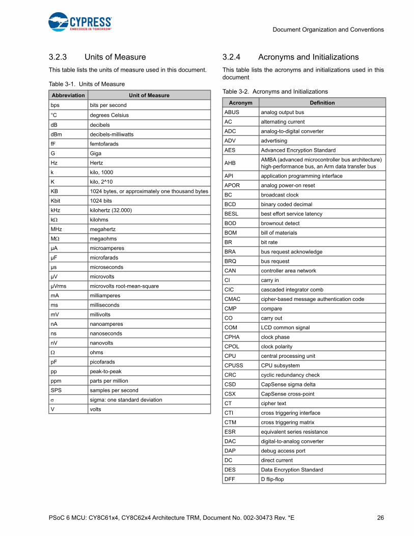
PSoC 6 MCU: CY8C61x4, CY8C62x4 Architecture TRM, Document No. 002-30473 Rev. *E 26
Document Organization and Conventions
3.2.3 Units of Measure
This table lists the units of measure used in this document.
3.2.4 Acronyms and Initializations
This table lists the acronyms and initializations used in thisdocument
Table 3-1. Units of Measure
Abbreviation Unit of Measure
bps bits per second
°C degrees Celsius
dB decibels
dBm decibels-milliwatts
fF femtofarads
G Giga
Hz Hertz
k kilo, 1000
K kilo, 2^10
KB 1024 bytes, or approximately one thousand bytes
Kbit 1024 bits
kHz kilohertz (32.000)
k kilohms
MHz megahertz
M megaohms
µA microamperes
µF microfarads
µs microseconds
µV microvolts
µVrms microvolts root-mean-square
mA milliamperes
ms milliseconds
mV millivolts
nA nanoamperes
ns nanoseconds
nV nanovolts
ohms
pF picofarads
pp peak-to-peak
ppm parts per million
SPS samples per second
sigma: one standard deviation
V volts
Table 3-2. Acronyms and Initializations
Acronym Definition
ABUS analog output bus
AC alternating current
ADC analog-to-digital converter
ADV advertising
AES Advanced Encryption Standard
AHBAMBA (advanced microcontroller bus architecture) high-performance bus, an Arm data transfer bus
API application programming interface
APOR analog power-on reset
BC broadcast clock
BCD binary coded decimal
BESL best effort service latency
BOD brownout detect
BOM bill of materials
BR bit rate
BRA bus request acknowledge
BRQ bus request
CAN controller area network
CI carry in
CIC cascaded integrator comb
CMAC cipher-based message authentication code
CMP compare
CO carry out
COM LCD common signal
CPHA clock phase
CPOL clock polarity
CPU central processing unit
CPUSS CPU subsystem
CRC cyclic redundancy check
CSD CapSense sigma delta
CSX CapSense cross-point
CT cipher text
CTI cross triggering interface
CTM cross triggering matrix
ESR equivalent series resistance
DAC digital-to-analog converter
DAP debug access port
DC direct current
DES Data Encryption Standard
DFF D flip-flop
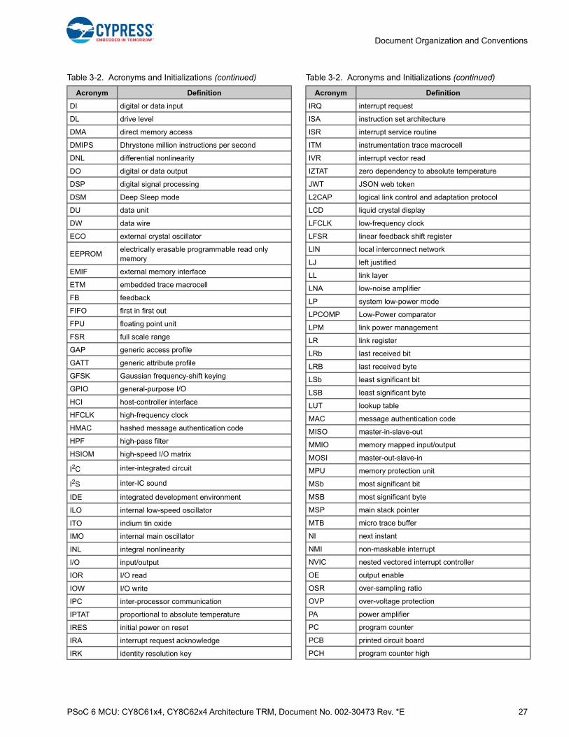
PSoC 6 MCU: CY8C61x4, CY8C62x4 Architecture TRM, Document No. 002-30473 Rev. *E 27
Document Organization and Conventions
DI digital or data input
DL drive level
DMA direct memory access
DMIPS Dhrystone million instructions per second
DNL differential nonlinearity
DO digital or data output
DSP digital signal processing
DSM Deep Sleep mode
DU data unit
DW data wire
ECO external crystal oscillator
EEPROMelectrically erasable programmable read only memory
EMIF external memory interface
ETM embedded trace macrocell
FB feedback
FIFO first in first out
FPU floating point unit
FSR full scale range
GAP generic access profile
GATT generic attribute profile
GFSK Gaussian frequency-shift keying
GPIO general-purpose I/O
HCI host-controller interface
HFCLK high-frequency clock
HMAC hashed message authentication code
HPF high-pass filter
HSIOM high-speed I/O matrix
I2C inter-integrated circuit
I2S inter-IC sound
IDE integrated development environment
ILO internal low-speed oscillator
ITO indium tin oxide
IMO internal main oscillator
INL integral nonlinearity
I/O input/output
IOR I/O read
IOW I/O write
IPC inter-processor communication
IPTAT proportional to absolute temperature
IRES initial power on reset
IRA interrupt request acknowledge
IRK identity resolution key
Table 3-2. Acronyms and Initializations (continued)
Acronym Definition
IRQ interrupt request
ISA instruction set architecture
ISR interrupt service routine
ITM instrumentation trace macrocell
IVR interrupt vector read
IZTAT zero dependency to absolute temperature
JWT JSON web token
L2CAP logical link control and adaptation protocol
LCD liquid crystal display
LFCLK low-frequency clock
LFSR linear feedback shift register
LIN local interconnect network
LJ left justified
LL link layer
LNA low-noise amplifier
LP system low-power mode
LPCOMP Low-Power comparator
LPM link power management
LR link register
LRb last received bit
LRB last received byte
LSb least significant bit
LSB least significant byte
LUT lookup table
MAC message authentication code
MISO master-in-slave-out
MMIO memory mapped input/output
MOSI master-out-slave-in
MPU memory protection unit
MSb most significant bit
MSB most significant byte
MSP main stack pointer
MTB micro trace buffer
NI next instant
NMI non-maskable interrupt
NVIC nested vectored interrupt controller
OE output enable
OSR over-sampling ratio
OVP over-voltage protection
PA power amplifier
PC program counter
PCB printed circuit board
PCH program counter high
Table 3-2. Acronyms and Initializations (continued)
Acronym Definition

PSoC 6 MCU: CY8C61x4, CY8C62x4 Architecture TRM, Document No. 002-30473 Rev. *E 28
Document Organization and Conventions
PCL program counter low
PD power down
PDU protocol data unit
PGA programmable gain amplifier
PHY physical layer
PLD programmable logic device
PM power management
PMA PSoC memory arbiter
POR power-on reset
PPOR precision power-on reset
PPU peripheral protection units
PRNG pseudo random number generator
PRS pseudo random sequence
PSA Platform Security Architecture
PSoC Programmable System-on-Chip
PSP process stack pointer
PSR program status register
PSRR power supply rejection ratio
PSSDC power system sleep duty cycle
PWM pulse width modulator
RAM random-access memory
RETI return from interrupt
RF radio frequency
RNG random number generator
ROM read only memory
ROT root of trust
RPA resolvable private address
RMS root mean square
RW read/write
SAR successive approximation register
SARSEQ SAR sequencer
SEG LCD segment signal
SE0 single-ended zero
SC switched capacitor
SCB serial communication block
SHA-256 Secure Hash Algorithm
SIE serial interface engine
SIMO single input multiple output
SIO special I/O
SNR signal-to-noise ratio
SMPU shared memory protection units
SOF start of frame
SOI start of instruction
Table 3-2. Acronyms and Initializations (continued)
Acronym Definition
SP stack pointer
SPD sequential phase detector
SPI serial peripheral interconnect
SPIM serial peripheral interconnect master
SPIS serial peripheral interconnect slave
SRAM static random-access memory
SROM supervisory read only memory
SRSS system resources subsystem
SSADC single slope ADC
SSC supervisory system call
SVCall supervisor call
SYSCLK system clock
SWD single wire debug
SWV serial wire viewer
TAR turn-around time
TC terminal count
TCPWM timer, counter, PWM
TD transaction descriptors
TDM time division multiplexed
TFF toggle flip-flop
TIA trans-impedance amplifier
TPIU trace port interface unit
TRM technical reference manual
TRNG True random number generator
UART universal asynchronous receiver/transmitter
ULB system ultra low-power mode
USB universal serial bus
USBIO USB I/O
VTOR vector table offset register
WCO watch crystal oscillator
WDT watchdog timer
WDR watchdog reset
WIC wakeup interrupt controller
XRES external reset
XRES_N external reset, active low
Table 3-2. Acronyms and Initializations (continued)
Acronym Definition
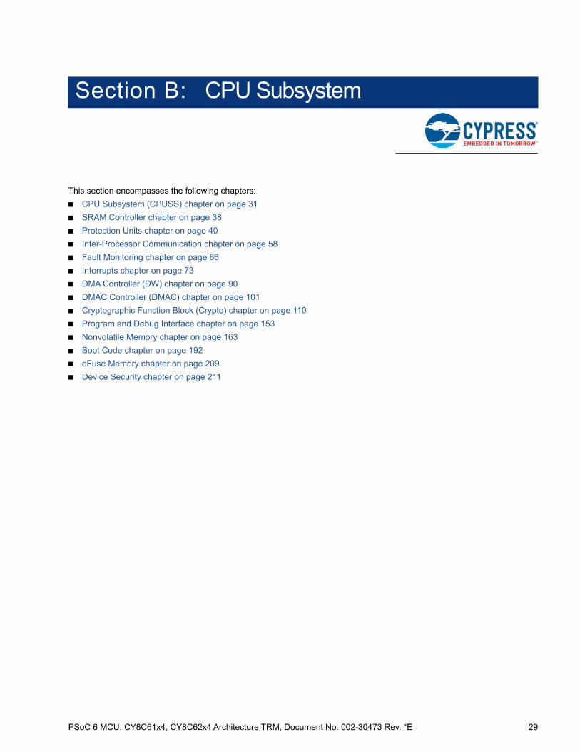
PSoC 6 MCU: CY8C61x4, CY8C62x4 Architecture TRM, Document No. 002-30473 Rev. *E 29
Section B: CPU Subsystem
This section encompasses the following chapters:
■ CPU Subsystem (CPUSS) chapter on page 31
■ SRAM Controller chapter on page 38
■ Protection Units chapter on page 40
■ Inter-Processor Communication chapter on page 58
■ Fault Monitoring chapter on page 66
■ Interrupts chapter on page 73
■ DMA Controller (DW) chapter on page 90
■ DMAC Controller (DMAC) chapter on page 101
■ Cryptographic Function Block (Crypto) chapter on page 110
■ Program and Debug Interface chapter on page 153
■ Nonvolatile Memory chapter on page 163
■ Boot Code chapter on page 192
■ eFuse Memory chapter on page 209
■ Device Security chapter on page 211

PSoC 6 MCU: CY8C61x4, CY8C62x4 Architecture TRM, Document No. 002-30473 Rev. *E 30
CPU Subsystem
Top Level Architecture
Figure 3-1. CPU System Block Diagram
CPU Subsystem
Sys
tem
Inte
rcon
nec
t (M
ulti
Lay
er A
HB
, IP
C, M
PU
/SM
PU
)
Cortex M4F CPU150/50 MHz, 1.1/0.9 VSWJ, ETM, ITM, CTI
Cortex M0+ CPU100/25 MHz, 1.1/0.9 V
SWJ, MTB, CTI
3x DMA Controller
CryptoDES/TDES, AES, SHA, CRC, TRNG, RSA/ECC
Accelerator
Flash256 KB + 32 KB
8 KB cache for each CPU
SRAM128 KB
ROM64 KB
SystemHibernate Mode
BackupDomain
SystemDeepSleep Mode
System LP/ULP ModeCPUs Active/Sleep
Color Key:Power Modes and
Domains
PSoC 6 MCU: CY8C61x4, CY8C62x4 Architecture TRM, Document No. 002-30473 Rev. *E 31
4. CPU Subsystem (CPUSS)
The CPU subsystem is based on dual 32-bit Arm Cortex CPUs, as Figure 4-1 shows. The Cortex-M4 is the main CPU. It isdesigned for short interrupt response time, high code density, and high 32-bit throughput while maintaining a strict cost andpower consumption budget. A secondary Cortex-M0+ CPU implements security, safety, and protection features.
This section provides only an overview of the Arm Cortex CPUs in PSoC 6 MCUs. For details, see the Arm documentationsets for Cortex-M4 and Cortex-M0+.
Some PSoC 6 MCU parts have only one CPU. See the PSoC 61 datasheet/PSoC 62 datasheet for details.
4.1 Features
The PSoC 6 MCU Arm Cortex CPUs have the following features:
■ Cortex-M4 has a floating-point unit (FPU) that supports single-cycle digital signal processing (DSP) instructions, and a memory protection unit (MPU). Cortex-M0+ has an MPU.
■ Both CPUs have 8-KB instruction caches with four-way set associativity.
■ Maximum clock frequency of 150 MHz for the Cortex-M4 and 100 MHz for the Cortex-M0+.
■ The Cortex-M4 implements a version of the Thumb instruction set based on Thumb-2 technology (defined in the Armv7-MArchitecture Reference Manual). The Cortex-M0+ supports the Armv6-M Thumb instruction set (defined in the Armv6-MArchitecture Reference Manual). See “Instruction Set” on page 37.
■ Both CPUs have nested vectored interrupt controllers (NVIC) for rapid and deterministic interrupt response. For details,see the Interrupts chapter on page 73
■ Both CPUs have extensive debug support. For details, see the Program and Debug Interface chapter on page 153.
❐ SWJ: combined serial wire debug (SWD) and Joint Test Action Group (JTAG) ports
❐ Serial wire viewer (SWV): provides real-time trace information through the serial wire output (SWO) interface
❐ Breakpoints
❐ Watchpoints
❐ Trace: Cortex-M4: embedded trace macrocell (ETM). Cortex-M0+: 4-KB micro trace buffer (MTB)
■ Inter-processor communication (IPC) hardware – see the Inter-Processor Communication chapter on page 58.
This PSoC 6 MCU technical reference manual (TRM) provides comprehensive and detailed information about thefunctions of the PSoC 6 MCU device hardware. It is divided into two books: architecture TRM and registers TRM. TheTRM is not recommended for those new to the PSoC 6 MCU, nor as a guide for developing PSoC 6 MCU applications.Use these documents instead:
■ PSoC 61 datasheet, PSoC 62 datasheet
■ Peripheral Driver Library (PDL) documentation
■ Application notes
■ Code examples
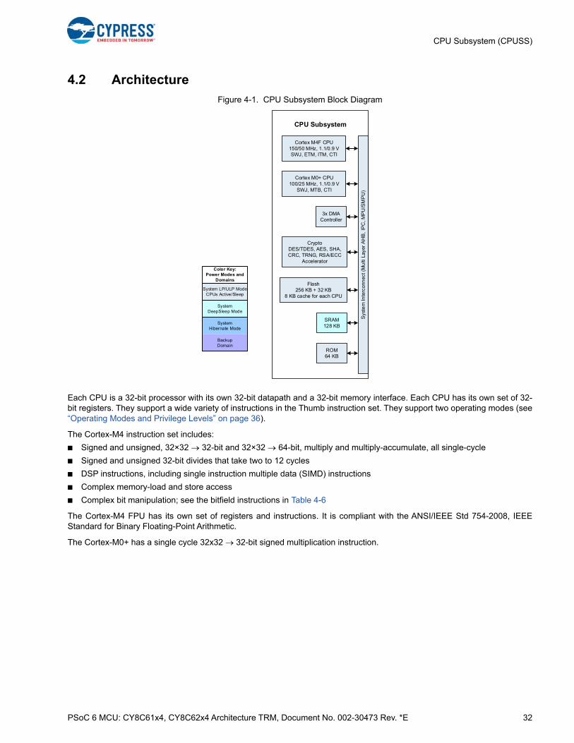
PSoC 6 MCU: CY8C61x4, CY8C62x4 Architecture TRM, Document No. 002-30473 Rev. *E 32
CPU Subsystem (CPUSS)
4.2 Architecture
Figure 4-1. CPU Subsystem Block Diagram
Each CPU is a 32-bit processor with its own 32-bit datapath and a 32-bit memory interface. Each CPU has its own set of 32-bit registers. They support a wide variety of instructions in the Thumb instruction set. They support two operating modes (see“Operating Modes and Privilege Levels” on page 36).
The Cortex-M4 instruction set includes:
■ Signed and unsigned, 32×32 32-bit and 32×32 64-bit, multiply and multiply-accumulate, all single-cycle
■ Signed and unsigned 32-bit divides that take two to 12 cycles
■ DSP instructions, including single instruction multiple data (SIMD) instructions
■ Complex memory-load and store access
■ Complex bit manipulation; see the bitfield instructions in Table 4-6
The Cortex-M4 FPU has its own set of registers and instructions. It is compliant with the ANSI/IEEE Std 754-2008, IEEEStandard for Binary Floating-Point Arithmetic.
The Cortex-M0+ has a single cycle 32x32 32-bit signed multiplication instruction.
CPU Subsystem
Sys
tem
Inte
rcon
nec
t (M
ulti
Lay
er A
HB
, IP
C, M
PU
/SM
PU
)
Cortex M4F CPU150/50 MHz, 1.1/0.9 VSWJ, ETM, ITM, CTI
Cortex M0+ CPU100/25 MHz, 1.1/0.9 V
SWJ, MTB, CTI
3x DMA Controller
CryptoDES/TDES, AES, SHA, CRC, TRNG, RSA/ECC
Accelerator
Flash256 KB + 32 KB
8 KB cache for each CPU
SRAM128 KB
ROM64 KB
SystemHibernate Mode
BackupDomain
SystemDeepSleep Mode
System LP/ULP ModeCPUs Active/Sleep
Color Key:Power Modes and
Domains
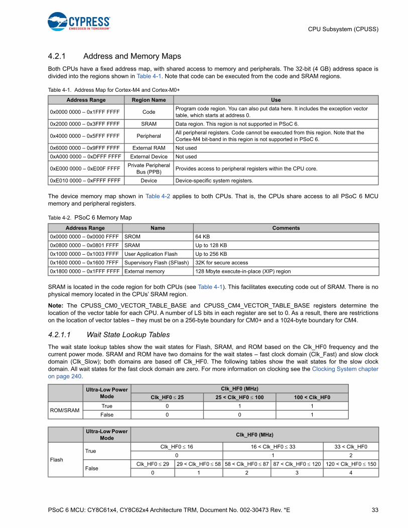
PSoC 6 MCU: CY8C61x4, CY8C62x4 Architecture TRM, Document No. 002-30473 Rev. *E 33
CPU Subsystem (CPUSS)
4.2.1 Address and Memory Maps
Both CPUs have a fixed address map, with shared access to memory and peripherals. The 32-bit (4 GB) address space isdivided into the regions shown in Table 4-1. Note that code can be executed from the code and SRAM regions.
The device memory map shown in Table 4-2 applies to both CPUs. That is, the CPUs share access to all PSoC 6 MCUmemory and peripheral registers.
SRAM is located in the code region for both CPUs (see Table 4-1). This facilitates executing code out of SRAM. There is nophysical memory located in the CPUs’ SRAM region.
Note: The CPUSS_CM0_VECTOR_TABLE_BASE and CPUSS_CM4_VECTOR_TABLE_BASE registers determine thelocation of the vector table for each CPU. A number of LS bits in each register are set to 0. As a result, there are restrictionson the location of vector tables – they must be on a 256-byte boundary for CM0+ and a 1024-byte boundary for CM4.
4.2.1.1 Wait State Lookup Tables
The wait state lookup tables show the wait states for Flash, SRAM, and ROM based on the Clk_HF0 frequency and thecurrent power mode. SRAM and ROM have two domains for the wait states – fast clock domain (Clk_Fast) and slow clockdomain (Clk_Slow); both domains are based off Clk_HF0. The following tables show the wait states for the slow clockdomain. All wait states for the fast clock domain are zero. For more information on clocking see the Clocking System chapteron page 240.
Table 4-1. Address Map for Cortex-M4 and Cortex-M0+
Address Range Region Name Use
0x0000 0000 – 0x1FFF FFFF CodeProgram code region. You can also put data here. It includes the exception vector table, which starts at address 0.
0x2000 0000 – 0x3FFF FFFF SRAM Data region. This region is not supported in PSoC 6.
0x4000 0000 – 0x5FFF FFFF PeripheralAll peripheral registers. Code cannot be executed from this region. Note that the Cortex-M4 bit-band in this region is not supported in PSoC 6.
0x6000 0000 – 0x9FFF FFFF External RAM Not used
0xA000 0000 – 0xDFFF FFFF External Device Not used
0xE000 0000 – 0xE00F FFFFPrivate Peripheral
Bus (PPB)Provides access to peripheral registers within the CPU core.
0xE010 0000 – 0xFFFF FFFF Device Device-specific system registers.
Table 4-2. PSoC 6 Memory Map
Address Range Name Comments
0x0000 0000 – 0x0000 FFFF SROM 64 KB
0x0800 0000 – 0x0801 FFFF SRAM Up to 128 KB
0x1000 0000 – 0x1003 FFFF User Application Flash Up to 256 KB
0x1600 0000 – 0x1600 7FFF Supervisory Flash (SFlash) 32K for secure access
0x1800 0000 – 0x1FFF FFFF External memory 128 Mbyte execute-in-place (XIP) region
Ultra-Low Power Mode
Clk_HF0 (MHz)
Clk_HF0 25 25 < Clk_HF0 100 100 < Clk_HF0
ROM/SRAMTrue 0 1 1
False 0 0 1
Ultra-Low Power Mode
Clk_HF0 (MHz)
Flash
TrueClk_HF0 16 16 < Clk_HF0 33 33 < Clk_HF0
0 1 2
FalseClk_HF0 29 29 < Clk_HF0 58 58 < Clk_HF0 87 87 < Clk_HF0 120 120 < Clk_HF0 150
0 1 2 3 4
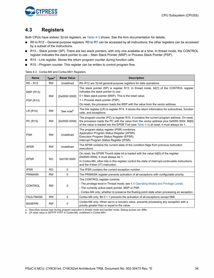
PSoC 6 MCU: CY8C61x4, CY8C62x4 Architecture TRM, Document No. 002-30473 Rev. *E 34
CPU Subsystem (CPUSS)
4.3 Registers
Both CPUs have sixteen 32-bit registers, as Table 4-3 shows. See the Arm documentation for details.
■ R0 to R12 – General-purpose registers. R0 to R7 can be accessed by all instructions; the other registers can be accessedby a subset of the instructions.
■ R13 – Stack pointer (SP). There are two stack pointers, with only one available at a time. In thread mode, the CONTROLregister indicates the stack pointer to use – Main Stack Pointer (MSP) or Process Stack Pointer (PSP).
■ R14 – Link register. Stores the return program counter during function calls.
■ R15 – Program counter. This register can be written to control program flow.
Table 4-3. Cortex-M4 and Cortex-M0+ Registers
Name Typea
a. Describes access type during program execution in thread mode and handler mode. Debug access can differ.
Reset Value Description
R0 – R12 RW Undefined R0–R12 are 32-bit general-purpose registers for data operations.
MSP (R13)
PSP (R13)
RW [0x0000 0000]
The stack pointer (SP) is register R13. In thread mode, bit[1] of the CONTROL registerindicates the stack pointer to use:
0 = Main stack pointer (MSP). This is the reset value.
1 = Process stack pointer (PSP).
On reset, the processor loads the MSP with the value from the vector address.
LR (R14) RW See noteb
b. LR reset value is 0xFFFF FFFF in Cortex-M4, undefined in Cortex-M0+.
The link register (LR) is register R14. It stores the return information for subroutines, functioncalls, and exceptions.
PC (R15) RW [0x0000 0004]The program counter (PC) is register R15. It contains the current program address. On reset,the processor loads the PC with the value from the vector address plus 0x0000 0004. Bit[0]of the value is loaded into the EPSR T-bit (see Table 4-4) at reset; it must always be 1.
PSR RW Undefined
The program status register (PSR) combines: Application Program Status Register (APSR). Execution Program Status Register (EPSR). Interrupt Program Status Register (IPSR).
APSR RW UndefinedThe APSR contains the current state of the condition flags from previous instruction executions.
EPSR RO 0x0100 0000
On reset, the EPSR Thumb state bit is loaded with the value bit[0] of the register [0x0000 0004]. It must always be 1.
In Cortex-M4, other bits in this register control the state of interrupt-continuable instructions and the if-then (IT) instruction.
IPSR RO 0 The IPSR contains the current exception number.
PRIMASK RW 0 The PRIMASK register prevents activation of all exceptions with configurable priority.
CONTROL RW 0
The CONTROL register controls:
- The privilege level in Thread mode; see 4.4 Operating Modes and Privilege Levels.
- The currently active stack pointer, MSP or PSP.
- Cortex-M4 only: whether to preserve the floating-point state when processing an exception.
FAULTMASK RW 0 Cortex-M4 only. Bit 0 = 1 prevents the activation of all exceptions except NMI.
BASEPRI RW 0Cortex-M4 only. When set to a nonzero value, prevents processing any exception with a priority greater than or equal to the value.
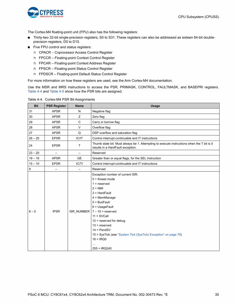
PSoC 6 MCU: CY8C61x4, CY8C62x4 Architecture TRM, Document No. 002-30473 Rev. *E 35
CPU Subsystem (CPUSS)
The Cortex-M4 floating-point unit (FPU) also has the following registers:
■ Thirty-two 32-bit single-precision registers, S0 to S31. These registers can also be addressed as sixteen 64-bit double-precision registers, D0 to D15.
■ Five FPU control and status registers:
❐ CPACR – Coprocessor Access Control Register
❐ FPCCR – Floating-point Context Control Register
❐ FPCAR – Floating-point Context Address Register
❐ FPSCR – Floating-point Status Control Register
❐ FPDSCR – Floating-point Default Status Control Register
For more information on how these registers are used, see the Arm Cortex-M4 documentation.
Use the MSR and MRS instructions to access the PSR, PRIMASK, CONTROL, FAULTMASK, and BASEPRI registers.Table 4-4 and Table 4-5 show how the PSR bits are assigned.
Table 4-4. Cortex-M4 PSR Bit Assignments
Bit PSR Register Name Usage
31 APSR N Negative flag
30 APSR Z Zero flag
29 APSR C Carry or borrow flag
28 APSR V Overflow flag
27 APSR Q DSP overflow and saturation flag
26 – 25 EPSR IC/IT Control interrupt-continuable and IT instructions
24 EPSR TThumb state bit. Must always be 1. Attempting to execute instructions when the T bit is 0 results in a HardFault exception.
23 – 20 – – Reserved
19 – 16 APSR GE Greater than or equal flags, for the SEL instruction
15 – 10 EPSR IC/TI Control interrupt-continuable and IT instructions
9 – – Reserved
8 – 0 IPSR ISR_NUMBER
Exception number of current ISR:
0 = thread mode
1 = reserved
2 = NMI
3 = HardFault
4 = MemManage
5 = BusFault
6 = UsageFault
7 – 10 = reserved
11 = SVCall
12 = reserved for debug
13 = reserved
14 = PendSV
15 = SysTick (see “System Tick (SysTick) Exception” on page 79)
16 = IRQ0
…
255 = IRQ240

PSoC 6 MCU: CY8C61x4, CY8C62x4 Architecture TRM, Document No. 002-30473 Rev. *E 36
CPU Subsystem (CPUSS)
4.4 Operating Modes and Privilege Levels
Both CPUs support two operating modes and two privilege levels:
■ Operating Modes:
❐ Thread Mode – used to execute application software. The processor enters Thread mode when it comes out of reset.
❐ Handler Mode – used to handle exceptions. The processor returns to Thread mode when it has finished all exceptionprocessing.
■ Privilege Levels:
❐ Unprivileged – the software has limited access to the MSR and MRS instructions, and cannot use the CPSID andCPSIE instructions. It cannot access the system timer, NVIC, or system control block. It may have restricted access tomemory or peripherals.
❐ Privileged – the software can use all the instructions and has access to all resources.
In Thread mode, the CONTROL register controls whether software execution is privileged or unprivileged. In Handler mode,software execution is always privileged.
Only privileged software can write to the CONTROL register to change the privilege level. Unprivileged software can use theSVC instruction to transfer control to privileged software.
In Handler mode, the MSP is always used. The exception entry and return mechanisms automatically update the CONTROLregister, which may change whether MSP/PSP is used.
In Thread mode, use the MSR instruction to set the stack pointer bit in the CONTROL register. When changing the stackpointer, use an ISB instruction immediately after the MSR instruction. This ensures that instructions after the ISB executeusing the new stack pointer.
Table 4-5. Cortex-M0+ PSR Bit Assignments
Bit PSR Register Name Usage
31 APSR N Negative flag
30 APSR Z Zero flag
29 APSR C Carry or borrow flag
28 APSR V Overflow flag
27 – 25 – – Reserved
24 EPSR TThumb state bit. Must always be 1. Attempting to execute instructions when the T bit is 0 results in a HardFault exception.
23 – 6 – – Reserved
5 – 0 IPSRException Number
Exception number of current ISR:
0 = thread mode
1 = reserved
2 = NMI
3 = HardFault
4 – 10 = reserved
11 = SVCall
12, 13 = reserved
14 = PendSV
15 = SysTick
16 = IRQ0
…
47 = IRQ31
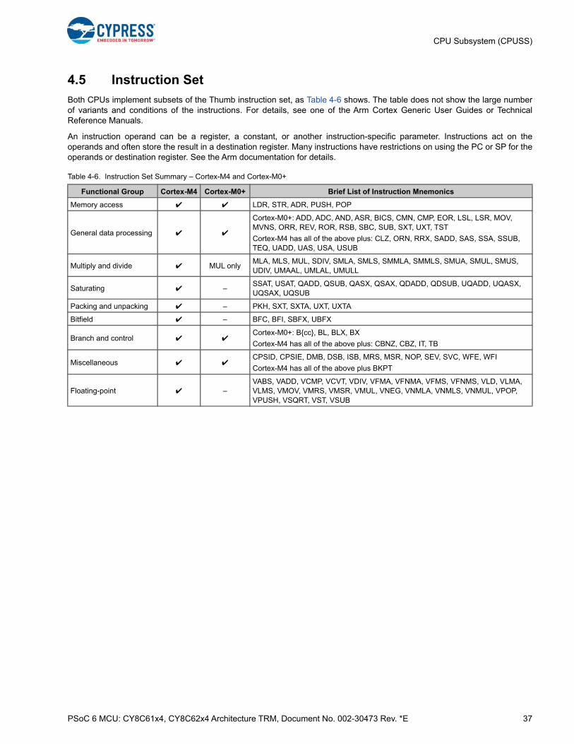
PSoC 6 MCU: CY8C61x4, CY8C62x4 Architecture TRM, Document No. 002-30473 Rev. *E 37
CPU Subsystem (CPUSS)
4.5 Instruction Set
Both CPUs implement subsets of the Thumb instruction set, as Table 4-6 shows. The table does not show the large numberof variants and conditions of the instructions. For details, see one of the Arm Cortex Generic User Guides or TechnicalReference Manuals.
An instruction operand can be a register, a constant, or another instruction-specific parameter. Instructions act on theoperands and often store the result in a destination register. Many instructions have restrictions on using the PC or SP for theoperands or destination register. See the Arm documentation for details.
Table 4-6. Instruction Set Summary – Cortex-M4 and Cortex-M0+
Functional Group Cortex-M4 Cortex-M0+ Brief List of Instruction Mnemonics
Memory access ✔ ✔ LDR, STR, ADR, PUSH, POP
General data processing ✔ ✔
Cortex-M0+: ADD, ADC, AND, ASR, BICS, CMN, CMP, EOR, LSL, LSR, MOV, MVNS, ORR, REV, ROR, RSB, SBC, SUB, SXT, UXT, TST
Cortex-M4 has all of the above plus: CLZ, ORN, RRX, SADD, SAS, SSA, SSUB, TEQ, UADD, UAS, USA, USUB
Multiply and divide ✔ MUL onlyMLA, MLS, MUL, SDIV, SMLA, SMLS, SMMLA, SMMLS, SMUA, SMUL, SMUS, UDIV, UMAAL, UMLAL, UMULL
Saturating ✔ –SSAT, USAT, QADD, QSUB, QASX, QSAX, QDADD, QDSUB, UQADD, UQASX, UQSAX, UQSUB
Packing and unpacking ✔ – PKH, SXT, SXTA, UXT, UXTA
Bitfield ✔ – BFC, BFI, SBFX, UBFX
Branch and control ✔ ✔Cortex-M0+: B{cc}, BL, BLX, BX
Cortex-M4 has all of the above plus: CBNZ, CBZ, IT, TB
Miscellaneous ✔ ✔CPSID, CPSIE, DMB, DSB, ISB, MRS, MSR, NOP, SEV, SVC, WFE, WFI
Cortex-M4 has all of the above plus BKPT
Floating-point ✔ –VABS, VADD, VCMP, VCVT, VDIV, VFMA, VFNMA, VFMS, VFNMS, VLD, VLMA, VLMS, VMOV, VMRS, VMSR, VMUL, VNEG, VNMLA, VNMLS, VNMUL, VPOP, VPUSH, VSQRT, VST, VSUB
PSoC 6 MCU: CY8C61x4, CY8C62x4 Architecture TRM, Document No. 002-30473 Rev. *E 38
5. SRAM Controller
This chapter explains the PSoC 6 MCU SRAM Controller, its features, architecture, and wait states. The SRAM controllerenables the CPU to read and write parts of the PSoC 6 SRAM.
5.1 Features
The CPUSS has up to three identical SRAM controllers; see the PSoC 61 datasheet/PSoC 62 datasheet for details.
The SRAM controller has the following features:
■ Consists of two AHB-Lite interfaces:
❐ An AHB-Lite bus interface on clk_fast that connects to the fast bus infrastructure
❐ An AHB-Lite bus interface on clk_slow that connects to the slow bus infrastructure
■ Supports programmable number of clk_hf wait states
■ Supports 8-, 16-, and 32-bit accesses
5.2 Architecture
The design has two AHB-Lite interfaces that connect to the AHB-Lite infrastructure. Each AHB-Lite interface is connected toa synchronization component that translates between the interface clock (either clk_fast or clk_slow) and the high-frequencyclock (clk_hf).
Arbitration is performed on the AHB-Lite transfers from the two ports (AHB-Lite interface). Arbitration uses device-wide busmaster specific arbitration priorities. Therefore, although two AHB-Lite interfaces are provided, only one AHB-Lite transfer isaccepted by the port arbitration component.
The AHB-Lite transfers are the origin for all SRAM accesses; that is, the write buffer and SRAM repair requests result fromAHB-Lite transfers. The SRAM controller differentiates between the following three types of AHB-Lite transfers:
■ AHB-Lite read transfers
■ 32-bit AHB-Lite write transfers
■ 8-bit and 16-bit AHB-Lite write transfers (also referred to as partial AHB-Lite write transfers)
Each type is described in more detail here.
AHB-Lite read transfers. An AHB-Lite read transfer is translated into an SRAM read access. If the read address matchesin the write buffer, the SRAM has stale data and the write data provides the requested read data (this functionality is providedby the read merge component).
This PSoC 6 MCU technical reference manual (TRM) provides comprehensive and detailed information about thefunctions of the PSoC 6 MCU device hardware. It is divided into two books: architecture TRM and registers TRM. TheTRM is not recommended for those new to the PSoC 6 MCU, nor as a guide for developing PSoC 6 MCU applications.Use these documents instead:
■ PSoC 61 datasheet, PSoC 62 datasheet
■ Peripheral Driver Library (PDL) documentation
■ Application notes
■ Code examples
PSoC 6 MCU: CY8C61x4, CY8C62x4 Architecture TRM, Document No. 002-30473 Rev. *E 39
SRAM Controller
32-bit AHB-Lite write transfers. A 32-bit AHB-Lite writetransfer is translated into an SRAM write access. If the writeaddress matches in the write buffer, the matching writebuffer entries have stale data and these entries areinvalidated.
Partial AHB-Lite write transfers. A partial AHB-Lite writetransfer is translated into an SRAM read access and anSRAM write access. The SRAM read access is the directresult of the partial write transfer and the SRAM writeaccess is the result of a write buffer request. A partial writetransfer requires an SRAM read access to retrieve the“missing” data bytes from the SRAM. If the read addressmatches in the write buffer, the SRAM has stale data andthe write data provides the requested read data (thisfunctionality is provided by the read merge component). Therequested read data is merged with the partial write data toprovide a complete 32-bit data word (this functionality isprovided by the write merge component). The address andthe merged write data are written to the write buffer. A futurewrite buffer request results in an SRAM write access withthe merged write data.
Only the partial AHB-Lite write transfers use the write buffer.
Write buffer. The write buffer is a temporary holdingstation for future SRAM write accesses.
The buffer allows SRAM write accesses to be postponed.This allows for more performance critical AHB-Lite requeststo “overtake” write buffer requests. Memory consistency isguaranteed by matching the SRAM access address with thewrite buffer entries' addresses: a “matching” SRAM readaccess uses the read merge component and a matchingSRAM write access invalidates the matching write bufferentries.
When the write buffer is full, an entry needs to be freed toaccommodate future partial AHB-Lite write transfers.Therefore, a full write buffer raises the priority of the writebuffer request path.
The write buffer is constructed as a FIFO with four entries(the order in which entries are written is the same as theorder in which entries are read). Each entry consists of:
■ A valid field
■ An invalidated field
■ A word address
■ A 32-bit data word
Note that the merged write data written to the write buffer is always a 32-bit data word. Therefore, no byte mask is required.
When the write buffer is written (an entry is added): the entryvalid field is set to ‘1’ and the invalidated field is set to ‘0’.
When the write buffer is read (an entry is removed): theentry valid field is set to ‘0’. If the entry invalidate field is ‘1’,the write buffer request path is selected for an SRAM write
access. If the entry valid field is ‘0’, no SRAM access isperformed.
On an SRAM read access, a matching entry provides writebuffer merge data for the read merge component.
On an SRAM write access resulting from a 32-bit AHB-Litewrite transfer, a matching entry invalidated field is set to ‘1’.
The state of the write buffer is reflected byRAMi_STATUS.WB_EMPTY. The write buffer is not retainedin Deep Sleep power mode. Therefore, when transitioning tosystem Deep Sleep power mode, the write buffer should beempty. Note that this requirement is typically met, because atransition to Deep Sleep power mode also requires thatthere are no outstanding AHB-Lite transfers. If there are nooutstanding AHB-Lite transfers, the write buffer gets SRAMaccess.
5.3 Wait States
The programmable wait states represent the number ofclk_hf cycles for a read path through the SRAM memory toflipflops in either the fast domain (CM4 CPU) or slow domain(such as CM0+ CPU, DataWire, and DMA controller).
As the wait states are represented in clk_hf cycles, the waitstates do not have to be reprogrammed when the fast clockdomain frequency (clk_fast) or slow clock domain frequency(clk_slow) is changed. However, it may be necessary toreprogram the wait states when the high-frequency clockdomain (clk_hf) is changed. This means the requirednumber of wait states is a function of the clk_hf frequency.
The fast clock domain is timing closed at a higher frequencythan the slow clock domain. Therefore, the read paththrough the SRAM memory to flipflops in the fast domain isfaster than the read path through the SRAM memory toflipflops in the slow domain. In other words, the requirednumber of “fast” wait states (RAMi_CTL.FAST_WS) shouldbe less than or equal to the required number of “slow” waitstates (RAMi_CTL.SLOW_WS).
The SRAM controller also has internal SRAM read paths.These paths are to flipflops in the SRAM controller in thehigh-frequency clock domain (clk_hf). For these SRAMaccesses (for example, an SRAM read access to support apartial AHB-Lite write transfer), the fast wait states are used.This is because the maximum fast domain frequency(clk_fast) equals the high-frequency domain frequency(clk_hf).

PSoC 6 MCU: CY8C61x4, CY8C62x4 Architecture TRM, Document No. 002-30473 Rev. *E 40
6. Protection Units
Protection units are implemented in the PSoC 6 MCU to enforce security based on different operations. A protection unitallows or restricts bus transfers. The rules are enforced based on specific properties of a transfer. The rules that determineprotection are implemented in protection structures (a register structure). A protection structure defines the protected addressspace and the protection attributes. The hardware that evaluates these protection structures, to restrict or permit access, isthe protection unit. The PSoC device has different types of protection units such as MPU, SMPU, and PPU. Each have adistinct set of protection structures, which helps define different protection regions and their attributes.
6.1 Architecture
Figure 6-1 shows a conceptual view of implementation of the PSoC protection system.
Figure 6-1. Conceptual View of PSoC Protection System
This PSoC 6 MCU technical reference manual (TRM) provides comprehensive and detailed information about thefunctions of the PSoC 6 MCU device hardware. It is divided into two books: architecture TRM and registers TRM. TheTRM is not recommended for those new to the PSoC 6 MCU, nor as a guide for developing PSoC 6 MCU applications.Use these documents instead:
■ PSoC 61 datasheet, PSoC 62 datasheet
■ Peripheral Driver Library (PDL) documentation
■ Application notes
■ Code examples
Protection Unit
Flash Memory
SRAMExternal Memory
Peripheral Memory
PSoC 6 Memory Map
CPU1 CPU2Test
ControllerDMA
Protection Structures
Bus Masters
Sets rules to check against
Memory Region
Protection Attribute
Bus Master’s Protection Attribute
Bus Master’s Protection Attribute
Bus Master’s Protection Attribute
Bus Master’s Protection Attribute
PSoC 6 MCU: CY8C61x4, CY8C62x4 Architecture TRM, Document No. 002-30473 Rev. *E 41
Protection Units
The functioning of a secure system is based on thefollowing:
■ Bus masters: This term refers to the bus masters in thearchitecture. In a PSoC 6 device, an example of a busmaster is a Cortex-M core, DMA, or a test controller.
■ Protection units: Protection units are the hardwareengines that enforce the protection defined by protectionstructures. There are three types of protection units,acting at different levels of memory access with differentprecedence and priority of protection – MPU, SMPU,and PPU.
■ Protection structure: A protection structure is a registerstructure in memory that sets up the rules based onwhich each protection unit will evaluate a transfer. Eachprotection unit associates itself to multiple protectionstructures. The protection structure associated with aprotection unit are evaluated in the order starting withthe protection structure with the largest index. Forexample, if there are 16 protection structures associatedwith a protection unit, then the evaluation of a transferstarts from protection structure 15 and counts down.Physically a protection structure is a register structure inthe memory map that defines a protection rule. Eachprotection structure constitutes the following:
❐ Defines a memory region on which the rule is applied. It designates what the bus transfer needs to be evaluated against this protection structure.
- Base address
- Size of memory block
❐ A set of protection attributes
- R/W/X
- User/privilege
- Secure/non Secure
- Protection context
■ Protection attributes: These are properties based onwhich a transfer is evaluated. There are multipleprotection attributes. The set of protection attributesavailable for a protection structure depends on theprotection unit it is associated with. Protection attributesappear in two places:
❐ Protection structures: Protection attributes associ-ated with a protection structure set the rules for access based on these attributes.
❐ Bus master's protection attribute: Each bus master has its own access attributes, which define the bus master's access privileges. Some of these attributes, such as secure/non-secure, are set for a master. Other attributes such as protection context and user/privilege attribute are dynamic attributes, which change based on bus master's context and state.
In summary, a PSoC 6 device has protection units that actas a gate for any access to the PSoC memory map. Therules for protection are set by the protection structures.
Each bus master is qualified by its own protection attribute.For every bus transfer, the protection unit compares the busmaster's protection attribute and accessed address againstthe rules set in the protection structures and decides onproviding or denying access.
6.2 PSoC 6 Protection Architecture
When there is a memory (SRAM/flash/peripheral) access bya bus master, the access is evaluated by a protection unitagainst the protection attributes set in protection structuresfor the memory location being accessed. If the bus master’sprotection attributes satisfy the protection attributes set inthe protection structures, then access is allowed by theprotection unit. If there is an access restriction, a faultcondition is triggered and a bus error occurs. Thusprotection units secure bus transfer address range either inmemory locations (SRAM/flash) or peripheral registers.From an architectural perspective, there is no differencebetween memory protection and peripheral protection.However, from an implementation perspective, separatememory and peripheral protection is provided.
Two types of protection units, memory protection units(MPU) and shared memory protection units (SMPU), areprovided in the CPU subsystem (CPUSS) to protect memorylocations. A separate protection unit type is provided forperipheral protection (PPU) in the PERI:
■ A bus master may have a dedicated MPU. In a CPU busmaster, the MPU is typically implemented as part of theCPU and is under control of the OS/kernel. In a non-CPU bus master, the MPU is typically implemented aspart of the bus infrastructure and under control of theOS/kernel of the CPU that “owns or uses” the busmaster. If a CPU switches tasks or if a non-CPUswitches ownership, the MPU settings are typicallyupdated by OS/kernel software. The different MPU typesare:
❐ An MPU that is implemented as part of the CPU. This type is found in the Arm CM0+ and CM4 CPUs.
❐ An MPU that is implemented as part of the bus infra-structure. This type is found in bus masters such as crypto and test controller. The definition of this MPU type follows the Arm MPU definition (in terms of memory region and access attribute definition) to ensure a consistent software interface.
■ SMPUs are intended for implementing protection in asituation with multiple bus masters. These protectionunits implement a concept called Protection Context. Aprotection context is a pseudo state of a bus master,which can be used to determine access attributes acrossmultiple masters. The protection context is a protectionattribute not specific to a bus master. The SMPUs candistinguish between different protection contexts; theycan also distinguish secure from non-secure accesses.
PSoC 6 MCU: CY8C61x4, CY8C62x4 Architecture TRM, Document No. 002-30473 Rev. *E 42
Protection Units
This allows for an effective protection in a multi-corescenario.
■ PPUs are protection units provided in the PERI registerspace for peripheral protection. The PPU attributes aresimilar to the SMPU, except that they are intended forprotecting the peripheral space. Refer to the registersTRM for details. The PPUs are intended to distinguishbetween different protection contexts and to distinguishsecure from non-secure accesses and user modeaccesses from privileged mode accesses. There are twotypes of PPU structures.
❐ Fixed PPUs implement protection for fixed address regions that typically correspond to a specific periph-eral
❐ Programmable PPUs allows the user to program the address region to be protected
The platform’s DMA controller does not have an MPU.Instead, a DMA controller channel inherits the accesscontrol attributes of the bus transfer that programmed thechannel.
The definition of SMPU and PPU follows the MPU definitionand adds the capability to distinguish accesses fromdifferent protection contexts (the MPU does not includesupport for a protection context). If security is required, theSMPU and possibly PPUs MMIO registers must becontrolled by a secure CPU that enforces system-wideprotection.
Figure 6-2 gives an overview of the location of MPUs,SMPUs, and PPUs in the system. Note that a peripheralgroup PPU needs to provide access control only to theperipherals within a peripheral group (group of peripheralswith a shared bus infrastructure).
As mentioned, the MPU, SMPU, and PPU protectionfunctionality follows the Arm MPU definition:
■ Multiple protection structures are supported.
■ Each structure specifies an address range in the unifiedmemory architecture and access attributes. An addressrange can be as small as 32 bytes.
A protection violation is caused by a mismatch between abus master’s access attributes and the protection structureand access attributes for the memory region configured inthe protection structure.
A bus transfer that violates a protection structure results in abus error.
For AXI transfers, the complete address range is matched. Ifa transfer references multiple 32-byte regions (the smallestprotection structure address range is 32 bytes), multiplecycles are required for matching – one cycle per 32-byteregion.
Protection violations are captured in the fault reportstructure to allow for failure analysis. The fault reportstructures can generate an interrupt to indicate the
occurrence of a fault. This is useful if the violating busmaster cannot resolve the bus error by itself, but requiresanother CPU bus master to resolve the bus error on itsbehalf.
For a buffered mode of transfer(CPUSS_BUFF_CTL[WRITE_BUFF]), the behavior duringprotection violation is different. WhenCPUSS_BUFF_CTL[WRITE_BUFF] is set to ‘1’, the writetransfers on the bus are buffered. So the transfer is firstacknowledged when the buffer receives the transfer. Aprotection violation will be only evaluated when the actualwrite happens at the destination register. This leads to thewrite transfer not generating a bus error for buffered mode.However, a fault will be registered as soon as the transfertries to write the destination location. Therefore, for bufferedwrites, the user must verify the fault structure to make sureno violations have occurred.
A protection violation results in a bus error and the bustransfer will not reach its target. An MPU or SMPU violationthat targets a peripheral will not reach the associatedprotection evaluation (PPU). In other words, MPU andSMPU have a higher priority over PPU.
Protection unit addresses the following:
■ Security requirements. This includes prevention ofmalicious attacks to access secure memory orperipherals. For example, a non-secure master shouldnot be able to access key information in a securememory region.
■ Safety requirements. This includes detection ofaccidental (non-malicious) software errors and randomhardware errors. Enabling failure analysis is importantso the root cause of a safety violation can beinvestigated. For example, analyzing a flash memoryfailure on a device that is returned from the field shouldbe possible.
To address security requirements, the Cortex M0+ is usedas a ‘secure CPU’. This CPU is considered a trusted entity.Any access by the CPU tagged as “secure” will be called“secure access”.

PSoC 6 MCU: CY8C61x4, CY8C62x4 Architecture TRM, Document No. 002-30473 Rev. *E 43
Protection Units
Figure 6-2. PSoC 6 Protection Architecture
The different types of protection units cater to different use cases for protection.
6.3 Register Architecture
The protection architecture has different conceptual pieces and different sets of registers correspond to each of theseconcepts.
6.3.1 Protection Structure and Attributes
The MPU, SMPU, and PPU protection structure definition follows the Arm definition. Each protection structure is defined by:
■ An address region
■ Access control attributes
A protection structure is always aligned on a 32-byte boundary in the memory space. Two registers define a protectionstructure: ADDR (address register) and ATT (attribute register). This structure alignment and organization allowstraightforward protection of the protection structures by the protection scheme. This is discussed later in this chapter.
Address region: The address region is defined by:
■ The base address of a region as specified by ADDR.ADDR.
■ The size of a region as specified by ATT.REGION_SIZE.
■ Individual disables for eight subregions within the region, as specified by ADDR.SUBREGION_DISABLE.
Table 6-1. Protection Use Cases
Protection Unit Type Use
Arm MPUUsed to protect memory between tasks within in a single Arm core. A task in one of the Arm cores can protect its memory from access by another task in the same core.
MPUSame as the Arm MPU, but for other bus masters such as the test controller or crypto, which do not have a built-in MPU in their block IP.
SMPU Used to protect memory addresses that are shared between multiple bus masters.
Fixed PPU protection structures
These protect specific peripheral memory space. The protection structures have a preprogrammed memory region and can be used only to protect the peripheral it was intended for.
Programmable PPU protection structures
These protect the peripheral space but the memory region is not fixed. So users can easily program it to protect any space in the peripheral memory region.
CM0+ Arm MPU
CM4 Arm MPU
CryptoDMA
(DataWire)
MPU
SMPU
AHB
PPU
GPIO
PPU
Fixed Function Blocks
PPU
Programmable Analog and Digital
Blocks
MPU: Memory Protection UnitSMPU: Shared Memory Protection UnitPPU: Peripheral Protection Unit
Bus Masters
Flash SRAM
Test Controller
MPU

PSoC 6 MCU: CY8C61x4, CY8C62x4 Architecture TRM, Document No. 002-30473 Rev. *E 44
Protection Units
The REGION_SIZE field specifies the size of a region. The region size is a power of 2 in the range of [256 B, 4 GB]. The baseaddress ADDR specifies the start of the region, which must be aligned to the region size. A region is partitioned into eightequally sized sub-regions. The SUBREGION_DISABLE field specifies individual enables for the sub-regions within a region.For example, a REGION_SIZE of “0x08” specifies a region size of 512 bytes. If the start address is 0x1000:5400 (512-bytealigned), the region ranges from 0x1000:5400 to 0x1000:55ff. This region is partitioned into the following eight 64-bytesubregions:
subregion 0 from 0x1000:5400 to 0x1000:543f
subregion 1 from 0x1000:5440 to 0x1000:547f
…
subregion 7 from 0x1000:55c0 to 0x1000:55ff.
If the SUBREGION_DISABLE is 0x82 (bitfields 1 and 7 are ‘1’), subregions 1 and 7 are disabled; subregions 0, 2, 3, 4, 5, and6 are enabled.
In addition, an ATT.ENABLED field specifies whether the region is enabled. Only enabled regions participate in the protection“matching” process. Matching identifies if a bus transfer address is contained within an enabled subregion(SUBREGION_DISABLE) of an enabled region (ENABLED).
Protection attributes: The protection attributes specify access control to the region (shared by all subregions within theregion). Access control is performed by comparing against a bus master's protection attributes of the bus master performingthe transfer. The following access control fields are supported:
■ Control for read accesses in user mode (ATT.UR field).
■ Control for write accesses in user mode (ATT.UW field).
■ Control for execute accesses in user mode (ATT.UX field).
■ Control for read accesses in privileged mode (ATT.PR field).
■ Control for write accesses in privileged mode (ATT.PW field).
■ Control for execute accesses in privileged mode (ATT.PX field).
■ Control for secure access (ATT.NS field).
■ Control for individual protection contexts (ATT.PC_MASK[15:0], with MASK[0] always constant at 1). This protectioncontext control field is present only for the SMPU and PPU.
The execute and read access control attributes are orthogonal. Execute transfers are typically read transfers. To allowexecute and read transfers in user mode, both ATT.UR and ATT.UX must be set to ‘1’. To allow data and read transfers in usermode, only ATT.UR must be set to ‘1’. In addition, the ATT.PC_MATCH control field is supported, which controls “matching”and “access evaluation” processes. This control field is present only for the SMPU and PPU protection structures.
For example, only protection context 2 can access a specific address range. These accesses are restricted to read and writesecure accesses in privileged mode. The access control fields are programmed as follows:
■ ATT.UR is 0: read accesses in user mode not allowed.
■ ATT.UW is 0: write accesses in user mode not allowed.
■ ATT.UX is 0: execute accesses in user mode not allowed.
■ ATT.PR is 1: read accesses in privileged mode allowed.
■ ATT.PW is 1: write accesses in privileged mode allowed.
■ ATT.PX is 0: execute accesses in privileged mode not allowed.
■ ATT.NS is 0: secure access required.
■ ATT.PC_MASK is 0x0005: protection context 1 and 3 accesses enabled (all other protection contexts are disabled).
■ ATT.PC_MATCH is 0: the PC_MASK field is used for access evaluation. Three separate access evaluation subprocessesare distinguished:
❐ A subprocess that evaluates the access based on read/write, execute, and user/privileged access attributes.
❐ A subprocess that evaluates the access based on the secure/non-secure attribute.
❐ A subprocess that evaluates the access based on the protection context index (used only by the SMPU and PPU when ATT.PC_MATCH is 0).

PSoC 6 MCU: CY8C61x4, CY8C62x4 Architecture TRM, Document No. 002-30473 Rev. *E 45
Protection Units
If all access evaluations are successful, access is allowed. If any process evaluation is unsuccessful, access is not allowed.Matching the bus transfer address and access evaluation of the bus transfer (based on access attributes) are twoindependent processes:
■ Matching process. For each protection structure, the process identifies whether a transfer address is contained within theaddress range. This identifies the “matching” regions.
■ Access evaluation process. For each protection structure, the process evaluates the bus transfer access attributesagainst the access control attributes.
A protection unit typically has multiple protection structures and evaluates the protection structures in decreasing order. Thefirst matching structure provides the access control attributes for the evaluation of the transfer's access attributes. In otherwords, higher-indexed structures take precedence over lower-indexed structures.
The following pseudo code illustrates the process. match = 0;for (i = n-1; i >= 0; i--)// n: number of protection regions if (Match (“transfer address”, “protection context” “MMIO registers ADDR and ATT of protection structure i”)) { match = 1; break; }|
if (match) AccessEvaluate (“transfer access attributes”, “protection context” “MMIO register ATT of protection structure i”);else “access allowed”
Notes:
■ If no protection structure provides a match, the access is allowed.
■ If multiple protection structures provide a match, the access control attributes for the access evaluation are provided bythe protection structure with the highest index.
An example of using the PC_MATCH feature is as follows. Two SMPU structures are configured to protect the same addressrange:
■ Case 1: SMPU#2: PC = 3, PC_MATCH = 0 SMPU#1: PC = 2, PC_MATCH = 0
To access the master of protection context 2, SMPU#2 has the highest index and address match, but attributes do notmatch; therefore, access is restricted. The SMPU#1 is not evaluated because the PC_MATCH is 0.
■ Case 2: SMPU#2: PC = 3, PC_MATCH = 1 SMPU#1: PC = 2, PC_MATCH = 0
The SMPU#2 address matches but PC does not match and is skipped because PC_MATCH is 1. SMPU#1 is evaluatedand the address and attributes match; therefore, access is allowed.
As mentioned, the protection unit evaluates the protection structures in decreasing order. From a security requirementsperspective, this is of importance: a non-secure protection context must not be able to add protection structures that have ahigher index than the protection structures that provide secure access. The protection structure with a higher index can beprogrammed to allow non-secure accesses. Therefore, in a secure system, the higher programmable protection structuresare protected to only allow restricted accesses
PSoC 6 MCU: CY8C61x4, CY8C62x4 Architecture TRM, Document No. 002-30473 Rev. *E 46
Protection Units
6.4 Bus Master Protection Attributes
The protection structures set up the rules for different memory regions and their access attributes. The bus master’s ownprotection attributes are used by the protection units to regulate access, based on rules set by the protection structures. Notall bus masters provide all protection attributes that are associated with a bus transfer. Some examples are:
■ None of the bus masters has a native protection context attribute. This must be set dynamically based on the task beingexecuted by the bus master.
■ The Arm Cortex M4 and Arm Cortex M0+ CPUs provide a user/privilege attribute, but do not provide a secure/non-secureattribute natively. This must be set at a system level.
To ensure system-wide restricted access, missing attributes are provided by register fields. These fields may be set during theboot process or by the secure CPU.
■ The SMPU MS_CTL.PC_MASK[] and MPU MS_CTL.PC[] register fields provide protection context functionality.
■ The SMPU MS_CTL.P register field provides the user/privileged attribute for those masters that do not provide their ownattribute.
■ The SMPU MS_CTL.NS register provides the secure/non-secure attribute for those masters that do not provide their ownattribute.
■ Masters that do not provide an execute attribute have the execute attribute set to ‘0’.
The DMA controller channels inherit the access control attributes of the bus transfers that configured the DMA channel.
■ All the bus masters in the system have SMPU and MPU MS_CTL registers associated with them.
■ The MPU MS_CTL.PC_SAVED field (and associated protection context 0 functionality, which is discussed later in thechapter) is only present for the CM0+ master.
■ The SMPU MS_CTL.P, MS_CTL.NS, and MS_CTL.PC_MASK fields are not present for the DMA. The bus transferattributes are provided through “inheritance”: the bus transfer attributes are from the master that owns the DMA channelthat initiated the bus transfer.
■ The MPU MS_CTL register is not present for the DMA masters. The protection context (PC) bus transfer attribute isprovided through inheritance.
6.5 Protection Context
Each bus master has a MPU MS_CTL.PC[3:0] protection context field. This protection context is used as the protectioncontext attribute for all bus transfers that are initiated by the master. The SMPUs and PPUs allow or restrict bus transfersbased on the protection context attribute.
Multiple masters can share a protection context. For example, a CPU and a crypto controlled by the CPU may share aprotection context (the CPU and crypto PC[] fields are the same). Therefore, the CPU and crypto share the SMPU and PPUaccess restrictions.
A bus master protection context is changed by reprogramming the master’s PC[] field. Changing a protection context isrequired for CPU bus masters that may transition between multiple tasks, each catering to different protection contexts. Asthe protection context allows or restricts bus transfers, changes to the protection context should be controlled and should notcompromise security. Furthermore, changes to the protection context should incur limited CPU overhead to allow for frequentprotection context changes. Consider a case in which a CPU executes two software stacks with different protection contexts.To this end, each bus master has an SMPU MS_CTL.PC_MASK[15:0] protection context mask field that identifies whatprotection contexts can be programmed for the bus master:
■ The protection context field MS_CTL.PC[3:0]. This register is controlled by the associated bus master and has the sameaccess restrictions as the bus master’s MPU registers.
■ The protection context mask field MS_CTL.PC_MASK[15:0]. This register is controlled by the secure CPU and has thesame access restrictions as the SMPU registers.
The PC_MASK[] field is a “hot-one” field that specifies whether the PC[] field can be programmed with a specific protectioncontext. Consider an attempt to program PC[] to ‘3’:
■ If PC_MASK[3] is ‘1’, PC[] is set to “3”.
■ If PC_MASK[3] is ‘0’, PC[] is not changed.
PSoC 6 MCU: CY8C61x4, CY8C62x4 Architecture TRM, Document No. 002-30473 Rev. *E 47
Protection Units
6.6 Protection Contexts 0, 1, 2, 3
The PSoC 6 MCU supports protection contexts to isolate software execution for security and safety purposes. Protectioncontexts are used to restrict access to memory and peripheral resources.
Out of a maximum of 16 protections contexts (PCs), four PCs are treated special: the entry to special PCs 0, 1, 2, and 3 ishardware-controlled. For each PC i, a programmable exception handler address is provided (CM0_PCi_HANDLER.ADDR[31:0]). A CPU exception handler fetch, which returns a handler address that matches the programmedCM0_PCi_HANDLER.ADDR[31:0] address value, causes the CM0+ PC to be changed to PC i by hardware. However, if thecurrent PC is already 0, 1, 2, or 3, the current PC is not changed (an attempt to change the PC results in an AHB-Lite buserror). This ensures that CPU execution in PC 0, 1, 2, or 3 cannot be interrupted/preempted by CPU execution in another PC0, 1, 2, or 3. In other words, CPU execution in PC 0, 1, 2, or 3 requires cooperative multi-tasking between the different PCs.This means that hand-overs between different PCs are software-scheduled/controlled. A security implementation requires PCsoftware to clean/zeroize information that it wants to keep confidential from other PC software.
The following pseudo code gives a description of the hardware control over the CM0+ current PC “pc”:if (CM0_PC_CTL.VALID[0] & (addr == CM0_PC0_HANDLER. ADDR)) {match_new, pc_new} = {1, 0};else if (CM0_PC_CTL.VALID[1] & (addr == CM0_PC1_HANDLER.ADDR)) {match_new, pc_new} = {1, 1};else if (CM0_PC_CTL.VALID[2] & (addr == CM0_PC2_HANDLER.ADDR)) {match_new, pc_new} = {1, 2};else if (CM0_PC_CTL.VALID[3] & (addr == CM0_PC3_HANDLER.ADDR)) {match_new, pc_new} = {1, 3};else match_new = 0;
if ("exception handler fetch")begin if (match_new) begin if (pc == pc_new) ; else if (CM0_PC_CTL.VALID[pc]) "AHB-Lite bus error"; else {pc, pc_saved} = {pc_new, pc}; // "push" end else begin {pc, pc_saved} = {pc_saved, pc_saved}; // "pop" endend
Note that each of the protection special PCs 0, 1, 2, and 3 have a dedicated CM0_PC_CTL.VALID[i] field to specify that thePC's exception handler address is provided through CM0_PCi_HANDLER.ADDR[31:0]. If a PC's exception handler addressis not provided, the PC is treated as an ordinary PC (PCs 4, 5, ..., 15). Note that the current PC “pc” and a saved PC“pc_saved” implement a two-entry stack. Hardware pushes the current PC to the stack upon entry of a special exceptionhandler. Hardware then pushes the saved PC from the stack upon entry of an ordinary exception handler. An attempt to entera special exception handler from a special exception handler with a different PC results in an AHB-Lite bus error (whichcauses the CPU to enter the bus fault exception handler). This scenario should not occur in a carefully designed cooperativemulti-tasking software implementation.
Of the four special PCs, PC 0 is treated differently:
■ It is the default PC value after a Deep Sleep reset.
■ It has unrestricted access; that is, it is not affected by the CPUSS and PERI protection schemes. Therefore, the Cypressboot code software always starts execution in PC 0. The boot code software initializes the protection structures andinitializes the CM0_PCi_HANDLER registers. The boot code is considered “trusted” software and its unrestricted accessin PC 0 is not considered a protection concern. After initialization of the protection information, the access to theprotection information itself is typically restricted for all other PCs (the boot code software deploys the restrictions) and theprotection information provides specific restricted access to the other special PCs and ordinary PCs (1, 2, ..., 15). As partof the boot process configuration, the following things happen:
❐ The boot process sets MPUn.MS_CTL.PC_SAVED to a context that is not a special. context. This is required to pre-vent accidental/malicious incorrect entry into a special context.
❐ If the system configuration does not use PC=0 after boot is complete, the boot process disables all future use of PC=0 by making ineffective CPUSS.CM0_PC0_HANDLER by clearing CPUSS.CM0_PC_CTL.VALID[0]. Furthermore, the
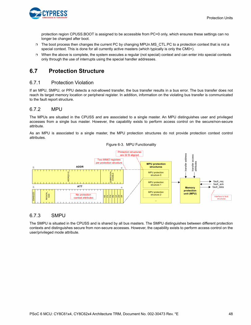
PSoC 6 MCU: CY8C61x4, CY8C62x4 Architecture TRM, Document No. 002-30473 Rev. *E 48
Protection Units
protection region CPUSS.BOOT is assigned to be accessible from PC=0 only, which ensures these settings can no longer be changed after boot.
❐ The boot process then changes the current PC by changing MPUn.MS_CTL.PC to a protection context that is not a special context. This is done for all currently active masters (which typically is only the CM0+).
❐ When the above is complete, the system executes a regular (not special) context and can enter into special contexts only through the use of interrupts using the special handler addresses.
6.7 Protection Structure
6.7.1 Protection Violation
If an MPU, SMPU, or PPU detects a not-allowed transfer, the bus transfer results in a bus error. The bus transfer does notreach its target memory location or peripheral register. In addition, information on the violating bus transfer is communicatedto the fault report structure.
6.7.2 MPU
The MPUs are situated in the CPUSS and are associated to a single master. An MPU distinguishes user and privilegedaccesses from a single bus master. However, the capability exists to perform access control on the secure/non-secureattribute.
As an MPU is associated to a single master, the MPU protection structures do not provide protection context controlattributes.
Figure 6-3. MPU Functionality
6.7.3 SMPU
The SMPU is situated in the CPUSS and is shared by all bus masters. The SMPU distinguishes between different protectioncontexts and distinguishes secure from non-secure accesses. However, the capability exists to perform access control on theuser/privileged mode attribute.
ATT 031
UR
UWUX
PR
PWPX
NS
EN
AB
LED
RE
GIO
N_
SIZ
E
ADDR 031
SU
BR
EG
ION
_D
ISA
BL
E
AD
DR
[23
:0]
MPU protectionstructures
MPU protectionstructure 0
...
tran
sfer
add
ress
tran
sfer
acc
ess
attr
ibut
es
Memory protection unit (MPU)
fault_reqfault_ack
fault_data
Interface to fault structures
Two MMIO registers per protection structure
Protection structures are 32 B aligned
No protection context attributes
MPU protectionstructure 1
MPU protectionstructure 2
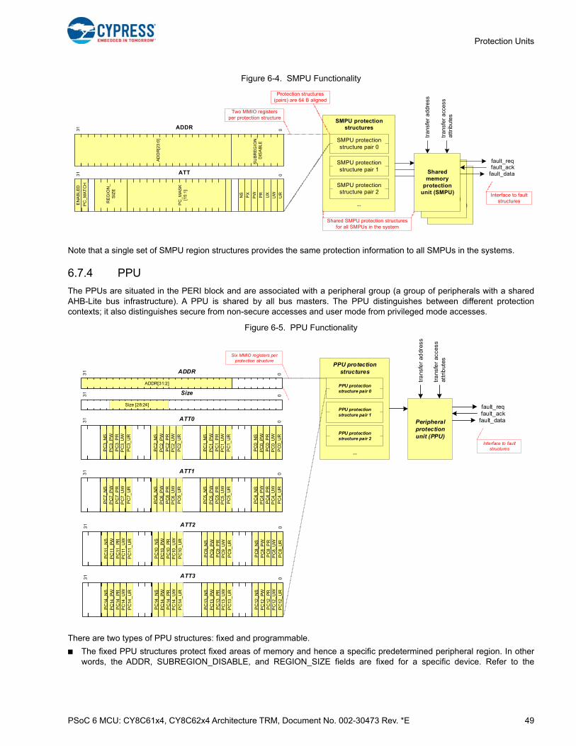
PSoC 6 MCU: CY8C61x4, CY8C62x4 Architecture TRM, Document No. 002-30473 Rev. *E 49
Protection Units
Figure 6-4. SMPU Functionality
Note that a single set of SMPU region structures provides the same protection information to all SMPUs in the systems.
6.7.4 PPU
The PPUs are situated in the PERI block and are associated with a peripheral group (a group of peripherals with a sharedAHB-Lite bus infrastructure). A PPU is shared by all bus masters. The PPU distinguishes between different protectioncontexts; it also distinguishes secure from non-secure accesses and user mode from privileged mode accesses.
Figure 6-5. PPU Functionality
There are two types of PPU structures: fixed and programmable.
■ The fixed PPU structures protect fixed areas of memory and hence a specific predetermined peripheral region. In otherwords, the ADDR, SUBREGION_DISABLE, and REGION_SIZE fields are fixed for a specific device. Refer to the
Shared memory
protection unit (SMPU)
Shared memory
protection unit (SMPU)
ATT 031
UR
UWUX
PR
PWPX
NS
PC
_M
AS
K[1
5:1]
EN
AB
LED
RE
GIO
N_
SIZ
E
ADDR 031
SU
BR
EG
ION
_D
ISA
BLE
AD
DR
[23
:0]
SMPU protection structures
...
tran
sfer
add
ress
tran
sfer
acc
ess
attr
ibut
es
Shared memory
protection unit (SMPU)
fault_reqfault_ack
fault_data
Interface to fault structures
Two MMIO registers per protection structure
Protection structures (pairs) are 64 B aligned
Shared SMPU protection structures for all SMPUs in the system
PC
_MA
TC
H
SMPU protectionstructure pair 0
SMPU protectionstructure pair 1
SMPU protectionstructure pair 2
PC
3_U
RP
C3_
UW
PC
3_P
RP
C3_
PW
PC
3_N
S
PC
1_U
RP
C1_
UW
PC
1_P
RP
C1_
PW
PC
1_N
S
ATT0 031
PC
0_U
RP
C0_
UW
PC
0_P
RP
C0_
PW
PC
0_N
S
ADDR 031
ADDR[31:2]
PPU protection structures
...
tra
nsfe
r ad
dres
s
tra
nsfe
r ac
cess
at
trib
utes
Peripheral protection unit (PPU)
fault_reqfault_ack
fault_data
Interface to fault structures
Six MMIO registers per protection structure
PPU protectionstructure pair 0
PPU protectionstructure pair 1
PPU protectionstructure pair 2
Size 031
Size [28:24]
PC
2_U
RP
C2_
UW
PC
2_P
RP
C2_
PW
PC
2_N
S
PC
7_U
RP
C7_
UW
PC
7_P
RP
C7_
PW
PC
7_N
S
PC
5_U
RP
C5_
UW
PC
5_P
RP
C5_
PW
PC
5_N
S
ATT1 031
PC
4_U
R
PC
4_U
WP
C4_
PR
PC
4_P
WP
C4_
NS
PC
6_U
RP
C6_
UW
PC
6_P
RP
C6_
PW
PC
6_N
S
PC
11_
UR
PC
11_
UW
PC
11_
PR
PC
11_
PW
PC
11_
NS
PC
9_U
RP
C9_
UW
PC
9_P
RP
C9_
PW
PC
9_N
S
ATT2 031
PC
8_U
R
PC
8_U
WP
C8_
PR
PC
8_P
WP
C8_
NS
PC
10_
UR
PC
10_
UW
PC
10_
PR
PC
10_
PW
PC
10_
NS
PC
14_
UR
PC
14_
UW
PC
14_
PR
PC
14_
PW
PC
14_
NS
PC
13_
UR
PC
13_
UW
PC
13_
PR
PC
13_
PW
PC
13_
NS
ATT3 031
PC
12_
UR
PC
12_
UW
PC
12_
PR
PC
12_
PW
PC
12_
NS
PC
14_
UR
PC
14_
UW
PC
14_
PR
PC
14_
PW
PC
14_
NS

PSoC 6 MCU: CY8C61x4, CY8C62x4 Architecture TRM, Document No. 002-30473 Rev. *E 50
Protection Units
registers TRM for a definition of fixed PPUs and the address regions they protect. Their protection attributes can beconfigured for each protection context.
Table 6-2. Fixed PPU Structure
Protection StructureBase Address of Protected
RegionSize of Protected Region Protected Block
PERI_MS_PPU_FX0 0x40000000 8 KB Peripheral Clock
PERI_MS_PPU_FX1 0x40004010 4 B Peripheral Group Structure 0
PERI_MS_PPU_FX2 0x40004030 4 B Peripheral Group Structure 1
PERI_MS_PPU_FX3 0x40004050 4 B Peripheral Group Structure 2
PERI_MS_PPU_FX4 0x40004060 32 B Peripheral Group Structure 3
PERI_MS_PPU_FX5 0x40004080 32 B Peripheral Group Structure 4
PERI_MS_PPU_FX6 0x400040A0 32 B Peripheral Group Structure 5
PERI_MS_PPU_FX7 0x400040C0 32 B Peripheral Group Structure 6
PERI_MS_PPU_FX8 0x40004120 32 B Peripheral Group Structure 9
PERI_MS_PPU_FX9 0x40008000 32 KB Peripheral Trigger Group
PERI_MS_PPU_FX16 0x40200000 1 KB CPUSS
PERI_MS_PPU_FX17 0x40201000 4 KB CPUSS_CM0
PERI_MS_PPU_FX18 0x40202000 512 B CPUSS_CM0
PERI_MS_PPU_FX19 0x40208000 1 KB CPUSS_CM0_SYSTEM_INT
PERI_MS_PPU_FX20 0x4020A000 1 KB CPUSS_CM4_SYSTEM_INT
PERI_MS_PPU_FX21 0x40210000 256 B Fault Structure 0
PERI_MS_PPU_FX22 0x40210100 256 B Fault Structure 1
PERI_MS_PPU_FX23 0x40220000 32 B IPC Structure 0
PERI_MS_PPU_FX24 0x40220020 32 B IPC Structure 1
PERI_MS_PPU_FX25 0x40220040 32 B IPC Structure 2
PERI_MS_PPU_FX26 0x40220060 32 B IPC Structure 3
PERI_MS_PPU_FX27 0x40220080 32 B IPC Structure 4
PERI_MS_PPU_FX28 0x402200A0 32 B IPC Structure 5
PERI_MS_PPU_FX29 0x402200C0 32 B IPC Structure 6
PERI_MS_PPU_FX30 0x402200E0 32 B IPC Structure 7
PERI_MS_PPU_FX31 0x40220100 32 B IPC Structure 8
PERI_MS_PPU_FX32 0x40220120 32 B IPC Structure 9
PERI_MS_PPU_FX33 0x40220140 32 B IPC Structure 10
PERI_MS_PPU_FX34 0x40220160 32 B IPC Structure 11
PERI_MS_PPU_FX35 0x40220180 32 B IPC Structure 12
PERI_MS_PPU_FX36 0x402201A0 32 B IPC Structure 13
PERI_MS_PPU_FX37 0x402201C0 32 B IPC Structure 14
PERI_MS_PPU_FX38 0x402201E0 32 B IPC Structure 15
PERI_MS_PPU_FX39 0x40221000 16 B IPC Interrupt Structure 0
PERI_MS_PPU_FX40 0x40221020 16 B IPC Interrupt Structure 1
PERI_MS_PPU_FX41 0x40221040 16 B IPC Interrupt Structure 2
PERI_MS_PPU_FX42 0x40221060 16 B IPC Interrupt Structure 3
PERI_MS_PPU_FX43 0x40221080 16 B IPC Interrupt Structure 4
PERI_MS_PPU_FX44 0x402210A0 16 B IPC Interrupt Structure 5
PERI_MS_PPU_FX45 0x402210C0 16 B IPC Interrupt Structure 6
PERI_MS_PPU_FX46 0x402210E0 16 B IPC Interrupt Structure 7
PERI_MS_PPU_FX47 0x40221100 16 B IPC Interrupt Structure 8
PERI_MS_PPU_FX48 0x40221120 16 B IPC Interrupt Structure 9
PERI_MS_PPU_FX49 0x40221140 16 B IPC Interrupt Structure 10

PSoC 6 MCU: CY8C61x4, CY8C62x4 Architecture TRM, Document No. 002-30473 Rev. *E 51
Protection Units
PERI_MS_PPU_FX50 0x40221160 16 B IPC Interrupt Structure 11
PERI_MS_PPU_FX51 0x40221180 16 B IPC Interrupt Structure 12
PERI_MS_PPU_FX52 0x402211A0 16 B IPC Interrupt Structure 13
PERI_MS_PPU_FX53 0x402211C0 16 B IPC Interrupt Structure 14
PERI_MS_PPU_FX54 0x402211E0 16 B IPC Interrupt Structure 15
PERI_MS_PPU_FX55 0x40230000 64 B Protection Unit SMPU
PERI_MS_PPU_FX56 0x40234000 4 B Protection Unit MPU0
PERI_MS_PPU_FX57 0x40237800 4 B Protection Unit MPU14
PERI_MS_PPU_FX58 0x40237C00 1 KB Protection Unit MPU15
PERI_MS_PPU_FX59 0x40240000 8 B FLASHC
PERI_MS_PPU_FX60 0x40240008 4 B FLASHC
PERI_MS_PPU_FX61 0x40240200 256 B FLASHC
PERI_MS_PPU_FX62 0x40240400 128 B FLASHC CM0+ cache
PERI_MS_PPU_FX63 0x40240480 128 B FLASHC CM4 cache
PERI_MS_PPU_FX64 0x40240500 4 B FLASHC Crypto Buffer
PERI_MS_PPU_FX65 0x40240580 4 B FLASHC DW0 Buffer
PERI_MS_PPU_FX66 0x40240600 4 B FLASHC DW1 Buffer
PERI_MS_PPU_FX67 0x40240680 4 B FLASHC DMAC Buffer
PERI_MS_PPU_FX68 0x4024F000 4 KB FLASHC Flash Macro
PERI_MS_PPU_FX69 0x40260000 256 B SRSS
PERI_MS_PPU_FX70 0x40260100 16 B Test Mode Control
PERI_MS_PPU_FX71 0x40260180 16 B Watchdog Counter Control
PERI_MS_PPU_FX72 0x40260200 128 B Multi-Counter Watchdog Timer
PERI_MS_PPU_FX73 0x40260300 256 B Clock
PERI_MS_PPU_FX74 0x40260400 1 KB Clock
PERI_MS_PPU_FX75 0x40260800 8 B Reset Cause
PERI_MS_PPU_FX76 0x40267000 4 KB Power and Clock Test Registers
PERI_MS_PPU_FX77 0x4026FF00 128 B Power and Clock Test Registers
PERI_MS_PPU_FX78 0x40270000 64 KB Backup Control
PERI_MS_PPU_FX79 0x40280000 128 B DMA Controller (DW) 0
PERI_MS_PPU_FX80 0x40290000 128 B DMA Controller (DW) 1
PERI_MS_PPU_FX81 0x40280100 128 B DMA Controller (DW) 0 CRC
PERI_MS_PPU_FX82 0x40290100 128 B DMA Controller (DW) 1 CRC
PERI_MS_PPU_FX83 0x40288000 64 B DMA Controller (DW) 0 Channel Structure 0
PERI_MS_PPU_FX84 0x40288040 64 B DMA Controller (DW) 0 Channel Structure 1
PERI_MS_PPU_FX85 0x40288080 64 B DMA Controller (DW) 0 Channel Structure 2
PERI_MS_PPU_FX86 0x402880C0 64 B DMA Controller (DW) 0 Channel Structure 3
PERI_MS_PPU_FX87 0x40288100 64 B DMA Controller (DW) 0 Channel Structure 4
PERI_MS_PPU_FX88 0x40288140 64 B DMA Controller (DW) 0 Channel Structure 5
PERI_MS_PPU_FX89 0x40288180 64 B DMA Controller (DW) 0 Channel Structure 6
PERI_MS_PPU_FX90 0x402881C0 64 B DMA Controller (DW) 0 Channel Structure 7
PERI_MS_PPU_FX91 0x40288200 64 B DMA Controller (DW) 0 Channel Structure 8
PERI_MS_PPU_FX92 0x40288240 64 B DMA Controller (DW) 0 Channel Structure 9
PERI_MS_PPU_FX93 0x40288280 64 B DMA Controller (DW) 0 Channel Structure 10
PERI_MS_PPU_FX94 0x402882C0 64 B DMA Controller (DW) 0 Channel Structure 11
PERI_MS_PPU_FX95 0x40288300 64 B DMA Controller (DW) 0 Channel Structure 12
Table 6-2. Fixed PPU Structure
Protection StructureBase Address of Protected
RegionSize of Protected Region Protected Block
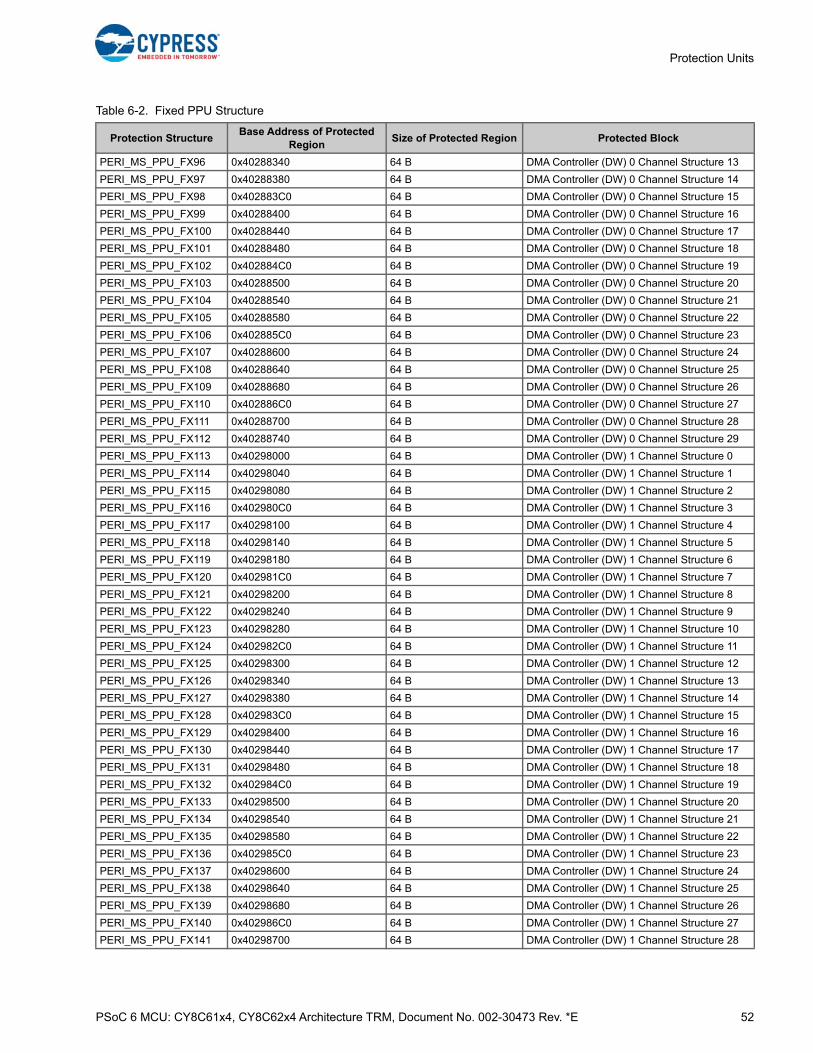
PSoC 6 MCU: CY8C61x4, CY8C62x4 Architecture TRM, Document No. 002-30473 Rev. *E 52
Protection Units
PERI_MS_PPU_FX96 0x40288340 64 B DMA Controller (DW) 0 Channel Structure 13
PERI_MS_PPU_FX97 0x40288380 64 B DMA Controller (DW) 0 Channel Structure 14
PERI_MS_PPU_FX98 0x402883C0 64 B DMA Controller (DW) 0 Channel Structure 15
PERI_MS_PPU_FX99 0x40288400 64 B DMA Controller (DW) 0 Channel Structure 16
PERI_MS_PPU_FX100 0x40288440 64 B DMA Controller (DW) 0 Channel Structure 17
PERI_MS_PPU_FX101 0x40288480 64 B DMA Controller (DW) 0 Channel Structure 18
PERI_MS_PPU_FX102 0x402884C0 64 B DMA Controller (DW) 0 Channel Structure 19
PERI_MS_PPU_FX103 0x40288500 64 B DMA Controller (DW) 0 Channel Structure 20
PERI_MS_PPU_FX104 0x40288540 64 B DMA Controller (DW) 0 Channel Structure 21
PERI_MS_PPU_FX105 0x40288580 64 B DMA Controller (DW) 0 Channel Structure 22
PERI_MS_PPU_FX106 0x402885C0 64 B DMA Controller (DW) 0 Channel Structure 23
PERI_MS_PPU_FX107 0x40288600 64 B DMA Controller (DW) 0 Channel Structure 24
PERI_MS_PPU_FX108 0x40288640 64 B DMA Controller (DW) 0 Channel Structure 25
PERI_MS_PPU_FX109 0x40288680 64 B DMA Controller (DW) 0 Channel Structure 26
PERI_MS_PPU_FX110 0x402886C0 64 B DMA Controller (DW) 0 Channel Structure 27
PERI_MS_PPU_FX111 0x40288700 64 B DMA Controller (DW) 0 Channel Structure 28
PERI_MS_PPU_FX112 0x40288740 64 B DMA Controller (DW) 0 Channel Structure 29
PERI_MS_PPU_FX113 0x40298000 64 B DMA Controller (DW) 1 Channel Structure 0
PERI_MS_PPU_FX114 0x40298040 64 B DMA Controller (DW) 1 Channel Structure 1
PERI_MS_PPU_FX115 0x40298080 64 B DMA Controller (DW) 1 Channel Structure 2
PERI_MS_PPU_FX116 0x402980C0 64 B DMA Controller (DW) 1 Channel Structure 3
PERI_MS_PPU_FX117 0x40298100 64 B DMA Controller (DW) 1 Channel Structure 4
PERI_MS_PPU_FX118 0x40298140 64 B DMA Controller (DW) 1 Channel Structure 5
PERI_MS_PPU_FX119 0x40298180 64 B DMA Controller (DW) 1 Channel Structure 6
PERI_MS_PPU_FX120 0x402981C0 64 B DMA Controller (DW) 1 Channel Structure 7
PERI_MS_PPU_FX121 0x40298200 64 B DMA Controller (DW) 1 Channel Structure 8
PERI_MS_PPU_FX122 0x40298240 64 B DMA Controller (DW) 1 Channel Structure 9
PERI_MS_PPU_FX123 0x40298280 64 B DMA Controller (DW) 1 Channel Structure 10
PERI_MS_PPU_FX124 0x402982C0 64 B DMA Controller (DW) 1 Channel Structure 11
PERI_MS_PPU_FX125 0x40298300 64 B DMA Controller (DW) 1 Channel Structure 12
PERI_MS_PPU_FX126 0x40298340 64 B DMA Controller (DW) 1 Channel Structure 13
PERI_MS_PPU_FX127 0x40298380 64 B DMA Controller (DW) 1 Channel Structure 14
PERI_MS_PPU_FX128 0x402983C0 64 B DMA Controller (DW) 1 Channel Structure 15
PERI_MS_PPU_FX129 0x40298400 64 B DMA Controller (DW) 1 Channel Structure 16
PERI_MS_PPU_FX130 0x40298440 64 B DMA Controller (DW) 1 Channel Structure 17
PERI_MS_PPU_FX131 0x40298480 64 B DMA Controller (DW) 1 Channel Structure 18
PERI_MS_PPU_FX132 0x402984C0 64 B DMA Controller (DW) 1 Channel Structure 19
PERI_MS_PPU_FX133 0x40298500 64 B DMA Controller (DW) 1 Channel Structure 20
PERI_MS_PPU_FX134 0x40298540 64 B DMA Controller (DW) 1 Channel Structure 21
PERI_MS_PPU_FX135 0x40298580 64 B DMA Controller (DW) 1 Channel Structure 22
PERI_MS_PPU_FX136 0x402985C0 64 B DMA Controller (DW) 1 Channel Structure 23
PERI_MS_PPU_FX137 0x40298600 64 B DMA Controller (DW) 1 Channel Structure 24
PERI_MS_PPU_FX138 0x40298640 64 B DMA Controller (DW) 1 Channel Structure 25
PERI_MS_PPU_FX139 0x40298680 64 B DMA Controller (DW) 1 Channel Structure 26
PERI_MS_PPU_FX140 0x402986C0 64 B DMA Controller (DW) 1 Channel Structure 27
PERI_MS_PPU_FX141 0x40298700 64 B DMA Controller (DW) 1 Channel Structure 28
Table 6-2. Fixed PPU Structure
Protection StructureBase Address of Protected
RegionSize of Protected Region Protected Block

PSoC 6 MCU: CY8C61x4, CY8C62x4 Architecture TRM, Document No. 002-30473 Rev. *E 53
Protection Units
PERI_MS_PPU_FX142 0x40298740 64 B DMA Controller (DW) 1 Channel Structure 29
PERI_MS_PPU_FX143 0x40298780 64 B DMA Controller (DW) 1 Channel Structure 30
PERI_MS_PPU_FX144 0x402987C0 64 B DMA Controller (DW) 1 Channel Structure 31
PERI_MS_PPU_FX145 0x402A0000 16 B DMAC Controller
PERI_MS_PPU_FX146 0x402A1000 256 B DMAC Controller Channel 0
PERI_MS_PPU_FX147 0x402A1100 256 B DMAC Controller Channel 1
PERI_MS_PPU_FX148 0x402C0000 128 B eFuse
PERI_MS_PPU_FX149 0x402C0800 512 B eFuse Data
PERI_MS_PPU_FX150 0x40300000 8 B HSIOM Port 0
PERI_MS_PPU_FX151 0x40300010 8 B HSIOM Port 1
PERI_MS_PPU_FX152 0x40300020 8 B HSIOM Port 2
PERI_MS_PPU_FX153 0x40300030 8 B HSIOM Port 3
PERI_MS_PPU_FX154 0x40300040 8 B HSIOM Port 4
PERI_MS_PPU_FX155 0x40300050 8 B HSIOM Port 5
PERI_MS_PPU_FX156 0x40300060 8 B HSIOM Port 6
PERI_MS_PPU_FX157 0x40300070 8 B HSIOM Port 7
PERI_MS_PPU_FX158 0x40300080 8 B HSIOM Port 8
PERI_MS_PPU_FX159 0x40300090 8 B HSIOM Port 9
PERI_MS_PPU_FX160 0x403000A0 8 B HSIOM Port 10
PERI_MS_PPU_FX161 0x403000B0 8 B HSIOM Port 11
PERI_MS_PPU_FX162 0x403000C0 8 B HSIOM Port 12
PERI_MS_PPU_FX163 0x403000D0 8 B HSIOM Port 13
PERI_MS_PPU_FX164 0x403000E0 8 B HSIOM Port 14
PERI_MS_PPU_FX165 0x40302000 32 B HSIOM AMUX
PERI_MS_PPU_FX167 0x40310000 64 B GPIO Port 0
PERI_MS_PPU_FX168 0x40310080 64 B GPIO Port 1
PERI_MS_PPU_FX169 0x40310100 64 B GPIO Port 2
PERI_MS_PPU_FX170 0x40310180 64 B GPIO Port 3
PERI_MS_PPU_FX171 0x40310200 64 B GPIO Port 4
PERI_MS_PPU_FX172 0x40310280 64 B GPIO Port 5
PERI_MS_PPU_FX173 0x40310300 64 B GPIO Port 6
PERI_MS_PPU_FX174 0x40310380 64 B GPIO Port 7
PERI_MS_PPU_FX175 0x40310400 64 B GPIO Port 8
PERI_MS_PPU_FX176 0x40310480 64 B GPIO Port 9
PERI_MS_PPU_FX177 0x40310500 64 B GPIO Port 10
PERI_MS_PPU_FX178 0x40310580 64 B GPIO Port 11
PERI_MS_PPU_FX179 0x40310600 64 B GPIO Port 12
PERI_MS_PPU_FX180 0x40310680 64 B GPIO Port 13
PERI_MS_PPU_FX181 0x40310700 64 B GPIO Port 14
PERI_MS_PPU_FX182 0x40310040 16 B GPIO Port 0 Interrupt
PERI_MS_PPU_FX183 0x403100C0 16 B GPIO Port 1 Interrupt
PERI_MS_PPU_FX184 0x40310140 16 B GPIO Port 2 Interrupt
PERI_MS_PPU_FX185 0x403101C0 16 B GPIO Port 3 Interrupt
PERI_MS_PPU_FX186 0x40310240 8 B GPIO Port 4 Interrupt
PERI_MS_PPU_FX187 0x403102C0 16 B GPIO Port 5 Interrupt
PERI_MS_PPU_FX188 0x40310340 16 B GPIO Port 6 Interrupt
Table 6-2. Fixed PPU Structure
Protection StructureBase Address of Protected
RegionSize of Protected Region Protected Block
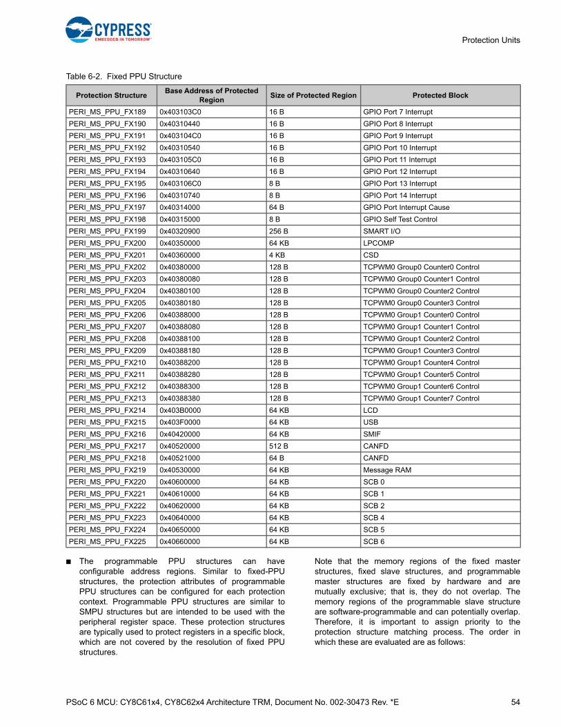
PSoC 6 MCU: CY8C61x4, CY8C62x4 Architecture TRM, Document No. 002-30473 Rev. *E 54
Protection Units
■ The programmable PPU structures can haveconfigurable address regions. Similar to fixed-PPUstructures, the protection attributes of programmablePPU structures can be configured for each protectioncontext. Programmable PPU structures are similar toSMPU structures but are intended to be used with theperipheral register space. These protection structuresare typically used to protect registers in a specific block,which are not covered by the resolution of fixed PPUstructures.
Note that the memory regions of the fixed masterstructures, fixed slave structures, and programmablemaster structures are fixed by hardware and aremutually exclusive; that is, they do not overlap. Thememory regions of the programmable slave structureare software-programmable and can potentially overlap.Therefore, it is important to assign priority to theprotection structure matching process. The order inwhich these are evaluated are as follows:
PERI_MS_PPU_FX189 0x403103C0 16 B GPIO Port 7 Interrupt
PERI_MS_PPU_FX190 0x40310440 16 B GPIO Port 8 Interrupt
PERI_MS_PPU_FX191 0x403104C0 16 B GPIO Port 9 Interrupt
PERI_MS_PPU_FX192 0x40310540 16 B GPIO Port 10 Interrupt
PERI_MS_PPU_FX193 0x403105C0 16 B GPIO Port 11 Interrupt
PERI_MS_PPU_FX194 0x40310640 16 B GPIO Port 12 Interrupt
PERI_MS_PPU_FX195 0x403106C0 8 B GPIO Port 13 Interrupt
PERI_MS_PPU_FX196 0x40310740 8 B GPIO Port 14 Interrupt
PERI_MS_PPU_FX197 0x40314000 64 B GPIO Port Interrupt Cause
PERI_MS_PPU_FX198 0x40315000 8 B GPIO Self Test Control
PERI_MS_PPU_FX199 0x40320900 256 B SMART I/O
PERI_MS_PPU_FX200 0x40350000 64 KB LPCOMP
PERI_MS_PPU_FX201 0x40360000 4 KB CSD
PERI_MS_PPU_FX202 0x40380000 128 B TCPWM0 Group0 Counter0 Control
PERI_MS_PPU_FX203 0x40380080 128 B TCPWM0 Group0 Counter1 Control
PERI_MS_PPU_FX204 0x40380100 128 B TCPWM0 Group0 Counter2 Control
PERI_MS_PPU_FX205 0x40380180 128 B TCPWM0 Group0 Counter3 Control
PERI_MS_PPU_FX206 0x40388000 128 B TCPWM0 Group1 Counter0 Control
PERI_MS_PPU_FX207 0x40388080 128 B TCPWM0 Group1 Counter1 Control
PERI_MS_PPU_FX208 0x40388100 128 B TCPWM0 Group1 Counter2 Control
PERI_MS_PPU_FX209 0x40388180 128 B TCPWM0 Group1 Counter3 Control
PERI_MS_PPU_FX210 0x40388200 128 B TCPWM0 Group1 Counter4 Control
PERI_MS_PPU_FX211 0x40388280 128 B TCPWM0 Group1 Counter5 Control
PERI_MS_PPU_FX212 0x40388300 128 B TCPWM0 Group1 Counter6 Control
PERI_MS_PPU_FX213 0x40388380 128 B TCPWM0 Group1 Counter7 Control
PERI_MS_PPU_FX214 0x403B0000 64 KB LCD
PERI_MS_PPU_FX215 0x403F0000 64 KB USB
PERI_MS_PPU_FX216 0x40420000 64 KB SMIF
PERI_MS_PPU_FX217 0x40520000 512 B CANFD
PERI_MS_PPU_FX218 0x40521000 64 B CANFD
PERI_MS_PPU_FX219 0x40530000 64 KB Message RAM
PERI_MS_PPU_FX220 0x40600000 64 KB SCB 0
PERI_MS_PPU_FX221 0x40610000 64 KB SCB 1
PERI_MS_PPU_FX222 0x40620000 64 KB SCB 2
PERI_MS_PPU_FX223 0x40640000 64 KB SCB 4
PERI_MS_PPU_FX224 0x40650000 64 KB SCB 5
PERI_MS_PPU_FX225 0x40660000 64 KB SCB 6
Table 6-2. Fixed PPU Structure
Protection StructureBase Address of Protected
RegionSize of Protected Region Protected Block

PSoC 6 MCU: CY8C61x4, CY8C62x4 Architecture TRM, Document No. 002-30473 Rev. *E 55
Protection Units
❐ The fixed master structures are evaluated in decreasing order.
❐ The fixed slave structures are evaluated in decreas-ing order.
❐ The programmable master structures are evaluated in decreasing order.
❐ The programmable slave structures are evaluated in decreasing order.
The programmable slave structures are evaluated last.These structures are software-programmable and canpotentially overlap (overlapping should not allowsoftware to circumvent the protection as provided by thefixed protection structure pairs).
Each peripheral group has a dedicated PPU. Theprotection information is provided by peripheral groupMMIO registers. A peripheral group PPU uses fixedprotection structure pairs for two purposes.
❐ Fixed protection structure pairs protect peripherals (one pair for each peripheral). The master structure protects the MMIO registers of the pair (the memory region encompasses the MMIO registers of the pair’s master structure and slave structure). The slave structure protects the peripheral (the memory region encompasses the peripheral address region).
❐ Fixed protection structure pairs protect specific peripheral subregions (one pair for each subregion). The master structure protects the MMIO registers of the pair. The slave structure protects the peripheral subregion. These pairs can be used to protect, for example, individual DW channels in the DW periph-eral or individual IPC structures in the IPC periph-eral.
Note that the memory regions of the fixed peripheralmaster structures, fixed peripheral slave structures, andfixed peripheral subregion master structures are fixed byhardware and are mutually exclusive; that is, they do notoverlap. The memory regions of the fixed peripheralsubregion slave structures are fixed by hardware andtypically are a subset of a peripheral address region, andtherefore overlap with a fixed peripheral slave structure.Therefore, it is important to assign priority to how theprotection structure matching process:
❐ The fixed peripheral subregion master structures are evaluated in decreasing order.
❐ The fixed peripheral subregion slave structures are evaluated in decreasing order.
❐ The fixed peripheral master structures are evaluated in decreasing order.
❐ The fixed peripheral slave structures are evaluated in decreasing order.
It is important to evaluate the fixed peripheral subregionmaster structures first. This allows software to assigndifferent protection for a subregion of a peripheral.
6.7.5 Protection of Protection Structures
The MPU, SMPU, and PPU-based protection architecture isconsistent and provides the flexibility to implement differentsystem-wide protection schemes. Protection structures canbe set once at boot time or can be changed dynamicallyduring device execution. For example, a CPU RTOS canchange the CPU’s MPU settings; a secure CPU can changethe SMPU and PPUs settings. But such a system will be leftinsecure if there is no way to protect the protectionstructures themselves. There must be a way to restrictaccess to the protection structures.
The protection of protection structures is achieved usinganother protection structure. For this reason, protectionstructures are defined in pairs of master and slave. We referto the slave and master protection structures as a protectionpair. Note that the address range of the master protectionstructure is known, that is, it is constant.
The first (slave) protection structure protects the resourceand the second (master) protection structure protects theprotection (address range of the second protection structureincludes both the master and slave protection structures).
The protection architecture is flexible enough to allow forvariations:
■ Exclusive peripheral ownership can be shared by morethan two protection contexts.
■ The ability to change ownership is under control of asingle protection context, and exclusive or non-exclusiveperipheral ownership is shared by multiple protectioncontexts.
Note that in secure systems, typically a single secure CPUis used. In these systems, the ability to change ownership isassigned to the secure CPU at boot time and notdynamically changed. Therefore, you must assign thesecure CPU its own, dedicated protection context.
Both PPU and SMPU is intended to distinguish betweendifferent protection contexts and to distinguish secure fromnon-secure accesses. Therefore, both PPU and SMPUprotection use protection structure pairs. In the SMPU, theslave protection structure provides SMPU protectioninformation and the master protection structure providesPPU protection information (the master and slave protectionstructures are registers).
The PERI_GR2_SL_CTL register is not protected fromapplication access. Writing to this register to disable group 2slaves stops the clock and asserts all protection unit resets(active and deep sleep). This in turn leads to clearance of allMMIO registers and reset of protection configuration. AllSMPUs and MPUs are disabled and the Protection Context(PC) of all masters is reset to 0. PC0 is not subject to accesspermission control; hence, every bus master (all CPUs,DAP, and so on) can access any address. In a securedsystem, to avoid this condition the PERI_GR2_SL_CTLregister should be protected from writes for PC > 0.
PSoC 6 MCU: CY8C61x4, CY8C62x4 Architecture TRM, Document No. 002-30473 Rev. *E 56
Protection Units
6.7.6 Protection Structure Types
Different protection structure types are used because someresources, such as peripheral registers, have a fixedaddress range. Protection of protection structures requirespairs of neighboring protection structures.
Three types of protection structures with a consistentregister interface are described here:
■ Programmable protection structures. These are 32-byteprotection structures with a programmable addressrange. These structures are used by the MPUs.
■ Fixed protection structure pairs. These are 64-bytemaster/slave protection structure pairs, consisting of two32-byte protection structures. These structures are usedby the PPUs. Both structures have a fixed, constantaddress region. The master structure has the UX and PXattributes as constant ‘0’ (execution is never allowed)and the UR and PR attributes as constant ‘1’ (reading isalways allowed). The slave structure has the UX and PXattributes as constant ‘1’.
■ Programmable protection structure pairs. These are 64-byte master/slave protection structure pairs, consistingof two 32-byte protection structures. These structuresare used by the PPU and SMPU. The master structurehas a fixed, constant address region. The slave structure
has a programmable address region. The masterstructure has the UX and PX attributes as constant ‘0’(execution is never allowed) and the UR and PRattributes as constant ‘1’ (reading is always allowed).The PPU slave structure has the UX and PX attributesas constant ‘1’. The SMPU slave structure hasprogrammable UX and PX attributes.
Note that the master protection structure in a protectionstructure pair is required only to address securityrequirements. The distinction between the three protectionstructure types is an implementation optimization. From anarchitectural perspective, all PPU protection structures arethe same, with the exception that for some protectionstructures the address range is fixed and not programmable.
As mentioned earlier, a protection unit evaluates theprotection regions in decreasing protection structure indexorder. The protection structures are evaluated in thefollowing order:
■ Fixed protection structures for specific peripherals orperipheral register address ranges.
■ Programmable protection structures.
In other words, fixed structures take precedence overprogrammable structures.

PSoC 6 MCU: CY8C61x4, CY8C62x4 Architecture TRM, Document No. 002-30473 Rev. *E 57
Protection Units
Figure 6-6. PPU and SMPU Pairs
Note: By default, both CPUs (CM0+ and CM4) are in protection context 0 when they come out of reset. In protection context0, the master is able to access all memory regardless of its protection settings. The master’s protection context will need to bechanged from protection context 0 to make any protection structure configuration effective. Multiple protection structures maybe preconfigured as part of the boot code, which sets up a secure environment at boot time. See the Boot Code chapter onpage 192 for details of these configurations.
Slave Structure
Master Structure
PPU, programmable protection structure pair
ATT 03 1
UR
UW
UX
PR
PW
PX
NS
PC
_MA
SK
[15
:1]
EN
AB
LE
D
RE
GIO
N_
SIZ
E
ADDR 03 1
SU
BR
EG
IO
N_
DIS
AB
LE
AD
DR
[2
3:0]
PC
_MA
TC
H
1
Slave Structure
ATT 03 1
UR
= 1
UW
UX
= 0
PR
= 1
PW
PX
= 0
NS
PC
_MA
SK
[15
:1]
EN
AB
LE
D
Co
nsta
nt
RE
GIO
N_
SIZ
E
03 1
ConstantSUBREGION_DISA
BLE
Constant ADDR[23:0], encompassing master and slave protection structures
PC
_MA
TC
H
1
Master Structure
SMPU, programmable protection structure pair
ATT0,1,2&3 03 1
ADDR 03 1
Slave Structure
Master Structure
PPU, fixed protection structure pair
Constant ADDR Encompassing Peripheral Slave MMIO Registers
03 1
Constant REGION SIZE
SIZE
Programmable PC Attributes
ATT0,1,2&3 03 1
ADDR 03 1
Constant ADDR Encompassing Peripheral Slave MMIO Registers
03 1
Constant REGION SIZE
SIZE
Programmable PC Attributes
ATT0,1,2&3 03 1
ADDR 03 1
Constant ADDR Encompassing Peripheral Slave MMIO Registers
03 1
Constant REGION SIZE
SIZE
Programmable PC Attributes
ATT0,1,2&3 03 1
ADDR 03 1
Programmable ADDR Encompassing Peripheral Slave MMIO Registers
03 1
Programmable REGION SIZE
SIZE
Programmable PC Attributes
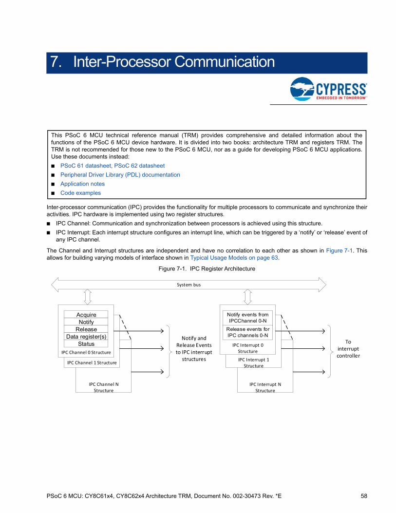
PSoC 6 MCU: CY8C61x4, CY8C62x4 Architecture TRM, Document No. 002-30473 Rev. *E 58
7. Inter-Processor Communication
Inter-processor communication (IPC) provides the functionality for multiple processors to communicate and synchronize theiractivities. IPC hardware is implemented using two register structures.
■ IPC Channel: Communication and synchronization between processors is achieved using this structure.
■ IPC Interrupt: Each interrupt structure configures an interrupt line, which can be triggered by a ‘notify’ or ‘release’ event ofany IPC channel.
The Channel and Interrupt structures are independent and have no correlation to each other as shown in Figure 7-1. Thisallows for building varying models of interface shown in Typical Usage Models on page 63.
Figure 7-1. IPC Register Architecture
This PSoC 6 MCU technical reference manual (TRM) provides comprehensive and detailed information about thefunctions of the PSoC 6 MCU device hardware. It is divided into two books: architecture TRM and registers TRM. TheTRM is not recommended for those new to the PSoC 6 MCU, nor as a guide for developing PSoC 6 MCU applications.Use these documents instead:
■ PSoC 61 datasheet, PSoC 62 datasheet
■ Peripheral Driver Library (PDL) documentation
■ Application notes
■ Code examples
IPC Channel 0 Structure
AcquireNotify
ReleaseData register(s)
Status
System bus
IPC Channel 1 Structure
IPC Channel N Structure
Notify and Release Events to IPC interrupt
structures
IPC Interrupt 0 Structure
Notify events from IPCChannel 0-N
IPC Interrupt 1 Structure
IPC Interrupt N Structure
To interrupt controller
Release events for IPC channels 0-N
PSoC 6 MCU: CY8C61x4, CY8C62x4 Architecture TRM, Document No. 002-30473 Rev. *E 59
Inter-Processor Communication
7.1 Features
The features of IPC are as follows:
■ Implements locks for mutual exclusion between processors
■ Allows sending messages between processors
■ Supports up to 16 channels for communication
■ Supports up to 16 interrupts, which can be triggered using notify or release events from the channels
7.2 Architecture
7.2.1 IPC Channel
An IPC channel is implemented as six hardware registers, as shown in Figure 7-2. The IPC channel registers are accessibleto all the processors in the system.
■ IPC_STRUCTx_ACQUIRE: This register determines the lock feature of the IPC. The IPC channel is acquired by readingthis register. If the SUCCESS field returns a ‘1’, the read acquired the lock.
If the SUCCESS field returns a ‘0’, the read did not acquire the lock.
Note that a single read access performs two functions:
❐ The attempt to acquire a lock.
❐ Return the result of the acquisition attempt (SUCCESS field).
The atomicity of these two functions is essential in a CPU with multiple tasks that can preempt each other.
The register also has bitfields that provide information about the processor that acquired it. When acquired, this register isreleased by writing any value into the IPC_STRUCTx_RELEASE register. If the register was already in an acquired stateanother attempt to read the register will not be able to acquire it.
■ IPC_STRUCTx_NOTIFY: This register is used to generate an IPC notify event. Each bit in this register corresponds to anIPC interrupt structure. The notify event generated from an IPC channel can trigger any or multiple interrupt structures.
■ IPC_STRUCTx_RELEASE: Any write to this register will release the IPC channel. This register also has a bit thatcorresponds to each IPC interrupt structure. The release event generated from an IPC channel can trigger any or multipleinterrupt structures. To only release the IPC channel and not generate an interrupt, you can write a zero into the IPCrelease register.
■ IPC_STRUCTx_DATA0 and IPC_STRUCTx_DATA1: These are two 32-bit register meant to hold data. These registerscan be considered as the shared data memory for the channel. Typically, these registers will hold messages that need tobe communicated between processors. If the messages are larger than the combined 64-bit size, place pointers in one orboth of these registers.
■ IPC_STRUCTx_LOCK_STATUS: This register provides the instantaneous lock status for the IPC channel. The registerprovides details if the channel is acquired. If acquired, it provides the processor’s ID, protection context, and other details.The reading of lock status provides only an instantaneous status, which can be changed in the next cycle based on theactivity of other processors on the channel.

PSoC 6 MCU: CY8C61x4, CY8C62x4 Architecture TRM, Document No. 002-30473 Rev. *E 60
Inter-Processor Communication
Figure 7-2. IPC Channel Structure
7.2.2 IPC Interrupt
Each IPC interrupt line in the system has a corresponding IPC interrupt structure. An IPC interrupt can be triggered by a notifyor a release event from any of the IPC channels in the system. You can choose to mask any of the sources of these eventsusing the IPC interrupt registers. Figure 7-3 shows the registers in an IPC Interrupt structure.
IPC_INTR_STRUCTx_INTR: This register provides the instantaneous status of the interrupt sources. Note that there are 16notify and 16 release event bits in this register. These are the notify and release events corresponding to the 16 IPCchannels. When a notify event is triggered in the IPC channel 0, the corresponding Notify0 bit is activated in the interruptregisters. A write of ‘1’ to a bit will clear the interrupt.
IPC_INTR_STRUCTx_INTR_MASK: The bit in this register masks the interrupt sources. Only the interrupt sources with theirmasks enabled can trigger the interrupt.
IPC_INTR_STRUCTx_INTR_SET: A write of ‘1’ into this register will set the interrupt.
IPC_INTR_STRUCTx_INTR_MASKED: This register provides the instantaneous value of the interrupts after they aremasked. The value in this register is (IPC_INTR_STRUCTx_INTR AND IPC_INTR_STRUCTx_INTR_MASK).
Figure 7-3. IPC Interrupt Structure
7.2.3 IPC Channels and Interrupts
The IPC block has a set of IPC interrupts associated with it. Each IPC interrupt register structure corresponds to an IPCinterrupt line. This interrupt can trigger an interrupt on any of the processors in the system. The interrupt routing forprocessors are dependent on the device architecture.
Each IPC channel has a release and notify register, which can drive events on any of the IPC interrupts. An illustration of thisrelation between the IPC channels and the IPC interrupt structure is shown in Figure 7-4.
IPC_STRUCTx_ACQUIRE
MS
[3:0
]
SU
CC
ES
S
031
IPC_STRUCTx_RELEASE 031
031 IPC_STRUCTx_NOTIFY
031 IPC_STRUCTx_DATA0
INT
R_
NO
T0
INT
R_
NO
T1
INT
R_
RE
L0
INT
R_
RE
L1
DA
TA
[31
:0]
INT
R_
NO
T1
4
INT
R_
NO
T1
5
INT
R_
NO
T1
2
INT
R_
NO
T1
3
INT
R_
NO
T1
0
INT
R_
NO
T1
1
INT
R_
NO
T8
INT
R_
NO
T9
INT
R_
NO
T6
INT
R_
NO
T7
INT
R_
NO
T4
INT
R_
NO
T5
INT
R_
NO
T2
INT
R_
NO
T3
INT
R_
RE
L14
INT
R_
RE
L15
INT
R_
RE
L12
INT
R_
RE
L13
INT
R_
RE
L10
INT
R_
RE
L11
INT
R_
RE
L8
INT
R_
RE
L9
INT
R_
RE
L6
INT
R_
RE
L7
INT
R_
RE
L4
INT
R_
RE
L5
INT
R_
RE
L2
INT
R_
RE
L3
AC
QU
IRE
D
PC
[3:0
]
PNS
IPC_STRUCTx_LOCK_STATUS
MS
[3:0
]
031
PC
[3:0
]
PNS
AC
QU
IRE
D
0
DA
TA
[31
:0]
IPC_STRUCTx_DATA131
031
RE
LE
AS
E0
RE
LE
AS
E1
RE
LE
AS
E1
4
RE
LE
AS
E1
5
RE
LE
AS
E1
2
RE
LE
AS
E1
3
RE
LE
AS
E1
0
RE
LE
AS
E1
1
RE
LE
AS
E8
RE
LE
AS
E9
RE
LE
AS
E6
RE
LE
AS
E7
RE
LE
AS
E4
RE
LE
AS
E5
RE
LE
AS
E2
RE
LE
AS
E3
NO
TIF
Y0
NO
TIF
Y1
NO
TIF
Y1
4
NO
TIF
Y1
5
NO
TIF
Y1
2
NO
TIF
Y1
3
NO
TIF
Y1
0
NO
TIF
Y1
1
NO
TIF
Y8
NO
TIF
Y9
NO
TIF
Y6
NO
TIF
Y7
NO
TIF
Y4
NO
TIF
Y5
NO
TIF
Y2
NO
TIF
Y3
031
RE
LE
AS
E0
RE
LE
AS
E1
RE
LEA
SE
14
RE
LEA
SE
15
RE
LEA
SE
12
RE
LEA
SE
13
RE
LE
AS
E1
0
RE
LE
AS
E1
1
RE
LE
AS
E8
RE
LE
AS
E9
RE
LE
AS
E6
RE
LE
AS
E7
RE
LE
AS
E4
RE
LE
AS
E5
RE
LE
AS
E2
RE
LE
AS
E3
IPC_INTR_STRUCTx_INTR_SET
NO
TIF
Y0
NO
TIF
Y1
NO
TIF
Y1
4
NO
TIF
Y1
5
NO
TIF
Y1
2
NO
TIF
Y1
3
NO
TIF
Y1
0
NO
TIF
Y1
1
NO
TIF
Y8
NO
TIF
Y9
NO
TIF
Y6
NO
TIF
Y7
NO
TIF
Y4
NO
TIF
Y5
NO
TIF
Y2
NO
TIF
Y3
031
RE
LE
AS
E0
RE
LE
AS
E1
RE
LE
AS
E1
4
RE
LE
AS
E1
5
RE
LE
AS
E1
2
RE
LE
AS
E1
3
RE
LE
AS
E1
0
RE
LE
AS
E1
1
RE
LE
AS
E8
RE
LE
AS
E9
RE
LE
AS
E6
RE
LE
AS
E7
RE
LE
AS
E4
RE
LE
AS
E5
RE
LE
AS
E2
RE
LE
AS
E3
NO
TIF
Y0
NO
TIF
Y1
NO
TIF
Y1
4
NO
TIF
Y1
5
NO
TIF
Y1
2
NO
TIF
Y1
3
NO
TIF
Y1
0
NO
TIF
Y1
1
NO
TIF
Y8
NO
TIF
Y9
NO
TIF
Y6
NO
TIF
Y7
NO
TIF
Y4
NO
TIF
Y5
NO
TIF
Y2
NO
TIF
Y3
031
RE
LE
AS
E0
RE
LE
AS
E1
RE
LE
AS
E1
4
RE
LE
AS
E1
5
RE
LE
AS
E1
2
RE
LE
AS
E1
3
RE
LE
AS
E1
0
RE
LE
AS
E1
1
RE
LE
AS
E8
RE
LE
AS
E9
RE
LE
AS
E6
RE
LE
AS
E7
RE
LE
AS
E4
RE
LE
AS
E5
RE
LE
AS
E2
RE
LE
AS
E3
IPC_INTR_STRUCTx_INTR_MASKED
NO
TIF
Y0
NO
TIF
Y1
NO
TIF
Y1
4
NO
TIF
Y1
5
NO
TIF
Y1
2
NO
TIF
Y1
3
NO
TIF
Y1
0
NO
TIF
Y1
1
NO
TIF
Y8
NO
TIF
Y9
NO
TIF
Y6
NO
TIF
Y7
NO
TIF
Y4
NO
TIF
Y5
NO
TIF
Y2
NO
TIF
Y3
IPC_INTR_STRUCTx_INTR IPC_INTR_STRUCTx_INTR_MASK

PSoC 6 MCU: CY8C61x4, CY8C62x4 Architecture TRM, Document No. 002-30473 Rev. *E 61
Inter-Processor Communication
Figure 7-4. IPC Channels and Interrupts
7.3 Implementing Locks
The IPC channels can be used to implement locks. Locksare typically used in multi-core systems to implement someform of mutually exclusive access to a shared resource.When multiple processors share a resource, the processorsare capable of acquiring and releasing the IPC channel. Sothe processor can assume an IPC channel as a lock. Thesemantics of this code is that access to the shared resourceis gated by the processor’s ownership of the channel. So theprocessors will need to acquire the IPC channel before theyaccess the shared resource.
A failure to acquire the IPC channel signifies a lock on theshared resource because another processor has control ofit. Note that the IPC channel will not enforce whichprocessor acquires or releases the channel. All processorscan acquire or release the IPC channel and the semantics ofthe code must make sure that the processor that acquiresthe channel is the one that releases it.
7.4 Message Passing
IPC channels can be used to communicate messagesbetween processors. In this use case, the channel is used inconjunction with the interrupt structures. The IPC channel isused to lock the access to the data registers. The IPCchannel is acquired by the sender and used to populate themessage. The receiver reads the message and thenreleases the channel. Thus, between the sender puttingdata into the channel and receiver reading it, the channel islocked for all other task access. The sender uses a notifyevent on the receiver’s IPC interrupt to denote a sendoperation. The receiver acts on this interrupt and reads thedata from the data registers. After the reception is complete,the receiver releases the channel and can also generate arelease event to the senders IPC interrupt. Note that theaction of locking the channel does not, in hardware, restrictaccess to the data registers. This is a semantic that shouldbe enforced by software.
Figure 7-5 portrays an example of a sender (Processor A)sending data to a receiver (Processor B). IPC interrupt A is
INTR_REL 0
INTR_REL 1
INTR_REL 3
INTR_REL 2
INTR_NOT 0
INTR_NOT 1
INTR_NOT 3
INTR _NOT 2
INTR_REL 4
INTR_REL 5
INTR_REL N
INTR_REL 6
INTR_NOT 4
INTR_NOT 5
INTR_NOT N
INTR _NOT 6
INTR 0
INTR_REL 0
INTR_REL 1
INTR_REL 3
INTR_REL 2
INTR_NOT 0
INTR_NOT 1
INTR_NOT 3
INTR _NOT 2
INTR_REL 4
INTR_REL 5
INTR_REL N
INTR_REL 6
INTR_NOT 4
INTR_NOT 5
INTR_NOT N
INTR _NOT 6
INTR 1
INTR_REL 0
INTR_REL 1
INTR_REL 3
INTR_REL 2
INTR_NOT 0
INTR_NOT 1
INTR_NOT 3
INTR _NOT 2
INTR_REL 4
INTR_REL 5
INTR_REL N
INTR_REL 6
INTR_NOT 4
INTR_NOT 5
INTR_NOT N
INTR _NOT 6
INTR 2
INTR_REL 0
INTR_REL 1
INTR_REL 3
INTR_REL 2
INTR_NOT 0
INTR_NOT 1
INTR_NOT 3
INTR _NOT 2
INTR_REL 4
INTR_REL 5
INTR_REL N
INTR_REL 6
INTR_NOT 4
INTR_NOT 5
INTR_NOT N
INTR _NOT 6
INTR 3
INTR 0
INTR 1
INTR 3
INTR 2
Release
INTR 0
INTR 1
INTR 3
INTR 2
Notify
IPC 0
INTR 0
INTR 1
INTR 3
INTR 2
Release
INTR 0
INTR 1
INTR 3
INTR 2
Notify
IPC 1
INTR 0
INTR 1
INTR 3
INTR 2
Release
INTR 0
INTR 1
INTR 3
INTR 2
Notify
IPC N
INTR N INTR N INTR N INTR N INTR N INTR N
Interrupt to processors
Interrupt to processors
Interrupt to processors
Interrupt to processors

PSoC 6 MCU: CY8C61x4, CY8C62x4 Architecture TRM, Document No. 002-30473 Rev. *E 62
Inter-Processor Communication
configured to interrupt Processor A. IPC interrupt B isconfigured to interrupt Processor B.
1. The sender will attempt to acquire the IPC channel byreading the IPC_STRUCTx_ACQUIRE register. If thechannel was acquired, the sender has ownership of thechannel for data transmission. This also changes thestatus of the channel and its correspondingIPC_STRUCTx_LOCK_STATUS register. If the channelwas not acquired, the processor should wait until thechannel is free for acquisition. This can be done bypolling the IPC channel’sIPC_STRUCTx_LOCK_STATUS register.
2. After the IPC channel is acquired, the sender has controlof the channel for communication and places the 64-bitmessage data in the IPC_STRUCTx_DATA0 andIPC_STRUCTx_DATA1 registers.
3. Now that the message is placed in the IPC channel, thesender generates a notify event on the receiver’sinterrupt line. It does this by setting the corresponding bitin the IPC channel’s IPC_STRUCTx_NOTIFY register.This event creates a notify event at IPC interrupt B(IPC_INTR_STRUCTx_INTR). If the IPC channel’s
notify event was enabled by setting the mask bit(IPC_INTR_STRUCTx_INTR_MASK [31:23]) in the IPCinterrupt B, this will generate an interrupt in the receiver.
4. When it receives IPC interrupt B, the receiver can pollthe IPC_INTR_STRUCTx_INTR_MASKED register tounderstand which IPC channel had triggered the notifyevent. Based on this, the receiver identifies the channelto read and reads from the IPC channel’sIPC_STRUCTx_DATA0 and IPC_STRUCTx_DATA1registers. The receiver has now received the data sentby the sender. It needs to release the channel so thatother processors/processes can use it.
5. The receiver releases the channel. It also optionallygenerates a release event on the sender’s IPC interruptA. This will generate a release event interrupt on thesender if the corresponding channel release event wasmasked.
On receiving the release interrupt, the sender can act on theevent based on the application requirement. It can either tryto reacquire the channel for further transmission or go on toother tasks because the transmission is complete.
Figure 7-5. Sending Messages using IPC
In the previous example, the size of the data being transmitted was just 64 bits. Larger messages can be sent as pointers.The sender can allocate a larger message structure in memory and pass the pointers in the data registers. Figure 7-6 showsthe usage. Note that the user code must implement the synchronization of the message read process.
■ The implementation can stall the channel until the receiver has used up all the data in the message packet and themessage packet can be rewritten. This is wasteful because it will stall other inter-process communications as the numberof IPC channels is limited.
■ The receiver can release the channel as soon as it receives the pointer to the message packet. It implements thesynchronization logic in the message packet as a flag, which the sender sets on write complete and receiver clears on aread complete.
IPC Channel
Acquire
Notify
Release
Data
Status
Sender (Processor A)
Receiver (Processor B)
(1)
(2)
(3)
IPC interrupt B
(3)(3)
IPC interrupt A
(4)
(5)(5)
(1) (5)
Hardware action
User action
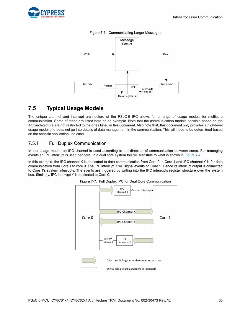
PSoC 6 MCU: CY8C61x4, CY8C62x4 Architecture TRM, Document No. 002-30473 Rev. *E 63
Inter-Processor Communication
Figure 7-6. Communicating Larger Messages
7.5 Typical Usage Models
The unique channel and interrupt architecture of the PSoC 6 IPC allows for a range of usage models for multicorecommunication. Some of these are listed here as an example. Note that the communication models possible based on theIPC architecture are not restricted to the ones listed in this document. Also note that, this document only provides a high-levelusage model and does not go into details of data management in the communication. This will need to be determined basedon the specific application use case.
7.5.1 Full Duplex Communication
In this usage model, an IPC channel is used according to the direction of communication between cores. For managingevents an IPC interrupt is used per core. In a dual core system this will translate to what is shown in Figure 7-7.
In this example, the IPC channel X is dedicated to data communication from Core 0 to Core 1 and IPC channel Y is for datacommunication from Core 1 to core 0. The IPC interrupt X will signal events on Core 1. Hence its interrupt output is connectedto Core 1's system interrupts. The events are triggered by writing into the IPC interrupts register structure over the systembus. Similarly, IPC interrupt Y is dedicated to Core 0.
Figure 7-7. Full Duplex IPC for Dual Core Communication
Message Packet
IPC
Data Registers
Sender ReceiverPointerInterrupt
ReadWrite
Release
Core 1Core 0
IPC Channel X
IPC Channel Y
IPC Interrupt X
IPC Interrupt Y
System Interrupt
System Interrupt
Data transfer/register updates over system bus
Digital signals such as triggers or interrupts

PSoC 6 MCU: CY8C61x4, CY8C62x4 Architecture TRM, Document No. 002-30473 Rev. *E 64
Inter-Processor Communication
7.5.2 Half Duplex with Independent Event Handling
In this case only one IPC channel is used to set up the transfer between the two cores. This means that only one side controlsdata transfer at a time. The channels Lock register must be used to avoid contention of the one shared IPC channel. Twoindependent events are supported due to the two IPC interrupt structures being used. This model is shown in Figure 7-8.
Figure 7-8. Half Duplex with Independent Event Handling
7.5.3 Half Duplex with Shared Event Handling
In this model both the IPC channel and interrupt are shared between the two cores. Since the interrupt is also shared, theaccess to the interrupt registers must be managed using the IPC lock of the channel. As shown in Figure 7-9, the IPCinterrupt will be set up to trigger interrupts in both cores. Hence the individual core interrupts should have logic in its ISR tocheck which core is in control of the IPC and determine if the message and event was for that core.
Core 1Core 0
IPC Interrupt X
IPC Interrupt Y
System Interrupt
System Interrupt
Data transfer/register updates over system bus
Digital signals such as triggers or interrupts
IPC Channel X
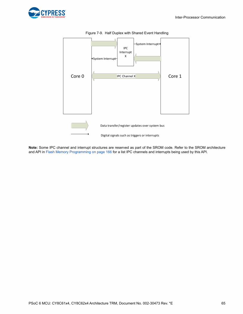
PSoC 6 MCU: CY8C61x4, CY8C62x4 Architecture TRM, Document No. 002-30473 Rev. *E 65
Inter-Processor Communication
Figure 7-9. Half Duplex with Shared Event Handling
Note: Some IPC channel and interrupt structures are reserved as part of the SROM code. Refer to the SROM architectureand API in Flash Memory Programming on page 166 for a list IPC channels and interrupts being used by this API.
Core 1Core 0
IPC Interrupt
X
System Interrupt
System Interrupt
Data transfer/register updates over system bus
Digital signals such as triggers or interrupts
IPC Channel X

PSoC 6 MCU: CY8C61x4, CY8C62x4 Architecture TRM, Document No. 002-30473 Rev. *E 66
8. Fault Monitoring
Fault monitoring allows you to monitor various faults generated within the device and take actions based on the fault reported.The fault structures present in the PSoC 6 MCU monitor access violation faults at protection units (MPU, SMPU, or PPU) andflash controller bus error/fault. In addition to reporting faults, the fault structures in PSoC 6 MCUs provide a mechanism to logdata from the fault sources and optionally perform soft reset.
The PSoC 6 MCU family supports two centralized fault report/monitoring structures that monitor faults generated within thedevice. Each fault report structure can monitor and report faults from up to 96 sources.
8.1 Features
Each PSoC 6 MCU fault report structure supports:
■ Monitoring protection unit access violation faults and flash controller bus errors
■ Four 32-bit data registers to record fault information
■ Soft reset on fault detection while retaining the fault information
■ Interrupt on fault detection
■ Trigger output to DMA for fault data transfer
■ Fault detected output to a pin for external fault handling
This PSoC 6 MCU technical reference manual (TRM) provides comprehensive and detailed information about thefunctions of the PSoC 6 MCU device hardware. It is divided into two books: architecture TRM and registers TRM. TheTRM is not recommended for those new to the PSoC 6 MCU, nor as a guide for developing PSoC 6 MCU applications.Use these documents instead:
■ PSoC 61 datasheet, PSoC 62 datasheet
■ Peripheral Driver Library (PDL) documentation
■ Application notes
■ Code examples

PSoC 6 MCU: CY8C61x4, CY8C62x4 Architecture TRM, Document No. 002-30473 Rev. *E 67
Fault Monitoring
8.2 Architecture
Figure 8-1. Fault Report Structure
The PSoC 6 MCU family uses centralized fault report structures. This centralized nature allows for a system wide handling offaults simplifying firmware development. Only a single fault interrupt handler is required to monitor multiple faults. The faultreport structure provides the fault source and additional fault specific information through a single set of registers; no iterativesearch for the fault source and fault information is required.
The fault structure can be configured to capture one or more faults as listed in Table 8-2. When a fault structure is configuredto capture a specific fault, an occurrence of that fault will be recorded as a pending fault. If the fault structure has finishedprocessing all other faults or if there are no other pending faults, the fault data will be captured into the fault structureregisters. In addition, a successful capture can trigger an interrupt and be processed by either Cortex-M4 or Cortex-M0+depending on the application requirement.
It should be noted that each fault structure is capable of capturing only one fault at a time and as long as that fault is notserviced, subsequent faults will not be captured by the fault structure. In addition to capturing faults, the fault structure canoptionally perform a soft reset while retaining the fault information. This reset results in RESET_ACT_FAULT reset cause inthe SRSS_RES_CAUSE register.
8.2.1 Fault Report
The PSoC 6 MCU family supports two fault report structures. Each fault report structure has a dedicated set of control andstatus registers. Each fault report structure captures a single fault. The captured fault information includes:
■ Fault validity bit that indicates a fault is captured (VALID bit [31] of the FAULT_STRUCTx_STATUS register). This bit is setwhenever a fault is captured. The bit should be cleared after processing the fault information. New faults are captured onlywhen this bit is ‘0’.
■ Fault index, as shown in Table 8-2, identifies the fault source (IDX bits [6:0] of FAULT_STRUCTx_STATUS)
■ Additional fault information describing fault specifics (FAULT_STRUCTx_DATA0 through FAULT_STRUCTx_DATA3registers). This additional information is fault source specific. For example, an MPU protection violation provides
Fault reportStructure[1] FAULT_PENDING0
Fault reportStructure[0]
Fault report Structure [x]
INTR_FAULT
FAULT_STATUS
INTR_FAULT_SET
INTR_FAULT_MASKED
FAULT_CTL
INTR_FAULT_MASK
FAULT_DATA0
...
FAULT_DATA3
FAULT_PENDING1
FAULT_PENDING2
FAULT_MASK0
FAULT_MASK1
FAULT_MASK2
interrupt_fault[x]
tr_fault[x]
fault_out[x]
fault_reset_req[x]
Fault source 0
ذ up to 96 ... Pending faults
Retained during soft reset
Fault source 95
Single structure, used by all fault report structures.
Fault Data
Fault Data
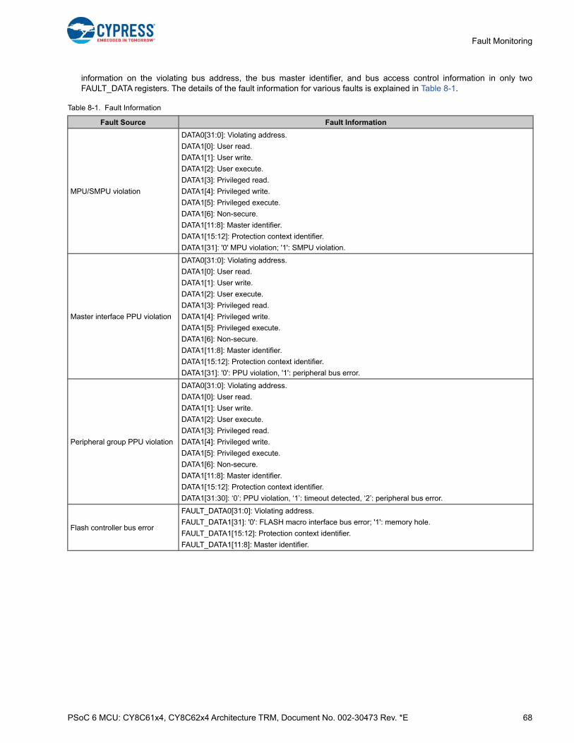
PSoC 6 MCU: CY8C61x4, CY8C62x4 Architecture TRM, Document No. 002-30473 Rev. *E 68
Fault Monitoring
information on the violating bus address, the bus master identifier, and bus access control information in only twoFAULT_DATA registers. The details of the fault information for various faults is explained in Table 8-1.
Table 8-1. Fault Information
Fault Source Fault Information
MPU/SMPU violation
DATA0[31:0]: Violating address.
DATA1[0]: User read.
DATA1[1]: User write.
DATA1[2]: User execute.
DATA1[3]: Privileged read.
DATA1[4]: Privileged write.
DATA1[5]: Privileged execute.
DATA1[6]: Non-secure.
DATA1[11:8]: Master identifier.
DATA1[15:12]: Protection context identifier.
DATA1[31]: '0' MPU violation; '1': SMPU violation.
Master interface PPU violation
DATA0[31:0]: Violating address.
DATA1[0]: User read.
DATA1[1]: User write.
DATA1[2]: User execute.
DATA1[3]: Privileged read.
DATA1[4]: Privileged write.
DATA1[5]: Privileged execute.
DATA1[6]: Non-secure.
DATA1[11:8]: Master identifier.
DATA1[15:12]: Protection context identifier.
DATA1[31]: '0': PPU violation, '1': peripheral bus error.
Peripheral group PPU violation
DATA0[31:0]: Violating address.
DATA1[0]: User read.
DATA1[1]: User write.
DATA1[2]: User execute.
DATA1[3]: Privileged read.
DATA1[4]: Privileged write.
DATA1[5]: Privileged execute.
DATA1[6]: Non-secure.
DATA1[11:8]: Master identifier.
DATA1[15:12]: Protection context identifier.
DATA1[31:30]: ‘0’: PPU violation, ‘1’: timeout detected, ‘2’: peripheral bus error.
Flash controller bus error
FAULT_DATA0[31:0]: Violating address.
FAULT_DATA1[31]: '0': FLASH macro interface bus error; '1': memory hole.
FAULT_DATA1[15:12]: Protection context identifier.
FAULT_DATA1[11:8]: Master identifier.
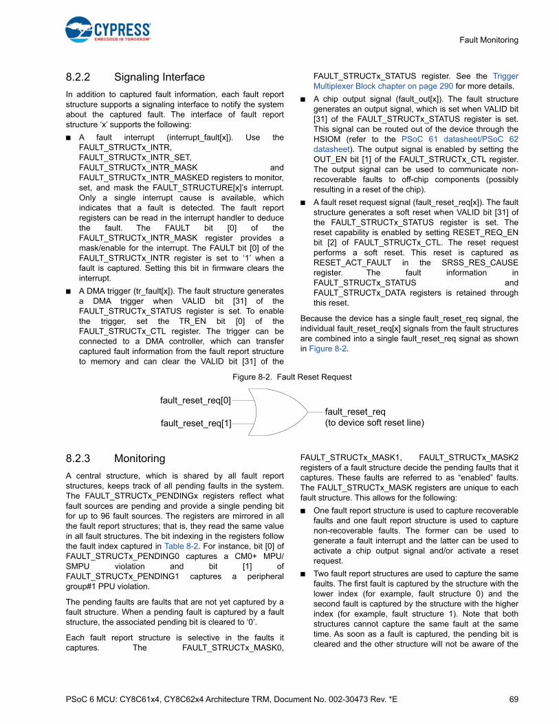
PSoC 6 MCU: CY8C61x4, CY8C62x4 Architecture TRM, Document No. 002-30473 Rev. *E 69
Fault Monitoring
8.2.2 Signaling Interface
In addition to captured fault information, each fault reportstructure supports a signaling interface to notify the systemabout the captured fault. The interface of fault reportstructure ‘x’ supports the following:
■ A fault interrupt (interrupt_fault[x]). Use theFAULT_STRUCTx_INTR,FAULT_STRUCTx_INTR_SET,FAULT_STRUCTx_INTR_MASK andFAULT_STRUCTx_INTR_MASKED registers to monitor,set, and mask the FAULT_STRUCTURE[x]’s interrupt.Only a single interrupt cause is available, whichindicates that a fault is detected. The fault reportregisters can be read in the interrupt handler to deducethe fault. The FAULT bit [0] of theFAULT_STRUCTx_INTR_MASK register provides amask/enable for the interrupt. The FAULT bit [0] of theFAULT_STRUCTx_INTR register is set to ‘1’ when afault is captured. Setting this bit in firmware clears theinterrupt.
■ A DMA trigger (tr_fault[x]). The fault structure generatesa DMA trigger when VALID bit [31] of theFAULT_STRUCTx_STATUS register is set. To enablethe trigger, set the TR_EN bit [0] of theFAULT_STRUCTx_CTL register. The trigger can beconnected to a DMA controller, which can transfercaptured fault information from the fault report structureto memory and can clear the VALID bit [31] of the
FAULT_STRUCTx_STATUS register. See the TriggerMultiplexer Block chapter on page 290 for more details.
■ A chip output signal (fault_out[x]). The fault structuregenerates an output signal, which is set when VALID bit[31] of the FAULT_STRUCTx_STATUS register is set.This signal can be routed out of the device through theHSIOM (refer to the PSoC 61 datasheet/PSoC 62datasheet). The output signal is enabled by setting theOUT_EN bit [1] of the FAULT_STRUCTx_CTL register.The output signal can be used to communicate non-recoverable faults to off-chip components (possiblyresulting in a reset of the chip).
■ A fault reset request signal (fault_reset_req[x]). The faultstructure generates a soft reset when VALID bit [31] ofthe FAULT_STRUCTx_STATUS register is set. Thereset capability is enabled by setting RESET_REQ_ENbit [2] of FAULT_STRUCTx_CTL. The reset requestperforms a soft reset. This reset is captured asRESET_ACT_FAULT in the SRSS_RES_CAUSEregister. The fault information inFAULT_STRUCTx_STATUS andFAULT_STRUCTx_DATA registers is retained throughthis reset.
Because the device has a single fault_reset_req signal, theindividual fault_reset_req[x] signals from the fault structuresare combined into a single fault_reset_req signal as shownin Figure 8-2.
Figure 8-2. Fault Reset Request
8.2.3 Monitoring
A central structure, which is shared by all fault reportstructures, keeps track of all pending faults in the system.The FAULT_STRUCTx_PENDINGx registers reflect whatfault sources are pending and provide a single pending bitfor up to 96 fault sources. The registers are mirrored in allthe fault report structures; that is, they read the same valuein all fault structures. The bit indexing in the registers followthe fault index captured in Table 8-2. For instance, bit [0] ofFAULT_STRUCTx_PENDING0 captures a CM0+ MPU/SMPU violation and bit [1] ofFAULT_STRUCTx_PENDING1 captures a peripheralgroup#1 PPU violation.
The pending faults are faults that are not yet captured by afault structure. When a pending fault is captured by a faultstructure, the associated pending bit is cleared to ‘0’.
Each fault report structure is selective in the faults itcaptures. The FAULT_STRUCTx_MASK0,
FAULT_STRUCTx_MASK1, FAULT_STRUCTx_MASK2registers of a fault structure decide the pending faults that itcaptures. These faults are referred to as “enabled” faults.The FAULT_STRUCTx_MASK registers are unique to eachfault structure. This allows for the following:
■ One fault report structure is used to capture recoverablefaults and one fault report structure is used to capturenon-recoverable faults. The former can be used togenerate a fault interrupt and the latter can be used toactivate a chip output signal and/or activate a resetrequest.
■ Two fault report structures are used to capture the samefaults. The first fault is captured by the structure with thelower index (for example, fault structure 0) and thesecond fault is captured by the structure with the higherindex (for example, fault structure 1). Note that bothstructures cannot capture the same fault at the sametime. As soon as a fault is captured, the pending bit iscleared and the other structure will not be aware of the
fault_reset_req[0]
fault_reset_req[1]fault_reset_req(to device soft reset line)
PSoC 6 MCU: CY8C61x4, CY8C62x4 Architecture TRM, Document No. 002-30473 Rev. *E 70
Fault Monitoring
fault. Fault structure 0 has precedence over faultstructure 1.
The fault structure captures “enabled” faults only whenVALID bit [31] of FAULT_STRUCTx_STATUS register is ‘0’.When a fault is captured, hardware sets the VALID bit [31] ofthe FAULT_STRUCTx_STATUS register. In addition,hardware clears the associated pending bit to ‘0’. When afault structure is processed, firmware or a DMA transfershould clear the VALID bit [31] of theFAULT_STRUCTx_STATUS register. Note that faultcapturing does not consider FAULT bit [0] ofFAULT_STRUCTx_INTR register and firmware should clearthe bit after servicing the interrupt, if the interrupt is enabled.
8.2.4 Low-power Mode Operation
The fault report structure functionality is available in Activeand Sleep (and their LP counterparts) power modes only.The interfaces between the fault sources and fault reportstructures are reset in the Deep Sleep power mode.Because the fault report structure is an active functionality,pending faults (in the FAULT_STRUCTx_PENDINGregisters) are not retained when transitioning to Deep Sleeppower mode. The fault structure’s registers can bepartitioned based on the reset domain and their retentioncapability as follows:
■ Active reset domain: FAULT_STRUCTx_PENDING,FAULT_STRUCTx_INTR,FAULT_STRUCTx_INTR_SET, andFAULT_STRUCTx_INTR_MASKED registers. Theseregisters are not retained in Deep Sleep power mode.
■ Deep Sleep reset domain: FAULT_STRUCTx_CTL,FAULT_STRUCTx_MASK, andFAULT_STRUCTx_INTR_MASK registers. Theseregisters are retained in Deep Sleep power mode butany system reset will reset these registers to the defaultstate.
■ Hard reset domain: FAULT_STRUCTx_STATUS andFAULT_STRUCTx_DATA registers. These registers areretained through soft resets (detectable inSRSS_RES_CAUSE registers). However, hard resetssuch as XRES/POR/BOD will reset the registers.
8.2.5 Using a Fault Structure
Follow these steps to configure and use a fault structure:
1. Identify the faults from Table 8-2 to be monitored in thesystem.
2. For firmware fault handling through interrupts
a. Set the FAULT bit [0] of the FAULT_STRUCTx_IN-TR_MASK register.
b. Set the FAULT bit [0] of the FAULT_STRUCTx_INTRregister to clear any pending interrupt.
c. Enable the FAULTx interrupt to the CPU by configur-ing the appropriate ISER register. Refer to theInterrupts chapter on page 73.
3. For fault handling through DMA
a. Set the TR_EN bit [0] of the FAULT_STRUCTx_CTLregister.
b. Route the tr_fault[x] signal to the trigger input DMAcontroller. Refer to the Trigger MultiplexerBlock chapter on page 290.
c. Configure and enable the DMA controller to transferFAULT_STRUCTx_STATUS and FAULT_STRUCTx-_DATA registers to memory and write back ‘0’ toFAULT_STRUCTx_STATUS register after the trans-fer is complete. Refer to the DMA Controller(DW) chapter on page 90.
4. For fault handling outside the device
a. Set the OUT_EN bit [1] of FAULT_STRUCTx_CTLregister.
b. Route the fault_out[x] signal to a pin through HSIOM.Refer to the PSoC 61 datasheet/PSoC 62 datasheet.
c. Use the signal externally for processing the fault –generate external reset, power cycle, or log faultinformation.
5. Set the RESET_REQ_EN bit [2] of the FAULT_-STRUCTx_CTL register, if a soft reset is required on anyfault detection in the structure.
6. Clear VALID bit [31] of the FAULT_STRUCTx_STATUSregister to clear any fault captured.
7. Set the fault index bits in the FAULT_STRUCTx_MASKregisters for faults that need to be captured by the faultstructure as explained in 8.2.3 Monitoring.
8.2.6 CPU Exceptions Versus Fault Monitoring
Some faults captured in Table 8-2 also result in bus errors orCPU exceptions (Cortex-M4 Bus/Usage/Memory/Hardfaults). The faults can be communicated in two ways:
■ As a bus error to the master of the faulting bus transfer.This will result in Bus, Usage, Memory, or Hard faultexceptions in the CPU.
■ As a fault in a fault report structure. This fault can becommunicated as a fault interrupt to any processor in thesystem. This allows fault handling on a processor that isnot the master of the faulting bus transfer. It is useful forfaults that cause the master of the faulting transfer tobecome unresponsive or unreliable.
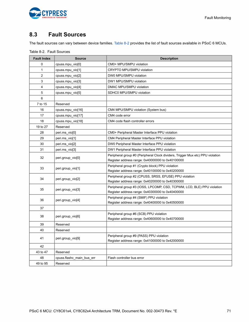
PSoC 6 MCU: CY8C61x4, CY8C62x4 Architecture TRM, Document No. 002-30473 Rev. *E 71
Fault Monitoring
8.3 Fault Sources
The fault sources can vary between device families. Table 8-2 provides the list of fault sources available in PSoC 6 MCUs.
Table 8-2. Fault Sources
Fault Index Source Description
0 cpuss.mpu_vio[0] CM0+ MPU/SMPU violation
1 cpuss.mpu_vio[1] CRYPTO MPU/SMPU violation
2 cpuss.mpu_vio[2] DW0 MPU/SMPU violation
3 cpuss.mpu_vio[3] DW1 MPU/SMPU violation
4 cpuss.mpu_vio[4] DMAC MPU/SMPU violation
5 cpuss.mpu_vio[5] SDHC0 MPU/SMPU violation
6
7 to 15 Reserved
16 cpuss.mpu_vio[16] CM4 MPU/SMPU violation (System bus)
17 cpuss.mpu_vio[17] CM4 code error
18 cpuss.mpu_vio[18] CM4 code flash controller errors
19 to 27 Reserved
28 peri.ms_vio[0] CM0+ Peripheral Master Interface PPU violation
29 peri.ms_vio[1] CM4 Peripheral Master Interface PPU violation
30 peri.ms_vio[2] DW0 Peripheral Master Interface PPU violation
31 peri.ms_vio[3] DW1 Peripheral Master Interface PPU violation
32 peri.group_vio[0]Peripheral group #0 (Peripheral Clock dividers, Trigger Mux etc) PPU violation
Register address range: 0x40000000 to 0x40100000
33 peri.group_vio[1]Peripheral group #1 (Crypto block) PPU violation
Register address range: 0x40100000 to 0x40200000
34 peri.group_vio[2]Peripheral group #2 (CPUSS, SRSS, EFUSE) PPU violation
Register address range: 0x40200000 to 0x40300000
35 peri.group_vio[3]Peripheral group #3 (IOSS, LPCOMP, CSD, TCPWM, LCD, BLE) PPU violation
Register address range: 0x40300000 to 0x40400000
36 peri.group_vio[4]Peripheral group #4 (SMIF) PPU violation
Register address range: 0x40400000 to 0x40500000
37
38 peri.group_vio[6]Peripheral group #6 (SCB) PPU violation
Register address range: 0x40600000 to 0x40700000
39 Reserved
40 Reserved
41 peri.group_vio[9]Peripheral group #9 (PASS) PPU violation
Register address range: 0x41000000 to 0x42000000
42
43 to 47 Reserved
48 cpuss.flashc_main_bus_err Flash controller bus error
49 to 95 Reserved
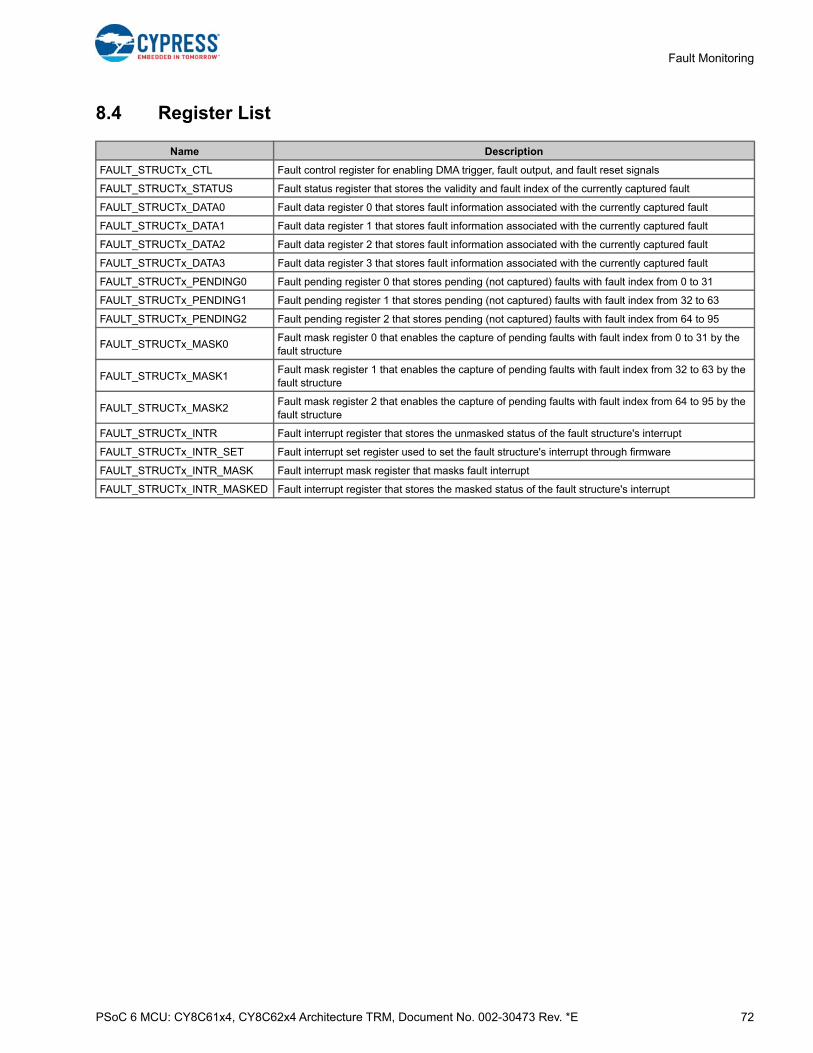
PSoC 6 MCU: CY8C61x4, CY8C62x4 Architecture TRM, Document No. 002-30473 Rev. *E 72
Fault Monitoring
8.4 Register List
Name Description
FAULT_STRUCTx_CTL Fault control register for enabling DMA trigger, fault output, and fault reset signals
FAULT_STRUCTx_STATUS Fault status register that stores the validity and fault index of the currently captured fault
FAULT_STRUCTx_DATA0 Fault data register 0 that stores fault information associated with the currently captured fault
FAULT_STRUCTx_DATA1 Fault data register 1 that stores fault information associated with the currently captured fault
FAULT_STRUCTx_DATA2 Fault data register 2 that stores fault information associated with the currently captured fault
FAULT_STRUCTx_DATA3 Fault data register 3 that stores fault information associated with the currently captured fault
FAULT_STRUCTx_PENDING0 Fault pending register 0 that stores pending (not captured) faults with fault index from 0 to 31
FAULT_STRUCTx_PENDING1 Fault pending register 1 that stores pending (not captured) faults with fault index from 32 to 63
FAULT_STRUCTx_PENDING2 Fault pending register 2 that stores pending (not captured) faults with fault index from 64 to 95
FAULT_STRUCTx_MASK0Fault mask register 0 that enables the capture of pending faults with fault index from 0 to 31 by the fault structure
FAULT_STRUCTx_MASK1Fault mask register 1 that enables the capture of pending faults with fault index from 32 to 63 by the fault structure
FAULT_STRUCTx_MASK2Fault mask register 2 that enables the capture of pending faults with fault index from 64 to 95 by the fault structure
FAULT_STRUCTx_INTR Fault interrupt register that stores the unmasked status of the fault structure's interrupt
FAULT_STRUCTx_INTR_SET Fault interrupt set register used to set the fault structure's interrupt through firmware
FAULT_STRUCTx_INTR_MASK Fault interrupt mask register that masks fault interrupt
FAULT_STRUCTx_INTR_MASKED Fault interrupt register that stores the masked status of the fault structure's interrupt
PSoC 6 MCU: CY8C61x4, CY8C62x4 Architecture TRM, Document No. 002-30473 Rev. *E 73
9. Interrupts
The PSoC 6 MCU family supports interrupts and CPU exceptions on both Cortex-M4 and Cortex-M0+ cores. Any conditionthat halts normal execution of instructions is treated as an exception by the CPU. Thus an interrupt request is treated as anexception. However, in the context of this chapter, interrupts refer to those events generated by peripherals external to theCPU such as timers, serial communication block, and port pin signals; exceptions refer to those events that are generated bythe CPU such as memory access faults and internal system timer events. Both interrupts and exceptions result in the currentprogram flow being stopped and the exception handler or interrupt service routine (ISR) being executed by the CPU. BothCortex-M4 and Cortex-M0+ cores provide their own unified exception vector table for both interrupt handlers/ISR andexception handlers.
9.1 Features
The PSoC 6 MCU supports the following interrupt features:
■ Supports up to 175 system interrupts
❐ 175 Arm Cortex-M4 interrupts
❐ Eight Arm Cortex-M0+ external interrupts and eight Arm Cortex-M0+ internal (software only) interrupts. The CPU sup-ports up to 32 interrupts, but only 16 interrupts are used by PSoC 6 interrupt infrastructure. The eight external CPU interrupts support deep sleep (WIC) functionality
❐ Four system interrupts can be mapped to each of the CPU non-maskable interrupt (NMI)
❐ Up to 45 interrupt sources capable of waking the device from Deep Sleep power mode
■ Nested vectored interrupt controller (NVIC) integrated with each CPU core, yielding low interrupt latency
■ Wakeup interrupt controller (WIC) enabling interrupt detection (CPU wakeup) in Deep Sleep power mode
■ Vector table may be placed in either flash or SRAM
■ Configurable priority levels (eight levels for Cortex-M4 and four levels for Cortex-M0+) for each interrupt
■ Level-triggered and pulse-triggered interrupt signals
This PSoC 6 MCU technical reference manual (TRM) provides comprehensive and detailed information about thefunctions of the PSoC 6 MCU device hardware. It is divided into two books: architecture TRM and registers TRM. TheTRM is not recommended for those new to the PSoC 6 MCU, nor as a guide for developing PSoC 6 MCU applications.Use these documents instead:
■ PSoC 61 datasheet, PSoC 62 datasheet
■ Peripheral Driver Library (PDL) documentation
■ Application notes
■ Code examples
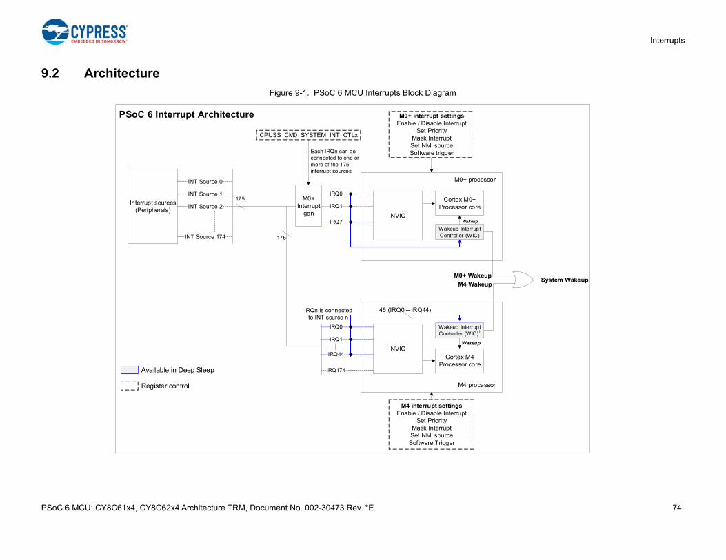
Interrupts
PSoC 6 MCU: CY8C61x4, CY8C62x4 Architecture TRM, Document No. 002-30473 Rev. *E 74
9.2 Architecture
Figure 9-1. PSoC 6 MCU Interrupts Block Diagram
Cortex M0+Processor core
NVIC
M0+ processor
175Interrupt sources
(Peripherals)
INT Source 1
INT Source 2
INT Source 0
Cortex M4Processor core
NVIC
M4 processor
175
Each IRQn can be connected to one or more of the 175 interrupt sources
IRQn is connected to INT source n
Register control
M0+ interrupt settingsEnable / Disable Interrupt
Set PriorityMask InterruptSet NMI sourceSoftware trigger
M4 interrupt settingsEnable / Disable Interrupt
Set PriorityMask InterruptSet NMI sourceSoftware Trigger
CPUSS_CM0_SYSTEM_INT_CTLx
INT Source 174
System WakeupM0+ Wakeup
M4 Wakeup
PSoC 6 Interrupt Architecture
Wakeup Interrupt Controller (WIC)1
Wakeup Interrupt Controller (WIC)
45 (IRQ0 – IRQ44)
Available in Deep Sleep
Wakeup
Wakeup
M0+ Interrupt
gen
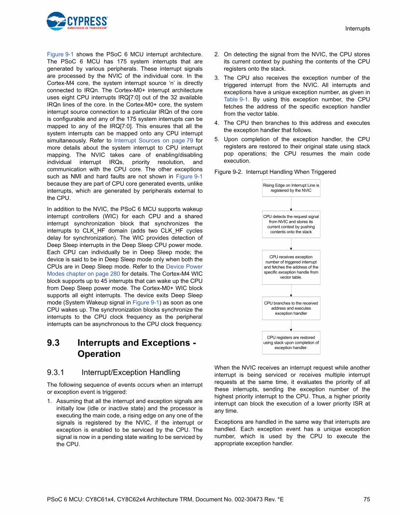
PSoC 6 MCU: CY8C61x4, CY8C62x4 Architecture TRM, Document No. 002-30473 Rev. *E 75
Interrupts
Figure 9-1 shows the PSoC 6 MCU interrupt architecture.The PSoC 6 MCU has 175 system interrupts that aregenerated by various peripherals. These interrupt signalsare processed by the NVIC of the individual core. In theCortex-M4 core, the system interrupt source ‘n’ is directlyconnected to IRQn. The Cortex-M0+ interrupt architectureuses eight CPU interrupts IRQ[7:0] out of the 32 availableIRQn lines of the core. In the Cortex-M0+ core, the systeminterrupt source connection to a particular IRQn of the coreis configurable and any of the 175 system interrupts can bemapped to any of the IRQ[7:0]. This ensures that all thesystem interrupts can be mapped onto any CPU interruptsimultaneously. Refer to Interrupt Sources on page 79 formore details about the system interrupt to CPU interruptmapping. The NVIC takes care of enabling/disablingindividual interrupt IRQs, priority resolution, andcommunication with the CPU core. The other exceptionssuch as NMI and hard faults are not shown in Figure 9-1because they are part of CPU core generated events, unlikeinterrupts, which are generated by peripherals external tothe CPU.
In addition to the NVIC, the PSoC 6 MCU supports wakeupinterrupt controllers (WIC) for each CPU and a sharedinterrupt synchronization block that synchronizes theinterrupts to CLK_HF domain (adds two CLK_HF cyclesdelay for synchronization). The WIC provides detection ofDeep Sleep interrupts in the Deep Sleep CPU power mode.Each CPU can individually be in Deep Sleep mode; thedevice is said to be in Deep Sleep mode only when both theCPUs are in Deep Sleep mode. Refer to the Device PowerModes chapter on page 280 for details. The Cortex-M4 WICblock supports up to 45 interrupts that can wake up the CPUfrom Deep Sleep power mode. The Cortex-M0+ WIC blocksupports all eight interrupts. The device exits Deep Sleepmode (System Wakeup signal in Figure 9-1) as soon as oneCPU wakes up. The synchronization blocks synchronize theinterrupts to the CPU clock frequency as the peripheralinterrupts can be asynchronous to the CPU clock frequency.
9.3 Interrupts and Exceptions - Operation
9.3.1 Interrupt/Exception Handling
The following sequence of events occurs when an interruptor exception event is triggered:
1. Assuming that all the interrupt and exception signals areinitially low (idle or inactive state) and the processor isexecuting the main code, a rising edge on any one of thesignals is registered by the NVIC, if the interrupt orexception is enabled to be serviced by the CPU. Thesignal is now in a pending state waiting to be serviced bythe CPU.
2. On detecting the signal from the NVIC, the CPU storesits current context by pushing the contents of the CPUregisters onto the stack.
3. The CPU also receives the exception number of thetriggered interrupt from the NVIC. All interrupts andexceptions have a unique exception number, as given inTable 9-1. By using this exception number, the CPUfetches the address of the specific exception handlerfrom the vector table.
4. The CPU then branches to this address and executesthe exception handler that follows.
5. Upon completion of the exception handler, the CPUregisters are restored to their original state using stackpop operations; the CPU resumes the main codeexecution.
Figure 9-2. Interrupt Handling When Triggered
When the NVIC receives an interrupt request while anotherinterrupt is being serviced or receives multiple interruptrequests at the same time, it evaluates the priority of allthese interrupts, sending the exception number of thehighest priority interrupt to the CPU. Thus, a higher priorityinterrupt can block the execution of a lower priority ISR atany time.
Exceptions are handled in the same way that interrupts arehandled. Each exception event has a unique exceptionnumber, which is used by the CPU to execute theappropriate exception handler.
Rising Edge on Interrupt Line is registered by the NVIC
CPU detects the request signal from NVIC and stores its
current context by pushing contents onto the stack
CPU receives exception number of triggered interrupt
and fetches the address of the specific exception handle from
vector table.
CPU branches to the received address and executes
exception handler
CPU registers are restored using stack upon completion of
exception handler.
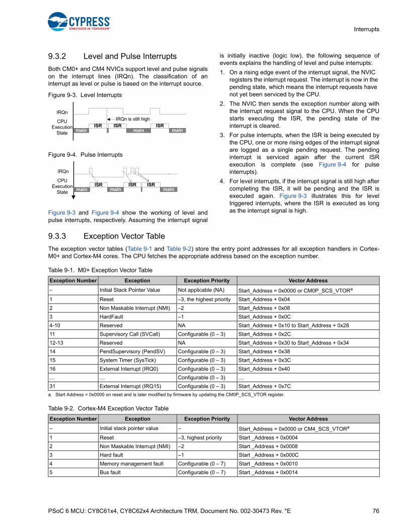
PSoC 6 MCU: CY8C61x4, CY8C62x4 Architecture TRM, Document No. 002-30473 Rev. *E 76
Interrupts
9.3.2 Level and Pulse Interrupts
Both CM0+ and CM4 NVICs support level and pulse signalson the interrupt lines (IRQn). The classification of aninterrupt as level or pulse is based on the interrupt source.
Figure 9-3. Level Interrupts
Figure 9-4. Pulse Interrupts
Figure 9-3 and Figure 9-4 show the working of level andpulse interrupts, respectively. Assuming the interrupt signal
is initially inactive (logic low), the following sequence ofevents explains the handling of level and pulse interrupts:
1. On a rising edge event of the interrupt signal, the NVIC registers the interrupt request. The interrupt is now in the pending state, which means the interrupt requests have not yet been serviced by the CPU.
2. The NVIC then sends the exception number along withthe interrupt request signal to the CPU. When the CPUstarts executing the ISR, the pending state of theinterrupt is cleared.
3. For pulse interrupts, when the ISR is being executed bythe CPU, one or more rising edges of the interrupt signalare logged as a single pending request. The pendinginterrupt is serviced again after the current ISRexecution is complete (see Figure 9-4 for pulseinterrupts).
4. For level interrupts, if the interrupt signal is still high aftercompleting the ISR, it will be pending and the ISR isexecuted again. Figure 9-3 illustrates this for leveltriggered interrupts, where the ISR is executed as longas the interrupt signal is high.
9.3.3 Exception Vector Table
The exception vector tables (Table 9-1 and Table 9-2) store the entry point addresses for all exception handlers in Cortex-M0+ and Cortex-M4 cores. The CPU fetches the appropriate address based on the exception number.
IRQn
CPU Execution
State mainISR ISR
mainISR
main
IRQn is still high
IRQn
CPU Execution
Statemain
ISRmain
ISRmain
ISR
Table 9-1. M0+ Exception Vector Table
Exception Number Exception Exception Priority Vector Address
– Initial Stack Pointer Value Not applicable (NA) Start_Address = 0x0000 or CM0P_SCS_VTORa
a. Start Address = 0x0000 on reset and is later modified by firmware by updating the CM0P_SCS_VTOR register.
1 Reset –3, the highest priority Start_Address + 0x04
2 Non Maskable Interrupt (NMI) –2 Start_Address + 0x08
3 HardFault –1 Start_Address + 0x0C
4-10 Reserved NA Start_Address + 0x10 to Start_Address + 0x28
11 Supervisory Call (SVCall) Configurable (0 – 3) Start_Address + 0x2C
12-13 Reserved NA Start_Address + 0x30 to Start_Address + 0x34
14 PendSupervisory (PendSV) Configurable (0 – 3) Start_Address + 0x38
15 System Timer (SysTick) Configurable (0 – 3) Start_Address + 0x3C
16 External Interrupt (IRQ0) Configurable (0 – 3) Start_Address + 0x40
… … Configurable (0 – 3) …
31 External Interrupt (IRQ15) Configurable (0 – 3) Start_Address + 0x7C
Table 9-2. Cortex-M4 Exception Vector Table
Exception Number Exception Exception Priority Vector Address
– Initial stack pointer value – Start_Address = 0x0000 or CM4_SCS_VTORa
1 Reset –3, highest priority Start _Address + 0x0004
2 Non Maskable Interrupt (NMI) –2 Start _Address + 0x0008
3 Hard fault –1 Start _Address + 0x000C
4 Memory management fault Configurable (0 – 7) Start _Address + 0x0010
5 Bus fault Configurable (0 – 7) Start _Address + 0x0014

PSoC 6 MCU: CY8C61x4, CY8C62x4 Architecture TRM, Document No. 002-30473 Rev. *E 77
Interrupts
In Table 9-1 and Table 9-2, the first word (4 bytes) is notmarked as exception number zero. This is because the firstword in the exception table is used to initialize the mainstack pointer (MSP) value on device reset; it is notconsidered as an exception. In the PSoC 6 MCU, both thevector tables can be configured to be located either in flashmemory or SRAM. The vector table offset register (VTOR)present as part of Cortex-M0+ and Cortex-M4 systemcontrol space registers configures the vector table offsetfrom the base address (0x0000). The CM0P_SCS_VTORregister sets the vector offset address for the CM0+ coreand CM4_SCS_VTOR sets the offset for the M4 core. TheVTOR value determines whether the vector table is in flashmemory (0x10000000 to 0x10100000) or SRAM. Note thatthe VTOR registers can be updated only in privilege CPUmode. The advantage of moving the vector table to SRAM isthat the exception handler addresses can be dynamicallychanged by modifying the SRAM vector table contents.However, the nonvolatile flash memory vector table must bemodified by a flash memory write. Note that the exceptiontable must be 256 byte-aligned for Cortex-M0+ and 1024byte-aligned for Cortex-M4.
The exception sources (exception numbers 1 to 15) areexplained in 9.4 Exception Sources. The exceptions markedas Reserved in Table 9-1 are not used, although they haveaddresses reserved for them in the vector table. Theinterrupt sources (exception numbers 16 to 189) areexplained in 9.5 Interrupt Sources.
9.4 Exception Sources
This section explains the different exception sources listedin Table 9-1 and Table 9-2 (exception numbers 1 to 15).
9.4.1 Reset Exception
Device reset is treated as an exception in PSoC 6 MCUs.Reset exception is always enabled with a fixed priority of –3,the highest priority exception in both the cores. When thedevice boots up, only the Cortex-M0+ core is available. TheCM0+ core executes the ROM boot code and can enable
Cortex-M4 core from the application code. The resetexception of the CM0+ core is tied to the device reset orstartup. When the Cortex-M0+ core releases the Cortex-M4reset, the M4 reset exception is executed. A device resetcan occur due to multiple reasons, such as power-on-reset(POR), external reset signal on XRES pin, or watchdogreset. When the device is reset, the initial boot code forconfiguring the device is executed by the Cortex-M0+ out ofsupervisory read-only memory (SROM). The boot code andother data in SROM memory are programmed by Cypress,and are not read/write accessible to external users. Aftercompleting the SROM boot sequence, the Cortex-M0+ codeexecution jumps to flash memory. Flash memory address0x10000004 (Exception#1 in Table 9-1) stores the locationof the startup code in flash memory. The CPU startsexecuting code out of this address. Note that the resetexception address in the SRAM vector table will never beused because the device comes out of reset with the flashvector table selected. The register configuration to select theSRAM vector table can be done only as part of the startupcode in flash after the reset is de-asserted. Note that thereset exception flow for Cortex-M4 is the same as Cortex-M0+. However, Cortex-M4 execution begins only afterCM0+ core de-asserts the M4 reset.
9.4.2 Non-Maskable Interrupt Exception
Non-maskable interrupt (NMI) is the highest priorityexception next to reset. It is always enabled with a fixedpriority of –2. Both the cores have their own NMI exception.There are three ways to trigger an NMI exception in a CPUcore:
■ NMI exception from a system interrupt: Both Cortex-M0+ and Cortex-M4 provide an option to trigger an NMIexception from up to four of the 175 system interrupts.The NMI exception triggered due to the interrupt willexecute the NMI handler pointed to by the activeexception vector table. The CPUSS_CM4_NMI_CTLxand CPUSS_CM0P_NMI_CTLx registers select theinterrupt source that triggers the NMI from hardware.The registers have a default value of 1023; that is, if the
6 Usage fault Configurable (0 – 7) Start _Address + 0x0018
7–10 Reserved – –
11 Supervisory call (SVCall) Configurable (0 – 7) Start _Address + 0x002C
12–13 Reserved – –
14 Pend Supervisory (PendSV) Configurable (0 – 7) Start _Address + 0x0038
15 System Tick timer (SysTick) Configurable (0 – 7) Start _Address + 0x003C
16 External interrupt (IRQ0) Configurable (0 – 7) Start _Address + 0x0040
…. …. …. ….
188 External interrupt (IRQ172) Configurable (0 – 7) Start _Address + 0x02F0
189 External interrupt (IRQ173) Configurable (0 – 7) Start _Address + 0x02F4
a. Start Address = 0x0000 on reset and is later modified by firmware by updating CM4_SCS_VTOR register.
Table 9-2. Cortex-M4 Exception Vector Table (continued)
Exception Number Exception Exception Priority Vector Address

PSoC 6 MCU: CY8C61x4, CY8C62x4 Architecture TRM, Document No. 002-30473 Rev. *E 78
Interrupts
register is set to 1023, then that particular register doesnot map any interrupt source to the NMI. There are foursuch registers and each can map one interrupt vector to
the NMI. NMI is triggered when any of the four interruptsare triggered; that is, the interrupts are logically ORed.See Figure 9-5.
Figure 9-5. NMI Trigger
■ NMI exception by setting NMIPENDSET bit (user NMIexception): An NMI exception can be triggered insoftware by setting the NMIPENDSET bit in the interruptcontrol state registers (CM0P_SCS_ICSR andCM4_SCS_ICSR). Setting this bit will execute the NMIhandler pointed to by the active vector table in therespective CPU cores.
■ System Call NMI exception: This exception is used fornonvolatile programming and other system calloperations such as flash write operation and flashchecksum operation. Inter processor communication(IPC) mechanism is used to implement a system call inPSoC 6 MCUs. A dedicated IPC mailbox is associatedwith each core (M0+ and M4) and the debug access port(DAP) to trigger a system call. The CPU or DAPacquires this dedicated mailbox, writes the system callopcode and argument to the mailbox, and notifies adedicated IPC structure. Typically, the argument is apointer to a structure in SRAM. This results in an NMIinterrupt in the CM0+ core. Note that all the system callsare serviced by Cortex-M0+ core. A Cortex-M0+ NMIexception triggered by this method executes the NMIexception handler code that resides in SROM. Note thatthe NMI exception handler address is automaticallyinitialized to the system call API located in SROM by theboot code. The value should be retained during vectortable relocations; otherwise, no system call will beexecuted. The NMI handler code in SROM is not read/write accessible because it contains nonvolatileprogramming routines that cannot be modified by theuser. The result of the system call is passed through thesame IPC mechanism. For details, refer to the Inter-Processor Communication chapter on page 58.
9.4.3 HardFault Exception
Both CM0+ and CM4 cores support HardFault exception.HardFault is an always-enabled exception that occursbecause of an error during normal or exception processing.HardFault has a fixed priority of –1, meaning it has higher
priority than any exception with configurable priority. AHardFault exception is a catch-all exception for differenttypes of fault conditions, which include executing anundefined instruction and accessing an invalid memoryaddresses. The CPU does not provide fault statusinformation to the HardFault exception handler, but it doespermit the handler to perform an exception return andcontinue execution in cases where software has the abilityto recover from the fault situation.
9.4.4 Memory Management Fault Exception
A memory management fault is an exception that occursbecause of a memory protection-related fault. The fixedmemory protection constraints determine this fault, for bothinstruction and data memory transactions. This fault isalways used to abort instruction accesses to Execute Never(XN) memory regions. The memory management fault isonly supported by the M4 core. The priority of the exceptionis configurable from 0 (highest) to 7 (lowest).
9.4.5 Bus Fault ExceptionA Bus Fault is an exception that occurs because of amemory-related fault for an instruction or data memorytransaction. This might be from an error detected on a bus inthe memory system. The bus fault is supported only by theM4 core. The priority of the exception is configurable from 0(highest) to 7 (lowest).
9.4.6 Usage Fault Exception
A Usage Fault is an exception that occurs because of a faultrelated to instruction execution. This includes:
■ an undefined instruction
■ an illegal unaligned access
■ invalid state on instruction execution
■ an error on exception return
System interrupt sources
n <= 1023(device
dependent)
INT Source 1
INT Source 2
INT Source 0
INT Source n-1
0
1
2
3
n
n
n
n
CPUSS_CM4_NMI_CTLxOr
CPUSS_CM0P_NMI_CTLx
CM4 NMIOr
CM0+ NMI
10
0
1023
1023
1023
1023

PSoC 6 MCU: CY8C61x4, CY8C62x4 Architecture TRM, Document No. 002-30473 Rev. *E 79
Interrupts
The following can cause a usage fault when the core isconfigured to report them:
■ an unaligned address on word and halfword memory access
■ division by zero
The usage fault is supported only by the M4 core. Thepriority of the exception is configurable from 0 (highest) to 7(lowest).
9.4.7 Supervisor Call (SVCall) Exception
Both CM0+ and CM4 cores support SVCall exception.Supervisor Call (SVCall) is an always-enabled exceptioncaused when the CPU executes the SVC instruction as partof the application code. Application software uses the SVCinstruction to make a call to an underlying operating systemand provide a service. This is known as a supervisor call.The SVC instruction enables the application to issue anSVCall that requires privileged access to the system.
The priority of an SVCall exception can be configured to avalue between 0 and 3 for CM0+ and 0 to 7 for CM4 core bywriting to the bitfields PRI_11 of the System Handler PriorityRegister 2 (CM0P_SCS_SHPR2 and CM4_SCS_SHPR2).When the SVC instruction is executed, the SVCall exceptionenters the pending state and waits to be serviced by theCPU. The SVCALLPENDED bit in the System HandlerControl and State Register (CM0P_SCS_SHCSR andCM4_SCS_SHCSR) can be used to check or modify thepending status of the SVCall exception.
9.4.8 PendSupervisory (PendSV) Exception
Both CM0+ and CM4 cores support PendSV exception.PendSV is another supervisor call related exception similarto SVCall, normally being software-generated. PendSV isalways enabled and its priority is configurable similar toSVCall. The PendSV exception is triggered by setting thePENDSVSET bit in the Interrupt Control State Register(CM0P_SCS_ICSR and CM4_SCS_ICSR). On setting thisbit, the PendSV exception enters the pending state, andwaits to be serviced by the CPU. The pending state of aPendSV exception can be cleared by setting thePENDSVCLR bit in the Interrupt Control State Register. Thepriority of a PendSV exception can be configured to a valuebetween 0 and 3 for CM0+ and 0 to 7 for M4 by writing to thebitfields PRI_14 of the System Handler Priority Register 3.See the Armv6-M Architecture Reference Manual for moredetails.
9.4.9 System Tick (SysTick) Exception
Both CM0+ and CM4 cores in PSoC 6 MCUs support asystem timer, referred to as SysTick, as part of their internalarchitecture. SysTick provides a simple, 24-bit decrementingcounter for various timekeeping purposes such as an RTOS
tick timer, high-speed alarm timer, or simple counter. TheSysTick timer can be configured to generate an interruptwhen its count value reaches zero, which is referred to as aSysTick exception. The exception is enabled by setting theTICKINT bit in the SysTick Control and Status Register(CM0P_SCS_SYST_CSR and CM4_SCS_SYST_CSR).The priority of a SysTick exception can be configured to avalue between 0 and 3 for CM0+ and 0 to 7 for M4 by writingto the bitfields PRI_15 of the System Handler PriorityRegister 3 (SHPR3). The SysTick exception can always begenerated in software at any instant by writing a one to thePENDSTSET bit in the Interrupt Control State Register.Similarly, the pending state of the SysTick exception can becleared by writing a one to the PENDSTCLR bit in theInterrupt Control State Register.
9.5 Interrupt Sources
The PSoC 6 MCU supports 175 interrupts from peripherals.The source of each interrupt is listed in Table 9-3. Thesesystem interrupts are mapped directly to Cortex-M4 core.For Cortex-M0+ core, any of the 175 interrupts can berouted to any of the available eight interrupts (IRQ0 to IRQ7or exception 16 to 23). TheCPUSS_CM0_SYSTEM_INT_CTLx registers are used tomake this interrupt selection in CM0+.
There are 175 CPUSS_CM0_SYSTEM_INT_CTLxregisters. The CPU_INT_IDX bits [2:0] of the register selectswhich IRQn line of CM0+, the xth system interrupt is mappedto. The CPU_INT_VALID bit [31] of the register decideswhether the xth interrupt is enabled for the core. For Cortex-M0+, multiple system interrupts can be mapped on thesame CPU interrupt. Therefore, an active CPU interrupt mayindicate one or multiple active system interrupts. Forinstance to connect Port 0 (IDX = 0) and Port 2 (IDX = 2)GPIO interrupts to IRQ0 of CM0+, CPU_INT_IDX bitsshould be set to ‘0’ and CPU_INT_VALID bit should be setto ‘1’ in CPUSS_CM0_SYSTEM_INT_CTL0 andCPUSS_CM0_SYSTEM_INT_CTL2 registers. Note that thisonly connects and enables the interrupts; configuration andmasking of the interrupt to the NVIC should be done as partof source peripheral configuration.
As a result of the reduction functionality in the Cortex-M0+core, multiple system interrupts share a CPU interrupthandler as provided by the CPU’s vector table. Each CPUinterrupt has an associated CPUSS_CM0_INTx_STATUSregister:
■ SYSTEM_INT_VALID bit[31] of the register specifies if any system interrupt is active for the CPU interrupt. This bit remains set until all the system interrupts connected to the CPU interrupts are cleared at the source.
■ SYSTEM_INT_IDX bits[9:0] of the register specifies the index (a number in the range [0, 1022]) of the lowest active system interrupt mapped to the corresponding CPU interrupt.

PSoC 6 MCU: CY8C61x4, CY8C62x4 Architecture TRM, Document No. 002-30473 Rev. *E 80
Interrupts
For instance, say CM0+ IRQ0 is connected to Port 0 andPort 2 GPIO interrupts. When an interrupt in both Port 0 andPort 2 are triggered simultaneously, IRQ0 in CM0+ will betriggered with CPUSS_CM0_INT0_STATUS reading 0 (Port0 interrupt) in SYSTEM_INT_IDX bit andSYSTEM_INT_VALID bit set. After Port 0 interrupt isserviced and cleared, IRQ0 will be triggered again withSYSTEM_INT_IDX bit set to 2 (Port 2 interrupt) in theCPUSS_CM0_INT0_STATUS register. Only after servicing
Port 2 interrupt and clearing, the SYSTEM_INT_VALID bitwill be cleared.
The CPU interrupt handler should use theSYSTEM_INT_IDX field to index a system interrupt lookuptable and jump to the system interrupt handler. The lookuptable is typically located in one of the system memories. Thefollowing code illustrates the approach:
typedef void (* SystemIntr_Handler)(void);void CM0_CpuIntr0_Handler (void){uint32_t system_int_idx;SystemIntr_Handler handler;if(CPUSS_CM0_INT0_STATUS.SYSTEM_INT_VALID){system_int_idx = CPUSS_CM0_INT0_STATUS.SYSTEM_INT_IDX;handler = SystemIntr_Table[system_int_idx];handler(); // jump to system interrupt handler}else{// Triggered by SW or due to SW clear error (SW cleared a peripheral// interrupt flag but didn't clear the Pending flag at NVIC)}}…void CM0_CpuIntr7_Handler (void){uint32_t system_int_idx;SystemIntr_Handler handler;if(CPUSS_CM0_INT7_STATUS.SYSTEM_INT_VALID){system_int_idx = CPUSS_CM0_INT7_STATUS.SYSTEM_INT_IDX;handler = SystemIntr_Table[system_int_idx];handler(); // jump to system interrupt handler}else{// Triggered by SW or due to SW clear error (SW cleared a peripheral// interrupt flag but didn't clear the Pending flag at NVIC)}}void CM0_SystemIntr0_Handler (void){// Clear the peripheral interrupt request flag by register write// Read back the register, to ensure the completion of register write access// Handle system interrupt 0.}…void CM0_SystemIntr167_Handler (void){// Clear the peripheral interrupt request flag by register write// Read back the register, to ensure the completion of register write access// Handle system interrupt 167.}

PSoC 6 MCU: CY8C61x4, CY8C62x4 Architecture TRM, Document No. 002-30473 Rev. *E 81
Interrupts
The interrupts include standard interrupts from the on-chipperipherals such as TCPWM, serial communication block,CSD block, watchdog, ADC, and so on. The interruptgenerated is usually the logical OR of the differentperipheral states. The peripheral interrupt status registershould be read in the ISR to detect which conditiongenerated the interrupt. These interrupts are usually levelinterrupts. The appropriate interrupt registers should becleared in the ISR to deassert the interrupt. Usually a write'1' is required to clear the registers. If the interrupt register isnot cleared in the ISR, the interrupt will remain asserted and
the ISR will be executed continuously. See the I/OSystem chapter on page 214 for details on GPIO interrupts.
As seen from Table 9-3, 45 interrupts (IRQ0 to IRQ44) arecapable of waking up the device from Deep Sleep powermode. For Cortex-M4, IRQ0 to IRQ44 directly map to thesesources. However, in the Cortex-M0+, all the eight IRQ linessupport Deep Sleep wakeup if they are connected to a deepsleep capable interrupt. This means the 45 Deep Sleepwakeup-capable interrupts can be connected to any of theeight IRQ lines of Cortex-M0+, if such a wakeup is desired.
Table 9-3. List of PSoC 6 Interrupt Sources
System InterruptCortex M4 Exception
NumberPower Mode Description
NMI 2 Active Any four of the below 175 IRQ sources
IRQ0 16 DeepSleep GPIO Interrupt - Port 0
IRQ1 17 DeepSleep Not available
IRQ2 18 DeepSleep GPIO Interrupt - Port 2
IRQ3 19 DeepSleep GPIO Interrupt - Port 3
IRQ4 20 DeepSleep Not available
IRQ5 21 DeepSleep GPIO Interrupt - Port 5
IRQ6 22 DeepSleep GPIO Interrupt - Port 6
IRQ7 23 DeepSleep GPIO Interrupt - Port 7
IRQ8 24 DeepSleep GPIO Interrupt - Port 8
IRQ9 25 DeepSleep GPIO Interrupt - Port 9
IRQ10 26 DeepSleep GPIO Interrupt - Port 10
IRQ11 27 DeepSleep GPIO Interrupt - Port 11
IRQ12 28 DeepSleep GPIO Interrupt - Port 12
IRQ13 29 DeepSleep Not available
IRQ14 30 DeepSleep GPIO Interrupt - Port 14
IRQ15 31 DeepSleep GPIO All Ports
IRQ16 32 DeepSleep GPIO Supply Detect Interrupt
IRQ17 33 DeepSleep Low Power Comparator Interrupt
IRQ18 34 DeepSleep Serial Communication Block #6
IRQ19 35 DeepSleep Multi Counter Watchdog Timer 0 interrupt
IRQ20 36 DeepSleep Multi Counter Watchdog Timer 1 interrupt
IRQ21 37 DeepSleep Backup domain interrupt
IRQ22 38 DeepSleep Other combined Interrupts for SRSS (LVD, WDT)
IRQ23 39 DeepSleep CPUSS Inter Process Communication Interrupt #0
IRQ24 40 DeepSleep CPUSS Inter Process Communication Interrupt #1
IRQ25 41 DeepSleep CPUSS Inter Process Communication Interrupt #2
IRQ26 42 DeepSleep CPUSS Inter Process Communication Interrupt #3
IRQ27 43 DeepSleep CPUSS Inter Process Communication Interrupt #4
IRQ28 44 DeepSleep CPUSS Inter Process Communication Interrupt #5
IRQ29 45 DeepSleep CPUSS Inter Process Communication Interrupt #6
IRQ30 46 DeepSleep CPUSS Inter Process Communication Interrupt #7
IRQ31 47 DeepSleep CPUSS Inter Process Communication Interrupt #8

PSoC 6 MCU: CY8C61x4, CY8C62x4 Architecture TRM, Document No. 002-30473 Rev. *E 82
Interrupts
IRQ32 48 DeepSleep CPUSS Inter Process Communication Interrupt #9
IRQ33 49 DeepSleep CPUSS Inter Process Communication Interrupt #10
IRQ34 50 DeepSleep CPUSS Inter Process Communication Interrupt #11
IRQ35 51 DeepSleep CPUSS Inter Process Communication Interrupt #12
IRQ36 52 DeepSleep CPUSS Inter Process Communication Interrupt #13
IRQ37 53 DeepSleep CPUSS Inter Process Communication Interrupt #14
IRQ38 54 DeepSleep CPUSS Inter Process Communication Interrupt #15
IRQ39 55 DeepSleep SAR ADC 0 interrupt
IRQ40 56 DeepSleep SAR ADC 1 interrupt
IRQ41 57 DeepSleep CTBm Interrupt
IRQ42 58 DeepSleep Not available
IRQ43 59 DeepSleep PASS FIFO 0 Interrupt
IRQ44 60 DeepSleep PASS FIFO 1 Interrupt
IRQ45 61 Active Serial Communication Block #0
IRQ46 62 Active Serial Communication Block #1
IRQ47 63 Active Serial Communication Block #2
IRQ48 64 Active Not available
IRQ49 65 Active Serial Communication Block #4
IRQ50 66 Active Serial Communication Block #5
IRQ51 67 Active CSD (Capsense) interrupt
IRQ52 68 Active CPUSS DMAC, Channel #0
IRQ53 69 Active CPUSS DMAC, Channel #1
IRQ54 70 Active Not available
IRQ55 71 Active Not available
IRQ56 72 Active CPUSS DataWire #0, Channel #0
IRQ57 73 Active CPUSS DataWire #0, Channel #1
IRQ58 74 Active CPUSS DataWire #0, Channel #2
IRQ59 75 Active CPUSS DataWire #0, Channel #3
IRQ60 76 Active CPUSS DataWire #0, Channel #4
IRQ61 77 Active CPUSS DataWire #0, Channel #5
IRQ62 78 Active CPUSS DataWire #0, Channel #6
IRQ63 79 Active CPUSS DataWire #0, Channel #7
IRQ64 80 Active CPUSS DataWire #0, Channel #8
IRQ65 81 Active CPUSS DataWire #0, Channel #9
IRQ66 82 Active CPUSS DataWire #0, Channel #10
IRQ67 83 Active CPUSS DataWire #0, Channel #11
IRQ68 84 Active CPUSS DataWire #0, Channel #12
IRQ69 85 Active CPUSS DataWire #0, Channel #13
IRQ70 86 Active CPUSS DataWire #0, Channel #14
IRQ71 87 Active CPUSS DataWire #0, Channel #15
IRQ72 88 Active CPUSS DataWire #0, Channel #16
IRQ73 89 Active CPUSS DataWire #0, Channel #17
IRQ74 90 Active CPUSS DataWire #0, Channel #18
Table 9-3. List of PSoC 6 Interrupt Sources
System InterruptCortex M4 Exception
NumberPower Mode Description

PSoC 6 MCU: CY8C61x4, CY8C62x4 Architecture TRM, Document No. 002-30473 Rev. *E 83
Interrupts
IRQ75 91 Active CPUSS DataWire #0, Channel #19
IRQ76 92 Active CPUSS DataWire #0, Channel #20
IRQ77 93 Active CPUSS DataWire #0, Channel #21
IRQ78 94 Active CPUSS DataWire #0, Channel #22
IRQ79 95 Active CPUSS DataWire #0, Channel #23
IRQ80 96 Active CPUSS DataWire #0, Channel #24
IRQ81 97 Active CPUSS DataWire #0, Channel #25
IRQ82 98 Active CPUSS DataWire #0, Channel #26
IRQ83 99 Active CPUSS DataWire #0, Channel #27
IRQ84 100 Active CPUSS DataWire #0, Channel #28
IRQ85 101 Active CPUSS DataWire #1, Channel #0
IRQ86 102 Active CPUSS DataWire #1, Channel #1
IRQ87 103 Active CPUSS DataWire #1, Channel #2
IRQ88 104 Active CPUSS DataWire #1, Channel #3
IRQ89 105 Active CPUSS DataWire #1, Channel #4
IRQ90 106 Active CPUSS DataWire #1, Channel #5
IRQ91 107 Active CPUSS DataWire #1, Channel #6
IRQ92 108 Active CPUSS DataWire #1, Channel #7
IRQ93 109 Active CPUSS DataWire #1, Channel #8
IRQ94 110 Active CPUSS DataWire #1, Channel #9
IRQ95 111 Active CPUSS DataWire #1, Channel #10
IRQ96 112 Active CPUSS DataWire #1, Channel #11
IRQ97 113 Active CPUSS DataWire #1, Channel #12
IRQ98 114 Active CPUSS DataWire #1, Channel #13
IRQ99 115 Active CPUSS DataWire #1, Channel #14
IRQ100 116 Active CPUSS DataWire #1, Channel #15
IRQ101 117 Active CPUSS DataWire #1, Channel #16
IRQ102 118 Active CPUSS DataWire #1, Channel #17
IRQ103 119 Active CPUSS DataWire #1, Channel #18
IRQ104 120 Active CPUSS DataWire #1, Channel #19
IRQ105 121 Active CPUSS DataWire #1, Channel #20
IRQ106 122 Active CPUSS DataWire #1, Channel #21
IRQ107 123 Active CPUSS DataWire #1, Channel #22
IRQ108 124 Active CPUSS DataWire #1, Channel #23
IRQ109 125 Active CPUSS DataWire #1, Channel #24
IRQ110 126 Active CPUSS DataWire #1, Channel #25
IRQ111 127 Active CPUSS DataWire #1, Channel #26
IRQ112 128 Active CPUSS DataWire #1, Channel #27
IRQ113 129 Active CPUSS DataWire #1, Channel #28
IRQ114 130 Active CPUSS Fault Structure Interrupt #0
IRQ115 131 Active CPUSS Fault Structure Interrupt #1
IRQ116 132 Active CRYPTO Accelerator Interrupt
IRQ117 133 Active FLASH Macro Interrupt
Table 9-3. List of PSoC 6 Interrupt Sources
System InterruptCortex M4 Exception
NumberPower Mode Description
PSoC 6 MCU: CY8C61x4, CY8C62x4 Architecture TRM, Document No. 002-30473 Rev. *E 84
Interrupts
IRQ118 134 Active Floating Point operation fault
IRQ119 135 Active CM0+ CTI #0
IRQ120 136 Active CM0+ CTI #1
IRQ121 137 Active CM4 CTI #0
IRQ122 138 Active CM4 CTI #1
IRQ123 139 Active TCPWM #0, Counter #0
IRQ124 140 Active TCPWM #0, Counter #1
IRQ125 141 Active TCPWM #0, Counter #2
IRQ126 142 Active TCPWM #0, Counter #3
IRQ127 143 Active Not available
IRQ128 144 Active Not available
IRQ129 145 Active Not available
IRQ130 146 Active Not available
IRQ131 147 Active TCPWM #0, Counter #256
IRQ132 148 Active TCPWM #0, Counter #257
IRQ133 149 Active TCPWM #0, Counter #258
IRQ134 150 Active TCPWM #0, Counter #259
IRQ135 151 Active TCPWM #0, Counter #260
IRQ136 152 Active TCPWM #0, Counter #261
IRQ137 153 Active TCPWM #0, Counter #262
IRQ138 154 Active TCPWM #0, Counter #263
IRQ139 155 Active Not available
IRQ140 156 Active Not available
IRQ141 157 Active Not available
IRQ142 158 Active Not available
IRQ143 159 Active Not available
IRQ144 160 Active Not available
IRQ145 161 Active Not available
IRQ146 162 Active Consolidated interrrupt for all DACs
IRQ147 163 Active Not available
IRQ148 164 Active Not available
IRQ149 165 Active Not available
IRQ150 166 Active Not available
IRQ151 167 Active Not available
IRQ152 168 Active Not available
IRQ153 169 Active Not available
IRQ154 170 Active Not available
IRQ155 171 Active Not available
IRQ156 172 Active Not available
IRQ157 173 Active Not available
IRQ158 174 Active Not available
IRQ159 175 Active Not available
IRQ160 176 Active Serial Memory Interface interrupt
Table 9-3. List of PSoC 6 Interrupt Sources
System InterruptCortex M4 Exception
NumberPower Mode Description
PSoC 6 MCU: CY8C61x4, CY8C62x4 Architecture TRM, Document No. 002-30473 Rev. *E 85
Interrupts
IRQ161 177 Active USB Interrupt
IRQ162 178 Active USB Interrupt
IRQ163 179 Active USB Interrupt
IRQ164 180 Active Not available
IRQ165 181 Active Not available
IRQ166 182 Active Not available
IRQ167 183 Active Not available
IRQ168 184 Active CAN consolidated interrupt #0
IRQ169 185 Active CAN Interrupt #0, Channel #0
IRQ170 186 Active CAN Interrupt #1, Channel #0
IRQ171 187 Active CPUSS DataWire #1, Channel #29
IRQ172 188 Active CPUSS DataWire #1, Channel #30
IRQ173 189 Active CPUSS DataWire #1, Channel #31
IRQ174 190 Active CPUSS DataWire #0, Channel #29
Table 9-3. List of PSoC 6 Interrupt Sources
System InterruptCortex M4 Exception
NumberPower Mode Description

PSoC 6 MCU: CY8C61x4, CY8C62x4 Architecture TRM, Document No. 002-30473 Rev. *E 86
Interrupts
9.6 Interrupt/Exception Priority
Exception priority is useful for exception arbitration whenthere are multiple exceptions that need to be serviced by theCPU. Both M4 and M0+ cores in PSoC 6 MCUs provideflexibility in choosing priority values for different exceptions.All exceptions other than Reset, NMI, and HardFault can beassigned a configurable priority level. The Reset, NMI, andHardFault exceptions have a fixed priority of –3, –2, and –1,respectively. In PSoC 6 MCUs, lower priority numbersrepresent higher priorities. This means that the Reset, NMI,and HardFault exceptions have the highest priorities. Theother exceptions can be assigned a configurable prioritylevel between 0 and 3 for Cortex-M0+ and 0 to 7 for Cortex-M4.
Both M0+ and M4 support nested exceptions in which ahigher priority exception can obstruct (interrupt) thecurrently active exception handler. This pre-emption doesnot happen if the incoming exception priority is the same asor lower than the active exception. The CPU resumesexecution of the lower priority exception handler afterservicing the higher priority exception. The CM0+ core in thePSoC 6 MCU allows nesting of up to four exceptions; theCM4 core allows up to eight exceptions. When the CPUreceives two or more exceptions requests of the samepriority, the lowest exception number is serviced first.
The registers to configure the priority of exception numbers1 to 15 are explained in Exception Sources on page 77.
The priority of the 8 CM0+ and 175 CM4 interrupts can beconfigured by writing to the respective Interrupt Priorityregisters (CM0P_SCS_IPR and CM4_SCS_IPR). This is agroup of eight (CM0+) and 60 (CM4) 32-bit registers witheach register storing the priority values of four interrupts, asgiven in Table 9-4 and Table 9-5. For CM0+, the first 16 bitsof the ISER and ICER registers are valid. Refer to InterruptSources on page 79 for details on how to map a CPUinterrupt to a system interrupt in CM0+.
9.7 Enabling and Disabling Interrupts
The NVICs of both CM0+ andCM4 core provide registers toindividually enable and disable the interrupts in software. Ifan interrupt is not enabled, the NVIC will not process theinterrupt requests on that interrupt line. The Interrupt Set-Enable Register (CM0P_SCS_ISER and CM4_SCS_ISER)and the Interrupt Clear-Enable Register (CM0P_SCS_ICERand CM4_SCS_ICER) are used to enable and disable theinterrupts respectively. These registers are 32-bit wide andeach bit corresponds to the same numbered interrupt inCM0+. For CM4 core, there are eight ISER/ICER registers.These registers can also be read in software to get theenable status of the interrupts. Table 9-6 shows the registeraccess properties for these two registers. Note that writingzero to these registers has no effect.
For CM0+, the first 16 bits of the ISER and ICER registersare valid. Refer to Interrupt Sources on page 79 for detailson how to map a CPU interrupt to a system interrupt inCM0+.
The ISER and ICER registers are applicable only for theinterrupts. These registers cannot be used to enable ordisable the exception numbers 1 to 15. The 15 exceptionshave their own support for enabling and disabling, asexplained in Exception Sources on page 77.
The PRIMASK register in the CPUs (both CM0+ and CM4)can be used as a global exception enable register to maskall the configurable priority exceptions irrespective ofwhether they are enabled. Configurable priority exceptionsinclude all the exceptions except Reset, NMI, and HardFaultlisted in Table 9-1. When the PM bit (bit 0) in the PRIMASKregister is set, none of the configurable priority exceptionscan be serviced by the CPU, though they can be in thepending state waiting to be serviced by the CPU after thePM bit is cleared.
Table 9-4. Interrupt Priority Register Bit Definitions for Cortex-M0+ (CM0P_SCS_IPR)
Bits Name Description
7:6 PRI_N0 Priority of interrupt number N.
15:14 PRI_N1 Priority of interrupt number N+1.
23:22 PRI_N2 Priority of interrupt number N+2.
31:30 PRI_N3 Priority of interrupt number N+3.
Table 9-5. Interrupt Priority Register Bit definitions for Cortex-M4 (CM4_SCS_IPR)
Bits Name Description
7:5 PRI_N0 Priority of interrupt number N
15:13 PRI_N1 Priority of interrupt number N+1
23:21 PRI_N2 Priority of interrupt number N+2
31:29 PRI_N3 Priority of interrupt number N+3
Table 9-6. Interrupt Enable/Disable Registers
Register Operation Bit Value Comment
Interrupt Set Enable Register
Write1 To enable the interrupt
0 No effect
Read1 Interrupt is enabled
0 Interrupt is disabled
Interrupt Clear Enable Register
Write1 To disable the interrupt
0 No effect
Read1 Interrupt is enabled
0 Interrupt is disabled
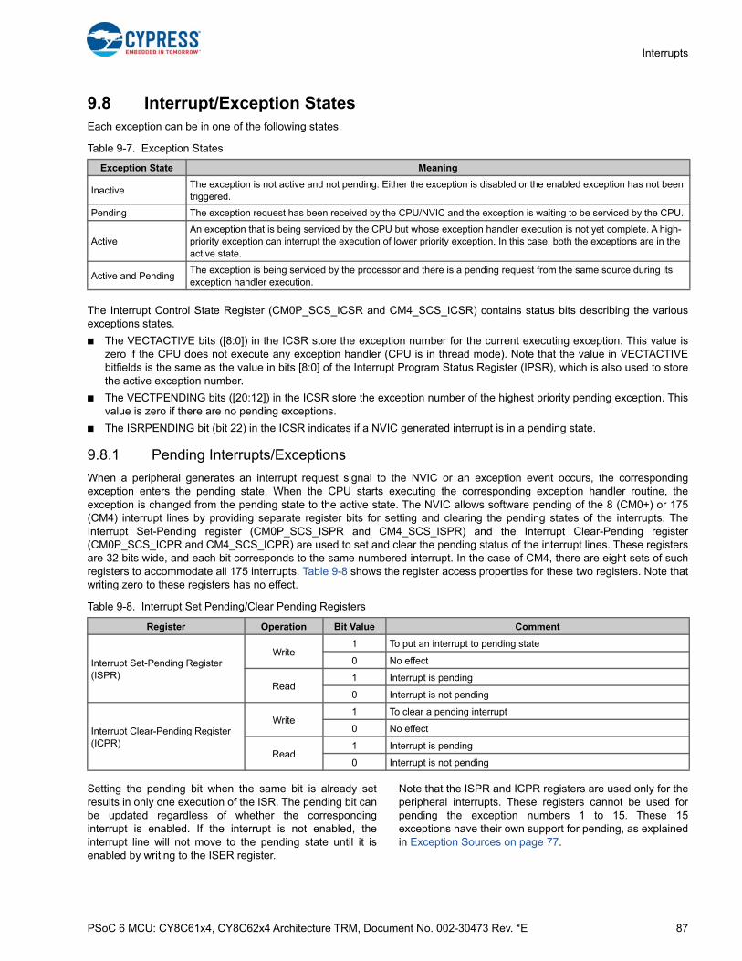
PSoC 6 MCU: CY8C61x4, CY8C62x4 Architecture TRM, Document No. 002-30473 Rev. *E 87
Interrupts
9.8 Interrupt/Exception StatesEach exception can be in one of the following states.
The Interrupt Control State Register (CM0P_SCS_ICSR and CM4_SCS_ICSR) contains status bits describing the variousexceptions states.
■ The VECTACTIVE bits ([8:0]) in the ICSR store the exception number for the current executing exception. This value iszero if the CPU does not execute any exception handler (CPU is in thread mode). Note that the value in VECTACTIVEbitfields is the same as the value in bits [8:0] of the Interrupt Program Status Register (IPSR), which is also used to storethe active exception number.
■ The VECTPENDING bits ([20:12]) in the ICSR store the exception number of the highest priority pending exception. Thisvalue is zero if there are no pending exceptions.
■ The ISRPENDING bit (bit 22) in the ICSR indicates if a NVIC generated interrupt is in a pending state.
9.8.1 Pending Interrupts/Exceptions
When a peripheral generates an interrupt request signal to the NVIC or an exception event occurs, the correspondingexception enters the pending state. When the CPU starts executing the corresponding exception handler routine, theexception is changed from the pending state to the active state. The NVIC allows software pending of the 8 (CM0+) or 175(CM4) interrupt lines by providing separate register bits for setting and clearing the pending states of the interrupts. TheInterrupt Set-Pending register (CM0P_SCS_ISPR and CM4_SCS_ISPR) and the Interrupt Clear-Pending register(CM0P_SCS_ICPR and CM4_SCS_ICPR) are used to set and clear the pending status of the interrupt lines. These registersare 32 bits wide, and each bit corresponds to the same numbered interrupt. In the case of CM4, there are eight sets of suchregisters to accommodate all 175 interrupts. Table 9-8 shows the register access properties for these two registers. Note thatwriting zero to these registers has no effect.
Setting the pending bit when the same bit is already setresults in only one execution of the ISR. The pending bit canbe updated regardless of whether the correspondinginterrupt is enabled. If the interrupt is not enabled, theinterrupt line will not move to the pending state until it isenabled by writing to the ISER register.
Note that the ISPR and ICPR registers are used only for theperipheral interrupts. These registers cannot be used forpending the exception numbers 1 to 15. These 15exceptions have their own support for pending, as explainedin Exception Sources on page 77.
Table 9-7. Exception States
Exception State Meaning
InactiveThe exception is not active and not pending. Either the exception is disabled or the enabled exception has not been triggered.
Pending The exception request has been received by the CPU/NVIC and the exception is waiting to be serviced by the CPU.
ActiveAn exception that is being serviced by the CPU but whose exception handler execution is not yet complete. A high-priority exception can interrupt the execution of lower priority exception. In this case, both the exceptions are in the active state.
Active and PendingThe exception is being serviced by the processor and there is a pending request from the same source during its exception handler execution.
Table 9-8. Interrupt Set Pending/Clear Pending Registers
Register Operation Bit Value Comment
Interrupt Set-Pending Register (ISPR)
Write1 To put an interrupt to pending state
0 No effect
Read1 Interrupt is pending
0 Interrupt is not pending
Interrupt Clear-Pending Register (ICPR)
Write1 To clear a pending interrupt
0 No effect
Read1 Interrupt is pending
0 Interrupt is not pending

PSoC 6 MCU: CY8C61x4, CY8C62x4 Architecture TRM, Document No. 002-30473 Rev. *E 88
Interrupts
9.9 Stack Usage for Interrupts/Exceptions
When the CPU executes the main code (in thread mode)and an exception request occurs, the CPU stores the stateof its general-purpose registers in the stack. It then startsexecuting the corresponding exception handler (in handlermode). The CPU pushes the contents of the eight 32-bitinternal registers into the stack. These registers are theProgram and Status Register (PSR), ReturnAddress, LinkRegister (LR or R14), R12, R3, R2, R1, and R0. BothCortex-M4 and Cortex-M0+ have two stack pointers - MSPand PSP. Only one of the stack pointers can be active at atime. When in thread mode, the Active Stack Pointer bit inthe Control register is used to define the current active stackpointer. When in handler mode, the MSP is always used asthe stack pointer. The stack pointer always growsdownwards and points to the address that has the lastpushed data.
When the CPU is in thread mode and an exception requestcomes, the CPU uses the stack pointer defined in thecontrol register to store the general-purpose registercontents. After the stack push operations, the CPU entershandler mode to execute the exception handler. Whenanother higher priority exception occurs while executing thecurrent exception, the MSP is used for stack push/popoperations, because the CPU is already in handler mode.See the CPU Subsystem (CPUSS) chapter on page 31 fordetails.
9.10 Interrupts and Low-Power Modes
The PSoC 6 MCU family allows device (CPU) wakeup fromlow-power modes when certain peripheral interrupt requestsare generated. The Wakeup Interrupt Controller (WIC) blockgenerates a wakeup signal that causes the CPU to enterActive mode when one or more wakeup sources generatean interrupt signal. After entering Active mode, the ISR ofthe peripheral interrupt is executed.
The Wait For Interrupt (WFI) or Wait For Event (WFE)instruction, executed by the CPU, triggers the transition intoSleep, and Deep Sleep modes. Both the WFI and WFEinstructions are capable of waking up on interrupts.However, the WFE requires the interrupts to be unmasked inthe CPU’s Priority Mask register. Refer to the PRIMASKregister definition on the Arm website. In addition, the WFEinstruction puts the CPU to sleep based on the status of anevent bit and wakes up from an event signal, typically sentby the other CPU. WFI does not require PRIMASKunmasking and can wake up the CPU from any pendinginterrupt masked to the NVIC or WIC. However, WFI cannotwake up the CPU from event signals from other CPUs. Thesequence of entering the different low-power modes isdetailed in the Device Power Modes chapter on page 280.
Chip low-power modes have two categories of interruptsources:
■ Interrupt sources that are available in the Active, Sleep,and Deep Sleep modes (watchdog timer interrupt, RTC,GPIO interrupts, and Low-Power comparators)
■ Interrupt sources that are available only in the Active andSleep modes
When using the WFE instruction in CM4, make sure to callthe WFE instruction twice to properly enter and exit Sleep/Deep Sleep modes. This behavior comes from the eventregister implementation in Arm v7 architecture used inCortex-M4. According to the ARM V7 architecture referencemanual (Section B1.5.18 Wait For Event and Send Event):
■ A reset clears the event register.
■ Any WFE wakeup event, or the execution of anexception return instruction, sets the event register.
■ A WFE instruction clears the event register.
■ Software cannot read or write the value of the event register directly.
Therefore, the first WFE instruction puts CM4 to sleep andsecond WFE clears the event register after a WFE wakeup,which sets the event register. So the next WFE will put thecore to sleep.
Note that this behavior is not present in Arm v6 architectureused in Cortex-M0+. Therefore, in CM0+ only one WFEinstruction is sufficient to successfully enter or exit Sleepand Deep Sleep modes.
9.11 Interrupt/Exception – Initialization/ Configuration
This section covers the different steps involved in initializingand configuring exceptions in the PSoC 6 MCU.
1. Configuring the Exception Vector Table Location: Thefirst step in using exceptions is to configure the vectortable location as required - either in flash memory orSRAM. This configuration is done as described inException Vector Table on page 76.
The vector table should be available in SRAM if theapplication must change the vector addressesdynamically. If the table is located in flash, then a flashwrite operation is required to modify the vector tablecontents. The Cortex-M startup code places the vectortable in SRAM by default.
2. Configuring Individual Exceptions: The next step is toconfigure individual exceptions required in anapplication, as explained in earlier sections.
a. Configure the exception or interrupt source; thisincludes setting up the interrupt generationconditions. The register configuration depends onthe specific exception required. Refer to therespective peripheral chapter to know more aboutthe interrupt configuration supported by them.
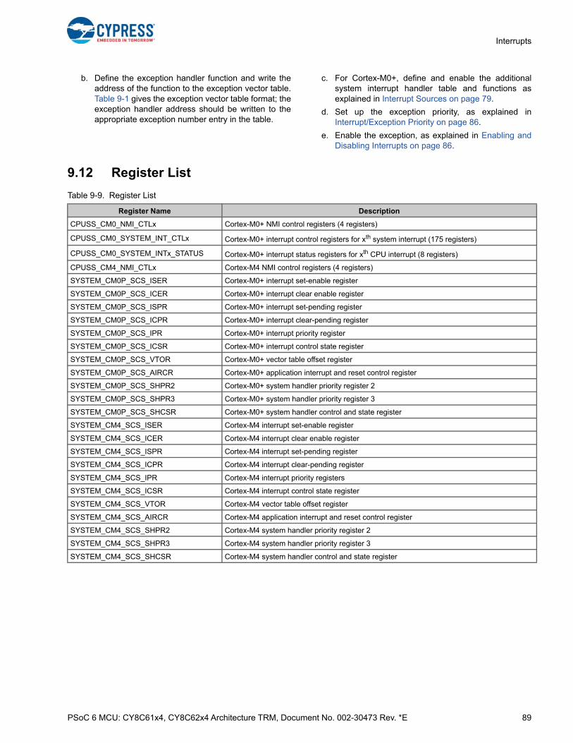
PSoC 6 MCU: CY8C61x4, CY8C62x4 Architecture TRM, Document No. 002-30473 Rev. *E 89
Interrupts
b. Define the exception handler function and write theaddress of the function to the exception vector table.Table 9-1 gives the exception vector table format; theexception handler address should be written to theappropriate exception number entry in the table.
c. For Cortex-M0+, define and enable the additionalsystem interrupt handler table and functions asexplained in Interrupt Sources on page 79.
d. Set up the exception priority, as explained inInterrupt/Exception Priority on page 86.
e. Enable the exception, as explained in Enabling andDisabling Interrupts on page 86.
9.12 Register List
Table 9-9. Register List
Register Name Description
CPUSS_CM0_NMI_CTLx Cortex-M0+ NMI control registers (4 registers)
CPUSS_CM0_SYSTEM_INT_CTLx Cortex-M0+ interrupt control registers for xth system interrupt (175 registers)
CPUSS_CM0_SYSTEM_INTx_STATUS Cortex-M0+ interrupt status registers for xth CPU interrupt (8 registers)
CPUSS_CM4_NMI_CTLx Cortex-M4 NMI control registers (4 registers)
SYSTEM_CM0P_SCS_ISER Cortex-M0+ interrupt set-enable register
SYSTEM_CM0P_SCS_ICER Cortex-M0+ interrupt clear enable register
SYSTEM_CM0P_SCS_ISPR Cortex-M0+ interrupt set-pending register
SYSTEM_CM0P_SCS_ICPR Cortex-M0+ interrupt clear-pending register
SYSTEM_CM0P_SCS_IPR Cortex-M0+ interrupt priority register
SYSTEM_CM0P_SCS_ICSR Cortex-M0+ interrupt control state register
SYSTEM_CM0P_SCS_VTOR Cortex-M0+ vector table offset register
SYSTEM_CM0P_SCS_AIRCR Cortex-M0+ application interrupt and reset control register
SYSTEM_CM0P_SCS_SHPR2 Cortex-M0+ system handler priority register 2
SYSTEM_CM0P_SCS_SHPR3 Cortex-M0+ system handler priority register 3
SYSTEM_CM0P_SCS_SHCSR Cortex-M0+ system handler control and state register
SYSTEM_CM4_SCS_ISER Cortex-M4 interrupt set-enable register
SYSTEM_CM4_SCS_ICER Cortex-M4 interrupt clear enable register
SYSTEM_CM4_SCS_ISPR Cortex-M4 interrupt set-pending register
SYSTEM_CM4_SCS_ICPR Cortex-M4 interrupt clear-pending register
SYSTEM_CM4_SCS_IPR Cortex-M4 interrupt priority registers
SYSTEM_CM4_SCS_ICSR Cortex-M4 interrupt control state register
SYSTEM_CM4_SCS_VTOR Cortex-M4 vector table offset register
SYSTEM_CM4_SCS_AIRCR Cortex-M4 application interrupt and reset control register
SYSTEM_CM4_SCS_SHPR2 Cortex-M4 system handler priority register 2
SYSTEM_CM4_SCS_SHPR3 Cortex-M4 system handler priority register 3
SYSTEM_CM4_SCS_SHCSR Cortex-M4 system handler control and state register
PSoC 6 MCU: CY8C61x4, CY8C62x4 Architecture TRM, Document No. 002-30473 Rev. *E 90
10. DMA Controller (DW)
The DMA transfers data to and from memory, peripherals, and registers. These transfers occur independent from the CPU.The DMA can be configured to perform multiple independent data transfers. All data transfers are managed by a channel.There can be up to 32 channels in the DMA. The number of channels in the DMA controller can vary with devices. Refer tothe PSoC 61 datasheet/PSoC 62 datasheet for the number of channels supported in the device. A channel has an associatedpriority; channels are arbitrated according to their priority.
10.1 Features
The DMA controller has the following features:
■ Supports up to 30 channels on DMA channel 0 (DW0) and 32 channels on DMA channel 1 (DW1); see the PSoC 61 datasheet/PSoC 62 datasheet for details
■ Supports multiple DMA controller instances in a device
■ Four levels of priority for each channel
■ Descriptors are defined in memory and referenced to the respective channels
■ Supports single, 1D, or 2D transfer modes for a descriptor
■ Supports transfer of up to 65536 data elements per descriptor
■ Configurable source and destination address increments
■ Supports 8-bit, 16-bit, and 32-bit data widths at both source and destination
■ Configurable input trigger behavior for each descriptor
■ Configurable interrupt generation in each descriptor
■ Configurable output trigger generation for each descriptor
■ Descriptors can be chained to other descriptors in memory
This PSoC 6 MCU technical reference manual (TRM) provides comprehensive and detailed information about thefunctions of the PSoC 6 MCU device hardware. It is divided into two books: architecture TRM and registers TRM. TheTRM is not recommended for those new to the PSoC 6 MCU, nor as a guide for developing PSoC 6 MCU applications.Use these documents instead:
■ PSoC 61 datasheet, PSoC 62 datasheet
■ Peripheral Driver Library (PDL) documentation
■ Application notes
■ Code examples
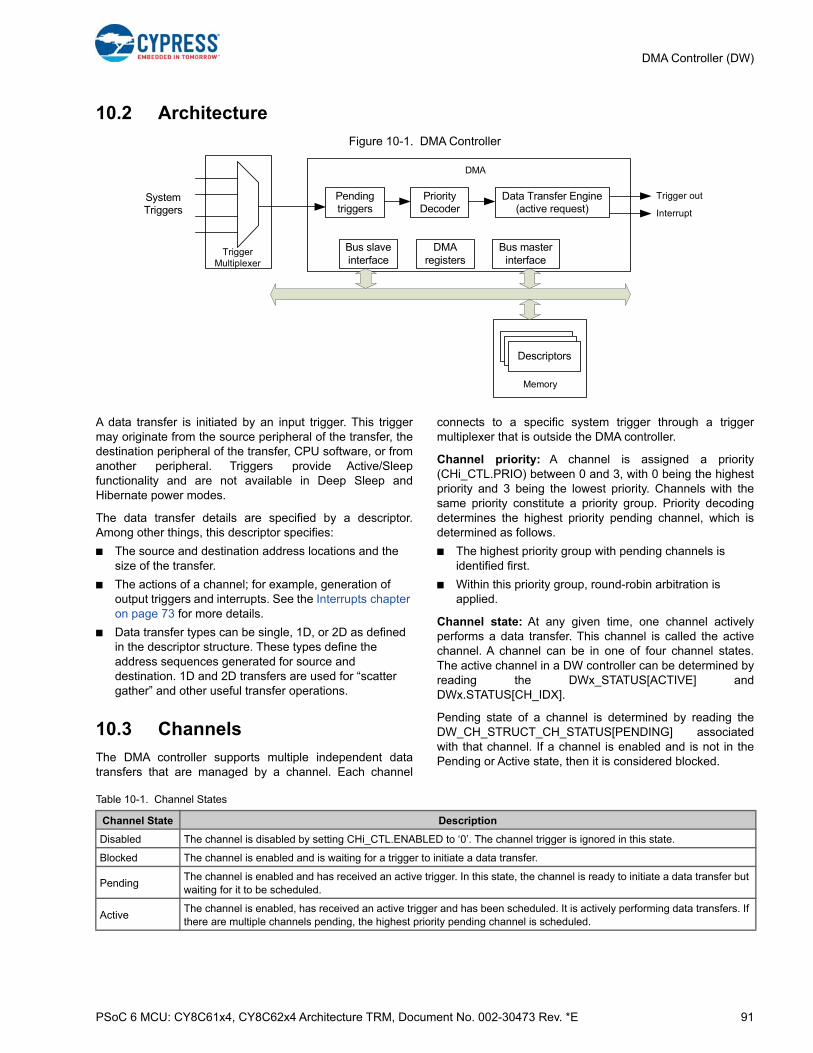
PSoC 6 MCU: CY8C61x4, CY8C62x4 Architecture TRM, Document No. 002-30473 Rev. *E 91
DMA Controller (DW)
10.2 Architecture
Figure 10-1. DMA Controller
A data transfer is initiated by an input trigger. This triggermay originate from the source peripheral of the transfer, thedestination peripheral of the transfer, CPU software, or fromanother peripheral. Triggers provide Active/Sleepfunctionality and are not available in Deep Sleep andHibernate power modes.
The data transfer details are specified by a descriptor.Among other things, this descriptor specifies:
■ The source and destination address locations and the size of the transfer.
■ The actions of a channel; for example, generation of output triggers and interrupts. See the Interrupts chapter on page 73 for more details.
■ Data transfer types can be single, 1D, or 2D as defined in the descriptor structure. These types define the address sequences generated for source and destination. 1D and 2D transfers are used for “scatter gather” and other useful transfer operations.
10.3 Channels
The DMA controller supports multiple independent datatransfers that are managed by a channel. Each channel
connects to a specific system trigger through a triggermultiplexer that is outside the DMA controller.
Channel priority: A channel is assigned a priority(CHi_CTL.PRIO) between 0 and 3, with 0 being the highestpriority and 3 being the lowest priority. Channels with thesame priority constitute a priority group. Priority decodingdetermines the highest priority pending channel, which isdetermined as follows.
■ The highest priority group with pending channels is identified first.
■ Within this priority group, round-robin arbitration is applied.
Channel state: At any given time, one channel activelyperforms a data transfer. This channel is called the activechannel. A channel can be in one of four channel states.The active channel in a DW controller can be determined byreading the DWx_STATUS[ACTIVE] andDWx.STATUS[CH_IDX].
Pending state of a channel is determined by reading theDW_CH_STRUCT_CH_STATUS[PENDING] associatedwith that channel. If a channel is enabled and is not in thePending or Active state, then it is considered blocked.
Trigger Multiplexer
System Triggers
Pending triggers
Priority Decoder
Data Transfer Engine (active request)
Bus slave interface
Bus master interface
DMA registers
DescriptorsDescriptorsDescriptors
Memory
DMA
Trigger out
Interrupt
Table 10-1. Channel States
Channel State Description
Disabled The channel is disabled by setting CHi_CTL.ENABLED to ‘0’. The channel trigger is ignored in this state.
Blocked The channel is enabled and is waiting for a trigger to initiate a data transfer.
PendingThe channel is enabled and has received an active trigger. In this state, the channel is ready to initiate a data transfer but waiting for it to be scheduled.
ActiveThe channel is enabled, has received an active trigger and has been scheduled. It is actively performing data transfers. If there are multiple channels pending, the highest priority pending channel is scheduled.

PSoC 6 MCU: CY8C61x4, CY8C62x4 Architecture TRM, Document No. 002-30473 Rev. *E 92
DMA Controller (DW)
The data transfer associated with a trigger is made up ofone or more ‘atomic transfers’ or ‘single transfers’; seeTable 10-2 for a better understanding. A single trigger couldbe configured to transfer multiple “single transfers”.
A channel can be marked preemptable(CHi_CTL.PREEMPTABLE). If preemptable, and there is ahigher priority pending channel, then that higher prioritychannel can preempt the current channel between singletransfers. If a channel is preempted, the existing singletransfer is completed; the current channel goes to pendingstate and the higher priority channel is serviced. Oncompletion of the higher priority channel's transfer, thepending channel is resumed. Note that preemption has animpact on the data transfer rates of the channel beingpreempted. Refer to “DMA Performance” on page 99 forthese performance implications.
A channel has two access control attributes that are used bythe shared memory protection units (SMPUs) and peripheralprotection units (PPUs) for access control. These fields aretypically inherited from the master that modified thechannel’s control register.
■ The Privileged Mode (CHi_CTL.P) attribute can be set to privileged or user.
■ The Non-secure (CHi_CTL.NS) attribute can be set to secure or non-secure.
A descriptor associated with each channel describes thedata transfer. The descriptor is stored in memory andCHi_CURR_PTR provides the descriptor addressassociated with channel “i” and Chi_IDX provides thecurrent X and Y indices into the descriptor.
A channel’s descriptor state is encoded as part of thechannel’s register state. The following registers provide achannel’s descriptor state:
■ CH_CTL. This register provides generic channel control information.
■ CH_CURR_PTR. This register provides the address of the memory location where the current descriptor is located. The user firmware must initialize this register. If the descriptors are chained, the DMA hardware automatically sets this register to the next descriptor pointer.
■ CH_IDX. This register provides the current X and Y indices of the channel into the current descriptor. User firmware must initialize this register. DMA hardware sets the X and Y indices to 0, when advancing from the current descriptor to the next descriptor in a descriptor list.
Note that channel state is retained in Deep Sleep powermode.
10.3.1 Channel Interrupts
Every DMA channel has an interrupt line associated with it.The INTR_TYPE parameter in the descriptor determines the
event that will trigger the interrupt for the channel. Inaddition each DMA channel has INTR, INTR_SET,INTR_MASK, and INTR_MASKED registers to control theirrespective interrupt lines. INTR_MASK can be used to maskthe interrupt from the DMA channel. The INTR andINTR_SET can be used to clear and set the interrupt,respectively, for debug purposes.
The DW_CH_STRUCT_CH_STATUS[INTR_CAUSE] fieldprovides the user a means to determine the cause of theinterrupt being generated. The following are different valuesfor this register:
■ 0: No interrupt generated
■ 1: Interrupt based on transfer completion configured based on INTR_TYPE field in the descriptor
■ 2: Source bus error
■ 3: Destination bus error
■ 4: Misaligned source address
■ 5: Misaligned destination address
■ 6: Current descriptor pointer is null
■ 7: Active channel is in disabled state
■ 8: Descriptor bus error
■ 9-15: Not used.
For error related interrupt causes (INTR_CAUSE is 2, 3,...,8), the channel is disabled (hardware setsCH_CTL.ENABLED to ‘0’).
The bus errors are typically caused by incompatibleaccesses to the addresses in question. This may be due tothose addresses being protected or having read or writerestrictions. Source and destination bus errors can alsooccur due to mismatch in data sizes (see “Transfer Size” onpage 96).

PSoC 6 MCU: CY8C61x4, CY8C62x4 Architecture TRM, Document No. 002-30473 Rev. *E 93
DMA Controller (DW)
10.4 Descriptors
The data transfer between a source and destination in a channel is configured using a descriptor. Descriptors are stored inmemory. The descriptor pointer is specified in the DMA channel registers. The DMA controller does not modify the descriptorand treats it as read only. A descriptor is a set of up to six 32-bit registers that contain the configuration for the transfer in theassociated channel. There are three types of descriptors.
Single Transfer:
The following pseudo code illustrates a single transfer.// DST_ADDR is a pointer to an object of type defined by DST_TRANSFER_SIZE// SRC_ADDR is a pointer to an object of type defined by SRC_TRANSFER_SIZE// t_DATA_SIZE is the type associated with the DATA_SIZEDST_ADDR[0] = (t_DATA_SIZE) SRC_ADDR[0];
Table 10-2. Descriptor Types
Descriptor Type Description
Single transfer
Transfers a single data element
1D transfer
Performs a one-dimensional “for loop”. This transfer is made up of X number of single transfers
2D transfer
Performs a two-dimensional “for loop”. This transfer is made up of Y number of 1D transfers
CRC transfer
This performs a one-dimensional “for loop” similar to the 1D transfer. However, the source data is not trans-ferred to a destination. Instead, a CRC is calculated over the source data. The CRC configuration is provided through a set of registers that is shared by all DMA channels. The assumption is that the DMA channels use the CRC functionality mutually exclusively in time. These registers are: CRC_CTL, CRC_DATA_CTL, CRC_POL_CTL, CRC_LFSR_CTL, CRC_REM_CTL, and CRC_REM_RESULT. Note that the CRC configu-ration is the same as the Crypto CRC configuration.
A B
A
A+1
A+2
A+X-1
B
B+1
B+2
B+ X-1
A
A+1
A+2
A+X-1
B
B+1
B+2
B+X-1
A+X
A+X+1
A+X+2
A+2X-1
B+X
B+X+1
B+X+2
B+2X-1
A+(X*Y)-1 B+X*Y-1
1st 1D transfer
2nd 1D transfer
Yth 1D transfer
PSoC 6 MCU: CY8C61x4, CY8C62x4 Architecture TRM, Document No. 002-30473 Rev. *E 94
DMA Controller (DW)
1D Transfer:
The following pseudo code illustrates a 1D transfer. Note that the 1D transfer is represented by a loop with each iterationexecuting a single transfer.// DST_ADDR is a pointer to an object of type defined by DST_TRANSFER_SIZE// SRC_ADDR is a pointer to an object of type defined by SRC_TRANSFER_SIZE// t_DATA_SIZE is the type associated with the DATA_SIZEfor (X_IDX = 0; X_IDX <= X_COUNT; X_IDX++) {DST_ADDR[X_IDX * DST_X_INCR] = (t_DATA_SIZE) SRC_ADDR[X_IDX * SRC_X_INCR];}
2D Transfer:
The following pseudo code illustrates a 2D transfer. Note that the 2D transfer is represented by a loop with each iterationexecuting an inner loop, which is the 1D transfer.// DST_ADDR is a pointer to an object of type defined by DST_TRANSFER_SIZE// SRC_ADDR is a pointer to an object of type defined by SRC_TRANSFER_SIZE// t_DATA_SIZE is the type associated with the DATA_SIZEfor (Y_IDX = 0; Y_IDX <= Y_COUNT; Y_IDX++) { for (X_IDX = 0; X_IDX <= X_COUNT; X_IDX++) {DST_ADDR[X_IDX * DST_X_INCR + Y_IDX * DST_Y_INCR ] = (t_DATA_SIZE) SRC_ADDR[X_IDX * SRC_X_INCR + Y_IDX * SRC_Y_INCR]; }}
CRC Transfer:
The following psuedo code illustrates CRC transfer. // DST_ADDR is a pointer to an address location where the calculated CRC is stored.// SRC_ADDR is a pointer to an object of type defined by SRC_TRANSFER_SIZE// t_DATA_SIZE is the type associated with the DATA_SIZECRC_STATE = CRC_LFSR_CTL;for (X_IDX = 0; X_IDX <= X_COUNT; X_IDX++) { Update_CRC (CRC_STATE, (t_DATA_SIZE) SRC_ADDR[X_IDX * SRC_X_INCR];}DST_ADDR = CRC_STATE;
The parameters in the descriptor help configure the different aspects of the transfers explained.
Figure 10-2 shows the structure of a descriptor.

PSoC 6 MCU: CY8C61x4, CY8C62x4 Architecture TRM, Document No. 002-30473 Rev. *E 95
DMA Controller (DW)
Figure 10-2. Descriptor Structure
10.4.1 Address Configuration
Source and Destination Address: The source anddestination addresses are set in the respective registers inthe descriptor. These set the base addresses for the sourceand destination location for the transfer. In case thedescriptor is configured to transfer a single element, thisfield holds the source/destination address of the dataelement. If the descriptor is configured to transfer multipleelements with source address or destination address or bothin an incremental mode, this field will hold the address of thefirst element that is transferred.
DESCR_TYPE: This field configures whether the descriptorhas a single, 1D, or 2D type.
Trigger input type, TR_IN_TYPE: This field determineshow the DMA engine responds to input trigger signal. Thisfield can be configured for one of the following modes:
■ Type 0: A trigger results in execution of a single transfer.Regardless of the DESCR_TYPE setting, a trigger inputwill trigger only a single element transfer. For example,in a 1D transfer, the DMA will transfer only one dataelement in every trigger.
■ Type 1: A trigger results in the execution of a single 1Dtransfer. If the DESCR_TYPE was set to single transfer,the trigger signal will trigger the single transfer specifiedby the descriptor. For a DESCR_TYPE set to 1Dtransfer, the trigger signal will trigger the entire 1Dtransfer configured in the descriptor. For a 2D transfer,the trigger signal will trigger only a single iteration of theY loop transfer.
■ Type 2: A trigger results in execution of the currentdescriptor. Regardless of DESCR_TYPE, the trigger willexecute the entire descriptor. If there was a nextdescriptor configured for the current descriptor, this
trigger setting will not automatically trigger the nextdescriptor.
■ Type 3: A trigger results in execution of the currentdescriptor and also triggering the next descriptor. Theexecution of the next descriptor from this point will bedetermined by the TR_IN_TYPE setting of the nextdescriptor.
Trigger out type, TR_OUT_TYPE: This field determineswhat completion event will generate the output triggersignal. This field can be configured to one of the followingmodes:
■ Type 0: Generates a trigger output for completion ofevery single element transfer.
■ Type 1: Generates a trigger output for completion of a1D transfer
■ Type 2: Generates a trigger output for completion of thecurrent descriptor. This trigger output is generatedindependent of the state of the DESCR_NEXT_PTR.
■ Type 3: Generates a trigger output on completion of thecurrent descriptor, when the current descriptor is the lastdescriptor in the descriptor chain. This means a trigger isgenerated when the descriptor execution is completeand the DESCR_NEXT_PTR is ‘0’.
Interrupt Type, INTR_TYPE: This field determines whichcompletion event will generate the output interrupt signal.This field can be configured to one of the following modes:
■ Type 0: Generates an interrupt output for completion ofevery single element transfer.
■ Type 1: Generates an interrupt output for completion of a1-D transfer.
Descriptor
Source AddressDESCR_SRC
Destination AddressDESCR_DST
X SizeSRC_X_INR DST_X_INCR
Y SizeSRC_Y_INR DST_Y_INCR
Next Descriptor AddressDESCR_NEXT_PTR
DESCR_TYPEDESCR_CTL
TR_IN_TYPESCR_TRANSFER_SIZE
TR_OUT_TYPEDST_TRANSFER_SIZE
DATA_SIZE
WAIT_FOR_DEACTINTR_TYPE CH_DISABLE

PSoC 6 MCU: CY8C61x4, CY8C62x4 Architecture TRM, Document No. 002-30473 Rev. *E 96
DMA Controller (DW)
■ Type 2: Generates an interrupt output for completion ofthe current descriptor. This interrupt output is generatedindependent of the state of the DESCR_NEXT_PTR.
■ Type 3: Generates an interrupt output on completion ofthe current descriptor, when the current descriptor is thelast descriptor in the descriptor chain. This means aninterrupt is generated when the descriptor execution iscomplete and the DESCR_NEXT_PTR is ‘0’.
WAIT_FOR_DEACT: When the DMA transfer based on theTR_IN_TYPE is completed, the data transfer engine checksthe state of trigger deactivation. The data transfer on thesecond trigger is initiated only after deactivation of the first.The WAIT_FOR_DEACT parameter will determine when thetrigger signal is considered deactivated. The first DMAtransfer is activated when the trigger is activated, but thetransfer is not considered complete until the trigger isdeactivated. This field is used to synchronize the controller’sdata transfers with the agent that generated the trigger. Thisfield has four settings:
■ 0 – Pulse Trigger: Do not wait for deactivation. When atrigger is detected, the transfer is initiated. Aftercompleting the transfer, if the trigger is still active then itis considered as another trigger and the subsequenttransfer is initiated immediately.
■ 1 – Level-sensitive waits four slow clock cycles after thetransfer to consider as a deactivation. When a trigger isdetected, the transfer is initiated. After completing thetransfer, if the trigger is still active then it is consideredas another trigger after waiting for four cycles. Then, asubsequent transfer is initiated. The transfercorresponding to the trigger is considered complete onlyat the end of the four additional cycles. Even triggeroutput events will be affected based on this delay. Thisparameter adds a four-cycle delay in each triggertransaction and hence affects throughput.
■ 2 – Level-sensitive waits 16 slow clock cycles after thetransfer to consider as a deactivation. When a trigger isdetected, the transfer is initiated. After completing thetransfer, if the trigger is still active then it is consideredas another trigger after waiting for 16 cycles. Then, asubsequent transfer is initiated. The transfercorresponding to the trigger is considered complete onlyat the end of the 16 additional cycles. Even triggeroutput events will be affected based on this delay. Thisparameter adds a 16-cycle delay in each triggertransaction and hence affects throughput.
■ 3 – Pulse trigger waits indefinitely for deactivation. TheDMA transfer is initiated after the trigger signaldeactivates. The next transfer is initiated only if thetrigger goes low and then high again. A trigger signalthat remains active or does not transition to zerobetween two transaction will simply stall the DMAchannel.
The WAIT_FOR_DEACT field is used in a system to cater to delayed response of other parts of the system to actions of the DMA. Consider an example of a TX FIFO
that has a trigger going to the DMA when its not full. Free space in FIFO will trigger a DMA transfer to the FIFO, which in turn will deactivate the trigger. However, there can be a delay in this deactivation by the agent, which may cause the DMA to have initiated another transfer that can cause a FIFO overflow. This can be avoided by using the four or 16 clock cycle delays.
X Count: This field determines the number of singleelement transfers present in the X loop (inner loop). Thisfield is valid when the DESCR_TYPE is set to 1D or 2Dtransfer.
Source Address Increment (X loop) (SCR_X_INCR): Thisfield configures the index by which the source address is tobe incremented for every iteration in an X loop. The field isexpressed in multiples of SRC_TRANSFER_SIZE. This fieldis a signed number and hence may be decrementing orincrementing. If the source address does not need to beincremented, you can set this parameter to zero.
Destination Address Increment (X loop) (DST_X_INCR):This field configures the index by which the destinationaddress is to be incremented, for every iteration in an Xloop. The field is expressed in multiples ofDST_TRANSFER_SIZE. This field is a signed number andhence may be decrementing or incrementing. If thedestination address does not need to be incremented, youcan set this parameter to zero.
Y Count: This field determines the number of 1-D transferspresent in the Y loop (outer loop). This field is valid when theDESCR_TYPE is set to 2-D transfer.
Source Address Increment (Y loop) (SCR_Y_INCR): Thisfield configures the index by which the source address is tobe incremented, for every iteration in a Y loop. The field isexpressed in multiples of SRC_TRANSFER_SIZE. This fieldis a signed number and hence may be decrementing orincrementing. If the source address does not need to beincremented, you can set this parameter to zero.
Destination Address Increment (X loop) (DST_Y_INCR):This field configures the index by which the destinationaddress is to be incremented, for every iteration in a Y loop.The field is expressed in multiples ofDST_TRANSFER_SIZE. This field is a signed number andhence may be decrementing or incrementing. If thedestination address does not need to be incremented, youcan set this parameter to zero.
Channel Disable (CH_DISABLE): This field specifieswhether the channel is disabled or not after completion ofthe current descriptor (independent of the value of theDESCR_NEXT_PTR). A disabled channel will ignore itsinput triggers.
10.4.2 Transfer Size
The word width for a transfer can be configured using thetransfer/data size parameter in the descriptor. The settings

PSoC 6 MCU: CY8C61x4, CY8C62x4 Architecture TRM, Document No. 002-30473 Rev. *E 97
DMA Controller (DW)
are diversified into source transfer size, destination transfersize, and data size. The data size parameter (DATA_SIZE)sets the width of the bus for the transfer. The source anddestination transfer sizes set by SCR_TRANSFER_SIZEand DST_TRANSFER_SIZE can have a value either theDATA_SIZE or 32 bit. DATA_SIZE can have a 32-bit, 16-bit,or 8-bit setting.
The source and destination transfer size for the DMA mustmatch the addressable width of the source and destination,regardless of the width of data that must be moved. TheDATA_SIZE parameter will correspond to the width of theactual data. For example, if a 16-bit PWM is used as adestination for DMA data, the DST_TRANSFER_SIZE must
be set to 32 bit to match the width of the PWM register,because the peripheral register width for the TCPWM block(and most PSoC 6 MCU peripherals) is always 32-bit wide.However, in this example the DATA_SIZE for the destinationmay still be set to 16 bit because the 16-bit PWM only usestwo bytes of data. SRAM and Flash are 8-bit, 16-bit, or 32-bit addressable and can use any source and destinationtransfer sizes to match the needs of the application.
Table 10-3 summarizes the possible combinations of thetransfer size settings and its description.
10.4.3 Descriptor Chaining
Descriptors can be chained together. The DESCR_NEXT_PTR field contains a pointer to the next descriptor in the chain. Achannel executes the next descriptor in the chain when it completes executing the current descriptor. The last descriptor inthe chain has DESCR_NEXT_PTR set to ‘0’ (NULL pointer). A descriptor chain is also referred to as a descriptor list. It ispossible to have a circular list; in a circular list, the execution continues indefinitely until there is an error or the channel or thecontroller is disabled by user code.
Table 10-3. Transfer Size Settings
DATA_SIZESCR_TRANSFER_
SIZEDST_TRANSFER_
SIZETypical Usage Description
8-bit 8-bit 8-bit Memory to Memory No data manipulation
8-bit 32-bit 8-bit Peripheral to Memory Higher 24 bits from the source dropped
8-bit 8-bit 32-bit Memory to Peripheral Higher 24 bits zero padded at destination
8-bit 32-bit 32-bit Peripheral to PeripheralHigher 24 bits from the source dropped and higher 24 bits zero padded at destination
16-bit 16-bit 16-bit Memory to Memory No data manipulation
16-bit 32-bit 16-bit Peripheral to Memory Higher 16 bits from the source dropped
16-bit 16-bit 32-bit Memory to Peripheral Higher 16 bits zero padded at destination
16-bit 32-bit 32-bit Peripheral to PeripheralHigher 16 bits from the source dropped and higher 16-bit zero padded at destination
32-bit 32-bit 32-bit Peripheral to Peripheral No data manipulation

PSoC 6 MCU: CY8C61x4, CY8C62x4 Architecture TRM, Document No. 002-30473 Rev. *E 98
DMA Controller (DW)
10.5 DMA Controller
Figure 10-3. DMA Controller Overview
10.5.1 Trigger Selection
Trigger signals can be generated from different sections ofthe chips. A trigger multiplexer block helps route thesetrigger signals to the destination. The DMA is one suchdestination of triggers. The trigger multiplexer block isoutside the DMA block and is discussed in the TriggerMultiplexer Block chapter on page 290.
10.5.2 Pending Triggers
Pending triggers keep track of activated triggers by locallystoring them in pending bits. This is essential becausemultiple channel triggers may be activated simultaneously,whereas only one channel can be served by the datatransfer engine at a time. This component enables the useof both level-sensitive (high/‘1’) and pulse-sensitive (twohigh/‘1’ clk_slow cycles) triggers.
■ Level-sensitive triggers are associated with a certainstate, for example, a FIFO being full. These triggersremain active as long as the state is maintained. It is notrequired to track pending level-sensitive triggers in theDMA controller because the triggers are maintainedoutside the controller.
■ Pulse-sensitive triggers are associated with a certainevent, for example, sample has become available. It isessential to track these triggers in the DMA controllerbecause the trigger pulse may disappear before it isserved by the data transfer engine. Pulse triggers shouldbe high/‘1’ for two clk_slow cycles.
The priority decoder determines the highest prioritypending channel.
The data transfer engine is responsible for the datatransfer from a source location to a destination location.When idle, the data transfer engine is ready to accept the
highest priority activated channel. It is also responsible forreading the channel descriptor from memory.
Master I/F is an AHB-Lite bus master that allows the DMAcontroller to initiate AHB-Lite data transfers to the sourceand destination locations as well as to read the descriptorfrom memory.
Slave I/F is an AHB-Lite bus slave that allows the main CPUto access DMA controller control/status registers.
10.5.3 Output Triggers
Each channel has an output trigger. This trigger is high fortwo slow clock cycles. The trigger is generated on thecompletion of a data transfer. At the system level, theseoutput triggers can be connected to the trigger multiplexercomponent. This connection allows a DMA controller outputtrigger to be connected to a DMA controller input trigger. Inother words, the completion of a transfer in one channel canactivate another channel or even reactivate the samechannel.
DMA output triggers routing to other DMA channels or otherperipheral trigger inputs is achieved using the triggermultiplexer. Refer to the Trigger Multiplexer Block chapteron page 290.
10.5.4 Status registers
The controller status register (DWx_STATUS) contains thefollowing information.
■ ACTIVE – Active channel present, yes/no.
■ P – Active channel's access control user/privileged
■ NS – Active channel's access control secure/non-secure
■ CH_IDX – Active channel index if there is an active channel
Trigger Multiplexer
System Triggers
Pending triggers
Priority Decoder
Data Transfer Engine (active request)
Bus slave interface
Bus master interface
DMA registers
DescriptorsDescriptorsDescriptors
Memory
DMA
Trigger out
Interrupt
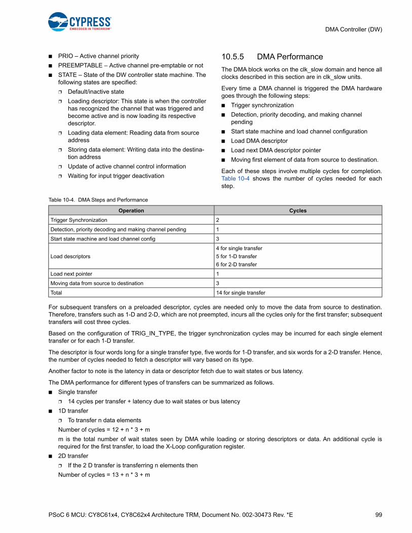
PSoC 6 MCU: CY8C61x4, CY8C62x4 Architecture TRM, Document No. 002-30473 Rev. *E 99
DMA Controller (DW)
■ PRIO – Active channel priority
■ PREEMPTABLE – Active channel pre-emptable or not
■ STATE – State of the DW controller state machine. The following states are specified:
❐ Default/inactive state
❐ Loading descriptor: This state is when the controller has recognized the channel that was triggered and become active and is now loading its respective descriptor.
❐ Loading data element: Reading data from source address
❐ Storing data element: Writing data into the destina-tion address
❐ Update of active channel control information
❐ Waiting for input trigger deactivation
10.5.5 DMA Performance
The DMA block works on the clk_slow domain and hence allclocks described in this section are in clk_slow units.
Every time a DMA channel is triggered the DMA hardwaregoes through the following steps:
■ Trigger synchronization
■ Detection, priority decoding, and making channel pending
■ Start state machine and load channel configuration
■ Load DMA descriptor
■ Load next DMA descriptor pointer
■ Moving first element of data from source to destination.
Each of these steps involve multiple cycles for completion.Table 10-4 shows the number of cycles needed for eachstep.
For subsequent transfers on a preloaded descriptor, cycles are needed only to move the data from source to destination.Therefore, transfers such as 1-D and 2-D, which are not preempted, incurs all the cycles only for the first transfer; subsequenttransfers will cost three cycles.
Based on the configuration of TRIG_IN_TYPE, the trigger synchronization cycles may be incurred for each single elementtransfer or for each 1-D transfer.
The descriptor is four words long for a single transfer type, five words for 1-D transfer, and six words for a 2-D transfer. Hence,the number of cycles needed to fetch a descriptor will vary based on its type.
Another factor to note is the latency in data or descriptor fetch due to wait states or bus latency.
The DMA performance for different types of transfers can be summarized as follows.
■ Single transfer
❐ 14 cycles per transfer + latency due to wait states or bus latency
■ 1D transfer
❐ To transfer n data elements
Number of cycles = 12 + n * 3 + m
m is the total number of wait states seen by DMA while loading or storing descriptors or data. An additional cycle isrequired for the first transfer, to load the X-Loop configuration register.
■ 2D transfer
❐ If the 2 D transfer is transferring n elements then
Number of cycles = 13 + n * 3 + m
Table 10-4. DMA Steps and Performance
Operation Cycles
Trigger Synchronization 2
Detection, priority decoding and making channel pending 1
Start state machine and load channel config 3
Load descriptors
4 for single transfer
5 for 1-D transfer
6 for 2-D transfer
Load next pointer 1
Moving data from source to destination 3
Total 14 for single transfer
PSoC 6 MCU: CY8C61x4, CY8C62x4 Architecture TRM, Document No. 002-30473 Rev. *E 100
DMA Controller (DW)
m is total number of wait states seen by DMA while loading or storing descriptors or data. Two additional cycles arerequired for the first transfer, to load the X-loop and Y-Loop configuration register.
Note: Descriptors in memory and memory wait states will also affect the descriptor load delay.
■ Wait states: Memory accesses can have a wait state associated with them. These wait states need to be accounted into the calculation of throughput.
■ Channel arbitration: Some time channels are not immediately made active after reception of trigger. This is due to other active channels in the system. This can lead to multiple cycles being lost before the channel is even made active.
■ Preemption: The choice of making a DMA channel preemptable impacts its performance. This is because every time a channel is prempted:
❐ The channel is in a pending state for as long as the higher priority channel is running
❐ On resumption, the channel descriptor needs to be fetched again. This is additional cycles for every resume. So if there are a large number of high-priority channels, making a low-priority channel preemptible can have adverse effects on its throughput. On the other hand, if there is a low-priority channel that is transferring a large amount of data, then not making it preemptable can starve other high-priority channels for too long.
Sometimes, users can also distribute channels across multiple DW blocks to avoid conditions of preemption and deal with the contention at the bus arbitration level.
■ Bus arbitration: Several bus masters access the bus, including the CPU cores and multiple DMA (DW) and DMAC. This makes any access to data movement over the bus subject to arbitration with other masters. Actions such as fetching the descriptor or data can be stalled by arbitration. The arbitration of the bus is based on the arbitration scheme configured in PROT_SMPU_MSx_CTL[PRIO]
■ Transfer width: The width of the transfer configured by the Data_size parameter in the descriptor is important in the transfer throughput calculation. 32-bit transfers are four times faster than 8-bit transfers.

PSoC 6 MCU: CY8C61x4, CY8C62x4 Architecture TRM, Document No. 002-30473 Rev. *E 101
11. DMAC Controller (DMAC)
The DMAC transfers data to and from memory, peripherals, and registers. These transfers occur independent from the CPU.The DMAC can be configured to perform multiple independent data transfers. All data transfers are managed by a channel.There can be up to 2 channels in the DMAC. The number of channels in the DMAC controller can vary with devices. Refer tothe PSoC 61 datasheet/PSoC 62 datasheet for the number of channels supported in the device. A channel has an associatedpriority; channels are arbitrated according to their priority. The main difference between the DMA (DW) and DMAC relate totheir usage. The DMA (DW) is meant as a small data size, transactional DMA, which would typically be used to transfer bytesbetween peripherals such as, from ADC to RAM. Using the DMA (DW) for large transaction is expensive on a system due toits relatively low performance. The DMAC is a transitional DMA. It is more efficient than the DMA (DW) and should be used totransfer large amounts of data. The DMAC has dedicated channel logic for all channels. Furthermore, the DMAC alsoincludes a 12-byte FIFO for temporary data storage. This results in increased memory bandwidth for the DMAC. The DMACalso supports an additional transfer mode called memory copy and scatter transfer.
11.1 Features
The DMAC controller has the following features:
■ Supports up to 2 channels per DMAC controller; see the PSoC 61 datasheet/PSoC 62 datasheet for details
■ Four levels of priority for each channel
■ Descriptors are defined in memory and referenced to the respective channels
■ Supports single, 1D, 2D, Memory-copy, or Scatter-transfer modes for a descriptor
■ Supports transfer of up to 2^32 data elements per descriptor
■ Configurable source and destination address increments
■ Supports 8-bit, 16-bit, and 32-bit data widths at both source and destination
■ Configurable input trigger behavior for each descriptor
■ Configurable interrupt generation in each descriptor
■ Configurable output trigger generation for each descriptor
■ Descriptors can be chained to other descriptors in memory
This PSoC 6 MCU technical reference manual (TRM) provides comprehensive and detailed information about thefunctions of the PSoC 6 MCU device hardware. It is divided into two books: architecture TRM and registers TRM. TheTRM is not recommended for those new to the PSoC 6 MCU, nor as a guide for developing PSoC 6 MCU applications.Use these documents instead:
■ PSoC 61 datasheet, PSoC 62 datasheet
■ Peripheral Driver Library (PDL) documentation
■ Application notes
■ Code examples
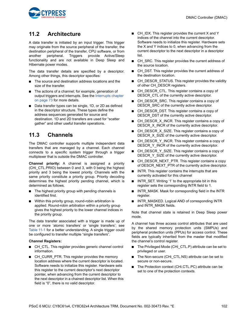
PSoC 6 MCU: CY8C61x4, CY8C62x4 Architecture TRM, Document No. 002-30473 Rev. *E 102
DMAC Controller (DMAC)
11.2 Architecture
A data transfer is initiated by an input trigger. This triggermay originate from the source peripheral of the transfer, thedestination peripheral of the transfer, CPU software, or fromanother peripheral. Triggers provide Active/Sleepfunctionality and are not available in Deep Sleep andHibernate power modes.
The data transfer details are specified by a descriptor.Among other things, this descriptor specifies:
■ The source and destination address locations and the size of the transfer.
■ The actions of a channel; for example, generation of output triggers and interrupts. See the Interrupts chapter on page 73 for more details.
■ Data transfer types can be single, 1D, or 2D as defined in the descriptor structure. These types define the address sequences generated for source and destination. 1D and 2D transfers are used for “scatter gather” and other useful transfer operations.
11.3 Channels
The DMAC controller supports multiple independent datatransfers that are managed by a channel. Each channelconnects to a specific system trigger through a triggermultiplexer that is outside the DMAC controller.
Channel priority: A channel is assigned a priority(CHi_CTL.PRIO) between 0 and 3, with 0 being the highestpriority and 3 being the lowest priority. Channels with thesame priority constitute a priority group. Priority decodingdetermines the highest priority pending channel, which isdetermined as follows.
■ The highest priority group with pending channels is identified first.
■ Within this priority group, round-robin arbitration is applied. Round-robin arbitration within a priority group gives the highest priority to the lower channel indices in the priority group.
The data transfer associated with a trigger is made up ofone or more ‘atomic transfers’ or ‘single transfers’; seeTable 11-1 for a better understanding. A single trigger couldbe configured to transfer multiple “single transfers”.
Channel Registers:
■ CH_CTL. This register provides generic channel control information.
■ CH_CURR_PTR. This register provides the memory location address where the current descriptor is located. Software needs to initialize this register. Hardware sets this register to the current descriptor’s next descriptor pointer, when advancing from the current descriptor to the next descriptor in a chained descriptor list. When this field is “0”, there is no valid descriptor.
■ CH_IDX. This register provides the current X and Y indices of the channel into the current descriptor. Software needs to initialize this register. Hardware sets the X and Y indices to 0, when advancing from the current descriptor to the next descriptor in a descriptor list.
■ CH_SRC. This register provides the current address of the source location.
■ CH_DST. This register provides the current address of the destination location.
■ CH_DESCR_STATUS. This register provides the validity of other CH_DESCR registers.
■ CH_DESCR_CTL. This register contains a copy of DESCR_CTL of the currently active descriptor.
■ CH_DESCR_SRC. This register contains a copy of DESCR_SRC of the currently active descriptor.
■ CH_DESCR_DST. This register contains a copy of DESCR_DST of the currently active descriptor.
■ CH_DESCR_X_INCR. This register contains a copy of DESCR_X_INCR of the currently active descriptor.
■ CH_DESCR_X_SIZE. This register contains a copy of DESCR_X_SIZE of the currently active descriptor.
■ CH_DESCR_Y_INCR. This register contains a copy of DESCR_Y_INCR of the currently active descriptor.
■ CH_DESCR_Y_SIZE. This register contains a copy of DESCR_Y_SIZE of the currently active descriptor.
■ CH_DESCR_NEXT_PTR. This register contains a copy of DESCR_NEXT_PTR of the currently active descriptor.
■ INTR. This register contains the interrupts that are currently activated for this channel
■ INTR_SET. Writing ‘1’ to the appropriate bit in this register sets the corresponding INTR field to 1.
■ INTR_MASK. Mask for corresponding field in the INTR register.
■ INTR_MASKED. Logical AND of corresponding INTR and INTR_MASK fields.
Note that channel state is retained in Deep Sleep powermode.
A channel has three access control attributes that are usedby the shared memory protection units (SMPUs) andperipheral protection units (PPUs) for access control. Thesefields are typically inherited from the master that modifiedthe channel’s control register.
■ The Privileged Mode (CHi_CTL.P) attribute can be set to privileged or user.
■ The Non-secure (CHi_CTL.NS) attribute can be set to secure or non-secure.
■ The Protection context (CHi.CTL.PC) attribute can be set to one of the protection contexts.

PSoC 6 MCU: CY8C61x4, CY8C62x4 Architecture TRM, Document No. 002-30473 Rev. *E 103
DMAC Controller (DMAC)
11.3.1 Channel Interrupts
Every DMAC channel has an interrupt line associated with it. The INTR_TYPE parameter in the descriptor determines theevent that will trigger the interrupt for the channel. In addition, each DMAC channel has INTR, INTR_SET, INTR_MASK, andINTR_MASKED registers to control their respective interrupt lines. INTR_MASK can be used to mask the interrupt from theDMA channel. The INTR and INTR_SET can be used to clear and set the interrupt, respectively, for debug purposes.
The DMAC_CHx_INTR registers allow the user to set different interrupt causes. The following causes are available toconfigure:
■ bit 0: Interrupt based on transfer completion configured based on INTR_TYPE field in the descriptor
■ bit 1: Source bus error
■ bit 2: Destination bus error
■ bit 3: Misaligned source address
■ bit 4: Misaligned destination address
■ bit 5: Current descriptor pointer is null
■ bit 6: Active channel is in disabled state
■ bit 7: Descriptor bus error
For error-related interrupt causes (every state other than Completion), the channel is disabled (hardware setsCH_CTL.ENABLED to ‘0’).

PSoC 6 MCU: CY8C61x4, CY8C62x4 Architecture TRM, Document No. 002-30473 Rev. *E 104
DMAC Controller (DMAC)
11.4 Descriptors
The data transfer between a source and destination in a channel is configured using a descriptor. Descriptors are stored inmemory. The descriptor pointer is specified in the DMAC channel registers. The DMAC controller does not modify thedescriptor and treats it as read only. A descriptor is a set of up to six 32-bit registers that contain the configuration for thetransfer in the associated channel. There are three types of descriptors.
Table 11-1. Descriptor Types
Descriptor Type Description
Single transfer
Transfers a single data element
1D transfer
Performs a one-dimensional “for loop”. This transfer is made up of X number of single transfers
2D transfer
Performs a two-dimensional “for loop”. This transfer is made up of Y number of 1D transfers
Memory copy
This is a special case of 1D transfer; DESCR_X_INCR.SRC_X_INCR and DESCR_X_INCR.DST_X_INCR are implicitly set to 1 and not as part of the descriptor (source and destinations data are consecutive). The descriptor type assumes that both source and destination locations are memory locations. Therefore, 8-bit, 16-bit, and 32-bit transfers can be used (as long as alignment requirements are met), rather than using trans-fer of a specific type (as specified by SRC_TRANSFER_SIZE and DST_TRANSFER_SIZE).
The size of the descriptor is five 32-bit words. DESCR_CTL, DESCR_SRC, DESCR_DST, DESCR_X_SIZE, and DESCR_NEXT_PTR (note that the descriptor size is one word less than the 1D transfer descriptor size).
Scatter: This descriptor type is intended to write a set of 32-bit data elements, whose addresses are “scattered” around the address space.
The size of the descriptor is four 32-bit words. DESCR_CTL, DESCR_SRC, DESCR_X_SIZE, and DESCR_NEXT_PTR.
Scatter transfer
This descriptor type is intended to write a set of 32-bit data elements, whose addresses are “scattered” around the address space.
The size of the descriptor is four 32-bit words. DESCR_CTL, DESCR_SRC, DESCR_X_SIZE, and DESCR_NEXT_PTR.
A B
A
A+1
A+2
A+X-1
B
B+1
B+2
B+ X-1
A
A+1
A+2
A+X-1
B
B+1
B+2
B+X-1
A+X
A+X+1
A+X+2
A+2X-1
B+X
B+X+1
B+X+2
B+2X-1
A+(X*Y)-1 B+X*Y-1
1st 1D transfer
2nd 1D transfer
Yth 1D transfer

PSoC 6 MCU: CY8C61x4, CY8C62x4 Architecture TRM, Document No. 002-30473 Rev. *E 105
DMAC Controller (DMAC)
Single Transfer:
The following pseudo code illustrates a single transfer.// DST_ADDR is a pointer to an object of type defined by DST_TRANSFER_SIZE// SRC_ADDR is a pointer to an object of type defined by SRC_TRANSFER_SIZE// t_DATA_SIZE is the type associated with the DATA_SIZEDST_ADDR[0] = (t_DATA_SIZE) SRC_ADDR[0];
1D Transfer:
The following pseudo code illustrates a 1D transfer. Note that the 1D transfer is represented by a loop with each iterationexecuting a single transfer.// DST_ADDR is a pointer to an object of type defined by DST_TRANSFER_SIZE// SRC_ADDR is a pointer to an object of type defined by SRC_TRANSFER_SIZE// t_DATA_SIZE is the type associated with the DATA_SIZEfor (X_IDX = 0; X_IDX <= X_COUNT; X_IDX++) {DST_ADDR[X_IDX * DST_X_INCR] = (t_DATA_SIZE) SRC_ADDR[X_IDX * SRC_X_INCR];}
2D Transfer:
The following pseudo code illustrates a 2D transfer. Note that the 2D transfer is represented by a loop with each iterationexecuting an inner loop, which is the 1D transfer.// DST_ADDR is a pointer to an object of type defined by DST_TRANSFER_SIZE// SRC_ADDR is a pointer to an object of type defined by SRC_TRANSFER_SIZE// t_DATA_SIZE is the type associated with the DATA_SIZEfor (Y_IDX = 0; Y_IDX <= Y_COUNT; Y_IDX++) { for (X_IDX = 0; X_IDX <= X_COUNT; X_IDX++) {DST_ADDR[X_IDX * DST_X_INCR + Y_IDX * DST_Y_INCR ] = (t_DATA_SIZE) SRC_ADDR[X_IDX * SRC_X_INCR + Y_IDX * SRC_Y_INCR]; }}
Memory copy:
The following pseudo code illustrates a memory copy. // DST_ADDR is a pointer to an object of type uint8_t// SRC_ADDR is a pointer to an object of type uint8_t// This transfer type uses 8-bit, 16-bit an 32-bit transfers. The HW ensures that// alignment requirements are met.for (X_IDX = 0; X_IDX <= X_COUNT; X_IDX++) {DST_ADDR[X_IDX] = SRC_ADDR[X_IDX];}
Scatter:
The following pseudo code illustrates the scatter transfer// SRC_ADDR is a pointer to an object of type uint32_tfor (X_IDX = 0; X_IDX < X_COUNT; X_IDX += 2) { address = SRC_ADDR[X_IDX]; data = SRC_ADDR[X_IDX + 1]; *address = data;}
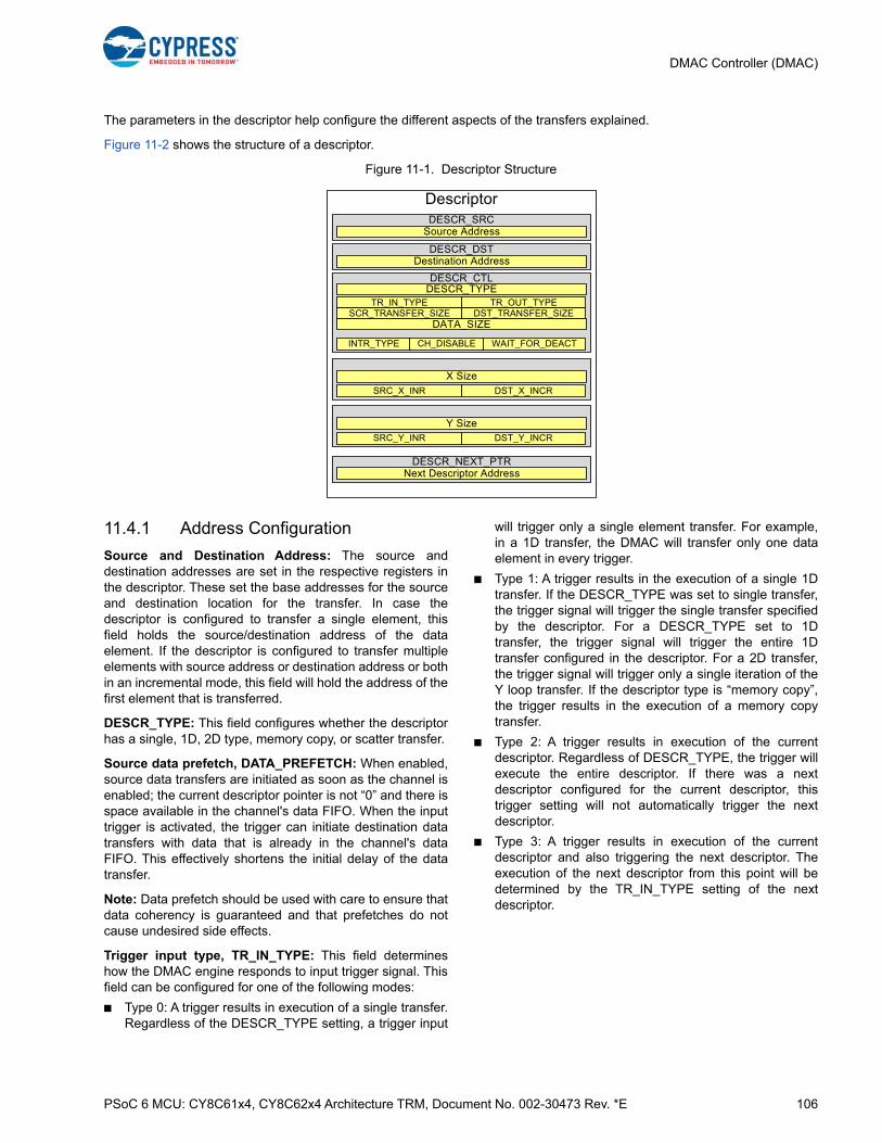
PSoC 6 MCU: CY8C61x4, CY8C62x4 Architecture TRM, Document No. 002-30473 Rev. *E 106
DMAC Controller (DMAC)
The parameters in the descriptor help configure the different aspects of the transfers explained.
Figure 11-2 shows the structure of a descriptor.
Figure 11-1. Descriptor Structure
11.4.1 Address Configuration
Source and Destination Address: The source anddestination addresses are set in the respective registers inthe descriptor. These set the base addresses for the sourceand destination location for the transfer. In case thedescriptor is configured to transfer a single element, thisfield holds the source/destination address of the dataelement. If the descriptor is configured to transfer multipleelements with source address or destination address or bothin an incremental mode, this field will hold the address of thefirst element that is transferred.
DESCR_TYPE: This field configures whether the descriptorhas a single, 1D, 2D type, memory copy, or scatter transfer.
Source data prefetch, DATA_PREFETCH: When enabled,source data transfers are initiated as soon as the channel isenabled; the current descriptor pointer is not “0” and there isspace available in the channel's data FIFO. When the inputtrigger is activated, the trigger can initiate destination datatransfers with data that is already in the channel's dataFIFO. This effectively shortens the initial delay of the datatransfer.
Note: Data prefetch should be used with care to ensure thatdata coherency is guaranteed and that prefetches do notcause undesired side effects.
Trigger input type, TR_IN_TYPE: This field determineshow the DMAC engine responds to input trigger signal. Thisfield can be configured for one of the following modes:
■ Type 0: A trigger results in execution of a single transfer.Regardless of the DESCR_TYPE setting, a trigger input
will trigger only a single element transfer. For example,in a 1D transfer, the DMAC will transfer only one dataelement in every trigger.
■ Type 1: A trigger results in the execution of a single 1Dtransfer. If the DESCR_TYPE was set to single transfer,the trigger signal will trigger the single transfer specifiedby the descriptor. For a DESCR_TYPE set to 1Dtransfer, the trigger signal will trigger the entire 1Dtransfer configured in the descriptor. For a 2D transfer,the trigger signal will trigger only a single iteration of theY loop transfer. If the descriptor type is “memory copy”,the trigger results in the execution of a memory copytransfer.
■ Type 2: A trigger results in execution of the currentdescriptor. Regardless of DESCR_TYPE, the trigger willexecute the entire descriptor. If there was a nextdescriptor configured for the current descriptor, thistrigger setting will not automatically trigger the nextdescriptor.
■ Type 3: A trigger results in execution of the currentdescriptor and also triggering the next descriptor. Theexecution of the next descriptor from this point will bedetermined by the TR_IN_TYPE setting of the nextdescriptor.
Descriptor
Source AddressDESCR_SRC
Destination AddressDESCR_DST
X SizeSRC_X_INR DST_X_INCR
Y SizeSRC_Y_INR DST_Y_INCR
Next Descriptor AddressDESCR_NEXT_PTR
DESCR_TYPEDESCR_CTL
TR_IN_TYPESCR_TRANSFER_SIZE
TR_OUT_TYPEDST_TRANSFER_SIZE
DATA_SIZE
WAIT_FOR_DEACTINTR_TYPE CH_DISABLE
PSoC 6 MCU: CY8C61x4, CY8C62x4 Architecture TRM, Document No. 002-30473 Rev. *E 107
DMAC Controller (DMAC)
Trigger out type, TR_OUT_TYPE: This field determineswhat completion event will generate the output triggersignal. This field can be configured to one of the followingmodes:
■ Type 0: Generates a trigger output for completion ofevery single element transfer.
■ Type 1: Generates a trigger output for completion of a1D transfer. If the descriptor type is “memory copy”, theoutput trigger is generated after the execution of amemory copy transfer. If the descriptor type is “scatter”,the output trigger is generated after the execution of ascatter transfer.
■ Type 2: Generates a trigger output for completion of thecurrent descriptor. This trigger output is generatedindependent of the state of the DESCR_NEXT_PTR.
■ Type 3: Generates a trigger output on completion of thecurrent descriptor, when the current descriptor is the lastdescriptor in the descriptor chain. This means a trigger isgenerated when the descriptor execution is completeand the DESCR_NEXT_PTR is ‘0’.
Interrupt Type, INTR_TYPE: This field determines whichcompletion event will generate the output interrupt signal.This field can be configured to one of the following modes:
■ Type 0: Generates an interrupt output for completion ofevery single element transfer.
■ Type 1: Generates an interrupt output for completion of a1-D transfer. If the descriptor type is “memory copy”, theinterrupt is generated after the execution of a memorycopy transfer. If the descriptor type is “scatter” theinterrupt is generated after the execution of a scattertransfer.
■ Type 2: Generates an interrupt output for completion ofthe current descriptor. This interrupt output is generatedindependent of the state of the DESCR_NEXT_PTR.
■ Type 3: Generates an interrupt output on completion ofthe current descriptor, when the current descriptor is thelast descriptor in the descriptor chain. This means aninterrupt is generated when the descriptor execution iscomplete and the DESCR_NEXT_PTR is ‘0’.
WAIT_FOR_DEACT: When the DMAC transfer based onthe TR_IN_TYPE is completed, the data transfer enginechecks the state of trigger deactivation. The data transfer onthe second trigger is initiated only after deactivation of thefirst. The WAIT_FOR_DEACT parameter will determinewhen the trigger signal is considered deactivated. The firstDMAC transfer is activated when the trigger is activated, butthe transfer is not considered complete until the trigger isdeactivated. This field is used to synchronize the controller’sdata transfers with the agent that generated the trigger. Thisfield has four settings:
■ 0 – Pulse Trigger: Do not wait for deactivation.
■ 1 – Level-sensitive waits four SYSCLK cycles: TheDMAC trigger is deactivated after the level trigger signalis detected for four cycles.
■ 2 – Level-sensitive waits 16 SYSCLK cycles: The DMACtransfer is initiated if the input trigger is seen to beactivated after 16 clock cycles.
■ 3 – Pulse trigger waits indefinitely for deactivation. TheDMAC transfer is initiated after the trigger signaldeactivates. The next transfer is initiated only if thetrigger goes low and then high again.
X Size: This field determines the number of single elementtransfers present in the X loop (inner loop). This field is validwhen the DESCR_TYPE is set to 1D or 2D transfer. For the“memory copy” descriptor type, (X_COUNT + 1) is thenumber of transferred Bytes. For the “scatter” descriptortype, ceiling (X_COUNT/2) is the number of (address, writedata) initialization pairs processed.
Source Address Increment (X loop) (SCR_X_INCR): Thisfield configures the index by which the source address is tobe incremented for every iteration in an X loop. The field isexpressed in multiples of SRC_TRANSFER_SIZE. This fieldis a signed number and hence may be decrementing orincrementing. If the source address does not need to beincremented, you can set this parameter to zero.
Destination Address Increment (X loop) (DST_X_INCR):This field configures the index by which the destinationaddress is to be incremented, for every iteration in an Xloop. The field is expressed in multiples ofDST_TRANSFER_SIZE. This field is a signed number andhence may be decrementing or incrementing. If thedestination address does not need to be incremented, youcan set this parameter to zero.
Y Size: This field determines the number of 1-D transferspresent in the Y loop (outer loop). This field is valid when theDESCR_TYPE is set to 2-D transfer.
Source Address Increment (Y loop) (SCR_Y_INCR): Thisfield configures the index by which the source address is tobe incremented, for every iteration in a Y loop. The field isexpressed in multiples of SRC_TRANSFER_SIZE. This fieldis a signed number and hence may be decrementing orincrementing. If the source address does not need to beincremented, you can set this parameter to zero.
Destination Address Increment (X loop) (DST_Y_INCR):This field configures the index by which the destinationaddress is to be incremented, for every iteration in a Y loop.The field is expressed in multiples ofDST_TRANSFER_SIZE. This field is a signed number andhence may be decrementing or incrementing. If thedestination address does not need to be incremented, youcan set this parameter to zero.
Channel Disable (CH_DISABLE): This field specifieswhether the channel is disabled or not after completion ofthe current descriptor (independent of the value of theDESCR_NEXT_PTR). A disabled channel will ignore itsinput triggers.
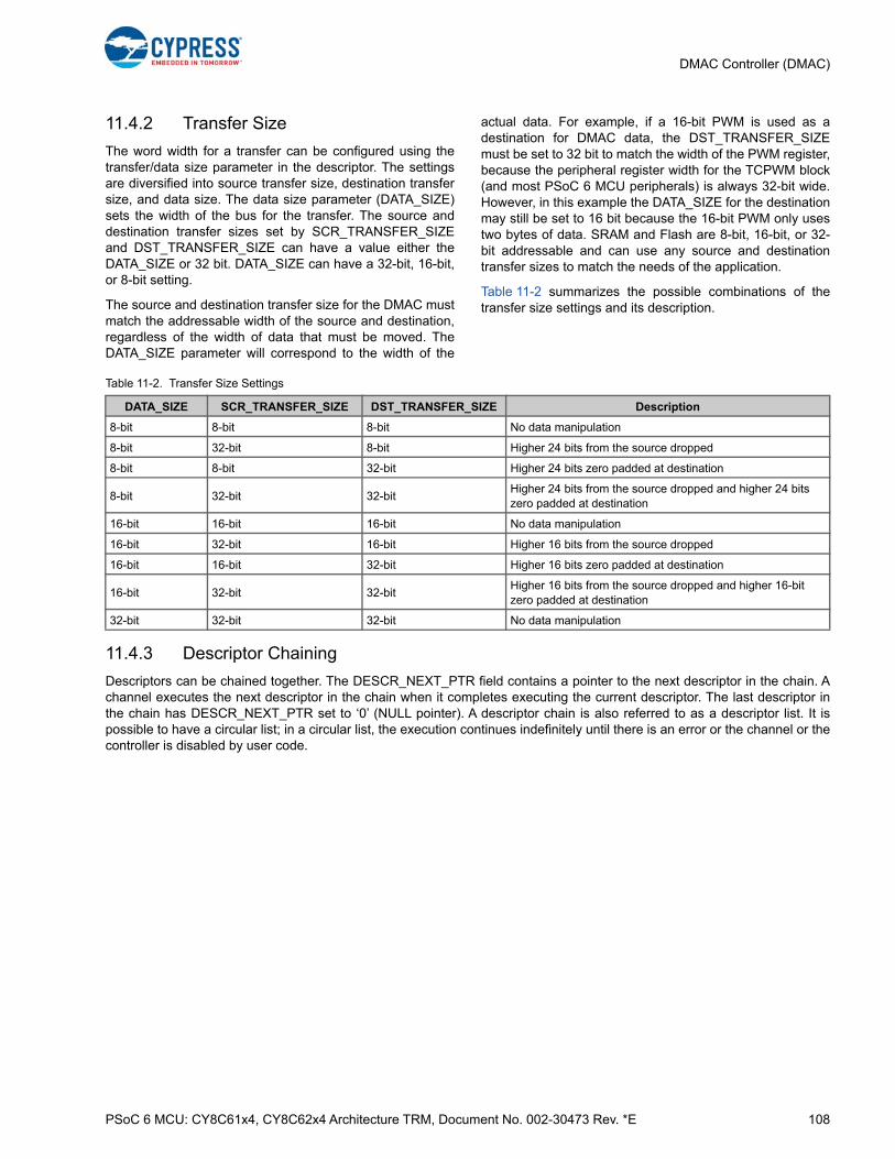
PSoC 6 MCU: CY8C61x4, CY8C62x4 Architecture TRM, Document No. 002-30473 Rev. *E 108
DMAC Controller (DMAC)
11.4.2 Transfer Size
The word width for a transfer can be configured using thetransfer/data size parameter in the descriptor. The settingsare diversified into source transfer size, destination transfersize, and data size. The data size parameter (DATA_SIZE)sets the width of the bus for the transfer. The source anddestination transfer sizes set by SCR_TRANSFER_SIZEand DST_TRANSFER_SIZE can have a value either theDATA_SIZE or 32 bit. DATA_SIZE can have a 32-bit, 16-bit,or 8-bit setting.
The source and destination transfer size for the DMAC mustmatch the addressable width of the source and destination,regardless of the width of data that must be moved. TheDATA_SIZE parameter will correspond to the width of the
actual data. For example, if a 16-bit PWM is used as adestination for DMAC data, the DST_TRANSFER_SIZEmust be set to 32 bit to match the width of the PWM register,because the peripheral register width for the TCPWM block(and most PSoC 6 MCU peripherals) is always 32-bit wide.However, in this example the DATA_SIZE for the destinationmay still be set to 16 bit because the 16-bit PWM only usestwo bytes of data. SRAM and Flash are 8-bit, 16-bit, or 32-bit addressable and can use any source and destinationtransfer sizes to match the needs of the application.
Table 11-2 summarizes the possible combinations of thetransfer size settings and its description.
11.4.3 Descriptor Chaining
Descriptors can be chained together. The DESCR_NEXT_PTR field contains a pointer to the next descriptor in the chain. Achannel executes the next descriptor in the chain when it completes executing the current descriptor. The last descriptor inthe chain has DESCR_NEXT_PTR set to ‘0’ (NULL pointer). A descriptor chain is also referred to as a descriptor list. It ispossible to have a circular list; in a circular list, the execution continues indefinitely until there is an error or the channel or thecontroller is disabled by user code.
Table 11-2. Transfer Size Settings
DATA_SIZE SCR_TRANSFER_SIZE DST_TRANSFER_SIZE Description
8-bit 8-bit 8-bit No data manipulation
8-bit 32-bit 8-bit Higher 24 bits from the source dropped
8-bit 8-bit 32-bit Higher 24 bits zero padded at destination
8-bit 32-bit 32-bitHigher 24 bits from the source dropped and higher 24 bits zero padded at destination
16-bit 16-bit 16-bit No data manipulation
16-bit 32-bit 16-bit Higher 16 bits from the source dropped
16-bit 16-bit 32-bit Higher 16 bits zero padded at destination
16-bit 32-bit 32-bitHigher 16 bits from the source dropped and higher 16-bit zero padded at destination
32-bit 32-bit 32-bit No data manipulation

PSoC 6 MCU: CY8C61x4, CY8C62x4 Architecture TRM, Document No. 002-30473 Rev. *E 109
DMAC Controller (DMAC)
11.5 DMAC Controller
Figure 11-2. DMAC Controller Overview
11.5.1 Trigger Selection
Trigger signals can be generated from different sections ofthe chips. A trigger multiplexer block helps route thesetrigger signals to the destination. The DMAC is one suchdestination of triggers. The trigger multiplexer block isoutside the DMAC block and is discussed in the TriggerMultiplexer Block chapter on page 290.
11.5.2 Channel Logic
The channel logic keeps track of pending triggers for eachchannel and initiates the transfer corresponding to the activedescriptor, based on availability of the bus and arbitration bypriority decoder.
The priority decoder determines the highest prioritypending channel.
Master I/F is an AHB-Lite bus master that allows the DMACcontroller to initiate AHB-Lite data transfers to the sourceand destination locations as well as to read the descriptorfrom memory.
Slave I/F is an AHB-Lite bus slave that allows the main CPUto access DMAC controller control/status registers.
11.5.3 Output Triggers
Each channel has an output trigger. This trigger is high fortwo slow clock cycles. The trigger is generated on thecompletion of a data transfer. At the system level, theseoutput triggers can be connected to the trigger multiplexercomponent. This connection allows a DMAC controlleroutput trigger to be connected to a DMAC controller inputtrigger. In other words, the completion of a transfer in onechannel can activate another channel or even reactivate thesame channel.
DMAC output triggers routing to other DMAC channels orother peripheral trigger inputs is achieved using the triggermultiplexer. Refer to the Trigger Multiplexer Block chapteron page 290.
DMA controller
Pending trigger
Channel0 logic
Priority decoder
Bus master interface
Data transfer engine
Bus slave interface
DMAC registers
Channel2 logic
Channel31 logic
� ...
MemoryMemory holds channel descriptor structure
Trigger multiplexers
tr_out[]System Triggers
tr_in[0]
tr_in[1]
tr_in[CH_NR-1]
Channel state

PSoC 6 MCU: CY8C61x4, CY8C62x4 Architecture TRM, Document No. 002-30473 Rev. *E 110
12. Cryptographic Function Block (Crypto)
The Cryptographic block (Crypto) provides hardware implementation and acceleration of cryptographic functions.Implementation in hardware takes less time and energy than the equivalent firmware implementation. In addition, the blockprovides True Random Number generation functionality in silicon, which is not available in firmware.
12.1 Features■ Advanced encryption standard (AES)
■ Data Encryption and Triple Data Encryption Standards (DES, TDES)
■ Secure Hash Algorithm (SHA)
■ Cyclic redundancy checking (CRC)
■ Pseudo random number generator (PRNG)
■ True random number generator (TRNG)
■ Vector unit (VU) to support asymmetric key cryptography, such as RSA and ECC.
This PSoC 6 MCU technical reference manual (TRM) provides comprehensive and detailed information about thefunctions of the PSoC 6 MCU device hardware. It is divided into two books: architecture TRM and registers TRM. TheTRM is not recommended for those new to the PSoC 6 MCU, nor as a guide for developing PSoC 6 MCU applications.Use these documents instead:
■ PSoC 61 datasheet, PSoC 62 datasheet
■ Peripheral Driver Library (PDL) documentation
■ Application notes
■ Code examples
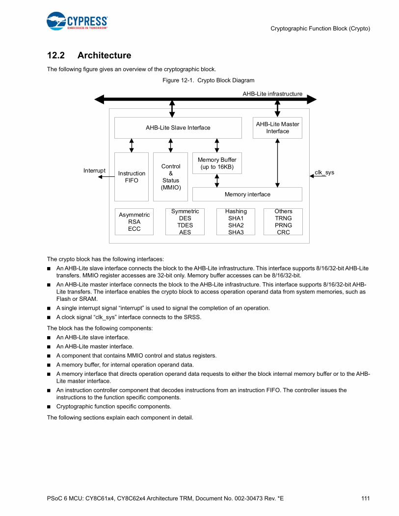
PSoC 6 MCU: CY8C61x4, CY8C62x4 Architecture TRM, Document No. 002-30473 Rev. *E 111
Cryptographic Function Block (Crypto)
12.2 Architecture
The following figure gives an overview of the cryptographic block.
Figure 12-1. Crypto Block Diagram
The crypto block has the following interfaces:
■ An AHB-Lite slave interface connects the block to the AHB-Lite infrastructure. This interface supports 8/16/32-bit AHB-Lite transfers. MMIO register accesses are 32-bit only. Memory buffer accesses can be 8/16/32-bit.
■ An AHB-Lite master interface connects the block to the AHB-Lite infrastructure. This interface supports 8/16/32-bit AHB-Lite transfers. The interface enables the crypto block to access operation operand data from system memories, such as Flash or SRAM.
■ A single interrupt signal “interrupt” is used to signal the completion of an operation.
■ A clock signal “clk_sys” interface connects to the SRSS.
The block has the following components:
■ An AHB-Lite slave interface.
■ An AHB-Lite master interface.
■ A component that contains MMIO control and status registers.
■ A memory buffer, for internal operation operand data.
■ A memory interface that directs operation operand data requests to either the block internal memory buffer or to the AHB-Lite master interface.
■ An instruction controller component that decodes instructions from an instruction FIFO. The controller issues the instructions to the function specific components.
■ Cryptographic function specific components.
The following sections explain each component in detail.
AHB-Lite Slave InterfaceAHB-Lite Master
Interface
InstructionFIFO
Memory Buffer(up to 16KB)
Memory interface
OthersTRNGPRNGCRC
AsymmetricRSAECC
SymmetricDES
TDESAES
HashingSHA1SHA2SHA3
Interrupt
AHB-Lite infrastructure
clk_sysControl
&Status(MMIO)
PSoC 6 MCU: CY8C61x4, CY8C62x4 Architecture TRM, Document No. 002-30473 Rev. *E 112
Cryptographic Function Block (Crypto)
12.3 Instruction Controller
The instruction controller consists of an instruction FIFO, an instruction decoder, and a general-purpose register file.
■ The instruction FIFO is software-programmable through MMIO registers that are accessed through the AHB-Lite slave interface. Software writes instructions and instruction operand data to the instruction FIFO. The FIFO consists of eight 32-bit FIFO entries.
■ The instruction decoder decodes the instructions (and the associated instruction operand data) from the instruction FIFO. The instruction decoder issues the decoded instruction to a specific functional component. The functional component is responsible for instruction execution.
■ The general-purpose register file consists of sixteen 32-bit registers. An instruction specifies the specific use of register-file registers. Registers are used to specify instruction operand data, such as memory locations (for example, for DES, AES, and SHA instructions) or immediate data operations (for example, for vector unit instructions).
12.3.1 Instructions
An instruction consists of a sequence of one, two, or three instruction words. Most instructions are encoded by a singleinstruction word.
The instruction FIFO can hold up to eight 32-bit instruction words. A CPU writes instruction words to the instruction FIFO(INSTR_FF_WR register) and the crypto block decodes the instruction words to execute the instructions.INSTR_FF_STATUS.USED specifies how many of the eight instruction FIFO entries are used. The instruction FIFOdecouples the progress of CPU execution from the crypto block execution: the CPU can write new instruction words to theFIFO, while the block executes previously written instructions.
There are multiple interrupt causes associated with the instruction FIFO and the instruction decoder:
■ The INTR.INSTR_FF_OVERFLOW interrupt cause is activated on a write to a full instruction FIFO.
■ THE INTR.INSTR_FF_LEVEL interrupt cause is activated when the number of used FIFO entries (INSTR_FF_STATUS.USED) is less than a specified number of FIFO entries (INSTR_FF_CTL.LEVEL).
■ The INTR.INSTR_OPC_ERROR interrupt cause is activated when an instruction's operation code is not defined.
■ The INTR.INSTR_CC_ERROR interrupt cause is activated when a vector unit instruction has an undefined condition code.
Most instructions perform specific cryptographic functionality. For example, the AES instruction performs and AdvancedEncryption Standard (AES) block cipher operation. Some instructions perform more generic functionality: most genericinstructions move operand data between different locations. Higher level symmetric cipher and hash functionality isimplemented using a combination of cryptographic instructions and generic instructions. Higher level asymmetric cipherfunctionality is implemented using a set of vector unit (VU) instructions.
In the CRYPTO_INSTR_FF_CTL register, the BLOCK bit must be set to ‘1’ and the CLEAR bit must be cleared to ‘0’ beforecalling any of the following system calls:
■ ComputeHash (CRC8 SAE type only, basic hash is calculated in SW instead)
■ GenerateHash
■ CheckFactoryHash
■ TransitionToSecure
■ TransitionToRMA
■ OpenRMA
PSoC 6 MCU: CY8C61x4, CY8C62x4 Architecture TRM, Document No. 002-30473 Rev. *E 113
Cryptographic Function Block (Crypto)
12.3.2 Instruction Operands
The instruction operands are found in one of the following locations:
■ System memory
■ Memory buffer
■ Instruction FIFO instruction words
■ Load and store FIFOs
■ Register buffer
■ Vector unit register-file
System memory. The system memory includes all memory-mapped memories attached to the bus infrastructure that areaccessible by the crypto block through the master bus interface.
Memory buffer. The crypto block memory buffer is an internal SRAM with a capacity of up to 16 KB. This internal SRAMprovides better latency and bandwidth characteristics than the system memory. Therefore, frequently accessed vector unitinstruction operand data is typically located in the memory buffer.
Both the block’s external system memory and internal memory buffer are accessed through the same memory interfacecomponent. The access address specifies if the access is to the system memory or the internal memory buffer (also seeVU_CTL.ADDR[31:14]).
External bus masters can access both the system memory and the crypto’s internal memory. The external bus mastersaccess the internal memory through the slave bus interface.
Instruction FIFO. For some instructions, immediate operand data is provided by the instruction words. The limited 32-bitinstruction words only allow for limited immediate operand data.
Load and store FIFOs. Most instructions have stream-like operand data: sequences of bytes that are specified by the accessaddress of the start byte. The two load FIFOs provide access to source operand data and the single store FIFO providesaccess to destination operand data. Typically, vector unit instruction operand data is “streamed” from the crypto block memorybuffer.
Register buffer. Most symmetric and hash cryptographic instructions benefit from a large (2048-bit) register buffer. Thisregister buffer provides access flexibility that is not provided by the load and store FIFOs. The register buffer is shared bydifferent instructions to amortize its cost (silicon area). After an Active reset or a crypto block reset (CTL.ENABLED), theregister buffer is set to ‘0’.
Vector unit register file. Most vector unit instructions perform large integer arithmetic functionality. For example, the VUADD instruction can add two 4096-bit numbers. Typically, operand data is “streamed” from the memory buffer. In addition, avector unit register file with sixteen registers is provided. Each register specifies the location of a number (start word accessaddress) and the size of the number (the size is in bits).
12.3.3 Load and Store FIFO Instructions
The load and store FIFOs provide access to operand data in a “streaming” nature. Operand data is streamed through thememory interface from or to either the internal memory buffer or the system memory.
Two independent load FIFOs provide access to streamed source operand data. Each FIFO has a multi-byte buffer to prefetchoperand data.
One store FIFO provides access to streamed destination operand data. The FIFO has a multi-byte buffer to temporarily holdthe data before it is written to the memory interface.
Streamed operand data is specified by a memory start address and an operand size in bytes.
Three FIFO instructions are supported: FF_START, FF_STOP, and FF_CONTINUE. The FF_START and FF_STOPinstructions are supported for both the load and store FIFOs. The FF_CONTINUE instruction is only supported for the loadFIFOs. The FF_START and FF_CONTINUE instructions consist of three instruction words. The FF_STOP instruction consistsof a single instruction word.
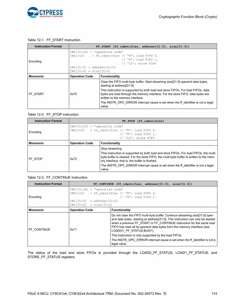
PSoC 6 MCU: CY8C61x4, CY8C62x4 Architecture TRM, Document No. 002-30473 Rev. *E 114
Cryptographic Function Block (Crypto)
The status of the load and store FIFOs is provided through the LOAD0_FF_STATUS, LOAD1_FF_STATUS, andSTORE_FF_STATUS registers.
Table 12-1. FF_START Instruction
Instruction Format FF_START (ff_identifier, address[31:0], size[31:0])
Encoding
IW0[31:24] = “operation code”IW0[3:0] = ff_identifier // “8”: load FIFO 0, // “9”: load FIFO 1, // “12”: store FIFOIW1[31:0] = address[31:0]IW2[31:0] = size[31:0]
Mnemonic Operation Code Functionality
FF_START 0x70
Clear the FIFO multi-byte buffer. Start streaming size[31:0] operand data bytes, starting at address[31:0].
This instruction is supported by both load and store FIFOs. For load FIFOs, data bytes are read through the memory interface. For the store FIFO, data bytes are written to the memory interface.
The INSTR_OPC_ERROR interrupt cause is set when the ff_identifier is not a legal value.
Table 12-2. FF_STOP instruction
Instruction Format FF_STOP (ff_identifier)
Encoding
IW0[31:24] = “operation code”IW0[3:0] = ff_identifier // “8”: load FIFO 0, // “9”: load FIFO 1, // “12”: store FIFO
Mnemonic Operation Code Functionality
FF_STOP 0x72
Stop streaming
This instruction is supported by both load and store FIFOs. For load FIFOs, the multi-byte buffer is cleared. For the store FIFO, the multi-byte buffer is written to the mem-ory interface; that is, the buffer is flushed.
The INSTR_OPC_ERROR interrupt cause is set when the ff_identifier is not a legal value.
Table 12-3. FF_CONTINUE Instruction
Instruction Format FF_CONTINUE (ff_identifier, address[31:0], size[31:0])
Encoding
IW0[31:24] = “operation code”IW0[3:0] = ff_identifier // “8”: load FIFO 0, // “9”: load FIFO 1, IW1[31:0] = address[31:0]IW2[31:0] = size[31:0]
Mnemonic Operation Code Functionality
FF_CONTINUE 0x71
Do not clear the FIFO multi-byte buffer. Continue streaming size[31:0] oper-and data bytes, starting at address[31:0]. This instruction can only be started when a previous FF_START or FF_CONTINUE instruction for the same load FIFO has read all its operand data bytes from the memory interface (see LOAD01/_FF_STATUS.BUSY).
This instruction is only supported by the load FIFOs.
The INSTR_OPC_ERROR interrupt cause is set when the ff_identifier is not a legal value.
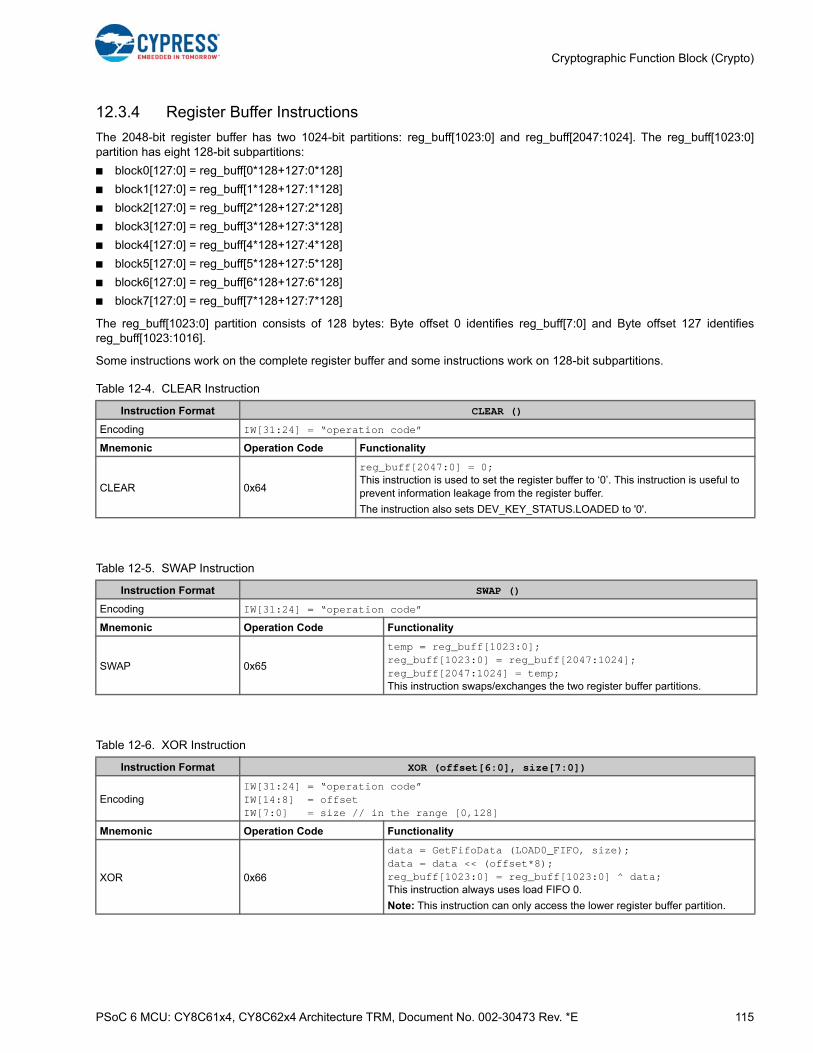
PSoC 6 MCU: CY8C61x4, CY8C62x4 Architecture TRM, Document No. 002-30473 Rev. *E 115
Cryptographic Function Block (Crypto)
12.3.4 Register Buffer Instructions
The 2048-bit register buffer has two 1024-bit partitions: reg_buff[1023:0] and reg_buff[2047:1024]. The reg_buff[1023:0]partition has eight 128-bit subpartitions:
■ block0[127:0] = reg_buff[0*128+127:0*128]
■ block1[127:0] = reg_buff[1*128+127:1*128]
■ block2[127:0] = reg_buff[2*128+127:2*128]
■ block3[127:0] = reg_buff[3*128+127:3*128]
■ block4[127:0] = reg_buff[4*128+127:4*128]
■ block5[127:0] = reg_buff[5*128+127:5*128]
■ block6[127:0] = reg_buff[6*128+127:6*128]
■ block7[127:0] = reg_buff[7*128+127:7*128]
The reg_buff[1023:0] partition consists of 128 bytes: Byte offset 0 identifies reg_buff[7:0] and Byte offset 127 identifiesreg_buff[1023:1016].
Some instructions work on the complete register buffer and some instructions work on 128-bit subpartitions.
Table 12-4. CLEAR Instruction
Instruction Format CLEAR ()
Encoding IW[31:24] = “operation code”
Mnemonic Operation Code Functionality
CLEAR 0x64
reg_buff[2047:0] = 0;This instruction is used to set the register buffer to ‘0’. This instruction is useful to prevent information leakage from the register buffer.
The instruction also sets DEV_KEY_STATUS.LOADED to '0'.
Table 12-5. SWAP Instruction
Instruction Format SWAP ()
Encoding IW[31:24] = “operation code”
Mnemonic Operation Code Functionality
SWAP 0x65
temp = reg_buff[1023:0];reg_buff[1023:0] = reg_buff[2047:1024];reg_buff[2047:1024] = temp;This instruction swaps/exchanges the two register buffer partitions.
Table 12-6. XOR Instruction
Instruction Format XOR (offset[6:0], size[7:0])
EncodingIW[31:24] = “operation code”IW[14:8] = offsetIW[7:0] = size // in the range [0,128]
Mnemonic Operation Code Functionality
XOR 0x66
data = GetFifoData (LOAD0_FIFO, size);data = data << (offset*8);reg_buff[1023:0] = reg_buff[1023:0] ^ data;This instruction always uses load FIFO 0.
Note: This instruction can only access the lower register buffer partition.

PSoC 6 MCU: CY8C61x4, CY8C62x4 Architecture TRM, Document No. 002-30473 Rev. *E 116
Cryptographic Function Block (Crypto)
Some instructions work on (up to) 128-bit subpartitions or blocks. In addition, these instructions can work on the load andstore FIFOs. The instructions' source and destination operand identifiers are encoded as follows:
■ 0: block0[127:0] = reg_buff[0*128+127:0*128]
■ 1: block1[127:0] = reg_buff[1*128+127:1*128]
■ 2: block2[127:0] = reg_buff[2*128+127:2*128]
■ 3: block3[127:0] = reg_buff[3*128+127:3*128]
■ 4: block4[127:0] = reg_buff[4*128+127:4*128]
■ 5: block5[127:0] = reg_buff[5*128+127:5*128]
■ 6: block6[127:0] = reg_buff[6*128+127:6*128]
■ 7: block7[127:0] = reg_buff[7*128+127:7*128]
■ 8: load FIFO 0
■ 9: load FIFO 1
■ 12: store FIFO
Table 12-7. STORE Instruction
Instruction Format STORE (offset[6:0], size[7:0])
EncodingIW[31:24] = “operation code”IW[14:8] = offsetIW[7:0] = size // in the range [0,128]
Mnemonic Operation Code Functionality
STORE 0x67data = reg_buff[1023:0]data = data >> (offset*8);SetFifoData (STORE_FIFO, size, data)
Table 12-8. BYTE_SET Instruction
Instruction Format BYTE_SET (offset[6:0], byte[7:0])
EncodingIW[31:24] = “operation code”IW[14:8] = offsetIW[7:0] = byte
Mnemonic Operation Code Functionality
BYTE_SET 0x68 reg_buff[offset*8 + 7: offset*8] = byte;

PSoC 6 MCU: CY8C61x4, CY8C62x4 Architecture TRM, Document No. 002-30473 Rev. *E 117
Cryptographic Function Block (Crypto)
Table 12-9. BLOCK_MOV Instruction
Instruction Format BLOCK_MOV (reflect[1], size[3:0], dst[3:0], src0[3:0])
Encoding
IW[31:24] = “operation code”IW[23] = reflectIW[19:16] = sizeIW[15:12] = dstIW[3:0] = src0
Mnemonic Operation Code Functionality
BLOCK_MOV 0x40
size = (size == 0) ? 16 : size;data1 = data0 = GetBlock (src0, size);if (reflect) { // assume size of 16 B / 128 bit temp = data0; for (i = 0; i < 16; i += 1) { for (j = 0; j < 8; j += 1) { // reflection of bits in a byte data1[8*i + j] = data0[8*i + 7-j]; } }}SetBlock (dst, size, data1);
Table 12-10. BLOCK_XOR Instruction
Instruction Format BLOCK_XOR (size[3:0], dst[3:0], src1[3:0], src0[3:0])
Encoding
IW[31:24] = “operation code”IW[19:16] = sizeIW[15:12] = dstIW[7:4] = src1IW[3:0] = src0
Mnemonic Operation Code Functionality
BLOCK_XOR 0x41
size = (size == 0) ? 16 : size;data0 = GetBlock (src0, size);data1 = GetBlock (src1, size);SetBlock (dst, size, data0 ^ data1);
Table 12-11. BLOCK_SET Instruction
Instruction Format BLOCK_SET (size[3:0], dst[3:0], byte[7:0])
Encoding
IW[31:24] = “operation code”IW[19:16] = sizeIW[15:12] = dstIW[7:0] = byte
Mnemonic Operation Code Functionality
BLOCK_SET 0x42size = (size == 0) ? 16 : size;SetBlock (dst, size, {16{byte[7:0]}})
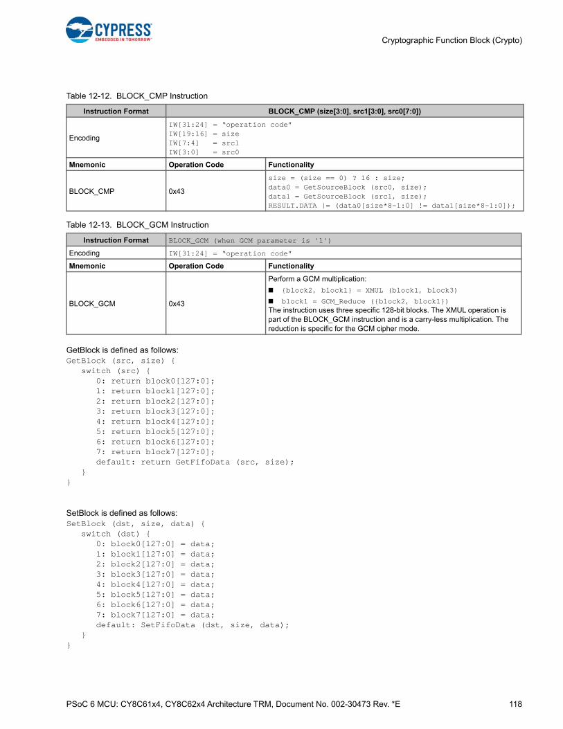
PSoC 6 MCU: CY8C61x4, CY8C62x4 Architecture TRM, Document No. 002-30473 Rev. *E 118
Cryptographic Function Block (Crypto)
GetBlock is defined as follows:GetBlock (src, size) { switch (src) { 0: return block0[127:0]; 1: return block1[127:0]; 2: return block2[127:0]; 3: return block3[127:0]; 4: return block4[127:0]; 5: return block5[127:0]; 6: return block6[127:0]; 7: return block7[127:0]; default: return GetFifoData (src, size); }}
SetBlock is defined as follows:SetBlock (dst, size, data) { switch (dst) { 0: block0[127:0] = data; 1: block1[127:0] = data; 2: block2[127:0] = data; 3: block3[127:0] = data; 4: block4[127:0] = data; 5: block5[127:0] = data; 6: block6[127:0] = data; 7: block7[127:0] = data; default: SetFifoData (dst, size, data); }}
Table 12-12. BLOCK_CMP Instruction
Instruction Format BLOCK_CMP (size[3:0], src1[3:0], src0[7:0])
Encoding
IW[31:24] = “operation code”IW[19:16] = sizeIW[7:4] = src1IW[3:0] = src0
Mnemonic Operation Code Functionality
BLOCK_CMP 0x43
size = (size == 0) ? 16 : size;data0 = GetSourceBlock (src0, size);data1 = GetSourceBlock (src1, size);RESULT.DATA |= (data0[size*8-1:0] != data1[size*8-1:0]);
Table 12-13. BLOCK_GCM Instruction
Instruction Format BLOCK_GCM (when GCM parameter is '1')
Encoding IW[31:24] = “operation code”
Mnemonic Operation Code Functionality
BLOCK_GCM 0x43
Perform a GCM multiplication:
■ {block2, block1} = XMUL (block1, block3)
■ block1 = GCM_Reduce ({block2, block1})The instruction uses three specific 128-bit blocks. The XMUL operation is part of the BLOCK_GCM instruction and is a carry-less multiplication. The reduction is specific for the GCM cipher mode.

PSoC 6 MCU: CY8C61x4, CY8C62x4 Architecture TRM, Document No. 002-30473 Rev. *E 119
Cryptographic Function Block (Crypto)
The GetFifoData function is defined as loading “size” bytes from a load FIFO. Up to 16 bytes can be loaded as data[127:0].The first (top) loaded FIFO entry is mapped on data[7:0], the second loaded FIFO entry is mapped on data[15:8], and so on.The SetFifoData function is defined as storing size bytes from a load FIFO. Up to 16 bytes can be stored as data[127:0]. Thefirst stored FIFO entry is mapped on data[7:0], the second stored FIFO entry is mapped on data[15:8], and so on.
12.4 Hash Algorithms
12.4.1 SHA1 and SHA2
The SHA1 and SHA2 functionality includes three hash instructions per the SHA standard (FIPS 180-4).
■ The SHA1 instruction provides all SHA1 functionality (SHA1 always uses 512-bit blocks).
■ The SHA2_256 instruction provides SHA2 functionality for 512-bit blocks.
■ The SHA2_512 instruction provides SHA2 functionality for 1024-bit blocks.
The instructions support different block sizes and hash sizes:
The SHA1 instruction supports a single algorithm with a specific message digest size. The SHA2_256 and SHA2_512instructions support multiple algorithms with different message digest sizes.
A SHA algorithm calculates a fixed-length hash value from a variable length message. The hash value is used to produce amessage digest or signature. It is computationally impossible to change the message without changing the hash value. Thealgorithm is stateless: a given message always produces the same hash value. To prevent “replay attacks”, a counter may beincluded in the message.
The variable length message must be preprocessed: a ‘1’ bit must be appended to the message followed by ‘0’s and a bit sizefield. The preprocessed message consists of an integer multiple of 512 bit or 1024 bit blocks. The SHA component processesa single block at a time:
■ The first SHA instruction on the first message block uses an initial hash value as defined by the standard (each SHA algorithm has a specific initial hash value).
■ Subsequent SHA instructions on successive message blocks use the produced hash value of the previous SHA operation.
The SHA instruction of the last message block produces the final hash value. The message digest is a subset of this finalhash value.
The SHA instructions do not perform the following functionality:
■ Preprocessing of a message.
■ Initialization of the register buffer with the algorithm’s specific initial hash value.
■ Copy the algorithm’s message digest to memory.
Instruction Block Size Hash Size
SHA1 512 bits 160 bits
SHA2_256 512 bits 256 bits
SHA2_512 1024 bits 512 bits
Instruction Algorithm Hash Size Message Digest Size
SHA1 SHA-1 160 bits 160 bits
SHA2_256SHA-224 256 bits 224 bits
SHA-256 256 bits 256 bits
SHA2_512
SHA-384 512 bits 384 bits
SHA-512 512 bits 512 bits
SHA-512/224 512 bits 224 bits
SHA-512/256 512 bits 256 bits

PSoC 6 MCU: CY8C61x4, CY8C62x4 Architecture TRM, Document No. 002-30473 Rev. *E 120
Cryptographic Function Block (Crypto)
Software is required to preprocess the message. The FIFO_START instruction can be used to load (load FIFO) the registerbuffer with the initial hash value and to store (store FIFO) the message digest.
A SHA instruction uses “round weights” that are derived from the message block. Each SHA round uses a dedicated roundweight. The “round weights” are derived on-the-fly (a new round weight is calculated when needed, and replaces a roundweight from a previous round). The following table provides the number of rounds.
The instructions use register buffer operands. Specifically, the instructions use reg_buff[2047:0]:
■ reg_buff[1023:0] is used for the round weights. Before an instruction, this region is written with the message block. The SHA1 and SHA2_256 instructions use reg_buff[511:0] and the SHA2_512 instruction uses reg_buff[1023:0].
■ reg_buff[1535:1024] is used for the hash value. Before the first SHA instruction, this region is written with the algorithm’s initial hash value. The algorithms with hash values smaller than 512 bits only use the lower bits of this region.
■ reg_buff[2047:1536] is used as a working copy of the hash value. This working copy is updated during the SHA rounds and copied to reg_buff[1535:1024] at the end of the instruction.
The instructions are described in the following tables.
Instruction Rounds
SHA1 80
SHA2_256 64
SHA2_512 80
Table 12-14. SHA1 Instruction
Instruction Format SHA1 ()
Encoding IW[31:24] = “operation code”
Mnemonic Operation Code Functionality
SHA1 0x69
Perform a SHA1 function on a 512-bit message block in reg_buff[511:0] with the current 160-bit hash value in reg_buff[1183:1024]. The resulting hash value is provided in reg_buff[1183:1024]. At the end of the instruction, reg_buff[1023:0] is set to ‘0’.
Table 12-15. SHA2_256 Instruction
Instruction Format SHA2_256 ()
Encoding IW[31:24] = “operation code”
Mnemonic Operation Code Functionality
SHA2_256 0x6a
Perform a SHA2 function on a 512-bit message block in reg_buff[511:0] with the current 256-bit hash value in reg_buff[1279:1024]. The resulting hash value is provided in reg_buff[1279:1024]. At the end of the instruction, reg_buff[1023:0] is set to ‘0’.
Table 12-16. SHA2_512 Instruction
Instruction Format SHA2_512 ()
Encoding IW[31:24] = “operation code”
Mnemonic Operation Code Functionality
SHA2_512 0x6b
Perform a SHA2 function on a 1024-bit message block in reg_buff[1023:0] with the current 512-bit hash value in reg_buff[1535:1024]. The resulting hash value is provided in reg_buff[1535:1024]. At the end of the instruction, reg_buff[1023:0] is set to ‘0’.

PSoC 6 MCU: CY8C61x4, CY8C62x4 Architecture TRM, Document No. 002-30473 Rev. *E 121
Cryptographic Function Block (Crypto)
12.4.2 SHA3
The Secure Hash Algorithm-3 (SHA-3) is a family of six algorithms:
■ SHA3-224
■ SHA3-256
■ SHA3-384
■ SHA3-512
■ SHAKE128
■ SHAKE256
Each of these algorithms relies on a specific instance of the Keccak-p[b, nr] permutation, with b = 1600 and nr = 24. Theparameter b specifies the permutation bit width (1600 bits) and the parameter nr specifies the number of permutation rounds(24 rounds).
The permutation bit width b is the sum of:
■ The rate r, which is the number of consumed message bits or produced digest bits per application of the Keccak permutation (SHA3 instruction).
■ The capacity c, which is defined as b-r.
All six hash algorithms are constructed by padding a message M and applying the Keccak-p[1600, 24] permutationrepeatedly. The algorithms differ in terms of the rate r and the padding.
The permutation’s rate r determines the speed of the algorithm: a higher rate requires less applications of the permutationfunction (SHA3 instruction).
The permutation’s capacity c determines the security of the algorithm: a higher capacity provides higher security.
Table 12-17 lists the algorithms’ rate and capacity. In addition, it lists the size of the message digest. Note: The SHA3 hashalgorithms have fixed-length digests and the SHAKE extendable output functions have variable-length digests.
The padded message has a length that is an integer multiple of the rate r. The message is processed by repeatedly applyingthe SHA3 permutation instruction. Each instruction application uses a message block of r bits. The permutation functioncombines the message block of r bits with the current permutation state of b bits and calculates a new permutation state of bbits.
■ The first SHA3 instruction on the first message block uses the first message block as the initial permutation state.
■ Subsequent SHA3 instructions on successive message blocks first combine the message block with an exclusive or (XOR) with the current state and calculate a new permutation state.
The message digest is produced in a similar way as the message is consumed: each application of the permutationinstruction produces a message digest of r bits.
The SHA3 functionality includes a SHA3 instruction. The instruction performs a permutation on the 1600-bit state inreg_buf[1599:0].
The instruction implements the permutation, all other functionality is implemented in sofftware (combination of message blockwith the permutation state and copying the message digest to memory).
Table 12-17. Algorithm Rate and Capacity
Algorithm Rate, Capacity Digest Length
SHA3-224 r = 1152 b, c = 448 b 224 b (28 B)
SHA3-256 r = 1088 b, c = 512 b 256 b (32 B)
SHA3-384 r = 832 b, c = 768 b 384 b (48 B)
SHA3-512 r = 576 b, c = 1024 b 512 b (64 B)
SHAKE128 r = 1344 b, c = 256 b Variable length
SHAKE256 r = 1088 b, c = 512 b Variable length
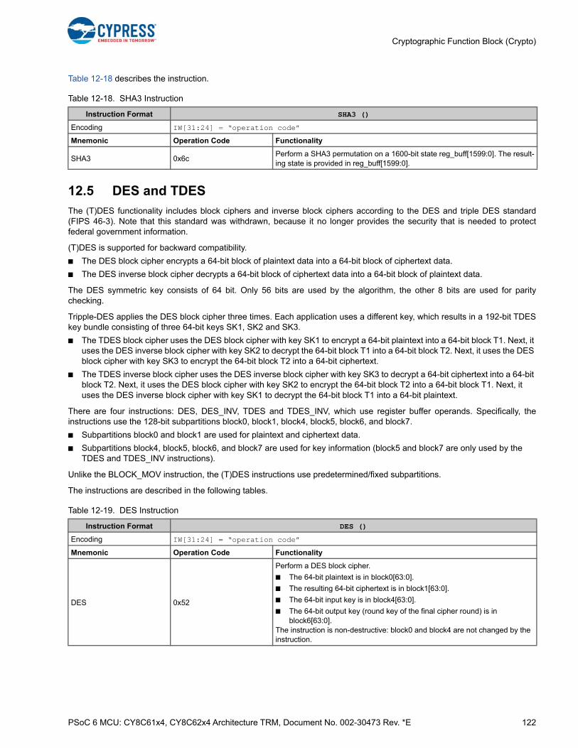
PSoC 6 MCU: CY8C61x4, CY8C62x4 Architecture TRM, Document No. 002-30473 Rev. *E 122
Cryptographic Function Block (Crypto)
Table 12-18 describes the instruction.
12.5 DES and TDES
The (T)DES functionality includes block ciphers and inverse block ciphers according to the DES and triple DES standard(FIPS 46-3). Note that this standard was withdrawn, because it no longer provides the security that is needed to protectfederal government information.
(T)DES is supported for backward compatibility.
■ The DES block cipher encrypts a 64-bit block of plaintext data into a 64-bit block of ciphertext data.
■ The DES inverse block cipher decrypts a 64-bit block of ciphertext data into a 64-bit block of plaintext data.
The DES symmetric key consists of 64 bit. Only 56 bits are used by the algorithm, the other 8 bits are used for paritychecking.
Tripple-DES applies the DES block cipher three times. Each application uses a different key, which results in a 192-bit TDESkey bundle consisting of three 64-bit keys SK1, SK2 and SK3.
■ The TDES block cipher uses the DES block cipher with key SK1 to encrypt a 64-bit plaintext into a 64-bit block T1. Next, it uses the DES inverse block cipher with key SK2 to decrypt the 64-bit block T1 into a 64-bit block T2. Next, it uses the DES block cipher with key SK3 to encrypt the 64-bit block T2 into a 64-bit ciphertext.
■ The TDES inverse block cipher uses the DES inverse block cipher with key SK3 to decrypt a 64-bit ciphertext into a 64-bit block T2. Next, it uses the DES block cipher with key SK2 to encrypt the 64-bit block T2 into a 64-bit block T1. Next, it uses the DES inverse block cipher with key SK1 to decrypt the 64-bit block T1 into a 64-bit plaintext.
There are four instructions: DES, DES_INV, TDES and TDES_INV, which use register buffer operands. Specifically, theinstructions use the 128-bit subpartitions block0, block1, block4, block5, block6, and block7.
■ Subpartitions block0 and block1 are used for plaintext and ciphertext data.
■ Subpartitions block4, block5, block6, and block7 are used for key information (block5 and block7 are only used by the TDES and TDES_INV instructions).
Unlike the BLOCK_MOV instruction, the (T)DES instructions use predetermined/fixed subpartitions.
The instructions are described in the following tables.
Table 12-18. SHA3 Instruction
Instruction Format SHA3 ()
Encoding IW[31:24] = “operation code”
Mnemonic Operation Code Functionality
SHA3 0x6cPerform a SHA3 permutation on a 1600-bit state reg_buff[1599:0]. The result-ing state is provided in reg_buff[1599:0].
Table 12-19. DES Instruction
Instruction Format DES ()
Encoding IW[31:24] = “operation code”
Mnemonic Operation Code Functionality
DES 0x52
Perform a DES block cipher.
■ The 64-bit plaintext is in block0[63:0].
■ The resulting 64-bit ciphertext is in block1[63:0].
■ The 64-bit input key is in block4[63:0].
■ The 64-bit output key (round key of the final cipher round) is in block6[63:0].
The instruction is non-destructive: block0 and block4 are not changed by the instruction.

PSoC 6 MCU: CY8C61x4, CY8C62x4 Architecture TRM, Document No. 002-30473 Rev. *E 123
Cryptographic Function Block (Crypto)
The (T)DES instructions are used with the FF_START, FF_CONTINUE, FF_STOP, BLOCK_MOV, BLOCK_XOR, andBLOCK_SET instructions to implement different block cipher modes, such as EBC, CBC, OFB, CTR, and CMAC.
Table 12-20. DES_INV Instruction
Instruction Format DES_INV ()
Encoding IW[31:24] = “operation code”
Mnemonic Operation Code Functionality
DES_INV 0x53
Perform a DES inverse block cipher.
■ The 64-bit ciphertext is in block0[63:0].
■ The resulting 64-bit plaintext is in block1[63:0].
■ The 64-bit input key is in block4[63:0].
■ The 64-bit output key (round key of the final inverse cipher round) is in block6[63:0].
The instruction is non-destructive: block0 and block4 are not changed by the instruction.
Table 12-21. TDES Instruction
Instruction Format TDES ()
Encoding IW[31:24] = “operation code”
Mnemonic Operation Code Functionality
TDES 0x54
Perform a TDES block cipher.
■ The 64-bit plaintext is in block0[63:0].
■ The resulting 64-bit ciphertext is in block1[63:0].
■ The 192-bit input key is in {block5[63:0], block4[127:0]} (= {SK3[63:0], SK2[63:0], SK1[63:0]}).
■ The 192-bit output key (round key of the final cipher round) is in {block7[63:0], block6[127:0]}.
The instruction is non-destructive: block0, block4 and block5 are not changed by the instruction.
Table 12-22. TDES_INV Instruction
Instruction Format TDES_INV ()
Encoding IW[31:24] = “operation code”
Mnemonic Operation Code Functionality
TDES_INV 0x55
Perform a TDES inverse block cipher.
■ The 64-bit ciphertext is in block0[63:0].
■ The resulting 64-bit plaintext is in block1[63:0].
■ The 192-bit input key is in {block5[63:0], block4[127:0]} (= {SK3[63:0], SK2[63:0], SK1[63:0]}).
■ The 192-bit output key (round key of the final cipher round) is in {block7[63:0], block6[127:0]}.
The instruction is non-destructive: block0, block4 and block5 are not changed by the instruction.

PSoC 6 MCU: CY8C61x4, CY8C62x4 Architecture TRM, Document No. 002-30473 Rev. *E 124
Cryptographic Function Block (Crypto)
12.6 AES
The AES functionality includes a block cipher and an inverse block cipher per the AES standard (FIPS 197):
■ The block cipher (AES instruction) encrypts a 128-bit block of plaintext data into a 128-bit block of ciphertext data.
■ The inverse block cipher (AES_INV instruction) decrypts a 128-bit block of ciphertext data into a 128-bit block of plaintext data.
AES is a symmetric block cipher: it uses the same symmetric key for the block cipher and inverse block cipher. The (inverse)block cipher consists of multiple rounds. Each round uses a round key that is generated from the symmetric key.
The block cipher uses the symmetric key as the (start) round key for the first cipher round. The round key for second cipherround is generated from the symmetric key. The round key for the third cipher round is generated from the round key of thesecond cipher round, and so forth. The round key for the last cipher round is generated from the round key of the one-before-last cipher round.
The inverse block cipher uses the round key of the final block cipher round as the (start) round key for the first inverse cipherround. The round key for the second inverse cipher round is generated from the round key of the first inverse cipher round,and so forth. The round key for the last inverse cipher round is generated from the round key of the one-before-last inversecipher round. The round key of the last inverse cipher round is the same as the round key of the first cipher round (thesymmetric key).
Round key generation is independent of the plaintext data or ciphertext data. The AES instruction requires the symmetric keyas input to the block cipher. The AES_INV instruction requires the round key of the final cipher round as input to the inverseblock cipher.
The component supports 128 bit, 192 bit, and 256 bit keys. The key size is specified by AES_CTL.KEY_SIZE[1:0]. The keysize determines the number of rounds. Table 12-23 gives the number of rounds.
AES and AES_INV are the two different AES instructions; they use register buffer operands. Specifically, the instructions usethe 128-bit subpartitions block0, block1, block4, block5, block6, and block7.
■ Subpartitions block0 and block1 are used for plaintext and ciphertext data.
■ Subpartitions block4, block5, block6 and block7 are used for key information.
Unlike, for example, the BLOCK_MOV instruction, the AES and AES_INV instructions use predetermined/fixed subpartitions.
Table 12-23. AES Cipher Rounds
AES Key Size Rounds
AES128 10 rounds
AES192 12 rounds
AES256 14 rounds
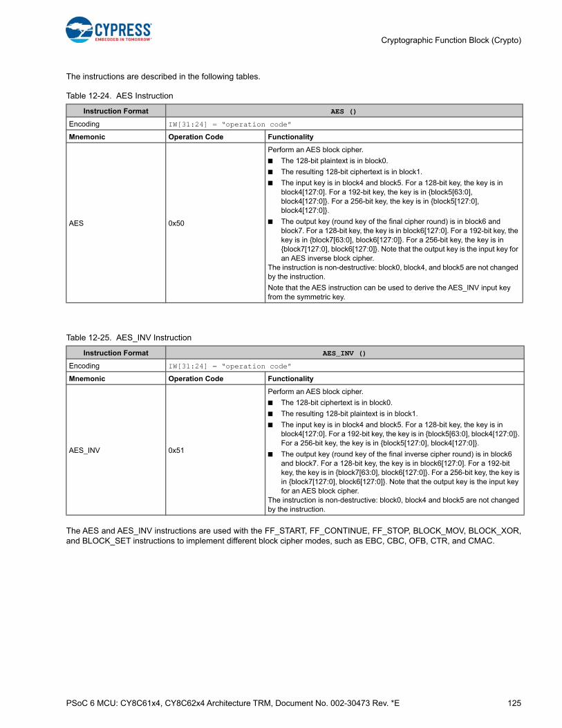
PSoC 6 MCU: CY8C61x4, CY8C62x4 Architecture TRM, Document No. 002-30473 Rev. *E 125
Cryptographic Function Block (Crypto)
The instructions are described in the following tables.
The AES and AES_INV instructions are used with the FF_START, FF_CONTINUE, FF_STOP, BLOCK_MOV, BLOCK_XOR,and BLOCK_SET instructions to implement different block cipher modes, such as EBC, CBC, OFB, CTR, and CMAC.
Table 12-24. AES Instruction
Instruction Format AES ()
Encoding IW[31:24] = “operation code”
Mnemonic Operation Code Functionality
AES 0x50
Perform an AES block cipher.
■ The 128-bit plaintext is in block0.
■ The resulting 128-bit ciphertext is in block1.
■ The input key is in block4 and block5. For a 128-bit key, the key is in block4[127:0]. For a 192-bit key, the key is in {block5[63:0], block4[127:0]}. For a 256-bit key, the key is in {block5[127:0], block4[127:0]}.
■ The output key (round key of the final cipher round) is in block6 and block7. For a 128-bit key, the key is in block6[127:0]. For a 192-bit key, the key is in {block7[63:0], block6[127:0]}. For a 256-bit key, the key is in {block7[127:0], block6[127:0]}. Note that the output key is the input key for an AES inverse block cipher.
The instruction is non-destructive: block0, block4, and block5 are not changed by the instruction.
Note that the AES instruction can be used to derive the AES_INV input key from the symmetric key.
Table 12-25. AES_INV Instruction
Instruction Format AES_INV ()
Encoding IW[31:24] = “operation code”
Mnemonic Operation Code Functionality
AES_INV 0x51
Perform an AES block cipher.
■ The 128-bit ciphertext is in block0.
■ The resulting 128-bit plaintext is in block1.
■ The input key is in block4 and block5. For a 128-bit key, the key is in block4[127:0]. For a 192-bit key, the key is in {block5[63:0], block4[127:0]}. For a 256-bit key, the key is in {block5[127:0], block4[127:0]}.
■ The output key (round key of the final inverse cipher round) is in block6 and block7. For a 128-bit key, the key is in block6[127:0]. For a 192-bit key, the key is in {block7[63:0], block6[127:0]}. For a 256-bit key, the key is in {block7[127:0], block6[127:0]}. Note that the output key is the input key for an AES block cipher.
The instruction is non-destructive: block0, block4 and block5 are not changed by the instruction.
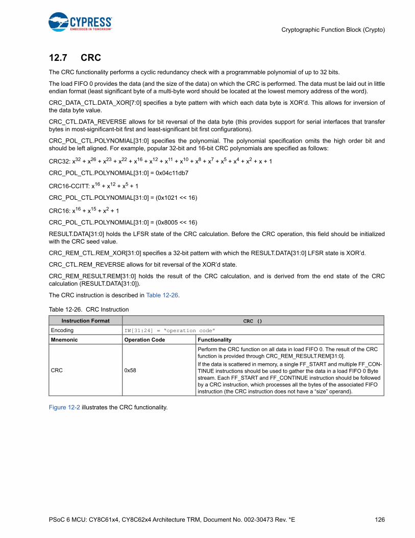
PSoC 6 MCU: CY8C61x4, CY8C62x4 Architecture TRM, Document No. 002-30473 Rev. *E 126
Cryptographic Function Block (Crypto)
12.7 CRC
The CRC functionality performs a cyclic redundancy check with a programmable polynomial of up to 32 bits.
The load FIFO 0 provides the data (and the size of the data) on which the CRC is performed. The data must be laid out in littleendian format (least significant byte of a multi-byte word should be located at the lowest memory address of the word).
CRC_DATA_CTL.DATA_XOR[7:0] specifies a byte pattern with which each data byte is XOR’d. This allows for inversion ofthe data byte value.
CRC_CTL.DATA_REVERSE allows for bit reversal of the data byte (this provides support for serial interfaces that transferbytes in most-significant-bit first and least-significant bit first configurations).
CRC_POL_CTL.POLYNOMIAL[31:0] specifies the polynomial. The polynomial specification omits the high order bit andshould be left aligned. For example, popular 32-bit and 16-bit CRC polynomials are specified as follows:
CRC32: x32 + x26 + x23 + x22 + x16 + x12 + x11 + x10 + x8 + x7 + x5 + x4 + x2 + x + 1
CRC_POL_CTL.POLYNOMIAL[31:0] = 0x04c11db7
CRC16-CCITT: x16 + x12 + x5 + 1
CRC_POL_CTL.POLYNOMIAL[31:0] = (0x1021 << 16)
CRC16: x16 + x15 + x2 + 1
CRC_POL_CTL.POLYNOMIAL[31:0] = (0x8005 << 16)
RESULT.DATA[31:0] holds the LFSR state of the CRC calculation. Before the CRC operation, this field should be initializedwith the CRC seed value.
CRC_REM_CTL.REM_XOR[31:0] specifies a 32-bit pattern with which the RESULT.DATA[31:0] LFSR state is XOR’d.
CRC_CTL.REM_REVERSE allows for bit reversal of the XOR’d state.
CRC_REM_RESULT.REM[31:0] holds the result of the CRC calculation, and is derived from the end state of the CRCcalculation (RESULT.DATA[31:0]).
The CRC instruction is described in Table 12-26.
Figure 12-2 illustrates the CRC functionality.
Table 12-26. CRC Instruction
Instruction Format CRC ()
Encoding IW[31:24] = “operation code”
Mnemonic Operation Code Functionality
CRC 0x58
Perform the CRC function on all data in load FIFO 0. The result of the CRC function is provided through CRC_REM_RESULT.REM[31:0].
If the data is scattered in memory, a single FF_START and multiple FF_CON-TINUE instructions should be used to gather the data in a load FIFO 0 Byte stream. Each FF_START and FF_CONTINUE instruction should be followed by a CRC instruction, which processes all the bytes of the associated FIFO instruction (the CRC instruction does not have a “size” operand).

PSoC 6 MCU: CY8C61x4, CY8C62x4 Architecture TRM, Document No. 002-30473 Rev. *E 127
Cryptographic Function Block (Crypto)
Figure 12-2. CRC Functionality
The Linear Feedback Shift Register functionality operates on the LFSR state. It uses the programmed polynomial andconsumes a data bit for each iteration (eight iterations are performed per cycle to provide a throughput of one data byte per
cycle). Figure 12-3 illustrates the functionality for the CRC32 polynomial (x32 + x26 + x23 + x22 + x16 + x12 + x11 + x10 + x8 + x7
+ x5 + x4 + x2 + x + 1).
Figure 12-3. CRC32 Functionality
CRC calculation
Single Byte
CRC_DATA_CTL.DATA_XOR[]
CRC_CTL.DATA_REVERSE
CRC_POL_CTL.POLYNOMIAL[]
CRC_REM_CTL.DATA_XOR[]
CRC_CTL.REM_REVERSE
CRC_REM_RESULT.REM[]
Load FIFO 0
Data bit reverse
Remainder bit reverse
RESULT.DATA[](LFSR state)
Q
31 30 29 28 27 26 25 24 23 22 21 20 19 18 17 16 15 14 13 12 11 10 9 8 7 6 5 4 3 2 1 0
D
CRC32 (x32 + x26 + x23 + x22 + x16 + x12 + x11 + x10 + x8 + x7 + x5 + x4 + x2 + x + 1)
LFSR0bit
clk
data bit
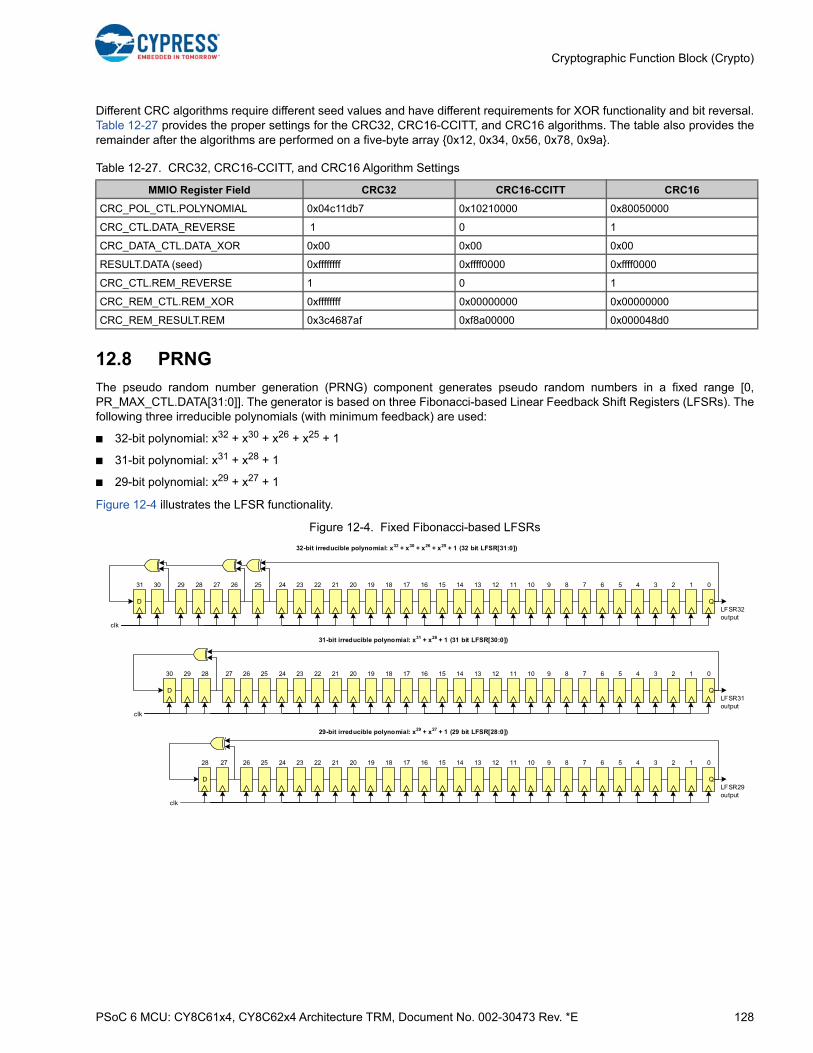
PSoC 6 MCU: CY8C61x4, CY8C62x4 Architecture TRM, Document No. 002-30473 Rev. *E 128
Cryptographic Function Block (Crypto)
Different CRC algorithms require different seed values and have different requirements for XOR functionality and bit reversal.Table 12-27 provides the proper settings for the CRC32, CRC16-CCITT, and CRC16 algorithms. The table also provides theremainder after the algorithms are performed on a five-byte array {0x12, 0x34, 0x56, 0x78, 0x9a}.
12.8 PRNG
The pseudo random number generation (PRNG) component generates pseudo random numbers in a fixed range [0,PR_MAX_CTL.DATA[31:0]]. The generator is based on three Fibonacci-based Linear Feedback Shift Registers (LFSRs). Thefollowing three irreducible polynomials (with minimum feedback) are used:
■ 32-bit polynomial: x32 + x30 + x26 + x25 + 1
■ 31-bit polynomial: x31 + x28 + 1
■ 29-bit polynomial: x29 + x27 + 1
Figure 12-4 illustrates the LFSR functionality.
Figure 12-4. Fixed Fibonacci-based LFSRs
Table 12-27. CRC32, CRC16-CCITT, and CRC16 Algorithm Settings
MMIO Register Field CRC32 CRC16-CCITT CRC16
CRC_POL_CTL.POLYNOMIAL 0x04c11db7 0x10210000 0x80050000
CRC_CTL.DATA_REVERSE 1 0 1
CRC_DATA_CTL.DATA_XOR 0x00 0x00 0x00
RESULT.DATA (seed) 0xffffffff 0xffff0000 0xffff0000
CRC_CTL.REM_REVERSE 1 0 1
CRC_REM_CTL.REM_XOR 0xffffffff 0x00000000 0x00000000
CRC_REM_RESULT.REM 0x3c4687af 0xf8a00000 0x000048d0
31-bit irreducible polynomial: x31 + x28 + 1 (31 bit LFSR[30:0])
32-bit irreducible polynomial: x32 + x30 + x26 + x25 + 1 (32 bit LFSR[31:0])
29-bit irreducible polynomial: x29 + x27 + 1 (29 bit LFSR[28:0])
D
clk
31 30 29 28 27 26 25 24 23 22 21 20 19 18 17 16 15 14 13 12 11 10 9 8 7 6 5 4 3 2 1 0
QLFSR32 output
clk
30 29 28 27 26 25 24 23 22 21 20 19 18 17 16 15 14 13 12 11 10 9 8 7 6 5 4 3 2 1 0
QLFSR31 output
D
clk
28 27 26 25 24 23 22 21 20 19 18 17 16 15 14 13 12 11 10 9 8 7 6 5 4 3 2 1 0
QLFSR29 output
D

PSoC 6 MCU: CY8C61x4, CY8C62x4 Architecture TRM, Document No. 002-30473 Rev. *E 129
Cryptographic Function Block (Crypto)
Software initializes the LFSRs with non-zero seed values. The PR_LFSR_CTL0, PR_LFSR_CTL1 and PR_LFSR_CTL2registers are provided for this purpose. At any time, the state of these registers can be read to retrieve the state of the LFSRs.The 32-bit LFSR generates a repeating bit sequence of 232 – 1 bits, the 31-bit LFSR generates a repeating bit sequence of231 – 1 and the 29-bit LFSR generates a repeating bit sequence of 229 – 1. As the
numbers 232-1, 231-1, and 229-1 are relatively prime, the XOR output is a repeating bit sequence of roughly 232+31+29.
The final pseudo random bit is the XOR of the three bits that are generated by the individual LFSRs.
Figure 12-5. XOR Reduction Logic
The pseudo random number generator uses a total of 33 pseudo random bits to generate a result in the range [0,PR_MAX_CTL.DATA[31:0]].
To generate a pseudo random number result, the following calculation is performed.
MAX[31:0] = PR_MAX_CTL.DATA[31:0]
MAX_PLUS1[32:0] = MAX[31:0] + 1;
product[63:0] = MAX_PLUS1[32:0] * pr[32:1] + MAX[31:0] * pr[0];
result = product[63:32];
PR_CMD.START is the PR command. The maximum value of the generated random number (in PR_RESULT.DATA) isspecified by PR_MAX_CTL.DATA. The PR command can be executed in parallel with the instruction FIFO instructions andthe TR command.
12.9 TRNG
The true random number generator component (TRNG) generates true random numbers. The bit size of these generatednumbers is programmable (TR_CTL.SIZE is in the range [0,32]).
The TRNG relies on up to six ring oscillators to provide physical noise sources. A ring oscillator consists of a series ofinverters connected in a feedback loop to form a ring. Due to (temperature) sensitivity of the inverter delays, jitter isintroduced on a ring's oscillating signal. The jittered oscillating signal is sampled to produce a “digitized analog signal” (DAS).This is done for all multiple ring oscillators.
To increase entropy and to reduce bias in DAS bits, the DAS bits are further postprocessed. Post-processing involves twosteps:
■ An optional reduction step (over up to six ring oscillator DAS bits and over one or multiple DAS bit periods) to increase entropy.
■ An optional “von Neumann correction” step to reduce a ‘0’ or ‘1’ bias.
This correction step processes pairs of reduction bits as produced by the previous step. Given two reduced bits r0 and r1 (with r0 being produced before r1), the correction step is defined as follows:
❐ {r0, r1} = {0, 0}: no bit is produced
❐ {r0, r1} = {0, 1}: a ‘0’ bit is produced (bit r0)
❐ {r0, r1} = {1, 0}: a ‘1’ bit is produced (bit r0)
❐ {r0, r1} = {1, 1}: no bit is produced
In other words the correction step only produces a bit on a ‘0’ to ‘1’ or ‘1’ to ‘0’ transition. Note that for a random input bitsequence, the correction step produces an output bit sequence of roughly one-quarter the frequency of the input bit sequence(the input reduction bits are processed in non-overlapping pairs and only half of the pair encodings result in an output bit).
Post-processing produces bit samples that are considered true random bit samples. The true random bit samples are shiftedinto a register, to provide random values of up to 32 bits.
pseudo random bitLFSR31 outputLFSR29 output
LFSR32 output

PSoC 6 MCU: CY8C61x4, CY8C62x4 Architecture TRM, Document No. 002-30473 Rev. *E 130
Cryptographic Function Block (Crypto)
As a result of high-switching activity, ring oscillators consume a significant amount of power. Therefore, when the TRNGfunctionality is disabled, the ring is “broken” to prevent switching. When the TRNG functionality is enabled, a ring oscillatorinitially has predictable behavior. However, over time, infinitesimal environmental (temperature) changes cause an increasingdeviation from this predictable behavior.
■ During the initial delay, the ring oscillator is not a reliable physical noise source.
■ After an initial delay, the same ring oscillator will show different oscillation behavior and provides a reliable physical noise source.
Therefore, the DAS bits can be dropped during an initialization period (TR_CTL.INIT_DELAY[]).
Figure 12-6 gives an overview of the TRNG component.
Figure 12-6. TRNG Overview
The “Sampler” logic digitizes an oscillating signal. Figure 12-7 illustrates the functionality (the complete logic is implementedusing standard platform toolkit components).
Figure 12-7. Sampler Logic
Note that when a ring oscillator is disabled, the synchronization logic is reset. Therefore, the ring oscillator contributes aconstant ‘0’ to the reduction step of the post-processing. As mentioned, the TRNG relies on up to six ring oscillators:
■ RO11: A fixed ring oscillator consisting of 11 inverters.
■ RO15: A fixed ring oscillator consisting of 15 inverters.
■ GARO15: A fixed Galois based ring oscillator of 15 inverters.
■ GARO31: A flexible Galois based ring oscillator of up to 31 inverters. A programmable polynomial of up to order 31 provides the flexibility in the oscillator feedback.
■ FIRO15: A fixed Fibonacci based ring oscillator of 15 inverters.
■ FIRO31: A flexible Fibonacci based ring oscillator of up to 31 inverters. A programmable polynomial of up to order 31 provides the flexibility in the oscillator feedback.
Sampler
Sampler
Sampler
Sampler
Sampler
Sampler
0 31
TR_RESULT.DATA[31:0]RED_CLOCK_DIV[]
SAMPLE_CLOCK_DIV[]
RO11
RO15
GARO15
GARO31
FIRO15
FIRO31
RO11_EN
RO15_EN
GARO15_EN
GARO31_EN
FIRO15_EN
FIRO31_EN
POLYNOMIAL[30:0]
POLYNOMIAL[30:0]
INIT_DELAY[]
INTR.TR_DATA_AVAILABLE
shift register
digitizedanalog
samples (DAS)oscillating signal
von Neumann corrector
VON_NEUMANN_CORR
Post-processing
INTR.TR_INITIALIZED
true random
bit
mxtk_clk_gate
mxtk_rst_and
mxtk_2dff_sync
START
clock_sample_en (derived from SAMPLE_CLOCK_DIV[])
“digitized analog sample”“oscillating signal”
test_icg_control
test_reset_control
clk_sys
rst_sys_act_n
Sampler
clk_sampler
rst_sampler_n
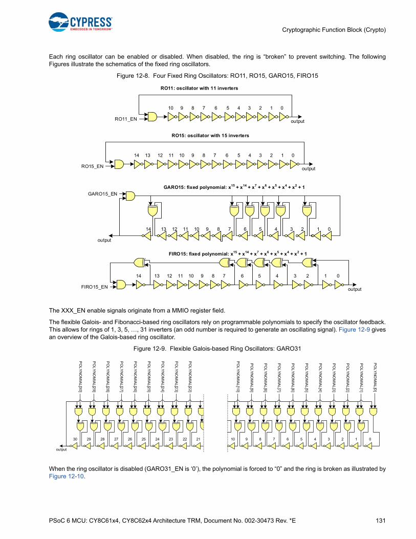
PSoC 6 MCU: CY8C61x4, CY8C62x4 Architecture TRM, Document No. 002-30473 Rev. *E 131
Cryptographic Function Block (Crypto)
Each ring oscillator can be enabled or disabled. When disabled, the ring is “broken” to prevent switching. The followingFigures illustrate the schematics of the fixed ring oscillators.
Figure 12-8. Four Fixed Ring Oscillators: RO11, RO15, GARO15, FIRO15
The XXX_EN enable signals originate from a MMIO register field.
The flexible Galois- and Fibonacci-based ring oscillators rely on programmable polynomials to specify the oscillator feedback.This allows for rings of 1, 3, 5, …, 31 inverters (an odd number is required to generate an oscillating signal). Figure 12-9 givesan overview of the Galois-based ring oscillator.
Figure 12-9. Flexible Galois-based Ring Oscillators: GARO31
When the ring oscillator is disabled (GARO31_EN is ‘0’), the polynomial is forced to “0” and the ring is broken as illustrated byFigure 12-10.
RO15: oscillator with 15 inverters
14 13 10 9 8 712 11 06
outputRO15_EN
3 2 15 4
RO11: oscillator with 11 inverters
10 9 8 7 06
outputRO11_EN
3 2 15 4
GARO15: fixed polynomial: x15 + x14 + x7 + x6 + x5 + x4 + x2 + 1
14
output
13 12 11 10 9 8 7 6 5 4 3 2 1 0
GARO15_EN
FIRO15: fixed polynomial: x15 + x14 + x7 + x6 + x5 + x4 + x2 + 1
14 13 10 9 8 712 11 6 5 4 3 2 1 0
outputFIRO15_EN
1 0
PO
LY
NO
MIA
L[1
]
PO
LY
NO
MIA
L[0
]
2
PO
LY
NO
MIA
L[2
]
3
PO
LY
NO
MIA
L[3
]
4
PO
LY
NO
MIA
L[4
]
5
PO
LY
NO
MIA
L[5
]
6
PO
LY
NO
MIA
L[6
]
7
PO
LY
NO
MIA
L[7
]
8
PO
LY
NO
MIA
L[8
]
24
PO
LY
NO
MIA
L[2
4]
25
PO
LY
NO
MIA
L[2
5]
26
PO
LY
NO
MIA
L[2
6]
27
PO
LY
NO
MIA
L[2
7]
28
PO
LY
NO
MIA
L[2
8]
29
PO
LY
NO
MIA
L[2
9]
30
PO
LY
NO
MIA
L[3
0]
9
PO
LY
NO
MIA
L[9
]
10
PO
LY
NO
MIA
L[1
0]
22
PO
LY
NO
MIA
L[2
2]
PO
LY
NO
MIA
L[2
3]
23 21
output
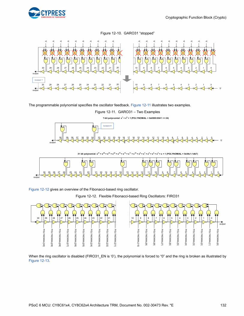
PSoC 6 MCU: CY8C61x4, CY8C62x4 Architecture TRM, Document No. 002-30473 Rev. *E 132
Cryptographic Function Block (Crypto)
Figure 12-10. GARO31 “stopped”
The programmable polynomial specifies the oscillator feedback. Figure 12-11 illustrates two examples.
Figure 12-11. GARO31 – Two Examples
Figure 12-12 gives an overview of the Fibonacci-based ring oscillator.
Figure 12-12. Flexible Fibonacci-based Ring Oscillators: FIRO31
When the ring oscillator is disabled (FIRO31_EN is ‘0’), the polynomial is forced to “0” and the ring is broken as illustrated byFigure 12-13.
1 0234567824252627282930
‘0’
9102223 21
output
‘0’
‘0’
‘0’
‘0’
‘0’
‘0’
‘0’
‘0’
‘0’
‘0’
‘0’
‘0’
‘0’
‘0’
‘0’
‘0’
‘0’
‘0’
‘0’
1 0234567824252627282930 9102223 21
output‘0’
Constant ‘1’
20
20
31 bit polynomial: x31 + x26 + x23 + x22 + x16 + x12 + x11 + x10 + x8 + x7 + x5 + x4 + x2 + x + 1 (POLYNOMIAL = 0x04c1:1db7)
30 29 28 27 25 24 23 22 21 20 19 18 17 16 15 14 13 12 11 10 9 8 7 6 5 4 3 2 1 026
7-bit polynomial: x7 + x6 + 1 (POLYNOMIAL = 0x0000:0041 << 24)
29 28 2730 26 25 24 22 21 20 19 18 17 16 15 14 13 12 11 10 9 8 7 6 5 4 423 2 1‘0’
Constant ‘0’
output
output
0
output
PO
LY
NO
MIA
L[3
0]
PO
LY
NO
MIA
L[2
9]
PO
LY
NO
MIA
L[2
8]
PO
LY
NO
MIA
L[2
7]
PO
LY
NO
MIA
L[2
6]
PO
LY
NO
MIA
L[2
5]
PO
LY
NO
MIA
L[2
4]
PO
LY
NO
MIA
L[2
3]
24252627282930 2223 21
PO
LY
NO
MIA
L[2
2]
PO
LY
NO
MIA
L[2
1]
10
PO
LY
NO
MIA
L[1
0]
PO
LY
NO
MIA
L[9
]
PO
LY
NO
MIA
L[8
]
PO
LY
NO
MIA
L[7
]
PO
LY
NO
MIA
L[6
]
PO
LY
NO
MIA
L[5
]
PO
LY
NO
MIA
L[4
]
PO
LY
NO
MIA
L[3
]
PO
LY
NO
MIA
L[2
]
3456789 12 0
PO
LY
NO
MIA
L[1
]
PO
LY
NO
MIA
L[0
]

PSoC 6 MCU: CY8C61x4, CY8C62x4 Architecture TRM, Document No. 002-30473 Rev. *E 133
Cryptographic Function Block (Crypto)
Figure 12-13. FIRO31 “stopped”
The programmable polynomial specifies the oscillator feedback. Figure 12-14 illustrates two examples.
Figure 12-14. FIRO31 – Two Examples
There is one TR command, TR_CMD.START, which can be executed in parallel with the instruction FIFO instructions and thePR command. The size of the generated random number (in TR_RESULT.DATA) is specified by TR_CTL.SIZE.
The TRNG has a built-in health monitor that performs tests on the digitized noise source to detect deviations from theintended behavior. For example, the health monitor detects “stuck at” faults in the digitized analog samples. The healthmonitor tests one out of three selected digitized bit streams:
■ DAS bitstream. This is XOR of the digitized analog samples.
■ RED bitstream. This is the bitstream of reduction bits. Note that each reduction bit may be calculated over multiple DAS bits.
■ TR bitstream. This is the bitstream of true random bits (after the “von Neumann reduction” step).
The health monitor performs two different tests:
The repetition count test. This test checks for the repetition of the same bit value (‘0’ or ‘1’) in a bitstream. A detectionindicates that a specific active bit value (specified by a status field BIT) has repeated for a pre-programmed number of bits(specified by a control field CUTOFF_COUNT[7:0]). The test uses a counter to maintain the number of repetitions of theactive bit value (specified by a status field REP_COUNT[7:0]).
If the test is started (specified by START_RC field) and a change in the bitstream value is observed, the active bit value BIT isset to the new bit value and the repetition counter REP_COUNT[] is set to ‘1’. If the bitstream value is unchanged, therepetition counter REP_COUNT[] is incremented by “1”.
A detection stops the repetition count test (the START_RC field is set to ‘0’), sets the associated interrupt status field to ‘1’ andensures that hardware does not modify the status fields. When the test is stopped, REP_COUNT[] equalsCUTOFF_COUNT[].
A detection stops the TRNG functionality (all TR_CTL.XXX_EN fields are set to ‘0’) if TR_CTL.STOP_ON_RC_DETECT isset to ‘1’.
The adaptive proportion test. This test checks for a disproportionate occurrence of a specific bit value (‘0’ or ‘1’) in a bitstream. A detection indicates that a specific active bit value (specified by a status field BIT) has occurred a pre-programmednumber of times (specified by a control field CUTOFF_COUNT[15:0]) in a bit sequence of a specific bit window size (specifiedby a control field WINDOW_SIZE[15:0]). The test uses a counter to maintain an index in the current window (specified by
output
‘0’
24252627282930 2223 21 10 3456789 12 0
‘0’
‘0’
‘0’
‘0’
‘0’
‘0’
‘0’
‘0’
‘0’
‘0’
‘0’
‘0’
‘0’
‘0’
‘0’
‘0’
‘0’
‘0’
‘0’
‘0’
‘0’
output‘0’
Constant ‘1’
20
24252627282930 2223 21 10 3456789 12 020
31 bit polynomial: x31 + x26 + x23 + x22 + x16 + x12 + x11 + x10 + x8 + x7 + x5 + x4 + x2 + x + 1 (POLYNOMIAL = 0x04c1:1db7)
30 29 28 27 26 25 24 23 22 21 20 19 18 17 16 15 14 13 12 11 10 9 8 7 6 5 4 3 2 1 0
output
7-bit polynomial: x7 + x6 + 1 (POLYNOMIAL = 0x0000:0041 << 24)
30 29 28 27 26 25 24 22 21 20 19 18 1723 16 15 14 13 10 9 8 7 6 512 11 4 3 2 1 0
output
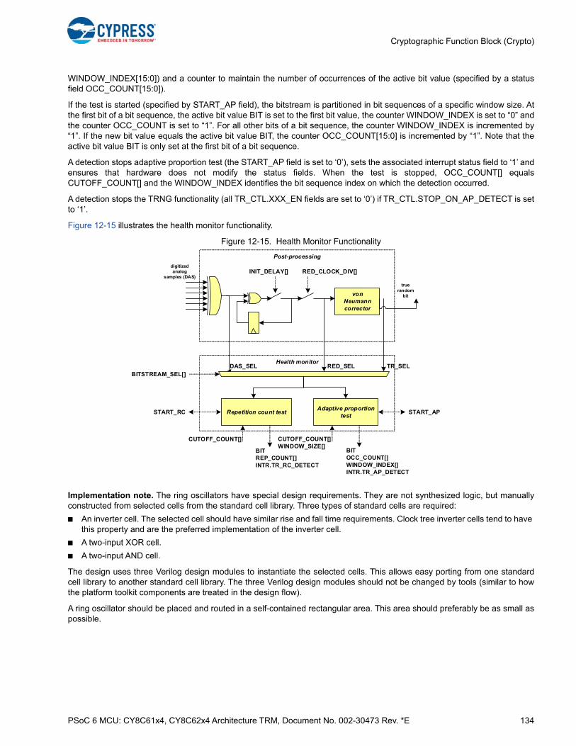
PSoC 6 MCU: CY8C61x4, CY8C62x4 Architecture TRM, Document No. 002-30473 Rev. *E 134
Cryptographic Function Block (Crypto)
WINDOW_INDEX[15:0]) and a counter to maintain the number of occurrences of the active bit value (specified by a statusfield OCC_COUNT[15:0]).
If the test is started (specified by START_AP field), the bitstream is partitioned in bit sequences of a specific window size. Atthe first bit of a bit sequence, the active bit value BIT is set to the first bit value, the counter WINDOW_INDEX is set to “0” andthe counter OCC_COUNT is set to “1”. For all other bits of a bit sequence, the counter WINDOW_INDEX is incremented by“1”. If the new bit value equals the active bit value BIT, the counter OCC_COUNT[15:0] is incremented by “1”. Note that theactive bit value BIT is only set at the first bit of a bit sequence.
A detection stops adaptive proportion test (the START_AP field is set to ‘0’), sets the associated interrupt status field to ‘1’ andensures that hardware does not modify the status fields. When the test is stopped, OCC_COUNT[] equalsCUTOFF_COUNT[] and the WINDOW_INDEX identifies the bit sequence index on which the detection occurred.
A detection stops the TRNG functionality (all TR_CTL.XXX_EN fields are set to ‘0’) if TR_CTL.STOP_ON_AP_DETECT is setto ‘1’.
Figure 12-15 illustrates the health monitor functionality.
Figure 12-15. Health Monitor Functionality
Implementation note. The ring oscillators have special design requirements. They are not synthesized logic, but manuallyconstructed from selected cells from the standard cell library. Three types of standard cells are required:
■ An inverter cell. The selected cell should have similar rise and fall time requirements. Clock tree inverter cells tend to have this property and are the preferred implementation of the inverter cell.
■ A two-input XOR cell.
■ A two-input AND cell.
The design uses three Verilog design modules to instantiate the selected cells. This allows easy porting from one standardcell library to another standard cell library. The three Verilog design modules should not be changed by tools (similar to howthe platform toolkit components are treated in the design flow).
A ring oscillator should be placed and routed in a self-contained rectangular area. This area should preferably be as small aspossible.
RED_CLOCK_DIV[]INIT_DELAY[]
von Neumann corrector
Post-processing
digitizedanalog
samples (DAS)
true random
bit
DAS_SEL RED_SEL TR_SELHealth monitor
Repetition count testAdaptive proportion
test
CUTOFF_COUNT[]
BITREP_COUNT[]INTR.TR_RC_DETECT
CUTOFF_COUNT[]WINDOW_SIZE[]
BITOCC_COUNT[]WINDOW_INDEX[]INTR.TR_AP_DETECT
START_RC START_AP
BITSTREAM_SEL[]
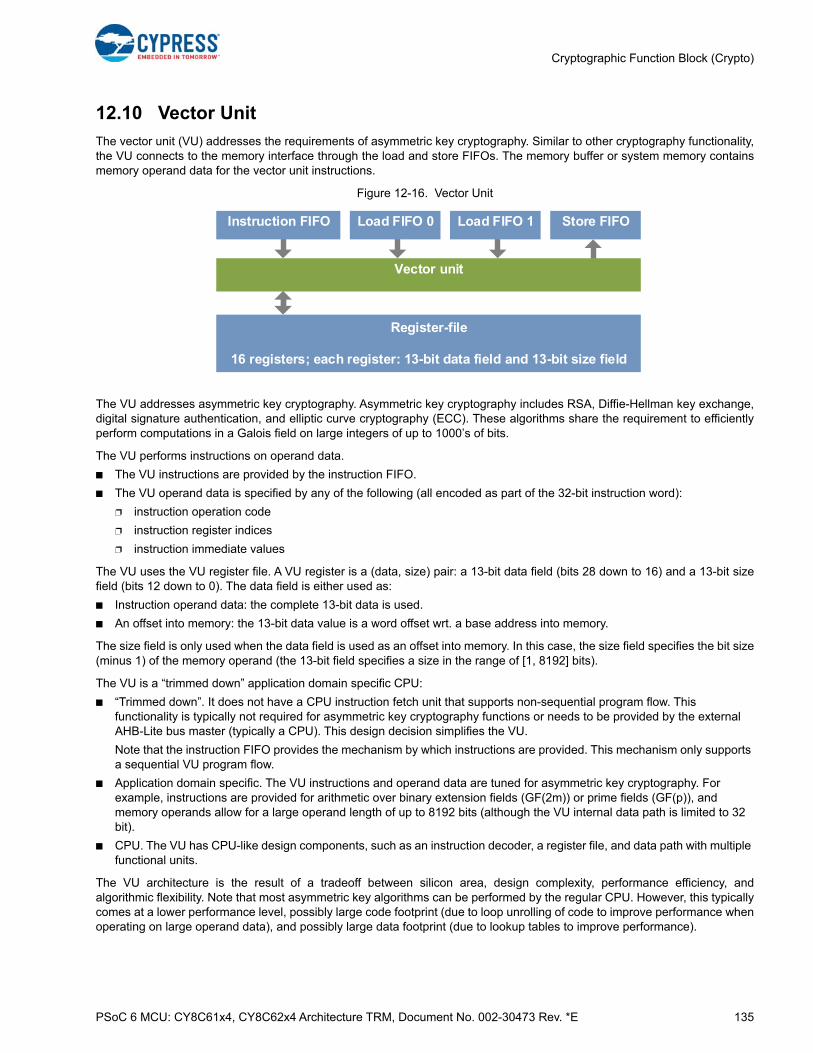
PSoC 6 MCU: CY8C61x4, CY8C62x4 Architecture TRM, Document No. 002-30473 Rev. *E 135
Cryptographic Function Block (Crypto)
12.10 Vector Unit
The vector unit (VU) addresses the requirements of asymmetric key cryptography. Similar to other cryptography functionality,the VU connects to the memory interface through the load and store FIFOs. The memory buffer or system memory containsmemory operand data for the vector unit instructions.
Figure 12-16. Vector Unit
The VU addresses asymmetric key cryptography. Asymmetric key cryptography includes RSA, Diffie-Hellman key exchange,digital signature authentication, and elliptic curve cryptography (ECC). These algorithms share the requirement to efficientlyperform computations in a Galois field on large integers of up to 1000’s of bits.
The VU performs instructions on operand data.
■ The VU instructions are provided by the instruction FIFO.
■ The VU operand data is specified by any of the following (all encoded as part of the 32-bit instruction word):
❐ instruction operation code
❐ instruction register indices
❐ instruction immediate values
The VU uses the VU register file. A VU register is a (data, size) pair: a 13-bit data field (bits 28 down to 16) and a 13-bit sizefield (bits 12 down to 0). The data field is either used as:
■ Instruction operand data: the complete 13-bit data is used.
■ An offset into memory: the 13-bit data value is a word offset wrt. a base address into memory.
The size field is only used when the data field is used as an offset into memory. In this case, the size field specifies the bit size(minus 1) of the memory operand (the 13-bit field specifies a size in the range of [1, 8192] bits).
The VU is a “trimmed down” application domain specific CPU:
■ “Trimmed down”. It does not have a CPU instruction fetch unit that supports non-sequential program flow. This functionality is typically not required for asymmetric key cryptography functions or needs to be provided by the external AHB-Lite bus master (typically a CPU). This design decision simplifies the VU.
Note that the instruction FIFO provides the mechanism by which instructions are provided. This mechanism only supports a sequential VU program flow.
■ Application domain specific. The VU instructions and operand data are tuned for asymmetric key cryptography. For example, instructions are provided for arithmetic over binary extension fields (GF(2m)) or prime fields (GF(p)), and memory operands allow for a large operand length of up to 8192 bits (although the VU internal data path is limited to 32 bit).
■ CPU. The VU has CPU-like design components, such as an instruction decoder, a register file, and data path with multiple functional units.
The VU architecture is the result of a tradeoff between silicon area, design complexity, performance efficiency, andalgorithmic flexibility. Note that most asymmetric key algorithms can be performed by the regular CPU. However, this typicallycomes at a lower performance level, possibly large code footprint (due to loop unrolling of code to improve performance whenoperating on large operand data), and possibly large data footprint (due to lookup tables to improve performance).
Register-file
16 registers; each register: 13-bit data field and 13-bit size field
Instruction FIFO Store FIFO
Vector unit
Load FIFO 0 Load FIFO 1
PSoC 6 MCU: CY8C61x4, CY8C62x4 Architecture TRM, Document No. 002-30473 Rev. *E 136
Cryptographic Function Block (Crypto)
The improved performance of the VU (over a regular CPU) for asymmetric key algorithms also allows for more genericalgorithmic implementations, as opposed to implementations targeting, such as specific primes or irreducible polynomials.
Before describing the architecture, a short C example is illustrates the VU functionality.#define SIZE 4096void Example (){int a = 0; int b = 1; int c = 2; // assign register indicesuint8_t c_data[SIZE/8];ALLOC_MEM (a, SIZE); // allocate 4096 bits of dataALLOC_MEM (b, SIZE); // allocate 4096 bits of dataALLOC_MEM (c, SIZE); // allocate 4096 bits of dataCrypto_WriteMemNumber (a, “0x21542555:fed35532: … :ffea2345”);Crypto_writeMemNumber (b, “0xef45ac2a:34a312bc: … :000003ab”);ADD (c, a, b);Crypto_ReadMemNumber (c, c_data);}
The example adds two 4096-bit numbers and produces a 4096-bit number. The example is explained as follows:
■ Three local variables are assigned VU register indices:
❐ local variable a uses register 0
❐ local variable b uses register 1
❐ local variable c used register 2
■ Memory is allocated in the memory buffer for each variable: each variable needs 4096 bits.
■ A function “Crypto_WriteMemNumber” is called to initialize the memory operand data for source variables a and b.
■ A VU ADD instruction (long integer addition) is executed.
■ A function “Crypto_WriteMemNumber” is called to read the result of the instruction from the memory.
The example illustrates that the full expressive power of the C language is available when writing software for the VU.
The example illustrates that relatively complex functionality can be expressed in only a few lines of C code (considerimplementing the same functionality on a 32-bit Arm processor).
The “Crypto_” functions copy data to and from the memory. These functions are executed on the regular CPU and may take asignificant number of cycles. Asymmetric key algorithm typically requires little copy functions and a lot of VU instructions. Asa result, the cycle overhead of the copy functions is negligible. As an example, RSA requires exponentiation of a number by asecond number modulo a third number. This RSA functionality requires only four copy functions (three to initialize threememory operands and one to read the result), but requires thousands of VU instructions.
The following sections provide an architectural overview of the VU.
12.10.1 VU Register File
The register file has sixteen registers (r0 through r15). Each register consists of a 13-bit data field and a 13-bit size field. Thedata field is either used as:
■ Instruction operand data: the 13-bit data is used.
■ An offset into memory: the 13-bit data value is a word offset for a base address into memory. Typically, memory operand data is located in the crypto memory buffer (this provides better latency/performance than memory operand data in system memory).
The size field is used only when the data field is used as an offset into memory. In this case, the size field specifies the bit size(minus 1) of the memory operand (the 13-bit field specifies a size in the range of [1, 8192] bits).
The CPU software decides what instructions use what registers. There is no compiler with specific conventions for registerusage or to perform register allocation. To ensure some consistency and interoperability of the functions in a software library,the software programmer should introduce its own conventions. Some examples of conventions are:
■ Each non-leaf function saves all registers to the stack on function entry and restores all registers from the stack on function exit. This makes all registers available for use within the function.
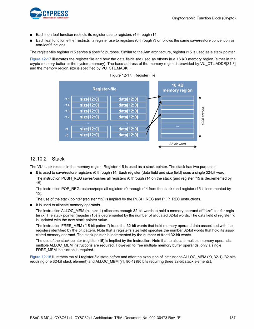
PSoC 6 MCU: CY8C61x4, CY8C62x4 Architecture TRM, Document No. 002-30473 Rev. *E 137
Cryptographic Function Block (Crypto)
■ Each non-leaf function restricts its register use to registers r4 through r14.
■ Each leaf function either restricts its register use to registers r0 through r3 or follows the same save/restore convention as non-leaf functions.
The register-file register r15 serves a specific purpose. Similar to the Arm architecture, register r15 is used as a stack pointer.
Figure 12-17 illustrates the register file and how the data fields are used as offsets in a 16 KB memory region (either in thecrypto memory buffer or the system memory). The base address of the memory region is provided by VU_CTL.ADDR[31:8]and the memory region size is specified by VU_CTL.MASK[].
Figure 12-17. Register File
12.10.2 Stack
The VU stack resides in the memory region. Register r15 is used as a stack pointer. The stack has two purposes:
■ It is used to save/restore registers r0 through r14. Each register (data field and size field) uses a single 32-bit word.
The instruction PUSH_REG saves/pushes all registers r0 through r14 on the stack (and register r15 is decremented by 15).
The instruction POP_REG restores/pops all registers r0 through r14 from the stack (and register r15 is incremented by 15).
The use of the stack pointer (register r15) is implied by the PUSH_REG and POP_REG instructions.
■ It is used to allocate memory operands.
The instruction ALLOC_MEM (rx, size-1) allocates enough 32-bit words to hold a memory operand of “size” bits for regis-ter rx. The stack pointer (register r15) is decremented by the number of allocated 32-bit words. The data field of register rx is updated with the new stack pointer value.
The instruction FREE_MEM (“15 bit pattern”) frees the 32-bit words that hold memory operand data associated with the registers identified by the bit pattern. Note that a register’s size field specifies the number 32-bit words that hold its asso-ciated memory operand. The stack pointer is incremented by the number of freed 32-bit words.
The use of the stack pointer (register r15) is implied by the instruction. Note that to allocate multiple memory operands, multiple ALLOC_MEM instructions are required. However, to free multiple memory buffer operands, only a single FREE_MEM instruction is required.
Figure 12-18 illustrates the VU register-file state before and after the execution of instructions ALLOC_MEM (r0, 32-1) (32 bitsrequiring one 32-bit stack element) and ALLOC_MEM (r1, 80-1) (80 bits requiring three 32-bit stack elements).
16 KBmemory regionRegister-file
size[12:0]
.........
r0
r1
r15
r14
r13
r12
32-bit word
4096
ent
ries
size[12:0]
size[12:0]
size[12:0]
size[12:0]
size[12:0]
data[12:0]
data[12:0]
data[12:0]
data[12:0]
data[12:0]
data[12:0]

PSoC 6 MCU: CY8C61x4, CY8C62x4 Architecture TRM, Document No. 002-30473 Rev. *E 138
Cryptographic Function Block (Crypto)
Figure 12-18. Left: Register File State before ALLOC_MEM Instructions; Right: Register File after ALLOC_MEM Instructions
Figure 12-19 illustrates the VU component state after the execution of the instruction FREE_MEM ((1 << r1) | (1 << r0)).
Figure 12-19. Register File State after FREE_MEM Instruction
Freeing of stack elements should be in the reverse order of allocation of stack elements. Also see the description of theFREE_MEM instruction for the order in which registers are freed (lower registers are freed before higher registers).
12.10.3 Memory Operands
Asymmetric key cryptography requires computations on large integers of up to 1000’s of bits. These integers areimplemented using memory operands. The instruction registers’ data values provide offsets in a memory region. The baseaddress of the memory region is provided by VU_CTL.ADDR[31:8]. The memory region is located in either the IP memorybuffer or the system memory. The memory region is accessed through the load and store FIFOs.
Memory operands are typically located in the crypto memory buffer (better access latency). Memory operand require one ormultiple 32-bit words. The register size field specifies the bit size of a memory operand. This size is limited to the range [1,8192] bits. Note that there is no size restriction within this range. A memory operand of n bits requires (n+31)/32 32-bit words.
12.10.4 Datapath
The VU instructions can operate on 13-bit register data values and/or large memory operands. The VU datapath is limited to32 bits (the width of a single memory word).
To operate on large memory operands, multiple datapath iterations are required. Dependent on the instruction opcode, theseiterations may be independent of each other (for example, a OR instruction) or may be dependent of each other (for example,an ADD instruction requires a carry). This complexity is completely hidden from software.
■ The instruction opcode specifies whether datapath iterations are dependent or independent.
■ The register size field provides the VU decoder and datapath with all the information it needs to determine the number of datapath iterations.
16 KBmemory regionRegister-file
don’t care A
data[12:0]
.........
r0
r1
r15
r14
r13
r12
A
16 KBmemory regionRegister-file
don’t care
79
31
A-4
A-4
A-1
.........
r0
r1
r15
r14
r13
r12
AA-1
A-4
size[12:0]
size[12:0]
size[12:0]
size[12:0]
size[12:0]
size[12:0]
size[12:0]
size[12:0]
data[12:0]
data[12:0]
data[12:0]
data[12:0]
data[12:0]
data[12:0]
data[12:0]
16 KBmemory regionRegister-file
don’t care
79
31
A
A-4
A-1
.........
r0
r1
r15
r14
r13
r12
A
size[12:0]
size[12:0]
size[12:0]
data[12:0]
data[12:0]
data[12:0]
PSoC 6 MCU: CY8C61x4, CY8C62x4 Architecture TRM, Document No. 002-30473 Rev. *E 139
Cryptographic Function Block (Crypto)
The VU datapath consists of three functional units:
■ An ALU that performs addition, subtraction, and logical instructions.
■ A barrel shifter that performs shift instructions.
■ A multiplier that performs multiplication and squaring instructions.
In addition, a state machine is present for instruction decoding and controlling multiple datapath iterations. The state machinealso performs administration instructions such as PUSH_REG, POP_REG, ALLOC_MEM, and FREE_MEM.
Note that the instruction execution time (in clock cycles) is typically independent of the instruction operand data values.However, the execution time is dependent on the size of memory operands (as specified by the register size field). This is animportant characteristic, as the data value independence complicates differential power or execution time attacks.
12.10.5 Status Register
Similar to the Arm architecture, the VU has a STATUS register:
■ It is affected by instruction execution.
■ It controls instruction execution.
The STATUS register is a 4-bit field, with the following fields:
■ CARRY field (bit 0). This field is set to ‘1’ if the result of an addition exceeds the destination operand size, if the result of a subtraction is positive or zero, or as the result of a shift instruction.
■ EVEN field (bit 1). This field is set to ‘1’ (and cleared to ‘0’ otherwise) if the result of an instruction is even (bit 0 of the destination operand is ‘0’).
■ ZERO field (bit 2). This field is set to ‘1’ (and cleared to ‘0’ otherwise) if the result of an instruction is “0”.
■ ONE field (bit 3). This field is set to ‘1’ (and cleared to ‘0’ otherwise) if the result of an instruction is “1”.
The STATUS register fields are set and cleared as a result of instruction execution. Not all instructions affect all STATUSregister fields.
Conditional execution. As mentioned, the STATUS register controls instruction execution. It does so through conditionalinstruction execution (again, similar to the Arm architecture). Almost all instructions (the SET_REG instruction is theexception) support conditional execution. Conditional execution only executes an instruction when a specific condition, asspecified by a condition code in the instruction word, is met. The condition code is dependent on the STATUS register fields.The following table lists the condition codes and the conditions under which the conditional instruction is executed.
If a conditional instruction has a condition code that evaluates to ‘0’/FALSE, it does not change the VU functional state. Thismeans that:
■ a destination operand is not updated
■ the STATUS register is not updated
Table 12-28. Condition Codes
Abbreviation Condition Code Value Description Condition
ALWAYS 0x0 Always ‘1’
EQ 0x1 Equal ZERO
NE 0x2 Not equal !ZERO
CS 0x3 Carry set/higher or same CARRY
CC 0x4 Carry clear/lower !CARRY
HI 0x5 Higher CARRY & !ZERO
LS 0x6 Lower or same !CARRY | ZERO
EVEN 0x7 Even EVEN
ODD 0x8 Odd !EVEN
ONE 0x9 One ONE
NOT_ONE 0xa Not one !ONE
PSoC 6 MCU: CY8C61x4, CY8C62x4 Architecture TRM, Document No. 002-30473 Rev. *E 140
Cryptographic Function Block (Crypto)
12.10.6 Instructions
The VU instructions operate on either register operand data or memory operand data.
Operand types. Typically, VU instruction operands all have the same type: either register or memory operands. However,some exceptions do exist. For example, consider the following CTSAME (count trailing same) instruction.
CTSAME (r0, r1, r2)
This instruction counts the number of trailing bits (least significant bits), which are the same as the two memory operands thatare identified by register r1 and r2. The instruction result is stored in the data field of register r0. This instruction has twosource operands of the memory type and one destination operand of the register type.
Conditional execution. Conditional execution makes the execution of an instruction dependent on a condition. For example,consider the COND_CTSAME (HI, r0, r1, r2) instruction. This instruction uses the “HI” condition code. The CTSAMEinstruction is only executed when the “HI” condition code evaluates to ‘1’/TRUE. This is the case when the CARRY field of theSTATUS register is ‘1’/TRUE and the ZERO field of the STATUS register is ‘0’/FALSE.
Unconditional execution uses the “ALWAYS” condition code, which always evaluates to ‘1’/TRUE. For brevity, andunconditional instruction XXX is not written as COND_XXX, but simply as XXX.
Note that a not executed conditional instruction does not update the STATUS register.
Memory operand data extension. Register operand data always has the same 13-bit size. Memory operand data has a sizethat is specified by a register’s size field. Therefore, it is possible to have memory operands with different sizes. This isintentional, but requires some rules in terms of how to deal with instructions that operate on memory operands with differentsizes. These rules are as follows:
■ If an instruction has a destination memory operand (for example, an ADD instruction), the size of this destination operand specifies the size of the instruction execution.
■ If an instruction has no destination memory operand (for example, a CTSAME instruction), the maximum size of all source memory operands specifies the size of the instruction.
■ If the instruction size (as determined by the previous two rules) is larger than a source memory operand, the memory operand is extended with leading ‘0’ bits (most significant ‘0’ bits).
■ If the instruction size is smaller than a source memory operand, the memory operand’s leading bits (most significant bits) are dropped/ignored (the LSR, LSR1, and LSR1_WITH_CARRY are an exception to this rule).
To illustrate memory operand extension, we give a few examples.CTSAME (r0, r1, r2)r1 specifies a 40-bit memory operand 0x11:12345678r2 specifies a 64-bit memory operand 0x11111111:ffffff78
The instruction size is 64 bits (maximum size of the two source memory operands). The memory operand 0x11:12345678 isextended to 0x00000011:12345678. The CTSAME instruction produces the result 8 in the register r0 data field.ADD (r0, r1, r2)r0 specifies a 48-bit memory operandr1 specifies a 40-bit memory operand 0x11:12345678r2 specifies a 64-bit memory operand 0xffffffff:ffffff78
The instruction size is 48 bits (size of the destination memory operand). The memory operand 0x11:12345678 is extended to0x0011:12345678. The memory operand 0xffffffff:ffffff78 is reduced to 0xffff:ffffff78. The ADD instruction produces the 40-bitresult 0x0011:123455f0 in the destination memory operand. Note that this instruction generates a carry and will set theCARRY field of the STATUS register to ‘1’/TRUE.
12.10.7 Instruction Set
This section describes all VU instructions. For each instruction, the following is described:
■ The instruction format
❐ Source operand types (register or memory operands)
❐ Support for conditional execution
❐ Encoding of the 32-bit instruction word (IW[31:0])
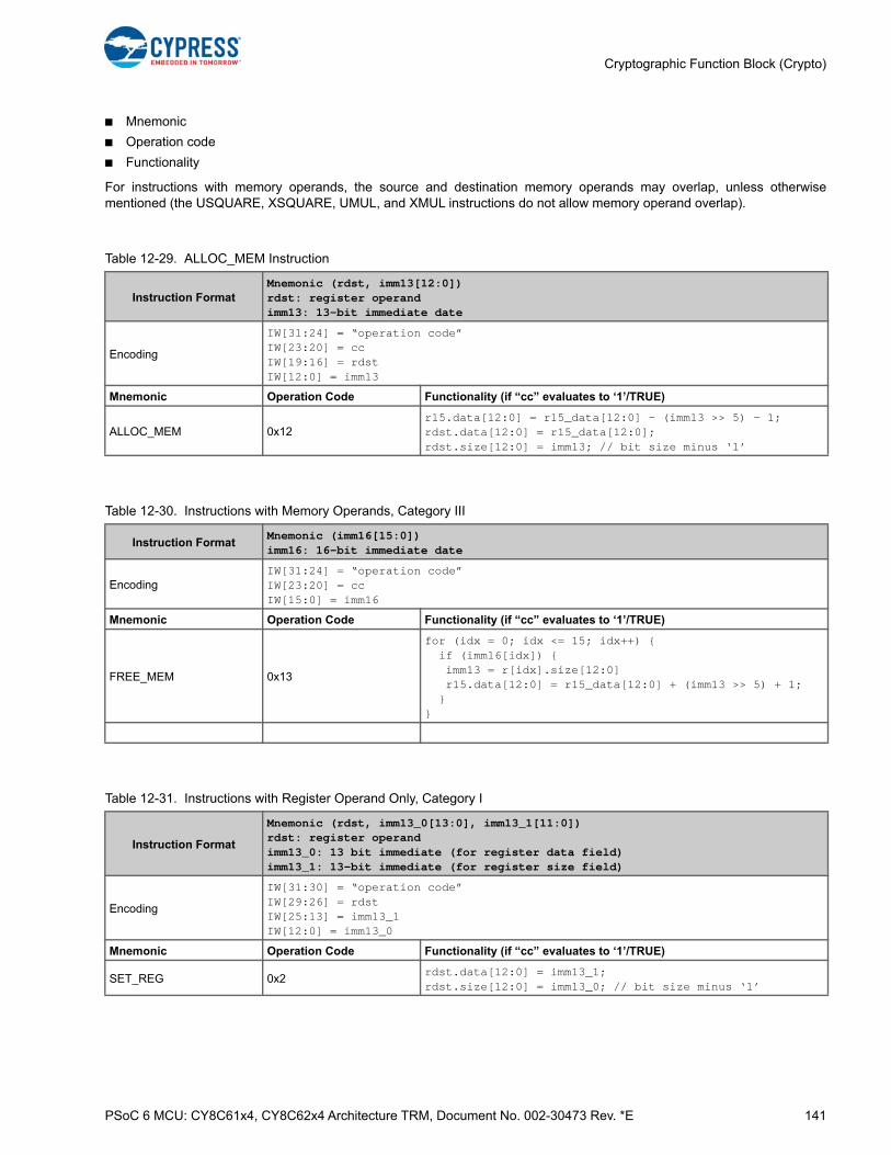
PSoC 6 MCU: CY8C61x4, CY8C62x4 Architecture TRM, Document No. 002-30473 Rev. *E 141
Cryptographic Function Block (Crypto)
■ Mnemonic
■ Operation code
■ Functionality
For instructions with memory operands, the source and destination memory operands may overlap, unless otherwisementioned (the USQUARE, XSQUARE, UMUL, and XMUL instructions do not allow memory operand overlap).
Table 12-29. ALLOC_MEM Instruction
Instruction FormatMnemonic (rdst, imm13[12:0])rdst: register operandimm13: 13-bit immediate date
Encoding
IW[31:24] = “operation code”IW[23:20] = ccIW[19:16] = rdstIW[12:0] = imm13
Mnemonic Operation Code Functionality (if “cc” evaluates to ‘1’/TRUE)
ALLOC_MEM 0x12r15.data[12:0] = r15_data[12:0] – (imm13 >> 5) - 1;rdst.data[12:0] = r15_data[12:0];rdst.size[12:0] = imm13; // bit size minus ‘1’
Table 12-30. Instructions with Memory Operands, Category III
Instruction FormatMnemonic (imm16[15:0])imm16: 16-bit immediate date
EncodingIW[31:24] = “operation code”IW[23:20] = ccIW[15:0] = imm16
Mnemonic Operation Code Functionality (if “cc” evaluates to ‘1’/TRUE)
FREE_MEM 0x13
for (idx = 0; idx <= 15; idx++) { if (imm16[idx]) { imm13 = r[idx].size[12:0] r15.data[12:0] = r15_data[12:0] + (imm13 >> 5) + 1; }}
Table 12-31. Instructions with Register Operand Only, Category I
Instruction Format
Mnemonic (rdst, imm13_0[13:0], imm13_1[11:0])rdst: register operandimm13_0: 13 bit immediate (for register data field)imm13_1: 13-bit immediate (for register size field)
Encoding
IW[31:30] = “operation code”IW[29:26] = rdstIW[25:13] = imm13_1IW[12:0] = imm13_0
Mnemonic Operation Code Functionality (if “cc” evaluates to ‘1’/TRUE)
SET_REG 0x2rdst.data[12:0] = imm13_1;rdst.size[12:0] = imm13_0; // bit size minus ‘1’

PSoC 6 MCU: CY8C61x4, CY8C62x4 Architecture TRM, Document No. 002-30473 Rev. *E 142
Cryptographic Function Block (Crypto)
Table 12-32. MOV_REG Instruction
Instruction Format
Mnemonic (rdst, rsrc) or COND_Mnemonic (cc, rdst, rsrc)rdst: register operandrsrc: register operandcc: condition code
Encoding
IW[31:24] = “operation code”IW[23:20] = ccIW[15:12] = rdstIW[3:0] = rsrc
Mnemonic Operation Code Functionality (if “cc” evaluates to ‘1’/TRUE)
MOV_REG 0x02 rdst.data = rsrc.data; rdst.size = rsrc.size;
Table 12-33. LD_REG Instruction
Instruction Format
Mnemonic (rsrc1, rsrc0) or COND_Mnemonic (cc, rsrc1, rsrc0)rsrc1: register operandrsrc0: register operandcc: condition code
Encoding
IW[31:24] = “operation code”IW[23:20] = ccIW[15:12] = rsrc1IW[3:0] = rsrc0
Mnemonic Operation Code Functionality (if “cc” evaluates to ‘1’/TRUE)
LD_REG 0x00
word = GetMemData (r15.data+rsrc0, 32-1); // r15: stack pointerrsrc1.data[12:0] = word >> 16;rsrc1.size[12:0] = word;
Table 12-34. ST_REG Instruction
Instruction Format
Mnemonic (rsrc1, rsrc0) or COND_Mnemonic (cc, rsrc1, rsrc0)rsrc1: register operandrsrc0: register operandcc: condition code
Encoding
IW[31:24] = “operation code”IW[23:20] = ccIW[7:4] = rsrc1IW[3:0] = rsrc0
Mnemonic Operation Code Functionality (if “cc” evaluates to ‘1’/TRUE)
ST_REG 0x01word = rsrc1.data[12:0] << 16 | rsrc1.size[12:0]SetMemBuffData (r15.data+rsrc0, word, 32-1);
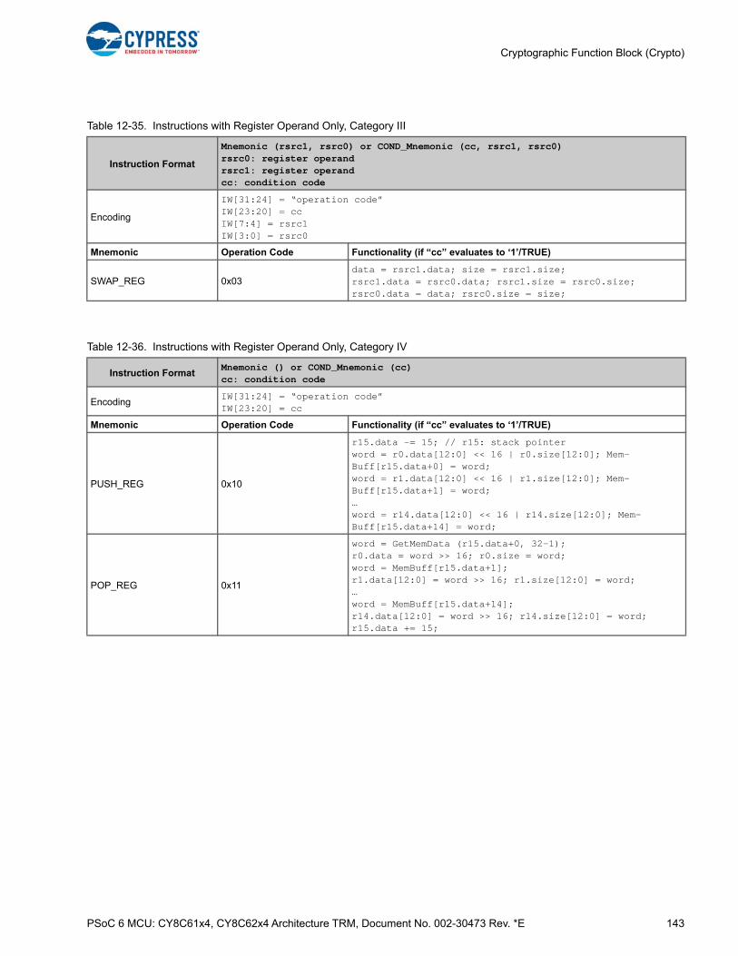
PSoC 6 MCU: CY8C61x4, CY8C62x4 Architecture TRM, Document No. 002-30473 Rev. *E 143
Cryptographic Function Block (Crypto)
Table 12-35. Instructions with Register Operand Only, Category III
Instruction Format
Mnemonic (rsrc1, rsrc0) or COND_Mnemonic (cc, rsrc1, rsrc0)rsrc0: register operandrsrc1: register operandcc: condition code
Encoding
IW[31:24] = “operation code”IW[23:20] = ccIW[7:4] = rsrc1IW[3:0] = rsrc0
Mnemonic Operation Code Functionality (if “cc” evaluates to ‘1’/TRUE)
SWAP_REG 0x03data = rsrc1.data; size = rsrc1.size;rsrc1.data = rsrc0.data; rsrc1.size = rsrc0.size;rsrc0.data = data; rsrc0.size = size;
Table 12-36. Instructions with Register Operand Only, Category IV
Instruction FormatMnemonic () or COND_Mnemonic (cc)cc: condition code
EncodingIW[31:24] = “operation code”IW[23:20] = cc
Mnemonic Operation Code Functionality (if “cc” evaluates to ‘1’/TRUE)
PUSH_REG 0x10
r15.data -= 15; // r15: stack pointerword = r0.data[12:0] << 16 | r0.size[12:0]; Mem-Buff[r15.data+0] = word;word = r1.data[12:0] << 16 | r1.size[12:0]; Mem-Buff[r15.data+1] = word;…word = r14.data[12:0] << 16 | r14.size[12:0]; Mem-Buff[r15.data+14] = word;
POP_REG 0x11
word = GetMemData (r15.data+0, 32-1);r0.data = word >> 16; r0.size = word;word = MemBuff[r15.data+1];r1.data[12:0] = word >> 16; r1.size[12:0] = word;…word = MemBuff[r15.data+14];r14.data[12:0] = word >> 16; r14.size[12:0] = word;r15.data += 15;
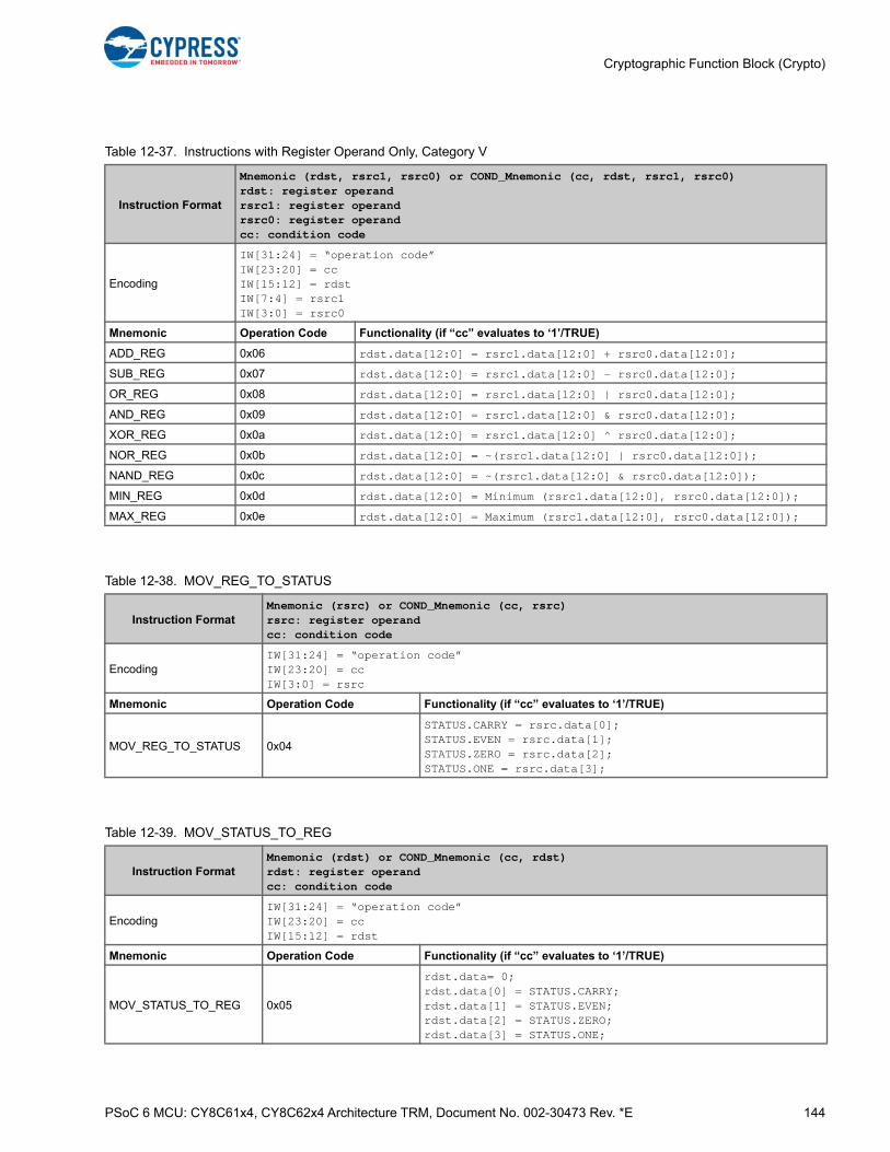
PSoC 6 MCU: CY8C61x4, CY8C62x4 Architecture TRM, Document No. 002-30473 Rev. *E 144
Cryptographic Function Block (Crypto)
Table 12-37. Instructions with Register Operand Only, Category V
Instruction Format
Mnemonic (rdst, rsrc1, rsrc0) or COND_Mnemonic (cc, rdst, rsrc1, rsrc0)rdst: register operandrsrc1: register operandrsrc0: register operandcc: condition code
Encoding
IW[31:24] = “operation code”IW[23:20] = ccIW[15:12] = rdstIW[7:4] = rsrc1IW[3:0] = rsrc0
Mnemonic Operation Code Functionality (if “cc” evaluates to ‘1’/TRUE)
ADD_REG 0x06 rdst.data[12:0] = rsrc1.data[12:0] + rsrc0.data[12:0];
SUB_REG 0x07 rdst.data[12:0] = rsrc1.data[12:0] – rsrc0.data[12:0];
OR_REG 0x08 rdst.data[12:0] = rsrc1.data[12:0] | rsrc0.data[12:0];
AND_REG 0x09 rdst.data[12:0] = rsrc1.data[12:0] & rsrc0.data[12:0];
XOR_REG 0x0a rdst.data[12:0] = rsrc1.data[12:0] ^ rsrc0.data[12:0];
NOR_REG 0x0b rdst.data[12:0] = ~(rsrc1.data[12:0] | rsrc0.data[12:0]);
NAND_REG 0x0c rdst.data[12:0] = ~(rsrc1.data[12:0] & rsrc0.data[12:0]);
MIN_REG 0x0d rdst.data[12:0] = Minimum (rsrc1.data[12:0], rsrc0.data[12:0]);
MAX_REG 0x0e rdst.data[12:0] = Maximum (rsrc1.data[12:0], rsrc0.data[12:0]);
Table 12-38. MOV_REG_TO_STATUS
Instruction FormatMnemonic (rsrc) or COND_Mnemonic (cc, rsrc)rsrc: register operandcc: condition code
EncodingIW[31:24] = “operation code”IW[23:20] = ccIW[3:0] = rsrc
Mnemonic Operation Code Functionality (if “cc” evaluates to ‘1’/TRUE)
MOV_REG_TO_STATUS 0x04
STATUS.CARRY = rsrc.data[0];STATUS.EVEN = rsrc.data[1];STATUS.ZERO = rsrc.data[2];STATUS.ONE = rsrc.data[3];
Table 12-39. MOV_STATUS_TO_REG
Instruction FormatMnemonic (rdst) or COND_Mnemonic (cc, rdst)rdst: register operandcc: condition code
EncodingIW[31:24] = “operation code”IW[23:20] = ccIW[15:12] = rdst
Mnemonic Operation Code Functionality (if “cc” evaluates to ‘1’/TRUE)
MOV_STATUS_TO_REG 0x05
rdst.data= 0;rdst.data[0] = STATUS.CARRY;rdst.data[1] = STATUS.EVEN;rdst.data[2] = STATUS.ZERO;rdst.data[3] = STATUS.ONE;

PSoC 6 MCU: CY8C61x4, CY8C62x4 Architecture TRM, Document No. 002-30473 Rev. *E 145
Cryptographic Function Block (Crypto)
Table 12-40. MOV_IMM_TO_STATUS
Instruction FormatMnemonic (imm4) or COND_Mnemonic (cc, imm4)imm4: immediate valuecc: condition code
EncodingIW[31:24] = “operation code”IW[23:20] = ccIW[3:0] = imm4
Mnemonic Operation Code Functionality (if “cc” evaluates to ‘1’/TRUE)
MOV_IMM_TO_STATUS 0x01
STATUS.CARRY = imm[0];STATUS.EVEN = imm[1];STATUS.ZERO = imm[2];STATUS.ONE = imm[3];
Table 12-41. Instructions with Mixed Operands, Category I
Instruction Format
Mnemonic (rdst, rsrc1, rsrc0) or COND_Mnemonic (cc, rdst, rsrc1, rsrc0)rdst: memory buffer operandrsrc1: memory buffer operandrsrc0: register operandcc: condition code
Encoding
IW[31:24] = “operation code”IW[23:20] = ccIW[15:12] = rdstIW[7:4] = rsrc1IW[3:0] = rsrc0
Shared FunctionalitySTATUS.EVEN = (dst_data[0] == 0)STATUS.ZERO = (dst_data[instr_size:0] == 0)STATUS.ONE = (dst_data[instr_size:0] == 1)
Mnemonic Operation Code Functionality (if “cc” evaluates to ‘1’/TRUE)
LSL 0x20
src1_data = GetMemData (rsrc1.data, rsrc1.size);src1_data = SizeAdjust (src1_data, rdst.size);dst_data = src1_data << rsrc0.data[12:0];if (rsrc0.data[12:0] != 0) STATUS.CARRY = dst_-data[rdst.size +1];else STATUS.CARRY = 0SetMemBuffData (rdst.data, dst_data, rdst.size);
LSR 0x23
src1_data = GetMemData (rsrc1.data, rsrc1.size);dst_data = src1_data >> rsrc0.data[12:0];if (rsrc0.data[12:0] != 0) STATUS.CARRY = dst_data[-1];else STATUS.CARRY = 0;SetMemBuffData (rdst.data, dst_data, rdst.size);
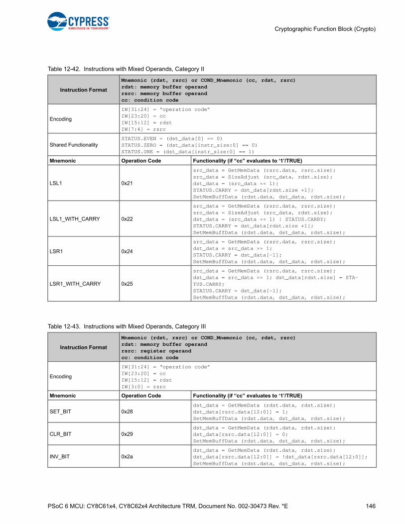
PSoC 6 MCU: CY8C61x4, CY8C62x4 Architecture TRM, Document No. 002-30473 Rev. *E 146
Cryptographic Function Block (Crypto)
Table 12-42. Instructions with Mixed Operands, Category II
Instruction Format
Mnemonic (rdst, rsrc) or COND_Mnemonic (cc, rdst, rsrc)rdst: memory buffer operandrsrc: memory buffer operandcc: condition code
Encoding
IW[31:24] = “operation code”IW[23:20] = ccIW[15:12] = rdstIW[7:4] = rsrc
Shared FunctionalitySTATUS.EVEN = (dst_data[0] == 0)STATUS.ZERO = (dst_data[instr_size:0] == 0)STATUS.ONE = (dst_data[instr_size:0] == 1)
Mnemonic Operation Code Functionality (if “cc” evaluates to ‘1’/TRUE)
LSL1 0x21
src_data = GetMemData (rsrc.data, rsrc.size);src_data = SizeAdjust (src_data, rdst.size);dst_data = (src_data << 1);STATUS.CARRY = dst_data[rdst.size +1];SetMemBuffData (rdst.data, dst_data, rdst.size);
LSL1_WITH_CARRY 0x22
src_data = GetMemData (rsrc.data, rsrc.size);src_data = SizeAdjust (src_data, rdst.size);dst_data = (src_data << 1) | STATUS.CARRY;STATUS.CARRY = dst_data[rdst.size +1];SetMemBuffData (rdst.data, dst_data, rdst.size);
LSR1 0x24
src_data = GetMemData (rsrc.data, rsrc.size);dst_data = src_data >> 1;STATUS.CARRY = dst_data[-1];SetMemBuffData (rdst.data, dst_data, rdst.size);
LSR1_WITH_CARRY 0x25
src_data = GetMemData (rsrc.data, rsrc.size);dst_data = src_data >> 1; dst_data[rdst.size] = STA-TUS.CARRY;STATUS.CARRY = dst_data[-1];SetMemBuffData (rdst.data, dst_data, rdst.size);
Table 12-43. Instructions with Mixed Operands, Category III
Instruction Format
Mnemonic (rdst, rsrc) or COND_Mnemonic (cc, rdst, rsrc)rdst: memory buffer operandrsrc: register operandcc: condition code
Encoding
IW[31:24] = “operation code”IW[23:20] = ccIW[15:12] = rdstIW[3:0] = rsrc
Mnemonic Operation Code Functionality (if “cc” evaluates to ‘1’/TRUE)
SET_BIT 0x28dst_data = GetMemData (rdst.data, rdst.size);dst_data[rsrc.data[12:0]] = 1;SetMemBuffData (rdst.data, dst_data, rdst.size);
CLR_BIT 0x29dst_data = GetMemData (rdst.data, rdst.size);dst_data[rsrc.data[12:0]] = 0;SetMemBuffData (rdst.data, dst_data, rdst.size);
INV_BIT 0x2adst_data = GetMemData (rdst.data, rdst.size);dst_data[rsrc.data[12:0]] = !dst_data[rsrc.data[12:0]];SetMemBuffData (rdst.data, dst_data, rdst.size);

PSoC 6 MCU: CY8C61x4, CY8C62x4 Architecture TRM, Document No. 002-30473 Rev. *E 147
Cryptographic Function Block (Crypto)
Table 12-44. Instructions with Mixed Operands, Category IV
Instruction Format
Mnemonic (rdst, rsrc1, rsrc0) or COND_Mnemonic (cc, rdst, rsrc1, rsrc0)rdst: register operandrsrc1: memory buffer operandrsrc0: register operandcc: condition code
Encoding
IW[31:24] = “operation code”IW[23:20] = ccIW[15:12] = rdstIW[7:4] = rsrc1IW[3:0] = rsrc0
Mnemonic Operation Code Functionality (if “cc” evaluates to ‘1’/TRUE)
GET_BIT 0x2b
src1_data = GetMemData (rsrc1.data, rsrc1.size);src1_bit = src1_data[rsrc0.data[12:0]];rdst.data = src1_bit;STATUS.CARRY = src1_bit;
Table 12-45. Instructions with Mixed Operands, Category V
Instruction Format
Mnemonic (rdst, rsrc1, rsrc0) or COND_Mnemonic (cc, rdst, rsrc1, rsrc0)rdst: register operandrsrc1: memory buffer operandrsrc0: memory buffer operandcc: condition code
Encoding
IW[31:24] = “operation code”IW[23:20] = ccIW[15:12] = rdstIW[7:4] = rsrc1IW[3:0] = rsrc0
Shared FunctionalitySTATUS.ZERO = (src0_data[instr_size:0] == src1_data[instr_size:0]) Note that for 8192-bit operands, two equal operands result in rdst.data[12:0] = “0”. The ZERO cause field can be used to identify this situation.
Mnemonic Operation Code Functionality (if “cc” evaluates to ‘1’/TRUE)
CLSAME 0x26
instr_size = Maximum (rsrc1.size, rsrc0.size);src0_data = GetMemData (rsrc0.data, rsrc0.size);src0_data = SizeAdjust (src0_data, instr_size);src1_data = GetMemData (rsrc1.data, rsrc1.size);src1_data = SizeAdjust (src1_data, instr_size);temp_data = src1_data ^ src0_data;for (idx = instr_size-1; idx >= 0; idx--) {if (temp_data[idx] == 1) break;}rdst.data[12:0] = instr_size - idx - 1;
CTSAME 0x27
instr_size = Maximum (rsrc1.size, rsrc0.size);src0_data = GetMemData (rsrc0.data, rsrc0.size);src0_data = SizeAdjust (src0_data, instr_size);src1_data = GetMemData (rsrc1.data, rsrc1.size);src1_data = SizeAdjust (src1_data, instr_size);temp_data = src1_data ^ src0_data;for (idx = 0; idx < instr_size; idx++) {if (temp_data[idx] == 1) break;}rdst.data[12:0] = idx;
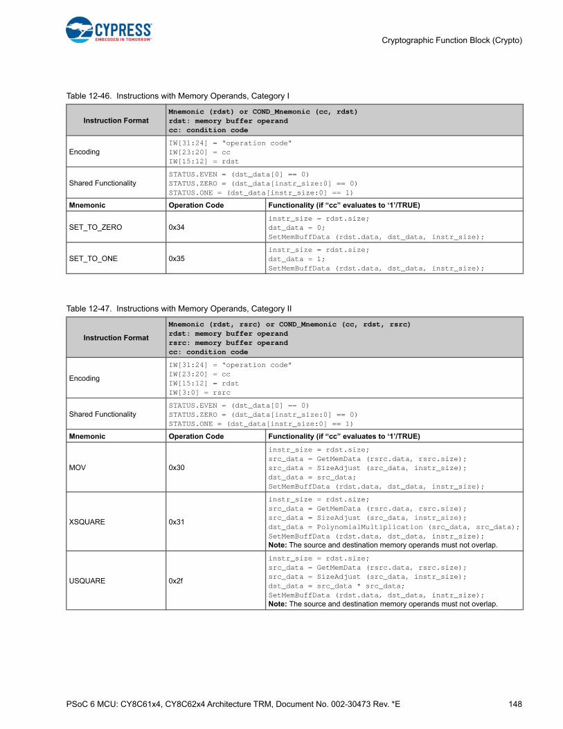
PSoC 6 MCU: CY8C61x4, CY8C62x4 Architecture TRM, Document No. 002-30473 Rev. *E 148
Cryptographic Function Block (Crypto)
Table 12-46. Instructions with Memory Operands, Category I
Instruction FormatMnemonic (rdst) or COND_Mnemonic (cc, rdst)rdst: memory buffer operandcc: condition code
EncodingIW[31:24] = “operation code”IW[23:20] = ccIW[15:12] = rdst
Shared FunctionalitySTATUS.EVEN = (dst_data[0] == 0)STATUS.ZERO = (dst_data[instr_size:0] == 0)STATUS.ONE = (dst_data[instr_size:0] == 1)
Mnemonic Operation Code Functionality (if “cc” evaluates to ‘1’/TRUE)
SET_TO_ZERO 0x34instr_size = rdst.size;dst_data = 0;SetMemBuffData (rdst.data, dst_data, instr_size);
SET_TO_ONE 0x35instr_size = rdst.size;dst_data = 1;SetMemBuffData (rdst.data, dst_data, instr_size);
Table 12-47. Instructions with Memory Operands, Category II
Instruction Format
Mnemonic (rdst, rsrc) or COND_Mnemonic (cc, rdst, rsrc)rdst: memory buffer operandrsrc: memory buffer operandcc: condition code
Encoding
IW[31:24] = “operation code”IW[23:20] = ccIW[15:12] = rdstIW[3:0] = rsrc
Shared FunctionalitySTATUS.EVEN = (dst_data[0] == 0)STATUS.ZERO = (dst_data[instr_size:0] == 0)STATUS.ONE = (dst_data[instr_size:0] == 1)
Mnemonic Operation Code Functionality (if “cc” evaluates to ‘1’/TRUE)
MOV 0x30
instr_size = rdst.size;src_data = GetMemData (rsrc.data, rsrc.size);src_data = SizeAdjust (src_data, instr_size);dst_data = src_data;SetMemBuffData (rdst.data, dst_data, instr_size);
XSQUARE 0x31
instr_size = rdst.size;src_data = GetMemData (rsrc.data, rsrc.size);src_data = SizeAdjust (src_data, instr_size);dst_data = PolynomialMultiplication (src_data, src_data);SetMemBuffData (rdst.data, dst_data, instr_size);Note: The source and destination memory operands must not overlap.
USQUARE 0x2f
instr_size = rdst.size;src_data = GetMemData (rsrc.data, rsrc.size);src_data = SizeAdjust (src_data, instr_size);dst_data = src_data * src_data;SetMemBuffData (rdst.data, dst_data, instr_size);Note: The source and destination memory operands must not overlap.
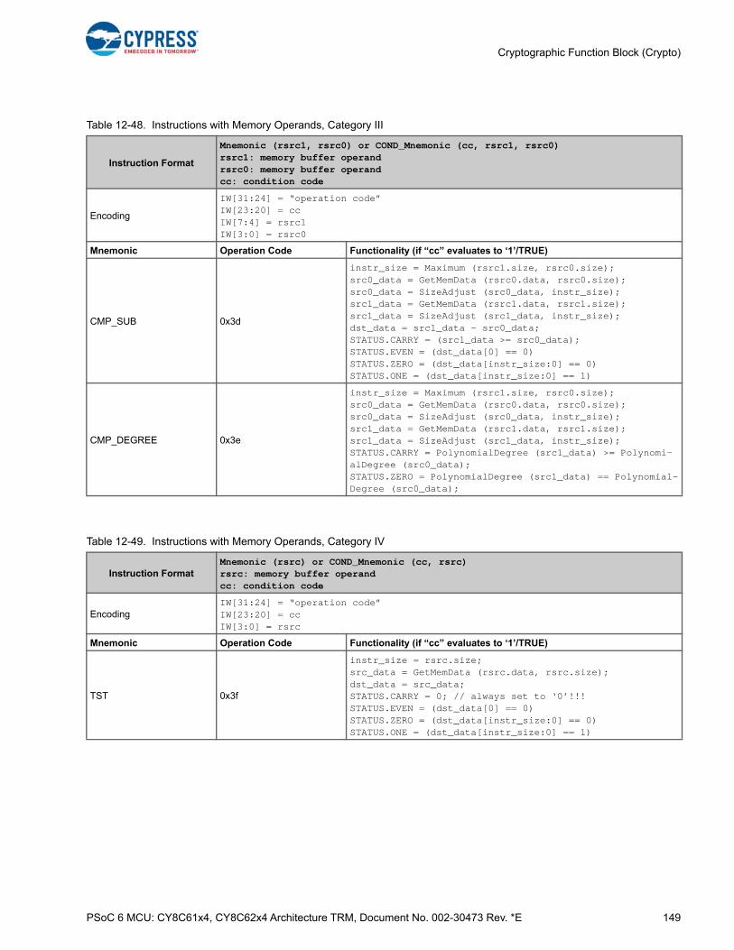
PSoC 6 MCU: CY8C61x4, CY8C62x4 Architecture TRM, Document No. 002-30473 Rev. *E 149
Cryptographic Function Block (Crypto)
Table 12-48. Instructions with Memory Operands, Category III
Instruction Format
Mnemonic (rsrc1, rsrc0) or COND_Mnemonic (cc, rsrc1, rsrc0)rsrc1: memory buffer operandrsrc0: memory buffer operandcc: condition code
Encoding
IW[31:24] = “operation code”IW[23:20] = ccIW[7:4] = rsrc1IW[3:0] = rsrc0
Mnemonic Operation Code Functionality (if “cc” evaluates to ‘1’/TRUE)
CMP_SUB 0x3d
instr_size = Maximum (rsrc1.size, rsrc0.size);src0_data = GetMemData (rsrc0.data, rsrc0.size);src0_data = SizeAdjust (src0_data, instr_size);src1_data = GetMemData (rsrc1.data, rsrc1.size);src1_data = SizeAdjust (src1_data, instr_size);dst_data = src1_data – src0_data;STATUS.CARRY = (src1_data >= src0_data);STATUS.EVEN = (dst_data[0] == 0)STATUS.ZERO = (dst_data[instr_size:0] == 0)STATUS.ONE = (dst_data[instr_size:0] == 1)
CMP_DEGREE 0x3e
instr_size = Maximum (rsrc1.size, rsrc0.size);src0_data = GetMemData (rsrc0.data, rsrc0.size);src0_data = SizeAdjust (src0_data, instr_size);src1_data = GetMemData (rsrc1.data, rsrc1.size);src1_data = SizeAdjust (src1_data, instr_size);STATUS.CARRY = PolynomialDegree (src1_data) >= Polynomi-alDegree (src0_data);STATUS.ZERO = PolynomialDegree (src1_data) == Polynomial-Degree (src0_data);
Table 12-49. Instructions with Memory Operands, Category IV
Instruction FormatMnemonic (rsrc) or COND_Mnemonic (cc, rsrc)rsrc: memory buffer operandcc: condition code
EncodingIW[31:24] = “operation code”IW[23:20] = ccIW[3:0] = rsrc
Mnemonic Operation Code Functionality (if “cc” evaluates to ‘1’/TRUE)
TST 0x3f
instr_size = rsrc.size;src_data = GetMemData (rsrc.data, rsrc.size);dst_data = src_data;STATUS.CARRY = 0; // always set to ‘0’!!!STATUS.EVEN = (dst_data[0] == 0)STATUS.ZERO = (dst_data[instr_size:0] == 0)STATUS.ONE = (dst_data[instr_size:0] == 1)

PSoC 6 MCU: CY8C61x4, CY8C62x4 Architecture TRM, Document No. 002-30473 Rev. *E 150
Cryptographic Function Block (Crypto)
Table 12-50. Instructions with Memory Operands, Category V
Instruction Format
Mnemonic (rdst, rsrc1, rsrc0) or COND_Mnemonic (cc, rdst, rsrc1, rsrc0)rdst: memory buffer operandrsrc1: memory buffer operandrsrc0: memory buffer operandcc: condition code
Encoding
IW[31:24] = “operation code”IW[23:20] = ccIW[15:12] = rdstIW[7:4] = rsrc1IW[3:0] = rsrc0
Shared FunctionalitySTATUS.EVEN = (dst_data[0] == 0)STATUS.ZERO = (dst_data[instr_size:0] == 0)STATUS.ONE = (dst_data[instr_size:0] == 1)
Mnemonic Operation Code Functionality (if “cc” evaluates to ‘1’/TRUE)
XMUL 0x32
instr_size = rdst.size;src0_data = GetMemData (rsrc0.data, rsrc0.size);src0_data = SizeAdjust (src0_data, instr_size);src1_data = GetMemData (rsrc1.data, rsrc1.size);src1_data = SizeAdjust (src1_data, instr_size);dst_data = PolynomialMultiplication (src1_data, src0_-data);SetMemBuffData (rdst.data, dst_data, instr_size);Note: The source and destination memory operands must not overlap.When one of the operands is 32 or less bits in size, performance is best when rsrc0 is used for this operand.
UMUL 0x33
instr_size = rdst.size;src0_data = GetMemData (rsrc0.data, rsrc0.size);src0_data = SizeAdjust (src0_data, instr_size);src1_data = GetMemData (rsrc1.data, rsrc1.size);src1_data = SizeAdjust (src1_data, instr_size);dst_data = src1_data * src0_data;SetMemBuffData (rdst.data, dst_data, instr_size);Note: The source and destination memory operands must not overlap.When one of the operands is 32 or less bits in size, performance is best when rsrc0 is used for this operand.
ADD 0x36
instr_size = rdst.size;src0_data = GetMemData (rsrc0.data, rsrc0.size);src0_data = SizeAdjust (src0_data, instr_size);src1_data = GetMemData (rsrc1.data, rsrc1.size);src1_data = SizeAdjust (src1_data, instr_size);dst_data = src1_data + src0_data;STATUS.CARRY = (dst_data >= (1 << instr_size));SetMemBuffData (rdst.data, dst_data, instr_size);

PSoC 6 MCU: CY8C61x4, CY8C62x4 Architecture TRM, Document No. 002-30473 Rev. *E 151
Cryptographic Function Block (Crypto)
SUB 0x37
instr_size = rdst.size;src0_data = GetMemData (rsrc0.data, rsrc0.size);src0_data = SizeAdjust (src0_data, instr_size);src1_data = GetMemData (rsrc1.data, rsrc1.size);src1_data = SizeAdjust (src1_data, instr_size);dst_data = src1_data - src0_data;STATUS.CARRY = (src1_data >= src0_data);SetMemBuffData (rdst.data, dst_data, instr_size);
ADD_WITH_CARRY 0x14
instr_size = rdst.size;src0_data = GetMemData (rsrc0.data, rsrc0.size);src0_data = SizeAdjust (src0_data, instr_size);src1_data = GetMemData (rsrc1.data, rsrc1.size);src1_data = SizeAdjust (src1_data, instr_size);dst_data = src1_data + src0_data + STATUS.CARRY;STATUS.CARRY = (dst_data >= (1 << instr_size));SetMemBuffData (rdst.data, dst_data, instr_size);
SUB_WITH_CARRY 0x15
instr_size = rdst.size;src0_data = GetMemData (rsrc0.data, rsrc0.size);src0_data = SizeAdjust (src0_data, instr_size);src1_data = GetMemData (rsrc1.data, rsrc1.size);src1_data = SizeAdjust (src1_data, instr_size);dst_data = src1_data - src0_data – !STATUS.CARRY;STATUS.CARRY = (src1_data >= src0_data);SetMemBuffData (rdst.data, dst_data, instr_size);
OR, AND, XOR, NOR, NAND
0x38, 0x39, 0x3a, 0x3b, 0x3c
instr_size = rdst.size;src0_data = GetMemData (rsrc0.data, rsrc0.size);src0_data = SizeAdjust (src0_data, instr_size);src1_data = GetMemData (rsrc1.data, rsrc1.size);src1_data = SizeAdjust (src1_data, instr_size);OR: dst_data = src1_data | src0_data;AND: dst_data = src1_data & src0_data;XOR: dst_data = src1_data ^ src0_data;NOR: dst_data = ~(src1_data | src0_data);NAND: dst_data = ~(src1_data & src0_data);SetMemBuffData (rdst.data, dst_data, instr_size);
Table 12-50. Instructions with Memory Operands, Category V
Instruction Format
Mnemonic (rdst, rsrc1, rsrc0) or COND_Mnemonic (cc, rdst, rsrc1, rsrc0)rdst: memory buffer operandrsrc1: memory buffer operandrsrc0: memory buffer operandcc: condition code
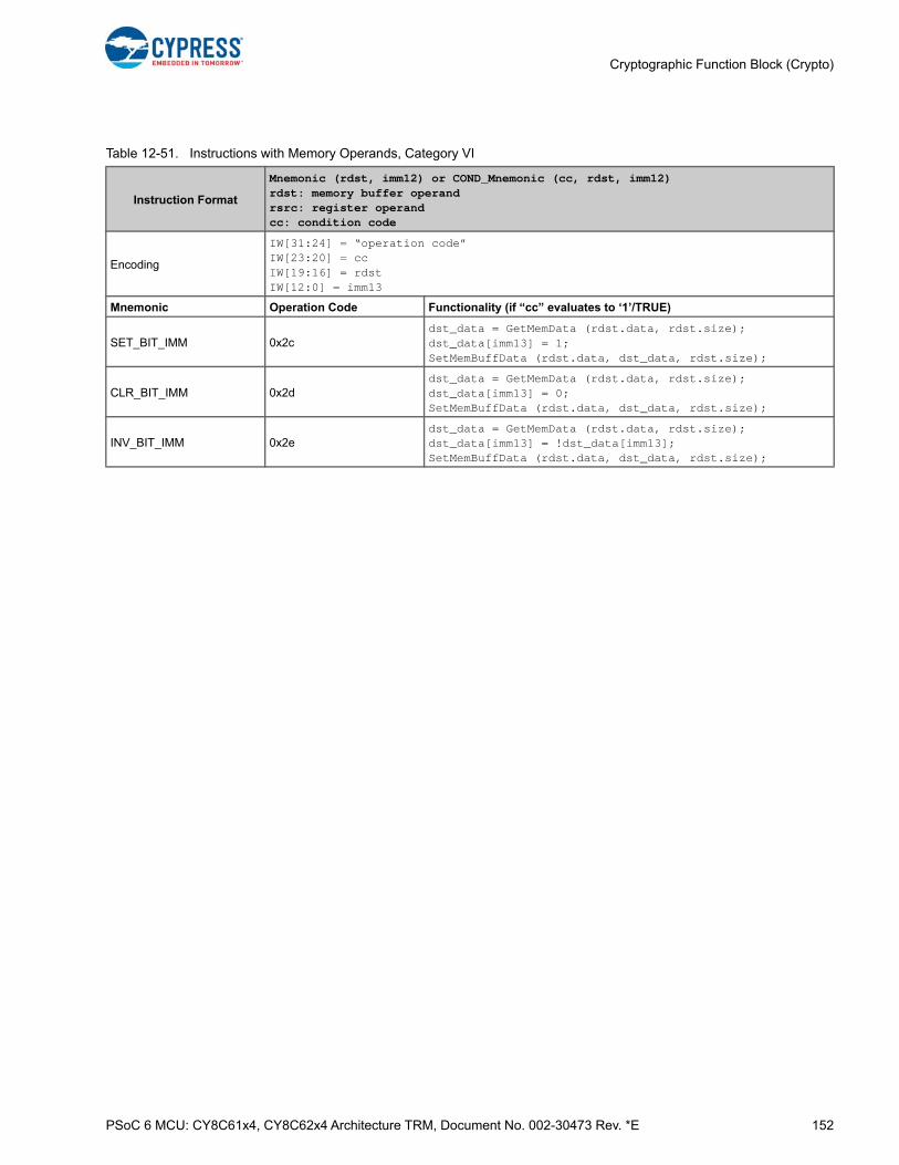
PSoC 6 MCU: CY8C61x4, CY8C62x4 Architecture TRM, Document No. 002-30473 Rev. *E 152
Cryptographic Function Block (Crypto)
Table 12-51. Instructions with Memory Operands, Category VI
Instruction Format
Mnemonic (rdst, imm12) or COND_Mnemonic (cc, rdst, imm12)rdst: memory buffer operandrsrc: register operandcc: condition code
Encoding
IW[31:24] = “operation code”IW[23:20] = ccIW[19:16] = rdstIW[12:0] = imm13
Mnemonic Operation Code Functionality (if “cc” evaluates to ‘1’/TRUE)
SET_BIT_IMM 0x2cdst_data = GetMemData (rdst.data, rdst.size);dst_data[imm13] = 1;SetMemBuffData (rdst.data, dst_data, rdst.size);
CLR_BIT_IMM 0x2ddst_data = GetMemData (rdst.data, rdst.size);dst_data[imm13] = 0;SetMemBuffData (rdst.data, dst_data, rdst.size);
INV_BIT_IMM 0x2edst_data = GetMemData (rdst.data, rdst.size);dst_data[imm13] = !dst_data[imm13];SetMemBuffData (rdst.data, dst_data, rdst.size);
PSoC 6 MCU: CY8C61x4, CY8C62x4 Architecture TRM, Document No. 002-30473 Rev. *E 153
13. Program and Debug Interface
The PSoC 6 MCU Program and Debug interface provides a communication gateway for an external device to performprogramming or debugging. The external device can be a Cypress-supplied programmer and debugger, or a third-partydevice that supports programming and debugging. The serial wire debug (SWD) or the JTAG interface can be used as thecommunication protocol between the external device and PSoC 6 MCUs.
13.1 Features■ Supports programming and debugging through the JTAG or SWD interface.
■ CM4 supports 4-bit ETM tracing, serial wire viewer (SWV), and printf() style debugging through the single-wire output (SWO) pin. CM0+ supports Micro Trace Buffer (MTB) with 4 KB dedicated RAM.
■ Supports Cross Triggering Interface (CTI) and Cross Triggering Matrix (CTM).
■ CM0+ supports four hardware breakpoints and two watchpoints. CM4 supports six hardware breakpoints and four watchpoints.
■ Provides read and write access to all memory and registers in the system while debugging, including the Cortex-M4 and Cortex-M0+ register banks when the core is running or halted.
13.2 Architecture
Figure 13-1 shows the block diagram of the program and debug interface in the PSoC 6 MCU. The debug and access port(DAP) acts as the program and debug interface. The external programmer or debugger, also known as the “host”,communicates with the DAP of the PSoC 6 MCU “target” using either the SWD or JTAG interface. The debug physical portpins communicate with the DAP through the high-speed I/O matrix (HSIOM). See the I/O System chapter on page 214 fordetails on HSIOM.
The debug infrastructure is organized in the following four groups:
■ DAP (provides pin interfaces through which the debug host can connect to the chip)
■ Cortex-M0+ core debug components
■ Cortex-M4 core debug components
■ Other debug infrastructure (includes the CM4 tracing, the CTM, and the System ROM table)
This PSoC 6 MCU technical reference manual (TRM) provides comprehensive and detailed information about thefunctions of the PSoC 6 MCU device hardware. It is divided into two books: architecture TRM and registers TRM. TheTRM is not recommended for those new to the PSoC 6 MCU, nor as a guide for developing PSoC 6 MCU applications.Use these documents instead:
■ PSoC 61 datasheet, PSoC 62 datasheet
■ Peripheral Driver Library (PDL) documentation
■ Application notes
■ Code examples

PSoC 6 MCU: CY8C61x4, CY8C62x4 Architecture TRM, Document No. 002-30473 Rev. *E 154
Program and Debug Interface
Figure 13-1. Program and Debug Interface
The DAP communicates with the Cortex-M0+ CPU using the Arm-specified advanced high-performance bus (AHB) interface.AHB is the systems interconnect protocol used inside the device, which facilitates memory and peripheral register access bythe AHB master. The PSoC 6 MCU has six AHB masters – Arm CM4 CPU core, Arm CM0 CPU core, Datawire0, Datawire1,Crypto, and DAP. The external host can effectively take control of the entire device through the DAP to perform programmingand debugging operations.
The following are the various debug and trace components:
■ Debug components
❐ JTAG and SWD for debug control and access
■ Trace source components
❐ Micro trace buffer (MTB-M0+) for tracing Cortex-M0+ program execution
❐ Embedded trace macrocell (ETM-M4) for tracing Cortex-M4 program execution
■ Trace sink components
❐ Trace port interface unit (TPIU) to drive the trace information out of the chip to an external trace port analyzer
■ Cross-triggering components
❐ Cross-trigger interface (CTI)
❐ Cross-trigger matrix (CTM)
■ ROM tables
Cortex-M0+
PSoC 6
SW
D/J
TA
G
CM0 Access Port
System Access Port
DA
P B
US
DAP
Arm Cortex-M4 subsystem
Arm Cortex-M0+ subsystem
CM0+ AHB decoder
Micro Trace Buffer (MTB)
Cross Trigger Interface (CTI)
CM0 external ROM table
SLV
AHB SRAM
Cortex-M4
CM4 APB decoder
Embedded Trace Macro (ETM)
Cross Trigger Interface (CTI)
CM4 ROM table
AHB
CM4 AP
DA
PD
AP
ITM
Debug APB decoder
Debug ROM table
Cross Trigger Interface (CTI)
Cross Trigger Matrix (CTM)
Trace Port Interface Unit
(TPIU)Por
t P
ins
System ROM table
PSoC 6 MCU: CY8C61x4, CY8C62x4 Architecture TRM, Document No. 002-30473 Rev. *E 155
Program and Debug Interface
13.2.1 Debug Access Port (DAP)
The DAP consists of a combined SWD/JTAG interface(SWJ) that also includes the SWD listener. The SWDlistener decides whether the JTAG interface (default) orSWD interface is active. Note that JTAG and SWD aremutually exclusive because they share pins.
The debug port (DP) connects to the DAP bus, which in turnconnects to one of three Access Ports (AP), namely:
■ The CM0-AP, which connects directly to the AHB debug slave port (SLV) of the CM0+ and gives access to the CM0+ internal debug components. This also allows access to the rest of the system through the CM0+ AHB master interface. This provides the debug host the same view as an application running on the CM0+. This includes access to the MMIO of other debug components of the Cortex M0+ subsystem. These debug components can also be accessed by the CM0+ CPU, but cannot be reached through the other APs or by the CM4 core.
■ The CM4-AP located inside the CM4 gives access to the CM4 internal debug components. The CM4-AP also allows access to the rest of the system through the CM4 AHB master interfaces. This provides the debug host the same view as an application running on the CM4 core. Additionally, the CM4-AP provides access to the debug components in the CM4 core through the External Peripheral Bus (EPB). These debug components can also be accessed by the CM4 CPU, but cannot be reached through the other APs or by the CM0+ core.
■ The System-AP, which through an AHB mux gives access to the rest of the system. This allows access to the System ROM table, which cannot be reached any other way. The System ROM table provides the chip ID but is otherwise empty.
13.2.1.1 DAP Security
For security reasons all three APs each can beindependently disabled. Each AP disable is controlled bytwo MMIO bits. One bit, CPUSS_AP_CTL.xxx_DISABLE(where xxx can be CM0 or CM4 or SYS), can be set duringboot, before the debugger can connect, based on eFusesettings. After this bit is set it cannot be cleared.
The second bit, CPUSS_AP_CTL.xxx_ENABLE, is a regularread/write bit. This bit also resets to zero and is set to ‘1’ byeither the ROM boot code or the flash boot code dependingon the life-cycle stage. This feature can be used to blockdebug access during normal operation, but re-enable somedebug access after a successful authentication.
In addition to the above, the System AP is also protected byan MPU. This can be used to give the debugger limitedaccess to the rest of the system. Allow access to the SystemROM table for chip identification. If debug access is restoredafter successful authentication, this MPU must beconfigured to allow authentication requests.
Note: The debug slave interfaces of both the CPUs bypassthe internal CPU MPU.
13.2.1.2 DAP Power Domain
Almost all the debug components are part of the Activepower domain. The only exception is the SWD/JTAG-DP,which is part of the Deep Sleep power domain. This allowsthe debug host to connect during Deep Sleep, while theapplication is ‘running’ or powered down. This enables in-field debugging for low-power applications in which the chipis mostly in Deep Sleep.
After the debugger is connected to the chip, it must bring thechip to the Active state before any operation. For this, theSWD/JTAG-DP has a register (DP_CTL_STAT) with twopower request bits. The two bits are CDBGPWRUPREQand CSYSPWRUPREQ, which request for debug powerand system power, respectively. These bits must remain setfor the duration of the debug session.
Note that only the two SWD pins (SWCLKTCK andSWDIOTMS) are operational during the Deep Sleep mode –the JTAG pins are operational only in Active mode. TheJTAG debug and JTAG boundary scan are not availablewhen the system is in Deep Sleep mode. JTAG functionalityis available only after a chip power-on-reset.
13.2.2 ROM Tables
The ROM tables are organized in a tree hierarchy. Each APhas a register that contains a 32-bit address pointer to thebase of the root ROM table for that AP. For PSoC 6 MCUs,there are three such root ROM tables.
Each ROM table contains 32-bit entries with an addresspointer that either points to the base of the next level ROMtable. Each ROM table also contains a set of ID registersthat hold JEDEC compliant identifiers to identify themanufacturer, part number, and major and minor revisionnumbers. For all ROM tables in PSoC 6 MCUs, these IDsare the same. Each ROM table and CoreSight compliantcomponent also contains component identification registers.
13.2.3 Trace
The micro trace buffer (MTB-M0+) component captures theprogram execution flow from Cortex-M0+ CPU and stores itin a local SRAM memory. This information can be read byan external debug tool through JTAG/SWD interface toconstruct the program execution flow.
The embedded trace macro (ETM) component connected toCortex-M4 captures the program execution flow fromCortex-M4 CPU and generates trace output on its advancedtrace bus (ATB) interface. The instrumentation tracemacrocell (ITM), which is inside Cortex-M4, also generatestrace output on its ATB interface. These two ATB interfaces(from ETM-M4 and ITM) are connected a trace port interfaceunit (TPIU).
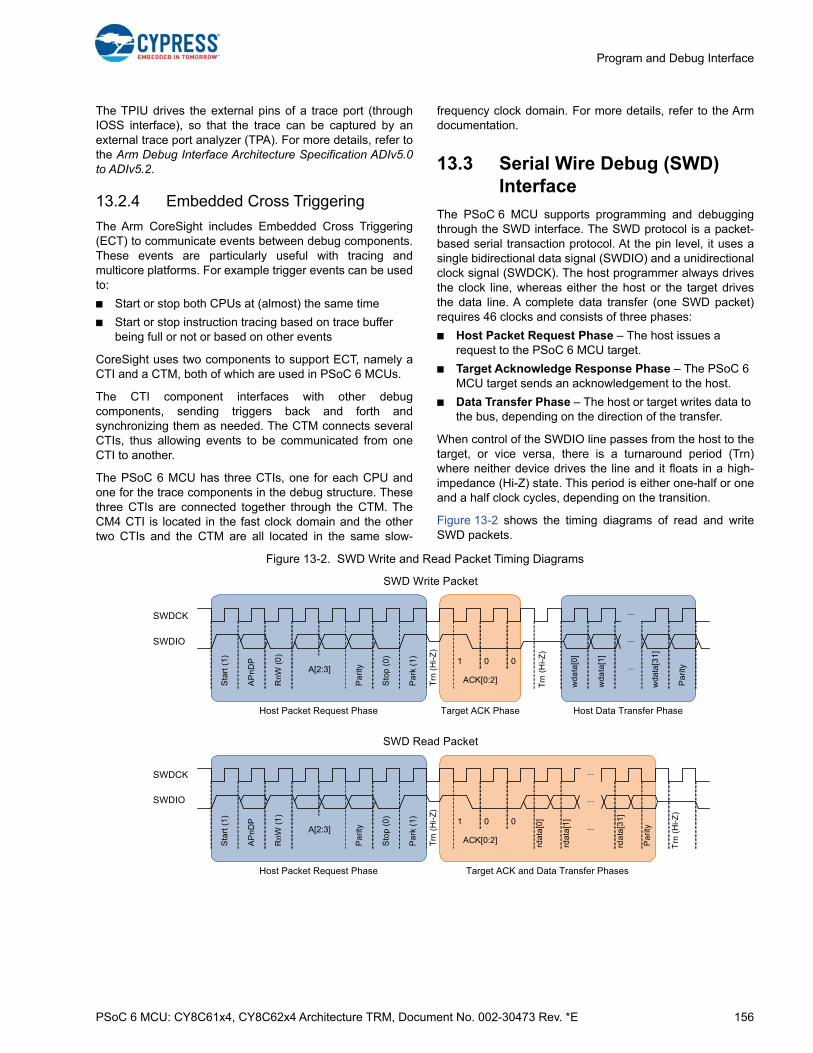
PSoC 6 MCU: CY8C61x4, CY8C62x4 Architecture TRM, Document No. 002-30473 Rev. *E 156
Program and Debug Interface
The TPIU drives the external pins of a trace port (throughIOSS interface), so that the trace can be captured by anexternal trace port analyzer (TPA). For more details, refer tothe Arm Debug Interface Architecture Specification ADIv5.0to ADIv5.2.
13.2.4 Embedded Cross Triggering
The Arm CoreSight includes Embedded Cross Triggering(ECT) to communicate events between debug components.These events are particularly useful with tracing andmulticore platforms. For example trigger events can be usedto:
■ Start or stop both CPUs at (almost) the same time
■ Start or stop instruction tracing based on trace buffer being full or not or based on other events
CoreSight uses two components to support ECT, namely aCTI and a CTM, both of which are used in PSoC 6 MCUs.
The CTI component interfaces with other debugcomponents, sending triggers back and forth andsynchronizing them as needed. The CTM connects severalCTIs, thus allowing events to be communicated from oneCTI to another.
The PSoC 6 MCU has three CTIs, one for each CPU andone for the trace components in the debug structure. Thesethree CTIs are connected together through the CTM. TheCM4 CTI is located in the fast clock domain and the othertwo CTIs and the CTM are all located in the same slow-
frequency clock domain. For more details, refer to the Armdocumentation.
13.3 Serial Wire Debug (SWD) Interface
The PSoC 6 MCU supports programming and debuggingthrough the SWD interface. The SWD protocol is a packet-based serial transaction protocol. At the pin level, it uses asingle bidirectional data signal (SWDIO) and a unidirectionalclock signal (SWDCK). The host programmer always drivesthe clock line, whereas either the host or the target drivesthe data line. A complete data transfer (one SWD packet)requires 46 clocks and consists of three phases:
■ Host Packet Request Phase – The host issues a request to the PSoC 6 MCU target.
■ Target Acknowledge Response Phase – The PSoC 6 MCU target sends an acknowledgement to the host.
■ Data Transfer Phase – The host or target writes data to the bus, depending on the direction of the transfer.
When control of the SWDIO line passes from the host to thetarget, or vice versa, there is a turnaround period (Trn)where neither device drives the line and it floats in a high-impedance (Hi-Z) state. This period is either one-half or oneand a half clock cycles, depending on the transition.
Figure 13-2 shows the timing diagrams of read and writeSWD packets.
Figure 13-2. SWD Write and Read Packet Timing Diagrams
Sta
rt (
1)
AP
nD
P
RnW
(0
)
A[2:3]
Pa
rity
Sto
p (
0)
Pa
rk (
1)
Trn
(H
i-Z)
1
wd
ata
[0]
Pa
rity
ACK[0:2]
0 0
wd
ata
[1]
wda
ta[3
1]
...
...
...
Trn
(H
i-Z
)
Host Packet Request Phase Target ACK Phase Host Data Transfer Phase
SWD Write Packet
Sta
rt (
1)
AP
nDP
Rn
W (
1)
A[2:3]
Pa
rity
Sto
p (
0)
Pa
rk (
1)
Trn
(H
i-Z
)
1
rda
ta[0
]
Pa
rity
ACK[0:2]
0 0
rda
ta[1
]
rda
ta[3
1]
...
...
...
Trn
(H
i-Z)
Host Packet Request Phase Target ACK and Data Transfer Phases
SWD Read Packet
SWDCK
SWDIO
SWDCK
SWDIO

PSoC 6 MCU: CY8C61x4, CY8C62x4 Architecture TRM, Document No. 002-30473 Rev. *E 157
Program and Debug Interface
The sequence to transmit SWD read and write packets areas follows:
1. Host Packet Request Phase: SWDIO driven by the host
a. The start bit initiates a transfer; it is always logic 1.
b. The AP not DP (APnDP) bit determines whether the transfer is an AP access – 1b or a DP access – 0b.
c. The Read not Write bit (RnW) controls which direction the data transfer is in. 1b represents a ‘read from’ the target, or 0b for a ‘write to’ the target.
d. The Address bits (A[3:2]) are register select bits for AP or DP, depending on the APnDP bit value. Note: Address bits are transmitted with the LSb first.
e. The parity bit contains the parity of APnDP, RnW, and ADDR bits. It is an even parity bit; this means, when XORed with the other bits, the result will be 0.
If the parity bit is not correct, the header is ignored by the PSoC 6 MCU; there is no ACK response (ACK = 111b). The programming operation should be aborted and retried again by following a device reset.
f. The stop bit is always logic 0.
g. The park bit is always logic 1.
2. Target Acknowledge Response Phase: SWDIO driven by the target
a. The ACK[2:0] bits represent the target to host response, indicating failure or success, among other results. See Table 13-1 for definitions. Note: ACK bits are transmitted with the LSb first.
3. Data Transfer Phase: SWDIO driven by either target or host depending on direction
a. The data for read or write is written to the bus, LSb first.
b. The data parity bit indicates the parity of the data read or written. It is an even parity; this means when XORed with the data bits, the result will be 0.
If the parity bit indicates a data error, corrective action should be taken. For a read packet, if the host detects a parity error, it must abort the programming operation and restart. For a write packet, if the target detects a parity error, it generates a FAULT ACK response in the next packet.
According to the SWD protocol, the host can generate anynumber of SWDCK clock cycles between two packets withSWDIO low. Three or more dummy clock cycles should begenerated between two SWD packets if the clock is not free-running or to make the clock free-running in IDLE mode.
The SWD interface can be reset by clocking the SWDCKline for 50 or more cycles with SWDIO high. To return to theidle state, clock the SWDIO low once.
13.3.1 SWD Timing Details
The SWDIO line is written to and read at different timesdepending on the direction of communication. The host
drives the SWDIO line during the Host Packet Requestphase and, if the host is writing data to the target, during theData Transfer phase as well. When the host is driving theSWDIO line, each new bit is written by the host on fallingSWDCK edges, and read by the target on rising SWDCKedges. The target drives the SWDIO line during the TargetAcknowledge Response phase and, if the target is readingout data, during the Data Transfer phase as well. When thetarget is driving the SWDIO line, each new bit is written bythe target on rising SWDCK edges, and read by the host onfalling SWDCK edges.
Table 13-1 and Figure 13-2 illustrate the timing of SWDIO bitwrites and reads.
13.3.2 ACK Details
The acknowledge (ACK) bitfield is used to communicate thestatus of the previous transfer. OK ACK means that previouspacket was successful. A WAIT response requires a dataphase. For a FAULT status, the programming operationshould be aborted immediately. Table 13-2 shows the ACKbit-field decoding details.
Details on WAIT and FAULT response behaviors are asfollows:
■ For a WAIT response, if the transaction is a read, the host should ignore the data read in the data phase. The target does not drive the line and the host must not check the parity bit as well.
■ For a WAIT response, if the transaction is a write, the data phase is ignored by the PSoC 6 MCU. But, the host must still send the data to be written to complete the packet. The parity bit corresponding to the data should also be sent by the host.
■ A WAIT response means that the PSoC 6 MCU is processing the previous transaction. The host can try for a maximum of four continuous WAIT responses to see whether an OK response is received. If it fails, then the
Table 13-1. SWDIO Bit Write and Read Timing
SWD Packet PhaseSWDIO Edge
Falling Rising
Host Packet RequestHost Write Target Read
Host Data Transfer
Target Ack ResponseHost Read Target Write
Target Data Transfer
Table 13-2. SWD Transfer ACK Response Decoding
Response ACK[2:0]
OK 001b
WAIT 010b
FAULT 100b
NO ACK 111b
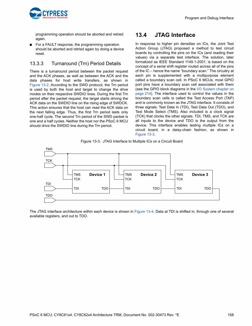
PSoC 6 MCU: CY8C61x4, CY8C62x4 Architecture TRM, Document No. 002-30473 Rev. *E 158
Program and Debug Interface
programming operation should be aborted and retried again.
■ For a FAULT response, the programming operation should be aborted and retried again by doing a device reset.
13.3.3 Turnaround (Trn) Period Details
There is a turnaround period between the packet requestand the ACK phases, as well as between the ACK and thedata phases for host write transfers, as shown inFigure 13-2. According to the SWD protocol, the Trn periodis used by both the host and target to change the drivemodes on their respective SWDIO lines. During the first Trnperiod after the packet request, the target starts driving theACK data on the SWDIO line on the rising edge of SWDCK.This action ensures that the host can read the ACK data onthe next falling edge. Thus, the first Trn period lasts onlyone-half cycle. The second Trn period of the SWD packet isone and a half cycles. Neither the host nor the PSoC 6 MCUshould drive the SWDIO line during the Trn period.
13.4 JTAG Interface
In response to higher pin densities on ICs, the Joint TestAction Group (JTAG) proposed a method to test circuitboards by controlling the pins on the ICs (and reading theirvalues) via a separate test interface. The solution, laterformalized as IEEE Standard 1149.1-2001, is based on theconcept of a serial shift register routed across all of the pinsof the IC – hence the name “boundary scan.” The circuitry ateach pin is supplemented with a multipurpose elementcalled a boundary scan cell. In PSoC 6 MCUs, most GPIOport pins have a boundary scan cell associated with them(see the GPIO block diagrams in the I/O System chapter onpage 214). The interface used to control the values in theboundary scan cells is called the Test Access Port (TAP)and is commonly known as the JTAG interface. It consists ofthree signals: Test Data In (TDI), Test Data Out (TDO), andTest Mode Select (TMS). Also included is a clock signal(TCK) that clocks the other signals. TDI, TMS, and TCK areall inputs to the device and TDO is the output from thedevice. This interface enables testing multiple ICs on acircuit board, in a daisy-chain fashion, as shown inFigure 13-3.
Figure 13-3. JTAG Interface to Multiple ICs on a Circuit Board
The JTAG interface architecture within each device is shown in Figure 13-4. Data at TDI is shifted in, through one of severalavailable registers, and out to TDO.
TMS
TCK
TDI TDO
TMS
TCK
TDI
TDO
Device 1 TMS
TCK
TDI TDO
Device 2 TMS
TCK
TDI TDO
Device 3
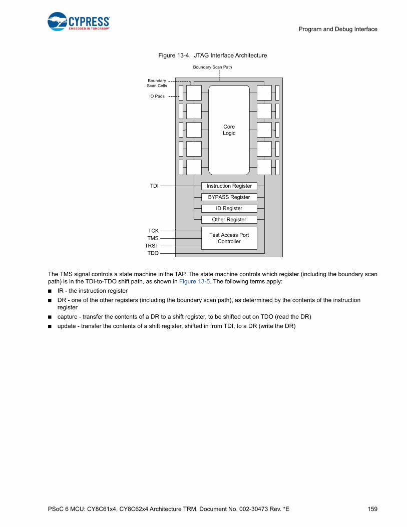
PSoC 6 MCU: CY8C61x4, CY8C62x4 Architecture TRM, Document No. 002-30473 Rev. *E 159
Program and Debug Interface
Figure 13-4. JTAG Interface Architecture
The TMS signal controls a state machine in the TAP. The state machine controls which register (including the boundary scanpath) is in the TDI-to-TDO shift path, as shown in Figure 13-5. The following terms apply:
■ IR - the instruction register
■ DR - one of the other registers (including the boundary scan path), as determined by the contents of the instruction register
■ capture - transfer the contents of a DR to a shift register, to be shifted out on TDO (read the DR)
■ update - transfer the contents of a shift register, shifted in from TDI, to a DR (write the DR)
Instruction Register
CoreLogic
BYPASS Register
ID Register
Other Register
Test Access Port Controller
Boundary Scan Path
IO Pads
BoundaryScan Cells
TDI
TCK
TMS
TRSTTDO
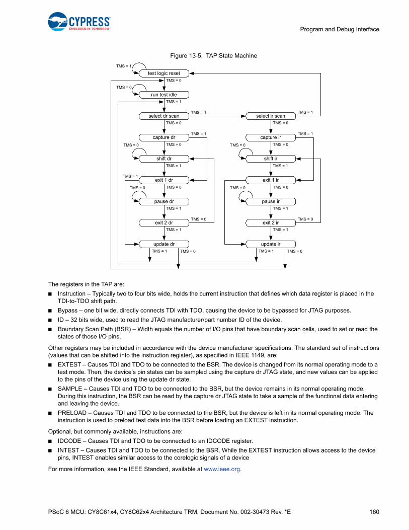
PSoC 6 MCU: CY8C61x4, CY8C62x4 Architecture TRM, Document No. 002-30473 Rev. *E 160
Program and Debug Interface
Figure 13-5. TAP State Machine
The registers in the TAP are:
■ Instruction – Typically two to four bits wide, holds the current instruction that defines which data register is placed in the TDI-to-TDO shift path.
■ Bypass – one bit wide, directly connects TDI with TDO, causing the device to be bypassed for JTAG purposes.
■ ID – 32 bits wide, used to read the JTAG manufacturer/part number ID of the device.
■ Boundary Scan Path (BSR) – Width equals the number of I/O pins that have boundary scan cells, used to set or read the states of those I/O pins.
Other registers may be included in accordance with the device manufacturer specifications. The standard set of instructions(values that can be shifted into the instruction register), as specified in IEEE 1149, are:
■ EXTEST – Causes TDI and TDO to be connected to the BSR. The device is changed from its normal operating mode to a test mode. Then, the device’s pin states can be sampled using the capture dr JTAG state, and new values can be applied to the pins of the device using the update dr state.
■ SAMPLE – Causes TDI and TDO to be connected to the BSR, but the device remains in its normal operating mode. During this instruction, the BSR can be read by the capture dr JTAG state to take a sample of the functional data entering and leaving the device.
■ PRELOAD – Causes TDI and TDO to be connected to the BSR, but the device is left in its normal operating mode. The instruction is used to preload test data into the BSR before loading an EXTEST instruction.
Optional, but commonly available, instructions are:
■ IDCODE – Causes TDI and TDO to be connected to an IDCODE register.
■ INTEST – Causes TDI and TDO to be connected to the BSR. While the EXTEST instruction allows access to the device pins, INTEST enables similar access to the corelogic signals of a device
For more information, see the IEEE Standard, available at www.ieee.org.
test logic reset
run test idle
select dr scan
capture dr
shift dr
exit 1 dr
pause dr
exit 2 dr
update dr
select ir scan
capture ir
shift ir
exit 1 ir
pause ir
exit 2 ir
update ir
TMS = 0
TMS = 1
TMS = 0
TMS = 0
TMS = 1
TMS = 0
TMS = 1
TMS = 1
TMS = 0TMS = 1
TMS = 0
TMS = 1
TMS = 1
TMS = 1
TMS = 0
TMS = 0
TMS = 1
TMS = 0
TMS = 0TMS = 1
TMS = 0
TMS = 1
TMS = 1
TMS = 0
TMS = 0
TMS = 1
TMS = 0
TMS = 1
TMS = 1
TMS = 0
TMS = 0
PSoC 6 MCU: CY8C61x4, CY8C62x4 Architecture TRM, Document No. 002-30473 Rev. *E 161
Program and Debug Interface
13.5 Programming the PSoC 6 MCU
The PSoC 6 MCU is programmed using the following sequence. Refer to the PSoC 6 MCU Programming Specifications forcomplete details on the programming algorithm, timing specifications, and hardware configuration required for programming.
1. Acquire the SWD port in the PSoC 6 MCU.
2. Enter the programming mode.
3. Execute the device programming routines such as Silicon ID Check, Flash Programming, Flash Verification, and Checksum Verification.
13.5.1 SWD Port Acquisition
13.5.1.1 SWD Port Acquire Sequence
The first step in device programming is for the host to acquire the target’s SWD port. The host first performs a device reset byasserting the external reset (XRES) pin. After removing the XRES signal, the host must send an SWD connect sequence forthe device within the acquire window to connect to the SWD interface in the DAP.
The debug access port must be reset using the standard Arm command. The DAP reset command consists of more than 49SWDCK clock cycles with SWDIO asserted high. The transaction must be completed by sending at least one SWDCK clockcycle with SWDIO asserted low. This sequence synchronizes the programmer and the chip. Read_DAP() refers to the read ofthe IDCODE register in the debug port. The sequence of line reset and IDCODE read should be repeated until an OK ACK isreceived for the IDCODE read or a timeout (2 ms) occurs. The SWD port is said to be in the acquired state if an OK ACK isreceived within the time window and the IDCODE read matches with that of the Cortex-M0+ DAP.
13.5.2 SWD Programming Mode Entry
After the SWD port is acquired, the host must enter the device programming mode within a specific time window. This is doneby setting the TEST_MODE bit (bit 31) in the test mode control register (MODE register). The debug port should also beconfigured before entering the device programming mode. Timing specifications and pseudo code for entering theprogramming mode are detailed in the PSoC 6 MCU Programming Specifications document.
13.5.3 SWD Programming Routine Executions
When the device is in programming mode, the external programmer can start sending the SWD packet sequence forperforming programming operations such as flash erase, flash program, checksum verification, and so on. The programmingroutines are explained in the Nonvolatile Memory chapter on page 163. The exact sequence of calling the programmingroutines is given in the PSoC 6 MCU Programming Specifications document.

PSoC 6 MCU: CY8C61x4, CY8C62x4 Architecture TRM, Document No. 002-30473 Rev. *E 162
Program and Debug Interface
13.6 Registers
Table 13-3. List of Registers
Register Name Description
CM0P_DWT Cortex M0+ Data Watchpoint and Trace (DWT) registers
CM0P_BP Cortex M0+ BreakPoint (BP) registers
CM0P_ROM Cortex M0+ CPU Coresight ROM table
CM0P_CTI Cortex M0+ Cross-Trigger Interface (CTI) registers
CM0P_MTB Cortex M0+ Micro Trace Buffer (MTB) registers
CM4_ITM Cortex M4 Instrumentation Trace Macrocell (ITM) registers
CM4_DWT Cortex M4 Data Watchpoint and Trace (DWT) registers
CM4_FPB Cortex M4 Flash Patch and Breakpoint (FPB) registers
CM4_SCS Cortex M4 System Control Space (SCS) registers
CM4_ETM Cortex M4 Embedded Trace Macrocell (ETM) registers
CM4_CTI Cortex M4 Cross-Trigger Interface (CTI) registers
CM4_ROM Cortex M4 CPU Coresight ROM table
TRC_TPIU System Trace Coresight Trace Port Interface Unit (TPIU) registers

PSoC 6 MCU: CY8C61x4, CY8C62x4 Architecture TRM, Document No. 002-30473 Rev. *E 163
14. Nonvolatile Memory
Nonvolatile memory refers to the flash and SROM memory in the PSoC 6 MCU. This chapter explains the geometry andcapability of the flash memory. It also lists the SROM API functions that are used to program the flash memory.
14.1 Flash Memory
The PSoC 6 flash offers high bulk program performance and supports ultra-low-power operation. Flash is typically used tostore CPU instructions and data when the device power is off. Flash may be written, but the process is much slower and morerestrictive than for SRAM.
14.1.1 Features
This section lists the features of PSoC 6 flash.
■ 512-byte row size; minimum programmable unit
■ Supports the Read While Write (RWW) feature with a RWW sector size of 128KB
■ 10-year retention
■ Endurance of 100 k program cycles
14.1.2 Configuration
14.1.2.1 Block Diagram
Flash is part of the CPU subsystem. The Cortex-M4 and Cortex M0+, as well as other bus masters, can access flash via theAHB.
This PSoC 6 MCU technical reference manual (TRM) provides comprehensive and detailed information about thefunctions of the PSoC 6 MCU device hardware. It is divided into two books: architecture TRM and registers TRM. TheTRM is not recommended for those new to the PSoC 6 MCU, nor as a guide for developing PSoC 6 MCU applications.Use these documents instead:
■ PSoC 61 datasheet, PSoC 62 datasheet
■ Peripheral Driver Library (PDL) documentation
■ Application notes
■ Code examples
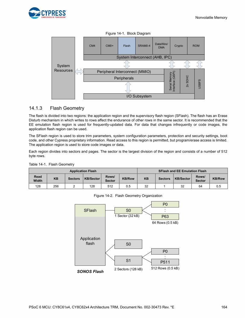
PSoC 6 MCU: CY8C61x4, CY8C62x4 Architecture TRM, Document No. 002-30473 Rev. *E 164
Nonvolatile Memory
Figure 14-1. Block Diagram
14.1.3 Flash Geometry
The flash is divided into two regions: the application region and the supervisory flash region (SFlash). The flash has an EraseDisturb mechanism in which writes to rows affect the endurance of other rows in the same sector. It is recommended that theEE emulation flash region is used for frequently-updated data. For data that changes infrequently or code images, theapplication flash region can be used.
The SFlash region is used to store trim parameters, system configuration parameters, protection and security settings, bootcode, and other Cypress proprietary information. Read access to this region is permitted, but program/erase access is limited.The application region is used to store code images or data.
Each region divides into sectors and pages. The sector is the largest division of the region and consists of a number of 512byte rows.
Figure 14-2. Flash Geometry Organization
Table 14-1. Flash Geometry
Application Flash SFlash and EE Emulation Flash
Read Width
KB Sectors KB/SectorRows/Sector
KB/Row KB Sectors KB/SectorRows/Sector
KB/Row
128 256 2 128 512 0.5 32 1 32 64 0.5
System Interconnect (AHB, IPC)
System Resources
Peripherals
CM4 CM0+ Flash SRAM0-4DataWire/
DMACrypto ROM
Peripheral Interconnect (MMIO)
Ser
ial M
emor
y In
terf
ace
(Q
SP
I)
2x S
DH
C
I/O Subsystem
US
BF
S
SFlash
Application flash
SONOS Flash
S1
P0
P511
S0
2 Sectors (128 kB) 512 Rows (0.5 kB)
S0
P0
P631 Sector (32 kB)
64 Rows (0.5 kB)

PSoC 6 MCU: CY8C61x4, CY8C62x4 Architecture TRM, Document No. 002-30473 Rev. *E 165
Nonvolatile Memory
14.1.4 Flash Controller
Access to the flash memory is enabled through the flash controller. The flash controller interfaces with the AHB-Lite bus andprovides flash access for the CM0+, CM4, Crypto, DataWire, and debug. The flash controller generates a bus error if:
■ A flash read access to a sector that is currently being programmed/erased
■ A read access to a memory hole in the flash memory region. A memory hole is defined as a location that is not occupied by the application flash or SFlash. Note that the SFlash space can be non-powers of 2 for some flash macros
The flash controller also provides the registers which support configuration of flash accesses.
14.1.4.1 Wait State Count
FLASHC_FLASH_CTL supports configuration of flash wait cycles. If clk_hf is greater than the maximum operating frequencyof the flash memory, it is necessary to insert wait cycles when accessing the flash memory by setting the appropriate value inthe FLASHC_FLASH_CTL.MAIN_WS register. Set the wait cycles as follows.
14.1.4.2 Power Modes
FLASHC_FLASH_PWR_CTL provides enable bits for the flash memory. Software can turn off all regions of the flash memoryby setting the ENABLE and ENABLE_HV fields to 0.
The wakeup time of flash memory is 10 µs. Software should wait at least 10 µs before reading from flash after it is re-enabledthrough the FLASHC_FLASH_PWR_CTL register.
The flash controller provides functionality down to the Deep Sleep power mode. In the Deep Sleep power mode, the followingflash controller information is retained:
■ The retention MMIO registers (listed in Table 14-2)
■ The cache data structure
Note that buffer information (in the AHB-Lite buffer interfaces and in the synchronization logic) is not retained. Losing bufferinformation after Deep Sleep transition has limited performance impact.
14.1.4.3 CPU Caches
The flash controller provides 8 kB caches for both the CM0+ and CM4 CPUs. Each cache is a four-way set associative with aleast recently used (LRU) replacement scheme. Four-way set associativity means that each cache has four ways per set, with
Table 14-2. Flash Controller Retention Registers
Register Name Description
FLASHC_FLASH_CTL Flash controller control register
FLASHC_FLASH_PWR_CTL Flash enable control
FLASHC_FLASH_CMD Flash commands for cache/buffer invalidation
FLASHC_CM0/CM4_STATUS CM0/4 interface status
FLASHC_CM0/CM4_CA_CTL CM0/4 cache control
FLASHC_*Peripheral*_BUFF_CTLBuffer control register where *peripheral* may be Crypto, DMA, DWx (DataWire x = 0, 1), or EXT_MSx (External master; x = 0, 1)
HF Clock Frequency FLASH_CTL.MAIN_WS[3:0]
clk_hf 33 MHz 0
33 < clk_hf 66 MHz 1
66 < clk_hf 99 MHz 2
99 < clk_hf 133 MHz 3
133 < clk_hf 150 MHz 4

PSoC 6 MCU: CY8C61x4, CY8C62x4 Architecture TRM, Document No. 002-30473 Rev. *E 166
Nonvolatile Memory
each way containing a valid bit, tag, and data. The cache looks at all of the ways in a selected set, checking for validity and amatching tag. These caches can be enabled/disabled through the FLASHC_CM0/4_CA_CTL.CA_EN registers.
The cache supports faster flash memory reads when enabled. On a read transfer “miss”, however, a normal flash controlleraccess will occur.
Cache Prefetch. The caches support pre-fetching through the CM0/4_CA_CTL.PREF_EN register.
If prefetch is enabled, a cache miss results in a 16 B refill forthe missing data and a 16 B prefetch for the next sequentialdata. The prefetch data is stored in a temporary buffer and isonly copied to the cache when a read transfer “misses” andrequires that data.
14.1.5 Read While Write (RWW) Support
The PSoC 6 MCU supports read operations on one areawhile programming/erasing in another area. This isimplemented to support firmware upgrades and paralleltasks in the dual-core system. The application flash containstwo RWW sectors, UFLASH0 and UFLASH1, each 128KBin size. The SFlash is an additional RWW sector apart fromthe main flash.
The RWW feature is available between sectors – you canread/execute from one sector while there is an ongoingwrite/erase operation in another sector. However, when thecode execution/read is in the last 16 bytes of a given sector(say sector 0) and the flash write/erase operation is in thenext sector (sector 1), an RWW violation may occur ifprefetch is enabled. This is because prefetch will fetch thenext 16 bytes of data, which is part of sector 1 while a writeoperation is underway in the same sector. This will result ina fault and should be considered during firmware design.Firmware can be designed to place dead code in the last 16bytes of every sector making sure the last 16 bytes of asector are never accessed or can disable prefetch during aflash write/erase operation.
14.2 Flash Memory Programming
14.2.1 Features
■ SROM API library for flash management through system calls such as Program Row, Erase Flash, and Blow eFuse
■ System calls can be performed using CM0+, CM4, or DAP
14.2.2 Architecture
Flash programming operations are implemented as systemcalls. System calls are executed out of SROM in ProtectionContext 0. System calls are executed inside CM0+ NMI. Thesystem call interface makes use of IPC to initiate an NMI toCM0+.
System calls can be performed by CM0+, CM4, or DAP.Each of them have a reserved IPC structure (used as amailbox) through which they can request CM0+ to perform asystem call. Each one acquires the specific mailbox, writesthe opcode and argument to the data field of the mailbox,and notifies a dedicated IPC interrupt structure. This resultsin an NMI interrupt in CM0+. The following diagramillustrates the system call interface using IPC.
Register Bit Field and Bit Name Description
CM0_CA_CTL[32:0] CA_EN[31]Cache enable:0: Disabled
1: Enabled
CM4_CA_CTL[32:0] CA_EN[31]Cache enable: 0: Disabled
1: Enabled
Table 14-3. CM0/4 Cache Control Prefetch Enable Register Values and Bit Field
Register Bit Field and Bit Name Description
CM0_CA_CTL[32:0] PREF_EN[30]
Prefetch enable:
0: Disabled
1: Enabled
CM4_CA_CTL[32:0] PREF_EN[30]
Prefetch enable:
0: Disabled
1: Enabled
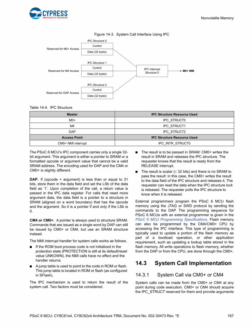
PSoC 6 MCU: CY8C61x4, CY8C62x4 Architecture TRM, Document No. 002-30473 Rev. *E 167
Nonvolatile Memory
Figure 14-3. System Call Interface Using IPC
The PSoC 6 MCU’s IPC component carries only a single 32-bit argument. This argument is either a pointer to SRAM or aformatted opcode or argument value that cannot be a validSRAM address. The encoding used for DAP and the CM4 orCM0+ is slightly different.
DAP. If (opcode + argument) is less than or equal to 31bits, store them in the data field and set the LSb of the datafield as ‘1’. Upon completion of the call, a return value ispassed in the IPC data register. For calls that need moreargument data, the data field is a pointer to a structure inSRAM (aligned on a word boundary) that has the opcodeand the argument. So it is a pointer if and only if the LSb is0.
CM4 or CM0+. A pointer is always used to structure SRAM.Commands that are issued as a single word by DAP can stillbe issued by CM0+ or CM4, but use an SRAM structureinstead.
The NMI interrupt handler for system calls works as follows.
■ If the ROM boot process code is not initialized in the protection state (PROTECTION is still at its default/reset value UNKOWN), the NMI calls have no effect and the handler returns.
■ A jump table is used to point to the code in ROM or flash. This jump table is located in ROM or flash (as configured in SFlash).
The IPC mechanism is used to return the result of thesystem call. Two factors must be considered.
■ The result is to be passed in SRAM: CM0+ writes the result in SRAM and releases the IPC structure. The requester knows that the result is ready from the RELEASE interrupt.
■ The result is scalar ( 32 bits) and there is no SRAM to pass the result: in this case, the CM0+ writes the result to the data field of the IPC structure and releases it. The requester can read the data when the IPC structure lock is released. The requester polls the IPC structure to know when it is released.
External programmers program the PSoC 6 MCU flashmemory using the JTAG or SWD protocol by sending thecommands to the DAP. The programming sequence forPSoC 6 MCUs with an external programmer is given in thePSoC 6 MCU Programming Specifications. Flash memorycan also be programmed by the CM4/CM0+ CPU byaccessing the IPC interface. This type of programming istypically used to update a portion of the flash memory aspart of a bootload operation, or other applicationrequirement, such as updating a lookup table stored in theflash memory. All write operations to flash memory, whetherfrom the DAP or from the CPU, are done through the CM0+.
14.3 System Call Implementation
14.3.1 System Call via CM0+ or CM4
System calls can be made from the CM0+ or CM4 at anypoint during code execution. CM0+ or CM4 should acquirethe IPC_STRUCT reserved for them and provide arguments
Table 14-4. IPC Structure
Master IPC Structure Resource Used
M0+ IPC_STRUCT0
M4 IPC_STRUCT1
DAP IPC_STRUCT2
Access Point IPC Structure Resource Used
CM0+ NMI interrupt IPC_INTR_STRUCT0
IPC Structure 0
IPC Structure 1
IPC Structure 2
IPC Interrupt Structure 0
M0+ NMI
Reserved for M0+ Access
Reserved for M4 Access
Reserved for DAP Access
Control
Data (32 bytes)
Control
Data (32 bytes)
Control
Data (32 bytes)
PSoC 6 MCU: CY8C61x4, CY8C62x4 Architecture TRM, Document No. 002-30473 Rev. *E 168
Nonvolatile Memory
in either of the methods described above and notify IPCinterrupt 0 to trigger a system call.
14.3.2 System Call via DAP
If the device is acquired, then the boot ROM enters “busy-wait loop” and waits for commands issued by the DAP. For adetailed description on acquiring the device see the PSoC 6MCU Programming Specifications.
14.3.3 Exiting from a System Call
When the API operation is complete, CM0+ will release theIPC structure that initiated the system call. If an interrupt isrequired upon release, the corresponding mask bit shouldbe set in IPC_INTR_STRUCT_INTR_MASK.RELEASE[i].The exit code must also restore the CM0+ protection context(PROT_MPU_MS_CTL.PC) to the one that was backed upin PROT_MPU_MS_CTL.PC_SAVED.
14.3.4 SRAM Usage
2KB of SRAM [TOP_OF_SRAM – 2KB, TOP_OF_SRAM] isreserved for system calls and 1KB of SRAM[TOP_OF_SRAM – 3KB, TOP_OF_SRAM – 2KB] is used bySROM boot and should not be part of noinit RAM.TOP_OF_SRAM is the last address of SRAM.
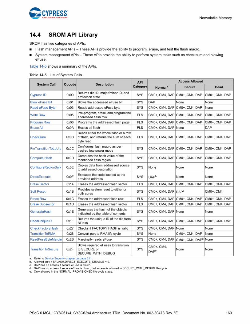
PSoC 6 MCU: CY8C61x4, CY8C62x4 Architecture TRM, Document No. 002-30473 Rev. *E 169
Nonvolatile Memory
14.4 SROM API Library
SROM has two categories of APIs:
■ Flash management APIs – These APIs provide the ability to program, erase, and test the flash macro.
■ System management APIs – These APIs provide the ability to perform system tasks such as checksum and blowing eFuse.
Table 14-5 shows a summary of the APIs.
Table 14-5. List of System Calls
System Call Opcode DescriptionAPI
Category
Access Allowed
Normala
a. Refer to Device Security chapter on page 211.
Secure Dead
Cypress ID 0x00Returns die ID, major/minor ID, and protection state
SYS CM0+, CM4, DAP CM0+, CM4, DAP CM0+, CM4, DAP
Blow eFuse Bit 0x01 Blows the addressed eFuse bit SYS DAP None None
Read eFuse Byte 0x03 Reads addressed eFuse byte SYS CM0+, CM4, DAP CM0+, CM4, DAP None
Write Row 0x05Pre-program, erase, and program the addressed flash row
FLS CM0+, CM4, DAP CM0+, CM4, DAP CM0+, CM4, DAP
Program Row 0x06 Programs the addressed flash page FLS CM0+, CM4, DAP CM0+, CM4, DAP CM0+, CM4, DAP
Erase All 0x0A Erases all flash FLS CM0+, CM4, DAP None DAP
Checksum 0x0BReads either the whole flash or a row of flash, and returns the sum of each byte read
FLS CM0+, CM4, DAP CM0+, CM4, DAP CM0+, CM4, DAP
FmTransitionToLpUlp 0x0CConfigures flash macro as per desired low-power mode
SYS CM0+, CM4, DAP CM0+, CM4, DAP CM0+, CM4, DAP
Compute Hash 0x0DComputes the hash value of the mentioned flash region
SYS CM0+, CM4, DAP CM0+, CM4, DAP CM0+, CM4, DAP
ConfigureRegionBulk 0x0ECopies data from addressed source to addressed destination
SYS None None None
DirectExecute 0x0FExecutes the code located at the provided address
SYS DAPb
b. Allowed only if SFLASH.DIRECT_EXECUTE_DISABLE = 0.
None None
Erase Sector 0x14 Erases the addressed flash sector FLS CM0+, CM4, DAP CM0+, CM4, DAP CM0+, CM4, DAP
Soft Reset 0x1BProvides system reset to either or both cores
SYS CM0+, CM4, DAP DAPc
c. DAP has no access if secure eFuse is blown.
CM0+, CM4
Erase Row 0x1C Erases the addressed flash row FLS CM0+, CM4, DAP CM0+, CM4, DAP CM0+, CM4, DAP
Erase Subsector 0x1D Erases the addressed flash sector FLS CM0+, CM4, DAP CM0+, CM4, DAP CM0+, CM4, DAP
GenerateHash 0x1EGenerates the hash of the objects indicated by the table of contents
SYS CM0+, CM4, DAP None None
ReadUniqueID 0x1FReturns the unique ID of the die from SFlash
SYS CM0+, CM4, DAP CM0+, CM4, DAP CM0+, CM4, DAP
CheckFactoryHash 0x27 Checks if FACTORY HASH is valid SYS CM0+, CM4, DAP None None
TransitionToRMA 0x28 Convert part to RMA life cycle SYS None CM0+, CM4, DAP None
ReadFuseByteMargin 0x2B Marginally reads eFuse SYS CM0+, CM4, DAP CM0+, CM4, DAPd
d. DAP has no access if secure eFuse is blown, but access is allowed in SECURE_WITH_DEBUG life cycle
None
TransitionToSecure 0x2FBlows required eFuses to transition to SECURE or SECURE_WITH_DEBUG
SYSCM0+, CM4,
DAPe
e. Only allowed in the NORMAL_PROVISIONED life-cycle stage.
None None
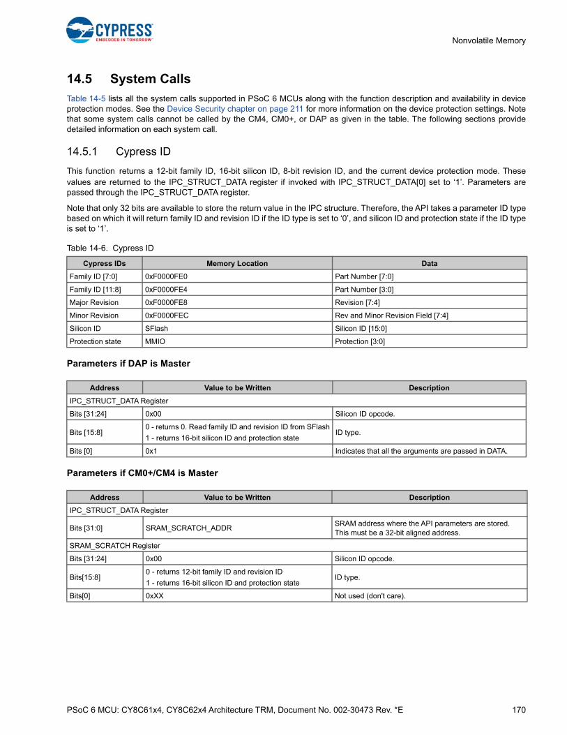
PSoC 6 MCU: CY8C61x4, CY8C62x4 Architecture TRM, Document No. 002-30473 Rev. *E 170
Nonvolatile Memory
14.5 System Calls
Table 14-5 lists all the system calls supported in PSoC 6 MCUs along with the function description and availability in deviceprotection modes. See the Device Security chapter on page 211 for more information on the device protection settings. Notethat some system calls cannot be called by the CM4, CM0+, or DAP as given in the table. The following sections providedetailed information on each system call.
14.5.1 Cypress ID
This function returns a 12-bit family ID, 16-bit silicon ID, 8-bit revision ID, and the current device protection mode. Thesevalues are returned to the IPC_STRUCT_DATA register if invoked with IPC_STRUCT_DATA[0] set to ‘1’. Parameters arepassed through the IPC_STRUCT_DATA register.
Note that only 32 bits are available to store the return value in the IPC structure. Therefore, the API takes a parameter ID typebased on which it will return family ID and revision ID if the ID type is set to ‘0’, and silicon ID and protection state if the ID typeis set to ‘1’.
Parameters if DAP is Master
Parameters if CM0+/CM4 is Master
Table 14-6. Cypress ID
Cypress IDs Memory Location Data
Family ID [7:0] 0xF0000FE0 Part Number [7:0]
Family ID [11:8] 0xF0000FE4 Part Number [3:0]
Major Revision 0xF0000FE8 Revision [7:4]
Minor Revision 0xF0000FEC Rev and Minor Revision Field [7:4]
Silicon ID SFlash Silicon ID [15:0]
Protection state MMIO Protection [3:0]
Address Value to be Written Description
IPC_STRUCT_DATA Register
Bits [31:24] 0x00 Silicon ID opcode.
Bits [15:8]0 - returns 0. Read family ID and revision ID from SFlash
1 - returns 16-bit silicon ID and protection stateID type.
Bits [0] 0x1 Indicates that all the arguments are passed in DATA.
Address Value to be Written Description
IPC_STRUCT_DATA Register
Bits [31:0] SRAM_SCRATCH_ADDRSRAM address where the API parameters are stored. This must be a 32-bit aligned address.
SRAM_SCRATCH Register
Bits [31:24] 0x00 Silicon ID opcode.
Bits[15:8]0 - returns 12-bit family ID and revision ID
1 - returns 16-bit silicon ID and protection stateID type.
Bits[0] 0xXX Not used (don't care).

PSoC 6 MCU: CY8C61x4, CY8C62x4 Architecture TRM, Document No. 002-30473 Rev. *E 171
Nonvolatile Memory
Return if DAP Invoked the System Call
Return if CM0+/CM4 Invoked the System Call
Address Return Value Description
IPC_STRUCT_DATA Register
Bits [7:0]If ID type = 0, Family ID Lo
If ID type = 1, Silicon ID Lo See the PSoC 61 datasheet/PSoC 62 datasheet for silicon ID values for different part numbers.
Bits [15:8]If ID type = 0, Family ID Hi
If ID type = 1, Silicon ID Hi
Bits [19:16]
If ID type = 0, Minor Revision ID
If ID type = 1, Protection state
0: UNKNOWN
1: VIRGIN
2: NORMAL
3: SECURE
4: DEAD See the PSoC 61 datasheet/PSoC 62 datasheet for these values.
Bits [23:20]
If ID Type = 0 Major Revision ID
If ID Type = 1 Life-cycle stage
0: VIRGIN
1: NORMAL
2: SEC_W_DBG
3: SECURE
4: RMA
Bits [27:24] 0xXX Not used (don't care).
Bits [31:28]0xA = SUCCESS
0xF = ERRORStatus code (see System Call Status for details).
Address Return Value Description
SRAM_SCRATCH Register
Bits [7:0]If ID type = 0, Family ID Lo
If ID type = 1, Silicon ID Lo See the PSoC 61 datasheet/PSoC 62 datasheet for silicon ID values for different part numbers.
Bits [15:8]If ID type = 0, Family ID Hi
If ID type = 1, Silicon ID Hi
Bits [19:16]
If ID type = 0, Minor Revision ID
If ID type = 1, Protection state
0: UNKNOWN
1: VIRGIN
2: NORMAL
3: SECURE
4: DEAD
Bits [23:20]
If ID Type = 0 Major Revision ID
If ID Type = 1 Life-cycle stage
0: VIRGIN
1: NORMAL
2: SEC_W_DBG
3: SECURE
4: RMA
Bits [27:24] 0xXX Not used (don't care).
Bits [31:28] 0xA Success status code.
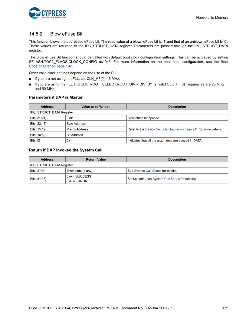
PSoC 6 MCU: CY8C61x4, CY8C62x4 Architecture TRM, Document No. 002-30473 Rev. *E 172
Nonvolatile Memory
14.5.2 Blow eFuse Bit
This function blows the addressed eFuse bit. The read value of a blown eFuse bit is ‘1’ and that of an unblown eFuse bit is ‘0’.These values are returned to the IPC_STRUCT_DATA register. Parameters are passed through the IPC_STRUCT_DATAregister.
The Blow eFuse Bit function should be called with default boot clock configuration settings. This can be achieved by settingSFLASH.TOC2_FLAGS.CLOCK_CONFIG as 0x3. For more information on the boot code configuration, see the BootCode chapter on page 192.
Other valid clock settings depend on the use of the FLL:
■ If you are not using the FLL, set CLK_HF[0] = 8 MHz.
■ If you are using the FLL and CLK_ROOT_SELECT.ROOT_DIV = DIV_BY_2, valid CLK_HF[0] frequencies are 25 MHz and 50 MHz.
Parameters if DAP is Master
Return if DAP Invoked the System Call
Address Value to be Written Description
IPC_STRUCT_DATA Register
Bits [31:24] 0x01 Blow efuse bit opcode.
Bits [23:16] Byte Address
Refer to the Device Security chapter on page 211 for more details.Bits [15:12] Macro Address
Bits [10:8] Bit Address
Bits [0] 0x1 Indicates that all the arguments are passed in DATA.
Address Return Value Description
IPC_STRUCT_DATA Register
Bits [27:0] Error code (if any) See System Call Status for details.
Bits [31:28]0xA = SUCCESS
0xF = ERRORStatus code (see System Call Status for details).

PSoC 6 MCU: CY8C61x4, CY8C62x4 Architecture TRM, Document No. 002-30473 Rev. *E 173
Nonvolatile Memory
14.5.3 Read eFuse Byte
This function returns the eFuse contents of the addressed byte. The read value of a blown eFuse bit is ‘1’ and that of anunblown eFuse bit is ‘0’. These values are returned to the IPC_STRUCT_DATA register. Parameters are passed through theIPC_STRUCT_DATA register.
Parameters if DAP is Master
Parameters if CM0+/CM4 is Master
Return if DAP Invoked the System Call
Return if CM0+/CM4 Invoked the System Call
Address Value to be Written Description
IPC_STRUCT_DATA Register
Bits [31:24] 0x03 Read eFuse bit opcode.
Bits [23:8] eFuse Address Refer to the eFuse Memory chapter on page 209 for more details.
Bits [0] 0x1 Indicates all arguments are passed in DATA.
Address Value to be Written Description
IPC_STRUCT_DATA Register
Bits [31:0] SRAM_SCRATCH_ADDRSRAM address where the API parameters are stored. This must be a 32-bit aligned address.
SRAM_SCRATCH Register
Bits [31:24] 0x03 Read eFuse bit opcode.
Bits [23:8] eFuse Address Refer to the eFuse Memory chapter on page 209 for more details.
Bits [7:0] 0xXX Not used (don't care).
Address Return Value Description
IPC_STRUCT_DATA Register
Bits [23:0] eFuse byte Byte read from eFuse if status is success; otherwise, error code.
Bits [27:24] 0xXX Not used (don't care).
Bits [31:28]0xA = SUCCESS
0xF = ERRORStatus code (see System Call Status for details).
Address Return Value Description
SRAM_SCRATCH Register
Bits [23:0] eFuse byte Byte read from eFuse if status is success; otherwise, error code.
Bits [27:24] 0xXX Not used (don't care).
Bits [31:28]0xA = SUCCESS
0xF = ERRORStatus code (see System Call Status for details).
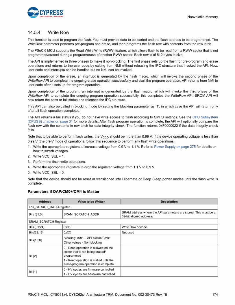
PSoC 6 MCU: CY8C61x4, CY8C62x4 Architecture TRM, Document No. 002-30473 Rev. *E 174
Nonvolatile Memory
14.5.4 Write Row
This function is used to program the flash. You must provide data to be loaded and the flash address to be programmed. TheWriteRow parameter performs pre-program and erase, and then programs the flash row with contents from the row latch.
The PSoC 6 MCU supports the Read While Write (RWW) feature, which allows flash to be read from a RWW sector that is notprogrammed/erased during a program/erase of another RWW sector. Each row is of 512 bytes in size.
The API is implemented in three phases to make it non-blocking. The first phase sets up the flash for pre-program and eraseoperations and returns to the user code by exiting from NMI without releasing the IPC structure that invoked the API. Now,user code and interrupts can be handled but no NMI can be invoked.
Upon completion of the erase, an interrupt is generated by the flash macro, which will invoke the second phase of theWriteRow API to complete the ongoing erase operation successfully and start the program operation. API returns from NMI touser code after it sets up for program operation.
Upon completion of the program, an interrupt is generated by the flash macro, which will invoke the third phase of theWriteRow API to complete the ongoing program operation successfully; this completes the WriteRow API. SROM API willnow return the pass or fail status and releases the IPC structure.
This API can also be called in blocking mode by setting the blocking parameter as ‘1’, in which case the API will return onlyafter all flash operation completes.
The API returns a fail status if you do not have write access to flash according to SMPU settings. See the CPU Subsystem(CPUSS) chapter on page 31 for more details. After flash program operation is complete, the API will optionally compare theflash row with the contents in row latch for data integrity check. The function returns 0xF0000022 if the data integrity checkfails.
Note that to be able to perform flash writes, the VCCD should be more than 0.99 V. If the device operating voltage is less than
0.99 V (the 0.9-V mode of operation), follow this sequence to perform any flash write operations.
1. Write the appropriate registers to increase voltage from 0.9 V to 1.1 V. Refer to Power Supply on page 275 for details on how to switch voltages.
2. Write VCC_SEL = 1.
3. Perform the flash write operations.
4. Write the appropriate registers to drop the regulated voltage from 1.1 V to 0.9 V.
5. Write VCC_SEL = 0.
Note that the device should not be reset or transitioned into Hibernate or Deep Sleep power modes until the flash write iscomplete.
Parameters if DAP/CM0+/CM4 is Master
Address Value to be Written Description
IPC_STRUCT_DATA Register
Bits [31:0] SRAM_SCRATCH_ADDRSRAM address where the API parameters are stored. This must be a 32-bit aligned address.
SRAM_SCRATCH Register
Bits [31:24] 0x05 Write Row opcode.
Bits[23:16] 0xXX Not used
Bits[15:8]Blocking: 0x01 – API blocks CM0+
Other values - Non-blocking
Bit [2]
0 - Read operation is allowed on the sector that is not being erased/programmed
1 - Read operation is stalled until the erase/program operation is complete
Bit [1]0 - HV cycles are firmware controlled
1 - HV cycles are hardware controlled

PSoC 6 MCU: CY8C61x4, CY8C62x4 Architecture TRM, Document No. 002-30473 Rev. *E 175
Nonvolatile Memory
Return if DAP/CM0+/CM4 Invoked the System Call
14.5.5 Program Row
This function programs the addressed flash row. You must provide the data to be loaded and flash address to beprogrammed. The flash row should be in the erased state before calling this function.
The function is implemented in two phases to make it non-blocking. The first phase sets up the flash for program operationand returns to user code by exiting from NMI without releasing the IPC structure that invoked the API. Now user code andinterrupts can be handled but no NMI can be invoked.
Upon completion of the program operation, an interrupt is generated by the flash macro, which will invoke the second phaseof the ProgramRow API to complete the ongoing program operation successfully. The SROM API will return the pass or failstatus and releases the IPC structure.
After flash program operation is complete, the API will optionally compare the flash row with the contents in the row latch fordata integrity check. It returns STATUS_PL_ROW_COMP_FA if data integrity check fails. The values are returned to theIPC_STRUCT_DATA register. Parameters are passed through the IPC_STRUCT_DATA register.
Note that to be able to perform flash writes, the VCCD should be more than 0.99 V. If the device operating voltage is less than
0.99 V (the 0.9-V mode of operation), follow this sequence to perform any flash write operations.
1. Write the appropriate registers to increase voltage from 0.9 V to 1.1 V. Refer to Power Supply on page 275 for details on how to switch voltages.
2. Write VCC_SEL = 1.
3. Perform the flash write operations.
4. Write the appropriate registers to drop the regulated voltage from 1.1 V to 0.9 V.
5. Write VCC_SEL = 0.
Note that the device should not be reset or transitioned into Hibernate or Deep Sleep power modes until the flash write iscomplete.
SRAM_SCRATCH Register + 0x04
Bits [23:16]
Verify row:
0 - Data integrity check is not performed
1 - Data integrity check is performed
Bits [31:24], Bits [15:0] 0xXX Not used (don't care).
SRAM_SCRATCH Register + 0x08
Bits [31:0]Flash address to be programmed. This should be provided in 32-bit system address format. For example, to program the second half-word, provide either of the byte address 0x1000003 or 0x1000004.
SRAM_SCRATCH Register + 0x0C
Bits [31:0]Data word 0 (data provided should be proportional to the data size provided, data to be programmed into LSbs)
SRAM_SCRATCH Register + 0x0C + n*0x04
Bits [31:0] Data word n (data to be programmed)
Address Return Value Description
SRAM_SCRATCH Register
Bits [27:0] Error code (if any) See System Call Status for details.
Bits [31:28]0xA = SUCCESS/Program command ongoing in background
0xF = ERRORStatus code (see System Call Status for details).
Address Value to be Written Description

PSoC 6 MCU: CY8C61x4, CY8C62x4 Architecture TRM, Document No. 002-30473 Rev. *E 176
Nonvolatile Memory
Parameters if DAP/CM0+/CM4 is Master
Return if DAP/CM0+/CM4 Invoked the System Call
Address Value to be Written Description
IPC_STRUCT_DATA Register
Bits [31:0] SRAM_SCRATCH_ADDRSRAM address where the API parameters are stored. This must be a 32-bit aligned address.
SRAM_SCRATCH Register
Bits[31:24] 0x06 Program Row opcode.
Bits[23:16]
Skip blank check:
0x01 – Skips the blank check step
Other – Perform blank check
Bits[15:8]Blocking: 0x01 – API blocks CM0+
Other values - Non-blocking
Bit [2]
0 - Read operation is allowed on the sector that is not being erased/programmed
1 - Read operation is stalled until the erase/program operation is complete
Bit [1]0 - HV cycles are firmware controlled
1 - HV cycles are hardware controlled
SRAM_SCRATCH Register + 0x04
Bits [23:16]
Verify row:
0 - Data integrity check is not performed
1 - Data integrity check is performed
Bits [15:8]
Data location:
0 - row latch
1 - SRAM
Bits[7:0] 0xXX Not used (don't care).
SRAM_SCRATCH Register + 0x08
Bits [31:0]Flash address to be programmed. This should be provided in 32-bit system address format. For example, to program the second half-word, provide either of the byte address 0x1000003 or 0x1000004.
SRAM_SCRATCH Register + 0x0C
Bits [31:0]Data word 0 (data provided should be proportional to data size provided, data to be programmed into LSbs)
SRAM_SCRATCH Register + 0x0C + n*0x04
Bits [31:0] Data word n (data to be programmed)
Address Return Value Description
SRAM_SCRATCH Register
Bits [27:0] Error code (if any) See System Call Status for details.
Bits [31:28]0xA = SUCCESS/Program command ongoing in background
0xF = ERRORStatus code (see System Call Status for details).

PSoC 6 MCU: CY8C61x4, CY8C62x4 Architecture TRM, Document No. 002-30473 Rev. *E 177
Nonvolatile Memory
14.5.6 Erase All
This function erases the entire flash macro specified. This API will erase only the main flash array. The API will check whetherall data is ‘0’ to confirm whether the erase is successful. It will return CHECKSUM_NON_ZERO error status if a non-zeroword is encountered in the available flash.
The values are returned to the IPC_STRUCT_DATA register. Parameters are passed through the IPC_STRUCT_DATAregister.
Note that to be able to perform flash writes, the VCCD should be more than 0.99 V. If the device operating voltage is less than
0.99 V (the 0.9-V mode of operation), follow this sequence to perform any flash write operation.
1. Write the appropriate registers to increase voltage from 0.9 V to 1.1 V. Refer to Power Supply on page 275 for details on how to switch voltages.
2. Write VCC_SEL = 1.
3. Perform the flash write operations.
4. Write the appropriate registers to drop the regulated voltage from 1.1 V to 0.9 V.
5. Write VCC_SEL = 0.
Parameters if DAP is Master
Parameters if CM0+/CM4 is Master
Return if DAP Invoked the System Call
Address Value to be Written Description
IPC_STRUCT_DATA Register
Bits [31:24] 0x0A Erase All opcode.
Bit [2]
0 - Read operation is allowed on the sector that is not being erased/ programmed
1 - Read operation is stalled until the erase/program operation is complete
Bit [1]0 - HV cycles are firmware controlled
1 - HV cycles are hardware controlled
Bits [0] 1 Indicates that all the arguments are passed in DATA.
Address Value to be Written Description
IPC_STRUCT_DATA Register
Bits [31:0] SRAM_SCRATCH_ADDRSRAM address where the API parameters are stored. This must be a 32-bit aligned address.
SRAM_SCRATCH Register
Bits [31:24] 0x0A Erase All opcode.
Bit [1]0 - HV cycles are firmware controlled
1 - HV cycles are hardware controlled
Address Return Value Description
IPC_STRUCT_DATA Register
Bits [23:20] 0x00
Bits [27:24] 0xXX Not used (don't care).
Bits [31:28] 0xA Success status code
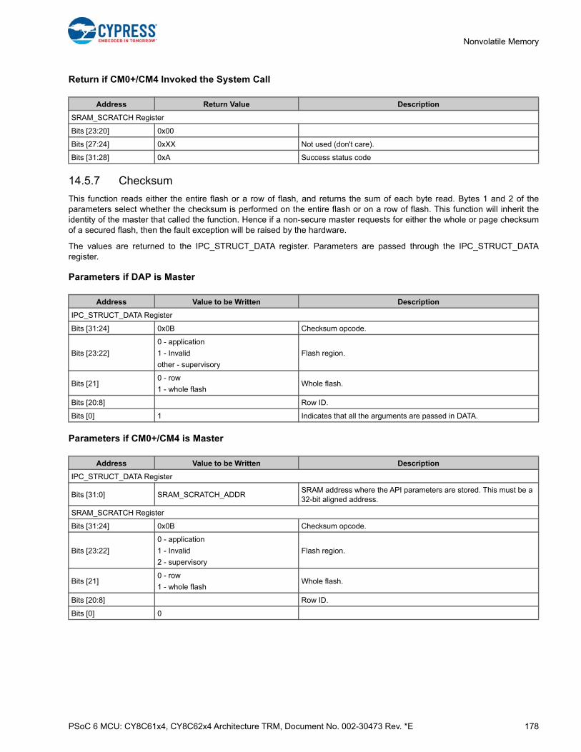
PSoC 6 MCU: CY8C61x4, CY8C62x4 Architecture TRM, Document No. 002-30473 Rev. *E 178
Nonvolatile Memory
Return if CM0+/CM4 Invoked the System Call
14.5.7 Checksum
This function reads either the entire flash or a row of flash, and returns the sum of each byte read. Bytes 1 and 2 of theparameters select whether the checksum is performed on the entire flash or on a row of flash. This function will inherit theidentity of the master that called the function. Hence if a non-secure master requests for either the whole or page checksumof a secured flash, then the fault exception will be raised by the hardware.
The values are returned to the IPC_STRUCT_DATA register. Parameters are passed through the IPC_STRUCT_DATAregister.
Parameters if DAP is Master
Parameters if CM0+/CM4 is Master
Address Return Value Description
SRAM_SCRATCH Register
Bits [23:20] 0x00
Bits [27:24] 0xXX Not used (don't care).
Bits [31:28] 0xA Success status code
Address Value to be Written Description
IPC_STRUCT_DATA Register
Bits [31:24] 0x0B Checksum opcode.
Bits [23:22]
0 - application
1 - Invalid
other - supervisory
Flash region.
Bits [21]0 - row
1 - whole flashWhole flash.
Bits [20:8] Row ID.
Bits [0] 1 Indicates that all the arguments are passed in DATA.
Address Value to be Written Description
IPC_STRUCT_DATA Register
Bits [31:0] SRAM_SCRATCH_ADDRSRAM address where the API parameters are stored. This must be a 32-bit aligned address.
SRAM_SCRATCH Register
Bits [31:24] 0x0B Checksum opcode.
Bits [23:22]
0 - application
1 - Invalid
2 - supervisory
Flash region.
Bits [21]0 - row
1 - whole flashWhole flash.
Bits [20:8] Row ID.
Bits [0] 0

PSoC 6 MCU: CY8C61x4, CY8C62x4 Architecture TRM, Document No. 002-30473 Rev. *E 179
Nonvolatile Memory
Return if DAP Invoked the System Call
Return if CM0+/CM4 Invoked the System Call
14.5.8 FmTransitionToLpUlp
This system call configures the required flash macro from trim bits when transitioning from LP to ULP mode or vice-versa.This function takes approximately 20 µs; reads from flash are stalled during this time.
Parameters if DAP/CM0+/CM4 is Master and SRAM is used
Parameters if DAP/CM0+/CM4 is Master and SRAM is not used
Address Return Value Description
IPC_STRUCT_DATA Register
Bits [23:0] Checksum Checksum if status is SUCCESS
Bits [27:24] 0xXX Not used (don’t care)
Bits [31:28]0xA = SUCCESS
0xF = ERRORStatus code (see System Call Status for details).
Address Return Value Description
SRAM_SCRATCH Register
Bits [23:0] Checksum Checksum if status is SUCCESS
Bits [27:24] 0xXX Not used (don’t care)
Bits [31:28]0xA = SUCCESS
0xF = ERRORStatus code (see System Call Status for details).
Address Value to be Written Description
IPC_STRUCT_DATA Register
Bits [31:0] SRAM_SCRATCH_ADDRSRAM address where the API parameters are stored. This must be a 32-bit aligned address.
SRAM_SCRATCH Register
Bits [31:24] 0x0C Opcode for FmTransitionToLpUlp.
Bits [23:2] 0xXX Not used (don’t care)
Bit [1]0 - Transition to LP
1 - Transition to ULPTransition mode
Bits [0] 0xXX Not used (don’t care)
Address Value to be Written Description
IPC_STRUCT_DATA Register
Bits [31:24] 0x0C Opcode for FmTransitionToLpUlp.
Bits [23:2] 0xXX Not used (don’t care)
Bit [1]0 - Transition to LP
1 - Transition to ULPTransition mode
Bit [0]0 - Parameters are in address pointed to by IPC_DATA
1 - Parameters are in IPC_DATAParameter location
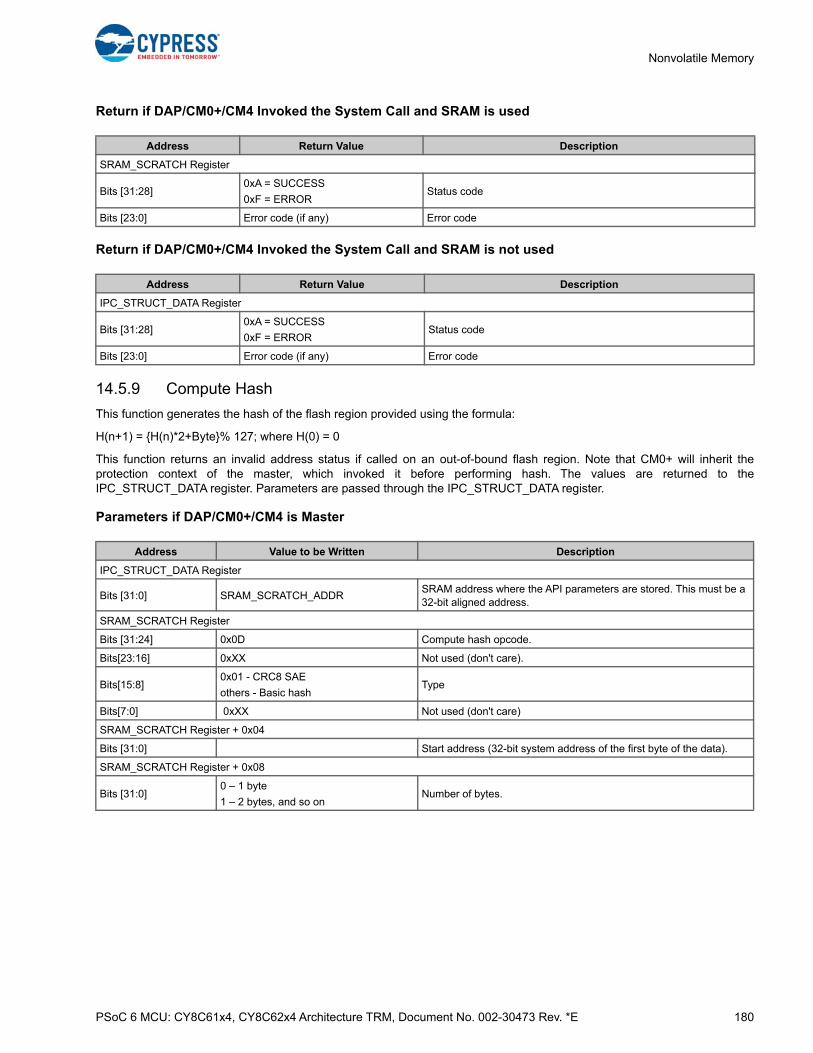
PSoC 6 MCU: CY8C61x4, CY8C62x4 Architecture TRM, Document No. 002-30473 Rev. *E 180
Nonvolatile Memory
Return if DAP/CM0+/CM4 Invoked the System Call and SRAM is used
Return if DAP/CM0+/CM4 Invoked the System Call and SRAM is not used
14.5.9 Compute Hash
This function generates the hash of the flash region provided using the formula:
H(n+1) = {H(n)*2+Byte}% 127; where H(0) = 0
This function returns an invalid address status if called on an out-of-bound flash region. Note that CM0+ will inherit theprotection context of the master, which invoked it before performing hash. The values are returned to theIPC_STRUCT_DATA register. Parameters are passed through the IPC_STRUCT_DATA register.
Parameters if DAP/CM0+/CM4 is Master
Address Return Value Description
SRAM_SCRATCH Register
Bits [31:28]0xA = SUCCESS
0xF = ERRORStatus code
Bits [23:0] Error code (if any) Error code
Address Return Value Description
IPC_STRUCT_DATA Register
Bits [31:28]0xA = SUCCESS
0xF = ERRORStatus code
Bits [23:0] Error code (if any) Error code
Address Value to be Written Description
IPC_STRUCT_DATA Register
Bits [31:0] SRAM_SCRATCH_ADDRSRAM address where the API parameters are stored. This must be a 32-bit aligned address.
SRAM_SCRATCH Register
Bits [31:24] 0x0D Compute hash opcode.
Bits[23:16] 0xXX Not used (don't care).
Bits[15:8]0x01 - CRC8 SAE
others - Basic hashType
Bits[7:0] 0xXX Not used (don't care)
SRAM_SCRATCH Register + 0x04
Bits [31:0] Start address (32-bit system address of the first byte of the data).
SRAM_SCRATCH Register + 0x08
Bits [31:0]0 – 1 byte
1 – 2 bytes, and so onNumber of bytes.
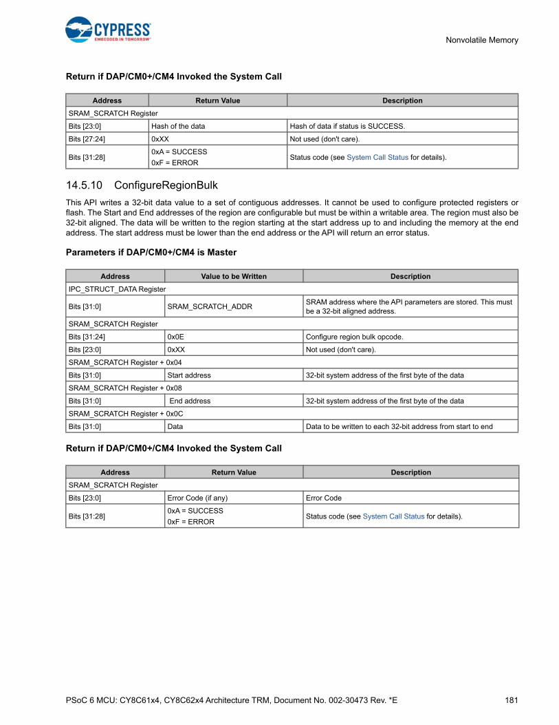
PSoC 6 MCU: CY8C61x4, CY8C62x4 Architecture TRM, Document No. 002-30473 Rev. *E 181
Nonvolatile Memory
Return if DAP/CM0+/CM4 Invoked the System Call
14.5.10 ConfigureRegionBulk
This API writes a 32-bit data value to a set of contiguous addresses. It cannot be used to configure protected registers orflash. The Start and End addresses of the region are configurable but must be within a writable area. The region must also be32-bit aligned. The data will be written to the region starting at the start address up to and including the memory at the endaddress. The start address must be lower than the end address or the API will return an error status.
Parameters if DAP/CM0+/CM4 is Master
Return if DAP/CM0+/CM4 Invoked the System Call
Address Return Value Description
SRAM_SCRATCH Register
Bits [23:0] Hash of the data Hash of data if status is SUCCESS.
Bits [27:24] 0xXX Not used (don't care).
Bits [31:28]0xA = SUCCESS
0xF = ERRORStatus code (see System Call Status for details).
Address Value to be Written Description
IPC_STRUCT_DATA Register
Bits [31:0] SRAM_SCRATCH_ADDRSRAM address where the API parameters are stored. This must be a 32-bit aligned address.
SRAM_SCRATCH Register
Bits [31:24] 0x0E Configure region bulk opcode.
Bits [23:0] 0xXX Not used (don't care).
SRAM_SCRATCH Register + 0x04
Bits [31:0] Start address 32-bit system address of the first byte of the data
SRAM_SCRATCH Register + 0x08
Bits [31:0] End address 32-bit system address of the first byte of the data
SRAM_SCRATCH Register + 0x0C
Bits [31:0] Data Data to be written to each 32-bit address from start to end
Address Return Value Description
SRAM_SCRATCH Register
Bits [23:0] Error Code (if any) Error Code
Bits [31:28]0xA = SUCCESS
0xF = ERRORStatus code (see System Call Status for details).
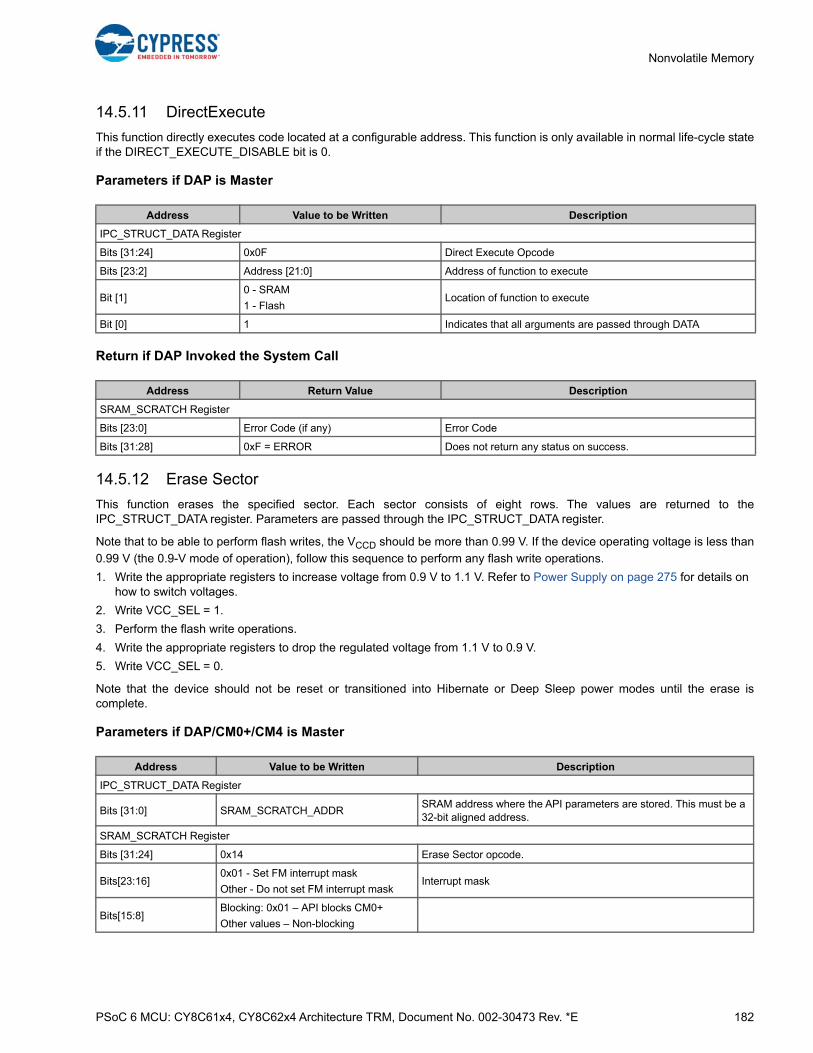
PSoC 6 MCU: CY8C61x4, CY8C62x4 Architecture TRM, Document No. 002-30473 Rev. *E 182
Nonvolatile Memory
14.5.11 DirectExecute
This function directly executes code located at a configurable address. This function is only available in normal life-cycle stateif the DIRECT_EXECUTE_DISABLE bit is 0.
Parameters if DAP is Master
Return if DAP Invoked the System Call
14.5.12 Erase Sector
This function erases the specified sector. Each sector consists of eight rows. The values are returned to theIPC_STRUCT_DATA register. Parameters are passed through the IPC_STRUCT_DATA register.
Note that to be able to perform flash writes, the VCCD should be more than 0.99 V. If the device operating voltage is less than
0.99 V (the 0.9-V mode of operation), follow this sequence to perform any flash write operations.
1. Write the appropriate registers to increase voltage from 0.9 V to 1.1 V. Refer to Power Supply on page 275 for details on how to switch voltages.
2. Write VCC_SEL = 1.
3. Perform the flash write operations.
4. Write the appropriate registers to drop the regulated voltage from 1.1 V to 0.9 V.
5. Write VCC_SEL = 0.
Note that the device should not be reset or transitioned into Hibernate or Deep Sleep power modes until the erase iscomplete.
Parameters if DAP/CM0+/CM4 is Master
Address Value to be Written Description
IPC_STRUCT_DATA Register
Bits [31:24] 0x0F Direct Execute Opcode
Bits [23:2] Address [21:0] Address of function to execute
Bit [1]0 - SRAM
1 - FlashLocation of function to execute
Bit [0] 1 Indicates that all arguments are passed through DATA
Address Return Value Description
SRAM_SCRATCH Register
Bits [23:0] Error Code (if any) Error Code
Bits [31:28] 0xF = ERROR Does not return any status on success.
Address Value to be Written Description
IPC_STRUCT_DATA Register
Bits [31:0] SRAM_SCRATCH_ADDRSRAM address where the API parameters are stored. This must be a 32-bit aligned address.
SRAM_SCRATCH Register
Bits [31:24] 0x14 Erase Sector opcode.
Bits[23:16]0x01 - Set FM interrupt mask
Other - Do not set FM interrupt maskInterrupt mask
Bits[15:8]Blocking: 0x01 – API blocks CM0+
Other values – Non-blocking
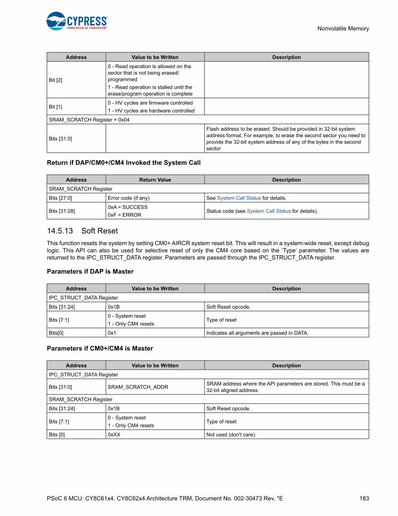
PSoC 6 MCU: CY8C61x4, CY8C62x4 Architecture TRM, Document No. 002-30473 Rev. *E 183
Nonvolatile Memory
Return if DAP/CM0+/CM4 Invoked the System Call
14.5.13 Soft Reset
This function resets the system by setting CM0+ AIRCR system reset bit. This will result in a system-wide reset, except debuglogic. This API can also be used for selective reset of only the CM4 core based on the ‘Type’ parameter. The values arereturned to the IPC_STRUCT_DATA register. Parameters are passed through the IPC_STRUCT_DATA register.
Parameters if DAP is Master
Parameters if CM0+/CM4 is Master
Bit [2]
0 - Read operation is allowed on the sector that is not being erased/programmed
1 - Read operation is stalled until the erase/program operation is complete
Bit [1]0 - HV cycles are firmware controlled
1 - HV cycles are hardware controlled
SRAM_SCRATCH Register + 0x04
Bits [31:0]
Flash address to be erased. Should be provided in 32-bit system address format. For example, to erase the second sector you need to provide the 32-bit system address of any of the bytes in the second sector.
Address Return Value Description
SRAM_SCRATCH Register
Bits [27:0] Error code (if any) See System Call Status for details.
Bits [31:28]0xA = SUCCESS
0xF = ERRORStatus code (see System Call Status for details).
Address Value to be Written Description
Address Value to be Written Description
IPC_STRUCT_DATA Register
Bits [31:24] 0x1B Soft Reset opcode.
Bits [7:1]0 - System reset
1 - Only CM4 resetsType of reset
Bits[0] 0x1 Indicates all arguments are passed in DATA.
Address Value to be Written Description
IPC_STRUCT_DATA Register
Bits [31:0] SRAM_SCRATCH_ADDRSRAM address where the API parameters are stored. This must be a 32-bit aligned address.
SRAM_SCRATCH Register
Bits [31:24] 0x1B Soft Reset opcode.
Bits [7:1]0 - System reset
1 - Only CM4 resetsType of reset
Bits [0] 0xXX Not used (don't care).
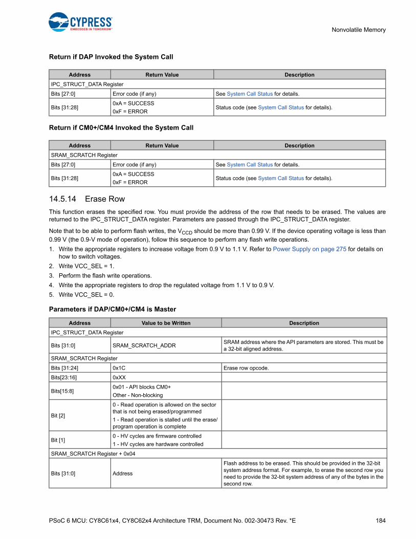
PSoC 6 MCU: CY8C61x4, CY8C62x4 Architecture TRM, Document No. 002-30473 Rev. *E 184
Nonvolatile Memory
Return if DAP Invoked the System Call
Return if CM0+/CM4 Invoked the System Call
14.5.14 Erase Row
This function erases the specified row. You must provide the address of the row that needs to be erased. The values arereturned to the IPC_STRUCT_DATA register. Parameters are passed through the IPC_STRUCT_DATA register.
Note that to be able to perform flash writes, the VCCD should be more than 0.99 V. If the device operating voltage is less than
0.99 V (the 0.9-V mode of operation), follow this sequence to perform any flash write operations.
1. Write the appropriate registers to increase voltage from 0.9 V to 1.1 V. Refer to Power Supply on page 275 for details on how to switch voltages.
2. Write VCC_SEL = 1.
3. Perform the flash write operations.
4. Write the appropriate registers to drop the regulated voltage from 1.1 V to 0.9 V.
5. Write VCC_SEL = 0.
Parameters if DAP/CM0+/CM4 is Master
Address Return Value Description
IPC_STRUCT_DATA Register
Bits [27:0] Error code (if any) See System Call Status for details.
Bits [31:28]0xA = SUCCESS
0xF = ERRORStatus code (see System Call Status for details).
Address Return Value Description
SRAM_SCRATCH Register
Bits [27:0] Error code (if any) See System Call Status for details.
Bits [31:28]0xA = SUCCESS
0xF = ERRORStatus code (see System Call Status for details).
Address Value to be Written Description
IPC_STRUCT_DATA Register
Bits [31:0] SRAM_SCRATCH_ADDRSRAM address where the API parameters are stored. This must be a 32-bit aligned address.
SRAM_SCRATCH Register
Bits [31:24] 0x1C Erase row opcode.
Bits[23:16] 0xXX
Bits[15:8]0x01 - API blocks CM0+
Other - Non-blocking
Bit [2]
0 - Read operation is allowed on the sector that is not being erased/programmed
1 - Read operation is stalled until the erase/program operation is complete
Bit [1]0 - HV cycles are firmware controlled
1 - HV cycles are hardware controlled
SRAM_SCRATCH Register + 0x04
Bits [31:0] Address
Flash address to be erased. This should be provided in the 32-bit system address format. For example, to erase the second row you need to provide the 32-bit system address of any of the bytes in the second row.

PSoC 6 MCU: CY8C61x4, CY8C62x4 Architecture TRM, Document No. 002-30473 Rev. *E 185
Nonvolatile Memory
Return if DAP/CM0+/CM4 Invoked the System Call
14.5.15 Erase Subsector
This function erases the specified subsector. The values are returned to the IPC_STRUCT_DATA register. Parameters arepassed through the IPC_STRUCT_DATA register.
Note that to be able to perform flash writes, the VCCD should be more than 0.99 V. If the device operating voltage is less than
0.99 V (the 0.9-V mode of operation), follow this sequence to perform any flash write operations.
1. Write the appropriate registers to increase voltage from 0.9 V to 1.1 V. Refer to Power Supply on page 275 for details on how to switch voltages.
2. Write VCC_SEL = 1.
3. Perform the flash write operations.
4. Write the appropriate registers to drop the regulated voltage from 1.1 V to 0.9 V.
5. Write VCC_SEL = 0.
Parameters if DAP/CM0+/CM4 is Master
Address Return Value Description
SRAM_SCRATCH Register
Bits [27:0] Error code (if any) See System Call Status for details.
Bits [31:28]0xA = SUCCESS
0xF = ERRORStatus code (see System Call Status for details).
Address Value to be Written Description
IPC_STRUCT_DATA Register
Bits [31:0] SRAM_SCRATCH_ADDRSRAM address where the API parameters are stored. This must be a 32-bit aligned address.
SRAM_SCRATCH Register
Bits [31:24] 0x1D Erase subsector opcode.
Bits [23:16] 0xXX Not used (don't care).
Bits [15:8]0x01- API blocks CM0+
Other - Non-blocking
Bit [2]
0 - Read operation is allowed on the sector that is not being erased/programmed
1 - Read operation is stalled until the erase/program operation is complete
Bit [1]0 - HV cycles are firmware controlled
1 - HV cycles are hardware controlled
SRAM_SCRATCH Register + 0x04
Bits [31:0] Address
Flash address to be erased. This should be provided in 32-bit system address format. For example, to erase the second subsector you need to provide the 32-bit system address of any of the bytes in the second subsector.
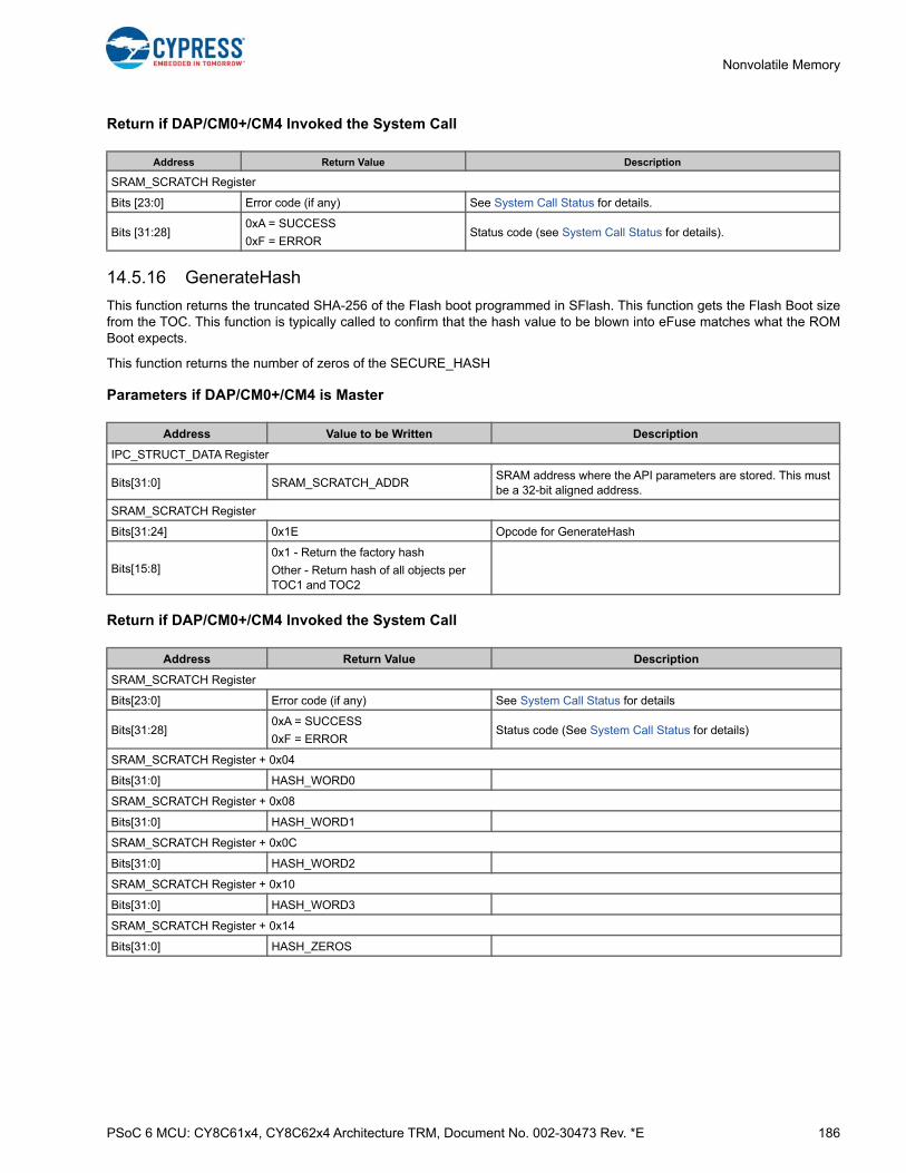
PSoC 6 MCU: CY8C61x4, CY8C62x4 Architecture TRM, Document No. 002-30473 Rev. *E 186
Nonvolatile Memory
Return if DAP/CM0+/CM4 Invoked the System Call
14.5.16 GenerateHash
This function returns the truncated SHA-256 of the Flash boot programmed in SFlash. This function gets the Flash Boot sizefrom the TOC. This function is typically called to confirm that the hash value to be blown into eFuse matches what the ROMBoot expects.
This function returns the number of zeros of the SECURE_HASH
Parameters if DAP/CM0+/CM4 is Master
Return if DAP/CM0+/CM4 Invoked the System Call
Address Return Value Description
SRAM_SCRATCH Register
Bits [23:0] Error code (if any) See System Call Status for details.
Bits [31:28]0xA = SUCCESS
0xF = ERRORStatus code (see System Call Status for details).
Address Value to be Written Description
IPC_STRUCT_DATA Register
Bits[31:0] SRAM_SCRATCH_ADDRSRAM address where the API parameters are stored. This must be a 32-bit aligned address.
SRAM_SCRATCH Register
Bits[31:24] 0x1E Opcode for GenerateHash
Bits[15:8]0x1 - Return the factory hash
Other - Return hash of all objects per TOC1 and TOC2
Address Return Value Description
SRAM_SCRATCH Register
Bits[23:0] Error code (if any) See System Call Status for details
Bits[31:28]0xA = SUCCESS
0xF = ERRORStatus code (See System Call Status for details)
SRAM_SCRATCH Register + 0x04
Bits[31:0] HASH_WORD0
SRAM_SCRATCH Register + 0x08
Bits[31:0] HASH_WORD1
SRAM_SCRATCH Register + 0x0C
Bits[31:0] HASH_WORD2
SRAM_SCRATCH Register + 0x10
Bits[31:0] HASH_WORD3
SRAM_SCRATCH Register + 0x14
Bits[31:0] HASH_ZEROS

PSoC 6 MCU: CY8C61x4, CY8C62x4 Architecture TRM, Document No. 002-30473 Rev. *E 187
Nonvolatile Memory
14.5.17 ReadUniqueID
This function returns the unique ID of the die from SFlash.
Parameters if DAP/ CM0+/CM4 is Master
Return if DAP/ CM0+/CM4 Invoked the System Call
14.5.18 CheckFactoryHash
This function generates the FACTORY_HASH according to the TOC1 and compares the value with the FACTORY1_HASHeFuse value.
Parameters if DAP is Master
Parameters if CM0+/CM4 is Master
Address Value to be Written Description
IPC_STRUCT_DATA Register
Bits[31:0] SRAM_SCRATCH_ADDRSRAM address where the API parameters are stored. This must be a 32-bit aligned address.
SRAM_SCRATCH Register
Bits[31:24] 0x1F Opcode for ReadUniqueID
Bits[15:0] Not Used (Don't care)
Address Return Value Description
SRAM_SCRATCH Register
Bits[23:0] DIE_LOT if SUCCESS See System Call Status for details
Bits[31:28]0xA = SUCCESS
0xF = ERRORStatus code (see System Call Status for details)
SRAM_SCRATCH Register + 0x04
Bits[31:0] DIE_ID0
SRAM_SCRATCH Register + 0x08
Bits[31:0] DIE_ID1
Address Value to be Written Description
IPC_STRUCT_DATA Register
Bits [31:24] 0x27 CheckFactoryHash Opcode
Bit [0] 1 Indicates all arguments are passed in DATA.
Address Value to be Written Description
IPC_STRUCT_DATA Register
Bits [31:0] SRAM_SCRATCH_ADDRSRAM address where the API parameters are stored. This must be a 32-bit aligned address.
SRAM_SCRATCH Register
Bits [31:24] 0x27 CheckFactoryHash Opcode
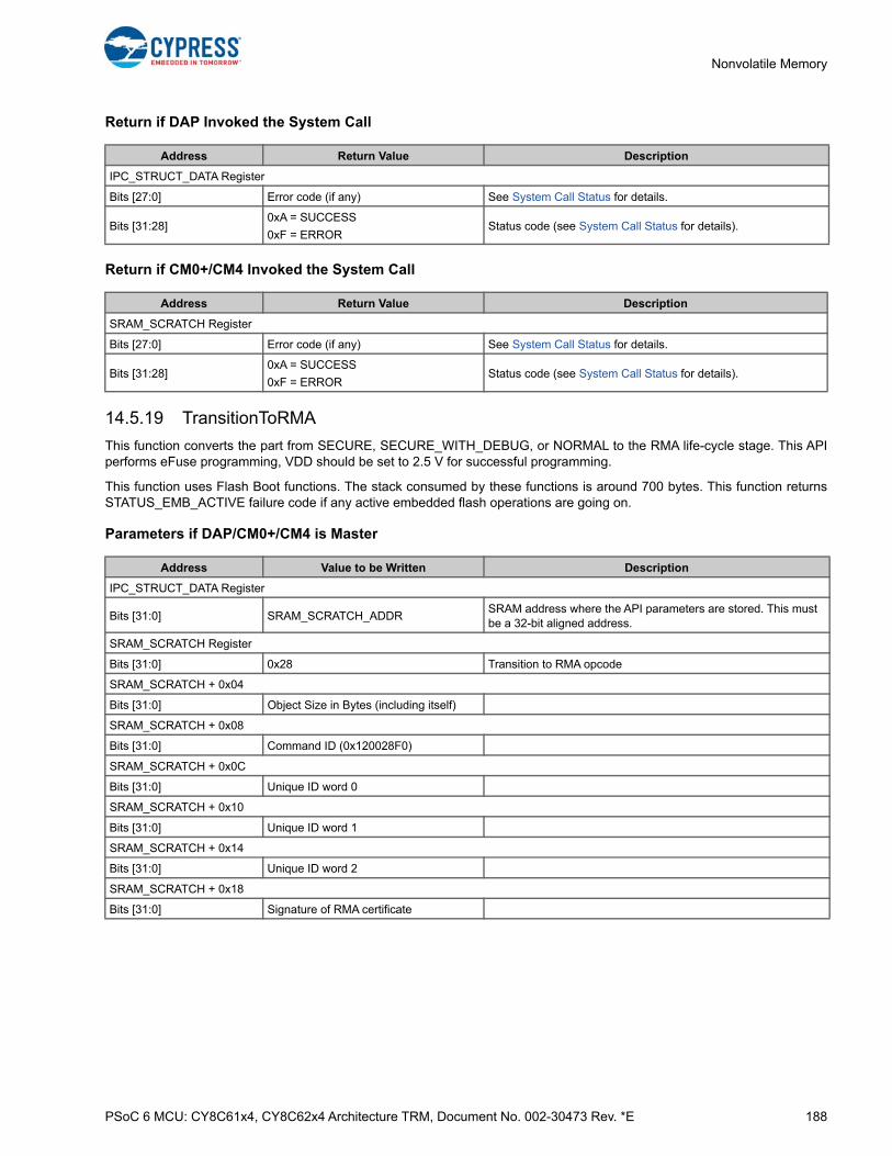
PSoC 6 MCU: CY8C61x4, CY8C62x4 Architecture TRM, Document No. 002-30473 Rev. *E 188
Nonvolatile Memory
Return if DAP Invoked the System Call
Return if CM0+/CM4 Invoked the System Call
14.5.19 TransitionToRMA
This function converts the part from SECURE, SECURE_WITH_DEBUG, or NORMAL to the RMA life-cycle stage. This APIperforms eFuse programming, VDD should be set to 2.5 V for successful programming.
This function uses Flash Boot functions. The stack consumed by these functions is around 700 bytes. This function returnsSTATUS_EMB_ACTIVE failure code if any active embedded flash operations are going on.
Parameters if DAP/CM0+/CM4 is Master
Address Return Value Description
IPC_STRUCT_DATA Register
Bits [27:0] Error code (if any) See System Call Status for details.
Bits [31:28]0xA = SUCCESS
0xF = ERRORStatus code (see System Call Status for details).
Address Return Value Description
SRAM_SCRATCH Register
Bits [27:0] Error code (if any) See System Call Status for details.
Bits [31:28]0xA = SUCCESS
0xF = ERRORStatus code (see System Call Status for details).
Address Value to be Written Description
IPC_STRUCT_DATA Register
Bits [31:0] SRAM_SCRATCH_ADDRSRAM address where the API parameters are stored. This must be a 32-bit aligned address.
SRAM_SCRATCH Register
Bits [31:0] 0x28 Transition to RMA opcode
SRAM_SCRATCH + 0x04
Bits [31:0] Object Size in Bytes (including itself)
SRAM_SCRATCH + 0x08
Bits [31:0] Command ID (0x120028F0)
SRAM_SCRATCH + 0x0C
Bits [31:0] Unique ID word 0
SRAM_SCRATCH + 0x10
Bits [31:0] Unique ID word 1
SRAM_SCRATCH + 0x14
Bits [31:0] Unique ID word 2
SRAM_SCRATCH + 0x18
Bits [31:0] Signature of RMA certificate
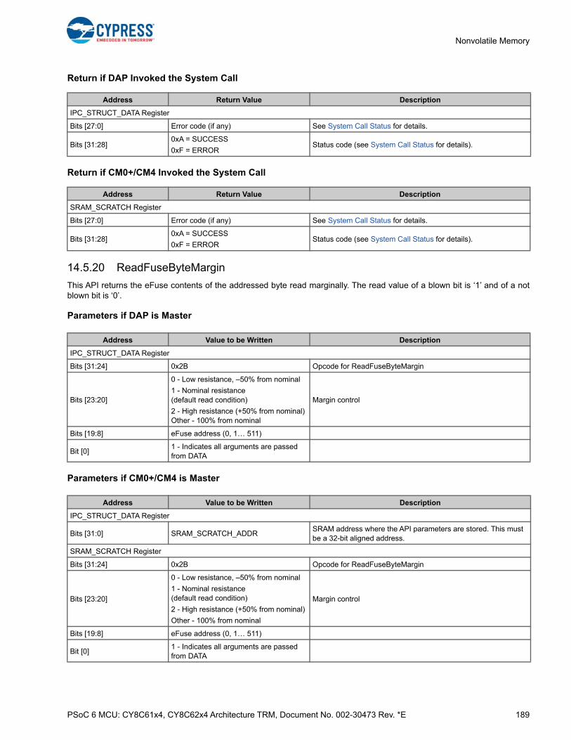
PSoC 6 MCU: CY8C61x4, CY8C62x4 Architecture TRM, Document No. 002-30473 Rev. *E 189
Nonvolatile Memory
Return if DAP Invoked the System Call
Return if CM0+/CM4 Invoked the System Call
14.5.20 ReadFuseByteMargin
This API returns the eFuse contents of the addressed byte read marginally. The read value of a blown bit is ‘1’ and of a notblown bit is ‘0’.
Parameters if DAP is Master
Parameters if CM0+/CM4 is Master
Address Return Value Description
IPC_STRUCT_DATA Register
Bits [27:0] Error code (if any) See System Call Status for details.
Bits [31:28]0xA = SUCCESS
0xF = ERRORStatus code (see System Call Status for details).
Address Return Value Description
SRAM_SCRATCH Register
Bits [27:0] Error code (if any) See System Call Status for details.
Bits [31:28]0xA = SUCCESS
0xF = ERRORStatus code (see System Call Status for details).
Address Value to be Written Description
IPC_STRUCT_DATA Register
Bits [31:24] 0x2B Opcode for ReadFuseByteMargin
Bits [23:20]
0 - Low resistance, –50% from nominal
1 - Nominal resistance (default read condition)
2 - High resistance (+50% from nominal) Other - 100% from nominal
Margin control
Bits [19:8] eFuse address (0, 1… 511)
Bit [0]1 - Indicates all arguments are passed from DATA
Address Value to be Written Description
IPC_STRUCT_DATA Register
Bits [31:0] SRAM_SCRATCH_ADDRSRAM address where the API parameters are stored. This must be a 32-bit aligned address.
SRAM_SCRATCH Register
Bits [31:24] 0x2B Opcode for ReadFuseByteMargin
Bits [23:20]
0 - Low resistance, –50% from nominal
1 - Nominal resistance (default read condition)
2 - High resistance (+50% from nominal)
Other - 100% from nominal
Margin control
Bits [19:8] eFuse address (0, 1… 511)
Bit [0]1 - Indicates all arguments are passed from DATA

PSoC 6 MCU: CY8C61x4, CY8C62x4 Architecture TRM, Document No. 002-30473 Rev. *E 190
Nonvolatile Memory
Return if DAP Invoked the System Call
Return if CM0+/CM4 Invoked the System Call
14.5.21 TransitionToSecure
This API validates the FACTORY_HASH value and programs the SECURE_HASH, secure access restrictions, and deadaccess restrictions into eFuse. This function programs the SECURE or SECURE_WITH_DEBUG eFuse to transition to theSECURE or SECURE_WITH_DEBUG life-cycle stage. If the FACTORY_HASH or the TOC1 magic number is invalid, thenthe API fails and returns status code 0xF00000b5. Note that if the Factory_HASH in eFuse is invalid, then theTransitionToSecure API fails and the error code is written to the IPC[2].DATA register.
Parameters if DAP/CM0+/CM4 is Master
Return if DAP/CM0+/CM4 Invoked the System Call
Address Return Value Description
IPC_STRUCT_DATA Register
Bits [31:28]0xA = SUCCESS
0xF = ERRORStatus code (see System Call Status for details).
Bits [23:0] Byte read from eFuse See System Call Status for details.
Address Return Value Description
SRAM_SCRATCH Register
Bits [31:28]0xA = SUCCESS
0xF = ERRORStatus code (see System Call Status for details).
Bits [23:0] Byte read from eFuse See System Call Status for details.
Address Value to be Written Description
IPC_STRUCT_DATA Register
Bits [31:0] SRAM_SCRATCH_ADDRSRAM address where the API parameters are stored. This must be a 32-bit aligned address.
SRAM_SCRATCH Register
Bits [31:24] 0x2F Transition to Secure opcode
Bits [15:8]1 - Blow Debug Fuse
Other - Blow Secure FuseSelect SECURE_WITH_DEBUG or SECURE life-cycle Stage
SRAM_SCRATCH + 0x04
Bits [31:0] SECURE_ACCESS_RESTRICT
SRAM_SCRATCH + 0x08
Bits [31:0] DEAD_ACCESS_RESTRICT
Address Return Value Description
SRAM_SCRATCH Register
Bits [27:0] Error code (if any) See System Call Status for details.
Bits [31:28]0xA = SUCCESS
0xF = ERRORStatus code (see System Call Status for details).
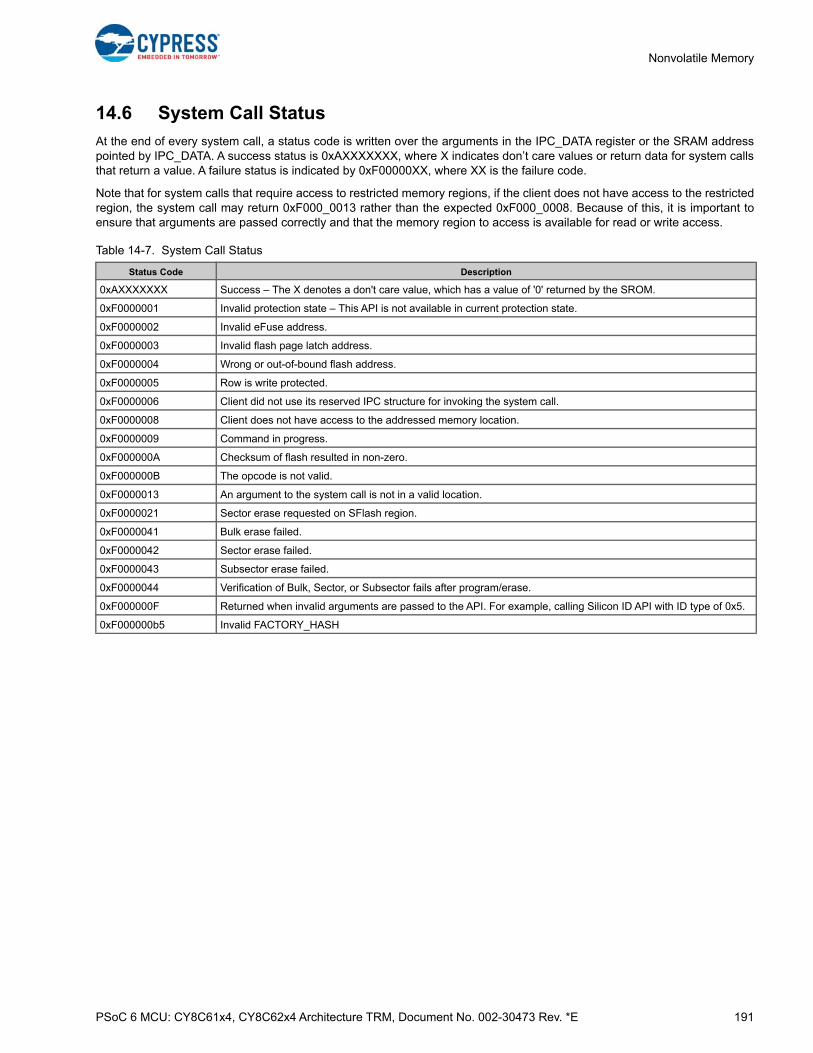
PSoC 6 MCU: CY8C61x4, CY8C62x4 Architecture TRM, Document No. 002-30473 Rev. *E 191
Nonvolatile Memory
14.6 System Call Status
At the end of every system call, a status code is written over the arguments in the IPC_DATA register or the SRAM addresspointed by IPC_DATA. A success status is 0xAXXXXXXX, where X indicates don’t care values or return data for system callsthat return a value. A failure status is indicated by 0xF00000XX, where XX is the failure code.
Note that for system calls that require access to restricted memory regions, if the client does not have access to the restrictedregion, the system call may return 0xF000_0013 rather than the expected 0xF000_0008. Because of this, it is important toensure that arguments are passed correctly and that the memory region to access is available for read or write access.
Table 14-7. System Call Status
Status Code Description
0xAXXXXXXX Success – The X denotes a don't care value, which has a value of '0' returned by the SROM.
0xF0000001 Invalid protection state – This API is not available in current protection state.
0xF0000002 Invalid eFuse address.
0xF0000003 Invalid flash page latch address.
0xF0000004 Wrong or out-of-bound flash address.
0xF0000005 Row is write protected.
0xF0000006 Client did not use its reserved IPC structure for invoking the system call.
0xF0000008 Client does not have access to the addressed memory location.
0xF0000009 Command in progress.
0xF000000A Checksum of flash resulted in non-zero.
0xF000000B The opcode is not valid.
0xF0000013 An argument to the system call is not in a valid location.
0xF0000021 Sector erase requested on SFlash region.
0xF0000041 Bulk erase failed.
0xF0000042 Sector erase failed.
0xF0000043 Subsector erase failed.
0xF0000044 Verification of Bulk, Sector, or Subsector fails after program/erase.
0xF000000F Returned when invalid arguments are passed to the API. For example, calling Silicon ID API with ID type of 0x5.
0xF000000b5 Invalid FACTORY_HASH
PSoC 6 MCU: CY8C61x4, CY8C62x4 Architecture TRM, Document No. 002-30473 Rev. *E 192
15. Boot Code
System boot is defined as the process of validating and starting the product firmware. CY8C6x24 has 64KB of embeddedSROM, which stores the firmware to begin the boot process. This firmware is called ROM boot. The second stage of the bootprocess takes place in SFlash and is called Flash boot. The main function of the boot process is to configure the system(apply trims, configure access, and set protection settings according to the product life-cycle stage), authenticate theapplication, and transfer control to the application.
15.1 Features
The PSoC 6 boot code supports the following features:
■ After reset, the boot code starts execution from ROM on the CM0+.
■ The boot process consists of two parts – ROM boot process and Flash boot process.
■ The ROM boot code applies life-cycle stage and protection state.
■ The ROM boot code validates the integrity of the Flash boot process before starting it.
■ The Flash boot code validates the integrity of the user application before starting it when the device in the SECURE life-cycle stage. User application validation may optionally be enabled in the NORMAL life-cycle stage.
15.2 ROM Boot
The boot code starts execution from ROM. The ROM boot code applies trims and configurations, and validates the integrity ofthe flash boot process before starting it.
15.2.1 Data Integrity Checks
ROM boot uses a Table of Contents (TOC) data structure to locate various objects that are stored in both application flash andSFlash. The location of some of these objects is fixed in the factory while other object locations are fixed at the originalequipment manufacturer (OEM). The TOC is split into two parts – TOC1 and TOC2 – that correspond to objects fixed in thefactory and objects fixed at OEM, respectively. TOC1 and TOC2 are stored in SFlash.
The data integrity of selected objects listed at the beginning of TOC1 must be verified at the OEM before transitioning the partto the SECURE life-cycle stage. The FACTORY_HASH is generated using SHA-256, which is the concatenation of theobjects to be verified in TOC1. The FACTORY_HASH is stored in eFuse before the device leaves Cypress. The devicevalidates the FACTORY_HASH as part of the TransitionToSecure system call.
The data integrity of selected objects in both TOC1 and TOC2 must be verified as part of authentication of Flash boot by ROMboot in the SECURE life-cycle stage. A 128-bit truncated SHA-256 value known as the SECURE_HASH is used to check the
This PSoC 6 MCU technical reference manual (TRM) provides comprehensive and detailed information about thefunctions of the PSoC 6 MCU device hardware. It is divided into two books: architecture TRM and registers TRM. TheTRM is not recommended for those new to the PSoC 6 MCU, nor as a guide for developing PSoC 6 MCU applications.Use these documents instead:
■ PSoC 61 datasheet, PSoC 62 datasheet
■ Peripheral Driver Library (PDL) documentation
■ Application notes
■ Code examples

PSoC 6 MCU: CY8C61x4, CY8C62x4 Architecture TRM, Document No. 002-30473 Rev. *E 193
Boot Code
integrity of these objects. If the TOC structures fail integrity checks, then the RTOC structures are checked for validity. If theRTOC structures are valid, then the boot process uses the RTOC structures in place of the TOC structures. TheSECURE_HASH is programmed automatically during the TransitionToSecure system call. If the TransitionToSecure systemcall fails, it will exit before programming the SECURE_HASH in eFuse. See System Call Status on page 191 for moreinformation.
A summary of the objects used in the data integrity checks is shown in Figure 15-1. The TOC structure formats are outlined inTable 15-1 to Table 15-3.
Figure 15-1. Objects, Memory Regions, and Stages of Boot Process for Data Integrity Checks
TOC 2
TOC 1
Flash BootCode
Trim Values& Misc
Public Key
SFlash
ROM Code
(Fixed)
Factory_HASH (Normal Mode)
Secure_HASH (Secure Mode)
Public Key
Factory_Hash is only used to validate that the device has not been modified before the transition to Secure mode.
eFuse cells can be programmed from 0 to 1, but not back to 0.
Secure_HASH
Factory_HASH
DAP Configs
LifeCycle State
eFuse (OTP)
In Secure mode, Flash Boot, Trim values, TOC1, TOC2, and Public key are validated with Secure_HASH in eFuse.
User Application Code
Digital Signature
User Application Block
Table 15-1. TOC1 Format
Offset from Beginning of Row
Purpose Comments
0x00 Object size in bytes for CRC calculation starting from offset 0x00
TOC1 filled in VIRGIN pro-tection state by Cypress
0x04 Magic number (0x01211219)
0x08 Number of objects starting from offset 0xC to be verified for FACTORY_HASH
0x0C Unused
0x10 Address of Unique ID (fixed size of 12 bytes) stored in SFlash
0x14 Address of Flash boot object that includes Flash Patch object stored in SFlash
0x18 Unused
0x1C-0x1F8 Unused
0x1FC CRC16-CCITT (the upper two bytes contain the CRC little endian value and the lower two bytes are 0)
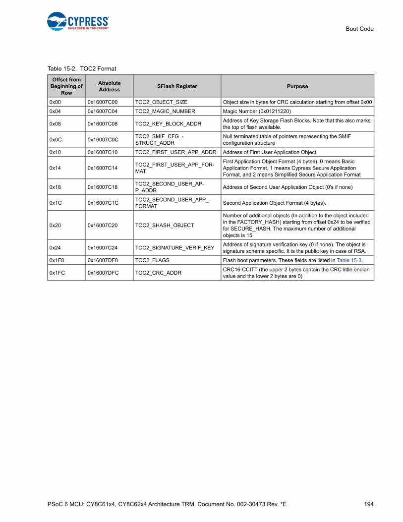
PSoC 6 MCU: CY8C61x4, CY8C62x4 Architecture TRM, Document No. 002-30473 Rev. *E 194
Boot Code
Table 15-2. TOC2 Format
Offset from Beginning of
Row
Absolute Address
SFlash Register Purpose
0x00 0x16007C00 TOC2_OBJECT_SIZE Object size in bytes for CRC calculation starting from offset 0x00
0x04 0x16007C04 TOC2_MAGIC_NUMBER Magic Number (0x01211220)
0x08 0x16007C08 TOC2_KEY_BLOCK_ADDRAddress of Key Storage Flash Blocks. Note that this also marks the top of flash available.
0x0C 0x16007C0CTOC2_SMIF_CFG_-STRUCT_ADDR
Null terminated table of pointers representing the SMIF configuration structure
0x10 0x16007C10 TOC2_FIRST_USER_APP_ADDR Address of First User Application Object
0x14 0x16007C14TOC2_FIRST_USER_APP_FOR-MAT
First Application Object Format (4 bytes). 0 means Basic Application Format, 1 means Cypress Secure Application Format, and 2 means Simplified Secure Application Format
0x18 0x16007C18TOC2_SECOND_USER_AP-P_ADDR
Address of Second User Application Object (0's if none)
0x1C 0x16007C1CTOC2_SECOND_USER_APP_-FORMAT
Second Application Object Format (4 bytes).
0x20 0x16007C20 TOC2_SHASH_OBJECT
Number of additional objects (In addition to the object included in the FACTORY_HASH) starting from offset 0x24 to be verified for SECURE_HASH. The maximum number of additional objects is 15.
0x24 0x16007C24 TOC2_SIGNATURE_VERIF_KEYAddress of signature verification key (0 if none). The object is signature scheme specific. It is the public key in case of RSA.
0x1F8 0x16007DF8 TOC2_FLAGS Flash boot parameters. These fields are listed in Table 15-3.
0x1FC 0x16007DFC TOC2_CRC_ADDRCRC16-CCITT (the upper 2 bytes contain the CRC little endian value and the lower 2 bytes are 0)
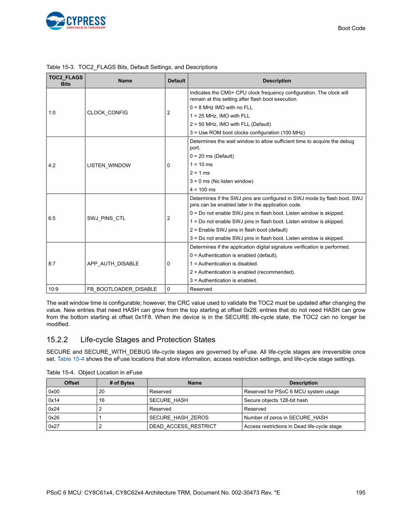
PSoC 6 MCU: CY8C61x4, CY8C62x4 Architecture TRM, Document No. 002-30473 Rev. *E 195
Boot Code
The wait window time is configurable; however, the CRC value used to validate the TOC2 must be updated after changing thevalue. New entries that need HASH can grow from the top starting at offset 0x28; entries that do not need HASH can growfrom the bottom starting at offset 0x1F8. When the device is in the SECURE life-cycle state, the TOC2 can no longer bemodified.
15.2.2 Life-cycle Stages and Protection States
SECURE and SECURE_WITH_DEBUG life-cycle stages are governed by eFuse. All life-cycle stages are irreversible onceset. Table 15-4 shows the eFuse locations that store information, access restriction settings, and life-cycle stage settings.
Table 15-3. TOC2_FLAGS Bits, Default Settings, and Descriptions
TOC2_FLAGS Bits
Name Default Description
1:0 CLOCK_CONFIG 2
Indicates the CM0+ CPU clock frequency configuration. The clock will remain at this setting after flash boot execution.
0 = 8 MHz IMO with no FLL
1 = 25 MHz, IMO with FLL
2 = 50 MHz, IMO with FLL (Default)
3 = Use ROM boot clocks configuration (100 MHz)
4:2 LISTEN_WINDOW 0
Determines the wait window to allow sufficient time to acquire the debug port.
0 = 20 ms (Default)
1 = 10 ms
2 = 1 ms
3 = 0 ms (No listen window)
4 = 100 ms
6:5 SWJ_PINS_CTL 2
Determines if the SWJ pins are configured in SWJ mode by flash boot. SWJ pins can be enabled later in the application code.
0 = Do not enable SWJ pins in flash boot. Listen window is skipped.
1 = Do not enable SWJ pins in flash boot. Listen window is skipped.
2 = Enable SWJ pins in flash boot (default)
3 = Do not enable SWJ pins in flash boot. Listen window is skipped.
8:7 APP_AUTH_DISABLE 0
Determines if the application digital signature verification is performed.
0 = Authentication is enabled (default).
1 = Authentication is disabled.
2 = Authentication is enabled (recommended).
3 = Authentication is enabled.
10:9 FB_BOOTLOADER_DISABLE 0 Reserved.
Table 15-4. Object Location in eFuse
Offset # of Bytes Name Description
0x00 20 Reserved Reserved for PSoC 6 MCU system usage
0x14 16 SECURE_HASH Secure objects 128-bit hash
0x24 2 Reserved Reserved
0x26 1 SECURE_HASH_ZEROS Number of zeros in SECURE_HASH
0x27 2 DEAD_ACCESS_RESTRICT Access restrictions in Dead life-cycle stage

PSoC 6 MCU: CY8C61x4, CY8C62x4 Architecture TRM, Document No. 002-30473 Rev. *E 196
Boot Code
Normal mode access restrictions to be applied on DAP are stored in SFlash.
The LIFECYCLE_STAGE object in eFuse is used to set the life-cycle state of the device. Table 15-6 shows the bits and theassociated settings of the LIFECYCLE_STAGE location.
DAP settings for Secure and Dead protection states are set in the SECURE_ACCESS_RESTRICT0 andDEAD_ACCESS_RESTRICT0 registers. DAP settings for the Normal protection state is set inNORMAL_ACCESS_RESTRICTIONS in SFlash. Table 15-7 shows the format used to set the DAP settings for these states.For more information about the protection states, see the Device Security chapter on page 211.
0x29 2 SECURE_ACCESS_RESTRICT Access restrictions in Secure life-cycle stage
0x2B 1 LIFECYCLE_STAGE Normal, Secure, and Secure with Debug fuse bits
0x2C 16 FACTORY_HASH FACTORY_HASH value
0x40 64 CUSTOMER_DATA Customer data
Table 15-5. Normal Life-cycle Stage DAP Restriction Register in SFlash
Offset # of Bytes Name Description
0x1A00 2 NORMAL_ACCESS_RESTRICTIONSAccess restrictions applied to DAP in NORMAL life-cycle state.
Table 15-6. eFuse Bits and Life-Cycle States
Bits Field Name Description
0 NORMALA ‘1’ indicates that all factory trimming and testing is complete. The device is in NORMAL mode.
1 SECURE_WITH_DEBUGA ‘1’ indicates that the device is in SECURE_WITH_DEBUG mode. Before the device is tran-sitioned to this stage, the SECURE_HASH must have been programmed in eFuse and valid application code must have been programmed in the main flash.
2 SECUREA ‘1’ indicates that the device is in SECURE mode. The SECURE_HASH must have been pro-grammed in eFuse and valid application code has been programmed in the main flash.
3 RMA This life-cycle stage allows Failure Analysis (FA). The part is transitioned to the RMA life-cycle stage when the customer wants Cypress to perform failure analysis. The customer erases all sensitive data before invoking the system call that transitions the part to RMA.
Table 15-7. DAP Access Restriction Registers for Normal, Secure, and Dead Protection States (all default to 0)
Bits Name Description
0 CM0_AP_DISABLE A ‘1’ indicates that this device does not allow access to the M0+ debug access port.
1 CM4_AP_DISABLE A ‘1’ indicates that this device does not allow access to the M4 debug access port.
Table 15-4. Object Location in eFuse
Offset # of Bytes Name Description

PSoC 6 MCU: CY8C61x4, CY8C62x4 Architecture TRM, Document No. 002-30473 Rev. *E 197
Boot Code
The SECURE_ACCESS_RESTRICT1, DEAD_ACCESS_RESTRICT1, and NORMAL_ACCESS_RESTRICTIONS [15:8](SFlash) registers control debug access restriction to specific memory regions. Table 15-8 shows the format used to set theserestrictions.
As an example, if you want to limit the lower one-quarter of flash of a device with 2MB of flash, a “4” is written into theFLASH_ALLOWED field. Only the flash area between 0x1000_0000 and 0x1007_FFFF will be accessible via the SYS_DAP.The remaining areal between 0x1008_0000 to 0x101F_FFFF is not accessible. This means that only the lower quarter offlash can be reprogrammed, erased, or read by the debug port.
2 SYS_AP_DISABLE A ‘1’ indicates that this device does not allow access to the system debug access port.
3 SYS_AP_MPU_ENABLE
A ‘1’ indicates that the MPU on the system debug access port must be programmed and locked according to the settings in the next four fields. The SYS_DISABLE bit must be left at ‘0’ for this setting to matter. If the SYS_DISABLE bit is set to ‘1’, then the next four fields are invalid. This affects only the SYS_AP. It does not affect the CM0/4 AP.
5:4 SFLASH_ALLOWED
This field indicates what portion of Supervisory Flash is accessible through the system debug access port. Only a portion of Supervisory Flash starting at the bottom of the area is exposed. Encoding is as follows:
0: entire region
1: one-half
2: one-quarter
3: nothing
For example, for an encoding of “2: one-quarter”, the valid code region starts at address 0x16000000 and will go up to one-quarter of the SFlash memory region.
7:6 MMIO_ALLOWED
This field indicates what portion of the MMIO region is accessible through the system debug access port. Encoding is as follows:
0: All MMIO registers
1: Only IPC MMIO registers accessible (system calls)
2, 3: No MMIO access
Table 15-8. SECURE_ACCESS_RESTRICT1, DEAD_ACCESS_RESTRICT1, and NORMAL_ACCESS_RESTRICTIONS [15:8] Registers (All default to 0)
Bits Name Description
2:0 FLASH_ALLOWED
This field indicates what portion of the main flash is accessible through the system debug access port. Only the portion starting at the bottom of flash (0x1000_0000) is exposed to the system DAP. The encoding is as follows:
0: entire region
1: seven-eighth
2: three-fourth
3: one-half
4: one-quarter
5: one-eighth
6: one-sixteenth
7: nothing
See Figure 15-2 for an example of the encoding for FLASH_ALLOWED.
5:3 SRAM_ALLOWEDThis field indicates what portion of SRAM 0 is accessible through the system debug access port. Only the portion starting at the bottom of the area is exposed. Encoding is the same as FLASH_ALLOWED.
6 UNUSED UNUSED
7 DIRECT_EXECUTE_DISABLEDisables DirectExecute system call functionality (implemented in software). See the Nonvolatile Memory chapter on page 163 for more information.
Table 15-7. DAP Access Restriction Registers for Normal, Secure, and Dead Protection States (all default to 0)
Bits Name Description

PSoC 6 MCU: CY8C61x4, CY8C62x4 Architecture TRM, Document No. 002-30473 Rev. *E 198
Boot Code
Figure 15-2. FLASH_ALLOWED with encoding “4”
As shown in Figure 15-2, if you want to limit the lower fourth of flash of a device with 2MB of flash, write a ‘4’ into theFLASH_ALLOWED field. Only the flash area between 0x10000000 and 0x1007FFFF will be accessible via the SYS_DAP.The remaining area between 0x10080000 to 0x101FFFFF would not be accessible. This means that only the lower fourth offlash can be reprogrammed, erased, or read by the debug port.
15.2.3 Secure Boot in ROM Boot
At the end of the ROM boot process, the SECURE eFuse bit is checked. If the life-cycle is SECURE, then ROM boot readsthe SECURE access restrictions in eFuse and deploys the settings using the SYS_AP MPU. If the APP_AUTH_DISABLEfield of the TOC2 is not disabled, then ROM boot calculates the SECURE_HASH value from the contents of Flash boot, theTOC1 and TOC2 structures, and the public key and compares it to the stored hash value (SECURE_HASH) in eFuse. If theymatch, the Flash boot code and data are authentic. If the Flash boot code is authentic, then ROM boot will hand over the bootprocess to Flash boot, which resides in SFlash. If the Flash boot is not authentic, then the boot code sets the device into theDEAD protection state.
15.2.4 Protection Setting
ROM boot sets some of the protections units (SMPU, PPU, and MPU) during the boot process. It is recommended that thesesettings are not modified.
SYS_AP DAP access restrictions are deployed by MPU15 based on access restrictions encoding stored in SFlash or eFuse.Eight MPU structures implement the SYS_AP DAP access restrictions. If the SYS_AP MPU is disabled, the following regionsare available for access through the system debug access port.
Table 15-9. Protection Setting
Protection Structure Attribute Settings Protected Region Region Base Region Size (Bytes)
PROT_MPU15_MPU_STRUCT0ADDR: 0x00000000
ATT: 0x9E000000ALL 0x00000000 2G
PROT_MPU15_MPU_STRUCT1ADDR: 0x402200F8
ATT: 0x8700007FIPC 0x40220000 96
Main Flash
0x10200000
0x10000000
Add
ress
DAP Accessable
0x10080000
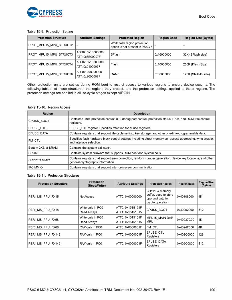
PSoC 6 MCU: CY8C61x4, CY8C62x4 Architecture TRM, Document No. 002-30473 Rev. *E 199
Boot Code
Other protection units are set up during ROM boot to restrict access to various regions to ensure device security. Thefollowing tables list those structures, the regions they protect, and the protection settings applied to those regions. Theprotection settings are applied in all life-cycle stages except VIRGIN.
PROT_MPU15_MPU_STRUCT2 –Work flash region protection option is not present in PSoC 6
– –
PROT_MPU15_MPU_STRUCT3ADDR: 0x16000000
ATT: 0x8E00007FSFlash 0x16000000 32K (SFlash size)
PROT_MPU15_MPU_STRUCT4ADDR: 0x10000000
ATT: 0x9100007FFlash 0x10000000 256K (Flash Size)
PROT_MPU15_MPU_STRUCT6ADDR: 0x8000000
ATT: 0x9000007FRAM0 0x08000000 128K (SRAM0 size)
Table 15-10. Region Access
Region Description
CPUSS_BOOTContains CM0+ protection context 0-3, debug port control, protection status, RAM, and ROM trim control registers.
EFUSE_CTL EFUSE_CTL register. Specifies retention for eFuse registers.
EFUSE_DATA Contains registers that support life-cycle setting, key storage, and other one-time-programmable data.
FM_CTLSpecifies flash hardware block control settings including direct memory cell access addressing, write enable, and interface selection.
Bottom 2KB of SRAM Contains the system call stack.
SROM Contains system firmware that supports ROM boot and system calls.
CRYPTO MMIOContains registers that support error correction, random number generation, device key locations, and other general cryptography information.
IPC MMIO Contains registers that support inter-processor communication
Table 15-11. Protection Structures
Protection StructureProtection
(Read/Write)Attribute Settings Protected Region Region Base
Region Size (Bytes)
PERI_MS_PPU_FX15 No Access ATT0: 0x00000000
CRYPTO Memory buffer, used to store operand data for crypto operation
0x40108000 4K
PERI_MS_PPU_FX18Write only in PC0
Read Always
ATT0: 0x1515151F
ATT1: 0x15151515CPUSS_BOOT 0x40202000 512
PERI_MS_PPU_FX58Write only in PC0
Read Always
ATT0: 0x1515151F
ATT1: 0x15151515MPU15_MAIN DAP MPU
0x40237C00 1K
PERI_MS_PPU_FX68 R/W only in PC0 ATT0: 0x0000001F FM_CTL 0x4024F000 4K
PERI_MS_PPU_FX148 R/W only in PC0 ATT0: 0x0000001FEFUSE_CTL Registers
0x402C0000 128
PERI_MS_PPU_FX149 R/W only in PC0 ATT0: 0x0000001FEFUSE_DATA Registers
0x402C0800 512
Table 15-9. Protection Setting
Protection Structure Attribute Settings Protected Region Region Base Region Size (Bytes)

PSoC 6 MCU: CY8C61x4, CY8C62x4 Architecture TRM, Document No. 002-30473 Rev. *E 200
Boot Code
15.2.5 SWD/JTAG Repurposing
When the user-configured access restrictions disable access to the debug access ports, the boot process does not access orchange the SWD/JTAG pins. User firmware can, at any time, change the configuration of the SWD/JTAG pins to anothermode, peripheral, configuration, or purpose. To allow debugging of such applications, a configurable ‘listen window’ isprovided in the TOC2 at offset 0x1F8 bits [4:2]. The boot process will connect and enable the JTAG/SWD interface and waitfor a specified time before starting application firmware. It is expected that application firmware checks the CPUSSDP_STATUS.SWJ_CONNECTED bit and repurposes the pins only when no SWD/JTAG connection is available.
15.2.6 Waking up from Hibernate
Waking up from Hibernate mode will result in system boot. The integrity checks on the SFlash trim values and SWD/JTAGconnection delay (listen window in Flash boot) are skipped when waking from hibernate.
15.2.7 Disable Watchdog Timer
The ROM boot code will disable the watchdog timer (WDT) if the eFuse.WDT_DISABLE bit is set.
15.2.8 ROM Boot Flow Chart
Figure 15-3 shows the ROM boot flow chart.
PROT_SMPU_SMPU_STRUCT15 Read only in PC0ATT0: 0x8AFFFE00
ATT1: 0x80FFFE40Last 2KB of SRAM 0x0801F7D0 2K
PROT_SMPU_SMPU_STRUCT14 Read only in PC0ATT0: 0x8E00FF00
ATT1: 0x8700FF49
SROM area containing boot code, Crypto, and Flash macro controls.
0x00001000 24K
PERI_MS_PPU_PR2
Disable access during system calls with Crypto enabled (all access allowed otherwise)
ATT0: 1F1F1F1F
ATT1: 1F1F1F1F
Entire Crypto MMIO region during any crypto operation
0x40100000 64K
PERI_MS_PPU_PR3Disable access during system calls (all access allowed otherwise)
ATT0: 1F1F1F1F
ATT1: 1F1F1F1FIPC MMIO (during system calls)
0x40220000 32
Table 15-11. Protection Structures
Protection StructureProtection
(Read/Write)Attribute Settings Protected Region Region Base
Region Size (Bytes)

PSoC 6 MCU: CY8C61x4, CY8C62x4 Architecture TRM, Document No. 002-30473 Rev. *E 201
Boot Code
Figure 15-3. ROM Boot Flow Chart
NoGet M4 Reset VectorCM4_VECTOR_TABLE_BASE (CPUSS MMIO)Set RST SPGoto RST PC
NoGet M0+ Reset VectorCM0_VECTOR_TABLE_BASE (CPUSS MMIO)Set RST SPGoto RST PC
Hash on trim area OK ? (Sflash)
Secure Boot ?(eFuse)
Yes
Yes
RESET
I am M0+?(CPUSS MMIO)
PROTECTION==UNKOWN ?(CPUSS MMIO)
No
Yes
No
Yes
No
Deploy NORMAL Access Restrictions
(SFLASH)
(Warm Boot due to CPU Reset)
Get Flashboot Location
Get Flashboot Location
Apply initial trim settings (eFuse)
Deploy SECURE Access Restrictions (eFuse)
Apply general trim settings (Sflash)
PROTECTION=NORMAL
Deploy DEAD Access Restrictions (eFuse)
Setup SysCall IPCConfigure SWD/JTAG pins
PROTECTION=DEAD
IDLE
(DEAD)(SECURE)
Flash boot
Flash boot
(NORMAL)
Test Mode ?(SRSS MMIO)
Enable SRAMs
PROTECTION=SECURE
Yes
Authenticate Flash BootCorrupt
PSoC 6 MCU: CY8C61x4, CY8C62x4 Architecture TRM, Document No. 002-30473 Rev. *E 202
Boot Code
15.3 Flash Boot
15.3.1 Overview
The second stage of boot, Flash boot, is entered after ROM boot has authenticated the Flash boot image if the device is in theSECURE or SECURE_WITH_DEBUG life-cycle stage, or if the APP_AUTH_DISABLE field is not set in TOC2. In theSECURE or SECURE_WITH_DEBUG life-cycle states, flash boot prevents an application that does not pass integrity checksfrom running. The integrity checks can optionally be enabled in the NORMAL mode by setting the APP_AUTH_DISABLE fieldin TOC2 to any 2-bit value other than 1. This ensures that the application originates from a valid source and has not beenaltered.
The Flash boot firmware:
■ Runs on the security processor (Cortex-M0+)
■ Validates the contents of the TOC2
■ Validates the user application in the Secure life-cycle state or optionally in the Normal life-cycle state
■ Sets up the debug access port (DAP)
■ Enables system calls
■ Hands control to the user application
15.3.2 Features of Flash Boot
■ RSASSA PKCS1 V1.5 with SHA-256 User Application Signature Verification
■ 2048-bit RSA public key with pre-calculated key coefficients for RSA calculation speed increase
■ Support for all device life-cycle stages
■ Configurable debug listen window
15.3.3 Using Flash Boot
Flash boot can be used to allow only authenticated firmware to run on a given platform.
Flash boot determines the life-cycle stage, validates the TOC2, and optionally validates the firmware before transferringexecution to the user's CM0+ application code. The user's CM0+ application enables the CM4 core.
The user firmware will not execute if it is modified by third-party malicious software. The user firmware in flash is validatedusing the RSA algorithm. The 2048-bit public key in SFlash and the digital signature stored with the user application arelocated using the table of contents, which is located at the end of SFlash. The public key is hashed by SECURE_HASH andis validated during boot time. If the code is defined as insecure, the device will go to dead mode with limited debug capabilitiesdetermined by the eFuse settings.
15.3.4 Flash Boot Layout
Flash boot consists of a Header field and a Code Segment field. For hash calculation, the object size must be a multiple of16B so zero padding is applied in the Code Segment.

PSoC 6 MCU: CY8C61x4, CY8C62x4 Architecture TRM, Document No. 002-30473 Rev. *E 203
Boot Code
Figure 15-4. Flash Boot Layout
15.3.4.1 Header
The Flash boot header consists of:
■ The Flash boot object size
■ The Flash boot application version
■ The number of cores (set to ‘1’ for Flash boot)
■ CM0+ vector table offset
■ Cypress ID and CPU Core Index
15.3.4.2 Code Segment
The CM0 code segment consists of:
■ CM0+ vector table
■ CM0+ Flash boot code and data
■ Zero padding to make the Flash boot object a multiple of 16B
15.3.5 Flash Boot Flow Chart
The Flash boot program flow is shown in Figure 15-5. The entry point is a fixed offset in SFlash. Each section of the flow chartis labeled with an index number. In the sections following the flow chart, explanations of each step are provided with theassociated index number.
Application ID/Version
Attributes
HeaderCore0 VT offset
Alignment Padding
CM0 Code Segment
Flash BootSize
Core[0] code and data (Flash boot, Flash Patch)
Object Size
Core[0] Vector Table
Number of cores (N)
Core0 CPU ID/Index
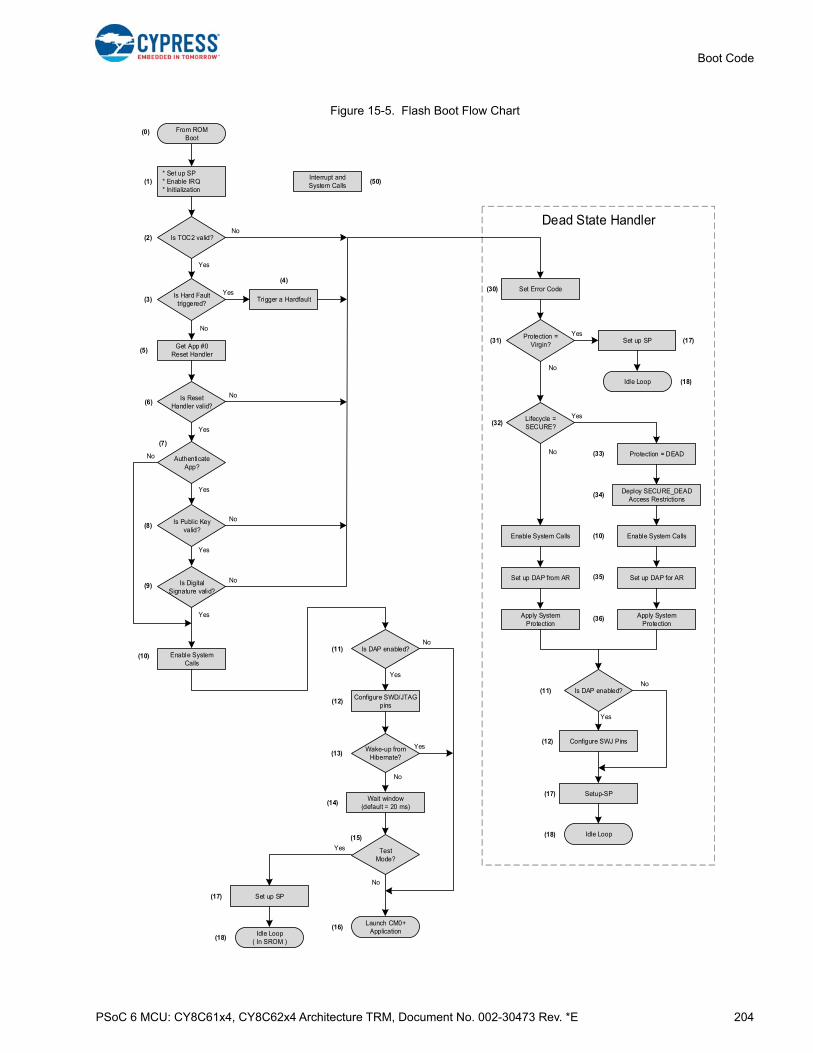
PSoC 6 MCU: CY8C61x4, CY8C62x4 Architecture TRM, Document No. 002-30473 Rev. *E 204
Boot Code
Figure 15-5. Flash Boot Flow Chart
Configure SWD/JTAG pins
Lifecycle = SECURE?
Set Error Code
(0)
Is TOC2 valid?
(1)
Is DAP enabled?
Idle Loop( In SROM )
TestMode?
Wait window(default = 20 ms)
Is Reset Handler valid?
AuthenticateApp?
No
Yes
* Set up SP* Enable IRQ* Initialization
Is Hard Fault triggered?
Get App #0 Reset Handler
Is Public Key valid?
Is Digital Signature valid?
Enable System Calls
Wake-up from Hibernate?
Trigger a Hardfault
From ROMBoot
Protection = Virgin?
Set up SP
Idle Loop
Enable System Calls
Set up DAP from AR
Apply System Protection
Protection = DEAD
Deploy SECURE_DEAD Access Restrictions
Enable System Calls
Set up DAP for AR
Apply System Protection
Is DAP enabled?
Configure SWJ Pins
Setup-SP
Idle Loop
Launch CM0+Application
Set up SP
Dead State Handler
Yes
No
No
No
No
No
No
No
No
No
No
No
Yes
Yes
Yes
Yes
Yes
Yes
Yes
Yes
Yes
Yes
Interrupt and System Calls
(2)
(3)
(4)
(5)
(6)
(7)
(8)
(9)
(10)(11)
(12)
(13)
(14)
(15)
(16)
(17)
(18)
(30)
(31) (17)
(18)
(32)
(34)
(10)
(35)
(36)
(11)
(12)
(17)
(18)
(33)
(50)
PSoC 6 MCU: CY8C61x4, CY8C62x4 Architecture TRM, Document No. 002-30473 Rev. *E 205
Boot Code
15.3.5.1 Entry from ROM Boot (0)
ROM boot transfers control to Flash boot after it validatesthe SFlash block and TOC1 in the user flash.
15.3.5.2 Basic Initialization (1)
This stage sets the value of the stack pointer during runtime.To support recovery from Hard-Fault exceptions duringFlash boot, this stage also enables interrupts.
15.3.5.3 Is TOC2 Valid? (2)
The TOC2 may be in three states:
■ VALID: The TOC2 structure and CRC are valid. This isthe default state of the TOC2.
■ CORRUPTED: Either the TOC2 structure or CRC valueare incorrect.
■ ERASED: The first two 32-bit words at the start of TOC2are equal to the SFlash erase value. The erased value is0x0000_0000.
If the PROTECTION is SECURE then ERASED state is apart of CORRUPTED state.
If the PROTECTION is not SECURE then ERASED state isa special case of VALID state. In this case, Flash boot treatsall the TOC2 entries as having a default value:
■ SFLASH_TOC2_FIRST_USER_APP_ADDR is0x1000_0000 (the start of Flash).
■ SFLASH_TOC2_FIRST_USER_APP_FORMAT is 0(Basic Application Format).
■ SFLASH_TOC2_FLAGS = 0x0000_0000
The other TOC2 entries will not be used when TOC2 is inERASED or corrupted states.
15.3.5.4 Is Hard Fault Triggered? (3)
The Flash boot test system requires a way to trigger a hardfault in the Flash boot code. The condition to trigger a hard-fault is as follows:
1. SFLASH_FLAGS bit FB_HARDFAULT is set.
2. A 32-bit word in TOC2 at offset + 500 contains an address to a 32-bit word named HardFaultTrigger.
3. HardFaultTrigger value is 0x0000_0001.
15.3.5.5 Trigger a Hard Fault (4)
Flash boot can be used to trigger a hard fault for a testingpurposes.
This can be done, for example, by a 32-bit word read orwrite to an unaligned address, or to an invalid memoryregion.
The hard fault handler recovers the MCU into the DEADstate branch. In this branch, an error code is set and theDAP is enabled.
15.3.5.6 Get App #0 Reset Handler (5)
Flash boot reads the application start address from theTOC2 entry:
■ SFLASH_TOC2_FIRST_USER_APP_ADDR for App#0.
The application format is stored in the TOC2 entry:
■ SFLASH_TOC2_FIRST_USER_APP_FORMAT for App#0.
The address of reset handler inside the application dependson the application format.
15.3.5.7 Is Reset Handler Valid? (6)
Flash boot checks if the address of the reset handler for theuser application is in RAM, SFlash, application flash, or EEEmulation flash.
15.3.5.8 Authenticate App? (7)
Flash boot optionally authenticates a digital signature for theapplication image if the TOC2_FLAGS bitAPP_AUTH_DISABLE = 1.
If this field is set then the authentication step is skipped.
15.3.5.9 Is Public Key Valid (8)
The public key structure is filled by the user. Thus, it must bevalidated to ensure the correctness of the its entries beforebeing used.
15.3.5.10 Is Digital Signature Valid? (9)
The user application located in main flash is validated usingthe standard RSA 2048-bit algorithm (RSASSA-PKCS1-v1_5-2048). The public key used for this operation is storedin the user public key area of SFlash.
The application can be in one of three formats, only two ofwhich are validated using a public key.
The Crypto block is used for validation and is only enabledduring the application validation process to conserve power.
The following figure shows the application validation flow.

PSoC 6 MCU: CY8C61x4, CY8C62x4 Architecture TRM, Document No. 002-30473 Rev. *E 206
Boot Code
Figure 15-6. Application Validation
15.3.5.11 Enable System Calls (10)
At this point the system calls are enabled. A table of thesystem calls is found in SROM API Library on page 169.The function calls are access via IPC that communicate tothe CM0+ with interrupts. The SROM functionEnableSystemCall() is called to enable these system calls.
15.3.5.12 Is DAP Enabled (11)
Determines if the Debug Access Port (DAP) is enabled byreading the CPUSS_AP_CTL register, that was set duringROM BOOT. The DAP consist of three sections: CM4 AP,CM0+ AP, and System AP. If any of these APs are enabled,then the DAP is considered to be enabled.
15.3.5.13 Configure SWD/JTAG Pins (12)
The SWD and JTAG GPIOs are configured to work with theDAP. The CPUSS_AP_CTL register will be used to set DAP.
15.3.5.14 Wake from Hibernate? (13)
If the reason for the reset was wake from hibernate, skip thewait window and test mode check.
15.3.5.15 Wait Window (14)
The CPU delays execution to allow the debug hardware toacquire the CM0+. The default delay time is 20 ms, but theuser can set other delay options. For a SECURE modedevice, it is recommended to set the delay to 0 as debug willnot be enabled.
This delay allows the debug hardware to acquire the debuginterface and set the operation to test mode.
15.3.5.16 Test Mode Enable? (15)
After the listen window delay, the firmware checks if theSRSS_TST_MODE register has either TEST_MODE orTEST_KEY_DFT_EN bit set. If either bit is set, execution istransferred to an endless loop in SROM. This is done bycalling the BusyWaitLoop() ROM boot function.
15.3.5.17 Launch CM0+ Application (16)
If the TOC2 is erased and the life-cycle stage is NORMAL,Flash boot assumes that an application is in the “BasicApplication Format” and the application start address is thestart of the user flash.
Binary CodeImage
(Firmware)
Hash Function
SHA-256
Decrypt
( RSA N-bit )
CalculatedDigital Digest
DigitalSignature
BinaryCode Image Application
Bundle
Public Key( 2048-bit)
DigitalSignature
Binary Firmware(Not Encrypted)
Compare Stored DigestWith Calculated Digest
DoSignatures
Match?
InvalidApplication
ValidApplication
DecryptedDigitalDigest
No
Yes

PSoC 6 MCU: CY8C61x4, CY8C62x4 Architecture TRM, Document No. 002-30473 Rev. *E 207
Boot Code
If the TOC2 is valid and the life-cycle stage is NORMAL,then the application can be in either the Basic or CypressStandard Secure application formats.
Otherwise, the application is stored in the Cypress Secureapplication format.
The procedure to launch a user application is:
1. Set CPUSS_CM0_VECTOR_TABLE_BASE to the start of the user application interrupt vector table.
2. Set CPUSS_CM4_VECTOR_TABLE_BASE to 0xFFFF_0000.
3. Perform a core reset.
4. After a core reset is performed ROM boot is launched (on CM0+).
5. ROM boot checks if CPUSS_PROTECTION ! = 0, which means ROM boot is launched on CM0+ after a core reset.
6. If (5) is true, ROM boot sets SP and PC register values from the user interrupt vector table. The address of a user application interrupt vector table is stored at step (1) to CPUSS_CM0_VECTOR_TABLE_BASE.
7. When ROM boot sets PC register value with the user reset handler address, user code starts executing.
15.3.5.18 Set Up SP (17)
The SP register value for Flash boot is at the top of userRAM.
15.3.5.19 Idle Loop (18)
Before going to an idle loop the Flash boot sets theCPUSS_CM0_VECTOR_TABLE_BASE MMIO register to0xFFFF_0000.
In this state, a NMI interrupt can wake up the device. Toprevent unwanted firmware access, device accessrestrictions must be set up correctly for the appropriate lifecycle stage. The protection settings for each life-cycle stageare listed in Life-cycle Stages and Protection States onpage 195.
15.3.5.20 Set Error Code (30)
If the user application flash or the TOC2 was determined tobe invalid, an error code will be written to IPC.DATA(structure 2); this will enable to detect the cause duringdebug.
Table 15-12. Error Code
Error Name Value Description
CY_FB_STATUS_SUCCESS 0xA100_0100 Success status value
CY_FB_STATUS_BUSY_WAIT_LOOP 0xA100_0101Debugger probe acquired the device in Test Mode. The Flash boot entered a busy wait loop.
CY_FB_ERROR_INVALID_APP_SIGN 0xF100_0100
Application signature validation failed for the device families where flash boot launches only one application from TOC2.
Either the application structure or a digital signature is invalid for the device families in which Flash boot may launch either of two applications in TOC2.
CY_FB_ERROR_INVALID_TOC 0xF100_0101 Empty or invalid TOC
CY_FB_ERROR_INVALID_KEY 0xF100_0102 Invalid public key
CY_FB_ERROR_UNREACHABLE 0xF100_0103 Unreachable code
CY_FB_ERROR_TOC_DATA_CLOCK 0xF100_0104 TOC contains invalid CM0+ clock attribute
CY_FB_ERROR_TOC_DATA_DELAY 0xF100_0105 TOC contains invalid listen window delay
CY_FB_ERROR_FLL_CONFIG 0xF100_0106 FLL configuration failed
CY_FB_ERROR_INVALID_APP0_DATA 0xF100_0107Application structure is invalid for the device families in which Flash boot may launch only one application from TOC2
CY_FB_ERROR_CRYPTO 0xF100_0108 Error in Crypto operation
CY_FB_ERROR_INVALID_PARAM 0xF100_0109 Invalid parameter value
CY_FB_ERROR_BOOT_HARD_FAULT 0xF100_010a A hard fault exception had happened in the Flash boot
CY_FB_ERROR_UNEXPECTED_INTERRUPT 0xF100_010B Any unexpected interrupt had happened in the Flash boot
CY_FB_ERROR_BOOTLOADER 0xF100_0140 Any bootloader error
CY_FB_ERROR_BOOT_LIN_INIT 0xF100_0141 Bootloader error, LIN initialization failed
CY_FB_ERROR_BOOT_LIN_SET_CMD 0xF100_0142 Bootloader error, LinSetCmd() failed

PSoC 6 MCU: CY8C61x4, CY8C62x4 Architecture TRM, Document No. 002-30473 Rev. *E 208
Boot Code
15.3.5.21 Protection = Virgin? (31)
The CPUSS_PROTECTION MMIO register value iscompared to the desired protection mode.
15.3.5.22 Life Cycle = SECURE (32)
The life-cycle stage value is stored in eFuse. To determinethis value, Flash boot reads the corresponding eFuse bits. Ifthe SECURE life-cycle bit is set in eFuse, then the device isin the SECURE life-cycle stage. Otherwise, the device is inanother life-cycle stage.
Note: Life-cycle stage is not the same as protection mode.In this case, SECURE_WITH_DEBUG is not equal toSECURE life-cycle stage; however, the protection stateequals to SECURE for both these stages.
15.3.5.23 Protection = DEAD (33)
In DEAD protection state, the system will not attempt to startany flash firmware and will restrict access to systemresources to shield secure/sensitive information. Theintention is to allow a controlled set of failure analysiscapabilities only. By default, DEAD mode is open to alldebug functions and users should change to the level ofsecurity required.
15.3.5.24 Deploy Access Restrictions (34)
SECURE_DEAD access restrictions are applied for enteringDEAD branch from the SECURE life-cycle stage.
Assess restrictions are applied by calling theRestrictAccess() ROM boot function.
15.3.5.25 Set Up DAP from AR (35)
ROM boot function GetAccessRestrictStruct() is called todetermine which APs (access points, one of CM0+ AP, CM4,and TC) are enabled. Based on this information the propervalues are written to the CPUSS_AP_CTL register.
15.3.5.26 Apply System Protection (36)
System protection settings are usually applied by ROM bootcode before entering Flash boot. If the device enters theDEAD branch, the system protection settings are changed.Thus, Flash boot calls the ROM boot functionApplyProtectionSettings() to reconfigure them.
PSoC 6 MCU: CY8C61x4, CY8C62x4 Architecture TRM, Document No. 002-30473 Rev. *E 209
16. eFuse Memory
The eFuse memory consists of a set of eFuse bits. When an eFuse bit is programmed, or “blown”, its value can never bechanged. Some of the eFuse bits are used to store various unchanging device parameters, including critical device factorytrim settings, device life cycle stages (see the Device Security chapter on page 211), DAP security settings, and encryptionkeys. Other eFuse bits are available for custom use.
16.1 Features
The PSoC 6 MCU eFuses have the following features:
■ A total of 1024 eFuse bits. 512 of them are available for custom purposes.
■ The eFuse bits are programmed one at a time, in a manufacturing environment. The eFuse bits cannot be programmed in the field.
■ Multiple eFuses can be read at the bit or byte level through a PDL API function call or an SROM call. An unblown eFuse reads as logic 0 and a blown eFuse reads as logic 1. There are no hardware connections from eFuse bits to elsewhere in the device.
■ SROM system calls are available to program and read eFuses. See the Nonvolatile Memory chapter on page 163. For detailed information on programming eFuses, see the PSoC 6 MCU Programming Specifications.
16.2 Architecture
The PSoC 6 MCU eFuses can be programmed only in a manufacturing environment. VDDIO0 must be set to 2.5 V, and thedevice must be in a specific test mode, entered through an XRES key. For more information, see the PSoC 6 MCUProgramming Specifications.
Table 16-1 shows the usage of the PSoC 6 MCU eFuse bytes.
Table 16-1. PSoC 6 MCU eFuse Byte Assignments
OffsetNo. of Bytes
Name Description
0 20 Reserved Reserved for PSoC 6 MCU system usage
20 16 SECURE_HASH Secure objects 128-bit hash
36 2 Reserved Reserved for PSoC 6 MCU system usage
38 1 SECURE_HASH_ZEROS Number of zeros in SECURE_HASH
39 2 DEAD_ACCESS_RESTRICT Access restrictions in DEAD life cycle stage
This PSoC 6 MCU technical reference manual (TRM) provides comprehensive and detailed information about thefunctions of the PSoC 6 MCU device hardware. It is divided into two books: architecture TRM and registers TRM. TheTRM is not recommended for those new to the PSoC 6 MCU, nor as a guide for developing PSoC 6 MCU applications.Use these documents instead:
■ PSoC 61 datasheet, PSoC 62 datasheet
■ Peripheral Driver Library (PDL) documentation
■ Application notes
■ Code examples
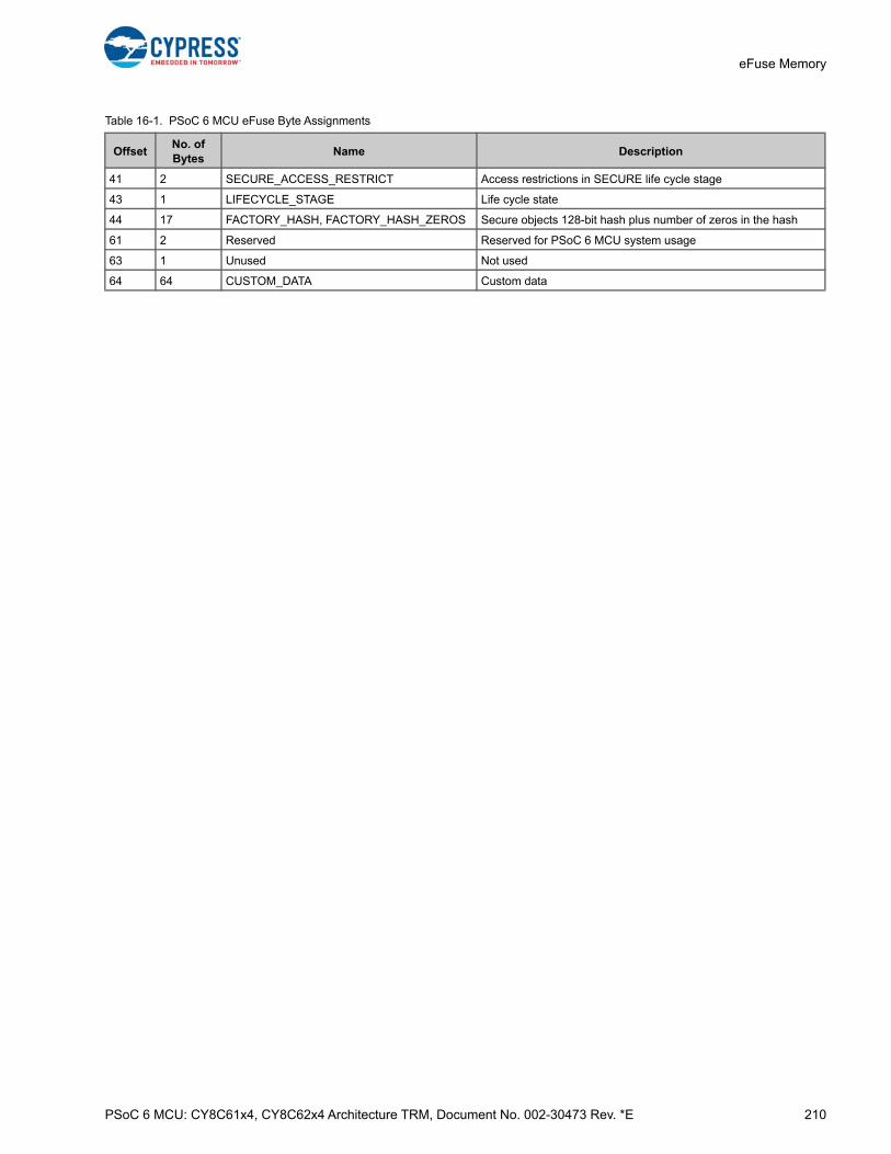
PSoC 6 MCU: CY8C61x4, CY8C62x4 Architecture TRM, Document No. 002-30473 Rev. *E 210
eFuse Memory
41 2 SECURE_ACCESS_RESTRICT Access restrictions in SECURE life cycle stage
43 1 LIFECYCLE_STAGE Life cycle state
44 17 FACTORY_HASH, FACTORY_HASH_ZEROS Secure objects 128-bit hash plus number of zeros in the hash
61 2 Reserved Reserved for PSoC 6 MCU system usage
63 1 Unused Not used
64 64 CUSTOM_DATA Custom data
Table 16-1. PSoC 6 MCU eFuse Byte Assignments
OffsetNo. of Bytes
Name Description
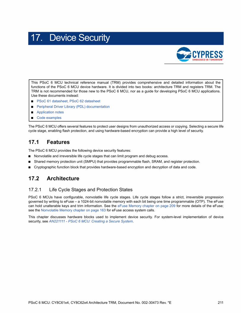
PSoC 6 MCU: CY8C61x4, CY8C62x4 Architecture TRM, Document No. 002-30473 Rev. *E 211
17. Device Security
The PSoC 6 MCU offers several features to protect user designs from unauthorized access or copying. Selecting a secure lifecycle stage, enabling flash protection, and using hardware-based encryption can provide a high level of security.
17.1 Features
The PSoC 6 MCU provides the following device security features:
■ Nonvolatile and irreversible life cycle stages that can limit program and debug access.
■ Shared memory protection unit (SMPU) that provides programmable flash, SRAM, and register protection.
■ Cryptographic function block that provides hardware-based encryption and decryption of data and code.
17.2 Architecture
17.2.1 Life Cycle Stages and Protection States
PSoC 6 MCUs have configurable, nonvolatile life cycle stages. Life cycle stages follow a strict, irreversible progressiongoverned by writing to eFuse – a 1024-bit nonvolatile memory with each bit being one time programmable (OTP). The eFusecan hold unalterable keys and trim information. See the eFuse Memory chapter on page 209 for more details of the eFuse;see the Nonvolatile Memory chapter on page 163 for eFuse access system calls.
This chapter discusses hardware blocks used to implement device security. For system-level implementation of devicesecurity, see AN221111 - PSoC 6 MCU: Creating a Secure System.
This PSoC 6 MCU technical reference manual (TRM) provides comprehensive and detailed information about thefunctions of the PSoC 6 MCU device hardware. It is divided into two books: architecture TRM and registers TRM. TheTRM is not recommended for those new to the PSoC 6 MCU, nor as a guide for developing PSoC 6 MCU applications.Use these documents instead:
■ PSoC 61 datasheet, PSoC 62 datasheet
■ Peripheral Driver Library (PDL) documentation
■ Application notes
■ Code examples
PSoC 6 MCU: CY8C61x4, CY8C62x4 Architecture TRM, Document No. 002-30473 Rev. *E 212
Device Security
Figure 17-1. PSoC 6 MCU Life Cycle Stage Transitions
The EFUSE_DATA_LIFECYCLE_STAGE eFuse governs the life-cycle stages.
17.2.2 Flash Security
PSoC 6 MCUs include a flexible flash-protection system that controls access to flash memory. This feature is designed tosecure proprietary code, but it can also be used to protect against inadvertent writes to the bootloader portion of flash.
Flash memory is organized in sectors. Flash protection is provided by a shared memory protection unit (SMPU). The SMPU isintended to distinguish between different protection contexts and to distinguish secure from non-secure accesses. Thesystem function that performs flash programming first looks at the SMPU settings and will not allow to program or erase flashblocks protected by the SMPUs.
For more details, see the Protection Units chapter on page 40.
17.2.3 Hardware-Based Encryption
The PSoC 6 MCU has a cryptographic block (Crypto) that provides hardware implementation and acceleration ofcryptographic functions. It implements symmetric key encryption and decryption, hashing, message authentication, randomnumber generation (pseudo and true), and cyclic redundancy checking. It can work with internal as well as external memory.See the Cryptographic Function Block (Crypto) chapter on page 110 and Serial Memory Interface (SMIF) chapter onpage 355 for more details.
Virgin
Normal
Secure Secure w/ Debug
Write Nomal eFuse
Write Secure eFuse
Write Secure /w Debug eFuse
RMA
Write RMA eFuse
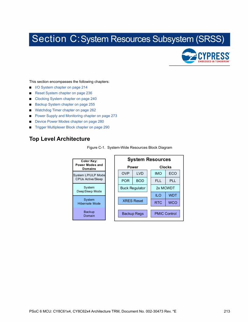
PSoC 6 MCU: CY8C61x4, CY8C62x4 Architecture TRM, Document No. 002-30473 Rev. *E 213
Section C:System Resources Subsystem (SRSS)
This section encompasses the following chapters:
■ I/O System chapter on page 214
■ Reset System chapter on page 236
■ Clocking System chapter on page 240
■ Backup System chapter on page 255
■ Watchdog Timer chapter on page 262
■ Power Supply and Monitoring chapter on page 273
■ Device Power Modes chapter on page 280
■ Trigger Multiplexer Block chapter on page 290
Top Level Architecture
Figure C-1. System-Wide Resources Block Diagram
System Resources
Power Clocks
POR
LVD
BOD
OVP
Buck Regulator
WCORTC
IMO
WDT
PLL
ECO
ILO
FLL
2x MCWDT
Backup Regs
XRES Reset
PMIC Control
SystemHibernate Mode
BackupDomain
SystemDeepSleep Mode
System LP/ULP ModeCPUs Active/Sleep
Color Key:Power Modes and
Domains
PSoC 6 MCU: CY8C61x4, CY8C62x4 Architecture TRM, Document No. 002-30473 Rev. *E 214
18. I/O System
This chapter explains the PSoC 6 MCU I/O system, its features, architecture, operating modes, and interrupts. The I/Osystem provides the interface between the CPU core and peripheral components to the outside world. The flexibility ofPSoC 6 MCUs and the capability of its I/O to route most signals to most pins greatly simplifies circuit design and board layout.The GPIO pins in the PSoC 6 MCU family are grouped into ports; a port can have a maximum of eight GPIO pins.
18.1 Features
The PSoC 6 MCU GPIOs have these features:
■ Analog and digital input and output capabilities
■ Eight drive strength modes
■ Separate port read and write registers
■ Overvoltage tolerant (OVT-GPIO) pins
■ Separate I/O supplies and voltages for up to six groups of I/O
■ Edge-triggered interrupts on rising edge, falling edge, or on both edges, on all GPIO
■ Slew rate control
■ Frozen mode for latching previous state (used to retain the I/O state in System Hibernate Power mode)
■ Selectable CMOS and low-voltage LVTTL input buffer mode
■ CapSense support
■ Smart I/O provides the ability to perform Boolean functions in the I/O signal path
■ Segment LCD drive support
This PSoC 6 MCU technical reference manual (TRM) provides comprehensive and detailed information about thefunctions of the PSoC 6 MCU device hardware. It is divided into two books: architecture TRM and registers TRM. TheTRM is not recommended for those new to the PSoC 6 MCU, nor as a guide for developing PSoC 6 MCU applications.Use these documents instead:
■ PSoC 61 datasheet, PSoC 62 datasheet
■ Peripheral Driver Library (PDL) documentation
■ Application notes
■ Code examples

PSoC 6 MCU: CY8C61x4, CY8C62x4 Architecture TRM, Document No. 002-30473 Rev. *E 215
I/O System
18.2 Architecture
The PSoC 6 MCU is equipped with analog and digital peripherals. Figure 18-1 shows an overview of the routing between theperipherals and pins.
Figure 18-1. GPIO Interface Overview
GPIO pins are connected to I/O cells. These cells are equipped with an input buffer for the digital input, providing high inputimpedance and a driver for the digital output signals. The digital peripherals connect to the I/O cells via the high-speed I/Omatrix (HSIOM). The HSIOM for each pin contains multiplexers to connect between the selected peripheral and the pin.Analog peripherals such as SAR ADC, Continuous Time Block (CTB), Low-Power comparator (LPCOMP), and CapSense areeither connected to the GPIO pins directly or through the AMUXBUS.
GPIO & Port Control
High Speed IO Matrix
CapSense Sensing
Analog Peripherals
CapSenseController
Segment LCD
Fixed Function Digital
Peripherals
Config
uratio
n
Interrupt
Interface
I/O Cell
Pin
AMUXBUS-AAMUXBUS-B
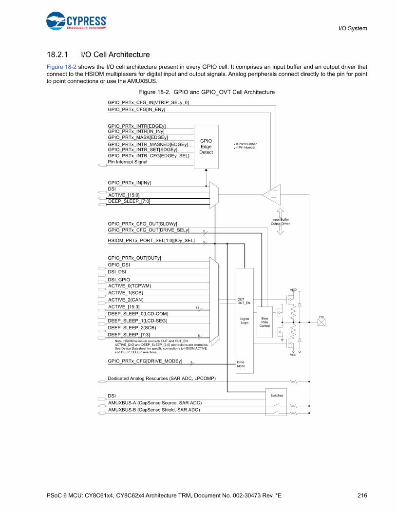
PSoC 6 MCU: CY8C61x4, CY8C62x4 Architecture TRM, Document No. 002-30473 Rev. *E 216
I/O System
18.2.1 I/O Cell Architecture
Figure 18-2 shows the I/O cell architecture present in every GPIO cell. It comprises an input buffer and an output driver thatconnect to the HSIOM multiplexers for digital input and output signals. Analog peripherals connect directly to the pin for pointto point connections or use the AMUXBUS.
Figure 18-2. GPIO and GPIO_OVT Cell Architecture
Digital Logic
Slew Rate
Control
GPIO Edge
Detect
HSIOM_PRTx_PORT_SEL[1:0][IOy_SEL]
DSIGPIO_PRTx_IN[INy]
ACTIVE_[15:0]DEEP_SLEEP_[7:0]
GPIO_PRTx_OUT[OUTy]
GPIO_DSI
DSI_DSI
DSI_GPIOACTIVE_0(TCPWM)
ACTIVE_1(SCB)
ACTIVE_2(CAN)
ACTIVE_[15:3]
DEEP_SLEEP_0(LCD-COM)
DEEP_SLEEP_1(LCD-SEG)
DEEP_SLEEP_2(SCB)
DEEP_SLEEP_[7:3]
OUT_ENOUT
Drive Mode
Pin
VDD
VSS
Input BufferOutput Driver
GPIO_PRTx_CFG[DRIVE_MODEy]
5
3
GPIO_PRTx_INTR[IN_INy]GPIO_PRTx_MASK[EDGEy]
GPIO_PRTx_INTR_MASKED[EDGEy]GPIO_PRTx_INTR_SET[EDGEy]GPIO_PRTx_INTR_CFG[EDGEy_SEL]Pin Interrupt Signal
GPIO_PRTx_CFG[IN_ENy]
GPIO_PRTx_CFG_IN[VTRIP_SELy_0]
GPIO_PRTx_CFG_OUT[DRIVE_SELy]GPIO_PRTx_CFG_OUT[SLOWy]
GPIO_PRTx_INTR[EDGEy]
2
Dedicated Analog Resources (SAR ADC, LPCOMP)
AMUXBUS-A (CapSense Source, SAR ADC)
AMUXBUS-B (CapSense Shield, SAR ADC)
Switches
x = Port Numbery = Pin Number
Note: HSIOM selection connects OUT and OUT_EN. ACTIVE_[2:0] and DEEP_SLEEP_[2:0] connections are examples. See Device Datasheet for specific connections to HSIOM ACTIVE and DEEP_SLEEP selections.
13
5
DSI

PSoC 6 MCU: CY8C61x4, CY8C62x4 Architecture TRM, Document No. 002-30473 Rev. *E 217
I/O System
18.2.2 Digital Input Buffer
The digital input buffer provides a high-impedance buffer forthe external digital input. The buffer is enabled or disabledby the IN_EN[7:0] bit of the Port Configuration Register(GPIO_PRTx_CFG, where x is the port number).
The input buffer is connected to the HSIOM for routing to theCPU port registers and selected peripherals. Writing to theHSIOM port select register (HSIOM_PORT_SELx) selectsthe pin connection. See the PSoC 61 datasheet/PSoC 62datasheet for the specific connections available for each pin.
If a pin is connected only to an analog signal, the inputbuffer should be disabled to avoid crowbar currents.
Each pin’s input buffer trip point and hysteresis areconfigurable for the following modes:
■ CMOS + I2C
■ TTL
These buffer modes are selected by the VTRIP_SEL[7:0]_0bit of the Port Input Buffer Configuration register.(GPIO_PRTx_CFG_IN).
18.2.3 Digital Output Driver
Pins are driven by the digital output driver. It consists ofcircuitry to implement different drive modes and slew ratecontrol for the digital output signals. The HSIOM selects thecontrol source for the output driver. The two primary types ofcontrol sources are CPU registers and fixed-function digitalperipherals. A particular HSIOM connection is selected by
writing to the HSIOM port select register(HSIOM_PORT_SELx).
I/O ports are powered by different sources. The specificallocation of ports to supply sources can be found in thePinout section of the PSoC 61 datasheet/PSoC 62datasheet.
Each GPIO pin has ESD diodes to clamp the pin voltage tothe I/O supply source. Ensure that the voltage at the pindoes not exceed the I/O supply voltage VDDIO/VDDD/VDDA ordrop below VSSIO/VSSD/VSSA. For the absolute maximumand minimum GPIO voltage, see the PSoC 61 datasheet/PSoC 62 datasheet.
18.2.3.1 Drive Modes
Each I/O is individually configurable to one of eight drivemodes by the DRIVE_MODE[7:0] field of the PortConfiguration register, GPIO_PRTx_CFG. Table 18-1 liststhe drive modes. Drive mode ‘1’ is reserved and should notbe used in most designs. CPU register and AMUXBUSconnections support seven discrete drive modes tomaximize design flexibility. Fixed-function digital peripherals,such as SCB and TCPWM blocks, support modifiedfunctionality for the same seven drive modes compatiblewith fixed peripheral signaling. Figure 18-3 shows simplifiedoutput driver diagrams of the pin view for CPU registercontrol on each of the eight drive modes. Figure 18-4 is asimplified output driver diagram that shows the pin view forfixed-function-based peripherals for each of the eight drivemodes.
Table 18-1. Drive Mode Settings
Drive Mode Value
CPU Register, AMUXBUS Fixed-Function Digital Peripheral
OUT_EN = 1 OUT_EN = 0 OUT_EN = 1 OUT_EN = 0
OUT = 1 OUT = 0 OUT = 1 OUT = 0 OUT = 1 OUT = 0 OUT = 1 OUT = 0
High Impedance 0 HI-Z HI-Z HI-Z HI-Z HI-Z HI-Z HI-Z HI-Z
Reserved 1 Strong 1 Strong 0 HI-Z HI-Z Strong 1 Strong 0Weak 1 & 0
Weak 1 & 0
Resistive Pull Up 2 Weak 1 Strong 0 HI-Z HI-Z Strong 1 Strong 0 Weak 1 Weak 1
Resistive Pull Down 3 Strong 1 Weak 0 HI-Z HI-Z Strong 1 Strong 0 Weak 0 Weak 0
Open Drain, Drives Low 4 HI-Z Strong 0 HI-Z HI-Z Strong 1 Strong 0 HI-Z HI-Z
Open Drain, Drives High 5 Strong 1 HI-Z HI-Z HI-Z Strong 1 Strong 0 HI-Z HI-Z
Strong 6 Strong 1 Strong 0 HI-Z HI-Z Strong 1 Strong 0 HI-Z HI-Z
Resistive Pull Up and Down 7 Weak 1 Weak 0 HI-Z HI-Z Strong 1 Strong 0 Weak 1 Weak 0
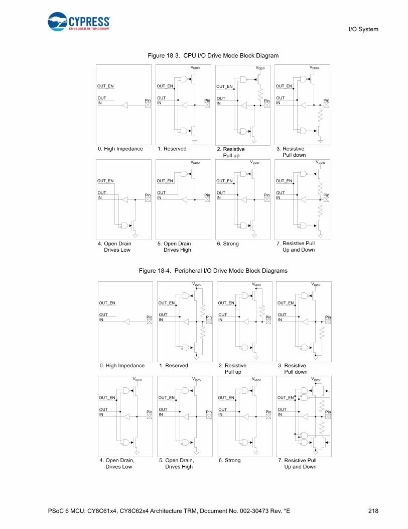
PSoC 6 MCU: CY8C61x4, CY8C62x4 Architecture TRM, Document No. 002-30473 Rev. *E 218
I/O System
Figure 18-3. CPU I/O Drive Mode Block Diagram
Figure 18-4. Peripheral I/O Drive Mode Block Diagrams
ResistivePull up
2.
INOUT
VDDIO
Pin
OUT_EN
High Impedance0.
INOUT
Pin
OUT_EN
Reserved1. ResistivePull down
3.
INOUT
VDDIO
Pin
OUT_EN
Open DrainDrives Low
4.
INOUT
Pin
OUT_EN
Open DrainDrives High
5.
INOUT
VDDIO
Pin
OUT_EN
Strong6. 7.
INOUT
VDDIO
Pin
OUT_EN
INOUT
VDDIO
Pin
OUT_EN
INOUT
VDDIO
Pin
OUT_EN
Resistive Pull Up and Down
ResistivePull up
2.
INOUT
VDDIO
Pin
OUT_EN
High Impedance0.
INOUT
Pin
OUT_EN
Reserved1. ResistivePull down
3.
INOUT
VDDIO
Pin
OUT_EN
Open Drain,Drives Low
4. Open Drain,Drives High
5.
INOUT
VDDIO
Pin
OUT_EN
INOUT
VDDIO
Pin
OUT_EN
Strong6. Resistive Pull Up and Down
7.
INOUT
VDDIO
Pin
OUT_EN
INOUT
VDDIO
Pin
OUT_EN
INOUT
VDDIO
Pin
OUT_EN
PSoC 6 MCU: CY8C61x4, CY8C62x4 Architecture TRM, Document No. 002-30473 Rev. *E 219
I/O System
■ High-Impedance
This is the standard high-impedance (HI-Z) staterecommended for analog and digital inputs. For digitalsignals, the input buffer is enabled; for analog signals, theinput buffer is typically disabled to reduce crowbar currentand leakage in low-power designs. To achieve the lowestdevice current, unused GPIOs must be configured to thehigh-impedance drive mode with input buffer disabled. High-impedance drive mode with input buffer disabled is also thedefault pin reset state.
■ Resistive Pull-Up or Resistive Pull-Down
Resistive modes provide a series resistance in one of thedata states and strong drive in the other. Pins can be usedfor either digital input or digital output in these modes. Ifresistive pull-up is required, a ‘1’ must be written to that pin’sData Register bit. If resistive pull-down is required, a ‘0’must be written to that pin’s Data Register. Interfacingmechanical switches is a common application of these drivemodes. The resistive modes are also used to interfacePSoC with open drain drive lines. Resistive pull-up is usedwhen the input is open drain low and resistive pull-down isused when the input is open drain high.
■ Open Drain Drives High and Open Drain Drives Low
Open drain modes provide high impedance in one of thedata states and strong drive in the other. Pins are useful asdigital inputs or outputs in these modes. Therefore, thesemodes are widely used in bidirectional digitalcommunication. Open drain drive high mode is used whenthe signal is externally pulled down and open drain drive lowis used when the signal is externally pulled high. A commonapplication for the open drain drives low mode is driving I2Cbus signal lines.
■ Strong Drive
The strong drive mode is the standard digital output modefor pins; it provides a strong CMOS output drive in both highand low states. Strong drive mode pins should not be usedas inputs under normal circumstances. This mode is oftenused for digital output signals or to drive external devices.
■ Resistive Pull-Up and Resistive Pull-Down
In the resistive pull-up and pull-down mode, the GPIO willhave a series resistance in both logic 1 and logic 0 outputstates. The high data state is pulled up while the low datastate is pulled down. This mode is useful when the pin isdriven by other signals that may cause shorts.
18.2.3.2 Slew Rate Control
GPIO pins have fast and slow output slew rate options forthe strong drivers configured using the SLOW bit of the portoutput configuration register (GPIO_PRTx_CFG_OUT). Bydefault, this bit is cleared and the port works in fast slewmode. This bit can be set if a slow slew rate is required.Slower slew rate results in reduced EMI and crosstalk and
are recommended for low-frequency signals or signalswithout strict timing constraints.
When configured for fast slew rate, the drive strength can beset to one of four levels using the DRIVE_SEL field of theport output configuration register (GPIO_PRTx_CFG_OUT).The drive strength field determines the active portion of theoutput drivers used and can affect the slew rate of outputsignals. Drive strength options are full drive strength(default), one-half strength, one-quarter strength, and one-eighth strength. Drive strength must be set to full drivestrength when the slow slew rate bit (SLOW) is set.
Note: For some devices in the PSoC 6 MCU family,simultaneous GPIO switching with unrestricted drivestrengths and frequency can induce noise in on-chipsubsystems affecting CapSense and ADC results. Refer tothe Errata section in the respective device datasheet fordetails.
18.2.3.3 GPIO-OVT Pins
Select device pins are overvoltage tolerant (OVT) and areuseful for interfacing to busses or other signals that mayexceed the pin’s VDDIO supply, or where the whole devicesupply or pin VDDIO may not be always present. They areidentical to regular GPIOs with the additional feature ofbeing overvoltage tolerant. GPIO-OVT pins have hardwareto compare VDDIO to the pin voltage. If the pin voltageexceeds VDDIO, the output driver is disabled and the pindriver is tristated. This results in negligible current sink at thepin.
Note that in overvoltage conditions, the input buffer data willnot be valid if the external source’s specification of VOH and
VOL do not match the trip points of the input buffer defined
by the current VDDIO voltage.
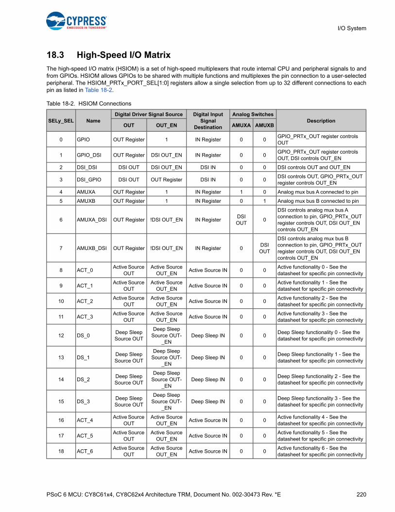
PSoC 6 MCU: CY8C61x4, CY8C62x4 Architecture TRM, Document No. 002-30473 Rev. *E 220
I/O System
18.3 High-Speed I/O Matrix
The high-speed I/O matrix (HSIOM) is a set of high-speed multiplexers that route internal CPU and peripheral signals to andfrom GPIOs. HSIOM allows GPIOs to be shared with multiple functions and multiplexes the pin connection to a user-selectedperipheral. The HSIOM_PRTx_PORT_SEL[1:0] registers allow a single selection from up to 32 different connections to eachpin as listed in Table 18-2.
Table 18-2. HSIOM Connections
SELy_SEL NameDigital Driver Signal Source Digital Input
Signal Destination
Analog SwitchesDescription
OUT OUT_EN AMUXA AMUXB
0 GPIO OUT Register 1 IN Register 0 0GPIO_PRTx_OUT register controls OUT
1 GPIO_DSI OUT Register DSI OUT_EN IN Register 0 0GPIO_PRTx_OUT register controls OUT, DSI controls OUT_EN
2 DSI_DSI DSI OUT DSI OUT_EN DSI IN 0 0 DSI controls OUT and OUT_EN
3 DSI_GPIO DSI OUT OUT Register DSI IN 0 0DSI controls OUT, GPIO_PRTx_OUT register controls OUT_EN
4 AMUXA OUT Register 1 IN Register 1 0 Analog mux bus A connected to pin
5 AMUXB OUT Register 1 IN Register 0 1 Analog mux bus B connected to pin
6 AMUXA_DSI OUT Register !DSI OUT_EN IN RegisterDSI OUT
0
DSI controls analog mux bus A connection to pin, GPIO_PRTx_OUT register controls OUT, DSI OUT_EN controls OUT_EN
7 AMUXB_DSI OUT Register !DSI OUT_EN IN Register 0DSI OUT
DSI controls analog mux bus B connection to pin, GPIO_PRTx_OUT register controls OUT, DSI OUT_EN controls OUT_EN
8 ACT_0Active Source
OUTActive Source
OUT_ENActive Source IN 0 0
Active functionality 0 - See the datasheet for specific pin connectivity
9 ACT_1Active Source
OUTActive Source
OUT_ENActive Source IN 0 0
Active functionality 1 - See the datasheet for specific pin connectivity
10 ACT_2Active Source
OUTActive Source
OUT_ENActive Source IN 0 0
Active functionality 2 - See the datasheet for specific pin connectivity
11 ACT_3Active Source
OUTActive Source
OUT_ENActive Source IN 0 0
Active functionality 3 - See the datasheet for specific pin connectivity
12 DS_0Deep Sleep Source OUT
Deep Sleep Source OUT-
_ENDeep Sleep IN 0 0
Deep Sleep functionality 0 - See the datasheet for specific pin connectivity
13 DS_1Deep Sleep Source OUT
Deep Sleep Source OUT-
_ENDeep Sleep IN 0 0
Deep Sleep functionality 1 - See the datasheet for specific pin connectivity
14 DS_2Deep Sleep Source OUT
Deep Sleep Source OUT-
_ENDeep Sleep IN 0 0
Deep Sleep functionality 2 - See the datasheet for specific pin connectivity
15 DS_3Deep Sleep Source OUT
Deep Sleep Source OUT-
_ENDeep Sleep IN 0 0
Deep Sleep functionality 3 - See the datasheet for specific pin connectivity
16 ACT_4Active Source
OUTActive Source
OUT_ENActive Source IN 0 0
Active functionality 4 - See the datasheet for specific pin connectivity
17 ACT_5Active Source
OUTActive Source
OUT_ENActive Source IN 0 0
Active functionality 5 - See the datasheet for specific pin connectivity
18 ACT_6Active Source
OUTActive Source
OUT_ENActive Source IN 0 0
Active functionality 6 - See the datasheet for specific pin connectivity
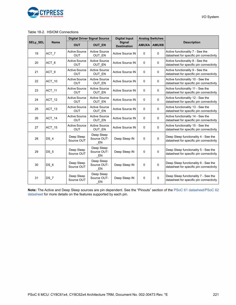
PSoC 6 MCU: CY8C61x4, CY8C62x4 Architecture TRM, Document No. 002-30473 Rev. *E 221
I/O System
Note: The Active and Deep Sleep sources are pin dependent. See the “Pinouts” section of the PSoC 61 datasheet/PSoC 62datasheet for more details on the features supported by each pin.
19 ACT_7Active Source
OUTActive Source
OUT_ENActive Source IN 0 0
Active functionality 7 - See the datasheet for specific pin connectivity
20 ACT_8Active Source
OUTActive Source
OUT_ENActive Source IN 0 0
Active functionality 8 - See the datasheet for specific pin connectivity
21 ACT_9Active Source
OUTActive Source
OUT_ENActive Source IN 0 0
Active functionality 9 - See the datasheet for specific pin connectivity
22 ACT_10Active Source
OUTActive Source
OUT_ENActive Source IN 0 0
Active functionality 10 - See the datasheet for specific pin connectivity
23 ACT_11Active Source
OUTActive Source
OUT_ENActive Source IN 0 0
Active functionality 11 - See the datasheet for specific pin connectivity
24 ACT_12Active Source
OUTActive Source
OUT_ENActive Source IN 0 0
Active functionality 12 - See the datasheet for specific pin connectivity
25 ACT_13Active Source
OUTActive Source
OUT_ENActive Source IN 0 0
Active functionality 13 - See the datasheet for specific pin connectivity
26 ACT_14Active Source
OUTActive Source
OUT_ENActive Source IN 0 0
Active functionality 14 - See the datasheet for specific pin connectivity
27 ACT_15Active Source
OUTActive Source
OUT_ENActive Source IN 0 0
Active functionality 15 - See the datasheet for specific pin connectivity
28 DS_4Deep Sleep Source OUT
Deep Sleep Source OUT-
_ENDeep Sleep IN 0 0
Deep Sleep functionality 4 - See the datasheet for specific pin connectivity
29 DS_5Deep Sleep Source OUT
Deep Sleep Source OUT-
_ENDeep Sleep IN 0 0
Deep Sleep functionality 5 - See the datasheet for specific pin connectivity
30 DS_6Deep Sleep Source OUT
Deep Sleep Source OUT-
_ENDeep Sleep IN 0 0
Deep Sleep functionality 6 - See the datasheet for specific pin connectivity
31 DS_7Deep Sleep Source OUT
Deep Sleep Source OUT-
_ENDeep Sleep IN 0 0
Deep Sleep functionality 7 - See the datasheet for specific pin connectivity
Table 18-2. HSIOM Connections
SELy_SEL NameDigital Driver Signal Source Digital Input
Signal Destination
Analog SwitchesDescription
OUT OUT_EN AMUXA AMUXB
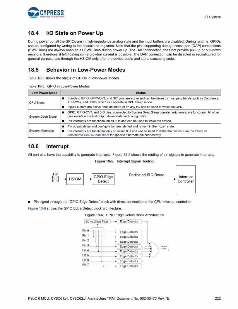
PSoC 6 MCU: CY8C61x4, CY8C62x4 Architecture TRM, Document No. 002-30473 Rev. *E 222
I/O System
18.4 I/O State on Power Up
During power up, all the GPIOs are in high-impedance analog state and the input buffers are disabled. During runtime, GPIOscan be configured by writing to the associated registers. Note that the pins supporting debug access port (DAP) connections(SWD lines) are always enabled as SWD lines during power up. The DAP connection does not provide pull-up or pull-downresistors; therefore, if left floating some crowbar current is possible. The DAP connection can be disabled or reconfigured forgeneral-purpose use through the HSIOM only after the device boots and starts executing code.
18.5 Behavior in Low-Power Modes
Table 18-3 shows the status of GPIOs in low-power modes.
18.6 Interrupt
All port pins have the capability to generate interrupts. Figure 18-5 shows the routing of pin signals to generate interrupts.
Figure 18-5. Interrupt Signal Routing
■ Pin signal through the “GPIO Edge Detect” block with direct connection to the CPU interrupt controller
Figure 18-6 shows the GPIO Edge Detect block architecture.
Figure 18-6. GPIO Edge Detect Block Architecture
Table 18-3. GPIO in Low-Power Modes
Low-Power Mode Status
CPU Sleep ■ Standard GPIO, GPIO-OVT, and SIO pins are active and can be driven by most peripherals such as CapSense,
TCPWMs, and SCBs, which can operate in CPU Sleep mode.
■ Inputs buffers are active; thus an interrupt on any I/O can be used to wake the CPU.
System Deep Sleep■ GPIO, GPIO-OVT, and SIO pins, connected to System Deep Sleep domain peripherals, are functional. All other
pins maintain the last output driver state and configuration.
■ Pin interrupts are functional on all I/Os and can be used to wake the device.
System Hibernate■ Pin output states and configuration are latched and remain in the frozen state.
■ Pin interrupts are functional only on select IOs and can be used to wake the device. See the PSoC 61 datasheet/PSoC 62 datasheet for specific hibernate pin connectivity.
GPIO Edge Detect
Interrupt Controller
Pin Dedicated IRQ RouteHSIOM
Edge Detector
Edge Detector
Edge Detector
Edge Detector
Edge Detector
Edge Detector
Edge Detector
Edge Detector
Edge Detector
50 ns Glitch Filter
Interrupt Signal
Pin 1
Pin 2
Pin 3
Pin 4
Pin 0
Pin 5
Pin 6
Pin 7
PSoC 6 MCU: CY8C61x4, CY8C62x4 Architecture TRM, Document No. 002-30473 Rev. *E 223
I/O System
An edge detector is present at each pin. It is capable ofdetecting rising edge, falling edge, and both edges withoutany reconfiguration. The edge detector is configured bywriting into the EDGEv_SEL bits of the Port InterruptConfiguration register, GPIO_PRTx_INTR_CFG, as shownin Table 18-4.
Writing ‘1’ to the corresponding status bit clears the pin edgestate. Clearing the edge state status bit is important;otherwise, an interrupt can occur repeatedly for a singletrigger or respond only once for multiple triggers, which isexplained later in this section. When the Port InterruptControl Status register is read at the same time an edge isoccurring on the corresponding port, it can result in the edgenot being properly detected. Therefore, when using GPIOinterrupts, read the status register only inside thecorresponding interrupt service routine and not in any otherpart of the code.
Firmware and the debug interface are able to trigger ahardware interrupt from any pin by setting the correspondingbit in the GPIO_PRTx_INTR_SET register.
In addition to the pins, each port provides a glitch filterconnected to its own edge detector. This filter can be drivenby one of the pins of a port. The selection of the driving pinis done by writing to the FLT_SEL field of theGPIO_PRTx_INTR_CFG register as shown in Table 18-5.
When a port pin edge occurs, you can read the PortInterrupt Status register, GPIO_PRTx_INTR, to know whichpin caused the edge. This register includes both the latchedinformation on which pin detected an edge and the currentpin status. This allows the CPU to read both information in asingle read operation. This register has an additional use –to clear the latched edge state.
The GPIO_PRTx_INTR_MASK register enables forwardingof the GPIO_PRTx_INTR edge detect signal to the interruptcontroller when a ‘1’ is written to a pin’s correspondingbitfield. The GPIO_PRTx_INTR_MASKED register can thenbe read to determine the specific pin that generated theinterrupt signal forwarded to the interrupt controller. Themasked edge detector outputs of a port are then ORedtogether and routed to the interrupt controller (NVIC in theCPU subsystem). Thus, there is only one interrupt vectorper port.
The masked and ORed edge detector block output is routedto the Interrupt Source Multiplexer shown in Figure 9-3 onpage 76, which gives an option of Level and Rising Edgedetection. If the Level option is selected, an interrupt istriggered repeatedly as long as the Port Interrupt Statusregister bit is set. If the Rising Edge detect option isselected, an interrupt is triggered only once if the PortInterrupt Status register is not cleared. Thus, the interruptstatus bit must be cleared if the Edge Detect block is used.
All of the port interrupt vectors are also ORed together into asingle interrupt vector for use on devices with more portsthan there are interrupt vectors available. To determine theport that triggered the interrupt, the GPIO_INTR_CAUSExregisters can be read. A ‘1’ present in a bit location indicatesthat the corresponding port has a pending interrupt. Theindicated GPIO_PRTx_INTR register can then be read todetermine the pin source.
18.7 Peripheral Connections
18.7.1 Firmware-Controlled GPIO
For standard firmware-controlled GPIO using registers, theGPIO mode must be selected in the HSIOM_PORT_SELxregister.
The GPIO_PRTx_OUT register is used to read and write theoutput buffer state for GPIOs. A write operation to thisregister changes the GPIO’s output driver state to thewritten value. A read operation reflects the output datawritten to this register and the resulting output driver state. Itdoes not return the current logic level present on GPIO pins,which may be different. Using the GPIO_PRTx_OUTregister, read-modify-write sequences can be safelyperformed on a port that has both input and output GPIOs.
In addition to the data register, three other registers –GPIO_PRTx_SET, GPIO_PRTx_CLR, andGPIO_PRTx_INV – are provided to set, clear, and invert theoutput data respectively on specific pins in a port withoutaffecting other pins. This avoids the need for read-modify-write operations in most use cases. Writing ‘1’ to theseregister bitfields will set, clear, or invert the respective pin;writing ‘0’ will have no affect on the pin state.
Table 18-4. Edge Detector Configuration
EDGE_SEL Configuration
00 Interrupt is disabled
01 Interrupt on Rising Edge
10 Interrupt on Falling Edge
11 Interrupt on Both Edges
Table 18-5. Glitch Filter Input Selection
FLT_SEL Selected Pin
000 Pin 0 is selected
001 Pin 1 is selected
010 Pin 2 is selected
011 Pin 3 is selected
100 Pin 4 is selected
101 Pin 5 is selected
110 Pin 6 is selected
111 Pin 7 is selected
PSoC 6 MCU: CY8C61x4, CY8C62x4 Architecture TRM, Document No. 002-30473 Rev. *E 224
I/O System
GPIO_PRTx_IN is the port I/O pad register, which providesthe actual logic level present on the GPIO pin when read.Writes to this register have no effect.
18.7.2 Analog I/O
Analog resources, such as LPCOMP, SAR ADC, and CTB,which require low-impedance routing paths have dedicatedpins. Dedicated analog pins provide direct connections tospecific analog blocks. They help improve performance andshould be given priority over other pins when using theseanalog resources. See the PSoC 61 datasheet/PSoC 62datasheet for details on these dedicated pins of the PSoC 6MCU.
To configure a GPIO as a dedicated analog I/O, it should beconfigured in high-impedance analog mode (see Table 18-1)with input buffer disabled. The respective connection shouldbe enabled via registers in the specific analog resource.
To configure a GPIO as an analog pin connecting toAMUXBUS, it should be configured in high-impedanceanalog mode with the input buffer disabled and then routedto the correct AMUXBUS using the HSIOM_PORT_SELxregister.
While it is preferred for analog pins to disable the inputbuffer, it is acceptable to enable the input buffer ifsimultaneous analog and digital input features are required.
18.7.2.1 AMUXBUS Connection and DSI
See the PSoC 61 datasheet/PSoC 62 datasheet todetermine which GPIO provides AMUXBUS connectivity.
Static connection is made by selecting AMUXA or AMUXB inthe HSIOM_PORT_SELx register.
To properly configure a pin as AMUXBUS input, follow thesesteps:
1. Configure the GPIO_PRTx_CFG register to set the pin in high-Impedance mode with input buffer disabled, enabling analog connectivity on the pin.
2. Configure the HSIOM_PRT_SELx register to connect the pin to AMUXBUS A or B.
18.7.3 LCD Drive
GPIOs have the capability of driving an LCD common orsegment line. See the PSoC 61 datasheet/PSoC 62datasheet to determine which GPIO provides LCDconnectivity. HSIOM_PORT_SELx registers are used toselect pins for the LCD drive. See the LCD DirectDrive chapter on page 522 for details.
18.7.4 CapSense
The pins that support CapSense can be configured asCapSense widgets such as buttons, slider elements,touchpad elements, or proximity sensors. See the PSoC 61
datasheet/PSoC 62 datasheet to determine which GPIOprovides CapSense connectivity. CapSense also requiresexternal capacitors and optional shield lines. See thePSoC 4 and PSoC 6 MCU CapSense Design Guide formore details.
18.8 Smart I/O
The Smart I/O block adds programmable logic to an I/O port.This programmable logic integrates board-level Booleanlogic functionality such as AND, OR, and XOR into the port.A graphical interface is provided with the ModusToolboxinstall for configuring the Smart I/O block. For more informa-tion about the configurator tool, see the ModusToolboxSmart I/O Configurator Guide.
The Smart I/O block has these features:
■ Integrate board-level Boolean logic functionality into a port
■ Ability to preprocess HSIOM input signals from the GPIO port pins
■ Ability to post-process HSIOM output signals to the GPIO port pins
■ Support in all device power modes except Hibernate
■ Integrate closely to the I/O pads, providing shortest signal paths with programmability
18.8.1 Overview
The Smart I/O block is positioned in the signal path betweenthe HSIOM and the I/O port. The HSIOM multiplexes theoutput signals from fixed-function peripherals and CPU to aspecific port pin and vice-versa. The Smart I/O block isplaced on this signal path, acting as a bridge that canprocess signals between port pins and HSIOM, as shown inFigure 18-7.

PSoC 6 MCU: CY8C61x4, CY8C62x4 Architecture TRM, Document No. 002-30473 Rev. *E 225
I/O System
Figure 18-7. Smart I/O Interface
The signal paths supported through the Smart I/O block asshown in Figure 18-7 are as follows:
1. Implement self-contained logic functions that directly operate on port I/O signals
2. Implement self-contained logic functions that operate on HSIOM signals
3. Operate on and modify HSIOM output signals and route the modified signals to port I/O signals
4. Operate on and modify port I/O signals and route the modified signals to HSIOM input signals
The following sections discuss the Smart I/O blockcomponents, routing, and configuration in detail. In thesesections, GPIO signals (io_data) refer to the input/outputsignals from the I/O port; device or chip (chip_data) signalsrefer to the input/output signals from HSIOM.
18.8.2 Block Components
The internal logic of the Smart I/O includes thesecomponents:
■ Clock/reset
■ Synchronizers
■ Three-input lookup table (LUT)
■ Data unit
18.8.2.1 Clock and Reset
The clock and reset component selects the Smart I/Oblock’s clock (clk_block) and reset signal (rst_block_n). Asingle clock and reset signal is used for all components inthe block. The clock and reset sources are determined bythe CLOCK_SRC[4:0] bitfield of the SMARTIO_PRTx_CTLregister. The selected clock is used for the synchronouslogic in the block components, which includes the I/O inputsynchronizers, LUT, and data unit components. Theselected reset is used to asynchronously reset thesynchronous logic in the LUT and data unit components.
Note that the selected clock (clk_block) for the block’ssynchronous logic is not phase-aligned with othersynchronous logic in the device, operating on the same
clock. Therefore, communication between Smart I/O andother synchronous logic should be treated as asynchronous.
The following clock sources are available for selection:
■ GPIO input signals “io_data_in[7:0]”. These clock sources have no associated reset.
■ HSIOM output signals “chip_data[7:0]”. These clock sources have no associated reset.
■ Smart I/O clock (clk_smartio). This is derived from the system clock (clk_sys) using a peripheral clock divider. See the Clocking System chapter on page 240 for details on peripheral clock dividers. This clock is available only in System LP and ULP power modes. The clock can have one out of two associated resets: rst_sys_act_n and rst_sys_dpslp_n. These resets determine in which system power modes the block synchronous state is reset; for example, rst_sys_act_n is intended for Smart I/O synchronous functionality in the System LP and ULP power modes and reset is activated in the System Deep Sleep power mode.
■ Low-frequency system clock (clk_lf). This clock is available in System Deep Sleep power mode. This clock has an associated reset, rst_lf_dpslp_n. Reset is activated if the system enters Hibernate, or is at POR.
When the block is enabled, the selected clock (clk_block)and associated reset (rst_block_n) are provided to the fabriccomponents. When the fabric is disabled, no clock isreleased to the fabric components and the reset is activated(the LUT and data unit components are set to the resetvalue of ‘0’).
The I/O input synchronizers introduce a delay of twoclk_block cycles (when synchronizers are enabled). As aresult, in the first two cycles, the block may be exposed tostale data from the synchronizer output. Hence, during thefirst two clock cycles, the reset is activated and the block isin bypass mode.
HSIOM Smart I/O I/O Port
HSIOM Output Signals
HSIOMInput Signals
GPIO Output Signals
GPIO Input Signals
12
4
3

PSoC 6 MCU: CY8C61x4, CY8C62x4 Architecture TRM, Document No. 002-30473 Rev. *E 226
I/O System
18.8.2.2 Synchronizer
Each GPIO input signal and device input signal (HSIOM input) can be used either asynchronously or synchronously. To usethe signals synchronously, a double flip-flop synchronizer, as shown in Figure 18-8, is placed on both these signal paths tosynchronize the signal to the Smart I/O clock (clk_block). The synchronization for each pin/input is enabled or disabled bysetting or clearing the IO_SYNC_EN[i] bitfield for GPIO input signal and CHIP_SYNC_EN[i] for HSIOM signal in theSMARTIO_PRTx_SYNC_CTL register, where ‘i’ is the pin number.
Figure 18-8. Smart I/O Clock Synchronizer
18.8.2.3 Lookup Table (LUT)
Each Smart I/O block contains eight lookup table (LUT) components. The LUT component consists of a three-input LUT anda flip-flop. Each LUT block takes three input signals and generates an output based on the configuration set in theSMARTIO_PRTx_LUT_CTLy register (y denotes the LUT number). For each LUT, the configuration is determined by an 8-bitlookup vector LUT[7:0] and a 2-bit opcode OPC[1:0] in the SMARTIO_PRTx_LUT_CTLy register. The 8-bit vector is used asa lookup table for the three input signals. The 2-bit opcode determines the usage of the flip-flop. The LUT configuration fordifferent opcodes is shown in Figure 18-9.
Table 18-6. Clock and Reset Register Control
Register[BIT_POS] Bit Name Description
SMARTIO_PRTn_CTL[12:8] CLOCK_SRC[4:0]
Clock (clk_block)/reset (rst_block_n) source selection:
0: io_data_in[0]/1
...
7: io_data_in[7]/1
8: chip_data[0]/1
...
15: chip_data[7]/1
16: clk_smartio/rst_sys_act_n; asserts reset in any power mode other than System LP or ULP; that is, Smart I/O is active only in LP or ULP power modes with clock from the peripheral divider.
17: clk_smartio/rst_sys_dpslp_n. Smart I/O is active in all power modes with a clock from the peripheral divider. However, the clock will not be active in System deep sleep power mode.
19: clk_lf/rst_lf_dpslp_n. Smart I/O is active in all power modes with a clock from ILO.
20-30: Clock source is a constant '0'. Any of these clock sources should be selected when Smart I/O is disabled to ensure low power consumption.
31: clk_sys/1. This selection is not intended for clk_sys operation. However, for asynchronous operation, three clk_sys cycles after enabling, the Smart I/O is fully functional (reset is de-activated). To be used for asynchronous (clockless) block functionality.
io_data_in[i]Or
chip_data_in[i]
clk_block
clkclk
DQDQ
0
1
SYNC_CTL.IO_SYNC_EN[i]Or
SYNC_CTL.CHIP_SYNC_EN[i]
To SMARTIO block
Clock Synchronizer
PSoC 6 MCU: CY8C61x4, CY8C62x4 Architecture TRM, Document No. 002-30473 Rev. *E 227
I/O System
The SMARTIO_PRTx_LUT_SELy registers select the three input signals (tr0_in, tr1_in, and tr2_in) going into each LUT. Theinput can come from the following sources:
■ Data unit output
■ Other LUT output signals (tr_out)
■ HSIOM output signals (chip_data[7:0])
■ GPIO input signals (io_data[7:0])
LUT_TR0_SEL[3:0] bits of the SMARTIO_PRTx_LUT_SELy register selects the tr0_in signal for the yth LUT. Similarly,LUT_TR1_SEL[3:0] bits and LUT_TR2_SEL[3:0] bits select the tr1_in and tr2_in signals, respectively. See Table 18-7 fordetails.
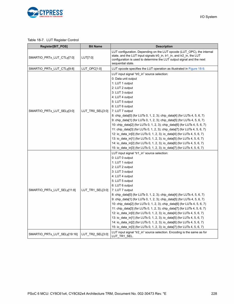
PSoC 6 MCU: CY8C61x4, CY8C62x4 Architecture TRM, Document No. 002-30473 Rev. *E 228
I/O System
Table 18-7. LUT Register Control
Register[BIT_POS] Bit Name Description
SMARTIO_PRTx_LUT_CTLy[7:0] LUT[7:0]
LUT configuration. Depending on the LUT opcode (LUT_OPC), the internal state, and the LUT input signals tr0_in, tr1_in, and tr2_in, the LUT configuration is used to determine the LUT output signal and the next sequential state.
SMARTIO_PRTx_LUT_CTLy[9:8] LUT_OPC[1:0] LUT opcode specifies the LUT operation as illustrated in Figure 18-9.
SMARTIO_PRTx_LUT_SELy[3:0] LUT_TR0_SEL[3:0]
LUT input signal “tr0_in” source selection:
0: Data unit output
1: LUT 1 output
2: LUT 2 output
3: LUT 3 output
4: LUT 4 output
5: LUT 5 output
6: LUT 6 output
7: LUT 7 output
8: chip_data[0] (for LUTs 0, 1, 2, 3); chip_data[4] (for LUTs 4, 5, 6, 7)
9: chip_data[1] (for LUTs 0, 1, 2, 3); chip_data[5] (for LUTs 4, 5, 6, 7)
10: chip_data[2] (for LUTs 0, 1, 2, 3); chip_data[6] (for LUTs 4, 5, 6, 7)
11: chip_data[3] (for LUTs 0, 1, 2, 3); chip_data[7] (for LUTs 4, 5, 6, 7)
12: io_data_in[0] (for LUTs 0, 1, 2, 3); io_data[4] (for LUTs 4, 5, 6, 7)
13: io_data_in[1] (for LUTs 0, 1, 2, 3); io_data[5] (for LUTs 4, 5, 6, 7)
14: io_data_in[2] (for LUTs 0, 1, 2, 3); io_data[6] (for LUTs 4, 5, 6, 7)
15: io_data_in[3] (for LUTs 0, 1, 2, 3); io_data[7] (for LUTs 4, 5, 6, 7)
SMARTIO_PRTx_LUT_SELy[11:8] LUT_TR1_SEL[3:0]
LUT input signal “tr1_in” source selection:
0: LUT 0 output
1: LUT 1 output
2: LUT 2 output
3: LUT 3 output
4: LUT 4 output
5: LUT 5 output
6: LUT 6 output
7: LUT 7 output
8: chip_data[0] (for LUTs 0, 1, 2, 3); chip_data[4] (for LUTs 4, 5, 6, 7)
9: chip_data[1] (for LUTs 0, 1, 2, 3); chip_data[5] (for LUTs 4, 5, 6, 7)
10: chip_data[2] (for LUTs 0, 1, 2, 3); chip_data[6] (for LUTs 4, 5, 6, 7)
11: chip_data[3] (for LUTs 0, 1, 2, 3); chip_data[7] (for LUTs 4, 5, 6, 7)
12: io_data_in[0] (for LUTs 0, 1, 2, 3); io_data[4] (for LUTs 4, 5, 6, 7)
13: io_data_in[1] (for LUTs 0, 1, 2, 3); io_data[5] (for LUTs 4, 5, 6, 7)
14: io_data_in[2] (for LUTs 0, 1, 2, 3); io_data[6] (for LUTs 4, 5, 6, 7)
15: io_data_in[3] (for LUTs 0, 1, 2, 3); io_data[7] (for LUTs 4, 5, 6, 7)
SMARTIO_PRTx_LUT_SELy[19:16] LUT_TR2_SEL[3:0]LUT input signal “tr2_in” source selection. Encoding is the same as for LUT_TR1_SEL.
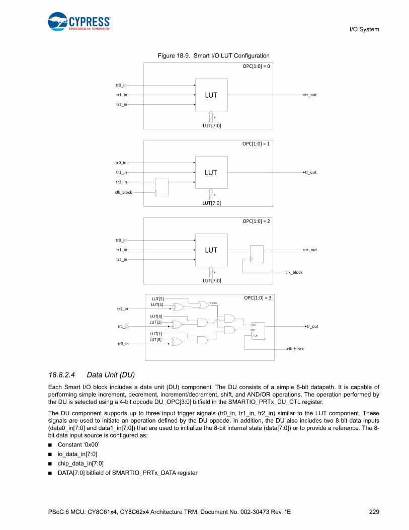
PSoC 6 MCU: CY8C61x4, CY8C62x4 Architecture TRM, Document No. 002-30473 Rev. *E 229
I/O System
Figure 18-9. Smart I/O LUT Configuration
18.8.2.4 Data Unit (DU)
Each Smart I/O block includes a data unit (DU) component. The DU consists of a simple 8-bit datapath. It is capable ofperforming simple increment, decrement, increment/decrement, shift, and AND/OR operations. The operation performed bythe DU is selected using a 4-bit opcode DU_OPC[3:0] bitfield in the SMARTIO_PRTx_DU_CTL register.
The DU component supports up to three input trigger signals (tr0_in, tr1_in, tr2_in) similar to the LUT component. Thesesignals are used to initiate an operation defined by the DU opcode. In addition, the DU also includes two 8-bit data inputs(data0_in[7:0] and data1_in[7:0]) that are used to initialize the 8-bit internal state (data[7:0]) or to provide a reference. The 8-bit data input source is configured as:
■ Constant ‘0x00’
■ io_data_in[7:0]
■ chip_data_in[7:0]
■ DATA[7:0] bitfield of SMARTIO_PRTx_DATA register
LUT
tr0_in
tr1_in
tr2_in
tr_out
8
OPC[1:0] = 0
LUT[7:0]
LUT
tr0_in
tr1_in
tr2_in
tr_out
8
OPC[1:0] = 1
LUT[7:0]
clk_block
LUT
tr0_in
tr1_in
tr2_in
8
OPC[1:0] = 2
LUT[7:0]
clk_block
tr_out
tr2_in
tr1_in
tr0_in
OPC[1:0] = 3
clk_block
tr_out
LUT[5]
LUT[4]
LUT[3]
LUT[2]
LUT[1]
LUT[0]
Set
Clr
Clk
Enable
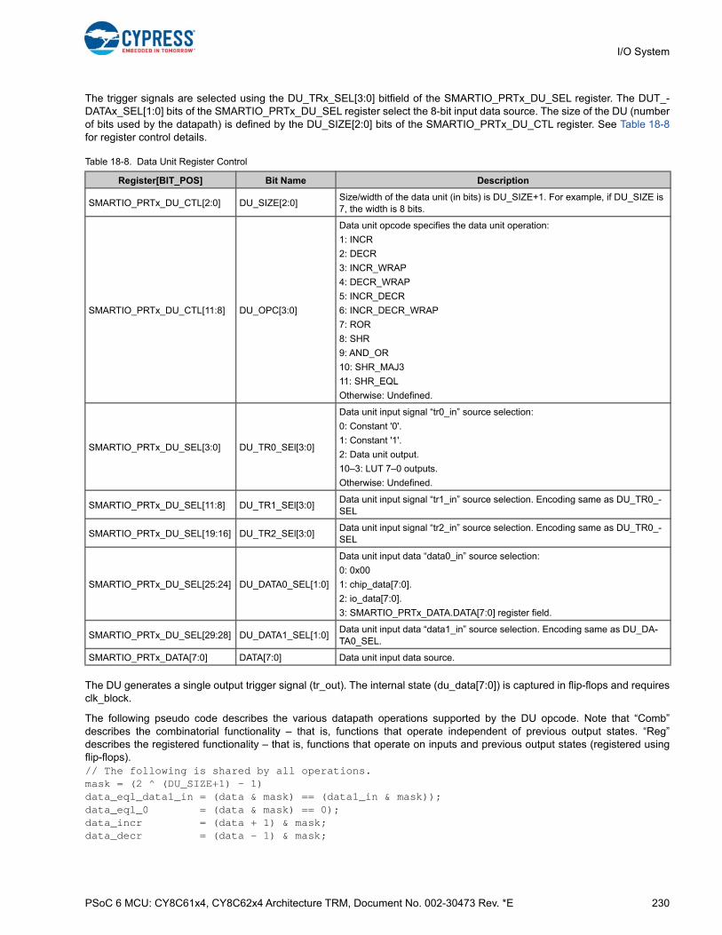
PSoC 6 MCU: CY8C61x4, CY8C62x4 Architecture TRM, Document No. 002-30473 Rev. *E 230
I/O System
The trigger signals are selected using the DU_TRx_SEL[3:0] bitfield of the SMARTIO_PRTx_DU_SEL register. The DUT_-DATAx_SEL[1:0] bits of the SMARTIO_PRTx_DU_SEL register select the 8-bit input data source. The size of the DU (numberof bits used by the datapath) is defined by the DU_SIZE[2:0] bits of the SMARTIO_PRTx_DU_CTL register. See Table 18-8for register control details.
The DU generates a single output trigger signal (tr_out). The internal state (du_data[7:0]) is captured in flip-flops and requiresclk_block.
The following pseudo code describes the various datapath operations supported by the DU opcode. Note that “Comb”describes the combinatorial functionality – that is, functions that operate independent of previous output states. “Reg”describes the registered functionality – that is, functions that operate on inputs and previous output states (registered usingflip-flops).// The following is shared by all operations.mask = (2 ^ (DU_SIZE+1) – 1)data_eql_data1_in = (data & mask) == (data1_in & mask));data_eql_0 = (data & mask) == 0);data_incr = (data + 1) & mask;data_decr = (data - 1) & mask;
Table 18-8. Data Unit Register Control
Register[BIT_POS] Bit Name Description
SMARTIO_PRTx_DU_CTL[2:0] DU_SIZE[2:0]Size/width of the data unit (in bits) is DU_SIZE+1. For example, if DU_SIZE is 7, the width is 8 bits.
SMARTIO_PRTx_DU_CTL[11:8] DU_OPC[3:0]
Data unit opcode specifies the data unit operation:
1: INCR
2: DECR
3: INCR_WRAP
4: DECR_WRAP
5: INCR_DECR
6: INCR_DECR_WRAP
7: ROR
8: SHR
9: AND_OR
10: SHR_MAJ3
11: SHR_EQL
Otherwise: Undefined.
SMARTIO_PRTx_DU_SEL[3:0] DU_TR0_SEl[3:0]
Data unit input signal “tr0_in” source selection:
0: Constant '0'.
1: Constant '1'.
2: Data unit output.
10–3: LUT 7–0 outputs.
Otherwise: Undefined.
SMARTIO_PRTx_DU_SEL[11:8] DU_TR1_SEl[3:0]Data unit input signal “tr1_in” source selection. Encoding same as DU_TR0_-SEL
SMARTIO_PRTx_DU_SEL[19:16] DU_TR2_SEl[3:0]Data unit input signal “tr2_in” source selection. Encoding same as DU_TR0_-SEL
SMARTIO_PRTx_DU_SEL[25:24] DU_DATA0_SEL[1:0]
Data unit input data “data0_in” source selection:
0: 0x00
1: chip_data[7:0].
2: io_data[7:0].
3: SMARTIO_PRTx_DATA.DATA[7:0] register field.
SMARTIO_PRTx_DU_SEL[29:28] DU_DATA1_SEL[1:0]Data unit input data “data1_in” source selection. Encoding same as DU_DA-TA0_SEL.
SMARTIO_PRTx_DATA[7:0] DATA[7:0] Data unit input data source.
PSoC 6 MCU: CY8C61x4, CY8C62x4 Architecture TRM, Document No. 002-30473 Rev. *E 231
I/O System
data0_masked = data_in0 & mask;
// INCR operation: increments data by 1 from an initial value (data0) until it reaches a// final value (data1).Comb:tr_out = data_eql_data1_in;Reg: data <= data; if (tr0_in) data <= data0_masked; //tr0_in is reload signal - loads masked data0 // into data else if (tr1_in) data <= data_eql_data1_in ? data : data_incr; //increment data until // it equals data1
// INCR_WRAP operation: operates similar to INCR but instead of stopping at data1, it wraps // around to data0.Comb:tr_out = data_eql_data1_in;Reg: data <= data; if (tr0_in) data <= data0_masked; else if (tr1_in) data <= data_eql_data1_in ? data0_masked : data_incr;
// DECR operation: decrements data from an initial value (data0) until it reaches 0.Comb:tr_out = data_eql_0;Reg: data <= data; if (tr0_in) data <= data0_masked; else if (tr1_in) data <= data_eql_0 ? data : data_decr;
// DECR_WRAP operation: works similar to DECR. Instead of stopping at 0, it wraps around to // data0.Comb:tr_out = data_eql_0;Reg: data <= data; if (tr0_in) data <= data0_masked; else if (tr1_in) data <= data_eql_0 ? data0_masked: data_decr;
// INCR_DECR operation: combination of INCR and DECR. Depending on trigger signals it either // starts incrementing or decrementing. Increment stops at data1 and decrement stops at 0.Comb:tr_out = data_eql_data1_in | data_eql_0;Reg: data <= data; if (tr0_in) data <= data0_masked; // Increment operation takes precedence over // decrement when both signal are available else if (tr1_in) data <= data_eql_data1_in ? data : data_incr; else if (tr2_in) data <= data_eql_0 ? data : data_decr;
// INCR_DECR_WRAP operation: same functionality as INCR_DECR with wrap around to data0 on // reaching the limits.Comb:tr_out = data_eql_data1_in | data_eql_0;Reg: data <= data; if (tr0_in) data <= data0_masked; else if (tr1_in) data <= data_eql_data1_in ? data0_masked : data_incr; else if (tr2_in) data <= data_eql_0 ? data0_masked : data_decr;
// ROR operation: rotates data right and LSb is sent out. The data for rotation is taken from // data0.Comb:tr_out = data[0];Reg: data <= data; if (tr0_in) data <= data0_masked; else if (tr1_in) { data <= {0, data[7:1]} & mask; //Shift right operation data[du_size] <= data[0]; //Move the data[0] (LSb) to MSb }

PSoC 6 MCU: CY8C61x4, CY8C62x4 Architecture TRM, Document No. 002-30473 Rev. *E 232
I/O System
// SHR operation: performs shift register operation. Initial data (data0) is shifted out and // data on tr2_in is shifted in.Comb:tr_out = data[0];Reg: data <= data; if (tr0_in) data <= data0_masked; else if (tr1_in) { data <= {0, data[7:1]} & mask; //Shift right operation data[du_size] <= tr2_in; //tr2_in Shift in operation }
// SHR_MAJ3 operation: performs the same functionality as SHR. Instead of sending out the // shifted out value, it sends out a '1' if in the last three samples/shifted-out values// (data[0]), the signal high in at least two samples. otherwise, sends a '0'. This function// sends out the majority of the last three samples. Comb:tr_out = (data == 0x03) | (data == 0x05) | (data == 0x06) | (data == 0x07);Reg: data <= data; if (tr0_in) data <= data0_masked; else if (tr1_in) { data <= {0, data[7:1]} & mask; data[du_size] <= tr2_in; }
// SHR_EQL operation: performs the same operation as SHR. Instead of shift-out, the output is // a comparison result (data0 == data1).Comb:tr_out = data_eql_data1_in;Reg: data <= data; if (tr0_in) data <= data0_masked; else if (tr1_in) { data <= {0, data[7:1]} & mask; data[du_size] <= tr2_in; }
// AND_OR operation: ANDs data1 and data0 along with mask; then, ORs all the bits of the// ANDed output.Comb:tr_out = | (data & data1_in & mask);Reg: data <= data; if (tr0_in) data <= data0_masked;
18.8.3 Routing
The Smart I/O block includes many switches that are used to route the signals in and out of the block and also betweenvarious components present inside the block. The routing switches are handled through the PRTGIO_PRTx_LUT_SELy andSMARTIO_PRTx_DU_SEL registers. Refer to the registers TRM for details. The Smart I/O internal routing is shown inFigure 18-10. In the figure, note that LUT7 to LUT4 operate on io_data/chip_data[7] to io_data/chip_data[4] whereas LUT3 toLUT0 operate on io_data/chip_data[3] to io_data/chip_data[0].

I/O System
PSoC 6 MCU: CY8C61x4, CY8C62x4 Architecture TRM, Document No. 002-30473 Rev. *E 233
Figure 18-10. Smart I/O Routing
Sync
Sync
Sync
Sync
Sync
Sync
Sync
Sync
Sync
Sync
Sync
Sync
Sync
Sync
Sync
Sync
LUT0
tr0_in
tr1_
intr2_
in
tr_o
ut
LUT1
tr0_
intr1_
intr2_in
tr_o
ut
LUT2
tr0_
intr1_
intr2_
in
tr_o
ut
LUT3
tr0_
intr1_in
tr2_
in
tr_o
ut
LUT4
tr0_
intr1_
intr2_
in
tr_o
ut
LUT5
tr0_in
tr1_in
tr2_in
tr_o
ut
LUT6
tr0_
intr1_
intr2_
in
tr_o
ut
LUT7
tr0_
intr1_
intr2_
in
tr_o
ut
Data Unit
tr0_
in
tr1_
in
tr2_
in
tr_o
ut
8
8
8
8
SMARTIO_PRTx_DATA.DATA[7:0]
0x00
chip_data[7:0]
io_data[7:0]
data_in0
data_in1
Clock and Reset
clk_smartio
clk_sys
clk_lf
io_data[7]smartio_data[7]
chip_data[7]
io_data[6]smartio_data[6]
chip_data[6]
io_data[5]smartio_data[5]
chip_data[5]
io_data[4]smartio_data[4]
chip_data[4]
io_data[3]smartio_data[3]
chip_data[3]
io_data[2]smartio_data[2]
chip_data[2]
io_data[1]smartio_data[1]
chip_data[1]
io_data[0]smartio_data[0]
chip_data[0]
rst_block_n
clk_block
smartio_data[7]chip_data[7]
smartio_data[6]chip_data[6]
smartio_data[5]chip_data[5]
smartio_data[4]chip_data[4]
smartio_data[3]chip_data[3]
smartio_data[2]chip_data[2]
smartio_data[1]chip_data[1]
smartio_data[0]chip_data[0]
1'b01'b1
clk_block
Various signals8‐bit wide data busProgrammable Switch (ONLY ONE of the switches along a vertical line can be closed at a time)
Closed switch connecting a bit of the 8‐bit data bus
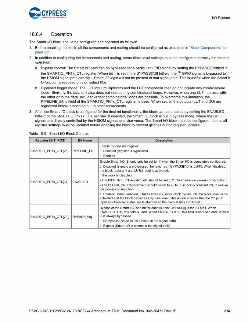
PSoC 6 MCU: CY8C61x4, CY8C62x4 Architecture TRM, Document No. 002-30473 Rev. *E 234
I/O System
18.8.4 Operation
The Smart I/O block should be configured and operated as follows:
1. Before enabling the block, all the components and routing should be configured as explained in “Block Components” on page 225.
2. In addition to configuring the components and routing, some block level settings must be configured correctly for desired operation.
a. Bypass control: The Smart I/O path can be bypassed for a particular GPIO signal by setting the BYPASS[i] bitfield in
the SMARTIO_PRTx_CTL register. When bit ‘i’ is set in the BYPASS[7:0] bitfield, the ith GPIO signal is bypassed to the HSIOM signal path directly – Smart I/O logic will not be present in that signal path. This is useful when the Smart I/O function is required only on select I/Os.
b. Pipelined trigger mode: The LUT input multiplexers and the LUT component itself do not include any combinatorial loops. Similarly, the data unit also does not include any combinatorial loops. However, when one LUT interacts with the other or to the data unit, inadvertent combinatorial loops are possible. To overcome this limitation, the PIPELINE_EN bitfield of the SMARTIO_PRTx_CTL register is used. When set, all the outputs (LUT and DU) are registered before branching out to other components.
3. After the Smart I/O block is configured for the desired functionality, the block can be enabled by setting the ENABLED bitfield of the SMARTIO_PRTx_CTL register. If disabled, the Smart I/O block is put in bypass mode, where the GPIO signals are directly controlled by the HSIOM signals and vice-versa. The Smart I/O block must be configured; that is, all register settings must be updated before enabling the block to prevent glitches during register updates.
Table 18-9. Smart I/O Block Controls
Register [BIT_POS] Bit Name Description
SMARTIO_PRTx_CTL[25] PIPELINE_EN
Enable for pipeline register:
0: Disabled (register is bypassed).
1: Enabled
SMARTIO_PRTx_CTL[31] ENABLED
Enable Smart I/O. Should only be set to '1' when the Smart I/O is completely configured:
0: Disabled (signals are bypassed; behavior as if BYPASS[7:0] is 0xFF). When disabled, the block (data unit and LUTs) reset is activated.
If the block is disabled:
- The PIPELINE_EN register field should be set to '1', to ensure low power consumption.
- The CLOCK_SRC register field should be set to 20 to 30 (clock is constant '0'), to ensure low power consumption.
1: Enabled. When enabled, it takes three clk_block clock cycles until the block reset is de-activated and the block becomes fully functional. This action ensures that the I/O pins' input synchronizer states are flushed when the block is fully functional.
SMARTIO_PRTx_CTL[7:0] BYPASS[7:0]
Bypass of the Smart I/O, one bit for each I/O pin: BYPASS[i] is for I/O pin i. When ENABLED is '1', this field is used. When ENABLED is '0', this field is not used and Smart I/O is always bypassed.
0: No bypass (Smart I/O is present in the signal path)
1: Bypass (Smart I/O is absent in the signal path)

PSoC 6 MCU: CY8C61x4, CY8C62x4 Architecture TRM, Document No. 002-30473 Rev. *E 235
I/O System
18.9 Registers
Note The ‘x’ in the GPIO register name denotes the port number. For example, GPIO_PTR1_OUT is the Port 1 output dataregister.
Table 18-10. I/O Registers
Name Description
GPIO_PRTx_OUT Port output data register reads and writes the output driver data for I/O pins in the port.
GPIO_PRTx_OUT_CLR Port output data clear register clears output data of specific I/O pins in the port.
GPIO_PRTx_OUT_SET Port output data set register sets output data of specific I/O pins in the port.
GPIO_PRTx_OUT_INV Port output data invert register inverts output data of specific I/O pins in the port.
GPIO_PRTx_IN Port input state register reads the current pin state present on I/O pin inputs.
GPIO_PRTx_INTR Port interrupt status register reads the current pin interrupt state.
GPIO_PRTx_INTR_MASKPort interrupt mask register configures the mask that forwards pin interrupts to the CPU’s interrupt controller.
GPIO_PRTx_INTR_MASKEDPort interrupt masked status register reads the masked interrupt status forwarded to the CPU interrupt controller.
GPIO_PRTx_INTR_SET Port interrupt set register allows firmware to set pin interrupts.
GPIO_PRTx_INTR_CFG Port interrupt configuration register selects the edge detection type for each pin interrupt.
GPIO_PRTx_CFG Port configuration register selects the drive mode and input buffer enable for each pin.
GPIO_PRTx_CFG_IN Port input buffer configuration register configures the input buffer mode for each pin.
GPIO_PRTx_CFG_OUT Port output buffer configuration register selects the output driver slew rate for each pin.
HSIOM_PORT_SELxHigh-speed I/O Mux (HSIOM) port selection register selects the hardware peripheral connection to I/O pins.
PSoC 6 MCU: CY8C61x4, CY8C62x4 Architecture TRM, Document No. 002-30473 Rev. *E 236
19. Reset System
The PSoC 6 MCU family supports several types of resets that guarantee error-free operation during power up and allow thedevice to reset based on user-supplied external hardware or internal software reset signals. The PSoC 6 MCU also containshardware to enable the detection of certain resets.
19.1 Features
The PSoC 6 MCU has these reset sources:
■ Power-on reset (POR) to hold the device in reset while the power supply ramps up to the level required for the device to function properly
■ Brownout reset (BOD) to reset the device if the power supply falls below the device specifications during normal operation
■ External reset (XRES) to reset the device using an external input
■ Watchdog timer (WDT) reset to reset the device if the firmware execution fails to periodically service the watchdog timer
■ Software initiated reset to reset the device on demand using firmware
■ Logic-protection fault resets to reset the device if unauthorized operating conditions occur
■ Clock-supervision logic resets to reset the device when clock-related errors occur
■ Hibernate wakeup reset to bring the device out of the Hibernate low-power mode
19.2 Architecture
The following sections provide a description of the reset sources available in the PSoC 6 MCU family.
Note: None of these sources can reset the Backup system. The Backup domain is reset only when all the power supplies areremoved from it, also known as a “cold start” or if the firmware triggers a reset using the BACKUP_RESET register. Firmwarereset is required if the VBACKUP supply was invalid during a previous power supply ramp-up or brownout event. For moredetails, see the Backup System chapter on page 255.
This PSoC 6 MCU technical reference manual (TRM) provides comprehensive and detailed information about thefunctions of the PSoC 6 MCU device hardware. It is divided into two books: architecture TRM and registers TRM. TheTRM is not recommended for those new to the PSoC 6 MCU, nor as a guide for developing PSoC 6 MCU applications.Use these documents instead:
■ PSoC 61 datasheet, PSoC 62 datasheet
■ Peripheral Driver Library (PDL) documentation
■ Application notes
■ Code examples
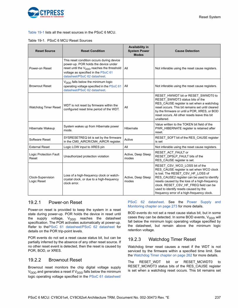
PSoC 6 MCU: CY8C61x4, CY8C62x4 Architecture TRM, Document No. 002-30473 Rev. *E 237
Reset System
Table 19-1 lists all the reset sources in the PSoC 6 MCU.
19.2.1 Power-on Reset
Power-on reset is provided to keep the system in a resetstate during power-up. POR holds the device in reset untilthe supply voltage, VDDD reaches the datasheetspecification. The POR activates automatically at power-up.Refer to thePSoC 61 datasheet/PSoC 62 datasheet fordetails on the POR trip-point levels.
POR events do not set a reset cause status bit, but can bepartially inferred by the absence of any other reset source. Ifno other reset event is detected, then the reset is caused byPOR, BOD, or XRES.
19.2.2 Brownout Reset
Brownout reset monitors the chip digital voltage supplyVDDD and generates a reset if VDDD falls below the minimum
logic operating voltage specified in the PSoC 61 datasheet/
PSoC 62 datasheet. See the Power Supply andMonitoring chapter on page 273 for more details.
BOD events do not set a reset cause status bit, but in somecases they can be detected. In some BOD events, VDDD willfall below the minimum logic operating voltage specified bythe datasheet, but remain above the minimum logicretention voltage.
19.2.3 Watchdog Timer Reset
Watchdog timer reset causes a reset if the WDT is notserviced by the firmware within a specified time limit. Seethe Watchdog Timer chapter on page 262 for more details.
The RESET_WDT bit or RESET_MCWDT0 toRESET_MCWDT3 status bits of the RES_CAUSE registeris set when a watchdog reset occurs. This bit remains set
Table 19-1. PSoC 6 MCU Reset Sources
Reset Source Reset ConditionAvailability in System Power
ModesCause Detection
Power-on Reset
This reset condition occurs during device power-up. POR holds the device under reset until the VDDD reaches the threshold
voltage as specified in the PSoC 61 datasheet/PSoC 62 datasheet.
All Not inferable using the reset cause registers.
Brownout ResetVDDD falls below the minimum logic
operating voltage specified in the PSoC 61 datasheet/PSoC 62 datasheet.
All Not inferable using the reset cause registers.
Watchdog Timer ResetWDT is not reset by firmware within the configured reset time period of the WDT.
All
RESET_HWWDT bit or RESET_SWWDT0 to RESET_SWWDT3 status bits of the RES_CAUSE register is set when a watchdog reset occurs. This bit remains set until cleared by the firmware or until a POR, XRES, or BOD reset occurs. All other resets leave this bit unaltered.
Hibernate WakeupSystem wakes up from Hibernate power mode.
HibernateValue written to the TOKEN bit field of the PWR_HIBERNATE register is retained after reset.
Software ResetSYSRESETREQ bit is set by the firmware in the CM0_AIRCR/CM4_AIRCR register.
ActiveRESET_SOFT bit of the RES_CAUSE register is set
External Reset Logic LOW input to XRES pin All Not inferable using the reset cause registers.
Logic Protection Fault Reset
Unauthorized protection violationActive, Deep Sleep modes
RESET_ACT_FAULT or RESET_DPSLP_FAULT bits of the RES_CAUSE register is set.
Clock-Supervision Logic Reset
Loss of a high-frequency clock or watch-crystal clock, or due to a high-frequency clock error.
Active, Deep Sleep modes
RESET_CSV_WCO_LOSS bit of the RES_CAUSE register is set when WCO clock is lost. The RESET_CSV_HF_LOSS of RES_CAUSE2 register can be used to identify resets caused by the loss of a high-frequency clock. RESET_CSV_HF_FREQ field can be used to identify resets caused by the frequency error of a high-frequency clock.
PSoC 6 MCU: CY8C61x4, CY8C62x4 Architecture TRM, Document No. 002-30473 Rev. *E 238
Reset System
until cleared by the firmware or until a POR, XRES, or BODreset occurs. All other resets leave this bit unaltered.
For more details, see the Watchdog Timer chapter onpage 262.
19.2.4 Software Initiated Reset
Software initiated reset is a mechanism that allows the CPUto request a reset. The Cortex-M0+ and Cortex-M4Application Interrupt and Reset Control registers(CM0_AIRCR and CM4_AIRCR, respectively) can request areset by writing a ‘1’ to the SYSRESETREQ bit of therespective registers.
Note that a value of 0x5FA should be written to theVECTKEY field of the AIRCR register before setting theSYSRESETREQ bit; otherwise, the processor ignores thewrite. See the CPU Subsystem (CPUSS) chapter onpage 31 and Arm documentation on AIRCR for more details.
The RESET_SOFT status bit of the RES_CAUSE register isset when a software reset occurs. This bit remains set untilcleared by firmware or until a POR, XRES, or BOD resetoccurs. All other resets leave this bit unaltered.
19.2.5 External Reset
External reset (XRES) is a reset triggered by an externalsignal that causes immediate system reset when asserted.The XRES pin is active low – a logic ‘1’ on the pin has noeffect and a logic ‘0’ causes reset. The pin is pulled to logic‘1’ inside the device. XRES is available as a dedicated pin.For detailed pinout, refer to the pinout section of the PSoC61 datasheet/PSoC 62 datasheet.
The XRES pin holds the device in reset as long as the pininput is ‘0’. When the pin is released (changed to logic ‘1’),the device goes through a normal boot sequence. Thelogical thresholds for XRES and other electricalcharacteristics are listed in the Electrical Specificationssection of the PSoC 61 datasheet/PSoC 62 datasheet.XRES is available in all power modes, but cannot reset theBackup system.
An XRES event does not set a reset cause status bit, butcan be partially inferred by the absence of any other resetsource. If no other reset event is detected, then the reset iscaused by POR, BOD, or XRES.
19.2.6 Logic Protection Fault Reset
Logic protection fault reset detects any unauthorizedprotection violations and causes the device to reset if theyoccur. One example of a protection fault is reaching a debugbreakpoint while executing privileged code.
The RESET_ACT_FAULT or RESET_DPSLP_FAULT bits ofthe RES_CAUSE register is set when a protection faultoccurs in Active or Deep Sleep modes, respectively. Thesebits remain set until cleared or until a POR, XRES, or BODreset. All other resets leave this bit unaltered.
19.2.7 Clock-Supervision Logic Reset
Clock-supervision logic initiates a reset due to the loss of ahigh-frequency clock or watch-crystal clock, or due to ahigh-frequency clock error.
The RESET_CSV_WCO_LOSS bit of the RES_CAUSEregister is set when the clock supervision logic requests areset due to the loss of a watch-crystal clock (if enabled).
The RESET_CSV_HF_LOSS is a 16-bit field in theRES_CAUSE2 register that can be used to identify resetscaused by the loss of a high-frequency clock. Similarly, theRESET_CSV_HF_FREQ field can be used to identify resetscaused by the frequency error of a high-frequency clock.
For more information on clocks, see the ClockingSystem chapter on page 240.
19.2.8 Hibernate Wakeup Reset
Hibernate wakeup reset occurs when one of the Hibernatewakeup sources performs a device reset to return to theActive power mode. See the Device Power Modes chapteron page 280 for details on Hibernate mode and availablewakeup sources.
TOKEN is an 8-bit field in the PWR_HIBERNATE registerthat is retained through a Hibernate wakeup sequence. Thefirmware can use this bitfield to differentiate hibernatewakeup from a general reset event. Similarly, thePWR_HIB_DATA register can retain its contents through aHibernate wakeup reset, but is cleared when XRES isasserted.
19.3 Identifying Reset Sources
When the device comes out of reset, it is often useful toknow the cause of the most recent or even older resets. Thisis achieved through the RES_CAUSE and RES_CAUSE2registers. These registers have specific status bits allocatedfor some of the reset sources. These registers record theoccurrences of WDT reset, software reset, logic-protectionfault, and clock-supervision resets. However, these registersdo not record the occurrences of POR, BOD, XRES, orHibernate wakeup resets. The bits in these registers are seton the occurrence of the corresponding reset and remain

PSoC 6 MCU: CY8C61x4, CY8C62x4 Architecture TRM, Document No. 002-30473 Rev. *E 239
Reset System
set after the reset, until cleared by the firmware or a loss ofretention, such as a POR, XRES, or BOD.
Hibernate wakeup resets can be detected by examining theTOKEN field in the PWR_HIBERNATE register as describedpreviously. Hibernate wakeup resets that occur as a result of
an XRES cannot be detected. The other reset sources canbe inferred to some extent by the status of the RES_CAUSEand RES_CAUSE2 registers, as shown in Table 19-2.
For more information, see the RES_CAUSE and RES_CAUSE2 registers in the registers TRM.
If these methods cannot detect the cause of the reset, then it can be one of the non-recorded and non-retention resets: BOD,POR, or XRES. These resets cannot be distinguished using on-chip resources.
19.4 Register List
Table 19-2. Reset Cause Bits to Detect Reset Source
Register BitfieldNumber of
BitsDescription
RES_CAUSE RESET_WDT 1 A hardware WDT reset has occurred since the last power cycle.
RES_CAUSE RESET_ACT_FAULT 1 Fault logging system requested a reset from its Active logic.
RES_CAUSE RESET_DPSLP_FAULT 1 Fault logging system requested a reset from its Deep Sleep logic.
RES_CAUSE RESET_CSV_WCO_LOSS 1Clock supervision logic requested a reset due to loss of a watch-crystal clock.
RES_CAUSE RESET_SOFT 1A CPU requested a system reset through its SYSRESETREQ. This can be done via a debugger probe or in firmware.
RES_CAUSE RESET_MCWDT0 1 Multi-counter WDT reset #0 has occurred since the last power cycle.
RES_CAUSE RESET_MCWDT1 1 Multi-counter WDT reset #1 has occurred since the last power cycle.
RES_CAUSE RESET_MCWDT2 1 Multi-counter WDT reset #2 has occurred since the last power cycle.
RES_CAUSE RESET_MCWDT3 1 Multi-counter WDT reset #3 has occurred since the last power cycle.
RES_CAUSE2 RESET_CSV_HF_LOSS 16Clock supervision logic requested a reset due to loss of a high-frequency clock. Each bit index K corresponds to a clk_hf<K>. Unimplemented clock bits return zero.
RES_CAUSE2 RESET_CSV_HF_FREQ 16Clock supervision logic requested a reset due to frequency error of a high-frequency clock. Each bit index K corresponds to a clk_hf<K>. Unimplemented clock bits return zero.
Table 19-3. Reset System Register List
Register Description
RES_CAUSE Reset cause observation register
RES_CAUSE2 Reset cause observation register 2
PWR_HIBERNATEHibernate power mode control register. Contains a TOKEN field that can be used to detect the Hibernate wakeup reset
PWR_HIB_DATA Retains its contents through Hibernate wakeup reset
CM4_AIRCR Application interrupt and reset control register of Cortex-M4
CM0_AIRCR Application interrupt and reset control register of Cortex-M0+
PSoC 6 MCU: CY8C61x4, CY8C62x4 Architecture TRM, Document No. 002-30473 Rev. *E 240
20. Clocking System
PSoC 6 MCU provides flexible clocking options with on-chip crystal oscillators, phase lock loop, frequency lock loop, andsupports multiple external clock sources.
20.1 Features
The PSoC 6 MCU clock system includes these resources:
■ Two internal clock sources:
❐ 8-MHz internal main oscillator (IMO)
❐ 32-kHz internal low-speed oscillator (ILO)
■ Three external clock sources
❐ External clock (EXTCLK) generated using a signal from an I/O pin
❐ External 16–35 MHz crystal oscillator (ECO)
❐ External 32-kHz watch crystal oscillator (WCO)
■ One frequency lock loop (FLL) with 24–100 MHz output range
■ One phase-locked loop (PLL) with 10.625–150 MHz output range
This PSoC 6 MCU technical reference manual (TRM) provides comprehensive and detailed information about thefunctions of the PSoC 6 MCU device hardware. It is divided into two books: architecture TRM and registers TRM. TheTRM is not recommended for those new to the PSoC 6 MCU, nor as a guide for developing PSoC 6 MCU applications.Use these documents instead:
■ PSoC 61 datasheet, PSoC 62 datasheet
■ Peripheral Driver Library (PDL) documentation
■ Application notes
■ Code examples

Clocking System
PSoC 6 MCU: CY8C61x4, CY8C62x4 Architecture TRM, Document No. 002-30473 Rev. *E 241
20.2 Architecture
Figure 20-1 gives a generic view of the clocking system in PSoC 6 MCUs.
Figure 20-1. Clocking System Block Diagram
ECO
IMO
EXTCLK
CLK_HF[0]Predivider(1/2/4/8)
WCO
ILO
CLK_LF
FLL
(FLL/PLLs) Root Clock mux (Clks_HF[i] are Root Clocks)
USB
QSPI
clk_extPredivider(1/2/4/8)
Predivider(1/2/4/8)
Predivider(1/2/4/8)
Path Mux
CLK_PATH3
CLK_HF[1]
CLK_HF[2]
CLK_HF[3]
PLL
CM4 Clock
PeripheralClock
Dividers
clk_periCM0+ Clock
LCD
CLK_MFIMO/4Predivider
(1/2/3... 256)
CLK_LFCLK_MF
CLK_PERI
0
1
CLK_PATH2

PSoC 6 MCU: CY8C61x4, CY8C62x4 Architecture TRM, Document No. 002-30473 Rev. *E 242
Clocking System
20.3 Clock Sources
20.3.1 Internal Main Oscillator (IMO)
The IMO is an accurate, high-speed internal (crystal-less)oscillator that produces a fixed frequency of 8 MHz. TheIMO output can be used by the PLL or FLL to generate awide range of higher frequency clocks, or it can be useddirectly by the high-frequency root clocks.
When USB is present the USB Start-of-Frame (SOF) signalis used to trim the IMO to ensure that the IMO matches theaccuracy of the USB SOF. The ENABLE_LOCK bitfield inthe USBFS0_USBDEV_CR register of the USB block needsto be set for this feature to work. The driver for the USBblock in the PDL does this automatically.
The IMO is available in the system LP, ULP, and Deep Sleeppower modes.
20.3.2 External Crystal Oscillator (ECO)
The PSoC 6 MCU contains an oscillator to drive an external16-MHz to 35-MHz crystal. This clock source is built usingan oscillator circuit in PSoC. The circuit employs an externalcrystal that needs to be populated on the external crystalpins of the PSoC 6 MCU. See AN218241 - PSoC 6 MCUHardware Design Considerations for more details.
The ECO can be enabled by using the CLK_ECO_CONFIGECO_EN register bitfields.
20.3.2.1 ECO Trimming
The ECO supports a wide variety of crystals and ceramicresonators with the nominal frequency range specification off = 16 MHz – 35 MHz. The crystal manufacturer typicallyprovides numerical values for parameters, namely themaximum drive level (DL), the maximum equivalent seriesresistance (ESR), shunt capacitance of the crystal (C0), andthe parallel load capacitance (CL). These parameters can beused to calculate the transconductance (gm) and themaximum peak to peak (VPP).
Max peak to peak value:
Transconductance:
ECO does not support VPP less than 1.3 V.
The following fields are found in the CLK_TRIM_ECO_CTLregister. The Amplitude trim (ATRIM) and WDTRIM settingscontrol the trim for amplitude of the oscillator output. ATRIM
sets the crystal drive level when automatic gain control(AGC) is enabled (CLK_ECO_CONFIG.AGC_EN = 1). AGCmust be enabled all the time.
ATRIM and WDTRIM values are set at 15 and 7,respectively.
The GTRIM sets up the trim for amplifier gain based on thecalculated gm, as shown in Table 20-1.
RTRIM and FTRIM are set to 0 and 3, respectively.
First, set up the trim values based on Table 20-1 and otherlisted values; then enable the ECO. After the ECO isenabled, the CLK_ECO_STATUS register can be checkedto ensure it is ready.
20.3.3 External Clock (EXTCLK)The external clock is a 0- to 100-MHz range clock that canbe sourced from a signal on a designated I/O pin. This clockcan be used as the source clock for either the PLL or FLL, orcan be used directly by the high-frequency clocks.
When manually configuring a pin as an input to EXTCLK,the drive mode of the pin must be set to high-impedancedigital to enable the digital input buffer. See the I/OSystem chapter on page 214 for more details. Consult thePSoC 61 datasheet/PSoC 62 datasheet to determine thespecific pin used for EXTCLK. See KBA224493 for moredetails.
20.3.4 Internal Low-speed Oscillator (ILO)The ILO operates with no external components and outputsa stable clock at 32.768 kHz nominal. The ILO is relativelylow power and low accuracy. It is available in all powermodes. If the ILO is to remain active in Hibernate mode, andacross power-on-reset (POR) or brownout detect (BOD), theILO_BACKUP bit must be set in the CLK_ILO_CONFIGregister.
The ILO can be used as the clock source for CLK_LF, whichin turn can be used as a source for the backup domain(CLK_BAK). CLK_BAK runs the real-time clock (RTC). Thiscan be useful if you do not wish to populate a WCO.Although the ILO is not suitable as an RTC due to its pooraccuracy, it can be used as a HIBERNATE wakeup sourceusing the wakeup alarm facility in the RTC. In this case, theVDDD rail must be supplied during HIBERNATE for the ILO
to run, and the ILO_BACKUP bit must be set in theCLK_ILO_CONFIG register. CLK_LF is also the source of
VPP 2 VP=
VP 2
2 DLESR
-----------------
4 f CL C0+ ----------------------------------------------=
gm 4 5 2 f CL C0+ 2ESR=
Table 20-1. GTRIM Settings
gm GTRIM
gm < 9 mA/V 0x01
9 mA/V < gm < 18 mA/V 0x00
gm > 18 mA/V INT (gm / 9 mA/V)
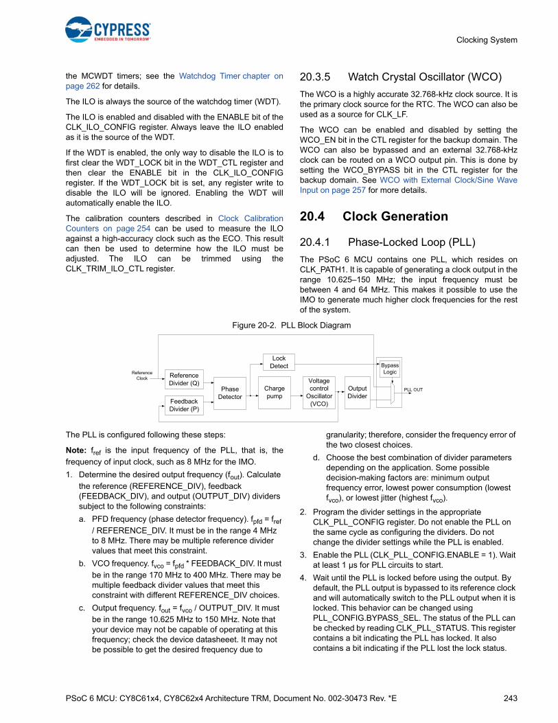
PSoC 6 MCU: CY8C61x4, CY8C62x4 Architecture TRM, Document No. 002-30473 Rev. *E 243
Clocking System
the MCWDT timers; see the Watchdog Timer chapter onpage 262 for details.
The ILO is always the source of the watchdog timer (WDT).
The ILO is enabled and disabled with the ENABLE bit of theCLK_ILO_CONFIG register. Always leave the ILO enabledas it is the source of the WDT.
If the WDT is enabled, the only way to disable the ILO is tofirst clear the WDT_LOCK bit in the WDT_CTL register andthen clear the ENABLE bit in the CLK_ILO_CONFIGregister. If the WDT_LOCK bit is set, any register write todisable the ILO will be ignored. Enabling the WDT willautomatically enable the ILO.
The calibration counters described in Clock CalibrationCounters on page 254 can be used to measure the ILOagainst a high-accuracy clock such as the ECO. This resultcan then be used to determine how the ILO must beadjusted. The ILO can be trimmed using theCLK_TRIM_ILO_CTL register.
20.3.5 Watch Crystal Oscillator (WCO)
The WCO is a highly accurate 32.768-kHz clock source. It isthe primary clock source for the RTC. The WCO can also beused as a source for CLK_LF.
The WCO can be enabled and disabled by setting theWCO_EN bit in the CTL register for the backup domain. TheWCO can also be bypassed and an external 32.768-kHzclock can be routed on a WCO output pin. This is done bysetting the WCO_BYPASS bit in the CTL register for thebackup domain. See WCO with External Clock/Sine WaveInput on page 257 for more details.
20.4 Clock Generation
20.4.1 Phase-Locked Loop (PLL)
The PSoC 6 MCU contains one PLL, which resides onCLK_PATH1. It is capable of generating a clock output in therange 10.625–150 MHz; the input frequency must bebetween 4 and 64 MHz. This makes it possible to use theIMO to generate much higher clock frequencies for the restof the system.
Figure 20-2. PLL Block Diagram
The PLL is configured following these steps:
Note: fref is the input frequency of the PLL, that is, the
frequency of input clock, such as 8 MHz for the IMO.
1. Determine the desired output frequency (fout). Calculate
the reference (REFERENCE_DIV), feedback (FEEDBACK_DIV), and output (OUTPUT_DIV) dividers subject to the following constraints:
a. PFD frequency (phase detector frequency). fpfd = fref
/ REFERENCE_DIV. It must be in the range 4 MHz to 8 MHz. There may be multiple reference divider values that meet this constraint.
b. VCO frequency. fvco = fpfd * FEEDBACK_DIV. It must
be in the range 170 MHz to 400 MHz. There may be multiple feedback divider values that meet this constraint with different REFERENCE_DIV choices.
c. Output frequency. fout = fvco / OUTPUT_DIV. It must
be in the range 10.625 MHz to 150 MHz. Note that your device may not be capable of operating at this frequency; check the device datasheeet. It may not be possible to get the desired frequency due to
granularity; therefore, consider the frequency error of the two closest choices.
d. Choose the best combination of divider parameters depending on the application. Some possible decision-making factors are: minimum output frequency error, lowest power consumption (lowest fvco), or lowest jitter (highest fvco).
2. Program the divider settings in the appropriate CLK_PLL_CONFIG register. Do not enable the PLL on the same cycle as configuring the dividers. Do not change the divider settings while the PLL is enabled.
3. Enable the PLL (CLK_PLL_CONFIG.ENABLE = 1). Wait at least 1 µs for PLL circuits to start.
4. Wait until the PLL is locked before using the output. By default, the PLL output is bypassed to its reference clock and will automatically switch to the PLL output when it is locked. This behavior can be changed using PLL_CONFIG.BYPASS_SEL. The status of the PLL can be checked by reading CLK_PLL_STATUS. This register contains a bit indicating the PLL has locked. It also contains a bit indicating if the PLL lost the lock status.
Phase Detector
Charge pump
Voltage control
Oscillator (VCO)Feedback
Divider (P)
Reference Divider (Q)
Reference Clock
PLL OUTOutput Divider
Lock Detect Bypass
Logic
PSoC 6 MCU: CY8C61x4, CY8C62x4 Architecture TRM, Document No. 002-30473 Rev. *E 244
Clocking System
To disable the PLL, first set the PLL_CONFIG.BYPASS_SELto PLL_REF. Then wait at least six PLL output clock cyclesbefore disabling the PLL by setting PLL_CONFIG.ENABLEto ‘0’.
20.4.2 Frequency Lock Loop (FLL)
The PSoC 6 MCU contains one frequency lock loop (FLL),which resides on Clock Path 0. The FLL is capable ofgenerating a clock output in the range 24 MHz to 100 MHz;the input frequency must be between 0.001 and 100 MHz,and must be at least 2.5 times less than the CCO frequency.This makes it possible to use the IMO to generate muchhigher clock frequencies for the rest of the system.
The FLL is similar in purpose to a PLL but is not equivalent:
■ FLL can start up (lock) much faster than the PLL.
■ It consumes less current than the PLL.
■ FLL does not lock the phase. At the heart of the FLL is a current-controlled oscillator (CCO). The output frequency of this CCO is controlled by adjusting the trim of the CCO; this is done in hardware and is explained in detail later in this section.
■ FLL can produce up to 100-MHz clock with good duty cycle through its divided clock output.
■ FLL reference clock can be the WCO (32 kHz), IMO (8 MHz), or any other periodic clock source.
Note: The CCO frequency must be at least 2.5 timesgreater than the reference frequency.
The CCO can output a stable frequency in the 48 MHz to200 MHz range. This range is divided into five sub-rangesas shown by Table 20-2.
Note: The output of the CCO has an option to enable adivide by two or not. For this device, the divide by two mustalways be enabled.
Within each range, the CCO output is controlled via a 9-bittrim field. This trim field is updated via hardware based onthe control algorithm described below.
A reference clock must be provided to the FLL. Thisreference clock is typically the IMO, but could be manydifferent clock sources. The FLL compares the referenceclock against the CCO clock to determine how to adjust theCCO trim. Specifically, the FLL will count the number ofCCO clock cycles inside a specified window of referenceclock cycles. The number of reference clock cycles to count
is set by the FLL_REF_DIV field in the CLK_FLL_CONFIG2register.
After the CCO clocks are counted, they are comparedagainst an ideal value and an error is calculated. The idealvalue is programmed into the FLL_MULT field of theCLK_FLL_CONFIG register.
As an example, the reference clock is the IMO (8 MHz), thedesired CCO frequency is 100 MHz, the value forFLL_REF_DIV is set to 146. This means that the FLL willcount the number of CCO clocks within 146 clock periods ofthe reference clock. In one clock cycle of the reference clock(IMO), there should be 100 / 8 = 12.5 clock cycles of theCCO. Multiply this number by 146 and the value ofFLL_MULT should be 1825.
If the FLL counts a value different from 1825, it attempts toadjust the CCO such that it achieves 1825 the next time itcounts. This is done by scaling the error term withFLL_LF_IGAIN and FLL_LF_PGAIN found inCLK_FLL_CONFIG3. Figure 20-3 shows how the error (err)term is multiplied by FLL_LF_IGAIN and FLL_LF_PGAINand then summed with the current trim to produce a newtrim value for the CCO. The CCO_LIMIT field in theCLK_FLL_CONFIG4 can be used to put an upper limit onthe trim adjustment; this is not needed for most situations.
Table 20-2. CCO Frequency Ranges
CCO Range
0 1 2 3 4
fmin 48 MHz 64 MHz 85 MHz 113 MHz 150 MHz
fmax 64 MHz 85 MHz 113 MHz 150 MHz 200 MHz
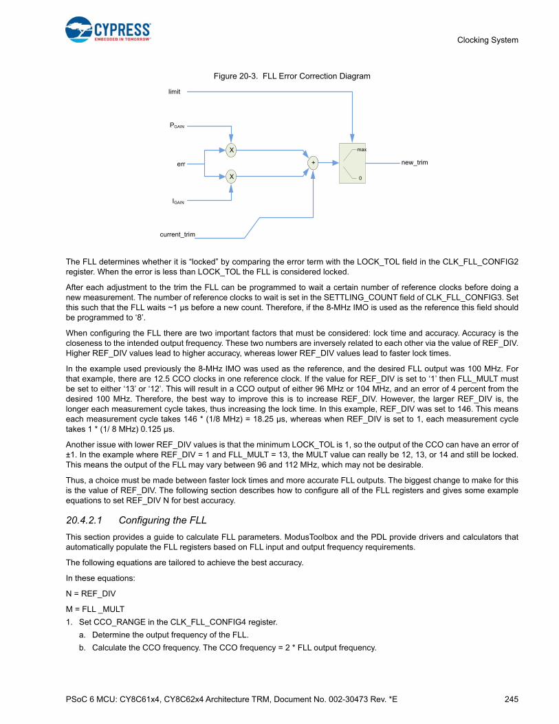
PSoC 6 MCU: CY8C61x4, CY8C62x4 Architecture TRM, Document No. 002-30473 Rev. *E 245
Clocking System
Figure 20-3. FLL Error Correction Diagram
The FLL determines whether it is “locked” by comparing the error term with the LOCK_TOL field in the CLK_FLL_CONFIG2register. When the error is less than LOCK_TOL the FLL is considered locked.
After each adjustment to the trim the FLL can be programmed to wait a certain number of reference clocks before doing anew measurement. The number of reference clocks to wait is set in the SETTLING_COUNT field of CLK_FLL_CONFIG3. Setthis such that the FLL waits ~1 µs before a new count. Therefore, if the 8-MHz IMO is used as the reference this field shouldbe programmed to ‘8’.
When configuring the FLL there are two important factors that must be considered: lock time and accuracy. Accuracy is thecloseness to the intended output frequency. These two numbers are inversely related to each other via the value of REF_DIV.Higher REF_DIV values lead to higher accuracy, whereas lower REF_DIV values lead to faster lock times.
In the example used previously the 8-MHz IMO was used as the reference, and the desired FLL output was 100 MHz. Forthat example, there are 12.5 CCO clocks in one reference clock. If the value for REF_DIV is set to ‘1’ then FLL_MULT mustbe set to either ‘13’ or ‘12’. This will result in a CCO output of either 96 MHz or 104 MHz, and an error of 4 percent from thedesired 100 MHz. Therefore, the best way to improve this is to increase REF_DIV. However, the larger REF_DIV is, thelonger each measurement cycle takes, thus increasing the lock time. In this example, REF_DIV was set to 146. This meanseach measurement cycle takes 146 * (1/8 MHz) = 18.25 µs, whereas when REF_DIV is set to 1, each measurement cycletakes 1 * (1/ 8 MHz) 0.125 µs.
Another issue with lower REF_DIV values is that the minimum LOCK_TOL is 1, so the output of the CCO can have an error of±1. In the example where REF_DIV = 1 and FLL_MULT = 13, the MULT value can really be 12, 13, or 14 and still be locked.This means the output of the FLL may vary between 96 and 112 MHz, which may not be desirable.
Thus, a choice must be made between faster lock times and more accurate FLL outputs. The biggest change to make for thisis the value of REF_DIV. The following section describes how to configure all of the FLL registers and gives some exampleequations to set REF_DIV N for best accuracy.
20.4.2.1 Configuring the FLL
This section provides a guide to calculate FLL parameters. ModusToolbox and the PDL provide drivers and calculators thatautomatically populate the FLL registers based on FLL input and output frequency requirements.
The following equations are tailored to achieve the best accuracy.
In these equations:
N = REF_DIV
M = FLL _MULT
1. Set CCO_RANGE in the CLK_FLL_CONFIG4 register.
a. Determine the output frequency of the FLL.
b. Calculate the CCO frequency. The CCO frequency = 2 * FLL output frequency.
limit
+
current_trim
IGAIN
PGAIN
err new_trim
X
X 0
max

PSoC 6 MCU: CY8C61x4, CY8C62x4 Architecture TRM, Document No. 002-30473 Rev. *E 246
Clocking System
c. Use Table 20-3 to determine the CCO range.
d. Write CCO range into CCO_RANGE in the CLK_FLL_CONFIG4 register.
2. Set the FLL_OUTPUT_DIV in CLK_FLL_CONFIG. Set the output divider to ‘1’.
3. Set FLL_REF_DIV in CLK_FLL_CONFIG2.
FLL_REF_DIV divides the FLL input clock. The FLL counts the number of CCO clocks within one period of the divided reference clock. A general equation to calculate the reference divider is as follows:
Equation 20-1
The CCOTrimStep is found in Table 20-4.
A larger N results in better precision on the FLL output, but longer lock times; a smaller N will result in faster lock times, but less precision.
Note: When the WCO is used as the reference clock, N must be set to 19.
4. Set FLL_MULT in CLK_FLL_CONFIG.
FLL_MULT is the ratio between the desired CCO frequency and the divided input frequency. This is the ideal value for the counter that counts the number of CCO clocks in one period of the divided input frequency.
Equation 20-2
5. Set the FLL_LF_IGAIN and FLL_LF_PGAIN in CLK_FLL_CONFIG3.
Within each range of the CCO there are 512 steps of adjustment for the CCO frequency. These steps are controlled by CCO_FREQ in the CLK_FLL_CONFIG4 register. The FLL automatically adjusts CCO_FREQ based on the output of the FLL counter.
The output of the counter gives the number of CCO clocks, over one period of the divided reference clock, by which the FLL is off. This value is then multiplied by the sum of FLL_LF_IGAIN and FLL_LF_PGAIN. The result of this multiplication is then summed with the value currently in the CCO_FREQ register.
To determine the values for IGAIN and PGAIN use the following equation:
Equation 20-3
Find the value of IGAIN closest but not over the values in the gain row in Table 20-5.
Table 20-3. CCO Frequency Ranges
CCO Range
0 1 2 3 4
fmin 48 MHz 64 MHz 85 MHz 113 MHz 150 MHz
fmax 64 MHz 85 MHz 113 MHz 150 MHz 200 MHz
Table 20-4. CCO Trim Steps
CCO Range 0 1 2 3 4
CCO_Trim_Steps 0.0011 0.0011 0.0011 0.0011 0.00117
Table 20-5. IGAIN and PGAIN Register Values
Register Value 0 1 2 3 4 5 6 7 8 9 10 11
Gain Value 1/256 1/128 1/64 1/32 1/16 1/8 1/4 1/2 1 2 4 8
N ROUNDUP2 fref
CCOTrimStepfCCOT etarg
-----------------------------------------------------------
=
M fCCOT etarg
Nfref--------=
IGAIN0.85
KCCON
fref--------
-----------------------------

PSoC 6 MCU: CY8C61x4, CY8C62x4 Architecture TRM, Document No. 002-30473 Rev. *E 247
Clocking System
Program FLL_LF_IGAIN with the register value that corresponds to the chosen gain value.
Take the IGAIN value from the register and use it in the following equation:
Equation 20-4
Find the value of PGAIN closest but not over the values in the gain row in Table 20-5. Program FLL_PF_IGAIN with the register value that corresponds to the chosen gain value.
For best performance Pgain_reg + Igain_reg should be as close as possible to calculated IGAIN without exceeding it. kCCO is the gain of the CCO; Table 20-6 lists the kCCO for each CCO range.
6. Set SETTLING_COUNT in CLK_FLL_CONFIG3.
SETTLING_COUNT is the number of reference clocks to wait for the CCO to settle after it has changed. It is best to set this such that the settling time is around 1 µs.
Do not set the settling time to anything less than 1 µs, greater will lead to longer lock times.
1. Set LOCK_TOL in CLK_FLL_CONFIG2.
LOCK_TOL determines how much error the FLL can tolerate at the output of the counter that counts the number of CCO clocks in one period of the divided reference clock. A higher tolerance can be used to lock more quickly or track a less accurate source. The tolerance should be set such that the FLL does not unlock under normal conditions. A lower tolerance means a more accurate output, but if the input reference is unstable then the FLL may unlock.
The following equation can be used to help determine the value:
Equation 20-5
CCO (accuracy) = 0.25% or 0.0025
ref (accuracy) is the accuracy of the reference clock
2. Set CCO_FREQ in CLK_FLL_CONFIG4.
This field determines the frequency at which the FLL starts before any measurement. The nearer the FLL is to the desired frequency, the faster it will lock.
Equation 20-6
fCCOBase can be found in Table 20-7.
Table 20-6. kCCO Values
CCO Range 0 1 2 3 4
kCCO 48109.38 64025.65 84920 113300 154521.85
Table 20-7. CCO Base Frequency
CCO Range 0 1 2 3 4
CCO_Base 43600 58100 77200 103000 132000
Table 20-8. CCO Trim Steps
CCO Range 0 1 2 3 4
CCO_Trim_Steps 0.0011 0.0011 0.0011 0.0011 0.00117
PGAIN IGAINreg0.85
KCCON
fref--------
-----------------------------–
SETTLING_COUNT =1 µs * fref
LOCK_TOL M1 CCOaccuracy+
1 Frefaccuracy–----------------------------------------- 1–=
CCOFREQ ROUPNDUP
LOGfCCOT etarg
fCCOBase
----------------------
LOG 1 CCOTrimStep+
----------------------------------------------------------
=

PSoC 6 MCU: CY8C61x4, CY8C62x4 Architecture TRM, Document No. 002-30473 Rev. *E 248
Clocking System
9. Calculating Precision, Accuracy, and Lock Time of FLL
To calculate the precision and accuracy of the FLL, the accuracy of the input source must be considered.
The precision is the larger of:
Equation 20-7
Or (CCO_Trim_Steps / 2)
Example: The desired FLL output is 100 MHz, thus CCO target is 200 MHz. The 2 percent accurate 8 MHz IMO is used as the reference input. N is calculated to be 69.
PrecisionFLL = ((8 MHz * 1.02)/(69 * 200 MHz)) = 0.059%, which is greater than the (CCO_Trim_Steps / 2)
The accuracy of the FLL output is the precision multiplied by the lock tolerance. If the CCO goes beyond this range, then the FLL will unlock.
AccuracyFLL = PrecisionFLL * LOCK_TOL
The value for the reference divider N should be tuned such that it achieves the best precision/accuracy versus lock time.
The lock time depends on the time for each adjustment step in the locking process;
Step_Time = (N / fref) + (SETTLING_COUNT / fref)
Multiply this number by the number of steps it takes to lock, to determine lock time. Typically, the FLL locks within the first ~10 steps.
20.4.2.2 Enabling and Disabling the FLL
The FLL requires firmware sequencing when enabling, disabling, and entering/exiting DEEPSLEEP.
To enable the FLL, follow these steps:
1. Enable the CCO by writing CLK_FLL_CONFIG4.CCO_ENABLE = 1 and wait until CLK_FLL_STATUS.CCO_READY==1.
2. Ensure the reference clock has stabilized and CLK_FLL_CONFIG3.BYPASS_SEL = FLL_REF.
3. Write FLL_ENABLE = 1 and wait until CLK_FLL_STATUS.LOCKED==1.
4. Write CLK_FLL_CONFIG3.BYPASS_SEL = FLL_OUT to switch to the FLL output.
To disable the FLL, follow these steps:
1. Ensure the processor is operating from a different clock than clk_path0. If the muxes are changed, wait four FLL output clock cycles for it to complete.
2. Write CLK_FLL_CONFIG3.BYPASS_SEL = FLL_REF and read the same register to ensure the write completes.
3. Wait at least six FLL reference clock cycles and disable it with FLL_ENABLE = 0.
4. Disable the CCO by writing CLK_FLL_CONFIG4.CCO_ENABLE = 0.
Before entering DEEPSLEEP, either disable the FLL using the above sequence or use the following procedure to deselect/select it before/after DEEPSLEEP. Before entering DEEPSLEEP, write CLK_FLL_CONFIG3.BYPASS_SEL = FLL_REF tochange the FLL to use its reference clock. After DEEPSLEEP wakeup, wait until CLK_FLL_STATUS.LOCKED==1 and thenwrite CLK_FLL_CONFIG3.BYPASS_SEL = FLL_OUT to switch to the FLL output.
Note: It is not recommended to use the FLL_AUTO option in the BYPASS_SEL field.
PrecisionFLL fref
1 fref accuracy +
N fCCOT etarg
----------------------------------------------
=
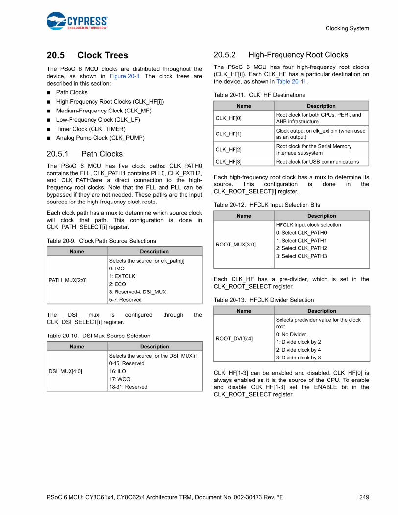
PSoC 6 MCU: CY8C61x4, CY8C62x4 Architecture TRM, Document No. 002-30473 Rev. *E 249
Clocking System
20.5 Clock Trees
The PSoC 6 MCU clocks are distributed throughout thedevice, as shown in Figure 20-1. The clock trees aredescribed in this section:
■ Path Clocks
■ High-Frequency Root Clocks (CLK_HF[i])
■ Medium-Frequency Clock (CLK_MF)
■ Low-Frequency Clock (CLK_LF)
■ Timer Clock (CLK_TIMER)
■ Analog Pump Clock (CLK_PUMP)
20.5.1 Path Clocks
The PSoC 6 MCU has five clock paths: CLK_PATH0contains the FLL, CLK_PATH1 contains PLL0, CLK_PATH2,and CLK_PATH3are a direct connection to the high-frequency root clocks. Note that the FLL and PLL can bebypassed if they are not needed. These paths are the inputsources for the high-frequency clock roots.
Each clock path has a mux to determine which source clockwill clock that path. This configuration is done inCLK_PATH_SELECT[i] register.
The DSI mux is configured through theCLK_DSI_SELECT[i] register.
20.5.2 High-Frequency Root Clocks
The PSoC 6 MCU has four high-frequency root clocks(CLK_HF[i]). Each CLK_HF has a particular destination onthe device, as shown in Table 20-11.
Each high-frequency root clock has a mux to determine itssource. This configuration is done in theCLK_ROOT_SELECT[i] register.
Each CLK_HF has a pre-divider, which is set in theCLK_ROOT_SELECT register.
CLK_HF[1-3] can be enabled and disabled. CLK_HF[0] isalways enabled as it is the source of the CPU. To enableand disable CLK_HF[1-3] set the ENABLE bit in theCLK_ROOT_SELECT register.
Table 20-9. Clock Path Source Selections
Name Description
PATH_MUX[2:0]
Selects the source for clk_path[i]
0: IMO
1: EXTCLK
2: ECO
3: Reserved4: DSI_MUX
5-7: Reserved
Table 20-10. DSI Mux Source Selection
Name Description
DSI_MUX[4:0]
Selects the source for the DSI_MUX[i]
0-15: Reserved
16: ILO
17: WCO
18-31: Reserved
Table 20-11. CLK_HF Destinations
Name Description
CLK_HF[0]Root clock for both CPUs, PERI, and AHB infrastructure
CLK_HF[1]Clock output on clk_ext pin (when used as an output)
CLK_HF[2]Root clock for the Serial Memory Interface subsystem
CLK_HF[3] Root clock for USB communications
Table 20-12. HFCLK Input Selection Bits
Name Description
ROOT_MUX[3:0]
HFCLK input clock selection
0: Select CLK_PATH0
1: Select CLK_PATH1
2: Select CLK_PATH2
3: Select CLK_PATH3
Table 20-13. HFCLK Divider Selection
Name Description
ROOT_DVI[5:4]
Selects predivider value for the clock root
0: No Divider
1: Divide clock by 2
2: Divide clock by 4
3: Divide clock by 8

PSoC 6 MCU: CY8C61x4, CY8C62x4 Architecture TRM, Document No. 002-30473 Rev. *E 250
Clocking System
20.5.3 Medium-Frequency Clock
The PSoC 6 MCU contains a medium-frequency clock(CLK_MF). The source for this clock, termed medium-frequency oscillator (MFO) is derived from the IMO and isfixed at a frequency of 2 MHz (IMO/4).
CLK_MF is enabled by setting CLK_MF_SELECT.ENABLEfield to ‘1’. CLK_MF can be pre-scaled by an integer valuebetween 1 and 256 using CLK_MF_SELECT.MFCLK_DIVfield. The MFCLK_DIV field should be modified only whenthe ENABLE field is ‘0’.
CLK_MF (and IMO) can be configured to operate in DeepSleep power mode by setting theCLK_MFO_CONFIG.DPSLP_ENABLE field to ‘1’.
The CLF_MF can be selected as one of the Deep Sleepsources of the LCD block, and provides better contrast thanthe low-frequency clock source.
20.5.4 Low-Frequency Clock
The low-frequency clock (CLK_LF) in the PSoC 6 MCU hastwo input options: ILO and WCO.
CLK_LF is the source for the multi-counter watchdog timers(MCWDT) and the RTC.
The source of CLK_LF is set in the LFCLK_SEL bits of theCLK_SELECT register. Writes to LFCLK_SEL bits areprotected by WDT_LOCK field of the WDT_CTL register;see Watchdog Timer chapter on page 262.
20.5.5 Timer Clock
The timer clock (CLK_TIMER) can be used as a clocksource for the CPU SYSTICK timer. The source forCLK_TIMER can either be the IMO or CLK_HF[0]. Thisselection is made in the TIMER_SEL bitfield of theCLK_TIMER_CTL register. Several dividers can be appliedto this clock, which are found in the CLK_TIMER_CTLregister.
20.5.6 Group Clocks (clk_sys)
On the PSoC 6 platform, peripherals are grouped. Eachgroup has a dedicated group clock (also referred to asclk_sys). The group clock sets the clock rate for the AHBinterface on the peripheral; it also sets the clock rate for the
trigger outputs and trigger input synchronization. Eachgroup clock has an eight-bit divider located in theCLOCK_CTL register in the PERI_GROUP_STRUCT in thePERI register set. For a majority of applications thesedividers should be left at default (divide by 1).
20.5.7 Backup Clock (clk_bak)
The backup clock is used to clock the backup domain,specifically the RTC. For more information see WCO withExternal Clock/Sine Wave Input on page 257.
Table 20-14. LFCLK Input Selection Bits LFCLK_SEL
Name Description
LFCLK_SEL[1:0]
LFCLK input clock selection
0: ILO. Uses the internal local oscillator as the source of the LFCLK
1: WCO. Uses the watch crystal oscillator as the source of the LFCLK
2: Reserved
3: Reserved
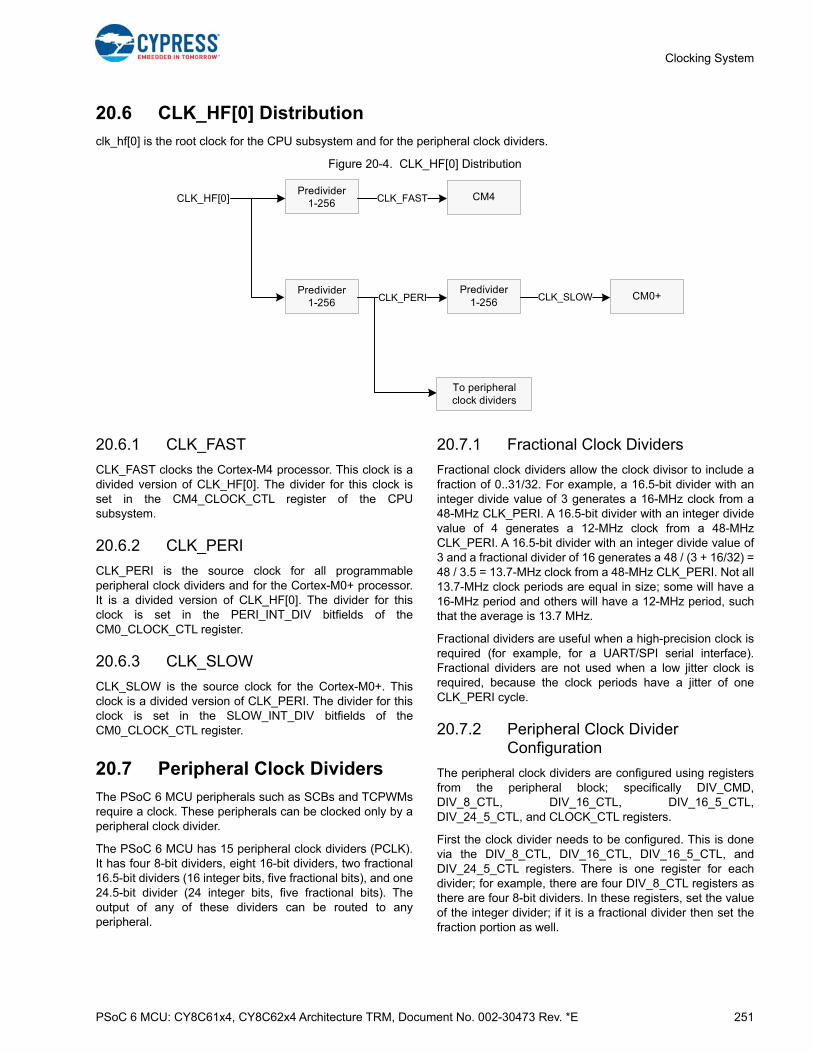
PSoC 6 MCU: CY8C61x4, CY8C62x4 Architecture TRM, Document No. 002-30473 Rev. *E 251
Clocking System
20.6 CLK_HF[0] Distribution
clk_hf[0] is the root clock for the CPU subsystem and for the peripheral clock dividers.
Figure 20-4. CLK_HF[0] Distribution
20.6.1 CLK_FAST
CLK_FAST clocks the Cortex-M4 processor. This clock is adivided version of CLK_HF[0]. The divider for this clock isset in the CM4_CLOCK_CTL register of the CPUsubsystem.
20.6.2 CLK_PERI
CLK_PERI is the source clock for all programmableperipheral clock dividers and for the Cortex-M0+ processor.It is a divided version of CLK_HF[0]. The divider for thisclock is set in the PERI_INT_DIV bitfields of theCM0_CLOCK_CTL register.
20.6.3 CLK_SLOW
CLK_SLOW is the source clock for the Cortex-M0+. Thisclock is a divided version of CLK_PERI. The divider for thisclock is set in the SLOW_INT_DIV bitfields of theCM0_CLOCK_CTL register.
20.7 Peripheral Clock Dividers
The PSoC 6 MCU peripherals such as SCBs and TCPWMsrequire a clock. These peripherals can be clocked only by aperipheral clock divider.
The PSoC 6 MCU has 15 peripheral clock dividers (PCLK).It has four 8-bit dividers, eight 16-bit dividers, two fractional16.5-bit dividers (16 integer bits, five fractional bits), and one24.5-bit divider (24 integer bits, five fractional bits). Theoutput of any of these dividers can be routed to anyperipheral.
20.7.1 Fractional Clock Dividers
Fractional clock dividers allow the clock divisor to include afraction of 0..31/32. For example, a 16.5-bit divider with aninteger divide value of 3 generates a 16-MHz clock from a48-MHz CLK_PERI. A 16.5-bit divider with an integer dividevalue of 4 generates a 12-MHz clock from a 48-MHzCLK_PERI. A 16.5-bit divider with an integer divide value of3 and a fractional divider of 16 generates a 48 / (3 + 16/32) =48 / 3.5 = 13.7-MHz clock from a 48-MHz CLK_PERI. Not all13.7-MHz clock periods are equal in size; some will have a16-MHz period and others will have a 12-MHz period, suchthat the average is 13.7 MHz.
Fractional dividers are useful when a high-precision clock isrequired (for example, for a UART/SPI serial interface).Fractional dividers are not used when a low jitter clock isrequired, because the clock periods have a jitter of oneCLK_PERI cycle.
20.7.2 Peripheral Clock Divider Configuration
The peripheral clock dividers are configured using registersfrom the peripheral block; specifically DIV_CMD,DIV_8_CTL, DIV_16_CTL, DIV_16_5_CTL,DIV_24_5_CTL, and CLOCK_CTL registers.
First the clock divider needs to be configured. This is donevia the DIV_8_CTL, DIV_16_CTL, DIV_16_5_CTL, andDIV_24_5_CTL registers. There is one register for eachdivider; for example, there are four DIV_8_CTL registers asthere are four 8-bit dividers. In these registers, set the valueof the integer divider; if it is a fractional divider then set thefraction portion as well.
Predivider 1-256CLK_HF[0] CLK_FAST CM4
Predivider 1-256 CLK_PERI
Predivider 1-256
CM0+CLK_SLOW
To peripheral clock dividers

PSoC 6 MCU: CY8C61x4, CY8C62x4 Architecture TRM, Document No. 002-30473 Rev. *E 252
Clocking System
After the divider is configured use the DIV_CMD register toenable the divider. This is done by setting the DIV_SEL tothe divider number you want to enable, and setting theTYPE_SEL to the divider type. For example, if you wantedto enable the 0th 16.5-bit divider, write ‘0’ to DIV_SEL and‘2’ to TYPE_SEL. If you wanted to enable the seventh 16-bitdivider, write ‘7’ to DIV_SEL and ‘1’ to TYPE_SEL. See theregisters TRM for more details.
20.7.2.1 Phase Aligning Dividers
For specific use cases, you must generate clocks that arephase-aligned. For example, consider the generation of twogated clocks at 24 and 12 MHz, both of which are derivedfrom a 48-MHz CLK_PERI. If phase alignment is notconsidered, the generated gated clocks appear as follows.
Figure 20-5. Non Phase-Aligned Clock Dividers
These clock signals may or may not be acceptable, depending on the logic functionality implemented on these two clocks. Ifthe two clock domains communicate with each other, and the slower clock domain (12 MHz) assumes that each high/‘1’ pulseon its clock coincides with a high/‘1’ phase pulse in the higher clock domain (24 MHz), the phase misalignment is notacceptable. To address this, it is possible to have dividers produce clock signals that are phase-aligned with any of the other(enabled) clock dividers. Therefore, if (enabled) divider x is used to generate the 24-MHz clock, divider y can be phase-aligned to divider x and used to generate the 12-MHz clock. The aligned clocks appear as follows.
Figure 20-6. Phase-Aligned Clock Dividers
Phase alignment also works for fractional divider values. If (enabled) divider x is used to generate the 38.4-MHz clock (divideby 1 8/32), divider y can be phase-aligned to divider x and used to generate the 19.2-MHz clock (divide by 2 16/32). Thegenerated gated clocks appear as follows.
Figure 20-7. Phase-Aligned Fractional Dividers
CLK_PERI (48 MHz)
24 MHz gated clock
12 MHz gated clock
No phase alignment
CLK_PERI (48 MHz)
24 MHz gated clock
12 MHz gated clock
Phase alignment
CLK_PERI (48 MHz)
38.4 MHz gated clock
19.2 MHz gated clock
Phase alignment

PSoC 6 MCU: CY8C61x4, CY8C62x4 Architecture TRM, Document No. 002-30473 Rev. *E 253
Clocking System
Divider phase alignment requires that the divider to which itis phase-aligned is already enabled. This requires thedividers to be enabled in a specific order.
Phase alignment is implemented by controlling the startmoment of the divider counters in hardware. When a divideris enabled, the divider counters are set to ‘0’. The dividercounters will only start incrementing from ‘0’ to theprogrammed integer and fractional divider values when thedivider to which it is phase-aligned has an integer countervalue of ‘0’.
Note that the divider and clock multiplexer control registerfields are all retained during the Deep Sleep power mode.However, the divider counters that are used to implementthe integer and fractional clock dividers are not. Thesecounters are set to ‘0’ during the Deep Sleep mode.Therefore, when transitioning from Deep Sleep to Activemode, all dividers (and clock signals) are enabled andphase-aligned by design.
Phase alignment is accomplished by setting thePA_DIV_SEL and PA_DIV_TYPE bits in the DIV_CMDregister before enabling the clock. For example, to align thefourth 8-bit divider to the third 16-bit divider, set DIV_SEL to‘4’, TYPE_SEL to ‘0’, PA_DIV_SEL to ‘3’, andPA_TYPE_SEL to ‘1’.
20.7.2.2 Connecting Dividers to Peripheral
The PSoC 6 MCU has 28 peripherals, which can connect toone of the programmable dividers. Table 20-15 lists thoseperipherals.
To connect a peripheral to a specific divider, thePERI_CLOCK_CTL register is used. There is onePERI_CLOCK_CTL register for each entry in Table 20-15.For example, to select the seventh 16-bit divider fortcpwm[0].clocks[262] write to CLOCK_CTL[17], set theDIV_SEL to ‘7’, and the TYPE_SEL to ‘1’.
Table 20-15. Clock Dividers to Peripherals
Clock Number Destination
0 scb[0].clock
1 scb[1].clock
2 scb[2].clock
3 scb[4].clock
4 scb[5].clock
5 scb[6].clock
6 smartio[9].clock
7 tcpwm[0].clocks[0]
8 tcpwm[0].clocks[1]
9 tcpwm[0].clocks[2]
10 tcpwm[0].clocks[3]
11 tcpwm[0].clocks[256]
12 tcpwm[0].clocks[257]
13 tcpwm[0].clocks[258]
14 tcpwm[0].clocks[259]
15 tcpwm[0].clocks[260]
16 tcpwm[0].clocks[261]
17 tcpwm[0].clocks[262]
18 tcpwm[0].clocks[263]
19 csd.clock
20 lcd.clock
21 cpuss.clock_trace_in
22 pass.clock_pump_peri
23 pass.clock_sar[0]
24 canfd[0].clock_can[0]
25 usb.clock_dev_brs
26 pass.clock_ctdac
27 pass.clock_sar[1]
Table 20-15. Clock Dividers to Peripherals
Clock Number Destination
PSoC 6 MCU: CY8C61x4, CY8C62x4 Architecture TRM, Document No. 002-30473 Rev. *E 254
Clocking System
20.8 Clock Calibration Counters
A feature of the clocking system in PSoC 6 MCUs is built-in hardware calibration counters. These counters can be used tocompare the frequency of two clock sources against one another. The primary use case is to take a higher accuracy clocksuch as the ECO and use it to measure a lower accuracy clock such as the ILO. The result of this measurement can then beused to trim the ILO.
There are two counters: Calibration Counter 1 is clocked off of Calibration Clock 1 (generally the high-accuracy clock) and itcounts down; Calibration Counter 2 is clocked off of Calibration Clock 2 and it counts up. When Calibration Counter 1 reaches0, Calibration Counter 2 stops counting up and its value can be read. From that value the frequency of Calibration Clock 2 canbe determined with the following equation.
For example, if Calibration Clock 1 = 8 MHz, Counter 1 = 1000, and Counter 2 = 5
Calibration Clock 1 Frequency = (5/1000) * 8 MHz = 40 kHz.
Calibration Clock 1 and Calibration Clock 2 are selected with the CLK_OUTPUT_FAST register. All clock sources areavailable as a source for these two clocks. CLK_OUTPUT_SLOW is also used to select the clock source.
Calibration Counter 1 is programmed in CLK_CAL_CNT1. Calibration Counter 2 can be read in CLK_CAL_CNT2.
When Calibration Counter 1 reaches 0, the CAL_COUNTER_DONE bit is set in the CLK_CAL_CNT1 register.
Calibration Clock 2 FrequencyCounter 2 Final ValueCounter 1 Initial Value---------------------------------------------------------- Calibration Clock 1 Frequency=

PSoC 6 MCU: CY8C61x4, CY8C62x4 Architecture TRM, Document No. 002-30473 Rev. *E 255
21. Backup System
The Backup domain adds an “always on” functionality to PSoC 6 MCUs using a separate power domain supplied by a backupsupply (VBACKUP) such as a battery or supercapacitor. It contains a real-time clock (RTC) with alarm feature, supported by a32768-Hz watch crystal oscillator (WCO), and power-management IC (PMIC) control.
Backup is not a power mode; it is a power domain with its own power supply, which can be active during any of the devicepower modes. For more details, see the Power Supply and Monitoring chapter on page 273 and Device PowerModes chapter on page 280.
21.1 Features■ Fully-featured RTC
❐ Year/Month/Date, Day-of-Week, Hour : Minute : Second fields
❐ All fields binary coded decimal (BCD)
❐ Supports both 12-hour and 24-hour formats
❐ Automatic leap year correction
■ Configurable alarm function
❐ Alarm on Month/Date, Day-of-Week, Hour : Minute : Second fields
❐ Two independent alarms
■ 32768-Hz WCO with calibration
■ Automatic backup power switching
■ Built-in supercapacitor charger
■ External PMIC control
■ 32-byte backup registers
This PSoC 6 MCU technical reference manual (TRM) provides comprehensive and detailed information about thefunctions of the PSoC 6 MCU device hardware. It is divided into two books: architecture TRM and registers TRM. TheTRM is not recommended for those new to the PSoC 6 MCU, nor as a guide for developing PSoC 6 MCU applications.Use these documents instead:
■ PSoC 61 datasheet, PSoC 62 datasheet
■ Peripheral Driver Library (PDL) documentation
■ Application notes
■ Code examples
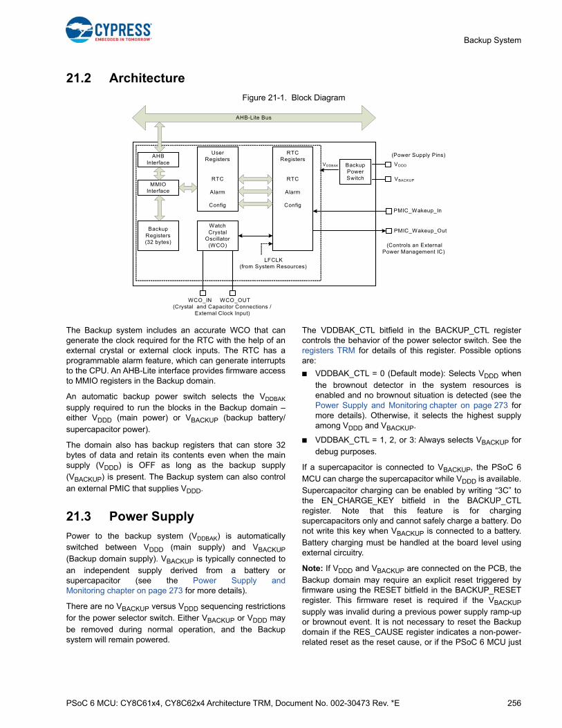
PSoC 6 MCU: CY8C61x4, CY8C62x4 Architecture TRM, Document No. 002-30473 Rev. *E 256
Backup System
21.2 Architecture
Figure 21-1. Block Diagram
The Backup system includes an accurate WCO that cangenerate the clock required for the RTC with the help of anexternal crystal or external clock inputs. The RTC has aprogrammable alarm feature, which can generate interruptsto the CPU. An AHB-Lite interface provides firmware accessto MMIO registers in the Backup domain.
An automatic backup power switch selects the VDDBAK
supply required to run the blocks in the Backup domain –either VDDD (main power) or VBACKUP (backup battery/
supercapacitor power).
The domain also has backup registers that can store 32bytes of data and retain its contents even when the mainsupply (VDDD) is OFF as long as the backup supply
(VBACKUP) is present. The Backup system can also control
an external PMIC that supplies VDDD.
21.3 Power Supply
Power to the backup system (VDDBAK) is automaticallyswitched between VDDD (main supply) and VBACKUP
(Backup domain supply). VBACKUP is typically connected to
an independent supply derived from a battery orsupercapacitor (see the Power Supply andMonitoring chapter on page 273 for more details).
There are no VBACKUP versus VDDD sequencing restrictions
for the power selector switch. Either VBACKUP or VDDD maybe removed during normal operation, and the Backupsystem will remain powered.
The VDDBAK_CTL bitfield in the BACKUP_CTL registercontrols the behavior of the power selector switch. See theregisters TRM for details of this register. Possible optionsare:
■ VDDBAK_CTL = 0 (Default mode): Selects VDDD when
the brownout detector in the system resources isenabled and no brownout situation is detected (see thePower Supply and Monitoring chapter on page 273 formore details). Otherwise, it selects the highest supplyamong VDDD and VBACKUP.
■ VDDBAK_CTL = 1, 2, or 3: Always selects VBACKUP for
debug purposes.
If a supercapacitor is connected to VBACKUP, the PSoC 6
MCU can charge the supercapacitor while VDDD is available.
Supercapacitor charging can be enabled by writing “3C” tothe EN_CHARGE_KEY bitfield in the BACKUP_CTLregister. Note that this feature is for chargingsupercapacitors only and cannot safely charge a battery. Donot write this key when VBACKUP is connected to a battery.
Battery charging must be handled at the board level usingexternal circuitry.
Note: If VDDD and VBACKUP are connected on the PCB, the
Backup domain may require an explicit reset triggered byfirmware using the RESET bitfield in the BACKUP_RESETregister. This firmware reset is required if the VBACKUP
supply was invalid during a previous power supply ramp-upor brownout event. It is not necessary to reset the Backupdomain if the RES_CAUSE register indicates a non-power-related reset as the reset cause, or if the PSoC 6 MCU just
RTC Registers
RTC
Alarm
Config
User Registers
RTC
Alarm
Config
Watch Crystal
Oscillator(WCO)
Backup Registers (32 bytes)
MMIO Interface
AHB Interface Backup
PowerSwitch
AHB-Lite Bus
VDDD
VBACKUP
WCO_IN WCO_OUT(Crystal and Capacitor Connections /
External Clock Input)
PMIC_Wakeup_In
PMIC_Wakeup_Out
(Power Supply Pins)
(Controls an External Power Management IC)
LFCLK (from System Resources)
VDDBAK
PSoC 6 MCU: CY8C61x4, CY8C62x4 Architecture TRM, Document No. 002-30473 Rev. *E 257
Backup System
woke from the Hibernate power mode and the supply isassumed to have been valid the entire time.
It is possible to monitor the VBACKUP supply using an ADCattached to AMUXBUS-A by setting the VBACKUP_MEASbit in the BACKUP_CTL register. Note that the VBACKUP
signal is scaled by 10 percent so it is within the supply rangeof the ADC. See the SAR ADC chapter on page 506 formore details on how to connect the ADC to AMUXBUS-A.
21.4 Clocking
The RTC primarily runs from a 32768-Hz clock, after it isscaled down to one-second ticks. This clock signal cancome from either of these internal sources:
■ Watch-crystal oscillator (WCO). This is a high-accuracyclock generator that is suitable for RTC applications andrequires a 32768-Hz external crystal populated on theapplication board. WCO can also operate withoutcrystal, using external clock/sine wave inputs. Theseadditional operating modes are explained later in thissection. WCO is supplied by the Backup domain and cantherefore run without VDDD present.
■ Alternate Backup Clock (ALTBAK): This option allowsthe use of LFCLK generated by the System ResourcesSubsystem (SRSS) as the Backup domain clock. Notethat LFCLK is not available in all device power modes orwhen the VDDD is removed. (See the Device Power
Modes chapter on page 280 for more detail.)
Clock glitches can propagate into the Backup system when LFCLK is enabled or disabled by the SRSS. In addition, LFCLK may not be as accurate as WCO depending on the actual source of LFCLK. Because of these reasons, LFCLK is not recommend for RTC applications. Also, if the WCO is intended as the clock source then choose it directly instead of routing through LFCLK.
For more details on these clocks and calibration, see theClocking System chapter on page 240.
The RTC clock source can be selected using the CLK_SELbitfield in the BACKUP_CTL register. The WCO_EN bit inthe BACKUP_CTL register can be used to enable or disablethe WCO. If the WCO operates with an external crystal,make sure the WCO_BYPASS bit in the BACKUP_CTLregister is cleared before enabling the WCO. In addition, thePRESCALER bitfield in BACKUP_CTL must be configuredfor a prescaler value of 32768.
Note: External crystal and bypass capacitors of propervalues must be connected to WCO_IN and WCO_OUT andpins. See the PSoC 61 datasheet/PSoC 62 datasheet fordetails of component values and electrical connections. Inaddition, GPIOs must be configured for WCO_OUT andWCO_IN signals. See the I/O System chapter on page 214to know how to configure the GPIOs.
21.4.1 WCO with External Clock/Sine Wave Input
The WCO can also operate from external clock/sine waveinputs. In these modes, WCO must be bypassed by settingthe WCO_BYPASS bit in the BACKUP_CTL register beforeenabling the WCO. Also, GPIOs must be configured forWCO_OUT and WCO_IN signals (in Analog mode). Theexternal clock/sine wave input modes, prescaler settings,and electrical connections are as follows:
■ 32768-Hz external clock mode: In this mode, WCO_IN isfloating and WCO_OUT is externally driven by a 32768-Hz square wave clock toggling between ground andVDDD supply levels. In this configuration, the WCO_OUT
pin functions as a digital input pin for the external clock.The PRESCALER bitfield in BACKUP_CTL must beconfigured for a prescaler value of 32768.
■ 60-Hz external clock mode: This mode can be used forderiving a clock from the 60-Hz AC mains supply. In thismode, WCO_OUT is floating and WCO_IN is driven withan external sine wave with zero DC offset, derived fromthe 60-Hz/120-V mains through a 100:1 capacitivedivider. For example, a suitable capacitive divider can beformed by connecting a 220-pF/6-V capacitor betweenWCO_IN and ground, and a 2.2-pF/ 200-V capacitorbetween WCO_IN and the 60-Hz/120-V mains input.The PRESCALER bitfield in BACKUP_CTL must beconfigured for a prescaler value of 60.
■ 50-Hz external clock mode: This mode is similar to the60-Hz mode, and can be used for 50-Hz/220-V mainsstandard. The capacitive divider explained previouslycan be modified to fit this type of supply by having a 1-pF/250-V capacitor between WCO_IN and the mains input.The PRESCALER bitfield in BACKUP_CTL must beconfigured for a prescaler value of 50.
21.4.2 Calibration
The absolute frequency of the clock input can be calibratedusing the BACKUP_CAL_CTL register. Calibration onlyworks when the PRESCALER bitfield in BACKUP_CTL isset to 32768.
CALIB_VAL is a 6-bit field in the BACKUP_CAL_CTLregister that holds the calibration value for absolutefrequency (at a fixed temperature). One bit of this fieldtranslates into 128 ticks to be added or removed from theclock count. Therefore, each bit translates to a change of1.085 ppm (= 128/(60*60*32768)).
The CALIB_SIGN field in the BACKUP_CAL_CTL registercontrols whether the ticks are added (it takes fewer clockticks to count one second) or subtracted (it takes more clockticks to count one second).
For more information, see the BACKUP_CAL_CTL registerin the registers TRM.
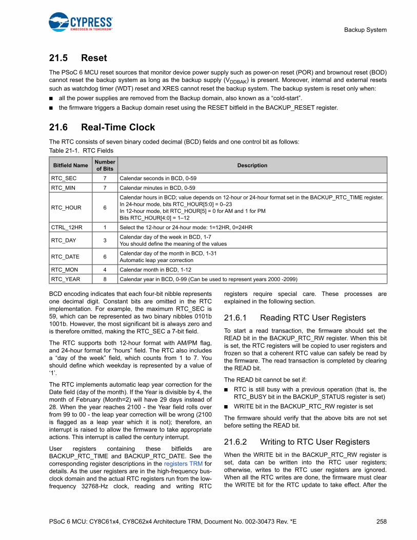
PSoC 6 MCU: CY8C61x4, CY8C62x4 Architecture TRM, Document No. 002-30473 Rev. *E 258
Backup System
21.5 Reset
The PSoC 6 MCU reset sources that monitor device power supply such as power-on reset (POR) and brownout reset (BOD)cannot reset the backup system as long as the backup supply (VDDBAK) is present. Moreover, internal and external resetssuch as watchdog timer (WDT) reset and XRES cannot reset the backup system. The backup system is reset only when:
■ all the power supplies are removed from the Backup domain, also known as a “cold-start”.
■ the firmware triggers a Backup domain reset using the RESET bitfield in the BACKUP_RESET register.
21.6 Real-Time Clock
The RTC consists of seven binary coded decimal (BCD) fields and one control bit as follows:
BCD encoding indicates that each four-bit nibble representsone decimal digit. Constant bits are omitted in the RTCimplementation. For example, the maximum RTC_SEC is59, which can be represented as two binary nibbles 0101b1001b. However, the most significant bit is always zero andis therefore omitted, making the RTC_SEC a 7-bit field.
The RTC supports both 12-hour format with AM/PM flag,and 24-hour format for “hours” field. The RTC also includesa “day of the week” field, which counts from 1 to 7. Youshould define which weekday is represented by a value of‘1’.
The RTC implements automatic leap year correction for theDate field (day of the month). If the Year is divisible by 4, themonth of February (Month=2) will have 29 days instead of28. When the year reaches 2100 - the Year field rolls overfrom 99 to 00 - the leap year correction will be wrong (2100is flagged as a leap year which it is not); therefore, aninterrupt is raised to allow the firmware to take appropriateactions. This interrupt is called the century interrupt.
User registers containing these bitfields areBACKUP_RTC_TIME and BACKUP_RTC_DATE. See thecorresponding register descriptions in the registers TRM fordetails. As the user registers are in the high-frequency bus-clock domain and the actual RTC registers run from the low-frequency 32768-Hz clock, reading and writing RTC
registers require special care. These processes areexplained in the following section.
21.6.1 Reading RTC User Registers
To start a read transaction, the firmware should set theREAD bit in the BACKUP_RTC_RW register. When this bitis set, the RTC registers will be copied to user registers andfrozen so that a coherent RTC value can safely be read bythe firmware. The read transaction is completed by clearingthe READ bit.
The READ bit cannot be set if:
■ RTC is still busy with a previous operation (that is, theRTC_BUSY bit in the BACKUP_STATUS register is set)
■ WRITE bit in the BACKUP_RTC_RW register is set
The firmware should verify that the above bits are not setbefore setting the READ bit.
21.6.2 Writing to RTC User Registers
When the WRITE bit in the BACKUP_RTC_RW register isset, data can be written into the RTC user registers;otherwise, writes to the RTC user registers are ignored.When all the RTC writes are done, the firmware must clearthe WRITE bit for the RTC update to take effect. After the
Table 21-1. RTC Fields
Bitfield Name Number of Bits
Description
RTC_SEC 7 Calendar seconds in BCD, 0-59
RTC_MIN 7 Calendar minutes in BCD, 0-59
RTC_HOUR 6
Calendar hours in BCD; value depends on 12-hour or 24-hour format set in the BACKUP_RTC_TIME register. In 24-hour mode, bits RTC_HOUR[5:0] = 0–23 In 12-hour mode, bit RTC_HOUR[5] = 0 for AM and 1 for PM Bits RTC_HOUR[4:0] = 1–12
CTRL_12HR 1 Select the 12-hour or 24-hour mode: 1=12HR, 0=24HR
RTC_DAY 3Calendar day of the week in BCD, 1-7 You should define the meaning of the values
RTC_DATE 6Calendar day of the month in BCD, 1-31 Automatic leap year correction
RTC_MON 4 Calendar month in BCD, 1-12
RTC_YEAR 8 Calendar year in BCD, 0-99 (Can be used to represent years 2000 -2099)

PSoC 6 MCU: CY8C61x4, CY8C62x4 Architecture TRM, Document No. 002-30473 Rev. *E 259
Backup System
WRITE bit is cleared, the hardware will copy all the new dataon one single WCO clock edge to ensure coherency to theactual RTC registers.
The WRITE bit cannot be set if:
■ RTC is still busy with a previous operation (that is, theRTC_BUSY bit in the BACKUP_STATUS register is set)
■ READ bit in the BACKUP_RTC_RW register is set
The firmware should make sure that the values written to theRTC fields form a coherent legal set. The hardware does notcheck the validity of the written values. Writing illegal valuesresults in undefined behavior of the RTC.
When in the middle of an RTC update with the WRITE bitset, and a brownout, reset, or entry to Deep Sleep orHibernate mode occurs, the write operation will not becomplete. This is because the WRITE bit will be cleared bya reset, and the RTC update is triggered only when this bit is
cleared by a WRITE transaction. If the write operation is inprogress (RTC_BUSY), data corruption can occur if thesystem is reset or enters Deep Sleep or Hibernate mode.
21.7 Alarm Feature
The Alarm feature allows the RTC to be used to generate aninterrupt, which may be used to wake up the system fromSleep, Deep Sleep, and Hibernate power modes.
The Alarm feature consists of six fields corresponding to thefields of the RTC: Month/Date, Day-of-Week, andHour : Minute : Second. Each Alarm field has an enable bitthat needs to be set to enable matching; if the bit is cleared,then the field will be ignored for matching.
The Alarm bitfields are as follows:
If the master enable (ALM_EN) is set, but all alarm fields for date and time are disabled, an alarm interrupt will be generatedonce every second. Note that there is no alarm field for Year because the life expectancy of a chip is about 20 years and thussetting an alarm for a certain year means that the alarm matches either once or never in the lifetime of the chip.
The PSoC 6 MCU has two independent alarms. See the BACKUP_ALM1_TIME, BACKUP_ALM1_DATE,BACKUP_ALM2_TIME, and BACKUP_ALM2_DATE registers in the registers TRM for details.
Note that the alarm user registers, similar to RTC user registers, require certain special steps before read/write operations, asexplained in sections Reading RTC User Registers on page 258 and Writing to RTC User Registers on page 258.
Interrupts must be properly configured for the RTC to generate interrupts/wake up events. Also, to enable RTC interrupts towake up the device from Hibernate mode, the MASK_HIBALARM bit in the PWR_HIBERNATE register must be set. See theDevice Power Modes chapter on page 280 and Interrupts chapter on page 73 for details.
Table 21-2. Alarm Bitfields
Bitfield Name Number of Bits
Description
ALARM_SEC 7 Alarm seconds in BCD, 0-59
ALARM_SEC_EN 1 Alarm second enable: 0=disable, 1=enable
ALARM _MIN 7 Alarm minutes in BCD, 0-59
ALARM _MIN_EN 1 Alarm minutes enable: 0=disable, 1=enable
ALARM _HOUR 6
Alarm hours in BCD, value depending on the 12-hour or 24-hour mode In 12-hour mode, bit ALARM _HOUR[5] = 0 for AM and 1 for PM, bits ALARM_HOUR[4:0] = 1–12 In 24-hour mode, bits ALARM_HOUR[5:0] = 0–23
ALARM _HOUR_EN 1 Alarm hour enable: 0=disable, 1=enable
ALARM_DAY 3Calendar day of the week in BCD, 1-7 You should define the meaning of the values
ALARM_DAY_EN 1 Alarm day of the week enable: 0=disable, 1=enable
ALARM _DATE 6Alarm day of the month in BCD, 1-31 Leap year corrected
ALARM _DATE_EN 1 Alarm day of the month enable: 0=disable, 1=enable
ALARM _MON 4 Alarm month in BCD, 1-12
ALARM _MON_EN 1 Alarm month enable: 0=disable, 1=enable
ALM_EN 1
Master enable for alarm. 0: Alarm is disabled. Fields for date and time are ignored. 1: Alarm is enabled. If none of the date and time fields are enabled, then this alarm triggers once every second.

PSoC 6 MCU: CY8C61x4, CY8C62x4 Architecture TRM, Document No. 002-30473 Rev. *E 260
Backup System
The BACKUP_INTR_MASK register can be used to disable certain interrupts from the backup system.
The RTC alarm can also control an external PMIC as explained in the following section.
21.8 PMIC Control
The backup system can control an external PMIC that supplies VDDD. PMIC enable is an active-high output that is available at
a certain pin PMIC_Wakeup_Out. See the PSoC 61 datasheet/PSoC 62 datasheet for the location of this pin. This pin can beconnected to the “enable” input of a PMIC. PMIC_Wakeup_Out will retain its state until the backup domain is powered. Ifthere is a brownout and backup domain looses power, the pin is reset to its default high value.
Table 21-4 shows the bitfields in BACKUP_PMIC_CTL.
Note that two writes to the BACKUP_PMIC_CTL registerare required to change the PMIC_EN setting. The first writeshould update the desired settings (including the UNLOCKcode) but should not change PMIC_EN orPMIC_EN_OUTEN. The second write must use the same bitvalues as the first one except desired PMIC_EN/PMIC_EN_OUTEN settings.
When the PMIC_EN bit is cleared by firmware, the externalPMIC is disabled and the system functions normally untilVDDD is no longer present (OFF with Backup mode). Thefirmware can set this bit if it does so before VDDD is actually
removed. The time between firmware disabling thePMIC_EN bit and the actual removal of VDDD depends onthe external PMIC and supply-capacitor characteristics.
Additionally, PMIC can be turned on by one of these events:
■ An RTC Alarm/Century Interrupt
■ A logic high input at the PMIC_Wakeup_In pin. See thePSoC 61 datasheet/PSoC 62 datasheet for the locationof this pin. This allows a mechanical button or anexternal input from another device to wake up thesystem and enable the PMIC. The POLARITY bit in the
Table 21-3. Interrupt Mask Bits
Bit Name Description
ALARM1 Mask bit for interrupt generated by ALARM1
ALARM2 Mask bit for interrupt generated by ALARM2
CENTURY Mask bit for century interrupt (interrupt generated when the Year field rolls over from 99 to 00)
Table 21-4. PMIC Control Bits
Bitfield Name Number of Bits
Description
UNLOCK 8This byte must be set to 0x3A for PMIC to be disabled. Any other value in this field will cause writes to PMIC_EN to be ignored. Do not change PMIC_EN in the same write cycle as setting/clearing the UNLOCK code; do these in separate write cycles.
POLARITY 1 Reserved for future use. Keep this bit at ‘1’.
PMIC_EN_OUTEN 1
Output enable of the PMIC_EN pin.
0: PMIC_EN pin output is HI-Z. This allows the PMIC_EN pin to be used as a GPIO. The HI-Z condition is kept only if the UNLOCK key (0x3A) is present.
1: PMIC_EN pin output is enabled.
PMIC_ALWAYSEN 1
Override normal PMIC controls to prevent errant firmware from accidentally turning off the PMIC.
0: Normal operation; PMIC_EN and PMIC_OUTEN work as explained in their bitfield descriptions.
1: PMIC_EN is forced set; PMIC_EN and PMIC_OUTEN are ignored.
This bit is a write-once bit that cannot be cleared until the next Backup domain reset.
PMIC_EN 1
Enable external PMIC (hardware output available at pin PMIC_Wakeup_Out). This bit is enabled by default.
This bit will only clear if the UNLOCK field was written correctly in a previous write operation and PMIC_ALWAYSEN = 0.

PSoC 6 MCU: CY8C61x4, CY8C62x4 Architecture TRM, Document No. 002-30473 Rev. *E 261
Backup System
BACKUP_PMIC_CTL register must be set to ‘1’ to usethis feature. The same wakeup pin PMIC_Wakeup_Incan wake up the device from Hibernate mode. See theDevice Power Modes chapter on page 280 for details.
Make sure that one or more of these events are configuredproperly, and a battery or supercapacitor is connected toVBACKUP with sufficient charge to power the backup system
until one of these events occur. Otherwise, the PMIC maycontinue to be in the disabled state with the PSoC 6 MCUunable to enable it again.
21.9 Backup Registers
The Backup domain has sixteen registers(BACKUP_BREG0 to BACKUP_BREG15), which can beused to store 64 bytes of important information/flags. Theseregisters retain their contents even when the main supply(VDDD) is off as long as backup supply (VBACKUP) is present.These registers can also be used to store information thatmust be retained when the device enters Hibernate mode.
21.10 Register List
Table 21-5. Backup Registers
Register Name Description
BACKUP_CTL Main control register (including power and clock)
BACKUP_RTC_RW RTC read/write control register
BACKUP_STATUS Status register
BACKUP_RTC_TIME Calendar seconds, minutes, hours, and day of week
BACKUP_RTC_DATE Calendar day of month, month, and year
BACKUP_ALM1_TIME Alarm 1 seconds, minute, hours, and day of week
BACKUP_ALM1_DATE Alarm 1 day of month, and month
BACKUP_ALM2_TIME Alarm 2 seconds, minute, hours, and day of week
BACKUP_ALM2_DATE Alarm 2 day of month, and month
BACKUP_INTR Interrupt request register
BACKUP_INTR_MASK Interrupt mask register
BACKUP_INTR_MASKED Interrupt masked request register
BACKUP_PMIC_CTL PMIC control register
BACKUP_BREG0 to BACK-UP_BREG15
Backup registers
BACKUP_RESET Reset register for the backup domain

PSoC 6 MCU: CY8C61x4, CY8C62x4 Architecture TRM, Document No. 002-30473 Rev. *E 262
22. Watchdog Timer
The watchdog timer (WDT) is a hardware timer that automatically resets the device in the event of an unexpected firmwareexecution path. The WDT, if enabled, must be serviced periodically in firmware to avoid a reset. Otherwise, the timer elapsesand generates a device reset. In addition, the WDT can be used as an interrupt source or a wakeup source in low-powermodes.
The PSoC 6 MCU family includes one free-running WDT and two multi-counter WDTs (MCWDT). The WDT has a 16-bitcounter. Each MCWDT has two 16-bit counters and one 32-bit counter. Thus, the watchdog system has a total of sevencounters – five 16-bit and two 32-bit. All 16-bit counters can generate a watchdog device reset. All seven counters cangenerate an interrupt on a match event.
22.1 Features
The PSoC 6 MCU WDT supports these features:
■ One 16-bit free-running WDT with:
❐ ILO as the input clock source
❐ Device reset generation if not serviced within a configurable interval
❐ Periodic Interrupt/wakeup generation in LP/ULP Active, LP/ULP Sleep, Deep Sleep, and Hibernate power modes
■ Two MCWDTs, each supporting:
❐ Device reset generation if not serviced within a configurable interval
❐ LFCLK (ILO or WCO) as the input clock source
❐ Periodic interrupt/wake up generation in LP/ULP Active, LP/ULP Sleep, and Deep Sleep power modes (Hibernate mode is not supported)
❐ Two 16-bit and one 32-bit independent counters, which can be configured as a single 64-bit or 48-bit (with one 16-bit independent counter), or two 32-bit cascaded counters
22.2 Architecture
The PSoC 6 MCU supports 174 system interrupts. The interrupts are routed to both the CPU cores. In the case of CM4 onlythe first 39 interrupts are routed to WIC while all 174 interrupts are routed to NVIC. The CM0 has access to only eightinterrupts of the maximum supported 32 interrupts. The 174 interrupt sources are multiplexed and at a time eight interruptsources can be connected to the CM0. The CPUSS_CM0_SYSTEM_INT_CTLx register decides which interrupts areconnected to the CM0. See the Interrupts chapter on page 73 for details on how to configure the interrupt for the free-running
This PSoC 6 MCU technical reference manual (TRM) provides comprehensive and detailed information about thefunctions of the PSoC 6 MCU device hardware. It is divided into two books: architecture TRM and registers TRM. TheTRM is not recommended for those new to the PSoC 6 MCU, nor as a guide for developing PSoC 6 MCU applications.Use these documents instead:
■ PSoC 61 datasheet, PSoC 62 datasheet
■ Peripheral Driver Library (PDL) documentation
■ Application notes
■ Code examples

PSoC 6 MCU: CY8C61x4, CY8C62x4 Architecture TRM, Document No. 002-30473 Rev. *E 263
Watchdog Timer
WDT/MCWDT to the required CPU. The free-running WDT/MCWDT resource must be used by one CPU only; it is notintended for simultaneous use by both CPUs because of the complexity involved in coordination.
Figure 22-1. Watchdog Timer Block Diagram
22.3 Free-running WDT
22.3.1 Overview
Figure 22-2 shows the functional overview of the free-running WDT. The WDT has a free-running wraparound up-counter witha maximum of 16-bit resolution. The counter is clocked by the ILO. The timer can generate an interrupt on match and a resetevent on the third unhandled interrupt. The number of bits used for a match comparison is configurable as depicted inFigure 22-2.
Figure 22-2. Free-running WDT Functional Diagram
Free running watchdog timer
Multi counter watchdog timers (x2)
Device Registers
Low frequency
clock (LFCLK)
Clock
CFG/STATUS
Reset
Interrupt
Clock
CFG/STATUS
Reset
Interrupt
2
2
WIC
Device Reset
ILO
WDT (16-bit Counter)
WDT_CNT
ILO2(16-WDT_MATCH.IGNORE_BITS*) -1
Bitwise AND
INTERRUPT
WDT_EN EN
SRSS_INTR.WDT_MATCH***
(Write 1 from Firmware)Count = 0
++Count
Count == 3 RESET
Reset Generation logic
Yes
Free-running WDT
== WDT_MATCH.MATCH **
* WDT_MATCH.IGNORE_BITS refer to value held by the bits[19:16] of the WDT_MATCH register.** WDT_MATCH.MATCH refer to the value held by the bits[15:0] of the WDT_MATCH register.*** SRSS_INTR.WDT_MATCH refers to the WDT_MATCH bit of the SRSS_INTR register.
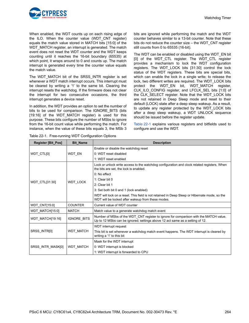
PSoC 6 MCU: CY8C61x4, CY8C62x4 Architecture TRM, Document No. 002-30473 Rev. *E 264
Watchdog Timer
When enabled, the WDT counts up on each rising edge ofthe ILO. When the counter value (WDT_CNT register)equals the match value stored in MATCH bits [15:0] of theWDT_MATCH register, an interrupt is generated. The matchevent does not reset the WDT counter and the WDT keepscounting until it reaches the 16-bit boundary (65535) atwhich point, it wraps around to 0 and counts up. The matchinterrupt is generated every time the counter value equalsthe match value.
The WDT_MATCH bit of the SRSS_INTR register is setwhenever a WDT match interrupt occurs. This interrupt mustbe cleared by writing a ‘1’ to the same bit. Clearing theinterrupt resets the watchdog. If the firmware does not clearthe interrupt for two consecutive occasions, the thirdinterrupt generates a device reset.
In addition, the WDT provides an option to set the number ofbits to be used for comparison. The IGNORE_BITS (bits[19:16] of the WDT_MATCH register) is used for thispurpose. These bits configure the number of MSbs to ignorefrom the 16-bit count value while performing the match. Forinstance, when the value of these bits equals 3, the MSb 3
bits are ignored while performing the match and the WDTcounter behaves similar to a 13-bit counter. Note that thesebits do not reduce the counter size – the WDT_CNT registerstill counts from 0 to 65535 (16-bit).
The WDT can be enabled or disabled using the WDT_EN bit[0] of the WDT_CTL register. The WDT_CTL registerprovides a mechanism to lock the WDT configurationregisters. The WDT_LOCK bits [31:30] control the lockstatus of the WDT registers. These bits are special bits,which can enable the lock in a single write; to release thelock, two different writes are required. The WDT_LOCK bitsprotect the WDT_EN bit, WDT_MATCH register,CLK_ILO_CONFIG register, and LFCLK_SEL bits [1:0] ofthe CLK_SELECT register. Note that the WDT_LOCK bitsare not retained in Deep Sleep mode and reset to theirdefault (LOCK) state after a deep sleep wakeup. As a result,to update any register protected by the WDT_LOCK bitsafter a deep sleep wakeup, a WDT UNLOCK sequenceshould be issued before the register update.
Table 22-1 explains various registers and bitfields used toconfigure and use the WDT.
Table 22-1. Free-running WDT Configuration Options
Register [Bit_Pos] Bit_Name Description
WDT_CTL[0] WDT_EN
Enable or disable the watchdog reset
0: WDT reset disabled
1: WDT reset enabled
WDT_CTL[31:30] WDT_LOCK
Lock or unlock write access to the watchdog configuration and clock related registers. When the bits are set, the lock is enabled.
0: No effect
1: Clear bit 0
2: Clear bit 1
3: Set both bit 0 and 1 (lock enabled)
WDT will lock on a reset. This field is not retained in Deep Sleep or Hibernate mode, so the WDT will be locked after wakeup from these modes.
WDT_CNT[15:0] COUNTER Current value of WDT counter
WDT_MATCH[15:0] MATCH Match value to a generate watchdog match event
WDT_MATCH[19:16] IGNORE_BITSNumber of MSbs of the WDT_CNT register to ignore for comparison with the MATCH value. Up to 12 MSbs can be ignored; settings above 12 act same as a setting of 12.
SRSS_INTR[0] WDT_MATCH
WDT interrupt request
This bit is set whenever a watchdog match event happens. The WDT interrupt is cleared by writing a ‘1’ to this bit
SRSS_INTR_MASK[0] WDT_MATCH
Mask for the WDT interrupt
0: WDT interrupt is blocked
1: WDT interrupt is forwarded to CPU
PSoC 6 MCU: CY8C61x4, CY8C62x4 Architecture TRM, Document No. 002-30473 Rev. *E 265
Watchdog Timer
22.3.2 Watchdog Reset
A watchdog is typically used to protect the device against firmware/system crashes or faults. When the WDT is used toprotect against system crashes, the WDT interrupt bit should be cleared by a portion of the code that is not directly associatedwith the WDT interrupt. Otherwise, even if the main function of the firmware crashes or is in an endless loop, the WDTinterrupt vector can still be intact and feed the WDT periodically. Note that when the debug probe is connected, the devicereset is blocked and an interrupt is generated instead.
The safest way to use the WDT against system crashes is to:
■ Configure the watchdog reset period such that firmware is able to reset the watchdog at least once during the period, even along the longest firmware delay path. If both CM4 and CM0 are being used then, use the free-running WDT for one of the CPU and one MCWDT for the other CPU to prevent firmware crashes on either core.
■ Reset (feed) the watchdog by clearing the interrupt bit regularly in the main body of the firmware code by writing a ‘1’ to the WDT_MATCH bit in the SRSS_INTR register. Note that this does not reset the watchdog counter, it feeds only the watchdog so that it does not cause a reset for the next two match events.
Do not reset the watchdog (clear interrupt) in the WDT interrupt service routine (ISR) if WDT is being used as a reset sourceto protect the system against crashes. Therefore, do not use the WDT reset feature and ISR together.
The recommended steps to use WDT as a reset source are as follows:
1. Make sure the WDT configuration is unlocked by clearing the WDT_LOCK bits[31:30] of the WDT_CTL register. Note that clearing the bits requires two writes to the register with each write clearing one bit as explained in Table 22-1.
2. Write the desired IGNORE_BITS in the WDT_MATCH register to set the counter resolution to be used for the match.
3. Write any match value to the WDT_MATCH register. The match value does not control the period of watchdog reset as the counter is not reset on a match event. This value provides an option to control only the first interrupt interval, after that the successive interrupts’ period is defined by the IGNORE_BITS. Approximate watchdog period (in seconds) is given by the following equation:
Equation 22-1
4. Set the WDT_MATCH bit in the SRSS_INTR register to clear any pending WDT interrupt.
5. Enable ILO by setting the ENABLE bit [31] of the CLK_ILO_CONFIG register.
6. Enable the WDT by setting the WDT_EN bit in WDT_CTL register.
7. Lock the WDT and ILO configuration by writing ‘3’ to the WDT_LOCK bits. This also locks the LFCLK_SEL bits of the CLK_SELECT register.
8. In the firmware, write ‘1’ to the WDT_MATCH bit in the SRSS_INT register to feed (clear interrupt) the watchdog.
22.3.3 Watchdog Interrupt
In addition to generating a device reset, the WDT can be used to generate interrupts. Note that interrupt servicing andwatchdog reset cannot be used simultaneously using the free-running WDT.
The watchdog counter can send interrupt requests to the CPU in CPU Active power modes and to the wakeup interruptcontroller (WIC) in CPU Sleep and Deep Sleep power modes. In addition, the watchdog is capable of waking up the devicefrom Hibernate power mode. It works as follows:
■ CPU Active Mode: In Active power mode, the WDT can send the interrupt to the CPU. The CPU acknowledges the interrupt request and executes the ISR. Clear the interrupt in the ISR.
■ CPU Sleep or Deep Sleep Mode: In this mode, the CPU is powered down. Therefore, the interrupt request from the WDT is directly sent to the WIC, which then wakes up the CPU. The CPU acknowledges the interrupt request and executes the ISR. Clear the interrupt in the ISR.
■ Hibernate Mode: In this mode, the entire device except a few peripherals (such as WDT and LPCOMP) are powered down. Any interrupt to wake up the device in this mode results in a device reset. Hence, there is no interrupt service routine or mechanism associated with this mode.
For more details on device power modes, see the Device Power Modes chapter on page 280.
Watchdog reset period = ILOperiod 2 2 16 IGNORE_BITS–WDT_MATCH+

PSoC 6 MCU: CY8C61x4, CY8C62x4 Architecture TRM, Document No. 002-30473 Rev. *E 266
Watchdog Timer
Because of its free-running nature, the WDT should not be used for periodic interrupt generation. Use the MCWDT instead;see 22.4 Multi-Counter WDTs. The MCWDT counters can be used to generate periodic interrupts. If absolutely required,follow these steps to use the WDT as a periodic interrupt generator:
1. Unlock the WDT if this is the first update to the WDT registers after a deep sleep or hibernate wakeup, or a device reset.
2. Write the desired IGNORE_BITS in the WDT_MATCH register to set the counter resolution to be used for the match.
3. Write the desired match value to the WDT_MATCH register.
4. Set the WDT_MATCH bit in the SRSS_INTR register to clear any pending WDT interrupt.
5. Enable the WDT interrupt to CPU by setting the WDT_MATCH bit in SRSS_INTR_MASK.
6. Enable SRSS interrupt to the CPU by configuring the appropriate ISER register (See the Interrupts chapter on page 73 for details).
7. In the ISR, unlock the WDT; clear the WDT interrupt and add the desired match value to the existing match value. By doing so, another interrupt is generated when the counter reaches the new match value (period).
22.4 Multi-Counter WDTs
22.4.1 Overview
Figure 22-3 shows the functional overview of a single multi-counter WDT block. The PSoC 6 MCU has two MCWDT blocks.Each MCWDT block includes two 16-bit counters (MCWDTx_WDT0 and MCWDTx_WDT1) and one 32-bit counter(MCWDTx_WDT2). These counters can be configured to work independently or in cascade (up to 64-bit). The 16-bit counterscan generate an interrupt or reset the device. The 32-bit counter can only generate an interrupt. All the counters are clockedby LFCLK.
Note: Because the PSoC 6 MCU includes two CPUs (Cortex-M0+ and Cortex-M4), associate one MCWDT block to only oneCPU during runtime. Although both the MCWDT blocks are available for both CPUs, a single MCWDT is not intended to beused by multiple CPUs simultaneously; however, a CPU can be associated with 0 or more MCWDTs.
Figure 22-3. Multi-Counter WDT Functional Diagram
LFCLK
MCWDTx_WDT0 (16-bit Counter)
MCWDT_CTR0
MCWDTx_WDT1 (16-bit Counter)
MCWDT_CTR1
MCWDTx_WDT2 (32-bit Counter)
MCWDT_CTRHIGH
MCWDT_CTR0 == MCWDT_MATCH0
MCWDT_CTR1 == MCWDT_MATCH1
321616
MCWDT Mode
ConfigurationMCWDT_MODE0
2MCWDT_MODE1
2
MCWDT Mode
ConfigurationMCWDT_MODE2
1
5MCWDT_BITS2
MCWDT_CASCADE0_1 MCWDT_CASCADE1_2
MCWDT_INT1MCWDT_INT0 MCWDT_INT2RESET RESET
INTERRUPT
RESET
MCWDT Mode
Configuration
Multi counter WDT
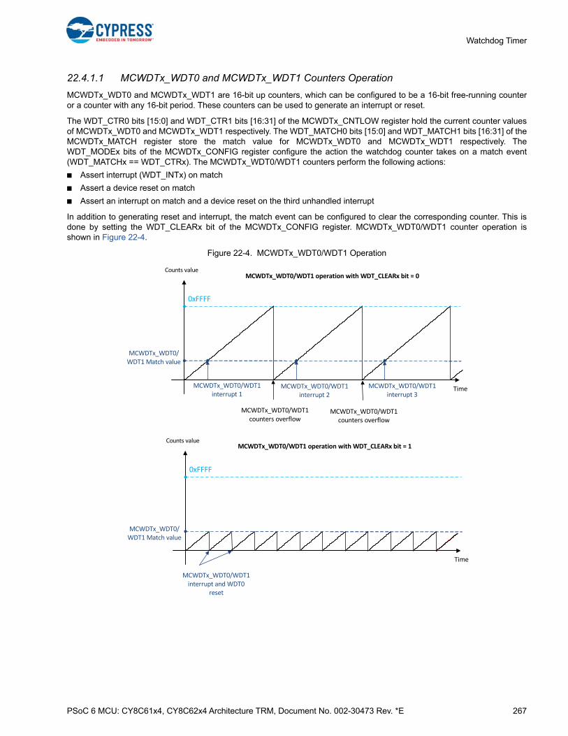
PSoC 6 MCU: CY8C61x4, CY8C62x4 Architecture TRM, Document No. 002-30473 Rev. *E 267
Watchdog Timer
22.4.1.1 MCWDTx_WDT0 and MCWDTx_WDT1 Counters Operation
MCWDTx_WDT0 and MCWDTx_WDT1 are 16-bit up counters, which can be configured to be a 16-bit free-running counteror a counter with any 16-bit period. These counters can be used to generate an interrupt or reset.
The WDT_CTR0 bits [15:0] and WDT_CTR1 bits [16:31] of the MCWDTx_CNTLOW register hold the current counter valuesof MCWDTx_WDT0 and MCWDTx_WDT1 respectively. The WDT_MATCH0 bits [15:0] and WDT_MATCH1 bits [16:31] of theMCWDTx_MATCH register store the match value for MCWDTx_WDT0 and MCWDTx_WDT1 respectively. TheWDT_MODEx bits of the MCWDTx_CONFIG register configure the action the watchdog counter takes on a match event(WDT_MATCHx == WDT_CTRx). The MCWDTx_WDT0/WDT1 counters perform the following actions:
■ Assert interrupt (WDT_INTx) on match
■ Assert a device reset on match
■ Assert an interrupt on match and a device reset on the third unhandled interrupt
In addition to generating reset and interrupt, the match event can be configured to clear the corresponding counter. This isdone by setting the WDT_CLEARx bit of the MCWDTx_CONFIG register. MCWDTx_WDT0/WDT1 counter operation isshown in Figure 22-4.
Figure 22-4. MCWDTx_WDT0/WDT1 Operation
Time
Time
Counts value
MCWDTx_WDT0/WDT1 Match value
0xFFFF
MCWDTx_WDT0/WDT1interrupt 1
MCWDTx_WDT0/WDT1interrupt 2
MCWDTx_WDT0/WDT1interrupt 3
MCWDTx_WDT0/WDT1 counters overflow
MCWDTx_WDT0/WDT1 operation with WDT_CLEARx bit = 0
Counts value
MCWDTx_WDT0/WDT1 Match value
0xFFFF
MCWDTx_WDT0/WDT1 interrupt and WDT0
reset
MCWDTx_WDT0/WDT1 operation with WDT_CLEARx bit = 1
MCWDTx_WDT0/WDT1 counters overflow

PSoC 6 MCU: CY8C61x4, CY8C62x4 Architecture TRM, Document No. 002-30473 Rev. *E 268
Watchdog Timer
22.4.1.2 MCWDTx_WDT2 Counter Operation
The MCWDTx_WDT2 is a 32-bit free-running counter, which can be configured to generate an interrupt. TheMCWDTx_CNTHIGH register holds the current value of the MCWDTx_WDT2 counter. MCWDTx_WDT2 does not support amatch feature. However, it can be configured to generate an interrupt when one of the counter bits toggle. The WDT_BITS2bits [28:24] of the MCWDTx_CONFIG register selects the bit on which the MCWDTx_WDT2 interrupt is asserted.WDT_MODE2 bit [16] of the MCWDTx_CONFIG register decides whether to assert an interrupt on bit toggle or not.Figure 22-5 shows the MCWDTx_WDT2 counter operation.
Figure 22-5. MCWDTx_WDT2 Operation
Table 22-2. MCWDTx_WDT0 and MCWDTx_WDT1 Configuration Options
Register [Bit_Pos] Bit_Name Description
MCWDTx_CONFIG[1:0]
MCWDTx_CONFIG[9:8]
WDT_MODE0
WDT_MODE1
WDT action on a match event (WDT_CTRx == WDT_MATCHx)
0: Do nothing
1: Assert interrupt (WDT_INTx)
2: Assert device reset
3: Assert interrupt on match and a device reset on the third unhandled interrupt
MCWDTx_CONFIG[2]
MCWDTx_CONFIG[10]
WDT_CLEAR0
WDT_CLEAR1
Clear the MCWDTx_WDT0/WDT1 counter on match. In other words, (WDT_-MATCHx + 1) acts similar to a period for the MCWDTx_WDT0/WDT1 counter.
0: Free-running counter
1: Clear WDT_CTRx bits on match
MCWDTx_CNTLOW[15:0]
MCWDTx_CNTLOW[16:31]
WDT_CTR0
WDT_CTR1Current counter values. Bits[15:0] contain the current value of the MCWDTx_WDT0 counter and bits[31:16] contain the current value of MCWDTx_WDT1 counter.
MCWDTx_MATCH[15:0]
MCWDTx_MATCH[16:31]
WDT_MATCH0
WDT_MATCH1
Match values
Changing WDT_MATCHx requires 1.5 LFCLK cycles to come into effect. After changing WDT_MATCHx, do not enter the Deep Sleep mode for at least one LFCLK cycle to ensure the WDT updates to the new setting.
MCWDTx_WDT2 Interrupt WDT_BITS2 = 1
MCWDTx_WDT2 Interrupt WDT_BITS2 = 2
Time
Counts value
0xFFFFFFFF
MCWDTx_WDT2 operation
MCWDTx_WDT2counter period
0x0000 0002
0x0000 0000
0x0000 0004
0x0000 0005
0x0000 0003
0x0000 0006
0x0000 0008
0x0000 0009
0x0000 0007
0x0000 000A
0x0000 000B
0x0000 000D0x0000 000C
0x0000 000E0x0000 000F
0x0000 0010
MCWDTx_WDT2 Interrupt WDT_BITS2 = 3
MCWDTx_WDT2 Interrupt WDT_BITS2 = 4
0x0000 0001
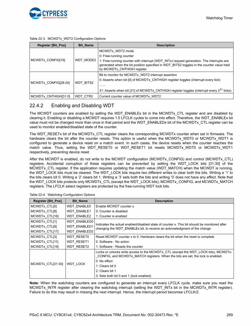
PSoC 6 MCU: CY8C61x4, CY8C62x4 Architecture TRM, Document No. 002-30473 Rev. *E 269
Watchdog Timer
22.4.2 Enabling and Disabling WDT
The MCWDT counters are enabled by setting the WDT_ENABLEx bit in the MCWDTx_CTL register and are disabled byclearing it. Enabling or disabling a MCWDT requires 1.5 LFCLK cycles to come into effect. Therefore, the WDT_ENABLEx bitvalue must not be changed more than once in that period and the WDT_ENABLEDx bit of the MCWDTx_CTL register can beused to monitor enabled/disabled state of the counter.
The WDT_RESETx bit of the MCWDTx_CTL register clears the corresponding MCWDTx counter when set in firmware. Thehardware clears the bit after the counter resets. This option is useful when the MCWDTx_WDT0 or MCWDTx_WDT1 isconfigured to generate a device reset on a match event. In such cases, the device resets when the counter reaches thematch value. Thus, setting the WDT_RESET0 or WDT_RESET1 bit resets MCWDTx_WDT0 or MCWDTx_WDT1respectively, preventing device reset.
After the MCWDT is enabled, do not write to the MCWDT configuration (MCWDTx_CONFIG) and control (MCWDTx_CTL)registers. Accidental corruption of these registers can be prevented by setting the WDT_LOCK bits [31:30] of theMCWDTx_CTL register. If the application requires updating the match value (WDT_MATCH) when the MCWDT is running,the WDT_LOCK bits must be cleared. The WDT_LOCK bits require two different writes to clear both the bits. Writing a ‘1’ tothe bits clears bit 0. Writing a ‘2’ clears bit 1. Writing a ‘3’ sets both the bits and writing ‘0’ does not have any effect. Note thatthe WDT_LOCK bits protects only MCWDTx_CTL (except the WDT_LOCK bits), MCWDTx_CONFIG, and MCWDTx_MATCHregisters. The LFCLK select registers are protected by the free-running WDT lock bits.
Note: When the watchdog counters are configured to generate an interrupt every LFCLK cycle, make sure you read theMCWDTx_INTR register after clearing the watchdog interrupt (setting the WDT_INTx bit in the MCWDTx_INTR register).Failure to do this may result in missing the next interrupt. Hence, the interrupt period becomes LFCLK/2.
Table 22-3. MCWDTx_WDT2 Configuration Options
Register [Bit_Pos] Bit_Name Description
MCWDTx_CONFIG[16] WDT_MODE2
MCWDTx_WDT2 mode
0: Free-running counter
1: Free-running counter with interrupt (WDT_INTx) request generation. The interrupts are generated when the bit position specified in WDT_BITS2 toggles in the counter value held by MCWDTx_CNTHIGH register.
MCWDTx_CONFIG[28:24] WDT_BITS2
Bit to monitor for MCWDTx_WDT2 interrupt assertion
0: Asserts when bit [0] of MCWDTx_CNTHIGH register toggles (interrupt every tick)
……
31: Asserts when bit [31] of MCWDTx_CNTHIGH register toggles (interrupt every 231 ticks)
MCWDTx_CNTHIGH[31:0] WDT_CTR2 Current counter value of MCWDTx_WDT2
Table 22-4. Watchdog Configuration Options
Register [Bit_Pos] Bit_Name Description
MCWDTx_CTL[0]
MCWDTx_CTL[8]
MCWDTx_CTL[16]
WDT_ENABLE0
WDT_ENABLE1
WDT_ENABLE2
Enable MCWDT counter x
0: Counter is disabled
1: Counter is enabled
MCWDTx_CTL[1]
MCWDTx_CTL[9]
MCWDTx_CTL[17]
WDT_ENABLED0
WDT_ENABLED1
WDT_ENABLED2
Indicates the actual enabled/disabled state of counter x. This bit should be monitored after changing the WDT_ENABLEx bit, to receive an acknowledgment of the change
MCWDTx_CTL[3]
MCWDTx_CTL[11]
MCWDTx_CTL[19]
WDT_RESET0
WDT_RESET1
WDT_RESET2
Reset MCWDT counter x to 0. Hardware clears the bit when the reset is complete
0: Software - No action
1: Software - Resets the counter
MCWDTx_CTL[31:30] WDT_LOCK
Locks or unlocks write access to the MCWDTx_CTL (except the WDT_LOCK bits), MCWDTx-_CONFIG, and MCWDTx_MATCH registers. When the bits are set, the lock is enabled.
0: No effect
1: Clears bit 0
2: Clears bit 1
3: Sets both bit 0 and 1 (lock enabled)

PSoC 6 MCU: CY8C61x4, CY8C62x4 Architecture TRM, Document No. 002-30473 Rev. *E 270
Watchdog Timer
22.4.3 Watchdog Cascade Options
The cascade configuration shown in Figure 22-3 provides an option to increase the MCWDT counter resolution. TheWDT_CASCADE0_1 bit [3] of the MCWDTx_CONFIG register cascades MCWDTx_WDT0 and MCWDTx_WDT1 and theWDT_CASCADE1_2 bit [11] of the MCWDTx_CONFIG register cascades MCWDTx_WDT1 and MCWDTx_WDT2. Note thatcascading two 16-bit counters does not provide a 32-bit counter; instead, you get a 16-bit period counter with a 16-bitprescaler. For example, when cascading MCWDTx_WDT0 and MCWDTx_WDT1, MCWDTx_WDT0 acts as a prescaler forMCWDTx_WDT1 and the prescaler value is defined by the WDT_MATCH0 bits [15:0] in the MCWDTx_MATCH register. TheMCWDTx_WDT1 has a period defined by WDT_MATCH1 bits [31:16] in the MCWDTx_MATCH register. The same logicapplies to MCWDTx_WDT1 and MCWDTx_WDT2 cascading.
When using cascade (WDT_CASCADE0_1 or WDT_CASCADE1_2 set), resetting the counters when the prescaler or lowercounter is at its match value with the counter configured to clear on match, results in the upper counter incrementing to 1instead of remaining at 0. This behavior can be corrected by issuing a second reset to the upper counter after approximately100 µs from the first reset. Note that the second reset is required only when the first reset is issued while the prescalercounter value is at its match value. Figure 22-6 illustrates the behavior when MCWDTx_WDT0 and MCWDTx_WDT1 arecascaded along with the second reset timing.
Figure 22-6. MCWDT Reset Behavior in Cascaded Mode
Table 22-5. Watchdog Cascade Options
Register [Bit_Pos] Bit_Name Description
MCWDTx_CONFIG[3] WDT_CASCADE0_1
Cascade MCWDTx_WDT0 and MCWDTx_WDT1
0: MCWDTx_WDT0 and MCWDTx_WDT1 are independent counters
1: MCWDTx_WDT1 increments two cycles after WDT_CTR0 == WDT_MATCH0
MCWDTx_CONFIG[11] WDT_CASCADE1_2
Cascade MCWDTx_WDT1 and MCWDTx_WDT2
0: MCWDTx_WDT1 and MCWDTx_WDT2 are independent counters
1: MCWDTx_WDT2 increments two cycles after WDT_CTR1 == WDT_MATCH1
0x001F 0x0020 0x0000 0x0001 0x0002 0x0003 0x0004 0x0005
0x0000 0x0001
First reset issued to both counters
Counter reset
Counter increment
WDT_CTRx == WDT_MATCHx
LFCLK
WDT_RESET0
WDT_RESET1
WDT_CTR0
WDT_CTR1
Other settings:WDT_CASCADE0_1 = 1WDT_CLEAR0 = 1WDT_MATCH0 = 0x0020
0x0000
Second reset to correct the behavior
~100 µs
Upper counter reset (second)

PSoC 6 MCU: CY8C61x4, CY8C62x4 Architecture TRM, Document No. 002-30473 Rev. *E 271
Watchdog Timer
In addition, the counters exhibit non-monotonicity in thefollowing cascaded conditions:
■ If WDT_CASCADE0_1 is set, then WDT_CTR1 does not increment the cycle after WDT_CTR0 = WDT_MATCH0.
■ If WDT_CASCADE1_2 is set, then WDT_CTR2 does not increment the cycle after WDT_CTR1 = WDT_MATCH1.
■ If both WDT_CASCADE0_1 and WDT_CASCADE1_2 are set, then WDT_CTR2 does not increment the cycle after WDT_CTR1 = WDT_MATCH1 and WDT_CTR1 does not increment the cycle after WDT_CTR0 = WDT_MATCH0.
When cascading is enabled, always read the WDT_CTR1 orWDT_CTR2 counter value only when the prescaler counter(WDT_CTR0 or WDT_CTR1) value is not 0. This makessure the upper counter is incremented after a match event inthe prescaler counter.
22.4.4 MCDWT Reset
MCWDTx_WDT0 and MCWDTx_WDT1 can be configuredto generate a device reset similar to the free-running WDTreset. Note that when the debug probe is connected, thedevice reset is blocked but an interrupt is generated ifconfigured. Follow these steps to use the MCWDTx_WDT0or MCWDTx_WDT1 counter of a MCWDTx block togenerate a system reset:
1. Configure the MCWDT to generate a reset using the WDT_MODEx bits in MCWDTx_CONFIG. Configure the WDT_MODE0 or WDT_MODE1 bits in MCWDTx_CONFIG to ‘2’ (reset on match) or ‘3’ (interrupt on match and reset on the third unhandled interrupt).
2. Optionally, set the WDT_CLEAR0 or WDT_CLEAR1 bit in the MCWDTx_CONFIG register for MCWDTx_WDT0 or MCWDTx_WDT1 to reset the corresponding watchdog counter to ‘0’ on a match event. Otherwise, the counters are free running. See Table 22-2 on page 268 for details.
3. Calculate the watchdog reset period such that firmware is able to reset the watchdog at least once during the period, even along the longest firmware delay path. For WDT_MODEx == 2, match value is same as the watchdog period. For WDT_MODEx == 3, match value is one-third of the watchdog period. Write the calculated match value to the WDT_MATCH register for MCWDTx_WDT0 or MCWDTx_WDT1. Optionally, enable cascading to increase the interval. Note: The legal value for the WDT_MATCH field is 1 to 65535.
4. For WDT_MODEx == 2, set the WDT_RESETx bit in the MCWDTx_CONFIG register to reset the WDTx counter to 0. For WDT_MODEx == 3, set the WDT_INTx bit in MCWDTx_INTR to clear any pending interrupts.
5. Enable WDTx by setting the WDT_ENABLEx bit in the MCWDTx_CTL register. Wait until the WDT_ENABLEDx bit is set.
6. Lock the MCWDTx configuration by setting the WDT_LOCK bits of the MCWDTx_CTL register.
7. In the firmware, feed (reset) the watchdog as explained in step 4.
Do not reset watchdog in the WDT ISR. It is also notrecommended to use the same watchdog counter togenerate a system reset and interrupt. For example, ifMCWDTx_WDT0 is used to generate system reset againstcrashes, then MCWDTx_WDT1 or MCWDTx_WDT2 shouldbe used for periodic interrupt generation.
22.4.5 MCWDT Interrupt
When configured to generate an interrupt, the WDT_INTxbits of the MCWDTx_INTR register provide the status of anypending watchdog interrupts. The firmware must clear theinterrupt by setting the WDT_INTx. The WDT_INTx bits ofthe MCWDTx_INTR_MASK register mask thecorresponding WDTx interrupt of the MCWDTx block to theCPU.
Follow these steps to use WDT as a periodic interruptgenerator:
1. Write the desired match value to the WDT_MATCH register for MCWDTx_WDT0/WDT1 or the WDT_BITS2 value to the MCWDTx_CONFIG register for MCWDTx_WDT2. Note: The legal value for the WDT_MATCH field is 1 to 65535.
2. Configure the WDTx to generate an interrupt using the WDT_MODEx bits in MCWDTx_CONFIG. Configure the WDT_MODE0 or WDT_MODE1 bits in MCWDTx_CONFIG for MCWDTx_WDT0 or MCWDTx_WDT1 to ‘1’ (interrupt on match) or ‘3’ (interrupt on match and reset on third unhandled interrupt). For MCWDTx_WDT2, set the WDT_MODE2 bit in the MCWDTx_CONFIG register.
3. Set the WDT_INT bit in MCWDTx_INTR to clear any pending interrupt.
4. Set the WDT_CLEAR0 or WDT_CLEAR1 bit in the MCWDTx_CONFIG register for MCWDTx_WDT0 or MCWDTx_WDT1 to reset the corresponding watchdog counter to ‘0’ on a match event.
5. Mask the WDTx interrupt to the CPU by setting the WDT_INTx bit in the MCWDTx_INTR_MASK register
6. Enable WDTx by setting the WDT_ENABLEx bit in the MCWDTx_CTL register. Wait until the WDT_ENABLEDx bit is set.
7. Enable MCWDTx interrupt to the CPU by configuring the appropriate ISER register. Refer to the Interrupts chapter on page 73.
8. In the ISR, clear the WDTx interrupt by setting the WDT_INTx bit in the MCWDTx_INTR register.
Note that interrupts from all three WDTx counters of theMCWDT block are mapped as a single interrupt to the CPU.In the interrupt service routine, the WDT_INTx bits of the

PSoC 6 MCU: CY8C61x4, CY8C62x4 Architecture TRM, Document No. 002-30473 Rev. *E 272
Watchdog Timer
MCWDTx_INTR register can be read to identify the interruptsource. However, each MCWDT block has its own interruptto the CPU. For details on interrupts, see theInterrupts chapter on page 73.
The MCWDT block can send interrupt requests to the CPUin Active power mode and to the WIC in Sleep and DeepSleep power modes. It works similar to the free-runningWDT.
22.5 Reset Cause Detection
The RESET_WDT bit [0] in the RES_CAUSE registerindicates the reset generated by the free-running WDT. TheRESET_MCWDTx bit in the RES_CAUSE register indicatesthe reset generated by the MCWDTx block. These bitsremain set until cleared or until a power-on reset (POR),brownout reset (BOD), or external reset (XRES) occurs. Allother resets leave this bit unaltered.
For more details, see the Reset System chapter onpage 236.
22.6 Register List
Table 22-6. WDT Registers
Name Description
WDT_CTL Watchdog Counter Control Register
WDT_CNT Watchdog Counter Count Register
WDT_MATCH Watchdog Counter Match Register
MCWDTx_MCWDT_CNTLOW Multi-counter WDT Sub-counters 0/1
MCWDTx_MCWDT_CNTHIGH Multi-counter WDT Sub-counter 2
MCWDTx_MCWDT_MATCH Multi-counter WDT Counter Match Register for counters 0 and 1
MCWDTx_MCWDT_CONFIG Multi-counter WDT Counter Configuration, including bit toggle interrupt generation for counter 2
MCWDTx_MCWDT_CTL Multi-counter WDT Counter Control
MCWDTx_MCWDT_INTR Multi-counter WDT Counter Interrupt Register
MCWDTx_MCWDT_INTR_SET Multi-counter WDT Counter Interrupt Set Register
MCWDTx_MCWDT_INTR_MASK Multi-counter WDT Counter Interrupt Mask Register
MCWDTx_MCWDT_INTR_MASKED Multi-counter WDT Counter Interrupt Masked Register
CLK_SELECT Clock Selection Register
CLK_ILO_CONFIG ILO Configuration
SRSS_INTR SRSS Interrupt Register
SRSS_INTR_SET SRSS Interrupt Set Register
SRSS_INTR_MASK SRSS Interrupt Mask Register
SRSS_INTR_MASKED SRSS Interrupt Masked Register
RES_CAUSE Reset Cause Observation Register
PSoC 6 MCU: CY8C61x4, CY8C62x4 Architecture TRM, Document No. 002-30473 Rev. *E 273
23. Power Supply and Monitoring
The PSoC 6 MCU family supports an operating voltage range of 1.7 V to 3.6 V. It integrates multiple regulators including anon-chip buck converter to power the blocks within the device in various power modes. The device supports multiple powersupply rails – VDDD, VDDA, VDDIO, and VBACKUP – enabling the application to use a dedicated supply for different blocks withinthe device. For instance, VDDA is used to power analog peripherals such as ADC and opamps.
The PSoC 6 MCU family supports power-on-reset (POR), brownout detection (BOD), over-voltage protection (OVP), and low-voltage-detection (LVD) circuit for power supply monitoring and failure protection purposes.
23.1 Features
The power supply subsystem of the PSoC 6 MCU supports the following features:
■ Operating voltage range of 1.7 V to 3.6 V
■ User-selectable core logic operation at either 1.1 V (LP) or 0.9 V (ULP)
■ Three independent supply rails (VDDD, VDDA, and VDDIO) for PSoC core peripherals and one independent supply rail
(VBACKUP) for backup domain
■ Multiple on-chip regulators
❐ One low-dropout (LDO) regulator to power peripherals in Active power mode
❐ One buck converter
❐ Multiple low-power regulators to power peripherals operating in different low-power modes
■ Two BOD circuit (VDDD and VCCD) in all power modes except Hibernate mode
■ LVD circuit to monitor VDDD, VAMUXA, VAMUXB, VBACKUP, or VDDIO
■ One OVP block monitoring VCCD
This PSoC 6 MCU technical reference manual (TRM) provides comprehensive and detailed information about thefunctions of the PSoC 6 MCU device hardware. It is divided into two books: architecture TRM and registers TRM. TheTRM is not recommended for those new to the PSoC 6 MCU, nor as a guide for developing PSoC 6 MCU applications.Use these documents instead:
■ PSoC 61 datasheet, PSoC 62 datasheet
■ Peripheral Driver Library (PDL) documentation
■ Application notes
■ Code examples

Power Supply and Monitoring
PSoC 6 MCU: CY8C61x4, CY8C62x4 Architecture TRM, Document No. 002-30473 Rev. *E 274
23.2 Architecture
Figure 23-1. Power System Block Diagram
VDDD VDDAVDDIOVBACKUP
VCCDPSLP
VCCRET
On-chip buck converter
2.2 uH
VIND
VDDBAK
Low-dropout regulator (Active regulator)
Backup Supply Selection
Dee-Sleep and Retention regulators
VCCD
Active domain and High frequency logic/
peripherals
Flash
Backup logic, WCO, RTC
Deep Sleep domain peripherals / SRAM
SRAM (Active)
High voltage (VDDD) and hibernate Domain
peripherals
IO Cells
Analog peripherals
0.1 µF1 µF 0.1 µF1 µF 0.1 µF1 µF 0.1 µF1 µF
4.7 µF
Regulators (LDO or Buck)
Deep Sleep power supply/logic
Active mode power supply/logic
Retention power supply/logic
Backup power supply/logic
Legend:
External power pad
External IO pad
Internal power rails
VSSD
VSSD VSSD VSSIO VSSA
PSoC 6
0.1 µF10 µF
VSS_NS VDD_NS
On-chip buck connections
PSoC 6 MCU: CY8C61x4, CY8C62x4 Architecture TRM, Document No. 002-30473 Rev. *E 275
Power Supply and Monitoring
See the PSoC 61 datasheet/PSoC 62 datasheet for thevalues to be used for the capacitors and inductor shown inFigure 23-1.
The regulators and supply pins/rails shown in Figure 23-1power various blocks inside the device. The availability ofvarious supply rails/pins for an application will depend onthe device package selected. Refer to the PSoC 61datasheet/PSoC 62 datasheet for details.
All the core regulators draw their input power from the VDDDsupply pin. The on-chip buck uses the VDD_NS supply pin asits input. VCCD supply is used to power all active domain andhigh frequency peripherals. The output of the buck isconnected to the VCCD pin and in firmware the VCCD supplycan be switched to the buck output. A dedicated Deep Sleepregulator powers all the Deep Sleep peripherals. The DeepSleep regulator switches its output to VCCD when availableand to its regulated output when VCCD is not present(System Deep Sleep power mode). Hibernate domain doesnot implement any regulators and the peripherals availablein that domain such as Low-Power comparator and ILOoperate directly from VDDD.
When the VDDA pin is not present, analog peripherals rundirectly from the VDDD.
The I/O cells operate from various VDDx (VDDA, VDDD, orVDDIO) pins depending on the port where they are located.VCCD supply is used to drive logic inside the I/O cells fromcore peripherals. VDDA powers the analog logic such asanalog mux switches inside the I/O cell. To know which I/Osoperate from which supply, refer to the PSoC 61 datasheet/PSoC 62 datasheet.
The device includes a VBACKUP supply pin to power a smallset of peripherals such as RTC and WCO, which runindependent from other supply rails available in the device.When the VBACKUP supply is not present, the device usesVDDD to power these peripherals.
In addition to the power rails and regulators, the deviceprovides options to monitor supply rails and protectionagainst potential supply failures. These include a PORcircuit, a BOD circuit, an OVP circuit, and a LVD circuit.
23.3 Power Supply
23.3.1 Regulators Summary
23.3.1.1 Core Regulators
The device includes the following core regulators to powerperipherals and blocks in various power modes.
Linear Core Regulator
The device includes a linear LDO regulator to power theActive and Sleep mode peripherals. This regulatorgenerates the core voltage (VCCD) required for Active mode
operation of the peripherals from VDDD. The regulator is
capable of providing 0.9 V and 1.1 V for core operation. SeeCore Operating Voltage on page 276. The regulator isavailable in Active and Sleep power modes. This regulatorimplements two sub-modes – high-current and low-currentmodes. LINREG_LPMODE bit [24] of the PWR_CTLregister selects between the two modes of operation. Thehigh-current mode is the normal operating mode, that is, thedevice operates to its full capacity in Active or Sleep powermodes. In the low-current mode or the minimum regulatorcurrent mode, the current output from the regulator islimited. This mode implements the Low-Power Active andSleep power modes. The low-current mode sets a limitationon the capabilities and availability of resources in the Low-Power Active and Sleep modes. For details, see the DevicePower Modes chapter on page 280.
By default, the linear regulator is powered on reset. Theregulator can be disabled by setting the LINREG_DIS bit[23] of the PWR_CTL register. Note that the linear regulatorshould be turned OFF only when the following conditionsare satisfied:
■ Switching buck regulator is ON.
■ The load current requirement of the device from theVCCD supply does not exceed 20 mA. This should be
ensured by the firmware by disabling power consuminghigh-frequency peripherals and reducing the systemclock frequency.
If the linear regulator is turned OFF without the aboveconditions satisfied, it will result in VCCD brownout and thedevice will reset.
Switching (Buck) Core Regulator
The device includes a switching (buck) core regulator. Thebuck requires an inductor and a capacitor to generate theoutput. Note that the buck output is also available in theDeep Sleep device power mode.
The buck regulator can be enabled by setting the BUCK_ENbit [30] of the PWR_BUCK_CTL register. The buck outputcan be enabled/disabled using the BUCK_OUT1_EN bit [31]of the PWR_BUCK_CTL registers. The buck outputsupports voltages from 0.85 V to 1.20 V. Use either 0.9 V or1.1 V for VCCD operation.
The output selection can be made using BUCK_OUT_SELbits in the PWR_BUCK_CTL registers.
When used to power the core peripherals, the buckregulator provides better power efficiency than the linearregulator, especially at higher VDDD. However, the buck
regulator has less load current capability (20 mA individuallyor 30 mA combined) than the linear regulator. Therefore,when using the buck regulator, take care not to overload theregulator by running only the necessary peripherals at alower frequency in firmware. Overload conditions can causethe buck output to drop and result in a brownout reset.
PSoC 6 MCU: CY8C61x4, CY8C62x4 Architecture TRM, Document No. 002-30473 Rev. *E 276
Power Supply and Monitoring
Follow these steps in firmware when switching to the buckregulator for core (VCCD) operation without causing a
brownout.
1. Make sure the necessary inductor and capacitorconnection for the buck as explained in Figure 23-1 ispresent in the hardware.
2. Change the core supply voltage to 50 mV more than thefinal buck voltage. For instance, if the final buck voltageis 0.9 V, then set the LDO output to 0.95 V and 1.15 V for1.1 V buck operation. Set the ACT_REG_TRIM bits[4:0]of the PWR_TRIM_PWRSYS_CTL register to ‘0x0B’ toswitch to 0.9 V and '0x1B' to switch to 1.1 V buckoperation. This is discussed in Core Operating Voltage.
3. Reduce the device current consumption by reducingclock frequency and switching off blocks to meet thebuck regulator’s load capacity.
4. Disable System Deep Sleep mode regulators. Becausethe buck regulator is available in the System Deep Sleeppower mode, other deep-sleep regulators can bepowered down. This is done by setting the following bitsin the PWR_CTL register:
a. DPSLP_REG_DIS bit [20] – Disables the deep-sleepcore regulator.
b. RET_REG_DIS bit [21] – Disables the logic retentionregulator.
c. NWELL_REG_DIS bit [22] – Disables the nwellregulator.
5. Set the buck output to the desired value by writing ‘2’ (for0.9 V) or ‘5’ (for 1.1 V) to the BUCK_OUT1_SEL bits[2:0]of the PWR_BUCK_CTL register.
6. Enable the buck regulator and output by setting theBUCK_EN bit[30] and BUCK_OUT1_EN bit[31] of thePWR_BUCK_CTL register.
7. Wait 200 µs for the buck regulator to start up and settle.
8. Disable the linear regulator by setting the LINREG_DISbit[23] of the PWR_CTL register.
After transitioning to the buck regulator, do not switch backto the linear regulator mode to ensure proper deviceoperation. This should happen once during powerup.
Core Operating Voltage
PSoC 6 MCUs can operate at either 0.9 V LP mode(nominal) or 1.1 V ULP mode (nominal) core voltage. Onreset, the core is configured to operate at 1.1 V by default.At 0.9 V, power consumption is less, but there are somelimitations. The maximum operating frequency for all HFCLKpaths should not exceed 50 MHz, whereas the peripheraland slow clock should not exceed 25 MHz.
Follow these steps to change the PSoC 6 MCU corevoltage:
1. While transitioning to 0.9 V (ULP mode), reduce the operating frequency to be within the HFCLK and peri clock limits defined in the PSoC 61 datasheet/PSoC 62 datasheet for ULP mode. Turn off blocks, if required, to be within the maximum current consumption limit of the linear regulator at 0.9 V.
2. Set the ACT_REG_TRIM bits[4:0] of the PWR_TRIM_PWRSYS_CTL register to ‘0x07’ for 0.9 V or ‘0x17’ for 1.1 V. For the buck regulator, set the BUCK_OUT1_SEL bits[2:0] of the PWR_BUCK_CTL register to ‘0x02’ for 0.9 V and ‘0x05’ for 1.1 V.
3. In the case of 1.1 V to 0.9 V transition, the time it takes to discharge or settle to the new voltage may depend on the load. So the system can continue to operate while the voltage discharges.
4. In the case of 0.9 V to 1.1 V transition, wait 9 µs for the regulator to stabilize to the new voltage. The clock frequency can be increased after the settling delay.
Notes:
■ When changing clock frequencies, make sure to updatewait states of RAM/ROM/FLASH. Refer to the CPUSubsystem (CPUSS) chapter on page 31 for details onthe wait states.
■ Flash write is not allowed in 0.9 V (ULP mode) coreoperation.
Other Low-power Regulators
In addition to the core active regulators, the device includesmultiple low-power regulators for powering Deep Sleepperipherals/logic (VCCDPSLP), digital retention logic/SRAM
(VCCRET), and N-wells (VNWELL) in the device. Note that
VNWELL is not shown in Figure 23-1 because this rail is usedacross the device for powering all the N-wells in the chip.These rails are shorted to VCCD in Active and Sleep power
modes. VCCRET powers all the Active mode logic that needsto be in retention in Deep Sleep mode.
Note that none of these power rails are available inHibernate mode. In Hibernate mode, all the hibernate logicand peripherals operate from VDDD directly and a Hibernatewakeup resets the device. For details, refer to the DevicePower Modes chapter on page 280.
PSoC 6 MCU: CY8C61x4, CY8C62x4 Architecture TRM, Document No. 002-30473 Rev. *E 277
Power Supply and Monitoring
23.3.2 Power Pins and Rails
Table 23-1 lists all the power supply pins available in the device. The supply rails running inside the device (VCCDPSLP,
VCCRET, VDDBAK, and VNWELL) are derived from these external supply pins/rails.
23.3.3 Power Sequencing Requirements
VDDD, VBACKUP, VDDIO, and VDDA do not have any
sequencing limitation and can establish in any order. Thepresence of VDDA without VDD or VDDD can cause some
leakage from VDDA. However, it will not drive any analog or
digital output. All the VDDA pins in packages that offermultiple VDDA supply pins, must be shorted externally (on
the PCB). Note that the system will not exit reset until bothVDDD and VDDA are established. However, it will not wait forother supplies to establish.
23.3.4 Backup Domain
The PSoC 6 MCU offers an independent backup supplyoption (VBACKUP). This rail powers a small set of peripheralsthat includes an RTC, WCO, and a small number ofretention registers. This rail is independent of all other railsand can exist even when other rails are absent. AsFigure 23-1 shows, this pin sources the VDDBAK rail in the
device. The VDDBAK rail is connected to VDDD when no
VBACKUP supply exists. For details on the backup domain,
refer to the Backup System chapter on page 255.
23.3.5 Power Supply Sources
The PSoC 6 MCU offers power supply options that supporta wide range of application voltages and requirements.VDDD input supports a voltage range of 1.7 V to 3.6 V. If the
application voltage is in this range, then the PSoC 6 MCU(VDDD) can be interfaced directly to the application voltage.
In applications that have voltage beyond this range, asuitable PMIC (Buck or Boost or Buck-Boost) should beused to bring the voltage to this range.
Other supply rails and pins such as VDDA, VDDIO, and
VBACKUP exist independent of VDDD and VCCD.
23.4 Voltage Monitoring
The PSoC 6 MCU offers multiple voltage monitoring andsupply failure protection options. This includes POR, BOD,LVD, and OVP.
23.4.1 Power-On-Reset (POR)
POR circuits provide a reset pulse during the initial powerramp. POR circuits monitor VDDD voltage. Typically, the
POR circuits are not very accurate about the trip-point.
POR circuits are used during initial chip power-up and thendisabled. Refer to the PSoC 61 datasheet/PSoC 62datasheet for details on the POR trip-point levels.
23.4.2 Brownout-Detect (BOD)
The BOD circuit protects the operating or retaining logicfrom possibly unsafe supply conditions by applying reset tothe device. The PSoC 6 MCU offers two BOD circuits –high-voltage BOD (HVBOD) and low-voltage BOD (LVBOD).The HVBOD monitors the VDDD voltage and LVBOD
monitors the VCCD voltage. Both BOD circuits generate areset if a voltage excursion dips below the minimum VDDD/
VCCD voltage required for safe operation (see the PSoC 61
datasheet/PSoC 62 datasheet for details). The system willnot come out of RESET until the supply is detected to bevalid again.
The HVBOD circuit guarantees a reset in System LP, ULP,and Deep Sleep power modes before the system crashes,
Table 23-1. Supply Pins
Supply Pin Ground Pin Voltage Range Supporteda
a. Refer to the PSoC 61 datasheet/PSoC 62 datasheet for exact range and recommended connections.
Description
VDD or VDDD VSS or VSSD 1.7 V to 3.6 VVDD is a single supply input for multiple supplies and VDDD is a
digital supply input. Either of the pins will be present in a given package.
VDD_NS VSS_NS 1.7 V to 3.6 V Supply input to the buck regulator on-chip.
VCCD VSS or VSSD Capacitor (0.9 V or 1.1 V)Core supply or bypass capacitor for the internal core regulator (LDO).
VDDA VSS or VSSA (if available) 1.7 V to 3.6 V Analog supply voltage.
VDDIO VSS or VSSIO (if available) 1.7 V to 3.6 V Additional I/O supply voltage.
VBACKUP VSS or VSSD (if available) 1.4 V to 3.6 V Backup domain supply voltage.
VIND – Inductor Inductor connection for the internal buck regulator.
PSoC 6 MCU: CY8C61x4, CY8C62x4 Architecture TRM, Document No. 002-30473 Rev. *E 278
Power Supply and Monitoring
provided the VDDD supply ramp satisfies the datasheet
maximum supply ramp limits in that mode. There is no BODsupport in Hibernate mode. Applications that require BODsupport should not use Hibernate mode and should disableit. Refer to the Device Power Modes chapter on page 280for details.
The LVBOD, operating on VCCD, is not as robust as the
HVBOD. The limitation is because of the small voltagedetection range available for LVBOD on the minimumallowed VCCD.
For details on the BOD trip-points, supported supply ramprate, and BOD detector response time, refer to the PSoC 61datasheet/PSoC 62 datasheet.
23.4.3 Low-Voltage-Detect (LVD)
An LVD circuit monitors external supply voltage andaccurately detects depletion of the energy source. The LVDgenerates an interrupt to cause the system to takepreventive measures.
The LVD can be configured to monitor VDDD, VAMUXA, orVAMUXB. The HVLVD1_SRCSEL bits [6:4] of the
PWR_LVD_CTL register selects the source of the LVD. TheLVD support up to 15 voltage levels (thresholds) to monitorbetween 1.2 V to 3.1 V. The HVLVD1_TRIPSEL bits [3:0] ofthe PWR_LVD_CTL register select the threshold levels ofthe LVD. LVD should be disabled before selecting thethreshold. The HVLVD1_EN bit [7] of the PWR_LVD_CTLregister can be used to enable or disable the LVD.
Whenever the voltage level of the supply being monitoreddrops below the threshold, the LVD generates an interrupt.This interrupt status is available in the SRSS_INTR register.HVLVD1 bit [1] of the SRSS_INTR register indicates apending LVD interrupt. The SRSS_INTR_MASK registerdecides whether LVD interrupts are forwarded to the CPU ornot.
Note that the LVD circuit is available only in Active,LPACTIVE, Sleep, and LPSLEEP power modes. If an LVD isrequired in Deep Sleep mode, then the device should beconfigured to periodically wake up from Deep Sleep modeusing a Deep Sleep wakeup source. This makes sure anLVD check is performed during Active/LPACTIVE mode.
When enabling the LVD circuit, it is possible to receive afalse interrupt during the initial settling time. Firmware canmask this by waiting for 8 µs after setting the HVLVD1_ENbit in the PWR_LVD_CTL register. The recommendedfirmware procedure to enable the LVD function is:
1. Ensure that the HVLVD1 bit in the SRSS_INTR_MASKregister is 0 to prevent propagating a false interrupt.
2. Set the required trip-point in the HVLVD1_TRIPSEL fieldof the PWR_LVD_CTL register.
3. Configure the LVD edge (falling/rising/both) that triggersthe interrupt by configuring HVLVD1_EDGE_SEL
bits[1:0] of SRSS_INTR_CFG register. By default, theconfiguration disables the interrupt. Note: LVD logic mayfalsely detect a falling edge during Deep Sleep entry.This applies only when HVLVD1_EDGE_SEL is set toFALLING(2) or BOTH(3). Firmware can workaround thiscondition by disabling falling edge detection beforeentering Deep Sleep, and re-enabling it after exitingDeep Sleep.
4. Enable the LVD by setting the HVLVD1_EN bit in thePWR_LVD_CTL register. This may cause a false LVDevent.
5. Wait at least 8 µs for the circuit to stabilize.
6. Clear any false event by setting the HVLVD1 bit in theSRSS_INTR register. The bit will not clear if the LVDcondition is truly present.
7. Unmask the interrupt by setting the HVLVD1 bit in SRSS_INTR_MASK.
LVD is used to detect potential brownouts. When the supplybeing monitored drops below the threshold, the interruptgenerated can be used to save necessary data to flash,dump logs, trigger external circuits, and so on.
For details on supported LVD thresholds, refer to the PSoC61 datasheet/PSoC 62 datasheet and the PWR_LVD_CTLregister definition in the registers TRM.

PSoC 6 MCU: CY8C61x4, CY8C62x4 Architecture TRM, Document No. 002-30473 Rev. *E 279
Power Supply and Monitoring
Figure 23-2. PSoC 6 MCU LVD Block
23.4.4 Over-Voltage Protection (OVP)
The PSoC 6 MCU offers an over-voltage protection circuit that monitors the VCCD supply. Similar to the BOD circuit, the OVP
circuit protects the device from unsafe supply conditions by applying a reset. As the name suggests, the OVP circuit applies adevice reset, when the VCCD supply goes above the maximum allowed voltage. The OVP circuit can generate a reset in all
device power modes except the Hibernate mode.
23.5 Register List
Name Description
PWR_CTLPower Mode Control register - controls the device power mode options and allows observation of current state
PWR_BUCK_CTL Buck Control register - controls the buck output and master buck enable
PWR_LVD_CTL LVD Configuration register
SRSS_INTR SRSS Interrupt register - shows interrupt requests from the SRSS peripheral
SRSS_INTR_MASK SRSS Interrupt Mask register - controls forwarding of the interrupt to CPU
SRSS_INTR_SET SRSS Interrupt Set register - sets interrupts; this register is used for firmware testing
SRSS_INTR_MASKEDSRSS Interrupt Masked register - logical AND of corresponding SRSS interrupt request (SRSS Interrupt register) and mask bits (SRSS Interrupt Mask register)
.
.
.
.
.
1.2 V
3.1 V
HVLVD1_TRIPSEL [3:0]
4
HVLVD1 SRSS_INTR[HVLVD1]
HVLVD1_SRCSEL [2:0]
3
VDDD
VAMUXA
VAMUXB
SRSS_INTR_MASK[HVLVD1]To CPU as SRSS interrupt
PSoC 6 LVD block
HVLVD1_EN
-
+
PSoC 6 MCU: CY8C61x4, CY8C62x4 Architecture TRM, Document No. 002-30473 Rev. *E 280
24. Device Power Modes
The PSoC 6 MCU can operate in four system and three CPU power modes. These modes are intended to minimize theaverage power consumption in an application. The power modes supported by PSoC 6 MCUs, in the order of decreasingpower consumption, are:
■ System Low Power (LP) – All peripherals and CPU power modes are available at maximum speed and current■ System Ultra Low Power (ULP) – All peripherals and CPU power modes are available, but with limited speed and current■ CPU Active – CPU is executing code in system LP or ULP mode■ CPU Sleep – CPU code execution is halted in system LP or ULP mode■ CPU Deep Sleep – CPU code execution is halted and system deep sleep is requested while in system LP or ULP mode■ System Deep Sleep – Entered only after both CPUs enter CPU Deep Sleep mode. Only low-frequency peripherals are
available■ System Hibernate – Device and I/O states are frozen and the device resets on wakeup
CPU Active, Sleep, and Deep Sleep are standard Arm-defined power modes supported by the Arm CPU instruction setarchitecture (ISA). System LP, ULP, Deep Sleep and Hibernate modes are additional low-power modes supported by PSoC 6.Hibernate mode is the lowest power mode in the PSoC 6 MCU and on wakeup, the CPU and all peripherals go through areset.
24.1 Features
The PSoC 6 MCU power modes have the following features:
■ Four system and three CPU power modes aimed at optimizing power consumption in an application■ System ULP mode with reduced operating current and clock frequency while supporting full device functionality■ System Deep Sleep mode with support for multiple wakeup sources and configurable amount of SRAM retention■ System Hibernate mode with wakeup from I/O, comparator, WDT, RTC, and timer alarms
The power consumption in different power modes is further controlled by using the following methods:
■ Enabling and disabling clocks to peripherals■ Powering on/off clock sources■ Powering on/off peripherals and resources inside the PSoC 6 device
24.2 Architecture
The PSoC 6 device supports multiple power modes. Some modes only affect the CPUs (CPU power modes) and others affectthe whole system (system power modes). The system and CPU power modes are used in combination to control the totalsystem performance and power. CPU power modes are entered separately for each CPU on the device.
This PSoC 6 MCU technical reference manual (TRM) provides comprehensive and detailed information about thefunctions of the PSoC 6 MCU device hardware. It is divided into two books: architecture TRM and registers TRM. TheTRM is not recommended for those new to the PSoC 6 MCU, nor as a guide for developing PSoC 6 MCU applications.Use these documents instead:
■ PSoC 61 datasheet, PSoC 62 datasheet
■ Peripheral Driver Library (PDL) documentation
■ Application notes
■ Code examples
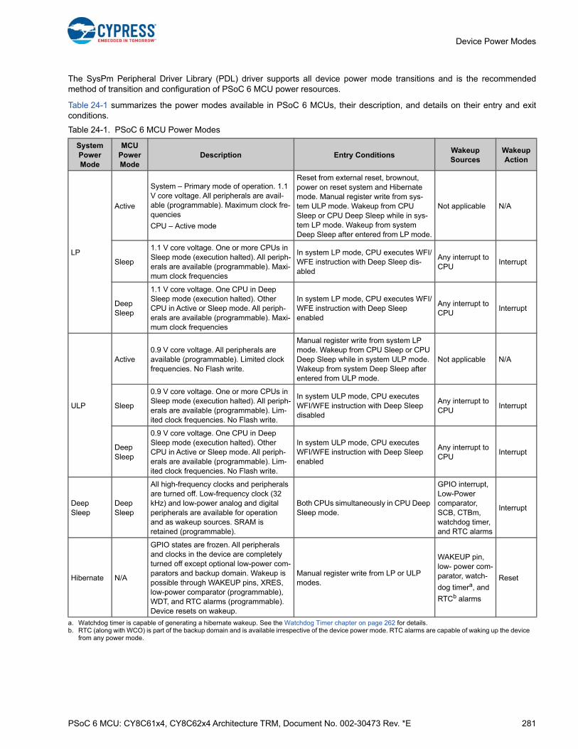
PSoC 6 MCU: CY8C61x4, CY8C62x4 Architecture TRM, Document No. 002-30473 Rev. *E 281
Device Power Modes
The SysPm Peripheral Driver Library (PDL) driver supports all device power mode transitions and is the recommendedmethod of transition and configuration of PSoC 6 MCU power resources.
Table 24-1 summarizes the power modes available in PSoC 6 MCUs, their description, and details on their entry and exitconditions.
Table 24-1. PSoC 6 MCU Power Modes
System Power Mode
MCU Power Mode
Description Entry ConditionsWakeup Sources
Wakeup Action
LP
Active
System – Primary mode of operation. 1.1 V core voltage. All peripherals are avail-able (programmable). Maximum clock fre-quencies
CPU – Active mode
Reset from external reset, brownout, power on reset system and Hibernate mode. Manual register write from sys-tem ULP mode. Wakeup from CPU Sleep or CPU Deep Sleep while in sys-tem LP mode. Wakeup from system Deep Sleep after entered from LP mode.
Not applicable N/A
Sleep
1.1 V core voltage. One or more CPUs in Sleep mode (execution halted). All periph-erals are available (programmable). Maxi-mum clock frequencies
In system LP mode, CPU executes WFI/WFE instruction with Deep Sleep dis-abled
Any interrupt to CPU
Interrupt
Deep Sleep
1.1 V core voltage. One CPU in Deep Sleep mode (execution halted). Other CPU in Active or Sleep mode. All periph-erals are available (programmable). Maxi-mum clock frequencies
In system LP mode, CPU executes WFI/WFE instruction with Deep Sleep enabled
Any interrupt to CPU
Interrupt
ULP
Active0.9 V core voltage. All peripherals are available (programmable). Limited clock frequencies. No Flash write.
Manual register write from system LP mode. Wakeup from CPU Sleep or CPU Deep Sleep while in system ULP mode. Wakeup from system Deep Sleep after entered from ULP mode.
Not applicable N/A
Sleep
0.9 V core voltage. One or more CPUs in Sleep mode (execution halted). All periph-erals are available (programmable). Lim-ited clock frequencies. No Flash write.
In system ULP mode, CPU executes WFI/WFE instruction with Deep Sleep disabled
Any interrupt to CPU
Interrupt
Deep Sleep
0.9 V core voltage. One CPU in Deep Sleep mode (execution halted). Other CPU in Active or Sleep mode. All periph-erals are available (programmable). Lim-ited clock frequencies. No Flash write.
In system ULP mode, CPU executes WFI/WFE instruction with Deep Sleep enabled
Any interrupt to CPU
Interrupt
Deep Sleep
Deep Sleep
All high-frequency clocks and peripherals are turned off. Low-frequency clock (32 kHz) and low-power analog and digital peripherals are available for operation and as wakeup sources. SRAM is retained (programmable).
Both CPUs simultaneously in CPU Deep Sleep mode.
GPIO interrupt, Low-Power comparator, SCB, CTBm, watchdog timer, and RTC alarms
Interrupt
Hibernate N/A
GPIO states are frozen. All peripherals and clocks in the device are completely turned off except optional low-power com-parators and backup domain. Wakeup is possible through WAKEUP pins, XRES, low-power comparator (programmable), WDT, and RTC alarms (programmable). Device resets on wakeup.
Manual register write from LP or ULP modes.
WAKEUP pin, low- power com-parator, watch-
dog timera, and
RTCb alarms
a. Watchdog timer is capable of generating a hibernate wakeup. See the Watchdog Timer chapter on page 262 for details.b. RTC (along with WCO) is part of the backup domain and is available irrespective of the device power mode. RTC alarms are capable of waking up the device
from any power mode.
Reset
PSoC 6 MCU: CY8C61x4, CY8C62x4 Architecture TRM, Document No. 002-30473 Rev. *E 282
Device Power Modes
24.2.1 CPU Power Modes
The CPU Active, Sleep, and Deep Sleep modes are thestandard Arm-defined power modes supported by bothCortex-M4 and Cortex-M0+ CPUs. All Arm CPU powermodes are available in both system LP and ULP powermodes. CPU power modes affect each CPU independently.
24.2.1.1 CPU Active Mode
In CPU Active mode, the CPU executes code and all logicand memory is powered. The firmware may decide toenable or disable specific peripherals and power domainsdepending on the application and power requirements. Allthe peripherals are available for use in Active mode. Thedevice enters CPU Active mode upon any device reset orwakeup.
24.2.1.2 CPU Sleep Mode
In CPU Sleep mode, the CPU clock is turned off and theCPU halts code execution. Note that in the PSoC 6 MCU,Cortex-M4 and Cortex-M0+ both support their own CPUSleep modes and each CPU can be in sleep independent ofthe other CPU state. All peripherals available in Active modeare also available in Sleep mode. Any peripheral interrupt,masked to the CPU, will wake the CPU to Active mode. Onlythe CPU(s) with the interrupt masked will wake.
24.2.1.3 CPU Deep Sleep Mode
In CPU Deep Sleep mode, the CPU requests the device togo into system Deep Sleep mode. When the device is ready,it enters Deep Sleep mode as detailed in 24.2.3 SystemDeep Sleep Mode.
Because PSoC 6 has more than one CPU, both CPUs mustindependently enter CPU Deep Sleep before the system willtransition to system Deep Sleep.
24.2.2 System Power Modes
System power modes affect the whole device and may becombined with CPU power modes.
24.2.2.1 System Low Power Mode
System Low Power (LP) mode is the default operating modeof the device after reset and provides maximum systemperformance. In LP mode all resources are available foroperation at their maximum power level and speed.
While in system LP mode the CPUs may operate in any ofthe standard Arm defined CPU modes detailed in 24.2.1CPU Power Modes.
24.2.2.2 System Ultra Low Power Mode
System Ultra Low Power (ULP) mode is identical to LPmode with a performance tradeoff made to achieve lowersystem current. This tradeoff lowers the core operating
voltage, which then requires reduced operating clockfrequency and limited high-frequency clock sources. Flashwrite operations are not available in ULP mode. Table 24-5provides the list of resources available in ULP mode alongwith limitations.
While in system ULP mode, the CPUs may operate in any ofthe standard Arm-defined CPU modes detailed in 24.2.1CPU Power Modes.
Transitioning between LP and ULP modes is performed byreducing the core regulator voltage from the LP modevoltage to the ULP mode voltage. The lower voltage reducessystem operating current and slows down signal speedsrequiring a lower maximum operating frequency. Refer toCore Operating Voltage section in Power Supply andMonitoring chapter on page 273 for details on how to switchbetween LP and ULP modes.
24.2.3 System Deep Sleep Mode
In system Deep Sleep mode, all the high-speed clocksources are off. This in turn makes high-speed peripheralsunusable in system Deep Sleep mode. However, low-speedclock sources and peripherals may continue to operate, ifconfigured and enabled by the firmware. In addition, theperipherals that do not need a clock or receive a clock fromtheir external interface (I2C or SPI slave) may continue tooperate, if configured for system Deep Sleep operation. ThePSoC 6 MCU provides an option to configure the amount ofSRAM, in blocks of 32 KB, that are retained during DeepSleep mode.
Both Cortex-M0+ and Cortex-M4 can enter CPU DeepSleep mode independently. However, the entire deviceenters system Deep Sleep mode only when both the CPUsare in CPU Deep Sleep. On wakeup, the CPU that woke upenters CPU Active mode and the other CPU remains in CPUDeep Sleep mode. On wakeup, the system will return to LPor ULP mode based on what mode was Active beforeentering system Deep Sleep. Both CPUs may wake up toCPU Active simultaneously from the same wakeup source ifso configured.
The device enters system Deep Sleep mode after thefollowing conditions are met.
■ The LPM_READY bit of the PWR_CTL register should read ‘1’. This ensures the system is ready to enter Deep Sleep. If the bit reads ‘0’, then the device will wait in system LP or ULP mode instead of system Deep Sleep until the bit is set, at which instant the device automatically enters Deep Sleep mode, if requested.
■ Both Cortex-M0+ and Cortex-M4 must be in CPU Deep Sleep. This is achieved by setting the SLEEPDEEP bit [2] of the SCR register of both Cortex-M0+ and Cortex-M4 and then executing WFI or WFE instruction.
■ The HIBERNATE bit [31] of the PWR_HIBERNATE register should be cleared; otherwise, the device will enter system Hibernate mode.
PSoC 6 MCU: CY8C61x4, CY8C62x4 Architecture TRM, Document No. 002-30473 Rev. *E 283
Device Power Modes
In system Deep Sleep mode, the LP and ULP moderegulator is turned off and a lower power, Deep Sleepregulator sources all the peripherals enabled in systemDeep Sleep mode. Alternatively, the buck regulator can beused to power the Deep Sleep peripherals. See the PowerSupply and Monitoring chapter on page 273 for details.Table 24-5 provides the list of resources available in systemDeep Sleep mode.
Interrupts from low-speed, asynchronous, or low-poweranalog peripherals can cause a CPU wakeup from systemDeep Sleep mode. Note that when a debugger is running oneither core, the device stays in system LP or ULP mode andthe CPUs enter CPU Sleep mode instead of CPU DeepSleep mode. PSoC 6 uses buffered writes. Therefore, writesto an MMIO register or memory can take few a cycles fromthe write instruction execution. The only way to ensure thatthe write operation is complete is by reading the samelocation after the write. It is required to follow a write by aread to the same location before executing a WFI/WFEinstruction to enter CPU Deep Sleep mode.
24.2.4 System Hibernate ModeSystem Hibernate mode is the lowest power mode of thedevice when external supplies are still present and XRES isdeasserted. It is intended for applications in a dormant state.In this mode, both the Active LP/ULP mode regulator andDeep Sleep regulator are turned off and GPIO states areautomatically frozen. Wakeup is facilitated throughdedicated wakeup pins and a Low-Power comparatoroutput. Low-Power comparator operation in Hibernate moderequires externally generated voltages for wakeupcomparison. Internal references are not available inHibernate mode. Optionally, an RTC alarm from the backupdomain or a watchdog timer (16-bit free-running WDT)interrupt can generate a Hibernate wakeup signal. Set theMASK_HIBALARM bit [18] of the PWR_HIBERNATEregister to enable the RTC alarm wakeup from Hibernatemode.
The device goes through a reset on wakeup from Hibernate.I/O pins remain in the configuration they were frozen beforeentering Hibernate mode. To differentiate between othersystem resets and a Hibernate mode wakeup, the TOKENbits [7:0] of the PWR_HIBERNATE register can be used asdescribed in the Power Mode Transitions on page 285. ThePWR_HIBERNATE (except the HIBERNATE bit [31])register along with the PWR_HIB_DATA register areretained through the Hibernate wakeup sequence and canbe used by the application for retaining some content. Notethat these registers are reset by other reset events. On aHibernate wakeup event, the HIBERNATE bit [31] of thePWR_HIBERNATE register is cleared.
The brownout detect (BOD) block is not available inHibernate mode. As a result, the device does not recoverfrom a brownout event in Hibernate mode. Do not enterHibernate mode in applications that require brownoutdetection, that is, applications where the supply is not
stable. In addition, make sure the supply is stable for at least250 µs before the device enters Hibernate mode. To preventaccidental entry into Hibernate mode in applications thatcannot meet these requirements, an option to disable theHibernate mode is provided. Set the HIBERNATE_DISABLEbit [30] of the PWR_HIBERNATE register to disableHibernate mode in the device. Note that this bit is a write-once bit during execution and is cleared only on reset.Debug functionality will be lost and the debugger willdisconnect on entering Hibernate mode.
24.2.5 Other Operation ModesIn addition to the power modes discussed in the previoussections, there are three other states the device can be in –Reset, Off, and Backup states. These states are determinedby the external power supply and XRES connections. Nofirmware action is required to enter these modes nor aninterrupt or wakeup event to exit them.
24.2.5.1 Backup Domain PSoC 6 offers an independent backup supply option thatcan be supplied through a separate Vbackup pin. For detailson the backup domain and the powering options, refer to theBackup System chapter on page 255. This domain powers areal-time clock (RTC) block, WCO, and a small set ofbackup registers. Because the power supply to these blockscome from a dedicated Vbackup pin, these blocks continueto operate in all CPU and system power modes, and evenwhen the device power is disconnected or held in reset aslong as a Vbackup supply is provided. The RTC present inthe backup domain provides an option to wake up thedevice from any CPU or system power mode. The RTC canbe clocked by an external crystal (WCO) or the internal low-speed oscillator (ILO). However, the ILO is available only ifthe device is powered – the device should not be in the off orreset state. Using ILO is not recommended for timekeepingpurpose; however, it can be used for wakeup from Hibernatepower mode.
24.2.5.2 Reset StateReset is the device state when an external reset (XRES pinpulled low) is applied or when POR/BOD is asserted. Resetis not a power mode. During the reset state, all thecomponents in the device are powered down and I/Os aretristated, keeping the power consumption to a minimum.
24.2.5.3 Off StateThe off state simply represents the device state with nopower applied. Even in the device off state, the backupdomain can continue to receive power (Vbackup pin) andrun the peripherals present in that domain. The reset and offstates are discussed for completeness of all possible modesand states the device can be in. These states can be used ina system to further optimize power consumption. Forinstance, the system can control the supply of the PSoC 6MCU by enabling or disabling the regulator output poweringthe device using the PMIC interface.

PSoC 6 MCU: CY8C61x4, CY8C62x4 Architecture TRM, Document No. 002-30473 Rev. *E 284
Device Power Modes
24.3 Power Mode Transitions
Figure 24-1 shows various states the device can be in along with possible power mode transition paths.
Figure 24-1. Power Mode Transitions in PSoC 6 MCU
S y s te m U LP(0 .9 V C o re )
S y s tem LP(1 .1 V C o re )
C P U A ctive C P U A ctive
C P U S leep /D eep s leep
C P U S leep /D eep s leep
S ystem H ibe rna te
X R E S
R ese t ev en t
F irm w are ac t ion
H ibe rna te w akeup even ts
P ow er M ode A c tion
L E G E N D :
X R E S /P O R /B O D
asse rt
F irm w are ac t ion
P e riphe ra l in te rrup t
F irm w are ac t ion
W akeup assert
X R E S /P O R /B O D deasse rt
P e riphe ra l in te rrup ts /H a rdw are even ts
S ys tem D eep s leep
O ff
B othC P U s in
D eep s leep D eep s leep in te rrup t fo r
th is C P U
F irm w are ac t ion
P e riphe ra l in te rrup t
D eep s leep in te rrup t fo r o ther C P U
D eep s leep in te rrup t fo r o the r C P U
D eep s leep in te rrup t fo r
th is C P U
F irm w are ac t ion

PSoC 6 MCU: CY8C61x4, CY8C62x4 Architecture TRM, Document No. 002-30473 Rev. *E 285
Device Power Modes
24.3.1 Power-up Transitions
Table 24-2 summarizes various power-up transitions, their type, triggers, and actions.
24.3.2 Power Mode Transitions
Table 24-2. Power Mode Transitions
Initial State Final State Type Trigger Actions
Off XRES ExternalPower rail (VDDD) ramps up
above POR voltage level with XRES pin asserted.
1. All high-voltage logic is reset
Off Reset ExternalPower rail (VDDD) ramps up
above POR voltage level with XRES pin de-asserted.
1. All high-voltage logic is reset
2. Low-voltage (internal core and Deep Sleep mode) regulators and references are ramped up
3. All low-voltage logic (logic operating from internal regulators) is reset
4. IMO clock is started
XRES Reset ExternalXRES is de-asserted with VDDD
present and above POR level.
1. Low-voltage regulators and references are ramped up
2. All low-voltage logic is reset
3. IMO clock is started
Reset Active InternalReset sequence completes. This transition can also be caused by internal resets.
1. Clock is released to the system
2. System reset is de-asserted
3. CPU starts execution
Table 24-3. Power Mode Transitions
Initial State Final State Type Trigger Actions
System LPSystem ULP
Internal
Firmware action
1. Ensure the Clk_HF paths, peripheral, and slow clocks are less than the ULP clock speed limitations.
2. Flash/SRAM/ROM wait states values are increased to ULP values as detailed in the Nonvolatile Memory chapter on page 163.
3. Configure the core regulator to 0.9 V.
1. Device is put into ULP mode with all peripherals available with limited speed. Flash write operation are not supported.
System ULP
System LP Internal
Firmware action
1. Configure the core regulator to 1.1 V.
2. Wait 9 µs to allow the core voltage to stabilize at the new value.
3. Flash/SRAM/ROM wait states values are decreased to LP values as detailed in the Nonvolatile Memory chapter on page 163.
4. Increase the Clk_HF paths, peripheral, and slow clocks as desired up to the maximum LP clock speed specifications.
1. Device is put into LP mode with all peripherals available with maximum speed. Flash write operations are supported.

PSoC 6 MCU: CY8C61x4, CY8C62x4 Architecture TRM, Document No. 002-30473 Rev. *E 286
Device Power Modes
System LP/ULP and CPU Active
System LP/ULP and CPU Sleep
Internal
Firmware action
1. Clear the SLEEPDEEP bit [2] of the SCR register for both Cortex-M0+ and Cortex-M4.
2. Optionally, set the SLEEPONEXIT bit [1] of the SCR register, if the CPU runs only on interrupts. When this bit is set, the CPU does not return to application code after the WFI/WFE instruction is executed. The CPU wakes up on any enabled (masked to CPU) interrupt or event and enters CPU Sleep mode as soon as it exits the interrupt or services the event.
3. Optionally, set the SEVONPEND bit [4] of the SCR register if the applica-tion must wake up the CPU from any pending interrupt. If this bit is set, any interrupt that enters a pending state wakes up the CPU. This includes all the disabled (unmasked) interrupts to CPU.
4. Execute WFI/WFE instruction on both CPUs.
1. CPU clocks are gated off
2. CPU waits for an inter-rupt or event to wake it up.
System LP/ULP and CPU Active
System LP/UP and CPU Deep Sleep
Internal
Firmware action
Perform these steps to enter Deep Sleep mode (LPM_READY bit [5] of the PWR_CTL register should read '1' before performing these steps):
1. Clear the HIBERNATE bit [31] of the PWR_HIBERNATE register.
2. Set the SLEEPDEEP bit [2] of the SCR register for one or both Cortex-M0+ and Cortex-M4.
3. Optionally, set the SLEEPONEXIT bit [1] of the SCR register if the CPU runs only on interrupts. When this bit is set, the CPU does not return to application code after the WFI/WFE instruction is executed. The CPU wakes up on any enabled (masked to CPU) interrupt or event and enters CPU Deep Sleep mode as soon as it exits the interrupt or services the event.
4. Optionally, set the SEVONPEND bit [4] of the SCR register if the applica-tion needs to wake up the CPU from any pending interrupt. If this bit is set, any interrupt that enters a pending state wakes up the CPU. This includes all the disabled (unmasked) interrupts to CPU.
5. Read the SCR register before executing a WFI/WFE instruction to ensure the write operation is complete. PSoC 6 uses buffered writes and any write transfer just before executing WFI/WFE instruction should be followed by a read to the same memory location. This ensures that the write operation has taken effect before entering Deep Sleep mode. Execute WFI/WFE instruc-tion on both CPUs.
6. CPU in Deep Sleep mode generates a hardware request for the whole device to enter system Deep Sleep. A CPU waiting in CPU Deep Sleep state is functionally identical to CPU Sleep mode with the exception of the hardware request.
7. If only one CPU is in Deep Sleep mode the system will remain in system LP or ULP mode until the other CPU also enters CPU Deep Sleep. While waiting, a masked interrupt can wake the CPU to Active mode.
1. CPU clocks are gated off
2. CPU waits for a Deep Sleep interrupt to wake it up.
System LP/ULP and CPU Deep Sleep
System Deep Sleep
Internal
Hardware action
1. When both CPUs enter CPU Deep Sleep mode and the LPM_READY bit [5] of the PWR_CTL register reads '1', the device will automatically transition to system Deep Sleep power mode.
1. High-frequency clocks are shut down.
2. Retention is enabled and non-retention logic is reset.
3. Active regulator is dis-abled and Deep Sleep regulator takes over.
Table 24-3. Power Mode Transitions
Initial State Final State Type Trigger Actions
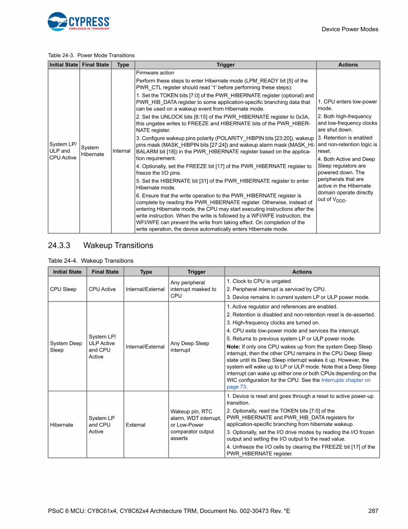
PSoC 6 MCU: CY8C61x4, CY8C62x4 Architecture TRM, Document No. 002-30473 Rev. *E 287
Device Power Modes
24.3.3 Wakeup Transitions
System LP/ULP and CPU Active
System Hibernate
Internal
Firmware action
Perform these steps to enter Hibernate mode (LPM_READY bit [5] of the PWR_CTL register should read '1' before performing these steps):
1. Set the TOKEN bits [7:0] of the PWR_HIBERNATE register (optional) and PWR_HIB_DATA register to some application-specific branching data that can be used on a wakeup event from Hibernate mode.
2. Set the UNLOCK bits [8:15] of the PWR_HIBERNATE register to 0x3A, this ungates writes to FREEZE and HIBERNATE bits of the PWR_HIBER-NATE register.
3. Configure wakeup pins polarity (POLARITY_HIBPIN bits [23:20]), wakeup pins mask (MASK_HIBPIN bits [27:24]) and wakeup alarm mask (MASK_HI-BALARM bit [18]) in the PWR_HIBERNATE register based on the applica-tion requirement.
4. Optionally, set the FREEZE bit [17] of the PWR_HIBERNATE register to freeze the I/O pins.
5. Set the HIBERNATE bit [31] of the PWR_HIBERNATE register to enter Hibernate mode.
6. Ensure that the write operation to the PWR_HIBERNATE register is complete by reading the PWR_HIBERNATE register. Otherwise, instead of entering Hibernate mode, the CPU may start executing instructions after the write instruction. When the write is followed by a WFI/WFE instruction, the WFI/WFE can prevent the write from taking effect. On completion of the write operation, the device automatically enters Hibernate mode.
1. CPU enters low-power mode.
2. Both high-frequency and low-frequency clocks are shut down.
3. Retention is enabled and non-retention logic is reset.
4. Both Active and Deep Sleep regulators are powered down. The peripherals that are active in the Hibernate domain operate directly out of VDDD.
Table 24-3. Power Mode Transitions
Initial State Final State Type Trigger Actions
Table 24-4. Wakeup Transitions
Initial State Final State Type Trigger Actions
CPU Sleep CPU Active Internal/ExternalAny peripheral interrupt masked to CPU
1. Clock to CPU is ungated.
2. Peripheral interrupt is serviced by CPU.
3. Device remains in current system LP or ULP power mode.
System Deep Sleep
System LP/ULP Active and CPU Active
Internal/ExternalAny Deep Sleep interrupt
1. Active regulator and references are enabled.
2. Retention is disabled and non-retention reset is de-asserted.
3. High-frequency clocks are turned on.
4. CPU exits low-power mode and services the interrupt.
5. Returns to previous system LP or ULP power mode.
Note: If only one CPU wakes up from the system Deep Sleep interrupt, then the other CPU remains in the CPU Deep Sleep state until its Deep Sleep interrupt wakes it up. However, the system will wake up to LP or ULP mode. Note that a Deep Sleep interrupt can wake up either one or both CPUs depending on the WIC configuration for the CPU. See the Interrupts chapter on page 73.
HibernateSystem LP and CPU Active
External
Wakeup pin, RTC alarm, WDT interrupt, or Low-Power comparator output asserts
1. Device is reset and goes through a reset to active power-up transition.
2. Optionally, read the TOKEN bits [7:0] of the PWR_HIBERNATE and PWR_HIB_DATA registers for application-specific branching from hibernate wakeup.
3. Optionally, set the I/O drive modes by reading the I/O frozen output and setting the I/O output to the read value.
4. Unfreeze the I/O cells by clearing the FREEZE bit [17] of the PWR_HIBERNATE register.

PSoC 6 MCU: CY8C61x4, CY8C62x4 Architecture TRM, Document No. 002-30473 Rev. *E 288
Device Power Modes
24.4 Summary
Table 24-5. Resources Available in Different Power Modes
Component
Power Modes
LP ULPDeep Sleep Hibernate XRES
Power Off with BackupCPU Active
CPU Sleep/Deep Sleep
CPU ActiveCPU Sleep/Deep Sleep
Core functions
CPU On Sleep On Sleep Retention Off Off Off
SRAM On On On On Retention Off Off Off
Flash Read/Write Read/Write Read Only Read Only Off Off Off Off
High-Speed Clock (IMO, ECO, PLL, FLL)
On On On On Off Off Off Off
LVD On On On On Off Off Off Off
ILO On On On On On On Off Off
Peripherals
SMIF On On On On Retention Off Off Off
SAR ADC On On On On On Off Off Off
LPCMP On On On On Ona Ona Off Off
CTBm On On On On On (lower GBW)b Off Off Off
TCPWM On On On On Off Off Off Off
CSD On On On On Retention Off Off Off
LCD On On On On On Off Off Off
SCB On On On OnRetention (I2C/SPI wakeup available)c
Off Off Off
GPIO On On On On On Freeze Off Off
Watchdog timer On On On On On On Off Off
Multi-Counter WDT On On On On On Off Off Off
Resets
XRES On On On On On On On Off
POR On On On On On On Off Off
BOD On On On On On Off Off Off
Watchdog reset On On On On On Ond Off Off
Backup domain
WCO, RTC, alarms On On On On On On On On
a. Low-Power comparator may be optionally enabled in the Hibernate mode to generate wakeup.b. Low-power comparator and CTBm may be optionally enabled in the system Deep Sleep mode to generate wakeup.c. Only the SCB with system Deep Sleep support is available in the Deep Sleep power mode; other SCBs are not available in the Deep Sleep power mode.d. Watchdog interrupt can generate a Hibernate wakeup. See the Watchdog Timer chapter on page 262 for details.
PSoC 6 MCU: CY8C61x4, CY8C62x4 Architecture TRM, Document No. 002-30473 Rev. *E 289
Device Power Modes
24.5 Register List
Name Description
PWR_CTL Power Mode Control register – controls the device power mode options and allows observation of current state
PWR_HIBERNATE Hibernate Mode register – controls various Hibernate mode entry/exit related options
PWR_HIB_DATA Hibernate Mode Data register – data register that is retained through a hibernate wakeup sequence
CM4_SCS_SCRCortex-M4 System Control register – controls the CM4 CPU sleep and deep sleep decisions on the WFI/WFE instruction execution. This register is detailed in the ARMv7-M Architecture Reference Manual available from Arm
CM0P_SCS_SCRCortex-M0+ System Control register – controls the CM0+ CPU sleep and deep sleep decisions on the WFI/WFE instruction execution. This register is detailed in the ARMv7-M Architecture Reference Manual available from Arm
CPUSS_CM0_CTLControls the CM0+ power state. Note that this register may only be modified by the CM4 while the CM0+ is in CPU Deep Sleep mode
CPUSS_CM0_STATUS Specifies if the CM0+ is in CPU Active, Sleep, or Deep Sleep power mode
CPUSS_CM4_PWR_CTLControls the CM4 power state. Note that this register may only be modified by the CM0+ while the CM4 is in CPU Deep Sleep mode.
CPUSS_CM4_STATUS Specifies if the CM4 is in CPU Active, Sleep, or Deep Sleep power mode

PSoC 6 MCU: CY8C61x4, CY8C62x4 Architecture TRM, Document No. 002-30473 Rev. *E 290
25. Trigger Multiplexer Block
Every peripheral in the PSoC 6 MCU is interconnected using trigger signals. Trigger signals are means by which peripheralsdenote an occurrence of an event or a state. These triggers are used as means to affect or initiate some action in otherperipherals. The trigger multiplexer block helps to route triggers from a source peripheral block to a destination.
25.1 Features■ Ability to connect any trigger signal from one peripheral to another
■ Supports a software trigger, which can trigger any signal in the block
■ Supports multiplexing of triggers between peripherals
■ One-to-one trigger paths for dedicated triggers that are more commonly routed
■ Ability to configure a trigger multiplexer with trigger manipulation features in hardware such as inversion and edge/level detection
■ Ability to block triggers in debug mode
25.2 Architecture
The trigger signals in the PSoC 6 MCU are digital signals generated by peripheral blocks to denote a state such as FIFOlevel, or an event such as the completion of an action. These trigger signals typically serve as initiator of other actions in otherperipheral blocks. An example is an ADC peripheral block sampling three channels. After the conversion is complete, atrigger signal will be generated, which in turn triggers a DMA channel that transfers the ADC data to a memory buffer. Thisexample is shown in Figure 25-1.
Figure 25-1. Trigger Signal Example
A PSoC 6 MCU has multiple peripheral bocks; each of these blocks can be connected to other blocks through trigger signals,based on the system implementation. To support this, the PSoC 6 MCU has hardware, which is a series of multiplexers usedto route the trigger signals from potential sources to destinations. This hardware is called the trigger multiplexer block. Thetrigger multiplexer can connect to any trigger signal emanating out of any peripheral block in the PSoC 6 MCU and route it toany other peripheral to initiate or affect an operation at the destination peripheral block.
This PSoC 6 MCU technical reference manual (TRM) provides comprehensive and detailed information about thefunctions of the PSoC 6 MCU device hardware. It is divided into two books: architecture TRM and registers TRM. TheTRM is not recommended for those new to the PSoC 6 MCU, nor as a guide for developing PSoC 6 MCU applications.Use these documents instead:
■ PSoC 61 datasheet, PSoC 62 datasheet
■ Peripheral Driver Library (PDL) documentation
■ Application notes
■ Code examples
ADC
Ch1
Ch2
Ch3 EoC
DMA
Trigger signal

PSoC 6 MCU: CY8C61x4, CY8C62x4 Architecture TRM, Document No. 002-30473 Rev. *E 291
Trigger Multiplexer Block
25.2.1 Trigger Multiplexer Group
The trigger multiplexer block is implemented using several trigger multiplexers. A trigger multiplexer selects a signal from aset of trigger output signals from different peripheral blocks to route it to a specific trigger input of another peripheral block.The multiplexers are grouped into trigger groups. All the trigger multiplexers in a trigger group have similar input options andare designed to feed similar destination signals. Hence the trigger group can be considered as a block that multiplexesmultiple inputs to multiple outputs. This concept is illustrated in Figure 25-2. Both the trigger multiplexers and the one-to-onetriggers offer trigger manipulation, which includes inversion or specifies the output signal as edge or level triggered. For edgetriggering, the trigger is synchronized to the consumer block’s (the peripheral block that is receiving the trigger) clock and atwo-cycle pulse is generated on this clock.
Figure 25-2. Trigger Multiplexer Groups
25.2.2 One-to-one Trigger
In addition to trigger multiplexers, there are dedicated trigger paths called one-to-one triggers. These trigger paths/routes arebetween fixed source and destination peripherals and cannot be multiplexed. These paths can be enabled or disabled. Agroup of registers in the format PERI_TR_1TO1_GR[X]_TR_CTL[Y], with X being the trigger group and Y being the outputtrigger number from the one-to-one trigger, can be used to enable or disable the triggers path.
25.2.3 Trigger Multiplexer Block
The trigger multiplexer block has two types of trigger routings: trigger multiplexers that are capable of selecting from multipletrigger sources to a specific trigger destination and one-to-one triggers that are predetermined fixed trigger paths that can beenabled or disabled. See Table 25-2 for more information on each trigger group and its description.
Note: The triggers output into different peripherals, which may have more routing than is shown on the trigger routingdiagram. For more information on this routing, go to the trigger destination peripheral block.
Figure 25-3 shows the trigger multiplexer architecture.
In [0:N-1] Out [0:M-1]
In_1
In_(N-1)
Out_0
Out_1
Out_(M-1)
Trigger multiplexer group takes N inputs and routes to M outputs
An equivalent implementation of a trigger multiplexer group with N inputs and M outputs
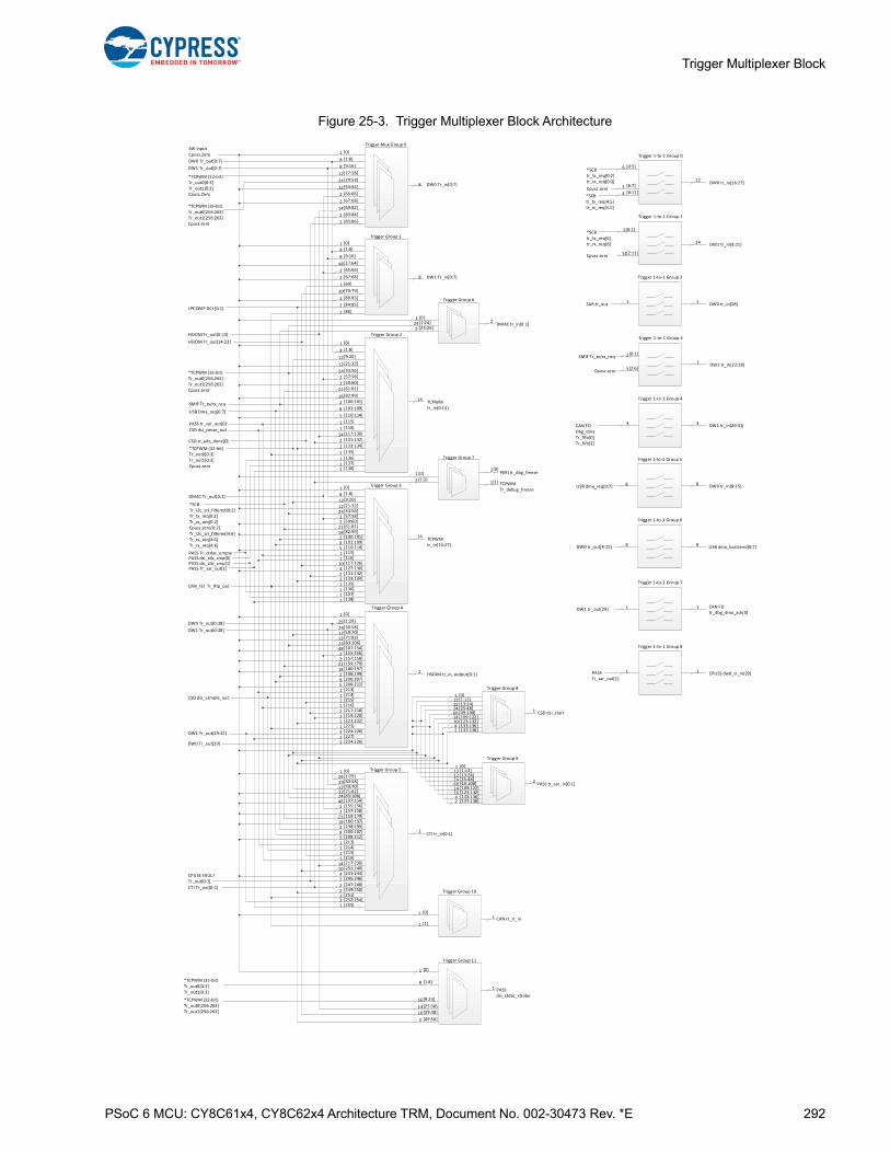
PSoC 6 MCU: CY8C61x4, CY8C62x4 Architecture TRM, Document No. 002-30473 Rev. *E 292
Trigger Multiplexer Block
Figure 25-3. Trigger Multiplexer Block Architecture
DW0 Tr_out[0:7] 8
DW1 Tr_out[0:7] 8
*TCPWM (32‐bit)Tr_out0[0:3]Tr_out1[0:3]Cpuss.Zero
DW0 Tr_in[0:7]8
Trigger Mux Group 0
Trigger Group 1
8
8
8
8DMAC Tr_out[0:1]
2
HSIOM Tr_out[0:13]
14
CTI Tr_out[0:1]
2
CPUSS FAULT Tr_out[0:1]
2
Trigger Group 2
Trigger Group 3
DW1 Tr_in[0:7]8
2
CSD tr_adc_done[0]
1
HSIOM Tr_out[14:23]
10
2LPCOMP DCI [0:1]
*TCPWM (32‐bit)Tr_out0[0:3]Tr_out1[0:3]Cpuss.zero
*TCPWM (16‐bit)Tr_out0[256:263]Tr_out1[256:263]Cpuss.zero
12
24
2
21
*SCBTr_i2c_scl_filtered[0:2]Tr_tx_req[0:2]Tr_rx_req[0:2]Cpuss.zero[0:2]Tr_i2c_scl_filtered[4:6]Tr_tx_req[4:6]Tr_rx_req[4:6]
SMIF Tr_tx/rx_req 2
USB Dma_req[0:7]8
CAN_FD. Tr_Rtp_out
1
PASS tr_sar_out[0] 1
CSD dsi_sense_out 1
142
2
12
242
21
28
1
1110
22
TCPWMtr_in[0:13]
14
TCPWMtr_in[14:27]
14
Trigger Group 4
DW0 Tr_out[0:28] 29
DW1 Tr_out[0:28] 2912
24
2
21
28
1
CSD dsi_sample_out 11
11222
2929
Trigger Group 5
242
Trigger Group 6
12
24
2
21
28
1
11111410
2
22
Trigger Group 8
12
24
1410
2
Trigger Group 9
12
24
1410
2
2
Trigger Group 7
HSOIM tr_io_output[0:1]2
CTI tr_in[0:1]2
DMAC tr_in[0:1]2
PERI tr_dbg_freeze1
CSD dsi_start1
2PASS tr_sar_in[0:1]
Trigger 1‐to‐1 Group 0
6*SCBtr_tx_req[0:2]tr_rx_req[0:2] 12 DW0 tr_in[16:27]
Trigger 1‐to‐1 Group 1
2*SCBtr_tx_req[6]tr_rx_req[6] 14 DW1 tr_in[8:21]
Trigger 1‐to‐1 Group 2
1SAR tr_out 1 DW0 tr_in[28]
Trigger 1‐to‐1 Group 3
7SMIF Tr_tx/rx_req 2
DW1 tr_in[22:28]
Trigger 1‐to‐1 Group 4
3 3 DW1 tr_in[29:31]CAN FDDbg_dmaTr_fifo[0]Tr_fifo[1]
Trigger 1‐to‐1 Group 5
88 DW0 tr_in[8:15]USB dma_req[0:7]
Trigger 1‐to‐1 Group 6
88DW0 tr_out[8:15] USB dma_burstend[0:7]
3DW1 Tr_out[29:31]
3
Trigger Group 10
SW InputCpuss.Zero 1 [0]
[1:8]
[9:16]
12[53:64]
[65:66]
2 [67:68]
[69:82]
[83:84]
[85:86]
1 [0]
[1:8]
[9:16]
48[17:64]
[65:66]
2 [67:68]
[69]
[70:79]
2 [80:83]
[84:85]
1 [86]
1 [0]
[1:8]
[9:20]
12[21:32]
[33:56]
[57:58]
2 [59:60][61:81]
18[82:99]
[100:101]
[102:109]
5 [110:114]
[115]
[116]
[117:130][131:132]
[133:134]
[135]
1 [0]
[1:8][9:20]
12[21:32][33:56][57:58]
2 [59:60][61:81]
18[82:99][100:101][102:109]
5 [110:114][115][116][117:126]
4 [127:130][131:132][133:134][135]
1 [0]
[1:29]
[30:58][59:70]
12[71:82][83:106]
48[107:154][155:156]
2 [157:158][159:179]
18 [180:197][198:199][200:207]
5 [208:212][213][214][215][216][217:218][219:220][221:222][223][224:226]
1 [0][1:29][30:58][59:70]
12[71:82][83:106]
48 [107:154][155:156]
2 [157:158][159:179]
18 [180:197][198:199][200:207]
5 [208:212][213][214][215][216][217:230][231:240]
4 [241:244][245:246]
[247:248][249:250][251][252:254]
1 [0][1:24][25:26]
[0][1:2]
1
1 [0][1:12]
12 [13:24][25:48]
60 [49:108][109:122][123:132]
4 [133:136][137:138]
[0][1:12][13:24][25:48][49:108][109:122][123:132][133:136][137:138]
1
12
60
4
1 [0]
1 [1]
1 CAN tt_tr_in
Trigger 1‐to‐1 Group 7
11DW1 tr_out[29]CAN FD tr_dbg_dma_ack[0]
12Cpuss.zero
5Cpuss.zero
*TCPWM (16‐bit)Tr_out0[256:263]Tr_out1[256:263]Cpuss.zero
12[17:28]
24[29:52]
1 [136]
1 [137]
1 [138]
PASS Tr_ctdac_emptyPASS dsi_ctb_cmp[0]
PASS Tr_sar_out[1]
1 [136]
1 [137]
1 [138]
1 [227]
DW0 Tr_out[29] 3 [224:226]
1 [255]
[0]
TCPWM Tr_debug_freeze
1[1]
Trigger Group 11
1 PASS dsi_ctdac_strobe
1 [0]
*TCPWM (32‐bit)Tr_out0[0:3]Tr_out1[0:3]
*TCPWM (32‐bit)Tr_out0[256:263]Tr_out1[256:263]
8 [1:8]
16[9:24]
14[25:38]
10[39:48]
2 [49:50]
[0:5]
2 [6:7]Cpuss.zero
*SCBtr_tx_req[4:5]tr_rx_req[4:5]
4 [8:11]
[0:1]
[2:11]
[0:1]
[2:6]
Trigger 1‐to‐1 Group 8
11PASS Tr_sar_out[1]
CPUSS dw0_tr_in[29]
PASS dsi_ctb_cmp[1]
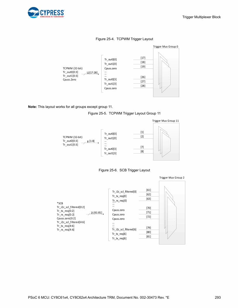
PSoC 6 MCU: CY8C61x4, CY8C62x4 Architecture TRM, Document No. 002-30473 Rev. *E 293
Trigger Multiplexer Block
Figure 25-4. TCPWM Trigger Layout
Note: This layout works for all groups except group 11.
Figure 25-5. TCPWM Trigger Layout Group 11
Figure 25-6. SCB Trigger Layout
Trigger Mux Group 0
Tr_out0[0]
Tr_out1[0]
Cpuss.zero
Tr_out0[3]
Tr_out1[3]
Cpuss.zero
...
[17]
[18]
[19]
[26]
[27]
[28]
...
...12[17:28]
TCPWM (32‐bit)Tr_out0[0:3]Tr_out1[0:3]Cpuss.Zero
Trigger Mux Group 11
Tr_out0[0]
Tr_out1[0]
Tr_out0[3]
Tr_out1[3]
...
[1]
[2]
[7]
[8]
...
...8 [1:8]
TCPWM (32‐bit)Tr_out0[0:3]Tr_out1[0:3]
Trigger Mux Group 2
Tr_i2c_scl_filtered[0]
Tr_tx_req[0]
Tr_rx_req[0]
Tr_i2c_scl_filtered[6]
Tr_tx_req[6]
Tr_tx_req[6]
...
[61]
[62]
[63]
[79]
[80]
[81]
...
...
21[61:81]
*SCBTr_i2c_scl_filtered[0:2]Tr_tx_req[0:2]Tr_rx_req[0:2]Cpuss.zero[0:2]Tr_i2c_scl_filtered[4:6]Tr_tx_req[4:6]Tr_rx_req[4:6]
...
...
...
Cpuss.zero
Cpuss.zero
Cpuss.zero
[70]
[71]
[72]
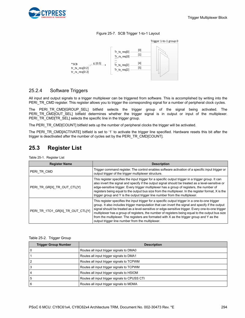
PSoC 6 MCU: CY8C61x4, CY8C62x4 Architecture TRM, Document No. 002-30473 Rev. *E 294
Trigger Multiplexer Block
Figure 25-7. SCB Trigger 1-to-1 Layout
25.2.4 Software Triggers
All input and output signals to a trigger multiplexer can be triggered from software. This is accomplished by writing into thePERI_TR_CMD register. This register allows you to trigger the corresponding signal for a number of peripheral clock cycles.
The PERI_TR_CMD[GROUP_SEL] bitfield selects the trigger group of the signal being activated. ThePERI_TR_CMD[OUT_SEL] bitfield determines whether the trigger signal is in output or input of the multiplexer.PERI_TR_CMD[TR_SEL] selects the specific line in the trigger group.
The PERI_TR_CMD[COUNT] bitfield sets up the number of peripheral clocks the trigger will be activated.
The PERI_TR_CMD[ACTIVATE] bitfield is set to ‘1’ to activate the trigger line specified. Hardware resets this bit after thetrigger is deactivated after the number of cycles set by the PERI_TR_CMD[COUNT].
25.3 Register List
Table 25-1. Register List
Register Name Description
PERI_TR_CMDTrigger command register. The control enables software activation of a specific input trigger or output trigger of the trigger multiplexer structure.
PERI_TR_GR[X]_TR_OUT_CTL[Y]
This register specifies the input trigger for a specific output trigger in a trigger group. It can also invert the signal and specify if the output signal should be treated as a level-sensitive or edge-sensitive trigger. Every trigger multiplexer has a group of registers, the number of registers being equal to the output bus size from the multiplexer. In the register format, X is the trigger group and Y is the output trigger line number from the multiplexer.
PERI_TR_1TO1_GR[X]_TR_OUT_CTL[Y]
This register specifies the input trigger for a specific output trigger in a one-to-one trigger group. It also includes trigger manipulation that can invert the signal and specify if the output signal should be treated as a level-sensitive or edge-sensitive trigger. Every one-to-one trigger multiplexer has a group of registers, the number of registers being equal to the output bus size from the multiplexer. The registers are formated with X as the trigger group and Y as the output trigger line number from the multiplexer.
Trigger 1‐to‐1 group 0
Tr_tx_req[0]
Tr_rx_req[0]
Tr_tx_req[2]
Tr_tx_req[2]
...
[0]
[1]
[4]
[5]
...
...6 [0:5]*SCB
tr_tx_req[0:2]tr_rx_req[0:2]
Table 25-2. Trigger Group
Trigger Group Number Description
0 Routes all input trigger signals to DMA0
1 Routes all input trigger signals to DMA1
2 Routes all input trigger signals to TCPWM
3 Routes all input trigger signals to TCPWM
4 Routes all input trigger signals to HSIOM
5 Routes all input trigger signals to CPUSS CTI
6 Routes all input trigger signals to MDMA

PSoC 6 MCU: CY8C61x4, CY8C62x4 Architecture TRM, Document No. 002-30473 Rev. *E 295
Trigger Multiplexer Block
7 Routes all input trigger signals to trigger freeze operation and TCWPM free operation
8 Routes all input trigger signals to CSD ADC start
9 Routes all input trigger signals to PASS ADC start
10 Routes all input trigger signals to CAN TT Sync Inputs
11 Routes all input trigger signals to CTDAC Strobe
Trigger 1-to-1 Group
0 Connects SCB triggers to DMA0
1 Connects SCB triggers to DMA1
2 Connects SAR0 triggers to DMA0
3 Connects SMIF triggers to DMA1
4 Connects CAN triggers to DMA1
5 Connects USB triggers to DMA0
6 Connects DMA0 triggers to USB
7 Connects DMA0 triggers to CAN
8 Connects SAR1 triggers to DMA1
Table 25-2. Trigger Group
Trigger Group Number Description

PSoC 6 MCU: CY8C61x4, CY8C62x4 Architecture TRM, Document No. 002-30473 Rev. *E 296
Section D: Digital Subsystem
This section encompasses the following chapters:
■ Serial Communications Block (SCB) chapter on page 298
■ Serial Memory Interface (SMIF) chapter on page 355
■ CAN FD Controller chapter on page 372
■ Timer, Counter, PWM chapter on page 427
■ Universal Serial Bus (USB) Host chapter on page 489
■ Universal Serial Bus (USB) Device Mode chapter on page 506
■ LCD Direct Drive chapter on page 522
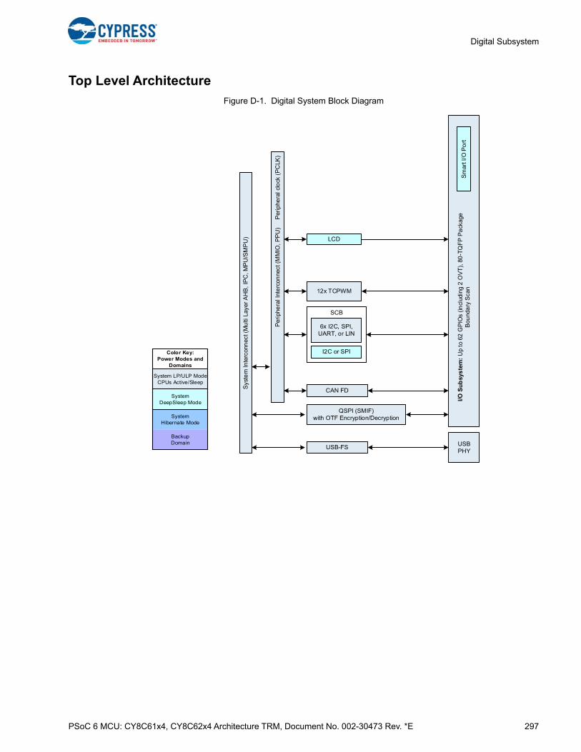
PSoC 6 MCU: CY8C61x4, CY8C62x4 Architecture TRM, Document No. 002-30473 Rev. *E 297
Digital Subsystem
Top Level Architecture
Figure D-1. Digital System Block Diagram
SCB
I/O S
ub
sys
tem
: U
p to
62
GP
IOs
(incl
udin
g 2
OV
T),
80
-TQ
FP
Pa
ckag
eB
ound
ary
Sca
nS
mar
t I/O
Po
rt
USBPHY
Per
iphe
ral I
nte
rcon
nect
(M
MIO
, PP
U)
Per
iphe
ral c
lock
(P
CLK
)
Sys
tem
Inte
rcon
nec
t (M
ulti
Lay
er A
HB
, IP
C, M
PU
/SM
PU
)
SystemHibernate Mode
BackupDomain
SystemDeepSleep Mode
System LP/ULP ModeCPUs Active/Sleep
Color Key:Power Modes and
Domains
PSoC 6 MCU: CY8C61x4, CY8C62x4 Architecture TRM, Document No. 002-30473 Rev. *E 298
26. Serial Communications Block (SCB)
The Serial Communications Block (SCB) supports three serial communication protocols: Serial Peripheral Interface (SPI),Universal Asynchronous Receiver Transmitter (UART), and Inter Integrated Circuit (I2C or IIC). Only one of the protocols issupported by an SCB at any given time. Note that the number of SCBs in a PSoC 6 MCU varies by part number. Also, not allSCBs support all three modes (SPI, UART, and I2C), and all SCBs do not operate in deep sleep. Consult the PSoC 61datasheet/PSoC 62 datasheet for these details.
26.1 Features
The SCB supports the following features:
■ Standard SPI master and slave functionality with Motorola, Texas Instruments, and National Semiconductor protocols
■ Standard UART functionality with SmartCard reader, Local Interconnect Network (LIN), and IrDA protocols
❐ Standard LIN slave functionality with LIN v1.3 and LIN v2.1/2.2 specification compliance
■ Standard I2C master and slave functionality
■ Trigger outputs for connection to DMA
■ Multiple interrupt sources to indicate status of FIFOs and transfers
■ Features available only on Deep Sleep-capable SCB:
❐ EZ mode for SPI and I2C slaves; allows for operation without CPU intervention
❐ CMD_RESP mode for SPI and I2C slaves; allows for operation without CPU intervention
❐ Low-power (Deep Sleep) mode of operation for SPI and I2C slaves (using external clocking)
❐ Deep Sleep wakeup on I2C slave address match or SPI slave selection
This PSoC 6 MCU technical reference manual (TRM) provides comprehensive and detailed information about thefunctions of the PSoC 6 MCU device hardware. It is divided into two books: architecture TRM and registers TRM. TheTRM is not recommended for those new to the PSoC 6 MCU, nor as a guide for developing PSoC 6 MCU applications.Use these documents instead:
■ PSoC 61 datasheet, PSoC 62 datasheet
■ Peripheral Driver Library (PDL) documentation
■ Application notes
■ Code examples
PSoC 6 MCU: CY8C61x4, CY8C62x4 Architecture TRM, Document No. 002-30473 Rev. *E 299
Serial Communications Block (SCB)
26.2 Architecture
The operation modes supported by SCB are described inthe following sections.
26.2.1 Buffer Modes
Each SCB has 256 bytes of dedicated RAM for transmit andreceive operation. This RAM can be configured in threedifferent modes (FIFO, EZ, or CMD_RESP). The followingsections give a high-level overview of each mode. Thesections on each protocol will provide more details.
■ Masters can only use FIFO mode
■ I2C and SPI slaves can use all three modes. Note: EZMode and CMD Response Mode are available only onthe Deep Sleep-capable SCB
■ UART only uses FIFO mode
Note: This document discusses hardware implementation ofthe EZ mode; for the firmware implementation, see the PDL.
26.2.1.1 FIFO Mode
In this mode the RAM is split into two 128-byte FIFOs, onefor transmit (TX) and one for receive (RX). The FIFOs canbe configured to be 8 bits x 128 elements or 16 bits x 64elements; this is done by setting the BYTE_MODE bit in theSCB control register.
FIFO mode of operation is available only in Active and Sleeppower modes. However, the I2C address or SPI slave selectcan be used to wake the device from Deep Sleep on theDeep Sleep-capable SCB.
Statuses are provided for both the RX and TX FIFOs. Thereare multiple interrupt sources available, which indicate thestatus of the FIFOs, such as full or empty; see “SCBInterrupts” on page 346.
26.2.1.2 EZ Mode
In easy (EZ) mode the RAM is used as a single 256-bytebuffer. The external master sets a base address and readsand writes start from that base address.
EZ Mode is available only for SPI slave and I2C slave. It isavailable only on the Deep Sleep capable SCB.
EZ mode is available in Active, Sleep, and Deep Sleeppower modes.
Note: This document discusses hardware implementation ofthe EZ mode; for the firmware implementation, see the PDL.
26.2.1.3 CMD_RESP Mode
Command Response (CMD_RESP) mode is similar to EZmode except that the base address is provided by the CPUnot the external master.
CMD_RESP mode is available only for SPI slave and I2Cslave. It is available only on the Deep Sleep-capable SCB.
CMD_RESP mode operation is available in Active, Sleep,and Deep Sleep power modes.
26.2.2 Clocking Modes
The SCB can be clocked either by an internal clock providedby the peripheral clock dividers (referred to as clk_scb in thisdocument), or it can be clocked by the external master.
■ UART, SPI master, and I2C master modes must useclk_scb.
■ Only SPI slave and I2C slave can use the clock from andexternal master, and only the Deep Sleep capable SCBsupports this.
Internally- and externally-clocked slave functionality isdetermined by two register fields of the SCB CTRL register:
■ EC_AM_MODE indicates whether SPI slave selection orI2C address matching is internally (‘0’) or externally (‘1’)clocked.
■ EC_OP_MODE indicates whether the rest of theprotocol operation (besides SPI slave selection and I2Caddress matching) is internally (‘0’) or externally (‘1’)clocked.
Notes:
■ FIFO mode supports an internally- or externally-clockedaddress match (EC_AM_MODE is ‘0’ or ‘1’); however,data transfer must be done with internal clocking.(EC_OP_MODE is ‘1’).
■ EZ and CMD_RESP modes are supported withexternally clocked operation (EC_OP_MODE is ‘1’).
Table 26-1 provides an overview of the clocking and buffermodes supported for each communication mode.
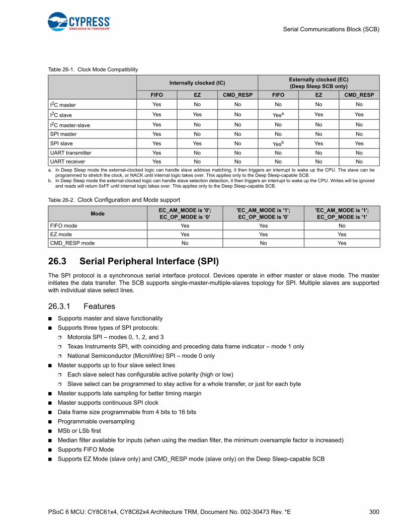
PSoC 6 MCU: CY8C61x4, CY8C62x4 Architecture TRM, Document No. 002-30473 Rev. *E 300
Serial Communications Block (SCB)
26.3 Serial Peripheral Interface (SPI)
The SPI protocol is a synchronous serial interface protocol. Devices operate in either master or slave mode. The masterinitiates the data transfer. The SCB supports single-master-multiple-slaves topology for SPI. Multiple slaves are supportedwith individual slave select lines.
26.3.1 Features
■ Supports master and slave functionality
■ Supports three types of SPI protocols:
❐ Motorola SPI – modes 0, 1, 2, and 3
❐ Texas Instruments SPI, with coinciding and preceding data frame indicator – mode 1 only
❐ National Semiconductor (MicroWire) SPI – mode 0 only
■ Master supports up to four slave select lines
❐ Each slave select has configurable active polarity (high or low)
❐ Slave select can be programmed to stay active for a whole transfer, or just for each byte
■ Master supports late sampling for better timing margin
■ Master supports continuous SPI clock
■ Data frame size programmable from 4 bits to 16 bits
■ Programmable oversampling
■ MSb or LSb first
■ Median filter available for inputs (when using the median filter, the minimum oversample factor is increased)
■ Supports FIFO Mode
■ Supports EZ Mode (slave only) and CMD_RESP mode (slave only) on the Deep Sleep-capable SCB
Table 26-1. Clock Mode Compatibility
Internally clocked (IC)Externally clocked (EC) (Deep Sleep SCB only)
FIFO EZ CMD_RESP FIFO EZ CMD_RESP
I2C master Yes No No No No No
I2C slave Yes Yes No Yesa Yes Yes
I2C master-slave Yes No No No No No
SPI master Yes No No No No No
SPI slave Yes Yes No Yesb Yes Yes
UART transmitter Yes No No No No No
UART receiver Yes No No No No No
a. In Deep Sleep mode the external-clocked logic can handle slave address matching, it then triggers an interrupt to wake up the CPU. The slave can beprogrammed to stretch the clock, or NACK until internal logic takes over. This applies only to the Deep Sleep-capable SCB.
b. In Deep Sleep mode the external-clocked logic can handle slave selection detection, it then triggers an interrupt to wake up the CPU. Writes will be ignoredand reads will return 0xFF until internal logic takes over. This applies only to the Deep Sleep-capable SCB.
Table 26-2. Clock Configuration and Mode support
ModeEC_AM_MODE is '0'; EC_OP_MODE is ‘0’
'EC_AM_MODE is '1'; EC_OP_MODE is '0’
'EC_AM_MODE is '1'; EC_OP_MODE is '1'
FIFO mode Yes Yes No
EZ mode Yes Yes Yes
CMD_RESP mode No No Yes
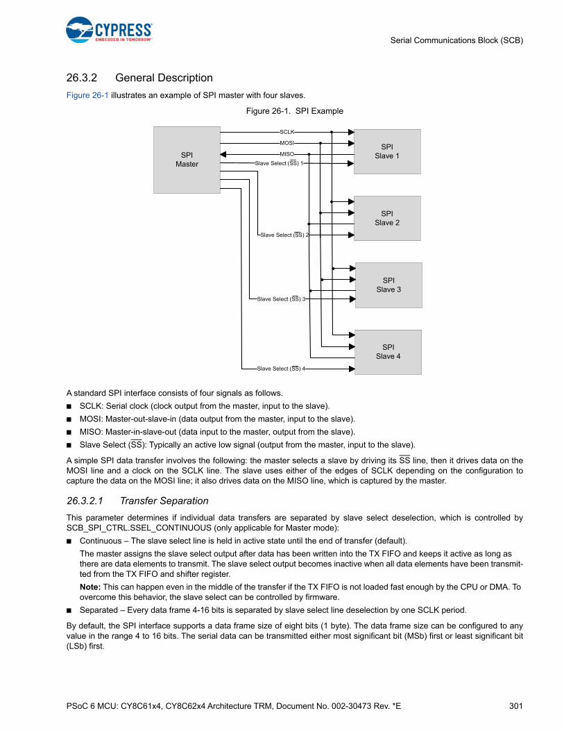
PSoC 6 MCU: CY8C61x4, CY8C62x4 Architecture TRM, Document No. 002-30473 Rev. *E 301
Serial Communications Block (SCB)
26.3.2 General Description
Figure 26-1 illustrates an example of SPI master with four slaves.
Figure 26-1. SPI Example
A standard SPI interface consists of four signals as follows.
■ SCLK: Serial clock (clock output from the master, input to the slave).
■ MOSI: Master-out-slave-in (data output from the master, input to the slave).
■ MISO: Master-in-slave-out (data input to the master, output from the slave).
■ Slave Select (SS): Typically an active low signal (output from the master, input to the slave).
A simple SPI data transfer involves the following: the master selects a slave by driving its SS line, then it drives data on theMOSI line and a clock on the SCLK line. The slave uses either of the edges of SCLK depending on the configuration tocapture the data on the MOSI line; it also drives data on the MISO line, which is captured by the master.
26.3.2.1 Transfer Separation
This parameter determines if individual data transfers are separated by slave select deselection, which is controlled bySCB_SPI_CTRL.SSEL_CONTINUOUS (only applicable for Master mode):
■ Continuous – The slave select line is held in active state until the end of transfer (default).
The master assigns the slave select output after data has been written into the TX FIFO and keeps it active as long as there are data elements to transmit. The slave select output becomes inactive when all data elements have been transmit-ted from the TX FIFO and shifter register.
Note: This can happen even in the middle of the transfer if the TX FIFO is not loaded fast enough by the CPU or DMA. To overcome this behavior, the slave select can be controlled by firmware.
■ Separated – Every data frame 4-16 bits is separated by slave select line deselection by one SCLK period.
By default, the SPI interface supports a data frame size of eight bits (1 byte). The data frame size can be configured to anyvalue in the range 4 to 16 bits. The serial data can be transmitted either most significant bit (MSb) first or least significant bit(LSb) first.
SPI Master
SPISlave 1
SPISlave 2
SPISlave 4
SCLK
MOSI
MISO
Slave Select (SS) 2
Slave Select (SS) 4
SPISlave 3
Slave Select (SS) 3
Slave Select (SS) 1

PSoC 6 MCU: CY8C61x4, CY8C62x4 Architecture TRM, Document No. 002-30473 Rev. *E 302
Serial Communications Block (SCB)
Three different variants of the SPI protocol are supported by the SCB:
■ Motorola SPI: This is the original SPI protocol.
■ Texas Instruments SPI: A variation of the original SPI protocol, in which data frames are identified by a pulse on the SSline.
■ National Semiconductors SPI: A half-duplex variation of the original SPI protocol.
26.3.3 SPI Modes of Operation
26.3.3.1 Motorola SPI
The original SPI protocol was defined by Motorola. It is a full duplex protocol. Multiple data transfers may happen with the SSline held at ‘0’. When not transmitting data, the SS line is held at ‘1’.
Clock Modes of Motorola SPI
The Motorola SPI protocol has four different clock modes based on how data is driven and captured on the MOSI and MISOlines. These modes are determined by clock polarity (CPOL) and clock phase (CPHA).
Clock polarity determines the value of the SCLK line when not transmitting data. CPOL = ‘0’ indicates that SCLK is ‘0’ whennot transmitting data. CPOL = ‘1’ indicates that SCLK is ‘1’ when not transmitting data.
Clock phase determines when data is driven and captured. CPHA = 0 means sample (capture data) on the leading (first)clock edge, while CPHA = 1 means sample on the trailing (second) clock edge, regardless of whether that clock edge is risingor falling. With CPHA = 0, the data must be stable for setup time before the first clock cycle.
■ Mode 0: CPOL is ‘0’, CPHA is ‘0’: Data is driven on a falling edge of SCLK. Data is captured on a rising edge of SCLK.
■ Mode 1; CPOL is ‘0’, CPHA is ‘1’: Data is driven on a rising edge of SCLK. Data is captured on a falling edge of SCLK.
■ Mode 2: CPOL is ‘1’, CPHA is ‘0’: Data is driven on a rising edge of SCLK. Data is captured on a falling edge of SCLK.
■ Mode 3: CPOL is ‘1’, CPHA is ‘1’: Data is driven on a falling edge of SCLK. Data is captured on a rising edge of SCLK.
Figure 26-2 illustrates driving and capturing of MOSI/MISO data as a function of CPOL and CPHA.
Figure 26-2. SPI Motorola, 4 Modes
CPOL = 0 CPHA = 0
SCLK
MISO / MOSI
SCLK
MISO / MOSI
SCLK
MISO / MOSI
SCLK
MISO / MOSI
MSb LSb
MSb LSb
MSb LSb
MSb LSb
CPOL = 0 CPHA = 1
CPOL = 1 CPHA = 0
CPOL = 1 CPHA = 1
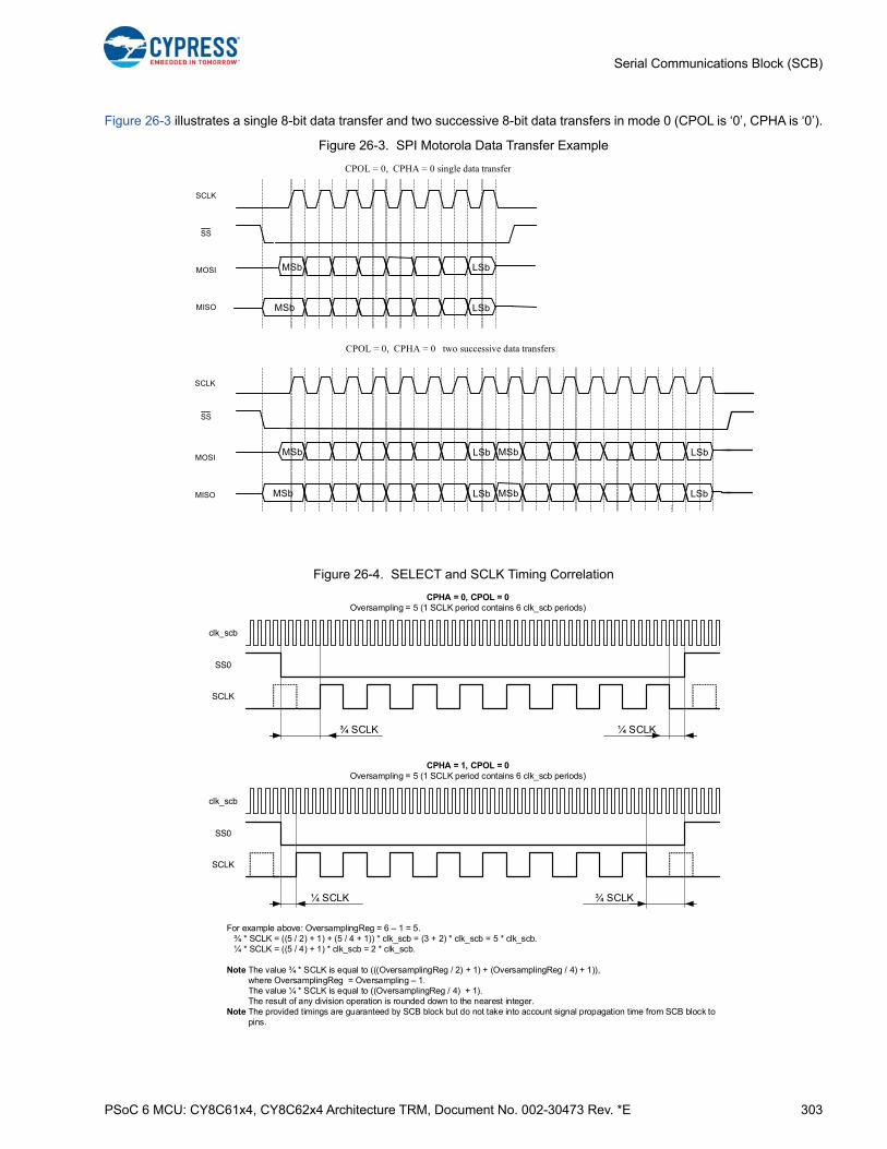
PSoC 6 MCU: CY8C61x4, CY8C62x4 Architecture TRM, Document No. 002-30473 Rev. *E 303
Serial Communications Block (SCB)
Figure 26-3 illustrates a single 8-bit data transfer and two successive 8-bit data transfers in mode 0 (CPOL is ‘0’, CPHA is ‘0’).
Figure 26-3. SPI Motorola Data Transfer Example
Figure 26-4. SELECT and SCLK Timing Correlation
SCLK
MOSI
MISO
SCLK
MOSI
MISO
CPOL = 0, CPHA = 0 single data transfer
MSb LSb
MSb LSb MSb LSb
LSbMSb
MSb LSb MSb LSb
CPOL = 0, CPHA = 0 two successive data transfers
SS
SS
CPHA = 0, CPOL = 0Oversampling = 5 (1 SCLK period contains 6 clk_scb periods)
SCLK
SS0
clk_scb
¾ SCLK ¼ SCLK
CPHA = 1, CPOL = 0Oversampling = 5 (1 SCLK period contains 6 clk_scb periods)
SCLK
SS0
clk_scb
¼ SCLK ¾ SCLK
For example above: OversamplingReg = 6 – 1 = 5. ¾ * SCLK = ((5 / 2) + 1) + (5 / 4 + 1)) * clk_scb = (3 + 2) * clk_scb = 5 * clk_scb. ¼ * SCLK = ((5 / 4) + 1) * clk_scb = 2 * clk_scb.
Note The value ¾ * SCLK is equal to (((OversamplingReg / 2) + 1) + (OversamplingReg / 4) + 1)), where OversamplingReg = Oversampling – 1. The value ¼ * SCLK is equal to ((OversamplingReg / 4) + 1). The result of any division operation is rounded down to the nearest integer.Note The provided timings are guaranteed by SCB block but do not take into account signal propagation time from SCB block to pins.

PSoC 6 MCU: CY8C61x4, CY8C62x4 Architecture TRM, Document No. 002-30473 Rev. *E 304
Serial Communications Block (SCB)
Configuring SCB for SPI Motorola Mode
To configure the SCB for SPI Motorola mode, set various register bits in the following order:
1. Select SPI by writing ‘01’ to the MODE (bits [25:24]) of the SCB_CTRL register.
2. Select SPI Motorola mode by writing ‘00’ to the MODE (bits [25:24]) of the SCB_SPI_CTRL register.
3. Select the clock mode in Motorola by writing to the CPHA and CPOL fields (bits 2 and 3 respectively) of theSCB_SPI_CTRL register.
4. Follow steps 2 to 4 mentioned in “Enabling and Initializing SPI” on page 314.
For more information on these registers, see the registers TRM.
26.3.3.2 Texas Instruments SPI
The Texas Instruments’ SPI protocol redefines the use of the SS signal. It uses the signal to indicate the start of a datatransfer, rather than a low active slave select signal, as in the case of Motorola SPI. The start of a transfer is indicated by ahigh active pulse of a single bit transfer period. This pulse may occur one cycle before the transmission of the first data bit, ormay coincide with the transmission of the first data bit. The TI SPI protocol supports only mode 1 (CPOL is ‘0’ and CPHA is‘1’): data is driven on a rising edge of SCLK and data is captured on a falling edge of SCLK.
Figure 26-5 illustrates a single 8-bit data transfer and two successive 8-bit data transfers. The SELECT pulse precedes thefirst data bit. Note how the SELECT pulse of the second data transfer coincides with the last data bit of the first data transfer.
Figure 26-5. SPI TI Data Transfer Example
Figure 26-6 illustrates a single 8-bit data transfer and two successive 8-bit data transfers. The SELECT pulse coincides withthe first data bit of a frame.
SCLK
MOSI
MISO
SCLK
MOSI
MISO
CPOL=0, CPHA=1 single data transfer
MSb LSb
MSb LSb MSb LSb
MSb LSb
MSb LSb MSb LSb
CPOL=0, CPHA=1 two successive data transfers
SS
SS
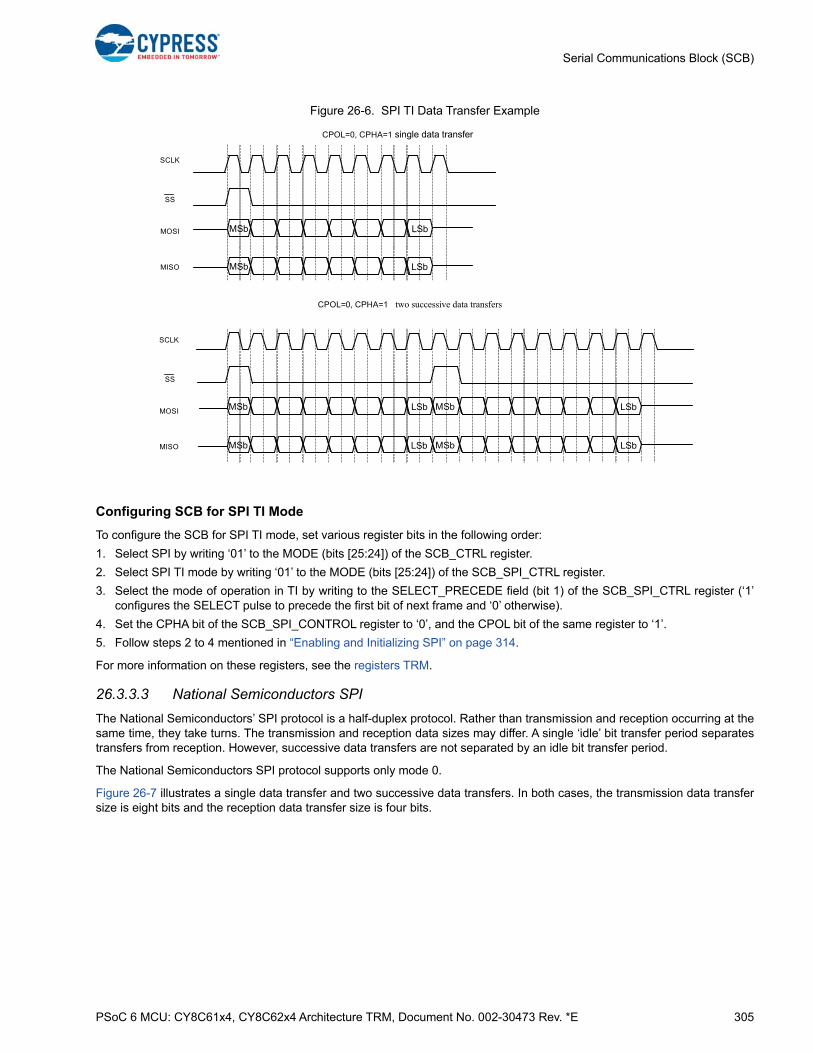
PSoC 6 MCU: CY8C61x4, CY8C62x4 Architecture TRM, Document No. 002-30473 Rev. *E 305
Serial Communications Block (SCB)
Figure 26-6. SPI TI Data Transfer Example
Configuring SCB for SPI TI Mode
To configure the SCB for SPI TI mode, set various register bits in the following order:
1. Select SPI by writing ‘01’ to the MODE (bits [25:24]) of the SCB_CTRL register.
2. Select SPI TI mode by writing ‘01’ to the MODE (bits [25:24]) of the SCB_SPI_CTRL register.
3. Select the mode of operation in TI by writing to the SELECT_PRECEDE field (bit 1) of the SCB_SPI_CTRL register (‘1’configures the SELECT pulse to precede the first bit of next frame and ‘0’ otherwise).
4. Set the CPHA bit of the SCB_SPI_CONTROL register to ‘0’, and the CPOL bit of the same register to ‘1’.
5. Follow steps 2 to 4 mentioned in “Enabling and Initializing SPI” on page 314.
For more information on these registers, see the registers TRM.
26.3.3.3 National Semiconductors SPI
The National Semiconductors’ SPI protocol is a half-duplex protocol. Rather than transmission and reception occurring at thesame time, they take turns. The transmission and reception data sizes may differ. A single ‘idle’ bit transfer period separatestransfers from reception. However, successive data transfers are not separated by an idle bit transfer period.
The National Semiconductors SPI protocol supports only mode 0.
Figure 26-7 illustrates a single data transfer and two successive data transfers. In both cases, the transmission data transfersize is eight bits and the reception data transfer size is four bits.
SCLK
MOSI
MISO
SCLK
MOSI
MISO
CPOL=0, CPHA=1 single data transfer
MSb LSb
MSb LSb MSb LSb
MSb LSb
MSb LSb MSb LSb
CPOL=0, CPHA=1 two successive data transfers
SS
SS

PSoC 6 MCU: CY8C61x4, CY8C62x4 Architecture TRM, Document No. 002-30473 Rev. *E 306
Serial Communications Block (SCB)
Figure 26-7. SPI NS Data Transfer Example
Configuring SCB for SPI NS Mode
To configure the SCB for SPI NS mode, set various register bits in the following order:
1. Select SPI by writing ‘01’ to the MODE (bits [25:24]) of the SCB_CTRL register.
2. Select SPI NS mode by writing ‘10’ to the MODE (bits [25:24]) of the SCB_SPI_CTRL register.
3. Set the CPOL and CHPA bits of the SCB_SPI_CTRL register to ‘0’.
4. Follow steps 2 to 4 mentioned in “Enabling and Initializing SPI” on page 314.
For more information on these registers, see the registers TRM.
MSb LSb
MSb LSb
MSb LSb
MSb LSb
MSb
idle 0 cycle
idle 0 cycleNo idle cycle
SCLK
MOSI
MISO
SCLK
MOSI
MISO
CPOL=0, CPHA=0 single data transfer
CPOL=0, CPHA=0 two successive data transfers
SS
SS

PSoC 6 MCU: CY8C61x4, CY8C62x4 Architecture TRM, Document No. 002-30473 Rev. *E 307
Serial Communications Block (SCB)
26.3.4 SPI Buffer Modes
SPI can operate in three different buffer modes – FIFO, EZ, and CMD_RESP modes. The buffer is used in different ways ineach of these modes. The following subsections explain each of these buffer modes in detail.
26.3.4.1 FIFO Mode
The FIFO mode has a TX FIFO for the data being transmitted and an RX FIFO for the data received. Each FIFO isconstructed out of the SRAM buffer. The FIFOs are either 64 elements deep with 16-bit data elements or 128 elements deepwith 8-bit data elements. The width of a FIFO is configured using the BYTE_MODE bitfield of the SCB.CTRL register.
FIFO mode of operation is available only in Active and Sleep power modes, and not in the Deep Sleep mode.
Transmit and receive FIFOs allow write and read accesses. A write access to the transmit FIFO uses the TX_FIFO_WRregister. A read access from the receive FIFO uses the RX_FIFO_RD register. For SPI master mode, data transfers arestarted when data is written into the TX FIFO. Note that when a master is transmitting and the FIFO becomes empty the slaveis de-selected.
Transmit and receive FIFO status information is available through status registers, TX_FIFO_STATUS andRX_FIFO_STATUS, and through the INTR_TX and INTR_RX registers.
Each FIFO has a trigger output. This trigger output can be routed through the trigger mux to various other peripheral on thedevice such as DMA or TCPWMs. The trigger output of the SCB is controlled through the TRIGGER_LEVEL field in theRX_CTRL and TX_CTRL registers.
■ For a TX FIFO a trigger is generated when the number of entries in the transmit FIFO is less than TX_FIFO_CTRL.TRIGGER_LEVEL.
■ For the RX FIFO a trigger is generated when the number of entries in the FIFO is greater than theRX_FIFO_CTRL.TRIGGER_LEVEL.
Note that the DMA has a trigger deactivation setting. For the SCB this should be set to 16.
Active to Deep Sleep Transition
Before going to deep sleep ensure that all active communication is complete. For a master this can easily be done bychecking the SPI_DONE bit in the INTR_M register, and ensuring the TX FIFO is empty.
For a slave this can be achieved by checking the BUS_BUSY bit in the SPI Status register. Also the RX FIFO should beempty before going to deep sleep. Any data in the FIFO will be lost during deep sleep.
Also before going to deep sleep the clock to the SCB needs to be disabled. This can be done by setting theSDA_IN_FILT_TRIM[1] bit in the I2C_CFG register to "0"
Lastly, when the device goes to deep sleep the SCB stops driving the GPIO lines. This leads to floating pins and can lead toundesirable current during deep sleep power modes. To avoid this condition before entering deep sleep mode change theHSIOM settings of the SCB pins to GPIO driven, then change the drive mode and drive state to the appropriate state to avoidfloating pins. Consult the I/O System chapter on page 214 for more information on pin drive modes.
Note: Before going into deep sleep the wakeup interrupt should be cleared. See the “SPI Interrupts” on page 347 for moredetails.
Deep Sleep to Active Transition
EC_AM = 1, EC_OP = 0, FIFO Mode.
When the SPI Slave Select line is asserted the device will be awoken by an interrupt. After the device is awoken change theSPI pin drive modes and HSIOM settings back to what they were before deep sleep. When clk_hf[0] is at the desiredfrequency set SDA_IN_FILT_TRIM[1] to ‘1’ to enable the clock to the SCB. Then write data into the TX FIFO. At this point themaster can read valid data from the slave. Before that any data read by the master will be invalid.
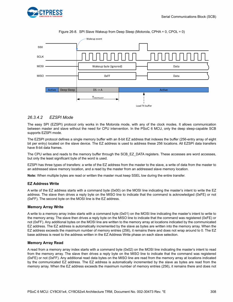
PSoC 6 MCU: CY8C61x4, CY8C62x4 Architecture TRM, Document No. 002-30473 Rev. *E 308
Serial Communications Block (SCB)
Figure 26-8. SPI Slave Wakeup from Deep Sleep (Motorola, CPHA = 0, CPOL = 0)
26.3.4.2 EZSPI Mode
The easy SPI (EZSPI) protocol only works in the Motorola mode, with any of the clock modes. It allows communicationbetween master and slave without the need for CPU intervention. In the PSoC 6 MCU, only the deep sleep-capable SCBsupports EZSPI mode.
The EZSPI protocol defines a single memory buffer with an 8-bit EZ address that indexes the buffer (256-entry array of eightbit per entry) located on the slave device. The EZ address is used to address these 256 locations. All EZSPI data transfershave 8-bit data frames.
The CPU writes and reads to the memory buffer through the SCB_EZ_DATA registers. These accesses are word accesses,but only the least significant byte of the word is used.
EZSPI has three types of transfers: a write of the EZ address from the master to the slave, a write of data from the master toan addressed slave memory location, and a read by the master from an addressed slave memory location.
Note: When multiple bytes are read or written the master must keep SSEL low during the entire transfer.
EZ Address Write
A write of the EZ address starts with a command byte (0x00) on the MOSI line indicating the master’s intent to write the EZaddress. The slave then drives a reply byte on the MISO line to indicate that the command is acknowledged (0xFE) or not(0xFF). The second byte on the MOSI line is the EZ address.
Memory Array Write
A write to a memory array index starts with a command byte (0x01) on the MOSI line indicating the master’s intent to write tothe memory array. The slave then drives a reply byte on the MISO line to indicate that the command was registered (0xFE) ornot (0xFF). Any additional bytes on the MOSI line are written to the memory array at locations indicated by the communicatedEZ address. The EZ address is automatically incremented by the slave as bytes are written into the memory array. When theEZ address exceeds the maximum number of memory entries (256), it remains there and does not wrap around to 0. The EZbase address is reset to the address written in the EZ Address Write phase on each slave selection.
Memory Array Read
A read from a memory array index starts with a command byte (0x02) on the MOSI line indicating the master’s intent to readfrom the memory array. The slave then drives a reply byte on the MISO line to indicate that the command was registered(0xFE) or not (0xFF). Any additional read data bytes on the MISO line are read from the memory array at locations indicatedby the communicated EZ address. The EZ address is automatically incremented by the slave as bytes are read from thememory array. When the EZ address exceeds the maximum number of memory entries (256), it remains there and does not
SCLK
Wakeup byte (ignored)MOSI
MISO
SS0
0xFF
Wakeup event
Deep SleepActive DS ‐> A Active
TDEEPSLEEP
Data
Load TX buffer
Data

PSoC 6 MCU: CY8C61x4, CY8C62x4 Architecture TRM, Document No. 002-30473 Rev. *E 309
Serial Communications Block (SCB)
wrap around to 0. The EZ base address is reset to the address written in the EZ Address Write phase on each slaveselection.
Figure 26-9 illustrates the write of EZ address, write to a memory array and read from a memory array operations in theEZSPI protocol.
Figure 26-9. EZSPI Example
Command 0x00 EZ Address
Command 0x00 : Write EZ address
Command 0x01
Command 0x01 : Write DATA
Write DATA
Command 0x02
Command 0x02 : Read DATA
Read DATA
SCLK
MOSI
MISO
SCLK
MOSI
MISO
SCLK
MOSI
MISO
EZ address
EZ address (8 bits)
EZ buffer(32 bytes SRAM)
EZ address
Write DATA
Read DATA
LEGEND :CPOL : Clock Polarity 0x00 : Write EZ addressCPHA : Clock Phase 0x01 : Write DATASCLK : SPI Interface Clock 0x02 : Read DATAMISO : SPI Master-In-Slave-Out 0xFE : slave readyMOSI : SPI Master-Out-Slave-In 0xFF : slave busy
SS
SS
SS

PSoC 6 MCU: CY8C61x4, CY8C62x4 Architecture TRM, Document No. 002-30473 Rev. *E 310
Serial Communications Block (SCB)
Configuring SCB for EZSPI Mode
By default, the SCB is configured for non-EZ mode ofoperation. To configure the SCB for EZSPI mode, set theregister bits in the following order:
1. Select EZ mode by writing ‘1’ to the EZ_MODE bit (bit10) of the SCB_CTRL register.
2. Set the EC_AM and EC_OP modes in the SCB_CTRLregister as appropriate.
3. Set the BYTE_MODE bit of the SCB_CTRL register to‘1’.
4. Follow the steps in “Configuring SCB for SPI MotorolaMode” on page 304.
5. Follow steps 2 to 4 mentioned in “Enabling and Initializ-ing SPI” on page 314.
For more information on these registers, see the registersTRM.
Active to Deep Sleep Transition
Before going to deep sleep ensure the master is notcurrently transmitting to the slave. This can be done bychecking the BUS_BUSY bit in the SPI_STATUS register.
If the bus is not busy, disable the clock to the SCB by settingthe SDA_IN_FILT_TRIM[1] bit to ‘0’ in the I2C_CFG register.
Deep Sleep to Active Transition
■ EC_AM = 1, EC_OP = 0, EZ Mode. MISO transmits0xFF until the internal clock is enabled. Data on MOSI isignored until the internal clock is enabled. Do not enablethe internal clock until clk_hf[0] is at the desiredfrequency. After clk_hf[0] is at the desired frequency setthe SDA_IN_FILT_TRIM[1] bit to ‘1’ to enable the clock.The external master needs to be aware that when itreads 0xFF on MISO the device is not ready yet.
■ EC_AM = 1, EC_OP = 1, EZ Mode. Do not enable theinternal clock until clk_hf[0] is at the desired frequency.After clk_hf[0] is at the desired frequency set theSDA_IN_FILT_TRIM[1] bit to ‘1’ to enable the clock.
26.3.4.3 Command-Response Mode
The command-response mode is defined only for an SPIslave. In the PSoC 6 MCU, only the deep sleep-capableSCB supports this mode. This mode has a single memorybuffer, a base read address, a current read address, a basewrite address, and a current write address that are used toindex the memory buffer. The base addresses are providedby the CPU. The current addresses are used by the slave toindex the memory buffer for sequential accesses of thememory buffer. The memory buffer holds 256 8-bit dataelements. The base and current addresses are in the range[0, 255]. This mode is only supported by the Motorola modeof operation.
The CPU writes and reads to the memory buffer through theSCB_EZ_DATA registers. These accesses are wordaccesses, but only the least significant byte of the word isused.
The slave interface accesses the memory buffer using thecurrent addresses. At the start of a write transfer (SPI slaveselection), the base write address is copied to the currentwrite address. A data element write is to the current writeaddress location. After the write access, the current addressis incremented by ‘1’. At the start of a read transfer, the baseread address is copied to the current read address. A dataelement read is to the current read address location. Afterthe read data element is transmitted, the current readaddress is incremented by ‘1’.
If the current addresses equal the last memory bufferaddress (address equals 255), the current addresses arenot incremented. Subsequent write accesses will overwriteany previously written value at the last buffer address.Subsequent read accesses will continue to provide the(same) read value at the last buffer address. The busmaster should be aware of the memory buffer capacity incommand-response mode.
The base addresses are provided throughCMD_RESP_CTRL. The current addresses are providedthrough CMD_RESP_STATUS. At the end of a transfer (SPIslave de-selection), the difference between a base andcurrent address indicates how many read/write accesseswere performed. The block provides interrupt cause fields toidentify the end of a transfer. Command-response modeoperation is available in Active, Sleep, and Deep Sleeppower modes.
The command-response mode has two phases of operation:
■ Write phase – The write phase begins with a selectionbyte, which has its last bit set to ‘0’ indicating a write.The master writes 8-bit data elements to the slave’smemory buffer following the selection byte. The slave’scurrent write address is set to the slave’s base writeaddress. Received data elements are written to thecurrent write address memory location. After eachmemory write, the current write address is incremented.
■ Read phase – The read phase begins with a selectionbyte, which has its last bit set to ‘1’ indicating a read. Themaster reads 8-bit data elements from the slave’smemory buffer. The slave’s current read address is setto the slave’s base read address. Transmitted dataelements are read from the current address memorylocation. After each read data element is transferred, thecurrent read address is incremented.
During the reception of the first byte, the slave (MISO)transmits either 0x62 (ready) or a value different from 0x62(busy). When disabled or reset, the slave transmits 0xFF(busy). The byte value can be used by the master todetermine whether the slave is ready to accept the SPIrequest.
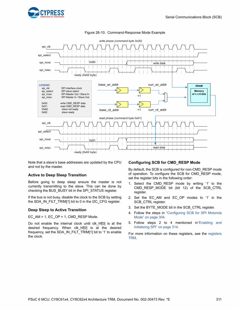
PSoC 6 MCU: CY8C61x4, CY8C62x4 Architecture TRM, Document No. 002-30473 Rev. *E 311
Serial Communications Block (SCB)
Figure 26-10. Command-Response Mode Example
Note that a slave’s base addresses are updated by the CPUand not by the master.
Active to Deep Sleep Transition
Before going to deep sleep ensure the master is notcurrently transmitting to the slave. This can be done bychecking the BUS_BUSY bit in the SPI_STATUS register.
If the bus is not busy, disable the clock to the SCB by settingthe SDA_IN_FILT_TRIM[1] bit to 0 in the I2C_CFG register.
Deep Sleep to Active Transition
EC_AM = 1, EC_OP = 1, CMD_RESP Mode.
Do not enable the internal clock until clk_hf[0] is at thedesired frequency. When clk_hf[0] is at the desiredfrequency, set the SDA_IN_FILT_TRIM[1] bit to ‘1’ to enablethe clock.
Configuring SCB for CMD_RESP Mode
By default, the SCB is configured for non-CMD_RESP modeof operation. To configure the SCB for CMD_RESP mode,set the register bits in the following order:
1. Select the CMD_RESP mode by writing ‘1’ to theCMD_RESP_MODE bit (bit 12) of the SCB_CTRLregister.
2. Set the EC_AM and EC_OP modes to ‘1’ in theSCB_CTRL register.
3. Set the BYTE_MODE bit in the SCB_CTRL register.
4. Follow the steps in “Configuring SCB for SPI MotorolaMode” on page 304.
5. Follow steps 2 to 4 mentioned in“Enabling andInitializing SPI” on page 314.
For more information on these registers, see the registersTRM.
write phase (command byte 0x00)
LEGEND: spi_clk: SPI interface clock spi_select: SPI slave select
spi_mosi: SPI Master Out / Slave In spi_miso: SPI Master In / Slave Out
0x00: write CMD_RESP data 0x01: read CMD_RESP data !0x62: slave not ready
0x62: slave ready
spi_clk
spi_select
spi_mosi
spi_miso
read phase (command byte 0x01)
spi_clk
spi_select
spi_mosi
spi_miso
0x01
0x00 write data
read data
ready (0x62 byte)
SRAM
Memory of n x 8-bits
curr_wr_addrbase_wr_addr
+1
curr_rd_addrbase_rd_addr +1
ready (0x62 byte)
PSoC 6 MCU: CY8C61x4, CY8C62x4 Architecture TRM, Document No. 002-30473 Rev. *E 312
Serial Communications Block (SCB)
26.3.5 Clocking and Oversampling
26.3.5.1 Clock Modes
The SCB SPI supports both internally and externally clockedoperation modes. Two bitfields (EC_AM_MODE andEC_OP MODE) in the SCB_CTRL register determine theSCB clock mode. EC_AM_MODE indicates whether SPIslave selection is internally (0) or externally (1) clocked.EC_OP_MODE indicates whether the rest of the protocoloperation (besides SPI slave selection) is internally (0) orexternally (1) clocked.
An externally-clocked operation uses a clock provided bythe external master (SPI SCLK). Note: In the PSoC 6 MCUonly the Deep Sleep-capable SCB supports externally-clocked mode of operation and only for SPI slave mode.
An internally-clocked operation uses the programmableclock dividers. For SPI, an integer clock divider must beused for both master and slave. For more information onsystem clocking, see the Clocking System chapter onpage 240.
The SCB_CTRL bitfields EC_AM_MODE andEC_OP_MODE can be configured in the following ways.
■ EC_AM_MODE is ‘0’ and EC_OP_MODE is ‘0’: Use thisconfiguration when only Active mode functionality isrequired.
❐ FIFO mode: Supported.
❐ EZ mode: Supported.
❐ Command-response mode: Not supported. The slave (MISO) transmits a value different from a ready (0x62) byte during the reception of the first byte if command-response mode is attempted in this configuration.
■ EC_AM_MODE is ‘1’ and EC_OP_MODE is ‘0’: Use thisconfiguration when both Active and Deep Sleepfunctionality are required. This configuration relies on theexternally-clocked functionality to detect the slaveselection and relies on the internally-clockedfunctionality to access the memory buffer.
The “hand over” from external to internal functionality relies on a busy/ready byte scheme. This scheme relies on the master to retry the current transfer when it receives a busy byte and requires the master to support busy/ready byte interpretation. When the slave is selected, INTR_SPI_EC.WAKE_UP is set to ‘1’. The associated Deep Sleep functionality interrupt brings the system into Active power mode.
❐ FIFO mode: Supported. The slave (MISO) transmits 0xFF until the CPU is awoken and the TX FIFO is populated. Any data on the MOSI line will be dropped until clk_scb is enabled see “Deep Sleep to Active Transition” on page 311 for more details
❐ EZ mode: Supported. In Deep Sleep power mode, the slave (MISO) transmits a busy (0xFF) byte during
the reception of the command byte. In Active power mode, the slave (MISO) transmits a ready (0xFE) byte during the reception of the command byte.
❐ CMD_RESP mode: Not supported. The slave trans-mits (MISO) a value different from a ready (0x62) byte during the reception of the first byte.
■ EC_AM_MODE is ‘1’ and EC_OP_MODE is ‘1’. Use thismode when both Active and Deep Sleep functionality arerequired. When the slave is selected,INTR_SPI_EC.WAKE_UP is set to ‘1’. The associatedDeep Sleep functionality interrupt brings the system intoActive power mode. When the slave is deselected,INTR_SPI_EC.EZ_STOP and/orINTR_SPI_EC.EZ_WRITE_STOP are set to ‘1’.
❐ FIFO mode: Not supported.
❐ EZ mode: Supported.
❐ CMD_RESP mode: Supported.
If EC_OP_MODE is ‘1’, the external interface logic accessesthe memory buffer on the external interface clock (SPISCLK). This allows for EZ and CMD_RESP modefunctionality in Active and Deep Sleep power modes.
In Active system power mode, the memory buffer requiresarbitration between external interface logic (on SPI SCLK)and the CPU interface logic (on system peripheral clock).This arbitration always gives the highest priority to theexternal interface logic (host accesses). The externalinterface logic takes two serial interface clock/bit periods forSPI. During this period, the internal logic is denied service tothe memory buffer. The PSoC 6 MCU provides twoprogrammable options to address this “denial of service”:
■ If the BLOCK bitfield of SCB_CTRL is ‘1’: An internallogic access to the memory buffer is blocked until thememory buffer is granted and the external interface logichas completed access. This option provides normal SCBregister functionality, but the blocking time introducesadditional internal bus wait states.
■ If the BLOCK bitfield of SCB_CTRL is ‘0’: An internallogic access to the memory buffer is not blocked, butfails when it conflicts with an external interface logicaccess. A read access returns the value 0xFFFF:FFFFand a write access is ignored. This option does notintroduce additional internal bus wait states, but anaccess to the memory buffer may not take effect. In thiscase, the following failures are detected:
❐ Read Failure: A read failure is easily detected because the returned value is 0xFFFF:FFFF. This value is unique as non-failing memory buffer read accesses return an unsigned byte value in the range 0x0000:0000-0x0000:00ff.
❐ Write Failure: A write failure is detected by reading back the written memory buffer location, and con-firming that the read value is the same as the written value.
PSoC 6 MCU: CY8C61x4, CY8C62x4 Architecture TRM, Document No. 002-30473 Rev. *E 313
Serial Communications Block (SCB)
For both options, a conflicting internal logic access to the memory buffer sets INTR_TX.BLOCKED field to ‘1’ (for writeaccesses) and INTR_RX.BLOCKED field to ‘1’ (for read accesses). These fields can be used as either status fields or asinterrupt cause fields (when their associated mask fields are enabled).
If a series of read or write accesses is performed and CTRL.BLOCKED is ‘0’, a failure is detected by comparing the “logical-or” of all read values to 0xFFFF:FFFF and checking the INTR_TX.BLOCKED and INTR_RX.BLOCKED fields to determinewhether a failure occurred for a series of write or read operations.
26.3.5.2 Using SPI Master to Clock Slave
In a normal SPI Master mode transmission, the SCLK is generated only when the SCB is enabled and data is beingtransmitted. This can be changed to always generate a clock on the SCLK line while the SCB is enabled. This is used whenthe slave uses the SCLK for functional operations other than just the SPI functionality. To enable this, write ‘1’ to theSCLK_CONTINUOUS (bit 5) of the SCB_SPI_CTRL register.
26.3.5.3 Oversampling and Bit Rate
SPI Master Mode
The SPI master does not support externally clocked mode. In internally clocked mode, the logic operates under internal clock.The internal clock has higher frequency than the interface clock (SCLK), such that the master can oversample its inputsignals (MISO).
The OVS (bits [3:0]) of the SCB_CTRL register specify the oversampling. The oversampling rate is calculated as the value inOVS register + 1. In SPI master mode, the valid range for oversampling is 4 to 16, when MISO is used; if MISO is not usedthen the valid range is 2 to 16. The bit rate is calculated as follows.
Equation 26-1
Hence, with clk_scb at 100 MHz, the maximum bit rate is 25 Mbps with MISO, or 50 Mbps without MISO.
The numbers above indicate how fast the SCB hardware can run SCLK. It does not indicate that the master will be able tocorrectly receive data from a slave at those speeds. To determine that, the path delay of MISO must be calculated. It can becalculated using the following equation:
Equation 26-2
Where:
tSCLK is the period of the SPI clock
tSCLK_PCB_D is the SCLK PCB delay from master to slave
tDSO is the total internal slave delay, time from SCLK edge at slave pin to MISO edge at slave pin
tSCLK_PCB_D is the MISO PCB delay from slave to master
tDSI is the master setup time
Most slave datasheets will list tDSO, It may have a different name; look for MISO output valid after SCLK edge. Most masterdatasheets will also list tDSI, or master setup time. tSCLK_PCB_D and tSCLK_PCB_D must be calculated based on specificPCB geometries.
Table 26-3. SPI Modes Compatibility
Internally clocked (IC) Externally clocked (EC) (Deep Sleep SCB only)
FIFO EZ CMD_RESP FIFO EZ CMD_RESP
SPI master Yes No No No No No
SPI slave Yes Yes No Yesa
a. In SPI slave FIFO mode, the external-clocked logic does selection detection, then triggers an interrupt to wake up the CPU. Writes will be ignored and readswill return 0xFF until the CPU is ready and the FIFO is populated.
Yes Yes
Bit Rate = clk_scb/OVS
12---tSCLK t SCLK_PCB_D tDSO tSCLK_PCB_D tDSI+ + +
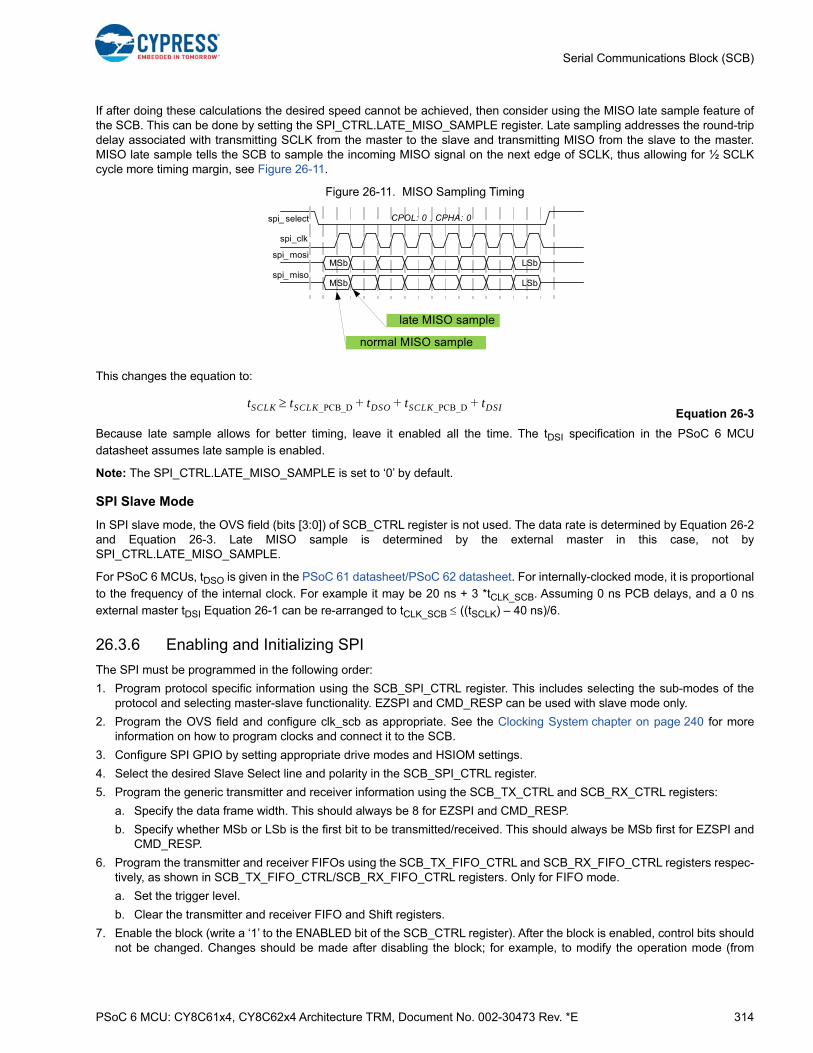
PSoC 6 MCU: CY8C61x4, CY8C62x4 Architecture TRM, Document No. 002-30473 Rev. *E 314
Serial Communications Block (SCB)
If after doing these calculations the desired speed cannot be achieved, then consider using the MISO late sample feature ofthe SCB. This can be done by setting the SPI_CTRL.LATE_MISO_SAMPLE register. Late sampling addresses the round-tripdelay associated with transmitting SCLK from the master to the slave and transmitting MISO from the slave to the master.MISO late sample tells the SCB to sample the incoming MISO signal on the next edge of SCLK, thus allowing for ½ SCLKcycle more timing margin, see Figure 26-11.
Figure 26-11. MISO Sampling Timing
This changes the equation to:
Equation 26-3
Because late sample allows for better timing, leave it enabled all the time. The tDSI specification in the PSoC 6 MCU
datasheet assumes late sample is enabled.
Note: The SPI_CTRL.LATE_MISO_SAMPLE is set to ‘0’ by default.
SPI Slave Mode
In SPI slave mode, the OVS field (bits [3:0]) of SCB_CTRL register is not used. The data rate is determined by Equation 26-2and Equation 26-3. Late MISO sample is determined by the external master in this case, not bySPI_CTRL.LATE_MISO_SAMPLE.
For PSoC 6 MCUs, tDSO is given in the PSoC 61 datasheet/PSoC 62 datasheet. For internally-clocked mode, it is proportional
to the frequency of the internal clock. For example it may be 20 ns + 3 *tCLK_SCB. Assuming 0 ns PCB delays, and a 0 ns
external master tDSI Equation 26-1 can be re-arranged to tCLK_SCB ((tSCLK) – 40 ns)/6.
26.3.6 Enabling and Initializing SPI
The SPI must be programmed in the following order:
1. Program protocol specific information using the SCB_SPI_CTRL register. This includes selecting the sub-modes of theprotocol and selecting master-slave functionality. EZSPI and CMD_RESP can be used with slave mode only.
2. Program the OVS field and configure clk_scb as appropriate. See the Clocking System chapter on page 240 for moreinformation on how to program clocks and connect it to the SCB.
3. Configure SPI GPIO by setting appropriate drive modes and HSIOM settings.
4. Select the desired Slave Select line and polarity in the SCB_SPI_CTRL register.
5. Program the generic transmitter and receiver information using the SCB_TX_CTRL and SCB_RX_CTRL registers:
a. Specify the data frame width. This should always be 8 for EZSPI and CMD_RESP.
b. Specify whether MSb or LSb is the first bit to be transmitted/received. This should always be MSb first for EZSPI andCMD_RESP.
6. Program the transmitter and receiver FIFOs using the SCB_TX_FIFO_CTRL and SCB_RX_FIFO_CTRL registers respec-tively, as shown in SCB_TX_FIFO_CTRL/SCB_RX_FIFO_CTRL registers. Only for FIFO mode.
a. Set the trigger level.
b. Clear the transmitter and receiver FIFO and Shift registers.
7. Enable the block (write a ‘1’ to the ENABLED bit of the SCB_CTRL register). After the block is enabled, control bits shouldnot be changed. Changes should be made after disabling the block; for example, to modify the operation mode (from
CPOL: 0 , CPHA: 0
spi_clk
spi_ mosiMSb LSb
spi_ select
spi_ misoMSb LSb
late MISO sample
normal MISO sample
tSCLK tSCLK_PCB_D tDSO tSCLK_PCB_D tDSI+ + +

PSoC 6 MCU: CY8C61x4, CY8C62x4 Architecture TRM, Document No. 002-30473 Rev. *E 315
Serial Communications Block (SCB)
Motorola mode to TI mode) or to go from externally clocked to internally clocked operation. The change takes effect onlyafter the block is re-enabled. Note: Re-enabling the block causes re-initialization and the associated state is lost (forexample, FIFO content).
26.3.7 I/O Pad Connection
26.3.7.1 SPI Master
Figure 26-12 and Table 26-4 list the use of the I/O pads for SPI Master.
Figure 26-12. SPI Master I/O Pad Connections
Normaloutput mode
spi_ctlspi_clk_out_en
spi_clk_out
spi_clk_inspi_clk
Input only
spi_miso spi_miso_in
0
don t care
spi_clk_out
spi_clk_out_en
spi_clk_in
spi_miso_out_en
spi_miso_out
spi_miso_in
Normaloutput mode
spi_select_out_en
spi_select_out
spi_select_inspi_select
spi_select_out
spi_select_out_en
spi_select_in
Normaloutput mode
spi_mosi_out_en
spi_mosi_out
spi_mosi_inspi_mosi
spi_mosi_out
spi_mosi_out_en
spi_mosi_in
spi_ctl
spi_ctl
spi_ctl
Table 26-4. SPI Master I/O Pad Connection Usage
I/O Pads Drive Mode On-chip I/O Signals Usage
spi_clk Normal output modespi_clk_out_en
spi_clk_outTransmit a clock signal
spi_select Normal output modespi_select_out_en
spi_select_outTransmit a select signal
spi_mosi Normal output modespi_mosi_out_en
spi_mosi_outTransmit a data element
spi_miso Input only spi_miso_in Receive a data element
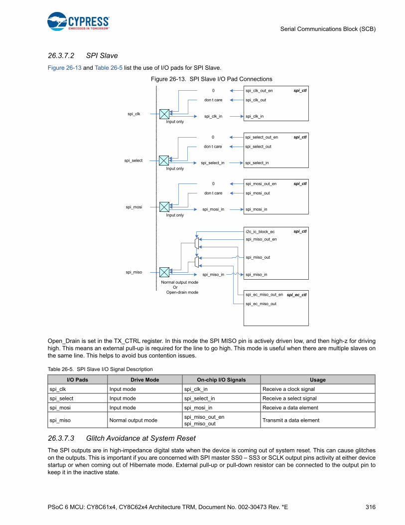
PSoC 6 MCU: CY8C61x4, CY8C62x4 Architecture TRM, Document No. 002-30473 Rev. *E 316
Serial Communications Block (SCB)
26.3.7.2 SPI Slave
Figure 26-13 and Table 26-5 list the use of I/O pads for SPI Slave.
Figure 26-13. SPI Slave I/O Pad Connections
Open_Drain is set in the TX_CTRL register. In this mode the SPI MISO pin is actively driven low, and then high-z for drivinghigh. This means an external pull-up is required for the line to go high. This mode is useful when there are multiple slaves onthe same line. This helps to avoid bus contention issues.
26.3.7.3 Glitch Avoidance at System Reset
The SPI outputs are in high-impedance digital state when the device is coming out of system reset. This can cause glitcheson the outputs. This is important if you are concerned with SPI master SS0 – SS3 or SCLK output pins activity at either devicestartup or when coming out of Hibernate mode. External pull-up or pull-down resistor can be connected to the output pin tokeep it in the inactive state.
Table 26-5. SPI Slave I/O Signal Description
I/O Pads Drive Mode On-chip I/O Signals Usage
spi_clk Input mode spi_clk_in Receive a clock signal
spi_select Input mode spi_select_in Receive a select signal
spi_mosi Input mode spi_mosi_in Receive a data element
spi_miso Normal output modespi_miso_out_en spi_miso_out
Transmit a data element
Input only
spi_ctl0
don t care
spi_clk_inspi_clk
Normal output modeOr
Open-drain mode
spi_misospi_miso_in
spi_clk_out
spi_clk_out_en
spi_clk_in
spi_miso_out_en
spi_miso_out
spi_miso_in
Input only
0
don t care
spi_select_inspi_select
spi_select_out
spi_select_out_en
spi_select_in
Input only
0
don t care
spi_mosi_inspi_mosi
spi_mosi_out
spi_mosi_out_en
spi_mosi_in
spi_ec_miso_out_en
spi_ec_miso_out
i2c_ic_block_ec
spi_ctl
spi_ctl
spi_ctl
spi_ec_ctl
PSoC 6 MCU: CY8C61x4, CY8C62x4 Architecture TRM, Document No. 002-30473 Rev. *E 317
Serial Communications Block (SCB)
26.3.7.4 Median Filter
This parameter applies a three-tap digital median filter on the input line. The master has one input line: MISO, and the slavehas three input lines: SCLK, MOSI, and SS. This filter reduces the susceptibility to errors. However, minimum oversamplingfactor value is increased. The default value is ‘Disabled’. To enable the median filter write a ‘1’ to RX_CTRL.MEDIAN.
26.3.8 SPI Registers
The SPI interface is controlled using a set of 32-bit control and status registers listed in Table 26-6. Some of these registersare used specifically with the Deep Sleep SCB; for more information on these registers, see the registers TRM.
Table 26-6. SPI Registers
Register Name Operation
SCB_CTRL Enables the SCB, selects the type of serial interface (SPI, UART, I2C), and selects internally and externally clocked operation, and EZ and non-EZ modes of operation.
SCB_STATUS (Deep Sleep SCB only)
In EZ mode, this register indicates whether the externally clocked logic is potentially using the EZ memory.
SCB_SPI_CTRLConfigures the SPI as either a master or a slave, selects SPI protocols (Motorola, TI, National) and clock-based submodes in Motorola SPI (modes 0,1,2,3), selects the type of SS signal in TI SPI.
SCB_SPI_STATUS Indicates whether the SPI bus is busy and sets the SPI slave EZ address in the internally clocked mode.
SCB_TX_CTRL Specifies the data frame width and specifies whether MSb or LSb is the first bit in transmission.
SCB_RX_CTRLPerforms the same function as that of the SCB_TX_CTRL register, but for the receiver. Also decides whether a median filter is to be used on the input interface lines.
SCB_TX_FIFO_CTRLSpecifies the trigger level, clears the transmitter FIFO and shift registers, and performs the FREEZE opera-tion of the transmitter FIFO.
SCB_RX_FIFO_CTRL Performs the same function as that of the SCB_TX_FIFO_CTRL register, but for the receiver.
SCB_TX_FIFO_WR Holds the data frame written into the transmitter FIFO. Behavior is similar to that of a PUSH operation.
SCB_RX_FIFO_RDHolds the data frame read from the receiver FIFO. Reading a data frame removes the data frame from the FIFO - behavior is similar to that of a POP operation. This register has a side effect when read by software: a data frame is removed from the FIFO.
SCB_RX_FIFO_RD_SILENTHolds the data frame read from the receiver FIFO. Reading a data frame does not remove the data frame from the FIFO; behavior is similar to that of a PEEK operation.
SCB_TX_FIFO_STATUSIndicates the number of bytes stored in the transmitter FIFO, the location from which a data frame is read by the hardware (read pointer), the location from which a new data frame is written (write pointer), and decides whether the transmitter FIFO holds the valid data.
SCB_RX_FIFO_STATUS Performs the same function as that of the SCB_TX_FIFO_STATUS register, but for the receiver.
SCB_EZ_DATA (Deep Sleep SCB only)
Holds the data in EZ memory location
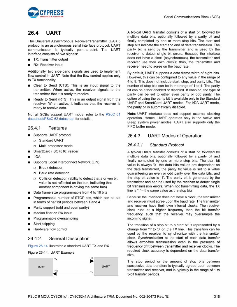
PSoC 6 MCU: CY8C61x4, CY8C62x4 Architecture TRM, Document No. 002-30473 Rev. *E 318
Serial Communications Block (SCB)
26.4 UART
The Universal Asynchronous Receiver/Transmitter (UART)protocol is an asynchronous serial interface protocol. UARTcommunication is typically point-to-point. The UARTinterface consists of two signals:
■ TX: Transmitter output
■ RX: Receiver input
Additionally, two side-band signals are used to implementflow control in UART. Note that the flow control applies onlyto TX functionality.
■ Clear to Send (CTS): This is an input signal to thetransmitter. When active, the receiver signals to thetransmitter that it is ready to receive.
■ Ready to Send (RTS): This is an output signal from thereceiver. When active, it indicates that the receiver isready to receive data.
Not all SCBs support UART mode; refer to the PSoC 61datasheet/PSoC 62 datasheet for details.
26.4.1 Features
■ Supports UART protocol
❐ Standard UART
❐ Multi-processor mode
■ SmartCard (ISO7816) reader
■ IrDA
■ Supports Local Interconnect Network (LIN)
❐ Break detection
❐ Baud rate detection
❐ Collision detection (ability to detect that a driven bit value is not reflected on the bus, indicating that another component is driving the same bus)
■ Data frame size programmable from 4 to 16 bits
■ Programmable number of STOP bits, which can be setin terms of half bit periods between 1 and 4
■ Parity support (odd and even parity)
■ Median filter on RX input
■ Programmable oversampling
■ Start skipping
■ Hardware flow control
26.4.2 General Description
Figure 26-14 illustrates a standard UART TX and RX.
Figure 26-14. UART Example
A typical UART transfer consists of a start bit followed bymultiple data bits, optionally followed by a parity bit andfinally completed by one or more stop bits. The start andstop bits indicate the start and end of data transmission. Theparity bit is sent by the transmitter and is used by thereceiver to detect single bit errors. Because the interfacedoes not have a clock (asynchronous), the transmitter andreceiver use their own clocks; thus, the transmitter andreceiver need to agree on the baud rate.
By default, UART supports a data frame width of eight bits.However, this can be configured to any value in the range of4 to 9. This does not include start, stop, and parity bits. Thenumber of stop bits can be in the range of 1 to 4. The paritybit can be either enabled or disabled. If enabled, the type ofparity can be set to either even parity or odd parity. Theoption of using the parity bit is available only in the StandardUART and SmartCard UART modes. For IrDA UART mode,the parity bit is automatically disabled.
Note: UART interface does not support external clockingoperation. Hence, UART operates only in the Active andSleep system power modes. UART also supports only theFIFO buffer mode.
26.4.3 UART Modes of Operation
26.4.3.1 Standard Protocol
A typical UART transfer consists of a start bit followed bymultiple data bits, optionally followed by a parity bit andfinally completed by one or more stop bits. The start bitvalue is always ‘0’, the data bits values are dependent onthe data transferred, the parity bit value is set to a valueguaranteeing an even or odd parity over the data bits, andthe stop bit value is ‘1’. The parity bit is generated by thetransmitter and can be used by the receiver to detect singlebit transmission errors. When not transmitting data, the TXline is ‘1’ – the same value as the stop bits.
Because the interface does not have a clock, the transmitterand receiver must agree upon the baud rate. The transmitterand receiver have their own internal clocks. The receiverclock runs at a higher frequency than the bit transferfrequency, such that the receiver may oversample theincoming signal.
The transition of a stop bit to a start bit is represented by achange from ‘1’ to ‘0’ on the TX line. This transition can beused by the receiver to synchronize with the transmitterclock. Synchronization at the start of each data transferallows error-free transmission even in the presence offrequency drift between transmitter and receiver clocks. Therequired clock accuracy is dependent on the data transfersize.
The stop period or the amount of stop bits betweensuccessive data transfers is typically agreed upon betweentransmitter and receiver, and is typically in the range of 1 to3-bit transfer periods.
UART UART
Tx
RxTx
Rx
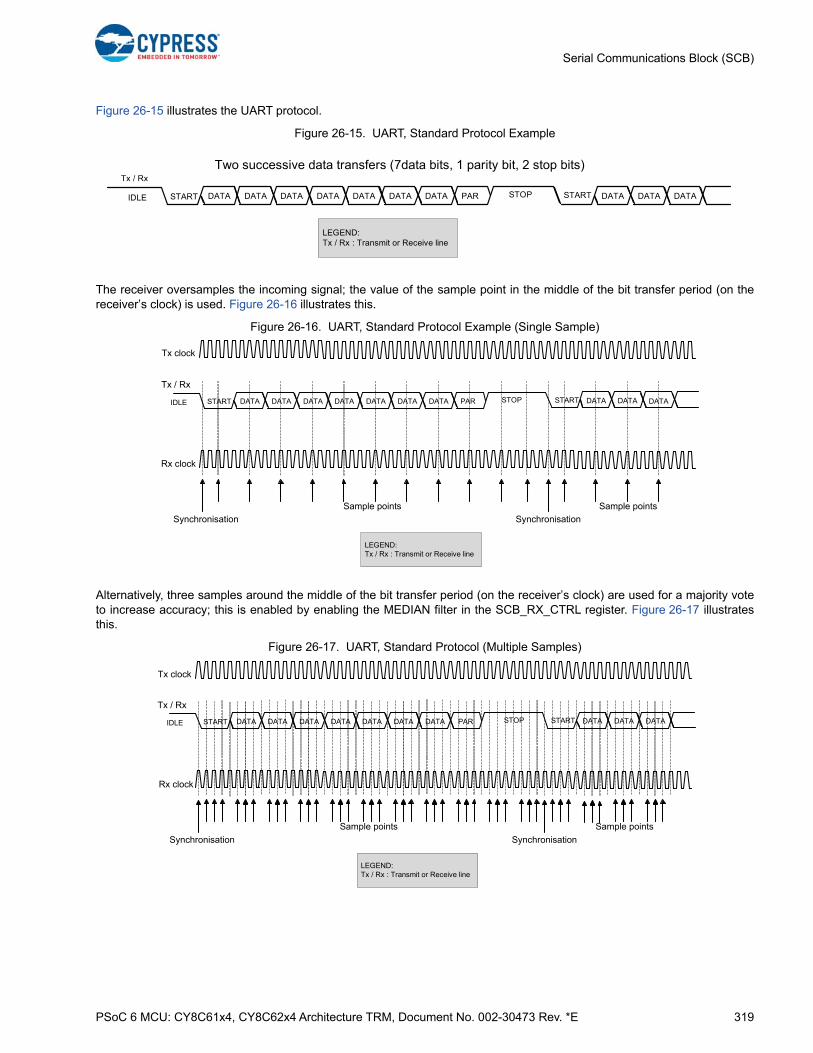
PSoC 6 MCU: CY8C61x4, CY8C62x4 Architecture TRM, Document No. 002-30473 Rev. *E 319
Serial Communications Block (SCB)
Figure 26-15 illustrates the UART protocol.
Figure 26-15. UART, Standard Protocol Example
The receiver oversamples the incoming signal; the value of the sample point in the middle of the bit transfer period (on thereceiver’s clock) is used. Figure 26-16 illustrates this.
Figure 26-16. UART, Standard Protocol Example (Single Sample)
Alternatively, three samples around the middle of the bit transfer period (on the receiver’s clock) are used for a majority voteto increase accuracy; this is enabled by enabling the MEDIAN filter in the SCB_RX_CTRL register. Figure 26-17 illustratesthis.
Figure 26-17. UART, Standard Protocol (Multiple Samples)
DATA DATA DATA DATA DATA DATA DATA PAR DATA DATA DATAIDLE START STOP START
Two successive data transfers (7data bits, 1 parity bit, 2 stop bits)
LEGEND:Tx / Rx : Transmit or Receive line
Tx / Rx
DATA DATA DATA DATA DATA DATA DATA PAR DATA DATA DATAIDLE START STOP START
Synchronisation
Sample points
Synchronisation
Sample points
Tx clock
Rx clock
Tx / Rx
LEGEND:Tx / Rx : Transmit or Receive line
DATA DATA DATA DATA DATA DATA DATA PAR DATA DATA DATAIDLE START STOP START
Synchronisation
Sample points
Synchronisation
Sample points
Tx clock
Rx clock
Tx / Rx
LEGEND:Tx / Rx : Transmit or Receive line
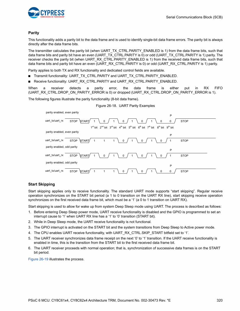
PSoC 6 MCU: CY8C61x4, CY8C62x4 Architecture TRM, Document No. 002-30473 Rev. *E 320
Serial Communications Block (SCB)
Parity
This functionality adds a parity bit to the data frame and is used to identify single-bit data frame errors. The parity bit is alwaysdirectly after the data frame bits.
The transmitter calculates the parity bit (when UART_TX_CTRL.PARITY_ENABLED is 1) from the data frame bits, such thatdata frame bits and parity bit have an even (UART_TX_CTRL.PARITY is 0) or odd (UART_TX_CTRL.PARITY is 1) parity. Thereceiver checks the parity bit (when UART_RX_CTRL.PARITY_ENABLED is 1) from the received data frame bits, such thatdata frame bits and parity bit have an even (UART_RX_CTRL.PARITY is 0) or odd (UART_RX_CTRL.PARITY is 1) parity.
Parity applies to both TX and RX functionality and dedicated control fields are available.
■ Transmit functionality: UART_TX_CTRL.PARITY and UART_TX_CTRL.PARITY_ENABLED.
■ Receive functionality: UART_RX_CTRL.PARITY and UART_RX_CTRL.PARITY_ENABLED.
When a receiver detects a parity error, the data frame is either put in RX FIFO(UART_RX_CTRL.DROP_ON_PARITY_ERROR is 0) or dropped (UART_RX_CTRL.DROP_ON_PARITY_ERROR is 1).
The following figures illustrate the parity functionality (8-bit data frame).
Figure 26-18. UART Parity Examples
Start Skipping
Start skipping applies only to receive functionality. The standard UART mode supports “start skipping”. Regular receiveoperation synchronizes on the START bit period (a 1 to 0 transition on the UART RX line), start skipping receive operationsynchronizes on the first received data frame bit, which must be a ‘1’ (a 0 to 1 transition on UART RX).
Start skipping is used to allow for wake up from system Deep Sleep mode using UART. The process is described as follows:
1. Before entering Deep Sleep power mode, UART receive functionality is disabled and the GPIO is programmed to set an interrupt cause to ‘1’ when UART RX line has a ‘1’ to ‘0’ transition (START bit).
2. While in Deep Sleep mode, the UART receive functionality is not functional.
3. The GPIO interrupt is activated on the START bit and the system transitions from Deep Sleep to Active power mode.
4. The CPU enables UART receive functionality, with UART_RX_CTRL.SKIP_START bitfield set to ‘1’.
5. The UART receiver synchronizes data frame receipt on the next ‘0’ to ‘1’ transition. If the UART receive functionality is enabled in time, this is the transition from the START bit to the first received data frame bit.
6. The UART receiver proceeds with normal operation; that is, synchronization of successive data frames is on the START bit period.
Figure 26-19 illustrates the process.
uart_tx/uart_rx
parity enabled, even parity
STOPSTARTSTOP 1 0 1 0 1 0 1 0 0
P
1st bit 2nd bit 3rd bit 4th bit 5th bit 6th bit 7th bit 8th bit 9th bit
uart_tx/uart_rx
parity enabled, even parity
STOPSTARTSTOP 1 1 1 0 1 0 1 0 1
P
uart_tx/uart_rx
parity enabled, odd parity
STOPSTARTSTOP 1 0 1 0 1 0 1 0 1
P
uart_tx/uart_rx
parity enabled, odd parity
STOPSTARTSTOP 1 1 1 0 1 0 1 0 0
P

PSoC 6 MCU: CY8C61x4, CY8C62x4 Architecture TRM, Document No. 002-30473 Rev. *E 321
Serial Communications Block (SCB)
Figure 26-19. UART Start Skip and Wakeup from Deep Sleep
Note that the above process works only for lower baud rates. The Deep Sleep to Active power mode transition and CPUenabling the UART receive functionality should take less than 1-bit period to ensure that the UART receiver is active in time todetect the ‘0’ to ‘1’ transition.
In step 4 of the above process, the firmware takes some time to finish the wakeup interrupt routine and enable the UARTreceive functionality before the block can detect the input rising edge on the UART RX line.
If the above steps cannot be completed in less than 1 bit time, first send a “dummy” byte to the device to wake it up beforesending real UART data. In this case, the SKIP_START bit can be left as 0. For more information on how to perform this infirmware, visit the UART section of the PDL.
Break Detection
Break detection is supported in the standard UART mode. This functionality detects when UART RX line is low (0) for morethan UART_RX_CTRL.BREAK_WIDTH bit periods. The break width should be larger than the maximum number of low (0) bitperiods in a regular data transfer, plus an additional 1-bit period. The additional 1-bit period is a minimum requirement andpreferably should be larger. The additional bit periods account for clock inaccuracies between transmitter and receiver.
For example, for an 8-bit data frame with parity support, the maximum number of low (0) bit periods is 10 (START bit, 8 ‘0’data frame bits, and one ‘0’ parity bit). Therefore, the break width should be larger than 10 + 1 = 11(UART_RX_CTRL.BREAK_WIDTH can be set to 11).
Note that the break detection applies only to receive functionality. A UART transmitter can generate a break by temporarilyincreasing TX_CTRL.DATA_WIDTH and transmitting an all zeroes data frame. A break is used by the transmitter to signal aspecial condition to the receiver. This condition may result in a reset, shut down, or initialization sequence at the receiver.
Break detection is part of the LIN protocol. When a break is detected, the INTR_RX.BREAK_DETECT interrupt cause is setto ‘1’. Figure 26-20 illustrates a regular data frame and break frame (8-bit data frame, parity support, and a break width of 12-bit periods).
Figure 26-20. UART – Regular Frame and Break Frame
uart_rx
1st bit
STARTIDLE/STOP D
1 Setup IOSS/GPIO
power mode Active ActiveDeep SleepA -> DS DS -> A
5
3 IOSS/GPIO wake up interrupt
4 CPU enables Rx functionality
UART RX synchronizes2 UART not operational
START
6UART Rx synchronizes
uart_rx
Regular frame
1st bit 2nd bit 3rd bit 4th bit 5th bit 6th bit
STOPSTARTSTOP
7th bit 8th bit 9th bit
Break frame (12 low/0-bit periods)
uart_rx STOPSTARTSTOP
D D D D D D D D P
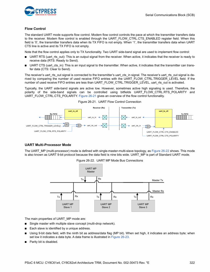
PSoC 6 MCU: CY8C61x4, CY8C62x4 Architecture TRM, Document No. 002-30473 Rev. *E 322
Serial Communications Block (SCB)
Flow Control
The standard UART mode supports flow control. Modem flow control controls the pace at which the transmitter transfers datato the receiver. Modem flow control is enabled through the UART_FLOW_CTRL.CTS_ENABLED register field. When thisfield is ‘0’, the transmitter transfers data when its TX FIFO is not empty. When ‘1’, the transmitter transfers data when UARTCTS line is active and its TX FIFO is not empty.
Note that the flow control applies only to TX functionality. Two UART side-band signal are used to implement flow control:
■ UART RTS (uart_rts_out): This is an output signal from the receiver. When active, it indicates that the receiver is ready toreceive data (RTS: Ready to Send).
■ UART CTS (uart_cts_in): This is an input signal to the transmitter. When active, it indicates that the transmitter can trans-fer data (CTS: Clear to Send).
The receiver’s uart_rts_out signal is connected to the transmitter’s uart_cts_in signal. The receiver’s uart_rts_out signal is de-rived by comparing the number of used receive FIFO entries with the UART_FLOW_CTRL.TRIGGER_LEVEL field. If thenumber of used receive FIFO entries are less than UART_FLOW_CTRL.TRIGGER_LEVEL, uart_rts_out is activated.
Typically, the UART side-band signals are active low. However, sometimes active high signaling is used. Therefore, thepolarity of the side-band signals can be controlled using bitfields UART_FLOW_CTRL.RTS_POLARITY andUART_FLOW_CTRL.CTS_POLARITY. Figure 26-21 gives an overview of the flow control functionality.
Figure 26-21. UART Flow Control Connection
UART Multi-Processor Mode
The UART_MP (multi-processor) mode is defined with single-master-multi-slave topology, as Figure 26-22 shows. This modeis also known as UART 9-bit protocol because the data field is nine bits wide. UART_MP is part of Standard UART mode.
Figure 26-22. UART MP Mode Bus Connections
The main properties of UART_MP mode are:
■ Single master with multiple slave concept (multi-drop network).
■ Each slave is identified by a unique address.
■ Using 9-bit data field, with the ninth bit as address/data flag (MP bit). When set high, it indicates an address byte; whenset low it indicates a data byte. A data frame is illustrated in Figure 26-23.
■ Parity bit is disabled.
uart_rx_ctl
Rx FIFO
Transmitter (Tx)
< uart_rts_out
UART_FLOW_CTRL.RTS_POLARITY
uart_rx_in
uart_tx_ctl
uart_cts_in
UART_FLOW_CTRL.CTS_POLARITY
UART_FLOW_CTRL.TRIGGER_LEVEL[]
uart_tx_out
Tx FIFO
UART_FLOW_CTRL.CTS_ENABLED
Receiver (Rx)
UART MPMaster
UART MPSlave 1
UART MPSlave 2
UART MPSlave 3
Tx
RxTx TxTx
Rx
RxRx
Master Tx
Master Rx

PSoC 6 MCU: CY8C61x4, CY8C62x4 Architecture TRM, Document No. 002-30473 Rev. *E 323
Serial Communications Block (SCB)
Figure 26-23. UART MP Address and Data Frame
The SCB can be used as either master or slave device in UART_MP mode. Both SCB_TX_CTRL and SCB_RX_CTRLregisters should be set to 9-bit data frame size. When the SCB works as UART_MP master device, the firmware changes theMP flag for every address or data frame. When it works as UART_MP slave device, the MP_MODE field of theSCB_UART_RX_CTRL register should be set to ‘1’. The SCB_RX_MATCH register should be set for the slave address andaddress mask. The matched address is written in the RX_FIFO when ADDR_ACCEPT field of the SCB_CTRL register is setto ‘1’. If the received address does not match its own address, then the interface ignores the following data, until next addressis received for compare.
Configuring the SCB as Standard UART Interface
To configure the SCB as a standard UART interface, set various register bits in the following order:
1. Configure the SCB as UART interface by writing ‘10b’ to the MODE field (bits [25:24]) of the SCB_CTRL register.
2. Configure the UART interface to operate as a Standard protocol by writing ‘00’ to the MODE field (bits [25:24]) of the SCB_UART_CTRL register.
3. To enable the UART MP Mode or UART LIN Mode, write ‘1’ to the MP_MODE (bit 10) or LIN_MODE (bit 12) respectively of the SCB_UART_RX_CTRL register.
4. Follow steps 2 to 4 described in “Enabling and Initializing the UART” on page 328.
For more information on these registers, see the registers TRM.
26.4.3.2 UART Local Interconnect Network (LIN) Mode
The LIN protocol is supported by the SCB as part of the standard UART. LIN is designed with single-master-multi-slavetopology. There is one master node and multiple slave nodes on the LIN bus. The SCB UART supports both LIN master andslave functionality. The LIN specification defines both physical layer (layer 1) and data link layer (layer 2). Figure 26-24illustrates the UART_LIN and LIN transceiver.
Figure 26-24. UART_LIN and LIN Transceiver
LIN protocol defines two tasks:
■ Master task: This task involves sending a header packet to initiate a LIN transfer.
■ Slave task: This task involves transmitting or receiving a response.
The master node supports master task and slave task; the slave node supports only slave task, as shown in Figure 26-25.
DATA DATA DATA DATA DATA DATA DATA DATAIDLE START STOPMP
DATA Field
UART LIN
LIN Transceiver
UART LIN
LIN Transceiver
LIN Master 1 LIN Slave 1 LIN Slave 2
Tx Rx Tx Rx
LIN BUS
UART LIN
LIN Transceiver
Tx Rx
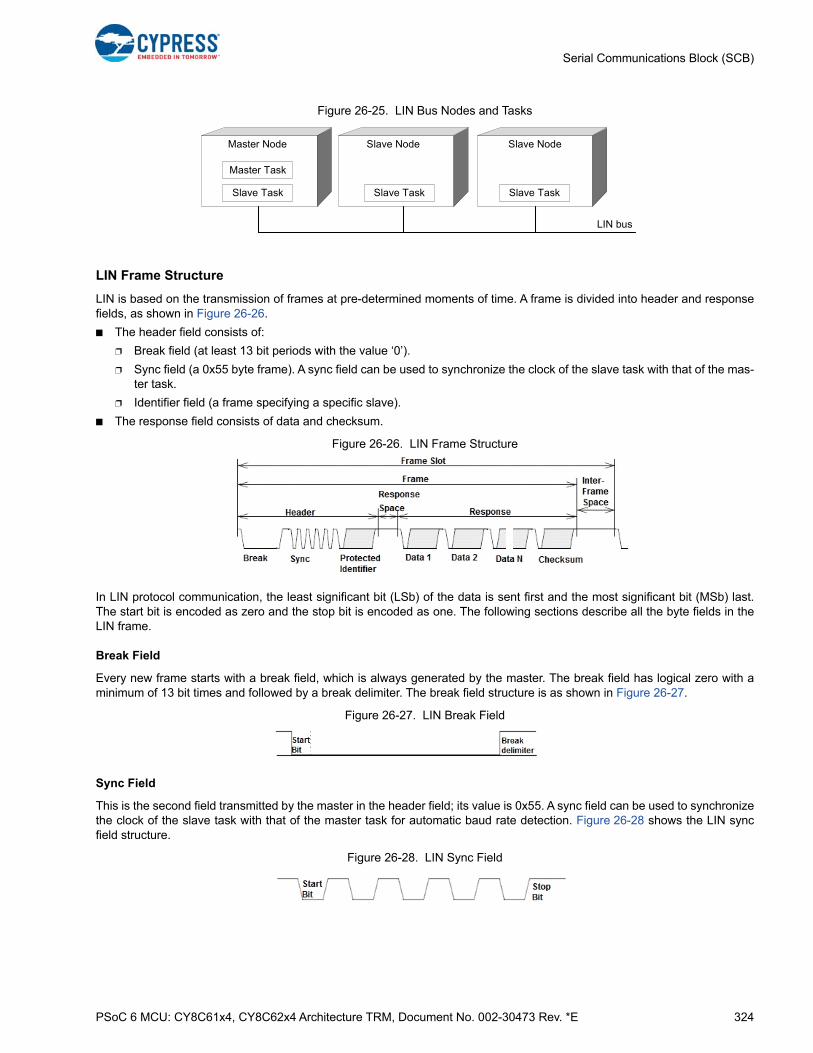
PSoC 6 MCU: CY8C61x4, CY8C62x4 Architecture TRM, Document No. 002-30473 Rev. *E 324
Serial Communications Block (SCB)
Figure 26-25. LIN Bus Nodes and Tasks
LIN Frame Structure
LIN is based on the transmission of frames at pre-determined moments of time. A frame is divided into header and responsefields, as shown in Figure 26-26.
■ The header field consists of:
❐ Break field (at least 13 bit periods with the value ‘0’).
❐ Sync field (a 0x55 byte frame). A sync field can be used to synchronize the clock of the slave task with that of the mas-ter task.
❐ Identifier field (a frame specifying a specific slave).
■ The response field consists of data and checksum.
Figure 26-26. LIN Frame Structure
In LIN protocol communication, the least significant bit (LSb) of the data is sent first and the most significant bit (MSb) last.The start bit is encoded as zero and the stop bit is encoded as one. The following sections describe all the byte fields in theLIN frame.
Break Field
Every new frame starts with a break field, which is always generated by the master. The break field has logical zero with aminimum of 13 bit times and followed by a break delimiter. The break field structure is as shown in Figure 26-27.
Figure 26-27. LIN Break Field
Sync Field
This is the second field transmitted by the master in the header field; its value is 0x55. A sync field can be used to synchronizethe clock of the slave task with that of the master task for automatic baud rate detection. Figure 26-28 shows the LIN syncfield structure.
Figure 26-28. LIN Sync Field
Master Node
Master Task
Slave Task
Slave Node Slave Node
LIN bus
Slave Task Slave Task

PSoC 6 MCU: CY8C61x4, CY8C62x4 Architecture TRM, Document No. 002-30473 Rev. *E 325
Serial Communications Block (SCB)
Protected Identifier (PID) Field
A protected identifier field consists of two sub-fields: theframe identifier (bits 0-5) and the parity (bit 6 and bit 7). ThePID field structure is shown in Figure 26-29.
■ Frame identifier: The frame identifiers are divided intothree categories
❐ Values 0 to 59 (0x3B) are used for signal carrying frames
❐ 60 (0x3C) and 61 (0x3D) are used to carry diagnostic and configuration data
❐ 62 (0x3E) and 63 (0x3F) are reserved for future pro-tocol enhancements
■ Parity: Frame identifier bits are used to calculate theparity
Figure 26-29 shows the PID field structure.
Figure 26-29. PID Field
Data. In LIN, every frame can carry a minimum of one byteand maximum of eight bytes of data. Here, the LSb of thedata byte is sent first and the MSb of the data byte is sentlast.
Checksum. The checksum is the last byte field in the LINframe. It is calculated by inverting the 8-bit sum along withcarryover of all data bytes only or the 8-bit sum with thecarryover of all data bytes and the PID field. There are twotypes of checksums in LIN frames. They are:
■ Classic checksum: the checksum calculated over all thedata bytes only (used in LIN 1.x slaves).
■ Enhanced checksum: the checksum calculated over allthe data bytes along with the protected identifier (used inLIN 2.x slaves).
LIN Frame Types
The type of frame refers to the conditions that need to bevalid to transmit the frame. According to the LINspecification, there are five different types of LIN frames. Anode or cluster does not have to support all frame types.
Unconditional Frame. These frames carry the signals andtheir frame identifiers (of 0x00 to 0x3B range). Thesubscriber will receive the frames and make it available tothe application; the publisher of the frame will provide theresponse to the header.
Event-Triggered Frame. The purpose of an event-triggered frame is to increase the responsiveness of the LINcluster without assigning too much of the bus bandwidth topolling of multiple slave nodes with seldom occurringevents. Event-triggered frames carry the response of one or
more unconditional frames. The unconditional framesassociated with an event triggered frame should:
■ Have equal length
■ Use the same checksum model (either classic orenhanced)
■ Reserve the first data field to its protected identifier
■ Be published by different slave nodes
■ Not be included directly in the same schedule table asthe event-triggered frame
Sporadic Frame. The purpose of the sporadic frames is tomerge some dynamic behavior into the schedule tablewithout affecting the rest of the schedule table. Theseframes have a group of unconditional frames that share theframe slot. When the sporadic frame is due for transmission,the unconditional frames are checked whether they haveany updated signals. If no signals are updated, no frame willbe transmitted and the frame slot will be empty.
Diagnostic Frames. Diagnostic frames always carrytransport layer, and contains eight data bytes.
The frame identifier for diagnostic frame is:
■ Master request frame (0x3C), or
■ Slave response frame (0x3D)
Before transmitting a master request frame, the master taskqueries its diagnostic module to see whether it will betransmitted or whether the bus will be silent. A slaveresponse frame header will be sent unconditionally. Theslave tasks publish and subscribe to the response accordingto their diagnostic modules.
Reserved Frames. These frames are reserved for futureuse; their frame identifiers are 0x3E and 0x3F.
LIN Go-To-Sleep and Wake-Up
The LIN protocol has the feature of keeping the LIN bus inSleep mode, if the master sends the go-to-sleep command.The go-to-sleep command is a master request frame (ID =0x3C) with the first byte field is equal to 0x00 and rest set to0xFF. The slave node application may still be active after thego-to-sleep command is received. This behavior isapplication specific. The LIN slave nodes automaticallyenter Sleep mode if the LIN bus inactivity is more than fourseconds.
Wake-up can be initiated by any node connected to the LINbus – either LIN master or any of the LIN slaves by forcingthe bus to be dominant for 250 µs to 5 ms. Each slaveshould detect the wakeup request and be ready to processheaders within 100 ms. The master should also detect thewakeup request and start sending headers when the slavenodes are active.
To support LIN, a dedicated (off-chip) line driver/receiver isrequired. Supply voltage range on the LIN bus is 7 V to 18 V.
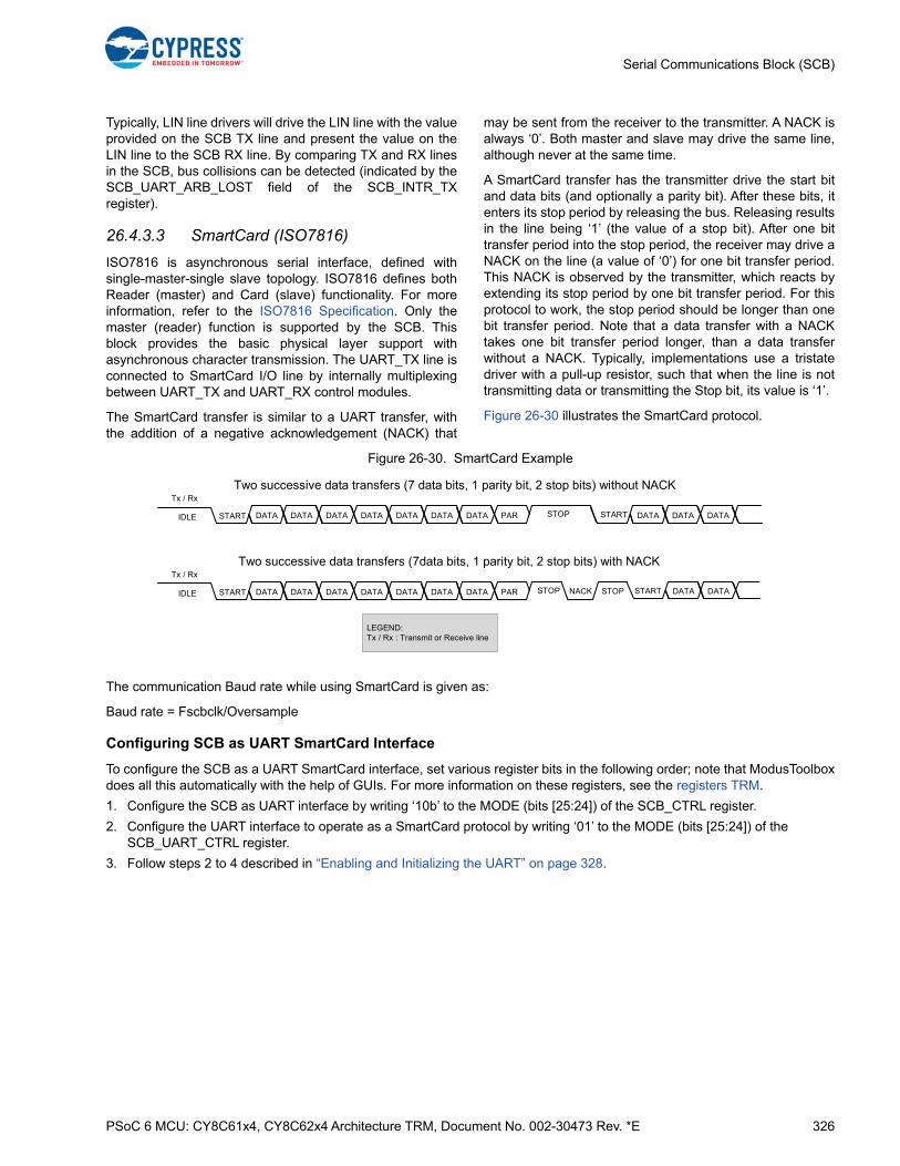
PSoC 6 MCU: CY8C61x4, CY8C62x4 Architecture TRM, Document No. 002-30473 Rev. *E 326
Serial Communications Block (SCB)
Typically, LIN line drivers will drive the LIN line with the valueprovided on the SCB TX line and present the value on theLIN line to the SCB RX line. By comparing TX and RX linesin the SCB, bus collisions can be detected (indicated by theSCB_UART_ARB_LOST field of the SCB_INTR_TXregister).
26.4.3.3 SmartCard (ISO7816)
ISO7816 is asynchronous serial interface, defined withsingle-master-single slave topology. ISO7816 defines bothReader (master) and Card (slave) functionality. For moreinformation, refer to the ISO7816 Specification. Only themaster (reader) function is supported by the SCB. Thisblock provides the basic physical layer support withasynchronous character transmission. The UART_TX line isconnected to SmartCard I/O line by internally multiplexingbetween UART_TX and UART_RX control modules.
The SmartCard transfer is similar to a UART transfer, withthe addition of a negative acknowledgement (NACK) that
may be sent from the receiver to the transmitter. A NACK isalways ‘0’. Both master and slave may drive the same line,although never at the same time.
A SmartCard transfer has the transmitter drive the start bitand data bits (and optionally a parity bit). After these bits, itenters its stop period by releasing the bus. Releasing resultsin the line being ‘1’ (the value of a stop bit). After one bittransfer period into the stop period, the receiver may drive aNACK on the line (a value of ‘0’) for one bit transfer period.This NACK is observed by the transmitter, which reacts byextending its stop period by one bit transfer period. For thisprotocol to work, the stop period should be longer than onebit transfer period. Note that a data transfer with a NACKtakes one bit transfer period longer, than a data transferwithout a NACK. Typically, implementations use a tristatedriver with a pull-up resistor, such that when the line is nottransmitting data or transmitting the Stop bit, its value is ‘1’.
Figure 26-30 illustrates the SmartCard protocol.
Figure 26-30. SmartCard Example
The communication Baud rate while using SmartCard is given as:
Baud rate = Fscbclk/Oversample
Configuring SCB as UART SmartCard Interface
To configure the SCB as a UART SmartCard interface, set various register bits in the following order; note that ModusToolboxdoes all this automatically with the help of GUIs. For more information on these registers, see the registers TRM.
1. Configure the SCB as UART interface by writing ‘10b’ to the MODE (bits [25:24]) of the SCB_CTRL register.
2. Configure the UART interface to operate as a SmartCard protocol by writing ‘01’ to the MODE (bits [25:24]) of the SCB_UART_CTRL register.
3. Follow steps 2 to 4 described in “Enabling and Initializing the UART” on page 328.
DATA DATA DATA DATA DATA DATA DATA PAR DATA DATA DATAIDLE START STOP START
Two successive data transfers (7 data bits, 1 parity bit, 2 stop bits) without NACKTx / Rx
DATA DATA DATA DATA DATA DATA DATA PAR DATA DATAIDLE START STOP START
Two successive data transfers (7data bits, 1 parity bit, 2 stop bits) with NACK
LEGEND:Tx / Rx : Transmit or Receive line
Tx / Rx
STOPNACK

PSoC 6 MCU: CY8C61x4, CY8C62x4 Architecture TRM, Document No. 002-30473 Rev. *E 327
Serial Communications Block (SCB)
26.4.3.4 Infrared Data Association (IrDA)
The SCB supports the IrDA protocol for data rates of up to 115.2 kbps using the UART interface. It supports only the basicphysical layer of IrDA protocol with rates less than 115.2 kbps. Hence, the system instantiating this block must consider howto implement a complete IrDA communication system with other available system resources.
The IrDA protocol adds a modulation scheme to the UART signaling. At the transmitter, bits are modulated. At the receiver,bits are demodulated. The modulation scheme uses a Return-to-Zero-Inverted (RZI) format. A bit value of ‘0’ is signaled by ashort ‘1’ pulse on the line and a bit value of ‘1’ is signaled by holding the line to ‘0’. For these data rates (<=115.2 kbps), theRZI modulation scheme is used and the pulse duration is 3/16 of the bit period. The sampling clock frequency should be set16 times the selected baud rate, by configuring the SCB_OVS field of the SCB_CTRL register. In addition, the PSoC 6 MCUSCB supports a low-power IrDA receiver mode, which allows it to detect pulses with a minimum width of 1.41 µs.
Different communication speeds under 115.2 kbps can be achieved by configuring clk_scb frequency. Additional allowablerates are 2.4 kbps, 9.6 kbps, 19.2 kbps, 38.4 kbps, and 57.6 kbps. Figure 26-31 shows how a UART transfer is IrDAmodulated.
Figure 26-31. IrDA Example
Configuring the SCB as a UART IrDA Interface
To configure the SCB as a UART IrDA interface, set various register bits in the following order; note that ModusToolbox doesall this automatically with the help of GUIs. For more information on these registers, see the registers TRM.
1. Configure the SCB as a UART interface by writing ‘10b’ to the MODE (bits [25:24]) of the SCB_CTRL register.
2. Configure the UART interface to operate as IrDA protocol by writing ‘10’ to the MODE (bits [25:24]) of the SCB_UART_C-TRL register.
3. Enable the Median filter on the input interface line by writing ‘1’ to MEDIAN (bit 9) of the SCB_RX_CTRL register.
4. Configure the SCB as described in “Enabling and Initializing the UART” on page 328.
PARIDLE START STOP START
Two successive data transfers (7 data bits, 1 parity bit, 2 stop bits)Tx / Rx
IrDATx / Rx
LEGEND:Tx / Rx : Transmit or Receive line
PSoC 6 MCU: CY8C61x4, CY8C62x4 Architecture TRM, Document No. 002-30473 Rev. *E 328
Serial Communications Block (SCB)
26.4.4 Clocking and Oversampling
The UART protocol is implemented using clk_scb as anoversampled multiple of the baud rate. For example, toimplement a 100-kHz UART, clk_scb could be set to 1 MHzand the oversample factor set to ‘10’. The oversampling isset using the SCB_CTRL.OVS register field. Theoversampling value is SCB_CTRL.OVS + 1. In the UARTstandard sub-mode (including LIN) and the SmartCard sub-mode, the valid range for the OVS field is [7, 15].
In UART transmit IrDA sub-mode, this field indirectlyspecifies the oversampling. Oversampling determines theinterface clock per bit cycle and the width of the pulse. Thissub-mode has only one valid OVS value–16 (which is avalue of 0 in the OVS field of the SCB_CTRL register); thepulse width is roughly 3/16 of the bit period (for all bit rates).
In UART receive IrDA sub-mode (1.2, 2.4, 9.6, 19.2, 38.4,57.6, and 115.2 kbps), this field indirectly specifies theoversampling. In normal transmission mode, this pulse isapproximately 3/16 of the bit period (for all bit rates). In low-power transmission mode, this pulse is potentially smaller(down to 1.62 µs typical and 1.41 µs minimal) than 3/16 ofthe bit period (for less than 115.2 kbps bit rates).
Pulse widths greater than or equal to two SCB input clockcycles are guaranteed to be detected by the receiver. Pulsewidths less than two clock cycles and greater than or equalto one SCB input clock cycle may be detected by thereceiver. Pulse widths less than one SCB input clock cyclewill not be detected by the receiver. Note that theSCB_RX_CTRL.MEDIAN should be set to ‘1’ for IrDAreceiver functionality.
The SCB input clock and the oversampling togetherdetermine the IrDA bit rate. Refer to the registers TRM formore details on the OVS values for different baud rates.
26.4.5 Enabling and Initializing the UART
The UART must be programmed in the following order:
1. Program protocol specific information using theUART_TX_CTRL, UART_RX_CTRL, andUART_FLOW_CTRL registers. This includes selectingthe submodes of the protocol, transmitter-receiverfunctionality, and so on.
2. Program the generic transmitter and receiver informationusing the SCB_TX_CTRL and SCB_RX_CTRLregisters.
a. Specify the data frame width.
b. Specify whether MSb or LSb is the first bit to betransmitted or received.
3. Program the transmitter and receiver FIFOs using theSCB_TX_FIFO_CTRL and SCB_RX_FIFO_CTRLregisters, respectively.
a. Set the trigger level.
b. Clear the transmitter and receiver FIFO and Shiftregisters.
4. Enable the block (write a ‘1’ to the ENABLE bit of theSCB_CTRL register). After the block is enabled, controlbits should not be changed. Changes should be madeafter disabling the block; for example, to modify theoperation mode (from SmartCard to IrDA). The changetakes effect only after the block is re-enabled. Note thatre-enabling the block causes re-initialization and theassociated state is lost (for example FIFO content).
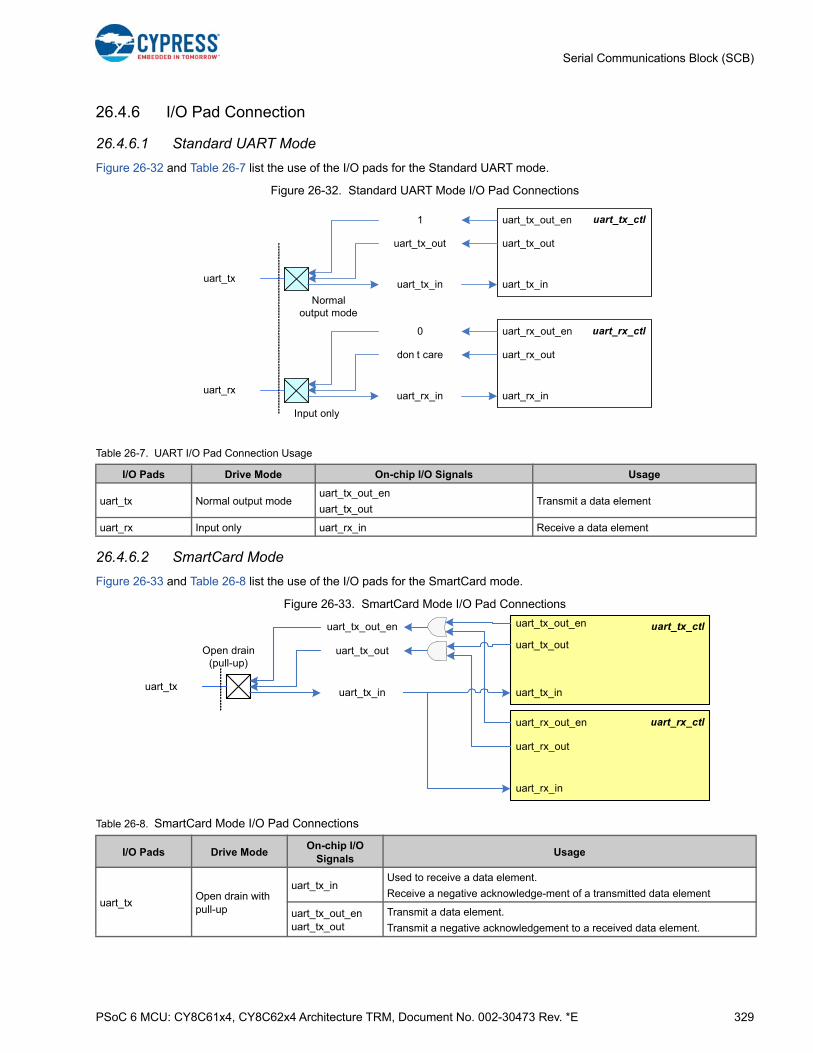
PSoC 6 MCU: CY8C61x4, CY8C62x4 Architecture TRM, Document No. 002-30473 Rev. *E 329
Serial Communications Block (SCB)
26.4.6 I/O Pad Connection
26.4.6.1 Standard UART Mode
Figure 26-32 and Table 26-7 list the use of the I/O pads for the Standard UART mode.
Figure 26-32. Standard UART Mode I/O Pad Connections
26.4.6.2 SmartCard Mode
Figure 26-33 and Table 26-8 list the use of the I/O pads for the SmartCard mode.
Figure 26-33. SmartCard Mode I/O Pad Connections
Table 26-7. UART I/O Pad Connection Usage
I/O Pads Drive Mode On-chip I/O Signals Usage
uart_tx Normal output modeuart_tx_out_en
uart_tx_outTransmit a data element
uart_rx Input only uart_rx_in Receive a data element
uart_rx_ctl
Normaloutput mode
uart_tx_ctl1
uart_tx_out
uart_tx_inuart_tx
Input only
uart_rxuart_rx_in
0
don t care
uart_tx_out
uart_tx_out_en
uart_tx_in
uart_rx_out_en
uart_rx_out
uart_rx_in
Table 26-8. SmartCard Mode I/O Pad Connections
I/O Pads Drive ModeOn-chip I/O
SignalsUsage
uart_txOpen drain with pull-up
uart_tx_inUsed to receive a data element.
Receive a negative acknowledge-ment of a transmitted data element
uart_tx_out_enuart_tx_out
Transmit a data element.
Transmit a negative acknowledgement to a received data element.
Open drain(pull-up)
uart_tx_out_en
uart_tx_out
uart_tx_inuart_tx
uart_tx_ctl
uart_rx_ctluart_rx_out_en
uart_rx_out
uart_rx_in
uart_tx_in
uart_tx_out
uart_tx_out_en

PSoC 6 MCU: CY8C61x4, CY8C62x4 Architecture TRM, Document No. 002-30473 Rev. *E 330
Serial Communications Block (SCB)
26.4.6.3 LIN Mode
Figure 26-34 and Table 26-9 list the use of the I/O pads for LIN mode.
Figure 26-34. LIN Mode I/O Pad Connections
26.4.6.4 IrDA Mode
Figure 26-35 and Table 26-10 list the use of the I/O pads for IrDA mode.
Figure 26-35. IrDA Mode I/O Pad Connections
Table 26-9. LIN Mode I/O Pad Connections
I/O Pads Drive ModeOn-chip I/O
SignalsUsage
uart_txNormal output mode
uart_tx_out_enuart_tx_out
Transmit a data element.
uart_rx Input only uart_rx_in Receive a data element.
Normaloutput mode
uart_tx_ctl1
uart_tx_out
uart_tx_inuart_tx
Input only
uart_rxuart_rx_in
0
don t care
uart_rx_ctl
uart_tx_out
uart_tx_out_en
uart_tx_in
uart_rx_out_en
uart_rx_out
uart_rx_in
LIN transceiver
chip
LIN
Table 26-10. IrDA Mode I/O Pad Connections
I/O Pads Drive ModeOn-chip I/O
SignalsUsage
uart_txNormal output mode
uart_tx_out_enuart_tx_out
Transmit a data element.
uart_rx Input only uart_rx_in Receive a data element.
Normaloutput mode
uart_tx_ctl1
uart_tx_out
uart_tx_inuart_tx
Input only
uart_rxuart_rx_in
0
don t care
uart_rx_ctl
uart_tx_out
uart_tx_out_en
uart_tx_in
uart_rx_out_en
uart_rx_out
uart_rx_in
IrDA transducer
module
IrDA
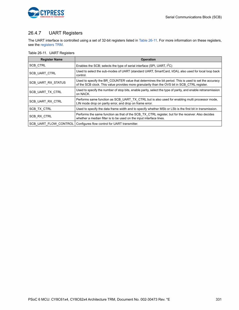
PSoC 6 MCU: CY8C61x4, CY8C62x4 Architecture TRM, Document No. 002-30473 Rev. *E 331
Serial Communications Block (SCB)
26.4.7 UART Registers
The UART interface is controlled using a set of 32-bit registers listed in Table 26-11. For more information on these registers,see the registers TRM.
Table 26-11. UART Registers
Register Name Operation
SCB_CTRL Enables the SCB; selects the type of serial interface (SPI, UART, I2C)
SCB_UART_CTRLUsed to select the sub-modes of UART (standard UART, SmartCard, IrDA), also used for local loop back control.
SCB_UART_RX_STATUSUsed to specify the BR_COUNTER value that determines the bit period. This is used to set the accuracy of the SCB clock. This value provides more granularity than the OVS bit in SCB_CTRL register.
SCB_UART_TX_CTRLUsed to specify the number of stop bits, enable parity, select the type of parity, and enable retransmission on NACK.
SCB_UART_RX_CTRLPerforms same function as SCB_UART_TX_CTRL but is also used for enabling multi processor mode, LIN mode drop on parity error, and drop on frame error.
SCB_TX_CTRL Used to specify the data frame width and to specify whether MSb or LSb is the first bit in transmission.
SCB_RX_CTRLPerforms the same function as that of the SCB_TX_CTRL register, but for the receiver. Also decides whether a median filter is to be used on the input interface lines.
SCB_UART_FLOW_CONTROL Configures flow control for UART transmitter.

PSoC 6 MCU: CY8C61x4, CY8C62x4 Architecture TRM, Document No. 002-30473 Rev. *E 332
Serial Communications Block (SCB)
26.5 Inter Integrated Circuit (I2C)
This section explains the I2C implementation in the PSoC 6 MCU. For more information on the I2C protocol specification, referto the I2C-bus specification available on the NXP website.
26.5.1 Features
This block supports the following features:
■ Master, slave, and master/slave mode
■ Standard-mode (100 kbps), fast-mode (400 kbps), and fast-mode plus (1000 kbps) data-rates
■ 7-bit slave addressing
■ Clock stretching
■ Collision detection
■ Programmable oversampling of I2C clock signal (SCL)
■ Auto ACK when RX FIFO not full, including address
■ General address detection
■ FIFO Mode
■ EZ and CMD_RESP modes
26.5.2 General Description
Figure 26-36 illustrates an example of an I2C communication network.
Figure 26-36. I2C Interface Block Diagram
The standard I2C bus is a two wire interface with the following lines:
■ Serial Data (SDA)
■ Serial Clock (SCL)
I2C devices are connected to these lines using open collector or open-drain output stages, with pull-up resistors (Rp). Asimple master/slave relationship exists between devices. Masters and slaves can operate as either transmitter or receiver.Each slave device connected to the bus is software addressable by a unique 7-bit address.
VDD
RpRp
SCL
SDA
I2CMaster I2C Slave I2C Slave I2C Slave

PSoC 6 MCU: CY8C61x4, CY8C62x4 Architecture TRM, Document No. 002-30473 Rev. *E 333
Serial Communications Block (SCB)
26.5.3 External Electrical Connections
As shown in Figure 26-37, the I2C bus requires external pull-up resistors. The pull-up resistors (RP) are primarily determinedby the supply voltage, bus speed, and bus capacitance. For detailed information on how to calculate the optimum pull-upresistor value for your design Cypress recommends using the UM10204 I2C-bus specification and user manual Rev. 6,available from the NXP website at www.nxp.com.
Figure 26-37. Connection of Devices to the I2C Bus
For most designs, the default values shown inTable 26-12 provide excellent performance without any calculations. Thedefault values were chosen to use standard resistor values between the minimum and maximum limits.
These values work for designs with 1.8 V to 5.0 V VDD, less than 200 pF bus capacitance (CB), up to 25 µA of total inputleakage (IIL), up to 0.4 V output voltage level (VOL), and a max VIH of 0.7 * VDD. Calculation of custom pull-up resistor valuesis required if your design does not meet the default assumptions, you use series resistors (RS) to limit injected noise, or youwant to maximize the resistor value for low power consumption. Calculation of the ideal pull-up resistor value involves findinga value between the limits set by three equations detailed in the NXP I2C specification. These equations are:
Equation 26-4
Equation 26-5
Equation 26-6
Equation parameters:
■ VDD = Nominal supply voltage for I2C bus
■ VOL = Maximum output low voltage of bus devices
■ IOL= Low-level output current from I2C specification
■ TR = Rise time of bus from I2C specification
■ CB = Capacitance of each bus line including pins and PCB traces
■ VIH = Minimum high-level input voltage of all bus devices
■ VNH = Minimum high-level input noise margin from I2C specification
■ IIH = Total input leakage current of all devices on the bus
Table 26-12. Recommended Default Pull-up Resistor Values
Standard Mode (0 – 100 kbps) Fast Mode (0 – 400 kbps) Fast Mode Plus (0 – 1000 kbps) Units
4.7 k, 5% 1.74 k, 1% 620, 5%
Device 1
SDA (Serial Data Line)
SCL (Serial Clock Line)
Device 2
Rp Rp
+VDD
pull-upresistors
RPMIN = (VDD(max) – VOL(max)) / IOL(min)
RPMAX = TR(max) / 0.8473 x CB(max)
RPMAX = VDD(min) – (VIH(min) + VNH(min)) / IIH(max)
PSoC 6 MCU: CY8C61x4, CY8C62x4 Architecture TRM, Document No. 002-30473 Rev. *E 334
Serial Communications Block (SCB)
The supply voltage (VDD) limits the minimum pull-up resistorvalue due to bus devices maximum low output voltage (VOL)specifications. Lower pull-up resistance increases currentthrough the pins and can therefore exceed the specconditions of VOH. Equation 26-4 is derived using Ohm's lawto determine the minimum resistance that will still meet theVOL specification at 3 mA for standard and fast modes, and20 mA for fast mode plus at the given VDD.
Equation 26-5 determines the maximum pull-up resistancedue to bus capacitance. Total bus capacitance is comprisedof all pin, wire, and trace capacitance on the bus. The higherthe bus capacitance the lower the pull-up resistancerequired to meet the specified bus speeds rise time due toRC delays. Choosing a pull-up resistance higher thanallowed can result in failing timing requirements resulting incommunication errors. Most designs with five of fewer I2Cdevices and up to 20 centimeters of bus trace length haveless than 100 pF of bus capacitance.
A secondary effect that limits the maximum pull-up resistorvalue is total bus leakage calculated in Equation 26-6. Theprimary source of leakage is I/O pins connected to the bus.If leakage is too high, the pull-ups will have difficultymaintaining an acceptable VIH level causing communicationerrors. Most designs with five or fewer I2C devices on thebus have less than 10 µA of total leakage current.
26.5.4 Terms and Definitions
Table 26-13 explains the commonly used terms in an I2Ccommunication network.
26.5.4.1 Clock Stretching
When a slave device is not yet ready to process data, it maydrive a ‘0’ on the SCL line to hold it down. Due to theimplementation of the I/O signal interface, the SCL linevalue will be ‘0’, independent of the values that any othermaster or slave may be driving on the SCL line. This isknown as clock stretching and is the only situation in whicha slave drives the SCL line. The master device monitors theSCL line and detects it when it cannot generate a positiveclock pulse (‘1’) on the SCL line. It then reacts by delayingthe generation of a positive edge on the SCL line, effectivelysynchronizing with the slave device that is stretching theclock. The SCB on the PSoC 6 MCU can and will stretch theclock.
26.5.4.2 Bus Arbitration
The I2C protocol is a multi-master, multi-slave interface. Busarbitration is implemented on master devices by monitoringthe SDA line. Bus collisions are detected when the masterobserves an SDA line value that is not the same as thevalue it is driving on the SDA line. For example, whenmaster 1 is driving the value ‘1’ on the SDA line and master2 is driving the value ‘0’ on the SDA line, the actual linevalue will be ‘0’ due to the implementation of the I/O signalinterface. Master 1 detects the inconsistency and losescontrol of the bus. Master 2 does not detect anyinconsistency and keeps control of the bus.
26.5.5 I2C Modes of Operation
I2C is a synchronous single master, multi-master, multi-slaveserial interface. Devices operate in either master mode,slave mode, or master/slave mode. In master/slave mode,the device switches from master to slave mode when it isaddressed. Only a single master may be active during adata transfer. The active master is responsible for driving theclock on the SCL line. Table 26-14 illustrates the I2C modesof operation.
Table 26-13. Definition of I2C Bus Terminology
Term Description
Transmitter The device that sends data to the bus
Receiver The device that receives data from the bus
MasterThe device that initiates a transfer, generates clock signals, and terminates a transfer
Slave The device addressed by a master
Multi-masterMore than one master can attempt to control the bus at the same time
Arbitration
Procedure to ensure that, if more than one master simultaneously tries to control the bus, only one is allowed to do so and the winning message is not corrupted
SynchronizationProcedure to synchronize the clock signals of two or more devices
Table 26-14. I2C Modes
Mode Description
Slave Slave only operation (default)
Master Master only operation
Multi-master Supports more than one master on the bus
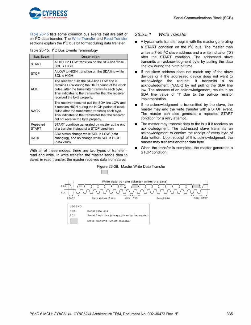
PSoC 6 MCU: CY8C61x4, CY8C62x4 Architecture TRM, Document No. 002-30473 Rev. *E 335
Serial Communications Block (SCB)
Table 26-15 lists some common bus events that are part ofan I2C data transfer. The Write Transfer and Read Transfersections explain the I2C bus bit format during data transfer.
With all of these modes, there are two types of transfer -read and write. In write transfer, the master sends data toslave; in read transfer, the master receives data from slave.
26.5.5.1 Write Transfer
■ A typical write transfer begins with the master generating
a START condition on the I2C bus. The master then
writes a 7-bit I2C slave address and a write indicator (‘0’)after the START condition. The addressed slavetransmits an acknowledgment byte by pulling the dataline low during the ninth bit time.
■ If the slave address does not match any of the slavedevices or if the addressed device does not want toacknowledge the request, it transmits a noacknowledgment (NACK) by not pulling the SDA linelow. The absence of an acknowledgement, results in anSDA line value of ‘1’ due to the pull-up resistorimplementation.
■ If no acknowledgment is transmitted by the slave, themaster may end the write transfer with a STOP event.The master can also generate a repeated STARTcondition for a retry attempt.
■ The master may transmit data to the bus if it receives anacknowledgment. The addressed slave transmits anacknowledgment to confirm the receipt of every byte ofdata written. Upon receipt of this acknowledgment, themaster may transmit another data byte.
■ When the transfer is complete, the master generates aSTOP condition.
Figure 26-38. Master Write Data Transfer
Table 26-15. I2C Bus Events Terminology
Bus Event Description
STARTA HIGH to LOW transition on the SDA line while SCL is HIGH
STOPA LOW to HIGH transition on the SDA line while SCL is HIGH
ACK
The receiver pulls the SDA line LOW and it remains LOW during the HIGH period of the clock pulse, after the transmitter transmits each byte. This indicates to the transmitter that the receiver received the byte properly.
NACK
The receiver does not pull the SDA line LOW and it remains HIGH during the HIGH period of clock pulse after the transmitter transmits each byte. This indicates to the transmitter that the receiver did not receive the byte properly.
Repeated START
START condition generated by master at the end of a transfer instead of a STOP condition
DATASDA status change while SCL is LOW (data changing), and no change while SCL is HIGH (data valid)
M Sb L S bSDA
SCL
START Slave address (7 bits) W rite ACK ACKData (8 b its) STO P
W rite data transfer (M aster w rites the data)
LEG EN D :
SDA: Seria l Data L ine
SCL: Seria l C lock Line (a lways driven by the m aster)
S lave Transm it / M aster R eceive
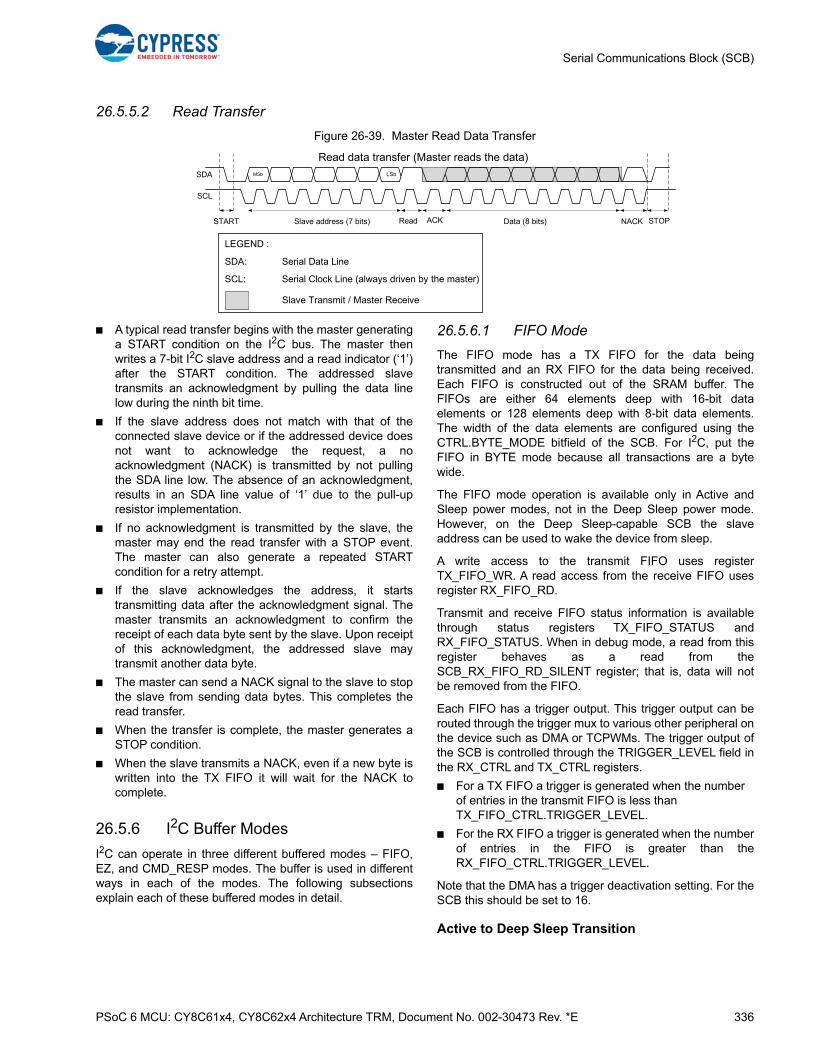
PSoC 6 MCU: CY8C61x4, CY8C62x4 Architecture TRM, Document No. 002-30473 Rev. *E 336
Serial Communications Block (SCB)
26.5.5.2 Read Transfer
Figure 26-39. Master Read Data Transfer
■ A typical read transfer begins with the master generatinga START condition on the I2C bus. The master thenwrites a 7-bit I2C slave address and a read indicator (‘1’)after the START condition. The addressed slavetransmits an acknowledgment by pulling the data linelow during the ninth bit time.
■ If the slave address does not match with that of theconnected slave device or if the addressed device doesnot want to acknowledge the request, a noacknowledgment (NACK) is transmitted by not pullingthe SDA line low. The absence of an acknowledgment,results in an SDA line value of ‘1’ due to the pull-upresistor implementation.
■ If no acknowledgment is transmitted by the slave, themaster may end the read transfer with a STOP event.The master can also generate a repeated STARTcondition for a retry attempt.
■ If the slave acknowledges the address, it startstransmitting data after the acknowledgment signal. Themaster transmits an acknowledgment to confirm thereceipt of each data byte sent by the slave. Upon receiptof this acknowledgment, the addressed slave maytransmit another data byte.
■ The master can send a NACK signal to the slave to stopthe slave from sending data bytes. This completes theread transfer.
■ When the transfer is complete, the master generates aSTOP condition.
■ When the slave transmits a NACK, even if a new byte iswritten into the TX FIFO it will wait for the NACK tocomplete.
26.5.6 I2C Buffer Modes
I2C can operate in three different buffered modes – FIFO,EZ, and CMD_RESP modes. The buffer is used in differentways in each of the modes. The following subsectionsexplain each of these buffered modes in detail.
26.5.6.1 FIFO Mode
The FIFO mode has a TX FIFO for the data beingtransmitted and an RX FIFO for the data being received.Each FIFO is constructed out of the SRAM buffer. TheFIFOs are either 64 elements deep with 16-bit dataelements or 128 elements deep with 8-bit data elements.The width of the data elements are configured using theCTRL.BYTE_MODE bitfield of the SCB. For I2C, put theFIFO in BYTE mode because all transactions are a bytewide.
The FIFO mode operation is available only in Active andSleep power modes, not in the Deep Sleep power mode.However, on the Deep Sleep-capable SCB the slaveaddress can be used to wake the device from sleep.
A write access to the transmit FIFO uses registerTX_FIFO_WR. A read access from the receive FIFO usesregister RX_FIFO_RD.
Transmit and receive FIFO status information is availablethrough status registers TX_FIFO_STATUS andRX_FIFO_STATUS. When in debug mode, a read from thisregister behaves as a read from theSCB_RX_FIFO_RD_SILENT register; that is, data will notbe removed from the FIFO.
Each FIFO has a trigger output. This trigger output can berouted through the trigger mux to various other peripheral onthe device such as DMA or TCPWMs. The trigger output ofthe SCB is controlled through the TRIGGER_LEVEL field inthe RX_CTRL and TX_CTRL registers.
■ For a TX FIFO a trigger is generated when the number of entries in the transmit FIFO is less than TX_FIFO_CTRL.TRIGGER_LEVEL.
■ For the RX FIFO a trigger is generated when the numberof entries in the FIFO is greater than theRX_FIFO_CTRL.TRIGGER_LEVEL.
Note that the DMA has a trigger deactivation setting. For theSCB this should be set to 16.
Active to Deep Sleep Transition
MSb LSb
START Slave address (7 bits) Read ACK NACKData (8 bits) STOP
Read data transfer (Master reads the data)
SDA
SCL
LEGEND :
SDA: Serial Data Line
SCL: Serial Clock Line (always driven by the master)
Slave Transmit / Master Receive
PSoC 6 MCU: CY8C61x4, CY8C62x4 Architecture TRM, Document No. 002-30473 Rev. *E 337
Serial Communications Block (SCB)
Before going to deep sleep ensure that all activecommunication is complete. This can be done by checkingthe BUS_BUSY bit in the I2C_Status register.
Ensure that the TX and RX FIFOs are empty as any data willbe lost during deep sleep.
Before going to deep sleep the clock to the SCB needs to bedisabled. This can be done by setting theSDA_IN_FILT_TRIM[1] bit in the I2C_CFG register to ‘0’.
Deep Sleep to Active Transition
EC_AM = 1, EC_OP = 0, FIFO Mode.
The following descriptions only apply to slave mode.
Master Write:
■ I2C_CTRL.S_NOT_READY_ADDR_NACK = 0,I2C_CTRL.S_READY_ADDR_ACK = 1. The clock isstretched until SDA_IN_FILT_TRIM[1] is set to ‘1’. Afterthat bit is set to 1, the clock stretch will be released
■ I2C_CTRL.S_NOT_READY_ADDR_NACK = 0,I2C_CTRL.S_READY_ADDR_ACK = 0. The clock isstretched until SDA_IN_FILT_TRIM[1] is set to ‘1’, andS_ACK or S_NACK is set in the I2C_S_CMD register.
■ I2C_CTRL.S_NOT_READY_ADDR_NACK = 1,I2C_CTRL.S_READY_ADDR_ACK = x. The incomingaddress is NACK’d until SDA_IN_FILT_TRIM[1] is set to‘1’. After that bit is set to 1, the slave will respond with anACK to a master address.
Master Read:
■ I2C_CTRL.S_NOT_READY_ADDR_NACK = 0,I2C_CTRL.S_READY_ADDR_ACK = x. The incomingaddress is stretched until SDA_IN_FILT_TRIM[1] is setto ‘1’. After that bit is set to 1, the clock stretch will bereleased.
■ I2C_CTRL.S_NOT_READY_ADDR_NACK = 1,I2C_CTRL.S_READY_ADDR_ACK = x. The incomingaddress is NACK’d until SDA_IN_FILT_TRIM[1] is set to‘1’. After that bit is set to 1, the slave will ACK.
Note: When doing a repeated start after a write, wait until the UNDERFLOW interrupt status is asserted before setting the I2C_M_CMD.START bit and writing the new address into the TX_FIFO. Otherwise, the address in the FIFO will be sent as data and not as an address.
26.5.6.2 EZI2C Mode
The Easy I2C (EZI2C) protocol is a unique communicationscheme built on top of the I2C protocol by Cypress. It uses ameta protocol around the standard I2C protocol tocommunicate to an I2C slave using indexed memorytransfers. This removes the need for CPU intervention.
The EZI2C protocol defines a single memory buffer with an8-bit address that indexes the buffer (256-entry array of 8-bitper entry is supported) located on the slave device. The EZ
address is used to address these 256 locations. The CPUwrites and reads to the memory buffer through theEZ_DATA registers. These accesses are word accesses,but only the least significant byte of the word is used.
The slave interface accesses the memory buffer using thecurrent address. At the start of a transfer (I2C START/RESTART), the base address is copied to the currentaddress. A data element write or read operation is to thecurrent address location. After the access, the currentaddress is incremented by ‘1’.
If the current address equals the last memory buffer address(255), the current address is not incremented. Subsequentwrite accesses will overwrite any previously written value atthe last buffer address. Subsequent read accesses willcontinue to provide the (same) read value at the last bufferaddress. The bus master should be aware of the memorybuffer capacity in EZ mode.
The I2C base and current addresses are provided throughI2C_STATUS. At the end of a transfer, the differencebetween the base and current addresses indicates howmany read or write accesses were performed. The blockprovides interrupt cause fields to identify the end of atransfer. EZI2C can be implemented through firmware orhardware. All SCBs can implement EZI2C through afirmware implementation in both Active and Sleep powermodes. The Deep Sleep SCB can implement a hardware-and firmware-based EZI2C with a Deep Sleep power mode.This document focuses on hardware-implemented EZI2C;for more information on software implementation, see thePDL.
EZI2C distinguishes three operation phases:
■ Address phase: The master transmits an 8-bit addressto the slave. This address is used as the slave base andcurrent address.
■ Write phase: The master writes 8-bit data element(s) tothe slave’s memory buffer. The slave’s current addressis set to the slave’s base address. Received dataelements are written to the current address memorylocation. After each memory write, the current address isincremented.
■ Read phase: The master reads 8-bit data elements fromthe slave’s memory buffer. The slave’s current addressis set to the slave’s base address. Transmitted dataelements are read from the current address memorylocation. After each memory read, the current address isincremented.
Note that a slave’s base address is updated by the masterand not by the CPU.

PSoC 6 MCU: CY8C61x4, CY8C62x4 Architecture TRM, Document No. 002-30473 Rev. *E 338
Serial Communications Block (SCB)
Figure 26-40. EZI2C Write and Read Data Transfer
Active to Deep Sleep Transition
Before going to deep sleep ensure that all active communication is complete. This can be done by checking the BUS_BUSYbit in the I2C_Status register.
Ensure that the TX and RX FIFOs are empty as any data will be lost during deep sleep.
Before going to deep sleep the clock to the SCB needs to be disabled. This can be done by setting theSDA_IN_FILT_TRIM[1] bit in the I2C_CFG register to ‘0’.
Deep Sleep to Active Transition
EC_AM = 1, EC_OP = 0, EZ Mode.
■ S_NOT_READY_ADDR_NACK = 0, S_READY_ADDR_ACK = 1. The clock is stretched until SDA_IN_FILT_TRIM[1] isset to ‘1’. After that bit is set to 1, the clock stretch will be released.
■ S_NOT_READY_ADDR_NACK = 1, S_READY_ADDR_ACK = x. The incoming address is NACK’d untilSDA_IN_FILT_TRIM[1] is set to ‘1’. After that bit is set to 1, the slave will ACK.
LEGEND :
MSb LSbSDA
SCL
START Slave address (7 bits) Write ACK ACKEZ address (8 bits) STOP
Write data transfer (single write data)
MSb LSb
START Slave address (7 bits) Read ACK NACKRead Data (8 bits) STOP
Read data transfer (single read data)
SDA
SCL
SDA: Serial Data Line
SCL: Serial Clock Line (always driven by the master)
Slave Transmit / Master Receive
Write Data (8 bits) ACK
EZ address
Address
Data
EZ Buffer(32 bytes SRAM)
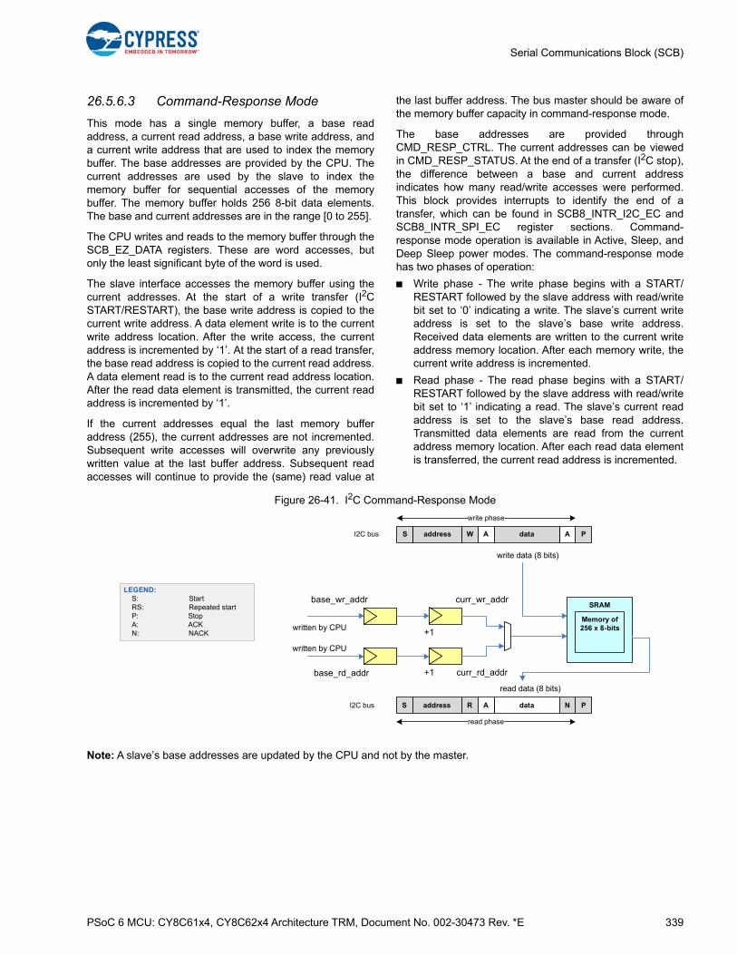
PSoC 6 MCU: CY8C61x4, CY8C62x4 Architecture TRM, Document No. 002-30473 Rev. *E 339
Serial Communications Block (SCB)
26.5.6.3 Command-Response Mode
This mode has a single memory buffer, a base readaddress, a current read address, a base write address, anda current write address that are used to index the memorybuffer. The base addresses are provided by the CPU. Thecurrent addresses are used by the slave to index thememory buffer for sequential accesses of the memorybuffer. The memory buffer holds 256 8-bit data elements.The base and current addresses are in the range [0 to 255].
The CPU writes and reads to the memory buffer through theSCB_EZ_DATA registers. These are word accesses, butonly the least significant byte of the word is used.
The slave interface accesses the memory buffer using thecurrent addresses. At the start of a write transfer (I2CSTART/RESTART), the base write address is copied to thecurrent write address. A data element write is to the currentwrite address location. After the write access, the currentaddress is incremented by ‘1’. At the start of a read transfer,the base read address is copied to the current read address.A data element read is to the current read address location.After the read data element is transmitted, the current readaddress is incremented by ‘1’.
If the current addresses equal the last memory bufferaddress (255), the current addresses are not incremented.Subsequent write accesses will overwrite any previouslywritten value at the last buffer address. Subsequent readaccesses will continue to provide the (same) read value at
the last buffer address. The bus master should be aware ofthe memory buffer capacity in command-response mode.
The base addresses are provided throughCMD_RESP_CTRL. The current addresses can be viewedin CMD_RESP_STATUS. At the end of a transfer (I2C stop),the difference between a base and current addressindicates how many read/write accesses were performed.This block provides interrupts to identify the end of atransfer, which can be found in SCB8_INTR_I2C_EC andSCB8_INTR_SPI_EC register sections. Command-response mode operation is available in Active, Sleep, andDeep Sleep power modes. The command-response modehas two phases of operation:
■ Write phase - The write phase begins with a START/RESTART followed by the slave address with read/writebit set to ‘0’ indicating a write. The slave’s current writeaddress is set to the slave’s base write address.Received data elements are written to the current writeaddress memory location. After each memory write, thecurrent write address is incremented.
■ Read phase - The read phase begins with a START/RESTART followed by the slave address with read/writebit set to ‘1’ indicating a read. The slave’s current readaddress is set to the slave’s base read address.Transmitted data elements are read from the currentaddress memory location. After each read data elementis transferred, the current read address is incremented.
Figure 26-41. I2C Command-Response Mode
Note: A slave’s base addresses are updated by the CPU and not by the master.
S address W PI2C bus A Adata
write data (8 bits)
write phase
LEGEND: S: Start RS: Repeated start P: Stop A: ACK N: NACK
SRAM
read data (8 bits)
Pdata NS address R A
read phase
I2C bus
Memory of 256 x 8-bits
curr_wr_addrbase_wr_addr
+1written by CPU
curr_rd_addrbase_rd_addr +1
written by CPU

PSoC 6 MCU: CY8C61x4, CY8C62x4 Architecture TRM, Document No. 002-30473 Rev. *E 340
Serial Communications Block (SCB)
26.5.7 Clocking and Oversampling
The SCB I2C supports both internally and externally clockedoperation modes. Two bitfields (EC_AM_MODE andEC_OP MODE) in the SCB_CTRL register determine theSCB clock mode. EC_AM_MODE indicates whether I2Caddress matching is internally (0) or externally (1) clocked.I2C address matching comprises the first part of the I2Cprotocol. EC_OP_MODE indicates whether the rest of theprotocol operation (besides I2C address matching) isinternally (0) or externally (1) clocked. The externallyclocked mode of operation is supported only in the I2C slavemode.
An internally-clocked operation uses the programmableclock dividers. For I2C, an integer clock divider must beused for both master and slave. For more information onsystem clocking, see the Clocking System chapter onpage 240. The internally-clocked mode does not support thecommand-response mode.
The SCB_CTRL bitfields EC_AM_MODE andEC_OP_MODE can be configured in the following ways.
■ EC_AM_MODE is ‘0’ and EC_OP_MODE is ‘0’: Use thisconfiguration when only Active mode functionality isrequired.
❐ FIFO mode: Supported.
❐ EZ mode: Supported.
❐ Command-response mode: Not supported. The slave NACKs every slave address.
■ EC_AM_MODE is ‘1’ and EC_OP_MODE is ‘0’: Use thisconfiguration when both Active and Deep Sleepfunctionality are required. This configuration relies on theexternally clocked functionality for the I2C addressmatching and relies on the internally clockedfunctionality to access the memory buffer. The “handover” from external to internal functionality relies eitheron an ACK/NACK or clock stretching scheme. Theformer may result in termination of the current transferand relies on a master retry. The latter stretches thecurrent transfer after a matching address is received.This mode requires the master to support either NACKgeneration (and retry) or clock stretching. When the I2Caddress is matched, INTR_I2C_EC.WAKE_UP is set to‘1’. The associated Deep Sleep functionality interruptbrings the system into Active power mode.
❐ FIFO mode: See “Deep Sleep to Active Transition” on page 337
❐ EZ mode: See “Deep Sleep to Active Transition” on page 338.
❐ CMD_RESP mode: Not supported. The slave NACKs every slave address.
■ EC_AM_MODE is ‘1’ and EC_OP_MODE is ‘1’. Use thismode when both Active and Deep Sleep functionality arerequired. When the slave is selected,INTR_I2C_EC.WAKE_UP is set to ‘1’. The associated
Deep Sleep functionality interrupt brings the system intoActive power mode. When the slave is deselected,INTR_I2C_EC.EZ_STOP and/orINTR_I2C_EC.EZ_WRITE_STOP are set to ‘1’.
❐ FIFO mode: Not supported.
❐ EZ mode: Supported.
❐ CMD_RESP mode: Supported.
An externally-clocked operation uses a clock provided bythe serial interface. The externally clocked mode does notsupport FIFO mode. If EC_OP_MODE is ‘1’, the externalinterface logic accesses the memory buffer on the externalinterface clock (I2C SCL). This allows for EZ andCMD_RESP mode functionality in Active and Deep Sleeppower modes.
In Active system power mode, the memory buffer requiresarbitration between external interface logic (on I2C SCL) andthe CPU interface logic (on system peripheral clock). Thisarbitration always gives the highest priority to the externalinterface logic (host accesses). The external interface logictakes one serial interface clock/bit periods for the I2C.During this period, the internal logic is denied service to thememory buffer. The PSoC 6 MCU provides twoprogrammable options to address this “denial of service”:
■ If the BLOCK bitfield of SCB_CTRL is ‘1’: An internallogic access to the memory buffer is blocked until thememory buffer is granted and the external interface logichas completed access. For a 100-kHz I2C interface, themaximum blocking period of one serial interface bitperiod measures 10 µs (approximately 208 clock cycleson a 48 MHz SCB input clock). This option providesnormal SCB register functionality, but the blocking timeintroduces additional internal bus wait states.
■ If the BLOCK bitfield of SCB_CTRL is ‘0’: An internallogic access to the memory buffer is not blocked, butfails when it conflicts with an external interface logicaccess. A read access returns the value 0xFFFF:FFFFand a write access is ignored. This option does notintroduce additional internal bus wait states, but anaccess to the memory buffer may not take effect. In thiscase, following failures are detected:
❐ Read Failure: A read failure is easily detected, as the returned value is 0xFFFF:FFFF. This value is unique as non-failing memory buffer read accesses return an unsigned byte value in the range 0x0000:0000-0x0000:00FF.
❐ Write Failure: A write failure is detected by reading back the written memory buffer location, and con-firming that the read value is the same as the written value.
For both options, a conflicting internal logic access to thememory buffer sets INTR_TX.BLOCKED field to ‘1’ (for writeaccess-es) and INTR_RX.BLOCKED field to ‘1’ (for readaccesses). These fields can be used as either status fields

PSoC 6 MCU: CY8C61x4, CY8C62x4 Architecture TRM, Document No. 002-30473 Rev. *E 341
Serial Communications Block (SCB)
or as interrupt cause fields (when their associated maskfields are enabled).
If a series of read or write accesses is performed andCTRL.BLOCKED is ‘0’, a failure is detected by comparingthe logical OR of all read values to 0xFFFF:FFFF andchecking the INTR_TX.BLOCKED andINTR_RX.BLOCKED fields to determine whether a failureoccurred for a (series of) write or read operation(s).
26.5.7.1 Glitch Filtering
The PSoC 6 MCU SCB I2C has analog and digital glitchfilters. Analog glitch filters are applied on the i2c_scl_in and
i2c_sda_in input signals (AF_in) to filter glitches of up to 50ns. An analog glitch filter is also applied on the i2c_sda_outoutput signal (AF_out). Analog glitch filters are enabled anddisabled in the SCB.I2C_CFG register. Do not change the_TRIM bitfields; only change the _SEL bitfields in thisregister.
Digital glitch filters are applied on the i2c_scl_in andi2c_sda_in input signals (DF_in). The digital glitch filter isenabled in the SCB.RX_CTRL register via the MEDIANbitfield.
Figure 26-42. I2C Glitch Filtering Connection
The following table lists the useful combinations of glitch filters.
When operating in EC_OP_MODE = 1, the 100-kHz, 400-kHz, and 1000-kHz modes require the following settings for AF_out:
26.5.7.2 Oversampling and Bit Rate
Internally-clocked Master
The PSoC 6 MCU implements the I2C clock as an oversampled multiple of the SCB input clock. In master mode, the blockdetermines the I2C frequency. Routing delays on the PCB, on the chip, and the SCB (including analog and digital glitch filters)all contribute to the signal interface timing. In master mode, the block operates off clk_scb and uses programmableoversampling factors for the SCL high (1) and low (0) times. For high and low phase oversampling, see
Table 26-16. Glitch Filter Combinations
AF_in AF_out DF_in Comments
0 0 1 Used when operating in internally-clocked mode and in master in fast-mode plus (1-MHz speed mode)
1 0 0 Used when operating in internally-clocked mode (EC_OP_MODE is '0')
1 1 0 Used when operating in externally-clocked mode (EC_OP_MODE is '1'). Only slave mode.
AF_in AF_out DF_in
1 1 0
100-kHz mode: I2C_CFG.SDA_OUT_FILT_SEL = 3
400-kHz mode: I2C_CFG.SDA_OUT_FILT_SEL = 3
1000-kHz mode: I2C_CFG.SDA_OUT_FILT_SEL = 1
i2c_scl_ini2c_scl
i2c_ctl
i2c_ec_ctli2c_ec_scl_out
i2c_scl_in
i2c_scl_in
i2c_ic_scl_out
i2c_sda_in
i2c_ic_sda_out
i2c_ec_sda_out
AF_in
i2c_sda_in
i2c_sda_ini2c_sda AF_in
AF_out
DF_in
DF_in
i2c_scl_out
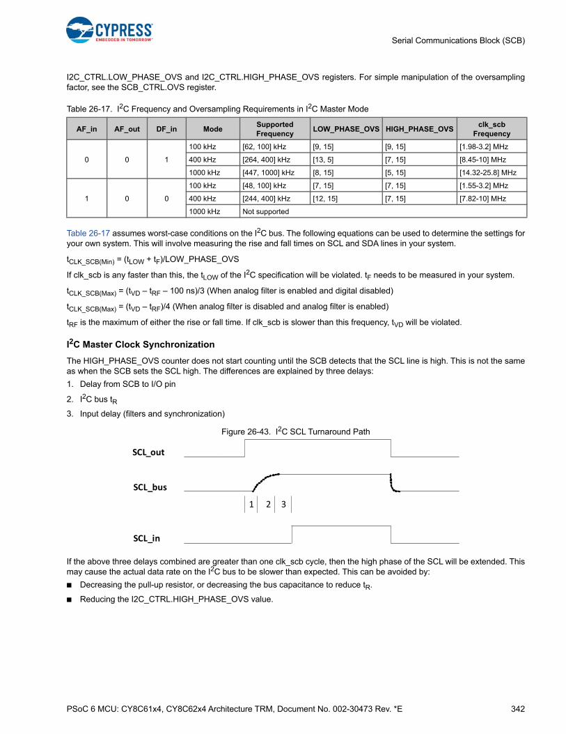
PSoC 6 MCU: CY8C61x4, CY8C62x4 Architecture TRM, Document No. 002-30473 Rev. *E 342
Serial Communications Block (SCB)
I2C_CTRL.LOW_PHASE_OVS and I2C_CTRL.HIGH_PHASE_OVS registers. For simple manipulation of the oversamplingfactor, see the SCB_CTRL.OVS register.
Table 26-17 assumes worst-case conditions on the I2C bus. The following equations can be used to determine the settings foryour own system. This will involve measuring the rise and fall times on SCL and SDA lines in your system.
tCLK_SCB(Min) = (tLOW + tF)/LOW_PHASE_OVS
If clk_scb is any faster than this, the tLOW of the I2C specification will be violated. tF needs to be measured in your system.
tCLK_SCB(Max) = (tVD – tRF – 100 ns)/3 (When analog filter is enabled and digital disabled)
tCLK_SCB(Max) = (tVD – tRF)/4 (When analog filter is disabled and analog filter is enabled)
tRF is the maximum of either the rise or fall time. If clk_scb is slower than this frequency, tVD will be violated.
I2C Master Clock Synchronization
The HIGH_PHASE_OVS counter does not start counting until the SCB detects that the SCL line is high. This is not the sameas when the SCB sets the SCL high. The differences are explained by three delays:
1. Delay from SCB to I/O pin
2. I2C bus tR
3. Input delay (filters and synchronization)
Figure 26-43. I2C SCL Turnaround Path
If the above three delays combined are greater than one clk_scb cycle, then the high phase of the SCL will be extended. Thismay cause the actual data rate on the I2C bus to be slower than expected. This can be avoided by:
■ Decreasing the pull-up resistor, or decreasing the bus capacitance to reduce tR.
■ Reducing the I2C_CTRL.HIGH_PHASE_OVS value.
Table 26-17. I2C Frequency and Oversampling Requirements in I2C Master Mode
AF_in AF_out DF_in ModeSupported Frequency
LOW_PHASE_OVS HIGH_PHASE_OVSclk_scb
Frequency
0 0 1
100 kHz [62, 100] kHz [9, 15] [9, 15] [1.98-3.2] MHz
400 kHz [264, 400] kHz [13, 5] [7, 15] [8.45-10] MHz
1000 kHz [447, 1000] kHz [8, 15] [5, 15] [14.32-25.8] MHz
1 0 0
100 kHz [48, 100] kHz [7, 15] [7, 15] [1.55-3.2] MHz
400 kHz [244, 400] kHz [12, 15] [7, 15] [7.82-10] MHz
1000 kHz Not supported
SCL_out
SCL_bus
SCL_in
1 2 3
PSoC 6 MCU: CY8C61x4, CY8C62x4 Architecture TRM, Document No. 002-30473 Rev. *E 343
Serial Communications Block (SCB)
Internally-clocked Slave
In slave mode, the I2C frequency is determined by the incoming I2C SCL signal. To ensure proper operation, clk_scb must besignificantly higher than the I2C bus frequency. Unlike master mode, this mode does not use programmable oversamplingfactors.
tCLK_SCB(Max) = (tVD – tRF – 100 ns) / 3 (When analog filter is enabled and digital disabled)
tCLK_SCB(Max) = (tVD – tRF) / 4 (When analog filter is disabled and analog filter is enabled)
tRF is the maximum of either the rise or fall time. If clk_scb is slower than this frequency, tVD will be violated.
The minimum period of clk_scb is determined by one of the following equations:
tCLK_SCB(MIN) = (tSU;DAT(min) + tRF) /16
or
tCLK_SCB(Min) = (0.6 * tF – 50 ns)/2 (When analog filter is enabled and digital disabled)
tCLK_SCB(Min) = (0.6 * tF)/3 (When analog filter is disabled and digital enabled)
The result that yields the largest period from the two sets of equations above should be used to set the minimum period ofclk_scb.
Master-Slave
In this mode, when the SCB is acting as a master device, the block determines the I2C frequency. When the SCB is acting asa slave device, the block does not determine the I2C frequency. Instead, the incoming I2C SCL signal does.
To guarantee operation in both master and slave modes, choose clock frequencies that work for both master and slave usingthe tables above.
26.5.8 Enabling and Initializing the I2C
The following section describes the method to configure the I2C block for standard (non-EZ) mode and EZI2C mode.
26.5.8.1 Configuring for I2C FIFO Mode
The I2C interface must be programmed in the following order.
1. Program protocol specific information using the SCB_I2C_CTRL register. This includes selecting master - slave function-ality.
2. Program the generic transmitter and receiver information using the SCB_TX_CTRL and SCB_RX_CTRL registers.
3. Set the SCB_CTRL.BYTE_MODE to ‘1’ to enable the byte mode.
4. Program the SCB_CTRL register to enable the I2C block and select the I2C mode. For a complete description of the I2C registers, see the registers TRM.
26.5.8.2 Configuring for EZ and CMD_RESP Modes
To configure the I2C block for EZ and CMD_RESP modes, set the following I2C register bits
Table 26-18. SCB Input Clock Requirements in I2C Slave Mode
AF_in AF_out DF_in Mode clk_scb Frequency Range
0 0 1
100 kHz [1.98-12.8] MHz
400 kHz [8.45-17.14] MHz
1000 kHz [14.32-44.77] MHz
1 0 0
100 kHz [1.55-12.8] MHz
400 kHz [7.82-15.38] MHz
1000 kHz [15.84-89.0] MHz
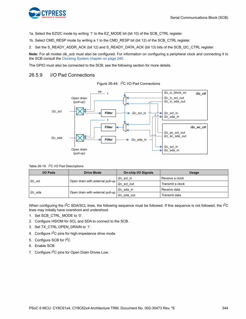
PSoC 6 MCU: CY8C61x4, CY8C62x4 Architecture TRM, Document No. 002-30473 Rev. *E 344
Serial Communications Block (SCB)
1a. Select the EZI2C mode by writing ‘1’ to the EZ_MODE bit (bit 10) of the SCB_CTRL register.
1b. Select CMD_RESP mode by writing a 1 to the CMD_RESP bit (bit 12) of the SCB_CTRL register.
2. Set the S_READY_ADDR_ACK (bit 12) and S_READY_DATA_ACK (bit 13) bits of the SCB_I2C_CTRL register.
Note: For all modes clk_scb must also be configured. For information on configuring a peripheral clock and connecting it tothe SCB consult the Clocking System chapter on page 240.
The GPIO must also be connected to the SCB; see the following section for more details.
26.5.9 I/O Pad Connections
Figure 26-44. I2C I/O Pad Connections
When configuring the I2C SDA/SCL lines, the following sequence must be followed. If this sequence is not followed, the I2Clines may initially have overshoot and undershoot.
1. Set SCB_CTRL_MODE to ‘0’.
2. Configure HSIOM for SCL and SDA to connect to the SCB.
3. Set TX_CTRL.OPEN_DRAIN to ‘1’.
4. Configure I2C pins for high-impedance drive mode.
5. Configure SCB for I2C
6. Enable SCB
7. Configure I2C pins for Open Drain Drives Low.
Table 26-19. I2C I/O Pad Descriptions
I/O Pads Drive Mode On-chip I/O Signals Usage
i2c_scl Open drain with external pull-upi2c_scl_in Receive a clock
i2c_scl_out Transmit a clock
i2c_sda Open drain with external pull-upi2c_sda_in Receive data
i2c_sda_out Transmit data
Open drain(pull-up)
1
i2c_scl_ini2c_scl
i2c_ctl
i2c_ec_ctl
i2c_ec_scl_out
i2c_scl_in
i2c_scl_in
i2c_ic_scl_out
i2c_ic_block_ec
i2c_sda_in
i2c_ic_sda_out
i2c_ec_sda_out
Filter
i2c_sda_inOpen drain(pull-up)
1
i2c_sda_ini2c_sda Filter
Filter
oe

PSoC 6 MCU: CY8C61x4, CY8C62x4 Architecture TRM, Document No. 002-30473 Rev. *E 345
Serial Communications Block (SCB)
26.5.10 I2C Registers
The I2C interface is controlled by reading and writing a set of configuration, control, and status registers, as listed inTable 26-20.
Note: Detailed descriptions of the I2C register bits are available in the registers TRM.
Table 26-20. I2C Registers
Register Function
SCB_CTRL Enables the SCB block and selects the type of serial interface (SPI, UART, I2C). Also used to select inter-nally and externally clocked operation and EZ and non-EZ modes of operation.
SCB_I2C_CTRL Selects the mode (master, slave) and sends an ACK or NACK signal based on receiver FIFO status.
SCB_I2C_STATUSIndicates bus busy status detection, read/write transfer status of the slave/master, and stores the EZ slave address.
SCB_I2C_M_CMD Enables the master to generate START, STOP, and ACK/NACK signals.
SCB_I2C_S_CMD Enables the slave to generate ACK/NACK signals.
SCB_STATUSIndicates whether the externally clocked logic is using the EZ memory. This bit can be used by software to determine whether it is safe to issue a software access to the EZ memory.
SCB_I2C_CFG Configures filters, which remove glitches from the SDA and SCL lines.
SCB_TX_CTRL Specifies the data frame width; also used to specify whether MSb or LSb is the first bit in transmission.
SCB_TX_FIFO_CTRLSpecifies the trigger level, clearing of the transmitter FIFO and shift registers, and FREEZE operation of the transmitter FIFO.
SCB_TX_FIFO_STATUSIndicates the number of bytes stored in the transmitter FIFO, the location from which a data frame is read by the hardware (read pointer), the location from which a new data frame is written (write pointer), and decides if the transmitter FIFO holds the valid data.
SCB_TX_FIFO_WR Holds the data frame written into the transmitter FIFO. Behavior is similar to that of a PUSH operation.
SCB_RX_CTRLPerforms the same function as that of the SCB_TX_CTRL register, but for the receiver. Also decides whether a median filter is to be used on the input interface lines.
SCB_RX_FIFO_CTRL Performs the same function as that of the SCB_TX_FIFO_CTRL register, but for the receiver.
SCB_RX_FIFO_STATUS Performs the same function as that of the SCB_TX_FIFO_STATUS register, but for the receiver.
SCB_RX_FIFO_RDHolds the data read from the receiver FIFO. Reading a data frame removes the data frame from the FIFO; behavior is similar to that of a POP operation. This register has a side effect when read by software: a data frame is removed from the FIFO.
SCB_RX_FIFO_RD_SILENTHolds the data read from the receiver FIFO. Reading a data frame does not remove the data frame from the FIFO; behavior is similar to that of a PEEK operation.
SCB_RX_MATCH Stores slave device address and is also used as slave device address MASK.
SCB_EZ_DATA Holds the data in an EZ memory location.
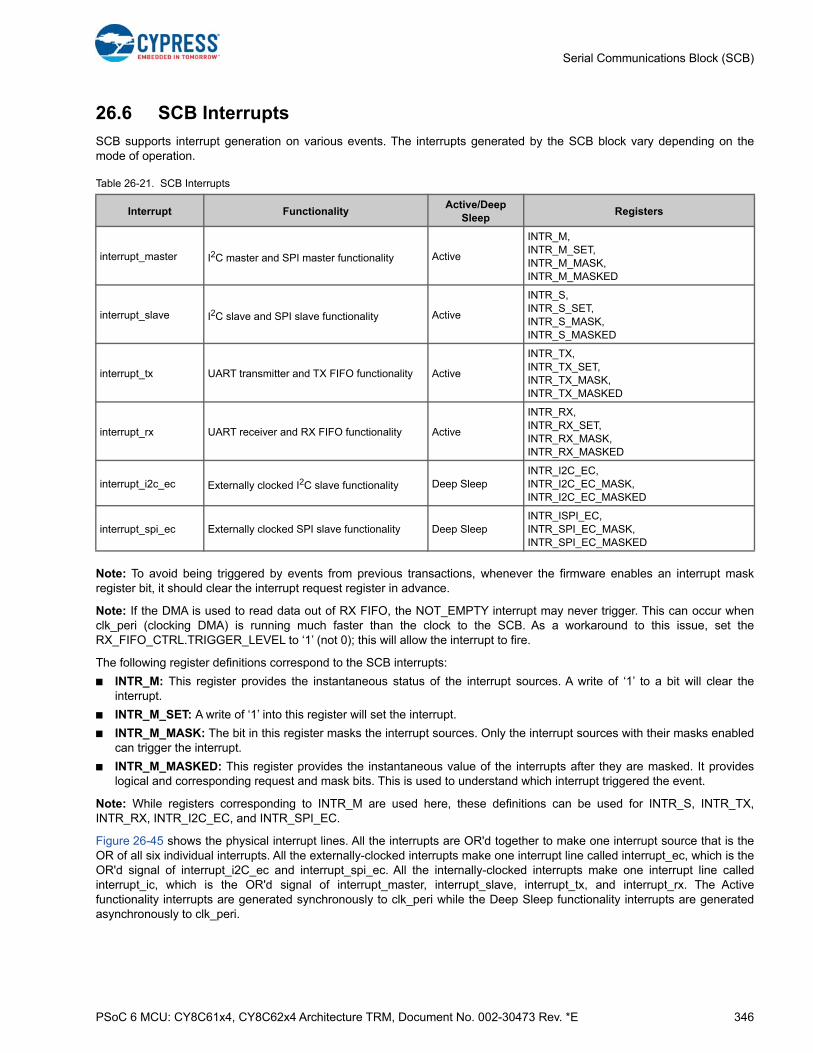
PSoC 6 MCU: CY8C61x4, CY8C62x4 Architecture TRM, Document No. 002-30473 Rev. *E 346
Serial Communications Block (SCB)
26.6 SCB Interrupts
SCB supports interrupt generation on various events. The interrupts generated by the SCB block vary depending on themode of operation.
Note: To avoid being triggered by events from previous transactions, whenever the firmware enables an interrupt maskregister bit, it should clear the interrupt request register in advance.
Note: If the DMA is used to read data out of RX FIFO, the NOT_EMPTY interrupt may never trigger. This can occur whenclk_peri (clocking DMA) is running much faster than the clock to the SCB. As a workaround to this issue, set theRX_FIFO_CTRL.TRIGGER_LEVEL to ‘1’ (not 0); this will allow the interrupt to fire.
The following register definitions correspond to the SCB interrupts:
■ INTR_M: This register provides the instantaneous status of the interrupt sources. A write of ‘1’ to a bit will clear theinterrupt.
■ INTR_M_SET: A write of ‘1’ into this register will set the interrupt.
■ INTR_M_MASK: The bit in this register masks the interrupt sources. Only the interrupt sources with their masks enabledcan trigger the interrupt.
■ INTR_M_MASKED: This register provides the instantaneous value of the interrupts after they are masked. It provideslogical and corresponding request and mask bits. This is used to understand which interrupt triggered the event.
Note: While registers corresponding to INTR_M are used here, these definitions can be used for INTR_S, INTR_TX,INTR_RX, INTR_I2C_EC, and INTR_SPI_EC.
Figure 26-45 shows the physical interrupt lines. All the interrupts are OR'd together to make one interrupt source that is theOR of all six individual interrupts. All the externally-clocked interrupts make one interrupt line called interrupt_ec, which is theOR'd signal of interrupt_i2C_ec and interrupt_spi_ec. All the internally-clocked interrupts make one interrupt line calledinterrupt_ic, which is the OR'd signal of interrupt_master, interrupt_slave, interrupt_tx, and interrupt_rx. The Activefunctionality interrupts are generated synchronously to clk_peri while the Deep Sleep functionality interrupts are generatedasynchronously to clk_peri.
Table 26-21. SCB Interrupts
Interrupt FunctionalityActive/Deep
SleepRegisters
interrupt_master I2C master and SPI master functionality Active
INTR_M, INTR_M_SET, INTR_M_MASK, INTR_M_MASKED
interrupt_slave I2C slave and SPI slave functionality Active
INTR_S, INTR_S_SET, INTR_S_MASK, INTR_S_MASKED
interrupt_tx UART transmitter and TX FIFO functionality Active
INTR_TX, INTR_TX_SET, INTR_TX_MASK, INTR_TX_MASKED
interrupt_rx UART receiver and RX FIFO functionality Active
INTR_RX, INTR_RX_SET, INTR_RX_MASK, INTR_RX_MASKED
interrupt_i2c_ec Externally clocked I2C slave functionality Deep SleepINTR_I2C_EC, INTR_I2C_EC_MASK,INTR_I2C_EC_MASKED
interrupt_spi_ec Externally clocked SPI slave functionality Deep SleepINTR_ISPI_EC, INTR_SPI_EC_MASK, INTR_SPI_EC_MASKED
PSoC 6 MCU: CY8C61x4, CY8C62x4 Architecture TRM, Document No. 002-30473 Rev. *E 347
Serial Communications Block (SCB)
Figure 26-45. Interrupt Lines
26.6.1 SPI Interrupts
The SPI interrupts can be classified as master interrupts, slave interrupts, TX interrupts, RX interrupts, and externally clocked(EC) mode interrupts. Each interrupt output is the logical OR of the group of all possible interrupt sources classified under thesection. For example, the TX interrupt output is the logical OR of the group of all possible TX interrupt sources. This signalgoes high when any of the enabled TX interrupt sources are true. The SCB also provides an interrupt cause register (SCB_INTR_CAUSE) that can be used to determine interrupt source. The interrupt registers are cleared by writing ‘1’ to thecorresponding bitfield. Note that certain interrupt sources are triggered again as long as the condition is met even if theinterrupt source was cleared. For example, the TX_FIFO_EMPTY is set as long as the transmit FIFO is empty even if theinterrupt source is cleared. For more information on interrupt registers, see the registers TRM. The SPI supports interrupts onthe following events:
■ SPI Master Interrupts
❐ SPI master transfer done – All data from the TX FIFO are sent. This interrupt source triggers later than TX_FI-FO_EMPTY by the amount of time it takes to transmit a single data element. TX_FIFO_EMPTY triggers when the last data element from the TX FIFO goes to the shifter register. However, SPI Done triggers after this data element is transmitted. This means SPI Done will be asserted one SCLK clock cycle earlier than the completion of data element reception.
■ SPI Slave Interrupts
❐ SPI Bus Error – Slave deselected at an unexpected time in the SPI transfer. The firmware may decide to clear the TX and RX FIFOs for this error.
❐ SPI slave deselected after any EZSPI transfer occurred.
❐ SPI slave deselected after a write EZSPI transfer occurred.
■ SPI TX
❐ TX FIFO has less entries than the value specified by TRIGGER_LEVEL in SCB_TX_FIFO_CTRL.
❐ TX FIFO not full – At least one data element can be written into the TX FIFO.
❐ TX FIFO empty – The TX FIFO is empty.
❐ TX FIFO overflow – Firmware attempts to write to a full TX FIFO.
❐ TX FIFO underflow – Hardware attempts to read from an empty TX FIFO. This happens when the SCB is ready to transfer data and EMPTY is ‘1’.
❐ TX FIFO trigger – Less entries in the TX FIFO than the value specified by TX_FIFO_CTRL.TRIGGER_LEVEL.
■ SPI RX
❐ RX FIFO has more entries than the value specified by TRIGGER_LEVEL in SCB_RX_FIFO_CTRL.
❐ RX FIFO full - RX FIFO is full.
❐ RX FIFO not empty - RX FIFO is not empty. At least one data element is available in the RX FIFO to be read.
❐ RX FIFO overflow - Hardware attempt to write to a full RX FIFO.
❐ RX FIFO underflow - Firmware attempts to read from and empty RX FIFO.
Interrupt Lines
INTR_M_MASKED[...]
INTR_S_MASKED[...]
INTR_TX_MASKED[...]
INTR_RX_MASKED[...]
Interrupt_master
Interrupt_slave
Interrupt_tx
Interrupt_rx
Interrupt_i2c_ec
Interrupt_spi_ec
Interrupt_ic
Interrupt_ec
Interrupt

PSoC 6 MCU: CY8C61x4, CY8C62x4 Architecture TRM, Document No. 002-30473 Rev. *E 348
Serial Communications Block (SCB)
❐ RX FIFO trigger - More entries in the RX FIFO than the value specified by RX_FIFO_CTRL.TRIGGER_LEVEL.
■ SPI Externally Clocked
❐ Wake up request on slave select – Active on incoming slave request (with address match). Only set when EC_AM is ‘1’.
❐ SPI STOP detection at the end of each transfer – Activated at the end of every transfer (I2C STOP). Only set for a slave request with an address match, in EZ and CMD_RESP modes, when EC_OP is ‘1’.
❐ SPI STOP detection at the end of a write transfer – Activated at the end of a write transfer (I2C STOP). This event is an indication that a buffer memory location has been written to. For EZ mode, a transfer that only writes the base address does not activate this event. Only set for a slave request with an address match, in EZ and CMD_RESP modes, when EC_OP is ‘1’.
❐ SPI STOP detection at the end of a read transfer – Activated at the end of a read transfer (I2C STOP). This event is an indication that a buffer memory location has been read from. Only set for a slave request with an address match, in EZ and CMD_RESP modes when EC_OP is ‘1’.
Figure 26-46 and Figure 26-47 show how each of the interrupts are triggered. Figure 26-46 shows the TX buffer and thecorresponding interrupts while Figure 26-47 shows all the corresponding interrupts for the RX buffer. The FIFO has 256 splitinto 128 bytes for TX and 128 bytes for RX instead of the 8 bytes shown in the figures. For more information on how toimplement and clear interrupts, see the SPI (SCB_SPI_PDL) datasheet and the PDL.
Figure 26-46. TX Interrupt Source Operation
Component Started Write 1 byte Write 1 more byte Write 4 more bytes Write 3 more bytes
TX FIFO Empty = 1
TX FIFO Level = 1
TX FIFO Not F ull = 1
SPI Done = 0
TX FIFO
Level = 4
Used = 0
TX Shifter
TX FIFO
Level = 4
Used = 0
TX Shifter
TX FIFO Empty = 0 (W1C)
TX FIFO Level = 1
TX FIFO Not F ull = 1
SPI Done = 0
TX FIFO
Level = 4
Used = 1
TX Shifter
TX FIFO Empty = 1
TX FIFO Level = 0 (W1C)
TX FIFO Not F ull = 1
SPI Done = 0
TX FIFO
Level = 4
Used = 5
TX Shifter
TX FIFO
Level = 4
TX Shifter
TX FIFO Empty = 0
TX FIFO Level = 0
TX FIFO Not F ull = 0 (W1C)
SPI Done = 0
Transmit 1 byte Transmit 3 more bytes Transmit 4 more bytes Transmit 7 more bits Transmit last bit
TX FIFO Empty = 0
TX FIFO Level = 1
TX FIFO Not F ull = 1
SPI Done = 0
TX FIFO
Level = 4
Used = 4
TX Shifter
TX FIFO Empty = 1
TX FIFO Level = 1
TX FIFO Not F ull = 1
SPI Done = 0
TX FIFO
Level = 4
Used = 0
TX Shifter
TX FIFO Empty = 1
TX FIFO Level = 1
TX FIFO Not F ull = 1
SPI Done =1
TX FIFO
Level = 4
Used = 0
TX Shifter
TX FIFO
Level = 4
TX Shifter
TX FIFO Empty = 0
TX FIFO Level = 0
TX FIFO Not F ull = 1
SPI Done = 0
Used = 7
TX FIFO
Level = 4
TX Shifter
TX FIFO Empty = 1
TX FIFO Level = 1
TX FIFO Not F ull = 1
TX FIFO Underflow = 1
Used = 0
TX FIFO Empty = 1
TX FIFO Level = 1
TX FIFO Not F ull = 1
SPI Done = 0
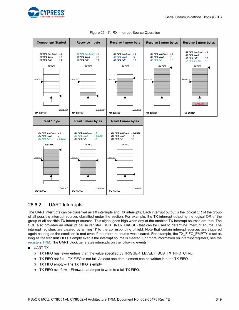
PSoC 6 MCU: CY8C61x4, CY8C62x4 Architecture TRM, Document No. 002-30473 Rev. *E 349
Serial Communications Block (SCB)
Figure 26-47. RX Interrupt Source Operation
26.6.2 UART Interrupts
The UART interrupts can be classified as TX interrupts and RX interrupts. Each interrupt output is the logical OR of the groupof all possible interrupt sources classified under the section. For example, the TX interrupt output is the logical OR of thegroup of all possible TX interrupt sources. This signal goes high when any of the enabled TX interrupt sources are true. TheSCB also provides an interrupt cause register (SCB_ INTR_CAUSE) that can be used to determine interrupt source. Theinterrupt registers are cleared by writing ‘1’ to the corresponding bitfield. Note that certain interrupt sources are triggeredagain as long as the condition is met even if the interrupt source was cleared. For example, the TX_FIFO_EMPTY is set aslong as the transmit FIFO is empty even if the interrupt source is cleared. For more information on interrupt registers, see theregisters TRM. The UART block generates interrupts on the following events:
■ UART TX
❐ TX FIFO has fewer entries than the value specified by TRIGGER_LEVEL in SCB_TX_FIFO_CTRL.
❐ TX FIFO not full – TX FIFO is not full. At least one data element can be written into the TX FIFO.
❐ TX FIFO empty – The TX FIFO is empty.
❐ TX FIFO overflow – Firmware attempts to write to a full TX FIFO.
Component Started Recevice 1 byte Receive 4 more byte Receive 3 more bytes Receive 3 more bytes
RX FIFO
Level = 4
Used = 0
RX Shifter
RX FIFO
Level = 4
Used = 0
RX Shifter
RX FIFO
Level = 4
Used = 5
RX Shifter
RX FIFO
Level = 4
RX Shifter
RX FIFO
Level = 4
Dropped
RX Shifter
RX FIFO Not Empty = 1
RX FIFO Level = 1
RX FIFO Full = 1
RX FIFO Oveflow = 1
Read 1 byte Read 3 more bytes Read 4 more bytes
RX FIFO
Level = 4
Used = 4
RX Shifter
RX FIFO
Level = 4
Used = 0
RX Shifter
RX FIFO
Level = 4
RX ShifterUsed = 7
RX FIFO Not Empty = 0
RX FIFO Level = 0
RX FIFO Full = 0
RX FIFO Not Empty = 1
RX FIFO Level = 0
RX FIFO Full = 0
RX FIFO Not Empty = 1
RX FIFO Level =1
RX FIFO Full = 0
RX FIFO Not Empty = 1
RX FIFO Level = 1
RX FIFO Full = 1
RX FIFO Not Empty = 1
RX FIFO Level = 1
RX FIFO Full = 0 (W1C)
RX FIFO Not Empty = 1
RX FIFO Level = 0 (W1C)
RX FIFO Full = 0
RX FIFO Not Empty = 0 (W1C)
RX FIFO Level = 0
RX FIFO Full = 0

PSoC 6 MCU: CY8C61x4, CY8C62x4 Architecture TRM, Document No. 002-30473 Rev. *E 350
Serial Communications Block (SCB)
❐ TX FIFO underflow – Hardware attempts to read from an empty TX FIFO. This happens when the SCB is ready to transfer data and EMPTY is ‘1’.
❐ TX NACK – UART transmitter receives a negative acknowledgment in SmartCard mode.
❐ TX done – This happens when the UART completes transferring all data in the TX FIFO and the last stop field is trans-mitted (both TX FIFO and transmit shifter register are empty).
❐ TX lost arbitration – The value driven on the TX line is not the same as the value observed on the RX line. This condi-tion event is useful when transmitter and receiver share a TX/RX line. This is the case in LIN or SmartCard modes.
■ UART RX
❐ RX FIFO has more entries than the value specified by TRIGGER_LEVEL in SCB_RX_FIFO_CTRL.
❐ RX FIFO full – RX FIFO is full. Note that received data frames are lost when the RX FIFO is full.
❐ RX FIFO not empty – RX FIFO is not empty.
❐ RX FIFO overflow – Hardware attempts to write to a full RX FIFO.
❐ RX FIFO underflow – Firmware attempts to read from an empty RX FIFO.
❐ Frame error in received data frame – UART frame error in received data frame. This can be either a start of stop bit error: Start bit error: After the beginning of a start bit period is detected (RX line changes from 1 to 0), the middle of the start bit period is sampled erroneously (RX line is ‘1’). Note: A start bit error is detected before a data frame is received.Stop bit error: The RX line is sampled as ‘0’, but a ‘1’ was expected. A stop bit error may result in failure to receive successive data frames. Note: A stop bit error is detected after a data frame is received.
❐ Parity error in received data frame – If UART_RX_CTL.DROP_ON_PARITY_ERROR is ‘1’, the received frame is dropped. If UART_RX_CTL.DROP_ON_PARITY_ERROR is ‘0’, the received frame is sent to the RX FIFO. In Smart-Card sub mode, negatively acknowledged data frames generate a parity error. Note that firmware can only identify the erroneous data frame in the RX FIFO if it is fast enough to read the data frame before the hardware writes a next data frame into the RX FIFO.
❐ LIN baud rate detection is completed – The receiver software uses the UART_RX_STATUS.BR_COUNTER value to set the clk_scb to guarantee successful receipt of the first LIN data frame (Protected Identifier Field) after the synchro-nization byte.
❐ LIN break detection is successful – The line is ‘0’ for UART_RX_CTRL.BREAK_WIDTH + 1 bit period. Can occur at any time to address unanticipated break fields; that is, “break-in-data” is supported. This feature is supported for the UART standard and LIN submodes. For the UART standard submodes, ongoing receipt of data frames is not affected; firmware is expected to take proper action. For the LIN submode, possible ongoing receipt of a data frame is stopped and the (partially) received data frame is dropped and baud rate detection is started. Set to ‘1’, when event is detected. Write with '1' to clear bit.
Figure 26-48 and Figure 26-49 show how each of the interrupts are triggered. Figure 26-48 shows the TX buffer and thecorresponding interrupts while Figure 26-49 shows all the corresponding interrupts for the RX buffer. The FIFO has 256 splitinto 128 bytes for TX and 128 bytes for RX instead of the 8 bytes shown in the figures. For more information on how toimplement and clear interrupts see the UART (SCB_UART_PDL) datasheet and the PDL.
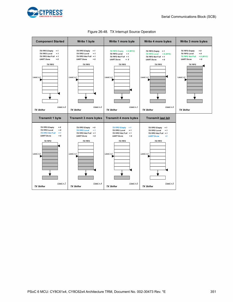
PSoC 6 MCU: CY8C61x4, CY8C62x4 Architecture TRM, Document No. 002-30473 Rev. *E 351
Serial Communications Block (SCB)
Figure 26-48. TX Interrupt Source Operation
Component Started Write 1 byte Write 1 more byte Write 4 more bytes Write 3 more bytes
TX FIFO Empty = 1
TX FIFO Level = 1
TX FIFO Not F ull = 1
UART Done = 0
TX FIFO
Level = 4
Used = 0
TX Shifter
TX FIFO
Level = 4
Used = 0
TX Shifter
TX FIFO Empty = 0 (W1C)
TX FIFO Level = 1
TX FIFO Not F ull = 1
UART Do ne = 0
TX FIFO
Level = 4
Used = 1
TX Shifter
TX FIFO Empty = 1
TX FIFO Level = 0 (W1C)
TX FIFO Not F ull = 1
UART Do ne = 0
TX FIFO
Level = 4
Used = 5
TX Shifter
TX FIFO
Level = 4
TX Shifter
TX FIFO Empty = 0
TX FIFO Level = 0
TX FIFO Not F ull = 0 (W1C)
UART Do ne = 0
Transmit 1 byte Transmit 3 more bytes Transmit 4 more bytes Transmit last bit
TX FIFO Empty = 0
TX FIFO Level = 1
TX FIFO Not F ull = 1
UART Done = 0
TX FIFO
Level = 4
Used = 4
TX Shifter
TX FIFO Empty = 1
TX FIFO Level = 1
TX FIFO Not F ull = 1
UART Do ne = 0
TX FIFO
Level = 4
Used = 0
TX Shifter
TX FIFO Empty = 1
TX FIFO Level = 1
TX FIFO Not F ull = 1
UART Do ne =1
TX FIFO
Level = 4
Used = 0
TX Shifter
TX FIFO
Level = 4
TX Shifter
TX FIFO Empty = 0
TX FIFO Level = 0
TX FIFO Not F ull = 1
UART Do ne = 0
Used = 7
TX FIFO Empty = 1
TX FIFO Level = 1
TX FIFO Not F ull = 1
UART Done = 0
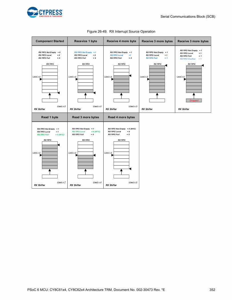
PSoC 6 MCU: CY8C61x4, CY8C62x4 Architecture TRM, Document No. 002-30473 Rev. *E 352
Serial Communications Block (SCB)
Figure 26-49. RX Interrupt Source Operation
Component Started Recevice 1 byte Receive 4 more byte Receive 3 more bytes Receive 3 more bytes
RX FIFO
Level = 4
Used = 0
RX Shifter
RX FIFO
Level = 4
Used = 0
RX Shifter
RX FIFO
Level = 4
Used = 5
RX Shifter
RX FIFO
Level = 4
RX Shifter
RX FIFO
Level = 4
Dropped
RX Shifter
RX FIFO Not Empty = 1
RX FIFO Level = 1
RX FIFO Full = 1
RX FIFO Oveflow = 1
Read 1 byte Read 3 more bytes Read 4 more bytes
RX FIFO
Level = 4
Used = 4
RX Shifter
RX FIFO
Level = 4
Used = 0
RX Shifter
RX FIFO
Level = 4
RX ShifterUsed = 7
RX FIFO Not Empty = 0
RX FIFO Level = 0
RX FIFO Full = 0
RX FIFO Not Empty = 1
RX FIFO Level = 0
RX FIFO Full = 0
RX FIFO Not Empty = 1
RX FIFO Level =1
RX FIFO Full = 0
RX FIFO Not Empty = 1
RX FIFO Level = 1
RX FIFO Full = 1
RX FIFO Not Empty = 1
RX FIFO Level = 1
RX FIFO Full = 0 (W1C)
RX FIFO Not Empty = 1
RX FIFO Level = 0 (W1C)
RX FIFO Full = 0
RX FIFO Not Empty = 0 (W1C)
RX FIFO Level = 0
RX FIFO Full = 0
PSoC 6 MCU: CY8C61x4, CY8C62x4 Architecture TRM, Document No. 002-30473 Rev. *E 353
Serial Communications Block (SCB)
26.6.3 I2C Interrupts
I2C interrupts can be classified as master interrupts, slave interrupts, TX interrupts, RX interrupts, and externally clocked (EC)mode interrupts. Each interrupt output is the logical OR of the group of all possible interrupt sources classified under thesection. For example, the TX interrupt output is the logical OR of the group of all possible TX interrupt sources. This signalgoes high when any of the enabled TX interrupt sources are true. The SCB also provides an interrupt cause register (SCB_INTR_CAUSE) that can be used to determine interrupt source. The interrupt registers are cleared by writing ‘1’ to thecorresponding bitfield. Note that certain interrupt sources are triggered again as long as the condition is met even if theinterrupt source was cleared. For example, the TX_FIFO_EMPTY is set as long as the transmit FIFO is empty even if theinterrupt source is cleared. For more information on interrupt registers, see the registers TRM. The I2C block generatesinterrupts for the following conditions.
■ I2C Master
❐ I2C master lost arbitration – The value driven by the master on the SDA line is not the same as the value observed on the SDA line.
❐ I2C master received NACK – When the master receives a NACK (typically after the master transmitted the slave address or TX data).
❐ I2C master received ACK – When the master receives an ACK (typically after the master transmitted the slave address or TX data).
❐ I2C master sent STOP – When the master has transmitted a STOP.
❐ I2C bus error – Unexpected stop/start condition is detected.
■ I2C Slave
❐ I2C slave lost arbitration – The value driven on the SDA line is not the same as the value observed on the SDA line (while the SCL line is ‘1’). This should not occur; it represents erroneous I2C bus behavior. In case of lost arbitration, the I2C slave state machine aborts the ongoing transfer. Software may decide to clear the TX and RX FIFOs in case of this error.
❐ I2C slave received NACK – When the slave receives a NACK (typically after the slave transmitted TX data).
❐ I2C slave received ACK – When the slave receives an ACK (typically after the slave transmitted TX data).
❐ I2C slave received STOP – I2C STOP event for I2C (read or write) transfer intended for this slave (address matching is performed). When STOP or REPEATED START event is detected. The REPEATED START event is included in this interrupt cause such that the I2C transfers separated by a REPEATED START can be distinguished and potentially treated separately by the firmware. Note that the second I2C transfer (after a REPEATED START) may be to a differ-ent slave address.The event is detected on any I2C transfer intended for this slave. Note that an I2C address intended for the slave (address matches) will result in an I2C_STOP event independent of whether the I2C address is ACK'd or NACK'd.
❐ I2C slave received START – When START or REPEATED START event is detected. In the case of an externally-clocked address matching (CTRL.EC_AM_MODE is ‘1’) and clock stretching is performed (until the internally-clocked logic takes over) (I2C_CTRL.S_NOT_READY_ADDR_NACK is ‘0’), this field is not set. Firmware should use INTR_S_EC.WAKE_UP, INTR_S.I2C_ADDR_MATCH, and INTR_S.I2C_GENERAL.
❐ I2C slave address matched – I2C slave matching address received. If CTRL.ADDR_ACCEPT, the received address (including the R/W bit) is available in the RX FIFO. In the case of externally-clocked address matching (CTRL.EC_AM_MODE is ‘1’) and internally-clocked operation (CTRL.EC_OP_MODE is '0'), this field is set when the event is detected.
❐ I2C bus error – Unexpected STOP/START condition is detected
■ I2C TX
❐ TX trigger – TX FIFO has fewer entries than the value specified by TRIGGER_LEVEL in SCB_TX_FIFO_CTRL.
❐ TX FIFO not full – At least one data element can be written into the TX FIFO.
❐ TX FIFO empty – The TX FIFO is empty.
❐ TX FIFO overflow – Firmware attempts to write to a full TX FIFO.
❐ TX FIFO underflow – Hardware attempts to read from an empty TX FIFO.
■ I2C RX
❐ RX FIFO has more entries than the value specified by TRIGGER_LEVEL in SCB_RX_FIFO_CTRL.
PSoC 6 MCU: CY8C61x4, CY8C62x4 Architecture TRM, Document No. 002-30473 Rev. *E 354
Serial Communications Block (SCB)
❐ RX FIFO is full – The RX FIFO is full.
❐ RX FIFO is not empty – At least one data element is available in the RX FIFO to be read.
❐ RX FIFO overflow – Hardware attempts to write to a full RX FIFO.
❐ RX FIFO underflow – Firmware attempts to read from an empty RX FIFO.
■ I2C Externally Clocked
❐ Wake up request on address match – Active on incoming slave request (with address match). Only set when EC_AM is ‘1’.
❐ I2C STOP detection at the end of each transfer – Only set for a slave request with an address match, in EZ and CMD_RESP modes, when EC_OP is ‘1’.
❐ I2C STOP detection at the end of a write transfer – Activated at the end of a write transfer (I2C STOP). This event is an indication that a buffer memory location has been written to. For EZ mode, a transfer that only writes the base address does not activate this event. Only set for a slave request with an address match, in EZ and CMD_RESP modes, when EC_OP is ‘1’.
❐ I2C STOP detection at the end of a read transfer – Activated at the end of a read transfer (I2C STOP). This event is an indication that a buffer memory location has been read from. Only set for a slave request with an address match, in EZ and CMD_RESP modes, when EC_OP is ‘1’.
For more information on how to implement and clear interrupts see the I2C (SCB_I2C_PDL) datasheet and the PDL.
PSoC 6 MCU: CY8C61x4, CY8C62x4 Architecture TRM, Document No. 002-30473 Rev. *E 355
27. Serial Memory Interface (SMIF)
The SMIF block implements a single-SPI, dual-SPI, quad-SPI, or octal-SPI communication to interface with external memorychips. The SMIF block’s primary use case is to set up the external memory and have it mapped to the PSoC 6 MCU memoryspace using the hardware. This mode of operation, called the XIP mode, allows the bus masters in the PSoC 6 MCU todirectly interact with the SMIF for memory access to an external memory location.
A graphical interface is provided with the ModusToolbox for configuring the QSPI (SMIF) block. For more information, see theModusToolbox QSPI Configurator Guide.
27.1 Features
The Serial Memory Interface (SMIF) block provides a master interface to serial memory devices that supports the followingfunctionality.
■ Interfacing up to four memory devices (slaves) at a time
■ SPI protocol
❐ SPI mode 0: clock polarity (CPOL) and clock phase (CPHA) are both ‘0’
❐ Support for single, dual, quad, and octal SPI protocols
❐ Support for dual-quad SPI mode: the use of two quad SPI memory devices to increase data bandwidth for SPI readand write transfers
❐ Support for configurable MISO sampling time and programmable receiver clock
■ Support for device capacities in the range of 64 KB to 128 MB
■ eXecute In Place (XIP) enables mapping the external memory into an internal memory address
■ Command mode enables using the SMIF block as a simple communication hardware
■ Supports a 4-KB read cache in memory mapped (XIP) mode
■ Supports on-the-fly 128-bit encryption and decryption
27.2 Architecture
Figure 27-1 shows a high-level block diagram of the SMIF hardware in PSoC 6 MCUs. Notice that the block is divided intomultiple clock domains. This enables multiple domains to access the SMIF and still enable maintaining an asynchronousclock for the communication interface.
The SMIF block can also generate DMA triggers and interrupt signals. This allows events in the SMIF block to trigger actionsin other parts of the system.
This PSoC 6 MCU technical reference manual (TRM) provides comprehensive and detailed information about thefunctions of the PSoC 6 MCU device hardware. It is divided into two books: architecture TRM and registers TRM. TheTRM is not recommended for those new to the PSoC 6 MCU, nor as a guide for developing PSoC 6 MCU applications.Use these documents instead:
■ PSoC 61 datasheet, PSoC 62 datasheet
■ Peripheral Driver Library (PDL) documentation
■ Application notes
■ Code examples
PSoC 6 MCU: CY8C61x4, CY8C62x4 Architecture TRM, Document No. 002-30473 Rev. *E 356
Serial Memory Interface (SMIF)
The SMIF interface is implemented using eight data lines, four slave select lines, and a clock line.
The access to the SMIF block can be by two modes: Command mode or XIP mode. The Command mode gives access to theSMIF’s peripheral registers and the internal FIFOs. This mode is used when the user code is responsible for constructing thecommand structure for the external memory. Typically, this mode is used when the SMIF writes to an external flash memory.The MMIO interface is also used to configure the SMIF hardware block, including configuring the device registers that set upthe XIP operation of the SMIF block.
The XIP mode of operation maps the external memory space to a range of addresses in the PSoC 6 MCU’s address space.Refer to the registers TRM for details. When this address range is accessed, the hardware automatically generates thecommands required to initiate the associated transfer from the external memory. The typical use case for the XIP mode is toexecute code placed in external memory. Thus executing code from external memory is seamless.
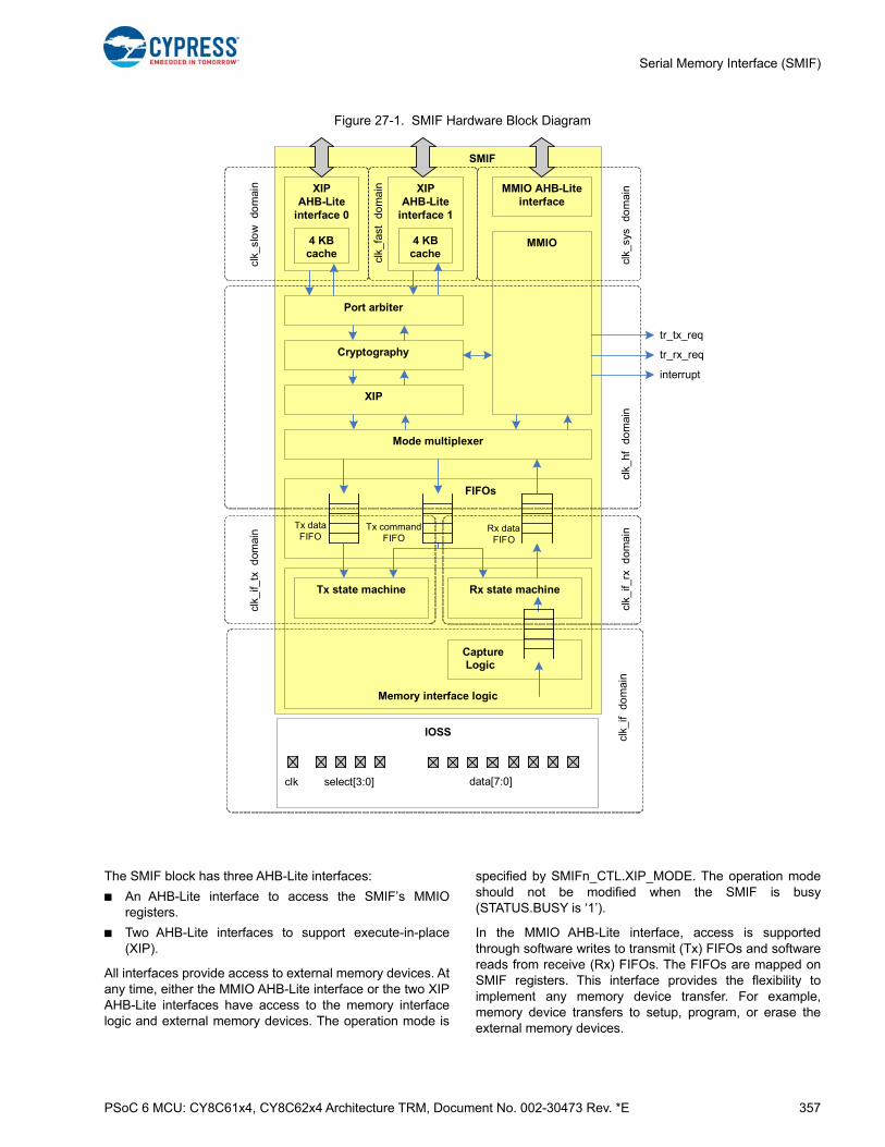
PSoC 6 MCU: CY8C61x4, CY8C62x4 Architecture TRM, Document No. 002-30473 Rev. *E 357
Serial Memory Interface (SMIF)
Figure 27-1. SMIF Hardware Block Diagram
The SMIF block has three AHB-Lite interfaces:
■ An AHB-Lite interface to access the SMIF’s MMIOregisters.
■ Two AHB-Lite interfaces to support execute-in-place(XIP).
All interfaces provide access to external memory devices. Atany time, either the MMIO AHB-Lite interface or the two XIPAHB-Lite interfaces have access to the memory interfacelogic and external memory devices. The operation mode is
specified by SMIFn_CTL.XIP_MODE. The operation modeshould not be modified when the SMIF is busy(STATUS.BUSY is ‘1’).
In the MMIO AHB-Lite interface, access is supportedthrough software writes to transmit (Tx) FIFOs and softwarereads from receive (Rx) FIFOs. The FIFOs are mapped onSMIF registers. This interface provides the flexibility toimplement any memory device transfer. For example,memory device transfers to setup, program, or erase theexternal memory devices.
SMIF
FIFOs
Memory interface logic
Tx state machine Rx state machine
clk_
if_rx
dom
ain
data[7:0]
Mode multiplexer
MMIO
XIP
Cryptography
MMIO AHB-Lite interface
clk_
if_tx
dom
ain
clk_
hfdo
mai
n
clk_
slo
wdo
mai
n
clk_
sys
dom
ain
IOSS
tr_tx_req
tr_rx_req
interrupt
Port arbiter
XIPAHB-Lite
interface 0
4 KB cache cl
k_fa
stdo
mai
n XIPAHB-Lite
interface 1
4 KB cache
Capture Logic
clk_
ifdo
mai
n
Tx data FIFO
Rx data FIFO
Tx command FIFO
select[3:0]clk

PSoC 6 MCU: CY8C61x4, CY8C62x4 Architecture TRM, Document No. 002-30473 Rev. *E 358
Serial Memory Interface (SMIF)
In an XIP AHB-Lite interface, access is supported throughXIP: AHB-Lite read and write transfers are automatically (bythe hardware) translated in memory device read and writetransfers. This interface provides efficient implementation ofmemory device read and write transfers, but does NOTsupport other types of memory device transfers. To improveXIP performance, the XIP AHB-Lite interface has a 4-KBread cache.
As mentioned, Command mode and XIP mode are mutuallyexclusive. The operation modes share Tx and Rx FIFOs andmemory interface logic. In Command mode, the Tx and RxFIFOs are accessed through the SMIF registers and undersoftware control. In XIP mode, the Tx and Rx FIFOs areunder hardware control. The memory interface logic iscontrolled through the Tx and Rx FIFOs and is agnostic ofthe operation mode.
27.2.1 Tx and Rx FIFOs
The SMIF block has two Tx FIFOs and one Rx FIFO. TheseFIFOs provide an asynchronous clock domain transferbetween clk_hf logic and clk_if_tx/clk_if_rx memoryinterface logic. The memory interface logic is completelycontrolled through the Tx and Rx FIFOs.
■ The Tx command FIFO transmits memory commands tothe memory interface logic.
■ The Tx data FIFO transmits write data to the memoryinterface transmit logic.
■ The Rx data FIFO receives read data from the memoryinterface receive logic.
27.2.1.1 Tx Command FIFO
The Tx command FIFO consists of four 20-bit entries. Eachentry holds a command. A memory transfer consists of aseries of commands. In other words, a command specifies aphase of a memory transfer. Four different types ofcommands are supported:
■ Tx command. A memory transfer must start with a Txcommand. The Tx command includes a byte that is to betransmitted over the memory interface. The Txcommand specifies the width of the data transfer (single,dual, quad, or octal data transfer). The Tx commandspecifies whether the command is for the last phase ofthe memory transfer (explicit “last command” indication).The Tx command specifies which of the four externaldevices are selected (multiple devices can be selectedsimultaneously); that is, the device selection as encodedby the Tx command is used for the complete memorytransfer. The Tx command asserts the correspondingslave select lines. This is the reason every memorytransfer should start with this command.
■ TX_COUNT command. The TX_COUNT commandspecifies the number of bytes to be transmitted from theTx data FIFO. This command relies on the Tx data FIFOto provide the bytes that are to be transmitted over the
memory interface. The TX_COUNT command specifiesthe width of the data transfer and always constitutes thelast phase of the memory transfer (implicit “lastcommand” indication - de-asserts the slave select). Notethat the TX_COUNT command does not assert the slaveselect lines. This must be done by a Tx commandpreceding it.
■ RX_COUNT command. The RX_COUNT commandspecifies the number of bytes to be received from the Rxdata FIFO. This command relies on the Rx data FIFO toaccept the bytes that are received over the memoryinterface. The RX_COUNT command specifies the widthof the data transfer and always constitutes the lastphase of the memory transfer (implicit “last command”indication - de-asserts the slave select). Note that theRX_COUNT command does not assert the slave selectlines. This must be done by a Tx command preceding it.
■ DUMMY_COUNT command. The DUMMY_COUNTcommand specifies a number of dummy cycles. Dummycycles are used to implement a turn-around (TAR) timein which the memory master changes from a transmitterdriving the data lines to a receiver receiving on the samedata lines. The DUMMY_COUNT command neverconstitutes the last phase of the memory transfer(implicit NOT “last command” indication - de-asserts theslave select); that is, it must be followed by anothercommand. Note that the DUMMY COUNT commanddoes not assert the slave select lines. This must be doneby a Tx command preceding it.
Together, the four command types can be used to constructany SPI transfer. The Tx command FIFO is used by both thememory interface transmit and receive logic. This ensureslockstep operation. The Tx command is a representation ofa queue of commands that are to be processed.
The software will write the sequence of commands into theTx command FIFO to generate a sequence responsible forthe communication with slave device. The software can readthe number of used Tx command FIFO entries through theTX_CMD_FIFO_STATUS.USED[2:0] register field.
The software can write to the Tx command FIFO through theMMIO TX_CMD_FIFO_WR register. If software attempts towrite to a full Tx command FIFO, the MMIO CTL.BLOCKfield specifies the behavior:
■ If CTL.BLOCK is ‘0’, an AHB-Lite bus error is generated.
■ If CTL.BLOCK is ‘1’, the AHB-Lite write transfer isextended until an entry is available. This increaseslatency.
27.2.1.2 Tx Data FIFO
The Tx data FIFO consists of eight 8-bit entries. A Txcommand FIFO TX_COUNT command specifies thenumber of bytes to be transmitted; that is, specifies thenumber of Tx data FIFO entries used. The Tx data FIFO isused by the memory interface transmit logic.
PSoC 6 MCU: CY8C61x4, CY8C62x4 Architecture TRM, Document No. 002-30473 Rev. *E 359
Serial Memory Interface (SMIF)
Software can read the number of used Tx data FIFO entriesthrough the TX_DATA_FIFO_STATUS.USED[3:0] registerfield.
Software can write to the Tx data FIFO through theTX_DATA_FIFO_WR1, TX_DATA_FIFO_WR2, andTX_DATA_FIFO_WR4 registers:
■ The TX_DATA_FIFO_WR1 register supports a write of asingle byte to the FIFO.
■ The TX_DATA_FIFO_WR2 register supports a write oftwo bytes to the FIFO.
■ The TX_DATA_FIFO_WR4 register supports a write offour bytes to the FIFO. If software attempts to write morebytes than available entries in the Tx data FIFO, theMMIO CTL.BLOCK field specifies the behavior:
■ If CTL.BLOCK is ‘0’, an AHB-Lite bus error is generated.
■ If CTL.BLOCK is ‘1’, the AHB-Lite write transfer isextended until the required entries are available.
27.2.1.3 Rx Data FIFO
The Rx data FIFO consists of eight 8-bit entries. A Txcommand FIFO RX_COUNT command specifies thenumber of bytes to be received; that is, specifies the numberof Rx data FIFO entries used. The memory interfacetransmit logic will stop generating the SPI clock when the Rxdata FIFO is full. This is how flow control is achieved.
Software can read the number of used Rx data FIFO entriesthrough the RX_DATA_FIFO_STATUS.USED[3:0] registerfield.
Software can read from the Rx data FIFO through the MMIORX_DATA_FIFO_RD1, RX_DATA_FIFO_RD2, andRX_DATA_FIFO_RD4 registers:
■ The RX_DATA_FIFO_RD1 register supports a read of asingle byte from the FIFO.
■ The RX_DATA_FIFO_RD2 register supports a read oftwo bytes from the FIFO.
■ The RX_DATA_FIFO_RD4 register supports a read offour bytes from the FIFO. If software attempts to readmore bytes than available in the Rx data FIFO, theMMIO CTL.BLOCK field specifies the behavior:
■ If BLOCK is ‘0’, an AHB-Lite bus error is generated andhard fault occurs.
If BLOCK is ‘1’, the AHB-Lite read transfer is extended untilthe bytes are available.
Software can also read the first byte of the RX data FIFOwithout changing the status of the FIFO through theRX_DATA_FIFO_RD1_SILENT register.
27.2.2 Command Mode
If CTL.XIP_MODE is ‘0’, the SMIF is in Command mode.Software generates SPI transfers by accessing the TxFIFOs and Rx FIFO. Software writes to the Tx FIFOs and
reads from the Rx FIFO. The Tx command FIFO hasformatted commands (Tx, TX_COUNT, RX_COUNT, andDUMMY_COUNT) that are described in the registers TRM.
Software should ensure that it generates correct memorytransfers and accesses the FIFOs correctly. For example, ifa memory transfer is generated to read four bytes from amemory device, software should read the four bytes fromthe Rx data FIFO. Similarly, if a memory transfer isgenerated to write four bytes to a memory device, softwareshould write the four bytes to the Tx command FIFO or Txdata FIFO.
Incorrect software behavior can lock up the memoryinterface. For example, a memory transfer to read 32 bytesfrom a memory device, without software reading the Rx dataFIFO will lock up the memory transfer as the memoryinterface cannot provide more than eight bytes to the Rxdata FIFO (the Rx data FIFO has eight entries). This willprevent any successive memory transfers from taking place.Hence, the software should make sure that it read the FIFOsto avoid congestion. Note that a locked up memory transferdue to Tx or Rx FIFO states is still compliant to the memorybus protocol (but undesirable): the SPI protocol allowsshutting down the interface clock in the middle of a memorytransfer.
27.2.3 XIP Mode
If CTL.XIP_MODE is ‘1’, the SMIF is in XIP mode. Hardwareautomatically (without software intervention) generatesmemory transfers by accessing the Tx FIFOs and Rx FIFO.Hardware supports only memory read and write transfers.Other functionality such as status reads are not supported.This means operations such as writing into a flash devicemay not be supported by XIP mode. This is because thewriting operation into a flash memory involves not only awrite command transfer, but also a status check to verify thestatus of the operation.
■ Hardware generates a memory read transfer for anAHB-Lite read transfer (to be precise: only for AHB-Literead transfers that miss in the cache).
■ Hardware generates a memory write transfer for anAHB-Lite write transfer.
Each slave device slot has a set of associated deviceconfiguration registers. To access a memory device in XIPmode, the corresponding device configuration registers(SMIFn_DEVICEn) should be initialized. The deviceconfiguration register sets up the following parameters formemory:
■ Write enable (WR_EN): Used to disable writes in XIPmode.
■ Crypto enable (CRYPTO_EN): When enabled, all readaccess to the memory is decrypted and write accessencrypted automatically.
■ Data Select (DATA_SEL): Selects the data lines to beused (Connecting SPI Memory Devices on page 362).
PSoC 6 MCU: CY8C61x4, CY8C62x4 Architecture TRM, Document No. 002-30473 Rev. *E 360
Serial Memory Interface (SMIF)
■ Base address and size: Sets up the mapped memoryspace. Any access in this space is converted to theaccess to the external memory automatically.
■ Read and write commands: Used to communicate withthe external memory device. These commands aredefined by multiple settings.
As different memory devices support different types ofmemory read and write commands, you must provide thehardware with device specifics, such that it can perform theautomatic translations. To this end, each memory devicehas a set of MMIO registers that specify its memory readand write transfers. This specification includes:
■ Presence and value of the SPI command byte.
■ Number of address bytes.
■ Presence and value of the mode byte.
■ Number of dummy cycles.
■ Specified data transfer widths.
The XIP interface logic produces an AHB-Lite bus errorunder the following conditions:
■ The SMIF is disabled (SMIFn_CTL.ENABLED is ‘0’).
■ The SMIF is not in XIP_MODE (SMIFn_CTL.XIP_MODEis ‘0’).
■ The transfer request is not in a memory region.
■ The transfer is a write and the identified memory regiondoes not support writes(SMIFn_DEVICEn_CTL.WR_EN is ‘0’).
■ In XIP mode (CTL.XIP_MODE is ‘1’) and dual quad SPImode (ADDR_CTL.DIV2 is ‘1’) or the transfer address isnot a multiple of 2.
■ In XIP mode (CTL.XIP_MODE is ‘1’) and dual quad SPImode (ADDR_CTL.DIV2 is ‘1’), the transfer size is not amultiple of 2.
27.2.4 Cache
To improve XIP performance, the XIP AHB-Lite interfacehas a cache. The cache is defined as follows:
■ 4 KB capacity.
■ Read-only cache. Write transfers bypass the cache. Awrite to an address, which is prefetched in the cache,invalidates the associated cache subsector. If there is awrite to a memory in Command mode then you mustinvalidate the cache while switching back to XIP mode.
■ Four-way set associative, with a least recently used(LRU) replacement scheme.
Each XIP interface implements a 4-KB cache memory,enabled by default. Any XIP access can be cached if acache is enabled. There are separate cache registers for theslow cache (in the clk_slow domain) and fast cache (in theclk_fast domain). The cache can be enabled using theSLOW_CA_CTL[ENABLED] or FAST_CA_CTL[ENABLED]registers. Read transfers that “hit” are processed by the
cache. Read transfers that “miss” result in a XIP memoryread transfer.
If CA_CTL.PREF_EN is ‘1’, prefetching is enabled and ifCA_CTL.PREF_EN is ‘0’, prefetching is disabled. If prefetchis enabled, a cache miss results in a 16 B (subsector) refillfor the missing data AND a 16 B prefetch for the nextsequential data (independent of whether this data is alreadyin the cache or not).
Cache coherency is not supported by the hardware. Forexample, an XIP interface 0 write to an address in the XIPinterface 0 cache invalidates (clears) the associated cachesubsector in the XIP interface 0 cache, but not in the XIPinterface 1 cache. This means XIP interface 1 cache nowhas outdated data. The user code can manually invalidatecache by using the SLOW_CA_CMD[INV] orFAST_CA_CMD[INV] register.
Caches should also be invalidated upon mode transitions.For example, in Command mode, a write to an address inthe cache interface will cause the data in the cache interfaceto be outdated. The cache should be invalidated whentransitioning to XIP mode to ensure that only valid data isused.
27.2.5 Arbitration
The SMIF provides two AHB-Lite slave interfaces to CPUSS(one fast interface and one slow interface). Both interfaceshave a cache (as described in 27.2.4 Cache) and cangenerate XIP requests to the external memory devices.
An arbitration component (as shown in Figure 27-1)arbitrates between the two interfaces. Arbitration is basedon the master identifier of the AHB-Lite transfer. Thearbitration priority is specified by a system wide priority.Each master identifier has a 2-bit priority level (“0” is thehighest priority level and “3” is the lowest priority level).Master identifiers with the same priority level are within thesame priority group. Within a priority group, round-robinarbitration is performed.
27.2.6 Deselect Delay
The SMIF supports configuration of deselect delay betweentransfers. The SMIFn_CTL.DESELECT_DELAY fieldcontrols the minimum number of interface cycles to hold thechip select line inactive.
27.2.7 Cryptography
In XIP mode, a cryptography component supports on-the-flyencryption for write data and on-the-fly decryption for readdata. The use of on-the-fly cryptography is determined by adevice’s MMIO CTL.CRYPTO_EN field. In Command mode,the cryptography component is accessible through aregister interface to support offline encryption anddecryption.

PSoC 6 MCU: CY8C61x4, CY8C62x4 Architecture TRM, Document No. 002-30473 Rev. *E 361
Serial Memory Interface (SMIF)
The usage scenario for cryptography is: data is encrypted inthe external memory devices. Therefore, memory read andwrite data transfers require decryption and encryptionfunctionality respectively. By storing data encrypted in theexternal memory devices (nonvolatile devices), leakage ofsensitive data is avoided.
Encryption and decryption are based on the AES-128forward block cipher: advanced encryption standard blockcipher with a 128-bit key. KEY[127:0] is a secret (private)key programmed into the CRYPTO_KEY3, …,CRYPTO_KEY0 registers. These registers are softwarewrite-only: a software read returns “0”. In the SMIF
hardware, by applying AES-128 with KEY[127:0] on aplaintext PT[127:0], we get a ciphertext CT[127:0].
In XIP mode, the XIP address is used as the plaintext PT[].The resulting ciphertext CT[] is used on-the-fly and notsoftware accessible. The XIP address is extended with theCRYPTO_INPUT3, …, CRYPTO_INPUT0 registers.
In Command mode, the MMIO CRYPTO_INPUT3, …,CRYPTO_INPUT0 registers provide the plaintext PT[]. Theresulting ciphertext CT[] is provided through the MMIOCRYPTO_OUTPUT3, …, CRYPTO_OUTPUT0 registers.
Figure 27-2 illustrates the functionality in XIP and Commandmodes.
Figure 27-2. Cryptography in XIP and Command Modes
In XIP mode, the resulting ciphertext CT[] (of the encrypted address) is XOR’d with the memory transfer’s read data or writedata. Note that the AES-128 block cipher is on the address of the data and not on the data itself. For memory read transfers,this means that as long as the latency of the memory transfer’s read data is longer than the AES-128 block cipher latency, theon-the-fly decryption does not add any delay. Figure 27-3 illustrates the complete XIP mode functionality.
The XIP mode only encrypts the address and XORs with the data; to implement the same in Command mode, you mustprovide the address as the PT[] into the crypto_INPUTx registers.
Figure 27-3. XIP Mode Functionality
AES-128 forward block
cipher
XIP mode
{CRYPTO_KEY3,CRYPTO_KEY2,CRYPTO_KEY1,CRYPTO_KEY0}
ciphertext CT[127:0]
AES-128 forward block
cipher
MMIO mode
{CRYPTO_INPUT3,CRYPTO_INPUT2,CRYPTO_INPUT1,CRYPTO_INPUT0}
{CRYPTO_KEY3,CRYPTO_KEY2,CRYPTO_KEY1,CRYPTO_KEY0}
{CRYPTO_OUTPUT3,CRYPTO_OUTPUT2,CRYPTO_OUTPUT1,CRYPTO_OUTPUT0}
{CRYPTO_INPUT3,CRYPTO_INPUT2,CRYPTO_INPUT1,
A[31:4], CRYPT0_INPUT0.INPUT[3:0]}
On-the-fly usage
AES-128 forward block
cipher
{CRYPTO_INPUT3,CRYPTO_INPUT2,CRYPTO_INPUT1,
A[31:4], CRYPT0_INPUT0.INPUT[3:0]}
{CRYPTO_KEY3,CRYPTO_KEY2,CRYPTO_KEY1,CRYPTO_KEY0}
ciphertext CT[127:0]
encrypted read data encrypted write data
decrypted read data decrypted write data
128 128
128128

PSoC 6 MCU: CY8C61x4, CY8C62x4 Architecture TRM, Document No. 002-30473 Rev. *E 362
Serial Memory Interface (SMIF)
27.3 Memory Device Signal Interface
The SMIF acts as a master for SPI applications. SPIrequires the definition of clock polarity and phase. In SPImode, the SMIF supports a single clock polarity and phaseconfiguration:
■ Clock polarity (CPOL) is ‘0’: the base value of the clockis 0.
■ Clock phase (CPHA) is ‘0’: driving of data is on thefalling edge of the clock; capturing of data is specified byCTL.CLOCK_IF_RX_SEL.
The above configuration is also known as SPI configuration0 and is supported by SPI memory devices.
27.3.1 Specifying Memory Devices
The SMIF requires that the memory devices are defined fortheir operation in XIP mode. The SMIF supports up to fourmemory devices. Each memory device is defined by a set ofregisters. The memory device specific register structureincludes:
■ The device base address and capacity. The ADDRregister specifies the memory device’s base address inthe PSoC 6 MCU address space and the MASK registerspecifies the memory device’s size/capacity. If a memorydevice is not present or is disabled, the ADDR andMASK registers specify a memory device with 0 Bcapacity. Typically, the devices’ address regions in thePSoC 6 MCU address space are non-overlapping(except for dual-quad SPI mode) to ensure that theactivation of select signals is mutually exclusive.
■ The device data signal connections (as described inConnecting SPI Memory Devices on page 362).
■ The definition of a read transfer to support XIP mode.
■ The definition of a write transfer to support XIP mode.
Each memory device uses a dedicated device select signal:memory device 0 uses select[0], memory device 1 usesselect[1], and so on. In other words, there is a fixed, one-to-one connection between memory device, register set, andselect signal connection.
In XIP mode, the XIP AHB-Lite bus transfer address iscompared with the device region. If the address is within thedevice region, the device select signal is activated. If an XIPAHB-Lite bus transfer address is within multiple regions (thisis possible if the device regions overlap), all associateddevice select signals are activated. This overlap enablesXIP in dual-quad SPI mode: the command, address, andmode bytes can be driven to two quad SPI devicessimultaneously.
In XIP mode, dual quad SPI mode requires theADDR_CTL.DIV2 field of the selected memory devices to beset to ‘1’. When this field is ‘1’, the transfer address isdivided by 2 and the divided by 2 address is provided to thememory devices.
In dual quad SPI mode, each memory device contributes a4-bit nibble for each 8-bit byte. However, both memorydevices are quad SPI memories with a byte interface.Therefore, the transfer size must be a multiple of 2.
The XIP_ALIGNMENT_ERROR interrupt cause is set underthe following conditions (in XIP mode and whenADDR_CTL.DIV2 is ‘1’):
■ The transfer address is not a multiple of 2. In this casethe divided by 2 address for the memory devices isincorrect.
■ The transfer size is not a multiple of 2. In this case, thememory devices contribute only a nibble of a byte. Thisis not supported as the memory devices have a byteinterface.
27.3.2 Connecting SPI Memory Devices
Memory device I/O signals (SCK, CS, SI/IO0, SO/IO1, IO2, IO3, IO4, IO5, IO6, IO7) are connected to the SMIF I/O signals(clk, select[3:0], and spi_data[7:0]). Not all memory devices provide the same number of I/O signals.
Table 27-1 illustrates that each memory has a single clock signal SCK, a single (low active) select signal (CS), and multipledata signals (IO0, IO1, …).
Each memory device has a fixed select signal connection (to select[3:0]).
Table 27-1. Memory Device I/O Signals
Memory Device IO Signals
Single SPI memory SCK, CS, SI, SO. This memory device has two data signals (SI and SO).
Dual SPI memory SCK, CS, IO0, IO1. This memory device has two data signals (IO0, IO1).
Quad SPI memory SCK, CS, IO0, IO1, IO2, IO3. This memory device has four data signals (IO0, IO1, IO2, IO3).
Octal SPI memorySCK, CS, IO0, IO1, IO2, IO3, IO4, IO5, IO6, IO7. This memory device has eight data signals (IO0, IO1, IO2, IO3, IO4, IO5, IO6, IO7).

PSoC 6 MCU: CY8C61x4, CY8C62x4 Architecture TRM, Document No. 002-30473 Rev. *E 363
Serial Memory Interface (SMIF)
Each memory device has programmable data signal connections (to data[7:0]): the CTL.DATA_SEL[1:0] field specifies how adevice’s data signals are connected. The CTL.DATA_SEL[1:0] is responsible for configuring the selection of data lines to beused by a slave. This is not to be confused with the select lines that are used for addressing the four slaves of the SMIFmaster. This information is used by the SMIF interface to drive out data on the correct spi_data[] outputs and capture datafrom the correct spi_data[] inputs. If multiple device select signals are activated, the same data is driven to all selecteddevices simultaneously.
Not all data signal connections are legal/supported. Supported connections are dependent on the type of memory device.
Memory devices can:
■ Use shared data signal connections.
■ Use dedicated data signal connections. This reduces the load on the data lines allowing faster signal level changes, whichin turn allows for a faster I/O interface.
Note that dual-quad SPI mode requires dedicated data signals to enable read and/or write data transfer from and to two quadSPI devices simultaneously.
Figure 27-4 illustrates memory device 0, which is a single SPI memory with data signals connections to spi_data[1:0].
Figure 27-4. Single SPI Memory Device 0 Connected to spi_data[1:0]
Table 27-2. Data Signal Connections
DATA_SEL[1:0] Single SPI Device Dual SPI Device Quad SPI Device Octal SPI Device
0spi_data[0] = SI
spi_data[1] = SO
spi_data[0] = IO0
spi_data[1] = IO1
spi_data[0] = IO0
…
spi_data[3] = IO3
spi_data[0] = IO0
…
spi_data[7] = IO7
1spi_data[2] = SI
spi_data[3] = SO
spi_data[2] = IO0
spi_data[3] = IO1Illegal Illegal
2spi_data[4] = SI
spi_data[5] = SO
spi_data[4] = IO0
spi_data[5] = IO1
spi_data[4] = IO0
…
spi_data[7] = IO3
Illegal
3spi_data[6] = SI
spi_data[7] = SO
spi_data[6] = IO0
spi_data[7] = IO1Illegal Illegal
Device 0: SPI memory
SoC
SMIFSCK
CS
SI
SO
spi_clk
spi_select[0]
spi_data[0]
spi_data[1]
CTL.DATA_SEL[1:0] = 0
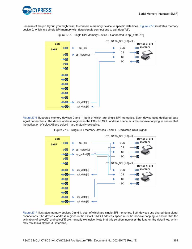
PSoC 6 MCU: CY8C61x4, CY8C62x4 Architecture TRM, Document No. 002-30473 Rev. *E 364
Serial Memory Interface (SMIF)
Because of the pin layout, you might want to connect a memory device to specific data lines. Figure 27-5 illustrates memorydevice 0, which is a single SPI memory with data signals connections to spi_data[7:6].
Figure 27-5. Single SPI Memory Device 0 Connected to spi_data[7:6]
Figure 27-6 illustrates memory devices 0 and 1, both of which are single SPI memories. Each device uses dedicated datasignal connections. The device address regions in the PSoC 6 MCU address space must be non-overlapping to ensure thatthe activation of select[0] and select[1] are mutually exclusive.
Figure 27-6. Single SPI Memory Devices 0 and 1 - Dedicated Data Signal
Figure 27-7 illustrates memory devices 0 and 1, both of which are single SPI memories. Both devices use shared data signalconnections. The devices’ address regions in the PSoC 6 MCU address space must be non-overlapping to ensure that theactivation of select[0] and select[1] are mutually exclusive. Note that this solution increases the load on the data lines, whichmay result in a slower I/O interface.
Device 0: SPI memory
SoC
SMIFSCK
CS
SI
SO
spi_clk
spi_select[0]
spi_data[6]
spi_data[7]
CTL.DATA_SEL[1:0] = 3
Device 0: SPI memory
SoC
SMIFSCK
CS
SI
SO
spi_clk
spi_select[0]
spi_data[0]
spi_data[1]
Device 1: SPI memorySCK
CS
SI
SO
spi_select[1]
CTL.DATA_SEL[1:0] = 0
CTL.DATA_SEL[1:0] = 3
spi_data[6]
spi_data[7]

PSoC 6 MCU: CY8C61x4, CY8C62x4 Architecture TRM, Document No. 002-30473 Rev. *E 365
Serial Memory Interface (SMIF)
Figure 27-7. Single SPI Memory Devices 0 and 1 - Shared Data Signal
Figure 27-8 illustrates memory device 0, which is a quad SPI memory with data signals connections to spi_data[7:4].
Figure 27-8. Quad SPI Memory Device 0
Figure 27-9 illustrates memory devices 0 and 1, device 0 is a single SPI memory and device 1 is a quad SPI memory. Eachdevice uses dedicated data signal connections. The device address regions in the PSoC 6 MCU address space must be non-overlapping to ensure that the activation of select[0] and select[1] are mutually exclusive.
Device 0: SPI memory
SoC
SMIFSCK
CS
SI
SO
spi_clk
spi_select[0]
spi_data[0]
spi_data[1]
Device 1: SPI memorySCK
CS
SI
SO
spi_select[1]
CTL.DATA_SEL[1:0] = 0
CTL.DATA_SEL[1:0] = 0
SoC
SMIFSCK
CS
SI/IO0
SO/IO1
spi_clk
spi_select[0]
spi_data[0]
spi_data[1]
spi_data[2]
spi_data[3]
Device 0: Quad SPI memory
WP/IO2
HOLD/IO3
CTL.DATA_SEL[1:0] = 0
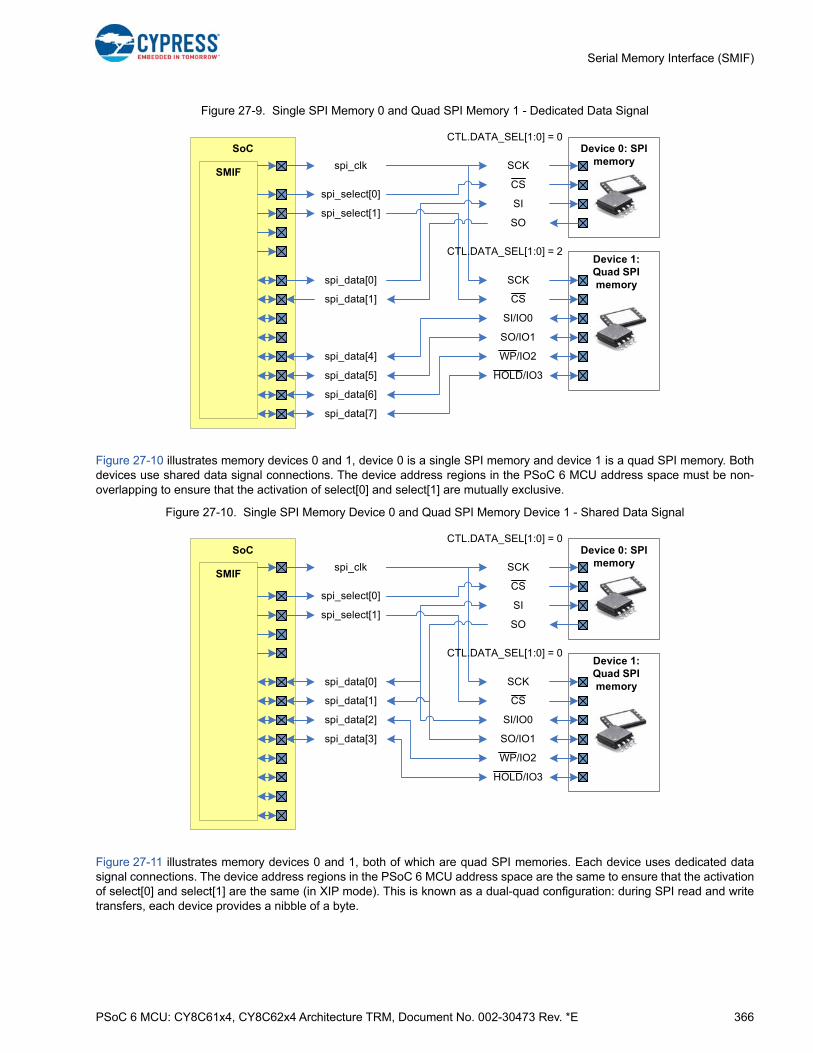
PSoC 6 MCU: CY8C61x4, CY8C62x4 Architecture TRM, Document No. 002-30473 Rev. *E 366
Serial Memory Interface (SMIF)
Figure 27-9. Single SPI Memory 0 and Quad SPI Memory 1 - Dedicated Data Signal
Figure 27-10 illustrates memory devices 0 and 1, device 0 is a single SPI memory and device 1 is a quad SPI memory. Bothdevices use shared data signal connections. The device address regions in the PSoC 6 MCU address space must be non-overlapping to ensure that the activation of select[0] and select[1] are mutually exclusive.
Figure 27-10. Single SPI Memory Device 0 and Quad SPI Memory Device 1 - Shared Data Signal
Figure 27-11 illustrates memory devices 0 and 1, both of which are quad SPI memories. Each device uses dedicated datasignal connections. The device address regions in the PSoC 6 MCU address space are the same to ensure that the activationof select[0] and select[1] are the same (in XIP mode). This is known as a dual-quad configuration: during SPI read and writetransfers, each device provides a nibble of a byte.
Device 0: SPI memory
SoC
SMIFSCK
CS
SI
SO
spi_clk
spi_select[0]
spi_data[0]
spi_data[1]
spi_select[1]
SCK
CS
SI/IO0
SO/IO1
Device 1: Quad SPI memory
WP/IO2
HOLD/IO3
CTL.DATA_SEL[1:0] = 0
CTL.DATA_SEL[1:0] = 2
spi_data[4]
spi_data[5]
spi_data[6]
spi_data[7]
Device 0: SPI memory
SoC
SMIFSCK
CS
SI
SO
spi_clk
spi_select[0]
spi_data[0]
spi_data[1]
spi_select[1]
SCK
CS
SI/IO0
SO/IO1
Device 1: Quad SPI memory
WP/IO2
HOLD/IO3
spi_data[2]
spi_data[3]
CTL.DATA_SEL[1:0] = 0
CTL.DATA_SEL[1:0] = 0
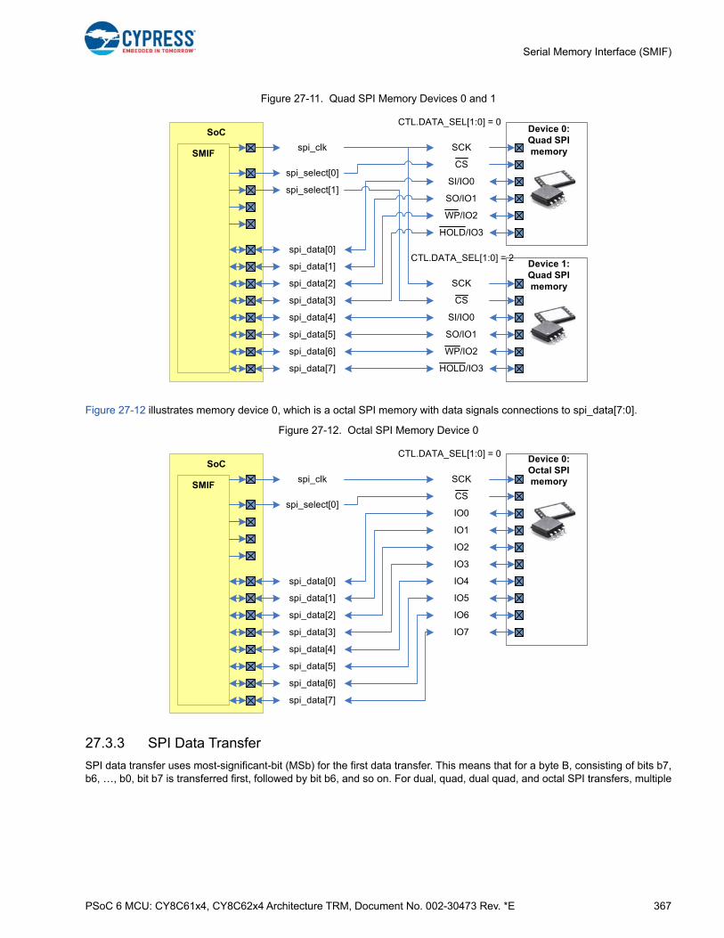
PSoC 6 MCU: CY8C61x4, CY8C62x4 Architecture TRM, Document No. 002-30473 Rev. *E 367
Serial Memory Interface (SMIF)
Figure 27-11. Quad SPI Memory Devices 0 and 1
Figure 27-12 illustrates memory device 0, which is a octal SPI memory with data signals connections to spi_data[7:0].
Figure 27-12. Octal SPI Memory Device 0
27.3.3 SPI Data Transfer
SPI data transfer uses most-significant-bit (MSb) for the first data transfer. This means that for a byte B, consisting of bits b7,b6, …, b0, bit b7 is transferred first, followed by bit b6, and so on. For dual, quad, dual quad, and octal SPI transfers, multiple
SoC
SMIFSCK
CS
SI/IO0
SO/IO1
spi_clk
spi_select[0]
spi_data[0]
spi_data[1]
spi_data[2]
spi_data[3]
Device 0: Quad SPI memory
WP/IO2
HOLD/IO3
SCK
CS
SI/IO0
SO/IO1
Device 1: Quad SPI memory
WP/IO2
HOLD/IO3
spi_data[4]
spi_data[5]
spi_data[6]
spi_data[7]
spi_select[1]
CTL.DATA_SEL[1:0] = 0
CTL.DATA_SEL[1:0] = 2
SoC
SMIFSCK
CS
IO0
IO1
spi_clk
spi_select[0]
spi_data[0]
spi_data[1]
spi_data[2]
spi_data[3]
Device 0: Octal SPI memory
IO2
IO3
CTL.DATA_SEL[1:0] = 0
IO4
IO5
IO6
IO7
spi_data[4]
spi_data[5]
spi_data[6]
spi_data[7]
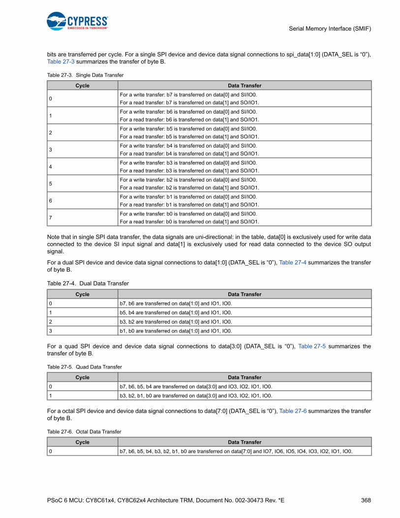
PSoC 6 MCU: CY8C61x4, CY8C62x4 Architecture TRM, Document No. 002-30473 Rev. *E 368
Serial Memory Interface (SMIF)
bits are transferred per cycle. For a single SPI device and device data signal connections to spi_data[1:0] (DATA_SEL is “0”),Table 27-3 summarizes the transfer of byte B.
Note that in single SPI data transfer, the data signals are uni-directional: in the table, data[0] is exclusively used for write dataconnected to the device SI input signal and data[1] is exclusively used for read data connected to the device SO outputsignal.
For a dual SPI device and device data signal connections to data[1:0] (DATA_SEL is “0”), Table 27-4 summarizes the transferof byte B.
For a quad SPI device and device data signal connections to data[3:0] (DATA_SEL is “0”), Table 27-5 summarizes thetransfer of byte B.
For a octal SPI device and device data signal connections to data[7:0] (DATA_SEL is “0”), Table 27-6 summarizes the transferof byte B.
Table 27-3. Single Data Transfer
Cycle Data Transfer
0For a write transfer: b7 is transferred on data[0] and SI/IO0.
For a read transfer: b7 is transferred on data[1] and SO/IO1.
1For a write transfer: b6 is transferred on data[0] and SI/IO0.
For a read transfer: b6 is transferred on data[1] and SO/IO1.
2For a write transfer: b5 is transferred on data[0] and SI/IO0.
For a read transfer: b5 is transferred on data[1] and SO/IO1.
3For a write transfer: b4 is transferred on data[0] and SI/IO0.
For a read transfer: b4 is transferred on data[1] and SO/IO1.
4For a write transfer: b3 is transferred on data[0] and SI/IO0.
For a read transfer: b3 is transferred on data[1] and SO/IO1.
5For a write transfer: b2 is transferred on data[0] and SI/IO0.
For a read transfer: b2 is transferred on data[1] and SO/IO1.
6For a write transfer: b1 is transferred on data[0] and SI/IO0.
For a read transfer: b1 is transferred on data[1] and SO/IO1.
7For a write transfer: b0 is transferred on data[0] and SI/IO0.
For a read transfer: b0 is transferred on data[1] and SO/IO1.
Table 27-4. Dual Data Transfer
Cycle Data Transfer
0 b7, b6 are transferred on data[1:0] and IO1, IO0.
1 b5, b4 are transferred on data[1:0] and IO1, IO0.
2 b3, b2 are transferred on data[1:0] and IO1, IO0.
3 b1, b0 are transferred on data[1:0] and IO1, IO0.
Table 27-5. Quad Data Transfer
Cycle Data Transfer
0 b7, b6, b5, b4 are transferred on data[3:0] and IO3, IO2, IO1, IO0.
1 b3, b2, b1, b0 are transferred on data[3:0] and IO3, IO2, IO1, IO0.
Table 27-6. Octal Data Transfer
Cycle Data Transfer
0 b7, b6, b5, b4, b3, b2, b1, b0 are transferred on data[7:0] and IO7, IO6, IO5, IO4, IO3, IO2, IO1, IO0.

PSoC 6 MCU: CY8C61x4, CY8C62x4 Architecture TRM, Document No. 002-30473 Rev. *E 369
Serial Memory Interface (SMIF)
In dual-quad SPI mode, two quad SPI devices are used.
■ The first device (the device with the lower device structure index) should have device data signal connections to data[3:0](DATA_SEL is 0).
■ The second device (the device with the higher device structure index) should have device data signal connection todata[7:4] (DATA_SEL is 2).
The command and data phases of the SPI transfer use different width data transfers:
■ The command, address, and mode bytes use quad SPI data transfer.
■ The read data and write data use octal data transfer. Each device provides a nibble of each data byte: the first deviceprovides the lower nibble and the second device provides the higher nibble.
Table 27-7 summarizes the transfer of a read data and write data byte B.
27.3.4 Example of Setting up SMIF
Devices 0 and 1 are used to implement the dual-quad SPI mode. Both devices are 1 MB / 8 Mb; the address requires 3 bytes.Device 0 has device data signal connections to data[3:0] and device 1 has device data signal connections to data[7:4].
Figure 27-13. Setting up SMIF
For dual quad SPI mode, the AHB-Lite bus transfer address is divided by two. Cryptography and write functionality aredisabled in the following example.#define MASK_1MB 0xfff00000;DEV0_ADDR = CPUSS_SMIF_BASE;DEV0_MASK = MASK_1MB // MASK: 1 MB regionDEV0_CTL =(0 << SMIF_DEVICE_CTL_DATA_SEL_Pos) // DATA_SEL: data[3:0] | (0 << SMIF_DEVICE_CTL_CRYPTO_EN_Pos) // CRYPTO_EN | (0 << SMIF_DEVICE_CTL_WR_EN_Pos)); // WR_ENDEV0_ADDR_CTL = (1 << SMIF_DEVICE_ADDR_CTL_DIV2_Pos) // DIV2: enabled | ((3-1) << SMIF_DEVICE_ADDR_CTL_SIZE2_Pos)); // SIZE: 3 B address
Table 27-7. Dual-quad SPI Mode, Octal Data Transfer
Cycle Data transfer
0b7, b6, b5, b4 are transferred on data[7:4] and second device IO3, IO2, IO1, IO0.
b3, b2, b1, b0 are transferred on data[3:0] and first device IO3, IO2, IO1, IO0.
SoC
SMIFSCK
CS
SI/IO0
SO/IO1
spi_clk
spi_select[0]
spi_data[0]
spi_data[1]
spi_data[2]
spi_data[3]
Device 0: Quad SPI memory
WP/IO2
HOLD/IO3
SCK
CS
SI/IO0
SO/IO1
Device 1: Quad SPI memory
WP/IO2
HOLD/IO3
spi_data[4]
spi_data[5]
spi_data[6]
spi_data[7]
spi_select[1]
CTL.DATA_SEL[1:0] = 0
CTL.DATA_SEL[1:0] = 2
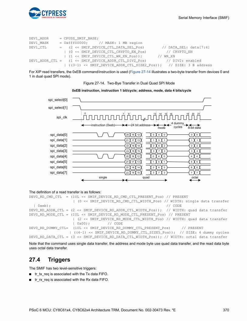
PSoC 6 MCU: CY8C61x4, CY8C62x4 Architecture TRM, Document No. 002-30473 Rev. *E 370
Serial Memory Interface (SMIF)
DEV1_ADDR = CPUSS_SMIF_BASE;DEV1_MASK = 0xfff00000; // MASK: 1 MB regionDEV1_CTL = (2 << SMIF_DEVICE_CTL_DATA_SEL_Pos) // DATA_SEL: data[7:4] | (0 << SMIF_DEVICE_CTL_CRYPTO_EN_Pos) // CRYPTO_EN | (1 << SMIF_DEVICE_CTL_WR_EN_Pos)); // WR_ENDEV1_ADDR_CTL = (1 << SMIF_DEVICE_ADDR_CTL_DIV2_Pos) // DIV2: enabled | ((3-1) << SMIF_DEVICE_ADDR_CTL_SIZE2_Pos)); // SIZE: 3 B address
For XIP read transfers, the 0xEB command/instruction is used (Figure 27-14 illustrates a two-byte transfer from devices 0 and1 in dual quad SPI mode).
Figure 27-14. Two-Bye Transfer in Dual Quad SPI Mode
The definition of a read transfer is as follows:DEV0_RD_CMD_CTL = (1UL << SMIF_DEVICE_RD_CMD_CTL_PRESENT_Pos) // PRESENT | (0 << SMIF_DEVICE_RD_CMD_CTL_WIDTH_Pos) // WIDTH: single data transfer | 0xeb); // CODEDEV0_RD_ADDR_CTL = (2 << SMIF_DEVICE_RD_ADDR_CTL_WIDTH_Pos)); // WIDTH: quad data transferDEV0_RD_MODE_CTL = (1UL << SMIF_DEVICE_RD_MODE_CTL_PRESENT_Pos) // PRESENT | (2 << SMIF_DEVICE_RD_MODE_CTL_WIDTH_Pos) // WIDTH: quad data transfer | 0x00); // CODEDEV0_RD_DUMMY_CTL= (1UL << SMIF_DEVICE_RD_DUMMY_CTL_PRESENT_Pos) // PRESENT | ((4-1) << SMIF_DEVICE_RD_DUMMY_CTL_SIZE5_Pos)); // SIZE: 4 dummy cyclesDEV0_RD_DATA_CTL = (3 << SMIF_DEVICE_RD_DATA_CTL_WIDTH_Pos)); // WIDTH: octal data transfer
Note that the command uses single data transfer, the address and mode byte use quad data transfer, and the read data byteuses octal data transfer.
27.4 Triggers
The SMIF has two level-sensitive triggers:
■ tr_tx_req is associated with the Tx data FIFO.
■ tr_rx_req is associated with the Rx data FIFO.
0 7 8 13 14 19 20 21
4 dummy cycles
24 bit addressinstruction (0xeb)
0
1 1
spi_select[1]
spi_clk
spi_data[0]
spi_data[1]
2 2spi_data[2]
3 3spi_data[3]
8-bit data
0 0
mode
15 16
4 020 16 12
1 5 117 13
2 6 218 14
3 7 319 15
21
22
23
0xEB instruction, instruction 1 bit/cycle; address, mode, data 4 bits/cycle
0
5 5
spi_data[4]
spi_data[5]
6 6spi_data[6]
7 7spi_data[7]
4 44 020 16 12
1 5 117 13
2 6 218 14
3 7 319 15
21
22
23
octalquadsingle
spi_select[0]
PSoC 6 MCU: CY8C61x4, CY8C62x4 Architecture TRM, Document No. 002-30473 Rev. *E 371
Serial Memory Interface (SMIF)
If the SMIF is enabled (CTL.ENABLED is ‘1’) and Command operation mode is selected (CTL.XIP_MODE is ‘0’), the triggerfunctionality is enabled. If the SMIF is disabled (CTL.ENABLED is ‘0’) or the XIP operation mode is selected (CTL.XIP_MODEis ‘1’), the triggers functionality is disabled. The trigger functionality is defined as follows:
■ The MMIO TX_DATA_FIFO_CTL.TRIGGER_LEVEL field specifies a number of FIFO entries. The tr_tx_req trigger isactive when the number of used Tx data FIFO entries is smaller or equal than the specified number; that is,TX_DATA_FIFO_STATUS.USED TRIGGER_LEVEL.
■ The MMIO RX_DATA_FIFO_CTL.TRIGGER_LEVEL field specifies a number of FIFO entries. The tr_rx_req trigger isactive when the number of used Rx data FIFO entries is greater than the specified number; that is,RX_DATA_FIFO_STATUS.USED > TRIGGER_LEVEL.
27.5 Interrupts
The SMIF has a single interrupt output with six interrupt causes:
■ INTR.TR_TX_REQ. This interrupt cause is activated in Command mode when the tr_tx_req trigger is activated.
■ INTR.TR_RX_REQ. This interrupt cause is activated in Command mode when the tr_rx_req trigger is activated.
■ INTR.XIP_ALIGNMENT_ERROR. This interrupt cause is activated in XIP mode when the selected device’sADDR_CTL.DIV2 field is ‘1’ and the AHB-Lite bus address is not a multiple of 2, or the requested transfer size is not amultiple of 2. This interrupt cause identifies erroneous behavior in dual-quad SPI mode (the selected deviceADDR_CTL.DIV2 field is set to ‘1’).
■ INTR.TX_CMD_FIFO_OVERFLOW. This interrupt cause is activated in Command mode, on an AHB-Lite write transfer tothe Tx command FIFO (TX_CMD_FIFO_WR) with insufficient free entries.
■ INTR.TX_DATA_FIFO_OVERFLOW. This interrupt cause is activated in Command mode, on an AHB-Lite write transferto the Tx data FIFO (TX_DATA_FIFO_WR1, TX_DATA_FIFO_WR2, and TX_DATA_FIFO_WR4) with insufficient freeentries.
■ INTR.RX_DATA_FIFO_OVERFLOW. This interrupt cause is activated in Command mode, on an AHB-Lite read transferfrom the Rx data FIFO (RX_DATA_FIFO_RD1, RX_DATA_FIFO_RD2, and RX_DATA_FIFO_RD4) with insufficient freeentries.
27.6 Sleep Operation
The SMIF hardware is operational in the Sleep and Active power modes. In the Sleep power mode, only DMA driventransactions can be performed because the CPU acting as the SPI master is not active.
27.7 Performance
Accesses to the external memory will have some latency, which is dependent upon the mode of SMIF operation, the amountof data being transferred, caching, and cryptography. In Command mode, the number of interface clock cycles per transfer isdetermined by the equation:
For example, in Figure 27-14, the equation to calculate the number of cycles would be (22 cycles = [8 bit instruction/1 singlewidth] + [24 bit address/4 width] + [8 bit mode/4 width] + 4 dummy cycles + [16 bit data/8 width]).
In XIP Mode, the performance is affected by the cache. For data reads that hit in the cache, the read will not incur anyinterface cycles. Read operations that miss in the cache will occur as a normal SMIF read operation and, if prefetching isenabled, will result in two 16 B cache sub-sector refills. Writes to external memory in XIP mode will occur as a normal SMIFwrite operation.
Enabling cryptography may impact SMIF performance. The AES-128 block cipher has a typical latency of 13 clk_hf cycles.This means that for transfers that take more than 13 cycles, the on-the-fly decryption does not add any delay. If the transfer isless than 13 cycles, the transfer latency will be 13 cycles. When the cache is enabled, the 13-cycle latency for encryption isincurred only once for every 16 B fetched for the cache.
Time to Transfer N bytes opcode size
opcode width---------------------------------- address size
address width------------------------------------ mode size
mode width----------------------------- dummycycles
data sizedata width--------------------------- + + + +
=(in interface clock cycles)

PSoC 6 MCU: CY8C61x4, CY8C62x4 Architecture TRM, Document No. 002-30473 Rev. *E 372
28. CAN FD Controller
28.1 Overview
The CAN FD controller complies with the ISO11898-1 (CAN specification Rev. 2.0 parts A and B). In addition, it supports theTime-Triggered CAN (TTCAN) protocol defined in ISO 11898-4.
All message handling functions are implemented by the RX and TX handlers. The RX handler manages message acceptancefiltering, transfer of received messages from the CAN core to a message RAM, and receive message status information. TheTX handler transfers transmit messages from the message RAM to the CAN core and provides transmit status information.
Two separate clocks are provided to the CAN FD controller: CAN clock (clk_can) for CAN operation and system clock(clk_sys) for internal block operation. Acceptance filtering is implemented by a combination of up to 192 filter elements, whereeach can be configured as a range, as a bit mask, or as a dedicated ID filter.
The CAN FD controller functions only in Active and Sleep power modes. In DeepSleep mode, it is not functional but is fullyretained except the Shared Time Stamp (TS) counter. In Hibernate power mode, the controller is neither functional norretained.
28.1.1 Features
The CAN FD controller has the following features:
■ Flexible data-rate (FD) (ISO 11898-1: 2015)
❐ Up to 64 data bytes per message
❐ Maximum 8 Mbps supported
■ Time-Triggered (TT) communication on CAN (ISO 11898-4: 2004)
❐ TTCAN protocol level 1 and level 2 completely in hardware
■ AUTOSAR support
■ Acceptance filtering
■ Two configurable receive FIFOs
■ Up to 64 dedicated receive buffers
■ Up to 32 dedicated transmit buffers
■ Configurable transmit FIFO
■ Configurable transmit queue
■ Configurable transmit event FIFO
This PSoC 6 MCU technical reference manual (TRM) provides comprehensive and detailed information about thefunctions of the PSoC 6 MCU device hardware. It is divided into two books: architecture TRM and registers TRM. TheTRM is not recommended for those new to the PSoC 6 MCU, nor as a guide for developing PSoC 6 MCU applications.Use these documents instead:
■ PSoC 61 datasheet, PSoC 62 datasheet
■ Peripheral Driver Library (PDL) documentation
■ Application notes
■ Code examples

PSoC 6 MCU: CY8C61x4, CY8C62x4 Architecture TRM, Document No. 002-30473 Rev. *E 373
CAN FD Controller
■ Programmable loop-back test mode
■ Power-down support
■ Shared message RAM (MRAM)
■ Receive FIFO top pointer logic
❐ Enables DMA access on the FIFO
■ DMA for debug message and received FIFOs
■ Shared time stamp counter
Note: Refer to the device datasheet to identify which device supports M_TTCAN and the total size of the related MRAM.
28.1.2 Features Not Supported
■ Asynchronous serial communication (ASC)
■ Interrupt of Bit Error Corrected (IR.BEC) in M_TTCAN
❐ This bit is fixed at ‘0’.
28.2 Configuration
28.2.1 Block Diagram
Figure 28-1. M_TTCAN Block Diagram
28.2.2 Dual Clock Sources
The M_TTCAN channel has two clock inputs: clk_can andclk_sys. The clk_can, derived from the system peripheralclock dividers, is used for the CAN (or CAN FD) operation.The clk_sys is used for everything except CAN operation;for example, register accesses, SRAM accesses and so on.For the CAN FD operation, it is recommended to use20 MHz, 40 MHz, or 80 MHz; for clk_can. clk_sys must runequal to or faster than clk_can, and it is allowed to bederived from a spread-spectrum PLL to minimize EMCunlike clk_can.
See the Clocking System chapter on page 240 for moredetails about clock configuration.
28.2.3 Interrupt Lines
The M_TTCAN channel provides two interrupt lines:interrupt0 and interrupt1. Interrupts from any source withinthe M_TTCAN channel can be routed either to interrupt0 orinterrupt1 by using the ILS and TTILS registers. By default,all interrupts are routed to interrupt0. By programmingEnable Interrupt Line 0 (ILE.EINT0) and Enable InterruptLine 1 (ILE.EINT1), the interrupt lines can be enabled ordisabled separately for each interrupt source.
M_TTCAN GroupM_TTCAN Decoder
TTCANFD Wrapper
M_TTCAN Channel
<clkstop IF> <counter value> <interrupts>
TTCANFD Wrap Regs
RX FIFO TopPointer
SRAM Arbiter
Timestamp Counter
<reg/sram acc.>
<reg w/r>
<reg w/r>
<sram w/r>
<sram w/r>
<sram w/r>
<fault report>
TTCANFD Regs
<ahb>
<CAN IF>
<interrupts>
<sram w/r>
<sram w/r>
<DMA IF on Debug Msg.>
<fault report IF>
<chk enable/err_inj>
AHB Slv IF
<ahb> <reg/sram acc.>
Shared MRAM
<Triggers onRx FIFOs>
SRAM Power Control
<Sync triggers>
<global control>
<intr status>
PSoC 6 MCU: CY8C61x4, CY8C62x4 Architecture TRM, Document No. 002-30473 Rev. *E 374
CAN FD Controller
28.3 Functional Description
28.3.1 Operation Modes
28.3.1.1 Software Initialization
This refers to setting or resetting the initialization bit(CCCR.INIT). The CCCR.INIT bit is set
■ either by software or hardware reset
■ when an uncorrected bit error is detected in MRAM
■ by going Bus Off
While the CCCR.INIT is set:
■ message transfer from and to the CAN bus is stopped
■ the status of the CAN bus output canfd[0].ttcan_tx[0] is recessive (high)
■ the protocol error counters are unchanged
Setting CCCR.INIT does not change any configurationregister.
Resetting CCCR.INIT finishes the software initialization. TheCAN FD controller then synchronizes itself to the datatransfer on the CAN bus by waiting for the occurrence of asequence of 11 consecutive recessive bits (Bus Idle) beforeit can take part in bus activities and start the messagetransfer.
Access/Set/Reset Properties of Registers Affected byConfiguration Change Enable (CCCR.CCE)
Access to the configuration registers is only enabled whenboth bits CCCR.INIT and CCCR.CCE are set (write-protected). CCCR.CCE can only be set/reset whileCCCR.INIT is 1. CCCR.CCE is automatically reset whenCCCR.INIT is reset.
The following registers are reset when CCCR.CCE is set
■ HPMS - High Priority Message Status
■ RXF0S - RX FIFO 0 Status
■ RXF1S - RX FIFO 1 Status
■ TXFQS - TX FIFO/Queue Status
■ TXBRP - TX Buffer Request Pending
■ TXBTO - TX Buffer Transmission Occurred
■ TXBCF - TX Buffer Cancellation Finished
■ TXEFS - TX Event FIFO Status
■ TTOST - TT Operation Status
■ TTLGT - TT Local and Global Time, only Global Time TTLGT.GT is reset
■ TTCTC - TT Cycle Time and Count
■ TTCSM - TT Cycle Sync Mark
In addition
■ Timeout Counter value (TOCV.TOC[15:0]) is preset to the value configured by the Timeout Period (TOCC.TOP[15:0]) when CCCR.CCE is set.
■ State machines of TX and RX handlers are held in idle state while CCCR.CCE is 1.
The following registers are only writeable while CCCR.CCEis 0.
■ TXBAR - TX Buffer Add Request
■ TXBCR - TX Buffer Cancellation Request
Test Mode Enable (CCCR.TEST) and Bus Monitoring mode(CCCR.MON) can only be set by the CPU while CCCR.INITis 1 and CCCR.CCE is 1. Both bits may be reset at any time.
Disable Automatic Retransmission (CCCR.DAR) can onlybe set/reset while CCCR.INIT is 1 and CCCR.CCE is 1.
Message RAM Initialization
Each MRAM word should be reset by writing 0x00000000before configuration of the CAN FD controller. This preventsMRAM bit errors when reading uninitialized words, and alsoavoids unexpected filter element configurations in MRAM.
28.3.1.2 Normal Operation
The M_TTCAN's default operating mode after hardwarereset is event-driven CAN communication without timetriggers (TTOCF.OM = 00). Both CCCR.INIT andCCCR.CCE must be set before the TT operation mode ischanged.
When M_TTCAN is initialized and CCCR.INIT is reset tozero, M_TTCAN synchronizes itself to the CAN bus and isready for communication.
After passing the acceptance filtering, received messagesincluding Message ID and DLC are stored into a dedicatedRX buffer or into RX FIFO 0 or RX FIFO 1.
For messages to be transmitted, dedicated TX buffers and aTX FIFO/TX queue can be initialized or updated. Automatedtransmission on reception of remote frames is notimplemented.
28.3.1.3 CAN FD Operation
The two variants in CAN FD frame transmission are:
■ CAN FD frame without bit rate switching
■ CAN FD frame where the control, data, and CRC fields are transmitted with a higher bit rate than the beginning and end of the frame
The previously reserved bit in CAN frames with 11-bitidentifiers and 29-bit identifiers will now be decoded as FDFbit.
■ FDF = recessive signifies a CAN FD frame
■ FDF = dominant signifies a classic CAN frame

PSoC 6 MCU: CY8C61x4, CY8C62x4 Architecture TRM, Document No. 002-30473 Rev. *E 375
CAN FD Controller
In a CAN FD frame, the two bits following FDF, reserved bits(res), and bit rate switch (BRS) decide whether the bit rateinside the CAN FD frame is switched. A CAN FD bit rateswitch signified by res is dominant and BRS is recessive.The coding of res as recessive is reserved for futureexpansion of the protocol. If the M_TTCAN receives a framewith FDF and res as recessive, it will signal a ProtocolException Event by setting the PSR.PXE bit. When ProtocolException Handling is enabled (CCCR.PXHD = 0), it causesthe operation state to change from Receiver (PSR.ACT =10) to Integrating (PSR.ACT = 00) at the next sample point.If Protocol Exception Handling is disabled (CCCR.PXHD =1), the M_TTCAN will treat a recessive res bit as a formerror and respond with an error frame.
CAN FD operation is enabled by programmingCCCR.FDOE. If CCCR.FDOE is '1', transmission andreception of CAN FD frames is enabled. Transmission andreception of classic CAN frames is always possible.Whether a CAN FD frame or a classic CAN frame istransmitted can be configured via the FDF bit in therespective TX buffer element. With CCCR.FDOE as '0',received frames are interpreted as classic CAN frames,which leads to the transmission of an error frame whenreceiving a CAN FD frame. When CAN FD operation isdisabled, no CAN FD frames are transmitted even if the FDFbit of a TX buffer element is set. CCCR.FDOE andCCCR.BRSE can only be changed while CCCR.INIT andCCCR.CCE are both set.
With CCCR.FDOE as '0', the setting of FDF and BRS isignored and frames are transmitted in classic CAN format.When CCCR.FDOE = 1 and CCCR.BRSE = 0, only FDF ofa TX buffer element is evaluated. When CCCR.FDOE = 1and CCCR.BRSE = 1, transmission of CAN FD frames withbit rate switching is enabled. All TX buffer elements withFDF and BRS bits set are transmitted in CAN FD format withbit rate switching.
A mode change during CAN operation is only recommendedunder the following conditions:
■ The failure rate in the CAN FD data phase is significantly higher than in the CAN FD arbitration phase. In this case disable the CAN FD bit rate switching option for transmissions.
■ During system startup, all nodes transmit classic CAN messages until it is verified that they can communicate in CAN FD format. If this is true, all nodes switch to CAN FD operation.
■ Wake-up messages in CAN partial networking must be transmitted in classic CAN format.
■ End-of-line programming occurs in case all nodes are not CAN FD capable. Non-CAN FD nodes are held in Silent mode until programming is completed. Then all nodes switch back to classic CAN communication.
In the CAN FD format, the coding of the DLC differs from thestandard CAN format. The DLC codes 0 to 8 have the samecoding as in standard CAN, codes 9 to 15, which in standard
CAN have a data field of 8 bytes, are coded according toTable 28-1.
In CAN FD frames, the bit timing will be switched inside theframe after the (BRS) bit, if this bit is recessive. Before theBRS bit, in the CAN FD arbitration phase, the nominal CANbit timing is used as defined by the Nominal Bit Timing andPrescaler Register (NBTP). In the following CAN FD dataphase, the data phase bit timing is used as defined by theData Bit Timing and Prescaler Register (DBTP). The bittiming is switched back from the data phase timing at theCRC delimiter or when an error is detected, whicheveroccurs first.
The maximum configurable bit rate in the CAN FD dataphase depends on the CAN clock frequency (clk_can). Forexample, with a CAN clock frequency of 20 MHz and theshortest configurable bit time of 4 tq, the bit rate in the dataphase is 5 Mbit/s.
In both data frame formats, CAN FD and CAN FD with bitrate switching, the value of the bit ESI (Error StatusIndicator) is determined by the transmitter's error state at thestart of the transmission. If the transmitter is error passive,ESI is transmitted recessive, else it is transmitted dominant.
28.3.1.4 Transmitter Delay Compensation
During the data phase of a CAN FD transmission only onenode is a transmitter; all others are receivers. The length ofthe bus line has no impact. When transmitting via pincanfd[0].ttcan_tx[0], the M_TTCAN receives the transmitteddata from its local CAN transceiver via pincanfd[0].ttcan_rx[0]. The received data is delayed by thetransmitter delay. In case this delay is greater than TSEG1(time segment before sample point), a bit error is detected.To enable a data phase bit time that is even shorter than thetransmitter delay, the delay compensation is introduced.Without transmitter delay compensation, the bit rate in thedata phase of a CAN FD frame is limited by the transmitterdelay.
Description
The M_TTCAN's protocol unit has implemented a delaycompensation mechanism to compensate the transmitterdelay. This enables transmission with higher bit rates duringthe CAN FD data phase, independent of the delay of aspecific CAN transceiver.
To check for bit errors during the data phase of transmittingnodes, the delayed transmit data is compared against thereceived data at the Secondary Sample Point (SSP). If a biterror is detected, the transmitter will react on this bit error atthe next following regular sample point. During the
Table 28-1. Extended Coding of DLC in CAN FD
DLC 9 10 11 12 13 14 15
Number of Data Bytes
12 16 20 24 32 48 64

PSoC 6 MCU: CY8C61x4, CY8C62x4 Architecture TRM, Document No. 002-30473 Rev. *E 376
CAN FD Controller
arbitration phase the delay compensation is alwaysdisabled.
The transmitter delay compensation enables configurationswhere the data bit time is shorter than the transmitter delay,it is described in detail in the new ISO 11898-1:2015. It isenabled by setting bit DBTP.TDC.
The received bit is compared against the transmitted bit atthe SSP. The SSP position is defined as the sum of themeasured delay from the M_TTCAN's transmit outputcanfd[0].ttcan_tx[0] through the transceiver to the receiveinput rx plus the transmitter delay compensation offset asconfigured by TDCR.TDCO. The transmitter delaycompensation offset is used to adjust the position of theSSP inside the received bit (for example, half of the bit timein the data phase). The position of the secondary samplepoint is rounded down to the next integer number of mtq(clk_can period).
PSR.TDCV shows the actual transmitter delaycompensation value. PSR.TDCV is cleared whenCCCR.INIT is set and is updated at each transmission of anFD frame while DBTP.TDC is set.
The following boundary conditions must be considered forthe transmitter delay compensation implemented in theM_TTCAN:
■ The sum of the measured delay from canfd[0].ttcan_tx[0] to canfd[0].ttcan_rx[0] and the configured transmitter delay compensation offset TDCR.TDCO must be less than 6 bit times in the data phase.
■ The sum of the measured delay from canfd[0].ttcan_tx[0] to canfd[0].ttcan_rx[0] and the configured transmitter delay compensation offset TDCR.TDCO should be less than or equal 127 mtq. In case this sum exceeds 127 mtq, the maximum value of 127 mtq is used for transmitter delay compensation
■ The data phase ends at the sample point of the CRC delimiter that stops checking of receive bits at the SSPs.
Transmitter Delay Compensation Measurement
If transmitter delay compensation is enabled byprogramming DBTP.TDC = 1, the measurement is startedwithin each transmitted CAN FD frame at the falling edge ofbit FDF to bit res. The measurement is stopped when thisedge is seen at the receive input canfd[0].ttcan_rx[0] of thetransmitter. The resolution of this measurement is one mtq(minimum time quanta).
Figure 28-2. Transmitter Delay Measurement
A dominant glitch inside the received FDF bit ends the delaycompensation measurement before the falling edge of thereceived res bit, resulting in an early SSP position. The useof a transmitter delay compensation filter window can beenabled by programming TDCR.TDCF. This defines aminimum value for the SSP position. Dominant edges oncanfd[0].ttcan_rx[0], that results in an earlier SSP positionare ignored for transmitter delay measurement. Themeasurement is stopped when the SSP position is at leastTDCR.TDCF and canfd[0].ttcan_rx[0] is low.
28.3.1.5 Restricted Operation mode
In Restricted Operation mode, the node is able to receivedata and remote frames and acknowledge valid frames, but
it does not send data frames, remote frames, active errorframes, or overload frames. In case of an error or overloadcondition, it does not send dominant bits; instead it waits forthe occurrence of a bus idle condition to resynchronize itselfto the CAN communication. The error counters (ECR.RECand ECR.TEC) are frozen while Error Logging (ECR.CEL) isactive.
The CPU can set the CAN FD controller into RestrictedOperation mode by setting the Restricted Operation modebit (CCCR.ASM). CCCR.ASM can only be set by the CPUwhen both CCCR.CCE and CCCR.INIT are set to ‘1‘.CCCR.ASM can be reset by the CPU at any time.
The CAN FD controller enters Restricted Operation modeautomatically when the TX handler is not able to read data
arbitration phasecanfd[0].ttcan_tx[0]
canfd[0].ttcan_rx[0]
TransmitterDelay
FDF
arbitration phase
res BRS
data phase
data phase
start stop
Delay counterclk_can/cclkDelay
TDCR.TDCODelay compensation Offset
+ SSP Position
ESI DLC

PSoC 6 MCU: CY8C61x4, CY8C62x4 Architecture TRM, Document No. 002-30473 Rev. *E 377
CAN FD Controller
from the MRAM in time. To leave this mode, the CPU shouldreset CCCR.ASM.
The Restricted Operation mode can be used in applicationsthat adapt themselves to different CAN bit rates. In thiscase, the application tests different bit rates and leaves themode after it has received a valid frame.
Note: The Restricted Operation mode must not becombined with the Loop Back mode (internal or external).
28.3.1.6 Bus Monitoring Mode
The M_TTCAN is set in Bus Monitoring mode byprogramming CCCR.MON to ‘1’ or when error level S3(TTOST.EL = 11) is entered. In Bus Monitoring mode, theM_TTCAN is able to receive valid data frames and validremote frames, but cannot start a transmission. In thismode, it sends only recessive bits on the CAN bus, if theM_TTCAN is required to send a dominant bit (ACK bit,overload flag, or active error flag), the bit is reroutedinternally so that the M_TTCAN monitors this dominant bit,although the CAN bus may remain in recessive state. In BusMonitoring mode, the TXBRP register is held in reset state.
The Bus Monitoring mode can be used to analyze the trafficon a CAN bus without affecting it by the transmission ofdominant bits. Figure 28-3 shows the connection of signalscanfd[0].ttcan_tx[0] and canfd[0].ttcan_rx[0] to theM_TTCAN in Bus Monitoring mode.
Figure 28-3. Pin Control in Bus Monitoring Mode
28.3.1.7 Disable Automatic Retransmission
M_TTCAN supports automatic retransmission of frames thathave lost arbitration or that have been disturbed by errorsduring transmission. By default, automatic retransmission isenabled. To support time-triggered communication (asdescribed in ISO 11898-1:2015, chapter 9.2), the automaticretransmission may be disabled via CCCR.DAR.
In DAR mode, all transmissions are automatically canceledafter they are started on the CAN bus. The TX RequestPending bit TXBRP.TRPx is reset after successfultransmission, when a transmission has not yet started at thepoint of cancellation, is aborted due to lost arbitration, orwhen an error occurred during frame transmission.
■ Successful transmission:
Corresponding TX Buffer Transmission Occurred bit TXBTO.TOx set
Corresponding TX Buffer Cancellation Finished bit TXBCF.CFx not set
■ Successful transmission in spite of cancellation:
Corresponding TX Buffer Transmission Occurred bit TXBTO.TOx set
Corresponding TX Buffer Cancellation Finished bit TXBCF.CFx set
■ Arbitration lost or frame transmission disturbed:
Corresponding TX Buffer Transmission Occurred bit TXBTO.TOx not set
Corresponding TX Buffer Cancellation Finished bit TXBCF.CFx set
In successful frame transmissions, and if storage of TXevents is enabled, a TX Event FIFO element is written withEvent Type ET = 10 (transmission despite cancellation).
28.3.1.8 Power Down (Sleep Mode)
The M_TTCAN channel can be set into power down modevia Clock Stop Request (CTL.STOP_REQ). As long as clockstop request is active, STOP_REQ bit is read as one.
When all pending transmission requests have completed,the M_TTCAN waits until bus idle state is detected. Thenthe M_TTCAN sets CCCR.INIT to one to prevent any furtherCAN transfers. Now the M_TTCAN acknowledges that it isready for power down by setting Clock Stop Acknowledge(STATUS.STOP_ACK). Upon receiving ack from channel,hardware automatically switches off the clock to therespective channel.
To leave power down mode, the application must resetCTL.STOP_REQ. The M_TTCAN will acknowledge this byresetting STATUS.STOP_ACK. Afterwards, the applicationcan restart CAN communication by resetting bit CCCR.INIT.
When the clock stop request is triggered throughCTL.STOP_REQ, it must not be cleared beforeSTATUS.STOP_ACK bit is set.
Note: Do not use the TTCAN CCCR.CSR register for thepower down control, instead use CTL.STOP_REQ.Similarly, use of CCCR.CSA should be avoided, instead useSTATUS.STOP_ACK.
28.3.1.9 Test Mode
To enable write access to TEST register, Test Mode Enablebit (CCCR.TEST) must be set to one. This allows theconfiguration of the test modes and test functions.
Four output functions are available for the CAN transmit pincanfd[0].ttcan_tx[0] by programming TEST.TX. Apart fromits default function of serial data output, it can drive the CANSample Point signal to monitor the M_TTCAN's bit timing; it
canfd[0].ttcan_tx[0] canfd[0].ttcan_rx[0]
="1"
Tx Rx
CAN FD Controller
Bus Monitoring Mode
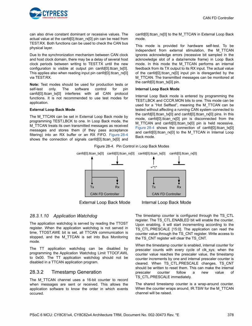
PSoC 6 MCU: CY8C61x4, CY8C62x4 Architecture TRM, Document No. 002-30473 Rev. *E 378
CAN FD Controller
can also drive constant dominant or recessive values. Theactual value at the canfd[0].ttcan_rx[0] pin can be read fromTEST.RX. Both functions can be used to check the CAN busphysical layer.
Due to the synchronization mechanism between CAN clockand host clock domain, there may be a delay of several hostclock periods between writing to TEST.TX until the newconfiguration is visible at output pin canfd[0].ttcan_tx[0].This applies also when reading input pin canfd[0].ttcan_rx[0]via TEST.RX.
Note: Test modes should be used for production tests orself-test only. The software control for pincanfd[0].ttcan_tx[0] interferes with all CAN protocolfunctions. It is not recommended to use test modes forapplication.
External Loop Back Mode
The M_TTCAN can be set in External Loop Back mode byprogramming TEST.LBCK to one. In Loop Back mode, theM_TTCAN treats its own transmitted messages as receivedmessages and stores them (if they pass acceptancefiltering) into an RX buffer or an RX FIFO. Figure 28-4shows the connection of signals canfd[0].ttcan_tx[0] and
canfd[0].ttcan_rx[0] to the M_TTCAN in External Loop Backmode.
This mode is provided for hardware self-test. To beindependent from external stimulation, the M_TTCANignores acknowledge errors (recessive bit sampled in theacknowledge slot of a data/remote frame) in Loop Backmode. In this mode the M_TTCAN performs an internalfeedback from its TX output to its RX input. The actual valueof the canfd[0].ttcan_rx[0] input pin is disregarded by theM_TTCAN. The transmitted messages can be monitored atthe canfd[0].ttcan_tx[0] pin.
Internal Loop Back Mode
Internal Loop Back mode is entered by programming theTEST.LBCK and CCCR.MON bits to one. This mode can beused for a “Hot Selftest”, meaning the M_TTCAN can betested without affecting a running CAN system connected tothe canfd[0].ttcan_tx[0] and canfd[0].ttcan_rx[0] pins. In thismode, canfd[0].ttcan_rx[0] pin is disconnected from theM_TTCAN and canfd[0].ttcan_tx[0] pin is held recessive.Figure 28-4 shows the connection of canfd[0].ttcan_tx[0]and canfd[0].ttcan_rx[0] to the M_TTCAN in Internal LoopBack mode.
Figure 28-4. Pin Control in Loop Back Modes
28.3.1.10 Application Watchdog
The application watchdog is served by reading the TTOSTregister. When the application watchdog is not served intime, TTOST.AWE bit is set, all TTCAN communication isstopped, and the M_TTCAN is set into Bus Monitoringmode.
The TT application watchdog can be disabled byprogramming the Application Watchdog Limit TTOCF.AWLto 0x00. The TT application watchdog should not bedisabled in a TTCAN application program.
28.3.2 Timestamp Generation
The M_TTCAN channel uses a 16-bit counter to recordwhen messages are sent or received. This allows theapplication software to know the order in which eventsoccured.
The timestamp counter is configured through the TS_CTLregister. The TS_CTL.ENABLED bit will enable the counter.Upon enabling, it will start incrementing according to theTS_CTL.PRESCALE [15:0]. The application can read thecounter value through the TS_CNT register. Write access tothe TS_CNT register will clear the TS_CNT.
When the timestamp counter is enabled, internal counter forprescaler counts with every cycle of clk_sys; when thecounter value reaches the prescaler value, the timestampcounter increments by one and internal prescaler counter iscleared. When TS_CTL.PRESCALE changes, TS_CNTshould be written to reset them. This can make the internalprescaler counter follow a new value ofTS_CTL.PRESCALE immediately.
The shared timestamp counter is a wrap-around counter.When the counter wraps around, IR.TSW for the M_TTCANchannel will be raised.
canfd[0].ttcan_tx[0] canfd[0].ttcan_rx[0]
Tx Rx
CAN FD Controller
External Loop Back Mode
canfd[0].ttcan_tx[0] canfd[0].ttcan_rx[0]
Tx Rx
CAN FD Controller
Internal Loop Back Mode
="1"

PSoC 6 MCU: CY8C61x4, CY8C62x4 Architecture TRM, Document No. 002-30473 Rev. *E 379
CAN FD Controller
On start of frame reception/transmission, the timestampcounter value is captured and stored into the timestampsection of an RX buffer/RX FIFO (RXTS [15:0]) or TX EventFIFO (TXTS [15:0]) element. Note: The counter valueTS_CNT is not retained in DeepSleep mode whereas theTS_CTL is retained.
28.3.3 Timeout Counter
To signal timeout conditions for RX FIFO 0, RX FIFO 1, andthe TX Event FIFO, the M_TTCAN supplies a 16-bit TimeoutCounter. It operates as down-counter and uses the sameprescaler controlled by TSCC.TCP as the timestampCounter. A prescaler TSCC.TCP should be configured toclock the timeout counter in multiples of CAN bit times(1…16). The timeout counter is configured via registerTOCC. The actual counter value can be read fromTOCV.TOC.
The timeout counter can only be started while CCCR.INIT =0. It is stopped when CCCR.INIT = 1; for example, when theM_TTCAN enters Bus_Off state.
The operation mode is selected by TOCC.TOS. Whenoperating in Continuous mode, the counter starts whenCCCR.INIT is reset. A write to TOCV presets the counter tothe value configured by TOCC.TOP and continues down-counting.
When the timeout counter is controlled by one of the FIFOs,an empty FIFO presets the counter to the value configuredby TOCC.TOP. Down-counting is started when the first FIFOelement is stored. Writing to TOCV has no effect.
When the counter reaches zero, interrupt flag IR.TOO is set.In Continuous mode, the counter is immediately restarted atTOCC.TOP.
Note: The clock signal for the timeout counter is derivedfrom the CAN Core's sample point signal. Therefore, thetime the Timeout Counter is decremented may vary due tothe synchronization/resynchronization mechanism of theCAN Core. If the bit rate switch feature in CAN FD is used,the timeout counter is clocked differently in arbitration anddata field.
28.3.4 RX Handling
The RX handler controls acceptance filtering, transfer ofreceived messages to the RX buffers or to one of the twoRX FIFOs, as well as RX FIFO's Put and Get Indices.
28.3.4.1 Acceptance Filtering
The M_TTCAN offers the possibility to configure two sets ofacceptance filters, one for standard identifiers and one forextended identifiers. These filters can be assigned to an RXbuffer or to RX FIFO 0,1. For acceptance filtering each list offilters is executed from element #0 until the first matchingelement. Acceptance filtering stops at the first matching
element. The following filter elements are not evaluated forthis message.
The main features are:
■ Each filter element can be configured as
❐ Range filter (from - to)
❐ Filter for one or two dedicated IDs
❐ Classic bit mask filter
■ Each filter element is configurable for acceptance or rejection filtering
■ Each filter element can be enabled/disabled individually
■ Filters are checked sequentially; execution stops with the first matching filter element
Related configuration registers are:
■ Global Filter Configuration (GFC)
■ Standard ID Filter Configuration (SIDFC)
■ Extended ID Filter Configuration (XIDFC)
■ Extended ID AND Mask (XIDAM)
Depending on the configuration of the filter element (SFEC/EFEC) a match triggers one of the following actions:
■ Store received frame in FIFO 0 or FIFO 1
■ Store received frame in RX buffer
■ Store received frame in RX buffer and generate pulse at filter event pin
■ Reject received frame
■ Set High-Priority Message interrupt flag IR.HPM
■ Set High-Priority Message interrupt flag IR.HPM and store received frame in FIFO 0 or FIFO 1
Acceptance filtering is started after the complete identifier isreceived. After acceptance filtering has completed, if amatching RX buffer or RX FIFO is found, the messagehandler starts writing the received message data in portionsof 32 bits to the matching RX buffer or RX FIFO. If the CANprotocol controller has detected an error condition (such asCRC error), this message is discarded with the followingimpact on the affected RX buffer or RX FIFO:
■ RX Buffer
New data flag of the matching RX buffer is not set, but RXbuffer is (partly) overwritten with received data. For errortype, see PSR.LEC and PSR.DLEC, respectively.
■ RX FIFO
Put index of matching RX FIFO is not updated, but relatedRX FIFO element is (partly) overwritten with received data.For error type, see PSR.LEC and PSR.DLEC, respectively.If the matching RX FIFO is operated in overwrite mode, theboundary conditions described in RX FIFO Overwrite Modeshould be considered.
Note: When an accepted message is written to one of thetwo RX FIFOs, or into an RX buffer, the unmodified receivedidentifier is stored independent of the filter(s) used. The
PSoC 6 MCU: CY8C61x4, CY8C62x4 Architecture TRM, Document No. 002-30473 Rev. *E 380
CAN FD Controller
result of the acceptance filter process depends on thesequence of configured filter elements.
Range Filter
The filter matches for all received frames with Message IDsin the range defined by SF1ID/SF2ID resp. EF1ID/EF2ID.
The two possibilities when range filtering is used withextended frames are:
■ EFT = 00: The Message ID of received frames is ANDed with the XIDAM before the range filter is applied
■ EFT = 11: The XIDAM is not used for range filtering
Filter for specific IDs
A filter element can be configured to filter one or two specificMessage IDs. To filter a specific Message ID, the filterelement should be configured with SF1ID = SF2ID andEF1ID = EF2ID, respectively.
Classic Bit Mask Filter
Classic bit mask filtering is intended to filter groups ofMessage IDs by masking single bits of a received MessageID. With classic bit mask filtering, SF1ID/EF1ID is used asMessage ID filter, while SF2ID/EF2ID is used as filter mask.
A zero bit at the filter mask will mask the corresponding bitposition of the configured ID filter; for example, the value ofthe received Message ID at that bit position is not relevantfor acceptance filtering. Only those bits of the receivedMessage ID where the corresponding mask bits are one arerelevant for acceptance filtering.
In case all mask bits are one, a match occurs only when thereceived Message ID and the Message ID filter are identical.If all mask bits are zero, all Message IDs match.
Standard Message ID Filtering
Figure 28-5 shows the flow for standard Message ID (11-bitIdentifier) filtering. The Standard Message ID Filter elementis described in Standard Message ID Filter Element onpage 397.
Controlled by the GFC and SIDFC Message IDs, theRemote Transmission Request bit (RTR) and the IdentifierExtension bit (IDE) of received frames are comparedagainst the list of configured filter elements.

PSoC 6 MCU: CY8C61x4, CY8C62x4 Architecture TRM, Document No. 002-30473 Rev. *E 381
CAN FD Controller
Figure 28-5. Standard Message ID Filter
Extended Message ID Filtering
Figure 28-6 shows the flow for extended Message ID (29-bit Identifier) filtering. The Extended Message ID Filter element isdescribed in Extended Message ID Filter Element on page 398.
Controlled by the GFC and XIDFC Message IDs, the RTR bit, and IDE bit of received frames are compared against the list ofconfigured filter elements.
The Extended ID AND Mask XIDAM[28:0] is ANDed with the received identifier before the filter list is executed.
valid frame received
11/29 bit idetifier29 bit11 bit
remote frameyes
reject remote frames
no GFC.RRFS = "0"
GFC.RRFS = "1"
receive filter list enabled
SIDFC.LSS[7:0] > "0"
match filter element #0yes
no
match filter element #SIDFC.LSS-1
no
SID
FC
.LS
S[7
:0]
= "
0"
yesacceptance / rejection
reject
accept non-matching frames
accept
discard frameGFC.ANFS[1] = "1"
GFC.ANFS[1] = "0"
FIFO selected andtarget FIFO full (blocking)
yes
no
store frame
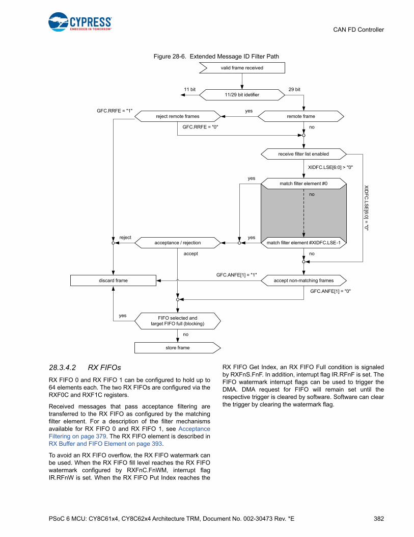
PSoC 6 MCU: CY8C61x4, CY8C62x4 Architecture TRM, Document No. 002-30473 Rev. *E 382
CAN FD Controller
Figure 28-6. Extended Message ID Filter Path
28.3.4.2 RX FIFOs
RX FIFO 0 and RX FIFO 1 can be configured to hold up to64 elements each. The two RX FIFOs are configured via theRXF0C and RXF1C registers.
Received messages that pass acceptance filtering aretransferred to the RX FIFO as configured by the matchingfilter element. For a description of the filter mechanismsavailable for RX FIFO 0 and RX FIFO 1, see AcceptanceFiltering on page 379. The RX FIFO element is described inRX Buffer and FIFO Element on page 393.
To avoid an RX FIFO overflow, the RX FIFO watermark canbe used. When the RX FIFO fill level reaches the RX FIFOwatermark configured by RXFnC.FnWM, interrupt flagIR.RFnW is set. When the RX FIFO Put Index reaches the
RX FIFO Get Index, an RX FIFO Full condition is signaledby RXFnS.FnF. In addition, interrupt flag IR.RFnF is set. TheFIFO watermark interrupt flags can be used to trigger theDMA. DMA request for FIFO will remain set until therespective trigger is cleared by software. Software can clearthe trigger by clearing the watermark flag.
valid frame received
11/29 bit idetifier29 bit11 bit
remote frame
no
reject remote frames
GFC.RRFE = "0"
yesGFC.RRFE = "1"
receive filter list enabled
XIDFC.LSE[6:0] > "0"
match filter element #0yes
no
match filter element #XIDFC.LSE-1
no
yes
XID
FC
.LS
E[6:0] =
"0"
acceptance / rejectionreject
discard frame
accept
FIFO selected andtarget FIFO full (blocking)
yes
accept non-matching framesGFC.ANFE[1] = "1"
GFC.ANFE[1] = "0"
no
store frame

PSoC 6 MCU: CY8C61x4, CY8C62x4 Architecture TRM, Document No. 002-30473 Rev. *E 383
CAN FD Controller
Figure 28-7. RX FIFO Status
When reading from an RX FIFO, RX FIFO Get IndexRXFnS.FnGI x FIFO Element Size has to be added to thecorresponding RX FIFO start address RXFnC.FnSA. RXFIFO Top pointer logic is added to the CAN FD controller tomake reading faster. See RX FIFO Top Pointer on page 384.
RX FIFO Blocking Mode
The RX FIFO blocking mode is configured by RXFnC.FnOM= 0. This is the default operation mode for RX FIFOs.
When an RX FIFO full condition is reached (RXFnS.FnPI =RXFnS.FnGI), no further messages are written to thecorresponding RX FIFO until at least one message is readand the RX FIFO Get Index is incremented. An RX FIFO fullcondition is signaled by RXFnS.FnF = 1. In addition, theinterrupt flag IR.RFnF is set.
If a message is received while the corresponding RX FIFOis full, this message is discarded and the message lostcondition is signaled by RXFnS.RFnL = 1. In addition, theinterrupt flag IR.RFnL is set.
RX FIFO Overwrite Mode
The RX FIFO overwrite mode is configured byRXFnC.FnOM = 1.
When an RX FIFO full condition (RXFnS.FnPI =RXFnS.FnGI) is signaled by RXFnS.FnF = 1, the next
message accepted for the FIFO will overwrite the oldestFIFO message. Put and Get indices are both incrementedby one.
When an RX FIFO is operated in overwrite mode and an RXFIFO full condition is signaled, reading of the RX FIFOelements should start at least at Get Index + 1. This isbecause a received message may be written to the MRAM(Put Index) while the CPU is reading from the MRAM (GetIndex). In this case, inconsistent data may be read from therespective RX FIFO element. Adding an offset to the GetIndex when reading from the RX FIFO avoids this problem.The offset depends on how fast the CPU accesses the RXFIFO. Figure 28-8 shows an offset of two with respect to theGet Index when reading the RX FIFO. In this case, the twomessages stored in element 1 and 2 are lost.
0
1
2
34
5
6
7
Get IndexRXFnS.FnGI
Fill LevelRXFnS.FnFL
Put IndexRXFnS.FnPI
Table 28-2. RX Buffer/FIFO Element size
RXESC.RBDS[2:0]RXESC.FnDS[2:0]
Data Field[bytes]
FIFO Element Size[RAM words]
000 8 4
001 12 5
010 16 6
011 20 7
100 24 8
101 32 10
110 48 14
111 64 18

PSoC 6 MCU: CY8C61x4, CY8C62x4 Architecture TRM, Document No. 002-30473 Rev. *E 384
CAN FD Controller
Figure 28-8. RX FIFO Overflow Handling
After reading from the RX FIFO, the number of the lastelement read must be written to the RX FIFO AcknowledgeIndex RXFnA.FnA. This increments the Get Index to thatelement number. If the Put Index is not incremented to thisRX FIFO element, the RX FIFO full condition is reset(RXFnS.FnF = 0).
RX FIFO Top Pointer
M_TTCAN supports two receive FIFOs. Reading from theseFIFOs requires application to go through following steps:
■ Retrieve read pointer
■ Calculate correct MRAM address
■ Read the data from MRAM
■ Update the read pointer
To avoid all these steps, RX FIFO Top Pointer logic hasbeen integrated in the CAN FD controller. It provides asingle MMIO location (RXFTOPn_DATA; n = 0,1) to read thedata from. Using such hardware logic has the followingbenefits:
■ Higher performance data access
■ Less bus traffic
■ Reduced CPU load
■ Reduced power
■ Enables DMA access to FIFO
This logic is enabled when RXFTOP_CTL.FnTPE is set.Setting this bit enables the logic to set the FIFO top address(FnTA) and internal message word counter. Receive FIFO inthe top status register (RXFTOPn_STAT) shows therespective FIFO top address and RXFTOPn_DATA providesthe data located at the top address. Refer to registerdefinitions for more details on both registers.
If RXFTOPn_DATA is read, the top pointer logic alsoupdates the RX FIFO Acknowledge Index (RXFnA.FnA) inTTCAN channel.
Note: Top pointer logic is disabled when the channel isbeing configured (CCCR.CCE = 1). ReadingRXFTOPn_DATA while the logic is disabled will return theinvalid data.
Note: When RX FIFO size is set to 1, do not use the RXFIFO top pointer function. Instead, read the receivedmessages from MRAM directly. When RX FIFO size is set to2 or more, there are no limitations.
28.3.4.3 Dedicated RX Buffers
The M_TTCAN supports up to 64 dedicated RX buffers. Thestart address of the dedicated RX buffer section isconfigured via RXBC.RBSA.
For each RX buffer, a Standard or Extended Message IDFilter Element with SFEC/EFEC = 111 and SFID2/EFID2[10:9] = 00 must be configured (see StandardMessage ID Filter Element on page 397 and ExtendedMessage ID Filter Element on page 398).
After a received message is accepted by a filter element, themessage is stored into the RX buffer in the message RAMreferenced by the filter element. The format is the same asfor an RX FIFO element. In addition, the flag IR.DRX(message stored in a dedicated RX buffer) in the interruptregister is set.
After the last word of a matching received message iswritten to the message RAM, the respective New Data flagin NDAT1 and 2 registers is set. As long as the New Dataflag is set, the respective RX buffer is locked against
0
1
2
34
5
6
7
RxFnS.FnPI= RxFnS.FnGI
Rx FIFO Full(RxFnS.FnF = "1")
Rx FIFO Overwrite(RxFnS.FnF = "1")
0
1
2
34
5
6
7
element 0 overwritten
RxFnS.FnPI= RxFnS.FnGI
read Get Index + 2
Table 28-3. Example Filter Configuration for RX Buffers
Filter Element
SFID1[10:0]EFID1[28:0]
SFID2[10:9]EFID2[10:9]
SFID2[5:0]EFID2[5:0]
0 ID message 1 00 00 0000
1 ID message 2 00 00 0001
2 ID message 3 00 00 0010

PSoC 6 MCU: CY8C61x4, CY8C62x4 Architecture TRM, Document No. 002-30473 Rev. *E 385
CAN FD Controller
updates from received matching frames. The New Dataflags should be reset by the host by writing a '1' to therespective bit position.
While an RX buffer's New Data flag is set, a Message IDFilter Element referencing the specific RX buffer will notmatch, causing the acceptance filtering to continue. Thefollowing Message ID Filter Elements may cause thereceived message to be stored into another RX buffer, orinto an RX FIFO, or the message may be rejected,depending on filter configuration.
■ Reset interrupt flag IR.DRX
■ Read New Data registers
■ Read messages from message RAM
■ Reset New Data flags of processed messages
28.3.4.4 Debug on CAN Support
Debug messages are stored into RX buffers; threeconsecutive RX buffers (for example, #61, #62, and #63)should be used to store debug messages A, B, and C. Theformat is the same for RX buffer and RX FIFO elements.
To filter debug messages Standard/Extended FilterElements with SFEC/EFEC = 111 should be set up.Messages that match these filter elements are stored intothe RX buffers addressed by SFID2/EFID2[5:0].
After message C is stored, the DMA request is activated andthe three messages can be read from the message RAMunder DMA control. The RAM words holding the debugmessages will not be changed by the M_TTCAN while DMArequest is activated. The behavior is similar to that of an RXbuffer with its New Data flag set.
After the DMA transfer is completed, an acknowledge fromDMA resets the DMA request. Now the M_TTCAN isprepared to receive the next set of debug messages.
Filtering Debug Messages
Debug messages are filtered by configuring one Standard/Extended Message ID filter element for each of the threedebug messages. To enable a filter element to filter debugmessages, SFEC/EFEC should be programmed to “111”. Inthis case the SFID1/SFID2 and EFID1/EFID2 fields have adifferent meaning (see Standard Message ID Filter Elementon page 397 and Extended Message ID Filter Element onpage 398). While SFID2/EFID2[10:9] controls the debugmessage handling state machine, SFID2/EFID2[5:0]controls the storage location of a received debug message.
When a debug message is stored, neither the respectiveNew Data flag nor IR.DRX are set. The reception of debugmessages can be monitored via RXF1S.DMS.
Debug Message Handling
The debug message handling state machine assures thatdebug messages are stored to three consecutive RX buffersin the correct order. If there are missing messages, theprocess is restarted. The DMA request is activated onlywhen all three debug messages A, B, and C are received incorrect order.
The status of the debug message handling state machine issignaled via RXF1S.DMS.
Figure 28-9. Debug Message Handling State Machine
Table 28-4. Example Filter Configuration for Debug Message
Filter Element
SFID1[10:0]EFID1[28:0]
SFID2[10:9]EFID2[10:9]
SFID2[5:0]EFID2[5:0]
0 ID debug message A 01 11 1101
1 ID debug message B 10 11 1110
2 ID debug message C 11 11 1111
DMS = "00"
HW reset orInit state
T0
DMS = "10"
T5 DMS = "01"
T1
T3
T4
T2
DMS = "11"
T6
T7T8
T0: reset DMA request, enable reception of debug messages A, B, and CT1: reception of debug message AT2: reception of debug message AT3: reception of debug message CT4: reception of debug message BT5: reception of debug messages A, BT6: reception of debug message CT7: DMA transfer completedT8: reception of debug message A, B, C (message rejected)

PSoC 6 MCU: CY8C61x4, CY8C62x4 Architecture TRM, Document No. 002-30473 Rev. *E 386
CAN FD Controller
28.3.5 TX Handling
The TX handler handles transmission requests for thededicated TX buffers, TX FIFO, and TX Queue. It controlsthe transfer of transmit messages to the CAN Core, the Putand Get Indices, and the TX Event FIFO. Up to 32 TXbuffers can be set up for message transmission. The CANmode for transmission (Classic CAN or CAN FD) can beconfigured separately for each TX buffer element. The TXbuffer element is described in TX Buffer Element onpage 395. Table 28-5 describes the possible configurationsfor frame transmission.
The TX handler starts a TX scan to check for the highestpriority pending TX request (TX buffer with lowest MessageID) when the TX Buffer Request Pending register (TXBRP)is updated, or when a transmission is started.
28.3.5.1 Transmit Pause
The transmit pause feature is intended for use in CANsystems where the CAN message identifiers are(permanently) assigned to specific values and cannot bechanged easily. These message identifiers may have ahigher CAN arbitration priority than other defined messages,while in a specific application their relative arbitration priorityshould be inverse. This may lead to a case where oneElectronic Control Unit (ECU) sends a burst of CANmessages that cause another ECU's CAN messages to bedelayed because the other messages have a lower CANarbitration priority.
For example, if CAN ECU-1 has the transmit pause featureenabled and is requested by the application software totransmit four messages, it will, after the first successfulmessage transmission, wait for two nominal bit times of busidle before it is allowed to start the next requested message.If there are other ECUs with pending messages, thosemessages are started in the idle time, they will not need toarbitrate with the next message of ECU-1. After havingreceived a message, ECU-1 is allowed to start its nexttransmission as soon as the received message releases theCAN bus.
The transmit pause feature is controlled by the TransmitPause bit (CCCR.TXP). If the bit is set, the M_TTCANcontroller will, each time it has successfully transmitted amessage, pause for two nominal bit times before starting thenext transmission. This enables other CAN nodes in thenetwork to transmit messages even if their messages havelower prior identifiers. Default is transmit pause disabled(CCCR.TXP = 0).
This feature loses burst transmissions coming from a singlenode and protects against “babbling idiot” scenarios wherethe application program erroneously requests too manytransmissions.
28.3.5.2 Dedicated TX Buffers
Dedicated TX buffers are intended for messagetransmission under complete control of the CPU. Eachdedicated TX buffer is configured with a specific MessageID. If multiple TX buffers are configured with the sameMessage ID, the TX buffer with the lowest buffer number istransmitted first.
If the data section is updated, a transmission is requestedby an Add Request via TXBAR.ARn. The requestedmessages arbitrate internally with messages from anoptional TX FIFO or TX Queue and externally withmessages on the CAN bus, and are sent out according totheir Message ID.
Addressing Dedicated TX Buffers
A dedicated TX buffer allocates an Element Size of 32-bitwords in the message RAM as shown in the Table 28-6.Therefore, the start address of a dedicated TX buffer in themessage RAM is calculated by
(transmit buffer index (0 to 31) × Element Size) + TX BuffersStart Address (TXBC.TBSA[15:2]).
28.3.5.3 TX FIFO
TX FIFO operation is configured by programmingTXBC.TFQM to '0'. Messages stored in the TX FIFO aretransmitted starting with the message referenced by the GetIndex TXFQS.TFGI. After each transmission, the Get Index
Table 28-5. Possible Configuration for Frame Transmission
CCCRTX Buffer Element Frame Transmission
BRSE FDOE FDF BRS
ignored 0 ignored ignored Classic CAN
0 1 0 ignored Classic CAN
0 1 1 ignoredFD without bit rate
switching
1 1 0 ignored Classic CAN
1 1 1 0FD without bit rate
switching
1 1 1 1 FD with bit rate switching
Table 28-6. TX Buffer/FIFO/Queue Element size
TXESC.TBDS[2:0]
Data Field[bytes]
Element Size[RAM words]
000 8 4
001 12 5
010 16 6
011 20 7
100 24 8
101 32 10
110 48 14
111 64 18

PSoC 6 MCU: CY8C61x4, CY8C62x4 Architecture TRM, Document No. 002-30473 Rev. *E 387
CAN FD Controller
is incremented cyclically until the TX FIFO is empty. The TXFIFO enables transmission of messages with the sameMessage ID from different TX buffers in the order thesemessages are written to the TX FIFO. The M_TTCANcalculates the TX FIFO Free Level TXFQS.TFFL asdifference between Get and Put Index. It indicates thenumber of available (free) TX FIFO elements.
New transmit messages must be written to the TX FIFOstarting with the TX buffer referenced by the Put IndexTXFQS.TFQPI. An Add Request increments the Put Indexto the next free TX FIFO element. When the Put Indexreaches the Get Index, TX FIFO Full (TXFQS.TFQF = 1) issignaled. In this case no further messages should be writtento the TX FIFO until the next message is transmitted and theGet Index is incremented.
When a single message is added to the TX FIFO, thetransmission is requested by writing a '1' to the TXBAR bitrelated to the TX buffer referenced by the TX FIFO's PutIndex.
When multiple (n) messages are added to the TX FIFO, theyare written to n consecutive TX buffers starting with the PutIndex. The transmissions are then requested via TXBAR.The Put Index is then cyclically incremented by n. Thenumber of requested TX buffers should not exceed thenumber of free TX buffers as indicated by the TX FIFO FreeLevel.
When a transmission request for the TX buffer referencedby the Get Index is canceled, the Get Index is incrementedto the next TX buffer with pending transmission request andthe TX FIFO Free Level is recalculated. When transmissioncancellation is applied to any other TX buffer, the Get Indexand the FIFO Free Level remain unchanged.
A TX FIFO element allocates Element Size 32-bit words inthe message RAM as shown in Table 28-6. Therefore, thestart address of the next available (free) TX FIFO buffer iscalculated by adding TX FIFO/Queue Put IndexTXFQS.TFQPI (0…31) × Element Size to the TX buffer StartAddress TXBC.TBSA.
28.3.5.4 TX Queue
TX Queue operation is configured by programmingTXBC.TFQM to '1'. Messages stored in the TX Queue aretransmitted starting with the message with the lowestMessage ID (highest priority). If multiple queue buffers areconfigured with the same Message ID, the queue buffer withthe lowest buffer number is transmitted first.
New messages must be written to the TX buffer referencedby the Put Index TXFQS.TFQPI. An Add Request cyclicallyincrements the Put Index to the next free TX buffer. If the TXQueue is full (TXFQS.TFQF = 1), the Put Index is not validand no further message should be written to the TX Queueuntil at least one of the requested messages is sent out or apending transmission request is canceled.
The application may use the TXBRP register instead of thePut Index and may place messages to any TX buffer withoutpending transmission request.
A TX Queue buffer allocates element size of 32-bit words inthe message RAM as shown in Table 28-6. Therefore, thestart address of the next available (free) TX Queue buffer iscalculated by adding TX FIFO/Queue Put IndexTXFQS.TFQPI (0…31) × Element Size to the TX buffer StartAddress TXBC.TBSA.
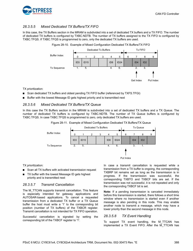
PSoC 6 MCU: CY8C61x4, CY8C62x4 Architecture TRM, Document No. 002-30473 Rev. *E 388
CAN FD Controller
28.3.5.5 Mixed Dedicated TX Buffers/TX FIFO
In this case, the TX Buffers section in the MRAM is subdivided into a set of dedicated TX buffers and a TX FIFO. The numberof dedicated TX buffers is configured by TXBC.NDTB. The number of TX buffers assigned to the TX FIFO is configured byTXBC.TFQS. If TXBC.TFQS is programmed to zero, only the dedicated TX buffers are used.
Figure 28-10. Example of Mixed Configuration Dedicated TX Buffers/TX FIFO
TX prioritization:
■ Scan dedicated TX buffers and oldest pending TX FIFO buffer (referenced by TXFS.TFGI)
■ Buffer with the lowest Message ID gets highest priority and is transmitted next
28.3.5.6 Mixed Dedicated TX Buffers/TX Queue
In this case the TX Buffers section in the MRAM is subdivided into a set of dedicated TX buffers and a TX Queue. Thenumber of dedicated TX buffers is configured by TXBC.NDTB. The number of TX Queue buffers is configured byTXBC.TFQS. In case TXBC.TFQS is programmed to zero, only dedicated TX buffers are used.
Figure 28-11. Example of Mixed Configuration Dedicated TX Buffers/TX Queue
TX prioritization:
■ Scan all TX buffers with activated transmission request
■ TX buffer with the lowest Message ID gets highest priority and is transmitted next
28.3.5.7 Transmit Cancellation
The M_TTCAN supports transmit cancellation. This featureis especially intended for gateway applications andAUTOSAR-based applications. To cancel a requestedtransmission from a dedicated TX buffer or a TX Queuebuffer the host must write a '1' to the corresponding bitposition (number of TX buffers) of the TXBCR register.Transmit cancellation is not intended for TX FIFO operation.
Successful cancellation is signaled by setting thecorresponding bit of the TXBCF register to '1'.
In case a transmit cancellation is requested while atransmission from a TX buffer is ongoing, the correspondingTXBRP bit remains set as long as the transmission is inprogress. If the transmission was successful, thecorresponding TXBTO and TXBCF bits are set. If thetransmission was not successful, it is not repeated and onlythe corresponding TXBCF bit is set.
Note: If a pending transmission is canceled immediatelybefore this transmission is started, there follows a short timewindow where no transmission is started even if anothermessage is also pending in this node. This may enableanother node to transmit a message, which may have alower priority than the second message in this node.
28.3.5.8 TX Event Handling
To support TX event handling, the M_TTCAN hasimplemented a TX Event FIFO. After the M_TTCAN has
ID3 ID15 ID8 ID24
0 1 2 3 4 5
1. 5. 4. 6.Tx Sequence
Buffer Index
Dedicated Tx Buffers
ID4 ID2
2. 3.
Tx FIFO
Get Index Put Index
6 7 8 9
ID3 ID15 ID8 ID24
0 1 2 3 4 5
2. 5. 4. 6.Tx Sequence
Buffer Index
Dedicated Tx Buffers
ID4 ID2
3. 1.
Tx Queue
Put Index
6 7 8 9

PSoC 6 MCU: CY8C61x4, CY8C62x4 Architecture TRM, Document No. 002-30473 Rev. *E 389
CAN FD Controller
transmitted a message on the CAN bus, the Message IDand timestamp are stored in a TX Event FIFO element. Tolink a TX event to a TX Event FIFO element, the MessageMarker from the transmitted TX buffer is copied into the TXEvent FIFO element.
The TX Event FIFO can be configured to a maximum of 32elements. The TX Event FIFO element is described in TXEvent FIFO Element on page 396.
The purpose of the TX Event FIFO is to decouple handlingtransmit status information from transmit message handling;that is, a TX buffer holds only the message to betransmitted, while the transmit status is stored separately inthe TX Event FIFO. This has the advantage, especiallywhen operating a dynamically managed transmit queue,that a TX buffer can be used for a new messageimmediately after successful transmission. There is no needto save transmit status information from a TX buffer beforeoverwriting that TX buffer.
When a TX Event FIFO full condition is signaled by IR.TEFF,no further elements are written to the TX Event FIFO until atleast one element is read out and the TX Event FIFO GetIndex is incremented. In case a TX event occurs while theTX Event FIFO is full, this event is discarded and interruptflag IR.TEFL is set.
To avoid a TX Event FIFO overflow, the TX Event FIFOwatermark can be used. When the TX Event FIFO fill levelreaches the TX Event FIFO watermark configured byTXEFC.EFWM, interrupt flag IR.TEFW is set.
When reading from the TX Event FIFO, the TX Event FIFOGet Index TXEFS.EFGI must be added twice to the TXEvent FIFO start address TXEFC.EFSA.
28.3.6 FIFO Acknowledge Handling
The Get indices of RX FIFO 0, RX FIFO 1, and the TX EventFIFO are controlled by the corresponding FIFOAcknowledge Index.
When RX FIFO top pointer hardware logic is used, itupdates the RX FIFO Acknowledge Index. AfterRXFTOPn_DATA is read, the Acknowledge Index(RXFnA.FnA) is updated automatically, which will eventuallyset the FIFO Get Index to the FIFO Acknowledge Index plusone and thereby updates the FIFO Fill Level.
When the application does not use RX FIFO top pointerlogic, the Acknowledge Index must be updated. This can bedone using one of the following two use cases:
■ When only a single element is read from the FIFO (the one being pointed to by the Get Index), the Get Index value is written to the FIFO Acknowledge Index.
■ When a sequence of elements is read from the FIFO, it is sufficient to write the FIFO Acknowledge Index only once at the end of that read sequence (value is the index of the last element read), to update the FIFO's Get Index.
Because the CPU has free access to the M_TTCAN'smessage RAM, take care when reading FIFO elements inan arbitrary order (Get Index not considered). This may beuseful when reading a high-priority message from one of thetwo RX FIFOs. In this case the FIFO Acknowledge Indexshould not be written because this will set the Get Index to awrong position and alter the FIFO's Fill Level. Some olderFIFO elements are lost.
Note: The application must ensure that a valid value iswritten to the FIFO Acknowledge Index. The M_TTCANdoes not check for erroneous values.
28.3.7 Configuring the CAN Bit Timing
Each node in the CAN network has its own clock generator(usually a quartz oscillator). The time parameter of the bittime can be configured individually for each CAN node.Even if each CAN node's oscillator has a different period, acommon bit rate can be generated.
The oscillator frequencies vary slightly because of changesin temperature or voltage, or deterioration of components.As long as the frequencies vary only within the tolerancerange of the oscillators, the CAN nodes can compensate forthe different bit rates by resynchronizing to the bit stream.
28.3.7.1 CAN Bit Timing
The CAN FD operation defines two bit times – nominal bittime and data bit time. The nominal bit time is for thearbitration phase. The data bit time has an equal or shorterlength and can be used to accelerate the data phase (seeCAN FD Operation on page 374).
The basic construction of a bit time is shared with both thenominal and data bit times. The bit time can be divided intofour segments according to the CAN specifications (seeFigure 28-12: the synchronization segment (Sync_Seg), thepropagation time segment (Prop_Seg), the phase buffersegment 1 (Phase_Seg1), and the phase buffer segment 2(Phase_Seg2). The sample point at which the bus level isread and interpreted as the value of that respective bit, islocated at the end of Phase_Seg1.

PSoC 6 MCU: CY8C61x4, CY8C62x4 Architecture TRM, Document No. 002-30473 Rev. *E 390
CAN FD Controller
Figure 28-12. Bit Time Construction
Each segment consists of a programmable number of time quanta, which is a multiple of the time quantum that is defined byclk_can and a prescaler. The values and prescalers used to define these parameters differ for the nominal and data bit times,and are configured by NBTP (Nominal Bit Timing and Prescaler Register) and DBTP (Data Bit Timing and Prescaler Register)as shown in Table 28-7.
Table 28-7. Bit Time Parameters
Parameter Description
Time quantum
tq (nominal) and tqd (data)
Time quantum. Derived by multiplying the basic unit time quanta (the clk_can period) with the respective prescaler.
The time quantum is configured by the CAN FD controller as
nominal: tq = (NBTP.NBRP[8:0] +1) × clk_can period
data: tqd = (DBTP.DBRP[4:0] + 1) × clk_can period
Sync_Seg
Sync_Seg is fixed to one time quantum as defined by the CAN specifications and is not configurable (inherently built into the CAN FD controller).
nominal: 1 tq
data: 1 tqd
Prop_Seg
Prop_Seg is the part of the bit time that is used to compensate for the physical delay times within the network. The CAN FD controller configures the sum of Prop_Seg and Phase_Seg1 with a single parameter:
nominal: Prop_Seg + Phase_Seg1 = NBTP.NTSEG1[7:0] + 1
data: Prop_Seg + Phase_Seg1 = DBTP.DTSEG1[4:0] + 1
Phase_Seg1
Phase_Seg1 is used to compensate for edge phase errors before the sampling point. Can be lengthened by the resyn-chronization jump width.
The sum of Prop_Seg and Phase_Seg1 is configured by the CAN FD controller as
nominal: NBTP.NTSEG1[7:0] + 1
data: DBTP.DTSEG1[4:0] + 1
Phase_Seg2
Phase_Seg2 is used to compensate for edge phase errors after the sampling point. Can be shortened by the resynchro-nization jump width.
Phase_Seg2 is configured by the CAN FD controller as
nominal: NBTP.NTSEG2[6:0] + 1
data: DBTP.DTSEG2[3:0] + 1
SJW
Resynchronization Jump Width. Used to adjust the length of Phase_Seg1 and Phase_Seg2. SJW will not be longer than either Phase_Seg1 or Phase_Seg2.
SJW is configured by the CAN FD controller as
nominal: NBTP.NSJW[6:0] + 1
data: DBTP.DSJW[3:0] + 1
Sampling pointA time quantum
A bit time
Sync_Seg Prop_Seg Phase_Seg1 Phase_Seg2

PSoC 6 MCU: CY8C61x4, CY8C62x4 Architecture TRM, Document No. 002-30473 Rev. *E 391
CAN FD Controller
These relations result in the following equations for the nominal and data bit times:
Nominal Bit time
= [Sync_Seg + Prop_Seg + Phase_Seg1 + Phase_Seg2] × tq
= [1 + (NBTP.NTSEG1[7:0] + 1) + (NBTP.NTSEG2[6:0] + 1)] × [(NBTP.NBRP[8:0] +1) × clk_can period]
Data Bit time
= [1 + (DBTP.DTSEG1[4:0] + 1) + (DBTP.DTSEG2[3:0] + 1)] × [(DBTP.DBRP[4:0] +1) × clk_can period]
Note: The Information Processing Time (IPT) of the CAN FD controller is zero; this means that the data for the next bit isavailable at the first CAN clock edge after the sample point. Therefore, the IPT does not have to be accounted for whenconfiguring Phase_Seg2, which is the maximum of Phase_Seg1 and the IPT.
28.3.7.2 CAN Bit Rates
The bit rate is the inverse of bit time; therefore, the nominal bit rate is
1 / [{1 + (NBTP.NTSEG1[7:0] + 1) + (NBTP.NTSEG2[6:0] + 1)} × {(NBTP.NBRP[8:0] +1) × clk_can period}]
and the data bit rate is
1 / [{1 + (DBTP.DTSEG1[4:0] + 1) + (DBTP.DTSEG2[3:0] + 1)} × {(DBTP.DBRP[4:0] +1) × clk_can period}]
From these formulas, we can see that the bit rates of the CAN FD controller depends on the CAN clock (clk_can) period, andthe range each parameter can be configured to. The following tables list examples of the configurable bit rates at varying CANclock frequencies. Empty boxes indicate that the desired bit rate cannot be configured at the specified input CAN clockfrequency.
Figure 28-13. Example Configuration for Nominal Bit Rates
CAN clockfrequency
configuration
nominalbit rate
125Kbps
250Kbps
500Kbps
1Mbps
8MHz
Nu
mber of tqs
per bit time
NB
TP
.NB
RP
+ 1
64tq32tq16tq8tq
10MHz 16MHz 20MHz 32MHz 40MHz
1248
80tq40tq20tq10tq
1248
128tq64tq32tq16tq8tq
1248
16
124816
160tq80tq40tq20tq10tq
1248
1632
256tq128tq64tq32tq16tq8tq
320tq160tq80tq40tq20tq10tq
1248
1632
32tq16tq8tq
124
40tq20tq10tq
124
64tq32tq16tq8tq
1248
80tq40tq20tq10tq
1248
128tq64tq32tq16tq8tq
1248
16
1248
16
160tq80tq40tq20tq10tq
16tq8tq
12
20tq10tq
12
32tq16tq8tq
124
40tq20tq10tq
124
64tq32tq16tq8tq
1248
80tq40tq20tq10tq
1248
8tq 1 10tq 1 16tq8tq
12
20tq10tq
12
32tq16tq8tq
124
40tq20tq10tq
124
NB
TP
.NB
RP
+ 1
NB
TP
.NB
RP
+ 1
NB
TP
.NB
RP
+ 1
NB
TP
.NB
RP
+ 1
NB
TP
.NB
RP
+ 1
Nu
mber of tqs
per bit time
Nu
mber of tqs
per bit time
Nu
mber of tqs
per bit time
Nu
mber of tqs
per bit time
Nu
mber of tqs
per bit time
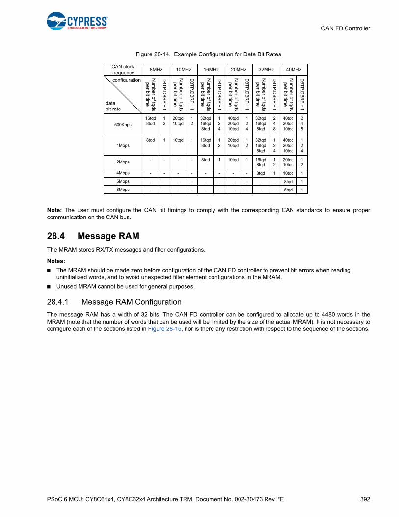
PSoC 6 MCU: CY8C61x4, CY8C62x4 Architecture TRM, Document No. 002-30473 Rev. *E 392
CAN FD Controller
Figure 28-14. Example Configuration for Data Bit Rates
Note: The user must configure the CAN bit timings to comply with the corresponding CAN standards to ensure propercommunication on the CAN bus.
28.4 Message RAM
The MRAM stores RX/TX messages and filter configurations.
Notes:
■ The MRAM should be made zero before configuration of the CAN FD controller to prevent bit errors when reading uninitialized words, and to avoid unexpected filter element configurations in the MRAM.
■ Unused MRAM cannot be used for general purposes.
28.4.1 Message RAM Configuration
The message RAM has a width of 32 bits. The CAN FD controller can be configured to allocate up to 4480 words in theMRAM (note that the number of words that can be used will be limited by the size of the actual MRAM). It is not necessary toconfigure each of the sections listed in Figure 28-15, nor is there any restriction with respect to the sequence of the sections.
CAN clockfrequency
configuration
databit rate
8MHz
Num
ber o
f tqds
pe
r bit tim
e
DB
TP
.DB
RP
+ 1
10MHz 16MHz 20MHz 32MHz 40MHz
DB
TP
.DB
RP
+ 1
DB
TP
.DB
RP
+ 1
DB
TP
.DB
RP
+ 1
DB
TP
.DB
RP
+ 1
DB
TP
.DB
RP
+ 1
500Kbps
1Mbps
2Mbps
4Mbps
5Mbps
12
16tqd8tqd
12
20tqd10tqd
124
32tqd16tqd8tqd
124
40tqd20tqd10tqd
248
32tqd16tqd8tqd
248
40tqd20tqd10tqd
18tqd 110tqd 12
16tqd8tqd
12
20tqd10tqd
124
32tqd16tqd8tqd
124
40tqd20tqd10tqd
-- -- 18tqd 110tqd 12
16tqd8tqd
12
20tqd10tqd
-- -- -- -- 18tqd 110tqd
-- -- -- -- -- 18tqd
Num
ber o
f tqds
pe
r bit tim
e
Num
ber o
f tqds
pe
r bit tim
e
Num
ber o
f tqds
pe
r bit tim
e
Num
ber o
f tqds
pe
r bit tim
e
Num
ber o
f tqds
pe
r bit tim
e
8Mbps -- -- -- -- -- 15tqd
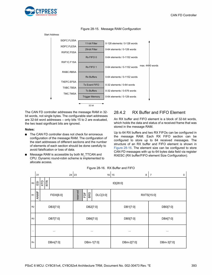
PSoC 6 MCU: CY8C61x4, CY8C62x4 Architecture TRM, Document No. 002-30473 Rev. *E 393
CAN FD Controller
Figure 28-15. Message RAM Configuration
The CAN FD controller addresses the message RAM in 32-bit words, not single bytes. The configurable start addressesare 32-bit word addresses – only bits 15 to 2 are evaluated,the two least significant bits are ignored.
Notes:
■ The CAN FD controller does not check for erroneous configuration of the message RAM. The configuration of the start addresses of different sections and the number of elements of each section should be done carefully to avoid falsification or loss of data.
■ Message RAM is accessible by both M_TTCAN and CPU. Dynamic round-robin scheme is implemented to allocate access.
28.4.2 RX Buffer and FIFO Element
An RX buffer and FIFO element is a block of 32-bit words,which holds the data and status of a received frame that wasstored in the message RAM.
Up to 64 RX buffers and two RX FIFOs can be configured inthe message RAM. Each RX FIFO section can beconfigured to store up to 64 received messages. Thestructure of an RX buffer and FIFO element is shown inFigure 28-16. The element size can be configured to storeCAN FD messages with up to 64 bytes data field via registerRXESC (RX buffer/FIFO element Size Configuration).
Figure 28-16. RX Buffer and FIFO
11-bit Filter
Start Address
SIDFC.FLSSA
XIDFC.FLESA
RXF0C.F0SA
RXF1C.F1SA
29-bit Filter
Rx FIFO 0
Rx FIFO 1
Rx Buffers
RXBC.RBSA
TXEFC.EFSATx Event FIFO
TXBC.TBSA
32 bit
0-128 elements / 0-128 words
0-64 elements / 0-128 words
0-64 elements / 0-1152 words
0-64 elements / 0-1152 words
0-64 elements / 0-1152 words
0-32 elements / 0-64 words
Tx Buffers 0-32 elements / 0-576 words
max. 4480 words
Trigger Memory 0-64 elements / 0-128 wordsTMC.TMSA
R0
R1
R2
R3
Rn
...
ES
I
XT
D
31
RT
R
2324 16 15 8 7 0
ID[28:0]
AN
MF
FIDX[6:0]
rese
rved
FD
F
BR
S
DLC[3:0] RXTS[15:0]
DB3[7:0]
DB7[7:0]
...
DBm[7:0]
DB2[7:0]
DB6[7:0]
DBm-1[7:0]
DB1[7:0] DB0[7:0]
DB5[7:0] DB4[7:0]
... ... ...
DBm-2[7:0] DBm-3[7:0]

PSoC 6 MCU: CY8C61x4, CY8C62x4 Architecture TRM, Document No. 002-30473 Rev. *E 394
CAN FD Controller
R0 [bit31] ESI: Error State Indicator
R0 [bit30] XTD: Extended Identifier
Signals to the CPU whether the received frame has astandard or extended identifier.
R0 [bit29] RTR: Remote Transmission Request
Signals to the CPU whether the received frame is a dataframe or a remote frame.
Note: There are no remote frames in CAN FD format. InCAN FD frames (FDF = 1), the dominant RRS (RemoteRequest Substitution) bit replaces bit RTR (RemoteTransmission Request).
R0 [bit28:0] ID[28:0]: Identifier
Standard or extended identifier depending on bit XTD. Astandard identifier is stored into ID[28:18].
R1 [bit31] ANMF: Accepted Non-matching Frame
Acceptance of non-matching frames may be enabled viaGFC.ANFS[1:0] (Accept Non-matching Frames Standard)and GFC.ANFE[1:0] (Accept Non-matching FramesExtended).
R1 [bit30:24] FIDX[6:0]: Filter Index
R1 [bit23:22] Reserved: Reserved Bits
When writing, always write ‘0’. The read value is undefined.
R1 [bit21] FDF: Extended Data Length
R1 [bit20] BRS: Bit Rate Switch
R1 [bit19:16] DLC[3:0]: Data Length Code
R1 [bit15:0] RXTS[15:0]: RX Timestamp
Timestamp Counter value captured on start of framereception. Resolution depending on configuration of theShared Timestamp Counter Pre-scalerTS_CTL.PRESCALE[15:0].
Notes:
■ Depending on the configuration of the element size (defined by RX buffer/FIFO Element Size Configuration (RXESC)), Rn will vary from n = 3 to 17.
■ m is a function of n, m = (n - 1) × 4 - 1.
■ The number of valid data bytes are defined by the Data Length Code.
Bit Description
0 Transmitting node is error active.
1 Transmitting node is error passive.
Bit Description
0 11-bit standard identifier.
1 29-bit extended identifier.
Bit Description
0 Received frame is a data frame.
1 Received frame is a remote frame.
Bit Description
0 Received frame matching filter index FIDX.
1Received frame did not match any RX filter element.
FIDX[6:0] Description
0-127
Index of matching RX acceptance filter ele-ment (invalid if ANMF = 1). Range is 0 to List Size Standard/Extended minus 1 (SIDFC.LSS - 1 resp. XIDFC.LSE - 1).
Bit Description
0 Classic CAN frame format.
1 CAN FD frame format.
Bit Description
0 Frame received without bit rate switching.
1 Frame received with bit rate switching.
DLC[3:0] Description
0-8Classic CAN + CAN FD: received frame has 0-8 data bytes.
9-15
Classic CAN: received frame has 8 data bytes.
CAN FD: received frame has 12/16/20/24/32/48/64 data bytes. See Table 28-1 for details.
R2 [bit31:24] DB3[7:0] : Data Byte 3
R2 [bit23:16] DB2[7:0] : Data Byte 2
R2 [bit15:8] DB1[7:0] : Data Byte 1
R2 [bit7:0] DB0[7:0] : Data Byte 0
R3 [bit31:24] DB7[7:0] : Data Byte 7
R3 [bit23:16] DB6[7:0] : Data Byte 6
R3 [bit15:8] DB5[7:0] : Data Byte 5
R3 [bit7:0] DB4[7:0] : Data Byte 4
… … …
Rn [bit31:24] DBm[7:0]: Data Byte m
Rn [bit23:16] DBm-1[7:0]: Data Byte m-1
Rn [bit15:8] DBm-2[7:0]: Data Byte m-2
Rn [bit7:0] DBm-3[7:0]: Data Byte m-3
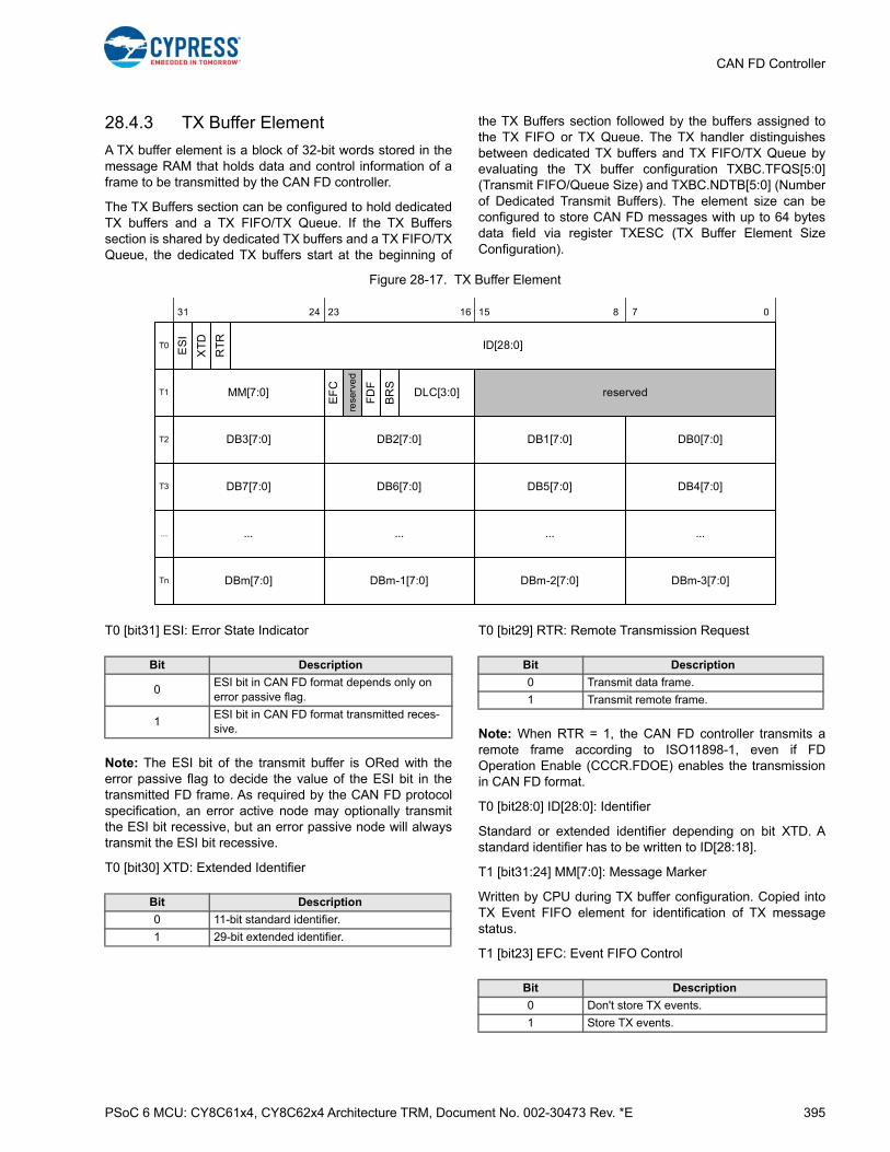
PSoC 6 MCU: CY8C61x4, CY8C62x4 Architecture TRM, Document No. 002-30473 Rev. *E 395
CAN FD Controller
28.4.3 TX Buffer Element
A TX buffer element is a block of 32-bit words stored in themessage RAM that holds data and control information of aframe to be transmitted by the CAN FD controller.
The TX Buffers section can be configured to hold dedicatedTX buffers and a TX FIFO/TX Queue. If the TX Bufferssection is shared by dedicated TX buffers and a TX FIFO/TXQueue, the dedicated TX buffers start at the beginning of
the TX Buffers section followed by the buffers assigned tothe TX FIFO or TX Queue. The TX handler distinguishesbetween dedicated TX buffers and TX FIFO/TX Queue byevaluating the TX buffer configuration TXBC.TFQS[5:0](Transmit FIFO/Queue Size) and TXBC.NDTB[5:0] (Numberof Dedicated Transmit Buffers). The element size can beconfigured to store CAN FD messages with up to 64 bytesdata field via register TXESC (TX Buffer Element SizeConfiguration).
Figure 28-17. TX Buffer Element
T0 [bit31] ESI: Error State Indicator
Note: The ESI bit of the transmit buffer is ORed with theerror passive flag to decide the value of the ESI bit in thetransmitted FD frame. As required by the CAN FD protocolspecification, an error active node may optionally transmitthe ESI bit recessive, but an error passive node will alwaystransmit the ESI bit recessive.
T0 [bit30] XTD: Extended Identifier
T0 [bit29] RTR: Remote Transmission Request
Note: When RTR = 1, the CAN FD controller transmits aremote frame according to ISO11898-1, even if FDOperation Enable (CCCR.FDOE) enables the transmissionin CAN FD format.
T0 [bit28:0] ID[28:0]: Identifier
Standard or extended identifier depending on bit XTD. Astandard identifier has to be written to ID[28:18].
T1 [bit31:24] MM[7:0]: Message Marker
Written by CPU during TX buffer configuration. Copied intoTX Event FIFO element for identification of TX messagestatus.
T1 [bit23] EFC: Event FIFO Control
T0
T1
T2
T3
Tn
...
ES
I
XT
D
31
RT
R
2324 16 15 8 7 0
ID[28:0]
MM[7:0]
rese
rve
d
FD
F
BR
SDLC[3:0] reserved
DB3[7:0]
DB7[7:0]
...
DBm[7:0]
DB2[7:0]
DB6[7:0]
DBm-1[7:0]
DB1[7:0] DB0[7:0]
DB5[7:0] DB4[7:0]
... ... ...
DBm-2[7:0] DBm-3[7:0]
EF
C
Bit Description
0ESI bit in CAN FD format depends only on error passive flag.
1ESI bit in CAN FD format transmitted reces-sive.
Bit Description
0 11-bit standard identifier.
1 29-bit extended identifier.
Bit Description
0 Transmit data frame.
1 Transmit remote frame.
Bit Description
0 Don't store TX events.
1 Store TX events.

PSoC 6 MCU: CY8C61x4, CY8C62x4 Architecture TRM, Document No. 002-30473 Rev. *E 396
CAN FD Controller
T1 [bit22] Reserved: Reserved Bit
When writing, always write ‘0’. The read value is undefined.
T1 [bit21] FDF: FD Format
T1 [bit20] BRS: Bit Rate Switching
Note: Bits ESI, FDF, and BRS are only evaluated whenCAN FD operation is enabled CCCR.FDOE = 1. Bit BRS isonly evaluated when in addition CCCR.BRSE = 1. SeeTable 28-5 for details of bits FDF and BRS.
T1 [bit19:16] DLC[3:0]: Data Length Code
CAN FD: transmit frame has 12/16/20/24/32/48/64 databytes.
T1 [bit15:0] Reserved: Reserved Bits
When writing, always write ‘0’. The read value is undefined.
Notes:
■ Depending on the configuration of the element size (TXESC), Tn will vary from n = 3 to 17.
■ m is a function of n: m = (n – 1) × 4 – 1.
28.4.4 TX Event FIFO Element
Each TX Event FIFO Element stores information abouttransmitted messages. By reading the TX Event FIFO, theCPU gets this information in the order the messages weretransmitted. Status information about the TX Event FIFOcan be obtained from register TXEFS (TX Event FIFOStatus).
Figure 28-18. TX Event FIFO Element
E0 [bit31] ESI: Error State Indicator
E0 [bit30] XTD: Extended Identifier
E0 [bit29] RTR: Remote Transmission Request
E0 [bit28:0] ID[28:0]: Identifier
Standard or extended identifier depending on bit XTD. Astandard identifier is stored into ID[28:18].
E1 [bit31:24] MM[7:0]: Message Marker
Bit Description
0 Frame transmitted in Classic CAN format.
1 Frame transmitted in CAN FD format.
Bit Description
0CAN FD frames transmitted without bit rate switching.
1CAN FD frames transmitted with bit rate switching.
DLC[3:0] Description
0-8Classic CAN + CAN FD: transmit frame has 0-8 data bytes.
9-15Classic CAN: transmit frame has 8 data bytes.
T2 [bit31:24] DB3[7:0] : Data Byte 3
T2 [bit23:16] DB2[7:0] : Data Byte 2
T2 [bit15:8] DB1[7:0] : Data Byte 1
T2 [bit7:0] DB0[7:0] : Data Byte 0
T3 [bit31:24] DB7[7:0] : Data Byte 7
T3 [bit23:16] DB6[7:0] : Data Byte 6
T3 [bit15:8] DB5[7:0] : Data Byte 5
T3 [bit7:0] DB4[7:0] : Data Byte 4
… … …
Tn [bit31:24] DBm[7:0]: Data Byte m
Tn [bit23:16] DBm-1[7:0]: Data Byte m-1
Tn [bit15:8] DBm-2[7:0]: Data Byte m-2
Tn [bit7:0] DBm-3[7:0]: Data Byte m-3
E0
E1
ES
I
XT
D
31
RT
R
2324 16 15 8 7 0
ID[28:0]
MM[7:0]
FD
F
BR
S
DLC[3:0] TXTS[15:0]ET
[1:0]
Bit Description
0 Transmitting node is error active.
1 Transmitting node is error passive.
Bit Description
0 11-bit standard identifier.
1 29-bit extended identifier.
Bit Description
0 Data frame transmitted.
1 Remote frame transmitted.

PSoC 6 MCU: CY8C61x4, CY8C62x4 Architecture TRM, Document No. 002-30473 Rev. *E 397
CAN FD Controller
Copied from TX buffer into TX Event FIFO element foridentification of TX message status.
E1 [bit23:22] ET[1:0]: Event Type
E1 [bit21] FDF: FD Format
E1 [bit20] BRS: Bit Rate Switching
E1 [bit19:16] DLC[3:0]: Data Length Code
E1 [bit15:0] TXTS[15:0]: TX Timestamp
Timestamp Counter value captured on start-of-frametransmission. Resolution depending on configuration of theShared Timestamp Counter Pre-scalerTS_CTL.PRESCALE[15:0].
28.4.5 Standard Message ID Filter Element
A Standard Message ID Filter Element consists of a single32-bit word, and can be configured as a range filter, dualfilter, classic bit mask filter, or filter for a single dedicated ID,for messages with 11-bit standard IDs.
Up to 128 filter elements can be configured for 11-bitstandard IDs. When accessing a Standard Message IDFilter element, its address is
Filter List Standard Start Address (SIDFC.FLSSA[15:2]) +index of the filter element (0 to 127).
Figure 28-19. Standard Message ID Filter
S0 [bit31:30] SFT[1:0]: Standard Filter Type
Note: With SFT = 11, the filter element is disabled and the acceptance filtering continues (same behavior as with SFEC =000).
S0 [bit29:27] SFEC[2:0]: Standard Filter Element Configuration
All enabled filter elements are used for acceptance filtering of standard frames. Acceptance filtering stops at the first matchingenabled filter element or when the end of the filter list is reached.
ET[1:0] Description
00 Reserved.
01 TX event.
10
Transmission in spite of cancellation.
Always set for transmissions in DAR mode (Disable Automatic Retransmission mode).
11 Reserved.
Bit Description
0 Classic CAN frame format.
1CAN FD frame format (new DLC-coding and CRC).
Bit Description
0 Frame transmitted without bit rate switching.
1 Frame transmitted with bit rate switching.
DLC[3:0] Description
0-8Classic CAN + CAN FD: frame with 0-8 data bytes transmitted.
9-15
Classic CAN: frame with 8 data bytes trans-mitted.
CAN FD: frame with 12/16/20/24/32/48/64 data bytes transmitted.
See Table 28-1 for details.
S0
31 2324 16 15 8 7 0
SFT[1:0]
SFEC[2:0]
SFID1[10:0] reserved SFID2[10:0]
SFT[1:0] Description
00Range filter from SFID1[10:0] to SFID2[10:0]
(SFID2[10:0] ≥ received ID ≥ SFID1[10:0]).
01 Dual ID filter for SFID1[10:0] or SFID2[10:0].
10Classic filter: SFID1[10:0] = filter, SFID2[10:0] = mask.
Only those bits of SFID1[10:0] where the corresponding SFID2[10:0] bits are 1 are relevant.
11 Filter element disabled.
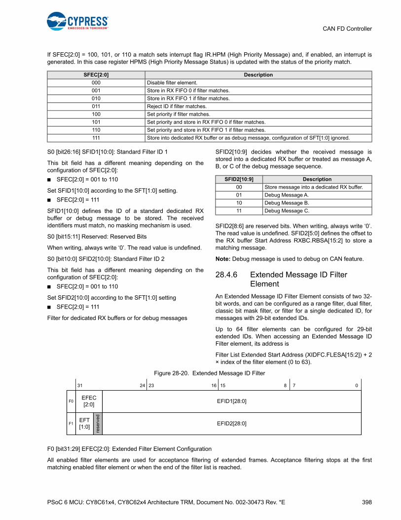
PSoC 6 MCU: CY8C61x4, CY8C62x4 Architecture TRM, Document No. 002-30473 Rev. *E 398
CAN FD Controller
If SFEC[2:0] = 100, 101, or 110 a match sets interrupt flag IR.HPM (High Priority Message) and, if enabled, an interrupt isgenerated. In this case register HPMS (High Priority Message Status) is updated with the status of the priority match.
S0 [bit26:16] SFID1[10:0]: Standard Filter ID 1
This bit field has a different meaning depending on theconfiguration of SFEC[2:0]:
■ SFEC[2:0] = 001 to 110
Set SFID1[10:0] according to the SFT[1:0] setting.
■ SFEC[2:0] = 111
SFID1[10:0] defines the ID of a standard dedicated RXbuffer or debug message to be stored. The receivedidentifiers must match, no masking mechanism is used.
S0 [bit15:11] Reserved: Reserved Bits
When writing, always write ‘0’. The read value is undefined.
S0 [bit10:0] SFID2[10:0]: Standard Filter ID 2
This bit field has a different meaning depending on theconfiguration of SFEC[2:0]:
■ SFEC[2:0] = 001 to 110
Set SFID2[10:0] according to the SFT[1:0] setting
■ SFEC[2:0] = 111
Filter for dedicated RX buffers or for debug messages
SFID2[10:9] decides whether the received message isstored into a dedicated RX buffer or treated as message A,B, or C of the debug message sequence.
SFID2[8:6] are reserved bits. When writing, always write ‘0’.The read value is undefined. SFID2[5:0] defines the offset tothe RX buffer Start Address RXBC.RBSA[15:2] to store amatching message.
Note: Debug message is used to debug on CAN feature.
28.4.6 Extended Message ID Filter Element
An Extended Message ID Filter Element consists of two 32-bit words, and can be configured as a range filter, dual filter,classic bit mask filter, or filter for a single dedicated ID, formessages with 29-bit extended IDs.
Up to 64 filter elements can be configured for 29-bitextended IDs. When accessing an Extended Message IDFilter element, its address is
Filter List Extended Start Address (XIDFC.FLESA[15:2]) + 2× index of the filter element (0 to 63).
Figure 28-20. Extended Message ID Filter
F0 [bit31:29] EFEC[2:0]: Extended Filter Element Configuration
All enabled filter elements are used for acceptance filtering of extended frames. Acceptance filtering stops at the firstmatching enabled filter element or when the end of the filter list is reached.
SFEC[2:0] Description
000 Disable filter element.
001 Store in RX FIFO 0 if filter matches.
010 Store in RX FIFO 1 if filter matches.
011 Reject ID if filter matches.
100 Set priority if filter matches.
101 Set priority and store in RX FIFO 0 if filter matches.
110 Set priority and store in RX FIFO 1 if filter matches.
111 Store into dedicated RX buffer or as debug message, configuration of SFT[1:0] ignored.
SFID2[10:9] Description
00 Store message into a dedicated RX buffer.
01 Debug Message A.
10 Debug Message B.
11 Debug Message C.
F0
F1
31 2324 16 15 8 7 0
EFID1[28:0]
EFT[1:0]
rese
rved
EFEC[2:0]
EFID2[28:0]
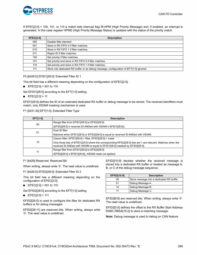
PSoC 6 MCU: CY8C61x4, CY8C62x4 Architecture TRM, Document No. 002-30473 Rev. *E 399
CAN FD Controller
If EFEC[2:0] = 100, 101, or 110 a match sets interrupt flag IR.HPM (High Priority Message) and, if enabled, an interrupt isgenerated. In this case register HPMS (High Priority Message Status) is updated with the status of the priority match.
F0 [bit28:0] EFID1[28:0]: Extended Filter ID 1
This bit field has a different meaning depending on the configuration of EFEC[2:0].
■ EFEC[2:0] = 001 to 110
Set EFID1[28:0] according to the EFT[1:0] setting.
■ EFEC[2:0] = 11
EFID1[28:0] defines the ID of an extended dedicated RX buffer or debug message to be stored. The received identifiers mustmatch, only XIDAM masking mechanism is used.
F1 [bit31:30] EFT[1:0]: Extended Filter Type
F1 [bit29] Reserved: Reserved Bit
When writing, always write ‘0’. The read value is undefined.
F1 [bit28:0] EFID2[28:0]: Extended Filter ID 2
This bit field has a different meaning depending on theconfiguration of EFEC[2:0]:
■ EFEC[2:0] = 001 to 110
Set EFID2[28:0] according to the EFT[1:0] setting
■ EFEC[2:0] = 111
EFID2[28:0] is used to configure this filter for dedicated RXbuffers or for debug messages
EFID2[28:11] are reserved bits. When writing, always write‘0’. The read value is undefined.
EFID2[10:9] decides whether the received message isstored into a dedicated RX buffer or treated as message A,B, or C of the debug message sequence.
EFID2[8:6] are reserved bits. When writing, always write ‘0’.The read value is undefined.
EFID2[5:0] defines the offset to the RX Buffer Start AddressRXBC.RBSA[15:2] to store a matching message.
Note: Debug message is used to debug on CAN feature.
EFEC[2:0] Description
000 Disable filter element.
001 Store in RX FIFO 0 if filter matches.
010 Store in RX FIFO 1 if filter matches.
011 Reject ID if filter matches.
100 Set priority if filter matches.
101 Set priority and store in RX FIFO 0 if filter matches.
110 Set priority and store in RX FIFO 1 if filter matches.
111 Store into dedicated RX buffer or as debug message, configuration of EFT[1:0] ignored.
EFT[1:0] Description
00Range filter from EFID1[28:0] to EFID2[28:0]
(EFID2[28:0] ≥ received ID ANDed with XIDAM ≥ EFID1[28:0]).
01Dual ID filter
Matches when EFID1[28:0] or EFID2[28:0] is equal to received ID ANDed with XIDAM.
10
Classic filter: EFID1[28:0] = filter, EFID2[28:0] = mask.
Only those bits of EFID1[28:0] where the corresponding EFID2[28:0] bits are 1 are relevant. Matches when the received ID ANDed with XIDAM is equal to EFID1[28:0] masked by EFID2[28:0].
11Range filter from EFID1[28:0] to EFID2[28:0]
(EFID2[28:0] ≥ EFID1[28:0]), XIDAM mask not applied.
EFID2[10:9] Description
00 Store message into a dedicated RX buffer.
01 Debug Message A.
10 Debug Message B.
11 Debug Message C.
PSoC 6 MCU: CY8C61x4, CY8C62x4 Architecture TRM, Document No. 002-30473 Rev. *E 400
CAN FD Controller
28.4.7 Trigger Memory Element
Up to 64 trigger memory elements can be configured. When accessing a trigger memory element, its address is the TriggerMemory Start Address TTTMC.TMSA plus the index of the trigger memory element (0…63).
Figure 28-21. Trigger Memory Element
T0 Bit 31:16 TM[15:0]: Time Mark
Cycle time for which the trigger becomes active.
T0 Bit 14:8 CC[6:0]: Cycle Code
Cycle count for which the trigger is valid. Ignored for triggertypes Tx_Ref_Trigger, Tx_Ref_Trigger_Gap,Watch_Trigger, Watch_Trigger_Gap, and End_of_List.
T0 Bit 7:6 ASC[1:0]: Asynchronous Serial Communication
Note: ASC functionality is not supported.
T0 Bit 5 TMIN: Time Mark Event Internal
T0 Bit 4 TMEX: Time Mark Event External
T0 Bit 3:0 TYPE[3:0]: Trigger Type
Notes:
■ For ASC operation (ASC = 10, 11) only trigger types Rx_Trigger and Time_Base_Trigger should be used.
■ ASC operation is not supported in this device.
T1 Bit 23 FTYPE: Filter Type
T1 Bit 22:16 MNR[6:0]: Message Number
T0
T1
31 2324 16 15 8 7 0
TYPE[3:0]
RES
FT
YP
E
MNR[6:0] RES
TMEX
TMIN
ASC[1:0]R
ES
CC[6:0]TM[15:0]
MSC[2:0]
CC[6:0] Description
000000x Valid for all cycles.
000001cValid every second cycle at cycle count mod2 = c.
00001ccValid every fourth cycle at cycle count mod4 = cc.
0001cccValid every eighth cycle at cycle count mod8 = ccc.
001ccccValid every sixteenth cycle at cycle count mod16 = cccc.
01cccccValid every thirty-second cycle at cycle count mod32 = ccccc.
1ccccccValid every sixty-fourth cycle at cycle count mod64 = cccccc.
ASC[1:0] Description
00 No ASC operation.
01 Reserved, do not use.
10 Node is ASC receiver.
11 Node is ASC transmitter.
TMIN Description
0 No action.
1TTIR.TTMI is set when trigger memory ele-ment becomes active.
TMEX Description
0 No action.
1
Pulse at output of Trigger Time Mark with the length of one clk_can period is generated when the time mark of the trigger memory element becomes active and TTOCN.TTMIE = 1.
TYPE [3:0] Description
0000 Tx_Ref_Trigger - valid when not in gap.
0001 Tx_Ref_Trigger_Gap - valid when in gap.
0010Tx_Trigger_Single - starts a single transmis-sion in an exclusive time window.
0011Tx_Trigger_Continous - starts continuous transmission in an exclusive time window.
0100Tx_Trigger_Arbitration - starts a transmission in an arbitrating time window.
0101Tx_Trigger_Merged - starts a merged arbitra-tion window.
0110 Watch_Trigger - valid when not in gap.
0111 Watch_Trigger_Gap - valid when in gap.
1000 Rx_Trigger - check for reception.
1001Time_Base_Trigger - only control TMIN, TMEX, and ASC.
1010 … 1111 End_of_List - illegal type, causes config error.
FTYPE Description
0 11-bit standard message ID.
1 29-bit extended message ID.
PSoC 6 MCU: CY8C61x4, CY8C62x4 Architecture TRM, Document No. 002-30473 Rev. *E 401
CAN FD Controller
Transmission: Trigger is valid for configured TX buffernumber. Valid values are 0 to 31.
Reception: Trigger is valid for standard/extended messageID filter element number. Valid values are 0 to 63 and 0 to127.
T1 Bits 2:0 MSC[2:0]: Message Status Count
Counts scheduling errors for periodic messages in exclusivetime windows. It has no function for arbitrating messagesand in event-driven CAN communication (ISO 11898-1:2015).
Notes:
■ The trigger memory elements should be written when the M_TTCAN is in INIT state. Write access to the trigger memory elements outside INIT state is not allowed.
■ There is an exception for TMIN and TMEX when they are defined as part of a trigger memory element of TYPE Tx_Ref_Trigger. In this case they become active at the time mark modified by the actual Reference Trigger Offset (TTOST.RTO).
28.4.8 MRAM OFF
Message RAM can be turned off to save power by settingCTL.MRAM_OFF bit. Default value of this bit is '0' andMRAM is retained in this configuration during DeepSleeppower mode.
The M_TTCAN channel must be powered down beforesetting MRAM_OFF bit. See Power Down (Sleep Mode) onpage 377 to power down the M_TTCAN channel. WhenMRAM is OFF, any access to MRAM may raise AddressError (MRAM_SIZE = 0).
After switching the MRAM on again, software needs to allowa certain power-up time before MRAM can be used, that is,before STOP_REQ can be de-asserted. Check theRAM_PWR_DELAY_CTL register to see the required timefor MRAM power up process. Refer to the registers TRM formore details.
28.4.9 RAM Watchdog (RWD)
The RAM Watchdog monitors the READY output of theMessage RAM. A Message RAM access starts the MessageRAM watchdog counter with the value configured byRWD.WDC. The counter is reloaded with RWD.WDC whenthe Message RAM signals successful completion byactivating its READY output. In case there is no responsefrom the Message RAM until the counter has counted downto zero, the counter stops and interrupt flag IR.WDI is set.The RAM watchdog counter is clocked by the host clock(clk_sys). Refer to the registers TRM for information aboutthe RWD register.
28.5 TTCAN Operation
28.5.1 Reference Message
A reference message is a data frame characterized by aspecific CAN identifier. It is received and accepted by allnodes except the time master (sender of the referencemessage).
For Level 1, the data length must be at least one. For Level0 and Level 2, the data length must be at least four;otherwise, the message is not accepted as a referencemessage. The reference message may be extended byother data up to the sum of eight CAN data bytes. All bits ofthe identifier except the three LSBs characterize themessage as a reference message. The last three bitsspecify the priorities of up to eight potential time masters.Reserved bits are transmitted as logical 0 and are ignoredby the receivers. The reference message is configuredusing the TTRMC register.
The time master transmits the reference message. If thereference message is disturbed by an error, it isretransmitted immediately. In a retransmission, thetransmitted Master_Ref_Mark is updated. The referencemessage is sent periodically, but it is allowed to stop theperiodic transmission (Next_is_Gap bit). It can initiate event-synchronized transmission at the start of the next basiccycle by the current time master or by one of the otherpotential time masters.
The node transmitting the reference message is the currenttime master. The time master is allowed to transmit othermessages. If the current time master fails, its function isreplicated by the potential time master with the highestpriority. Nodes that are neither time master nor potentialtime master are time-receiving nodes.
28.5.1.1 Level 1
Level 1 operation is configured via TTOCF.OM = 01 andTTOCF.GEN. External clock synchronization is not availablein Level 1.
The information related to the reference message is storedin the first data byte as shown in Table 28-8. Cycle_Count isoptional.
Table 28-8. First Byte of Level 1 Reference Message
Bits 7 6 5 4 3 2 1 0
First Byte
Next_is_Gap Reserved Cycle_Count [5:0]

PSoC 6 MCU: CY8C61x4, CY8C62x4 Architecture TRM, Document No. 002-30473 Rev. *E 402
CAN FD Controller
28.5.1.2 Level 2
Level 2 operation is configured via TTOCF.OM = 10 andTTOCF.GEN.
The information related to the reference message is storedin the first four data bytes as shown in Table 28-9.Cycle_Count and the lower four bits of NTU_Res areoptional. The M_TTCAN does not evaluate NTU_Res[3:0]from received reference messages, it always transmitsthese bits as zero.
28.5.1.3 Level 0
Level 0 operation is configured via TTOCF.OM = 11.External event-synchronized time-triggered operation is notavailable in Level 0.
The information related to the reference message is storedin the first four data bytes as shown in Table 28-10. In Level0, Next_is_Gap is always zero. Cycle_Count and the lowerfour bits of NTU_Res are optional. The M_TTCAN does notevaluate NTU_Res[3:0] from received reference messages;it always transmits these bits as zero.
28.5.2 TTCAN Configuration
28.5.2.1 TTCAN Timing
The Network Time Unit (NTU) is the unit in which all timesare measured. The NTU is a constant of the whole networkand is defined by the network system designer. In TTCANLevel 1 the NTU is the nominal CAN bit time. In TTCANLevel 0 and Level 2 the NTU is a fraction of the physicalsecond.
The NTU is the time base for the local time. The integer partof the local time (16-bit value) is incremented once for eachNTU. Cycle time and global time are both derived from localtime. The fractional part (3-bit value) of local time, cycletime, and global time is not readable.
In TTCAN Level 0 and Level 2, the length of the NTU isdefined by the Time Unit Ratio (TUR). The TUR is a non-integer number given by the formula TUR = TURNA.NAV/TURCF.DC. The length of the NTU is given by the formulaNTU = CAN Clock Period × TUR.
The TUR Numerator Configuration NC is an 18-bit number,TURCF.NCL[15:0] can be programmed in the range0x0000-0xFFFF. TURCF.NCH[17:16] is hard-wired to 0b01.When the number 0xnnnn is written to TURCF.NCL[15:0],TURNA.NAV starts with the value 0x10000 + 0x0nnnn =0x1nnnn. The TUR Denominator Configuration TURCF.DCis a 14-bit number. TURCF.DC may be programmed in therange 0x0001 - 0x3FFF; 0x0000 is an illegal value.
In Level 1, NC must be ≥ 4 × TURCF.DC. In Level 0 andLevel 2 NC must be ≥ 8 × TURCF.DC to allow the 3-bitresolution for the internal fractional part of the NTU.
A hardware reset presets TURCF.DC to 0x1000 andTURCF.NCL to 0x10000, resulting in an NTU consisting of16 CAN clock periods. Local time and application watchdogare not started before either the CCCR.INIT is reset orTURCF.ELT is set. TURCF.ELT may not be set before theNTU is configured. Setting TURCF.ELT to '1' also locks thewrite access to register TURCF.
At startup TURNA.NAV is updated from NC (= TURCF.NCL+ 0x10000) when TURCF.ELT is set. In TTCAN Level 1there is no drift compensation. TURNA.NAV does notchange during operation, it always equals NC.
In TTCAN Level 0 and Level 2, there are two possibilities forTURNA.NAV to change. When operating as time slave orbackup time master, and when TTOCF.ECC is set,TURNA.NAV is updated automatically to the valuecalculated from the monitored global time speed, as long asthe M_TTCAN is in synchronization states In_Schedule orIn_Gap. When it loses synchronization, it returns to NC.When operating as the actual time master, and whenTTOCF.EECS is set, the host may update TURCF.NCL.When the host sets TTOCN.ECS, TURNA.NAV will beupdated from the new value of NC at the next referencemessage. The status flag TTOST.WECS is set whenTTOCN.ECS is set and is cleared when TURNA.NAV isupdated. TURCF.NCL is write-locked while TTOST.WECS isset.
In TTCAN Level 0 and Level 2, the clock calibration processadapts TURNA.NAV in the range of the synchronizationdeviation limit (SDL) of NC ± 2 (TTOCF.LDSDL+5).TURCF.NCL should be programmed to the largestapplicable numerical value to achieve the best accuracy inthe calculation of TURNA.NAV.
Table 28-9. First Four Bytes of Level 2 Reference Message
Bits 7 6 5 4 3 2 1 0
First Byte Next_is_Gap Reserved Cycle_Count[5:0]
Second Byte
NTU_Res[6:4] NTU_Res[3:0] Disc_Bit
Third Byte
Master_Ref_Mark[7:0]
Fourth Byte
Master_Ref_Mark[15:8]
Table 28-10. First four Bytes of Level 0 Reference Message
Bits 7 6 5 4 3 2 1 0
First ByteNex-t_is_Gap
Reserved Cycle_Count[5:0]
Second Byte
NTU_Res[6:4] NTU_Res[3:0] Disc_Bit
Third Byte
Master_Ref_Mark[7:0]
Fourth Byte
Master_Ref_Mark[15:8]
PSoC 6 MCU: CY8C61x4, CY8C62x4 Architecture TRM, Document No. 002-30473 Rev. *E 403
CAN FD Controller
The synchronization deviation (SD) is the differencebetween NC and TURNA.NAV (SD = |NC - TURNA.NAV|). Itis limited by the SDL, which is configured by its duallogarithm TTOCF.LDSDL (SDL = 2 (TTOCF.LDSDL+5)) andshould not exceed the clock tolerance given by the CAN bittiming configuration. SD is calculated at each new basiccycle. When the calculated TURNA.NAV deviates by more
than SDL from NC, or if the Disc_Bit in the referencemessage is set, the drift compensation is suspended,TTIR.GTE is set, and TTOSC.QCS is reset; if Disc_Bit = 1,TTIR.GTD is set.
TUR configuration examples are shown in Table 28-11.
TTOCN.ECS schedules NC for activation by the nextreference message. TTOCN.SGT schedules TTGTP.TP foractivation by the next reference message. Setting ofTTOCN.ECS and TTOCN.SGT requires TTOCF.EECS to beset (external clock synchronization enabled) while theM_TTCAN is actual time master.
The M_TTCAN module provides an application watchdog toverity the function of the application program. The host hasto serve this watchdog regularly, else all CAN bus activity isstopped. The Application Watchdog Limit TTOCF.AWLspecifies the number of NTUs the watchdog has to beserved. The maximum number of NTUs is 256. TheApplication Watchdog is served by reading register TTOST.TTOST.AWE indicates whether the watchdog is served intime. In case the application failed to serve the applicationwatchdog, interrupt flag TTIR.AW is set. For softwaredevelopment, the application watchdog may be disabled byprogramming TTOCF.AWL to 0x00 (see ApplicationWatchdog on page 378).
28.5.2.2 Message Scheduling
TTOCF.TM controls whether the M_TTCAN operates as apotential time master or as a time slave. If it is a potentialtime master, the three LSBs of the reference messageidentifier TTRMC.RID define the master priority, 0 being thehighest and 7 the lowest priority. Two nodes in the networkmay not useg the same master priority. TTRMC.RID is usedfor recognition of reference messages. TTRMC.RMPS is notrelevant for time slaves.
The Initial Reference Trigger Offset TTOCF.IRTO is a 7-bit-value that defines (in NTUs) how long a backup time masterwaits before it starts the transmission of a referencemessage, when a reference message is expected but thebus remains idle. The recommended value for TTOCF.IRTOis the master priority multiplied with a factor depending onthe expected clock drift between the potential time mastersin the network. The sequential order of the backup timemasters, when one of them starts the reference message ifthe current time master fails, should correspond to theirmaster priority, even with maximum clock drift.
TTOCF.OM decides whether the node operates in TTCANLevel 0, Level 1, or Level 2. In one network, all potential time
masters should operate on the same level. Time slaves mayoperate on Level 1 in a Level 2 network, but not vice versa.The configuration of the TTCAN operation mode viaTTOCF.OM is the last step in the setup. When TTOCF.OM =00 (event-driven CAN communication), the M_TTCANoperates according to ISO 11898-1:2015, without timetriggers. When TTOCF.OM = 01 (Level 1), the M_TTCANoperates according to ISO 11898-4, but without thepossibility to synchronize the basic cycles to externalevents, the Next_is_Gap bit in the reference message isignored. When TTOCF.OM = 10 (Level 2), the M_TTCANoperates according to ISO 11898-4, including the event-synchronized start of a basic cycle. When TTOCF.OM = 11(Level 0), the M_TTCAN operates as event-driven CAN butmaintains a calibrated global time base similar to Level 2.
TTOCF.EECS enables the external clock synchronization,allowing the application program of the current time masterto update the TUR configuration during time-triggeredoperation, to adapt the clock speed and (in Level 0,2 only)the global clock phase to an external reference.
TTMLM.ENTT in the TT Matrix Limits register specifies thenumber of expected Tx_Triggers in the system matrix. Thisis the sum of Tx_Triggers for exclusive single arbitrating andmerged arbitrating windows, excluding the Tx_Ref_Triggers.Note that this is usually not the number of Tx_Triggermemory elements; the number of basic cycles in the systemmatrix and the trigger's repeat factors must be taken intoaccount. An inaccurate configuration of TTMLM.ENTT willresult in either a TX Count Underflow (TTIR.TXU = 1 andTTOST.EL = 01, severity 1) or in a TX Count Overflow(TTIR.TXO = 1 and TTOST.EL = 10, severity 2).
Note: In case the first reference message seen by a nodedoes not have Cycle_Count zero, this node may finish itsfirst matrix cycle with its TX count resulting in a TX CountUnderflow condition. As long as a node is in state,synchronizing its Tx_Triggers will not lead to transmissions.
TTMLM.CCM specifies the number of the last basic cycle inthe system matrix. The counting of basic cycles starts at 0.In a system matrix consisting of eight basic cyclesTTMLM.CCM would be 7. TTMLM.CCM is ignored by timeslaves, a receiver of a reference message considers the
Table 28-11. TUR Configuration Examples
TUR 8 10 24 50 510 125000 32.5 100/12 529/17
NC 0x1FFF8 0x1FFFE 0x1FFF8 0x1FFEA 0x1FFFE 0x1FFE0 0x1FFE0 0x19000 0x10880
TURCF.DC 0x3FFF 0x3333 0x1555 0x0A3D 0x0101 0x0001 0x0FC0 0x3000 0x0880

PSoC 6 MCU: CY8C61x4, CY8C62x4 Architecture TRM, Document No. 002-30473 Rev. *E 404
CAN FD Controller
received cycle count as the valid cycle count for the actualbasic cycle.
TTMLM.TXEW specifies the length of the TX enable windowin NTUs. The TX enable window is the period at thebeginning of a time window where a transmission may bestarted. If the sample point of the first bit of a transmitmessage is not inside the TX enable window, thetransmission cannot be started in that time window at all. Anexample is because of an overlap from the previous timewindow's message. TTMLM.TXEW should be chosen basedon the network's synchronization quality and the relationbetween the length of the time windows and the length ofmessages.
28.5.2.3 Trigger Memory
The trigger memory is part of the message RAM. It stores upto 64 trigger elements. A trigger memory element consists ofTime Mark TM, Cycle Code CC, Trigger Type TYPE, FilterType FTYPE, Message Number MNR, Message StatusCount MSC, Time Mark Event Internal TMIN, Time MarkEvent External TMEX, and Asynchronous SerialCommunication ASC (see Trigger Memory Element onpage 400).
The time mark defines at which cycle time a triggerbecomes active. The trigger elements in the trigger memorymust be sorted by their time marks. The trigger element withthe lowest time mark is written to the first trigger memoryword. Message number and cycle code are ignored fortriggers of type Tx_Ref_Trigger, Tx_Ref_Trigger_Gap,Watch_Trigger, Watch_Trigger_Gap, and End_of_List.
When the cycle time reaches the time mark of the actualtrigger, the FSE switches to the next trigger and starts toread it from the trigger memory. For a transmit trigger, theTX handler starts to read the message from the messageRAM as soon as the FSE switches to its trigger. The RAMaccess speed defines the minimum time step between atransmit trigger and its preceding trigger, the TX handlershould be able to prepare the transmission before thetransmit trigger's time mark is reached. The RAM accessspeed also limits the number of non-matching (with regardto their cycle code) triggers between two matching triggers,the next matching trigger must be read before its time markis reached. If the reference message is n NTU long, a triggerwith a time mark less than n will never become active andwill be treated as a configuration error.
The starting point of cycle time is the sample point of thereference message's start-of-frame bit. The next referencemessage is requested when cycle time reaches theTx_Ref_Trigger's time mark. The M_TTCAN reacts to thetransmission request at the next sample point. A newSync_Mark is captured at the start-of-frame bit, but the cycletime is incremented until the reference message issuccessfully transmitted (or received) and the Sync_Mark istaken as the new Ref_Mark. At that point, cycle time isrestarted. As a consequence, cycle time can never (with the
exception of initialization) be seen at a value less than n,with n being the length of the reference message measuredin NTU.
Length of a basic cycle: Tx_Ref_Trigger time mark + 1 NTU+ 1 CAN bit time
The trigger list will be different for all nodes in the TTCANnetwork. Each node knows only the Tx_Triggers for its owntransmit messages, the Rx_Triggers for the receivemessages that are processed by this node, and the triggersconcerning the reference messages.
Trigger Types
Tx_Ref_Trigger (TYPE = 0000) and Tx_Ref_Trigger_Gap(TYPE = 0001) cause the transmission of a referencemessage by a time master. A configuration error (TTOST.EL= 11, severity 3) is detected when a time slave encounters aTx_Ref_Trigger(_Gap) in its trigger memory.Tx_Ref_Trigger_Gap is only used in external event-synchronized time-triggered operation mode. In that mode,Tx_Ref_Trigger is ignored when the M_TTCANsynchronization state is In_Gap (TTOST.SYS = 10).
Tx_Trigger_Single (TYPE = 0010), Tx_Continous (TYPE =0011), Tx_Trigger_Arbitration (TYPE = 0100), andTx_Trigger_Merged (TYPE = 0101) cause the start of atransmission. They define the start of a time window.
Tx_Trigger_Single starts a single transmission in anexclusive time window when the message buffer'sTransmission Request Pending bit is set. After successfultransmission, the Transmission Request Pending bit isreset.
Tx_Trigger_Continuous starts a transmission in an exclusivetime window when the message buffer's transmissionRequest Pending bit is set. After successful transmission,the Transmission Request Pending bit remains set, and themessage buffer is transmitted again in the next matchingtime window.
Tx_Trigger_Arbitration starts an arbitrating time window,Tx_Trigger_Merged a merged arbitrating time window. Thelast Tx_Trigger of a merged arbitrating time window must beof type Tx_Trigger_Arbitration. A Configuration Error(TTOST.EL = 11, severity 3) is detected when a trigger oftype Tx_Trigger_Merged is followed by any other Tx_Triggerthan one of type Tx_Trigger_Merged orTx_Trigger_Arbitration. Several Tx_Triggers may be definedfor the same TX message buffer. Depending on their cyclecode, they may be ignored in some basic cycles. The cyclecode should be considered when the expected number ofTx_Triggers (TTMLM.ENTT) is calculated.
Watch_Trigger (TYPE = 0110) and Watch_Trigger_Gap(TYPE = 0111) check for missing reference messages. Theyare used by both time masters and time slaves.Watch_Trigger_Gap is only used in external event-synchronized time-triggered operation mode. In that mode,
PSoC 6 MCU: CY8C61x4, CY8C62x4 Architecture TRM, Document No. 002-30473 Rev. *E 405
CAN FD Controller
a Watch_Trigger is ignored when the M_TTCANsynchronization state is In_Gap (TTOST.SYS = 10).
Rx_Trigger (TYPE = 1000) is used to check for the receptionof periodic messages in exclusive time windows.Rx_Triggers are not active until state In_Schedule orIn_Gap is reached. The time mark of an Rx_Trigger shouldbe placed after the end of that message transmission,independent of time window boundaries. Depending on theircycle code, Rx_Triggers may be ignored in some basiccycles. At the Rx_Trigger time mark, it is checked whetherthe last received message before this time mark and afterstart of cycle or previous Rx_Trigger matches theacceptance filter element referenced by MNR. Acceptedmessages are stored in one of two receive FIFOs, accordingto the acceptance filtering, independent of the Rx_Trigger.Acceptance filter elements that are referenced byRx_Triggers should be placed at the beginning of the filterlist to ensure that the filtering is finished before theRx_Trigger time mark is reached.
Time_Base_Trigger (TYPE = 1001) is used to generateinternal/external events depending on the configuration ofASC, TMIN, and TMEX.
End_of_List (TYPE = 1010…1111) is an illegal trigger type,a configuration error (TTOST.EL = 11, severity 3) is detectedwhen an End_of_List trigger is encountered in the triggermemory before the Watch_Trigger or Watch_Trigger_Gap.
Restrictions for the Node's Trigger List
Two triggers may not be active at the same cycle time andcycle count, but triggers that are active in different basiccycles (different cycle code) may share the same time mark.
Rx_Triggers and Time_Base_Triggers may not be placedinside the TX enable windows of Tx_Trigger_Single/Continuous/Arbitration, but they may be placed afterTx_Trigger_Merged.
Triggers that are placed after the Watch_Trigger (or theWatch_Trigger_Gap when TTOST.SYS = 10) will neverbecome active. The watch triggers themselves will notbecome active when the reference messages aretransmitted on time.
All unused trigger memory words (after the Watch_Triggeror after the Watch_Trigger_Gap when TTOST.SYS = 10)must be set to trigger type End_of_List.
A typical trigger list for a potential time master will begin witha number of Tx_Triggers and Rx_Triggers followed by theTx_Ref_Trigger and Watch_Trigger. For networks withexternal event-synchronized time-triggered communication,this is followed by the Tx_Ref_Trigger_Gap and theWatch_Trigger_Gap. The trigger list for a time slave will bethe same but without the Tx_Ref_Trigger and theTx_Ref_Trigger_Gap.
At the beginning of each basic cycle, that is at eachreception or transmission of a reference message, thetrigger list is processed starting with the first trigger memoryelement. The FSE looks for the first trigger with a cycle codethat matches the current cycle count. The FSE waits untilcycle time reaches the trigger's time mark and activates thetrigger. Later, the FSE looks for the next trigger in the listwith a cycle code that matches the current cycle count.
Special consideration is needed for the time aroundTx_Ref_Trigger and Tx_Ref_Trigger_Gap. In a time mastercompeting for master ship, the effective time mark of aTx_Ref_Trigger may be decremented to be the first node tostart a reference message. In backup time masters theeffective time mark of a Tx_Ref_Trigger orTx_Ref_Trigger_Gap is the sum of its configured time markand the Reference Trigger Offset TTOCF.IRTO. If error level2 is reached (TTOST.EL = 10), the effective time mark is thesum of its time mark and 0x127. No other trigger elementsshould be placed in this range; otherwise, the time marksmay appear out of order and are flagged as a configurationerror. Trigger elements that are coming after Tx_Ref_Triggermay never become active as long as the referencemessages come in time.
There are interdependencies between the followingparameters:
■ Host clock frequency
■ Speed and waiting time for Trigger RAM accesses
■ Length of the acceptance filter list
■ Number of trigger elements
■ Complexity of cycle code filtering in the trigger elements
■ Offset between time marks of the trigger elements
Examples of Trigger Handling
The following example shows how the trigger list is derivedfrom a node's system matrix. Assume that node A is a firsttime master; a section of the system matrix shown inTable 28-12.
The cycle count starts with 0 – 0, 1, 3, 7, 15, 31, 63 (thenumber of basic cycles in the system matrix is 1, 2, 4, 8, 16,32, 64). The maximum cycle count is configured byTTMLM.CCM. The Cycle Code (CC) is composed of repeatfactor (value of most significant '1') and the number of thefirst basic cycle in the system matrix (bit field after mostsignificant '1').
Table 28-12. System Matrix Node A
Cycle Count
Time Mark1
Time Mark2
Time Mark3
Time Mark4
Time Mark5
Time Mark6
Time Mark7
0 Tx7 TxRef Error
1 Rx3 Tx2, Tx4 TxRef Error
2 TxRef Error
3 Tx7 Rx5 TxRef Error
4 Tx7 Rx6 TxRef Error
PSoC 6 MCU: CY8C61x4, CY8C62x4 Architecture TRM, Document No. 002-30473 Rev. *E 406
CAN FD Controller
Example: When CC is 0b0010011 (repeat factor: 16, firstbasic cycle: 3) and maximum cycle count of TTMLM.CCM =0x3F, matches occur at cycle counts 3, 19, 35, 51.
A trigger element consists of Time Mark (TM), Cycle Code(CC), Trigger Type (TYPE), and Message Number (MNR).For transmission, MNR references the TX buffer number(0..31). For reception, MNR references the number of thefilter element (0..127) that matched during acceptancefiltering. Depending on the configuration of the Filter TypeFTYPE, the 11-bit or 29-bit message ID filter list isreferenced.
In addition, a trigger element can be configured forAsynchronous Serial Communication (ASC), generation ofTime Mark Event Internal (TMIN), and Time Mark EventExternal (TMEX). The Message Status Count (MSC) holdsthe counter value (0..7) for scheduling errors for periodicmessages in exclusive time windows when the time mark ofthe trigger element becomes active.
Tx_Trigger_Single, Tx_Trigger_Continous,Tx_Trigger_Merged, Tx_Trigger_Arbitration, Rx_Trigger,and Time_Base_Trigger are only valid for the specified cyclecode. For all other trigger types the cycle code is ignored.
The FSE starts the basic cycle by scanning the trigger liststarting from zero until a trigger with time mark that isgreater than the cycle time is reached, CC matches theactual cycle count, or a trigger of type Tx_Ref_Trigger,Tx_Ref_Trigger_Gap, Watch_Trigger, orWatch_Trigger_Gap is encountered.
When the cycle time reaches TM, the action defined byTYPE and MNR is started. There is an error in theconfiguration when it reaches End_of_List.
At Mark6, the reference message (always TxRef) istransmitted. After transmission, the FSE returns to thebeginning of the trigger list. When it reaches Watch Triggerat Mark7, the node is unable to transmit the referencemessage; error treatment is then started.
Detection of Configuration Errors
A configuration error is signaled via TTOST.EL = 11 (severity3) when:
■ The FSE comes to a trigger in the list with a cycle code that matches the current cycle count but with a time mark that is less than the cycle time.
■ The previous active trigger was a Tx_Trigger_Merged and the FSE comes to a trigger in the list with a cycle code that matches the current cycle count but that is neither a Tx_Trigger_Merged nor a Tx_Trigger_Arbitration nor a Time_Base_Trigger nor an Rx_Trigger.
■ The FSE of a node with TTOCF.TM = 0 (time slave) encounters a Tx_Ref_Trigger or a Tx_Ref_Trigger_Gap.
■ Any time mark placed inside the TX enable window (defined by TTMLM.TXEW) of a Tx_Trigger with a matching cycle code.
■ A time mark is placed near the time mark of a Tx_Ref_Trigger and the Reference Trigger Offset TTOST.RTO causes a reversal of their sequential order measured in cycle time.
28.5.2.4 TTCAN Schedule Initialization
The synchronization to the M_TTCAN message schedulestarts when CCCR.INIT is reset. The M_TTCAN can operatetime-triggered (TTOCF.GEN = 0) or external event-synchronized time-triggered (TTOCF.GEN = 1). All nodesstart with cycle time zero at the beginning of their trigger listwith TTOST.SYS = 00 (out of synchronization); notransmission is enabled with the exception of the referencemessage. Nodes in external event-synchronized time-triggered operation mode will ignore Tx_Ref_Trigger andWatch_Trigger and use Tx_Ref_Trigger_Gap andWatch_Trigger_Gap instead until the first referencemessage decides whether a gap is active.
Time Slaves
After configuration, a time slave will ignore its Watch_Triggerand Watch_Trigger_Gap when it does not receive anymessage before reaching the Watch_Triggers. When itreaches Init_Watch_Trigger, interrupt flag TTIR.IWT is set,the FSE is frozen, and the cycle time will become invalid.However, the node will still be able to take part in CAN buscommunication (to give acknowledge or to send error flags).The first received reference message will restart the FSEand the cycle time.
Note: Init_Watch_Trigger is not part of the trigger list. It isimplemented as an internal counter that counts up to0xFFFF = maximum cycle time.
When a time slave receives any message but the referencemessage before reaching the Watch_Triggers, it will assumea fatal error (TTOST.EL = 11, severity 3), set interrupt flagTTIR.WT, switch off its CAN bus output, and enter the busmonitoring mode (CCCR.MON set to '1'). In the bus
Table 28-13. Trigger List Node A
TriggerTime Mark
TM[15:0]
Cycle Code CC[6:0]
Trigger Type TYPE[3:0]
Mess. No. MNR[6:0]
0 Mark1 0000100 Tx_Trigger_Single 7
1 Mark1 1000000 Rx_Trigger 3
2 Mark1 1000011 Tx_Trigger_Single 7
3 Mark3 1000001 Tx_Trigger_Merged 2
4 Mark3 1000011 Rx_Trigger 5
5 Mark4 1000001 Tx_Trigger_Arbitration 4
6 Mark4 1000100 Rx_Trigger 6
7 Mark6 n.a. Tx_Ref_Trigger 0 (Ref)
8 Mark7 n.a. Watch_Trigger n.a.
9 n.a. n.a. End_of_List n.a.
PSoC 6 MCU: CY8C61x4, CY8C62x4 Architecture TRM, Document No. 002-30473 Rev. *E 407
CAN FD Controller
monitoring mode, it is still able to receive messages, butcannot send any dominant bits and therefore, cannotacknowledge.
Note: To leave the fatal error state, the host must setCCCR.INIT = 1. After reset of CCCR.INIT, the node restartsTTCAN communication.
When no error is encountered during synchronization, thefirst reference message sets TTOST.SYS = 01(synchronizing), the second sets the TTCANsynchronization state (depending on its Next_is_Gap bit) toTTOST.SYS = 11 (In_Schedule) or TTOST.SYS = 10(In_Gap), enabling all Tx_Triggers and Rx_Triggers.
Potential Time Master
After configuration, a potential time master will start thetransmission of a reference message when it reaches itsTx_Ref_Trigger (or its Tx_Ref_Trigger_Gap when inexternal event-synchronized time-triggered operation). It willignore its Watch_Trigger and Watch_Trigger_Gap when itdoes not receive any message or transmit the referencemessage successfully before reaching the Watch_Triggers(the reason assumed is that all other nodes still in reset orconfiguration and does not acknowledge). When it reachesInit_Watch_Trigger, the attempted transmission is aborted,interrupt flag TTIR.IWT is set, the FSE is frozen, and thecycle time will become invalid, but the node will still be ableto take part in CAN bus communication (to acknowledge orsend error flags). Resetting TTIR.IWT will re-enable thetransmission of reference messages until the next timeInit_Watch_Trigger condition is met, or another CANmessage is received. The FSE will be restarted by thereception of a reference message.
When a potential time master reaches the Watch_Triggersafter it has received any message but the referencemessage, it will assume a fatal error (TTOST.EL = 11,severity 3), set interrupt flag TTIR.WT, switch off its CAN busoutput, and enter the bus monitoring mode (CCCR.MON setto ‘1’). In bus monitoring mode, it is still able to receivemessages, but it cannot send any dominant bits andtherefore, cannot acknowledge.
When no error is detected during initialization, the firstreference message sets TTOST.SYS = 01 (synchronizing),the second sets the TTCAN synchronization state(depending on its Next_is_Gap bit) to TTOST.SYS = 11(In_Schedule) or TTOST.SYS = 10 (In_Gap), enabling allTx_Triggers and Rx_Triggers.
A potential time master is current time master (TTOST.MS =11) when it is the transmitter of the last reference message;otherwise, it is the backup time master (TTOST.MS = 10).
When all potential time masters have finished configuration,the node with the highest time master priority in the networkwill become the current time master.
28.5.3 TTCAN Gap Control
All functions related to gap control apply only when theM_TTCAN is operated in external event-synchronized time-triggered mode (TTOCF.GEN = 1). In this operation modethe TTCAN message schedule may be interrupted byinserting gaps between the basic cycles of the systemmatrix. All nodes connected to the CAN network should beconfigured for external event-synchronized time-triggeredoperation.
During a gap, all transmissions are stopped and the CANbus remains idle. A gap is finished when the next referencemessage starts a new basic cycle. The gap starts at the endof a basic cycle that was started by a reference messagewith bit Next_is_Gap = 1; for example, gaps are initiated bythe current time master.
The current time master has two options to initiate a gap. Agap can be initiated under software control when theapplication program writes TTOCN.NIG = 1. TheNext_is_Gap bit will be transmitted as ‘1’ with the nextreference message. A gap can also be initiated underhardware control when the application program writesTTOCN.GCS = 1. When a reference message is started andTTOCN.GCS is set, Next_is_Gap = 1 will be set.
As soon as that reference message is completed, theTTOST.WFE bit will announce the gap to the time masterand slaves. The current basic cycle will continue until its lasttime window. The time after the last time window is the gaptime.
For the actual time master and the potential time masters,TTOST.GSI will be set when the last basic cycle has finishedand the gap time starts. In nodes that are time slaves, theTTOST.GSI bit will remain at '0'.
When a potential time master is in synchronization stateIn_Gap (TTOST.SYS = 10), it has four options tointentionally finish a gap:
■ Under software control by writing TTOCN.FGP = 1.
■ Under hardware control (TTOCN.GCS = 1), TTOCN.FGP will automatically be set when an edge from HIGH to LOW at the internal event trigger input pin is detected and restarts the schedule.
■ The third option is a time-triggered restart. When TTOCN.TMG = 1, the next register time mark interrupt (TTIR.RTMI = 1) will set TTOCN.FGP and start the reference message.
■ Any potential time master will finish a gap when it reaches its Tx_Ref_Trigger_Gap, assuming that the event to synchronize to did not occur on time.
None of these options can cause a basic cycle to beinterrupted with a reference message.
Setting TTOCN.FGP after the gap time has started will startthe transmission of a reference message immediately andwill thereby synchronize the message schedule. When

PSoC 6 MCU: CY8C61x4, CY8C62x4 Architecture TRM, Document No. 002-30473 Rev. *E 408
CAN FD Controller
TTOCN.FGP is set before the gap time has started (whilethe basic cycle is still in progress), the next referencemessage is started at the end of the basic cycle, at theTx_Ref_Trigger – there will be no gap time in the messageschedule.
In time-triggered operation, bit Next_is_Gap = 1 in thereference message will be ignored, and the bitsTTOCN.NIG, TTOCN.FGP, and TTOCN.TMG will beconsidered.
28.5.4 Stop Watch
The stop watch function enables capturing of M_TTCANinternal time values (local time, cycle time, or global time)triggered by an external event.
To enable the stop watch function, the application programmust first define local time, cycle time, or global time as stopwatch source via TTOCN.SWS. When TTOCN.SWS is notequal to ‘00’ and TT Interrupt Register flag TTIR.SWE is ‘0’,the actual value of the time selected by TTOCN.SWS will becopied into TTCPT.SWV on the next rising/falling edge (asconfigured via TTOCN.SWP) on Stop Watch Trigger. Thiswill set interrupt flag TTIR.SWE. After the applicationprogram has read TTCPT.SWV, it may enable the next stopwatch event by resetting TTIR.SWE to '0'.
28.5.5 Local Time, Cycle Time, Global Time, and External Clock Synchronization
There are two possible levels in time-triggered CAN: Level 1and Level 2. Level 1 provides only time-triggered operation
using cycle time. Level 2 additionally provides increasedsynchronization quality, global time, and external clocksynchronization. In both levels, all timing features are basedon a local time base – the local time.
The local time is a 16-bit cyclic counter, it is incrementedonce each NTU. Internally the NTU is represented by a 3-bitcounter, which can be regarded as a fractional part (threebinary digits) of the local time. Generally, the 3-bit NTUcounter is incremented eight times each NTU. If the lengthof the NTU is shorter than eight CAN clock periods (as maybe configured in Level 1, or as a result of clock calibration inLevel 2), the length of the NTU fraction is adapted, and theNTU counter is incremented only four times each NTU.
Figure 28-22 describes the synchronization of the cycle timeand global time, performed in the same manner by allTTCAN nodes, including the time master. Any messagereceived or transmitted invokes a capture of the local timetaken at the message's frame synchronization event. Thisframe synchronization event occurs at the sample point ofeach Start-of-Frame (SoF) bit and causes the local time tobe stored as Sync_Mark. Sync_Marks and Ref_Marks arecaptured including the 3-bit fractional part.
Whenever a valid reference message is transmitted orreceived, the internal Ref_Mark is updated from theSync_Mark. The difference between Ref_Mark andSync_Mark is the Cycle Sync Mark (Cycle Sync Mark =Sync_Mark – Ref_Mark) stored in register TTCSM. Themost significant 16 bits of the difference between Ref_Markand the actual value of the local time is the cycle time (CycleTime = Local Time – Ref_Mark).
Figure 28-22. Cycle Time and Global Time Synchronization
The cycle time that can be read from TTCTC.CT is thedifference of the node's local time and Ref_Mark, bothsynchronized into the host clock domain and truncated to 16bits.
The global time exists for TTCAN Level 0 and Level 2 only,in Level 1 it is invalid. The node's view of the global time isthe local image of the global time in (local) NTUs. Afterconfiguration, a potential time master will use its own local
NTULocal Time
Sync Mark
Ref Mark
Frame Synchronisation
ReferenceMessage Valid
Cycle TimeCycle Sync Mark
Reference Message Sync_Mark
Master_Ref_Mark Ref_Mark
Local_OffsetLocal Time
Global Time
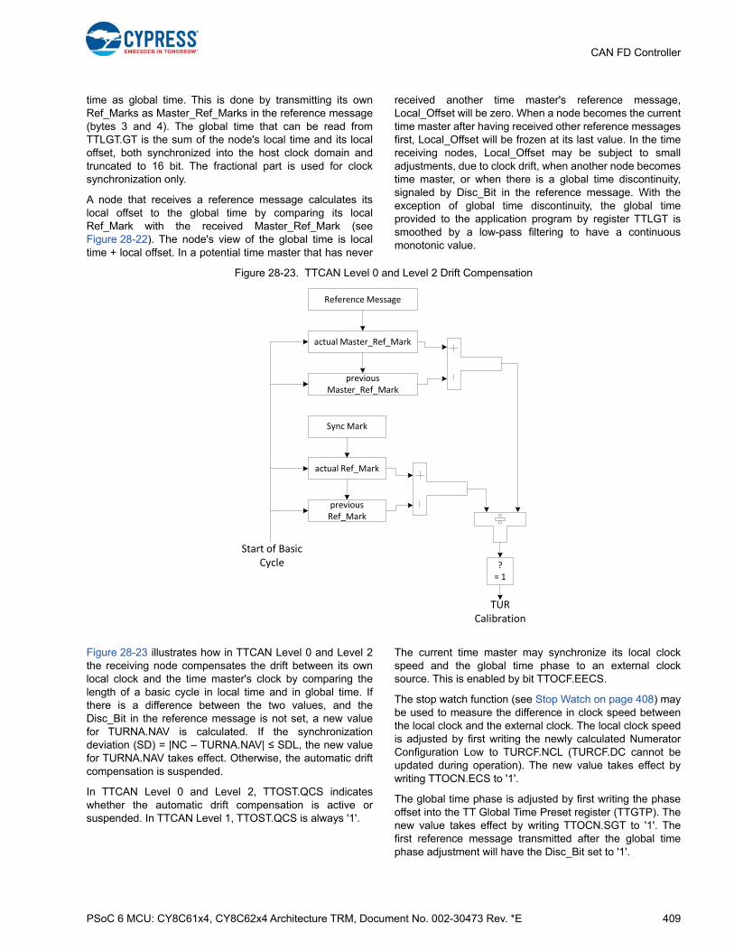
PSoC 6 MCU: CY8C61x4, CY8C62x4 Architecture TRM, Document No. 002-30473 Rev. *E 409
CAN FD Controller
time as global time. This is done by transmitting its ownRef_Marks as Master_Ref_Marks in the reference message(bytes 3 and 4). The global time that can be read fromTTLGT.GT is the sum of the node's local time and its localoffset, both synchronized into the host clock domain andtruncated to 16 bit. The fractional part is used for clocksynchronization only.
A node that receives a reference message calculates itslocal offset to the global time by comparing its localRef_Mark with the received Master_Ref_Mark (seeFigure 28-22). The node's view of the global time is localtime + local offset. In a potential time master that has never
received another time master's reference message,Local_Offset will be zero. When a node becomes the currenttime master after having received other reference messagesfirst, Local_Offset will be frozen at its last value. In the timereceiving nodes, Local_Offset may be subject to smalladjustments, due to clock drift, when another node becomestime master, or when there is a global time discontinuity,signaled by Disc_Bit in the reference message. With theexception of global time discontinuity, the global timeprovided to the application program by register TTLGT issmoothed by a low-pass filtering to have a continuousmonotonic value.
Figure 28-23. TTCAN Level 0 and Level 2 Drift Compensation
Figure 28-23 illustrates how in TTCAN Level 0 and Level 2the receiving node compensates the drift between its ownlocal clock and the time master's clock by comparing thelength of a basic cycle in local time and in global time. Ifthere is a difference between the two values, and theDisc_Bit in the reference message is not set, a new valuefor TURNA.NAV is calculated. If the synchronizationdeviation (SD) = |NC – TURNA.NAV| ≤ SDL, the new valuefor TURNA.NAV takes effect. Otherwise, the automatic driftcompensation is suspended.
In TTCAN Level 0 and Level 2, TTOST.QCS indicateswhether the automatic drift compensation is active orsuspended. In TTCAN Level 1, TTOST.QCS is always '1'.
The current time master may synchronize its local clockspeed and the global time phase to an external clocksource. This is enabled by bit TTOCF.EECS.
The stop watch function (see Stop Watch on page 408) maybe used to measure the difference in clock speed betweenthe local clock and the external clock. The local clock speedis adjusted by first writing the newly calculated NumeratorConfiguration Low to TURCF.NCL (TURCF.DC cannot beupdated during operation). The new value takes effect bywriting TTOCN.ECS to '1'.
The global time phase is adjusted by first writing the phaseoffset into the TT Global Time Preset register (TTGTP). Thenew value takes effect by writing TTOCN.SGT to '1'. Thefirst reference message transmitted after the global timephase adjustment will have the Disc_Bit set to '1'.
Reference Message
actual Master_Ref_Mark
previous Master_Ref_Mark
Sync Mark
actual Ref_Mark
previous Ref_Mark
Start of Basic Cycle ?
= 1
TURCalibration

PSoC 6 MCU: CY8C61x4, CY8C62x4 Architecture TRM, Document No. 002-30473 Rev. *E 410
CAN FD Controller
TTOST.QGTP shows whether the node's global time is inphase with the time master's global time. TTOST.QGTP ispermanently '0' in TTCAN Level 1 and when the SDL isexceeded in TTCAN Level 0,2 (TTOST.QCS = 0). It istemporarily '0' while the global time is low-pass filtered tosupply the application with a continuous monotonic value.There is no low-pass filtering when the last referencemessage contains a Disc_Bit = 1 or when TTOST.QCS = 0.
28.5.6 TTCAN Error Level
The ISO 11898-4 specifies four levels of error severity:
■ S0 - No Error
■ S1 - Warning
Only notification of application, reaction application-spe-cific.
■ S2 Error
Notification of application. All transmissions in exclusive or arbitrating time windows are disabled (that is, no data or remote frames may be started). Potential time mas-ters still transmit reference messages with the Refer-ence Trigger Offset TTOST.RTO set to the maximum value of 127.
■ S3 - Severe Error
Notification of application. All CAN bus operations are stopped; that is, transmission of dominant bits is not allowed, and CCCR.MON is set. The S3 error condition remains active until the application updates the configu-ration (set CCCR.CCE).
If several errors are detected at the same time, the highestseverity prevails. When an error is detected, the applicationis notified by TTIR.ELC. The error level is monitored byTTOST.EL.
The M_TTCAN signals the following error conditions asrequired by ISO 11898-4:
Config_Error (S3)
Sets error level TTOST.EL to ‘11’ when a merged arbitratingtime window is not properly closed or when there is aTx_Trigger with a time mark beyond the Tx_Ref_Trigger.
Watch_Trigger_Reached (S3)
Sets error level TTOST.EL to ‘11’ when a watch trigger isreached because the reference message is missing.
Application_Watchdog (S3)
Sets error level TTOST.EL to ‘11’ when the application failsto serve the application watchdog. The applicationwatchdog is configured via TTOCF.AWL. It is served byreading the TTOST register. When the watchdog is notserved in time, bit TTOST.AWE and interrupt flag TTIR.AWare set, all TTCAN communication is stopped, and theM_TTCAN is set into bus monitoring mode (CCCR.MON setto '1').
CAN_Bus_Off (S3)
Entering CAN_Bus_Off state sets error level TTOST.EL to‘11’. CAN_Bus_Off state is signaled by PSR.BO = 1 andCCCR.INIT = 1.
Scheduling_Error_2 (S2)
Sets error level TTOST.EL to ‘10’ if the MSC of oneTx_Trigger has reached 7. In addition, interrupt flagTTIR.SE2 is set. TTOST.EL is reset to 00 at the beginning ofa matrix cycle when no Tx_Trigger has an MSC of 7 in thepreceding matrix cycle.
Tx_Overflow (S2)
Sets error level TTOST.EL to ‘10’ when the TX count isequal or higher than the expected number of Tx_TriggersTTMLM.ENTT and a Tx_Trigger event occurs. In addition,interrupt flag TTIR.TXO is set. TTOST.EL is reset to 00when the TX count is no more than TTMLM.ENTT at thestart of a new matrix cycle.
Scheduling_Error_1 (S1)
Sets error level TTOST.EL to ‘01’ if within one matrix cyclethe difference between the maximum MSC and theminimum MSC for all trigger memory elements (of exclusivetime windows) is larger than 2, or if one of the MSCs of anexclusive Rx_Trigger has reached 7. In addition, interruptflag TTIR.SE1 is set. If within one matrix cycle none of theseconditions is valid, TTOST.EL is reset to 00.
Tx_Underflow (S1)
Sets error level TTOST.EL to ‘01’ when the TX count is lessthan the expected number of Tx_Triggers TTMLM.ENTT atthe start of a new matrix cycle. In addition, interrupt flagTTIR.TXU is set. TTOST.EL is reset to 00 when the TXcount is at least TTMLM.ENTT at the start of a new matrixcycle.
28.5.7 TTCAN Message Handling
28.5.7.1 Reference Message
For potential time masters, the identifier of the referencemessage is configured via TTRMC.RID. No dedicated TXbuffer is required for transmission of the reference message.When a reference message is transmitted, the first data byte(TTCAN Level 1) and the first four data bytes (TTCAN Level0 and Level 2) will be provided by the FSE.
If the Payload Select reference message TTRMC.RMPS isset, the rest of the reference message's payload (Level 1:bytes 2-8, Level 0 and Level 2: bytes 5-6) is taken from TXBuffer 0. In this case, the data length DLC code frommessage buffer 0 is used.
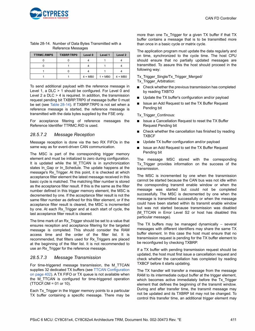
PSoC 6 MCU: CY8C61x4, CY8C62x4 Architecture TRM, Document No. 002-30473 Rev. *E 411
CAN FD Controller
To send additional payload with the reference message inLevel 1, a DLC > 1 should be configured. For Level 0 andLevel 2 a DLC > 4 is required. In addition, the transmissionrequest pending bit TXBRP.TRP0 of message buffer 0 mustbe set (see Table 28-14). If TXBRP.TRP0 is not set when areference message is started, the reference message istransmitted with the data bytes supplied by the FSE only.
For acceptance filtering of reference messages theReference Identifier TTRMC.RID is used.
28.5.7.2 Message Reception
Message reception is done via the two RX FIFOs in thesame way as for event-driven CAN communication.
The MSC is part of the corresponding trigger memoryelement and must be initialized to zero during configuration.It is updated while the M_TTCAN is in synchronizationstates In_Gap or In_Schedule. The update happens at themessage's Rx_Trigger. At this point, it is checked at whichacceptance filter element the latest message received in thisbasic cycle is matched. The matching filter number is storedas the acceptance filter result. If this is the same as the filternumber defined in this trigger memory element, the MSC isdecremented by one. If the acceptance filter result is not thesame filter number as defined for this filter element, or if theacceptance filter result is cleared, the MSC is incrementedby one. At each Rx_Trigger and at each start of cycle, thelast acceptance filter result is cleared.
The time mark of an Rx_Trigger should be set to a value thatensures reception and acceptance filtering for the targetedmessage is completed. This should consider the RAMaccess time and the order of the filter list. It isrecommended, that filters used for Rx_Triggers are placedat the beginning of the filter list. It is not recommended touse an Rx_Trigger for the reference message.
28.5.7.3 Message Transmission
For time-triggered message transmission, the M_TTCANsupplies 32 dedicated TX buffers (see TTCAN Configurationon page 402). A TX FIFO or TX queue is not available whenthe M_TTCAN is configured for time-triggered operation(TTOCF.OM = 01 or 10).
Each Tx_Trigger in the trigger memory points to a particularTX buffer containing a specific message. There may be
more than one Tx_Trigger for a given TX buffer if that TXbuffer contains a message that is to be transmitted morethan once in a basic cycle or matrix cycle.
The application program must update the data regularly andon time, synchronized to the cycle time. The host CPUshould ensure that no partially updated messages aretransmitted. To assure this the host should proceed in thefollowing way:
Tx_Trigger_Single/Tx_Trigger_Merged/Tx_Trigger_Arbitration:
■ Check whether the previous transmission has completed by reading TXBTO
■ Update the TX buffer's configuration and/or payload
■ Issue an Add Request to set the TX Buffer Request Pending bit
Tx_Trigger_Continous:
■ Issue a Cancellation Request to reset the TX Buffer Request Pending bit
■ Check whether the cancellation has finished by reading TXBCF
■ Update TX buffer configuration and/or payload
■ Issue an Add Request to set the TX Buffer Request Pending bit
The message MSC stored with the correspondingTx_Trigger provides information on the success of thetransmission.
The MSC is incremented by one when the transmissioncannot be started because the CAN bus was not idle withinthe corresponding transmit enable window or when themessage was started but could not be completedsuccessfully. The MSC is decremented by one when themessage is transmitted successfully or when the messagecould have been started within its transmit enable windowbut was not started because transmission was disabled(M_TTCAN in Error Level S2 or host has disabled thisparticular message).
The TX buffers may be managed dynamically – severalmessages with different identifiers may share the same TXbuffer element. In this case the host must ensure that notransmission request is pending for the TX buffer element tobe reconfigured by checking TXBRP.
If a TX buffer with pending transmission request should beupdated, the host must first issue a cancellation request andcheck whether the cancellation has completed by readingTXBCF before it starts updating.
The TX handler will transfer a message from the messageRAM to its intermediate output buffer at the trigger element,which becomes active immediately before the Tx_Triggerelement that defines the beginning of the transmit window.During and after transfer time, the transmit message maynot be updated and its TXBRP bit may not be changed. Tocontrol this transfer time, an additional trigger element may
Table 28-14. Number of Data Bytes Transmitted with a Reference Messages
TTRMC.RMPS TXBRP.TRP0 Level 0 Level 1 Level 2
0 0 4 1 4
0 1 4 1 4
1 0 4 1 4
1 1 4 + MB0 1 + MB0 4 + MB0
PSoC 6 MCU: CY8C61x4, CY8C62x4 Architecture TRM, Document No. 002-30473 Rev. *E 412
CAN FD Controller
be placed before the Tx_Trigger. An example is aTime_Base_Trigger, which does not cause any other action.The difference in time marks between the Tx_Trigger andthe preceding trigger should be large enough to guaranteethat the TX handler can read four words from the messageRAM even at high RAM access load from other modules.
Transmission in Exclusive Time Windows
A transmission is started time-triggered when the cycle timereaches the time mark of a Tx_Trigger_Single orTx_Trigger_Continous. There is no arbitration on the buswith messages from other nodes. The MSC is updatedaccording the result of the transmission attempt. Aftersuccessful transmission started by a Tx_Trigger_Single, therespective TX Buffer Request Pending bit is reset. Aftersuccessful transmission started by a Tx_Trigger_Continousthe respective TX Buffer Request Pending bit remains set.When the transmission is not successful due todisturbances, it will be repeated the next time one of itsTx_Triggers becomes active.
Transmission in Arbitrating Time Windows
A transmission is started time-triggered when the cycle timereaches the time mark of a Tx_Trigger_Arbitration. Severalnodes may start to transmit at the same time. In this casethe message has to arbitrate with the messages from othernodes. The MSC is not updated. When the transmission isnot successful (lost arbitration or disturbance), it will berepeated the next time one of its Tx_Triggers becomesactive.
Transmission in Merged Arbitrating Time Windows
The purpose of a merged arbitrating time window is toenable multiple nodes to send a limited number of frames,which are transmitted in immediate sequence, the ordergiven by CAN arbitration. It is not intended for bursttransmission by a single node. Because the node does nothave exclusive access within this time window, all requestedtransmissions may not be successful.
Messages that have lost arbitration or were disturbed by anerror, may be retransmitted inside the same mergedarbitrating time window. The retransmission will not bestarted if the corresponding Transmission Request Pendingflag was reset by a successful TX cancellation.
In single transmit windows, the TX handler transmits themessage indicated by the message number of the triggerelement. In merged arbitrating time windows, it can handleup to three message numbers from the trigger list. Theirtransmissions will be attempted in the sequence defined bythe trigger list. If the time mark of a fourth message is readbefore the first is transmitted (or canceled by the host), thefourth request will be ignored.
The transmission inside a merged arbitrating time window isnot time-triggered. The transmission of a message may startbefore its time mark, or after the time mark if the bus was notidle.
The messages transmitted by a specific node inside amerged arbitrating time window will be started in the order oftheir Tx_Triggers. Therefore, a message with low CANpriority may prevent the successful transmission of afollowing message with higher priority, if there is competingbus traffic. This should be considered for the configuration ofthe trigger list. Time_Base_Triggers may be placed betweenconsecutive Tx_Triggers to define the time until the data ofthe corresponding TX buffer needs to be updated.
28.5.8 TTCAN Interrupt and Error Handling
The TT Interrupt Register TTIR consists of four segments.Each interrupt can be enabled separately by thecorresponding bit in the TT Interrupt Enable register TTIE.The flags remain set until the host clears them. A flag iscleared by writing a '1' to the corresponding bit position.
The first segment consists of flags CER, AW, WT, and IWT.Each flag indicates a fatal error condition where the CANcommunication is stopped. With the exception of IWT, theseerror conditions require a reconfiguration of the M_TTCANmodule before the communication can be restarted.
The second segment consists of flags ELC, SE1, SE2, TXO,TXU, and GTE. Each flag indicates an error condition wherethe CAN communication is disturbed. If they are caused bya transient failure, such as by disturbances on the CAN bus,they will be handled by the TTCAN protocol's failurehandling and do not require intervention by the applicationprogram.
The third segment consists of flags GTD, GTW, SWE, TTMI,and RTMI. The first two flags are controlled by global timeevents (Level 0 and Level 2 only) that require a reaction bythe application program. With a Stop Watch Event, internaltime values are captured. The Trigger Time Mark Interruptnotifies the application that a specific Time_Base_Trigger isreached. The Register Time Mark Interrupt signals that thetime referenced by TTOCN.TMC (cycle, local, or global)equals time mark TTTMK.TM. It can also be used to finish agap.
The fourth segment consists of flags SOG, CSM, SMC, andSBC. These flags provide a means to synchronize theapplication program to the communication schedule.
28.5.9 Level 0
TTCAN Level 0 is not part of ISO11898-4. This operationmode makes the hardware, that in TTCAN Level 2 maintainsthe calibrated global time base, also available for event-driven CAN according to ISO 11898-1:2015.
Level 0 operation is configured via TTOCF.OM = 11. In thismode, M_TTCAN operates in event-driven CANcommunication; there is no fixed schedule, the configurationof TTOCF.GEN is ignored. External event-synchronized

PSoC 6 MCU: CY8C61x4, CY8C62x4 Architecture TRM, Document No. 002-30473 Rev. *E 413
CAN FD Controller
operation is not available in Level 0. A synchronized timebase is maintained by transmission of reference messages.
In Level 0 the trigger memory is not active and need not beconfigured. The time mark interrupt flag (TTIR.TTMI) is setwhen the cycle time has reached TTOCF.IRTO × 0x200. Itreminds the host to set a transmission request for messagebuffer 0. The Watch_Trigger interrupt flag (TTIR.WT) is setwhen the cycle time has reached 0xFF00. These valueswere chosen to have enough margin for a stable clockcalibration. There are no further TT-error-checks.
Register time mark interrupts (TTIR.RTMI) are alsopossible.
The reference message is configured as for Level 2operation. Received reference messages are recognized bythe identifier configured in register TTRMC. For thetransmission of reference messages only message buffer 0may be used. The node transmits reference messages anytime the host sets a transmission request for message buffer0; there is no reference trigger offset.
Level 0 operation is configured via:
■ TTRMC
■ TTOCF except EVTP, AWL, GEN
■ TTMLM except ENTT, TXEW
■ TURCF
Level 0 operation is controlled via:
■ TTOCN except NIG, TMG, FGP, GCS, TTMIE
■ TTGTP
■ TTTMK
■ TTIR excluding bits CER, AW, IWT SE2, SE1, TXO, TXU, SOG (no function)
■ TTIR – the following bits have changed function:
❐ TTMI not defined by trigger memory - activated at cycle time TTOCF.IRTO × 0x200
❐ WT not defined by trigger memory - activated at cycle time 0xFF00
Level 0 operation is signaled via:
■ TTOST excluding bits AWE, WFE, GSI, GFI, RTO (no function)
28.5.9.1 Synchronizing
Figure 28-24 describes the states and state transitions inTTCAN Level 0 operation. Level 0 has no In_Gap state.
Figure 28-24. Level 0 Schedule Synchronization State Machine
28.5.9.2 Handling Error Levels
During Level 0 operation only the following error conditionsmay occur:
■ Watch_Trigger_Reached (S3), reached cycle time 0xFF00
■ CAN_Bus_Off (S3)
Because S1 and S2 errors are not possible, the error levelcan only switch between S0 (No Error) and S3 (SevereError). In TTCAN Level 0 an S3 error is handled differently.When S3 error is reached, both TTOST.SYS and TTOST.MSare reset, and interrupt flags TTIR.GTE and TTIR.GTD areset.
When S3 (TTOST.EL = 11) is entered, bus monitoring modeis, contrary to TTCAN Level 1 and Level 2, not entered. S3error level is left automatically after transmission (timemaster) or reception (time slave) of the next referencemessage.
Sync_Off
Synchronizing
In_Schedule
HW reset or Init state S3
T0
T1
T2
Sync_Off
Synchronizing
In_Schedule
HW reset or Init state S3
T0
T1
T2
T0: transition condition always taking prevalence
T1: Init state left, cycle time is zero
T2: at least two successive reference messages observed (last reference message did not contain a set Disc_Bit bit)
Sync_Off
Synchronizing
In_Schedule
HW reset or Init state S3
T0
T1
T2
T0: transition condition always taking prevalence
T1: Init state left, cycle time is zero
T2: at least two successive reference messages observed (last reference message did not contain a set Disc_Bit bit)
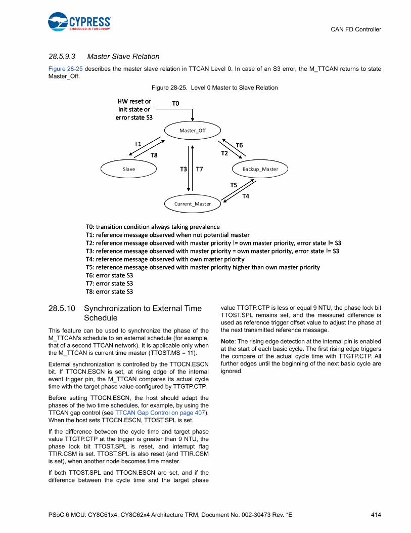
PSoC 6 MCU: CY8C61x4, CY8C62x4 Architecture TRM, Document No. 002-30473 Rev. *E 414
CAN FD Controller
28.5.9.3 Master Slave Relation
Figure 28-25 describes the master slave relation in TTCAN Level 0. In case of an S3 error, the M_TTCAN returns to stateMaster_Off.
Figure 28-25. Level 0 Master to Slave Relation
28.5.10 Synchronization to External Time Schedule
This feature can be used to synchronize the phase of theM_TTCAN's schedule to an external schedule (for example,that of a second TTCAN network). It is applicable only whenthe M_TTCAN is current time master (TTOST.MS = 11).
External synchronization is controlled by the TTOCN.ESCNbit. If TTOCN.ESCN is set, at rising edge of the internalevent trigger pin, the M_TTCAN compares its actual cycletime with the target phase value configured by TTGTP.CTP.
Before setting TTOCN.ESCN, the host should adapt thephases of the two time schedules, for example, by using theTTCAN gap control (see TTCAN Gap Control on page 407).When the host sets TTOCN.ESCN, TTOST.SPL is set.
If the difference between the cycle time and target phasevalue TTGTP.CTP at the trigger is greater than 9 NTU, thephase lock bit TTOST.SPL is reset, and interrupt flagTTIR.CSM is set. TTOST.SPL is also reset (and TTIR.CSMis set), when another node becomes time master.
If both TTOST.SPL and TTOCN.ESCN are set, and if thedifference between the cycle time and the target phase
value TTGTP.CTP is less or equal 9 NTU, the phase lock bitTTOST.SPL remains set, and the measured difference isused as reference trigger offset value to adjust the phase atthe next transmitted reference message.
Note: The rising edge detection at the internal pin is enabledat the start of each basic cycle. The first rising edge triggersthe compare of the actual cycle time with TTGTP.CTP. Allfurther edges until the beginning of the next basic cycle areignored.
Master_Off
Slave
Current_Master
Backup_Master
T0HW reset or Init state or error state S3
T1
T2
T3
T4
T5
T6
T7
T8
Master_Off
Slave
Current_Master
Backup_Master
T0HW reset or Init state or error state S3
T1
T2
T3
T4
T5
T6
T7
T8
T0: transition condition always taking prevalenceT1: reference message observed when not potential masterT2: reference message observed with master priority != own master priority, error state != S3T3: reference message observed with master priority = own master priority, error state != S3T4: reference message observed with own master priorityT5: reference message observed with master priority higher than own master priorityT6: error state S3T7: error state S3T8: error state S3
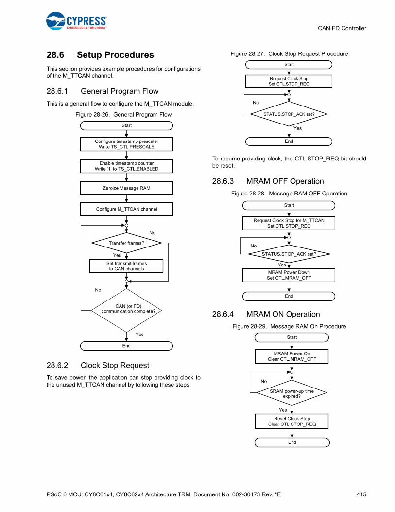
PSoC 6 MCU: CY8C61x4, CY8C62x4 Architecture TRM, Document No. 002-30473 Rev. *E 415
CAN FD Controller
28.6 Setup Procedures
This section provides example procedures for configurationsof the M_TTCAN channel.
28.6.1 General Program Flow
This is a general flow to configure the M_TTCAN module.
Figure 28-26. General Program Flow
28.6.2 Clock Stop Request
To save power, the application can stop providing clock tothe unused M_TTCAN channel by following these steps.
Figure 28-27. Clock Stop Request Procedure
To resume providing clock, the CTL.STOP_REQ bit shouldbe reset.
28.6.3 MRAM OFF Operation
Figure 28-28. Message RAM OFF Operation
28.6.4 MRAM ON Operation
Figure 28-29. Message RAM On Procedure
End
Start
Configure timestamp prescaler Write TS_CTL.PRESCALE
Enable timestamp counter Write ‘1’ to TS_CTL.ENABLED
Configure M_TTCAN channel
Yes
No
Transfer frames?
No
Set transmit frames to CAN channels
Yes
Zeroize Message RAM
CAN (or FD) communication complete?
End
Start
Request Clock StopSet CTL.STOP_REQ
STATUS.STOP_ACK set?
No
Yes
End
Start
Request Clock Stop for M_TTCANSet CTL.STOP_REQ
STATUS.STOP_ACK set?
No
Yes
MRAM Power DownSet CTL.MRAM_OFF
End
Start
Reset Clock StopClear CTL.STOP_REQ
MRAM Power OnClear CTL.MRAM_OFF
Yes
No
SRAM power-up timeexpired?
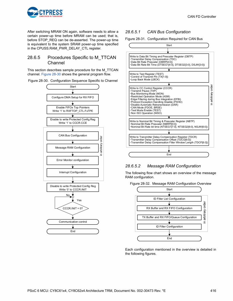
PSoC 6 MCU: CY8C61x4, CY8C62x4 Architecture TRM, Document No. 002-30473 Rev. *E 416
CAN FD Controller
After switching MRAM ON again, software needs to allow acertain power-up time before MRAM can be used; that is,before STOP_REQ can be de-asserted. The power-up timeis equivalent to the system SRAM power-up time specifiedin the CPUSS.RAM_PWR_DELAY_CTL register.
28.6.5 Procedures Specific to M_TTCAN Channel
This section describes sample procedure for the M_TTCANchannel. Figure 28-30 shows the general program flow.
Figure 28-30. Configuration Sequence Specific to Channel
28.6.5.1 CAN Bus Configuration
Figure 28-31. Configuration Required for CAN Bus
28.6.5.2 Message RAM Configuration
The following flow chart shows an overview of the messageRAM configuration.
Figure 28-32. Message RAM Configuration Overview
Each configuration mentioned in the overview is detailed inthe following figures.
Disable to write Protected Config RegWrite ‘0’ to CCCR.INIT
in a
rbitr
ary
ord
er
CCCR.INIT = 0?
Yes
No
Enable to write Protected Config RegWrite ‘1’ to CCCR.CCE
Configure DMA Setup for RX FIFO
Enable FIFOx Top PointersWrite ‘1’ to RXFTOP_CTL.FxTPE
End
Start
Communication control
CAN Bus Configuration
Message RAM Configuration
Error Monitor configuration
Interrupt Configuration
in a
rbitr
ary
ord
er
Write to Data Bit Timing and Prescaler Register (DBTP)・Transmitter Delay Compensation (TDC)・Data Bit Rate Prescaler (DBRP[4:0])・Data Bit Rate Bit Time (DTSEG1[4:0], DTSEG2[3:0], DSJW[3:0])
Write to Test Register (TEST)・Control of Transmit Pin (TX[1:0])・Loop Back Mode (LBCK)
Write to CC Control Register (CCCR)・Transmit Pause (TXP)・Bus Monitoring Mode (MON)・Restricted Operation Mode (ASM)・Edge Filtering during Bus Integration (EFBI)・Protocol Exception Handling Disable (PXHD)・Disable Automatic Retransmission (DAR)・CAN Mode (FDOE, BRSE)・Test Mode Enable (TEST)・Non ISO Operation (NISO)
Write to Nominal Bit Timing & Prescaler Register (NBTP)・Nominal Bit Rate Prescaler (NBRP[8:0])・Nominal Bit Rate bit time (NTSEG1[7:0], NTSEG2[6:0], NSJW[6:0])
Write to Transmitter Delay Compensation Register (TDCR)・Transmitter Delay Compensation Offset (TDCO[6:0])・Transmitter Delay Compensation Filter Window Length (TDCF[6:0])
End
Start
in a
rbitr
ary
ord
er
End
Start
ID Filter List Configuration
RX Buffer and RX FIFO Configuration
TX Buffer and RX FIFO/Queue Configuration
ID Filter Configuration
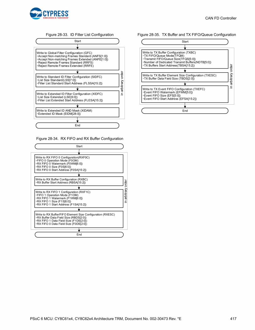
PSoC 6 MCU: CY8C61x4, CY8C62x4 Architecture TRM, Document No. 002-30473 Rev. *E 417
CAN FD Controller
Figure 28-33. ID Filter List Configuration
Figure 28-34. RX FIFO and RX Buffer Configuration
Figure 28-35. TX Buffer and TX FIFO/Queue Configuration
in a
rbitr
ary
ord
er
Write to Global Filter Configuration (GFC)・Accept Non-matching Frames Standard (ANFS[1:0])・Accept Non-matching Frames Extended (ANFE[1:0])・Reject Remote Frames Standard (RRFS)・Reject Remote Frames Extended (RRFE)
Write to Standard ID Filter Configuration (SIDFC)・List Size Standard(LSS[7:0])・Filter List Standard Start Address (FLSSA[15:2])
Write to Extended ID Filter Configuration (XIDFC)・List Size Extended (LSE[6:0])・Filter List Extended Start Address (FLESA[15:2])
Write to Extended ID AND Mask (XIDAM)・Extended ID Mask (EIDM[28:0])
Start
Endin
arb
itrar
y o
rde
r
Write to RX FIFO 0 Configuration(RXF0C)・FIFO 0 Operation Mode (F0OM)・RX FIFO 0 Watermark (F0WM[6:0])・RX FIFO 0 Size (F0S[6:0])・RX FIFO 0 Start Address (F0SA[15:2])
Write to RX Buffer Configuration (RXBC)・RX Buffer Start Address (RBSA[15:2])
Write to RX FIFO 1 Configuration (RXF1C)・FIFO 1 Operation Mode (F1OM)・RX FIFO 1 Watermark (F1WM[6:0])・RX FIFO 1 Size (F1S[6:0])・RX FIFO 1 Start Address (F1SA[15:2])
Write to RX Buffer/FIFO Element Size Configuration (RXESC)・RX Buffer Data Field Size (RBDS[2:0])・RX FIFO 1 Data Field Size (F1DS[2:0])・RX FIFO 0 Data Field Size (F0DS[2:0])
Start
Endin
arb
itrar
y o
rde
r
Write to TX Buffer Configuration (TXBC)・TX FIFO/Queue Mode(TFQM)・Transmit FIFO/Queue Size(TFQS[5:0])・Number of Dedicated Transmit Buffers(NDTB[5:0])・TX Buffers Start Address(TBSA[15:2])
Write to TX Buffer Element Size Configuration (TXESC)・TX Buffer Data Field Size (TBDS[2:0])
Write to TX Event FIFO Configuration (TXEFC)・Event FIFO Watermark (EFWM[5:0])・Event FIFO Size (EFS[5:0])・Event FIFO Start Address (EFSA[15:2])
Start
End

PSoC 6 MCU: CY8C61x4, CY8C62x4 Architecture TRM, Document No. 002-30473 Rev. *E 418
CAN FD Controller
Figure 28-36. ID Filter Configuration
28.6.5.3 Interrupt Configuration
Figure 28-37. Interrupt Configuration
ID Filter configuration is requested?
Read Filter List Standard Start AddressSA = SIDFC.FLSSA[15:2]
Standard ID or Extended ID
ID Filter configuration completed?
Calculate access pointer (AP)AP = SA + Std_element
Write Standard ID Filter information to Message RAMMessage RAM (AP) = Standard ID Filter information (S0)
Yes
Yes
No
No
Extended ID
Standard ID
Read Filter List Extended Start AddressSA = XIDFC.FLESA[15:2]
Calculate access pointer(AP)AP = SA + (Ext_eLement × 2)
Write Extended ID Filter information to Message RAMMessage RAM (AP) = Extended ID Filter information (F0)
Message RAM (AP+1) = Extended ID Filter information (F1)
Std_element = index of next free Standard Message ID Filter Element (ID Filter elements should be controlled by software)
Ext_element = Index of next free Extended Message ID Filter Element (ID Filter elements should be controlled by software)
Start
End
in a
rbitr
ary
ord
er
Write to Interrupt Enable (IE)Write ‘1’ to each bit, if canfd_int0/1 enable to be signaled
Write to Interrupt Line Select (ILS) Write ‘1’ (‘0’) to each bit, if interrupt assigned to interrupt line
canfd_int1 (canfd_int0)
Write to Interrupt Line Enable (ILE)Enable Interrupt Line 1 (EINT1)Enable Interrupt Line 0 (EINT0)
Write to TX Buffer Transmission Interrupt Enable (TXBTIE)Write ‘1’ to TXBTIE.TIEn, if transmission interrupt enabled
Write to TX Buffer Cancellation Finished Interrupt Enable (TXBCIE)Write ‘1’ to TXBCIE.CFIEn, if cancellation finished interrupt enable
Start
End

PSoC 6 MCU: CY8C61x4, CY8C62x4 Architecture TRM, Document No. 002-30473 Rev. *E 419
CAN FD Controller
28.6.5.4 Transmit Frame Configuration
Figure 28-38. Transmit Frame Configuration
Use dedicated transmit buffers? Use TX FIFO or TX Queue?
Check the pending requestsRead TXBRP
Is the requested element unset?
TXBRP.TRP[element] = 0
Calculate access pointer (AP)AP = SA + {eLement × element length}
Write transmission frame information to Message RAM
Message RAM (AP) = Frame info (T0)Message RAM (AP+1) = Frame info (T1)Message RAM (AP+2) = Frame info (T2)
:Message RAM (AP+n) = Frame info (Tn)
Write to TX Buffer Add RequestTXBAR.AR[element] = 1
Check TX FIFO statusRead TXFQS
Is Tx FIFO not full?TXFQS.TFQF = 0
Calculate access pointer (AP)AP = SA + {TXFQS.TFQPI[4:0] ×
element length}
Write transmission frame information to Message RAM
Message RAM (AP) = Frame info (T0)Message RAM (AP+1) = Frame info (T1)Message RAM (AP+2) = Frame info (T2)
:Message RAM (AP+n) = Frame info (Tn)
Write to TX Buffer Add RequestTXBAR.AR[TXFQS.TFQPI[4:0]] = 1
Control with TXFQS.TFQPI?
Check the pending requestsRead TXBRP
Is the requested element unset?
TXBRP.TRP[element] = 0
Write transmission frame information to Message RAM
Message RAM (AP) = Frame info (T0)Message RAM (AP+1) = Frame info (T1)Message RAM (AP+2) = Frame info (T2)
:Message RAM (AP+n) = Frame info (Tn)
Write to TX Buffer Add RequestTXBAR.AR[element] = 1
Yes
No
TX FIFO
TX Queue
Yes
No
Yes Yes Yes
No NoNo
Calculate access pointer(AP)AP = SA + {element × element length}
Transmission frame configuration complete?
Yes
No
Start
End
Read TX Buffers Start AddressSA = TXBC.TBSA[15:2]
Read TX Buffers Start AddressSA = TXBC.TBSA[15:2]
Read TX Buffers Start AddressSA = TXBC.TBSA[15:2]
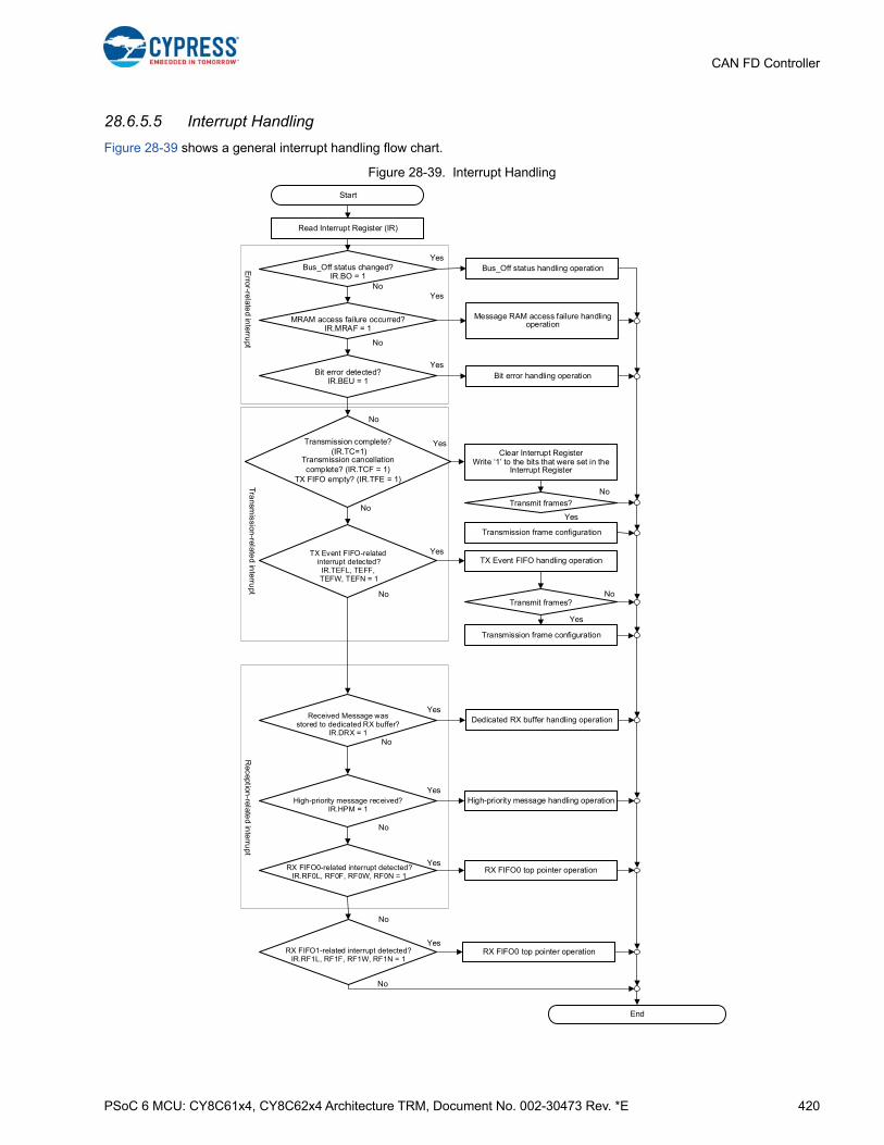
PSoC 6 MCU: CY8C61x4, CY8C62x4 Architecture TRM, Document No. 002-30473 Rev. *E 420
CAN FD Controller
28.6.5.5 Interrupt Handling
Figure 28-39 shows a general interrupt handling flow chart.
Figure 28-39. Interrupt Handling
Bus_Off status changed?IR.BO = 1
MRAM access failure occurred?IR.MRAF = 1
Bit error detected?IR.BEU = 1
Error-relate
d interru
pt
No
No
No
Yes
Yes
Yes
No
TX Event FIFO-related interrupt detected?
IR.TEFL, TEFF, TEFW, TEFN = 1
Read Interrupt Register (IR)
Tra
nsmission-relate
d interru
pt
Clear Interrupt RegisterWrite ‘1’ to the bits that were set in the
Interrupt Register
Yes
Yes
Received Message was stored to dedicated RX buffer?
IR.DRX = 1
No
Yes
High-priority message received?IR.HPM = 1
Yes
RX FIFO0-related interrupt detected?IR.RF0L, RF0F, RF0W, RF0N = 1
Yes
No
Reception
-related in
terrupt
No
No
Transmit frames?
Yes
No
Transmit frames?
Yes
No
RX FIFO1-related interrupt detected?IR.RF1L, RF1F, RF1W, RF1N = 1
Yes
No
Transmission complete? (IR.TC=1)
Transmission cancellationcomplete? (IR.TCF = 1)
TX FIFO empty? (IR.TFE = 1)
Start
End
Bus_Off status handling operation
Message RAM access failure handling operation
Bit error handling operation
Transmission frame configuration
TX Event FIFO handling operation
Transmission frame configuration
Dedicated RX buffer handling operation
High-priority message handling operation
RX FIFO0 top pointer operation
RX FIFO0 top pointer operation
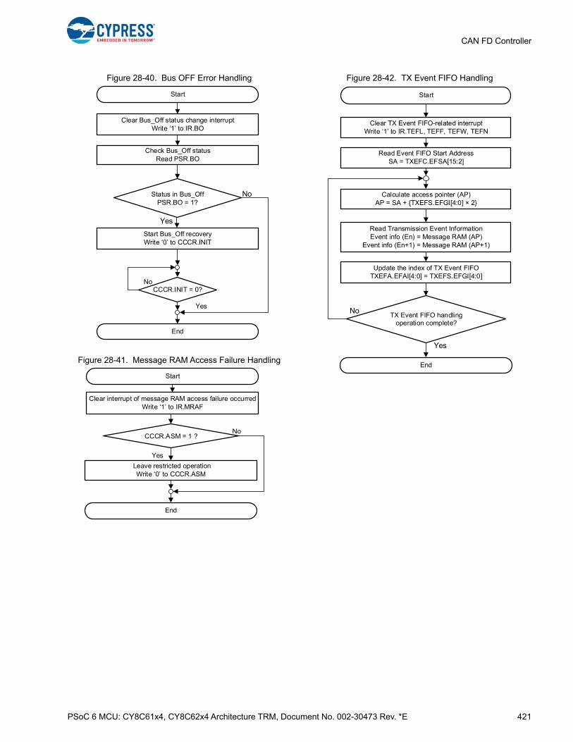
PSoC 6 MCU: CY8C61x4, CY8C62x4 Architecture TRM, Document No. 002-30473 Rev. *E 421
CAN FD Controller
Figure 28-40. Bus OFF Error Handling
Figure 28-41. Message RAM Access Failure Handling
Figure 28-42. TX Event FIFO Handling
Clear Bus_Off status change interruptWrite ‘1’ to IR.BO
Status in Bus_Off PSR.BO = 1?
Check Bus_Off statusRead PSR.BO
Start Bus_Off recoveryWrite ‘0’ to CCCR.INIT
Yes
No
CCCR.INIT = 0?
Yes
No
Start
End
Clear interrupt of message RAM access failure occurredWrite ‘1’ to IR.MRAF
CCCR.ASM = 1 ?
Yes
No
Leave restricted operationWrite ‘0’ to CCCR.ASM
Start
End
Read Event FIFO Start AddressSA = TXEFC.EFSA[15:2]
Calculate access pointer (AP)AP = SA + {TXEFS.EFGI[4:0] × 2}
Read Transmission Event InformationEvent info (En) = Message RAM (AP)
Event info (En+1) = Message RAM (AP+1)
Update the index of TX Event FIFOTXEFA.EFAI[4:0] = TXEFS.EFGI[4:0]
Yes
No
Clear TX Event FIFO-related interruptWrite ‘1’ to IR.TEFL, TEFF, TEFW, TEFN
Start
End
TX Event FIFO handling operation complete?
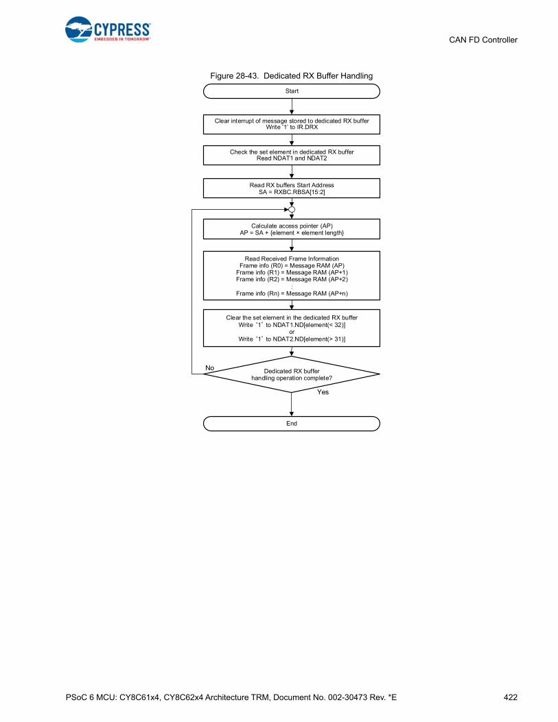
PSoC 6 MCU: CY8C61x4, CY8C62x4 Architecture TRM, Document No. 002-30473 Rev. *E 422
CAN FD Controller
Figure 28-43. Dedicated RX Buffer Handling
Calculate access pointer (AP)AP = SA + {element × element length}
Read Received Frame Information Frame info (R0) = Message RAM (AP)
Frame info (R1) = Message RAM (AP+1)Frame info (R2) = Message RAM (AP+2)
:Frame info (Rn) = Message RAM (AP+n)
Clear the set element in the dedicated RX bufferWrite ‘1’ to NDAT1.ND[element(< 32)]
orWrite ‘1’ to NDAT2.ND[element(> 31)]
Dedicated RX buffer handling operation complete?
Yes
No
Check the set element in dedicated RX buffer Read NDAT1 and NDAT2
Clear interrupt of message stored to dedicated RX bufferWrite ‘1’ to IR.DRX
Read RX buffers Start AddressSA = RXBC.RBSA[15:2]
End
Start
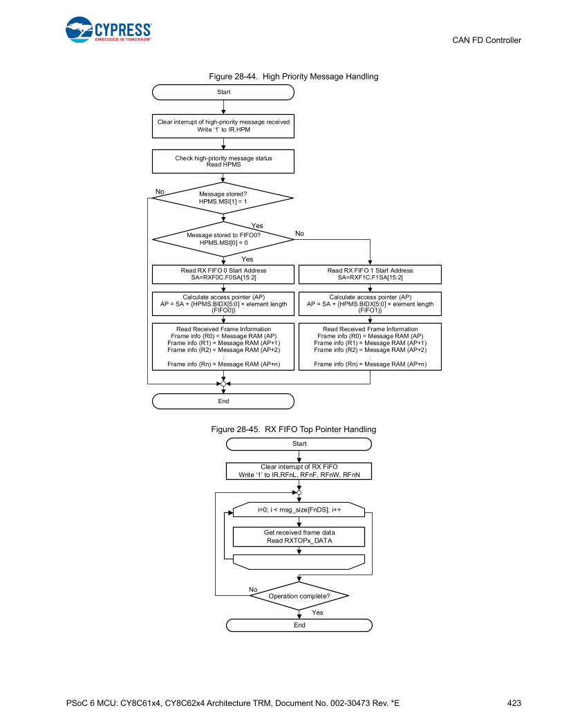
PSoC 6 MCU: CY8C61x4, CY8C62x4 Architecture TRM, Document No. 002-30473 Rev. *E 423
CAN FD Controller
Figure 28-44. High Priority Message Handling
Figure 28-45. RX FIFO Top Pointer Handling
Read RX FIFO 0 Start AddressSA=RXF0C.F0SA[15:2]
Calculate access pointer (AP)AP = SA + {HPMS.BIDX[5:0] × element length
(FIFO0)}
Read Received Frame Information Frame info (R0) = Message RAM (AP)
Frame info (R1) = Message RAM (AP+1)Frame info (R2) = Message RAM (AP+2)
:Frame info (Rn) = Message RAM (AP+n)
Clear interrupt of high-priority message receivedWrite ‘1’ to IR.HPM
Check high-priority message statusRead HPMS
Message stored?HPMS.MSI[1] = 1
Message stored to FIFO0?HPMS.MSI[0] = 0
Read RX FIFO 1 Start AddressSA=RXF1C.F1SA[15:2]
Calculate access pointer (AP)AP = SA + {HPMS.BIDX[5:0] × element length
(FIFO1)}
Read Received Frame Information Frame info (R0) = Message RAM (AP)
Frame info (R1) = Message RAM (AP+1)Frame info (R2) = Message RAM (AP+2)
:Frame info (Rn) = Message RAM (AP+n)
Yes
No
Yes
No
Start
End
Start
Get received frame dataRead RXTOPx_DATA
End
i=0; i < msg_size[FnDS]; i++
Operation complete?No
Yes
Clear interrupt of RX FIFOWrite ‘1’ to IR.RFnL, RFnF, RFnW, RFnN

PSoC 6 MCU: CY8C61x4, CY8C62x4 Architecture TRM, Document No. 002-30473 Rev. *E 424
CAN FD Controller
28.7 Registers
Register Name Description
CANFD_CH_CREL Core Release Register Displays the revision of the CAN FD controller.
CANFD_CH_ENDN Endian RegisterChecks the endianness of the CAN FD controller when accessed by the CPU.
CANFD_CH_DBTPData Bit Timing and Prescaler Register
Configures the data bit time and enables Transmitter Delay Compensation.
CANFD_CH_TEST Test RegisterMonitors the canfd[0].ttcan_rx[0]/canfd[0].ttcan_tx[0] pins. It is also used to enable the Loop Back modes.
CANFD_CH_RWD RAM Watchdog Monitors the message RAM to see if it is ready to be accessed.
CANFD_CH_CCCR CC Control Register Configures various operating modes of the CAN FD controller.
CANFD_CH_NBTPNominal Bit Timing and Prescaler Register
Configures the nominal bit time of the CAN FD controller.
CANFD_CH_TSCC Timestamp Counter Configuration Holds the settings for Timestamp Generation.
CANFD_CH_TSCV Timestamp Counter Value Hold the value of the Timestamp Counter.
CANFD_CH_TOCC Timeout Counter Configuration Holds the settings for the Timeout Counter.
CANFD_CH_TOCV Timeout Counter Value Holds the value of the Timeout Counter.
CANFD_CH_ECR Error Counter Register Holds the values of the Error Counters
CANFD_CH_PSR Protocol Status Register Displays the CAN protocol status of the CAN FD controller.
CANFD_CH_TDCRTransmitter Delay Compensation Register
Configures the offset value and the filter window length for Transmitter Delay Compensation
CANFD_CH_IR Interrupt RegisterHolds the flags that are set when one of the listed conditions is detected (edge-sensitive).
CANFD_CH_IE Interrupt EnableThe settings in this register determine which status changes in the Interrupt Register (IR) will be signaled on an interrupt line
CANFD_CH_ILS Interrupt Line SelectAssigns an interrupt generated by a specific interrupt flag from the Interrupt Register (IR) to one of the two CAN FD controller interrupt lines (CANFD_int0/1).
CANFD_CH_ILE Interrupt Line EnableThis register can separately enable/disable each of the two interrupt lines to the CPU.
CANFD_CH_GFC Global Filter Configuration Global settings for Message ID filtering.
CANFD_CH_SIDFC Standard ID Filter Configuration Settings for 11-bit standard Message ID filtering.
CANFD_CH_XIDFC Extended ID Filter Configuration Settings for 29-bit extended Message ID filtering.
CANFD_CH_XIDAM Extended ID AND Mask Defines the valid bits of a 29-bit ID for acceptance filtering.
CANFD_CH_HPMS High Priority Message StatusThis register is updated every time a Message ID filter element configured to generate a priority event matches.
CANFD_CH_NDAT1 New Data 1Holds flags that are set when the respective dedicated RX buffer receives a frame.
CANFD_CH_NDAT2 New Data 2Holds flags that are set when the respective dedicated RX buffer receives a frame.
CANFD_CH_RXF0C RX FIFO 0 Configuration Settings for the RX FIFO 0.
CANFD_CH_RXF0S RX FIFO 0 Status Status of the RX FIFO 0.
CANFD_CH_RXF0A RX FIFO 0 AcknowledgeAcknowledges that the CPU has read a message or a sequence of messages from the RX FIFO 0 to indicate to the CAN FD controller that the corresponding message RAM area may be released.
CANFD_CH_RXBC RX Buffer ConfigurationDefines the start address of the RX Buffer section in the message RAM.
CANFD_CH_RXF1C RX FIFO 1 Configuration Settings for the RX FIFO 1.
CANFD_CH_RXF1S RX FIFO 1 Status Status of the RX FIFO 1.
CANFD_CH_RXF1A RX FIFO 1 AcknowledgeAcknowledges that the CPU has read a message or a sequence of messages from the RX FIFO 1 to indicate to the CAN FD controller that the corresponding message RAM area may be released.
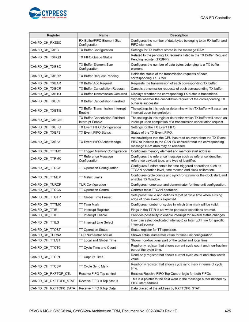
PSoC 6 MCU: CY8C61x4, CY8C62x4 Architecture TRM, Document No. 002-30473 Rev. *E 425
CAN FD Controller
CANFD_CH_RXESCRX Buffer/FIFO Element Size Configuration
Configures the number of data bytes belonging to an RX buffer and FIFO element.
CANFD_CH_TXBC TX Buffer Configuration Settings for TX buffers stored in the message RAM
CANFD_CH_TXFQS TX FIFO/Queue StatusRelated to the pending TX requests listed in the TX Buffer Request Pending register (TXBRP).
CANFD_CH_TXESCTX Buffer Element Size Configuration
Configures the number of data bytes belonging to a TX buffer element
CANFD_CH_TXBRP TX Buffer Request PendingHolds the status of the transmission requests of each corresponding TX Buffer
CANFD_CH_TXBAR TX Buffer Add Request Requests the transmission of each corresponding TX buffer.
CANFD_CH_TXBCR TX Buffer Cancellation Request Cancels transmission requests of each corresponding TX buffer.
CANFD_CH_TXBTO TX Buffer Transmission Occurred Displays whether the corresponding TX buffer is transmitted.
CANFD_CH_TXBCF TX Buffer Cancellation FinishedSignals whether the cancellation request of the corresponding TX buffer is successful.
CANFD_CH_TXBTIETX Buffer Transmission Interrupt Enable
The settings in this register determine which TX buffer will assert an interrupt upon transmission.
CANFD_CH_TXBCIETX Buffer Cancellation Finished Interrupt Enable
The settings in this register determine which TX buffer will assert an interrupt upon completion of a transmission cancellation request.
CANFD_CH_TXEFC TX Event FIFO Configuration Settings for the TX Event FIFO.
CANFD_CH_TXEFS TX Event FIFO Status Status of the TX Event FIFO.
CANFD_CH_TXEFA TX Event FIFO AcknowledgeAcknowledges that the CPU has read an event from the TX Event FIFO to indicate to the CAN FD controller that the corresponding message RAM area may be released.
CANFD_CH_TTTMC TT Trigger Memory Configuration Configures memory element and memory start address.
CANFD_CH_TTRMCTT Reference Message Configuration
Configures the reference message such as reference identifier, reference payload type, and type of identifier.
CANFD_CH_TTOCF TT Operation ConfigurationConfigures fundamentals for time-triggered operations such as TTCAN operation level, time master, and clock calibration.
CANFD_CH_TTMLM TT Matrix LimitsConfigures cycle counts and synchronization for the clock start, and enables TX Window.
CANFD_CH_TURCF TUR Configuration Configures numerator and denominator for time unit configuration.
CANFD_CH_TTOCN TT Operation Control Controls main TTCAN operation.
CANFD_CH_TTGTP TT Global Time PresetSets preset value and defines target of cycle time when a rising edge of ttcan event is expected.
CANFD_CH_TTTMK TT Time Mark Configures number of cycles in which time mark will be valid.
CANFD_CH_TTIR TT Interrupt Register Flags in the TTIR is set when particular conditions are met.
CANFD_CH_TTIE TT Interrupt Enable Provides possibility to enable interrupt for several status changes.
CANFD_CH_TTILS TT Interrupt Line SelectUser can select dedicated Interrupt0 or Interrupt1 line for specific interrupt source.
CANFD_CH_TTOST TT Operation Status Status register for TT operation.
CANFD_CH_TURNA TUR Numerator Actual Shows actual numerator value for time unit configuration.
CANFD_CH_TTLGT TT Local and Global Time Shows non-fractional part of the global and local time.
CANFD_CH_TTCTC TT Cycle Time and CountRead-only register that shows current cycle count and non-fraction part of the cycle time.
CANFD_CH_TTCPT TT Capture TimeRead-only register that shows current cycle count and stop watch value.
CANFD_CH_TTCSM TT Cycle Sync MarkRead-only register that shows cycle sync mark in terms of cycle time.
CANFD_CH_RXFTOP_CTL Receive FIFO Top control Enables Receive FIFO Top Control logic for both FIFOs.
CANFD_CH_RXFTOP0_STAT Receive FIFO 0 Top StatusThis is a pointer to the next word in the message buffer defined by FIFO start address.
CANFD_CH_RXFTOP0_DATA Receive FIFO 0 Top Data Data placed at the address by RXFTOP0_STAT.
Register Name Description

PSoC 6 MCU: CY8C61x4, CY8C62x4 Architecture TRM, Document No. 002-30473 Rev. *E 426
CAN FD Controller
CANFD_CH_RXFTOP1_STAT Receive FIFO 1 Top StatusThis is a pointer to the next word in the message buffer defined by FIFO start address.
CANFD_CH_RXFTOP1_DATA Receive FIFO 1 Top Data Data placed at the address by RXFTOP1_STAT.
CANFD_CTL Global CAN Control Register Provides clock control to the TTCAN channel.
CANFD_STATUS Global CAN Status RegisterRead-only register that shows the acknowledge from the respective TTCAN channel for the clock stop request.
CANFD_INTR0_CAUSE Consolidated Int0 Cause Register Shows pending interrupt0 for the TTCAN channel.
CANFD_INTR1_CAUSE Consolidated Int1 Cause Register Shows pending interrupt1 for the TTCAN channel.
CANFD_TS_CTL Time Stamp Control RegisterConfiguration for the Timestamp prescaler and counter enable is done in this register.
CANFD_TS_CNT Time Stamp Count Register Shows timestamp counter value.
Register Name Description
PSoC 6 MCU: CY8C61x4, CY8C62x4 Architecture TRM, Document No. 002-30473 Rev. *E 427
29. Timer, Counter, PWM
The Timer, Counter, Pulse Width Modulator (TCPWM) block in the PSoC 6 MCU can be configured as a timer, counter, pulsewidth modulator (PWM), pseudo random PWM, shift register, or a quadrature decoder. TCPWM includes up to four countergroups where each group can include up to 256 counters (refer to the PSoC 61 datasheet/PSoC 62 datasheet for details).The counter can be used to measure the period and pulse width of an input signal (timer), find the number of times an eventoccurs (counter), generate PWM signals, or decode quadrature signals. The TCPWM block works in Active and Sleepmodes.
This chapter explains the features, implementation, and operational modes of the TCPWM block.
29.1 Features
The TCPWM block has the following features:
■ Supports up to four counter groups (refer to the PSoC 61 datasheet/PSoC 62 datasheet for details)
■ Each counter group consists up to 256 counters (refer to the PSoC 61 datasheet/PSoC 62 datasheet for details)
■ Each counter can run in one of seven function modes:
❐ Timer-counter with compare
❐ Timer-counter with capture
❐ Quadrature decoding
❐ Pulse width modulation
❐ PWM with dead time
❐ Pseudo-random PWM
❐ Shift register mode
■ 16-bit or 32-bit counters (counter group specific)
■ Up, down, and up/down counting modes
■ Clock pre-scaling (division by 1, 2, 4, ... 64, 128)
■ Up to two capture and compare functions (counter group specific; refer to the PSoC 61 datasheet/PSoC 62 datasheet for details)
■ Double buffering of all compare/capture and period registers
■ Two output trigger signals for each counter to indicate underflow, overflow, and capture/compare events (events refer to peripheral generated signals that trigger specific functions in each counter); they can also directly be connected with the line output signal
■ Supports interrupt on:
❐ Terminal Count - Depends on the mode; typically occurs on overflow or underflow
This PSoC 6 MCU technical reference manual (TRM) provides comprehensive and detailed information about thefunctions of the PSoC 6 MCU device hardware. It is divided into two books: architecture TRM and registers TRM. TheTRM is not recommended for those new to the PSoC 6 MCU, nor as a guide for developing PSoC 6 MCU applications.Use these documents instead:
■ PSoC 61 datasheet, PSoC 62 datasheet
■ Peripheral Driver Library (PDL) documentation
■ Application notes
■ Code examples
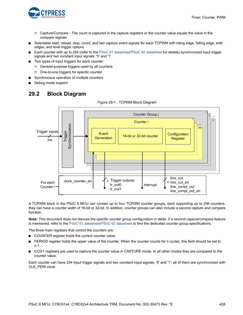
PSoC 6 MCU: CY8C61x4, CY8C62x4 Architecture TRM, Document No. 002-30473 Rev. *E 428
Timer, Counter, PWM
❐ Capture/Compare - The count is captured in the capture registers or the counter value equals the value in the compare register
■ Selectable start, reload, stop, count, and two capture event signals for each TCPWM with rising edge, falling edge, both edges, and level trigger options
■ Each counter with up to 254 (refer to the PSoC 61 datasheet/PSoC 62 datasheet for details) synchronized input trigger signals and two constant input signals: '0' and '1'.
■ Two types of input triggers for each counter:
❐ General-purpose triggers used by all counters
❐ One-to-one triggers for specific counter
■ Synchronous operation of multiple counters
■ Debug mode support
29.2 Block Diagram
Figure 29-1. TCPWM Block Diagram
A TCPWM block in the PSoC 6 MCU can contain up to four TCPWM counter groups, each supporting up to 256 counters;they can have a counter width of 16-bit or 32-bit. In addition, counter groups can also include a second capture and comparefunction.
Note: This document does not discuss the specific counter group configuration in detail. If a second capture/compare featureis mentioned, refer to the PSoC 61 datasheet/PSoC 62 datasheet to find the dedicated counter group specifications.
The three main registers that control the counters are:
■ COUNTER register holds the current counter value.
■ PERIOD register holds the upper value of the counter. When the counter counts for n cycles, this field should be set to n-1.
■ CC0/1 registers are used to capture the counter value in CAPTURE mode. In all other modes they are compared to the counter value.
Each counter can have 254 input trigger signals and two constant input signals, '0' and '1'; all of them are synchronized withCLK_PERI clock.
Counter i
256 Tri
gge
r S
ynch
ron
izat
ion
Trigger inputs
Trigger outputs:tr_out0tr_out1
interrupt
line_out,line_out_enline_compl_outline_compl_out_en
42clock_counter_enFor each Counter i
Counter Group jCounter Group j
Counter Group j ...
Counter i
EventGeneration 16-bit or 32-bit counter
Counter i
EventGeneration 16-bit or 32-bit counter Configuration
Register
Counter i
EventGeneration 16-bit or 32-bit counter Configuration
Register
...1
2
256
4
12

PSoC 6 MCU: CY8C61x4, CY8C62x4 Architecture TRM, Document No. 002-30473 Rev. *E 429
Timer, Counter, PWM
The TCPWM block has these interfaces:
■ Bus interface: Connects the block to the CPU subsystem via AHB-Lite interface.
■ I/O signal interface: Consists of input triggers (such as reload, start, stop, count, and capture0/1) and output signals (such as LINE_OUT, LINE_COMPL_OUT, TR_OUT0, and TR_OUT1). All the input signals are used to trigger an event within the counter, such as a reload trigger generating a reload event. The output signals are generated by internal events (underflow, overflow, and capture/compare) and can be connected to other peripherals to trigger events.
■ Interrupts: Provides interrupt request signals from each counter, based on terminal count (TC), Compare/Capture CC0_match, or Compare/Capture CC1_match event.
■ System interface: Consists of control signals such as clock and reset from the system resources subsystem (SRSS).
The TCPWM block can be configured by writing to the TCPWM registers. See “TCPWM Registers” on page 488 for moreinformation on all registers required for this block.
29.2.1 Enabling and Disabling Counters in TCPWM
A counter can be enabled by writing '1' to the corresponding ENABLE bit of the CTRL register; it can be disabled by writing '0'to the same bit.Note: The counter must be configured before enabling it. Disabling the counter retains the values in the configurationregisters.
29.2.2 Clocking
Each TCPWM counter can have its own clock; the only source for the clock is from the configurable peripheral clock dividersgenerated by the clocking system; see the Clocking System chapter on page 240 for details. To select a clock divider for aparticular counter inside a TCPWM, use the CLOCK_CTL register from the PERI register space.
In this section the clock to the counter will be called clk_counter. Event generation is performed on clk_counter. Another clock,CLK_SYS, is used for the pulse width of the output triggers. CLK_SYS is synchronous to CLK_PERI, but can be divided usingCLOCK_CTL from the PERI_GROUP_STRUCT register.
29.2.2.1 Clock Prescaling
clk_counter can be further divided inside each counter, with values of 1, 2, 4, 8…64, 128. This division is called prescaling.The prescaling is set in the DT_LINE_OUT_L [7:0] field of the DT register. The lower three bits of this field determineprescaling of the selected counter clock.
Note: Clock prescaling is not available in quadrature mode and pulse width modulation mode with dead time.
29.2.2.2 Count Event
The counter increments or decrements on a prescaled clock in which the count input is active – “active count”.Note: Count events are not supported in quadrature and pulse-width modulation pseudo-random modes; the clk_counter isused in these cases instead of the active count prescaled clock.
Figure 29-2. Counter Clock Generation
■ When the count input is configured as level, the count value is changed on each prescaled clk_counter edge in which the count input is high.
■ When the count input is configured as rising/falling the count value is changed on each prescaled clk_counter edge in which an edge is detected on the count input.
The next section contains additional details on edge detection configuration.
clk_counter
not supported in all modes
Pre-scaling pre-scaled counter clock
count event
“active count”pre-scaled
counter clock
Counter functionality
Note: The count event and pre-scaled counter clock are AND together, which means that a count event must occur to generate an active count pre-scaled counter clock.

PSoC 6 MCU: CY8C61x4, CY8C62x4 Architecture TRM, Document No. 002-30473 Rev. *E 430
Timer, Counter, PWM
29.2.3 Trigger Inputs
Each TCPWM block has 254 Trigger_In signals and constant '0' and '1' signals, which come from other on-chip resourcessuch as other TCPWMs, SCBs, and DMA. The Trigger_In signals are shared with all counters inside one TCPWM block.
Two types of trigger signals are synchronized and can be used by the counters to generate events.
■ General-purpose triggers. These can be used by all counters. These triggers are generated by different blocks in the system and are distributed by the trigger infrastructure (peripheral trigger multiplexers). See the Trigger Multiplexer Block chapter on page 290 for more details.
■ One-to-one triggers. A separate set exists for each counter, only connected to that counter. These triggers are used for direct trigger connections from trigger sources (such as ADC channels) to associated TCPWM counters.
Use the trigger mux registers TR_IN_SEL0 and TR_IN_SEL1 to configure which signals get routed to the Trigger_In for eachTCPWM block. See Table 29-1 for all possible multiplexer settings selecting an input trigger event for a TCPWM block. Foreach event two constant trigger inputs are available. Input trigger 0 is always constant '0' and input trigger 1 is alwaysconstant '1'.
Each counter can select any of the 256 trigger signals to be the source for any of the following events:
■ Capture 0 and Capture 1
■ Count
■ Reload
■ Stop/Kill
■ Start
Note: The TR_CMD register can be used to trigger the Reload, Stop, Start, and Capture0/1 respectively from software.
The following sections describe each TCPWM mode and the function of each input event in detail.
Typical operation uses the reload event once to initialize and start the counter and the stop event to stop the counter. Whenthe counter is stopped, the start event can be used to start the counter with its counter value unmodified from when it wasstopped.
If stop, reload, and start events coincide, the following precedence relationship holds:
■ A stop event has higher priority than a reload event.
■ A reload event has higher priority that a start event.
As a result, when a reload or start event coincides with a stop event, the reload or start event has no effect.
Before going to the counter each Trigger_IN can pass through a positive edge detector, negative edge detector, both edgedetector, or pass straight through to the counter. This is controlled using TR_IN_EDGE_SEL register.
Table 29-1. Multiplexer Selection for Input Trigger Events
Input Trigger Selection Register
Bit Field Bits Description
TR_IN_SEL0
CAPTURE0_SEL 7:0Selects one of the up to 256 input triggers as a capture0 trigger. In the PWM, PWM_DT, and PWM_PR modes this trigger is used to switch the values if the compare and period registers with their buffer counterparts.
COUNT_SEL 15:8Selects one of the 256 input triggers as a count trigger. In QUAD mode, this is the first phase (phi A)
RELOAD_SEL 23:16Selects one of the 256 input triggers as a reload trigger. In QUAD mode, this is the index or revolution pulse
STOP_SEL 31:24Selects one of the 256 input triggers as a stop trigger. In PWM, PWM_DT, and PWM_PR modes, this is the kill trigger
TR_IN_SEL1START_SEL 7:0
Selects one of the 256 input triggers as a start trigger. In QUAD mode, this is the sec-ond phase (phi B)
CAPTURE1_SEL 15:8 Selects one of the up to 256 input triggers as a capture1 trigger
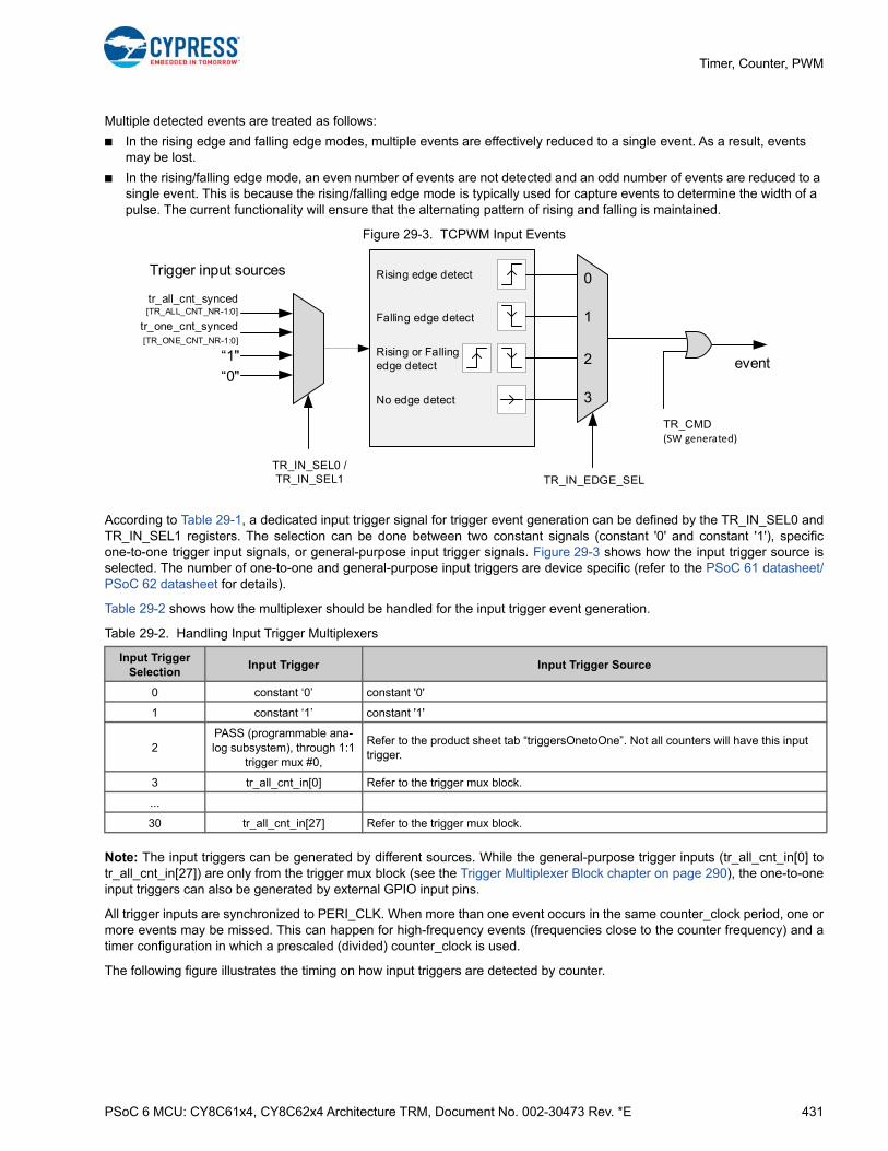
PSoC 6 MCU: CY8C61x4, CY8C62x4 Architecture TRM, Document No. 002-30473 Rev. *E 431
Timer, Counter, PWM
Multiple detected events are treated as follows:
■ In the rising edge and falling edge modes, multiple events are effectively reduced to a single event. As a result, events may be lost.
■ In the rising/falling edge mode, an even number of events are not detected and an odd number of events are reduced to a single event. This is because the rising/falling edge mode is typically used for capture events to determine the width of a pulse. The current functionality will ensure that the alternating pattern of rising and falling is maintained.
Figure 29-3. TCPWM Input Events
According to Table 29-1, a dedicated input trigger signal for trigger event generation can be defined by the TR_IN_SEL0 andTR_IN_SEL1 registers. The selection can be done between two constant signals (constant '0' and constant '1'), specificone-to-one trigger input signals, or general-purpose input trigger signals. Figure 29-3 shows how the input trigger source isselected. The number of one-to-one and general-purpose input triggers are device specific (refer to the PSoC 61 datasheet/PSoC 62 datasheet for details).
Table 29-2 shows how the multiplexer should be handled for the input trigger event generation.
Note: The input triggers can be generated by different sources. While the general-purpose trigger inputs (tr_all_cnt_in[0] totr_all_cnt_in[27]) are only from the trigger mux block (see the Trigger Multiplexer Block chapter on page 290), the one-to-oneinput triggers can also be generated by external GPIO input pins.
All trigger inputs are synchronized to PERI_CLK. When more than one event occurs in the same counter_clock period, one ormore events may be missed. This can happen for high-frequency events (frequencies close to the counter frequency) and atimer configuration in which a prescaled (divided) counter_clock is used.
The following figure illustrates the timing on how input triggers are detected by counter.
Table 29-2. Handling Input Trigger Multiplexers
Input Trigger Selection
Input Trigger Input Trigger Source
0 constant ‘0’ constant '0'
1 constant ‘1’ constant '1'
2PASS (programmable ana-log subsystem), through 1:1
trigger mux #0,
Refer to the product sheet tab “triggersOnetoOne”. Not all counters will have this input trigger.
3 tr_all_cnt_in[0] Refer to the trigger mux block.
...
30 tr_all_cnt_in[27] Refer to the trigger mux block.
0
1
2
3
Rising edge detect
Falling edge detect
Rising or Falling edge detect
No edge detect
“0"“1" event
Trigger input sources
TR_IN_SEL0 /TR_IN_SEL1
tr_all_cnt_synced[TR_ALL_CNT_NR-1:0]
tr_one_cnt_synced[TR_ONE_CNT_NR-1:0]
TR_IN_EDGE_SEL
TR_CMD (SW generated)

PSoC 6 MCU: CY8C61x4, CY8C62x4 Architecture TRM, Document No. 002-30473 Rev. *E 432
Timer, Counter, PWM
Figure 29-4. Input Trigger Detection by “active count” Prescaled Counter Clock
Note: The arrows in the figure depict the events that are detected by the counter.
Two examples explain how edge detection event works on active count prescaled counter clocks:
■ In PWM mode, if PWM_IMM_KILL = 0, the rising edge kill asserts while count event is inactive, line output will not be suppressed until the next prescaled counter clock after the count event becomes active.
■ In capture mode, if rising edge capture0 inputs while count event is inactive, CC0 and CC0_BUFF will get updated at the next prescaled counter clock after count event becomes active.
Typically, the count event is a constant '1' and prescaling is off. In this case, the active count prescaled counter clock is thesame as the counter clock. In other cases, edge detection may detect multiple events (on the counter clock) before the nextactive count prescaled counter clock on which the detected event is used. Multiple detected events are treated as follows:
■ In the rising edge and falling edge modes, multiple events are effectively reduced to a single event. As a result, events may be lost.
■ In the rising/falling edge mode, an even number of events is not detected and an odd number of events is reduced to a single event. This is because the rising/falling edge mode is typically used for capture events to determine the width of a pulse. The current functionality will ensure that the alternating pattern of rising, falling, rising, falling, and so on is maintained.
A pass-through event will not be remembered by CLK_PERI; it will affect the functionality if it lasts and can be detected by acounter operation clock. If the pulse width of a pass-through event is less than a counter operation clock cycle, it may get lost.Pass-through detection may result in an event that is active for multiple counter clocks. This may result in undesirablebehavior of the counter and its associated trigger outputs. Pass-through event detection should only be used for stop andcount event types in most function modes. Pass-through mode can also be used in switch events in the PWM/PWM_DT/PWM_PR mode, if it selects the constant high as the source. In quadrature mode, both start and count event is used withpass through in X1/X2/X4 mode.
29.2.4 Trigger Outputs
Each counter has two trigger output signals (TR_OUT0 and TR_OUT1) to indicate following events. They can be routedthrough the trigger mux to other peripherals on the device. The bit field OUT0 in TR_OUT_SEL register is used to select oneof the internal events to generate output trigger 0 (TR_OUT0), respectively the bit field OUT1 is selecting one of the internalevents to generate TR_OUT1. It allows also to disable the output triggers.
■ Overflow (OV): An overflow event indicates that in up counting mode, COUNTER equals PERIOD register, and is changed to a different value.
■ Underflow (UN): An underflow event indicates that in down counting mode, COUNTER equals 0, and is changed to a different value.
■ TC (Terminal Count): A TC event is the logical OR of the underflow and overflow events
MODE = TIMERUP_DOWN_MODE = COUNT_UPPERIOD = 4RELOAD = RISING_EDGESTOP = FALLING_EDGESTART = NO_EDGE_DET
Reload trigger
Active countسpre-scaled counter clock
Stop trigger
Start trigger
STATUS.RUNNING
CO
UN
TE
R
4
3
2
1
0
start
stop
reload
Event detected by counter
Selected input trigger
PSoC 6 MCU: CY8C61x4, CY8C62x4 Architecture TRM, Document No. 002-30473 Rev. *E 433
Timer, Counter, PWM
■ CC0/1_MATCH: This event is generated when the counter is running and one of the following conditions occur:
❐ Counter equals the compare value. This event is either generated when the match is about to occur (COUNTER does not equal CC0/1 and is changed to CC0/1) or when the match is about to not occur (COUNTER equals CC0/1 and is changed to a different value).
❐ A capture event has occurred and the CC0 (CC1) and CC0_BUFF (CC1_BUFF) registers are updated.
■ LINE_OUT: A PWM output signal
■ DISABLED: Output trigger is disabled
The selection of the events for the output trigger generation is done by the TR_OUT_SEL register. It also allows disabling theoutput triggers.
Note: These signals only remain high for two cycles of CLK_SYS. For reliable operation, the condition that causes this triggershould be a maximum of one quarter of the CLK_SYS. For example, if the CLK_SYS is running at 24 MHz, the conditioncausing the trigger should occur at a frequency equal to or less than 6 MHz.
When LINE_OUT is selected for output triggers, output trigger will bypass two cycle pulses generation logic and directlyoutput LINE_OUT.
The generated triggers have two main uses:
■ Initiating a DW/DMA data transfer. For example, in PWM mode with an up counting timer, the overflow can be used to transfer new period and compare values from memory to the counters' PERIOD_BUFF and CC0_BUFF registers.
■ Reconstruction of a PWM signal in a programmable digital component. As documented in 29.3.4 Pulse Width Modulation (PWM) Mode, the PWM line output signal is derived from the cc0_match (cc1_match), underflow, and overflow internal events. By making these internal events available as output triggers, other components can reconstruct and potentially modify the PWM signal (note the mentioned frequency restrictions).
29.2.5 Internal Events
29.2.5.1 Underflow Event
An underflow event indicates that in down counting, COUNTER equals zero, and is changed to a different value. Reload willalso generate underflow event in some specific mode. Table 29-3 summarizes the underflow generation of each functionmode.
Table 29-3. Underflow Generation
MODE UP DOWN UPDN1 UPDN2
TIMERCounter is decrementing and changes from a state in which COUNTER equals 0.
Reload event in DOWN, UPDN1, and UPDN2 modes.
CAPTURECounter is decrementing and changes from a state in which COUNTER equals 0.
Reload event in DOWN, UPDN1, and UPDN2 modes.
QUAD
QUAD_RANGE0: Not used
QUAD_RANGE0_CMP: Not used
QUAD_RANGE1_CMP: Counter value COUNTER equals 0 and is decrementing.
QUAD_RANGE1_CAPT: Counter value COUNTER equals 0 and is decrementing.
PWMCounter is decrementing and changes from a state in which COUNTER equals 0.
Reload event in DOWN, UPDN1, and UPDN2 modes.
PWM_DTCounter is decrementing and changes from a state in which COUNTER equals 0.
Reload event in DOWN, UPDN1, and UPDN2 modes.
PWM_PR Not used
SR Not used
PSoC 6 MCU: CY8C61x4, CY8C62x4 Architecture TRM, Document No. 002-30473 Rev. *E 434
Timer, Counter, PWM
29.2.5.2 Overflow Event
An overflow event indicates that in up counting, COUNTER equals PERIOD, and is changed to a different value. Reload willalso generate overflow event in some specific mode. Table 29-4 summarizes the overflow generation of each function mode.
29.2.5.3 TC Event
A tc (terminal count) event is the logical OR of the underflow and overflow events. An exception is that reload event willgenerate an underflow or overflow, but not a tc event. In quadrature mode, index will generate a tc event. Table 29-5summarizes the tc generation of each function mode.
Table 29-4. Overflow Generation
MODE UP DOWN UPDN1 UPDN2
TIMERCounter is incrementing and changes from a state in which COUNTER equals PERIOD.
Reload event in UP count mode.
CAPTURECounter is incrementing and changes from a state in which COUNTER equals PERIOD.
Reload event in UP count mode.
QUAD
QUAD_RANGE0: Not used
QUAD_RANGE0_CMP: Not used
QUAD_RANGE1_CMP: Counter value COUNTER equals PERIOD and is incrementing.
QUAD_RANGE1_CAPT: Counter value COUNTER equals PERIOD and is incrementing.
PWMCounter is incrementing and changes from a state in which COUNTER equals PERIOD.
Reload event in UP count mode.
PWM_DTCounter is incrementing and changes from a state in which COUNTER equals PERIOD.
Reload event in UP count mode.
PWM_PR Not used
SR Not used
Table 29-5. TC Generation
MODE UP DOWN UPDN1 UPDN2
TIMER Overflow Underflow UnderflowLogic OR of overflow and underflow
CAPTURE Overflow Underflow UnderflowLogic OR of overflow and underflow
QUAD
QUAD_RANGE0:
■ Index event.
QUAD_RANGE0_CMP:
■ Counter value COUNTER equals 0 or 0xFFFF/0xFFFFFFFF in “wraparound capture” mode.
■ Index or capture0 event in “index capture” mode.
QUAD_RANGE1_CMP:
■ Counter value COUNTER equals 0 and decrementing (underflow), or PERIOD and incrementing (overflow).
■ Index event.
QUAD_RANGE1_CAPT:
■ Same as QUAD_RANGE1_CMP.
PWM Overflow Underflow UnderflowLogic OR of overflow and underflow
PWM_DT Overflow Underflow UnderflowLogic OR of overflow and underflow
PWM_PR Counter changes from a state in which COUNTER equals PERIOD.
SR Not used
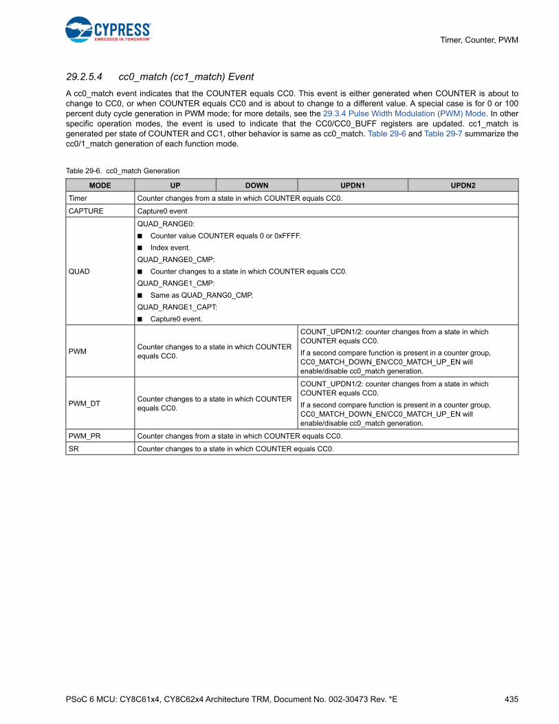
PSoC 6 MCU: CY8C61x4, CY8C62x4 Architecture TRM, Document No. 002-30473 Rev. *E 435
Timer, Counter, PWM
29.2.5.4 cc0_match (cc1_match) Event
A cc0_match event indicates that the COUNTER equals CC0. This event is either generated when COUNTER is about tochange to CC0, or when COUNTER equals CC0 and is about to change to a different value. A special case is for 0 or 100percent duty cycle generation in PWM mode; for more details, see the 29.3.4 Pulse Width Modulation (PWM) Mode. In otherspecific operation modes, the event is used to indicate that the CC0/CC0_BUFF registers are updated. cc1_match isgenerated per state of COUNTER and CC1, other behavior is same as cc0_match. Table 29-6 and Table 29-7 summarize thecc0/1_match generation of each function mode.
Table 29-6. cc0_match Generation
MODE UP DOWN UPDN1 UPDN2
Timer Counter changes from a state in which COUNTER equals CC0.
CAPTURE Capture0 event
QUAD
QUAD_RANGE0:
■ Counter value COUNTER equals 0 or 0xFFFF.
■ Index event.
QUAD_RANGE0_CMP:
■ Counter changes to a state in which COUNTER equals CC0.
QUAD_RANGE1_CMP:
■ Same as QUAD_RANG0_CMP.
QUAD_RANGE1_CAPT:
■ Capture0 event.
PWMCounter changes to a state in which COUNTER equals CC0.
COUNT_UPDN1/2: counter changes from a state in which COUNTER equals CC0.
If a second compare function is present in a counter group, CC0_MATCH_DOWN_EN/CC0_MATCH_UP_EN will enable/disable cc0_match generation.
PWM_DTCounter changes to a state in which COUNTER equals CC0.
COUNT_UPDN1/2: counter changes from a state in which COUNTER equals CC0.
If a second compare function is present in a counter group, CC0_MATCH_DOWN_EN/CC0_MATCH_UP_EN will enable/disable cc0_match generation.
PWM_PR Counter changes from a state in which COUNTER equals CC0.
SR Counter changes to a state in which COUNTER equals CC0.
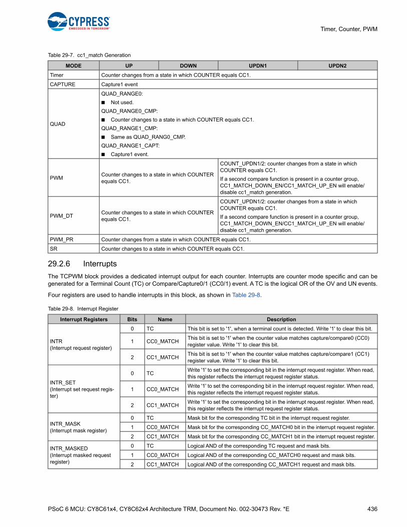
PSoC 6 MCU: CY8C61x4, CY8C62x4 Architecture TRM, Document No. 002-30473 Rev. *E 436
Timer, Counter, PWM
29.2.6 Interrupts
The TCPWM block provides a dedicated interrupt output for each counter. Interrupts are counter mode specific and can begenerated for a Terminal Count (TC) or Compare/Capture0/1 (CC0/1) event. A TC is the logical OR of the OV and UN events.
Four registers are used to handle interrupts in this block, as shown in Table 29-8.
Table 29-7. cc1_match Generation
MODE UP DOWN UPDN1 UPDN2
Timer Counter changes from a state in which COUNTER equals CC1.
CAPTURE Capture1 event
QUAD
QUAD_RANGE0:
■ Not used.
QUAD_RANGE0_CMP:
■ Counter changes to a state in which COUNTER equals CC1.
QUAD_RANGE1_CMP:
■ Same as QUAD_RANG0_CMP.
QUAD_RANGE1_CAPT:
■ Capture1 event.
PWMCounter changes to a state in which COUNTER equals CC1.
COUNT_UPDN1/2: counter changes from a state in which COUNTER equals CC1.
If a second compare function is present in a counter group, CC1_MATCH_DOWN_EN/CC1_MATCH_UP_EN will enable/disable cc1_match generation.
PWM_DTCounter changes to a state in which COUNTER equals CC1.
COUNT_UPDN1/2: counter changes from a state in which COUNTER equals CC1.
If a second compare function is present in a counter group, CC1_MATCH_DOWN_EN/CC1_MATCH_UP_EN will enable/disable cc1_match generation.
PWM_PR Counter changes from a state in which COUNTER equals CC1.
SR Counter changes to a state in which COUNTER equals CC1.
Table 29-8. Interrupt Register
Interrupt Registers Bits Name Description
INTR (Interrupt request register)
0 TC This bit is set to '1', when a terminal count is detected. Write '1' to clear this bit.
1 CC0_MATCHThis bit is set to '1' when the counter value matches capture/compare0 (CC0) register value. Write '1' to clear this bit.
2 CC1_MATCHThis bit is set to '1' when the counter value matches capture/compare1 (CC1) register value. Write '1' to clear this bit.
INTR_SET (Interrupt set request regis-ter)
0 TCWrite '1' to set the corresponding bit in the interrupt request register. When read, this register reflects the interrupt request register status.
1 CC0_MATCHWrite '1' to set the corresponding bit in the interrupt request register. When read, this register reflects the interrupt request register status.
2 CC1_MATCHWrite '1' to set the corresponding bit in the interrupt request register. When read, this register reflects the interrupt request register status.
INTR_MASK (Interrupt mask register)
0 TC Mask bit for the corresponding TC bit in the interrupt request register.
1 CC0_MATCH Mask bit for the corresponding CC_MATCH0 bit in the interrupt request register.
2 CC1_MATCH Mask bit for the corresponding CC_MATCH1 bit in the interrupt request register.
INTR_MASKED (Interrupt masked request register)
0 TC Logical AND of the corresponding TC request and mask bits.
1 CC0_MATCH Logical AND of the corresponding CC_MATCH0 request and mask bits.
2 CC1_MATCH Logical AND of the corresponding CC_MATCH1 request and mask bits.

PSoC 6 MCU: CY8C61x4, CY8C62x4 Architecture TRM, Document No. 002-30473 Rev. *E 437
Timer, Counter, PWM
29.2.7 Debug Mode
The TCPWM counters support debugging. It can be configured per counter if the counter operation continues or pauses indebug state (for example, after running to a break point). This feature is especially intended when using a TCPWM counter asan OS timer. It is realized by gating the clk_counter when entering debug state by setting the DBG_FREEZE_EN bit to ‘1’ inthe CTRL register and asserting a debug pause trigger.
In a multicore environment ‘debug state’ means that at least one of the CPUs is in the debug state. In cases where only oneCPU is debugged but another or multiple other CPUs are continuously running, the user can configure the counter via thedebugger to continue or pause depending on which CPU is using the counter.
Note: The trigger input cannot be asserted when the counter is in debug state.
29.2.8 PWM Outputs
The PWM, PWM_DT, PWM_PR, and SR operation modes produce two output signals:
■ A PWM LINE_OUT output signal
■ A complementary PWM LINE_COMPL_OUT output signal (inverted version of LINE_OUT)
Note that in PWM and PWM_DT modes the CC0_match, CC1_match, underflow, and overflow internal event conditions areused to drive LINE_OUT and LINE_COMPL_OUT, by configuring the TR_PWM_CTRL register (Table 29-9). In PWM_PR andSR modes, line output is not controlled by TR_PWM_CTRL.
The generation of PWM output signals is a multi-step process. Both LINE_OUT and LINE_COMPL_OUT are generated fromthe PWM signal line. The PWM signal line is generated as per the state of cc0_match, cc1_match, underflow, and overflowinternal events, as specified by the counter's TR_PWM_CTRL register. For each internal event, the TR_PWM_CTRL registerspecifies how the event affects the output LINE_OUT
■ The output is set to '0'
■ The output is set to '1'
■ The output is inverted
■ The output is not affected
Table 29-9. Configuring Output Line for OV, UN, and CC0/1 Conditions
Field Bit Value Event Description
CC0_MATCH_MODE Default Value = 3
1:0
0 Set LINE_OUT to '1
Configures output line on a compare match (CC0) event
1 Clear LINE_OUT to '0
2 Invert LINE_OUT
3 No change
OVERFLOW_MODE Default Value = 3
3:2
0 Set LINE_OUT to '1
Configures output line on an overflow (OV) event1 Clear LINE_OUT to '0
2 Invert LINE_OUT
3 No change
UNDERFLOW_MODE Default Value = 3
5:4
0 Set LINE_OUT to '1
Configures output line on an underflow (UN) event1 Clear LINE_OUT to '0
2 Invert LINE_OUT
3 No change
CC1_MATCH_MODE Default Value = 3
7:6
0 Set LINE_OUT to '1
Configures output line on a compare match (CC1) event
1 Clear LINE_OUT to '0
2 Invert LINE_OUT
3 No change
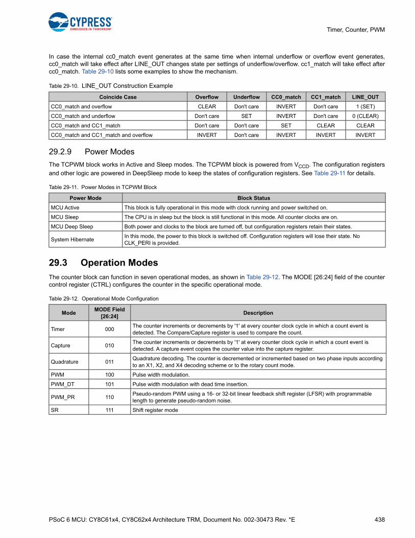
PSoC 6 MCU: CY8C61x4, CY8C62x4 Architecture TRM, Document No. 002-30473 Rev. *E 438
Timer, Counter, PWM
In case the internal cc0_match event generates at the same time when internal underflow or overflow event generates,cc0_match will take effect after LINE_OUT changes state per settings of underflow/overflow. cc1_match will take effect aftercc0_match. Table 29-10 lists some examples to show the mechanism.
29.2.9 Power Modes
The TCPWM block works in Active and Sleep modes. The TCPWM block is powered from VCCD. The configuration registers
and other logic are powered in DeepSleep mode to keep the states of configuration registers. See Table 29-11 for details.
29.3 Operation Modes
The counter block can function in seven operational modes, as shown in Table 29-12. The MODE [26:24] field of the countercontrol register (CTRL) configures the counter in the specific operational mode.
Table 29-10. LINE_OUT Construction Example
Coincide Case Overflow Underflow CC0_match CC1_match LINE_OUT
CC0_match and overflow CLEAR Don't care INVERT Don't care 1 (SET)
CC0_match and underflow Don't care SET INVERT Don't care 0 (CLEAR)
CC0_match and CC1_match Don't care Don't care SET CLEAR CLEAR
CC0_match and CC1_match and overflow INVERT Don't care INVERT INVERT INVERT
Table 29-11. Power Modes in TCPWM Block
Power Mode Block Status
MCU Active This block is fully operational in this mode with clock running and power switched on.
MCU Sleep The CPU is in sleep but the block is still functional in this mode. All counter clocks are on.
MCU Deep Sleep Both power and clocks to the block are turned off, but configuration registers retain their states.
System HibernateIn this mode, the power to this block is switched off. Configuration registers will lose their state. No CLK_PERI is provided.
Table 29-12. Operational Mode Configuration
ModeMODE Field
[26:24]Description
Timer 000The counter increments or decrements by '1' at every counter clock cycle in which a count event is detected. The Compare/Capture register is used to compare the count.
Capture 010The counter increments or decrements by '1' at every counter clock cycle in which a count event is detected. A capture event copies the counter value into the capture register.
Quadrature 011Quadrature decoding. The counter is decremented or incremented based on two phase inputs according to an X1, X2, and X4 decoding scheme or to the rotary count mode.
PWM 100 Pulse width modulation.
PWM_DT 101 Pulse width modulation with dead time insertion.
PWM_PR 110Pseudo-random PWM using a 16- or 32-bit linear feedback shift register (LFSR) with programmable length to generate pseudo-random noise.
SR 111 Shift register mode
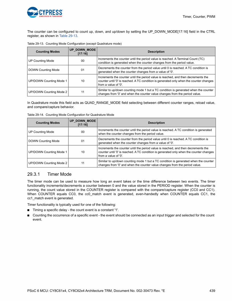
PSoC 6 MCU: CY8C61x4, CY8C62x4 Architecture TRM, Document No. 002-30473 Rev. *E 439
Timer, Counter, PWM
The counter can be configured to count up, down, and up/down by setting the UP_DOWN_MODE[17:16] field in the CTRLregister, as shown in Table 29-13.
In Quadrature mode this field acts as QUAD_RANGE_MODE field selecting between different counter ranges, reload value,and compare/capture behavior.
29.3.1 Timer Mode
The timer mode can be used to measure how long an event takes or the time difference between two events. The timerfunctionality increments/decrements a counter between 0 and the value stored in the PERIOD register. When the counter isrunning, the count value stored in the COUNTER register is compared with the compare/capture register (CC0 and CC1).When COUNTER equals CC0, the cc0_match event is generated, even-handedly when COUNTER equals CC1, thecc1_match event is generated.
Timer functionality is typically used for one of the following:
■ Timing a specific delay - the count event is a constant '1'.
■ Counting the occurrence of a specific event - the event should be connected as an input trigger and selected for the count event.
Table 29-13. Counting Mode Configuration (except Quadrature mode)
Counting ModesUP_DOWN_MODE
[17:16]Description
UP Counting Mode 00Increments the counter until the period value is reached. A Terminal Count (TC) condition is generated when the counter changes from the period value.
DOWN Counting Mode 01Decrements the counter from the period value until 0 is reached. A TC condition is generated when the counter changes from a value of '0'.
UP/DOWN Counting Mode 1 10Increments the counter until the period value is reached, and then decrements the counter until '0' is reached. A TC condition is generated only when the counter changes from a value of '0'.
UP/DOWN Counting Mode 2 11Similar to up/down counting mode 1 but a TC condition is generated when the counter changes from '0' and when the counter value changes from the period value.
Table 29-14. Counting Mode Configuration for Quadrature Mode
Counting ModesUP_DOWN_MODE
[17:16]Description
UP Counting Mode 00Increments the counter until the period value is reached. A TC condition is generated when the counter changes from the period value.
DOWN Counting Mode 01Decrements the counter from the period value until 0 is reached. A TC condition is generated when the counter changes from a value of '0'.
UP/DOWN Counting Mode 1 10Increments the counter until the period value is reached, and then decrements the counter until '0' is reached. A TC condition is generated only when the counter changes from a value of '0'.
UP/DOWN Counting Mode 2 11Similar to up/down counting mode 1 but a TC condition is generated when the counter changes from '0' and when the counter value changes from the period value.
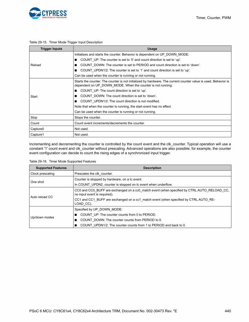
PSoC 6 MCU: CY8C61x4, CY8C62x4 Architecture TRM, Document No. 002-30473 Rev. *E 440
Timer, Counter, PWM
Incrementing and decrementing the counter is controlled by the count event and the clk_counter. Typical operation will use aconstant '1' count event and clk_counter without prescaling. Advanced operations are also possible; for example, the counterevent configuration can decide to count the rising edges of a synchronized input trigger.
Table 29-15. Timer Mode Trigger Input Description
Trigger Inputs Usage
Reload
Initializes and starts the counter. Behavior is dependent on UP_DOWN_MODE:
■ COUNT_UP: The counter is set to ‘0’ and count direction is set to ‘up’.
■ COUNT_DOWN: The counter is set to PERIOD and count direction is set to ‘down’.
■ COUNT_UPDN1/2: The counter is set to ‘1’ and count direction is set to ‘up’.
Can be used when the counter is running or not running.
Start
Starts the counter. The counter is not initialized by hardware. The current counter value is used. Behavior is dependent on UP_DOWN_MODE. When the counter is not running:
■ COUNT_UP: The count direction is set to ‘up’.
■ COUNT_DOWN: The count direction is set to ‘down’.
■ COUNT_UPDN1/2: The count direction is not modified.
Note that when the counter is running, the start event has no effect.
Can be used when the counter is running or not running.
Stop Stops the counter.
Count Count event increments/decrements the counter.
Capture0 Not used.
Capture1 Not used.
Table 29-16. Timer Mode Supported Features
Supported Features Description
Clock prescaling Prescales the clk_counter.
One shotCounter is stopped by hardware, on a tc event.
In COUNT_UPDN2, counter is stopped on tc event when underflow.
Auto reload CC
CC0 and CC0_BUFF are exchanged on a cc0_match event (when specified by CTRL.AUTO_RELOAD_CC, no input event is required).
CC1 and CC1_BUFF are exchanged on a cc1_match event (when specified by CTRL.AUTO_RE-LOAD_CC).
Up/down modes
Specified by UP_DOWN_MODE:
■ COUNT_UP: The counter counts from 0 to PERIOD.
■ COUNT_DOWN: The counter counts from PERIOD to 0.
■ COUNT_UPDN1/2: The counter counts from 1 to PERIOD and back to 0.
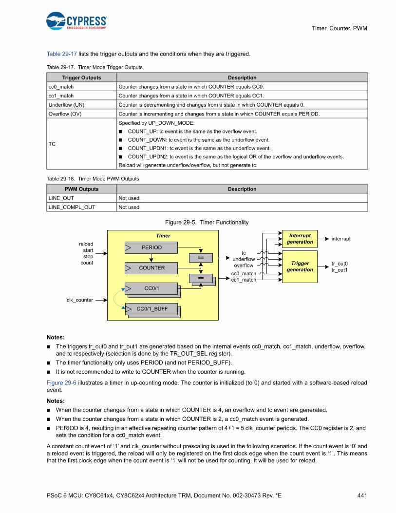
PSoC 6 MCU: CY8C61x4, CY8C62x4 Architecture TRM, Document No. 002-30473 Rev. *E 441
Timer, Counter, PWM
Table 29-17 lists the trigger outputs and the conditions when they are triggered.
Figure 29-5. Timer Functionality
Notes:
■ The triggers tr_out0 and tr_out1 are generated based on the internal events cc0_match, cc1_match, underflow, overflow, and tc respectively (selection is done by the TR_OUT_SEL register).
■ The timer functionality only uses PERIOD (and not PERIOD_BUFF).
■ It is not recommended to write to COUNTER when the counter is running.
Figure 29-6 illustrates a timer in up-counting mode. The counter is initialized (to 0) and started with a software-based reloadevent.
Notes:
■ When the counter changes from a state in which COUNTER is 4, an overflow and tc event are generated.
■ When the counter changes from a state in which COUNTER is 2, a cc0_match event is generated.
■ PERIOD is 4, resulting in an effective repeating counter pattern of 4+1 = 5 clk_counter periods. The CC0 register is 2, and sets the condition for a cc0_match event.
A constant count event of ‘1’ and clk_counter without prescaling is used in the following scenarios. If the count event is ‘0’ anda reload event is triggered, the reload will only be registered on the first clock edge when the count event is ‘1’. This meansthat the first clock edge when the count event is ‘1’ will not be used for counting. It will be used for reload.
Table 29-17. Timer Mode Trigger Outputs
Trigger Outputs Description
cc0_match Counter changes from a state in which COUNTER equals CC0.
cc1_match Counter changes from a state in which COUNTER equals CC1.
Underflow (UN) Counter is decrementing and changes from a state in which COUNTER equals 0.
Overflow (OV) Counter is incrementing and changes from a state in which COUNTER equals PERIOD.
TC
Specified by UP_DOWN_MODE:
■ COUNT_UP: tc event is the same as the overflow event.
■ COUNT_DOWN: tc event is the same as the underflow event.
■ COUNT_UPDN1: tc event is the same as the underflow event.
■ COUNT_UPDN2: tc event is the same as the logical OR of the overflow and underflow events.
Reload will generate underflow/overflow, but not generate tc.
Table 29-18. Timer Mode PWM Outputs
PWM Outputs Description
LINE_OUT Not used.
LINE_COMPL_OUT Not used.
Timer
==
reloadstartstop
count
clk_counter
COUNTER
PERIOD
==
CC0/1
CC0/1_BUFF
==
tcunderflowoverflow Trigger
generationtr_out0tr_out1
Interrupt generation
interrupt
cc0_matchcc1_match
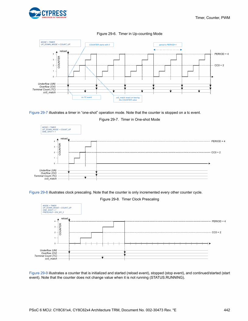
PSoC 6 MCU: CY8C61x4, CY8C62x4 Architecture TRM, Document No. 002-30473 Rev. *E 442
Timer, Counter, PWM
Figure 29-6. Timer in Up-counting Mode
Figure 29-7 illustrates a timer in “one-shot” operation mode. Note that the counter is stopped on a tc event.
Figure 29-7. Timer in One-shot Mode
Figure 29-8 illustrates clock prescaling. Note that the counter is only incremented every other counter cycle.
Figure 29-8. Timer Clock Prescaling
Figure 29-9 illustrates a counter that is initialized and started (reload event), stopped (stop event), and continued/started (startevent). Note that the counter does not change value when it is not running (STATUS.RUNNING).
cc0_match
Underflow (UN)Overflow (OV)
Terminal Count (TC)
CO
UN
TE
R
PERIOD = 4
CC0 = 2
MODE = TIMERUP_DOWN_MODE = COUNT_UP
4
3
2
1
0
COUNTER starts with 0 period is PERIOD+1
reload
no TC event cc0_match event on leaving the COUNTER value
CO
UN
TE
R
PERIOD = 4
CC0 = 2
MODE = TIMERUP_DOWN_MODE = COUNT_UPONE_SHOT = 1
4
3
2
1
0
reload
cc0_match
Underflow (UN)Overflow (OV)
Terminal Count (TC)
CO
UN
TE
R
PERIOD = 4
CC0 = 2
MODE = TIMERUP_DOWN_MODE = COUNT_UPONE_SHOT = 1PRESCALE = DIV_BY_2
4
3
2
1
0
reload
cc0_match
Underflow (UN)Overflow (OV)
Terminal Count (TC)

PSoC 6 MCU: CY8C61x4, CY8C62x4 Architecture TRM, Document No. 002-30473 Rev. *E 443
Timer, Counter, PWM
Figure 29-9. Counter Start/Stopped/Continued
Figure 29-10 illustrates a timer that uses CC0/1 and CC0/1_BUFF registers. Note that CC0/1 and CC0/1_BUFF registercontents are exchanged on a cc0/1_match event.
Figure 29-10. Use of CC0 and CC0_BUFF Register Bits
Figure 29-11 illustrates a timer in down-counting mode. The counter is initialized (to PERIOD) and started with asoftware-based reload event.
Notes:
■ When the counter changes from a state in which COUNTER is 0, an underflow and tc event are generated.
■ When the counter changes from a state in which COUNTER is 2, a cc0_match event is generated.
■ PERIOD is 4, resulting in an effective repeating counter pattern of 4+1 = 5 counter clock periods.
CO
UN
TE
RPERIOD = 4
CC0 = 2
MODE = TIMERUP_DOWN_MODE = COUNT_UP
4
3
2
1
0
RUNNING
cc0_match
Underflow (UN)Overflow (OV)
Terminal Count (TC)
reloadstopstart
CO
UN
TE
R
PERIOD = 4
MODE = TIMERUP_DOWN_MODE = COUNT_UPAUTO_RELOAD_CC0 = 1
4
3
2
1
0
reload 03 CC030 CC0_BUFF
30
03
30
03
30
03
30
03
cc0_match
Underflow (UN)Overflow (OV)
Terminal Count (TC)

PSoC 6 MCU: CY8C61x4, CY8C62x4 Architecture TRM, Document No. 002-30473 Rev. *E 444
Timer, Counter, PWM
Figure 29-11. Timer in Down-counting Mode
Figure 29-12 illustrates a timer in up/down counting mode 1. The counter is initialized (to 1) and started with a software-basedreload event.
Notes:
■ When the counter changes from a state in which COUNTER is 4, an overflow is generated.
■ When the counter changes from a state in which COUNTER is 0, an underflow and tc event are generated.
■ When the counter changes from a state in which COUNTER is 2, a cc0_match event is generated.
■ PERIOD is 4, resulting in an effective repeating counter pattern of 2 × 4 = 8 counter clock periods.
Figure 29-12. Timer in Up/Down Counting Mode 1
Figure 29-13 illustrates a timer in up/down counting mode 1, with different CC values.
Notes:
■ When CC0 is 0, the cc0_match event is generated at the start of the period (when the counter changes from a state in which COUNTER is 0).
■ When CC0 is PERIOD, the cc0_match event is generated at the middle of the period (when the counter changes from a state in which COUNTER is PERIOD).
cc0_match
Underflow (UN)Overflow (OV)
Terminal Count (TC)
CO
UN
TE
R
PERIOD = 4
CC0 = 2
MODE = TIMERUP_DOWN_MODE = COUNT_DOWN
4
3
2
1
0
COUNTER starts with PERIOD period is PERIOD+1
reload
no TC event CC0 event on leaving the COUNTER value
cc0_match
Underflow (UN)Overflow (OV)
Terminal Count (TC)
CO
UN
TE
R
PERIOD = 4
CC0 = 2
MODE = TIMERUP_DOWN_MODE = COUNT_UPDN1
4
3
2
1
0
COUNTER starts with 1 period is 2*PERIOD
reload
no TC event cc0_match event on leaving the COUNTER value
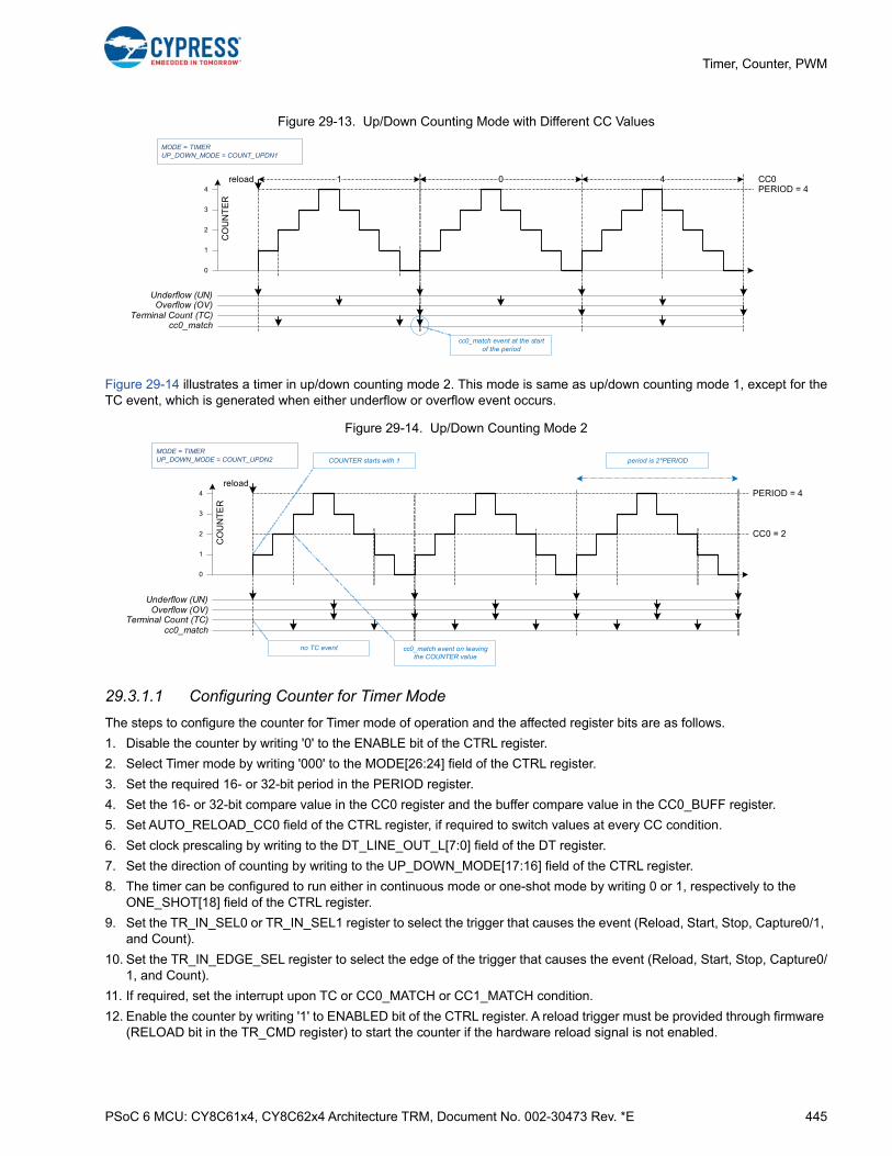
PSoC 6 MCU: CY8C61x4, CY8C62x4 Architecture TRM, Document No. 002-30473 Rev. *E 445
Timer, Counter, PWM
Figure 29-13. Up/Down Counting Mode with Different CC Values
Figure 29-14 illustrates a timer in up/down counting mode 2. This mode is same as up/down counting mode 1, except for theTC event, which is generated when either underflow or overflow event occurs.
Figure 29-14. Up/Down Counting Mode 2
29.3.1.1 Configuring Counter for Timer Mode
The steps to configure the counter for Timer mode of operation and the affected register bits are as follows.
1. Disable the counter by writing '0' to the ENABLE bit of the CTRL register.
2. Select Timer mode by writing '000' to the MODE[26:24] field of the CTRL register.
3. Set the required 16- or 32-bit period in the PERIOD register.
4. Set the 16- or 32-bit compare value in the CC0 register and the buffer compare value in the CC0_BUFF register.
5. Set AUTO_RELOAD_CC0 field of the CTRL register, if required to switch values at every CC condition.
6. Set clock prescaling by writing to the DT_LINE_OUT_L[7:0] field of the DT register.
7. Set the direction of counting by writing to the UP_DOWN_MODE[17:16] field of the CTRL register.
8. The timer can be configured to run either in continuous mode or one-shot mode by writing 0 or 1, respectively to the ONE_SHOT[18] field of the CTRL register.
9. Set the TR_IN_SEL0 or TR_IN_SEL1 register to select the trigger that causes the event (Reload, Start, Stop, Capture0/1, and Count).
10. Set the TR_IN_EDGE_SEL register to select the edge of the trigger that causes the event (Reload, Start, Stop, Capture0/1, and Count).
11. If required, set the interrupt upon TC or CC0_MATCH or CC1_MATCH condition.
12. Enable the counter by writing '1' to ENABLED bit of the CTRL register. A reload trigger must be provided through firmware (RELOAD bit in the TR_CMD register) to start the counter if the hardware reload signal is not enabled.
MODE = TIMERUP_DOWN_MODE = COUNT_UPDN1
CO
UN
TE
R
PERIOD = 4CC0
4
3
2
1
0
1 0 4reload
cc0_match
Underflow (UN)Overflow (OV)
Terminal Count (TC)
cc0_match event at the start of the period
cc0_match
Underflow (UN)Overflow (OV)
Terminal Count (TC)
CO
UN
TE
R
PERIOD = 4
CC0 = 2
MODE = TIMERUP_DOWN_MODE = COUNT_UPDN2
4
3
2
1
0
COUNTER starts with 1 period is 2*PERIOD
reload
no TC event cc0_match event on leaving the COUNTER value

PSoC 6 MCU: CY8C61x4, CY8C62x4 Architecture TRM, Document No. 002-30473 Rev. *E 446
Timer, Counter, PWM
29.3.2 Capture Mode
The capture functionality increments and decrements a counter between 0 and PERIOD. When the capture event is activatedthe counter value COUNTER is copied to CC0/1 (and CC0/1 is copied to CC0/1_BUFF).
The capture functionality can be used to measure the width of a pulse (connected as one of the input triggers and used ascapture event).
The capture event can be triggered through the capture trigger input or through a firmware write to CAPTURE0/1 bit in theTR_CMD command register.
Table 29-19. Capture Mode Trigger Input Description
Generated Events Usage
Reload
Sets the counter value and starts the counter. Behavior is dependent on UP_DOWN_MODE:
■ COUNT_UP: The counter is set to ‘0’ and count direction is set to ‘up’.
■ COUNT_DOWN: The counter is set to PERIOD and count direction is set to ‘down’.
■ COUNT_UPDN1/2: The counter is set to ‘1’ and count direction is set to ‘up’.
Can be used when the counter is running or not running.
Start
Starts the counter. The counter is not initialized by hardware. The current counter value is used. Behavior is dependent on UP_DOWN_MODE:
■ COUNT_UP: The count direction is set to ‘up’.
■ COUNT_DOWN: The count direction is set to ‘down’.
■ COUNT_UPDN1/2: The count direction is not modified.
Note that when the counter is running, the start event has no effect.
Can be used when the counter is running or not running.
Stop Stops the counter.
Count Count event increments/decrements the counter.
Capture0 Copies the counter value to CC0 and copies CC0 to CC0_BUFF.
Capture1 Copies the counter value to CC1 and copies CC1 to CC1_BUFF.
Table 29-20. Supported Features of CAPTURE
Supported Features Description
Clock prescaling Prescales the clk_counter.
One shot
Counter is stopped by hardware, after a single period of the counter:
■ COUNT_UP: on an overflow event.
■ COUNT_DOWN, COUNT_UPDN1/2: on an underflow event.
Up/down modes
Specified by UP_DOWN_MODE:
■ COUNT_UP: The counter counts from 0 to PERIOD.
■ COUNT_DOWN: The counter counts from PERIOD to 0.
■ COUNT_UPDN1/2: The counter counts from 1 to PERIOD and back to 0.
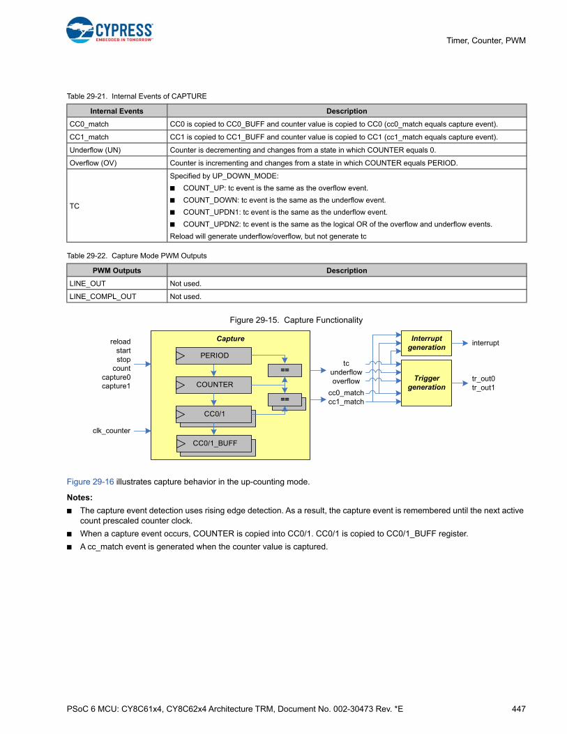
PSoC 6 MCU: CY8C61x4, CY8C62x4 Architecture TRM, Document No. 002-30473 Rev. *E 447
Timer, Counter, PWM
Figure 29-15. Capture Functionality
Figure 29-16 illustrates capture behavior in the up-counting mode.
Notes:
■ The capture event detection uses rising edge detection. As a result, the capture event is remembered until the next active count prescaled counter clock.
■ When a capture event occurs, COUNTER is copied into CC0/1. CC0/1 is copied to CC0/1_BUFF register.
■ A cc_match event is generated when the counter value is captured.
Table 29-21. Internal Events of CAPTURE
Internal Events Description
CC0_match CC0 is copied to CC0_BUFF and counter value is copied to CC0 (cc0_match equals capture event).
CC1_match CC1 is copied to CC1_BUFF and counter value is copied to CC1 (cc1_match equals capture event).
Underflow (UN) Counter is decrementing and changes from a state in which COUNTER equals 0.
Overflow (OV) Counter is incrementing and changes from a state in which COUNTER equals PERIOD.
TC
Specified by UP_DOWN_MODE:
■ COUNT_UP: tc event is the same as the overflow event.
■ COUNT_DOWN: tc event is the same as the underflow event.
■ COUNT_UPDN1: tc event is the same as the underflow event.
■ COUNT_UPDN2: tc event is the same as the logical OR of the overflow and underflow events.
Reload will generate underflow/overflow, but not generate tc
Table 29-22. Capture Mode PWM Outputs
PWM Outputs Description
LINE_OUT Not used.
LINE_COMPL_OUT Not used.
Capture
==
reloadstartstop
countcapture0capture1
clk_counter
COUNTER
PERIOD
==
CC0/1
CC0/1_BUFF
==
tcunderflowoverflow Trigger
generationtr_out0tr_out1
Interrupt generation
interrupt
cc0_matchcc1_match

PSoC 6 MCU: CY8C61x4, CY8C62x4 Architecture TRM, Document No. 002-30473 Rev. *E 448
Timer, Counter, PWM
Figure 29-16. Capture in Up-Counting Mode
When multiple capture events are detected before the next active count prescaled counter clock, capture events are treatedas follows:
■ In the rising edge and falling edge modes, multiple events are effectively reduced to a single event.
■ In the rising/falling edge mode, an even number of events is not detected and an odd number of events is reduced to a single event.
This behavior is illustrated by Figure 29-17, in which a prescaler by a factor of 4 is used.
Figure 29-17. Multiple Events Detected before Active Count
29.3.2.1 Configuring Counter for Capture Mode
The steps to configure the counter for Capture mode operation and the affected register bits are as follows.
1. Disable the counter by writing '0' to the ENABLE bit of the CTRL register.
2. Select Capture mode by writing '010' to the MODE[26:24] field of the CTRL register.
3. Set the required 16-bit period in the PERIOD register.
4. Set clock prescaling by writing to the DT_LINE_OUT_L[17:16] field of the DT register.
5. Set the direction of counting by writing to the UP_DOWN_MODE[17:16] field of the CTRL register.
6. Counter can be configured to run either in continuous mode or one-shot mode by writing 0 or 1, respectively to the ONE_SHOT[18] field of the CTRL register.
7. Set the TR_IN_SEL0 or TR_IN_SEL1 register to select the trigger that causes the event (Reload, Start, Stop, Capture0/1, and Count).
CO
UN
TE
R
PERIOD = 4
MODE = CAPTUREUP_DOWN_MODE = COUNT_UPCAPTURE_EDGE = RISING_EDGE
4
3
2
1
0
reload
CC0CC0_BUFF
1 41
capture
34
cc0_match
Underflow (UN)Overflow (OV)
Terminal Count (TC)
missed capture event
CO
UN
TE
R
PERIOD = 4
MODE = CAPTUREUP_DOWN_MODE = COUNT_UPCAPTURE_EDGE = RISING_EDGE
4
3
2
1
0
reload
CC0CC0_BUFF
1
capture
31
cc0_match
Underflow (UN)Overflow (OV)
Terminal Count (TC)

PSoC 6 MCU: CY8C61x4, CY8C62x4 Architecture TRM, Document No. 002-30473 Rev. *E 449
Timer, Counter, PWM
8. Set the TR_IN_EDGE_SEL register to select the edge that causes the event (Reload, Start, Stop, Capture0/1, and Count).
9. If required, set the interrupt upon TC or CC0_MATCH or CC1_MATCH condition.
10. Enable the counter by writing '1' to the ENABLED bit in CTRL register. A reload trigger must be provided through firmware (RELOAD bit in TR_CMD register) to start the counter if the hardware reload signal is not enabled.
29.3.3 Quadrature Decoder Mode
Quadrature functionality increments and decrements a counter between 0 and 0xFFFF or 0xFFFFFFFF (32-bit mode) orPERIOD (depending on QUAD_RANGE_MODE). Counter updates are under control of quadrature signal inputs: index, phiA,and phiB. The index input is used to indicate an absolute position. The phiA and phiB inputs are used to determine a changein position (the rate of change in position can be used to derive speed).
Table 29-23 shows an overview of supported range modes, which varies between different maximum counter values usescapture and compare functionalities.
The quadrature inputs are mapped onto triggers (as described in Table 29-24).
Table 29-23. Quadrature Mode Functionality Overview
Supported Range Modes (QUAD_RANGE_MODE)
Description
QUAD_RANGE0 Counter range is between 0x0000 and 0xFFFF/0xFFFFFFFF (32-bit mode).
QUAD_RANGE0_CMPCounter range is between 0x0000 and 0xFFFF/0xFFFFFFFF (32-bit mode). In this mode a compare function is supported during quadrature decoding using the CC0/CC0_BUFF (CC1/CC1_BUFF) registers and the cc0_match (cc1_match) event.
QUAD_RANGE1_CMPThe compare functionality is the same as for QUAD_RANGE0_CMP mode. The counter range can be set between 0x0000 and PERIOD.
QUAD_RANGE1_CAPTCounter range is between 0x0000 and PERIOD. Quadrature functionality in QUAD_RANGE1_CAPT mode provides the same functionality as the QUAD_RANGE1_CMP mode with the only difference that 1 or 2 capture functions are available instead of 1 or 2 compare functions.
Table 29-24. Quadrature Mode Trigger Input Description
Trigger Input Usage
reload/index
This event acts as a quadrature index input. It initializes the counter to the counter midpoint 0x8000 (16-bit) or 0x8000000 (32-bit mode) and starts the quadrature functionality. Rising edge event detection or falling edge detection mode must be used.
■ QUAD_RANGE0: initialize counter to 0x8000/0x80000000 (midpoint)
■ QUAD_RANGE0_CMP: initialize counter to 0x8000/0x80000000 (midpoint)
■ QUAD_RANGE1_CMP: initialize counter to 0.
■ QUAD_RANGE1_CAPT: initialize counter to 0.
start/phiBThis event acts as a quadrature phiB input. Pass-through (no edge detection) event detection mode must be used for X1, X2, or X4.
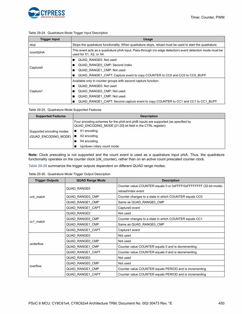
PSoC 6 MCU: CY8C61x4, CY8C62x4 Architecture TRM, Document No. 002-30473 Rev. *E 450
Timer, Counter, PWM
Note: Clock prescaling is not supported and the count event is used as a quadrature input phiA. Thus, the quadraturefunctionality operates on the counter clock (clk_counter), rather than on an active count prescaled counter clock.
Table 29-26 summarize the trigger outputs dependent on different QUAD range modes.
stop Stops the quadrature functionality. When quadrature stops, reload must be used to start the quadrature.
count/phiAThis event acts as a quadrature phiA input. Pass-through (no edge detection) event detection mode must be used for X1, X2, or X4.
Capture0
■ QUAD_RANGE0: Not used
■ QUAD_RANGE0_CMP: Second index
■ QUAD_RANGE1_CMP: Not used.
■ QUAD_RANGE1_CAPT: Capture event to copy COUNTER to CC0 and CC0 to CC0_BUFF.
Capture1
Available only in counter groups with second capture function.
■ QUAD_RANGE0: Not used
■ QUAD_RANGE0_CMP: Not used
■ QUAD_RANGE1_CMP: Not used.
■ QUAD_RANGE1_CAPT: Second capture event to copy COUNTER to CC1 and CC1 to CC1_BUFF.
Table 29-25. Quadrature Mode Supported Features
Supported Features Description
Supported encoding modes
(QUAD_ENCODING_MODE)
Four encoding schemes for the phiA and phiB inputs are supported (as specified by QUAD_ENCODING_MODE [21:20] bit field in the CTRL register):
■ X1 encoding.
■ X2 encoding.
■ X4 encoding.
■ Up/down rotary count mode
Table 29-26. Quadrature Mode Trigger Output Description
Trigger Outputs QUAD Range Mode Description
cc0_match
QUAD_RANGE0Counter value COUNTER equals 0 or 0xFFFF/0xFFFFFFFF (32-bit mode)
reload/index event
QUAD_RANGE0_CMP Counter changes to a state in which COUNTER equals CC0
QUAD_RANGE1_CMP Same as QUAD_RANGE0_CMP
QUAD_RANGE1_CAPT Capture0 event
cc1_match
QUAD_RANGE0 Not used
QUAD_RANGE0_CMP Counter changes to a state in which COUNTER equals CC1
QUAD_RANGE1_CMP Same as QUAD_RANGE0_CMP
QUAD_RANGE1_CAPT Capture1 event
underflow
QUAD_RANGE0 Not used
QUAD_RANGE0_CMP Not used
QUAD_RANGE1_CMP Counter value COUNTER equals 0 and is decrementing
QUAD_RANGE1_CAPT Counter value COUNTER equals 0 and is decrementing
overflow
QUAD_RANGE0 Not used
QUAD_RANGE0_CMP Not used
QUAD_RANGE1_CMP Counter value COUNTER equals PERIOD and is incrementing
QUAD_RANGE1_CAPT Counter value COUNTER equals PERIOD and is incrementing
Table 29-24. Quadrature Mode Trigger Input Description
Trigger Input Usage

PSoC 6 MCU: CY8C61x4, CY8C62x4 Architecture TRM, Document No. 002-30473 Rev. *E 451
Timer, Counter, PWM
Counter increments (incr1 event) and decrements (decr1 event) are determined by the quadrature encoding scheme asillustrated by Figure 29-18.
Figure 29-18. Quadrature Mode Waveforms (X1, X2, and X4 mode)
Note: The x1 encoding scheme is identical to the up/down counting functionality as follows: Rising edges of input phiAincrement or decrement the counter depending on the state of input phiB (direction input).
With UP_DOWN encoding (up/down rotary count mode) the counter is incremented by phiA and decremented by phiB asillustrated by Figure 29-19.
Figure 29-19. Up/down Rotary Mode
The state of phiA/phiB determines the increment/decrement according to settings of the encoding mode; the phiA/phiB isdetected by counter clock. The increment/decrement occurs at the next counter clock rising edge after edges of phiA/phiB.For example, the condition of increment in X1 mode is, at the first counter clock rising edge, the phiA is low, at the second
tc
QUAD_RANGE0 Index event
QUAD_RANGE0_CMP
Counter value COUNTER equals 0 or 0xFFFF/0xFFFFFFFF
Index or capture on index event (specified by AUTO_RELOAD_PERIOD in the CTRL register)
QUAD_RANGE1_CMP
Counter value COUNTER equals 0 and is decrementing (underflow) or PERIOD and is incrementing (overflow)
Index event
QUAD_RANGE1_CAPT Same as QUAD_RANGE1_CMP
Table 29-27. Quadrature Mode PWM Outputs
PWM Outputs Description
LINE_OUT Not used.
LINE_COMPL_OUT Not used.
Table 29-26. Quadrature Mode Trigger Output Description
Trigger Outputs QUAD Range Mode Description
phiA
phiB
incr1
Quadrature decodingQUADRATURE_MODE = X1
decr1
incr1
Quadrature decodingQUADRATURE_MODE = X2
decr1
incr1
Quadrature decodingQUADRATURE_MODE = X4
decr1
Two times the events of X1 mode
Four times the events of X1 mode
phiA
phiB
incr1
Up/down rotary counting modeQUAD_ENCODING_MODE = UP_DOWNCOUNT_EDGE (phA edge) = RISING_EDGESTART_EDGE (phiB edge) = RISING_EDGE
decr1
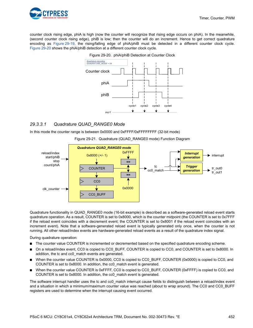
PSoC 6 MCU: CY8C61x4, CY8C62x4 Architecture TRM, Document No. 002-30473 Rev. *E 452
Timer, Counter, PWM
counter clock rising edge, phiA is high (now the counter will recognize that rising edge occurs on phiA). In the meanwhile,(second counter clock rising edge), phiB is low; then the counter will do an increment. Hence to get correct quadratureencoding as Figure 29-19, the rising/falling edge of phiA/phiB must be detected in a different counter clock cycle.Figure 29-20 shows the phiA/phiB detection at a different counter clock cycle.
Figure 29-20. phiA/phiB Detection at Counter Clock
29.3.3.1 Quadrature QUAD_RANGE0 Mode
In this mode the counter range is between 0x0000 and 0xFFFF/0xFFFFFFFF (32-bit mode)
Figure 29-21. Quadrature (QUAD_RANGE0 mode) Function Diagram
Quadrature functionality in QUAD_RANGE0 mode (16-bit example) is described as a software-generated reload event startsquadrature operation. As a result, COUNTER is set to 0x8000, which is the counter midpoint (the COUNTER is set to 0x7FFFif the reload event coincides with a decrement event; the COUNTER is set to 0x8001 if the reload event coincides with anincrement event). Note that a software-generated reload event is typically generated only once, when the counter is notrunning. All other reload/index events are hardware-generated reload events as a result of the quadrature index signal.
During quadrature operation:
■ The counter value COUNTER is incremented or decremented based on the specified quadrature encoding scheme.
■ On a reload/index event, CC0 is copied to CC0_BUFF, COUNTER is copied to CC0, and COUNTER is set to 0x8000. In addition, the tc and cc0_match events are generated.
■ When the counter value COUNTER is 0x0000, CC0 is copied to CC0_BUFF, COUNTER (0x0000) is copied to CC0, and COUNTER is set to 0x8000. In addition, the cc0_match event is generated.
■ When the counter value COUNTER is 0xFFFF, CC0 is copied to CC0_BUFF, COUNTER (0xFFFF) is copied to CC0, and COUNTER is set to 0x8000. In addition, the cc0_match event is generated.
The software interrupt handler uses the tc and cc0_match interrupt cause fields to distinguish between a reload/index eventand a situation in which a minimum/maximum counter value was reached (about to wrap around). The CC0 and CC0_BUFFregisters are used to determine when the interrupt causing event occurred.
cycle1 cycle2 cycle3
Counter clock
phiA
phiB
incr1
Quadrature decodingQUADRATURE_MODE = X4
cycle4
Quadrature QUAD_RANGE0 mode
reload/indexstart/phiB
stopcount/phiA
clk_counter
COUNTER
0x8000 (+/- 1)
==
CC0
CC0_BUFF
==
0xFFFF
0x0000
tr_out0tr_out1
Interrupt generation
interrupt
tccc0_match
Trigger generation

PSoC 6 MCU: CY8C61x4, CY8C62x4 Architecture TRM, Document No. 002-30473 Rev. *E 453
Timer, Counter, PWM
Note that a counter increment/decrement can coincide with a reload/index/tc event or with a situation cc0_match event.Under these circumstances, the counter value is set to either 0x8000+1 (increment) or 0x8000-1 (decrement).
Figure 29-22 illustrates quadrature functionality as a function of the reload/index, incr1, and decr1 events. Note that the firstreload/index event copies the counter value COUNTER to CC0.
Figure 29-22. Overflow Coincides with Increment
Figure 29-23 to Figure 29-25 illustrate quadrature functionality for different event scenarios (including scenarios withcoinciding events). In all scenarios, the first reload/index event is generated by software when the counter is not yet running.
Figure 29-23. Underflow Coincides with Decrement
Figure 29-24. Underflow Coincides with Increment and Overflow Coincides with Decrement
0x8000COUNTER
incr1decr1
Reload / Index
CC0
CC0_BUFF
cc0_matchtc
X 0x8001 0x8002 0x8003
counter cycle
0xfffe 0xffff 0x8001 0xfffe 0xffff 0x8000
0xffff 0xffff
0xffff
X
Y X
0xffff
X
Quadrature decodingQUAD_RANGE_MODE = QUAD_RANGE0increment behavior, no coinciding reload and increment events
overflow without incr1 eventoverflow with incr1 event
RUNNING
XY
YZ
0x8000COUNTER
incr1decr1
Reload / Index
CC0
CC0_BUFF
cc0_matchtc
X 0x7fff 0x7ffe 0x7ffd
counter cycle
0x0001 0x0000 0x7fff 0x0001 0x0000 0x8000
0x0000 0x0000
0x0000
0x0000
Quadrature decodingQUAD_RANGE_MODE = QUAD_RANGE0decrement behavior, no coinciding reload and decrement events
underflow without decr1 eventunderflow with decr1 event
RUNNING
X
Y X X
XY
YZ
0x8000COUNTER
incr1decr1
Reload / Index
CC0
CC0_BUFF
cc0_matchtc
X 0x7fff 0x7ffe 0x7ffd
counter cycle
0x0001 0x0000 0x8001
0x0000
Quadrature decodingQUAD_RANGE_MODE = QUAD_RANGE0decrement/increment behavior, no coinciding reload events
overflow with decr1 eventunderflow with incr1 event
0xfffe 0xffff 0x7fff
0xffff
0x0000
0x0000
RUNNING
X
Y X X
XY
YZ
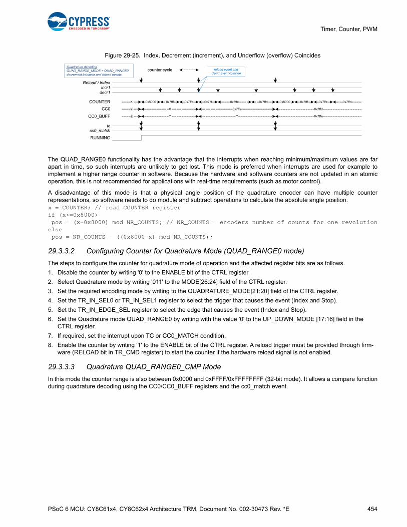
PSoC 6 MCU: CY8C61x4, CY8C62x4 Architecture TRM, Document No. 002-30473 Rev. *E 454
Timer, Counter, PWM
Figure 29-25. Index, Decrement (increment), and Underflow (overflow) Coincides
The QUAD_RANGE0 functionality has the advantage that the interrupts when reaching minimum/maximum values are farapart in time, so such interrupts are unlikely to get lost. This mode is preferred when interrupts are used for example toimplement a higher range counter in software. Because the hardware and software counters are not updated in an atomicoperation, this is not recommended for applications with real-time requirements (such as motor control).
A disadvantage of this mode is that a physical angle position of the quadrature encoder can have multiple counterrepresentations, so software needs to do module and subtract operations to calculate the absolute angle position.x = COUNTER; // read COUNTER registerif (x>=0x8000) pos = (x-0x8000) mod NR_COUNTS; // NR_COUNTS = encoders number of counts for one revolutionelse pos = NR_COUNTS - ((0x8000-x) mod NR_COUNTS);
29.3.3.2 Configuring Counter for Quadrature Mode (QUAD_RANGE0 mode)
The steps to configure the counter for quadrature mode of operation and the affected register bits are as follows.
1. Disable the counter by writing '0' to the ENABLE bit of the CTRL register.
2. Select Quadrature mode by writing '011' to the MODE[26:24] field of the CTRL register.
3. Set the required encoding mode by writing to the QUADRATURE_MODE[21:20] field of the CTRL register.
4. Set the TR_IN_SEL0 or TR_IN_SEL1 register to select the trigger that causes the event (Index and Stop).
5. Set the TR_IN_EDGE_SEL register to select the edge that causes the event (Index and Stop).
6. Set the Quadrature mode QUAD_RANGE0 by writing with the value '0' to the UP_DOWN_MODE [17:16] field in the CTRL register.
7. If required, set the interrupt upon TC or CC0_MATCH condition.
8. Enable the counter by writing '1' to the ENABLE bit of the CTRL register. A reload trigger must be provided through firm-ware (RELOAD bit in TR_CMD register) to start the counter if the hardware reload signal is not enabled.
29.3.3.3 Quadrature QUAD_RANGE0_CMP Mode
In this mode the counter range is also between 0x0000 and 0xFFFF/0xFFFFFFFF (32-bit mode). It allows a compare functionduring quadrature decoding using the CC0/CC0_BUFF registers and the cc0_match event.
0x8000COUNTER
incr1decr1
Reload / Index
CC0
CC0_BUFF
cc0_matchtc
X
Y
Z
0x7fff 0x7ffe 0x7fff
counter cycleQuadrature decodingQUAD_RANGE_MODE = QUAD_RANGE0decrement behavior and reload events
0x7ffe 0x7ffd 0x8000
0x7ffd0x7ffe
Y 0x7ffe
0x7fff 0x7ffe 0x7ffd
reload event anddecr1 event coincide
RUNNING
X
Y

PSoC 6 MCU: CY8C61x4, CY8C62x4 Architecture TRM, Document No. 002-30473 Rev. *E 455
Timer, Counter, PWM
Figure 29-26. Quadrature (QUAD_RANGE0_CMP mode) Function Diagram
Quadrature functionality in QUAD_RANGE0_CMP mode provides the same functionality as the QUAD_RANGE0 mode,except for the following differences:
■ PERIOD and PERIOD_BUFF are used instead of CC0 and CC0_BUFF to capture the counter value when a reload/index event occurs or the minimum/maximum value is reached (about to wrap around).
❐ When the 'capture on index' function is selected (via overloaded AUTO_RELOAD_PERIOD bit) and a reload/index event occurs, PERIOD is copied to PERIOD_BUFF, COUNTER is copied to PERIOD, and COUNTER is set to 0x8000. In addition, the tc event is generated.
❐ When the 'capture on wrap-around' function is selected (via overloaded AUTO_RELOAD_PERIOD bit) and the counter value COUNTER is 0x0000 or 0xFFFF, PERIOD is copied to PERIOD_BUFF, COUNTER (0x0000 or 0xFFFF) is copied to PERIOD, and COUNTER is set to 0x8000. In addition, the tc event is generated.
■ Capture0 can be used as the second index event. This event acts as a second quadrature index input. It has the same function as the reload/index0 event. Both events are OR combined.
■ CC0 (CC1) and CC0_BUFF (CC1_BUFF) are used for compare functionality.
❐ A cc0_match (cc1_match) event is generated when the counter changes to a state in which COUNTER equals CC0 (CC1).
❐ CC0 (CC1) and CC0_BUFF (CC1_BUFF) are exchanged on a cc0_match (cc1_match) event (when specified by AUTO_RELOAD_CC bit).
Note that 'capture on index' and 'capture on wraparound' functions are separated to prevent PERIOD and PERIOD_BUFFfrom being overwritten before software has read them in case a wraparound is followed by multiple index events in a shorttime (quadrature encoder is moved back and forth around its index point). If both functions are needed, the two counters canbe used synchronously (or a counter group, which includes two compare functions) in QUAD_RANGE0_CMP mode, one with'capture on index', the other with 'capture on wraparound' behavior selected. Note also that multiple compare values can berealized by multiple synchronous counters in QUAD_RANGE0_CMP mode with different CC0 values. Except the differencesmentioned above, the QUAD_RANGE0_CMP mode behaves as the QUAD_RANGE0 mode including behavior withcoinciding events. Figure 29-27 illustrates an example scenario with decrementing counter and additional comparefunctionality.
Quadrature QUAD_RANGE0_CMP mode
==
reload/index0start/phiB
stopcount/phiA
capture0/index1
clk_counter
COUNTER
0x8000 (+/- 1)
==
CC0/1
CC0/1_BUFF
==
0x0000
PERIOD
PERIOD_BUFF
==
tctr_out0tr_out1
Interrupt generation
interrupt
cc0_matchcc1_match
Trigger generation
0xffff

PSoC 6 MCU: CY8C61x4, CY8C62x4 Architecture TRM, Document No. 002-30473 Rev. *E 456
Timer, Counter, PWM
Figure 29-27. Quadrature (QUAD_RANGE0_CMP) Operation
The QUAD_RANGE0_CMP functionality still allows a similar interrupt usage as in QUAD_RANGE0 mode. Additionally itsupports one or two compare functions. More compare functions can be reached with multiple synchronously runningcounters in QUAD_RANGE0_CMP mode. These compare functions can be for example used for a position compare. As inQUAD_RANGE0 mode there is the disadvantage that a physical angle position of the quadrature encoder can have multiplecounter representations, so software needs to do module and subtract operations to calculate the absolute angle position. InQUAD_RANGE0_CMP mode this software operation can be simplified using two compare functions; for example, by settingCC0 = 0x8000 + NR_COUNTS and CC1 = 0x8000 - NR_COUNTS, and feeding back the cc0/1_match events back into theTCPWM counter as index0/1 events using peripheral trigger multiplexers. This sets the counter back to its midpoint whenreaching CC0 or CC1 value (after up to three CLK_PERI cycles for synchronization). This way the module operation can besaved in software when calculating the absolute angle position:x = COUNTER; // read COUNTER register if (x>=0x8000) pos = x-0x8000; else pos = x - CC1;
This is much less software overhead than in QUAD_RANGE0 mode; however, software is still involved. A DMA copy of theabsolute angle position, for example, to send a buffer of CAN/UART/field bus interface to synchronize with other devices isnot possible. This can only be supported when the counter represents the absolute angle position, as done in theQUAD_RANGE1_CAPT and QUAD_RANGE1_CMP modes.
0x8000COUNTER
incr1decr1
Reload / Index
PERIOD
PERIOD_BUFF
cc0_matchtc
X
Y
Z
0x7fff 0x7ffe 0x7fff
counter cycle
Quadrature decodingQUAD_RANGE_MODE = QUAD_RANGE0_CMPdecrement behavior and reload eventscapture on index = 1 (AUTO_RELOAD_RERIOD)AUTO_RELOAD_CC = 1
0x7ffe 0x7ffd 0x8000
0x7ffd0x7ffe
X 0x7ffe
0x7fff 0x7ffe 0x7ffd
reload event and decr1 event coincide
RUNNING
X
Y
CC0
CC0_BUFF
0x7ffe0x7ffd0x7ffe
0x7ffd 0x7ffe
0x7ffe 0x7ffd
0x7ffd0x7ffd 0x7ffe
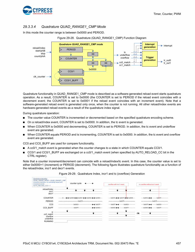
PSoC 6 MCU: CY8C61x4, CY8C62x4 Architecture TRM, Document No. 002-30473 Rev. *E 457
Timer, Counter, PWM
29.3.3.4 Quadrature QUAD_RANGE1_CMP Mode
In this mode the counter range is between 0x0000 and PERIOD.
Figure 29-28. Quadrature (QUAD_RANGE1_CMP) Function Diagram
Quadrature functionality in QUAD_RANGE1_CMP mode is described as a software-generated reload event starts quadratureoperation. As a result, COUNTER is set to 0x0000 (the COUNTER is set to PERIOD if the reload event coincides with adecrement event; the COUNTER is set to 0x0001 if the reload event coincides with an increment event). Note that asoftware-generated reload event is generated only once, when the counter is not running. All other reload/index events arehardware-generated reload events as a result of the quadrature index signal.
During quadrature operation:
■ The counter value COUNTER is incremented or decremented based on the specified quadrature encoding scheme.
■ On a reload/index event, COUNTER is set to 0x0000. In addition, the tc event is generated.
■ When COUNTER is 0x0000 and decrementing, COUNTER is set to PERIOD. In addition, the tc event and underflow event are generated.
■ When COUNTER equals PERIOD and is incrementing, COUNTER is set to 0x0000. In addition, the tc event and overflow event are generated.
CC0 and CC0_BUFF are used for compare functionality.
■ A cc0/1_match event is generated when the counter changes to a state in which COUNTER equals CC0/1.
■ CC0/1 and CC0/1_BUFF are exchanged on a cc0/1_match event (when specified by AUTO_RELOAD_CC bit in the CTRL register).
Note that a counter increment/decrement can coincide with a reload/index/tc event. In this case, the counter value is set toeither 0x0000+1 (increment) or PERIOD (decrement). The following figure illustrates quadrature functionality as a function ofthe reload/index, incr1 and decr1 events.
Figure 29-29. Quadrature Index, incr1 and tc (overflow) Generation
Quadrature QUAD_RANGE1_CMP mode
==
reload/indexstart/phiB
stopcount/phiA
clk_counter
COUNTER
==
CC0/1
CC0/1_BUFF
==
0x0000
PERIOD
==
tcunderflowoverflow
tr_out0tr_out1
Interrupt generation
interrupt
cc0_matchcc1_match
Trigger generation
0x0000COUNTER
incr1decr1
reload/index
CC0
CC0_BUFF
cc0_matchtc
X 0x0001 0x0002 0x0003
counter cycle
0x007e 0x007f 0x0000 0x007e 0x007f
0x00030x007f
0x0003 0x007f
Quadrature decodingQUAD_RANGE_MODE = QUAD_RANGE1_CMPincrement behavior, no coinciding reload and increment eventsAUTO_RELOAD_CC0 = 1
no overflow without incr1 eventoverflow with incr1 event
RUNNING
PERIOD 0x007f 0x007f 0x007f
0x0003
0x007f
0x007f
0x0003
( )
0x00030x007f
0x0003 0x007f
underflowoverflow

PSoC 6 MCU: CY8C61x4, CY8C62x4 Architecture TRM, Document No. 002-30473 Rev. *E 458
Timer, Counter, PWM
The following figures illustrate quadrature functionality for different event scenarios (including scenarios with coincidingevents). In all scenarios, the first reload/index event is generated by software when the counter is not yet running.
Figure 29-30. Quadrature Index, decr1 and tc (underflow) Generation
Figure 29-31. No tc (underflow) after COUNTER = 0x0000 and no tc (overflow) after COUNTER = PERIOD
Figure 29-32. Index, Decrement, Underflow, and cc0_match Coincide
0x0000COUNTER
incr1decr1
reload/index
cc0_matchtc
X 0x007f 0x007e 0x007d
counter cycle
0x0001 0x0000 0x007f 0x0001 0x0000
Quadrature decodingQUAD_RANGE_MODE = QUAD_RANGE1_CMPdecrement behavior, no coinciding reload and decrement eventsAUTO_RELOAD_CC0 = 1
no underflow without decr1 eventunderflow with decr1 event
RUNNING
0x007f 0x007f 0x007fPERIOD
CC0
CC0_BUFF
0x007d0x0000
0x007d 0x0000
0x007d
0x0000
0x0000
0x007d
( )
0x007d0x0000
0x007d 0x0000
underflowoverflow
0x0000COUNTER
incr1decr1
reload/index
cc0_matchtc
X 0x007f 0x007e 0x007d
counter cycle
0x0001 0x0000 0x0001
Quadrature decodingQUAD_RANGE_MODE = QUAD_RANGE1_CMPdecrement/increment behavior, no coinciding reload eventsAUTO_RELOAD_CC0 = 1
no overflow with decr1 eventno underflow with incr1 event
0x007e 0x007f 0x007e
0x007f 0x007f 0x007fPERIOD
CC0
CC0_BUFF
0x007d0x0000
0x007d 0x0000
0x007d
0x0000
0x0000
0x007d
( )
0x0000
0x007d
RUNNINGunderflow
overflow
0x007fCOUNTER
incr1decr1
reload/index
cc0_matchtc
X 0x007e 0x007d 0x007c
counter cycle
Quadrature decodingQUAD_RANGE_MODE = QUAD_RANGE1_CMPDecrement behavior, coinciding reload eventsAUTO_RELOAD_CC0 = 1
0x0001 0x0000 0x007f
Index with dec1 when current counter value is 0x0000
0x0078 0x0077 0x007f
0x007f 0x007f 0x007fPERIOD
CC0
CC0_BUFF
0x00000x007f
0x0000
0x007d
0x007f
0x007f
0x007d
0x0000
0x007f
RUNNINGunderflow
overflow
0x007f
Underflow is generated on index
cc0_match is generated when CC0 is 0x7f.
0x0000SW update

PSoC 6 MCU: CY8C61x4, CY8C62x4 Architecture TRM, Document No. 002-30473 Rev. *E 459
Timer, Counter, PWM
Figure 29-33. Index, Increment, Overflow, and cc0_match Coincide
The QUAD_RANGE1_CMP functionality allows the COUNTER register to reflect the current angle position of the rotaryencoder; that is, no MOD or SUB calculations need to be done in software on the COUNTER value to get the current angleposition. This allows a DMA copy of the current angle position from the COUNTER register; for example, to send a buffer ofCAN/UART/field bus interface to synchronize with other devices. However, a disadvantage of this mode is that fastsequences of tc interrupts can occur (when encoder moves back and forth around start position). It is recommended to notuse the tc interrupt in this mode.
29.3.3.5 Quadrature QUAD_RANGE1_CAPT Mode
In this mode the counter range is also between 0x0000 and PERIOD. Quadrature functionality in QUAD_RANGE1_CAPTmode provides the same functionality as the QUAD_RANGE1_CMP mode with the only difference that one or two capturefunctions are available instead of one or two compare functions.
Figure 29-34. Quadrature (QUAD_RANGE1_CAPT) Function Diagram
Figure 29-35 illustrates an example scenario with decrementing counter and capture functionality.
0x0001COUNTER
incr1decr1
reload/index
cc0_matchtc
X 0x0002 0x0003 0x0004
counter cycle
Quadrature decodingQUAD_RANGE_MODE = QUAD_RANGE1_CMPIncrement behavior, coinciding reload eventsAUTO_RELOAD_CC0 = 1
0x007e 0x007f 0x0001
Index with incr1 whencurrent counter value equals to Period
0x0003 0x0004 0x0001
0x007f 0x007f 0x007fPERIOD
CC0
CC0_BUFF
0x0001
0x0000
0x0003
0x0001
0x0001
0x0003
0x0000
0x0001
RUNNINGunderflow
overflow
Overflow is not generated on index whatever current counter value is.
cc0_match is generated when CC0 is 0x01.
0x0000
0x0000
0x0001
SW update
Quadrature QUAD_RANGE1_CMP mode
==
reload/indexstart/phiB
stopcount/phiA
clk_counter
COUNTER
==
CC0/1
CC0/1_BUFF
==
0x0000
PERIOD
==
tcunderflowoverflow
tr_out0tr_out1
Interrupt generation
interrupt
cc0_matchcc1_match
Trigger generation
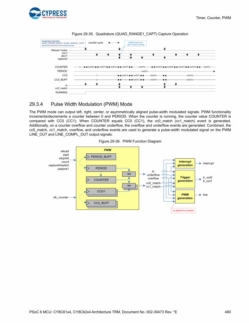
PSoC 6 MCU: CY8C61x4, CY8C62x4 Architecture TRM, Document No. 002-30473 Rev. *E 460
Timer, Counter, PWM
Figure 29-35. Quadrature (QUAD_RANGE1_CAPT) Capture Operation
29.3.4 Pulse Width Modulation (PWM) Mode
The PWM mode can output left, right, center, or asymmetrically aligned pulse-width modulated signals. PWM functionalityincrements/decrements a counter between 0 and PERIOD. When the counter is running, the counter value COUNTER iscompared with CC0 (CC1). When COUNTER equals CC0 (CC1), the cc0_match (cc1_match) event is generated.Additionally, on a counter overflow and counter underflow, the overflow and underflow events are generated. Combined, thecc0_match, cc1_match, overflow, and underflow events are used to generate a pulse-width modulated signal on the PWMLINE_OUT and LINE_COMPL_OUT output signals.
Figure 29-36. PWM Function Diagram
0x0000COUNTER
incr1decr1
Reload / Index
CC0
CC0_BUFF
cc0_matchtc
X
Y
0x007f 0x007e 0x007f
counter cycleQuadrature decodingQUAD_RANGE_MODE = QUAD_RANGE1_CAPTdecrement behavior and reload events
0x007e 0x007d 0x0000
0x007d
0x007f 0x007e 0x007d
reload event and decr1 event coincide
PERIOD 0x007f
0x007e
RUNNING
capture0
0x007e 0x007f
Z 0x007e0x007fY 0x007e
PWMreloadstart
stop/killcount
capture0/switchcapture1
clk_counter
COUNTER
PERIOD
==
PERIOD_BUFF
CC0/1
CC0_BUFF
====
no dead time insertion
PWM generation
line
tcunderflowoverflow Trigger
generationtr_out0tr_out1
Interrupt generation
interrupt
cc0_matchcc1_match

PSoC 6 MCU: CY8C61x4, CY8C62x4 Architecture TRM, Document No. 002-30473 Rev. *E 461
Timer, Counter, PWM
Note that the PWM mode does not support dead time insertion. This functionality is supported by the separate PWM_DTmode.
Table 29-28. PWM Mode Trigger Input Description
Trigger Inputs Usage
reload
Sets the counter value and starts the counter. Behavior is dependent on UP_DOWN_MODE:
■ COUNT_UP: The counter is set to ‘0’ and count direction is set to ‘up’.
■ COUNT_DOWN: The counter is set to PERIOD and count direction is set to ‘down’.
■ COUNT_UPDN1/2: The counter is set to ‘1’ and count direction is set to ‘up’.
Can only be used when the counter is not running.
start
Starts the counter. The counter is not initialized by hardware. The current counter value is used. Behavior is dependent on UP_DOWN_MODE:
■ COUNT_UP: The count direction is set to ‘up’.
■ COUNT_DOWN: The count direction is set to ‘down’.
■ COUNT_UPDN1/2: The count direction is set to ‘up’.
Can only be used when the counter is not running.
stop/kill Stops the counter. Different stop/kill modes exist.
count Count event increments/decrements the counter.
Capture0
This event acts as a switch event. When this event is active, the CC0/CC0_BUFF, CC1/CC1_BUFF, and PERIOD/PERIOD_BUFF registers are exchanged on a tc event (when specified by AUTO_RELOAD_CC bit and AUTO_RELOAD_PERIOD bit in the CTRL register).
A switch event requires rising, falling, or rising/falling edge event detection mode. Pass-through mode is not supported, unless the selected event is a constant '0' or '1'.
When a switch event is detected and the counter is running, the event is kept pending until the next tc event. The switch event will be cleared and has no effect if it is detected when counter is not running.
Capture1 (stop1/kill1)
This event acts as a second stop/kill event. It has the same function as the stop0/kill0 event. Both events are OR combined.
Note: Having two stop/kill events for a PWM allows selecting a common trigger for one stop/kill event from a PERI trigger multiplexer (allowing synchronous stop/kill operation of multiple PWMs) while selecting a dedi-cated ADC out-of-range trigger for the other stop/kill event (allowing real-time hardware stop of a PWM when current PWM driven signal is out of range).
Table 29-29. PWM Mode Supported Features
Supported Features Description
Clock prescaling Prescales the clk_counter.
One shot
Counter is stopped by hardware, after a single period of the counter:
■ COUNT_UP: on an overflow event.
■ COUNT_DOWN and COUNT_UPDN1/2: on an underflow event.
Auto reload CCCC0/1 and CC0/1_BUFF are exchanged on a switch event and tc event (when specified by AUTO_RELOAD_CC bit in CTRL register).
Auto reload PERIOD
PERIOD and PERIOD_BUFF are exchanged on a switch event and tc event (when specified by CTRL.AUTO_RELOAD_PERIOD). Note: When COUNT_UPDN2 mode exchanges PERIOD and PERIOD_BUFF at a tc event that coincides with an overflow event, software should ensure that the PERIOD and PERIOD_BUFF values are the same.
Up/down modes
Specified by UP_DOWN_MODE:
■ COUNT_UP: The counter counts from 0 to PERIOD.
■ COUNT_DOWN: The counter counts from PERIOD to 0.
■ COUNT_UPDN1/2: The counter counts from 1 to PERIOD and back to 0.
Kill modes Specified by PWM_IMM_KILL, PWM_SYNC_KILL, and PWM_STOP_ON_KILL.

PSoC 6 MCU: CY8C61x4, CY8C62x4 Architecture TRM, Document No. 002-30473 Rev. *E 462
Timer, Counter, PWM
Note that the cc0_match event generation in COUNT_UP and COUNT_DOWN modes are different from the generation inother functional modes or counting modes. This is to ensure that 0 percent and 100 percent duty cycles can be generated.
PWM behavior depends on the PERIOD and CC0 registers. Software can update the PERIOD_BUFF and CC0_BUFFregisters, without affecting the PWM behavior. The switch/capture event can be used to switch the values of the compare andbuffered compare registers. It also switches the values of the period and buffered period registers. This is the main rationalefor double buffering these registers. Table 29-32 summarizes the kill mode supported in PWM mode.
Table 29-30. PWM Mode Trigger Output Description
Trigger Output Description
cc0_match
Specified by UP_DOWN_MODE:
■ COUNT_UP and COUNT_DOWN: The counter changes to a state in which COUNTER equals CC0.
■ COUNT_UPDN1/2: counter changes from a state in which COUNTER equals CC0.
cc1_match
Specified by UP_DOWN_MODE:
■ COUNT_UP and COUNT_DOWN: The counter changes to a state in which COUNTER equals CC1.
■ COUNT_UPDN1/2: counter changes from a state in which COUNTER equals CC1.
Underflow (UN)Counter is decrementing and changes from a state in which COUNTER equals 0. Reload event generate underflow in COUNT_DOWN, COUNT_UPDN1, or COUNT_UPDN2 mode.
Overflow (OV)Counter is incrementing and changes from a state in which COUNTER equals PERIOD. Reload event gen-erate overflow in COUNT_UP mode.
tc
Specified by UP_DOWN_MODE:
■ COUNT_UP: tc event is the same as the overflow event.
■ COUNT_DOWN: tc event is the same as the underflow event.
■ COUNT_UPDN1: tc event is the same as the underflow event.
■ COUNT_UPDN2: tc event is the same as the logical OR of the overflow and underflow events.
Reload will generate underflow/overflow, but not the tc output trigger.
Table 29-31. PWM Mode PWM Outputs
PWM Outputs Description
LINE_OUT PWM line output.
LINE_COMPL_OUT Complementary PWM line output.
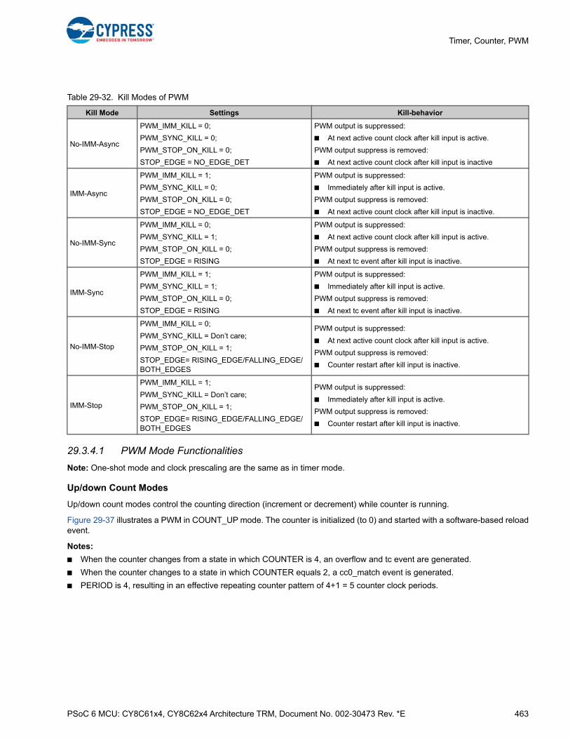
PSoC 6 MCU: CY8C61x4, CY8C62x4 Architecture TRM, Document No. 002-30473 Rev. *E 463
Timer, Counter, PWM
29.3.4.1 PWM Mode Functionalities
Note: One-shot mode and clock prescaling are the same as in timer mode.
Up/down Count Modes
Up/down count modes control the counting direction (increment or decrement) while counter is running.
Figure 29-37 illustrates a PWM in COUNT_UP mode. The counter is initialized (to 0) and started with a software-based reloadevent.
Notes:
■ When the counter changes from a state in which COUNTER is 4, an overflow and tc event are generated.
■ When the counter changes to a state in which COUNTER equals 2, a cc0_match event is generated.
■ PERIOD is 4, resulting in an effective repeating counter pattern of 4+1 = 5 counter clock periods.
Table 29-32. Kill Modes of PWM
Kill Mode Settings Kill-behavior
No-IMM-Async
PWM_IMM_KILL = 0;
PWM_SYNC_KILL = 0;
PWM_STOP_ON_KILL = 0;
STOP_EDGE = NO_EDGE_DET
PWM output is suppressed:
■ At next active count clock after kill input is active.
PWM output suppress is removed:
■ At next active count clock after kill input is inactive
IMM-Async
PWM_IMM_KILL = 1;
PWM_SYNC_KILL = 0;
PWM_STOP_ON_KILL = 0;
STOP_EDGE = NO_EDGE_DET
PWM output is suppressed:
■ Immediately after kill input is active.
PWM output suppress is removed:
■ At next active count clock after kill input is inactive.
No-IMM-Sync
PWM_IMM_KILL = 0;
PWM_SYNC_KILL = 1;
PWM_STOP_ON_KILL = 0;
STOP_EDGE = RISING
PWM output is suppressed:
■ At next active count clock after kill input is active.
PWM output suppress is removed:
■ At next tc event after kill input is inactive.
IMM-Sync
PWM_IMM_KILL = 1;
PWM_SYNC_KILL = 1;
PWM_STOP_ON_KILL = 0;
STOP_EDGE = RISING
PWM output is suppressed:
■ Immediately after kill input is active.
PWM output suppress is removed:
■ At next tc event after kill input is inactive.
No-IMM-Stop
PWM_IMM_KILL = 0;
PWM_SYNC_KILL = Don’t care;
PWM_STOP_ON_KILL = 1;
STOP_EDGE= RISING_EDGE/FALLING_EDGE/BOTH_EDGES
PWM output is suppressed:
■ At next active count clock after kill input is active.
PWM output suppress is removed:
■ Counter restart after kill input is inactive.
IMM-Stop
PWM_IMM_KILL = 1;
PWM_SYNC_KILL = Don’t care;
PWM_STOP_ON_KILL = 1;
STOP_EDGE= RISING_EDGE/FALLING_EDGE/BOTH_EDGES
PWM output is suppressed:
■ Immediately after kill input is active.
PWM output suppress is removed:
■ Counter restart after kill input is inactive.

PSoC 6 MCU: CY8C61x4, CY8C62x4 Architecture TRM, Document No. 002-30473 Rev. *E 464
Timer, Counter, PWM
Figure 29-37. PWM in Up Counting Mode
Figure 29-38 illustrates a PWM in down counting mode. The counter is initialized (to PERIOD) and started with asoftware-based reload event.
Notes:
■ When the counter changes from a state in which COUNTER is 0, an underflow and tc event are generated.
■ When the counter changes to a state in which COUNTER is 2, a cc0_match event is generated.
■ PERIOD is 4, resulting in an effective repeating counter pattern of 4+1 = 5 counter clock periods.
Figure 29-38. PWM in Down Counting Mode
Figure 29-39 illustrates a PWM in up/down counting mode. The counter is initialized (to 1) and started with a software-basedreload event.
Notes:
■ When the counter changes from a state in which COUNTER is 4, an overflow is generated.
■ When the counter changes from a state in which COUNTER is 0, an underflow and tc event are generated.
■ When the counter changes from a state in which COUNTER is 2, a cc0_match event is generated. Note that the actual counter value COUNTER from before the reload event is not used, instead the counter value before the reload event is considered to be 0.
■ PERIOD is 4, resulting in an effective repeating counter pattern of 2 × 4 = 8 counter clock periods.
CO
UN
TE
R
PERIOD = 4
CC0 = 2
MODE = PWMUP_DOWN_MODE = COUNT_UP
4
3
2
1
0
COUNTER starts with 0 period is PERIOD+1
reload
no tc event cc0_match event on entering the COUNTER value
cc0_match
Underflow (UN)Overflow (OV)
Terminal Count (TC)
CO
UN
TE
R
PERIOD = 4
CC = 2
MODE = PWMUP_DOWN_MODE = COUNT_DOWN
4
3
2
1
0
period is PERIOD+1COUNTER starts with PERIOD
reload
no tc event cc_match event on entering the COUNTER value
Compare/Capture (CC)
Underflow (UV)Overflow (OV)
Terminal Count (TC)
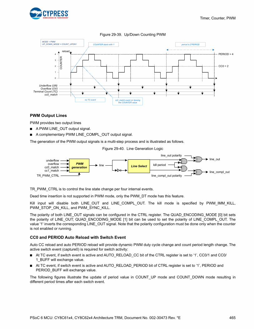
PSoC 6 MCU: CY8C61x4, CY8C62x4 Architecture TRM, Document No. 002-30473 Rev. *E 465
Timer, Counter, PWM
Figure 29-39. Up/Down Counting PWM
PWM Output Lines
PWM provides two output lines
■ A PWM LINE_OUT output signal.
■ A complementary PWM LINE_COMPL_OUT output signal.
The generation of the PWM output signals is a multi-step process and is illustrated as follows.
Figure 29-40. Line Generation Logic
TR_PWM_CTRL is to control the line state change per four internal events.
Dead time insertion is not supported in PWM mode, only the PWM_DT mode has this feature.
Kill input will disable both LINE_OUT and LINE_COMPL_OUT. The kill mode is specified by PWM_IMM_KILL,PWM_STOP_ON_KILL, and PWM_SYNC_KILL.
The polarity of both LINE_OUT signals can be configured in the CTRL register. The QUAD_ENCODING_MODE [0] bit setsthe polarity of LINE_OUT; QUAD_ENCODING_MODE [1] bit can be used to set the polarity of LINE_COMPL_OUT. Thevalue '1' inverts the corresponding LINE_OUT signal. Note that the polarity configuration must be done only when the counteris not enabled or running.
CC0 and PERIOD Auto Reload with Switch Event
Auto CC reload and auto PERIOD reload will provide dynamic PWM duty cycle change and count period length change. Theactive switch event (capture0) is required for switch activity:
■ At TC event, if switch event is active and AUTO_RELOAD_CC bit of the CTRL register is set to ‘1’, CC0/1 and CC0/1_BUFF will exchange value.
■ At TC event, if switch event is active and AUTO_RELOAD_PERIOD bit of CTRL register is set to ‘1’, PERIOD and PERIOD_BUFF will exchange value.
The following figures illustrate the update of period value in COUNT_UP mode and COUNT_DOWN mode resulting indifferent period times after each switch event.
cc0_match
Underflow (UN)Overflow (OV)
Terminal Count (TC)
CO
UN
TE
R
PERIOD = 4
CC0 = 2
MODE = PWMUP_DOWN_MODE = COUNT_UPDN1
4
3
2
1
0
COUNTER starts with 1 period is 2*PERIOD
reload
no TC event cc0_match event on leaving the COUNTER value
line kill period
line_out
line_compl_out
line_out polarity
line_compl_out polarity
cc0_match
underflowoverflow
TR_PWM_CTRL
PWM generation Line Select
cc1_match

PSoC 6 MCU: CY8C61x4, CY8C62x4 Architecture TRM, Document No. 002-30473 Rev. *E 466
Timer, Counter, PWM
Figure 29-41. PERIOD/PERIOD_BUFF Exchange in COUNT_UP Mode by a Switch Event
Figure 29-42. PERIOD/PERIOD_BUFF Exchange in COUNT_DOWN Mode by a Switch Event
A potential problem arises when software updates are not completed before the next tc event with an active pending switchevent. For example, if software updates PERIOD_BUFF before the tc event and CC0_BUFF after the tc event, switching doesnot reflect the CC0_BUFF register update. To prevent this from happening, the switch event should be generated by softwarethrough a MMIO register write after both the PERIOD_BUFF and CC0_BUFF registers are updated. The switch event is keptpending by the hardware until the next tc event occurs.
Left/Right/Center Align PWM with CC0/CC0_BUFF Auto Reload
PWM can generate left-align, right-align. and center-align with the following features supported in PWM mode:
■ Up/down count mode must be used to generate different phase aligned PWM.
■ Line state is changed per underflow/overflow/cc0_match/cc1_match internal event and can be configured in TR_PWM_CTRL register.
The required settings for left-aligned, right-aligned, and center-aligned PWM are:
■ Left-align:
❐ Write the value '0' to UP_DOWN_MODE [17:16] field in the CTRL register to set the counter direction to COUNT_UP mode
❐ Write the value '0' (SET) to OVERFLOW_MODE [3:2] field of the TR_PWM_CTRL register to set the LINE_OUT signal to '1' when the COUNTER reaches PERIOD value.
❐ Write the value '1' (CLEAR) to CC0_MATCH_MODE [1:0] field in the TR_PWM_CTRL register to set the LINE_OUT signal to '0' when the COUNTER equals CC0 value.
MODE = PWMUP_DOWN_MODE = COUNT_UP
CO
UN
TE
R
4
3
2
1
0
reload PERIOD4PERIOD_BUFF5
5 45
5
4
Underflow (UN)Overflow (OV)
Terminal Count (TC)
54
MODE = PWMUP_DOWN_MODE = COUNT_DOWN
CO
UN
TE
R
4
3
2
1
0
reload PERIOD4PERIOD_BUFF5
5 45
5
4
Underflow (UN)Overflow (OV)
Terminal Count (TC)
54

PSoC 6 MCU: CY8C61x4, CY8C62x4 Architecture TRM, Document No. 002-30473 Rev. *E 467
Timer, Counter, PWM
■ Right-align:
❐ Write the value '1' to UP_DOWN_MODE [17:16] field in the CTRL register to set the counter direction to COUNT_DOWN mode
❐ Write the value '0' (SET) to CC0_MATCH_MODE [1:0] field in the TR_PWM_CTRL register to set the LINE_OUT signal to '1' when the COUNTER equals CC0 value.
❐ Write the value '1' (CLEAR) to UNDERFLOW_MODE [5:4] field in the TR_PWM_CTRL register to set the LINE_OUT signal to '0' when the COUNTER reaches '0'.
■ Center-align:
❐ Write the value '2' to UP_DOWN_MODE [17:16] field in the CTRL register to set the counter direction to COUNT_UPDN1 mode
❐ Write the value '0' (SET) to OVERFLOW_MODE [3:2] field in the TR_PWM_CTRL register to set the LINE_OUT signal to '1' when the COUNTER reaches PERIOD value.
❐ Write the value '1' (CLEAR) to UNDERFLOW_MODE [5:4] field in the TR_PWM_CTRL register to set the LINE_OUT signal to '0' when the COUNTER reaches '0'.
❐ Write the value '2' (INVERT) to CC0_MATCH_MODE [1:0] field in the TR_PWM_CTRL register to invert the LINE_OUT signal when the COUNTER equals CC0 value.
Figure 29-43 illustrates a PWM in COUNT_UP mode with different CC0 values. The figure also illustrates how a left-alignedand right-aligned PWM can be created using the PWM in COUNT_UP mode.
Note: CC0 is changed (to CC0_BUFF, which is not depicted) on a tc event. The switch event is a constant 1.
A special case of 0 or 100 percent duty cycle is realized using the following setting (for example, left-aligned):
■ 0 percent CC0/1 = 0
■ 100 percent CC0/1 > PERIOD (a PERIOD value of 0xFFFF/0xFFFFFFFF is restricted)
Figure 29-43. Left-aligned and Right-aligned PWM in COUNT_UP Mode
Figure 29-44 illustrates a PWM in COUNT_DOWN mode with different CC0 values. The figure also illustrates how aright-aligned PWM can be created using the PWM in COUNT_DOWN mode.
Note: CC0 is changed (to CC0_BUFF, which is not depicted) on a tc event. The switch event is a constant 1.
CO
UN
TE
R
4201PERIOD = 4CC05
Left aligned PWMCC0 = pulse widthOVERFLOW_MODE = SETCC_MATCH_MODE = CLEAR
line
Right aligned PWMCC0 = (PERIOD+1) – pulse widthOVERFLOW_MODE = CLEARCC0_MATCH_MODE = SET
line
MODE = PWMUP_DOWN_MODE = COUNT_UP
4
3
2
1
0
reload
cc0_match
Underflow (UN)Overflow (OV)
Terminal Count (TC)

PSoC 6 MCU: CY8C61x4, CY8C62x4 Architecture TRM, Document No. 002-30473 Rev. *E 468
Timer, Counter, PWM
A special case of 0 or 100 percent duty cycle is realized using the following setting (for example, right-aligned):
■ 0 percent CC0/1 > PERIOD (a PERIOD value of 0xFFFF/0xFFFFFFFF is restricted)
■ 100 percent CC0/1 = PERIOD
Figure 29-44. Right-aligned and Left-aligned PWM in COUNT_DOWN Mode
Figure 29-45 illustrates a PWM in COUNT_UPDN1 with different CC0 values. The figure also illustrates how a center-alignedPWM can be creating using the PWM in COUNT_UPDN1 mode.
Note: The switch event is generated by hardware trigger 1, which is a constant '1' and therefore always active at the TCcondition. CC0 is changed (to CC0_BUFF, which is not depicted) on a tc event.
A special case of 0 or 100 percent duty cycle is realized using the following setting (for example, center-aligned):
■ 0 percent CC0/1 = PERIOD (there is no restriction for PERIOD)
■ 100 percent CC0/1 = 0
cc0_match will generate at the beginning of the count period when the CC0 switches to 0. In a special case, the cc0_matchgenerates without COUNTER equals CC0 (CC0 changes to 0 and at the same time COUNTER changes to 1 from 0).
CO
UN
TE
R4201
PERIOD = 4CC -1 or 0xFFFF
Right aligned PWMCC = pulse width - 1UNDERFLOW_MODE = CLEARCC_MATCH_MODE = SET
pwm
MODE = PWMUP_DOWN_MODE = COUNT_DOWN
4
3
2
1
0
reload
Compare/Capture (CC)
Underflow (UN)Overflow (OV)
Terminal Count (TC)
Left aligned PWMCC = PERIOD - pulse widthUNDERFLOW_MODE = SETCC_MATCH_MODE = CLEAR
pwm
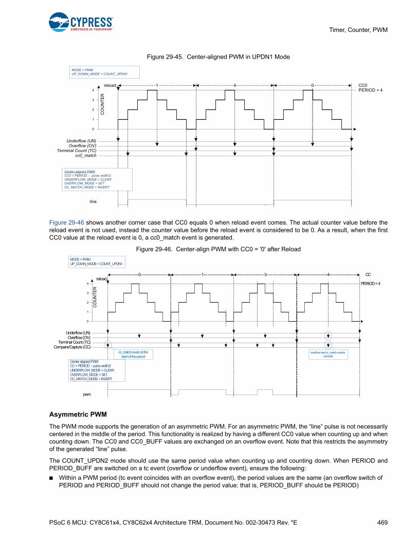
PSoC 6 MCU: CY8C61x4, CY8C62x4 Architecture TRM, Document No. 002-30473 Rev. *E 469
Timer, Counter, PWM
Figure 29-45. Center-aligned PWM in UPDN1 Mode
Figure 29-46 shows another corner case that CC0 equals 0 when reload event comes. The actual counter value before thereload event is not used, instead the counter value before the reload event is considered to be 0. As a result, when the firstCC0 value at the reload event is 0, a cc0_match event is generated.
Figure 29-46. Center-align PWM with CC0 = '0' after Reload
Asymmetric PWM
The PWM mode supports the generation of an asymmetric PWM. For an asymmetric PWM, the “line” pulse is not necessarilycentered in the middle of the period. This functionality is realized by having a different CC0 value when counting up and whencounting down. The CC0 and CC0_BUFF values are exchanged on an overflow event. Note that this restricts the asymmetryof the generated “line” pulse.
The COUNT_UPDN2 mode should use the same period value when counting up and counting down. When PERIOD andPERIOD_BUFF are switched on a tc event (overflow or underflow event), ensure the following:
■ Within a PWM period (tc event coincides with an overflow event), the period values are the same (an overflow switch of PERIOD and PERIOD_BUFF should not change the period value; that is, PERIOD_BUFF should be PERIOD)
MODE = PWMUP_DOWN_MODE = COUNT_UPDN1
CO
UN
TE
R
PERIOD = 4CC0
4
3
2
1
0
1 4 0
line
reload
cc0_match
Underflow (UN)Overflow (OV)
Terminal Count (TC)
Center aligned PWMCC0 = PERIOD – pulse width/2UNDERFLOW_MODE = CLEAROVERFLOW_MODE = SETCC_MATCH_MODE = INVERT
MODE = PWMUP_DOWN_MODE = COUNT_UPDN1
CO
UN
TE
R
PERIOD = 4
CC
4
3
2
1
0
0 1 4
Center aligned PWMCC = PERIOD –pulse width/2UNDERFLOW_MODE = CLEAROVERFLOW_MODE = SETCC_MATCH_MODE = INVERT
pwm
reload
cc_match event at the start of the period
overflow and cc_match events coincide
Compare/Capture (CC)
Underflow (UN)Overflow (OV)
Terminal Count (TC)
3

PSoC 6 MCU: CY8C61x4, CY8C62x4 Architecture TRM, Document No. 002-30473 Rev. *E 470
Timer, Counter, PWM
■ Between PWM periods (tc event coincides with an underflow event), the period value can change (an underflow switch of PERIOD and PERIOD_BUFF may change the period value; that is, PERIOD_BUFF may be different from PERIOD).
Figure 29-47 illustrates how the COUNT_UPDN2 mode is used to generate an asymmetric PWM.
Notes:
■ When up counting and the CC0 value at the underflow event is 0, a cc0_match event is generated.
■ When down counting and the CC0 value at the overflow event is PERIOD, a cc0_match event is generated.
■ A tc event is generated for both an underflow and overflow event. The tc event is used to exchange the CC0 and CC0_BUFF values.
Figure 29-47. Asymmetric PWM
The previous waveform illustrated functionality when the CC values are neither 0 not PERIOD. Corner case conditions inwhich the CC values equal 0 or PERIOD are illustrated in the following figures.
Figure 29-48 illustrates how the COUNT_UPDN2 mode is used to generate an asymmetric PWM.
Notes:
■ When up counting and CC0 value at the underflow event is 0, a cc0_match event is generated.
■ When down counting and CC0 value at the overflow event is PERIOD, a cc0_match event is generated.
■ A tc event is generated for both an underflow and overflow event. The tc event is used to exchange the CC0 and CC0_BUFF values.
■ Software updates CC0_BUFF and PERIOD_BUFF in an interrupt handler on the tc event (and overwrites the hardware updated values from the CC0/CC0_BUFF and PERIOD/PERIOD_BUFF exchanges).
MODE = PWMUP_DOWN_MODE = COUNT_UPDN2
CO
UN
TE
R
PERIOD = 4CC0
4
3
2
1
0
1 3
Asymmetric PWMCC0 = PERIOD – pulse width/2UNDERFLOW_MODE = CLEAROVERFLOW_MODE = SETCC0_MATCH_MODE = INVERT
line
reloadCC0_BUFF3 1
1 33 1
1 33 1
cc0_match
Underflow (UN)Overflow (OV)
Terminal Count (TC)

PSoC 6 MCU: CY8C61x4, CY8C62x4 Architecture TRM, Document No. 002-30473 Rev. *E 471
Timer, Counter, PWM
Figure 29-48. Asymmetric PWM when Compare = 0 or Period
When the counter group includes also compare function 1 with registers CC1 and CC1_BUFF, which generate cc1_matchevent, the compare feature behaves the same as for compare 0 function.
The cc1_match event can also be used to generate the PWM output signals. Using both cc0_match and cc1_match eventsfor PWM output signal generation provides another way to generate an asymmetric PWM as shown in Figure 29-49.
Figure 29-49. Asymmetric PWM with cc0_match and cc1_match
MODE = PWMUP_DOWN_MODE = COUNT_UPDN2
CO
UN
TE
R
CC0
4
3
2
1
0
0 4
Asymmetric PWMCC0 = PERIOD – pulse width/2UNDERFLOW_MODE = CLEAROVERFLOW_MODE = SETCC0_MATCH_MODE = INVERT
line
reload
CC0_BUFF4 55 0
4 03 3
3 3
PERIOD4 4PERIOD_BUFF4 5
5 53
3 33
5
54 5
0 5
4
1
upcounting and CC0 = 0 => cc0_match event
at underflow
downcounting and CC 0 = PERIOD => cc0_match
event at overflow
downcounting and CC0 = PERIOD => cc0_match
event at overflow
SW update SW update SW update SW update SW update
cc0_match
Underflow (UN)Overflow (OV)
Terminal Count (TC)
MODE = PWMUP_DOWN_MODE = COUNT_UP
CO
UN
TE
R
CC1
4
3
2
1
0
2 0
line
reload
CC01 03 40
52 0
PERIOD = 45
cc0_match
Underflow (UV)Overflow (OV)
Terminal Count (TC)
cc1_match
Asymmetric PWMCC1-CC0 = PERIOD – pulse widthCC0_MATCH_MODE = SETCC1_MATCH_MODE = CLEAROVERFLOW_MODE = CLEAR

PSoC 6 MCU: CY8C61x4, CY8C62x4 Architecture TRM, Document No. 002-30473 Rev. *E 472
Timer, Counter, PWM
Such asymmetric PWM generation is more flexible than using only one compare function in the COUNT_UPDN2 mode.However, if another (third) compare function is needed, For example, to trigger an ADC, another synchronously runningcounter should be used.
For Advanced Motor Control, the generation of compare match 0 and compare match 1 events can be enabled or disabledindividually for up and down counting (during COUNT_UPDN1/2 mode). This allows asymmetric PWM generation inCOUNT_UPDN1 mode where one compare match event modifies the PWM output only while counting up and the othercompare match event modifies the PWM output only while counting down. This is illustrated in the following figure, whichshows one of three center-aligned PWM phases for motor control when the duty cycle value is increased from one period tothe next (rising part of sign wave modulated onto the PWM signal).
Figure 29-50. Asymmetric PWM by cc0_match and cc1_match in COUNT_UPDN1 Mode
Instead of an always center-aligned PWM, the phase of the PWM signal can be temporarily shifted to allow a single shuntcurrent measurement (current measurement at two triggers with difference calculation in software) for motor control of apermanent-magnet synchronous motor (PMSM) when the current duty cycle values of the three phases do not allow that (toosmall window where one PWM channel is active and two others are not). Compared to the asymmetric PWM realized withonly one compare function in the COUNT_UPDN2 mode this solution uses two independent buffered compare values andgenerates less CPU load (less interrupts needed). This means all updates can be done for example, in the 'ADC done'interrupt service routine calculating the new duty cycle values and introducing a temporary phase shift for single shunt currentmeasurement.
The required settings for typical, asymmetric PWM output modes are:
■ Asymmetric with CC0:
❐ Write the ‘3’ to the UP_DOWN_MODE [17:16] field in the CTRL register to set the counter direction to COUNT_UPDN2 mode.
❐ Write ‘0’ (SET) to the OVERFLOW_MODE [3:2] field in the TR_PWM_CTRL register to set the LINE_OUT signal to '1' when the COUNTER reaches PERIOD value.
❐ Write ‘1’ (CLEAR) to the UNDERFLOW_MODE [5:4] field in the TR_PWM_CTRL register to set the LINE_OUT signal to '0' when the COUNTER reaches '0'.
❐ Write ‘2’ (INVERT) to the CC0_MATCH_MODE [1:0] field in the TR_PWM_CTRL register to invert the LINE_OUT signal when the COUNTER equals CC0 value.
■ Asymmetric with CC0 and CC1 (only for counter groups with a second compare function):
❐ Write ‘0’ to the UP_DOWN_MODE [17:16] field in the CTRL register to set the counter direction to COUNT_UP mode.
MODE = PWMUP_DOWN_MODE = COUNT_UPDN1AUTO_RELOAD_CC0 = 1,AUTO_RELOAD_CC1 = 1
cc0_match
underflowoverflow
tc
CO
UN
TE
R
CC0
4
3
2
1
0
3
Center-aligned PWMCC0 = PERIOD – pulse width/2UNDERFLOW_MODE = CLEAROVERFLOW_MODE = SETCC0_MATCH_MODE = SET, CC0_MATCH_UP_EN = 1, CC0_MATCH_DOWN_EN = 0CC1_MATCH_MODE = CLEAR, CC1_MATCH_UP_EN = 0, CC1_MATCH_DOWN_EN = 1
line
reload
CC0_BUFFx1
31
1
PERIOD = 43
CC1_BUFFy3 1
333
SW update
CC11
SW update1 1
0
SW update0
cc1_match
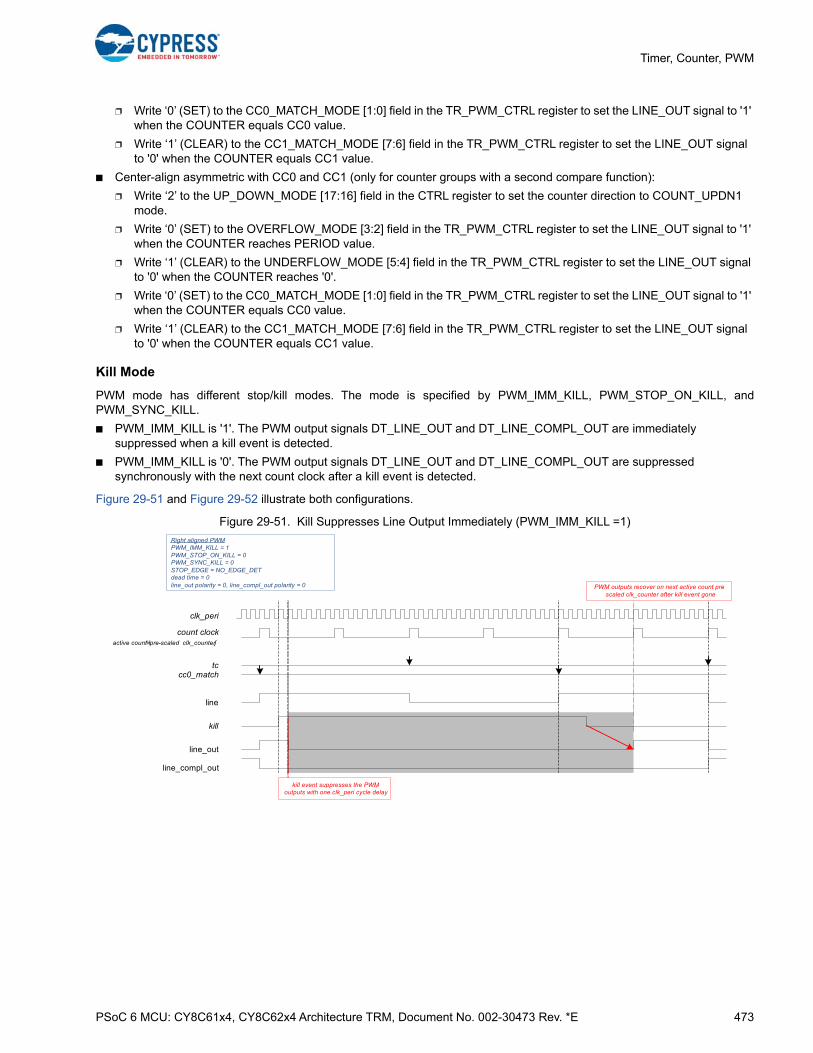
PSoC 6 MCU: CY8C61x4, CY8C62x4 Architecture TRM, Document No. 002-30473 Rev. *E 473
Timer, Counter, PWM
❐ Write ‘0’ (SET) to the CC0_MATCH_MODE [1:0] field in the TR_PWM_CTRL register to set the LINE_OUT signal to '1' when the COUNTER equals CC0 value.
❐ Write ‘1’ (CLEAR) to the CC1_MATCH_MODE [7:6] field in the TR_PWM_CTRL register to set the LINE_OUT signal to '0' when the COUNTER equals CC1 value.
■ Center-align asymmetric with CC0 and CC1 (only for counter groups with a second compare function):
❐ Write ‘2’ to the UP_DOWN_MODE [17:16] field in the CTRL register to set the counter direction to COUNT_UPDN1 mode.
❐ Write ‘0’ (SET) to the OVERFLOW_MODE [3:2] field in the TR_PWM_CTRL register to set the LINE_OUT signal to '1' when the COUNTER reaches PERIOD value.
❐ Write ‘1’ (CLEAR) to the UNDERFLOW_MODE [5:4] field in the TR_PWM_CTRL register to set the LINE_OUT signal to '0' when the COUNTER reaches '0'.
❐ Write ‘0’ (SET) to the CC0_MATCH_MODE [1:0] field in the TR_PWM_CTRL register to set the LINE_OUT signal to '1' when the COUNTER equals CC0 value.
❐ Write ‘1’ (CLEAR) to the CC1_MATCH_MODE [7:6] field in the TR_PWM_CTRL register to set the LINE_OUT signal to '0' when the COUNTER equals CC1 value.
Kill Mode
PWM mode has different stop/kill modes. The mode is specified by PWM_IMM_KILL, PWM_STOP_ON_KILL, andPWM_SYNC_KILL.
■ PWM_IMM_KILL is '1'. The PWM output signals DT_LINE_OUT and DT_LINE_COMPL_OUT are immediately suppressed when a kill event is detected.
■ PWM_IMM_KILL is '0'. The PWM output signals DT_LINE_OUT and DT_LINE_COMPL_OUT are suppressed synchronously with the next count clock after a kill event is detected.
Figure 29-51 and Figure 29-52 illustrate both configurations.
Figure 29-51. Kill Suppresses Line Output Immediately (PWM_IMM_KILL =1)
line
line_out
line_compl_out
Right aligned PWMPWM_IMM_KILL = 1PWM_STOP_ON_KILL = 0PWM_SYNC_KILL = 0STOP_EDGE = NO_EDGE_DETdead time = 0line_out polarity = 0, line_compl_out polarity = 0
tccc0_match
kill
PWM outputs recover on next active count pre-scaled clk_counter after kill event gone
clk_peri
count clock�active countҸpre-scaled clk_counterꭍ
kill event suppresses the PWM outputs with one clk_peri cycle delay

PSoC 6 MCU: CY8C61x4, CY8C62x4 Architecture TRM, Document No. 002-30473 Rev. *E 474
Timer, Counter, PWM
Figure 29-52. Kill Suppresses Line Output by Count Clock (PWM_IMM_KILL = 0)
The PWM_STOP_ON_KILL and PWM_SYNC_KILL modes specifies the functionality of kill input. The following three modesare supported:
■ PWM_STOP_ON_KILL is '1' (PWM_SYNC_KILL is don't care). This mode stops the counter on a stop/kill event.
■ PWM_STOP_ON_KILL is '0' and PWM_SYNC_KILL is '0'. This mode keeps the counter running, but suppresses the PWM output signals synchronously with the next count clock (active count prescaled clk_counter) and continues to do so for the duration of the stop/kill event.
■ PWM_STOP_ON_KILL is '0' and PWM_SYNC_KILL is '1'. This mode keeps the counter running, but suppresses the PWM output signals synchronously with the next count clock (active count prescaled clk_counter) and continues to do so until the next tc event without a stop/kill event.
Figure 29-53, Figure 29-54, and Figure 29-55 illustrate these three modes.
Figure 29-53. PWM Stop on Kill
line
line_out
line_compl_out
Right aligned PWMPWM_IMM_KILL = 0PWM_STOP_ON_KILL = 0PWM_SYNC_KILL = 0STOP_EDGE = NO_EDGE_DETdead time = 0line_out polarity = 0, line_compl_out polarity = 0
tccc0_match
kill
PWM outputs recover on next active count pre-scaled clk_counter after kill event gone
clk_counter
count clock�active countҸpre-scaled clk_counterꭍ
kill event suppresses the PWM outputs on next active count pre-scaled clk_counter
Right aligned PWMPWM_STOP_ON_KILL = 1STOP_EDGE = RISING_EDGEdead time = 0line_out polarity = 0, line_compl_out polarity = 0
line
line_out
line_compl_out
tccc0_match
kill
line_out and line_compl_out set to programmed polarity
kill event stops counter
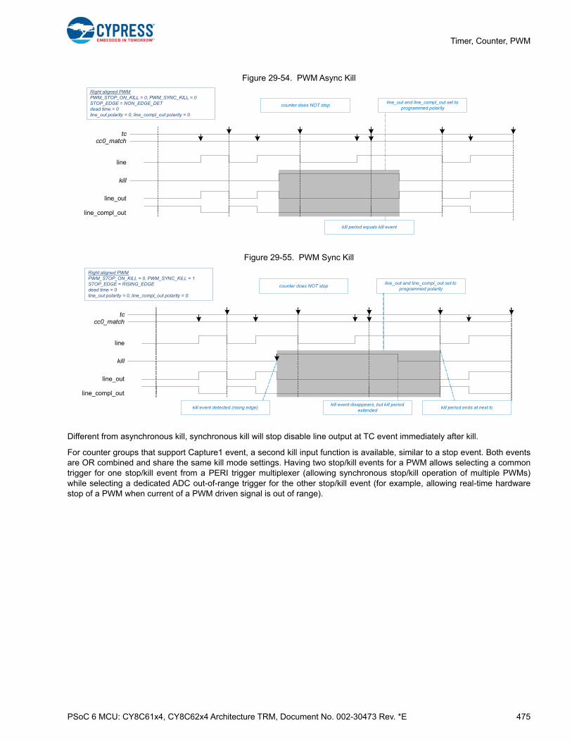
PSoC 6 MCU: CY8C61x4, CY8C62x4 Architecture TRM, Document No. 002-30473 Rev. *E 475
Timer, Counter, PWM
Figure 29-54. PWM Async Kill
Figure 29-55. PWM Sync Kill
Different from asynchronous kill, synchronous kill will stop disable line output at TC event immediately after kill.
For counter groups that support Capture1 event, a second kill input function is available, similar to a stop event. Both eventsare OR combined and share the same kill mode settings. Having two stop/kill events for a PWM allows selecting a commontrigger for one stop/kill event from a PERI trigger multiplexer (allowing synchronous stop/kill operation of multiple PWMs)while selecting a dedicated ADC out-of-range trigger for the other stop/kill event (for example, allowing real-time hardwarestop of a PWM when current of a PWM driven signal is out of range).
line
line_out
line_compl_out
Right aligned PWMPWM_STOP_ON_KILL = 0, PWM_SYNC_KILL = 0STOP_EDGE = NON_EDGE_DETdead time = 0line_out polarity = 0, line_compl_out polarity = 0
tccc0_match
kill
line_out and line_compl_out set to programmed polarity
counter does NOT stop
kill period equals kill event
line
line_out
line_compl_out
Right aligned PWMPWM_STOP_ON_KILL = 0, PWM_SYNC_KILL = 1STOP_EDGE = RISING_EDGEdead time = 0line_out polarity = 0, line_compl_out polarity = 0
tccc0_match
kill
line_out and line_compl_out set to programmed polarity
counter does NOT stop
kill period ends at next tckill event detected (rising edge)kill event disappears, but kill period
extended

PSoC 6 MCU: CY8C61x4, CY8C62x4 Architecture TRM, Document No. 002-30473 Rev. *E 476
Timer, Counter, PWM
29.3.4.2 Configuring Counter for PWM Mode
The steps to configure the counter for the PWM mode of operation and the affected register bits are as follows.
1. Disable the counter by writing '0' to the ENABLE bit of the CTRL register.
2. Select PWM mode by writing '100' to the MODE[26:24] field of the CTRL register.
3. Set clock prescaling by writing to the DT_LINE_OUT_L[7:0] field of the DT register.
4. Set the required 16-bit/32-bit period in the PERIOD register and the buffer period value in the PERIOD_BUFF register to switch values, if required.
5. Set the 16-bit/32-bit compare value in the CC0/1 register and buffer compare value in the CC0/1_BUFF register to switch values, if required.
6. Set the direction of counting by writing to the UP_DOWN_MODE[17:16] field of the CTRL register to configure left-aligned, right-aligned, or center-aligned PWM.
7. Set the PWM_IMM_KILL, PWM_STOP_ON_KILL, and PWM_SYNC_KILL fields of the CTRL register as required.
8. Set the TR_IN_SEL0 or TR_IN_SEL1 register to select the trigger that causes the event (Reload, Start, Stop, Capture0/1, and Count).
9. Set the TR_IN_EDGE_SEL register to select the edge of the trigger that causes the event (Reload, Start, Stop, Capture0/1, and Count).
10. LINE_OUT and LINE_COMPL_OUT can be controlled by the TR_PWM_CTRL register to set, reset, or invert upon cc0_match, cc1_match, overflow, and underflow conditions.
11. If required, set the interrupt upon TC or CC0/1 condition.
12. Enable the counter by writing '1' to ENABLED bit of the CTRL register. A reload trigger must be provided through firmware (RELOAD bit in the TR_CMD register) to start the counter if the hardware reload signal is not enabled.
29.3.5 Pulse Width Modulation with Dead Time Mode
The PWM-DT functionality is the same as PWM functionality, except for the following differences:
■ PWM_DT supports dead time insertion; PWM does not support dead time insertion.
■ PWM_DT does not support clock prescaling; PWM supports clock prescaling.
Figure 29-56. PWM with Dead Time Functionality
Dead time insertion is a step that operates on a preliminary PWM output signal line, as illustrated in Figure 29-40.
The dead time insertion for two PWM complementary output lines ranges from 0 to 255 (8 bit) or from 0 to 65535 (16 bit, onlyfor counter groups supporting Advanced Motor Control) counter clock cycles. The setup can be done in DT_LINE_OUT_L[7:0] field (low byte) and in DT_LINE_OUT_L [15:8] field in the DT register. For the Advanced Motor Control counter,DT_LINE_OUT[15:0] is for LINE_OUT, DT_LINE_COMPL_OUT[15:0] is for LINE_COMPL_OUT.
Figure 29-57 illustrates dead time insertion for different dead times and different output signal polarity settings.
PWM_DT
==
clk_counter
COUNTER
PERIOD
==
CC0/1
CC0/1_BUFF
==
PERIOD_BUFF
no clock pre-scaling
PWM generation
line
tcunderflowoverflow Trigger
generationtr_out0tr_out1
Interrupt generation
interrupt
cc0_matchcc1_match
reloadstart
stop/killcount
capture0/switchcapture1

PSoC 6 MCU: CY8C61x4, CY8C62x4 Architecture TRM, Document No. 002-30473 Rev. *E 477
Timer, Counter, PWM
Figure 29-57. Dead-time Timing
Figure 29-58 illustrates how the polarity settings and stop/kill functionality combined control the PWM output signalsLINE_OUT and LINE_COMPL_OUT.
Figure 29-58. Dead Time and Kill
line
line_out
line_compl_out
line_out
line_compl_out
MODE = PWM_DTdead time = 0line_out polarity = 0line_compl_out polarity = 0
MODE = PWM_DTdead time = 1line_out polarity = 0line_compl_out polarity = 0
1dead time:
line_out
line_compl_out
MODE = PWM_DTdead time = 2line_out polarity = 0line_compl_out polarity = 0
2dead time:pulse is gone
line_out
line_compl_out
MODE = PWM_DTdead time = 2line_out polarity = 1line_compl_out polarity = 1
2dead time:
line
line_out
line_compl_out
Right aligned PWMPWM_STOP_ON_KILL = 0, PWM_SYNC_KILL = 0STOP_EDGE = NO_EDGE_DETdead time = 1line_out polarity = 0, line_compl_out polarity = 1
tccc0_match
kill
1dead time:
reload
RUNNING
counter not running counter temporarily killed
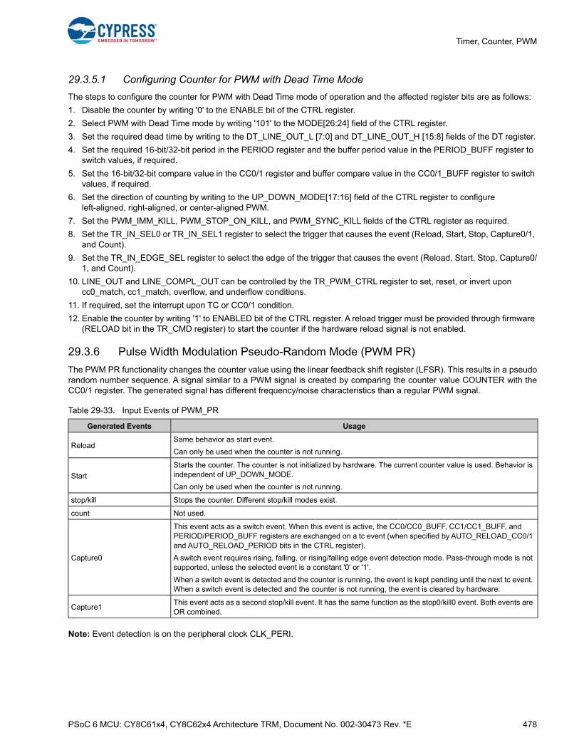
PSoC 6 MCU: CY8C61x4, CY8C62x4 Architecture TRM, Document No. 002-30473 Rev. *E 478
Timer, Counter, PWM
29.3.5.1 Configuring Counter for PWM with Dead Time Mode
The steps to configure the counter for PWM with Dead Time mode of operation and the affected register bits are as follows:
1. Disable the counter by writing '0' to the ENABLE bit of the CTRL register.
2. Select PWM with Dead Time mode by writing '101' to the MODE[26:24] field of the CTRL register.
3. Set the required dead time by writing to the DT_LINE_OUT_L [7:0] and DT_LINE_OUT_H [15:8] fields of the DT register.
4. Set the required 16-bit/32-bit period in the PERIOD register and the buffer period value in the PERIOD_BUFF register to switch values, if required.
5. Set the 16-bit/32-bit compare value in the CC0/1 register and buffer compare value in the CC0/1_BUFF register to switch values, if required.
6. Set the direction of counting by writing to the UP_DOWN_MODE[17:16] field of the CTRL register to configure left-aligned, right-aligned, or center-aligned PWM.
7. Set the PWM_IMM_KILL, PWM_STOP_ON_KILL, and PWM_SYNC_KILL fields of the CTRL register as required.
8. Set the TR_IN_SEL0 or TR_IN_SEL1 register to select the trigger that causes the event (Reload, Start, Stop, Capture0/1, and Count).
9. Set the TR_IN_EDGE_SEL register to select the edge of the trigger that causes the event (Reload, Start, Stop, Capture0/1, and Count).
10. LINE_OUT and LINE_COMPL_OUT can be controlled by the TR_PWM_CTRL register to set, reset, or invert upon cc0_match, cc1_match, overflow, and underflow conditions.
11. If required, set the interrupt upon TC or CC0/1 condition.
12. Enable the counter by writing '1' to ENABLED bit of the CTRL register. A reload trigger must be provided through firmware (RELOAD bit in the TR_CMD register) to start the counter if the hardware reload signal is not enabled.
29.3.6 Pulse Width Modulation Pseudo-Random Mode (PWM PR)
The PWM PR functionality changes the counter value using the linear feedback shift register (LFSR). This results in a pseudorandom number sequence. A signal similar to a PWM signal is created by comparing the counter value COUNTER with theCC0/1 register. The generated signal has different frequency/noise characteristics than a regular PWM signal.
Note: Event detection is on the peripheral clock CLK_PERI.
Table 29-33. Input Events of PWM_PR
Generated Events Usage
ReloadSame behavior as start event.
Can only be used when the counter is not running.
Start
Starts the counter. The counter is not initialized by hardware. The current counter value is used. Behavior is independent of UP_DOWN_MODE.
Can only be used when the counter is not running.
stop/kill Stops the counter. Different stop/kill modes exist.
count Not used.
Capture0
This event acts as a switch event. When this event is active, the CC0/CC0_BUFF, CC1/CC1_BUFF, and PERIOD/PERIOD_BUFF registers are exchanged on a tc event (when specified by AUTO_RELOAD_CC0/1 and AUTO_RELOAD_PERIOD bits in the CTRL register).
A switch event requires rising, falling, or rising/falling edge event detection mode. Pass-through mode is not supported, unless the selected event is a constant '0' or '1'.
When a switch event is detected and the counter is running, the event is kept pending until the next tc event. When a switch event is detected and the counter is not running, the event is cleared by hardware.
Capture1This event acts as a second stop/kill event. It has the same function as the stop0/kill0 event. Both events are OR combined.

PSoC 6 MCU: CY8C61x4, CY8C62x4 Architecture TRM, Document No. 002-30473 Rev. *E 479
Timer, Counter, PWM
Note: The count event is not used. As a result, the PWM_PR functionality operates on the prescaled counter clock(clk_counter), rather than on an active count prescaled counter clock.
Figure 29-59. PWM_PR Functionality
The PWM_PR functionality is described as follows:
■ The counter value COUNTER is initialized by software (to a value different from 0).
■ Programmable LFSR length
Table 29-34. Basic Features of PWM_PR
Supported Features Description
Clock prescaling Prescales the clk_counter.
One shotCounter is stopped by hardware, after a single period of the counter (counter value equals period value PERIOD).
Auto reload CCCC0/1 and CC0/1_BUFF are exchanged on a switch event AND tc event (when specified by AUTO_RELOAD_CC bit in CTRL register).
Auto reload PERIODPERIOD and PERIOD_BUFF are exchanged on a switch event and tc event (when specified by AUTO_RELOAD_PERIOD bit in CTRL register).
Kill modes Specified by PWM_SYNC_KILL, PWM_STOP_ON_KILL, and PWM_IMM_KILL.
Table 29-35. Trigger Outputs of PWM_PR
Trigger Output Description
cc0_match (CC) Counter changes from a state in which COUNTER equals CC0.
cc1_match (CC) Counter changes from a state in which COUNTER equals CC1.
Underflow (UN) Not used.
Overflow (OV) Not used.
TC Counter changes from a state in which COUNTER equals PERIOD.
Table 29-36. PWM_PR PWM Outputs
PWM Outputs Description
LINE_OUT PWM line output.
LINE_COMPL_OUT Complementary PWM line output.
PWM_PR
reloadstart
stop/killcapture0/switch
clk_counter
COUNTER (SR)
PERIOD
==
CC0/1
CC0/1_BUFF
line kill period
line_outline_out polarity
line_compl_outline_compl_out polarity
====
<
tc
tr_out0tr_out1
Interrupt generation
interrupt
cc0_matchcc1_match
Trigger generation
PERIOD_BUFF (Tap enable)
feedbackTap en/xor
Line Select
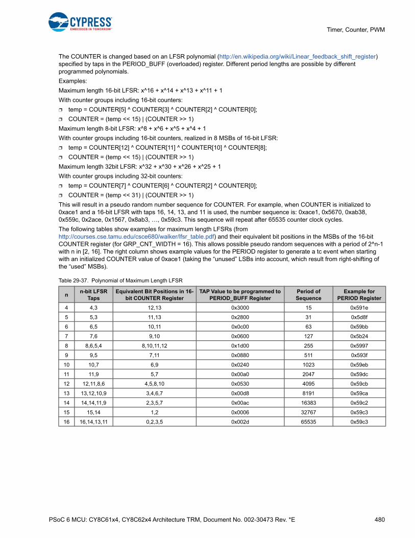
PSoC 6 MCU: CY8C61x4, CY8C62x4 Architecture TRM, Document No. 002-30473 Rev. *E 480
Timer, Counter, PWM
The COUNTER is changed based on an LFSR polynomial (http://en.wikipedia.org/wiki/Linear_feedback_shift_register) specified by taps in the PERIOD_BUFF (overloaded) register. Different period lengths are possible by different programmed polynomials.
Examples:
Maximum length 16-bit LFSR: x^16 + x^14 + x^13 + x^11 + 1
With counter groups including 16-bit counters:
❐ temp = COUNTER[5] ^ COUNTER[3] ^ COUNTER[2] ^ COUNTER[0];
❐ COUNTER = (temp << 15) | (COUNTER >> 1)
Maximum length 8-bit LFSR: x^8 + x^6 + x^5 + x^4 + 1
With counter groups including 16-bit counters, realized in 8 MSBs of 16-bit LFSR:
❐ temp = COUNTER[12] ^ COUNTER[11] ^ COUNTER[10] ^ COUNTER[8];
❐ COUNTER = (temp << 15) | (COUNTER >> 1)
Maximum length 32bit LFSR: x^32 + x^30 + x^26 + x^25 + 1
With counter groups including 32-bit counters:
❐ temp = COUNTER[7] ^ COUNTER[6] ^ COUNTER[2] ^ COUNTER[0];
❐ COUNTER = (temp << 31) | (COUNTER >> 1)
This will result in a pseudo random number sequence for COUNTER. For example, when COUNTER is initialized to 0xace1 and a 16-bit LFSR with taps 16, 14, 13, and 11 is used, the number sequence is: 0xace1, 0x5670, 0xab38, 0x559c, 0x2ace, 0x1567, 0x8ab3, …, 0x59c3. This sequence will repeat after 65535 counter clock cycles.
The following tables show examples for maximum length LFSRs (from http://courses.cse.tamu.edu/csce680/walker/lfsr_table.pdf) and their equivalent bit positions in the MSBs of the 16-bit COUNTER register (for GRP_CNT_WIDTH = 16). This allows possible pseudo random sequences with a period of 2^n-1 with n in [2, 16]. The right column shows example values for the PERIOD register to generate a tc event when starting with an initialized COUNTER value of 0xace1 (taking the “unused” LSBs into account, which result from right-shifting of the “used” MSBs).
Table 29-37. Polynomial of Maximum Length LFSR
nn-bit LFSR
TapsEquivalent Bit Positions in 16-
bit COUNTER RegisterTAP Value to be programmed to
PERIOD_BUFF RegisterPeriod of Sequence
Example for PERIOD Register
4 4,3 12,13 0x3000 15 0x591e
5 5,3 11,13 0x2800 31 0x5d8f
6 6,5 10,11 0x0c00 63 0x59bb
7 7,6 9,10 0x0600 127 0x5b24
8 8,6,5,4 8,10,11,12 0x1d00 255 0x5997
9 9,5 7,11 0x0880 511 0x593f
10 10,7 6,9 0x0240 1023 0x59eb
11 11,9 5,7 0x00a0 2047 0x59dc
12 12,11,8,6 4,5,8,10 0x0530 4095 0x59cb
13 13,12,10,9 3,4,6,7 0x00d8 8191 0x59ca
14 14,14,11,9 2,3,5,7 0x00ac 16383 0x59c2
15 15,14 1,2 0x0006 32767 0x59c3
16 16,14,13,11 0,2,3,5 0x002d 65535 0x59c3

PSoC 6 MCU: CY8C61x4, CY8C62x4 Architecture TRM, Document No. 002-30473 Rev. *E 481
Timer, Counter, PWM
The programmable taps allow LFSRs other than maximum cycle LFSRs in Table 29-37, which can result in periods other than 2^n-1. The following table shows some examples.
However, it is not recommended to use such non-maximum cycle LFSRs to generate a pseudo-random PWM signal, even if they result in the same cycle length as shorter maximum cycle LFSRs (for example, 255 cycles for taps 16,15). This because the values occurring in such sequences are not equally distributed over the possible value space, which results in much bigger errors compared with the desired PWM duty cycle accumulated over a full pseudo random number sequence. For example, the 8-bit LFSR with taps 8,6,5,4 (realized in 8 MSBs of 16-bit LFSR) and the 16-bit LFSR with the taps 16,15 result both in a period of 255 cycles, but a CC0 value of 0x4000 (for a desired 50 percent “accumulated duty cycle”) results in an accumulated duty cycle of:
49.8% for the 8-bit LFSR with taps 8,6,5,4 (realized in 8 MSBs of 16-bit LFSR).
❐ 0.39% error
46.7% for the 16-bit LFSR with the taps 16,15
❐ 6.66% error
■ Asymmetric with CC0
❐ Write ‘3’ to the UP_DOWN_MODE [17:16] field in the CTRL register to set the counter direction to COUNT_UPDN2 mode.
■ When COUNTER equals CC0 (CC1), a cc0_match (cc1_match) event is generated.
■ When COUNTER equals PERIOD, a tc event is generated. Note that the LFSR produces a deterministic number sequence (given a specific counter initialization value). Therefore, it is possible to calculate the COUNTER value after a certain number of LFSR iterations n. This calculated COUNTER value can be used as PERIOD value, and the tc event will be generated after precisely n counter clocks.
■ On a tc event, the CC0/CC0_BUFF and CC1/CC1_BUFF can be conditionally exchanged under control of the capture0/switch event and the AUTO_RELOAD_CC0 field of the CTRL register (see 29.3.4.1 PWM Mode Functionalities).
Note: To generate a tc event, PERIOD must be set to a value which the LFSR (register COUNTER) reaches. When realizing a shorter maximum length LFSR (n < GRP_CNT_WIDTH) within the n MSBs of a GRP_CNT_WIDTH wide LFSR, the “unused” LSBs need to be set to a value which results from right-shifting of the “used” MSBs.
■ The output line reflects: COUNTER[14:0] < CC0[15:0]. Note that only the lower 15 bits of COUNTER are used. As a result, for CC0 greater or equal to 0x8000, “line” is always 1. The line polarity can be inverted (as specified by QUAD_ENCODING_MODE[0] of the CTRL register). For counter groups including 32-bit counters the output line reflects: COUNTER[30:0] < CC0[31:0].
■ During PWM_PR operation:
❐ When COUNTER equals CC0 (CC01), a cc0_match (cc1_match) event is generated.
❐ When COUNTER equals PERIOD, a tc event is generated.
Table 29-38. Polynomial of Non-maximum Length LFSR
n-bit LFSR TapsBit Positions in 16-bit
Counter RegisterPeriod of Sequence
n-bit LFSR TapsBit Positions in 16-bit
Counter RegisterPeriod of Sequence
16,15 0,1 255 16,15,11 0,1,5 4340
16,14 0,2 126 16,15,10 0,1,6 24573
16,13 0,3 8191 16,15,9 0,1,7 32766
16,12 0,4 60 16,15,8 0,1,8 4681
16,11 0,5 16383 16,15,7 0,1,9 504
16,10 0,6 434 16,15,6 0,1,10 10235
16,9 0,7 63457 16,15,5 0,1,11 3906
16,8 0,8 24 16,15,4 0,1,12 7161
16,15,14 0,1,2 32767 16,15,3 0,1,13 3276
16,15,13 0,1,3 11811 16,15,2 0,1,14 32767
16,15,12 0,1,4 63 16,15,1 0,1,15 30
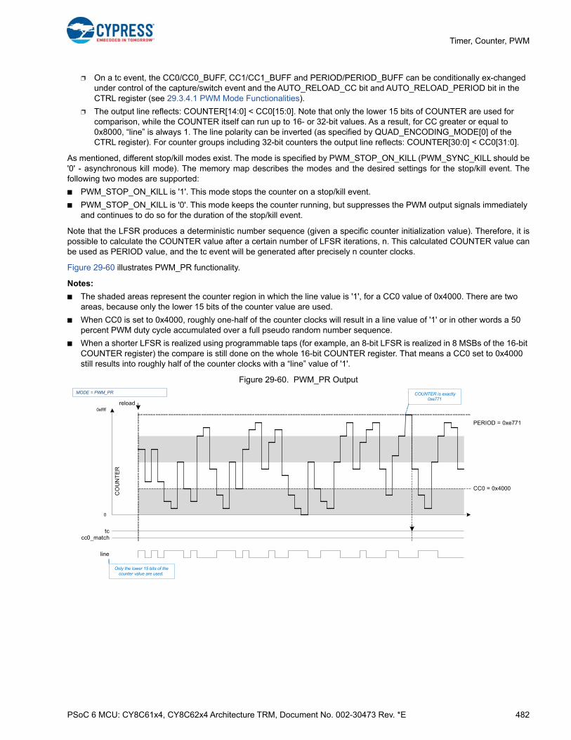
PSoC 6 MCU: CY8C61x4, CY8C62x4 Architecture TRM, Document No. 002-30473 Rev. *E 482
Timer, Counter, PWM
❐ On a tc event, the CC0/CC0_BUFF, CC1/CC1_BUFF and PERIOD/PERIOD_BUFF can be conditionally ex-changed under control of the capture/switch event and the AUTO_RELOAD_CC bit and AUTO_RELOAD_PERIOD bit in the CTRL register (see 29.3.4.1 PWM Mode Functionalities).
❐ The output line reflects: COUNTER[14:0] < CC0[15:0]. Note that only the lower 15 bits of COUNTER are used for comparison, while the COUNTER itself can run up to 16- or 32-bit values. As a result, for CC greater or equal to 0x8000, “line” is always 1. The line polarity can be inverted (as specified by QUAD_ENCODING_MODE[0] of the CTRL register). For counter groups including 32-bit counters the output line reflects: COUNTER[30:0] < CC0[31:0].
As mentioned, different stop/kill modes exist. The mode is specified by PWM_STOP_ON_KILL (PWM_SYNC_KILL should be'0' - asynchronous kill mode). The memory map describes the modes and the desired settings for the stop/kill event. Thefollowing two modes are supported:
■ PWM_STOP_ON_KILL is '1'. This mode stops the counter on a stop/kill event.
■ PWM_STOP_ON_KILL is '0'. This mode keeps the counter running, but suppresses the PWM output signals immediately and continues to do so for the duration of the stop/kill event.
Note that the LFSR produces a deterministic number sequence (given a specific counter initialization value). Therefore, it ispossible to calculate the COUNTER value after a certain number of LFSR iterations, n. This calculated COUNTER value canbe used as PERIOD value, and the tc event will be generated after precisely n counter clocks.
Figure 29-60 illustrates PWM_PR functionality.
Notes:
■ The shaded areas represent the counter region in which the line value is '1', for a CC0 value of 0x4000. There are two areas, because only the lower 15 bits of the counter value are used.
■ When CC0 is set to 0x4000, roughly one-half of the counter clocks will result in a line value of '1' or in other words a 50 percent PWM duty cycle accumulated over a full pseudo random number sequence.
■ When a shorter LFSR is realized using programmable taps (for example, an 8-bit LFSR is realized in 8 MSBs of the 16-bit COUNTER register) the compare is still done on the whole 16-bit COUNTER register. That means a CC0 set to 0x4000 still results into roughly half of the counter clocks with a “line” value of '1'.
Figure 29-60. PWM_PR Output
cc0_matchtc
CO
UN
TE
R
PERIOD = 0xe771
CC0 = 0x4000
MODE = PWM_PR
0
COUNTER is exactly 0xe771
reload0xffff
line
Only the lower 15 bits of the counter value are used.
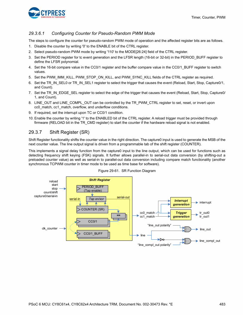
PSoC 6 MCU: CY8C61x4, CY8C62x4 Architecture TRM, Document No. 002-30473 Rev. *E 483
Timer, Counter, PWM
29.3.6.1 Configuring Counter for Pseudo-Random PWM Mode
The steps to configure the counter for pseudo-random PWM mode of operation and the affected register bits are as follows.
1. Disable the counter by writing '0' to the ENABLE bit of the CTRL register.
2. Select pseudo-random PWM mode by writing '110' to the MODE[26:24] field of the CTRL register.
3. Set the PERIOD register for tc event generation and the LFSR length (16-bit or 32-bit) in the PERIOD_BUFF register to define the LFSR polynomial.
4. Set the 16-bit compare value in the CC0/1 register and the buffer compare value in the CC0/1_BUFF register to switch values.
5. Set the PWM_IMM_KILL, PWM_STOP_ON_KILL, and PWM_SYNC_KILL fields of the CTRL register as required.
6. Set the TR_IN_SEL0 or TR_IN_SEL1 register to select the trigger that causes the event (Reload, Start, Stop, Capture0/1, and Count).
7. Set the TR_IN_EDGE_SEL register to select the edge of the trigger that causes the event (Reload, Start, Stop, Capture0/1, and Count).
8. LINE_OUT and LINE_COMPL_OUT can be controlled by the TR_PWM_CTRL register to set, reset, or invert upon cc0_match, cc1_match, overflow, and underflow conditions.
9. If required, set the interrupt upon TC or CC0/1 condition.
10. Enable the counter by writing '1' to the ENABLED bit of the CTRL register. A reload trigger must be provided through firmware (RELOAD bit in the TR_CMD register) to start the counter if the hardware reload signal is not enabled.
29.3.7 Shift Register (SR)
Shift Register functionality shifts the counter value in the right direction. The capture0 input is used to generate the MSB of thenext counter value. The line output signal is driven from a programmable tab of the shift register (COUNTER).
This implements a signal delay function from the capture0 input to the line output, which can be used for functions such asdetecting frequency shift keying (FSK) signals. It further allows parallel-in to serial-out data conversion (by shifting-out apreloaded counter value) as well as serial-in to parallel-out data conversion including compare match functionality (anothersynchronous TCPWM counter in timer mode to be used as time base for software).
Figure 29-61. SR Function Diagram
Shift Register
==
reloadstartstop
count/shiftcapture0/serial-in
COUNTER (SR)
PERIOD_BUFF (Tap enable)
CC0/1
CC0/1_BUFF
==
clk_counter
serial-in serial-out
line
line_out“line_out polarity”
line_compl_out“line_compl_out polarity”
tr_out0tr_out1
Interrupt generation
interrupt
cc0_matchcc1_match
Trigger generation
Tap en/xor

PSoC 6 MCU: CY8C61x4, CY8C62x4 Architecture TRM, Document No. 002-30473 Rev. *E 484
Timer, Counter, PWM
29.3.7.1 SR Mode Functionality Overview
Note: Event detection is on the peripheral clock, CLK_PERI.
Count event works to generate active count prescaled counter clock same as other function modes. This is how the shiftworks. Shifting the counter value is controlled by the count event and the counter clock, clk_counter. A constant '1' as well assynchronized input trigger edges can be used as count events.
Table 29-39. Input Events of SR
External Events Usage
ReloadSets the counter value to '0' and starts the counter shift operation.
Can only be used when the counter is not running.
Start
Starts the counter shift operation. The counter is not initialized by hardware. The current counter value is used.
Can only be used when the counter is not running.
Stop Stops the counter.
Count/Shift Shifts the counter in the right direction.
Capture0/serial-in This event input is used as serial input to the MSB of the counter.
Capture1 Stops the counter.
Table 29-40. Basic Features of SR
Supported Features Description
Clock prescaling Prescales the clk_counter.
Auto reload CCCC0 (CC1) and CC0_BUFF (CC1_BUFF) are exchanged on a cc0_match (cc1_match) event (when specified by AUTO_RELOAD_CC0/1 bit in CTRL register).
Table 29-41. Internal Events of SR
Internal Events Description
cc0_match Counter changes to a state in which COUNTER equals CC0.
cc1_match Counter changes to a state in which COUNTER equals CC1.
Underflow Not used.
Overflow Not used.
TC Not used.
Table 29-42. Line Output of SR
Supported Features Description
LINE_OUT
PWM line output. In Shift Register mode it is generated from an XOR combination of all enabled counter taps (bit position) defined by PERIOD_BUFF. For a shift register function only one tap should be used; that is, a one-hot value must be written to PERIOD_BUFF. If multiple bits in PERIOD_BUFF are set then the taps are XOR combined.
LINE_COMPL_OUT Complementary PWM line output.
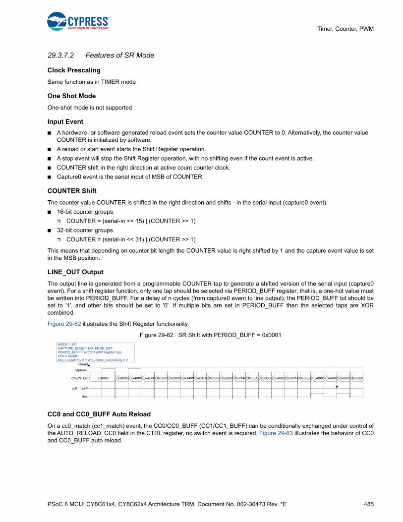
PSoC 6 MCU: CY8C61x4, CY8C62x4 Architecture TRM, Document No. 002-30473 Rev. *E 485
Timer, Counter, PWM
29.3.7.2 Features of SR Mode
Clock Prescaling
Same function as in TIMER mode
One Shot Mode
One-shot mode is not supported
Input Event
■ A hardware- or software-generated reload event sets the counter value COUNTER to 0. Alternatively, the counter value COUNTER is initialized by software.
■ A reload or start event starts the Shift Register operation.
■ A stop event will stop the Shift Register operation, with no shifting even if the count event is active.
■ COUNTER shift in the right direction at active count counter clock.
■ Capture0 event is the serial input of MSB of COUNTER.
COUNTER Shift
The counter value COUNTER is shifted in the right direction and shifts - in the serial input (capture0 event).
■ 16-bit counter groups:
❐ COUNTER = (serial-in << 15) | (COUNTER >> 1)
■ 32-bit counter groups
❐ COUNTER = (serial-in << 31) | (COUNTER >> 1)
This means that depending on counter bit length the COUNTER value is right-shifted by 1 and the capture event value is setin the MSB position.
LINE_OUT Output
The output line is generated from a programmable COUNTER tap to generate a shifted version of the serial input (capture0event). For a shift register function, only one tap should be selected via PERIOD_BUFF register; that is, a one-hot value mustbe written into PERIOD_BUFF. For a delay of n cycles (from capture0 event to line output), the PERIOD_BUFF bit should beset to '1', and other bits should be set to '0'. If multiple bits are set in PERIOD_BUFF then the selected taps are XORcombined.
Figure 29-62 illustrates the Shift Register functionality.
Figure 29-62. SR Shift with PERIOD_BUFF = 0x0001
CC0 and CC0_BUFF Auto Reload
On a cc0_match (cc1_match) event, the CC0/CC0_BUFF (CC1/CC1_BUFF) can be conditionally exchanged under control ofthe AUTO_RELOAD_CC0 field in the CTRL register, no switch event is required. Figure 29-63 illustrates the behavior of CC0and CC0_BUFF auto reload.
cc0_match
MODE = SRCAPTURE_EDGE = NO_EDGE_DETPERIOD_BUFF = 0x0001 (shift register tap)CC0 = 0x0001line_out polarity = 0, line_compl_out polarity = 0
reload
capture0
line
COUNTER 0x0000 0x8000 0x4000 0xA000 0x5000 0x2800 0x1400 0x0A00 0x0500 0x0280 0x0140 0x00A0 0x0050 0x0028 0x0014 0x000A 0x0005 0x0002 0x0001 0x0000
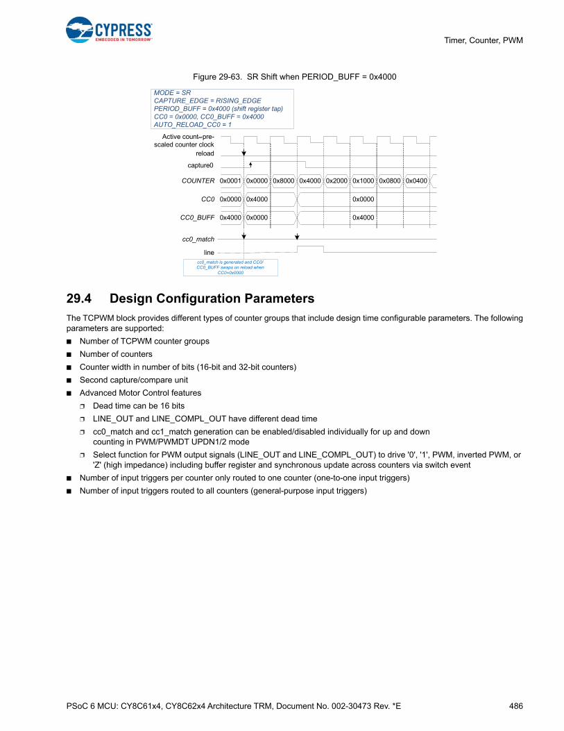
PSoC 6 MCU: CY8C61x4, CY8C62x4 Architecture TRM, Document No. 002-30473 Rev. *E 486
Timer, Counter, PWM
Figure 29-63. SR Shift when PERIOD_BUFF = 0x4000
29.4 Design Configuration Parameters
The TCPWM block provides different types of counter groups that include design time configurable parameters. The followingparameters are supported:
■ Number of TCPWM counter groups
■ Number of counters
■ Counter width in number of bits (16-bit and 32-bit counters)
■ Second capture/compare unit
■ Advanced Motor Control features
❐ Dead time can be 16 bits
❐ LINE_OUT and LINE_COMPL_OUT have different dead time
❐ cc0_match and cc1_match generation can be enabled/disabled individually for up and down counting in PWM/PWMDT UPDN1/2 mode
❐ Select function for PWM output signals (LINE_OUT and LINE_COMPL_OUT) to drive '0', '1', PWM, inverted PWM, or 'Z' (high impedance) including buffer register and synchronous update across counters via switch event
■ Number of input triggers per counter only routed to one counter (one-to-one input triggers)
■ Number of input triggers routed to all counters (general-purpose input triggers)
cc0_match
MODE = SRCAPTURE_EDGE = RISING_EDGEPERIOD_BUFF = 0x4000 (shift register tap)CC0 = 0x0000, CC0_BUFF = 0x4000AUTO_RELOAD_CC0 = 1
Active countسpre-scaled counter clock
line
COUNTER 0x0001 0x0000 0x8000 0x2000 0x04000x0800
reload
capture0
cc0_match is generated and CC0/CC0_BUFF swaps on reload when
CC0=0x0000
0x4000 0x1000
CC0 0x0000 0x4000 0x0000
CC0_BUFF 0x4000 0x0000 0x4000
PSoC 6 MCU: CY8C61x4, CY8C62x4 Architecture TRM, Document No. 002-30473 Rev. *E 487
Timer, Counter, PWM
29.5 Recovery
TCPWM can be recovered with any Active reset event, such as:
■ Power-on reset (POR)
■ External reset (XRES_L)
■ Watchdog timer reset (MCWDT and WDT)
■ Brownout detection reset
■ Over-voltage and over-current detection reset
There is no unexpected state in which the TCPWM can enter.
29.6 Initialize
The initial state of TCPWM pins is Hi-Z. Some registers are reset on an Active reset; some of the MMIO registers are retainedin DeepSleep. None of the registers are retained through Hibernate or other low-power modes. An Active reset will reset thepin state back to Hi-Z.
29.7 Pin Status
When TCPWM is unused, the status for TCPWM pins will be Hi-Z. To disable TCPWM, make sure the ENABLED andPWM_DISABLE_MODE bits in the CTRL register are set to ‘0’.

PSoC 6 MCU: CY8C61x4, CY8C62x4 Architecture TRM, Document No. 002-30473 Rev. *E 488
Timer, Counter, PWM
29.8 TCPWM Registers
Note: In TCPWM0_GRPx_CNTy, 'x' signifies the group number and 'y' is the counter in the respective TCWPM group.
Note that overwriting the same value on each register has different effects and they are explained in the register map by thesoftware access attributes. TCPWM registers have the following access restrictions:
■ All status registers are not software-writable.
■ TR_CMD is set in software and cleared in hardware.
■ INTR is cleared in software and set in hardware (by writing ‘1’ to INTR_SET).
■ Read INTR_SET will return the value of INTR.
■ Other registers are normal and can be overwritten with the same value.
Table 29-43. List of TCPWM Registers
Register Name Description
TCPWM0_GRPx_CNTy_CTRL Counter control registerSelects the counter mode and debug mode, and enables the counter
TCPWM0_GRPx_CNTy_STATUS Counter status registerReads the direction of counting and dead time duration, and indicates the actual level of trigger input and trigger outputs signals; checks if the counter is running
TCPWM0_GRPx_CNTy_COUNTER Counter count register Contains the 16- or 32-bit counter value
TCPWM0_GRPx_CNTy_CC0 Counter compare/capture 0 registerCaptures the counter value 0 or compares the value with counter value 0
TCPWM0_GRPx_CNTy_CC0_BUFFCounter buffered compare/capture 0 register
Buffer register for counter CC0 register
TCPWM0_GRPx_CNTy_CC1 Counter compare/capture 1 registerCaptures the counter value 1 or compares the value with counter value 1
TCPWM0_GRPx_CNTy_CC1_BUFFCounter buffered compare/capture 1 register
Buffer register for counter CC1 register
TCPWM0_GRPx_CNTy_PERIOD Counter period register Contains upper value of the counter
TCPWM0_GRPx_CNTy_PERIOD_BUFF Counter buffered period register Buffer register for counter period register
TCPWM0_GRPx_CNTy_DT Counter PWM dead time registerConfiguration of PWM dead time affecting LINE_OUT and LINE_COMPL_OUT signals
TCPWM0_GRPx_CNTy_TR_CMD Counter trigger command registerEnables software-controlled operation for this counter. It includes the software trigger for CAPTURE0, CAPTURE1, RELOAD, START, and STOP
TCPWM0_GRPx_CNTy_TR_IN_SEL0 Counter input trigger selection register 0Selects triggers for specific counter events: CAPTURE0, COUNT, RELOAD, or STOP event
TCPWM0_GRPx_CNTy_TR_IN_SEL1 Counter input trigger selection register 1Selects triggers for specific counter events: CAPTURE1 or START event
TCPWM0_GRPx_CNTy_TR_IN_EDGE_SELCounter input trigger edge selection register
Determines edge detection for specific counter triggers. Events will only take effect on enabled counters
TCPWM0_GRPx_CNTy_TR_PWM_CTRL Counter trigger PWM control registerControls counter LINE_OUT, DT_LINE_OUT, and DT_LINE_COMPL_OUT output signals
TCPWM0_GRPx_CNTy_TR_OUT_SEL Counter output trigger selection register Selects internal events for output trigger generation
TCPWM0_GRPx_CNTy_INTR Interrupt request registerSets the register bit when TC or CC0/1 condition is detected
TCPWM0_GRPx_CNTy_INTR_SET Interrupt set request register Sets the corresponding bits in interrupt request register
TCPWM0_GRPx_CNTy_INTR_MASK Interrupt mask register Mask for interrupt request register
TCPWM0_GRPx_CNTy_INTR_MASKED Interrupt masked request register Bitwise AND of interrupt request and mask registers

PSoC 6 MCU: CY8C61x4, CY8C62x4 Architecture TRM, Document No. 002-30473 Rev. *E 489
30. Universal Serial Bus (USB) Host
The USB subsystem in PSoC 6 MCUs can be configured to function as a USB host. The USB host in the PSoC 6 MCU sup-ports both full-speed (12 Mbps) and low-speed (1.5 Mbps) devices and is designed to be complaint with the USB Specifica-tion Revision 2.0. This chapter details the PSoC 6 MCU USB and its operations. For details about the USB specification, referto the USB Implementers Forum website.
30.1 FeaturesThe USB host in the PSoC 6 MCU has the following features:
■ Automatic detection of device connection or disconnection
■ Automatic detection of full-speed or low-speed transfer
■ Supports USB bus reset function
■ Supports IN, OUT, SETUP. and SOF tokens
■ Supports Bulk, Control, Interrupt, and Isochronous transfer
■ Automatic detection of handshake packet for OUT token and automatic sending of handshake packet for IN token (exclud-ing STALL)
■ Supports a maximum packet length of up to 256 bytes
■ Supports action against errors (CRC error, toggle error, and timeout)
This PSoC 6 MCU technical reference manual (TRM) provides comprehensive and detailed information about thefunctions of the PSoC 6 MCU device hardware. It is divided into two books: architecture TRM and registers TRM. TheTRM is not recommended for those new to the PSoC 6 MCU, nor as a guide for developing PSoC 6 MCU applications.Use these documents instead:
■ PSoC 61 datasheet, PSoC 62 datasheet
■ Peripheral Driver Library (PDL) documentation
■ Application notes
■ Code examples
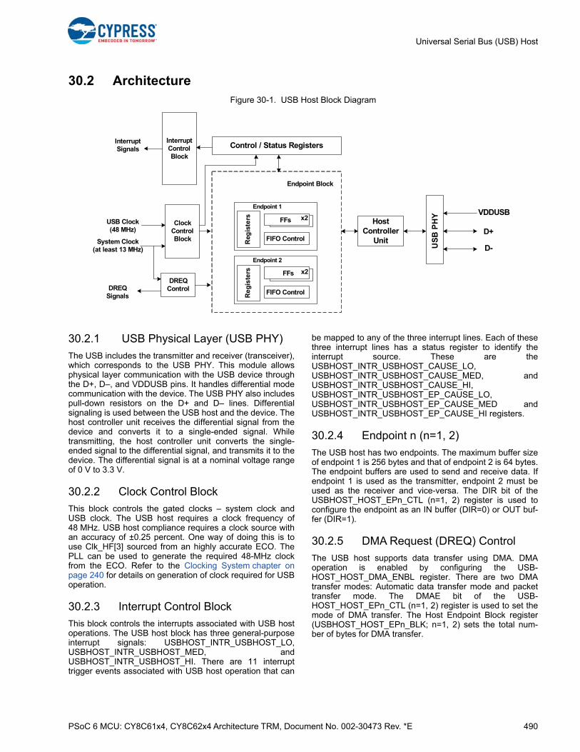
PSoC 6 MCU: CY8C61x4, CY8C62x4 Architecture TRM, Document No. 002-30473 Rev. *E 490
Universal Serial Bus (USB) Host
30.2 ArchitectureFigure 30-1. USB Host Block Diagram
30.2.1 USB Physical Layer (USB PHY)
The USB includes the transmitter and receiver (transceiver),which corresponds to the USB PHY. This module allowsphysical layer communication with the USB device throughthe D+, D–, and VDDUSB pins. It handles differential modecommunication with the device. The USB PHY also includespull-down resistors on the D+ and D– lines. Differentialsignaling is used between the USB host and the device. Thehost controller unit receives the differential signal from thedevice and converts it to a single-ended signal. Whiletransmitting, the host controller unit converts the single-ended signal to the differential signal, and transmits it to thedevice. The differential signal is at a nominal voltage rangeof 0 V to 3.3 V.
30.2.2 Clock Control Block
This block controls the gated clocks – system clock andUSB clock. The USB host requires a clock frequency of48 MHz. USB host compliance requires a clock source withan accuracy of ±0.25 percent. One way of doing this is touse Clk_HF[3] sourced from an highly accurate ECO. ThePLL can be used to generate the required 48-MHz clockfrom the ECO. Refer to the Clocking System chapter onpage 240 for details on generation of clock required for USBoperation.
30.2.3 Interrupt Control Block
This block controls the interrupts associated with USB hostoperations. The USB host block has three general-purposeinterrupt signals: USBHOST_INTR_USBHOST_LO,USBHOST_INTR_USBHOST_MED, andUSBHOST_INTR_USBHOST_HI. There are 11 interrupttrigger events associated with USB host operation that can
be mapped to any of the three interrupt lines. Each of thesethree interrupt lines has a status register to identify theinterrupt source. These are theUSBHOST_INTR_USBHOST_CAUSE_LO,USBHOST_INTR_USBHOST_CAUSE_MED, andUSBHOST_INTR_USBHOST_CAUSE_HI,USBHOST_INTR_USBHOST_EP_CAUSE_LO,USBHOST_INTR_USBHOST_EP_CAUSE_MED andUSBHOST_INTR_USBHOST_EP_CAUSE_HI registers.
30.2.4 Endpoint n (n=1, 2)
The USB host has two endpoints. The maximum buffer sizeof endpoint 1 is 256 bytes and that of endpoint 2 is 64 bytes.The endpoint buffers are used to send and receive data. Ifendpoint 1 is used as the transmitter, endpoint 2 must beused as the receiver and vice-versa. The DIR bit of theUSBHOST_HOST_EPn_CTL (n=1, 2) register is used toconfigure the endpoint as an IN buffer (DIR=0) or OUT buf-fer (DIR=1).
30.2.5 DMA Request (DREQ) Control
The USB host supports data transfer using DMA. DMAoperation is enabled by configuring the USB-HOST_HOST_DMA_ENBL register. There are two DMAtransfer modes: Automatic data transfer mode and packettransfer mode. The DMAE bit of the USB-HOST_HOST_EPn_CTL (n=1, 2) register is used to set themode of DMA transfer. The Host Endpoint Block register(USBHOST_HOST_EPn_BLK; n=1, 2) sets the total num-ber of bytes for DMA transfer.
Control / Status RegistersInterruptControlBlock
ClockControlBlock
InterruptSignals
System Clock(at least 13 MHz)
DREQSignals
USB Clock(48 MHz)
Endpoint Block
Endpoint 1
Reg
iste
rs FFs
FIFO Control
x2
Endpoint 2
Re
gis
ters
FIFO Control
FFsDREQ
Control
Host Controller
Unit
US
B P
HY
D+
D-
VDDUSB
x2
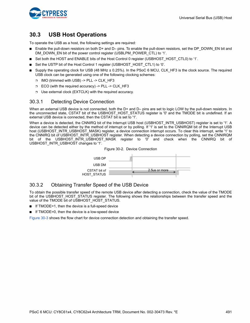
PSoC 6 MCU: CY8C61x4, CY8C62x4 Architecture TRM, Document No. 002-30473 Rev. *E 491
Universal Serial Bus (USB) Host
30.3 USB Host OperationsTo operate the USB as a host, the following settings are required:
■ Enable the pull-down resistors on both D+ and D– pins. To enable the pull-down resistors, set the DP_DOWN_EN bit andDM_DOWN_EN bit of the power control register (USBLPM_POWER_CTL) to ‘1’.
■ Set both the HOST and ENABLE bits of the Host Control 0 register (USBHOST_HOST_CTL0) to ‘1’.
■ Set the USTP bit of the Host Control 1 register (USBHOST_HOST_CTL1) to ‘0’.
■ Supply the operating clock for USB (48 MHz ± 0.25%). In the PSoC 6 MCU, CLK_HF3 is the clock source. The requiredUSB clock can be generated using one of the following clocking schemes:
❐ IMO (trimmed with USB) -> PLL -> CLK_HF3
❐ ECO (with the required accuracy) -> PLL -> CLK_HF3
❐ Use external clock (EXTCLK) with the required accuracy.
30.3.1 Detecting Device Connection
When an external USB device is not connected, both the D+ and D– pins are set to logic LOW by the pull-down resistors. Inthe unconnected state, CSTAT bit of the USBHOST_HOST_STATUS register is '0' and the TMODE bit is undefined. If anexternal USB device is connected, then the CSTAT bit is set to '1'.
When a device is detected, the CNNIRQ bit of the Interrupt USB host (USBHOST_INTR_USBHOST) register is set to '1'. Adevice can be detected either by the method of interrupt or by polling. If '1' is set to the CNNIRQM bit of the Interrupt USBhost (USBHOST_INTR_USBHOST_MASK) register, a device connection interrupt occurs. To clear this interrupt, write '1' tothe CNNIRQ bit of USBHOST_INTR_USBHOST register. When detecting a device connection by polling, set the CNNIRQMbit of the USBHOST_INTR_USBHOST_MASK register to '0' and check when the CNNIRQ bit ofUSBHOST_INTR_USBHOST changes to '1'.
Figure 30-2. Device Connection
30.3.2 Obtaining Transfer Speed of the USB Device
To obtain the possible transfer speed of the remote USB device after detecting a connection, check the value of the TMODEbit of the USBHOST_HOST_STATUS register. The following shows the relationships between the transfer speed and thevalue of the TMODE bit of USBHOST_HOST_STATUS.
■ If TMODE=1, then the device is a full-speed device
■ If TMODE=0, then the device is a low-speed device
Figure 30-3 shows the flow chart for device connection detection and obtaining the transfer speed.
USB DP
USB DM
CSTAT bit of HOST_STATUS
2.5us or more
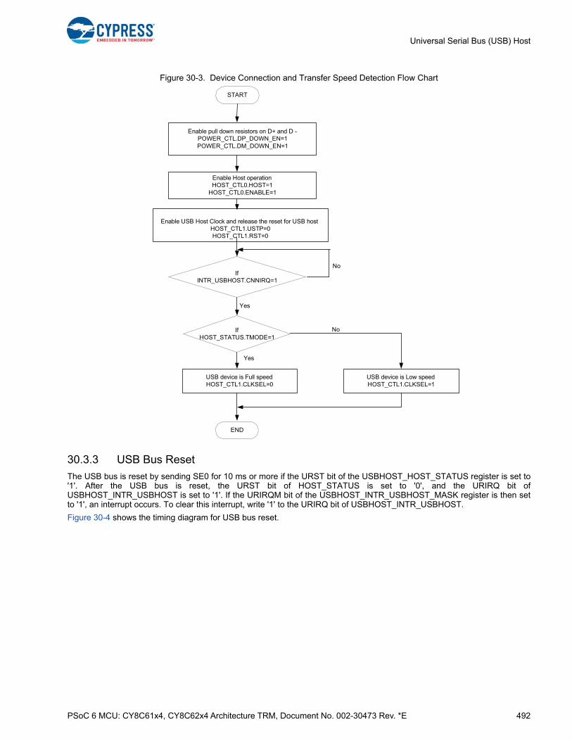
PSoC 6 MCU: CY8C61x4, CY8C62x4 Architecture TRM, Document No. 002-30473 Rev. *E 492
Universal Serial Bus (USB) Host
Figure 30-3. Device Connection and Transfer Speed Detection Flow Chart
30.3.3 USB Bus Reset
The USB bus is reset by sending SE0 for 10 ms or more if the URST bit of the USBHOST_HOST_STATUS register is set to'1'. After the USB bus is reset, the URST bit of HOST_STATUS is set to '0', and the URIRQ bit ofUSBHOST_INTR_USBHOST is set to '1'. If the URIRQM bit of the USBHOST_INTR_USBHOST_MASK register is then setto '1', an interrupt occurs. To clear this interrupt, write '1' to the URIRQ bit of USBHOST_INTR_USBHOST.
Figure 30-4 shows the timing diagram for USB bus reset.
START
Enable pull down resistors on D+ and D -POWER_CTL.DP_DOWN_EN=1POWER_CTL.DM_DOWN_EN=1
Enable Host operationHOST_CTL0.HOST=1
HOST_CTL0.ENABLE=1
Enable USB Host Clock and release the reset for USB hostHOST_CTL1.USTP=0HOST_CTL1.RST=0
If INTR_USBHOST.CNNIRQ=1
IfHOST_STATUS.TMODE=1
USB device is Full speedHOST_CTL1.CLKSEL=0
USB device is Low speedHOST_CTL1.CLKSEL=1
END
Yes
No
Yes
No
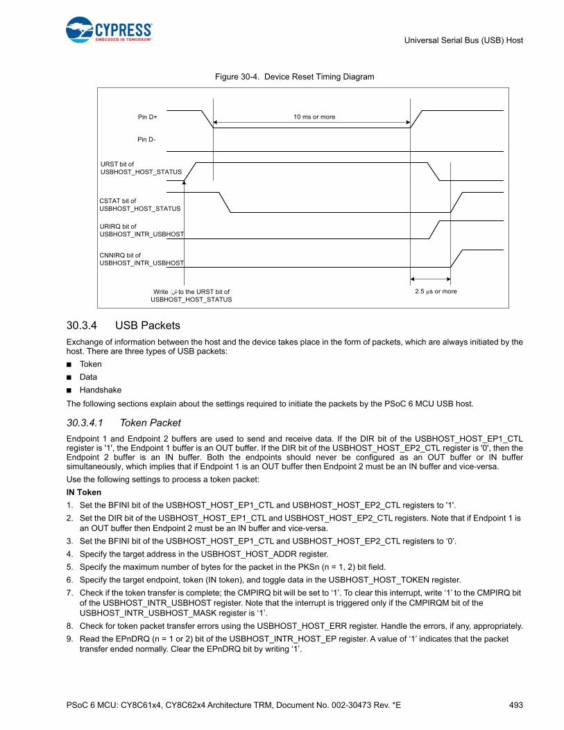
PSoC 6 MCU: CY8C61x4, CY8C62x4 Architecture TRM, Document No. 002-30473 Rev. *E 493
Universal Serial Bus (USB) Host
Figure 30-4. Device Reset Timing Diagram
30.3.4 USB Packets
Exchange of information between the host and the device takes place in the form of packets, which are always initiated by thehost. There are three types of USB packets:
■ Token
■ Data
■ Handshake
The following sections explain about the settings required to initiate the packets by the PSoC 6 MCU USB host.
30.3.4.1 Token Packet
Endpoint 1 and Endpoint 2 buffers are used to send and receive data. If the DIR bit of the USBHOST_HOST_EP1_CTLregister is '1', the Endpoint 1 buffer is an OUT buffer. If the DIR bit of the USBHOST_HOST_EP2_CTL register is '0', then theEndpoint 2 buffer is an IN buffer. Both the endpoints should never be configured as an OUT buffer or IN buffersimultaneously, which implies that if Endpoint 1 is an OUT buffer then Endpoint 2 must be an IN buffer and vice-versa.
Use the following settings to process a token packet:
IN Token
1. Set the BFINI bit of the USBHOST_HOST_EP1_CTL and USBHOST_HOST_EP2_CTL registers to '1'.
2. Set the DIR bit of the USBHOST_HOST_EP1_CTL and USBHOST_HOST_EP2_CTL registers. Note that if Endpoint 1 is an OUT buffer then Endpoint 2 must be an IN buffer and vice-versa.
3. Set the BFINI bit of the USBHOST_HOST_EP1_CTL and USBHOST_HOST_EP2_CTL registers to ‘0’.
4. Specify the target address in the USBHOST_HOST_ADDR register.
5. Specify the maximum number of bytes for the packet in the PKSn (n = 1, 2) bit field.
6. Specify the target endpoint, token (IN token), and toggle data in the USBHOST_HOST_TOKEN register.
7. Check if the token transfer is complete; the CMPIRQ bit will be set to ‘1’. To clear this interrupt, write ‘1’ to the CMPIRQ bit of the USBHOST_INTR_USBHOST register. Note that the interrupt is triggered only if the CMPIRQM bit of the USBHOST_INTR_USBHOST_MASK register is ‘1’.
8. Check for token packet transfer errors using the USBHOST_HOST_ERR register. Handle the errors, if any, appropriately.
9. Read the EPnDRQ (n = 1 or 2) bit of the USBHOST_INTR_HOST_EP register. A value of ‘1’ indicates that the packet transfer ended normally. Clear the EPnDRQ bit by writing ‘1’.
Pin D+
Pin D-
URST bit of USBHOST_HOST_STATUS
CSTAT bit of USBHOST_HOST_STATUS
URIRQ bit of USBHOST_INTR_USBHOST
CNNIRQ bit of USBHOST_INTR_USBHOST
10 ms or more
2.5 µs or moreWrite ش to the URST bit of USBHOST_HOST_STATUS

PSoC 6 MCU: CY8C61x4, CY8C62x4 Architecture TRM, Document No. 002-30473 Rev. *E 494
Universal Serial Bus (USB) Host
10. Read data received from USBHOST_HOST_EPn_RWn_DR register (n =1, 2).
OUT and SETUP Tokens
1. Set the BFINI bit of the USBHOST_HOST_EP1_CTL and USBHOST_HOST_EP2_CTL registers to ‘1’.
2. Set the DIR bit of the USBHOST_HOST_EP1_CTL and USBHOST_HOST_EP2_CTL registers. Note that if Endpoint 1 is an OUT buffer then Endpoint 2 must be an IN buffer and vice-versa.
3. Set the BFINI bit of the USBHOST_HOST_EP1_CTL and USBHOST_HOST_EP2_CTL registers to ‘0’.
4. Specify the target address in the USBHOST_HOST_ADDR register.
5. Specify the maximum number of bytes for the packet in the PKSn (n = 1, 2) bit field.
6. Write the data to be sent to the Endpoint n (n = 1 or 2) buffer. Use USBHOST_HOST_EPn_WR1_DR for 1-byte data and USBHOST_HOST_EPn_WR2_DR for 2-byte data. Also, set the EPnDRQ (n = 1 or 2) bit of the USBHOST_IN-TR_HOST_EP register as ‘1’.
7. Specify the target endpoint, token (OUT token), and toggle data in the USBHOST_HOST_TOKEN register.
8. Check if the token transfer is complete; the CMPIRQ bit will be set to ‘1’. To clear this interrupt, write ‘1’ to the CMPIRQ bit of the USBHOST_INTR_USBHOST register. Note that the interrupt is triggered only if the CMPIRQM bit of the USB-HOST_INTR_USBHOST_MASK register is ‘1’.
9. Check for token packet transfer errors using the USBHOST_HOST_ERR register. Handle the errors, if any, appropriately.
The USB PHY sends a token packet in the order of sync, token, address, endpoint, CRC5, and EOP based on the specifiedtoken; however, sync, CRC5, and EOP are sent automatically. After one packet is sent, the CMPIRQ bit of theUSBHOST_INTR_USBHOST register is set to ‘1’. The TKNEN bit of the USBHOST_HOST_TOKEN register is set to ‘000’. Atthis time, if the CMPIRQM bit of USBHOST_INTR_USBHOST_MASK register is '1', an interrupt occurs. To clear thisinterrupt, write '1' to the CMPIRQ bit of the USBHOST_INTR_USBHOST register.
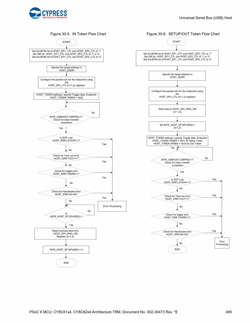
PSoC 6 MCU: CY8C61x4, CY8C62x4 Architecture TRM, Document No. 002-30473 Rev. *E 495
Universal Serial Bus (USB) Host
Figure 30-5. IN Token Flow Chart Figure 30-6. SETUP/OUT Token Flow Chart
Specify the target address inHOST_ADDR
Configure the packet size for the endpoints using the
HOST_EPn_CTL (n=1,2) registers
HOST_TOKEN settings ( specify Toggle data, Endpoint)HOST_TOKEN.TKNEN = 0x02
INTR_USBHOST.CMPIRQ=1?Check for token transfer
completion
Is SOF LostHOST_ERR.LSTSOF=1?
Check for Time out errorHOST_ERR.TOUT=1?
Check for Handshake errorHOST_ERR.HS=00?
END
Error Processing
Check for toggle errorHOST_ERR.TGERR=1?
No
Yes
No
No
No
No
Is INTR_HOST_EP.EPnDRQ=1
Read received data fromHOST_EPn_RWn_DR
Register (n=1,2)
INTR_HOST_EP.EPnDRQ = 0
No
Yes
START
Set the BFINI bit of HOST_EP1_CTL and HOST_EP2_CTL to ‘1'Set DIR bit HOST_EP1_CTL and HOST_EP2_CTL to ‘1’ or ‘0’.
Set the BFINI bit of HOST_EP1_CTL and HOST_EP2_CTL to ‘0'
Yes
Yes
Yes
Yes
START
Specify the target address inHOST_ADDR
Configure the packet size for the endpoints using the
HOST_EPn_CTL (n=1,2) registers
HOST_TOKEN settings ( specify Toggle data, Endpoint)HOST_TOKEN.TKNEN = 0x01 for Setup TokenHOST_TOKEN.TKNEN = 0x03 for Out Token
INTR_USBHOST.CMPIRQ=1?Check for token transfer
completion
Is SOF LostHOST_ERR.LSTSOF=1?
Check for Time out errorHOST_ERR.TOUT=1?
Check for Handshake errorHOST_ERR.HS=00?
END
Error Processing
Check for toggle errorHOST_ERR.TGERR=1?
No
Yes
No
No
Yes
Write data to HOST_EPn_RWn_DR(n= 1,2)
Set INTR_HOST_EP.EPnDRQ=1(n=1,2)
No
Yes
Yes
Yes
Set the BFINI bit of HOST_EP1_CTL and HOST_EP2_CTL to ‘1'Set DIR bit HOST_EP1_CTL and HOST_EP2_CTL to ‘1’ or ‘0’.
Set the BFINI bit of HOST_EP1_CTL and HOST_EP2_CTL to ‘0'
Yes
No

PSoC 6 MCU: CY8C61x4, CY8C62x4 Architecture TRM, Document No. 002-30473 Rev. *E 496
Universal Serial Bus (USB) Host
When issuing an SOF token, specify the EOF time in the Host EOF Setup (USBHOST_HOST_EOF) register and the framenumber in the Host Frame Setup (USBHOST_HOST_FRAME) register respectively. Then, specify an SOF token code in theTKNEN bit of the USBHOST_HOST_TOKEN register. After sync, SOF token, frame number, CRC5, and EOP are sent, theSOFBUSY bit of the USBHOST_HOST_STATUS register is set to ‘1’, and the USBHOST_HOST_FRAME register isincremented by one. The CMPIRQ bit of the USBHOST_INTR_USBHOST register is also set to ‘1’, causing the TKNEN bit ofthe USBHOST_HOST_TOKEN register to be cleared to ‘000’. To clear a token completion interrupt, write ‘1’ to the CMPIRQbit of the Host Interrupt (USBHOST_HIRQ) register.
An SOF is automatically sent every 1 ms while the SOFBUSY bit of the USBHOST_HOST_STATUS register is ‘1’.Figure 30-7 depicts steps to send an SOF token
Figure 30-7. SOF Token Flow Chart
The conditions (SOF stop conditions) to set the SOFBUSY bit of the USBHOST_HOST_STATUS register to ‘0’ are as fol-lows:
■ Writing 0 to the SOFBUSY bit of USBHOST_HOST_STATUS
■ Resetting the USB bus
■ Writing 1 to the SUSP bit of USBHOST_HOST_STATUS
■ Disconnecting the USB device (when the CSTAT bit of USBHOST_HOST_STATUS is ‘0’)
The USBHOST_HOST_EOF register is used to prevent the SOF from being sent simultaneously with other tokens. If theTKNEN bit of the USBHOST_HOST_TOKEN register is written within the time period specified by theUSBHOST_HOST_EOF register, the specified token is placed into the wait state. After the SOF is sent, the token in the waitstate is issued. The HOST_EOF Setup register specifies a 1-bit time as the time unit. When the EOF setting is shorter thanthe 1-packet time, SOF may be sent doubly during execution of other tokens. In this case, the LSTSOF bit of the Host ErrorStatus (USBHOST_HOST_ERR) register is set to ‘1’ and SOF is not sent. If ‘1’ is set to the LSTSOF bit of theUSBHOST_HOST_ERR register, the value of the Host EOF Setup register must be increased.
Figure 30-8. SOF Timing
START
HOST_FRAME Setting
HOST_EOF Setting
HOST_TOKEN setting
INTR_USBHOST.CMPIRQ=1?
HOST_ERR.LSTSOF=1?
END
Error Processing
Yes
No
Yes
No
1 ms
EOF setting time
SOF
EOF setting time
SOF
EOF > 1-packet time
PSoC 6 MCU: CY8C61x4, CY8C62x4 Architecture TRM, Document No. 002-30473 Rev. *E 497
Universal Serial Bus (USB) Host
30.3.4.2 Data Packet
Follow these steps to send or receive a data packet aftersending a token packet.
■ Transmitting data (host to device)
❐ Sync pattern is automatically sent.
❐ If the TGGL bit of USBHOST_HOST_TOKEN is 0, DATA0 is sent. If the TGGL bit is 1, DATA1 is sent.
❐ If the DIR bit of the USBHOST_HOST_EP1_CTL register is 1 (that is, if EP1 is an OUT endpoint), select the Endpoint 1 buffer; otherwise, select the Endpoint 2 buffer. Then, send all the target data.
❐ 16-bit CRC is automatically sent.
❐ 2-bit EOP is automatically sent.
❐ 1-bit J State is automatically sent.
■ Receiving data (device to host)
❐ Receive sync.
❐ Receive toggle data, and compare it with the value of the TGGL bit of HOST_TOKEN.
❐ If the toggle data matches the value of the TGGL bit, check the DIR bit of HOST_EP1_CTL. If the DIR bit is 1, select the Endpoint 2 buffer; otherwise, select the Endpoint 1 buffer. Then, distribute the received data to the respective buffers.
❐ Verify the 16-bit CRC when EOF is received.
30.3.4.3 Handshake Packet
A handshake packet is used to notify the remote device ofthe status of the local device. A handshake packet sendseither one of ACK, NAK, and STALL from the receiving sidewhen it is judged that the receiving side is ready to receivedata normally. If the USB circuit receives a handshakepacket, the type of the received handshake packet is set tothe HS bit of the USBHOST_HOST_ERR register.
30.3.5 Retry Function
When a NAK or CRC error occurs at the end of a packet, if‘1’ is set to the RETRY bit of the Host Control 2(USBHOST_HOST_CTL2) register, processing is retriedrepeatedly for the period specified in the Host Retry TimerSetup (USBHOST_HOST_RTIMER) register.
When an error other than STALL or device disconnectionoccurs, the target token is retried if the RETRY bit ofHOST_CTL2 is 1. The conditions to end retry processingare as follows.
■ The RETRY bit of HOST_CTL2 is set to 0.
■ ‘0’ is detected in the retry timer.
■ The interrupt flag is generated by SOF (SOFIRQ ofUSBHOST_INTR_USBHOST = 1).
■ ACK is detected.
■ A device disconnection is detected.
The retry timer is activated when a token is sent while theRETRY bit of HOST_CTL2 is ‘1’. The retry time is then dec-
remented by one when a 1-bit transfer clock (12 MHz in full-speed mode) is output. When the retry timer reaches 0, thetarget token is sent, and processing ends. If a token retryoccurs in the EOF area, the retry timer is stopped until SOFis sent. After SOF is sent, the retry timer restarts with thevalue that is set when the timer stopped.
30.3.6 Error Status
The USB host supports detection of the following types oferrors:
■ Stuffing Error
If 1 is writter to six successive bits, 0 is inserted into one bit. If 1 is successively detected in seven bits, it is regarded as a Stuffing error, and the STUFF bit of the USBHOST_HOST_ERR register is set to 1. To clear this status, write ‘1’ to the STUFF bit.
■ Toggle Error
When sending an IN token, the Toggle Data field of a data packet is compared with the value of the TGGL bit of the USBHOST_HOST_TOKEN register. If they do not match, the TGERR bit of the USBHOST_HOST_ERR register is set to 1. To clear the TGERR bit, write ‘1’ to the TGERR bit of the USBHOST_HOST_ERR register.
■ CRC Error
When receiving an IN token, the data and CRC of the received data packet are obtained with the CRC polynomial G(X) = X16 + X15 + X2 + 1. If the remainder is not 0x800D, it means that a CRC error has occurred, and the CRC bit of the USBHOST_HOST_ERR register is set to 1. To clear the CRC bit, write ‘1’ to the CRC bit of USBHOST_HOST_ERR. For more details, refer to the documentation: CRC in USB.
■ Time Out Error
The TOUT bit of the USBHOST_HOST_ERR register is set and time out error is considered under any of the following conditions:
❐ A data packet or handshake packet is not input in the specified time
❐ SE0 is detected when receiving data
❐ Stuffing error is detected
To clear the TOUT bit, write 0 to the TOUT bit of the USBHOST_HOST_ERR register.
■ Receive Error
The PKSn (n = 1, 2) bit of Endpoint Control register (USBHOST_HOST_EPn_CTL; n=1, 2) indicates the receiver packet size. When the received data exceeds the specified receive packet size, the RERR bit of the USBHOST_HOST_ERR register is set to 1. To clear the RERR bit, write ‘1’ to the RERR bit of USBHOST_HOST_ERR.
■ Lost SOF Error
When the LSTSOF bit of the USBHOST_HOST_ERR register is set, it means that the SOF token cannot be

PSoC 6 MCU: CY8C61x4, CY8C62x4 Architecture TRM, Document No. 002-30473 Rev. *E 498
Universal Serial Bus (USB) Host
sent because another token is in process. When this bit is ‘0’, it means that no lost SOF error is detected.
30.3.7 End of Packet (EOP)
If a packet ends in the USB host, the CMPIRQ bit of theUSBHOST_INTR_USBHOST register is set to 1. At this
time, if the CMPIRQM bit of theUSBHOST_INTR_USBHOST_MASK register is 1, aninterrupt occurs.
When a packet ends, the interrupt is generated when theTKNEN bit of the USBHOST_HOST_TOKEN register is setas ‘001’ (SETUP token), ‘010’ (IN token), ‘011’ (OUT token),or ‘100’ (SOF token).
Figure 30-9. EOP Interrupt Timing Diagram (for IN/OUT/SETUP token)
Figure 30-10. EOP Interrupt Timing Diagram (for SOF token)
30.3.8 Interrupt Sources
The USB host generates 11 interrupts to the CPU. These interrupts are mapped to three general-purpose interrupt lines:USBHOST_INTR_LO, USBHOST_INTR_MED, and USBHOST_INTR_HI. Each of these three interrupt lines has anassociated status register, which identifies the cause of the interrupt event. These areUSBHOST_INTR_USBHOST_CAUSE_LO, USBHOST_INTR_USBHOST_CAUSE_MED,USBHOST_INTR_USBHOST_CAUSE_HI, USBHOST_INTR_HOST_EP_CAUSE_LO,USBHOST_INTR_HOST_EP_CAUSE_MED, and USBHOST_INTR_HOST_EP_CAUSE_HI.
J‐ST DATA
CMPIRQ bit of INTR_USBHOST
Sync TKN ADR ENDP CRC5 EOP J‐ST Sync TGGL CRC16 EOP J‐ST Sync ACK EOP J‐ST
J‐ST : J State
TKN
ADR
ENDP
TGGL
: Token
: Address
: Endpoint
: Toggle
Write data to the TKNEN bit of HOST_TOKEN Token Packet Data Packet Handshake Packet
Write data to the TKNEN bit of HTOKEN.
J-ST Sync TKN FRAME CRC5 EOP J-ST
CMPIRQ bit(HIRQ)
J-ST : J StateTKN : TokenFRAME : Frame Number
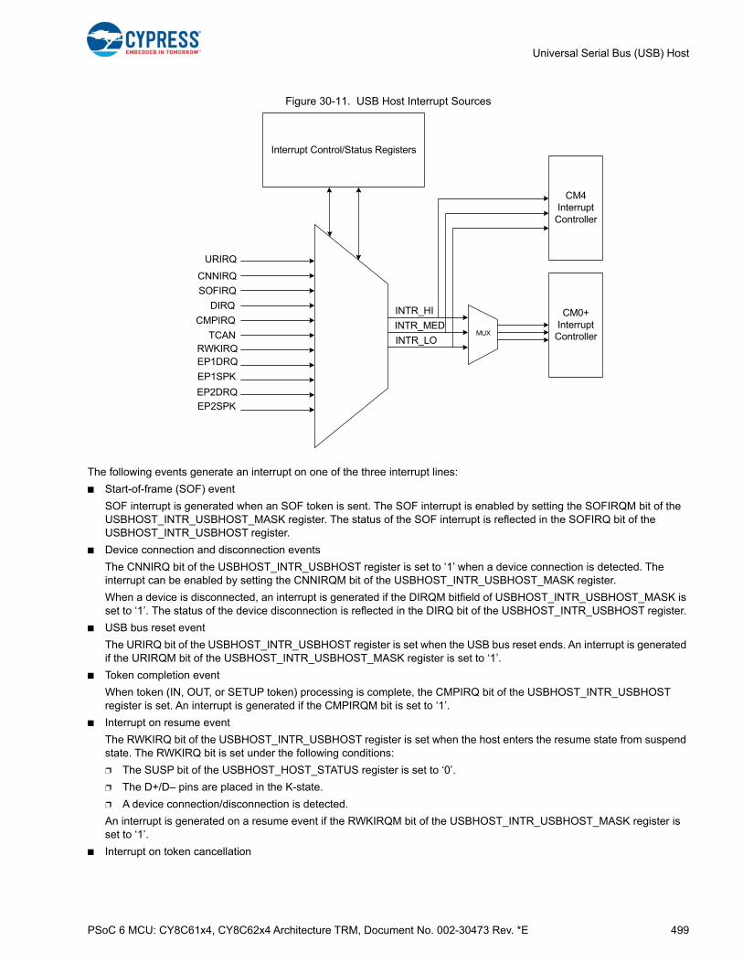
PSoC 6 MCU: CY8C61x4, CY8C62x4 Architecture TRM, Document No. 002-30473 Rev. *E 499
Universal Serial Bus (USB) Host
Figure 30-11. USB Host Interrupt Sources
The following events generate an interrupt on one of the three interrupt lines:
■ Start-of-frame (SOF) event
SOF interrupt is generated when an SOF token is sent. The SOF interrupt is enabled by setting the SOFIRQM bit of the USBHOST_INTR_USBHOST_MASK register. The status of the SOF interrupt is reflected in the SOFIRQ bit of the USBHOST_INTR_USBHOST register.
■ Device connection and disconnection events
The CNNIRQ bit of the USBHOST_INTR_USBHOST register is set to ‘1’ when a device connection is detected. The interrupt can be enabled by setting the CNNIRQM bit of the USBHOST_INTR_USBHOST_MASK register.
When a device is disconnected, an interrupt is generated if the DIRQM bitfield of USBHOST_INTR_USBHOST_MASK is set to ‘1’. The status of the device disconnection is reflected in the DIRQ bit of the USBHOST_INTR_USBHOST register.
■ USB bus reset event
The URIRQ bit of the USBHOST_INTR_USBHOST register is set when the USB bus reset ends. An interrupt is generated if the URIRQM bit of the USBHOST_INTR_USBHOST_MASK register is set to ‘1’.
■ Token completion event
When token (IN, OUT, or SETUP token) processing is complete, the CMPIRQ bit of the USBHOST_INTR_USBHOST register is set. An interrupt is generated if the CMPIRQM bit is set to ‘1’.
■ Interrupt on resume event
The RWKIRQ bit of the USBHOST_INTR_USBHOST register is set when the host enters the resume state from suspend state. The RWKIRQ bit is set under the following conditions:
❐ The SUSP bit of the USBHOST_HOST_STATUS register is set to ‘0’.
❐ The D+/D– pins are placed in the K-state.
❐ A device connection/disconnection is detected.
An interrupt is generated on a resume event if the RWKIRQM bit of the USBHOST_INTR_USBHOST_MASK register is set to ‘1’.
■ Interrupt on token cancellation
Interrupt Control/Status Registers
CM4Interrupt
Controller
DIRQ
RWKIRQ
INTR_HI
INTR_MED
INTR_LO
CM0+Interrupt
ControllerMUX
SOFIRQ
CNNIRQ
CMPIRQ
URIRQ
TCAN
EP2DRQ
EP1SPK
EP1DRQ
EP2SPK
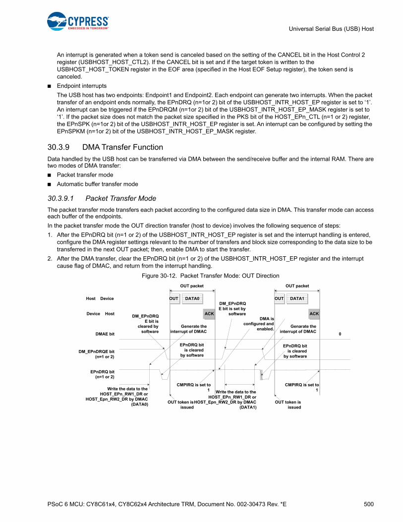
PSoC 6 MCU: CY8C61x4, CY8C62x4 Architecture TRM, Document No. 002-30473 Rev. *E 500
Universal Serial Bus (USB) Host
An interrupt is generated when a token send is canceled based on the setting of the CANCEL bit in the Host Control 2 register (USBHOST_HOST_CTL2). If the CANCEL bit is set and if the target token is written to the USBHOST_HOST_TOKEN register in the EOF area (specified in the Host EOF Setup register), the token send is canceled.
■ Endpoint interrupts
The USB host has two endpoints: Endpoint1 and Endpoint2. Each endpoint can generate two interrupts. When the packet transfer of an endpoint ends normally, the EPnDRQ (n=1or 2) bit of the USBHOST_INTR_HOST_EP register is set to ‘1’. An interrupt can be triggered if the EPnDRQM (n=1or 2) bit of the USBHOST_INTR_HOST_EP_MASK register is set to ‘1’. If the packet size does not match the packet size specified in the PKS bit of the HOST_EPn_CTL (n=1 or 2) register, the EPnSPK (n=1or 2) bit of the USBHOST_INTR_HOST_EP register is set. An interrupt can be configured by setting the EPnSPKM (n=1or 2) bit of the USBHOST_INTR_HOST_EP_MASK register.
30.3.9 DMA Transfer Function
Data handled by the USB host can be transferred via DMA between the send/receive buffer and the internal RAM. There aretwo modes of DMA transfer:
■ Packet transfer mode
■ Automatic buffer transfer mode
30.3.9.1 Packet Transfer Mode
The packet transfer mode transfers each packet according to the configured data size in DMA. This transfer mode can accesseach buffer of the endpoints.
In the packet transfer mode the OUT direction transfer (host to device) involves the following sequence of steps:
1. After the EPnDRQ bit (n=1 or 2) of the USBHOST_INTR_HOST_EP register is set and the interrupt handling is entered, configure the DMA register settings relevant to the number of transfers and block size corresponding to the data size to be transferred in the next OUT packet; then, enable DMA to start the transfer.
2. After the DMA transfer, clear the EPnDRQ bit (n=1 or 2) of the USBHOST_INTR_HOST_EP register and the interrupt cause flag of DMAC, and return from the interrupt handling.
Figure 30-12. Packet Transfer Mode: OUT Direction
Host Device OUT DATA0
ACKDevice Host
DMAE bit 0
DM_EPnDRQE bit (n=1 or 2)
EPnDRQ bit (n=1 or 2)
OUT DATA1
ACK
Write the data to the HOST_EPn_RW1_DR or
HOST_Epn_RW2_DR by DMAC (DATA0)
EPnDRQ bit is cleared
by software
Write the data to the HOST_EPn_RW1_DR or
HOST_Epn_RW2_DR by DMAC (DATA1)
EPnDRQ bit is cleared
by software
Generate the interrupt of DMAC
Genarate the interrupt of DMAC
OUT packet OUT packet
OUT token is issued
OUT token is issued
DMA is configured and
enabled.
CMPIRQ is set to 1
CMPIRQ is set to 1
DM_EPnDRQE bit is
cleared by software
DM_EPnDRQE bit is set by
software
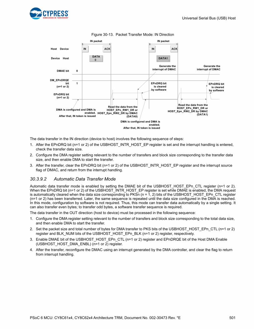
PSoC 6 MCU: CY8C61x4, CY8C62x4 Architecture TRM, Document No. 002-30473 Rev. *E 501
Universal Serial Bus (USB) Host
Figure 30-13. Packet Transfer Mode: IN Direction
The data transfer in the IN direction (device to host) involves the following sequence of steps:
1. After the EPnDRQ bit (n=1 or 2) of the USBHOST_INTR_HOST_EP register is set and the interrupt handling is entered, check the transfer data size.
2. Configure the DMA register setting relevant to the number of transfers and block size corresponding to the transfer data size, and then enable DMA to start the transfer.
3. After the transfer, clear the EPnDRQ bit (n=1 or 2) of the USBHOST_INTR_HOST_EP register and the interrupt source flag of DMAC, and return from the interrupt handling.
30.3.9.2 Automatic Data Transfer Mode
Automatic data transfer mode is enabled by setting the DMAE bit of the USBHOST_HOST_EPn_CTL register (n=1 or 2).When the EPnDRQ bit (n=1 or 2) of the USBHOST_INTR_HOST_EP register is set while DMAE is enabled, the DMA requestis automatically cleared when the data size corresponding to PKSn (n = 1, 2) bits of the USBHOST_HOST_EPn_CTL register(n=1 or 2) has been transferred. Later, the same sequence is repeated until the data size configured in the DMA is reached.In this mode, configuration by software is not required. Thus, this mode can transfer data automatically by a single setting. Itcan also transfer even bytes; to transfer odd bytes, a software transfer sequence is required.
The data transfer in the OUT direction (host to device) must be processed in the following sequence:
1. Configure the DMA register setting relevant to the number of transfers and block size corresponding to the total data size, and then enable DMA to start the transfer.
2. Set the packet size and total number of bytes for DMA transfer to PKS bits of the USBHOST_HOST_EPn_CTL (n=1 or 2) register and BLK_NUM bits of the USBHOST_HOST_EPn_BLK (n=1 or 2) register, respectively.
3. Enable DMAE bit of the USBHOST_HOST_EPn_CTL (n=1 or 2) register and EPnDRQE bit of the Host DMA Enable (USBHOST_HOST_DMA_ENBL) (n=1 or 2) register.
4. After the transfer, reconfigure the DMAC using an interrupt generated by the DMA controller, and clear the flag to return from interrupt handling.
Host Device IN
DATA0
ACK
Device Host
DMAE bit 0
DM_EPnDRQE bit
(n=1 or 2)1
EPnDRQ bit (n=1 or 2)
IN
DATA1
ACK
Read the data from the HOST_EPn_RW1_DR or
HOST_Epn_RW2_DR by DMAC (DATA1)
EPnDRQ bit is cleared
by software
Read the data from the HOST_EPn_RW1_DR or
HOST_Epn_RW2_DR by DMAC (DATA0)
EPnDRQ bit is cleared
by software
Generate the interrupt of DMAC
Generate the interrupt of DMAC
IN packet IN packet
DMA is configured and DMA is enabled.
After that, IN token is issued
DMA is configured and DMA is enabled.
After that, IN token is issued
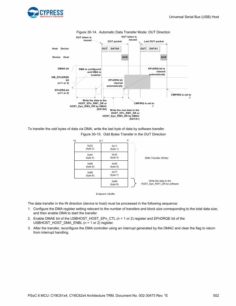
PSoC 6 MCU: CY8C61x4, CY8C62x4 Architecture TRM, Document No. 002-30473 Rev. *E 502
Universal Serial Bus (USB) Host
Figure 30-14. Automatic Data Transfer Mode: OUT Direction
To transfer the odd bytes of data via DMA, write the last byte of data by software transfer.
Figure 30-15. Odd Bytes Transfer in the OUT Direction
The data transfer in the IN direction (device to host) must be processed in the following sequence:
1. Configure the DMA register setting relevant to the number of transfers and block size corresponding to the total data size, and then enable DMA to start the transfer.
2. Enable DMAE bit of the USBHOST_HOST_EPn_CTL (n = 1 or 2) register and EPnDRQE bit of the USBHOST_HOST_DMA_ENBL (n = 1 or 2) register.
3. After the transfer, reconfigure the DMA controller using an interrupt generated by the DMAC and clear the flag to return from interrupt handling.
Host Device OUT DATA0
ACKDevice Host
DMAE bit
EPnDRQ bit(n=1 or 2)
OUT DATA1
ACK
Write the data to the HOST_EPn_RW1_DR or
HOST_Epn_RW2_DR by DMAC (DATA0)
EPnDRQ bit cleared
automatically
Write the rest data to the HOST_EPn_RW1_DR or
HOST_Epn_RW2_DR by DMAC (DATA1)
EPnDRQ bit is cleared
automatically
OUT packet Last OUT packet
DM_EPnDRQE bit
(n=1 or 2)
OUT token is issued
DMA is configured and DMA is
enabled.
CMPIRQ is set to 1
OUT token is issued
CMPIRQ is set to 1
DMA Transfer (Write)
Write the data to theHOST_Epn_RW1_DR by software
08 715
0x11(byte 1)
0x22(byte 2)
0x44(byte 4)
0x33(byte 3)
0x66(byte 6)
0x55(byte 5)
0x88(byte 8)
0x77(byte 7)
0x99(byte 9)
Endpoint n Buffer
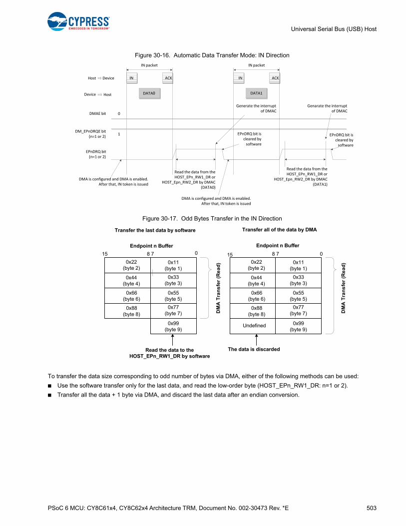
PSoC 6 MCU: CY8C61x4, CY8C62x4 Architecture TRM, Document No. 002-30473 Rev. *E 503
Universal Serial Bus (USB) Host
Figure 30-16. Automatic Data Transfer Mode: IN Direction
Figure 30-17. Odd Bytes Transfer in the IN Direction
To transfer the data size corresponding to odd number of bytes via DMA, either of the following methods can be used:
■ Use the software transfer only for the last data, and read the low-order byte (HOST_EPn_RW1_DR: n=1 or 2).
■ Transfer all the data + 1 byte via DMA, and discard the last data after an endian conversion.
IN
DATA0
ACK
DMAE bit 0
DM_EPnDRQE bit(n=1 or 2)
1
EPnDRQ bit (n=1 or 2)
IN
DATA1
ACK
Read the data from the HOST_EPn_RW1_DR or
HOST_Epn_RW2_DR by DMAC (DATA1)
EPnDRQ bit is cleared by software
Read the data from the HOST_EPn_RW1_DR or
HOST_Epn_RW2_DR by DMAC (DATA0)
EPnDRQ bit is cleared by software
Genarate the interrupt of DMAC
Generate the interrupt of DMAC
IN packet IN packet
DMA is configured and DMA is enabled.After that, IN token is issued
DMA is configured and DMA is enabled.After that, IN token is issued
Host Device
Device Host
DM
A T
ran
sfe
r (R
ea
d)
Read the data to theHOST_EPn_RW1_DR by software
08 715
0x11(byte 1)
0x22(byte 2)
0x44(byte 4)
0x33(byte 3)
0x66(byte 6)
0x55(byte 5)
0x88(byte 8)
0x77(byte 7)
0x99(byte 9)
DM
A T
ran
sfe
r (R
ea
d)
08 715
0x11(byte 1)
0x22(byte 2)
0x44(byte 4)
0x33(byte 3)
0x66(byte 6)
0x55(byte 5)
0x88(byte 8)
0x77(byte 7)
0x99(byte 9)
Endpoint n BufferEndpoint n Buffer
Undefined
The data is discarded
Transfer all of the data by DMATransfer the last data by software
PSoC 6 MCU: CY8C61x4, CY8C62x4 Architecture TRM, Document No. 002-30473 Rev. *E 504
Universal Serial Bus (USB) Host
30.3.10 Suspend and Resume Operations
The USB host supports suspend and resume operations.
30.3.10.1 Suspend Operation
If the SUSP bit of the USBHOST_HOST_STATUS register is set, the following procedure is performed, and the USB circuit isplaced in the suspend state.
■ The USB bus is placed in the high-impedance state.
■ All circuit blocks with no clock required are stopped.
30.3.10.2 Resume Operation
The USB bus changes from the suspend state to the resume state to start processing when one of the following conditions issatisfied.
■ SUSP bit of the USBHOST_HOST_STATUS register is set to ‘0’.
■ The D+ or D– pin is placed in the K-state mode by the device.
■ A device disconnection is detected.
■ A device connection is detected.
The host can start issuing tokens when RWKIRQ bit of the USBHOST_INTR_USBHOST register is set to ‘1’.
30.3.11 Device Disconnection
The device disconnection timer starts when both the D+ and D– pins are set to LOW. If both D+ and D– remain at LOW for2.5 µs or more, the device is considered to be disconnected. This then sets the CSTAT bit of the USBHOST_HOST_STATUSregister as ‘0’ and the DIRQ bit of the USBHOST_INTR_USBHOST register as ‘1’. At this time, if the DIRQM bit of theUSBHOST_INTR_USBHOST_MASK register is 1, an interrupt occurs. To clear this interrupt, write '1' to the DIRQ bit of theUSBHOST_INTR_USBHOST register.
If the USB bus is reset, the device is considered to be disconnected. In this case, the CSTAT bit of theUSBHOST_HOST_STATUS register is set to ‘0’, but the DIRQ bit of the USBHOST_INTR_USBHOST register is not set to 1.
PSoC 6 MCU: CY8C61x4, CY8C62x4 Architecture TRM, Document No. 002-30473 Rev. *E 505
Universal Serial Bus (USB) Host
30.4 USB Host Registers
Name Description
USBHOST_HOST_CTL0 Host control 0 register
USBHOST_HOST_CTL1 Host control 1 register
USBHOST_HOST_CTL2 Host control 2 register
USBHOST_HOST_ERR Host error status register
USBHOST_HOST_STATUS Host status register
USBHOST_HOST_FCOMP Host SOF interrupt frame compare register
USBHOST_HOST_RTIMER Host retry timer setup register
USBHOST_HOST_ADDR Host address register
USBHOST_HOST_EOF Host EOF setup register
USBHOST_HOST_FRAME Host frame setup register
USBHOST_HOST_TOKEN Host token endpoint register
USBHOST_HOST_EP1_CTL Host endpoint 1 control register
USBHOST_HOST_EP1_STATUS Host endpoint 1 status register
USBHOST_HOST_EP1_RW1_DR Host endpoint 1 data 1-byte register
USBHOST_HOST_EP1_RW2_DR Host endpoint 1 data 2-byte register
USBHOST_HOST_EP2_CTL Host endpoint 2 control register
USBHOST_HOST_EP2_STATUS Host endpoint 2 status register
USBHOST_HOST_EP2_RW1_DR Host endpoint 2 data 1-byte register
USBHOST_HOST_EP2_RW2_DR Host endpoint 2 data 2-byte register
USBHOST_HOST_LVL1_SEL Host interrupt level 1 selection register
USBHOST_HOST_LVL2_SEL Host interrupt level 2 selection register
USBHOST_INTR_USBHOST_CAUSE_HI Interrupt USB host cause high register
USBHOST_INTR_USBHOST_CAUSE_MED Interrupt USB host cause medium register
USBHOST_INTR_USBHOST_CAUSE_LO Interrupt USB host cause low register
USBHOST_INTR_HOST_EP_CAUSE_HI Interrupt USB host endpoint cause high register
USBHOST_INTR_HOST_EP_CAUSE_MED Interrupt USB host endpoint cause medium register
USBHOST_INTR_HOST_EP_CAUSE_LO Interrupt USB host endpoint cause low register
USBHOST_INTR_USBHOST Interrupt USB host register
USBHOST_INTR_USBHOST_SET Interrupt USB host set register
USBHOST_INTR_USBHOST_MASK Interrupt USB host mask register
USBHOST_INTR_USBHOST_MASKED Interrupt USB host masked register
USBHOST_INTR_HOST_EP Interrupt USB host endpoint register
USBHOST_INTR_HOST_EP_SET Interrupt USB host endpoint set register
USBHOST_INTR_HOST_EP_MASK Interrupt USB host endpoint mask register
USBHOST_INTR_HOST_EP_MASKED Interrupt USB host endpoint masked register
USBHOST_HOST_DMA_ENBL Host DMA enable register
USBHOST_HOST_EP1_BLK Host endpoint 1 block register
USBHOST_HOST_EP2_BLK Host endpoint 2 block register
PSoC 6 MCU: CY8C61x4, CY8C62x4 Architecture TRM, Document No. 002-30473 Rev. *E 506
31. Universal Serial Bus (USB) Device Mode
The PSoC 6 MCU USB block can act as a USB device that communicates with a USB host. The USB block is available as afixed-function digital block in the PSoC 6 MCU. It supports full-speed communication (12 Mbps) and is designed to be compli-ant with the USB Specification Revision 2.0. USB devices can be designed for plug-and-play applications with the host andalso support hot swapping. This chapter details the PSoC 6 MCU USB block and transfer modes. For details about the USBspecification, see the USB Implementers Forum website.
31.1 FeaturesThe USB in the PSoC 6 MCU has the following features:
■ Complies with USB Specification 2.0
■ Supports full-speed peripheral device operation with a signaling bit rate of 12 Mbps
■ Supports eight data endpoints and one control endpoint
■ Provides shared 512-byte buffer for data endpoints
■ Provides dedicated 8-byte memory for control endpoint (EP0)
■ Supports four types of transfers – bulk, interrupt, isochronous, and control
■ Supports bus- and self-powered configurations
■ Enables USB suspend mode for low power
■ Supports three types of logical transfer modes:
❐ No DMA mode (Mode 1)
❐ Manual DMA mode (Mode 2)
❐ Automatic DMA mode (Mode 3)
■ Supports maximum packet size of 512 bytes using Mode 1 and Mode 2, and maximum packet size of 1023 bytes for iso-chronous transfer using Mode 3
■ Provides integrated 22- USB termination resistors on D+ and D– lines, and 1.5-k pull-up resistor on the D+ line
■ Supports USB 2.0 Link Power Management (LPM)
■ Can be configured using the USB Device Configurator available with the ModusToolbox software
This PSoC 6 MCU technical reference manual (TRM) provides comprehensive and detailed information about thefunctions of the PSoC 6 MCU device hardware. It is divided into two books: architecture TRM and registers TRM. TheTRM is not recommended for those new to the PSoC 6 MCU, nor as a guide for developing PSoC 6 MCU applications.Use these documents instead:
■ PSoC 61 datasheet, PSoC 62 datasheet
■ Peripheral Driver Library (PDL) documentation
■ Application notes
■ Code examples

PSoC 6 MCU: CY8C61x4, CY8C62x4 Architecture TRM, Document No. 002-30473 Rev. *E 507
Universal Serial Bus (USB) Device Mode
31.2 ArchitectureFigure 31-1 illustrates the device architecture of the USB block in PSoC 6 MCUs. It consists of the USB Physical Layer (USBPHY), Serial Interface Engine (SIE), and the local 512-byte memory buffer.
Figure 31-1. USB Device Block Diagram
31.2.1 USB Physical Layer (USB PHY)
The USB PHY allows physical layer communication with theUSB host through the D+, D–, and VBUS pins. It handlesthe differential mode communication with the host, VBUSdetection, and monitoring events such as SE0 on the USBbus.
31.2.2 Serial Interface Engine (SIE)
The SIE handles the decoding and creating of data and con-trol packets during transmit and receive. It decodes the USBbit streams into USB packets during receive, and createsUSB bit streams during transmit. The following are the fea-tures of the SIE:
■ Conforms to USB Specification 2.0
■ Supports one device address
■ Supports eight data endpoints and one control endpoint
■ Supports interrupt trigger events for each endpoint
■ Integrates an 8-byte buffer in the control endpoint
The registers for the SIE are mainly used to configure thedata endpoint operations and the control endpoint data buf-fers. This block also controls the interrupt events availablefor each endpoint.
31.2.3 Arbiter
The Arbiter handles access of the SRAM memory by theendpoints. The SRAM memory can be accessed by theCPU, DMA, or SIE. The arbiter handles the arbitrationbetween the CPU, DMA, and SIE. The arbiter consists of thefollowing blocks:
■ SIE Interface Module
■ CPU/DMA Interface
■ Memory Interface
■ Arbiter Logic
The arbiter registers are used to handle the endpoint config-urations, read address, and write address for the endpoints.It also configures the logical transfer type required for eachendpoint.
31.2.3.1 SIE Interface Module
This module handles all the transactions with the SIE. TheSIE reads data from the SRAM memory and transmits to thehost. Similarly, it writes the data received from the host tothe SRAM memory. These requests are registered in theSIE Interface module and are handled by this module.
USB Block
Arbiter
Arbiter Logic
Memory Interface
CPU/DMA Interface
SIE Interface
SIE
CPU/DMA Subsystem
512 Bytes SRAM
D+ D-
USB PHY
VBUS

PSoC 6 MCU: CY8C61x4, CY8C62x4 Architecture TRM, Document No. 002-30473 Rev. *E 508
Universal Serial Bus (USB) Device Mode
31.2.3.2 CPU/DMA Interface Block
This module handles all transactions with the CPU andDMA. The CPU requests for reads and writes to the SRAMmemory for each endpoint. These requests are registered inthis interface and are handled by the block. When the DMAis configured, this interface is responsible for all transactionsbetween the DMA and USB. The block supports the DMArequest line for each data endpoint. The behavior of theDMA depends on the type of logical transfer mode config-ured in the configuration register.
31.2.3.3 Memory Interface
The memory interface is used to control the interfacebetween the USB and SRAM memory unit. The maximummemory size supported is 512 bytes organized as 256 × 16-bit memory unit. This is a dedicated memory for the USB.The memory access can be requested by the SIE or by theCPU/DMA. The SIE Interface block and the CPU/DMA Inter-face block handle these requests.
31.2.3.4 Arbiter Logic
This is the main block of the arbiter. It is responsible for arbi-trations for all the transactions that happen in the arbiter. Itarbitrates the CPU, DMA, and SIE access to the memoryunit and the registers. This block also handles memory man-agement, which is either ‘Manual’ or ‘Automatic’. In Manualmemory management, the read and write address manipu-lations are done by the firmware. In Automatic management,all the memory handling is done by the block itself. Thisblock takes care of the buffer size allocation. It also handlescommon memory area. This block also handles the interruptrequests for each endpoint.
31.3 Operation
31.3.1 USB Clocking Scheme
The USB device block should be clocked at 48 MHz with an
accuracy of ±0.25%. In the PSoC 6 MCU, CLK_HF3 is theclock source. The USB device block also requires a 100-kHzperipheral clock for USB bus reset timing. The required USBclock can be generated using one of the following clockingschemes:
■ IMO (trimmed with USB) -> PLL -> CLK_HF3
■ ECO (with the required accuracy) -> FLL -> CLK_HF3
■ ECO (with the required accuracy) -> PLL -> CLK_HF3
■ Use external clock (EXTCLK) with the required accuracy
31.3.2 USB PHY
The USB includes the transmitter and receiver (transceiver),which corresponds to the USB PHY. Figure 31-2 shows thePHY architecture. The USB PHY also includes the pull-upresistor on the D+ line to identify the device as full-speedtype to the host. The PHY integrates the 22- series termi-nation resistors on the USB line. The signal between theUSB device and the host is a differential signal. The receiverreceives the differential signal from the host and converts itto a single-ended signal for processing by the SIE. Thetransmitter converts the single-ended signal from the SIE tothe differential signal, and transmits it to the host. The differ-ential signal is given to the upstream devices at a nominalvoltage range of 0 V to 3.3 V.
31.3.2.1 Power Scheme
The USB PHY is powered by the VBUS power pad of thePSoC 6 MCU. The VBUS pad can be driven either by thehost VBUS (bus-powered) or an external power supply (self-powered).
The USB PHY needs a nominal voltage of 3.3 V for its com-munication with the host.
Figure 31-2. USB PHY Architecture
22
VDDUSB
D+
D-
UpstreamHost/Hub
USB D+ Pull Up Enable Logic
22
Transmitter Logic
Receiver Logic
1.5 K
GPIO ModeLogic
Bus (Host) powered or Self Powered
tentddpidmi
rddpo
dmorse0
PSoC 6 MCU

PSoC 6 MCU: CY8C61x4, CY8C62x4 Architecture TRM, Document No. 002-30473 Rev. *E 509
Universal Serial Bus (USB) Device Mode
31.3.2.2 VBUS Detection
USB devices can either be bus-powered (power sourcedfrom the host) or self-powered (power sourced from anexternal power supply). The VDDUSB power pad pin pow-ers the USB PHY and USB I/Os (D+ and D– pins). The pres-ence of VBUS can be detected using the following steps:
1. Enable the interrupt on VDDUSB power pad. For this write ‘1’ to the VDDIO_ACTIVE[5] bit of VDD_IN-TR_MASK register.
2. VDDIO_ACTIVE[5] bit of the supply detection interrupt register (VDD_INTR) is set to ‘1’ whenever a change to supply is detected. Clear the interrupt cause by writing ‘1’ to the bitfield.
3. Check the status of the VDD_ACTIVE[5] bit of the exter-nal power supply detection register (VDD_ACTIVE). The bit is set to ‘1’ when there is supply and ‘0’ when there is no supply.
31.3.2.3 USB D+ Pin Pull-up Enable Logic
When a USB device is self-powered, the USB specificationwarrants that the device enable the pull-up resistor on its D+pin to identify itself as a full-speed device to the host. Whenthe host VBUS is removed, the device should disable thepull-up resistor on the D+ line to not back power the host.The USB PHY includes an internal 1.5-k pull-up resistor onthe D+ line to indicate to the host that the PSoC 6 MCU is afull-speed device. The pull-up resistor can be enabled ordisabled by configuring the DP_UP_EN bit in theUSBLPM_POWER_CTRL register.
31.3.2.4 Transmitter and Receiver Logic
The transceiver block transmits and receives USB differen-tial signals with an upstream device, and includes the USBD+ pull-up resistor used to maintain an idle state on the bus.Output data is differentially transmitted to upstream devicesat a nominal voltage of 3.3 V. The differential inputsreceived from upstream devices are converted into single-ended data and sent to the core logic at a nominal voltage of1.8 V. The D+ and D– pins are terminated with 22- resis-tors to meet the USB impedance specification.
31.3.2.5 GPIO Mode Logic
The D+ and D– pins can be used either as GPIO pins orUSB I/O pins. This is controlled by the IOMODE bit of theUSBDEV_USBIO_CR1 register. This bit should be set HIGHfor GPIO functionality and LOW for USB operation.
31.3.2.6 Link Power Management (LPM)
The USB PHY supports link power management (LPM),which is similar to the suspend mode, but has transitionallatencies in tens of microseconds between power states,compared to the greater than 20 ms latency associated withsuspend/resume modes. For more details on LPM, refer tothe USB 2.0 specification. The following features are sup-ported for LPM.
■ The LPM_CTL register should be configured to enable/disable LPM, type of response when LPM is enabled,
and the response when a sub PID other than the LPMtoken is received from the host.
■ The LPM_STAT register stores the values of the BestEffort Service Latency (BESL) and the remote wakeupfeature as sent by the host. The firmware should readthis register on the LPM interrupt event and enter theappropriate low-power mode (Deep Sleep or Sleep)based on the BESL value from the host.
31.3.3 Endpoints
The SIE and arbiter support eight data endpoints (EP1 toEP8) and one control endpoint (EP0). The data endpointsshare the SRAM memory area of 512 bytes. The endpointmemory management can be either manual or automatic.The endpoints are configured for direction and other config-uration using the SIE and arbiter registers. The endpointread address and write address registers are accessedthrough the arbiter.
The endpoints can be individually made active. In the AutoManagement mode, the register EP_ACTIVE is written tocontrol the active state of the endpoint. The endpoint activa-tion cannot be dynamically changed during runtime. In Man-ual Memory Management mode, the firmware decides thememory allocation, so it is not required to specify the activeendpoints. The EP_ACTIVE register is ignored during themanual memory management mode. The EP_TYPE regis-ter is used to control the transfer direction (IN, OUT) for theendpoints. The control endpoint has separate eight bytes forits data (EP0_DR registers).
31.3.4 Transfer Types
The PSoC 6 MCU USB supports full-speed transfers and iscompliant with the USB 2.0 specification. It supports fourtypes of transfers:
■ Interrupt Transfer
■ Bulk Transfer
■ Isochronous Transfer
■ Control Transfer
For further details about these transfers, refer to the USB2.0 specification.
31.3.5 Interrupt Sources
The USB device block generates 14 interrupts to the CPU.These interrupts are mapped to three general-purposeinterrupt lines – INTR_LO, INTR_MED, and INTR_HI. Eachof these three interrupt lines has an associated statusregister, which identifies the cause of the interrupt event.These are the USBLPM_INTR_CAUSE_LO,USBLPM_INTR_CAUSE_MED, andUSBLPM_INTR_CAUSE_HI registers. The routing of theseinterrupts is controlled by the USBLPM_INTR_LVL_SELregister fields.
The following events generate an interrupt on one of thethree interrupt lines:
■ USB start of frame (SOF) event
PSoC 6 MCU: CY8C61x4, CY8C62x4 Architecture TRM, Document No. 002-30473 Rev. *E 510
Universal Serial Bus (USB) Device Mode
■ USB bus reset event
■ Eight data endpoint (EP1 – EP8) interrupt events
■ Control endpoint (EP0) interrupt event
■ Link power management (LPM) event
■ Resume event
■ Arbiter Interrupt event
31.3.5.1 USB Start of Frame (SOF) Event
The SOF interrupt is generated upon receiving an SOFpacket from the USB host. The SOF interrupt is enabledusing the SOF_INTR_MASK bitfield in the USBLPM_IN-TR_SIE_MASK register.
■ The SOF interrupt status is reflected in the SOF_INTRstatus bit in the USBLPM_INTR_SIE status register.
■ The SOF interrupt status is also available in theSOF_INTR_MASKED bit of theUSBLPM_INTR_SIE_MASKED register – this bit is thelogical AND of the corresponding SOF bits in theUSBLPM_INTR_SIE_MASK register and theUSBLPM_INTR_SIE register.
■ If there is no SOF interrupt for 3 ms, the USB devicegoes into SUSPEND state.
31.3.5.2 USB Bus Reset Event
The USB bus reset interrupt is generated when a USB busreset condition occurs. The bus reset interrupt is enabled bysetting the BUS_RESET_INTR_MASK bit in theUSBLPM_INTR_SIE_MASK register.
■ The bus reset interrupt status is reflected in theBUS_RESET_INTR bit in the USBLPM_INTR_SIE sta-tus register.
■ The bus reset interrupt status is also available in theBUS_RESET_INTR_MASKED bit of theUSBLPM_INTR_SIE_MASKED register – this bit is thelogical AND of the corresponding bus reset bits in theUSBLPM_INTR_SIE_MASK register and theUSBLPM_INTR_SIE register.
■ The SIE logic triggers the counter to start running on thedivided version of CLK_PERI when an SE0 condition isdetected on the USB bus. When the counter reaches thecount value configured in the USBDEV_BUS_RST_CNTregister, the bus reset interrupt is triggered. Typically,divided CLK_PERI is set to 100 kHz and USB-DEV_BUS_RST_CNT is set to ‘10’.
31.3.5.3 Data Endpoint Interrupt Events
These are eight interrupt events corresponding to each dataendpoint (EP1-EP8). Each of the endpoint interrupt eventscan be enabled/disabled by using the corresponding bit inthe USBDEV_SIE_EP_INT_EN register. The interrupt sta-tus of each endpoint can be known by reading the USB-DEV_SIE_EP_INT_SR status register. An endpoint whoseinterrupt is enabled can trigger the interrupt on the followingevents:
■ Successful completion of an IN/OUT transfer
■ NAK-ed IN/OUT transaction if the correspondingNAK_INT_EN bit in the SIE_EPx_CR0 register is set
■ When there is an error in the transaction, theERR_IN_TXN bit in the SIE_EPx_CR0 register is setand interrupt is generated.
■ If the STALL bit in SIE_EPx_CR0 is set, then stall eventscan generate interrupts. This stall event can occur if anOUT packet is received for an endpoint whose mode bitsin SIE_EPx_CR0 are set to ACK_OUT or if an IN packetis received with mode bits set to ACK_IN.
31.3.5.4 Control Endpoint Interrupt Event
The interrupt event corresponding to the control endpoint(EP0) is generated under the following events:
■ Successful completion of an IN/OUT transfer
■ When a SETUP packet is received on the control end-point
The EP0 interrupt is setup using the EP0_INTR_SET bit ofthe USBLPM_INTR_SIE_SET register.
31.3.5.5 Link Power Management (LPM) Event
Generated whenever the LPM token packet is received. TheLPM interrupt is enabled by setting the LPM_INTR_MASKbit in the USBLPM_INTR_SIE_MASK register. The LPMinterrupt status is reflected in the LPM_INTR status bit in theUSBLPM_INTR_SIE status register.
The LPM interrupt status is also available in the LPM_IN-TR_MASKED bit of the USBLPM_INTR_SIE_MASKED reg-ister; this bit is the logical AND of the corresponding LPMbits in the USBLPM_INTR_SIE_MASK and USBLPM_IN-TR_SIE registers.
The firmware needs to read the USBLPM_LPM_STAT reg-ister to read the BESL remote wakeup values and appropri-ately enter the desired low-power mode. Enter the low-power mode in the main code. The exit from LPM is identicalto the resume event wakeup in the case of suspend mode.
31.3.5.6 RESUME Interrupt
The RESUME interrupt is asserted by the USB block when itdetects ‘0’ on the DP pad. The RESUME interrupt is enabledby setting the RESUME_INTR_MASK bitfield of theUSBLPM_INTR_SIE_MASK register.
■ The RESUME interrupt status is reflected in theRESUME_INTR status bit in the USBLPM_INTR_SIEstatus register.
■ The RESUME interrupt status is also available in theRESUME_INTR_MASKED bit of the USBLPM_IN-TR_SIE_MASKED register – this bit is the logical AND ofthe corresponding RESUME bits in the USBLPM_IN-TR_SIE_MASK register and the USBLPM_INTR_SIEregister.
The RESUME interrupt is an Active mode interrupt and notavailable in Deep Sleep or Hibernate mode.
PSoC 6 MCU: CY8C61x4, CY8C62x4 Architecture TRM, Document No. 002-30473 Rev. *E 511
Universal Serial Bus (USB) Device Mode
31.3.5.7 Arbiter Interrupt Event
The arbiter interrupt can arise from five possible sources.Each interrupt source is logically ANDed with its corre-sponding ENABLE bit and the results are logically ORed toresult in a single arbiter interrupt event.
The arbiter interrupt event can arise under any of the follow-ing five scenarios:
■ DMA Grant
■ IN Buffer Full
■ Buffer Overflow
■ Buffer Underflow
■ DMA Termin
DMA Grant
This event is applicable in Mode 2 or Mode 3. (See LogicalTransfer Modes on page 512 for details on DMA modes).This event is triggered when the DMA controller pulses theBurstend signal corresponding to that endpoint, for which aDMA request had been raised to the DMA controller earlier.The request may have been either a manual DMA requestor an automatic arbiter DMA request. A common grant sta-tus exists for both modes of requests. This grant status indi-cates completion of the DMA transaction. This statusindication can be used by firmware to determine when thenext manual DMA request can be raised. Multiple requestsraised for the same endpoint before the DMA grant status isset will be dropped by the block. Only the first of multiplerequests will be transmitted to DMA controller.
IN Buffer Full
This event status can occur in any of the DMA modes (Mode1, 2, or 3) and is applicable only for IN endpoints.
■ Store and Forward Mode (Modes 1 and 2): This status isset when the entire packet data is transferred to the localmemory. The check is that data written for the particularendpoint is equal to the programmed byte count for thatendpoint in the USBDEV_SIE_EPx_CNT0 and USB-DEV_SIE_EPx_CNT1 registers.
■ Cut Through Mode (Mode 3): In this mode, the IN bufferfull status is set when the IN endpoint’s dedicated bufferis filled with the packet data. The size of this buffer isdetermined by the value programmed in bits [3:0] of theUSBDEV_BUF_SIZE register. This status indication canbe used to determine when the mode value in the USB-DEV_SIE_EPx_CR0 register can be programmed toacknowledge an IN token for that endpoint.
Buffer Overflow
This event status is active only in the Cut Through Mode(Mode 3). The following conditions can cause this bit to beset:
■ Data overflow on the endpoint dedicated buffer space
❐ In an IN endpoint, the dedicated buffer can overflow if the DMA transfer writes a larger number of bytes than the space available in the dedicated buffer. Until
an IN token is received for that endpoint, it cannot use the common buffer area, hence resulting in an overflow of data. The possible causes of this buffer overflow can be incorrect programming of either the DMA transfer descriptor transfer size or the USB-DEV_BUF_SIZE register.
❐ In an OUT endpoint, the dedicated buffer can over-flow if two OUT transactions occur consecutively. The data from the previous transaction is still present in the common area and the current ongoing trans-action fills up the OUT endpoint’s dedicated buffer space and overflows. The possible causes of this overflow can be the overall DMA bandwidth con-straint due to other DMA transactions or reduced size of the dedicated OUT buffer size.
■ Common area data overflow
❐ In an IN endpoint, the common area overflow occurs when the DMA transfer writes a larger number of bytes than the space available in the common area. This situation may arise due to incorrect programming of either the DMA transfer descriptor transfer size or the USBDEV_DMA_THRESH and USBDEV_DMA_THRESH_MSB registers.
❐ In an OUT endpoint, the common area overflow occurs when the data written to the common area has not yet been read and new data overwrites the existing data.
Buffer Underflow
This event is applicable only in the Cut Through mode(Mode 3). This underflow condition can occur only for an INendpoint. The underflow condition can occur either in thededicated buffer space or common buffer space. The under-flow condition on the dedicated buffer space can either bedue to the reduced dedicated IN buffer size or DMA band-width constraint. The underflow condition can occur on thecommon buffer space due to DMA bandwidth constraintand/or lower DMA channel priority.
DMA Termin
This status is set when USBDEV generates a dma_terminsignal to indicate the total programmed/ received bytes thatare written/read by the DMA controller. This status indicationcan be used by the firmware to reprogram the IN/OUT end-point for the next transfer. For an OUT endpoint, this indi-cates that the OUT packet data is available in the systemmemory for further processing by the application.
31.3.6 DMA Support
Each of the eight data endpoints has one DMA channelavailable to transfer data between the endpoint buffer andthe SRAM memory. The USB generates the DMA requestsignals (usb.dma_req[7:0]) to the respective DMA channelsto initiate the data transfer for the endpoint. This goes to theTrigger Group 13 multiplexer as input triggers that can berouted to one of the trigger inputs of the DMA block. TheBurstend signals from the DMA channel to the correspond-

PSoC 6 MCU: CY8C61x4, CY8C62x4 Architecture TRM, Document No. 002-30473 Rev. *E 512
Universal Serial Bus (USB) Device Mode
ing endpoint is routed using the Trigger Group 9 multiplexer.For more details, see the DMA Controller (DW) chapter onpage 90 and Trigger Multiplexer Block chapter on page 290.
31.4 Logical Transfer ModesThe USB block in PSoC 6 MCUs supports two types of logi-cal transfers. The logical transfers can be configured usingthe register setting for each endpoint. Any of the logicaltransfer methods can be adapted to support the three typesof data transfers (Interrupt, Bulk, and Isochronous) men-tioned in the USB 2.0 specification. The control transfer ismandatory in any USB device.
The logical transfer mode is a combination of memory man-agement and DMA configurations. The logical transfermodes are related to the data transfer within the USB (to
and from the SRAM memory unit for each endpoint). It doesnot represent the transfer methods between the device andthe host (the transfer types specified in the USB 2.0 specifi-cation).
The USB supports two basic types of transfer modes:
■ Store and Forward mode
❐ Manual Memory Management with No DMA Access (Mode 1)
❐ Manual Memory Management with Manual DMA Access (Mode 2)
■ Cut Through mode
❐ Automatic Memory Management with Automatic DMA Access (Mode 3)
Table 31-1 gives a comparison of the two transfer modes.
Every endpoint has a set of registers that need to be handled during the modes of operation, as detailed in Table 31-2.
Table 31-1. USB Transfer Modes
Feature Store and Forward Mode Cut Through Mode
SRAM Memory Usage Requires more memory Requires less memory
SRAM Memory Manage-ment
Manual Auto
SRAM Memory Sharing512 bytes of SRAM shared between endpoints. Sharing is done by firmware.
Each endpoint is allocated a lesser share of memory auto-matically by the block. The remaining memory is available as “common area.” This common area is used during the transfer.
IN CommandEntire packet present in SRAM memory before the IN command is received.
Memory filled with data only when SRAM IN command is received. Data is given to host when enough data is avail-able (based on DMA configuration). Does not wait for the entire data to be filled.
OUT CommandEntire packet is written to SRAM memory on OUT command. After entire data is available, it is cop-ied from SRAM memory to the USB device.
Waits only for enough bytes (depends on DMA configura-tion) to be written in SRAM memory. When enough bytes are present, it is immediately copied from SRAM memory to the USB device.
Transfer of DataData is transferred when all bytes are written to the memory.
Data is transferred when enough bytes are available. It does not wait for the entire data to be filled.
Types Based on DMANo DMA mode
Manual DMA modeOnly Auto DMA mode
Supported Transfer Types Ideal for interrupt and bulk transfers Ideal for Isochronous transfer

PSoC 6 MCU: CY8C61x4, CY8C62x4 Architecture TRM, Document No. 002-30473 Rev. *E 513
Universal Serial Bus (USB) Device Mode
In Manual memory management, the endpoint read and endpoint write address registers are updated by the firmware. So thememory allocation can be done by the user. The memory allocation decides which endpoints are active; that is, you candecide to share the 512 bytes for all the eight endpoints or a lesser number of endpoints.
In Automatic memory management, the endpoint read and endpoint write address registers are updated by the USB block.The block assigns memory to the endpoints that are activated using the USBDEV_EP_ACTIVE register. The size of memoryallocated depends on the value in the USBDEV_BUF_SIZE register. The remaining memory, after allocation, is called thecommon area memory and is used for data transfer.
In all of these modes, either the 8-bit endpoint data register or the 16-bit endpoint data register can be used to read/write tothe endpoint buffer. While transferring data to the 16-bit data registers, ensure that the corresponding SRAM memoryaddress locations are also 16-bit aligned.
In the following text, the algorithm for the IN and OUT transaction for each mode is discussed. An IN transaction is when thedata is read by the USB host (for example, PC). An OUT transaction is when the data is written by the USB host to the USBdevice. The choice of using the DMA and memory management can be configured using the USBDEV_ARB_EPx_CFG reg-ister.
Table 31-2. Endpoint Registers
Register Comment Content Usage
USBDEV_ARB_RWx_WAEndpoint Write Address Register
Address of the SRAM This register indicates the SRAM location to which the data in the data register is to be written.
USBDEV_ARB_RWx_RAEndpoint Read Address Register
Address of the SRAMThis register indicates the SRAM location from which the data must be read and stored to the data register.
USBDEV_ARB_RWx_DREndpoint Data Regis-ter
8-Bit Data
Data register is read/written to perform any transaction.
IN command: Data written to the data register is copied to the SRAM location specified by the WA register. After write, the WA value is automatically incremented to point to the next memory location.
OUT command: Data available in the SRAM location pointed by the USBDEV_ARB_RWx_RA register is read and stored to the DR. When the DR is read, the value of USBDEV_ARB_R-Wx_RA is automatically incremented to point to the next SRAM memory location that must be read.
USBDEV_SIE_EPx-_CNT0 and USB-DEV_SIE_EPx_CNT1
Endpoint Byte Count Register
Number of Bytes
Holds the number of bytes that can be transferred.
IN command: Holds the number of bytes to be transferred to host.
OUT command: Holds the maximum number of bytes that can be received. The firmware programs the maximum num-ber of bytes that can be received for that endpoint. The SIE updates the register with the number of bytes received for the endpoint.
“Mode” bits in USB-DEV_SIE_EPx_CR0
Mode Values Response to the HostControls how the USB device responds to the USB traffic and the USB host. Some examples of modes are ACK, NAK, and STALL.
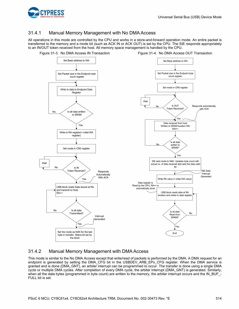
PSoC 6 MCU: CY8C61x4, CY8C62x4 Architecture TRM, Document No. 002-30473 Rev. *E 514
Universal Serial Bus (USB) Device Mode
31.4.1 Manual Memory Management with No DMA Access
All operations in this mode are controlled by the CPU and works in a store-and-forward operation mode. An entire packet istransferred to the memory and a mode bit (such as ACK IN or ACK OUT) is set by the CPU. The SIE responds appropriatelyto an IN/OUT token received from the host. All memory space management is handled by the CPU.
Figure 31-3. No DMA Access IN Transaction Figure 31-4. No DMA Access OUT Transaction
31.4.2 Manual Memory Management with DMA Access
This mode is similar to the No DMA Access except that write/read of packets is performed by the DMA. A DMA request for anendpoint is generated by setting the DMA_CFG bit in the USBDEV_ARB_EPx_CFG register. When the DMA service isgranted and is done (DMA_GNT), an arbiter interrupt can be programmed to occur. The transfer is done using a single DMAcycle or multiple DMA cycles. After completion of every DMA cycle, the arbiter interrupt (DMA_GNT) is generated. Similarly,when all the data bytes (programmed in byte count) are written to the memory, the arbiter interrupt occurs and the IN_BUF_-FULL bit is set.
Set Base address to WA
Set Packet size in the Endpoint byte count register
Write to data to Endpoint Data Register
Is all data written to SRAM
Write to RA register(= initial WA register)
Set mode in CR0 register
Is INToken Received?
USB block reads Data stored at RA and transmit to Host.RA++
Is all dataTransmitted?
Set the mode as NAK for the last byte in transfer. Status bit set by
the block
Wait
No
Yes
No
Yes
Responds Automatically
With ACK
Interrupt Generated
No
Yes
Set Base address to WA
Set Packet size in the Endpoint byte count register
Set mode in CR0 register
Is OUTToken Received?
Write RA value (= initial WA value)
Wait
No
Yes
Data received from hostWritten to SRAM location WA
WA++
Is all data written to SRAM?
No
SIE sets mode to NAK. Updates byte count with actual no. of data received abd sets the data valid
bit
USB block reads data at RA location and writes to data register
Is all dataRead from
SRAM?
Yes
Yes
End
Responds automatically with ACK
SIE DataInterrupt
Generated
Data register is Read by the CPU, RA++ is
automatically done
No
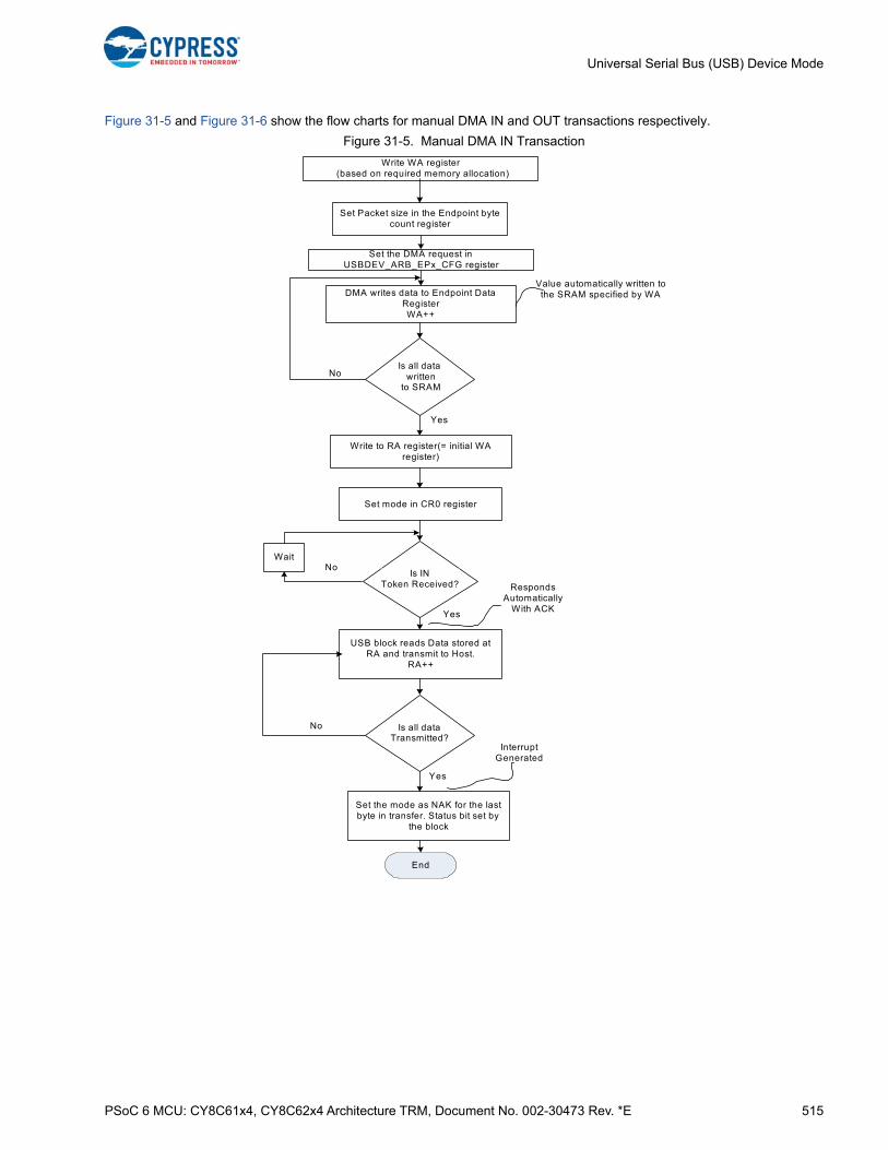
PSoC 6 MCU: CY8C61x4, CY8C62x4 Architecture TRM, Document No. 002-30473 Rev. *E 515
Universal Serial Bus (USB) Device Mode
Figure 31-5 and Figure 31-6 show the flow charts for manual DMA IN and OUT transactions respectively.
Figure 31-5. Manual DMA IN Transaction
Write WA register (based on required memory allocation)
Set Packet size in the Endpoint byte count register
DMA writes data to Endpoint Data RegisterWA++
Is all data written
to SRAM
Write to RA register(= initial WA register)
Set mode in CR0 register
Is INToken Received?
USB block reads Data stored at RA and transmit to Host.
RA++
Is all dataTransmitted?
Set the mode as NAK for the last byte in transfer. Status bit set by
the block
WaitNo
Yes
No
Yes
Responds Automatically
With ACK
Interrupt Generated
Set the DMA request in USBDEV_ARB_EPx_CFG register
No
Yes
Value automatically written to the SRAM specified by WA
End
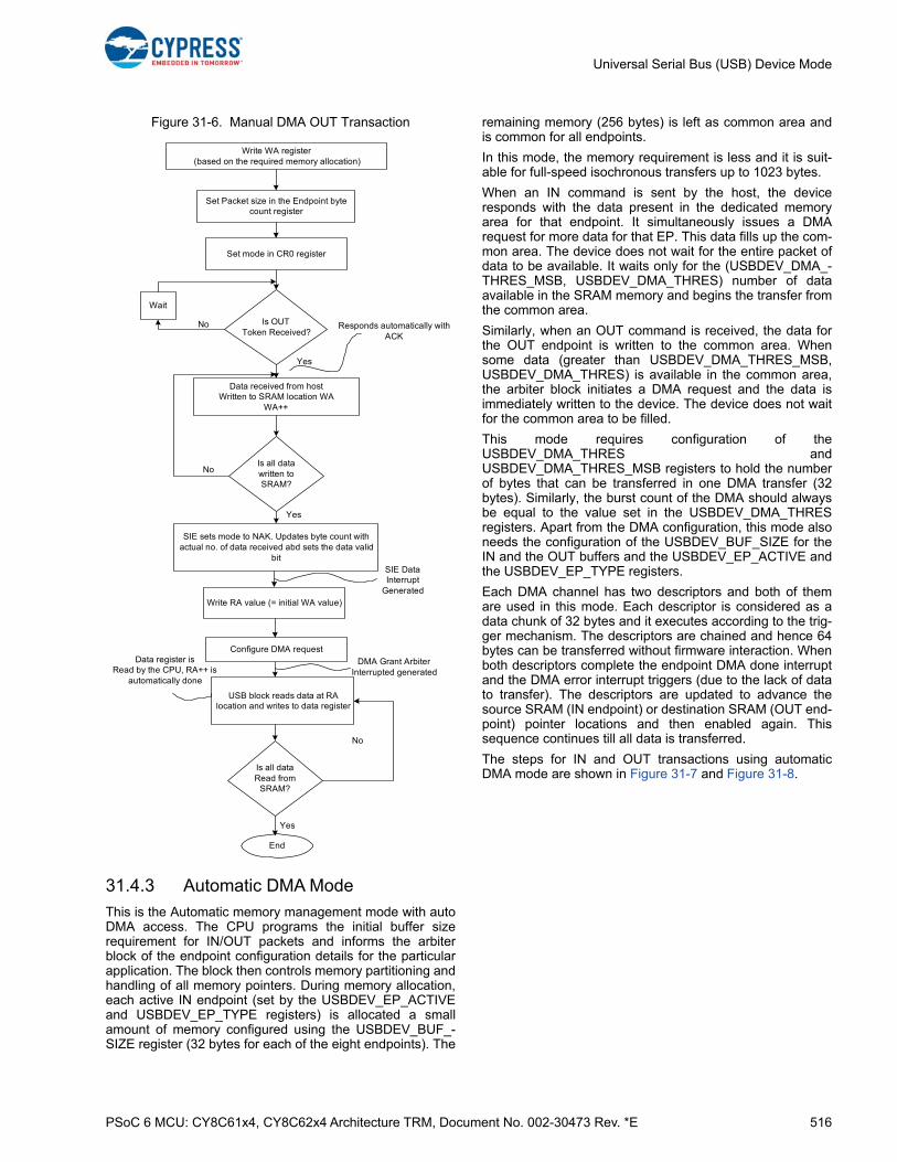
PSoC 6 MCU: CY8C61x4, CY8C62x4 Architecture TRM, Document No. 002-30473 Rev. *E 516
Universal Serial Bus (USB) Device Mode
Figure 31-6. Manual DMA OUT Transaction
31.4.3 Automatic DMA Mode
This is the Automatic memory management mode with autoDMA access. The CPU programs the initial buffer sizerequirement for IN/OUT packets and informs the arbiterblock of the endpoint configuration details for the particularapplication. The block then controls memory partitioning andhandling of all memory pointers. During memory allocation,each active IN endpoint (set by the USBDEV_EP_ACTIVEand USBDEV_EP_TYPE registers) is allocated a smallamount of memory configured using the USBDEV_BUF_-SIZE register (32 bytes for each of the eight endpoints). The
remaining memory (256 bytes) is left as common area andis common for all endpoints.
In this mode, the memory requirement is less and it is suit-able for full-speed isochronous transfers up to 1023 bytes.
When an IN command is sent by the host, the deviceresponds with the data present in the dedicated memoryarea for that endpoint. It simultaneously issues a DMArequest for more data for that EP. This data fills up the com-mon area. The device does not wait for the entire packet ofdata to be available. It waits only for the (USBDEV_DMA_-THRES_MSB, USBDEV_DMA_THRES) number of dataavailable in the SRAM memory and begins the transfer fromthe common area.
Similarly, when an OUT command is received, the data forthe OUT endpoint is written to the common area. Whensome data (greater than USBDEV_DMA_THRES_MSB,USBDEV_DMA_THRES) is available in the common area,the arbiter block initiates a DMA request and the data isimmediately written to the device. The device does not waitfor the common area to be filled.
This mode requires configuration of theUSBDEV_DMA_THRES andUSBDEV_DMA_THRES_MSB registers to hold the numberof bytes that can be transferred in one DMA transfer (32bytes). Similarly, the burst count of the DMA should alwaysbe equal to the value set in the USBDEV_DMA_THRESregisters. Apart from the DMA configuration, this mode alsoneeds the configuration of the USBDEV_BUF_SIZE for theIN and the OUT buffers and the USBDEV_EP_ACTIVE andthe USBDEV_EP_TYPE registers.
Each DMA channel has two descriptors and both of themare used in this mode. Each descriptor is considered as adata chunk of 32 bytes and it executes according to the trig-ger mechanism. The descriptors are chained and hence 64bytes can be transferred without firmware interaction. Whenboth descriptors complete the endpoint DMA done interruptand the DMA error interrupt triggers (due to the lack of datato transfer). The descriptors are updated to advance thesource SRAM (IN endpoint) or destination SRAM (OUT end-point) pointer locations and then enabled again. Thissequence continues till all data is transferred.
The steps for IN and OUT transactions using automaticDMA mode are shown in Figure 31-7 and Figure 31-8.
Write WA register(based on the required memory allocation)
Set Packet size in the Endpoint byte count register
Set mode in CR0 register
Is OUTToken Received?
Write RA value (= initial WA value)
Wait
No
Yes
Data received from hostWritten to SRAM location WA
WA++
Is all data written to SRAM?
No
SIE sets mode to NAK. Updates byte count with actual no. of data received abd sets the data valid
bit
Yes
Responds automatically with ACK
SIE DataInterrupt
Generated
USB block reads data at RA location and writes to data register
Is all dataRead from
SRAM?
No
Yes
End
Data register is Read by the CPU, RA++ is
automatically done
Configure DMA request
DMA Grant Arbiter Interrupted generated

PSoC 6 MCU: CY8C61x4, CY8C62x4 Architecture TRM, Document No. 002-30473 Rev. *E 517
Universal Serial Bus (USB) Device Mode
Figure 31-7. IN Transaction using Automatic DMA Mode
Set Packet size in the Endpoint byte count register
Set IN_DATA_RDY for the endpoint in ARB_EP1_CFG register
Is the endpointBuffer full?
Block automatically raises interrupt for DMA
DMA writes to Data register
Update mode value in the Mode register
Is IN Command received?
Is the completedata available in the memory
SIE reads data from SRAM (specified by location RA) and transmits to host
Is all datain buffer
transmitted?
Wait
No
Yes
No
Yes
Yes
Set the data valid bits
End
No
Yes
RA++
Raise a DMA Request
SIE reads data from SRAM (specified by location RA) and transmits to host
Is all datain buffer
transmitted?
Yes
RA++No
Is data in Common Area>(DMA THRES, DMA THRES MSB)
Wait
Initiate PHUBtransfer
Block transfer data availablein Common Area
Set the data valid bits
End
The process is continued till all
the data is transferred
No
Yes
In the mean time, the PHUB initiates the transaction. The
data from the device is copied to the common area. The data
from the USB is written to the SRAM by the DMA
This memory location is very limited. The memory location is filled initially to make sure the host does not stall when an IN command is sent. When an IN command is received the PHUB initiates the copy of data from device tocommon area. This initialization would take some time. The data in the end point buffer is transmitted until the data is copied to the common area
Data automatically read and written to SRAM pointed by WA.
WA++
IN_BUF_FULL Interruptgenerated
Block automatically sends the ACK (Configured as Mode
value)
No

PSoC 6 MCU: CY8C61x4, CY8C62x4 Architecture TRM, Document No. 002-30473 Rev. *E 518
Universal Serial Bus (USB) Device Mode
Figure 31-8. OUT Transaction using Automatic DMA Mode
31.4.4 Control Endpoint Logical Transfer
The control endpoint has a special logical transfer mode. It does not share the 512 bytes of memory. Instead, it has a dedi-cated 8-byte register buffer (USBDEV_EP0_DRx registers). The IN and OUT transaction for the control endpoint is detailed inthe following figures.
Write maximum bytes to Byte Count register
Program the Mode register for the endpoint
Is OUTToken Received?
USB Block writes the data from SRAM to the Data register
Wait
No
Yes
The DMA writes the received data to the SRAM in location specified by WA
DMA request is raised
Yes
Is all datafrom SRAM
copied to device?
End
Is data inSRAM>(DMA_THRES,DMA_TH
RES_MSB)?
NoWA++
Set the data valid bits
No
Yes
The process is continued till all
the data is transferred
Data in the Data register is read and given to the USB device by
the DMA. RA is incremented automatically

PSoC 6 MCU: CY8C61x4, CY8C62x4 Architecture TRM, Document No. 002-30473 Rev. *E 519
Universal Serial Bus (USB) Device Mode
Figure 31-9. Control Endpoint IN Transaction Figure 31-10. Control Endpoint OUT Transaction
Set the mode bits to ACK the IN token
Is SETUP token received?
The block ACKs it
Generates Interrupt and sets the bit in EP0_CR register to indicate that SETUP token was received
No
Yes
Read the status bit and data valid bit
Is Data Valid?
Read the EP0_DRx register to find the type of request
Copy the required data to the EP0_DRx registers
Set the data valid bit and the mode bits.Also update the byte count value
Is INToken Received?
No
The block transmits the data from the EP0_DRx registers
The block sets the mode value to NAK all further IN tokens
Block generates interrupt on receiving ACK from host and sets the IN byte
received bit
Are all bytes transferred?
End
No
No
Yes
Yes
Yes
Program the mode bits for ACK_OUT
Is SETUP token received?
The block ACKs it
Generates Interrupt and sets the bit in EP0_CR register to indicate that SETUP token was received
No
Yes
Read the data valid bit in EP0_CNT
Is Data Valid?
Read the EP0_DRx register to find the type of request
Update the mode bits to ACK an OUT token
Is OUTToken Received?
No
The block stores the received byte to the EP0_DRx registers and ACK the received
byte
Interrupt generated
Read the status and data valid bits
Are all bytes transferred?
End
No
No
Yes
Yes
Is dataValid?
Set the mode bit to NAK all OUT tokens till all bytes have been received
No
Yes
Yes
PSoC 6 MCU: CY8C61x4, CY8C62x4 Architecture TRM, Document No. 002-30473 Rev. *E 520
Universal Serial Bus (USB) Device Mode
31.5 USB Power ModesThe USB supports two modes of operation:
■ Active mode: In this mode, the USB is powered up and clocks are turned on.
■ Low-power (Deep Sleep) mode: In this mode, all clocks except the low-frequency clock are turned off.
Before entering low-power mode, the firmware should enable the GPIO interrupt (falling edge interrupt) on the D+ pin. TheUSB suspend mode can be determined by monitoring the SOF interrupt; this means, if there is no SOF interrupt from the USBfor more than 3 ms, the USB goes into suspend mode and the block can be put into low-power mode by the firmware.
If there is any activity on the USB bus, D+ will be pulled low, which will cause a CPU interrupt. This interrupt can be used towake up the USB device.
31.6 USB Device Registers
Name Description
USBDEV_EP0_DR Control endpoint EP0 data register
USBDEV_CR0 USB control 0 register
USBDEV_CR1 USB control 1 register
USBDEV_SIE_EP_INT_EN USB SIE data endpoint interrupt enable register
USBDEV_SIE_EP_INT_SR USB SIE data endpoint interrupt status
USBDEV_SIE_EPx_CNT0 Non-control endpoint count register
USBDEV_SIE_EPx_CNT1 Non-control endpoint count register
USBDEV_SIE_EPx_CR0 Non-control endpoint's control register
USBDEV_USBIO_CR0 USBIO control 0 register
USBDEV_USBIO_CR2 USBIO control 2 register
USBDEV_USBIO_CR1 USBIO control 1 register
USBDEV_DYN_RECONFIG USB dynamic reconfiguration register
USBDEV_SOF0 Start of frame register
USBDEV_SOF1 Start of frame register
USBDEV_OSCLK_DR0 Oscillator lock data register 0
USBDEV_OSCLK_DR1 Oscillator lock data register 1
USBDEV_EP0_CR Endpoint0 control register
USBDEV_EP0_CNT Endpoint0 count register
USBDEV_ARB_RWx_WAEndpoint write address value register. Pointer value increments by 1 when accessed by CPU/debugger
USBDEV_ARB_RWx_WA_MSB Endpoint write address value register
USBDEV_ARB_RWx_RAEndpoint read address value register. Pointer value increments by 1 when accessed by CPU/debugger
USBDEV_ARB_RWx_RA_MSB Endpoint read address value register
USBDEV_ARB_RWx_DR Endpoint data register
USBDEV_BUF_SIZE Dedicated endpoint buffer size register
USBDEV_EP_ACTIVE Endpoint active indication register
USBDEV_EP_TYPE Endpoint type (IN/OUT) indication register
USBDEV_ARB_EPx_CFG Endpoint configuration register
USBDEV_ARB_EPx_INT_EN Endpoint interrupt enable register
USBDEV_ARB_EPx_SR Endpoint interrupt enable register
USBDEV_ARB_CFG Arbiter configuration register
USBDEV_USB_CLK_EN USB block clock enable register
PSoC 6 MCU: CY8C61x4, CY8C62x4 Architecture TRM, Document No. 002-30473 Rev. *E 521
Universal Serial Bus (USB) Device Mode
USBDEV_ARB_INT_EN Arbiter interrupt enable register
USBDEV_ARB_INT_SR Arbiter interrupt status register
USBDEV_CWA Common area write address register
USBDEV_CWA_MSB Endpoint read address value register
USBDEV_DMA_THRES DMA burst / threshold configuration register
USBDEV_DMA_THRES_MSB DMA burst / threshold configuration register
USBDEV_BUS_RST_CNT Bus reset count register
USBDEV_MEM_DATA Data register
USBDEV_SOF16 Start of frame register
USBDEV_OSCLK_DR16 Oscillator lock data register
USBDEV_ARB_RWx_WA16Endpoint write address value register. Pointer value increments by 2 when accessed by CPU/debugger
USBDEV_ARB_RWx_RA16Endpoint read address value register. Pointer value increments by 2 when accessed by CPU/debugger
USBDEV_ARB_RWx_DR16 Endpoint data register
USBDEV_DMA_THRES16 DMA burst / threshold configuration register
USBLPM_POWER_CTL Power control register
USBLPM_USBIO_CTL USB IO control register
USBLPM_FLOW_CTL Flow control register
USBLPM_LPM_CTL LPM control register
USBLPM_LPM_STAT LPM status register
USBLPM_INTR_SIE USB SOF, BUS RESET, and EP0 interrupt status register
USBLPM_INTR_SIE_SET USB SOF, BUS RESET, and EP0 interrupt set register
USBLPM_INTR_SIE_MASK USB SOF, BUS RESET,, and EP0 interrupt mask register
USBLPM_INTR_SIE_MASKED USB SOF, BUS RESET, and EP0 interrupt masked register
USBLPM_INTR_LVL_SEL Select interrupt level for each interrupt source register
USBLPM_INTR_CAUSE_HI High-priority interrupt cause register
USBLPM_INTR_CAUSE_MED Medium-priority interrupt cause register
USBLPM_INTR_CAUSE_LO Low-priority interrupt cause register
Name Description

PSoC 6 MCU: CY8C61x4, CY8C62x4 Architecture TRM, Document No. 002-30473 Rev. *E 522
32. LCD Direct Drive
The PSoC 6 MCU Liquid Crystal Display (LCD) drive system is a highly configurable peripheral that allows the device todirectly drive STN and TN segment LCDs.
32.1 FeaturesThe PSoC 6 MCU LCD segment drive block has the following features:
■ Supports up to 52 segments and 8 commons
■ Supports Type A (standard) and Type B (low-power) drive waveforms
■ Any GPIO can be configured as a common or segment
■ Supports five drive methods:
❐ Digital correlation
❐ PWM at 1/2 bias
❐ PWM at 1/3 bias
❐ PWM at 1/4 bias
■ Ability to drive 3-V displays from 1.8 V VDD in Digital Correlation mode
■ Operates in Active, Sleep, and Deep Sleep modes
■ Digital contrast control
32.2 Architecture
32.2.1 LCD Segment Drive Overview
A segmented LCD panel has the liquid crystal material between two sets of electrodes and various polarization and reflectorlayers. The two electrodes of an individual segment are called commons (COM) or backplanes and segment electrodes(SEG). From an electrical perspective, an LCD segment can be considered as a capacitive load; the COM/SEG electrodescan be considered as the rows and columns in a matrix of segments. The opacity of an LCD segment is controlled by varyingthe root-mean-square (RMS) voltage across the corresponding COM/SEG pair.
The following terms/voltages are used in this chapter to describe LCD drive:
■ VRMSOFF: The voltage that the LCD driver can realize on segments that are intended to be off.
■ VRMSON: The voltage that the LCD driver can realize on segments that are intended to be on.
This PSoC 6 MCU technical reference manual (TRM) provides comprehensive and detailed information about thefunctions of the PSoC 6 MCU device hardware. It is divided into two books: architecture TRM and registers TRM. TheTRM is not recommended for those new to the PSoC 6 MCU, nor as a guide for developing PSoC 6 MCU applications.Use these documents instead:
■ PSoC 61 datasheet, PSoC 62 datasheet
■ Peripheral Driver Library (PDL) documentation
■ Application notes
■ Code examples
PSoC 6 MCU: CY8C61x4, CY8C62x4 Architecture TRM, Document No. 002-30473 Rev. *E 523
LCD Direct Drive
■ Discrimination Ratio (D): The ratio of VRMSON and VRMSOFF that the LCD driver can realize. This depends on the type ofwaveforms applied to the LCD panel. Higher discrimination ratio results in higher contrast.
Liquid crystal material does not tolerate long term exposure to DC voltage. Therefore, any waveforms applied to the panelmust produce a 0-V DC component on every segment (on or off). Typically, LCD drivers apply waveforms to the COM andSEG electrodes that are generated by switching between multiple voltages. The following terms are used to define thesewaveforms:
■ Duty: A driver is said to operate in 1/M duty when it drives ‘M’ number of COM electrodes. Each COM electrode is effec-tively driven 1/M of the time.
■ Bias: A driver is said to use 1/B bias when its waveforms use voltage steps of (1/B) × VDRV. VDRV is the highest drivevoltage in the system (equals VDD). The PSoC 6 MCU supports 1/2, 1/3, and 1/4 biases in PWM drive modes.
■ Frame: A frame is the length of time required to drive all the segments. During a frame, the driver cycles through the com-mons in sequence. All segments receive 0-V DC (but non-zero RMS voltage) when measured over the entire frame.
The PSoC 6 MCU supports two different types of drive waveforms in all drive modes. These are:
■ Type-A Waveform: In this type of waveform, the driver structures a frame into M sub-frames. ‘M’ is the number of COMelectrodes. Each COM is addressed only once during a frame. For example, COM[i] is addressed in sub-frame i.
■ Type-B Waveform: The driver structures a frame into 2M sub-frames. The two sub-frames are inverses of each other.Each COM is addressed twice during a frame. For example, COM[i] is addressed in sub-frames i and M+i. Type-B wave-forms are slightly more power efficient because it contains fewer transitions per frame.
32.2.2 Drive Modes
The PSoC 6 MCU supports the following drive modes.
■ PWM drive at 1/2 bias
■ PWM drive at 1/3 bias
■ PWM drive at 1/4 bias with CLK_PERI and CLK_MF
■ Digital correlation
32.2.2.1 PWM Drive
In PWM drive mode, multi-voltage drive signals are generated using a PWM output signal together with the intrinsic resis-tance and capacitance of the LCD. Figure 32-1 illustrates this.

PSoC 6 MCU: CY8C61x4, CY8C62x4 Architecture TRM, Document No. 002-30473 Rev. *E 524
LCD Direct Drive
Figure 32-1. PWM Drive (at 1/3 Bias)
The output waveform of the drive electronics is a PWM waveform. With the Indium Tin Oxide (ITO) panel resistance and thesegment capacitance to filter the PWM, the voltage across the LCD segment is an analog voltage, as shown in Figure 32-1.This figure illustrates the generation of a 1/3 bias waveform (four commons and voltage steps of VDD/3). See the ClockingSystem chapter on page 240 for details.
The PWM is derived from either CLK_LF/CLK_MF (low-speed operation) or CLK_PERI (high-speed operation). See theClocking System chapter on page 240 for more details of peripheral and low-frequency clocks. The filtered analog voltageacross the LCD segments typically runs at low frequency for segment LCD driving. To acquire higher contrast performance inDeep Sleep mode, PWM mode can be selected while the low-speed generator is configured running at CLK_MF. CLK_MF issourced from IMO, which can be enabled in Deep Sleep mode.
Figure 32-2 and Figure 32-3 illustrate the Type A and Type B waveforms for COM and SEG electrodes for 1/2 bias and 1/4duty. Only COM0/COM1 and SEG0/SEG1 are drawn for demonstration purpose. Similarly, Figure 32-4 and Figure 32-5 illus-trate the Type A and Type B waveforms for COM and SEG electrodes for 1/3 bias and 1/4 duty.
PWM Generator
PWM Generator
SEG
COM
GPIO Output Impedance ITO Panel Resistance LCD Segment Capacitance
VPWM VLCD
VDDD
VDDDD
2/3 VDDD
1/3 VDDD
0
0
t
t
VPWM
VLCD
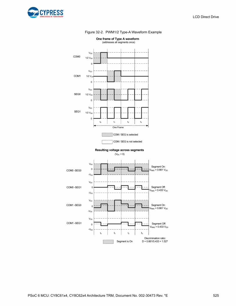
PSoC 6 MCU: CY8C61x4, CY8C62x4 Architecture TRM, Document No. 002-30473 Rev. *E 525
LCD Direct Drive
Figure 32-2. PWM1/2 Type-A Waveform Example
VDD
0COM0 -SEG0
VDD
0
VDD
0
VDD
0
t0 t1 t2 t3
Resulting voltage across segments
COM0 -SEG1
COM1 -SEG0
COM1 -SEG1
Segment On:VRMS = 0.661 VDD
(VDC = 0)
Segment On:VRMS = 0.661 VDD
Segment Off:VRMS = 0.433 VDD
Segment Off:VRMS = 0.433 VDD
Discrimination ratio:D = 0.661/0.433 = 1.527Segment is On
-VDD
-VDD
-VDD
-VDD
VDD
1/2 VDD
0
COM0
VDD
1/2 VDD
0
COM1
VDD
1/2 VDD
0
SEG0
VDD
1/2 VDD
0
SEG1
t0 t1 t2 t3
One frame of Type A waveform(addresses all segments once)
One Frame
COM / SEG is selected
COM / SEG is not selected

PSoC 6 MCU: CY8C61x4, CY8C62x4 Architecture TRM, Document No. 002-30473 Rev. *E 526
LCD Direct Drive
Figure 32-3. PWM1/2 Type-B Waveform Example
VDD
0COM0 -SEG0
VDD
0
VDD
0
VDD
0
t0 t1 t2 t3
Resulting voltage across segments
COM0 -SEG1
COM1 -SEG0
COM1 -SEG1
Segment On:VRMS = 0.661 VDD
(VDC = 0)
Segment On:VRMS = 0.661 VDD
Segment Off:VRMS = 0.433 VDD
Segment Off:VRMS = 0.433 VDD
Discrimination ratio:D = 0.661/0.433 = 1.527Segment is On
Segment is Off
-VDD
-VDD
-VDD
-VDD
VDD
1/2 VDD
0
COM0
VDD
1/2 VDD
0
COM1
VDD
1/2 VDD
0
SEG0
VDD
1/2 VDD
0
SEG1
t0 t1 t2 t3
One frame of Type B waveform(addresses all segments twice)
One Frame
COM / SEG is selected
COM / SEG is not selected
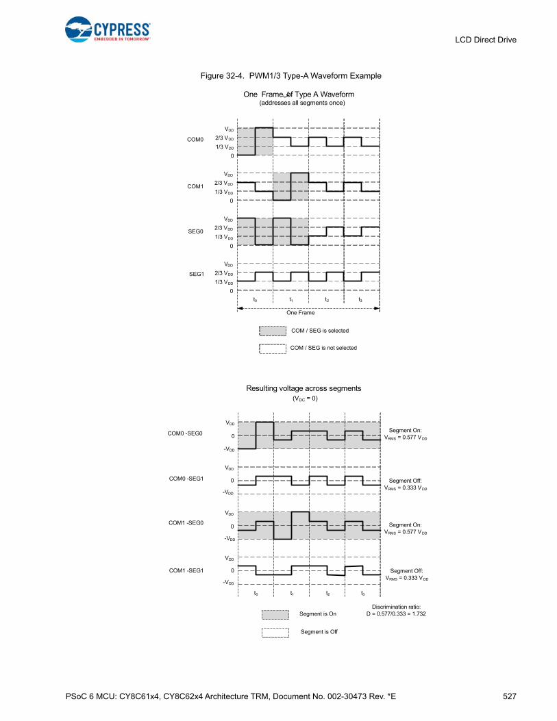
PSoC 6 MCU: CY8C61x4, CY8C62x4 Architecture TRM, Document No. 002-30473 Rev. *E 527
LCD Direct Drive
Figure 32-4. PWM1/3 Type-A Waveform Example
VDD
0COM0 -SEG0
VDD
0
VDD
0
VDD
0
t0 t1 t2 t3
Resulting voltage across segments
COM0 -SEG1
COM1 -SEG0
COM1 -SEG1
Segment On:VRMS = 0.577 VDD
(VDC = 0)
Segment On:VRMS = 0.577 VDD
Segment Off:VRMS = 0.333 VDD
Segment Off:VRMS = 0.333 VDD
Discrimination ratio:D = 0.577/0.333 = 1.732Segment is On
Segment is Off
-VDD
-VDD
-VDD
-VDD
VDD
2/3 VDD
1/3 VDD
0
COM0
VDD
2/3 VDD
1/3 VDD
0
COM1
VDD
2/3 VDD
1/3 VDD
0
SEG0
VDD
2/3 VDD
1/3 VDD
0
SEG1
t0 t1 t2 t3
One Frameشof Type A Waveform(addresses all segments once)
One Frame
COM / SEG is selected
COM / SEG is not selected
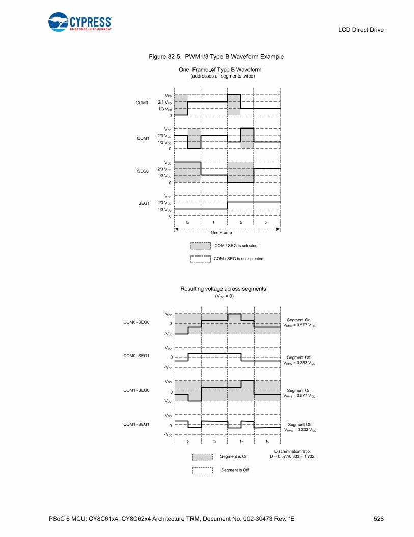
PSoC 6 MCU: CY8C61x4, CY8C62x4 Architecture TRM, Document No. 002-30473 Rev. *E 528
LCD Direct Drive
Figure 32-5. PWM1/3 Type-B Waveform Example
VDD
0COM0 -SEG0
VDD
0
VDD
0
VDD
0
t0 t1 t2 t3
Resulting voltage across segments
COM0 -SEG1
COM1 -SEG0
COM1 -SEG1
Segment On:VRMS = 0.577 VDD
(VDC = 0)
Segment On:VRMS = 0.577 VDD
Segment Off:VRMS = 0.333 VDD
Segment Off:VRMS = 0.333 VDD
Discrimination ratio:D = 0.577/0.333 = 1.732Segment is On
Segment is Off
-VDD
-VDD
-VDD
-VDD
VDD
2/3 VDD
1/3 VDD
0
COM0
VDD
2/3 VDD
1/3 VDD
0
COM1
VDD
2/3 VDD
1/3 VDD
0
SEG0
VDD
2/3 VDD
1/3 VDD
0
SEG1
t0 t1 t2 t3
One Frameشof Type B Waveform(addresses all segments twice)
One Frame
COM / SEG is selected
COM / SEG is not selected
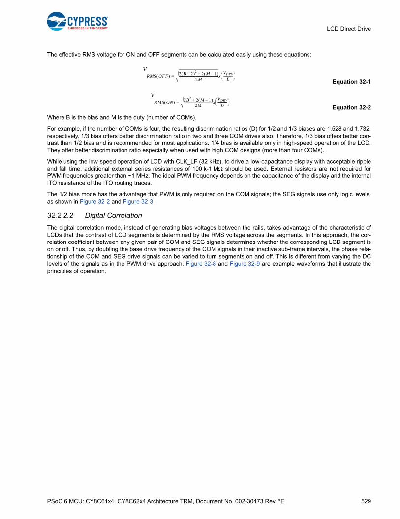
PSoC 6 MCU: CY8C61x4, CY8C62x4 Architecture TRM, Document No. 002-30473 Rev. *E 529
LCD Direct Drive
The effective RMS voltage for ON and OFF segments can be calculated easily using these equations:
Equation 32-1
Equation 32-2
Where B is the bias and M is the duty (number of COMs).
For example, if the number of COMs is four, the resulting discrimination ratios (D) for 1/2 and 1/3 biases are 1.528 and 1.732,respectively. 1/3 bias offers better discrimination ratio in two and three COM drives also. Therefore, 1/3 bias offers better con-trast than 1/2 bias and is recommended for most applications. 1/4 bias is available only in high-speed operation of the LCD.They offer better discrimination ratio especially when used with high COM designs (more than four COMs).
While using the low-speed operation of LCD with CLK_LF (32 kHz), to drive a low-capacitance display with acceptable rippleand fall time, additional external series resistances of 100 k-1 M should be used. External resistors are not required forPWM frequencies greater than ~1 MHz. The ideal PWM frequency depends on the capacitance of the display and the internalITO resistance of the ITO routing traces.
The 1/2 bias mode has the advantage that PWM is only required on the COM signals; the SEG signals use only logic levels,as shown in Figure 32-2 and Figure 32-3.
32.2.2.2 Digital Correlation
The digital correlation mode, instead of generating bias voltages between the rails, takes advantage of the characteristic ofLCDs that the contrast of LCD segments is determined by the RMS voltage across the segments. In this approach, the cor-relation coefficient between any given pair of COM and SEG signals determines whether the corresponding LCD segment ison or off. Thus, by doubling the base drive frequency of the COM signals in their inactive sub-frame intervals, the phase rela-tionship of the COM and SEG drive signals can be varied to turn segments on and off. This is different from varying the DClevels of the signals as in the PWM drive approach. Figure 32-8 and Figure 32-9 are example waveforms that illustrate theprinciples of operation.
VRMS OFF 2 B 2– 2
2 M 1– +2M
----------------------------------------------------= xVDRV
B------------
VRMS ON 2B2 2 M 1– +
2M--------------------------------------= x
VDRV
B------------

PSoC 6 MCU: CY8C61x4, CY8C62x4 Architecture TRM, Document No. 002-30473 Rev. *E 530
LCD Direct Drive
Figure 32-6. Digital Correlation Type-A Waveform
VDD
0COM0 -SEG0
VDD
0
VDD
0
VDD
0
t0 t1 t2 t3
Resulting voltage across segments
COM0 -SEG1
COM1 -SEG0
COM1 -SEG1
Segment On:VRMS = 0.791 VDD
(VDC = 0)
Segment On:VRMS = 0.791 VDD
Segment Off:VRMS = 0.612 VDD
Segment Off:VRMS = 0.612 VDD
Discrimination ratio:D = 0.791/0.612 = 1.291Segment is On
Segment is Off
-VDD
-VDD
-VDD
-VDD
VDD
0
COM0
VDD
0
COM1
VDD
0
SEG0
VDD
0
SEG1
t0 t1 t2 t3
One Frameشof Type A Waveform(addresses all segments once)
One Frame
COM / SEG is selected
COM / SEG is not selected
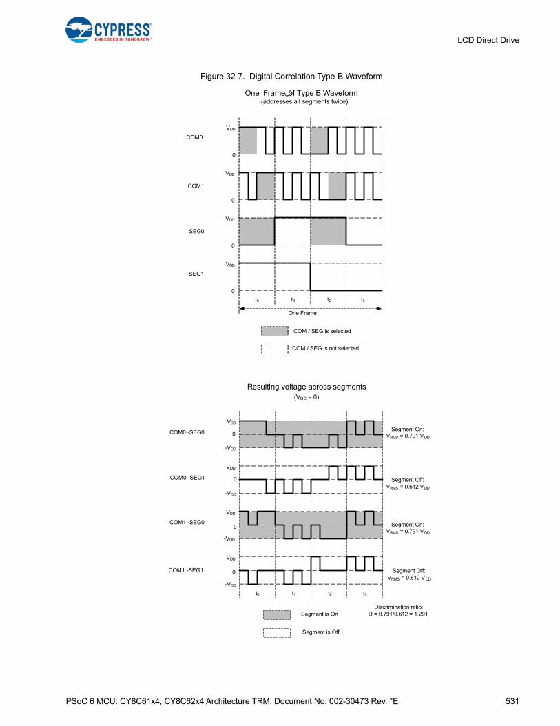
PSoC 6 MCU: CY8C61x4, CY8C62x4 Architecture TRM, Document No. 002-30473 Rev. *E 531
LCD Direct Drive
Figure 32-7. Digital Correlation Type-B Waveform
VDD
0COM0 -SEG0
VDD
0
VDD
0
VDD
0
t0 t1 t2 t3
Resulting voltage across segments
COM0 -SEG1
COM1 -SEG0
COM1 -SEG1
Segment On:VRMS = 0.791 VDD
(VDC = 0)
Segment On:VRMS = 0.791 VDD
Segment Off:VRMS = 0.612 VDD
Segment Off:VRMS = 0.612 VDD
Discrimination ratio:D = 0.791/0.612 = 1.291Segment is On
Segment is Off
-VDD
-VDD
-VDD
-VDD
VDD
0
COM0
VDD
0
COM1
VDD
0
SEG0
VDD
0
SEG1
t0 t1 t2 t3
One Frameشof Type B Waveform(addresses all segments twice)
One Frame
COM / SEG is selected
COM / SEG is not selected

PSoC 6 MCU: CY8C61x4, CY8C62x4 Architecture TRM, Document No. 002-30473 Rev. *E 532
LCD Direct Drive
The RMS voltage applied to on and off segments can be calculated as follows:
Where B is the bias and M is the duty (number of COMs). This leads to a discrimination ratio (D) of 1.291 for four COMs.Digital correlation mode also has the ability to drive 3-V displays from 1.8-V VDD.
32.2.3 Recommended Usage of Drive Modes
The PWM drive mode has higher discrimination ratios compared to the digital correlation mode, as explained in 32.2.2.1PWM Drive and 32.2.2.2 Digital Correlation. Therefore, the contrast in digital correlation method is lower than PWM methodbut digital correlation has lower power consumption because its waveforms toggle at low frequencies.
The digital correlation mode creates reduced, but acceptable contrast on TN displays, but no noticeable difference in contrastor viewing angle on higher contrast STN displays. Because each mode has strengths and weaknesses, recommended usageis as follows.
32.2.4 Digital Contrast Control
In all drive modes, digital contrast control can be used to change the contrast level of the segments. This method reducescontrast by reducing the driving time of the segments. This is done by inserting a ‘Dead-Time’ interval after each frame.During dead time, all COM and SEG signals are driven to a logic 1 state. The dead time can be controlled in fine resolution.Figure 32-8 illustrates the dead-time contrast control method for 1/3 bias and 1/4 duty implementation.
Figure 32-8. Dead-Time Contrast Control
Table 32-1. Recommended Usage of Drive Modes
Display Type Deep Sleep Mode Sleep/Active Mode Notes
Four COM TN Glass
Digital correlation or PWM at CLK_MF
PWM 1/3 biasFirmware must switch between LCD drive modes before going to deep sleep or waking up.
Four COM STN Glass
Digital correlation No contrast advantage for PWM drive with STN glass.
Eight COM, STN PWM at CLK_MF PWM 1/4 biasThe low-speed CLK_LF is not fast enough to make the PWM work at high multiplex ratios.
VRMS OFF M 1–
2M------------------= x VDD
VRMS ON 2 M 1– +
2M----------------------------= x VDD
VDD
2/3 VDD
1/3 VDD
0
COM0
VDD
2/3 VDD
1/3 VDD
0
COM1
VDD
2/3 VDD
1/3 VDD
0
SEG0
VDD
2/3 VDD
1/3 VDD
0
SEG1
t0 t1 t2 t3
Two Frames of of Type A Waveform with Dead-time
(Example for 1/4th Duty and 1/3rd bias)
Dead-Time
t0 t1 t2dt dtt3
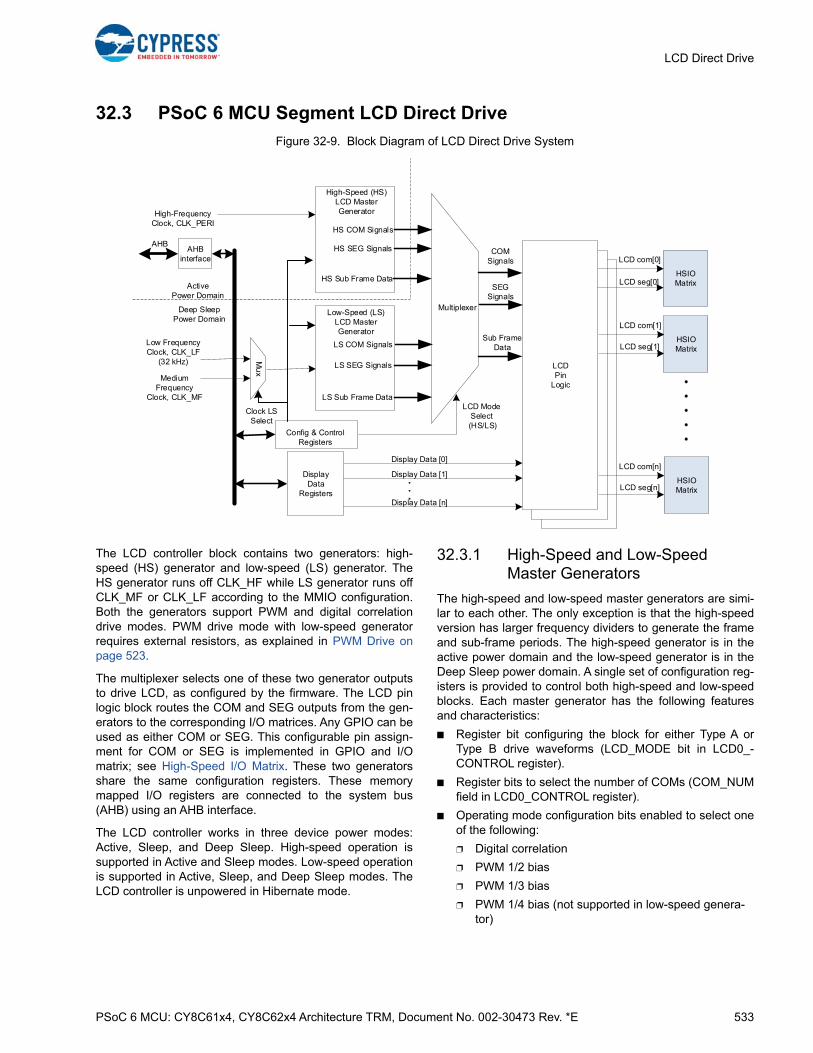
PSoC 6 MCU: CY8C61x4, CY8C62x4 Architecture TRM, Document No. 002-30473 Rev. *E 533
LCD Direct Drive
32.3 PSoC 6 MCU Segment LCD Direct Drive
Figure 32-9. Block Diagram of LCD Direct Drive System
The LCD controller block contains two generators: high-speed (HS) generator and low-speed (LS) generator. TheHS generator runs off CLK_HF while LS generator runs offCLK_MF or CLK_LF according to the MMIO configuration.Both the generators support PWM and digital correlationdrive modes. PWM drive mode with low-speed generatorrequires external resistors, as explained in PWM Drive onpage 523.
The multiplexer selects one of these two generator outputsto drive LCD, as configured by the firmware. The LCD pinlogic block routes the COM and SEG outputs from the gen-erators to the corresponding I/O matrices. Any GPIO can beused as either COM or SEG. This configurable pin assign-ment for COM or SEG is implemented in GPIO and I/Omatrix; see High-Speed I/O Matrix. These two generatorsshare the same configuration registers. These memorymapped I/O registers are connected to the system bus(AHB) using an AHB interface.
The LCD controller works in three device power modes:Active, Sleep, and Deep Sleep. High-speed operation issupported in Active and Sleep modes. Low-speed operationis supported in Active, Sleep, and Deep Sleep modes. TheLCD controller is unpowered in Hibernate mode.
32.3.1 High-Speed and Low-Speed Master Generators
The high-speed and low-speed master generators are simi-lar to each other. The only exception is that the high-speedversion has larger frequency dividers to generate the frameand sub-frame periods. The high-speed generator is in theactive power domain and the low-speed generator is in theDeep Sleep power domain. A single set of configuration reg-isters is provided to control both high-speed and low-speedblocks. Each master generator has the following featuresand characteristics:
■ Register bit configuring the block for either Type A orType B drive waveforms (LCD_MODE bit in LCD0_-CONTROL register).
■ Register bits to select the number of COMs (COM_NUMfield in LCD0_CONTROL register).
■ Operating mode configuration bits enabled to select oneof the following:
❐ Digital correlation
❐ PWM 1/2 bias
❐ PWM 1/3 bias
❐ PWM 1/4 bias (not supported in low-speed genera-tor)
High-Speed (HS) LCD Master Generator
AHB interface
AHB
Low Frequency Clock, CLK_LF
(32 kHz)
Config & Control Registers
LCD Mode Select
(HS/LS)
Sub Frame Data
Display Data
HSIOMatrix
LCD com[0]
Display Data [0]
LCDPin
Logic
DisplayData
Registers
HSIOMatrix
HSIOMatrix
High-Frequency Clock, CLK_PERI
LCD seg[0]
LCD com[1]
LCD seg[1]
LCD com[n]
LCD seg[n]
Active Power Domain
Deep Sleep Power Domain
Low-Speed (LS)LCD Master Generator
Multiplexer
Display Data [1]
Display Data [n]
HS COM Signals
HS SEG Signals
LS COM Signals
LS SEG Signals
HS Sub Frame Data
LS Sub Frame Data
COM Signals
SEG Signals
Mu
x
Medium Frequency
Clock, CLK_MF
Clock LS Select

PSoC 6 MCU: CY8C61x4, CY8C62x4 Architecture TRM, Document No. 002-30473 Rev. *E 534
LCD Direct Drive
❐ Off/disabled. Typically, one of the two generators will be configured to be Off
OP_MODE and BIAS fields in LCD0_CONTROL bits select the drive mode.
■ A counter to generate the sub-frame timing. The SUB-FR_DIV field in the LCD0_DIVIDER register determinesthe duration of each sub-frame. If the divide value writteninto this counter is C, the sub-frame period is4 × (C+1).The low-speed and high-speed generatorshave a 16-bit counter.
■ A counter to generate the dead time period. Thesecounters have the same number of bits as the sub-frameperiod counters and use the same clocks. DEAD_DIVfield in the LCD0_DIVIDER register controls the deadtime period.
32.3.2 Multiplexer and LCD Pin Logic
The multiplexer selects the output signals of either high-speed or low-speed master generator blocks and feeds it tothe LCD pin logic. This selection is controlled by the configu-ration and control register. The LCD pin logic uses the sub-
frame signal from the multiplexer to choose the display data.This pin logic will be replicated for each LCD pin.
32.3.3 Display Data Registers
Each LCD segment pin is part of an LCD port with its owndisplay data register, LCD0_DATAx. The device has eightsuch LCD ports. Note that these ports are not real pin portsbut the ports/connections available in the LCD hardware formapping the segments to commons. Each LCD segmentconfigured is considered as a pin in these LCD ports. TheLCD0_DATAxx registers are 32-bit wide and store the ON/OFF data for all SEG-COM combination enabled in thedesign. For example, LCD0_DATA0x holds SEG-COM datafor COM0 to COM3 and LCD0_DATA1x holds SEG-COMdata for COM4 to COM7. The bits [4i+3:4i] (where ‘i’ is thepin number) of each LCD0_DATAxx register represent theON/OFF data for Pin[i], as shown in Table 32-2. TheLCD0_DATAxx register should be programmed according tothe display data of each frame. The display data registersare Memory Mapped I/O (MMIO) and accessed through theAHB slave interface. See the PSoC 61 datasheet/PSoC 62datasheet for the pin connections.
32.4 Register List
Table 32-2. SEG-COM Mapping Example of LCD0_DATA00 Register (each SEG is a pin of the LCD port)
BITS[31:28] = PIN_7[3:0] BITS[27:24] = PIN_6[3:0]
PIN_7-COM3 PIN_7-COM2 PIN_7-COM1 PIN_7-COM0 PIN_6-COM3 PIN_6-COM2 PIN_6-COM1 PIN_6-COM0
BITS[23:20] = PIN_5[3:0] BITS[19:16] = PIN_4[3:0]
PIN_5-COM3 PIN_5-COM2 PIN_5-COM1 PIN_5-COM0 PIN_4-COM3 PIN_4-COM2 PIN_4-COM1 PIN_4-COM0
BITS[15:12] = PIN_3[3:0] BITS[11:8] = PIN_2[3:0]
PIN_3-COM3 PIN_3-COM2 PIN_3-COM1 PIN_3-COM0 PIN_2-COM3 PIN_2-COM2 PIN_2-COM1 PIN_2-COM0
BITS[7:3] = PIN_1[3:0] BITS[3:0] = PIN_0[3:0]
PIN_1-COM3 PIN_1-COM2 PIN_1-COM1 PIN_1-COM0 PIN_0-COM3 PIN_0-COM2 PIN_0-COM1 PIN_0-COM0
Table 32-3. LCD Direct Drive Register List
Register Name Description
LCD0_ID This register includes the information of LCD controller ID and revision number
LCD0_DIVIDER This register controls the sub-frame and dead-time period
LCD0_CONTROL This register is used to configure high-speed and low-speed generators
LCD0_DATA0x LCD port pin data register for COM0 to COM3
LCD0_DATA1x LCD port pin data register for COM4 to COM7

PSoC 6 MCU: CY8C61x4, CY8C62x4 Architecture TRM, Document No. 002-30473 Rev. *E 535
Section E: Analog Subsystem
This section encompasses the following chapters:
■ CapSense chapter on page 536
■ Analog Reference Block chapter on page 537
■ Temperature Sensor chapter on page 541
■ SAR ADC chapter on page 545
■ Low-Power Comparator chapter on page 570
■ Continuous Time DAC chapter on page 576
■ Continuous Time Block mini (CTBm) chapter on page 589
■ Analog Routing chapter on page 597
Top Level Architecture
Figure E-1. Analog System Block Diagram
Programmable Analog
2x SAR ADC 12 bit
SA
RM
UX
DAC 12 bit
2x Opamp
Temperature Sensor
I/O S
ub
sys
tem
: U
p to
62
GP
IOs
(incl
udin
g 2
OV
T),
80
-TQ
FP
Pa
ckag
eB
ound
ary
Sca
nS
mar
t I/O
Po
rt
Per
iphe
ral I
nte
rcon
nect
(M
MIO
, PP
U)
Per
iphe
ral c
lock
(P
CLK
)
SystemHibernate Mode
BackupDomain
SystemDeepSleep Mode
System LP/ULP ModeCPUs Active/Sleep
Color Key:Power Modes and
Domains

PSoC 6 MCU: CY8C61x4, CY8C62x4 Architecture TRM, Document No. 002-30473 Rev. *E 536
33. CapSense
The CapSense system can measure the self-capacitance of an electrode or the mutual capacitance between a pair ofelectrodes. In addition to capacitive sensing, the CapSense system can function as an ADC to measure voltage on any GPIOpin that supports the CapSense functionality.
The CapSense touch sensing method in PSoC 6 MCUs, which senses self-capacitance, is known as CapSense Sigma Delta(CSD). Similarly, the mutual-capacitance sensing method is known as CapSense Cross-point (CSX). The CSD and CSXtouch sensing methods provide the industry’s best-in-class signal-to-noise ratio (SNR), high touch sensitivity, low-poweroperation, and superior EMI performance.
CapSense touch sensing is a combination of hardware and firmware techniques. Therefore, use the CapSense componentprovided by the ModusToolbox IDE to implement CapSense designs. See the PSoC 4 and PSoC 6 MCU CapSense DesignGuide for more details.

PSoC 6 MCU: CY8C61x4, CY8C62x4 Architecture TRM, Document No. 002-30473 Rev. *E 537
34. Analog Reference Block
The Analog Reference block (AREF) generates highly accurate reference voltage and currents needed by the programmableanalog subsystem (PASS) and CapSense (CSD) blocks.
34.1 Features■ Provides accurate bandgap references for PASS and CSD subsystems
■ 1.2-V voltage reference (VREF) generator
■ Option to output alternate voltage references routed from SRSS or from an external pin
■ Proportional to absolute temperature (IPTAT) current reference generation
■ Zero dependency to absolute temperature (IZTAT) flat current reference generation, which is independent of temperaturevariations
■ Option to generate IZTAT from SRSS generated current reference
■ Option to enable or disable references in System Deep-Sleep mode
This PSoC 6 MCU technical reference manual (TRM) provides comprehensive and detailed information about thefunctions of the PSoC 6 MCU device hardware. It is divided into two books: architecture TRM and registers TRM. TheTRM is not recommended for those new to the PSoC 6 MCU, nor as a guide for developing PSoC 6 MCU applications.Use these documents instead:
■ PSoC 61 datasheet, PSoC 62 datasheet
■ Peripheral Driver Library (PDL) documentation
■ Application notes
■ Code examples
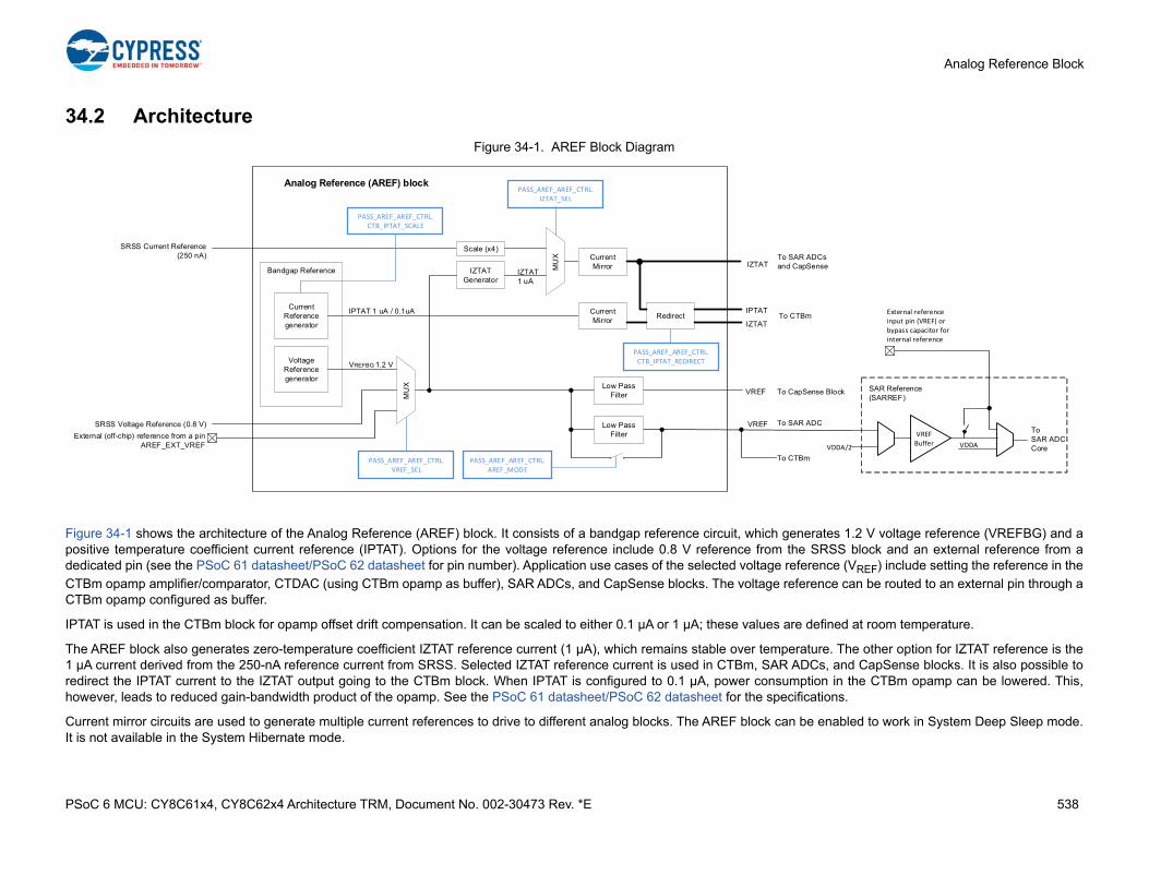
Analog Reference Block
PSoC 6 MCU: CY8C61x4, CY8C62x4 Architecture TRM, Document No. 002-30473 Rev. *E 538
34.2 Architecture
Figure 34-1. AREF Block Diagram
Figure 34-1 shows the architecture of the Analog Reference (AREF) block. It consists of a bandgap reference circuit, which generates 1.2 V voltage reference (VREFBG) and apositive temperature coefficient current reference (IPTAT). Options for the voltage reference include 0.8 V reference from the SRSS block and an external reference from adedicated pin (see the PSoC 61 datasheet/PSoC 62 datasheet for pin number). Application use cases of the selected voltage reference (VREF) include setting the reference in the
CTBm opamp amplifier/comparator, CTDAC (using CTBm opamp as buffer), SAR ADCs, and CapSense blocks. The voltage reference can be routed to an external pin through aCTBm opamp configured as buffer.
IPTAT is used in the CTBm block for opamp offset drift compensation. It can be scaled to either 0.1 µA or 1 µA; these values are defined at room temperature.
The AREF block also generates zero-temperature coefficient IZTAT reference current (1 µA), which remains stable over temperature. The other option for IZTAT reference is the1 µA current derived from the 250-nA reference current from SRSS. Selected IZTAT reference current is used in CTBm, SAR ADCs, and CapSense blocks. It is also possible toredirect the IPTAT current to the IZTAT output going to the CTBm block. When IPTAT is configured to 0.1 µA, power consumption in the CTBm opamp can be lowered. This,however, leads to reduced gain-bandwidth product of the opamp. See the PSoC 61 datasheet/PSoC 62 datasheet for the specifications.
Current mirror circuits are used to generate multiple current references to drive to different analog blocks. The AREF block can be enabled to work in System Deep Sleep mode.It is not available in the System Hibernate mode.
MU
X
Bandgap Reference
Current Reference generator
VREF
IZTAT
IPTAT
Analog Reference (AREF) block
Voltage Reference generator
SRSS Voltage Reference (0.8 V)
External (off-chip) reference from a pin AREF_EXT_VREF
SRSS Current Reference (250 nA)
IPTAT 1 uA / 0.1uA
VREFBG 1.2 V
IZTATGenerator
MU
X
IZTAT1 uA
Current Mirror
Current Mirror
RedirectIZTAT
To CTBm
To SAR ADCs and CapSense
To CTBm
PASS_AREF_AREF_CTRL. IZTAT_SEL
PASS_AREF_AREF_CTRL. VREF_SEL
PASS_AREF_AREF_CTRL. CTB_IPTAT_REDIRECT
PASS_AREF_AREF_CTRL. CTB_IPTAT_SCALE
VREF
To CapSense Block
Scale (x4)
Low Pass Filter
Low Pass Filter
PASS_AREF_AREF_CTRL. AREF_MODE
VDDAVDDA/2
VREF Buffer
External reference input pin (VREF) or bypass capacitor for internal reference
SAR Reference (SARREF)
To SAR ADC Core
To SAR ADC
PSoC 6 MCU: CY8C61x4, CY8C62x4 Architecture TRM, Document No. 002-30473 Rev. *E 539
Analog Reference Block
The following sections explain the configurations in detail.
34.2.1 Bandgap Reference Block
The AREF block contains a local bandgap reference generator, which has tighter accuracy, temperature stability, and lowernoise than the SRSS bandgap reference. The bandgap reference block provides a temperature stable voltage (VREFBG) and
an additional current that tracks temperature (IPTAT). See the PSoC 61 datasheet/PSoC 62 datasheet to know the accuracyof VREFBG.
IPTAT current can be scaled to either 0.1 µA or 1 µA using CTB_IPTAT_SCALE bit of the PASS_AREF_AREF_CTRLregister.
The AREF block is enabled by writing ‘1’ into the ENABLED bit of the PASS_AREF_AREF_CTRL register.
34.2.2 VREF Reference Voltage Selection Multiplexer Options
The multiplexer in AREF is used to select the sources for the output voltage reference. The following options are available forselection using VREF_SEL bits of the PASS_AREF_AREF_CTRL register.
34.2.3 Zero Dependency To Absolute Temperature Current Generator (IZTAT)
The IZTAT current generator uses the output of the selected reference voltage (VREF) to generate a precise current reference,
which has a low variation over temperature.
Table 34-1. Bandgap References in AREF
Bandgap Reference Outputs
Value
VREFBG 1.2 V
IPTAT 1 µA (if CTB_IPTAT_SCALE = 0) or 0.1 µA (if CTB_IPTAT_SCALE = 1)
Table 34-2. Reference Voltage Multiplexer Options
VREF_SEL[1:0] Description
00 (SRSS)
Routes the VREF from SRSS (0.8 V)
Note: SRSS references are not available in System Deep Sleep power mode. This option should not be used if the analog blocks – CTBm and SAR ADCs are required to be functional in System Deep Sleep mode.
01 (LOCAL) Routes locally generated bandgap reference (1.2V)
02 (EXTERNAL) Routes the reference from the external pin – AREF_EXT_VREFa
a. The AREF_EXT_VREF pin is different from the VREF pin. VREF pin is used by SAR ADC to take the reference directly bypassing the reference voltage fromAREF.
Table 34-3. IZTAT Reference
IZTAT Reference Outputs Value
IZTAT 1 µA
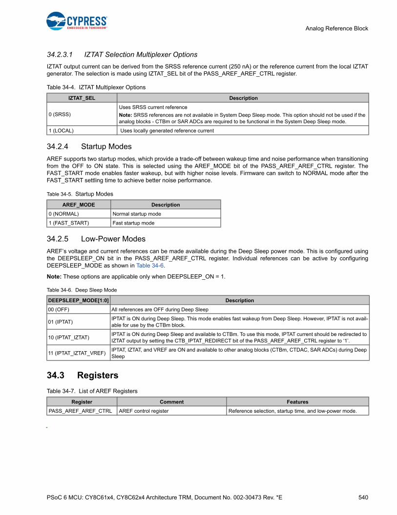
PSoC 6 MCU: CY8C61x4, CY8C62x4 Architecture TRM, Document No. 002-30473 Rev. *E 540
Analog Reference Block
34.2.3.1 IZTAT Selection Multiplexer Options
IZTAT output current can be derived from the SRSS reference current (250 nA) or the reference current from the local IZTATgenerator. The selection is made using IZTAT_SEL bit of the PASS_AREF_AREF_CTRL register.
34.2.4 Startup Modes
AREF supports two startup modes, which provide a trade-off between wakeup time and noise performance when transitioningfrom the OFF to ON state. This is selected using the AREF_MODE bit of the PASS_AREF_AREF_CTRL register. TheFAST_START mode enables faster wakeup, but with higher noise levels. Firmware can switch to NORMAL mode after theFAST_START settling time to achieve better noise performance.
34.2.5 Low-Power Modes
AREF’s voltage and current references can be made available during the Deep Sleep power mode. This is configured usingthe DEEPSLEEP_ON bit in the PASS_AREF_AREF_CTRL register. Individual references can be active by configuringDEEPSLEEP_MODE as shown in Table 34-6.
Note: These options are applicable only when DEEPSLEEP_ON = 1.
34.3 Registers
Table 34-4. IZTAT Multiplexer Options
IZTAT_SEL Description
0 (SRSS) Uses SRSS current reference
Note: SRSS references are not available in System Deep Sleep mode. This option should not be used if the analog blocks - CTBm or SAR ADCs are required to be functional in the System Deep Sleep mode.
1 (LOCAL) Uses locally generated reference current
Table 34-5. Startup Modes
AREF_MODE Description
0 (NORMAL) Normal startup mode
1 (FAST_START) Fast startup mode
Table 34-6. Deep Sleep Mode
DEEPSLEEP_MODE[1:0] Description
00 (OFF) All references are OFF during Deep Sleep
01 (IPTAT)IPTAT is ON during Deep Sleep. This mode enables fast wakeup from Deep Sleep. However, IPTAT is not avail-able for use by the CTBm block.
10 (IPTAT_IZTAT)IPTAT is ON during Deep Sleep and available to CTBm. To use this mode, IPTAT current should be redirected to IZTAT output by setting the CTB_IPTAT_REDIRECT bit of the PASS_AREF_AREF_CTRL register to ‘1’.
11 (IPTAT_IZTAT_VREF)IPTAT, IZTAT, and VREF are ON and available to other analog blocks (CTBm, CTDAC, SAR ADCs) during Deep Sleep
Table 34-7. List of AREF Registers
Register Comment Features
PASS_AREF_AREF_CTRL AREF control register Reference selection, startup time, and low-power mode.

PSoC 6 MCU: CY8C61x4, CY8C62x4 Architecture TRM, Document No. 002-30473 Rev. *E 541
35. Temperature Sensor
This product line has two on-chip temperature sensors that are used to measure the internal die temperature. The sensorconsists of a transistor connected in diode configuration.
35.1 Features■ Measures device temperature
■ Voltage output can be internally connected to SAR ADC for digital readout. Each temperature sensor connects to one ofthe SAR ADCs.
■ Factory calibrated parameters
35.2 Architecture
The temperature sensor consists of a single bipolar junction transistor (BJT) in the form of a diode. The transistor is biasedusing a reference current IREF from the analog reference block (see the Analog Reference Block chapter on page 537 for
more details). Its base-to-emitter voltage (VBE) has a strong dependence on temperature at a constant collector current and
zero collector-base voltage. This property is used to calculate the die temperature by measuring the VBE of the transistor
using the SAR ADC, as shown in Figure 35-1.
This PSoC 6 MCU technical reference manual (TRM) provides comprehensive and detailed information about thefunctions of the PSoC 6 MCU device hardware. It is divided into two books: architecture TRM and registers TRM. TheTRM is not recommended for those new to the PSoC 6 MCU, nor as a guide for developing PSoC 6 MCU applications.Use these documents instead:
■ PSoC 61 datasheet, PSoC 62 datasheet
■ Peripheral Driver Library (PDL) documentation
■ Application notes
■ Code examples

PSoC 6 MCU: CY8C61x4, CY8C62x4 Architecture TRM, Document No. 002-30473 Rev. *E 542
Temperature Sensor
Figure 35-1. Temperature Sensing Mechanism
The analog output from the sensor (VBE) is measured using the SAR ADC. Die temperature in °C can be calculated from the
ADC results as given in the following equation:
Equation 35-1
■ Temp is the slope compensated temperature in °C represented as Q16.16 fixed point number format.
■ ‘A’ is the 16-bit multiplier constant. The value of A is determined using the PSoC 6 MCU characterization data of two pointslope calculation. It is calculated as given in the following equation.
Equation 35-2
Where,
SAR100C = ADC counts at 100 °C
SAR–40C = ADC counts at –40 °C
Constant ‘A’ is stored in a register SFLASH_SAR_TEMP_MULTIPLIER. See the registers TRM for more details.
■ ‘B’ is the 16-bit offset value. The value of B is determined on a per die basis by taking care of all the process variationsand the actual bias current (IREF) present in the chip. It is calculated as given in the following equation.
Equation 35-3
Where,
SAR100C = ADC counts at 100 °C
Constant ‘B’ is stored in a register SFLASH_SAR_TEMP_OFFSET. See the registers TRM for more details.
■ Tadjust is the slope correction factor in °C. The temperature sensor is corrected for dual slopes using the slope correctionfactor. It is evaluated based on the result obtained without slope correction, which is given by the following equation:
Equation 35-4
If Tinitial is greater than the center value (15 °C), then Tadjust is given by the following equation.
TemperatureSensor
SA
RM
UX
SAR ADCx CPU
IREF
SARx_MUX_SWITCH0. MUX_FW_TEMP_VPLUS
VSSA
Current from Analog Reference Block
VPLUS
VMINUS
12 bit
VREF=1.2V
VSSA
vssa_kelvin
Temp A SARout 210
B+ Tadjust+=
A signed int 216 100C 40C– –
SAR100C SAR 40C––--------------------------------------------------------
=
B unsigned int 26x100C
A SAR100C
210
---------------------------------
–
=
Tinitial A SAROUT 210
+ B =
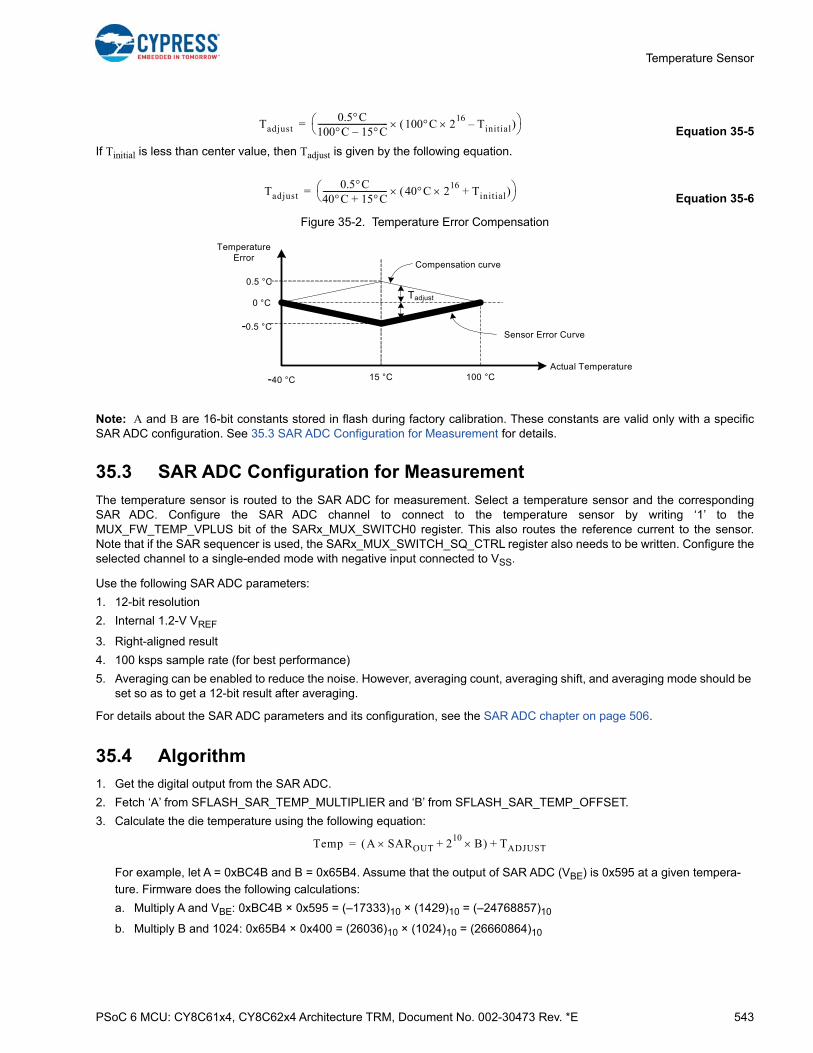
PSoC 6 MCU: CY8C61x4, CY8C62x4 Architecture TRM, Document No. 002-30473 Rev. *E 543
Temperature Sensor
Equation 35-5
If Tinitial is less than center value, then Tadjust is given by the following equation.
Equation 35-6
Figure 35-2. Temperature Error Compensation
Note: A and B are 16-bit constants stored in flash during factory calibration. These constants are valid only with a specificSAR ADC configuration. See 35.3 SAR ADC Configuration for Measurement for details.
35.3 SAR ADC Configuration for Measurement
The temperature sensor is routed to the SAR ADC for measurement. Select a temperature sensor and the correspondingSAR ADC. Configure the SAR ADC channel to connect to the temperature sensor by writing ‘1’ to theMUX_FW_TEMP_VPLUS bit of the SARx_MUX_SWITCH0 register. This also routes the reference current to the sensor.Note that if the SAR sequencer is used, the SARx_MUX_SWITCH_SQ_CTRL register also needs to be written. Configure theselected channel to a single-ended mode with negative input connected to VSS.
Use the following SAR ADC parameters:
1. 12-bit resolution
2. Internal 1.2-V VREF
3. Right-aligned result
4. 100 ksps sample rate (for best performance)
5. Averaging can be enabled to reduce the noise. However, averaging count, averaging shift, and averaging mode should be set so as to get a 12-bit result after averaging.
For details about the SAR ADC parameters and its configuration, see the SAR ADC chapter on page 506.
35.4 Algorithm1. Get the digital output from the SAR ADC.
2. Fetch ‘A’ from SFLASH_SAR_TEMP_MULTIPLIER and ‘B’ from SFLASH_SAR_TEMP_OFFSET.
3. Calculate the die temperature using the following equation:
For example, let A = 0xBC4B and B = 0x65B4. Assume that the output of SAR ADC (VBE) is 0x595 at a given tempera-
ture. Firmware does the following calculations:
a. Multiply A and VBE: 0xBC4B × 0x595 = (–17333)10 × (1429)10 = (–24768857)10
b. Multiply B and 1024: 0x65B4 × 0x400 = (26036)10 × (1024)10 = (26660864)10
Tadjust0.5C
100C 15C–----------------------------------- 100C 2
16Tinitial–
=
Tadjust0.5C
40C 15C+-------------------------------- 40C 2
16Tinitial+
=
TemperatureError
Actual Temperature15 °C 100 °C-40 °C
0 °C
0.5 °C
-0.5 °C
Compensation curve
Sensor Error Curve
Tadjust
Temp A SAROUT 210
+ B TADJUST+=
PSoC 6 MCU: CY8C61x4, CY8C62x4 Architecture TRM, Document No. 002-30473 Rev. *E 544
Temperature Sensor
c. Add the result of steps 1 and 2 to get Tinitial: (–24768857)10 + (26660864)10 = (1892007)10 = 0x1CDEA7
d. Calculate Tadjust using Tinitial value: Tinitial is the upper 16 bits multiplied by 216, that is, 0x1C00 = (1835008)10. It is
greater than 15°C (0x1C - upper 16 bits). Use Equation 4 to calculate Tadjust. It comes to 0x6B1D = (27421)10
e. Add Tadjust to Tinitial: (1892007)10 + (27421)10 = (1919428)10 = 0x1D49C4
f. The integer part of temperature is the upper 16 bits = 0x001D = (29)10
g. The decimal part of temperature is the lower 16 bits = 0x4B13 = (0.18884)10
h. Combining the result of steps f and g, Temp = 29.18884 °C ~ 29.2°C
35.5 Registers
Name Description
SFLASH_SAR_TEMP_MULTIPLIER Multiplier constant 'A' as defined in Equation 35-1.
SFLASH_SAR_TEMP_OFFSET Constant 'B' as defined in Equation 35-1.

PSoC 6 MCU: CY8C61x4, CY8C62x4 Architecture TRM, Document No. 002-30473 Rev. *E 545
36. SAR ADC
This product line has two 12-bit successive approximation register analog-to-digital converters (SAR ADC), each with amaximum sample rate of 2 Msps. They are designed for applications that require moderate resolution and high data rate.
36.1 Features■ 2x SAR ADCs with a maximum sample rate of 2 Msps
■ Sixteen individually configurable logical channels that can scan thirteen unique input sources. Each channel has thefollowing features:
❐ Single-ended or differential measurement
❐ Input from eight dedicated pins (eight single-ended mode or four differential inputs) or internal signals (CTBm opampoutput, analog mux buses, or temperature sensor)
❐ Each channel may choose one of four programmable acquisition times to compensate for external factors (such ashigh input impedance sources with long settling times)
❐ Averaging and accumulation
❐ Double-buffered results
■ Configurable injection channel for infrequent signal measurement
❐ Can be interleaved between two scan sequences (tailgating)
❐ Selectable sample time, resolution, single-ended or differential, averaging
■ Result may be left- or right-aligned, or may be represented in 16-bit sign extended
■ Operational in System Deep Sleep mode
❐ 64 × 20 bits FIFO per ADC to store the results in System Deep Sleep mode; option to chain the two FIFOs to doublethe buffer depth
❐ Maximum sample rate is approximately 100 kHz with 2 MHz input clock
■ Conversion process can be triggered by firmware or from other peripherals
❐ One-shot and periodic or continuous mode
❐ Configurable number of ADC scans per trigger
❐ Option to synchronize sampling between the two ADCs
■ Hardware averaging/accumulation of configurable number of samples (2, 4, 8, 16, 32, 64, 128, or 256)
■ Selectable voltage references
❐ Internal VDDA and VDDA/2 references
❐ Internal 1.2-V reference with buffer
❐ External reference
This PSoC 6 MCU technical reference manual (TRM) provides comprehensive and detailed information about thefunctions of the PSoC 6 MCU device hardware. It is divided into two books: architecture TRM and registers TRM. TheTRM is not recommended for those new to the PSoC 6 MCU, nor as a guide for developing PSoC 6 MCU applications.Use these documents instead:
■ PSoC 61 datasheet, PSoC 62 datasheet
■ Peripheral Driver Library (PDL) documentation
■ Application notes
■ Code examples

PSoC 6 MCU: CY8C61x4, CY8C62x4 Architecture TRM, Document No. 002-30473 Rev. *E 546
SAR ADC
■ Interrupt generation
❐ End of scan (EOS)
❐ Saturation detect and over-range (configurable) detect for every channel
❐ Scan results overflow
❐ Collision detect
❐ FIFO - Level
❐ FIFO - Overflow
❐ FIFO - Underflow
36.2 Architecture
Figure 36-1. SAR ADC Block Diagram
Figure 36-1 shows a simplified block diagram of the SAR ADC system. Each ADC includes a SARMUX, SAR converter,reference, sequencer, and FIFO. Preceding the SAR ADC converter is the SARMUX, which routes external pins and internalsignals (CTBm opamp outputs, AMUXBUS-A/AMUXBUS-B, or temperature sensor output) to the SAR ADC. The sequencer(SARSEQ) controls the SARMUX and SAR ADC to do an automatic scan on all enabled channels without CPU intervention.SARSEQ also performs post-processing such as averaging/accumulating the output data and generating interrupts at the endof the scan. It is also capable of generating interrupts under certain useful conditions.
The conversion results are loaded into double buffers and FIFOs. The FIFOs can also store ADC data during System DeepSleep, when the CPU is inactive. The FIFOs can be chained to double the FIFO size. Chained FIFOs can store data only fromADC 0. Low-power oscillator (LPOSC) is one of the clock sources that can be used to operate the SAR ADCs in SystemDeep Sleep mode; the other clock source is Medium Frequency clock (CLK_MF) derived from IMO. The device can be wokenup from System Deep Sleep mode using interrupts generated by FIFO.
SAR ADCs can be configured to sample simultaneously; this is useful for applications such as Field Oriented Control (FOC)of three-phase AC motors. To trigger the SAR ADCs, a 16-bit timer can be used, which works even in System Deep Sleepmode.
SA
RM
UX
0
SAR ADC 0
FIFO 0(64x20 bits)
Shared Resources and Controller
8MHz LPOSC
DeepSleep Duty Cycle Control
Simultaneous Sampling Control
16‐bit Timer
Sequencer 0
(Double buffer, SARMUX Control, Averaging and
Interrupts)
FIFO Chain Control
SAR Converter
SAR Reference
VMINUS
VPLUS
SA
RM
UX
1
SAR ADC 1
FIFO 1(64x20 bits)
Sequencer 1
(Double buffer, SARMUX Control, Averaging and
Interrupts)
SAR Converter
SAR Rererence
VMINUS
VPLUS
Pin [0‐7]
AMUXBUS A
AMUXBUS B
SARBUS0
SARBUS1
SARMUX Port
AMUXBUS connects to other pins / analog peripherals
SARBUS connects toCTBm outputs
Temp0
VSSA_KELVIN
Connects to internal Temperature Sensor
VSSA_KELVIN
Connects to internal Temperature Sensor
Temp1
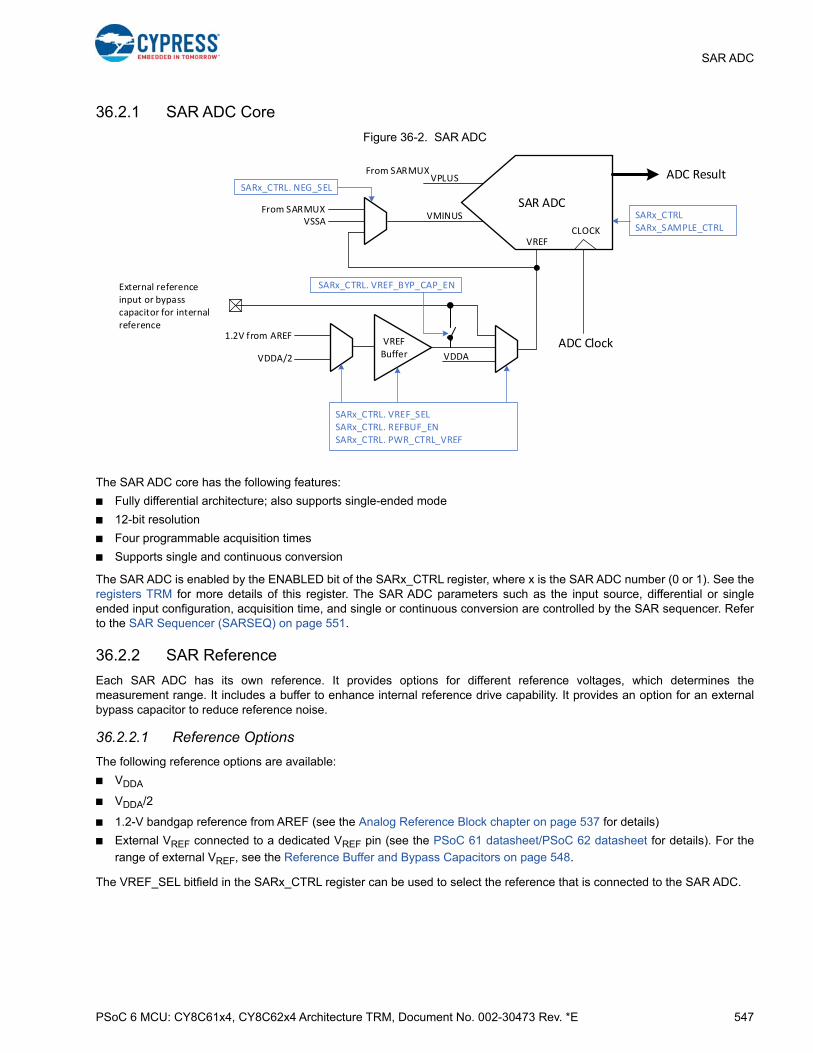
PSoC 6 MCU: CY8C61x4, CY8C62x4 Architecture TRM, Document No. 002-30473 Rev. *E 547
SAR ADC
36.2.1 SAR ADC Core
Figure 36-2. SAR ADC
The SAR ADC core has the following features:
■ Fully differential architecture; also supports single-ended mode
■ 12-bit resolution
■ Four programmable acquisition times
■ Supports single and continuous conversion
The SAR ADC is enabled by the ENABLED bit of the SARx_CTRL register, where x is the SAR ADC number (0 or 1). See theregisters TRM for more details of this register. The SAR ADC parameters such as the input source, differential or singleended input configuration, acquisition time, and single or continuous conversion are controlled by the SAR sequencer. Referto the SAR Sequencer (SARSEQ) on page 551.
36.2.2 SAR Reference
Each SAR ADC has its own reference. It provides options for different reference voltages, which determines themeasurement range. It includes a buffer to enhance internal reference drive capability. It provides an option for an externalbypass capacitor to reduce reference noise.
36.2.2.1 Reference Options
The following reference options are available:
■ VDDA
■ VDDA/2
■ 1.2-V bandgap reference from AREF (see the Analog Reference Block chapter on page 537 for details)
■ External VREF connected to a dedicated VREF pin (see the PSoC 61 datasheet/PSoC 62 datasheet for details). For the
range of external VREF, see the Reference Buffer and Bypass Capacitors on page 548.
The VREF_SEL bitfield in the SARx_CTRL register can be used to select the reference that is connected to the SAR ADC.
SAR ADC
VREF
VPLUS
VMINUSFrom SARMUX
VSSA
From SARMUX
1.2V from AREF
VDDAVDDA/2
VREF Buffer
External reference input or bypass capacitor for internal reference
CLOCK
ADC Clock
SARx_CTRL. VREF_SELSARx_CTRL. REFBUF_ENSARx_CTRL. PWR_CTRL_VREF
SARx_CTRL. NEG_SEL
SARx_CTRL. VREF_BYP_CAP_EN
SARx_CTRLSARx_SAMPLE_CTRL
ADC Result

PSoC 6 MCU: CY8C61x4, CY8C62x4 Architecture TRM, Document No. 002-30473 Rev. *E 548
SAR ADC
36.2.2.2 Reference Buffer and Bypass Capacitors
The internal references, 1.2 V from bandgap and VDDA/2, are buffered with the reference buffer. This reference may be routedto the external VREF pin where a capacitor can be used to filter noise that may exist on the reference.
The VREF_BYP_CAP_EN bitfield in the SARx_CTRL register can be used to enable the bypass capacitor. REFBUF_EN andPWR_CTRL_VREF bitfields in the same register can be used to enable the buffer, and select one of eight available powerlevels of the reference buffer respectively. The choice for the reference buffer power level depends on the ADC clockfrequency. If the SAR clock frequency is greater than 3.6 MHz, chose 60% power level or more. If the SAR clock frequency isless than 3.6 MHz, use 30% power level.
SAR performance (maximum sample rate) varies with the reference selection.
Reference buffer startup time varies with different bypass capacitor size. Table 36-2 lists two common values for the bypasscapacitor and the reference buffer startup time. If reference selection is changed between scans or when scanning afterdevice low-power modes in which the ADC is not active (see the Device Power Modes chapter on page 280), make sure thereference buffer is settled before the SAR ADC starts sampling.
36.2.2.3 Input Range
All inputs should be in the range of VSS to VDDA. Input voltage range is also limited by VREF. If voltage on negative input isVMINUS and the ADC reference is VREF, the range on the positive input is VMINUS ± VREF. This criterion applies for bothsingle-ended and differential modes. In single-ended mode, VMINUS is connected to VSS, VREF, internal analog block output,or an external input. See Negative Input Selection on page 554 for more details.
Note that VMINUS ± VREF must be in the range of VSS to VDDA. For example, if the negative input is connected to VSS, therange on the positive input is 0 to VREF, not –VREF to VREF. Only half of the ADC range is usable because the positive inputsignal cannot swing below VSS, which effectively only generates an 11-bit result.
Table 36-1. Reference Selection
Reference Selection VREF Range VDDAMaximum SAR ADC
Clock FrequencyMaximum Sample Rate
External Reference1 V to VDDA 1.7 V to 3.6 V 18 MHz 1 Msps
2 V to VDDA 2.7 V to 3.6 V 36 MHz 2 Msps
Internal reference without bypass capacitor 1 V to (VDDA–0.5 V) 1.7 V to 3.6 V 1.8 MHz 100 ksps
Internal reference with bypass capacitor 1 V to (VDDA–0.5 V) 1.7 V to 3.6 V 18 MHz 1 Msps
VDDA as reference1.7 V to VDDA 1.7 V to 2.7 V 18 MHz 1 Msps
2.7 V to VDDA 2.7 V to 3.6 V 36 MHz 2 Msps
Table 36-2. Bypass Capacitor Values vs Startup Time
Capacitor Value Startup Time
Internal reference with bypass capacitor (100 nF) 210 µs
Internal reference without bypass capacitor 10 µs
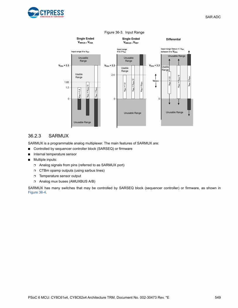
PSoC 6 MCU: CY8C61x4, CY8C62x4 Architecture TRM, Document No. 002-30473 Rev. *E 549
SAR ADC
Figure 36-3. Input Range
36.2.3 SARMUX
SARMUX is a programmable analog multiplexer. The main features of SARMUX are:
■ Controlled by sequencer controller block (SARSEQ) or firmware
■ Internal temperature sensor
■ Multiple inputs:
❐ Analog signals from pins (referred to as SARMUX port)
❐ CTBm opamp outputs (using sarbus lines)
❐ Temperature sensor output
❐ Analog mux buses (AMUXBUS A/B)
SARMUX has many switches that may be controlled by SARSEQ block (sequencer controller) or firmware, as shown inFigure 36-4.
0
UsableRange
Unusable Range
VDDA = 3.3
UnusableRange
VR
EF =
1.2
VR
EF =
VD
DA
/ 2
VR
EF =
VD
DA
Single EndedVMINUS = VSSA
UsableRange
UsableRange
0
VDDA = 3.3
0
VDDA = 3.3
Single EndedVMINUS = VREF
Differential
UnusableRange
VR
EF =
1.2
VR
EF =
VD
DA
/ 2
VR
EF =
VD
DA
Unusable Range
Unusable Range
VR
EF
= V
DD
A
VR
EF =
1.2
VMINUS
VR
EF =
VD
DA
/ 2
1.2
1.65
2.4
Input range 0 to VREF
Input range 0 to 2*VREF
Input range VMINUS +/- VREF,
between 0 to VDDA
Unusable Range

PSoC 6 MCU: CY8C61x4, CY8C62x4 Architecture TRM, Document No. 002-30473 Rev. *E 550
SAR ADC
Figure 36-4. SARMUX Switches
Firmware control: In firmware control, registers are written by the firmware to connect required signals to the VPLUS/VMINUS
terminals before starting the scan. Firmware can control every switch in SARMUX, as Figure 36-4 shows. TheSARx_MUX_SWITCH0 register can be used by firmware to close the SARMUX switches. To open the switches,SARx_MUX_SWITCH_CLEAR0 register can be used. Note that additional register writes may be required to connect blocksoutside the SARMUX control. However, firmware control needs continuous CPU intervention for multi-channel scans, which issolved by using sequencer control.
Sequencer control: In the sequencer control mode, the SARMUX switches are controlled by the SARSEQ block. Afterconfiguring each channel’s analog routing, it enables multi-channel, automatic scan in a round-robin fashion, without CPUintervention. Every switch in the SARMUX can be controlled by the sequencer. The SARx_MUX_SWITCH_SQ_CTRLregister is used to enable/disable SARSEQ control of SARMUX switches, which includes connection to the SARMUX portpins, temperature sensor, analog mux buses, and sarbus lines. There is one bit per input source in this register; to enable itsconnection to either VPLUS or VMINUS, the SARx_MUX_SWITCH0 register must be set. For example, there is one bit in
SARx_MUX_SWITCH_SQ_CTRL to enable SARSEQ control over connection to the Px.0 pin; to enable a particular switch soas to connect to VPLUS or VMINUS, the SARx_MUX_SWITCH0 register must be configured.
The analog interconnection is very flexible. The SAR ADC can be connected to multiple inputs via its SARMUX, includingboth external pins and internal signals.
■ SARMUX Port
There is a dedicated port, comprising of eight GPIO pins, which the SARMUX can directly connect to. Both the SARSEQ and firmware can be used to control the switches to select pins for single-ended mode or differential mode. In addition to SARMUX switch configuration, explained previously, the GPIOs must be configured properly to connect to the SARMUX. See the I/O System chapter on page 214 for more details.
■ Input from Other Pins through AMUXBUS
The SARMUX can connect to both of the analog mux buses (AMUXBUS A/B) using either firmware or sequencer control. However, additional switches must be turned ON to connect pins to AMUXBUS A/B. See the I/O System chapter on page 214 for details of AMUXBUS connections. Note that the SARSEQ can control the switches connecting AMUX buses to the inputs of ADC but not the switches that connect pins to the AMUX buses – that requires firmware control. Thus, if there are multiple channels configured with port pins other than the SARMUX port, firmware intervention is required to disconnect the pins associated with the previous channel from the AMUX buses and connect the pins of the next channel to it.
SAR ADC0
Pin 0
Pin 1
Pin 2
Pin 3
Pin 4
Pin 5
Pin 6
Pin 7
AMUXBUS A
AMUXBUS B
SARBUS0
SARBUS1
Temp
VSSA_KELVIN
TemperatureSensor
MUX_FW_P0_VMINUS MUX_FW_P0_VPLUS
MUX_FW_P1_VMINUS MUX_FW_P1_VPLUS
MUX_FW_P2_VMINUS MUX_FW_P2_VPLUS
MUX_FW_P3_VMINUS MUX_FW_P3_VPLUS
MUX_FW_P4_VMINUS MUX_FW_P4_VPLUS
MUX_FW_P5_VMINUS MUX_FW_P5_VPLUS
MUX_FW_P6_VMINUS MUX_FW_P6_VPLUS
MUX_FW_P7_VMINUS MUX_FW_P7_VPLUS
MUX_FW_AMUXBUSA_VMINUS MUX_FW_AMUXBUSA_VPLUS
MUX_FW_AMUXBUSB_VMINUS MUX_FW_AMUXBUSB_VPLUS
MUX_FW_SARBUS0_VMINUS MUX_FW_SARBUS0_VPLUS
MUX_FW_SARBUS1_VMINUS MUX_FW_SARBUS1_VPLUS
MUX_FW_TEMP_VPLUS
MUX_FW_VSSA_VMINUS
SARMUXSwitches controlled by firmware using MUX_SWITCH0 registers of SAR ADC 0 or by its sequencer
Pins of SARMUX Portpass(x)_sarmux_pads[0]to pass(x)_sarmux_pads[7]
See the device datasheet for the location of SARMUX Port.
AMUXBUS connects to other pins / analog peripherals
SARBUS connects toCTBm outputs
VSSA
Enable
VPLUS
VMINUS
SAR ADC1
MUX_FW_P0_VPLUS
MUX_FW_P1_VPLUS
MUX_FW_P2_VPLUS
MUX_FW_P3_VPLUS
MUX_FW_P4_VPLUS
MUX_FW_P5_VPLUS
MUX_FW_P6_VPLUS
MUX_FW_P7_VPLUS
MUX_FW_AMUXBUSA_VPLUS
MUX_FW_AMUXBUSB_VPLUS
MUX_FW_SARBUS0_VPLUS
MUX_FW_SARBUS1_VPLUS
MUX_FW_TEMP_VPLUS
VPLUS
VMINUS
Temp
VSSA_KELVIN
TemperatureSensor
MUX_FW_VSSA_VMINUS
VSSA
Enable
MUX_FW_P0_VMINUS
MUX_FW_P1_VMINUS
MUX_FW_P2_VMINUS
MUX_FW_P3_VMINUS
MUX_FW_P4_VMINUS
MUX_FW_P5_VMINUS
MUX_FW_P6_VMINUS
MUX_FW_P7_VMINUS
MUX_FW_AMUXBUSA_VMINUS
MUX_FW_AMUXBUSB_VMINUS
MUX_FW_SARBUS0_VMINUS
MUX_FW_SARBUS1_VMINUS
SARMUXSwitches controlled by firmware using MUX_SWITCH0 registers of SAR ADC 1 or by its sequencer
PSoC 6 MCU: CY8C61x4, CY8C62x4 Architecture TRM, Document No. 002-30473 Rev. *E 551
SAR ADC
The additional switches reduce the scanning performance (more parasitic coupling, longer RC time to settle). This is not recommended for external signals; the dedicated SARMUX port should be used, if possible.
AMUXBUS A and B can also be used to connect other analog peripherals to the SAR ADC. See the Analog Routing chapter on page 597 for more details.
■ CTBm opamp output through sarbus
SARMUX can connect to the CTBm opamp outputs using sarbus 0/1. In contrast to the control of the input from analog mux buses, here both the set of switches connecting opamp outputs to the sarbus and sarbus to ADC via SAR-MUX can be controlled not only by firmware but also using the SARSEQ. See the Continuous Time Block mini (CTBm) chapter on page 589 for details on the switches controlling the connection of opamp output to sarbus.
■ Input from temperature sensor
On-chip temperature sensors can be used to measure the device temperature. See the Temperature Sensor chapter on page 541 for more details of this block. For temperature sensors, differential conversions are not available (conversion result is undefined), thus always use it in singled-ended mode. A temperature sensor can be routed to the positive input of the corresponding SAR ADC using a switch that can be controlled by the sequencer or firmware. Setting the MUX_FW_TEMP_VPLUS bit in the SARx_MUX_SWITCH0 register enables the temperature sensor and connects its output to the positive input of the SAR ADC; clearing this bit (by writing ‘1’ into corresponding the bit of the SARx_MUX_SWITCH0_CLEAR register) disables temperature sensor by cutting off its bias current.
36.2.4 SAR Sequencer (SARSEQ)
The SARSEQ is a dedicated control block that automatically sequences the input mux, SARMUX, from one ADC channel tothe next while placing the result in an array of registers, one per ADC channel. Each ADC has a SARSEQ block. SARSEQhas the following functions:
■ Controls SARMUX analog routing automatically without CPU intervention.
■ Controls the SAR ADC core parameters such as acquisition times.
■ Receives data from the SAR ADC and processes it (average, range detect).
■ Double-buffers the results so that the CPU can safely read the results of the last scan while the next scan is in progress. Ascan refers to the conversion of all the enabled channels.
■ Moves the results into FIFO when enabled.
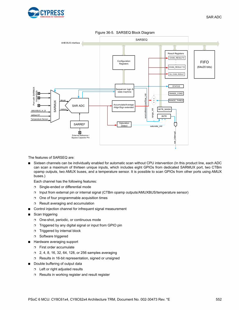
PSoC 6 MCU: CY8C61x4, CY8C62x4 Architecture TRM, Document No. 002-30473 Rev. *E 552
SAR ADC
Figure 36-5. SARSEQ Block Diagram
The features of SARSEQ are:
■ Sixteen channels can be individually enabled for automatic scan without CPU intervention (In this product line, each ADCcan scan a maximum of thirteen unique inputs, which includes eight GPIOs from dedicated SARMUX port, two CTBmopamp outputs, two AMUX buses, and a temperature sensor. It is possible to scan GPIOs from other ports using AMUXbuses.)
Each channel has the following features:
❐ Single-ended or differential mode
❐ Input from external pin or internal signal (CTBm opamp outputs/AMUXBUS/temperature sensor)
❐ One of four programmable acquisition times
❐ Result averaging and accumulation
■ Control injection channel for infrequent signal measurement
■ Scan triggering
❐ One-shot, periodic, or continuous mode
❐ Triggered by any digital signal or input from GPIO pin
❐ Triggered by internal block
❐ Software triggered
■ Hardware averaging support
❐ First order accumulate
❐ 2, 4, 8, 16, 32, 64, 128, or 256 samples averaging
❐ Results in 16-bit representation, signed or unsigned
■ Double buffering of output data
❐ Left or right adjusted results
❐ Results in working register and result register
Sequencer logic & state machine
CHAN_RESULT0
CHAN_RESULT15
INJ_CHAN_RESULT
RANGE_COND
RANGE_THRES
SA
RM
UX
Po
rt w
ith S
AR
MU
X
con
ne
ctiv
ity
。。
。
AMUXBUS_A/_B
Temperature Sensor
Accumulate/Average/Align/Sign extended
INTR_MASK
INTR
SAR ADC
Saturation Detect
<=>
AHB BUS interfaceSARSEQ
saturate_intr
ran
ge
_in
tr
eo
s/co
llisi
on
/ove
rflo
w_
intr
sar_
inte
rrup
t
。。
。
VPLUS
VMINUS
ConfigurationRegisters
Result Registers
SARREF
External Reference /Bypass Capacitor Pin
STATUS
FIFO(64x20 bits)
sarbus 0/1

PSoC 6 MCU: CY8C61x4, CY8C62x4 Architecture TRM, Document No. 002-30473 Rev. *E 553
SAR ADC
■ FIFO buffering
❐ 64 × 20 bits FIFO for each SAR ADC enabling storing of the results without CPU involvement
■ Interrupt generation
❐ Finished scan conversion
❐ Channel saturation detection
❐ Range (configurable) detection
❐ Scan results overflow
❐ Collision detection
❐ FIFO level
❐ FIFO overflow
❐ FIFO underflow
36.2.4.1 Single-ended and Differential Modes
The SAR ADC can operate in single-ended and differential modes. Differential or single-ended mode can be configured usingthe DIFFERENTIAL_EN bitfield in the channel configuration register, SARx_CHAN_CONFIGy, where y is the channelnumber (0–15).
SAR ADC gives full range output (0 to 4095) for differential inputs in the range of –VREF to +VREF relative to negative input
voltage (VMINUS).
Note: The precise value of the input range in the differential mode is –VREF to (+VREF – (VREF/2047)). The positive input
range is limited by the ADC resolution.
The single-ended mode options of negative input include VSSA, VREF, or an external input from Px.1, Px.3, Px.5, or Px.7 pins
of the SARMUX port. See the Negative Input Selection on page 554 for more details.
Note that temperature sensor can only be used in single-ended mode.
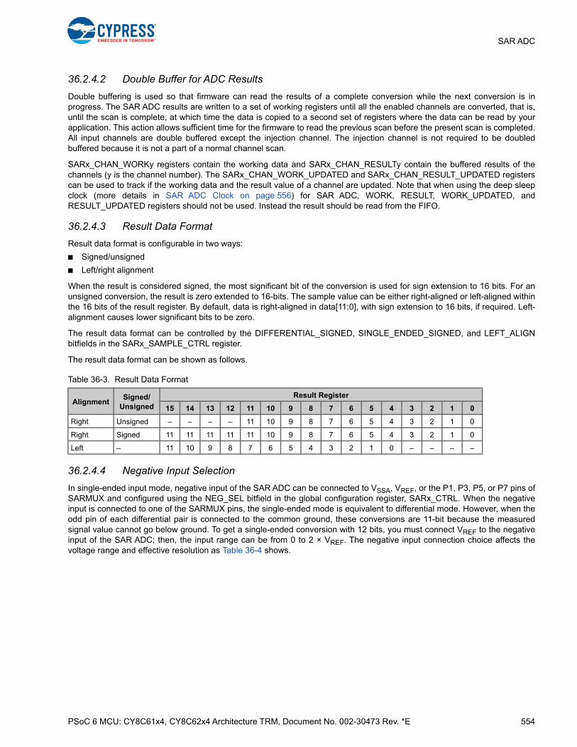
PSoC 6 MCU: CY8C61x4, CY8C62x4 Architecture TRM, Document No. 002-30473 Rev. *E 554
SAR ADC
36.2.4.2 Double Buffer for ADC Results
Double buffering is used so that firmware can read the results of a complete conversion while the next conversion is inprogress. The SAR ADC results are written to a set of working registers until all the enabled channels are converted, that is,until the scan is complete, at which time the data is copied to a second set of registers where the data can be read by yourapplication. This action allows sufficient time for the firmware to read the previous scan before the present scan is completed.All input channels are double buffered except the injection channel. The injection channel is not required to be doubledbuffered because it is not a part of a normal channel scan.
SARx_CHAN_WORKy registers contain the working data and SARx_CHAN_RESULTy contain the buffered results of thechannels (y is the channel number). The SARx_CHAN_WORK_UPDATED and SARx_CHAN_RESULT_UPDATED registerscan be used to track if the working data and the result value of a channel are updated. Note that when using the deep sleepclock (more details in SAR ADC Clock on page 556) for SAR ADC, WORK, RESULT, WORK_UPDATED, andRESULT_UPDATED registers should not be used. Instead the result should be read from the FIFO.
36.2.4.3 Result Data Format
Result data format is configurable in two ways:
■ Signed/unsigned
■ Left/right alignment
When the result is considered signed, the most significant bit of the conversion is used for sign extension to 16 bits. For anunsigned conversion, the result is zero extended to 16-bits. The sample value can be either right-aligned or left-aligned withinthe 16 bits of the result register. By default, data is right-aligned in data[11:0], with sign extension to 16 bits, if required. Left-alignment causes lower significant bits to be zero.
The result data format can be controlled by the DIFFERENTIAL_SIGNED, SINGLE_ENDED_SIGNED, and LEFT_ALIGNbitfields in the SARx_SAMPLE_CTRL register.
The result data format can be shown as follows.
36.2.4.4 Negative Input Selection
In single-ended input mode, negative input of the SAR ADC can be connected to VSSA, VREF, or the P1, P3, P5, or P7 pins ofSARMUX and configured using the NEG_SEL bitfield in the global configuration register, SARx_CTRL. When the negativeinput is connected to one of the SARMUX pins, the single-ended mode is equivalent to differential mode. However, when theodd pin of each differential pair is connected to the common ground, these conversions are 11-bit because the measuredsignal value cannot go below ground. To get a single-ended conversion with 12 bits, you must connect VREF to the negativeinput of the SAR ADC; then, the input range can be from 0 to 2 × VREF. The negative input connection choice affects thevoltage range and effective resolution as Table 36-4 shows.
Table 36-3. Result Data Format
AlignmentSigned/
Unsigned
Result Register
15 14 13 12 11 10 9 8 7 6 5 4 3 2 1 0
Right Unsigned – – – – 11 10 9 8 7 6 5 4 3 2 1 0
Right Signed 11 11 11 11 11 10 9 8 7 6 5 4 3 2 1 0
Left – 11 10 9 8 7 6 5 4 3 2 1 0 – – – –
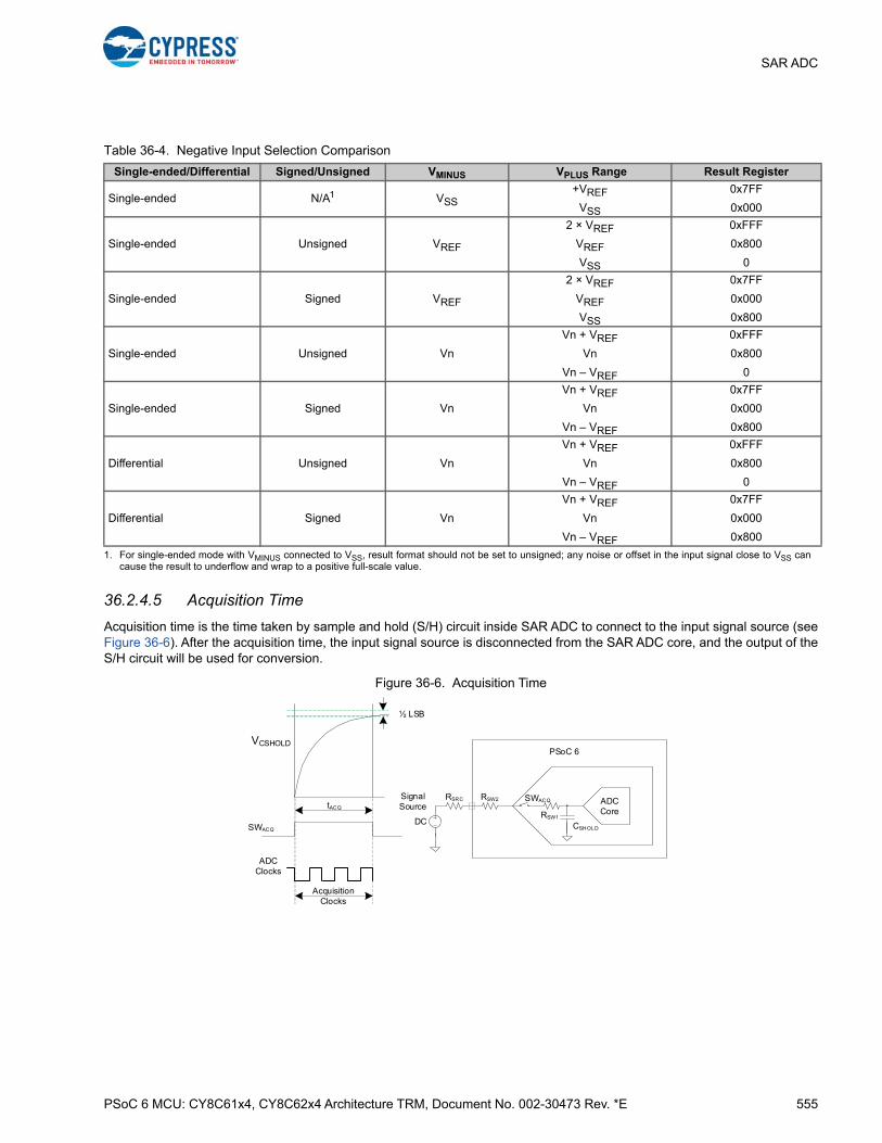
PSoC 6 MCU: CY8C61x4, CY8C62x4 Architecture TRM, Document No. 002-30473 Rev. *E 555
SAR ADC
36.2.4.5 Acquisition Time
Acquisition time is the time taken by sample and hold (S/H) circuit inside SAR ADC to connect to the input signal source (seeFigure 36-6). After the acquisition time, the input signal source is disconnected from the SAR ADC core, and the output of theS/H circuit will be used for conversion.
Figure 36-6. Acquisition Time
Table 36-4. Negative Input Selection Comparison
Single-ended/Differential Signed/Unsigned VMINUS VPLUS Range Result Register
Single-ended N/A1
1. For single-ended mode with VMINUS connected to VSS, result format should not be set to unsigned; any noise or offset in the input signal close to VSS cancause the result to underflow and wrap to a positive full-scale value.
VSS+VREF
VSS
0x7FF
0x000
Single-ended Unsigned VREF
2 × VREF
VREF
VSS
0xFFF
0x800
0
Single-ended Signed VREF
2 × VREF
VREF
VSS
0x7FF
0x000
0x800
Single-ended Unsigned Vn
Vn + VREF
Vn
Vn – VREF
0xFFF
0x800
0
Single-ended Signed Vn
Vn + VREF
Vn
Vn – VREF
0x7FF
0x000
0x800
Differential Unsigned Vn
Vn + VREF
Vn
Vn – VREF
0xFFF
0x800
0
Differential Signed Vn
Vn + VREF
Vn
Vn – VREF
0x7FF
0x000
0x800
Acquisition Clocks
SWACQ
ADCClocks
tACQADC CoreRSW1
RSW2
CSHOLD
SWACQ
DC
RSRC
PSoC 6
SignalSource
½ LSB
VCSHOLD
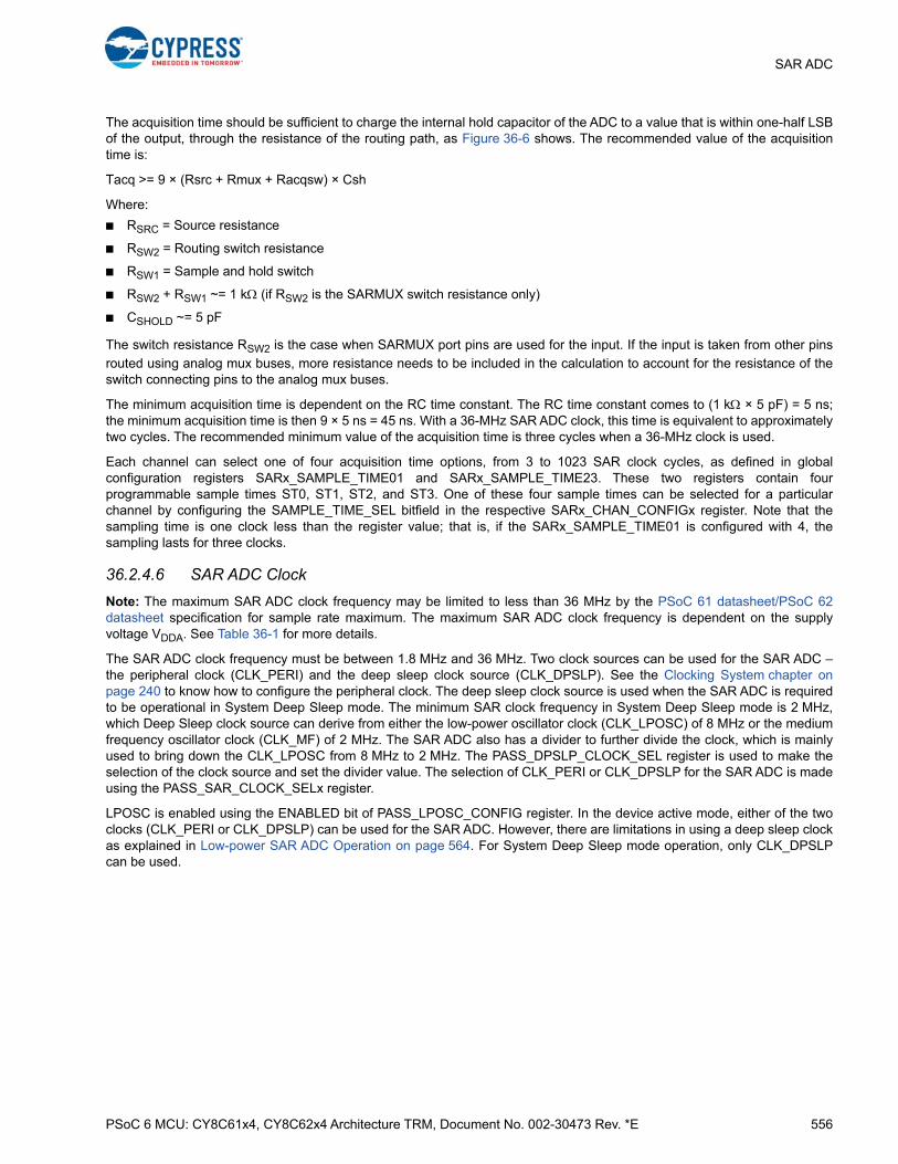
PSoC 6 MCU: CY8C61x4, CY8C62x4 Architecture TRM, Document No. 002-30473 Rev. *E 556
SAR ADC
The acquisition time should be sufficient to charge the internal hold capacitor of the ADC to a value that is within one-half LSBof the output, through the resistance of the routing path, as Figure 36-6 shows. The recommended value of the acquisitiontime is:
Tacq >= 9 × (Rsrc + Rmux + Racqsw) × Csh
Where:
■ RSRC = Source resistance
■ RSW2 = Routing switch resistance
■ RSW1 = Sample and hold switch
■ RSW2 + RSW1 ~= 1 k (if RSW2 is the SARMUX switch resistance only)
■ CSHOLD ~= 5 pF
The switch resistance RSW2 is the case when SARMUX port pins are used for the input. If the input is taken from other pins
routed using analog mux buses, more resistance needs to be included in the calculation to account for the resistance of theswitch connecting pins to the analog mux buses.
The minimum acquisition time is dependent on the RC time constant. The RC time constant comes to (1 k × 5 pF) = 5 ns;the minimum acquisition time is then 9 × 5 ns = 45 ns. With a 36-MHz SAR ADC clock, this time is equivalent to approximatelytwo cycles. The recommended minimum value of the acquisition time is three cycles when a 36-MHz clock is used.
Each channel can select one of four acquisition time options, from 3 to 1023 SAR clock cycles, as defined in globalconfiguration registers SARx_SAMPLE_TIME01 and SARx_SAMPLE_TIME23. These two registers contain fourprogrammable sample times ST0, ST1, ST2, and ST3. One of these four sample times can be selected for a particularchannel by configuring the SAMPLE_TIME_SEL bitfield in the respective SARx_CHAN_CONFIGx register. Note that thesampling time is one clock less than the register value; that is, if the SARx_SAMPLE_TIME01 is configured with 4, thesampling lasts for three clocks.
36.2.4.6 SAR ADC Clock
Note: The maximum SAR ADC clock frequency may be limited to less than 36 MHz by the PSoC 61 datasheet/PSoC 62datasheet specification for sample rate maximum. The maximum SAR ADC clock frequency is dependent on the supplyvoltage VDDA. See Table 36-1 for more details.
The SAR ADC clock frequency must be between 1.8 MHz and 36 MHz. Two clock sources can be used for the SAR ADC –the peripheral clock (CLK_PERI) and the deep sleep clock source (CLK_DPSLP). See the Clocking System chapter onpage 240 to know how to configure the peripheral clock. The deep sleep clock source is used when the SAR ADC is requiredto be operational in System Deep Sleep mode. The minimum SAR clock frequency in System Deep Sleep mode is 2 MHz,which Deep Sleep clock source can derive from either the low-power oscillator clock (CLK_LPOSC) of 8 MHz or the mediumfrequency oscillator clock (CLK_MF) of 2 MHz. The SAR ADC also has a divider to further divide the clock, which is mainlyused to bring down the CLK_LPOSC from 8 MHz to 2 MHz. The PASS_DPSLP_CLOCK_SEL register is used to make theselection of the clock source and set the divider value. The selection of CLK_PERI or CLK_DPSLP for the SAR ADC is madeusing the PASS_SAR_CLOCK_SELx register.
LPOSC is enabled using the ENABLED bit of PASS_LPOSC_CONFIG register. In the device active mode, either of the twoclocks (CLK_PERI or CLK_DPSLP) can be used for the SAR ADC. However, there are limitations in using a deep sleep clockas explained in Low-power SAR ADC Operation on page 564. For System Deep Sleep mode operation, only CLK_DPSLPcan be used.

PSoC 6 MCU: CY8C61x4, CY8C62x4 Architecture TRM, Document No. 002-30473 Rev. *E 557
SAR ADC
Figure 36-7. SAR ADC Clock
36.2.4.7 SAR ADC Timing
Figure 36-8 shows an ADC conversion at the maximum sample rate. An external trigger initiates the process. It takes amaximum of 1.5 x SAR ADC clocks + 2 SYS clocks to start the sample of the input. The sampling period is configured asdescribed in Acquisition Time on page 555. When the sampling period ends, there is a half clock delay and then theconversion process begins with each output bit taking one clock cycle. When 12 bits are obtained, an end of conversionsignal is generated and the auto-zeroing of the internal comparator (part of SAR ADC) offset is done. If the continuousconversion mode is being used, immediately after the auto-zeroing, sampling is initiated; if one shot mode is being used, itwaits for another trigger signal.
For a continuous conversion mode with a minimum of three acquisition clocks, the calculation of the number of clocks takenby SAR ADC is as follows:
3 clock cycles for sampling the input (minimum acquisition time set by SARx_SAMPLE_TIME01 or SARx_SAMPLE_TIME23)
+ ½ clock to complete auto-zero
+ ½ clock for non-overlap
+ 12 clocks for conversion (with 12-bit resolution)
+ 1 clock for EOF output signal
+ 1 clock for auto-zero
= 18 clock cycles
EOF is not accessible; it is used internally to load the result into the output registers. The End of Scan (EOS) output, which isaccessible, is asserted at the end of conversion of all the enabled channels.
Figure 36-8. SAR ADC Timing
36.2.4.8 Channel Configuration
The SARx_CHAN_CONFIGy register contains the following bitfields, which control the behavior of respective channels duringa SARSEQ scan:
■ POS_PORT_ADDR and POS_PIN_ADDR select the connection to the VPLUS terminal of the ADC
SAR ADCx
CLK_PERI
Divider (1, 2, 4, 8, 16)
CLK_LPOSC
CLK_MF
PASS_DPSLP_CLOCK_SEL
PASS_SAR_CLOCK_SELx
ADC Clock
CLK_DPSLP
SAR CLOCK
EXT TRIGGER
SAMPLE
S12 S11 S10 S9 S8 S7 S6 S5 S4 S3 S2 S1STATE
EOF SAMPLE
EOF 1.5 SAR CLOCK + 2 SYS CLOCK
AZ S12SAMPLE
18 clocks
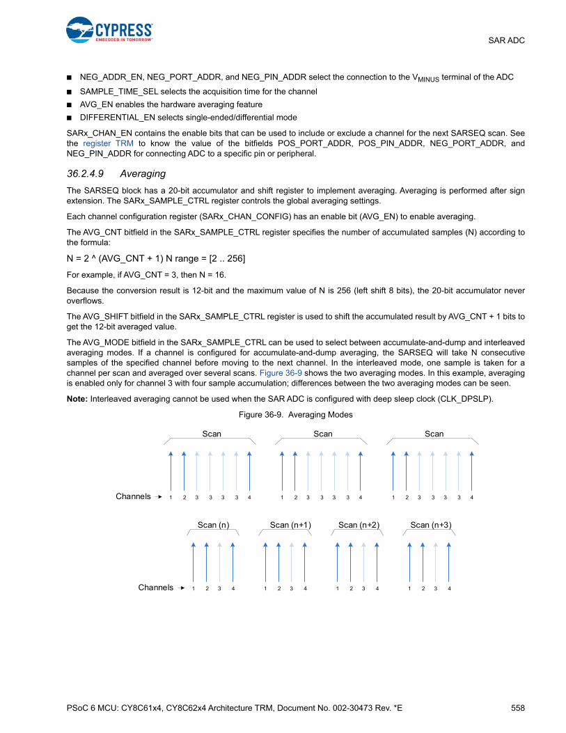
PSoC 6 MCU: CY8C61x4, CY8C62x4 Architecture TRM, Document No. 002-30473 Rev. *E 558
SAR ADC
■ NEG_ADDR_EN, NEG_PORT_ADDR, and NEG_PIN_ADDR select the connection to the VMINUS terminal of the ADC
■ SAMPLE_TIME_SEL selects the acquisition time for the channel
■ AVG_EN enables the hardware averaging feature
■ DIFFERENTIAL_EN selects single-ended/differential mode
SARx_CHAN_EN contains the enable bits that can be used to include or exclude a channel for the next SARSEQ scan. Seethe register TRM to know the value of the bitfields POS_PORT_ADDR, POS_PIN_ADDR, NEG_PORT_ADDR, andNEG_PIN_ADDR for connecting ADC to a specific pin or peripheral.
36.2.4.9 Averaging
The SARSEQ block has a 20-bit accumulator and shift register to implement averaging. Averaging is performed after signextension. The SARx_SAMPLE_CTRL register controls the global averaging settings.
Each channel configuration register (SARx_CHAN_CONFIG) has an enable bit (AVG_EN) to enable averaging.
The AVG_CNT bitfield in the SARx_SAMPLE_CTRL register specifies the number of accumulated samples (N) according tothe formula:
N = 2 ^ (AVG_CNT + 1) N range = [2 .. 256]
For example, if AVG_CNT = 3, then N = 16.
Because the conversion result is 12-bit and the maximum value of N is 256 (left shift 8 bits), the 20-bit accumulator neveroverflows.
The AVG_SHIFT bitfield in the SARx_SAMPLE_CTRL register is used to shift the accumulated result by AVG_CNT + 1 bits toget the 12-bit averaged value.
The AVG_MODE bitfield in the SARx_SAMPLE_CTRL can be used to select between accumulate-and-dump and interleavedaveraging modes. If a channel is configured for accumulate-and-dump averaging, the SARSEQ will take N consecutivesamples of the specified channel before moving to the next channel. In the interleaved mode, one sample is taken for achannel per scan and averaged over several scans. Figure 36-9 shows the two averaging modes. In this example, averagingis enabled only for channel 3 with four sample accumulation; differences between the two averaging modes can be seen.
Note: Interleaved averaging cannot be used when the SAR ADC is configured with deep sleep clock (CLK_DPSLP).
Figure 36-9. Averaging Modes
1 2 3 3 3 3 4 1 2 3 3 3 3 4 1 2 3 3 3 3 4
Scan Scan Scan
Channels
1 2 3 4
Scan (n)
Channels 1 2 3 4 1 2 3 4 1 2 3 4
Scan (n+1) Scan (n+2) Scan (n+3)
PSoC 6 MCU: CY8C61x4, CY8C62x4 Architecture TRM, Document No. 002-30473 Rev. *E 559
SAR ADC
36.2.5 Injection Channel
The injection channel is similar to the other channels, with the exception that it is not part of a regular scan. The injectionchannel is used for incidental or rare conversions; for example, sampling the temperature sensor every two seconds. Notethat if SAR is operating in continuous mode, enabling the injection channel will change the sample rate.
The injection channel can only be controlled by the firmware with a firmware trigger (one-shot). This means the injectionchannel does not support continuous or hardware trigger. It works only when the SAR ADC is configured with the peripheralclock (and not the deep sleep clock) and does not support output of its data to FIFO; the result should be read from the dedi-cated result register. Because the only trigger is one-shot, there is no need for double buffering or an overflow interrupt.
The conversions for the injection channel can be configured in the same way as the regular channels by setting the SARx_IN-J_CHAN_CONFIG register; it supports:
■ Pin or signal selection
■ Single-ended or differential selection
■ Sample time select from one of the four globally specified sample times
■ Average enable
The injection channel supports the same interrupts as the regular channel except the overflow interrupt.
■ Maskable end-of-conversion interrupt INJ_EOC_INTR
■ Maskable range detect interrupt INJ_RANGE_INTR
■ Maskable saturation detect interrupt INJ_SATURATE_INTR
■ Maskable collision interrupt INJ_COLLISION_INTR
SAR_INTR, SAR_INTR_MASK, SAR_INTR_MASKED, and SAR_INTR_SET are the corresponding registers.
Interrupts are described in SAR Interrupts on page 566.
36.2.5.1 Tailgating
The injection channel conversion can be triggered by setting the enable bit INJ_START_EN (SARx_INJ_CHAN_CONFIG[31]). It is recommended to select tailgating by setting INJ_TAILGATING = 1 (SARx_INJ_CHAN_CONFIG [30]). The injectionchannel will be scanned at the end of the ongoing scan of regular channels without any collision. However, if there is no ongo-ing scan or the SAR ADC is idle, and tailgating is selected, INJ_START_EN will enable the injection channel to be scanned atthe end of the next scan of regular channels.
If tailgating is not selected, setting the INJ_START_EN bit immediately starts the conversion of the injection channel providedthere is no ongoing scan or SAR ADC is idle. If a scan of the regular channels is ongoing, then the injection channel will bescanned at the end of the ongoing scan, but it will cause a collision and generate a collision interrupt (INJ_COLLI-SION_INTR). Note that if continuous trigger or hardware trigger level mode is being used for the regular channels, collisioninterrupt is not triggered. Another consequence of not enabling the tailgating is that it causes jitter on a regular scan.
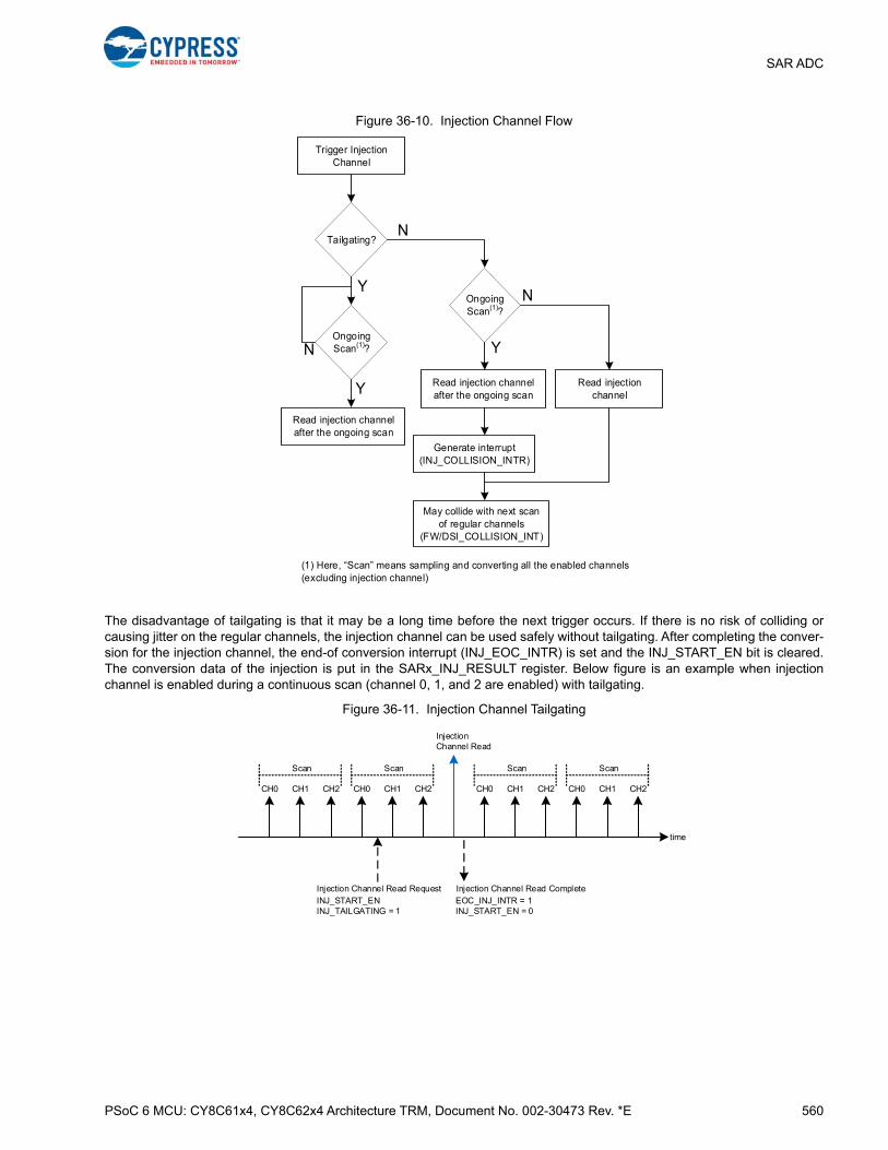
PSoC 6 MCU: CY8C61x4, CY8C62x4 Architecture TRM, Document No. 002-30473 Rev. *E 560
SAR ADC
Figure 36-10. Injection Channel Flow
The disadvantage of tailgating is that it may be a long time before the next trigger occurs. If there is no risk of colliding orcausing jitter on the regular channels, the injection channel can be used safely without tailgating. After completing the conver-sion for the injection channel, the end-of conversion interrupt (INJ_EOC_INTR) is set and the INJ_START_EN bit is cleared.The conversion data of the injection is put in the SARx_INJ_RESULT register. Below figure is an example when injectionchannel is enabled during a continuous scan (channel 0, 1, and 2 are enabled) with tailgating.
Figure 36-11. Injection Channel Tailgating
Trigger Injection Channel
Tailgating?
Ongoing Scan(1)?
Read injection channelafter the ongoing scan
Ongoing Scan(1)?
Read injection channel after the ongoing scan
Generate interrupt(INJ_COLLISION_INTR)
May collide with next scan of regular channels
(FW/DSI_COLLISION_INT)
Read injection channel
N
N
NY
Y
Y
(1) Here, “Scan” means sampling and converting all the enabled channels (excluding injection channel)
time
CH0 CH1 CH2 CH0 CH1 CH2 CH0 CH1 CH2 CH0 CH1 CH2
INJ_START_ENINJ_TAILGATING = 1
Injection Channel Read Request
Injection Channel Read
Scan Scan Scan Scan
EOC_INJ_INTR = 1INJ_START_EN = 0
Injection Channel Read Complete
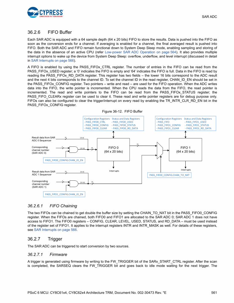
PSoC 6 MCU: CY8C61x4, CY8C62x4 Architecture TRM, Document No. 002-30473 Rev. *E 561
SAR ADC
36.2.6 FIFO Buffer
Each SAR ADC is equipped with a 64 sample depth (64 x 20 bits) FIFO to store the results. Data is pushed into the FIFO assoon as the conversion ends for a channel. If averaging is enabled for a channel, the final averaged result is pushed intoFIFO. Both the SAR ADC and FIFO remain functional down to System Deep Sleep mode, enabling sampling and storing ofthe data in the absence of an active CPU (refer Low-power SAR ADC Operation on page 564). It also provides multipleinterrupt options to wake up the device from System Deep Sleep: overflow, underflow, and level interrupt (discussed in detailin SAR Interrupts on page 566).
A FIFO is enabled by using the PASS_FIFOx_CTRL register. The number of entries in the FIFO can be read from thePASS_FIFOx_USED register; a ‘0’ indicates the FIFO is empty and ‘64’ indicates the FIFO is full. Data in the FIFO is read byreading the PASS_FIFOx_RD_DATA register. This register has two fields – the lower 16 bits correspond to the ADC resultand the next 4 bits corresponds to the channel ID. To set the channel ID in the read register, CHAN_ID_EN should be set inthe PASS_FIFOx_CONFIG register. Two pointers – write and read – are used for the FIFO operation. When the ADC writesdata into the FIFO, the write pointer is incremented. When the CPU reads the data from the FIFO, the read pointer isincremented. The read and write pointers to the FIFO can be read from the PASS_FIFOx_STATUS register; thePASS_FIFO_CLEARx register can be used to clear it. These read and write pointer registers are for debug purpose only.FIFOs can also be configured to clear the trigger/interrupt on every read by enabling the TR_INTR_CLR_RD_EN bit in thePASS_FIFOx_CONFIG register.
Figure 36-12. FIFO Buffer
36.2.6.1 FIFO Chaining
The two FIFOs can be chained to get double the buffer size by setting the CHAIN_TO_NXT bit in the PASS_FIFO0_CONFIGregister. When the FIFOs are chained, both FIFO0 and FIFO1 are allocated to the SAR ADC 0; SAR ADC 1 does not haveaccess to FIFO1. The FIFO0 registers – CONFIG, CLEAR, LEVEL, USED, STATUS, and RD_DATA – must be used insteadof the register set of FIFO1. It applies to the interrupt registers INTR and INTR_MASK as well. For details of these registers,see SAR Interrupts on page 566.
36.2.7 Trigger
The SAR ADC can be triggered to start conversion by two sources.
36.2.7.1 Firmware
A trigger is generated using firmware by writing to the FW_TRIGGER bit of the SARx_START_CTRL register. After the scanis completed, the SARSEQ clears the FW_TRIGGER bit and goes back to idle mode waiting for the next trigger. The
FIFO 0(64 x 20 bits)
Configuration Registers Status and Data Registers ‐ PASS_FIFO0_CTRL ‐ PASS_FIFO0_USED‐ PASS_FIFO0_CONFIG ‐ PASS_FIFO0_STATUS‐ PASS_FIFO0_CLEAR ‐ PASS_FIFO0_RD_DATA
Configuration Registers Status and Data Registers ‐ PASS_FIFO ‐ PASS_FIFO1_USED‐ PASS_FIFO1_CONFIG ‐ PASS_FIFO1_STATUS‐ PASS_FIFO1_CLEAR ‐ PASS_FIFO1_RD_DATA
16
420
[15:0]
[19:16]
Result data from SAR ADC 0 Sequencer
Corresponding channel number(SAR ADC 0)
PASS_FIFO0_CONFIG.CHAN_ID_EN
FIFO 1(64 x 20 bits)
16
420
[15:0]
[19:16]
Result data from SAR ADC 1 Sequencer
Corresponding channel number(SAR ADC 1)
PASS_FIFO1_CONFIG.CHAN_ID_EN
20
PASS_FIFO0_CONFIG.CHAN_TO_NXT
Interrupts Interrupts
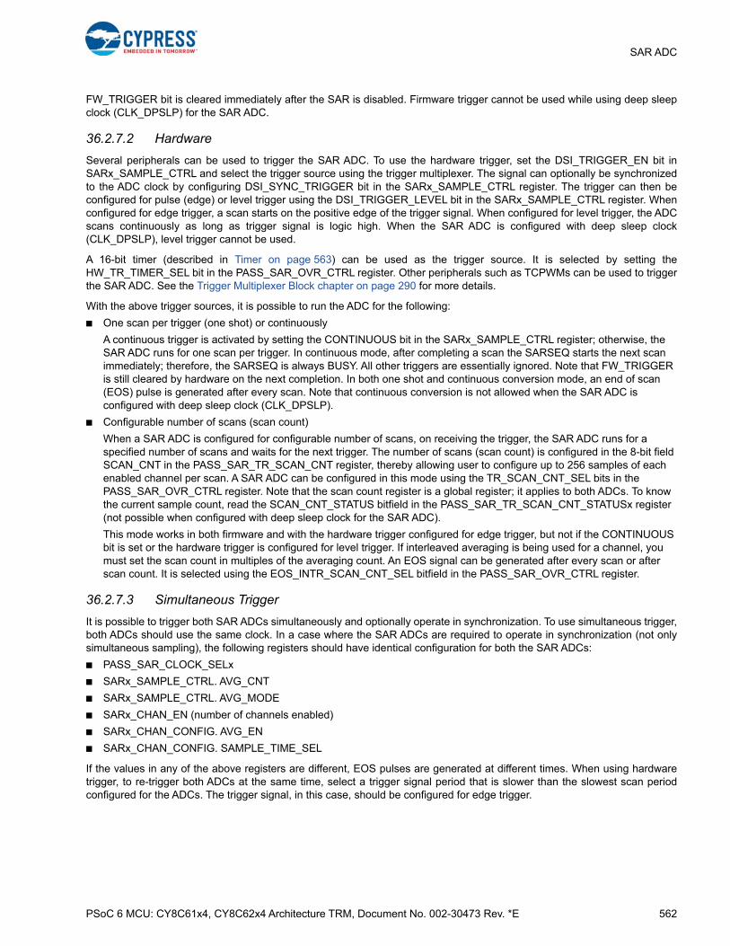
PSoC 6 MCU: CY8C61x4, CY8C62x4 Architecture TRM, Document No. 002-30473 Rev. *E 562
SAR ADC
FW_TRIGGER bit is cleared immediately after the SAR is disabled. Firmware trigger cannot be used while using deep sleepclock (CLK_DPSLP) for the SAR ADC.
36.2.7.2 Hardware
Several peripherals can be used to trigger the SAR ADC. To use the hardware trigger, set the DSI_TRIGGER_EN bit inSARx_SAMPLE_CTRL and select the trigger source using the trigger multiplexer. The signal can optionally be synchronizedto the ADC clock by configuring DSI_SYNC_TRIGGER bit in the SARx_SAMPLE_CTRL register. The trigger can then beconfigured for pulse (edge) or level trigger using the DSI_TRIGGER_LEVEL bit in the SARx_SAMPLE_CTRL register. Whenconfigured for edge trigger, a scan starts on the positive edge of the trigger signal. When configured for level trigger, the ADCscans continuously as long as trigger signal is logic high. When the SAR ADC is configured with deep sleep clock(CLK_DPSLP), level trigger cannot be used.
A 16-bit timer (described in Timer on page 563) can be used as the trigger source. It is selected by setting theHW_TR_TIMER_SEL bit in the PASS_SAR_OVR_CTRL register. Other peripherals such as TCPWMs can be used to triggerthe SAR ADC. See the Trigger Multiplexer Block chapter on page 290 for more details.
With the above trigger sources, it is possible to run the ADC for the following:
■ One scan per trigger (one shot) or continuously
A continuous trigger is activated by setting the CONTINUOUS bit in the SARx_SAMPLE_CTRL register; otherwise, the SAR ADC runs for one scan per trigger. In continuous mode, after completing a scan the SARSEQ starts the next scan immediately; therefore, the SARSEQ is always BUSY. All other triggers are essentially ignored. Note that FW_TRIGGER is still cleared by hardware on the next completion. In both one shot and continuous conversion mode, an end of scan (EOS) pulse is generated after every scan. Note that continuous conversion is not allowed when the SAR ADC is configured with deep sleep clock (CLK_DPSLP).
■ Configurable number of scans (scan count)
When a SAR ADC is configured for configurable number of scans, on receiving the trigger, the SAR ADC runs for a specified number of scans and waits for the next trigger. The number of scans (scan count) is configured in the 8-bit field SCAN_CNT in the PASS_SAR_TR_SCAN_CNT register, thereby allowing user to configure up to 256 samples of each enabled channel per scan. A SAR ADC can be configured in this mode using the TR_SCAN_CNT_SEL bits in the PASS_SAR_OVR_CTRL register. Note that the scan count register is a global register; it applies to both ADCs. To know the current sample count, read the SCAN_CNT_STATUS bitfield in the PASS_SAR_TR_SCAN_CNT_STATUSx register (not possible when configured with deep sleep clock for the SAR ADC).
This mode works in both firmware and with the hardware trigger configured for edge trigger, but not if the CONTINUOUS bit is set or the hardware trigger is configured for level trigger. If interleaved averaging is being used for a channel, you must set the scan count in multiples of the averaging count. An EOS signal can be generated after every scan or after scan count. It is selected using the EOS_INTR_SCAN_CNT_SEL bitfield in the PASS_SAR_OVR_CTRL register.
36.2.7.3 Simultaneous Trigger
It is possible to trigger both SAR ADCs simultaneously and optionally operate in synchronization. To use simultaneous trigger,both ADCs should use the same clock. In a case where the SAR ADCs are required to operate in synchronization (not onlysimultaneous sampling), the following registers should have identical configuration for both the SAR ADCs:
■ PASS_SAR_CLOCK_SELx
■ SARx_SAMPLE_CTRL. AVG_CNT
■ SARx_SAMPLE_CTRL. AVG_MODE
■ SARx_CHAN_EN (number of channels enabled)
■ SARx_CHAN_CONFIG. AVG_EN
■ SARx_CHAN_CONFIG. SAMPLE_TIME_SEL
If the values in any of the above registers are different, EOS pulses are generated at different times. When using hardwaretrigger, to re-trigger both ADCs at the same time, select a trigger signal period that is slower than the slowest scan periodconfigured for the ADCs. The trigger signal, in this case, should be configured for edge trigger.
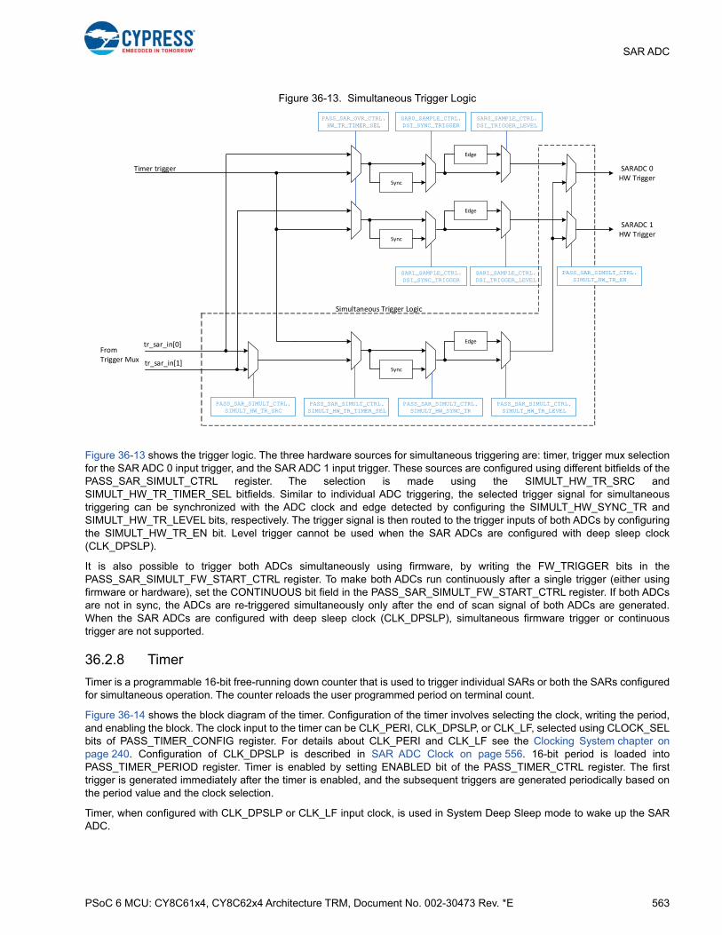
PSoC 6 MCU: CY8C61x4, CY8C62x4 Architecture TRM, Document No. 002-30473 Rev. *E 563
SAR ADC
Figure 36-13. Simultaneous Trigger Logic
Figure 36-13 shows the trigger logic. The three hardware sources for simultaneous triggering are: timer, trigger mux selectionfor the SAR ADC 0 input trigger, and the SAR ADC 1 input trigger. These sources are configured using different bitfields of thePASS_SAR_SIMULT_CTRL register. The selection is made using the SIMULT_HW_TR_SRC andSIMULT_HW_TR_TIMER_SEL bitfields. Similar to individual ADC triggering, the selected trigger signal for simultaneoustriggering can be synchronized with the ADC clock and edge detected by configuring the SIMULT_HW_SYNC_TR andSIMULT_HW_TR_LEVEL bits, respectively. The trigger signal is then routed to the trigger inputs of both ADCs by configuringthe SIMULT_HW_TR_EN bit. Level trigger cannot be used when the SAR ADCs are configured with deep sleep clock(CLK_DPSLP).
It is also possible to trigger both ADCs simultaneously using firmware, by writing the FW_TRIGGER bits in thePASS_SAR_SIMULT_FW_START_CTRL register. To make both ADCs run continuously after a single trigger (either usingfirmware or hardware), set the CONTINUOUS bit field in the PASS_SAR_SIMULT_FW_START_CTRL register. If both ADCsare not in sync, the ADCs are re-triggered simultaneously only after the end of scan signal of both ADCs are generated.When the SAR ADCs are configured with deep sleep clock (CLK_DPSLP), simultaneous firmware trigger or continuoustrigger are not supported.
36.2.8 Timer
Timer is a programmable 16-bit free-running down counter that is used to trigger individual SARs or both the SARs configuredfor simultaneous operation. The counter reloads the user programmed period on terminal count.
Figure 36-14 shows the block diagram of the timer. Configuration of the timer involves selecting the clock, writing the period,and enabling the block. The clock input to the timer can be CLK_PERI, CLK_DPSLP, or CLK_LF, selected using CLOCK_SELbits of PASS_TIMER_CONFIG register. For details about CLK_PERI and CLK_LF see the Clocking System chapter onpage 240. Configuration of CLK_DPSLP is described in SAR ADC Clock on page 556. 16-bit period is loaded intoPASS_TIMER_PERIOD register. Timer is enabled by setting ENABLED bit of the PASS_TIMER_CTRL register. The firsttrigger is generated immediately after the timer is enabled, and the subsequent triggers are generated periodically based onthe period value and the clock selection.
Timer, when configured with CLK_DPSLP or CLK_LF input clock, is used in System Deep Sleep mode to wake up the SARADC.
PASS_SAR_OVR_CTRL. HW_TR_TIMER_SEL
Timer trigger
Sync
Edge
SAR0_SAMPLE_CTRL. DSI_SYNC_TRIGGER
SAR0_SAMPLE_CTRL. DSI_TRIGGER_LEVEL
Sync
Edge
Sync
Edgetr_sar_in[0]
tr_sar_in[1]
From Trigger Mux
PASS_SAR_SIMULT_CTRL. SIMULT_HW_TR_TIMER_SEL
PASS_SAR_SIMULT_CTRL. SIMULT_HW_SYNC_TR
SAR1_SAMPLE_CTRL. DSI_SYNC_TRIGGER
SAR1_SAMPLE_CTRL. DSI_TRIGGER_LEVEL
PASS_SAR_SIMULT_CTRL. SIMULT_HW_TR_SRC
PASS_SAR_SIMULT_CTRL. SIMULT_HW_TR_LEVEL
SARADC 0HW Trigger
SARADC 1HW Trigger
Simultaneous Trigger Logic
PASS_SAR_SIMULT_CTRL. SIMULT_HW_TR_EN
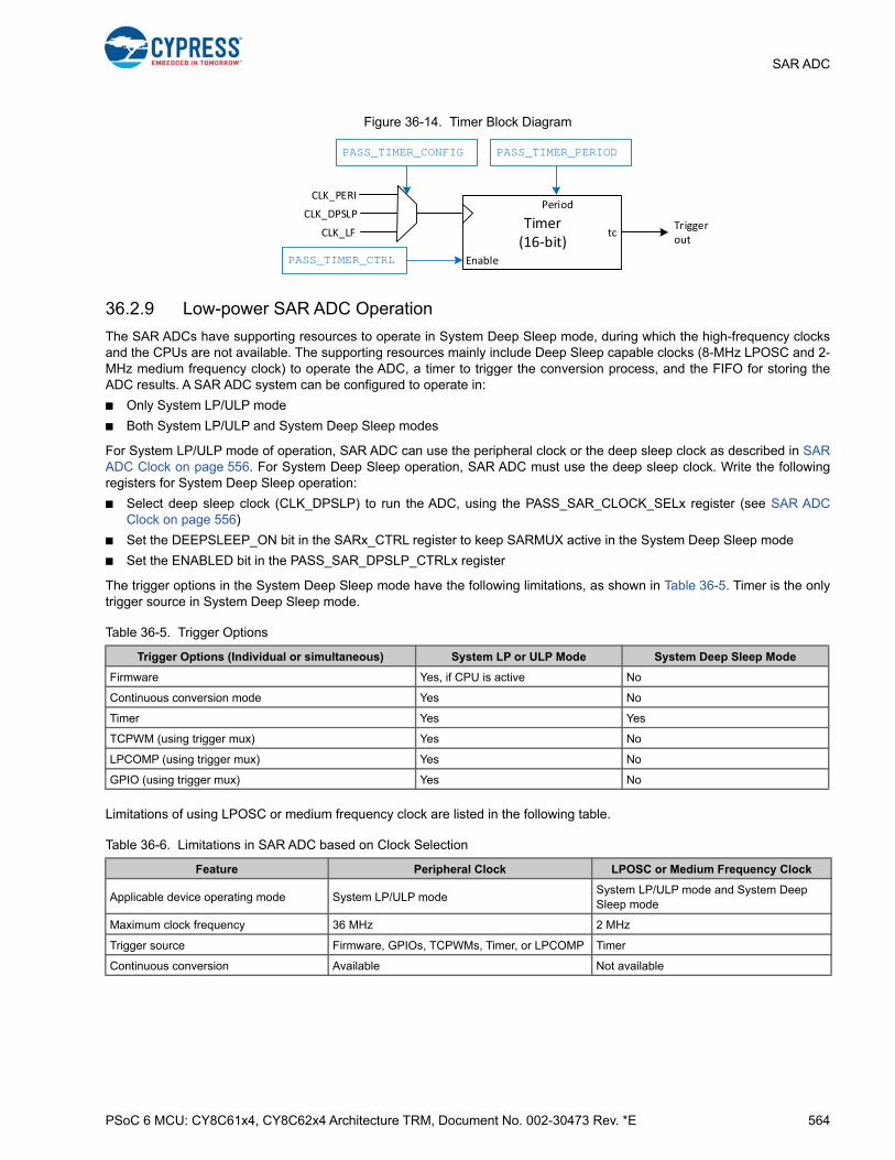
PSoC 6 MCU: CY8C61x4, CY8C62x4 Architecture TRM, Document No. 002-30473 Rev. *E 564
SAR ADC
Figure 36-14. Timer Block Diagram
36.2.9 Low-power SAR ADC Operation
The SAR ADCs have supporting resources to operate in System Deep Sleep mode, during which the high-frequency clocksand the CPUs are not available. The supporting resources mainly include Deep Sleep capable clocks (8-MHz LPOSC and 2-MHz medium frequency clock) to operate the ADC, a timer to trigger the conversion process, and the FIFO for storing theADC results. A SAR ADC system can be configured to operate in:
■ Only System LP/ULP mode
■ Both System LP/ULP and System Deep Sleep modes
For System LP/ULP mode of operation, SAR ADC can use the peripheral clock or the deep sleep clock as described in SARADC Clock on page 556. For System Deep Sleep operation, SAR ADC must use the deep sleep clock. Write the followingregisters for System Deep Sleep operation:
■ Select deep sleep clock (CLK_DPSLP) to run the ADC, using the PASS_SAR_CLOCK_SELx register (see SAR ADCClock on page 556)
■ Set the DEEPSLEEP_ON bit in the SARx_CTRL register to keep SARMUX active in the System Deep Sleep mode
■ Set the ENABLED bit in the PASS_SAR_DPSLP_CTRLx register
The trigger options in the System Deep Sleep mode have the following limitations, as shown in Table 36-5. Timer is the onlytrigger source in System Deep Sleep mode.
Limitations of using LPOSC or medium frequency clock are listed in the following table.
Table 36-5. Trigger Options
Trigger Options (Individual or simultaneous) System LP or ULP Mode System Deep Sleep Mode
Firmware Yes, if CPU is active No
Continuous conversion mode Yes No
Timer Yes Yes
TCPWM (using trigger mux) Yes No
LPCOMP (using trigger mux) Yes No
GPIO (using trigger mux) Yes No
Table 36-6. Limitations in SAR ADC based on Clock Selection
Feature Peripheral Clock LPOSC or Medium Frequency Clock
Applicable device operating mode System LP/ULP modeSystem LP/ULP mode and System Deep Sleep mode
Maximum clock frequency 36 MHz 2 MHz
Trigger source Firmware, GPIOs, TCPWMs, Timer, or LPCOMP Timer
Continuous conversion Available Not available
Timer(16‐bit)
CLK_PERI
CLK_DPSLP
CLK_LF
PASS_TIMER_CONFIG
EnablePASS_TIMER_CTRL
PASS_TIMER_PERIOD
Period
Triggerout
tc

PSoC 6 MCU: CY8C61x4, CY8C62x4 Architecture TRM, Document No. 002-30473 Rev. *E 565
SAR ADC
In System Deep Sleep mode, the SAR ADC operation is duty-cycled, which improves power efficiency. Whereas, in SystemLP/ULP mode, SAR ADC power remains ON all the time. Figure 36-15 shows the state machine diagram with varioustransitions in duty-cycled Deep Sleep mode operation.
In System Deep Sleep operation, SAR ADC moves to a Power Down state where it waits for the timer trigger. When the timertrigger is asserted, the SAR ADC power is turned ON. To allow the circuit to settle after powering ON, delay is provided. Thisdelay is adjustable from 0 to 255 CLK_DPSLP cycles using PWR_UP_DELAY in the ANA_PWR_CFG register. After thisdelay elapses, the SAR ADC initiates a conversion process and when EOS is asserted, the SAR ADC is turned OFF. It thenwaits for the next timer trigger. The maximum sample rate that can be achieved in this mode is 500 sps. When CLK_LPOSCis selected for running the SAR ADC in System Deep Sleep mode, it can also be duty-cycled similar to the SAR ADC's powerby setting the DEEPSLEEP_MODE of the PASS_LPOSC_CONFIG register. Timer enables both the LPOSC and the SARADC periodically. In this case, the timer should not be configured with CLK_LPOSC as input clock, instead CLK_LF orCLK_MF should be used.
When both the SAR ADCs are configured to operate in System Deep Sleep mode, the device waits for the EOS signals fromboth ADCs before powering down.
The device can be woken up using interrupts from the SAR ADC. One use case is to enable the FIFO Level interrupt. Whenthe configured number of samples are accumulated in the FIFO, interrupt is generated, and the device is woken up. Details ofinterrupts are in SAR Interrupts on page 566.
Figure 36-15. Deep Sleep Mode State Machine Diagram
When SAR ADC is configured to operate in System Deep Sleep mode, along with the SAR ADC, CTBm opamp power is alsoduty-cycled. It is important to adjust the delay (using ANA_PWR_CFG) so that the CTBm opamp output settles before SARADC samples.
The following are the limitations when deep sleep clock source (CLK_DPSLP) is used for the SAR ADC (in both System LP/ULP mode and System Deep Sleep mode):
■ Hardware level and continuous trigger are not supported (for both individual SAR triggering and simultaneous triggering)
■ Firmware one-shot and continuous trigger are not supported
■ Result and work registers cannot be read; instead, FIFO should be used
Interleaved averaging Available Not available
Result register Available Not available (only FIFO)
DSI/FW collision and overflow interrupt Available Not available
Injection channel conversion and associ-ated interrupts
Available Not available
Table 36-6. Limitations in SAR ADC based on Clock Selection
Feature Peripheral Clock LPOSC or Medium Frequency Clock
SYSTEM LP / ULP MODE
SAR operation in active mode
SAR, (CTBm and LPOSC if duty cycle Is enabled) POWERED‐OFF
Wait for timer trigger
SAR (CTBm and LPOSC if duty cycle is enabled)
POWERED‐ON
Start PWR_UP_DELAY
SAR ACTIVE
SAR conversion in progress
SAR configured for Deep‐Sleep function
Timer trigger asserted PWR_UP_DELAY elapsed
End of scan (EOS)
SAR Interrupt
DEVICE DEEP‐SLEEPDUTY‐CYCLED SAR OPERATION

PSoC 6 MCU: CY8C61x4, CY8C62x4 Architecture TRM, Document No. 002-30473 Rev. *E 566
SAR ADC
■ Injection channel cannot be used
■ Interleaved averaging cannot be used
■ Interrupts – overflow, collision, and injection channel interrupts are not supported
CTBm opamps can also be configured to duty cycle in synchronization with the SAR ADC. See Continuous Time Block mini(CTBm) chapter on page 589 for more information,
36.2.10 SAR Interrupts
Table 36-7 shows the interrupts generated by the SAR ADC. All interrupts have an interrupt mask in the SARx_INTR_MASK,SARx_RANGE_INTR_MASK, SARx_SATURATE_INTR_MASK, or FIFOx_INTR_MASK registers. If the interrupt mask bit islow, the corresponding interrupt source is ignored. The SAR interrupt is generated if the interrupt mask bit is high and thecorresponding interrupt source is pending. When the source asserts an interrupt, the corresponding bit in the INTR register(SARx_INTR, SARx_RANGE_INTR, SARx_SATURATE_INTR, FIFOx_INTR) is set and remains pending until it is cleared byan interrupt service routine (ISR) writing a ‘1’ to the same bit in the INTR register.
Table 36-7. SAR ADC Interrupts
SAR ADC Interrupt Description
End of Scan (EOS)Triggered when the scan is complete for all enabled channels. Firmware should clear this interrupt after picking up the data from the RESULT registers.
OverflowTriggered when the result register is updated before the previous result is read. This interrupt is not supported when SAR is configured in Deep Sleep mode.
Collision
Triggered when a new trigger is received while the SAR ADC is still processing the previous result. The scan for the new trigger is delayed until the ongoing scan is completed. There are two collision interrupt options: one triggered from a hardware source and another from firmware. This interrupt is not supported when SAR is configured in Deep Sleep mode.
Range Detection
Triggered when the channel result meets the threshold value.
The SARSEQ supports range detection to allow automatic detection of result values compared to two programmable thresholds, without CPU involvement. Range detection is defined by the SARx_RANGE_THRES register. The RANGE_LOW field in the SARx_RANGE_THRES register defines the lower threshold, and RANGE_HIGH field defines the upper threshold of the range.
The RANGE_COND bitfield in the SARx_RANGE_COND register defines the condition that triggers a channel maskable range detect interrupt. The following conditions can be selected:
0: result < RANGE_LOW (below the range)
1: RANGE_LOW result < RANGE_HIGH (inside the range)
2: RANGE_HIGH result (above the range)
3: result < RANGE_LOW || RANGE_HIGH result (outside range)
A range detection interrupt flag is set (in the SARx_RANGE_INTR register) immediately after averaging, alignment, and sign extension (if applicable) before the next scan. The threshold values must have the same data format as the result data.
SaturationTriggered when the conversion result (before averaging, if enabled) is equal to the minimum or maximum value. This interrupt can individually be enabled for all the channels.
Injection Channel End of Conversion (EOC)
Triggered when the conversion is complete for the injection channel irrespective of tailgating. Firmware should clear this interrupt after picking up the data from the SARx_INJ_RESULT register. This interrupt is not supported when SAR is configured in Deep Sleep mode.
Injection Channel SaturationTriggered when the conversion result of the injection channel (before averaging, if enabled) is equal to the minimum or maximum value. This interrupt is not supported when SAR is configured in Deep Sleep mode.
Injection Channel Range Detection
Triggered if the injection conversion result (after averaging) meets the condition specified by the SAR_RANGE registers. This interrupt is not supported when SAR is configured in Deep Sleep mode.
PSoC 6 MCU: CY8C61x4, CY8C62x4 Architecture TRM, Document No. 002-30473 Rev. *E 567
SAR ADC
The SARx_INTR_MASKED, SARx_RANGE_INTR_MASKED, SARx_SATURATE_INTR_MASKED, andFIFOx_INTR_MASKED registers are the logical AND between the interrupt sources and the interrupt mask. These registersprovide a convenient way for the firmware to determine the source of the interrupt.
For verification and debug purposes, a set bit (such as EOS_SET in the SARx_INTR_SET register) is used to trigger eachinterrupt. This action allows the firmware to generate an interrupt without the actual event occurring.
Note: Overflow, Collision, and Injection channel interrupts are not supported if deep sleep clock (CLK_DPSLP) is selected forthe SAR ADC.
36.2.10.1 Interrupt Cause Overview
The SARx_INTR_CAUSE register contains an overview of all pending SAR interrupts excluding FIFO interrupts. It allows theISR to determine the cause of the interrupt in a single register read. This register contains a mirror copy of theSARx_INTR_MASKED, SARx_RANGE_INTR_MASKED, and SARx_SATURATE_INTR_MASKED registers. To know theinterrupt at the source level (SARx, FIFOx, CTBm, or CTDAC), read the INTR_CAUSE register.
36.2.11 SAR ADC Status
The current SAR ADC status can be observed through the BUSY and CUR_CHAN fields in the SARx_STATUS register. TheBUSY bit is high whenever the ADC is busy sampling or converting a channel; the CUR_CHAN bits indicate the number ofthe current channel being sampled.
The CUR_AVG_ACCU and CUR_AVG_CNT bitfields in the SARx_AVG_STAT register indicate the current averagingaccumulator contents and the current sample counter value for averaging (counts down).
The SARx_MUX_SWITCH_STATUS register gives the current switch status of the SARx_MUX_SWITCH0 register. Thesestatus registers help to debug SAR behavior.
Note: The above mentioned status registers (except the BUSY bit of SARx_STATUS register) cannot be used while usingdeep sleep clock (CLK_DPSLP) for the SAR ADC.
36.3 Registers
Injection Channel CollisionTriggered after sampling the injection channel when the INJ_START_EN is asserted during the active scan (only if tailgating is disabled). This interrupt is not supported when SAR is configured in Deep Sleep mode.
FIFO Level
Triggered when the number of data samples in the FIFO exceeds the "Level" value configured in the PASS_FIFOx_LEVEL register, where x is the FIFO number (0 or 1).
The interrupt behavior is also guided by the TR_INTR_CLR_RD_EN bit in the PASS_FIFOx_CONFIG register. If cleared, a level interrupt is triggered whenever the number of unread samples exceeds the “Level” value. For example, if the “Level” is set to 5, then the interrupt is triggered when the FIFO collects six samples. If only two samples are read, then the interrupt is triggered again after the FIFO collects two more new samples. On the other hand, if TR_INTR_CLR_RD_EN is set, the interrupt is not triggered again until all six samples are read.
EOS signal can be generated when the level condition is met by configuring the PASS_SAR_TR_OUT_CTRL register.
FIFO Overflow Triggered when a new data sample is posted into an already full FIFO
FIFO Underflow Triggered when the CPU or the DMA tries to read an empty FIFO
Name Description
SARx_CTRL Global configuration register. Analog control register where x is the ADC number (0 or 1)
SARx_SAMPLE_CTRL Global configuration register. Sample control register
SARx_SAMPLE_TIME01 Global configuration register. Sample time specification ST0 and ST1
SARx_SAMPLE_TIME23 Global configuration register. Sample time specification ST2 and ST3
SARx_RANGE_THRES Global range detect threshold register
Table 36-7. SAR ADC Interrupts
SAR ADC Interrupt Description

PSoC 6 MCU: CY8C61x4, CY8C62x4 Architecture TRM, Document No. 002-30473 Rev. *E 568
SAR ADC
SARx_RANGE_COND Global range detect mode register
SARx_CHAN_EN Enable bits for the channels
SARx_START_CTRL Start control register (firmware trigger)
SARx_CHAN_CONFIGy Channel configuration register. There are 16 such registers with y = 0 to 15
SARx_CHAN_WORKy Channel working data register. There are 16 such registers with y = 0 to 15
SARx_CHAN_RESULTy Channel result data register. There are 16 such registers with y = 0 to 15
SARx_CHAN_WORK_UPDATED Channel working data register: updated bits
SARx_CHAN_RESULT_UPDATED Channel result data register: updated bits
SARx_STATUS Current status of internal SAR registers (for debug)
SARx_AVG_STAT Current averaging status register (for debug)
SARx_INTR Interrupt request register
SARx_INTR_SET Interrupt set request register
SARx_INTR_MASK Interrupt mask register
SARx_INTR_MASKED Interrupt masked request register
SARx_SATURATE_INTR Saturate interrupt request register
SARx_SATURATE_INTR_SET Saturate interrupt set request register
SARx_SATURATE_INTR_MASK Saturate interrupt mask register
SARx_SATURATE_INTR_MASKED Saturate interrupt masked request register
SARx_RANGE_INTR Range detect interrupt request register
SARx_RANGE_INTR_SET Range detect interrupt set request register
SARx_RANGE_INTR_MASK Range detect interrupt mask register
SARx_RANGE_INTR_MASKED Range interrupt masked request register
SARx_INTR_CAUSE Interrupt cause register
SARx_INJ_CHAN_CONFIG Injection Channel Configuration Register
SARx_INJ_RESULT Injection Channel Result Register
SARx_MUX_SWITCH0 SARMUX firmware switch control register
SARx_MUX_SWITCH_CLEAR0 SARMUX firmware switch control clear register
SARx_MUX_SWITCH_SQ_CTRL SARMUX switch sequencer control register
SARx_MUX_SWITCH_STATUS SARMUX switch status register
PASS_INTR_CAUSE Interrupt cause register
PASS_DPSLP_CLOCK_SEL Deep-sleep clock select register
PASS_SAR_DPSLP_CTRLx SAR deep-sleep control register
PASS_SAR_CLOCK_SELx SAR clock select register
PASS_SAR_TR_SCAN_CNT_STATUSx SAR trigger scan count status register
PASS_SAR_TR_SCAN_CNT SAR trigger scan count register
PASS_SAR_OVR_CTRL SAR hardware trigger override register
PASS_SAR_SIMULT_CTRL SAR simultaneous trigger control register
PASS_SAR_SIMULT_FW_START_CTRL SAR simultaneous start control register
PASS_SAR_TR_OUT_CTRL SAR trigger out control register
PASS_TIMER_CTRL Timer control register
PASS_TIMER_CONFIG Timer configuration register
PASS_TIMER_PERIOD Timer period register
PASS_FIFOx_CTRL FIFO control register
PASS_FIFOx_CONFIG FIFO configuration register
PASS_FIFOx_CLEAR FIFO status clear register
PASS_FIFOx_LEVEL FIFO level configuration register
Name Description

PSoC 6 MCU: CY8C61x4, CY8C62x4 Architecture TRM, Document No. 002-30473 Rev. *E 569
SAR ADC
PASS_FIFOx_USED FIFO usage status register
PASS_FIFOx_STATUS FIFO status register
PASS_FIFOx_RD_DATA FIFO read data register
PASS_FIFOx_INTR FIFO interrupt request register
PASS_FIFOx_INTR_SET FIFO interrupt trigger
PASS_FIFOx_INTR_MASK FIFO interrupt mask register
PASS_FIFOx_INTR_MASKED FIFO interrupt masked register
PASS_LPSOSC_CTRL Low-power oscillator control register
PASS_LPOSC_CONFIG Low-power oscillator configuration register
Name Description
PSoC 6 MCU: CY8C61x4, CY8C62x4 Architecture TRM, Document No. 002-30473 Rev. *E 570
37. Low-Power Comparator
PSoC 6 MCUs have two Low-Power comparators, which can perform fast analog signal comparison in all system powermodes. Low-Power comparator output can be inspected by the CPU, used as an interrupt/wakeup source to the CPU when inCPU Sleep mode, or used as a wakeup source to system resources when in System Deep Sleep or Hibernate mode. Thecomparator output can also be routed to GPIO or to on-chip peripherals – SAR ADCs start of conversion (SOC) input, CTDACstrobe input, or DMA and TCPWM trigger input using the trigger multiplexer.
37.1 Features
The PSoC 6 MCU comparators have the following features:
■ Programmable power and speed
■ Ultra low-power mode support
■ Each comparator features a one-sided hysteresis option
■ Rising edge, falling edge, combined rising and falling edge detection at the comparator output
■ Local reference voltage generation
■ Wakeup source from low-power modes
This PSoC 6 MCU technical reference manual (TRM) provides comprehensive and detailed information about thefunctions of the PSoC 6 MCU device hardware. It is divided into two books: architecture TRM and registers TRM. TheTRM is not recommended for those new to the PSoC 6 MCU, nor as a guide for developing PSoC 6 MCU applications.Use these documents instead:
■ PSoC 61 datasheet, PSoC 62 datasheet
■ Peripheral Driver Library (PDL) documentation
■ Application notes
■ Code examples

PSoC 6 MCU: CY8C61x4, CY8C62x4 Architecture TRM, Document No. 002-30473 Rev. *E 571
Low-Power Comparator
37.2 Architecture
Figure 37-1 shows the block diagram for the Low-Power comparator.
Figure 37-1. Low-Power Comparator Block Diagram
Figure 37-1 shows the Low-Power Comparator (LPCOMP)block diagram. The block, on a higher level, consists of twosubsections – analog and digital logic. The analogsubsection consists of two comparators with the option ofhysteresis, switches to make connection to the inputs, andthe reference voltage source. The output from thecomparators are driven to the System ResourcesSubsystem (SRSS) directly for device wakeup fromhibernate mode.
Comparator output is also driven to the digital subsection.This subsection provides different output options such assynchronous level and pulse output, and options to triggerinterrupts on positive, negative, or both edges of thecomparator outputs to wake up the device from SystemDeep Sleep and CPU Sleep modes.
The following sections describe the operation of the PSoC 6MCU Low-Power comparator, including input configuration,power and speed modes, output and interrupt configuration,hysteresis, and wakeup from low-power modes.
37.2.1 Input Configuration
Low-Power comparators can operate with the following inputoptions:
■ Compare two voltages from external pins.
■ Compare a voltage from an external pin against aninternally generated analog-signal (through AMUXBUS).
■ Compare two internal voltages through AMUXBUS-A/AMUXBUS-B.
■ Compare internal and external signals with a locally-generated reference voltage. Note that this voltage is nota precision reference and can vary from 0.45 V–0.75 V.
The switches in the LPCOMP block are controlled using theLPCOMP_CMP0_SW, LPCOMP_CM1_SW,LPCOMP_CMP0_SW_CLEAR, andLPCOMP_CMP1_SW_CLEAR registers.
Switches connecting the inputs of LPCOMP (AA_SL,AA_SR, BB_SL and BB_SR) to the analog mux buses arecontrolled using the HSIOM_AMUX_SPLIT_CTL0 register.
Switches connecting the pins to the analog mux buses arecontrolled using the HSIOM_PRTx_PORT_SEL0 orHSIOM_PRTx_PORT_SEL1 register, where x is the portnumber. See the PSoC 61 datasheet/PSoC 62 datasheet toknow the dedicated LPCOMP input pins. Details of the pinconnection to the analog mux buses are covered in the I/OSystem chapter on page 214.
To route on-chip peripheral such as CTBm opamp output toLPCOMP inputs, see the Analog Routing chapter onpage 597 for details on the device-level analog routing.
If the inverting input of a comparator is routed to a localvoltage reference, LPREF_EN bit in the LPCOMP_CONFIGregister must be set to enable the voltage reference.
See the register TRM for the details of these registers.
Note that AMUXBUS connections are not available in DeepSleep and Hibernate modes. If Deep Sleep or Hibernateoperation is required, the Low-Power comparator must beconnected to the dedicated pins. This restriction also
includes routing of any internally-generated signal, which uses the AMUXBUS for the connection.
Low Power Comparator Block
Analog Sub-Section
Wake up signals to System Resources Sub-System
Comparator1
Part of I/O system
+
-
+
-
VREF (0.45 V -0.75 V)
VN1
VN0BN0AN0
BP0AP0
BN1AN1
BP1AP1
IN0
IP0
IN1
IP1
AM
UX
BU
S-A
AM
UX
BU
S-B
P1BP1A
P0BP0A
P3BP3A
P2BP2A
Comparator0
Routing Switches
AA_SL
BB_SL
AA_SR
BB_SR
Edge Detector
Edge Detector
LPCOMP_CMP0_CTRL.INTTYPE0
LPCOMP_CMP1_CTRL.INTTYPE1
LPCOMP_CMP0_CTRL.DSI_BYPASS0 and
.DSI_LEVEL0
Sync
Sync
Edge | Pulse
Edge | Pulse
LPCOMP_CMP1_CTRL.DSI_BYPASS1 and
.DSI_LEVEL1
lpcomp.inp_comp0
lpcomp.inn_comp0
lpcomp.inp_comp1
lpcomp.inn_comp1
lpcomp.dsi_comp0(To HSIOM or trigger multiplexer)
lpcomp.dsi_comp1(To HSIOM or trigger multiplexer)
Combiner & MaskInterrupt to CPU Subsystem
LPCOMP_INTR, LPCOMP_SET, LPCOMP_MASK, INTR_MASKED
LPCOMP_STATUS.OUT0
LPCOMP_STATUS.OUT1
LPCOMP_CMP0_SWLPCOMP_CMP0_SW_CLEAR
LPCOMP_CMP1_SWLPCOMP_CMP1_SW_CLEAR
Analog Mux Buses
PSoC 6 MCU: CY8C61x4, CY8C62x4 Architecture TRM, Document No. 002-30473 Rev. *E 572
Low-Power Comparator
37.2.2 Output and Interrupt Configuration
Both Comparator0 and Comparator1 have hardware outputsavailable at dedicated pins. See the PSoC 61 datasheet/PSoC 62 datasheet for the location of comparator outputpins.
Output can be configured to one of the following optionsusing the control registers (LPCOMP_CMP0_CTRL andLPCOMP_CMP1_CTRL):
■ Direct comparator output
■ Synchronous comparator output - Level
■ Synchronous comparator output - Pulse
DSI_BYPASS0 and DSI_BYPASS1 bits of the controlregister selects direct comparator output or the synchronouscomparator output.
DSI_LEVEL0 and DSI_LEVEL1 bits of the control register,selects between pulse or level output. Pulse output is twoCLK_SYS cycles and it can be generated on positive edge,negative edge, or on both edges configured usingINTTYPE0 and INTTYPE1 bits of the control register.
Table 37-1 summarizes the configuration.
In addition, comparator outputs can be routed to GPIOs andother on-chip peripherals, such as SAR ADC, CTDAC,DMA, and TCPWMs using the trigger multiplexer. See theTrigger Multiplexer Block chapter on page 290 for moredetails.
Firmware readout of Comparator0 and Comparator1 outputsare available at the OUT0 and OUT1 bits of theLPCOMP_STATUS register (Table 37-2). The output of eachcomparator is connected to a corresponding edge detectorblock. This block determines the edge that triggers theinterrupt. The edge selection and interrupt enable isconfigured using the INTTYPE0 and INTTYPE1 bitfields inthe LPCOMP_CMP0_CTRL and LPCOMP_CMP1_CTRLregisters for Comparator0 and Comparator1, respectively.Using the INTTYPE0 and INTTYPE1 bits, the interrupt typecan be selected to disabled, rising edge, falling edge, orboth edges, as described in Table 37-2.
During an edge event, the comparator will trigger aninterrupt. The interrupt request is registered in the COMP0bit and COMP1 bit of the LPCOMP_INTR register forComparator0 and Comparator1, respectively. BothComparator0 and Comparator1 share a common interruptsignal output (see Figure 37-1), which is a logical OR of thetwo interrupts and mapped as the Low-Power comparatorblock’s interrupt in the CPU NVIC. Refer to theInterrupts chapter on page 73 for details. COMP0_MASK bitand COMP1_MASK bit of the LPCOMP_INTR_MASKregister can be used to mask the Comparator0 andComparator1 interrupts to the CPU. Only the maskedinterrupts will be serviced by the CPU. After the interrupt isprocessed, the interrupt should be cleared by writing a ‘1’ tothe COMP0 and COMP1 bits of the LPCOMP_INTR register
in firmware. If the interrupt to the CPU is not cleared, it staysactive regardless of the next compare events and interruptsthe CPU continuously.
LPCOMP_INTR_SET register bits [1:0] can be used toassert an interrupt for firmware debugging.
In Deep Sleep mode, the wakeup interrupt controller (WIC)can be activated by a comparator edge event, which thenwakes up the CPU. Similarly in Hibernate mode, theLPCOMP can wake up the system resources sub-system.Thus, the LPCOMP has the capability to monitor a specifiedsignal in low-power modes. See the Power Supply andMonitoring chapter on page 273 and the Device PowerModes chapter on page 280 for more details.
Table 37-1. Output Configuration
DSI_BYPASS0 DSI_LEVEL0 INTTYPE0 Output
1 x x Direct comparator0 output
0 1 x Synchronous comparator0 output - Level
0 0 1 Synchronous comparator0 output - Pulse
DSI_BYPASS1 DSI_LEVEL1 INTTYPE1 Output
1 x x Direct comparator1 output
0 1 x Synchronous comparator1 output - Level
0 0 1 Synchronous comparator1 output - Pulse
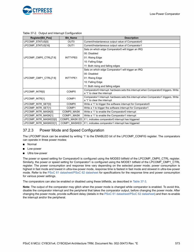
PSoC 6 MCU: CY8C61x4, CY8C62x4 Architecture TRM, Document No. 002-30473 Rev. *E 573
Low-Power Comparator
37.2.3 Power Mode and Speed Configuration
The LPCOMP block can be enabled by writing ‘1’ to the ENABLED bit of the LPCOMP_CONFIG register. The comparatorscan operate in three power modes:
■ Normal
■ Low-power
■ Ultra low-power
The power or speed setting for Comparator0 is configured using the MODE0 bitfield of the LPCOMP_CMP0_CTRL register.Similarly, the power or speed setting for Comparator1 is configured using the MODE1 bitfield of the LPCOMP_CMP1_CTRLregister. The power consumption and response time vary depending on the selected power mode; power consumption ishighest in fast mode and lowest in ultra-low-power mode, response time is fastest in fast mode and slowest in ultra-low-powermode. Refer to the PSoC 61 datasheet/PSoC 62 datasheet for specifications for the response time and power consumptionfor various power settings.
The comparators can also be enabled or disabled using these bitfields, as described in Table 37-3.
Note: The output of the comparator may glitch when the power mode is changed while comparator is enabled. To avoid this,disable the comparator interrupt and the peripheral that takes the comparator output, before changing the power mode. Afterchanging the power mode, provide sufficient delay (details in the PSoC 61 datasheet/PSoC 62 datasheet) and then re-enablethe interrupt and/or the peripheral.
Table 37-2. Output and Interrupt Configuration
Register[Bit_Pos] Bit_Name Description
LPCOMP_STATUS[0] OUT0 Current/Instantaneous output value of Comparator0
LPCOMP_STATUS[16] OUT1 Current/Instantaneous output value of Comparator1
LPCOMP_CMP0_CTRL[7:6] INTTYPE0
Sets on which edge Comparator0 will trigger an IRQ
00: Disabled
01: Rising Edge
10: Falling Edge
11: Both rising and falling edges
LPCOMP_CMP1_CTRL[7:6] INTTYPE1
Sets on which edge Comparator1 will trigger an IRQ
00: Disabled
01: Rising Edge
10: Falling Edge
11: Both rising and falling edges
LPCOMP_INTR[0] COMP0Comparator0 Interrupt: hardware sets this interrupt when Comparator0 triggers. Write a '1' to clear the interrupt
LPCOMP_INTR[1] COMP1Comparator1 Interrupt: hardware sets this interrupt when Comparator1 triggers. Write a '1' to clear the interrupt
LPCOMP_INTR_SET[0] COMP0 Write a '1' to trigger the software interrupt for Comparator0
LPCOMP_INTR_SET[1] COMP1 Write a 1 to trigger the software interrupt for Comparator1
LPCOMP_INTR_MASK[0] COMP0_MASK Write a ‘1’ to enable the Comparator0 interrupt
LPCOMP_INTR_MASK[1] COMP1_MASK Write a ‘1’ to enable the Comparator1 interrupt
LPCOMP_INTR_MASKED[0] COMP0_MASK ED If 1, indicates comparator0 interrupt has triggered
LPCOMP_INTR_MASKED[1] COMP1_MASKED If 1, indicates comparator1 interrupt has triggered
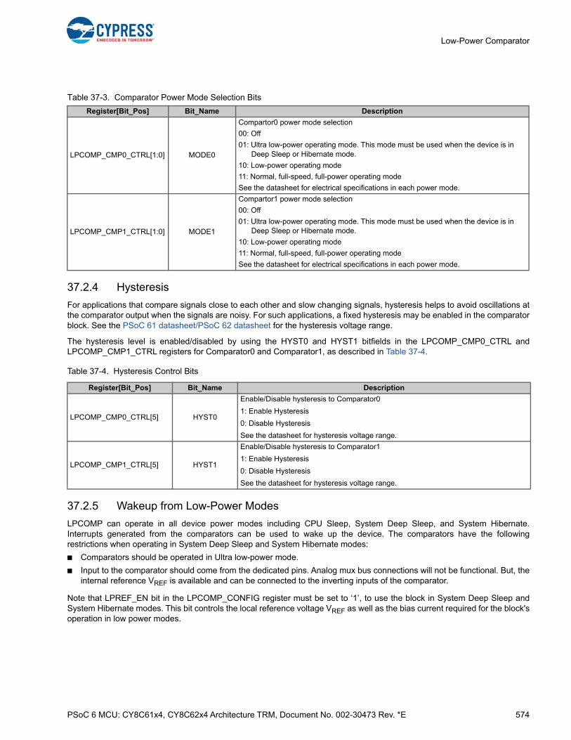
PSoC 6 MCU: CY8C61x4, CY8C62x4 Architecture TRM, Document No. 002-30473 Rev. *E 574
Low-Power Comparator
37.2.4 Hysteresis
For applications that compare signals close to each other and slow changing signals, hysteresis helps to avoid oscillations atthe comparator output when the signals are noisy. For such applications, a fixed hysteresis may be enabled in the comparatorblock. See the PSoC 61 datasheet/PSoC 62 datasheet for the hysteresis voltage range.
The hysteresis level is enabled/disabled by using the HYST0 and HYST1 bitfields in the LPCOMP_CMP0_CTRL andLPCOMP_CMP1_CTRL registers for Comparator0 and Comparator1, as described in Table 37-4.
Table 37-4. Hysteresis Control Bits
37.2.5 Wakeup from Low-Power Modes
LPCOMP can operate in all device power modes including CPU Sleep, System Deep Sleep, and System Hibernate.Interrupts generated from the comparators can be used to wake up the device. The comparators have the followingrestrictions when operating in System Deep Sleep and System Hibernate modes:
■ Comparators should be operated in Ultra low-power mode.
■ Input to the comparator should come from the dedicated pins. Analog mux bus connections will not be functional. But, theinternal reference VREF is available and can be connected to the inverting inputs of the comparator.
Note that LPREF_EN bit in the LPCOMP_CONFIG register must be set to ‘1’, to use the block in System Deep Sleep andSystem Hibernate modes. This bit controls the local reference voltage VREF as well as the bias current required for the block'soperation in low power modes.
Table 37-3. Comparator Power Mode Selection Bits
Register[Bit_Pos] Bit_Name Description
LPCOMP_CMP0_CTRL[1:0] MODE0
Compartor0 power mode selection
00: Off
01: Ultra low-power operating mode. This mode must be used when the device is in Deep Sleep or Hibernate mode.
10: Low-power operating mode
11: Normal, full-speed, full-power operating mode
See the datasheet for electrical specifications in each power mode.
LPCOMP_CMP1_CTRL[1:0] MODE1
Compartor1 power mode selection
00: Off
01: Ultra low-power operating mode. This mode must be used when the device is in Deep Sleep or Hibernate mode.
10: Low-power operating mode
11: Normal, full-speed, full-power operating mode
See the datasheet for electrical specifications in each power mode.
Register[Bit_Pos] Bit_Name Description
LPCOMP_CMP0_CTRL[5] HYST0
Enable/Disable hysteresis to Comparator0
1: Enable Hysteresis
0: Disable Hysteresis
See the datasheet for hysteresis voltage range.
LPCOMP_CMP1_CTRL[5] HYST1
Enable/Disable hysteresis to Comparator1
1: Enable Hysteresis
0: Disable Hysteresis
See the datasheet for hysteresis voltage range.
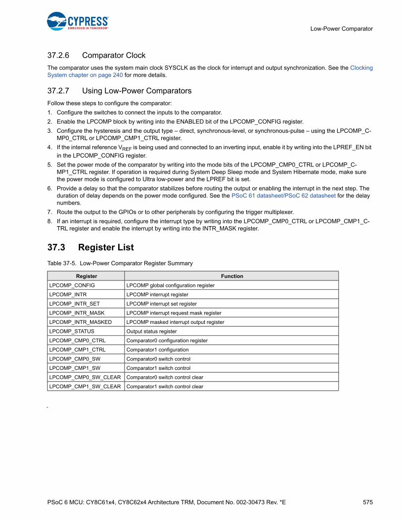
PSoC 6 MCU: CY8C61x4, CY8C62x4 Architecture TRM, Document No. 002-30473 Rev. *E 575
Low-Power Comparator
37.2.6 Comparator Clock
The comparator uses the system main clock SYSCLK as the clock for interrupt and output synchronization. See the ClockingSystem chapter on page 240 for more details.
37.2.7 Using Low-Power Comparators
Follow these steps to configure the comparator:
1. Configure the switches to connect the inputs to the comparator.
2. Enable the LPCOMP block by writing into the ENABLED bit of the LPCOMP_CONFIG register.
3. Configure the hysteresis and the output type – direct, synchronous-level, or synchronous-pulse – using the LPCOMP_C-MP0_CTRL or LPCOMP_CMP1_CTRL register.
4. If the internal reference VREF is being used and connected to an inverting input, enable it by writing into the LPREF_EN bit
in the LPCOMP_CONFIG register.
5. Set the power mode of the comparator by writing into the mode bits of the LPCOMP_CMP0_CTRL or LPCOMP_C-MP1_CTRL register. If operation is required during System Deep Sleep mode and System Hibernate mode, make sure the power mode is configured to Ultra low-power and the LPREF bit is set.
6. Provide a delay so that the comparator stabilizes before routing the output or enabling the interrupt in the next step. The duration of delay depends on the power mode configured. See the PSoC 61 datasheet/PSoC 62 datasheet for the delay numbers.
7. Route the output to the GPIOs or to other peripherals by configuring the trigger multiplexer.
8. If an interrupt is required, configure the interrupt type by writing into the LPCOMP_CMP0_CTRL or LPCOMP_CMP1_C-TRL register and enable the interrupt by writing into the INTR_MASK register.
37.3 Register List
Table 37-5. Low-Power Comparator Register Summary
Register Function
LPCOMP_CONFIG LPCOMP global configuration register
LPCOMP_INTR LPCOMP interrupt register
LPCOMP_INTR_SET LPCOMP interrupt set register
LPCOMP_INTR_MASK LPCOMP interrupt request mask register
LPCOMP_INTR_MASKED LPCOMP masked interrupt output register
LPCOMP_STATUS Output status register
LPCOMP_CMP0_CTRL Comparator0 configuration register
LPCOMP_CMP1_CTRL Comparator1 configuration
LPCOMP_CMP0_SW Comparator0 switch control
LPCOMP_CMP1_SW Comparator1 switch control
LPCOMP_CMP0_SW_CLEAR Comparator0 switch control clear
LPCOMP_CMP1_SW_CLEAR Comparator1 switch control clear

PSoC 6 MCU: CY8C61x4, CY8C62x4 Architecture TRM, Document No. 002-30473 Rev. *E 576
38. Continuous Time DAC
The PSoC 6 MCU analog subsystem supports a 12-bit continuous time digital-to-analog converter (CTDAC). The 12-bit DACprovides continuous time output without the need for an external sample and hold (S/H) circuit. The CTDAC block can beused in applications that require voltage references, bias, or analog waveform output. It consists of the following blocks:
■ CTDAC core
■ CTDAC control interface
The CTDAC core includes a combination of 8-bit R-2R ladder DAC and 4-bit thermometer decoded resistors to generate the12-bit DAC output voltage from the reference. VDDA or any signal buffered through Opamp1 of the CTBm provides the refer-ence voltage to the DAC. The core is closely integrated with the CTBm, which provides easy buffering of the DAC output volt-age in addition to providing buffered input reference voltage and sample/hold feature for the DAC output. A programmablegain amplifier (PGA) can be made using the CTBm opamp and the R-2R ladder of DAC.
The CTDAC control interface provides an option to control the DAC output through CPU and DMA. This includes a double-buffered DAC voltage control register, clock input for programmable update rate, interrupt on DAC buffer empty to CPU, andtrigger to DMA and TCPWMs. Figure 38-1 shows the CTDAC block diagram.
38.1 Features
The CTDAC has the following features
■ 12-bit continuous time output – no external S/H required
■ 2-µs settling time for a 25 pF load when buffered using the CTBm opamp
■ Support in System Deep Sleep power mode
■ Selectable voltage reference:
❐ VDDA
❐ Internal VREF buffered through Opamp1 of CTBm
❐ External VREF buffered through Opamp1 of CTBm
■ Selectable output paths:
❐ Buffered DAC output through Opamp0 of CTBm
❐ Sample and hold output path through Opamp0
■ Selectable input modes:
❐ Unsigned 12-bit mode
❐ Two's complement (signed) 12-bit mode
This PSoC 6 MCU technical reference manual (TRM) provides comprehensive and detailed information about thefunctions of the PSoC 6 MCU device hardware. It is divided into two books: architecture TRM and registers TRM. TheTRM is not recommended for those new to the PSoC 6 MCU, nor as a guide for developing PSoC 6 MCU applications.Use these documents instead:
■ PSoC 61 datasheet, PSoC 62 datasheet
■ Peripheral Driver Library (PDL) documentation
■ Application notes
■ Code examples
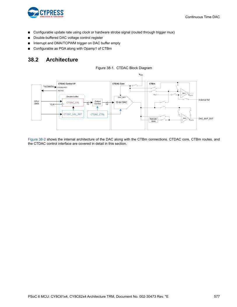
PSoC 6 MCU: CY8C61x4, CY8C62x4 Architecture TRM, Document No. 002-30473 Rev. *E 577
Continuous Time DAC
■ Configurable update rate using clock or hardware strobe signal (routed through trigger mux)
■ Double-buffered DAC voltage control register
■ Interrupt and DMA/TCPWM trigger on DAC buffer empty
■ Configurable as PGA along with Opamp1 of CTBm
38.2 Architecture
Figure 38-1. CTDAC Block Diagram
Figure 38-2 shows the internal architecture of the DAC along with the CTBm connections. CTDAC core, CTBm routes, andthe CTDAC control interface are covered in detail in this section.
CTDAC Core
12-bit DAC
CTDAC Control I/F
_
+OA0
_
+OA1
DAC_BUF_OUT
VREF
VOUT0
External Ref
VDDA
DAC_REF
CTBm
CPU/DMA
IRQ/TRIG
Output Control
Sample/Hold
CTDAC_VAL
CTDAC_VAL_NXT
Double buffer
CLK 12 12
STROBE INPUTFrom Trigger Mux
CTDAC_CTRL
VOUT1

PSoC 6 MCU: CY8C61x4, CY8C62x4 Architecture TRM, Document No. 002-30473 Rev. *E 578
Continuous Time DAC
Figure 38-2. CTDAC with CTBm
38.2.1 CTDAC Core
The CTDAC core includes the following components:
■ R-2R and thermometer decoder architecture with switches
■ Input reference selection
■ Output path selection
■ Flip-flops to register input from the control interface
Switch types
CTBm
_
+OA0
_
+OA1
VREF
CRD
CRS
COS
CH
D
CHOLD
COR
CA0
CIS
P9.2
(A03/A13/A43)
A81
(D51)
(A00/A20)
(A22)
(A11)
A73
A82
D81
(D52/D62)
CTDAC Core
2R
R
1
0
B(7)
2R
R
1
0
B(6)
2R
1
0
B(5)
2R
R
1
0
B(2)
2R
R
1
0
B(1)
S(1
)
VDACREF
VSSA
2R 2R
1
OUT_EN
2R
1
0
B(0)
LSb
2R
1
0
Range
TERM
CVD
VDDA
Vrefsense
Vdacout
Vrefdrive
1
S(1
5)
S(15)
S(1)
DIS_Z
R
CLK
F/F
B(0)
logic
Large switch – Low resistance
Very large switch – Very low resistance
Small switch – High resistance
(xxx) CTBm switches to other peripherals (I/Os, SAR ADC, AMUX)
0 0
COB
ILR
Tiny switch – Very high resistance
C6H A30
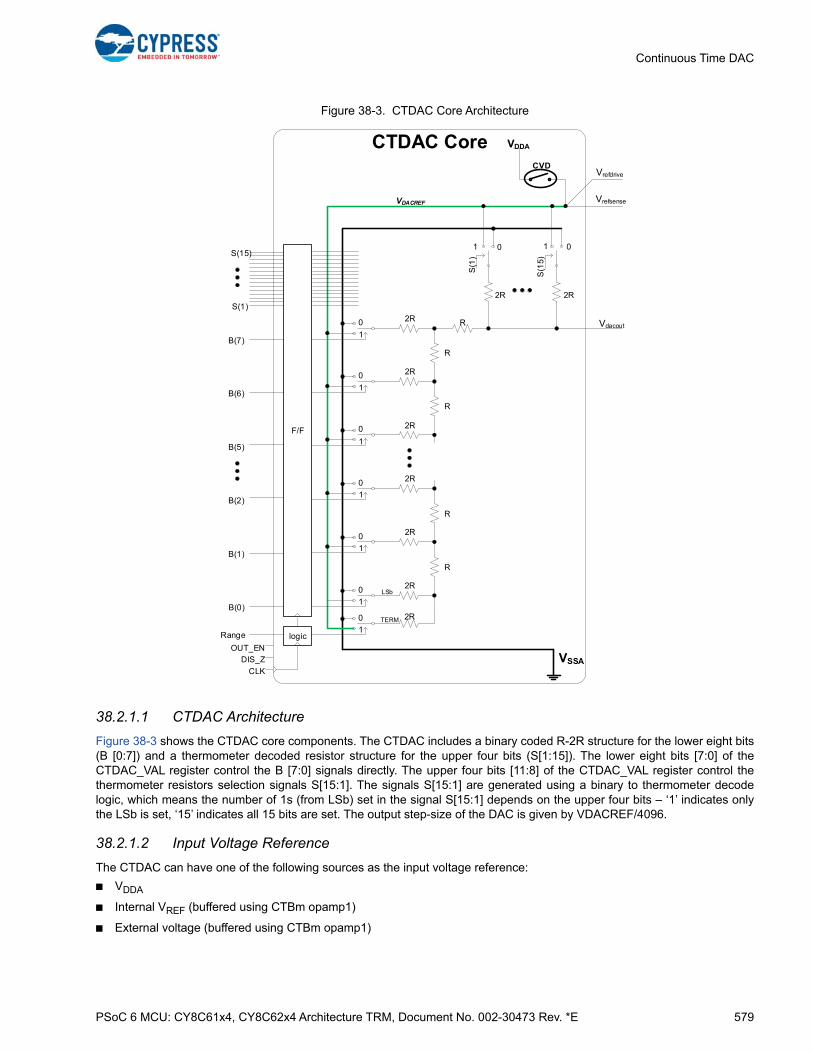
PSoC 6 MCU: CY8C61x4, CY8C62x4 Architecture TRM, Document No. 002-30473 Rev. *E 579
Continuous Time DAC
Figure 38-3. CTDAC Core Architecture
38.2.1.1 CTDAC Architecture
Figure 38-3 shows the CTDAC core components. The CTDAC includes a binary coded R-2R structure for the lower eight bits(B [0:7]) and a thermometer decoded resistor structure for the upper four bits (S[1:15]). The lower eight bits [7:0] of theCTDAC_VAL register control the B [7:0] signals directly. The upper four bits [11:8] of the CTDAC_VAL register control thethermometer resistors selection signals S[15:1]. The signals S[15:1] are generated using a binary to thermometer decodelogic, which means the number of 1s (from LSb) set in the signal S[15:1] depends on the upper four bits – ‘1’ indicates onlythe LSb is set, ‘15’ indicates all 15 bits are set. The output step-size of the DAC is given by VDACREF/4096.
38.2.1.2 Input Voltage Reference
The CTDAC can have one of the following sources as the input voltage reference:
■ VDDA
■ Internal VREF (buffered using CTBm opamp1)
■ External voltage (buffered using CTBm opamp1)
CTDAC Core
2R
R
1
0
B(7)
2R
R
1
0
B(6)
2R
1
0
B(5)
2R
R
1
0
B(2)
2R
R
1
0
B(1)
S(1
)
VDACREF
VSSA
2R 2R
1
OUT_EN
2R
1
0
B(0)
LSb
2R
1
0
Range
TERM
CVD
VDDA
Vdacout
1
S(1
5)
S(15)
S(1)
DIS_Z
R
CLK
F/F
B(0)
logic
0 0
Vrefsense
Vrefdrive

PSoC 6 MCU: CY8C61x4, CY8C62x4 Architecture TRM, Document No. 002-30473 Rev. *E 580
Continuous Time DAC
Closing the CVD switch (CTDD_CVD bit [0] of CTDAC_SW register) selects VDDA as the CTDAC voltage reference.
Figure 38-4 shows the signal path. Note that CVD is a very low-resistance switch and minimizes the non-linearity in output.
Figure 38-4. VDDA Voltage Reference
Figure 38-5 shows the signal path to select the internal VREF as the CTDAC reference. As seen, this signal path includes var-
ious switches from the CTBm along with Opamp1 (OA1). Internal reference (VREF) is buffered through OA1 and then is routed
through CRD switch in CTBm to the CTDAC reference. The internal reference can be used when the DAC output needs to beaccurate and supply independent. Note that for the CTDAC to operate properly in this configuration, CTBm should beenabled and OA1 should be configured in voltage follower mode with all the switches configured properly. See the Continu-ous Time Block mini (CTBm) chapter on page 589 for details.
Figure 38-5. Internal VREF as Voltage Reference
Figure 38-6 shows the signal path to connect an external signal as CTDAC reference. The signal path appears similar to theinternal reference signal path. Instead of routing the internal VREF, the OA1 positive terminal connections can be used to route
an external signal.
CTBm
_
+OA0
_
+OA1
VREF
CRD
CRS
COS
CH
D
CHOLD
COR
CA0
CIS
P9.2
(A03/A13/A43)
A81
(D51)
(A00/A20)
(A22)
(A11)
A73
A82
D81
(D52/D62)
VREFSENSE
VDACOUT
VREFDRIVE
COB
ILR
CTDACVDDA
REF
VOUT
CVD
C6H A30
CTBm
_
+OA0
_
+OA1
VREF
CRD
CRS
COS
CH
D
CHOLD
COR
CA0
CIS
P9.2
(A03/A13/A43)
A81
(D51)
(A00/A20)
(A22)
(A11)
A73
C6H
A82
D81
(D52/D62)
VREFSENSE
VDACOUT
VREFDRIVE
COB
ILR
CTDACVDDA
REF
VOUT
CVD
A30
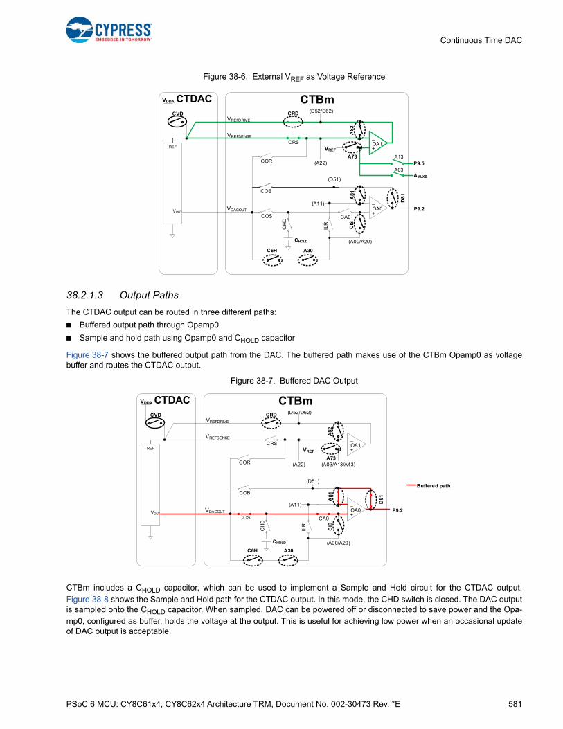
PSoC 6 MCU: CY8C61x4, CY8C62x4 Architecture TRM, Document No. 002-30473 Rev. *E 581
Continuous Time DAC
Figure 38-6. External VREF as Voltage Reference
38.2.1.3 Output Paths
The CTDAC output can be routed in three different paths:
■ Buffered output path through Opamp0
■ Sample and hold path using Opamp0 and CHOLD capacitor
Figure 38-7 shows the buffered output path from the DAC. The buffered path makes use of the CTBm Opamp0 as voltagebuffer and routes the CTDAC output.
Figure 38-7. Buffered DAC Output
CTBm includes a CHOLD capacitor, which can be used to implement a Sample and Hold circuit for the CTDAC output.
Figure 38-8 shows the Sample and Hold path for the CTDAC output. In this mode, the CHD switch is closed. The DAC outputis sampled onto the CHOLD capacitor. When sampled, DAC can be powered off or disconnected to save power and the Opa-
mp0, configured as buffer, holds the voltage at the output. This is useful for achieving low power when an occasional updateof DAC output is acceptable.
CTBm
_
+OA0
_
+OA1
VREF
CRD
CRS
COS
CH
D
CHOLD
COR
CA0
CIS
P9.2
A81
(A00/A20)
(A22)
A82
D81
(D52/D62)
VREFSENSE
VDACOUT
VREFDRIVE
CTDACVDDA
REF
VOUT
CVD
P9.5
AMUXB
A13
A03
(D51)
(A11)
COB
ILR
A73
C6H A30
CTBm
_
+OA0
_
+OA1
VREF
CRD
CRS
COS
CH
D
CHOLD
COR
CA0
P9.2
(A03/A13/A43)
A81
(D51)
(A00/A20)
(A22)
(A11)
A82
D81
(D52/D62)
VREFSENSE
VDACOUT
VREFDRIVE
CTDACVDDA
REF
VOUT
CVD
Buffered path
CIS
COB
A73
ILR
C6H A30

PSoC 6 MCU: CY8C61x4, CY8C62x4 Architecture TRM, Document No. 002-30473 Rev. *E 582
Continuous Time DAC
Figure 38-8. Sample Mode using DAC
Figure 38-9. Hold Mode using DAC
38.2.1.4 Other Configurations
The CTDAC with the Opamp1 can be used to implement a PGA (see Figure 38-10). In this configuration, the COR switchfeeds back the Opamp1 output through the R-2R divider. The CTDAC_VAL register controls the gain of the amplifier. The gainis given by (4096/CTDAC_VAL). Note that this configuration should be used only for very low frequency signals and is notguaranteed to work for fast-switching signals. This is because of significant destabilizing capacitance introduced by the DACin the amplifier feedback loop, which can result in oscillations.
CTBm
_
+OA0
_
+OA1
VREF
CRD
CRS
COS
CH
D
CHOLD
COR
CA0
ILR
P9.2
(A03/A13/A43)
A81
(A00/A20)
(A22)
(A11)
A73
A82
D81
(D52/D62)
VREFSENSE
VDACOUT
VREFDRIVE
CTDACVDDA
REF
VOUT
CVD
Sample mode
(D51)
COB
CIS
C6H A30
CTBm
_
+OA0
_
+OA1
VREF
CRD
CRS
COS
CH
D
CHOLD
COR
CA0
CIS
P9.2
(A03/A13/A43)
A81
(A00/A20)
(A22)A73
A82
D81
(D52/D62)
VREFSENSE
VDACOUT
VREFDRIVE
CTDACVDDA
REF
VOUT
CVD
Hold mode(D51)
(A11)
COB
ILR
C6H A30
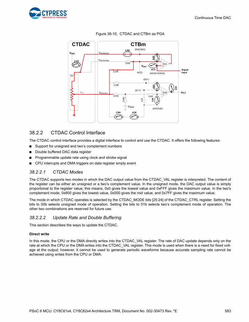
PSoC 6 MCU: CY8C61x4, CY8C62x4 Architecture TRM, Document No. 002-30473 Rev. *E 583
Continuous Time DAC
Figure 38-10. CTDAC and CTBm as PGA
38.2.2 CTDAC Control Interface
The CTDAC control interface provides a digital interface to control and use the CTDAC. It offers the following features:
■ Support for unsigned and two’s complement numbers
■ Double buffered DAC data register
■ Programmable update rate using clock and strobe signal
■ CPU interrupts and DMA triggers on data register empty event
38.2.2.1 CTDAC Modes
The CTDAC supports two modes in which the DAC output value from the CTDAC_VAL register is interpreted. The content ofthe register can be either an unsigned or a two’s complement value. In the unsigned mode, the DAC output value is simplyproportional to the register value; this means, 0x0 gives the lowest value and 0xFFF gives the maximum value. In the two'scomplement mode, 0x800 gives the lowest value, 0x000 gives the mid value, and 0x7FF gives the maximum value.
The mode in which CTDAC operates is selected by the CTDAC_MODE bits [25:24] of the CTDAC_CTRL register. Setting thebits to 00b selects unsigned mode of operation. Setting the bits to 01b selects two’s complement mode of operation. Theother two combinations are reserved for future use.
38.2.2.2 Update Rate and Double Buffering
This section describes the ways to update the CTDAC.
Direct write
In this mode, the CPU or the DMA directly writes into the CTDAC_VAL register. The rate of DAC update depends only on therate at which the CPU or the DMA writes into the CTDAC_VAL register. This mode is used when there is a need for fixed volt-age at the output; however, it cannot be used to generate periodic waveforms because accurate sampling rate cannot beachieved using writes from the CPU or DMA.
CTBm
_
+OA0
_
+OA1
VREF
CRD
CRS
COS
CH
D
CHOLD
COR
CA0
CIS
P9.2
(A03/A13/A43)
A81
(D51)
(A00/A20)
(A22)
(A11)
A73
A82
D81
(D52/D62)
VREFSENSE
VDACOUT
VREFDRIVE
CTDAC
VDDA
REF
VOUT
CVD
ILR
COB
C6H A30
Signal Input
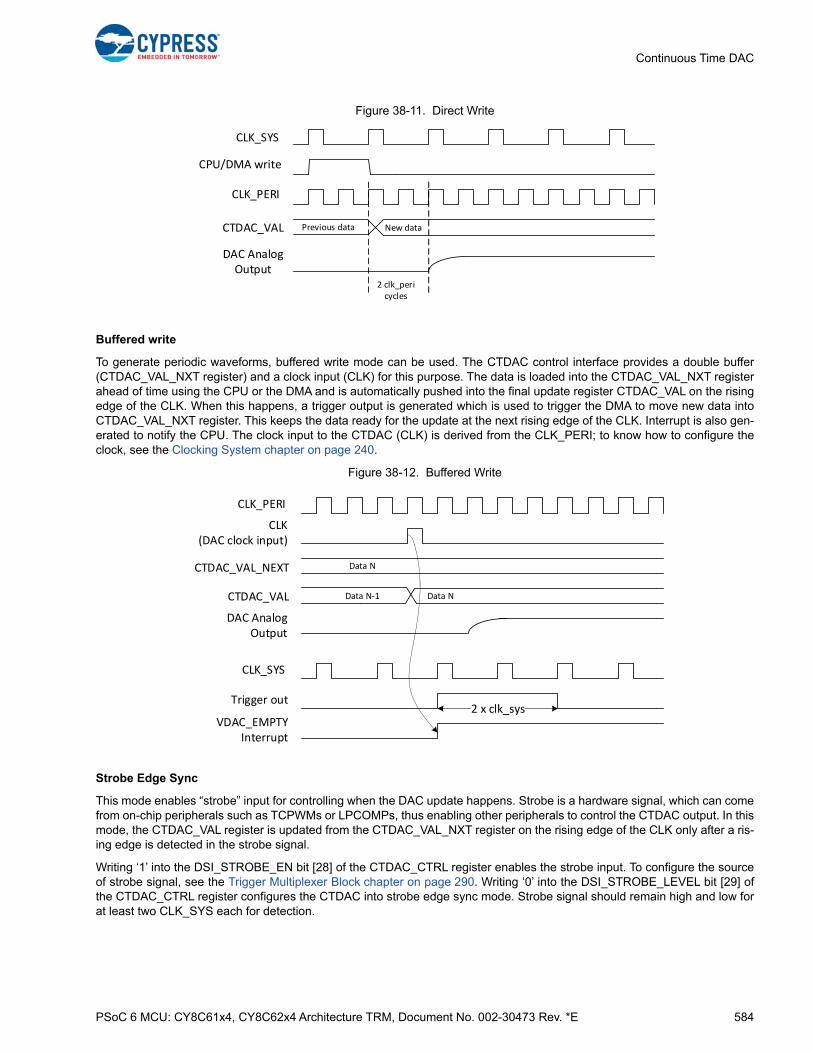
PSoC 6 MCU: CY8C61x4, CY8C62x4 Architecture TRM, Document No. 002-30473 Rev. *E 584
Continuous Time DAC
Figure 38-11. Direct Write
Buffered write
To generate periodic waveforms, buffered write mode can be used. The CTDAC control interface provides a double buffer(CTDAC_VAL_NXT register) and a clock input (CLK) for this purpose. The data is loaded into the CTDAC_VAL_NXT registerahead of time using the CPU or the DMA and is automatically pushed into the final update register CTDAC_VAL on the risingedge of the CLK. When this happens, a trigger output is generated which is used to trigger the DMA to move new data intoCTDAC_VAL_NXT register. This keeps the data ready for the update at the next rising edge of the CLK. Interrupt is also gen-erated to notify the CPU. The clock input to the CTDAC (CLK) is derived from the CLK_PERI; to know how to configure theclock, see the Clocking System chapter on page 240.
Figure 38-12. Buffered Write
Strobe Edge Sync
This mode enables “strobe” input for controlling when the DAC update happens. Strobe is a hardware signal, which can comefrom on-chip peripherals such as TCPWMs or LPCOMPs, thus enabling other peripherals to control the CTDAC output. In thismode, the CTDAC_VAL register is updated from the CTDAC_VAL_NXT register on the rising edge of the CLK only after a ris-ing edge is detected in the strobe signal.
Writing ‘1’ into the DSI_STROBE_EN bit [28] of the CTDAC_CTRL register enables the strobe input. To configure the sourceof strobe signal, see the Trigger Multiplexer Block chapter on page 290. Writing ‘0’ into the DSI_STROBE_LEVEL bit [29] ofthe CTDAC_CTRL register configures the CTDAC into strobe edge sync mode. Strobe signal should remain high and low forat least two CLK_SYS each for detection.
CLK_SYS
CPU/DMA write
CLK_PERI
CTDAC_VAL
DAC Analog Output
2 clk_peri cycles
Previous data New data
CLK_SYS
CLK(DAC clock input)
CLK_PERI
CTDAC_VAL
DAC Analog Output
Data N‐1 Data N
CTDAC_VAL_NEXT Data N
Trigger out
VDAC_EMPTYInterrupt
2 x clk_sys
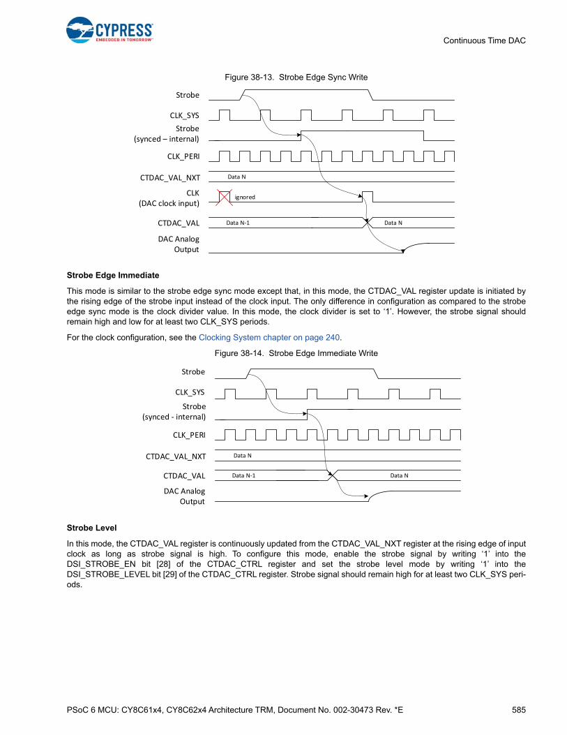
PSoC 6 MCU: CY8C61x4, CY8C62x4 Architecture TRM, Document No. 002-30473 Rev. *E 585
Continuous Time DAC
Figure 38-13. Strobe Edge Sync Write
Strobe Edge Immediate
This mode is similar to the strobe edge sync mode except that, in this mode, the CTDAC_VAL register update is initiated bythe rising edge of the strobe input instead of the clock input. The only difference in configuration as compared to the strobeedge sync mode is the clock divider value. In this mode, the clock divider is set to ‘1’. However, the strobe signal shouldremain high and low for at least two CLK_SYS periods.
For the clock configuration, see the Clocking System chapter on page 240.
Figure 38-14. Strobe Edge Immediate Write
Strobe Level
In this mode, the CTDAC_VAL register is continuously updated from the CTDAC_VAL_NXT register at the rising edge of inputclock as long as strobe signal is high. To configure this mode, enable the strobe signal by writing ‘1’ into theDSI_STROBE_EN bit [28] of the CTDAC_CTRL register and set the strobe level mode by writing ‘1’ into theDSI_STROBE_LEVEL bit [29] of the CTDAC_CTRL register. Strobe signal should remain high for at least two CLK_SYS peri-ods.
CLK_SYS
Strobe(synced – internal)
CLK_PERI
CTDAC_VAL
DAC Analog Output
ignored
Data N‐1 Data N
Strobe
CTDAC_VAL_NXT Data N
CLK(DAC clock input)
CLK_SYS
Strobe(synced ‐ internal)
CLK_PERI
CTDAC_VAL
DAC Analog Output
Data N‐1 Data N
Strobe
CTDAC_VAL_NXT Data N
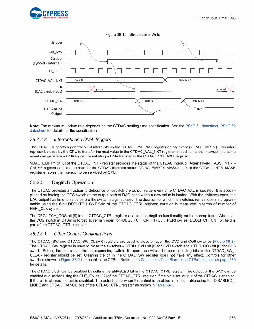
PSoC 6 MCU: CY8C61x4, CY8C62x4 Architecture TRM, Document No. 002-30473 Rev. *E 586
Continuous Time DAC
Figure 38-15. Strobe Level Write
Note: The maximum update rate depends on the CTDAC settling time specification. See the PSoC 61 datasheet, PSoC 62datasheet for details for the specification.
38.2.2.3 Interrupts and DMA Triggers
The CTDAC supports a generation of interrupts on the CTDAC_VAL_NXT register empty event (VDAC_EMPTY). This inter-rupt can be used by the CPU to transfer the next value to the CTDAC_VAL_NXT register. In addition to the interrupt, the sameevent can generate a DMA trigger for initiating a DMA transfer to the CTDAC_VAL_NXT register.
VDAC_EMPTY bit [0] of the CTDAC_INTR register provides the status of the CTDAC interrupt. Alternatively, PASS_INTR_-CAUSE register can also be read for the CTDAC interrupt status. VDAC_EMPTY_MASK bit [0] of the CTDAC_INTR_MASKregister enables the interrupt to be serviced by CPU.
38.2.3 Deglitch Operation
The CTDAC provides an option to debounce or deglitch the output value every time CTDAC_VAL is updated. It is accom-plished by forcing the COS switch at the output path of DAC open when a new value is loaded. With the switches open, theDAC output has time to settle before the switch is again closed. The duration for which the switches remain open is program-mable using the 6-bit DEGLITCH_CNT field of the CTDAC_CTRL register; duration is measured in terms of number ofPERI_CLK cycles.
The DEGLITCH_COS bit [9] in the CTDAC_CTRL register enables the deglitch functionality on the opamp input. When set,the COS switch in CTBm is forced to remain open for (DEGLITCH_CNT+1) CLK_PERI cycles. DEGLITCH_CNT bit field ispart of the CTDAC_CTRL register.
38.2.3.1 Other Control Configurations
The CTDAC_SW and CTDAC_SW_CLEAR registers are used to close or open the CVD and CO6 switches (Figure 38-2).The CTDAC_SW register is used to close the switches – CTDD_CVD bit [0] for CVD switch and CTDD_CO6 bit [8] for CO6switch. Setting the bits closes the corresponding switch. To open the switch, the corresponding bits in the CTDAC_SW_-CLEAR register should be set. Clearing the bit in the CTDAC_SW register does not have any effect. Controls for otherswitches shown in Figure 38-2 is present in the CTBm. Refer to the Continuous Time Block mini (CTBm) chapter on page 589for details.
The CTDAC block can be enabled by setting the ENABLED bit in the CTDAC_CTRL register. The output of the DAC can beenabled or disabled using the OUT_EN bit [22] of the CTDAC_CTRL register. If the bit is set, output of the CTDAC is enabled.If the bit is cleared, output is disabled. The output state when the output is disabled is configurable using the DISABLED_-MODE and CTDAC_RANGE bits of the CTDAC_CTRL register as shown in Table 38-1.
CLK_SYS
Strobe(synced ‐ Internal)
CLK_PERI
CTDAC_VAL
DAC Analog Output
ignored
Data N‐1 Data N
Strobe
CTDAC_VAL_NXT Data N
CLK(DAC clock input)
Data N + 1
ignored
Data N + 1

PSoC 6 MCU: CY8C61x4, CY8C62x4 Architecture TRM, Document No. 002-30473 Rev. *E 587
Continuous Time DAC
The CTDAC supports two output ranges:
■ VSSA to (VDACREF × 4095/4096)
■ VDACREF/4096 to VDACREF
The two ranges are almost the same except that the second range is lifted by one LSb. The CTDAC_RANGE bit [23] of theCTDAC_CTRL register decides the range. Setting the bit provides one LSb lifted range.
The CTDAC supports output to be maintained in System Deep Sleep power mode. However, no update is possible. To enableDeep Sleep operation, set the DEEPSLEEP_ON bit [30] of the CTDAC_CTRL register.
38.2.4 Using CTDAC
Follow these steps to use the CTDAC:
1. Configure various switches in CTDAC and CTBm according to the input reference voltage and output path selection.
2. Configure deglitch, CTDAC mode, range, Deep Sleep operation capability, and strobe control in the CTDAC_CTRL regis-ter according to your requirements.
3. Enable VDAC_EMPTY interrupt if used.
4. Configure and enable DMA with VDAC_EMPTY as trigger and CTDAC_VAL_NXT register as destination (see the DMAController (DW) chapter on page 90), if used.
5. Configure and enable the clock for CTDAC (see the Clocking System chapter on page 240).
6. Enable the CTBm and opamps based on the configuration in step 1.
a. Enable the CTBm if any of the switches from the CTBm is used in the input reference and output path.
b. Enable Opamp1 if an internal reference is used.
c. Enable and configure the Opamp1 positive input if an external reference is used.
d. Enable Opamp0 if the DAC output is buffered.
7. Enable the CTDAC block by setting the ENABLED bit in the CTDAC_CTRL register.
8. Enable the DAC output by setting the OUT_EN bit in the CTDAC_CTRL register.
9. Update the CTDAC_VAL register for fixed output and the CTDAC_VAL_NXT register for clocked output.
10. Additional updates can happen in VDAC_EMPTY ISR or through DMA transfers.
11. The DAC output can be enabled/disabled at any time using the OUT_EN bit.
Table 38-1. Output State
OUT_EN DISABLED_MODE CTDAC_RANGE OUTPUT_STATE
0 0 x Tristate
0 1 0 VSSA
0 1 1 VREF
1 x x Programmed value

PSoC 6 MCU: CY8C61x4, CY8C62x4 Architecture TRM, Document No. 002-30473 Rev. *E 588
Continuous Time DAC
38.3 Register List
Table 38-2. List of CTDAC Registers
Name Description
CTDAC_CTRL Global CTDAC control register
CTDAC_INTR CTDAC interrupt request register
CTDAC_INTR_SET CTDAC interrupt request set register
CTDAC_INTR_MASK CTDAC interrupt request mask
CTDAC_INTR_MASKED CTDAC interrupt request masked
CTDAC_CTDAC_SW CTDAC switch control register
CTDAC_CTDAC_SW_CLEAR CTDAC switch control clear register
CTDAC_CTDAC_VAL Current DAC value register
CTDAC_CTDAC_VAL_NXT Next DAC value (double buffering) register
CTDAC_TRIM CTDAC trim register
PSoC 6 MCU: CY8C61x4, CY8C62x4 Architecture TRM, Document No. 002-30473 Rev. *E 589
39. Continuous Time Block mini (CTBm)
The Continuous Time Block mini (CTBm) provides on-chip operational amplifiers (opamps) for creating continuous-timesignal chains. Each CTBm includes a switch matrix for input/output configuration, two identical opamps, which are alsoconfigurable as two comparators, a charge pump inside each opamp, a sample-and-hold circuit, and a digital interface forcomparator output routing, switch controls, and interrupts. CTBm and CTDAC are intended to work together in manyapplications. See the Continuous Time DAC chapter on page 576 for details.
39.1 Features
The PSoC 6 MCU CTBm has the following features:
■ Discrete, high-performance, and highly configurable on-chip operational amplifiers
■ Programmable power, bandwidth, compensation, and output drive strength
■ Flexible input and output routing
■ Support for opamp voltage-follower mode using internal connections
■ Comparator mode with optional 10-mV hysteresis
■ Works as buffer/pre-amplifier for SAR inputs
■ Works as buffer/amplifier/sample-and-hold for CTDAC outputs
■ Operates in System Deep Sleep mode
■ Buffering external Vref of CTDAC
■ Option to operate in duty-cycling mode in synchronization with SAR ADC
This PSoC 6 MCU technical reference manual (TRM) provides comprehensive and detailed information about thefunctions of the PSoC 6 MCU device hardware. It is divided into two books: architecture TRM and registers TRM. TheTRM is not recommended for those new to the PSoC 6 MCU, nor as a guide for developing PSoC 6 MCU applications.Use these documents instead:
■ PSoC 61 datasheet, PSoC 62 datasheet
■ Peripheral Driver Library (PDL) documentation
■ Application notes
■ Code examples

PSoC 6 MCU: CY8C61x4, CY8C62x4 Architecture TRM, Document No. 002-30473 Rev. *E 590
Continuous Time Block mini (CTBm)
39.2 Architecture
Figure 39-1. CTBm Block Diagram
Note: CTDAC is not a part of the CTBm. See the Continuous Time DAC chapter on page 576 for more details.
S/H Leakage Reduction
CTDAC Routing and Sample and Hold Circuit.Note: Internal switches of the CTDAC not shown. See the CTDAC chapter for details
OPAMP 0
AMUXBUS A
Pin 0
OA0P_A00
OA0P_A20
OA0P_A30
CTDH_CIS
Pin 1
CTDH_ILR
OA0M_A11
OA0M_A81
Pin 2
OA0O_D81
AMUXBUS BOA1P_A03
OA1P_A43
OA1P_A13
Pin 4OA1M_A22
OA1M_A82
Pin 5
Pin 3
OA1O_D82
Internal Reference from AREF OA1P_A73
OA1O_D62
OA0O_D51
OA1O_D52
SARBUS0
SARBUS1
External Output Driver
Internal Output Driver
External Output Driver
Internal Output Driver
Comparator Output (digital)
CHOLD
CTDO_C6H
CTDH_CHDCTDH_CA0
CTDO_COS
CTDS_COR
CTDH_COB CTDS_CRS
CTDD_CRD
VSSA
10X
1X
OPAMP 1
1X
10X
Pins of CTBm Port. See the device datasheet for the location of CTBm Port.
Each of these pins can also connect to AMUXBUS A or AMUXBUS B.
CTDAC
Sample and Hold (S/H)
To SARMUX
ctdrefdrivectdrefsense
ctdvout
SW_NAME
SW_NAME
SW_NAME
Opamp routing switches. Controlled by CTBM_OA0_SW and CTBM_OA1_SW registers.
CTDAC routing and sample and hold switches. Controlled by CTBM_CDT_SW register.
Legend
SARBUS routing switches. Controlled by CTBM_OA0_SW and CTBM_OA1_SW registers, and the SAR Sequencer.
Comparator Output (digital)
ctb_oa0+
ctb_oa0-
ctb_oa0_out
ctb_oa1_out
ctb_oa1-
ctb_oa1+
NC*
NC*
* No Connect - In this product line, these routes are open. In other PSoC 6 MCUs, these are routed to pin 6 or pin 7 of the CTBm port, if available.
PSoC 6 MCU: CY8C61x4, CY8C62x4 Architecture TRM, Document No. 002-30473 Rev. *E 591
Continuous Time Block mini (CTBm)
The CTBm has two identical opamps, a switch routing matrix and a sample and hold circuit. Each opamp is configurable asan amplifier (with external passive components) or as a comparator. The opamp pins can be brought out to the pins usingconfigurable switches, where external components can be connected to build useful circuits such as non-inverting amplifier,active filters, transimpedance amplifier, and many more. When opamps are used as amplifier, the output drive strength isconfigurable to drive internal blocks or external pins. When opamps are used as comparators, options are provided togenerate interrupts and to trigger TCPWMs.
The CTBm block is designed to work closely with the CTDAC block. Opamps are used to buffer the reference input from a pinor internal reference (VREF) and to buffer the output of the DAC. The sample and hold circuit allow sampling of the CTDAC
output. The resistor array of CTDAC can be used as feedback network around CTBm opamp to build a configurable gainamplifier. See the Continuous Time DAC chapter on page 576 for details of different use cases.
Opamps can be operated in System Deep Sleep mode with reduced performance (lower gain-bandwidth product). Similar tothe ADCs, opamps can also work in system Deep Sleep mode, in the following modes:
■ Always-ON in LP/ULP mode and powered-OFF in system Deep Sleep mode
■ Always-ON in LP/ULP mode and duty-cycling in system Deep Sleep mode
■ Always-ON in LP/ULP mode and system Deep Sleep mode
Duty-cycling of opamps is linked to the duty-cycling of ADCs in system Deep Sleep mode. Duty-cycling of opamps is possibleonly when at least one of the ADCs is used in system Deep Sleep mode. The timer trigger wakes up both the opamps and theenabled ADCs. When the conversions are complete, the opamps and ADCs are powered down at the same time. Whenopamp duty-cycling is not used or if the ADCs are configured to operate only in LP/ULP mode, the opamps remain ONcontinuously throughout the system Deep Sleep time. To configure the opamps in duty-cycling operation, enable “Deep SleepEnable” in programmable analog, enable all voltages and current generators in Deep Sleep mode, and then set the CTBmclock source to “Deep Sleep Clock”.
The following sections describe the CTBm block configuration.
39.2.1 Power Mode and Output Strength Configuration
The opamp can operate in three power modes - low, medium, and high. An additional option to select a 100 nA or 1 uAcurrent reference from the Analog Reference block is common for all opamps in the device. This allows a total of sixconfigurable power options for opamp in Deep Sleep mode. Refer to the PSoC 61 datasheet/PSoC 62 datasheet for thecurrent consumption numbers when opamp is in system Deep Sleep mode. Power modes are configured using thePWR_MODE bitfield in the respective CTBM_OA_RESx_CTRL register. The slew rate and gain-bandwidth product (GBW)are maximum in highest power mode and minimum in lowest power mode.
In addition, the output driver of each opamp can be configured to the internal driver low output drive strength or high outputdrive strength external driver. Low and high output drive strengths are mutually exclusive – they cannot be active at the sametime. Low output drive strength is suited to drive smaller on-chip capacitive and resistive loads at higher speeds. High outputdrive strengths is useful for driving large off-chip capacitive and resistive loads. See the PSoC 61 datasheet/PSoC 62datasheet for gain bandwidth, slew rate, and maximum output drive capability (IOUT specifications in various power modesand output strength configurations. Table 39-1 summarizes the bits used to configure the opamp output drive strength andpower modes.
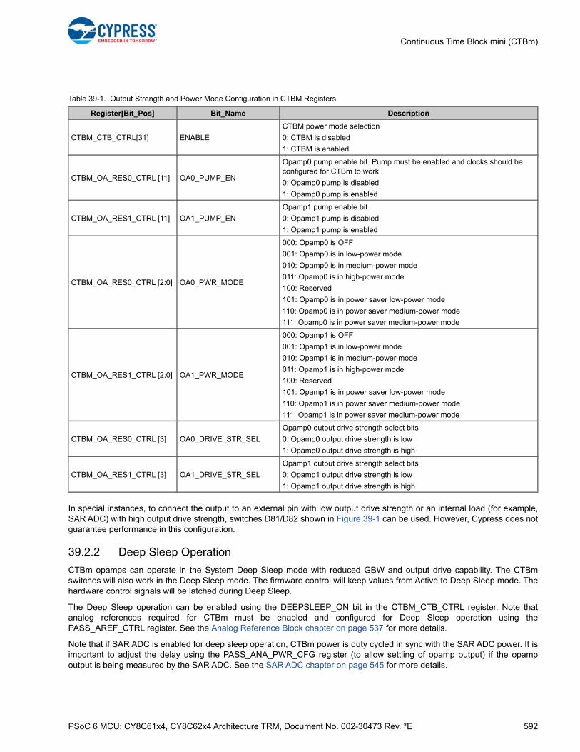
PSoC 6 MCU: CY8C61x4, CY8C62x4 Architecture TRM, Document No. 002-30473 Rev. *E 592
Continuous Time Block mini (CTBm)
In special instances, to connect the output to an external pin with low output drive strength or an internal load (for example,SAR ADC) with high output drive strength, switches D81/D82 shown in Figure 39-1 can be used. However, Cypress does notguarantee performance in this configuration.
39.2.2 Deep Sleep Operation
CTBm opamps can operate in the System Deep Sleep mode with reduced GBW and output drive capability. The CTBmswitches will also work in the Deep Sleep mode. The firmware control will keep values from Active to Deep Sleep mode. Thehardware control signals will be latched during Deep Sleep.
The Deep Sleep operation can be enabled using the DEEPSLEEP_ON bit in the CTBM_CTB_CTRL register. Note thatanalog references required for CTBm must be enabled and configured for Deep Sleep operation using thePASS_AREF_CTRL register. See the Analog Reference Block chapter on page 537 for more details.
Note that if SAR ADC is enabled for deep sleep operation, CTBm power is duty cycled in sync with the SAR ADC power. It isimportant to adjust the delay using the PASS_ANA_PWR_CFG register (to allow settling of opamp output) if the opampoutput is being measured by the SAR ADC. See the SAR ADC chapter on page 545 for more details.
Table 39-1. Output Strength and Power Mode Configuration in CTBM Registers
Register[Bit_Pos] Bit_Name Description
CTBM_CTB_CTRL[31] ENABLE
CTBM power mode selection
0: CTBM is disabled
1: CTBM is enabled
CTBM_OA_RES0_CTRL [11] OA0_PUMP_EN
Opamp0 pump enable bit. Pump must be enabled and clocks should be configured for CTBm to work
0: Opamp0 pump is disabled
1: Opamp0 pump is enabled
CTBM_OA_RES1_CTRL [11] OA1_PUMP_EN
Opamp1 pump enable bit
0: Opamp1 pump is disabled
1: Opamp1 pump is enabled
CTBM_OA_RES0_CTRL [2:0] OA0_PWR_MODE
000: Opamp0 is OFF
001: Opamp0 is in low-power mode
010: Opamp0 is in medium-power mode
011: Opamp0 is in high-power mode
100: Reserved
101: Opamp0 is in power saver low-power mode
110: Opamp0 is in power saver medium-power mode
111: Opamp0 is in power saver medium-power mode
CTBM_OA_RES1_CTRL [2:0] OA1_PWR_MODE
000: Opamp1 is OFF
001: Opamp1 is in low-power mode
010: Opamp1 is in medium-power mode
011: Opamp1 is in high-power mode
100: Reserved
101: Opamp1 is in power saver low-power mode
110: Opamp1 is in power saver medium-power mode
111: Opamp1 is in power saver medium-power mode
CTBM_OA_RES0_CTRL [3] OA0_DRIVE_STR_SEL
Opamp0 output drive strength select bits
0: Opamp0 output drive strength is low
1: Opamp0 output drive strength is high
CTBM_OA_RES1_CTRL [3] OA1_DRIVE_STR_SEL
Opamp1 output drive strength select bits
0: Opamp1 output drive strength is low
1: Opamp1 output drive strength is high

PSoC 6 MCU: CY8C61x4, CY8C62x4 Architecture TRM, Document No. 002-30473 Rev. *E 593
Continuous Time Block mini (CTBm)
39.2.3 Charge Pump
Each opamp includes a charge pump to allow rail-to-rail input. The clock for running the charge pumps is selected usingeither CLOCK_PUMP_PERI_SEL bits of the PASS_AREF_CTRL register (see the Analog Reference Block chapter onpage 537) or DPSLP_CLOCK_SEL register. The selected clock will be common to both the opamps in the CTBm block.
Pump clock input frequency requires to be in a certain range depending on the opamp power mode. See Table 39-2.
For the opamp configured for operation in System Deep Sleep mode, pump clock can be sourced from the deep sleep clock(CLK_DPSLP) and it should be configured to 2 MHz irrespective of the opamp power mode. See the SAR ADC chapter onpage 545 for more details about the configuration of deep sleep clock.
Charge pump is enabled by setting the OA0_PUMP_EN bit in the CTBM_OA_RES0_CTRL register for Opamp0 andOA1_PUMP_EN bit in the CTBM_OA_RES1_CTRL register for Opamp1.
39.2.4 Reference Currents
Opamps require reference currents (IPTAT and IZTAT) for its operation. These currents are generated by the AnalogReference block. Follow this procedure to configure the reference currents:
1. Enable the reference using ENABLED bit in the PASS_AREF_CTRL register.
2. If the opamps are required to be operational in System Deep Sleep mode, AREF also needs to be active simultaneously. Configure the DEEPSLEEP_MODE and DEEPSLEEP_ON bit fields in the PASS_AREF_CTRL register to keep the refer-ence currents ON during System Deep Sleep mode.
3. Power consumption in opamps can be reduced by lowering the reference current (IPTAT) from 1 µA to 100 nA at the expense of reduced gain bandwidth product. IPTAT value is configured using CTB_IPTAT_SCALE bit of the PASS_AREF_CTRL register. Choose the setting based on the application requirements. Performance specifications are provided in the PSoC 61 datasheet/PSoC 62 datasheet.
The AREF settings apply to all the opamps. See the Analog Reference Block chapter on page 537 for more details.
39.2.5 Compensation Trim Bits
For opamp stability, compensation bits need to be set based on the selected drive strength. Set the compensation trimregisters OA0_COMP_TRIM and OA1_COMP_TRIM to 03h for 10x output drive strength and 01h for 1x output drivestrength.
39.2.6 Switching Matrix
The CTBm has many switches to configure input and output routing of the opamps, as shown in Figure 39-1. Table 39-3 liststhe switches and the respective control bits to open/close the switches.
Table 39-2. Pump Clock Frequency
Opamp Power Mode Pump Clock Frequency
High 24 MHz
Medium 8 MHz to 24 MHz
Low 8 MHz to 24 MHz
Table 39-3. Switches and their Control Bits
Switch Description Register Bitfield
A00 Opamp0 non-inverting input to AMUXBUS A CTBM_OA0_SW OA0P_A00
A20 Opamp0 non-inverting input to Px.0 CTBM_OA0_SW OA0P_A00
A30 Opamp0 non-inverting input to Px.6 (and C6H) CTBM_OA0_SW OA0P_A30
A11 Opamp0 inverting input to Px.1 CTBM_OA0_SW OA0M_A11
A81 Opamp0 inverting input to output CTBM_OA0_SW OA0M_A81
D51 Opamp0 output to sarbus0 CTBM_OA0_SW OA0O_D51
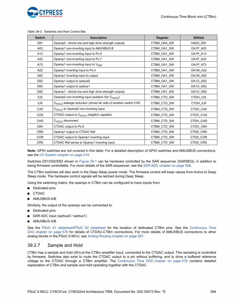
PSoC 6 MCU: CY8C61x4, CY8C62x4 Architecture TRM, Document No. 002-30473 Rev. *E 594
Continuous Time Block mini (CTBm)
Note: GPIO switches are not covered in this table. For a detailed description of GPIO switches and AMUXBUS connections,see the I/O System chapter on page 214.
Switches D51/D52/D62 shown in Figure 39-1 can be hardware controlled by the SAR sequencer (SARSEQ), in addition tobeing firmware controllable. For more details of the SAR sequencer, see the SAR ADC chapter on page 506.
The CTBm switches will also work in the Deep Sleep power mode. The firmware control will keep values from Active to DeepSleep mode. The hardware control signals will be latched during Deep Sleep.
Using the switching matrix, the opamps in CTBm can be configured to have inputs from:
■ Dedicated pins
■ CTDAC
■ AMUXBUS A/B
Similarly, the output of the opamps can be connected to:
■ Dedicated pins
■ SAR ADC input (sarbus0 / sarbus1)
■ AMUXBUS A/B
See the PSoC 61 datasheet/PSoC 62 datasheet for the location of dedicated CTBm pins. See the Continuous TimeDAC chapter on page 576 for details of CTDAC-CTBm connections. For more details of AMUXBUS connections to otheranalog blocks in the PSoC 6 MCU, see Analog Routing chapter on page 597.
39.2.7 Sample and Hold
CTBm has a sample and hold (SH) at the CTBm amplifier input, connected to the CTDAC output. This sampling is controlledby firmware. Switches also exist to route the CTDAC output to a pin without buffering, and to drive a buffered referencevoltage to the CTDAC through a CTBm amplifier. The Continuous Time DAC chapter on page 576 contains detailedexplanation of CTBm and sample and hold operating together with the CTDAC.
D81 Opamp0 - shorts low and high drive strength outputs CTBM_OA0_SW OA0O_D81
A03 Opamp1 non-inverting input to AMUXBUS B CTBM_OA1_SW OA1P_A03
A13 Opamp1 non-inverting input to Px.5 CTBM_OA1_SW OA1P_A13
A43 Opamp1 non-inverting input to Px.7 CTBM_OA1_SW OA1P_A43
A73 Opamp1 non-inverting input to VREF CTBM_OA1_SW OA1P_A73
A22 Opamp1 inverting input to Px.4 CTBM_OA1_SW OA1M_A22
A82 Opamp1 inverting input to output CTBM_OA1_SW OA1M_A82
D52 Opamp1 output to sarbus0 CTBM_OA1_SW OA1O_D52
D62 Opamp1 output to sarbus1 CTBM_OA1_SW OA1O_D62
D82 Opamp1 - shorts low and high drive strength outputs CTBM_OA1_SW OA1O_D82
CIS Opamp0 non-inverting input isolation (for CHOLD) CTBM_CTD_SW CTDH_CIS
ILR CHOLD leakage reduction (drives far side of isolation switch CIS) CTBM_CTD_SW CTDH_ILR
CA0 CHOLD to Opamp0 non-inverting input CTBM_CTD_SW CTDH_CA0
COS CTDAC output to CHOLD (deglitch capable) CTBM_CTD_SW CTDO_COS
CHD CHOLD disconnect CTBM_CTD_SW CTDH_CHD
C6H CTDAC output to Px.6 CTBM_CTD_SW CTDO_C6H
CRD Opamp1 output to CTDAC Ref CTBM_CTD_SW CTDD_CRD
COR CTDAC output to Opamp1 inverting input CTBM_CTD_SW CTDS_COR
CRS CTDAC Ref sense to Opamp1 inverting input CTBM_CTD_SW CTDS_CRS
Table 39-3. Switches and their Control Bits
Switch Description Register Bitfield
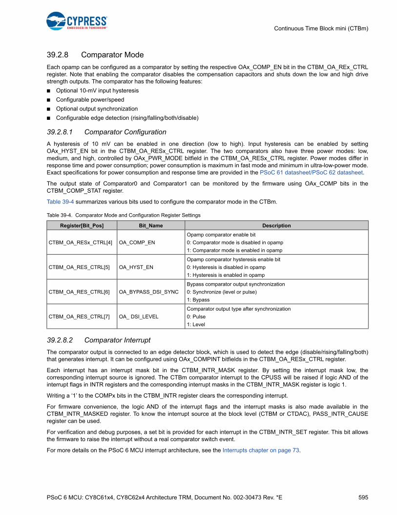
PSoC 6 MCU: CY8C61x4, CY8C62x4 Architecture TRM, Document No. 002-30473 Rev. *E 595
Continuous Time Block mini (CTBm)
39.2.8 Comparator Mode
Each opamp can be configured as a comparator by setting the respective OAx_COMP_EN bit in the CTBM_OA_REx_CTRLregister. Note that enabling the comparator disables the compensation capacitors and shuts down the low and high drivestrength outputs. The comparator has the following features:
■ Optional 10-mV input hysteresis
■ Configurable power/speed
■ Optional output synchronization
■ Configurable edge detection (rising/falling/both/disable)
39.2.8.1 Comparator Configuration
A hysteresis of 10 mV can be enabled in one direction (low to high). Input hysteresis can be enabled by settingOAx_HYST_EN bit in the CTBM_OA_RESx_CTRL register. The two comparators also have three power modes: low,medium, and high, controlled by OAx_PWR_MODE bitfield in the CTBM_OA_RESx_CTRL register. Power modes differ inresponse time and power consumption; power consumption is maximum in fast mode and minimum in ultra-low-power mode.Exact specifications for power consumption and response time are provided in the PSoC 61 datasheet/PSoC 62 datasheet.
The output state of Comparator0 and Comparator1 can be monitored by the firmware using OAx_COMP bits in theCTBM_COMP_STAT register.
Table 39-4 summarizes various bits used to configure the comparator mode in the CTBm.
39.2.8.2 Comparator Interrupt
The comparator output is connected to an edge detector block, which is used to detect the edge (disable/rising/falling/both)that generates interrupt. It can be configured using OAx_COMPINT bitfields in the CTBM_OA_RESx_CTRL register.
Each interrupt has an interrupt mask bit in the CTBM_INTR_MASK register. By setting the interrupt mask low, thecorresponding interrupt source is ignored. The CTBm comparator interrupt to the CPUSS will be raised if logic AND of theinterrupt flags in INTR registers and the corresponding interrupt masks in the CTBM_INTR_MASK register is logic 1.
Writing a ‘1’ to the COMPx bits in the CTBM_INTR register clears the corresponding interrupt.
For firmware convenience, the logic AND of the interrupt flags and the interrupt masks is also made available in theCTBM_INTR_MASKED register. To know the interrupt source at the block level (CTBM or CTDAC), PASS_INTR_CAUSEregister can be used.
For verification and debug purposes, a set bit is provided for each interrupt in the CTBM_INTR_SET register. This bit allowsthe firmware to raise the interrupt without a real comparator switch event.
For more details on the PSoC 6 MCU interrupt architecture, see the Interrupts chapter on page 73.
Table 39-4. Comparator Mode and Configuration Register Settings
Register[Bit_Pos] Bit_Name Description
CTBM_OA_RESx_CTRL[4] OA_COMP_EN
Opamp comparator enable bit
0: Comparator mode is disabled in opamp
1: Comparator mode is enabled in opamp
CTBM_OA_RES_CTRL[5] OA_HYST_EN
Opamp comparator hysteresis enable bit
0: Hysteresis is disabled in opamp
1: Hysteresis is enabled in opamp
CTBM_OA_RES_CTRL[6] OA_BYPASS_DSI_SYNC
Bypass comparator output synchronization
0: Synchronize (level or pulse)
1: Bypass
CTBM_OA_RES_CTRL[7] OA_ DSI_LEVEL
Comparator output type after synchronization
0: Pulse
1: Level
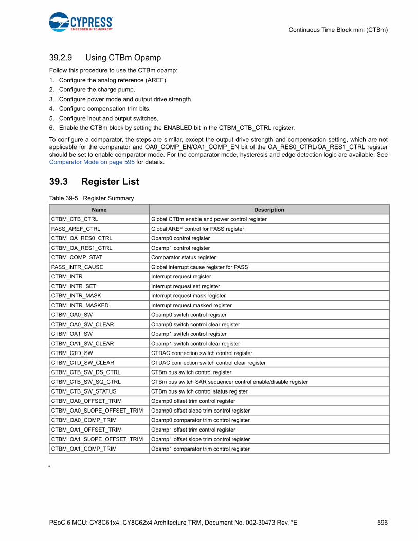
PSoC 6 MCU: CY8C61x4, CY8C62x4 Architecture TRM, Document No. 002-30473 Rev. *E 596
Continuous Time Block mini (CTBm)
39.2.9 Using CTBm Opamp
Follow this procedure to use the CTBm opamp:
1. Configure the analog reference (AREF).
2. Configure the charge pump.
3. Configure power mode and output drive strength.
4. Configure compensation trim bits.
5. Configure input and output switches.
6. Enable the CTBm block by setting the ENABLED bit in the CTBM_CTB_CTRL register.
To configure a comparator, the steps are similar, except the output drive strength and compensation setting, which are notapplicable for the comparator and OA0_COMP_EN/OA1_COMP_EN bit of the OA_RES0_CTRL/OA_RES1_CTRL registershould be set to enable comparator mode. For the comparator mode, hysteresis and edge detection logic are available. SeeComparator Mode on page 595 for details.
39.3 Register List
Table 39-5. Register Summary
Name Description
CTBM_CTB_CTRL Global CTBm enable and power control register
PASS_AREF_CTRL Global AREF control for PASS register
CTBM_OA_RES0_CTRL Opamp0 control register
CTBM_OA_RES1_CTRL Opamp1 control register
CTBM_COMP_STAT Comparator status register
PASS_INTR_CAUSE Global interrupt cause register for PASS
CTBM_INTR Interrupt request register
CTBM_INTR_SET Interrupt request set register
CTBM_INTR_MASK Interrupt request mask register
CTBM_INTR_MASKED Interrupt request masked register
CTBM_OA0_SW Opamp0 switch control register
CTBM_OA0_SW_CLEAR Opamp0 switch control clear register
CTBM_OA1_SW Opamp1 switch control register
CTBM_OA1_SW_CLEAR Opamp1 switch control clear register
CTBM_CTD_SW CTDAC connection switch control register
CTBM_CTD_SW_CLEAR CTDAC connection switch control clear register
CTBM_CTB_SW_DS_CTRL CTBm bus switch control register
CTBM_CTB_SW_SQ_CTRL CTBm bus switch SAR sequencer control enable/disable register
CTBM_CTB_SW_STATUS CTBm bus switch control status register
CTBM_OA0_OFFSET_TRIM Opamp0 offset trim control register
CTBM_OA0_SLOPE_OFFSET_TRIM Opamp0 offset slope trim control register
CTBM_OA0_COMP_TRIM Opamp0 comparator trim control register
CTBM_OA1_OFFSET_TRIM Opamp1 offset trim control register
CTBM_OA1_SLOPE_OFFSET_TRIM Opamp1 offset slope trim control register
CTBM_OA1_COMP_TRIM Opamp1 comparator trim control register
PSoC 6 MCU: CY8C61x4, CY8C62x4 Architecture TRM, Document No. 002-30473 Rev. *E 597
40. Analog Routing
The PSoC 6 MCU has a flexible analog routing system that interconnects programmable analog blocks and GPIOs. Analogrouting in the PSoC 6 MCU reduces external connections, allows last-minute feature changes, and eliminates delays causedby PCB spins by reconfiguring interconnection between analog blocks.
40.1 Features
The PSoC 6 MCU analog routing has the following features:
■ Flexible connections between different analog blocks and GPIOs
■ Two system-wide analog mux buses (AMUXBUS) that interconnect all analog capable GPIOs
■ Switches in the analog routing can be used to create analog multiplexers
This PSoC 6 MCU technical reference manual (TRM) provides comprehensive and detailed information about thefunctions of the PSoC 6 MCU device hardware. It is divided into two books: architecture TRM and registers TRM. TheTRM is not recommended for those new to the PSoC 6 MCU, nor as a guide for developing PSoC 6 MCU applications.Use these documents instead:
■ PSoC 61 datasheet, PSoC 62 datasheet
■ Peripheral Driver Library (PDL) documentation
■ Application notes
■ Code examples
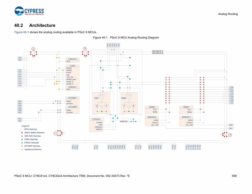
Analog Routing
PSoC 6 MCU: CY8C61x4, CY8C62x4 Architecture TRM, Document No. 002-30473 Rev. *E 598
40.2 Architecture
Figure 40-1 shows the analog routing available in PSoC 6 MCUs.
Figure 40-1. PSoC 6 MCU Analog Routing Diagram
Legend
GPIO Switches
AMUX Splitter Switches
SAR ADC Switches
CTBm Switches
CTDAC Switches
LPCOMP Switches
CapSense Switches
AMUXBUS-AAMUXBUS-B
P2[
7]
P2[
6]
P2[
5]
P2[
4]
P2[
3]
P2[
2]
P2[
1]
P2[
0]
P1[
2]
P1[
1]
P1[
0]
P0[
4]
P0[
3]
P0[
2]
P0[
1]
P0[
0]
P0[
5]
P12
[0]
P12
[1]
P11
[7]
P11
[6]
P11
[5]
P11
[4]
P11
[3]
P11
[2]
P11
[1]
P10[5]
P10[4]
P10[3]
P10[1]
P10[0]
P10[2]
SARADC0
VSSA
TEMP0
tempVSSA
TEMP1
temp
SARADC1
P6[2]
P8[0]
P8[1]
P6[3]
P6[4]
P6[5]
P6[6]
P6[7]
P5[6]
P5[7]
LPCOMP1
LPCOMP0
P5[
1]
P5[
2]
P5[
0]
P3[
0]
P3[
1]
32
OA0OA1
1
5
VREF1
VREF
P10[7]
P10[6]

PSoC 6 MCU: CY8C61x4, CY8C62x4 Architecture TRM, Document No. 002-30473 Rev. *E 599
Analog Routing
Notes:
■ The analog features and GPIOs shown in Figure 40-1 may not be available in all PSoC 6 MCUs. See the respectivedevice datasheet for available analog features and ports in a device.
■ Certain analog blocks such as CapSense and LPCOMP have additional internal routing, which is not shown inFigure 40-1. See the respective chapters of these blocks in this document for details.
Analog routing in the PSoC 6 MCU consists of several on-chip analog buses and analog switches. Table 40-1 gives asummary of connections available between analog blocks.
Notes:
■ For detailed routing and switch-control information of a block, click on the respective block name.
■ CapSense block connections used for touch sensing are not shown in Table 40-1 because CapSense is not connected toany other analog blocks during touch sensing.
■ AMUXBUS routing is not available in system Deep Sleep and Hibernate power modes of PSoC 6 MCUs.
■ If the routing uses switches belonging to a particular analog block, for example, SAR ADC, then SAR ADC block needs tobe enabled.
■ SAR ADCs are designed with 16 channels, but each ADC can scan thirteen unique inputs, which includes eight GPIOsfrom dedicated SARMUX port, two CTBm opamp outputs, two AMUX buses, and a temperature sensor. It is possible toscan GPIOs from other ports using AMUX buses.
Most analog blocks have dedicated connections to certain pins, which, when used, provide the best possible performance.However, these blocks can be also connected to other GPIOs and each other using AMUXBUS in case the dedicated pin isnot available or is used by another resource.
40.2.1 AMUXBUS Splitting
AMUXBUS A and AMUXBUS B are system-wide analog buses that can connect to almost all analog blocks and some GPIOsin the PSoC 6 MCU. However, the PSoC 6 MCU has only two of these buses. Each AMUXBUS can be split into multiplesegments using 3 switches controlled by writing into the HSIOM_AMUX_SPLIT_CTL registers. An example use case wouldbe to disconnect the AMUX switch 3 (see Figure 40-1) when using CapSense with touch pads connected to Port 7 and Port 8.This leaves other AMUX bus segments free for use by other analog blocks. For more information on AMUXBUS connections,see the I/O System chapter on page 214.
Table 40-1. Available Connections between PSoC 6 MCU Analog Blocks
To GPIOs To SAR ADCTo CTBm (OA0,
OA1)To CTDAC To LPCOMP
To CapSense IDACs
From GPIOsAMUXBUS A
AMUXBUS B
Dedicated SARSEQ port
Through CTBm
AMUXBUS A
AMUXBUS B
Dedicated CTBm pins
AMUXBUS A
AMUXBUS B
N/A1
1. CTDAC does not have analog inputs.
Dedicated LPCOMP pins
AMUXBUS A
AMUXBUS B
N/A2
2. IDAC does not have analog inputs.
From SAR ADC N/A3
3. SAR ADC does not have analog outputs.
N/A4
4. Same block
N/A3 N/A3 N/A3 N/A3
From CTBm (OA0, OA1)
Dedicated CTBm pins
AMUXBUS A
AMUXBUS B
Internal bus
AMUXBUS A
AMUXBUS B
N/A4 N/A1AMUXBUS A
AMUXBUS BN/A2
From CTDAC Through CTBm Through CTBm Internal bus N/A4 Through CTBm N/A2
From LPCOMP N/A5
5. LPCOMP does not have analog outputs.
N/A5 N/A5 N/A5 N/A4 N/A5
From CapSense IDACs
AMUXBUS A
AMUXBUS B
AMUXBUS A6
AMUXBUS B6
6. External resistor may be required to convert current to voltage.
AMUXBUS A
AMUXBUS BN/A1
AMUXBUS A6
AMUXBUS B6N/A4

PSoC 6 MCU: CY8C61x4, CY8C62x4 Architecture TRM, Document No. 002-30473 Rev. *E 600
Analog Routing
40.3 Register List
Table 40-2. Register Summary
Name Description
HSIOM_ AMUX_SPLIT_CTL This register controls the breaking of AMUX buses A and B into multiple segments.