
16-bit MCU with 256 Kbyte Flash memory and 16 Kbyte RAM
328
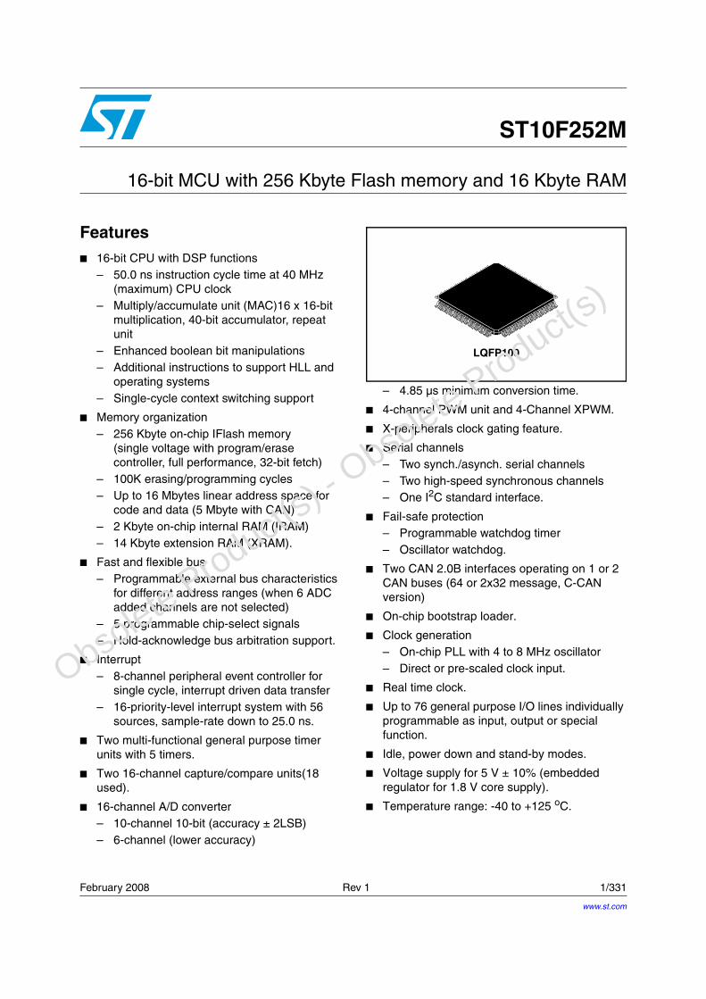
February 2008 Rev 1 1/331 1 ST10F252M 16-bit MCU with 256 Kbyte Flash memory and 16 Kbyte RAM Features ■ 16-bit CPU with DSP functions – 50.0 ns instruction cycle time at 40 MHz (maximum) CPU clock – Multiply/accumulate unit (MAC)16 x 16-bit multiplication, 40-bit accumulator, repeat unit – Enhanced boolean bit manipulations – Additional instructions to support HLL and operating systems – Single-cycle context switching support ■ Memory organization – 256 Kbyte on-chip IFlash memory (single voltage with program/erase controller, full performance, 32-bit fetch) – 100K erasing/programming cycles – Up to 16 Mbytes linear address space for code and data (5 Mbyte with CAN) – 2 Kbyte on-chip internal RAM (IRAM) – 14 Kbyte extension RAM (XRAM). ■ Fast and flexible bus – Programmable external bus characteristics for different address ranges (when 6 ADC added channels are not selected) – 5 programmable chip-select signals – Hold-acknowledge bus arbitration support. ■ Interrupt – 8-channel peripheral event controller for single cycle, interrupt driven data transfer – 16-priority-level interrupt system with 56 sources, sample-rate down to 25.0 ns. ■ Two multi-functional general purpose timer units with 5 timers. ■ Two 16-channel capture/compare units(18 used). ■ 16-channel A/D converter – 10-channel 10-bit (accuracy ± 2LSB) – 6-channel (lower accuracy) – 4.85 μs minimum conversion time. ■ 4-channel PWM unit and 4-Channel XPWM. ■ X-peripherals clock gating feature. ■ Serial channels – Two synch./asynch. serial channels – Two high-speed synchronous channels – One I 2 C standard interface. ■ Fail-safe protection – Programmable watchdog timer – Oscillator watchdog. ■ Two CAN 2.0B interfaces operating on 1 or 2 CAN buses (64 or 2x32 message, C-CAN version) ■ On-chip bootstrap loader. ■ Clock generation – On-chip PLL with 4 to 8 MHz oscillator – Direct or pre-scaled clock input. ■ Real time clock. ■ Up to 76 general purpose I/O lines individually programmable as input, output or special function. ■ Idle, power down and stand-by modes. ■ Voltage supply for 5 V ± 10% (embedded regulator for 1.8 V core supply). ■ Temperature range: -40 to +125 o C. LQFP100 www.st.com Obsolete Product(s) - Obsolete Product(s)
-
Upload
khangminh22 -
Category
Documents
-
view
1 -
download
0
Transcript of 16-bit MCU with 256 Kbyte Flash memory and 16 Kbyte RAM
February 2008 Rev 1 1/331
1
ST10F252M
16-bit MCU with 256 Kbyte Flash memory and 16 Kbyte RAM
Features■ 16-bit CPU with DSP functions
– 50.0 ns instruction cycle time at 40 MHz (maximum) CPU clock
– Multiply/accumulate unit (MAC)16 x 16-bit multiplication, 40-bit accumulator, repeat unit
– Enhanced boolean bit manipulations– Additional instructions to support HLL and
operating systems– Single-cycle context switching support
■ Memory organization– 256 Kbyte on-chip IFlash memory
(single voltage with program/erase controller, full performance, 32-bit fetch)
– 100K erasing/programming cycles– Up to 16 Mbytes linear address space for
code and data (5 Mbyte with CAN)– 2 Kbyte on-chip internal RAM (IRAM)– 14 Kbyte extension RAM (XRAM).
■ Fast and flexible bus– Programmable external bus characteristics
for different address ranges (when 6 ADC added channels are not selected)
– 5 programmable chip-select signals– Hold-acknowledge bus arbitration support.
■ Interrupt– 8-channel peripheral event controller for
single cycle, interrupt driven data transfer– 16-priority-level interrupt system with 56
sources, sample-rate down to 25.0 ns.
■ Two multi-functional general purpose timer units with 5 timers.
■ Two 16-channel capture/compare units(18 used).
■ 16-channel A/D converter – 10-channel 10-bit (accuracy ± 2LSB)– 6-channel (lower accuracy)
– 4.85 µs minimum conversion time.
■ 4-channel PWM unit and 4-Channel XPWM.
■ X-peripherals clock gating feature.
■ Serial channels– Two synch./asynch. serial channels– Two high-speed synchronous channels– One I2C standard interface.
■ Fail-safe protection– Programmable watchdog timer– Oscillator watchdog.
■ Two CAN 2.0B interfaces operating on 1 or 2 CAN buses (64 or 2x32 message, C-CAN version)
■ On-chip bootstrap loader.
■ Clock generation– On-chip PLL with 4 to 8 MHz oscillator – Direct or pre-scaled clock input.
■ Real time clock.
■ Up to 76 general purpose I/O lines individually programmable as input, output or special function.
■ Idle, power down and stand-by modes.
■ Voltage supply for 5 V ± 10% (embedded regulator for 1.8 V core supply).
■ Temperature range: -40 to +125 oC.
LQFP100
www.st.com
O
bsolete Product(
s) - O
bsolete Product(
s)
Contents ST10F252M
2/328
Contents
1 Introduction . . . . . . . . . . . . . . . . . . . . . . . . . . . . . . . . . . . . . . . . . . . . . . . 18
1.1 Description . . . . . . . . . . . . . . . . . . . . . . . . . . . . . . . . . . . . . . . . . . . . . . . . 18
2 Pin data . . . . . . . . . . . . . . . . . . . . . . . . . . . . . . . . . . . . . . . . . . . . . . . . . . 19
3 Functional description . . . . . . . . . . . . . . . . . . . . . . . . . . . . . . . . . . . . . . 24
4 Memory organization . . . . . . . . . . . . . . . . . . . . . . . . . . . . . . . . . . . . . . . 25
4.1 XPERCON and XPEREMU registers . . . . . . . . . . . . . . . . . . . . . . . . . . . . 28
4.2 Emulation dedicated registers . . . . . . . . . . . . . . . . . . . . . . . . . . . . . . . . . 30
4.3 XRAM2 memory range . . . . . . . . . . . . . . . . . . . . . . . . . . . . . . . . . . . . . . . 31
5 Central processing unit . . . . . . . . . . . . . . . . . . . . . . . . . . . . . . . . . . . . . 35
5.1 The system configuration register SYSCON . . . . . . . . . . . . . . . . . . . . . . 36
6 Multiplier-accumulator unit . . . . . . . . . . . . . . . . . . . . . . . . . . . . . . . . . . 38
6.1 MAC features . . . . . . . . . . . . . . . . . . . . . . . . . . . . . . . . . . . . . . . . . . . . . . 38
6.1.1 Enhanced addressing capabilities . . . . . . . . . . . . . . . . . . . . . . . . . . . . . 38
6.1.2 General . . . . . . . . . . . . . . . . . . . . . . . . . . . . . . . . . . . . . . . . . . . . . . . . . 38
6.1.3 Program control . . . . . . . . . . . . . . . . . . . . . . . . . . . . . . . . . . . . . . . . . . . 39
6.2 MAC operation . . . . . . . . . . . . . . . . . . . . . . . . . . . . . . . . . . . . . . . . . . . . . 39
6.2.1 Instruction pipelining . . . . . . . . . . . . . . . . . . . . . . . . . . . . . . . . . . . . . . . 39
6.2.2 Particular pipeline effects with the MAC unit . . . . . . . . . . . . . . . . . . . . . 40
6.2.3 Address generation . . . . . . . . . . . . . . . . . . . . . . . . . . . . . . . . . . . . . . . . 40
6.2.4 16 x 16 signed / unsigned parallel multiplier . . . . . . . . . . . . . . . . . . . . . 42
6.2.5 40-bit signed arithmetic unit . . . . . . . . . . . . . . . . . . . . . . . . . . . . . . . . . . 42
6.2.6 40-bit adder/subtracter . . . . . . . . . . . . . . . . . . . . . . . . . . . . . . . . . . . . . . 43
6.2.7 Data limiter . . . . . . . . . . . . . . . . . . . . . . . . . . . . . . . . . . . . . . . . . . . . . . . 43
6.2.8 The accumulator shifter . . . . . . . . . . . . . . . . . . . . . . . . . . . . . . . . . . . . . 43
6.2.9 Repeat unit . . . . . . . . . . . . . . . . . . . . . . . . . . . . . . . . . . . . . . . . . . . . . . 44
6.2.10 MAC interrupt . . . . . . . . . . . . . . . . . . . . . . . . . . . . . . . . . . . . . . . . . . . . . 44
6.2.11 Number representation and rounding . . . . . . . . . . . . . . . . . . . . . . . . . . 45
6.3 MAC register set . . . . . . . . . . . . . . . . . . . . . . . . . . . . . . . . . . . . . . . . . . . . 45
6.3.1 Address registers . . . . . . . . . . . . . . . . . . . . . . . . . . . . . . . . . . . . . . . . . . 45
O
bsolete Product(
s) - O
bsolete Product(
s)

ST10F252M Contents
3/328
6.3.2 Accumulator and control registers . . . . . . . . . . . . . . . . . . . . . . . . . . . . . 46
7 External bus controller . . . . . . . . . . . . . . . . . . . . . . . . . . . . . . . . . . . . . . 50
7.1 Controlling the external bus controller . . . . . . . . . . . . . . . . . . . . . . . . . . . 50
7.1.1 External bus controller registers . . . . . . . . . . . . . . . . . . . . . . . . . . . . . . 50
7.2 EA functionality . . . . . . . . . . . . . . . . . . . . . . . . . . . . . . . . . . . . . . . . . . . . . 52
8 Internal Flash memory . . . . . . . . . . . . . . . . . . . . . . . . . . . . . . . . . . . . . . 53
8.1 Overview . . . . . . . . . . . . . . . . . . . . . . . . . . . . . . . . . . . . . . . . . . . . . . . . . 53
8.2 Functional description . . . . . . . . . . . . . . . . . . . . . . . . . . . . . . . . . . . . . . . 53
8.2.1 Structure . . . . . . . . . . . . . . . . . . . . . . . . . . . . . . . . . . . . . . . . . . . . . . . . 53
8.2.2 Modules structure . . . . . . . . . . . . . . . . . . . . . . . . . . . . . . . . . . . . . . . . . 54
8.2.3 Low power mode . . . . . . . . . . . . . . . . . . . . . . . . . . . . . . . . . . . . . . . . . . 55
8.3 Write operation . . . . . . . . . . . . . . . . . . . . . . . . . . . . . . . . . . . . . . . . . . . . . 56
8.4 Registers description . . . . . . . . . . . . . . . . . . . . . . . . . . . . . . . . . . . . . . . . 56
8.4.1 Flash control register 0 low (FCR0L) . . . . . . . . . . . . . . . . . . . . . . . . . . . 56
8.4.2 Flash control register 0 high (FCR0H) . . . . . . . . . . . . . . . . . . . . . . . . . . 57
8.4.3 Flash control register 1 low (FCR1L) . . . . . . . . . . . . . . . . . . . . . . . . . . . 59
8.4.4 Flash control register 1 high (FCR1H) . . . . . . . . . . . . . . . . . . . . . . . . . . 59
8.4.5 Flash data register 0 low (FDR0L) . . . . . . . . . . . . . . . . . . . . . . . . . . . . . 60
8.4.6 Flash data register 0 high (FDR0H) . . . . . . . . . . . . . . . . . . . . . . . . . . . . 61
8.4.7 Flash data register 1 low (FDR1L) . . . . . . . . . . . . . . . . . . . . . . . . . . . . . 61
8.4.8 Flash data register 1 high (FDR1H) . . . . . . . . . . . . . . . . . . . . . . . . . . . . 61
8.4.9 Flash address register low (FARL) . . . . . . . . . . . . . . . . . . . . . . . . . . . . . 62
8.4.10 Flash address register high (FARH) . . . . . . . . . . . . . . . . . . . . . . . . . . . . 62
8.4.11 Flash error register (FER) . . . . . . . . . . . . . . . . . . . . . . . . . . . . . . . . . . . 62
8.5 Protection strategy . . . . . . . . . . . . . . . . . . . . . . . . . . . . . . . . . . . . . . . . . . 63
8.5.1 Protection registers . . . . . . . . . . . . . . . . . . . . . . . . . . . . . . . . . . . . . . . . 64
8.5.2 Flash non-volatile write protection I register (FNVWPIR) . . . . . . . . . . . 64
8.5.3 Flash non-volatile access protection register 0 (FNVAPR0) . . . . . . . . . 64
8.5.4 Flash non-volatile access protection register 1 low (FNVAPR1L) . . . . . 65
8.5.5 Flash non-volatile access protection register 1 high (FNVAPR1H) . . . . 65
8.5.6 XBus Flash volatile temporary access unprotection register(XFVTAUR0) . . . . . . . . . . . . . . . . . . . . . . . . . . . . . . . . . . . . . . . . . . . . . 65
8.5.7 Access protection . . . . . . . . . . . . . . . . . . . . . . . . . . . . . . . . . . . . . . . . . 66
8.5.8 Write protection . . . . . . . . . . . . . . . . . . . . . . . . . . . . . . . . . . . . . . . . . . . 67
8.5.9 Temporary unprotection . . . . . . . . . . . . . . . . . . . . . . . . . . . . . . . . . . . . . 67
O
bsolete Product(
s) - O
bsolete Product(
s)

Contents ST10F252M
4/328
8.6 Write operation examples . . . . . . . . . . . . . . . . . . . . . . . . . . . . . . . . . . . . . 67
8.7 Write operation summary . . . . . . . . . . . . . . . . . . . . . . . . . . . . . . . . . . . . . 71
9 Interrupt system . . . . . . . . . . . . . . . . . . . . . . . . . . . . . . . . . . . . . . . . . . . 72
9.1 Fast external interrupt . . . . . . . . . . . . . . . . . . . . . . . . . . . . . . . . . . . . . . . 72
9.1.1 External interrupt source selection register (EXISEL) . . . . . . . . . . . . . . 72
9.1.2 External interrupt control register (EXICON) . . . . . . . . . . . . . . . . . . . . . 74
9.2 X-Peripheral interrupt . . . . . . . . . . . . . . . . . . . . . . . . . . . . . . . . . . . . . . . . 75
9.3 Interrupt sources . . . . . . . . . . . . . . . . . . . . . . . . . . . . . . . . . . . . . . . . . . . 76
9.4 Exception and traps list . . . . . . . . . . . . . . . . . . . . . . . . . . . . . . . . . . . . . . 78
10 Capture compare (CAPCOM) units . . . . . . . . . . . . . . . . . . . . . . . . . . . . 80
11 General purpose timer unit . . . . . . . . . . . . . . . . . . . . . . . . . . . . . . . . . . 82
11.1 GPT1 . . . . . . . . . . . . . . . . . . . . . . . . . . . . . . . . . . . . . . . . . . . . . . . . . . . . 82
11.2 GPT2 . . . . . . . . . . . . . . . . . . . . . . . . . . . . . . . . . . . . . . . . . . . . . . . . . . . . 83
12 PWM modules . . . . . . . . . . . . . . . . . . . . . . . . . . . . . . . . . . . . . . . . . . . . . 85
13 Parallel ports . . . . . . . . . . . . . . . . . . . . . . . . . . . . . . . . . . . . . . . . . . . . . . 86
13.1 Introduction . . . . . . . . . . . . . . . . . . . . . . . . . . . . . . . . . . . . . . . . . . . . . . . 86
13.2 I/O’s special features . . . . . . . . . . . . . . . . . . . . . . . . . . . . . . . . . . . . . . . . 88
13.2.1 Open drain mode . . . . . . . . . . . . . . . . . . . . . . . . . . . . . . . . . . . . . . . . . . 88
13.2.2 Input threshold control . . . . . . . . . . . . . . . . . . . . . . . . . . . . . . . . . . . . . 88
13.2.3 Alternate port functions . . . . . . . . . . . . . . . . . . . . . . . . . . . . . . . . . . . . . 89
13.3 PORT0 . . . . . . . . . . . . . . . . . . . . . . . . . . . . . . . . . . . . . . . . . . . . . . . . . . . 90
13.3.1 Alternate functions of PORT0 . . . . . . . . . . . . . . . . . . . . . . . . . . . . . . . . 91
13.3.2 Disturb protection on analog inputs . . . . . . . . . . . . . . . . . . . . . . . . . . . . 93
13.4 PORT1 . . . . . . . . . . . . . . . . . . . . . . . . . . . . . . . . . . . . . . . . . . . . . . . . . . . 95
13.4.1 Alternate functions of PORT1 . . . . . . . . . . . . . . . . . . . . . . . . . . . . . . . . 98
13.5 PORT2 . . . . . . . . . . . . . . . . . . . . . . . . . . . . . . . . . . . . . . . . . . . . . . . . . . 104
13.5.1 Alternate functions of PORT2 . . . . . . . . . . . . . . . . . . . . . . . . . . . . . . . 105
13.6 PORT3 . . . . . . . . . . . . . . . . . . . . . . . . . . . . . . . . . . . . . . . . . . . . . . . . . . 108
13.6.1 Alternate functions of PORT3 . . . . . . . . . . . . . . . . . . . . . . . . . . . . . . . 110
13.7 PORT4 . . . . . . . . . . . . . . . . . . . . . . . . . . . . . . . . . . . . . . . . . . . . . . . . . . 112
13.7.1 Alternate functions of PORT4 . . . . . . . . . . . . . . . . . . . . . . . . . . . . . . . 113
O
bsolete Product(
s) - O
bsolete Product(
s)

ST10F252M Contents
5/328
13.8 PORT7 . . . . . . . . . . . . . . . . . . . . . . . . . . . . . . . . . . . . . . . . . . . . . . . . . . 119
13.8.1 Alternate functions of PORT7 . . . . . . . . . . . . . . . . . . . . . . . . . . . . . . . 120
13.9 PORT5 . . . . . . . . . . . . . . . . . . . . . . . . . . . . . . . . . . . . . . . . . . . . . . . . . . 122
13.9.1 Alternate functions of PORT5 . . . . . . . . . . . . . . . . . . . . . . . . . . . . . . . 123
13.9.2 Disturb protection on analog inputs . . . . . . . . . . . . . . . . . . . . . . . . . . . 124
14 Analog / digital converter . . . . . . . . . . . . . . . . . . . . . . . . . . . . . . . . . . 125
14.1 Mode selection and operation . . . . . . . . . . . . . . . . . . . . . . . . . . . . . . . . 127
14.1.1 Fixed channel conversion modes . . . . . . . . . . . . . . . . . . . . . . . . . . . . . 129
14.1.2 Auto scan conversion modes . . . . . . . . . . . . . . . . . . . . . . . . . . . . . . . . 129
14.1.3 Wait for ADDAT read mode . . . . . . . . . . . . . . . . . . . . . . . . . . . . . . . . . 130
14.1.4 Channel injection mode . . . . . . . . . . . . . . . . . . . . . . . . . . . . . . . . . . . . 131
14.1.5 ADC power down (ADOFF) . . . . . . . . . . . . . . . . . . . . . . . . . . . . . . . . . 133
14.2 Conversion timing control . . . . . . . . . . . . . . . . . . . . . . . . . . . . . . . . . . . 134
14.3 ADC interrupt control . . . . . . . . . . . . . . . . . . . . . . . . . . . . . . . . . . . . . . . 135
14.4 Calibration . . . . . . . . . . . . . . . . . . . . . . . . . . . . . . . . . . . . . . . . . . . . . . . 136
15 Programmable output clock divider . . . . . . . . . . . . . . . . . . . . . . . . . . 137
15.1 Functionality . . . . . . . . . . . . . . . . . . . . . . . . . . . . . . . . . . . . . . . . . . . . . . 137
16 Serial channels . . . . . . . . . . . . . . . . . . . . . . . . . . . . . . . . . . . . . . . . . . . 138
16.1 Asynchronous / synchronous serial interfaces . . . . . . . . . . . . . . . . . . . . 138
16.2 ASCx in asynchronous mode . . . . . . . . . . . . . . . . . . . . . . . . . . . . . . . . . 138
16.3 ASCx in synchronous mode . . . . . . . . . . . . . . . . . . . . . . . . . . . . . . . . . . 139
16.4 High speed synchronous serial interfaces . . . . . . . . . . . . . . . . . . . . . . . 139
17 I2C interface . . . . . . . . . . . . . . . . . . . . . . . . . . . . . . . . . . . . . . . . . . . . . . 141
18 CAN modules . . . . . . . . . . . . . . . . . . . . . . . . . . . . . . . . . . . . . . . . . . . . . 142
18.1 Memory and pin mapping . . . . . . . . . . . . . . . . . . . . . . . . . . . . . . . . . . . . 142
18.1.1 CAN1 mapping . . . . . . . . . . . . . . . . . . . . . . . . . . . . . . . . . . . . . . . . . . 142
18.1.2 CAN2 mapping . . . . . . . . . . . . . . . . . . . . . . . . . . . . . . . . . . . . . . . . . . 142
18.1.3 Register summary . . . . . . . . . . . . . . . . . . . . . . . . . . . . . . . . . . . . . . . . 143
18.2 Interrupt . . . . . . . . . . . . . . . . . . . . . . . . . . . . . . . . . . . . . . . . . . . . . . . . . 145
18.3 Configuration support . . . . . . . . . . . . . . . . . . . . . . . . . . . . . . . . . . . . . . . 145
18.3.1 Configuration examples . . . . . . . . . . . . . . . . . . . . . . . . . . . . . . . . . . . . 146
O
bsolete Product(
s) - O
bsolete Product(
s)

Contents ST10F252M
6/328
18.4 Clock prescaling . . . . . . . . . . . . . . . . . . . . . . . . . . . . . . . . . . . . . . . . . . . 148
18.5 CAN module: functional overview . . . . . . . . . . . . . . . . . . . . . . . . . . . . . 149
18.6 Block diagram . . . . . . . . . . . . . . . . . . . . . . . . . . . . . . . . . . . . . . . . . . . . . 150
18.7 Operating modes . . . . . . . . . . . . . . . . . . . . . . . . . . . . . . . . . . . . . . . . . . 150
18.7.1 Software initialisation . . . . . . . . . . . . . . . . . . . . . . . . . . . . . . . . . . . . . . 150
18.7.2 CAN message transfer . . . . . . . . . . . . . . . . . . . . . . . . . . . . . . . . . . . . . 151
18.7.3 Disabled automatic retransmission . . . . . . . . . . . . . . . . . . . . . . . . . . . 151
18.7.4 Test mode . . . . . . . . . . . . . . . . . . . . . . . . . . . . . . . . . . . . . . . . . . . . . . 152
18.7.5 Silent mode . . . . . . . . . . . . . . . . . . . . . . . . . . . . . . . . . . . . . . . . . . . . . 152
18.7.6 Loop back mode . . . . . . . . . . . . . . . . . . . . . . . . . . . . . . . . . . . . . . . . . 152
18.7.7 Loop back combined with silent mode . . . . . . . . . . . . . . . . . . . . . . . . . 153
18.7.8 Basic mode . . . . . . . . . . . . . . . . . . . . . . . . . . . . . . . . . . . . . . . . . . . . . 153
18.7.9 Software control of pin CAN_TX . . . . . . . . . . . . . . . . . . . . . . . . . . . . . 154
18.8 Programmer’s model . . . . . . . . . . . . . . . . . . . . . . . . . . . . . . . . . . . . . . . 154
18.8.1 Hardware reset description . . . . . . . . . . . . . . . . . . . . . . . . . . . . . . . . . 156
18.8.2 CAN protocol related registers . . . . . . . . . . . . . . . . . . . . . . . . . . . . . . . 156
18.8.3 Message interface register sets . . . . . . . . . . . . . . . . . . . . . . . . . . . . . . 161
18.8.4 IFx message buffer registers . . . . . . . . . . . . . . . . . . . . . . . . . . . . . . . . 164
18.8.5 Message Handler Registers . . . . . . . . . . . . . . . . . . . . . . . . . . . . . . . . 169
18.8.6 Transmission request registers . . . . . . . . . . . . . . . . . . . . . . . . . . . . . . 170
18.8.7 New data registers . . . . . . . . . . . . . . . . . . . . . . . . . . . . . . . . . . . . . . . . 171
18.8.8 Interrupt pending registers . . . . . . . . . . . . . . . . . . . . . . . . . . . . . . . . . . 172
18.8.9 Message valid registers . . . . . . . . . . . . . . . . . . . . . . . . . . . . . . . . . . . . 172
18.9 CAN application . . . . . . . . . . . . . . . . . . . . . . . . . . . . . . . . . . . . . . . . . . . 173
18.9.1 Management of message objects . . . . . . . . . . . . . . . . . . . . . . . . . . . . 173
18.9.2 Message handler state machine . . . . . . . . . . . . . . . . . . . . . . . . . . . . . 173
18.9.3 Configuration of a transmit object . . . . . . . . . . . . . . . . . . . . . . . . . . . . 176
18.9.4 Updating a transmit object . . . . . . . . . . . . . . . . . . . . . . . . . . . . . . . . . . 176
18.9.5 Configuration of a receive object . . . . . . . . . . . . . . . . . . . . . . . . . . . . . 177
18.9.6 Handling of received messages . . . . . . . . . . . . . . . . . . . . . . . . . . . . . . 177
18.9.7 Configuration of a FIFO buffer . . . . . . . . . . . . . . . . . . . . . . . . . . . . . . . 178
18.9.8 Reception of messages with FIFO buffers . . . . . . . . . . . . . . . . . . . . . . 178
18.9.9 Handling of interrupts . . . . . . . . . . . . . . . . . . . . . . . . . . . . . . . . . . . . . . 179
18.9.10 Configuration of bit timing . . . . . . . . . . . . . . . . . . . . . . . . . . . . . . . . . . 180
19 Watchdog timer . . . . . . . . . . . . . . . . . . . . . . . . . . . . . . . . . . . . . . . . . . . 189
O
bsolete Product(
s) - O
bsolete Product(
s)

ST10F252M Contents
7/328
20 System reset . . . . . . . . . . . . . . . . . . . . . . . . . . . . . . . . . . . . . . . . . . . . . 191
20.1 Input filter . . . . . . . . . . . . . . . . . . . . . . . . . . . . . . . . . . . . . . . . . . . . . . . . 191
20.2 Asynchronous reset . . . . . . . . . . . . . . . . . . . . . . . . . . . . . . . . . . . . . . . . 192
20.3 Synchronous reset (warm reset) . . . . . . . . . . . . . . . . . . . . . . . . . . . . . . 197
20.4 Software reset . . . . . . . . . . . . . . . . . . . . . . . . . . . . . . . . . . . . . . . . . . . . 203
20.5 Watchdog timer reset . . . . . . . . . . . . . . . . . . . . . . . . . . . . . . . . . . . . . . . 204
20.6 Bidirectional Reset . . . . . . . . . . . . . . . . . . . . . . . . . . . . . . . . . . . . . . . . . 205
20.7 Reset circuitry . . . . . . . . . . . . . . . . . . . . . . . . . . . . . . . . . . . . . . . . . . . . 208
20.8 Reset summary . . . . . . . . . . . . . . . . . . . . . . . . . . . . . . . . . . . . . . . . . . . 211
21 Power reduction modes . . . . . . . . . . . . . . . . . . . . . . . . . . . . . . . . . . . . 214
21.1 Idle mode . . . . . . . . . . . . . . . . . . . . . . . . . . . . . . . . . . . . . . . . . . . . . . . . 214
21.2 Power down mode . . . . . . . . . . . . . . . . . . . . . . . . . . . . . . . . . . . . . . . . . 214
21.2.1 Protected power down mode . . . . . . . . . . . . . . . . . . . . . . . . . . . . . . . . 216
21.2.2 Interruptible power down mode . . . . . . . . . . . . . . . . . . . . . . . . . . . . . . 217
21.2.3 Real time clock and power down mode . . . . . . . . . . . . . . . . . . . . . . . . 219
21.3 Stand-by mode . . . . . . . . . . . . . . . . . . . . . . . . . . . . . . . . . . . . . . . . . . . . 219
21.3.1 Entering stand-by mode . . . . . . . . . . . . . . . . . . . . . . . . . . . . . . . . . . . . 220
21.3.2 Exiting stand-by mode . . . . . . . . . . . . . . . . . . . . . . . . . . . . . . . . . . . . . 221
21.3.3 Real time clock and stand-by mode . . . . . . . . . . . . . . . . . . . . . . . . . . . 221
22 Real time clock . . . . . . . . . . . . . . . . . . . . . . . . . . . . . . . . . . . . . . . . . . . 222
22.1 RTC registers . . . . . . . . . . . . . . . . . . . . . . . . . . . . . . . . . . . . . . . . . . . . . 223
22.1.1 RTCCON: RTC control register . . . . . . . . . . . . . . . . . . . . . . . . . . . . . . 223
22.1.2 RTC prescaler divider loaded value registers . . . . . . . . . . . . . . . . . . . 224
22.1.3 RTC prescaler divider current value registers . . . . . . . . . . . . . . . . . . . 225
22.1.4 RTC programmable counter registers . . . . . . . . . . . . . . . . . . . . . . . . . 226
22.1.5 RTC alarm registers . . . . . . . . . . . . . . . . . . . . . . . . . . . . . . . . . . . . . . . 227
22.2 Programming the RTC . . . . . . . . . . . . . . . . . . . . . . . . . . . . . . . . . . . . . . 227
23 System start-up configuration . . . . . . . . . . . . . . . . . . . . . . . . . . . . . . . 229
24 Bootstrap loader . . . . . . . . . . . . . . . . . . . . . . . . . . . . . . . . . . . . . . . . . . 231
24.1 Selection between user-code or standard bootstrap . . . . . . . . . . . . . . . 231
24.2 Standard bootstrap loader . . . . . . . . . . . . . . . . . . . . . . . . . . . . . . . . . . . 231
24.2.1 Entering the standard bootstrap loader . . . . . . . . . . . . . . . . . . . . . . . . 231
O
bsolete Product(
s) - O
bsolete Product(
s)

Contents ST10F252M
8/328
24.2.2 ST10 configuration in BSL . . . . . . . . . . . . . . . . . . . . . . . . . . . . . . . . . . 233
24.2.3 Booting steps . . . . . . . . . . . . . . . . . . . . . . . . . . . . . . . . . . . . . . . . . . . . 234
24.2.4 Hardware to activate BSL . . . . . . . . . . . . . . . . . . . . . . . . . . . . . . . . . . 235
24.2.5 Memory configuration in bootstrap loader mode . . . . . . . . . . . . . . . . . 236
24.2.6 Loading the start-up code . . . . . . . . . . . . . . . . . . . . . . . . . . . . . . . . . . 237
24.2.7 Exiting bootstrap loader mode . . . . . . . . . . . . . . . . . . . . . . . . . . . . . . . 237
24.2.8 Hardware requirements . . . . . . . . . . . . . . . . . . . . . . . . . . . . . . . . . . . . 237
24.3 Standard bootstrap with UART (RS232 or K-Line) . . . . . . . . . . . . . . . . . 238
24.3.1 Features . . . . . . . . . . . . . . . . . . . . . . . . . . . . . . . . . . . . . . . . . . . . . . . . 238
24.3.2 Entering bootstrap via UART . . . . . . . . . . . . . . . . . . . . . . . . . . . . . . . . 238
24.3.3 ST10 configuration in UART BSL (RS232 or K-Line) . . . . . . . . . . . . . . 239
24.3.4 Loading the start-up code . . . . . . . . . . . . . . . . . . . . . . . . . . . . . . . . . . 239
24.3.5 Choosing the baud rate for the BSL via UART . . . . . . . . . . . . . . . . . . 240
24.4 Standard bootstrap with CAN . . . . . . . . . . . . . . . . . . . . . . . . . . . . . . . . . 241
24.4.1 Features . . . . . . . . . . . . . . . . . . . . . . . . . . . . . . . . . . . . . . . . . . . . . . . . 241
24.4.2 Entering the CAN bootstrap loader (BSL) . . . . . . . . . . . . . . . . . . . . . . 242
24.4.3 ST10 configuration in CAN BSL . . . . . . . . . . . . . . . . . . . . . . . . . . . . . 242
24.4.4 Loading the startup code via CAN . . . . . . . . . . . . . . . . . . . . . . . . . . . . 243
24.4.5 Choosing the baud rate for the BSL via CAN . . . . . . . . . . . . . . . . . . . 244
24.4.6 How to compute the baud rate error . . . . . . . . . . . . . . . . . . . . . . . . . . 247
24.4.7 Bootstrap via CAN . . . . . . . . . . . . . . . . . . . . . . . . . . . . . . . . . . . . . . . . 248
24.5 Comparing the old and the new bootstrap loader . . . . . . . . . . . . . . . . . 248
24.5.1 Software aspects . . . . . . . . . . . . . . . . . . . . . . . . . . . . . . . . . . . . . . . . . 248
24.5.2 Hardware aspects . . . . . . . . . . . . . . . . . . . . . . . . . . . . . . . . . . . . . . . . 249
25 Identification registers . . . . . . . . . . . . . . . . . . . . . . . . . . . . . . . . . . . . . 251
26 Register set . . . . . . . . . . . . . . . . . . . . . . . . . . . . . . . . . . . . . . . . . . . . . . 254
26.1 General purpose registers . . . . . . . . . . . . . . . . . . . . . . . . . . . . . . . . . . . 254
26.2 Special function register overview . . . . . . . . . . . . . . . . . . . . . . . . . . . . . 255
26.2.1 Registers ordered by name . . . . . . . . . . . . . . . . . . . . . . . . . . . . . . . . . 255
26.2.2 Registers ordered by address . . . . . . . . . . . . . . . . . . . . . . . . . . . . . . . 262
26.3 X-registers overview . . . . . . . . . . . . . . . . . . . . . . . . . . . . . . . . . . . . . . . . 269
26.3.1 X-registers ordered by name . . . . . . . . . . . . . . . . . . . . . . . . . . . . . . . . 269
26.3.2 X-registers ordered by address . . . . . . . . . . . . . . . . . . . . . . . . . . . . . . 274
26.4 Flash control registers overview . . . . . . . . . . . . . . . . . . . . . . . . . . . . . . . 279
O
bsolete Product(
s) - O
bsolete Product(
s)
ST10F252M Contents
9/328
26.4.1 Registers ordered by name . . . . . . . . . . . . . . . . . . . . . . . . . . . . . . . . . 279
26.4.2 Registers ordered by address . . . . . . . . . . . . . . . . . . . . . . . . . . . . . . . 279
27 Electrical Characteristics . . . . . . . . . . . . . . . . . . . . . . . . . . . . . . . . . . . 281
27.1 Absolute maximum ratings . . . . . . . . . . . . . . . . . . . . . . . . . . . . . . . . . . . 281
27.2 Recommended operating conditions . . . . . . . . . . . . . . . . . . . . . . . . . . . 282
27.3 Power considerations . . . . . . . . . . . . . . . . . . . . . . . . . . . . . . . . . . . . . . . 282
27.4 Parameter interpretation . . . . . . . . . . . . . . . . . . . . . . . . . . . . . . . . . . . . . 283
27.5 DC characteristics . . . . . . . . . . . . . . . . . . . . . . . . . . . . . . . . . . . . . . . . . 283
27.6 Flash characteristics . . . . . . . . . . . . . . . . . . . . . . . . . . . . . . . . . . . . . . . 288
27.7 A/D converter characteristics . . . . . . . . . . . . . . . . . . . . . . . . . . . . . . . . . 289
27.7.1 Conversion timing control . . . . . . . . . . . . . . . . . . . . . . . . . . . . . . . . . . 290
27.7.2 A/D conversion accuracy . . . . . . . . . . . . . . . . . . . . . . . . . . . . . . . . . . . 291
27.7.3 Total unadjusted error . . . . . . . . . . . . . . . . . . . . . . . . . . . . . . . . . . . . . 292
27.7.4 Analog reference pins . . . . . . . . . . . . . . . . . . . . . . . . . . . . . . . . . . . . . 293
27.8 AC characteristics . . . . . . . . . . . . . . . . . . . . . . . . . . . . . . . . . . . . . . . . . 299
27.8.1 Test waveforms . . . . . . . . . . . . . . . . . . . . . . . . . . . . . . . . . . . . . . . . . . 299
27.8.2 Definition of internal timing . . . . . . . . . . . . . . . . . . . . . . . . . . . . . . . . . 299
27.8.3 Clock generation modes . . . . . . . . . . . . . . . . . . . . . . . . . . . . . . . . . . . 300
27.8.4 Prescaler operation . . . . . . . . . . . . . . . . . . . . . . . . . . . . . . . . . . . . . . . 301
27.8.5 Direct drive . . . . . . . . . . . . . . . . . . . . . . . . . . . . . . . . . . . . . . . . . . . . . . 301
27.8.6 Oscillator watchdog (OWD) . . . . . . . . . . . . . . . . . . . . . . . . . . . . . . . . . 301
27.8.7 Phase locked loop (PLL) . . . . . . . . . . . . . . . . . . . . . . . . . . . . . . . . . . . 302
27.8.8 Voltage controlled oscillator . . . . . . . . . . . . . . . . . . . . . . . . . . . . . . . . . 302
27.8.9 PLL jitter . . . . . . . . . . . . . . . . . . . . . . . . . . . . . . . . . . . . . . . . . . . . . . . . 303
27.8.10 PLL lock / unlock . . . . . . . . . . . . . . . . . . . . . . . . . . . . . . . . . . . . . . . . . 305
27.8.11 Main oscillator specifications . . . . . . . . . . . . . . . . . . . . . . . . . . . . . . . . 306
27.8.12 External clock drive XTAL1 . . . . . . . . . . . . . . . . . . . . . . . . . . . . . . . . . 307
27.8.13 Memory cycle variables . . . . . . . . . . . . . . . . . . . . . . . . . . . . . . . . . . . . 307
27.8.14 External memory bus timing . . . . . . . . . . . . . . . . . . . . . . . . . . . . . . . . 308
27.8.15 Multiplexed bus . . . . . . . . . . . . . . . . . . . . . . . . . . . . . . . . . . . . . . . . . . 308
27.8.16 Demultiplexed bus . . . . . . . . . . . . . . . . . . . . . . . . . . . . . . . . . . . . . . . . 314
27.8.17 CLKOUT and READY . . . . . . . . . . . . . . . . . . . . . . . . . . . . . . . . . . . . . 320
27.8.18 High-speed synchronous serial interface (SSC) timing . . . . . . . . . . . . 321
28 Package information . . . . . . . . . . . . . . . . . . . . . . . . . . . . . . . . . . . . . . . 325
O
bsolete Product(
s) - O
bsolete Product(
s)
Contents ST10F252M
10/328
29 Ordering Information . . . . . . . . . . . . . . . . . . . . . . . . . . . . . . . . . . . . . . 326
30 Revision history . . . . . . . . . . . . . . . . . . . . . . . . . . . . . . . . . . . . . . . . . . 327
O
bsolete Product(
s) - O
bsolete Product(
s)
ST10F252M List of tables
11/328
List of tables
Table 1. Pin description . . . . . . . . . . . . . . . . . . . . . . . . . . . . . . . . . . . . . . . . . . . . . . . . . . . . . . . . . . 19Table 2. IFlash addresses . . . . . . . . . . . . . . . . . . . . . . . . . . . . . . . . . . . . . . . . . . . . . . . . . . . . . . . . 25Table 3. XPERCON register functions . . . . . . . . . . . . . . . . . . . . . . . . . . . . . . . . . . . . . . . . . . . . . . . 28Table 4. XRAM2 memory range functions . . . . . . . . . . . . . . . . . . . . . . . . . . . . . . . . . . . . . . . . . . . . 31Table 5. Definition of address areas . . . . . . . . . . . . . . . . . . . . . . . . . . . . . . . . . . . . . . . . . . . . . . . . . 32Table 6. XRAM2EN of XPERCON register programming. . . . . . . . . . . . . . . . . . . . . . . . . . . . . . . . . 32Table 7. System configuration register SYSCON functions . . . . . . . . . . . . . . . . . . . . . . . . . . . . . . . 36Table 8. Example of MAC register read access . . . . . . . . . . . . . . . . . . . . . . . . . . . . . . . . . . . . . . . . 40Table 9. Pointer post-modification combinations for IDXi and Rwn . . . . . . . . . . . . . . . . . . . . . . . . . 41Table 10. Parallel data move addressing . . . . . . . . . . . . . . . . . . . . . . . . . . . . . . . . . . . . . . . . . . . . . . 41Table 11. Limiter output using CoSTORE instruction . . . . . . . . . . . . . . . . . . . . . . . . . . . . . . . . . . . . . 43Table 12. Address pointer functions . . . . . . . . . . . . . . . . . . . . . . . . . . . . . . . . . . . . . . . . . . . . . . . . . . 46Table 13. Offset register functions . . . . . . . . . . . . . . . . . . . . . . . . . . . . . . . . . . . . . . . . . . . . . . . . . . . 46Table 14. MAH register functions . . . . . . . . . . . . . . . . . . . . . . . . . . . . . . . . . . . . . . . . . . . . . . . . . . . . 46Table 15. MAL register functions . . . . . . . . . . . . . . . . . . . . . . . . . . . . . . . . . . . . . . . . . . . . . . . . . . . . 47Table 16. Status word register functions . . . . . . . . . . . . . . . . . . . . . . . . . . . . . . . . . . . . . . . . . . . . . . 47Table 17. Control register functions . . . . . . . . . . . . . . . . . . . . . . . . . . . . . . . . . . . . . . . . . . . . . . . . . . 48Table 18. Repeat register functions . . . . . . . . . . . . . . . . . . . . . . . . . . . . . . . . . . . . . . . . . . . . . . . . . . 48Table 19. Register address in CoReg addressing mode . . . . . . . . . . . . . . . . . . . . . . . . . . . . . . . . . . 49Table 20. External bus controller functions. . . . . . . . . . . . . . . . . . . . . . . . . . . . . . . . . . . . . . . . . . . . . 51Table 21. Address space reserved for the Flash module . . . . . . . . . . . . . . . . . . . . . . . . . . . . . . . . . . 53Table 22. Flash modules sectorization (read operations) . . . . . . . . . . . . . . . . . . . . . . . . . . . . . . . . . . 54Table 23. Flash modules sectorization (write operations or with ROMS1=’1’or Bootstrap mode) . . . 54Table 24. Control register interface . . . . . . . . . . . . . . . . . . . . . . . . . . . . . . . . . . . . . . . . . . . . . . . . . . 55Table 25. Flash control register 0 low. . . . . . . . . . . . . . . . . . . . . . . . . . . . . . . . . . . . . . . . . . . . . . . . . 57Table 26. Flash control register 0 high . . . . . . . . . . . . . . . . . . . . . . . . . . . . . . . . . . . . . . . . . . . . . . . . 58Table 27. Flash control register 1 low. . . . . . . . . . . . . . . . . . . . . . . . . . . . . . . . . . . . . . . . . . . . . . . . . 59Table 28. Flash control register 1 high . . . . . . . . . . . . . . . . . . . . . . . . . . . . . . . . . . . . . . . . . . . . . . . . 60Table 29. Banks (BxS) and sectors (BxFy) status bits meaning. . . . . . . . . . . . . . . . . . . . . . . . . . . . . 60Table 30. Flash data register 0 low. . . . . . . . . . . . . . . . . . . . . . . . . . . . . . . . . . . . . . . . . . . . . . . . . . . 60Table 31. Flash data register 0 high . . . . . . . . . . . . . . . . . . . . . . . . . . . . . . . . . . . . . . . . . . . . . . . . . . 61Table 32. Flash data register 1 low. . . . . . . . . . . . . . . . . . . . . . . . . . . . . . . . . . . . . . . . . . . . . . . . . . . 61Table 33. Flash data register 1 high . . . . . . . . . . . . . . . . . . . . . . . . . . . . . . . . . . . . . . . . . . . . . . . . . . 61Table 34. Flash address register low . . . . . . . . . . . . . . . . . . . . . . . . . . . . . . . . . . . . . . . . . . . . . . . . . 62Table 35. Flash address register high . . . . . . . . . . . . . . . . . . . . . . . . . . . . . . . . . . . . . . . . . . . . . . . . 62Table 36. Flash error register . . . . . . . . . . . . . . . . . . . . . . . . . . . . . . . . . . . . . . . . . . . . . . . . . . . . . . . 63Table 37. Flash non-volatile write protection I register . . . . . . . . . . . . . . . . . . . . . . . . . . . . . . . . . . . . 64Table 38. Flash non-volatile access protection register 0. . . . . . . . . . . . . . . . . . . . . . . . . . . . . . . . . . 64Table 39. Flash non-volatile access protection register 1 low . . . . . . . . . . . . . . . . . . . . . . . . . . . . . . 65Table 40. Flash non-volatile access protection register 1 high. . . . . . . . . . . . . . . . . . . . . . . . . . . . . . 65Table 41. XBus Flash volatile temporary access unprotection register . . . . . . . . . . . . . . . . . . . . . . . 65Table 42. Summary of access protection level . . . . . . . . . . . . . . . . . . . . . . . . . . . . . . . . . . . . . . . . . . 66Table 43. Flash write operations. . . . . . . . . . . . . . . . . . . . . . . . . . . . . . . . . . . . . . . . . . . . . . . . . . . . . 71Table 44. External interrupt source selection register functions . . . . . . . . . . . . . . . . . . . . . . . . . . . . . 73Table 45. EXIxSS interrupts . . . . . . . . . . . . . . . . . . . . . . . . . . . . . . . . . . . . . . . . . . . . . . . . . . . . . . . . 73Table 46. CAN parallel mode pin configurations . . . . . . . . . . . . . . . . . . . . . . . . . . . . . . . . . . . . . . . . 74Table 47. External interrupt control register functions . . . . . . . . . . . . . . . . . . . . . . . . . . . . . . . . . . . . 74Table 48. X-Interrupt detailed mapping . . . . . . . . . . . . . . . . . . . . . . . . . . . . . . . . . . . . . . . . . . . . . . . 76
O
bsolete Product(
s) - O
bsolete Product(
s)

List of tables ST10F252M
12/328
Table 49. Interrupt sources. . . . . . . . . . . . . . . . . . . . . . . . . . . . . . . . . . . . . . . . . . . . . . . . . . . . . . . . . 76Table 50. Trap priorities . . . . . . . . . . . . . . . . . . . . . . . . . . . . . . . . . . . . . . . . . . . . . . . . . . . . . . . . . . . 78Table 51. PWM unit frequencies and resolutions at 40 MHz CPU clock . . . . . . . . . . . . . . . . . . . . . . 85Table 52. Port input control register (PICON). . . . . . . . . . . . . . . . . . . . . . . . . . . . . . . . . . . . . . . . . . . 89Table 53. Additional port input control register (XPICON) . . . . . . . . . . . . . . . . . . . . . . . . . . . . . . . . . 89Table 54. P0L and P0H registers functions . . . . . . . . . . . . . . . . . . . . . . . . . . . . . . . . . . . . . . . . . . . . 91Table 55. DP0L and DP0H registers functions . . . . . . . . . . . . . . . . . . . . . . . . . . . . . . . . . . . . . . . . . . 91Table 56. Disturb protection register functions . . . . . . . . . . . . . . . . . . . . . . . . . . . . . . . . . . . . . . . . . . 94Table 57. P1L and P1H registers functions . . . . . . . . . . . . . . . . . . . . . . . . . . . . . . . . . . . . . . . . . . . . 96Table 58. DP1L and DP1H registers functions . . . . . . . . . . . . . . . . . . . . . . . . . . . . . . . . . . . . . . . . . . 96Table 59. XSSCPORT register functions . . . . . . . . . . . . . . . . . . . . . . . . . . . . . . . . . . . . . . . . . . . . . . 97Table 60. XS1PORT register functions. . . . . . . . . . . . . . . . . . . . . . . . . . . . . . . . . . . . . . . . . . . . . . . . 97Table 61. XPWPORT register functions . . . . . . . . . . . . . . . . . . . . . . . . . . . . . . . . . . . . . . . . . . . . . . . 98Table 62. PORT2 register functions . . . . . . . . . . . . . . . . . . . . . . . . . . . . . . . . . . . . . . . . . . . . . . . . . 105Table 63. PORT2 direction register functions. . . . . . . . . . . . . . . . . . . . . . . . . . . . . . . . . . . . . . . . . . 105Table 64. PORT2 open drain control register functions . . . . . . . . . . . . . . . . . . . . . . . . . . . . . . . . . . 105Table 65. PORT2 alternate functions . . . . . . . . . . . . . . . . . . . . . . . . . . . . . . . . . . . . . . . . . . . . . . . . 106Table 66. PORT3 register functions . . . . . . . . . . . . . . . . . . . . . . . . . . . . . . . . . . . . . . . . . . . . . . . . . 109Table 67. PORT3 direction register functions. . . . . . . . . . . . . . . . . . . . . . . . . . . . . . . . . . . . . . . . . . 109Table 68. PORT3 open drain control register functions . . . . . . . . . . . . . . . . . . . . . . . . . . . . . . . . . . 109Table 69. PORT3 alternative functions. . . . . . . . . . . . . . . . . . . . . . . . . . . . . . . . . . . . . . . . . . . . . . . 110Table 70. PORT4 register functions . . . . . . . . . . . . . . . . . . . . . . . . . . . . . . . . . . . . . . . . . . . . . . . . . 112Table 71. PORT4 direction register functions. . . . . . . . . . . . . . . . . . . . . . . . . . . . . . . . . . . . . . . . . . 113Table 72. PORT4 open drain control register functions . . . . . . . . . . . . . . . . . . . . . . . . . . . . . . . . . . 113Table 73. PORT4 alternate functions . . . . . . . . . . . . . . . . . . . . . . . . . . . . . . . . . . . . . . . . . . . . . . . . 114Table 74. PORT7 register functions . . . . . . . . . . . . . . . . . . . . . . . . . . . . . . . . . . . . . . . . . . . . . . . . . 120Table 75. PORT7 direction register functions. . . . . . . . . . . . . . . . . . . . . . . . . . . . . . . . . . . . . . . . . . 120Table 76. PORT7 open drain control register functions . . . . . . . . . . . . . . . . . . . . . . . . . . . . . . . . . . 120Table 77. PORT7 alternate functions . . . . . . . . . . . . . . . . . . . . . . . . . . . . . . . . . . . . . . . . . . . . . . . . 121Table 78. PORT5 register functions . . . . . . . . . . . . . . . . . . . . . . . . . . . . . . . . . . . . . . . . . . . . . . . . . 123Table 79. PORT5 alternate functions . . . . . . . . . . . . . . . . . . . . . . . . . . . . . . . . . . . . . . . . . . . . . . . . 123Table 80. PORT5 digital disable register functions. . . . . . . . . . . . . . . . . . . . . . . . . . . . . . . . . . . . . . 124Table 81. ADCON functions . . . . . . . . . . . . . . . . . . . . . . . . . . . . . . . . . . . . . . . . . . . . . . . . . . . . . . . 127Table 82. ADDAT and ADDAT2 registers functions . . . . . . . . . . . . . . . . . . . . . . . . . . . . . . . . . . . . . 128Table 83. ADC programming . . . . . . . . . . . . . . . . . . . . . . . . . . . . . . . . . . . . . . . . . . . . . . . . . . . . . . 135Table 84. CLKOUTDIV functions . . . . . . . . . . . . . . . . . . . . . . . . . . . . . . . . . . . . . . . . . . . . . . . . . . . 137Table 85. ASC asynchronous baudrates by reload value and deviation errors (fCPU = 40 MHz) . . 138Table 86. ASC synchronous baudrates by reload value and deviation errors (fCPU = 40 MHz) . . . 139Table 87. Synchronous baudrate and reload values (fCPU = 40 MHz) . . . . . . . . . . . . . . . . . . . . . . 140Table 88. CAN1 register mapping . . . . . . . . . . . . . . . . . . . . . . . . . . . . . . . . . . . . . . . . . . . . . . . . . . 143Table 89. CAN2 register mapping . . . . . . . . . . . . . . . . . . . . . . . . . . . . . . . . . . . . . . . . . . . . . . . . . . 144Table 90. XMISC register functions . . . . . . . . . . . . . . . . . . . . . . . . . . . . . . . . . . . . . . . . . . . . . . . . . 146Table 91. C-CAN register summary . . . . . . . . . . . . . . . . . . . . . . . . . . . . . . . . . . . . . . . . . . . . . . . . . 154Table 92. CAN control register (addresses 0x01 and 0x00) functions . . . . . . . . . . . . . . . . . . . . . . . 156Table 93. Status register (addresses 0x03 and 0x02) functions. . . . . . . . . . . . . . . . . . . . . . . . . . . . 157Table 94. Error counter (addresses 0x05 and 0x04) functions. . . . . . . . . . . . . . . . . . . . . . . . . . . . . 159Table 95. Bit timing register (addresses 0x07 and 0x06) functions . . . . . . . . . . . . . . . . . . . . . . . . . 159Table 96. Test register (addresses 0x0B and 0x0A) functions . . . . . . . . . . . . . . . . . . . . . . . . . . . . . 160Table 97. BRP extension register (addresses 0x0D and 0x0C) functions . . . . . . . . . . . . . . . . . . . . 161Table 98. IF1 and IF2 message interface register sets . . . . . . . . . . . . . . . . . . . . . . . . . . . . . . . . . . 161Table 99. IFx command request registers functions. . . . . . . . . . . . . . . . . . . . . . . . . . . . . . . . . . . . . 162Table 100. IFx command mask registers functions . . . . . . . . . . . . . . . . . . . . . . . . . . . . . . . . . . . . . . 163
O
bsolete Product(
s) - O
bsolete Product(
s)
ST10F252M List of tables
13/328
Table 101. IFx command mask registers functions (direction - write). . . . . . . . . . . . . . . . . . . . . . . . . 163Table 102. IFx command mask registers functions (direction - read) . . . . . . . . . . . . . . . . . . . . . . . . . 164Table 103. IFx Data A and Data B registers . . . . . . . . . . . . . . . . . . . . . . . . . . . . . . . . . . . . . . . . . . . . 166Table 104. Message object functions . . . . . . . . . . . . . . . . . . . . . . . . . . . . . . . . . . . . . . . . . . . . . . . . . 167Table 105. Interrupt register (addresses 0x09 and 0x08) functions . . . . . . . . . . . . . . . . . . . . . . . . . . 170Table 106. Transmission request register functions . . . . . . . . . . . . . . . . . . . . . . . . . . . . . . . . . . . . . . 171Table 107. New data register functions . . . . . . . . . . . . . . . . . . . . . . . . . . . . . . . . . . . . . . . . . . . . . . . 171Table 108. Interrupt pending register functions . . . . . . . . . . . . . . . . . . . . . . . . . . . . . . . . . . . . . . . . . 172Table 109. Message valid register functions . . . . . . . . . . . . . . . . . . . . . . . . . . . . . . . . . . . . . . . . . . . 173Table 110. Parameters of the CAN bit time . . . . . . . . . . . . . . . . . . . . . . . . . . . . . . . . . . . . . . . . . . . . 181Table 111. WDTCON register functions . . . . . . . . . . . . . . . . . . . . . . . . . . . . . . . . . . . . . . . . . . . . . . . 189Table 112. Reset flag settings . . . . . . . . . . . . . . . . . . . . . . . . . . . . . . . . . . . . . . . . . . . . . . . . . . . . . . 190Table 113. Reset event definition . . . . . . . . . . . . . . . . . . . . . . . . . . . . . . . . . . . . . . . . . . . . . . . . . . . . 191Table 114. Reset events summary . . . . . . . . . . . . . . . . . . . . . . . . . . . . . . . . . . . . . . . . . . . . . . . . . . . 211Table 115. PORT0 latched configuration for the different reset events . . . . . . . . . . . . . . . . . . . . . . . 212Table 116. XMISC register functions . . . . . . . . . . . . . . . . . . . . . . . . . . . . . . . . . . . . . . . . . . . . . . . . . 215Table 117. SYSCON PWDCFG functions . . . . . . . . . . . . . . . . . . . . . . . . . . . . . . . . . . . . . . . . . . . . . 216Table 118. EXICON register functions . . . . . . . . . . . . . . . . . . . . . . . . . . . . . . . . . . . . . . . . . . . . . . . . 217Table 119. RTC control register functions . . . . . . . . . . . . . . . . . . . . . . . . . . . . . . . . . . . . . . . . . . . . . 224Table 120. RTC external interrupt control register functions . . . . . . . . . . . . . . . . . . . . . . . . . . . . . . . 227Table 121. RTC external interrupt select register functions . . . . . . . . . . . . . . . . . . . . . . . . . . . . . . . . 228Table 122. RTC/CAPCOM interrupt control requests . . . . . . . . . . . . . . . . . . . . . . . . . . . . . . . . . . . . . 228Table 123. Start up configuration register functions . . . . . . . . . . . . . . . . . . . . . . . . . . . . . . . . . . . . . . 230Table 124. ST10F252M boot mode selection. . . . . . . . . . . . . . . . . . . . . . . . . . . . . . . . . . . . . . . . . . . 231Table 125. Register configuration in BSL . . . . . . . . . . . . . . . . . . . . . . . . . . . . . . . . . . . . . . . . . . . . . . 233Table 126. Register configuration in UART BSL . . . . . . . . . . . . . . . . . . . . . . . . . . . . . . . . . . . . . . . . 239Table 127. Ranges of timer contents in function of BRP value . . . . . . . . . . . . . . . . . . . . . . . . . . . . . 246Table 128. Software topics summary . . . . . . . . . . . . . . . . . . . . . . . . . . . . . . . . . . . . . . . . . . . . . . . . . 248Table 129. Hardware topics summary . . . . . . . . . . . . . . . . . . . . . . . . . . . . . . . . . . . . . . . . . . . . . . . . 249Table 130. Manufacturer identifier register functions . . . . . . . . . . . . . . . . . . . . . . . . . . . . . . . . . . . . . 251Table 131. Chip identifier register functions . . . . . . . . . . . . . . . . . . . . . . . . . . . . . . . . . . . . . . . . . . . . 251Table 132. Internal memory and size identifier register functions. . . . . . . . . . . . . . . . . . . . . . . . . . . . 252Table 133. Programming voltage description register functions. . . . . . . . . . . . . . . . . . . . . . . . . . . . . 252Table 134. General purpose registers (GPRs) . . . . . . . . . . . . . . . . . . . . . . . . . . . . . . . . . . . . . . . . . . 254Table 135. General purpose registers (GPRs) bit wise addressing . . . . . . . . . . . . . . . . . . . . . . . . . . 254Table 136. Special function registers listed by name . . . . . . . . . . . . . . . . . . . . . . . . . . . . . . . . . . . . . 255Table 137. Special function registers listed by address . . . . . . . . . . . . . . . . . . . . . . . . . . . . . . . . . . . 262Table 138. Registers listed by name . . . . . . . . . . . . . . . . . . . . . . . . . . . . . . . . . . . . . . . . . . . . . . . . . 269Table 139. Registers listed by address. . . . . . . . . . . . . . . . . . . . . . . . . . . . . . . . . . . . . . . . . . . . . . . . 274Table 140. Flash registers listed by name . . . . . . . . . . . . . . . . . . . . . . . . . . . . . . . . . . . . . . . . . . . . . 279Table 141. Flash registers listed by address . . . . . . . . . . . . . . . . . . . . . . . . . . . . . . . . . . . . . . . . . . . 279Table 142. Absolute maximum ratings . . . . . . . . . . . . . . . . . . . . . . . . . . . . . . . . . . . . . . . . . . . . . . . . 281Table 143. Recommended operating conditions . . . . . . . . . . . . . . . . . . . . . . . . . . . . . . . . . . . . . . . . 282Table 144. Thermal characteristics. . . . . . . . . . . . . . . . . . . . . . . . . . . . . . . . . . . . . . . . . . . . . . . . . . . 283Table 145. DC characteristics. . . . . . . . . . . . . . . . . . . . . . . . . . . . . . . . . . . . . . . . . . . . . . . . . . . . . . . 283Table 146. Flash characteristics . . . . . . . . . . . . . . . . . . . . . . . . . . . . . . . . . . . . . . . . . . . . . . . . . . . . . 288Table 147. Flash data retention characteristics . . . . . . . . . . . . . . . . . . . . . . . . . . . . . . . . . . . . . . . . . 289Table 148. A/D converter characteristics . . . . . . . . . . . . . . . . . . . . . . . . . . . . . . . . . . . . . . . . . . . . . . 289Table 149. A/D converter programming . . . . . . . . . . . . . . . . . . . . . . . . . . . . . . . . . . . . . . . . . . . . . . . 291Table 150. On-chip clock generator selections. . . . . . . . . . . . . . . . . . . . . . . . . . . . . . . . . . . . . . . . . . 300Table 151. Internal PLL divider mechanism . . . . . . . . . . . . . . . . . . . . . . . . . . . . . . . . . . . . . . . . . . . . 302Table 152. PLL characteristics (VDD = 5V ± 10%, VSS = 0V, TA = -40 to +125°C) . . . . . . . . . . . . . . 305
O
bsolete Product(
s) - O
bsolete Product(
s)

List of tables ST10F252M
14/328
Table 153. Main oscillator characteristics . . . . . . . . . . . . . . . . . . . . . . . . . . . . . . . . . . . . . . . . . . . . . . 306Table 154. Main oscillator negative resistance (module) . . . . . . . . . . . . . . . . . . . . . . . . . . . . . . . . . . 306Table 155. External clock drive. . . . . . . . . . . . . . . . . . . . . . . . . . . . . . . . . . . . . . . . . . . . . . . . . . . . . . 307Table 156. Memory cycle variables . . . . . . . . . . . . . . . . . . . . . . . . . . . . . . . . . . . . . . . . . . . . . . . . . . 308Table 157. Multiplexed bus timings . . . . . . . . . . . . . . . . . . . . . . . . . . . . . . . . . . . . . . . . . . . . . . . . . . 308Table 158. Demultiplexed bus timings . . . . . . . . . . . . . . . . . . . . . . . . . . . . . . . . . . . . . . . . . . . . . . . . 314Table 159. CLKOUT and READY timings . . . . . . . . . . . . . . . . . . . . . . . . . . . . . . . . . . . . . . . . . . . . . 320Table 160. SSC master mode timings . . . . . . . . . . . . . . . . . . . . . . . . . . . . . . . . . . . . . . . . . . . . . . . . 321Table 161. SSC slave mode timings. . . . . . . . . . . . . . . . . . . . . . . . . . . . . . . . . . . . . . . . . . . . . . . . . . 323Table 162. Device summary . . . . . . . . . . . . . . . . . . . . . . . . . . . . . . . . . . . . . . . . . . . . . . . . . . . . . . . . 326Table 163. Document revision history . . . . . . . . . . . . . . . . . . . . . . . . . . . . . . . . . . . . . . . . . . . . . . . . 327
O
bsolete Product(
s) - O
bsolete Product(
s)

ST10F252M List of figures
15/328
List of figures
Figure 1. Logic symbol . . . . . . . . . . . . . . . . . . . . . . . . . . . . . . . . . . . . . . . . . . . . . . . . . . . . . . . . . . . . 18Figure 2. Pin configuration (top view) . . . . . . . . . . . . . . . . . . . . . . . . . . . . . . . . . . . . . . . . . . . . . . . . 19Figure 3. Block diagram . . . . . . . . . . . . . . . . . . . . . . . . . . . . . . . . . . . . . . . . . . . . . . . . . . . . . . . . . . . 24Figure 4. ST10F252M memory mapping (user mode: flash read operations or XADRS = F006h) . . 33Figure 5. ST10F252M memory mapping (user mode: flash write operations or ROMS1=1). . . . . . . 34Figure 6. CPU block diagram (MAC unit not included) . . . . . . . . . . . . . . . . . . . . . . . . . . . . . . . . . . . 35Figure 7. MAC unit architecture . . . . . . . . . . . . . . . . . . . . . . . . . . . . . . . . . . . . . . . . . . . . . . . . . . . . . 39Figure 8. Example of parallel data move . . . . . . . . . . . . . . . . . . . . . . . . . . . . . . . . . . . . . . . . . . . . . . 42Figure 9. Pipeline diagram for MAC interrupt response time . . . . . . . . . . . . . . . . . . . . . . . . . . . . . . . 45Figure 10. EA/VSTBY external circuit . . . . . . . . . . . . . . . . . . . . . . . . . . . . . . . . . . . . . . . . . . . . . . . . . 52Figure 11. Flash modules structure . . . . . . . . . . . . . . . . . . . . . . . . . . . . . . . . . . . . . . . . . . . . . . . . . . . 53Figure 12. Write operation control flow . . . . . . . . . . . . . . . . . . . . . . . . . . . . . . . . . . . . . . . . . . . . . . . . 71Figure 13. X-interrupt basic structure. . . . . . . . . . . . . . . . . . . . . . . . . . . . . . . . . . . . . . . . . . . . . . . . . . 75Figure 14. SFR and port pins associated with CAPCOM units . . . . . . . . . . . . . . . . . . . . . . . . . . . . . . 81Figure 15. SFRs and port pins associated with timer block GPT1. . . . . . . . . . . . . . . . . . . . . . . . . . . . 83Figure 16. SFRs and port pins associated with timer block GPT2. . . . . . . . . . . . . . . . . . . . . . . . . . . . 84Figure 17. Block diagram of PWM module . . . . . . . . . . . . . . . . . . . . . . . . . . . . . . . . . . . . . . . . . . . . . 85Figure 18. SFRs, XBUS registers and pins associated with the parallel ports. . . . . . . . . . . . . . . . . . . 87Figure 19. Output drivers in push/pull mode and in open drain mode . . . . . . . . . . . . . . . . . . . . . . . . . 88Figure 20. Hysteresis concept . . . . . . . . . . . . . . . . . . . . . . . . . . . . . . . . . . . . . . . . . . . . . . . . . . . . . . . 89Figure 21. PORT0 I/O and alternate functions. . . . . . . . . . . . . . . . . . . . . . . . . . . . . . . . . . . . . . . . . . . 92Figure 22. Block diagram of a PORT0 . . . . . . . . . . . . . . . . . . . . . . . . . . . . . . . . . . . . . . . . . . . . . . . . 93Figure 23. Block diagram of input section of PORT0L pin . . . . . . . . . . . . . . . . . . . . . . . . . . . . . . . . . . 94Figure 24. Block diagram of a PORT0 pin . . . . . . . . . . . . . . . . . . . . . . . . . . . . . . . . . . . . . . . . . . . . . . 95Figure 25. PORT1 I/O and alternate functions. . . . . . . . . . . . . . . . . . . . . . . . . . . . . . . . . . . . . . . . . . . 99Figure 26. Block diagram of a PORT1 pin P1H.7...P1H.4 . . . . . . . . . . . . . . . . . . . . . . . . . . . . . . . . . . 99Figure 27. Block diagram of pins P1H.3 ...P1H.1 . . . . . . . . . . . . . . . . . . . . . . . . . . . . . . . . . . . . . . . 100Figure 28. Block diagram of pin P1L.6, P1.7 . . . . . . . . . . . . . . . . . . . . . . . . . . . . . . . . . . . . . . . . . . . 101Figure 29. Block diagram of pins P1L.5 . . . . . . . . . . . . . . . . . . . . . . . . . . . . . . . . . . . . . . . . . . . . . . . 102Figure 30. Block diagram of pins P1L.4 . . . . . . . . . . . . . . . . . . . . . . . . . . . . . . . . . . . . . . . . . . . . . . . 103Figure 31. Block diagram of pins P1L.3...P1L.0. . . . . . . . . . . . . . . . . . . . . . . . . . . . . . . . . . . . . . . . . 104Figure 32. PORT2 I/O and alternate functions. . . . . . . . . . . . . . . . . . . . . . . . . . . . . . . . . . . . . . . . . . 107Figure 33. Block diagram of a PORT2 pin . . . . . . . . . . . . . . . . . . . . . . . . . . . . . . . . . . . . . . . . . . . . . 108Figure 34. PORT3 I/O and alternate functions. . . . . . . . . . . . . . . . . . . . . . . . . . . . . . . . . . . . . . . . . . 110Figure 35. Block diagram of PORT3 pin with alternate input or alternate output function . . . . . . . . . 111Figure 36. Block diagram of pins P3.15 (CLKOUT) and P3.12 (BHE/WRH) . . . . . . . . . . . . . . . . . . . 112Figure 37. PORT4 I/O and alternate functions. . . . . . . . . . . . . . . . . . . . . . . . . . . . . . . . . . . . . . . . . . 114Figure 38. Block diagram of pins P4.0 ... P4.3. . . . . . . . . . . . . . . . . . . . . . . . . . . . . . . . . . . . . . . . . . 115Figure 39. Block diagram of pin P4.4. . . . . . . . . . . . . . . . . . . . . . . . . . . . . . . . . . . . . . . . . . . . . . . . . 116Figure 40. Block diagram of pin P4.5. . . . . . . . . . . . . . . . . . . . . . . . . . . . . . . . . . . . . . . . . . . . . . . . . 117Figure 41. Block diagram of pin P4.6. . . . . . . . . . . . . . . . . . . . . . . . . . . . . . . . . . . . . . . . . . . . . . . . . 118Figure 42. Block diagram of pin P4.7. . . . . . . . . . . . . . . . . . . . . . . . . . . . . . . . . . . . . . . . . . . . . . . . . 119Figure 43. PORT7 I/O and alternate functions. . . . . . . . . . . . . . . . . . . . . . . . . . . . . . . . . . . . . . . . . . 121Figure 44. Block diagram of PORT7 pins P7.3...P7.0 . . . . . . . . . . . . . . . . . . . . . . . . . . . . . . . . . . . . 122Figure 45. PORT5 I/O and alternate functions. . . . . . . . . . . . . . . . . . . . . . . . . . . . . . . . . . . . . . . . . . 123Figure 46. Block diagram of a PORT5 pin . . . . . . . . . . . . . . . . . . . . . . . . . . . . . . . . . . . . . . . . . . . . . 124Figure 47. SFRs, XBUS registers and port pins associated with the A/D converter . . . . . . . . . . . . . 126Figure 48. Analog to digital converter block diagram. . . . . . . . . . . . . . . . . . . . . . . . . . . . . . . . . . . . . 126
O
bsolete Product(
s) - O
bsolete Product(
s)

List of figures ST10F252M
16/328
Figure 49. Auto scan conversion mode example. . . . . . . . . . . . . . . . . . . . . . . . . . . . . . . . . . . . . . . . 130Figure 50. Wait for read mode example. . . . . . . . . . . . . . . . . . . . . . . . . . . . . . . . . . . . . . . . . . . . . . . 131Figure 51. Channel injection example . . . . . . . . . . . . . . . . . . . . . . . . . . . . . . . . . . . . . . . . . . . . . . . . 131Figure 52. Channel injection example with wait for read . . . . . . . . . . . . . . . . . . . . . . . . . . . . . . . . . 133Figure 53. Connection to single CAN bus via separate CAN transceivers . . . . . . . . . . . . . . . . . . . . 147Figure 54. Connection to single CAN bus via one common transceiver . . . . . . . . . . . . . . . . . . . . . . 147Figure 55. Connection to two different CAN buses (for example, for gateway application) . . . . . . . . 148Figure 56. Connection to one CAN bus with internal parallel mode enabled. . . . . . . . . . . . . . . . . . . 148Figure 57. Block diagram of the C-CAN. . . . . . . . . . . . . . . . . . . . . . . . . . . . . . . . . . . . . . . . . . . . . . . 150Figure 58. CAN core in silent mode . . . . . . . . . . . . . . . . . . . . . . . . . . . . . . . . . . . . . . . . . . . . . . . . . . 152Figure 59. CAN core in loop back mode . . . . . . . . . . . . . . . . . . . . . . . . . . . . . . . . . . . . . . . . . . . . . . 153Figure 60. CAN core in loop back combined with silent mode. . . . . . . . . . . . . . . . . . . . . . . . . . . . . . 153Figure 61. Structure of a message object in the message memory. . . . . . . . . . . . . . . . . . . . . . . . . . 167Figure 62. Data transfer between IFx registers and message RAM . . . . . . . . . . . . . . . . . . . . . . . . . 174Figure 63. Initialisation of a transmit object . . . . . . . . . . . . . . . . . . . . . . . . . . . . . . . . . . . . . . . . . . . . 176Figure 64. Initialization of a receive object . . . . . . . . . . . . . . . . . . . . . . . . . . . . . . . . . . . . . . . . . . . . . 177Figure 65. CPU Handling of a FIFO Buffer . . . . . . . . . . . . . . . . . . . . . . . . . . . . . . . . . . . . . . . . . . . . 179Figure 66. Bit timing . . . . . . . . . . . . . . . . . . . . . . . . . . . . . . . . . . . . . . . . . . . . . . . . . . . . . . . . . . . . . . 181Figure 67. The propagation time segment . . . . . . . . . . . . . . . . . . . . . . . . . . . . . . . . . . . . . . . . . . . . . 182Figure 68. Synchronisation on “late” and “early” edges . . . . . . . . . . . . . . . . . . . . . . . . . . . . . . . . . . . 184Figure 69. Filtering of short dominant spikes . . . . . . . . . . . . . . . . . . . . . . . . . . . . . . . . . . . . . . . . . . . 185Figure 70. Structure of the CAN Core’s CAN Protocol Controller . . . . . . . . . . . . . . . . . . . . . . . . . . . 186Figure 71. Asynchronous power-on RESET (EA=1) . . . . . . . . . . . . . . . . . . . . . . . . . . . . . . . . . . . . . 194Figure 72. Asynchronous power-on RESET (EA=0) . . . . . . . . . . . . . . . . . . . . . . . . . . . . . . . . . . . . . 195Figure 73. Asynchronous hardware RESET (EA=1) . . . . . . . . . . . . . . . . . . . . . . . . . . . . . . . . . . . . . 196Figure 74. Asynchronous hardware RESET (EA=0) . . . . . . . . . . . . . . . . . . . . . . . . . . . . . . . . . . . . . 197Figure 75. Synchronous short / long hardware RESET (EA=1). . . . . . . . . . . . . . . . . . . . . . . . . . . . . 200Figure 76. Synchronous short / long hardware RESET (EA=0). . . . . . . . . . . . . . . . . . . . . . . . . . . . . 201Figure 77. Synchronous long hardware RESET (EA=1) . . . . . . . . . . . . . . . . . . . . . . . . . . . . . . . . . . 202Figure 78. Synchronous long hardware RESET (EA=0) . . . . . . . . . . . . . . . . . . . . . . . . . . . . . . . . . . 203Figure 79. SW / WDT unidirectional RESET (EA=1) . . . . . . . . . . . . . . . . . . . . . . . . . . . . . . . . . . . . . 204Figure 80. SW / WDT unidirectional RESET (EA=0) . . . . . . . . . . . . . . . . . . . . . . . . . . . . . . . . . . . . . 205Figure 81. SW / WDT bidirectional RESET (EA=1) . . . . . . . . . . . . . . . . . . . . . . . . . . . . . . . . . . . . . . 207Figure 82. SW / WDT bidirectional RESET (EA=0) . . . . . . . . . . . . . . . . . . . . . . . . . . . . . . . . . . . . . . 207Figure 83. SW / WDT bidirectional RESET (EA=0) . . . . . . . . . . . . . . . . . . . . . . . . . . . . . . . . . . . . . . 208Figure 84. Minimum external reset circuitry . . . . . . . . . . . . . . . . . . . . . . . . . . . . . . . . . . . . . . . . . . . . 209Figure 85. System reset circuit . . . . . . . . . . . . . . . . . . . . . . . . . . . . . . . . . . . . . . . . . . . . . . . . . . . . . 210Figure 86. Internal (simplified) reset circuitry . . . . . . . . . . . . . . . . . . . . . . . . . . . . . . . . . . . . . . . . . . . 210Figure 87. EXICON register . . . . . . . . . . . . . . . . . . . . . . . . . . . . . . . . . . . . . . . . . . . . . . . . . . . . . . . . 217Figure 88. RPD pin: external circuit to exit power down . . . . . . . . . . . . . . . . . . . . . . . . . . . . . . . . . . 218Figure 89. Simplified power down exit circuitry . . . . . . . . . . . . . . . . . . . . . . . . . . . . . . . . . . . . . . . . . 218Figure 90. Power down exit sequence using an external interrupt (PLL x 2). . . . . . . . . . . . . . . . . . . 219Figure 91. SFRs associated with the RTC. . . . . . . . . . . . . . . . . . . . . . . . . . . . . . . . . . . . . . . . . . . . . 223Figure 92. RTC block diagram . . . . . . . . . . . . . . . . . . . . . . . . . . . . . . . . . . . . . . . . . . . . . . . . . . . . . . 223Figure 93. RTC prescaler register function . . . . . . . . . . . . . . . . . . . . . . . . . . . . . . . . . . . . . . . . . . . . 225Figure 94. RTC prescaler divider register functions. . . . . . . . . . . . . . . . . . . . . . . . . . . . . . . . . . . . . . 226Figure 95. PORT0 configuration during Reset . . . . . . . . . . . . . . . . . . . . . . . . . . . . . . . . . . . . . . . . . . 229Figure 96. ST10F252M new bootstrap loader program flow . . . . . . . . . . . . . . . . . . . . . . . . . . . . . . . 233Figure 97. Booting steps for ST10F252M . . . . . . . . . . . . . . . . . . . . . . . . . . . . . . . . . . . . . . . . . . . . . 235Figure 98. Hardware provisions to activate BSL . . . . . . . . . . . . . . . . . . . . . . . . . . . . . . . . . . . . . . . . 235Figure 99. Memory configuration in bootstrap loader mode . . . . . . . . . . . . . . . . . . . . . . . . . . . . . . . 236Figure 100. UART bootstrap loader sequence . . . . . . . . . . . . . . . . . . . . . . . . . . . . . . . . . . . . . . . . . . 238
O
bsolete Product(
s) - O
bsolete Product(
s)

ST10F252M List of figures
17/328
Figure 101. Baudrate deviation between host and ST10F252M . . . . . . . . . . . . . . . . . . . . . . . . . . . . . 240Figure 102. CAN bootstrap loader sequence. . . . . . . . . . . . . . . . . . . . . . . . . . . . . . . . . . . . . . . . . . . . 241Figure 103. Register configuration in CAN BSL. . . . . . . . . . . . . . . . . . . . . . . . . . . . . . . . . . . . . . . . . . 243Figure 104. Bit rate measurement over a predefined zero-frame . . . . . . . . . . . . . . . . . . . . . . . . . . . . 244Figure 105. Reset Boot Sequence. . . . . . . . . . . . . . . . . . . . . . . . . . . . . . . . . . . . . . . . . . . . . . . . . . . . 250Figure 106. Internal memory and size identifier register . . . . . . . . . . . . . . . . . . . . . . . . . . . . . . . . . . . 252Figure 107. Port2 test mode structure . . . . . . . . . . . . . . . . . . . . . . . . . . . . . . . . . . . . . . . . . . . . . . . . . 286Figure 108. Supply current versus the operating frequency (RUN and IDLE modes) . . . . . . . . . . . . . 287Figure 109. A/D conversion characteristics . . . . . . . . . . . . . . . . . . . . . . . . . . . . . . . . . . . . . . . . . . . . . 293Figure 110. A/D converter input pins scheme . . . . . . . . . . . . . . . . . . . . . . . . . . . . . . . . . . . . . . . . . . . 294Figure 111. Charge sharing timing diagram during sampling phase . . . . . . . . . . . . . . . . . . . . . . . . . . 295Figure 112. Anti-aliasing filter and conversion rate . . . . . . . . . . . . . . . . . . . . . . . . . . . . . . . . . . . . . . . 296Figure 113. Input / output waveforms . . . . . . . . . . . . . . . . . . . . . . . . . . . . . . . . . . . . . . . . . . . . . . . . . 299Figure 114. Float waveforms . . . . . . . . . . . . . . . . . . . . . . . . . . . . . . . . . . . . . . . . . . . . . . . . . . . . . . . . 299Figure 115. Generation mechanisms for the CPU clock . . . . . . . . . . . . . . . . . . . . . . . . . . . . . . . . . . . 300Figure 116. ST10F252M PLL jitter . . . . . . . . . . . . . . . . . . . . . . . . . . . . . . . . . . . . . . . . . . . . . . . . . . . . 305Figure 117. Crystal oscillator and resonator connection diagram . . . . . . . . . . . . . . . . . . . . . . . . . . . . 306Figure 118. External clock drive XTAL1. . . . . . . . . . . . . . . . . . . . . . . . . . . . . . . . . . . . . . . . . . . . . . . . 307Figure 119. External memory cycle: multiplexed bus, with/without read/write delay, normal ALE. . . . 310Figure 120. External memory cycle: multiplexed bus, with/without read/write delay, extended ALE. . 311Figure 121. External memory cycle: multiplexed bus, with/without r/w delay, normal ALE, r/w CS. . . 312Figure 122. External memory cycle: multiplexed bus, with/without r/w delay, extended ALE, r/w CS. 313Figure 123. External memory cycle: demultiplexed bus, with/without r/w delay, normal ALE . . . . . . . 316Figure 124. External memory cycle: demultiplexed bus, with/without r/w delay, extended ALE . . . . . 317Figure 125. External memory cycle: demultiplexed bus, with/without r/w delay, normal ALE, r/w CS. 318Figure 126. External memory cycle: Demultiplexed bus, without r/w delay, extended ALE, r/w CS . . 319Figure 127. CLKOUT and READY. . . . . . . . . . . . . . . . . . . . . . . . . . . . . . . . . . . . . . . . . . . . . . . . . . . . 321Figure 128. SSC master timing . . . . . . . . . . . . . . . . . . . . . . . . . . . . . . . . . . . . . . . . . . . . . . . . . . . . . . 322Figure 129. SSC slave timing . . . . . . . . . . . . . . . . . . . . . . . . . . . . . . . . . . . . . . . . . . . . . . . . . . . . . . . 324Figure 130. LQFP100 mechanical data and package dimensions . . . . . . . . . . . . . . . . . . . . . . . . . . . 325
O
bsolete Product(
s) - O
bsolete Product(
s)

Introduction ST10F252M
18/328
1 Introduction
1.1 Description The ST10F252M is a new derivative of the STMicroelectronics ST10 family of 16-bit single-chip CMOS microcontrollers.
The ST10F252M combines high CPU performance (up to 24 million instructions per second) with high peripheral functionality and enhanced I/O capabilities. It also provides on-chip high-speed single voltage Flash memory, on-chip high-speed RAM, and clock generation via PLL.
The ST10F252M is processed in 0.18 µm CMOSM8 technology. The MCU core and the logic is supplied with a 5 V to 1.8 V on-chip voltage regulator. The part is supplied with a single 5 V supply and I/Os work at 5 V.
The ST10F252M is an optimized version of ST10F252E device, upward compatible with the following set of differences.
● The AC and DC parameters are modified due to a difference in the maximum CPU frequency. Refer to Section 27.5 and Section 27.8 for detailed description.
● XASC, XSSC, XPWM and I2C have been changed. Refer to Chapter 13.
● No external bus is available when all 16 ADC channels are selected.
● Pin T3EUD is added for encoder interface as alternate function of P1H.0.
● A/D Converter has 16 channels, 10 are on standard Port5, 6 channels on Port0.
● XPERCON register bit mapping modified according to new peripherals implementation.
● External bus NO ARBITRATION and READY, hold and ready pins not available
● On-chip low power oscillator, 32 KHz, is no longer available.
Figure 1. Logic symbol
XTAL1
RSTIN
XTAL2
RSTOUT
NMI
EA / VSTBY
RPD
ALE
RD
WR / WRL
Port 510-bit
Port 4 (high)4-bit
Port 312-bit
Port 214-bit
Port 116-bit
Port 016-bit
VDD VSS
Port 7 or Port 4 (low)4-bit
VAREF
VAGND
ST10F252M
V18
O
bsolete Product(
s) - O
bsolete Product(
s)

ST10F252M Pin data
19/328
2 Pin data
Figure 2. Pin configuration (top view)
1
2
3
5
6
4
7
8
9
10
45
11
46 47 48 49 50
86 85 84 83 8182 80 79 78 77 76
70
69
68
66
65
67
75
74
73
71
72
TQFP100
40 41 42 43 44
97 96 95 94 9293 91 90 89 88 87100 99 98
34 35 36 37 38 3929 30 31 32 3326 27 28
12
13
14
16
17
15
18
19
20
21
22
59
58
57
55
54
56
64
63
62
60
61
23
24
25
52
51
53
RSTIN
RSTOUT
NMI
P2.2 / CC2IO
P2.3 / CC3IO
P2.4 / CC4IO
P2.5 / CC5IO
P2.6 / CC6IO
P2.7 / CC7IO
P2.8 / CC8IO / EX0IN
P2.9 / CC9IO / EX1IN
VDD
VSS
V18
P2.10 / CC10IO / EX2IN
P2.11 / CC11IO / EX3IN
P2.12 / CC12IO / EX4IN
P2.13 / CC13IO / EX5IN
P2.14 / CC14IO / EX6IN
P2.15 / CC15IO / EX7IN / T7IN
P5.0 / AN0
P5.1 / AN1
P5.2 / AN2
P5.3 / AN3
P5.4 / AN4
VA
RE
F
VA
GN
D
P5.
5 / A
N5
P5.
6 / A
N6
P5.
7 / A
N7
P5.
8 / A
N8
P5.
9 / A
N9
P3.
0 / T
0IN
P3.
1 / T
6OU
T
P3.
2 / C
AP
IN
P3.
6 / T
3IN
VS
S
VD
D
P3.
7 / T
2IN
P3.
8 / M
RS
T0
P3.
9 / M
TSR
0
P3.
10 /
TxD
0
P3.
11 /
RxD
0
P3.
12 /
BH
E/ W
RH
P3.
13 /
SC
LK0
P3.
15 /
CLK
OU
T
P4.
0 / A
16 /
P7.
0 / P
OU
T0
P4.
1 / A
17 /
P7.
1 / P
OU
T1
P4.
2 / A
18 /
P7.
2 / P
OU
T2
P4.
3 / A
19 /
P7.
3 / P
OU
T3
P0H.4 / AD12 / AN15
P0H.3 / AD11 / AN14
P0H.2 / AD10 / AN13
P0H.1 / AD9 / AN12
P0H.0 / AD8 / AN11
P0L.7 / AD7 / AN10
P0L.6 / AD6
P0L.5 / AD5
P0L.4 / AD4
P0L.3 / AD3
P0L.2 / AD2
P0L.1 / AD1
P0L.0 / AD0
V18VSSVDDEA / Vstby
ALE
WR / WRLN
RD
RPD
P4.7 / A23 / CAN2_TxD
P4.6 / A22 / CAN1_TxD / CAN2_TxD
P4.5 / A21 / CAN1_RxD / CAN2_RxD
P4.4 / A20 / CAN2_RxD
VS
S
XTA
L1
XTA
L2
VD
D
P1H
.7 /
A15
/ C
C27
I
P1H
.6 /
A14
/ C
C26
I
P1H
.5 /
A13
/ C
C25
I
P1H
.4 /
A12
/ C
C24
I
P1H
.3 /
A11
/ S
CLK
1
P1H
.2 /
A10
/ M
TSR
1
P1H
.1 /
A9
/ MR
ST1
P1H
.0 /
A8
/T3E
UD
VS
S
VD
D
P1L
.7 /
A7
/ SD
A
P1L
.6 /
A6
/ SC
L
P1L
.5 /
A5
/ RX
D1
P1L
.4 /
A4
/ TX
D1
P1L
.3 /
A3
/ XP
OU
T3
P1L
.2 /
A2
/ XP
OU
T2
P1L
.1 /
A1
/ XP
OU
T1
P1L
.0 /
A0
/ XP
OU
T0
P0H
.7 /
AD
15
P0H
.6 /
AD
14
P0H
.5 /
AD
13
ST10F252M
Table 1. Pin description
Symbol Pin Type Function
RSTIN 1 I
Reset Input with Schmitt-trigger characteristics. A low level at this pin for a specified duration while the oscillator is running resets the ST10F252M. An internal pull-up resistor permits power-on reset using only a capacitor connected to VSS.In bidirectional reset mode (enabled by setting bit BDRSTEN in SYSCON register), the RSTIN line is pulled low for the duration of the internal reset sequence.
RSTOUT 2 OInternal reset indication output. This pin is set to a low level when the device is executing either a hardware, a software or a watchdog timer reset. RSTOUT remains low until the EINIT (end of initialization) instruction is executed.
NMI 3 I
Non-maskable interrupt input. A high to low transition at this pin causes the CPU to vector to the NMI trap routine. If bit PWDCFG = ‘0’ in SYSCON register, when the PWRDN (power-down) instruction is executed, the NMI pin must be low in order to force the ST10F252M to go into power-down mode. If NMI is high and PWDCFG =’0’, when PWRDN is executed, the part will continue to run in normal mode.If not used, pin NMI should be pulled high externally.
O
bsolete Product(
s) - O
bsolete Product(
s)

Pin data ST10F252M
20/328
P2.2 - P2.15
4-1115-20
I/O
PORT2 is a 14-bit bidirectional I/O port. It is bitwise programmable for input or output via direction bit. Programming an I/O pin as input forces the corresponding output driver to high impedance state. PORT2 outputs can be configured as push/pull or open drain drivers. The input threshold of PORT2 is selectable (TTL or CMOS).The following PORT2 pins have alternate functions:
4 I/O P2.2 CC2IO CAPCOM1: CC2 capture input / compare output
... ... ... ... ...
9 I/O P2.7 CC7IO CAPCOM1: CC7 capture input / compare output
10I/O
P2.8 CC8IO CAPCOM1: CC8 capture input / compare output
I EX0IN Fast external interrupt 0 input
11I/O
P2.9CC9IO CAPCOM1: CC9 capture-in/compare-out
I EX1IN Fast external interrupt 1input
15I/O
P2.10CC10IO CAPCOM1: CC10 capture-in/compare-out
I EX2IN Fast external interrupt 2 input
... ... ... ... ...
20
I/O
P2.15
CC15IO CAPCOM1: CC15 capture-in/compare-out
I EX7IN Fast external interrupt 7 input
I T7IN CAPCOM2 timer T7 count input
P5.0–P5.921-25 I PORT5 is a 10-bit input-only port with Schmitt-trigger characteristics. The pins of
PORT5 can be the analog input channels (up to 10) for the A/D converter where P5.x equivals ANx (analog input channel x).28-32 I
P3.0–P3.2,
P3.6P3.7-P3.13
P3.15
33-3536,
39-4546
I/OI/OI/O
PORT3 is a 12-bit (P3.3:5, P3.14 are missing) bidirectional I/O port, bitwise programmable for input or output via direction bit. Programming an I/O pin as input forces the corresponding output driver to high impedance state. PORT3 outputs can be configured as push/pull or open drain drivers. The input threshold of PORT3 is selectable (TTL or CMOS).The following PORT3 pins have alternate functions:
33 I P3.0 T0IN CAPCOM:1 timer T0 count input
34 O P3.1 T6OUT GPT2: timer T6 toggle latch output
35 I P3.2 CAPIN GPT2: register CAPREL capture input
36 I P3.6 T3IN GPT1: timer T3 count / gate input
39 I P3.7 T2IN GPT1: timer T2 input for count / gate / reload / capture
40 I/O P3.8 MRST0 SSC0 master-receiver / slave-transmitter I/O
41 I/O P3.9 MTSR0 SSC0 master-transmitter / slave-receiver O/I
42 O P3.10 TxD0 ASC0: clock / data output (asynchronous / synchronous)
43 I/O P3.11 RxD0 ASC0: data input (asynchronous) or I/O (synchronous)
44O
P3.12 BHE External memory high byte enable signal
O WRH External memory high byte write strobe
Table 1. Pin description (continued)
Symbol Pin Type Function
O
bsolete Product(
s) - O
bsolete Product(
s)

ST10F252M Pin data
21/328
P3.0–P3.2,P3.6
P3.7-P3.13
P3.15
45 I/O P3.13 SCLK0 SSC0: master clock output / slave clock input
46 O P3.15 CLKOUTSystem clock output (programmable divider on CPU clock)
P7.0–P7.3
47-50 I/O
PORT7 is a 4-bit bidirectional I/O port, bitwise programmable for input or output via direction bit (this port is connected to pins 47-50 only if bit P7EN of XMISC register is set.). Programming an I/O pin as input forces the corresponding output driver to high impedance state. PORT7 outputs can be configured as push/pull or open drain drivers. The input threshold of PORT7 is selectable (TTL or CMOS).The following PORT7 pins have alternate functions: (only if bit P7EN of XMISC register is set)
47 O P7.0 POUT0 PWM0: channel 0 output
... ... ... ... PWM0: channel 1 output
50 O P7.3 POUT3 PWM0: channel 3 output
P4.0–P4.7
47-54 I/O
PORT4 is an 8-bit bidirectional I/O port. P4.0-P4.3 are connected to pins 47-50 only if P7EN of XMISC is not set (default after reset).
It is bit-wise programmable for input or output via direction bits. For a pin configured as input, the output driver is put into high-impedance state.In case of an external bus configuration, PORT4 can be used to output the segment address lines (A16...A19 output only if bit P7EN of XMISC register is not set):
47 O P4.0 A16 Segment address line
48 O P4.1 A17 Segment address line
49 O P4.2 A18 Segment address line
50 O P4.3 A19 Segment address line
51O
P4.4 A20 Segment address line
I CAN2_RxD CAN2: receive data input
52
O
P4.5
A21 Segment address line
I CAN1_RxD CAN1: receive data input
I CAN2_RxD CAN2: receive data input
53
O
P4.6
A22 Segment address line
O CAN1_TxD CAN1 transmit data output
O CAN2_TxD CAN2 transmit data output
54O
P4.7 A23 Segment address line
O CAN2_TxD CAN2 transmit data output
RPD 55 -Timing pin for the return from interruptible power-down and synchronous / asynchronous reset selection.
RD 56 OExternal memory read strobe. RD is activated for every external instruction or data read access.
Table 1. Pin description (continued)
Symbol Pin Type Function
O
bsolete Product(
s) - O
bsolete Product(
s)

Pin data ST10F252M
22/328
WR/WRL 57 O
External memory write strobe. In WR-mode this pin is activated for every external data write access. In WRL-mode this pin is activated for low byte data write accesses on a 16-bit bus, and for every data write access on an 8-bit bus. See WRCFG in SYSCON register for mode selection.
ALE 58 OAddress latch enable output. In case of use of external addressing or of multiplexed mode, this signal is the latch command pf the address lines.
EA / VSTBY 59 I
External access enable pin. A low level applied to this pin during and after Reset forces the ST10F252M to start the program from the external memory space. A high level forces ST10F252M to start in the internal memory space. This pin is also used (when Stand-by mode is entered, that is ST10F252M under reset and main VDD turned off) to provide a reference voltage for the low-power embedded voltage regulator which generates the internal 1.8V supply for the RTC module (when not disabled) and to retain data inside the Stand-by portion of the XRAM (16 Kbyte).It can range from 4.5 to 5.5V. In running mode, this pin can be tied low during reset RTC and XRAM activities, since the presence of a stable VDD guarantees the proper biasing of all those modules.
P0L.0-P0L.7,P0H.0-P0H.7
63-70
71-78I/O
PORT0 is a two 8-bit bidirectional I/O ports P0L and P0H, bitwise programmable for input or output via direction bit. Programming an I/O pin as input forces the corresponding output driver to high impedance state. The input threshold of PORT0 is selectable (TTL or CMOS).In case of an external bus configuration, PORT0 serves as the address (A) and as the address / data (AD) bus in multiplexed bus modes and as the data (D) bus in demultiplexed bus modes.
Demultiplexed bus modes
Multiplexed bus modes
The pins of P0L / P0H also serve as the additional (up to six) analog input channels for the A/D converter, where P0L.7 equals to AN10 and P0H.x equals ANy (Analog input channel y, where y = x + 11). This additional function has a higher priority on demultiplexed bus function.
P1L.0-P1L.7,P1H.0-P1H.7
79-86
89-96I/O
PORT1 is a two 8-bit bidirectional I/O ports P1L and P1H, bitwise programmable for input or output via direction bit. Programming an I/O pin as input forces the corresponding output driver to high impedance state. PORT1 is used as the 16-bit address bus (A) in demultiplexed bus modes: If at least BUSCONx is configured such that the demultiplexed mode is selected, the pins of PORT1 are not available for general purpose I/O function. The input threshold of PORT1 is selectable (TTL or CMOS).The following PORT1 pins have alternate functions:
79 O P1L.0 XPOUT XPWM: channel 0 output
Table 1. Pin description (continued)
Symbol Pin Type Function
Data path width 8-bit 16-bit
P0L.0 – P0L.7: D0 – D7 D0 - D7
P0H.0 – P0H.7: I/O D8 - D15
Data path width 8-bit 16-bit
P0L.0 – P0L.7: AD0 – AD7 AD0 - AD7
P0H.0 – P0H.7: A8 – A15 AD8 - AD15
O
bsolete Product(
s) - O
bsolete Product(
s)

ST10F252M Pin data
23/328
P1L.0-P1L.7,P1H.0-P1H.7
80 O P1L.1 XPOUT XPWM: channel 1 output
81 O P1L.2 XPOUT XPWM: channel 2 output
82 O P1L.3 XPOUT XPWM: channel 3 output
83 O P1L.4 TxD1 ASC1: data input (asynchronous / synchronous)
84 I/O P1L.5 RxD1 ASC1: data input (asynchronous) or I/O (synchronous)
85 I/O P1L.6 SCL I2C interface serial clock
86 I/O P1L.7 SDA I2C interface serial data
89I/O P1H.0 General purpose input
I P3.4 T3EUD GPT3: external up / down
90 I/O P1H.1 MRST1 SSC1: master-receiver / slave-transmitter I/O
91 I/O P1H.2 MTSR1 SSC1: master-transmitter / slave-receiver O/I
92 I/O P1H.3 SCLK1 SSC1: master clock output / slave clock input
93 I P1H.4 CC24I CAPCOM2: CC24 capture input
94 I P1H.5 CC25I CAPCOM2: CC25 capture input
95 I P1H.6 CC26I CAPCOM2: CC26 capture input
96 I P1H.7 CC27I CAPCOM2: CC27 capture input
XTAL2 98 O XTAL2 Output of the oscillator amplifier circuit.
To clock the device from an external source, drive XTAL1, while leaving XTAL2 unconnected. Minimum and maximum high/low and rise/fall times specified in the AC characteristics must be observed.
XTAL1 99 I XTAL1 Main oscillator amplifier circuit and/or external clock input.
VAREF 26 - A/D converter reference voltage and analog supply.
VAGND 27 - A/D converter reference and analog ground.
V18 14, 62 O1.8 V decoupling pin.A decoupling capacitor (typical value of 10 nF, max. 100 nF) must be connected between this pin and nearest VSS pin.
VDD
12, 38, 60, 87,
97-
Digital supply voltage = +5 V during normal operation, idle mode and power-down modes.It can be turned off when Stand-by RAM mode is selected.
VSS
13, 37, 61, 88,
100- Digital ground.
Table 1. Pin description (continued)
Symbol Pin Type Function
O
bsolete Product(
s) - O
bsolete Product(
s)

Functional description ST10F252M
24/328
3 Functional description
The architecture of the ST10F252M combines advantages of both RISC and CISC processors and an advanced peripheral subsystem. The block diagram gives an overview of the different on-chip components and the high bandwidth internal bus structure of the ST10F252M.
Figure 3. Block diagram
Ext
erna
l Bus
Con
trol
ler
10-b
it A
DC
GP
T1
/ GP
T2
AS
C0
BRG BRG
SS
C0
PW
M
CA
PC
OM
2
CA
PC
OM
1Por
t 0P
ort 1
Por
t 4
Port 5
CPU-Core and MAC Unit
XCAN2
XSSC
XASC
XCAN1
XI2C
XRAM12K
XRAM212K
(STBY)
(PEC)
IFlash256K
32
16
16
16 16
16 16
16 16
16
PEC
Interrupt Controller
Port 3 Port 7
16
Watchdog
IRAM2K
16
XRTC
Oscillator
PLL
5V-1.8VVoltage
Regulator
Por
t 2
16
16
8
10 12 4
14
16
XPWM16
O
bsolete Product(
s) - O
bsolete Product(
s)
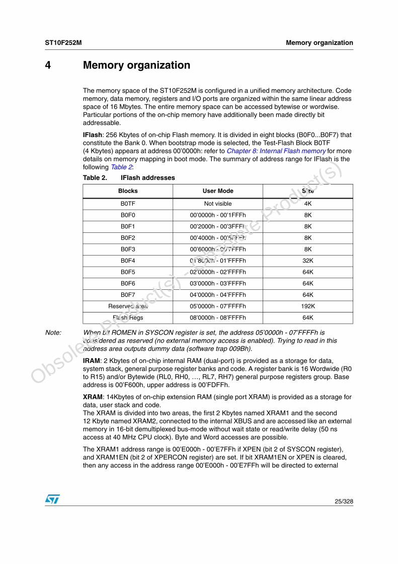
ST10F252M Memory organization
25/328
4 Memory organization
The memory space of the ST10F252M is configured in a unified memory architecture. Code memory, data memory, registers and I/O ports are organized within the same linear address space of 16 Mbytes. The entire memory space can be accessed bytewise or wordwise. Particular portions of the on-chip memory have additionally been made directly bit addressable.
IFlash: 256 Kbytes of on-chip Flash memory. It is divided in eight blocks (B0F0...B0F7) that constitute the Bank 0. When bootstrap mode is selected, the Test-Flash Block B0TF (4 Kbytes) appears at address 00’0000h: refer to Chapter 8: Internal Flash memory for more details on memory mapping in boot mode. The summary of address range for IFlash is the following Table 2:
Note: When bit ROMEN in SYSCON register is set, the address 05’0000h - 07’FFFFh is considered as reserved (no external memory access is enabled). Trying to read in this address area outputs dummy data (software trap 009Bh).
IRAM: 2 Kbytes of on-chip internal RAM (dual-port) is provided as a storage for data, system stack, general purpose register banks and code. A register bank is 16 Wordwide (R0 to R15) and/or Bytewide (RL0, RH0, …, RL7, RH7) general purpose registers group. Base address is 00’F600h, upper address is 00’FDFFh.
XRAM: 14Kbytes of on-chip extension RAM (single port XRAM) is provided as a storage for data, user stack and code. The XRAM is divided into two areas, the first 2 Kbytes named XRAM1 and the second 12 Kbyte named XRAM2, connected to the internal XBUS and are accessed like an external memory in 16-bit demultiplexed bus-mode without wait state or read/write delay (50 ns access at 40 MHz CPU clock). Byte and Word accesses are possible.
The XRAM1 address range is 00’E000h - 00’E7FFh if XPEN (bit 2 of SYSCON register), and XRAM1EN (bit 2 of XPERCON register) are set. If bit XRAM1EN or XPEN is cleared, then any access in the address range 00’E000h - 00’E7FFh will be directed to external
Table 2. IFlash addresses
Blocks User Mode Size
B0TF Not visible 4K
B0F0 00’0000h - 00’1FFFh 8K
B0F1 00’2000h - 00’3FFFh 8K
B0F2 00’4000h - 00’5FFFh 8K
B0F3 00’6000h - 00’7FFFh 8K
B0F4 01’8000h - 01’FFFFh 32K
B0F5 02’0000h - 02’FFFFh 64K
B0F6 03’0000h - 03’FFFFh 64K
B0F7 04’0000h - 04’FFFFh 64K
Reserved area 05’0000h - 07’FFFFh 192K
Flash Regs 08’0000h - 08’FFFFh 64K
O
bsolete Product(
s) - O
bsolete Product(
s)

Memory organization ST10F252M
26/328
memory interface, using the BUSCONx register corresponding to address matching ADDRSELx register.
The XRAM2 address range is the one selected programming XADDR3 register, if XPEN (bit 2 in SYSCON register), and XRAM2EN (bit 3 of XPERCON register) are set. If bit XPEN is cleared, then any access in the address range programmed for XRAM2 will be directed to external memory interface, using the BUSCONx register corresponding to address matching ADDRSELx register.After reset, the XRAM2 address range is 09’0000h-09’3FFFh and is mirrored every 16 Kbyte boundary until 0F’FFFFh.
XRAM2 also represents the Stand-by RAM, which can be maintained biased through EA/VSTBY pin when the main supply VDD is turned off.As the XRAM appears like external memory, it cannot be used as system stack or as register banks. The XRAM is not provided for single bit storage and therefore is not bit addressable.
SFR/ESFR: 1024 bytes (2 x 512 bytes) of address space is reserved for the special function register areas. SFRs are Wordwide registers which are used to control and to monitor the function of the different on-chip units.
CAN1: Address range 00’EF00h - 00’EFFFh is reserved for the CAN1 module access. The CAN1 is enabled by setting XPEN bit 2 of the SYSCON register and by setting CAN1EN bit 0 of the XPERCON register. Accesses to the CAN1 module use demultiplexed addresses and a 16-bit data bus (only word accesses are possible). Two wait states give an access time of 100 ns at 40 MHz CPU clock. No tristate waitstate is used.
CAN2: Address range 00’EE00h - 00’EEFFh is reserved for the CAN2 module access. The CAN2 is enabled by setting XPEN bit 2 of the SYSCON register and by setting CAN2EN bit 1 of the XPERCON register. Accesses to the CAN2 module use demultiplexed addresses and a 16-bit data bus (only word accesses are possible). Two wait states give an access time of 100.0 ns at 40 MHz CPU clock. No tristate waitstate is used.
Note: If one or the two CAN modules are used, Port 4 cannot be programmed to output all eight segment address lines. Thus, only four segment address lines can be used, reducing the external memory space to 5 Mbytes (1 Mbyte per CS line).
XRTC: Address range 00’ED00h - 00’EDFFh is reserved for the XRTC module access. The XRTC is enabled by setting XPEN bit 2 of the SYSCON register and bit 4 of the XPERCON register. Accesses to the XRTC module use demultiplexed addresses and a 16-bit data bus (only word accesses are possible). Two wait states give an access time of 100.0 ns at 40 MHz CPU clock. No tristate waitstate is used.
XPWM: Address range 00’EC00h - 00’ECFFh is reserved for the XPWM module access. The XPWM is enabled by setting XPEN bit 2 of the SYSCON register and bit 6 of the XPERCON register. Accesses to the XPWM module use demultiplexed addresses and a 16-bit data bus (only word accesses are possible). Two waitstates give an access time of 100.0 ns at 40 MHz CPU clock. No tristate waitstate is used. Only word access is allowed.
XASC: Address range 00’E900h - 00’E9FFh is reserved for the XASC module access. The XASC is enabled by setting XPEN bit 2 of the SYSCON register and bit 7 of the XPERCON register. Accesses to the XASC module use demultiplexed addresses and a 16-bit data bus (only word accesses are possible). Two waitstates give an access time of 100.0 ns at 40 MHz CPU clock. No tristate waitstate is used.
O
bsolete Product(
s) - O
bsolete Product(
s)

ST10F252M Memory organization
27/328
XSSC: Address range 00’E800h - 00’E8FFh is reserved for the XSSC module access. The XSSC is enabled by setting XPEN bit 2 of the SYSCON register and bit 8 of the XPERCON register. Accesses to the XSSC module use demultiplexed addresses and a 16-bit data bus (only word accesses are possible). Two waitstates give an access time of 100.0 ns at 40 MHz CPU clock. No tristate waitstate is used.
XI2C: Address range 00’EA00h - 00’EAFFh is reserved for the XI2C module access. The XI2C is enabled by setting XPEN bit 2 of the SYSCON register and bit 9 of the XPERCON register. Accesses to the XI2C module use demultiplexed addresses and a 16-bit data bus (only word accesses are possible). Two waitstates give an access time of 100.0 ns at 40 MHz CPU clock. No tristate waitstate is used.
X-Miscellaneous: Address range 00’EB00h - 00’EBFFh is reserved for the access to a set of XBUS additional features. They are enabled by setting XPEN bit 2 of the SYSCON register and bit10 of the XPERCON register. Accesses to these additional features use demultiplexed addresses and a 16-bit data bus (only word accesses are possible). Two waitstates give an access time of 100.0 ns at 40 MHz CPU clock. No tristate waitstate is used. The following set of features are provided:
● CLKOUT programmable divider
● XBUS interrupt management registers
● CAN2 multiplexing on P4.5/P4.6
● CAN1-2 main clock prescaler
● main voltage regulator disable for power-down mode
● TTL / CMOS threshold selection for Port0, Port1, and Port5
● Flash temporary unprotection
● Port4/Port7 selection for pins 47-50
In order to keep the needs of designs where more memory is required than is provided on the chip, up to 16 Mbytes of external memory can be connected to the microcontroller.
Note: When P7EN bit is set in XMISC register, the Port7 low nibble is available on the pins 47 to 50 and Port4 low is not available. Therefore the relative address lines are not available and the external memory space is reduced to 64 Kbytes."
Visibility of XBUS peripherals
In order to keep the ST10F252M compatible with ST10F168 / ST10F269, the XBUS peripherals can be selected to be visible on the external address / data bus. Different bits for X-peripheral enabling in XPERCON register must be set. If these bits are cleared before the global enabling with XPEN bit in SYSCON register, the corresponding address space, port pins and interrupts are not occupied by the peripherals, thus the peripheral is not visible and not available. Refer to Chapter 26: Register set on page 254
XPERCON and XPEREMU clock gating
As already mentioned, the XPERCON register has to be programmed to enable the single X-BUS modules separately. The XPERCON is a read/write ESFR register.The new feature of clock gating has been implemented by mean of this register. Once the EINIT instruction has been executed, all the peripherals (except RAMs and XMISC), not enabled in the XPERCON register are not be clocked. The clock gating can reduce power consumption and improve EMI when the user doesn’t use all the X-Peripherals
Note: When the clock has been gated in the disabled Peripherals, no Reset will be raised once the EINIT instruction has been executed.
O
bsolete Product(
s) - O
bsolete Product(
s)

Memory organization ST10F252M
28/328
4.1 XPERCON and XPEREMU registersOnce the XPEN bit of the SYSCON register is set and at least one of the X-peripherals (except memories) is activated, the register XPEREMU must be written with the same content of XPERCON: this is mandatory to allow correct emulation of the features on the X-BUS for the new ST10 generation.
XPEREMU must be programmed after XPERCON and after SYSCON so that the final configuration for X-peripherals is stored in XPEREMU and used for the emulation hardware setup.
XPERCON
15 14 13 12 11 10 9 8 7 6 5 4 3 2 1 0
reserved
XM
ISC
XI2
CE
N
XS
SC
EN
XA
SC
EN
XP
WM
rese
rved
XR
TC
EN
XR
AM
2EN
XR
AM
1EN
CA
N2E
N
CA
N1E
N
- - - - - RW RW RW RW RW - RW RW RW RW RW
Table 3. XPERCON register functions
Bit Name Function
15:11 Reserved
10 XMISCEN
XBUS additional features enable bit‘0’: Access to the additional miscellaneous features is disabled. The address range 00’EB00h-00’EBFFh is directed to external memory only if CAN1EN, CAN2EN, XRTCEN, XASCEN, XSSCEN, XPWMEN and XI2CEN are ‘0’ also.
‘1’: The Additional Features are enabled and can be accessed.
9 XI2CEN
XI2C enable bit
‘0’: Accesses to the on-chip XI2C are disabled, external access is performed. The address range 00’EA00h-00’EAFFh is directed to external memory only if CAN1EN, CAN2EN, XRTCEN, XASCEN, XSSCEN, XPWMEN and XMISCEN are ‘0’ also.‘1’: The on-chip XI2C is enabled and can be accessed.
8 XSSCEN
XSSC enable bit‘0’: Accesses to the on-chip XSSC are disabled, external access is performed. The address range 00’E800h-00’E8FFh is directed to external memory only if CAN1EN, CAN2EN, XRTCEN, XASCEN, XI2CEN, XPWMEN and XMISCEN are ‘0’ also.
‘1’: The on-chip XSSC is enabled and can be accessed.
7 XASCEN
XASC enable bit
‘0’: Accesses to the on-chip XASC are disabled, external access is performed. The address range 00’E900h-00’E9FFh is directed to external memory only if CAN1EN, CAN2EN, XRTCEN, XASCEN, XI2CEN, XPWMEN and XMISCEN are ‘0’ also.
‘1’: The on-chip XASC is enabled and can be accessed.
O
bsolete Product(
s) - O
bsolete Product(
s)

ST10F252M Memory organization
29/328
Note: When CAN1, CAN2, XRTC, XASC, XSSC, XI2C, XPWM and the XBUS additional features are all disabled via XPERCON setting, any access in the address range 00’E800h - 00’EFFFh is directed to external memory interface, using the BUSCONx register corresponding to address matching ADDRSELx register. All pins involved with
6 XPWMEN
XPWM enable‘0’: Accesses to the on-chip XPWM module are disabled, external access is performed. The address range 00’EC00h-00’ECFF is directed to external memory only if CAN1EN, CAN2EN, XASCEN, XSSCEN, XI2CEN, XRTCEN and XMISCEN are ‘0’ also.
‘1’: The on-chip XPWM module is enabled and can be accessed.
5 Reserved
4 XRTCEN
XRTC enable‘0’: Accesses to the on-chip XRTC module are disabled, external access is performed. The address range 00’ED00h-00’EDFF is directed to external memory only if CAN1EN, CAN2EN, XASCEN, XSSCEN, XI2CEN, XPWMEN and XMISCEN are ‘0’ also.
‘1’: The on-chip XRTC module is enabled and can be accessed.
3 XRAM2EN
XRAM2 enable bit
‘0’: Accesses to the on-chip 16 Kbyte XRAM are disabled, external access is performed. ‘1’: The on-chip 16 Kbyte XRAM is enabled and can be accessed.
2 XRAM1EN
XRAM1 enable bit‘0’: Accesses to the on-chip 2 Kbyte XRAM are disabled. The address range 00’E000h-00’E7FFh is directed to external memory.‘1’: The on-chip 2 Kbyte XRAM is enabled and can be accessed.
1 CAN2EN
CAN2 enable bit‘0’: Accesses to the on-chip CAN2 X=peripheral and its functions are disabled (P4.4 and P4.7 pins can be used as general purpose I/Os, but the address range 00’EC00h-00’EFFFh is directed to external memory only if CAN1EN, XRTCEN, XASCEN, XSSCEN, XI2CEN, XPWMEN and XMISCEN are ‘0’ also).‘1’: The on-chip CAN2 X-peripheral is enabled and can be accessed.
0 CAN1EN
CAN1 enable bit‘0’: Accesses to the on-chip CAN1 X-peripheral and its functions are disabled (P4.5 and P4.6 pins can be used as general purpose I/Os, but the address range 00’EC00h-00’EFFFh is directed to external memory only if CAN2EN, XRTCEN, XASCEN, XSSCEN, XI2CEN, XPWMEN an XMISCEN are ‘0’ also).‘1’: The on-chip CAN1 X-peripheral is enabled and can be accessed.
Table 3. XPERCON register functions (continued)
Bit Name Function
O
bsolete Product(
s) - O
bsolete Product(
s)

Memory organization ST10F252M
30/328
X-peripherals, can be used as general purpose I/O whenever the related module is not enabled.
When one or more of the peripherals XASC, XI2C, XSSC, and XPWM are enabled, port P1 cannot be used for external memory addressing, that is, the external bus controller in demultiplexed mode is not available.
The default XPER selection after reset is identical to XBUS configuration of ST10F168/ST10F269: CAN1 is enabled, CAN2 is disabled, XRAM1 (2 Kbyte XRAM) is enabled, XRAM2 (16 Kbyte XRAM) is disabled; all the other X-peripherals are disabled after reset.
The register XPERCON cannot be changed after the global enabling of X-peripherals, that is, after setting of bit XPEN in SYSCON register.
In Emulation mode, all the X-peripherals are enabled (XPERCON bits are all set). It is up to the bondout chip (ST10R201) whether of not to redirect an access to external memory or to XBUS.
Reserved bits of XPERCON register are always written to ‘0’.
XPEREMU
The bit meaning is exactly the same as XPERCON.
4.2 Emulation dedicated registersA set of four additional registers are for emulation purpose only. Similarly to XPEREMU, they are write only registers.
Emulation register 1
Emulation register 2
15 14 13 12 11 10 9 8 7 6 5 4 3 2 1 0
reserved
XM
ISC
XI2
CE
N
XS
SC
EN
XA
SC
EN
XP
WM
rese
rved
XR
TC
EN
XR
AM
2 E
N
XR
AM
1 E
N
CA
N2E
N
CA
N1E
N
RW RW RW RW RW RW RW RW RW RW
15 14 13 12 11 10 9 8 7 6 5 4 3 2 1 0
W W W W W W W W W W W W W W W W
15 14 13 12 11 10 9 8 7 6 5 4 3 2 1 0
W W W W W W W W W W W W W W W W
O
bsolete Product(
s) - O
bsolete Product(
s)

ST10F252M Memory organization
31/328
Emulation register 3
Emulation register 4 RegTitle
4.3 XRAM2 memory rangeXRAM2 memory range is addressed by an internal XBUS chip select. This internal chip select is enabled when XPEN bit of the SYSCON register is set and XRAM2EN bit of the XPERCOM register is set. Although this address range is accessed as external memory, it does not occupy the BUSCONx or ADDRSELx registers but is selected via additional dedicated XBCON/XADRS registers. The XADRS reset value is mask-programmed but the XADRS3 register used for flash control registers and XRAM2 memory range can be accessed and modified.
XRAM2 memory range
The register functionality is the same as the one of ADDRSELx registers use for external address range selection. However, the XADRS3 register is protected and it can only be written before the EINIT instruction execution. The range start address can be only on boundaries specified by the selected range size. Table 5 gives a definition of Range Size Selection and Range Start Address.
Upon Reset, the XADRS3 register is programmed so that address range 08’0000h-0F’FFFFh is accessed with the internal XBUS chip select. The range 08’0000h-08’FFFFh is
15 14 13 12 11 10 9 8 7 6 5 4 3 2 1 0
W W W W W W W W W W W W W W W W
15 14 13 12 11 10 9 8 7 6 5 4 3 2 1 0
W W W W W W W W W W W W W W W W
15 14 13 12 11 10 9 8 7 6 5 4 3 2 1 0
RGSAD RGSZ
RW RW RW RW RW RW RW RW RW RW RW RW RW RW RW RW
Table 4. XRAM2 memory range functions
Bit Name Function
15:4 RGSAD
Range Start AddressDefines the upper bits (A8...A19) of the start address of the respective address area. Bits A23...A20 of the resulting address are set to 0. See Table 5.
3:0 RGSZRange Size Selection
Defines the size of the address area controlled by XBCON3 and XADRS3 register pair. See Table 5.
Obso
lete Product(s)
- Obso
lete Product(s)

Memory organization ST10F252M
32/328
overlapped by IFlash memory space (flash control register), which has higher priority on XBUS space.
The address range defined by XADRS3 can be reduced by reprogramming it before EINIT execution; the area which is no longer inside the new address range becomes external memory space (apart from range 08’0000h-08’FFFFh, which is dedicated to IFlash as long as ROMEN bit in SYSCON register is set).
The address range defined by XADRS3 has priority over any external address range defined through ADDRSELx (x=1...4) registers.
XRAM2 can be remapped on any 16 Kbyte Boundary within 00’8000h-00’BFFF address area and within 09’0000h-0F’FFFFF address area.
For example, to map the 16Kbyte XRAM2 in page 60 (starting address 0F’0000h, compatible with ST10F276), XADRS3 must be initialized with the value F006H. To map the 16Kbyte XRAM2 in page 2 (starting address 00’8000h, compatible with ST10F280), XADRS3 must be initialized with the value 0806H.
Note: If XADRS3 is not reprogrammed after reset, the XRAM2 address window overlaps the one dedicated to IFlash. So Segment 8 address range mapping depends on bits ROMEN and XPEN of SYSCON register, and XRAM2EN of XPERCON register programming as summarized in Table 6.
Table 5. Definition of address areas
Bit-field RGSZ Resulting Window Size Relevant bit (R) of Start Address (A19...A8)
0 0 0 00 0 0 10 0 1 00 0 1 1 0 1 0 00 1 0 10 1 1 00 1 1 11 0 0 01 0 0 11 0 1 01 0 1 11 1 x x
256 bytes512 bytes
1 Kbyte2 Kbytes4 Kbytes8 Kbytes
16 Kbytes32 Kbytes64 Kbytes
128 Kbytes256 Kbytes512 Kbytes
Reserved
A19 A8
R R R R R R R R R R R RR R R R R R R R R R R xR R R R R R R R R R x xR R R R R R R R R x x xR R R R R R R R x x x xR R R R R R R x x x x xR R R R R R x x x x x xR R R R R x x x x x x xR R R R x x x x x x x xR R R x x x x x x x x xR R x x x x x x x x x xR x x x x x x x x x x x
Table 6. XRAM2EN of XPERCON register programming
ROMEN XPEN XRAM2EN Segment 8
0 0 x External memory
0 1 0 External memory
0 1 1 Reserved
1 x x IFlash registers
O
bsolete Product(
s) - O
bsolete Product(
s)
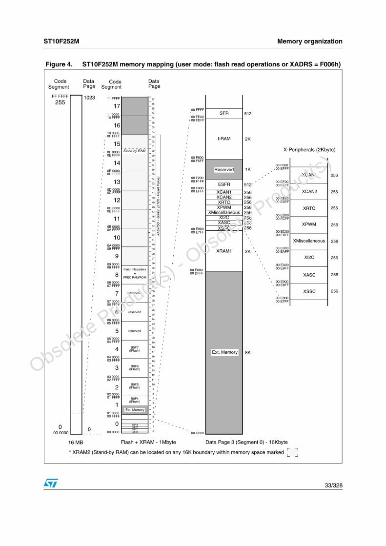
ST10F252M Memory organization
33/328
Figure 4. ST10F252M memory mapping (user mode: flash read operations or XADRS = F006h)
FF FFFF
00 0000
16 MB
255
0
Code DataPage
1023
0
DataPage
1
3
5
7
1
2
3
4
5
6
7
8
9
10
11
12
13
14
15
16
17
18
19
07 FFFF
06 000005 FFFF
04 000003 FFFF
02 000001 FFFF
00 0000
B0F4
B0F5
reserved
00 C000
00 FFFF
XCAN1
ESFR
SFR
I-RAM
Reserved
Ext. Memory
00 E7FF00 E800
00 FDFF00 FE00
00 F1FF00 F200
00 F5FF00 F600
8K
256
512
1K
2K
512
Data Page 3 (Segment 0) - 16Kbyte
256XCAN2
9
20
21
22
23
0A 000009 FFFF
08 0000
11
24
25
26
27
0C 00000B FFFF
13
28
29
30
31
0E 00000D FFFF
15
32
33
34
35
0F FFFF
00 F000
XCAN1
XCAN2
00 EFFF00 F000
00 EEFF00 EF00
00 EDFF00 EE00
00 EAFF00 EB00
256
256
256
256XSSC
00 E7FF00 E800
XRAM1 2K
14
0F 00000E FFFF
12
0D 00000C FFFF
10
0B 00000A FFFF
8
6
4
05 000004 FFFF
07 000006 FFFF
09 000008 FFFF
2
03 000002 FFFF
00B0F0
B0F1B0F2
36
37
38
39
40
41
42
43
44
45
46
47
48
49
50
51
52
53
54
55
56
57
58
59
60
61
62
63
B0F6
reserved
reserved
B0F7
01 000000 FFFF
CodeSegment
64
65
66
67
64
65
66
67
16
17
10 0000
10 FFFF11 0000
11 FFFF
Flash + XRAM - 1Mbyte
XRTC
00 EFFF
XSSCXASCXI2C
256256
256
XRTC
XASC
XI2C
256
256
00 E8FF00 E900
00 E9FF00 EA00
256
00 ECFF00 ED00
256
(IFlash)
(IFlash)
(IFlash)
(IFlash)
XPWM 256
XPWM
256
256
00 EBFF00 EC00
XMiscellaneous
XMiscellaneous
X-Peripherals (2Kbyte)
Segment
B0F3
Ext. Memory
XA
DR
S3
= 8
00B
h (5
12K
- R
eset
Val
ue)
00 DFFF00 E000Flash Registers
+FPEC RAM/ROM
Stand-by RAM
* XRAM2 (Stand-by RAM) can be located on any 16K boundary within memory space marked
O
bsolete Product(
s) - O
bsolete Product(
s)
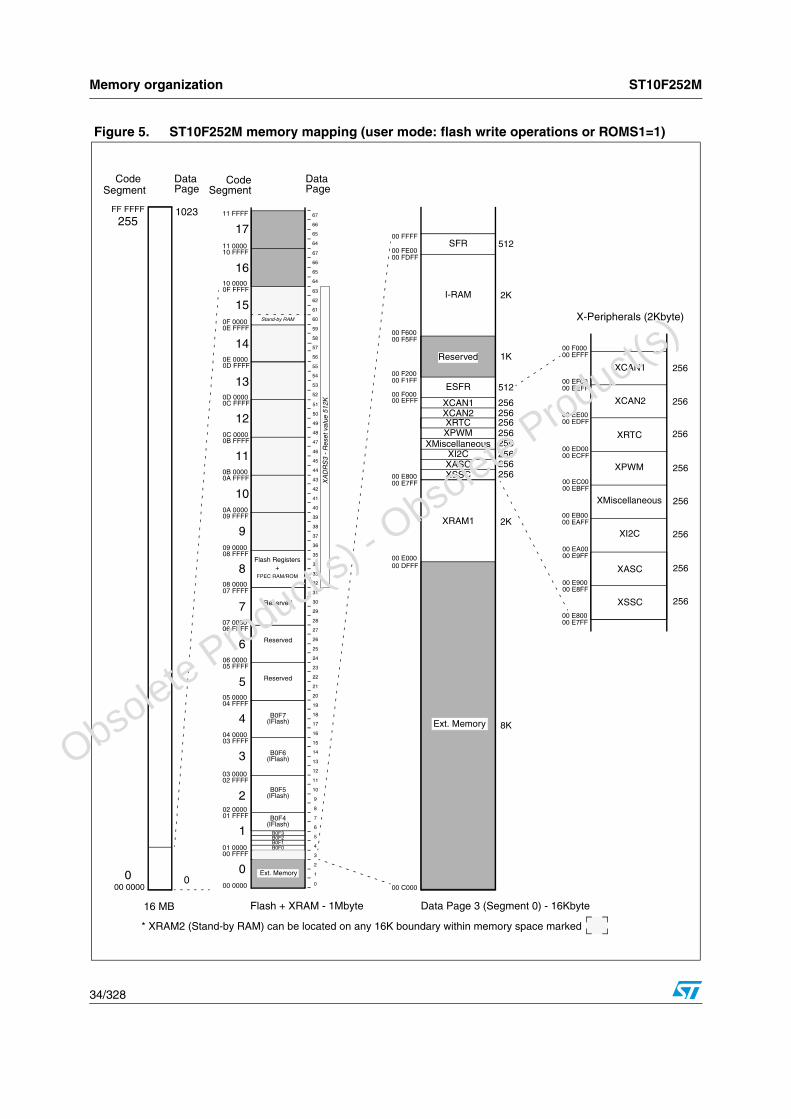
Memory organization ST10F252M
34/328
Figure 5. ST10F252M memory mapping (user mode: flash write operations or ROMS1=1)
FF FFFF
00 0000
16 MB
255
0
Code DataPage
1023
0
DataPage
1
3
5
7
1
2
3
4
5
6
7
8
9
10
11
12
13
14
15
16
17
18
19
07 FFFF
06 000005 FFFF
04 000003 FFFF
02 000001 FFFF
00 0000
B0F4
B0F5
Reserved
00 C000
00 FFFF
XCAN1
ESFR
SFR
I-RAM
Reserved
00 DFFF00 E000
00 E7FF00 E800
00 FDFF00 FE00
00 F1FF00 F200
00 F5FF00 F600
8K
256
512
1K
2K
512
Data Page 3 (Segment 0) - 16Kbyte
256XCAN2
9
20
21
22
23
0A 000009 FFFF
08 0000
11
24
25
26
27
0C 00000B FFFF
13
28
29
30
31
0E 00000D FFFF
15
32
33
34
35
0F FFFF
00 F000
XCAN1
XCAN2
00 EFFF00 F000
00 EEFF00 EF00
00 EDFF00 EE00
00 EAFF00 EB00
256
256
256
256XSSC
00 E7FF00 E800
XRAM1 2K
14
0F 00000E FFFF
12
0D 00000C FFFF
10
0B 00000A FFFF
8
6
4
05 000004 FFFF
07 000006 FFFF
09 000008 FFFF
2
03 000002 FFFF
00
B0F0B0F1B0F2
36
37
38
39
40
41
42
43
44
45
46
47
48
49
50
51
52
53
54
55
56
57
58
59
60
61
62
63
B0F6
Reserved
Reserved
B0F7
01 000000 FFFF
CodeSegment
64
65
66
67
64
65
66
67
16
17
10 0000
10 FFFF11 0000
11 FFFF
Flash + XRAM - 1Mbyte
XRTC
00 EFFF
XSSCXASCXI2C
256256
256
XRTC
XASC
XI2C
256
256
00 E8FF00 E900
00 E9FF00 EA00
256
00 ECFF00 ED00
256
(IFlash)
(IFlash)
(IFlash)
(IFlash)
XPWM 256
XPWM
256
256
00 EBFF00 EC00
XMiscellaneous
XMiscellaneous
X-Peripherals (2Kbyte)
Segment
B0F3
XA
DR
S3
- R
eset
val
ue 5
12K
Ext. Memory
Ext. Memory
Flash Registers+
FPEC RAM/ROM
Stand-by RAM
* XRAM2 (Stand-by RAM) can be located on any 16K boundary within memory space marked
O
bsolete Product(
s) - O
bsolete Product(
s)

ST10F252M Central processing unit
35/328
5 Central processing unit
The central processing unit (CPU) includes a four-stage instruction pipeline, a 16-bit arithmetic and logic unit (ALU) and dedicated SFRs. Additional hardware provides for a separate multiply and divide unit, a bit-mask generator and a barrel shifter.
Most of the ST10F252M’s instructions can be executed in one instruction cycle which requires 50 ns at 40 MHz CPU clock. For example, shift and rotate instructions are processed in one instruction cycle independent of the number of bits to be shifted. Multiple-cycle instructions have been optimized; branches are carried out in two cycles, 16 x 16 bit multiplication in five cycles and a 32/16 bit division in ten cycles. The jump cache reduces the execution time of repeatedly performed jumps in a loop, from two cycles to one cycle.
Figure 6. CPU block diagram (MAC unit not included)
The CPU uses an actual register context consisting of up to 16 wordwide GPRs physically allocated within the on-chip RAM area. A context pointer (CP) register determines the base address of the active register bank to be accessed by the CPU. The number of register banks is only restricted by the available internal RAM space. For easy parameter passing, a register bank may overlap others.
A system stack of up to 1024 bytes is provided as a storage for temporary data. The system stack is allocated in the on-chip RAM area, and it is accessed by the CPU via the stack pointer (SP) register. Two separate SFRs, STKOV and STKUN, are implicitly compared against the stack pointer value upon each stack access for the detection of a stack overflow or underflow.
32
InternalRAM
2K Byte
General PurposeRegisters
R0
R15MDHMDL
Barrel-Shift
Mul./Div.-HWBit-Mask Gen.
ALU
16-Bit
CP
SPSTKOVSTKUN
Exec. UnitInstr. Ptr
4-StagePipeline
PSWSYSCON
BUSCON 0BUSCON 1BUSCON 2BUSCON 3BUSCON 4
ADDRSEL 1ADDRSEL 2ADDRSEL 3ADDRSEL 4
Data Pg. Ptrs Code Seg. Ptr.
CPU
256 Kbyte
Flash
memory
16
16
Bankn
Banki
Bank0
O
bsolete Product(
s) - O
bsolete Product(
s)
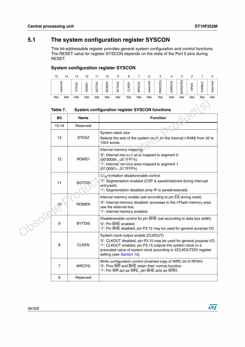
Central processing unit ST10F252M
36/328
5.1 The system configuration register SYSCON This bit-addressable register provides general system configuration and control functions. The RESET value for register SYSCON depends on the state of the Port 0 pins during RESET.
System configuration register SYSCON
15 14 13 12 11 10 9 8 7 6 5 4 3 2 1 0
rese
rved
ST
KS
Z
RO
MS
1
SG
TD
IS
RO
ME
N
BY
TD
IS
CLK
EN
WR
CF
G
rese
sved
PW
DC
FG
OW
DD
IS
BD
RS
TE
N
XP
EN
VIS
IBLE
rese
rved
RW RW RW RW RW RW RW RW RW RW RW RW RW RW RW RW
Table 7. System configuration register SYSCON functions
Bit Name Function
15:14 Reserved
13 STKSZSystem stack size
Selects the size of the system stack (in the internal I-RAM) from 32 to 1024 words.
12 ROMS1
Internal memory mapping‘0’: Internal memory area mapped to segment 0 (00’0000h...00’7FFFh).‘1’: Internal memory area mapped to segment 1 (01’0000h...01’7FFFh).
11 SGTDIS
Segmentation disable/enable control‘0’: Segmentation enabled (CSP is saved/restored during interrupt entry/exit).‘1’: Segmentation disabled (only IP is saved/restored).
10 ROMEN
Internal memory enable (set according to pin EA during reset)
‘0’: Internal memory disabled: accesses to the I-Flash memory area use the external bus.‘1’: Internal memory enabled.
9 BYTDISDisable/enable control for pin BHE (set according to data bus width)
‘0’: Pin BHE enabled.‘1’: Pin BHE disabled, pin P3.12 may be used for general purpose I/O.
8 CLKEN
System clock output enable (CLKOUT)
‘0’: CLKOUT disabled, pin P3.15 may be used for general purpose I/O.‘1’: CLKOUT enabled, pin P3.15 outputs the system clock or a prescaled value of system clock according to XCLKOUTDIV register setting (see Section 15).
7 WRCFGWrite configuration control (inverted copy of WRC bit of RP0H)‘0’: Pins WR and BHE retain their normal function.‘1’: Pin WR act as WRL, pin BHE acts as WRH.
6 Reserved
O
bsolete Product(
s) - O
bsolete Product(
s)

ST10F252M Central processing unit
37/328
5 PWDCFG
Power down mode configuration control‘0’: Power down mode can only be entered during PWRDN instruction execution if NMI pin is low, otherwise the instruction has no effect. To exit power down mode, an external reset must occurs by asserting the RSTIN pin.‘1’: Power down mode can only be entered during PWRDN instruction execution if all enabled fast external interrupt EXxIN pins are in their inactive level. Exiting this mode can be done by asserting one enabled EXxIN pin or with external reset.
4 OWDDIS
Oscillator watchdog disable control
‘0’: Oscillator watchdog (OWD) is enabled. If PLL is bypassed, the OWD monitors XTAL1 activity. If there is no activity on XTAL1 for at least 1 µs, the CPU clock is switched automatically to PLL’s base frequency (around 750 kHz-3 MHz).‘1’: OWD is disabled. If the PLL is bypassed, the CPU clock is always driven by XTAL1 signal. The PLL is turned off to reduce power supply current.
3 XPEN
XBUS peripheral enable bit‘0’: Accesses to the on-chip X-peripherals and their functions are disabled.‘1’: The on-chip X-peripherals are enabled and can be accessed.
3 BDRSTEN
Bidirectional reset enable ‘0’: RSTIN pin is an input pin only. SW Reset or WDT Reset have no effect on this pin.‘1’: RSTIN pin is a bidirectional pin. This pin is pulled low during 1024 TCL during reset sequence.
1 VISIBLE
Visible mode control‘0’: Accesses to XBUS peripherals are internal.‘1’: XBUS peripherals accesses are visible externally on the external pins.
Table 7. System configuration register SYSCON functions (continued)
Bit Name Function
O
bsolete Product(
s) - O
bsolete Product(
s)

Multiplier-accumulator unit ST10F252M
38/328
6 Multiplier-accumulator unit
The multiplier-accumulator (MAC) unit is a specialized co-processor that improves the performance of signal processing algorithms. It includes:
● a multiply-accumulate unit.
● an address generation unit, able to feed the MAC unit with two operands per cycle.
● a repeat unit, to execute a series of multiply-accumulate instructions.
The CPU can supply the MAC with up to two operands per instruction cycle. The MAC instructions multiply, multiply-accumulate, 32-bit signed arithmetic operations and the CoMOV transfer instruction are part of the standard instruction set. Full details are provided in the ‘ST10 Family Programming Manual’.
6.1 MAC features
6.1.1 Enhanced addressing capabilities
The MAC has the following enhanced addressing capabilities:
● double indirect addressing mode with pointer post-modification
● parallel data move allows one operand move during multiply-accumulate instructions without penalty
● coSTORE instruction (for fast access to the MAC SFRs) and CoMOV (for fast memory to memory table transfer).
6.1.2 General
The MAC also has the following features:
● two-cycle execution for all MAC operations
● 16 x 16 signed/unsigned parallel multiplier
● 40-bit signed arithmetic unit with automatic saturation mode
● 40-bit accumulator
● 8-bit left/right shifter
● scaler (one-bit left shifter)
● data limiter
● full instruction set with multiply and multiply-accumulate, 32-bit signed arithmetic and compare instructions
● three 16-bit status and control registers: MSW (MAC status word), MCW (MAC control word), and MRW (MAC repeat word).
The working register of the MAC unit is a dedicated 40-bit wide accumulator register. A set of consistent flags is automatically updated in the MSW register (see Section 6.3.2) after each MAC operation. These flags allow branching on specific conditions. Unlike the PSW flags, these flags are not preserved automatically by the CPU upon entry into an interrupt or trap routine. All dedicated MAC registers must be saved on the stack if the MAC unit is shared between different tasks and interrupts.
O
bsolete Product(
s) - O
bsolete Product(
s)

ST10F252M Multiplier-accumulator unit
39/328
6.1.3 Program control
MAC program control features include:
● a repeat unit that allows some MAC co-processor instructions to be repeated up to 8192 times – repeated instructions may be interrupted
● MAC interrupt (class B trap) on MAC condition flags.
6.2 MAC operation *
1. Shared with standard ALU.
6.2.1 Instruction pipelining
All MAC instructions use the four-stage pipeline. During each stage the following tasks are performed.
1. FETCH: All new instructions are double-word instructions.
2. DECODE: If required, operand addresses are calculated and the resulting operands are fetched. IDX and GPR pointers are post-modified if necessary.
3. EXECUTE: Performs the MAC operation. At the end of the cycle, the accumulator and the MAC condition flags are updated if required. Modified GPR pointers are written-back during this stage, if required.
4. WRITEBACK: Operand write-back in the case of parallel data move.
Figure 7. MAC unit architecture
Operand 2Operand 1
Control Unit
Repeat Unit
ST10 CPU
InterruptController
MSW
MRW
MAH MAL
MCW
Flags MAE
Mux
8-bit Left/RightShifter
Mux
Mux
Sign Extend
16 x 16
Concatenation
signed/unsignedMultiplier
40-bit Signed Arithmetic Unit
0h 0h08000h
40
16
40 40
32 32
16
40
40
40
40
40
Scaler
A B
40
GPR Pointers (1)
IDX0 PointerIDX1 Pointer
QR0 GPR Offset RegisterQR1 GPR Offset Register
QX0 IDX Offset RegisterQX1 IDX Offset Register
DataLimiter
O
bsolete Product(
s) - O
bsolete Product(
s)

Multiplier-accumulator unit ST10F252M
40/328
6.2.2 Particular pipeline effects with the MAC unit
Because the registers used by the MAC are shared with the standard ALU and because of the MAC instructions pipelining, some care must be taken when switching from the “standard instruction set” to the “MAC instruction set”.
Initialization of the pointers and offset registers
The MAC instructions which use IDXi pointer are mostly not capable of using a IDXi register value, which is updated by an immediately preceding instruction. Thus, to make sure that the IDXi register value is used, at least one instruction must be inserted between a IDXi-changing instruction and one MAC instruction which explicitly uses IDXi in its addressing mode as shown in the following example,
The requirements between the update of one of the offset registers, QXi and QRi, and their next use are the same.
Read access to MAC registers (CoReg)
At least one instruction which does not use the MAC must be inserted between two instructions that read from a MAC register. This is because the accumulator and the status of the MAC are modified during the execute stage.
In this example, the BFLDL instruction performs a read access to the MSW during the decode stage while the MSW.Z flag is only set at the end of the execute stage of the CoADD.
6.2.3 Address generation
MAC instructions can use some standard ST10 addressing modes such as GPR direct or #data4 for immediate shift value.
In: MOV IDX0, #0F200h update IDX0 register
In+1: … must not be an CoXXX [IDX0⊗], [Rwm⊗] instruction
In+2:CoXXX [IDX0+QX1], [R2]first operand read at (IDX0) address to provide the MAC function
parallel data move to (((IDX0))-((QX1))) address (if CoXXX is CoMACM)
move (R2) content to (IDX0) address (if CoXXX is CoMOV)
(IDX0) <-- (IDX0) + (QX1) post modification of the pointer
Table 8. Example of MAC register read access
Code MSW (before) MSW (after) Comment
MOV MSW, #0 - 0000h
MOV R0, #0 - -
CoADD R0, R0 0000h 0200h MSW.Z set at execute
BFLDL MSW, #FFh, #FFh 0200h 00FFh Error! O
bsolete Product(
s) - O
bsolete Product(
s)

ST10F252M Multiplier-accumulator unit
41/328
Addressing modes have been added to supply the MAC with two new operands per instruction cycle. These allow indirect addressing with address pointer post-modification.
Double indirect addressing requires two pointers. Any GPR can be used for one pointer, the other pointer is provided by one of two specific SFRs IDX0 and IDX1. Two pairs of offset registers QR0/QR1 and QX0/QX1 are associated with each pointer (GPR or IDXi). The GPR pointer allows access to the entire memory space, but IDXi are limited to the internal dual-port RAM, except for the CoMOV instruction.
Table 9 shows the various combinations of pointer post-modification for each of these 2 new addressing modes. In this document, the symbols “[Rwn⊗]” and “[IDXi⊗]” refer to these addressing modes.
For the CoMACM class of instruction, a parallel data move mechanism is implemented. This class of instruction is only available with double indirect addressing mode. Parallel data move allows the operand, pointed to by IDXi, to be moved to a new location in parallel with the MAC operation. The write-back address of parallel data move is calculated depending on the post-modification of IDXi. It is obtained by the reverse operation than the one used to calculate the new value of IDXi. Table 10 shows these rules.
Table 9. Pointer post-modification combinations for IDXi and Rwn
Symbol Mnemonic Address pointer operation
“[IDXi⊗]” stands for
[IDXi] (IDXi) ← (IDXi) (no-op)
[IDXi+] (IDXi) ← (IDXi) +2 (i=0,1)
[IDXi -] (IDXi) ← (IDXi) -2 (i=0,1)
[IDXi + QXj] (IDXi) ← (IDXi) + (QXj) (i, j =0,1)
[IDXi - QXj] (IDXi) ← (IDXi) - (QXj) (i, j =0,1)
“[Rwn⊗]” stands for
[Rwn] (Rwn) ← (Rwn) (no-op)
[Rwn+] (Rwn) ← (Rwn) +2 (n=0-15)
[Rwn-] (Rwn) ← (Rwn) -2 (k=0-15)
[Rwn+QRj] (Rwn) ← (Rwn) + (QRj) (n=0-15;j =0,1)
[Rwn - QRj] (Rwn) ← (Rwn) - (QRj) (n=0-15; j =0,1)
Table 10. Parallel data move addressing
Instruction Writeback address
CoMACM [IDXi+],... <IDXi-2>
CoMACM [IDXi-],... <IDXi+2>
CoMACM [IDXi+QXj],... <IDXi-QXj>
CoMACM [IDXi-QXj],... <IDXi+QXj>
Obso
lete Product(s)
- Obso
lete Product(s)

Multiplier-accumulator unit ST10F252M
42/328
The parallel data move shifts a table of operands in parallel with a computation on those operands. Its specific use is for signal processing algorithms like filter computation. Figure 8 gives an example of parallel data move with CoMACM instruction.
6.2.4 16 x 16 signed / unsigned parallel multiplier
The multiplier executes 16 x 16-bit parallel signed/unsigned fractional and integer multiplies. The multiplier has two 16-bit input ports, and a 32-bit product output port. The input ports can accept data from the MA-bus and from the MB-bus. The output is sign-extended and feeds a scaler that shifts the multiplier output according to the shift mode bit MP specified in the co-processor control word (MCW). The product can be shifted one bit left to compensate for the extra sign bit gained in multiplying two 16-bit signed (2’s complement) fractional numbers if bit MP is set.
6.2.5 40-bit signed arithmetic unit
The arithmetic unit is over 32 bits wide to allow intermediate overflow in a series of multiply/accumulate operations. The extension flag E, contained in the most significant byte of MSW, is set when the accumulator has overflowed beyond the 32-bit boundary, that is, when there are significant (non-sign) bits in the top eight (signed arithmetic) bits of the accumulator.
The 40-bit arithmetic unit has two 40-bit input ports A and B. The A-input port accepts data from four possible sources: 00,0000,0000h, 00,0000,8000h (round), the sign-extended product, or the sign-extended data conveyed by the 32-bit bus resulting from the concatenation of MA- and MB-buses. Product and concatenation can be shifted left by one according to MP for the multiplier or to the instruction for the concatenation. The B-input port is fed either by the 40-bit shifted/not shifted and inverted/not inverted accumulator or by 00,0000,0000h. A-input and B-input ports can receive 00,0000,0000h to allow direct transfers from the B-source and A-source, respectively, to the accumulator (in the case of multiplication or shift). The output of the arithmetic unit goes to the accumulator.
It is also possible to saturate the accumulator on a 32-bit value, automatically after every accumulation. Automatic saturation is enabled by setting the saturation bit MS in the MCW register. When the accumulator is in the saturation mode and an 32-bit overflow occurs, the accumulator is loaded with either the most positive or the most negative value representable in a 32-bit value, depending on the direction of the overflow. The value of the accumulator upon saturation is 00,7fff,ffffh (positive) or ff,8000,0000h (negative) in signed arithmetic. Automatic saturation sets the SL flag MSW. This flag is a sticky flag which means it stays set until it is explicitly reset.
40-bit overflow of the accumulator sets the SV flag in MSW. This flag is also a sticky flag.
Figure 8. Example of parallel data move
CoMACM [IDX0+], [R2+]
X
n+2
n
n-2
n-4
16-bit
IDX0 X
X
n+2
n
n-2
n-4
IDX0
Parallel Data Move
After ExecutionBefore Execution
O
bsolete Product(
s) - O
bsolete Product(
s)

ST10F252M Multiplier-accumulator unit
43/328
6.2.6 40-bit adder/subtracter
The 40-bit adder/subtracter allows intermediate overflows in a series of multiply/accumulate operations. The adder/subtracter has two input ports. One input is the feedback of the 40-bit signed accumulator output through the ACCU-shifter.The second input is the 32-bit operand coming from the one-bit scaler. The 32-bit operands are sign-extended to 40-bit before the addition/subtraction is performed.
The output of the adder/subtracter goes to the 40-bit signed accumulator. It is also possible to round and to saturate the result to 32-bit automatically after every accumulation before to be loaded into the accumulator. The round operation is performed by adding 00’00008000h to the result. Automatic saturation is enabled by setting the MCW.MS saturation bit.
When the 40-bit signed accumulator is in the overflow saturation mode and an overflow occurs, the accumulator is loaded with either the most positive or the most negative possible 32-bit value, depending on the direction of the overflow as well as the arithmetic used. The value of the accumulator upon saturation is 00’7FFF FFFFh (positive) or FF’8000’0000h (negative).
6.2.7 Data limiter
Saturation arithmetic is also provided to selectively limit overflow, when reading the accumulator by means of a CoSTORE <destination> MAS instruction. Limiting is performed on the MAC accumulator. If the contents of the accumulator can be represented in the destination operand size without overflow, the data limiter is disabled and the operand is not modified. If the contents of the accumulator cannot be represented without overflow in the destination operand size, the limiter substitutes a ‘limited’ data as explained in Table 11’
6.2.8 The accumulator shifter
The accumulator shifter is a parallel shifter with a 40-bit input and a 40-bit output. The source accumulator shifting operation are:
● no shift (unmodified)
● up to 8-bit arithmetic left shift
● up to 8-bit arithmetic right shift
MSW.ME, MSW.MSV and MSW.MSL bits (see the MSW register description) are affected by left shifts. Therefore, if the saturation detection is enabled (MCW.MS bit is set), the behavior is similar to the one of the adder/subtracter.
Table 11. Limiter output using CoSTORE instruction
ME-flag MN-flag MAS value (saturated MAH value)(1)
1. If the data limiter is activated, a read with “CoSTORE <destination>, <MAH> instruction” or “CoSTORE <destination>, <MAS> instruction” gives different results.
0 x Unchanged(2)
2. When the data limiter is disabled, a reading with “CoSTORE <destination>, <MAH> instruction” or “CoSTORE <destination>, <MAS> instruction” gives the same result.
1 0 7FFFh(3)
3. If the data limiter is activated, a read with “CoSTORE <destination>, <MAH> instruction” or “CoSTORE <destination>, <MAS> instruction” gives different results.
1 1 8000h(4)
4. If the data limiter is activated, a read with “CoSTORE <destination>, <MAH> instruction” or “CoSTORE <destination>, <MAS> instruction” gives different results.
O
bsolete Product(
s) - O
bsolete Product(
s)

Multiplier-accumulator unit ST10F252M
44/328
Some precautions are required for left shift with enabled saturation. If the MSW.MAE bit-field (the most significant byte of the 40-bit signed accumulator) contains significant bits, the 32-bit value in the accumulator is generally saturated. However, it is possible that a left shift may move some significant bits out of the accumulator. The 40-bit result will be misinterpreted and will be either not be saturated or saturated incorrectly. There is a chance that the result of a left shift may produce a result which can saturate an original positive number to the minimum negative value, or vice versa.
6.2.9 Repeat unit
The MAC includes a repeat unit that allows the repetition of some co-processor instructions up to 213 (8192) times. The repeat count may be specified either by an immediate value (up to 31 times) or by the content of the repeat count (bits 12 to 0) in the MAC repeat word (MRW). If the repeat count is “N” the instruction is executed “N+1” times. At each iteration of a cumulative instruction, the repeat count is tested for zero. If it is zero the instruction is terminated, otherwise the repeat count is decremented and the instruction is repeated. During such a repeat sequence, the repeat flag in MRW is set until the last execution of the repeated instruction.
The syntax of repeated instructions is shown in the following examples:.
In this example, the instruction is repeated according to a 5-bit immediate value. The repeat count in MRW is automatically loaded with this value minus one (MRW=23).
In this example, the instruction is repeated according to the repeat count in MRW. Due to the pipeline processing at least one instruction should be inserted between the write of MRW and the next repeated instruction.
Repeat sequences may be interrupted. When an interrupt occurs during a repeat sequence, the sequence is stopped and the interrupt routine is executed. The repeat sequence resumes at the end of the interrupt routine. During the interrupt, MR remains set, indicating that a repeated instruction has been interrupted and the repeat count holds the number (minus 1) of repetition that remains to complete the sequence. If the repeat unit is used in the interrupt routine, MRW must be saved and restored before the end of the interrupt routine.
Note: The repeat count should be used with caution. In this case, MR should be written as 0. In general, MR should not be set otherwise correct instruction processing can not be guaranteed.
6.2.10 MAC interrupt
The MAC can generate an interrupt according to the value of the status flags C (carry), SV (overflow), E (extension) or SL (limit) of the MSW. The MAC interrupt is globally enabled when the MIE flag in MCW is set. When it is enabled the flags C, SV, E or SL can trigger a MAC interrupt when they are set provided that the corresponding mask flag, CM, VM, EM or LM in MCW, is also set. A MAC interrupt request sets the MIR flag in MSW; this flag must be
1 Repeat #24 times
CoMAC[IDX0+],[R0+] ; repeated 24 times
1 MOV MRW, #00FFh ; load MRW
NOP ; instruction latency
Repeat MRW times
CoMACM [IDX1-],[R2+] ; repeated 256 times
O
bsolete Product(
s) - O
bsolete Product(
s)
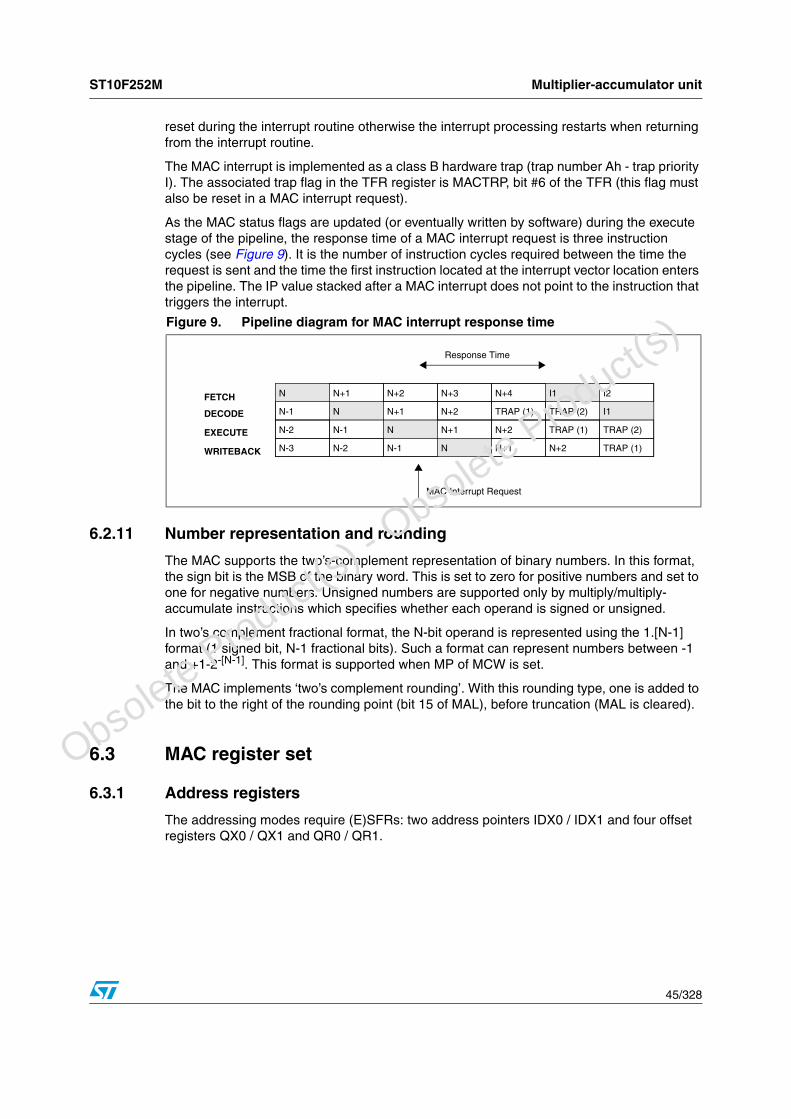
ST10F252M Multiplier-accumulator unit
45/328
reset during the interrupt routine otherwise the interrupt processing restarts when returning from the interrupt routine.
The MAC interrupt is implemented as a class B hardware trap (trap number Ah - trap priority I). The associated trap flag in the TFR register is MACTRP, bit #6 of the TFR (this flag must also be reset in a MAC interrupt request).
As the MAC status flags are updated (or eventually written by software) during the execute stage of the pipeline, the response time of a MAC interrupt request is three instruction cycles (see Figure 9). It is the number of instruction cycles required between the time the request is sent and the time the first instruction located at the interrupt vector location enters the pipeline. The IP value stacked after a MAC interrupt does not point to the instruction that triggers the interrupt.
6.2.11 Number representation and rounding
The MAC supports the two’s-complement representation of binary numbers. In this format, the sign bit is the MSB of the binary word. This is set to zero for positive numbers and set to one for negative numbers. Unsigned numbers are supported only by multiply/multiply-accumulate instructions which specifies whether each operand is signed or unsigned.
In two’s complement fractional format, the N-bit operand is represented using the 1.[N-1] format (1 signed bit, N-1 fractional bits). Such a format can represent numbers between -1 and +1-2-[N-1]. This format is supported when MP of MCW is set.
The MAC implements ‘two’s complement rounding’. With this rounding type, one is added to the bit to the right of the rounding point (bit 15 of MAL), before truncation (MAL is cleared).
6.3 MAC register set
6.3.1 Address registers
The addressing modes require (E)SFRs: two address pointers IDX0 / IDX1 and four offset registers QX0 / QX1 and QR0 / QR1.
Figure 9. Pipeline diagram for MAC interrupt response time
N
N
N
I1
I1
N
N+2
N+1
N-1
N-1
N-2
N-3
N+1
N-1
N-2
N+4
TRAP (1)
N+2
N+1
TRAP (1)
N+2
I2
TRAP (2)
TRAP (1)
N+3
N+2
N+1
FETCH
DECODE
EXECUTE
WRITEBACK
MAC Interrupt Request
Response Time
TRAP (2)
O
bsolete Product(
s) - O
bsolete Product(
s)

Multiplier-accumulator unit ST10F252M
46/328
Address pointer
Offset register
6.3.2 Accumulator and control registers
The MAC unit SFRs include the 40-bit accumulator (MAL, MAH and the low byte of MSW) and three control registers: the status word MSW, the control word MCW and the repeat word MRW.
MAH and MAL are located in the non bit-addressable SFR space.
MAH register
15 14 13 12 11 10 9 8 7 6 5 4 3 2 1 0
ID Xy
RW RW RW RW RW RW RW RW RW RW RW RW RW RW RW RW
Table 12. Address pointer functions
Bit Name Function
15.0 IDXy 16-bit IDXy address
15 14 13 12 11 10 9 8 7 6 5 4 3 2 1 0
QXz/QRz 0
RW RW RW RW RW RW RW RW RW RW RW RW RW RW RW R
Table 13. Offset register functions
Bit Name Function
15.0 QRz/QXz16-bit address offset for IDXy pointers (QXz) or GPR pointers (QRz).As MAC instructions handle word operands, bit 0 of these offset registers is hard-wired to ‘0’.
15 14 13 12 11 10 9 8 7 6 5 4 3 2 1 0
MAH
RW RW RW RW RW RW RW RW RW RW RW RW RW RW RW RW
Table 14. MAH register functions
Bit Name Function
15.0 MAH MAC unit accumulator high (bits [31..16])
O
bsolete Product(
s) - O
bsolete Product(
s)

ST10F252M Multiplier-accumulator unit
47/328
MAL register
Status word register
Note: The MAC condition flags are evaluated (if required) by the instruction being executed. In particular, they are not affected by any instruction of the regular instruction set. In consequence, their values may not be consistent with the accumulator content. For example, loading the accumulator with MOV instructions will not modify the condition flags
15 14 13 12 11 10 9 8 7 6 5 4 3 2 1 0
MAL
RW RW RW RW RW RW RW RW RW RW RW RW RW RW RW RW
Table 15. MAL register functions
Bit Name Function
15.0 MAL MAC unit accumulator low (bits [15..0])
15 14 13 12 11 10 9 8 7 6 5 4 3 2 1 0
MIR Res. SL E SV C Z N MAE
R - RW RW RW RW RW RW RW RW RW RW RW RW RW RW
Table 16. Status word register functions
Bit Name Function
15 MIRMAC interrupt requestSet when the MAC unit generates an interrupt request.
14 Reserved
13 SL
Sticky limit flag
Set when the result of a MAC operation is automatically saturated. Also used for CoMIN, CoMAX instructions to indicate that the accumulator has changed. It remains set until it is explicitly reset by software.
12 EExtension flagSet when MAE contains significant bits at the end of a MAC operation
11 SVSticky overflow flagSet when a MAC operation produces a 40-bit arithmetic overflow. It remains set until it is explicitly reset by software.
19 CCarry flag
Set when a MAC operation produces a carry or a borrow bit.
9 ZZero flag
Set when the accumulator is zero at the end of a MAC operation.
8 NNegative flag
Set when the accumulator is negative at the end of a MAC operation.
7:0 MAE Accumulator extension (bits [39:32])
O
bsolete Product(
s) - O
bsolete Product(
s)

Multiplier-accumulator unit ST10F252M
48/328
Control register
Repeat register
Note: As for the CPU Core SFRs, any write operation with the regular instruction set to a single byte of a MAC SFR clears the non-addressed complementary byte within the specified SFR. Non-implemented SFR bits cannot be modified and will always supply a read value of’0’.
15 14 13 12 11 10 9 8 7 6 5 4 3 2 1 0
MIE LM EM VM CM MP MS reserved
RW RW RW RW RW RW RW
Table 17. Control register functions
Bit Name Function
15 MIE
MAC Interrupt Enable
‘0’: MAC interrupt globally disabled,‘1’: MAC interrupt globally enabled.
14 LMSL MaskWhen set, the SL Flag can generate a MAC interrupt request.
13 EME MaskWhen set, the E Flag can generate a MAC interrupt request.
12 VMSV Mask
When set, the SV Flag can generate a MAC interrupt request.
11 CMC Mask
When set, the C Flag can generate a MAC interrupt request.
10 MPProduct Shift Mode
When set, enables the one-bit left shift of the multiplier output in case of a signed-signed multiplication
9 MSSaturation Mode
When set, enables automatic 32-bit saturation of the result of a MAC operation
8:0 Reserved
15 14 13 12 11 10 9 8 7 6 5 4 3 2 1 0
MR - - Repeat Count
RW RW
Table 18. Repeat register functions
Bit Name Function
15 MRRepeat Flag
Set when a repeated instruction is executed
12.0 Repeat Count13-bit unsigned integer value
Indicates the number of time minus one a repeated instruction must be executed
O
bsolete Product(
s) - O
bsolete Product(
s)

ST10F252M Multiplier-accumulator unit
49/328
These registers are mapped in the SFR space and can addressed by the regular instruction set like any SFR. They can also be addressed by the new instruction CoSTORE. This instruction allows the user to access the MAC registers without any pipeline side effect. CoSTORE uses a specific 5-bit addressing mode called CoReg. The following table gives the address of the MAC registers in this CoReg addressing mode.
Table 19. Register address in CoReg addressing mode
Registers Description Address
MSW MAC unit status word 00000b
MAH MAC unit accumulator high 00001b
MAS “limited” MAH /signed 00010b
MAL MAC unit accumulator low 00100b
MCW MAC unit control word 00101b
MRW MAC unit repeat word 00110b
O
bsolete Product(
s) - O
bsolete Product(
s)
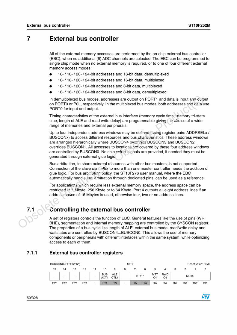
External bus controller ST10F252M
50/328
7 External bus controller
All of the external memory accesses are performed by the on-chip external bus controller (EBC), when no additional (6) ADC channels are selected. The EBC can be programmed to single chip mode when no external memory is required, or to one of four different external memory access modes:
● 16- / 18- / 20- / 24-bit addresses and 16-bit data, demultiplexed
● 16- / 18- / 20- / 24-bit addresses and 16-bit data, multiplexed
● 16- / 18- / 20- / 24-bit addresses and 8-bit data, multiplexed
● 16- / 18- / 20- / 24-bit addresses and 8-bit data, demultiplexed
In demultiplexed bus modes, addresses are output on PORT1 and data is input and output on PORT0 or P0L, respectively. In the multiplexed bus modes, both addresses and data use PORT0 for input and output.
Timing characteristics of the external bus interface (memory cycle time, memory tri-state time, length of ALE and read write delay) are programmable giving the choice of a wide range of memories and external peripherals.
Up to four independent address windows may be defined (using register pairs ADDRSELx / BUSCONx) to access different resources and bus characteristics. These address windows are arranged hierarchically where BUSCON4 overrides BUSCON3 and BUSCON2 overrides BUSCON1. All accesses to locations not covered by these four address windows are controlled by BUSCON0. No chip select signals are provided, if needed they must be generated through external glue logic.
Bus arbitration, to share external resources with other bus masters, is not supported. Connection of the slave controller to more than one master controller needs the addition of glue logic. For bus arbitration policy, the ST10F276 user manual, where the EBC automatically handle bus arbitration through dedicated pins, can be used as a reference.
For applications which require less external memory space, the address space can be restricted to 1 Mbyte, 256 Kbyte or to 64 Kbyte. Port 4 outputs all eight address lines if an address space of 16 Mbytes is used, otherwise four, two or no address lines.
7.1 Controlling the external bus controllerA set of registers controls the function of EBC. General features like the use of pins (WR, BHE), segmentation and internal memory mapping are controlled by the SYSCON register. The properties of a bus cycle like length of ALE, external bus mode, read/write delay and waitstates are controlled by BUSCON4...BUSCON0. This allows the use of memory components or peripherals with different interfaces within the same system, while optimizing access to each of them.
7.1.1 External bus controller registers
BUSCON0 (FF0Ch/86h) SFR Reset value: 0xx0
15 14 13 12 11 10 9 8 7 6 5 4 3 2 1 0
- - - - - BUS ACT4
ALE CTL4 BTYP MTT
C4RWD C4 MCTC
RW RW RW RW - RW RW - RW RW RW RW RW RW RW RW
O
bsolete Product(
s) - O
bsolete Product(
s)

ST10F252M External bus controller
51/328
BUSCON1 (FF14h/8Ah) SFR Reset value: 0000
15 14 13 12 11 10 9 8 7 6 5 4 3 2 1 0
- - - - - BUS ACT4
ALE CTL4
MTTC4
RWD C4
RW RW RW RW - RW RW - RW RW RW RW RW RW RW RW
BUSCON2 (FF16h/8Bh) SFR Reset value: 0000
15 14 13 12 11 10 9 8 7 6 5 4 3 2 1 0
- - - - - BUS ACT4
ALE CTL4
MTTC4
RWD C4
RW RW RW RW - RW RW - RW RW RW RW RW RW RW RW
BUSCON3 (FF18h/8Ch) SFR Reset value: 0000
15 14 13 12 11 10 9 8 7 6 5 4 3 2 1 0
- - - - - BUS ACT4
ALE CTL4
MTTC4
RWD C4
RW RW RW RW - RW RW - RW RW RW RW RW RW RW RW
BUSCON4 (FF1Ah/8Dh) SFR Reset value: 0000
15 14 13 12 11 10 9 8 7 6 5 4 3 2 1 0
- - - - - BUS ACT4
ALE CTL4
MTTC4
RWD C4
RW RW RW RW - RW RW - RW RW RW RW RW RW RW RW
Table 20. External bus controller functions
Bit Name Function
10 BUSACTx‘0’: Bus not active
‘1’: Bus active
9 ALECTLx
ALE lengthening control
‘0’: Normal ALE signal‘1’: Lengthened ALE signal
6.7 BTYP
External bus configuration0 0: 8-bit demultiplexed
0 1: 8-bit multiplexed
1 0: 16-bit Demultiplexed1 1: 16-bit multiplexed
For BUSCON0 BTYP is defined via PORT0 during reset,
5 MTTCx
Memory Tristate Time Control
‘0’: 1 waitstates
‘1’: No waitstates
4 RWDCX
Read/write delay control for BUSCONx
‘0’: With read/write delay: activate command 1 TCL after falling edge of ALE
‘1’: No read/write delay: activate command with falling edge of ALE
0.3 MCTC
Memory cycle time control (number of memory cycle time wait states)
0 0 0 0: 15 waitstates (number = 15 -<MCTC>). . .
1 1 1 1: no waitstates
O
bsolete Product(
s) - O
bsolete Product(
s)

External bus controller ST10F252M
52/328
7.2 EA functionalityIn ST10F252M, the EA pin is shared with VSTBY supply pin. When main VDD is on and stable, VSTBY can be temporary grounded: in stand-by mode, the logic that is powered by VSTBY (that is 12Kbyte portion of XRAM and stand-by voltage regulator), is powered by the main VDD. This means that the EA pin can be driven low during reset, if requested, to configure the system to start from the external memory.
An appropriate external circuit must be provided to manage dynamically both the functionalities associated with the pin: during reset and with stable VDD, the pin can be tied low, while after reset (or anyway before turning off the main VDD to enter stand-by mode) the VSTBY supply is applied. Refer to Section 21.3 for more details.
In Figure 10, a possible external circuit is represented. When selecting the resistance for current limitation, ensure that the resistance does not disturb the stand-by mode when some current (in the order of hundreds of μA) is provided to the device by VSTBY; the voltage at the pin of ST10F252M cannot become lower than 4.5 V.
To reduce the effect of the current consumption transients on VSTBY pin (refer to ISB3 in the Electrical Characteristics section), add an external capacitance which can filter any current peaks, which could create potential problems of voltage drops if a very low power external voltage regulator is used. The external hardware must limit current peaks due to the presence of the capacitance (when EA is used and the external bipolar is turned on, see Figure 10).
Figure 10. EA/VSTBY external circuit
VSTBY
VSS
4 - 5.5 Volt
EA function
EA / VSTBY
VSS
O
bsolete Product(
s) - O
bsolete Product(
s)
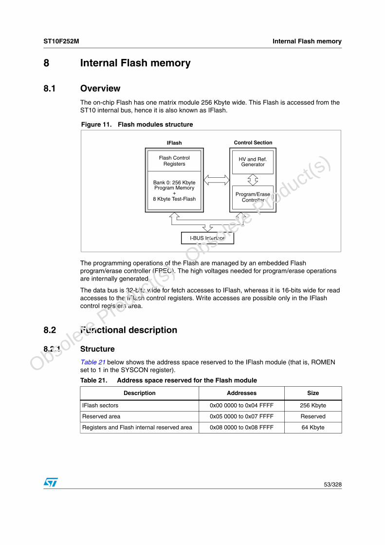
ST10F252M Internal Flash memory
53/328
8 Internal Flash memory
8.1 OverviewThe on-chip Flash has one matrix module 256 Kbyte wide. This Flash is accessed from the ST10 internal bus, hence it is also known as IFlash.
The programming operations of the Flash are managed by an embedded Flash program/erase controller (FPEC). The high voltages needed for program/erase operations are internally generated.
The data bus is 32-bits wide for fetch accesses to IFlash, whereas it is 16-bits wide for read accesses to the IFlash control registers. Write accesses are possible only in the IFlash control registers area.
8.2 Functional description
8.2.1 Structure
Table 21 below shows the address space reserved to the IFlash module (that is, ROMEN set to 1 in the SYSCON register).
Figure 11. Flash modules structure
Flash Control
Bank 0: 256 KbyteProgram Memory
HV and Ref.Generator
Program/EraseController
I-BUS Interface
+8 Kbyte Test-Flash
IFlash Control Section
Registers
Table 21. Address space reserved for the Flash module
Description Addresses Size
IFlash sectors 0x00 0000 to 0x04 FFFF 256 Kbyte
Reserved area 0x05 0000 to 0x07 FFFF Reserved
Registers and Flash internal reserved area 0x08 0000 to 0x08 FFFF 64 Kbyte
O
bsolete Product(
s) - O
bsolete Product(
s)
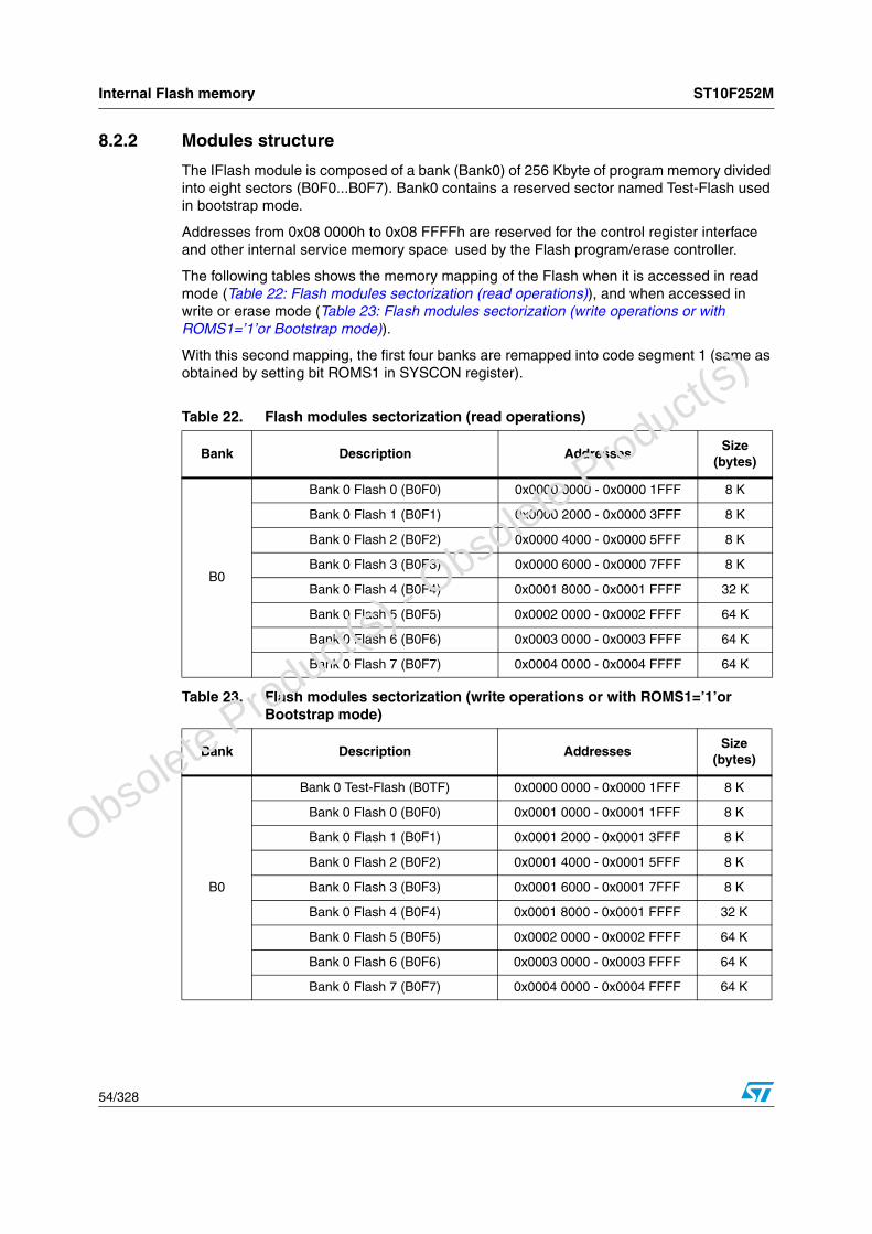
Internal Flash memory ST10F252M
54/328
8.2.2 Modules structure
The IFlash module is composed of a bank (Bank0) of 256 Kbyte of program memory divided into eight sectors (B0F0...B0F7). Bank0 contains a reserved sector named Test-Flash used in bootstrap mode.
Addresses from 0x08 0000h to 0x08 FFFFh are reserved for the control register interface and other internal service memory space used by the Flash program/erase controller.
The following tables shows the memory mapping of the Flash when it is accessed in read mode (Table 22: Flash modules sectorization (read operations)), and when accessed in write or erase mode (Table 23: Flash modules sectorization (write operations or with ROMS1=’1’or Bootstrap mode)).
With this second mapping, the first four banks are remapped into code segment 1 (same as obtained by setting bit ROMS1 in SYSCON register).
Table 22. Flash modules sectorization (read operations)
Bank Description AddressesSize
(bytes)
B0
Bank 0 Flash 0 (B0F0) 0x0000 0000 - 0x0000 1FFF 8 K
Bank 0 Flash 1 (B0F1) 0x0000 2000 - 0x0000 3FFF 8 K
Bank 0 Flash 2 (B0F2) 0x0000 4000 - 0x0000 5FFF 8 K
Bank 0 Flash 3 (B0F3) 0x0000 6000 - 0x0000 7FFF 8 K
Bank 0 Flash 4 (B0F4) 0x0001 8000 - 0x0001 FFFF 32 K
Bank 0 Flash 5 (B0F5) 0x0002 0000 - 0x0002 FFFF 64 K
Bank 0 Flash 6 (B0F6) 0x0003 0000 - 0x0003 FFFF 64 K
Bank 0 Flash 7 (B0F7) 0x0004 0000 - 0x0004 FFFF 64 K
Table 23. Flash modules sectorization (write operations or with ROMS1=’1’or Bootstrap mode)
Bank Description AddressesSize
(bytes)
B0
Bank 0 Test-Flash (B0TF) 0x0000 0000 - 0x0000 1FFF 8 K
Bank 0 Flash 0 (B0F0) 0x0001 0000 - 0x0001 1FFF 8 K
Bank 0 Flash 1 (B0F1) 0x0001 2000 - 0x0001 3FFF 8 K
Bank 0 Flash 2 (B0F2) 0x0001 4000 - 0x0001 5FFF 8 K
Bank 0 Flash 3 (B0F3) 0x0001 6000 - 0x0001 7FFF 8 K
Bank 0 Flash 4 (B0F4) 0x0001 8000 - 0x0001 FFFF 32 K
Bank 0 Flash 5 (B0F5) 0x0002 0000 - 0x0002 FFFF 64 K
Bank 0 Flash 6 (B0F6) 0x0003 0000 - 0x0003 FFFF 64 K
Bank 0 Flash 7 (B0F7) 0x0004 0000 - 0x0004 FFFF 64 K
O
bsolete Product(
s) - O
bsolete Product(
s)

ST10F252M Internal Flash memory
55/328
Table 23 above refers to the configuration when bit ROMS1 of SYSCON register is set. Refer to Chapter 24 for more details on bootstrap mode memory mapping during Bootstrap mode. In particular, when Bootstrap mode is entered:
● Test-Flash is seen and available for code fetches (address 00 0000h).
● user I-Flash is available for read and write accesses.
● write accesses must be made with addresses starting in segment 1 from 01 0000h, whatever ROMS1 bit in SYSCON value.
● read accesses are made in segment 0 or in segment 1 depending on ROMS1 value.
In bootstrap mode, ROMS1 = 0 by default, so the first 32 Kbytes of IFlash are mapped in segment 0.
Example:
In default configuration, to program address 0, the user must put the value 01 0000h in the FARL and FARH registers but to verify the content of the address 0, a read to 00 0000h must be performed.
The next Table 24 shows the control register interface composition: this set of registers can be addressed by the CPU.
8.2.3 Low power mode
The Flash module is automatically switched off when executing a PWRDN instruction. The consumption is drastically reduced, but exiting this state can require a long time (tPD).
Recovery time from power-down mode for the Flash modules is anyway shorter than the main oscillator start-up time. To avoid any problems in restarting to fetch code from the Flash, it is important to size properly the external circuit on RPD pin.
Note: PWRDN instruction must not be executed while a Flash program/erase operation is in progress.
Table 24. Control register interface
Name Description AddressesSize
(bytes)Bus size
FCR1-0 Flash control registers 1-0 0x0008 0000 - 0x0008 0007 8
16-bit
FAR Flash address registers 0x0008 0010 - 0x0008 0013 4
FER Flash error register 0x0008 0014 - 0x0008 0015 2
FNVWPIRFlash non-volatile protection I register
0x0008 DFB0 - 0x0008 DFB1 2
FNVWPIR- Mirror
Flash non-volatile protection I register
0x0008 DFB4 - 0x0008 DFB5 2
FNVAPR0Flash non-volatile access protection register 0
0x0008 DFB8 - 0x0008 DFB9 2
FNVAPR1Flash non-volatile access protection register 1
0x0008 DFBC - 0x0008 DFBF 4
FVTAU0Flash volatile temporary access unprotection register 0
0x0000 EB50 - 0x0000 EB51 2
O
bsolete Product(
s) - O
bsolete Product(
s)

Internal Flash memory ST10F252M
56/328
8.3 Write operationThe Flash module has one single register interface mapped in the memory space of the IBus (08’0000h - 08’0015h). All the operations are enabled through four 16-bit control registers: Flash Control Register 1-0 High/Low (FCR1H/L-FCR0H/L). Eight other 16-bit registers are used to store Flash address and data for program operations (FARH/L and FDR1H/L-FDR0H/L) and Write Operation Error flags (FERH/L). All registers are accessible with 8- and 16-bit instructions (since the IBUS operates in 16-bit mode for read/write accesses to data).
Note: The register that controls the Temporary Unprotection of the Flash is located on the XBus at address 00 EB50h in the XMiscellaneous Register area.
Before accessing the IFlash module (and consequently the Flash register to be used for program/erasing operations), the ROMEN bit in SYSCON register must be set.
Caution: During a Flash write operation any attempt to read the Flash itself, that is under modification, will output invalid data (software trap 009Bh). This means that the Flash is not fetchable when a programming operation is active. The write operation commands must be executed from another memory (internal RAM or external memory), as in ST10F269 device. In fact, due to IBus characteristics, it is not possible to perform a write operation on IFlash, when fetching code from IFlash.Direct addressing is not allowed for write accesses to IFlash Control Registers.
Warning: During a Write operation, when bit LOCK of FCR0 is set, it is forbidden to write into the Flash Control Registers.
Power supply drop
If during a write operation the internal low voltage supply drops below a certain internal voltage threshold, any write operation running is suddenly interrupted and the module is reset to Read mode. At following Power-on, the interrupted Flash write operation must be repeated.
8.4 Registers description
8.4.1 Flash control register 0 low (FCR0L)
The Flash Control Register 0 Low (FCR0L) together with the Flash Control Register 0 High (FCR0H) are used to enable and to monitor all the write operations on the IFlash. The user has no access in write mode to the Test-Flash (B0TF). Moreover, the Test-Flash block is seen by the user in Bootstrap mode only.
FCR0L (0x08 0000) FCR Reset value: 0000h
15 14 13 12 11 10 9 8 7 6 5 4 3 2 1 0
Reserved LOCK Reserved BSY0 Res.
- RO - RO -
O
bsolete Product(
s) - O
bsolete Product(
s)

ST10F252M Internal Flash memory
57/328
8.4.2 Flash control register 0 high (FCR0H)
The Flash Control Register 0 High (FCR0H) together with the Flash Control Register 0 Low (FCR0L) is used to enable and to monitor all the write operations on the IFlash. The user has no access in write mode to the Test-Flash (B0TF). Moreover, the Test-Flash block is seen by the user in Bootstrap mode only.
Table 25. Flash control register 0 low
Bit Name Function
15:5 Reserved These bits are left at their reset value (0).
4 LOCK
Flash Registers Access Locked
When this bit is set, it means that the access to the Flash Control Registers FCR0H/-FCR1H/L, FDR0H/L-FDR1H/L, FARH/L and FER is locked by the FPEC: any read access to the registers will output invalid data (software trap 009Bh) and any write access will be ineffective. LOCK bit is automatically set when the Flash bit WMS is set.This is the only bit the user can always access to detect the status of the Flash: once it is found low, the rest of FCR0L and all the other Flash registers are accessible by the user as well.Note that FER content can be read when LOCK is low, but its content is updated only when the BSY0 bit is reset.
3.2 Reserved These bits are left at their reset value (0).
1 BSY
Bank 0 Busy (IFlash)
This bit indicates that a write operation is running on Bank 0 (IFlash). It is automatically set when bit WMS is set. Setting Protection operation sets bit BSY0 (since protection registers are in this Block). When this bit is set, every read access to Bank 0 will output invalid data (software trap 009Bh), while every write access to the Bank will be ignored. At the end of the write operation or during a Program or Erase Suspend this bit is automatically reset and the Bank returns to read mode. After a Program or Erase Resume this bit is automatically set again.
0 Reserved This bit is left at its reset value (0).
FCR0H (0x08 0002) FCR Reset value: 0000h
15 14 13 12 11 10 9 8 7 6 5 4 3 2 1 0
WMS SUSP WPG DWPG SER Reserved SPR Reserved
RW RW RW RW RW - RW -
O
bsolete Product(
s) - O
bsolete Product(
s)
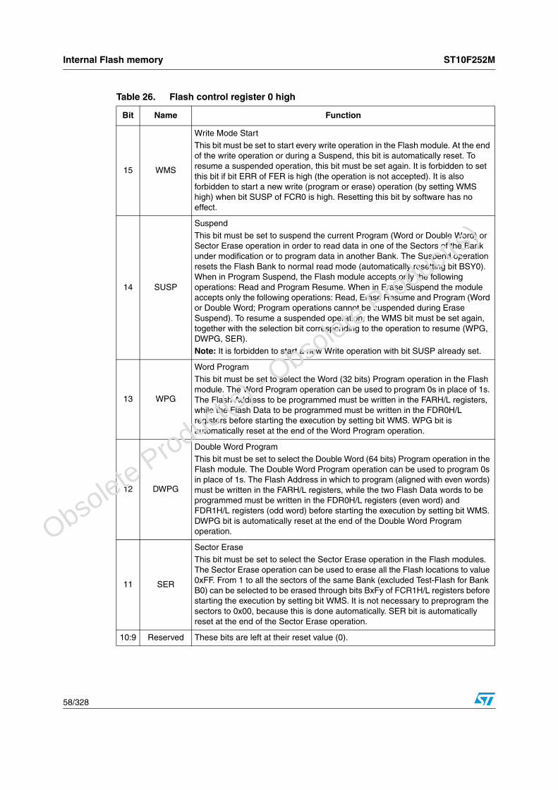
Internal Flash memory ST10F252M
58/328
Table 26. Flash control register 0 high
Bit Name Function
15 WMS
Write Mode Start
This bit must be set to start every write operation in the Flash module. At the end of the write operation or during a Suspend, this bit is automatically reset. To resume a suspended operation, this bit must be set again. It is forbidden to set this bit if bit ERR of FER is high (the operation is not accepted). It is also forbidden to start a new write (program or erase) operation (by setting WMS high) when bit SUSP of FCR0 is high. Resetting this bit by software has no effect.
14 SUSP
Suspend
This bit must be set to suspend the current Program (Word or Double Word) or Sector Erase operation in order to read data in one of the Sectors of the Bank under modification or to program data in another Bank. The Suspend operation resets the Flash Bank to normal read mode (automatically resetting bit BSY0). When in Program Suspend, the Flash module accepts only the following operations: Read and Program Resume. When in Erase Suspend the module accepts only the following operations: Read, Erase Resume and Program (Word or Double Word; Program operations cannot be suspended during Erase Suspend). To resume a suspended operation, the WMS bit must be set again, together with the selection bit corresponding to the operation to resume (WPG, DWPG, SER).
Note: It is forbidden to start a new Write operation with bit SUSP already set.
13 WPG
Word Program
This bit must be set to select the Word (32 bits) Program operation in the Flash module. The Word Program operation can be used to program 0s in place of 1s. The Flash Address to be programmed must be written in the FARH/L registers, while the Flash Data to be programmed must be written in the FDR0H/L registers before starting the execution by setting bit WMS. WPG bit is automatically reset at the end of the Word Program operation.
12 DWPG
Double Word Program
This bit must be set to select the Double Word (64 bits) Program operation in the Flash module. The Double Word Program operation can be used to program 0s in place of 1s. The Flash Address in which to program (aligned with even words) must be written in the FARH/L registers, while the two Flash Data words to be programmed must be written in the FDR0H/L registers (even word) and FDR1H/L registers (odd word) before starting the execution by setting bit WMS. DWPG bit is automatically reset at the end of the Double Word Program operation.
11 SER
Sector Erase
This bit must be set to select the Sector Erase operation in the Flash modules. The Sector Erase operation can be used to erase all the Flash locations to value 0xFF. From 1 to all the sectors of the same Bank (excluded Test-Flash for Bank B0) can be selected to be erased through bits BxFy of FCR1H/L registers before starting the execution by setting bit WMS. It is not necessary to preprogram the sectors to 0x00, because this is done automatically. SER bit is automatically reset at the end of the Sector Erase operation.
10:9 Reserved These bits are left at their reset value (0).
O
bsolete Product(
s) - O
bsolete Product(
s)

ST10F252M Internal Flash memory
59/328
8.4.3 Flash control register 1 low (FCR1L)
The Flash Control Register 1 Low (FCR1L), together with Flash Control Register 1 High (FCR1H), is used to select the Sectors to Erase, or during any write operation to monitor the status of each Sector and Bank.
8.4.4 Flash control register 1 high (FCR1H)
The Flash Control Register 1 High (FCR1H), together with Flash Control Register 1 Low (FCR1L), is used to select the Sectors to Erase, or during any write operation to monitor the status of each Sector and Bank.
8 SPR
Set protection. This bit is set to select the set protection operation. The set protection operation programs 0s in place of 1s in the Flash non volatile protection registers. The Flash address in which to program is written in the FARH/L registers, while the Flash data to be programmed is written in the FDR0H/L before starting the execution by setting bit WMS. A sequence error is flagged by bit SEQER of FER if the address written in FARH/L is not in the range 0x08DFB0-0x08DFBF. This bit is automatically reset at the end of the set protection operation.
7:0 Reserved These bits are left at their reset value (0).
Table 26. Flash control register 0 high (continued)
Bit Name Function
FCR1L (0x08 0004) FCR Reset value: 0000h
15 14 13 12 11 10 9 8 7 6 5 4 3 2 1 0
Reserved B0F7 B0F6 B0F5 B0F4 B0F3 B0F2 B0F1 B0F0
- RS RS RS RS RS RS RS RS
Table 27. Flash control register 1 low
Bit Name Function
15:8 Reserved These bits are left at their reset value (0).
7:0 B0F[7:0]
Bank 0 IFlash Sectors 7-0 Status
These bits must be set during a Sector Erase operation to select the sectors to erase in Bank 0. Moreover, during any erase operation, these bits are automatically set and give the status of the eight sectors of Bank 0 (B0F7-B0F0). The meaning of B0Fy bit for Sector y of Bank 0 is given in Table 29. These bits are automatically reset at the end of a write operation if no errors are detected.
FCR1H (0x08 0006) FCR Reset value: 0000h
15 14 13 12 11 10 9 8 7 6 5 4 3 2 1 0
Reserved B0S Reserved
- RS -
O
bsolete Product(
s) - O
bsolete Product(
s)

Internal Flash memory ST10F252M
60/328
During any erase operation, this bit is automatically set and gives the status of the Bank 0. The meaning of B0Fy bit for Sector y of Bank 0 is given by the next Table 4 Banks (BxS) and Sectors (BxFy) Status bits meaning. These bits are automatically reset at the end of an erase operation if no errors are detected.
8.4.5 Flash data register 0 low (FDR0L)
During program operations, the Flash Address Registers (FARH/L) are used to store the Flash address in which to program and the Flash Data Registers (FDR1H/L-FDR0H/L) are used to store the Flash data to program.
Table 28. Flash control register 1 high
Bit Name Function
7:0 Reserved These bits are left at their reset value (0).
8 B0S
Bank 0 Status (IFlash)
During any erase operation, this bit is automatically modified and gives the status of the Bank 0. The meaning of B0S bit is given in Table 29. This bit is automatically reset at the end of an erase operation if no errors are detected.
15:9 Reserved These bits are left at their reset value (0).
Table 29. Banks (BxS) and sectors (BxFy) status bits meaning
ERR SUSP B0S = 1 meaning B0Fy = 1 meaning
1 - Erase Error in Bank0 Erase Error in Sector y of Bank0
0 1 Erase Suspended in Bank0 Erase Suspended in Sector y of Bank0
0 0 Don’t care Don’t care
FDR0L (0x08 0008) FCR Reset value: FFFFh
15 14 13 12 11 10 9 8 7 6 5 4 3 2 1 0
DIN15 DIN14 DIN13 DIN12 DIN11 DIN10 DIN9 DIN8 DIN7 DIN6 DIN5 DIN4 DIN3 DIN2 DIN1 DIN0
RW RW RW RW RW RW RW RW RW RW RW RW RW RW RW RW
Table 30. Flash data register 0 low
Bit Name Function
15:0 DIN[15:0]
Data Input 15:0
These bits must be written with the Data to program the Flash with the following operations: Word Program (32-bit), Double Word Program (64-bit) and Set Protection.
Obso
lete Product(s)
- Obso
lete Product(s)

ST10F252M Internal Flash memory
61/328
8.4.6 Flash data register 0 high (FDR0H)
8.4.7 Flash data register 1 low (FDR1L)
8.4.8 Flash data register 1 high (FDR1H)
FDR0H (0x08 000A) FCR Reset value: FFFFh
15 14 13 12 11 10 9 8 7 6 5 4 3 2 1 0
DIN31 DIN30 DIN29 DIN28 DIN27 DIN26 DIN25 DIN24 DIN23 DIN22 DIN21 DIN20 DIN19 DIN18 DIN17 DIN16
RW RW RW RW RW RW RW RW RW RW RW RW RW RW RW RW
Table 31. Flash data register 0 high
Bit Name Function
15:0 DIN[31:16]
Data Input 31:16
These bits must be written with the Data to program the Flash with the following operations: Word Program (32-bit), Double Word Program (64-bit) and Set Protection.
FDR1L (0x08 000C) FCR Reset value: FFFFh
15 14 13 12 11 10 9 8 7 6 5 4 3 2 1 0
DIN15 DIN14 DIN13 DIN12 DIN11 DIN10 DIN9 DIN8 DIN7 DIN6 DIN5 DIN4 DIN3 DIN2 DIN1 DIN0
RW RW RW RW RW RW RW RW RW RW RW RW RW RW RW RW
Table 32. Flash data register 1 low
Bit Name Function
15:0 DIN[15:0]
Data Input 15:0These bits must be written with the Data to program the Flash with the following operations: Word Program (32-bit), Double Word Program (64-bit) and Set Protection.
FDR1H (0x08 000E) FCR Reset value: FFFFh
15 14 13 12 11 10 9 8 7 6 5 4 3 2 1 0
DIN31 DIN30 DIN29 DIN28 DIN27 DIN26 DIN25 DIN24 DIN23 DIN22 DIN21 DIN20 DIN19 DIN18 DIN17 DIN16
RW RW RW RW RW RW RW RW RW RW RW RW RW RW RW RW
Table 33. Flash data register 1 high
Bit Name Function
15:0 DIN[31:16]
Data Input 31:16
These bits must be written with the Data to program the Flash with the following operations: Word Program (32-bit), Double Word Program (64-bit) and Set Protection.
O
bsolete Product(
s) - O
bsolete Product(
s)
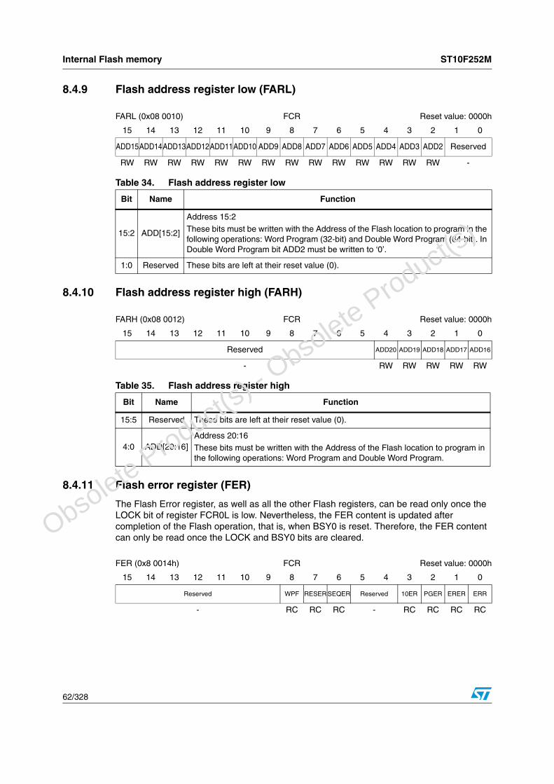
Internal Flash memory ST10F252M
62/328
8.4.9 Flash address register low (FARL)
8.4.10 Flash address register high (FARH)
8.4.11 Flash error register (FER)
The Flash Error register, as well as all the other Flash registers, can be read only once the LOCK bit of register FCR0L is low. Nevertheless, the FER content is updated after completion of the Flash operation, that is, when BSY0 is reset. Therefore, the FER content can only be read once the LOCK and BSY0 bits are cleared.
FARL (0x08 0010) FCR Reset value: 0000h
15 14 13 12 11 10 9 8 7 6 5 4 3 2 1 0
ADD15ADD14ADD13ADD12ADD11ADD10 ADD9 ADD8 ADD7 ADD6 ADD5 ADD4 ADD3 ADD2 Reserved
RW RW RW RW RW RW RW RW RW RW RW RW RW RW -
Table 34. Flash address register low
Bit Name Function
15:2 ADD[15:2]
Address 15:2
These bits must be written with the Address of the Flash location to program in the following operations: Word Program (32-bit) and Double Word Program (64-bit). In Double Word Program bit ADD2 must be written to ‘0’.
1:0 Reserved These bits are left at their reset value (0).
FARH (0x08 0012) FCR Reset value: 0000h
15 14 13 12 11 10 9 8 7 6 5 4 3 2 1 0
Reserved ADD20 ADD19 ADD18 ADD17 ADD16
- RW RW RW RW RW
Table 35. Flash address register high
Bit Name Function
15:5 Reserved These bits are left at their reset value (0).
4:0 ADD[20:16]Address 20:16
These bits must be written with the Address of the Flash location to program in the following operations: Word Program and Double Word Program.
FER (0x8 0014h) FCR Reset value: 0000h
15 14 13 12 11 10 9 8 7 6 5 4 3 2 1 0
Reserved WPF RESER SEQER Reserved 10ER PGER ERER ERR
- RC RC RC - RC RC RC RC
O
bsolete Product(
s) - O
bsolete Product(
s)

ST10F252M Internal Flash memory
63/328
8.5 Protection strategyThe protection bits are stored in Non-Volatile Flash cells inside IFlash module, that are read once at reset and stored in four Volatile registers. Before they are read from the Non- Volatile cells, all the available protections are forced active during reset.
The protections can be programmed using the Set Protection operation (see Flash Control Registers paragraph), that can be executed from all the internal or external memories except from the Flash itself.
Table 36. Flash error register
Bit Name Function
15:9 Reserved These bits are left at their reset value (0).
8 WPF
Write Protection Flag
This bit is automatically set when trying to program or erase in a sector write protected. In case of multiple Sector Erase, the not protected sectors are erased, while the protected sectors are not erased and bit WPF is set. This bit has to be software reset.
7 RESER
Resume Error
This bit is automatically set when a suspended Program or Erase operation is not resumed correctly due to a protocol error. In this case the suspended operation is aborted. This bit has to be software reset.
6 SEQER
Sequence ErrorThis bit is automatically set when the control registers (FCR1H/L-FCR0H/L, FARH/L, FDR1H/L-FDR0H/L) are not correctly filled to execute a valid Write Operation. In this case no Write Operation is executed. This bit has to be software reset.
5:4 Reserved These bits are left at their reset value (0).
3 10ER
1 over 0 Error
This bit is automatically set when trying to program at 1 bits previously set at 0 (this does not happen when programming the Protection bits). This error is not due to a failure of the Flash cell, but only flags that the desired data has not been written. This bit has to be software reset.
2 PGER
Program Error
This bit is automatically set when a Program error occurs during a Flash write operation. This error is due to a real failure of a Flash cell, that can no more be programmed. The word where this error occurred must be discarded. This bit has to be software reset.
1 ERER
Erase Error
This bit is automatically set when an Erase error occurs during a Flash write operation. This error is due to a real failure of a Flash cell, that can no more be erased. This kind of error is fatal and the sector where it occurred must be discarded. This bit has to be software reset.
0 ERR
Write Error
This bit is automatically set when an error occurs during a Flash write operation or when a bad write operation setup is done. Once the error has been discovered and understood, ERR bit must be software reset.
O
bsolete Product(
s) - O
bsolete Product(
s)

Internal Flash memory ST10F252M
64/328
Two kind of protections are available: write protections to avoid unwanted writings and access protections to avoid piracy. In next paragraphs all different level of protections are shown, and architecture limitations are highlighted as well.
8.5.1 Protection registers
The four Non-Volatile Protection Registers are one time programmable for the user.
One register (FNVWPIR) is used to store the Write Protection fuses respectively for each sector IFlash module. The other three registers (FNVAPR0 and FNVAPR1L/H) are used to store the Access Protection fuses.
8.5.2 Flash non-volatile write protection I register (FNVWPIR)
8.5.3 Flash non-volatile access protection register 0 (FNVAPR0)
FNVWPIR (0x08 DFB0) NVR Reset value: FFFFh
15 14 13 12 11 10 9 8 7 6 5 4 3 2 1 0
Reserved W0P7W0P6W0P5W0P4W0P3W0P2W0P1W0P0
- RW RW RW RW RW RW RW RW
Table 37. Flash non-volatile write protection I register
Bit Name Function
15:8 Reserved These bits are left at their reset value (F).
7:0 W0P[7:0]Write Protection Bank 0 / Sectors 7-0 (IFlash)
These bits, if programmed at 0, disable any write access to the sectors of Bank 0 (IFlash)
FNVAPR0 (0x08 DFB8) NVR Delivery value: ACFFh
15 14 13 12 11 10 9 8 7 6 5 4 3 2 1 0
Reserved DBGP ACCP
- RW RW
Table 38. Flash non-volatile access protection register 0
Bit Name Function
15:2 Reserved
1 DBGP
Debug ProtectionThis bit, if erased at 1, can be used to by-pass all the protections using the Debug features through the Test Interface. If programmed at 0, on the contrary, all the debug features, the Test Interface and all the Flash Test modes are disabled. Even STMicroelectronics will not be able to access the device to run any eventual failure analysis.
0 ACCP
Access Protection
This bit, if programmed at 0, disables any access (read/write) to data mapped inside IFlash Module address space, unless the current instruction is fetched from IFlash.
O
bsolete Product(
s) - O
bsolete Product(
s)

ST10F252M Internal Flash memory
65/328
8.5.4 Flash non-volatile access protection register 1 low (FNVAPR1L)
8.5.5 Flash non-volatile access protection register 1 high (FNVAPR1H)
8.5.6 XBus Flash volatile temporary access unprotection register (XFVTAUR0)
FNVAPR1L (0x08 DFBC) NVR Delivery value: FFFFh
15 14 13 12 11 10 9 8 7 6 5 4 3 2 1 0
PDS15 PDS14 PDS13 PDS12PDS11 PDS10 PDS9 PDS8 PDS7 PDS6 PDS5 PDS4 PDS3 PDS2 PDS1 PDS0
RW RW RW RW RW RW RW RW RW RW RW RW RW RW RW RW
Table 39. Flash non-volatile access protection register 1 low
Bit Name Function
15:0 PDS[15:0]
Protections Disable 15-0
If bit PDSx is programmed at 0 and bit PENx is erased at 1, the action of bit ACCP is disabled. Bit PDS0 can be programmed at 0 only if both bits DBGP and ACCP have already been programmed at 0. Bit PDSx can be programmed at 0 only if bit PENx-1 has already been programmed at 0.
FNVAPR1H (0x08 DFBE) NVR Delivery value: FFFFh
15 14 13 12 11 10 9 8 7 6 5 4 3 2 1 0
PEN15PEN14PEN13PEN12PEN11PEN10 PEN9 PEN8 PEN7 PEN6 PEN5 PEN4 PEN3 PEN2 PEN1 PEN0
RW RW RW RW RW RW RW RW RW RW RW RW RW RW RW RW
Table 40. Flash non-volatile access protection register 1 high
Bit Name Function
15:0 PEN[15:0]
Protections Enable 15-0
If bit PENx is programmed at 0 and bit PDSx+1 is erased at 1, the action of bit ACCP is enabled again. Bit PENx can be programmed at 0 only if bit PDSx has already been programmed at 0.
XFVTAUR0 (0x00 EB50) NVR Reset value: 0000h
15 14 13 12 11 10 9 8 7 6 5 4 3 2 1 0
Reserved TAUB
- RW
Table 41. XBus Flash volatile temporary access unprotection register
Bit Name Function
15:1 Reserved These bits are left at their reset value (0).
0 TAUB
Temporary Access Unprotection bit
If this bit is set to 1, the Access Protection is temporary disabled.The fact that this bit can be written only while executing from IFlash guarantees that only a code executed in IFlash can unprotect the IFlash when it is Access Protected.
O
bsolete Product(
s) - O
bsolete Product(
s)

Internal Flash memory ST10F252M
66/328
8.5.7 Access protection
The IFlash module has one level of access protection (access to data both in Reading and Writing).
When bit ACCP of FNVAPR0 is programmed at 0 and bit TAUB in XFVTAUR0 is set at 0, the IFlash module becomes access protected (data in the IFlash module can be read only if the current execution is from the IFlash module itself).
Trying to read into the access protected Flash from internal RAM or external memories will output a dummy data (software trap 009Bh).
When the Flash module is protected in access, data access through PEC transfers is also forbidden. To read/write data through PEC in a protected Bank, first it is necessary to temporarily unprotect the Flash module.
To enable Access Protection, the following sequence of operations is recommended:
● execution from external memory or internal Rams
● program TAUB bit at 1 in XFVTAUR0 register
● program ACCP bit in FNVAPR0 to 0 using Set Protection operation
● program TAUB bit at 0 in XFVTAUR0 register
● Access Protection is active when both ACCP bit and TAUB bit are set to 0.
Protection can be permanently disabled by programming bit PDS0 of FNVAPR1H, in order to analyze rejects. Protection can be permanently enabled again by programming bit PEN0 of FNVAPR1L. The action to disable and enable again Access Protections in a permanent way can be executed a maximum of 16 times. To execute the above described operations, the Flash has to be temporarily unprotected (see Section 8.5.9: Temporary unprotection).
Trying to write into the access protected Flash from internal RAM or external memories will be unsuccessful. Trying to read into the access protected Flash from internal RAM or external memories will output dummy data (software trap 0x009Bh).
When the Flash module is protected in access, data access through PEC of a peripheral is also forbidden. To read/write data in PEC mode from/to a protected Bank, it is necessary to first temporarily unprotect the Flash module.
The following table summarizes all possible Access Protection levels: In particular, it shows what is possible and not possible to do when fetching from a memory (see fetch location column) supposing all possible access protections are enabled.
Table 42. Summary of access protection level
Fetch locationRead IFlash /
Jump to IFlash
Read XRAM or External Memory /
Jump to XRAM or External
Memory
Read FlashRegisters
Write FlashRegisters
Fetching from IFlash Yes / Yes Yes / Yes Yes No
Fetching from IRAM No / Yes No / Yes Yes / No No
Fetching from XRAM No / Yes No / Yes Yes / No No
Fetching from external memory
No / Yes No / Yes Yes / No No
O
bsolete Product(
s) - O
bsolete Product(
s)

ST10F252M Internal Flash memory
67/328
When the Access Protection is enabled, Flash registers can not be written, so no program/erase operation can be run on IFlash. To enable the access to registers again, the Temporary Access Unprotection procedure has to be followed (see Section 8.5.9).
8.5.8 Write protection
The Flash modules have one level of Write Protections: each Sector of each Bank of each Flash Module can be Software Write Protected by programming at 0 the related bit W0Px in FNVWPIRL register.
8.5.9 Temporary unprotection
Bits W0Px of FNVWPIRL can be temporarily unprotected by executing the Set Protection operation and by writing 1 into these bits.
To restore the write protection bits it is necessary to reset the microcontroller or to execute a Set Protection operation and write 0 into the desired bits.
In reality, when a temporary write unprotection operation is executed, the corresponding volatile register is written to 1, while the non-volatile registers bits previously written to 0 (for a protection set operation), will continue to maintain the 0. For this reason, the User software must be in charge to track the current write protection status (for instance using a specific RAM area), it is not possible to deduce it by reading the non-volatile register content (a temporary unprotection cannot be detected).
To temporarily unprotect the Flash when the Access Protection is active, it is necessary to set to ‘1’ the bit TAUB in XFVTAUR0. This bit can be set to ‘1’ only while executing from Flash: In this way only an instruction executed from Flash can unprotect the Flash itself.
To restore the Access Protection, it is necessary to reset the microcontroller or to write at 0 the bit TAUB in XFVTAUR0.
8.6 Write operation examplesThe following examples represent each kind of Flash write operation.
Note: The write operation commands must be executed from another memory (internal RAM or external memory), as in ST10F269 device. In fact, due to I-bus characteristics, it is not possible to perform write operation in IFlash while fetching code from IFlash.
Direct addressing is not allowed for write accesses to IFlash control registers. This means that both address and data for a writing operation must be loaded in one ST10 GPR register (R0...R15).
A write operation on the I-bus is 16 bits wide.
Example: indirect addressing mode:
Word program example: 32-bit word program of data 0xAAAAAAAA at address 0x015554.
MOV RWm, #ADDRESS; /*Load Add in RWm*/
MOV RWn, #DATA; /*Load Data in RWn*/
MOV [RWm], RWn; /*Indirect addressing*/
FCR0H |= 0x2000; /*Set WPG in FCR0H*/
FARL = 0x5554; /*Load Add in FARL*/
O
bsolete Product(
s) - O
bsolete Product(
s)

Internal Flash memory ST10F252M
68/328
Double word program example: double word program (64-bit) of data 0x55AA55AA at address 0x015558 and data 0xAA55AA55 at address 0x01555C.
Note: A double word program is always performed on the double word aligned on a even word – bit ADD2 of FARL is ignored.
Sector erase example: sector erase of sectors B0F1 and B0F0 of Bank0 in IFlash module.
Suspend and resume example: word program, double word program, and sector erase operations can be suspended in the following way.
The operation can be resumed in the following way.
Note: The original set up of select operation bits in FCR0H/L must be restored before the operation resume, otherwise the operation is aborted and bit RESER of FER is set.
Erase suspend, program and resume examples: a sector erase operation can be suspended to program (word or double word) another sector.
Sector erase of sector B0F1 of Bank0 in IFlash module.
Sector erase suspend.
FARH = 0x0001; /*Load Add in FARH*/
FDR0L = 0xAAAA; /*Load Data in FDR0L*/
FDR0H = 0xAAAA; /*Load Data in FDR0H*/
FCR0H |= 0x8000; /*Operation start*/
FCR0H |= 0x1000; /*Set DWPG*/
FARL = 0x5558; /*Load Add in FARL*/
FARH = 0x0001; /*Load Add in FARH*/
FDR0L = 0x55AA; /*Load Data in FDR0L*/
FDR0H = 0x55AA; /*Load Data in FDR0H*/
FDR1L = 0xAA55; /*Load Data in FDR1L*/
FDR1H = 0xAA55; /*Load Data in FDR1H*/
FCR0H |= 0x8000; /*Operation start*/
FCR0H |= 0x0800; /*Set SER in FCR0H*/
FCR1H |= 0x0003; /*Set B0F1, B0F0*/
FCR0H |= 0x8000; /*Operation start*/
FCR0H |= 0x4000; /*Set SUSP in FCR0H*/
FCR0H &= 0xBFFF; /*Rst SUSP in FCR0H*/
FCR0H |= 0x8000; /*Operation resume*/
FCR0H |= 0x0800; /*Set SER in FCR0H*/
FCR1H |= 0x0002; /*Set B3F1*/
FCR0H |= 0x8000; /*Operation start*/
FCR0H |= 0x4000; /*Set SUSP in FCR0H*/
do /*Loop to Wait WMS=0*/
{tmp = FCR0H; /*Read FCR0H*/
} while (tmp & 0x8000);
O
bsolete Product(
s) - O
bsolete Product(
s)

ST10F252M Internal Flash memory
69/328
Example: word program of data 0x5555AAAA at address 0x015554 in IFlash module.
Once the program operation is finished, the erase operation can be resumed in the following way.
Note: During the program operation in erase suspend, bits SER and SUSP remain high. A word or double word program during erase suspend cannot be suspended.
Set protection example 1: enable write protection of sectors B0F3...B0F0 of Bank 0 in IFlash module.
Set protection example 2: enable access and debug protection.
Set protection example 3: permanently disable access and debug protection.
Set protection example 4: permanently re-enable access and debug protection, after having disabled them.
FCR0H |= 0x2000; /*Set WPG in FCR0H*/
FARL = 0x5554; /*Load Add in FARL*/
FARH = 0x000C; /*Load Add in FARH*/
FDR0L = 0xAAAA; /*Load Data in FDR0L*/
FDR0H = 0x5555; /*Load Data in FDR0H*/
FCR0H |= 0x8000; /*Operation start*/
FCR0H &= 0xBFFF; /*Rst SUSP in FCR0H*/
FCR0H |= 0x8000; /*Operation resume*/
FCR0H |= 0x0100; /*Set SPR in FCR0H*/
FARL = 0xDFB4; /*Load Add of register FNVWPIRL in FARL*/
FARH = 0x0008; /*Load Add of register FNVWPIRL in FARH*/
FDR0L = 0xFFF0; /*Load Data in FDR0L*/
FCR0H |= 0x8000; /*Operation start*/
FVTUR = 0x0001; /*Set TAUB in FVTAUR0*/
FCR0H |= 0x0100; /*Set SPR in FCR0H*/
FARL = 0xDFB8; /*Load Add of register FNVAPR0 in FARL*/
FARH = 0x0008; /*Load Add of register FNVAPR0 in FARH*/
FDR0L = 0xFFFC; /*Load Data in FDR0L*/
FCR0H |= 0x8000; /*Operation start*/
FVTUR = 0x0000; /*Set TAUB in FVTAUR0*/
FVTUR = 0x0001; /*Set TAUB in FVTAUR0*/
FCR0H |= 0x0100; /*Set SPR in FCR0H*/
FARL = 0xDFBC; /*Load Add of register FNVAPR1L in FARL*/
FARH = 0x000E; /*Load Add of register FNVAPR1L in FARH*/
FDR0L = 0xFFFE; /*Load Data in FDR0L for clearing PDS0*/
FCR0H |= 0x8000; /*Operation start*/
FVTUR = 0x0001; /*Set TAUB in FVTAUR0*/
FCR0H |= 0x0100; /*Set SPR in FCR0H*/
O
bsolete Product(
s) - O
bsolete Product(
s)

Internal Flash memory ST10F252M
70/328
Note: Disable and re-enable of access and debug protection in a permanently (as shown by examples 3 and 4) can be done for a maximum of 16 times.
FARL = 0xDFBC; /*Load Add register FNVAPR1H in FARL*/
FARH = 0x0008; /*Load Add register FNVAPR1H in FARH*/
FDR0H = 0xFFFE; /*Load Data in FDR0H for clearing PEN0*/
FCR0H |= 0x8000; /*Operation start*/
FVTUR = 0x0000; /*Set TAUB in FVTAUR0*/
O
bsolete Product(
s) - O
bsolete Product(
s)

ST10F252M Internal Flash memory
71/328
8.7 Write operation summaryIn general, each write operation is started through a sequence of three steps:
1. The first instruction is used to select the desired operation by setting its corresponding selection bit in the Flash Control Register 0.
2. The second step is the definition of the Address and Data for programming or the Sectors or Banks to erase.
3. The last instruction is used to start the write operation, by setting the start bit WMS in the FCR0.
Once selected, but not yet started, one operation can be canceled by resetting the operation selection bit.
Available Flash Module Write Operations are summarized in the following Table 43.
Figure 12 shows the complete flow needed for a Write operation.
Figure 12. Write operation control flow
Table 43. Flash write operations
Operation Select bit Address and data Start bit
Word program (32-bit) WPGFARL/FARH
FDR0L/FDR0HWMS
Double word program (64-bit) DWPGFARL/FARH
FDR0L/FDR0HFDR1L/FDR1H
WMS
Sector erase SER FCR1L/FCR1H WMS
Set protection SPR FDR0L/FDR0H WMS
Program/erase suspend SUSP None None
Start Write Operation
FCR0L.LOCK == 0? No
Yes
Write Operation finished?(Check related busy bit) No
Yes
Check Error Status
No error:Proceed with application
Error:Error handler, ...
Re-start operation
O
bsolete Product(
s) - O
bsolete Product(
s)

Interrupt system ST10F252M
72/328
9 Interrupt system
The interrupt response time for internal program execution is from 125 ns to 300 ns at 40 MHz CPU frequency.
The ST10F252M architecture supports several mechanisms for fast and flexible response to service requests that can be generated from various sources internal or external to the microcontroller. Any of these interrupt requests can be serviced by the interrupt controller or by the peripheral event controller (PEC).
In contrast to a standard interrupt service where the current program execution is suspended and a branch to the interrupt vector table is performed, just one cycle is ‘stolen’ from the current CPU activity to perform a PEC service. A PEC service implies a single byte or word data transfer between any two memory locations with an additional increment of either the PEC source or the destination pointer. An individual PEC transfer counter is implicitly decremented for each PEC service except when performing in the continuous transfer mode. When this counter reaches zero, a standard interrupt is performed to the corresponding source related vector location. PEC services are very well suited, for example, for supporting the transmission or reception of blocks of data. The ST10F252M has eight PEC channels each of which offers such fast interrupt-driven data transfer capabilities.
There is a separate control register, which contains an interrupt request flag, an interrupt enable flag and an interrupt priority bit-field for each of the possible interrupt sources. Via its related register, each source can be programmed to one of sixteen interrupt priority levels. Once having been accepted by the CPU, an interrupt service can only be interrupted by a higher prioritized service request. For the standard interrupt processing, each of the possible interrupt sources has a dedicated vector location.
Software interrupts are supported by means of the ‘TRAP’ instruction in combination with an individual trap (interrupt) number.
9.1 Fast external interruptFast external interrupt inputs are provided to service external interrupts with high precision requirements. These fast interrupt inputs feature programmable edge detection (rising edge, falling edge or both edges).
9.1.1 External interrupt source selection register (EXISEL)
Fast external interrupts may also have interrupt sources selected from other peripherals; for example the CANx controller receive signal (CANx_RxD) can be used to interrupt the system. The same is valid for I2C interface serial clock line (SCL), and for real time clock. This function is controlled using the external interrupt source selection register (EXISEL), and allows to wake-up the system from interruptible power down having to reset the device.
O
bsolete Product(
s) - O
bsolete Product(
s)

ST10F252M Interrupt system
73/328
External interrupt source selection register
CAN and I2C interrupt need some considerations, the following are general rules.
● When a module is not enabled, even though the interrupt source is enabled (see for example EXIxSS=’01’), an event on the pin does not generate any request to the CPU.
● CAN parallel mode is enabled only when both CAN modules are enabled (on the contrary it has no effect).
EXxIN inputs are normally sampled interrupt inputs. However, the power down mode circuitry uses them as level-sensitive inputs. An EXxIN (x = 7...0) interrupt enable bit (bit CCxIE in the respective CCxIC register) needs not to be set to bring the device out of power down mode.
If the Interrupt was enabled (bit CCxIE=’1’ in the respective CCxIC register) before entering power down mode, the device executes the interrupt service routine, and then resumes execution after the PWRDN instruction. If the interrupt was disabled, the device executes the instruction following PWRDN instruction, and the interrupt request flag (bit CCxIR in the respective CCxIC register) remains set until it is cleared by software.
In Table 46, all the possible pin configurations are summarized for CAN parallel mode. In the table, the bit of XPERCON register are shown (used to enable/disable each module) and the bit CANPAR of XMISC register used to enable/disable the CAN parallel mode. The table
External interrupt source selection register (F1DA ED) EXISEL Reset value: 0000h
15 14 13 12 11 10 9 8 7 6 5 4 3 2 1 0
EXI7SS EXI6SS EXI5SS EXI4SS EXI3SS EXI2SS EXI1SS EXI0SS
RW RW RW RW RW RW RW RW
Table 44. External interrupt source selection register functions
Bit Name Function
15.0 EXIxSS(7:0)
External interrupt x source selection (x=7...0)
‘00’: Input from associated port 2 pin.
‘01’: Input from “alternate source”.‘10’: Input from port 2 pin ORed with “alternate source”.
‘11’: Input from port 2 pin ANDed with “alternate source”.
Table 45. EXIxSS interrupts
EXIxSS Port 2 pin Alternate Source
0 P2.8 CAN1_RxD P4.5
1 P2.9 CAN2_RxD P4.4
2 P2.10 RTC_secIT Internal MUX
3 P2.11 RTC_alarmIT Internal MUX
4 P2.12 SCL P1.6
5...7 P2.13...15 Not used (zero) -
O
bsolete Product(
s) - O
bsolete Product(
s)

Interrupt system ST10F252M
74/328
shows when the wake-up interrupt can be generated by the two modules (providing that the EXISEL register is properly set).
Note: For CAN1 (and CAN2 when parallel mode is set) the related interrupt control register is CC8IC; for CAN2 the register is CC9IC, for I2C is CC12IC
9.1.2 External interrupt control register (EXICON)
The Power Down mode can be entered if enabled Fast External Interrupt pins (EXxIN pins, Alternate Functions of Port 2 pins, with x = 7...0) are in their inactive level. This inactive level is configured with the EXIxES bit field in the EXICON register.
External interrupt control register
While for CAN and I2C the EXICON programming depends on the customer application (even though inactive state of both CAN and I2C protocols is the high level, so a new activity on the bus can be detected by a falling edge observed at the related pins), for RTC the internal hardware circuitry is such that the interrupts are generated on the positive edge, so the EXICON register must be programmed accordingly.
Note: The I2C interface implements a input analog filter to avoid spurious spikes are assumed as valid bus transitions. For this reason, a pulse on SCL line is long enough to be recognized as valid pulse: this is in the range of 500 ns (minimum). All pulses shorter than 50 ns are
Table 46. CAN parallel mode pin configurations
CANPAR CAN2EN CAN1EN Interrupt P4.5 Interrupt P4.4
x 0 0 No No
x 0 1 Yes (CAN1) No
x 1 0 No Yes (CAN2)
0 1 1 Yes (CAN1) Yes (CAN2)
1 1 1 Yes (CAN1/2) No
External interrupt control register (F1CD EB) EXICON Reset value: 0000h
15 14 13 12 11 10 9 8 7 6 5 4 3 2 1 0
EXI7ES EXI6ES EXI5ES EXI4ES EXI3ES EXI2ES EXI1ES EXI0ES
RW RW RW RW RW RW RW RW
Table 47. External interrupt control register functions
Bit Name Function
15.0 EXIxES(7:0)
External Interrupt x Edge Selection Field (x=7...0)‘00’: Fast external interrupts disabled: standard mode. The EXxIN pin is not taken into account for entering/exiting power down mode.‘01’: Interrupt on positive edge (rising). Enter power down mode if EXiIN = ‘0’, exit if EXxIN = ‘1’ (referred as ‘high’ active level)‘10’: Interrupt on negative edge (falling). Enter power down mode if EXiIN = ‘1’, exit if EXxIN = ‘0’ (referred as ‘low’ active level)‘11’: Interrupt on any edge (rising or falling). Always enter power down mode, exit if EXxIN level changes.
Obso
lete Product(s)
- Obso
lete Product(s)

ST10F252M Interrupt system
75/328
certainly filtered: a pulse longer than 50 ns but shorter than 500 ns could either trigger or not trigger the exit from power down mode.
9.2 X-Peripheral interruptThe limited number of X-Bus interrupt lines of the present ST10 architecture, imposes some constraints on the implementation of the new functionality. In particular, the additional X-Peripherals SSC1, ASC1, I2C, PWM1 and RTC need some resources to implement interrupt and PEC transfer capabilities. For this reason, a multiplexed structure for the interrupt management is proposed. In the next Figure 13, the principle is explained through a simple diagram, which shows the basic structure replicated for each of the four X-interrupt available vectors (XP0INT, XP1INT, XP2INT and XP3INT).
It is based on a set of 16-bit registers XIRxSEL (x = 0,1,2,3), divided in two portions each:
● Byte High XIRxSEL[15:8] Interrupt Enable bits
● Byte Low XIRxSEL[7:0] Interrupt Flag bits
When different sources submit an interrupt request, the enable bits (Byte High of XIRxSEL register) define a mask which controls which sources will be associated with the unique available vector. If more than one source is enabled to issue the request, the service routine will have to take care to identify the real event to be serviced. This can easily be done by checking the flag bits (Byte Low of XIRxSEL register). Note that the flag bits can also provide information about events which are not currently serviced by the interrupt controller (since they are masked through the enable bits), allowing an effective software management even if the related interrupt request cannot be served: A periodic polling of the flag bits may be implemented inside the user application.
Table 48 summarizes the mapping of the different interrupt sources, which share the four X-interrupt vectors.
Figure 13. X-interrupt basic structure
XIRxSEL[7:0] (x = 0, 1, 2, 3)
XIRxSEL[15:8] (x = 0, 1, 2, 3)
XPxIC.IR (x = 0, 1, 2, 3)
7 0
15 8
IT Source 7
IT Source 6
IT Source 5
IT Source 4
IT Source 3
IT Source 2
IT Source 1
IT Source 0
Enable[7:0]
Flag[7:0]
O
bsolete Product(
s) - O
bsolete Product(
s)
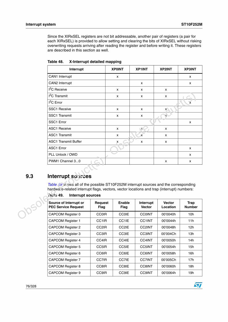
Interrupt system ST10F252M
76/328
Since the XIRxSEL registers are not bit addressable, another pair of registers (a pair for each XIRxSEL) is provided to allow setting and clearing the bits of XIRxSEL without risking overwriting requests arriving after reading the register and before writing it. These registers are described in this section as well.
9.3 Interrupt sourcesTable 49 shows all of the possible ST10F252M interrupt sources and the corresponding hardware-related interrupt flags, vectors, vector locations and trap (interrupt) numbers:
Table 48. X-Interrupt detailed mapping
Interrupt XP0INT XP1INT XP2INT XP3INT
CAN1 Interrupt x x
CAN2 Interrupt x x
I2C Receive x x x
I2C Transmit x x x
I2C Error x
SSC1 Receive x x x
SSC1 Transmit x x x
SSC1 Error x
ASC1 Receive x x x
ASC1 Transmit x x x
ASC1 Transmit Buffer x x x
ASC1 Error x
PLL Unlock / OWD x
PWM1 Channel 3...0 x x
Table 49. Interrupt sources
Source of Interrupt or PEC Service Request
RequestFlag
EnableFlag
InterruptVector
VectorLocation
TrapNumber
CAPCOM Register 0 CC0IR CC0IE CC0INT 00’0040h 10h
CAPCOM Register 1 CC1IR CC1IE CC1INT 00’0044h 11h
CAPCOM Register 2 CC2IR CC2IE CC2INT 00’0048h 12h
CAPCOM Register 3 CC3IR CC3IE CC3INT 00’004Ch 13h
CAPCOM Register 4 CC4IR CC4IE CC4INT 00’0050h 14h
CAPCOM Register 5 CC5IR CC5IE CC5INT 00’0054h 15h
CAPCOM Register 6 CC6IR CC6IE CC6INT 00’0058h 16h
CAPCOM Register 7 CC7IR CC7IE CC7INT 00’005Ch 17h
CAPCOM Register 8 CC8IR CC8IE CC8INT 00’0060h 18h
CAPCOM Register 9 CC9IR CC9IE CC9INT 00’0064h 19h
O
bsolete Product(
s) - O
bsolete Product(
s)
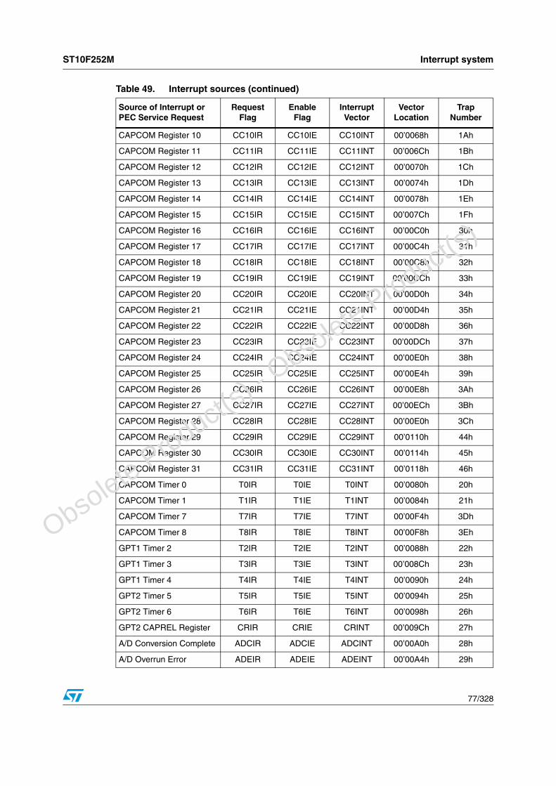
ST10F252M Interrupt system
77/328
CAPCOM Register 10 CC10IR CC10IE CC10INT 00’0068h 1Ah
CAPCOM Register 11 CC11IR CC11IE CC11INT 00’006Ch 1Bh
CAPCOM Register 12 CC12IR CC12IE CC12INT 00’0070h 1Ch
CAPCOM Register 13 CC13IR CC13IE CC13INT 00’0074h 1Dh
CAPCOM Register 14 CC14IR CC14IE CC14INT 00’0078h 1Eh
CAPCOM Register 15 CC15IR CC15IE CC15INT 00’007Ch 1Fh
CAPCOM Register 16 CC16IR CC16IE CC16INT 00’00C0h 30h
CAPCOM Register 17 CC17IR CC17IE CC17INT 00’00C4h 31h
CAPCOM Register 18 CC18IR CC18IE CC18INT 00’00C8h 32h
CAPCOM Register 19 CC19IR CC19IE CC19INT 00’00CCh 33h
CAPCOM Register 20 CC20IR CC20IE CC20INT 00’00D0h 34h
CAPCOM Register 21 CC21IR CC21IE CC21INT 00’00D4h 35h
CAPCOM Register 22 CC22IR CC22IE CC22INT 00’00D8h 36h
CAPCOM Register 23 CC23IR CC23IE CC23INT 00’00DCh 37h
CAPCOM Register 24 CC24IR CC24IE CC24INT 00’00E0h 38h
CAPCOM Register 25 CC25IR CC25IE CC25INT 00’00E4h 39h
CAPCOM Register 26 CC26IR CC26IE CC26INT 00’00E8h 3Ah
CAPCOM Register 27 CC27IR CC27IE CC27INT 00’00ECh 3Bh
CAPCOM Register 28 CC28IR CC28IE CC28INT 00’00E0h 3Ch
CAPCOM Register 29 CC29IR CC29IE CC29INT 00’0110h 44h
CAPCOM Register 30 CC30IR CC30IE CC30INT 00’0114h 45h
CAPCOM Register 31 CC31IR CC31IE CC31INT 00’0118h 46h
CAPCOM Timer 0 T0IR T0IE T0INT 00’0080h 20h
CAPCOM Timer 1 T1IR T1IE T1INT 00’0084h 21h
CAPCOM Timer 7 T7IR T7IE T7INT 00’00F4h 3Dh
CAPCOM Timer 8 T8IR T8IE T8INT 00’00F8h 3Eh
GPT1 Timer 2 T2IR T2IE T2INT 00’0088h 22h
GPT1 Timer 3 T3IR T3IE T3INT 00’008Ch 23h
GPT1 Timer 4 T4IR T4IE T4INT 00’0090h 24h
GPT2 Timer 5 T5IR T5IE T5INT 00’0094h 25h
GPT2 Timer 6 T6IR T6IE T6INT 00’0098h 26h
GPT2 CAPREL Register CRIR CRIE CRINT 00’009Ch 27h
A/D Conversion Complete ADCIR ADCIE ADCINT 00’00A0h 28h
A/D Overrun Error ADEIR ADEIE ADEINT 00’00A4h 29h
Table 49. Interrupt sources (continued)
Source of Interrupt or PEC Service Request
RequestFlag
EnableFlag
InterruptVector
VectorLocation
TrapNumber
O
bsolete Product(
s) - O
bsolete Product(
s)

Interrupt system ST10F252M
78/328
Hardware traps are exceptions or error conditions that arise during run-time. They cause an immediate non-maskable system reaction similar to a standard interrupt service (branching to a dedicated vector table location).
The occurrence of a hardware trap is additionally signified by an individual bit in the trap flag register (TFR). Except when another higher prioritized trap service is in progress, a hardware trap will interrupt any actual program execution. In turn, hardware trap services can normally not be interrupted by standard or PEC interrupts.
9.4 Exception and traps listTable 50 shows all of the possible exceptions or error conditions that can arise during run-time.
ASC0 Transmit S0TIR S0TIE S0TINT 00’00A8h 2Ah
ASC0 Transmit Buffer S0TBIR S0TBIE S0TBINT 00’011Ch 47h
ASC0 Receive S0RIR S0RIE S0RINT 00’00ACh 2Bh
ASC0 Error S0EIR S0EIE S0EINT 00’00B0h 2Ch
SSC Transmit SCTIR SCTIE SCTINT 00’00B4h 2Dh
SSC Receive SCRIR SCRIE SCRINT 00’00B8h 2Eh
SSC Error SCEIR SCEIE SCEINT 00’00BCh 2Fh
PWM Channel 0...3 PWMIR PWMIE PWMINT 00’00FCh 3Fh
See Section 9.2
XP0IR XP0IE XP0INT 00’0100h 40h
XP1IR XP1IE XP1INT 00’0104h 41h
XP2IR XP2IE XP2INT 00’0108h 42h
XP3IR XP3IE XP3INT 00’010Ch 43h
Table 49. Interrupt sources (continued)
Source of Interrupt or PEC Service Request
RequestFlag
EnableFlag
InterruptVector
VectorLocation
TrapNumber
Table 50. Trap priorities
Exception conditionTrapflag
Trapvector
Vectorlocation
Trapnumber
Trap priority(1)
Reset Functions:Hardware ResetSoftware ResetWatchdog Timer Overflow
RESETRESETRESET
00’0000h00’0000h00’0000h
00h00h00h
IIIIIIIII
Class A Hardware Traps:Non-Maskable InterruptStack OverflowStack Underflow
NMISTKOFSTKUF
NMITRAPSTOTRAPSTUTRAP
00’0008h00’0010h00’0018h
02h04h06h
IIIIII
O
bsolete Product(
s) - O
bsolete Product(
s)
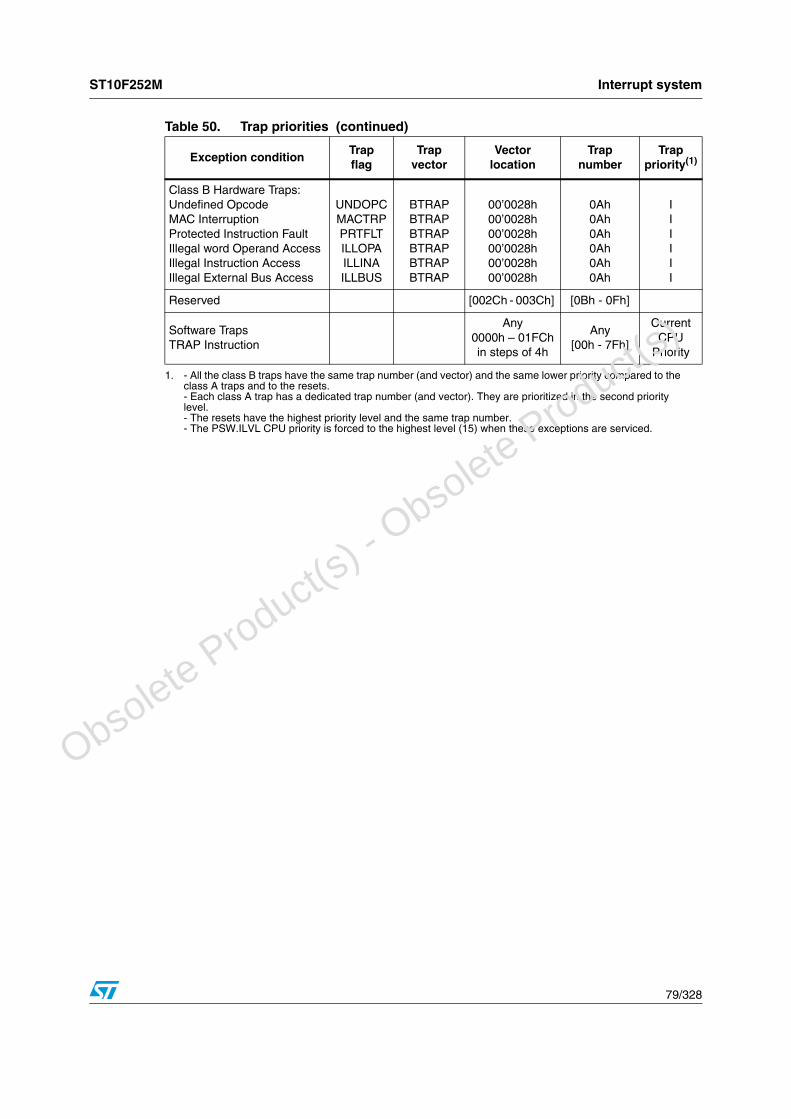
ST10F252M Interrupt system
79/328
Class B Hardware Traps:Undefined OpcodeMAC InterruptionProtected Instruction FaultIllegal word Operand AccessIllegal Instruction AccessIllegal External Bus Access
UNDOPCMACTRPPRTFLTILLOPAILLINAILLBUS
BTRAPBTRAPBTRAPBTRAPBTRAPBTRAP
00’0028h00’0028h00’0028h00’0028h00’0028h00’0028h
0Ah0Ah0Ah0Ah0Ah0Ah
IIIIII
Reserved [002Ch - 003Ch] [0Bh - 0Fh]
Software TrapsTRAP Instruction
Any 0000h – 01FChin steps of 4h
Any[00h - 7Fh]
CurrentCPU
Priority
1. - All the class B traps have the same trap number (and vector) and the same lower priority compared to the class A traps and to the resets.- Each class A trap has a dedicated trap number (and vector). They are prioritized in the second priority level.- The resets have the highest priority level and the same trap number.- The PSW.ILVL CPU priority is forced to the highest level (15) when these exceptions are serviced.
Table 50. Trap priorities (continued)
Exception conditionTrapflag
Trapvector
Vectorlocation
Trapnumber
Trap priority(1)
O
bsolete Product(
s) - O
bsolete Product(
s)
Capture compare (CAPCOM) units ST10F252M
80/328
10 Capture compare (CAPCOM) units
The ST10F252M has two 16 channel CAPCOM units. They support generation and control of timing sequences on up to 32 channels with a maximum resolution of 200 ns at 40 MHz CPU clock.
The CAPCOM units are typically used to handle high speed I/O tasks such as pulse and waveform generation, pulse width modulation (PMW), digital to analog (D/A) conversion, software timing, or time recording relative to external events.
These two CAPCOM units are identical to the ones of the ST10F269 and ST10F27x, but, due to 100-pins limitation in the ST10F252, the I/O capability is limited to 18 channels.
For CAPCOM1, 14 input-capture/output-compare channels with 4 only input-capture channel for CAPCOM2.
The number of timer input lines has not changed, the T0IN input line is available for CAPCOM1, T7IN input line timer for CAPCOM2.
All capture/compare registers and timers register are available, but some of them are not connected to external pins
O
bsolete Product(
s) - O
bsolete Product(
s)

ST10F252M Capture compare (CAPCOM) units
81/328
Figure 14. SFR and port pins associated with CAPCOM unitsP
orts
& D
irect
ion
Con
trol
Alte
rnat
e F
unct
ions
Dat
a R
egis
ters
15 -
14 -
13 -
12 -
11 -
10 -
9 -
8 -
7 Y
6 Y
5 Y
4 Y
3 -
2 -
1 -
0 -D
P1H
ET
0
15 Y
14 Y
13 Y
12 Y
11 Y
10 Y
9 Y
8 Y
7 Y
6 Y
5 Y
4 Y
3 Y
2 Y
1 Y
0 Y
--
--
--
--
YY
YY
--
--
P1H
YY
YY
YY
YY
YY
YY
YY
YY
OD
P2
E
T0R
EL
YY
YY
YY
YY
YY
YY
YY
YY
T1
YY
YY
YY
YY
YY
YY
YY
YY
Con
trol
Reg
iste
rsIn
terr
upt C
ontr
ol
15 Y
14 Y
13 Y
12 Y
11 Y
10 Y
9 Y
8 Y
7 Y
6 Y
5 Y
4 Y
3 Y
2 Y
1 Y
0 YT
01C
ON
1514
1312
1110
98
76
54
32
10
T0I
C
--
--
--
--
YY
YY
YY
YY
T1I
C
--
--
--
--
YY
YY
YY
YY
T7I
C E
--
--
--
--
YY
YY
YY
YY
CC
0IO
/P2.
0...C
C15
IO/P
2.15
CC
24IO
/P1H
.4...
CC
27IO
/P1H
.7
TxR
ELC
AP
CO
M T
imer
x R
eloa
d R
egis
ter
TxC
AP
CO
M T
imer
x R
egis
ter
CC
0...1
5CA
PC
OM
1 R
egis
ter
0...1
5
CC
16...
31C
AP
CO
M2
Reg
iste
r 16
...31
CC
M0.
..3C
AP
CO
M1
Mod
e C
ontr
ol R
egis
ter
0...3
CC
M4.
..7C
AP
CO
M2
Mod
e C
ontr
ol R
egis
ter
4...7
CC
0...1
5IC
CA
PC
OM
1 In
terr
upt C
ontr
ol R
egis
ter
0...1
5
CC
16..3
1IC
CA
PC
OM
2 In
terr
upt C
ontr
ol R
egis
ter
16...
31
OD
PxP
ort x
Ope
n D
rain
Con
trol
Reg
iste
r
DP
xPor
t x D
irect
ion
Con
trol
Reg
iste
r
PxP
ort x
Dat
a R
egis
ter
T01
CO
NC
AP
CO
M1
Tim
ers
T0
and
T1
Con
trol
Reg
iste
r
T78
CO
NC
AP
CO
M2
Tim
ers
T7
and
T8
Con
trol
Reg
iste
r
T0I
C/T
1IC
CA
PC
OM
1 T
imer
0/1
Inte
rrup
t Con
trol
Reg
iste
r
T7I
C/T
8IC
CA
PC
OM
2 T
imer
7/8
Inte
rrup
t Con
trol
Reg
iste
r
YY
YY
YY
YY
YY
YY
YY
YY
DP
2
YY
YY
YY
YY
YY
YY
YY
YY
P2
--
--
--
--
--
--
--
-Y
OD
P3
E
--
--
--
--
--
--
--
-Y
DP
3
--
--
--
--
--
--
--
-Y
P3
T1R
EL
YY
YY
YY
YY
YY
YY
YY
YY
T7
EY
YY
YY
YY
YY
YY
YY
YY
Y
T7R
EL
EY
YY
YY
YY
YY
YY
YY
YY
Y
T8
EY
YY
YY
YY
YY
YY
YY
YY
Y
T8R
EL
EY
YY
YY
YY
YY
YY
YY
YY
Y
CC
0-3
YY
YY
YY
YY
YY
YY
YY
YY
CC
4-7
YY
YY
YY
YY
YY
YY
YY
YY
CC
8-11
YY
YY
YY
YY
YY
YY
YY
YY
CC
12-1
5Y
YY
YY
YY
YY
YY
YY
YY
Y
CC
16-1
9Y
YY
YY
YY
YY
YY
YY
YY
Y
CC
20-2
3Y
YY
YY
YY
YY
YY
YY
YY
Y
CC
24-2
7Y
YY
YY
YY
YY
YY
YY
YY
Y
CC
28-3
1Y
YY
YY
YY
YY
YY
YY
YY
Y
YY
YY
YY
YY
YY
YY
YY
YY
T78
CO
N
CC
M0
YY
YY
YY
YY
YY
YY
YY
YY
CC
M1
YY
YY
YY
YY
YY
YY
YY
YY
CC
M2
YY
YY
YY
YY
YY
YY
YY
YY
CC
M3
YY
YY
YY
YY
YY
YY
YY
YY
CC
M4
YY
YY
YY
YY
YY
YY
YY
YY
CC
M5
YY
YY
YY
YY
YY
YY
YY
YY
CC
M6
YY
YY
YY
YY
YY
YY
YY
YY
CC
M7
YY
YY
YY
YY
YY
YY
YY
YY
--
--
--
--
YY
YY
YY
YY
T8I
C E
--
--
--
--
YY
YY
YY
YY
CC
0IC
-3IC
--
--
--
--
YY
YY
YY
YY
CC
4IC
-7IC
--
--
--
--
YY
YY
YY
YY
CC
8IC
-11I
C
--
--
--
--
YY
YY
YY
YY
CC
12IC
-15I
C
--
--
--
--
YY
YY
YY
YY
CC
16IC
-19I
C E
--
--
--
--
YY
YY
YY
YY
CC
20IC
-23I
C E
--
--
--
--
YY
YY
YY
YY
CC
24IC
-27I
C E
--
--
--
--
YY
YY
YY
YY
CC
28IC
-31I
C E
Bit
is li
nked
to a
func
tion
Bit
has
no fu
nctio
n or
is n
ot im
plem
ente
dR
egis
ter
is in
ES
FR
inte
rnal
mem
ory
spac
e
Y - E
: : :
O
bsolete Product(
s) - O
bsolete Product(
s)

General purpose timer unit ST10F252M
82/328
11 General purpose timer unit
The general purpose timer (GPT) unit is a flexible multifunctional timer/counter structure which is used for time related tasks such as event timing and counting, pulse width and duty cycle measurements, pulse generation, or pulse multiplication. The GPT unit contains five 16-bit timers organized into two separate modules GPT1 and GPT2. Each timer in each module may operate independently in several different modes, or may be concatenated with another timer of the same module.
11.1 GPT1Each of the three timers T2, T3, T4 of the GPT1 module can be configured individually for one of four basic modes of operation:
1. timer
2. gated timer
3. counter mode
4. incremental interface mode.
Although due to pins limitation in ST10F252 not all modes are available for each timer.
In timer mode, the input clock for a timer is derived from the CPU clock, divided by a programmable prescaler, Each of the three timers T2, T3, T4 of the GPT1 module can be configured in this mode.
In counter mode, the timer is clocked by reference to external events. Pulse width or duty cycle measurement is supported in gated timer mode where the operation of a timer is controlled by the ‘gate’ level on an external input pin. For these purposes, timers have one associated port pin (TxIN) which serves as gate or clock input. Only T2 and T3 have such an input pin associated in ST10F252, so gated timer and counter mode are not available for timer T4.
The count direction (up/down) for each timer is programmable only by software. Functionality that dynamically changes direction by an external signal on a port pin is not available on ST10F252. For the same reason, incremental interface mode is not available for all the GPT1 timers (T2, T3, T4).
Timer T3 has output toggle latches (TxOTL) which changes state on each timer over-flow/underflow. The state of this latch may be used internally to clock timers T2 and T4 for measuring long time periods with high resolution.
In addition to their basic operating modes, timers T2 and T4 may be configured as reload or capture registers for timer T3. When used as capture or reload registers, timers T2 and T4 are stopped. The contents of timer T3 is captured into T2 or T4 in response to a signal at their associated input pins (TxIN). Timer T3 is reloaded with the contents of T2 or T4 triggered either by an external signal or by a selectable state transition of its toggle latch T3OTL. When both T2 and T4 are configured to alternately reload T3 on opposite state transitions of T3OTL with the low and high times of a PWM signal, this signal can be constantly generated without software intervention.
O
bsolete Product(
s) - O
bsolete Product(
s)

ST10F252M General purpose timer unit
83/328
Figure 15. SFRs and port pins associated with timer block GPT1
11.2 GPT2The GPT2 module provides precise event control and time measurement. It includes two timers (T5, T6) and a capture/reload register (CAPREL). Both timers can be clocked with an input clock which is derived from the CPU clock via a programmable prescaler. The count direction (up/down) for each timer is programmable by software. Concatenation of the timers is supported via the output toggle latch (T6OTL) of timer T6 which changes its state on each timer overflow/underflow.
The state of this latch may be used to clock timer T5, or it may be output on a port pin (T6OUT). The overflow/underflow of timer T6 can additionally be used to clock the CAPCOM timers T0 or T1, and to cause a reload from the CAPREL register. The CAPREL register may capture the contents of timer T5 based on an external signal transition on the corresponding port pin (CAPIN), and timer T5 may optionally be cleared after the capture procedure. This allows absolute time differences to be measured or pulse multiplication to be performed without software overhead.
The capture trigger (timer T5 to CAPREL) may also be generated upon transitions of GPT1 timer T3’s inputs T3IN and/or T3EUD.
Note: In ST10F252, port pins to clock timers T5 and T6 with external signals and pins to control counter direction are not available.
Ports & Direction Control Alternate Functions Data Registers
15
-
14
-
13
-
12
-
11
-
10
-
9
-
8
-
7
Y
6
Y
5
-
4
Y
3
-
2
-
1
-
0
-ODP3 E T2
15
Y
14
Y
13
Y
12
Y
11
Y
10
Y
9
Y
8
Y
7
Y
6
Y
5
Y
4
Y
3
Y
2
Y
1
Y
0
Y
- - - - - - - - Y Y - Y - - - -DP3
- - - - - - - - Y Y - Y - - - -P3
T3 Y Y Y Y Y Y Y Y Y Y Y Y Y Y Y Y
T4 Y Y Y Y Y Y Y Y Y Y Y Y Y Y Y Y
Control Registers Interrupt Control
15
Y
14
Y
13
Y
12
Y
11
Y
10
Y
9
Y
8
Y
7
Y
6
Y
5
Y
4
Y
3
Y
2
Y
1
Y
0
YT2CON
Y Y Y Y Y Y Y Y Y Y Y Y Y Y Y YT3CON
Y Y Y Y Y Y Y Y Y Y Y Y Y Y Y YT4CON
151413121110 9 8 7 6 5 4 3 2 1 0
T2IC
- - - - - - - - Y Y Y Y Y Y Y YT3IC
T2 GPT1 Timer 2 RegisterT3 GPT1 Timer 3 RegisterT4 GPT1 Timer 4 RegisterT2IC GPT1 Timer 2 Interrupt Control RegisterT3IC GPT1 Timer 3 Interrupt Control RegisterT4IC GPT1 Timer 4 Interrupt Control Register
T2IN/P3.7T3IN/P3.6T3EUD/P3.4
ODP3 Port3 Open Drain Control RegisterDP3 Port3 Direction Control RegisterP3 Port3 Data RegisterT2CON GPT1 Timer 2 Control RegisterT3CON GPT1 Timer 3 Control RegisterT4CON GPT1 Timer 4 Control Register
- - - - - - - - Y Y Y Y Y Y Y YT4IC
- - - - - - - - Y Y Y Y Y Y Y Y
Bit is linked to a functionBit has no function or is not implementedRegister is in ESFR internal memory space
Y-E
:::
O
bsolete Product(
s) - O
bsolete Product(
s)

General purpose timer unit ST10F252M
84/328
Figure 16. SFRs and port pins associated with timer block GPT2
Ports & Direction Control Alternate Functions Data Registers
15
-
14
-
13
-
12
-
11
-
10
-
9
-
8
-
7
-
6
-
5
-
4
-
3
-
2
Y
1
Y
0
-ODP3 E T5
15
Y
14
Y
13
Y
12
Y
11
Y
10
Y
9
Y
8
Y
7
Y
6
Y
5
Y
4
Y
3
Y
2
Y
1
Y
0
Y
- - - - - - - - - - - - - Y Y -DP3
- - - - - - - - - - - - - Y Y -P3
T6 Y Y Y Y Y Y Y Y Y Y Y Y Y Y Y Y
CAPREL Y Y Y Y Y Y Y Y Y Y Y Y Y Y Y Y
Control Registers
Interrupt Control
15
Y
14
Y
13
Y
12
Y
11
Y
10
Y
9
Y
8
Y
7
Y
6
Y
5
Y
4
Y
3
Y
2
Y
1
Y
0
YT5CON
Y Y Y Y Y Y Y Y Y Y Y Y Y Y Y YT6CON
15 14 13 12 11 10 9 8 7 6 5 4 3 2 1 0
T5IC
- - - - - - - - Y Y Y Y Y Y Y YT6IC
- - - - - - - - Y Y Y Y Y Y Y YCRIC
- - - - - - - - Y Y Y Y Y Y Y Y
ODP3 Port3 Open Drain Control RegisterDP3 Port3 Direction Control RegisterP3 Port3 Data RegisterT5CON GPT2 Timer 5 Control RegisterT6CON GPT2 Timer 6 Control Register
CAPIN/P3.2 T6OUT/P3.1
T5 GPT2 Timer 5 RegisterT6 GPT2 Timer 6 RegisterCAPREL GPT2 Capture/Reload RegisterT5IC GPT2 Timer 5 Interrupt Control RegisterT6IC GPT2 Timer 6 Interrupt Control RegisterCRIC GPT2 CAPREL Interrupt Control Register
Bit is linked to a functionBit has no function or is not implementedRegister is in ESFR internal memory space
Y-E
:::
O
bsolete Product(
s) - O
bsolete Product(
s)
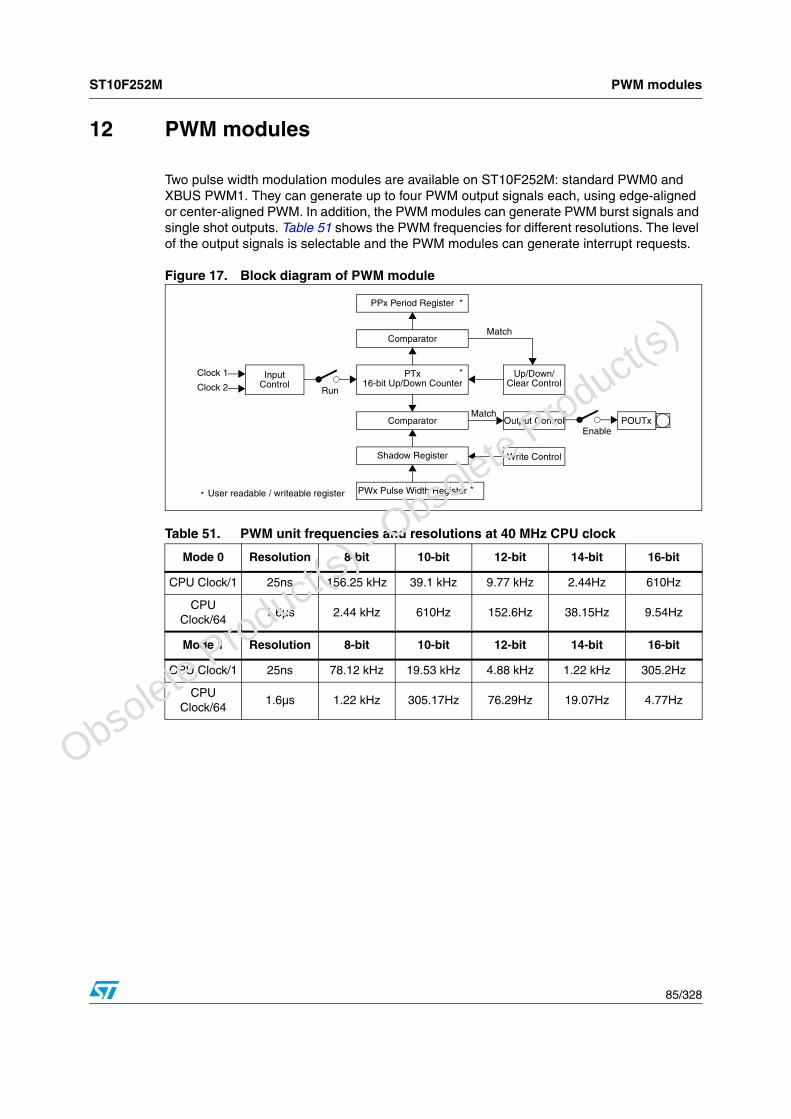
ST10F252M PWM modules
85/328
12 PWM modules
Two pulse width modulation modules are available on ST10F252M: standard PWM0 and XBUS PWM1. They can generate up to four PWM output signals each, using edge-aligned or center-aligned PWM. In addition, the PWM modules can generate PWM burst signals and single shot outputs. Table 51 shows the PWM frequencies for different resolutions. The level of the output signals is selectable and the PWM modules can generate interrupt requests.
Figure 17. Block diagram of PWM module
Table 51. PWM unit frequencies and resolutions at 40 MHz CPU clock
Mode 0 Resolution 8-bit 10-bit 12-bit 14-bit 16-bit
CPU Clock/1 25ns 156.25 kHz 39.1 kHz 9.77 kHz 2.44Hz 610Hz
CPU Clock/64
1.6µs 2.44 kHz 610Hz 152.6Hz 38.15Hz 9.54Hz
Mode 1 Resolution 8-bit 10-bit 12-bit 14-bit 16-bit
CPU Clock/1 25ns 78.12 kHz 19.53 kHz 4.88 kHz 1.22 kHz 305.2Hz
CPU Clock/64
1.6µs 1.22 kHz 305.17Hz 76.29Hz 19.07Hz 4.77Hz
PPx Period Register
Comparator
PTx16-bit Up/Down Counter
Shadow Register
PWx Pulse Width Register
Input
RunControl
Clock 1
Clock 2
Comparator
*
*
*
Up/Down/Clear Control
Match
Output ControlMatch
Write Control
* User readable / writeable register
EnablePOUTx
O
bsolete Product(
s) - O
bsolete Product(
s)

Parallel ports ST10F252M
86/328
13 Parallel ports
13.1 IntroductionTo accept or generate single external control signals or parallel data, the ST10F252 provides up to 76 parallel I/O lines, organized into one 14-bit I/O port (Port 2), five 8-bit I/O ports (PORT0 comprising P0H and P0L, PORT1 comprising P1H and P1L, and Port 4), one 12-bit I/O port (Port 3) and one 10-bit input port (Port 5).
These port lines may be used for general purpose input and output, controlled via software, or may be used implicitly by ST10F252’s integrated peripherals or the external bus controller.
All port lines are bit addressable and all input/output lines are individually (bit-wise) programmable as inputs or outputs via direction registers (except for Port 5). The I/O ports are true bidirectional ports, which are switched to high impedance state when configured as inputs. The output drivers of three I/O ports (2, 3, 4) can be configured (pin by pin) for push/pull operation or open-drain operation via control registers.
The logic level of a pin is clocked into the input latch once per state time, regardless whether the port is configured for input or output.
A write operation to a port pin configured as an input causes the value to be written into the port output latch, while a read operation returns the latched state of the pin itself. A read-modify-write operation reads the value of the pin, modifies it, and writes it back to the output latch.
Writing to a pin configured as an output (DPx.y=‘1’) causes the output latch and the pin to have the written value, since the output buffer is enabled. Reading this pin returns the value of the output latch. A read-modify-write operation reads the value of the output latch, modifies it, and writes it back to the output latch, thus also modifying the level at the pin.
Note: A set of registers, mapped on XBUS, is implemented on ST10F252 to manage the data, direction and open-drain mode for those pins where the XPWM, XASC and XSSC are mapped. The standard port register bits for these pins are working when the X-peripherals are not enabled (see XPERCON register); however, when the X-Peripherals are enabled, the new registers take the control of the pins and the content if the standard registers is ignored.
O
bsolete Product(
s) - O
bsolete Product(
s)

ST10F252M Parallel ports
87/328
Figure 18. SFRs, XBUS registers and pins associated with the parallel ports
Dat
a In
put /
Out
put R
egis
ter
15 -
14 -
13 -
12 -
11 -
10 -
9 -
8 -
7 Y
6 Y
5 Y
4 Y
3 Y
2 Y
1 Y
0 YP
0L
--
--
--
--
YY
YY
YY
YY
P0H
--
--
--
--
YY
YY
YY
YY
P1L
--
--
--
--
YY
YY
YY
YY
P1H
YY
YY
YY
YY
YY
YY
YY
--
P2
Y-
YY
YY
YY
YY
-Y
-Y
YY
P3
--
--
--
--
YY
YY
YY
YY
P4
--
--
--
YY
YY
YY
YY
YY
P5
--
--
--
--
--
--
YY
YY
P7
Dire
ctio
n C
ontr
ol R
egis
ters
15 -
14 -
13 -
12 -
11 -
10 -
9 -
8 -
7 Y
6 Y
5 Y
4 Y
3 Y
2 Y
1 Y
0 YD
P0L
--
--
--
--
YY
YY
YY
YY
DP
0H
--
--
--
--
YY
YY
YY
YY
DP
1L
--
--
--
--
YY
YY
YY
YY
DP
1H
YY
YY
YY
YY
YY
YY
YY
--
DP
2
Y-
YY
YY
YY
YY
-Y
-Y
YY
DP
3
--
--
--
--
YY
YY
YY
YY
DP
4
--
--
--
--
--
--
YY
YY
DP
7
Thr
esho
ld /
Ope
n D
rain
Con
trol
15 -
14 -
13 -
12 -
11 -
10 -
9 -
8 -
7 Y
6 Y
5 Y
4 Y
3 Y
2 Y
1 Y
0 YP
ICO
N
YY
YY
YY
YY
YY
YY
YY
--
OD
P2
--
Y-
YY
YY
YY
-Y
-Y
YY
OD
P3
--
--
--
--
YY
YY
--
--
OD
P4
--
--
--
--
--
--
YY
YY
OD
P7
Y:
Bit
has
an I/
O fu
nctio
n-
:B
it ha
s no
I/O
ded
icat
ed fu
nctio
n or
is n
ot im
plem
ente
dR
egis
ter
belo
ngs
to E
SF
R a
rea
E:
--
--
--
YY
YY
YY
YY
YY
P5D
IDIS
PIC
ON
:P
2LIN
P2H
INP
3LIN
P3H
INP
4LIN
P6L
INP
7LIN
P8L
IN
E E E E
E E E E E
XB
US
Reg
iste
rs
15 -
14 -
13 -
12 -
11 -
10 -
9 -
8 -
7 Y
6 Y
5 Y
4 Y
3 Y
2 Y
1 Y
0 YX
SS
CP
OR
T
--
--
--
--
--
YY
YY
YY
XS
1PO
RT
--
--
YY
YY
YY
YY
YY
YY
XW
PM
PO
RT
--
--
--
--
--
YY
YY
YY
XP
ICO
N
XP
ICO
N:
P0L
IN P
0HIN
P1L
IN P
1HIN
P5L
IN P
5HIN
O
bsolete Product(
s) - O
bsolete Product(
s)
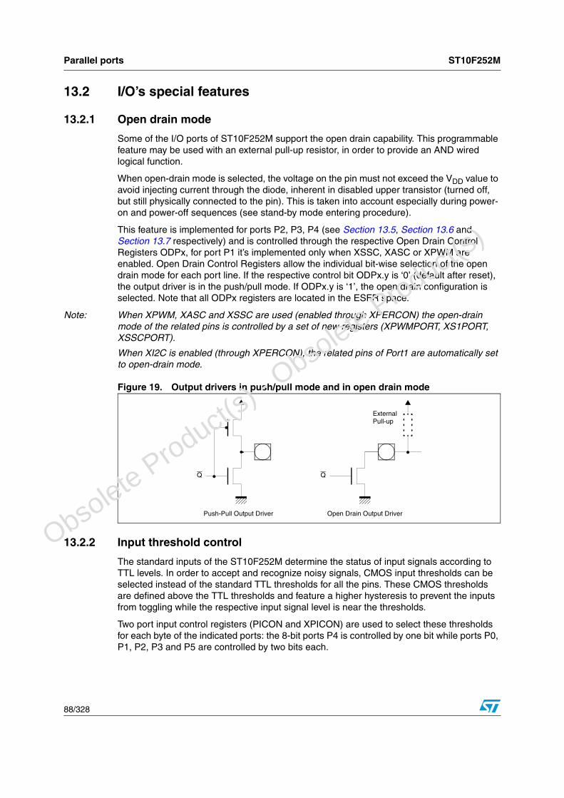
Parallel ports ST10F252M
88/328
13.2 I/O’s special features
13.2.1 Open drain mode
Some of the I/O ports of ST10F252M support the open drain capability. This programmable feature may be used with an external pull-up resistor, in order to provide an AND wired logical function.
When open-drain mode is selected, the voltage on the pin must not exceed the VDD value to avoid injecting current through the diode, inherent in disabled upper transistor (turned off, but still physically connected to the pin). This is taken into account especially during power-on and power-off sequences (see stand-by mode entering procedure).
This feature is implemented for ports P2, P3, P4 (see Section 13.5, Section 13.6 and Section 13.7 respectively) and is controlled through the respective Open Drain Control Registers ODPx, for port P1 it’s implemented only when XSSC, XASC or XPWM are enabled. Open Drain Control Registers allow the individual bit-wise selection of the open drain mode for each port line. If the respective control bit ODPx.y is ‘0’ (default after reset), the output driver is in the push/pull mode. If ODPx.y is ‘1’, the open drain configuration is selected. Note that all ODPx registers are located in the ESFR space.
Note: When XPWM, XASC and XSSC are used (enabled through XPERCON) the open-drain mode of the related pins is controlled by a set of new registers (XPWMPORT, XS1PORT, XSSCPORT).
When XI2C is enabled (through XPERCON), the related pins of Port1 are automatically set to open-drain mode.
Figure 19. Output drivers in push/pull mode and in open drain mode
13.2.2 Input threshold control
The standard inputs of the ST10F252M determine the status of input signals according to TTL levels. In order to accept and recognize noisy signals, CMOS input thresholds can be selected instead of the standard TTL thresholds for all the pins. These CMOS thresholds are defined above the TTL thresholds and feature a higher hysteresis to prevent the inputs from toggling while the respective input signal level is near the thresholds.
Two port input control registers (PICON and XPICON) are used to select these thresholds for each byte of the indicated ports: the 8-bit ports P4 is controlled by one bit while ports P0, P1, P2, P3 and P5 are controlled by two bits each.
Q
Push-Pull Output Driver
Q
Open Drain Output Driver
ExternalPull-up
O
bsolete Product(
s) - O
bsolete Product(
s)

ST10F252M Parallel ports
89/328
Note: PICON is an ESFR register, while XPICON is an XBUS register. XPICON is accessible only after bit XMISCEN of XPERCON register and bit XPEN of SYSCON register have been set.
All options for individual direction and output mode control are available for each pin, independent of the selected input threshold. The input hysteresis (variable, according to TTL or CMOS selection) provides stable inputs from noisy or slowly changing external signals.
13.2.3 Alternate port functions
Each port line has one (or more) associated programmable alternate input or output functions. If an alternate output function of a pin is to be used, the direction of this pin must be programmed for output (DPx.y=‘1’), except for some signals that are used directly after reset and are configured automatically. Otherwise the pin remains in the high-impedance
PICON (F1C4 / E2) ESFR Reset value: --00h
15 14 13 12 11 10 9 8 7 6 5 4 3 2 1 0
Reserved P4LINP3HINP3LINP2HINP2LIN
- - - - - - - - - - - RW RW RW RW RW
Table 52. Port input control register (PICON)
Bit Name Function
15:5 Reserved
4:0 PxLIN
Port x low byte input level selection
’0’: Pins Px.7...Px.0 switch on standard TTL input levels.’1’: Pins Px.7...Px.0 switch on standard CMOS input levels.
XPICON (EB26) XBUS Reset value: --00h
15 14 13 12 11 10 9 8 7 6 5 4 3 2 1 0
Reserved P5HIN P5LIN P1HIN P1LIN P0HIN P0LIN
- - - - - - - - - - RW RW RW RW RW RW
Table 53. Additional port input control register (XPICON)
Bit Name Function
15:6 Reserved
5:0 PxHINPort x high byte input level selection’0’: Pins Px.15...Px.8 switch on standard TTL input levels.
’1’: Pins Px.15...Px.8 switch on standard CMOS input levels.
Figure 20. Hysteresis concept
Input level
Bit state
Hysteresis
O
bsolete Product(
s) - O
bsolete Product(
s)

Parallel ports ST10F252M
90/328
state and is not affected by the alternate output function. The respective port latch should hold a ‘1’, because its output is ANDed with the alternate output data (except for PWM output signals).
If an alternate input function of a pin is used, the direction of the pin must be programmed for input (DPx.y=‘0’) if an external device is driving the pin. The input direction is the default after reset. If no external device is connected to the pin, however, the direction for this pin can also be set to output. In this case, the pin reflects the state of the port output latch. Thus, the alternate input function reads the value stored in the port output latch. This can be used for testing purposes to allow a software trigger of an alternate input function by writing to the port output latch.
On most of the port lines, user software is responsible for setting the proper direction when using an alternate input or output function of a pin. This is done by setting or clearing the direction control bit DPx.y of the pin before enabling the alternate function. There are port lines, however, where the direction of the port line is switched automatically. For instance, in the multiplexed external bus modes of PORT0, the direction must be switched several times for an instruction fetch to output the addresses and to input the data. Obviously, this cannot be done through instructions. In these cases, the direction of the port line is switched automatically by hardware if the alternate function of such a pin is enabled. To determine the appropriate level of the port output latches check how the alternate data output is combined with the respective port latch output.
There is one basic structure for all port lines with only an alternate input function. Port lines with only an alternate output function, however, have different structures due to the way the direction of the pin is switched and depending on whether the pin is accessible by the user software or not in the alternate function mode.
All port lines that are not used for these Alternate Functions may be used as general purpose I/O lines. When using port pins for general purpose output, the initial output value should be written to the port latch prior to enabling the output drivers, to avoid undesired transitions on the output pins. This applies to single pins as well as to pin groups (see examples below).
Note: When using several BSET pairs to control more pins of one port, these pairs must be separated by instructions, which do not reference the respective port.
13.3 PORT0The two 8-bit ports P0H and P0L represent the higher and lower part of PORT0, respectively. Both halves of PORT0 can be written (for example, via a PEC transfer) without affecting the other half.
SINGLE_BIT: BSET P4.7 ; Initial output level is “high”
BSET DP4.7 ; Switch on the output driver
BIT_GROUP: BFLDH P4, #24H, #24H ; Initial output level is “high”
BFLDH DP4, #24H, #24H ; Switch on the output drivers
O
bsolete Product(
s) - O
bsolete Product(
s)

ST10F252M Parallel ports
91/328
P0L register
P0H register
If this port is used for general purpose I/O, the direction of each line can be configured via the corresponding direction registers DP0H and DP0L.
DP0L register
DP0H register
13.3.1 Alternate functions of PORT0
When an external bus is enabled, PORT0 is used as a data bus or an address and data bus, when no additional ADC Channels (6) are selected.
P0L register (FF00/80) SFR Reset value: --00h
15 14 13 12 11 10 9 8 7 6 5 4 3 2 1 0
reserved POL.7 POL.6 POL.5 POL.4 POL.3 POL.2 POL.1 POL.0
- RW RW RW RW RW RW RW RW
P0H register (FF02/81) SFR Reset value: --00h
15 14 13 12 11 10 9 8 7 6 5 4 3 2 1 0
reserved POH.7
POH.6
POH.5
POH.4
POH.3
POH.2 POH.1 POH.0
- RW RW RW RW RW RW RW RW
Table 54. P0L and P0H registers functions
Bit Name Function
P0L 7.0
P0H 7.0P0X.y Port data register P0H or P0L bit y
DP0L register (F100/80) ESFR Reset value: --00h
15 14 13 12 11 10 9 8 7 6 5 4 3 2 1 0
- DPOL.7
DPOL.6
DPOL.5
DPOL.4
DPOL.3
DPOL.2
DPOL.1
DPOL.0
- RW RW RW RW RW RW RW RW
DP0H register (F102/81) ESFR Reset value: --00h
15 14 13 12 11 10 9 8 7 6 5 4 3 2 1 0
- DPOH.7
DPOH.6
DPOH.5
DPOH.4
DPOH.3
DPOH.2
DPOH.1
DPOH.0
- RW RW RW RW RW RW RW RW
Table 55. DP0L and DP0H registers functions
Bit Name Function
DP0L 7.0DP0H 7.0
DP0X.y
Port direction register DP0H or DP0L bit y
‘0’: Port line P0X.y is an input (high-impedance)
‘1’: Port line P0X.y is an output
O
bsolete Product(
s) - O
bsolete Product(
s)

Parallel ports ST10F252M
92/328
An external 8-bit de-multiplexed bus only uses P0L, while P0H is free for I/O (provided that no other bus mode is enabled).
PORT0 is also used to select the system start-up configuration. During reset, PORT0 is configured to input and each line is held high through an internal pull-up device. Each line can now be individually pulled to a low level (see the DC-level specifications in the appropriate data sheets) through an external pull-down device. A default configuration is selected when the respective PORT0 lines are at a high level. Through pulling individual lines to a low level, this default can be changed according to the needs of the application. The internal pull-up devices are designed such that an external pull-down resistors (see Data Sheet specification) can be used to apply a correct low level. These external pull-down resistors can remain connected to the PORT0 pins also during normal operation, however, take care that they do not disturb the normal function of PORT0 (this may be the case, for example, if the external resistor is too strong).
At the end of reset, the selected bus configuration is written to the BUSCON0 register. The configuration of the high byte of PORT0, is copied into the special register RP0H. This read-only register holds the selection for the number of chip selects and segment addresses. Software can read this register to react to the selected configuration, if required. When the reset is terminated, the internal pull-up devices are switched off, and PORT0 is switched to the appropriate operating mode.
During external accesses in multiplexed bus modes, PORT0 first outputs the 16-bit intra-segment address as an alternate output function. PORT0 is then switched to high-impedance input mode to read the incoming instruction or data. In 8-bit data bus mode, two memory cycles are required for word accesses, the first for the low byte and the second for the high byte of the word. During write cycles PORT0 outputs the data byte or word after outputting the address. During external accesses in de-multiplexed bus modes, PORT0 reads the incoming instruction or data word or outputs the data byte or word.
Figure 21. PORT0 I/O and alternate functions
When an external bus mode is enabled, the direction of the port pin and the loading of data into the port output latch are controlled by the bus controller hardware. The input of the port output latch is disconnected from the internal bus and is switched to the line labeled “Alternate Data Output” via a multiplexer. The alternate data can be the 16-bit intra-segment address or the 8/16-bit data information. The incoming data on PORT0 is read on the line “Alternate Data Input”. While an external bus mode is enabled, the user software should not
P0H.7
P0H.6
P0H.5
P0H.4/AN15
P0H.3/AN14
P0H.2/AN13
P0H.1/AN12
P0H.0/AN11
P0L.7/AN10
P0L.6
P0L.5
P0L.4
P0L.3
P0L.2
P0L.1
P0L.0
PORT0
P0H
P0L
Alternate Function a) b) c) d)
General PurposeI/O and Analog Inputs
8-bitDemux Bus
16-bitDemux Bus
8-bitMUX Bus
16-bitMUX Bus
D7
D6
D5
D4
D3
D2
D1
D0
D15
D14
D13
D12
D11
D10
D9
D8
D7
D6
D5
D4
D3
D2
D1
D0
A15
A14
A13
A12
A11
A10
A9
A8
AD7
AD6
AD5
AD4
AD3
AD2
AD1
AD0
AD15
AD14
AD13
AD12
AD11
AD10
AD9
AD8
AD7
AD6
AD5
AD4
AD3
AD2
AD1
AD0
O
bsolete Product(
s) - O
bsolete Product(
s)

ST10F252M Parallel ports
93/328
write to the port output latch, otherwise unpredictable results may occur. When the external bus modes are disabled, the contents of the direction register last written becomes active.
Figure 22 shows the structure of a PORT0 pin.
Figure 22. Block diagram of a PORT0
13.3.2 Disturb protection on analog inputs
A register is provided for additional disturb protection support on analog inputs for PORT0. In particular, the register can disable both the digital input and output sections of the I/O structure. To access this register the bit XMISCEN of register XPERCON and bit XPEN of register SYSCON must be set.
DirectionLatch
Write DP0H.y / DP0L.y
Read DP0H.y / DP0L.y
Port OutputLatch
Write P0H.y / P0L.y
Read P0H.y / P0L.y
Inte
rnal
Bus
MUX
0
1
MUX
0
1
AlternateDataOutput
MUX
0
1AlternateDirection
InputLatch
Clock
P0H.yP0L.yOutput
Buffer
y = 7...0
AlternateFunctionEnable
Port DataOutput
O
bsolete Product(
s) - O
bsolete Product(
s)
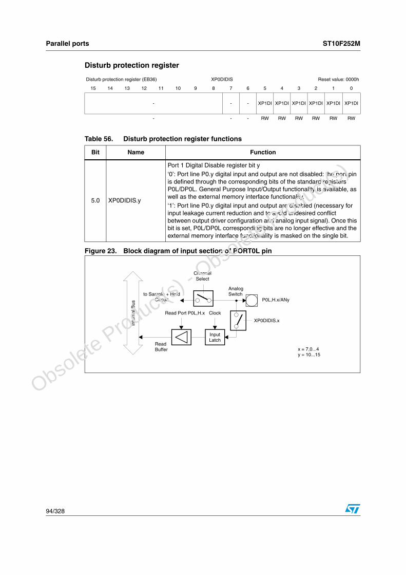
Parallel ports ST10F252M
94/328
Disturb protection register
Figure 23. Block diagram of input section of PORT0L pin
Disturb protection register (EB36) XP0DIDIS Reset value: 0000h
15 14 13 12 11 10 9 8 7 6 5 4 3 2 1 0
- - - XP1DI XP1DI XP1DI XP1DI XP1DI XP1DI
- - - RW RW RW RW RW RW
Table 56. Disturb protection register functions
Bit Name Function
5.0 XP0DIDIS.y
Port 1 Digital Disable register bit y‘0’: Port line P0.y digital input and output are not disabled: the port pin is defined through the corresponding bits of the standard registers P0L/DP0L. General Purpose Input/Output functionality is available, as well as the external memory interface functionality.
‘1’: Port line P0.y digital input and output are disabled (necessary for input leakage current reduction and to avoid undesired conflict between output driver configuration and analog input signal). Once this bit is set, P0L/DP0L corresponding bits are no longer effective and the external memory interface functionality is masked on the single bit.
Read Port P0L,H.x
Inte
rnal
Bus
InputLatch
Clock
P0L,H.x/ANy
ReadBuffer
to Sample + HoldCircuit
ChannelSelect
AnalogSwitch
x = 7,0...4
XP0DIDIS.x
y = 10...15
O
bsolete Product(
s) - O
bsolete Product(
s)

ST10F252M Parallel ports
95/328
Figure 24. Block diagram of a PORT0 pin
13.4 PORT1The two 8-bit ports P1H and P1L represent the higher and lower part of PORT1, respectively. Either half of PORT1 can be written (for example, by a PEC transfer) without effecting the other half.
P1L register
P1H register
DirectionLatch
Write DP0H.7 / DP0L.y
Read DP0H.7 / DP0L.y
Port OutputLatch
Write P0H.7 / P0L.y
Read P0H.7 / P0L.y
Inte
rnal
Bus
MUX
0
1
MUX
0
1
MUX
0
1“1”
InputLatch
Clock
P0H.yP0L.7Output
Buffer
y = 0...4
AlternateFunctionEnable
Port DataOutput
AlternateDataOutput
XP0DIDIS.y,5
P1L register (FF04/82) SFR Reset value: --00h
15 14 13 12 11 10 9 8 7 6 5 4 3 2 1 0
- P1L7 P1L6 P1L5 P1L4 P1L3 P1L2 P1L1 P1L0
- RW RW RW RW RW RW RW RW
P1H register (FF06/83) SFR Reset value: --00h
15 14 13 12 11 10 9 8 7 6 5 4 3 2 1 0
- P1H7 P1H6 P1H5 P1H4 P1H3 P1H2 P1H1 P1H0
- RW RW RW RW RW RW RW RW
O
bsolete Product(
s) - O
bsolete Product(
s)

Parallel ports ST10F252M
96/328
If PORT1 is used for general purpose I/O, the direction of each line can be configured via the corresponding direction registers DP1H and DP1L.
DP1L register
DP1H register
If PORT1 pins are used as alternate function for input/output of XPWM, XASC or XSSC peripherals, the direction of each pins is configured by dedicated registers mapped in the X-peripheral memory area, an open drain setting is also available for used port P1 pins. Registers that are used for different alternate function are described in the following.
XSSCPORT
This register is enabled and visible only when bit XPEN of SYSCON is set, and bit XSSCEN in XPERCON is also set. If not enabled, the standard P1H, DP1H registers are used to configure pins P1H.1, P1H.2 and P1H.3; the open drain setting is not available.
XSSCPORT register
Table 57. P1L and P1H registers functions
Pin Name Function
P1L 7.0
P1R 7.0P1X.y Port data register P1H or P1L bit y
DP1L register (F104/82) ESFR Reset value: --00h
15 14 13 12 11 10 9 8 7 6 5 4 3 2 1 0
- DP1L.7
DP1L.6
DP1L.5
DP1L.4
DP1L.3
DP1L.2
DP1L.1
DP1L.0
- RW RW RW RW RW RW RW RW
DP1H register (F106/83) ESFR Reset value: --00h
15 14 13 12 11 10 9 8 7 6 5 4 3 2 1 0
- DP1H.7
DP1H.6
DP1H.5
DP1H.4
DP1H.3
DP1H.2
DP1H.1
DP1H.0
- RW RW RW RW RW RW RW RW
Table 58. DP1L and DP1H registers functions
Bit Name Function
DP1L 7.0
DP1H 7.0DP1X.y
Port direction register DP1H or DP1L bit y‘0’: Port line P1X.y is an input (high-impedance)
‘1’: Port line P1X.y is an output
XSSCPORT register (E880) Reset value: 0000h
15 14 13 12 11 10 9 8 7 6 5 4 3 2 1 0
- XODP1H.3
XP1H.3
XDP1H.3.7
XODP1H.2
XP1H.2
XDP1H.2.6
XODP1H.1
XP1H.1
XDP1H.1
- RW RW RW RW RW RW RW RW RW
O
bsolete Product(
s) - O
bsolete Product(
s)

ST10F252M Parallel ports
97/328
XS1PORT
This register is enabled and visible only when bit XPEN of SYSCON is set, and bit XASCEN in XPERCON is also set. If not enabled, the standard P1L, DP1L registers are used to configure pins P1L.4 and P1L.5; the open drain setting is not available.
XS1PORT register
XPWMPORT
This register is enabled and visible only when bit XPEN of SYSCON is set, and bit XPWMEN in XPERCON is also set. If not enabled, the standard P1L, DP1L registers are used to configure pins P1L.0, P1L.1, P1L.2 and P1L.3; the open drain setting is not available.
Table 59. XSSCPORT register functions
Bit Name Function
8, 5, 2 XODP1H.y
Port open drain control register bit y (y = 1, 2, 3 only)
‘0’: Port line P1H.y output driver in push/pull mode‘1’: Port line P1H.y output driver in open drain mode
7, 4, 1 XP1H.y Port data register bit y (y = 1, 2, 3 only)
6. 3. 0 XDP1H.y
Port direction register bit y (y = 1, 2, 3 only)
‘0’: Port line P1H.y is an input (high-impedance)‘1’: Port line P1H.y is an output
XS1PORT register (E980) Reset value: 0000h
15 14 13 12 11 10 9 8 7 6 5 4 3 2 1 0
Reserved XODP1L.4
XP1L.4
XDP1L.4.7
XODP1L.5
XP1L.5
XDP1L.5
- RW RW RW RW RW RW
Table 60. XS1PORT register functions
Bit Name Function
5, 2 XODP1L.y
Port open drain control register bit y (y = 4, 5 only)
‘0’: Port line P1L.y output driver in push/pull mode‘1’: Port line P1L.y output driver in open drain mode
4, 1 XP1L.y Port data register bit y (y = 4, 5 only)
3, 0 XDP1L.y
Port direction register bit y (y = 4, 5 only)
‘0’: Port line P1L.y is an input (high-impedance)‘1’: Port line P1L.y is an output
O
bsolete Product(
s) - O
bsolete Product(
s)

Parallel ports ST10F252M
98/328
XPWPORT register
13.4.1 Alternate functions of PORT1
When a de-multiplexed external bus is enabled, PORT1 is used as address bus. De-multiplexed bus modes use PORT1 as a 16-bit port. Otherwise all 16 port lines can be used for general purpose I/O.
Pins P1H.3...P1H.1 of PORT1 are also used for receive/transmit and clock lines of SSC1.
Pins P1L.7 and P1L.6 of PORT1 are also used for input/output lines of I2C.
Pins P1L.5 and P1L.4 of PORT1 are also used for receive, transmit lines of ASC1.
Pins P1L.3...P1L.0 of PORT1 are also used for output lines of PWM1.
The upper four pins of PORT1 (P1H.7...P1H.4) also serve as capture input lines for the CAPCOM2 unit (CC27I...CC24I). As all other capture inputs, the capture input function of pins P1H.7...P1H.4 can also be used as external interrupt inputs (83.34 ns sample rate at 48 MHz CPU clock).
During external accesses in de-multiplexed bus modes, PORT1 outputs the 16-bit intra-segment address as an alternate output function.
During external accesses in multiplexed bus modes, when no BUSCON register selects a de-multiplexed bus mode, PORT1 is not used and is available for general purpose I/O and other alternate functions.
XPWNPORT register (EC80) Reset value: 0000h
15 14 13 12 11 10 9 8 7 6 5 4 3 2 1 0
- XODP1L.3
XP1L.3
XDP1L.3
XODP1L.2
XP1L.2
XDP1L.2.2
XODP1L.1
XP1L.1
XDP1L.1
XODP1L.0
XP1L.0
XDP1L.0
- RW RW RW RW RW RW RW RW RW RW RW RW
Table 61. XPWPORT register functions
Bit Name Function
11, 8, 5, 2
XODP1L.yPort open drain control register bit y (y = 0, 1, 2, 3 only)‘0’: Port line P1L.y output driver in push/pull mode
‘1’: Port line P1L.y output driver in open drain mode
10, 7, 4, 1
XP1L.y Port data register bit y (y = 0, 1, 2, 3 only)
9, 6, 3, 0
XDP1L.y
Port direction register bit y (y = 0, 1, 2, 3 only)
‘0’: Port line P1L.y is an input (high-impedance)
‘1’: Port line P1L.y is an output
O
bsolete Product(
s) - O
bsolete Product(
s)

ST10F252M Parallel ports
99/328
Figure 25. PORT1 I/O and alternate functions
When demultiplexed external bus mode is enabled, the direction of the port pin and the loading of data into the port output latch are controlled by the bus controller hardware. The input of the port output latch is disconnected from the internal bus and is switched to the line labeled “Demux Bus” via a multiplexer. The alternate data is the 16-bit intra-segment address. While an external bus mode is enabled, the software does not write to the port output latch, otherwise unpredictable results may occur. When external bus modes are disabled, the contents of the direction register last written becomes active.
If one or more peripherals from XASC, I2C, XSSC, XPWM (bit XPEN of SYSCON is set, and associated bit to peripheral in XPERCON is set) are enabled, alternate functions for demultiplexed bus cannot be used.
Figure 26. Block diagram of a PORT1 pin P1H.7...P1H.4
PORT1
P1H
P1L
Alternate Function a)
General PurposeInput/Output
8/16-bitDemux bus
b)
CAPCOM2 Capt.In/XPWM/XSSC/XASC/I2C
P1H.7P1H.6P1H.5P1H.4P1H.3P1H.2P1H.1P1H.0P1L.7P1L.6P1L.5P1L.4P1L.3P1L.2P1L.1P1L.0
A15A14A13A12A11A10A9A8A7A6A5A4A3A2A1A0
CC27ICC26ICC25ICC24ISCLKMTSRMRST
SDASCLRxDTxDXPOUT3XPOUT2XPOUT1XPOUT0
DirectionLatch
Write DP1H.y
Read DP1H.y / DP1L.y
Port OutputLatch
Write P1H.y
Read P1H.y
Inte
rnal
Bus
MUX
0
1
MUX
0
1
MUX
0
1“1”
InputLatch
Clock
P1H.y
OutputBuffer
(y = 7...4)
DEMUXBUSEnable
Port DataOutput
DEMUX BUSOutput
O
bsolete Product(
s) - O
bsolete Product(
s)
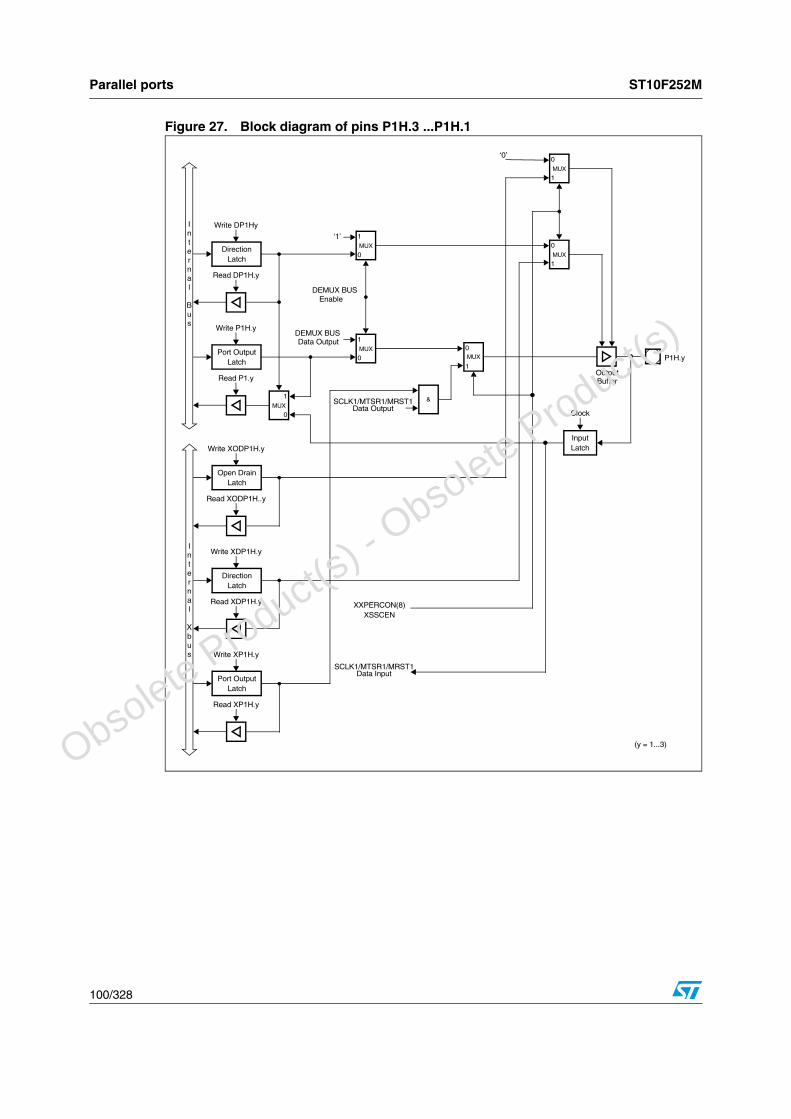
Parallel ports ST10F252M
100/328
Figure 27. Block diagram of pins P1H.3 ...P1H.1
P1H.y
DirectionLatch
Write DP1Hy
Read DP1H.y
Port OutputLatch
Write P1H.y
Read P1.y
MUX
1
0
MUX
1
0
MUX
1
0
Data Output
MUX
1
0
‘1’
Enable
Open DrainLatch
Write XODP1H.y
Read XODP1H..y
DirectionLatch
Write XDP1H.y
Read XDP1H.y
Port OutputLatch
Write XP1H.y
Read XP1H.y
&SCLK1/MTSR1/MRST1Data Output
OutputBuffer
MUX
0
1
MUX
0
1
InputLatch
Clock
SCLK1/MTSR1/MRST1Data Input
(y = 1...3)
Internal
Bus
Internal
Xbus
XSSCENXXPERCON(8)
DEMUX BUS
DEMUX BUS
‘0’
O
bsolete Product(
s) - O
bsolete Product(
s)

ST10F252M Parallel ports
101/328
Figure 28. Block diagram of pin P1L.6, P1.7
P1L.y
DirectionLatch
Write DP1L.y
Read DP1L.y
Port OutputLatch
Write P1L.y
Read P1L.y
MUX
1
0
MUX
1
0
DEMUX BUSData Output
MUX
1
0
‘1’
DEMUX BUS
OutputBuffer
InputLatch
Clock
Internal
Bus
MUX
1
0
SDA/SCLData Output
MUX
0
1‘1’
XPERCON.9(I2CEN)
SDA/SCLData Input
Open Drain
(y = 6,7)
Enable
O
bsolete Product(
s) - O
bsolete Product(
s)
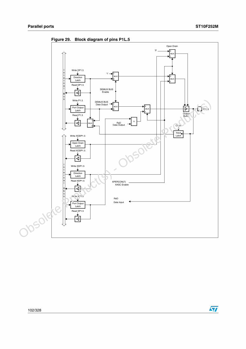
Parallel ports ST10F252M
102/328
Figure 29. Block diagram of pins P1L.5
P1L.5
DirectionLatch
Write DP1.5
Read DP1.5
Port OutputLatch
Write P1.5
Read P1.5
MUX
1
0
MUX
1
0
MUX
1
0
Data Output
MUX
1
0
‘1’
Enable
Open DrainLatch
Write XODP1.5
Read XODP1.5
DirectionLatch
Write XDP1.5
Read XDP1.5
Port OutputLatch
Write XP1.5
Read XP1.5
&RxD
Data Output
OutputBuffer
MUX
0
1
MUX
0
1
InputLatch
Clock
Data Input
Internal
Bus
Internal
Xbus
XASC EnableXPERCON(7)
DEMUX BUS
DEMUX BUS
RxD
‘0’
Open Drain
O
bsolete Product(
s) - O
bsolete Product(
s)

ST10F252M Parallel ports
103/328
Figure 30. Block diagram of pins P1L.4
P1L.4
DirectionLatch
Write DP1L.4
Read DP1L.4
Port OutputLatch
Write P1L.4
Read P1L.4
MUX
1
0
MUX
1
0
MUX
1
0
Data Output
MUX
1
0
‘1’
Enable
Open DrainLatch
Write XODP1L.4
Read XODP1L.4
DirectionLatch
Write XDP1L.4
Read XDP1L.4
Port OutputLatch
Write XP1L.4
Read XP1L.4
&TxD
Data Output
OutputBuffer
MUX
0
1
MUX
0
1
InputLatch
Clock
Internal
Bus
Internal
Xbus
XASCENXPERCON(7)
DEMUX BUS
DEMUX BUS
‘0’
Open Drain
O
bsolete Product(
s) - O
bsolete Product(
s)

Parallel ports ST10F252M
104/328
Figure 31. Block diagram of pins P1L.3...P1L.0
13.5 PORT2If this 14-bit port is used for general purpose I/O, the direction of each line is configured by the corresponding direction register DP2. Each port line can be switched into push/pull or open drain mode by the open drain control register ODP2.
P1L.y
DirectionLatch
Write DP1L.y
Read DP1L.y
Port OutputLatch
Write P1L.y
Read P1L.y
MUX
1
0
MUX
1
0
MUX
1
0
Data Output
MUX
1
0
‘1’
Enable
Open DrainLatch
Write XODP1L.y
Read XODP1L.y
DirectionLatch
Write XDP1L.y
Read XDP1L.y
Port OutputLatch
Write XP1L.y
Read XP1L.y
XPOUTyData Output
OutputBuffer
MUX
0
1
MUX
0
1
InputLatch
Clock
Internal
Bus
Internal
Xbus
XPWMENXPERCON(6)
DEMUX BUS
DEMUX BUS
‘0’
=1
EXOR
(y = 0...3)
Open Drain
O
bsolete Product(
s) - O
bsolete Product(
s)

ST10F252M Parallel ports
105/328
PORT2 register
PORT2 direction register
PORT2 open drain control register
13.5.1 Alternate functions of PORT2
All PORT2 lines (P2.15 to P2.2) serve as capture inputs or compare outputs (CC15IO to CC2IO) for the CAPCOM1 unit.
PORT2 register (FFC0/E0) SFR Reset value: 0000h
15 14 13 12 11 10 9 8 7 6 5 4 3 2 1 0
P2.15 P2.14 P2.13 P2.12 P2.11 P2.10 P2.9 P2.8 P2.7 P2.6 P2.5 P2.4 P2.3 P2.2 - -
RW RW RW RW RW RW RW RW RW RW RW RW RW RW - -
Table 62. PORT2 register functions
Bit Name Function
15.2 P2.y Port data register P2 bit y
PORT2 direction register (FFC2/E1) SFR Reset value: 0000h
15 14 13 12 11 10 9 8 7 6 5 4 3 2 1 0
DP2.15
DP2.14
DP2.13
DP2.12
DP2.11
DP2.10 DP2.9 DP2.8 DP2.7 DP2.6 DP2.5 DP2.4 DP2.3 DP2.2 - -
RW RW RW RW RW RW RW RW RW RW RW RW RW RW - -
Table 63. PORT2 direction register functions
Bit Name Function
15.2 DP2.yPort direction register DP2 bit y‘0’: Port line P2.y is an input (high-impedance)
‘1’: Port line P2.y is an output
PORT2 open drain control register (F1C2/E1) ESFR Reset value: 0000h
15 14 13 12 11 10 9 8 7 6 5 4 3 2 1 0
ODP2. 15
ODP2. 14
ODP2.13
ODP2. 12
ODP2. 11
ODP2. 10
ODP2.9
ODP2.8
ODP2.7
ODP2.6
ODP2.5
ODP2.4
ODP2.3
ODP2.2 - -
RW RW RW RW RW RW RW RW RW RW RW RW RW RW - -
Table 64. PORT2 open drain control register functions
Bit Name Function
15.2 ODP2.y
Port 2 open drain control register bit y
‘0’: Port line P2.y output driver in push/pull mode‘1’: Port line P2.y output driver in open drain mode
O
bsolete Product(
s) - O
bsolete Product(
s)

Parallel ports ST10F252M
106/328
When a PORT2 line is used as a capture input, the state of the input latch, which represents the state of the port pin, is directed to the CAPCOM unit via the line “Alternate Pin Data Input”. If an external capture trigger signal is used, the direction of the respective pin is set to input. If the direction is set to output, the state of the port output latch is read since the pin represents the state of the output latch. This can be used to trigger a capture event through software by setting or clearing the port latch. In the output configuration, no external device may drive the pin, otherwise conflicts would occur.
When a PORT2 line is used as a compare output (compare modes 1 and 3), the compare event (or the timer overflow in compare mode 3) directly effects the port output latch. In compare mode 1, when a valid compare match occurs, the state of the port output latch is read by the CAPCOM control hardware via the line “Alternate Latch Data Input”, inverted, and written back to the latch via the line “Alternate Data Output”. The port output latch is clocked by the signal “Compare Trigger” which is generated by the CAPCOM unit. In compare mode 3, when a match occurs, the value '1' is written to the port output latch via the line “Alternate Data Output”. When an overflow of the corresponding timer occurs, a '0' is written to the port output latch. In both cases, the output latch is clocked by the signal “Compare Trigger”. The direction of the pin is set to output by the user, otherwise the pin will be in the high-impedance state and will not reflect the state of the output latch.
As can be seen from the port structure (Figure 33), the user software always has free access to the port pin even when it is used as a compare output. This is useful for setting up the initial level of the pin when using compare mode 1 or the double-register mode. In these modes, unlike in compare mode 3, the pin is not set to a specific value when a compare match occurs but is toggled instead.
When the user software wants to write to the port pin at the same time a compare trigger tries to clock the output latch, the write operation of the user software has priority. Each time a CPU write access to the port output latch occurs, the input multiplexer of the port output latch is switched to the line connected to the internal bus. The port output latch receives the value from the internal bus and the hardware-triggered change is lost.
As all other capture inputs, the capture input function of pins P2.15...P2.0 can also be used as external interrupt inputs (83.34 ns sample rate at 48 MHz CPU clock).
The upper eight PORT2 lines (P2.15 to P2.8) also can serve as fast external Interrupt inputs (EX7IN to EX0IN).
P2.15 also serves as the input for CAPCOM2 timer T7 (T7IN).
Table 65 summarizes the alternate functions of PORT2.
Table 65. PORT2 alternate functions
Pin Alternate function a) Alternate function b) Alternate function c)
P2.2 CC2IO
P2.3 CC3IO - -
P2.4 CC4IO - -
P2.5 CC5IO - -
P2.6 CC6IO - -
P2.7 CC7IO - -
P2.8 CC8IO EX0IN Fast Ext. Interrupt 0 Input -
P2.9 CC9IO EX1IN Fast Ext. Interrupt 1 Input -
O
bsolete Product(
s) - O
bsolete Product(
s)

ST10F252M Parallel ports
107/328
Figure 32. PORT2 I/O and alternate functions
The pins of PORT2 combine internal bus data with alternate data output before the port latch input.
P2.10 CC10IO EX2IN Fast Ext. Interrupt 0 Input -
P2.11 CC11IO EX3IN Fast Ext. Interrupt 1 Input -
P2.12 CC12IO EX4IN Fast Ext. Interrupt 0 Input -
P2.13 CC13IO EX5IN Fast Ext. Interrupt 1 Input -
P2.14 CC14IO EX6IN Fast Ext. Interrupt 0 Input -
P2.15 CC15IO EX7IN Fast Ext. Interrupt 1 Input T7IN timer external count input
Table 65. PORT2 alternate functions (continued)
Pin Alternate function a) Alternate function b) Alternate function c)
Port 2
Alternate Function a)
General PurposeInput/Output
CAPCOM1Capt.Inp./Comp.Output
b)
Fast ExternalInterrupt Input
c)
CAPCOM2Timer T7 Input
P2.15P2.14P2.13P2.12P2.11P2.10P2.9P2.8P2.7P2.6P2.5P2.4P2.3P2.2
CC15IOCC14IOCC13IOCC12IOCC11IOCC10IOCC9IOCC8IOCC7IOCC6IOCC5IOCC4IOCC3IOCC2IO
EX7INEX6INEX5INEX4INEX3INEX2INEX1INEX0IN
T7IN
No Pins
O
bsolete Product(
s) - O
bsolete Product(
s)

Parallel ports ST10F252M
108/328
Figure 33. Block diagram of a PORT2 pin
13.6 PORT3If this 12-bit port is used for general purpose I/O, the direction of each line can be configured by the corresponding direction register DP3. Most port lines can be switched into push/pull or open drain mode by the open drain control register ODP3 (pins P3.15 and P3.12 do not support open drain mode). P3.4 function can be used if P34EN, bit 5 of XMISC register, is set to 1, see Section 18.3.
Open DrainLatch
Write 0DP2.y
Read 0DP2.y
DirectionLatch
Write DP2.y
Read DP2.y
Inte
rnal
Bus
MUX
0
1
Alternate Data Input
InputLatch
Clock
P2.yCCyIO
OutputBuffer
x = 7...0
AlternateDataOutput
MUX
0
1OutputLatch
≥ 1Write Port P2.y
Compare Trigger
Read P2.y
Fast External Interrupt Input
EXxIN
y = 15...2
O
bsolete Product(
s) - O
bsolete Product(
s)

ST10F252M Parallel ports
109/328
PORT3 register
PORT3 direction register
PORT3 open drain control register
PORT3 register (FFC4/E2) SFR Reset value: 0000h
15 14 13 12 11 10 9 8 7 6 5 4 3 2 1 0
P3.15 - P3.13 P3. 12 P3. 11 P3. 10 P3.9 P3.8 P3.7 P3.6 - P3.4 - P3.2 P3.1 P3.0
RW - RW RW RW RW RW RW RW RW - - - RW RW RW
Table 66. PORT3 register functions
Bit Name Function
15.0 P3.y Port data register P3 bit y
PORT3 direction register (FFC6/E3) SFR Reset value: 0000h
15 14 13 12 11 10 9 8 7 6 5 4 3 2 1 0
DP3.15 - DP3.1
3DP3.1
2DP3.1
1DP3.1
0 DP3.9 DP3.8 DP3.7 DP3.6 - DP3.4 - DP3.2 DP3.1 DP3.0
RW - RW RW RW RW RW RW RW RW - - - RW RW RW
Table 67. PORT3 direction register functions
Bit Name Function
15.0 DP3.yPort direction register DP3 bit y‘0’: Port line P3.y is an input (high-impedance)
‘1’: Port line P3.y is an output
PORT3 open drain control register (F1C5/E3) ESFR Reset value: 0000h
15 14 13 12 11 10 9 8 7 6 5 4 3 2 1 0
- - ODP3.13 - ODP3.
11ODP3.
10ODP3.
9ODP3.
8ODP3.
7ODP3.
6 - ODP3.4 - ODP3.
2ODP3.
1ODP3.
0
- - RW - RW RW RW RW RW RW - - - RW RW RW
Table 68. PORT3 open drain control register functions
Bit Name Function
13.0 ODP3.y
Port 3 open drain control register bit y
‘0’: Port line P3.y output driver in push/pull mode
‘1’: Port line P3.y output driver in open drain mode
O
bsolete Product(
s) - O
bsolete Product(
s)

Parallel ports ST10F252M
110/328
13.6.1 Alternate functions of PORT3
The pins of PORT3 serve for various functions which include external timer control lines, two serial interfaces ASC0 and SSC0, the control lines BHE/WRH and CLKOUT.
Figure 34. PORT3 I/O and alternate functions
The port structure of the PORT3 pins depends on their alternate function (see Figure 35).
When the on-chip peripheral associated with a PORT3 pin is configured to use the alternate input function, it reads the input latch, which represents the state of the pin, via the line labeled “Alternate Data Input”. PORT3 pins with alternate input functions are T0IN, T2IN, T3IN , T3EUD and CAPIN.
When the on-chip peripheral associated with a PORT3 pin is configured to use the alternate output function, its “Alternate Data Output” line is ANDed with the port output latch line. When using these alternate functions, the user software must set the direction of the port line to output (DP3.y=1) and set the port output latch (P3.y=1). Otherwise, the pin is in its high-impedance state (when configured as input) or the pin is held at '0' (when the port
Table 69. PORT3 alternative functions
PORT3 Pin
Name
P3.0
P3.1P3.2
P3.3
P3.4P3.5
P3.6
P3.7P3.8
P3.9
P3.10
P3.11P3.12
P3.13
P3.14P3.15
T0IN
T6OUTCAPIN
---
T3EUD---
T3IN
T2INMRST0
MTSR0
TxD0
RxD0BHE/WRH
SCLK0
---CLKOUT
CAPCOM1 Timer 0 Count Input
Timer 6 Toggle OutputGPT2 Capture Input
No pin assigned!
Timer 3 External Up/Down InputNo pin assigned!
Timer 3 Count Input
Timer 2 Count InputSSC0 Master Receive / Slave Transmit
SSC0 Master Transmit / Slave Receive
ASC0 Transmit Data Output
ASC0 Receive Data InputByte High Enable / Write High Output
SSC0 Shift Clock Input/Output
No pin assigned!System Clock Output (either prescaled or not through register CLKDIV)
Port 3
No Pin
Alternate Function a) b)
General PurposeInput/Output
P3.15
P3.13P3.12P3.11P3.10P3.9P3.8P3.7P3.6
P3.2P3.1P3.0
CLKOUT
SCLK0BHERxD0TxD0MTSR0MRST0T2INT3IN
T3EUD
CAPINT6OUTT0IN
WRH
No Pins
O
bsolete Product(
s) - O
bsolete Product(
s)

ST10F252M Parallel ports
111/328
output latch is cleared). When the alternate output functions are not used, the “Alternate Data Output” line is in its inactive state, which is a high level ('1'). PORT3 pins with alternate output functions are: T6OUT, TxD0 and CLKOUT.
When the on-chip peripheral associated with a PORT3 pin is configured to use both the alternate input and output function, the descriptions above apply to the respective current operating mode. The direction must be set accordingly. PORT3 pins with alternate input and output functions are: MTSR0, MRST0, RxD0, TxD0 and SCLK0.
Note: Enabling the CLKOUT function automatically enables the P3.15 output driver. Setting bit DP3.15 = ‘1’ is not required.
Figure 35. Block diagram of PORT3 pin with alternate input or alternate output function
Pin P3.12 (BHE/WRH) is another pin with an alternate output function, however, its structure is slightly different (see Figure 36). After reset, the BHE or WRH function must be used
Open DrainLatch
Write 0DP3.y
Read 0DP3.y
DirectionLatch
Write DP3.y
Read DP3.y
Inte
rnal
Bus
MUX
0
1
AlternateDataInput
InputLatch
Clock
P3.yOutputBuffer
y = 13, 11...0
Port OutputLatch
Read P3.y
Write DP3.y
&
AlternateData Output
Port DataOutput
O
bsolete Product(
s) - O
bsolete Product(
s)

Parallel ports ST10F252M
112/328
depending on the system start-up configuration. In either of these cases, it is not possible to program port latches. Thus, the appropriate alternate function is selected automatically. If BHE/WRH is not used in the system, this pin can be used for general purpose I/O by disabling the alternate function (BYTDIS = ‘1’ / WRCFG=’0’).
Figure 36. Block diagram of pins P3.15 (CLKOUT) and P3.12 (BHE/WRH)
Note: Enabling the BHE or WRH function automatically enables the P3.12 output driver. Setting bit DP3.12 = ‘1’ is not required.
13.7 PORT4Port 4 is 8-bit port, it can be used for general purpose I/O, the direction of each line can be configured via the corresponding direction register DP4.
PORT4 register
DirectionLatch
Write DP3.x
Read DP3.x
Port OutputLatch
Write P3.x
Read P3.x
Inte
rnal
Bus
MUX
0
1
MUX
0
1AlternateDataOutput
MUX
0
1“1”
InputLatch
Clock
P3.12/BHEP3.15/CLKOUTOutput
Buffer
x = 15, 12
AlternateFunctionEnable
PORT4 register (FFC8/E4) SFR Reset value: --00h
15 14 13 12 11 10 9 8 7 6 5 4 3 2 1 0
- P4.7 P4.6 P4.5 P4.4 P4.3 P4.2 P4.1 P4.0
- RW RW RW RW RW RW RW RW
Table 70. PORT4 register functions
Bit Name Function
7.0 P4.y Port data register P4 bit y
O
bsolete Product(
s) - O
bsolete Product(
s)

ST10F252M Parallel ports
113/328
PORT4 direction register
For CAN configuration support (see Section 18), PORT4 has an open drain function, controlled with the ODP4 register.
PORT4 open drain control register
Only bits 4, 5, 6 and 7 are implemented, all other bits are read as “0”.
Port 4 pins 0,1, 2, and 3 are connected to external pins 47-50 only if bit P7EN of XMISC register is zero, that is its default value (see Section 18.3 for XMISC description).
13.7.1 Alternate functions of PORT4
During external bus cycles that use segmentation (that is, an address space above 64 Kbyte), a number of PORT4 pins may output the segment address lines. The number of pins that is used for segment address output determines the external address space which is directly accessible. The other pins of PORT4 may be used for general purpose I/O. If segment address lines are selected, the alternate function of PORT4 may be necessary to access, for example, external memory directly after reset. For this reason, PORT4 is switched to this alternate function automatically.
The number of segment address lines is selected via PORT0 during reset. The selected value can be read from bitfield SALSEL in register RP0H (read only) to, for example, check the configuration during run time.
PORT4 direction register (FFCA/E5) SFR Reset value: --00h
15 14 13 12 11 10 9 8 7 6 5 4 3 2 1 0
- DP4.7 DP4.6 DP4.5 DP4.4 DP4.3 DP4.2 DP4.1 DP4.0
- RW RW RW RW RW RW RW RW
Table 71. PORT4 direction register functions
Bit Name Function
7.0 DP4.yPort direction register DP4 bit y‘0’: Port line P4.y is an input (high-impedance)
‘1’: Port line P4.y is an output
PORT4 open drain control register (F1CA/E5) ESFR Reset value: --00h
15 14 13 12 11 10 9 8 7 6 5 4 3 2 1 0
- ODP4.7
ODP4.6
ODP4.5
ODP4.4 -
- RW RW RW RW -
Table 72. PORT4 open drain control register functions
Bit Name Function
7.4 ODP4.y
Port 4 open drain control register bit y
‘0’: Port line P4.y output driver in push/pull mode‘1’: Port line P4.y output driver in open drain mode if P4.y is not a segment address line output
O
bsolete Product(
s) - O
bsolete Product(
s)

Parallel ports ST10F252M
114/328
Devices with CAN interfaces use two pins of PORT4 to interface each CAN Module to an external CAN transceiver. In this case, the number of possible segment address lines is reduced.
Table 73 summarizes the alternate functions of PORT4 depending on the number of selected segment address lines (coded via bitfield SALSEL).
Note: When SALSEL=’10’, CAN1 and CAN2 cannot be used: it means that external memory has higher priority on CAN alternate function. PORT4 I/O and alternate functions
Table 73. PORT4 alternate functions
PinStandard function
SALSEL=01 64 Kb
Alternate function
SALSEL=11 256 Kb
Alternate function
SALSEL=00 1 Mb
Alternate function
SALSEL=10 6 Mb
P4.0P4.1
P4.2
P4.3P4.4
P4.5
P4.6
P4.7
GPIOGPIO
GPIO
GPIOGPIO/CAN2_RxD
GPIO/CAN1-2_RxD
GPIO/CAN1-2_TxD
GPIO/CAN2_TxD
Seg. Address A16Seg. Address A17
GPIO
GPIOGPIO/CAN2_RxD
GPIO/CAN1-2_RxD
GPIO/CAN1-2_TxD
GPIO/CAN2_TxD
Seg. Address A16Seg. Address A17
Seg. Address A18
Seg. Address A19GPIO/CAN2_RxD
GPIO/CAN1-2_RxD
GPIO/CAN1-2_TxD
GPIO/CAN2_TxD
Seg. Address A16Seg. Address A17
Seg. Address A18
Seg. Address A19Seg. Address A20
Seg. Address A21
Seg. Address A22
Seg. Address A23
Figure 37. PORT4 I/O and alternate functions
--------P4.7P4.6P4.5P4.4P4.3P4.2P4.1P4.0
Port 4
Alternate Function a)
General PurposeInput/Output
b)
--------A23A22A21A20A19A18A17A16
--------CAN2_TxD CAN1_TxD / CAN2_TxDCAN1_RxD / CAN2_RxDCAN2_RxD
O
bsolete Product(
s) - O
bsolete Product(
s)

ST10F252M Parallel ports
115/328
Figure 38. Block diagram of pins P4.0 ... P4.3
DirectionLatch
Write DP4.y
Read DP4.y
Port OutputLatch
Write P4.y
Read P4.y
Inte
rnal
Bus
MUX
0
1
MUX
0
1AlternateDataOutput
MUX
0
1“1”
InputLatch
Clock
P4.yOutputBuffer
y = 3...0
AlternateFunctionEnable
O
bsolete Product(
s) - O
bsolete Product(
s)

Parallel ports ST10F252M
116/328
Figure 39. Block diagram of pin P4.4
1. When SALSEL=’10’, that is 8-bit segment address lines are selected, P4.4 is dedicated to output the address; any attempt to use CAN2 on P4.4 is maskedWhen CAN parallel mode is selected, CAN2_RxD is remapped on P4.5; this occurs only if CAN1 is also enabled. If CAN1 is disabled, no remapping occurs.
P4.4
DirectionLatch
Write DP4.4
Read DP4.4
Port OutputLatch
Write P4.4
Read P4.4
MUX
1
0
MUX
1
0
Ext. MemoryData Output
MUX
1
0
‘1’
Ext. MemoryFunction
OutputBuffer
MUX
0
1
InputLatch
Clock
XPERCON.1(CAN2EN)
Internal
Bus
Enable
MUX
0
1
CAN2_RxDData Input
XMISC.1(CANPAR)
P4.5
‘0’
&
&XPERCON.0(CAN1EN)
MUX
0
1
Open DrainLatch
Write ODP4.4
Read ODP4.4 ‘0’
O
bsolete Product(
s) - O
bsolete Product(
s)

ST10F252M Parallel ports
117/328
Figure 40. Block diagram of pin P4.5
1. When SALSEL=’10’, that is 8-bit segment address lines are selected, P4.5 is dedicated to output the address; any attempt to use the CAN1 on P4.5 is masked. When CAN parallel mode is selected, CAN2_RxD is remapped on P4.5; this occurs only if CAN1 is also enabled. If CAN1 is disabled, no remapping occurs.
P4.5
DirectionLatch
Write DP4.5
Read DP4.5
Port OutputLatch
Write P4.5
Read P4.5
MUX
1
0
InputLatch
Clock
XPERCON.0(CAN1EN)
CAN1_RxDData Input
Internal
Bus
MUX
1
0
Ext. MemoryData Output
MUX
1
0
‘1’
Ext. MemoryFunction
MUX
0
1
Enable
‘0’
MUX
1
0CAN2_RxDData Input
XMISC.1(CANPAR)
P4.4&
&
XPERCON.1(CAN2EN)
&
MUX
0
1
Open DrainLatch
Write ODP4.5
Read ODP4.5 ‘0’
OutputBuffer
O
bsolete Product(
s) - O
bsolete Product(
s)

Parallel ports ST10F252M
118/328
Figure 41. Block diagram of pin P4.6
1. When SALSEL=’10’, that is 8-bit segment address lines are selected, P4.6 is dedicated to output the address; any attempt to use the CAN1 on P4.6 is masked. When CAN parallel mode is selected, CAN2_TxD is remapped on P4.6: this occurs only if CAN1 is also enabled. If CAN1 is disabled, no remapping occurs.
MUX
0
1
P4.6
Open DrainLatch
Write ODP4.6
Read ODP4.6
DirectionLatch
Write DP4.6
Read DP4.6
Port OutputLatch
Write P4.6
Read P4.6
MUX
1
0
MUX
1
0
‘0’
CAN2_TxDData Output
OutputBuffer
InputLatch
Clock
XMISC.1(CANPAR)
Internal
Bus
&MUX
1
0
CAN1_TxDData Output
XPERCON.0(CAN1EN)
MUX
1
0
Ext. MemoryData Output
MUX
1
0
‘1’
Ext. MemoryFunction
MUX
0
1
Enable
‘1’
XPERCON.1(CAN2EN) &
O
bsolete Product(
s) - O
bsolete Product(
s)

ST10F252M Parallel ports
119/328
Figure 42. Block diagram of pin P4.7
1. When SALSEL=’10’, that is 8-bit segment address lines are selected, P4.7 is dedicated to output the address; any attempt to use the CAN2 on P4.7 is masked. When CAN parallel mode is selected, CAN2_TxD is remapped on P4.6: this occurs only if CAN1 is also enabled. If CAN1 is disabled, no remapping occurs.
13.8 PORT7PORT7 is a 4-bit bidirectional I/O port. This port is connected to pins 47-50 only if bit P7EN of the XMISC register is set (see Section 18.3 for XMISC description). If it is used for general purpose I/O, the direction of each line can be configured using the corresponding direction register DP7. Each port line can be switched into push/pull or open drain mode by the open drain control register ODP7.
MUX
0
1
P4.7
Open DrainLatch
Write ODP4.7
Read ODP4.7
DirectionLatch
Write DP4.7
Read DP4.7
Port OutputLatch
Write P4.7
Read P4.7
MUX
1
0
MUX
1
0
MUX
1
0
Ext. MemoryData Output
MUX
1
0
‘1’
Ext. MemoryFunction
‘0’
CAN2_TxDData Output
OutputBuffer
MUX
0
1
InputLatch
Clock
XPERCON.1(CAN2EN)
Internal
Bus
Enable
‘1’
&
XMISC.1(CANPAR)
O
bsolete Product(
s) - O
bsolete Product(
s)
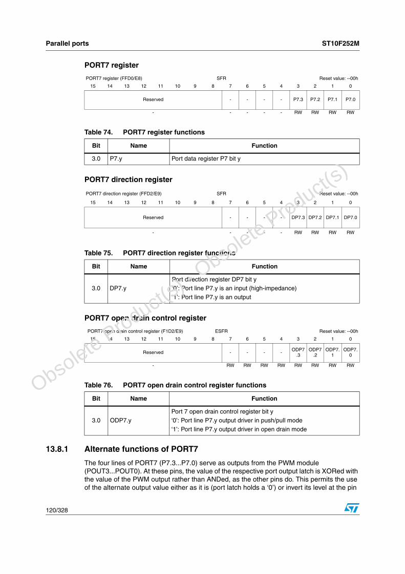
Parallel ports ST10F252M
120/328
PORT7 register
PORT7 direction register
PORT7 open drain control register
13.8.1 Alternate functions of PORT7
The four lines of PORT7 (P7.3...P7.0) serve as outputs from the PWM module (POUT3...POUT0). At these pins, the value of the respective port output latch is XORed with the value of the PWM output rather than ANDed, as the other pins do. This permits the use of the alternate output value either as it is (port latch holds a ‘0’) or invert its level at the pin
PORT7 register (FFD0/E8) SFR Reset value: --00h
15 14 13 12 11 10 9 8 7 6 5 4 3 2 1 0
Reserved - - - - P7.3 P7.2 P7.1 P7.0
- - - - - RW RW RW RW
Table 74. PORT7 register functions
Bit Name Function
3.0 P7.y Port data register P7 bit y
PORT7 direction register (FFD2/E9) SFR Reset value: --00h
15 14 13 12 11 10 9 8 7 6 5 4 3 2 1 0
Reserved - - - - DP7.3 DP7.2 DP7.1 DP7.0
- - - - - RW RW RW RW
Table 75. PORT7 direction register functions
Bit Name Function
3.0 DP7.yPort direction register DP7 bit y‘0’: Port line P7.y is an input (high-impedance)
‘1’: Port line P7.y is an output
PORT7 open drain control register (F1D2/E9) ESFR Reset value: --00h
15 14 13 12 11 10 9 8 7 6 5 4 3 2 1 0
Reserved - - - - ODP7.3
ODP7.2
ODP7.1
ODP7.0
- RW RW RW RW RW RW RW RW
Table 76. PORT7 open drain control register functions
Bit Name Function
3.0 ODP7.yPort 7 open drain control register bit y‘0’: Port line P7.y output driver in push/pull mode
‘1’: Port line P7.y output driver in open drain mode
O
bsolete Product(
s) - O
bsolete Product(
s)

ST10F252M Parallel ports
121/328
(port latch holds a ‘1’). The PWM outputs must be enabled via the respective PENx bits in PWMCON1.
Table 77 summarizes the alternate functions of PORT7.
Figure 43. PORT7 I/O and alternate functions
The port structures of PORT7 differ in the way the output latches are connected to the internal bus and to the pin driver (see Figure 44 and Figure 45).
Pins P7.3...P7.0 (POUT3...POUT0) XOR the alternate data output with the port latch output, which permits the use of the alternate data directly or inverted at the pin driver.
Table 77. PORT7 alternate functions
Pin Name Alternate function
P7.0
P7.1
P7.2P7.3
POUT0
POUT1
POUT2POUT3
PWM0 channel 0 output
PWM0 channel 1 output
PWM0 channel 2 outputPWM0 channel 3 output
------------POUT3POUT2POUT1POUT0
General PurposeInput/Output
--------
P7.3P7.2P7.1
PWM
No Pins
Port 7
O
bsolete Product(
s) - O
bsolete Product(
s)

Parallel ports ST10F252M
122/328
Figure 44. Block diagram of PORT7 pins P7.3...P7.0
13.9 PORT5This 10-bit input port can only read data. There is no output latch and no direction register. Data written to P5 is lost.
Open DrainLatch
Write 0DP7.y
Read 0DP7.y
DirectionLatch
Write DP7.y
Read DP7.y
Inte
rnal
Bus
MUX
0
1
InputLatch
Clock
P7.y/POUTyOutputBuffer
y = 3...0
Port OutputLatch
Read P7.y
Write DP7.y
=1Port DataOutput
EXOR
AlternateDataOutput
O
bsolete Product(
s) - O
bsolete Product(
s)

ST10F252M Parallel ports
123/328
PORT5 register
13.9.1 Alternate functions of PORT5
Each line of PORT5 is also connected to one of the multiplexers of the analog to digital converter (ADC). All port lines (P5.9...P5.0) can accept analog signals (AN9...AN0) that can be converted by the ADC. No special programming is required for pins that shall be used as analog inputs.
Table 79 summarizes the alternate functions of PORT5.
Figure 45. PORT5 I/O and alternate functions
PORT5 register (FFA2/D1) SFR Reset value: xxxxh
15 14 13 12 11 10 9 8 7 6 5 4 3 2 1 0
- P5.9 P5.8 P5.7 P5.6 P5.5 P5.4 P5.3 P5.2 P5.1 P5.0
- R R R R R R R R R R
Table 78. PORT5 register functions
Bit Name Function
9.0 P5.y Port data register P5 bit y (Read only)
Table 79. PORT5 alternate functions
Port 5 Pin Alternate function
P5.0
P5.1
P5.2P5.3
P5.4
P5.5P5.6
P5.7
P5.8P5.9
Analog Input AN0
Analog Input AN1
Analog Input AN2 Analog Input AN3
Analog Input AN4
Analog Input AN5 Analog Input AN6
Analog Input AN7
Analog Input AN8Analog Input AN9
P5.9P5.8P5.7P5.6P5.5P5.4P5.3P5.2P5.1P5.0
Port 5AN9AN8AN7AN6AN5AN4AN3AN2AN1AN0
Alternate Function
General PurposeInput
A/D ConverterInput
No Pins O
bsolete Product(
s) - O
bsolete Product(
s)

Parallel ports ST10F252M
124/328
PORT5 pins have a special port structure (see Figure 46), first because it is an input only port, and second because the analog input channels are directly connected to the pins rather than to the input latches.
13.9.2 Disturb protection on analog inputs
A register is provided for additional disturb protection support on analog inputs for PORT5.
PORT5 digital disable register
Note: This feature is currently not supported by the emulator.
Figure 46. Block diagram of a PORT5 pin
PORT5 disturb protection register (FFA4/D2) SFR Reset value: 0000h
15 14 13 12 11 10 9 8 7 6 5 4 3 2 1 0
P5
DID
IS. 1
5
P5
DID
IS.1
4
P5
DID
IS.1
3
P5
DID
IS.1
2
P5
DID
IS.1
1
P5
DID
IS.1
0
P5
DID
IS.9
P5
DID
IS.8
P5
DID
IS.7
P5
DID
IS.6
P5
DID
IS.5
P5
DID
IS.4
P5
DID
IS.3
P5
DID
IS.2
P5
DID
IS.1
P5
DID
IS.0
RW RW RW RW RW RW RW RW RW RW RW RW RW RW RW RW
Table 80. PORT5 digital disable register functions
Bit Name Function
15-0 P5DIDIS.y
PORT5 digital disable register bit y
‘0’: Port line P5.y digital input is enabled (Schmitt trigger enabled)
‘1’: Port line P5.y digital input is disabled (Schmitt trigger disabled, necessary for input leakage current reduction)
Read Port P5.y
Inte
rnal
Bus
InputLatch
Clock
P5.y/ANy
ReadBuffer
to Sample + HoldCircuit
ChannelSelect
AnalogSwitch
y = 15...0
P5DIDIS.y
O
bsolete Product(
s) - O
bsolete Product(
s)

ST10F252M Analog / digital converter
125/328
14 Analog / digital converter
The ST10F252M provides an analog to digital converter (ADC) with 10-bit resolution and a sample and hold circuit on-chip. A multiplexer selects between up to 10+6 analog input channels (alternate functions of PORT5 and PORT0) either via software (fixed channel modes) or automatically (auto scan modes works automatically among the 10 channels on PORT5, or among the 8 channels on PORT0). An automatic self-calibration adjusts the ADC module to process parameter variations at each reset event.
The accuracy is guaranteed with a total unadjusted error of + 2LSB on PORT5 and + 5 LSB on PORT0 (+ 7 LSB when overload condition is applied). Refer to Section 27.7 for detailed characteristics. The sample time (for loading the capacitors) and the conversion time is programmable and can be adjusted by external circuitry.
To fulfill most requirements of embedded control applications, the ADC supports the following conversion modes:
● fixed channel single conversionproduces just one result from the selected channel
● fixed channel continuous conversionrepeatedly converts the selected channel
● auto scan single conversionproduces one result from each of a selected group of channels
● auto scan continuous conversionrepeatedly converts the selected group of channels
● wait for ADDAT read modestart a conversion automatically when the previous result is read
● channel injection modeinsert the conversion of a specific channel into a group conversion (auto scan).
A set of SFRs and port pins provide access to control functions and results of the ADC.
O
bsolete Product(
s) - O
bsolete Product(
s)

Analog / digital converter ST10F252M
126/328
Figure 47. SFRs, XBUS registers and port pins associated with the A/D converter
The external analog reference voltages VAREF and VAGND are fixed.
The sample time as well as the conversion time, is programmable, so that the ADC can be adjusted to the internal resistances of the analog sources and/or the analog reference voltage supply.
Figure 48. Analog to digital converter block diagram
Ports & Direction Control Alternate Functions Data Registers
15
-
14
-
13
-
12
-
11
-
10
-
9
Y
8
Y
7
Y
6
Y
5
Y
4
Y
3
Y
2
Y
1
Y
0
YP5 ADDAT
15
Y
14
Y
13
Y
12
Y
11
-
10
-
9
Y
8
Y
7
Y
6
Y
5
Y
4
Y
3
Y
2
Y
1
Y
0
Y
ADDAT2 E Y Y Y Y - - Y Y Y Y Y Y Y Y Y Y
Control Registers
Interrupt Control
15
Y
14
Y
13
Y
12
Y
11
Y
10
Y
9
Y
8
Y
7
Y
6
-
5
Y
4
Y
3
Y
2
Y
1
Y
0
YADCON
15 14 13 12 11 10 9 8 7 6 5 4 3 2 1 0
ADCIC - - - - - - - - Y Y Y Y Y Y Y Y
ADEIC - - - - - - - - Y Y Y Y Y Y Y Y
AN0/P5.0... AN9/P5.9
P5 Port5 Data RegisterP5DIDIS Port5 Analog Inputs Disturb Protection RegisterDP0L Port0L Direction RegisterP0L Port0L Data RegisterDP0H Port0H Direction RegisterP0H Port0H Data RegisterADDAT A/D Converter Result RegisterADDAT2 A/D Converter Channel Injection Result RegisterADCON A/D Converter Control RegisterXMISC Miscellaneous Register (XBUS)ADCIC A/D Converter Interrupt Control Register
(End of Conversion)ADEIC A/D Converter Interrupt Control Register
(Overrun Error / Channel Injection)
Bit is linked to a functionBit has no function or is not implementedRegister is in ESFR internal memory space
Y-E
:::
DP0L
P0L
15
-
14
-
13
-
12
-
11
-
10
-
9
-
8
-
7
Y
6
-
5
-
4
-
3
-
2
-
1
-
0
-
- - - - - - - - Y - - - - - - -
- - - - - - Y Y Y Y Y Y Y Y Y YP5DIDIS
- - - - - - - - - - - - Y Y Y YXMISC
DP0H - - - - - - - - - - - Y Y Y Y Y
P0H - - - - - - - - - - - Y Y Y Y Y
AN10/P0L.7... AN15/P0H.4
ADCIR
ADEIR
S + H10-Bit
Converter
ConversionControl
ADCON
Result Reg. ADDAT
Result Reg. ADDAT2
InterruptRequests
VAREF VAGND
AN9P5.9
MUX16-1
AN0P5.0
10AnalogInput
Channels::
::
AN10-15P0L.7-P0H.0,4
Obso
lete Product(s)
- Obso
lete Product(s)

ST10F252M Analog / digital converter
127/328
14.1 Mode selection and operationThe analog input channels AN0 to AN9 are alternate functions of PORT5 which is a 10-bit input-only port. The PORT5 lines may either be used as analog or digital inputs. No special action is required to configure the PORT5 lines as analog inputs. The additional register P5DIDIS can be used to further protect the ADC input analog section by disabling the digital input section. Refer to Section 13.9.2 for details on register P5DIDIS.
The functions of the A/D converter are controlled by the bit-addressable A/D Converter Control Register ADCON.
Its bit fields specify the analog channel to be acted upon, the conversion mode, and also reflect the status of the converter.
ADCON (FFA0h / D0h) SFR Reset Value: 0000h
Bit field ADCH specifies the analog input channel which is to be converted (first channel of a conversion sequence in auto scan modes). Bit field ADM selects the operating mode of the ADC. A conversion (or a sequence) is started by setting bit ADST. Clearing ADST stops the ADC after a specified operation which depends on the selected operating mode.
The busy flag (read-only) ADBSY is set, as long as a conversion is in progress. After reset, this bit is set because the self-calibration is ongoing (duration of self-calibration depends on
15 14 13 12 11 10 9 8 7 6 5 4 3 2 1 0
ADCTC ADSTCAD
CRQADCIN
ADWR
ADBSY
ADSTAD
OFFADM ADCH
RW RW RW RW RW R RW RW RW RW
Table 81. ADCON functions
Bit Name Function
15:14 ADCTC ADC Conversion Time Control (1)
13:12 ADSTC ADC Sample Time Control (1)
1. ADSTC and ADCTC control the conversion timing. Refer to Section 14.2 on page 134.
11 ADCRQ ADC Channel Injection Request Flag
10 ADCIN ADC Channel Injection Enable
9 ADWR ADC Wait for Read Control
8 ADBSYADC Busy Flag ‘1’: a conversion or calibration is active
7 ADST ADC Start bit
6 ADOFF
ADC Disable ‘0’: Analog circuitry of A/D converter is on: it can be used properly‘1’: Analog circuitry of A/D converter is turned off (no consumption): non conversion possible
5 ADM
ADC Mode Selection’0 0’: Fixed Channel Single Conversion’0 1’: Fixed Channel Continuous Conversion’1 0’: Auto Scan Single Conversion’1 1’: Auto Scan Continuous Conversion
4:0 ADCH ADC Analog Channel Input Selection O
bsolete Product(
s) - O
bsolete Product(
s)

Analog / digital converter ST10F252M
128/328
CPU clock: it takes up to 40.629 ± 1 clock pulses). The user software can poll this bit to determine when the first conversion can be launched.
The result of a conversion is stored in the result register ADDAT, or in ADDAT2 for an injected conversion.
Note: Bit field CHNR of register ADDAT is loaded by the ADC to indicate, which channel the result refers to. Bit field CHNR of register ADDAT2 is loaded by the CPU to select the analog channel, which is to be injected.
ADDAT register
ADDAT2 register
A conversion is started by setting bit ADST to ‘1’. The busy flag ADBSY is set and the converter selects and samples the input channel, which is specified by the channel selection field ADCH in register ADCON. The sampled level is held internally during the conversion. When the conversion of this channel is complete, the 10-bit result together with the number of the converted channel is transferred into the result register ADDAT and the interrupt request flag ADCIR is set. Field ADCH represents the channel of PORT5 (0h = channel 0, 1h = channel 1, ... , 9h = channel 9).
If bit ADST is reset via software while a conversion is in progress, the ADC stops after the current conversion (fixed channel modes) or after the current conversion sequence (auto scan modes).
Setting bit ADST, while a conversion is running, aborts this conversion and starts a new conversion with the parameters specified in ADCON.
Note: Abortion and restart (see above) are triggered by bit ADST changing from ‘0’ to ‘1’, that is, ADST must be ‘0’ before being set.
While a conversion is in progress, the mode selection field ADM and the channel selection field ADCH may be changed. ADM is evaluated after the current conversion. ADCH is evaluated after the current conversion (fixed channel modes) or after the current conversion sequence (auto scan modes).
ADDAT register (FEA0/50) SFR Reset value: 0000h
15 14 13 12 11 10 9 8 7 6 5 4 3 2 1 0
CHNR - - ADRES
RW - - RW
ADDAT2 register (F9A0/50) SFR Reset value: 0000h
15 14 13 12 11 10 9 8 7 6 5 4 3 2 1 0
CHNR - - ADRES
RW - - RW
Table 82. ADDAT and ADDAT2 registers functions
Bit Name Function
15.12 CHNR Channel number (4-bit, identifies the converted analog channel)
9.0 ADRES Analog to digital conversion result (10-bit)
O
bsolete Product(
s) - O
bsolete Product(
s)

ST10F252M Analog / digital converter
129/328
14.1.1 Fixed channel conversion modes
These modes are selected by programming the mode selection field ADM in register ADCON to ‘00’ (single conversion) or to ‘01’ (continuous conversion). After starting the converter through bit ADST, the busy flag ADBSY is set and the channel specified in bit field ADCH is converted. After the conversion is complete, the interrupt request flag ADCIR (bit 7 of ADCIC register; Section 14.3) is set.
● In single conversion mode, the converter automatically stops and resets bits ADBSY and ADST.
● In continuous conversion mode, the converter automatically starts a new conversion of the channel specified in ADCH. ADCIR is set after each completed conversion.
When bit ADST is reset by software while a conversion is in progress, the converter completes the current conversion and then stops and resets bit ADBSY.
14.1.2 Auto scan conversion modes
These modes are selected by programming the mode selection field ADM in register ADCON to ‘10’ (single conversion) or to ‘11’ (continuous conversion). Auto scan modes automatically convert a sequence of analog channels, beginning with the channel specified in bit field ADCH and ending with channel 0, without requiring software to change the channel number. If the ADCH value is greater than 9h, the sequence starts converting the nonexistent channel; this corresponds to an unpredictable result, since the input of ADC is left floating.
After starting the converter through bit ADST, the busy flag ADBSY is set and the channel specified in bit field ADCH is converted. After the conversion is complete, the interrupt request flag ADCIR is set and the converter automatically starts a new conversion of the next lower channel. ADCIR set after each completed conversion. After conversion of channel 0 the current sequence is complete.
● In single conversion mode the converter automatically stops and resets bits ADBSY and ADST.
● In continuous conversion mode the converter automatically starts a new sequence beginning with the conversion of the channel specified in ADCH.
When bit ADST is reset by software while a conversion is in progress, the converter completes the current sequence (including conversion of channel 0) and then stops and resets bit ADBSY.
O
bsolete Product(
s) - O
bsolete Product(
s)

Analog / digital converter ST10F252M
130/328
Figure 49. Auto scan conversion mode example
14.1.3 Wait for ADDAT read mode
If, in the default mode of the ADC, a previous conversion result has not been read out of register ADDAT by the time a new conversion is complete, the previous result in register ADDAT is lost because it is overwritten by the new value and the analog to digital overrun error interrupt request flag ADEIR (bit 7 of ADEIC register; see Section 14.3) is set.
To avoid error interrupts and the loss of conversion results, especially when using continuous conversion modes, the ADC can be switched to “Wait for ADDAT read mode” by setting bit ADWR in register ADCON.
If the value in ADDAT has not been read by the time the current conversion is complete, the new result is stored in a temporary buffer and the next conversion is suspended (ADST and ADBSY remain set in the meantime but no end-of-conversion interrupt is generated). After reading the previous value from ADDAT, the temporary buffer is copied into ADDAT (generating an ADCIR interrupt) and the suspended conversion is started. This mechanism applies to both single and continuous conversion modes.
Note: While in standard mode, continuous conversions are executed at a fixed rate (determined by the conversion time), in “Wait for ADDAT read mode” there may be delays due to suspended conversions. However, this only affects the conversions, if the CPU (or PEC) cannot keep track with the conversion rate.
Conversion #2 #1 #0 #3 #2
#x #3 #2 #3#1 #0
#x #3 #2 #1 #3
Write ADDATADDAT Full
Generate InterruptRequest
Read of ADDAT;Result of Channel:
ADDAT Full;Channel 0Result Lost
Overrun Error Interrupt Request
#3of Channel:
O
bsolete Product(
s) - O
bsolete Product(
s)

ST10F252M Analog / digital converter
131/328
Figure 50. Wait for read mode example
14.1.4 Channel injection mode
Channel injection mode allows the conversion of a specific analog channel (also while the ADC is running in a continuous or auto scan mode) without changing the current operating mode. After the conversion of this specific channel, the ADC continues with the original operating mode.
Channel injection mode is enabled by setting bit ADCIN in register ADCON and requires the Wait for ADDAT read mode (ADWR=‘1’). The channel to be converted in this mode is specified in bit field CHNR of register ADDAT2.
Note: These four bits in ADDAT2 are not modified by the ADC, but only the ADRES bit field. Since the channel number for an injected conversion is not buffered, bitfield CHNR of ADDAT2 is never modified during the sample phase of an injected conversion, otherwise the input multiplexer switches to the new channel. It is recommended to only change the channel number with no injected conversion running.
Figure 51. Channel injection example
#3 #2 #1 #0 #3Conversion
#x #3 #2 #0#1
#x #3 #2 #1 #0
Write ADDATADDAT Full
Generate InterruptRequest
Read of ADDAT;Result of Channel:
Wait
Temp-Latch Full
#3
#1
Hold Result inTemp-Latch
of Channel:
#x #x-1 #x-2 #x-3 #x-4Conversion
#x+1 #x #x-1 #x-3
#x+1
Write ADDAT
ADDAT Full
Read ADDAT
#x-4
#...
#x-2
#x #x-1 #x-2 #x-3 #x-4
#y
Write ADDAT2
Channel InjectionRequest by CC31
Interrupt RequestADEINT
Injected Conversionof Channel #y
ADDAT2 Full
Read ADDAT2
of Channel:
O
bsolete Product(
s) - O
bsolete Product(
s)

Analog / digital converter ST10F252M
132/328
A channel injection can be triggered by set the channel injection request bit ADCRQ via software.
Note: While an injected conversion is in progress, no further channel injection request can be triggered. The channel injection request flag ADCRQ remains set until the result of the injected conversion is written to the ADDAT2 register.
If the converter was idle before the channel injection, and during the injected conversion the converter is started by software for normal conversions, the channel injection is aborted, and the converter starts in the selected mode (as described above). This can be avoided by checking the busy bit ADBSY before starting a new operation.
After completing the current conversion (if any is in progress), the converter starts (injects) the conversion of the specified channel. When the conversion of this channel is complete, the result is placed into the alternate result register ADDAT2, and a channel injection complete interrupt request is generated, which uses the interrupt request flag ADEIR (for this reason the Wait for ADDAT read mode is required).
Note: If the temporary data register used in Wait for ADDAT read mode is full, the respective next conversion (standard or injected) is suspended. The temporary register can hold data for ADDAT (from a standard conversion) or for ADDAT2 (from an injected conversion).
O
bsolete Product(
s) - O
bsolete Product(
s)

ST10F252M Analog / digital converter
133/328
Figure 52. Channel injection example with wait for read
14.1.5 ADC power down (ADOFF)
Setting bit ADOFF in ADCON register, turns off the ADC and zeroes the static power consumption related with ADC analog circuitry. If this bit is set during a conversion, the command is ignored (even though the ADOFF bit is immediately set); only at the end of the conversion (or sequence of conversions if SCAN mode was selected), is the ADC switched off (as soon as the ADBSY bit is cleared).
When ADC is off (ADOFF bit set), setting bit ADST automatically wakes up the ADC and a conversion starts; the accuracy is unfortunately not yet granted, since the analog circuitry
#x #x-1 #x-2 #x-3Conversion
#x+1 #x #x-1 #x-2
#x+1
Write ADDAT
ADDAT Full
Read ADDAT
#x-3
#...
#x #x-1 #x-2 #x-3
#yChannel InjectionRequest by CC31
Injected Conversionof Channel #y Write ADDAT2
#y
InterruptRequest
#z #y
ADDAT2 Full
Read ADDAT2
Temp-Latch Full
#x #x-1 #x-2 #x-3Conversion
#x+1 #x #x-1 #x-2
#x+1
Write ADDAT
ADDAT Full
Read ADDAT
#x-3
#...
#x #x-2 #x-3
#y
Channel InjectionRequest by CC31
Write ADDAT2
Interrupt RequestADEINT
#y
ADDAT2 Full
Read ADDAT2
#x-1
Temp-Latch Full
Wait until ADDAT2is read
of Channel:
of Channel:
#z
ADEINT
Wait untilADDAT2 is
read
O
bsolete Product(
s) - O
bsolete Product(
s)

Analog / digital converter ST10F252M
134/328
needs at least 50 µs to complete the power-up transient phase. Clear the ADOFF bit first, and start the first conversion only after 50 µs.
Note: If bit ADOFF is set and when ADST is also set, at the end of the conversion (or cycle of conversions if SCAN mode is selected), the ADC is switched off (as soon as ADBSY is cleared).
Turning off ADC consumption (setting bit ADOFF) should be done once the calibration is completed (starts after every reset occurrence); if not, the calibration is stopped by setting bit ADOFF and not restarted/completed when bit ADOFF is cleared again.
14.2 Conversion timing control When a conversion is started, first the capacitances of the converter are loaded via the respective analog input pin to the current analog input voltage. The time to load the capacitances is referred to as sample time. Next the sampled voltage is converted to a digital value in several successive steps, which correspond to the 10-bit resolution of the ADC. During these steps the internal capacitances are repeatedly charged and discharged via the VAREF pin.
The current that has to be drawn from the sources for sampling and changing charges depends on the time that each respective step takes, because the capacitors must reach their final voltage level within the given time, at least with a certain approximation. The maximum current, however, that a source can deliver, depends on its internal resistance.
The time that the two different actions during conversion take (sampling, and converting) can be programmed within a certain range in the ST10F252M with respect to the CPU clock. The absolute time that is consumed by the different conversion steps is independent of the general speed of the controller. This allows the ADC of the ST10F252M to be adjusted to the properties of the system.
● Fast conversion can be achieved by programming the respective times to their absolute possible minimum. This is preferable for scanning high frequency signals. However, the internal resistance of analog source and analog supply must be sufficiently low.
● High internal resistance can be achieved by programming the respective times to a higher value, or the possible maximum. This is preferable when using analog sources and supply with a high internal resistance to keep the current as low as possible. The conversion rate in this case may be considerably lower.
The ADC input bandwidth is limited by the achievable accuracy. For example, supposing a maximum error of 0.5LSB (2 mV) impacting the global TUE (TUE also depends on other causes), in the worst case of temperature and process, the maximum frequency for a sine wave analog signal is around 7.5 kHz. To reduce the effect of the input signal variation on the accuracy down to 0.05LSB, the maximum input frequency of the sine wave is reduced to 800 Hz.
If a static signal is applied during the sampling phase, the series resistance is not greater than 20 kΩ (this takes into account any possible input leakage). Do not connect any capacitance on analog input pins to reduce the effect of charge partitioning (and consequent voltage drop error) between the external and the internal capacitance. If an RC filter is necessary, the external capacitance must be greater than 10 nF to minimize the accuracy impact.
O
bsolete Product(
s) - O
bsolete Product(
s)

ST10F252M Analog / digital converter
135/328
The conversion times are programmed via the upper four bits of register ADCON. Bit fields ADCTC and ADSTC are used to define the basic conversion time and, in particular, the partition between sample phase and comparison phases. The table below lists the possible combinations. The timings refer to the unit TCL, where fCPU = 1/2TCL.
The complete conversion time includes the conversion itself, the sample time and the time required to transfer the digital value to the result register.
Note: The total conversion time is compatible with the formula valid for ST10F269, while the meaning of the bit fields ADCTC and ADSTC is no longer compatible: the minimum conversion time is 388 TCL, which at 40 MHz CPU frequency corresponds to 4.85 μs (see ST10F269).
14.3 ADC interrupt controlAt the end of each conversion, the interrupt request flag ADCIR in the interrupt control register ADCIC is set. This end-of-conversion interrupt request may cause an interrupt to vector ADCINT or it may trigger a PEC data transfer which reads the conversion result from register ADDAT, for example, to store it in a table in the internal RAM for later evaluation.
The interrupt request flag ADEIR in the register ADEIC is set if either a conversion result overwrites a previous value in register ADDAT (error interrupt in standard mode) or if the result of an injected conversion has been stored in ADDAT2 (end-of-injected-conversion interrupt). This interrupt request may be used to cause an interrupt to vector ADEINT or it may trigger a PEC data transfer.
Table 83. ADC programming
ADCTC ADSTC Sample Comparison Extra Total conversion
00 00 TCL * 120 TCL * 240 TCL * 28 TCL * 388
00 01 TCL * 140 TCL * 280 TCL * 16 TCL * 436
00 10 TCL * 200 TCL * 280 TCL * 52 TCL * 532
00 11 TCL * 400 TCL * 280 TCL * 44 TCL * 724
11 00 TCL * 240 TCL * 480 TCL * 52 TCL * 772
11 01 TCL * 280 TCL * 560 TCL * 28 TCL * 868
11 10 TCL * 400 TCL * 560 TCL * 100 TCL * 1060
11 11 TCL * 800 TCL * 560 TCL * 52 TCL * 1444
10 00 TCL * 480 TCL * 960 TCL * 100 TCL * 1540
10 01 TCL * 560 TCL * 1120 TCL * 52 TCL * 1732
10 10 TCL * 800 TCL * 1120 TCL * 196 TCL * 2116
10 11 TCL * 1600 TCL * 1120 TCL * 164 TCL * 2884
O
bsolete Product(
s) - O
bsolete Product(
s)

Analog / digital converter ST10F252M
136/328
ADC interrupt control
Note: Refer to the general interrupt control register description (Section 9.1.2) for an explanation of the control fields.
14.4 CalibrationA full calibration sequence is performed after a reset. This full calibration lasts 40.629 ± 1 CPU clock cycles. During this time, the busy flag ADBSY is set to indicate the operation. It compensates for any capacitance mismatch, so the calibration procedure does not need any update during normal operation.
No conversion can be performed during this time. The bit ADBSY can be polled to verify when the calibration is over, and the module is able to start a conversion.
Since the calibration process writes repeatedly spurious conversion results to the ADDAT register, at the end of the calibration, both ADCIR and ADEIR flags are set. For this reason, before starting a conversion, the ADC initialization routine performs a dummy read of ADDAT register and clears the two flags.
Note: If ADDAT is not read before starting the first conversion and, for example, “wait for read mode” is entered (ADWR bit set), the ADC is stack waiting for the ADDAT read, since the result of the current conversion cannot be immediately written to ADDAT, which contains the results of the calibration (meaningless data).
ADCIC register (FF98/CC) SFR Reset value: --00h
15 14 13 12 11 10 9 8 7 6 5 4 3 2 1 0
- ADC IR
ADC IE ILVL GLVL
- RW RW RW RW
ADEIC register (FF9A/CD) SFR Reset value: --00h
15 14 13 12 11 10 9 8 7 6 5 4 3 2 1 0
- ADE IR
ADE IE ILVL GLVL
- RW RW RW RW
O
bsolete Product(
s) - O
bsolete Product(
s)

ST10F252M Programmable output clock divider
137/328
15 Programmable output clock divider
15.1 FunctionalityA specific register mapped on the XBUS allows to choose the division factor on the CLKOUT signal (P3.15). This register is mapped on X-Miscellaneous memory address range.
XCLKOUTDIV (EB02h) XBUS Reset Value: - - 00h
Table 84. CLKOUTDIV functions
When the CLKOUT function is enabled by setting bit CLKEN of register SYSCON, by default the CPU clock is output on P3.15. Setting bit XMISCEN of register XPERCON and bit XPEN of register SYSCON programs the clock prescaling factor. In this way, a prescaled value of the CPU clock is output on P3.15.
When the CLKOUT function is not enabled (bit CLKEN of register SYSCON cleared), P3.15 does not output any clock signal, even though the XCLKOUTDIV register is programmed.
15 14 13 12 11 10 9 8 7 6 5 4 3 2 1 0
- - - - - - - - DIV
RW
Bit Name Function
7:0 DIV
Clock Divider setting‘00h’: fCLKOUT = fCPU‘01h’: fCLKOUT = fCPU / 2‘02h’: fCLKOUT = fCPU / 3‘03h’: fCLKOUT = fCPU / 4
:
‘FFh’: fCLKOUT = fCPU / 256
O
bsolete Product(
s) - O
bsolete Product(
s)

Serial channels ST10F252M
138/328
16 Serial channels
Serial communication with other microcontrollers, microprocessors, terminals or external peripheral components is provided by up to four serial interfaces: two asynchronous / synchronous serial channels (ASC0 and ASC1) and two high-speed synchronous serial channel (SSC0 and SSC1). Dedicated baudrate generators set up all standard baudrates without the requirement of oscillator tuning. For transmission, reception and erroneous reception, separate interrupt vectors are provided for ASC0 and SSC0 serial channel. A more complex mechanism of interrupt sources multiplexing is implemented for ASC1 and SSC1 (XBUS mapped).
16.1 Asynchronous / synchronous serial interfacesThe asynchronous / synchronous serial interfaces (ASC0 and ASC1) provides serial communication between the ST10F252M and other microcontrollers, microprocessors or external peripherals.
16.2 ASCx in asynchronous modeIn asynchronous mode, 8- or 9-bit data transfer, parity generation and the number of stop bits can be selected. Parity framing and overrun error detection is provided to increase the reliability of data transfers. Transmission and reception of data is double-buffered. Full-duplex communication up to 1.25 Mbaud (at 40 MHz of fCPU) is supported in this mode.
Note: The deviation errors given in the Table 85 are rounded off. To avoid deviation errors use a baudrate crystal (providing a multiple of the ASC0 sampling frequency).
Table 85. ASC asynchronous baudrates by reload value and deviation errors (fCPU = 40 MHz)
S0BRS = ‘0’, fCPU = 40 MHz S0BRS = ‘1’, fCPU = 40 MHz
Baudrate (baud) Deviation errorReload value
(hex)Baudrate (baud) Deviation error
Reload value(hex)
1 250 000 0.0% / 0.0% 0000 / 0000 833 333 0.0% / 0.0% 0000 / 0000
112 000 +1.5% / -7.0% 000A / 000B 112 000 +6.3% / -7.0% 0006 / 0007
56 000 +1.5% / -3.0% 0015 / 0016 56 000 +6.3% / -0.8% 000D / 000E
38 400 +1.7% / -1.4% 001F / 0020 38 400 +3.3% / -1.4% 0014 / 0015
19 200 +0.2% / -1.4% 0040 / 0041 19 200 +0.9% / -1.4% 002A / 002B
9 600 +0.2% / -0.6% 0081 / 0082 9 600 +0.9% / -0.2% 0055 / 0056
4 800 +0.2% / -0.2% 0103 / 0104 4 800 +0.4% / -0.2% 00AC / 00AD
2 400 +0.2% / 0.0% 0207 / 0208 2 400 +0.1% / -0.2% 015A / 015B
1 200 0.1% / 0.0% 0410 / 0411 1 200 +0.1% / -0.1% 02B5 / 02B6
600 0.0% / 0.0% 0822 / 0823 600 +0.1% / 0.0% 056B / 056C
300 0.0% / 0.0% 1045 / 1046 300 0.0% / 0.0% 0AD8 / 0AD9
153 0.0% / 0.0% 1FE8 / 1FE9 102 0.0% / 0.0% 1FE8 / 1FE9
O
bsolete Product(
s) - O
bsolete Product(
s)

ST10F252M Serial channels
139/328
16.3 ASCx in synchronous modeIn synchronous mode, data is transmitted or received synchronously to a shift clock which is generated by the ST10F252M. Half-duplex communication up to 5 Mbaud (at 40 MHz of fCPU) is possible in this mode.
Note: The deviation errors given in the Table 86 are rounded off. To avoid deviation errors use a baudrate crystal (providing a multiple of the ASC0 sampling frequency).
16.4 High speed synchronous serial interfacesThe High-Speed Synchronous Serial Interfaces (SSC0 and SSC1) provides flexible high-speed serial communication between the ST10F252M and other microcontrollers, microprocessors or external peripherals.
The SSCx supports full-duplex and half-duplex synchronous communication. The serial clock signal can be generated by the SSCx itself (master mode) or be received from an external master (slave mode). Data width, shift direction, clock polarity and phase are programmable.
This allows communication with SPI-compatible devices. Transmission and reception of data is double-buffered. A 16-bit baudrate generator provides the SSCx with a separate serial clock signal. The serial channel SSCx has its own dedicated 16-bit baudrate generator with 16-bit reload capability, allowing baudrate generation independent from the timers.
Table 87 lists some possible baudrates against the required reload values and the resulting bit times for the 40 MHz CPU clock. The maximum is limited to 8 Mbaud.
Table 86. ASC synchronous baudrates by reload value and deviation errors (fCPU = 40 MHz)
S0BRS = ‘0’, fCPU = 40 MHz S0BRS = ‘1’, fCPU = 40 MHz
Baudrate (baud) Deviation errorReload value
(hex)Baudrate (baud) Deviation error
Reload value(hex)
5 000 000 0.0% / 0.0% 0000 / 0000 3 333 333 0.0% / 0.0% 0000 / 0000
112 000 +1.5% / -0.8% 002B / 002C 112 000 +2.6% / -0.8% 001C / 001D
56 000 +0.3% / -0.8% 0058 / 0059 56 000 +0.9% / -0.8% 003A / 003B
38 400 +0.2% / -0.6% 0081 / 0082 38 400 +0.9% / -0.2% 0055 / 0056
19 200 +0.2% / -0.2% 0103 / 0104 19 200 +0.4% / -0.2% 00AC / 00AD
9 600 +0.2% / 0.0% 0207 / 0208 9 600 +0.1% / -0.2% 015A / 015B
4 800 +0.1% / 0.0% 0410 / 0411 4 800 +0.1% / -0.1% 02B5 / 02B6
2 400 0.0% / 0.0% 0822 / 0823 2 400 +0.1% / 0.0% 056B / 056C
1 200 0.0% / 0.0% 1045 / 1046 1 200 0.0% / 0.0% 0AD8 / 0AD9
900 0.0% / 0.0% 15B2 / 15B3 600 0.0% / 0.0% 15B2 / 15B3
612 0.0% / 0.0% 1FE8 / 1FE9 407 0.0% / 0.0% 1FFD / 1FFE
O
bsolete Product(
s) - O
bsolete Product(
s)
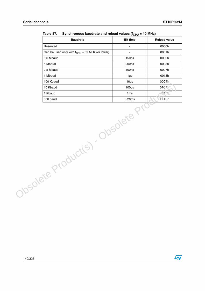
Serial channels ST10F252M
140/328
Table 87. Synchronous baudrate and reload values (fCPU = 40 MHz)
Baudrate Bit time Reload value
Reserved - 0000h
Can be used only with fCPU = 32 MHz (or lower) - 0001h
6.6 Mbaud 150ns 0002h
5 Mbaud 200ns 0003h
2.5 Mbaud 400ns 0007h
1 Mbaud 1µs 0013h
100 Kbaud 10µs 00C7h
10 Kbaud 100µs 07CFh
1 Kbaud 1ms 4E1Fh
306 baud 3.26ms FF4Eh
O
bsolete Product(
s) - O
bsolete Product(
s)

ST10F252M I2C interface
141/328
17 I2C interface
The integrated I2C Bus Module handles the transmission and reception of frames over the two-line SDA/SCL in accordance with the I2C Bus specification. The I2C Module can operate in slave mode, in master mode or in multi-master mode. It can receive and transmit data using 7-bit or 10-bit addressing. Data can be transferred at speeds up to 400 Kbit/s (both Standard and Fast I2C bus modes are supported).
The module can generate three different types of interrupt:
● requests related to bus events, such as start or stop events, or arbitration lost
● requests related to data transmission
● requests related to data reception
These requests are issued to the interrupt controller by three different lines, and identified as Error, Transmit, and Receive interrupt lines.
When the I2C module is enabled by setting bit XI2CEN in XPERCON register, pins P4.4 and P4.7 (where SCL and SDA are respectively mapped as alternate functions) are automatically configured as bidirectional open-drain: the value of the external pull-up resistor depends on the application. P4, DP4 and ODP4 cannot influence the pin configuration.
When the I2C cell is disabled (clearing bit XI2CEN), P4.4 and P4.7 pins are standard I/ O controlled by P4, DP4 and ODP4.
The speed of the I2C interface can be selected between Standard mode (0 to 100 kHz) and Fast I2C mode (100 to 400 kHz).
O
bsolete Product(
s) - O
bsolete Product(
s)
CAN modules ST10F252M
142/328
18 CAN modules
The two integrated CAN modules (CAN1 and CAN2) are identical and handle the completely autonomous transmission and reception of CAN frames in accordance with the CAN specification V2.0 part A and B (active).
These two CAN modules are different with respect to the ones implemented on ST10F269. The new module is based on C-CAN module characteristics. The following system resources are used to interface the module with the ST10 core:
● Interrupt of CAN1 and CAN2 are connected to the XBUS interrupt lines: refer to Section 18.2 for details.
● Both CAN modules have to be selected, before the bit XPEN is set in SYSCON register, by setting the proper bit in XPERCON register.
● After reset, CAN1 is enabled by default (see the reset value of the XPERCON register). The CAN2 is not enabled.
This peripheral uses the new clock gating feature.
Note: When the clock is gated, no reset is raised once the EINIT instruction has been executed.
18.1 Memory and pin mapping
18.1.1 CAN1 mapping
Address range 00’EF00h - 00’EFFFh is reserved for the CAN1 module access. The CAN1 is enabled by setting bit XPEN of the SYSCON register and bit 0 of XPERCON register. Accesses to the CAN module use demultiplexed addresses and a 16-bit data bus (only word accesses are possible). Two wait states give an access time of 83.34 ns at 40 MHz CPU clock. No tristate wait state is used.
After reset, CAN1 is enabled by default (see the reset value of the XPERCON register). It is available on pins P4.5 and P4.6.
18.1.2 CAN2 mapping
Address range 00’EE00h - 00’EEFFh is reserved for the CAN2 module access. The CAN2 is enabled by setting bit XPEN of the SYSCON register and bit 1 of the XPERCON register. Accesses to the CAN module use demultiplexed addresses and a 16-bit data bus (only word accesses are possible). Two wait states give an access time of 83.34 ns at40 MHz CPU clock. No tristate wait state is used.
After reset, CAN2 is disabled by default (see the reset value of the XPERCON register). Once enabled, it is available on pins P4.4 and P4.7.
Note: If one or both CAN modules are used, PORT4 cannot be programmed to output all 8 segment address lines. Thus, only 4 segment address lines can be used, reducing the external memory space to 1 Mbyte.
O
bsolete Product(
s) - O
bsolete Product(
s)
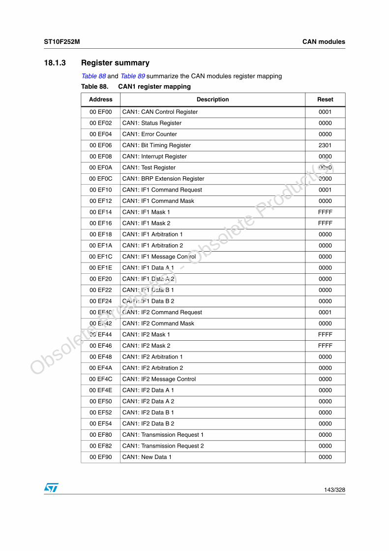
ST10F252M CAN modules
143/328
18.1.3 Register summary
Table 88 and Table 89 summarize the CAN modules register mapping
Table 88. CAN1 register mapping
Address Description Reset
00 EF00 CAN1: CAN Control Register 0001
00 EF02 CAN1: Status Register 0000
00 EF04 CAN1: Error Counter 0000
00 EF06 CAN1: Bit Timing Register 2301
00 EF08 CAN1: Interrupt Register 0000
00 EF0A CAN1: Test Register 00x0
00 EF0C CAN1: BRP Extension Register 0000
00 EF10 CAN1: IF1 Command Request 0001
00 EF12 CAN1: IF1 Command Mask 0000
00 EF14 CAN1: IF1 Mask 1 FFFF
00 EF16 CAN1: IF1 Mask 2 FFFF
00 EF18 CAN1: IF1 Arbitration 1 0000
00 EF1A CAN1: IF1 Arbitration 2 0000
00 EF1C CAN1: IF1 Message Control 0000
00 EF1E CAN1: IF1 Data A 1 0000
00 EF20 CAN1: IF1 Data A 2 0000
00 EF22 CAN1: IF1 Data B 1 0000
00 EF24 CAN1: IF1 Data B 2 0000
00 EF40 CAN1: IF2 Command Request 0001
00 EF42 CAN1: IF2 Command Mask 0000
00 EF44 CAN1: IF2 Mask 1 FFFF
00 EF46 CAN1: IF2 Mask 2 FFFF
00 EF48 CAN1: IF2 Arbitration 1 0000
00 EF4A CAN1: IF2 Arbitration 2 0000
00 EF4C CAN1: IF2 Message Control 0000
00 EF4E CAN1: IF2 Data A 1 0000
00 EF50 CAN1: IF2 Data A 2 0000
00 EF52 CAN1: IF2 Data B 1 0000
00 EF54 CAN1: IF2 Data B 2 0000
00 EF80 CAN1: Transmission Request 1 0000
00 EF82 CAN1: Transmission Request 2 0000
00 EF90 CAN1: New Data 1 0000
O
bsolete Product(
s) - O
bsolete Product(
s)
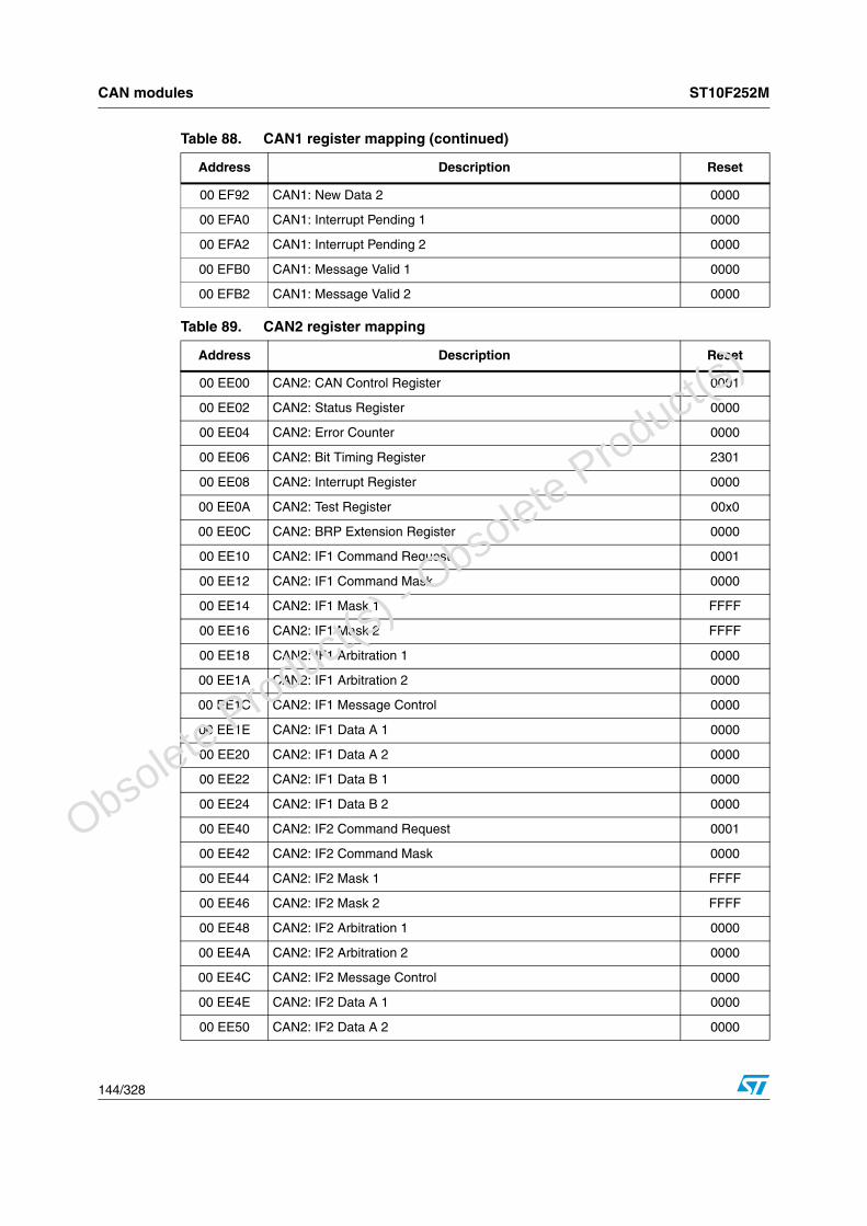
CAN modules ST10F252M
144/328
00 EF92 CAN1: New Data 2 0000
00 EFA0 CAN1: Interrupt Pending 1 0000
00 EFA2 CAN1: Interrupt Pending 2 0000
00 EFB0 CAN1: Message Valid 1 0000
00 EFB2 CAN1: Message Valid 2 0000
Table 89. CAN2 register mapping
Address Description Reset
00 EE00 CAN2: CAN Control Register 0001
00 EE02 CAN2: Status Register 0000
00 EE04 CAN2: Error Counter 0000
00 EE06 CAN2: Bit Timing Register 2301
00 EE08 CAN2: Interrupt Register 0000
00 EE0A CAN2: Test Register 00x0
00 EE0C CAN2: BRP Extension Register 0000
00 EE10 CAN2: IF1 Command Request 0001
00 EE12 CAN2: IF1 Command Mask 0000
00 EE14 CAN2: IF1 Mask 1 FFFF
00 EE16 CAN2: IF1 Mask 2 FFFF
00 EE18 CAN2: IF1 Arbitration 1 0000
00 EE1A CAN2: IF1 Arbitration 2 0000
00 EE1C CAN2: IF1 Message Control 0000
00 EE1E CAN2: IF1 Data A 1 0000
00 EE20 CAN2: IF1 Data A 2 0000
00 EE22 CAN2: IF1 Data B 1 0000
00 EE24 CAN2: IF1 Data B 2 0000
00 EE40 CAN2: IF2 Command Request 0001
00 EE42 CAN2: IF2 Command Mask 0000
00 EE44 CAN2: IF2 Mask 1 FFFF
00 EE46 CAN2: IF2 Mask 2 FFFF
00 EE48 CAN2: IF2 Arbitration 1 0000
00 EE4A CAN2: IF2 Arbitration 2 0000
00 EE4C CAN2: IF2 Message Control 0000
00 EE4E CAN2: IF2 Data A 1 0000
00 EE50 CAN2: IF2 Data A 2 0000
Table 88. CAN1 register mapping (continued)
Address Description Reset
O
bsolete Product(
s) - O
bsolete Product(
s)
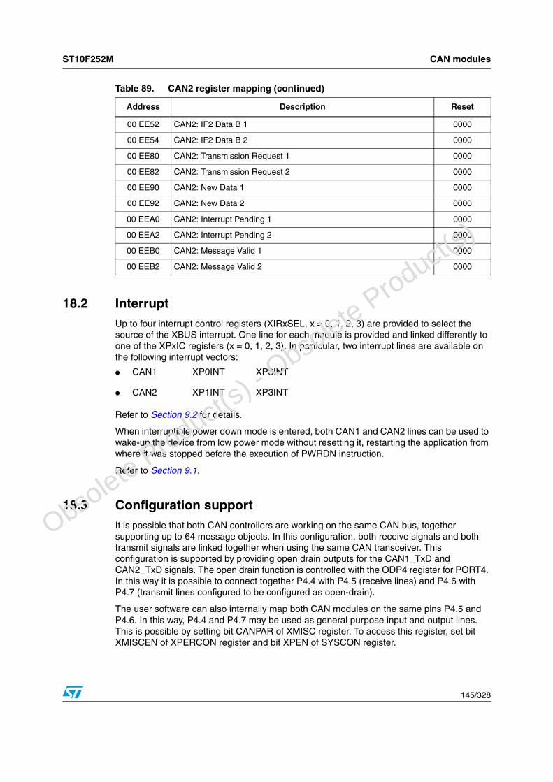
ST10F252M CAN modules
145/328
18.2 InterruptUp to four interrupt control registers (XIRxSEL, x = 0, 1, 2, 3) are provided to select the source of the XBUS interrupt. One line for each module is provided and linked differently to one of the XPxIC registers (x = 0, 1, 2, 3). In particular, two interrupt lines are available on the following interrupt vectors:
Refer to Section 9.2 for details.
When interruptible power down mode is entered, both CAN1 and CAN2 lines can be used to wake-up the device from low power mode without resetting it, restarting the application from where it was stopped before the execution of PWRDN instruction.
Refer to Section 9.1.
18.3 Configuration supportIt is possible that both CAN controllers are working on the same CAN bus, together supporting up to 64 message objects. In this configuration, both receive signals and both transmit signals are linked together when using the same CAN transceiver. This configuration is supported by providing open drain outputs for the CAN1_TxD and CAN2_TxD signals. The open drain function is controlled with the ODP4 register for PORT4. In this way it is possible to connect together P4.4 with P4.5 (receive lines) and P4.6 with P4.7 (transmit lines configured to be configured as open-drain).
The user software can also internally map both CAN modules on the same pins P4.5 and P4.6. In this way, P4.4 and P4.7 may be used as general purpose input and output lines. This is possible by setting bit CANPAR of XMISC register. To access this register, set bit XMISCEN of XPERCON register and bit XPEN of SYSCON register.
00 EE52 CAN2: IF2 Data B 1 0000
00 EE54 CAN2: IF2 Data B 2 0000
00 EE80 CAN2: Transmission Request 1 0000
00 EE82 CAN2: Transmission Request 2 0000
00 EE90 CAN2: New Data 1 0000
00 EE92 CAN2: New Data 2 0000
00 EEA0 CAN2: Interrupt Pending 1 0000
00 EEA2 CAN2: Interrupt Pending 2 0000
00 EEB0 CAN2: Message Valid 1 0000
00 EEB2 CAN2: Message Valid 2 0000
Table 89. CAN2 register mapping (continued)
Address Description Reset
• CAN1 XP0INT XP3INT
• CAN2 XP1INT XP3INT
O
bsolete Product(
s) - O
bsolete Product(
s)

CAN modules ST10F252M
146/328
Note: CAN parallel mode is possible only if both CAN1 and CAN2 are enabled through the setting of bits CAN1EN and CAN2EN in XPERCON register. If CAN1 is disabled, CAN2 remains on P4.4/P4.7 even if bit CANPAR is set.
XMISC register
18.3.1 Configuration examples
Figure 53, Figure 54, Figure 55 and Figure 56 show different configuration examples, where the two CAN controllers of the ST10F252M are working on the same CAN bus or on different CAN busses.
Wired-OR connections to a CAN bus use open drain outputs as described above. A wired-OR structure can be used for on-board data exchange between two or more controller devices via one signal line. As no CAN transceiver is used in this case, the maximum wire length is very limited (<< 1 m) and noise conditions must be considered.
XMISC register (EB46h) SFR Reset value: 0000h
15 14 13 12 11 10 9 8 7 6 5 4 3 2 1 0
- - - P34EN P7EN VREG
OFFCANC
K2CANP
AR -
- - - RW RW RW RW RW -
Table 90. XMISC register functions
Bit Name Function
5 P34EN
Port pin P3.4 enable on Port pin P1H.0
‘0’ pins 0 of Port1(P1H.0) is connected to external pin 89
‘1’ pins 4 of Port3 (P3.4) is connected to external pin 89
4 P7EN
Port 7[3:0] enable on Port4[3:0]
‘0’ pins 3:0 of Port4 are connected to external pins 47-50
‘1’ pins 3:0 of Port7 are connected to external pins 47-50
3 VREGOFF
Main Voltage Regulator disable in Power-Down mode
‘0’: On-chip Main Regulator is held active when Power-Down mode is entered‘1’: On-chip Main Regulator is turned off when Power-Down mode is entered
2 CANCK2
CAN Clock divider by 2 disable
‘0’: Clock provided to CAN modules is CPU clock divided by 2 (mandatory when fCPU is higher than 40MHz)
‘1’: Clock provided to CAN modules is directly CPU clock
1 CANPAR
CAN parallel mode selection
‘0’: CAN2 is mapped on P4.4/P4.7, while CAN1 is mapped on P4.5/P4.6
‘1’: CAN1 and CAN2 are mapped in parallel on P4.5/P4.6. This is effective only if both CAN1 and CAN2 are enabled through setting of bits CAN1EN and CAN2EN in XPERCON register. If CAN1 is disabled, CAN2 remains on P4.4/P4.7 even if bit CANPAR is set.
O
bsolete Product(
s) - O
bsolete Product(
s)
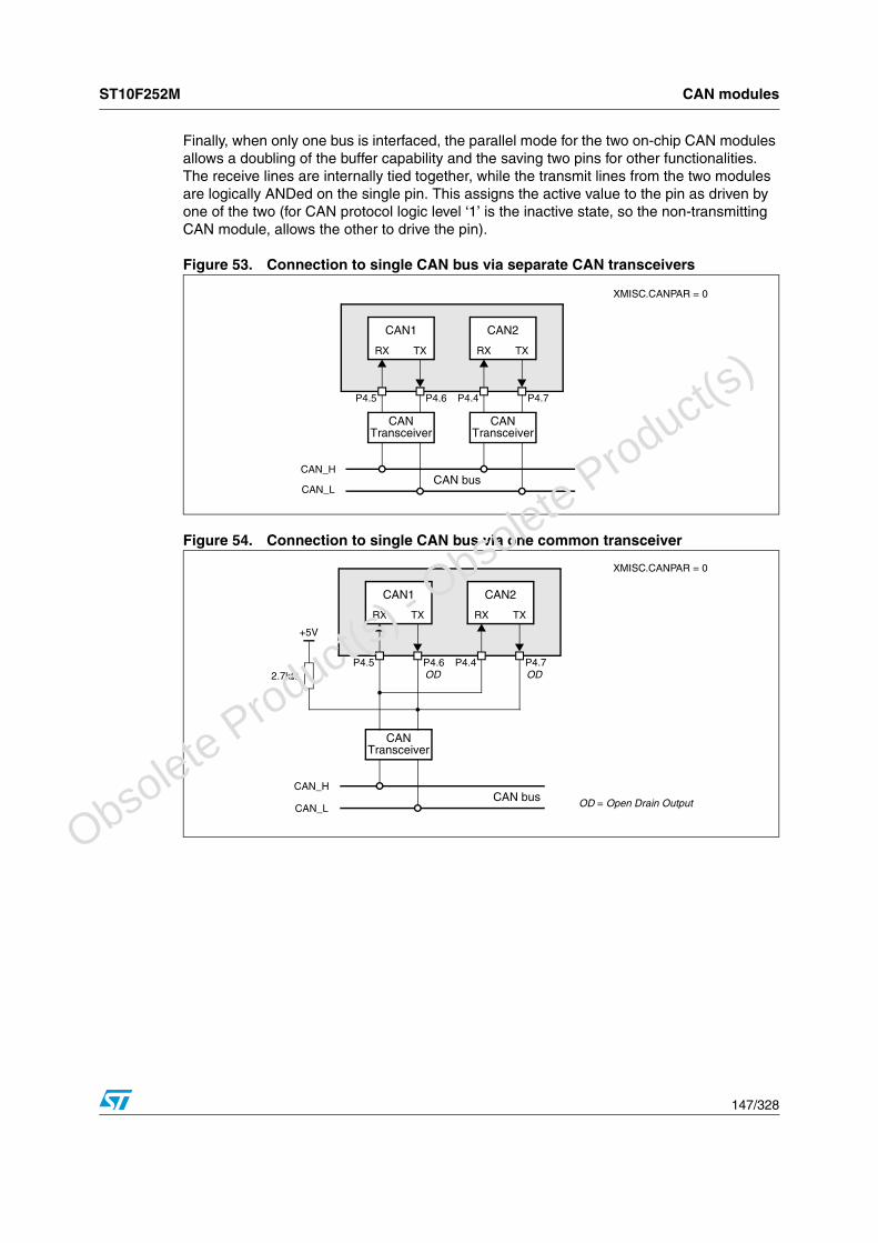
ST10F252M CAN modules
147/328
Finally, when only one bus is interfaced, the parallel mode for the two on-chip CAN modules allows a doubling of the buffer capability and the saving two pins for other functionalities. The receive lines are internally tied together, while the transmit lines from the two modules are logically ANDed on the single pin. This assigns the active value to the pin as driven by one of the two (for CAN protocol logic level ‘1’ is the inactive state, so the non-transmitting CAN module, allows the other to drive the pin).
Figure 53. Connection to single CAN bus via separate CAN transceivers
Figure 54. Connection to single CAN bus via one common transceiver
CAN1
RX TX
CAN_H
CAN_LCAN bus
CAN2
RX TX
XMISC.CANPAR = 0
CAN CANTransceiverTransceiver
P4.4 P4.7P4.5 P4.6
OD = Open Drain Output
+5V
CAN
CAN_H
CAN_LCAN bus
2.7kΩ OD
Transceiver
XMISC.CANPAR = 0
CAN1
RX TX
CAN2
RX TX
P4.4 P4.7P4.5 P4.6OD
O
bsolete Product(
s) - O
bsolete Product(
s)

CAN modules ST10F252M
148/328
Figure 55. Connection to two different CAN buses (for example, for gateway application)
Figure 56. Connection to one CAN bus with internal parallel mode enabled
18.4 Clock prescalingIn the register XMISC, there is also a bit (CANCK2) to modify the clock frequency driving both the CAN modules. For architectural limitations of the CAN module, when the CPU frequency is higher than 40 MHz, it is recommended to divide the CPU clock by two to each CAN module. 20 MHz is sufficient for CAN module to produce the maximum baud rate defined by the protocol standard. If, on the other hand, the CPU frequency can be reduced to 8 MHz, thus providing the CAN module directly with the CPU clock and disabling the prescaler factor, it is still possible to obtain the maximum CAN speed (1 Mbaud).
After reset, the prescaler is enabled so the CPU clock is divided by two and provided to the CAN modules. According to the system clock frequency, the application can disable the prescaler to obtain the required baud rate.
Refer to Section 18.3.1 for the description of the register XMISC.
CAN_H
CAN_LCAN bus 1
CAN_H
CAN_LCAN bus 2
XMISC.CANPAR = 0
CAN1
RX TX
CAN2
RX TX
CAN CANTransceiverTransceiver
P4.4 P4.7P4.5 P4.6
XMISC.CANPAR = 1
CAN2
RX TX
P4.4 P4.7P4.5 P4.6
CAN
CAN_H
CAN_LCAN bus
Transceiver
CAN1
RX TX
(Both CAN enabled)
O
bsolete Product(
s) - O
bsolete Product(
s)

ST10F252M CAN modules
149/328
18.5 CAN module: functional overviewThe C-CAN consists of the components (see Figure 57):
● CAN core
● message RAM
● message handler
● control registers
● module interface.
The CAN core performs communication according to the CAN protocol version 2.0 parts A and B. The bit rate can be programmed to values up to 1 MBit/s depending on the technology used. For the connection to the physical layer, additional transceiver hardware is required.
For communication on a CAN network, individual message objects are configured. The message objects and identifier masks for acceptance filtering of received messages are stored in the message RAM.
All functions concerning the handling of messages are implemented in the message handler. Those functions are the acceptance filtering, the transfer of messages between the CAN core and the message RAM, and the handling of transmission requests as well as the generation of the module interrupt.
The register set of the C-CAN can be accessed directly by an external CPU via the module interface. These registers are used to control/configure the CAN core and the message handler and to access the message RAM.
The module interfaces delivered with the C-CAN module can easily be replaced by a customized module interface adapted to user requirements.
C-CAN implements the following features:
● CAN protocol version 2.0 parts A and B
● bit rates up to 1 MBit/s
● 32 message objects
● each message object has its own identifier mask
● programmable FIFO mode (concatenation of message objects)
● maskable interrupt
● disabled automatic retransmission mode for time triggered CAN applications
● programmable loop-back mode for self-test operation.
O
bsolete Product(
s) - O
bsolete Product(
s)

CAN modules ST10F252M
150/328
18.6 Block diagramThe design consists of the following functional blocks (see Figure 57):
● CAN core
CAN protocol controller and Rx/Tx shift register for serial/parallel conversion of messages.
● Message RAM
Stores message objects and identifier masks.
● Registers
All registers used to control and to configure the C-CAN module.
● Message handler
State machine that controls the data transfer between the Rx/Tx shift register of the CAN core and the message RAM as well as the generation of interrupts as programmed in the control and configuration registers.
Figure 57. Block diagram of the C-CAN
18.7 Operating modes
18.7.1 Software initialisation
Software initialization is started by setting the Init bit in the CAN control register, either by software or by a hardware reset, or by going Bus_Off.
While Init is set, all message transfer from and to the CAN bus is stopped, the status of the CAN bus output CAN_TX is recessive (HIGH). The counters of the EML are unchanged. Setting Init does not change any configuration register.
C-CAN
CAN Core
Registers
Module Interface
Mes
sage
Han
dler
CAN_TX CAN_RX
Message RAM
Dat
aIN
Inte
rrup
t
Clo
ck
Res
et
Add
ress
(7:0
)
Con
trol
CA
N_W
AIT
_B
Dat
aOU
T
O
bsolete Product(
s) - O
bsolete Product(
s)
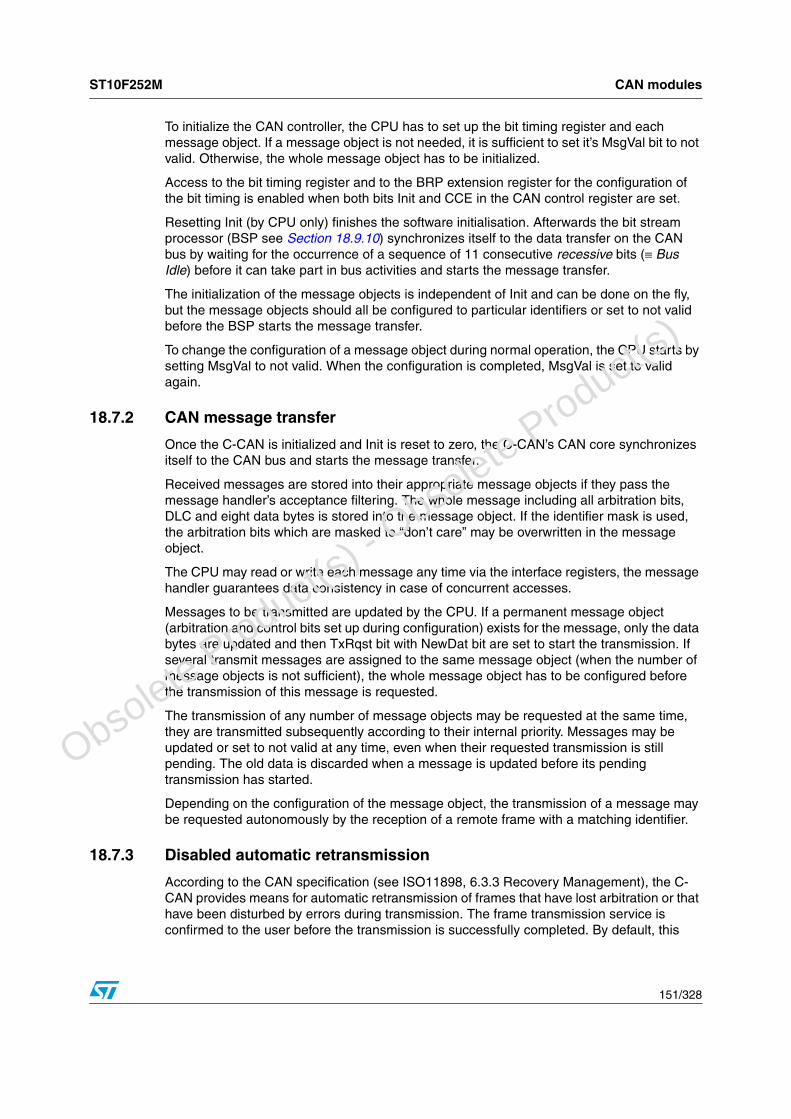
ST10F252M CAN modules
151/328
To initialize the CAN controller, the CPU has to set up the bit timing register and each message object. If a message object is not needed, it is sufficient to set it’s MsgVal bit to not valid. Otherwise, the whole message object has to be initialized.
Access to the bit timing register and to the BRP extension register for the configuration of the bit timing is enabled when both bits Init and CCE in the CAN control register are set.
Resetting Init (by CPU only) finishes the software initialisation. Afterwards the bit stream processor (BSP see Section 18.9.10) synchronizes itself to the data transfer on the CAN bus by waiting for the occurrence of a sequence of 11 consecutive recessive bits (≡ Bus Idle) before it can take part in bus activities and starts the message transfer.
The initialization of the message objects is independent of Init and can be done on the fly, but the message objects should all be configured to particular identifiers or set to not valid before the BSP starts the message transfer.
To change the configuration of a message object during normal operation, the CPU starts by setting MsgVal to not valid. When the configuration is completed, MsgVal is set to valid again.
18.7.2 CAN message transfer
Once the C-CAN is initialized and Init is reset to zero, the C-CAN’s CAN core synchronizes itself to the CAN bus and starts the message transfer.
Received messages are stored into their appropriate message objects if they pass the message handler’s acceptance filtering. The whole message including all arbitration bits, DLC and eight data bytes is stored into the message object. If the identifier mask is used, the arbitration bits which are masked to “don’t care” may be overwritten in the message object.
The CPU may read or write each message any time via the interface registers, the message handler guarantees data consistency in case of concurrent accesses.
Messages to be transmitted are updated by the CPU. If a permanent message object (arbitration and control bits set up during configuration) exists for the message, only the data bytes are updated and then TxRqst bit with NewDat bit are set to start the transmission. If several transmit messages are assigned to the same message object (when the number of message objects is not sufficient), the whole message object has to be configured before the transmission of this message is requested.
The transmission of any number of message objects may be requested at the same time, they are transmitted subsequently according to their internal priority. Messages may be updated or set to not valid at any time, even when their requested transmission is still pending. The old data is discarded when a message is updated before its pending transmission has started.
Depending on the configuration of the message object, the transmission of a message may be requested autonomously by the reception of a remote frame with a matching identifier.
18.7.3 Disabled automatic retransmission
According to the CAN specification (see ISO11898, 6.3.3 Recovery Management), the C-CAN provides means for automatic retransmission of frames that have lost arbitration or that have been disturbed by errors during transmission. The frame transmission service is confirmed to the user before the transmission is successfully completed. By default, this
O
bsolete Product(
s) - O
bsolete Product(
s)
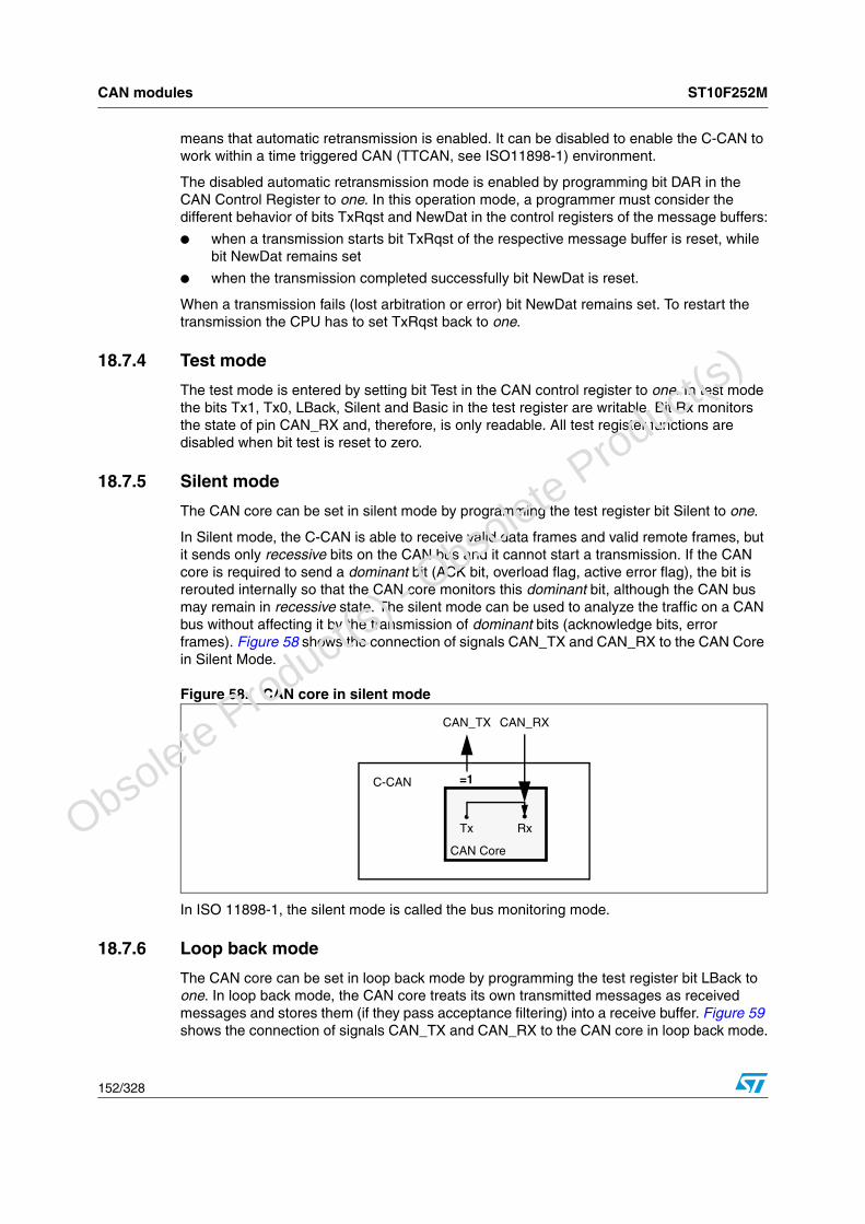
CAN modules ST10F252M
152/328
means that automatic retransmission is enabled. It can be disabled to enable the C-CAN to work within a time triggered CAN (TTCAN, see ISO11898-1) environment.
The disabled automatic retransmission mode is enabled by programming bit DAR in the CAN Control Register to one. In this operation mode, a programmer must consider the different behavior of bits TxRqst and NewDat in the control registers of the message buffers:
● when a transmission starts bit TxRqst of the respective message buffer is reset, while bit NewDat remains set
● when the transmission completed successfully bit NewDat is reset.
When a transmission fails (lost arbitration or error) bit NewDat remains set. To restart the transmission the CPU has to set TxRqst back to one.
18.7.4 Test mode
The test mode is entered by setting bit Test in the CAN control register to one. In test mode the bits Tx1, Tx0, LBack, Silent and Basic in the test register are writable. Bit Rx monitors the state of pin CAN_RX and, therefore, is only readable. All test register functions are disabled when bit test is reset to zero.
18.7.5 Silent mode
The CAN core can be set in silent mode by programming the test register bit Silent to one.
In Silent mode, the C-CAN is able to receive valid data frames and valid remote frames, but it sends only recessive bits on the CAN bus and it cannot start a transmission. If the CAN core is required to send a dominant bit (ACK bit, overload flag, active error flag), the bit is rerouted internally so that the CAN core monitors this dominant bit, although the CAN bus may remain in recessive state. The silent mode can be used to analyze the traffic on a CAN bus without affecting it by the transmission of dominant bits (acknowledge bits, error frames). Figure 58 shows the connection of signals CAN_TX and CAN_RX to the CAN Core in Silent Mode.
Figure 58. CAN core in silent mode
In ISO 11898-1, the silent mode is called the bus monitoring mode.
18.7.6 Loop back mode
The CAN core can be set in loop back mode by programming the test register bit LBack to one. In loop back mode, the CAN core treats its own transmitted messages as received messages and stores them (if they pass acceptance filtering) into a receive buffer. Figure 59 shows the connection of signals CAN_TX and CAN_RX to the CAN core in loop back mode.
CAN_TX CAN_RX
Tx Rx
CAN Core
C-CAN
••
=1
O
bsolete Product(
s) - O
bsolete Product(
s)

ST10F252M CAN modules
153/328
Figure 59. CAN core in loop back mode
This mode is provided for self-test functions. To be independent from external stimulation, the CAN core ignores acknowledge errors (recessive bit sampled in the acknowledge slot of a data/remote frame) in loop back mode. In this mode the CAN core performs an internal feedback from its Tx output to its Rx input. The actual value of the CAN_RX input pin is disregarded by the CAN core. The transmitted messages can be monitored at the CAN_TX pin.
18.7.7 Loop back combined with silent mode
It is also possible to combine loop back mode and silent mode by programming bits LBack and Silent to one at the same time. This mode can be used for a “hot self test”, meaning the C-CAN can be tested without affecting a running CAN system connected to the pins CAN_TX and CAN_RX. In this mode, the CAN_RX pin is disconnected from the CAN core and the CAN_TX pin is held recessive. Figure 60 shows the connection of signals CAN_TX and CAN_RX to the CAN core in case of the combination of loop back mode with silent mode.
Figure 60. CAN core in loop back combined with silent mode
18.7.8 Basic mode
The CAN core can be set in basic mode by programming the test register bit Basic to one. In this mode the C-CAN module runs without the message RAM.
The IF1 registers are used as transmit buffer. The transmission of the contents of the IF1 registers is requested by writing the Busy bit of the IF1 command request register to ‘1’. The IF1 registers are locked while the Busy bit is set. The Busy bit indicates that the transmission is pending.
CAN_TX CAN_RX
Tx Rx
CAN Core
C-CAN
••
CAN_TX CAN_RX
Tx Rx
CAN Core
C-CAN
••
=1
O
bsolete Product(
s) - O
bsolete Product(
s)

CAN modules ST10F252M
154/328
As soon the CAN bus is idle, the IF1 registers are loaded into the shift register of the CAN core and the transmission is started. When the transmission has completed, the Busy bit is reset and the locked IF1 registers are released.
A pending transmission can be aborted at any time by resetting the Busy bit in the IF1 command request register while the IF1 registers are locked. If the CPU has reset the Busy bit, a possible retransmission in case of lost arbitration or in case of an error is disabled.
The IF2 registers are used as the receive buffer. After the reception of a message the contents of the shift register is stored into the IF2 registers, without any acceptance filtering.
Additionally, the actual contents of the shift register can be monitored during the message transfer. Each time a read message object is initiated by writing the Busy bit of the IF2 command request register to ‘1’, the contents of the shift register are stored into the IF2 registers.
In basic mode the evaluation of all message object related control and status bits and of the control bits of the IFx command mask registers is turned off. The message number of the command request registers is not evaluated. The NewDat and MsgLst bits of the IF2 message control register retain their function, DLC3-0 shows the received DLC, the other control bits are read as ‘0’.
In basic mode the ready output CAN_WAIT_B is disabled (always ‘1’).
18.7.9 Software control of pin CAN_TX
Four output functions are available for the CAN transmit pin CAN_TX. Additionally to its default function – the serial data output, it can drive the CAN sample point signal to monitor CAN_Core’s bit timing and it can drive constant dominant or recessive values. The last two functions, combined with the readable CAN receive pin CAN_RX, can be used to check the CAN bus physical layer.
The output mode of pin CAN_TX is selected by programming the Test Register bits Tx1 and Tx0 as described in Section 18.8.2.
The three test functions for pin CAN_TX interfere with all CAN protocol functions. CAN_TX must be left in its default function when CAN message transfer or any of the test modes loop back mode, silent mode, or basic mode are selected.
18.8 Programmer’s modelThe C-CAN module allocates an address space of 256 bytes. The registers are organized as 16-bit registers, with the high byte at the odd address and the low byte at the even address.
The two sets of interface registers (IF1 and IF2) control the CPU access to the message RAM. They buffer the data to be transferred to and from the RAM, avoiding conflicts between CPU accesses and message reception/transmission.
Table 91. C-CAN register summary
Address Name Reset Value Note
CAN Base + 0x00 CAN Control Register 0x0001
CAN Base + 0x02 Status Register 0x0000
CAN Base + 0x04 Error Counter 0x0000 read only
O
bsolete Product(
s) - O
bsolete Product(
s)
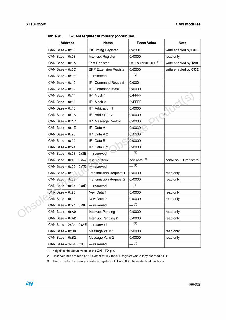
ST10F252M CAN modules
155/328
CAN Base + 0x06 Bit Timing Register 0x2301 write enabled by CCE
CAN Base + 0x08 Interrupt Register 0x0000 read only
CAN Base + 0x0A Test Register 0x00 & 0br0000000 (1) write enabled by Test
CAN Base + 0x0C BRP Extension Register 0x0000 write enabled by CCE
CAN Base + 0x0E — reserved — (2)
CAN Base + 0x10 IF1 Command Request 0x0001
CAN Base + 0x12 IF1 Command Mask 0x0000
CAN Base + 0x14 IF1 Mask 1 0xFFFF
CAN Base + 0x16 IF1 Mask 2 0xFFFF
CAN Base + 0x18 IF1 Arbitration 1 0x0000
CAN Base + 0x1A IF1 Arbitration 2 0x0000
CAN Base + 0x1C IF1 Message Control 0x0000
CAN Base + 0x1E IF1 Data A 1 0x0000
CAN Base + 0x20 IF1 Data A 2 0x0000
CAN Base + 0x22 IF1 Data B 1 0x0000
CAN Base + 0x24 IF1 Data B 2 0x0000
CAN Base + 0x28 - 0x3E — reserved — (2)
CAN Base + 0x40 - 0x54 IF2 registers see note (3) same as IF1 registers
CAN Base + 0x56 - 0x7E — reserved — (2)
CAN Base + 0x80 Transmission Request 1 0x0000 read only
CAN Base + 0x82 Transmission Request 2 0x0000 read only
CAN Base + 0x84 - 0x8E — reserved — (2)
CAN Base + 0x90 New Data 1 0x0000 read only
CAN Base + 0x92 New Data 2 0x0000 read only
CAN Base + 0x94 - 0x9E — reserved — (2)
CAN Base + 0xA0 Interrupt Pending 1 0x0000 read only
CAN Base + 0xA2 Interrupt Pending 2 0x0000 read only
CAN Base + 0xA4 - 0xAE — reserved — (2)
CAN Base + 0xB0 Message Valid 1 0x0000 read only
CAN Base + 0xB2 Message Valid 2 0x0000 read only
CAN Base + 0xB4 - 0xBE — reserved — (2)
1. r signifies the actual value of the CAN_RX pin.
2. Reserved bits are read as ‘0’ except for IFx mask 2 register where they are read as ‘1’
3. The two sets of message interface registers - IF1 and IF2 - have identical functions.
Table 91. C-CAN register summary (continued)
Address Name Reset Value Note
O
bsolete Product(
s) - O
bsolete Product(
s)

CAN modules ST10F252M
156/328
18.8.1 Hardware reset description
After hardware reset, the busoff state is reset and the output CAN_TX is set to recessive (HIGH). The value 0x0001 (Init = ‘1’) in the CAN control register enables the software initialisation. The C-CAN does not influence the CAN bus until the CPU resets Init to ‘0’.
The data stored in the message RAM is not affected by a hardware reset. After power-on, the contents of the message RAM are undefined.
18.8.2 CAN protocol related registers
These registers are related to the CAN protocol controller in the CAN core. They control the operating modes and the configuration of the CAN bit timing and provide status information.
CAN control register (addresses 0x01 and 0x00)
CAN control register SFR Reset value: xxxxh
15 14 13 12 11 10 9 8 7 6 5 4 3 2 1 0
reserved Test CCE DAR reserved EIE SIE IE Init
R R R R R R R R RW RW RW R RW RW RW RW
Table 92. CAN control register (addresses 0x01 and 0x00) functions
Bit Name Function
7 Test
Test mode enable
‘1’ Test mode‘0’ Normal operation.
6 CCEConfiguration change enable‘1’ The CPU has write access to the bit timing register (while Init=1)
‘0’ The CPU has no write access to the bit timing register.
5 DAR
Disable automatic retransmission
‘1’ Automatic retransmission disabled
‘0’ Automatic retransmission of disturbed messages enabled.
3 EIE
Error interrupt enable
‘1’ Enabled - A change in the bits BOff or EWarn in the register generates an interrupt
‘0’ Disabled - no error status interrupt is generated.
2 SIE
Status change interrupt enable
‘1’ Enabled - an interrupt is generated when a message transfer is successfully completed or a CAN bus error is detected
‘0’ Disabled - no status change interrupt is generated.
O
bsolete Product(
s) - O
bsolete Product(
s)
ST10F252M CAN modules
157/328
Note: The busoff recovery sequence (see CAN Specification Rev. 2.0) cannot be shortened by setting or resetting Init. If the device goes busoff, it sets Init of its own accord, stopping all bus activities. Once Init has been cleared by the CPU, the device waits for 129 occurrences of Bus Idle (129 * 11 consecutive recessive bits) before resuming normal operations. At the end of the busoff recovery sequence, the error management counters are reset.
During the waiting time after the resetting of Init, each time a sequence of 11 recessive bits has been monitored, a Bit0Error code is written to the status register, enabling the CPU to readily check up whether the CAN bus is stuck at dominant or continuously disturbed and to monitor the proceeding of the busoff recovery sequence.
Status register (addresses 0x03 and 0x02)
1 IE
Module interrupt enable‘1’ Enabled - interrupts set IRQ_B to LOW. IRQ_B remains LOW until all pending interrupts are processed.‘0’ Disabled - module interrupt IRQ_B is always HIGH.
0 INITInitialization‘1’ Initialization is started.
‘0’ Normal operation.
Table 92. CAN control register (addresses 0x01 and 0x00) functions (continued)
Bit Name Function
Status register SFR Reset value: xxxxh
15 14 13 12 11 10 9 8 7 6 5 4 3 2 1 0
reserved BOff EWarn EPass RxOk TxOk LEC
R R R R R R R R R R R R RW RW
Table 93. Status register (addresses 0x03 and 0x02) functions
Bit Name Function
7 BOffBusoff status‘1’ The CAN module is in busoff state
‘0’ The CAN module is not busoff.
6 EWarn
Warning status
‘1’ At least one of the error counters in the EML has reached the error warning limit of 96
‘0’ Both error counters are below the error warning limit of 96.
5 EPass
Error passive
‘1’ The CAN core is in the error passive state as defined in the CAN specification
‘0’ The CAN core is error active.
O
bsolete Product(
s) - O
bsolete Product(
s)
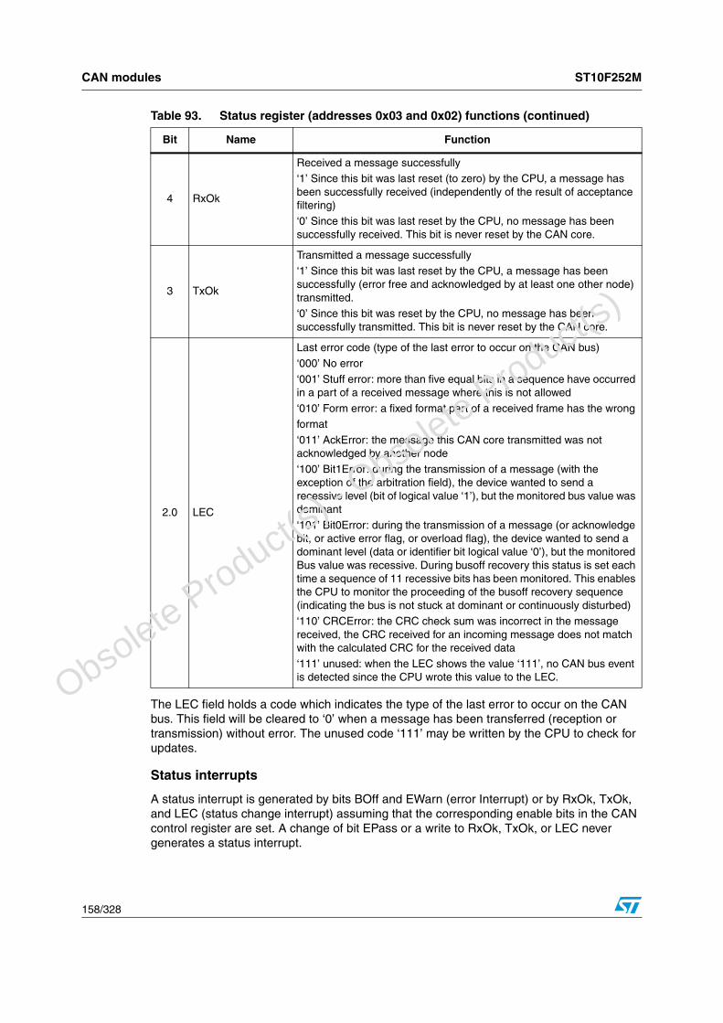
CAN modules ST10F252M
158/328
The LEC field holds a code which indicates the type of the last error to occur on the CAN bus. This field will be cleared to ‘0’ when a message has been transferred (reception or transmission) without error. The unused code ‘111’ may be written by the CPU to check for updates.
Status interrupts
A status interrupt is generated by bits BOff and EWarn (error Interrupt) or by RxOk, TxOk, and LEC (status change interrupt) assuming that the corresponding enable bits in the CAN control register are set. A change of bit EPass or a write to RxOk, TxOk, or LEC never generates a status interrupt.
4 RxOk
Received a message successfully‘1’ Since this bit was last reset (to zero) by the CPU, a message has been successfully received (independently of the result of acceptance filtering)
‘0’ Since this bit was last reset by the CPU, no message has been successfully received. This bit is never reset by the CAN core.
3 TxOk
Transmitted a message successfully
‘1’ Since this bit was last reset by the CPU, a message has been successfully (error free and acknowledged by at least one other node) transmitted.‘0’ Since this bit was reset by the CPU, no message has been successfully transmitted. This bit is never reset by the CAN core.
2.0 LEC
Last error code (type of the last error to occur on the CAN bus)
‘000’ No error
‘001’ Stuff error: more than five equal bits in a sequence have occurred in a part of a received message where this is not allowed
‘010’ Form error: a fixed format part of a received frame has the wrong format
‘011’ AckError: the message this CAN core transmitted was not acknowledged by another node
‘100’ Bit1Error: during the transmission of a message (with the exception of the arbitration field), the device wanted to send a recessive level (bit of logical value ‘1’), but the monitored bus value was dominant
‘101’ Bit0Error: during the transmission of a message (or acknowledge bit, or active error flag, or overload flag), the device wanted to send a dominant level (data or identifier bit logical value ‘0’), but the monitored Bus value was recessive. During busoff recovery this status is set each time a sequence of 11 recessive bits has been monitored. This enables the CPU to monitor the proceeding of the busoff recovery sequence (indicating the bus is not stuck at dominant or continuously disturbed)‘110’ CRCError: the CRC check sum was incorrect in the message received, the CRC received for an incoming message does not match with the calculated CRC for the received data
‘111’ unused: when the LEC shows the value ‘111’, no CAN bus event is detected since the CPU wrote this value to the LEC.
Table 93. Status register (addresses 0x03 and 0x02) functions (continued)
Bit Name Function
O
bsolete Product(
s) - O
bsolete Product(
s)
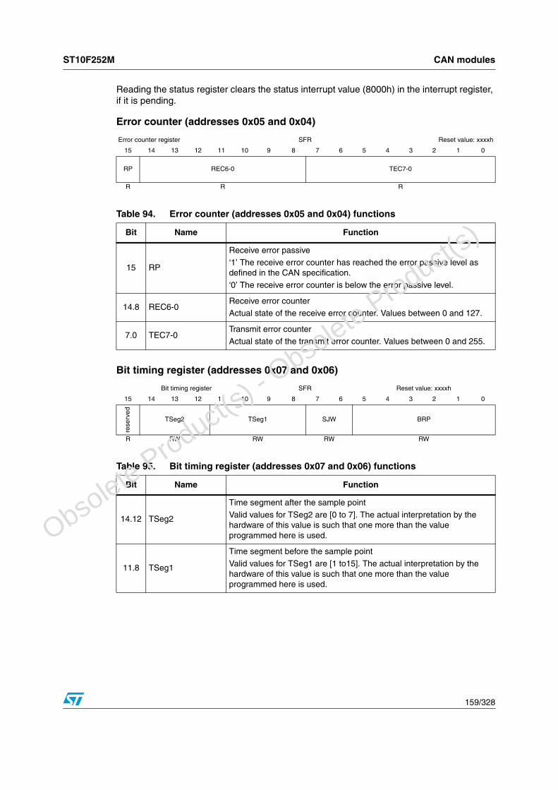
ST10F252M CAN modules
159/328
Reading the status register clears the status interrupt value (8000h) in the interrupt register, if it is pending.
Error counter (addresses 0x05 and 0x04)
Bit timing register (addresses 0x07 and 0x06)
Error counter register SFR Reset value: xxxxh
15 14 13 12 11 10 9 8 7 6 5 4 3 2 1 0
RP REC6-0 TEC7-0
R R R
Table 94. Error counter (addresses 0x05 and 0x04) functions
Bit Name Function
15 RP
Receive error passive
‘1’ The receive error counter has reached the error passive level as defined in the CAN specification.
‘0’ The receive error counter is below the error passive level.
14.8 REC6-0Receive error counter
Actual state of the receive error counter. Values between 0 and 127.
7.0 TEC7-0Transmit error counter
Actual state of the transmit error counter. Values between 0 and 255.
Bit timing register SFR Reset value: xxxxh
15 14 13 12 11 10 9 8 7 6 5 4 3 2 1 0
rese
rved
TSeg2 TSeg1 SJW BRP
R RW RW RW RW
Table 95. Bit timing register (addresses 0x07 and 0x06) functions
Bit Name Function
14.12 TSeg2
Time segment after the sample point
Valid values for TSeg2 are [0 to 7]. The actual interpretation by the hardware of this value is such that one more than the value programmed here is used.
11.8 TSeg1
Time segment before the sample point
Valid values for TSeg1 are [1 to15]. The actual interpretation by the hardware of this value is such that one more than the value programmed here is used.
O
bsolete Product(
s) - O
bsolete Product(
s)
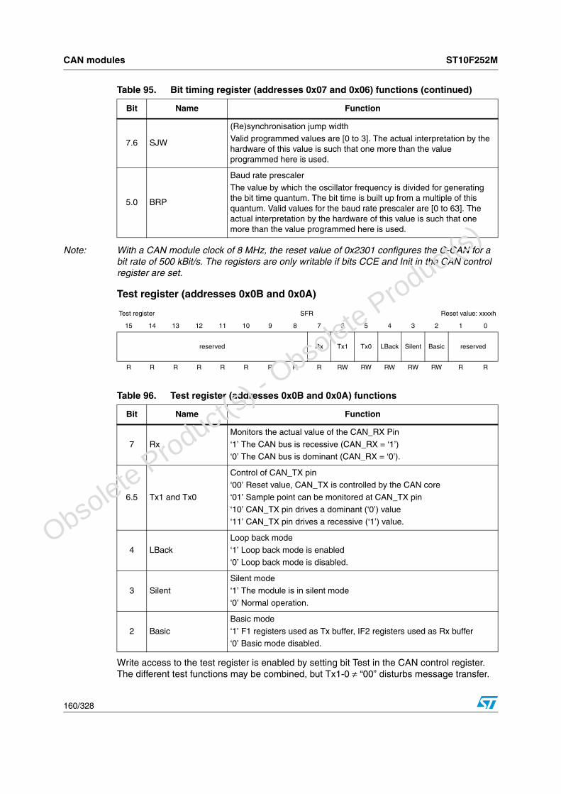
CAN modules ST10F252M
160/328
Note: With a CAN module clock of 8 MHz, the reset value of 0x2301 configures the C-CAN for a bit rate of 500 kBit/s. The registers are only writable if bits CCE and Init in the CAN control register are set.
Test register (addresses 0x0B and 0x0A)
Write access to the test register is enabled by setting bit Test in the CAN control register. The different test functions may be combined, but Tx1-0 ≠ “00” disturbs message transfer.
7.6 SJW
(Re)synchronisation jump widthValid programmed values are [0 to 3]. The actual interpretation by the hardware of this value is such that one more than the value programmed here is used.
5.0 BRP
Baud rate prescaler
The value by which the oscillator frequency is divided for generating the bit time quantum. The bit time is built up from a multiple of this quantum. Valid values for the baud rate prescaler are [0 to 63]. The actual interpretation by the hardware of this value is such that one more than the value programmed here is used.
Table 95. Bit timing register (addresses 0x07 and 0x06) functions (continued)
Bit Name Function
Test register SFR Reset value: xxxxh
15 14 13 12 11 10 9 8 7 6 5 4 3 2 1 0
reserved Rx Tx1 Tx0 LBack Silent Basic reserved
R R R R R R R R R RW RW RW RW RW R R
Table 96. Test register (addresses 0x0B and 0x0A) functions
Bit Name Function
7 Rx
Monitors the actual value of the CAN_RX Pin
‘1’ The CAN bus is recessive (CAN_RX = ‘1’)‘0’ The CAN bus is dominant (CAN_RX = ‘0’).
6.5 Tx1 and Tx0
Control of CAN_TX pin‘00’ Reset value, CAN_TX is controlled by the CAN core
‘01’ Sample point can be monitored at CAN_TX pin
‘10’ CAN_TX pin drives a dominant (‘0’) value‘11’ CAN_TX pin drives a recessive (‘1’) value.
4 LBackLoop back mode‘1’ Loop back mode is enabled
‘0’ Loop back mode is disabled.
3 Silent
Silent mode
‘1’ The module is in silent mode
‘0’ Normal operation.
2 Basic
Basic mode
‘1’ F1 registers used as Tx buffer, IF2 registers used as Rx buffer‘0’ Basic mode disabled.
O
bsolete Product(
s) - O
bsolete Product(
s)

ST10F252M CAN modules
161/328
BRP extension register (addresses 0x0D and 0x0C)
18.8.3 Message interface register sets
There are two sets of interface registers which are used to control the CPU access to the message RAM. The interface registers avoid conflicts between CPU access to the message RAM and CAN message reception and transmission by buffering the data to be transferred. A complete message object or parts of the message object may be transferred between the message RAM and the IFx message buffer registers in one single transfer.
The function of the two interface register sets is identical (except for test mode Basic). They can be used the way that one set of registers is used for data transfer to the message RAM while the other set of registers is used for the data transfer from the message RAM, allowing both processes to be interrupted by each other. Table 98 gives an overview of the two interface register sets.
Each set of interface registers consists of message buffer registers controlled by their own command registers. The command mask register specifies the direction of the data transfer and which parts of a message object are transferred. The command request register is used to select a message object in the message RAM as target or source for the transfer and to start the action specified in the command mask register.
BRP extension register SFR Reset value: xxxxh
15 14 13 12 11 10 9 8 7 6 5 4 3 2 1 0
reserved BRPE
R R R R R R R R R R R R RW
Table 97. BRP extension register (addresses 0x0D and 0x0C) functions
Bit Name Function
3.0 BRPE
Baud rate prescaler extensionBy programming BRPE
the baud rate prescaler can be extended to values up to 1023. The actual interpretation by the hardware is that one more than the value programmed by BRPE (MSBs) and BRP (LSBs) is used.
Table 98. IF1 and IF2 message interface register sets
Address IF1 Register Set Address IF2 Register Set
CAN Base + 0x10 IF1 Command Request CAN Base + 0x40 IF2 Command Request
CAN Base + 0x12 IF1 Command Mask CAN Base + 0x42 IF2 Command Mask
CAN Base + 0x14 IF1 Mask 1 CAN Base + 0x44 IF2 Mask 1
CAN Base + 0x16 IF1 Mask 2 CAN Base + 0x46 IF2 Mask 2
CAN Base + 0x18 IF1 Arbitration 1 CAN Base + 0x48 IF2 Arbitration 1
CAN Base + 0x1A IF1 Arbitration 2 CAN Base + 0x4A IF2 Arbitration 2
CAN Base + 0x1C IF1 Message Control CAN Base + 0x4C IF2 Message Control
CAN Base + 0x1E IF1 Data A 1 CAN Base + 0x4E IF2 Data A 1
CAN Base + 0x20 IF1 Data A 2 CAN Base + 0x50 IF2 Data A 2
O
bsolete Product(
s) - O
bsolete Product(
s)

CAN modules ST10F252M
162/328
A message transfer is started as soon as the CPU has written the message number to the command request register. With this write operation the Busy bit is automatically set to ‘1’. After a wait time of 3 to 6 CAN clock periods, the transfer between the interface register and the message RAM is completed and the Busy bit is set back to zero.
IFx command request registers
Note: When a message number that is not valid is written into the command request register, the message number is transformed into a valid value and that message object is transferred.
The control bits of the IFx command mask register specify the transfer direction and select which of the IFx message buffer registers are source or target of the data transfer.
CAN Base + 0x22 IF1 Data B 1 CAN Base + 0x52 IF2 Data B 1
CAN Base + 0x24 IF1 Data B 2 CAN Base + 0x54 IF2 Data B 2
IF1 Command Request Register (addresses 0x11 & 0x10) SFR Reset value: xxxxh
15 14 13 12 11 10 9 8 7 6 5 4 3 2 1 0
Busy reserved Message Number
R R R R R R R R R R RW
IF2 Command Request Register (addresses 0x41 & 0x40) SFR Reset value: xxxxh
15 14 13 12 11 10 9 8 7 6 5 4 3 2 1 0
Busy reserved Message Number
R R R R R R R R R R RW
Table 99. IFx command request registers functions
Bit Name Function
15 Busy
Busy flag
‘1’ Set when writing to the IFx command request register
‘0’ Read/write action has finished.
5.0 Message Number
Message number
‘0x01-0x20’ Valid message number, the message object in the message RAM is selected for data transfer
‘0x00’ Not a valid message number, interpreted as 0x20
‘0x21-0x3F’ Not a valid message number, interpreted as 0x01-0x1F.
Table 98. IF1 and IF2 message interface register sets (continued)
Address IF1 Register Set Address IF2 Register Set
O
bsolete Product(
s) - O
bsolete Product(
s)

ST10F252M CAN modules
163/328
IFx command mask registers
The other bits of IFx command mask register have different functions depending on the transfer direction.
IF1 Command Mask Register (addresses 0x13 & 0x12) SFR Reset value: xxxxh
15 14 13 12 11 10 9 8 7 6 5 4 3 2 1 0
reserved WR/RD Mask Arb Contr
olClrIntPnd
TxRqst/
NewDat
Data A Data B
R R R R R R R R RW RW RW RW RW RW RW RW
IF2 Command Mask Register (addresses 0x43 & 0x42) SFR Reset value: xxxxh
15 14 13 12 11 10 9 8 7 6 5 4 3 2 1 0
reserved WR/RD Mask Arb Contr
olClrIntPnd
TxRqst/
NewDat
Data A Data B
R R R R R R R R RW RW RW RW RW RW RW RW
Table 100. IFx command mask registers functions
Bit Name Function
7 WR/RD
Write/Read
‘1’ Write: transfer data from the selected message buffer registers to the message object addressed by the command request register
‘0’ Read: transfer data from the message object addressed by the command request register into the selected message buffer registers.
Table 101. IFx command mask registers functions (direction - write)
Bit Name Function
6 Mask
Access mask bits
‘1’ Transfer identifier mask + MDir + MXtd to message object
‘0’ Mask bits unchanged.
5 Arb
Access arbitration bits
‘1’ Transfer identifier + Dir + Xtd + MsgVal to message object‘0’ Arbitration bits unchanged.
4 ControlAccess control bits‘1’ Transfer control bits to message object
‘0’ Control bits unchanged.
3 ClrIntPndClear interrupt pending bit
When writing to a message object, this bit is ignored.
2 TxRqst/NewDat
Access transmission request bit
‘1’ Set TxRqst bit
‘0’ TxRqst bit unchangedIf a transmission is requested by programming bit TxRqst/NewDat in the IFx command mask register, bit TxRqst in the IFx message control register is ignored.
O
bsolete Product(
s) - O
bsolete Product(
s)

CAN modules ST10F252M
164/328
18.8.4 IFx message buffer registers
The bits of the message buffer registers mirror the message objects in the message RAM.
1 Data AAccess data bytes 0-3‘1’ Transfer data bytes 0-3 to message object
‘0’ Data bytes 0-3 unchanged.
0 Data B
Access data bytes 4-7
‘1’ Transfer data bytes 4-7 to message object
‘0’ Data bytes 4-7 unchanged.
Table 102. IFx command mask registers functions (direction - read)
Bit Name Function
6 Mask
Access mask bits
‘1’ Transfer identifier mask + MDir + MXtd to IFx message buffer register
‘0’ Mask bits unchanged.
5 Arb
Access arbitration bits‘1’ Transfer identifier + Dir + Xtd + MsgVal to IFx message buffer register‘0’ Arbitration bits unchanged.
4 ControlAccess control bits‘1’ Transfer control bits to IFx message buffer register
‘0’ Control bits unchanged.
3 ClrIntPnd
Clear interrupt pending bit
‘1’ Clear IntPnd bit in the message object
‘0’ IntPnd bit remains unchanged
2 TxRqst/NewDat
Access new data bit
‘1’ Clear NewDat bit in the message object‘0’ NewDat bit remains unchanged.
A read access to a Message Object can be combined with the reset of the control bits IntPnd and NewDat. The values of these bits transferred to the IFx Message Control Register always reflect the status before resetting these bits.
1 Data A
Access data bytes 0-3
‘1’ Transfer data bytes 0-3 to IFx message buffer register
‘0’ Data Bytes 0-3 unchanged.
0 Data B
Access data bytes 4-7
‘1’ Transfer data bytes 4-7 to IFx message buffer register‘0’ Data Bytes 4-7 unchanged
Table 101. IFx command mask registers functions (direction - write) (continued)
Bit Name Function
O
bsolete Product(
s) - O
bsolete Product(
s)

ST10F252M CAN modules
165/328
IFx mask register
IFx arbitration registers
IF1 Mask 1 Register (addresses 0x15 & 0x14) SFR Reset value: xxxxh
15 14 13 12 11 10 9 8 7 6 5 4 3 2 1 0
Msk15-0
RW RW R RW RW RW RW RW RW RW RW RW RW RW RW RW
IF1 Mask 2 Register (addresses 0x17 & 0x16) SFR Reset value: xxxxh
15 14 13 12 11 10 9 8 7 6 5 4 3 2 1 0
MXtd MDir reserved Msk28-16
RW RW R RW RW RW RW RW RW RW RW RW RW RW RW RW
IF1 Mask 1 Register (addresses 0x45 & 0x44) SFR Reset value: xxxxh
15 14 13 12 11 10 9 8 7 6 5 4 3 2 1 0
Msk15-0
RW RW R RW RW RW RW RW RW RW RW RW RW RW RW RW
IF1 Mask 2 Register (addresses 0x47 & 0x46) SFR Reset value: xxxxh
15 14 13 12 11 10 9 8 7 6 5 4 3 2 1 0
MXtd MDir
rese
rved
Msk28-16
RW RW R RW RW RW RW RW RW RW RW RW RW RW RW RW
IF1 Arbitration 1 Register (addresses 0x19 & 0x18) SFR Reset value: xxxxh
15 14 13 12 11 10 9 8 7 6 5 4 3 2 1 0
ID15-0
RW RW R RW RW RW RW RW RW RW RW RW RW RW RW RW
IF1 Arbitration 2 Register (addresses 0x1B & 0x1A) SFR Reset value: xxxxh
15 14 13 12 11 10 9 8 7 6 5 4 3 2 1 0
MsgVal Xtd Dir ID28-16
RW RW R RW RW RW RW RW RW RW RW RW RW RW RW RW
IF2 Arbitration 1 Register (addresses 0x49 & 0x48) SFR Reset value: xxxxh
15 14 13 12 11 10 9 8 7 6 5 4 3 2 1 0
ID15-0
RW RW R RW RW RW RW RW RW RW RW RW RW RW RW RW
O
bsolete Product(
s) - O
bsolete Product(
s)

CAN modules ST10F252M
166/328
IFx message control registers
IFx Data A and Data B Registers
The data bytes of CAN messages are stored in the IFx Message Buffer Registers in the order shown in Table 103.
In a CAN data frame, Data(0) is the first, Data(7) is the last byte to be transmitted or received. In CAN’s serial bit stream, the MSB of each byte is transmitted first.
Message object in the message memory
There are 32 message objects in the message RAM. To avoid conflicts between CPU access to the message RAM and CAN message reception and transmission, the CPU cannot directly access the message objects, these accesses are handled via the IFx interface registers.
IF2 Arbitration 2 Register (addresses 0x4B & 0x4A) SFR Reset value: xxxxh
15 14 13 12 11 10 9 8 7 6 5 4 3 2 1 0
MsgVal Xtd Dir ID28-16
RW RW R RW RW RW RW RW RW RW RW RW RW RW RW RW
IF1 Message Control Register (addresses 0x1D & 0x1C) SFR Reset value: xxxxh
15 14 13 12 11 10 9 8 7 6 5 4 3 2 1 0
NewDat
MsgLst IntPnd UMas
k TxIE RxIE RmtEn TxRqst EoB reserved
reserved
reserved DLC3-0
RW RW R RW RW RW RW RW RW RW RW RW RW RW RW RW
IF2 Message Control Register (addresses 0x4D & 0x4C) SFR Reset value: xxxxh
15 14 13 12 11 10 9 8 7 6 5 4 3 2 1 0
NewDat
MsgLst IntPnd UMas
k TxIE RxIE RmtEn TxRqst EoB reserved
reserved
reserved DLC3-0
RW RW R RW RW RW RW RW RW RW RW RW RW RW RW RW
Table 103. IFx Data A and Data B registers
[15:8] [7:0]
IF1 Message Data A1 (addresses 0x1F & 0x1E) Data(1) Data(0)
IF1 Message Data A2 (addresses 0x21 & 0x20) Data(3) Data(2)
IF1 Message Data B1 (addresses 0x23 & 0x22) Data(5) Data(4)
IF1 Message Data B2 (addresses 0x25 & 0x24) Data(7) Data(6)
IF2 Message Data A1 (addresses 0x4F & 0x4E) Data(1) Data(0)
IF2 Message Data A2 (addresses 0x51 & 0x50) Data(3) Data(2)
IF2 Message Data B1 (addresses 0x53 & 0x52) Data(5) Data(4)
IF2 Message Data B2 (addresses 0x55 & 0x54) Data(7) Data(6) O
bsolete Product(
s) - O
bsolete Product(
s)
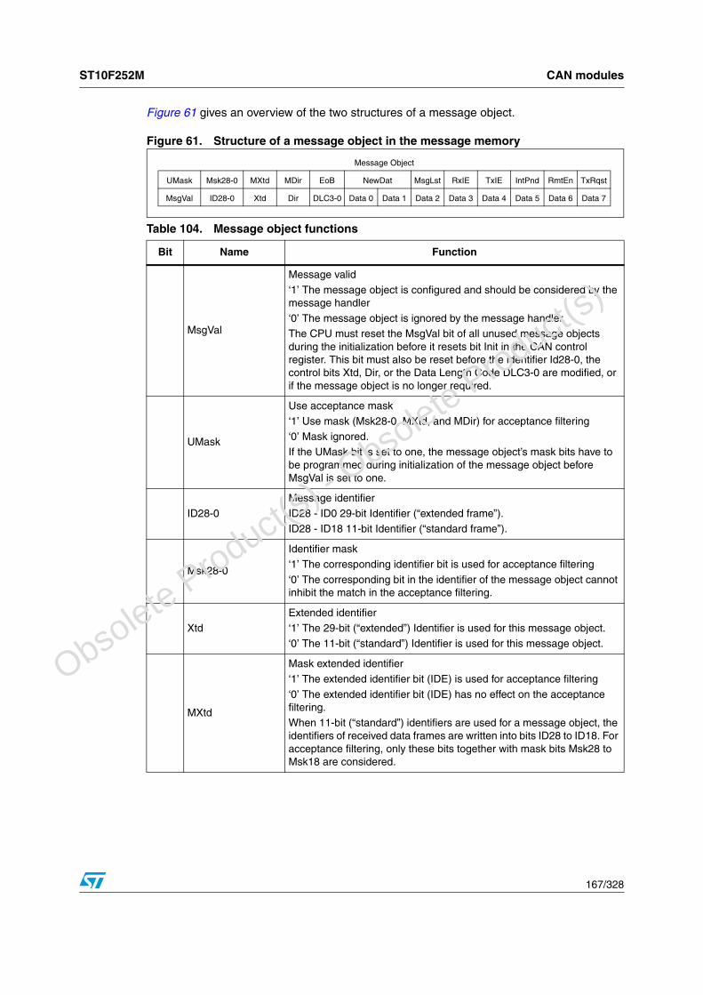
ST10F252M CAN modules
167/328
Figure 61 gives an overview of the two structures of a message object.
Figure 61. Structure of a message object in the message memory
Table 104. Message object functions
Bit Name Function
MsgVal
Message valid
‘1’ The message object is configured and should be considered by the message handler
‘0’ The message object is ignored by the message handler.The CPU must reset the MsgVal bit of all unused message objects during the initialization before it resets bit Init in the CAN control register. This bit must also be reset before the identifier Id28-0, the control bits Xtd, Dir, or the Data Length Code DLC3-0 are modified, or if the message object is no longer required.
UMask
Use acceptance mask
‘1’ Use mask (Msk28-0, MXtd, and MDir) for acceptance filtering‘0’ Mask ignored.
If the UMask bit is set to one, the message object’s mask bits have to be programmed during initialization of the message object before MsgVal is set to one.
ID28-0
Message identifier
ID28 - ID0 29-bit Identifier (“extended frame”).ID28 - ID18 11-bit Identifier (“standard frame”).
Msk28-0
Identifier mask‘1’ The corresponding identifier bit is used for acceptance filtering
‘0’ The corresponding bit in the identifier of the message object cannot inhibit the match in the acceptance filtering.
XtdExtended identifier‘1’ The 29-bit (“extended”) Identifier is used for this message object.
‘0’ The 11-bit (“standard”) Identifier is used for this message object.
MXtd
Mask extended identifier
‘1’ The extended identifier bit (IDE) is used for acceptance filtering
‘0’ The extended identifier bit (IDE) has no effect on the acceptance filtering.
When 11-bit (“standard”) identifiers are used for a message object, the identifiers of received data frames are written into bits ID28 to ID18. For acceptance filtering, only these bits together with mask bits Msk28 to Msk18 are considered.
Message Object
UMask Msk28-0 MXtd MDir EoB NewDat MsgLst RxIE TxIE IntPnd RmtEn TxRqst
MsgVal ID28-0 Xtd Dir DLC3-0 Data 0 Data 1 Data 2 Data 3 Data 4 Data 5 Data 6 Data 7
O
bsolete Product(
s) - O
bsolete Product(
s)

CAN modules ST10F252M
168/328
Dir
Message direction‘1’ Direction = transmit: On TxRqst, the respective message object is transmitted as a data frame. On reception of a remote frame with matching identifier, the TxRqst bit of this message object is set (if RmtEn = one)
‘0’ Direction = receive: On TxRqst, a remote frame with the identifier of this message object is transmitted. On reception of a data frame with matching identifier, that message is stored in this message object.
MDir
Mask message direction
‘1’ The message direction bit (Dir) is used for acceptance filtering‘0’ The message direction bit (Dir) has no effect on the acceptance filtering.The arbitration registers ID28-0, Xtd, and Dir are used to define the identifier and type of outgoing messages and are used (together with the mask registers Msk28-0, MXtd, and MDir) for acceptance filtering of incoming messages. A received message is stored into the valid message object with matching identifier and Direction=receive (data frame) or Direction=transmit (remote frame). Extended frames can be stored only in message objects with Xtd = one, standard frames in message objects with Xtd = zero. If a received message (data frame or remote frame) matches with more than one valid Message Object, it is stored into that with the lowest message number. For details see Section 18.9.2.
EoB
End of buffer
‘1’ Single message object or last message object of a FIFO buffer
‘0’ Message object belongs to a FIFO buffer and is not the last message object of that FIFO buffer.
This bit is used to concatenate two ore more message objects (up to 32) to build a FIFO buffer. For single message objects (not belonging to a FIFO buffer) this bit is always be set to one. For details on the concatenation of message objects see Section 18.9.7.
NewDat
New data
‘1’ The message handler or the CPU has written new data into the data portion of this message object
‘0’ No new data has been written into the data portion of this message object by the message handler since last time this flag was cleared by the CPU.
MsgLst
Message lost (only valid for message objects with direction = receive)‘1’ The message handler stored a new message into this object when NewDat was still set, the CPU has lost a message‘0’ No message lost since last time this bit was reset by the CPU.
RxIEReceive interrupt enable‘1’ IntPnd is set after a successful reception of a frame
‘0’ IntPnd is left unchanged after a successful reception of a frame.
Table 104. Message object functions (continued)
Bit Name Function
O
bsolete Product(
s) - O
bsolete Product(
s)

ST10F252M CAN modules
169/328
18.8.5 Message Handler Registers
All Message Handler registers are read-only. Their contents (TxRqst, NewDat, IntPnd, and MsgVal bits of each Message Object and the Interrupt Identifier) is status information provided by the Message Handler FSM.
TxIE
Transmit interrupt enable‘1’ IntPnd is set after a successful transmission of a frame
‘0’ IntPnd is left unchanged after the successful transmission of a frame.
IntPnd
Interrupt pending‘1’ This message object is the source of an interrupt. The interrupt identifier in the interrupt register point to this message object if there is no other interrupt source with higher priority
‘0’ This message object is not the source of an interrupt.
RmtEn
Remote enable
‘1’ At the reception of a remote frame, TxRqst is set‘0’ At the reception of a remote frame, TxRqst is left unchanged.
TxRqst
Transmit request
‘1’ The transmission of this message object is requested and is not yet done
‘0’ This message object is not waiting for transmission.
DLC3-0
Data length code
‘0-8’ Data frame has 0-8 data bytes.‘9-15’ Data frame has 8 data bytes
The data length code of a message object is defined the same as in all the corresponding objects with the same identifier at other nodes. When the message handler stores a data frame, it will write the DLC to the value given by the received message.
Data 0 1st data byte of a CAN data frameData 1 2nd data byte of a CAN data frame
Data 2 3rd data byte of a CAN data frame
Data 3 4th data byte of a CAN data frameData 4 5th data byte of a CAN data frame
Data 5 6th data byte of a CAN data frame
Data 6 7th data byte of a CAN data frameData 7 8th data byte of a CAN data frame
Byte Data 0 is the first data byte shifted into the shift register of the CAN core during a reception, byte Data 7 is the last. When the message handler stores a data frame, it writes all the eight data bytes into a message object. If the data length code is less than 8, the remaining bytes of the message object are overwritten by non specified values.
Table 104. Message object functions (continued)
Bit Name Function
O
bsolete Product(
s) - O
bsolete Product(
s)
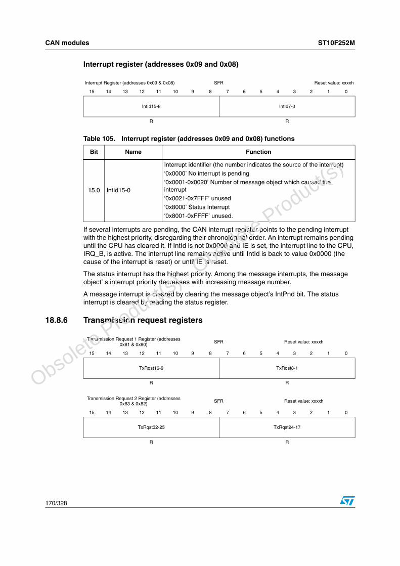
CAN modules ST10F252M
170/328
Interrupt register (addresses 0x09 and 0x08)
If several interrupts are pending, the CAN interrupt register points to the pending interrupt with the highest priority, disregarding their chronological order. An interrupt remains pending until the CPU has cleared it. If IntId is not 0x0000 and IE is set, the interrupt line to the CPU, IRQ_B, is active. The interrupt line remains active until IntId is back to value 0x0000 (the cause of the interrupt is reset) or until IE is reset.
The status interrupt has the highest priority. Among the message interrupts, the message object’ s interrupt priority decreases with increasing message number.
A message interrupt is cleared by clearing the message object’s IntPnd bit. The status interrupt is cleared by reading the status register.
18.8.6 Transmission request registers
Interrupt Register (addresses 0x09 & 0x08) SFR Reset value: xxxxh
15 14 13 12 11 10 9 8 7 6 5 4 3 2 1 0
IntId15-8 IntId7-0
R R
Table 105. Interrupt register (addresses 0x09 and 0x08) functions
Bit Name Function
15.0 IntId15-0
Interrupt identifier (the number indicates the source of the interrupt)‘0x0000’ No interrupt is pending
‘0x0001-0x0020’ Number of message object which caused the interrupt
‘0x0021-0x7FFF’ unused
‘0x8000’ Status Interrupt
‘0x8001-0xFFFF’ unused.
Transmission Request 1 Register (addresses 0x81 & 0x80) SFR Reset value: xxxxh
15 14 13 12 11 10 9 8 7 6 5 4 3 2 1 0
TxRqst16-9 TxRqst8-1
R R
Transmission Request 2 Register (addresses 0x83 & 0x82) SFR Reset value: xxxxh
15 14 13 12 11 10 9 8 7 6 5 4 3 2 1 0
TxRqst32-25 TxRqst24-17
R R
O
bsolete Product(
s) - O
bsolete Product(
s)

ST10F252M CAN modules
171/328
These registers hold the TxRqst bits of the 32 message objects. By reading out the TxRqst bits, the CPU can check for which message object a transmission request is pending. The TxRqst bit of a specific message object can be set/reset by the CPU via the IFx message interface registers or by the message handler after reception of a remote frame or after a successful transmission.
18.8.7 New data registers
These registers hold the NewDat bits of the 32 message objects. By reading out the NewDat bits, the CPU can check for which message object the data portion is updated. The NewDat bit of a specific message object can be set/reset by the CPU via the IFx message interface registers or by the message handler after reception of a data frame or after a successful transmission.
Table 106. Transmission request register functions
Bit Name Function
15.0 TxRqst32-1
Transmission request bits (of all message objects)
‘1’ The transmission of this message object is requested and is not yet done
‘0’ This message object is not waiting for transmission.
New Data 1 Register (addresses 0x91 & 0x90) SFR Reset value: xxxxh
15 14 13 12 11 10 9 8 7 6 5 4 3 2 1 0
NewDat16-9 NewDat8-1
R R
New Data 2 Register (addresses 0x93 & 0x92) SFR Reset value: xxxxh
15 14 13 12 11 10 9 8 7 6 5 4 3 2 1 0
NewDat32-25 NewDat24-17
R R
Table 107. New data register functions
Bit Name Function
15.0 NewDat32-1
New data bits (of all message objects)‘1’ The message handler or the CPU has written new data into the data portion of this message object‘0’ No new data has been written into the data portion of this message object by the message handler since last time this flag was cleared by the CPU.
O
bsolete Product(
s) - O
bsolete Product(
s)
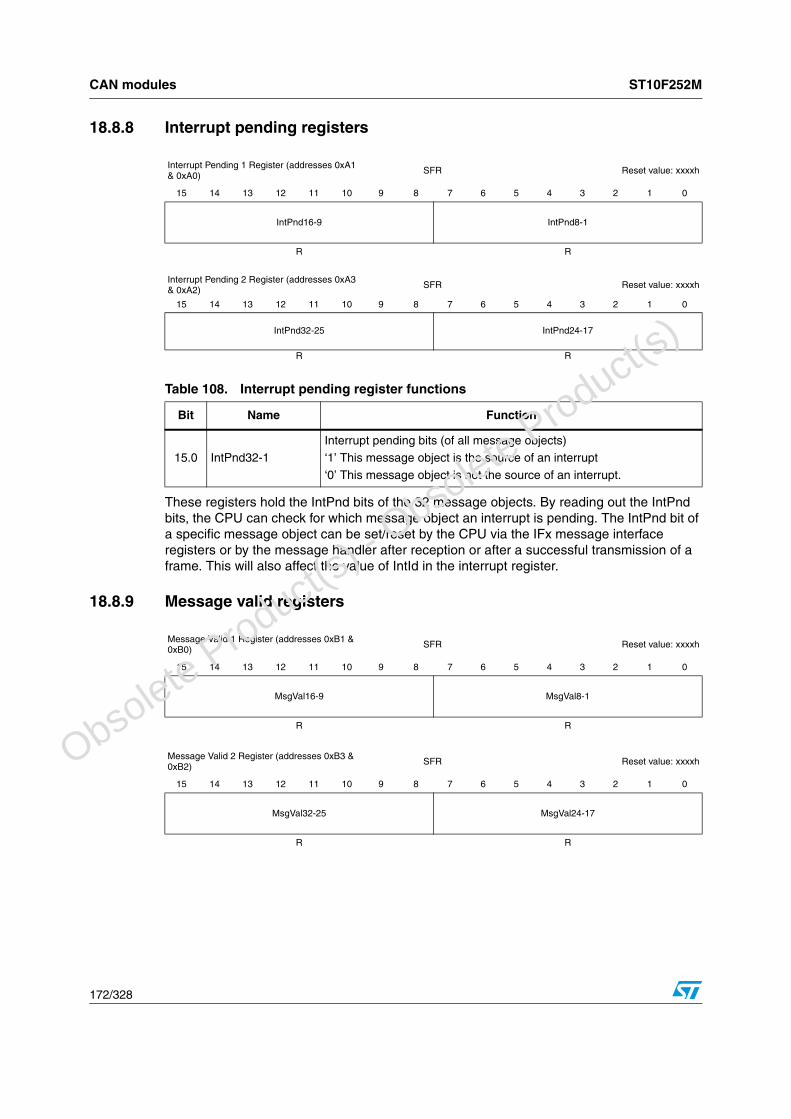
CAN modules ST10F252M
172/328
18.8.8 Interrupt pending registers
These registers hold the IntPnd bits of the 32 message objects. By reading out the IntPnd bits, the CPU can check for which message object an interrupt is pending. The IntPnd bit of a specific message object can be set/reset by the CPU via the IFx message interface registers or by the message handler after reception or after a successful transmission of a frame. This will also affect the value of IntId in the interrupt register.
18.8.9 Message valid registers
Interrupt Pending 1 Register (addresses 0xA1 & 0xA0) SFR Reset value: xxxxh
15 14 13 12 11 10 9 8 7 6 5 4 3 2 1 0
IntPnd16-9 IntPnd8-1
R R
Interrupt Pending 2 Register (addresses 0xA3 & 0xA2) SFR Reset value: xxxxh
15 14 13 12 11 10 9 8 7 6 5 4 3 2 1 0
IntPnd32-25 IntPnd24-17
R R
Table 108. Interrupt pending register functions
Bit Name Function
15.0 IntPnd32-1Interrupt pending bits (of all message objects)‘1’ This message object is the source of an interrupt
‘0’ This message object is not the source of an interrupt.
Message Valid 1 Register (addresses 0xB1 & 0xB0) SFR Reset value: xxxxh
15 14 13 12 11 10 9 8 7 6 5 4 3 2 1 0
MsgVal16-9 MsgVal8-1
R R
Message Valid 2 Register (addresses 0xB3 & 0xB2) SFR Reset value: xxxxh
15 14 13 12 11 10 9 8 7 6 5 4 3 2 1 0
MsgVal32-25 MsgVal24-17
R R
O
bsolete Product(
s) - O
bsolete Product(
s)
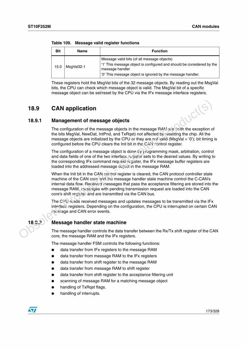
ST10F252M CAN modules
173/328
These registers hold the MsgVal bits of the 32 message objects. By reading out the MsgVal bits, the CPU can check which message object is valid. The MsgVal bit of a specific message object can be set/reset by the CPU via the IFx message interface registers.
18.9 CAN application
18.9.1 Management of message objects
The configuration of the message objects in the message RAM are (with the exception of the bits MsgVal, NewDat, IntPnd, and TxRqst) not affected by resetting the chip. All the message objects are initialized by the CPU or they are not valid (MsgVal = ‘0’); bit timing is configured before the CPU clears the Init bit in the CAN control register.
The configuration of a message object is done by programming mask, arbitration, control and data fields of one of the two interface register sets to the desired values. By writing to the corresponding IFx command request register, the IFx message buffer registers are loaded into the addressed message object in the message RAM.
When the Init bit in the CAN control register is cleared, the CAN protocol controller state machine of the CAN core and the message handler state machine control the C-CAN’s internal data flow. Received messages that pass the acceptance filtering are stored into the message RAM, messages with pending transmission request are loaded into the CAN core’s shift register and are transmitted via the CAN bus.
The CPU reads received messages and updates messages to be transmitted via the IFx interface registers. Depending on the configuration, the CPU is interrupted on certain CAN message and CAN error events.
18.9.2 Message handler state machine
The message handler controls the data transfer between the Rx/Tx shift register of the CAN core, the message RAM and the IFx registers.
The message handler FSM controls the following functions:
● data transfer from IFx registers to the message RAM
● data transfer from message RAM to the IFx registers
● data transfer from shift register to the message RAM
● data transfer from message RAM to shift register
● data transfer from shift register to the acceptance filtering unit
● scanning of message RAM for a matching message object
● handling of TxRqst flags.
● handling of interrupts.
Table 109. Message valid register functions
Bit Name Function
15.0 MsgVal32-1
Message valid bits (of all message objects)
‘1’ This message object is configured and should be considered by the message handler
‘0’ This message object is ignored by the message handler.
O
bsolete Product(
s) - O
bsolete Product(
s)

CAN modules ST10F252M
174/328
Data transfer from and to message RAM
When the CPU initiates a data transfer between the IFx registers and message RAM, the message handler sets the Busy bit in the respective command register to ‘1’. After the transfer has completed, the Busy bit is set back to ‘0’ (see Figure 62).
The respective command mask register specifies whether a complete message object or only parts of it are transferred. Due to the structure of the message RAM it is not possible to write single bits/bytes of one message object, it is always necessary to write a complete message object into the message RAM. Therefore, the data transfer from the IFx registers to the message RAM requires a read-modify-write cycle. First, those parts of the message object that are not to be changed are read from the Message RAM and, then, the complete contents of the message buffer registers are into the message object.
Figure 62. Data transfer between IFx registers and message RAM
After the partial write of a message object, the message buffer registers that are not selected in the command mask register are set to the actual contents of the selected message object.
After the partial read of a message object, the message buffer registers that are not selected in the command mask register are left unchanged.
START
WR/RD = 1
Busy = 0
Busy = 1
Read Message Object to IFx
Write IFx to Message RAM
Read Message Object to IFx
No Yes
CAN_WAIT_B = 0
CAN_WAIT_B = 1
Write Command Request RegisterNo
Yes
O
bsolete Product(
s) - O
bsolete Product(
s)
ST10F252M CAN modules
175/328
Transmission of messages
If the shift register of the CAN core cell is ready for loading and if there is no data transfer between the IFx registers and message RAM, the MsgVal bits in the message valid register TxRqst bits in the transmission request register are evaluated. The valid message object with the highest priority pending transmission request is loaded into the shift register by the message handler and the transmission is started. The message object’s NewDat bit is reset.
After a successful transmission and if no new data was written to the message object (NewDat = ‘0’) since the start of the transmission, the TxRqst bit is reset. If TxIE is set, IntPnd is set after a successful transmission. If the C-CAN has lost the arbitration or if an error occurred during the transmission, the message is retransmitted as soon as the CAN bus is free again. If, meanwhile, the transmission of a message with higher priority is requested, the messages are transmitted in the order of their priority.
Acceptance filtering of received messages
When the arbitration and control field (Identifier + IDE + RTR + DLC) of an incoming message is completely shifted into the Rx/Tx shift register of the CAN core, the message handler FSM starts the scanning of the message RAM for a matching valid message object.
To scan the message RAM for a matching message object, the acceptance filtering unit is loaded with the arbitration bits from the CAN core shift register. The arbitration and mask fields (including MsgVal, UMask, NewDat, and EoB) of message object 1 are loaded into the acceptance filtering unit and compared with the arbitration field from the shift register. This is repeated with each following message object until a matching message object is found or until the end of the message RAM is reached.
If a match occurs, the scanning is stopped and the message handler FSM proceeds depending on the type of frame (data frame or remote frame) received.
Reception of data frame
The message handler FSM stores the message from the CAN core shift register into the respective message object in the message RAM. Not only the data bytes, but all arbitration bits and the data length code are stored into the corresponding message object. This is implemented to keep the data bytes connected with the identifier even if arbitration mask registers are used.
The NewDat bit is set to indicate that new data (not yet seen by the CPU) has been received. The CPU resets NewDat when it reads the message object. If, at the time of the reception, the NewDat bit was already set, MsgLst is set to indicate that the previous data (supposedly not seen by the CPU) is lost. If the RxIE bit is set, the IntPnd bit is set, causing the interrupt register to point to this message object.
The TxRqst bit of this message object is reset to prevent the transmission of a remote frame, while the requested data frame has just been received.
Reception of remote frame
When a remote frame is received, three different configurations of the matching message object have to be considered:
O
bsolete Product(
s) - O
bsolete Product(
s)

CAN modules ST10F252M
176/328
1. Dir = ‘1’ (direction = transmit), RmtEn = ‘1’, UMask = ‘1’ or ‘0’At the reception of a matching remote frame, the TxRqst bit of this message object is set. The rest of the message object remains unchanged.
2. Dir = ‘1’ (direction = transmit), RmtEn = ‘0’, UMask = ‘0’At the reception of a matching remote frame, the TxRqst bit of this message object remains unchanged; the remote frame is ignored.
3. Dir = ‘1’ (direction = transmit), RmtEn = ‘0’, UMask = ‘1’At the reception of a matching remote frame, the TxRqst bit of this message object is reset. The arbitration and control field (Identifier + IDE + RTR + DLC) from the shift register is stored into the message object in the message RAM and the NewDat bit of this message object is set. The data field of the message object remains unchanged; the remote frame is treated similar to a received data frame.
Receive/transmit priority
The receive/transmit priority for the message objects is attached to the message number. Message object 1 has the highest priority, while message object 32 has the lowest priority. If more than one transmission request is pending, they are serviced according to the priority of the corresponding message object.
18.9.3 Configuration of a transmit object
Figure 63 shows how a transmit object is initialized.
Figure 63. Initialisation of a transmit object
The arbitration registers (ID28-0 and Xtd bit) are given by the application. They define the identifier and type of the outgoing message. If an 11-bit identifier (“standard frame”) is used, it is programmed to ID28 - ID18, ID17 - ID0 can be disregarded.
If the TxIE bit is set, the IntPnd bit is be set after a successful transmission of the message object.
If the RmtEn bit is set, a matching received remote frame causes the TxRqst bit to be set; the remote frame is autonomously answered by a Data Frame.
The data registers (DLC3-0, Data0-7) are given by the application, TxRqst and RmtEn may not be set before the data is valid.
The mask registers (Msk28-0, UMask, MXtd, and MDir bits) may be used (UMask=’1’) to allow groups of remote frames with similar identifiers to set the TxRqst bit. For details see Section 18.9.2, handle with care; the Dir bit should not be masked.
18.9.4 Updating a transmit object
The CPU may update the data bytes of a transmit object any time via the IFx interface registers, neither MsgVal nor TxRqst need be reset before the update.
Even if only a part of the data bytes are to be updated, all four bytes of the corresponding IFx Data A Register or IFx Data B Register have to be valid before the content of that register is transferred to the message object. Either the CPU has to write all four bytes into
MsgVal Arb Data Mask EoB Dir NewDat MsgLst RxIE TxIE IntPnd RmtEn TxRqst
1 appl. appl. appl. 1 1 0 0 0 appl. 0 appl. 0
O
bsolete Product(
s) - O
bsolete Product(
s)

ST10F252M CAN modules
177/328
the IFx data register or the message object is transferred to the IFx data register before the CPU writes the new data bytes.
When only the (eight) data bytes are updated, first, 0x0087 is written to the command mask register and, then, the number of the message object is written to the command request register, concurrently updating the data bytes and setting TxRqst.
To prevent the reset of TxRqst at the end of a transmission that may already be in progress while the data is updated, NewDat is set together with TxRqst. For details see Section 18.9.2.
When NewDat is set together with TxRqst, NewDat is reset as soon as the new transmission has started.
18.9.5 Configuration of a receive object
Figure 64 shows how a receive object is initialized.
Figure 64. Initialization of a receive object
The arbitration registers (ID28-0 and Xtd bit) are given by the application. They define the identifier and type of accepted received messages. If an 11-bit Identifier (“standard frame”) is used, it is programmed to ID28 - ID18, ID17 - ID0 can then be disregarded. When a data frame with an 11-bit Identifier is received, ID17 - ID0 is set to ‘0’.
If the RxIE bit is set, the IntPnd bit is set when a received data frame is accepted and stored in the message object.
The data length code (DLC3-0) is given by the application. When the message handler stores a data frame in the message object, it stores the received data length code and eight data bytes. If the data length code is less than eight, the remaining bytes of the message object are overwritten by non specified values.
The mask registers (Msk28-0, UMask, MXtd, and MDir bits) may be used (UMask=’1’) to allow groups of data frames with similar identifiers to be accepted. For details see Section 18.9.2. The Dir bit should not be masked in typical applications.
18.9.6 Handling of received messages
The CPU may read a received message any time via the IFx interface registers, the data consistency is guaranteed by the message handler state machine.
Typically, the CPU first writes 0x007F to the command mask register and then writes the number of the message object to the command request register. This combination transfers the whole received message from the message RAM into the message buffer register. Additionally, the bits NewDat and IntPnd are cleared in the message RAM (not in the message buffer).
If the message object uses masks for acceptance filtering, the arbitration bits show which of the matching messages has been received.
The actual value of NewDat shows whether a new message has been received since last time this message object was read. The actual value of MsgLst shows whether more than
MsgVal Arb Data Mask EoB Dir NewDat MsgLst RxIE TxIE IntPnd RmtEn TxRqst
1 appl. appl. appl. 1 0 0 0 appl. 0 0 0 0
O
bsolete Product(
s) - O
bsolete Product(
s)
CAN modules ST10F252M
178/328
one message has been received since last time this message object was read. MsgLst is not automatically reset.
By a remote frame, the CPU may request another CAN node to provide new data for a receive object. Setting the TxRqst bit of a receive object causes the transmission of a remote frame with the receive object’s identifier. This remote frame triggers the other CAN node to start the transmission of the matching data frame. If the matching data frame is received before the remote frame could be transmitted, the TxRqst bit is automatically reset.
18.9.7 Configuration of a FIFO buffer
With the exception of the EoB bit, the configuration of receive objects belonging to a FIFO buffer is the same as the configuration of a (single) receive object, see Section 18.9.5.
To concatenate two or more message objects into a FIFO buffer, the identifiers and masks (if used) of these message objects have to be programmed to matching values. Due to the implicit priority of the message objects, the message object with the lowest number will be the first message object of the FIFO buffer. The EoB bit of all message objects of a FIFO buffer except the last have to be programmed to zero. The EoB bits of the last message object of a FIFO buffer is set to one, configuring it as the end of the block.
18.9.8 Reception of messages with FIFO buffers
Received messages with identifiers matching to a FIFO buffer are stored into a message object of this FIFO buffer starting with the message object with the lowest message number.
When a message is stored into a message object of a FIFO buffer, the NewDat bit of this message object is set. By setting NewDat while EoB is zero, the message object is locked for further write accesses by the message handler until the CPU has written the NewDat bit back to zero.
Messages are stored into a FIFO buffer until the last message object of this FIFO buffer is reached. If none of the preceding message objects is released by writing NewDat to zero, all further messages for this FIFO buffer are written into the last message object of the FIFO buffer and, therefore, overwrite previous messages.
Reading from a FIFO buffer
When the CPU transfers the contents of message object to the IFx message buffer registers by writing its number to the IFx command request register, the corresponding command mask register is programmed such that bits NewDat and IntPnd are reset to zero (TxRqst/NewDat = ‘1’ and ClrIntPnd = ‘1’). The values of these bits in the message control register always reflect the status before resetting the bits.
To assure the correct function of a FIFO buffer, the CPU reads out the message objects starting at the FIFO Object with the lowest message number.
Figure 65 shows how a set of message objects which are concatenated to a FIFO buffer can be handled by the CPU.
O
bsolete Product(
s) - O
bsolete Product(
s)

ST10F252M CAN modules
179/328
Figure 65. CPU Handling of a FIFO Buffer
18.9.9 Handling of interrupts
If several interrupts are pending, the CAN interrupt register points to the pending interrupt with the highest priority, disregarding their chronological order. An interrupt remains pending until the CPU has cleared it.
The status interrupt has the highest priority. Among the message interrupts, the message object’ s interrupt priority decreases with increasing message number.
A message interrupt is cleared by clearing the message object’s IntPnd bit. The status interrupt is cleared by reading the status register.
Read Interrupt Pointer
START
case Interrupt Pointer0x8000h else 0x0000h
Status Change END
MessageNum = Interrupt Pointer
Write MessageNum to IFx Command Request
(Read Message to IFx Registers,Reset NewDat = 0,Reset IntPnd = 0)
Read IFx Message Control
NewDat = 1
Read Data from IFx Data A,B
EoB = 1
MessageNum = MessageNum + 1
Yes
No
Yes
No
Message Interrupt
Interrupt Handling
O
bsolete Product(
s) - O
bsolete Product(
s)

CAN modules ST10F252M
180/328
The interrupt identifier IntId in the interrupt register indicates the cause of the interrupt. When no interrupt is pending, the register holds the value zero. If the value of the interrupt register is not zero, there is an interrupt pending and, if IE is set, the interrupt line to the CPU, IRQ_B, is active. The interrupt line remains active until the interrupt register is back to value zero (the cause of the interrupt is reset) or until IE is reset.
The value 0x8000 indicates that an interrupt is pending because the CAN core has updated (not necessarily changed) the status register (error interrupt or status interrupt). This interrupt has the highest priority. The CPU can update (reset) the status bits RxOk, TxOk and LEC, but a write access of the CPU to the status register can never generate or reset an interrupt.
All other values indicate that the source of the interrupt is one of the message objects, IntId points to the pending message interrupt with the highest interrupt priority.
The CPU controls whether a change of the status register may cause an interrupt (bits EIE and SIE in the CAN control register) and whether the interrupt line becomes active when the interrupt register is not zero (bit IE in the CAN control register). The interrupt register is updated even when IE is reset.
The CPU has two possibilities to follow the source of a message interrupt. First it can follow the IntId in the interrupt register and second it can poll the interrupt pending register (see Section 18.8.5).
An interrupt service routine reading the message that is the source of the interrupt may read the message and reset the message object’s IntPnd at the same time (bit ClrIntPnd in the command mask register). When IntPnd is cleared, the interrupt register points to the next message object with a pending interrupt.
18.9.10 Configuration of bit timing
Even if minor errors in the configuration of the CAN bit timing do not result in immediate failure, the performance of a CAN network can be reduced significantly.
In many cases, the CAN bit synchronization amends a faulty configuration of the CAN bit timing to such a degree that only an occasional error frame is generated. In the case of arbitration however, when two or more CAN nodes simultaneously try to transmit a frame, a misplaced sample point may cause one of the transmitters to become error passive.
The analysis of such sporadic errors requires a detailed knowledge of the CAN bit synchronization inside a CAN node and of the CAN nodes’ interaction on the CAN bus.
Bit time and bit rate
CAN supports bit rates in the range of lower than 1 kBit/s up to 1000 kBit/s. Each member of the CAN network has its own clock generator, usually a quartz oscillator. The timing parameter of the bit time (that is, the reciprocal of the bit rate) can be configured individually for each CAN node, creating a common bit rate even though the CAN nodes’ oscillator periods (fosc) may be different.
The frequencies of these oscillators are not absolutely stable, small variations are caused by changes in temperature or voltage and by deteriorating components. As long as the variations remain inside a specific oscillator tolerance range (df), the CAN nodes are able to compensate for the different bit rates by resynchronising to the bit stream.
According to the CAN specification, the bit time is divided into four segments (see Figure 66):
O
bsolete Product(
s) - O
bsolete Product(
s)

ST10F252M CAN modules
181/328
1. the synchronization segment
2. the propagation time segment
3. the phase buffer segment 1
4. the phase buffer segment 2.
Each segment consists of a specific, programmable number of time quanta (see Table 110). The length of the time quantum (tq), which is the basic time unit of the bit time, is defined by the CAN controller’s system clock fsys and the baud rate prescaler (BRP): tq = BRP / fsys. The C-CAN’s system clock fsys is the frequency of its CAN module clock input.
The synchronization segment, Sync_Seg, is that part of the bit time where edges of the CAN bus level are expected to occur; the distance between an edge that occurs outside of Sync_Seg and the Sync_Seg is called the phase error of that edge. The propagation time segment, Prop_Seg, is intended to compensate for the physical delay times within the CAN network. The phase buffer segments, Phase_Seg1 and Phase_Seg2, surround the sample point. the (re-)synchronisation jump width (SJW) defines how far a resynchronisation may move the sample point inside the limits defined by the phase buffer segments to compensate for edge phase errors.
Figure 66. Bit timing
A given bit rate may be met by different bit time configurations but, for the proper function of the CAN network, the physical delay times and the oscillator’s tolerance range have to be considered.
Propagation time segment
This part of the bit time is used to compensate physical delay times within the network. These delay times consist of the signal propagation time on the bus and the internal delay time of the CAN nodes.
Table 110. Parameters of the CAN bit timeParameter Range Remark
BRP [1 .. 32] defines the length of the time quantum tq
Sync_Seg 1 tq fixed length, synchronisation of bus input to system clock
Prop_Seg [1 .. 8] tq compensates for the physical delay times
Phase_Seg1 [1 .. 8] tq may be lengthened temporarily by synchronisation
Phase_Seg2 [1 .. 8] tq may be shortened temporarily by synchronisation
SJW [1 .. 4] tq may not be longer than either Phase Buffer Segment
This table describes the minimum programmable ranges required by the CAN protocol
1 Time Quantum( tq )
Sync_ Prop_Seg Phase_Seg1 Phase_Seg2
Sample Point
Nominal CAN Bit Time
Seg
O
bsolete Product(
s) - O
bsolete Product(
s)

CAN modules ST10F252M
182/328
Any CAN node synchronized to the bit stream on the CAN bus is out of phase with the transmitter of that bit stream, caused by the signal propagation time between the two nodes. The CAN protocol’s non-destructive bitwise arbitration and the dominant acknowledge bit provided by receivers of CAN messages require that a CAN node transmitting a bit stream must also be able to receive dominant bits transmitted by other CAN nodes that are synchronized to that bit stream. The example in Figure 67 shows the phase shift and propagation times between two CAN nodes.
Figure 67. The propagation time segment
In this example, both nodes A and B are transmitters performing an arbitration for the CAN bus. The node A has sent its start of frame bit less than one bit time earlier than node B, therefore, node B has synchronized itself to the received edge from recessive to dominant. Since node B has received this edge delay(A_to_B) after it has been transmitted, B’s bit timing segments are shifted with regard to A. Node B sends an identifier with higher priority and so it wins the arbitration at a specific identifier bit when it transmits a dominant bit while node A transmits a recessive bit. The dominant bit transmitted by node B arrives at node A after the delay(B_to_A).
Due to oscillator tolerances, the actual position of node A’s sample point can be anywhere inside the nominal range of node A’s phase buffer segments, so the bit transmitted by node B must arrive at node A before the start of Phase_Seg1. This condition defines the length of Prop_Seg.
If the edge from recessive to dominant transmitted by node B arrives at node A after the start of Phase_Seg1, it could happen that node A samples a recessive bit instead of a dominant bit, resulting in a bit error and the destruction of the current frame by an error flag.
The error occurs only when two nodes arbitrate for the CAN bus that have oscillators of opposite ends of the tolerance range and that are separated by a long bus line; this is an example of a minor error in the bit timing configuration (Prop_Seg too short) that causes sporadic bus errors.
Some CAN implementations provide an optional three-sample mode The C-CAN does not. In this mode, the CAN bus input signal passes a digital low-pass filter, using three samples and a majority logic to determine the valid bit value. This results in an additional input delay of 1 tq, requiring a longer Prop_Seg.
Sync_Seg Prop_Seg Phase_Seg1 Phase_Seg2
Node B
Node A
Delay A_to_B Delay B_to_A
Prop_Seg >= Delay A_to_B + Delay B_to_A
Prop_Seg >= 2 • [max(node output delay+ bus line delay + node input delay)]
Delay A_to_B >= node output delay(A) + bus line delay(A→B) + node input delay(B)
O
bsolete Product(
s) - O
bsolete Product(
s)

ST10F252M CAN modules
183/328
Phase buffer segments and synchronisation
The phase buffer segments (Phase_Seg1 and Phase_Seg2) and the synchronisation jump width (SJW) are used to compensate for the oscillator tolerance. The phase buffer segments may be lengthened or shortened by synchronisation.
Synchronizations occur on edges from recessive to dominant, their purpose is to control the distance between edges and sample points.
Edges are detected by sampling the actual bus level in each time quantum and comparing it with the bus level at the previous sample point. A synchronisation may be done only if a recessive bit was sampled at the previous sample point and if the actual time quantum’s bus level is dominant.
An edge is synchronous if it occurs inside of Sync_Seg, otherwise the distance between edge and the end of Sync_Seg is the edge phase error, measured in time quanta. If the edge occurs before Sync_Seg, the phase error is negative, else it is positive.
Two types of synchronisation exist: hard synchronisation and resynchronisation. A hard synchronisation is done once at the start of a frame; inside a frame only resynchronisations occur.
● Hard synchronisation
After a hard synchronisation, the bit time is restarted with the end of Sync_Seg, regardless of the edge phase error. Thus hard synchronisation forces the edge which has caused the hard synchronisation to lie within the synchronisation segment of the restarted bit time.
● Bit resynchronisation
Resynchronisation leads to a shortening or lengthening of the bit time such that the position of the sample point is shifted with regard to the edge.When the phase error of the edge which causes resynchronisation is positive, Phase_Seg1 is lengthened. If the magnitude of the phase error is less than SJW, Phase_Seg1 is lengthened by the magnitude of the phase error, else it is lengthened by SJW.When the phase error of the edge which causes resynchronisation is negative, Phase_Seg2 is shortened. If the magnitude of the phase error is less than SJW, Phase_Seg2 is shortened by the magnitude of the phase error, else it is shortened by SJW.
When the magnitude of the phase error of the edge is less than or equal to the programmed value of SJW, the results of hard synchronisation and resynchronisation are the same. If the magnitude of the phase error is larger than SJW, the resynchronisation cannot compensate the phase error completely, an error of (phase error - SJW) remains.
Only one synchronisation may be done between two sample points. The synchronisations maintain a minimum distance between edges and sample points, giving the bus level time to stabilize and filtering out spikes that are shorter than (Prop_Seg + Phase_Seg1).
Apart from noise spikes, most synchronisations are caused by arbitration. All nodes synchronize “hard” on the edge transmitted by the “leading” transceiver that started transmitting first, but due to propagation delay times, they cannot become ideally synchronized. The “leading” transmitter does not necessarily win the arbitration, therefore the receivers have to synchronize themselves to different transmitters that subsequently “take the lead” and that are differently synchronized to the previously “leading” transmitter. The same happens at the acknowledge field, where the transmitter and some of the
O
bsolete Product(
s) - O
bsolete Product(
s)
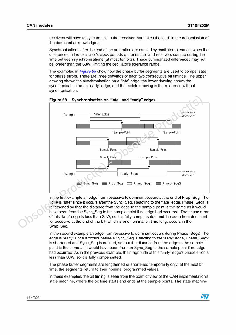
CAN modules ST10F252M
184/328
receivers will have to synchronize to that receiver that “takes the lead” in the transmission of the dominant acknowledge bit.
Synchronisations after the end of the arbitration are caused by oscillator tolerance, when the differences in the oscillator’s clock periods of transmitter and receivers sum up during the time between synchronisations (at most ten bits). These summarized differences may not be longer than the SJW, limiting the oscillator’s tolerance range.
The examples in Figure 68 show how the phase buffer segments are used to compensate for phase errors. There are three drawings of each two consecutive bit timings. The upper drawing shows the synchronisation on a “late” edge, the lower drawing shows the synchronisation on an “early” edge, and the middle drawing is the reference without synchronisation.
Figure 68. Synchronisation on “late” and “early” edges
In the first example an edge from recessive to dominant occurs at the end of Prop_Seg. The edge is “late” since it occurs after the Sync_Seg. Reacting to the “late” edge, Phase_Seg1 is lengthened so that the distance from the edge to the sample point is the same as it would have been from the Sync_Seg to the sample point if no edge had occurred. The phase error of this “late” edge is less than SJW, so it is fully compensated and the edge from dominant to recessive at the end of the bit, which is one nominal bit time long, occurs in the Sync_Seg.
In the second example an edge from recessive to dominant occurs during Phase_Seg2. The edge is “early” since it occurs before a Sync_Seg. Reacting to the “early” edge, Phase_Seg2 is shortened and Sync_Seg is omitted, so that the distance from the edge to the sample point is the same as it would have been from an Sync_Seg to the sample point if no edge had occurred. As in the previous example, the magnitude of this “early” edge’s phase error is less than SJW, so it is fully compensated.
The phase buffer segments are lengthened or shortened temporarily only; at the next bit time, the segments return to their nominal programmed values.
In these examples, the bit timing is seen from the point of view of the CAN implementation’s state machine, where the bit time starts and ends at the sample points. The state machine
recessivedominant
recessivedominant
Sync_Seg Prop_Seg Phase_Seg1 Phase_Seg2
“late” Edge
“early” Edge
Rx-Input
Rx-Input
Sample-Point Sample-Point
Sample-PointSample-Point
Sample-Point Sample-Point
O
bsolete Product(
s) - O
bsolete Product(
s)

ST10F252M CAN modules
185/328
omits Sync_Seg when synchronizing on an “early” edge because it cannot subsequently redefine that time quantum of Phase_Seg2 where the edge occurs to be the Sync_Seg.
The examples in Figure 69 show how short dominant noise spikes are filtered by synchronisations. In both examples the spike starts at the end of Prop_Seg and has the length of (Prop_Seg + Phase_Seg1).
Figure 69. Filtering of short dominant spikes
In the first example, the synchronisation jump width is greater than or equal to the phase error of the spike’s edge from recessive to dominant. Therefore, the sample point is shifted after the end of the spike; a recessive bus level is sampled.
In the second example, SJW is shorter than the phase error, so the sample point cannot be shifted far enough; the dominant spike is sampled as actual bus level.
Oscillator tolerance range
The oscillator tolerance range was increased when the CAN protocol was developed from version 1.1 to version 1.2 (version 1.0 was never implemented in silicon). The option to synchronize on edges from dominant to recessive became obsolete, only edges from recessive to dominant are considered for synchronisation. The protocol update to version 2.0 (A and B) had no influence on the oscillator tolerance.
The tolerance range df for an oscillator’s frequency fosc around the nominal frequency fnom with depends on the proportions of Phase_Seg1, Phase_Seg2, SJW, and the bit time. The maximum tolerance df is the defined by two conditions (both must be met):
recessivedominant
Sync_Seg Prop_Seg Phase_Seg1 Phase_Seg2
SpikeRx-Input
Sample-Point Sample-Point
Sample-PointSample-Point
recessivedominantSpikeRx-Input
SJW ≥ Phase Error
SJW < Phase Error
1 df–( ) fnom• fosc 1 df+( ) fnom•≤ ≤
I: df min Phase_Seg1 Phase_Seg2( , )2 13 bit_time⋅ Phase_Seg2–( )⋅------------------------------------------------------------------------------------------------=
II: df SJW20 bit_time⋅-------------------------------------=
O
bsolete Product(
s) - O
bsolete Product(
s)
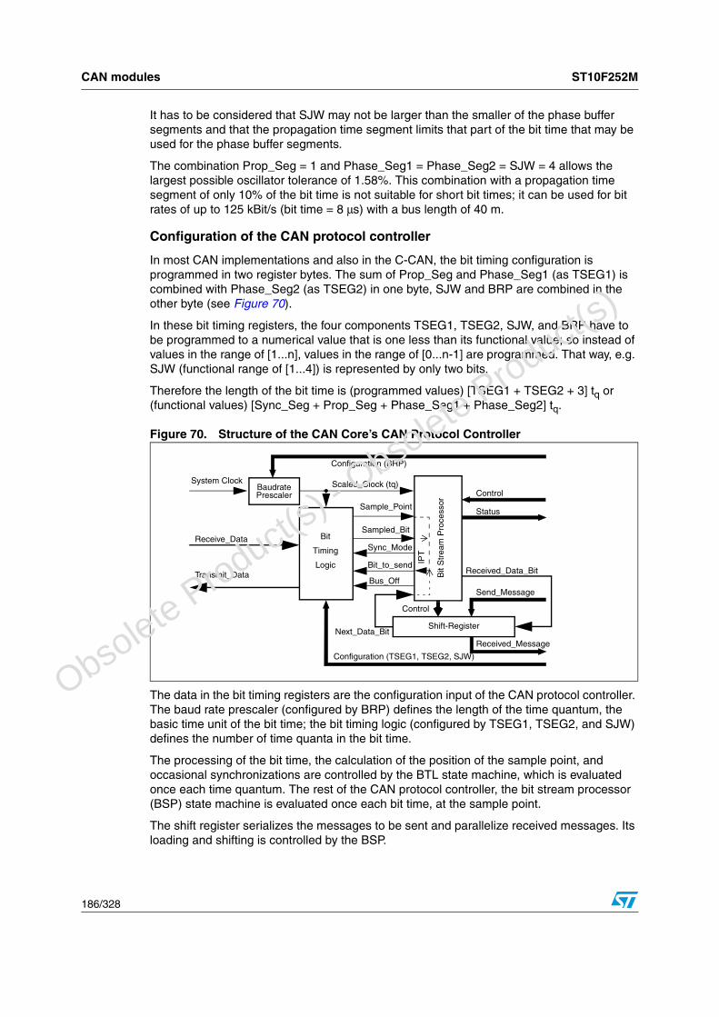
CAN modules ST10F252M
186/328
It has to be considered that SJW may not be larger than the smaller of the phase buffer segments and that the propagation time segment limits that part of the bit time that may be used for the phase buffer segments.
The combination Prop_Seg = 1 and Phase_Seg1 = Phase_Seg2 = SJW = 4 allows the largest possible oscillator tolerance of 1.58%. This combination with a propagation time segment of only 10% of the bit time is not suitable for short bit times; it can be used for bit rates of up to 125 kBit/s (bit time = 8 μs) with a bus length of 40 m.
Configuration of the CAN protocol controller
In most CAN implementations and also in the C-CAN, the bit timing configuration is programmed in two register bytes. The sum of Prop_Seg and Phase_Seg1 (as TSEG1) is combined with Phase_Seg2 (as TSEG2) in one byte, SJW and BRP are combined in the other byte (see Figure 70).
In these bit timing registers, the four components TSEG1, TSEG2, SJW, and BRP have to be programmed to a numerical value that is one less than its functional value; so instead of values in the range of [1...n], values in the range of [0...n-1] are programmed. That way, e.g. SJW (functional range of [1...4]) is represented by only two bits.
Therefore the length of the bit time is (programmed values) [TSEG1 + TSEG2 + 3] tq or (functional values) [Sync_Seg + Prop_Seg + Phase_Seg1 + Phase_Seg2] tq.
Figure 70. Structure of the CAN Core’s CAN Protocol Controller
The data in the bit timing registers are the configuration input of the CAN protocol controller. The baud rate prescaler (configured by BRP) defines the length of the time quantum, the basic time unit of the bit time; the bit timing logic (configured by TSEG1, TSEG2, and SJW) defines the number of time quanta in the bit time.
The processing of the bit time, the calculation of the position of the sample point, and occasional synchronizations are controlled by the BTL state machine, which is evaluated once each time quantum. The rest of the CAN protocol controller, the bit stream processor (BSP) state machine is evaluated once each bit time, at the sample point.
The shift register serializes the messages to be sent and parallelize received messages. Its loading and shifting is controlled by the BSP.
Sample_Point
Bit_to_send
Sync_Mode
Bus_Off
Scaled_Clock (tq)System Clock
Receive_Data
Transmit_Data
Control
Received_Message
Send_Message
Status
Bit
Timing
Logic
BaudratePrescaler
Sampled_Bit
Configuration (TSEG1, TSEG2, SJW)
Configuration (BRP)
Shift-Register
Received_Data_Bit
Next_Data_Bit
Control
Bit
Str
eam
Pro
cess
or
IPT
O
bsolete Product(
s) - O
bsolete Product(
s)
ST10F252M CAN modules
187/328
The BSP translates messages into frames and vice versa. It generates and discards the enclosing fixed format bits, inserts and extracts stuff bits, calculates and checks the CRC code, performs the error management, and decides which type of synchronization is to be used. It is evaluated at the sample point and processes the sampled bus input bit. The time after the sample point that is needed to calculate the next bit to be sent (for example, data bit, CRC bit, stuff bit, error flag, or idle) is called the information processing time (IPT).
The IPT is application specific but may not be longer than 2 tq; the C-CAN’s IPT is 0 tq. Its length is the lower limit of the programmed length of Phase_Seg2. For a synchronization, Phase_Seg2 may be shortened to a value less than IPT, which does not affect bus timing.
Calculation of the bit timing parameters
Usually, the calculation of the bit timing configuration starts with a desired bit rate or bit time. The resulting bit time (1/bit rate) must be an integer multiple of the system clock period.
The bit time may consist of 4 to 25 time quanta, the length of the time quantum tq is defined by the baud rate prescaler with tq = (Baud Rate Prescaler)/fsys. Several combinations may lead to the desired bit time, allowing iterations of the following steps.
The first part of the bit time to be defined is the Prop_Seg. Its length depends on the delay times measured in the system. A maximum bus length as well as a maximum node delay has to be defined for expandible CAN bus systems. The resulting time for Prop_Seg is converted into time quanta (rounded up to the nearest integer multiple of tq).
The Sync_Seg is 1 tq long (fixed), leaving (bit time – Prop_Seg – 1) tq for the two phase buffer segments. If the number of remaining tq is even, the phase buffer segments have the same length, Phase_Seg2 = Phase_Seg1, else Phase_Seg2 = Phase_Seg1 + 1.
The minimum nominal length of Phase_Seg2 must be considered as well. Phase_Seg2 may not be shorter than the CAN controller’s information processing time, which is, depending on the actual implementation, in the range of [0...2] tq.
The length of the synchronization jump width is set to its maximum value, which is the minimum of four and Phase_Seg1.
The oscillator tolerance range necessary for the resulting configuration is calculated by the formulae given in Section 18.9.10
If more than one configuration is possible, that configuration allowing the highest oscillator tolerance range should be chosen.
CAN nodes with different system clocks require different configurations to come to the same bit rate. The calculation of the propagation time in the CAN network, based on the nodes with the longest delay times, is done once for the whole network.
The CAN system’s oscillator tolerance range is limited by that node with the lowest tolerance range.
The calculation may show that bus length or bit rate have to be decreased or that the oscillator frequencies’ stability has to be increased in order to find a protocol compliant configuration of the CAN bit timing.
The resulting configuration is written into the bit timing register:
(Phase_Seg2 - 1) and (Phase_Seg1 + Prop_Seg - 1) and (SynchronisationJumpWidth - 1) and (Prescaler - 1).
O
bsolete Product(
s) - O
bsolete Product(
s)

CAN modules ST10F252M
188/328
Example for bit timing at high baud rate
In this example, the frequency of CAN module clock is 10 MHz, BRP is 0, the bit rate is 1 MBit/s.
In this example, the concatenated bit time parameters are (2-1)3 & (7-1)4 & (1-1)2 & (1-1)6, the bit timing register is programmed to= 0x1600.
Example for bit timing at low baud rate
In this example, the frequency of CAN module clock is 2 MHz, BRP is 1, the bit rate is 100 KBit/s.
In this example, the concatenated bit time parameters are (4-1)3 & (5-1)4 & (4-1)2 & (2-1)6, the bit timing register is programmed to= 0x34C1.
tq 100 ns = tCAN_CLK
delay of bus driver 50 ns
delay of receiver circuit 30 ns
delay of bus line (40m) 220 ns
tProp 600 ns = 6 x tq
tSJW 100 ns = 1 x tq
tTSeg1 700 ns = tProp + tSJW
tTSeg2 200 ns = Information Processing Time + 1 • tq
tSync-Seg 100 ns = 1 x tq
bit time 1000 ns = tSync-Seg + tTSeg1 + tTSeg2
tolerance for CAN clock 0.39 % =
=
tq 1 μs = 2 x tCAN_CLK
delay of bus driver 200 ns
delay of receiver circuit 80 ns
delay of bus line (40m) 220 ns
tProp 1 μs = 1 x tq
tSJW 4 μs = 4 x tq
tTSeg1 5 μs = tProp + tSJW
tTSeg2 4 μs = Information Processing Time + 3 • tq
tSync-Seg 1 μs = 1 x tq
bit time 10 μs = tSync-Seg + tTSeg1 + tTSeg2
tolerance for CAN clock 1.58 % =
=
min PB1 PB2( , )2 13 bit_time⋅ PB2–( )⋅----------------------------------------------------------------------
0.1μs2 13 1μs 0.2μs–⋅( )⋅------------------------------------------------------------
min PB1 PB2( , )2 13 bit_time⋅ PB2–( )⋅-----------------------------------------------------------------------
4μs2 13 10μs 4μs–⋅( )⋅-----------------------------------------------------------
O
bsolete Product(
s) - O
bsolete Product(
s)

ST10F252M Watchdog timer
189/328
19 Watchdog timer
The watchdog timer is a fail-safe mechanism which prevents the microcontroller from malfunctioning for long periods of time. The watchdog timer is always enabled after a reset of the chip (just after PORT0 latching) and can only be disabled in the time interval until the EINIT (end of initialization) instruction has been executed. Therefore, the chip’s start-up procedure is always monitored. The software is designed to service the watchdog timer before it overflows. If, due to hardware or software related failures, the software fails to do so, the watchdog timer overflows and generates an internal hardware reset. It pulls the RSTOUT pin low to allow external hardware components to be reset.
Each of the different reset sources is indicated in the WDTCON register. The indicated bits are cleared with the EINIT instruction. It is, thus, possible to identify the reset during the initialization phase. The mechanism only detects a failure on the internal 1.8V, not on the external power supply (VDD).
WDTCON register
WDTCON register (FFAEh/D7h) SFR Reset value: 00xxh
15 14 13 12 11 10 9 8 7 6 5 4 3 2 1 0
WDTREL Reserved PONR LHWR SHWR SWR WDTR WDTI
N
RW - R R R R R RW
Table 111. WDTCON register functions
Bit Name Function
0 WDTIN
Watchdog timer input frequency selection
‘0’: Input frequency is fCPU/2.
‘1’: Input frequency is fCPU/128.
1 WDTR (1) (3)
1. More than one reset indication flag may be set. After EINIT, all flags are cleared.
Watchdog timer reset indication flag
Set by the watchdog timer on an overflow. Cleared by a hardware reset or by the SRVWDT instruction.
2 SWR (1)(3) Software reset indication flag
Set by the SRST execution. Cleared by the EINIT instruction.
3 SHWR (1)(3) Short hardware reset indication flag
Set by the input RSTIN. Cleared by the EINIT instruction.
4 LHWR (1)(3) Long hardware reset indication flag
Set by the input RSTIN. Cleared by the EINIT instruction.
5 PONR(1)(2)(3)
2. Power-on is detected when a ramp on internal 1.8V (generated by the on-chip voltage regulator) is detected.
3. These bits cannot be directly modified by software.
Power-on (asynchronous) reset indication flag
Set by the input RSTIN if a power-on condition has been detected. Cleared by the EINIT instruction.
15:8 WDTREL Watchdog timer reload value (for the high byte)
O
bsolete Product(
s) - O
bsolete Product(
s)

Watchdog timer ST10F252M
190/328
Note: PONR bit may not be set for short supply failure.
If a bi-directional reset is enabled and if the RSTIN pin is latched low after the end of the internal reset sequence, a short hardware reset, a software reset or a watchdog reset triggers a long hardware reset. Thus, reset indications flags are set to indicate a long hardware reset.
Table 112. Reset flag settings
Reset Source PONR LHWR SHWR SWR WDTR
Power On Reset X X X X
Power On after a partial supply failure (see Note) X X X
Long Hardware Reset X X X
Short Hardware Reset X X
Software Reset X
Watchdog Reset X X
O
bsolete Product(
s) - O
bsolete Product(
s)

ST10F252M System reset
191/328
20 System reset
System reset initializes the device in a predefined state. There are many ways to activate a reset state. The system start-up configuration is different for each case as shown in Table 113. The reset history is flagged inside WDTCON register (see also Chapter 19 for additional details).
20.1 Input filterOn RSTIN input pin, there is an on-chip RC filter. This filter is sized to filter all the spikes shorter than 50 ns. A valid pulse must be longer than 500 ns before the ST10 recognizes a reset command. Between 50 ns and 500 ns a pulse can either be filtered or recognized as valid, depending on the operating conditions and process variations.
For this reason all minimum durations, mentioned in this chapter for the different kind of reset events, should be carefully evaluated taking into account of the above requirements.
In particular, for short hardware reset, where only 4 TCL is specified as minimum input reset pulse duration, the operating frequency is a key factor. For example:
● for a CPU clock of 40 MHz, 4 TCL is 50 ns, so it would be filtered; in this case the minimum becomes the one imposed by the filter (that is 500 ns)
● for a CPU clock of 4 MHz, 4 TCL is 500 ns; in this case the minimum from the formula is coherent with the limit imposed by the filter.
Table 113. Reset event definition
Reset Source FlagRPD
StatusConditions
Power-on reset PONR Low Power-on
Asynchronous hardware reset
LHWR
Low tRSTIN > (1)
1. RSTIN pulse should be longer than 500ns (Filter) and than settling time for configuration of PORT0.
Synchronous long hardware reset
HightRSTIN > (1032 + 12) TCL + max(4 TCL, 500ns)
Synchronous short hardware reset (2)
2. See Section 20.1 for more details on minimum reset pulse duration.
SHWR HightRSTIN > max(4 TCL, 500ns)tRSTIN ≤ (1032 + 12) TCL + max(4 TCL, 500ns)
Watchdog timer reset WDTR (3)
3. The RPD status has no influence unless bidirectional reset is activated (bit BDRSTEN in SYSCON): RPD low inhibits the
bidirectional reset on SW and WDT reset events, that is RSTIN is not activated (refer to Section 20.4, Section 20.5 and
Section 20.6).
WDT overflow
Software reset SWR (3) SRST instruction execution
O
bsolete Product(
s) - O
bsolete Product(
s)

System reset ST10F252M
192/328
20.2 Asynchronous resetAn asynchronous reset is triggered when RSTIN pin is pulled low while the RPD pin is low. The ST10F252M is immediately (after the input filter delay) forced in reset default state. It pulls low the RSTOUT pin, it cancels pending internal hold states if any, it aborts all internal/external bus cycles, it switches buses (data, address and control signals) and I/O pin drivers to high-impedance, it pulls high PORT0 pins.
Note: If an asynchronous reset occurs during a read or write phase in internal memories, the content of the memory itself could be corrupted. To avoid this, synchronous reset use is strongly recommended.
Power-on reset
Asynchronous reset must be used during the power-on of the device. Depending on crystal or resonator frequency, the on-chip oscillator needs about 1 ms to 10 ms to stabilize (refer to Section 27.8.2), with an already stable VDD. The logic of the ST10F252M does not need a stabilized clock signal to detect an asynchronous reset, so it is suitable for power-on conditions. To ensure a proper reset sequence, the RSTIN pin and the RPD pin must be held at low level until the device clock signal is stabilized and the system configuration value on PORT0 is settled.
At power-on it is important to consider some additional constraints introduced by the start-up phase of the different embedded modules.
In particular the on-chip voltage regulator needs at least 1 ms to stabilize the internal 1.8 V for the core logic – this time is computed from when the external reference (VDD) becomes stable (inside specification range, that is at least 4.5 V). This is a constraint for the application hardware (external voltage regulator). The RSTIN pin assertion should be extended to guarantee the voltage regulator stabilization.
A second constraint is imposed by the embedded Flash. When booting from internal memory, starting from the release of RSTIN, it needs a maximum of 1 ms for its initialization; before that, the internal reset (RST signal) is not released, so the CPU does not start code execution in internal memory.
Note: This is not true if external memory is used (pin EA held low during reset phase). In this case, once RSTIN pin is released, and after few CPU clock pulses (filter delay plus 3...8 TCL), the internal reset signal RST is released, so the code execution can start immediately. Access to the data in internal Flash is forbidden before its initialization phase is completed; an attempted access during the start-up phase returns FFFFh (just at the beginning), while later 009Bh (an illegal opcode trap is generated).
At power-on, the RSTIN pin is tied low for a minimum time that includes also the start-up time of the main oscillator (tSTUP = 1 ms for resonator, 10 ms for crystal) and PLL synchronization time (tPSUP = 200 µs). This means that, if the internal Flash is used, the RSTIN pin could be released before the main oscillator and PLL are stable to recover some time in the start-up phase (Flash initialization only needs stable V18, but does not need stable system clock since an internal dedicated oscillator is used).
O
bsolete Product(
s) - O
bsolete Product(
s)

ST10F252M System reset
193/328
Warning: It is recommended to provide the external hardware with a current limitation circuitry. This is necessary to avoid permanent damage to the device during the power-on transient, when the capacitance on V18 pin is charged. For the on-chip voltage regulator functionality, 10 nF is sufficient. However, a maximum of 100 nF on the V18 pin should not generate problems of over-current (higher value is allowed if current is limited by the external hardware). External current limitation is also recommended to avoid risk of damage in the event of a temporary short between V18 and ground. The internal 1.8V drivers are sized to drive currents of several tens of Amperes, so the current should be limited by the external hardware. The limit of current is imposed by power dissipation considerations (refer to Section 27.3 for details).
In the next Figure 71 and 72 Asynchronous Power-on timing diagrams are shown, respectively with boot from internal or external memory, highlighting the reset phase extension introduced by the embedded Flash module when selected.
O
bsolete Product(
s) - O
bsolete Product(
s)

System reset ST10F252M
194/328
Figure 71. Asynchronous power-on RESET (EA=1)
RSTF
P0[15:13]
P0[12:2]
transparent
transparent
P0[1:0] not t.not transparent
FLARST
V18
XTAL1 ...
≤ 2 TCL
RST
≤ 1 ms
Latching point of Port0 forsystem start-up configuration
VDD
≥ 1 ms (for on-chip VREG stabilization)
RPD
IBUS-CS
≤ 1.2 ms (for resonator oscillation + PLL stabilization)≤ 10.2 ms (for crystal oscillation + PLL stabilization)
RSTIN
(After Filter)
≤ 500 ns≥ 50 ns
7 TCL
3..4 TCL
(Internal)
not t.
not t.not t.
O
bsolete Product(
s) - O
bsolete Product(
s)

ST10F252M System reset
195/328
Figure 72. Asynchronous power-on RESET (EA=0)
1. 3 to 8 TCL depending on clock source selection.
Hardware reset
The asynchronous reset must be used to recover from catastrophic situations of the application. It may be triggered by the hardware of the application. Internal hardware logic and application circuitry are described in Section 20.7 and Figure 84, Figure 85 and Figure 86. It occurs when RSTIN is low and RPD is detected (or becomes) low as well.
RSTIN
P0[15:13]
P0[12:2]
not t.
transparent not t.
P0[1:0] not t.not transparent
V18
XTAL1 ...
3..8 TCL(1)
RST
Latching point of Port0 forsystem start-up configuration
VDD
≥ 1 ms (for on-chip VREG stabilization)
RPD
ALE
≥ 1.2 ms (for resonator oscillation + PLL stabilization)≥ 10.2 ms (for crystal oscillation + PLL stabilization)
RSTF
≤ 500 ns
(After Filter)
≥ 50 ns
8 TCL
transparent
3..4 TCL
O
bsolete Product(
s) - O
bsolete Product(
s)

System reset ST10F252M
196/328
Figure 73. Asynchronous hardware RESET (EA=1)
1. Longer than Port0 settling time + PLL synchronization (if needed, that is P0(15:13) changed)Longer than 500ns to take into account of Input Filter on RSTIN pin
RSTF
P0[15:13]
P0[12:2]
transparent
transparent not t.
P0[1:0] not t.not transparent
FLARST
≤ 2 TCL
RST
≤ 1 ms
Latching point of Port0 forsystem start-up configuration
RPD
IBUS-CS
(1)
not transparent
not transparent
(After Filter)
RSTIN
≤ 500 ns≥ 50 ns
≤ 500 ns≥ 50 ns
7 TCL
(internal)
3..4 TCL
not t. not t.
O
bsolete Product(
s) - O
bsolete Product(
s)

ST10F252M System reset
197/328
Figure 74. Asynchronous hardware RESET (EA=0)
1. Longer than Port0 settling time + PLL synchronization (if needed, that is P0(15:13) changed)Longer than 500ns to take into account of Input Filter on RSTIN pin
2. 3 to 8 TCL depending on clock source selection.
Exit from asynchronous reset state
When the RSTIN pin is pulled high, the device restarts. As already mentioned, if internal Flash is used, the restarting occurs after the embedded Flash initialization routine is completed. The system configuration is latched from PORT0: ALE, RD and WR/WRL pins are driven to their inactive level. The ST10F252M starts program execution from memory location 00'0000h in code segment 0. This starting location will typically points to the general initialization routine. The timing of asynchronous hardware reset sequence are summarized in Figure 73 and Figure 74.
20.3 Synchronous reset (warm reset)A synchronous reset is triggered when RSTIN pin is pulled low while RPD pin is at high level. In order to properly activate the internal reset logic of the device, the RSTIN pin must be held low, at least, during 4 TCL (two periods of CPU clock): refer also to Section 20.1 for details on minimum reset pulse duration. The I/O pins are set to high impedance and RSTOUT pin is driven low. After RSTIN level is detected, a short duration of a maximum of 12 TCL (six periods of CPU clock) elapses, during which pending internal hold states are
RSTF
P0[15:13]
P0[12:2]
transparent not t.
transparent not t.
P0[1:0] not t.not transparent
3..8 TCL(2)
RST
Latching point of Port0 forsystem start-up configuration
RPD
ALE
(1)
not transparent
not transparent
(After Filter)
RSTIN
≤ 500 ns≥ 50 ns
≤ 500 ns≥ 50 ns
8 TCL
3..4 TCL
O
bsolete Product(
s) - O
bsolete Product(
s)
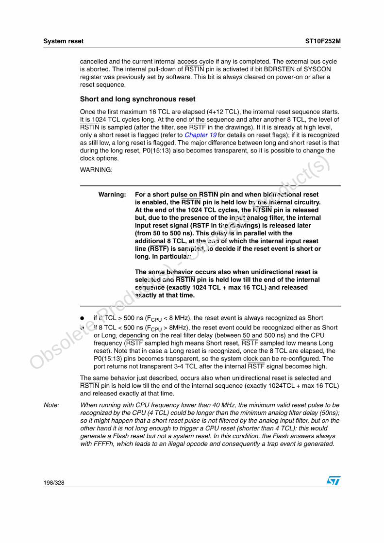
System reset ST10F252M
198/328
cancelled and the current internal access cycle if any is completed. The external bus cycle is aborted. The internal pull-down of RSTIN pin is activated if bit BDRSTEN of SYSCON register was previously set by software. This bit is always cleared on power-on or after a reset sequence.
Short and long synchronous reset
Once the first maximum 16 TCL are elapsed (4+12 TCL), the internal reset sequence starts. It is 1024 TCL cycles long. At the end of the sequence and after another 8 TCL, the level of RSTIN is sampled (after the filter, see RSTF in the drawings). If it is already at high level, only a short reset is flagged (refer to Chapter 19 for details on reset flags); if it is recognized as still low, a long reset is flagged. The major difference between long and short reset is that during the long reset, P0(15:13) also becomes transparent, so it is possible to change the clock options.
WARNING:
Warning: For a short pulse on RSTIN pin and when bidirectional reset is enabled, the RSTIN pin is held low by the internal circuitry. At the end of the 1024 TCL cycles, the RTSIN pin is released but, due to the presence of the input analog filter, the internal input reset signal (RSTF in the drawings) is released later (from 50 to 500 ns). This delay is in parallel with the additional 8 TCL, at the end of which the internal input reset line (RSTF) is sampled, to decide if the reset event is short or long. In particular:
The same behavior occurs also when unidirectional reset is selected and RSTIN pin is held low till the end of the internal sequence (exactly 1024 TCL + max 16 TCL) and released exactly at that time.
● if 8 TCL > 500 ns (FCPU < 8 MHz), the reset event is always recognized as Short
● if 8 TCL < 500 ns (FCPU > 8MHz), the reset event could be recognized either as Short or Long, depending on the real filter delay (between 50 and 500 ns) and the CPU frequency (RSTF sampled high means Short reset, RSTF sampled low means Long reset). Note that in case a Long reset is recognized, once the 8 TCL are elapsed, the P0(15:13) pins becomes transparent, so the system clock can be re-configured. The port returns not transparent 3-4 TCL after the internal RSTF signal becomes high.
The same behavior just described, occurs also when unidirectional reset is selected and RSTIN pin is held low till the end of the internal sequence (exactly 1024TCL + max 16 TCL) and released exactly at that time.
Note: When running with CPU frequency lower than 40 MHz, the minimum valid reset pulse to be recognized by the CPU (4 TCL) could be longer than the minimum analog filter delay (50ns); so it might happen that a short reset pulse is not filtered by the analog input filter, but on the other hand it is not long enough to trigger a CPU reset (shorter than 4 TCL): this would generate a Flash reset but not a system reset. In this condition, the Flash answers always with FFFFh, which leads to an illegal opcode and consequently a trap event is generated.
O
bsolete Product(
s) - O
bsolete Product(
s)

ST10F252M System reset
199/328
Exit from synchronous reset state
The reset sequence is extended until RSTIN level becomes high. Moreover, it is internally prolonged by the Flash initialization when EA=1 (internal memory selected). Then, the code execution restarts. The system configuration is latched from PORT0, and ALE, RD and WR/WRL pins are driven to their inactive level. The ST10F252M starts program execution from memory location 00'0000h in code segment 0. This starting location will typically points to the general initialization routine. Timing of synchronous reset sequence is summarized in Figure 75 and Figure 76 where a Short reset event is shown, with particular emphasis on the fact that it can degenerate into Long reset: the two figures show the behavior when booting from internal or external memory respectively. Figure 77 and 78 report the timing of a typical synchronous Long reset, again when booting from internal or external memory.
Synchronous reset and RPD pin
Whenever the RSTIN pin is pulled low (by external hardware or as a consequence of a Bidirectional reset), the RPD internal weak pull-down is activated. The external capacitance (if any) on the RPD pin is slowly discharged through the internal weak pull-down. If the voltage level on the RPD pin reaches the input low threshold (approximately 2.5 V), the reset event becomes immediately asynchronous. In case of hardware reset (short or long) the situation goes immediately to the one illustrated in Figure 73. There is no effect if RPD comes again above the input threshold: the asynchronous reset is completed coherently. To correctly complete a synchronous reset, the value of the capacitance should be big enough to maintain a sufficiently high voltage on the RPD pin for the duration of the internal reset sequence.
For a Software or Watchdog reset events, an active synchronous reset is completed regardless of the RPD status.
It is important to highlight that the signal that makes RPD status transparent under reset is the internal RSTF (after the noise filter).
O
bsolete Product(
s) - O
bsolete Product(
s)

System reset ST10F252M
200/328
Figure 75. Synchronous short / long hardware RESET (EA=1)
1. RSTIN assertion can be released there. Refer also to Section 21.1 for details on minimum pulse duration.
2. If during the reset condition (RSTIN low), RPD voltage drops below the threshold voltage (about 2.5V for 5V operation), the asynchronous reset is then immediately entered.
3. RSTIN pin is pulled low if bit BDRSTEN (bit 3 of SYSCON register) was previously set by software.Bit BDRSTEN is cleared after reset.
4. Minimum RSTIN low pulse duration shall also be longer than 500ns to guarantee the pulse is not masked by the internal filter (refer to Section 21.1)
P0[15:13] not transparent
RSTF
P0[12:2] transparent not t.
P0[1:0] not t.not transparent
FLARST
RST
≤ 1 ms
1024 TCL
≤ 2 TCL
(2) VRPD > 2.5V Asynchronous Reset not entered200µA Discharge
RPD
RSTOUT
At this time RSTF is sampled HIGH or LOWso it is SHORT or LONG reset
(After Filter)
RSTIN
< 1032 TCL≤4 TCL(4)
(3)
≤12 TCL
(1)
≤ 500 ns≥ 50 ns
≤ 500 ns≥ 50 ns
≤ 500 ns≥ 50 ns
IBUS-CS
7 TCL
(Internal)
8 TCL
not t.
O
bsolete Product(
s) - O
bsolete Product(
s)
ST10F252M System reset
201/328
Figure 76. Synchronous short / long hardware RESET (EA=0)
1. RSTIN assertion can be released there. Refer also to Section 21.1 for details on minimum pulse duration.
2. If during the reset condition (RSTIN low), RPD voltage drops below the threshold voltage (about 2.5V for 5V operation), the asynchronous reset is then immediately entered.
3. 3 to 8 TCL depending on clock source selection.
4. RSTIN pin is pulled low if bit BDRSTEN (bit 3 of SYSCON register) was previously set by software. Bit BDRSTEN is cleared after reset.
5. Minimum RSTIN low pulse duration shall also be longer than 500ns to guarantee the pulse is not masked by the internal filter (refer to Section 21.1).
P0[15:13] not transparent
RSTF
P0[12:2] transparent not t.
P0[1:0] not t.not transparent
RST
1024 TCL
3..8 TCL(3)
(2) VRPD > 2.5V Asynchronous Reset not entered200µA Discharge
RPD
RSTOUT
At this time RSTF is sampled HIGH or LOWso it is SHORT or LONG reset
(After Filter)
RSTIN
< 1032 TCL≤4 TCL(5)
(4)
≤12 TCL
(1)
≤ 500 ns≥ 50 ns
≤ 500 ns≥ 50 ns
≤ 500 ns≥ 50 ns
ALE
8 TCL
8 TCL
not t.
O
bsolete Product(
s) - O
bsolete Product(
s)

System reset ST10F252M
202/328
Figure 77. Synchronous long hardware RESET (EA=1)
1. If during the reset condition (RSTIN low), RPD voltage drops below the threshold voltage (about 2.5V for 5V operation), the asynchronous reset is then immediately entered. Even if RPD returns above the threshold, the reset is definitively taken as asynchronous.
2. Minimum RSTIN low pulse duration shall also be longer than 500ns to guarantee the pulse is not masked by the internal filter (refer to Section 21.1).
P0[15:13] not transparent
RSTF
P0[12:2] transparent not t.
P0[1:0] not t.not transparent
FLARST
RST
≤ 1 ms
1024+8 TCL
≤ 2 TCL
(1) VRPD > 2.5V Asynchronous Reset not entered200µA Discharge
RPD
RSTOUT
At this time RSTF is sampled LOWso it is definitely LONG reset
(After Filter)
RSTIN
1024+8 TCL≤4 TCL(2) ≤12 TCL
≤ 500 ns≥ 50 ns
≤ 500 ns≥ 50 ns
≤ 500 ns≥ 50 ns
IBUS-CS
7 TCL
not t.transparent
not t.
3..4 TCL
(Internal)
O
bsolete Product(
s) - O
bsolete Product(
s)

ST10F252M System reset
203/328
Figure 78. Synchronous long hardware RESET (EA=0)
1. If during the reset condition (RSTIN low), RPD voltage drops below the threshold voltage (about 2.5V for 5V operation), the asynchronous reset is then immediately entered.
2. Minimum RSTIN low pulse duration shall also be longer than 500ns to guarantee the pulse is not masked by the internal filter (refer to Section 21.1).
3. 3 to 8 TCL depending on clock source selection.
20.4 Software resetA software reset sequence can be triggered at any time by the protected SRST (software reset) instruction. This instruction can be deliberately executed within a program, for example, to leave bootstrap loader mode, or on a hardware trap that reveals system failure.
On execution of the SRST instruction, the internal reset sequence is started. The microcontroller behavior is the same as for a synchronous short reset, except that only bits P0.12...P0.8 are latched at the end of the reset sequence, while previously latched, bits P0.7...P0.2 are cleared (that is written at ‘1’).
A Software reset is always taken as synchronous. There is no influence on Software reset behavior with RPD status. In case a bidirectional reset is selected, a Software reset event
P0[15:13] not transparent
RSTF
P0[12:2] transparent not t.
P0[1:0] not t.not transparent
RST
1024+8 TCL
3..8 TCL(3)
(1) VRPD > 2.5V Asynchronous Reset not entered200 µA Discharge
RPD
RSTOUT
At this time RSTF is sampled LOWso it is LONG reset
(After Filter)
RSTIN
1024+8 TCL4 TCL(2) 12 TCL
≤ 500 ns≥ 50 ns
≤ 500 ns≥ 50 ns
≤ 500 ns≥ 50 ns
ALE
8 TCL
not t.transparent
3..4 TCL
O
bsolete Product(
s) - O
bsolete Product(
s)

System reset ST10F252M
204/328
pulls RSTIN pin low: this occurs only if RPD is high; if RPD is low, RSTIN pin is not pulled low even though Bidirectional reset is selected.
Refer to Figure 79 and Figure 80 for unidirectional software reset timing, and to Figure 81, Figure 82 and Figure 83 for bidirectional.
20.5 Watchdog timer resetWhen the watchdog timer is not disabled during the initialization, or serviced regularly during program execution, it overflows and triggers the reset sequence.
Unlike hardware and software resets, the watchdog reset completes a running external bus cycle if this bus cycle either does not use READY, or if READY is sampled active (low) after the programmed wait states.
When READY is sampled inactive (high) after the programmed wait states the running external bus cycle is aborted. Then the internal reset sequence is started.
Bit P0.12...P0.8 are latched at the end of the reset sequence and bit P0.7...P0.2 are cleared (that is written at ‘1’).
A Watchdog reset is always synchronous. There is no influence on Watchdog reset behavior with RPD status. In case a Bidirectional reset is selected, a Watchdog reset event pulls RSTIN pin low; this occurs only if RPD is high; if RPD is low, RSTIN pin is not pulled low even though bidirectional reset is selected.
Refer to Figure 79 and Figure 80 for unidirectional SW reset timing, and to Figure 81, Figure 82 and Figure 83 for bidirectional.
Figure 79. SW / WDT unidirectional RESET (EA=1)
P0[7:2] not transparent
P0[12:8] transparent not t.
P0[1:0] not t.not transparent
RST
1024 TCL
RSTOUT
RSTIN
IBUS-CS
7 TCL
P0[15:13] not transparent
FLARST
≤ 1 ms
(Internal)
≤ 2 TCL
O
bsolete Product(
s) - O
bsolete Product(
s)

ST10F252M System reset
205/328
Figure 80. SW / WDT unidirectional RESET (EA=0)
20.6 Bidirectional ResetAs shown in the previous sections, the RSTOUT pin is driven active (low level) at the beginning of any reset sequence (synchronous/asynchronous hardware, software and watchdog timer resets). RSTOUT pin stays active low beyond the end of the initialization routine, until the protected EINIT instruction (end of initialization) is completed.
The Bidirectional reset function is useful when external devices require a reset signal but cannot be connected to RSTOUT pin, because RSTOUT signal lasts during initialization. It is, for instance, the case of external memory running initialization routine before the execution of EINIT instruction.
Bidirectional reset function is enabled by setting bit 3 (BDRSTEN) in SYSCON register. It only can be enabled during the initialization routine, before EINIT instruction is completed.
When enabled, the open drain of the RSTIN pin is activated, pulling down the reset signal, for the duration of the internal reset sequence (synchronous/asynchronous hardware, synchronous software and synchronous watchdog timer resets). At the end of the internal reset sequence (1024 TCL) the pull down is released and the following may occur.
● After a Short Synchronous Bidirectional Hardware Reset, if RSTF is sampled low 8 TCL periods after the internal reset sequence completion (refer to Figure 75 and Figure 76), the Short reset becomes a Long reset. Otherwise, if RSTF is sampled high the device simply exits reset state.
● After a Software or Watchdog Bidirectional reset, the device exits from reset. If RSTF remains still low for at least 4 TCL periods (minimum time to recognize a Short
P0[7:2] not transparent
P0[12:8] transparent not t.
P0[1:0] not t.not transparent
RST
1024 TCL
RSTOUT
RSTIN
ALE
8 TCL
P0[15:13] not transparent
O
bsolete Product(
s) - O
bsolete Product(
s)
System reset ST10F252M
206/328
hardware reset) after the reset exiting (refer to Figure 81 and 82), the Software or Watchdog reset become a Short Hardware reset. On the contrary, if RSTF remains low for less than 4 TCL, the device simply exits reset state.
The Bidirectional reset is not effective in case RPD is held low, when a Software or Watchdog reset event occurs. On the contrary, if a Software or Watchdog Bidirectional reset event is active and RPD becomes low, the RSTIN pin is immediately released, while the internal reset sequence is completed regardless of RPD status change (1024 TCL).
Note: The bidirectional reset function is disabled by any reset sequence (bit BDRSTEN of SYSCON is cleared). To be activated again it must be enabled during the initialization routine.
WDTCON flags
Similar to what is highlighted in the previous section, when discussing Short reset and the degeneration into Long reset, comparable situations may occur when Bidirectional reset is enabled. The presence of the internal filter on RSTIN pin introduces a delay: When RSTIN is released, the internal signal after the filter (see RSTF in the drawings) is delayed, so it remains still active (low) for a while. It means that depending on the internal clock speed, a short reset may be recognized as a long reset: The WDTCON flags are set accordingly.
Moreover, when either Software or Watchdog bidirectional reset events occur, when the RSTIN pin is released (at the end of the internal reset sequence), the RSTF internal signal (after the filter) remains low for a while, and depending on the clock frequency it is recognized high or low. If the RSTF signal is recognized low for at least another 4 TCL after the completion of the internal sequence, a hardware reset sequence starts, and WDTCON flags this last event, masking the previous one (software or watchdog reset). Typically, a short hardware reset is recognized, unless the RSTIN pin (and consequently internal signal RSTF) is held sufficiently low by the external hardware to inject a long hardware reset. After this occurrence, the initialization routine is not able to recognize a software or watchdog bidirectional reset event, since a different source is flagged inside WDTCON register. This phenomenon does not occur when internal Flash is selected during reset (EA = 1), since the initialization of the Flash extends the internal reset duration well beyond the filter delay.
The next Figure 81, 82 and 83 summarize the timing for Software and Watchdog Timer Bidirectional reset events. In particular, Figure 83 shows the degeneration into Hardware reset.
O
bsolete Product(
s) - O
bsolete Product(
s)

ST10F252M System reset
207/328
Figure 81. SW / WDT bidirectional RESET (EA=1)
Figure 82. SW / WDT bidirectional RESET (EA=0)
P0[15:13] not transparent
RSTF
P0[12:8] transparent not t.
P0[1:0] not t.not transparent
RST
1024 TCL
RSTOUT
(After Filter)
RSTIN
≤ 500 ns≥ 50 ns
≤ 500 ns≥ 50 ns
IBUS-CS
7 TCL
FLARST
≤ 1 ms
≤ 2 TCL
(Internal)
P0[7:2] not transparent
4 TCL
P0[15:13] not transparent
RSTF
P0[12:8] transparent not t.
P0[1:0] not t.not transparent
RST
1024 TCL
RSTOUT
At this time RSTF is already HIGHso SW or WDT Reset is exited and flagged in WDTCON
(After Filter)
RSTIN
≤ 500 ns≥ 50 ns
≤ 500 ns≥ 50 ns
ALE
8 TCL
P0[7:2] not transparent
4 TCL
(no new HW reset is generated)
O
bsolete Product(
s) - O
bsolete Product(
s)

System reset ST10F252M
208/328
Figure 83. SW / WDT bidirectional RESET (EA=0)
20.7 Reset circuitryInternal reset circuitry is described in Figure 86. The RSTIN pin provides an internal pull-up resistor of 50 kΩ to 250 kΩ (the minimum reset time must be calculated using the lowest value).
It also provides a programmable (BDRSTEN bit of SYSCON register) pull-down to output internal reset state signal (synchronous reset, watchdog timer reset or software reset).
This bidirectional reset function is useful in applications where external devices require a reset signal but cannot be connected to RSTOUT pin.
This is the case of an external memory running codes before EINIT (end of initialization) instruction is executed. RSTOUT pin is pulled high only when EINIT is executed.
The RPD pin provides an internal weak pull-down resistor which discharges external capacitor at a typical rate of 200 µA. If bit PWDCFG of SYSCON register is set, an internal pull-up resistor is activated at the end of the reset sequence. This pull-up charges any capacitor connected on RPD pin.
The simplest way to reset the ST10F252M is to insert a capacitor C1 between RSTIN pin and VSS, and a capacitor between RPD pin and VSS (C0) with a pull-up resistor R0 between RPD pin and VDD. The input RSTIN provides an internal pull-up device equalling a resistor of 50 kΩ to 250 kΩ (the minimum reset time must be determined by the lowest value). Select a
P0[15:13] not transparent
RSTF
P0[12:8] transparent not t.
P0[1:0] not t.not transparent
RST
1024 TCL
RSTOUT
RSTF remains LOW for more than 4 TCLso new HW Reset is entered and flagged
(After Filter)
RSTIN
≤ 500 ns≥ 50 ns
ALE
4 TCL
≤ 500 ns≥ 50 ns
P0[7:2] not transparent
in WDTCON register
O
bsolete Product(
s) - O
bsolete Product(
s)

ST10F252M System reset
209/328
value of C1 that produces a sufficient discharge time to permit the internal or external oscillator and/or internal PLL and the on-chip voltage regulator to stabilize.
To ensure correct power-up reset with controlled supply current consumption, specially if the clock signal requires a long period of time to stabilize, an asynchronous hardware reset is required during power-up. For this reason, it is recommended to connect the external R0-C0 circuit, shown in Figure 84, to the RPD pin. On power-up, the logical low level on the RPD pin forces an asynchronous hardware reset when RSTIN is asserted low. The external pull-up R0 will then charges the capacitor C0. Note that an internal pull-down device on RPD pin is turned on when RSTIN pin is low and causes the external capacitor (C0) to begin discharging at a typical rate of 100-200 µA. With this mechanism, after power-up reset, short low pulses applied on RSTIN produce synchronous hardware reset. If RSTIN is asserted longer than the time needed for C0 to be discharged by the internal pull-down device, the device is forced in an asynchronous reset. This mechanism insures recovery from very catastrophic failure.
Figure 84. Minimum external reset circuitry
The minimum reset circuit of Figure 84 is not adequate when the RSTIN pin is driven from the ST10F252M itself during software or watchdog triggered resets, because of the capacitor C1 that keeps the voltage on RSTIN pin above VIL after the end of the internal reset sequence, and, thus will triggers an asynchronous reset sequence.
Figure 85 shows an example of a reset circuit. In this example, an R1-C1 external circuit is only used to generate power-up or manual reset, and the R0-C0 circuit on RPD is used for power-up reset and to exit from power down mode. Diode D1 creates a wired-OR gate connection to the reset pin and may be replaced by open-collector Schmitt trigger buffer. Diode D2 provides a faster cycle time for repetitive power-on resets.
R2 is an optional pull-up for faster recovery and correct biasing of TTL open collector drivers.
RSTOUT
RPD
RSTIN
C1 a) Hardware
VCC
+
C0
R0 b) For Power-up
(and InterruptiblePower Down
External Hardware
Reset
mode)
Reset
+
ST10F252M
O
bsolete Product(
s) - O
bsolete Product(
s)

System reset ST10F252M
210/328
Figure 85. System reset circuit
Figure 86. Internal (simplified) reset circuitry
RPD
RSTIN
VDD
+
C0
R0
External Hardware
VDD
R2
+
C1
R1D2
D1
o.d. ExternalReset Source
Open Drain Inverter
VDD
ST10F252M
RSTOUT
EINIT Instruction
Trigger
Clr
Clock
Reset StateMachine
Internalresetsignal
Reset sequence(512 CPU Clock Cycles)
SRST instructionwatchdog overflow
RSTIN
VDD
BDRSTEN
VDD
RPD
Weak pulldown(~200µA)
From / to Exit powerdowncircuit
AsynchronousReset
Clr
Q
Set
O
bsolete Product(
s) - O
bsolete Product(
s)

ST10F252M System reset
211/328
20.8 Reset summaryTable 114 summarizes the different reset events.
Table 114. Reset events summary
EventR
PD
EA
Bid
ir
Syn
ch.
Asy
nch
. RSTIN WDTCON Flags
min max
PO
NR
LH
WR
SH
WR
SW
R
WD
TR
Power-on Reset
0 0 NAsynch
.
1 ms (VREG)1.2 ms (Reson. +
PLL)10.2 ms (Crystal +
PLL)
- 1 1 1 1 0
0 1 NAsynch
.1ms (VREG) - 1 1 1 1 0
1 x x FORBIDDEN
x x Y NOT APPLICABLE
Hardware Reset(Asynchronous)(1)
0 0 NAsynch
.500ns - 0 1 1 1 0
0 1 NAsynch
.500ns - 0 1 1 1 0
0 0 YAsynch
.500ns - 0 1 1 1 0
0 1 YAsynch
.500ns - 0 1 1 1 0
Short Hardware Reset
(Synchronous) 1
1 0 N Synch. max (4 TCL, 500ns)1032 + 12 TCL +
max(4 TCL, 500ns)0 0 1 1 0
1 1 N Synch. max (4 TCL, 500ns)1032 + 12 TCL +
max(4 TCL, 500ns)0 0 1 1 0
1 0 Y Synch.max (4 TCL, 500ns)
1032 + 12 TCL +max(4 TCL, 500ns) 0 0 1 1 0
Activated by internal logic for 1024TCL
1 1 Y Synch.max (4 TCL, 500ns)
1032 + 12 TCL +max(4 TCL, 500ns) 0 0 1 1 0
Activated by internal logic for 1024 TCL
O
bsolete Product(
s) - O
bsolete Product(
s)
System reset ST10F252M
212/328
The start-up configurations are selected on reset sequences as described in Table 115.It describes what is the system configuration latched on PORT0 in the six different reset modes.
Long Hardware Reset
(Synchronous)
1 0 N Synch.1032 + 12 TCL +
max(4 TCL, 500ns)- 0 1 1 1 0
1 1 N Synch.1032 + 12 TCL +
max(4 TCL, 500ns)- 0 1 1 1 0
1 0 Y Synch.
1032 + 12 TCL +max(4 TCL, 500ns)
-0 1 1 1 0
Activated by internal logic only for 1024 TCL
1 1 Y Synch.
1032 + 12 TCL +max(4 TCL, 500ns)
-0 1 1 1 0
Activated by internal logic only for 1024 TCL
Software Reset (2)
x 0 N Synch. Not activated 0 0 0 1 0
x 0 N Synch. Not activated 0 0 0 1 0
0 1 Y Synch. Not activated 0 0 0 1 0
1 1 Y Synch. Activated by internal logic for 1024 TCL 0 0 0 1 0
Watchdog Reset (2)
x 0 N Synch. Not activated 0 0 0 1 1
x 0 N Synch. Not activated 0 0 0 1 1
0 1 Y Synch. Not activated 0 0 0 1 1
1 1 Y Synch. Activated by internal logic for 1024 TCL 0 0 0 1 1
1. It can degenerate into a long hardware reset and consequently differently flagged (see Figure 20.3 for details).
2. When Bidirectional is active (and with RPD=0), it can be followed by a short hardware reset and consequently differently flagged (see Section 20.3 for details).
Table 114. Reset events summary (continued)
Event
RP
D
EA
Bid
ir
Syn
ch.
Asy
nch
. RSTIN WDTCON Flags
min max
PO
NR
LH
WR
SH
WR
SW
R
WD
TR
Table 115. PORT0 latched configuration for the different reset events
X : Pin is sampled
- : Pin is not sampled
PORT0
Clo
ck O
pti
on
s
Seg
m. A
dd
r. L
ines
Ch
ip S
elec
ts
WR
co
nfi
gu
rati
on
Bu
s Ty
pe
Res
erve
d
BS
L
Res
erve
d
Res
erve
d
Ad
apt
Mo
de
Em
u M
od
e
Sample event
P0H
.7
P0H
.6
P0H
.5
P0H
.4
P0H
.3
P0H
.2
P0H
.1
P0H
.0
P0L
.7
P0L
.6
P0L
.5
P0L
.4
P0L
.3
P0L
.2
P0L
.1
P0L
.0
Software Reset - - - X X X X X X X - - - - - -
Watchdog Reset - - - X X X X X X X - - - - - -
O
bsolete Product(
s) - O
bsolete Product(
s)
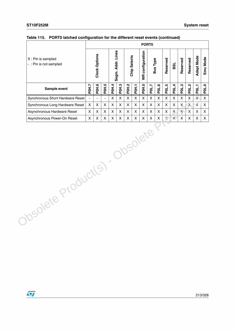
ST10F252M System reset
213/328
Synchronous Short Hardware Reset - - - X X X X X X X X X X X X X
Synchronous Long Hardware Reset X X X X X X X X X X X X X X X X
Asynchronous Hardware Reset X X X X X X X X X X X X X X X X
Asynchronous Power-On Reset X X X X X X X X X X X X X X X X
Table 115. PORT0 latched configuration for the different reset events (continued)
X : Pin is sampled
- : Pin is not sampled
PORT0
Clo
ck O
pti
on
s
Seg
m. A
dd
r. L
ines
Ch
ip S
elec
ts
WR
co
nfi
gu
rati
on
Bu
s Ty
pe
Res
erve
d
BS
L
Res
erve
d
Res
erve
d
Ad
apt
Mo
de
Em
u M
od
e
Sample eventP
0H.7
P0H
.6
P0H
.5
P0H
.4
P0H
.3
P0H
.2
P0H
.1
P0H
.0
P0L
.7
P0L
.6
P0L
.5
P0L
.4
P0L
.3
P0L
.2
P0L
.1
P0L
.0
O
bsolete Product(
s) - O
bsolete Product(
s)

Power reduction modes ST10F252M
214/328
21 Power reduction modes
Several different power reduction modes with different levels of power reduction have been implemented in the ST10F252M, which may be entered under software and/or hardware control.
In idle mode the CPU is stopped, while the peripherals continue their operation. Idle mode can be terminated by any reset or interrupt request.
In power down mode both the CPU and the peripherals are stopped. Power down mode can be configured by software to be terminated only by a hardware reset, by a transition on enabled fast external interrupt pins, by an interrupt generated by the real time clock, by an interrupt generated by the activity on CAN and I2C module interfaces.
Note: All external bus actions are completed before idle or power down mode is entered.
To use the real time clock when the device is in power down mode a reference clock is needed (XTAL1 / XTAL2 pins). In this case, the main oscillator is not stopped when power down is entered, and the real time clock continues to work using the main oscillator clock signal as reference.
Stand-by mode is achieved by turning off the main power supply (VDD) while VSTBY remains the only active supply for the device. In this condition, the VSTBY pin provides the supply to a portion of the XRAM (the stand-by RAM, 16 Kbyte in this device) through a dedicated on-chip low power voltage regulator; the content of this RAM can be retained and is available at next system start-up.
Note: VSTBY is always powered in the range of 4.5-5.5 Volt.
An exception for the VSTBY value is allowed when RSTIN pin is held low and the main VDD is on – this drives pin EA (mapped together with VSTBY) and configures the access to external memory. After the RSTIN pin is released, VSTBY returns high to be used as the VSTBY supply voltage.
The real time clock cannot be used in stand-by-mode. Turning off the main power supply (VDD) of the device, stop the main oscillator circuitry working. Standard power down mode must be used to continue operating the real time clock (RTC).
21.1 Idle modeThis mode is exactly the same as for the ST10F168 or the ST10F269.
In idle mode the CPU is stopped, while the peripherals continue their operation. Idle mode can be terminated by any reset or interrupt request. Any operation, required by the interrupt is completed and the CPU returns to normal operation.
21.2 Power down modeTo further reduce the power consumption the microcontroller can be switched to power down mode. Clocking of all internal blocks is stopped, the contents of the internal RAM, however, are preserved through the voltage supplied via the VDD pins (and the on-chip voltage regulator). The watchdog timer is also stopped in power down mode. The only exception could be the real time clock, if appropriately programmed, and the oscillator circuit as a consequence (the main oscillator).
O
bsolete Product(
s) - O
bsolete Product(
s)

ST10F252M Power reduction modes
215/328
When the ST10F252M is in power-down mode, its on-chip voltage regulator remains on by default. To further reduce the consumption, it can be put in its power-saving mode; the low-power voltage regulator delivers about 1.65 V to supply the core logic. It is mandatory not to reduce the VDD during power down mode – it must be always in the range 5V ±10% when in power down mode. Before executing the PWRDN instruction, bit 3 of the XMISC register is set to turn off the main voltage regulator when power down is entered.
XMISC register
The ST10F252M provides two different operating power down modes:
● protected power down mode
● interruptible power down mode.
The power down operating mode is selected by the bit PWDCFG in SYSCON register.
XMISC register (EB46h) SFR Reset value: 0000h
15 14 13 12 11 10 9 8 7 6 5 4 3 2 1 0
- P7EN VREGOFF
CANCK2
CANPAR -
- RRW RRW RRW RRW -
Table 116. XMISC register functions
Bit Name Function
4 P7ENConnect PORT7 to pins‘0’: Ports P4.0-P4.3 are connected to pins 47-50 (default configuration).
‘1’: Ports P7.0-P7.3 are connected to pins 47-50
3 VREGOFF
Main voltage regulator disable in power-down mode
‘0’: On-chip main regulator is held active when power-down mode is entered
‘1’: On-chip main regulator is turned off when power-down mode is entered
2 CANCK2
CAN clock divider by 2 disable‘0’: Clock provided to CAN modules is CPU clock divided by two (mandatory when fCPU is higher than 40 MHz)‘1’: Clock provided to CAN modules is directly CPU clock
1 CANPAR
CAN parallel mode selection‘0’: CAN2 is mapped on P4.4/P4.7, while CAN1 is mapped on P4.5/P4.6‘1’: CAN1 and CAN2 are mapped in parallel on P4.5/P4.6. This is effective only if both CAN1 and CAN2 are enabled through setting of bits CAN1EN and CAN2EN in XPERCON register. If CAN1 is disabled, CAN2 remains on P4.4/P4.7 even if bit CANPAR is set.
O
bsolete Product(
s) - O
bsolete Product(
s)
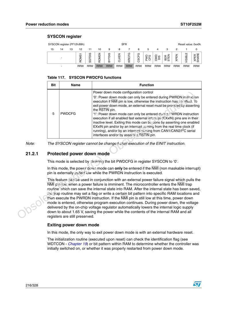
Power reduction modes ST10F252M
216/328
SYSCON register
Note: The SYSCON register cannot be changed after execution of the EINIT instruction.
21.2.1 Protected power down mode
This mode is selected by clearing the bit PWDCFG in register SYSCON to ‘0’.
In this mode, the power down mode can only be entered if the NMI (non maskable interrupt) pin is externally pulled low while the PWRDN instruction is executed.
This feature can be used in conjunction with an external power failure signal which pulls the NMI pin low when a power failure is imminent. The microcontroller enters the NMI trap routine which can save the internal state into RAM. After the internal state has been saved, the trap routine may set a flag or write a certain bit pattern into specific RAM locations and then execute the PWRDN instruction. If the NMI pin is still low at this time, power down mode is entered, otherwise program execution continues. During power down, the voltage delivered by the on-chip voltage regulator automatically lowers the internal logic supply down to about 1.65 V, saving the power while the contents of the internal RAM and all registers are still preserved.
Exiting power down mode
In this mode, the only way to exit power down mode is with an external hardware reset.
The initialization routine (executed upon reset) can check the identification flag (see WDTCON - Chapter 19) or bit pattern within RAM to determine whether the controller was initially switched on, or whether it was properly restarted from power down mode.
SYSCON register (FF12h/89h) SFR Reset value: 0xx0h
15 14 13 12 11 10 9 8 7 6 5 4 3 2 1 0
-
RO
MS
1
SG
TD
IS
RO
ME
N
BY
TD
IS
CLK
EN
WR
CF
G
CS
CF
G
PW
DC
FG
OW
DD
IS
BD
RS
TE
N
XP
EN
VIS
IBLE
XP
ER
SH
AR
E
- RRW RRW RRW RRW RRW RRW RRW RRW RRW RRW RRW RRW RRW
Table 117. SYSCON PWDCFG functions
Bit Name Function
5 PWDCFG
Power down mode configuration control‘0’: Power down mode can only be entered during PWRDN instruction execution if NMI pin is low, otherwise the instruction has no effect. To exit power down mode, an external reset must be provided by asserting the RSTIN pin.‘1’: Power down mode can only be entered during PWRDN instruction execution if all enabled fast external interrupt (EXxIN) pins are in their inactive level. Exiting this mode can be done by asserting one enabled EXxIN pin and/or by an interrupt coming from the real time clock (if running), and/or by an interrupt coming from CAN1/CAN2/I2C serial interfaces and/or by asserting RSTIN pin.
O
bsolete Product(
s) - O
bsolete Product(
s)

ST10F252M Power reduction modes
217/328
21.2.2 Interruptible power down mode
This mode is selected by setting the bit PWDCFG in register SYSCON to ‘1’.
In this mode, the power down mode can be entered if the fast external interrupt pins (EXxIN pins, alternate functions of PORT2 pins, with x = 7...0) are in their inactive level. This inactive level is configured with the EXIxES bit field in the EXICON register
Figure 87. EXICON register
Exiting power down mode
When interruptible power down mode is entered, the CPU and peripheral clocks are frozen, and the oscillator and PLL are stopped (when RTC is disabled, so there is no need for a clock reference). Interruptible power down mode can be exited by either asserting RSTIN or one of the enabled EXxIN pin (fast external interrupt). If the real time clock module needs to be running during power down, the main oscillator is not stopped. The PLL, on the contrary is switched off.
If power down mode is exited by a hardware RESET, the RSTIN pin must be held low until the oscillator (if not already running for real time clock operation) and PLL have restarted and stabilized.
EXxIN inputs are normally sampled interrupt inputs. However, the power down mode circuitry uses them as level-sensitive inputs. An EXxIN (x = 7...0) interrupt enable bit (bit CCxIE in respective CCxIC register) needs not to be set to bring the device out of power down mode.
To guarantee stabilization time before restart the operation when exiting from power down (especially if the main oscillator was stopped – typically when the real time clock module is not used), an external RC circuit must be connected to RPD pin (return from power down), as shown in the Figure 88.
EXICON register (F1C0h/E0) ESFR Reset value: 0000h
15 14 13 12 11 10 9 8 7 6 5 4 3 2 1 0
EXI7ES EXI6ES EXI5ES EXI4ES EXI3ES EXI2ES EXI1ES EXI0ES
RRW RRW RRW RRW RRW RRW RRW RRW
Table 118. EXICON register functions
Bit Name Function
15.0 EXIxES (x=7...0)
External interrupt x edge selection field (x=7...0)‘00’: Fast external interrupts disabled: standard mode. EXxIN pin not taken into account for entering or exiting power down mode.‘01’: Interrupt on positive edge (rising). Enter power down mode if EXiIN = ‘0’, exit if EXxIN = ‘1’ (referred as ‘high’ active level)‘10’: Interrupt on negative edge (falling). Enter power down mode if EXiIN = ‘1’, exit if EXxIN = ‘0’ (referred as ‘low’ active level)‘11’: Interrupt on any edge (rising or falling). Always enter power down mode, exit if EXxIN level changed.
O
bsolete Product(
s) - O
bsolete Product(
s)

Power reduction modes ST10F252M
218/328
Figure 88. RPD pin: external circuit to exit power down
To exit power down mode with external interrupt, an EXxIN pin has to be asserted for at least 40 ns (x = 7...0). This signal enables the internal main oscillator (if not already running) and PLL circuitry, and also turns on the internal weak pull-down on RPD pin (see Figure 89). The discharging of the external capacitor provides a delay that allows the oscillator and PLL circuits to stabilize before the internal CPU and peripheral clocks are enabled. When the voltage on RPD pin drops below the threshold voltage (about 2.5 V), the Schmitt trigger clears Q2 flip-flop, thus enabling the CPU and peripheral clocks, and the device resumes code execution.
If the Interrupt was enabled (bit CCxIE=’1’ in the respective CCxIC register) before entering power down mode, the device executes the interrupt service routine, and resumes execution after the PWRDN instruction (see note below). If the interrupt was disabled, the device executes the instruction following PWRDN instruction, and the interrupt request flag (bit CCxIR in the respective CCxIC register) remains set until it is cleared by software.
Note: Due to internal pipeline, the instruction that follows the PWRDN instruction is executed before the CPU performs a call of the interrupt service routine when exiting power down mode.
Figure 89. Simplified power down exit circuitry
RPD
220k - 1M Ohm (typ)
1µF (typ)
ST10F252M
+
VDD
C1
R1
Enter
Externalinterrupt
Reset
stop PLLstop oscillator
VDD
D Q
Qcd system clock
CPU and peripherals clocks
RPD
VDD
exit_pwrd
en_clk_n
Pull-Up
Weak pull-down(~ 200 µA)
power down
Q2
VDD
D Q
Qcd
Q1
O
bsolete Product(
s) - O
bsolete Product(
s)

ST10F252M Power reduction modes
219/328
Exiting from interruptible power down is also possible through the CAN receive lines and I2C Serial Clock line (if properly enabled through CC8IC and CC9IC registers), an activity on pins P4.5 and P4.4 is interpreted as a fast external interrupt event able to wake-up the device. For more details refers also to Section 9.1.
Figure 90. Power down exit sequence using an external interrupt (PLL x 2)
21.2.3 Real time clock and power down mode
If the real time clock is running (RTOFF bit of RTCCON register cleared), when PWRDN instruction is executed, the oscillator circuit which is providing the reference to the counter is not stopped.
21.3 Stand-by modeIn Stand-by mode, the RAM array is maintained powered through the dedicated pin VSTBY when ST10F252M main power supply (VDD) is turned off.
To enter stand-by mode it is mandatory to hold the device under reset; once the device is under reset, the RAM is disabled (see XRAM2EN and XRAM1EN bits of XPERCON register), and its digital interface is frozen to avoid any kind of data corruption. It is then possible to turn off the main VDD provided that VSTBY is on.
A dedicated embedded low-power voltage regulator is implemented to generate the internal low voltage supply (about 1.65 V in stand-by mode) to bias all those circuits that remain active: XRAM2 (12Kbytes).
In normal running mode (that is when main VDD is on), the VSTBY pin can be tied to VSS during reset to exercise the EA functionality associated with the same pin; the voltage supply for the circuitries which are usually biased with VSTBY (see in particular the low-power oscillator used in conjunction with real time clock module), is granted by the active main VDD.
Stand-by mode can generate problems associated with the use of different power supplies in CMOS systems. Pay particular attention when the ST10F252M I/O lines are interfaced with other external CMOS integrated circuits. If VDD of ST10F252M becomes (for example
CPU clk
Power Down Signal
External
RPD
ExitPwrd
XTAL1
(Internal)
Interrupt
(Internal)
~ 2.5 V
Delay for oscillator / PLLstabilization
O
bsolete Product(
s) - O
bsolete Product(
s)

Power reduction modes ST10F252M
220/328
in stand-by mode) lower than the output level forced by the I/O lines of these external integrated circuits, the ST10F252M could be directly powered through the inherent diode existing on ST10F252M output driver circuitry. The same is valid for ST10F252M interfaced to active or inactive communication buses during stand-by mode: current injection can be generated through the inherent diode. Furthermore, the sequence of turning on/off of the different voltage could be critical for the system (not only for the ST10F252M device). The device stand-by mode current (ISTBY) may vary while VDD to VSTBY (and vice versa) transition occurs. Some current flows between VDD and VSTBY pins. System noise on both VDD and VSTBY can contribute to increase this phenomenon.
21.3.1 Entering stand-by mode
To enter stand-by mode XRAM2EN and XRAM1EN bits in the XPERCON register must be cleared (this bit is automatically reset by any kind of RESET event, see Chapter 20); this immediately freezes the RAM interface, avoiding any data corruption. As a consequence of a RESET event, the RAM power supply is switched to the internal low-voltage supply, V18SB (derived from VSTBY through the low-power voltage regulator). The RAM interface remains frozen until the bits XRAM1EN and XRAM2EN are set again by software initialization routine (at next exit from main VDD power-on reset sequence).
Since V18 is falling (as a consequence of VDD turning off), it can happen that the XRAM2EN bit is no longer able to guarantee its content (logic “0”), as the XPERCON register is powered by the internal V18. This does not generate any problem, because the Stand-by mode dedicated switching circuit continues to confirm the freezing of the RAM interface, irrespective the XRAM2EN bit content. The XRAM2EN bit status is considered again when internal V18 comes back over internal stand-by reference V18SB.
If internal V18 becomes lower than the internal stand-by reference (V18SB) of about 0.3-0.45V with bit XRAM2EN set, the RAM supply switching circuit is not active. If there is a temporary drop on internal V18 voltage versus internal V18SB during normal code execution, no spurious stand-by mode switching can occur (the RAM is not frozen and can still be accessed).
The ST10F252M core module, generating the RAM control signals, is powered by the internal V18 supply. During turning off, these control signals follow the V18, while RAM is switched to the V18SB internal reference. It could happen that a high level of RAM write strobe from ST10F252M core (active low signal) is low enough to be recognized as a logic “0” by the RAM interface (due to V18 lower than V18SB); the bus status could contain a valid address for the RAM and an unwanted data corruption could occur. For this reason, an extra interface, powered by the switched supply, is used to prevent the RAM from this kind of potential corruption mechanism.
Warning: During power-off phase, it is important that the external hardware maintains a stable ground level on RSTIN pin, without any glitch, to avoid spurious exiting from reset status with unstable power supply.
O
bsolete Product(
s) - O
bsolete Product(
s)

ST10F252M Power reduction modes
221/328
21.3.2 Exiting stand-by mode
After the system has entered the stand-by mode, the procedure to exit this mode consists of a standard power-on sequence, with the only difference that the RAM is already powered through the V18SB internal reference (derived from VSTBY pin external voltage).
Hold the device under RESET (RSTIN pin forced low) until external VDD voltage pin is stable. Even though, at the very beginning of the power-on phase, the device is maintained under reset by the internal low voltage detector circuit (implemented inside the main voltage regulator) until the internal V18 becomes higher than about 1.0V, there is no warranty that the device stays under reset status if RSTIN is at high level during power ramp up. So, it is important the external hardware is able to guarantee a stable ground level on RSTIN along the power-on phase, without any temporary glitch.
The external hardware is responsible to drive the RSTIN pin low until VDD is stable, even though the internal LVD is active. It is requested an additional time (at least 1 ms) to allow internal voltage regulator stabilization before releasing the RSTIN pin; this is necessary since the internal Flash has to begin its initialization phase (starting when RSTIN pin is released) with an already stable V18.
Once the internal reset signal goes low, the RAM (still frozen) power supply is switched to the main V18.
At this time, everything becomes stable, and the execution of the initialization routines can start: XRAM1EN and XRAM2EN bit can be set, enabling the RAM.
21.3.3 Real time clock and stand-by mode
When stand-by mode is entered (turning off the main supply VDD), the real time clock counting stops running. This is because the main oscillator is used as reference for the counter. As the main oscillator powered by VDD, once this is switched off, the oscillator stops.
O
bsolete Product(
s) - O
bsolete Product(
s)

Real time clock ST10F252M
222/328
22 Real time clock
The Real Time Clock is an independent timer, in which the clock is derived directly from the clock oscillator on XTAL1 (main oscillator) input or XTAL3 input (32 kHz low-power oscillator) so that it can continue running even in Idle or Power-down modes (if so enabled). Registers access is implemented onto the XBUS. This module is designed with the following characteristics:
● generation of the current time and date for the system
● cyclic time based interrupt, on Port2 external interrupts every “RTC basic clock tick” and after n ’RTC basic clock ticks’ (n is programmable) if enabled
● 58-bit timer for long term measurement
● capability to exit the ST10 chip from Power-down mode (if PWDCFG of SYSCON set) after a programmed delay
Note: When the clock is gated, no reset is raised after the EINIT instruction has been executed.
The RTC consists of a chain of programmable counters made of two main blocks. The first block is a prescaler which generates a basic reference clock (for example, a one second period clock). This basic reference clock includes a fixed prescaler divider (1/64) and two programmable dividers: RTCPH (RTC prescaler high – 4-bits) and RTCPL (RTC prescaler low – 16-bits). The second block, which uses TRCLK as an input clock, comprises two 16-bit programmable counters, RTCH and RTCL, that may be initialized to the current system time. This system time is increased at the TRCLK rate and compared with a programmable date to generate an alarm via an interrupt request (RTC_alarmIT), if enabled in the RTC control register.
If enabled in the RTC control register, the RTC generates an interrupt request (RTC_SecIT) every TRCLK period.
RTC_SecIT and RTC_alarmIT can trigger a fast external interrupt via EXISEL register of PORT2 and wake the ST10 chip if it is in power down mode (refer to Section 9.2 for details). Another function, implemented in the RTC, is to switch off the main on-chip oscillator if the ST10 enters the power down mode, so that the chip can be fully switched off (if the RTC is disabled).
At power on and after reset, the main oscillator drives the RTC counter, and since it is powered by the main power supply, it cannot be maintained running in stand-by mode, while in power down mode the main oscillator is maintained running to provide the reference to the RTC module (if not disabled).
O
bsolete Product(
s) - O
bsolete Product(
s)

ST10F252M Real time clock
223/328
Figure 91. SFRs associated with the RTC
Figure 92. RTC block diagram
22.1 RTC registers
22.1.1 RTCCON: RTC control register
The functions of the RTC are controlled by the bit-addressable RTC control register RTCCON. If the RTOFF bit is set, the RTC dividers and counters clocks are disabled and registers can be written; when the ST10 chip enters power down mode the clock oscillators (both main and low-power) are switched off. The RTC has two interrupt sources, one is triggered every second, the other one is the alarm. RTCCON includes an interrupt request
- - - - - - - - Y Y Y Y - - - -EXISEL E
EXISEL External Interrupt Source Selection register (Port2)
- - - - - - - - Y Y Y Y Y Y Y YCCxIC
15 14 13 12 11 10 9 8 7 6 5 4 3 2 1 0 15 14 13 12 11 10 9 8 7 6 5 4 3 2 1 0
- - - - - - - - Y Y Y Y - - - -EXICON E
EXICON External Interrupt Control register (Port2)CCxIC CAPCOM1 Interrupt Control registers (x = 10, 11)
Bit is linked to a functionBit has no function or is not implementedRegister is in ESFR internal memory space
Y-E
:::
Interrupt Control
/64
RTCPLRTCPH
RTCH RTCL RTCDH RTCDL
RTCAH RTCAL
OSC_CLK
reload=
programmable 20 bits dividerprogrammable 32 bits counter
RTCCON
alarmIT SecIT
RTC_SecIT
RTC_alarmIT
OSC_STOP
O
bsolete Product(
s) - O
bsolete Product(
s)

Real time clock ST10F252M
224/328
flag and an interrupt enable bit for each of them. This register is read and written via the XBUS.
RTC control register
Note: All the bits of RTCCON are active high.
The two RTC Interrupt request lines are connected to PORT2 to trigger an external interrupt that wakes the chip up if in power down mode.
All the RTC registers are not bit addressable. To clear the RTC interrupt request flags (bit 0 and bit 2 of the RTCCON register) it is necessary to write a ‘1’ to the corresponding bit of the RTCCON register.
22.1.2 RTC prescaler divider loaded value registers
The 20 bit programmable prescaler divider is loaded by two registers. The divisor 4 MSBs are stored into RTCPH and the 16 LSBs in RTCPL. These registers are not reset to keep the system clock. They are write protected by bit RTOFF of RTCCON register, write operation is allowed if RTOFF is set.
RTCCON register (ED00h) ESFR Reset value: 000uh
15 14 13 12 11 10 9 8 7 6 5 4 3 2 1 0
- - - RTCOFF - - - RTAE
N RTAIR RTSEN RTSIR
- - - RRW - - - RRW RRW RRW RRW
Table 119. RTC control register functions
Bit Name Function
7 RTCOFF
RTC switch off bit
‘0’: clock oscillator and RTC keep on running even if ST10 in power down mode.
‘1’: clock oscillator is switched off when ST10 enters power down mode. Setting this bit, RTC dividers and counters are stopped and registers can be written.
3 RTAEN
RTC alarm interrupt enable
‘0’: RTC_alarmIT is disabled.
‘1’: RTC_alarmIT is enabled, it is generated every n seconds.
2 RTAIR
RTC alarm interrupt request flag (when the alarm is triggered)
‘0’: the bit was reset less than n seconds ago.‘1’: the interrupt was triggered.
1 RTSENRTC second interrupt enable‘0’: RTC_SecIT is disabled.
‘1’: RTC_SecIT is enabled, it is generated every second.
0 RTSIR
RTC second interrupt request flag (every second)
‘0’: the bit was reset less than a second ago.
‘1’: the interrupt was triggered.
O
bsolete Product(
s) - O
bsolete Product(
s)

ST10F252M Real time clock
225/328
RTC prescaler register
Figure 93. RTC prescaler register function
The value stored into RTCPH, RTCPL is called RTCP (coded on 20 bits). The dividing ratio of the prescaler divider is:
ratio = 64 x (RTCP)
The minimum value which can be set in RTCPL is 0002h.
22.1.3 RTC prescaler divider current value registers
Every period of TRCLK the dividers are reloaded with the value stored in RTCPH and RTCPL registers. To get an accurate time measurement, it is possible to access the internal value of the dividers, reading the registers RTCDH, RTCDL. These registers are read only. When any bit changed in the programmable prescaler divider, the new internal value is loaded in the registers.
RTC prescaler divider register
Note: These registers are not reset, and are read only.
RTCCPL register (ED06h) ESFR Reset value: uuuuh
15 14 13 12 11 10 9 8 7 6 5 4 3 2 1 0
RTCPL
RRW
RTCCPH register (ED08h) ESFR Reset value: uuuuh
15 14 13 12 11 10 9 8 7 6 5 4 3 2 1 0
RTCPH
RRW
3 2 1 07 6 5 411 10 9 815 14 13 123 2 1 0
RTCPH RTCPL
3 2 1 07 6 5 411 10 9 815 14 13 1219 18 17 16
20 bits word divider
RTCCDL register (ED0Ah) ESFR Reset value: uuuuh
15 14 13 12 11 10 9 8 7 6 5 4 3 2 1 0
RTCDL
R
RTCCDH register (ED0Ch) ESFR Reset value: uuuuh
15 14 13 12 11 10 9 8 7 6 5 4 3 2 1 0
RTCDH
R
O
bsolete Product(
s) - O
bsolete Product(
s)

Real time clock ST10F252M
226/328
The divider works as a decrement operator. When the internal value reaches 0001h, the second interrupt is generated. When the next decrement occurs (which would set the divider register to the value 0000h), the 20-bit word stored in RTCPH, RTCPL registers is loaded in the divider. The minimum value which can be programmed in RTCPL is 0002h; if 0001h were set, just one second interrupt would be generated, since the divider would stay fixed at the value 0001h forever (a successive second interrupt cannot occur).
Figure 94. RTC prescaler divider register functions
The bits 15 down to 4 of RTCPH and RTCDH are not used. When reading, the return value of these bits is zero.
22.1.4 RTC programmable counter registers
The RTC has two 16-bit programmable counters whose count rate is based on the 1 second time reference. These counters can be used as a system clock as the clock oscillator can be working even in power down mode (either the main or the low power on-chip oscillator) if bit RTOFF of RTCCON register is reset. To keep this system clock, the counters are not reset with any system reset; the only way to force their value is to write them via the XBUS.
These counters are write protected. The bit RTOFF of the RTCCON register must be set (RTC dividers and counters are stopped) to enable a write operation on RTCH or RTCL.
A write operation on RTCH or RTCL register loads directly the corresponding counter. When reading, the current value in the counter (system date) is returned.
The counters are kept on running while at least one clock oscillator is working (either the main or the low-power on-chip oscillator).
RTC programmable counter register
Note: These registers are not reset.
3 2 1 07 6 5 411 10 9 815 14 13 123 2 1 0
RTCDH RTCDL
3 2 1 07 6 5 411 10 9 815 14 13 1219 18 17 16
20 bits word internal value of the prescaler divider
RTCL register (ED0Eh) ESFR Reset value: uuuuh
15 14 13 12 11 10 9 8 7 6 5 4 3 2 1 0
RTCL
RW
RTH register (ED10h) ESFR Reset value: uuuuh
15 14 13 12 11 10 9 8 7 6 5 4 3 2 1 0
RTCH
RW
O
bsolete Product(
s) - O
bsolete Product(
s)

ST10F252M Real time clock
227/328
22.1.5 RTC alarm registers
When the programmable counters reach the 32 bits value stored into RTCAH & RTCAL registers an alarm is triggered and the interrupt request RTAIR is generated. These registers are not protected.
RTC alarm register
Note: These registers are not reset.
22.2 Programming the RTCRTC interrupt request signals are connected to PORT2, pin 10 (RTCSI) and pin 11 (RTCAI).
EXICON ESFR controls the external interrupt edge selection; RTC interrupt requests are rising edge active.
RTC external interrupt control register
RTCAL register (ED12h) ESFR Reset value: uuuuh
15 14 13 12 11 10 9 8 7 6 5 4 3 2 1 0
RTCAL
RW
RTCAH register (ED14h) ESFR Reset value: uuuuh
15 14 13 12 11 10 9 8 7 6 5 4 3 2 1 0
RTCAH
RW
EXICON register (F1C0h/E0) ESFR Reset value: 0000h
15 14 13 12 11 10 9 8 7 6 5 4 3 2 1 0
EXI7ES EXI6ES EXI5ES EXI4ES EXI3ES EXI2ES EXI1ES EXI0ES
RW
Table 120. RTC external interrupt control register functions
Bit Name Function
15.0 EXIxES (x=7...0)
External interrupt x edge selection field (x=7...0)
‘00’: Fast external interrupts disabled: standard mode. EXxIN pin not taken into account for entering or exiting power down mode.
‘01’: Interrupt on positive edge (rising). Enter power down mode if EXiIN = ‘0’, exit if EXxIN = ‘1’ (referred as ‘high’ active level)
‘10’: Interrupt on negative edge (falling). Enter power down mode if EXiIN = ‘1’, exit if EXxIN = ‘0’ (referred as ‘low’ active level)
‘11’: Interrupt on any edge (rising or falling). Always enter power down mode, exit if EXxIN level changed.
O
bsolete Product(
s) - O
bsolete Product(
s)
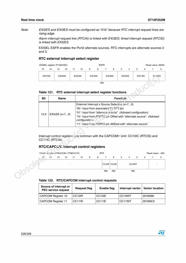
Real time clock ST10F252M
228/328
Note: EXI2ES and EXI3ES must be configured as “01b” because RTC interrupt request lines are rising edge.
Alarm interrupt request line (RTCAI) is linked with EXI3ES; timed interrupt request (RTCSI) is linked with EXI2ES.
EXISEL ESFR enables the Port2 alternate sources. RTC interrupts are alternate sources 2 and 3.
RTC external interrupt select register
Interrupt control registers are common with the CAPCOM1 Unit: CC10IC (RTCSI) and CC11IC (RTCAI).
RTC/CAPCOM interrupt control registers
EXISEL register (F1DAh/ED) ESFR Reset value: 0000h
15 14 13 12 11 10 9 8 7 6 5 4 3 2 1 0
EXI7SS EXI6SS EXI5SS EXI4SS EXI3SS EXI2SS EXI1SS EXI0SS
RW
Table 121. RTC external interrupt select register functions
Bit Name Function
15.0 EXIxSS (x=7...0)
External Interrupt x Source Selection (x=7...0)
‘00’: Input from associated PORT2 pin
‘01’: Input from “alternate source”. (Advised configuration)‘10’: Input from PORT2 pin ORed with “alternate source”. (Advised configuration)‘11’: Input from PORT2 pin ANDed with “alternate source”.
CCxIC register (FF8Ch/C6h, FF8Eh/C7h) SFR Reset value: --00h
15 14 13 12 11 10 9 8 7 6 5 4 3 2 1 0
- CCxIR CCxIE CCxINT -
RW RW RW
Table 122. RTC/CAPCOM interrupt control requests
Source of interrupt or PEC service request
Request flag Enable flag Interrupt vector Vector location
CAPCOM Register 10 CC10IR CC10IE CC10INT 00’0068h
CAPCOM Register 11 CC11IR CC11IE CC11INT 00’006Ch
O
bsolete Product(
s) - O
bsolete Product(
s)
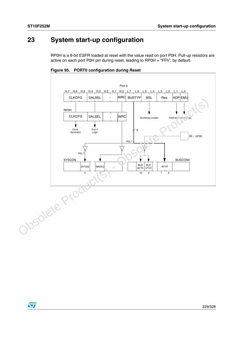
ST10F252M System start-up configuration
229/328
23 System start-up configuration
RP0H is a 8-bit ESFR loaded at reset with the value read on port P0H. Pull-up resistors are active on each port P0H pin during reset, leading to RP0H = “FFh”, by default.
Figure 95. PORT0 configuration during Reset
L.5 L.4 L.3 L.2 L.1 L.0H.3 H.2 H.1 H.0 L.7 L.6H.7 H.6 H.5 H.4
EMUADPWRC-SALSEL BUSTYP
RP0H
Clock Port 4Logic
SYSCON BUSCON0
Internal Control Logic
CLKCFG
7 6
2
P0L.7
P0L.7
79
BYTDIS WRCFG
Port 0
Bootstrap Loader
Generator
CLKCFG SALSEL WRC
BTYP
BSL Res.
10 9
ALECTL0
BUSACT0
EA / VSTBY
-
O
bsolete Product(
s) - O
bsolete Product(
s)

System start-up configuration ST10F252M
230/328
Start up configuration register
Note: RP0H(7:5) bits are loaded only during a long hardware reset.
RPOH register (F108h/84h) ESFR Reset value: --xxh
15 14 13 12 11 10 9 8 7 6 5 4 3 2 1 0
- CLKSEL SALSEL - WRC
RO RO RO
Table 123. Start up configuration register functions
Bit Name Function
7.5 CLKSEL
System Clock Selection‘000’: fCPU = 16 * fOSC
‘001’: fCPU = 0.5 * fOSC
‘010’: fCPU = 10 * fOSC
‘011’: fCPU = fOSC
‘100’: fCPU = 5 * fOSC
‘101’: fCPU = 8 * fOSC
‘110’: fCPU = 3 * fOSC
‘111’: fCPU = 4 * fOSC
4.3 SALSEL
Segment Address Line Selection (Number of active segment address outputs)0 0: 4-bit segment address: A19...A16
0 1: No segment address lines at all
1 0: 8-bit segment address: A23...A161 1: 2-bit segment address: A17...A16 (Default without pull-downs)
0 WRCWrite Configuration Control‘0’: Pins WR acts as WRL, pin BHE acts as WRH
‘1’: Pins WR and BHE retain their normal function
O
bsolete Product(
s) - O
bsolete Product(
s)

ST10F252M Bootstrap loader
231/328
24 Bootstrap loader
ST10F252M has an ST10 standard bootstrap mode that supports bootstrap via UART or CAN.
24.1 Selection between user-code or standard bootstrapThe selection between user-code or standard bootstrap is made by special combinations on PORT0L[5...4] during the time the reset configuration is latched from PORT0.
Bootstrap mode is triggered with a special combination set on PORT0L[5...4]. These signals, as are other configuration signals, are latched on the rising edge of RSTIN pin.
● Decoding of reset configuration (P0L.5 = 1, P0L.4 = 1) selects the normal mode and selects the user Flash to be mapped from address 00’0000h.
● Decoding of reset configuration (P0L.5 = 1, P0L.4 = 0) selects the ST10 standard bootstrap mode (user Flash is remapped at address 01’0000h and test Flash is mapped at address 00’0000h).
24.2 Standard bootstrap loaderThe built-in bootstrap loader (BSL) of the ST10F252M provides a mechanism to load the startup program, which is executed after reset, via the serial interface. In this case, no external (ROM) memory or internal ROM is required for the initialization code starting at location 00’000oh. The bootstrap loader moves code and data into the internal RAM but it is also possible to transfer data via the serial interface into an external RAM using a second level loader routine. ROM memory (internal or external) is not necessary. However, it may be used to provide lookup tables or may provide “core-code”, that is, a set of general-purpose subroutines, for example, for I/O operations, number crunching, system initialization, etc.
The bootstrap loader may be used to load the complete application software into ROMless systems, it may load temporary software into complete systems for testing or calibration, it may also be used to load a programming routine for Flash devices.
The BSL mechanism may be used for standard system startup as well as only for special occasions like system maintenance (firmware update) or end-of-line programming or testing.
24.2.1 Entering the standard bootstrap loader
As with the old ST10 bootstrap mode, the ST10F252M enters BSL mode, if pin P0L.4 is sampled low at the end of a hardware reset. In this case, the built-in bootstrap loader is
Table 124. ST10F252M boot mode selection
P0.5 P0.4 ST10 decoding
1 1 No test mode: user Flash mapped at 00’0000h
1 0 Standard Bootstrap loader: User Flash mapped from 01’0000h
0 x Reserved
O
bsolete Product(
s) - O
bsolete Product(
s)

Bootstrap loader ST10F252M
232/328
activated independently of the selected bus mode. The bootstrap loader code is stored in a special test Flash; no part of the standard of the Flash memory area is required for this.
After entering BSL mode and the respective initialization, the ST10F252M scans the RxD0 line and the CAN1_RxD line to receive either a valid dominant bit from CAN interface, or a start condition from UART line.
● Start condition on UART RxD
ST10F252M starts standard bootstrap loader. This bootstrap loader is identical to other ST10 devices (example: ST10F269, ST10F168). See Section 24.3 for details.
● Valid dominant bit on CAN1 RxD
ST10F252M start bootstrapping via CAN; the bootstrapping method is new and is described in Section 24.4. Figure 96 shows the program flow of the new bootstrap loader. It illustrates clearly how the new functionalities are implemented:
– UART: UART has priority over CAN after a falling edge on CAN1_RxD till the 1st valid rising edge on CAN1_RxD
– CAN: pulses on CAN1_RxD shorter than 20*CPU-cycles are filtered.
O
bsolete Product(
s) - O
bsolete Product(
s)

ST10F252M Bootstrap loader
233/328
24.2.2 ST10 configuration in BSL
When the ST10F252M has entered BSL mode, the following configuration is automatically set (values that deviate from the normal reset values, are marked):
Figure 96. ST10F252M new bootstrap loader program flow
START
Falling-edge onUART0 RxD?
Falling-edge onCAN1 RxD?
Start Timer PT0
UART RxD = 0?
CAN1 RxD = 1?
PT0 > 20?
No
Count = 1
CAN RxD = 0?No
CAN1 RxD = 1?No
Count += 1
Count = 5?
Stop Timer PT0Initialize CAN
Address = FA40h
No
Stop Timer PT0
Message Received?No
[Address] = MO15_data0Address = Address + 1
Address = FAC0h?No
Glitch on CAN1 RxD
Clear Timer PT0
No No
Start Timer T6
UART0 RxD = 1?No
Stop Timer T6Initialize UART
Send AcknowledgeAddress = FA40h
byte Received?No
[Address] = S0RBUFAddress = Address + 1
Address = FA60h?No
Yes
Jump to Address FA40h
UART BOOT
CAN BOOT
CAN BOOTUART BOOT
No
Table 125. Register configuration in BSL
Register Value Notes
Watchdog Timer: Disabled
Register SYSCON: 0404h (1) XPEN bit set for Bootstrap viaCAN or Alternate Boot Mode
Context Pointer CP: FA00h
Register STKUN: FC00h
O
bsolete Product(
s) - O
bsolete Product(
s)

Bootstrap loader ST10F252M
234/328
Other than after a normal reset, the watchdog timer is disabled, so the bootstrap loading sequence is not time limited. Depending on the serial link (UART or CAN), the pin TxD0 or CAN1_TxD is configured as output, so the ST10F252M can return an acknowledge. Even if the internal IFlash is enabled, no code can be executed out of it.
24.2.3 Booting steps
As Figure 97 shows, booting ST10F252M with the boot loader code occurs in a minimum of four steps.
1. The ST10F252M is reset with P0L.4 low.
2. The internal new bootstrap code runs on the ST10 and a first level user code is downloaded from the external device using the selected serial link (UART or CAN). The bootstrap code is contained in the ST10F252M test Flash and is automatically run when ST10F252M is reset with P0L.4 low. After loading a preselected number of bytes, ST10F252M begins executing the downloaded program.
3. The first level user code run on ST10F252M. Typically, this first level user code is another loader that is used to download the application software into the ST10F252M.
4. The loaded application software is now running.
Stack Pointer SP: FA40h
Register STKOV: FA00h
Register BUSCON0:acc. to startup
configuration (2)
Register S0CON: 8011h Initialized only if Bootstrap via UART
Register S0BG: acc. to ‘00’ byte Initialized only if Bootstrap via UART
P3.10 / TXD0: ‘1’ Initialized only if Bootstrap via UART
DP3.10: ‘1’ Initialized only if Bootstrap via UART
CAN Status/Control register: 0000h Initialized only if Bootstrap via CAN
CAN Bit Timing Register: acc. to ‘0’ frame Initialized only if Bootstrap via CAN
XPERCON: 042DhXRAM1-2, XFlash, CAN1 and XMISC enabled.Initialized only if Bootstrap via CAN
P4.6 / CAN1_TxD: ‘1’ Initialized only if Bootstrap via CAN
DP4.6: ‘1’ Initialized only if Bootstrap via CAN
1. In bootstrap modes (standard or alternate) ROMEN, bit 10 of SYSCON, is always set regardless of EA pin level. BYTDIS, bit 9 of SYSCON, is set according to data bus width selection via PORT0 configuration.
2. BUSCON0 is initialized with 0000h, external bus disabled, if pin EA is high during reset. If pin EA is low during reset, BUSACT0, bit 10, and ALECTL0, bit 9, are set enabling the external bus with lengthened ALE signal. BTYP field, bit 7 and 6, is set according to Port0 configuration.
Table 125. Register configuration in BSL (continued)
Register Value Notes
O
bsolete Product(
s) - O
bsolete Product(
s)

ST10F252M Bootstrap loader
235/328
24.2.4 Hardware to activate BSL
The hardware that activates the BSL during reset may be a simple pull-down resistor on P0L.4 for systems that use this feature upon every hardware reset. Alternatively, use a switchable solution (via jumper or an external signal) for systems that only temporarily use the bootstrap loader.
Note: CAN alternate function on PORT4 lines is not activated if the user has selected eight address segments (PORT4 pins have three functions: I/O-port, address-segment, CAN). Boot via CAN requires that four address segments or less are selected.
Figure 98. Hardware provisions to activate BSL
Figure 97. Booting steps for ST10F252M
External device
SerialLink
External device
SerialLink
External device
SerialLink
External device
SerialLink
Run Bootstrap Code
Run 1st level Code
Run Application Code
Step1
Step2
Step3
Step4
Download1st level user code
DownloadApplication
Entering bootstrap
Loading 1st level user code
Loading the applicationand exiting BSL
ST10F252M
ST10F252M
ST10F252M
ST10F252M
from Test-Flash
from DPRAM @FA40h
RP0L.48kΩ max.
Circuit 1
P0L.4 P0L.4
Normal Boot
BSL
ExternalSignal
RP0L.48kΩ max.
Circuit 2
O
bsolete Product(
s) - O
bsolete Product(
s)

Bootstrap loader ST10F252M
236/328
24.2.5 Memory configuration in bootstrap loader mode
The configuration (that is, the accessibility) of the ST10F252M’s memory areas after reset in bootstrap loader mode differs from the standard case. Pin EA is evaluated when BSL mode is selected to enable or not the external bus:
● if EA = 1, the external bus is disabled (BUSACT0 = 0 in BUSCON0 register)
● if EA = 0, the external bus is enabled (BUSACT0 = 1 in BUSCON0 register)
Moreover, while in BSL mode, accesses to the internal Flash area are partly redirected:
● all code accesses are made from the special test Flash seen in the range 00’0000h to 00’01FFFh
● user IFlash is only available for read and write accesses (test Flash can neither be read nor written)
● write accesses must be made with addresses starting in segment 1 from 01'0000h, whatever the value of ROMS1 bit in SYSCON register
● read accesses are made in segment 0 or in segment 1 depending of ROMS1 value
● in BSL mode by default, ROMS1=0 so the first 32 Kbytes of IFlash are mapped in segment 0.
For example: in the default configuration, to program address 0, the user software must put the value 01'0000h in the FARL and FARH registers but, to verify the content of the address 0, a read to 00'0000h must be performed.
Figure 99. Memory configuration in bootstrap loader mode
Note: As long as ST10F252M is in BSL, the user software should not try to execute code from the internal IFlash as the fetches are redirected to the test Flash.
16 Mbytes 16 Mbytes 16 Mbytes
BSL mode active Yes (P0L.4=’0’) Yes (P0L.4=’0’) No (P0L.4=’1’)
EA pin high low according to application
Code fetch from inter-
nal Flash areaTest-Flash access Test-Flash access User IFlash access
Data fetch from inter-
nal Flash areaUser IFlash access User IFlash access User IFlash access
int. Flashenabled
test
flash
user
Fla
sh access to
externalbusdisabled
access to
int.RAM
1
0
255
int. Flashenabled
test
flash
user
Fla
sh access to
externalbusenabled
access to
int.RAM
1
0
255
Depends onreset config.
user
Fla
sh
int.RAM
255
1
0
Depends onreset config.(EA, P0)
O
bsolete Product(
s) - O
bsolete Product(
s)

ST10F252M Bootstrap loader
237/328
24.2.6 Loading the start-up code
After the serial link initialization sequence, the BSL enters a loop to receive 32 bytes (boot via UART) or 128 bytes (boot via CAN).
These bytes are stored sequentially into ST10F252M dual-port RAM from location 00’FA40h.
To execute the loaded code, the BSL jumps to location 00’FA40h. The bootstrap sequence running from the test Flash is now terminated but the microcontroller remains in BSL mode.
Most probably, the initially loaded routine (the first level user code) will load additional code and data. This first level user code may use the pre-initialized interface (UART or CAN) to receive data, a second level of code, and store it in arbitrary user-defined locations.
This second level of code may be the final application code. It may also be another, more sophisticated, loader routine that adds a transmission protocol to enhance the integrity of the loaded code or data. It may also contain a code sequence to change the system configuration and enable the bus interface to store the received data into external memory.
In all cases, the ST10F252M still runs in BSL mode, that is, with the watchdog timer disabled and limited access to the internal IFlash area.
24.2.7 Exiting bootstrap loader mode
To execute a program in normal mode, the BSL mode must be terminated. The ST10F252M exits BSL mode upon a software reset (level on P0L.4 is ignored) or a hardware reset (P0L.4 must be high). After the reset, the ST10F252M starts executing from location 00’0000h of the internal Flash (user Flash) or the external memory, as programmed via pin EA.
Note: If a bidirectional software reset is executed and external memory boot is selected (EA=0), a degeneration of the software reset event into a hardware reset can occur (refer to Section 20.6 for details). This would imply that P0L.4 becomes transparent so, to exit from bootstrap mode, it is necessary to release pin P0L.4 (it is no longer ignored).
24.2.8 Hardware requirements
Although the new bootstrap loader has been designed to be compatible with the old bootstrap loader, there are few hardware requirements related with the new bootstrap loader:
● external bus configuration needs to use four segment address lines or less to keep CAN I/O available
● use of CAN pins (P4.5 and P4.6): even in bootstrap via UART, pin P4.5 (CAN1_RxD) can not be used as port output but only as input; pin P4.6 (CAN1_TxD) can be used as input or output only if bootstrap via UART is needed
● level on UART RxD and CAN1_RxD during the bootstrap phase (see Figure 97 - Step 2) must be 1 (an external pull-up is recommended).
O
bsolete Product(
s) - O
bsolete Product(
s)
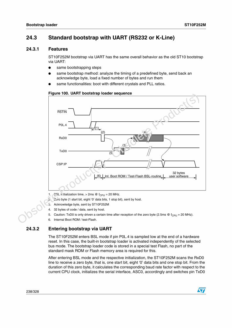
Bootstrap loader ST10F252M
238/328
24.3 Standard bootstrap with UART (RS232 or K-Line)
24.3.1 Features
ST10F252M bootstrap via UART has the same overall behavior as the old ST10 bootstrap via UART:
● same bootstrapping steps
● same bootstrap method: analyze the timing of a predefined byte, send back an acknowledge byte, load a fixed number of bytes and run them
● same functionalities: boot with different crystals and PLL ratios.
Figure 100. UART bootstrap loader sequence
1. BSL initialization time, > 2ms @ fCPU = 20 MHz.
2. Zero byte (1 start bit, eight ‘0’ data bits, 1 stop bit), sent by host.
3. Acknowledge byte, sent by ST10F252M
4. 32 bytes of code / data, sent by host.
5. Caution: TxD0 is only driven a certain time after reception of the zero byte (2.5ms @ fCPU = 20 MHz).
6. Internal Boot ROM / test-Flash.
24.3.2 Entering bootstrap via UART
The ST10F252M enters BSL mode if pin P0L.4 is sampled low at the end of a hardware reset. In this case, the built-in bootstrap loader is activated independently of the selected bus mode. The bootstrap loader code is stored in a special test Flash, no part of the standard mask ROM or Flash memory area is required for this.
After entering BSL mode and the respective initialization, the ST10F252M scans the RxD0 line to receive a zero byte, that is, one start bit, eight ‘0’ data bits and one stop bit. From the duration of this zero byte, it calculates the corresponding baud rate factor with respect to the current CPU clock, initializes the serial interface, ASC0, accordingly and switches pin TxD0
RSTIN
TxD0
Int. Boot ROM / Test-Flash BSL-routine 32 bytes
(2)
(3)
RxD0
CSP:IP
user software
(4)
(6)
P0L.4(1)
(5)
O
bsolete Product(
s) - O
bsolete Product(
s)

ST10F252M Bootstrap loader
239/328
to output. Using this baud rate, an acknowledge byte is returned to the host that provides the loaded data.
The acknowledge byte is D5h for the ST10F252M.
24.3.3 ST10 configuration in UART BSL (RS232 or K-Line)
When the ST10F252M has entered BSL mode on UART, the following configuration is automatically set (values that deviate from the normal reset values, are marked):
Other than after a normal reset, the watchdog timer is disabled so the bootstrap loading sequence is not time limited. Pin TxD0 is configured as output, so the ST10F252M can return the acknowledge byte. Even if the internal IFlash is enabled, no code can be executed from it.
24.3.4 Loading the start-up code
After sending the acknowledge byte, the BSL enters a loop to receive 32 bytes via ASC0. These bytes are stored sequentially into locations 00’FA40h through 00’FA5Fh of the internal RAM. So up to 16 instructions may be placed into the RAM area. To execute the loaded code, the BSL jumps to location 00’FA40h, that is, the first loaded instruction. The bootstrap loading sequence is now terminated but the ST10F252M remains in BSL mode. Most probably, the initially loaded routine will load additional code or data, as an average application is likely to require substantially more than 16 instructions. This second receive loop may directly use the pre-initialized interface ASC0 to receive data and store it to arbitrary user-defined locations.
This second level of loaded code may be the final application code. It may also be another, more sophisticated, loader routine that adds a transmission protocol to enhance the integrity
Table 126. Register configuration in UART BSL
Register Value Notes
Watchdog Timer: Disabled
Register SYSCON: 0400h (1)
1. In bootstrap modes (standard or alternate), ROMEN, bit 10 of SYSCON, is always set regardless of EA pin level. BYTDIS, bit 9 of SYSCON, is set according to data bus width selection via PORT0 configuration.
Context Pointer CP: FA00h
Register STKUN: FA00h
Stack Pointer SP: FA40h
Register STKOV: FC00h
Register S0CON: 8011h
Register BUSCON0: acc. to startup configuration(2)
2. BUSCON0 is initialized with 0000h, external bus disabled, if pin EA is high during reset. If pin EA is low during reset, BUSACT0, bit 10, and ALECTL0, bit 9, are set enabling the external bus with lengthened ALE signal. BTYP field, bit 7 and 6, is set according to PORT0 configuration.
Register S0BG: acc. to ‘00’ byte
P3.10 / TXD0: ‘1’
DP3.10: ‘1’
O
bsolete Product(
s) - O
bsolete Product(
s)

Bootstrap loader ST10F252M
240/328
of the loaded code or data. It may also contain a code sequence to change the system configuration and enable the bus interface to store the received data into external memory.
This process may go through several iterations or may directly execute the final application. In all cases the ST10F252M still runs in BSL mode, that is, with the watchdog timer disabled and limited access to the internal Flash area. All code fetches from the IFlash area (01’0000h...08’FFFFh, if mapped to segment 1) are redirected to the special test Flash. Data read operations access the internal Flash of the ST10F252M, if any is available, but will return undefined data on ROM-less devices.
24.3.5 Choosing the baud rate for the BSL via UART
The calculation of the serial baud rate for ASC0 from the length of the first zero byte that is received allows the operation of the bootstrap loader of the ST10F252M with a wide range of baud rates. However, the upper and lower limits have to be kept, to insure proper data transfer.
The ST10F252M uses timer T6 to measure the length of the initial zero byte. The quantization uncertainty of this measurement implies the first deviation from the real baud rate, the next deviation is implied by the computation of the S0BRL reload value from the timer contents. The formula below shows the association:
For a correct data transfer from the host to the ST10F252M the maximum deviation between the internal initialized baudrate for ASC0 and the real baud rate of the host should be below 2.5%. The deviation (FB, in percent) between host baud rate and ST10F252M baud rate can be calculated via the formula below
Note: Function (FB) does not consider the tolerances of oscillators and other devices supporting the serial communication.
This baud rate deviation is a nonlinear function depending on the CPU clock and the baud rate of the host. The maxima of the function (FB) increases with the host baud rate due to the smaller baud rate pre-scaler factors and the implied higher quantization error (see Figure 101).
Figure 101. Baudrate deviation between host and ST10F252M
fCPU32 S0BRL 1+( )⋅---------------------------------------------BST10F252M =
S0BRL T6 36–72
--------------------= T6 94--
fCPUBHost---------------⋅=,
FBBContr BHost–
BContr---------------------------------------- 100⋅= % FB 2.5≤ %,
BLow
2.5%
FB
BHigh
I
II
BHOST
O
bsolete Product(
s) - O
bsolete Product(
s)
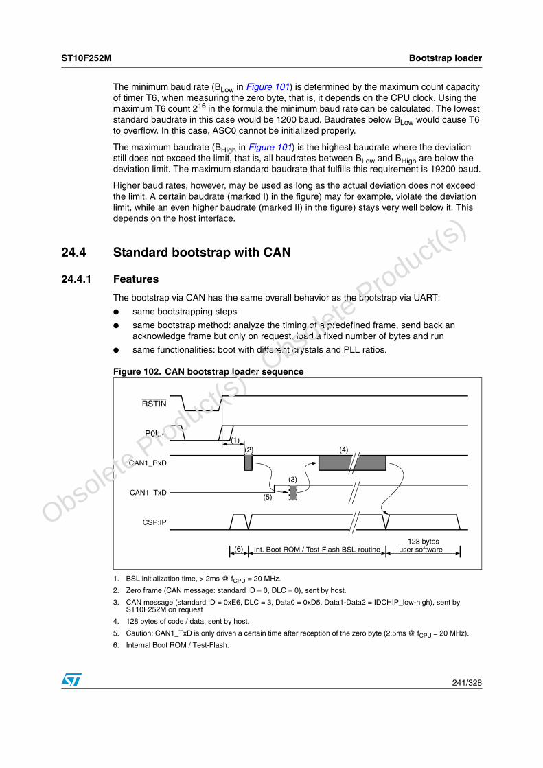
ST10F252M Bootstrap loader
241/328
The minimum baud rate (BLow in Figure 101) is determined by the maximum count capacity of timer T6, when measuring the zero byte, that is, it depends on the CPU clock. Using the maximum T6 count 216 in the formula the minimum baud rate can be calculated. The lowest standard baudrate in this case would be 1200 baud. Baudrates below BLow would cause T6 to overflow. In this case, ASC0 cannot be initialized properly.
The maximum baudrate (BHigh in Figure 101) is the highest baudrate where the deviation still does not exceed the limit, that is, all baudrates between BLow and BHigh are below the deviation limit. The maximum standard baudrate that fulfills this requirement is 19200 baud.
Higher baud rates, however, may be used as long as the actual deviation does not exceed the limit. A certain baudrate (marked I) in the figure) may for example, violate the deviation limit, while an even higher baudrate (marked II) in the figure) stays very well below it. This depends on the host interface.
24.4 Standard bootstrap with CAN
24.4.1 Features
The bootstrap via CAN has the same overall behavior as the bootstrap via UART:
● same bootstrapping steps
● same bootstrap method: analyze the timing of a predefined frame, send back an acknowledge frame but only on request, load a fixed number of bytes and run
● same functionalities: boot with different crystals and PLL ratios.
Figure 102. CAN bootstrap loader sequence
1. BSL initialization time, > 2ms @ fCPU = 20 MHz.
2. Zero frame (CAN message: standard ID = 0, DLC = 0), sent by host.
3. CAN message (standard ID = 0xE6, DLC = 3, Data0 = 0xD5, Data1-Data2 = IDCHIP_low-high), sent by ST10F252M on request
4. 128 bytes of code / data, sent by host.
5. Caution: CAN1_TxD is only driven a certain time after reception of the zero byte (2.5ms @ fCPU = 20 MHz).
6. Internal Boot ROM / Test-Flash.
RSTIN
CAN1_TxD
Int. Boot ROM / Test-Flash BSL-routine 128 bytes
(2)
(3)
CAN1_RxD
CSP:IP
user software
(4)
(6)
P0L.4(1)
(5)
O
bsolete Product(
s) - O
bsolete Product(
s)

Bootstrap loader ST10F252M
242/328
The Bootstrap Loader may be used to load the complete application software into ROM-less systems, it may load temporary software into complete systems for testing or calibration, it may also be used to load a programming routine for Flash devices.
The BSL mechanism may be used for standard system start-up as well as only for special occasions like system maintenance (firmware update) or end-of-line programming or testing.
24.4.2 Entering the CAN bootstrap loader (BSL)
The ST10F252M enters BSL mode, if pin P0L.4 is sampled low at the end of a hardware reset. In this case, the built-in bootstrap loader is activated independently of the selected bus mode. The bootstrap loader code is stored in a special test Flash, no part of the standard mask ROM or Flash memory area is required for this.
After entering BSL mode and completing the initialization, the ST10F252M scans the CAN1_TxD line to receive the following initialization frame:
● standard identifier = 0x0
● DLC = 0x0.
As all the bits to be transmitted are dominant bits, a succession of five dominant bits and one stuff bit on the CAN network is used. From the duration of this frame, it calculates the corresponding baud rate factor with respect to the current CPU clock, initializes the CAN1 interface accordingly, switches pin CAN1_TxD to output and enables the CAN1 interface to take part in the network communication. Using this baud rate, a message object is configured to send an acknowledge frame. The ST10F252M does not send this message object but the host can request it by sending a remote frame.
The acknowledge frame is the following for the ST10F252M:
● standard identifier = 0xE6
● DLC = 0x3
● Data0 = 0xD5, that is, generic acknowledge of the ST10 devices
● Data1 = IDCHIP least significant byte
● Data2 = IDCHIP most significant byte
For the ST10F252M, IDCHIP = 0FCXh.
Note: Two behaviors can be distinguished in the acknowledging of the ST10 to the host. If the host is behaving according to the CAN protocol, as at the beginning, the ST10 CAN is not configured, the host is alone on the CAN network and will not get any acknowledgement. It automatically resends the zero frame. As soon as the ST10 CAN is configured, it acknowledges the zero frame. The “acknowledge frame” with identifier 0xE6 is configured, but the transmit request is not set. The host can request this frame to be sent and, therefore, get the IDCHIP by sending a remote frame.
As the IDCHIP is sent in the acknowledge frame, the Flash programming software can now know immediately the exact type of device to be programmed.
24.4.3 ST10 configuration in CAN BSL
When the ST10F252M enters BSL mode via CAN, the following configuration is automatically set (values that deviate from the normal reset values, are marked):
O
bsolete Product(
s) - O
bsolete Product(
s)

ST10F252M Bootstrap loader
243/328
The watchdog timer is disabled, so the bootstrap loading sequence is not time limited. Pin CAN1_TxD is configured as output, so the ST10F252M can return the identification frame. Even if the internal Flash is enabled, no code can be executed from it.
24.4.4 Loading the startup code via CAN
After sending the acknowledge byte the BSL enters a loop to receive 128 bytes via CAN1.
Hint: the number of bytes loaded when booting via the CAN interface has been extended to 128 bytes to allow the re-configuration of the CAN bit timing register with the best timings (synchronization window, ...). This can be achieved by the following sequence of instructions:
These 128 bytes are stored sequentially into locations 00’FA40h through 00’FABFh of the internal RAM (DPRAM). Up to 64 instructions may be placed into the RAM area. To execute the loaded code, the BSL jumps to location 00’FA40h, that is, the first loaded instruction. The bootstrap loading sequence is now terminated but the ST10F252M remains in BSL mode. Most probably, the initially loaded routine loads additional code or data, as an average application is likely to require substantially more than 64 instructions. This second
Figure 103. Register configuration in CAN BSL
Register Value Notes
Watchdog Timer: Disabled
XPERCON: 042DhXRAM1-2, CAN1, XFlash andXMISC enabled
SYSCON: 0404h (1)
1. In bootstrap modes (standard or alternate), ROMEN, bit 10 of SYSCON, is always set regardless of EA pin level. BYTDIS, bit 9 of SYSCON, is set according to data bus width selection via PORT0 configuration.
XPEN bit set
Context Pointer CP: FA00h
Register STKUN: FA00h
Stack Pointer SP: FA40h
Register STKOV: FC00h
BUSCON0:according to start-up
configuration (2)
2. BUSCON0 is initialized with 0000h, external bus disabled, if pin EA is high during reset. If pin EA is low during reset, BUSACT0, bit 10, and ALECTL0, bit 9, are set enabling the external bus with lengthened ALE signal. BTYP field, bit 7 and 6, is set according to PORT0 configuration.
CAN1 Status/Control Register: 0000h
CAN1 Bit Timing Register:according to ‘Zero’
frame
P4.6 / CAN1_TxD: ‘1’
DP4.6: ‘1’
ReconfigureBaudRate:
MOV R1,#041h
MOV DPP3:0EF00h,R1 ; Put CAN in Init, enable Configuration Change
MOV R1,#01600h
MOV DPP3:0EF06h,R1 ; 1MBaud at Fcpu = 20 MHz
O
bsolete Product(
s) - O
bsolete Product(
s)

Bootstrap loader ST10F252M
244/328
receive loop may directly use the pre-initialized CAN interface to receive data and store it in arbitrary user-defined locations.
This second level of loaded code may be the final application code. It may also be another, more sophisticated, loader routine that adds a transmission protocol to enhance the integrity of the loaded code or data. It may also contain a code sequence to change the system configuration and enable the bus interface to store the received data into external memory.
This process may go through several iterations or may directly execute the final application. In all cases, the ST10F252M still runs in BSL mode, that is, with the watchdog timer disabled and limited access to the internal Flash area. All code fetches from the internal Flash area (01’0000h to 08’FFFFh) are redirected to the special test Flash. Data fetches access the internal Flash of the ST10F252M, if any is available, but return undefined data on ROM-less devices.
24.4.5 Choosing the baud rate for the BSL via CAN
The bootstrap via CAN acts in the same way than the UART bootstrap mode. When the ST10F252M is started in BSL mode, it polls the RxD0 and CAN1_RxD lines. On polling a low level on one of these lines, a timer is launched that is stopped when the line gets back to high level.
For CAN communication, the algorithm is made to receive a zero frame, that is, a standard identifier is 0x0, DLC is 0. This frame will produce the following levels: 5D, 1R, 5D, 1R, 5D, 1R, 5D, 1R, 5D, 1R, 4D, 1R, 1D, 11R. The algorithm runs the timer until the detection of the fifth recessive bit. This calculates the bit timing over the duration of 29 bits; this minimizes the error introduced by the polling.
Error induced by the polling
The code used for the polling is as follows:
Figure 104. Bit rate measurement over a predefined zero-frame
WaitCom:
JNB P4.5,CAN_Boot ; if SOF detected on CAN, then go to CAN loader
JB P3.11,WaitCom ; Wait for start bit at RXD0
BSET T6R ; Start Timer T6
....
CAN_Boot:
BSET PWMCON0.0 ; Start PWM Timer0 ; (resolution is 1 CPU clk cycle)
........
Start Stuff bit Stuff bit Stuff bit Stuff bit
Measured Time
O
bsolete Product(
s) - O
bsolete Product(
s)

ST10F252M Bootstrap loader
245/328
Therefore, the maximum error at the detection of the communication on CAN pin is:
(1 not taken + 1 taken jumps) + 1 taken jump + 1 bit set: (6) + 6 CPU clock cycles
The error at the detection for the fifth recessive bit is:
(1 taken jump) + 1 not taken jump + 1 compare + 1 bit clear: (4) + 6 CPU cycles
In the worst case, the induced error is of six CPU clock cycles. So the polling could induce an error of six timer ticks.
Error induced by the bit rate calculation
The code used for the polling is as follows:
Therefore, the maximum error at the detection of the communication on CAN pin is:
(1 not taken + 1 taken jumps) + 1 taken jump + 1 bit set: (6) + 6 CPU clock cycles
JMPR cc_UC,WaitRecessiveBit
WaitDominantBit:
JB P4.5,WaitDominantBit ; wait for end of stuff bit
WaitRecessiveBit:
JNB P4.5,WaitRecessiveBit; wait for 1st dominant bit = Stuff bit
CMPI1 R1,#5 ; Test if 5th stuff bit detected
JMPR cc_NE,WaitDominantBit; No, go back to count more
BCLR PWMCON.0 ; Stop timer; here the 5th stuff bit is detected: ; PT0 = 29 Bit_Time (25D and 4R)
WaitCom:
JNB P4.5,CAN_Boot ; if SOF detected on CAN, ; then go to CAN loader
JB P3.11,WaitCom ; Wait for start bit at RxD0
BSET T6R ; Start Timer T6
....
CAN_Boot:
BSET PWMCON0.0 ; Start PWM Timer0 ; (resolution is 1 CPU clk cycle)
JMPR cc_UC,WaitRecessiveBit
WaitDominantBit:
JB P4.5,WaitDominantBit ; wait for end of stuff bit
WaitRecessiveBit:
JNB P4.5,WaitRecessiveBit ; wait for 1st dominant bit = Stuff bit
CMPI1 R1,#5 ; Test if 5th stuff bit detected
JMPR cc_NE,WaitDominantBit ; No, go back to count more
BCLR PWMCON.0 ; Stop timer; here the 5th stuff bit is detected: ; PT0 = 29 Bit_Time (25D and 4R)
O
bsolete Product(
s) - O
bsolete Product(
s)
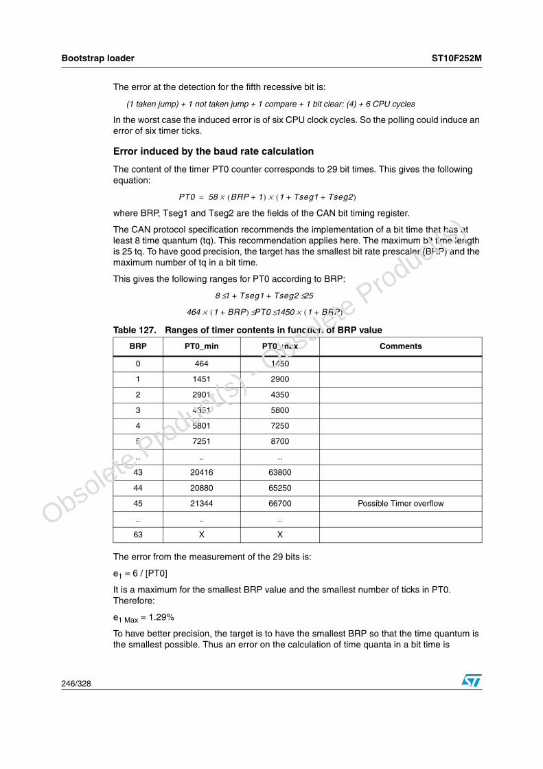
Bootstrap loader ST10F252M
246/328
The error at the detection for the fifth recessive bit is:
(1 taken jump) + 1 not taken jump + 1 compare + 1 bit clear: (4) + 6 CPU cycles
In the worst case the induced error is of six CPU clock cycles. So the polling could induce an error of six timer ticks.
Error induced by the baud rate calculation
The content of the timer PT0 counter corresponds to 29 bit times. This gives the following equation:
where BRP, Tseg1 and Tseg2 are the fields of the CAN bit timing register.
The CAN protocol specification recommends the implementation of a bit time that has at least 8 time quantum (tq). This recommendation applies here. The maximum bit time length is 25 tq. To have good precision, the target has the smallest bit rate prescaler (BRP) and the maximum number of tq in a bit time.
This gives the following ranges for PT0 according to BRP:
The error from the measurement of the 29 bits is:
e1 = 6 / [PT0]
It is a maximum for the smallest BRP value and the smallest number of ticks in PT0. Therefore:
e1 Max = 1.29%
To have better precision, the target is to have the smallest BRP so that the time quantum is the smallest possible. Thus an error on the calculation of time quanta in a bit time is
Table 127. Ranges of timer contents in function of BRP value
BRP PT0_min PT0_max Comments
0 464 1450
1 1451 2900
2 2901 4350
3 4351 5800
4 5801 7250
5 7251 8700
.. .. ..
43 20416 63800
44 20880 65250
45 21344 66700 Possible Timer overflow
.. .. ..
63 X X
PT0 58 BRP 1+( )× 1 Tseg1 Tseg2+ +( )×=
8 1 Tseg1 Tseg2 25≤+ +≤
464 1 BRP+( )× PT0 1450 1 BRP+( )×≤≤
O
bsolete Product(
s) - O
bsolete Product(
s)
ST10F252M Bootstrap loader
247/328
minimized. To do so, the value of PT0 is divided in ranges of 1450 ticks. In the algorithm, PT0 is divided by 1451 and the result is BRP.
The calculated BRP value is used to divide PT0 to have the value of (1 + Tseg1 + Tseg2). A table is generated to set the values for Tseg1 and Tseg2 according to the value of (1 + Tseg1 + Tseg2). These values of Tseg1 and Tseg2 are chosen to reach a sample point between 70% and 80% of the bit time.
During the calculation of (1 + Tseg1 + Tseg2), an error e2 can be introduced by the division. This error is a maximum of one time quantum.
To compensate any possible error on bit rate, the (re)synchronization jump width is fixed at two time quanta.
24.4.6 How to compute the baud rate error
Considering the following conditions, the error is calculated as example.
● CPU frequency: 20 MHz
● target bit rate: 1 Mbit/s
In these conditions, the content of PT0 timer for 29 Bit should be:
Therefore:
This gives:
● BRP = 0
● tq = 100 ns
Computation of 1 + Tseg1 + Tseg2 from the equation:
Thus:
In the algorithm, a rounding to the superior value is made if the remainder of the division is greater than half of the divisor. Here it would have been the case if the PT0 content was 574. Thus in this example it results 1+Tseg1+Tseg2 = 10, giving a bit time of exactly 1μs and, thus, no error in bit rate.
Note: In most cases (24 MHz, 32 MHz, 40 MHz of CPU frequency and 125, 250, 500 or 1 Mb/s of bit rate), there is no error. However, it is better to check the error with the real application parameters.
The content of the Bit Timing register is: 0x1640. This gives a sample point at 80%.
Note: The (re)synchronization jump width is fixed at two time quanta.
PT0[ ] 29 Fcpu×BitRate
---------------------------- 29 20 6× 10×1 6× 10
--------------------------------- 580===
574 PT0[ ] 586< <
PT0[ ] 58 1 BRP+( )× 1 Tseg1 Tseg2+ +( )×=
957458
---------- 1 Tseg1 Tseg2 58658
---------- 10=≤+ +≤=
O
bsolete Product(
s) - O
bsolete Product(
s)

Bootstrap loader ST10F252M
248/328
24.4.7 Bootstrap via CAN
After the bootstrap phase, the ST10F252 CAN module is configured as follow:
● the pin P4.6 is configured as output (the latch value is ‘1’ = recessive) to assume CAN1_TxD function.
● the MO2 is configured to output the acknowledge of the bootstrap with the standard identifier 0xE6, a DLC of 3 and Data0 = 0xD5, Data1 and 2 = IDCHIP.
● The MO1 is configured to receive messages with the standard identifier 0x5; its acceptance mask is set so that all bits match – the DLC received is not checked; the ST10 expects only 1 byte of data at a time.
No other message is sent by the ST10F252M after the acknowledge.
Note: The CAN boot waits for 128 byte of data instead of 32 (see UART boot). This is done in order to allow the user to reconfigure the CAN bitrate as soon as possible.
24.5 Comparing the old and the new bootstrap loaderTable 128 and 129 summarize the differences between the old ST10 (boot via UART only) bootstrap and the new one (boot via UART or CAN).
24.5.1 Software aspects
Table 128 summarizes the software differences.
As the CAN1 is needed, the XPERCON register is configured by the bootstrap loader code and bit XPEN of SYSCON is set. As long as the EINIT instruction is not executed (and it is not in the bootstrap loader code), the settings can be modified. Perform the following steps to do this:
● disable the XPeripherals by clearing XPEN in SYSCON register; this part of code must not be located in XRAM as it will be disabled
● enabled the required XPeripherals by writing the correct value in XPERCON register
● set XPEN bit in SYSCON.
Table 128. Software topics summary
Old bootstrap loader New bootstrap loader Comments
uses only 32 bytes in Dual-Port RAM from 00’FA40h
uses up to 128 bytes in Dual-Port RAM from 00’FA40h
for compatibility between boot via UART and boot via CAN1, please avoid loading the application software in the 00’FA60h/00’FABFh range
load 32 bytes from UARTload 32 bytes from UART (boot via UART mode)
same files can be used for boot via UART.
user selected Xperipherals can be enabled during boot (step 3 or step 4)
Xperipherals selection is fixed.user can change the Xperipherals selections through a specific code.
O
bsolete Product(
s) - O
bsolete Product(
s)

ST10F252M Bootstrap loader
249/328
24.5.2 Hardware aspects
Although the new bootstrap loader has been designed to be compatible with the old bootstrap loader, there are few hardware requirements with the new bootstrap loader. These are summarized in Table 129.
Table 129. Hardware topics summary
Actual bootstrap loader New bootstrap loader Comments
P4.5 and P4.6 can be used as output in BSL mode
P4.5 and P4.6 cannot be used as user output in BSL mode, but only as CAN1 alternate pins or inputs or address-segments
level on CAN1_RxD can change during boot step2
level on CAN1_RxD must be stable at ‘1’ during boot step2
external pull-up on P4.5 needed
O
bsolete Product(
s) - O
bsolete Product(
s)

Bootstrap loader ST10F252M
250/328
Figure 105. Reset Boot Sequence
Standard Start
K2 is not OK
No (P0L[5..4] = ‘11’)
K2 is OK
K1 is not OK
K1 is OK
Running from test Flash
Yes (P0L[5..4] = ‘01’)
ABM / User FlashStart at 09’0000h
Std. Bootstrap LoaderJump to Test-Flash
User Mode / User FlashStart at 00’0000h
RSTIN 0 to 1
Boot Mode?
Yes (P0L[5..4] = ‘10’)
Software ChecksUser Reset Vector
(K1 is OK?)
Software ChecksAlternate Reset Vector
(K2 is OK?)
Long Jump to09’0000h SW RESET
ST Test Modes
No (P0L[5..4] = ‘other config.’)
Selective Bootstrap LoaderJump to Test-Flash
Read 00’1FFCh
O
bsolete Product(
s) - O
bsolete Product(
s)

ST10F252M Identification registers
251/328
25 Identification registers
The ST10F252M has four Identification registers, mapped in ESFR space. These register contain:
● a manufacturer identifier
● a chip identifier, with its revision
● an internal memory and size identifier
● programming voltage description.
Manufacturer identifier register
Chip identifier register
IDMANUF register (F07Eh/3Fh) ESFR Reset value: 0403h
15 14 13 12 11 10 9 8 7 6 5 4 3 2 1 0
MANUF PROCESSID
RO RO RO RO RO RO
Table 130. Manufacturer identifier register functions
Bit Name Function
15.5 MANUFManufacturer identifier
‘020h’: STMicroelectronics manufacturer (JTAG worldwide normalization)
4.0 PROCESSIDProcess identifier‘03h’: 0.18 μm CMOS process
IDCHIP register (F07Ch/3Eh) ESFR Reset value: 0FCxh
15 14 13 12 11 10 9 8 7 6 5 4 3 2 1 0
PCONF CHIPID REVID
RO RO RO RO RO RO
Table 131. Chip identifier register functions
Bit Name Function
15.14 PCONF
Peripheral Configuration‘00’: (E) Enhanced (ST10F252)‘01’: (B) Basic‘10’: (D) Dedicated‘11’: reserved
O
bsolete Product(
s) - O
bsolete Product(
s)

Identification registers ST10F252M
252/328
Figure 106. Internal memory and size identifier register
Programming voltage description register
13.4 CHIPIDST10 Module Identifier‘0FCh’: ST10F252M Identifier (252)
3.0 REVID
ST10 Module Revision Identifier (Full Mask Set revision)‘01h’: Rev. A (First main revision)
‘02h’: Rev. B (Second main revision)
:‘0Fh’: Rev. P
IDMEM register (F07Ah/3Dh) ESFR Reset value: 2040h
15 14 13 12 11 10 9 8 7 6 5 4 3 2 1 0
MEMTYP MEMSIZE
RO RO
Table 132. Internal memory and size identifier register functions
Bit Name Function
15.12 MEMTYP
Internal memory type
‘0h’: ROM-less‘1h’: (M) ROM memory‘2h’: (S) Standard Flash memory (ST10F252M)‘3h’: (H) High performance Flash memory‘4h...Fh’: reserved.
11.0 MEMSIZInternal Memory SizeInternal Memory size is 4 * <MEMSIZE> (in Kbyte)
‘040h’: ST10F252M (256 Kbytes).
IDPROG register (F078h/3Ch) ESFR Reset value: 0040h
15 14 13 12 11 10 9 8 7 6 5 4 3 2 1 0
PROGVPP PROGVDD
RO RO
Table 133. Programming voltage description register functions
Bit Name Function
15.8 PROGVPP Programming VPP voltage (no need of external VPP) - 00h
7.0 PROGVDD
Programming VDD voltageVDD voltage when programming EPROM or Flash devices is calculated using the following formula:VDD = 20 * <PROGVDD> / 256 [V]
‘40h’: ST10F252M (5.0 V).
Table 131. Chip identifier register functions (continued)
Bit Name Function
O
bsolete Product(
s) - O
bsolete Product(
s)
ST10F252M Identification registers
253/328
The values written in the different identification register bits are valid only after the Flash initialization phase is completed. When code execution is started from internal memory (pin EA held high during reset), the Flash has certainly completed its initialization, so the bits of identification registers are immediately ready to be read out. When code execution is started from external memory (pin EA held low during reset), the Flash initialization is not yet completed, so the bits of identification registers are not ready. Poll bits 15 and 14 of the IDMEM register; when both bits read low, the Flash initialization is complete, so all identification register bits are correct.
Before Flash initialization completion, the default setting of the different Identification Registers are as follows:
IDMANUF 0403h
IDCHIP 0FCnh 0FBnh (with n representing the silicon revision number)
IDMEM F2040h
IDPROG 0040h
O
bsolete Product(
s) - O
bsolete Product(
s)

Register set ST10F252M
254/328
26 Register set
26.1 General purpose registersGeneral purpose registers (GPRs) form the register bank that the CPU works with. This register bank may be located anywhere within the internal RAM via the context pointer (CP). Due to the addressing mechanism, GPR banks can only reside within the internal RAM. All GPRs are bit-addressable.
The first eight GPRs (R7...R0) may also be accessed byte wise. Other than with SFRs, writing to a GPR byte does not affect the other byte of the respective GPR. The respective halves of the byte-accessible registers receive special names as shown in Table 135.
Table 134. General purpose registers (GPRs)
NamePhysicaladdress
8-bitaddress
DescriptionResetvalue
R0 (CP) + 0 F0h CPU General Purpose (word) Register R0 UUUUh
R1 (CP) + 2 F1h CPU General Purpose (word) Register R1 UUUUh
R2 (CP) + 4 F2h CPU General Purpose (word) Register R2 UUUUh
R3 (CP) + 6 F3h CPU General Purpose (word) Register R3 UUUUh
R4 (CP) + 8 F4h CPU General Purpose (word) Register R4 UUUUh
R5 (CP) + 10 F5h CPU General Purpose (word) Register R5 UUUUh
R6 (CP) + 12 F6h CPU General Purpose (word) Register R6 UUUUh
R7 (CP) + 14 F7h CPU General Purpose (word) Register R7 UUUUh
R8 (CP) + 16 F8h CPU General Purpose (word) Register R8 UUUUh
R9 (CP) + 18 F9h CPU General Purpose (word) Register R9 UUUUh
R10 (CP) + 20 FAh CPU General Purpose (word) Register R10 UUUUh
R11 (CP) + 22 FBh CPU General Purpose (word) Register R11 UUUUh
R12 (CP) + 24 FCh CPU General Purpose (word) Register R12 UUUUh
R13 (CP) + 26 FDh CPU General Purpose (word) Register R13 UUUUh
R14 (CP) + 28 FEh CPU General Purpose (word) Register R14 UUUUh
R15 (CP) + 30 FFh CPU General Purpose (word) Register R15 UUUUh
Table 135. General purpose registers (GPRs) bit wise addressing
NamePhysicaladdress
8-bitaddress
DescriptionResetvalue
RL0 (CP) + 0 F0h CPU General Purpose (byte) Register RL0 UUh
RH0 (CP) + 1 F1h CPU General Purpose (byte) Register RH0 UUh
RL1 (CP) + 2 F2h CPU General Purpose (byte) Register RL1 UUh
RH1 (CP) + 3 F3h CPU General Purpose (byte) Register RH1 UUh
RL2 (CP) + 4 F4h CPU General Purpose (byte) Register RL2 UUh
O
bsolete Product(
s) - O
bsolete Product(
s)
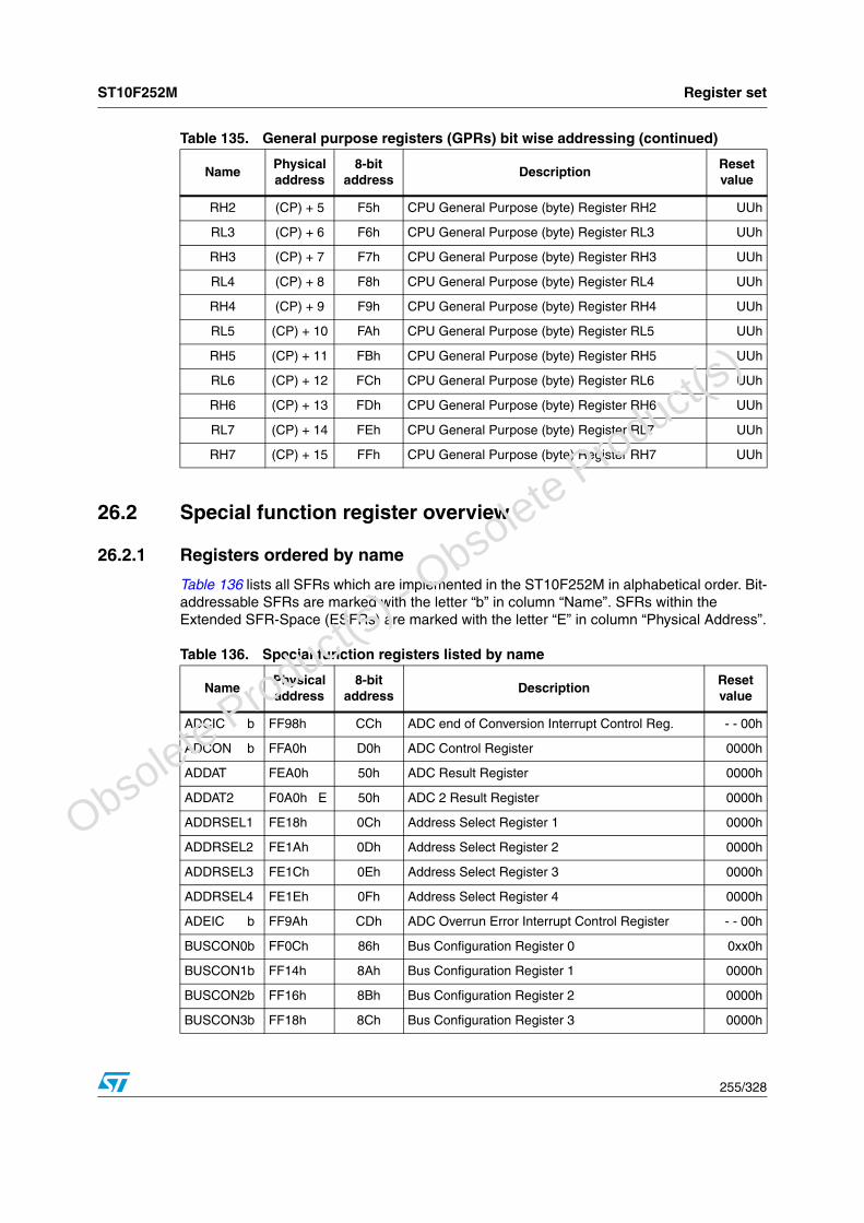
ST10F252M Register set
255/328
26.2 Special function register overview
26.2.1 Registers ordered by name
Table 136 lists all SFRs which are implemented in the ST10F252M in alphabetical order. Bit-addressable SFRs are marked with the letter “b” in column “Name”. SFRs within the Extended SFR-Space (ESFRs) are marked with the letter “E” in column “Physical Address”.
RH2 (CP) + 5 F5h CPU General Purpose (byte) Register RH2 UUh
RL3 (CP) + 6 F6h CPU General Purpose (byte) Register RL3 UUh
RH3 (CP) + 7 F7h CPU General Purpose (byte) Register RH3 UUh
RL4 (CP) + 8 F8h CPU General Purpose (byte) Register RL4 UUh
RH4 (CP) + 9 F9h CPU General Purpose (byte) Register RH4 UUh
RL5 (CP) + 10 FAh CPU General Purpose (byte) Register RL5 UUh
RH5 (CP) + 11 FBh CPU General Purpose (byte) Register RH5 UUh
RL6 (CP) + 12 FCh CPU General Purpose (byte) Register RL6 UUh
RH6 (CP) + 13 FDh CPU General Purpose (byte) Register RH6 UUh
RL7 (CP) + 14 FEh CPU General Purpose (byte) Register RL7 UUh
RH7 (CP) + 15 FFh CPU General Purpose (byte) Register RH7 UUh
Table 135. General purpose registers (GPRs) bit wise addressing (continued)
NamePhysicaladdress
8-bitaddress
DescriptionResetvalue
Table 136. Special function registers listed by name
NamePhysicaladdress
8-bitaddress
DescriptionResetvalue
ADCIC b FF98h CCh ADC end of Conversion Interrupt Control Reg. - - 00h
ADCON b FFA0h D0h ADC Control Register 0000h
ADDAT FEA0h 50h ADC Result Register 0000h
ADDAT2 F0A0h E 50h ADC 2 Result Register 0000h
ADDRSEL1 FE18h 0Ch Address Select Register 1 0000h
ADDRSEL2 FE1Ah 0Dh Address Select Register 2 0000h
ADDRSEL3 FE1Ch 0Eh Address Select Register 3 0000h
ADDRSEL4 FE1Eh 0Fh Address Select Register 4 0000h
ADEIC b FF9Ah CDh ADC Overrun Error Interrupt Control Register - - 00h
BUSCON0b FF0Ch 86h Bus Configuration Register 0 0xx0h
BUSCON1b FF14h 8Ah Bus Configuration Register 1 0000h
BUSCON2b FF16h 8Bh Bus Configuration Register 2 0000h
BUSCON3b FF18h 8Ch Bus Configuration Register 3 0000h
O
bsolete Product(
s) - O
bsolete Product(
s)

Register set ST10F252M
256/328
BUSCON4b FF1Ah 8Dh Bus Configuration Register 4 0000h
CAPREL FE4Ah 25h GPT2 Capture/Reload Register 0000h
CC0 FE80h 40h CAPCOM Register 0 0000h
CC0IC b FF78h BCh CAPCOM Register 0 Interrupt Control Register - - 00h
CC1 FE82h 41h CAPCOM Register 1 0000h
CC1IC b FF7Ah BDh CAPCOM Register 1 Interrupt Control Register - - 00h
CC2 FE84h 42h CAPCOM Register 2 0000h
CC2IC b FF7Ch BEh CAPCOM Register 2 Interrupt Control Register - - 00h
CC3 FE86h 43h CAPCOM Register 3 0000h
CC3IC b FF7Eh BFh CAPCOM Register 3 Interrupt Control Register - - 00h
CC4 FE88h 44h CAPCOM Register 4 0000h
CC4IC b FF80h C0h CAPCOM Register 4 Interrupt Control Register - - 00h
CC5 FE8Ah 45h CAPCOM Register 5 0000h
CC5IC b FF82h C1h CAPCOM Register 5 Interrupt Control Register - - 00h
CC6 FE8Ch 46h CAPCOM Register 6 0000h
CC6IC b FF84h C2h CAPCOM Register 6 Interrupt Control Register - - 00h
CC7 FE8Eh 47h CAPCOM Register 7 0000h
CC7IC b FF86h C3h CAPCOM Register 7 Interrupt Control Register - - 00h
CC8 FE90h 48h CAPCOM Register 8 0000h
CC8IC b FF88h C4h CAPCOM Register 8 Interrupt Control Register - - 00h
CC9 FE92h 49h CAPCOM Register 9 0000h
CC9IC b FF8Ah C5h CAPCOM Register 9 Interrupt Control Register - - 00h
CC10 FE94h 4Ah CAPCOM Register 10 0000h
CC10IC b FF8Ch C6h CAPCOM Register 10 Interrupt Control Register - - 00h
CC11 FE96h 4Bh CAPCOM Register 11 0000h
CC11IC b FF8Eh C7h CAPCOM Register 11 Interrupt Control Register - - 00h
CC12 FE98h 4Ch CAPCOM Register 12 0000h
CC12IC b FF90h C8h CAPCOM Register 12 Interrupt Control Register - - 00h
CC13 FE9Ah 4Dh CAPCOM Register 13 0000h
CC13IC b FF92h C9h CAPCOM Register 13 Interrupt Control Register - - 00h
CC14 FE9Ch 4Eh CAPCOM Register 14 0000h
CC14IC b FF94h CAh CAPCOM Register 14 Interrupt Control Register - - 00h
CC15 FE9Eh 4Fh CAPCOM Register 15 0000h
CC15IC b FF96h CBh CAPCOM Register 15 Interrupt Control Register - - 00h
Table 136. Special function registers listed by name (continued)
NamePhysicaladdress
8-bitaddress
DescriptionResetvalue
O
bsolete Product(
s) - O
bsolete Product(
s)

ST10F252M Register set
257/328
CC16 FE60h 30h CAPCOM Register 16 0000h
CC16IC b F160h E B0h CAPCOM Register 16 Interrupt Control Register - - 00h
CC17 FE62h 31h CAPCOM Register 17 0000h
CC17IC b F162h E B1h CAPCOM Register 17 Interrupt Control Register - - 00h
CC18 FE64h 32h CAPCOM Register 18 0000h
CC18IC b F164h E B2h CAPCOM Register 18 Interrupt Control Register - - 00h
CC19 FE66h 33h CAPCOM Register 19 0000h
CC19IC b F166h E B3h CAPCOM Register 19 Interrupt Control Register - - 00h
CC20 FE68h 34h CAPCOM Register 20 0000h
CC20IC b F168h E B4h CAPCOM Register 20 Interrupt Control Register - - 00h
CC21 FE6Ah 35h CAPCOM Register 21 0000h
CC21IC b F16Ah E B5h CAPCOM Register 21 Interrupt Control Register - - 00h
CC22 FE6Ch 36h CAPCOM Register 22 0000h
CC22IC b F16Ch E B6h CAPCOM Register 22 Interrupt Control Register - - 00h
CC23 FE6Eh 37h CAPCOM Register 23 0000h
CC23IC b F16Eh E B7h CAPCOM Register 23 Interrupt Control Register - - 00h
CC24 FE70h 38h CAPCOM Register 24 0000h
CC24IC b F170h E B8h CAPCOM Register 24 Interrupt Control Register - - 00h
CC25 FE72h 39h CAPCOM Register 25 0000h
CC25IC b F172h E B9h CAPCOM Register 25 Interrupt Control Register - - 00h
CC26 FE74h 3Ah CAPCOM Register 26 0000h
CC26IC b F174h E BAh CAPCOM Register 26 Interrupt Control Register - - 00h
CC27 FE76h 3Bh CAPCOM Register 27 0000h
CC27IC b F176h E BBh CAPCOM Register 27 Interrupt Control Register - - 00h
CC28 FE78h 3Ch CAPCOM Register 28 0000h
CC28IC b F178h E BCh CAPCOM Register 28 Interrupt Control Register - - 00h
CC29 FE7Ah 3Dh CAPCOM Register 29 0000h
CC29IC b F184h E C2h CAPCOM Register 29 Interrupt Control Register - - 00h
CC30 FE7Ch 3Eh CAPCOM Register 30 0000h
CC30IC b F18Ch E C6h CAPCOM Register 30 Interrupt Control Register - - 00h
CC31 FE7Eh 3Fh CAPCOM Register 31 0000h
CC31IC b F194h E CAh CAPCOM Register 31 Interrupt Control Register - - 00h
CCM0 b FF52h A9h CAPCOM Mode Control Register 0 0000h
CCM1 b FF54h AAh CAPCOM Mode Control Register 1 0000h
Table 136. Special function registers listed by name (continued)
NamePhysicaladdress
8-bitaddress
DescriptionResetvalue
O
bsolete Product(
s) - O
bsolete Product(
s)

Register set ST10F252M
258/328
CCM2 b FF56h ABh CAPCOM Mode Control Register 2 0000h
CCM3 b FF58h ACh CAPCOM Mode Control Register 3 0000h
CCM4 b FF22h 91h CAPCOM Mode Control Register 4 0000h
CCM5 b FF24h 92h CAPCOM Mode Control Register 5 0000h
CCM6 b FF26h 93h CAPCOM Mode Control Register 6 0000h
CCM7 b FF28h 94h CAPCOM Mode Control Register 7 0000h
CP FE10h 08h CPU Context Pointer Register FC00h
CRIC b FF6Ah B5h GPT2 CAPREL Interrupt Control Register - - 00h
CSP FE08h 04h CPU Code Segment Pointer Register (read only) 0000h
DP0L b F100h E 80h P0L Direction Control Register - - 00h
DP0H b F102h E 81h P0h Direction Control Register - - 00h
DP1L b F104h E 82h P1L Direction Control Register - - 00h
DP1H b F106h E 83h P1h Direction Control Register - - 00h
DP2 b FFC2h E1h Port 2 Direction Control Register 0000h
DP3 b FFC6h E3h Port 3 Direction Control Register 0000h
DP4 b FFCAh E5h Port 4 Direction Control Register - - 00h
DP6 b FFCEh E7h Port 6 Direction Control Register - - 00h
DP7 b FFD2h E9h Port 7 Direction Control Register - - 00h
DP8 b FFD6h EBh Port 8 Direction Control Register - - 00h
DPP0 FE00h 00h CPU Data Page Pointer 0 Register (10-bit) 0000h
DPP1 FE02h 01h CPU Data Page Pointer 1 Register (10-bit) 0001h
DPP2 FE04h 02h CPU Data Page Pointer 2 Register (10-bit) 0002h
DPP3 FE06h 03h CPU Data Page Pointer 3 Register (10-bit) 0003h
EXICON b F1C0h E E0h External Interrupt Control Register 0000h
EXISEL b F1DAh E EDh External Interrupt Source Selection Register 0000h
IDCHIP F07Ch E 3Eh Device Identifier Register (n is the device revision) FBnh
IDMANUF F07Eh E 3Fh Manufacturer Identifier Register 0403h
IDMEM F07Ah E 3Dh On-chip Memory Identifier Register 2040h
IDPROG F078h E 3Ch Programming Voltage Identifier Register 0040h
IDX0 b FF08h 84h MAC Unit Address Pointer 0 0000h
IDX1 b FF0Ah 85h MAC Unit Address Pointer 1 0000h
MAH FE5Eh 2Fh MAC Unit Accumulator - High Word 0000h
MAL FE5Ch 2Eh MAC Unit Accumulator - Low Word 0000h
MCW b FFDCh EEh MAC Unit Control Word 0000h
Table 136. Special function registers listed by name (continued)
NamePhysicaladdress
8-bitaddress
DescriptionResetvalue
O
bsolete Product(
s) - O
bsolete Product(
s)

ST10F252M Register set
259/328
MDC b FF0Eh 87h CPU Multiply Divide Control Register 0000h
MDH FE0Ch 06h CPU Multiply Divide Register – High Word 0000h
MDL FE0Eh 07h CPU Multiply Divide Register – Low Word 0000h
MRW b FFDAh EDh MAC Unit Repeat Word 0000h
MSW b FFDEh EFh MAC Unit Status Word 0200h
ODP2 b F1C2h E E1h Port 2 Open Drain Control Register 0000h
ODP3 b F1C6h E E3h Port 3 Open Drain Control Register 0000h
ODP4 b F1CAh E E5h Port 4 Open Drain Control Register - - 00h
ODP6 b F1CEh E E7h Port 6 Open Drain Control Register - - 00h
ODP7 b F1D2h E E9h Port 7 Open Drain Control Register - - 00h
ODP8 b F1D6h E EBh Port 8 Open Drain Control Register - - 00h
ONES b FF1Eh 8Fh Constant Value 1’s Register (read only) FFFFh
P0L b FF00h 80h PORT0 Low Register (Lower half of PORT0) - - 00h
P0H b FF02h 81h PORT0 High Register (Upper half of PORT0) - - 00h
P1L b FF04h 82h PORT1 Low Register (Lower half of PORT1) - - 00h
P1H b FF06h 83h PORT1 High Register (Upper half of PORT1) - - 00h
P2 b FFC0h E0h Port 2 Register 0000h
P3 b FFC4h E2h Port 3 Register 0000h
P4 b FFC8h E4h Port 4 Register (8-bit) - - 00h
P5 b FFA2h D1h Port 5 Register (read only) XXXXh
P6 b FFCCh E6h Port 6 Register (8-bit) - - 00h
P7 b FFD0h E8h Port 7 Register (8-bit) - - 00h
P8 b FFD4h EAh Port 8 Register (8-bit) - - 00h
P5DIDIS b FFA4h D2h Port 5 Digital Disable Register 0000h
PECC0 FEC0h 60h PEC Channel 0 Control Register 0000h
PECC1 FEC2h 61h PEC Channel 1 Control Register 0000h
PECC2 FEC4h 62h PEC Channel 2 Control Register 0000h
PECC3 FEC6h 63h PEC Channel 3 Control Register 0000h
PECC4 FEC8h 64h PEC Channel 4 Control Register 0000h
PECC5 FECAh 65h PEC Channel 5 Control Register 0000h
PECC6 FECCh 66h PEC Channel 6 Control Register 0000h
PECC7 FECEh 67h PEC Channel 7 Control Register 0000h
PICON b F1C4h E E2h Port Input Threshold Control Register - - 00h
PP0 F038h E 1Ch PWM Module Period Register 0 0000h
Table 136. Special function registers listed by name (continued)
NamePhysicaladdress
8-bitaddress
DescriptionResetvalue
O
bsolete Product(
s) - O
bsolete Product(
s)

Register set ST10F252M
260/328
PP1 F03Ah E 1Dh PWM Module Period Register 1 0000h
PP2 F03Ch E 1Eh PWM Module Period Register 2 0000h
PP3 F03Eh E 1Fh PWM Module Period Register 3 0000h
PSW b FF10h 88h CPU Program Status Word 0000h
PT0 F030h E 18h PWM Module Up/Down Counter 0 0000h
PT1 F032h E 19h PWM Module Up/Down Counter 1 0000h
PT2 F034h E 1Ah PWM Module Up/Down Counter 2 0000h
PT3 F036h E 1Bh PWM Module Up/Down Counter 3 0000h
PW0 FE30h 18h PWM Module Pulse Width Register 0 0000h
PW1 FE32h 19h PWM Module Pulse Width Register 1 0000h
PW2 FE34h 1Ah PWM Module Pulse Width Register 2 0000h
PW3 FE36h 1Bh PWM Module Pulse Width Register 3 0000h
PWMCON0b FF30h 98h PWM Module Control Register 0 0000h
PWMCON1b FF32h 99h PWM Module Control Register 1 0000h
PWMIC b F17Eh E BFh PWM Module Interrupt Control Register - - 00h
QR0 F004h E 02h MAC Unit Offset Register R0 0000h
QR1 F006h E 03h MAC Unit Offset Register R1 0000h
QX0 F000h E 00h MAC Unit Offset Register X0 0000h
QX1 F002h E 01h MAC Unit Offset Register X1 0000h
RP0H b F108h E 84h System Start-up Configuration Register (read only) - - XXh
S0BG FEB4h5Ah
Serial Channel 0 Baud Rate Generator Reload Register
0000h
S0CON b FFB0h D8h Serial Channel 0 Control Register 0000h
S0EIC b FF70h B8h Serial Channel 0 Error Interrupt Control Register - - 00h
S0RBUF FEB2h59h
Serial Channel 0 Receive Buffer Register (read only)
- - XXh
S0RIC b FF6EhB7h
Serial Channel 0 Receive Interrupt Control Register
- - 00h
S0TBIC b F19Ch ECEh
Serial Channel 0 Transmit Buffer Interrupt Control Reg.
- - 00h
S0TBUF FEB0h58h
Serial Channel 0 Transmit Buffer Register (write only)
0000h
S0TIC b FF6ChB6h
Serial Channel 0 Transmit Interrupt Control Register
- - 00h
SP FE12h 09h CPU System Stack Pointer Register FC00h
SSCBR F0B4h E 5Ah SSC Baud Rate Register 0000h
Table 136. Special function registers listed by name (continued)
NamePhysicaladdress
8-bitaddress
DescriptionResetvalue
O
bsolete Product(
s) - O
bsolete Product(
s)

ST10F252M Register set
261/328
SSCCON b FFB2h D9h SSC Control Register 0000h
SSCEIC b FF76h BBh SSC Error Interrupt Control Register - - 00h
SSCRB F0B2h E 59h SSC Receive Buffer (read only) XXXXh
SSCRIC b FF74h BAh SSC Receive Interrupt Control Register - - 00h
SSCTB F0B0h E 58h SSC Transmit Buffer (write only) 0000h
SSCTIC b FF72h B9h SSC Transmit Interrupt Control Register - - 00h
STKOV FE14h 0Ah CPU Stack Overflow Pointer Register FA00h
STKUN FE16h 0Bh CPU Stack Underflow Pointer Register FC00h
SYSCON b FF12h 89h CPU System Configuration Register 0xx0h 1)
T0 FE50h 28h CAPCOM Timer 0 Register 0000h
T01CON b FF50h A8h CAPCOM Timer 0 and Timer 1 Control Register 0000h
T0IC b FF9Ch CEh CAPCOM Timer 0 Interrupt Control Register - - 00h
T0REL FE54h 2Ah CAPCOM Timer 0 Reload Register 0000h
T1 FE52h 29h CAPCOM Timer 1 Register 0000h
T1IC b FF9Eh CFh CAPCOM Timer 1 Interrupt Control Register - - 00h
T1REL FE56h 2Bh CAPCOM Timer 1 Reload Register 0000h
T2 FE40h 20h GPT1 Timer 2 Register 0000h
T2CON b FF40h A0h GPT1 Timer 2 Control Register 0000h
T2IC b FF60h B0h GPT1 Timer 2 Interrupt Control Register - - 00h
T3 FE42h 21h GPT1 Timer 3 Register 0000h
T3CON b FF42h A1h GPT1 Timer 3 Control Register 0000h
T3IC b FF62h B1h GPT1 Timer 3 Interrupt Control Register - - 00h
T4 FE44h 22h GPT1 Timer 4 Register 0000h
T4CON b FF44h A2h GPT1 Timer 4 Control Register 0000h
T4IC b FF64h B2h GPT1 Timer 4 Interrupt Control Register - - 00h
T5 FE46h 23h GPT2 Timer 5 Register 0000h
T5CON b FF46h A3h GPT2 Timer 5 Control Register 0000h
T5IC b FF66h B3h GPT2 Timer 5 Interrupt Control Register - - 00h
T6 FE48h 24h GPT2 Timer 6 Register 0000h
T6CON b FF48h A4h GPT2 Timer 6 Control Register 0000h
T6IC b FF68h B4h GPT2 Timer 6 Interrupt Control Register - - 00h
T7 F050h E 28h CAPCOM Timer 7 Register 0000h
T78CON b FF20h 90h CAPCOM Timer 7 and 8 Control Register 0000h
T7IC b F17Ah E BDh CAPCOM Timer 7 Interrupt Control Register - - 00h
Table 136. Special function registers listed by name (continued)
NamePhysicaladdress
8-bitaddress
DescriptionResetvalue
O
bsolete Product(
s) - O
bsolete Product(
s)
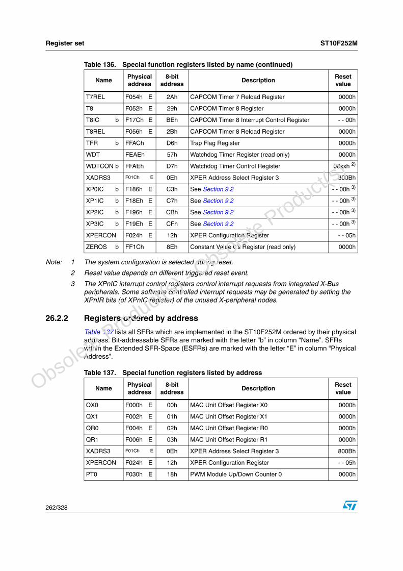
Register set ST10F252M
262/328
Note: 1 The system configuration is selected during reset.
2 Reset value depends on different triggered reset event.
3 The XPnIC interrupt control registers control interrupt requests from integrated X-Bus peripherals. Some software controlled interrupt requests may be generated by setting the XPnIR bits (of XPnIC register) of the unused X-peripheral nodes.
26.2.2 Registers ordered by address
Table 137 lists all SFRs which are implemented in the ST10F252M ordered by their physical address. Bit-addressable SFRs are marked with the letter “b” in column “Name”. SFRs within the Extended SFR-Space (ESFRs) are marked with the letter “E” in column “Physical Address”.
T7REL F054h E 2Ah CAPCOM Timer 7 Reload Register 0000h
T8 F052h E 29h CAPCOM Timer 8 Register 0000h
T8IC b F17Ch E BEh CAPCOM Timer 8 Interrupt Control Register - - 00h
T8REL F056h E 2Bh CAPCOM Timer 8 Reload Register 0000h
TFR b FFACh D6h Trap Flag Register 0000h
WDT FEAEh 57h Watchdog Timer Register (read only) 0000h
WDTCON b FFAEh D7h Watchdog Timer Control Register 00xxh 2)
XADRS3 F01Ch E 0Eh XPER Address Select Register 3 800Bh
XP0IC b F186h E C3h See Section 9.2 - - 00h 3)
XP1IC b F18Eh E C7h See Section 9.2 - - 00h 3)
XP2IC b F196h E CBh See Section 9.2 - - 00h 3)
XP3IC b F19Eh E CFh See Section 9.2 - - 00h 3)
XPERCON F024h E 12h XPER Configuration Register - - 05h
ZEROS b FF1Ch 8Eh Constant Value 0’s Register (read only) 0000h
Table 136. Special function registers listed by name (continued)
NamePhysicaladdress
8-bitaddress
DescriptionResetvalue
Table 137. Special function registers listed by address
NamePhysicaladdress
8-bitaddress
DescriptionResetvalue
QX0 F000h E 00h MAC Unit Offset Register X0 0000h
QX1 F002h E 01h MAC Unit Offset Register X1 0000h
QR0 F004h E 02h MAC Unit Offset Register R0 0000h
QR1 F006h E 03h MAC Unit Offset Register R1 0000h
XADRS3 F01Ch E 0Eh XPER Address Select Register 3 800Bh
XPERCON F024h E 12h XPER Configuration Register - - 05h
PT0 F030h E 18h PWM Module Up/Down Counter 0 0000h
O
bsolete Product(
s) - O
bsolete Product(
s)

ST10F252M Register set
263/328
PT1 F032h E 19h PWM Module Up/Down Counter 1 0000h
PT2 F034h E 1Ah PWM Module Up/Down Counter 2 0000h
PT3 F036h E 1Bh PWM Module Up/Down Counter 3 0000h
PP0 F038h E 1Ch PWM Module Period Register 0 0000h
PP1 F03Ah E 1Dh PWM Module Period Register 1 0000h
PP2 F03Ch E 1Eh PWM Module Period Register 2 0000h
PP3 F03Eh E 1Fh PWM Module Period Register 3 0000h
T7 F050h E 28h CAPCOM Timer 7 Register 0000h
T8 F052h E 29h CAPCOM Timer 8 Register 0000h
T7REL F054h E 2Ah CAPCOM Timer 7 Reload Register 0000h
T8REL F056h E 2Bh CAPCOM Timer 8 Reload Register 0000h
IDPROG F078h E 3Ch Programming Voltage Identifier Register 001740h
IDMEM F07Ah E 3Dh On-chip Memory Identifier Register 32040h
IDCHIP F07Ch E 3Eh Device Identifier Register (n is the device revision) FBnh
IDMANUF F07Eh E 3Fh Manufacturer Identifier Register 0403h
ADDAT2 F0A0h E 50h ADC 2 Result Register 0000h
SSCTB F0B0h E 58h SSC Transmit Buffer (write only) 0000h
SSCRB F0B2h E 59h SSC Receive Buffer (read only) XXXXh
SSCBR F0B4h E 5Ah SSC Baud Rate Register 0000h
DP0L b F100h E 80h P0L Direction Control Register - - 00h
DP0H b F102h E 81h P0h Direction Control Register - - 00h
DP1L b F104h E 82h P1L Direction Control Register - - 00h
DP1H b F106h E 83h P1h Direction Control Register - - 00h
RP0H b F108h E 84h System Start-up Configuration Register (read only) - - XXh
CC16IC b F160h E B0h CAPCOM Register 16 Interrupt Control Register - - 00h
CC17IC b F162h E B1h CAPCOM Register 17 Interrupt Control Register - - 00h
CC18IC b F164h E B2h CAPCOM Register 18 Interrupt Control Register - - 00h
CC19IC b F166h E B3h CAPCOM Register 19 Interrupt Control Register - - 00h
CC20IC b F168h E B4h CAPCOM Register 20 Interrupt Control Register - - 00h
CC21IC b F16Ah E B5h CAPCOM Register 21 Interrupt Control Register - - 00h
CC22IC b F16Ch E B6h CAPCOM Register 22 Interrupt Control Register - - 00h
CC23IC b F16Eh E B7h CAPCOM Register 23 Interrupt Control Register - - 00h
CC24IC b F170h E B8h CAPCOM Register 24 Interrupt Control Register - - 00h
CC25IC b F172h E B9h CAPCOM Register 25 Interrupt Control Register - - 00h
Table 137. Special function registers listed by address (continued)
NamePhysicaladdress
8-bitaddress
DescriptionResetvalue
O
bsolete Product(
s) - O
bsolete Product(
s)

Register set ST10F252M
264/328
CC26IC b F174h E BAh CAPCOM Register 26 Interrupt Control Register - - 00h
CC27IC b F176h E BBh CAPCOM Register 27 Interrupt Control Register - - 00h
CC28IC b F178h E BCh CAPCOM Register 28 Interrupt Control Register - - 00h
T7IC b F17Ah E BDh CAPCOM Timer 7 Interrupt Control Register - - 00h
T8IC b F17Ch E BEh CAPCOM Timer 8 Interrupt Control Register - - 00h
PWMIC b F17Eh E BFh PWM Module Interrupt Control Register - - 00h
CC29IC b F184h E C2h CAPCOM Register 29 Interrupt Control Register - - 00h
XP0IC b F186h E C3h See Section 9.2 - - 00h 3)
CC30IC b F18Ch E C6h CAPCOM Register 30 Interrupt Control Register - - 00h
XP1IC b F18Eh E C7h See Section 9.2 - - 00h 3)
CC31IC b F194h E CAh CAPCOM Register 31 Interrupt Control Register - - 00h
XP2IC b F196h E CBh See Section 9.2 - - 00h 3)
S0TBIC b F19Ch ECEh
Serial Channel 0 Transmit Buffer Interrupt Control Reg.
- - 00h
XP3IC b F19Eh E CFh See Section 9.2 - - 00h 3)
EXICON b F1C0h E E0h External Interrupt Control Register 0000h
ODP2 b F1C2h E E1h Port 2 Open Drain Control Register 0000h
PICON b F1C4h E E2h Port Input Threshold Control Register - - 00h
ODP3 b F1C6h E E3h Port 3 Open Drain Control Register 0000h
ODP4 b F1CAh E E5h Port 4 Open Drain Control Register - - 00h
ODP6 b F1CEh E E7h Port 6 Open Drain Control Register - - 00h
ODP7 b F1D2h E E9h Port 7 Open Drain Control Register - - 00h
ODP8 b F1D6h E EBh Port 8 Open Drain Control Register - - 00h
EXISEL b F1DAh E EDh External Interrupt Source Selection Register 0000h
DPP0 FE00h 00h CPU Data Page Pointer 0 Register (10-bit) 0000h
DPP1 FE02h 01h CPU Data Page Pointer 1 Register (10-bit) 0001h
DPP2 FE04h 02h CPU Data Page Pointer 2 Register (10-bit) 0002h
DPP3 FE06h 03h CPU Data Page Pointer 3 Register (10-bit) 0003h
CSP FE08h 04h CPU Code Segment Pointer Register (read only) 0000h
MDH FE0Ch 06h CPU Multiply Divide Register – High Word 0000h
MDL FE0Eh 07h CPU Multiply Divide Register – Low Word 0000h
CP FE10h 08h CPU Context Pointer Register FC00h
SP FE12h 09h CPU System Stack Pointer Register FC00h
STKOV FE14h 0Ah CPU Stack Overflow Pointer Register FA00h
Table 137. Special function registers listed by address (continued)
NamePhysicaladdress
8-bitaddress
DescriptionResetvalue
O
bsolete Product(
s) - O
bsolete Product(
s)

ST10F252M Register set
265/328
STKUN FE16h 0Bh CPU Stack Underflow Pointer Register FC00h
ADDRSEL1 FE18h 0Ch Address Select Register 1 0000h
ADDRSEL2 FE1Ah 0Dh Address Select Register 2 0000h
ADDRSEL3 FE1Ch 0Eh Address Select Register 3 0000h
ADDRSEL4 FE1Eh 0Fh Address Select Register 4 0000h
PW0 FE30h 18h PWM Module Pulse Width Register 0 0000h
PW1 FE32h 19h PWM Module Pulse Width Register 1 0000h
PW2 FE34h 1Ah PWM Module Pulse Width Register 2 0000h
PW3 FE36h 1Bh PWM Module Pulse Width Register 3 0000h
T2 FE40h 20h GPT1 Timer 2 Register 0000h
T3 FE42h 21h GPT1 Timer 3 Register 0000h
T4 FE44h 22h GPT1 Timer 4 Register 0000h
T5 FE46h 23h GPT2 Timer 5 Register 0000h
T6 FE48h 24h GPT2 Timer 6 Register 0000h
CAPREL FE4Ah 25h GPT2 Capture/Reload Register 0000h
T0 FE50h 28h CAPCOM Timer 0 Register 0000h
T1 FE52h 29h CAPCOM Timer 1 Register 0000h
T0REL FE54h 2Ah CAPCOM Timer 0 Reload Register 0000h
T1REL FE56h 2Bh CAPCOM Timer 1 Reload Register 0000h
MAL FE5Ch 2Eh MAC Unit Accumulator - Low Word 0000h
MAH FE5Eh 2Fh MAC Unit Accumulator - High Word 0000h
CC16 FE60h 30h CAPCOM Register 16 0000h
CC17 FE62h 31h CAPCOM Register 17 0000h
CC18 FE64h 32h CAPCOM Register 18 0000h
CC19 FE66h 33h CAPCOM Register 19 0000h
CC20 FE68h 34h CAPCOM Register 20 0000h
CC21 FE6Ah 35h CAPCOM Register 21 0000h
CC22 FE6Ch 36h CAPCOM Register 22 0000h
CC23 FE6Eh 37h CAPCOM Register 23 0000h
CC24 FE70h 38h CAPCOM Register 24 0000h
CC25 FE72h 39h CAPCOM Register 25 0000h
CC26 FE74h 3Ah CAPCOM Register 26 0000h
CC27 FE76h 3Bh CAPCOM Register 27 0000h
CC28 FE78h 3Ch CAPCOM Register 28 0000h
Table 137. Special function registers listed by address (continued)
NamePhysicaladdress
8-bitaddress
DescriptionResetvalue
O
bsolete Product(
s) - O
bsolete Product(
s)

Register set ST10F252M
266/328
CC29 FE7Ah 3Dh CAPCOM Register 29 0000h
CC30 FE7Ch 3Eh CAPCOM Register 30 0000h
CC31 FE7Eh 3Fh CAPCOM Register 31 0000h
CC0 FE80h 40h CAPCOM Register 0 0000h
CC1 FE82h 41h CAPCOM Register 1 0000h
CC2 FE84h 42h CAPCOM Register 2 0000h
CC3 FE86h 43h CAPCOM Register 3 0000h
CC4 FE88h 44h CAPCOM Register 4 0000h
CC5 FE8Ah 45h CAPCOM Register 5 0000h
CC6 FE8Ch 46h CAPCOM Register 6 0000h
CC7 FE8Eh 47h CAPCOM Register 7 0000h
CC8 FE90h 48h CAPCOM Register 8 0000h
CC9 FE92h 49h CAPCOM Register 9 0000h
CC10 FE94h 4Ah CAPCOM Register 10 0000h
CC11 FE96h 4Bh CAPCOM Register 11 0000h
CC12 FE98h 4Ch CAPCOM Register 12 0000h
CC13 FE9Ah 4Dh CAPCOM Register 13 0000h
CC14 FE9Ch 4Eh CAPCOM Register 14 0000h
CC15 FE9Eh 4Fh CAPCOM Register 15 0000h
ADDAT FEA0h 50h ADC Result Register 0000h
WDT FEAEh 57h Watchdog Timer Register (read only) 0000h
S0TBUF FEB0h58h
Serial Channel 0 Transmit Buffer Register (write only)
0000h
S0RBUF FEB2h59h
Serial Channel 0 Receive Buffer Register (read only)
- - XXh
S0BG FEB4h5Ah
Serial Channel 0 Baud Rate Generator Reload Register
0000h
PECC0 FEC0h 60h PEC Channel 0 Control Register 0000h
PECC1 FEC2h 61h PEC Channel 1 Control Register 0000h
PECC2 FEC4h 62h PEC Channel 2 Control Register 0000h
PECC3 FEC6h 63h PEC Channel 3 Control Register 0000h
PECC4 FEC8h 64h PEC Channel 4 Control Register 0000h
PECC5 FECAh 65h PEC Channel 5 Control Register 0000h
PECC6 FECCh 66h PEC Channel 6 Control Register 0000h
PECC7 FECEh 67h PEC Channel 7 Control Register 0000h
Table 137. Special function registers listed by address (continued)
NamePhysicaladdress
8-bitaddress
DescriptionResetvalue
O
bsolete Product(
s) - O
bsolete Product(
s)

ST10F252M Register set
267/328
P0L b FF00h 80h PORT0 Low Register (Lower half of PORT0) - - 00h
P0H b FF02h 81h PORT0 High Register (Upper half of PORT0) - - 00h
P1L b FF04h 82h PORT1 Low Register (Lower half of PORT1) - - 00h
P1H b FF06h 83h PORT1 High Register (Upper half of PORT1) - - 00h
IDX0 b FF08h 84h MAC Unit Address Pointer 0 0000h
IDX1 b FF0Ah 85h MAC Unit Address Pointer 1 0000h
BUSCON0b FF0Ch 86h Bus Configuration Register 0 0xx0h
MDC b FF0Eh 87h CPU Multiply Divide Control Register 0000h
PSW b FF10h 88h CPU Program Status Word 0000h
SYSCON b FF12h 89h CPU System Configuration Register 0xx0h 1)
BUSCON1b FF14h 8Ah Bus Configuration Register 1 0000h
BUSCON2b FF16h 8Bh Bus Configuration Register 2 0000h
BUSCON3b FF18h 8Ch Bus Configuration Register 3 0000h
BUSCON4b FF1Ah 8Dh Bus Configuration Register 4 0000h
ZEROS b FF1Ch 8Eh Constant Value 0’s Register (read only) 0000h
ONES b FF1Eh 8Fh Constant Value 1’s Register (read only) FFFFh
T78CON b FF20h 90h CAPCOM Timer 7 and 8 Control Register 0000h
CCM4 b FF22h 91h CAPCOM Mode Control Register 4 0000h
CCM5 b FF24h 92h CAPCOM Mode Control Register 5 0000h
CCM6 b FF26h 93h CAPCOM Mode Control Register 6 0000h
CCM7 b FF28h 94h CAPCOM Mode Control Register 7 0000h
PWMCON0b FF30h 98h PWM Module Control Register 0 0000h
PWMCON1b FF32h 99h PWM Module Control Register 1 0000h
T2CON b FF40h A0h GPT1 Timer 2 Control Register 0000h
T3CON b FF42h A1h GPT1 Timer 3 Control Register 0000h
T4CON b FF44h A2h GPT1 Timer 4 Control Register 0000h
T5CON b FF46h A3h GPT2 Timer 5 Control Register 0000h
T6CON b FF48h A4h GPT2 Timer 6 Control Register 0000h
T01CON b FF50h A8h CAPCOM Timer 0 and Timer 1 Control Register 0000h
CCM0 b FF52h A9h CAPCOM Mode Control Register 0 0000h
CCM1 b FF54h AAh CAPCOM Mode Control Register 1 0000h
CCM2 b FF56h ABh CAPCOM Mode Control Register 2 0000h
CCM3 b FF58h ACh CAPCOM Mode Control Register 3 0000h
T2IC b FF60h B0h GPT1 Timer 2 Interrupt Control Register - - 00h
Table 137. Special function registers listed by address (continued)
NamePhysicaladdress
8-bitaddress
DescriptionResetvalue
O
bsolete Product(
s) - O
bsolete Product(
s)

Register set ST10F252M
268/328
T3IC b FF62h B1h GPT1 Timer 3 Interrupt Control Register - - 00h
T4IC b FF64h B2h GPT1 Timer 4 Interrupt Control Register - - 00h
T5IC b FF66h B3h GPT2 Timer 5 Interrupt Control Register - - 00h
T6IC b FF68h B4h GPT2 Timer 6 Interrupt Control Register - - 00h
CRIC b FF6Ah B5h GPT2 CAPREL Interrupt Control Register - - 00h
S0TIC b FF6ChB6h
Serial Channel 0 Transmit Interrupt Control Register
- - 00h
S0RIC b FF6EhB7h
Serial Channel 0 Receive Interrupt Control Register
- - 00h
S0EIC b FF70h B8h Serial Channel 0 Error Interrupt Control Register - - 00h
SSCTIC b FF72h B9h SSC Transmit Interrupt Control Register - - 00h
SSCRIC b FF74h BAh SSC Receive Interrupt Control Register - - 00h
SSCEIC b FF76h BBh SSC Error Interrupt Control Register - - 00h
CC0IC b FF78h BCh CAPCOM Register 0 Interrupt Control Register - - 00h
CC1IC b FF7Ah BDh CAPCOM Register 1 Interrupt Control Register - - 00h
CC2IC b FF7Ch BEh CAPCOM Register 2 Interrupt Control Register - - 00h
CC3IC b FF7Eh BFh CAPCOM Register 3 Interrupt Control Register - - 00h
CC4IC b FF80h C0h CAPCOM Register 4 Interrupt Control Register - - 00h
CC5IC b FF82h C1h CAPCOM Register 5 Interrupt Control Register - - 00h
CC6IC b FF84h C2h CAPCOM Register 6 Interrupt Control Register - - 00h
CC7IC b FF86h C3h CAPCOM Register 7 Interrupt Control Register - - 00h
CC8IC b FF88h C4h CAPCOM Register 8 Interrupt Control Register - - 00h
CC9IC b FF8Ah C5h CAPCOM Register 9 Interrupt Control Register - - 00h
CC10IC b FF8Ch C6h CAPCOM Register 10 Interrupt Control Register - - 00h
CC11IC b FF8Eh C7h CAPCOM Register 11 Interrupt Control Register - - 00h
CC12IC b FF90h C8h CAPCOM Register 12 Interrupt Control Register - - 00h
CC13IC b FF92h C9h CAPCOM Register 13 Interrupt Control Register - - 00h
CC14IC b FF94h CAh CAPCOM Register 14 Interrupt Control Register - - 00h
CC15IC b FF96h CBh CAPCOM Register 15 Interrupt Control Register - - 00h
ADCIC b FF98h CCh ADC end of Conversion Interrupt Control Reg. - - 00h
ADEIC b FF9Ah CDh ADC Overrun Error Interrupt Control Register - - 00h
T0IC b FF9Ch CEh CAPCOM Timer 0 Interrupt Control Register - - 00h
T1IC b FF9Eh CFh CAPCOM Timer 1 Interrupt Control Register - - 00h
ADCON b FFA0h D0h ADC Control Register 0000h
P5 b FFA2h D1h Port 5 Register (read only) XXXXh
Table 137. Special function registers listed by address (continued)
NamePhysicaladdress
8-bitaddress
DescriptionResetvalue
O
bsolete Product(
s) - O
bsolete Product(
s)
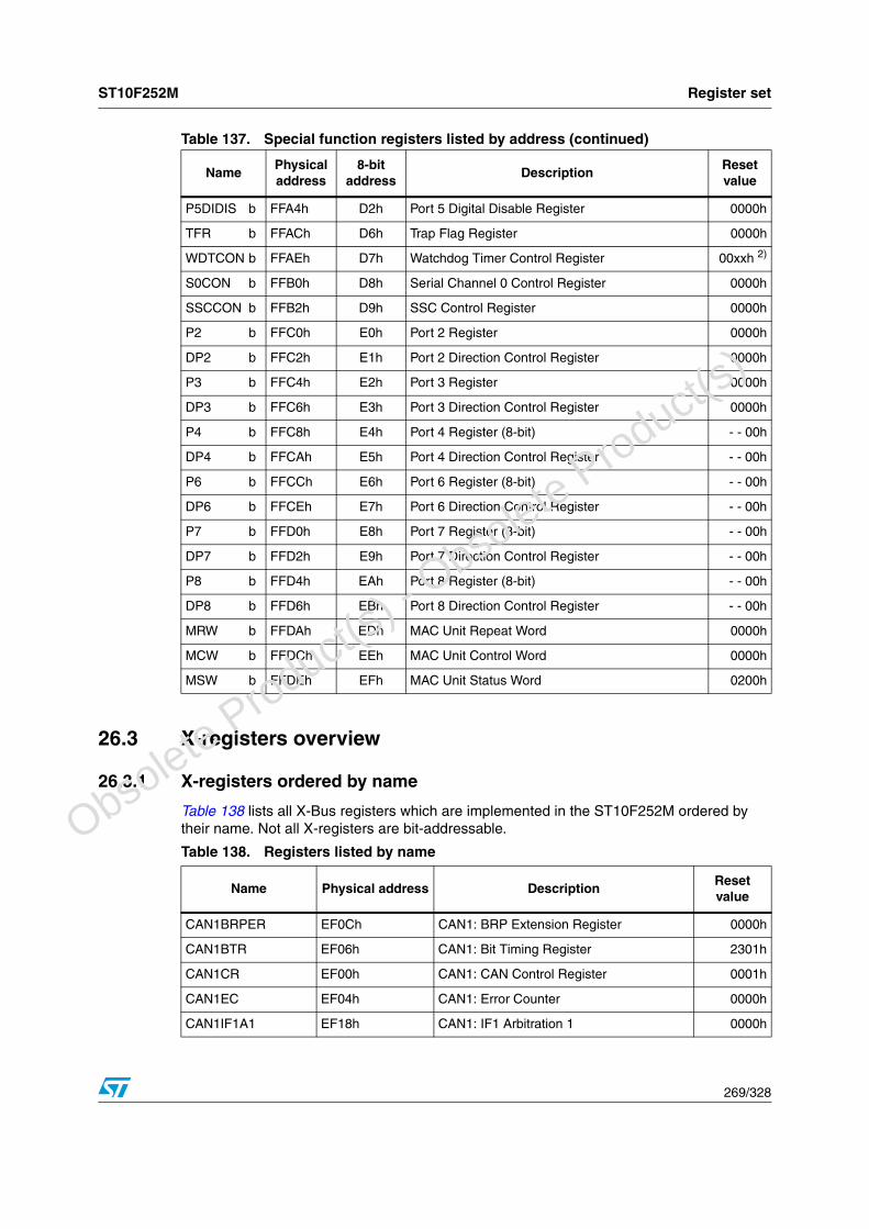
ST10F252M Register set
269/328
26.3 X-registers overview
26.3.1 X-registers ordered by name
Table 138 lists all X-Bus registers which are implemented in the ST10F252M ordered by their name. Not all X-registers are bit-addressable.
P5DIDIS b FFA4h D2h Port 5 Digital Disable Register 0000h
TFR b FFACh D6h Trap Flag Register 0000h
WDTCON b FFAEh D7h Watchdog Timer Control Register 00xxh 2)
S0CON b FFB0h D8h Serial Channel 0 Control Register 0000h
SSCCON b FFB2h D9h SSC Control Register 0000h
P2 b FFC0h E0h Port 2 Register 0000h
DP2 b FFC2h E1h Port 2 Direction Control Register 0000h
P3 b FFC4h E2h Port 3 Register 0000h
DP3 b FFC6h E3h Port 3 Direction Control Register 0000h
P4 b FFC8h E4h Port 4 Register (8-bit) - - 00h
DP4 b FFCAh E5h Port 4 Direction Control Register - - 00h
P6 b FFCCh E6h Port 6 Register (8-bit) - - 00h
DP6 b FFCEh E7h Port 6 Direction Control Register - - 00h
P7 b FFD0h E8h Port 7 Register (8-bit) - - 00h
DP7 b FFD2h E9h Port 7 Direction Control Register - - 00h
P8 b FFD4h EAh Port 8 Register (8-bit) - - 00h
DP8 b FFD6h EBh Port 8 Direction Control Register - - 00h
MRW b FFDAh EDh MAC Unit Repeat Word 0000h
MCW b FFDCh EEh MAC Unit Control Word 0000h
MSW b FFDEh EFh MAC Unit Status Word 0200h
Table 137. Special function registers listed by address (continued)
NamePhysicaladdress
8-bitaddress
DescriptionResetvalue
Table 138. Registers listed by name
Name Physical address DescriptionReset value
CAN1BRPER EF0Ch CAN1: BRP Extension Register 0000h
CAN1BTR EF06h CAN1: Bit Timing Register 2301h
CAN1CR EF00h CAN1: CAN Control Register 0001h
CAN1EC EF04h CAN1: Error Counter 0000h
CAN1IF1A1 EF18h CAN1: IF1 Arbitration 1 0000h
O
bsolete Product(
s) - O
bsolete Product(
s)

Register set ST10F252M
270/328
CAN1IF1A2 EF1Ah CAN1: IF1 Arbitration 2 0000h
CAN1IF1CM EF12h CAN1: IF1 Command Mask 0000h
CAN1IF1CR EF10h CAN1: IF1 Command Request 0001h
CAN1IF1DA1 EF1Eh CAN1: IF1 Data A 1 0000h
CAN1IF1DA2 EF20h CAN1: IF1 Data A 2 0000h
CAN1IF1DB1 EF22h CAN1: IF1 Data B 1 0000h
CAN1IF1DB2 EF24h CAN1: IF1 Data B 2 0000h
CAN1IF1M1 EF14h CAN1: IF1 Mask 1 FFFFh
CAN1IF1M2 EF16h CAN1: IF1 Mask 2 FFFFh
CAN1IF1MC EF1Ch CAN1: IF1 Message Control 0000h
CAN1IF2A1 EF48h CAN1: IF2 Arbitration 1 0000h
CAN1IF2A2 EF4Ah CAN1: IF2 Arbitration 2 0000h
CAN1IF2CM EF42h CAN1: IF2 Command Mask 0000h
CAN1IF2CR EF40h CAN1: IF2 Command Request 0001h
CAN1IF2DA1 EF4Eh CAN1: IF2 Data A 1 0000h
CAN1IF2DA2 EF50h CAN1: IF2 Data A 2 0000h
CAN1IF2DB1 EF52h CAN1: IF2 Data B 1 0000h
CAN1IF2DB2 EF54h CAN1: IF2 Data B 2 0000h
CAN1IF2M1 EF44h CAN1: IF2 Mask 1 FFFFh
CAN1IF2M2 EF46h CAN1: IF2 Mask 2 FFFFh
CAN1IF2MC EF4Ch CAN1: IF2 Message Control 0000h
CAN1IP1 EFA0h CAN1: Interrupt Pending 1 0000h
CAN1IP2 EFA2h CAN1: Interrupt Pending 2 0000h
CAN1IR EF08h CAN1: Interrupt Register 0000h
CAN1MV1 EFB0h CAN1: Message Valid 1 0000h
CAN1MV2 EFB2h CAN1: Message Valid 2 0000h
CAN1ND1 EF90h CAN1: New Data 1 0000h
CAN1ND2 EF92h CAN1: New Data 2 0000h
CAN1SR EF02h CAN1: Status Register 0000h
CAN1TR EF0Ah CAN1: Test Register 00x0h
CAN1TR1 EF80h CAN1: Transmission Request 1 0000h
CAN1TR2 EF82h CAN1: Transmission Request 2 0000h
CAN2BRPER EE0Ch CAN2: BRP Extension Register 0000h
CAN2BTR EE06h CAN2: Bit Timing Register 2301h
Table 138. Registers listed by name (continued)
Name Physical address DescriptionReset value
O
bsolete Product(
s) - O
bsolete Product(
s)

ST10F252M Register set
271/328
CAN2CR EE00h CAN2: CAN Control Register 0001h
CAN2EC EE04h CAN2: Error Counter 0000h
CAN2IF1A1 EE18h CAN2: IF1 Arbitration 1 0000h
CAN2IF1A2 EE1Ah CAN2: IF1 Arbitration 2 0000h
CAN2IF1CM EE12h CAN2: IF1 Command Mask 0000h
CAN2IF1CR EE10h CAN2: IF1 Command Request 0001h
CAN2IF1DA1 EE1Eh CAN2: IF1 Data A 1 0000h
CAN2IF1DA2 EE20h CAN2: IF1 Data A 2 0000h
CAN2IF1DB1 EE22h CAN2: IF1 Data B 1 0000h
CAN2IF1DB2 EE24h CAN2: IF1 Data B 2 0000h
CAN2IF1M1 EE14h CAN2: IF1 Mask 1 FFFFh
CAN2IF1M2 EE16h CAN2: IF1 Mask 2 FFFFh
CAN2IF1MC EE1Ch CAN2: IF1 Message Control 0000h
CAN2IF2A1 EE48h CAN2: IF2 Arbitration 1 0000h
CAN2IF2A2 EE4Ah CAN2: IF2 Arbitration 2 0000h
CAN2IF2CM EE42h CAN2: IF2 Command Mask 0000h
CAN2IF2CR EE40h CAN2: IF2 Command Request 0001h
CAN2IF2DA1 EE4Eh CAN2: IF2 Data A 1 0000h
CAN2IF2DA2 EE50h CAN2: IF2 Data A 2 0000h
CAN2IF2DB1 EE52h CAN2: IF2 Data B 1 0000h
CAN2IF2DB2 EE54h CAN2: IF2 Data B 2 0000h
CAN2IF2M1 EE44h CAN2: IF2 Mask 1 FFFFh
CAN2IF2M2 EE46h CAN2: IF2 Mask 2 FFFFh
CAN2IF2MC EE4Ch CAN2: IF2 Message Control 0000h
CAN2IP1 EEA0h CAN2: Interrupt Pending 1 0000h
CAN2IP2 EEA2h CAN2: Interrupt Pending 2 0000h
CAN2IR EE08h CAN2: Interrupt Register 0000h
CAN2MV1 EEB0h CAN2: Message Valid 1 0000h
CAN2MV2 EEB2h CAN2: Message Valid 2 0000h
CAN2ND1 EE90h CAN2: New Data 1 0000h
CAN2ND2 EE92h CAN2: New Data 2 0000h
CAN2SR EE02h CAN2: Status Register 0000h
CAN2TR EE0Ah CAN2: Test Register 00x0h
CAN2TR1 EE80h CAN2: Transmission Request 1 0000h
Table 138. Registers listed by name (continued)
Name Physical address DescriptionReset value
O
bsolete Product(
s) - O
bsolete Product(
s)

Register set ST10F252M
272/328
CAN2TR2 EE82h CAN2: Transmission Request 2 0000h
CCR1 EA06h I2C Clock Control Register 1 0000h
CCR2 EA0Eh I2C Clock Control Register 2 0000h
CR EA00h I2C Control Register 0000h
DR EA0Ch I2C Data Register 0000h
OAR1 EA08h I2C Own Address Register 1 0000h
OAR2 EA0Ah I2C Own Address Register 1 0000h
RTCAH ED14h RTC Alarm Register High Byte XXXXh
RTCAL ED12h RTC Alarm Register Low Byte XXXXh
RTCCON ED00H RTC Control Register 000Xh
RTCDH ED0Ch RTC Divider Counter High Byte XXXXh
RTCDL ED0Ah RTC Divider Counter Low Byte XXXXh
RTCH ED10h RTC Programmable Counter High Byte XXXXh
RTCL ED0Eh RTC Programmable Counter Low Byte XXXXh
RTCPH ED08h RTC Prescaler Register High Byte XXXXh
RTCPL ED06h RTC Prescaler Register Low Byte XXXXh
SR1 EA02h I2C Status Register 1 0000h
SR2 EA04h I2C Status Register 2 0000h
XCLKOUTDIV EB02h CLKOUT Divider Control Register - - 00h
XEMU0 EB76h XBUS Emulation Register 0 (write only) XXXXh
XEMU1 EB78h XBUS Emulation Register 1 (write only) XXXXh
XEMU2 EB7Ah XBUS Emulation Register 2 (write only) XXXXh
XEMU3 EB7Ch XBUS Emulation Register 3 (write only) XXXXh
XIR0CLR EB14h X-Interrupt 0 Clear Register (write only) 0000h
XIR0SEL EB10h X-Interrupt 0 Selection Register 0000h
XIR0SET EB12h X-Interrupt 0 Set Register (write only) 0000h
XIR1CLR EB24h X-Interrupt 1 Clear Register (write only) 0000h
XIR1SEL EB20h X-Interrupt 1 Selection Register 0000h
XIR1SET EB22h X-Interrupt 1 Set Register (write only) 0000h
XIR2CLR EB34h X-Interrupt 2 Clear Register (write only) 0000h
XIR2SEL EB30h X-Interrupt 2 Selection Register 0000h
XIR2SET EB32h X-Interrupt 2 Set Register (write only) 0000h
XIR3CLR EB44hX-Interrupt 3 Clear Selection Register (write only)
0000h
Table 138. Registers listed by name (continued)
Name Physical address DescriptionReset value
O
bsolete Product(
s) - O
bsolete Product(
s)

ST10F252M Register set
273/328
XIR3SEL EB40h X-Interrupt 3 Selection Register 0000h
XIR3SET EB42hX-Interrupt 3 Set Selection Register (write only)
0000h
XMISC EB46h XBUS Miscellaneous Features Register 0000h
XP0DIDIS EB36h Port 1 Digital Disable Register 0000h
XPEREMU EB7Eh XPERCON copy for Emulation (write only) XXXXh
XPICON EB26h Port Input Threshold Control Register - - 00h
XPMWCON0CLR EC08hXPWM Module Clear Control Reg. 0 (write only)
0000h
XPMWCON0SET EC06hXPWM Module Set Control Register 0 (write only)
0000h
XPMWCON1CLR EC0ChXPWM Module Clear Control Reg. 0 (write only)
0000h
XPMWCON1SET EC0AhXPWM Module Set Control Register 0 (write only)
0000h
XPOLAR EC04h XPWM Module Channel Polarity Register 0000h
XPP0 EC20h XPWM Module Period Register 0 0000h
XPP1 EC22h XPWM Module Period Register 1 0000h
XPP2 EC24h XPWM Module Period Register 2 0000h
XPP3 EC26h XPWM Module Period Register 3 0000h
XPT0 EC10h XPWM Module Up/Down Counter 0 0000h
XPT1 EC12h XPWM Module Up/Down Counter 1 0000h
XPT2 EC14h XPWM Module Up/Down Counter 2 0000h
XPT3 EC16h XPWM Module Up/Down Counter 3 0000h
XPW0 EC30h XPWM Module Pulse Width Register 0 0000h
XPW1 EC32h XPWM Module Pulse Width Register 1 0000h
XPW2 EC34h XPWM Module Pulse Width Register 2 0000h
XPW3 EC36h XPWM Module Pulse Width Register 3 0000h
XPWMCON0 EC00h XPWM Module Control Register 0 0000h
XPWMCON1 EC02h XPWM Module Control Register 1 0000h
XPWMPORT EC80h XPWM Module Port Control Register 0000h
XS1BG E906hXASC Baud Rate Generator Reload Register
0000h
XS1CON E900h XASC Control Register 0000h
XS1CONCLR E904h XASC Clear Control Register (write only) 0000h
XS1CONSET E902h XASC Set Control Register (write only) 0000h
Table 138. Registers listed by name (continued)
Name Physical address DescriptionReset value
O
bsolete Product(
s) - O
bsolete Product(
s)

Register set ST10F252M
274/328
26.3.2 X-registers ordered by address
Table 139 lists all X-Bus registers which are implemented in the ST10F252M ordered by their physical address. Not all X-registers are bit-addressable.
XS1PORT E980h XASC Port Control Register 0000h
XS1RBUF E90Ah XASC Receive Buffer Register 0000h
XS1TBUF E908h XASC Transmit Buffer Register 0000h
XSSCBR E80Ah XSSC Baud Rate Register 0000h
XSSCCON E800h XSSC Control Register 0000h
XSSCCONCLR E804h XSSC Clear Control Register (write only) 0000h
XSSCCONSET E802h XSSC Set Control Register (write only) 0000h
XSSCPORT E880h XSSC Port Control Register 0000h
XSSCRB E808h XSSC Receive Buffer XXXXh
XSSCTB E806h XSSC Transmit Buffer 0000h
Table 138. Registers listed by name (continued)
Name Physical address DescriptionReset value
Table 139. Registers listed by address
Name Physical address DescriptionReset value
XSSCCON E800h XSSC Control Register 0000h
XSSCCONSET E802h XSSC Set Control Register (write only) 0000h
XSSCCONCLR E804h XSSC Clear Control Register (write only) 0000h
XSSCTB E806h XSSC Transmit Buffer 0000h
XSSCRB E808h XSSC Receive Buffer XXXXh
XSSCBR E80Ah XSSC Baud Rate Register 0000h
XSSCPORT E880h XSSC Port Control Register 0000h
XS1CON E900h XASC Control Register 0000h
XS1CONSET E902h XASC Set Control Register (write only) 0000h
XS1CONCLR E904h XASC Clear Control Register (write only) 0000h
XS1BG E906hXASC Baud Rate Generator Reload Register
0000h
XS1TBUF E908h XASC Transmit Buffer Register 0000h
XS1RBUF E90Ah XASC Receive Buffer Register 0000h
XS1PORT E980h XASC Port Control Register 0000h
CR EA00h I2C Control Register 0000h
SR1 EA02h I2C Status Register 1 0000h
O
bsolete Product(
s) - O
bsolete Product(
s)

ST10F252M Register set
275/328
SR2 EA04h I2C Status Register 2 0000h
CCR1 EA06h I2C Clock Control Register 1 0000h
OAR1 EA08h I2C Own Address Register 1 0000h
OAR2 EA0Ah I2C Own Address Register 1 0000h
DR EA0Ch I2C Data Register 0000h
CCR2 EA0Eh I2C Clock Control Register 2 0000h
XCLKOUTDIV EB02h CLKOUT Divider Control Register - - 00h
XIR0SEL EB10h X-Interrupt 0 Selection Register 0000h
XIR0SET EB12h X-Interrupt 0 Set Register (write only) 0000h
XIR0CLR EB14h X-Interrupt 0 Clear Register (write only) 0000h
XIR1SEL EB20h X-Interrupt 1 Selection Register 0000h
XIR1SET EB22h X-Interrupt 1 Set Register (write only) 0000h
XIR1CLR EB24h X-Interrupt 1 Clear Register (write only) 0000h
XPICON EB26h Port Input Threshold Control Register - - 00h
XIR2SEL EB30h X-Interrupt 2 Selection Register 0000h
XIR2SET EB32h X-Interrupt 2 Set Register (write only) 0000h
XIR2CLR EB34h X-Interrupt 2 Clear Register (write only) 0000h
XP0DIDIS EB36h Port 1 Digital Disable Register 0000h
XIR3SEL EB40h X-Interrupt 3 Selection Register 0000h
XIR3SET EB42hX-Interrupt 3 Set Selection Register (write only)
0000h
XIR3CLR EB44hX-Interrupt 3 Clear Selection Register (write only)
0000h
XMISC EB46h XBUS Miscellaneous Features Register 0000h
XEMU0 EB76h XBUS Emulation Register 0 (write only) XXXXh
XEMU1 EB78h XBUS Emulation Register 1 (write only) XXXXh
XEMU2 EB7Ah XBUS Emulation Register 2 (write only) XXXXh
XEMU3 EB7Ch XBUS Emulation Register 3 (write only) XXXXh
XPEREMU EB7Eh XPERCON copy for Emulation (write only) XXXXh
XPWMCON0 EC00h XPWM Module Control Register 0 0000h
XPWMCON1 EC02h XPWM Module Control Register 1 0000h
XPOLAR EC04h XPWM Module Channel Polarity Register 0000h
XPMWCON0SET EC06hXPWM Module Set Control Register 0 (write only)
0000h
Table 139. Registers listed by address (continued)
Name Physical address DescriptionReset value
O
bsolete Product(
s) - O
bsolete Product(
s)

Register set ST10F252M
276/328
XPMWCON0CLR EC08hXPWM Module Clear Control Reg. 0 (write only)
0000h
XPMWCON1SET EC0AhXPWM Module Set Control Register 0 (write only)
0000h
XPMWCON1CLR EC0ChXPWM Module Clear Control Reg. 0 (write only)
0000h
XPT0 EC10h XPWM Module Up/Down Counter 0 0000h
XPT1 EC12h XPWM Module Up/Down Counter 1 0000h
XPT2 EC14h XPWM Module Up/Down Counter 2 0000h
XPT3 EC16h XPWM Module Up/Down Counter 3 0000h
XPP0 EC20h XPWM Module Period Register 0 0000h
XPP1 EC22h XPWM Module Period Register 1 0000h
XPP2 EC24h XPWM Module Period Register 2 0000h
XPP3 EC26h XPWM Module Period Register 3 0000h
XPW0 EC30h XPWM Module Pulse Width Register 0 0000h
XPW1 EC32h XPWM Module Pulse Width Register 1 0000h
XPW2 EC34h XPWM Module Pulse Width Register 2 0000h
XPW3 EC36h XPWM Module Pulse Width Register 3 0000h
XPWMPORT EC80h XPWM Module Port Control Register 0000h
RTCCON ED00H RTC Control Register 000Xh
RTCPL ED06h RTC Prescaler Register Low Byte XXXXh
RTCPH ED08h RTC Prescaler Register High Byte XXXXh
RTCDL ED0Ah RTC Divider Counter Low Byte XXXXh
RTCDH ED0Ch RTC Divider Counter High Byte XXXXh
RTCL ED0Eh RTC Programmable Counter Low Byte XXXXh
RTCH ED10h RTC Programmable Counter High Byte XXXXh
RTCAL ED12h RTC Alarm Register Low Byte XXXXh
RTCAH ED14h RTC Alarm Register High Byte XXXXh
CAN2CR EE00h CAN2: CAN Control Register 0001h
CAN2SR EE02h CAN2: Status Register 0000h
CAN2EC EE04h CAN2: Error Counter 0000h
CAN2BTR EE06h CAN2: Bit Timing Register 2301h
CAN2IR EE08h CAN2: Interrupt Register 0000h
CAN2TR EE0Ah CAN2: Test Register 00x0h
CAN2BRPER EE0Ch CAN2: BRP Extension Register 0000h
Table 139. Registers listed by address (continued)
Name Physical address DescriptionReset value
O
bsolete Product(
s) - O
bsolete Product(
s)

ST10F252M Register set
277/328
CAN2IF1CR EE10h CAN2: IF1 Command Request 0001h
CAN2IF1CM EE12h CAN2: IF1 Command Mask 0000h
CAN2IF1M1 EE14h CAN2: IF1 Mask 1 FFFFh
CAN2IF1M2 EE16h CAN2: IF1 Mask 2 FFFFh
CAN2IF1A1 EE18h CAN2: IF1 Arbitration 1 0000h
CAN2IF1A2 EE1Ah CAN2: IF1 Arbitration 2 0000h
CAN2IF1MC EE1Ch CAN2: IF1 Message Control 0000h
CAN2IF1DA1 EE1Eh CAN2: IF1 Data A 1 0000h
CAN2IF1DA2 EE20h CAN2: IF1 Data A 2 0000h
CAN2IF1DB1 EE22h CAN2: IF1 Data B 1 0000h
CAN2IF1DB2 EE24h CAN2: IF1 Data B 2 0000h
CAN2IF2CR EE40h CAN2: IF2 Command Request 0001h
CAN2IF2CM EE42h CAN2: IF2 Command Mask 0000h
CAN2IF2M1 EE44h CAN2: IF2 Mask 1 FFFFh
CAN2IF2M2 EE46h CAN2: IF2 Mask 2 FFFFh
CAN2IF2A1 EE48h CAN2: IF2 Arbitration 1 0000h
CAN2IF2A2 EE4Ah CAN2: IF2 Arbitration 2 0000h
CAN2IF2MC EE4Ch CAN2: IF2 Message Control 0000h
CAN2IF2DA1 EE4Eh CAN2: IF2 Data A 1 0000h
CAN2IF2DA2 EE50h CAN2: IF2 Data A 2 0000h
CAN2IF2DB1 EE52h CAN2: IF2 Data B 1 0000h
CAN2IF2DB2 EE54h CAN2: IF2 Data B 2 0000h
CAN2TR1 EE80h CAN2: Transmission Request 1 0000h
CAN2TR2 EE82h CAN2: Transmission Request 2 0000h
CAN2ND1 EE90h CAN2: New Data 1 0000h
CAN2ND2 EE92h CAN2: New Data 2 0000h
CAN2IP1 EEA0h CAN2: Interrupt Pending 1 0000h
CAN2IP2 EEA2h CAN2: Interrupt Pending 2 0000h
CAN2MV1 EEB0h CAN2: Message Valid 1 0000h
CAN2MV2 EEB2h CAN2: Message Valid 2 0000h
CAN1CR EF00h CAN1: CAN Control Register 0001h
CAN1SR EF02h CAN1: Status Register 0000h
CAN1EC EF04h CAN1: Error Counter 0000h
CAN1BTR EF06h CAN1: Bit Timing Register 2301h
Table 139. Registers listed by address (continued)
Name Physical address DescriptionReset value
O
bsolete Product(
s) - O
bsolete Product(
s)
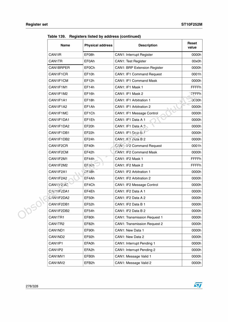
Register set ST10F252M
278/328
CAN1IR EF08h CAN1: Interrupt Register 0000h
CAN1TR EF0Ah CAN1: Test Register 00x0h
CAN1BRPER EF0Ch CAN1: BRP Extension Register 0000h
CAN1IF1CR EF10h CAN1: IF1 Command Request 0001h
CAN1IF1CM EF12h CAN1: IF1 Command Mask 0000h
CAN1IF1M1 EF14h CAN1: IF1 Mask 1 FFFFh
CAN1IF1M2 EF16h CAN1: IF1 Mask 2 FFFFh
CAN1IF1A1 EF18h CAN1: IF1 Arbitration 1 0000h
CAN1IF1A2 EF1Ah CAN1: IF1 Arbitration 2 0000h
CAN1IF1MC EF1Ch CAN1: IF1 Message Control 0000h
CAN1IF1DA1 EF1Eh CAN1: IF1 Data A 1 0000h
CAN1IF1DA2 EF20h CAN1: IF1 Data A 2 0000h
CAN1IF1DB1 EF22h CAN1: IF1 Data B 1 0000h
CAN1IF1DB2 EF24h CAN1: IF1 Data B 2 0000h
CAN1IF2CR EF40h CAN1: IF2 Command Request 0001h
CAN1IF2CM EF42h CAN1: IF2 Command Mask 0000h
CAN1IF2M1 EF44h CAN1: IF2 Mask 1 FFFFh
CAN1IF2M2 EF46h CAN1: IF2 Mask 2 FFFFh
CAN1IF2A1 EF48h CAN1: IF2 Arbitration 1 0000h
CAN1IF2A2 EF4Ah CAN1: IF2 Arbitration 2 0000h
CAN1IF2MC EF4Ch CAN1: IF2 Message Control 0000h
CAN1IF2DA1 EF4Eh CAN1: IF2 Data A 1 0000h
CAN1IF2DA2 EF50h CAN1: IF2 Data A 2 0000h
CAN1IF2DB1 EF52h CAN1: IF2 Data B 1 0000h
CAN1IF2DB2 EF54h CAN1: IF2 Data B 2 0000h
CAN1TR1 EF80h CAN1: Transmission Request 1 0000h
CAN1TR2 EF82h CAN1: Transmission Request 2 0000h
CAN1ND1 EF90h CAN1: New Data 1 0000h
CAN1ND2 EF92h CAN1: New Data 2 0000h
CAN1IP1 EFA0h CAN1: Interrupt Pending 1 0000h
CAN1IP2 EFA2h CAN1: Interrupt Pending 2 0000h
CAN1MV1 EFB0h CAN1: Message Valid 1 0000h
CAN1MV2 EFB2h CAN1: Message Valid 2 0000h
Table 139. Registers listed by address (continued)
Name Physical address DescriptionReset value
O
bsolete Product(
s) - O
bsolete Product(
s)

ST10F252M Register set
279/328
26.4 Flash control registers overview
26.4.1 Registers ordered by name
Table 140 lists all Flash control registers which are implemented in the ST10F252M ordered by their name. As these registers are physically mapped on the I-Bus, they are not bit-addressable.
26.4.2 Registers ordered by address
Table 141 lists all Flash control registers which are implemented in the ST10F252M ordered by their physical address. As these registers are physically mapped on the I-Bus, they are not bit-addressable.
Table 140. Flash registers listed by name
Name Physical address DescriptionReset value
FARH 0x0008 0012 Flash Address Register High 0000h
FARL 0x0008 0010 Flash Address Register Low 0000h
FCR0H 0x0008 0002 Flash Control Register 0 - High 0000h
FCR0L 0x0008 0000 Flash Control Register 0 - Low 0000h
FCR1H 0x0008 0006 Flash Control Register 1 - High 0000h
FCR1L 0x0008 0004 Flash Control Register 1 - Low 0000h
FDR0H 0x0008 000A Flash Data Register 0 - High FFFFh
FDR0L 0x0008 0008 Flash Data Register 0 - Low FFFFh
FDR1H 0x0008 000E Flash Data Register 1 - High FFFFh
FDR1L 0x0008 000C Flash Data Register 1 - Low FFFFh
FER 0x0008 0014 Flash Error Register 0000h
FNVAPR 0x0008 DFB8 Flash Non Volatile Access Protection Reg. 0 ACFFh
FNVWPIR-Mirror 0x0008 DFB4 Flash Non Volatile Protection I Reg. FFFFh
FNVAPR1H 0x0008 DFBEFlash Non Volatile Access Protection Reg. 1 - High
FFFFh
FNVAPR1L 0x0008 DFBCFlash Non Volatile Access Protection Reg. 1 - Low
FFFFh
FNVWPIR 0x0008 DFB0 Flash Non Volatile Protection I Reg. FFFFh
XFVTAU0 0x0000 EB50 Xbus Flash Temporary Unprotection Register 0000h
Table 141. Flash registers listed by address
Name Physical address DescriptionReset value
FCR0L 0x000B 0000 Flash Control Register 0 - Low 0000h
FCR0H 0x000B 0002 Flash Control Register 0 - High 0000h
O
bsolete Product(
s) - O
bsolete Product(
s)

Register set ST10F252M
280/328
FCR1L 0x000B 0004 Flash Control Register 1 - Low 0000h
FCR1H 0x000B 0006 Flash Control Register 1 - High 0000h
FDR0L 0x000B 0008 Flash Data Register 0 - Low FFFFh
FDR0H 0x000B 000A Flash Data Register 0 - High FFFFh
FDR1L 0x000B 000C Flash Data Register 1 - Low FFFFh
FDR1H 0x000B 000E Flash Data Register 1 - High FFFFh
FARL 0x000B 0010 Flash Address Register Low 0000h
FARH 0x000B 0012 Flash Address Register High 0000h
FER 0x000B 0014 Flash Error Register 0000h
FNVWPIRL 0x000B DFB0 Flash Non Volatile Protection I Reg. Low FFFFh
FNVAPR0 0x000B DFB8 Flash Non Volatile Access Protection Reg. 0 ACFFh
FNVAPR1L 0x000B DFBCFlash Non Volatile Access Protection Reg. 1 - Low
FFFFh
FNVAPR1H 0x000B DFBEFlash Non Volatile Access Protection Reg. 1 - High
FFFFh
XTAUR0 0x0000 EB50 Xbus Flash Temporary Unprotection Register 0000h
Table 141. Flash registers listed by address (continued)
Name Physical address DescriptionReset value
O
bsolete Product(
s) - O
bsolete Product(
s)
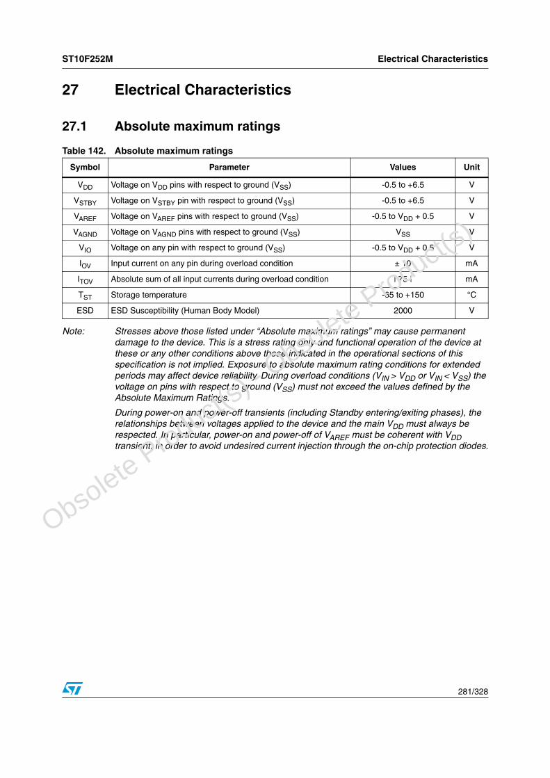
ST10F252M Electrical Characteristics
281/328
27 Electrical Characteristics
27.1 Absolute maximum ratings
Note: Stresses above those listed under “Absolute maximum ratings” may cause permanent damage to the device. This is a stress rating only and functional operation of the device at these or any other conditions above those indicated in the operational sections of this specification is not implied. Exposure to absolute maximum rating conditions for extended periods may affect device reliability. During overload conditions (VIN > VDD or VIN < VSS) the voltage on pins with respect to ground (VSS) must not exceed the values defined by the Absolute Maximum Ratings.
During power-on and power-off transients (including Standby entering/exiting phases), the relationships between voltages applied to the device and the main VDD must always be respected. In particular, power-on and power-off of VAREF must be coherent with VDD transient, in order to avoid undesired current injection through the on-chip protection diodes.
Table 142. Absolute maximum ratings
Symbol Parameter Values Unit
VDD Voltage on VDD pins with respect to ground (VSS) -0.5 to +6.5 V
VSTBY Voltage on VSTBY pin with respect to ground (VSS) -0.5 to +6.5 V
VAREF Voltage on VAREF pins with respect to ground (VSS) -0.5 to VDD + 0.5 V
VAGND Voltage on VAGND pins with respect to ground (VSS) VSS V
VIO Voltage on any pin with respect to ground (VSS) -0.5 to VDD + 0.5 V
IOV Input current on any pin during overload condition ± 10 mA
ITOV Absolute sum of all input currents during overload condition | 75 | mA
TST Storage temperature -65 to +150 °C
ESD ESD Susceptibility (Human Body Model) 2000 V
O
bsolete Product(
s) - O
bsolete Product(
s)

Electrical Characteristics ST10F252M
282/328
27.2 Recommended operating conditions
27.3 Power considerationsThe average chip-junction temperature, TJ, in degrees Celsius, may be calculated using the following equation:
TJ = TA + (PD x ΘJA) (1)
Where:
– TA is the Ambient Temperature in ° C,
– ΘJA is the Package Junction-to-Ambient Thermal Resistance, in ° C/W,
– PD is the sum of PINT and PI/O (PD = PINT + PI/O),
– PINT is the product of IDD and V18, expressed in Watt. This is the Chip Internal Power,
– PI/O represents the Power Dissipation on Input and Output Pins; User Determined.
Most of the time for the applications PI/O< PINT and may be neglected. On the other hand, PI/O may be significant if the device is configured to drive continuously external modules and/or memories.
An approximate relationship between PD and TJ (if PI/O is neglected) is given by:
PD = K / (TJ + 273°C) (2)
Therefore (solving equations 1 and 2):
K = PD x (TA + 273°C) + ΘJA x PD2 (3)
Where:
K is a constant for the particular part, which may be determined from equation (3) by measuring PD (at equilibrium) for a known TA. Using this value of K, the values of PD and TJ may be obtained by solving equations (1) and (2) iteratively for any value of TA.
Table 143. Recommended operating conditions
Symbol ParameterValue
UnitMin Max
VDD Operating supply voltage4.5 5.5 V
VSTBY Operation stand-by supply voltage(1)
1. The value of the VSTBY voltage is specified in the range of 4.5 to 5.5 volts. When VSTBY voltage is lower than main VDD, the input section of VSTBY/EA pin can generate a spurious static consumption on VDD power supply (in the range of tenth of µA).
VAREF Operating analog reference voltage(2)
2. For details on operating conditions concerning the usage of A/D Converter refer to Section 27.7.
0 VDD + 0.1 V
TA Ambient temperature under bias-40
+125°C
TJ Junction temperature under bias +150
O
bsolete Product(
s) - O
bsolete Product(
s)
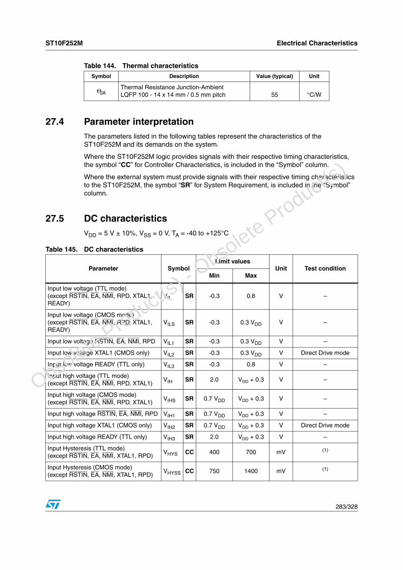
ST10F252M Electrical Characteristics
283/328
27.4 Parameter interpretationThe parameters listed in the following tables represent the characteristics of the ST10F252M and its demands on the system.
Where the ST10F252M logic provides signals with their respective timing characteristics, the symbol “CC” for Controller Characteristics, is included in the “Symbol” column.
Where the external system must provide signals with their respective timing characteristics to the ST10F252M, the symbol “SR” for System Requirement, is included in the “Symbol” column.
27.5 DC characteristicsVDD = 5 V ± 10%, VSS = 0 V, TA = -40 to +125°C
Table 144. Thermal characteristicsSymbol Description Value (typical) Unit
ΘJAThermal Resistance Junction-AmbientLQFP 100 - 14 x 14 mm / 0.5 mm pitch 55 °C/W
Table 145. DC characteristics
Parameter SymbolLimit values
Unit Test conditionMin Max
Input low voltage (TTL mode)(except RSTIN, EA, NMI, RPD, XTAL1, READY)
VIL SR -0.3 0.8 V –
Input low voltage (CMOS mode)(except RSTIN, EA, NMI, RPD, XTAL1, READY)
VILS SR -0.3 0.3 VDD V –
Input low voltage RSTIN, EA, NMI, RPD VIL1 SR -0.3 0.3 VDD V –
Input low voltage XTAL1 (CMOS only) VIL2 SR -0.3 0.3 VDD V Direct Drive mode
Input low voltage READY (TTL only) VIL3 SR -0.3 0.8 V –
Input high voltage (TTL mode)(except RSTIN, EA, NMI, RPD, XTAL1)
VIH SR 2.0 VDD + 0.3 V –
Input high voltage (CMOS mode)(except RSTIN, EA, NMI, RPD, XTAL1)
VIHS SR 0.7 VDD VDD + 0.3 V –
Input high voltage RSTIN, EA, NMI, RPD VIH1 SR 0.7 VDD VDD + 0.3 V –
Input high voltage XTAL1 (CMOS only) VIH2 SR 0.7 VDD VDD + 0.3 V Direct Drive mode
Input high voltage READY (TTL only) VIH3 SR 2.0 VDD + 0.3 V –
Input Hysteresis (TTL mode)(except RSTIN, EA, NMI, XTAL1, RPD)
VHYS CC 400 700 mV (1)
Input Hysteresis (CMOS mode)(except RSTIN, EA, NMI, XTAL1, RPD)
VHYSS CC 750 1400 mV (1)
O
bsolete Product(
s) - O
bsolete Product(
s)
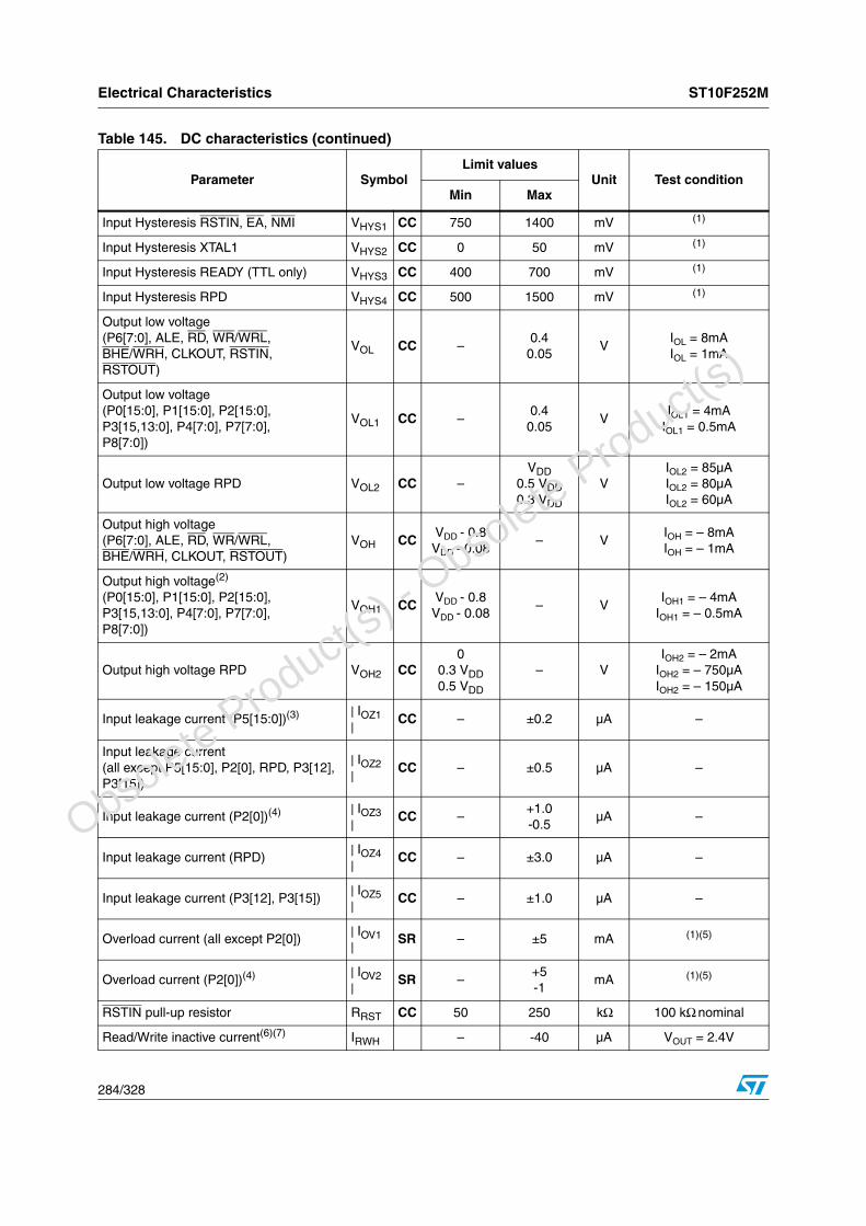
Electrical Characteristics ST10F252M
284/328
Input Hysteresis RSTIN, EA, NMI VHYS1 CC 750 1400 mV (1)
Input Hysteresis XTAL1 VHYS2 CC 0 50 mV (1)
Input Hysteresis READY (TTL only) VHYS3 CC 400 700 mV (1)
Input Hysteresis RPD VHYS4 CC 500 1500 mV (1)
Output low voltage(P6[7:0], ALE, RD, WR/WRL,BHE/WRH, CLKOUT, RSTIN,RSTOUT)
VOL CC –0.4
0.05V
IOL = 8mAIOL = 1mA
Output low voltage(P0[15:0], P1[15:0], P2[15:0],P3[15,13:0], P4[7:0], P7[7:0],P8[7:0])
VOL1 CC –0.4
0.05V
IOL1 = 4mAIOL1 = 0.5mA
Output low voltage RPD VOL2 CC –VDD
0.5 VDD0.3 VDD
VIOL2 = 85µAIOL2 = 80µAIOL2 = 60µA
Output high voltage (P6[7:0], ALE, RD, WR/WRL,BHE/WRH, CLKOUT, RSTOUT)
VOH CCVDD - 0.8VDD - 0.08
– VIOH = – 8mAIOH = – 1mA
Output high voltage(2)
(P0[15:0], P1[15:0], P2[15:0],P3[15,13:0], P4[7:0], P7[7:0],P8[7:0])
VOH1 CCVDD - 0.8VDD - 0.08
– VIOH1 = – 4mA
IOH1 = – 0.5mA
Output high voltage RPD VOH2 CC0
0.3 VDD0.5 VDD
– VIOH2 = – 2mA
IOH2 = – 750µAIOH2 = – 150µA
Input leakage current (P5[15:0])(3) | IOZ1 | CC – ±0.2 µA –
Input leakage current (all except P5[15:0], P2[0], RPD, P3[12], P3[15])
| IOZ2 | CC – ±0.5 µA –
Input leakage current (P2[0])(4) | IOZ3 | CC –
+1.0-0.5
µA –
Input leakage current (RPD)| IOZ4 | CC – ±3.0 µA –
Input leakage current (P3[12], P3[15])| IOZ5 | CC – ±1.0 µA –
Overload current (all except P2[0]) | IOV1 | SR – ±5 mA (1)(5)
Overload current (P2[0])(4) | IOV2 | SR –
+5-1
mA (1)(5)
RSTIN pull-up resistor RRST CC 50 250 kΩ 100 kΩ nominal
Read/Write inactive current(6)(7) IRWH – -40 µA VOUT = 2.4V
Table 145. DC characteristics (continued)
Parameter SymbolLimit values
Unit Test conditionMin Max
O
bsolete Product(
s) - O
bsolete Product(
s)

ST10F252M Electrical Characteristics
285/328
Read/Write active current(6)(8) IRWL -500 – µA VOUT = 0.4V
ALE inactive current(6)(7) IALEL 20 – µA VOUT = 0.4V
ALE active current(6)(8) IALEH – 300 µA VOUT = 2.4V
Port 6 inactive current (P6[4:0])(6)(7) IP6H – -40 µA VOUT = 2.4V
Port 6 active current (P6[4:0])(6)(8) IP6L -500 – µA VOUT = 0.4V
PORT0 configuration current(6)IP0H
(6) – -10 µA VIN = 2.0V
IP0L(7) -100 – µA VIN = 0.8V
Pin Capacitance (Digital inputs / outputs) CIO CC – 10 pF (1)(6)
Run Mode Power supply current(9)
(Execution from Internal RAM)ICC1 –
15 + 1.5 fCPU
mA –
Run Mode Power supply current(1)(10)
(Execution from Internal Flash)ICC2 –
15 + 1.5 fCPU
mA –
Idle mode supply current(11) IID –15 + 0.6
fCPUmA –
Power-down supply current(12)
(RTC off, Oscillators off, Main Voltage Regulator off)
IPD1 – 150 µA TA = 25°C
Power-down supply current(12)
(RTC on, Main Oscillator on, Main Voltage Regulator off)
IPD2 –400
1100µA TA = 25°C
Stand-by supply current(12)
(RTC off, Oscillators off, VDD off, VSTBY on)
ISB1
– 120 µAVSTBY = 5.5V
TA = TJ = 25°C
– 500 µAVSTBY = 5.5V
TA = TJ = 125°C
Stand-by supply current(1)(12)
(VDD transient condition)ISB3 – 2.5 mA –
1. Not 100% tested, guaranteed by design characterization.
2. This specification is not valid for outputs which are switched to open drain mode. In this case the respective output will float and the voltage is imposed by the external circuitry.
3. Port 5 leakage values are granted for not selected A/D Converter channel. One channels is always selected (by default, after reset, P5.0 is selected). For the selected channel the leakage value is similar to that of other port pins.
4. The leakage of P2.0 is higher than other pins due to the additional logic (pass gates active only in specific test modes) implemented on input path. Pay attention to not stress P2.0 input pin with negative overload beyond the specified limits: failures in Flash reading may occur (sense amplifier perturbation). Refer to next Figure 107 for a scheme of the input circuitry.
5. Overload conditions occur if the standard operating conditions are exceeded, that is, the voltage on any pin exceeds the specified range (that is, VOV > VDD + 0.3V or VOV < -0.3V). The absolute sum of input overload currents on all port pins may not exceed 50mA. The supply voltage must remain within the specified limits.
6. This specification is only valid during Reset, or during Hold- or Adapt-mode. Port 6 pins are only affected, if they are used for CS output and the open drain function is not enabled.
7. The maximum current may be drawn while the respective signal line remains inactive.
8. The minimum current must be drawn in order to drive the respective signal line active.
Table 145. DC characteristics (continued)
Parameter SymbolLimit values
Unit Test conditionMin Max
O
bsolete Product(
s) - O
bsolete Product(
s)
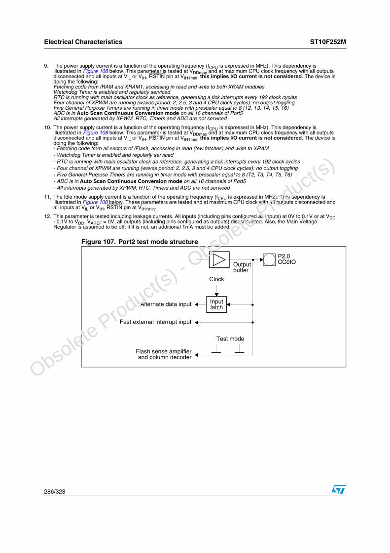
Electrical Characteristics ST10F252M
286/328
Figure 107. Port2 test mode structure
9. The power supply current is a function of the operating frequency (fCPU is expressed in MHz). This dependency is illustrated in Figure 108 below. This parameter is tested at VDDmax and at maximum CPU clock frequency with all outputs disconnected and all inputs at VIL or VIH, RSTIN pin at VIH1min: this implies I/O current is not considered. The device is doing the following: Fetching code from IRAM and XRAM1, accessing in read and write to both XRAM modulesWatchdog Timer is enabled and regularly servicedRTC is running with main oscillator clock as reference, generating a tick interrupts every 192 clock cyclesFour channel of XPWM are running (waves period: 2, 2.5, 3 and 4 CPU clock cycles): no output togglingFive General Purpose Timers are running in timer mode with prescaler equal to 8 (T2, T3, T4, T5, T6)ADC is in Auto Scan Continuous Conversion mode on all 16 channels of Port5All interrupts generated by XPWM, RTC, Timers and ADC are not serviced
10. The power supply current is a function of the operating frequency (fCPU is expressed in MHz). This dependency is illustrated in Figure 108 below. This parameter is tested at VDDmax and at maximum CPU clock frequency with all outputs disconnected and all inputs at VIL or VIH, RSTIN pin at VIH1min: this implies I/O current is not considered. The device is doing the following: - Fetching code from all sectors of IFlash, accessing in read (few fetches) and write to XRAM- Watchdog Timer is enabled and regularly serviced- RTC is running with main oscillator clock as reference, generating a tick interrupts every 192 clock cycles- Four channel of XPWM are running (waves period: 2, 2.5, 3 and 4 CPU clock cycles): no output toggling- Five General Purpose Timers are running in timer mode with prescaler equal to 8 (T2, T3, T4, T5, T6)- ADC is in Auto Scan Continuous Conversion mode on all 16 channels of Port5- All interrupts generated by XPWM, RTC, Timers and ADC are not serviced
11. The Idle mode supply current is a function of the operating frequency (fCPU is expressed in MHz). This dependency is illustrated in Figure 108 below. These parameters are tested and at maximum CPU clock with all outputs disconnected and all inputs at VIL or VIH, RSTIN pin at VIH1min.
12. This parameter is tested including leakage currents. All inputs (including pins configured as inputs) at 0V to 0.1V or at VDD - 0.1V to VDD, VAREF = 0V, all outputs (including pins configured as outputs) disconnected. Also, the Main Voltage Regulator is assumed to be off; if it is not, an additional 1mA must be added.
Inputlatch
Clock
P2.0CC0IOOutput
buffer
Test mode
Alternate data input
Fast external interrupt input
Flash sense amplifierand column decoder
O
bsolete Product(
s) - O
bsolete Product(
s)
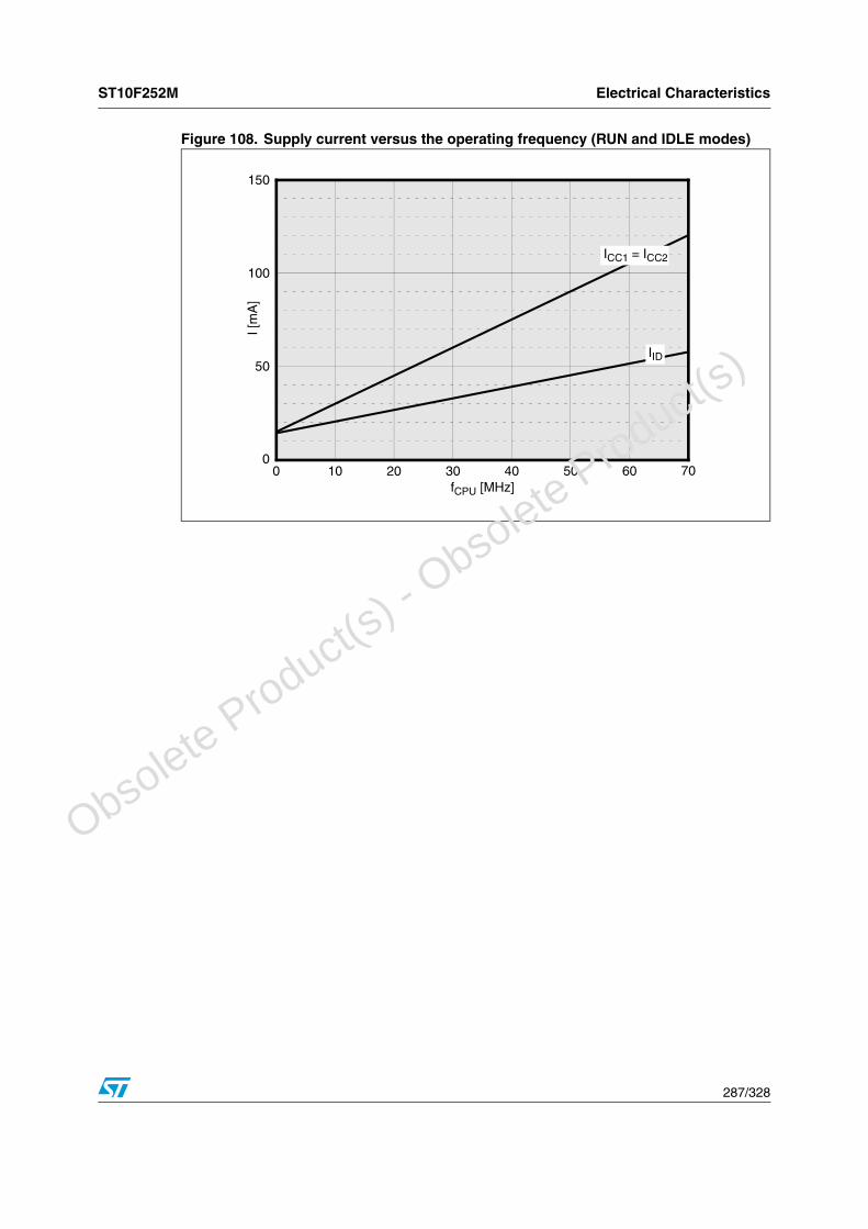
ST10F252M Electrical Characteristics
287/328
Figure 108. Supply current versus the operating frequency (RUN and IDLE modes)
I [m
A]
fCPU [MHz]10 20
150
100
50
4030 50 60 7000
IID
ICC1 = ICC2
O
bsolete Product(
s) - O
bsolete Product(
s)
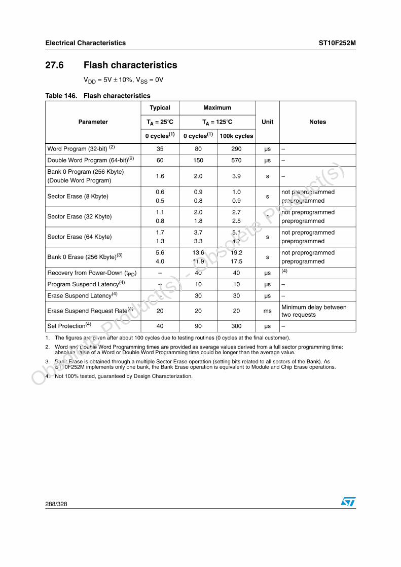
Electrical Characteristics ST10F252M
288/328
27.6 Flash characteristicsVDD = 5V ± 10%, VSS = 0V
Table 146. Flash characteristics
Parameter
Typical Maximum
Unit NotesTA = 25°C TA = 125°C
0 cycles(1) 0 cycles(1) 100k cycles
Word Program (32-bit) (2) 35 80 290 µs –
Double Word Program (64-bit)(2) 60 150 570 µs –
Bank 0 Program (256 Kbyte)
(Double Word Program)1.6 2.0 3.9 s –
Sector Erase (8 Kbyte)0.6
0.5
0.9
0.8
1.0
0.9s
not preprogrammed
preprogrammed
Sector Erase (32 Kbyte)1.10.8
2.01.8
2.72.5
snot preprogrammedpreprogrammed
Sector Erase (64 Kbyte)1.71.3
3.73.3
5.14.7
snot preprogrammedpreprogrammed
Bank 0 Erase (256 Kbyte)(3) 5.64.0
13.611.9
19.217.5
snot preprogrammedpreprogrammed
Recovery from Power-Down (tPD) – 40 40 µs (4)
Program Suspend Latency(4) – 10 10 µs –
Erase Suspend Latency(4) – 30 30 µs –
Erase Suspend Request Rate(4) 20 20 20 msMinimum delay between two requests
Set Protection(4) 40 90 300 µs –
1. The figures are given after about 100 cycles due to testing routines (0 cycles at the final customer).
2. Word and Double Word Programming times are provided as average values derived from a full sector programming time: absolute value of a Word or Double Word Programming time could be longer than the average value.
3. Bank Erase is obtained through a multiple Sector Erase operation (setting bits related to all sectors of the Bank). As ST10F252M implements only one bank, the Bank Erase operation is equivalent to Module and Chip Erase operations.
4. Not 100% tested, guaranteed by Design Characterization.
O
bsolete Product(
s) - O
bsolete Product(
s)

ST10F252M Electrical Characteristics
289/328
27.7 A/D converter characteristicsVDD = 5V ± 10%, VSS = 0V, TA = -40 to +125°C, 4.5V ≤ VAREF ≤ VDD, VSS ≤ VAGND ≤ VSS + 0.2V
Table 147. Flash data retention characteristics
Number of program / erase cycles(-40°C < TA < 125°C)
Data retention time(average ambient temperature 60°C)
256 Kbyte (code store) 64 Kbyte (EEPROM emulation)(1)
0 - 100 > 20 years > 20 years
1000 - > 20 years
10000 - 10 years
100000 - 1 year
1. Two 64 Kbyte Flash Sectors may be typically used to emulate up to 4, 8 or 16 Kbytes of EEPROM. Therefore, in case of an emulation of a 16 Kbyte EEPROM, 100,000 Flash Program / Erase cycles are equivalent to 800,000 EEPROM Program/Erase cycles. For an efficient use of the EEPROM Emulation please refer to dedicated Application Note document (AN2061 - “EEPROM Emulation with ST10F2xx”). Contact your local field service, local sales person or STMicroelectronics representative to obtain a copy of such a guideline document.
Table 148. A/D converter characteristics
Parameter SymbolLimit values
Unit Test conditionMin Max
Analog Reference voltage(1) VAREF SR 4.5 VDD V
Analog Ground voltage VAGND SR VSS VSS + 0.2 V
Analog Input voltage(2) VAIN SR VAGND VAREF V
Reference supply current IAREF CC–
–
5
1
mA
µARunning mode(3)
Power-down mode
Sample time tS CC 1 – µs (4)
Conversion time tC CC 3 – µs (5)
Differential Non Linearity(6) DNL CC -1 +1 LSB No overload
Integral Non Linearity(6) INL CC -1.5 +1.5 LSB No overload
Offset Error(6) OFS CC -1.5 +1.5 LSB No overload
Total unadjusted error(6) TUE CC-2.0
-5.0
-7.0
+2.0
+5.0
+7.0 LSB
Port5
Port1 - No overload(3)
Port1 - Overload(3)
Coupling Factor between inputs(3)(7) K CC – 10–6 – On both Port5 and Port1
Input Pin Capacitance(3)(8)
CP1 CC – 3 pF
CP2 CC –46
pFPort5Port1
Sampling Capacitance(3)(8) CS CC – 3.5 pF
O
bsolete Product(
s) - O
bsolete Product(
s)

Electrical Characteristics ST10F252M
290/328
27.7.1 Conversion timing control
When a conversion is started, first the capacitances of the converter are loaded via the respective analog input pin to the current analog input voltage. The time to load the capacitances is referred to as sample time. Next the sampled voltage is converted to a digital value several successive steps, which correspond to the 10-bit resolution of the ADC. During these steps the internal capacitances are repeatedly charged and discharged via the VAREF pin.
The current that has to be drawn from the sources for sampling and changing charges depends on the time that each respective step takes, because the capacitors must reach their final voltage level within the given time, at least with a certain approximation. The maximum current, however, that a source can deliver, depends on its internal resistance.
The time that the two different actions during conversion take (sampling, and converting) can be programmed within a certain range in the ST10F252M relative to the CPU clock. The absolute time that is consumed by the different conversion steps therefore is independent from the general speed of the controller. This allows adjustment of the ST10F252M A/D converter to the system’s properties:
Analog Switch Resistance(3)(8)RSW CC
–
–
600
1600W
Port5
Port1
RAD CC – 1300 W
1. VAREF can be tied to ground when A/D Converter is not in use: There is increased consumption (approximately 200µA) on main VDD due to internal analog circuitry not being completely turned off. Therefore, it is suggested to maintain the VAREF at VDD level even when not in use, and to eventually switch off the A/D Converter circuitry setting bit ADOFF in ADCON register.
2. VAIN may exceed VAGND or VAREF up to the absolute maximum ratings. However, the conversion result in these cases will be 0x000H or 0x3FFH, respectively
3. Not 100% tested, guaranteed by design characterization
4. During the sample time the input capacitance CAIN can be charged/discharged by the external source. The internal resistance of the analog source must allow the capacitance to reach its final voltage level within tS. After the end of the sample time tS, changes of the analog input voltage have no effect on the conversion result.Values for the sample clock tS depend on programming and can be taken from Table 149: A/D converter programming.
5. This parameter includes the sample time tS, the time for determining the digital result and the time to load the result register with the conversion result. Values for the conversion clock tCC depend on programming and can be taken from the next Table 149.
6. DNL, INL, OFS and TUE are tested at VAREF = 5.0V, VAGND = 0V, VDD = 5.0V. It is guaranteed by design characterization for all other voltages within the defined voltage range.‘LSB’ has a value of VAREF/1024. For Port5 channels, the specified TUE (± 2LSB) is guaranteed also with an overload condition (see IOV specification) occurring on maximum 2 not selected analog input pins of Port5 and the absolute sum of input overload currents on all Port5 analog input pins does not exceed 10mA. For Port1 channels, the specified TUE is guaranteed when no overload condition is applied to Port1 pins: when an overload condition occurs on maximum 2 not selected analog input pins of Port1 and the input positive overload current on all analog input pins does not exceed 10mA (either dynamic or static injection), the specified TUE is degraded (± 7LSB). To obtain the same accuracy, the negative injection current on Port1 pins must not exceed -1mA in case of both dynamic and static injection.
7. The coupling factor is measured on a channel while an overload condition occurs on the adjacent not selected channels with the overload current within the different specified ranges (for both positive and negative injection current).
8. Refer to scheme shown in Figure 110.
Table 148. A/D converter characteristics (continued)
Parameter SymbolLimit values
Unit Test conditionMin Max
O
bsolete Product(
s) - O
bsolete Product(
s)

ST10F252M Electrical Characteristics
291/328
Fast conversion can be achieved by programming the respective times to their absolute possible minimum. This is preferable for scanning high frequency signals. The internal resistance of analog source and analog supply must be sufficiently low, however.
High internal resistance can be achieved by programming the respective times to a higher value, or the possible maximum. This is preferable when using analog sources and supply with a high internal resistance in order to keep the current as low as possible. The conversion rate in this case may be considerably lower, however.
The conversion times are programmed via the upper four bits of register ADCON. Bit fields ADCTC and ADSTC are used to define the basic conversion time and in particular the partition between sample phase and comparison phases. The table below lists the possible combinations. The timings refer to the unit TCL, where fCPU = 1/2TCL. A complete conversion time includes the conversion itself, the sample time and the time required to transfer the digital value to the result register.
Note: The total conversion time is compatible with the formula valid for ST10F269, while the meaning of the bit fields ADCTC and ADSTC is no longer compatible: the minimum conversion time is 388 TCL, which at 40 MHz CPU frequency corresponds to 4.85µs (see ST10F269).
27.7.2 A/D conversion accuracy
The A/D Converter compares the analog voltage sampled on the selected analog input channel to its analog reference voltage (VAREF) and converts it into 10-bit digital data. The absolute accuracy of the A/D conversion is the deviation between the input analog value and the output digital value. It includes the following errors:
● Offset error (OFS)
● Gain Error (GE)
● Quantization error
● Non-Linearity error (Differential and Integral)
Table 149. A/D converter programming
ADCTC ADSTC Sample Comparison Extra Total conversion
00 00 TCL * 120 TCL * 240 TCL * 28 TCL * 388
00 01 TCL * 140 TCL * 280 TCL * 16 TCL * 436
00 10 TCL * 200 TCL * 280 TCL * 52 TCL * 532
00 11 TCL * 400 TCL * 280 TCL * 44 TCL * 724
11 00 TCL * 240 TCL * 480 TCL * 52 TCL * 772
11 01 TCL * 280 TCL * 560 TCL * 28 TCL * 868
11 10 TCL * 400 TCL * 560 TCL * 100 TCL * 1060
11 11 TCL * 800 TCL * 560 TCL * 52 TCL * 1444
10 00 TCL * 480 TCL * 960 TCL * 100 TCL * 1540
10 01 TCL * 560 TCL * 1120 TCL * 52 TCL * 1732
10 10 TCL * 800 TCL * 1120 TCL * 196 TCL * 2116
10 11 TCL * 1600 TCL * 1120 TCL * 164 TCL * 2884
O
bsolete Product(
s) - O
bsolete Product(
s)
Electrical Characteristics ST10F252M
292/328
These four error quantities are explained below using Figure 109.
Offset error
Offset error is the deviation between actual and ideal A/D conversion characteristics when the digital output value changes from the minimum (zero voltage) 00 to 01 (Figure 109, see OFS).
Gain error
Gain error is the deviation between the actual and ideal A/D conversion characteristics when the digital output value changes from the 3FE to the maximum 3FF, once offset error is subtracted. Gain error combined with offset error represents the so-called full-scale error (Figure 109, OFS + GE).
Quantization error
Quantization error is the intrinsic error of the A/D converter and is expressed as 1/2 LSB.
Non-linearity error
Non-Linearity error is the deviation between actual and the best-fitting A/D conversion characteristics (see Figure 109):
● Differential Non-Linearity error is the actual step dimension versus the ideal one (1 LSBIDEAL).
● Integral Non-Linearity error is the distance between the center of the actual step and the center of the bisector line, in the actual characteristics. Note that for Integral Non-Linearity error, the effect of offset, gain and quantization errors is not included.
Note: Bisector characteristic is obtained drawing a line from 1/2 LSB before the first step of the real characteristic, and 1/2 LSB after the last step again of the real characteristic.
27.7.3 Total unadjusted error
The Total Unadjusted Error specifies the maximum deviation from the ideal characteristic: the number provided in the Data Sheet represents the maximum error with respect to the entire characteristic. It is a combination of the Offset, Gain and Integral Linearity errors. The different errors may compensate each other depending on the relative sign of the Offset and Gain errors. Refer to Figure 109, see TUE.
O
bsolete Product(
s) - O
bsolete Product(
s)

ST10F252M Electrical Characteristics
293/328
Figure 109. A/D conversion characteristics
27.7.4 Analog reference pins
The accuracy of the A/D converter depends on how accurate is its analog reference: a noise in the reference results in at least that much error in a conversion. A low pass filter on the A/D converter reference source (supplied through pins VAREF and VAGND), is recommended in order to clean the signal, minimizing the noise. A simple capacitive bypassing may be sufficient in most of the cases; in presence of high RF noise energy, inductors or ferrite beads may be necessary.
In this architecture, VAREF and VAGND pins represents also the power supply of the analog circuitry of the A/D converter: there is an effective DC current requirement from the reference voltage by the internal resistor string in the R-C DAC array and by the rest of the analog circuitry.
An external resistance on VAREF could introduce error under certain conditions: for this reasons, series resistance are not advisable, and more in general any series devices in the filter network should be designed to minimize the DC resistance.
Analog input pins
To improve the accuracy of the A/D converter, it is definitively necessary that analog input pins have low AC impedance. Placing a capacitor with good high frequency characteristics at the input pin of the device, can be effective: the capacitor should be as large as possible, ideally infinite. This capacitor contributes to attenuating the noise present on the input pin; moreover, it sources charge during the sampling phase, when the analog signal source is a high-impedance source.
(2)
(1)
(3)
(4)
(5)
Offset Error OFS
Offset Error OFS
Gain Error GE
1 LSB (ideal)
VAIN (LSBIDEAL)[LSBIDEAL = VAREF / 1024]
Digital Out(HEX)
3FF
3FE
3FD
3FC
3FB
3FA
005
004
003
002
001
000
007
006
(1) Example of an actual transfer curve(2) The ideal transfer curve(3) Differential Non-Linearity Error (DNL)(4) Integral Non-Linearity Error (INL)(5) Center of a step of the actual transfer curve(6) Quantization Error (1/2 LSB)(7) Total Unadjusted Error (TUE)
1 3 5 7 10241022102010182 4 6
(6)
(7)
Bisector Characteristic
Ideal Characteristic
O
bsolete Product(
s) - O
bsolete Product(
s)

Electrical Characteristics ST10F252M
294/328
A real filter, can typically be obtained by using a series resistance with a capacitor on the input pin (simple RC Filter). The RC filtering may be limited according to the value of source impedance of the transducer or circuit supplying the analog signal to be measured. The filter at the input pins must be designed taking into account the dynamic characteristics of the input signal (bandwidth).
Figure 110. A/D converter input pins scheme
Input leakage and external circuit
The series resistor utilized to limit the current to a pin (see RL in Figure 110), in combination with a large source impedance can lead to a degradation of A/D converter accuracy when input leakage is present.
Data about maximum input leakage current at each pin is provided in the Data Sheet (Electrical Characteristics section). Input leakage is greatest at high operating temperatures, and in general it decreases by one half for each 10° C decrease in temperature.
Considering that, for a 10-bit A/D converter one count is about 5mV (assuming VAREF = 5V), an input leakage of 100nA acting though an RL = 50kΩ of external resistance leads to an error of exactly one count (5mV); if the resistance were 100kΩ the error would become two counts.
Eventual additional leakage due to external clamping diodes must also be taken into account in computing the total leakage affecting the A/D converter measurements. Another contribution to the total leakage is represented by the charge sharing effects with the sampling capacitance: being CS substantially a switched capacitance, with a frequency equal to the conversion rate of a single channel (maximum when fixed channel continuous conversion mode is selected), it can be seen as a resistive path to ground. For instance, assuming a conversion rate of 250 kHz, with CS equal to 4pF, a resistance of 1MΩ is obtained (REQ = 1 / fCCS, where fC represents the conversion rate at the considered channel). To minimize the error induced by the voltage partitioning between this resistance
RF
CF
RS RL RSW
CP2 CS
VDD
SamplingSource Filter Current Limiter
EXTERNAL CIRCUIT INTERNAL CIRCUIT SCHEME
RS Source ImpedanceRF Filter ResistanceCF Filter CapacitanceRL Current Limiter ResistanceRSW Channel Selection Switch ImpedanceRAD Sampling Switch ImpedanceCP Pin Capacitance (two contributions, CP1 and CP2)CS Sampling Capacitance
CP1
RAD
ChannelSelection
VA
O
bsolete Product(
s) - O
bsolete Product(
s)

ST10F252M Electrical Characteristics
295/328
(sampled voltage on CS) and the sum of RS + RF + RL + RSW + RAD, the external circuit must be designed to respect the following relation:
The formula above provides constraints for external network design, in particular on resistive path.
A second aspect involving the capacitance network must be considered. Assuming the three capacitances CF, CP1 and CP2 initially charged at the source voltage VA (refer to the equivalent circuit shown in Figure 110), when the sampling phase is started (A/D switch close), a charge sharing phenomena is installed.
Figure 111. Charge sharing timing diagram during sampling phase
In particular two different transient periods can be distinguished (see Figure 111):
● A first and quick charge transfer from the internal capacitance CP1 and CP2 to the sampling capacitance CS occurs (CS is supposed initially completely discharged): considering a worst case (since the time constant in reality would be faster) in which CP2 is shown in parallel to CP1 (call CP = CP1 + CP2), the two capacitance CP and CS are in series, and the time constant is:
This relation can again be simplified considering only CS as an additional worst condition. In reality, the transient is faster, but the A/D Converter circuitry has been designed to be robust also in the very worst case: the sampling time TS is always much longer than the internal time constant:
The charge of CP1 and CP2 is redistributed also on CS, determining a new value of the voltage VA1 on the capacitance according to the following equation:
VA
RS RF RL RSW RAD+ + + +
REQ------------------------------------------------------------------------------⋅ 1
2--- LSB<
VA
VA1
VA2
tTS
VCS Voltage Transient on CS
ΔV < 0.5 LSB
1 2
τ 1 < (RSW + RAD) CS << TS
τ 2 = RL (CS + CP1 + CP2)
τ 1 RSW RAD+( )=CP CS⋅
CP CS+------------------------⋅
τ 1 RSW RAD+( )< CS TS< <⋅
VA1 CS CP1 CP2+ +( )⋅ VA CP1 CP2+( )⋅=
O
bsolete Product(
s) - O
bsolete Product(
s)

Electrical Characteristics ST10F252M
296/328
● A second charge transfer involves also CF (that is typically bigger than the on-chip capacitance) through the resistance RL: again considering the worst case in which CP2 and CS were in parallel to CP1 (since the time constant in reality would be faster), the time constant is:
In this case, the time constant depends on the external circuit: in particular imposing that the transient is completed well before the end of sampling time TS, a constraint on RL sizing is obtained:
Of course, RL must also be sized according to the current limitation constraints, in combination with RS (source impedance) and RF (filter resistance). Being CF definitively bigger than CP1, CP2 and CS, then the final voltage VA2 (at the end of the charge transfer transient) will be much higher than VA1. The following equation must be respected (charge balance assuming now CS already charged at VA1):
The two transients above are not influenced by the voltage source that, due to the presence of the RFCF filter, is not able to provide the extra charge to compensate the voltage drop on CS with respect to the ideal source VA; the time constant RFCF of the filter is very high with respect to the sampling time (TS). The filter is typically designed to act as anti-aliasing (see Figure 112).
Calling f0 the bandwidth of the source signal (and as a consequence the cut-off frequency of the anti-aliasing filter, fF), according to Nyquist theorem the conversion rate fC must be at least 2f0; it means that the constant time of the filter is greater than or at least equal to twice the conversion period (TC). Again the conversion period TC is longer than the sampling time TS, which is just a portion of it, even when fixed channel continuous conversion mode is selected (fastest conversion rate at a specific channel): in conclusion it is evident that the time constant of the filter RFCF is definitively much higher than the sampling time TS, so the charge level on CS cannot be modified by the analog signal source during the time in which the sampling switch is closed.
Figure 112. Anti-aliasing filter and conversion rate
τ 2 RL< CS CP1 CP2+ +( )⋅
10 τ 2⋅ 10 R⋅ L= CS CP1 CP2+ +( ) TS≤⋅
VA2 CS CP1 CP2 CF+ + +( )⋅ VA CF⋅ VA1+ CP1 CP2+ CS+( )⋅=
f0 f
Analog Source Bandwidth (VA)
f0 f
Sampled Signal Spectrum (fC = conversion Rate)
fCf
Anti-Aliasing Filter (fF = RC Filter pole)
fF
2 f0 ≤ fC (Nyquist)fF = f0 (Anti-aliasing Filtering Condition)
TC ≤ 2 RFCF (Conversion Rate vs. Filter Pole)
Noise
O
bsolete Product(
s) - O
bsolete Product(
s)

ST10F252M Electrical Characteristics
297/328
The considerations above lead to impose new constraints to the external circuit, to reduce the accuracy error due to the voltage drop on CS; from the two charge balance equations above, it is simple to derive the following relation between the ideal and real sampled voltage on CS:
From this formula, in the worst case (when VA is maximum, that is for instance 5V), assuming to accept a maximum error of half a count (~2.44mV), a constraint is immediately evident on CF value:
In the next section an example of how to design the external network is provided, assuming some reasonable values for the internal parameters and making a hypothesis on the characteristics of the analog signal to be sampled.
Example of external network sizing
The following hypotheses are formulated in order to proceed in designing the external network on A/D Converter input pins:
● Analog Signal Source Bandwidth (f0): 10 kHz
● conversion Rate (fC): 25 kHz
● Sampling Time (TS): 1µs
● Pin Input Capacitance (CP1): 5pF
● Pin Input Routing Capacitance (CP2): 1pF
● Sampling Capacitance (CS): 4pF
● Maximum Input Current Injection (IINJ): 3mA
● Maximum Analog Source Voltage (VAM): 12V
● Analog Source Impedance (RS): 100Ω● Channel Switch Resistance (RSW): 500Ω● Sampling Switch Resistance (RAD): 200Ω
VAVA2-----------
CP1 CP2+ CF+
CP1 CP2+ CF CS+ +------------------------------------------------------------=
CF 2048 CS⋅>
O
bsolete Product(
s) - O
bsolete Product(
s)
Electrical Characteristics ST10F252M
298/328
1. Supposing to design the filter with the pole exactly at the maximum frequency of the signal, the time constant of the filter is:
2. Using the relation between CF and CS and taking some margin (4000 instead of 2048), it is possible to define CF:
3. As a consequence of step 1 and 2, RC can be chosen:
4. Considering the current injection limitation and supposing that the source can go up to 12V, the total series resistance can be defined as:
from which is now simple to define the value of RL:
5. Now the three elements of the external circuit RF, CF and RL are defined. Some conditions discussed in the previous paragraphs have been used to size the component, the other must now be verified. The relation which allows minimization of the accuracy error introduced by the switched capacitance equivalent resistance is in this case:
So the error due to the voltage partitioning between the real resistive path and CS is less then half a count (considering the worst case when VA = 5V):
The other condition to be verified is if the time constants of the transients are really and significantly shorter than the sampling period duration TS:
For the complete set of parameters characterizing the ST10F252M A/D Converter equivalent circuit, refer to Section 27.7: A/D converter characteristics on page 289.
RCCF1
2πf0------------ 15.9μs==
CF 4000 CS⋅ 16nF==
RF1
2πf0CF--------------------- 995Ω 1kΩ≅==
RS RF RLVAMIINJ------------- 4kΩ==+ +
RLVAMIINJ------------- RF RS 2.9kΩ=––=
REQ1
fCCS--------------- 10MΩ==
VARS RF RL RSW RAD+ + + +
REQ--------------------------------------------------------------------------- 2.35mV=⋅ 1
2---LSB<
τ 1 RSW RAD+( )= CS 2.8ns=⋅ << TS = 1μs
10 τ 2⋅ 10 R⋅ L= CS CP1 CP2+ +( ) 290ns=⋅ < TS = 1μs O
bsolete Product(
s) - O
bsolete Product(
s)

ST10F252M Electrical Characteristics
299/328
27.8 AC characteristics
27.8.1 Test waveforms
Figure 113. Input / output waveforms
Figure 114. Float waveforms
27.8.2 Definition of internal timing
The internal operation of the ST10F252M is controlled by the internal CPU clock fCPU. Both edges of the CPU clock can trigger internal (for example, pipeline) or external (for example, bus cycles) operations.
The specification of the external timing (AC Characteristics) therefore depends on the time between two consecutive edges of the CPU clock, called “TCL”.
The CPU clock signal can be generated by different mechanisms. The duration of TCL and its variation (and also the derived external timing) depends on the mechanism used to generate fCPU.
This influence must be regarded when calculating the timings for the ST10F252M.
The example for PLL operation shown in Figure 115 refers to a PLL factor of 4.
The mechanism used to generate the CPU clock is selected during reset by the logic levels on pins P0.15-13 (P0H.7-5).
2.4V
0.4V
Test Points
2.0V 2.0V
0.8V 0.8V
AC inputs during testing are driven at 2.4V for a logic ‘1’ and 0.4V for a logic ‘0’.Timing measurements are made at VIH min. for a logic ‘1’ and VIL max for a logic ‘0’.
TimingReference
Points
VLOAD + 0.1V
VLOAD - 0.1V
VOH - 0.1V
VOL + 0.1V
VLOAD
VOL
VOH
For timing purposes a port pin is no longer floating when VLOAD changes of ±100mV.It begins to float when a 100mV change from the loaded VOH/VOL level occurs (IOH/IOL = 20mA).
O
bsolete Product(
s) - O
bsolete Product(
s)

Electrical Characteristics ST10F252M
300/328
Figure 115. Generation mechanisms for the CPU clock
27.8.3 Clock generation modes
The next Table 150 associates the combinations of these three bits with the respective clock generation mode.
TCLTCL
TCLTCL
fCPU
fXTAL
fCPU
fXTAL
Phase locked loop operation
Direct Clock Drive
TCL TCL
fCPU
fXTAL
Prescaler Operation
Table 150. On-chip clock generator selections
P0.15-13(P0H.7-5)
CPU frequencyfCPU = fXTAL x F
External clock input range(1)(3)
1. The external clock input range refers to a CPU clock range of 1...40 MHz. Moreover, the PLL usage is limited to 4-8 MHz. All configurations need a crystal (or ceramic resonator) to generate the CPU clock through the internal oscillator amplifier (apart from Direct Drive): vice versa, the clock can be forced through an external clock source only in Direct Drive mode (on-chip oscillator amplifier disabled, so no crystal or resonator can be used).
Notes
1 1 1 fXTAL x 4 4 to 8 MHz Default configuration
1 1 0 fXTAL x 3 5.3 to 8 MHz
1 0 1 fXTAL x 8 4 to 5 MHz
1 0 0 fXTAL x 5 6.4 to 8 MHz
0 1 1 fXTAL x 1 1 to 40 MHz Direct Drive (oscillator bypassed)(2)
2. The maximum depends on the duty cycle of the external clock signal: when 40 MHz is used, 50% duty cycle is granted (low phase = high phase = 12.5ns); when 20 MHz is selected a 25% duty cycle can be accepted (minimum phase, high or low, again equal to 12.5ns).
0 1 0 fXTAL x 10 4 MHz
0 0 1 fXTAL / 2 4 to 8 MHz CPU clock via prescaler(3)
3. The limits on input frequency are 4-8 MHz since the usage of the internal oscillator amplifier is required. Also when the PLL is not used and the CPU clock corresponds to fXTAL/2, an external crystal or resonator must be used: It is not possible to force any clock though an external clock source.
0 0 0 - - Reserved
O
bsolete Product(
s) - O
bsolete Product(
s)

ST10F252M Electrical Characteristics
301/328
27.8.4 Prescaler operation
When pins P0.15-13 (P0H.7-5) equal “001” during reset, the CPU clock is derived from the internal oscillator (input clock signal) by a 2:1 prescaler.The frequency of fCPU is half the frequency of fXTAL and the high and low time of fCPU (that is, the duration of an individual TCL) is defined by the period of the input clock fXTAL.
The timings listed in the AC Characteristics that refer to TCL therefore can be calculated using the period of fXTAL for any TCL.
Note that if the bit OWDDIS in SYSCON register is cleared, the PLL runs on its free-running frequency and delivers the clock signal for the Oscillator Watchdog. If bit OWDDIS is set, then the PLL is switched off.
27.8.5 Direct drive
When pins P0.15-13 (P0H.7-5) equal “011” during reset the on-chip phase locked loop is disabled, the on-chip oscillator amplifier is bypassed and the CPU clock is directly driven by the input clock signal on XTAL1 pin.
The frequency of CPU clock (fCPU) directly follows the frequency of fXTAL so the high and low time of fCPU (that is, the duration of an individual TCL) is defined by the duty cycle of the input clock fXTAL.
Therefore, the timings given in this chapter refer to the minimum TCL. This minimum value can be calculated by the following formula:
For two consecutive TCLs, the deviation caused by the duty cycle of fXTAL is compensated, so the duration of 2TCL is always 1/fXTAL.
The minimum value TCLmin has to be used only once for timings that require an odd number of TCLs (1,3,...). Timings that require an even number of TCLs (2,4,...) may use the formula:
The address float timings in Multiplexed bus mode (t11 and t45) use the maximum duration of TCL (TCLmax = 1/fXTAL x DCmax) instead of TCLmin.Similarly to what happen for Prescaler Operation, if the bit OWDDIS in SYSCON register is cleared, the PLL runs on its free-running frequency and delivers the clock signal for the Oscillator Watchdog. If bit OWDDIS is set, then the PLL is switched off.
27.8.6 Oscillator watchdog (OWD)
An on-chip watchdog oscillator is implemented in the ST10F252M. This feature is used for safety operation with external crystal oscillator (available only when using direct drive mode with or without prescaler, so the PLL is not used to generate the CPU clock multiplying the frequency of the external crystal oscillator). This watchdog oscillator operates as following.
The reset default configuration enables the watchdog oscillator. It can be disabled by setting the OWDDIS (bit 4) of SYSCON register.
When the OWD is enabled, the PLL runs at its free-running frequency, and it increments the watchdog counter. On each transition of external clock, the watchdog counter is cleared. If
TCLmin 1 f⁄ XTALlxlDCmin=
DC duty cycle=
2TCL 1 fXTAL⁄=
O
bsolete Product(
s) - O
bsolete Product(
s)

Electrical Characteristics ST10F252M
302/328
an external clock failure occurs, then the watchdog counter overflows (after 16 PLL clock cycles).
The CPU clock signal will be switched to the PLL free-running clock signal, and the oscillator watchdog Interrupt Request is flagged. The CPU clock will not switch back to the external clock even if a valid external clock exits on XTAL1 pin. Only a hardware reset (or bidirectional Software / Watchdog reset) can switch the CPU clock source back to direct clock input.
When the OWD is disabled, the CPU clock is always the external oscillator clock (in Direct Drive or Prescaler Operation) and the PLL is switched off to decrease consumption supply current.
27.8.7 Phase locked loop (PLL)
For all other combinations of pins P0.15-13 (P0H.7-5) during reset the on-chip phase locked loop is enabled and it provides the CPU clock (see Table 150). The PLL multiplies the input frequency by the factor F which is selected via the combination of pins P0.15-13 (fCPU = fXTAL x F). With every F’th transition of fXTAL the PLL circuit synchronizes the CPU clock to the input clock. This synchronization is done smoothly, so the CPU clock frequency does not change abruptly.
Due to this adaptation to the input clock the frequency of fCPU is constantly adjusted so it is locked to fXTAL. The slight variation causes a jitter of fCPU which also effects the duration of individual TCLs.
The timings listed in the AC Characteristics that refer to TCLs therefore must be calculated using the minimum TCL that is possible under the respective circumstances.
The real minimum value for TCL depends on the jitter of the PLL. The PLL tunes fCPU to keep it locked on fXTAL. The relative deviation of TCL is the maximum when it is referred to one TCL period.
This is especially important for bus cycles using wait states and for example, such as for the operation of timers or serial interfaces. For all slower operations and longer periods (for example, pulse train generation or measurement, or lower baudrates) the deviation caused by the PLL jitter is negligible. Refer to next Section 27.8.9: PLL jitter for more details.
27.8.8 Voltage controlled oscillator
The ST10F252M implements a PLL which combines different levels of frequency dividers with a Voltage Controlled Oscillator (VCO) working as frequency multiplier. The following table gives a detailed summary of the internal settings and VCO frequency.
Table 151. Internal PLL divider mechanism
P0.15-13(P0H.7-5)
XTAL frequencyInput
prescaler
PLL Output prescaler
CPU frequency fCPU = fXTAL x FMultiply by Divide by
1 1 1 4 to 8 MHz fXTAL / 4 64 4 – fXTAL x 4
1 1 0 5.3 to 8 MHz(1) fXTAL / 4 48 4 – fXTAL x 3
1 0 1 4 to 5 MHz fXTAL / 4 64 2 – fXTAL x 8
1 0 0 6.4 to 8 MHz(1) fXTAL / 4 40 2 – fXTAL x 5
0 1 1 1 to 40 MHz – PLL bypassed – fXTAL x 1
O
bsolete Product(
s) - O
bsolete Product(
s)
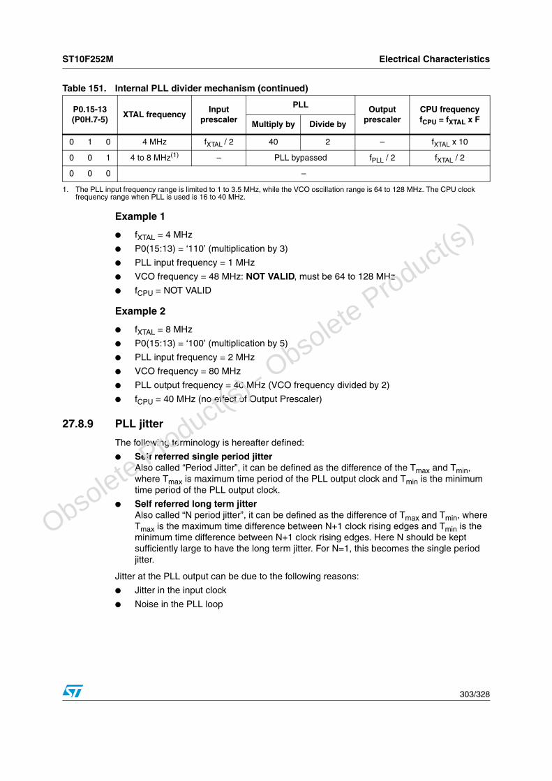
ST10F252M Electrical Characteristics
303/328
Example 1
● fXTAL = 4 MHz
● P0(15:13) = ‘110’ (multiplication by 3)
● PLL input frequency = 1 MHz
● VCO frequency = 48 MHz: NOT VALID, must be 64 to 128 MHz
● fCPU = NOT VALID
Example 2
● fXTAL = 8 MHz
● P0(15:13) = ‘100’ (multiplication by 5)
● PLL input frequency = 2 MHz
● VCO frequency = 80 MHz
● PLL output frequency = 40 MHz (VCO frequency divided by 2)
● fCPU = 40 MHz (no effect of Output Prescaler)
27.8.9 PLL jitter
The following terminology is hereafter defined:
● Self referred single period jitterAlso called “Period Jitter”, it can be defined as the difference of the Tmax and Tmin, where Tmax is maximum time period of the PLL output clock and Tmin is the minimum time period of the PLL output clock.
● Self referred long term jitter Also called “N period jitter”, it can be defined as the difference of Tmax and Tmin, where Tmax is the maximum time difference between N+1 clock rising edges and Tmin is the minimum time difference between N+1 clock rising edges. Here N should be kept sufficiently large to have the long term jitter. For N=1, this becomes the single period jitter.
Jitter at the PLL output can be due to the following reasons:
● Jitter in the input clock
● Noise in the PLL loop
0 1 0 4 MHz fXTAL / 2 40 2 – fXTAL x 10
0 0 1 4 to 8 MHz(1) – PLL bypassed fPLL / 2 fXTAL / 2
0 0 0 –
1. The PLL input frequency range is limited to 1 to 3.5 MHz, while the VCO oscillation range is 64 to 128 MHz. The CPU clock frequency range when PLL is used is 16 to 40 MHz.
Table 151. Internal PLL divider mechanism (continued)
P0.15-13(P0H.7-5)
XTAL frequencyInput
prescaler
PLL Output prescaler
CPU frequency fCPU = fXTAL x FMultiply by Divide by
O
bsolete Product(
s) - O
bsolete Product(
s)

Electrical Characteristics ST10F252M
304/328
Jitter in the input clock
PLL acts like a low pass filter for any jitter in the input clock. Input Clock jitter with the frequencies within the PLL loop bandwidth is passed to the PLL output and higher frequency jitter (frequency > PLL bandwidth) is attenuated @20dB/decade.
Noise in the PLL loop
This contribution again can be caused by the following sources:
● Device noise of the circuit in the PLL
● Noise in supply and substrate.
Device noise of the circuit in the PLL
The long term jitter is inversely proportional to the bandwidth of the PLL: the wider the loop bandwidth is, the lower the jitter is due to noise in the loop. Moreover, the long term jitter is practically independent of the multiplication factor.
The most noise sensitive circuit in the PLL circuit is definitively the VCO (Voltage Controlled Oscillator). There are two main sources of noise: thermal (random noise, frequency-independent noise, thus, practically white noise) and flicker (low frequency noise, 1/f). For the frequency characteristics of the VCO circuitry, the effect of the thermal noise results in a 1/f2 region in the output noise spectrum, while the flicker noise in a 1/f3. Assuming a noiseless PLL input and supposing that the VCO is dominated by its 1/f2 noise, the R.M.S. value of the accumulated jitter is proportional to the square root of N, where N is the number of clock periods within the considered time interval.On the contrary, assuming again a noiseless PLL input and supposing that the VCO is dominated by its 1/f3 noise, the R.M.S. value of the accumulated jitter is proportional to N, where N is the number of clock periods within the considered time interval.
The jitter in the PLL loop can be modelized as dominated by the i1/f2 noise for N smaller than a certain value depending on the PLL output frequency and on the bandwidth characteristics of loop. Above this first value, the jitter becomes dominated by the i1/f3 noise component. Lastly, for N greater than a second value of N, a saturation effect is evident, so the jitter does not grow anymore when considering a longer time interval (jitter stable increasing the number of clock periods N). The PLL loop acts as a high pass filter for any noise in the loop, with cutoff frequency equal to the bandwidth of the PLL. The saturation value corresponds to what has been called self referred long term jitter of the PLL. In Figure 116 the maximum jitter trend versus the number of clock periods N (for some typical CPU frequencies) is shown: The curves represent the very worst case, computed taking into account all corners of temperature, power supply and process variations: The real jitter is always measured well below the given worst case values.
Noise in supply and substrate
Digital supply noise adds deterministic components to the PLL output jitter, independent of the multiplication factor. Its effects are strongly reduced thanks to the particular care used in the physical implementation and integration of the PLL module inside the device. Nonetheless, the contribution of the digital noise to the global jitter is widely taken into account in the curves provided in Figure 116.
O
bsolete Product(
s) - O
bsolete Product(
s)

ST10F252M Electrical Characteristics
305/328
Figure 116. ST10F252M PLL jitter
27.8.10 PLL lock / unlock
During normal operation, if the PLL gets unlocked for any reason, an interrupt request to the CPU is generated, and the reference clock (oscillator) is automatically disconnected from the PLL input: in this way, the PLL goes into free-running mode, providing the system with a backup clock signal (free running frequency ffree). This feature allows recovery from a crystal failure occurrence without risking to go into an undefined configuration: The system is provided with a clock allowing the execution of the PLL unlock interrupt routine in a safe mode.
The path between reference clock and PLL input can be restored only by a hardware reset, or by a bidirectional software or watchdog reset event that forces the RSTIN pin low.
Note: The external RC circuit on RSTIN pin must be properly sized in order to extend the duration of the low pulse to lock the PLL before the level at RSTIN pin is recognized high: A bidirectional reset internally drives the RSTIN pin low for just 1024 TCL (definitely not sufficient to lock the PLL starting from free-running mode).
Jitte
r [n
s]
N (CPU clock periods)200 400
±5
±1
800600 1000 1200 140000
64MHz
±2
±3
±4
24MHz 40MHz32MHz16MHz
TJIT
Table 152. PLL characteristics (VDD = 5V ± 10%, VSS = 0V, TA = -40 to +125°C)
Symbol Parameter ConditionsValue
UnitMin Max
tPSUP PLL Start-up time(1)
1. Not 100% tested, guaranteed by design characterization
Stable VDD and reference clock – 300 µs
tLOCK PLL Lock-in timeStable VDD and reference clock, starting from free-running mode
– 250 µs
TJITSingle Period Jitter(1)
(cycle to cycle = 2 TCL) 6 sigma time period variation(peak to peak)
-500 +500 ps
ffree PLL free running frequencyMultiplication factors: 3, 4 250 2000
kHzMultiplication factors: 5, 8, 10, 16 500 4000
O
bsolete Product(
s) - O
bsolete Product(
s)

Electrical Characteristics ST10F252M
306/328
27.8.11 Main oscillator specifications
VDD = 5V ± 10%, VSS = 0V, TA = -40 to +125°C
Figure 117. Crystal oscillator and resonator connection diagram
The given values of CA do not include the stray capacitance of the package and of the printed circuit board: the negative resistance values are calculated assuming additional 5pF to the values in the table. The crystal shunt capacitance (C0) and the package capacitance between XTAL1 and XTAL2 pins is globally assumed equal to 10pF.
The external resistance between XTAL1 and XTAL2 is not necessary, since already present on the silicon.
Table 153. Main oscillator characteristics
Symbol Parameter ConditionsValue
UnitMin Typ Max
gmOscillator Transconductance
1.4 2.6 4.2 mA/V
VOSC Oscillation Amplitude(1)
1. Not 100% tested, guaranteed by design characterization
Peak to Peak – 1.5 – V
VAV Oscillation Voltage level(1) Sine wave middle – 0.8 – V
tSTUP Oscillator Start-up Time(1)Stable VDD - Crystal – 6 10 ms
Stable VDD - Resonator – 1 2 ms
Table 154. Main oscillator negative resistance (module)
CA = 15pF CA = 25pF CA = 35pF
Min Typ Max Min Typ Max Min Typ Max
4 MHz 545 Ω 1035 Ω – 550 Ω 1050 Ω – 430 Ω 850 Ω –
8 MHz 240 Ω 450 Ω – 170 Ω 350 Ω – 120 Ω 250 Ω –
CACA
Crystal
XTA
L1
XTA
L2
Resonator
XTA
L1
XTA
L2
ST10F252M ST10F252M
O
bsolete Product(
s) - O
bsolete Product(
s)

ST10F252M Electrical Characteristics
307/328
27.8.12 External clock drive XTAL1
When Direct Drive configuration is selected during reset, it is possible to drive the CPU clock directly from the XTAL1 pin, without particular restrictions on the maximum frequency, since the on-chip oscillator amplifier is bypassed. The speed limit is imposed by internal logic that targets a maximum CPU frequency of 40 MHz.
In all other clock configurations (Direct Drive with Prescaler or PLL usage) the on-chip oscillator amplifier is not bypassed, so it determines the input clock speed limit. Then, when the on-chip oscillator is enabled it is forbidden to use any external clock source different from crystal or ceramic resonator.
Figure 118. External clock drive XTAL1
Note: When Direct Drive is selected, an external clock source can be used to drive XTAL1. The maximum frequency of the external clock source depends on the duty cycle: When 40 MHz is used, 50% duty cycle is granted (low phase = high phase = 12.5ns); when for instance 20 MHz is used, a 25% duty cycle can be accepted (minimum phase, high or low, again equal to 12.5ns).
27.8.13 Memory cycle variables
The tables below use three variables which are derived from the BUSCONx registers and represent the special characteristics of the programmed memory cycle. The following table describes how these variables are to be computed.
Table 155. External clock drive
Parameter Symbol
Direct drive fCPU = fXTAL
Direct drive withprescaler
fCPU = fXTAL / 2
PLL usagefCPU = fXTAL x F Unit
Min Max Min Max Min Max
XTAL1 period(1)(2)
1. The minimum value for the XTAL1 signal period is considered the theoretical minimum. The real minimum value depends on the duty cycle of the input clock signal.
2. 4 to 8 MHz is the input frequency range when using an external clock source. 40 MHz can be applied with an external clock source only when Direct Drive mode is selected: in this case, the oscillator amplifier is bypassed so it does not limit the input frequency.
tOSC SR 25 – 83.3 250 83.3 250 ns
High time(3)
3. The input clock signal must reach the defined levels VIL2 and VIH2.
t1 SR 6 – 3 – 6 – ns
Low time(3) t2 SR 6 – 3 – 6 – ns
Rise time(3) t3 SR – 2 – 2 – 2 ns
Fall time(3) t4 SR – 2 – 2 – 2 ns
t1 t3 t4
VIL2t2
tOSC
VIH2
O
bsolete Product(
s) - O
bsolete Product(
s)

Electrical Characteristics ST10F252M
308/328
27.8.14 External memory bus timing
The following sections include the External Memory Bus timings. The given values are computed for a maximum CPU clock of 40 MHz.
Note: All External Memory Bus Timings and SSC Timings listed in the following tables are granted by Design Characterization and not fully tested in production.
27.8.15 Multiplexed bus
VDD = 5V ± 10%, VSS = 0V, TA = -40 to +125°C, CL = 50pF, ALE cycle time = 6 TCL + 2tA + tC + tF (75ns at 40 MHz CPU clock without wait states)
Table 156. Memory cycle variables
Description Symbol Values
ALE Extension tA TCL x [ALECTL]
Memory Cycle Time wait states tC 2TCL x (15 - [MCTC])
Memory Tri-state Time tF 2TCL x (1 - [MTTC])
Table 157. Multiplexed bus timings
Symbol Parameter
fCPU = 40 MHzTCL = 12.5ns
Variable CPU clock1/2 TCL = 1 to 40 MHz Unit
Min Max Min Max
t5 CC ALE high time 4 + tA – TCL – 8.5 + tA – ns
t6 CC Address setup to ALE 1.5 + tA – TCL – 11 + tA – ns
t7 CC Address hold after ALE 4 + tA – TCL – 8.5 + tA – ns
t8 CCALE falling edge to RD, WR (with RW-delay)
4 + tA – TCL – 8.5 + tA – ns
t9 CCALE falling edge to RD, WR (no RW-delay)
– 8.5 + tA – – 8.5 + tA – ns
t10 CCAddress float after RD, WR (with RW-delay)1
– 6 – 6 ns
t11 CCAddress float after RD, WR (no RW-delay)1
– 18.5 – TCL + 6 ns
t12 CCRD, WR low time(with RW-delay)
15.5 + tC – 2TCL – 9.5 + tC – ns
t13 CCRD, WR low time (no RW-delay)
28 + tC – 3TCL – 9.5 + tC – ns
t14 SRRD to valid data in (with RW-delay)
– 6 + tC – 2TCL – 19 + tC ns
t15 SRRD to valid data in (no RW-delay)
– 18.5 + tC – 3TCL – 19 + tC ns
t16 SR ALE low to valid data in –17.5 +
+ tA + tC–
3TCL – 20 ++ tA + tC
ns
O
bsolete Product(
s) - O
bsolete Product(
s)

ST10F252M Electrical Characteristics
309/328
t17 SRAddress/Unlatched CS to valid data in
–20 + 2tA +
+ tC–
4TCL – 30 ++ 2tA + tC
ns
t18 SRData hold after RDrising edge
0 – 0 – ns
t19 SR Data float after RD1 – 16.5 + tF – 2TCL – 8.5 + tF ns
t22 CC Data valid to WR 10 + tC – 2TCL – 15 + tC – ns
t23 CC Data hold after WR 4 + tF – 2TCL – 8.5 + tF – ns
t25 CC ALE rising edge after RD, WR 15 + tF – 2TCL – 10 + tF – ns
t27 CCAddress/Unlatched CS hold after RD, WR
10 + tF – 2TCL – 15 + tF – ns
t38 CC ALE falling edge to Latched CS – 4 – tA 10 – tA – 4 – tA 10 – tA ns
t39 SR Latched CS low to Valid Data In –16.5 + tC +
+ 2tA–
3TCL - 21 ++ tC + 2tA
ns
t40 CC Latched CS hold after RD, WR 27 + tF – 3TCL - 10.5 + tF – ns
t42 CCALE fall. edge to RdCS, WrCS (with RW delay)
7 + tA – TCL - 5.5 + tA – ns
t43 CCALE fall. edge to RdCS, WrCS (no RW delay)
-5.5 + tA – -5.5 + tA – ns
t44 CCAddress float after RdCS, WrCS (with RW delay)1
– 1.5 – 1.5 ns
t45 CCAddress float after RdCS, WrCS (no RW delay)1
– 14 – TCL + 1.5 ns
t46 SRRdCS to Valid Data In(with RW delay)
– 4 + tC – 2TCL - 21 + tC ns
t47 SRRdCS to Valid Data In(no RW delay)
– 16.5 + tC – 3TCL - 21 + tC ns
t48 CCRdCS, WrCS Low Time(with RW delay)
15.5 + tC – 2TCL - 9.5 + tC – ns
t49 CCRdCS, WrCS Low Time(no RW delay)
28 + tC – 3TCL - 9.5 + tC – ns
t50 CC Data valid to WrCS 10 + tC – 2TCL - 15 + tC – ns
t51 SR Data hold after RdCS 0 – 0 – ns
t52 SR Data float after RdCS1 – 16.5 + tF – 2TCL - 8.5 + tF ns
t54 CCAddress hold afterRdCS, WrCS
6 + tF – 2TCL - 19 + tF – ns
t56 CC Data hold after WrCS 6 + tF – 2TCL - 19 + tF – ns
Table 157. Multiplexed bus timings (continued)
Symbol Parameter
fCPU = 40 MHzTCL = 12.5ns
Variable CPU clock1/2 TCL = 1 to 40 MHz Unit
Min Max Min Max
O
bsolete Product(
s) - O
bsolete Product(
s)
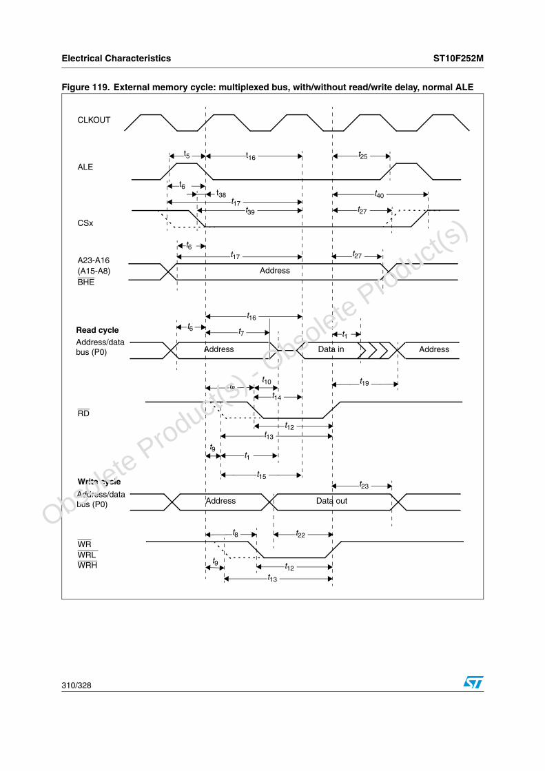
Electrical Characteristics ST10F252M
310/328
Figure 119. External memory cycle: multiplexed bus, with/without read/write delay, normal ALE
Data in
Data outAddress
Address
t38
t10
Read cycle
Write cycle
t5 t16
t39
t40
t25
t27
t1
t14
t22
t23
t12
t8
t8
t6
t19
Address
t17
t6
t7
t9t1
t13
t15
t16
t12t13
Address
t9
t17
t6
t27
CLKOUT
ALE
CSx
A23-A16(A15-A8)
Address/data
RD
WRWRL
BHE
WRH
bus (P0)
Address/databus (P0)
O
bsolete Product(
s) - O
bsolete Product(
s)
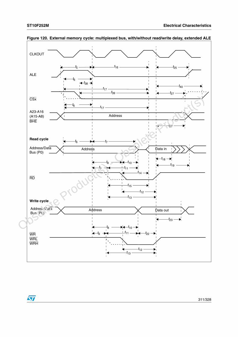
ST10F252M Electrical Characteristics
311/328
Figure 120. External memory cycle: multiplexed bus, with/without read/write delay, extended ALE
Data outAddress
Data inAddress
Address
t5 t16
t6 t7
t39
t40
t14
t8t18
t23
t6
t27
t38
t10 t19
t25
t17
t9 t11
t15
t12
t13
t8 t10
t9 t11
t12t13
t22
t27
t17
t6
Read cycle
Write cycle
CLKOUT
ALE
CSx
A23-A16(A15-A8)
RD
WRWRL
BHE
WRH
Address/DataBus (P0)
Address/DataBus (P0)
O
bsolete Product(
s) - O
bsolete Product(
s)
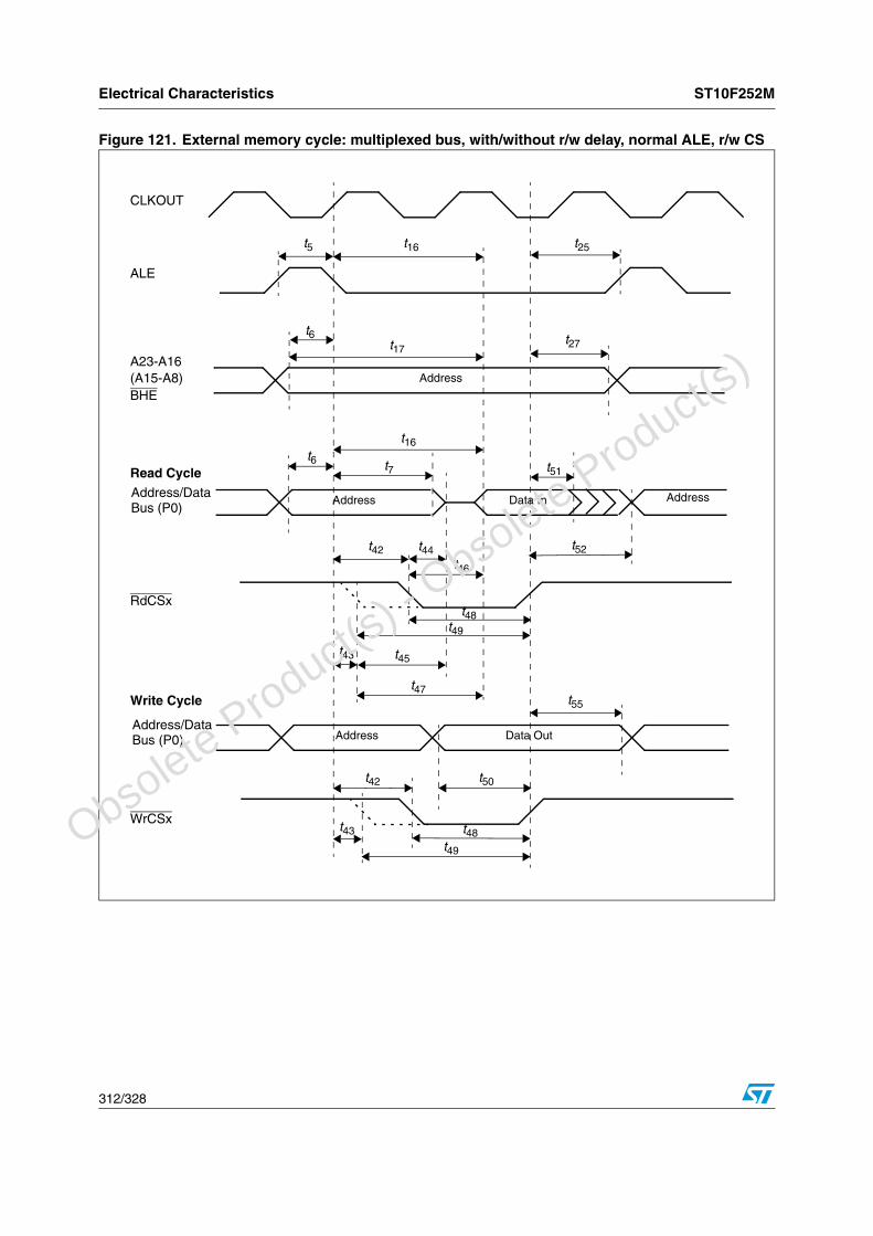
Electrical Characteristics ST10F252M
312/328
Figure 121. External memory cycle: multiplexed bus, with/without r/w delay, normal ALE, r/w CS
Read Cycle
Write Cycle
CLKOUT
ALE
A23-A16(A15-A8)BHE
Data In
Data OutAddress
Address
Address
Address
RdCSx
WrCSx
Address/DataBus (P0)
Address/DataBus (P0)
t25t16t5
t6t17
t27
t51
t16
t7t6
t42 t44 t52
t46
t48t49
t43 t45
t47t55
t42 t50
t48t49
t43
O
bsolete Product(
s) - O
bsolete Product(
s)
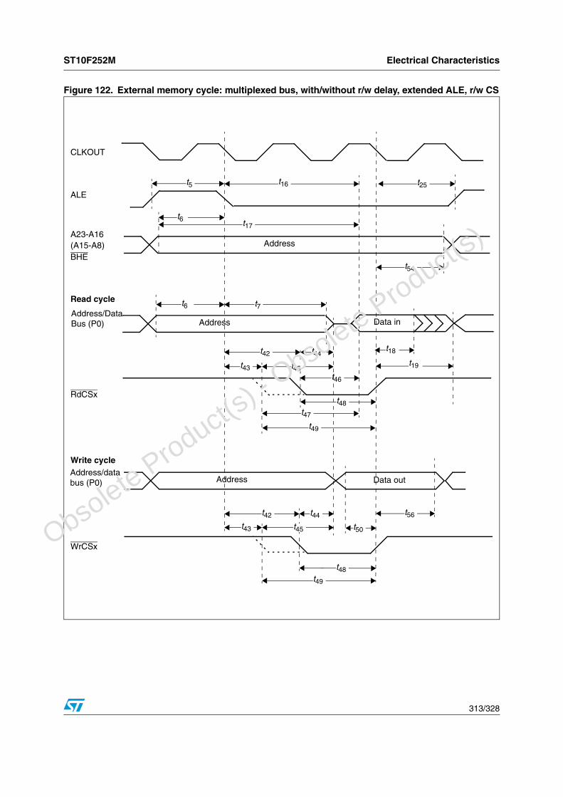
ST10F252M Electrical Characteristics
313/328
Figure 122. External memory cycle: multiplexed bus, with/without r/w delay, extended ALE, r/w CS
Data outAddress
Data inAddress
Address
t5 t16
t6 t7
t46
t42
t42
t50
t18
t56
t6
t54
t44t19
t25
t17
t43 t45
t47
t48
t49
t49
t43
t48
t44
t45
Read cycle
Write cycle
CLKOUT
ALE
A23-A16(A15-A8)BHE
RdCSx
WrCSx
Address/DataBus (P0)
Address/databus (P0)
O
bsolete Product(
s) - O
bsolete Product(
s)

Electrical Characteristics ST10F252M
314/328
27.8.16 Demultiplexed bus
VDD = 5V ± 10%, VSS = 0V, TA = -40 to +125°C, CL = 50pF, ALE cycle time = 4 TCL + 2tA + tC + tF (50ns at 40 MHz CPU clock without wait states).
.
Table 158. Demultiplexed bus timings
Symbol Parameter
fCPU = 40 MHzTCL = 12.5ns
Variable CPU clock1/2 TCL = 1 to 40 MHz Unit
Min Max Min Max
t5 CC ALE high time 4 + tA – TCL - 8.5 + tA – ns
t6 CC Address setup to ALE 1.5 + tA – TCL - 11 + tA – ns
t80 CCAddress/Unlatched CS setup to RD, WR (with RW-delay)
12.5 + 2tA –2TCL - 12.5 +
+ 2tA– ns
t81 CCAddress/Unlatched CS setup to RD, WR (no RW-delay)
0.5 + 2tA – TCL - 12 + 2tA – ns
t12 CCRD, WR low time (with RW-delay)
15.5 + tC – 2TCL - 9.5 + tC – ns
t13 CCRD, WR low time (no RW-delay)
28 + tC – 3TCL - 9.5 + tC – ns
t14 SRRD to valid data in (with RW-delay)
– 6 + tC – 2TCL - 19 + tC ns
t15 SRRD to valid data in (no RW-delay)
– 18.5 + tC – 3TCL - 19 + tC ns
t16 SR ALE low to valid data in –17.5 + tA +
+ tC–
3TCL - 20 + + tA + tC
ns
t17 SRAddress/Unlatched CS to valid data in
–20 + 2tA +
+ tC–
4TCL - 30 ++ 2tA + tC
ns
t18 SRData hold after RDrising edge
0 – 0 – ns
t20 SRData float after RD rising edge (with RW-delay)(1) – 16.5 + tF –
2TCL - 8.5 ++ tF + 2tA
ns
t21 SRData float after RD rising edge (no RW-delay)(1) – 4 + tF –
TCL - 8.5 ++ tF + 2tA
ns
t22 CC Data valid to WR 10 + tC – 2TCL - 15 + tC – ns
t24 CC Data hold after WR 4 + tF – TCL - 8.5 + tF – ns
t26 CC ALE rising edge after RD, WR -10 + tF – -10 + tF – ns
t28 CCAddress/Unlatched CS hold after RD, WR(2) 0 + tF – 0 + tF – ns
t28h CCAddress/Unlatched CS hold
after WRH -5 + tF – -5 + tF – ns
t38 CCALE falling edge to Latched CS
-4 - tA 6 - tA -4 - tA 6 - tA ns
O
bsolete Product(
s) - O
bsolete Product(
s)
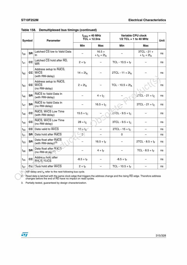
ST10F252M Electrical Characteristics
315/328
t39 SRLatched CS low to Valid Data In
–16.5 +
+ tC + 2tA–
3TCL - 21 ++ tC + 2tA
ns
t41 CCLatched CS hold after RD, WR
2 + tF – TCL - 10.5 + tF – ns
t82 CCAddress setup to RdCS, WrCS (with RW-delay)
14 + 2tA – 2TCL - 11 + 2tA – ns
t83 CCAddress setup to RdCS, WrCS (no RW-delay)
2 + 2tA – TCL - 10.5 + 2tA – ns
t46 SRRdCS to Valid Data In(with RW-delay)
– 4 + tC – 2TCL - 21 + tC ns
t47 SRRdCS to Valid Data In(no RW-delay)
– 16.5 + tC – 3TCL - 21 + tC ns
t48 CCRdCS, WrCS Low Time(with RW-delay)
15.5 + tC – 2TCL - 9.5 + tC – ns
t49 CCRdCS, WrCS Low Time(no RW-delay)
28 + tC – 3TCL - 9.5 + tC – ns
t50 CC Data valid to WrCS 10 + tC – 2TCL - 15 + tC – ns
t51 SR Data hold after RdCS 0 – 0 – ns
t53 SRData float after RdCS(with RW-delay)(3) – 16.5 + tF – 2TCL - 8.5 + tF ns
t68 SRData float after RdCS(no RW-delay)(3) – 4 + tF – TCL - 8.5 + tF ns
t55 CCAddress hold afterRdCS, WrCS
-8.5 + tF – -8.5 + tF – ns
t57 CC Data hold after WrCS 2 + tF – TCL - 10.5 + tF – ns
1. RW-delay and tA refer to the next following bus cycle.
2. Read data is latched with the same clock edge that triggers the address change and the rising RD edge. Therefore address changes before the end of RD have no impact on read cycles.
3. Partially tested, guaranteed by design characterization.
Table 158. Demultiplexed bus timings (continued)
Symbol Parameter
fCPU = 40 MHzTCL = 12.5ns
Variable CPU clock1/2 TCL = 1 to 40 MHz Unit
Min Max Min Max
O
bsolete Product(
s) - O
bsolete Product(
s)
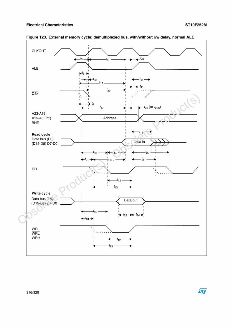
Electrical Characteristics ST10F252M
316/328
Figure 123. External memory cycle: demultiplexed bus, with/without r/w delay, normal ALE
Write cycle
CLKOUT
ALE
A23-A16A15-A0 (P1)BHE
WRWRL WRH
Data in
Data out
t38
t5 t9
t39
t41
t18
t14
t22
t12
Address
t17
t13
t15
t12
t13
t21
t20
t81
t80
t26
t24
t17
t6
t41u
t6
t80
t81
t28 (or t28h)
CSx
Read cycleData bus (P0)
RD
(D15-D8) D7-D0
Data bus (P0)(D15-D8) D7-D0
O
bsolete Product(
s) - O
bsolete Product(
s)

ST10F252M Electrical Characteristics
317/328
Figure 124. External memory cycle: demultiplexed bus, with/without r/w delay, extended ALE
t5
Read cycle
Write cycle
CLKOUT
ALE
CSx
RD
WRWRL WRH
Data bus (P0)(D15-D8) D7-D0
Data bus (P0)(D15-D8) D7-D0
A23-A16A15-A0 (P1)BHE
t26t16
t17
t39
t41
t28
t38
t6
t6 t17 t28
Address
t18
Data in
t20t14t80
t81 t15 t21
t13
t12
Data out
t80
t81t22 t24
t12
t13
O
bsolete Product(
s) - O
bsolete Product(
s)

Electrical Characteristics ST10F252M
318/328
Figure 125. External memory cycle: demultiplexed bus, with/without r/w delay, normal ALE, r/w CS
Read cycle
Write cycle
CLKOUT
ALE
Data in
Data out
t5 t16
t5
t46
t50
t48
Address
t17
t49
t47
t48
t49
t68
t53
t83
t82
t26
t57
t55
t6
t82
t83
RdCSx
WrCSx
Data bus (P0)(D15-D8) D7-D0
Data bus (P0)(D15-D8) D7-D0
A23-A16A15-A0 (P1)BHE
O
bsolete Product(
s) - O
bsolete Product(
s)

ST10F252M Electrical Characteristics
319/328
Figure 126. External memory cycle: Demultiplexed bus, without r/w delay, extended ALE, r/w CS
Address
t5t16
t46
t57
t6
t53
t26
t17
t47
t48
t49
t48
t49
t50
Data in
t51
t68
t55
Data out
t82
t83
t82
t83
Read cycle
Write cycle
CLKOUT
ALE
RdCSx
WrCSx
Data bus (P0)(D15-D8) D7-D0
Data bus (P0)(D15-D8) D7-D0
A23-A16A15-A0 (P1)BHE
O
bsolete Product(
s) - O
bsolete Product(
s)

Electrical Characteristics ST10F252M
320/328
27.8.17 CLKOUT and READY
VDD = 5V ± 10%, VSS = 0V, TA = -40 to + 125°C, CL = 50pF
Table 159. CLKOUT and READY timings
Symbol Parameter
fCPU = 40 MHzTCL = 12.5ns
Variable CPU clock1/2 TCL = 1 to 40 MHz Unit
Min Max Min Max
t29 CC CLKOUT cycle time 25 25 2TCL 2TCL ns
t30 CC CLKOUT high time 9 – TCL - 3.5 – ns
t31 CC CLKOUT low time 10 – TCL - 2.5 – ns
t32 CC CLKOUT rise time – 4 – 4 ns
t33 CC CLKOUT fall time – 4 – 4 ns
t34 CC CLKOUT rising edge to ALE falling edge -2 + tA 8 + tA -2 + tA 8 + tA ns
t35 SRSynchronous READY setup time toCLKOUT
17 – 17 – ns
t36 SRSynchronous READY hold time after CLKOUT
2 – 2 – ns
t37 SR Asynchronous READY low time 35 – 2TCL + 10 – ns
t58 SR Asynchronous READY setup time(1) 17 – 17 – ns
t59 SR Asynchronous READY hold time(1) 2 – 2 – ns
t60 SRAsynchronous READY hold time after RD, WR high (Demultiplexed Bus)(2) 0 2tA + tC + tF 0 2tA + tC + tF ns
1. These timings are given for characterization purposes only, in order to assure recognition at a specific clock edge.
2. Demultiplexed bus is the worst case. For multiplexed bus 2TCL are to be added to the maximum values. This adds even more time for deactivating READY. 2tA and tC refer to the next following bus cycle, tF refers to the current bus cycle.
O
bsolete Product(
s) - O
bsolete Product(
s)
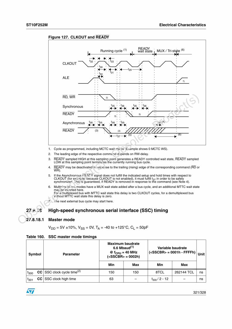
ST10F252M Electrical Characteristics
321/328
Figure 127. CLKOUT and READY
1. Cycle as programmed, including MCTC wait states (Example shows 0 MCTC WS).
2. The leading edge of the respective command depends on RW-delay.
3. READY sampled HIGH at this sampling point generates a READY controlled wait state, READY sampled LOW at this sampling point terminates the currently running bus cycle.
4. READY may be deactivated in response to the trailing (rising) edge of the corresponding command (RD or WR).
5. If the Asynchronous READY signal does not fulfill the indicated setup and hold times with respect to CLKOUT (for example, because CLKOUT is not enabled), it must fulfill t37 in order to be safely synchronized. This is guaranteed, if READY is removed in response to the command (see Note 4).
6. Multiplexed bus modes have a MUX wait state added after a bus cycle, and an additional MTTC wait state may be inserted here.For a multiplexed bus with MTTC wait state this delay is two CLKOUT cycles, for a demultiplexed bus without MTTC wait state this delay is zero.
7. The next external bus cycle may start here.
27.8.18 High-speed synchronous serial interface (SSC) timing
27.8.18.1 Master mode
VDD = 5V ±10%, VSS = 0V, TA = -40 to +125°C, CL = 50pF
t30
t34
t35 t36 t35 t36
t58 t59 t58 t59
wait stateREADY
MUX / Tri-state (6)
t32 t33
t29
Running cycle (1)
t31
t37
3)3)
(5)
t60 (4)
(6)
2)
7)
(3) (3)
CLKOUT
ALE
RD, WR
Synchronous
Asynchronous
READY
READY
Table 160. SSC master mode timings
Symbol Parameter
Maximum baudrate6.6 Mbaud(1)
@ fCPU = 40 MHz(<SSCBR> = 0002h)
Variable baudrate(<SSCBR> = 0001h - FFFFh) Unit
Min Max Min Max
t300 CC SSC clock cycle time(2) 150 150 8TCL 262144 TCL ns
t301 CC SSC clock high time 63 – t300 / 2 - 12 – ns
O
bsolete Product(
s) - O
bsolete Product(
s)

Electrical Characteristics ST10F252M
322/328
Figure 128. SSC master timing
1. The phase and polarity of shift and latch edge of SCLK is programmable. This figure uses the leading clock edge as shift edge (drawn in bold), with latch on trailing edge (SSCPH = 0b), Idle clock line is low, leading clock edge is low-to-high transition (SSCPO = 0b).
2. The bit timing is repeated for all bits to be transmitted or received.
t302 CC SSC clock low time 63 – t300 / 2 - 12 – ns
t303 CC SSC clock rise time – 10 – 10 ns
t304 CC SSC clock fall time – 10 – 10 ns
t305 CC Write data valid after shift edge – 15 – 15 ns
t306 CC Write data hold after shift edge(3) -2 – -2 – ns
t307p SRRead data setup time before latchedge, phase error detection on(SSCPEN = 1)
37.5 – 2TCL + 12.5 – ns
t308p SRRead data hold time after latchedge, phase error detection on(SSCPEN = 1)
50 – 4TCL – ns
t307 SRRead data setup time before latchedge, phase error detection off(SSCPEN = 0)
25 – 2TCL – ns
t308 SRRead data hold time after latchedge, phase error detection off(SSCPEN = 0)
0 – 0 – ns
1. When 40 MHz CPU clock is used the maximum baudrate cannot be higher than 6.6Mbaud (<SSCBR> = ‘2h’) due to the limited granularity of <SSCBR>. Value ‘1h’ for <SSCBR> can be used only with CPU clock equal to (or lower than) 32 MHz.
2. Formula for SSC Clock Cycle time: t300 = 4 TCL x (<SSCBR> + 1) Where <SSCBR> represents the content of the SSC baudrate register, taken as unsigned 16-bit integer. Minimum limit allowed for t300 is 125ns (corresponding to 8Mbaud).
3. Partially tested, guaranteed by design characterization.
Table 160. SSC master mode timings (continued)
Symbol Parameter
Maximum baudrate6.6 Mbaud(1)
@ fCPU = 40 MHz(<SSCBR> = 0002h)
Variable baudrate(<SSCBR> = 0001h - FFFFh) Unit
Min Max Min Max
1st out bit Last out bit2nd out bit
(1) (2)
2nd In bit1st in bit Last in bit
SCLK
MTSR
MRST
t308t307t308t307
t305 t305
t300 t301 t302
t304 t303t306
t305
O
bsolete Product(
s) - O
bsolete Product(
s)
ST10F252M Electrical Characteristics
323/328
27.8.18.2 Slave mode
VDD = 5V ±10%, VSS = 0V, TA = -40 to +125°C, CL = 50pF
Table 161. SSC slave mode timings
Symbol Parameter
Maximum baudrate6.6 Mbaud(1)
@ fCPU = 40 MHz(<SSCBR> = 0002h)
Variable baudrate (<SSCBR> = 0001h - FFFFh) Unit
Min Max Min Max
t310 SR SSC clock cycle time(2) 150 150 8TCL 262144 TCL ns
t311 SR SSC clock high time 63 – t310 / 2 - 12 – ns
t312 SR SSC clock low time 63 – t310 / 2 - 12 – ns
t313 SR SSC clock rise time – 10 – 10 ns
t314 SR SSC clock fall time – 10 – 10 ns
t315 CC Write data valid after shift edge – 55 – 2TCL + 30 ns
t316 CC Write data hold after shift edge 0 – 0 – ns
t317p SRRead data setup time before latchedge, phase error detection on(SSCPEN = 1)
62 – 4TCL + 12 – ns
t318p SRRead data hold time after latchedge, phase error detection on(SSCPEN = 1)
87 – 6TCL + 12 – ns
t317 SRRead data setup time before latchedge, phase error detection off(SSCPEN = 0)
6 – 6 – ns
t318 SRRead data hold time after latchedge, phase error detection off(SSCPEN = 0)
31 – 2TCL + 6 – ns
1. When 40 MHz CPU clock is used the maximum baudrate cannot be higher than 6.6Mbaud (<SSCBR> = ‘2h’) due to the limited granularity of <SSCBR>. Value ‘1h’ for <SSCBR> may be used only with CPU clock lower than 32 MHz (after checking that resulting timings are suitable for the master).
2. Formula for SSC Clock Cycle time: t310 = 4 TCL * (<SSCBR> + 1) Where <SSCBR> represents the content of the SSC baudrate register, taken as unsigned 16-bit integer.Minimum limit allowed for t310 is 125ns (corresponding to 8Mbaud).
O
bsolete Product(
s) - O
bsolete Product(
s)

Electrical Characteristics ST10F252M
324/328
Figure 129. SSC slave timing
1. The phase and polarity of shift and latch edge of SCLK is programmable. This figure uses the leading clock edge as shift edge (drawn in bold), with latch on trailing edge (SSCPH = 0b), Idle clock line is low, leading clock edge is low-to-high transition (SSCPO = 0b).
2. The bit timing is repeated for all bits to be transmitted or received.
1st out bit Last out bit2nd out bit
(1) (2)
2nd in bit1st in bit Last in bit
SCLK
MRST
MTSR
t313t314
t315t316t315
t317 t318t317 t318
t315
t310 t311 t312
O
bsolete Product(
s) - O
bsolete Product(
s)

ST10F252M Package information
325/328
28 Package information
In order to meet environmental requirements, ST (also) offers these devices in ECOPACK® packages. ECOPACK® packages are lead-free. The category of second Level Interconnect is marked on the package and on the inner box label, in compliance with JEDEC Standard JESD97. The maximum ratings related to soldering conditions are also marked on the inner box label.
ECOPACK is an ST trademark. ECOPACK specifications are available at: www.st.com.
Figure 130.LQFP100 mechanical data and package dimensions
OUTLINE ANDMECHANICAL DATA
DIM.mm inch
MIN. TYP. MAX. MIN. TYP. MAX.
A 1.600 0.0630
A1 0.050 0.150 0.0020 0.0059
A2 1.350 1.400 1.450 0.0531 0.0551 0.0571
b 0.170 0.220 0.270 0.0067 0.0087 0.0106
c 0.090 0.200 0.0035 0.0079
D 15.800 16.000 16.200 0.6220 0.6299 0.6378
D1 13.800 14.000 14.200 0.5433 0.5512 0.5591
D3 12.000 0.4724
E 15.800 16.000 16.200 0.6220 0.6299 0.6378
E1 13.800 14.000 14.200 0.5433 0.5512 0.5591
E3 12.000 0.4724
e 0.500 0.0197
L 0.450 0.600 0.750 0.0177 0.0236 0.0295
L1 1.000 0.0394
K 0˚ (min.), 3.5˚ (typ.), 7˚(max.)
ccc 0.080 0.003
LQFP100 (14x14x1.40mm)Low profile Quad Flat Package
0086901 D
O
bsolete Product(
s) - O
bsolete Product(
s)

Ordering Information ST10F252M
326/328
29 Ordering Information
Table 162. Device summary
Order code Package PackingTemperature
range (°C)CPU frequency
range (MHz)
ST10F252M-4T3LQFP100
Tray-40 to +125 1 to 40
ST10F252M-4TR3 Tape and reel
O
bsolete Product(
s) - O
bsolete Product(
s)
ST10F252M Revision history
327/328
30 Revision history
Table 163. Document revision history
Date Revision Changes
7-Feb-2008 1 Initial release
O
bsolete Product(
s) - O
bsolete Product(
s)

ST10F252M
328/328
Please Read Carefully:
Information in this document is provided solely in connection with ST products. STMicroelectronics NV and its subsidiaries (“ST”) reserve theright to make changes, corrections, modifications or improvements, to this document, and the products and services described herein at anytime, without notice.
All ST products are sold pursuant to ST’s terms and conditions of sale.
Purchasers are solely responsible for the choice, selection and use of the ST products and services described herein, and ST assumes noliability whatsoever relating to the choice, selection or use of the ST products and services described herein.
No license, express or implied, by estoppel or otherwise, to any intellectual property rights is granted under this document. If any part of thisdocument refers to any third party products or services it shall not be deemed a license grant by ST for the use of such third party productsor services, or any intellectual property contained therein or considered as a warranty covering the use in any manner whatsoever of suchthird party products or services or any intellectual property contained therein.
UNLESS OTHERWISE SET FORTH IN ST’S TERMS AND CONDITIONS OF SALE ST DISCLAIMS ANY EXPRESS OR IMPLIEDWARRANTY WITH RESPECT TO THE USE AND/OR SALE OF ST PRODUCTS INCLUDING WITHOUT LIMITATION IMPLIEDWARRANTIES OF MERCHANTABILITY, FITNESS FOR A PARTICULAR PURPOSE (AND THEIR EQUIVALENTS UNDER THE LAWSOF ANY JURISDICTION), OR INFRINGEMENT OF ANY PATENT, COPYRIGHT OR OTHER INTELLECTUAL PROPERTY RIGHT.
UNLESS EXPRESSLY APPROVED IN WRITING BY AN AUTHORIZED ST REPRESENTATIVE, ST PRODUCTS ARE NOTRECOMMENDED, AUTHORIZED OR WARRANTED FOR USE IN MILITARY, AIR CRAFT, SPACE, LIFE SAVING, OR LIFE SUSTAININGAPPLICATIONS, NOR IN PRODUCTS OR SYSTEMS WHERE FAILURE OR MALFUNCTION MAY RESULT IN PERSONAL INJURY,DEATH, OR SEVERE PROPERTY OR ENVIRONMENTAL DAMAGE. ST PRODUCTS WHICH ARE NOT SPECIFIED AS "AUTOMOTIVEGRADE" MAY ONLY BE USED IN AUTOMOTIVE APPLICATIONS AT USER’S OWN RISK.
Resale of ST products with provisions different from the statements and/or technical features set forth in this document shall immediately voidany warranty granted by ST for the ST product or service described herein and shall not create or extend in any manner whatsoever, anyliability of ST.
ST and the ST logo are trademarks or registered trademarks of ST in various countries.
Information in this document supersedes and replaces all information previously supplied.
The ST logo is a registered trademark of STMicroelectronics. All other names are the property of their respective owners.
© 2008 STMicroelectronics - All rights reserved
STMicroelectronics group of companies
Australia - Belgium - Brazil - Canada - China - Czech Republic - Finland - France - Germany - Hong Kong - India - Israel - Italy - Japan - Malaysia - Malta - Morocco - Singapore - Spain - Sweden - Switzerland - United Kingdom - United States of America
www.st.com
O
bsolete Product(
s) - O
bsolete Product(
s)


![Microsoft Word - \256]\255}\277o\275\327\244\345final](https://static.fdokumen.com/doc/165x107/6334cc342532592417003b0e/microsoft-word-256255277o275327244345final.jpg)