AN-256 MP3 NG - Next Generation Consumer Platform - Renesas
24
1 of 23 DSC 4885 This application note illustrates the use of Spartan FPGA and an IDT RC32364 RISController CPU in a handheld consumer electronics platform. Specifically the target application is an MP3 audio player with advanced user interface features. In this application the Spartan device is used to implement the complex system level glue logic required to interface and manage the memory and I/O devices. The RC32364 implements the MP3 decoding func- tions, the graphical user interface, and various device control functions. While the design is targeted at solving a specific problem, decoding and playing compressed audio streams, it illustrates solutions to a number of general technical issues. These include: ◆ Supporting a graphical user interface in an embedded system. ◆ Implementing cost-effective interfaces to LCD displays, touch screens, USB, IRDA, and Compact- Flash in an embedded system. ◆ Error handling when using NAND FLASH memory. ◆ Controlling SDRAM memory. The MP3 player market emerged in late 1998, when Diamond Multimedia shipped its Rio MP3 audio player. Like any new market, the feature set of MP3 players is likely to change as more users buy them. Key dynamics in this market include: ◆ Copy Protection While the Secure Digital Music Initiative (SDMI) promises to make a wider variety of music available in MP3 format, there is considerable technical uncertainty about implementation timetables. ◆ Non-MP3 Formats While MP3 is the dominant format for music available on the Internet, other for- mats are also available. ◆ Extended Features At $150 to $250 an MP3 player is a relatively expensive consumer electronics purchase. The dominant component of that price is the FLASH memory that these devices use. This cost component is more or less the same for all vendors, and constrains price point differentia- tion. One way to increase the perceived value of an MP3 player is to add value-added features tai- lored to the target market. Due to these market dynamics, including the potential for rapid changes in feature requirements, the best approach is a flexible high performance system. This flexibility manifests itself in two forms. The first is the use of a high performance processor, which supports the addition of additional soft features without the need to resort to optimized assembly language. The second is the use of a low cost, high density FPGA to provide flexible I/O support for the processor. MP3 refers to the MPEG Layer 3 audio compression scheme that was defined as part of the Interna- tional Standards Organization (ISO) Moving Picture Experts Group (MPEG) audio/video coding standard. MPEG-I defined three encoding schemes, referred to as Layer 1, Layer 2, and Layer 3. Each of these schemes uses increasing sophisticated encoding techniques and gives correspondingly better audio quality at a given bit rate. The three layers are hierarchical, in that a Layer 3 decoder decodes Layer 1, 2, and 3 bitstreams; a Layer 2 decoder decodes Layer 2, and 1 bitstreams; and a Layer 1 decoder decodes only
-
Upload
khangminh22 -
Category
Documents
-
view
6 -
download
0
Transcript of AN-256 MP3 NG - Next Generation Consumer Platform - Renesas

�����
��� ��
������������ �������� ���� � �� �� �� �����
�������� �������������������� ������������������������
��������������������� �� �� �� �
��������������������������������������������
����������������
������������������������
����������������������������������������
This application note illustrates the use of Spartan FPGA and an IDT RC32364 RISC ontroller CPU in ahandheld consumer electronics platform. Specifically the target application is an MP3 audio player withadvanced user interface features.
In this application the Spartan device is used to implement the complex system level glue logic requiredto interface and manage the memory and I/O devices. The RC32364 implements the MP3 decoding func-tions, the graphical user interface, and various device control functions.
While the design is targeted at solving a specific problem, decoding and playing compressed audiostreams, it illustrates solutions to a number of general technical issues. These include:
◆ Supporting a graphical user interface in an embedded system.◆ Implementing cost-effective interfaces to LCD displays, touch screens, USB, IRDA, and Compact-
Flash in an embedded system.◆ Error handling when using NAND FLASH memory.◆ Controlling SDRAM memory.
� � � ����� ��������������������������������
MP3 Market
The MP3 player market emerged in late 1998, when Diamond Multimedia shipped its Rio MP3 audioplayer. Like any new market, the feature set of MP3 players is likely to change as more users buy them. Keydynamics in this market include:
◆ Copy Protection While the Secure Digital Music Initiative (SDMI) promises to make a wider varietyof music available in MP3 format, there is considerable technical uncertainty about implementationtimetables.
◆ Non-MP3 Formats While MP3 is the dominant format for music available on the Internet, other for-mats are also available.
◆ Extended Features At $150 to $250 an MP3 player is a relatively expensive consumer electronicspurchase. The dominant component of that price is the FLASH memory that these devices use.This cost component is more or less the same for all vendors, and constrains price point differentia-tion. One way to increase the perceived value of an MP3 player is to add value-added features tai-lored to the target market.
Due to these market dynamics, including the potential for rapid changes in feature requirements, thebest approach is a flexible high performance system. This flexibility manifests itself in two forms. The first isthe use of a high performance processor, which supports the addition of additional soft features without theneed to resort to optimized assembly language. The second is the use of a low cost, high density FPGA toprovide flexible I/O support for the processor.
MP3 Technology
MP3 refers to the MPEG Layer 3 audio compression scheme that was defined as part of the Interna-tional Standards Organization (ISO) Moving Picture Experts Group (MPEG) audio/video coding standard.MPEG-I defined three encoding schemes, referred to as Layer 1, Layer 2, and Layer 3. Each of theseschemes uses increasing sophisticated encoding techniques and gives correspondingly better audio qualityat a given bit rate. The three layers are hierarchical, in that a Layer 3 decoder decodes Layer 1, 2, and 3bitstreams; a Layer 2 decoder decodes Layer 2, and 1 bitstreams; and a Layer 1 decoder decodes only
1 of 23 ���� ��� ����
DSC 4885

�������� �������
��� ��
Layer 1 bitstreams. Each of the layers support decoding audio sampled at 48, 44.1, or 32 kHz. MPEG 2uses the same family of codecs but extends it by adding support for 24, 22.05, or 16 kHz sampling rates aswell as more audio channels for surround sound and multilingual applications.
All Layers use the same basic structure. The coding scheme can be described as "perceptual noiseshaping" or "perceptual subband / transform coding". The encoder analyzes the spectral components of theaudio signal by calculating a filterbank (transform) and applies a psycho-acoustic model to estimate the justnoticeable noise-level. In its quantization and coding stage, the encoder tries to allocate the availablenumber of data bits in a way to meet both the bitrate and masking requirements. In plain English, the algo-rithm exploits the fact that loud sounds mask out the listener’s ability to perceive quieter sounds in the samefrequency range. The encoder uses this property to remove information from the signal that would not beheard anyway.
Like all of the MPEG compression technologies, the algorithms are designed so that the decoder ismuch less complex. Its only task is to synthesize an audio signal out of the coded spectral components. AllLayers use the same analysis filter bank (polyphase with 32 sub-bands). Layer-3 adds a MDCT transformto increase the frequency resolution.
All layers use the same header information in their bitstream, to support the hierarchical structure of thestandard.
���������������������������� ��������������������������������
A key design objective for this application note was the creation of a solution with the lowest possiblecost, while at the same time providing support for value-added features. These features include the abilityto store contact information and record memos and other functions commonly found in Personal DigitalAssistants (PDAs).
Figure 1 gives an overview of the design. The key features of which are:◆ 128 by 128 pixel graphical touch screen.◆ USB interface for download music and network connectivity.◆ IRDA compliant infra-red interface for exchanging data with other units.◆ 32 MB of on board FLASH storage.◆ CompactFlash interface for storage expansion using CompactFlash cards or MicroDrive hard
drives.
All of this is driven by a high performance IDT RC32364 32-bit RISC ontroller processor and interfacedusing a next generation Spartan II FPGA. Before we examine the functions implemented in the Spartandevice, and the software function running on the RC32364, let’s get a overview of the Application SpecificStandard Products (ASSPs) that are included in the design.
� �� �� ���� ��� ����

�������� �������
��� ��
Figure 1 MP3 NG System Block Diagram
IDT RC32364 RISController™
The processor chosen for this design is the IDT RC32364. The features of this device that are leveragedin this application are:
◆ Paged memory management unit◆ High performance, 195 dhrystone MIPS @ 150 MHz◆ Integer Multiply ACcumulate (MAC) support, 75 M MACs/second @ 150 MHz◆ Separate, line lockable, instruction (8KB) and data (2KB) caches◆ Power saving features including active power management, and a power-down operating mode.◆ On-chip In Circuit Emulation (ICE) interface to provide access to internal CPU state (registers,
cache) and for debug control (breakpoints, single step, insert instructions into pipeline).
Figure 2 shows the block diagram for this device. The complete data sheet for the RC32364 can befound at the following URL:
http://www.idt.com/products/pages/RISC-79RC32364.html
Figure 2 RC32364 Block Diagram
System Control Coprocessor (CPO)
2kB D-Cache, 2-set,
Clock
Enhanced JTAG
(ICE Interface)
TLB
MMU
lockable, write-back/write-through
GenerationUnit
RC32364 Bus Interface Unit
8kB I-Cache,lockable2-set,
RISCore32300 Internal Bus Interface
RISCore4000 Compatiblew/
RISCore32300TM
Extended MIPS 32Integer CPU Core
� �� �� ���� ��� ����

�������� �������
��� ��
The RC32364’s MMU consists of address translation logic and a Translation Lookaside Buffer (TLB)capable of supporting demand paged virtual memory. In addition it includes several features that are valu-able in an embedded application such as variable sized pages and lockable TLB entries.
Figure 3 illustrates the virtual to physical address translation performed by the RC32364.
The variable page size lets each mapping independently represent memory regions that can range from4KB to 16MB. This feature lets the system designer adjust the address mapping granularity for differentmemory regions.
Locking TLB entries excludes entries from being recommended for replacement when there is anaddress miss. This lets the system designer have mappings for critical regions of code and or data lockedinto the TLB for predictable real time performance.
Figure 3 RC32364 Address Translation
The RC32364 interfaces to the system through a 32 bit multiplexed address/data bus. The bus offers arich set of signals to control transfers of which only a subset was required for this application.
Figure 4 shows the timing for read transactions on this bus.
28 11 0
20 12
2931
VPN Offset
3239
ASID
8
Virtual Address with 1M (220) 4-Kbyte pages
23 0
8 24
Offset
39
Virtual Address with 256 (28)16-Mbyte pages
8 bits = 256 pages
20 bits = 1M 12
ASID 8
28 293132
VPN
24
Virtual-to-physical transla-tion in TLB
Bits 31, 30 and 29 of thevirtual address select user, super-visor, or kernel address spaces.
Offset passedunchanged tophysical memory
Virtual-to-physical-translation in TLB
TLB
TLB
31 0PFN Offset
32-bit Physical Address
Offset pa ssedunchanged to physicalmemory.
� �� �� ���� ��� ����

�������� �������
��� ��
Figure 4 RC32364 Read Timing
Crystal CS4343 Stereo DAC
The Digital to Analog Converter chosen for this design is the Crystal CS4343 from Cirrus Logic. Thisdevice features:
◆ 1.8V to 3.3V operation◆ 24 bit conversion at up to 96 kHz◆ Digital volume control◆ Digital bass and treble boost◆ Built in headphone amplifier capable of delivering 5 mW into a 16 ohm load.
Figure 5 shows the block diagram for this device.
Figure 5 CS4343 Block Diagram (Figure Courtesy Cirrus Logic)
The CS4343 provides three interfaces: the analog stereo headphone interface, the serial port used totransfer digital audio data streams, and the control port used to configure the device.
M asterC lock
AD(31:0)Addr Data Input
Addr(3:2)
ALE
DataEn*
Ack*
Last*
Rd*
C IP*
I/D*
DT/R*
W r*
Addr Data Input
W idth(1:0)
SCLK/DEM
SDATA
DIF1/SDA
MCLK
VA_HP
HP_A
SERIALPORT
DE-
CONTROL PORT
∆ΣDAC
RST
LRCK
DIF0/SCL
VA
VD_IO
DIGITALVOLUME
CONTROLBASS/TREBLE
BOOSTCOMPRESSION
LIMITING∆Σ
DAC
DIGITALFILTERS
ANALOGFILTER
ANALOGFILTER
GND FILT+ REF_GND
ANALOGVOLUME
CONTROL
HEAD-PHONE
AMPLIFIERANALOGVOLUME
CONTROL
HP_BEMPHASIS
VQ_HP
� �� �� ���� ��� ����

�������� �������
��� ��
The control port is an industry standard I2C slave interface. I2C is a multidrop, two wire, serial interfaceconsisting of a clock (SCL) and data (SDA) and operating at up to 100 kHz. The control port is used toconfigure device features such as volume, muting, equalization, power management, and the operatingmode of the serial port.
Figure 6 gives an overview of control port timing. A detailed description of I2C operation can be found inthe I2C specification as described in the references.
Figure 6 Control Port Timing (Figure Courtesy Cirrus Logic)
The serial port can be configured for several operating modes. The mode of operation chosen for thisapplication is referred to in the CS4343 documentation as “Serial Audio Format 2”. Figure 7 gives an over-view of serial port timing when in this mode.
Figure 7 Serial Port Timing (Figure Courtesy Cirrus Logic)
Samsung FLASH Memory
The FLASH memory chosen for this design is the KM29U64000T 8M x 8 device from Samsung semi-conductor. This device is based on NAND FLASH technology and is popular in MP3 player applications dueto its high density and low cost per bit.
Figure 8 shows the block diagram for this device. The complete data sheet for the KM29U64000T canbe found at the following URL:
http://www.usa.samsungsemi.com/products/prodspec/flash/km29u64000(i)t.pdf
t buf t hdstt hdst
tlow
t r
t f
thdd
t high
t sud tsust
tsusp
Stop Start Start StopRepeated
SDA
SCL
t irs
RST
LRCK
SCLK
Left Channel Right Channel
SDATA 6 5 4 3 2 1 09 8 715 14 13 12 11 10 6 5 4 3 2 1 09 8 715 14 13 12 11 10
� �� �� ���� ��� ����
�������� �������
��� ��
Figure 8 KM29U64000T Block Diagram (Figure Courtesy Samsung Semiconductor)
Unfortunately this device also has two characteristics that present significant system level design chal-lenges. The first of these is the narrow, highly multiplexed interface that is used to access the device. TheKM29U64000T interfaces to the system through an eight bit wide port that is used for both address anddata. Figure 9 illustrates the read timing for this device.
Figure 9 KM29U64000T Read Timing (Figure Courtesy Samsung Semiconductor)
The second and most challenging issue relates to data integrity, which is an issue common to mostdevices using NAND technology. There are two aspects to this, the first of which is the fact that deviceswhen shipped may have memory blocks that may not be used due to data errors. The data sheet for thedevice has a parameter called NVB that is the number valid blocks that the device contains. The value ofNVB varies from device to device and is specified to have a minimum of 1014, a maximum of 1024, and typi-cally 1020. While the first block is guaranteed to be good, bad blocks can occur at any other location within
X-Buffers
Y-Gating
64M + 2M Bit
Command
2nd half Page Register & S/A
NAND FlashARRAY
(512 + 16)Byte x 16384
Y-Gating
1st half Page Register & S/A
I/O Buffers & Latches
Latches& Decoders
Y-BuffersLatches& Decoders
Register
Control Logic& High VoltageGenerator Global Buffers Output
Driver
A9 - A22
A 0 - A7
Command
CEREWE
CLE ALE WP
I/0 0
I/0 7
VCC QVSS
A8
CE
CLE
R/B
I/O0 ~ 7
WE
ALE
RE
Busy
00h or 01h A0 ~ A7 A9 ~ A16 A17 ~ A22 Dout N Dout N+1 Dout N+2 Dout N+3 Dout 527
ColumnAddress
Page(Row)Address
tWB
tAR2
tR tRCtRHZ
tRR
tCHZ
tCEH
tRB
tCRY
tWC
≈≈
≈
� �� �� ���� ��� ����

�������� �������
��� ��
the memory array. Invalid blocks are marked at the factory by storing a 0 value at location 0 in either the firstor second block of the page. The system level impact of this is that it must keep track of which blocks aregood within the device and that this results in a non-contiguous memory map.
The second issue is that while the device is guaranteed to provide at least the minimum number of validblocks over its operational lifetime these devices may experience failures in additional blocks throughouttheir life. In order to ensure system integrity some form of error detection and correction must be imple-mented.
The discussion of the FLASH memory interface will discuss how these issues were addressed in thisdesign.
Micron SDRAM Memory
The SDRAM memory chosen for this design is the MT48LC1M16A1S - 512K x 16 x 2 bank device fromMicron semiconductor. This device is available in speed grades from 125 to 166 MHz operating over anLVTTL synchronous interface. Figure 10 shows the block diagram for this device. The complete data sheet for theMT48LC1M16 can be found at the following URL:
http://www.micron.com/mti/msp/pdf/datasheets/16MSDRAMx16.pdf
Figure 10 MT48LC1M16A1 Block Diagram (Figure courtesy of Micron Technology, Inc.)
11
11
11
RAS#
REFRESHCONTROLLER
2,048
REFRESHCOUNTER
CAS#
256
256 (x16)
8
CO
LU
MN
-A
DD
RE
SS
BU
FF
ER
BU
RS
T C
OU
NT
ER
ROW-ADDRESS
MUX
CLK
CS#
WE#
CKE
256 (x16)
BANK1MEMORYARRAY
(2,048 x 256 x 16)
SENSE AMPLIFIERSI/O GATING
DQM MASK LOGIC
CONTROLLOGIC
COLUMNDECODER
CO
LU
MN
-A
DD
RE
SS
LA
TC
H
8
MODE REGISTER
ROW-ADDRESS
LATCH11
RO
WD
EC
OD
ER
11
CO
MM
AN
D
DE
CO
DE
DQ0-DQ15
A0-A10, BA
16
8
DQML, DQMH
256
2,048
BANK0MEMORYARRAY
(2,048 x 256 x 16)
RO
WD
EC
OD
ER
ROW-ADDRESS
LATCH11
12
ADDRESSREGISTER
12 SENSE AMPLIFIERSI/O GATING
DQM MASK LOGIC
DATAINPUT
REGISTER
DATAOUTPUT
REGISTER
16
16
� �� �� ���� ��� ����
�������� �������
��� ��
Figure 11 MT48LC1M16A1 Read Timing (Figure courtesy of Micron Technology, Inc.)
#�"� �� ���"�� $���� %�&#'�(� %�& �� �"� �� ������
The USB interface in the design is based on a National Semiconductor USBN9602 controller. Thisdevice, packaged in a 28 pin SOIC package, supports full speed USB function controller operation, andincludes an integrated USB transceiver. It contains seven endpoint FIFOs, two of which are 64 bytes deep.
http://www.national.com/ds/US/USBN9602.pdf
Figure 12 shows a block diagram of this device. The complete data sheet for the USBN9602 can be foundat the following URL:
http://www.national.com/ds/US/USBN9602.pdf
Figure 12 USBN9602 Block Diagram (Figure Courtesy National Semiconductor)
ENABLE AUTO PRECHARGE
tCH
tCLtCK
tAC
tLZ
tRP
tRAS
tRCD CAS Latency
tRC
DQM3
CKE
CLK
A0-A9
DQ
BA
A10
tOH
DOUT m
tAHtAS
tAHtAS
tAHtAS
ROW
COLUMN m(A0 - A7)2 ROW
BANK BANK
ROW
ROW
BANK
tHZ
tOH
DOUT m + 3
tACtOH
tACtOH
tAC
DOUT m + 2DOUT m + 1
COMMAND
tCMHtCMS
tCMHtCMS
NOPNOP NOPACTIVE NOP READ NOP ACTIVENOP
tCKHtCKS
T0 T1 T2 T3 T4 T5 T6 T7 T8
Physical Layer Interface (PHY)
Media Access Controller (MAC)
Transceiver
48 MHz
Oscillator
Clock
Generator
XIN
XOUT
CLKOUT
Microcontroller Interface
D+ D- Upstream Port
INTR
V3.3
CS RD WR A0/ALE D[7:0]/AD[7:0]
EP
2
End
poin
t0
EP
1
EP
6E
P5
RX
TX
Endpoint/Control FIFOs
VReg AGND
RESET
Vcc
GND
MODE[1:0]
StatusControl
SIE
USB Event
Detect
ClockRecovery
EP
4E
P3
�� �� ���� ��� ����
System Implementation
MP3 NG
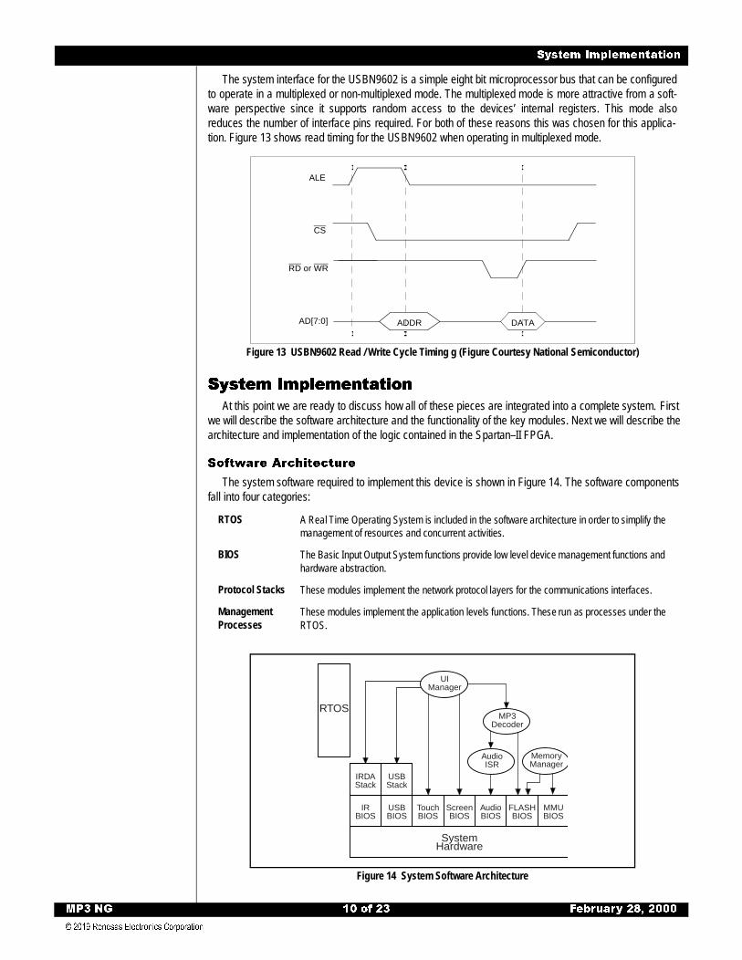
The system interface for the USBN9602 is a simple eight bit microprocessor bus that can be configuredto operate in a multiplexed or non-multiplexed mode. The multiplexed mode is more attractive from a soft-ware perspective since it supports random access to the devices’ internal registers. This mode alsoreduces the number of interface pins required. For both of these reasons this was chosen for this applica-tion. Figure 13 shows read timing for the USBN9602 when operating in multiplexed mode.
Figure 13 USBN9602 Read / Write Cycle Timing g (Figure Courtesy National Semiconductor)
� ���! �� ���! �� ���! �� ���! �!!!!���!������!������!������!�����������������������
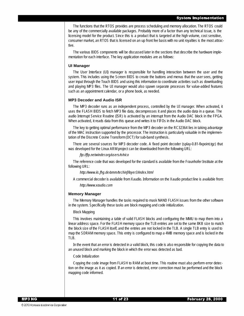
At this point we are ready to discuss how all of these pieces are integrated into a complete system. Firstwe will describe the software architecture and the functionality of the key modules. Next we will describe thearchitecture and implementation of the logic contained in the Spartan–II FPGA.
��)*��� ����"�����
The system software required to implement this device is shown in Figure 14. The software componentsfall into four categories:
Figure 14 System Software Architecture
RTOS A Real Time Operating System is included in the software architecture in order to simplify the management of resources and concurrent activities.
BIOS The Basic Input Output System functions provide low level device management functions and hardware abstraction.
Protocol Stacks These modules implement the network protocol layers for the communications interfaces.
Management Processes
These modules implement the application levels functions. These run as processes under the RTOS.
ALE
CS
AD[7:0] DATA
RD or WR
ADDR
AudioBIOS
TouchBIOS
FLASHBIOS
IRBIOS
USBBIOS
MMUBIOS
ScreenBIOS
SystemHardware
IRDAStack
USBStack
RTOS
AudioISR
MP3Decoder
MemoryManager
UIManager
10 of 23 February 28, 2000
System Implementation
MP3 NG
The functions that the RTOS provides are process scheduling and memory allocation. The RTOS couldbe any of the commercially available packages. Probably more of a factor than any technical issue, is thelicensing model for the product. Since this is a product that is targeted at the high volume, cost sensitive,consumer market, an RTOS that is licensed on an up front fee basis with no unit royalties is the most attrac-tive.
The various BIOS components will be discussed later in the sections that describe the hardware imple-mentation for each interface. The key application modules are as follows:
UI Manager
The User Interface (UI) manager is responsible for handling interaction between the user and thesystem. This includes using the Screen BIOS to create the buttons and menus that the user sees, gettinguser input through the Touch BIOS and using this information to coordinate activities such as downloadingand playing MP3 files. The UI manager would also spawn separate processes for value-added featuressuch as an appointment calendar, or a phone book, as needed.
MP3 Decoder and Audio ISR
The MP3 decoder runs as an independent process, controlled by the UI manager. When activated, ituses the FLASH BIOS to fetch MP3 file data, decompresses it and places the audio data in a queue. Theaudio Interrupt Service Routine (ISR) is activated by an interrupt from the Audio DAC block in the FPGA.When activated, it reads data from this queue and writes it to FIFOs in the Audio DAC block.
The key to getting optimal performance from the MP3 decoder on the RC32364 lies in taking advantageof the MAC instruction supported by the processor. The instruction is particularly valuable in the implemen-tation of the Discrete Cosine Transform (DCT) for sub-band synthesis.
There are several sources for MP3 decoder code. A fixed point decoder (splay-0.81-fixpoint.tgz) thatwas developed for the Linux ARM project can be downloaded from the following URL:
ftp://ftp.netwinder.org/users/n/nico
The reference code that was developed for the standard is available from the Fraunhofer Institute at thefollowing URL:
http://www.iis.fhg.de/amm/techinf/layer3/index.html
A commercial decoder is available from Xaudio. Information on the Xaudio product line is available from:
http://www.xaudio.com
Memory Manager
The Memory Manager handles the tasks required to mask NAND FLASH issues from the other softwarein the system. Specifically these tasks are block mapping and code initialization.
Block Mapping
This involves maintaining a table of valid FLASH blocks and configuring the MMU to map them into alinear address space. For the FLASH memory space the TLB entries are set to the same 8KB size to matchthe block size of the FLASH itself, and the entries are not locked in the TLB. A single TLB entry is used tomap the SDRAM memory space. This entry is configured to map a 4MB memory space and is locked in theTLB.
In the event that an error is detected in a valid block, this code is also responsible for copying the data toan unused block and marking the block in which the error was detected as bad.
Code Initialization
Copying the code image from FLASH to RAM at boot time. This routine must also perform error detec-tion on the image as it as copied. If an error is detected, error correction must be performed and the blockmapping code informed.
11 of 23 February 28, 2000

System Implementation
MP3 NG
+"�" , �-��� .�� ��/�
Figure 15 shows the architecture implemented in the Spartan device for this application. It consists ofeight major functional blocks:
◆ Inter-Module Bus (IMB) Controller◆ CPU Interface◆ LCD Controller◆ Memory Datapath◆ SDRAM Controller◆ FLASH Controller◆ CompactFlash Controller◆ IRDA Controller◆ DAC interface◆ Touch screen interface
These blocks are interconnected by a simple non-multiplexed, multi-master, address data bus that wewill refer to as the Inter-Module Bus (IMB). While the IMB may appear to be a bus to the function blocks, itis not a bus at all but instead uses multiplexers for gating data into the internal datapaths. This approacheliminates the need for tristate drivers within the design. In this implementation the bus has two masters;the CPU interface and the LCD Controller.
Figure 15 shows a top level block diagram of the FPGA.
Figure 15 FPGA Logic Block Diagram
While most of the blocks are fairly independent, the FLASH, SDRAM, and CompactFlash interfacesshare common address and data busses. While this results in a fairly complex muxing scheme for thesedatapaths it is necessary to keep the pin count within an acceptable range.
CPU Control
D_OUT[31:0]D_IN[31:0]
A_OUT[31:2]Control Out
CPU Address/Data
CPU Interface
D_OUT[31:0]D_IN[31:0]
A_IN[3:2]Control In
Tranceiver InterfaceSignals
IRDA Controller
USB Control
D_IN[31:0]A_OUT[3:2]Control Out
LCD ControlSignals
LCD Controller
D_OUT[31:0]D_IN[31:0]A_IN[3:2]Control In
DAC InterfaceSignals
DAC Interface
D_OUT[31:0]D_IN[31:0]A_IN[3:2]Control In
ADC InterfaceSignals
Touch Screen Interface
Control In SDRAM ControlSignals
SDRAM Controller
Control In FLASH ControlSignals
FLASH Controller
Control InCompactFlash
ControlSignals
CompactFlash Controller
MUX
D_OUT[31:0]D_IN[31:0]A_IN[3:2]Control In
Memory Data
Memory Interface
Memory Address
MUX
MUX
12 of 23 February 28, 2000

System Implementation
MP3 NG
The following sections will discuss the implementation of each of these functional blocks and outline thehardware and software resources needed to support each.
� ��.��$��� &�� 0��&1 �� ������
The IMB Controller block performs two functions: block address decoding, and IMB arbitration.
The address decode block generates device selects for the IP block that is the target of the transfer. Italso controls the multiplexers that select the response signals from the target of the transfer (ACK, DOUTetc.).
IMB arbitration between access requests from the CPU Interface and the LCD controller are handled byusing a simple rotating priority scheme. The arbiter block also controls the multiplexers that select which setof transfer control signals (RD, WR etc.) control the transfer.
The FPGA device resources used to implement this block include an estimated 32 CLBs but no I/Opads. There is no software required to support this block.
��% � ��)���
The CPU interface block performs three functions: protocol conversion, CPU initialization and addressde-multiplexing. Figure 16 shows a block diagram of this block.
Figure 16 CPU Interface Block Diagram
The CPU initialization block generates the required timing for the reset signals, and drives configurationinformation onto bus grant and the interrupts. This configuration information configures the boot PROMwidth and enables the CPU timer. After initialization is complete the block drives the IRDA and audio DACinterrupts out onto the CPU interrupt signals.
The bus state machine converts the signaling on the CPU bus into the format used on the local IMB, orif the transaction is to the USB interface, the signaling accepted by the USBN9602.
The FPGA device resources used to implement this block include an estimated 46 CLBs and the fifty-four I/O pads listed in Table 1.
Latch28
Enable
28D Q AOUT[31:4]
GNT_IN
RD_OUT_NWR_OUT_N[3:0]ACK_INREQ_OUT
Bus StateMachine
CPU_CIP_NCPU_BE_N[3:0]
CPU_ACK_N
CPU_RD_N
CPU_AD[31:0]
CPU_ADDR[3:2]2
AOUT[3:2]
DIN[31:0]
DOUT[31:0]
CPU_ALE
IR_INT_N
CPUInitialization
SYS_CLK
CPU_COLDRESET_NCPU_RESET_N
CPU_BUSGNT_NCPU_INT_N[3:0]
DAC_INT_N
SYS_CLK
CPU_WR_N
CPU_MASTERCLK
USB_CS_NUSB_RD_NUSB_WR_N
13 of 23 February 28, 2000

System Implementation
MP3 NG
There is no software support required for this block per se, but the USB interface itself requires consid-erable software for operation. This software consists of the USB protocol stack, which includes a USB inter-rupt service routine. The USB stack itself consists of two parts. The first of these is the software required forparticipating in the USB protocol and the plug and play. The second part is the application specific coderequired to transfers MP3 files from the host system to the player.
�� �� ������
The LCD controller is responsible for refreshing the screen with an image stored in the SDRAM. Ingeneral its operation is similar to that of a CRT display controller. Unlike most display controllers, the displayformat generated by the LCD controllers is not programmable by the CPU. The raster format is fixed at 128by 128 pixels and the display timing is fixed as well. This makes sense in an embedded system such as thiswhere the display is integrated into the unit. Although the display format cannot be changed in the system,loading different FPGA configurations into the FLASH when the unit is manufactured can accommodatedifferent displays. Figure 17 shows the block diagram of the LCD Controller.
Signal Type Description
CPU_MASTERCLK Output All bus timing is relative to this clock. The CPU core frequency is derived by multiplying this clock.
CPU_AD[31:0] I/O High-order multiplexed address and data bits.
CPU_ADDR[3:2] Input Non-multiplexed address lines. These serve as the word within block address for cache refills (Addr(3:2)).
CPU_BE_N[3:0] Input Indicates which byte lanes are expected to participate in the transfer.
CPU_ALE Input Address latch enable.
CPU_CIP_N Input Denotes that a cycle is in progress. Asserted in the address phase and is asserted until the ACK* for the last data is sampled.
CPU_RD_N Input This active-low signal indicates that the current transaction is a read.
CPU_WR_N Input This active-low signal indicates that the current cycle transaction is a write.
CPU_BUSGNT_N Output During the power-on reset (Cold Reset), BusGnt* is an input, and is used to load ModeBit(5).
CPU_ACK_N Output On read transactions, this signal indicates to the RC32364 that the memory system has placed valid data on the A/D bus, and that the processor may move the data into the on-chip Read Buffer. On a write transaction, this indicates to the RC32364 that the memory system has accepted the data on the A/D bus.
CPU_RESET_N Output This active-low signal is used for both power-on and warm reset.
CPU_COLDRESET_N Output This active-low signal is used for power-on reset.
CPU_INT_N[3:0] Output Active low interrupt signals to the CPU. During power-on, Int*(3:0) serves as ModeBit(9:6).
US_CS_N Output USB controller chip select
US_RD_N Output USB controller read strobe
US_WR_N Output USB controller write strobe
Table 1 CPU Interface Signal Summary
14 of 23 February 28, 2000

System Implementation
MP3 NG
Figure 17 LCD Controller Block Diagram
The LCD controller is an Inter-Module Bus (IMB) master and fetches data for screen refresh indepen-dently of CPU activities. The display data that is fetched is loaded into a FIFO using a block transfer acrossthe IMB. The shift register loads display data from the FIFO and shifts it out as a four-bit wide data streamat 16 MHz the maximum shift rate supported by the display drivers.
In order to prevent disruption of the display image, the FIFO must have a new data word available forthe shift register every time it empties. This occurs every 500 nS (1 / (16 mHz / 8)). Since there is a signifi-cant amount of overhead associated with each non-sequential access to the SDRAM memory, fetches aremade from it using multi word bursts. The size of these bursts is a compromise between different factors.Longer bursts are more efficient since the SDRAM access overhead is amortized over a larger number ofdata words. Smaller bursts reduce the size of the FIFO and also reduce bus latency by reducing the timethat the LCD controller ties up the Inter-Module Bus (IMB). For this application a two-word burst waschosen. The result is a three word deep FIFO and display buffer fetches every 1 microsecond.
The FPGA device resources used to implement this block include an estimated TBD CLBs and the nineI/O pads listed in Table 2.
The only software support required for this block is the screen BIOS which consists of functions togenerate screen images by manipulating the frame buffer memory. This buffer appears as an array of 512,32-bit words with each word containing 32 pixels of the screen image. The most significant bit of the word at
Signal Type Description
DI_XD[3:0] Output X driver data
DI_XSCL Output X driver data shift clock
DI_LP Output Latch pulse
DI_FR Output Frame signal
DI_YD Output Y driver scan start pulse
DI_YSCL Output Y driver shift clock
Table 2 LCD Controller Interface Signal Summary
DIN[31:0]32
FIFOShift
Register
RdWr
32D Q
LoadEnable
4D Q DI_D[3:0]
DI_XSCLDI_LPDI_FRDI_YDDI_YSCL
StateMachine
9
LoadEnable
9DQ
SYS_CLK
BREQ_NBGNT_N
ACK_NRD_N
AddressCounter
AOUT[11:2]
BaseAddress
9
21AOUT[31:11]
15 of 23 February 28, 2000

System Implementation
MP3 NG
the base address appears as the pixel in the upper left-hand corner of the screen. The least significant bit of
that memory word appears as the 32nd pixel in the first row. The word and bit address of any pixel on thescreen can be calculated using the following formula:
������ � ��)���
The memory interface block implements the data path required to map the eight and sixteen bit memorydevices to the 32-bit Inter-Module Bus. While the RC32364 is capable of fetching instructions and data fromdevices with varying bus widths, having the FPGA build 32-bit words for the CPU reduces the number ofbus cycles. This increases performance and also reduces power consumption. Figure 16 shows a blockdiagram of this block.
Figure 18 Memory Interface Block Diagram
����� �� ������
The SDRAM controller design is based on the design developed by Xilinx in application note XAPP 134.The changes made in the original design are to adapt to the differences in the host interface. In the originaldesign the host interface is a multiplexed address data bus. In this application, the Inter-Module Bus (IMB)is non-multiplexed. Another difference is that the original design supported a 32-bit wide memory configura-tion with two MT48LC1M16 memory devices. In the design a 16-bit wide memory datapath and a singleMT48LC1M16 is used.
Memory Address = X * Y MOD 32
Bit Address = X * Y REM 32
Where: X and Y are the horizontal and vertical coordinates of the screen and assume that the origin (X = 0, Y = 0) is in the upper left-hand corner of the screen.
MOD the integer division.
REM is the remainder of the division
MUX
MUX
D_IN[7:0]
D_IN[15:8]
D_IN[23:16]
D_IN[31:24]
MEM_DOUT[15:8]
MEM_DOUT[7:0]
MEM_D[15:0]
Register
Q D MUXD_OUT[31:24]
Register
Q DD_OUT[23:16]
Register
Q DMUX
D_OUT[15:8]
D_OUT[7:0]
MEM_DIN[15:8]
MEM_DIN[7:0]
MUX MEM_ADDR[10:0]A_IN[8:1]
A_IN[19:9]
A_IN[10:0]
16 of 23 February 28, 2000
System Implementation
MP3 NG
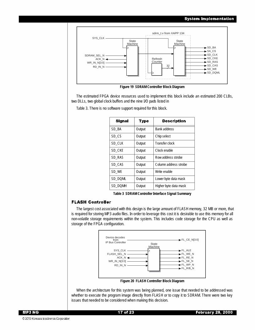
Figure 19 SDRAM Controller Block Diagram
The estimated FPGA device resources used to implement this block include an estimated 200 CLBs,two DLLs, two global clock buffers and the nine I/O pads listed in
Table 3. There is no software support required for this block.
� ��! �� ������
The largest cost associated with this design is the large amount of FLASH memory, 32 MB or more, thatis required for storing MP3 audio files. In order to leverage this cost it is desirable to use this memory for allnon-volatile storage requirements within the system. This includes code storage for the CPU as well asstorage of the FPGA configuration.
Figure 20 FLASH Controller Block Diagram
When the architecture for this system was being planned, one issue that needed to be addressed waswhether to execute the program image directly from FLASH or to copy it to SDRAM. There were two keyissues that needed to be considered when making this decision.
Signal Type Description
SD_BA Output Bank address
SD_CS Output Chip select
SD_CLK Output Transfer clock
SD_CKE Output Clock enable
SD_RAS Output Row address strobe
SD_CAS Output Column address strobe
SD_WE Output Write enable
SD_DQML Output Lower byte data mask
SD_DQMH Output Higher byte data mask
Table 3 SDRAM Controller Interface Signal Summary
32
SD_BASA_CSSD_CLKSD_CKESD_RAS
StateMachine
SYS_CLK
SD_CASSD_WESD_DQML
SDRAM_SEL_N
WR_IN_N[3:0]ACK_N Refresh
Counter
StateMachine
sdrm_t.v from XAPP 134
RD_IN_N
FL_ALEFL_WE_NFL_RE_NFL_SE_NFL_WP_N
StateMachine
SYS_CLK
FL_R/B_N
FLASH_SEL_N
WR_IN_N[3:0]ACK_N
RD_IN_N
FL_CE_N[3:0]Device decodes
fromIP Bus Controller
17 of 23 February 28, 2000

System Implementation
MP3 NG
Performance
The narrow, eight bit, interface used for both address and data is one performance issue, but it is not thebiggest. The real problem is random access latency. Within a 512 byte memory page, data can be read witha 50 nS read cycle time. The problem comes when the processor accesses data in a different page. Thetime required to load a page into the page register, where it can be accessed, is 7 uS. With a 66 MHzprocessor frequency this represents 462 instruction times. This latency will adversely effect real-time perfor-mance.
Error Handling
Each 512 byte page in the FLASH has 16 bytes of spare storage for storing ECC information. Theproblem is that this is nowhere near enough storage for implementing ECC for small block sizes. Forexample, to correct single bit errors on a RC32364 cache line (16 bytes) using a Hamming code thefollowing relationship must be satisfied:
Since there are 32 (512 / 16) cache lines per page, a total of 36 bytes are needed for ECC storage.Recall that 16 bytes are available.
In order to get around this problem, the block size could be increased to 32 bytes. At 32 bytes, 10 bits ofECC are required per block, but there are now only 16 blocks per page which is consistent with the avail-able ECC memory per page. Performing the block check over two cache lines could accommodate thislarger block size. The down side to this is that every time a cache line is loaded, two would have to bechecked with a corresponding increase in memory latency.
As a result of this the decision was made to copy the executable image to the SDRAM memory at boottime. This not only increases performance but also turns the ECC checking issue into a non real-time soft-ware exercise.
The estimated FPGA device resources used to implement this block include an estimated 100 CLBs,and the ten I/O pads listed in Table 4.
Software support required for this block consists of the FLASH BIOS which implements low level primi-tives for programming, erasing, and checking validity of memory blocks.
N <= 2**K - K – 1
where: N is the number of data bits in the block
K is the number of ECC bits
Solving for K:
16 * 8 = 256 <= 2K - K - 1
K = 9 ECC bits per cache line
Signal Type Description
FL_CE_N[3:0] Output Device chip enables, active low.
FL_ALE Output Address latch enable
FL_WE_N Output Write enable, write data is latched on the rising edge
FL_RE_N Output Read enable, when low enables device data output buffers
FL_SE_N Output Enable spare area when low
FL_WP_N Output Write protect, active low
FL_R/B_N Input Open drain output from devices, pulled low when a program, erase, or read operation is in progress
Table 4 FLASH Controller Interface Signal Summary
18 of 23 February 28, 2000

System Implementation
MP3 NG
���� �� ������
The IRDA controller is essentially a specialized, fixed function UART. The separate, two word, transmitand receive FIFOs reduce the interrupt overhead associated with data transmission. At the maximum datarate that the IR transceiver can support (115 kb/s) the CPU will get an interrupt every 557 mS.
Figure 21 IRDA Controller Block Diagram
��$"� ��� � ��)���
The interface for the CS4343 consists of two separate functional blocks, one for each of the serial inter-faces that are required to support this device.
Figure 22 shows a block diagram of this interface.
Signal Type Description
IR_TXD Output Transmit data
IR_RXD Input Receive data
IR_SD Output Shut down signal, puts transceiver into low power mode
Table 5 FLASH Controller Interface Signal Summary
D_IN[31:0]
32FIFO
ShiftRegister
32Q D Q D
Bus StateMachine
SYS_CLKINT_N
RD_IN_N
ACK_NWR_IN_N[3:0]
32
FIFOShift
Register32
D Q D QMUX IR_TXD
D_IN[31:0]
Tx StateMachine
IR_RXD
Rx StateMachine
19 of 23 February 28, 2000
System Implementation
MP3 NG
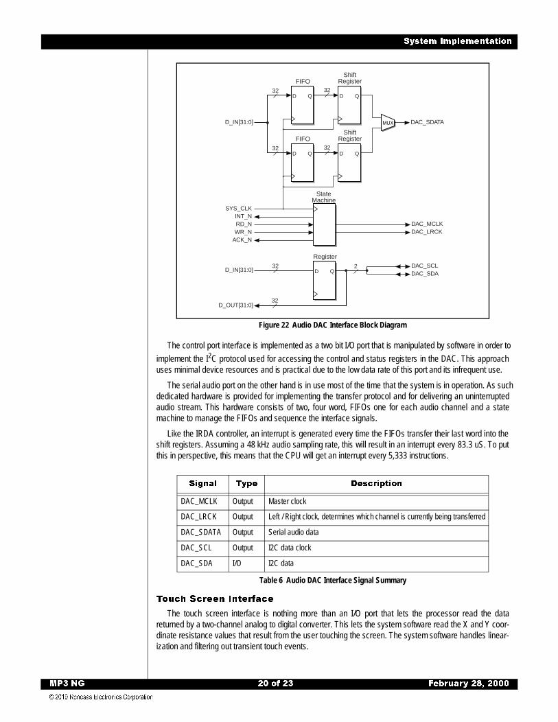
Figure 22 Audio DAC Interface Block Diagram
The control port interface is implemented as a two bit I/O port that is manipulated by software in order to
implement the I2C protocol used for accessing the control and status registers in the DAC. This approachuses minimal device resources and is practical due to the low data rate of this port and its infrequent use.
The serial audio port on the other hand is in use most of the time that the system is in operation. As suchdedicated hardware is provided for implementing the transfer protocol and for delivering an uninterruptedaudio stream. This hardware consists of two, four word, FIFOs one for each audio channel and a statemachine to manage the FIFOs and sequence the interface signals.
Like the IRDA controller, an interrupt is generated every time the FIFOs transfer their last word into theshift registers. Assuming a 48 kHz audio sampling rate, this will result in an interrupt every 83.3 uS. To putthis in perspective, this means that the CPU will get an interrupt every 5,333 instructions.
���� ����� � ��)���
The touch screen interface is nothing more than an I/O port that lets the processor read the datareturned by a two-channel analog to digital converter. This lets the system software read the X and Y coor-dinate resistance values that result from the user touching the screen. The system software handles linear-ization and filtering out transient touch events.
Signal Type Description
DAC_MCLK Output Master clock
DAC_LRCK Output Left / Right clock, determines which channel is currently being transferred
DAC_SDATA Output Serial audio data
DAC_SCL Output I2C data clock
DAC_SDA I/O I2C data
Table 6 Audio DAC Interface Signal Summary
D_IN[31:0]
32
FIFOShift
Register32
D Q D Q
DAC_MCLKDAC_LRCK
StateMachine
SYS_CLKINT_NRD_N
ACK_NWR_N
32
FIFOShift
Register32
D Q D Q
MUX DAC_SDATA
Register
D QD_IN[31:0]32 2 DAC_SCL
DAC_SDA
D_OUT[31:0]32
20 of 23 February 28, 2000

Spartan Device Selection
MP3 NG
Figure 23 Touch Interface Block Diagram
������������������� "��� "��� "��� "�������� �������� �������� �������� ������������������������
Spartan devices are available in a range of densities and packages. The following criteria were used toselect the device used in this application:
Based on these criteria the device selected for this design is the XC2S50. This device offers 50Kdensity, 3.3V operation, 176 user I/O, and is packaged in a space saving FG256 BGA package.
Signal Type Description
AD_SCK Output Serial data clock
AD_SDI Input Serial data in
AD_SDO Output Serial data out
Table 7 Touch Screen Interface Signal Summary
I/O Pins The design requires a total of 137 I/O pins. I/O pin requirements per block are summarized in Table 8.
Voltage The design operates at 3.3V.
Density The estimated size of the design is 83K gates, with the usage broken out in Table 8.
Performance The highest clock speed used in the device is 64 MHz, used to clock the SDRAM controller state machines. The remaining logic runs at sub multiples of this clock rate.
Packaging The size constraints imposed on most modem designs dictates a high-density surface mount package.
Interface CLB Usage Number of Signals
CPU 25 51
LCD display 58 9
IRDA 59 3
USB 21 3
DAC 23 5
ADC 0 3
SDRAM 100 9
FLASH 100 10
CompactFlash 100 17
Memory address bus 4 11
Memory data bus 10 16
Total: 500 137
Table 8 FPGA Resource Usage Summary
Register
D QD_IN[31:0]32 3
AD_SCK
AD_SDO
D_OUT[31:0]32
AD_SDI
21 of 23 February 28, 2000

Conclusion
MP3 NG
#��#��#��#��������������������������
The design that has been outlined meets both original design objectives. Even with budgetary pricingthe cost of the solution is well below $100. Table 9 shows the cost breakdown of the system. The designalso has enough spare resources both in terms of CPU cycles and FPGA gates to support field upgrades.Operating at a core clock speed of 64 MHz, the RC32364 will provide enough performance for both audiodecoding and user interface functions. By locking the audio decode functions in the instruction cache asignificant increase in system performance as well as reduced power consumption is achieved.
This design also illustrates how manufacturers can create designs that the optimized integration of anASIC while supporting the manufacturing and field upgrade flexibility of an FPGA.
$$$$����%%%%����������������������������
RC32364 RISController, Hardware User’s Manual, April 1999, Integrated Device Technology
Xilinx Spartan II FPGA Data Sheet, January 2000, Xilinx
IRMS6100 1.15 Mb/s IrDT Data Transceiver Data Sheet, May 1999, Infineon Technologies
SED1743 160-bit LCD Common Driver Data Sheet, Epson Electronics
SED1758 160-bit LCD Segment Driver Data Sheet, Epson Electronics
CS4343 Low Voltage, Stereo DAC with Headphone Amp Data Sheet, June 1999, Cirrus Logic
MAX1108 2-Channel, Serial 8-Bit ADC, Data Sheet, October 1998, Maxim Integrated Products
Item
Qty.
Mfg. Part Number Description VolumeUnit
Cost
Ext.
Cost
1 4 Samsung KM29U6400T Flash, 64Mb 1M/Yr. $10.00 $40.00
2 1 Micron Mt48C1LC1M16A1TG7SIT SDRAM,512K x 16 x 2 banks
200K/m $3.50 $3.50
3 1 IDT 79RC32V364-133 RISC CPU 100K $11.50 $11.50
4 1 Xilinx XC2S100 FPGA 20K/m $10.00 $10.00
5 1 Xilinx XC1801 Serial Configuration PROM
20K/m $3.00 $3.00
6 1 NSC USB9602 USB Interface Controller 20K/m $1.63 $1.63
7 1 SMOS SED1758T0A LCD Common Driver, 160 Rows
20K/m $2.50 $2.50
8 1 SMOS SED1743T0A LCD Segment Driver, 160 Rows
20K/m $2.50 $2.50
9 1 Various TBD 160 x 160 LCD Panel, Glass Only
est. $5.00 $5.00
10 1 MicroTouch TBD Touch Screen est. $5.00 $5.00
11 1 Infineon IRDT6100 1Mb IRDA Transceiver 20K/m $2.00 $2.00
12 1 Crystal CS4343 DAC Stereo Audio est. $2.00 $2.00
13 1 Maxim MAX1108 AD Converter disti $2.68 $2.68
14 1 Maxim MAX1705 Step-up DC to DC Converter
10K $2.81 $2.81
Note: BOM includes only semiconductor content. Total: $94.12
Table 9 NG Player Semiconductor BOM
22 of 23 February 28, 2000

References
MP3 NG
USBN9602 Full Speed Function Controller With DMA Support Data Sheet, May 1998, National Semi-conductor
MT48LC1M16A1 S - 512K x 16 x 2 banks Synchronous DRAM Data Sheet, August 1999, Micron Tech-nologies
KM29U64000T 8M x 8 Bit NAND Flash Memory, April 1999, Samsung Semiconductor
23 of 23 February 28, 2000

Corporate HeadquartersTOYOSU FORESIA, 3-2-24 Toyosu,Koto-ku, Tokyo 135-0061, Japanwww.renesas.com
Contact InformationFor further information on a product, technology, the most up-to-date version of a document, or your nearest sales office, please visit:www.renesas.com/contact/
TrademarksRenesas and the Renesas logo are trademarks of Renesas Electronics Corporation. All trademarks and registered trademarks are the property of their respective owners.
IMPORTANT NOTICE AND DISCLAIMER
RENESAS ELECTRONICS CORPORATION AND ITS SUBSIDIARIES (“RENESAS”) PROVIDES TECHNICAL SPECIFICATIONS AND RELIABILITY DATA (INCLUDING DATASHEETS), DESIGN RESOURCES (INCLUDING REFERENCE DESIGNS), APPLICATION OR OTHER DESIGN ADVICE, WEB TOOLS, SAFETY INFORMATION, AND OTHER RESOURCES “AS IS” AND WITH ALL FAULTS, AND DISCLAIMS ALL WARRANTIES, EXPRESS OR IMPLIED, INCLUDING, WITHOUT LIMITATION, ANY IMPLIED WARRANTIES OF MERCHANTABILITY, FITNESS FOR A PARTICULAR PURPOSE, OR NON-INFRINGEMENT OF THIRD PARTY INTELLECTUAL PROPERTY RIGHTS.
These resources are intended for developers skilled in the art designing with Renesas products. You are solely responsible for (1) selecting the appropriate products for your application, (2) designing, validating, and testing your application, and (3) ensuring your application meets applicable standards, and any other safety, security, or other requirements. These resources are subject to change without notice. Renesas grants you permission to use these resources only for development of an application that uses Renesas products. Other reproduction or use of these resources is strictly prohibited. No license is granted to any other Renesas intellectual property or to any third party intellectual property. Renesas disclaims responsibility for, and you will fully indemnify Renesas and its representatives against, any claims, damages, costs, losses, or liabilities arising out of your use of these resources. Renesas' products are provided only subject to Renesas' Terms and Conditions of Sale or other applicable terms agreed to in writing. No use of any Renesas resources expands or otherwise alters any applicable warranties or warranty disclaimers for these products.
(Rev.1.0 Mar 2020)
© 2020 Renesas Electronics Corporation. All rights reserved.